Contentshft.uni-duisburg-essen.de/lehre/kdk/protected_kdk/versuch2.pdf · Komponenten - Praktikum...
27
Fakultat fur Ingenieurwissenschaften Universitat Duisburg-Essen H F T Fachgebiet Hochfrequenztechnik Prof. Dr.-Ing. K. Solbach .. .. .. Abteilung Elektrotechnik und Informationstechnik Komponenten f¨ ur die drahtlose Kommunikation Experiment No. 2 Version: April 19, 2012 Noise Characterization of Two-Port Networks Last name: First name: Matr.-No.: Tutor: Date: Contents 1 Literature 2 2 Introduction 2 3 Theoretical Background 2 3.1 Noise Sources ................................. 2 3.2 Measurement of Noise Temperature T e (Y-Factor Method) ........ 6 3.3 Noise Figure F and Signal-to-Noise Ratio S/N ............... 8 3.4 Noise Figure F cas of Cascaded Networks .................. 10 4 Homework 12 5 Description of Instruments 13 5.1 The Spectrum Analyzer FSL ......................... 13 5.2 Noise Source .................................. 14 6 Performing the Experiments 15 6.1 Measurement of Noise Temperature T e and Noise Figure F ........ 15 6.1.1 Using the Y-Factor Method ..................... 15 6.1.2 Using the Noise & Gain Measurement Option of the Spectrum Analyzer FSL ....................... 19 6.2 Cascaded Circuits ............................... 22 6.3 Signal-to-Noise Ratio S/N .......................... 24 7 Formulary 27 1
Transcript of Contentshft.uni-duisburg-essen.de/lehre/kdk/protected_kdk/versuch2.pdf · Komponenten - Praktikum...

Fakultat fur Ingenieurwissenschaften Universitat Duisburg−Essen
H F T
FachgebietHochfrequenztechnikProf. Dr.−Ing. K. Solbach
.. ....
Abteilung Elektrotechnik undInformationstechnik
Komponenten fur die drahtlose Kommunikation
Experiment No. 2 Version: April 19, 2012
Noise Characterization of Two-Port Networks
Last name: First name: Matr.-No.:
Tutor: Date:
Contents
1 Literature 2
2 Introduction 2
3 Theoretical Background 23.1 Noise Sources . . . . . . . . . . . . . . . . . . . . . . . . . . . . . . . . . 23.2 Measurement of Noise Temperature Te (Y-Factor Method) . . . . . . . . 63.3 Noise Figure F and Signal-to-Noise Ratio S/N . . . . . . . . . . . . . . . 83.4 Noise Figure Fcas of Cascaded Networks . . . . . . . . . . . . . . . . . . 10
4 Homework 12
5 Description of Instruments 135.1 The Spectrum Analyzer FSL . . . . . . . . . . . . . . . . . . . . . . . . . 135.2 Noise Source . . . . . . . . . . . . . . . . . . . . . . . . . . . . . . . . . . 14
6 Performing the Experiments 156.1 Measurement of Noise Temperature Te and Noise Figure F . . . . . . . . 15
6.1.1 Using the Y-Factor Method . . . . . . . . . . . . . . . . . . . . . 156.1.2 Using the Noise & Gain Measurement Option of the
Spectrum Analyzer FSL . . . . . . . . . . . . . . . . . . . . . . . 196.2 Cascaded Circuits . . . . . . . . . . . . . . . . . . . . . . . . . . . . . . . 226.3 Signal-to-Noise Ratio S/N . . . . . . . . . . . . . . . . . . . . . . . . . . 24
7 Formulary 27
1
Komponenten - Praktikum Noise Characterization of Two-Port Networks
1 Literature
a) K. Solbach: Microwave Theory and Techniques,Lecture notes available from department HFT
b) D. Pozar: Microwave EngineeringNew York: John Wiley & Sons, 2005, chapter 10
c) K. Solbach: Hochfrequenz-Elektronik,Lecture notes available from department HFT
d) Hewlett Packard: Application Note AN 57-1,“Fundamentals of RF and Microwave Noise Figure Measurement”http://cp.literature.agilent.com/litweb/pdf/5952-8255E.pdf
2 Introduction
Signals in RF systems are generally accompanied by unwanted variations of non-regular,random nature. At low frequencies. e.g. in audio amplifiers we can hear this variationas ”noise ”. Noise signals can completely cover the wanted signals, if the wanted signalpower level is below the noise power level. In order to find the lowest useful signal levelthat stands out against the noise level, we have to measure RF system noise levels anddiscriminate noise that is introduced together with the wanted signal against added noisethat is produced inside our RF system.
3 Theoretical Background
3.1 Noise Sources
The most significant noise source in electrical networks is the thermal vibration of elec-trons in conductors, Thermal Noise, which produces a random voltage un (effectivevalue, RMS) across the terminals of a resistor at ambient temperature T (Fig. 1)
un =√
4kTBR (1)
where
k = 1.38 · 10−23 J/K (Boltzmann’s Constant)T = temperature in degrees Kelvin (K)B = bandwidth of the system in HzR = resistance in Ω
1J = 1Ws = 30dBm/Hz0dBm = 1mW
Eq.(1) is approximately
valid for RF-frequencies and does not exhibit any variation with center frequency of thesystem bandwidth, a characteristic that is termed ”white ” in reference to the constantspectral density of ”white ” light.
2

Komponenten - Praktikum Noise Characterization of Two-Port Networks
u( )t
u( )t
Fig. 1: A Random Voltage Generated by a Noisy Resistor.
The noise resistor can be assumed to be a generator of noise signal, e.g. replaced by aThevenin equivalent circuit consisting of a voltage generator with voltage given by eq. (1)and a noiseless resistor in series. Connecting a load resistor R results in maximum powertransfer from the noise resistor, so that the ”available power ” is:
Pn =( un
2R
)2 ·R =u2n
4R= kTB
=− 174dBm + 10dB · log( B
Hz
)+ 10dB · log
( T
290K
)with 10dB · log(kT0) = −174dBm/Hz and T0 = 290K
(2)
In general, any RF system can be described as a load resistor connected to a thermalnoise source, but the frequency spectrum that enters the RF system and is processedby the RF system can be described by a filter function, which limits the systembandwidth B (Fig. 2).
There are also other sources of noise in electrical circuits, e.g. Shot Noise due
un
Fig. 2: Equivalent Circuit of a Noisy Resistor Delivering Maximum Power toa Load Resistor Through an Ideal Bandpass Filter.
to random fluctuations of charge carriers in an electron tube or solid-state device orFlicker Noise due to carrier transport effects in surface areas of solid-state componentsand vacuum tubes, etc.
3

Komponenten - Praktikum Noise Characterization of Two-Port Networks
As long as the power spectrum from such noise sources can be described as ”white ”, wemay model the noise source as equivalent thermal noise source and characterize it withan equivalent noise temperature Te based on Fig. 3.
Nout N
out
kB
NT
out
e=
Te
Fig. 3: The Equivalent Noise Temperature Te of an Arbitrary White NoiseSource.
An arbitrary (white) noise source of impedance R delivers a noise power of Nout to a loadresistor R. This noise source can be replaced by a thermal noise resistor of value R, at(equivalent) temperature Te, which is selected such, that the same noise power is deliveredto the load. That is
Te =Nout
kB. (3)
For a certain bandwidth B of the component or system to be characterized, we give itan equivalent noise temperature Te.
Nin=0 N
out
N kT Bin e= N GkT B
out e=
Te
TS
Fig. 4: Defining the Equivalent Noise Temperature Te of a Noisy Amplifier.(a) Noisy Amplifier, (b) Noiseless Amplifier.
For example, we consider a noisy amplifier of bandwidth B and gain G, as given inFig. 4a. Assume that the input is matched to a source resistor and the output is matched
4

Komponenten - Praktikum Noise Characterization of Two-Port Networks
to a noiseless load resistor. If the source resistor is at Ts = 0 K, then the input noisepower to the amplifier will be Nin = 0W and the output noise power Nout will be dueonly to the noise generated by the amplifier itself.
On the other hand, Fig. 4b, we can obtain the same load noise power Nout by driv-ing an ideal noiseless amplifier with a resistor at temperature so that in both cases wehave Nout = GkTeB output power. Thus, Te is the equivalent noise temperature of theamplifier!
Te =Nout
GkB, (4)
For test purposes, we require calibrated noise sources. The most straightforward way isto heat a resistor to a higher temperature than ambient (without melting the device,e.g. 200C) or to cool a resistor to low temperature, e.g. by using liquid nitrogen at77 K. Equipment for such devices need good heat insulation and precise temperaturecontrol and tends to be very bulky. Better suited to the use in electronic laboratoryenvironments are active noise sources, e.g. semiconductor avalanche diodes,which produce much higher noise power than heated resistors and which can be handledwithout temperature control.
Active noise generators can be characterized by an equivalent noise temperature Te, buta more common measure is the Excess Noise Ratio (ENR), due to:
ENR(dB) = 10dB · log(N1 −N2
N2
) = 10dB · log(T1 − T2
T2
) (5)
where N1 and T1 are noise power and equivalent temperature of the generators internalresistance when switched ”On ”, or ”hot ”, while N2 and T2 are noise power and tempera-ture of the generator at room temperature when switched ”Off ”, or ”cold ”; as a standardroom temperatur T2 we assume T0 =290K and standard noise power N2 as N0 = kT0B.Practical ENR numbers are found between 20dB and 40dB!
5
Komponenten - Praktikum Noise Characterization of Two-Port Networks
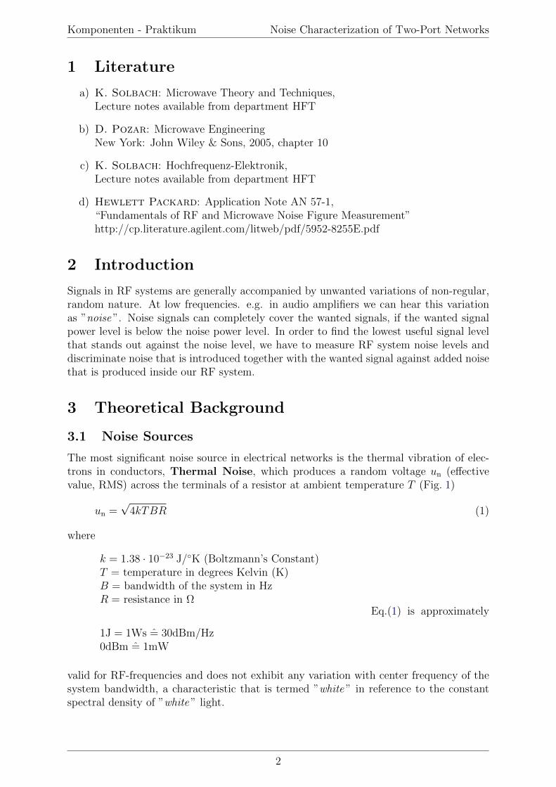
3.2 Measurement of Noise Temperature Te (Y-Factor Method)
As discussed above, the equivalent noise temperature Te of a component can be deter-mined from the output noise power Nout that is produced by the component when amatched load at T = 0 K is connected to the input. Since such a load is difficult torealize, we use two loads of precisely defined but different temperatures T1 and T2.
Nout 1
Nout 2
Fig. 5: The Y-Factor Method for Measuring the Equivalent Noise Tempera-ture Te of an Amplifier.
In Fig. 5, the device under test (amplifier or other component) is seen to be connected toone of the two matched loads at different temperatures and the output power is measuredfor each case:
T1 is temperature of the ”hot ” load.T2 is temperature of the ”cold ” load, with T1 > T2.Nout1 is output noise power with ”hot ” load.Nout2 is output noise power with ”cold ” load.
The output power Nout is the sum of noise power generated by the device under test plusthe amplified thermal noise power from the source resistor. Thus, we have
Nout1 = GkT1B + GkTeB (6)
Nout2 = GkT2B + GkTeB (7)
which are two equations for the two unknowns Te and G · B. When we measure theoutput power, we can calculate the Y-factor:
Y =Nout1
Nout2
=T1 + Te
T2 + Te
> 1. (8)
Using Y, we can solve eq.(6) and eq.(7) for the equivalent noise temperature
Te =T1 − Y T2
Y − 1(9)
in terms of the load resistor temperatures T1, T2 and the Y-factor.
As can be recognized from the formula, we should use as high temperature differenceT1 − T2 as possible in order to achieve highest accuracy of the evaluation. Usingactive noise sources will satisfy this requirement, since we have high equivalent noisetemperature T1 for the ”On ”-state, while in the ”Off ”-state the active noise source can
6

Komponenten - Praktikum Noise Characterization of Two-Port Networks
be modeled as a resistor at ambient temperature T2 = T0 = 290K.
We can identify the temperature ratio of the active noise generator by solving eq.(5)
T1
T2
= 10(ENR10dB
) + 1 (10)
so that
T1 = T0 · (10(ENR10dB
) + 1) with T0 = 290K . (11)
E.g. for ENR = 40 dB,
we haveT1
T0
= 104 + 1 ≈ 104 and T1 ≈ 2.9 · 106K.
This very high ”on ”-state temperature gives room for an attenuator between the gen-erator and the device under test in order to improve the matching of the generatorimpedance. The ENR dB-value is simply reduced by the attenuation a (dB) as
ENR(dB)reduced = ENR(dB)− a(dB), if ENR(dB) a(dB). (12)
Eq.6 and eq.7 can also be solved graphically as shown in Fig. 6. We plot the measuredoutput power Nout as a function of input load temperature T and connect the two pointsby a line.
When we determine the power for T = 0K from the intersection of the line with the
T0
0
2T 1T
BGkTe
Nout1
Nout2
N Tout( )
Fig. 6: Output Noise Power Nout of Device Versus Temperature T of InputLoad Resistor.
ordinate axis, we have found N(T = 0 K) = GkTeB. If we determine the slope s of theline (the derivative of N(T ) with respect to T ), we have found
s =Nout1 −Nout2
T1 − T2
= GkB, (13)
so that
Te =Nout(T = 0 K)
sand G =
s
kB. (14)
7

Komponenten - Praktikum Noise Characterization of Two-Port Networks
3.3 Noise Figure F and Signal-to-Noise Ratio S/N
Another way of looking at noise characterization of networks is the degradation of signalsdue to the superposition by unwanted noise signals. The Signal-to-Noise ratio S/N isthe ratio of desired signal power S to undesired noise power N , which is dependent onsignal level.
If a signal plus noise enter a noiseless network (amplifier or passive network, etc.), boththe signal and the noise component are amplified or attenuated by the same factor G(gain), so that the signal-to-noise ratio S/N will remain unchanged.
However, if the network is noisy, the output noise power will be increased by the addednetwork noise, so that the signal-to-noise ratio S/N is reduced at the output. Thedegradation is quantified by the ratio of Sin/Nin at the input over Sout/Nout at the output,at room temperature T = T0 = 290K and is termed noise figure F :
F =Sin/Nin
Sout/Nout
∣∣∣∣Tin=T0
≥ 1 . (15)
Note: By definition, the input noise power Nin is that of a matched load atTin = T0 = 290K that is Nin = kT0B. The relation between noise figure F and andequivalent noise temperature Te is found from considering the circuit given in Fig. 7.
P S Nin in in= + P S N
out out out= +
Fig. 7: Determining the Noise Figure F of a Noisy Network.
The input port of a noisy network is fed by a generator, which produces signal power Sin
from its Thevenin signal voltage source and noise power Nin from its Thevenin resistor R,which is assumed to be at ambient temperature T0. The input noise power is Nin = kT0B,where B is the effective bandwidth of the network. The output noise power Nout is thesum of the amplified noise power (gain-factor G) and the internally generated noise,expressed by the amplified thermal noise due to the equivalent temperature Te
Nout = kGB(T0 + Te) = kGBT0 (1 +Te
T0
)︸ ︷︷ ︸F
. (16)
8
Komponenten - Praktikum Noise Characterization of Two-Port Networks
The output signal power is the amplified input signal power Sout = G · Sin. Thus, thenoise figure F is
F =
Sin
kT0BGSin
kGB(T0 + Te)
= 1 +Te
T0
≥ 1 , (17)
in decibels,
FdB = 10dB · log(1 + Te/T0) ≥ 0.
If the network were noiseless, we have Te = 0 and F = 1 or FdB = 0 dB.
Solving eq. (17) for the eqivalent temperature Te gives:
Te = (F − 1) · T0 . (18)
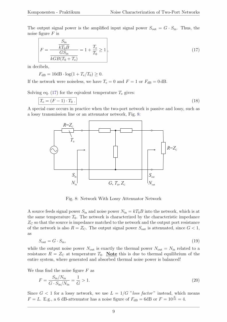
A special case occurs in practice when the two-port network is passive and lossy, such asa lossy transmission line or an attenuator network, Fig. 8:
R Z= C
Sin
Nin
Sout
NoutG T Z, ,0 C
R Z= C
T0
Fig. 8: Network With Lossy Attenuator Network
A source feeds signal power Sin and noise power Nin = kT0B into the network, which is atthe same temperature T0. The network is characterized by the characteristic impedanceZC so that the source is impedance matched to the network and the output port resistanceof the network is also R = ZC. The output signal power Sout is attenuated, since G < 1,as
Sout = G · Sin, (19)
while the output noise power Nout is exactly the thermal power Nout = Nin related to aresistance R = ZC at temperature T0. Note this is due to thermal equilibrium of theentire system, where generated and absorbed thermal noise power is balanced!
We thus find the noise figure F as
F =Sin/Nin
G · Sin/Nin
=1
G> 1. (20)
Since G < 1 for a lossy network, we use L = 1/G ”loss factor ” instead, which means
F = L. E.g., a 6 dB-attenuator has a noise figure of FdB = 6dB or F = 10610 = 4.
9

Komponenten - Praktikum Noise Characterization of Two-Port Networks
3.4 Noise Figure Fcas of Cascaded Networks
In RF- and microwave systems, signals travel through a cascade of many different stages,each of which may degrade the signal-to-noise ratio S/N . The resultant noise figure Fcas
of a cascaded system has to consider the noise figure of each of the stages, and mostlywe find that the first stage is the most critical. The analysis starts with a cascade of twocomponents, Fig. 9. The two components are characterized by gains G1 and G2, noise
Nin
Nout
Nin
Nout
Fig. 9: Noise Figure F and Equivalent Noise Temperature Te of a CascadedSystem. (a) Two Cascaded Networks, (b) Equivalent Network.
figures F1 and F2 and equivalent noise temperatures Te1 and Te2. We wish to describethe cascade by an equivalent network of overall gain G1G2 and an unknown overall noisefigure Fcas and overall equivalent temperature Tecas .
Using the noise temperature Te at the first stage output we find
N1 = G1kT0B + G1kTe1B = G1kT0B(1 +Te1
T0
) = G1kT0BF (21)
since Nin = kT0B.
The noise power at the output of the second stage is
Nout = G2N1 + G2kTe2B = G1G2kB(T0 + Te1 +1
G1
Te2) (22)
For the equivalent network we have
Nout = G1G2kB(T0 + Tecas) (23)
so that by comparison with eq.(22)
Tecas = Te1 +1
G1
Te2 (24)
10

Komponenten - Praktikum Noise Characterization of Two-Port Networks
and converting to noise figure by eq. (18)
Fcas = F1 +1
G1
(F2 − 1) . (25)
From eq.(24) and (25) we learn that the contribution by the second stage to the overallnoise temperature or noise figure is reduced by the gain G1 of the first stage.
Thus, we must try to make the first stage as low-noise as possible and ashigh gain as possible in order to achieve a good overall result of the cascade!
Generalizing the results, we find for an arbitrary number of stages:
Tecas = Te1 +Te2
G1
+Te3
G1G2
+ · · · (26)
Fcas = F1 +F2 − 1
G1
+F3 − 1
G1G2
+ · · · (27)
11

Komponenten - Praktikum Noise Characterization of Two-Port Networks
4 Homework
(In preparation for the lab!)
4.1 Calculate the effective noise voltage un across a resistor of R = 100Ω at roomtemperature T01 = 290K and at T02 = 310C and give the available noise power Pn,if the measurement bandwidth B is from frequency f = 0Hz to f = 1GHz.
4.2 Determine the noise temperature T1 of the noise source, described in section 5.2, in”hot ” state for the frequency f = 1GHz.
4.3 A noise source of ENR = 15.8dB is used in a Y-factor measurement at roomtemperatur T2 = T0. The ”hot ” noise power at the DUT output is measured asN1 = −94dBm and the ”cold ” noise power as N2 = −95.6dBm.Calculate the temperature T1 (the ”hot ” state) of the noise source, the Y-factor Y ,the equivalent temperature Te and the noise figure F of the device under test (DUT)!
4.4 A narrow-band amplifier is characterized by equivalent noise temperatureTe = 290K, gain G = 20dB and bandwidth B = 1MHz. The signal is providedby an antenna that picks up a signal power Sin and a noise power Nin = kB · 100K.
Calculate
(a) the noise figure F of the amplifier,
(b) the noise power Nout at the output and
(c) the required antenna signal power Sin in order that the output signal-to-noiseratio is unity (Sout/Nout = 1).
4.5 An amplifier of noise figure F = 3dB and gain G = 20dB is cascaded with anattenuator of a = 3dB. Give the resultant cascaded gain Gcas, cascaded noise figureFcas and cascaded equivalent temperature Tecas for two cases:
(a) The attenuator is cascaded in front of the amplifier!
(b) The attenuator is cascaded behind the amplifier!
Note: Assume a temperature T = T0 = 290K!
4.6 The measurement of the noise figure Fcas of a cascade of a preamplifier (G1 = 16dB)with a receiver (F = 20dB) has produced a cascaded noise figure of Fcas = 6.5.Calculate the noise figure F1 in dB of the preamplifier!
12

Komponenten - Praktikum Noise Characterization of Two-Port Networks
5 Description of Instruments
5.1 The Spectrum Analyzer FSL
We use the R&S FSL Spectrum Analyzer with Option K30 Noise&Gain, shown in Fig. 10,which combines a spectrum analyzer with a switched power supply for an external noisesource and a software that calculates and displays the noise figure and gain of a DeviceUnder Test (DUT).
Fig. 10: Spectrum Analyzer R&S FSL
The Spectrum Analyzer basically is a heterodyne receiver with a 50Ω Radio Frequency(RF) input impedance that amplifies the input signal, transfers it to an IntermediateFrequency (IF) where it is filtered by a selectable resolution bandwidth, square-lawrectifies the signal to represent the power of the received signal and displays the resultingDC amplitude. It operates over a frequency range of f = 9kHz to f = 3GHz in one sweepand measures and displays the RF input signal power in dBm as function of frequency(spectrum). The correct combination of sweep time and sweep frequency range withthe resolution bandwidth (filter) can be controlled automatically. If we measure noisepower at the input port, the instrument adds some extra noise power (the Noise FigureF is between 10dB and 20dB) and the measured noise power N is proportional to thereceiver resolution bandwidth. We can reduce the statistical measurement variations(due to noise) by averaging over many measurements (equivalent to low-pass filtering ofthe output signal).
The instrument can be switched into a special mode for the measurement ofNoise Figure F and Gain G, whereby an external noise source (diode) is supplied witha DC voltage to switch between ”cold ”- and ”hot ”-state and the Spectrum Analyzermeasures the noise power F from the DUT in both states, calculates the Y-factor andsolves for and displays the resulting noise figure F and gain G of the DUT.
13

Komponenten - Praktikum Noise Characterization of Two-Port Networks
5.2 Noise Source
The avalanche breakdown process in diodes is inherently noisy (or random). Some diodesare designed to have a very well controlled avalanche breakdown characteristic; these canbe used as white noise generators. If you are not looking for something particularly fancy,a normal avalanche zener diode (not a tunneling zener diode) will work quite well as anoise source when biased in breakdown. In this experiment, we use the commercially
Fig. 11: Noise Source EATON 7616
available noise source type 7616 from EATON (Fig. 11), which operates over a frequencyrange from frequency f = 1GHz to f = 12.4GHz. The ENR for lowest frequencyflow = 1GHz is specified with ENRlow = 15.8dB up to ENRhigh = 15.1dB for the highestfrequency fhigh = 12.4GHz. A DC-voltage of U = 28V at the input, drives the noisesource into the ”hot ” temperature state.
14

Komponenten - Praktikum Noise Characterization of Two-Port Networks
6 Performing the Experiments
6.1 Measurement of Noise Temperature Te and Noise Figure F
6.1.1 Using the Y-Factor Method
Our device under test (DUT) is the Power Amplifier of the ME1000 RF Training Kit(TX-Box) which is designed for operation around frequency f = 870MHz. To switch-onthe amplifier we use the computer control interface.
After switching-on the Spectrum Analyzer instrument and automatic loading of theoperating system, we first press the green PRESET key (left upper edge) to set theinstrument to a well defined starting state as a Spectrum Analyzer!
Note:Whenever the settings of the instrument get mixed up, you can revert to the Preset
state and start again with new settings!
We start measurements by first defining the frequency range, switching-on the preampli-fier of the Spectrum Analyzer, cutting the input port attenuation to zero and setting theaveraging of measurements. Measurement results can be read-out using a marker whichis moved to our center frequency of f = 870MHz.
• Press the FREQ function key to select CENTER-Frequency as 870MHz, press SPAN andset to 50MHz.
• Press AMPT to change settings:
– Preamp set to ON.
– RF Atten Manual set to 0dB.
• Press the TRACE function key to set Trace Mode to Average.
• Press the SWEEP function key to set Sweep Count to 1000 (number of measurementsaveraged).
• Press the BW (bandwidth) function key to set Res BW Manual (Resolution band-width) to 3MHz.
• Press the MKR function key (Marker) to set the frequency to 870MHz by rotatingthe knob or by numeric entry.
15

Komponenten - Praktikum Noise Characterization of Two-Port Networks
The active noise source from section 5.2 is used to feed the input of the device under test(DUT). The output noise power Nout from the DUT is fed to the matched RF input portof the Spectrum Analyzer and is measured and displayed. The noise source is switchedfrom ”cold ”- to ”hot ”state by applying a supply voltage of Uhot = 28V to the internalavalanche diode, see Fig. 12.
"Cold" "Hot"
(DUT)
noise source
Spectrum
Analyzer
Uhot=28V
PowerAmplifier
Fig. 12: Noise Measurement Set-Up
The DUT is the Power Amplifier of the ME1000 RF Training Kit (TX-Box, Fig. 13)which is activated by applying a biasing voltage via the USB interface and under controlby the Dream Catcher Control Panel switches.
Fig. 13: The Power Amplifier Circuit as DUT
16
Komponenten - Praktikum Noise Characterization of Two-Port Networks
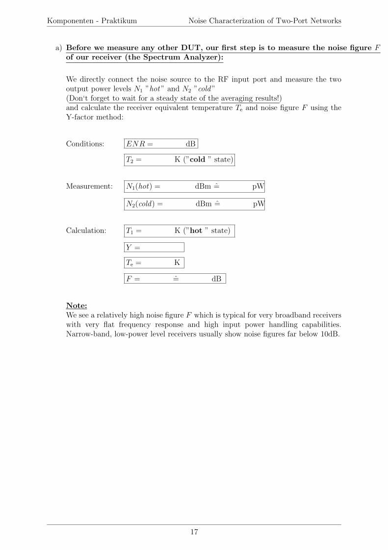
a) Before we measure any other DUT, our first step is to measure the noise figure Fof our receiver (the Spectrum Analyzer):
We directly connect the noise source to the RF input port and measure the twooutput power levels N1 ”hot ” and N2 ”cold ”(Don‘t forget to wait for a steady state of the averaging results!)and calculate the receiver equivalent temperature Te and noise figure F using theY-factor method:
Conditions: ENR = dB
T2 = K (”cold ” state)
Measurement: N1(hot) = dBm = pW
N2(cold) = dBm = pW
Calculation: T1 = K (”hot ” state)
Y =
Te = K
F = = dB
Note:We see a relatively high noise figure F which is typical for very broadband receiverswith very flat frequency response and high input power handling capabilities.Narrow-band, low-power level receivers usually show noise figures far below 10dB.
17

Komponenten - Praktikum Noise Characterization of Two-Port Networks
b) We next investigate the Power Amplifier in cascade with the receiver:
Insert the Power Amplifier between the noise source and the Spectrum Analyzer.The DUT is now the combination of the two devices. Activate the Power Amplifierby using the Dream Catcher Control Panel Switch (Power Amplifier). Measure thetwo output power levels N1 ”hot ” and N2 ”cold ” and calculate the DUT equivalenttemperature Te using the Y-factor method, the noise figure F and determine thegain G of the DUT:
Conditions: ENR = dB
T2 = K (”cold ” state)
Measurement: N1(hot) = dBm = pW
N2(cold) = dBm = pW
Calculation: T1 = K (”hot ” state)
Y =
Te = K
F = = dB
s = W/K
G = = dB with B = 3MHz
18

Komponenten - Praktikum Noise Characterization of Two-Port Networks
6.1.2 Using the Noise & Gain Measurement Option of theSpectrum Analyzer FSL
Disconnect the DC bias supply from the noise source - the noise source bias now isprovided by the Spectrum Analyzer through a BNC cable from the back connector plate.Connect the noise source output directly to the RF input port of the instrument (Fig. 14).
Spectrum Analyzer
Noise & Gain Meter
Rohde & Schwarz FSL
NoiseSource
Noise SourceControl 0/28V
RF INPUT
Fig. 14: Test Setup for Noise Calibration
We switch to the Noise & Gain Measurement Mode of the Spectrum Analyzer bypressing the MODE function key and checking the Noise box. Press the MENU key belowthe MODE key to bring up the soft keys on the display.
Instrument Settings:
• Activate Freq Settings:Set the start frequency to f = 850MHz and the stop frequency to f = 900MHz withsteps of ∆f = 10MHz.
• Activate ENR Settings and check the Selection:Accept Constant and enter the ENR given on the noise source calibration tableand enter the room temperature as T = 290K.
• Activate the Measurements Settings:Under Calibration, click the 2nd stage correction (this will allow the charac-terization of the Spectrum Analyzer noise and gain).Under Analyzer Settings set the resolution bandwidth RBW to 3MHz.For the number of samples set Average to 20.Set RF Attenuation to 0dB andSwitch the preamplifier on by checking the Preamplifier box.
19
Komponenten - Praktikum Noise Characterization of Two-Port Networks
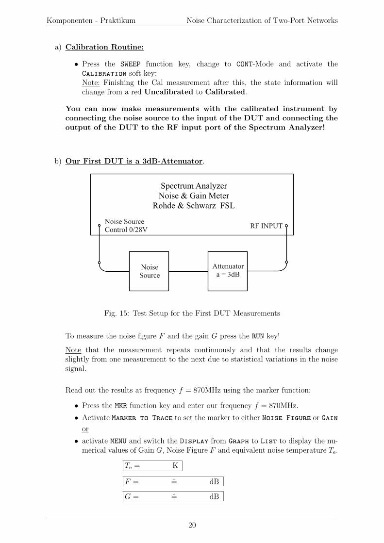
a) Calibration Routine:
• Press the SWEEP function key, change to CONT-Mode and activate theCalibration soft key;Note: Finishing the Cal measurement after this, the state information willchange from a red Uncalibrated to Calibrated.
You can now make measurements with the calibrated instrument byconnecting the noise source to the input of the DUT and connecting theoutput of the DUT to the RF input port of the Spectrum Analyzer!
b) Our First DUT is a 3dB-Attenuator.
Spectrum Analyzer
Noise & Gain Meter
Rohde & Schwarz FSL
NoiseSource
Noise SourceControl 0/28V
RF INPUT
Attenuatora = 3dB
Fig. 15: Test Setup for the First DUT Measurements
To measure the noise figure F and the gain G press the RUN key!
Note that the measurement repeats continuously and that the results changeslightly from one measurement to the next due to statistical variations in the noisesignal.
Read out the results at frequency f = 870MHz using the marker function:
• Press the MKR function key and enter our frequency f = 870MHz.
• Activate Marker to Trace to set the marker to either Noise Figure or Gain
or
• activate MENU and switch the Display from Graph to List to display the nu-merical values of Gain G, Noise Figure F and equivalent noise temperature Te.
Te = K
F = = dB
G = = dB
20

Komponenten - Praktikum Noise Characterization of Two-Port Networks
Compare the results to theory!
Te = K
F = = dB
G = = dB
c) Our Second DUT is the Power Amplifier from the TX-Box.
Disconnect the 3dB-attenuator and connect the noise source to the power amplifierand the output of the amplifier to the RF input port of the analyzer. Read-out thenoise figure F and gain G at frequency f = 870MHz and compare the results withtask 6.1.1!
Spectrum Analyzer
Noise & Gain Meter
Rohde & Schwarz FSL
NoiseSource
Noise SourceControl 0/28V
RF INPUT
PowerAmplifier
Fig. 16: Test Setup for the Second DUT Measurements
F = = dB
G = = dB
Calculate the cascaded noise figure Fcas of the cascade of amplifier and receiver(Spectrum Analyzer) and compare to the measurement result under task 6.1.1(b)!
Fcas = = dB
Fcas,6.1.1(b) = = dB
21

Komponenten - Praktikum Noise Characterization of Two-Port Networks
6.2 Cascaded Circuits
The power amplifier of task 6.1 from the TX-Box is cascaded with an attenuator ofa = 20dB loss-factor, as given in Fig. 17.
(a)
(b)
Spectrum Analyzer
Noise & Gain Meter
Rohde & Schwarz FSL
AttenuatorNoiseSource
AttenuatorNoiseSource
a = 20dB
a = 20dB
Noise SourceControl 0/28V
RF INPUT
PowerAmplifier
PowerAmplifier
Fig. 17: Cascaded Circuits Test Setup
6.1 Cascade the attenuator at the output of the power amplifier and measure theoverall noise figure Fcas,1 (Fig. 17a) at frequency f = 870MHz.
Fcas,1 = = dB
Gcas,1 = = dB
Compare to theory!
Fcas,1 = = dB
Gcas,1 = = dB
22
Komponenten - Praktikum Noise Characterization of Two-Port Networks
6.2 Cascade the attenuator at the input of the power amplifier and repeat measurementand evaluation (Fig. 17b).
Fcas,2 = = dB
Gcas,2 = = dB
Compare to theory!
Fcas,2 = = dB
Gcas,2 = = dB
Why is the noise figure F degraded in both cases?
23
Komponenten - Praktikum Noise Characterization of Two-Port Networks
6.3 Signal-to-Noise Ratio S/N
We can observe the signal-to-noise power ratio S/N on the Spectrum Analyzer as ourreceiver, when we feed the DUT with a sinusoidal signal, Fig. 18. The signal generator’sinternal impedance generates the same noise power as is generated by a ”cold” noisesource and in addition we get a harmonic signal with a constant amplitude when thegenerator is switched-on. The Spectrum Analyzer measures the power of the signal S,when the marker is set to the signal frequency (the peak of the response) and when thesignal is switched off, the noise power N remains and can be measured as the availablepower within the resolution bandwidth B of the receiver (the Spectrum Analyzer).
DUT
Signal
GeneratorSpectrum
Analyzer
S
N
in
in
, S
N
out
out
,
T0
Fig. 18: Signal-to-Noise Ratio Test Setup
Make the measurements start again from PRESET and recall all settings of the instrumentas used in section 6.1.
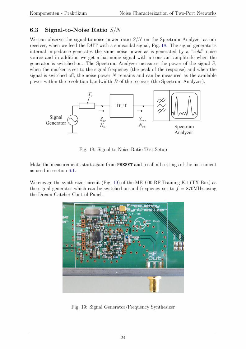
We engage the synthesizer circuit (Fig. 19) of the ME1000 RF Training Kit (TX-Box) asthe signal generator which can be switched-on and frequency set to f = 870MHz usingthe Dream Catcher Control Panel.
Fig. 19: Signal Generator/Frequency Synthesizer
24

Komponenten - Praktikum Noise Characterization of Two-Port Networks
We insert a 40dB-attenuator as the DUT at the output port of the synthesizer and connectto the RF input port of the Spectrum Analyzer (Fig. 20).
Signal
GeneratorSpectrum
Analyzer
S
N
in
in
, S
N
out
out
,
T0
Attenuator
a = 40dB
Fig. 20: Setup for Signal-to-Noise Ratio Measurement
We move the marker to the signal peak and read the signal power S(direct)
We disconnect the signal and read the noise power N(direct) (called the noise floor).
Note: The noise floor is flat; the level can also be measured at frequencies far from thecarrier without switching the generator off!
S(direct) = dBm
N(direct) = dBm
S/N(direct) = dB
Calculate the power ratio; this is the signal-to-noise ratio S/N(direct).
We now feed the attenuated synthesizer signal to the input of the power amplifier circuit(TX-Box) (Fig. 21). The output signal from the power amplifier circuit then is connectedto the RF input port of the Spectrum Analyzer. Of course, the signal now is amplifiedby the gain of the Power Amplifier, but the noise floor has not grown at the same ratio.
Signal
GeneratorSpectrum
Analyzer
S
N
in
in
, S
N
out
out
,
T0
Attenuator
a = 40dB
PowerAmplifier
Fig. 21: Setup for Signal-to-Noise Ratio Measurement with a DUT
25

Komponenten - Praktikum Noise Characterization of Two-Port Networks
The new power ratio S/N(preamp) with the Power Amplifier as a preamplifier to thereceiver (the Spectrum Analyzer) is now:
S(preamp) = dBm
N(preamp) = dBm
S/N(preamp) = dB
(a) We observe an increase of the signal-to-noise ratio S/N , that is, we have animprovement!
Can you explain this result?
Compare to theory!
(b) Reduce the resolution bandwidth (RBW) to B = 300kHz. Note the noise level Nand the signal-to-noise ratio S/N :
S = dBm
N = dBm
S/N = dB
Can you explain the result?
What would be the required signal power in order to get S/N = 1?
26

Komponenten - Praktikum Noise Characterization of Two-Port Networks
7 Formulary
T [K] = T [C] + 273K
T0 = 290K; k = 1.38 · 10−23 Ws
K
un =√
4kTBR
Pn = N = kTB
Pn(dB) = N(dB) = 10dB · log(kTB)
=− 174dBm + 10dB · log( B
Hz
)+ 10dB · log
( T
290K
)N0 = kT0B
N0(dB) = −174dBm + 10dB · log( B
Hz
)N1
N0
=T1
T0
ENR(dB) = 10dB log(N1
N0
− 1)
= 10dB · log(T1
T0
− 1)
T1 = T0 ·(1 + 10
ENR10dB
)Y =
Nout1
Nout2
=T1 + Te
T2 + Te
Te =T1 − Y T2
Y − 1
F =Sin/Nin
Sout/Nout
∣∣∣∣Tin=T0
= 1 +Te
T0
F (dB) = 10dB · log(
1 +Te
T0
)Te = (F − 1) · T0
s =N1 −N2
T1 − T2
; G =s
kB
Tecas = Te1 +1
G1
Te2
Fcas = F1 +1
G1
(F2 − 1)
P = 10P (dBm)10dBm
27


![KDK Bruttopreisliste Fachhandel 2020 · 2020. 9. 30. · KDK Dornscheidt GmbH, Königswinter ]o XrE X Z ] µvP ¦ 0l 0^ lX< o}P^X 5 Werkzeug/Montage 31002066 Werkzeugkoffer-Case ELK-05](https://static.fdokument.com/doc/165x107/60c1620fb39e8e338d3e8b18/kdk-bruttopreisliste-fachhandel-2020-2020-9-30-kdk-dornscheidt-gmbh-knigswinter.jpg)