An easily reproducible, Hall-device based demonstration ...
8
An easily reproducible, Hall-device based demonstration model for Scanning Tunnelling Microscopy (STM) N. Hommrichhausen 1,2 , M. Kramler 1,3 , M. Voss 1,3 , W.M. Heckl 1,3 and F. Trixler 1,3,4,* 1 Deutsches Museum, Museumsinsel 1, 80538 München, Germany 2 Hochschule für Technik Stuttgart, Labor für Bauchemie, Fakultät Bauingenieurwesen, Bauphysik und Wirtschaft, Schellingstraße 24, 70174 Stuttgart, Germany 3 School of Education, Technische Universität München, Marsstr. 20-22, 80335 München, Germany 4 Center for NanoScience (CeNS) and Department for Earth and Environmental Sciences, Ludwig-Maximilians- Universität München, Theresienstr. 41, 80333 München, Germany *Corresponding author: e-mail: [email protected] Quantum physical effects such as tunnelling are hard to perceive due to their counter-intuitive and abstract nature. However, in this strange world of quantum physics, Scanning Tunnelling Microscopy (STM) is allowing users to fulfil their fascination of directly ‘seeing’ atoms – the essence of our material world. Such fascination, nevertheless, frequently raises questions about the origin of atomic resolution of this type of microscopy. Hence, in this regard, we present the design of a demonstration model enabling an interactive and easy way to comprehend the basic issues of electron tunnelling and the working principle of scanning tunnelling microscopy. The demonstration model, being based on a commercially available Hall-effect sensor, is applicable for various educational purposes such as offering hands-on- experiments to visitors of science museums and to students in their courses on nanotechnology and scanning probe microscopy. We further present our hardware design as well as the programming of the model, aiding its easy reproducibility by other laboratories or museums for educational purposes. The practicability of the model was tested at the Open Research Laboratory in the visitor area of the Deutsches Museum. Keywords: Scanning Tunnelling Microscopy; Quantum Tunnelling; Demonstration Model; Science Communication; Deutsches Museum; Open Research Laboratory 1. Introduction Scanning Tunnelling Microscopy (STM) [1] is unlike any conventional microscopes. Whereas conventional microscopes operate with optical lenses (a type of component which is also a part of our day to day lives used e.g. in spectacles, cameras, magnifying glasses, and so on), STM, on the other hand, instead of employing any lenses for optical magnification, uses completely different components and physical principles to achieve magnifications reaching atomic resolution. However, the core component of the STM, the piezo scanner, is hidden deep within a shielded structure, and the realisation of the basic principle of probe microscopy, the tip movement over a sample surface in a scan-mode pattern, is invisible to the naked eye as the movement distances are typically in the range of just a few hundred nanometres. Further, the image generating signal – the tunnelling current – being a quantum physical process makes it entirely a counter-intuitive phenomenon. Therefore, finding an easy-to-grasp and a catchy way to communicate the working principle of STM becomes a highly important and a challenging task, as to offer practical courses for students or to generate enhanced interest among general public at museums in this kind of microscopy. In this regard, some possibilities that come to the mind for demonstrating the fundamental principles of STM are technically simple to achieve – as the use of a film, an animation, or just even a text with images. So the question arises: why spend the time to develop an object that comes at a greater cost, needs room for storage, and needs to be taken care of for its appearance and functionality? An explanation to the above, however, can be given by stating that such a model allows for a very specific kind of enlargement, visualisation, and palpability of processes – which in our case are invisible and indiscernible in the real world. Our model can hence be regarded as scale model [2] enabling visualization of the nanometre-scale imaging process. Furthermore, the model serves as a representative of the quantum tunnelling by using the Hall-effect, for producing visual and acoustic signals whose values depend on the tip-surface distance just as it would be for the nanoscopic electron tunnelling phenomena. In museum education and science communication, models are used for various reasons – some of which apply to our model being as stated in the sub-sections below: 1. Sensuousness – Perception: Our model in its three-dimensional materiality and its multi-faceted design appeals to various senses, enabling its operators to see, touch, and hear. Hooper-Greenhill [3, p. 106] speaks of “looking on its own” as a “distancing sense” that is “less immediate’’ and “less physical” than the other senses. She argues that “looking in conjunction with handling is quite different” and will “provoke initial involvement” in a way that cannot be achieved by “looking on its own”. Hence, while exploring our model, initially the students and visitors get involved by combining looking, touching, and hearing, with the handling of the object. Thus, the model changes the otherwise quite unapproachable working principle of the STM into something that is perceptible to the senses. Microscopy and imaging science: practical approaches to applied research and education (A. Méndez-Vilas, Ed.) 681 ___________________________________________________________________________________________
Transcript of An easily reproducible, Hall-device based demonstration ...
An easily reproducible, Hall-device based demonstration model for Scanning Tunnelling Microscopy (STM)
N. Hommrichhausen1,2, M. Kramler1,3, M. Voss1,3, W.M. Heckl1,3 and F. Trixler1,3,4,* 1 Deutsches Museum, Museumsinsel 1, 80538 München, Germany 2 Hochschule für Technik Stuttgart, Labor für Bauchemie, Fakultät Bauingenieurwesen, Bauphysik und Wirtschaft,
Schellingstraße 24, 70174 Stuttgart, Germany 3 School of Education, Technische Universität München, Marsstr. 20-22, 80335 München, Germany 4 Center for NanoScience (CeNS) and Department for Earth and Environmental Sciences, Ludwig-Maximilians-
Universität München, Theresienstr. 41, 80333 München, Germany *Corresponding author: e-mail: [email protected]
Quantum physical effects such as tunnelling are hard to perceive due to their counter-intuitive and abstract nature. However, in this strange world of quantum physics, Scanning Tunnelling Microscopy (STM) is allowing users to fulfil their fascination of directly ‘seeing’ atoms – the essence of our material world. Such fascination, nevertheless, frequently raises questions about the origin of atomic resolution of this type of microscopy. Hence, in this regard, we present the design of a demonstration model enabling an interactive and easy way to comprehend the basic issues of electron tunnelling and the working principle of scanning tunnelling microscopy. The demonstration model, being based on a commercially available Hall-effect sensor, is applicable for various educational purposes such as offering hands-on-experiments to visitors of science museums and to students in their courses on nanotechnology and scanning probe microscopy. We further present our hardware design as well as the programming of the model, aiding its easy reproducibility by other laboratories or museums for educational purposes. The practicability of the model was tested at the Open Research Laboratory in the visitor area of the Deutsches Museum.
Keywords: Scanning Tunnelling Microscopy; Quantum Tunnelling; Demonstration Model; Science Communication; Deutsches Museum; Open Research Laboratory
1. Introduction
Scanning Tunnelling Microscopy (STM) [1] is unlike any conventional microscopes. Whereas conventional microscopes operate with optical lenses (a type of component which is also a part of our day to day lives used e.g. in spectacles, cameras, magnifying glasses, and so on), STM, on the other hand, instead of employing any lenses for optical magnification, uses completely different components and physical principles to achieve magnifications reaching atomic resolution. However, the core component of the STM, the piezo scanner, is hidden deep within a shielded structure, and the realisation of the basic principle of probe microscopy, the tip movement over a sample surface in a scan-mode pattern, is invisible to the naked eye as the movement distances are typically in the range of just a few hundred nanometres. Further, the image generating signal – the tunnelling current – being a quantum physical process makes it entirely a counter-intuitive phenomenon. Therefore, finding an easy-to-grasp and a catchy way to communicate the working principle of STM becomes a highly important and a challenging task, as to offer practical courses for students or to generate enhanced interest among general public at museums in this kind of microscopy. In this regard, some possibilities that come to the mind for demonstrating the fundamental principles of STM are technically simple to achieve – as the use of a film, an animation, or just even a text with images. So the question arises: why spend the time to develop an object that comes at a greater cost, needs room for storage, and needs to be taken care of for its appearance and functionality? An explanation to the above, however, can be given by stating that such a model allows for a very specific kind of enlargement, visualisation, and palpability of processes – which in our case are invisible and indiscernible in the real world. Our model can hence be regarded as scale model [2] enabling visualization of the nanometre-scale imaging process. Furthermore, the model serves as a representative of the quantum tunnelling by using the Hall-effect, for producing visual and acoustic signals whose values depend on the tip-surface distance just as it would be for the nanoscopic electron tunnelling phenomena. In museum education and science communication, models are used for various reasons – some of which apply to our model being as stated in the sub-sections below:
1. Sensuousness – Perception: Our model in its three-dimensional materiality and its multi-faceted design appeals to various senses, enabling its operators to see, touch, and hear. Hooper-Greenhill [3, p. 106] speaks of “looking on its own” as a “distancing sense” that is “less immediate’’ and “less physical” than the other senses. She argues that “looking in conjunction with handling is quite different” and will “provoke initial involvement” in a way that cannot be achieved by “looking on its own”. Hence, while exploring our model, initially the students and visitors get involved by combining looking, touching, and hearing, with the handling of the object. Thus, the model changes the otherwise quite unapproachable working principle of the STM into something that is perceptible to the senses.
Microscopy and imaging science: practical approaches to applied research and education (A. Méndez-Vilas, Ed.)
681
___________________________________________________________________________________________
2. Interactivity – Experience: Next, our model is interactive in the way as defined by McLean [4, p. 92]: “The
visitor acts upon the exhibit, and the exhibit does something that acts upon the visitor”. The interactivity leads to a vital distinction in the role of the audience: while watching a film or an animation, while reading a text and looking at images, students and visitors largely remain passive recipients. However, while interacting with the STM model, their role changes dramatically – they now being actively involved explorers, trying to figure out something about the phenomena they perceive. Hence, students and visitors gain experiences in their interaction with the model, and gather empirical knowledge allowing them to classify reactions. The National Research Council [5, p. 140] reports as “a key finding from the field […] that learners are engaged by experiences that offer interactivity”. Further, experiences of this kind of engagement are though based on the senses, not limited to them, as they entail additional levels such as emotional responses. Thus, the model allows for an individual emotional experience, along with the acquisition of new experiences with the otherwise rather impenetrable working principle of the STM.
3. Representation – Thinking: The interactive processes triggered by our model are representations of the
underlying working principle of the STM. The reactions of the model to actions of the visitor are not randomly distributed, but in fact, mirror the authentic working process of an STM. As light and sound will be stronger where a measurement would show a high amperage and less strong where a measurement would show a low amperage, students and visitors are investigating these connections via continuous measurements and compare their sensual perceptions with the amperage displayed by the measuring device. Thus, the experimental experiences from students and/or visitors can result in findings like: sound and light give a very strong response in the middle of each ball and a much weaker response in the space between balls – corresponding with high or low amperage respectively. In this quite open approach they are hence able to disclose by themselves the authentic measurement process of the STM while translating their findings from symbolized to real carbon atoms. Based on the outcomes of their measurements, the users might also be able to conclude which information they receive about atoms and their surface in a subsequent real STM measurement. As Hooper-Greenhill [3, p. 102] puts it: “Working with real things enables all kinds of thinking to occur, including making comparisons, remembering, making relationships, classifying, interrogating, moving from concrete observations to abstract concepts, extending from the known into the unknown, and from specific observations to generalizations [emphasis added].” Thus, our model facilitates a transfer from a concrete object to rather abstract explanations of one’s perceptions and experiences. This, in turn, might, in spite of the inherent unapproachability and impenetrability of the genuine apparatus, lead to a sound understanding of the working principle of the STM.
2. General design and handling of the model
When conceptualising the model, two features most distinctive for the STM were focussed upon: movement of an atomically sharp tip very close to a surface, and detection of a quantum physical electron tunnelling current determined in turn by the tip-surface distance. Thus, keeping the above in mind, our model (Fig. 1) comprised of the following parts:
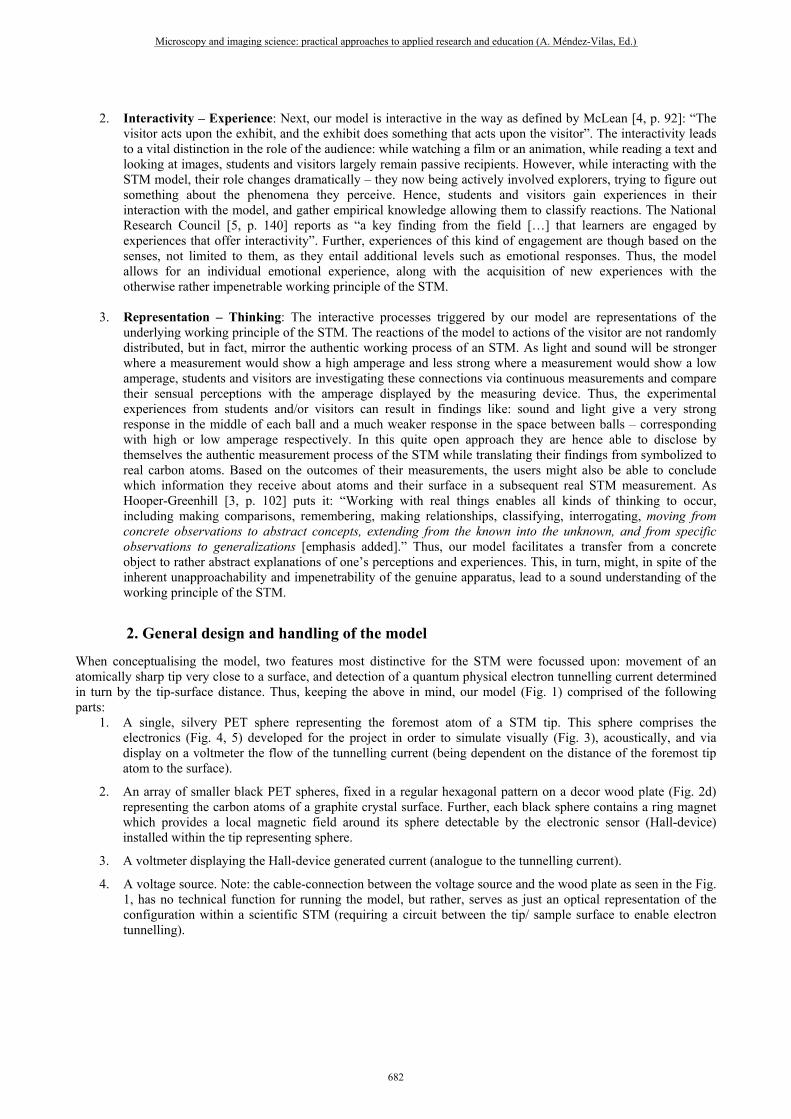
1. A single, silvery PET sphere representing the foremost atom of a STM tip. This sphere comprises the electronics (Fig. 4, 5) developed for the project in order to simulate visually (Fig. 3), acoustically, and via display on a voltmeter the flow of the tunnelling current (being dependent on the distance of the foremost tip atom to the surface).
2. An array of smaller black PET spheres, fixed in a regular hexagonal pattern on a decor wood plate (Fig. 2d) representing the carbon atoms of a graphite crystal surface. Further, each black sphere contains a ring magnet which provides a local magnetic field around its sphere detectable by the electronic sensor (Hall-device) installed within the tip representing sphere.
3. A voltmeter displaying the Hall-device generated current (analogue to the tunnelling current).
4. A voltage source. Note: the cable-connection between the voltage source and the wood plate as seen in the Fig. 1, has no technical function for running the model, but rather, serves as just an optical representation of the configuration within a scientific STM (requiring a circuit between the tip/ sample surface to enable electron tunnelling).
Microscopy and imaging science: practical approaches to applied research and education (A. Méndez-Vilas, Ed.)
682
___________________________________________________________________________________________
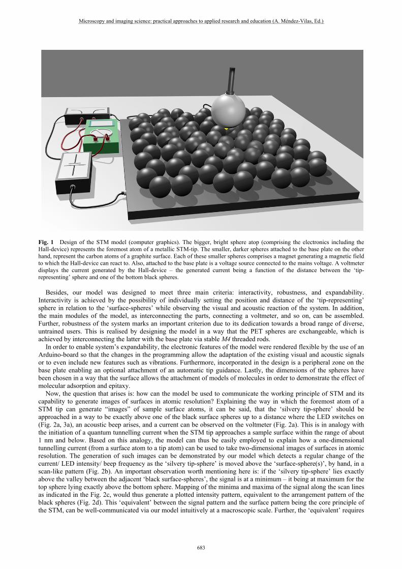
Fig. 1 Design of the STM model (computer graphics). The bigger, bright sphere atop (comprising the electronics including the Hall-device) represents the foremost atom of a metallic STM-tip. The smaller, darker spheres attached to the base plate on the other hand, represent the carbon atoms of a graphite surface. Each of these smaller spheres comprises a magnet generating a magnetic field to which the Hall-device can react to. Also, attached to the base plate is a voltage source connected to the mains voltage. A voltmeter displays the current generated by the Hall-device – the generated current being a function of the distance between the ‘tip-representing’ sphere and one of the bottom black spheres. Besides, our model was designed to meet three main criteria: interactivity, robustness, and expandability. Interactivity is achieved by the possibility of individually setting the position and distance of the ‘tip-representing’ sphere in relation to the ‘surface-spheres’ while observing the visual and acoustic reaction of the system. In addition, the main modules of the model, as interconnecting the parts, connecting a voltmeter, and so on, can be assembled. Further, robustness of the system marks an important criterion due to its dedication towards a broad range of diverse, untrained users. This is realised by designing the model in a way that the PET spheres are exchangeable, which is achieved by interconnecting the latter with the base plate via stable M4 threaded rods. In order to enable system’s expandability, the electronic features of the model were rendered flexible by the use of an Arduino-board so that the changes in the programming allow the adaptation of the existing visual and acoustic signals or to even include new features such as vibrations. Furthermore, incorporated in the design is a peripheral zone on the base plate enabling an optional attachment of an automatic tip guidance. Lastly, the dimensions of the spheres have been chosen in a way that the surface allows the attachment of models of molecules in order to demonstrate the effect of molecular adsorption and epitaxy. Now, the question that arises is: how can the model be used to communicate the working principle of STM and its capability to generate images of surfaces in atomic resolution? Explaining the way in which the foremost atom of a STM tip can generate “images” of sample surface atoms, it can be said, that the ‘silvery tip-sphere’ should be approached in a way to be exactly above one of the black surface spheres up to a distance where the LED switches on (Fig. 2a, 3a), an acoustic beep arises, and a current can be observed on the voltmeter (Fig. 2a). This is in analogy with the initiation of a quantum tunnelling current when the STM tip approaches a sample surface within the range of about 1 nm and below. Based on this analogy, the model can thus be easily employed to explain how a one-dimensional tunnelling current (from a surface atom to a tip atom) can be used to take two-dimensional images of surfaces in atomic resolution. The generation of such images can be demonstrated by our model which detects a regular change of the current/ LED intensity/ beep frequency as the ‘silvery tip-sphere’ is moved above the ‘surface-sphere(s)’, by hand, in a scan-like pattern (Fig. 2b). An important observation worth mentioning here is: if the ‘silvery tip-sphere’ lies exactly above the valley between the adjacent ‘black surface-spheres’, the signal is at a minimum – it being at maximum for the top sphere lying exactly above the bottom sphere. Mapping of the minima and maxima of the signal along the scan lines as indicated in the Fig. 2c, would thus generate a plotted intensity pattern, equivalent to the arrangement pattern of the black spheres (Fig. 2d). This ‘equivalent’ between the signal pattern and the surface pattern being the core principle of the STM, can be well-communicated via our model intuitively at a macroscopic scale. Further, the ‘equivalent’ requires
Microscopy and imaging science: practical approaches to applied research and education (A. Méndez-Vilas, Ed.)
683
___________________________________________________________________________________________
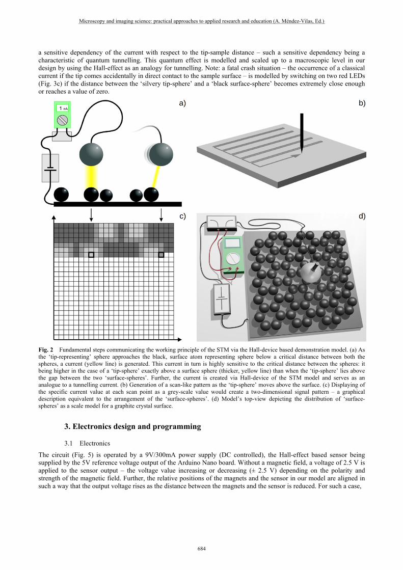
a sensitive dependency of the current with respect to the tip-sample distance – such a sensitive dependency being a characteristic of quantum tunnelling. This quantum effect is modelled and scaled up to a macroscopic level in our design by using the Hall-effect as an analogy for tunnelling. Note: a fatal crash situation – the occurrence of a classical current if the tip comes accidentally in direct contact to the sample surface – is modelled by switching on two red LEDs (Fig. 3c) if the distance between the ‘silvery tip-sphere’ and a ‘black surface-sphere’ becomes extremely close enough or reaches a value of zero.
Fig. 2 Fundamental steps communicating the working principle of the STM via the Hall-device based demonstration model. (a) As the ‘tip-representing’ sphere approaches the black, surface atom representing sphere below a critical distance between both the spheres, a current (yellow line) is generated. This current in turn is highly sensitive to the critical distance between the spheres: it being higher in the case of a ‘tip-sphere’ exactly above a surface sphere (thicker, yellow line) than when the ‘tip-sphere’ lies above the gap between the two ‘surface-spheres’. Further, the current is created via Hall-device of the STM model and serves as an analogue to a tunnelling current. (b) Generation of a scan-like pattern as the ‘tip-sphere’ moves above the surface. (c) Displaying of the specific current value at each scan point as a grey-scale value would create a two-dimensional signal pattern – a graphical description equivalent to the arrangement of the ‘surface-spheres’. (d) Model’s top-view depicting the distribution of ‘surface-spheres’ as a scale model for a graphite crystal surface.
3. Electronics design and programming
3.1 Electronics
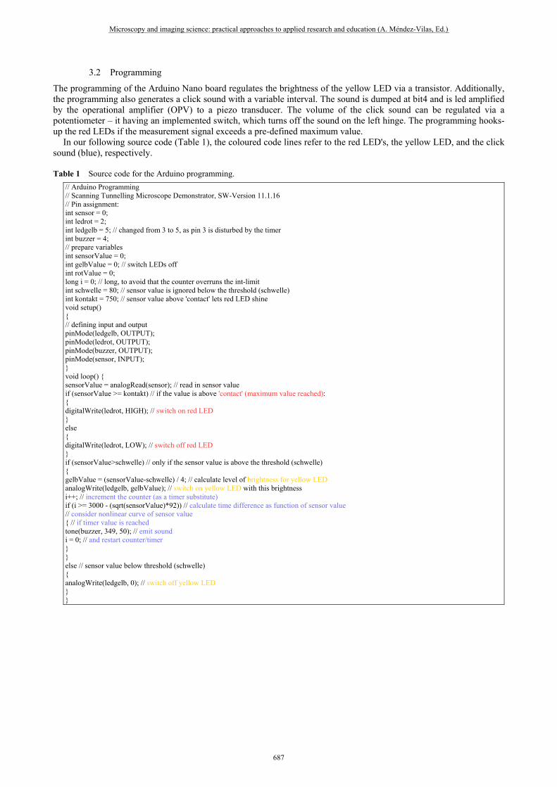
The circuit (Fig. 5) is operated by a 9V/300mA power supply (DC controlled), the Hall-effect based sensor being supplied by the 5V reference voltage output of the Arduino Nano board. Without a magnetic field, a voltage of 2.5 V is applied to the sensor output – the voltage value increasing or decreasing (± 2.5 V) depending on the polarity and strength of the magnetic field. Further, the relative positions of the magnets and the sensor in our model are aligned in such a way that the output voltage rises as the distance between the magnets and the sensor is reduced. For such a case,
Microscopy and imaging science: practical approaches to applied research and education (A. Méndez-Vilas, Ed.)
684
___________________________________________________________________________________________
Fig. 3 Response of the LED's within the tip representing sphere when approaching the surface (indicated by a blue cap containing a ring magnet). (a) At a greater distance, the yellow LED is off but starts to emit a faint light at a distance where the Hall-device produces a measurable current in response to the magnetic field of the surface. (b) The brightness of the LED increases as the distance between the tip-sphere and the surface decreases. (c) As the sphere gets in direct contact with the surface, the red LED’s switch on, simulating a crash situation in the STM (direct contact of the STM tip with the sample surface leading to the collapse of the tunnelling current and initiation of the classical current).
the sensor voltage is amplified and the zero-point voltage is shifted to ground (GND); the amplified measurement signal being read into the analogue input 'ai0' of the Arduino Nano. Additionally, as this signal overdrives at low distances, the non-amplified sensor signal is led to the input 'ai1', but is not evaluated. Next, the analogue output of the Arduino though is incapable of generating any desired voltage, it however, displays a pulse width modulated signal – this being highly suitable for controlling the brightness of the Light-Emitting Diodes (LEDs). In this regard, hence, the yellow LED is controlled by an analogue output, whilst the red LED is controlled by a digital one. Further, the ‘click-sound’ is generated by a sound-command: the higher the input signal, the shorter being the click interval. This programmed correlation was intended to acoustically represent a rising tunnelling current (represented as shorter click intervals) when decreasing the tip-sample distance in the STM. However, the obvious though upon idea to generate this acoustically modelled correlation by using a wait command and to get a parameter for it (so as to subtract the sensor output from an offset) would outbreak the loop and would require the transference of the process to a second task. Another possibility, nevertheless, would be to use a timer. However, timer being already reserved for both the generation of the PWM signal (for the yellow LED) and the generation of the sounds, a counter to the click interval was used: within the loop the variable 'int i' increments. When this variable reaches or even exceeds a limit, a sound (click) is emitted and 'i' is reset to zero. The limit further depends on the sensor signal: the higher the sensor value, the lower is the limit. To enhance the variations, this dependency was programmed as being non-linear (Table 1): 'if (i >= 3000 - (sqrt(sensorValue)*92))'. The maximum interval being 3000 (loop passes). The current interval was reduced by the square root of the sensor value, multiplied with a factor (for the factor 'value=92', a comfortable interval being yielded). Moreover, it appeared as a feature of the Arduino, that the timer used for the sound function affects the output pin 3, which was initially designated for triggering the yellow LED. Therefore, pin 3 remains disconnected – the yellow LED instead being controlled by the pin 5.
Microscopy and imaging science: practical approaches to applied research and education (A. Méndez-Vilas, Ed.)
685
___________________________________________________________________________________________
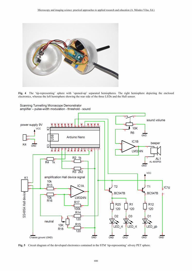
Fig. 4 The ‘tip-representing’ sphere with ‘opened-up’ separated hemispheres. The right hemisphere depicting the enclosed electronics, whereas the left hemisphere showing the rear side of the three LEDs and the Hall sensor.
Fig. 5 Circuit diagram of the developed electronics contained in the STM ‘tip-representing’ silvery PET sphere.
Microscopy and imaging science: practical approaches to applied research and education (A. Méndez-Vilas, Ed.)
686
___________________________________________________________________________________________
3.2 Programming
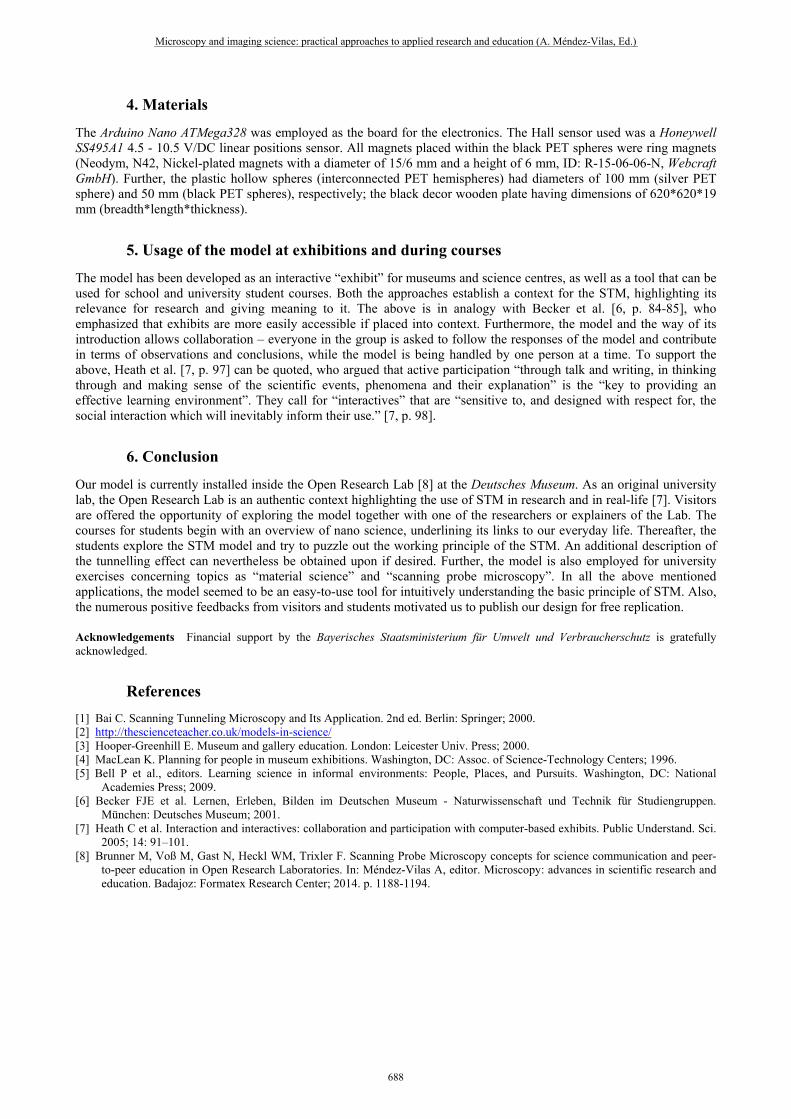
The programming of the Arduino Nano board regulates the brightness of the yellow LED via a transistor. Additionally, the programming also generates a click sound with a variable interval. The sound is dumped at bit4 and is led amplified by the operational amplifier (OPV) to a piezo transducer. The volume of the click sound can be regulated via a potentiometer – it having an implemented switch, which turns off the sound on the left hinge. The programming hooks-up the red LEDs if the measurement signal exceeds a pre-defined maximum value. In our following source code (Table 1), the coloured code lines refer to the red LED's, the yellow LED, and the click sound (blue), respectively. Table 1 Source code for the Arduino programming.
// Arduino Programming // Scanning Tunnelling Microscope Demonstrator, SW-Version 11.1.16 // Pin assignment: int sensor = 0; int ledrot = 2; int ledgelb = 5; // changed from 3 to 5, as pin 3 is disturbed by the timer int buzzer = 4; // prepare variables int sensorValue = 0; int gelbValue = 0; // switch LEDs off int rotValue = 0; long i = 0; // long, to avoid that the counter overruns the int-limit int schwelle = 80; // sensor value is ignored below the threshold (schwelle) int kontakt = 750; // sensor value above 'contact' lets red LED shine void setup() { // defining input and output pinMode(ledgelb, OUTPUT); pinMode(ledrot, OUTPUT); pinMode(buzzer, OUTPUT); pinMode(sensor, INPUT); } void loop() { sensorValue = analogRead(sensor); // read in sensor value if (sensorValue >= kontakt) // if the value is above 'contact' (maximum value reached): { digitalWrite(ledrot, HIGH); // switch on red LED } else { digitalWrite(ledrot, LOW); // switch off red LED } if (sensorValue>schwelle) // only if the sensor value is above the threshold (schwelle) { gelbValue = (sensorValue-schwelle) / 4; // calculate level of brightness for yellow LED analogWrite(ledgelb, gelbValue); // switch on yellow LED with this brightness i++; // increment the counter (as a timer substitute) if (i >= 3000 - (sqrt(sensorValue)*92)) // calculate time difference as function of sensor value // consider nonlinear curve of sensor value { // if timer value is reached tone(buzzer, 349, 50); // emit sound i = 0; // and restart counter/timer } } else // sensor value below threshold (schwelle) { analogWrite(ledgelb, 0); // switch off yellow LED } }
Microscopy and imaging science: practical approaches to applied research and education (A. Méndez-Vilas, Ed.)
687
___________________________________________________________________________________________
4. Materials
The Arduino Nano ATMega328 was employed as the board for the electronics. The Hall sensor used was a Honeywell SS495A1 4.5 - 10.5 V/DC linear positions sensor. All magnets placed within the black PET spheres were ring magnets (Neodym, N42, Nickel-plated magnets with a diameter of 15/6 mm and a height of 6 mm, ID: R-15-06-06-N, Webcraft GmbH). Further, the plastic hollow spheres (interconnected PET hemispheres) had diameters of 100 mm (silver PET sphere) and 50 mm (black PET spheres), respectively; the black decor wooden plate having dimensions of 620*620*19 mm (breadth*length*thickness).
5. Usage of the model at exhibitions and during courses
The model has been developed as an interactive “exhibit” for museums and science centres, as well as a tool that can be used for school and university student courses. Both the approaches establish a context for the STM, highlighting its relevance for research and giving meaning to it. The above is in analogy with Becker et al. [6, p. 84-85], who emphasized that exhibits are more easily accessible if placed into context. Furthermore, the model and the way of its introduction allows collaboration – everyone in the group is asked to follow the responses of the model and contribute in terms of observations and conclusions, while the model is being handled by one person at a time. To support the above, Heath et al. [7, p. 97] can be quoted, who argued that active participation “through talk and writing, in thinking through and making sense of the scientific events, phenomena and their explanation” is the “key to providing an effective learning environment”. They call for “interactives” that are “sensitive to, and designed with respect for, the social interaction which will inevitably inform their use.” [7, p. 98].
6. Conclusion
Our model is currently installed inside the Open Research Lab [8] at the Deutsches Museum. As an original university lab, the Open Research Lab is an authentic context highlighting the use of STM in research and in real-life [7]. Visitors are offered the opportunity of exploring the model together with one of the researchers or explainers of the Lab. The courses for students begin with an overview of nano science, underlining its links to our everyday life. Thereafter, the students explore the STM model and try to puzzle out the working principle of the STM. An additional description of the tunnelling effect can nevertheless be obtained upon if desired. Further, the model is also employed for university exercises concerning topics as “material science” and “scanning probe microscopy”. In all the above mentioned applications, the model seemed to be an easy-to-use tool for intuitively understanding the basic principle of STM. Also, the numerous positive feedbacks from visitors and students motivated us to publish our design for free replication.
Acknowledgements Financial support by the Bayerisches Staatsministerium für Umwelt und Verbraucherschutz is gratefully acknowledged.
References [1] Bai C. Scanning Tunneling Microscopy and Its Application. 2nd ed. Berlin: Springer; 2000. [2] http://thescienceteacher.co.uk/models-in-science/ [3] Hooper-Greenhill E. Museum and gallery education. London: Leicester Univ. Press; 2000. [4] MacLean K. Planning for people in museum exhibitions. Washington, DC: Assoc. of Science-Technology Centers; 1996. [5] Bell P et al., editors. Learning science in informal environments: People, Places, and Pursuits. Washington, DC: National
Academies Press; 2009. [6] Becker FJE et al. Lernen, Erleben, Bilden im Deutschen Museum - Naturwissenschaft und Technik für Studiengruppen.
München: Deutsches Museum; 2001. [7] Heath C et al. Interaction and interactives: collaboration and participation with computer-based exhibits. Public Understand. Sci.
2005; 14: 91–101. [8] Brunner M, Voß M, Gast N, Heckl WM, Trixler F. Scanning Probe Microscopy concepts for science communication and peer-
to-peer education in Open Research Laboratories. In: Méndez-Vilas A, editor. Microscopy: advances in scientific research and education. Badajoz: Formatex Research Center; 2014. p. 1188-1194.
Microscopy and imaging science: practical approaches to applied research and education (A. Méndez-Vilas, Ed.)
688
___________________________________________________________________________________________


![„Klima schützen – Kohle stoppen!“ Demonstration zur ... · [Medien-Info zur internen Planung] „Klima schützen – Kohle stoppen!“ Demonstration zur Weltklimakonferenz](https://static.fdokument.com/doc/165x107/5d4d0eaf88c993c96c8ba1a0/klima-schuetzen-kohle-stoppen-demonstration-zur-medien-info.jpg)