Chemical and material characterization of smartphones with ... · SEM analysis resulted that...
9
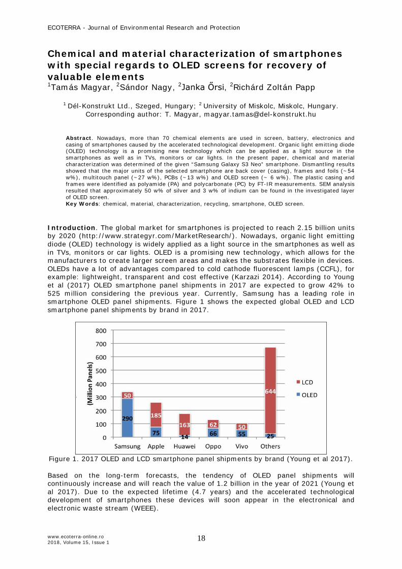
ECOTERRA - Journal of Environmental Research and Protection www.ecoterra-online.ro 2018, Volume 15, Issue 1 18 Chemical and material characterization of smartphones with special regards to OLED screens for recovery of valuable elements 1 Tamás Magyar, 2 Sándor Nagy, 2 Janka Őrsi, 2 Richárd Zoltán Papp 1 Dél-Konstrukt Ltd., Szeged, Hungary; 2 University of Miskolc, Miskolc, Hungary. Corresponding author: T. Magyar, [email protected] Abstract. Nowadays, more than 70 chemical elements are used in screen, battery, electronics and casing of smartphones caused by the accelerated technological development. Organic light emitting diode (OLED) technology is a promising new technology which can be applied as a light source in the smartphones as well as in TVs, monitors or car lights. In the present paper, chemical and material characterization was determined of the given “Samsung Galaxy S3 Neo” smartphone. Dismantling results showed that the major units of the selected smartphone are back cover (casing), frames and foils (~54 w%), multitouch panel (~27 w%), PCBs (~13 w%) and OLED screen (~ 6 w%). The plastic casing and frames were identified as polyamide (PA) and polycarbonate (PC) by FT-IR measurements. SEM analysis resulted that approximately 50 w% of silver and 3 w% of indium can be found in the investigated layer of OLED screen. Key Words: chemical, material, characterization, recycling, smartphone, OLED screen. Introduction. The global market for smartphones is projected to reach 2.15 billion units by 2020 (http://www.strategyr.com/MarketResearch/). Nowadays, organic light emitting diode (OLED) technology is widely applied as a light source in the smartphones as well as in TVs, monitors or car lights. OLED is a promising new technology, which allows for the manufacturers to create larger screen areas and makes the substrates flexible in devices. OLEDs have a lot of advantages compared to cold cathode fluorescent lamps (CCFL), for example: lightweight, transparent and cost effective (Karzazi 2014). According to Young et al (2017) OLED smartphone panel shipments in 2017 are expected to grow 42% to 525 million considering the previous year. Currently, Samsung has a leading role in smartphone OLED panel shipments. Figure 1 shows the expected global OLED and LCD smartphone panel shipments by brand in 2017. Figure 1. 2017 OLED and LCD smartphone panel shipments by brand (Young et al 2017). Based on the long-term forecasts, the tendency of OLED panel shipments will continuously increase and will reach the value of 1.2 billion in the year of 2021 (Young et al 2017). Due to the expected lifetime (4.7 years) and the accelerated technological development of smartphones these devices will soon appear in the electronical and electronic waste stream (WEEE).
Transcript of Chemical and material characterization of smartphones with ... · SEM analysis resulted that...
ECOTERRA - Journal of Environmental Research and Protection
www.ecoterra-online.ro 2018, Volume 15, Issue 1
18
Chemical and material characterization of smartphones with special regards to OLED screens for recovery of valuable elements 1Tamás Magyar, 2Sándor Nagy, 2Janka Őrsi, 2Richárd Zoltán Papp
1 Dél-Konstrukt Ltd., Szeged, Hungary; 2 University of Miskolc, Miskolc, Hungary. Corresponding author: T. Magyar, [email protected]
Abstract. Nowadays, more than 70 chemical elements are used in screen, battery, electronics and casing of smartphones caused by the accelerated technological development. Organic light emitting diode (OLED) technology is a promising new technology which can be applied as a light source in the smartphones as well as in TVs, monitors or car lights. In the present paper, chemical and material characterization was determined of the given “Samsung Galaxy S3 Neo” smartphone. Dismantling results showed that the major units of the selected smartphone are back cover (casing), frames and foils (~54 w%), multitouch panel (~27 w%), PCBs (~13 w%) and OLED screen (~ 6 w%). The plastic casing and frames were identified as polyamide (PA) and polycarbonate (PC) by FT-IR measurements. SEM analysis resulted that approximately 50 w% of silver and 3 w% of indium can be found in the investigated layer of OLED screen. Key Words: chemical, material, characterization, recycling, smartphone, OLED screen.
Introduction. The global market for smartphones is projected to reach 2.15 billion units by 2020 (http://www.strategyr.com/MarketResearch/). Nowadays, organic light emitting diode (OLED) technology is widely applied as a light source in the smartphones as well as in TVs, monitors or car lights. OLED is a promising new technology, which allows for the manufacturers to create larger screen areas and makes the substrates flexible in devices. OLEDs have a lot of advantages compared to cold cathode fluorescent lamps (CCFL), for example: lightweight, transparent and cost effective (Karzazi 2014). According to Young et al (2017) OLED smartphone panel shipments in 2017 are expected to grow 42% to 525 million considering the previous year. Currently, Samsung has a leading role in smartphone OLED panel shipments. Figure 1 shows the expected global OLED and LCD smartphone panel shipments by brand in 2017.
Figure 1. 2017 OLED and LCD smartphone panel shipments by brand (Young et al 2017). Based on the long-term forecasts, the tendency of OLED panel shipments will continuously increase and will reach the value of 1.2 billion in the year of 2021 (Young et al 2017). Due to the expected lifetime (4.7 years) and the accelerated technological development of smartphones these devices will soon appear in the electronical and electronic waste stream (WEEE).
ECOTERRA - Journal of Environmental Research and Protection
www.ecoterra-online.ro 2018, Volume 15, Issue 1
19
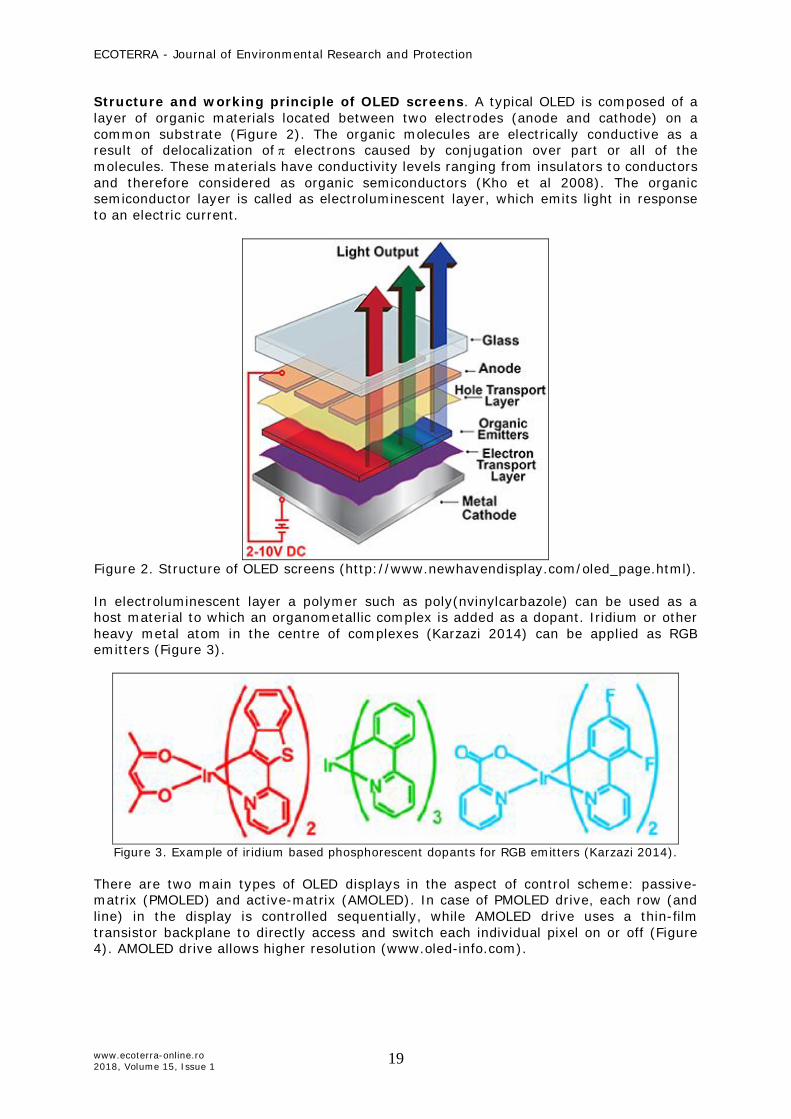
Structure and working principle of OLED screens. A typical OLED is composed of a layer of organic materials located between two electrodes (anode and cathode) on a common substrate (Figure 2). The organic molecules are electrically conductive as a result of delocalization of electrons caused by conjugation over part or all of the molecules. These materials have conductivity levels ranging from insulators to conductors and therefore considered as organic semiconductors (Kho et al 2008). The organic semiconductor layer is called as electroluminescent layer, which emits light in response to an electric current.
Figure 2. Structure of OLED screens (http://www.newhavendisplay.com/oled_page.html). In electroluminescent layer a polymer such as poly(nvinylcarbazole) can be used as a host material to which an organometallic complex is added as a dopant. Iridium or other heavy metal atom in the centre of complexes (Karzazi 2014) can be applied as RGB emitters (Figure 3).
Figure 3. Example of iridium based phosphorescent dopants for RGB emitters (Karzazi 2014).
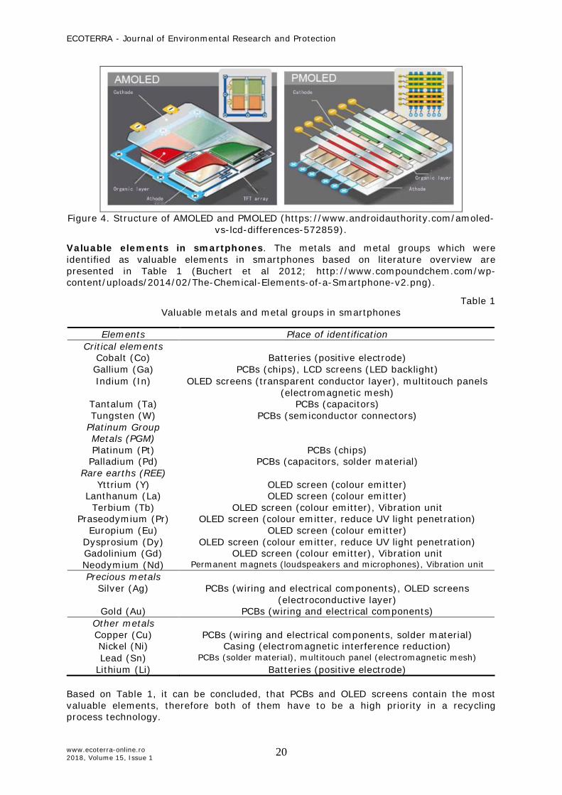
There are two main types of OLED displays in the aspect of control scheme: passive-matrix (PMOLED) and active-matrix (AMOLED). In case of PMOLED drive, each row (and line) in the display is controlled sequentially, while AMOLED drive uses a thin-film transistor backplane to directly access and switch each individual pixel on or off (Figure 4). AMOLED drive allows higher resolution (www.oled-info.com).
ECOTERRA - Journal of Environmental Research and Protection
www.ecoterra-online.ro 2018, Volume 15, Issue 1
20
Figure 4. Structure of AMOLED and PMOLED (https://www.androidauthority.com/amoled-
vs-lcd-differences-572859).
Valuable elements in smartphones. The metals and metal groups which were identified as valuable elements in smartphones based on literature overview are presented in Table 1 (Buchert et al 2012; http://www.compoundchem.com/wp-content/uploads/2014/02/The-Chemical-Elements-of-a-Smartphone-v2.png).
Table 1 Valuable metals and metal groups in smartphones
Elements Place of identification
Critical elements Cobalt (Co) Batteries (positive electrode) Gallium (Ga) PCBs (chips), LCD screens (LED backlight) Indium (In) OLED screens (transparent conductor layer), multitouch panels
(electromagnetic mesh) Tantalum (Ta) PCBs (capacitors) Tungsten (W) PCBs (semiconductor connectors)
Platinum Group Metals (PGM) Platinum (Pt) Palladium (Pd)
PCBs (chips) PCBs (capacitors, solder material)
Rare earths (REE) Yttrium (Y)
Lanthanum (La) Terbium (Tb)
Praseodymium (Pr) Europium (Eu)
Dysprosium (Dy) Gadolinium (Gd) Neodymium (Nd)
OLED screen (colour emitter) OLED screen (colour emitter)
OLED screen (colour emitter), Vibration unit OLED screen (colour emitter, reduce UV light penetration)
OLED screen (colour emitter) OLED screen (colour emitter, reduce UV light penetration)
OLED screen (colour emitter), Vibration unit Permanent magnets (loudspeakers and microphones), Vibration unit
Precious metals Silver (Ag) PCBs (wiring and electrical components), OLED screens
(electroconductive layer) Gold (Au) PCBs (wiring and electrical components)
Other metals Copper (Cu) PCBs (wiring and electrical components, solder material) Nickel (Ni) Casing (electromagnetic interference reduction) Lead (Sn) PCBs (solder material), multitouch panel (electromagnetic mesh)
Lithium (Li) Batteries (positive electrode)
Based on Table 1, it can be concluded, that PCBs and OLED screens contain the most valuable elements, therefore both of them have to be a high priority in a recycling process technology.
ECOTERRA - Journal of Environmental Research and Protection
www.ecoterra-online.ro 2018, Volume 15, Issue 1
21
Material and Method. The Institute of Raw Materials Preparation and Environmental Process Engineering of University of Miskolc works on the exploration and recovery of valuable elements from secondary raw materials sources within the frame of “Sustainable Raw Material Management Thematic Network – RING 2017” project. The project started in June 2017 and will be finished in 2020. In the future, our main task will be to develop process techniques and technologies for the prospective sources. This paper summarizes the first results of analytical investigations related to OLED smartphones. Sample. A “Samsung Galaxy S3 Neo” type of smartphone was selected for preliminary investigations. The selected smartphone has Super AMOLED screen. The technical details are shown in Table 2.
Table 2 Technical details of Super AMOLED screen of “Samsung Galaxy S3 Neo”
Parameter Value
Type Super AMOLED capacitive touchscreen, 16M colours Size 63.5 cm2 (~65.7% screen-to-body ratio)
Resolution 720×1280 pixels, 16:9 ratio (~306 ppi density) Multitouch Yes
Results and Discussion Dismantling. As a first step of dismantling process, the smartphone frame was removed by using a heat gun (220°C). The direct heat softens the organic glue between the plastic units, therefore the screen frame can be removed, which resulted that inner parts became available. The inner parts and units were manually further dismantled (Figure 5).
Figure 5. “Samsung Galaxy S3 Neo” after manual dismantling.
The dismantled parts (or major units) and the associated yields can be seen in Table 3.
ECOTERRA - Journal of Environmental Research and Protection
www.ecoterra-online.ro 2018, Volume 15, Issue 1
22
Table 3 Dismantling results of “Samsung Galaxy S3 Neo”
Dismantled parts Mass [g] Yield [%]
OLED Screen 7.87 8.81 Multitouch panel 23.79 26.62
Screen frame (plastic) 22.90 25.62 Back cover (casing) (plastic) 8.76 9.80 Printed circuit boards (PCBs) 11.48 12.85 Smartphone frame (plastic) 14.04 15.71
Screws 0.53 0.59 Total 89.37 100
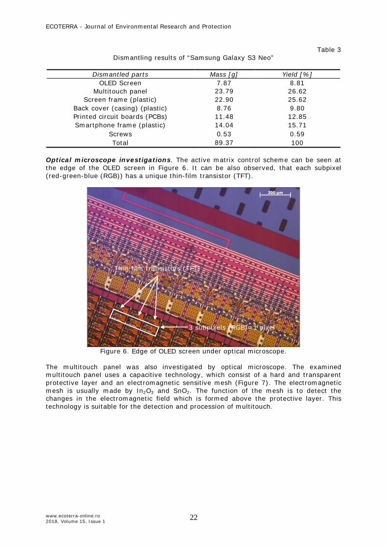
Optical microscope investigations. The active matrix control scheme can be seen at the edge of the OLED screen in Figure 6. It can be also observed, that each subpixel (red-green-blue (RGB)) has a unique thin-film transistor (TFT).
Figure 6. Edge of OLED screen under optical microscope.
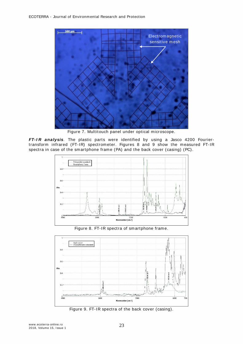
The multitouch panel was also investigated by optical microscope. The examined multitouch panel uses a capacitive technology, which consist of a hard and transparent protective layer and an electromagnetic sensitive mesh (Figure 7). The electromagnetic mesh is usually made by In2O3 and SnO2. The function of the mesh is to detect the changes in the electromagnetic field which is formed above the protective layer. This technology is suitable for the detection and procession of multitouch.
Thin-film transistors (TFT)
3 subpixels (RGB)=1 pixel
ECOTERRA - Journal of Environmental Research and Protection
www.ecoterra-online.ro 2018, Volume 15, Issue 1
23
Figure 7. Multitouch panel under optical microscope.
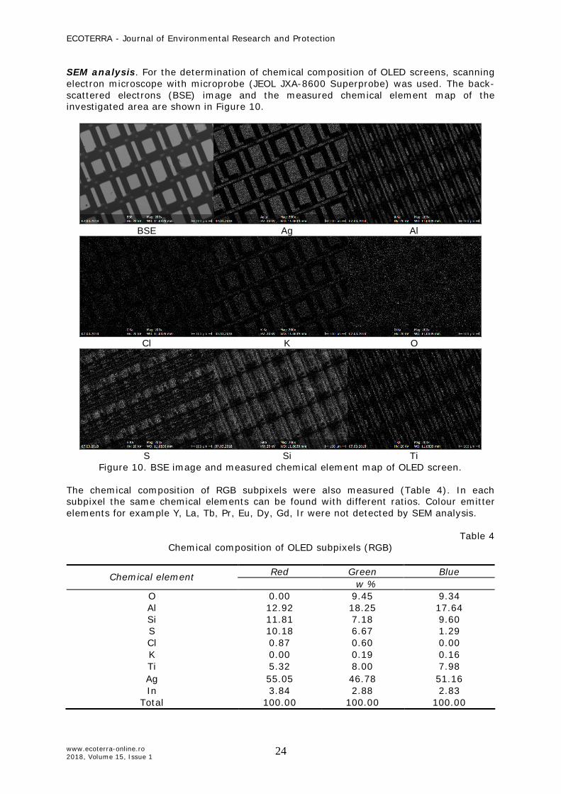
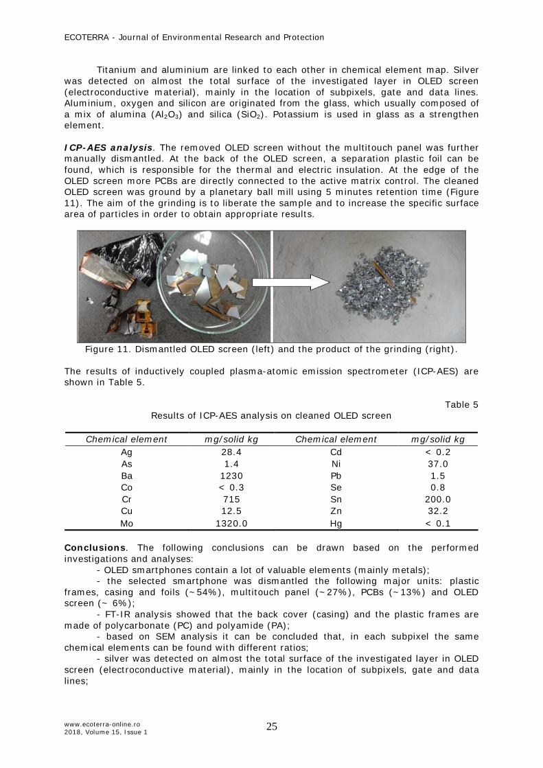
FT-IR analysis. The plastic parts were identified by using a Jasco 4200 Fourier-transform infrared (FT-IR) spectrometer. Figures 8 and 9 show the measured FT-IR spectra in case of the smartphone frame (PA) and the back cover (casing) (PC).
Figure 8. FT-IR spectra of smartphone frame.
Figure 9. FT-IR spectra of the back cover (casing).
Electromagnetic sensitive mesh
ECOTERRA - Journal of Environmental Research and Protection
www.ecoterra-online.ro 2018, Volume 15, Issue 1
24
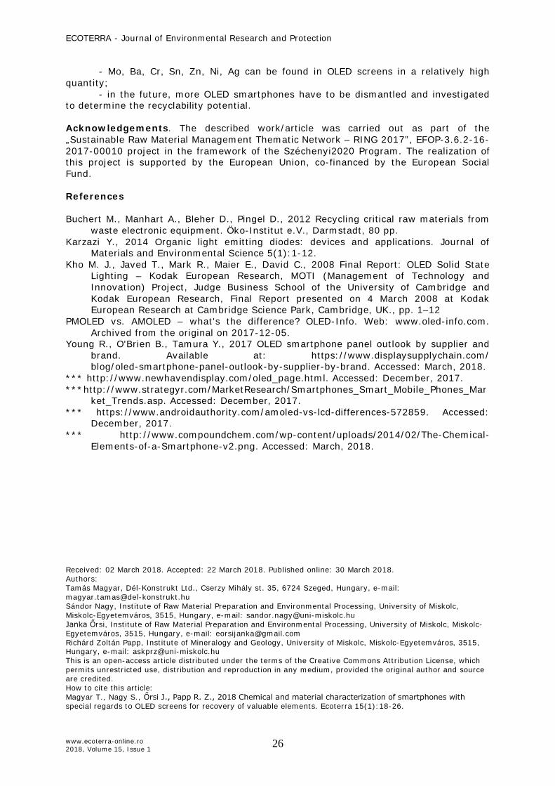
SEM analysis. For the determination of chemical composition of OLED screens, scanning electron microscope with microprobe (JEOL JXA-8600 Superprobe) was used. The back-scattered electrons (BSE) image and the measured chemical element map of the investigated area are shown in Figure 10.
BSE Ag Al
Cl K O
S Si Ti
Figure 10. BSE image and measured chemical element map of OLED screen.
The chemical composition of RGB subpixels were also measured (Table 4). In each subpixel the same chemical elements can be found with different ratios. Colour emitter elements for example Y, La, Tb, Pr, Eu, Dy, Gd, Ir were not detected by SEM analysis.
Table 4 Chemical composition of OLED subpixels (RGB)
Red Green Blue Chemical element
w % O 0.00 9.45 9.34 Al 12.92 18.25 17.64 Si 11.81 7.18 9.60 S 10.18 6.67 1.29 Cl 0.87 0.60 0.00 K 0.00 0.19 0.16 Ti 5.32 8.00 7.98 Ag 55.05 46.78 51.16 In 3.84 2.88 2.83
Total 100.00 100.00 100.00
ECOTERRA - Journal of Environmental Research and Protection
www.ecoterra-online.ro 2018, Volume 15, Issue 1
25
Titanium and aluminium are linked to each other in chemical element map. Silver was detected on almost the total surface of the investigated layer in OLED screen (electroconductive material), mainly in the location of subpixels, gate and data lines. Aluminium, oxygen and silicon are originated from the glass, which usually composed of a mix of alumina (Al2O3) and silica (SiO2). Potassium is used in glass as a strengthen element. ICP-AES analysis. The removed OLED screen without the multitouch panel was further manually dismantled. At the back of the OLED screen, a separation plastic foil can be found, which is responsible for the thermal and electric insulation. At the edge of the OLED screen more PCBs are directly connected to the active matrix control. The cleaned OLED screen was ground by a planetary ball mill using 5 minutes retention time (Figure 11). The aim of the grinding is to liberate the sample and to increase the specific surface area of particles in order to obtain appropriate results.
Figure 11. Dismantled OLED screen (left) and the product of the grinding (right).
The results of inductively coupled plasma-atomic emission spectrometer (ICP-AES) are shown in Table 5.
Table 5 Results of ICP-AES analysis on cleaned OLED screen
Chemical element mg/solid kg Chemical element mg/solid kg
Ag 28.4 Cd < 0.2 As 1.4 Ni 37.0 Ba 1230 Pb 1.5 Co < 0.3 Se 0.8 Cr 715 Sn 200.0 Cu 12.5 Zn 32.2 Mo 1320.0 Hg < 0.1
Conclusions. The following conclusions can be drawn based on the performed investigations and analyses:
- OLED smartphones contain a lot of valuable elements (mainly metals); - the selected smartphone was dismantled the following major units: plastic
frames, casing and foils (~54%), multitouch panel (~27%), PCBs (~13%) and OLED screen (~ 6%);
- FT-IR analysis showed that the back cover (casing) and the plastic frames are made of polycarbonate (PC) and polyamide (PA);
- based on SEM analysis it can be concluded that, in each subpixel the same chemical elements can be found with different ratios;
- silver was detected on almost the total surface of the investigated layer in OLED screen (electroconductive material), mainly in the location of subpixels, gate and data lines;
ECOTERRA - Journal of Environmental Research and Protection
www.ecoterra-online.ro 2018, Volume 15, Issue 1
26
- Mo, Ba, Cr, Sn, Zn, Ni, Ag can be found in OLED screens in a relatively high quantity;
- in the future, more OLED smartphones have to be dismantled and investigated to determine the recyclability potential. Acknowledgements. The described work/article was carried out as part of the „Sustainable Raw Material Management Thematic Network – RING 2017”, EFOP-3.6.2-16-2017-00010 project in the framework of the Széchenyi2020 Program. The realization of this project is supported by the European Union, co-financed by the European Social Fund. References Buchert M., Manhart A., Bleher D., Pingel D., 2012 Recycling critical raw materials from
waste electronic equipment. Öko-Institut e.V., Darmstadt, 80 pp. Karzazi Y., 2014 Organic light emitting diodes: devices and applications. Journal of
Materials and Environmental Science 5(1):1-12. Kho M. J., Javed T., Mark R., Maier E., David C., 2008 Final Report: OLED Solid State
Lighting – Kodak European Research, MOTI (Management of Technology and Innovation) Project, Judge Business School of the University of Cambridge and Kodak European Research, Final Report presented on 4 March 2008 at Kodak European Research at Cambridge Science Park, Cambridge, UK., pp. 1–12
PMOLED vs. AMOLED – what's the difference? OLED-Info. Web: www.oled-info.com. Archived from the original on 2017-12-05.
Young R., O'Brien B., Tamura Y., 2017 OLED smartphone panel outlook by supplier and brand. Available at: https://www.displaysupplychain.com/ blog/oled-smartphone-panel-outlook-by-supplier-by-brand. Accessed: March, 2018.
*** http://www.newhavendisplay.com/oled_page.html. Accessed: December, 2017. ***http://www.strategyr.com/MarketResearch/Smartphones_Smart_Mobile_Phones_Mar
ket_Trends.asp. Accessed: December, 2017. *** https://www.androidauthority.com/amoled-vs-lcd-differences-572859. Accessed:
December, 2017. *** http://www.compoundchem.com/wp-content/uploads/2014/02/The-Chemical-
Elements-of-a-Smartphone-v2.png. Accessed: March, 2018. Received: 02 March 2018. Accepted: 22 March 2018. Published online: 30 March 2018. Authors: Tamás Magyar, Dél-Konstrukt Ltd., Cserzy Mihály st. 35, 6724 Szeged, Hungary, e-mail: [email protected] Sándor Nagy, Institute of Raw Material Preparation and Environmental Processing, University of Miskolc, Miskolc-Egyetemváros, 3515, Hungary, e-mail: [email protected] Janka Őrsi, Institute of Raw Material Preparation and Environmental Processing, University of Miskolc, Miskolc-Egyetemváros, 3515, Hungary, e-mail: [email protected] Richárd Zoltán Papp, Institute of Mineralogy and Geology, University of Miskolc, Miskolc-Egyetemváros, 3515, Hungary, e-mail: [email protected] This is an open-access article distributed under the terms of the Creative Commons Attribution License, which permits unrestricted use, distribution and reproduction in any medium, provided the original author and source are credited. How to cite this article: Magyar T., Nagy S., Őrsi J., Papp R. Z., 2018 Chemical and material characterization of smartphones with special regards to OLED screens for recovery of valuable elements. Ecoterra 15(1):18-26.