Circuit quantum electrodynamics with transmon qubitsJavier_Maste… · WMI TECHNISCHE UNIVERSITÄT...
67
WMI TECHNISCHE UNIVERSITÄT MÜNCHEN WALTHER - MEISSNER - INSTITUT FÜR TIEF - TEMPERATURFORSCHUNG BAYERISCHE AKADEMIE DER WISSENSCHAFTEN Circuit quantum electrodynamics with transmon qubits Master’s Thesis Javier Puertas Martínez Supervisor: Prof. Dr. Rudolf Gross Munich, February 2015
Transcript of Circuit quantum electrodynamics with transmon qubitsJavier_Maste… · WMI TECHNISCHE UNIVERSITÄT...
WMITECHNISCHEUNIVERSITÄT
MÜNCHEN
WALTHER - MEISSNER -INSTITUT FÜR TIEF -
TEMPERATURFORSCHUNG
BAYERISCHEAKADEMIE DER
WISSENSCHAFTEN
Circuit quantum electrodynamics with
transmon qubits
Master’s ThesisJavier Puertas Martínez
Supervisor: Prof. Dr. Rudolf GrossMunich, February 2015


WMITECHNISCHEUNIVERSITÄT
MÜNCHEN
WALTHER - MEISSNER -INSTITUT FÜR TIEF -
TEMPERATURFORSCHUNG
BAYERISCHEAKADEMIE DER
WISSENSCHAFTEN
Circuit quantum electrodynamics with
transmon qubits
Master’s ThesisJavier Puertas Martínez
Supervisor: Prof. Dr. Rudolf GrossMunich, February 2015

Contents
Introduction 1
1 Theory 3
1.1 Josephson junctions . . . . . . . . . . . . . . . . . . . . . . . . . . . . . . . . 31.1.1 Josephson equations . . . . . . . . . . . . . . . . . . . . . . . . . . . 41.1.2 I-V curve for the Josephson junction . . . . . . . . . . . . . . . . . . . 51.1.3 DC-SQUID . . . . . . . . . . . . . . . . . . . . . . . . . . . . . . . . 8
1.2 The transmon qubit . . . . . . . . . . . . . . . . . . . . . . . . . . . . . . . . 91.2.1 The qubit as a two-level quantum system . . . . . . . . . . . . . . . . . 101.2.2 Dynamics of the qubit . . . . . . . . . . . . . . . . . . . . . . . . . . 101.2.3 The Transmon qubit derived from the Cooper pair box . . . . . . . . . 11
1.3 Coplanar waveguide resonators . . . . . . . . . . . . . . . . . . . . . . . . . . 141.4 Coupling of the transmon qubit to the CPW resonator . . . . . . . . . . . . . . 17
1.4.1 Zero detuning . . . . . . . . . . . . . . . . . . . . . . . . . . . . . . . 181.4.2 Dispersive regime . . . . . . . . . . . . . . . . . . . . . . . . . . . . . 191.4.3 The Purcell effect . . . . . . . . . . . . . . . . . . . . . . . . . . . . . 21
2 Experimental techniques 23
2.1 Nanofabrication . . . . . . . . . . . . . . . . . . . . . . . . . . . . . . . . . . 232.1.1 Optical lithography . . . . . . . . . . . . . . . . . . . . . . . . . . . . 232.1.2 Electron beam lithography . . . . . . . . . . . . . . . . . . . . . . . . 24
2.2 Experimental setup . . . . . . . . . . . . . . . . . . . . . . . . . . . . . . . . 272.2.1 3He cryostat . . . . . . . . . . . . . . . . . . . . . . . . . . . . . . . . 282.2.2 Dilution refrigerators . . . . . . . . . . . . . . . . . . . . . . . . . . . 28
3 Experimental results 31
3.1 Measured samples . . . . . . . . . . . . . . . . . . . . . . . . . . . . . . . . . 313.1.1 The resonators . . . . . . . . . . . . . . . . . . . . . . . . . . . . . . 313.1.2 The transmon qubit . . . . . . . . . . . . . . . . . . . . . . . . . . . . 32
3.2 DC measurements . . . . . . . . . . . . . . . . . . . . . . . . . . . . . . . . . 363.3 Transmission measurements . . . . . . . . . . . . . . . . . . . . . . . . . . . 373.4 Two-tone spectroscopy . . . . . . . . . . . . . . . . . . . . . . . . . . . . . . 41
3.4.1 Power calibration . . . . . . . . . . . . . . . . . . . . . . . . . . . . . 43
I
II Contents
3.4.2 Flux dependence of the qubit frequency . . . . . . . . . . . . . . . . . 453.4.3 Qubit anharmonicity . . . . . . . . . . . . . . . . . . . . . . . . . . . 48
3.5 Time domain measurements . . . . . . . . . . . . . . . . . . . . . . . . . . . 51
4 Summary and outlook 55
Bibliography 57
Introduction
Quantum computing was proposed by Feynman [1] as a way of efficiently studying quantumsystems. It allows for an exponential speedup in the computation of certain problems withrespect to a classical computer [2] . The key element of a quantum computer is the qubit. Itis the analog to the classic bit. However, while a classical bit can only be in states 0 and 1,the qubit, due to its quantum nature, can be in any superposition of these states. The first stepis to find in nature any two-level quantum system that might be used as a qubit. One of thefirst approaches was the use of two isolated levels of an atom. The atom can be placed insidean optical cavity where some photons are trapped. The interaction between the atom and thephotons can be used for manipulating and transferring quantum information [3]. This field wascalled cavity quantum electrodynamics (QED).Another approach was the use of superconducting circuits instead of atoms and cavities. Cavitieswere replaced by superconducting resonators and atoms were replaced by superconductingqubits. Different circuits designs have been proposed for the superconducting qubits, mainlyphase, flux and charge qubits [4]. They make use of Josephson junctions that can be seen asnon-linear inductors. This non-linearity produces a non-equal spacing of the energy levels and,hence, makes the circuit suitable as a two-level system [5]. In 2004 the first measurement of asuperconducting qubit coupled to a superconducting resonator was performed using a chargequbit and a coplanar waveguide resonator [6]. Due to the similarities with cavity QED, this fieldwas called circuit QED.In this work, we couple a transmon qubit to a superconducting resonator. We study twosamples that differ on the type of resonator used. From transmission measurements we obtainthe coupling strength between the resonator and the qubit reaching the strong coupling limit.Using two-tone spectroscopy the energy levels of the qubit are measured. In addition the qubitcoherence time is obtained from both spectroscopy and time domain measurements.The thesis is organized as follows. In Chapter 1 we introduce the theoretical concepts neededfor the understanding of the performed measurements. In Chapter 2 we describe the fabricationprocess for both resonators and the transmon qubit. In Chapter 3 the measurements are shownand the main results are given.
1

Chapter 1
Theory
In this chapter we will introduce the theoretical concepts that are needed to understand theperformed measurements. First the Josephson junction and the Josephson equations are ex-plained. Then the transmon qubit and the coplanar waveguide resonator are described. Finallythe coupling between the resonator and the qubit is studied using the Jaynes-Cummings model.
1.1 Josephson junctions
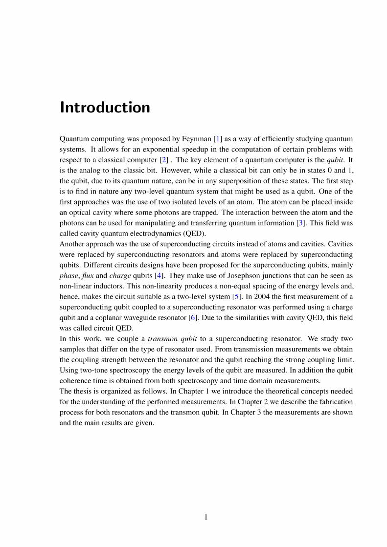
Josephson junctions represent the key element in superconducting quantum bits (qubits). Assuperconductor devices, they have unique macroscopic quantum properties that can be exploitedin the field of quantum computation. In this section we give the equations for the current andthe voltage in a Josephson junction, the so called Josephson equations, and we use a simplemodel to describe its current-voltage characteristic curve. A Josephson junction consists on twosuperconductors separated by an insulator [Fig. 1.1(a)].
Superconductor
Insulator
(a)
V (x)
x
ΨA ΨBd
V0
(b)
Figure 1.1: (a) A schematic supercondcutor, insulator, superconductor (SIS) Josephsonjunction. The insulator is usually an oxide. (b) Sketch of the time-independentpart of the macroscopic wavefunction (blue line) in an SIS Josephson junction.The red rectangle represents the insulation barrier.
3
4 Chapter 1 Theory
Each superconductor can be described by a macroscopic wave function [7]. If we call themsuperconductor A and B we will have
ΨA(~r) = Ψ0eiφA(~r) ΨB(~r) = Ψ0eiφB(~r) (1.1)
where |Ψ0|2 = n(~r,t) is the density of Cooper pairs in the superconductor. In a similar processto that of an electronic wave function, these macroscopic wave functions can tunnel through thepotential barrier created by the insulator [Fig. 1.1(b)]. If we solve the Schrödinger equation forthe three regions (superconductor A, insulator, superconductor B) and use the wave matchingmethod, we arrive to the expression for the current density in the junction
J = Jc sin(φA−φB) (1.2)
where Jc is a material parameter. It depends on the characteristic decay constant κ = (2m(V0−E)/h2)1/2. For real junctions usually the barrier height V0 is of the order of a few eV andtherefore the decay length 1/κ less than a nanometer. In addition, the barrier thickness d isusually a few nm. Thus κd 1. In this regime Jc ∝ exp(−2κd). It decays exponentially withincreasing barrier width d.
1.1.1 Josephson equations
From the tunneling described in the previous section we can derive the equations for the voltageand the current in a Josephson junction. They are the so called Josephson equations [7].
I = Ic sinδ (1.3a)
V =Φ0
2π
dδ
dt(1.3b)
Here, δ is the gauge invariant phase difference between superconductor A and superconductorB [7]. The quantity Ic is the critical current above which the Josephson junction shows a finiteresistance. Two main properties of the junction can be derived from the above equations. Firstthe current flow between the superconductors depends only on the relative phase of their macro-scopic wave functions. Second there is only a voltage drop between both superconductors whenthis phase evolves in time. An important parameter than can be obtained from these equations isthe Josephson inductance LJ .
1.1 Josephson junctions 5
dIdt
= Ic cosδ2π
Φ0V → LJ =
Φ0
2πIc cosδ=
Φ0
2πIc
√1−(
IIc
)2(1.4)
As it can be seen, the Josephson inductance is not linear with current which makes it a funda-mental element for superconducting qubits. The energy stored in the junction will be given by
U =∫ t
0IV dt =
Φ0
2π
∫ t
0Idφ
dtdt =
Φ0
2π
∫ t
0Ic sin(φ)dφ = EJ(1− cosφ) (1.5)
where
EJ =IcΦ0
2π(1.6)
is the Josephson energy. Furthermore, we point out that due to the fact that a Josephson junctionconsists of two metals separated by an insulator, it will have some capacitance C. From thiscapacitance we can define the charging energy of the junction as
EC =e2
2C(1.7)
Finally, from LJ and C we define the Josephson junction plasma frequency
ωp =1√LJC
=1h
√8EJEC (1.8)
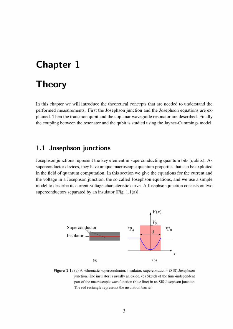
1.1.2 I-V curve for the Josephson junction
In the previous section we treated the Josephson junction as a perfect tunneling junction witha capacitance C. In order to study its I-V curve we have to take into account its resistance forI > Ic [Fig. 1.2].
Real junctionC JJ R
Figure 1.2: The junction is divided into three components: a perfect tunneling component,a capacitor and a resistor
6 Chapter 1 Theory
The resistively and capacitively shunted junction model (RCSJ) takes into account both thecapacitance and the resistance of the junction.
RCSJ model
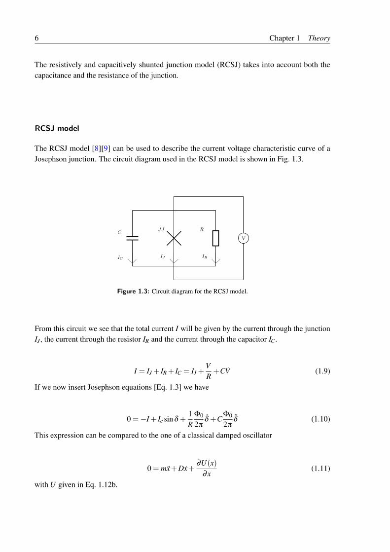
The RCSJ model [8][9] can be used to describe the current voltage characteristic curve of aJosephson junction. The circuit diagram used in the RCSJ model is shown in Fig. 1.3.
VC
JJ R
IC IJ IR
Figure 1.3: Circuit diagram for the RCSJ model.
From this circuit we see that the total current I will be given by the current through the junctionIJ , the current through the resistor IR and the current through the capacitor IC.
I = IJ + IR + IC = IJ +VR+CV (1.9)
If we now insert Josephson equations [Eq. 1.3] we have
0 =−I + Ic sinδ +1R
Φ0
2πδ +C
Φ0
2πδ (1.10)
This expression can be compared to the one of a classical damped oscillator
0 = mx+Dx+∂U(x)
∂x(1.11)
with U given in Eq. 1.12b.
1.1 Josephson junctions 7
∂U(δ )
∂δ=
IcΦ0
2π(− I
Ic+ sinδ ) (1.12a)
⇒U(δ ) = EJ(−IIc
δ − cosδ ) (1.12b)
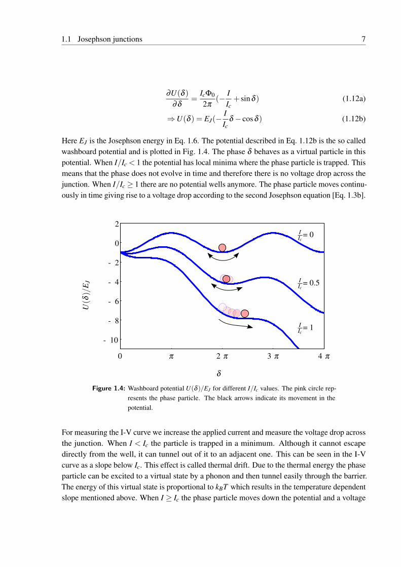
Here EJ is the Josephson energy in Eq. 1.6. The potential described in Eq. 1.12b is the so calledwashboard potential and is plotted in Fig. 1.4. The phase δ behaves as a virtual particle in thispotential. When I/Ic < 1 the potential has local minima where the phase particle is trapped. Thismeans that the phase does not evolve in time and therefore there is no voltage drop across thejunction. When I/Ic ≥ 1 there are no potential wells anymore. The phase particle moves continu-ously in time giving rise to a voltage drop according to the second Josephson equation [Eq. 1.3b].
0 π 2 π 3 π 4 π
- 10
- 8
- 6
- 4
- 2
0
2IIc
= 0
IIc
= 1
IIc
= 0.5
δ
U(δ
)/E
J
Figure 1.4: Washboard potential U(δ )/EJ for different I/Ic values. The pink circle rep-resents the phase particle. The black arrows indicate its movement in thepotential.
For measuring the I-V curve we increase the applied current and measure the voltage drop acrossthe junction. When I < Ic the particle is trapped in a minimum. Although it cannot escapedirectly from the well, it can tunnel out of it to an adjacent one. This can be seen in the I-Vcurve as a slope below Ic. This effect is called thermal drift. Due to the thermal energy the phaseparticle can be excited to a virtual state by a phonon and then tunnel easily through the barrier.The energy of this virtual state is proportional to kBT which results in the temperature dependentslope mentioned above. When I ≥ Ic the phase particle moves down the potential and a voltage
8 Chapter 1 Theory
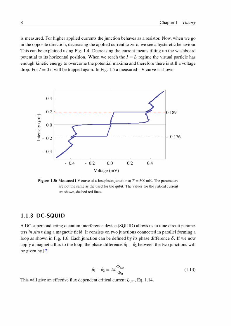
is measured. For higher applied currents the junction behaves as a resistor. Now, when we goin the opposite direction, decreasing the applied current to zero, we see a hysteretic behaviour.This can be explained using Fig. 1.4. Decreasing the current means tilting up the washboardpotential to its horizontal position. When we reach the I = Ic regime the virtual particle hasenough kinetic energy to overcome the potential maxima and therefore there is still a voltagedrop. For I = 0 it will be trapped again. In Fig. 1.5 a measured I-V curve is shown.
- 0.4 - 0.2 0.0 0.2 0.4
- 0.4
- 0.2
0.0
0.2
0.4
0.189
- 0.176
Voltage (mV)
Inte
nsity
(µm
)
Figure 1.5: Measured I-V curve of a Josephson junction at T = 500 mK. The parametersare not the same as the used for the qubit. The values for the critical currentare shown, dashed red lines.
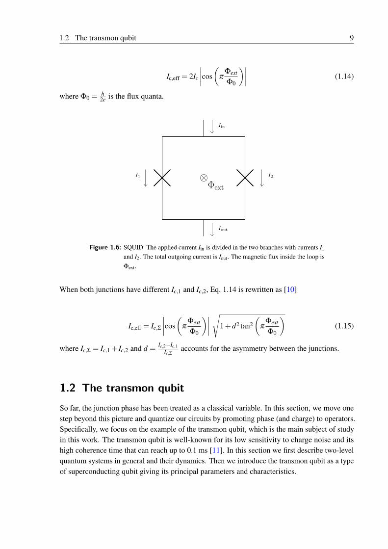
1.1.3 DC-SQUID
A DC superconducting quantum interference device (SQUID) allows us to tune circuit parame-ters in situ using a magnetic field. It consists on two junctions connected in parallel forming aloop as shown in Fig. 1.6. Each junction can be defined by its phase difference δ . If we nowapply a magnetic flux to the loop, the phase difference δ1−δ2 between the two junctions willbe given by [7]
δ1−δ2 = 2πΦext
Φ0(1.13)
This will give an effective flux dependent critical current Ic,eff, Eq. 1.14.
1.2 The transmon qubit 9
Ic,eff = 2Ic
∣∣∣∣cos(
πΦext
Φ0
)∣∣∣∣ (1.14)
where Φ0 =h2e is the flux quanta.
I1 I2
Iin
Iout
Φext
Figure 1.6: SQUID. The applied current Iin is divided in the two branches with currents I1
and I2. The total outgoing current is Iout. The magnetic flux inside the loop isΦext.
When both junctions have different Ic,1 and Ic,2, Eq. 1.14 is rewritten as [10]
Ic,eff = Ic,Σ
∣∣∣∣cos(
πΦext
Φ0
)∣∣∣∣√
1+d2 tan2(
πΦext
Φ0
)(1.15)
where Ic,Σ = Ic,1 + Ic,2 and d =Ic,2−Ic,1
Ic,Σaccounts for the asymmetry between the junctions.
1.2 The transmon qubit
So far, the junction phase has been treated as a classical variable. In this section, we move onestep beyond this picture and quantize our circuits by promoting phase (and charge) to operators.Specifically, we focus on the example of the transmon qubit, which is the main subject of studyin this work. The transmon qubit is well-known for its low sensitivity to charge noise and itshigh coherence time that can reach up to 0.1 ms [11]. In this section we first describe two-levelquantum systems in general and their dynamics. Then we introduce the transmon qubit as a typeof superconducting qubit giving its principal parameters and characteristics.
10 Chapter 1 Theory
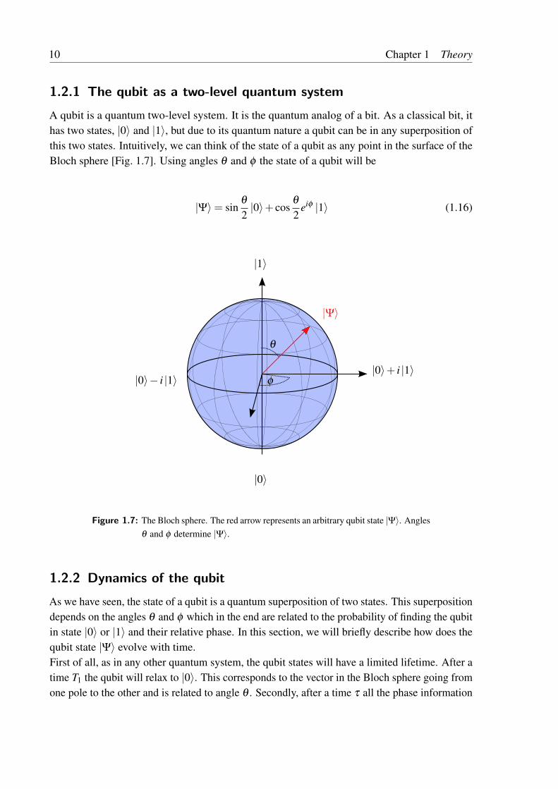
1.2.1 The qubit as a two-level quantum system
A qubit is a quantum two-level system. It is the quantum analog of a bit. As a classical bit, ithas two states, |0〉 and |1〉, but due to its quantum nature a qubit can be in any superposition ofthis two states. Intuitively, we can think of the state of a qubit as any point in the surface of theBloch sphere [Fig. 1.7]. Using angles θ and φ the state of a qubit will be
|Ψ〉= sinθ
2|0〉+ cos
θ
2eiφ |1〉 (1.16)
|1〉
|0〉
|0〉+ i |1〉|0〉− i |1〉
|Ψ〉
φ
θ
Figure 1.7: The Bloch sphere. The red arrow represents an arbitrary qubit state |Ψ〉. Anglesθ and φ determine |Ψ〉.
1.2.2 Dynamics of the qubit
As we have seen, the state of a qubit is a quantum superposition of two states. This superpositiondepends on the angles θ and φ which in the end are related to the probability of finding the qubitin state |0〉 or |1〉 and their relative phase. In this section, we will briefly describe how does thequbit state |Ψ〉 evolve with time.First of all, as in any other quantum system, the qubit states will have a limited lifetime. After atime T1 the qubit will relax to |0〉. This corresponds to the vector in the Bloch sphere going fromone pole to the other and is related to angle θ . Secondly, after a time τ all the phase information
1.2 The transmon qubit 11
contained in angle φ will be lost and therefore we won’t have a quantum superposition of statesanymore. This process in which we lose phase information of our system is called dephasing. Itcorresponds to changes in angle φ . Of course, T1 and τ are related. No matter the dephasing,after a time T1 vector |Ψ〉 will be pointing at the south pole and the information in angle φ willbe lost. Therefore a time T2 is defined which accounts for both effects and is the one we measurein our experiments. It is given by
1T2
=1
2T1+
1τ
(1.17)
1.2.3 The Transmon qubit derived from the Cooper pair box
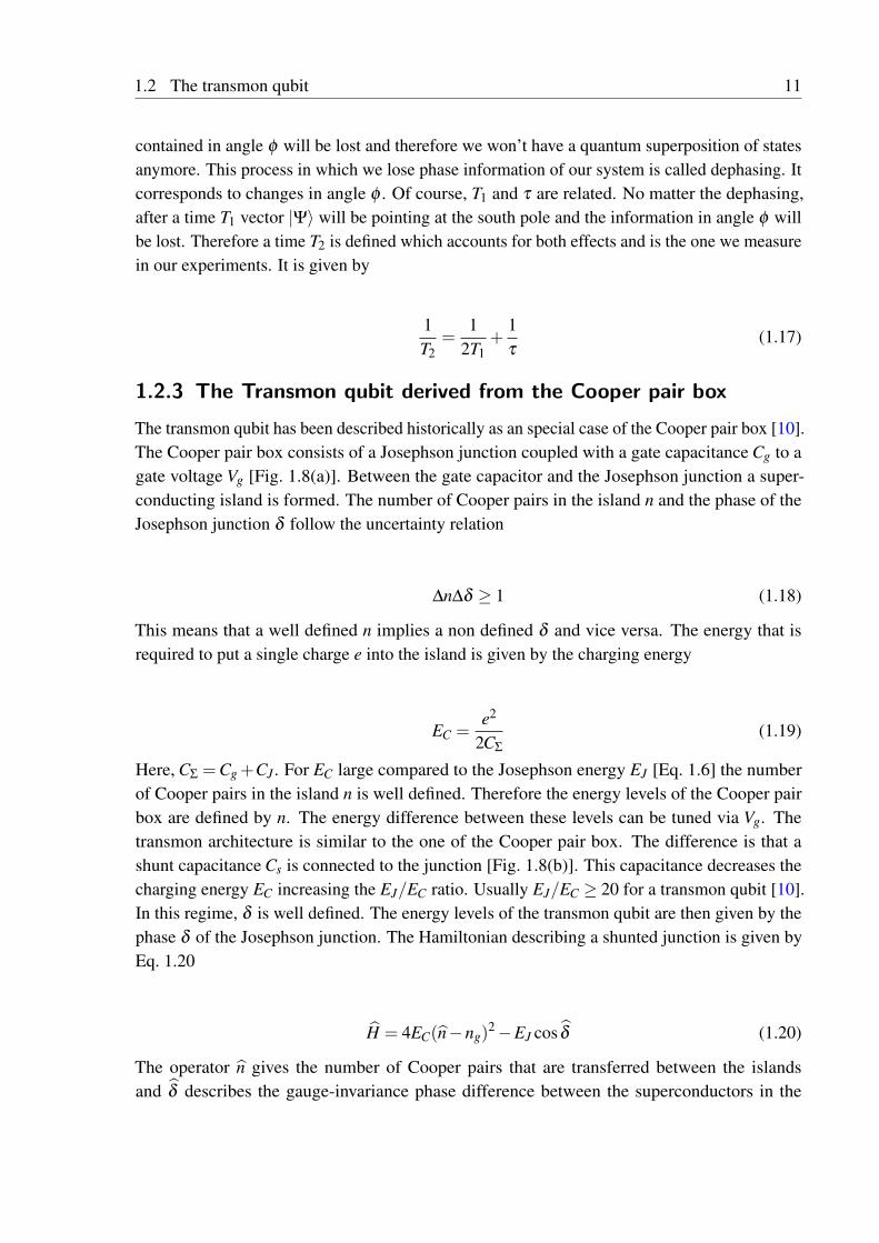
The transmon qubit has been described historically as an special case of the Cooper pair box [10].The Cooper pair box consists of a Josephson junction coupled with a gate capacitance Cg to agate voltage Vg [Fig. 1.8(a)]. Between the gate capacitor and the Josephson junction a super-conducting island is formed. The number of Cooper pairs in the island n and the phase of theJosephson junction δ follow the uncertainty relation
∆n∆δ ≥ 1 (1.18)
This means that a well defined n implies a non defined δ and vice versa. The energy that isrequired to put a single charge e into the island is given by the charging energy
EC =e2
2CΣ
(1.19)
Here, CΣ =Cg +CJ . For EC large compared to the Josephson energy EJ [Eq. 1.6] the numberof Cooper pairs in the island n is well defined. Therefore the energy levels of the Cooper pairbox are defined by n. The energy difference between these levels can be tuned via Vg. Thetransmon architecture is similar to the one of the Cooper pair box. The difference is that ashunt capacitance Cs is connected to the junction [Fig. 1.8(b)]. This capacitance decreases thecharging energy EC increasing the EJ/EC ratio. Usually EJ/EC ≥ 20 for a transmon qubit [10].In this regime, δ is well defined. The energy levels of the transmon qubit are then given by thephase δ of the Josephson junction. The Hamiltonian describing a shunted junction is given byEq. 1.20
H = 4EC(n−ng)2−EJ cos δ (1.20)
The operator n gives the number of Cooper pairs that are transferred between the islandsand δ describes the gauge-invariance phase difference between the superconductors in the
12 Chapter 1 Theory
Vg
Cg
CJ
(a) Cooper pair box
VgCJ
Cg
Cs
(b) Transmon qubit
Figure 1.8: (a) Circuit scheme of the Cooper pair box. A Josephson junction with intrinsiccapacitance CJ is coupled through a gate capacitance Cg to a gate voltage Vg.(b) Circuit scheme of the transmon qubit. The shunting capacitance Cs in thetransmon makes it insensitive to charge noise and reduces its charging energyEC.
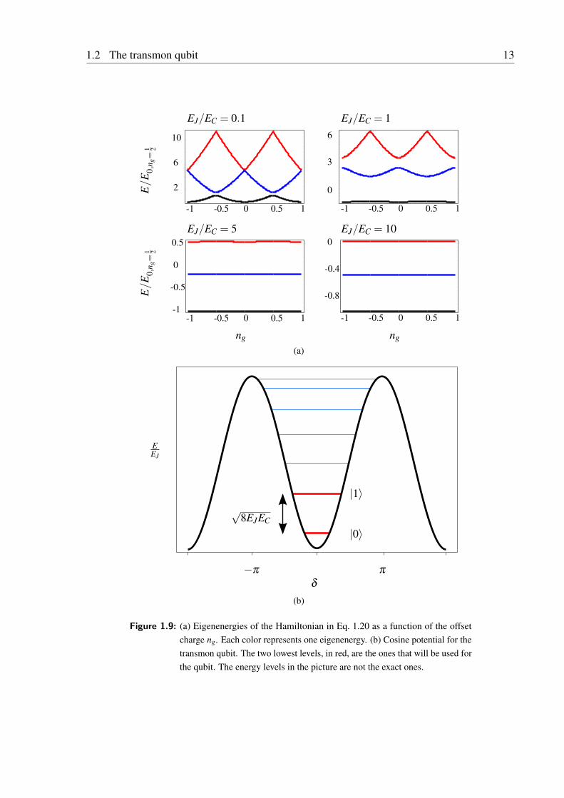
Josephson junction, which is now promoted to a quantum mechanical operator. The offsetcharge ng =CgVg/2e is the charge in units of Cooper pairs induced by the gate voltage. The firstterm in Eq. 1.20 is related to the kinetic energy of the system and the second term is related to itspotential energy. The energy levels as a function of the offset charge ng are shown in Fig. 1.9(a)for different EJ/EC ratios. As it can be seen, upon increasing the EJ/EC ratio, the energy levelsbecome flat. This means that the system is less sensitive to the ubiquitous charge noise. Onthe other hand, with an increasing EJ/EC ratio the anharmonicity is reduced. According toRef. [10] the flattening of the levels decreases much faster than the anharmonicity. In Fig. 1.9(b)the cosine potential with the energy levels for high EJ/EC is shown.As seen in Fig. 1.9(b), the difference between energy levels is not constant. This is importantwhen designing a qubit. If all the level transitions were equal, we would not be able to performoperations between just two levels. In Fig. 1.9(b) the two lowest levels are depicted in red.These are the levels used for the qubit. To obtain the frequency transition between this levels,we notice that the transmon qubit [Fig. 1.8(b)] is simply an LC oscillator with a non-linearinductance. The first transition frequency can be approximated by the plasma frequency
ωq =1√LJC≈ 1
h
√8EJEC (1.21)
For EJ/EC 1, we can write the anharmonicity α as [10]
α = E12−E01 =−EC (1.22)
1.2 The transmon qubit 13
ng ng
E/E
0,n g=
1 2E/E
0,n g=
1 2
EJ/EC = 0.1 EJ/EC = 1
EJ/EC = 5 EJ/EC = 10
10
6
2
-1 -0.5 0 0.5 1
-1 -0.5 0 0.5 1 -1 -0.5 0 0.5 1
-1 -0.5 0 0.5 1
6
3
0
0.5
0
-0.5
-1
0
-0.4
-0.8
(a)
δ
|0〉
|1〉
−π π
EEJ
√8EJEC
(b)
Figure 1.9: (a) Eigenenergies of the Hamiltonian in Eq. 1.20 as a function of the offsetcharge ng. Each color represents one eigenenergy. (b) Cosine potential for thetransmon qubit. The two lowest levels, in red, are the ones that will be used forthe qubit. The energy levels in the picture are not the exact ones.
14 Chapter 1 Theory
where Ei j is the energy difference between level |i〉 and | j〉. If the line width of the transition ismuch smaller than α we can describe the transmon as an effective two-level system. Then wecan rewrite the Hamiltonian in Eq. 1.20 using the Pauli matrix σz and ωq
H =h2
ωqσz (1.23)
1.3 Coplanar waveguide resonators
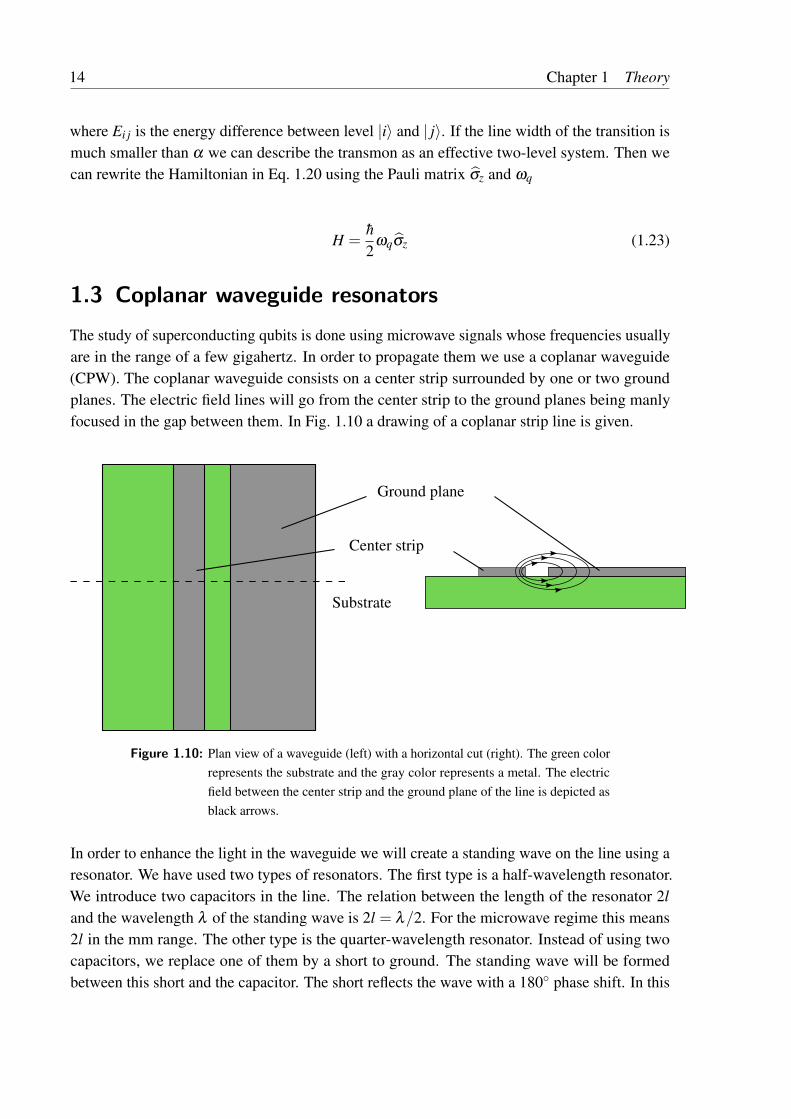
The study of superconducting qubits is done using microwave signals whose frequencies usuallyare in the range of a few gigahertz. In order to propagate them we use a coplanar waveguide(CPW). The coplanar waveguide consists on a center strip surrounded by one or two groundplanes. The electric field lines will go from the center strip to the ground planes being manlyfocused in the gap between them. In Fig. 1.10 a drawing of a coplanar strip line is given.
Substrate
Center strip
Ground plane
Figure 1.10: Plan view of a waveguide (left) with a horizontal cut (right). The green colorrepresents the substrate and the gray color represents a metal. The electricfield between the center strip and the ground plane of the line is depicted asblack arrows.
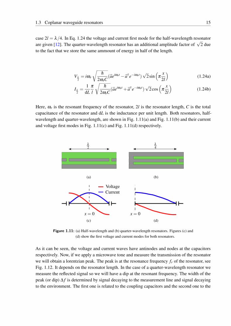
In order to enhance the light in the waveguide we will create a standing wave on the line using aresonator. We have used two types of resonators. The first type is a half-wavelength resonator.We introduce two capacitors in the line. The relation between the length of the resonator 2land the wavelength λ of the standing wave is 2l = λ/2. For the microwave regime this means2l in the mm range. The other type is the quarter-wavelength resonator. Instead of using twocapacitors, we replace one of them by a short to ground. The standing wave will be formedbetween this short and the capacitor. The short reflects the wave with a 180 phase shift. In this
1.3 Coplanar waveguide resonators 15
case 2l = λ/4. In Eq. 1.24 the voltage and current first mode for the half-wavelength resonatorare given [12]. The quarter-wavelength resonator has an additional amplitude factor of
√2 due
to the fact that we store the same ammount of energy in half of the length.
Vλ
2= iωr
√h
2ωrC(aeiωrt− a†e−iωrt)
√2sin
(π
x2l
)(1.24a)
Iλ
2=
1dL
π
l
√h
2ωrC(aeiωrt + a†e−iωrt)
√2cos
(π
x2l
)(1.24b)
Here, ωr is the resonant frequency of the resonator, 2l is the resonator length, C is the totalcapacitance of the resonator and dL is the inductance per unit length. Both resonators, half-wavelength and quarter-wavelength, are shown in Fig. 1.11(a) and Fig. 1.11(b) and their currentand voltage first modes in Fig. 1.11(c) and Fig. 1.11(d) respectively.
λ
2
(a)
λ
4
(b)
VoltageCurrent
x = 0(c)
x = 0(d)
Figure 1.11: (a) Half-wavelength and (b) quarter-wavelength resonators. Figures (c) and(d) show the first voltage and current modes for both resonators.
As it can be seen, the voltage and current waves have antinodes and nodes at the capacitorsrespectively. Now, if we apply a microwave tone and measure the transmission of the resonatorwe will obtain a lorentzian peak. The peak is at the resonance frequency fr of the resonator, seeFig. 1.12. It depends on the resonator length. In the case of a quarter-wavelength resonator wemeasure the reflected signal so we will have a dip at the resonant frequency. The width of thepeak (or dip) ∆ f is determined by signal decaying to the measurement line and signal decayingto the environment. The first one is related to the coupling capacitors and the second one to the
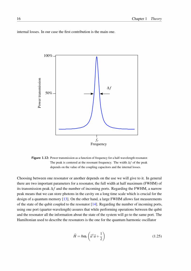
16 Chapter 1 Theory
internal losses. In our case the first contribution is the main one.
fr
∆ f
Frequency
50%
100%
Pow
ertr
ansm
issi
on
Figure 1.12: Power transmission as a function of frequency for a half-wavelength resonator.The peak is centered at the resonant frequency. The width ∆ f of the peakdepends on the value of the coupling capacitors and the internal losses.
Choosing between one resonator or another depends on the use we will give to it. In generalthere are two important parameters for a resonator, the full width at half maximum (FWHM) ofits transmission peak ∆ f and the number of incoming ports. Regarding the FWHM, a narrowpeak means that we can store photons in the cavity on a long time scale which is crucial for thedesign of a quantum memory [13]. On the other hand, a large FWHM allows fast measurementsof the state of the qubit coupled to the resonator [14]. Regarding the number of incoming ports,using one port (quarter-wavelength) assures that while performing operations between the qubitand the resonator all the information about the state of the system will go to the same port. TheHamiltonian used to describe the resonators is the one for the quantum harmonic oscillator
H = hωr
(a†a+
12
)(1.25)
1.4 Coupling of the transmon qubit to the CPW resonator 17
where ωr =1√LC
is the resonance frequency of the resonator.
1.4 Coupling of the transmon qubit to the CPW
resonator
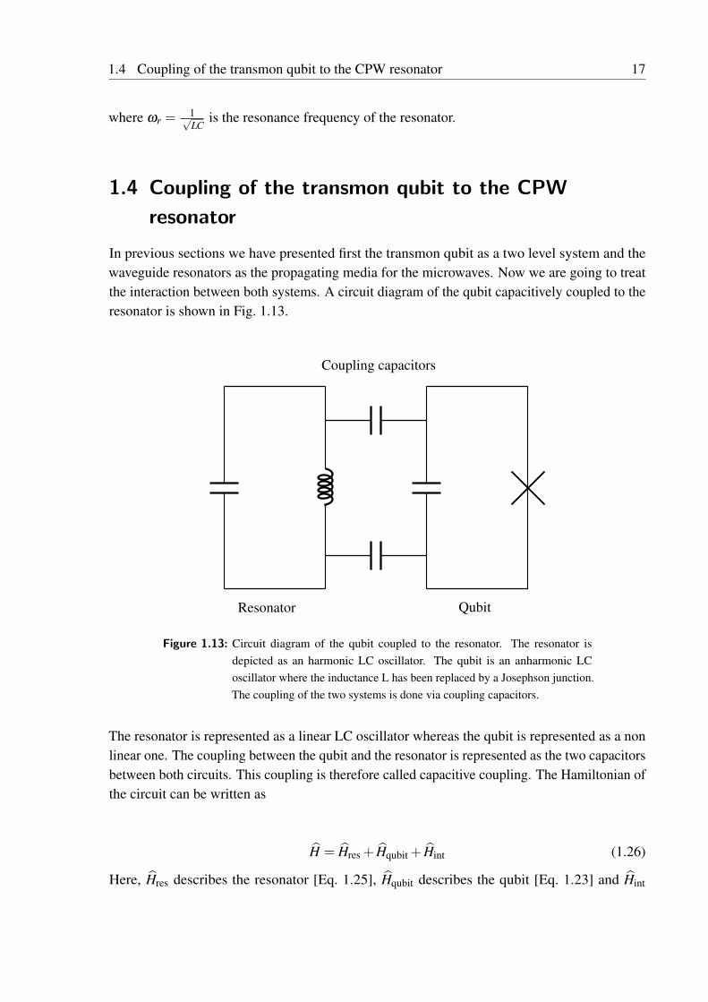
In previous sections we have presented first the transmon qubit as a two level system and thewaveguide resonators as the propagating media for the microwaves. Now we are going to treatthe interaction between both systems. A circuit diagram of the qubit capacitively coupled to theresonator is shown in Fig. 1.13.
Resonator Qubit
Coupling capacitors
Figure 1.13: Circuit diagram of the qubit coupled to the resonator. The resonator isdepicted as an harmonic LC oscillator. The qubit is an anharmonic LCoscillator where the inductance L has been replaced by a Josephson junction.The coupling of the two systems is done via coupling capacitors.
The resonator is represented as a linear LC oscillator whereas the qubit is represented as a nonlinear one. The coupling between the qubit and the resonator is represented as the two capacitorsbetween both circuits. This coupling is therefore called capacitive coupling. The Hamiltonian ofthe circuit can be written as
H = Hres + Hqubit + Hint (1.26)
Here, Hres describes the resonator [Eq. 1.25], Hqubit describes the qubit [Eq. 1.23] and Hint
18 Chapter 1 Theory
describes the interaction between the qubit and the resonator. The interaction will be given bythe dipole operator and the electric field operator.
Hint =−~d · ~E (1.27)
Taking into account that ~d ∝ (σ++ σ−) and ~E ∝(a† + a
)we can rewrite the interaction Hamil-
tonian as
Hint = hg(σ++ σ
−)(a† + a)
(1.28)
Here g is the coupling constant. From this expression we can neglect the terms proportional toσ+a† and σ−a because they violate energy conservation (rotating wave approximation) [15].All the terms together give the Jaynes-Cummings Hamiltonian [16].
H = hωr
(a†a+
12
)+
h2
ωqσz + hg(
σ+a+ σ
−a†)
(1.29)
In the coupling term we have two terms. The first term σ+a is the annihilation of a photon inthe resonator and the excitation of the qubit. The second term σ−a† represents the opposite, therelaxation of the qubit and the creation of a photon in the resonator. The coupling constant ggives the hopping rate of a photon between the resonator and the qubit when ωr = ωq. Next,we study the Hamiltonian in Eq. 1.29 as a function of the detuning ∆ between the qubit and theresonator.
∆ = ωq−ωr (1.30)
We distinguish two regimes, zero detuning (∆ = 0) and dispersive regime (g/∆ 1).
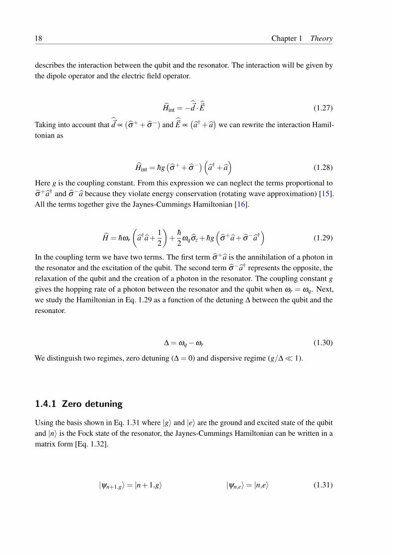
1.4.1 Zero detuning
Using the basis shown in Eq. 1.31 where |g〉 and |e〉 are the ground and excited state of the qubitand |n〉 is the Fock state of the resonator, the Jaynes-Cummings Hamiltonian can be written in amatrix form [Eq. 1.32].
|ψn+1,g〉= |n+1,g〉 |ψn,e〉= |n,e〉 (1.31)
1.4 Coupling of the transmon qubit to the CPW resonator 19
H =
hωr(n+ 3
2
)− h
2ωq hg√
n+1
hg√
n+1 hωr(n+ 1
2
)+ h
2ωq
(1.32)
For zero coupling g = 0 and zero detuning ∆ = 0, the eigenstates of the Hamiltonian are theones of Eq. 1.31. As shown in Fig. 1.14, the states |n+1,g〉 and |n,e〉 have the same energy(black levels). Now, if we couple both systems g , 0, the eigenstates of the Hamiltonian for zerodetuning are an equal superposition of |n+1,g〉 and |n,e〉
|n,+〉= 1√2(|n+1,g〉+ |n,e〉) (1.33a)
|n,−〉= 1√2(|n+1,g〉− |n,e〉) (1.33b)
with eigenenergies
En± = hωr (n+1)± hg√
n+1 (1.34)
As it can be seen, due to the coupling, the degeneracy of the energy levels is lifted, blue levels inFig. 1.14(a). The splitting of this levels depends on the coupling constant g and the number n ofphotons in the resonator.
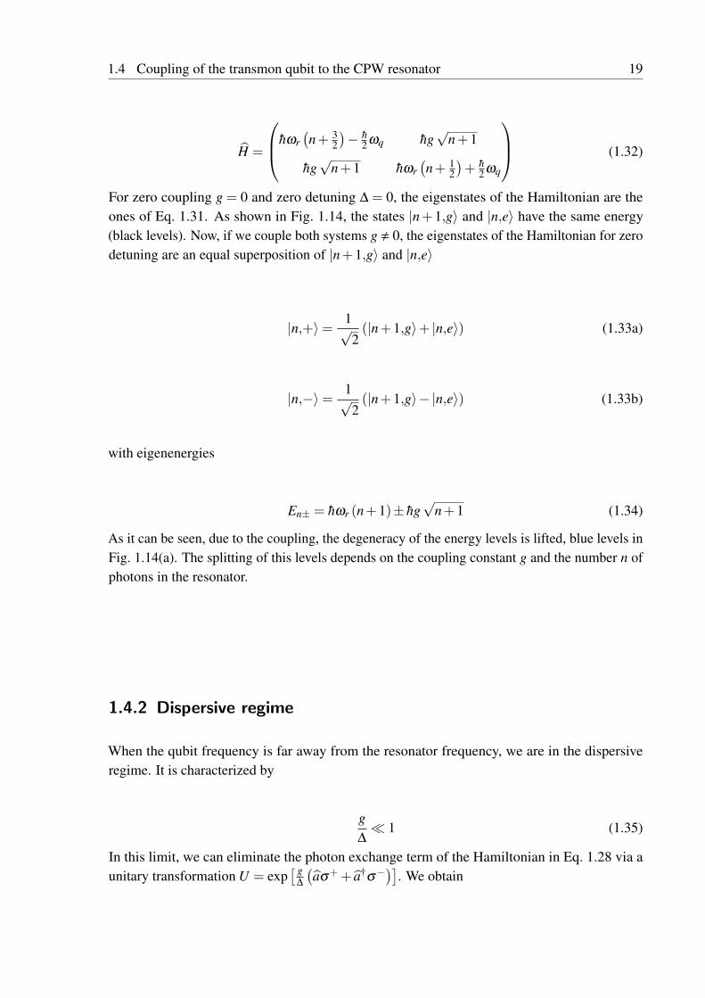
1.4.2 Dispersive regime
When the qubit frequency is far away from the resonator frequency, we are in the dispersiveregime. It is characterized by
g∆ 1 (1.35)
In this limit, we can eliminate the photon exchange term of the Hamiltonian in Eq. 1.28 via aunitary transformation U = exp
[ g∆
(aσ++ a†σ−
)]. We obtain
20 Chapter 1 Theory
|0〉
|1〉
|2〉
|n+ 1〉
|n,+〉
|n,−〉
|0〉
|1〉
|n〉
|g〉 |e〉
2g√n+ 1
2g
|0〉
|1〉
|2〉
|0〉
|1〉
|2〉
|g〉 |e〉
ωr − χ∆
χ
2χ
E
(a)∆ = 0 (b)∆ g
Figure 1.14: Energy levels for the system qubit plus resonator. In black the levels for zerocoupling. (a) For zero detuning each level is split in two due to the coupling,blue lines. (b) In the dispersive regime the levels can be seen as shifted infrequency depending on the state of the qubit, blue and red lines.
Heff = UHU†
= h [ωr +χσz] a†a+h2[ωq +χ
]σz (1.36a)
Where
χ =g2
∆(1.37)
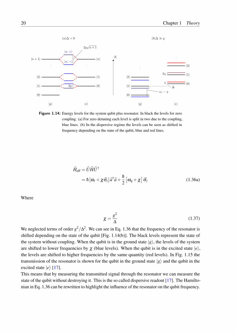
We neglected terms of order g2/∆2. We can see in Eq. 1.36 that the frequency of the resonator isshifted depending on the state of the qubit [Fig. 1.14(b)]. The black levels represent the state ofthe system without coupling. When the qubit is in the ground state |g〉, the levels of the systemare shifted to lower frequencies by χ (blue levels). When the qubit is in the excited state |e〉,the levels are shifted to higher frequencies by the same quantity (red levels). In Fig. 1.15 thetransmission of the resonator is shown for the qubit in the ground state |g〉 and the qubit in theexcited state |e〉 [17].This means that by measuring the transmitted signal through the resonator we can measure thestate of the qubit without destroying it. This is the so called dispersive readout [17]. The Hamilto-nian in Eq. 1.36 can be rewritten to highlight the influence of the resonator on the qubit frequency.
1.4 Coupling of the transmon qubit to the CPW resonator 21
ωr−χ ωr +χ
|g〉 |e〉
Frequency
Pow
ertr
ansm
issi
on
Figure 1.15: Power transmission of a half-wavelength resonator for the qubit in the ground(blue) and in the excited state (red).
Heff = hωra†a+h2
[ωq +2χ a†a+χ
]σz (1.38)
Now it can clearly be seen that the qubit frequency depends linearly on the number of photonsin the resonator. This will be used in Sec. 3.4.1 to calibrate the photon number in the resonator.
1.4.3 The Purcell effect
When placed inside a resonator, the qubit spontaneous emission rate is altered. This is due tothe so called Purcell effect. In the case of our resonator-transmon system, depending on thedetuning , the qubit state has a resonator part that affects its line width. Therefore, the Purcelleffect contributes with an induced relaxation rate γP given by [10]
γP = κg2
∆2 (1.39)
where κ is the linewidth of the resonator and is related to its average photon loss. g and ∆ arerespectively the coupling constant and the detuning between the resonator and the qubit.

Chapter 2
Experimental techniques
In this chapter we introduce the experimental techniques used for the fabrication and measure-ment of the samples. In Sec. 2.1 we describe the fabrication of the resonators with opticallithography and that of the transmon qubits with electron beam lithography. We include thedose test performed for writing the interdigitals of the transmon qubit. The shadow evaporationtechnique is also explained. In Sec. 2.2 we briefly describe the experimental setup and therefrigerators used for the measurements.
2.1 Nanofabrication
The sample consists of a coplanar waveguide resonator made from niobium and a transmonqubit made from aluminum capacitively coupled to it. The fabrication process is divided intotwo parts, we first make the resonator using optical lithography and then we write the transmonin the resonator using e-beam lithography.
2.1.1 Optical lithography
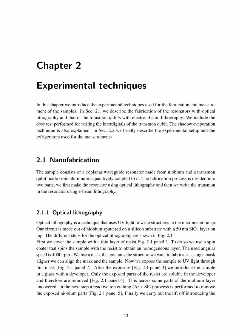
Optical lithography is a technique that uses UV light to write structures in the micrometer range.Our circuit is made out of niobium sputtered on a silicon substrate with a 50 nm SiO2 layer ontop. The different steps for the optical lithography are shown in Fig. 2.1.First we cover the sample with a thin layer of resist Fig. 2.1 panel 1. To do so we use a spincoater that spins the sample with the resist to obtain an homogeneous layer. The used angularspeed is 4000 rpm . We use a mask that contains the structure we want to fabricate. Using a maskaligner we can align the mask and the sample. Now we expose the sample to UV light throughthis mask [Fig. 2.1 panel 2]. After the exposure [Fig. 2.1 panel 3] we introduce the samplein a glass with a developer. Only the exposed parts of the resist are soluble in the developerand therefore are removed [Fig. 2.1 panel 4]. This leaves some parts of the niobium layeruncovered. In the next step a reactive ion etching (Ar + SF6) process is performed to removethe exposed niobium parts [Fig. 2.1 panel 5]. Finally we carry out the lift off introducing the
23
24 Chapter 2 Experimental techniques
Resist
Niobium
Silicon oxide
1 2 3
4 5 6 7
Figure 2.1: Optical lithography steps. The substrate is represented in dark green, thenioubium in gray and the resist in pink. The blue arrows in 2 represent theUV light. The pink arrows in 5 represent the ion etching. See text for furtherdetails.
sample in acetone to remove the remaining resist [Fig. 2.1 panel 6 and 7]. In order to improvethe resolution of the structure we first do steps 2 and 3 exposing only the edges of the chip witha high dose. The fabrication parameters are summarized in Table 2.1.
Resist 5214EDeveloper AZ 726 MIFDose for the edges( mJ
cm2 ) 100Dose for the structure( mJ
cm2 ) 36Development time (s) 110
Table 2.1: Parameters for the fabrication of the resonators using optical lithography.
2.1.2 Electron beam lithography
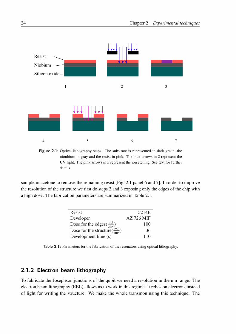
To fabricate the Josephson junctions of the qubit we need a resolution in the nm range. Theelectron beam lithography (EBL) allows us to work in this regime. It relies on electrons insteadof light for writing the structure. We make the whole transmon using this technique. The
2.1 Nanofabrication 25
principal steps are shown in Fig. 2.2.
Upper resist
Lower resist
Silicon oxide
1 2
δ
3
Figure 2.2: Electron beam lithography steps. The substrate is represented in dark green,the lower resist in blue and the upper resist in red. The orange and yellowcolors in 2 represent the beam of electrons. The undercut is depicted as δ in 3.See text for further details.
As in optical lithography, we first spin coat the sample with resist. The difference is that theresist is deposited directly on the silicon substrate. In this case we use two resists [Fig. 2.2panel 1] in order to obtain some undercut δ [Fig. 2.2 panel 3]. This undercut will be crucialfor the fabrication of the junctions using shadow evaporation. The first resist is spin coated at2000 rpm to obtain a thicker layer and the second one at 4000 rpm. After the spin coating weintroduce the sample in the EBL for writing. As it can be seen in Fig. 2.2 panel 2, the incomingelectrons reach the first resist with a high kinetic energy. The beam used is not perfectly focused,mainly due to electrons backscattered from the substrate. This means that regions next to thewriting position also get exposed with a lower dose. In addition the two resists have differentsensitivity. Only the lower resist is fully exposed by background electrons. After the writing wedevelop the sample in two steps. First we introduce it in the developer AR 600-56 and then inisopropanol. Both resists have different sensitivity to isopropanol, the lower one has a highersensitivity than the upper one. These two effects lead after the development [Fig. 2.2 panel3] to an undercut δ as mentioned before. Using this undercut, resist bridges necessary for thefabrication of nanoscale Josephson junctions are created at suitable locations. For a detaileddescription of the EBL process see Ref. [18]. The fabrication parameters for the transmon qubitare shown in Table 2.2.Finally we carry out the evaporation of aluminum on the sample. We use the shadow evaporationtechnique [19][20] pictured in Fig. 2.3.
26 Chapter 2 Experimental techniques
Lower resist PMM/MA 33%Upper resist PMMA 950KDose for the SQUID ( µC
cm2 ) 680E-beam voltage (keV) 30Developer AR 600-56Development time (s) 60Time in isopropanol (s) 120
Table 2.2: Fabrication parameters for the transmon qubit using electron beam lithography.
θ
Al
1
AlOx
2
−θ
Al
Junction
3
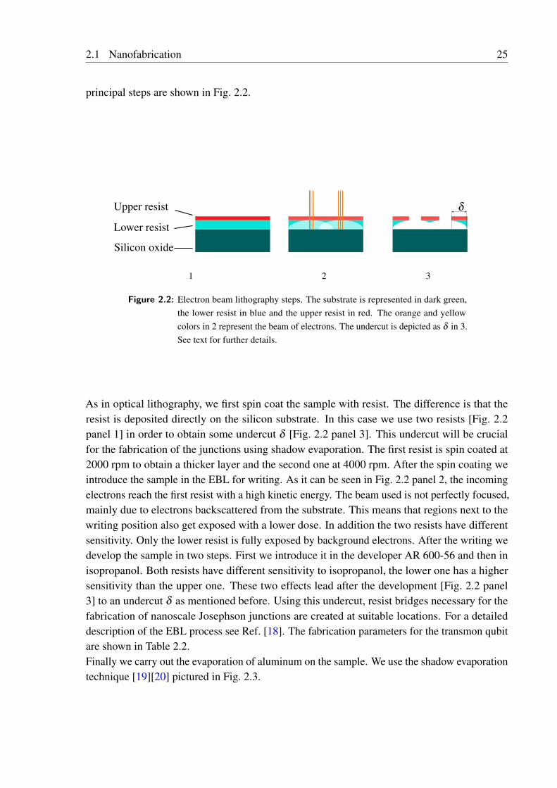
Figure 2.3: Shadow evaporation steps. The substrate is represented in dark green, the alu-minum in gray and the aluminum oxide in dark red. The bridge is representedin the upper part in blue for the lower resist and red for the upper resists. Theevaporation angle θ is given. In 3 the junction is marked in red.
The shadow evaporation technique allows the fabrication of the junctions in one step. Afterpreparing a resist bridge as described above, we evaporate aluminum under an angle θ [Fig. 2.3panel 1]. The shadow mask of the resist bridge manifests as a gap in the evaporated aluminum.Then we oxidize the aluminum [Fig. 2.3 panel 2]. This oxide plays the role of the insulatorin the junction. Finally we evaporate aluminum again using the angle −θ . Due to the shiftedposition of the gap in this upper aluminum layer we obtain an SIS Josephson junction [Fig. 2.3panel 3]. The evaporation parameters are shown in Table 2.3.
Aluminum thickness 1 (nm) 40Angle 1 (θ ) −17
Aluminum thickness 2 (nm) 70Angle 2 (−θ ) +17
Oxygen pressure (mbar) 7.3×10⁻³
Oxidation time (min) 40
Table 2.3: Evaporation parameters
2.2 Experimental setup 27
2.2 Experimental setup
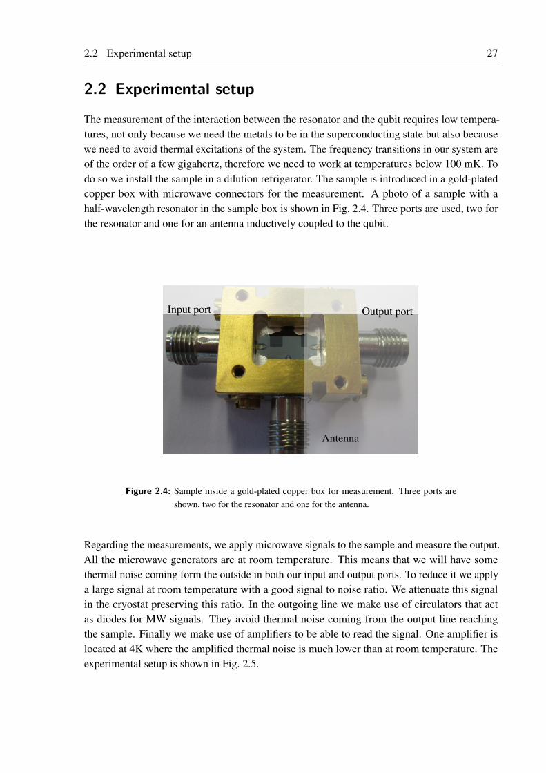
The measurement of the interaction between the resonator and the qubit requires low tempera-tures, not only because we need the metals to be in the superconducting state but also becausewe need to avoid thermal excitations of the system. The frequency transitions in our system areof the order of a few gigahertz, therefore we need to work at temperatures below 100 mK. Todo so we install the sample in a dilution refrigerator. The sample is introduced in a gold-platedcopper box with microwave connectors for the measurement. A photo of a sample with ahalf-wavelength resonator in the sample box is shown in Fig. 2.4. Three ports are used, two forthe resonator and one for an antenna inductively coupled to the qubit.
Input port Output port
Antenna
Figure 2.4: Sample inside a gold-plated copper box for measurement. Three ports areshown, two for the resonator and one for the antenna.
Regarding the measurements, we apply microwave signals to the sample and measure the output.All the microwave generators are at room temperature. This means that we will have somethermal noise coming form the outside in both our input and output ports. To reduce it we applya large signal at room temperature with a good signal to noise ratio. We attenuate this signalin the cryostat preserving this ratio. In the outgoing line we make use of circulators that actas diodes for MW signals. They avoid thermal noise coming from the output line reachingthe sample. Finally we make use of amplifiers to be able to read the signal. One amplifier islocated at 4K where the amplified thermal noise is much lower than at room temperature. Theexperimental setup is shown in Fig. 2.5.
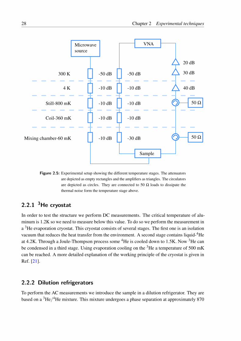
28 Chapter 2 Experimental techniques
300 K
4 K
Still-800 mK
Coil-360 mK
Mixing chamber-60 mK
VNA
50 Ω
50 Ω
Sample
-50 dB
-10 dB
-10 dB
-10 dB
-30 dB
20 dB
30 dB
40 dB
Microwavesource
-50 dB
-10 dB
-10 dB
-10 dB
-10 dB
Figure 2.5: Experimental setup showing the different temperature stages. The attenuatorsare depicted as empty rectangles and the amplifiers as triangles. The circulatorsare depicted as circles. They are connected to 50 Ω loads to dissipate thethermal noise form the temperature stage above.
2.2.1 3He cryostat
In order to test the structure we perform DC measurements. The critical temperature of alu-minum is 1.2K so we need to measure below this value. To do so we perform the measurement ina 3He evaporation cryostat. This cryostat consists of several stages. The first one is an isolationvacuum that reduces the heat transfer from the environment. A second stage contains liquid-4Heat 4.2K. Through a Joule-Thompson process some 4He is cooled down to 1.5K. Now 3He canbe condensed in a third stage. Using evaporation cooling on the 3He a temperature of 500 mKcan be reached. A more detailed explanation of the working principle of the cryostat is given inRef. [21].
2.2.2 Dilution refrigerators
To perform the AC measurements we introduce the sample in a dilution refrigerator. They arebased on a 3He/4He mixture. This mixture undergoes a phase separation at approximately 870
2.2 Experimental setup 29
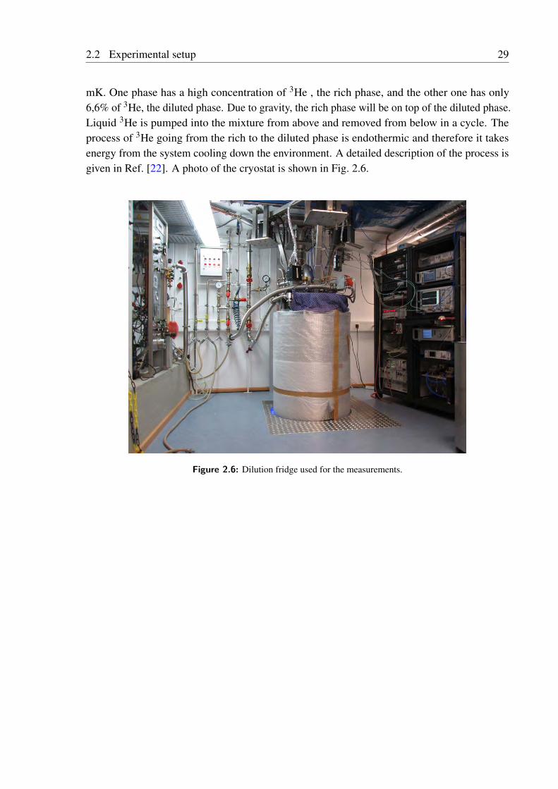
mK. One phase has a high concentration of 3He , the rich phase, and the other one has only6,6% of 3He, the diluted phase. Due to gravity, the rich phase will be on top of the diluted phase.Liquid 3He is pumped into the mixture from above and removed from below in a cycle. Theprocess of 3He going from the rich to the diluted phase is endothermic and therefore it takesenergy from the system cooling down the environment. A detailed description of the process isgiven in Ref. [22]. A photo of the cryostat is shown in Fig. 2.6.
Figure 2.6: Dilution fridge used for the measurements.

Chapter 3
Experimental results
In this chapter we include a description of the fabricated samples and the performed measure-ments. In Sec. 3.1 we give the design and parameters for both resonators, half-wavelength andquarter-wavelength, and the design and dose test for the transmon qubits. In Sec. 3.2 the DCmeasurements used to test the qubit junctions are shown. Transmission measurements of theresonator coupled to the qubit are included in Sec. 3.3. Two-tone spectroscopy measurementsare shown in Sec. 3.4. Finally, an exemplary time domain measurement is included in Sec. 3.5.
3.1 Measured samples
In this work we study two different samples, sample A and sample B. In sample A we couplethe transmon qubit to a half-wavelength resonator. In sample B we use a quarter-wavelengthresonator. In this section we describe first the resonators and then the transmon qubits.
3.1.1 The resonators
Sample A has three ports, two for the input and output signal and the third one for an antennainductively coupled to the qubit. This antenna is meant for tuning the qubit frequency. In sampleB we have two quarter-wavelength resonators each one with an input port, a transmon qubitcoupled to them and a similar antenna. We only perform measurements on one of the qubits insample B.
Parameter λ/2 λ/4Resonant frequency (GHz) 6.54 6.05∆ f (MHz) 7 20Finger width (µm) 4 3.3Finger spacing (µm) 5 3.3
Table 3.1: Resonators parameters
31
32 Chapter 3 Experimental results
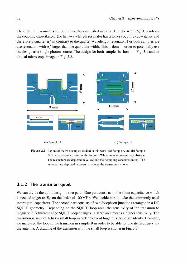
The different parameters for both resonators are listed in Table 3.1. The width ∆ f depends onthe coupling capacitance. The half-wavelength resonator has a lower coupling capacitance andtherefore a smaller ∆ f in contrary to the quarter-wavelength resonator. For both samples weuse resonators with ∆ f larger than the qubit line width. This is done in order to potentially usethe design as a single photon source. The design for both samples is shown in Fig. 3.1 and anoptical microscope image in Fig. 3.2.
10 mm
6m
m
100µm
100µm
(a) Sample A
12 mm
12m
m
100µm
100µm
(b) Sample B
Figure 3.1: Layout of the two samples studied in this work: (a) Sample A and (b) SampleB. Blue areas are covered with niobium. White areas represent the substrate.The resonators are depicted in yellow and their coupling capacitors in red. Theantennas are depicted in green. In orange the transmon is shown.
3.1.2 The transmon qubit
We can divide the qubit design in two parts. One part consists on the shunt capacitance whichis needed to get an EC on the order of 100 MHz. We decide here to take the commonly usedinterdigital capacitors. The second part consists of two Josephson junctions arranged in a DCSQUID geometry. Depending on the SQUID loop area, the sensitivity of the transmon tomagnetic flux threading the SQUID loop changes. A large area means a higher sensitivity. Thetransmon is sample A has a small loop in order to avoid huge flux noise sensitivity. However,we increased the loop in the transmon in sample B in order to be able to tune its frequency viathe antenna. A drawing of the transmon with the small loop is shown in Fig. 3.3.
3.1 Measured samples 33
100µm
100µm
100µm
(a) Sample A
100µm
100µm
(b) Sample B
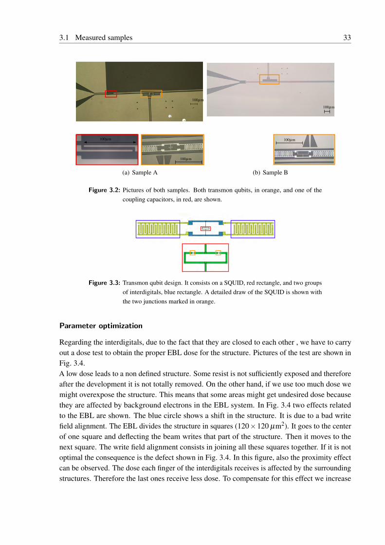
Figure 3.2: Pictures of both samples. Both transmon qubits, in orange, and one of thecoupling capacitors, in red, are shown.
Figure 3.3: Transmon qubit design. It consists on a SQUID, red rectangle, and two groupsof interdigitals, blue rectangle. A detailed draw of the SQUID is shown withthe two junctions marked in orange.
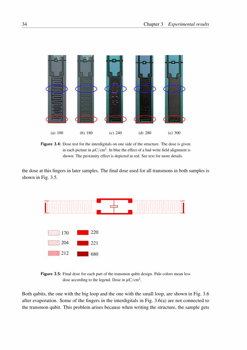
Parameter optimization
Regarding the interdigitals, due to the fact that they are closed to each other , we have to carryout a dose test to obtain the proper EBL dose for the structure. Pictures of the test are shown inFig. 3.4.A low dose leads to a non defined structure. Some resist is not sufficiently exposed and thereforeafter the development it is not totally removed. On the other hand, if we use too much dose wemight overexpose the structure. This means that some areas might get undesired dose becausethey are affected by background electrons in the EBL system. In Fig. 3.4 two effects relatedto the EBL are shown. The blue circle shows a shift in the structure. It is due to a bad writefield alignment. The EBL divides the structure in squares (120×120 µm2). It goes to the centerof one square and deflecting the beam writes that part of the structure. Then it moves to thenext square. The write field alignment consists in joining all these squares together. If it is notoptimal the consequence is the defect shown in Fig. 3.4. In this figure, also the proximity effectcan be observed. The dose each finger of the interdigitals receives is affected by the surroundingstructures. Therefore the last ones receive less dose. To compensate for this effect we increase
34 Chapter 3 Experimental results
(a) 100 (b) 180 (c) 240 (d) 280 (e) 300
Figure 3.4: Dose test for the interdigitals on one side of the structure. The dose is givenin each picture in µC/cm2. In blue the effect of a bad write field alignment isshown. The proximity effect is depicted in red. See text for more details.
the dose at this fingers in later samples. The final dose used for all transmons in both samples isshown in Fig. 3.5.
170
204
212 680
221
220
Figure 3.5: Final dose for each part of the transmon qubit design. Pale colors mean lessdose according to the legend. Dose in µC/cm2.
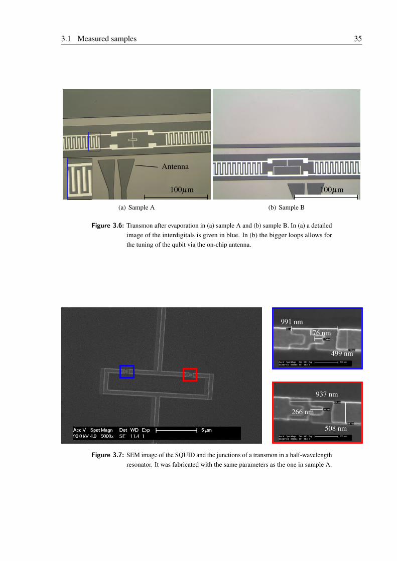
Both qubits, the one with the big loop and the one with the small loop, are shown in Fig. 3.6after evaporation. Some of the fingers in the interdigitals in Fig. 3.6(a) are not connected tothe transmon qubit. This problem arises because when writing the structure, the sample gets
3.1 Measured samples 35
100µm
Antenna
(a) Sample A
100µm
(b) Sample B
Figure 3.6: Transmon after evaporation in (a) sample A and (b) sample B. In (a) a detailedimage of the interdigitals is given in blue. In (b) the bigger loops allows forthe tuning of the qubit via the on-chip antenna.
991 nm
176 nm
499 nm
937 nm
266 nm
508 nm
Figure 3.7: SEM image of the SQUID and the junctions of a transmon in a half-wavelengthresonator. It was fabricated with the same parameters as the one in sample A.
36 Chapter 3 Experimental results
charged and this charge deflects the beam. To avoid this we superpose the fingers to the body ofthe transmon in the design file of the second qubit. This means that the interdigital capacitancefor the transmon in sample A is smaller than in sample B leading to an increase in the chargingenergy EC. This affects some qubit parameters. An scanning electron microscope (SEM) imageof the SQUID and the junctions for a transmon in a half-wavelength resonator is shown inFig. 3.7.
3.2 DC measurements
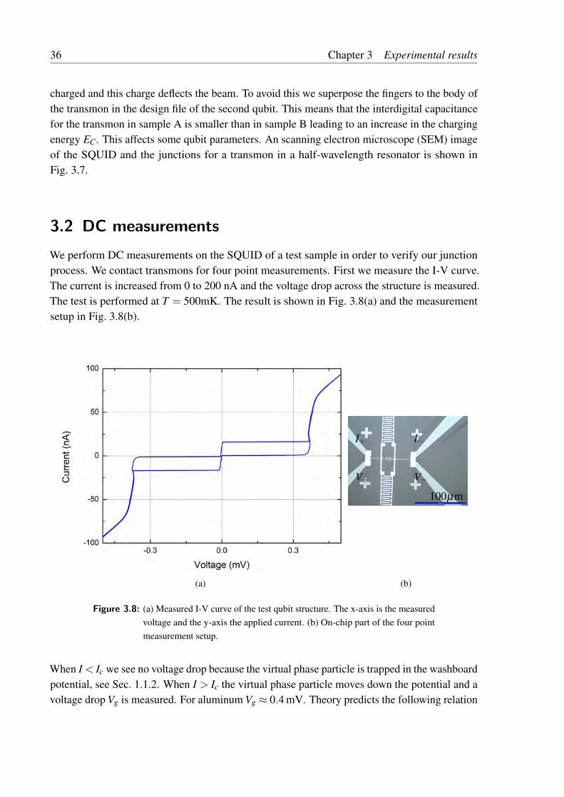
We perform DC measurements on the SQUID of a test sample in order to verify our junctionprocess. We contact transmons for four point measurements. First we measure the I-V curve.The current is increased from 0 to 200 nA and the voltage drop across the structure is measured.The test is performed at T = 500mK. The result is shown in Fig. 3.8(a) and the measurementsetup in Fig. 3.8(b).
(a)
100µm
I+
V+
I−
V−
(b)
Figure 3.8: (a) Measured I-V curve of the test qubit structure. The x-axis is the measuredvoltage and the y-axis the applied current. (b) On-chip part of the four pointmeasurement setup.
When I < Ic we see no voltage drop because the virtual phase particle is trapped in the washboardpotential, see Sec. 1.1.2. When I > Ic the virtual phase particle moves down the potential and avoltage drop Vg is measured. For aluminum Vg ≈ 0.4 mV. Theory predicts the following relation
3.3 Transmission measurements 37
between the critical current Ic and the gap voltage Vg [7]
IcRn =π
4Vg (3.1)
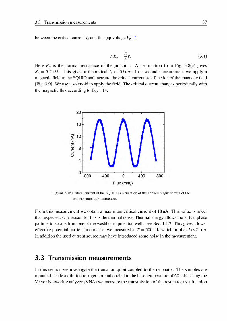
Here Rn is the normal resistance of the junction. An estimation from Fig. 3.8(a) givesRn = 5.7 kΩ. This gives a theoretical Ic of 55 nA. In a second measurement we apply amagnetic field to the SQUID and measure the critical current as a function of the magnetic field[Fig. 3.9]. We use a solenoid to apply the field. The critical current changes periodically withthe magnetic flux according to Eq. 1.14.
Figure 3.9: Critical current of the SQUID as a function of the applied magnetic flux of thetest transmon qubit structure.
From this measurement we obtain a maximum critical current of 18 nA. This value is lowerthan expected. One reason for this is the thermal noise. Thermal energy allows the virtual phaseparticle to escape from one of the washboard potential wells, see Sec. 1.1.2. This gives a lowereffective potential barrier. In our case, we measured at T = 500 mK which implies I ≈ 21 nA.In addition the used current source may have introduced some noise in the measurement.
3.3 Transmission measurements
In this section we investigate the transmon qubit coupled to the resonator. The samples aremounted inside a dilution refrigerator and cooled to the base temperature of 60 mK. Using theVector Network Analyzer (VNA) we measure the transmission of the resonator as a function
38 Chapter 3 Experimental results
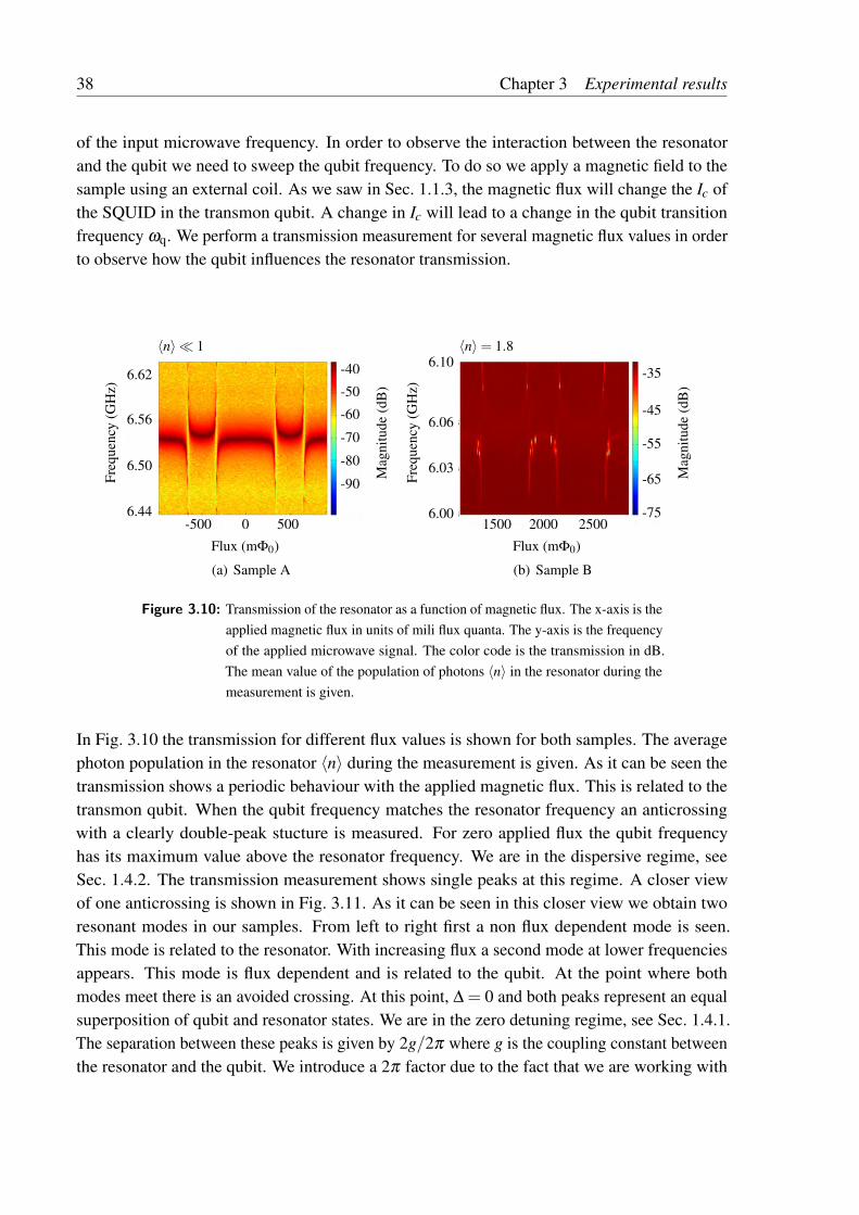
of the input microwave frequency. In order to observe the interaction between the resonatorand the qubit we need to sweep the qubit frequency. To do so we apply a magnetic field to thesample using an external coil. As we saw in Sec. 1.1.3, the magnetic flux will change the Ic ofthe SQUID in the transmon qubit. A change in Ic will lead to a change in the qubit transitionfrequency ωq. We perform a transmission measurement for several magnetic flux values in orderto observe how the qubit influences the resonator transmission.
〈n〉 1
Flux (mΦ0)
Mag
nitu
de(d
B)
Freq
uenc
y(G
Hz)
6.62
6.50
6.56
6.44-500 0 500
-40
-50
-60
-70
-80
-90
(a) Sample A
〈n〉= 1.8
Flux (mΦ0)
Mag
nitu
de(d
B)
Freq
uenc
y(G
Hz)
6.10
6.03
6.06
6.001500 2000 2500
-35
-45
-55
-65
-75
(b) Sample B
Figure 3.10: Transmission of the resonator as a function of magnetic flux. The x-axis is theapplied magnetic flux in units of mili flux quanta. The y-axis is the frequencyof the applied microwave signal. The color code is the transmission in dB.The mean value of the population of photons 〈n〉 in the resonator during themeasurement is given.
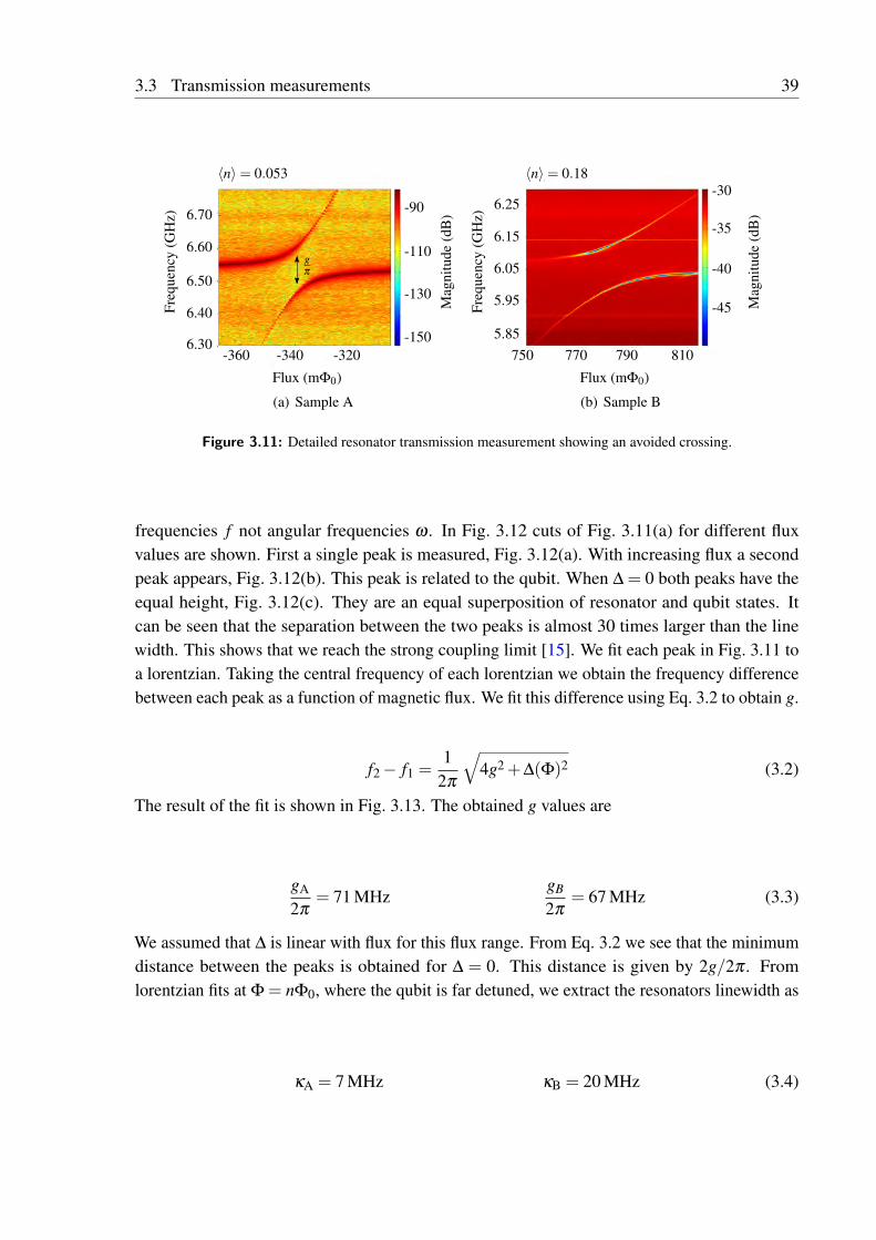
In Fig. 3.10 the transmission for different flux values is shown for both samples. The averagephoton population in the resonator 〈n〉 during the measurement is given. As it can be seen thetransmission shows a periodic behaviour with the applied magnetic flux. This is related to thetransmon qubit. When the qubit frequency matches the resonator frequency an anticrossingwith a clearly double-peak stucture is measured. For zero applied flux the qubit frequencyhas its maximum value above the resonator frequency. We are in the dispersive regime, seeSec. 1.4.2. The transmission measurement shows single peaks at this regime. A closer viewof one anticrossing is shown in Fig. 3.11. As it can be seen in this closer view we obtain tworesonant modes in our samples. From left to right first a non flux dependent mode is seen.This mode is related to the resonator. With increasing flux a second mode at lower frequenciesappears. This mode is flux dependent and is related to the qubit. At the point where bothmodes meet there is an avoided crossing. At this point, ∆ = 0 and both peaks represent an equalsuperposition of qubit and resonator states. We are in the zero detuning regime, see Sec. 1.4.1.The separation between these peaks is given by 2g/2π where g is the coupling constant betweenthe resonator and the qubit. We introduce a 2π factor due to the fact that we are working with
3.3 Transmission measurements 39
gπ
〈n〉= 0.053
Flux (mΦ0)
Mag
nitu
de(d
B)
Freq
uenc
y(G
Hz) 6.70
6.50
6.60
-360 -340 -320
-90
-110
-130
-150
6.40
6.30
(a) Sample A
〈n〉= 0.18
Flux (mΦ0)
Mag
nitu
de(d
B)
Freq
uenc
y(G
Hz)
6.25
6.05
6.15
750 770 790
-30
-35
-40
-455.95
5.85810
(b) Sample B
Figure 3.11: Detailed resonator transmission measurement showing an avoided crossing.
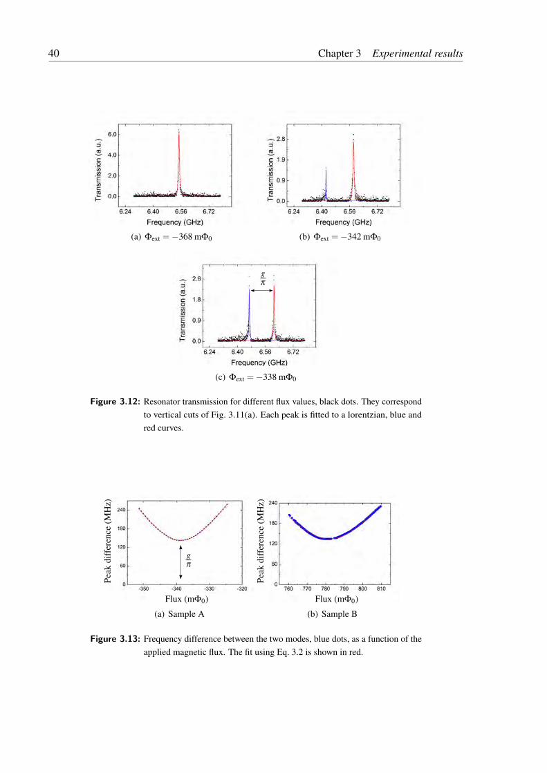
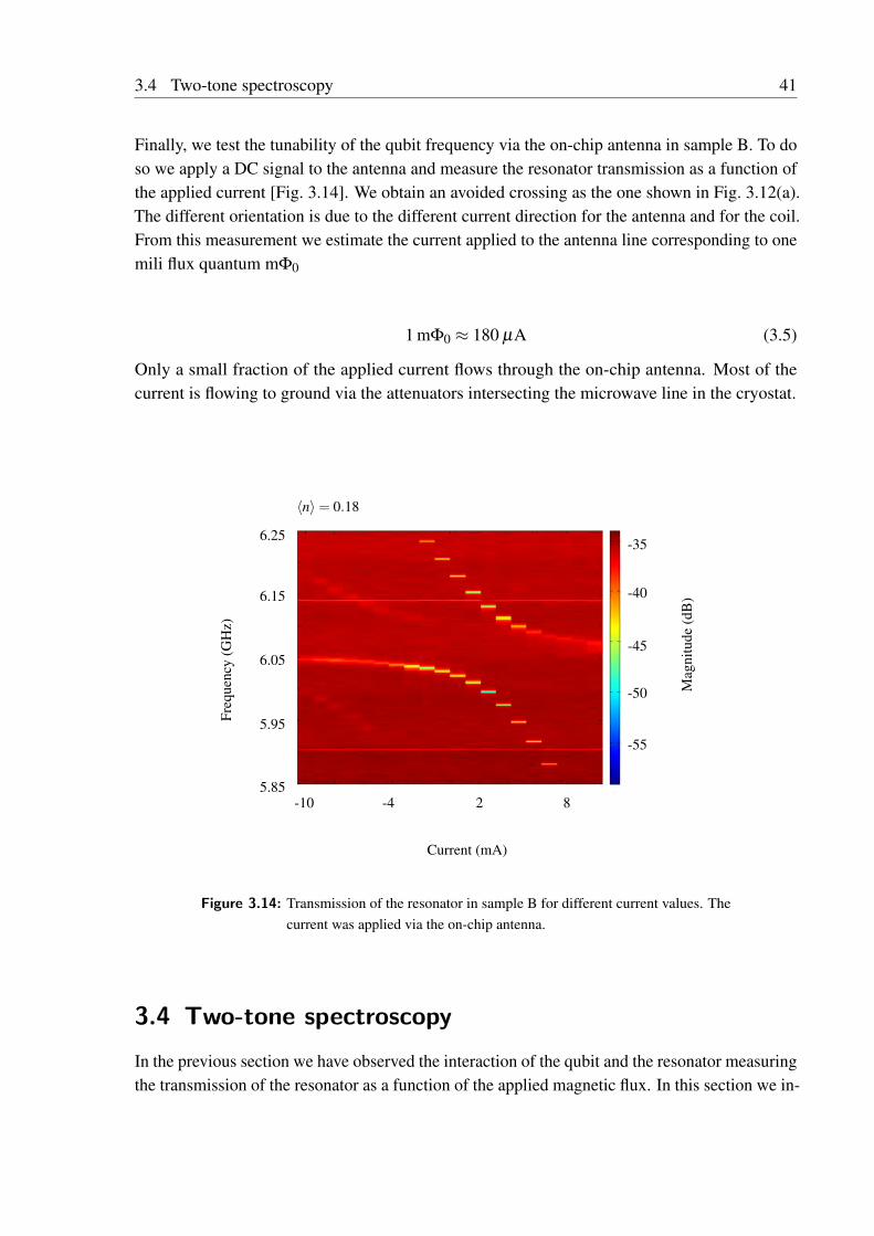
frequencies f not angular frequencies ω . In Fig. 3.12 cuts of Fig. 3.11(a) for different fluxvalues are shown. First a single peak is measured, Fig. 3.12(a). With increasing flux a secondpeak appears, Fig. 3.12(b). This peak is related to the qubit. When ∆ = 0 both peaks have theequal height, Fig. 3.12(c). They are an equal superposition of resonator and qubit states. Itcan be seen that the separation between the two peaks is almost 30 times larger than the linewidth. This shows that we reach the strong coupling limit [15]. We fit each peak in Fig. 3.11 toa lorentzian. Taking the central frequency of each lorentzian we obtain the frequency differencebetween each peak as a function of magnetic flux. We fit this difference using Eq. 3.2 to obtain g.
f2− f1 =1
2π
√4g2 +∆(Φ)2 (3.2)
The result of the fit is shown in Fig. 3.13. The obtained g values are
gA
2π= 71 MHz
gB
2π= 67 MHz (3.3)
We assumed that ∆ is linear with flux for this flux range. From Eq. 3.2 we see that the minimumdistance between the peaks is obtained for ∆ = 0. This distance is given by 2g/2π . Fromlorentzian fits at Φ = nΦ0, where the qubit is far detuned, we extract the resonators linewidth as
κA = 7 MHz κB = 20 MHz (3.4)
40 Chapter 3 Experimental results
(a) Φext =−368 mΦ0 (b) Φext =−342 mΦ0
gπ
(c) Φext =−338 mΦ0
Figure 3.12: Resonator transmission for different flux values, black dots. They correspondto vertical cuts of Fig. 3.11(a). Each peak is fitted to a lorentzian, blue andred curves.
gπ
Flux (mΦ0)
Peak
diff
eren
ce(M
Hz)
(a) Sample A
Flux (mΦ0)
Peak
diff
eren
ce(M
Hz)
(b) Sample B
Figure 3.13: Frequency difference between the two modes, blue dots, as a function of theapplied magnetic flux. The fit using Eq. 3.2 is shown in red.
3.4 Two-tone spectroscopy 41
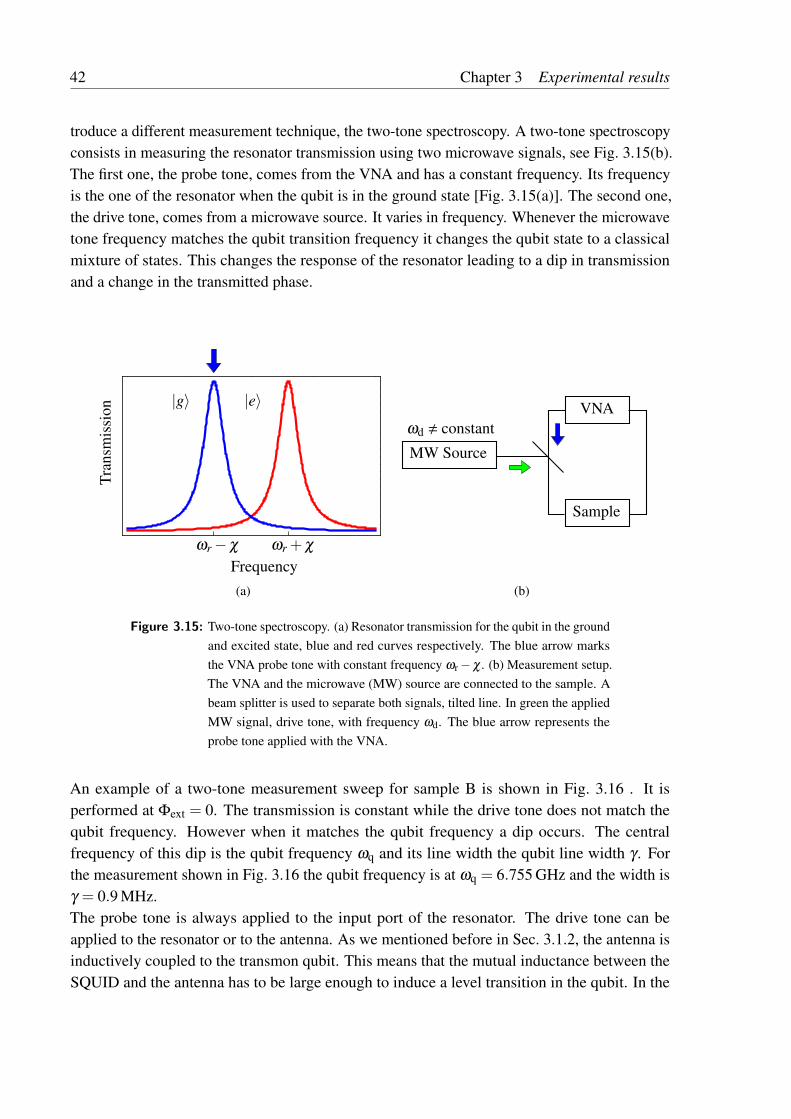
Finally, we test the tunability of the qubit frequency via the on-chip antenna in sample B. To doso we apply a DC signal to the antenna and measure the resonator transmission as a function ofthe applied current [Fig. 3.14]. We obtain an avoided crossing as the one shown in Fig. 3.12(a).The different orientation is due to the different current direction for the antenna and for the coil.From this measurement we estimate the current applied to the antenna line corresponding to onemili flux quantum mΦ0
1 mΦ0 ≈ 180 µA (3.5)
Only a small fraction of the applied current flows through the on-chip antenna. Most of thecurrent is flowing to ground via the attenuators intersecting the microwave line in the cryostat.
〈n〉= 0.18
Current (mA)
Mag
nitu
de(d
B)
Freq
uenc
y(G
Hz)
6.25
6.05
6.15
-10 -4 2
-35
-40
-45
-555.95
5.858
-50
Figure 3.14: Transmission of the resonator in sample B for different current values. Thecurrent was applied via the on-chip antenna.
3.4 Two-tone spectroscopy
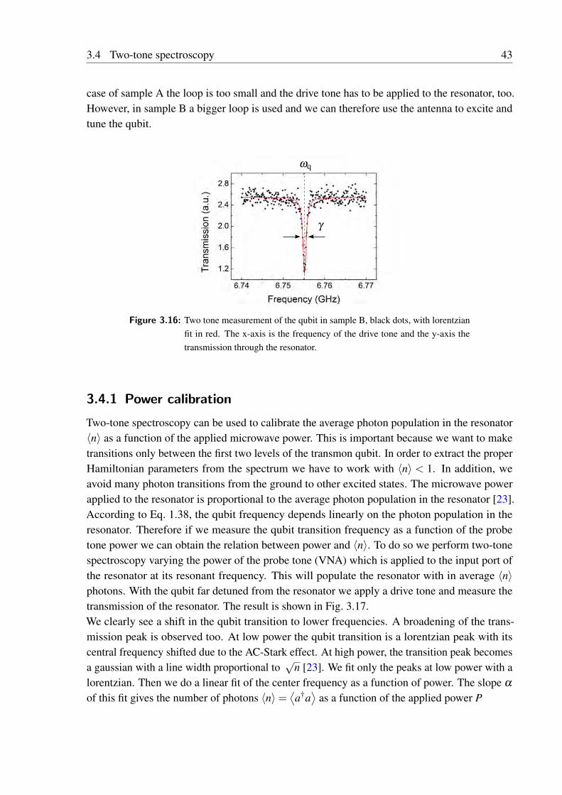
In the previous section we have observed the interaction of the qubit and the resonator measuringthe transmission of the resonator as a function of the applied magnetic flux. In this section we in-
42 Chapter 3 Experimental results
troduce a different measurement technique, the two-tone spectroscopy. A two-tone spectroscopyconsists in measuring the resonator transmission using two microwave signals, see Fig. 3.15(b).The first one, the probe tone, comes from the VNA and has a constant frequency. Its frequencyis the one of the resonator when the qubit is in the ground state [Fig. 3.15(a)]. The second one,the drive tone, comes from a microwave source. It varies in frequency. Whenever the microwavetone frequency matches the qubit transition frequency it changes the qubit state to a classicalmixture of states. This changes the response of the resonator leading to a dip in transmissionand a change in the transmitted phase.
ωr−χ ωr +χ
|g〉 |e〉
Frequency
Tran
smis
sion
(a)
Sample
VNA
MW Source
ωd , constant
(b)
Figure 3.15: Two-tone spectroscopy. (a) Resonator transmission for the qubit in the groundand excited state, blue and red curves respectively. The blue arrow marksthe VNA probe tone with constant frequency ωr−χ . (b) Measurement setup.The VNA and the microwave (MW) source are connected to the sample. Abeam splitter is used to separate both signals, tilted line. In green the appliedMW signal, drive tone, with frequency ωd. The blue arrow represents theprobe tone applied with the VNA.
An example of a two-tone measurement sweep for sample B is shown in Fig. 3.16 . It isperformed at Φext = 0. The transmission is constant while the drive tone does not match thequbit frequency. However when it matches the qubit frequency a dip occurs. The centralfrequency of this dip is the qubit frequency ωq and its line width the qubit line width γ . Forthe measurement shown in Fig. 3.16 the qubit frequency is at ωq = 6.755 GHz and the width isγ = 0.9 MHz.The probe tone is always applied to the input port of the resonator. The drive tone can beapplied to the resonator or to the antenna. As we mentioned before in Sec. 3.1.2, the antenna isinductively coupled to the transmon qubit. This means that the mutual inductance between theSQUID and the antenna has to be large enough to induce a level transition in the qubit. In the
3.4 Two-tone spectroscopy 43
case of sample A the loop is too small and the drive tone has to be applied to the resonator, too.However, in sample B a bigger loop is used and we can therefore use the antenna to excite andtune the qubit.
γ
ωq
Figure 3.16: Two tone measurement of the qubit in sample B, black dots, with lorentzianfit in red. The x-axis is the frequency of the drive tone and the y-axis thetransmission through the resonator.
3.4.1 Power calibration
Two-tone spectroscopy can be used to calibrate the average photon population in the resonator〈n〉 as a function of the applied microwave power. This is important because we want to maketransitions only between the first two levels of the transmon qubit. In order to extract the properHamiltonian parameters from the spectrum we have to work with 〈n〉 < 1. In addition, weavoid many photon transitions from the ground to other excited states. The microwave powerapplied to the resonator is proportional to the average photon population in the resonator [23].According to Eq. 1.38, the qubit frequency depends linearly on the photon population in theresonator. Therefore if we measure the qubit transition frequency as a function of the probetone power we can obtain the relation between power and 〈n〉. To do so we perform two-tonespectroscopy varying the power of the probe tone (VNA) which is applied to the input port ofthe resonator at its resonant frequency. This will populate the resonator with in average 〈n〉photons. With the qubit far detuned from the resonator we apply a drive tone and measure thetransmission of the resonator. The result is shown in Fig. 3.17.We clearly see a shift in the qubit transition to lower frequencies. A broadening of the trans-mission peak is observed too. At low power the qubit transition is a lorentzian peak with itscentral frequency shifted due to the AC-Stark effect. At high power, the transition peak becomesa gaussian with a line width proportional to
√n [23]. We fit only the peaks at low power with a
lorentzian. Then we do a linear fit of the center frequency as a function of power. The slope α
of this fit gives the number of photons 〈n〉=⟨a†a⟩
as a function of the applied power P
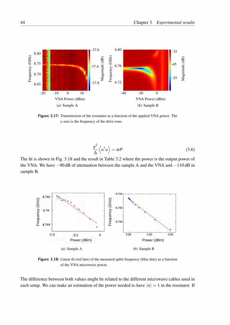
44 Chapter 3 Experimental results
VNA Power (dBm)M
agni
tude
(dB
)
Freq
uenc
y(G
Hz)
8.80
8.70
8.75
-20 -10
-37.0
-37.4
-37.88.65
0 10
(a) Sample A
VNA Power (dBm)
Mag
nitu
de(d
B)
Freq
uenc
y(G
Hz)
6.80
6.72
6.76
-40 -20
-35
-45
-55
0
(b) Sample B
Figure 3.17: Transmission of the resonator as a function of the applied VNA power. They-axis is the frequency of the drive tone.
g2
∆
⟨a†a⟩= αP (3.6)
The fit is shown in Fig. 3.18 and the result in Table 3.2 where the power is the output power ofthe VNA. We have −90 dB of attenuation between the sample A and the VNA and −110 dB insample B.
Power (dBm)
Fre
quen
cy (
GH
z)
(a) Sample A
Fre
quen
cy (
GH
z)
Power (dBm)
(b) Sample B
Figure 3.18: Linear fit (red line) of the measured qubit frequency (blue dots) as a functionof the VNA microwave power.
The difference between both values might be related to the different microwave cables used ineach setup. We can make an estimation of the power needed to have 〈n〉= 1 in the resonator. If
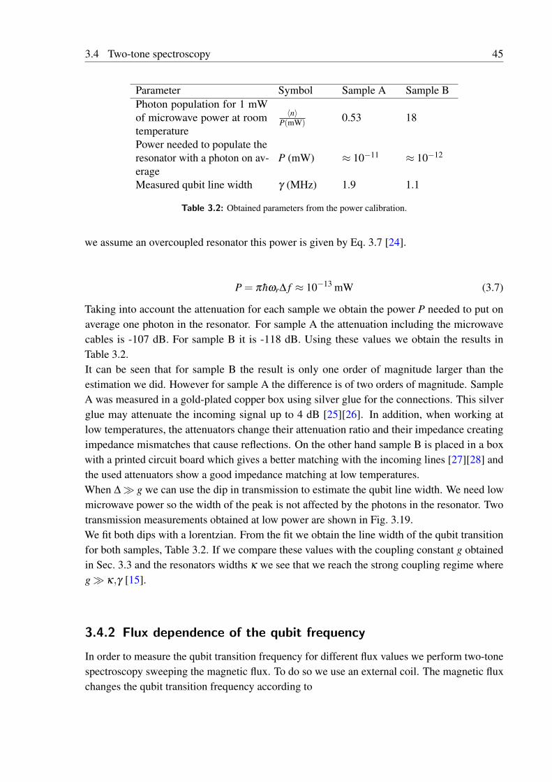
3.4 Two-tone spectroscopy 45
Parameter Symbol Sample A Sample BPhoton population for 1 mWof microwave power at roomtemperature
〈n〉P(mW)
0.53 18
Power needed to populate theresonator with a photon on av-erage
P (mW) ≈ 10−11 ≈ 10−12
Measured qubit line width γ (MHz) 1.9 1.1
Table 3.2: Obtained parameters from the power calibration.
we assume an overcoupled resonator this power is given by Eq. 3.7 [24].
P = π hωr∆ f ≈ 10−13 mW (3.7)
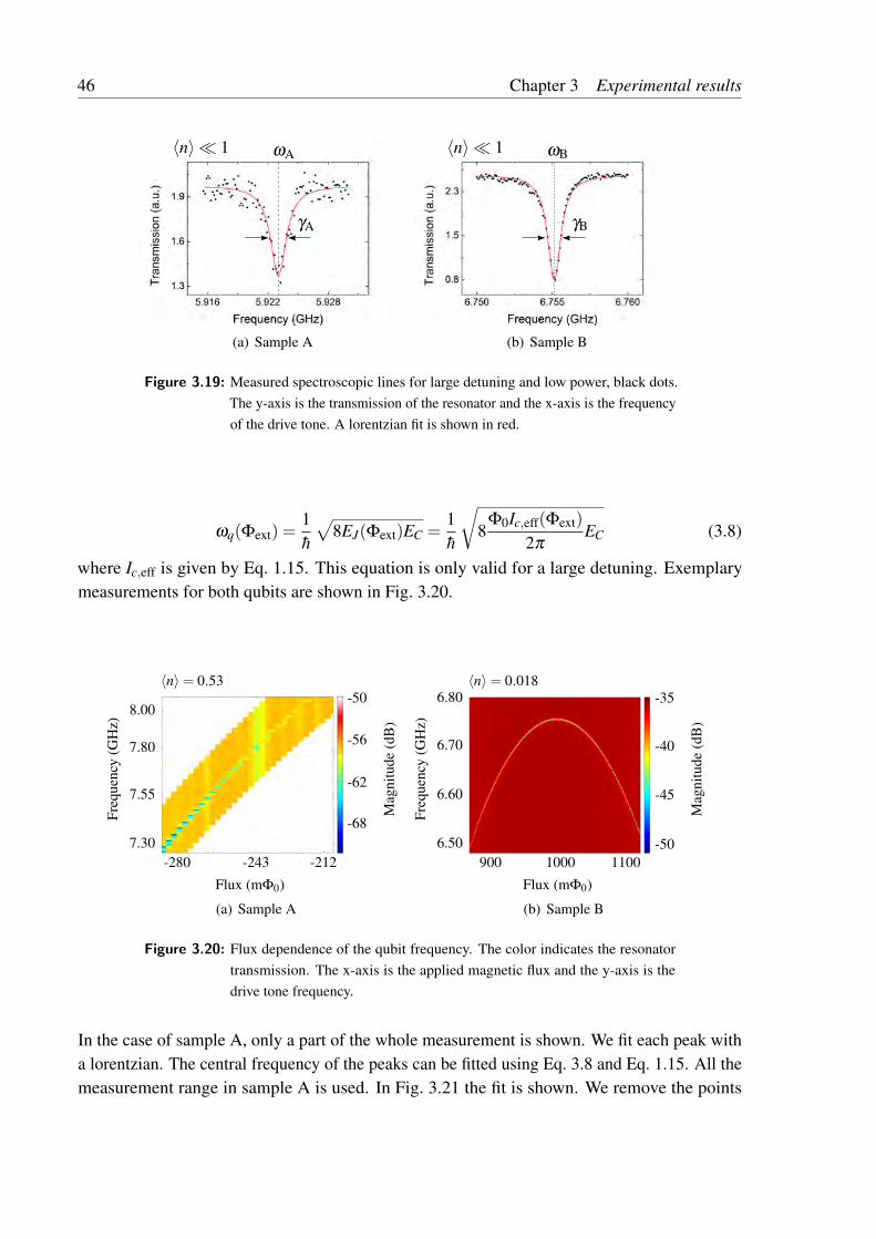
Taking into account the attenuation for each sample we obtain the power P needed to put onaverage one photon in the resonator. For sample A the attenuation including the microwavecables is -107 dB. For sample B it is -118 dB. Using these values we obtain the results inTable 3.2.It can be seen that for sample B the result is only one order of magnitude larger than theestimation we did. However for sample A the difference is of two orders of magnitude. SampleA was measured in a gold-plated copper box using silver glue for the connections. This silverglue may attenuate the incoming signal up to 4 dB [25][26]. In addition, when working atlow temperatures, the attenuators change their attenuation ratio and their impedance creatingimpedance mismatches that cause reflections. On the other hand sample B is placed in a boxwith a printed circuit board which gives a better matching with the incoming lines [27][28] andthe used attenuators show a good impedance matching at low temperatures.When ∆ g we can use the dip in transmission to estimate the qubit line width. We need lowmicrowave power so the width of the peak is not affected by the photons in the resonator. Twotransmission measurements obtained at low power are shown in Fig. 3.19.We fit both dips with a lorentzian. From the fit we obtain the line width of the qubit transitionfor both samples, Table 3.2. If we compare these values with the coupling constant g obtainedin Sec. 3.3 and the resonators widths κ we see that we reach the strong coupling regime whereg κ,γ [15].
3.4.2 Flux dependence of the qubit frequency
In order to measure the qubit transition frequency for different flux values we perform two-tonespectroscopy sweeping the magnetic flux. To do so we use an external coil. The magnetic fluxchanges the qubit transition frequency according to
46 Chapter 3 Experimental results
γA
ωA〈n〉 1
(a) Sample A
γB
ωB〈n〉 1
(b) Sample B
Figure 3.19: Measured spectroscopic lines for large detuning and low power, black dots.The y-axis is the transmission of the resonator and the x-axis is the frequencyof the drive tone. A lorentzian fit is shown in red.
ωq(Φext) =1h
√8EJ(Φext)EC =
1h
√8
Φ0Ic,eff(Φext)
2πEC (3.8)
where Ic,eff is given by Eq. 1.15. This equation is only valid for a large detuning. Exemplarymeasurements for both qubits are shown in Fig. 3.20.
〈n〉= 0.53
Flux (mΦ0)
Mag
nitu
de(d
B)
Freq
uenc
y(G
Hz)
8.00
7.55
7.80
7.30-280 -243 -212
-50
-56
-62
-68
(a) Sample A
〈n〉= 0.018
Flux (mΦ0)
Mag
nitu
de(d
B)
Freq
uenc
y(G
Hz)
6.80
6.60
6.70
6.50900 1000 1100
-35
-40
-45
-50
(b) Sample B
Figure 3.20: Flux dependence of the qubit frequency. The color indicates the resonatortransmission. The x-axis is the applied magnetic flux and the y-axis is thedrive tone frequency.
In the case of sample A, only a part of the whole measurement is shown. We fit each peak witha lorentzian. The central frequency of the peaks can be fitted using Eq. 3.8 and Eq. 1.15. All themeasurement range in sample A is used. In Fig. 3.21 the fit is shown. We remove the points
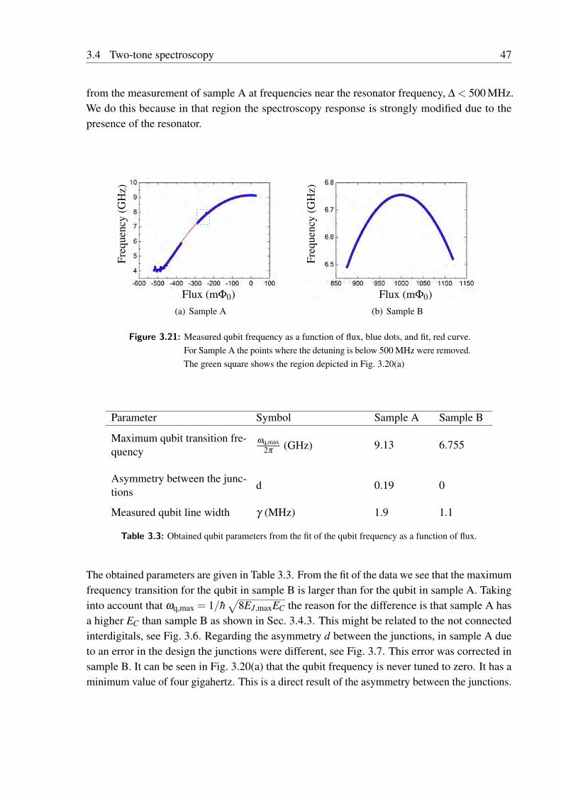
3.4 Two-tone spectroscopy 47
from the measurement of sample A at frequencies near the resonator frequency, ∆ < 500 MHz.We do this because in that region the spectroscopy response is strongly modified due to thepresence of the resonator.
Freq
uenc
y(G
Hz)
Flux (mΦ0)(a) Sample A
Freq
uenc
y(G
Hz)
Flux (mΦ0)(b) Sample B
Figure 3.21: Measured qubit frequency as a function of flux, blue dots, and fit, red curve.For Sample A the points where the detuning is below 500 MHz were removed.The green square shows the region depicted in Fig. 3.20(a)
Parameter Symbol Sample A Sample B
Maximum qubit transition fre-quency
ωq,max2π
(GHz) 9.13 6.755
Asymmetry between the junc-tions
d 0.19 0
Measured qubit line width γ (MHz) 1.9 1.1
Table 3.3: Obtained qubit parameters from the fit of the qubit frequency as a function of flux.
The obtained parameters are given in Table 3.3. From the fit of the data we see that the maximumfrequency transition for the qubit in sample B is larger than for the qubit in sample A. Takinginto account that ωq,max = 1/h
√8EJ,maxEC the reason for the difference is that sample A has
a higher EC than sample B as shown in Sec. 3.4.3. This might be related to the not connectedinterdigitals, see Fig. 3.6. Regarding the asymmetry d between the junctions, in sample A dueto an error in the design the junctions were different, see Fig. 3.7. This error was corrected insample B. It can be seen in Fig. 3.20(a) that the qubit frequency is never tuned to zero. It has aminimum value of four gigahertz. This is a direct result of the asymmetry between the junctions.
48 Chapter 3 Experimental results
3.4.3 Qubit anharmonicity
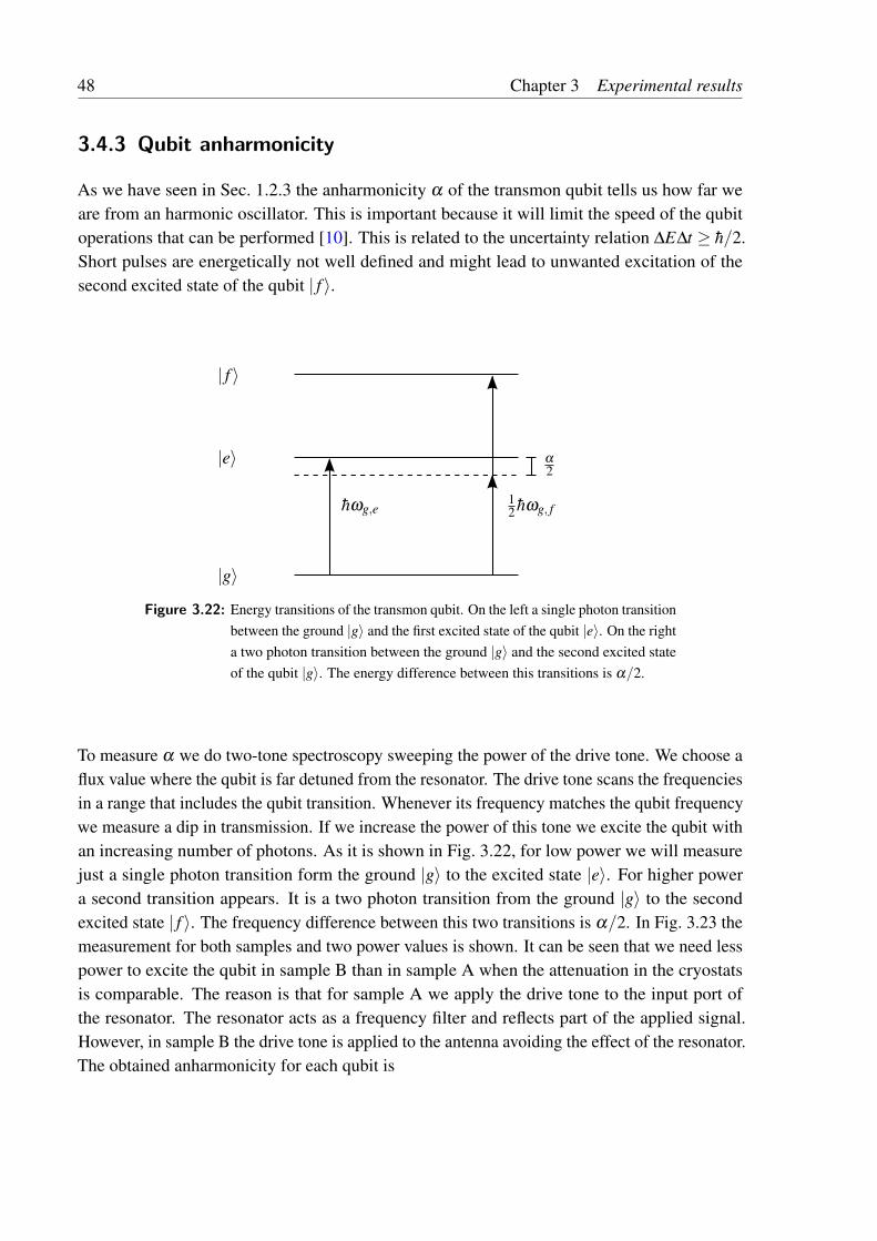
As we have seen in Sec. 1.2.3 the anharmonicity α of the transmon qubit tells us how far weare from an harmonic oscillator. This is important because it will limit the speed of the qubitoperations that can be performed [10]. This is related to the uncertainty relation ∆E∆t ≥ h/2.Short pulses are energetically not well defined and might lead to unwanted excitation of thesecond excited state of the qubit | f 〉.
|g〉
|e〉
| f 〉
hωg,e12 hωg, f
α
2
Figure 3.22: Energy transitions of the transmon qubit. On the left a single photon transitionbetween the ground |g〉 and the first excited state of the qubit |e〉. On the righta two photon transition between the ground |g〉 and the second excited stateof the qubit |g〉. The energy difference between this transitions is α/2.
To measure α we do two-tone spectroscopy sweeping the power of the drive tone. We choose aflux value where the qubit is far detuned from the resonator. The drive tone scans the frequenciesin a range that includes the qubit transition. Whenever its frequency matches the qubit frequencywe measure a dip in transmission. If we increase the power of this tone we excite the qubit withan increasing number of photons. As it is shown in Fig. 3.22, for low power we will measurejust a single photon transition form the ground |g〉 to the excited state |e〉. For higher powera second transition appears. It is a two photon transition from the ground |g〉 to the secondexcited state | f 〉. The frequency difference between this two transitions is α/2. In Fig. 3.23 themeasurement for both samples and two power values is shown. It can be seen that we need lesspower to excite the qubit in sample B than in sample A when the attenuation in the cryostatsis comparable. The reason is that for sample A we apply the drive tone to the input port ofthe resonator. The resonator acts as a frequency filter and reflects part of the applied signal.However, in sample B the drive tone is applied to the antenna avoiding the effect of the resonator.The obtained anharmonicity for each qubit is
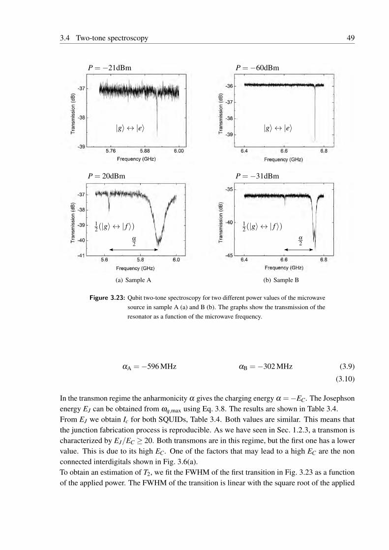
3.4 Two-tone spectroscopy 49
|g〉 ↔ |e〉
P =−21dBm
|g〉 ↔ |e〉
P =−60dBm
α
2
12(|g〉 ↔ | f 〉)
P = 20dBm
(a) Sample A
α
2
12(|g〉 ↔ | f 〉)
P =−31dBm
(b) Sample B
Figure 3.23: Qubit two-tone spectroscopy for two different power values of the microwavesource in sample A (a) and B (b). The graphs show the transmission of theresonator as a function of the microwave frequency.
αA =−596 MHz αB =−302 MHz (3.9)
(3.10)
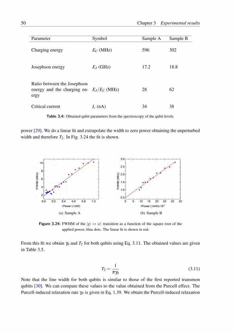
In the transmon regime the anharmonicity α gives the charging energy α =−EC. The Josephsonenergy EJ can be obtained from ωq,max using Eq. 3.8. The results are shown in Table 3.4.From EJ we obtain Ic for both SQUIDs, Table 3.4. Both values are similar. This means thatthe junction fabrication process is reproducible. As we have seen in Sec. 1.2.3, a transmon ischaracterized by EJ/EC ≥ 20. Both transmons are in this regime, but the first one has a lowervalue. This is due to its high EC. One of the factors that may lead to a high EC are the nonconnected interdigitals shown in Fig. 3.6(a).To obtain an estimation of T2, we fit the FWHM of the first transition in Fig. 3.23 as a functionof the applied power. The FWHM of the transition is linear with the square root of the applied
50 Chapter 3 Experimental results
Parameter Symbol Sample A Sample B
Charging energy EC (MHz) 596 302
Josephson energy EJ (GHz) 17.2 18.8
Ratio between the Josephsonenergy and the charging en-ergy
EJ/EC (MHz) 28 62
Critical current Ic (nA) 34 38
Table 3.4: Obtained qubit parameters from the spectroscopy of the qubit levels.
power [29]. We do a linear fit and extrapolate the width to zero power obtaining the unperturbedwidth and therefore T2. In Fig. 3.24 the fit is shown.
(a) Sample A (b) Sample B
Figure 3.24: FWHM of the |g〉 ↔ |e〉 transition as a function of the square root of theapplied power, blue dots. The linear fit is shown in red.
From this fit we obtain γ0 and T2 for both qubits using Eq. 3.11. The obtained values are givenin Table 3.5.
T2 =1
πγ0(3.11)
Note that the line width for both qubits is similar to those of the first reported transmonqubits [30]. We can compare these values to the value obtained from the Purcell effect. ThePurcell-induced relaxation rate γP is given in Eq. 1.39. We obtain the Purcell-induced relaxation
3.5 Time domain measurements 51
Parameter Symbol Sample A Sample B
Qubit line width extrapolatedto zero power
γ0 (MHz) 1.81 0.505
Qubit coherent time extrapo-lated to zero power
T2 (µs) 0.18 0.63
Table 3.5: Qubit parameters extrapolated to zero microwave power.
rate for both samples, Table 3.6.
Parameter Symbol Sample A Sample B
Purcell-induced qubit linewidth
γP (MHz) 0.078 0.181
Purcell-induced qubit coher-ent time
T2,P (MHz) 4.09 1.76
Table 3.6: Purcell-induced qubit line width and coherence time.
For sample B we obtain a Purcell-induced line width only three times smaller than the ex-trapolated γ0 at zero power. The smallest measured line width for the qubit in sample B isγB = 0.9 MHz, which is just five times greater than the Purcell-induced relaxation rate. Thismeans that the Purcell limit is a significant loss channel in this sample, but there also have to beadditional dephasing and/or loss channels in the same order of magnitude.
3.5 Time domain measurements
In previous sections we have introduced spectroscopy measurements of the samples. One or twomicrowave tones have been applied to the sample and the transmission of the resonator has beenmeasured in a continuous-wave fashion. Here we introduce the time domain measurements,which give us access to the coherent qubit dynamics. Using the antenna a series of microwavepulses are applied to the qubit, which is far detuned form the resonator. These pulses changethe state of the qubit on the Bloch sphere. After the pulse series a readout tone is applied tothe input tone of the resonator. Due to the dispersive shift, the transmission of the resonatorwill depend on the qubit state. Therefore with the readout tone we know the state of the qubitafter all the pulses. The outcome of the measurement depends on the different tones used andtheir length. It gives information about how does the qubit state evolve in time. Time domainmeasurements can be used to accurately measure T1 and T2.In the performed measurement we obtain T2 from the so called spin echo sequence, which com-
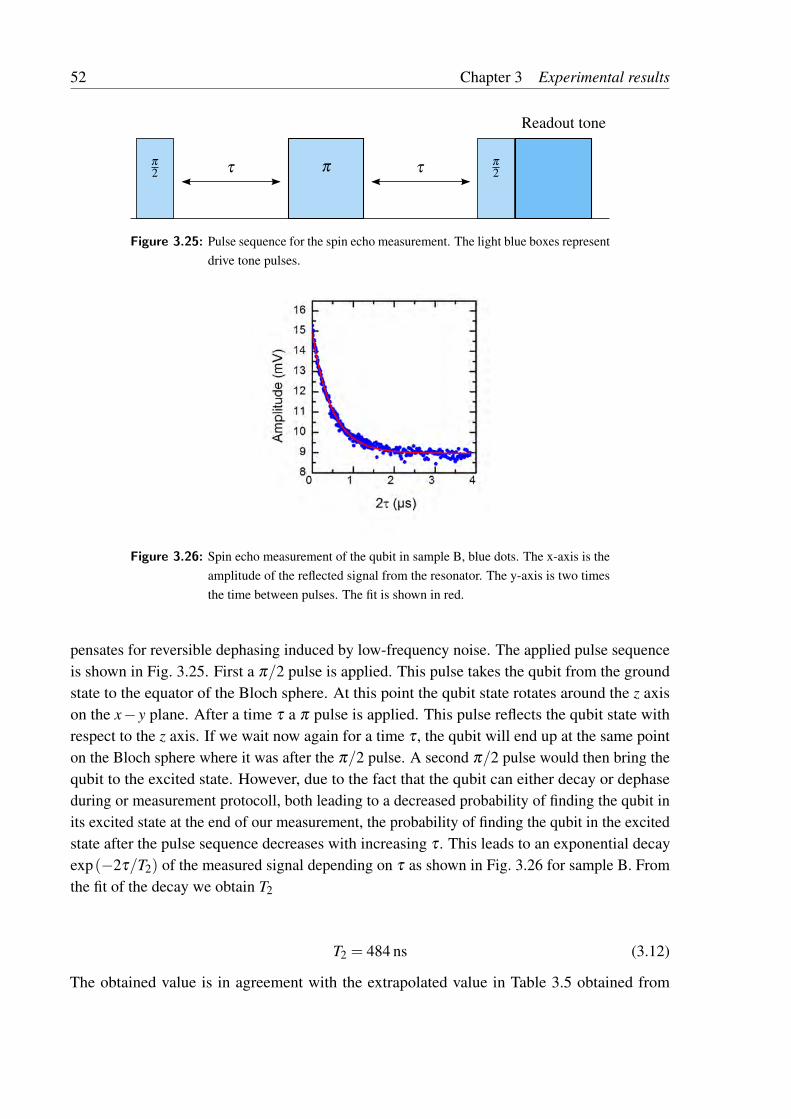
52 Chapter 3 Experimental results
τ τπ
2 ππ
2
Readout tone
Figure 3.25: Pulse sequence for the spin echo measurement. The light blue boxes representdrive tone pulses.
Figure 3.26: Spin echo measurement of the qubit in sample B, blue dots. The x-axis is theamplitude of the reflected signal from the resonator. The y-axis is two timesthe time between pulses. The fit is shown in red.
pensates for reversible dephasing induced by low-frequency noise. The applied pulse sequenceis shown in Fig. 3.25. First a π/2 pulse is applied. This pulse takes the qubit from the groundstate to the equator of the Bloch sphere. At this point the qubit state rotates around the z axison the x− y plane. After a time τ a π pulse is applied. This pulse reflects the qubit state withrespect to the z axis. If we wait now again for a time τ , the qubit will end up at the same pointon the Bloch sphere where it was after the π/2 pulse. A second π/2 pulse would then bring thequbit to the excited state. However, due to the fact that the qubit can either decay or dephaseduring or measurement protocoll, both leading to a decreased probability of finding the qubit inits excited state at the end of our measurement, the probability of finding the qubit in the excitedstate after the pulse sequence decreases with increasing τ . This leads to an exponential decayexp(−2τ/T2) of the measured signal depending on τ as shown in Fig. 3.26 for sample B. Fromthe fit of the decay we obtain T2
T2 = 484 ns (3.12)
The obtained value is in agreement with the extrapolated value in Table 3.5 obtained from

3.5 Time domain measurements 53
two-tone spectroscopy. Further measurements in this direction are currently ongoing.

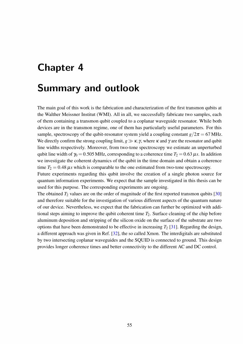
Chapter 4
Summary and outlook
The main goal of this work is the fabrication and characterization of the first transmon qubits atthe Walther Meissner Institut (WMI). All in all, we successfully fabricate two samples, eachof them containing a transmon qubit coupled to a coplanar waveguide resonator. While bothdevices are in the transmon regime, one of them has particularly useful parameters. For thissample, spectroscopy of the qubit-resonator system yield a coupling constant g/2π = 67 MHz.We directly confirm the strong coupling limit, g κ,γ , where κ and γ are the resonator and qubitline widths respectively. Moreover, from two-tone spectroscopy we estimate an unperturbedqubit line width of γ0 = 0.505 MHz, corresponding to a coherence time T2 = 0.63 µs. In additionwe investigate the coherent dynamics of the qubit in the time domain and obtain a coherencetime T2 = 0.48 µs which is comparable to the one estimated from two-tone spectroscopy.Future experiments regarding this qubit involve the creation of a single photon source forquantum information experiments. We expect that the sample investigated in this thesis can beused for this purpose. The corresponding experiments are ongoing.The obtained T2 values are on the order of magnitude of the first reported transmon qubits [30]and therefore suitable for the investigation of various different aspects of the quantum natureof our device. Nevertheless, we expect that the fabrication can further be optimized with addi-tional steps aiming to improve the qubit coherent time T2. Surface cleaning of the chip beforealuminum deposition and stripping of the silicon oxide on the surface of the substrate are twooptions that have been demonstrated to be effective in increasing T2 [31]. Regarding the design,a different approach was given in Ref. [32], the so called Xmon. The interdigitals are substitutedby two intersecting coplanar waveguides and the SQUID is connected to ground. This designprovides longer coherence times and better connectivity to the different AC and DC control.
55

Bibliography
[1] R. P. Feynman, “Simulating Physics with Computers”, International Journal of TheoreticalPhysics 21, 467 (1982).
[2] M. Nielsen and I. Chuang, Quantum Computation and Quantum Information (CambridgeUniversity Press, 2000).
[3] P. Grangier, G. Reymond, and N. Schlosser, “Implementations of Quantum ComputingUsing Cavity Quantum Electrodynamics Schemes”, Fortschritte der Physik 48, 859 (2000).
[4] J. Clarke and F. K. Wilhelm, “Superconducting quantum bits”, Nature 453, 1031 (2008).
[5] J. M. Martinis and K. Osborne, “Superconducting Qubits and the Physics of JosephsonJunctions”, eprint arXiv:cond-mat/0402415:cond-mat/0402415 (2004).
[6] A. Wallraff, D. I. Schuster, A. Blais, L. Frunzio, R.-S. Huang, J. Majer, S. Kumar, S. M.Girvin, and R. J. Schoelkopf, “Strong coupling of a single photon to a superconductingqubit using circuit quantum electrodynamics”, Nature 431, 162 (2004).
[7] M. Tinkham, Introduction to Superconductivity (Robert E. Krieger Publishing Company,1975).
[8] W. C. Stewart, “Current -voltage characteristics of Josephson junctions”, Applied PhysicsLetters 12, 277 (1968).
[9] D. E. McCumber, “Effect of ac impedance on dc voltage-current characteristics of super-conducting weak-link junctions”, Journal of Applied Physics 39, 3113 (1968).
[10] J. Koch, T. M. Yu, J. Gambetta, A. A. Houck, D. I. Schuster, J. Majer, A. Blais, M. H.Devoret, S. M. Girvin, and R. J. Schoelkopf, “Charge-insensitive qubit design derivedfrom the Cooper pair box”, Phys. Rev. A 76, 042319 (2007).
[11] M.-H. Devoret and R. Schoelkpof, “Superconducting circuits for quantum information:An outlook”, Science 339, 1169 (2013).
[12] J. Bourassa, J. M. Gambetta, A. A. Abdumalikov, Jr., O. Astafiev, Y. Nakamura, andA. Blais, “Ultrastrong coupling regime of cavity QED with phase-biased flux qubits”,Physical Review A 80, 032109 (2009).
57
58 Bibliography
[13] M. A. Sillanpää, J. I. Park, and R. W. Simmonds, “Coherent quantum state storage andtransfer between two phase qubits via a resonant cavity”, Nature 449, 438 (2007).
[14] A. Wallraff, D. I. Schuster, A. Blais, L. Frunzio, J. Majer, M. H. Devoret, S. M. Girvin, andR. J. Schoelkopf, “Approaching Unit Visibility for Control of a Superconducting Qubitwith Dispersive Readout”, Physical Review Letters 95, 060501 (2005).
[15] D.F.Walls and G. J.Milburn, Quantum Optics (Springer, 2010).
[16] E. Jaynes and F.W.Cummings, “Comparision of Quantum and Semiclassical RadiationTheories with Application to the Beam Maser”, Proceedings of the IEEE 51, 89 (1963).
[17] A. Blais, R.-S. Huang, A. Wallraff, S. M. Girvin, and R. J. Schoelkopf, “Cavity quantumelectrodynamics for superconducting electrical circuits: An architecture for quantumcomputation”, Physical Review A 69, 062320 (2004).
[18] E. Xie, “Optimized fabrication process for nanoscale Josephson junction used in supercon-ducting quantum circuits”, Master’s thesis, Technische Universität München (2013).
[19] J.Niemeyer, “Eine einfache Methode zur Herstellung kleiner Josephson-Elemente”, PTB-Mitt 84, 251 (1974).
[20] G. J. Dolan, “Offset masks for lift-off photoprocessing”, Applied Physics Letters 31, 337(1977).
[21] K. F. Wulschner, “Nb/AlOx/Nb Josephson-Kontakte für supraleitende Quanten-schaltkreise”, Diploma thesis, Technische Universität München (2011).
[22] J. Kuerten, “3He-4He II mixtures: thermodynamic and hydrodynamic properties”, Ph.D.thesis, Technische Universität Eindhoven (1987).
[23] D. I. Schuster, A. Wallraff, A. Blais, L. Frunzio, R.-S. Huang, J. Majer, S. M. Girvin, andR. J. Schoelkopf, “ac Stark Shift and Dephasing of a Superconducting Qubit StronglyCoupled to a Cavity Field”, Physical Review Letters 94, 123602 (2005).
[24] S. Meier, “Loss reduction of superconducting coplanar microwave resonators on sapphiresubstrates”, Bachelor thesis, Technische Universität München (2014).
[25] U. Shaumburger, “Ketten von Resonatoren mit einstellbarer Nichtlinearität”, Diplomathesis, Technische Universität München (2014).
[26] K. Reiser, “Supraleitende Quantenschaltkreise: Mikrowellenresonatoren mit Antenne”,Bachelor thesis, Technische Universität München (2014).
[27] C. Schneider, “On-chip Superconducting Microwave Beam Splitter”, Master’s thesis,Technische Universität München (2014).
Bibliography 59
[28] M. Fischer, “On-chip Superconducting Microwave Interferometer”, Master’s thesis, Tech-nische Universität München (2014).
[29] G. Ithier, E. Collin, P. Joyez, P. J. Meeson, D. Vion, D. Esteve, F. Chiarello, A. Shnirman,Y. Makhlin, J. Schriefl, and G. Schön, “Decoherence in a superconducting quantum bitcircuit”, Phys. Rev. B 72, 134519 (2005).
[30] A. A. Houck, D. I. Schuster, J. M. Gambetta, J. A. Schreier, B. R. Johnson, J. M. Chow,L. Frunzio, J. Majer, M. H. Devoret, S. M. Girvin, and R. J. Schoelkopf, “Generatingsingle microwave photons in a circuit”, Nature 449, 328 (2007).
[31] C. M. Quintana, A. Megrant, Z. Chen, A. Dunsworth, B. Chiaro, R. Barends, B. Campbell,Y. Chen, I.-C. Hoi, E. Jeffrey, J. Kelly, J. Y. Mutus, P. J. J. O’Malley, C. Neill, P. Roushan,D. Sank, A. Vainsencher, J. Wenner, T. C. White, A. N. Cleland, and J. M. Martinis, “Char-acterization and reduction of microfabrication-induced decoherence in superconductingquantum circuits”, Applied Physics Letters 105, 062601 (2014).
[32] R. Barends, J. Kelly, A. Megrant, D. Sank, E. Jeffrey, Y. Chen, Y. Yin, B. Chiaro, J. Mutus,C. Neill, P. O’Malley, P. Roushan, J. Wenner, T. C. White, A. N. Cleland, and J. M.Martinis, “Coherent Josephson Qubit Suitable for Scalable Quantum Integrated Circuits”,Phys. Rev. Lett. 111, 080502 (2013).

Acknowledgment
I would like to say thanks to everyone that helped me during this thesis.
First of all I want to thank Prof. Dr. Rudolf Gross for giving me the opportunity to do my masterthesis at the Walther Meissner Institut.
Secondly I would like to thank Friedrich Wulschner for his supervision during the whole thesisand all the knowledge I acquired.
Thanks to Dr. Frank Deppe for his advice and corrections.
Thanks to Jan Goetz and Miriam Mueting for the spin echo data.
I would also like to thank all the qubit group for their help. Specially Max and Edwar for helpingme with the e-beam. Thanks to my office partners for their company.
Finally I would like to thank my family, specially my parents, my brother and my sisters fortheir support via WhatsApp. And thanks to Ana for her support but mainly for bringing megalletas Marbú Dorada to Munich.
61