
Correlation of particle fluxes and film properties ... · 5.2 Macroparticle Filtering 38 5.3 Anodic...
179
Correlation of particle fluxes and film properties deposited by vacuum arc Dissertation Von der Fakultät für Physik der Universität Duisburg-Essen zur Erlangung des akademischen Grades eines Doktors der Naturwissenschaften (Dr. rer. Nat.) genehmigten Dissertation von Oleksiy Filipov geboren am 17. August 1977 in Charkiw / Ukraine Tag der Disputation: 08. Mai 2013 Prüfungsvorsitzender: Prof. Dr. Peter Kratzer Erster Gutachter: Prof. Dr. Volker Buck Zweiter Gutachter: Prof. Dr. Dieter Mergel
Transcript of Correlation of particle fluxes and film properties ... · 5.2 Macroparticle Filtering 38 5.3 Anodic...
Correlation of particle fluxes and film properties deposited by
vacuum arc
Dissertation
Von der Fakultät für Physik
der Universität Duisburg-Essen
zur Erlangung des akademischen Grades eines
Doktors der Naturwissenschaften (Dr. rer. Nat.)
genehmigten Dissertation
von
Oleksiy Filipov
geboren am 17. August 1977
in Charkiw / Ukraine
Tag der Disputation: 08. Mai 2013
Prüfungsvorsitzender: Prof. Dr. Peter Kratzer
Erster Gutachter: Prof. Dr. Volker Buck
Zweiter Gutachter: Prof. Dr. Dieter Mergel
2
Murphy's First Laboratory Law:
Hot glass looks exactly the same as cold glass.

3
Dedicated to my beloved parents
for their love, endless support
and encouragement
4
Table of Contents
Acknowledgments 8
1 Introduction 10
2 Fundamentals 15
2.1 Carbon 15
2.1.1 Electronic Structure of Carbon 15
2.1.2 Hybridization of Atomic Orbitals 16
2.1.2.1 sp 3
Hybridization 16
2.1.2.2 sp 2
Hybridization 17
2.1.2.3 sp 1
Hybridization 17
2.1.2.4 and Bonds 18
2.2 Carbon Allotropes 19
2.2.1 Diamond 20
2.2.2 Graphite 21
2.2.3 Fullerene 22
2.2.4 Nanotubes 22
2.2.5 Graphene 23
2.2.6 Amorphous Carbon 24
2.3 DLC Models 26
3 DLC Deposition Techniques 28
4 DC Discharge in the Vacuum 29
5 Arc Discharge 32
5.1 Cathodic Arc 34
5.2 Macroparticle Filtering 38
5.3 Anodic Arc 40
5.4 Transition From Cathodic to Anodic Arc 40
6 Diagnostics 41
6.1 Plasma Diagnostics 41
6.1.1 Retarding Field Energy Analyzer (RFEA) 41
6.2 Film Diagnostics 44
6.2.1 Nuclear Reaction Analysis (NRA) 44
5
6.2.2 Spectroscopic Diagnostic Methods 45
6.2.2.1 UV-VIS Spectroscopy 45
6.2.3 Physical Structure 46
6.2.3.1 X-Ray Diffraction (XRD) and Williamson-Hall Method 46
6.2.4 Mechanical Properties 50
6.2.4.1 Residual Stress 50
6.2.4.2 SSIOD 54
7 Experimental Setup 56
7.1 Experimental Setup for DLC Film Deposition 56
7.2 Experimental Setup for Magnesium Film Deposition 60
8 Experimental Results 64
8.1 Plasma Diagnostics 64
8.1.1 Influence of Deposition Parameters on Plasma Properties 64
8.1.1.1 Mass-spectroscopy During DLC Film Deposition 64
8.1.2 Influence of Electrode Material on Plasma Composition 67
8.1.2.1 Electrode Degasation 67
8.1.2.2 Electrode Material Impurity 69
8.1.3 Influence of Deposition Parameters on Plasma Properties 71
8.1.3.1 Mass Spectroscopy During Magnesium Film Deposition 71
8.1.4 Particle Energy Measurement During DLC Film Deposition 73
8.1.4.1 Influence of Different Arc Modes on the Ion Energy 73
8.1.4.2 Influence of Different Hydrogen Flow Rates on the Ion Energy 76
8.1.4.3 Degree of Ionisation as a Function of Different Arc Modes 77
8.1.5 Particle Energy Measurement During Magnesium Film Deposition 79
8.1.5.1 Influence of Different Hydrogen Flow Rates on the Ion Energy 79
8.2 Film Diagnostics 81
8.2.1 Arc Modes 81
8.2.2 Deposition Rate 83
8.2.3 Structural Properties 84
8.2.3.1 Film Morphology 84
8.2.3.1.1 Influence of Different Arc Modes on Film Morphology 85
8.2.3.1.2 Influence of Bias Voltage on Film Morphology 89
8.2.3.1.3 Influence of Different Hydrogen Flow Rates on Film Morphology 92
6
8.2.3.2 Hydrogen Content in the DLC Film 97
8.2.3.2.1 Hydrogen to Carbon Ratio 97
8.2.3.2.2 Nuclear Reaction Analysis (NRA) 99
8.2.3.2.3 Adhesion Coefficient 102
8.2.4 Optical Properties and Electronic Structure of DLC Films 103
8.2.4.1 Film Transmittance 103
8.2.4.1.1 Influence of Different Arc Modes on Film Transmittance 103
8.2.4.1.2 Influence of Different Hydrogen Flow Rates on Film Transmittance 105
8.2.4.2 The Optical Band Gap 109
8.2.4.2.1 Influence of Different Arc Modes on the Band Gap 109
8.2.4.2.2 Influence of Different Hydrogen Flow Rates on the Band Gap 110
8.2.4.3 DLC Band Model 111
8.2.4.4 The sp3 Content in DLC Film as a Function of Deposition Parameters 114
8.2.4.4.1 Influence of Different Arc Modes on sp3 Content 114
8.2.4.4.2 Influence of Different Deposition Parameters on sp3 Content 115
8.2.4.5 The Complex Dielectric Function 116
8.2.4.5.1 Influence of Different Arc Modes on 2 119
8.2.4.5.2 Influence of Different Hydrogen Flow Rates on 2 120
8.2.4.5.3 Influence of Bias Voltage on 2 122
8.2.5 Raman Spectroscopy 126
8.2.5.1 The G-Peak Position 127
8.2.5.1.1 Influence of Different Arc Modes on the G- Peak Position 128
8.2.5.1.2 Influence of Bias Voltage and Different Hydrogen Flow Rates on the G-Peak
Position 129
8.2.5.2 The ID/IG Ratio 131
8.2.5.2.1 Influence of Different Arc Modes on the ID/IG Ratio 132
8.2.5.2.2 Influence of Bias Voltage and Different Hydrogen Flow Rates on the
ID/IG Ratio 133
8.2.5.3 The Full Width at Half Maximum of G-Peak (FWHM G) 135
8.2.5.3.1 Influence of Different Arc Modes on FWHM G 135
8.2.5.3.2 Influence of Bias Voltage and Different Hydrogen Flow Rates on
FWHM G 136
8.2.5.4 The G-Peak Dispersion (DispG) 137
7
8.2.5.5 Correlation between Results from Raman and UV-VIS Spectroscopy 139
8.2.5.5.1 The Optical Band Gap and Raman Parameters 139
8.2.5.5.2 The Imaginary Part 2 of the Dielectric Function and Raman Parameters 140
8.2.6 Mechanical Properties 141
8.2.6.1 Residual Stress Measurements 141
8.2.6.1.1 Thermal Stress 141
8.2.6.1.2 Influence of Different Arc Modes on Residual Stress 142
8.2.6.1.3 Influence of Bias Voltage on Residual Stress 143
8.2.6.1.4 Influence of Different Hydrogen Flow Rates on Residual Stress 144
8.3 DLC Film Classification 148
8.4 Magnesium Films Deposition 150
8.4.1 Energy-Dispersive X-Ray Spectroscopy (EDX) 150
8.4.2 Grain size by SEM 154
8.4.3 Grain Size by XRD 155
9 Results And Outlook 157
10 References 160
Appendix I 171

8
Acknowledgments
I am very grateful and would like to express my acknowledgement to
My supervisor Prof. Dr. Volker Buck for welcoming me into his group, his guidance in my
scientific work, providing outstanding working facilities and friendly working atmosphere,
always ready to help in finding a solution to any problem,
Prof. Dr. Dieter Mergel my second reviewer for good advices, attention to details, and useful
comments,
Dr. Alexei Poukhovoi for his friendship all the time, willingness to help, companionship in many
good activities inside and outside the office,
Dr. Nicolas Wöhrl for his help in stress measurements, scientific advices, good old days together
when we were young and a robot,
Dr. Stefan Reuter for his kindness and his cooperation during my work, good times and
conversations which I’m missing now,
Sebastian Schipporeit for his help, friendly conversations, readiness to correct my English
grammar,
Dr. Viktor Kadetov for his friendly support at the beginning of my time in Germany,
Dr. Werner Becker for providing data from NRA measurements,
Dr. Nebati Abdelkader for his help with XRD measurements,
Dipl.-Ing. Smail Boukercha for his help in SEM measurements and friendly conversations,
Dipl.-Phys. Marcus Neubert for his friendly advices and cooperation,
Dipl.-Phys. Matthias Haase for willingness to discuss any encountered problems and his opinion,
Dipl.-Phys. Klaus Pärschke for his readiness to help and useful advices,
Dipl.-Phys. Victoria Khlopyanova for her smile, kindly provided data for missing experiments,
Dipl.-Phys.Ing. Martin Jerman his help with the vacuum arc chamber,
Dipl.-Ing. Monika Timpner for many friendly conversations,
Mrs. Heidi Pärschke for her help especially with German office bureaucracy,
Peter Walter and Heinz Loffeld for their technical assistance,
co-workers of the Essen mechanic workshop (especially to prematurely deceased Frank Matthies)
for help and advices in construction activities, on time and accurate manufacturing,
Dietrich Tönnes and Dr. Bärbel Maullu for their help, friendly conversations and support,
My family who always believe in me, for their love, whom I owe everything I have...
9
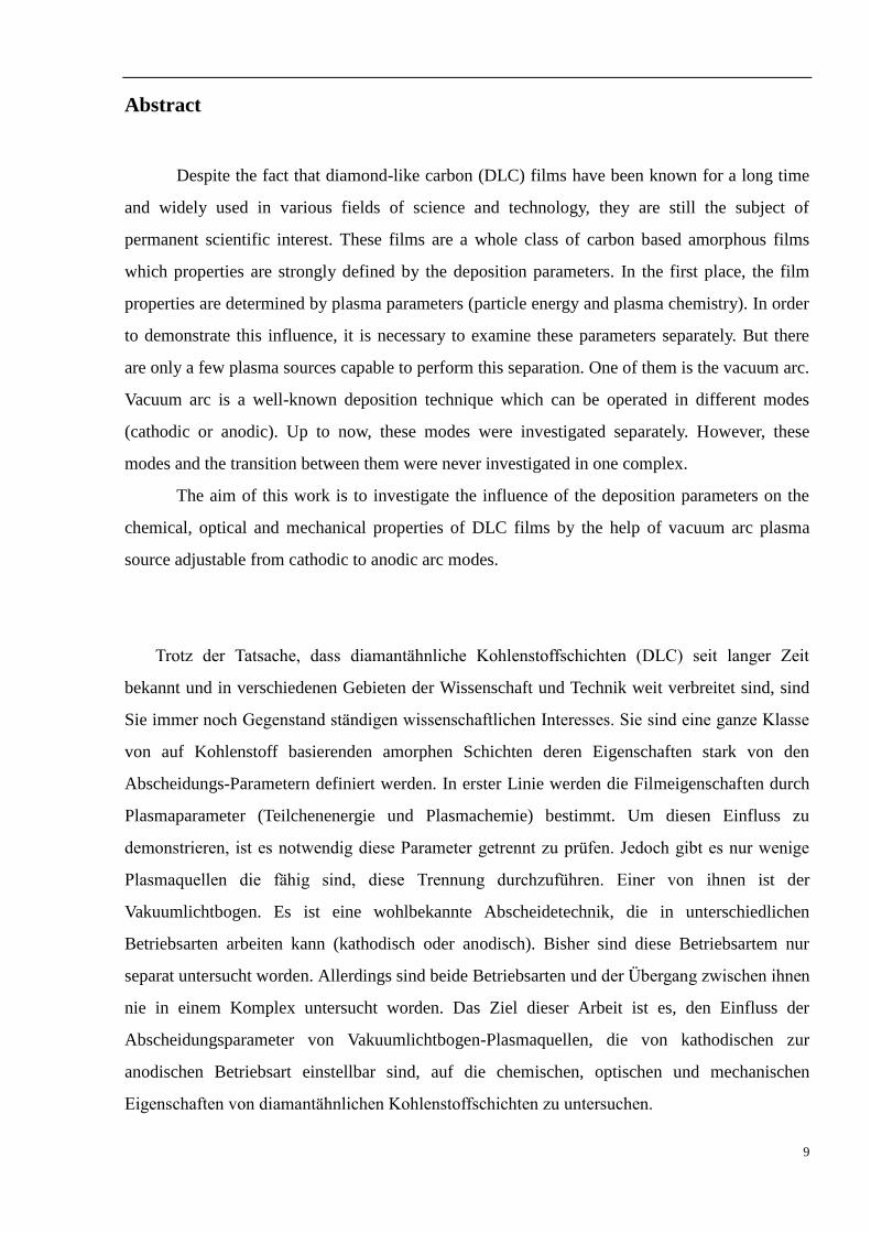
Abstract
Despite the fact that diamond-like carbon (DLC) films have been known for a long time
and widely used in various fields of science and technology, they are still the subject of
permanent scientific interest. These films are a whole class of carbon based amorphous films
which properties are strongly defined by the deposition parameters. In the first place, the film
properties are determined by plasma parameters (particle energy and plasma chemistry). In order
to demonstrate this influence, it is necessary to examine these parameters separately. But there
are only a few plasma sources capable to perform this separation. One of them is the vacuum arc.
Vacuum arc is a well-known deposition technique which can be operated in different modes
(cathodic or anodic). Up to now, these modes were investigated separately. However, these
modes and the transition between them were never investigated in one complex.
The aim of this work is to investigate the influence of the deposition parameters on the
chemical, optical and mechanical properties of DLC films by the help of vacuum arc plasma
source adjustable from cathodic to anodic arc modes.
Trotz der Tatsache, dass diamantähnliche Kohlenstoffschichten (DLC) seit langer Zeit
bekannt und in verschiedenen Gebieten der Wissenschaft und Technik weit verbreitet sind, sind
Sie immer noch Gegenstand ständigen wissenschaftlichen Interesses. Sie sind eine ganze Klasse
von auf Kohlenstoff basierenden amorphen Schichten deren Eigenschaften stark von den
Abscheidungs-Parametern definiert werden. In erster Linie werden die Filmeigenschaften durch
Plasmaparameter (Teilchenenergie und Plasmachemie) bestimmt. Um diesen Einfluss zu
demonstrieren, ist es notwendig diese Parameter getrennt zu prüfen. Jedoch gibt es nur wenige
Plasmaquellen die fähig sind, diese Trennung durchzuführen. Einer von ihnen ist der
Vakuumlichtbogen. Es ist eine wohlbekannte Abscheidetechnik, die in unterschiedlichen
Betriebsarten arbeiten kann (kathodisch oder anodisch). Bisher sind diese Betriebsartem nur
separat untersucht worden. Allerdings sind beide Betriebsarten und der Übergang zwischen ihnen
nie in einem Komplex untersucht worden. Das Ziel dieser Arbeit ist es, den Einfluss der
Abscheidungsparameter von Vakuumlichtbogen-Plasmaquellen, die von kathodischen zur
anodischen Betriebsart einstellbar sind, auf die chemischen, optischen und mechanischen
Eigenschaften von diamantähnlichen Kohlenstoffschichten zu untersuchen.
10
Introduction
Since the beginning of mankind, humans have been creating new tools and new devices
in order to improve the existing ones and create more efficient and durable ones. Each era is
determined by its technology, from the simplest bronze cutting tools to high-tech lasers and
multilayered ceramic cutters. Science has been looking deeper and deeper and opened up newer
and newer horizons. And the time when there was a requirement for new materials with new
properties has come. During the last century, thin film technology has become more and more
popular. This technology stands for whole new materials with the special properties which may
differ from those of bulk ones. Using such technology we are able to intentionally modify bulk
material properties only by coating it with a very thin layer of another material. These materials
can be deposited directly onto any required surface in order to confer special properties or a set
of properties. Such technology requires a new means of production: vacuum technology and
plasma technology. The most rapidly developing and growing technique is plasma deposition.
This technology allows us to operate with another state of matter – plasma, and create hitherto
unknown metastable conditions in which a new kind of chemical processes and reactions is
possible. These processes are not possible under standard conditions but we are able to use
common materials and give them new functional properties.
The functional properties – macroscopic properties, of deposited films usually determine
their application area. In some cases, films should be hard or soft, hydrophilic or hydrophobic, or
multilayered with different optical properties. These properties usually appear to be a product of
trial and error in industrial researches to receive the films with desired macroscopic parameters.
Usually these thin film deposition methods are “empirically” developed without understanding
the physical processes which lie under the surface. In order to optimize the existing methods and
to develop a modern one it is necessary to gain the knowledge and comprehension of film
deposition processes and factors affecting these processes. Only thin film technology is able to
give a comprehensive answer to this question. The tailoring of microscopic properties will give
us the means to tune up the macroscopic properties of the deposited films.
The following figure shows the influence of different parameters onto functional properties
of deposited films [Buck93].
11
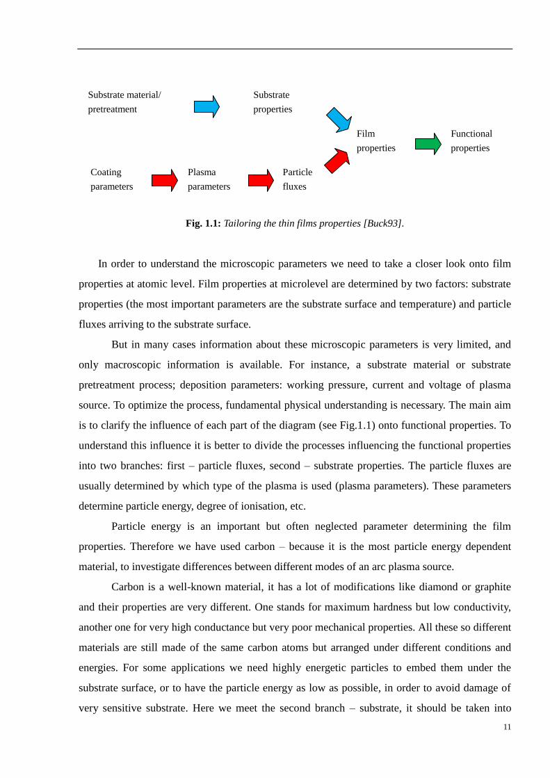
Fig. 1.1: Tailoring the thin films properties [Buck93].
In order to understand the microscopic parameters we need to take a closer look onto film
properties at atomic level. Film properties at microlevel are determined by two factors: substrate
properties (the most important parameters are the substrate surface and temperature) and particle
fluxes arriving to the substrate surface.
But in many cases information about these microscopic parameters is very limited, and
only macroscopic information is available. For instance, a substrate material or substrate
pretreatment process; deposition parameters: working pressure, current and voltage of plasma
source. To optimize the process, fundamental physical understanding is necessary. The main aim
is to clarify the influence of each part of the diagram (see Fig.1.1) onto functional properties. To
understand this influence it is better to divide the processes influencing the functional properties
into two branches: first – particle fluxes, second – substrate properties. The particle fluxes are
usually determined by which type of the plasma is used (plasma parameters). These parameters
determine particle energy, degree of ionisation, etc.
Particle energy is an important but often neglected parameter determining the film
properties. Therefore we have used carbon – because it is the most particle energy dependent
material, to investigate differences between different modes of an arc plasma source.
Carbon is a well-known material, it has a lot of modifications like diamond or graphite
and their properties are very different. One stands for maximum hardness but low conductivity,
another one for very high conductance but very poor mechanical properties. All these so different
materials are still made of the same carbon atoms but arranged under different conditions and
energies. For some applications we need highly energetic particles to embed them under the
substrate surface, or to have the particle energy as low as possible, in order to avoid damage of
very sensitive substrate. Here we meet the second branch – substrate, it should be taken into
Substrate material/
pretreatment
Substrate
properties
Coating
parameters
Plasma
parameters
Particle
fluxes
Film
properties
Functional
properties
12
account which type of substrate material is used (plastic or metal), its surface condition
(roughness, oxide layers) and temperature.
As one can see there are many parameters influencing deposition processes, in addition
these parameters are also interacting with each other and causing more complex effects. It is
necessary to consider “hidden parameters”. These indeterminate parameters can be only detected
after series of similar experiments [Buck93].
Diamond-like carbon (DLC) stands for a whole class of materials based on carbon
(amorphous carbon, hydrogenated carbon, tetrahedral amorphous carbon, etc.), where the
properties can be varied in an unusually large area – e.g. from conductive to isolating or from
hydrophilic to hydrophobic [Grill03]. Also be gradually changed in hardness, intrinsic
mechanical stress, E-module, roughness, gas permeability, etc. – and these properties can be
varied by choosing suitable coating parameters. In order to influence the film properties it is
necessary to control particle energy but it is only possible for charged particles and the amount of
the charged particles (ionisation rate) is a crucial parameter. Very interesting material properties
are expected for films produced with particle energy in the range 10 eV – 100 eV [Robertson02],
but there are only a few plasma sources that deliver high fluxes at these energies, the hybrid
radiofrequency source and the DC arc source seems to be the most promising for this purpose.
But these sources are rather different in the way of plasma generation, ionisation rate and
deposition rates. Therefore, the obtained films have differences in structure and chemical
composition, consequently film properties differ.
The cathodic arc is the most commonly used deposition method in a vacuum technology.
Such arc is a powerful plasma source with high deposition rate, but the biggest problem is
macroparticle or droplet formation. Usually macroparticles are formed by the materials with the
low melting temperature like Al, Cu where amount of ions evaporated is very low. When a
materials with the high melting temperature like C, W, Mo or the sublimation materials are used
it is possible to reduce macroparticle content and to increase the amount of ions evaporated
[Eckhardt75]. But for some applications where the surface properties like the roughness or the
film transparency are very important, the amount of macroparticles does not allow to use this
method. In that case there is a possibility to keep the advantages of the cathodic vacuum arc like
high degree of ionisation and very high deposition rate, but avoid macroparticles generation.
There have been several attempts [Aksenov78, Karpov97, Anders99,] one of them is an anodic
vacuum arc. The anodic arc can be more successfully used especially in thin films technology
applications instead of the cathodic arc deposition method.
13
An arc plasma source adjustable from cathodic to anodic mode allows us to customize
plasma properties in order to obtain nanostructured coatings with reduced droplet incorporation.
In order to adjust film properties, DLC films were deposited by using different deposition
regimes of a DC vacuum arc plasma source. The variation in process parameters such as
substrate bias and gas admixture is used to influence the film properties. The plasma parameters
were monitored during deposition by mass-spectrometer and ion energy by retarding field energy
analyzer. The films were deposited on polished (100) Si, BK-7 glass and steel substrates in order
to investigate their mechanical, chemical and optical properties. For the film morphology
analysis and surface roughness evaluation of deposited films, scanning electron microscopy
(SEM) and atomic force microscopy (AFM) were used. Nuclear reaction analysis (NRA) was
used to evaluate hydrogen content in the films. The optical properties of the films were ex-situ
examined by UV-VIS spectroscopy and from these data details of the band structure were
modelled. The Raman spectroscopy was used to investigate the chemical composition of the
obtained films. The relation between particle energy and deposited film properties is determined.
The residual stress is a significant parameter for growing films. It influences adhesion of
the growing films and therefore their application areas. The residual stress in the deposited films
was ex-situ measured using Surface Stress Induced Optical Deflection (SSIOD) method
[Woehrl10]. The custom made anodic arc plasma source with graphite electrodes, which was
used in order to investigate the transition between the cathodic and anodic arc modes, is not
suitable for the metallic film deposition. Therefore another anodic arc modification with different
electrode configuration and exchangeable electrode material was used. This was also made to
demonstrate the flexibility of the anodic vacuum arc in comparison to the cathodic arc, where
only materials with a high melting temperature can be used [Eckhardt75]. In order to
demonstrate the influence of particle energy onto grain size of growing metallic films,
magnesium has been used. This metal was chosen also because magnesium is a very promising,
widely available and cheap material for the energy-storage technologies, especially hydrogen. It
is known that physical storage of hydrogen, as a highly pressurized gas or in liquid phase at low
temperature, is associated with significant security risks and energy losses [Zecchina05].
Furthermore, physical adsorption of hydrogen onto lightweight nanomaterials, such as zeolites,
carbon nanotubes, and activated carbons, yields only low storage densities and also needs low
temperature [Bogdanovic85, Rudy05, Schlapbach01, Schimmel03 and Zuttel04]. The alternative
is chemical storage: the reversible absorption of hydrogen into another material [Hirscher01].
Especially metal hydrides offer a promising and safe alternative to storage in compressed or
14
liquid form [Dillon97, Dillon01]. Magnesium hydride MgH2 has a high hydrogen storage
capacity of 7.6 wt % [Nijkamp01, Huot01 and Rudy05] and exceeds all known reversible metal
hydrides. The crucial parameter for storage capacity is magnesium hydride grain size. In
comparison with the common reactive ball milling [Imamura10, Varin06, Darriet80 and
Zaluska99] of magnesium, where hydrogen is stored only on the surface, anodic vacuum arc
deposition of magnesium films in vacuum chamber with controlled hydrogen atmosphere, allows
us to introduce hydrogen directly into deposited magnesium films layer by layer at any necessary
surface and material.
In this work the influence and correlation between different deposition parameters
(especially particle energy) using different modes of an arc plasma source and obtained film
properties are shown.
15
2 Fundamentals
2.1 Carbon
Carbon (Lat. - carbo), С, is a chemical element of group IV in the periodic table, atomic
number - 6, atomic mass – 12.011. There are two stable isotopes: 12C (98.892%) and 13C
(1.108%). Carbon has been known since ancient times as coal and diamond, but as a chemical
element it was discovered at 1789 by the chemist Antoine Lavoisier.
There are four crystalline carbon modifications: diamond, graphite, lonsdaleite and
carbyne. All the carbon modifications are resistant to alkalis and acids; they are also insoluble in
common organic and inorganic solvents.
The unique ability of carbon atoms connected together to build strong and long chains and
cycles leads to appearance of an enormous number of various carbon modifications.
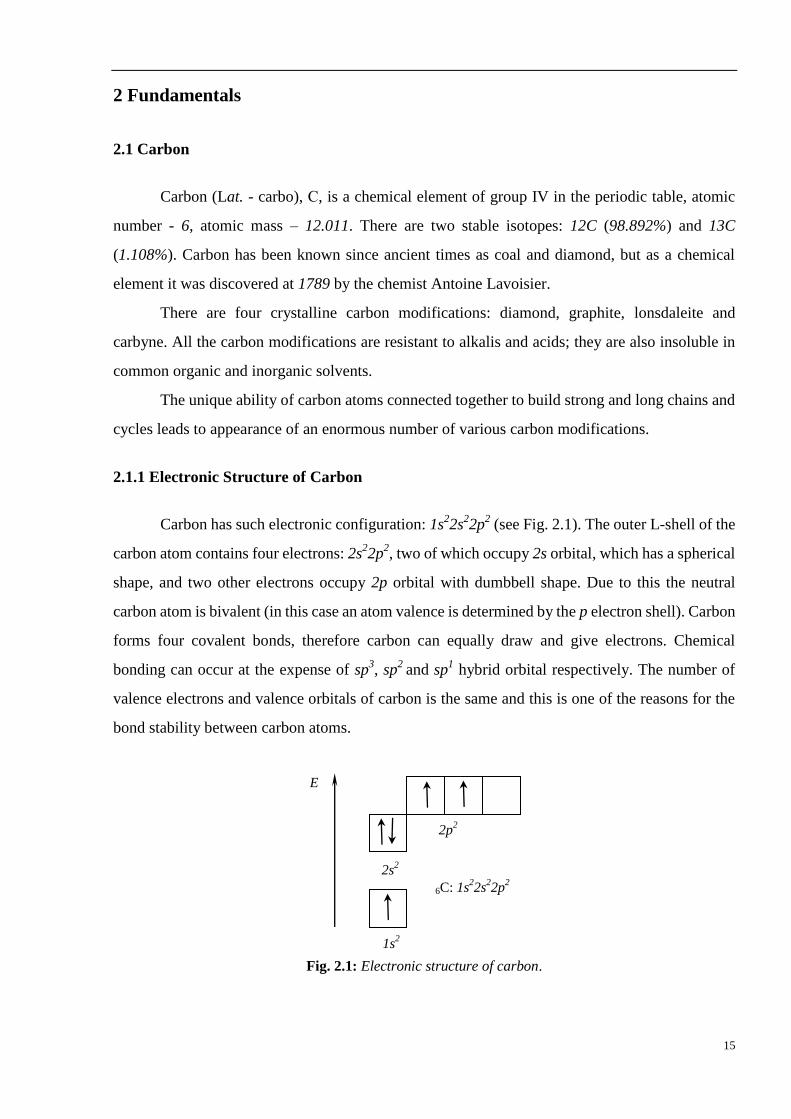
2.1.1 Electronic Structure of Carbon
Carbon has such electronic configuration: 1s22s
22p
2 (see Fig. 2.1). The outer L-shell of the
carbon atom contains four electrons: 2s22p
2, two of which occupy 2s orbital, which has a spherical
shape, and two other electrons occupy 2p orbital with dumbbell shape. Due to this the neutral
carbon atom is bivalent (in this case an atom valence is determined by the p electron shell). Carbon
forms four covalent bonds, therefore carbon can equally draw and give electrons. Chemical
bonding can occur at the expense of sp3, sp
2 and sp
1 hybrid orbital respectively. The number of
valence electrons and valence orbitals of carbon is the same and this is one of the reasons for the
bond stability between carbon atoms.
Fig. 2.1: Electronic structure of carbon.
2s2
1s2
2p2
6C: 1s22s
22p
2
E
16
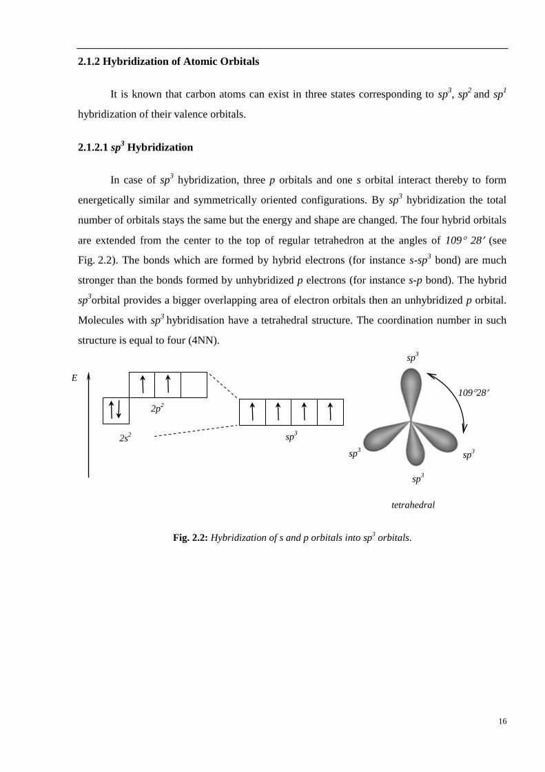
2.1.2 Hybridization of Atomic Orbitals
It is known that carbon atoms can exist in three states corresponding to sp3, sp
2 and sp
1
hybridization of their valence orbitals.
2.1.2.1 sp3 Hybridization
In case of sp3 hybridization, three p orbitals and one s orbital interact thereby to form
energetically similar and symmetrically oriented configurations. By sp3 hybridization the total
number of orbitals stays the same but the energy and shape are changed. The four hybrid orbitals
are extended from the center to the top of regular tetrahedron at the angles of 109 28 (see
Fig. 2.2). The bonds which are formed by hybrid electrons (for instance s-sp3 bond) are much
stronger than the bonds formed by unhybridized p electrons (for instance s-p bond). The hybrid
sp3orbital provides a bigger overlapping area of electron orbitals then an unhybridized p orbital.
Molecules with sp3
hybridisation have a tetrahedral structure. The coordination number in such
structure is equal to four (4NN).
Fig. 2.2: Hybridization of s and p orbitals into sp3 orbitals.
sp3
sp3
sp3
sp3
10928
tetrahedral
2s2
2p2
E
sp3
17
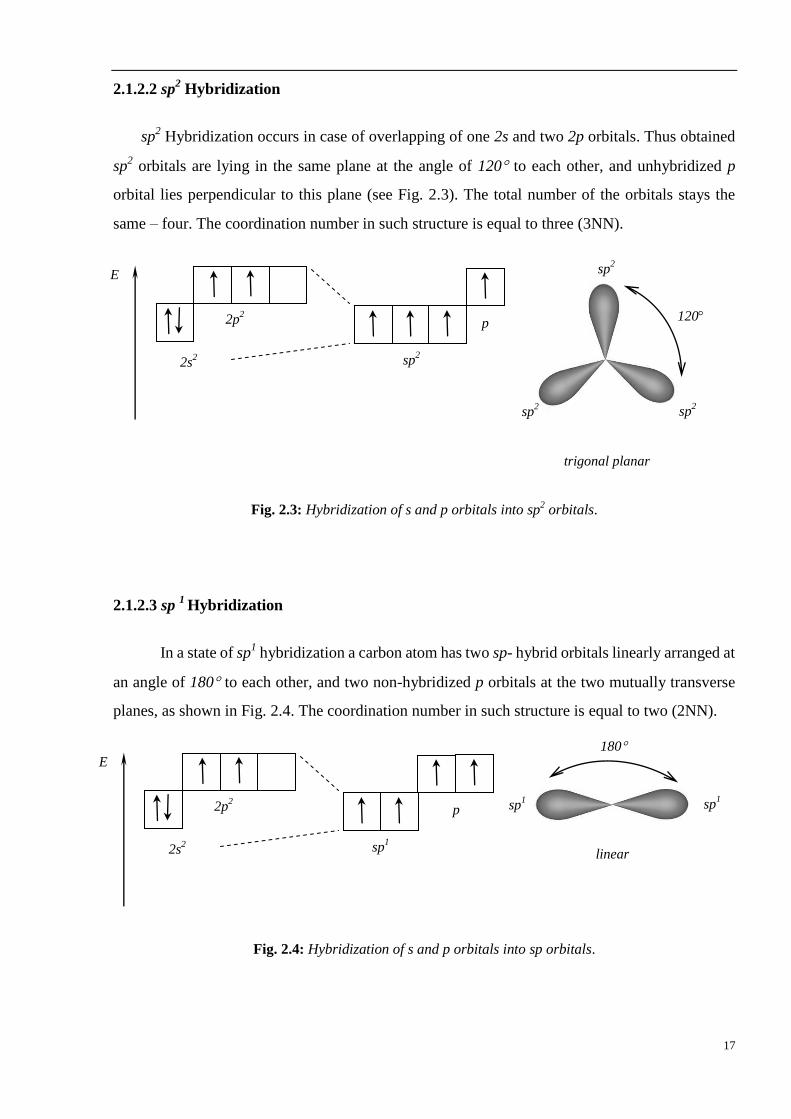
2.1.2.2 sp2 Hybridization
sp2 Hybridization occurs in case of overlapping of one 2s and two 2p orbitals. Thus obtained
sp2 orbitals are lying in the same plane at the angle of 120 to each other, and unhybridized p
orbital lies perpendicular to this plane (see Fig. 2.3). The total number of the orbitals stays the
same – four. The coordination number in such structure is equal to three (3NN).
Fig. 2.3: Hybridization of s and p orbitals into sp2 orbitals.
2.1.2.3 sp 1
Hybridization
In a state of sp1 hybridization a carbon atom has two sp- hybrid orbitals linearly arranged at
an angle of 180 to each other, and two non-hybridized p orbitals at the two mutually transverse
planes, as shown in Fig. 2.4. The coordination number in such structure is equal to two (2NN).
Fig. 2.4: Hybridization of s and p orbitals into sp orbitals.
sp2
sp2 sp
2
120
trigonal planar
sp1 sp
1
180
linear
2s2
2p2
E
sp2
p
2s2
2p2
E
sp1
p
18
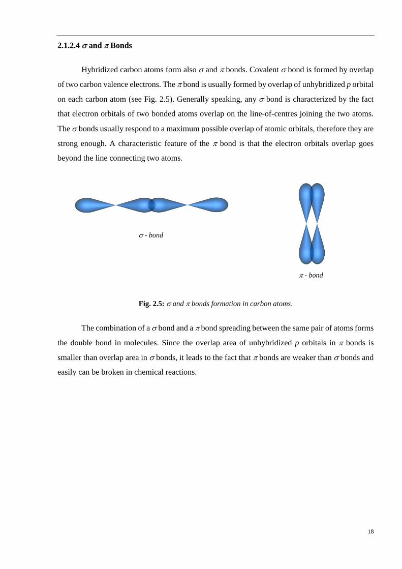
2.1.2.4 and Bonds
Hybridized carbon atoms form also and bonds. Covalent bond is formed by overlap
of two carbon valence electrons. The bond is usually formed by overlap of unhybridized p orbital
on each carbon atom (see Fig. 2.5). Generally speaking, any bond is characterized by the fact
that electron orbitals of two bonded atoms overlap on the line-of-centres joining the two atoms.
The bonds usually respond to a maximum possible overlap of atomic orbitals, therefore they are
strong enough. A characteristic feature of the bond is that the electron orbitals overlap goes
beyond the line connecting two atoms.
Fig. 2.5: and bonds formation in carbon atoms.
The combination of a bond and a bond spreading between the same pair of atoms forms
the double bond in molecules. Since the overlap area of unhybridized p orbitals in bonds is
smaller than overlap area in bonds, it leads to the fact that bonds are weaker than bonds and
easily can be broken in chemical reactions.
- bond
- bond
19
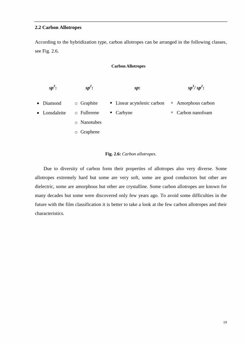
2.2 Carbon Allotropes
According to the hybridization type, carbon allotropes can be arranged in the following classes,
see Fig. 2.6.
Fig. 2.6: Carbon allotropes.
Due to diversity of carbon form their properties of allotropes also very diverse. Some
allotropes extremely hard but some are very soft, some are good conductors but other are
dielectric, some are amorphous but other are crystalline. Some carbon allotropes are known for
many decades but some were discovered only few years ago. To avoid some difficulties in the
future with the film classification it is better to take a look at the few carbon allotropes and their
characteristics.
Carbon Allotropes
sp3:
Diamond
Lonsdaleite
sp2:
o Graphite
o Fullerene
o Nanotubes
o Graphene
o Graphene
sp:
Linear acytelenic carbon
Carbyne
sp3/ sp
2:
Amorphous carbon
Carbon nanofoam
20
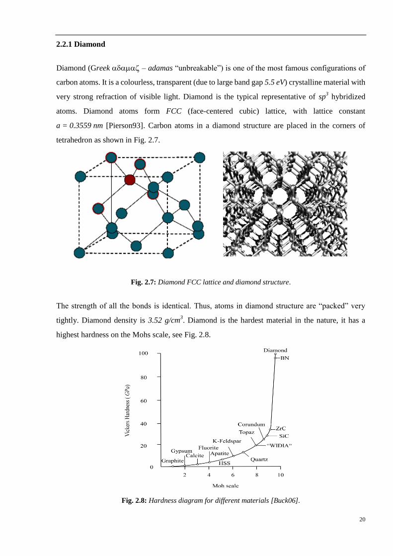
2.2.1 Diamond
Diamond (Greek – adamas “unbreakable”) is one of the most famous configurations of
carbon atoms. It is a colourless, transparent (due to large band gap 5.5 eV) crystalline material with
very strong refraction of visible light. Diamond is the typical representative of sp3 hybridized
atoms. Diamond atoms form FCC (face-centered cubic) lattice, with lattice constant
a = 0.3559 nm [Pierson93]. Carbon atoms in a diamond structure are placed in the corners of
tetrahedron as shown in Fig. 2.7.
Fig. 2.7: Diamond FCC lattice and diamond structure.
The strength of all the bonds is identical. Thus, atoms in diamond structure are “packed” very
tightly. Diamond density is 3.52 g/cm3. Diamond is the hardest material in the nature, it has a
highest hardness on the Mohs scale, see Fig. 2.8.
Fig. 2.8: Hardness diagram for different materials [Buck06].
21
Covalent bonded diamond atoms have no free electrons; therefore diamond is an insulator with
band gap around 5.5 eV.
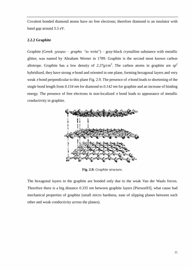
2.2.2 Graphite
Graphite (Greek – grapho “to write”) – gray-black crystalline substance with metallic
glitter, was named by Abraham Werner in 1789. Graphite is the second most known carbon
allotrope. Graphite has a low density of 2.27g/cm3. The carbon atoms in graphite are sp
2
hybridized, they have strong bond and oriented in one plane, forming hexagonal layers and very
weak bond perpendicular to this plane Fig. 2.9. The presence of bond leads to shortening of the
single bond length from 0.154 nm for diamond to 0.142 nm for graphite and an increase of binding
energy. The presence of free electrons in non-localized bond leads to appearance of metallic
conductivity in graphite.
Fig. 2.9: Graphite structure.
The hexagonal layers in the graphite are bonded only due to the weak Van der Waals forces.
Therefore there is a big distance 0.335 nm between graphite layers [Pierson93], what cause bad
mechanical properties of graphite (small micro hardness, ease of slipping planes between each
other and weak conductivity across the planes).
22
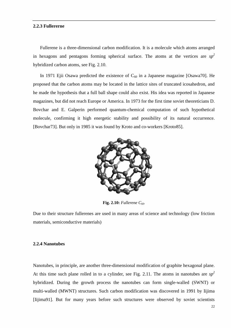
2.2.3 Fullererne
Fullerene is a three-dimensional carbon modification. It is a molecule which atoms arranged
in hexagons and pentagons forming spherical surface. The atoms at the vertices are sp2
hybridized carbon atoms, see Fig. 2.10.
In 1971 Ejii Osawa predicted the existence of C60 in a Japanese magazine [Osawa70]. He
proposed that the carbon atoms may be located in the lattice sites of truncated icosahedron, and
he made the hypothesis that a full ball shape could also exist. His idea was reported in Japanese
magazines, but did not reach Europe or America. In 1973 for the first time soviet theoreticians D.
Bovchar and E. Galperin performed quantum-chemical computation of such hypothetical
molecule, confirming it high energetic stability and possibility of its natural occurrence.
[Bovchar73]. But only in 1985 it was found by Kroto and co-workers [Kroto85].
Fig. 2.10: Fullerene C60.
Due to their structure fullerenes are used in many areas of science and technology (low friction
materials, semiconductive materials)
2.2.4 Nanotubes
Nanotubes, in principle, are another three-dimensional modification of graphite hexagonal plane.
At this time such plane rolled in to a cylinder, see Fig. 2.11. The atoms in nanotubes are sp2
hybridized. During the growth process the nanotubes can form single-walled (SWNT) or
multi-walled (MWNT) structures. Such carbon modification was discovered in 1991 by Iijima
[Iijima91]. But for many years before such structures were observed by soviet scientists
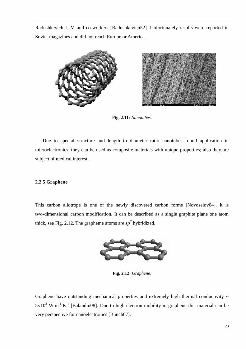
23
Radushkevich L. V. and co-workers [Radushkevich52]. Unfortunately results were reported in
Soviet magazines and did not reach Europe or America.
Fig. 2.11: Nanotubes.
Due to special structure and length to diameter ratio nanotubes found application in
microelectronics, they can be used as composite materials with unique properties; also they are
subject of medical interest.
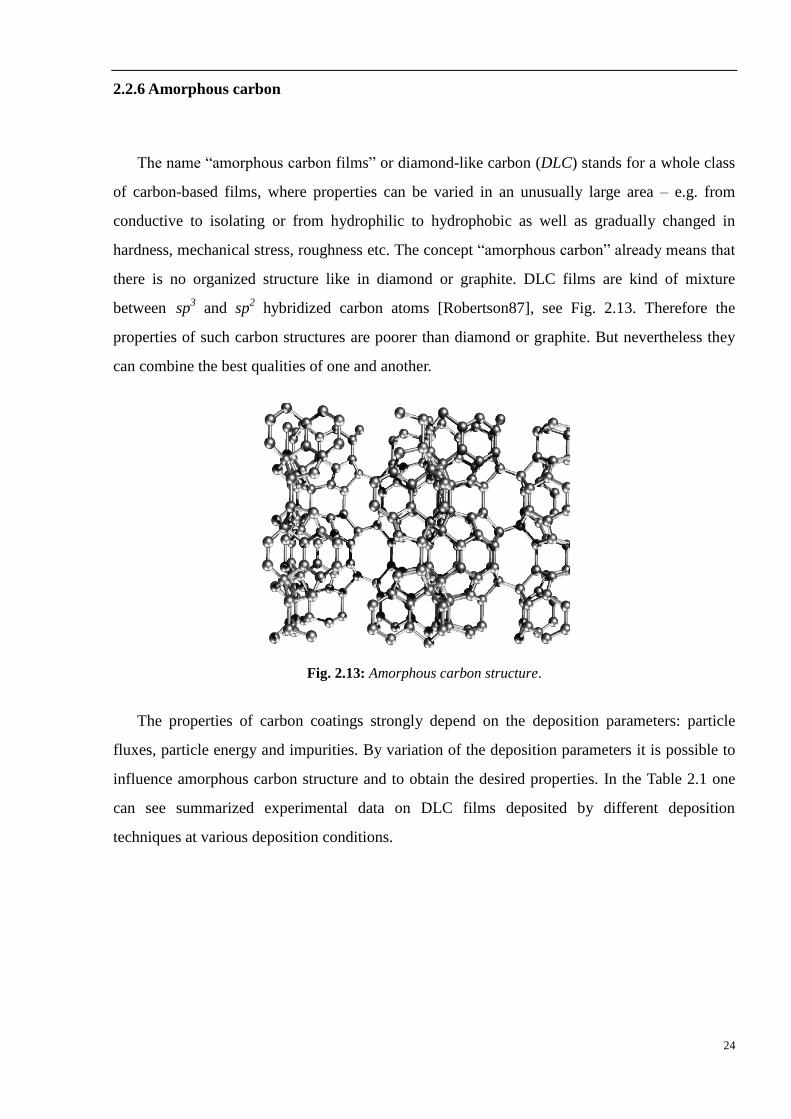
2.2.5 Graphene
This carbon allotrope is one of the newly discovered carbon forms [Novoselov04]. It is
two-dimensional carbon modification. It can be described as a single graphite plane one atom
thick, see Fig. 2.12. The grapheme atoms are sp2 hybridized.
Fig. 2.12: Graphene.
Graphene have outstanding mechanical properties and extremely high thermal conductivity
5103 Wm
-1K
-1 [Balandin08]. Due to high electron mobility in graphene this material can be
very perspective for nanoelectronics [Bunch07].
24
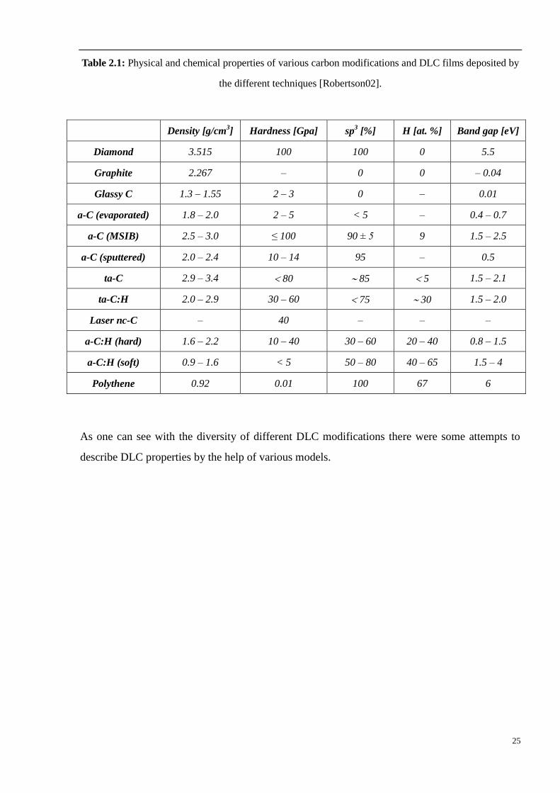
2.2.6 Amorphous carbon
The name “amorphous carbon films” or diamond-like carbon (DLC) stands for a whole class
of carbon-based films, where properties can be varied in an unusually large area – e.g. from
conductive to isolating or from hydrophilic to hydrophobic as well as gradually changed in
hardness, mechanical stress, roughness etc. The concept “amorphous carbon” already means that
there is no organized structure like in diamond or graphite. DLC films are kind of mixture
between sp3 and sp
2 hybridized carbon atoms [Robertson87], see Fig. 2.13. Therefore the
properties of such carbon structures are poorer than diamond or graphite. But nevertheless they
can combine the best qualities of one and another.
Fig. 2.13: Amorphous carbon structure.
The properties of carbon coatings strongly depend on the deposition parameters: particle
fluxes, particle energy and impurities. By variation of the deposition parameters it is possible to
influence amorphous carbon structure and to obtain the desired properties. In the Table 2.1 one
can see summarized experimental data on DLC films deposited by different deposition
techniques at various deposition conditions.
25
Table 2.1: Physical and chemical properties of various carbon modifications and DLC films deposited by
the different techniques [Robertson02].
Density [g/cm3] Hardness [Gpa] sp
3 [%] H [at. %] Band gap [eV]
Diamond 3.515 100 100 0 5.5
Graphite 2.267 – 0 0 – 0.04
Glassy C 1.3 – 1.55 2 – 3 0 – 0.01
a-C (evaporated) 1.8 – 2.0 2 – 5 < 5 – 0.4 – 0.7
a-C (MSIB) 2.5 – 3.0 ≤ 100 90 ± 5 9 1.5 – 2.5
a-C (sputtered) 2.0 – 2.4 10 – 14 95 – 0.5
ta-C 2.9 – 3.4 80 85 5 1.5 – 2.1
ta-C:H 2.0 – 2.9 30 – 60 75 30 1.5 – 2.0
Laser nc-C – 40 – – –
a-C:H (hard) 1.6 – 2.2 10 – 40 30 – 60 20 – 40 0.8 – 1.5
a-C:H (soft) 0.9 – 1.6 < 5 50 – 80 40 – 65 1.5 – 4
Polythene 0.92 0.01 100 67 6
As one can see with the diversity of different DLC modifications there were some attempts to
describe DLC properties by the help of various models.
26
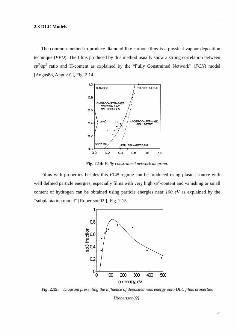
2.3 DLC Models
The common method to produce diamond like carbon films is a physical vapour deposition
technique (PVD). The films produced by this method usually show a strong correlation between
sp3/sp
2 ratio and H-content as explained by the “Fully Constrained Network” (FCN) model
[Angus88, Angus91], Fig. 2.14.
Fig. 2.14: Fully constrained network diagram.
Films with properties besides this FCN-regime can be produced using plasma source with
well defined particle energies, especially films with very high sp3-content and vanishing or small
content of hydrogen can be obtained using particle energies near 100 eV as explained by the
“subplantation model” [Robertson02 ], Fig. 2.15.
Fig. 2.15: Diagram presenting the influence of deposited ions energy onto DLC films properties
[Robertson02].
27
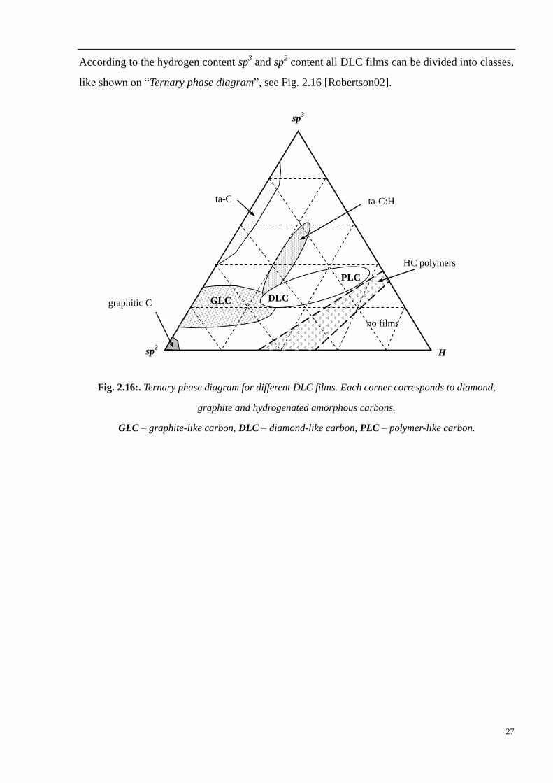
According to the hydrogen content sp3 and sp
2 content all DLC films can be divided into classes,
like shown on “Ternary phase diagram”, see Fig. 2.16 [Robertson02].
Fig. 2.16:. Ternary phase diagram for different DLC films. Each corner corresponds to diamond,
graphite and hydrogenated amorphous carbons.
GLC – graphite-like carbon, DLC – diamond-like carbon, PLC – polymer-like carbon.
sp2
sp3
H
no films
ta-C ta-C:H
HC polymers
graphitic C
PLC
DLC GLC
28
3 DLC Deposition Techniques
Diamond like carbon films are usually produced by vacuum deposition technique and in
some cases by liquid electrochemical technique [He11]. The deposition methods can be divided
in two groups according to the phase of matter of ion source:
CVD – Chemical Vapour Deposition (gaseous phase)
PVD – Physical Vapour Deposition (solid phase)
These methods are differing in many parameters one of them is a particle fluxes (ion energy,
plasma chemistry) and therefore the deposited DLC films properties depend on these parameters.
According to [Robertson02] very interesting material properties are expected for films produced
with particle energy in the range 10 eV – 100 eV, but there are only a few deposition techniques
that deliver high fluxes at these energies, Radio Frequency Plasma Enhanced Chemical Vapour
Deposition (RFPECVD) [Kadetov04] technique and the DC vacuum arc PVD method [Buck91]
seems to be the most promising for this purpose. But these deposition techniques are rather
different in the way of plasma generation, ionisation rate and deposition rates. Therefore, the
obtained films have differences in structure and chemical composition. But the main advantage
of PVD vacuum arc is that it is able to operate without any gases. This allows investigating the
influence of plasma parameters on film properties separately.
In order to know better the properties of vacuum arc discharge it is necessary to have a closer
look at those processes in a vacuum.
29
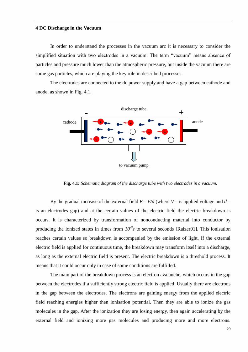
4 DC Discharge in the Vacuum
In order to understand the processes in the vacuum arc it is necessary to consider the
simplified situation with two electrodes in a vacuum. The term “vacuum” means absence of
particles and pressure much lower than the atmospheric pressure, but inside the vacuum there are
some gas particles, which are playing the key role in described processes.
The electrodes are connected to the dc power supply and have a gap between cathode and
anode, as shown in Fig. 4.1.
Fig. 4.1: Schematic diagram of the discharge tube with two electrodes in a vacuum.
By the gradual increase of the external field E= V/d (where V – is applied voltage and d –
is an electrodes gap) and at the certain values of the electric field the electric breakdown is
occurs. It is characterized by transformation of nonconducting material into conductor by
producing the ionized states in times from 10-9
s to several seconds [Raizer01]. This ionisation
reaches certain values so breakdown is accompanied by the emission of light. If the external
electric field is applied for continuous time, the breakdown may transform itself into a discharge,
as long as the external electric field is present. The electric breakdown is a threshold process. It
means that it could occur only in case of some conditions are fulfilled.
The main part of the breakdown process is an electron avalanche, which occurs in the gap
between the electrodes if a sufficiently strong electric field is applied. Usually there are electrons
in the gap between the electrodes. The electrons are gaining energy from the applied electric
field reaching energies higher then ionisation potential. Then they are able to ionize the gas
molecules in the gap. After the ionization they are losing energy, then again accelerating by the
external field and ionizing more gas molecules and producing more and more electrons.
to vacuum pump
discharge tube
cathode anode
- +
+ +
+
+ +
30
Electrons lose energy to excite molecules and atoms; on impacts. Due to the applied electric field
the electrons are moved towards the anode and disappear after the breakdown. The processes of
electrons creation and disappearance are competing processes. The electron creation rate is
described by the ionization frequency and strongly depends on the external field strength. The
electron disappearance rate also depends on the field [Raizer01]. As a result of all the processes
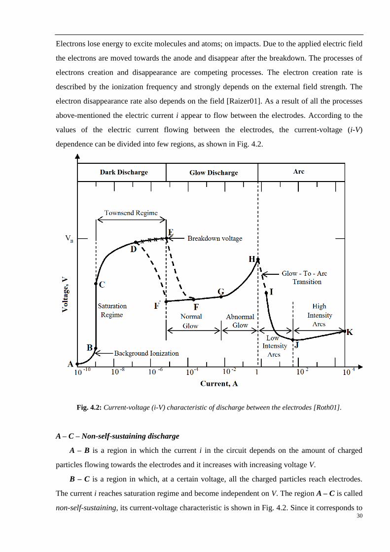
above-mentioned the electric current i appear to flow between the electrodes. According to the
values of the electric current flowing between the electrodes, the current-voltage (i-V)
dependence can be divided into few regions, as shown in Fig. 4.2.
Fig. 4.2: Current-voltage (i-V) characteristic of discharge between the electrodes [Roth01].
A – C – Non-self-sustaining discharge
A – B is a region in which the current i in the circuit depends on the amount of charged
particles flowing towards the electrodes and it increases with increasing voltage V.
B – C is a region in which, at a certain voltage, all the charged particles reach electrodes.
The current i reaches saturation regime and become independent on V. The region A – C is called
non-self-sustaining, its current-voltage characteristic is shown in Fig. 4.2. Since it corresponds to
31
a steady state, it is static.
C – E – Townsend dark discharge
After the breakdown voltage VB is reached, the discharge transfer into self-sustaining regime.
The voltage VB provides stable reproduction of electrons emitted from the cathode towards the
anode. As long as the external electric field is independent on carrier densities the
current-voltage (i-V) characteristic is constant V = constant = VB, it corresponds to the area B –
C on Fig. 4.2. There is virtually no light radiation due to the very small ionization rates. This
regime is called Townsend dark discharge.
E – G – Normal glow discharge
When a certain value of the current i is reached, the voltage across the electrodes decreases
what corresponds to the E – F section. After the voltage falls, the current i become almost
constant. This region corresponds to the F – G section in Fig. 4.2. This regime is called normal
glow discharge. It has a special feature: the discharge density at the cathode is still constant
independently from discharge current. Only the current flow area is changing. The glow
discharge is characterized by high cathode potential fall, which can be around hundreds of volts,
and low currents i 10-5
– 10-2
A.
G – H – Abnormal glow discharge
In case when no more free surface is left on the cathode, then current i is increased by an
increase of voltage and the cathode current density is growing. This region is called abnormal
glow discharge - G – H section of Fig.4.2. It is characterized by currents i 10-2
– 1 A.
H – I – Transition to arc
When the current i reaches values around 1 A, the glow discharge conversed into the arc
regime.
I – K – Arc
The arc regime is a self-sustaining discharge which is characterized by low cathode potential
fall and high discharge current i 1 – 104 A. [Raizer01].
32
5 Arc Discharge
The arc discharge is known for almost 100 years, it is characterized by rather high
currents i 1 – 104 A and low voltages V 20 – 40 V. The small value of the potential fall is
explained by the cathode emission mechanism, due to the high electron current from the cathode.
This current is the result of emission processes such as a thermionic emission and field emission
or their combination. In the case of arc discharge, electrodes because of the ohmic resistance
transfer the high current to the surface into the heat, which leads to the strong heating of the
electrodes material. This effect can occur locally or over the whole cathode area, usually for a
short time. The electrodes sustain erosion and evaporation. The eroded material immediately fills
up the discharge gap between the electrodes. The arc discharge is burning in the vapour of the
vaporized material, its parameters strongly depend on working gas pressure, and characterized
by high degree of ionisation due to the high burning current. The arc temperature reaches the
value around 105 K.
There are several arc discharge ignition methods [Boxman95]. The easiest method is to
bring two electrodes which are connected to the power supply into contact and separate from
each other after some time. The electrodes due to the high resistance and high current at the
contact point, owing to the ohmic resistance, become very hot and reach vaporization
temperature in local points. This leads to the emission of neutral atoms and charged particles
(electrons and ions) and at the separation moment arc ignites between the electrodes. The
vaporized electrode material is much easier to be ionized (because of their high temperature)
then the neutral gas molecules. After the arc ignition the working gas molecules afterwards
replace vaporized molecules originated from the electrodes. The high temperature in the arc
leads to the destruction of the working gas molecular bonds and participation of these atoms in
the deposition processes.
The next method is to use an auxiliary electrode. This small electrode is brought into
contact with the cathode. After applying the voltage to the stationary electrodes, this auxiliary
electrode is separated from the cathode, which leads to the vaporization of the auxiliary electrode
material and formation of arc discharge.
Another method is to connect two stationary electrodes using thin wire, after applying the
voltage, due to the high ohmic resistance of thin wire it evaporates and this evaporated material
ignites the arc discharge.
Additional method is to ionize the electrodes gap by some external ionization source (this
33
can be done by UV – radiation, laser ionisation or another electron source).
Another possibility is to apply high voltage which should be enough for gas breakdown
between stationary electrodes. In this case the arc discharge ignition occurs according to the
current-voltage characteristic of discharge between the electrodes as shown in Fig.4 2. First it
forms the glow discharge, which transforms into the arc discharge as cathode reachs sufficient
temperature for the vaporisation.
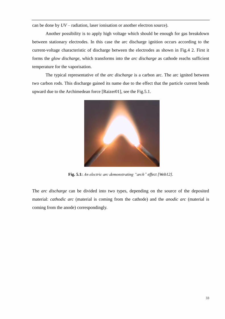
The typical representative of the arc discharge is a carbon arc. The arc ignited between
two carbon rods. This discharge gained its name due to the effect that the particle current bends
upward due to the Archimedean force [Raizer01], see the Fig.5.1.
Fig. 5.1: An electric arc demonstrating “arch” effect [Web12].
The arc discharge can be divided into two types, depending on the source of the deposited
material: cathodic arc (material is coming from the cathode) and the anodic arc (material is
coming from the anode) correspondingly.
34
5.1 Cathodic Arc
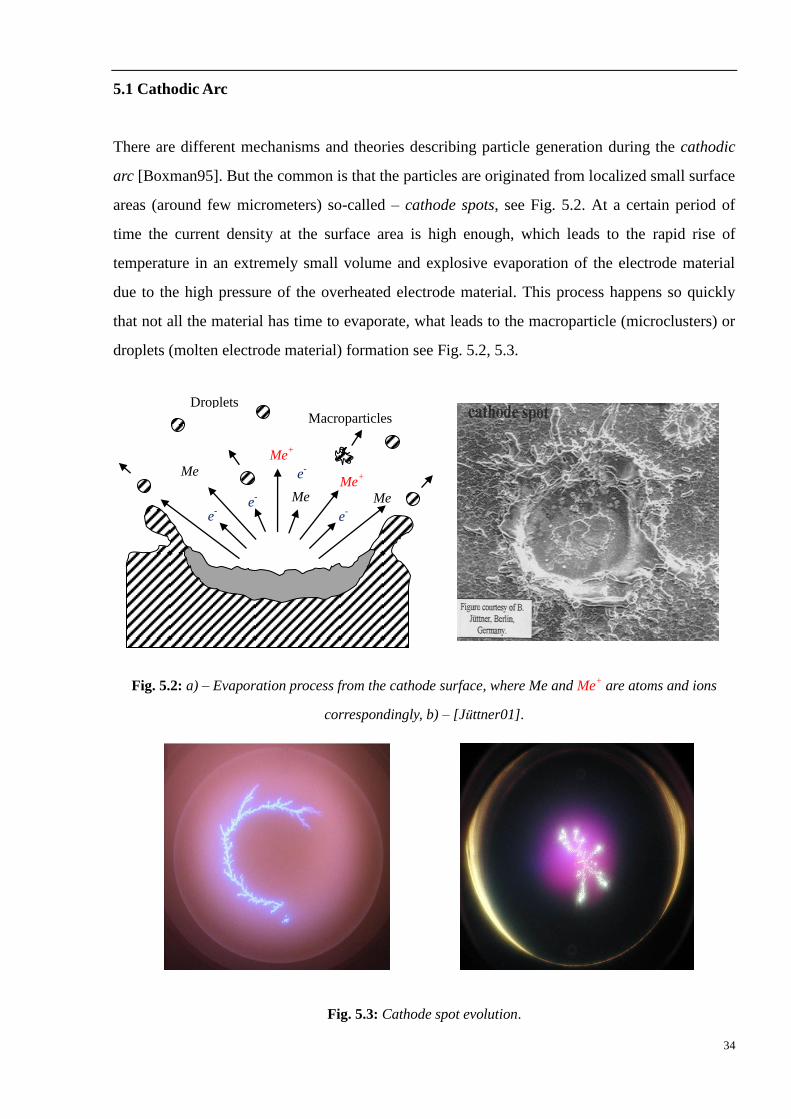
There are different mechanisms and theories describing particle generation during the cathodic
arc [Boxman95]. But the common is that the particles are originated from localized small surface
areas (around few micrometers) so-called – cathode spots, see Fig. 5.2. At a certain period of
time the current density at the surface area is high enough, which leads to the rapid rise of
temperature in an extremely small volume and explosive evaporation of the electrode material
due to the high pressure of the overheated electrode material. This process happens so quickly
that not all the material has time to evaporate, what leads to the macroparticle (microclusters) or
droplets (molten electrode material) formation see Fig. 5.2, 5.3.
Fig. 5.2: a) – Evaporation process from the cathode surface, where Me and Me+ are atoms and ions
correspondingly, b) – [Jüttner01].
Fig. 5.3: Cathode spot evolution.
Me
Me+
e-
e-
e-
e-
Me+
Droplets
Macroparticles
Me
Me
35
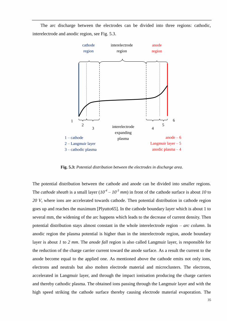
The arc discharge between the electrodes can be divided into three regions: cathodic,
interelectrode and anodic region, see Fig. 5.3.
Fig. 5.3: Potential distribution between the electrodes in discharge area.
The potential distribution between the cathode and anode can be divided into smaller regions.
The cathode sheath is a small layer (10-4
– 10-3
mm) in front of the cathode surface is about 10 to
20 V, where ions are accelerated towards cathode. Then potential distribution in cathode region
goes up and reaches the maximum [Plyutto65]. In the cathode boundary layer which is about 1 to
several mm, the widening of the arc happens which leads to the decrease of current density. Then
potential distribution stays almost constant in the whole interelectrode region – arc column. In
anodic region the plasma potential is higher than in the interelectrode region, anode boundary
layer is about 1 to 2 mm. The anode fall region is also called Langmuir layer, is responsible for
the reduction of the charge carrier current toward the anode surface. As a result the current to the
anode become equal to the applied one. As mentioned above the cathode emits not only ions,
electrons and neutrals but also molten electrode material and microclusters. The electrons,
accelerated in Langmuir layer, and through the impact ionisation producing the charge carriers
and thereby cathodic plasma. The obtained ions passing through the Langmuir layer and with the
high speed striking the cathode surface thereby causing electrode material evaporation. The
1 2
3 4 5
6
cathode
region
interelectrode
region
anode
region
1 – cathode
2 – Langmuir layer
3 – cathodic plasma
interelectrode
expanding
plasma anode – 6
Langmuir layer – 5
anodic plasma – 4
36
cathodic plasma expands into interelectrode region toward anode. The interelectrode plasma is
weakly active plasma which is supported only by the expanding electrode plasmas. Electrons are
losing their energy due to elastic and inelastic collisions with the atoms and ions in near
electrode plasma regions. These regions are also called energy-loss regions. Near the electrodes a
particle densities and temperatures are reaching their maximum. Due to the high excitation and
recombination rates these areas are visible as a plasma spots. The dimensions of those plasma
spot are much bigger than the mean free path for excitation and ionisation. Expanding plasma
ions reach the energy which may lie above the ion sound speed cs = (Te/M)1/2
[Hasse92].
The cathodic arc, due to the high concentration of highly energetic ions inside the expanding
cathodic plasma, is used as a coating source [Boxman95].
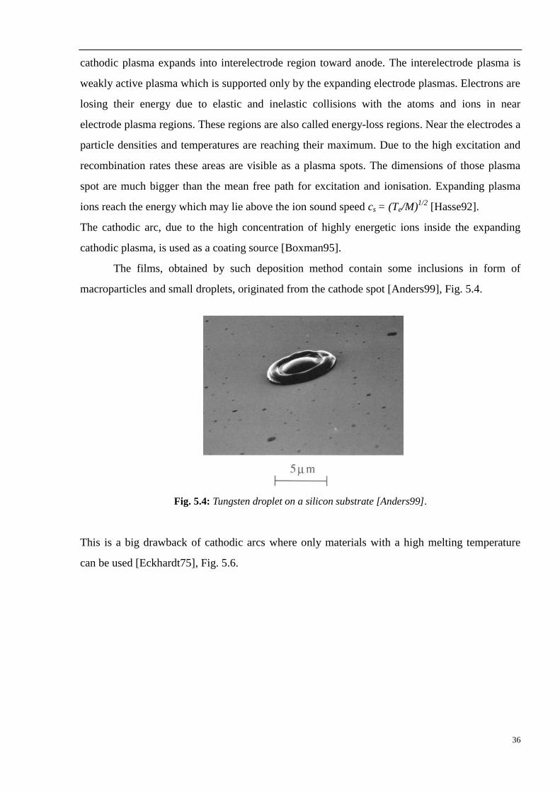
The films, obtained by such deposition method contain some inclusions in form of
macroparticles and small droplets, originated from the cathode spot [Anders99], Fig. 5.4.
Fig. 5.4: Tungsten droplet on a silicon substrate [Anders99].
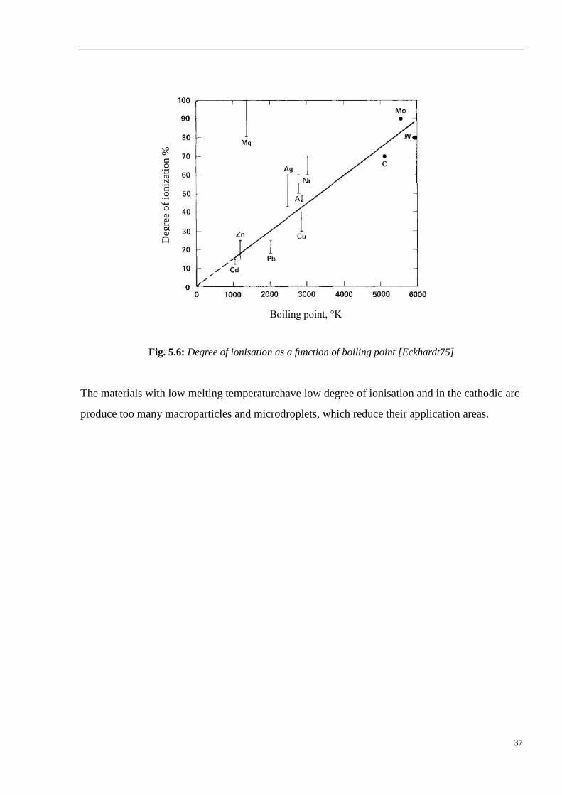
This is a big drawback of cathodic arcs where only materials with a high melting temperature
can be used [Eckhardt75], Fig. 5.6.
37
Fig. 5.6: Degree of ionisation as a function of boiling point [Eckhardt75]
The materials with low melting temperaturehave low degree of ionisation and in the cathodic arc
produce too many macroparticles and microdroplets, which reduce their application areas.
Boiling point, °K
Deg
ree
of
ioniz
atio
n %
38
5.2 Macroparticle Filtering
The presence of macroscopic inclusions in the films deposited by cathodic arc has
significantly reduced the range of application of such deposition technique.
In order to reduce the negative influence of the macroparticles on to thin films properties some
types of filters were used [Aksenov78, Anders99, Karpov97].
The common feature for all of them is the mechanical separation of macroparticles and droplets
from the arc plasma.
One solution is to turn the substrate at 90 to the expanding plasma, so the macroparticles
will be simply flying along the substrate. But the probability to reach the substrate surface still
very high. The growing film becomes inhomogeneous due to film thickness gradient.
The next solution is to place the grounded protective shield in front of the substrate. The
shield must be larger than the substrate. But the biggest drawback is that such shield protects the
substrate surface from all kind of particles, even the charged one. A large amount of ions needed
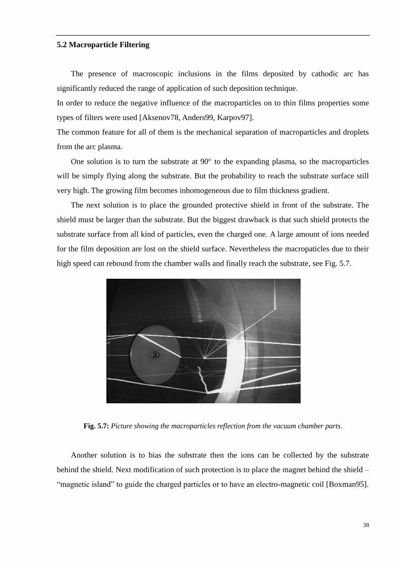
for the film deposition are lost on the shield surface. Nevertheless the macropaticles due to their
high speed can rebound from the chamber walls and finally reach the substrate, see Fig. 5.7.
Fig. 5.7: Picture showing the macroparticles reflection from the vacuum chamber parts.
Another solution is to bias the substrate then the ions can be collected by the substrate
behind the shield. Next modification of such protection is to place the magnet behind the shield –
“magnetic island” to guide the charged particles or to have an electro-magnetic coil [Boxman95].
39
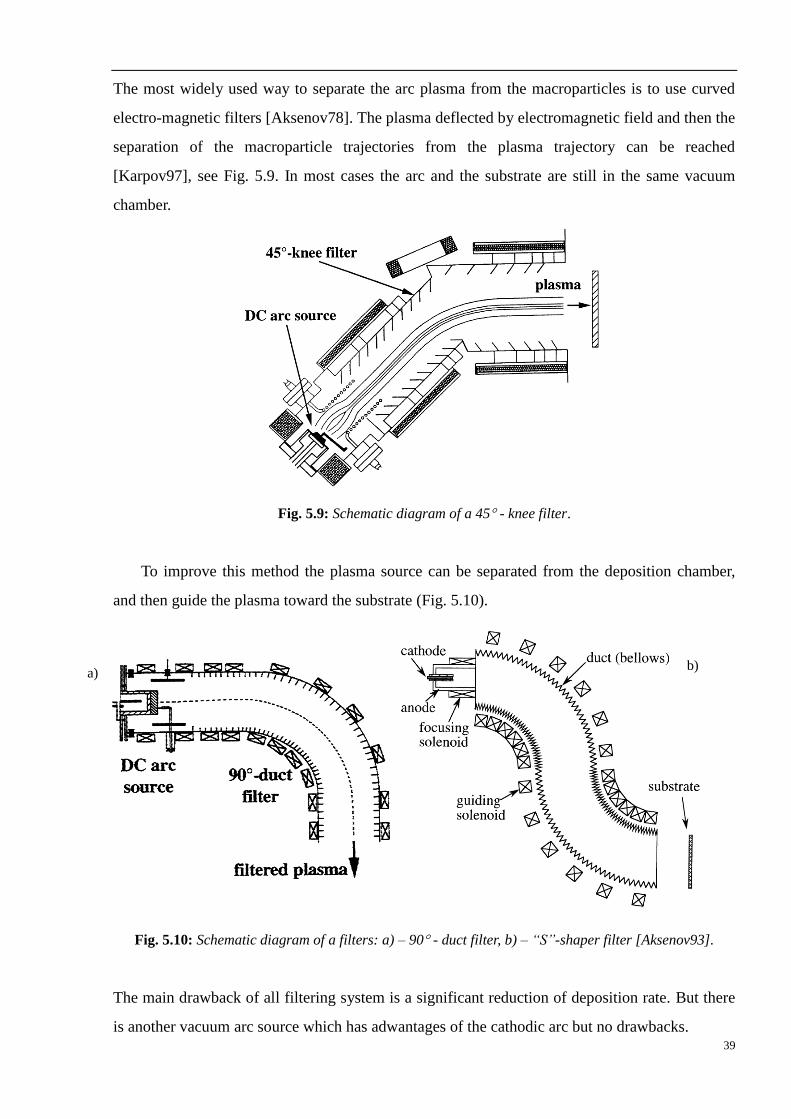
The most widely used way to separate the arc plasma from the macroparticles is to use curved
electro-magnetic filters [Aksenov78]. The plasma deflected by electromagnetic field and then the
separation of the macroparticle trajectories from the plasma trajectory can be reached
[Karpov97], see Fig. 5.9. In most cases the arc and the substrate are still in the same vacuum
chamber.
Fig. 5.9: Schematic diagram of a 45 - knee filter.
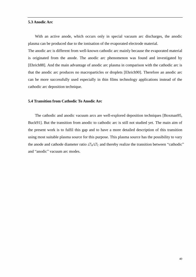
To improve this method the plasma source can be separated from the deposition chamber,
and then guide the plasma toward the substrate (Fig. 5.10).
Fig. 5.10: Schematic diagram of a filters: a) – 90 - duct filter, b) – “S”-shaper filter [Aksenov93].
The main drawback of all filtering system is a significant reduction of deposition rate. But there
is another vacuum arc source which has adwantages of the cathodic arc but no drawbacks.
a) b)
40
5.3 Anodic Arc
With an active anode, which occurs only in special vacuum arc discharges, the anodic
plasma can be produced due to the ionisation of the evaporated electrode material.
The anodic arc is different from well-known cathodic arc mainly because the evaporated material
is originated from the anode. The anodic arc phenomenon was found and investigated by
[Ehrich88]. And the main advantage of anodic arc plasma in comparison with the cathodic arc is
that the anodic arc produces no macroparticles or droplets [Ehrich90]. Therefore an anodic arc
can be more successfully used especially in thin films technology applications instead of the
cathodic arc deposition technique.
5.4 Transition from Cathodic To Anodic Arc
The cathodic and anodic vacuum arcs are well-explored deposition techniques [Boxman95,
Buck91]. But the transition from anodic to cathodic arc is still not studied yet. The main aim of
the present work is to fulfil this gap and to have a more detailed description of this transition
using most suitable plasma source for this purpose. This plasma source has the possibility to vary
the anode and cathode diameter ratio A/C and thereby realize the transition between “cathodic”
and “anodic” vacuum arc modes.
41
6 Diagnostics
In order to know the influence of plasma parameters on the film parameters first the plasma
properties should be investigated.
6.1 Plasma Diagnostics
Plasma diagnostic is the main method to know plasma properties like chemical composition
and particle energy. For the chemical composition a mass-spectrometry is used. To measure the
particle energy an energy analyzer is used.
6.2 Retarding Field Energy Analyzer (RFEA)
The key role in every plasma deposition process is played by ions. To know and to
control the deposition parameters it is necessary to monitor the ion energy during the deposition
process.
Energy resolved ion current measurements were performed by retarding field plasma
analysis [Stephanakis68, Musa94]. The schematic diagram of the analyzer is shown in Fig. 6.1.
Fig. 6.1: Schematic diagram of retarding field energy analyzer.
The energy analyzer consists of the entrance aperture, screening grid with small spacing
and a ion collector. The housing and ion collector were made of stainless steel. The grid was kept
under 0 V potential. To avoid additional distortion of ion current measurements by the plasma,
aperture (-80 V)
grid (0 V)
ion collector
mica rings
housing (0 V)
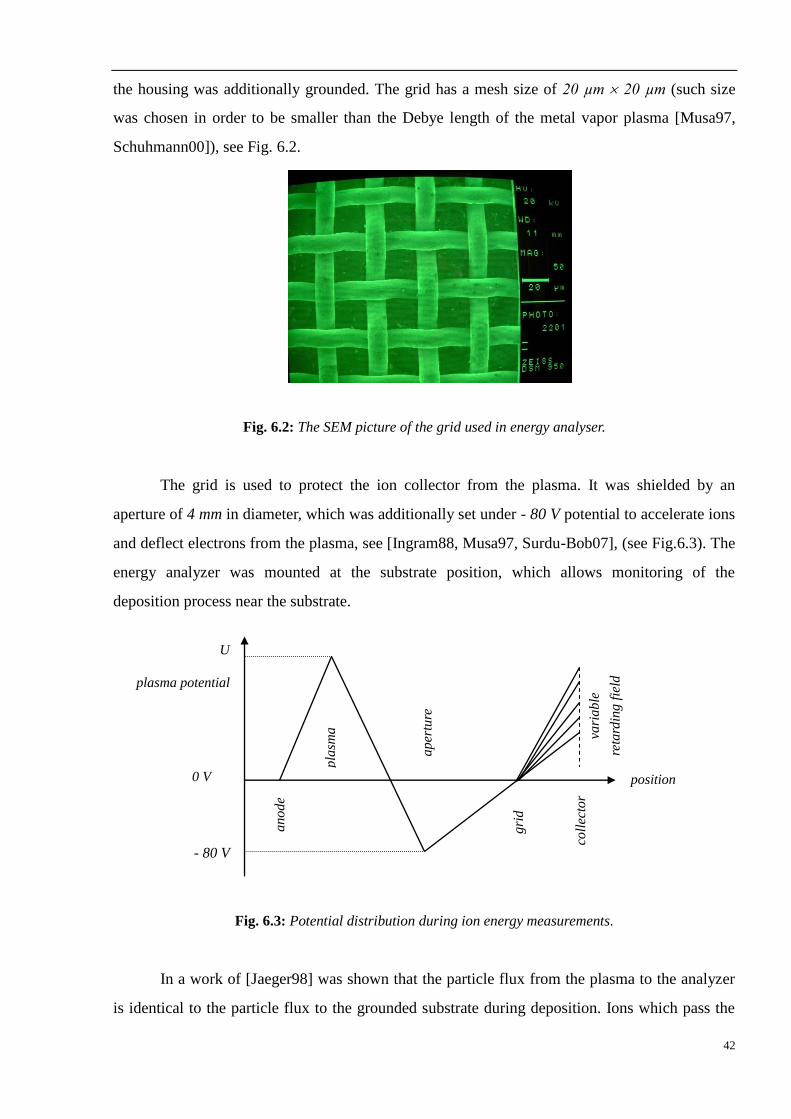
42
the housing was additionally grounded. The grid has a mesh size of 20 µm 20 µm (such size
was chosen in order to be smaller than the Debye length of the metal vapor plasma [Musa97,
Schuhmann00]), see Fig. 6.2.
Fig. 6.2: The SEM picture of the grid used in energy analyser.
The grid is used to protect the ion collector from the plasma. It was shielded by an
aperture of 4 mm in diameter, which was additionally set under - 80 V potential to accelerate ions
and deflect electrons from the plasma, see [Ingram88, Musa97, Surdu-Bob07], (see Fig.6.3). The
energy analyzer was mounted at the substrate position, which allows monitoring of the
deposition process near the substrate.
Fig. 6.3: Potential distribution during ion energy measurements.
In a work of [Jaeger98] was shown that the particle flux from the plasma to the analyzer
is identical to the particle flux to the grounded substrate during deposition. Ions which pass the
U
0 V
plasma potential
- 80 V
anode
pla
sma
aper
ture
gri
d
coll
ecto
r va
riable
reta
rdin
g f
ield
position
43
grid are repelled by positive collector bias. Only ions with sufficient kinetic energy are
neutralized at the collector surface. Thus, the collector current decreases monotonically with
increasing collector bias. The dependence of the collector current on applied potential barrier
Emin = eUcoll is given by Eq. 6.1 [Jaeger98]:
𝐼𝑐𝑜𝑙𝑙(𝐸𝑚𝑖𝑛) − 𝐼𝑆𝐸 = 𝐴𝑒 ∫ 𝑛(𝐸)𝑣(𝐸)𝑑𝐸∞
𝐸𝑚𝑖𝑛, (6.1)
where A is the effective area with respect to the transmittance of the grids and ISE is the current
caused by secondary electron emission, n(E) is the ion energy distribution function (IEDF) and v(E)
the velocity of the ions. Using Eq. 6.1, IEDF can be written as:
𝑛(𝐸) = −1
𝐴𝑒𝑣(𝐸)
𝑑𝐼𝑐𝑜𝑙𝑙
𝑑𝐸 . (6.2)
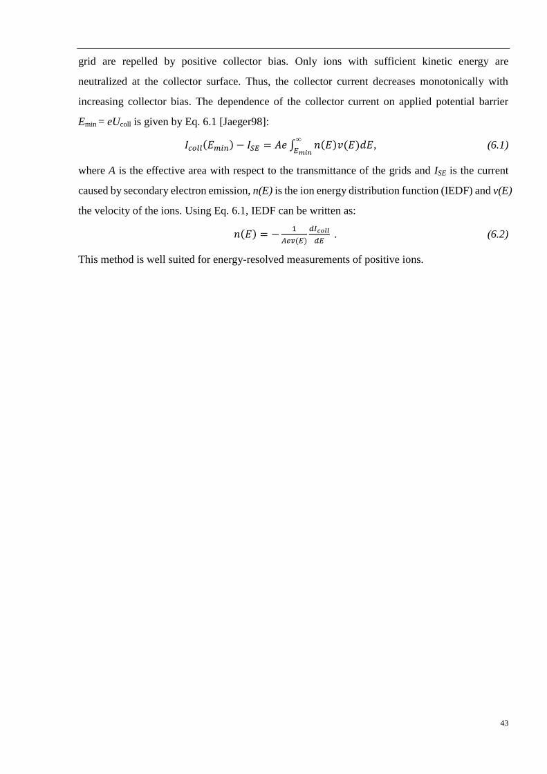
This method is well suited for energy-resolved measurements of positive ions.
44
6.2 Film Diagnostics
The film diagnostics begins with the film weight, thickness measurements. Then the film
morphology is analyzed by Scanning Electron Microscopy (SEM) and Atomic Force Microscopy
(AFM). To know the chemical composition Energy-dispersive X-ray Spectroscopy (EDX) and
Nuclear Reaction Analysis (NRA) were used.
6.2.1 NRA (Nuclear Reaction Analysis)
NRA is well-known analytical method for material characterization [Lanford95]. NRA is a
non-destructive nuclear method to measure the chemical composition and concentration of
specified chemical elements, which is widely used in solid state physics. In this method the
incident nuclei, accelerated to certain energies from 100 keV to 10 MeV, interact with the sample
material and initiate a nuclear reaction with elements in the investigated sample. The product of
such nuclear reaction is an excited nucleus with very short decay period. During the decay this
nucleus emits ionizing radiation ( and - particle). The resulting radiation is characteristic for
the analysed element. The intensity of the emitted radiation is proportional to the concentration
of this certain chemical element. NRA is usually used for surface analysis. The depth resolution
of NRA is energy bound; it is growing with the incident nuclei energy and decreasing with
atomic number. At some special conditions depth resolution can be around micromeres. By the
variation of incident nuclei energy it is possible to obtain information about depth profile for
specified chemical element in the investigated sample.
NRA is widely used for the concentration measurements of the elements with low nuclear
masses (hydrogen, carbon, nitrogen, oxygen...).
The most important NRA application is hydrogen concentration quantification. This method has
sensitivity around 100 ppm and depth resolution around 10 nm.
The 15
N hydrogen profiling method uses such reaction 15
N + 1H
12C +
4He + (4,43 MeV) to
measure the hydrogen concentration. This reaction is schematically shown in Fig. 6.4.
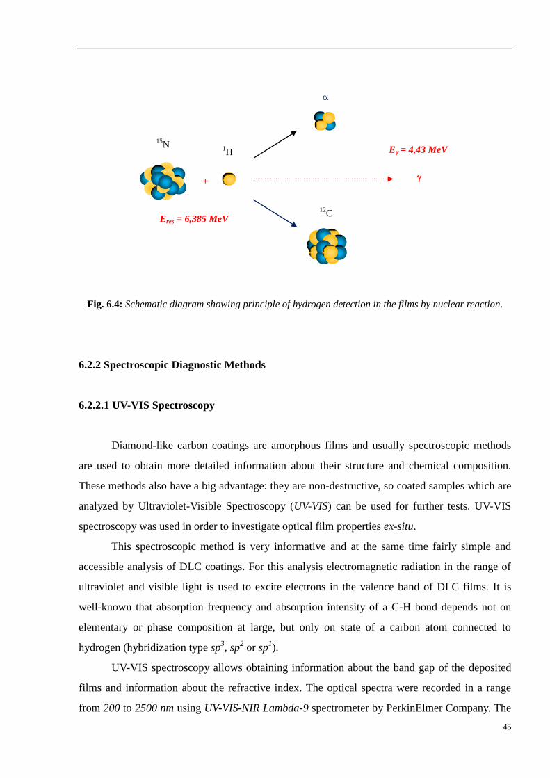
45
Fig. 6.4: Schematic diagram showing principle of hydrogen detection in the films by nuclear reaction.
6.2.2 Spectroscopic Diagnostic Methods
6.2.2.1 UV-VIS Spectroscopy
Diamond-like carbon coatings are amorphous films and usually spectroscopic methods
are used to obtain more detailed information about their structure and chemical composition.
These methods also have a big advantage: they are non-destructive, so coated samples which are
analyzed by Ultraviolet-Visible Spectroscopy (UV-VIS) can be used for further tests. UV-VIS
spectroscopy was used in order to investigate optical film properties ex-situ.
This spectroscopic method is very informative and at the same time fairly simple and
accessible analysis of DLC coatings. For this analysis electromagnetic radiation in the range of
ultraviolet and visible light is used to excite electrons in the valence band of DLC films. It is
well-known that absorption frequency and absorption intensity of a C-H bond depends not on
elementary or phase composition at large, but only on state of a carbon atom connected to
hydrogen (hybridization type sp3, sp
2 or sp
1).
UV-VIS spectroscopy allows obtaining information about the band gap of the deposited
films and information about the refractive index. The optical spectra were recorded in a range
from 200 to 2500 nm using UV-VIS-NIR Lambda-9 spectrometer by PerkinElmer Company. The
E = 4,43 MeV
15N 1
H
+
Eres = 6,385 MeV 12
C
46
spectrometer was operated in transmittance mode.
The obtained optical spectra were converted by commercial SCOUT 2.3 simulation
program, where they were fitted using dielectric function, for interband transitions and for the
band gap transitions. In this dielectric function two types of harmonic oscillators for interband
transitions were used. For the band gap calculation the OJL (O’Leary, Johnson, Lim [O’Leary97])
interband transition model was used.
In order to know the chemical composition the Raman spectroscopy was used [Ferrari00].
6.2.3 Physical Structure
To know the physical structure of the deposited films X-Ray Diffraction (XRD) technique is
used.
6.2.3.1 X-Ray Diffraction (XRD) and Williamson-Hall Method
The Bragg’s law [Bragg13] determines the essential condition which must be fulfilled if
diffraction is to occur:
n=2dsin (6.3)
where n is the order of diffraction (is an integer), λ is the x-ray wavelength, d is the distance
between the planes in the atomic lattice, and θ is the angle measured between the incident ray
and the particular crystal planes under consideration (Bragg’s angle). It also assumes that
incident beam consist of perfectly parallel and monochromatic x-rays. This leads to the
formation of a sharp diffraction maximum. But in a real situation, these flawless conditions are
never fulfilled. Small crystallite size and crystal imperfection or defects (vacancies, dislocations,
grain boundaries and voids) are commonly considered to be a reason for broadening of the peaks
in the diffraction pattern.
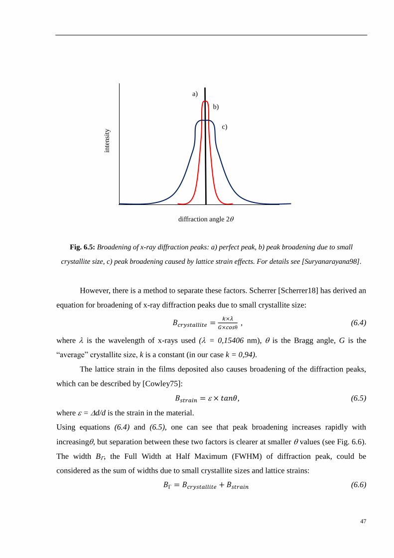
Broadening of diffraction peaks arises mainly due to two factors: small crystallite size
and lattice strain. These factors transform perfect peak (peak without width) into observed
broadened peak (see Fig. 6.5).
47
Fig. 6.5: Broadening of x-ray diffraction peaks: a) perfect peak, b) peak broadening due to small
crystallite size, c) peak broadening caused by lattice strain effects. For details see [Suryanarayana98].
However, there is a method to separate these factors. Scherrer [Scherrer18] has derived an
equation for broadening of x-ray diffraction peaks due to small crystallite size:
𝐵𝑐𝑟𝑦𝑠𝑡𝑎𝑙𝑙𝑖𝑡𝑒 =𝑘×𝜆
𝐺×𝑐𝑜𝑠θ , (6.4)
where is the wavelength of x-rays used ( = 0,15406 nm), is the Bragg angle, G is the
“average” crystallite size, k is a constant (in our case k = 0,94).
The lattice strain in the films deposited also causes broadening of the diffraction peaks,
which can be described by [Cowley75]:
𝐵𝑠𝑡𝑟𝑎𝑖𝑛 = × 𝑡𝑎𝑛𝜃, (6.5)
where = d/d is the strain in the material.
Using equations (6.4) and (6.5), one can see that peak broadening increases rapidly with
increasing, but separation between these two factors is clearer at smaller values (see Fig. 6.6).
The width B, the Full Width at Half Maximum (FWHM) of diffraction peak, could be
considered as the sum of widths due to small crystallite sizes and lattice strains:
𝐵Γ = 𝐵𝑐𝑟𝑦𝑠𝑡𝑎𝑙𝑙𝑖𝑡𝑒 + 𝐵𝑠𝑡𝑟𝑎𝑖𝑛 (6.6)
diffraction angle 2
inte
nsi
ty
a)
b)
c)
48
Fig. 6.6: Dependence of FWHM caused by small crystallite size and lattice strain on the diffraction angle
[Suryanarayana98].
From equations (6.4), (6.5) and (6.6) we get:
𝐵Γ =𝑘×𝜆
𝐺×𝑐𝑜𝑠𝜃+ × 𝑡𝑎𝑛𝜃. (6.7)
Multiplying Eq. (6.7) by cos, obtain:
𝐵Γ𝑐𝑜𝑠𝜃 =𝑘×𝜆
𝐺+ × 𝑠𝑖𝑛𝜃. (6.8)
If we plot now Bcos against sin we obtain a straight line with slope and intercept k/G. This
method is called Williamson-Hall Plot [Williamson53]. The smaller the value of , the flatter the
straight line, the smaller is the amount of strain in the sample.
0 50 100 150
diffraction angle 2
BГ,
(FW
HM
) 𝐵𝑐𝑟𝑦𝑠𝑡𝑎𝑙𝑙𝑖𝑡𝑒
𝐵𝑠𝑡𝑟𝑎𝑖𝑛
180
49
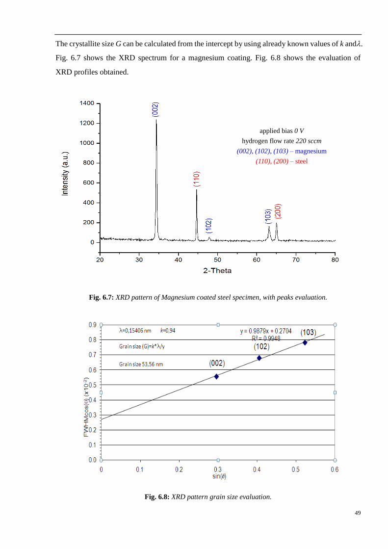
The crystallite size G can be calculated from the intercept by using already known values of k and.
Fig. 6.7 shows the XRD spectrum for a magnesium coating. Fig. 6.8 shows the evaluation of
XRD profiles obtained.
Fig. 6.7: XRD pattern of Magnesium coated steel specimen, with peaks evaluation.
Fig. 6.8: XRD pattern grain size evaluation.
applied bias 0 V
hydrogen flow rate 220 sccm
(002), (102), (103) – magnesium
(110), (200) – steel
50
6.2.4 Mechanical Properties
The mechanical properties of DLC films mainly determined by the residual stress in the growing
films.
6.2.4.1 Residual Stress
One of the most significant parameters for growing films is the residual stress. It determines the
thin film properties and therefore their application areas. In the most cases, two factors are
responsible for stress formation:
- substrate material properties;
- deposition parameters.
It is common in thin film technology that the substrate is pre-specified by a customer or by the
application area. The task is then to adjust the deposition parameters for optimal results.
For instance, the substrate can have different crystal lattice orientation or different thermal
expansion coefficient, which leads to stress formation in the substrate-film boundary. The plasma
deposition parameters can also cause stress due to the different particle energies or high
deposition temperatures. As one can see there are a lot of effects influencing the film properties
which have to be taken into account.
The pioneering work in the film stress investigation was done by Stoney [Stoney09] when he
observed growth processes of metallic films and found their delamination after they reached
certain thickness. He also found the possibility to determine the residual film stress. This method
is based on the fact that growing films can bend thin substrates because of residual stress, and by
substrate curvature evaluation the stress values can be calculated.
The residual stress in thin films consists of the following components:
= th +lat + int, (6.9)
where th is component caused by the thermal stress, lat is the lattice mismatch component
caused by the mismatch between the growing film and the substrate lattice and int is the
component arising from the intrinsic stress [Woehrl06]. The thermal stress th can be described
as:
th = EC(C – S)(TC – TM), (6.10)
where EC is the elastic modulus of the coating, C and S are the thermal expansion coefficients
for the coating and for the substrate, TC is the temperature during the coating process and TM is
51
the one during the stress measurement [Windischmann91].
The thin film’s intrinsic stress in turn has two different components responsible for two
different stress types, there are two models describing these components:
grain boundaries mismatch model: describes the “tensile stress” [Hoffman76];
ion-peening model: describes the “compressive stress” [Windischmann92].
Tensile stress
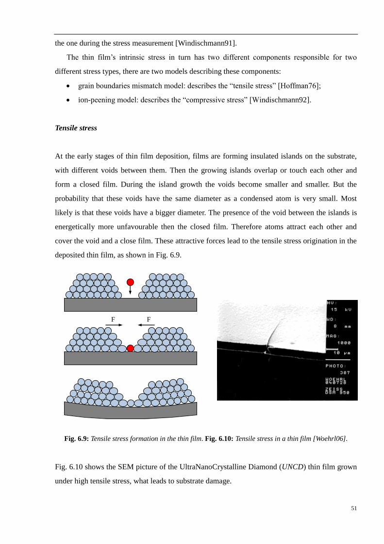
At the early stages of thin film deposition, films are forming insulated islands on the substrate,
with different voids between them. Then the growing islands overlap or touch each other and
form a closed film. During the island growth the voids become smaller and smaller. But the
probability that these voids have the same diameter as a condensed atom is very small. Most
likely is that these voids have a bigger diameter. The presence of the void between the islands is
energetically more unfavourable then the closed film. Therefore atoms attract each other and
cover the void and a close film. These attractive forces lead to the tensile stress origination in the
deposited thin film, as shown in Fig. 6.9.
Fig. 6.9: Tensile stress formation in the thin film. Fig. 6.10: Tensile stress in a thin film [Woehrl06].
Fig. 6.10 shows the SEM picture of the UltraNanoCrystalline Diamond (UNCD) thin film grown
under high tensile stress, what leads to substrate damage.
F F
52
Compressive stress
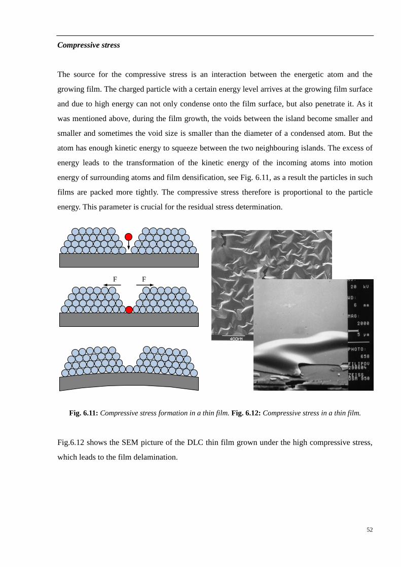
The source for the compressive stress is an interaction between the energetic atom and the
growing film. The charged particle with a certain energy level arrives at the growing film surface
and due to high energy can not only condense onto the film surface, but also penetrate it. As it
was mentioned above, during the film growth, the voids between the island become smaller and
smaller and sometimes the void size is smaller than the diameter of a condensed atom. But the
atom has enough kinetic energy to squeeze between the two neighbouring islands. The excess of
energy leads to the transformation of the kinetic energy of the incoming atoms into motion
energy of surrounding atoms and film densification, see Fig. 6.11, as a result the particles in such
films are packed more tightly. The compressive stress therefore is proportional to the particle
energy. This parameter is crucial for the residual stress determination.
Fig. 6.11: Compressive stress formation in a thin film. Fig. 6.12: Compressive stress in a thin film.
Fig.6.12 shows the SEM picture of the DLC thin film grown under the high compressive stress,
which leads to the film delamination.
F F
53
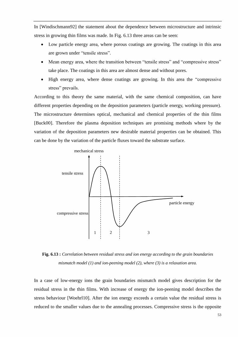
In [Windischmann92] the statement about the dependence between microstructure and intrinsic
stress in growing thin films was made. In Fig. 6.13 three areas can be seen:
Low particle energy area, where porous coatings are growing. The coatings in this area
are grown under “tensile stress”.
Mean energy area, where the transition between “tensile stress” and “compressive stress”
take place. The coatings in this area are almost dense and without pores.
High energy area, where dense coatings are growing. In this area the “compressive
stress” prevails.
According to this theory the same material, with the same chemical composition, can have
different properties depending on the deposition parameters (particle energy, working pressure).
The microstructure determines optical, mechanical and chemical properties of the thin films
[Buck00]. Therefore the plasma deposition techniques are promising methods where by the
variation of the deposition parameters new desirable material properties can be obtained. This
can be done by the variation of the particle fluxes toward the substrate surface.
Fig. 6.13 : Correlation between residual stress and ion energy according to the grain boundaries
mismatch model (1) and ion-peening model (2), where (3) is a relaxation area.
In a case of low-energy ions the grain boundaries mismatch model gives description for the
residual stress in the thin films. With increase of energy the ion-peening model describes the
stress behaviour [Woehrl10]. After the ion energy exceeds a certain value the residual stress is
reduced to the smaller values due to the annealing processes. Compressive stress is the opposite
1 2 3
tensile stress
compressive stress
particle energy
mechanical stress
54
of tensile stress and as agreed the compressive stress is negative and tensile stress is positive.
6.2.4.2 SSIOD (Surface Stress Induced Optical Deflection)
There are many stress measurement methods such as optical: shift of the Raman peaks,
Tolansky interferometry; or mechanical: stylus profilometry; or even method based on X-ray
diffraction lines broadening. But these methods have a lot of limitations and special conditions
which should be fulfilled, and they are not able to give information about the total film stress. In
comparison to these methods the Surface Stress Induced Optical Deflection (SSIOD) method can
be easily used with different substrates, in-situ or ex-situ, transparent or opaque films.
This method is based on the fact that the residual stress in the growing films bends the substrate
and this substrate curvature can be measured by position sensing diode.
SSIOD method is based on the Stoney approach [Stoney09]:
=𝐸𝑠𝑢𝑏
(1−𝜈)
𝑡𝑠𝑢𝑏2
6∙𝑡𝑓𝑖𝑙𝑚(
1
𝑅𝑎−
1
𝑅𝑏), (6.11)
where Esub is the substrate elastic modulus, is the substrate Poisson ratio, tsub is substrate
thickness, tfilm is the deposited film thickness and R is the difference in the substrate curvature
(measured before the deposition Rb and after Ra). The only information which is necessary to
know is the film thickness.
In order to determine film stress more precisely the SSIOD method should fulfil some conditions
such as: substrate thickness should be smaller than the curvature radius, as well as substrate
length at least two times bigger than the substrate width.
In Fig .6.14 one can see the schematic diagram of SSIOD method for curved and flat substrates
and principle of mechanic stress determination. During the scan over the substrate laser beam is
deflected at certain angle to the position sensing diode (defined by the substrate curvature).
In Fig. 6.15 the schematic diagram of stress measurement system is shown.
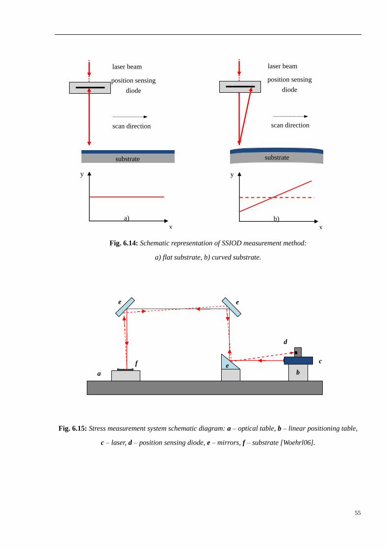
55
Fig. 6.14: Schematic representation of SSIOD measurement method:
a) flat substrate, b) curved substrate.
Fig. 6.15: Stress measurement system schematic diagram: a – optical table, b – linear positioning table,
c – laser, d – position sensing diode, e – mirrors, f – substrate [Woehrl06].
e e
e f
a b
d
c
y
x
a)
substrate
scan direction
laser beam
position sensing
diode
y
x
b)
scan direction
laser beam
position sensing
diode
substrate
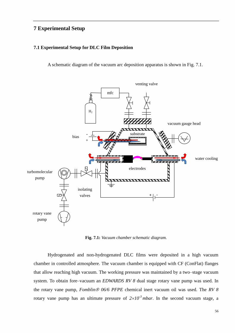
56
7 Experimental Setup
7.1 Experimental Setup for DLC Film Deposition
A schematic diagram of the vacuum arc deposition apparatus is shown in Fig. 7.1.
Fig. 7.1: Vacuum chamber schematic diagram.
Hydrogenated and non-hydrogenated DLC films were deposited in a high vacuum
chamber in controlled atmosphere. The vacuum chamber is equipped with CF (ConFlat) flanges
that allow reaching high vacuum. The working pressure was maintained by a two–stage vacuum
system. To obtain fore–vacuum an EDWARDS RV 8 dual stage rotary vane pump was used. In
the rotary vane pump, Fomblin 06/6 PFPE chemical inert vacuum oil was used. The RV 8
rotary vane pump has an ultimate pressure of 210-3
mbar. In the second vacuum stage, a
+ -
water cooling
turbomolecular
pump
isolating
valves
rotary vane
pump
vacuum gauge head
venting valve
substrate -
+ bias
electrodes
mfc
H2
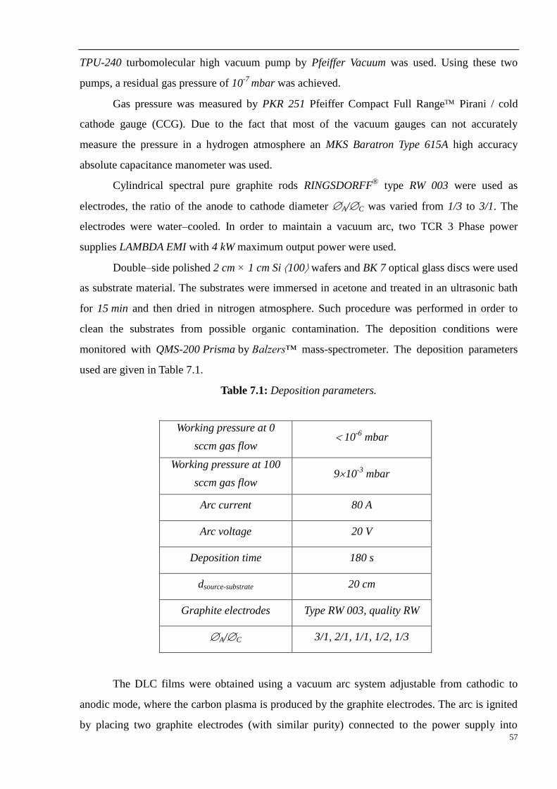
57
TPU-240 turbomolecular high vacuum pump by Pfeiffer Vacuum was used. Using these two
pumps, a residual gas pressure of 10-7
mbar was achieved.
Gas pressure was measured by PKR 251 Pfeiffer Compact Full Range Pirani / cold
cathode gauge (CCG). Due to the fact that most of the vacuum gauges can not accurately
measure the pressure in a hydrogen atmosphere an MKS Baratron Type 615A high accuracy
absolute capacitance manometer was used.
Cylindrical spectral pure graphite rods RINGSDORFF®
type RW 003 were used as
electrodes, the ratio of the anode to cathode diameter A/C was varied from 1/3 to 3/1. The
electrodes were water–cooled. In order to maintain a vacuum arc, two TCR 3 Phase power
supplies LAMBDA EMI with 4 kW maximum output power were used.
Double–side polished 2 cm × 1 cm Si 100 wafers and BK 7 optical glass discs were used
as substrate material. The substrates were immersed in acetone and treated in an ultrasonic bath
for 15 min and then dried in nitrogen atmosphere. Such procedure was performed in order to
clean the substrates from possible organic contamination. The deposition conditions were
monitored with QMS-200 Prisma by Balzers™ mass-spectrometer. The deposition parameters
used are given in Table 7.1.
Table 7.1: Deposition parameters.
Working pressure at 0
sccm gas flow 10
-6 mbar
Working pressure at 100
sccm gas flow 910
-3 mbar
Arc current 80 A
Arc voltage 20 V
Deposition time 180 s
dsource-substrate 20 cm
Graphite electrodes Type RW 003, quality RW
A/C 3/1, 2/1, 1/1, 1/2, 1/3
The DLC films were obtained using a vacuum arc system adjustable from cathodic to
anodic mode, where the carbon plasma is produced by the graphite electrodes. The arc is ignited
by placing two graphite electrodes (with similar purity) connected to the power supply into
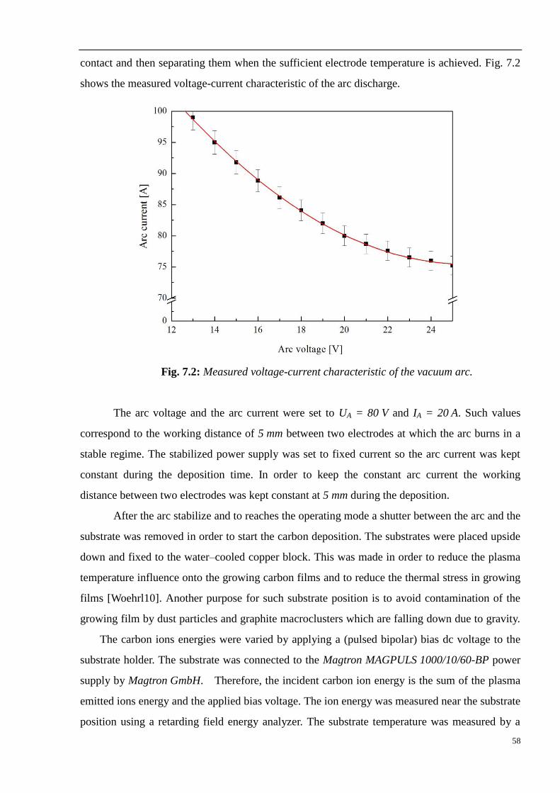
58
contact and then separating them when the sufficient electrode temperature is achieved. Fig. 7.2
shows the measured voltage-current characteristic of the arc discharge.
Fig. 7.2: Measured voltage-current characteristic of the vacuum arc.
The arc voltage and the arc current were set to UA = 80 V and IA = 20 A. Such values
correspond to the working distance of 5 mm between two electrodes at which the arc burns in a
stable regime. The stabilized power supply was set to fixed current so the arc current was kept
constant during the deposition time. In order to keep the constant arc current the working
distance between two electrodes was kept constant at 5 mm during the deposition.
After the arc stabilize and to reaches the operating mode a shutter between the arc and the
substrate was removed in order to start the carbon deposition. The substrates were placed upside
down and fixed to the water–cooled copper block. This was made in order to reduce the plasma
temperature influence onto the growing carbon films and to reduce the thermal stress in growing
films [Woehrl10]. Another purpose for such substrate position is to avoid contamination of the
growing film by dust particles and graphite macroclusters which are falling down due to gravity.
The carbon ions energies were varied by applying a (pulsed bipolar) bias dc voltage to the
substrate holder. The substrate was connected to the Magtron MAGPULS 1000/10/60-BP power
supply by Magtron GmbH. Therefore, the incident carbon ion energy is the sum of the plasma
emitted ions energy and the applied bias voltage. The ion energy was measured near the substrate
position using a retarding field energy analyzer. The substrate temperature was measured by a
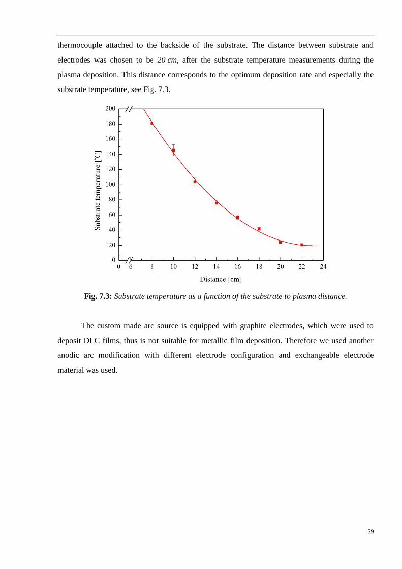
59
thermocouple attached to the backside of the substrate. The distance between substrate and
electrodes was chosen to be 20 cm, after the substrate temperature measurements during the
plasma deposition. This distance corresponds to the optimum deposition rate and especially the
substrate temperature, see Fig. 7.3.
Fig. 7.3: Substrate temperature as a function of the substrate to plasma distance.
The custom made arc source is equipped with graphite electrodes, which were used to
deposit DLC films, thus is not suitable for metallic film deposition. Therefore we used another
anodic arc modification with different electrode configuration and exchangeable electrode
material was used.
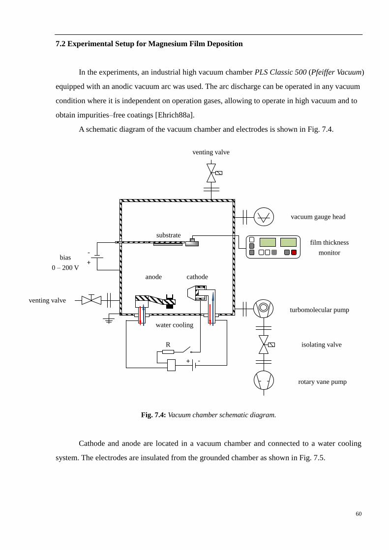
60
7.2 Experimental Setup for Magnesium Film Deposition
In the experiments, an industrial high vacuum chamber PLS Classic 500 (Pfeiffer Vacuum)
equipped with an anodic vacuum arc was used. The arc discharge can be operated in any vacuum
condition where it is independent on operation gases, allowing to operate in high vacuum and to
obtain impurities–free coatings [Ehrich88a].
A schematic diagram of the vacuum chamber and electrodes is shown in Fig. 7.4.
Fig. 7.4: Vacuum chamber schematic diagram.
Cathode and anode are located in a vacuum chamber and connected to a water cooling
system. The electrodes are insulated from the grounded chamber as shown in Fig. 7.5.
turbomolecular pump
Turbo molecular pump
R isolating valve
rotary vane pump
venting valve
vacuum gauge head
venting valve
substrate
+ -
-
+
anode cathode
bias
0 – 200 V
100 0.05 film thickness
monitor
water cooling
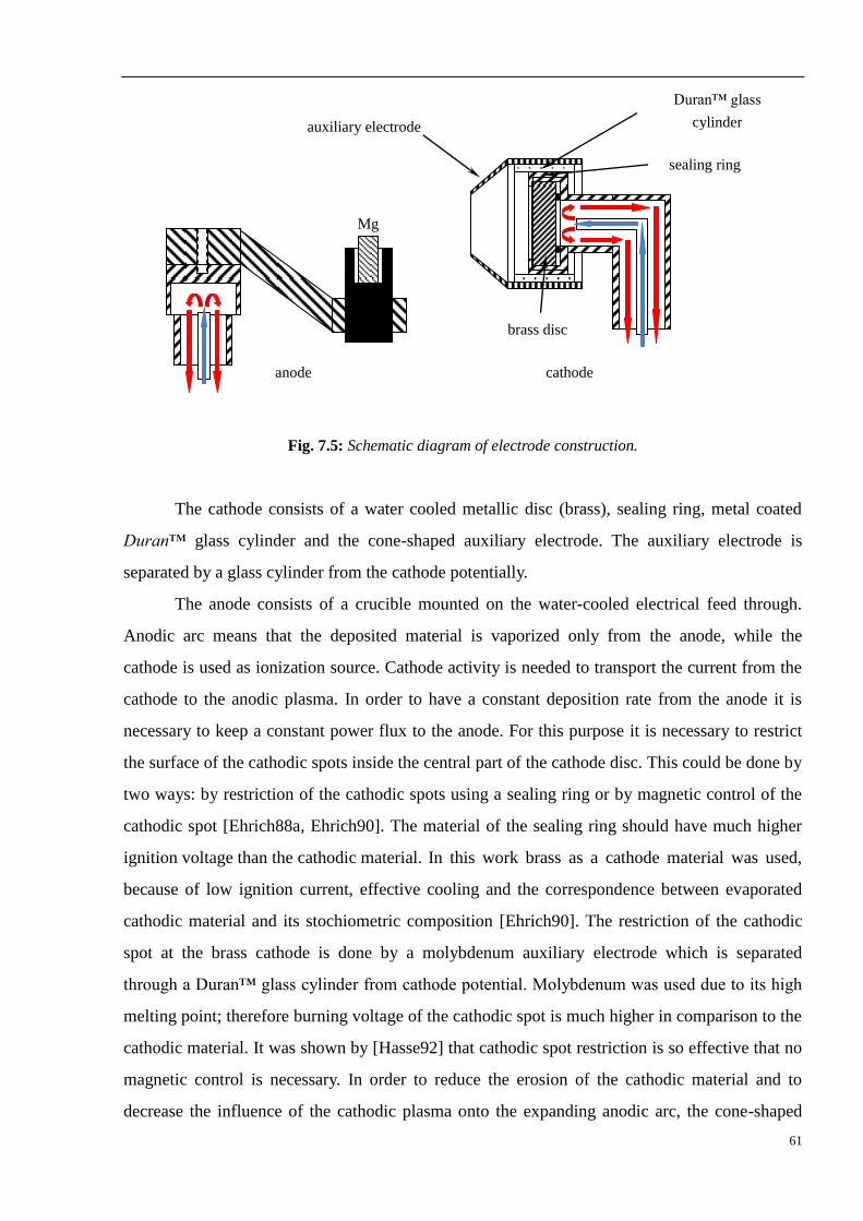
61
Fig. 7.5: Schematic diagram of electrode construction.
The cathode consists of a water cooled metallic disc (brass), sealing ring, metal coated
Duran™ glass cylinder and the cone-shaped auxiliary electrode. The auxiliary electrode is
separated by a glass cylinder from the cathode potentially.
The anode consists of a crucible mounted on the water-cooled electrical feed through.
Anodic arc means that the deposited material is vaporized only from the anode, while the
cathode is used as ionization source. Cathode activity is needed to transport the current from the
cathode to the anodic plasma. In order to have a constant deposition rate from the anode it is
necessary to keep a constant power flux to the anode. For this purpose it is necessary to restrict
the surface of the cathodic spots inside the central part of the cathode disc. This could be done by
two ways: by restriction of the cathodic spots using a sealing ring or by magnetic control of the
cathodic spot [Ehrich88a, Ehrich90]. The material of the sealing ring should have much higher
ignition voltage than the cathodic material. In this work brass as a cathode material was used,
because of low ignition current, effective cooling and the correspondence between evaporated
cathodic material and its stochiometric composition [Ehrich90]. The restriction of the cathodic
spot at the brass cathode is done by a molybdenum auxiliary electrode which is separated
through a Duran™ glass cylinder from cathode potential. Molybdenum was used due to its high
melting point; therefore burning voltage of the cathodic spot is much higher in comparison to the
cathodic material. It was shown by [Hasse92] that cathodic spot restriction is so effective that no
magnetic control is necessary. In order to reduce the erosion of the cathodic material and to
decrease the influence of the cathodic plasma onto the expanding anodic arc, the cone-shaped
anode
Mg
cathode
brass disc
auxiliary electrode
Duran™ glass
cylinder
sealing ring
62
auxiliary electrode orifice was made as small as possible. During the plasma operation the
temperature inside the auxiliary electrode was so high that even backward evaporation of zinc
onto the cathode surface occurred, this leads to the reduction of cathode material erosion. It was
found [Filipov05] during the anodic arc deposition the evaporated anodic material is also
deposited onto the cathode surface, what on its part decreases the plasma and films
contamination by the cathode material, see Fig. 8.89. As indicated below, the anodic plasma and
in turn the deposited magnesium film have no contamination from the evaporated cathodic
material, see Fig. 8.87.
In comparison with the cathodic arc deposition, the anodic arc has a significant advantage:
there are no macroparticles produced during the deposition due to the evaporation of the metal
from the anodic crucible [Ehrich88a].
To ignite the plasma, it was necessary to use an auxiliary electrode. After applying current
between molybdenum auxiliary electrode and the cathode, the thin metallic layer on the Duran™
glass cylinder evaporates due to the ohmic heating. This ignites an auxiliary arc. After the
auxiliary arc ignition, the electrons which leave the cathode due to the potential difference
between the electrodes move toward the anode. This results in rapid evaporation of the anode
material and also its ionization. The anodic arc ignites when a critical evaporation rate is reached.
Then the auxiliary arc electric circuit is turned off. By using auxiliary arc ignition, the cathodic
material erosion could be avoided and thus film contamination. During the deposition, the power
input to the anode is concentrated on the molten material. Intense and bright color of the
evaporated metal in the plasma cloud around the anode, prove strong activation (excitation and
ionization) of the produced anodic arc plasma [Ehrich88b].
In order to prevent contamination of the magnesium coatings, a carbon crucible was used
because of its high melting temperature and absence of chemical reactions between magnesium
and a carbon crucible. Due to the physical-chemical properties of magnesium it sublimates
during the evaporation and passes liquid phase formation what prevents formation of magnesium
melts and to contaminate expanding anodic plasma.
The films were deposited on 50 mm × 50 mm steel substrates. These substrates were
pretreated in an ultrasonic bath with acetone to remove surface contamination. After the cleaning
procedure the substrates were transferred into the vacuum chamber. The chamber was pumped
down to 10-7
mbar. The variation of process parameters, such as substrate bias (from 0 V to –
200 V) and hydrogen admixture (from 0 sccm to 1000 sccm), is used to influence the film
properties. According to different hydrogen flow rates different deposition pressures were
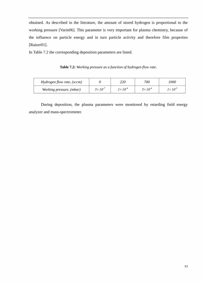
63
obtained. As described in the literature, the amount of stored hydrogen is proportional to the
working pressure [Varin06]. This parameter is very important for plasma chemistry, because of
the influence on particle energy and in turn particle activity and therefore film properties
[Raizer01].
In Table 7.2 the corresponding deposition parameters are listed.
Table 7.2: Working pressure as a function of hydrogen flow rate.
Hydrogen flow rate, (sccm) 0 220 700 1000
Working pressure, (mbar) 5×10⁻⁷
1×10⁻⁴
5×10⁻⁴
1×10⁻³
During deposition, the plasma parameters were monitored by retarding field energy
analyzer and mass-spectrometer.
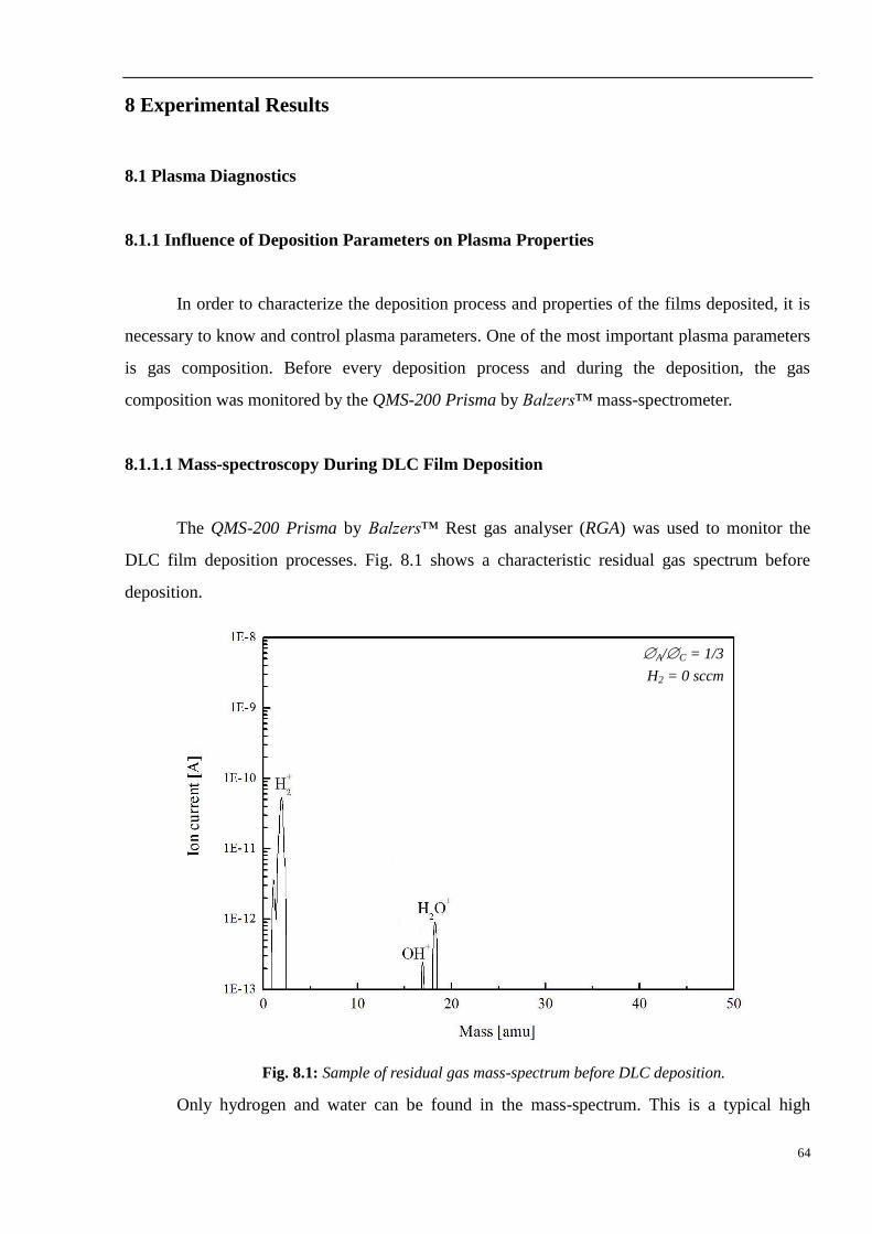
64
8 Experimental Results
8.1 Plasma Diagnostics
8.1.1 Influence of Deposition Parameters on Plasma Properties
In order to characterize the deposition process and properties of the films deposited, it is
necessary to know and control plasma parameters. One of the most important plasma parameters
is gas composition. Before every deposition process and during the deposition, the gas
composition was monitored by the QMS-200 Prisma by Balzers™ mass-spectrometer.
8.1.1.1 Mass-spectroscopy During DLC Film Deposition
The QMS-200 Prisma by Balzers™ Rest gas analyser (RGA) was used to monitor the
DLC film deposition processes. Fig. 8.1 shows a characteristic residual gas spectrum before
deposition.
Fig. 8.1: Sample of residual gas mass-spectrum before DLC deposition.
Only hydrogen and water can be found in the mass-spectrum. This is a typical high
A/C = 1/3
H2 = 0 sccm
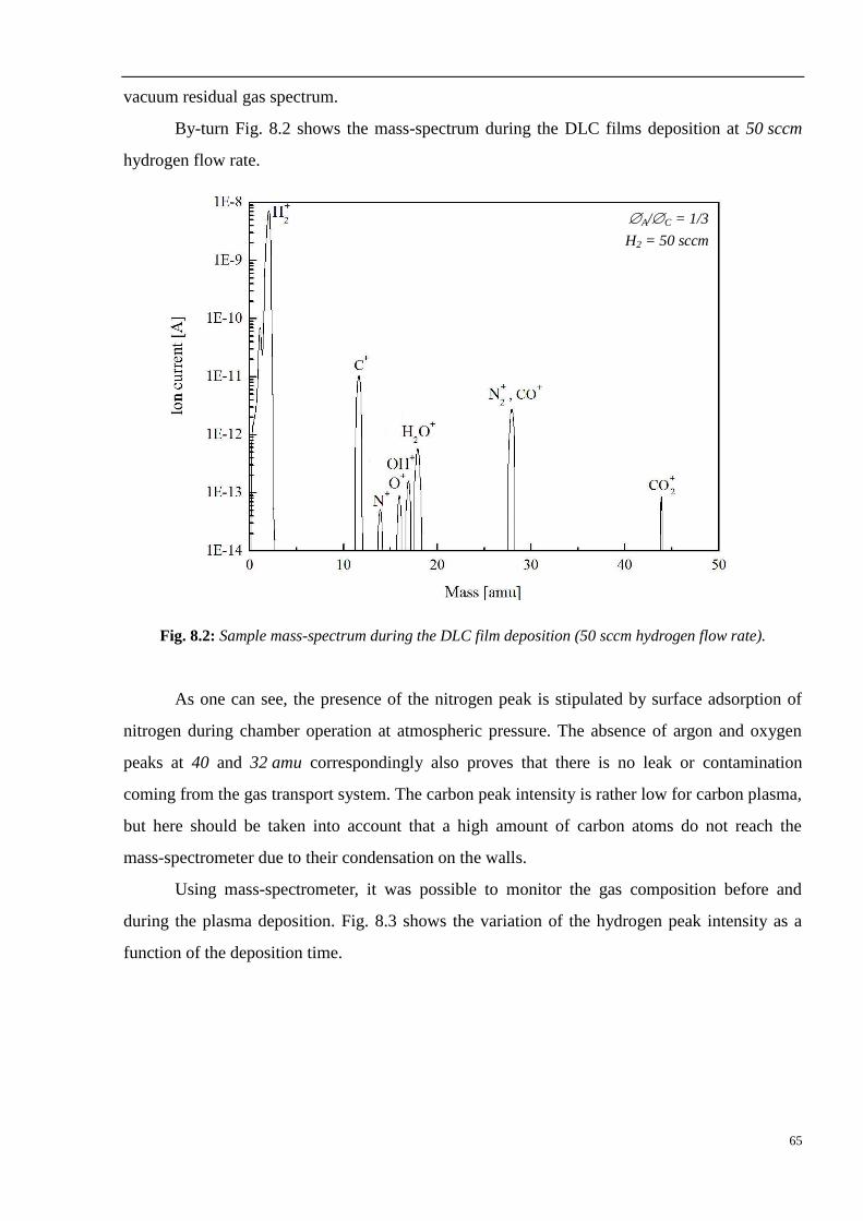
65
vacuum residual gas spectrum.
By-turn Fig. 8.2 shows the mass-spectrum during the DLC films deposition at 50 sccm
hydrogen flow rate.
Fig. 8.2: Sample mass-spectrum during the DLC film deposition (50 sccm hydrogen flow rate).
As one can see, the presence of the nitrogen peak is stipulated by surface adsorption of
nitrogen during chamber operation at atmospheric pressure. The absence of argon and oxygen
peaks at 40 and 32 amu correspondingly also proves that there is no leak or contamination
coming from the gas transport system. The carbon peak intensity is rather low for carbon plasma,
but here should be taken into account that a high amount of carbon atoms do not reach the
mass-spectrometer due to their condensation on the walls.
Using mass-spectrometer, it was possible to monitor the gas composition before and
during the plasma deposition. Fig. 8.3 shows the variation of the hydrogen peak intensity as a
function of the deposition time.
A/C = 1/3
H2 = 50 sccm
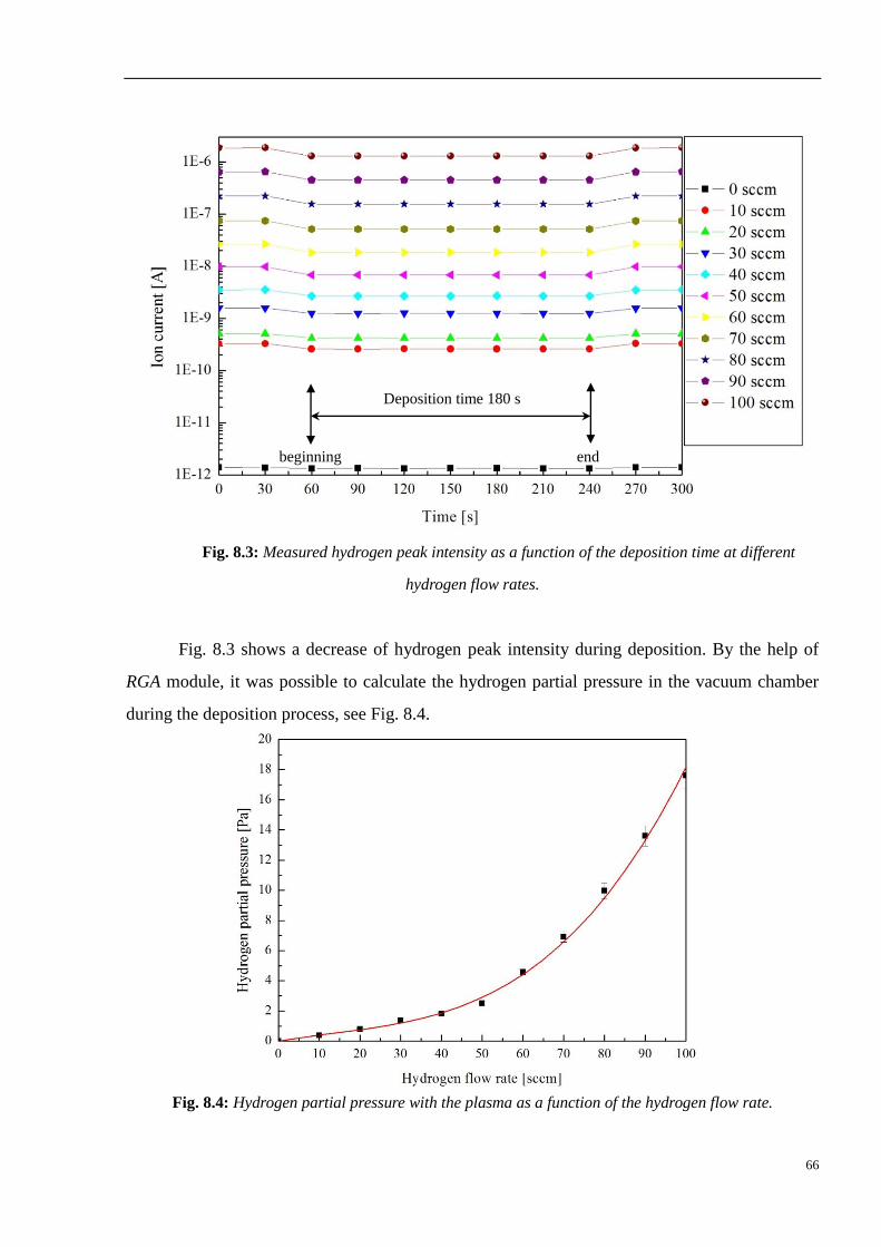
66
Fig. 8.3: Measured hydrogen peak intensity as a function of the deposition time at different
hydrogen flow rates.
Fig. 8.3 shows a decrease of hydrogen peak intensity during deposition. By the help of
RGA module, it was possible to calculate the hydrogen partial pressure in the vacuum chamber
during the deposition process, see Fig. 8.4.
Fig. 8.4: Hydrogen partial pressure with the plasma as a function of the hydrogen flow rate.
Deposition time 180 s
beginning end
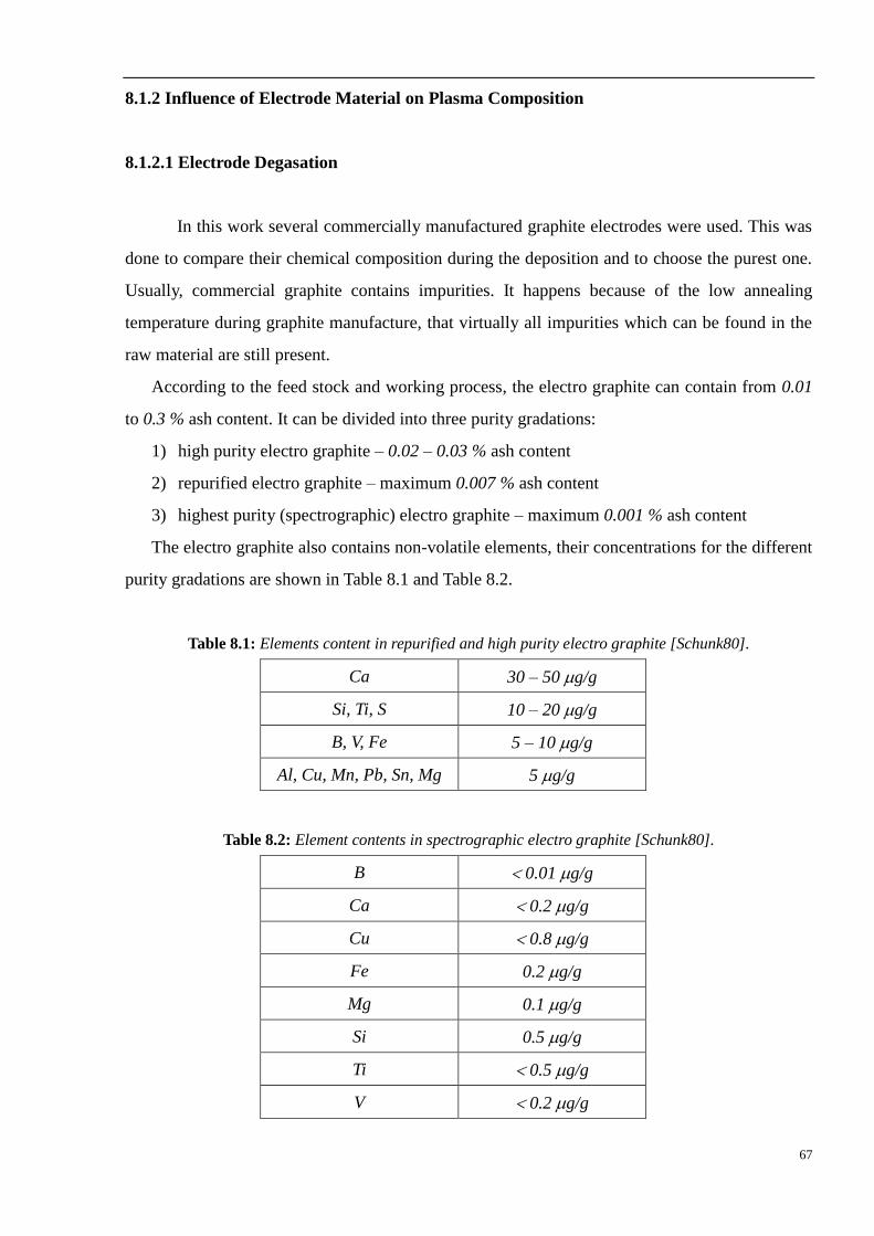
67
8.1.2 Influence of Electrode Material on Plasma Composition
8.1.2.1 Electrode Degasation
In this work several commercially manufactured graphite electrodes were used. This was
done to compare their chemical composition during the deposition and to choose the purest one.
Usually, commercial graphite contains impurities. It happens because of the low annealing
temperature during graphite manufacture, that virtually all impurities which can be found in the
raw material are still present.
According to the feed stock and working process, the electro graphite can contain from 0.01
to 0.3 % ash content. It can be divided into three purity gradations:
1) high purity electro graphite – 0.02 – 0.03 % ash content
2) repurified electro graphite – maximum 0.007 % ash content
3) highest purity (spectrographic) electro graphite – maximum 0.001 % ash content
The electro graphite also contains non-volatile elements, their concentrations for the different
purity gradations are shown in Table 8.1 and Table 8.2.
Table 8.1: Elements content in repurified and high purity electro graphite [Schunk80].
Ca 30 – 50 g/g
Si, Ti, S 10 – 20 g/g
B, V, Fe 5 – 10 g/g
Al, Cu, Mn, Pb, Sn, Mg 5 g/g
Table 8.2: Element contents in spectrographic electro graphite [Schunk80].
B 0.01 g/g
Ca 0.2 g/g
Cu 0.8 g/g
Fe 0.2 g/g
Mg 0.1 g/g
Si 0.5 g/g
Ti 0.5 g/g
V 0.2 g/g
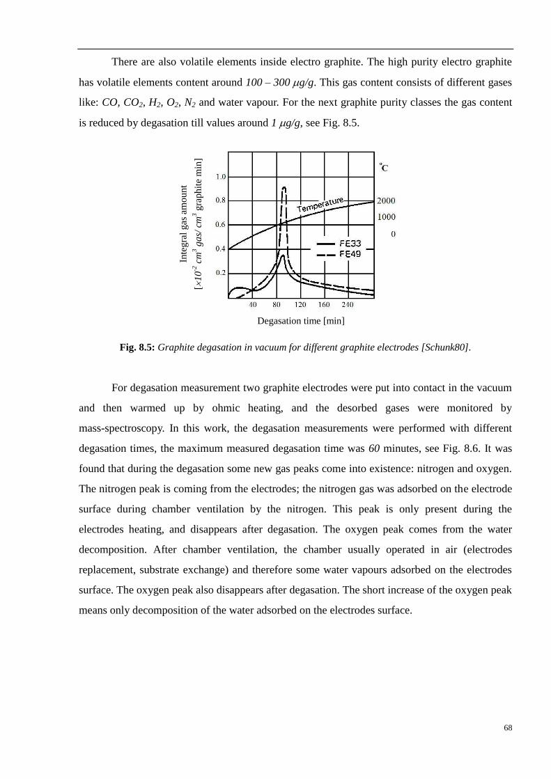
68
There are also volatile elements inside electro graphite. The high purity electro graphite
has volatile elements content around 100 – 300 g/g. This gas content consists of different gases
like: CO, CO2, H2, O2, N2 and water vapour. For the next graphite purity classes the gas content
is reduced by degasation till values around 1 g/g, see Fig. 8.5.
Fig. 8.5: Graphite degasation in vacuum for different graphite electrodes [Schunk80].
For degasation measurement two graphite electrodes were put into contact in the vacuum
and then warmed up by ohmic heating, and the desorbed gases were monitored by
mass-spectroscopy. In this work, the degasation measurements were performed with different
degasation times, the maximum measured degasation time was 60 minutes, see Fig. 8.6. It was
found that during the degasation some new gas peaks come into existence: nitrogen and oxygen.
The nitrogen peak is coming from the electrodes; the nitrogen gas was adsorbed on the electrode
surface during chamber ventilation by the nitrogen. This peak is only present during the
electrodes heating, and disappears after degasation. The oxygen peak comes from the water
decomposition. After chamber ventilation, the chamber usually operated in air (electrodes
replacement, substrate exchange) and therefore some water vapours adsorbed on the electrodes
surface. The oxygen peak also disappears after degasation. The short increase of the oxygen peak
means only decomposition of the water adsorbed on the electrodes surface.
Inte
gra
l g
as a
mo
un
t
[1
0-2
cm
3 g
as/
cm
3 g
raph
ite
min
]
Degasation time [min]
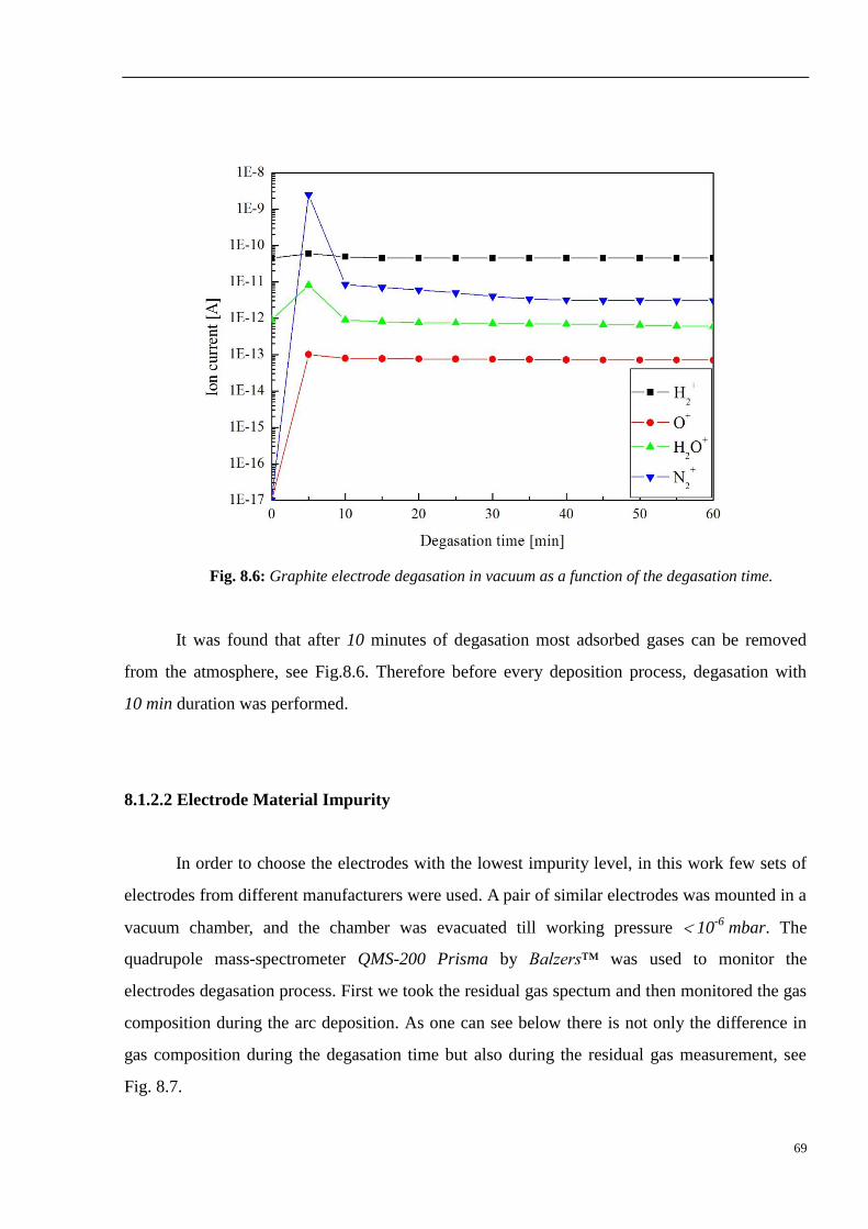
69
Fig. 8.6: Graphite electrode degasation in vacuum as a function of the degasation time.
It was found that after 10 minutes of degasation most adsorbed gases can be removed
from the atmosphere, see Fig.8.6. Therefore before every deposition process, degasation with
10 min duration was performed.
8.1.2.2 Electrode Material Impurity
In order to choose the electrodes with the lowest impurity level, in this work few sets of
electrodes from different manufacturers were used. A pair of similar electrodes was mounted in a
vacuum chamber, and the chamber was evacuated till working pressure 10-6
mbar. The
quadrupole mass-spectrometer QMS-200 Prisma by Balzers™ was used to monitor the
electrodes degasation process. First we took the residual gas spectum and then monitored the gas
composition during the arc deposition. As one can see below there is not only the difference in
gas composition during the degasation time but also during the residual gas measurement, see
Fig. 8.7.
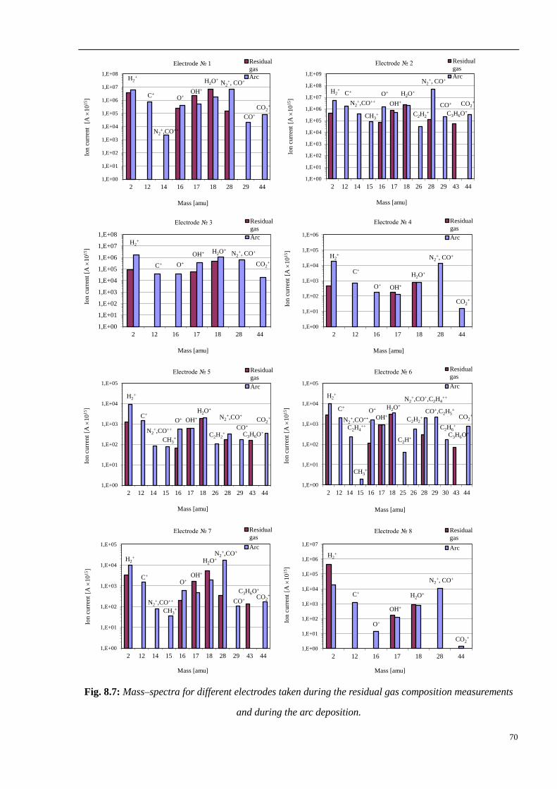
70
Fig. 8.7: Mass–spectra for different electrodes taken during the residual gas composition measurements
and during the arc deposition.
1,E+00
1,E+01
1,E+02
1,E+03
1,E+04
1,E+05
1,E+06
1,E+07
1,E+08
2 12 14 16 17 18 28 29 44
Ion c
urr
ent
[A
10
15]
Mass [amu]
Residual
gas
Arc
Electrode № 1
H2+
C+
N2+,CO++
O+ OH+
H2O+ N2
+, CO+
CO2+
CO+
1,E+00
1,E+01
1,E+02
1,E+03
1,E+04
1,E+05
1,E+06
1,E+07
1,E+08
1,E+09
2 12 14 15 16 17 18 26 28 29 43 44
Ion c
urr
ent
[A
10
15]
Mass [amu]
Residual
gas
Arc
Electrode № 2
H2+
C+
N2+,CO++
O+
OH+
H2O+
N2+, CO+
CO+ CO2+
C2H2+
CH3+
C3H6O
+
1,E+00
1,E+01
1,E+02
1,E+03
1,E+04
1,E+05
1,E+06
1,E+07
1,E+08
2 12 16 17 18 28 44
Ion c
urr
ent
[A
10
15]
Mass [amu]
Residual
gas
Arc
Electrode № 3
H2+
C+ O+
OH+ H2O+ N2
+, CO+
CO2+
1,E+00
1,E+01
1,E+02
1,E+03
1,E+04
1,E+05
1,E+06
2 12 16 17 18 28 44
Ion c
urr
ent
[A
10
15]
Mass [amu]
Residual
gas
Arc
Electrode № 4
H2+
C+
O+ OH+
H2O+
N2+, CO+
CO2+
1,E+00
1,E+01
1,E+02
1,E+03
1,E+04
1,E+05
2 12 14 15 16 17 18 26 28 29 43 44
Ion c
urr
ent
[A
10
15]
Mass [amu]
Residual
gas
Arc
Electrode № 5
H2+
C+ N2+,CO+
O+ OH+
H2O+
CO+
CO2+
C2H2+
CH3
+
C3H6O+
N2+,CO++
1,E+00
1,E+01
1,E+02
1,E+03
1,E+04
1,E+05
2 12 14 15 16 17 18 25 26 28 29 30 43 44
Ion c
urr
ent
[A
10
15]
Mass [amu]
Residual
gas
Arc
Electrode № 6
H2+
C+
N2+,CO++,
C2H4++
CH3+
O+
OH+
H2O+
C2H2+
C2H+
N2+,CO+,C2H4
++
CO+,C2H5+
C2H6+
C3H6O+
CO2+
1,E+00
1,E+01
1,E+02
1,E+03
1,E+04
1,E+05
2 12 14 15 16 17 18 28 29 43 44
Ion c
urr
ent
[A
10
15]
Mass [amu]
Residual
gas
Arc
Electrode № 7
H2+
C+
N2+,CO++
CH3+
O+ OH+
H2O+ N2
+,CO+
CO+
C3H6O+
CO2
+
1,E+00
1,E+01
1,E+02
1,E+03
1,E+04
1,E+05
1,E+06
1,E+07
2 12 16 17 18 28 44
Ion c
urr
ent
[A
10
15]
Mass [amu]
Residual
gas
Arc
Electrode № 8
H2+
C+
O+
OH+
H2O+
N2+, CO+
CO2+
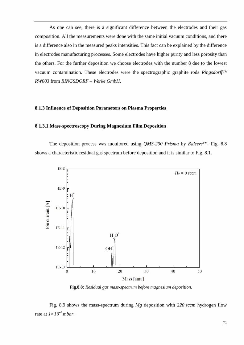
71
As one can see, there is a significant difference between the electrodes and their gas
composition. All the measurements were done with the same initial vacuum conditions, and there
is a difference also in the measured peaks intensities. This fact can be explained by the difference
in electrodes manufacturing processes. Some electrodes have higher purity and less porosity than
the others. For the further deposition we choose electrodes with the number 8 due to the lowest
vacuum contamination. These electrodes were the spectrographic graphite rods Ringsdorff
RW003 from RINGSDORF – Werke GmbH.
8.1.3 Influence of Deposition Parameters on Plasma Properties
8.1.3.1 Mass-spectroscopy During Magnesium Film Deposition
The deposition process was monitored using QMS-200 Prisma by Balzers™. Fig. 8.8
shows a characteristic residual gas spectrum before deposition and it is similar to Fig. 8.1.
Fig.8.8: Residual gas mass-spectrum before magnesium deposition.
Fig. 8.9 shows the mass-spectrum during Mg deposition with 220 sccm hydrogen flow
rate at 1×10⁻⁴
mbar.
H2 = 0 sccm
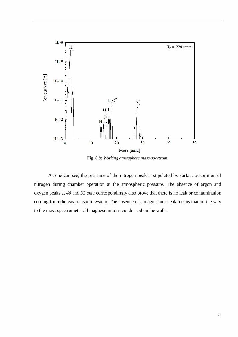
72
Fig. 8.9: Working atmosphere mass-spectrum.
As one can see, the presence of the nitrogen peak is stipulated by surface adsorption of
nitrogen during chamber operation at the atmospheric pressure. The absence of argon and
oxygen peaks at 40 and 32 amu correspondingly also prove that there is no leak or contamination
coming from the gas transport system. The absence of a magnesium peak means that on the way
to the mass-spectrometer all magnesium ions condensed on the walls.
H2 = 220 sccm
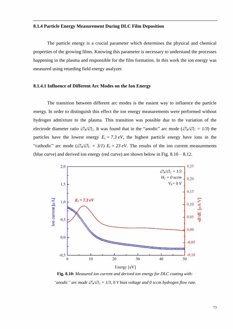
73
8.1.4 Particle Energy Measurement During DLC Film Deposition
The particle energy is a crucial parameter which determines the physical and chemical
properties of the growing films. Knowing this parameter is necessary to understand the processes
happening in the plasma and responsible for the film formation. In this work the ion energy was
measured using retarding field energy analyzer.
8.1.4.1 Influence of Different Arc Modes on the Ion Energy
The transition between different arc modes is the easiest way to influence the particle
energy. In order to distinguish this effect the ion energy measurements were performed without
hydrogen admixture to the plasma. This transition was possible due to the variation of the
electrode diameter ratio A/C. It was found that in the “anodic” arc mode (A/C = 1/3) the
particles have the lowest energy Ei = 7.3 eV, the highest particle energy have ions in the
“cathodic” arc mode (A/C = 3/1) Ei = 23 eV. The results of the ion current measurements
(blue curve) and derived ion energy (red curve) are shown below in Fig. 8.10 – 8.12.
Fig. 8.10: Measured ion current and derived ion energy for DLC coating with:
“anodic” arc mode A/C = 1/3, 0 V bias voltage and 0 sccm hydrogen flow rate.
Ei = 7.3 eV
A/C = 1/3
H2 = 0 sccm
Vb= 0 V
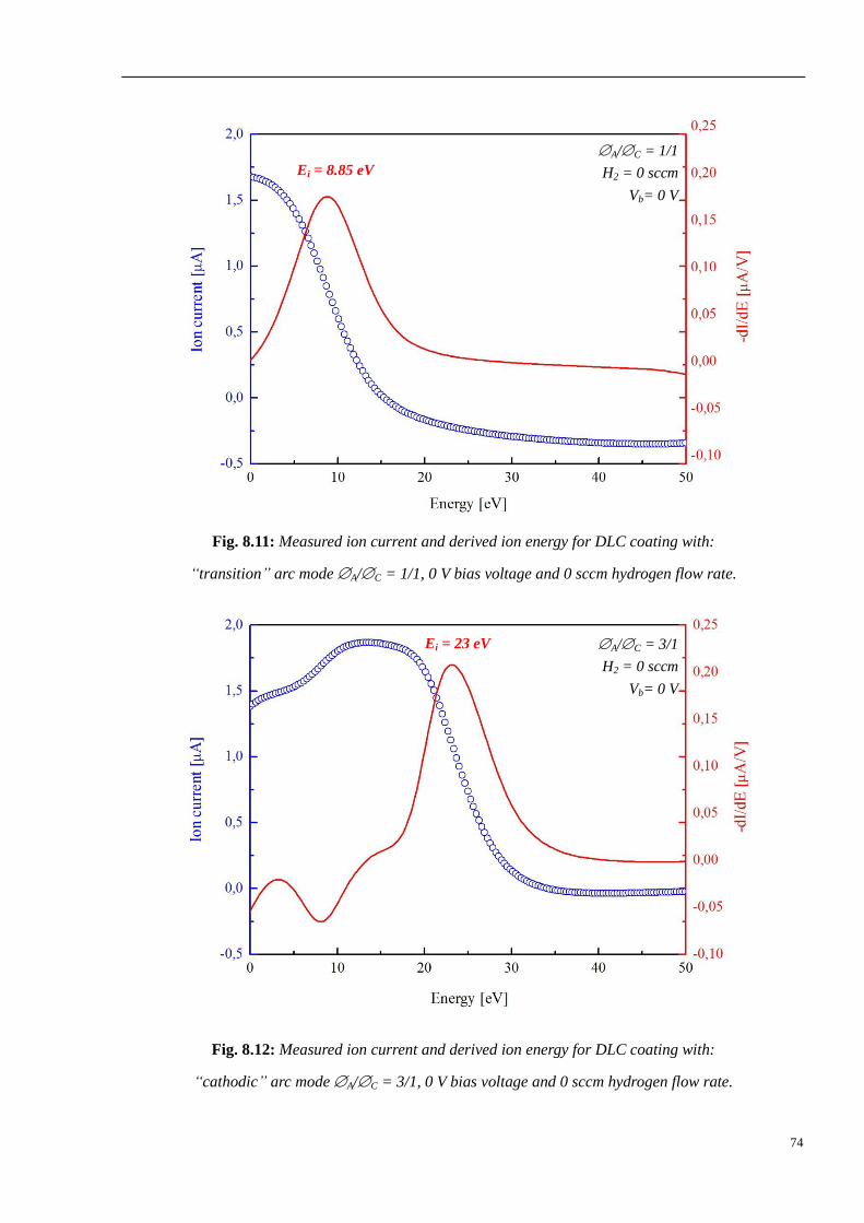
74
Fig. 8.11: Measured ion current and derived ion energy for DLC coating with:
“transition” arc mode A/C = 1/1, 0 V bias voltage and 0 sccm hydrogen flow rate.
Fig. 8.12: Measured ion current and derived ion energy for DLC coating with:
“cathodic” arc mode A/C = 3/1, 0 V bias voltage and 0 sccm hydrogen flow rate.
Ei = 8.85 eV
Ei = 23 eV
A/C = 1/1
H2 = 0 sccm
Vb= 0 V
A/C = 3/1
H2 = 0 sccm
Vb= 0 V
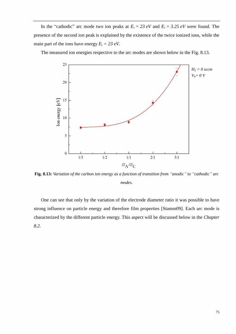
75
In the “cathodic” arc mode two ion peaks at Ei = 23 eV and Ei = 3.25 eV were found. The
presence of the second ion peak is explained by the existence of the twice ionized ions, while the
main part of the ions have energy Ei = 23 eV.
The measured ion energies respective to the arc modes are shown below in the Fig. 8.13.
Fig. 8.13: Variation of the carbon ion energy as a function of transition from “anodic” to “cathodic” arc
modes.
One can see that only by the variation of the electrode diameter ratio it was possible to have
strong influence on particle energy and therefore film properties [Stamm09]. Each arc mode is
characterized by the different particle energy. This aspect will be discussed below in the Chapter
8.2.
H2 = 0 sccm
Vb= 0 V
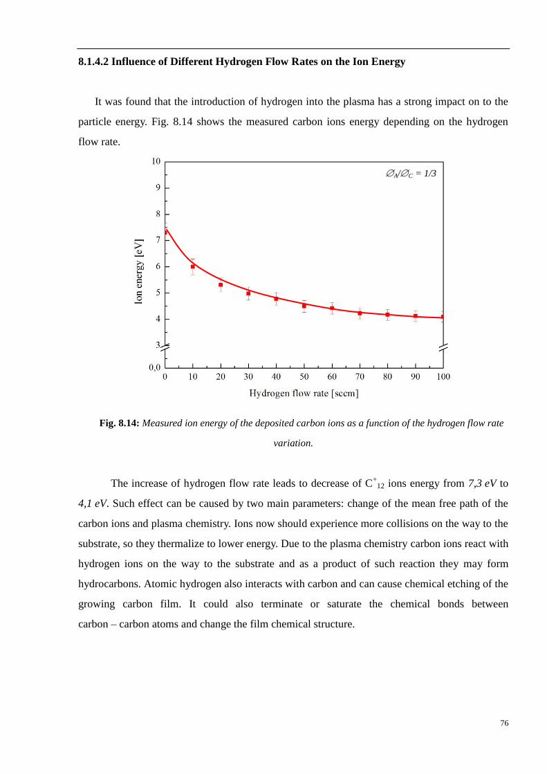
76
8.1.4.2 Influence of Different Hydrogen Flow Rates on the Ion Energy
It was found that the introduction of hydrogen into the plasma has a strong impact on to the
particle energy. Fig. 8.14 shows the measured carbon ions energy depending on the hydrogen
flow rate.
Fig. 8.14: Measured ion energy of the deposited carbon ions as a function of the hydrogen flow rate
variation.
The increase of hydrogen flow rate leads to decrease of C+
12 ions energy from 7,3 eV to
4,1 eV. Such effect can be caused by two main parameters: change of the mean free path of the
carbon ions and plasma chemistry. Ions now should experience more collisions on the way to the
substrate, so they thermalize to lower energy. Due to the plasma chemistry carbon ions react with
hydrogen ions on the way to the substrate and as a product of such reaction they may form
hydrocarbons. Atomic hydrogen also interacts with carbon and can cause chemical etching of the
growing carbon film. It could also terminate or saturate the chemical bonds between
carbon – carbon atoms and change the film chemical structure.
A/C = 1/3
77
8.1.4.3 Degree of Ionisation as a Function of Different Arc Modes
In order to control the film properties it is necessary to have a possibility to influence the
particles arriving to the growing film surface. Such control is only possible on charged particles
(ionized particles). The amount of ionized particles is the crucial parameter. So it means that the
more ionized particles there are in the incident flux to the surface, the more control on the
growing film properties we have.
The degree of ionisation Q – is the ratio of the amount of neutral particles to ionized ones,
which arrive to a certain surface through a certain period of time.
Ion flux density ji:
k
isati
eA
Ij ; (8.1)
Iisat – ion sturation current (ion current to the collector at 0 V),
e - elementary charge,
Ak – ion collector surface (0.1257 cm2), dk = 4 mm.
Using density of mass flux jm we could calculate the particle flux density jt, consisting of
neutrals and ions.
c
mt
m
jj . (8.2)
Density of mass flux jm is a mass growth per time t, t = 180 s was used; it corresponds
to the deposition time for every experiment.
sub
mtA
mj
; (8.3)
m – mass of the deposited film, Asub – coated substrate surface (8.0425 cm2).
Degree of ionisation:
100t
i
j
jQ %. (8.4)
Fig. 8.15 shows the degree of ionisation calculated according to the equation (8.4) for the
different arc modes.
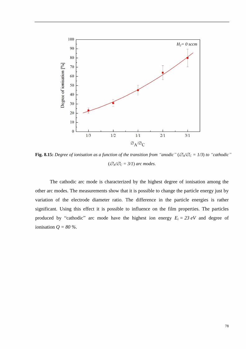
78
Fig. 8.15: Degree of ionisation as a function of the transition from “anodic” (A/C = 1/3) to “cathodic”
(A/C = 3/1) arc modes.
The cathodic arc mode is characterized by the highest degree of ionisation among the
other arc modes. The measurements show that it is possible to change the particle energy just by
variation of the electrode diameter ratio. The difference in the particle energies is rather
significant. Using this effect it is possible to influence on the film properties. The particles
produced by “cathodic” arc mode have the highest ion energy Ei = 23 eV and degree of
ionisation Q = 80 %.
H2= 0 sccm
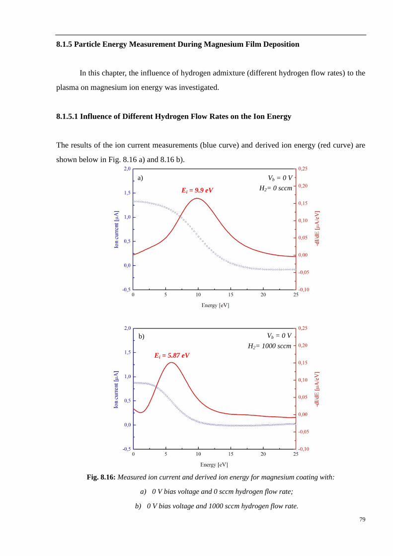
79
8.1.5 Particle Energy Measurement During Magnesium Film Deposition
In this chapter, the influence of hydrogen admixture (different hydrogen flow rates) to the
plasma on magnesium ion energy was investigated.
8.1.5.1 Influence of Different Hydrogen Flow Rates on the Ion Energy
The results of the ion current measurements (blue curve) and derived ion energy (red curve) are
shown below in Fig. 8.16 a) and 8.16 b).
Fig. 8.16: Measured ion current and derived ion energy for magnesium coating with:
a) 0 V bias voltage and 0 sccm hydrogen flow rate;
b) 0 V bias voltage and 1000 sccm hydrogen flow rate.
Ei = 5.87 eV
Ei = 9.9 eV
a)
b)
Vb = 0 V
H2= 0 sccm
Vb = 0 V
H2= 1000 sccm
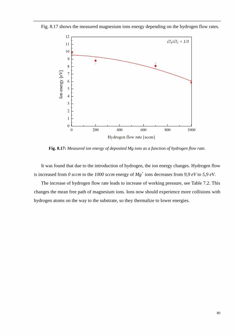
80
Fig. 8.17 shows the measured magnesium ions energy depending on the hydrogen flow rates.
Fig. 8.17: Measured ion energy of deposited Mg ions as a function of hydrogen flow rate.
It was found that due to the introduction of hydrogen, the ion energy changes. Hydrogen flow
is increased from 0 sccm to the 1000 sccm energy of Mg+ ions decreases from 9,9 eV to 5,9 eV.
The increase of hydrogen flow rate leads to increase of working pressure, see Table 7.2. This
changes the mean free path of magnesium ions. Ions now should experience more collisions with
hydrogen atoms on the way to the substrate, so they thermalize to lower energies.
A/C = 1/3
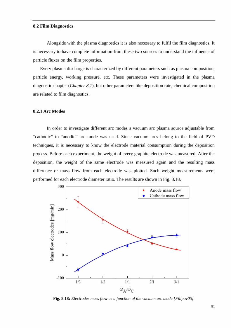
81
8.2 Film Diagnostics
Alongside with the plasma diagnostics it is also necessary to fulfil the film diagnostics. It
is necessary to have complete information from these two sources to understand the influence of
particle fluxes on the film properties.
Every plasma discharge is characterized by different parameters such as plasma composition,
particle energy, working pressure, etc. These parameters were investigated in the plasma
diagnostic chapter (Chapter 8.1), but other parameters like deposition rate, chemical composition
are related to film diagnostics.
8.2.1 Arc Modes
In order to investigate different arc modes a vacuum arc plasma source adjustable from
“cathodic” to “anodic” arc mode was used. Since vacuum arcs belong to the field of PVD
techniques, it is necessary to know the electrode material consumption during the deposition
process. Before each experiment, the weight of every graphite electrode was measured. After the
deposition, the weight of the same electrode was measured again and the resulting mass
difference or mass flow from each electrode was plotted. Such weight measurements were
performed for each electrode diameter ratio. The results are shown in Fig. 8.18.
Fig. 8.18: Electrodes mass flow as a function of the vacuum arc mode [Filipov05].
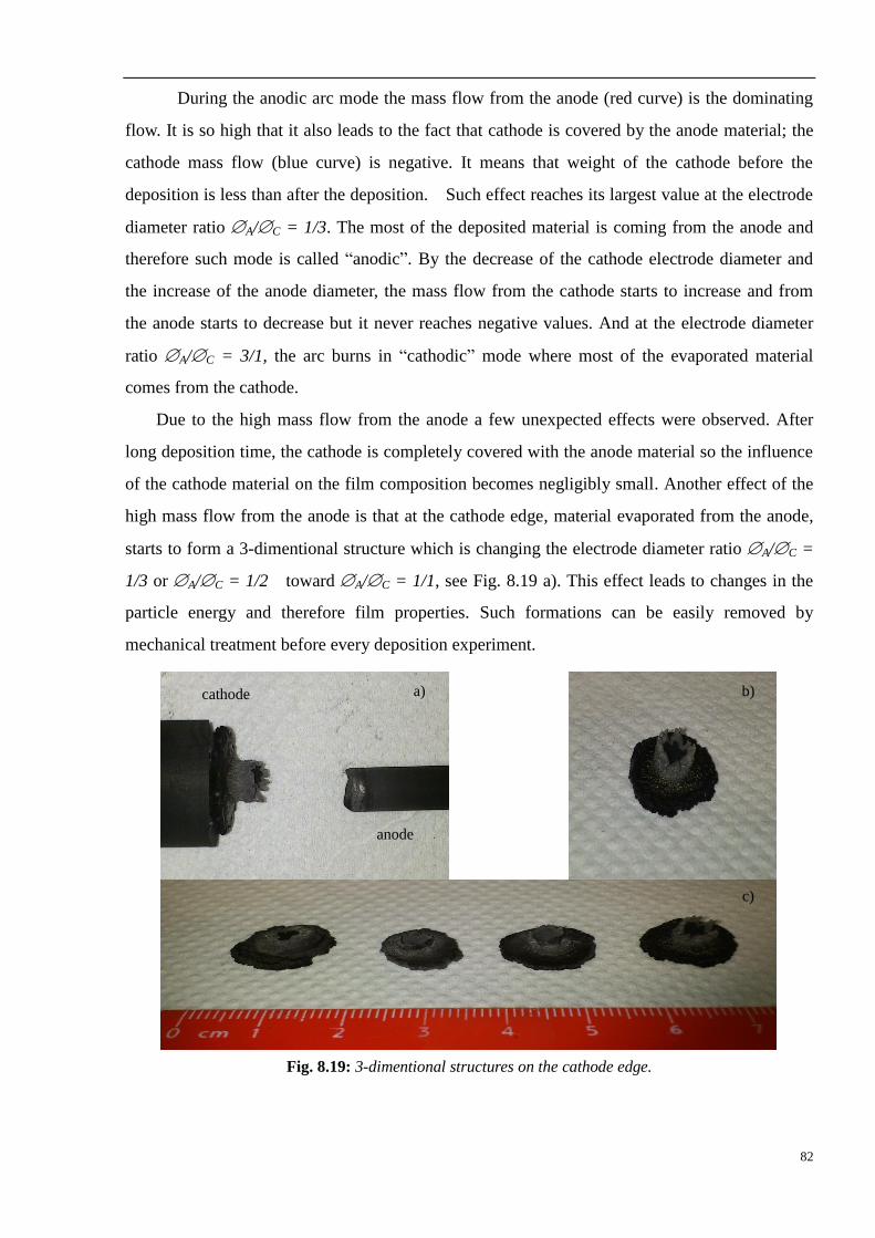
82
During the anodic arc mode the mass flow from the anode (red curve) is the dominating
flow. It is so high that it also leads to the fact that cathode is covered by the anode material; the
cathode mass flow (blue curve) is negative. It means that weight of the cathode before the
deposition is less than after the deposition. Such effect reaches its largest value at the electrode
diameter ratio A/C = 1/3. The most of the deposited material is coming from the anode and
therefore such mode is called “anodic”. By the decrease of the cathode electrode diameter and
the increase of the anode diameter, the mass flow from the cathode starts to increase and from
the anode starts to decrease but it never reaches negative values. And at the electrode diameter
ratio A/C = 3/1, the arc burns in “cathodic” mode where most of the evaporated material
comes from the cathode.
Due to the high mass flow from the anode a few unexpected effects were observed. After
long deposition time, the cathode is completely covered with the anode material so the influence
of the cathode material on the film composition becomes negligibly small. Another effect of the
high mass flow from the anode is that at the cathode edge, material evaporated from the anode,
starts to form a 3-dimentional structure which is changing the electrode diameter ratio A/C =
1/3 or A/C = 1/2 toward A/C = 1/1, see Fig. 8.19 a). This effect leads to changes in the
particle energy and therefore film properties. Such formations can be easily removed by
mechanical treatment before every deposition experiment.
Fig. 8.19: 3-dimentional structures on the cathode edge.
a) b)
anode
cathode
c)
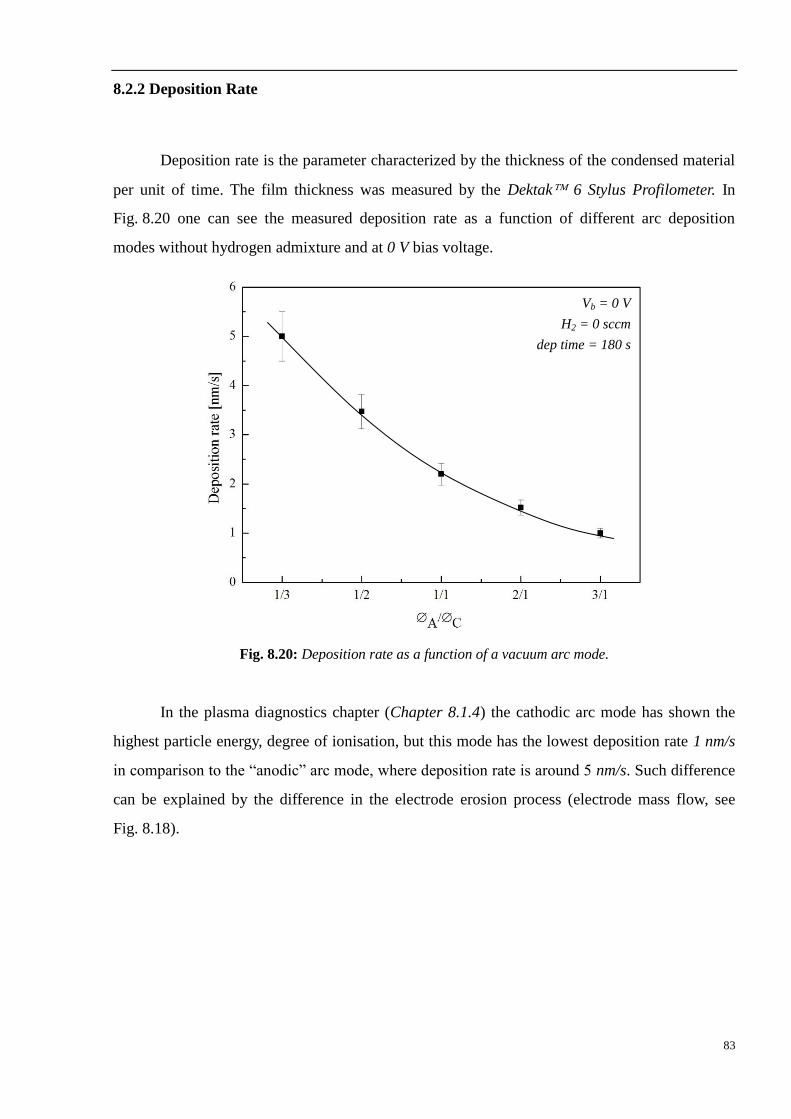
83
8.2.2 Deposition Rate
Deposition rate is the parameter characterized by the thickness of the condensed material
per unit of time. The film thickness was measured by the Dektak 6 Stylus Profilometer. In
Fig. 8.20 one can see the measured deposition rate as a function of different arc deposition
modes without hydrogen admixture and at 0 V bias voltage.
Fig. 8.20: Deposition rate as a function of a vacuum arc mode.
In the plasma diagnostics chapter (Chapter 8.1.4) the cathodic arc mode has shown the
highest particle energy, degree of ionisation, but this mode has the lowest deposition rate 1 nm/s
in comparison to the “anodic” arc mode, where deposition rate is around 5 nm/s. Such difference
can be explained by the difference in the electrode erosion process (electrode mass flow, see
Fig. 8.18).
Vb = 0 V
H2 = 0 sccm
dep time = 180 s
84
8.2.3 Structural Properties
One of the main parameter defining the thin film application area is their structural
properties. Especially this fact is very important for DLC films. As mentioned above DLC is a
whole class of carbon based coatings, which properties are widely varied according to their
structure. But these properties are mostly determined by the plasma deposition process and the
particle energy. There are several ways to influence the particle energy in the plasma: first –
plasma discharge itself (by selection of an appropriate discharge type [Raizer01]), second –
biasing the substrate, third – selecting working gas. In this chapter the influence of particle
energy onto structural film properties will be shown.
8.2.3.1 Film Morphology
The film morphology is the first and an easily measured parameter which can
immediately provide information about the influence of the deposition parameters onto film
properties and its further sphere of application. The films with flat and smooth surface can be
used as protective coatings, where the friction plays an important role and should be as small as
possible. In turn films with high surface roughness can be used as an intermediate layer to
improve adhesion between this film and subsequent one (sandwich structure).
For thin film analysis microscopic methods (SEM and AFM) are used to investigate film
morphology and surface roughness. Optical microscopy is no longer the research routine in thin
films technology due to the small film thickness and low resolution of an optical microscope.
To investigate film morphology a scanning electron microscope ESEM Quanta 400 FEG
by FEI Company was used. The pictures were taken with 15 kV acceleration voltage and with
different magnifications of 20000 and 100000 times.
For further film morphology investigation it was necessary to use AFM technique. This
method is alongside with SEM and can provide us very detailed information about surface
roughness. For the surface roughness evaluation was used AFM Veeco Dimension 3100
microscope. AFM was operated in the non-contact tapping mode. The square area of
5 m 5 m typical for AFM measurements was used.
85
8.2.3.1.1 Influence of Different Arc Modes on Film Morphology
At the beginning, the influence of transition from cathodic to anodic arc mode on the
DLC film morphology was investigated. As it was described above the films were deposited onto
double-side polished 2 cm 1 cm Si 100 wafers. The transition from the “cathodic” to the
“anodic” arc mode was performed by variation of the electrode diameter ratio A/C. During the
experiments no macroparticle filters were used. In the case when electrode ratio is A/C = 3/1
arc operates in “cathodic” mode, when ratio is A/C = 1/3 it was the “anodic mode”. The terms
“anodic” or “cathodic” are used to describe which electrode is active and emits more particles.
For each experiment the certain anode to cathode electrode diameter ratio was used, with the
same deposition parameters, without working gas and bias voltage, as shown in a Table 8.4.
Table 8.4: Deposition parameters during the cathodic to anodic arc transition experiment.
Working pressure 5 10-6
mbar
Deposition time 120 s
Graphite electrodes RW 003, quality RW
A/C 3/1, 2/1, 1/1, 1/2, 1/3
Typical SEM pictures of the deposited films are shown in Fig. 8.21. These images
demonstrate the film morphology of the deposited DLC films by transition from “cathodic” arc
mode to the “anodic” one.
In Fig. 8.21 a) and b) one can see the films deposited which were produced with an anode
to cathode diameter ratio A/C = 3/1, in which the arc is running in a pure “cathodic” mode.
This mode is characterized by low deposition rate (see Fig.8.20 in Chapter 8.2.2) and high
macroparticle content in the films deposited. SEM image a) was taken with magnification of
20000 and image b) with magnification of 100000 times. Using the SEM images it was possible
to evaluate macroparticle size distribution typical for this mode, which lies in a range from
100 nm to 600 nm.
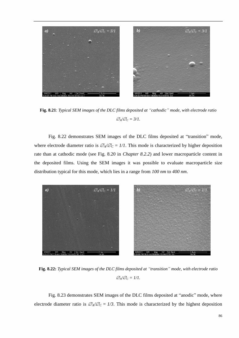
86
Fig. 8.21: Typical SEM images of the DLC films deposited at “cathodic” mode, with electrode ratio
A/C = 3/1.
Fig. 8.22 demonstrates SEM images of the DLC films deposited at “transition” mode,
where electrode diameter ratio is A/C = 1/1. This mode is characterized by higher deposition
rate than at cathodic mode (see Fig. 8.20 in Chapter 8.2.2) and lower macroparticle content in
the deposited films. Using the SEM images it was possible to evaluate macroparticle size
distribution typical for this mode, which lies in a range from 100 nm to 400 nm.
Fig. 8.22: Typical SEM images of the DLC films deposited at “transition” mode, with electrode ratio
A/C = 1/1.
Fig. 8.23 demonstrates SEM images of the DLC films deposited at “anodic” mode, where
electrode diameter ratio is A/C = 1/3. This mode is characterized by the highest deposition
a) b)
a) b)
A/C = 3/1 A/C = 3/1
A/C = 1/1 A/C = 1/1
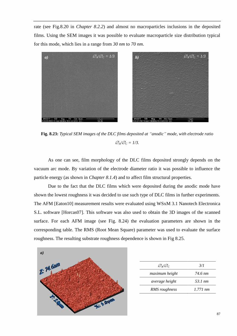
87
rate (see Fig.8.20 in Chapter 8.2.2) and almost no macroparticles inclusions in the deposited
films. Using the SEM images it was possible to evaluate macroparticle size distribution typical
for this mode, which lies in a range from 30 nm to 70 nm.
Fig. 8.23: Typical SEM images of the DLC films deposited at “anodic” mode, with electrode ratio
A/C = 1/3.
As one can see, film morphology of the DLC films deposited strongly depends on the
vacuum arc mode. By variation of the electrode diameter ratio it was possible to influence the
particle energy (as shown in Chapter 8.1.4) and to affect film structural properties.
Due to the fact that the DLC films which were deposited during the anodic mode have
shown the lowest roughness it was decided to use such type of DLC films in further experiments.
The AFM [Eaton10] measurement results were evaluated using WSxM 3.1 Nanotech Electronica
S.L. software [Horcas07]. This software was also used to obtain the 3D images of the scanned
surface. For each AFM image (see Fig. 8.24) the evaluation parameters are shown in the
corresponding table. The RMS (Root Mean Square) parameter was used to evaluate the surface
roughness. The resulting substrate roughness dependence is shown in Fig 8.25.
a) b)
a)
A/C 3/1
maximum height 74.6 nm
average height 53.1 nm
RMS roughness 1.771 nm
A/C = 1/3 A/C = 1/3
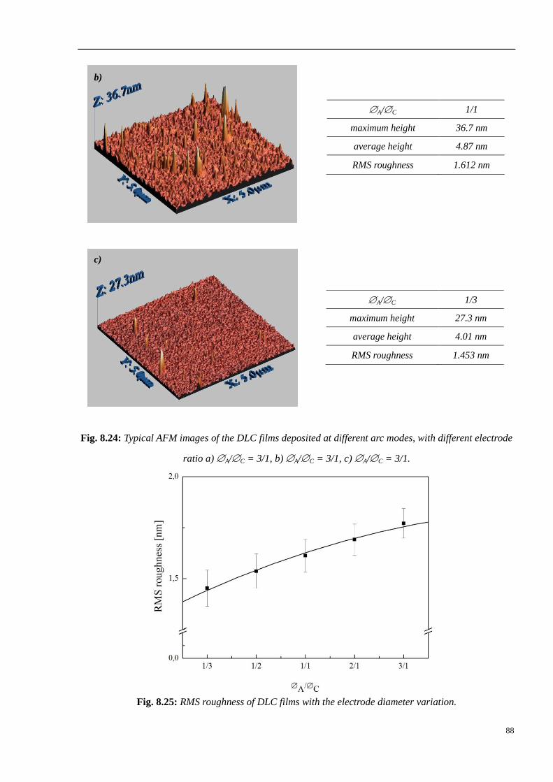
88
Fig. 8.24: Typical AFM images of the DLC films deposited at different arc modes, with different electrode
ratio a) A/C = 3/1, b) A/C = 3/1, c) A/C = 3/1.
Fig. 8.25: RMS roughness of DLC films with the electrode diameter variation.
A/C 1/1
maximum height 36.7 nm
average height 4.87 nm
RMS roughness 1.612 nm
A/C 1/3
maximum height 27.3 nm
average height 4.01 nm
RMS roughness 1.453 nm
b)
c)
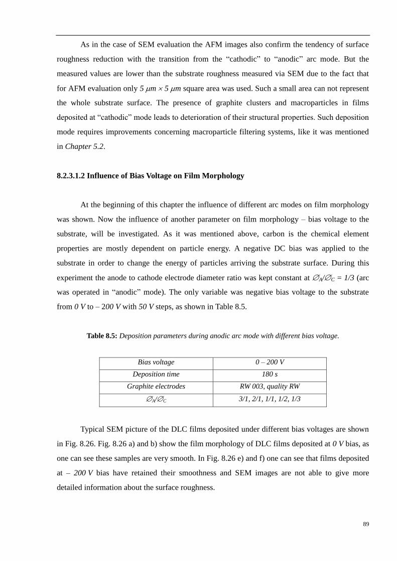
89
As in the case of SEM evaluation the AFM images also confirm the tendency of surface
roughness reduction with the transition from the “cathodic” to “anodic” arc mode. But the
measured values are lower than the substrate roughness measured via SEM due to the fact that
for AFM evaluation only 5 m 5 m square area was used. Such a small area can not represent
the whole substrate surface. The presence of graphite clusters and macroparticles in films
deposited at “cathodic” mode leads to deterioration of their structural properties. Such deposition
mode requires improvements concerning macroparticle filtering systems, like it was mentioned
in Chapter 5.2.
8.2.3.1.2 Influence of Bias Voltage on Film Morphology
At the beginning of this chapter the influence of different arc modes on film morphology
was shown. Now the influence of another parameter on film morphology – bias voltage to the
substrate, will be investigated. As it was mentioned above, carbon is the chemical element
properties are mostly dependent on particle energy. A negative DC bias was applied to the
substrate in order to change the energy of particles arriving the substrate surface. During this
experiment the anode to cathode electrode diameter ratio was kept constant at A/C = 1/3 (arc
was operated in “anodic” mode). The only variable was negative bias voltage to the substrate
from 0 V to – 200 V with 50 V steps, as shown in Table 8.5.
Table 8.5: Deposition parameters during anodic arc mode with different bias voltage.
Bias voltage 0 – 200 V
Deposition time 180 s
Graphite electrodes RW 003, quality RW
A/C 3/1, 2/1, 1/1, 1/2, 1/3
Typical SEM picture of the DLC films deposited under different bias voltages are shown
in Fig. 8.26. Fig. 8.26 a) and b) show the film morphology of DLC films deposited at 0 V bias, as
one can see these samples are very smooth. In Fig. 8.26 e) and f) one can see that films deposited
at – 200 V bias have retained their smoothness and SEM images are not able to give more
detailed information about the surface roughness.
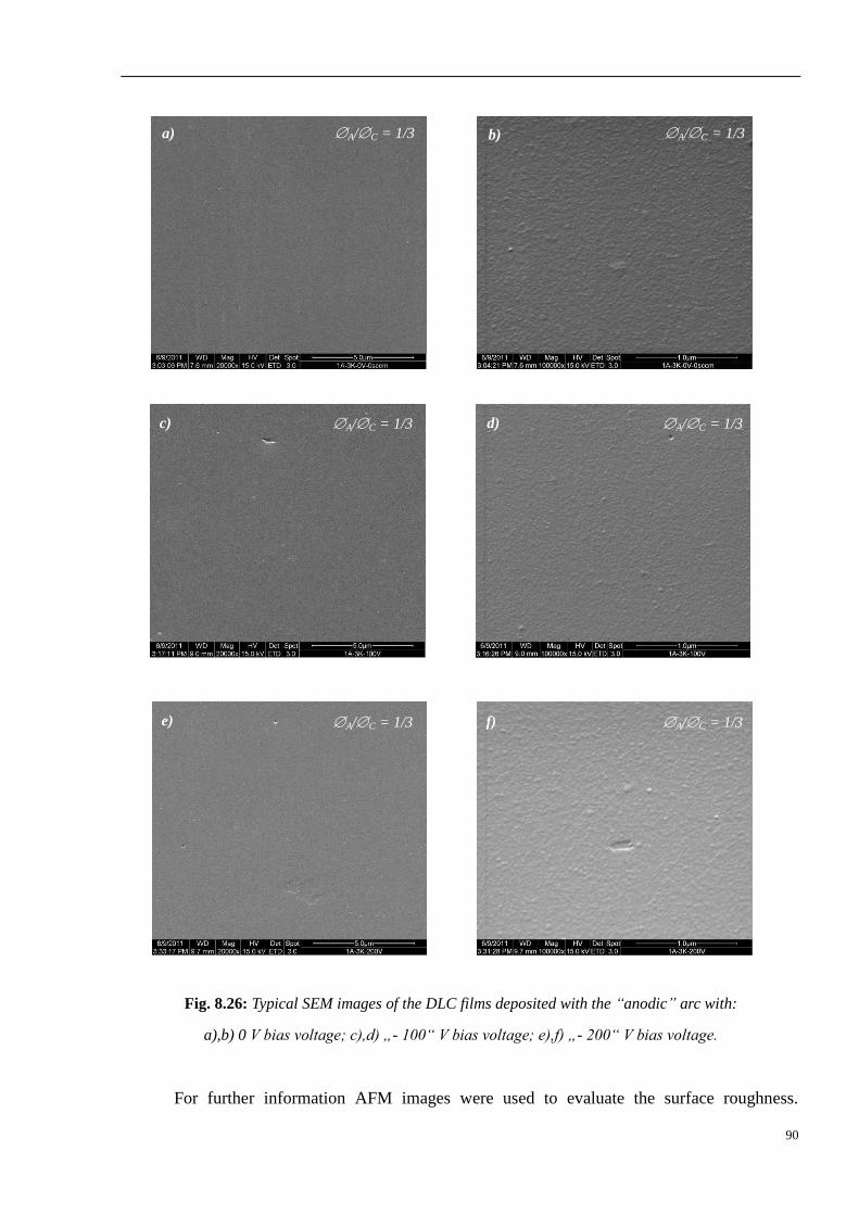
90
Fig. 8.26: Typical SEM images of the DLC films deposited with the “anodic” arc with:
a),b) 0 V bias voltage; c),d) „- 100“ V bias voltage; e),f) „- 200“ V bias voltage.
For further information AFM images were used to evaluate the surface roughness.
a) b)
c) d)
e) f)
A/C = 1/3 A/C = 1/3
A/C = 1/3 A/C = 1/3
A/C = 1/3 A/C = 1/3
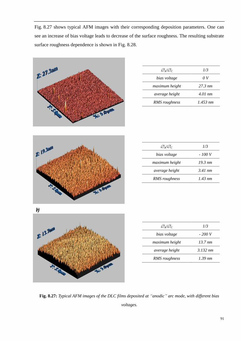
91
Fig. 8.27 shows typical AFM images with their corresponding deposition parameters. One can
see an increase of bias voltage leads to decrease of the surface roughness. The resulting substrate
surface roughness dependence is shown in Fig. 8.28.
Fig. 8.27: Typical AFM images of the DLC films deposited at “anodic” arc mode, with different bias
voltages.
A/C 1/3
bias voltage 0 V
maximum height 27.3 nm
average height 4.01 nm
RMS roughness 1.453 nm
a)
A/C 1/3
bias voltage - 100 V
maximum height 19.3 nm
average height 3.41 nm
RMS roughness 1.43 nm
b)
A/C 1/3
bias voltage - 200 V
maximum height 13.7 nm
average height 3.132 nm
RMS roughness 1.39 nm
c)
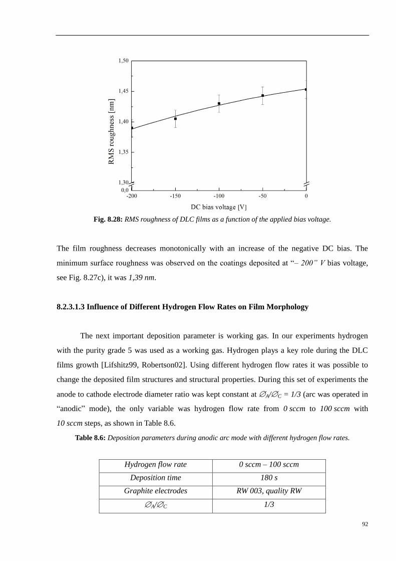
92
Fig. 8.28: RMS roughness of DLC films as a function of the applied bias voltage.
The film roughness decreases monotonically with an increase of the negative DC bias. The
minimum surface roughness was observed on the coatings deposited at “– 200” V bias voltage,
see Fig. 8.27c), it was 1,39 nm.
8.2.3.1.3 Influence of Different Hydrogen Flow Rates on Film Morphology
The next important deposition parameter is working gas. In our experiments hydrogen
with the purity grade 5 was used as a working gas. Hydrogen plays a key role during the DLC
films growth [Lifshitz99, Robertson02]. Using different hydrogen flow rates it was possible to
change the deposited film structures and structural properties. During this set of experiments the
anode to cathode electrode diameter ratio was kept constant at A/C = 1/3 (arc was operated in
“anodic” mode), the only variable was hydrogen flow rate from 0 sccm to 100 sccm with
10 sccm steps, as shown in Table 8.6.
Table 8.6: Deposition parameters during anodic arc mode with different hydrogen flow rates.
Hydrogen flow rate 0 sccm – 100 sccm
Deposition time 180 s
Graphite electrodes RW 003, quality RW
A/C 1/3
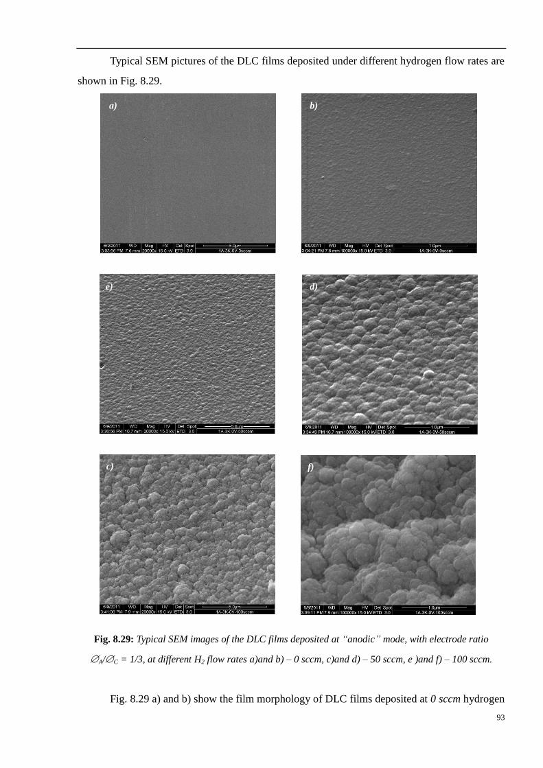
93
Typical SEM pictures of the DLC films deposited under different hydrogen flow rates are
shown in Fig. 8.29.
Fig. 8.29: Typical SEM images of the DLC films deposited at “anodic” mode, with electrode ratio
A/C = 1/3, at different H2 flow rates a)and b) – 0 sccm, c)and d) – 50 sccm, e )and f) – 100 sccm.
Fig. 8.29 a) and b) show the film morphology of DLC films deposited at 0 sccm hydrogen
e)
f) c)
a)
d)
b)
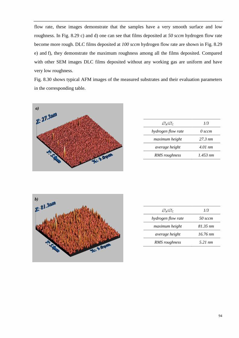
94
flow rate, these images demonstrate that the samples have a very smooth surface and low
roughness. In Fig. 8.29 c) and d) one can see that films deposited at 50 sccm hydrogen flow rate
become more rough. DLC films deposited at 100 sccm hydrogen flow rate are shown in Fig. 8.29
e) and f), they demonstrate the maximum roughness among all the films deposited. Compared
with other SEM images DLC films deposited without any working gas are uniform and have
very low roughness.
Fig. 8.30 shows typical AFM images of the measured substrates and their evaluation parameters
in the corresponding table.
A/C 1/3
hydrogen flow rate 0 sccm
maximum height 27.3 nm
average height 4.01 nm
RMS roughness 1.453 nm
A/C 1/3
hydrogen flow rate 50 sccm
maximum height 81.35 nm
average height 16.76 nm
RMS roughness 5.21 nm
a)
b)
a)
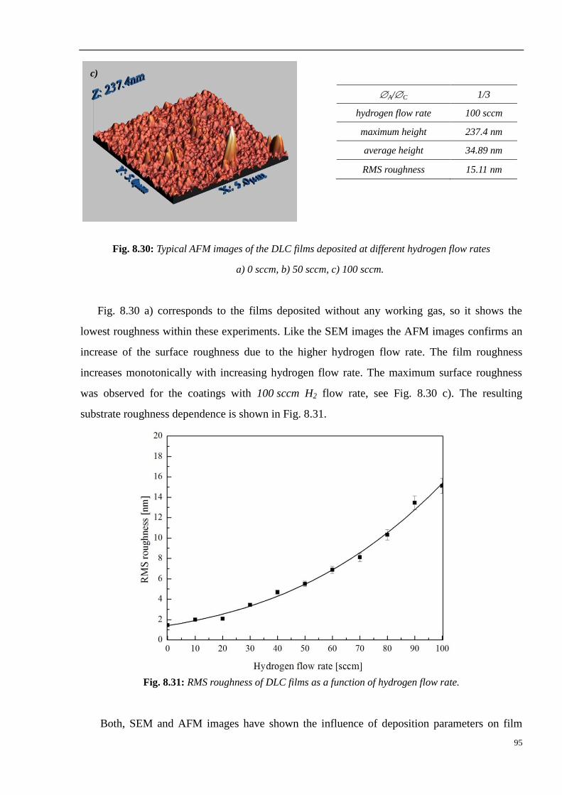
95
Fig. 8.30: Typical AFM images of the DLC films deposited at different hydrogen flow rates
a) 0 sccm, b) 50 sccm, c) 100 sccm.
Fig. 8.30 a) corresponds to the films deposited without any working gas, so it shows the
lowest roughness within these experiments. Like the SEM images the AFM images confirms an
increase of the surface roughness due to the higher hydrogen flow rate. The film roughness
increases monotonically with increasing hydrogen flow rate. The maximum surface roughness
was observed for the coatings with 100 sccm H2 flow rate, see Fig. 8.30 c). The resulting
substrate roughness dependence is shown in Fig. 8.31.
Fig. 8.31: RMS roughness of DLC films as a function of hydrogen flow rate.
Both, SEM and AFM images have shown the influence of deposition parameters on film
A/C 1/3
hydrogen flow rate 100 sccm
maximum height 237.4 nm
average height 34.89 nm
RMS roughness 15.11 nm
c)
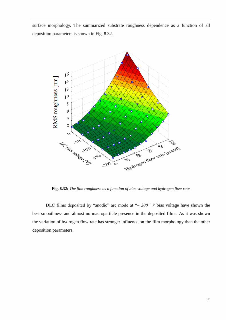
96
surface morphology. The summarized substrate roughness dependence as a function of all
deposition parameters is shown in Fig. 8.32.
Fig. 8.32: The film roughness as a function of bias voltage and hydrogen flow rate.
DLC films deposited by “anodic” arc mode at “– 200” V bias voltage have shown the
best smoothness and almost no macroparticle presence in the deposited films. As it was shown
the variation of hydrogen flow rate has stronger influence on the film morphology than the other
deposition parameters.
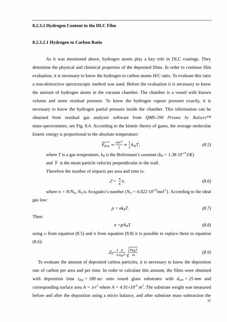
97
8.2.3.2 Hydrogen Content in the DLC Film
8.2.3.2.1 Hydrogen to Carbon Ratio
As it was mentioned above, hydrogen atoms play a key role in DLC coatings. They
determine the physical and chemical properties of the deposited films. In order to continue film
evaluation, it is necessary to know the hydrogen to carbon atoms H/C ratio. To evaluate this ratio
a non-destructive spectroscopic method was used. Before the evaluation it is necessary to know
the amount of hydrogen atoms in the vacuum chamber. The chamber is a vessel with known
volume and some residual pressure. To know the hydrogen vapour pressure exactly, it is
necessary to know the hydrogen partial pressure inside the chamber. This information can be
obtained from residual gas analyzer software from QMS-200 Prisma by Balzers™
mass-spectrometer, see Fig. 8.4. According to the kinetic theory of gases, the average molecular
kinetic energy is proportional to the absolute temperature:
𝐸𝑘𝑖𝑛 =𝑚𝑣2
2=
3
2𝑘𝐵𝑇, (8.5)
where T is a gas temperature, kB is the Boltzmann’s constant (kB = 1.3810-23
J/K)
and 𝑣 is the mean particle velocity perpendicular to the wall.
Therefore the number of impacts per area and time is:
= 𝑛
6𝑣, (8.6)
where n = N/NA, NA is Avogadro’s number (NA = 6.02210-23
mol-1
). According to the ideal
gas law:
p = nkBT. (8.7)
Then:
n =p/kBT (8.8)
using from equation (8.5) and n from equation (8.8) it is possible to replace them in equation
(8.6):
H=1
6
𝑝
𝑘𝐵𝑇√
3𝑘𝐵𝑇
𝑚 (8.9)
To evaluate the amount of deposited carbon particles, it is necessary to know the deposition
rate of carbon per area and per time. In order to calculate this amount, the films were obtained
with deposition time tdep = 180 sec onto round glass substrates with dsub = 25 mm and
corresponding surface area A = r2 where A = 4.9110
-4 m
2. The substrate weight was measured
before and after the deposition using a micro balance, and after substrate mass subtraction the
98
mass of the deposited film – m was obtained.
It is known that:
1 Mol C 12g (8.10).
For a single carbon atom:
mC = 12
6.022×10⁻²³ g = 20.106 10
-27 kg (8.11)
When the deposited mass is known one can calculate the amount of the deposited carbon
atoms at the whole substrate area. Then, dividing it by the deposition time and surface area, one
can calculate the amount of deposited carbon atoms per area per second.
In order to estimate the number of carbon atoms in the deposited film, it was necessary to
make the assumption that deposited film contains only carbon atom. But this assumption is
inaccurate due to the fact that the deposited film contains not only carbon atoms but also
hydrogen atoms. In fact, the deposited films contain some amount of hydrogen atoms in addition
to carbon atoms with mass mC = 12 amu when the hydrogen atom mass mH is only 1 amu. Even
if one assume that in deposited film there is an equal amount of carbon and hydrogen atoms the
error in the calculations is still less than 10%.
The next assumption is that the adhesion coefficient of all particles coming to the surface is equal
to one.
In the following Table 8.7, the calculated hydrogen to carbon atoms ratio for different
films depending on the deposition parameters is given:
Table 8.7 Calculated hydrogen to carbon atoms ratio
Bias voltage [V] 0 100 200 100 200 0 100
H2 flow rate [sccm] 10 10 10 50 50 80 80
H2 part. pres. [Pa] 0.41 0.37 0.39 2.52 2.50 9.97 10
Deposition time [s] 180 180 180 180 180 180 180
Mass deposited [kg] 1.0410-6
1.0610-6
9.0310-7
1.4410-6
1.0910-6
2.0210-6
1.3510-6
Film thickness [m] 1.0910-6
9.6310-7
8.8610-7
1.4410-6
1.1610-6
2.4710-6
1.4410-6
ZH [at m-2 s
-1] 4.5010
22 4.0610
22 4.2810
22 2.7710
23 2.7410
23 1.0910
24 1.1010
24
ZC [at m-2 s
-1] 5.8810
23 5.9810
22 5.0810
22 8.1310
23 6.1210
23 1.1410
24 7.6010
24
ZH/(ZH+ZC) [%] 7 6 8 25 31 49 59
As one can see the concentration of hydrogen atoms in the deposited films is proportional
to the hydrogen flow rate and also depends on the applied bias voltage. These results are shown
in Fig. 8.33.
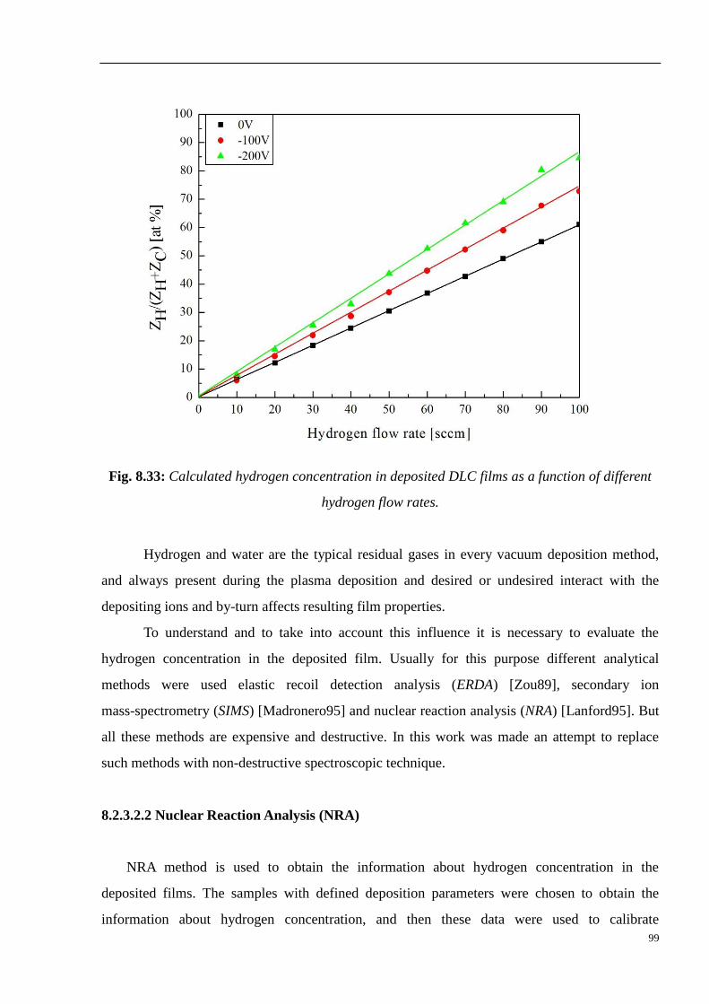
99
Fig. 8.33: Calculated hydrogen concentration in deposited DLC films as a function of different
hydrogen flow rates.
Hydrogen and water are the typical residual gases in every vacuum deposition method,
and always present during the plasma deposition and desired or undesired interact with the
depositing ions and by-turn affects resulting film properties.
To understand and to take into account this influence it is necessary to evaluate the
hydrogen concentration in the deposited film. Usually for this purpose different analytical
methods were used elastic recoil detection analysis (ERDA) [Zou89], secondary ion
mass-spectrometry (SIMS) [Madronero95] and nuclear reaction analysis (NRA) [Lanford95]. But
all these methods are expensive and destructive. In this work was made an attempt to replace
such methods with non-destructive spectroscopic technique.
8.2.3.2.2 Nuclear Reaction Analysis (NRA)
NRA method is used to obtain the information about hydrogen concentration in the
deposited films. The samples with defined deposition parameters were chosen to obtain the
information about hydrogen concentration, and then these data were used to calibrate
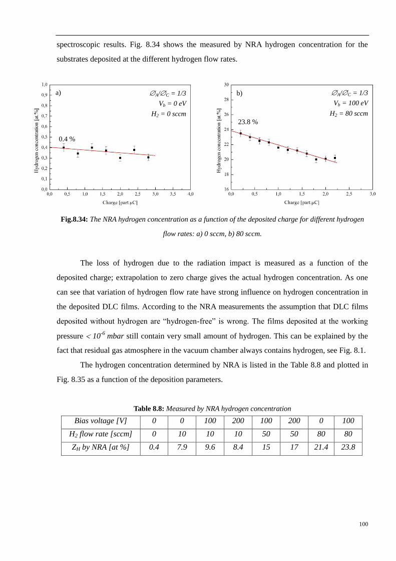
100
spectroscopic results. Fig. 8.34 shows the measured by NRA hydrogen concentration for the
substrates deposited at the different hydrogen flow rates.
Fig.8.34: The NRA hydrogen concentration as a function of the deposited charge for different hydrogen
flow rates: a) 0 sccm, b) 80 sccm.
The loss of hydrogen due to the radiation impact is measured as a function of the
deposited charge; extrapolation to zero charge gives the actual hydrogen concentration. As one
can see that variation of hydrogen flow rate have strong influence on hydrogen concentration in
the deposited DLC films. According to the NRA measurements the assumption that DLC films
deposited without hydrogen are “hydrogen-free” is wrong. The films deposited at the working
pressure 10-6
mbar still contain very small amount of hydrogen. This can be explained by the
fact that residual gas atmosphere in the vacuum chamber always contains hydrogen, see Fig. 8.1.
The hydrogen concentration determined by NRA is listed in the Table 8.8 and plotted in
Fig. 8.35 as a function of the deposition parameters.
Table 8.8: Measured by NRA hydrogen concentration
Bias voltage [V] 0 0 100 200 100 200 0 100
H2 flow rate [sccm] 0 10 10 10 50 50 80 80
ZH by NRA [at %] 0.4 7.9 9.6 8.4 15 17 21.4 23.8
0.4 %
23.8 %
A/C = 1/3
Vb = 0 eV
H2 = 0 sccm
A/C = 1/3
Vb = 100 eV
H2 = 80 sccm
a) b)
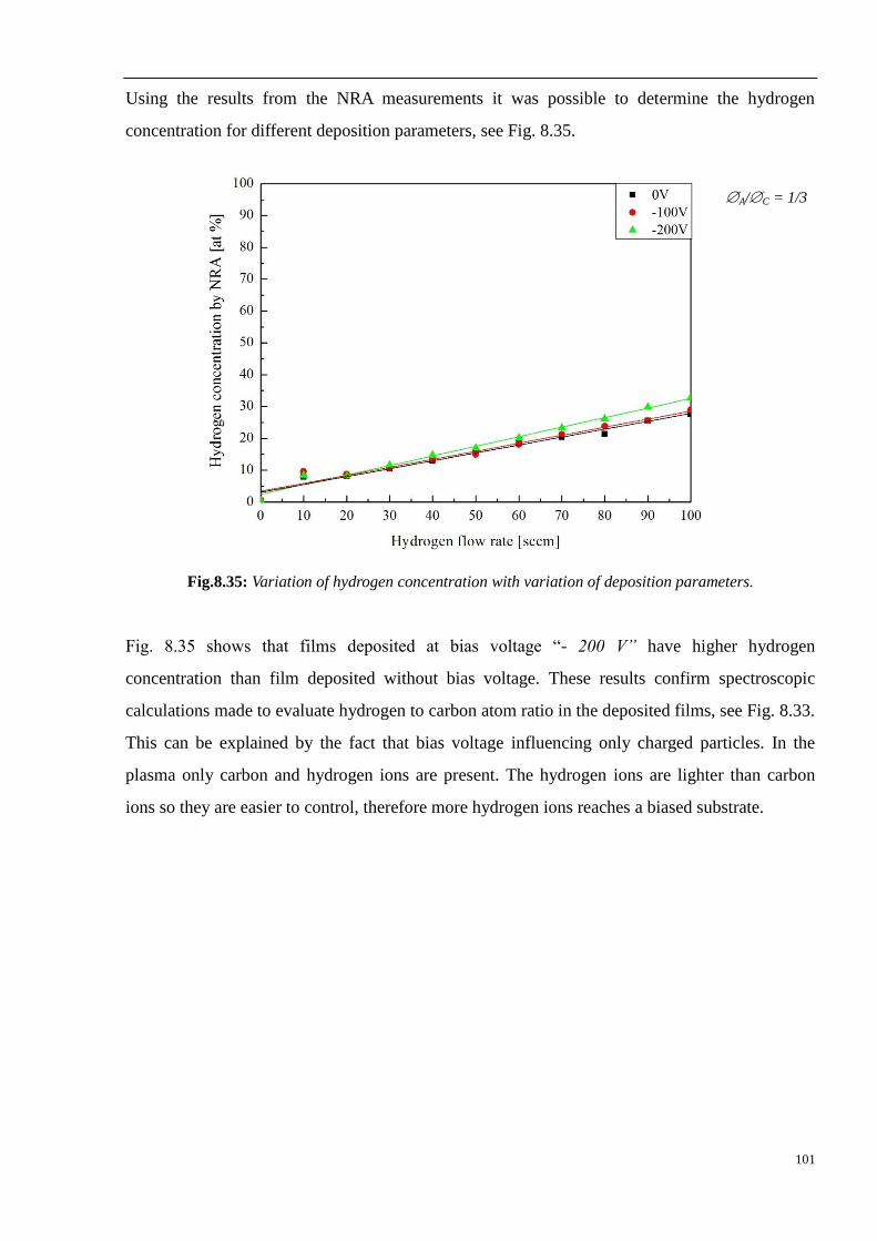
101
Using the results from the NRA measurements it was possible to determine the hydrogen
concentration for different deposition parameters, see Fig. 8.35.
Fig.8.35: Variation of hydrogen concentration with variation of deposition parameters.
Fig. 8.35 shows that films deposited at bias voltage “- 200 V” have higher hydrogen
concentration than film deposited without bias voltage. These results confirm spectroscopic
calculations made to evaluate hydrogen to carbon atom ratio in the deposited films, see Fig. 8.33.
This can be explained by the fact that bias voltage influencing only charged particles. In the
plasma only carbon and hydrogen ions are present. The hydrogen ions are lighter than carbon
ions so they are easier to control, therefore more hydrogen ions reaches a biased substrate.
A/C = 1/3
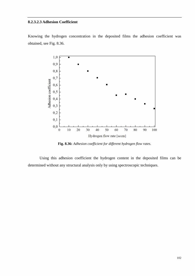
102
8.2.3.2.3 Adhesion Coefficient
Knowing the hydrogen concentration in the deposited films the adhesion coefficient was
obtained, see Fig. 8.36.
Fig. 8.36: Adhesion coefficient for different hydrogen flow rates.
Using this adhesion coefficient the hydrogen content in the deposited films can be
determined without any structural analysis only by using spectroscopic techniques.
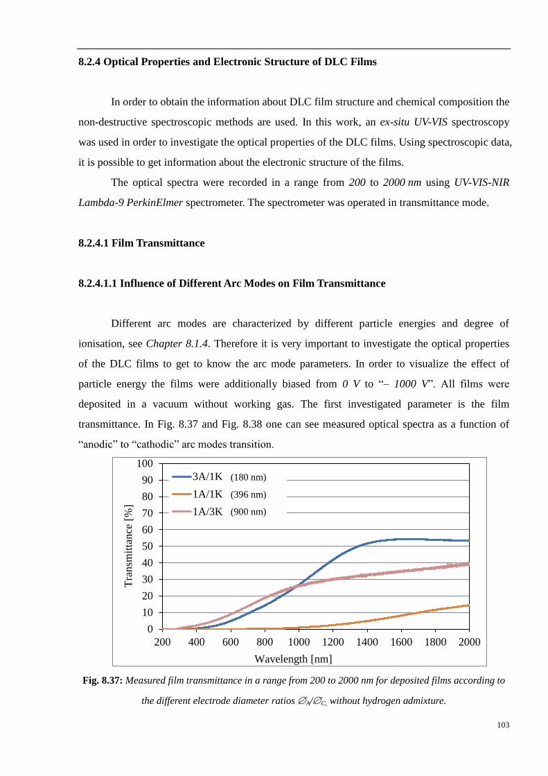
103
8.2.4 Optical Properties and Electronic Structure of DLC Films
In order to obtain the information about DLC film structure and chemical composition the
non-destructive spectroscopic methods are used. In this work, an ex-situ UV-VIS spectroscopy
was used in order to investigate the optical properties of the DLC films. Using spectroscopic data,
it is possible to get information about the electronic structure of the films.
The optical spectra were recorded in a range from 200 to 2000 nm using UV-VIS-NIR
Lambda-9 PerkinElmer spectrometer. The spectrometer was operated in transmittance mode.
8.2.4.1 Film Transmittance
8.2.4.1.1 Influence of Different Arc Modes on Film Transmittance
Different arc modes are characterized by different particle energies and degree of
ionisation, see Chapter 8.1.4. Therefore it is very important to investigate the optical properties
of the DLC films to get to know the arc mode parameters. In order to visualize the effect of
particle energy the films were additionally biased from 0 V to “– 1000 V”. All films were
deposited in a vacuum without working gas. The first investigated parameter is the film
transmittance. In Fig. 8.37 and Fig. 8.38 one can see measured optical spectra as a function of
“anodic” to “cathodic” arc modes transition.
Fig. 8.37: Measured film transmittance in a range from 200 to 2000 nm for deposited films according to
the different electrode diameter ratios A/C, without hydrogen admixture.
0
10
20
30
40
50
60
70
80
90
100
200 400 600 800 1000 1200 1400 1600 1800 2000
3A/1K
1A/1K
1A/3K
Wavelength [nm]
Tra
nsm
itta
nce
[%
]
(180 nm)
(396 nm)
(900 nm)
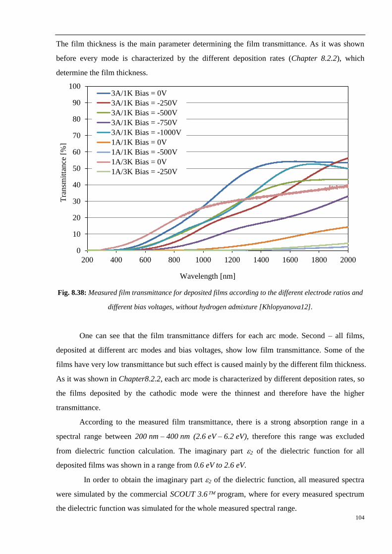
104
The film thickness is the main parameter determining the film transmittance. As it was shown
before every mode is characterized by the different deposition rates (Chapter 8.2.2), which
determine the film thickness.
Fig. 8.38: Measured film transmittance for deposited films according to the different electrode ratios and
different bias voltages, without hydrogen admixture [Khlopyanova12].
One can see that the film transmittance differs for each arc mode. Second – all films,
deposited at different arc modes and bias voltages, show low film transmittance. Some of the
films have very low transmittance but such effect is caused mainly by the different film thickness.
As it was shown in Chapter8.2.2, each arc mode is characterized by different deposition rates, so
the films deposited by the cathodic mode were the thinnest and therefore have the higher
transmittance.
According to the measured film transmittance, there is a strong absorption range in a
spectral range between 200 nm – 400 nm (2.6 eV – 6.2 eV), therefore this range was excluded
from dielectric function calculation. The imaginary part 2 of the dielectric function for all
deposited films was shown in a range from 0.6 eV to 2.6 eV.
In order to obtain the imaginary part 2 of the dielectric function, all measured spectra
were simulated by the commercial SCOUT 3.6 program, where for every measured spectrum
the dielectric function was simulated for the whole measured spectral range.
0
10
20
30
40
50
60
70
80
90
100
200 400 600 800 1000 1200 1400 1600 1800 2000
3A/1K Bias = 0V
3A/1K Bias = -250V
3A/1K Bias = -500V
3A/1K Bias = -750V
3A/1K Bias = -1000V
1A/1K Bias = 0V
1A/1K Bias = -500V
1A/3K Bias = 0V
1A/3K Bias = -250V
Wavelength [nm]
Tra
nsm
itta
nce
[%
]
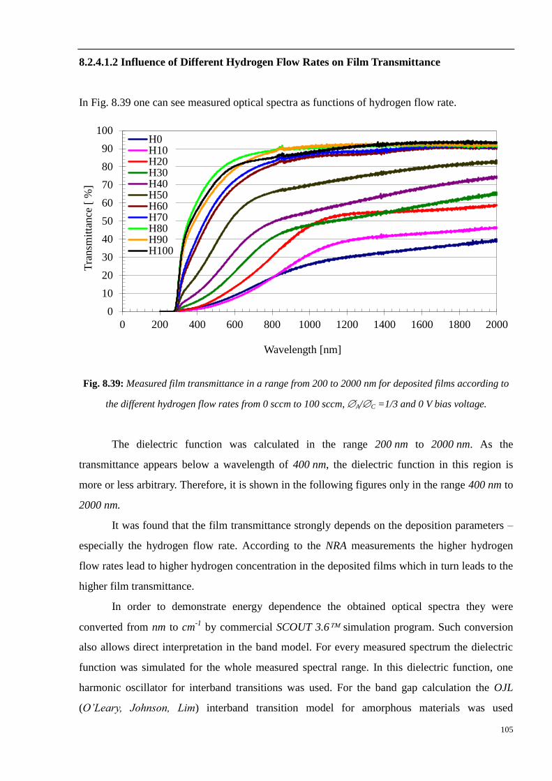
105
8.2.4.1.2 Influence of Different Hydrogen Flow Rates on Film Transmittance
In Fig. 8.39 one can see measured optical spectra as functions of hydrogen flow rate.
Fig. 8.39: Measured film transmittance in a range from 200 to 2000 nm for deposited films according to
the different hydrogen flow rates from 0 sccm to 100 sccm, A/C =1/3 and 0 V bias voltage.
The dielectric function was calculated in the range 200 nm to 2000 nm. As the
transmittance appears below a wavelength of 400 nm, the dielectric function in this region is
more or less arbitrary. Therefore, it is shown in the following figures only in the range 400 nm to
2000 nm.
It was found that the film transmittance strongly depends on the deposition parameters –
especially the hydrogen flow rate. According to the NRA measurements the higher hydrogen
flow rates lead to higher hydrogen concentration in the deposited films which in turn leads to the
higher film transmittance.
In order to demonstrate energy dependence the obtained optical spectra they were
converted from nm to cm-1
by commercial SCOUT 3.6 simulation program. Such conversion
also allows direct interpretation in the band model. For every measured spectrum the dielectric
function was simulated for the whole measured spectral range. In this dielectric function, one
harmonic oscillator for interband transitions was used. For the band gap calculation the OJL
(O’Leary, Johnson, Lim) interband transition model for amorphous materials was used
0
10
20
30
40
50
60
70
80
90
100
0 200 400 600 800 1000 1200 1400 1600 1800 2000
Tra
nsm
itta
nce
[ %
]
Wavelength [nm]
H0H10H20H30H40H50H60H70H80H90H100
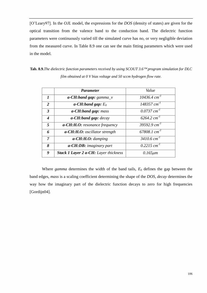
106
[O’Leary97]. In the OJL model, the expressions for the DOS (density of states) are given for the
optical transition from the valence band to the conduction band. The dielectric function
parameters were continuously varied till the simulated curve has no, or very negligible deviation
from the measured curve. In Table 8.9 one can see the main fitting parameters which were used
in the model.
Tab. 8.9.The dielectric function parameters received by using SCOUT 3.6 program simulation for DLC
film obtained at 0 V bias voltage and 50 sccm hydrogen flow rate.
Parameter Value
1 a-CH:band gap: gamma_v 10436.4 cm-1
2 a-CH:band gap: E0 148357 cm-1
3 a-CH:band gap: mass 0.0737 cm-1
4 a-CH:band gap: decay 6264.2 cm-1
5 a-CH:H.O: resonance frequency 39592.9 cm-1
6 a-CH:H.O: oscillator strength 67808.1 cm-1
7 a-CH:H.O: damping 3410.6 cm-1
8 a-CH:DB: imaginary part 0.2215 cm-1
9 Stack 1 Layer 2 a-CH: Layer thickness 0.165m
Where gamma determines the width of the band tails, E0 defines the gap between the
band edges, mass is a scaling coefficient determining the shape of the DOS, decay determines the
way how the imaginary part of the dielectric function decays to zero for high frequencies
[Gordijn04].
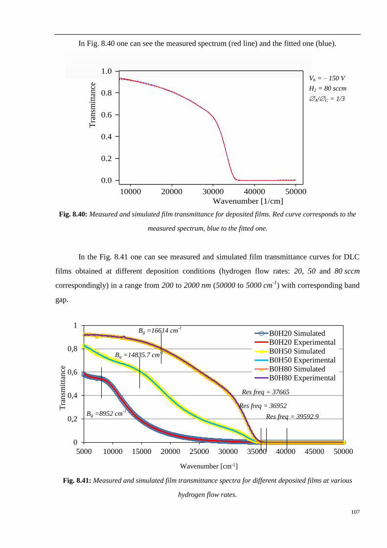
107
10000 20000 30000 40000 50000
Wavenumber [1/cm]
0.0
0.2
0.4
0.6
0.8
1.0
Tra
nsm
itta
nce
In Fig. 8.40 one can see the measured spectrum (red line) and the fitted one (blue).
Fig. 8.40: Measured and simulated film transmittance for deposited films. Red curve corresponds to the
measured spectrum, blue to the fitted one.
In the Fig. 8.41 one can see measured and simulated film transmittance curves for DLC
films obtained at different deposition conditions (hydrogen flow rates: 20, 50 and 80 sccm
correspondingly) in a range from 200 to 2000 nm (50000 to 5000 cm-1
) with corresponding band
gap.
Fig. 8.41: Measured and simulated film transmittance spectra for different deposited films at various
hydrogen flow rates.
0
0,2
0,4
0,6
0,8
1
5000 10000 15000 20000 25000 30000 35000 40000 45000 50000
B0H20 Simulated
B0H20 Experimental
B0H50 Simulated
B0H50 Experimental
B0H80 SimulatedB0H80 Experimental
Wavenumber [cm-1]
Tra
nsm
itta
nce
Vb = – 150 V
H2 = 80 sccm
A/C = 1/3
Res freq = 39592.9
Bg =14835.7 cm-1
Bg =8952 cm-1
Bg =16614 cm-1
Res freq = 36952
Res freq = 37665
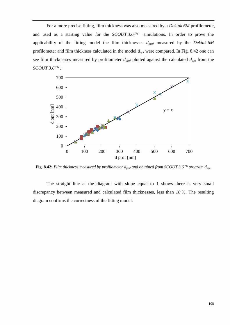
108
For a more precise fitting, film thickness was also measured by a Dektak 6M profilometer,
and used as a starting value for the SCOUT 3.6 simulations. In order to prove the
applicability of the fitting model the film thicknesses dprof measured by the Dektak 6M
profilometer and film thickness calculated in the model dopt were compared. In Fig. 8.42 one can
see film thicknesses measured by profilometer dprof plotted against the calculated dopt from the
SCOUT 3.6 .
Fig. 8.42: Film thickness measured by profilometer dprof and obtained from SCOUT 3.6 program dopt.
The straight line at the diagram with slope equal to 1 shows there is very small
discrepancy between measured and calculated film thicknesses, less than 10 %. The resulting
diagram confirms the correctness of the fitting model.
0
100
200
300
400
500
600
700
0 100 200 300 400 500 600 700
d o
pt
[nm
]
d prof [nm]
y = x
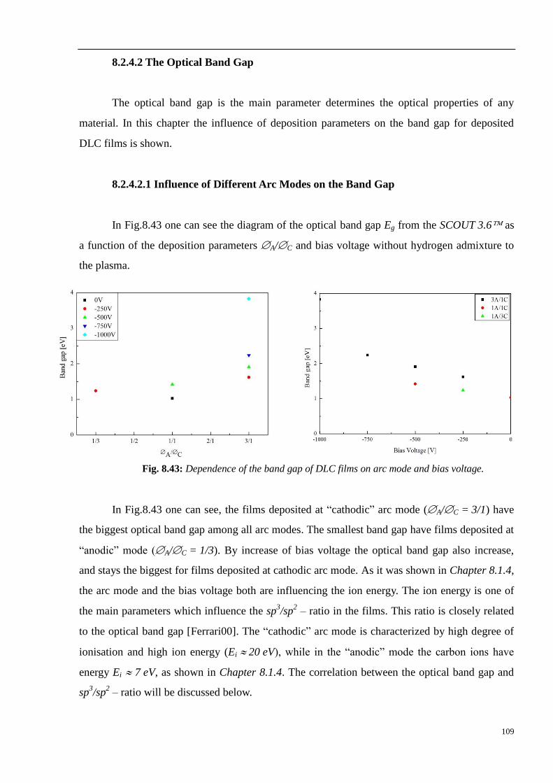
109
8.2.4.2 The Optical Band Gap
The optical band gap is the main parameter determines the optical properties of any
material. In this chapter the influence of deposition parameters on the band gap for deposited
DLC films is shown.
8.2.4.2.1 Influence of Different Arc Modes on the Band Gap
In Fig.8.43 one can see the diagram of the optical band gap Eg from the SCOUT 3.6 as
a function of the deposition parameters A/C and bias voltage without hydrogen admixture to
the plasma.
Fig. 8.43: Dependence of the band gap of DLC films on arc mode and bias voltage.
In Fig.8.43 one can see, the films deposited at “cathodic” arc mode (A/C = 3/1) have
the biggest optical band gap among all arc modes. The smallest band gap have films deposited at
“anodic” mode (A/C = 1/3). By increase of bias voltage the optical band gap also increase,
and stays the biggest for films deposited at cathodic arc mode. As it was shown in Chapter 8.1.4,
the arc mode and the bias voltage both are influencing the ion energy. The ion energy is one of
the main parameters which influence the sp3/sp
2 – ratio in the films. This ratio is closely related
to the optical band gap [Ferrari00]. The “cathodic” arc mode is characterized by high degree of
ionisation and high ion energy (Ei 20 eV), while in the “anodic” mode the carbon ions have
energy Ei 7 eV, as shown in Chapter 8.1.4. The correlation between the optical band gap and
sp3/sp
2 – ratio will be discussed below.
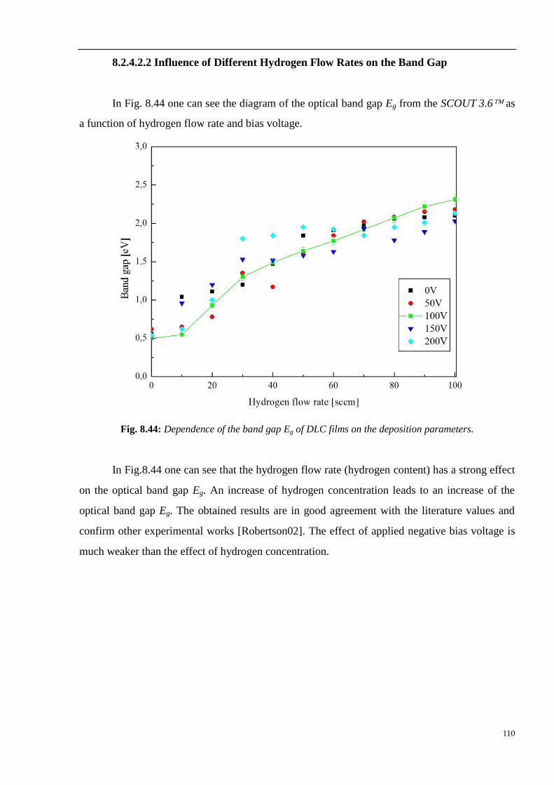
110
8.2.4.2.2 Influence of Different Hydrogen Flow Rates on the Band Gap
In Fig. 8.44 one can see the diagram of the optical band gap Eg from the SCOUT 3.6 as
a function of hydrogen flow rate and bias voltage.
Fig. 8.44: Dependence of the band gap Eg of DLC films on the deposition parameters.
In Fig.8.44 one can see that the hydrogen flow rate (hydrogen content) has a strong effect
on the optical band gap Eg. An increase of hydrogen concentration leads to an increase of the
optical band gap Eg. The obtained results are in good agreement with the literature values and
confirm other experimental works [Robertson02]. The effect of applied negative bias voltage is
much weaker than the effect of hydrogen concentration.
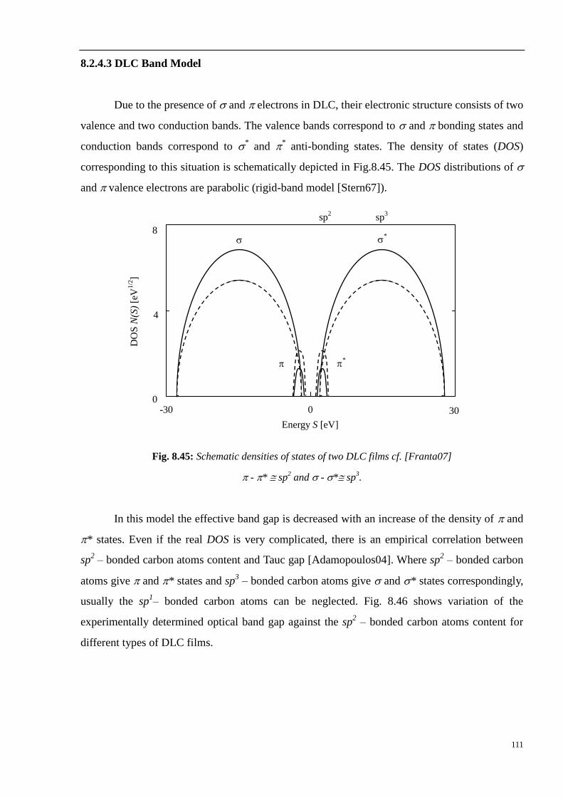
111
8.2.4.3 DLC Band Model
Due to the presence of and electrons in DLC, their electronic structure consists of two
valence and two conduction bands. The valence bands correspond to and bonding states and
conduction bands correspond to * and *
anti-bonding states. The density of states (DOS)
corresponding to this situation is schematically depicted in Fig.8.45. The DOS distributions of
and valence electrons are parabolic (rigid-band model [Stern67]).
Fig. 8.45: Schematic densities of states of two DLC films cf. [Franta07]
- * sp2 and - * sp
3.
In this model the effective band gap is decreased with an increase of the density of and
* states. Even if the real DOS is very complicated, there is an empirical correlation between
sp2 – bonded carbon atoms content and Tauc gap [Adamopoulos04]. Where sp
2 – bonded carbon
atoms give and * states and sp3 – bonded carbon atoms give and * states correspondingly,
usually the sp1– bonded carbon atoms can be neglected. Fig. 8.46 shows variation of the
experimentally determined optical band gap against the sp2 – bonded carbon atoms content for
different types of DLC films.
*
*
DO
S N
(S)
[eV
1/2
]
Energy S [eV]
0 30 -30 0
8
4
sp2
sp3
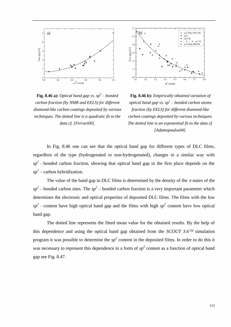
112
Fig. 8.46 a): Optical band gap vs. sp3 – bonded
carbon fraction (by NMR and EELS) for different
diamond-like carbon coatings deposited by various
techniques. The dotted line is a quadratic fit to the
data cf. [Ferrari00].
Fig. 8.46 b): Empirically obtained variation of
optical band gap vs. sp2 – bonded carbon atoms
fraction (by EELS) for different diamond-like
carbon coatings deposited by various techniques.
The dotted line is an exponential fit to the data cf.
[Adamopoulos04].
In Fig. 8.46 one can see that the optical band gap for different types of DLC films,
regardless of the type (hydrogenated or non-hydrogenated), changes in a similar way with
sp2 – bonded carbon fraction, showing that optical band gap in the first place depends on the
sp2 – carbon hybridization.
The value of the band gap in DLC films is determined by the density of the states of the
sp2 – bonded carbon sites. The sp
2 – bonded carbon fraction is a very important parameter which
determines the electronic and optical properties of deposited DLC films. The films with the low
sp2 – content have high optical band gap and the films with high sp
2 content have low optical
band gap.
The dotted line represents the fitted mean value for the obtained results. By the help of
this dependence and using the optical band gap obtained from the SCOUT 3.6 simulation
program it was possible to determine the sp2 content in the deposited films. In order to do this it
was necessary to represent this dependence in a form of sp2 content as a function of optical band
gap see Fig. 8.47.
a) b) a)
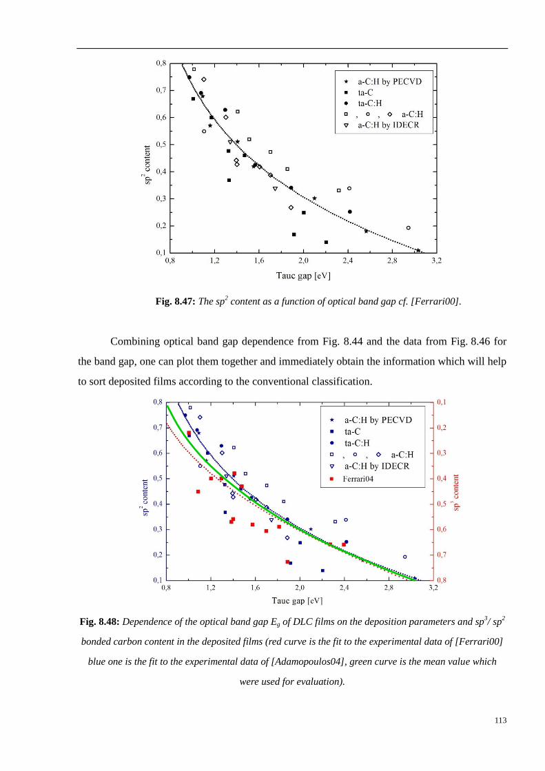
113
Fig. 8.47: The sp2 content as a function of optical band gap cf. [Ferrari00].
Combining optical band gap dependence from Fig. 8.44 and the data from Fig. 8.46 for
the band gap, one can plot them together and immediately obtain the information which will help
to sort deposited films according to the conventional classification.
Fig. 8.48: Dependence of the optical band gap Eg of DLC films on the deposition parameters and sp3/ sp
2
bonded carbon content in the deposited films (red curve is the fit to the experimental data of [Ferrari00]
blue one is the fit to the experimental data of [Adamopoulos04], green curve is the mean value which
were used for evaluation).
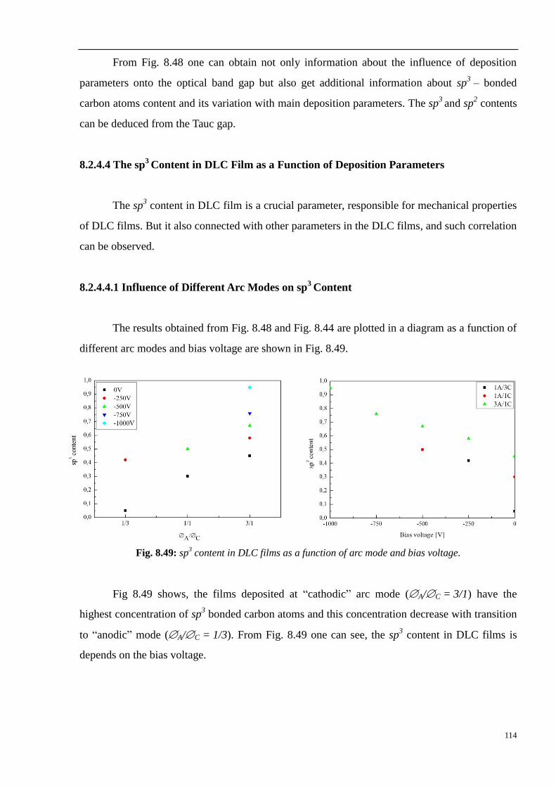
114
From Fig. 8.48 one can obtain not only information about the influence of deposition
parameters onto the optical band gap but also get additional information about sp3
– bonded
carbon atoms content and its variation with main deposition parameters. The sp3
and sp2 contents
can be deduced from the Tauc gap.
8.2.4.4 The sp3 Content in DLC Film as a Function of Deposition Parameters
The sp3 content in DLC film is a crucial parameter, responsible for mechanical properties
of DLC films. But it also connected with other parameters in the DLC films, and such correlation
can be observed.
8.2.4.4.1 Influence of Different Arc Modes on sp3
Content
The results obtained from Fig. 8.48 and Fig. 8.44 are plotted in a diagram as a function of
different arc modes and bias voltage are shown in Fig. 8.49.
Fig. 8.49: sp3 content in DLC films as a function of arc mode and bias voltage.
Fig 8.49 shows, the films deposited at “cathodic” arc mode (A/C = 3/1) have the
highest concentration of sp3 bonded carbon atoms and this concentration decrease with transition
to “anodic” mode (A/C = 1/3). From Fig. 8.49 one can see, the sp3 content in DLC films is
depends on the bias voltage.
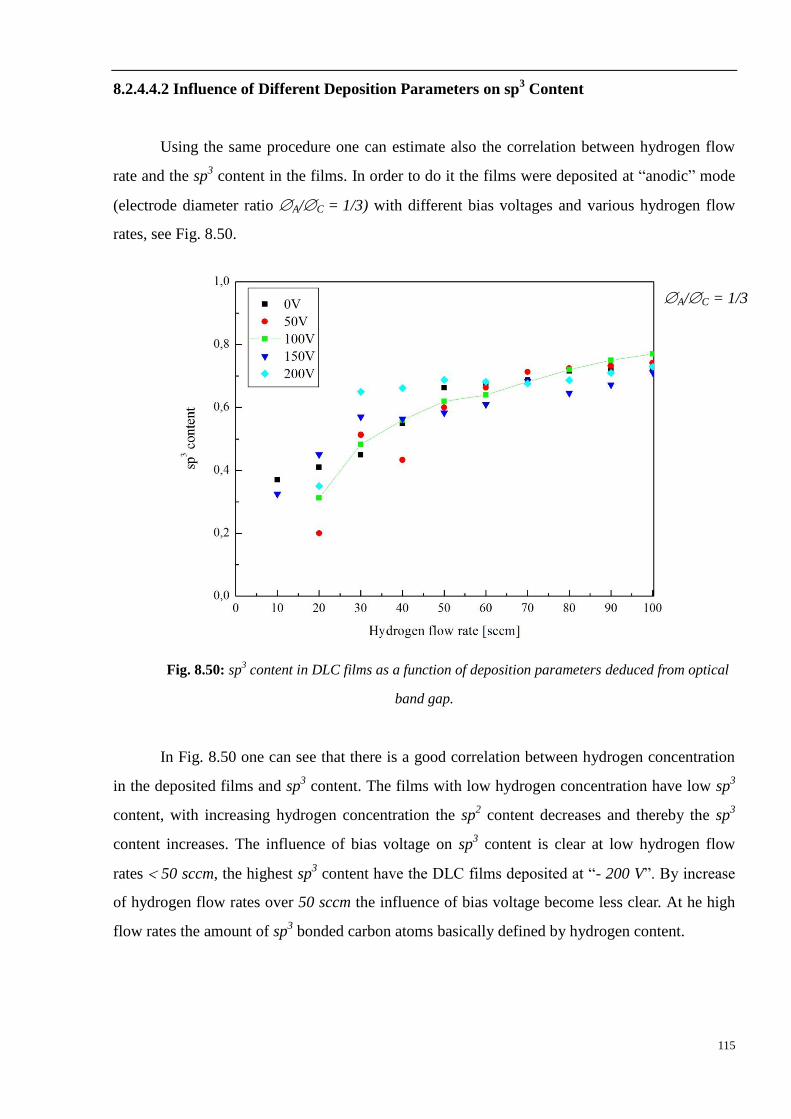
115
8.2.4.4.2 Influence of Different Deposition Parameters on sp3 Content
Using the same procedure one can estimate also the correlation between hydrogen flow
rate and the sp3 content in the films. In order to do it the films were deposited at “anodic” mode
(electrode diameter ratio A/C = 1/3) with different bias voltages and various hydrogen flow
rates, see Fig. 8.50.
Fig. 8.50: sp3 content in DLC films as a function of deposition parameters deduced from optical
band gap.
In Fig. 8.50 one can see that there is a good correlation between hydrogen concentration
in the deposited films and sp3 content. The films with low hydrogen concentration have low sp
3
content, with increasing hydrogen concentration the sp2 content decreases and thereby the sp
3
content increases. The influence of bias voltage on sp3 content is clear at low hydrogen flow
rates 50 sccm, the highest sp3 content have the DLC films deposited at “- 200 V”. By increase
of hydrogen flow rates over 50 sccm the influence of bias voltage become less clear. At he high
flow rates the amount of sp3 bonded carbon atoms basically defined by hydrogen content.
A/C = 1/3
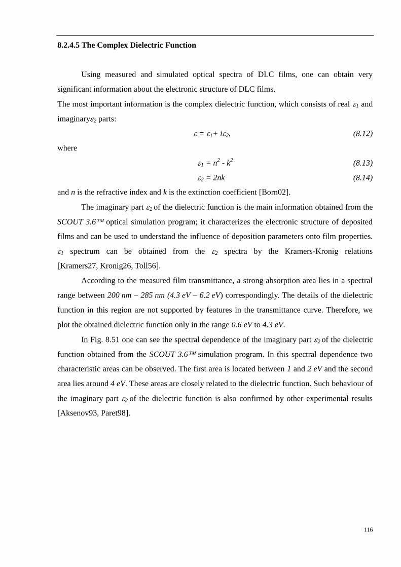
116
8.2.4.5 The Complex Dielectric Function
Using measured and simulated optical spectra of DLC films, one can obtain very
significant information about the electronic structure of DLC films.
The most important information is the complex dielectric function, which consists of real 1 and
imaginary2 parts:
= 1+ i2, (8.12)
where
1 = n2 - k
2 (8.13)
2 = 2nk (8.14)
and n is the refractive index and k is the extinction coefficient [Born02].
The imaginary part 2 of the dielectric function is the main information obtained from the
SCOUT 3.6 optical simulation program; it characterizes the electronic structure of deposited
films and can be used to understand the influence of deposition parameters onto film properties.
1 spectrum can be obtained from the 2 spectra by the Kramers-Kronig relations
[Kramers27, Kronig26, Toll56].
According to the measured film transmittance, a strong absorption area lies in a spectral
range between 200 nm – 285 nm (4.3 eV – 6.2 eV) correspondingly. The details of the dielectric
function in this region are not supported by features in the transmittance curve. Therefore, we
plot the obtained dielectric function only in the range 0.6 eV to 4.3 eV.
In Fig. 8.51 one can see the spectral dependence of the imaginary part 2 of the dielectric
function obtained from the SCOUT 3.6 simulation program. In this spectral dependence two
characteristic areas can be observed. The first area is located between 1 and 2 eV and the second
area lies around 4 eV. These areas are closely related to the dielectric function. Such behaviour of
the imaginary part 2 of the dielectric function is also confirmed by other experimental results
[Aksenov93, Paret98].
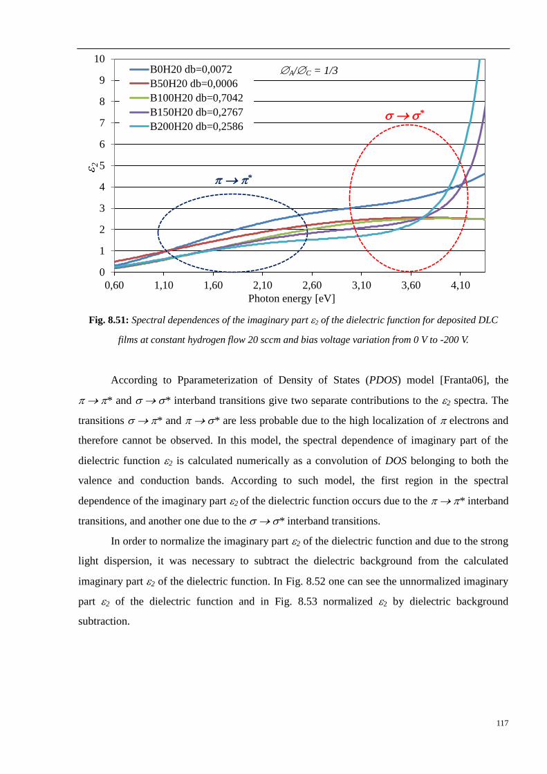
117
Fig. 8.51: Spectral dependences of the imaginary part 2 of the dielectric function for deposited DLC
films at constant hydrogen flow 20 sccm and bias voltage variation from 0 V to -200 V.
According to Pparameterization of Density of States (PDOS) model [Franta06], the
* and * interband transitions give two separate contributions to the 2 spectra. The
transitions * and * are less probable due to the high localization of electrons and
therefore cannot be observed. In this model, the spectral dependence of imaginary part of the
dielectric function 2 is calculated numerically as a convolution of DOS belonging to both the
valence and conduction bands. According to such model, the first region in the spectral
dependence of the imaginary part 2 of the dielectric function occurs due to the * interband
transitions, and another one due to the * interband transitions.
In order to normalize the imaginary part 2 of the dielectric function and due to the strong
light dispersion, it was necessary to subtract the dielectric background from the calculated
imaginary part 2 of the dielectric function. In Fig. 8.52 one can see the unnormalized imaginary
part 2 of the dielectric function and in Fig. 8.53 normalized 2 by dielectric background
subtraction.
0
1
2
3
4
5
6
7
8
9
10
0,60 1,10 1,60 2,10 2,60 3,10 3,60 4,10
B0H20 db=0,0072
B50H20 db=0,0006
B100H20 db=0,7042
B150H20 db=0,2767
B200H20 db=0,2586
*
*
Photon energy [eV]
2
A/C = 1/3
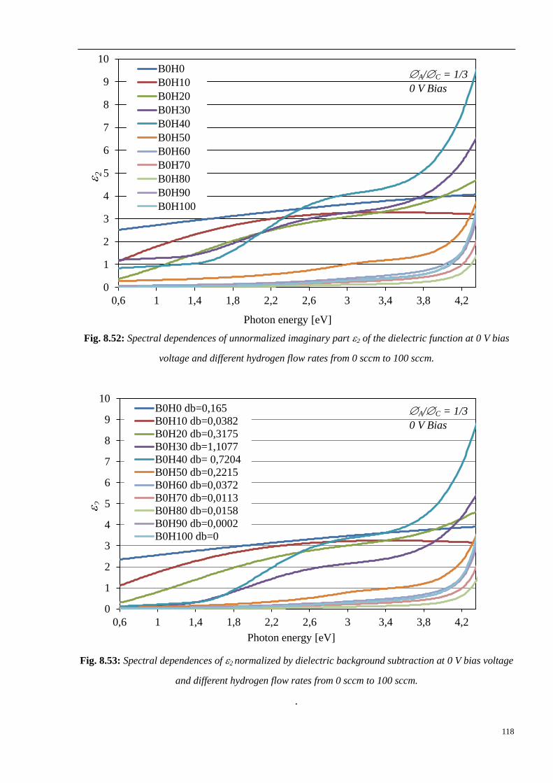
118
Fig. 8.52: Spectral dependences of unnormalized imaginary part 2 of the dielectric function at 0 V bias
voltage and different hydrogen flow rates from 0 sccm to 100 sccm.
Fig. 8.53: Spectral dependences of 2 normalized by dielectric background subtraction at 0 V bias voltage
and different hydrogen flow rates from 0 sccm to 100 sccm.
.
0
1
2
3
4
5
6
7
8
9
10
0,6 1 1,4 1,8 2,2 2,6 3 3,4 3,8 4,2
B0H0
B0H10
B0H20
B0H30
B0H40
B0H50
B0H60
B0H70
B0H80
B0H90
B0H100
Photon energy [eV]
2
0
1
2
3
4
5
6
7
8
9
10
0,6 1 1,4 1,8 2,2 2,6 3 3,4 3,8 4,2
B0H0 db=0,165
B0H10 db=0,0382
B0H20 db=0,3175
B0H30 db=1,1077
B0H40 db= 0,7204
B0H50 db=0,2215
B0H60 db=0,0372
B0H70 db=0,0113
B0H80 db=0,0158
B0H90 db=0,0002
B0H100 db=0
Photon energy [eV]
2
A/C = 1/3
0 V Bias
A/C = 1/3
0 V Bias
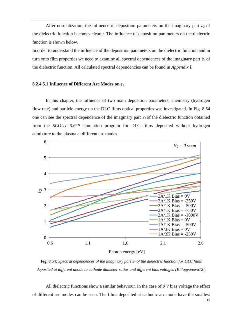
119
After normalization, the influence of deposition parameters on the imaginary part 2 of
the dielectric function becomes clearer. The influence of deposition parameters on the dielectric
function is shown below.
In order to understand the influence of the deposition parameters on the dielectric function and in
turn onto film properties we need to examine all spectral dependences of the imaginary part 2 of
the dielectric function. All calculated spectral dependencies can be found in Appendix I.
8.2.4.5.1 Influence of Different Arc Modes on 2
In this chapter, the influence of two main deposition parameters, chemistry (hydrogen
flow rate) and particle energy on the DLC films optical properties was investigated. In Fig. 8.54
one can see the spectral dependence of the imaginary part 2 of the dielectric function obtained
from the SCOUT 3.6 simulation program for DLC films deposited without hydrogen
admixture to the plasma at different arc modes.
Fig. 8.54: Spectral dependences of the imaginary part 2 of the dielectric function for DLC films
deposited at different anode to cathode diameter ratios and different bias voltages [Khlopyanova12].
All dielectric functions show a similar behaviour. In the case of 0 V bias voltage the effect
of different arc modes can be seen. The films deposited at cathodic arc mode have the smallest
0
1
2
3
4
5
6
0,6 1,1 1,6 2,1 2,6
3A/1K Bias = 0V3A/1K Bias = -250V3A/1K Bias = -500V3A/1K Bias = -750V3A/1K Bias = -1000V1A/1K Bias = 0V1A/1K Bias = -500V1A/3K Bias = 0V1A/3K Bias = -250V
Photon energy [eV]
2
H2 = 0 sccm
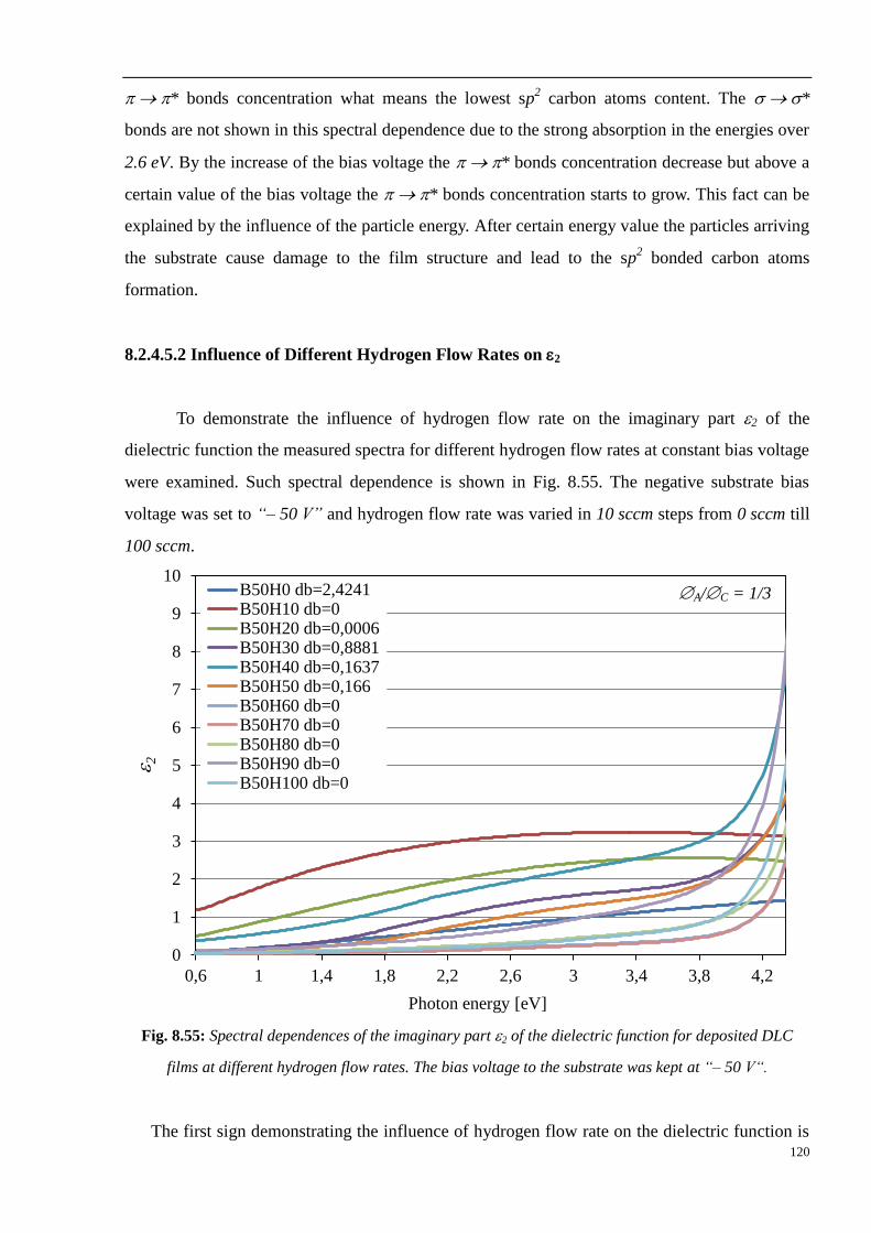
120
* bonds concentration what means the lowest sp2 carbon atoms content. The *
bonds are not shown in this spectral dependence due to the strong absorption in the energies over
2.6 eV. By the increase of the bias voltage the * bonds concentration decrease but above a
certain value of the bias voltage the * bonds concentration starts to grow. This fact can be
explained by the influence of the particle energy. After certain energy value the particles arriving
the substrate cause damage to the film structure and lead to the sp2 bonded carbon atoms
formation.
8.2.4.5.2 Influence of Different Hydrogen Flow Rates on 2
To demonstrate the influence of hydrogen flow rate on the imaginary part 2 of the
dielectric function the measured spectra for different hydrogen flow rates at constant bias voltage
were examined. Such spectral dependence is shown in Fig. 8.55. The negative substrate bias
voltage was set to “– 50 V” and hydrogen flow rate was varied in 10 sccm steps from 0 sccm till
100 sccm.
Fig. 8.55: Spectral dependences of the imaginary part 2 of the dielectric function for deposited DLC
films at different hydrogen flow rates. The bias voltage to the substrate was kept at “– 50 V“.
The first sign demonstrating the influence of hydrogen flow rate on the dielectric function is
0
1
2
3
4
5
6
7
8
9
10
0,6 1 1,4 1,8 2,2 2,6 3 3,4 3,8 4,2
B50H0 db=2,4241B50H10 db=0B50H20 db=0,0006B50H30 db=0,8881B50H40 db=0,1637B50H50 db=0,166B50H60 db=0B50H70 db=0B50H80 db=0B50H90 db=0B50H100 db=0
Photon energy [eV]
2
A/C = 1/3
121
that the imaginary part 2 changes its shape only due to the variation of hydrogen flow rate.
According to the shape, all spectral dependencies of the imaginary part 2 of the dielectric
function can be divided in few groups as a function of the hydrogen flow rate and
correspondingly hydrogen concentration in the deposited films:
a) H0 – H20 – very low hydrogen content ([H] 10 at. %),
b) H30 – H50 – low hydrogen content (10 at. % [H] 20 at. %),
c) H60 – H100 – intermediate hydrogen content (20 at. % [H] 40 at. %).
The hydrogen content determination of the deposited DLC films was carried out by nuclear
reaction analysis (NRA), and it was discussed in Chapter 8.2.3.2.
Such correlation between the hydrogen flow rate and the shape of the imaginary part 2 of the
dielectric function was also observed for all films independently from the applied bias voltage,
see Appendix I.
Another sign of the influence of the hydrogen flow rate on the imaginary part 2 of the
dielectric function is that for films deposited at the residual hydrogen atmosphere (working
pressure 10-6
mbar) spectrum is located above all other spectra. And increase of hydrogen flow
rate leads to a decrease in the values of the spectra of the imaginary part 2 of the dielectric
function, see Fig. 8.55.
In regard to the * and * bonds, one can say that * bonds in the first
region of the imaginary part 2 of the dielectric function are reduced by an increase of hydrogen
flow rate from 0 sccm to 50 sccm and * bonds in the second region on the contrary are
increased. At flow rates above 50 sccm * bonds reduced even stronger than at small flow
rates, and * bonds also start to reduce but very slowly in comparison to the * bonds.
Such behaviour of and bonds can be explained as follows. The DLC films deposited at
small hydrogen flow rates 30 sccm have high amount of sp2 – hybridized carbon atoms and
have a small optical band gap. The films deposited at flow rates of 30 – 50 sccm show presence
of both sp2 and sp
3 – hybridized carbon atoms in similar amounts, and low concentration of
hydrogen. And in the films deposited at flow rates 50 sccm the content of sp2 – hybridized
carbon atoms becomes very small (optical band gap increases), Fig. 8.44 and the content of sp3–
hybridized carbon atoms increases strongly (Fig. 8.50), but hydrogen concentration in such films
is also increased. Such assumptions are in good agreement with the literature [Casiragi05]. In
most types of DLC films, an increasing content of sp3 – bonded carbon atoms correlates with
increasing hydrogen content. Hydrogen saturates C = C bonds by transformation of sp2 carbon
sites into sp3 = CH2 and CH sites. This increase the amount of all sp
3 bonds but not the C = C
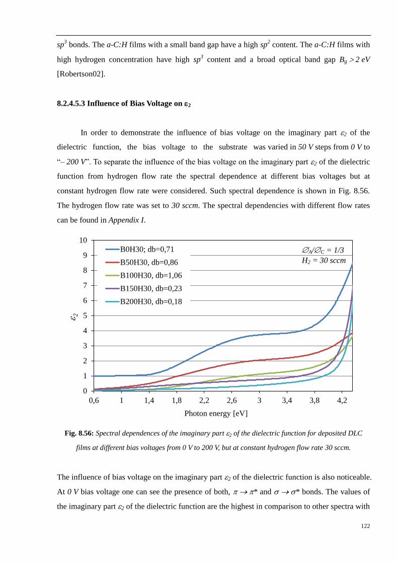
122
sp3 bonds. The a-C:H films with a small band gap have a high sp
2 content. The a-C:H films with
high hydrogen concentration have high sp3 content and a broad optical band gap Bg 2 eV
[Robertson02].
8.2.4.5.3 Influence of Bias Voltage on 2
In order to demonstrate the influence of bias voltage on the imaginary part 2 of the
dielectric function, the bias voltage to the substrate was varied in 50 V steps from 0 V to
“– 200 V”. To separate the influence of the bias voltage on the imaginary part 2 of the dielectric
function from hydrogen flow rate the spectral dependence at different bias voltages but at
constant hydrogen flow rate were considered. Such spectral dependence is shown in Fig. 8.56.
The hydrogen flow rate was set to 30 sccm. The spectral dependencies with different flow rates
can be found in Appendix I.
Fig. 8.56: Spectral dependences of the imaginary part 2 of the dielectric function for deposited DLC
films at different bias voltages from 0 V to 200 V, but at constant hydrogen flow rate 30 sccm.
The influence of bias voltage on the imaginary part 2 of the dielectric function is also noticeable.
At 0 V bias voltage one can see the presence of both, * and * bonds. The values of
the imaginary part 2 of the dielectric function are the highest in comparison to other spectra with
0
1
2
3
4
5
6
7
8
9
10
0,6 1 1,4 1,8 2,2 2,6 3 3,4 3,8 4,2
B0H30; db=0,71
B50H30, db=0,86
B100H30, db=1,06
B150H30, db=0,23
B200H30, db=0,18
Photon energy [eV]
2
A/C = 1/3
H2 = 30 sccm
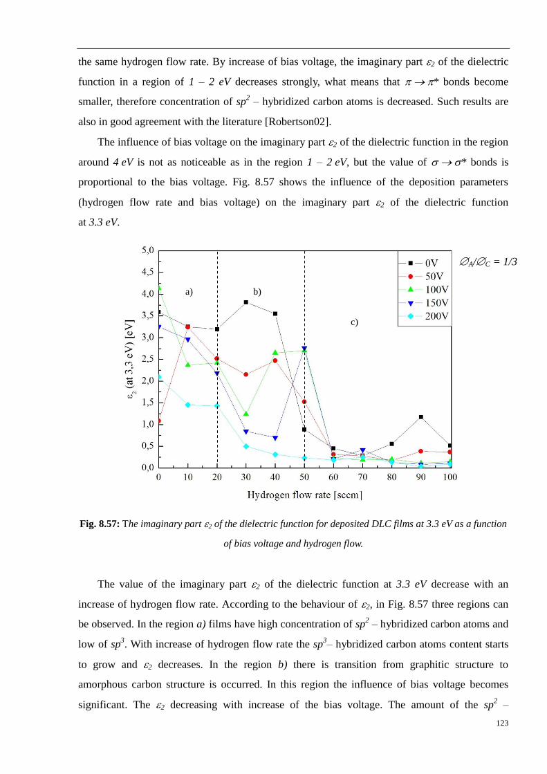
123
the same hydrogen flow rate. By increase of bias voltage, the imaginary part 2 of the dielectric
function in a region of 1 – 2 eV decreases strongly, what means that * bonds become
smaller, therefore concentration of sp2 – hybridized carbon atoms is decreased. Such results are
also in good agreement with the literature [Robertson02].
The influence of bias voltage on the imaginary part 2 of the dielectric function in the region
around 4 eV is not as noticeable as in the region 1 – 2 eV, but the value of * bonds is
proportional to the bias voltage. Fig. 8.57 shows the influence of the deposition parameters
(hydrogen flow rate and bias voltage) on the imaginary part 2 of the dielectric function
at 3.3 eV.
Fig. 8.57: The imaginary part 2 of the dielectric function for deposited DLC films at 3.3 eV as a function
of bias voltage and hydrogen flow.
The value of the imaginary part 2 of the dielectric function at 3.3 eV decrease with an
increase of hydrogen flow rate. According to the behaviour of 2, in Fig. 8.57 three regions can
be observed. In the region a) films have high concentration of sp2 – hybridized carbon atoms and
low of sp3. With increase of hydrogen flow rate the sp
3– hybridized carbon atoms content starts
to grow and 2 decreases. In the region b) there is transition from graphitic structure to
amorphous carbon structure is occurred. In this region the influence of bias voltage becomes
significant. The 2 decreasing with increase of the bias voltage. The amount of the sp2 –
a) b)
c)
A/C = 1/3
124
hybridized carbon atoms starts to decrease and content of the sp3 – hybridized carbon atoms
increases. In the region c) a polymerization of DLC films occur. The behaviour of the imaginary
part 2 of the dielectric function at 3.3 eV is characteristic for DLC films deposited at high
hydrogen flow rare and high bias voltage [Aksenov93] (very low values of 2).
Conclusion
Both deposition parameters (hydrogen flow rate and negative bias voltage to the substrate)
demonstrate strong influence on the imaginary part 2 of the dielectric function. By PDOS
(parameterization of density of states) model, this influence can be interpreted in terms of sp2
and sp3 – hybridized carbon atoms concentration.
The influence of hydrogen on the dielectric function is much stronger than the influence
of the negative bias voltage. According to the results the DLC films deposited at low hydrogen
flow rate 30 sccm and bias voltage less than 50 V demonstrate high concentration of sp2
bonded carbon atoms and have small optical band gap. Increase of bias voltage leads to a
decrease of sp2 bonded carbon atoms content.
By increasing of hydrogen flow rate from 30 sccm to 50 sccm, the concentration of sp2
bonded carbon atoms decreases and sp3 content increases which leads to an increase of the
optical band gap. A hydrogen flow rate of 50 sccm corresponds to 20 at.% of hydrogen
concentration in DLC. This is the determinative flow rate, responsible for the changes in the
structure of DLC films. It can be seen in the spectral dependence of the imaginary part 2 of the
dielectric function.
At high hydrogen flow rates 50 sccm the content of sp3 bonded carbon reaches its
maximum and films have the biggest band gap among the DLC films deposited in these
experiments. Using the experimental data, the band gap and the hydrogen content were plotted
together with the results from other authors [Casiragi05, Poukhovoi11], see Fig. 8.58.
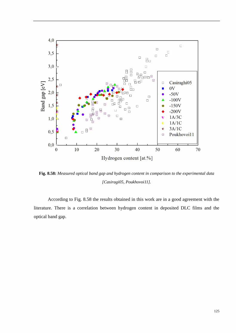
125
Fig. 8.58: Measured optical band gap and hydrogen content in comparison to the experimental data
[Casiragi05, Poukhovoi11].
According to Fig. 8.58 the results obtained in this work are in a good agreement with the
literature. There is a correlation between hydrogen content in deposited DLC films and the
optical band gap.
126
8.2.5 Raman Spectroscopy
In case of DLC coatings, Raman spectroscopy is a commonly used analytical method to
obtain information about carbon hybridisation state. A significant number of experimental results
based on different analytical techniques including Raman spectroscopy which were summarized
by Robertson and co-workers [Robertson91, Ferrari00]. But the interpretation of Raman spectra
is rather complicated and cannot be used solely without any other analytical methods. Raman
spectroscopy is rather an additional method to confirm previous results and to complete the films
analytical results. Using these results, it is possible to classify the deposited DLC films and to
determine their electronic structures. Due to the fact that Raman spectroscopy for sp2 –
hybridized carbon atoms is 50 – 230 times more sensitive than for sp3 – hybridized carbon atoms
(due to the higher cross section), this method does not provide direct evaluation of sp3/sp
2 –
hybridized carbon atoms content. Such information can be indirectly derived from Raman
spectroscopy.
In order to obtain reliable information from Raman spectra, a multiwavelength micro-Raman
by Jobin Yvon was used. Measurements were taken with 100 objective. In order to prevent
the damage of the DLC film caused by the laser, the measurements were taken using 0.6
diaphragm (25% transmittance). Raman spectra were recorded using two lasers: Ar laser with the
wavelength 1 = 514 nm and He-Ne laser with the wavelength 2 = 633 nm. To evaluate the
measured spectra it is necessary to use such parameters as peak position (G-peak position), peak
intensity ratio (ID/IG), full width at half maximum of the G-peak (FWHM G), the G-peak
dispersion (DispG). Fig. 8.59 shows measured at 633 nm Raman spectra for DLC films deposited
at “anodic” mode (electrode diameter ratio A/C = 1/3) with various hydrogen flow rates. The
first thing needs to be mentioned is a photoluminescence (PL) background. The presence of
photoluminescence in visible Raman spectra is the characteristic feature for hydrogenated carbon
films. The higher hydrogen content in the DLC film the bigger is photoluminescence
[Casiragi05].
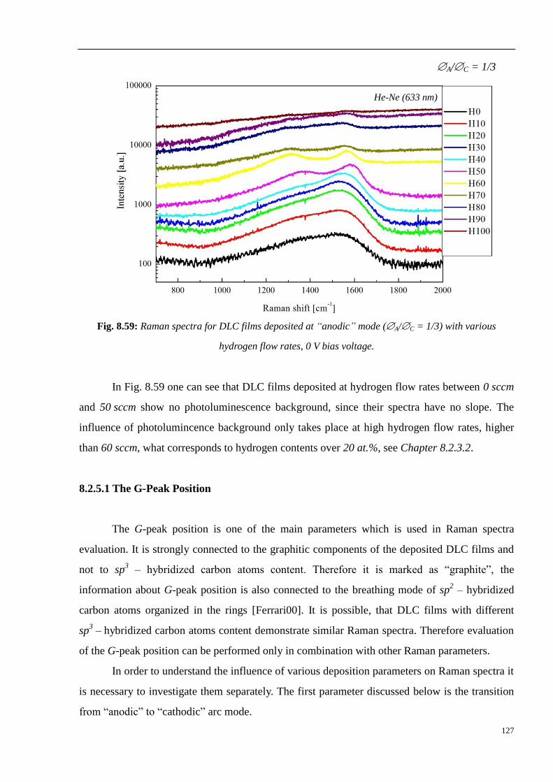
127
Fig. 8.59: Raman spectra for DLC films deposited at “anodic” mode (A/C = 1/3) with various
hydrogen flow rates, 0 V bias voltage.
In Fig. 8.59 one can see that DLC films deposited at hydrogen flow rates between 0 sccm
and 50 sccm show no photoluminescence background, since their spectra have no slope. The
influence of photolumincence background only takes place at high hydrogen flow rates, higher
than 60 sccm, what corresponds to hydrogen contents over 20 at.%, see Chapter 8.2.3.2.
8.2.5.1 The G-Peak Position
The G-peak position is one of the main parameters which is used in Raman spectra
evaluation. It is strongly connected to the graphitic components of the deposited DLC films and
not to sp3 – hybridized carbon atoms content. Therefore it is marked as “graphite”, the
information about G-peak position is also connected to the breathing mode of sp2 – hybridized
carbon atoms organized in the rings [Ferrari00]. It is possible, that DLC films with different
sp3 – hybridized carbon atoms content demonstrate similar Raman spectra. Therefore evaluation
of the G-peak position can be performed only in combination with other Raman parameters.
In order to understand the influence of various deposition parameters on Raman spectra it
is necessary to investigate them separately. The first parameter discussed below is the transition
from “anodic” to “cathodic” arc mode.
He-Ne (633 nm)
A/C = 1/3
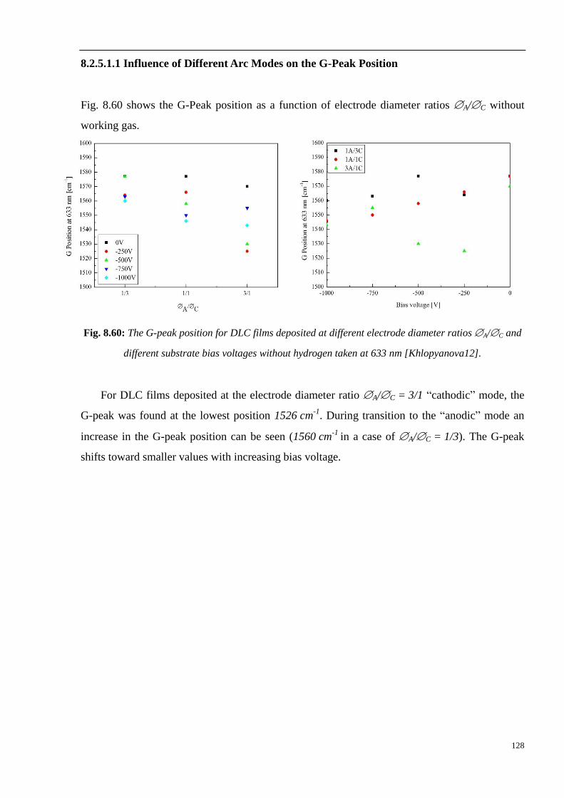
128
8.2.5.1.1 Influence of Different Arc Modes on the G-Peak Position
Fig. 8.60 shows the G-Peak position as a function of electrode diameter ratios A/C without
working gas.
Fig. 8.60: The G-peak position for DLC films deposited at different electrode diameter ratios A/C and
different substrate bias voltages without hydrogen taken at 633 nm [Khlopyanova12].
For DLC films deposited at the electrode diameter ratio A/C = 3/1 “cathodic” mode, the
G-peak was found at the lowest position 1526 cm-1
. During transition to the “anodic” mode an
increase in the G-peak position can be seen (1560 cm-1
in a case of A/C = 1/3). The G-peak
shifts toward smaller values with increasing bias voltage.
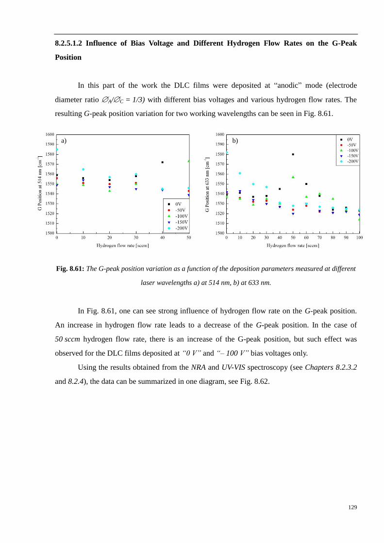
129
8.2.5.1.2 Influence of Bias Voltage and Different Hydrogen Flow Rates on the G-Peak
Position
In this part of the work the DLC films were deposited at “anodic” mode (electrode
diameter ratio A/C = 1/3) with different bias voltages and various hydrogen flow rates. The
resulting G-peak position variation for two working wavelengths can be seen in Fig. 8.61.
Fig. 8.61: The G-peak position variation as a function of the deposition parameters measured at different
laser wavelengths a) at 514 nm, b) at 633 nm.
In Fig. 8.61, one can see strong influence of hydrogen flow rate on the G-peak position.
An increase in hydrogen flow rate leads to a decrease of the G-peak position. In the case of
50 sccm hydrogen flow rate, there is an increase of the G-peak position, but such effect was
observed for the DLC films deposited at “0 V” and “– 100 V” bias voltages only.
Using the results obtained from the NRA and UV-VIS spectroscopy (see Chapters 8.2.3.2
and 8.2.4), the data can be summarized in one diagram, see Fig. 8.62.
a) b)
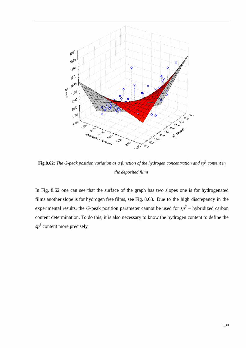
130
Fig.8.62: The G-peak position variation as a function of the hydrogen concentration and sp3 content in
the deposited films.
In Fig. 8.62 one can see that the surface of the graph has two slopes one is for hydrogenated
films another slope is for hydrogen free films, see Fig. 8.63. Due to the high discrepancy in the
experimental results, the G-peak position parameter cannot be used for sp3 – hybridized carbon
content determination. To do this, it is also necessary to know the hydrogen content to define the
sp3 content more precisely.
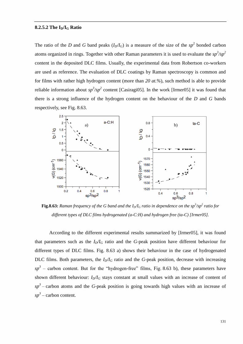
131
8.2.5.2 The ID/IG Ratio
The ratio of the D and G band peaks (ID/IG) is a measure of the size of the sp2 bonded carbon
atoms organized in rings. Together with other Raman parameters it is used to evaluate the sp3/sp
2
content in the deposited DLC films. Usually, the experimental data from Robertson co-workers
are used as reference. The evaluation of DLC coatings by Raman spectroscopy is common and
for films with rather high hydrogen content (more than 20 at.%), such method is able to provide
reliable information about sp3/sp
2 content [Casiragi05]. In the work [Irmer05] it was found that
there is a strong influence of the hydrogen content on the behaviour of the D and G bands
respectively, see Fig. 8.63.
Fig.8.63: Raman frequency of the G band and the ID/IG ratio in dependence on the sp3/sp
2 ratio for
different types of DLC films hydrogenated (a-C:H) and hydrogen free (ta-C) [Irmer05].
According to the different experimental results summarized by [Irmer05], it was found
that parameters such as the ID/IG ratio and the G-peak position have different behaviour for
different types of DLC films. Fig. 8.63 a) shows their behaviour in the case of hydrogenated
DLC films. Both parameters, the ID/IG ratio and the G-peak position, decrease with increasing
sp3 – carbon content. But for the “hydrogen-free” films, Fig. 8.63 b), these parameters have
shown different behaviour: ID/IG stays constant at small values with an increase of content of
sp3 – carbon atoms and the G-peak position is going towards high values with an increase of
sp3 – carbon content.
a) b)
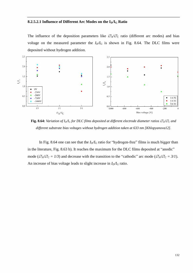
132
8.2.5.2.1 Influence of Different Arc Modes on the ID/IG Ratio
The influence of the deposition parameters like A/C ratio (different arc modes) and bias
voltage on the measured parameter the ID/IG is shown in Fig. 8.64. The DLC films were
deposited without hydrogen addition.
Fig. 8.64: Variation of ID/IG for DLC films deposited at different electrode diameter ratios A/C and
different substrate bias voltages without hydrogen addition taken at 633 nm [Khlopyanova12].
In Fig. 8.64 one can see that the ID/IG ratio for “hydrogen-free” films is much bigger than
in the literature, Fig. 8.63 b). It reaches the maximum for the DLC films deposited at “anodic”
mode (A/C = 1/3) and decrease with the transition to the “cathodic” arc mode (A/C = 3/1).
An increase of bias voltage leads to slight increase in ID/IG ratio.
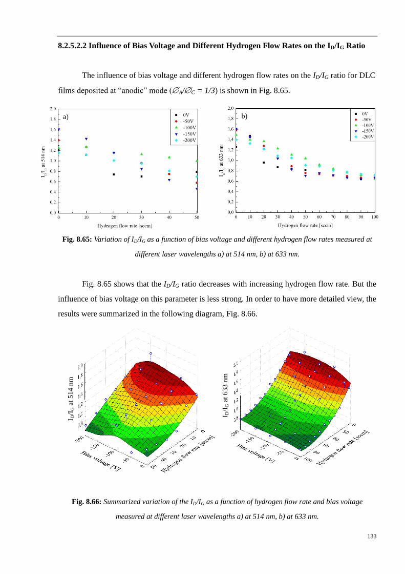
133
8.2.5.2.2 Influence of Bias Voltage and Different Hydrogen Flow Rates on the ID/IG Ratio
The influence of bias voltage and different hydrogen flow rates on the ID/IG ratio for DLC
films deposited at “anodic” mode (A/C = 1/3) is shown in Fig. 8.65.
Fig. 8.65: Variation of ID/IG as a function of bias voltage and different hydrogen flow rates measured at
different laser wavelengths a) at 514 nm, b) at 633 nm.
Fig. 8.65 shows that the ID/IG ratio decreases with increasing hydrogen flow rate. But the
influence of bias voltage on this parameter is less strong. In order to have more detailed view, the
results were summarized in the following diagram, Fig. 8.66.
Fig. 8.66: Summarized variation of the ID/IG as a function of hydrogen flow rate and bias voltage
measured at different laser wavelengths a) at 514 nm, b) at 633 nm.
a) b)
I D/I
G a
t 633 n
m
I D/I
G a
t 514
nm
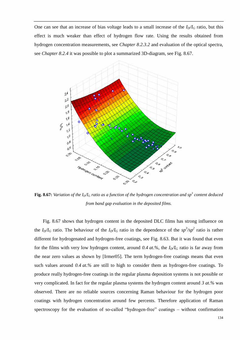
134
One can see that an increase of bias voltage leads to a small increase of the ID/IG ratio, but this
effect is much weaker than effect of hydrogen flow rate. Using the results obtained from
hydrogen concentration measurements, see Chapter 8.2.3.2 and evaluation of the optical spectra,
see Chapter 8.2.4 it was possible to plot a summarized 3D-diagram, see Fig. 8.67.
Fig. 8.67: Variation of the ID/IG ratio as a function of the hydrogen concentration and sp3 content deduced
from band gap evaluation in the deposited films.
Fig. 8.67 shows that hydrogen content in the deposited DLC films has strong influence on
the ID/IG ratio. The behaviour of the ID/IG ratio in the dependence of the sp3/sp
2 ratio is rather
different for hydrogenated and hydrogen-free coatings, see Fig. 8.63. But it was found that even
for the films with very low hydrogen content, around 0.4 at.%, the ID/IG ratio is far away from
the near zero values as shown by [Irmer05]. The term hydrogen-free coatings means that even
such values around 0.4 at.% are still to high to consider them as hydrogen-free coatings. To
produce really hydrogen-free coatings in the regular plasma deposition systems is not possible or
very complicated. In fact for the regular plasma systems the hydrogen content around 3 at.% was
observed. There are no reliable sources concerning Raman behaviour for the hydrogen poor
coatings with hydrogen concentration around few percents. Therefore application of Raman
spectroscopy for the evaluation of so-called “hydrogen-free” coatings – without confirmation
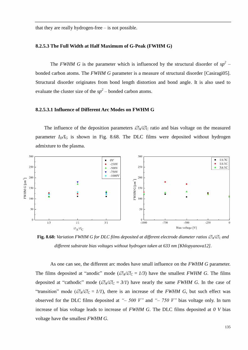
135
that they are really hydrogen-free – is not possible.
8.2.5.3 The Full Width at Half Maximum of G-Peak (FWHM G)
The FWHM G is the parameter which is influenced by the structural disorder of sp2 –
bonded carbon atoms. The FWHM G parameter is a measure of structural disorder [Casiragi05].
Structural disorder originates from bond length distortion and bond angle. It is also used to
evaluate the cluster size of the sp2 – bonded carbon atoms.
8.2.5.3.1 Influence of Different Arc Modes on FWHM G
The influence of the deposition parameters A/C ratio and bias voltage on the measured
parameter ID/IG is shown in Fig. 8.68. The DLC films were deposited without hydrogen
admixture to the plasma.
Fig. 8.68: Variation FWHM G for DLC films deposited at different electrode diameter ratios A/C and
different substrate bias voltages without hydrogen taken at 633 nm [Khlopyanova12].
As one can see, the different arc modes have small influence on the FWHM G parameter.
The films deposited at “anodic” mode (A/C = 1/3) have the smallest FWHM G. The films
deposited at “cathodic” mode (A/C = 3/1) have nearly the same FWHM G. In the case of
“transition” mode (A/C = 1/1), there is an increase of the FWHM G, but such effect was
observed for the DLC films deposited at “– 500 V” and “– 750 V” bias voltage only. In turn
increase of bias voltage leads to increase of FWHM G. The DLC films deposited at 0 V bias
voltage have the smallest FWHM G.
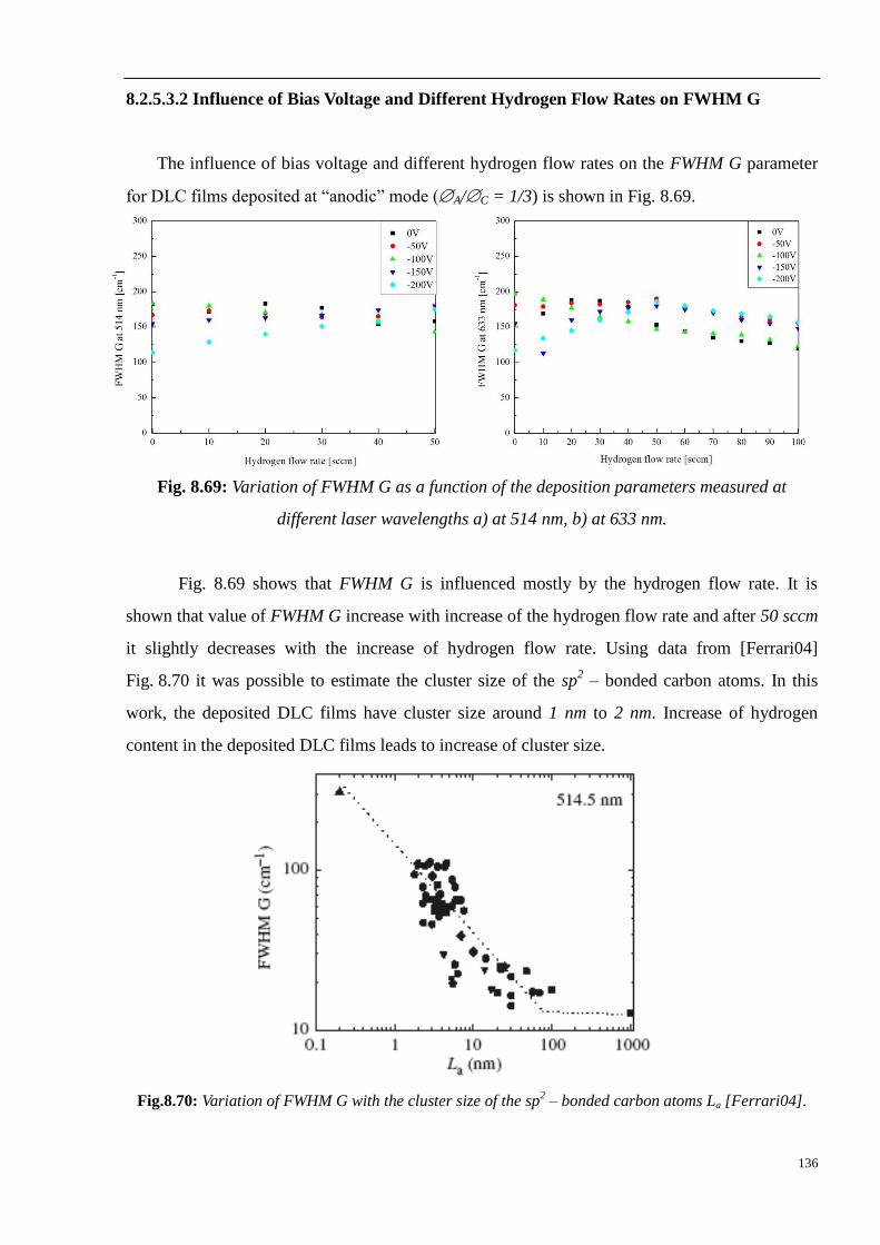
136
8.2.5.3.2 Influence of Bias Voltage and Different Hydrogen Flow Rates on FWHM G
The influence of bias voltage and different hydrogen flow rates on the FWHM G parameter
for DLC films deposited at “anodic” mode (A/C = 1/3) is shown in Fig. 8.69.
Fig. 8.69: Variation of FWHM G as a function of the deposition parameters measured at
different laser wavelengths a) at 514 nm, b) at 633 nm.
Fig. 8.69 shows that FWHM G is influenced mostly by the hydrogen flow rate. It is
shown that value of FWHM G increase with increase of the hydrogen flow rate and after 50 sccm
it slightly decreases with the increase of hydrogen flow rate. Using data from [Ferrari04]
Fig. 8.70 it was possible to estimate the cluster size of the sp2 – bonded carbon atoms. In this
work, the deposited DLC films have cluster size around 1 nm to 2 nm. Increase of hydrogen
content in the deposited DLC films leads to increase of cluster size.
Fig.8.70: Variation of FWHM G with the cluster size of the sp2 – bonded carbon atoms La [Ferrari04].
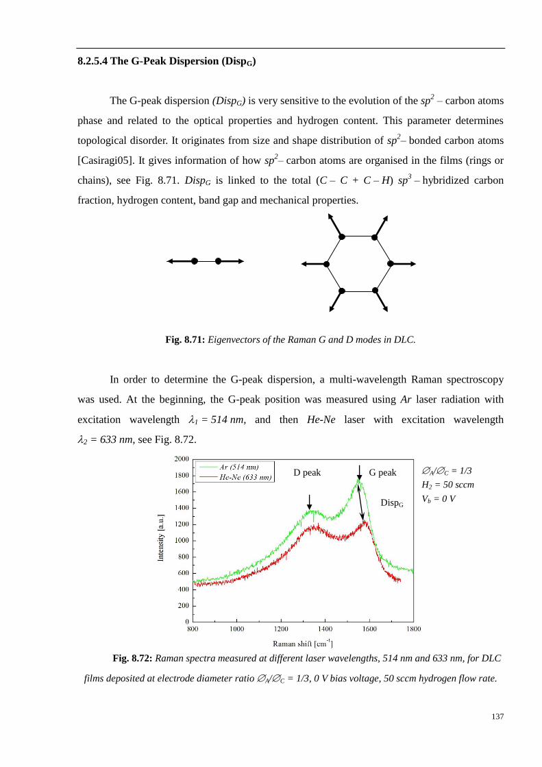
137
8.2.5.4 The G-Peak Dispersion (DispG)
The G-peak dispersion (DispG) is very sensitive to the evolution of the sp2 – carbon atoms
phase and related to the optical properties and hydrogen content. This parameter determines
topological disorder. It originates from size and shape distribution of sp2– bonded carbon atoms
[Casiragi05]. It gives information of how sp2– carbon atoms are organised in the films (rings or
chains), see Fig. 8.71. DispG is linked to the total (C – C + C – H) sp3 – hybridized carbon
fraction, hydrogen content, band gap and mechanical properties.
Fig. 8.71: Eigenvectors of the Raman G and D modes in DLC.
In order to determine the G-peak dispersion, a multi-wavelength Raman spectroscopy
was used. At the beginning, the G-peak position was measured using Ar laser radiation with
excitation wavelength 1 = 514 nm, and then He-Ne laser with excitation wavelength
2 = 633 nm, see Fig. 8.72.
Fig. 8.72: Raman spectra measured at different laser wavelengths, 514 nm and 633 nm, for DLC
films deposited at electrode diameter ratio A/C = 1/3, 0 V bias voltage, 50 sccm hydrogen flow rate.
A/C = 1/3
H2 = 50 sccm
Vb = 0 V DispG
G peak D peak
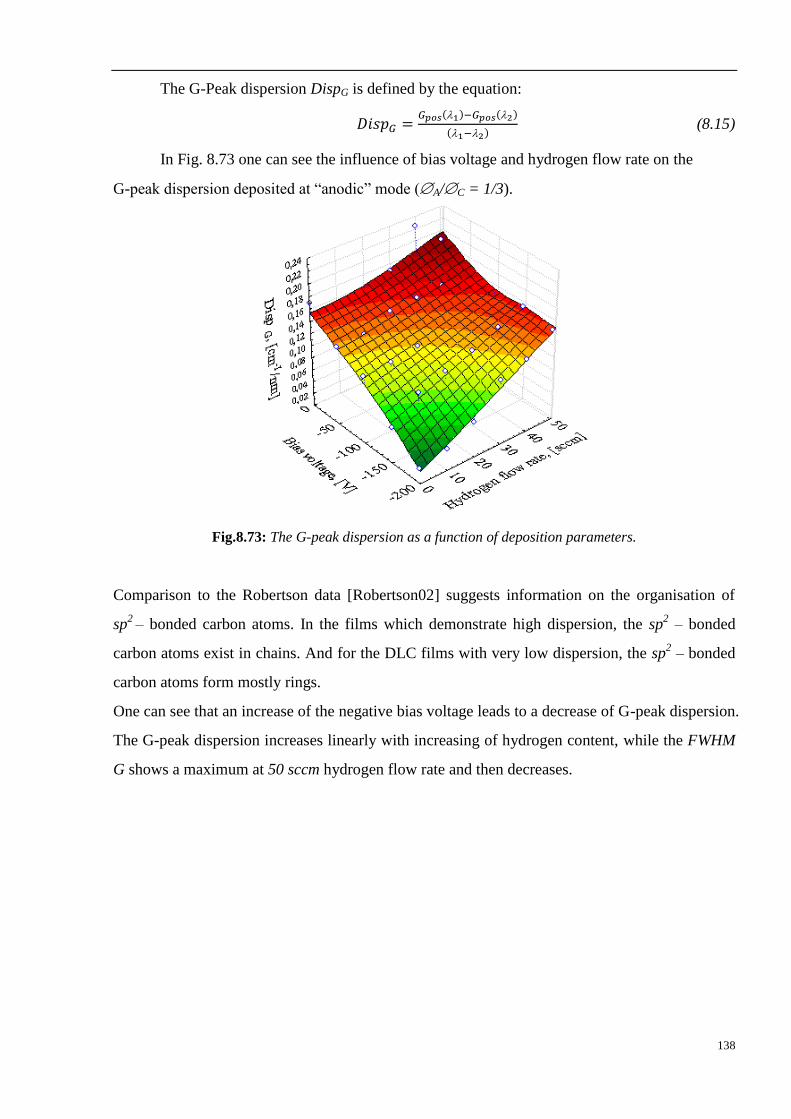
138
The G-Peak dispersion DispG is defined by the equation:
𝐷𝑖𝑠𝑝𝐺 =𝐺𝑝𝑜𝑠(1)−𝐺𝑝𝑜𝑠(2)
(1−2) (8.15)
In Fig. 8.73 one can see the influence of bias voltage and hydrogen flow rate on the
G-peak dispersion deposited at “anodic” mode (A/C = 1/3).
Fig.8.73: The G-peak dispersion as a function of deposition parameters.
Comparison to the Robertson data [Robertson02] suggests information on the organisation of
sp2
– bonded carbon atoms. In the films which demonstrate high dispersion, the sp2 – bonded
carbon atoms exist in chains. And for the DLC films with very low dispersion, the sp2 – bonded
carbon atoms form mostly rings.
One can see that an increase of the negative bias voltage leads to a decrease of G-peak dispersion.
The G-peak dispersion increases linearly with increasing of hydrogen content, while the FWHM
G shows a maximum at 50 sccm hydrogen flow rate and then decreases.
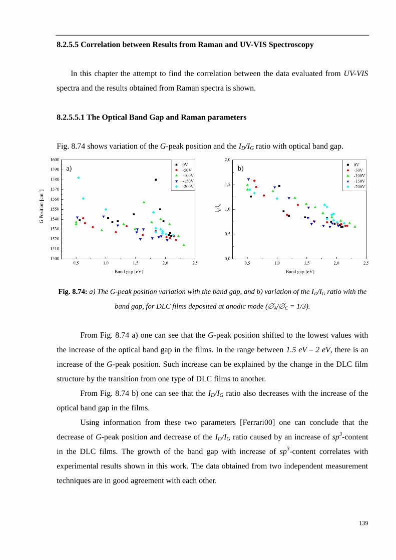
139
8.2.5.5 Correlation between Results from Raman and UV-VIS Spectroscopy
In this chapter the attempt to find the correlation between the data evaluated from UV-VIS
spectra and the results obtained from Raman spectra is shown.
8.2.5.5.1 The Optical Band Gap and Raman parameters
Fig. 8.74 shows variation of the G-peak position and the ID/IG ratio with optical band gap.
Fig. 8.74: a) The G-peak position variation with the band gap, and b) variation of the ID/IG ratio with the
band gap, for DLC films deposited at anodic mode (A/C = 1/3).
From Fig. 8.74 a) one can see that the G-peak position shifted to the lowest values with
the increase of the optical band gap in the films. In the range between 1.5 eV – 2 eV, there is an
increase of the G-peak position. Such increase can be explained by the change in the DLC film
structure by the transition from one type of DLC films to another.
From Fig. 8.74 b) one can see that the ID/IG ratio also decreases with the increase of the
optical band gap in the films.
Using information from these two parameters [Ferrari00] one can conclude that the
decrease of G-peak position and decrease of the ID/IG ratio caused by an increase of sp3-content
in the DLC films. The growth of the band gap with increase of sp3-content correlates with
experimental results shown in this work. The data obtained from two independent measurement
techniques are in good agreement with each other.
a) b)
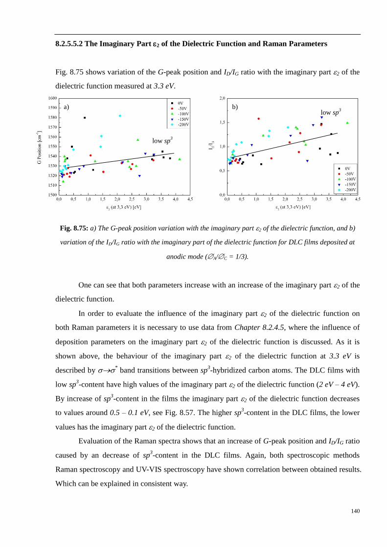
140
8.2.5.5.2 The Imaginary Part 2 of the Dielectric Function and Raman Parameters
Fig. 8.75 shows variation of the G-peak position and ID/IG ratio with the imaginary part 2 of the
dielectric function measured at 3.3 eV.
Fig. 8.75: a) The G-peak position variation with the imaginary part 2 of the dielectric function, and b)
variation of the ID/IG ratio with the imaginary part of the dielectric function for DLC films deposited at
anodic mode (A/C = 1/3).
One can see that both parameters increase with an increase of the imaginary part 2 of the
dielectric function.
In order to evaluate the influence of the imaginary part 2 of the dielectric function on
both Raman parameters it is necessary to use data from Chapter 8.2.4.5, where the influence of
deposition parameters on the imaginary part 2 of the dielectric function is discussed. As it is
shown above, the behaviour of the imaginary part 2 of the dielectric function at 3.3 eV is
described by * band transitions between sp
3-hybridized carbon atoms. The DLC films with
low sp3-content have high values of the imaginary part 2 of the dielectric function (2 eV – 4 eV).
By increase of sp3-content in the films the imaginary part 2 of the dielectric function decreases
to values around 0.5 – 0.1 eV, see Fig. 8.57. The higher sp3-content in the DLC films, the lower
values has the imaginary part 2 of the dielectric function.
Evaluation of the Raman spectra shows that an increase of G-peak position and ID/IG ratio
caused by an decrease of sp3-content in the DLC films. Again, both spectroscopic methods
Raman spectroscopy and UV-VIS spectroscopy have shown correlation between obtained results.
Which can be explained in consistent way.
a) b)
low sp3
low sp3
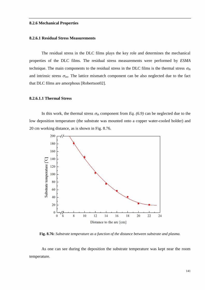
141
8.2.6 Mechanical Properties
8.2.6.1 Residual Stress Measurements
The residual stress in the DLC films plays the key role and determines the mechanical
properties of the DLC films. The residual stress measurements were performed by ESMA
technique. The main components to the residual stress in the DLC films is the thermal stress th
and intrinsic stress int. The lattice mismatch component can be also neglected due to the fact
that DLC films are amorphous [Robertson02].
8.2.6.1.1 Thermal Stress
In this work, the thermal stress th component from Eq. (6.9) can be neglected due to the
low deposition temperature (the substrate was mounted onto a copper water-cooled holder) and
20 cm working distance, as is shown in Fig. 8.76.
Fig. 8.76: Substrate temperature as a function of the distance between substrate and plasma.
As one can see during the deposition the substrate temperature was kept near the room
temperature.
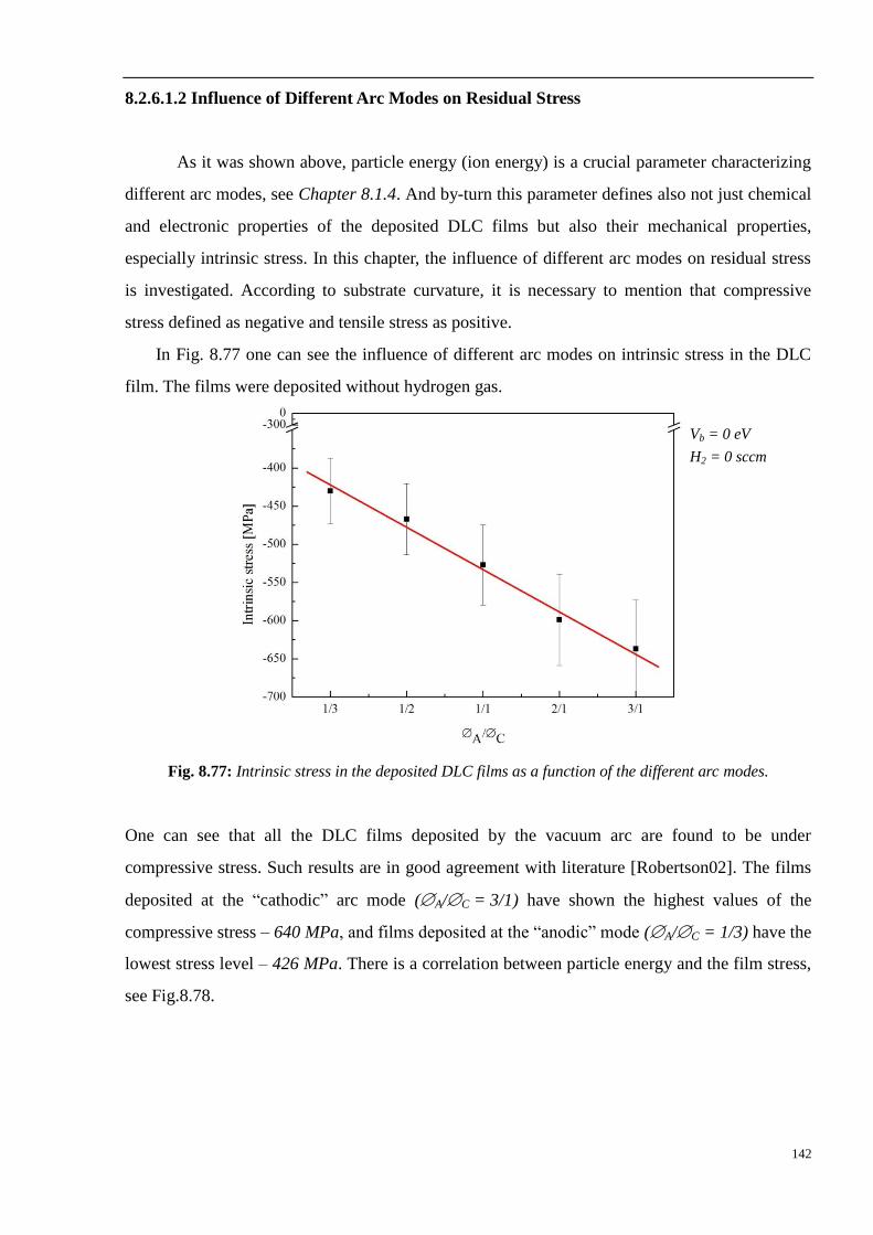
142
8.2.6.1.2 Influence of Different Arc Modes on Residual Stress
As it was shown above, particle energy (ion energy) is a crucial parameter characterizing
different arc modes, see Chapter 8.1.4. And by-turn this parameter defines also not just chemical
and electronic properties of the deposited DLC films but also their mechanical properties,
especially intrinsic stress. In this chapter, the influence of different arc modes on residual stress
is investigated. According to substrate curvature, it is necessary to mention that compressive
stress defined as negative and tensile stress as positive.
In Fig. 8.77 one can see the influence of different arc modes on intrinsic stress in the DLC
film. The films were deposited without hydrogen gas.
Fig. 8.77: Intrinsic stress in the deposited DLC films as a function of the different arc modes.
One can see that all the DLC films deposited by the vacuum arc are found to be under
compressive stress. Such results are in good agreement with literature [Robertson02]. The films
deposited at the “cathodic” arc mode (A/C = 3/1) have shown the highest values of the
compressive stress – 640 MPa, and films deposited at the “anodic” mode (A/C = 1/3) have the
lowest stress level – 426 MPa. There is a correlation between particle energy and the film stress,
see Fig.8.78.
Vb = 0 eV
H2 = 0 sccm
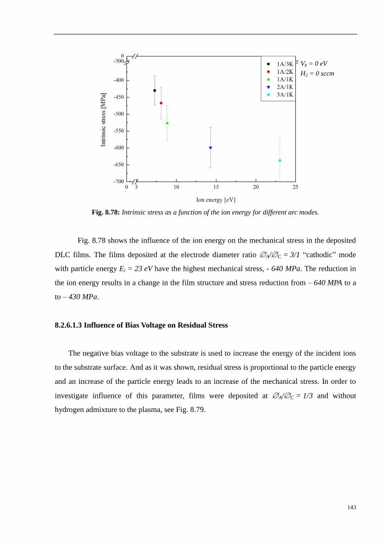
143
Fig. 8.78: Intrinsic stress as a function of the ion energy for different arc modes.
Fig. 8.78 shows the influence of the ion energy on the mechanical stress in the deposited
DLC films. The films deposited at the electrode diameter ratio A/C = 3/1 “cathodic” mode
with particle energy Ei = 23 eV have the highest mechanical stress, - 640 MPa. The reduction in
the ion energy results in a change in the film structure and stress reduction from – 640 MPA to a
to – 430 MPa.
8.2.6.1.3 Influence of Bias Voltage on Residual Stress
The negative bias voltage to the substrate is used to increase the energy of the incident ions
to the substrate surface. And as it was shown, residual stress is proportional to the particle energy
and an increase of the particle energy leads to an increase of the mechanical stress. In order to
investigate influence of this parameter, films were deposited at A/C = 1/3 and without
hydrogen admixture to the plasma, see Fig. 8.79.
Vb = 0 eV
H2 = 0 sccm
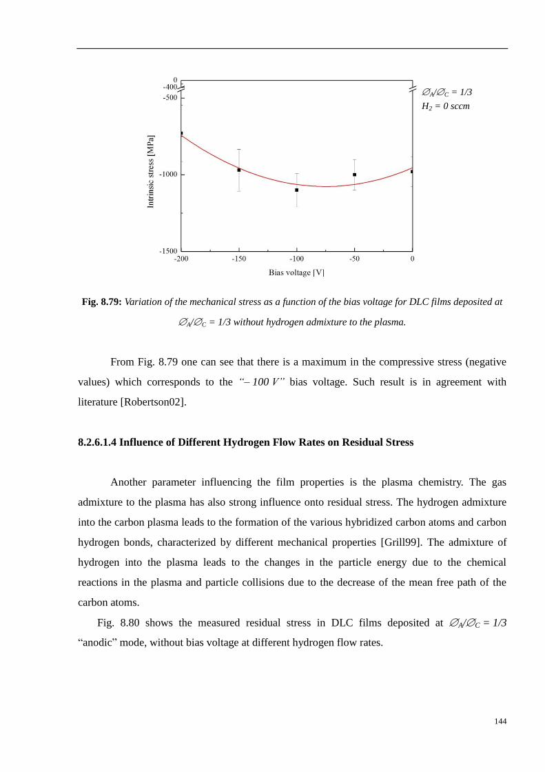
144
Fig. 8.79: Variation of the mechanical stress as a function of the bias voltage for DLC films deposited at
A/C = 1/3 without hydrogen admixture to the plasma.
From Fig. 8.79 one can see that there is a maximum in the compressive stress (negative
values) which corresponds to the “– 100 V” bias voltage. Such result is in agreement with
literature [Robertson02].
8.2.6.1.4 Influence of Different Hydrogen Flow Rates on Residual Stress
Another parameter influencing the film properties is the plasma chemistry. The gas
admixture to the plasma has also strong influence onto residual stress. The hydrogen admixture
into the carbon plasma leads to the formation of the various hybridized carbon atoms and carbon
hydrogen bonds, characterized by different mechanical properties [Grill99]. The admixture of
hydrogen into the plasma leads to the changes in the particle energy due to the chemical
reactions in the plasma and particle collisions due to the decrease of the mean free path of the
carbon atoms.
Fig. 8.80 shows the measured residual stress in DLC films deposited at A/C = 1/3
“anodic” mode, without bias voltage at different hydrogen flow rates.
A/C = 1/3
H2 = 0 sccm
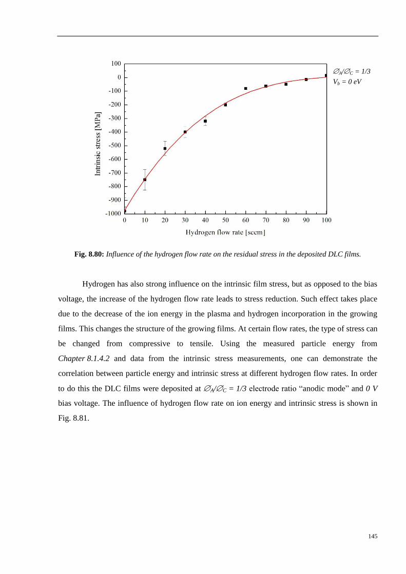
145
Fig. 8.80: Influence of the hydrogen flow rate on the residual stress in the deposited DLC films.
Hydrogen has also strong influence on the intrinsic film stress, but as opposed to the bias
voltage, the increase of the hydrogen flow rate leads to stress reduction. Such effect takes place
due to the decrease of the ion energy in the plasma and hydrogen incorporation in the growing
films. This changes the structure of the growing films. At certain flow rates, the type of stress can
be changed from compressive to tensile. Using the measured particle energy from
Chapter 8.1.4.2 and data from the intrinsic stress measurements, one can demonstrate the
correlation between particle energy and intrinsic stress at different hydrogen flow rates. In order
to do this the DLC films were deposited at A/C = 1/3 electrode ratio “anodic mode” and 0 V
bias voltage. The influence of hydrogen flow rate on ion energy and intrinsic stress is shown in
Fig. 8.81.
A/C = 1/3
Vb = 0 eV
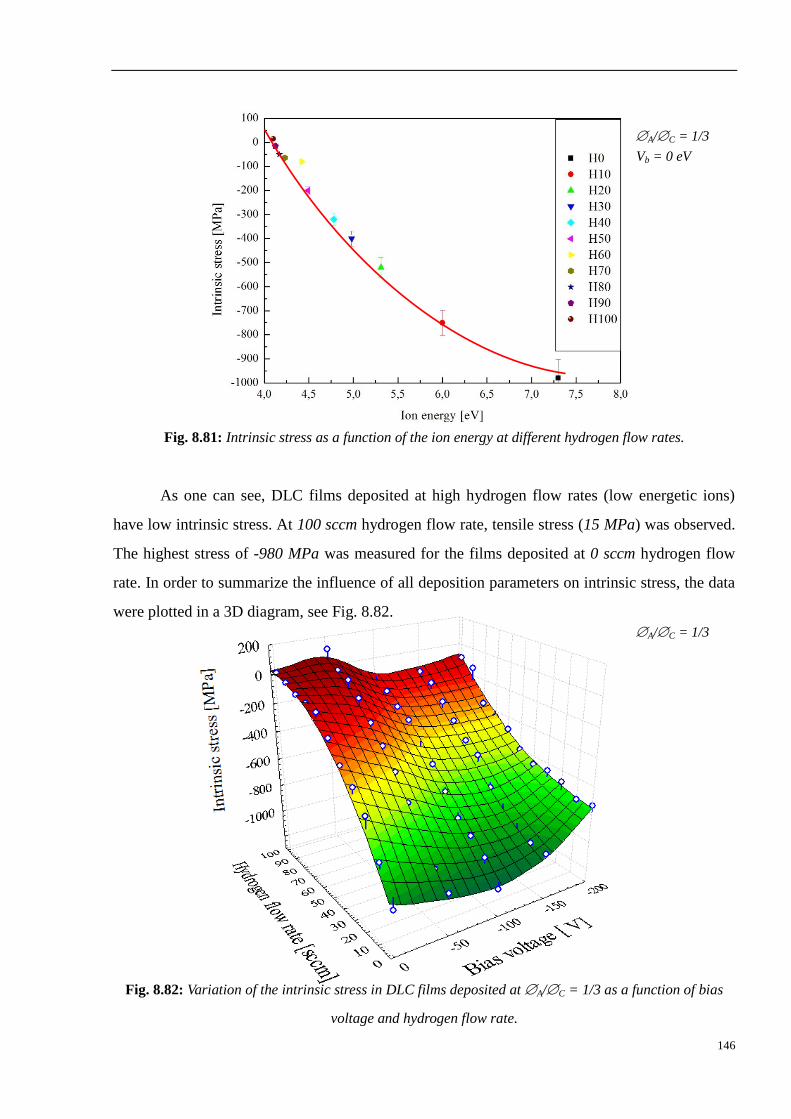
146
Fig. 8.81: Intrinsic stress as a function of the ion energy at different hydrogen flow rates.
As one can see, DLC films deposited at high hydrogen flow rates (low energetic ions)
have low intrinsic stress. At 100 sccm hydrogen flow rate, tensile stress (15 MPa) was observed.
The highest stress of -980 MPa was measured for the films deposited at 0 sccm hydrogen flow
rate. In order to summarize the influence of all deposition parameters on intrinsic stress, the data
were plotted in a 3D diagram, see Fig. 8.82.
Fig. 8.82: Variation of the intrinsic stress in DLC films deposited at A/C = 1/3 as a function of bias
voltage and hydrogen flow rate.
A/C = 1/3
Vb = 0 eV
A/C = 1/3
147
In a case of DLC films deposited without working gas an increase of the bias voltage till
“– 100 V” leads to an increase of the residual film stress. Such effect can be explained by the
increase of the C C sp3 – hybridized carbon atoms content (the amount of stress is proportional
to the sp3 content, as explained by “subplantation model” [Robertson99]). Further increase of
bias voltage leads to the reduction of the intrinsic stress.
For the DLC films deposited in hydrogen atmosphere the increase of the hydrogen flow
rate leads to “stress termination”, it saturates carbon bonds and prevents formation of the C C
sp3– hybridized carbon atoms. Presence of hydrogen leads to formation of soft polymeric
sp3 = CH2 and CH sites, (see Chapter 8.2.4.4.2) which are responsible for poor mechanical
properties of such DLC films.
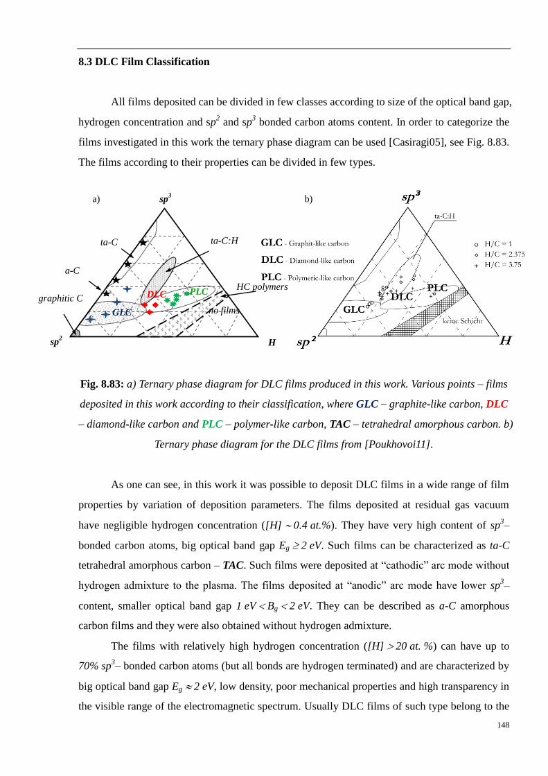
148
8.3 DLC Film Classification
All films deposited can be divided in few classes according to size of the optical band gap,
hydrogen concentration and sp2 and sp
3 bonded carbon atoms content. In order to categorize the
films investigated in this work the ternary phase diagram can be used [Casiragi05], see Fig. 8.83.
The films according to their properties can be divided in few types.
Fig. 8.83: a) Ternary phase diagram for DLC films produced in this work. Various points – films
deposited in this work according to their classification, where GLC – graphite-like carbon, DLC
– diamond-like carbon and PLC – polymer-like carbon, TAC – tetrahedral amorphous carbon. b)
Ternary phase diagram for the DLC films from [Poukhovoi11].
As one can see, in this work it was possible to deposit DLC films in a wide range of film
properties by variation of deposition parameters. The films deposited at residual gas vacuum
have negligible hydrogen concentration ([H] 0.4 at.%). They have very high content of sp3–
bonded carbon atoms, big optical band gap Eg 2 eV. Such films can be characterized as ta-C
tetrahedral amorphous carbon – TAC. Such films were deposited at “cathodic” arc mode without
hydrogen admixture to the plasma. The films deposited at “anodic” arc mode have lower sp3–
content, smaller optical band gap 1 eV Bg 2 eV. They can be described as a-C amorphous
carbon films and they were also obtained without hydrogen admixture.
The films with relatively high hydrogen concentration ([H] 20 at. %) can have up to
70% sp3– bonded carbon atoms (but all bonds are hydrogen terminated) and are characterized by
big optical band gap Eg 2 eV, low density, poor mechanical properties and high transparency in
the visible range of the electromagnetic spectrum. Usually DLC films of such type belong to the
b) a) sp3
H
no films
ta-C:H
HC polymers
graphitic C
sp2
ta-C
PLC DLC
GLC
a-C
149
polymer-like DLC – PLC. Such films were deposited at high hydrogen flow rates over 50 sccm
in “anodic” arc mode.
The a-C:H films with low hydrogen concentration (10 at. % [H] 20 at. %) have
lower content of sp3– bonded carbon atoms than polymer-like DLC but the concentration of C –
C sp3
bonds is higher. Therefore they have higher density and their mechanical properties are
much better than for PLC. Their optical transmittance is lower than for polymer-like films and
their optical band gap is narrower 1 eV Bg 2 eV. The films with such properties are common
for DLC a-C:H films – DLC. Such films were deposited at the hydrogen flow rates between 30
and 50 sccm in “anodic” arc mode.
DLC films with low hydrogen content ([H] 10 at. %) are usually characterized by high
sp2– bonded carbon atoms concentration. They have narrow band gap Bg 1 eV, low
transmittance and poor mechanical properties. Such films are usually called – graphite-like
a-C:H films – GLC. Such films were deposited at the hydrogen flow rates below 30 sccm in
“anodic” arc mode.
Comparing the films deposited in this work by vacuum arc Fig. 8.83a) and the films
deposited by ICP/CCP plasma source [Poukhovoi11] Fig. 8.83b), one can see that both plasma
sources are working in the same particle energy range from several eV till 100 eV. Such
similarity is also confirmed by the ternary phase diagrams obtained in this work and in the work
[Poukhovoi11]. Both plasma sources are able to produce DLC coatings in a wide range of the
film classes. But there is a difference mainly originated from the differences between CVD and
PVD deposition techniques. By the CVD system, it was possible to deposit ta-C:H films but
such class of coatings was not possible to obtain by PVD method in this work. However the
CVD system is not able to produce DLC coatings with low hydrogen content or “hydrogen-free”
coatings.
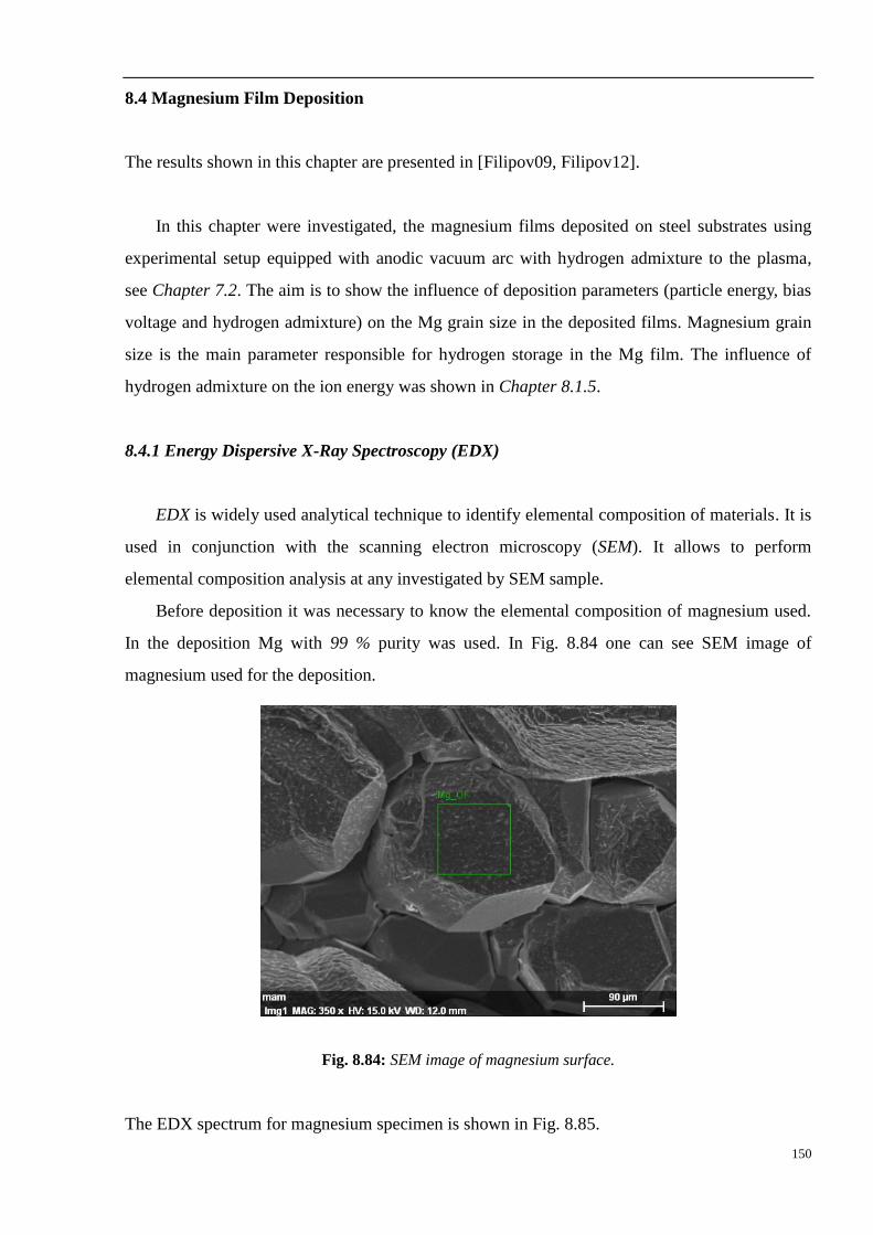
150
8.4 Magnesium Film Deposition
The results shown in this chapter are presented in [Filipov09, Filipov12].
In this chapter were investigated, the magnesium films deposited on steel substrates using
experimental setup equipped with anodic vacuum arc with hydrogen admixture to the plasma,
see Chapter 7.2. The aim is to show the influence of deposition parameters (particle energy, bias
voltage and hydrogen admixture) on the Mg grain size in the deposited films. Magnesium grain
size is the main parameter responsible for hydrogen storage in the Mg film. The influence of
hydrogen admixture on the ion energy was shown in Chapter 8.1.5.
8.4.1 Energy Dispersive X-Ray Spectroscopy (EDX)
EDX is widely used analytical technique to identify elemental composition of materials. It is
used in conjunction with the scanning electron microscopy (SEM). It allows to perform
elemental composition analysis at any investigated by SEM sample.
Before deposition it was necessary to know the elemental composition of magnesium used.
In the deposition Mg with 99 % purity was used. In Fig. 8.84 one can see SEM image of
magnesium used for the deposition.
Fig. 8.84: SEM image of magnesium surface.
The EDX spectrum for magnesium specimen is shown in Fig. 8.85.
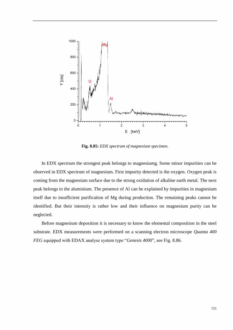
151
Fig. 8.85: EDX spectrum of magnesium specimen.
In EDX spectrum the strongest peak belongs to magnesiumg. Some minor impurities can be
observed in EDX spectrum of magnesium. First impurity detected is the oxygen. Oxygen peak is
coming from the magnesium surface due to the strong oxidation of alkaline earth metal. The next
peak belongs to the aluminium. The presence of Al can be explained by impurities in magnesium
itself due to insufficient purification of Mg during production. The remaining peaks cannot be
identified. But their intensity is rather low and their influence on magnesium purity can be
neglected.
Before magnesium deposition it is necessary to know the elemental composition in the steel
substrate. EDX measurements were performed on a scanning electron microscope Quanta 400
FEG equipped with EDAX analyse system type “Genesis 4000”, see Fig. 8.86.
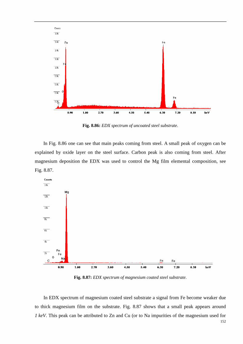
152
Fig. 8.86: EDX spectrum of uncoated steel substrate.
In Fig. 8.86 one can see that main peaks coming from steel. A small peak of oxygen can be
explained by oxide layer on the steel surface. Carbon peak is also coming from steel. After
magnesium deposition the EDX was used to control the Mg film elemental composition, see
Fig. 8.87.
Fig. 8.87: EDX spectrum of magnesium coated steel substrate.
In EDX spectrum of magnesium coated steel substrate a signal from Fe become weaker due
to thick magnesium film on the substrate. Fig. 8.87 shows that a small peak appears around
1 keV. This peak can be attributed to Zn and Cu (or to Na impurities of the magnesium used for
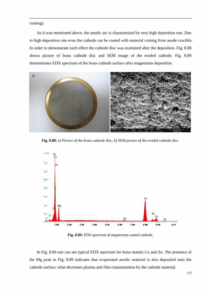
153
coating).
As it was mentioned above, the anodic arc is characterized by very high deposition rate. Due
to high deposition rate even the cathode can be coated with material coming from anode crucible.
In order to demonstrate such effect the cathode disc was examined after the deposition. Fig. 8.88
shows picture of brass cathode disc and SEM image of the eroded cathode. Fig. 8.89
demonstrates EDX spectrum of the brass cathode surface after magnesium deposition.
Fig. 8.88: a) Picture of the brass cathode disc, b) SEM picture of the eroded cathode disc.
Fig. 8.89: EDX spectrum of magnesium coated cathode.
In Fig. 8.89 one can see typical EDX spectrum for brass mainly Cu and Zn. The presence of
the Mg peak in Fig. 8.89 indicates that evaporated anodic material is also deposited onto the
cathode surface, what decreases plasma and film contamination by the cathode material.
a) b)
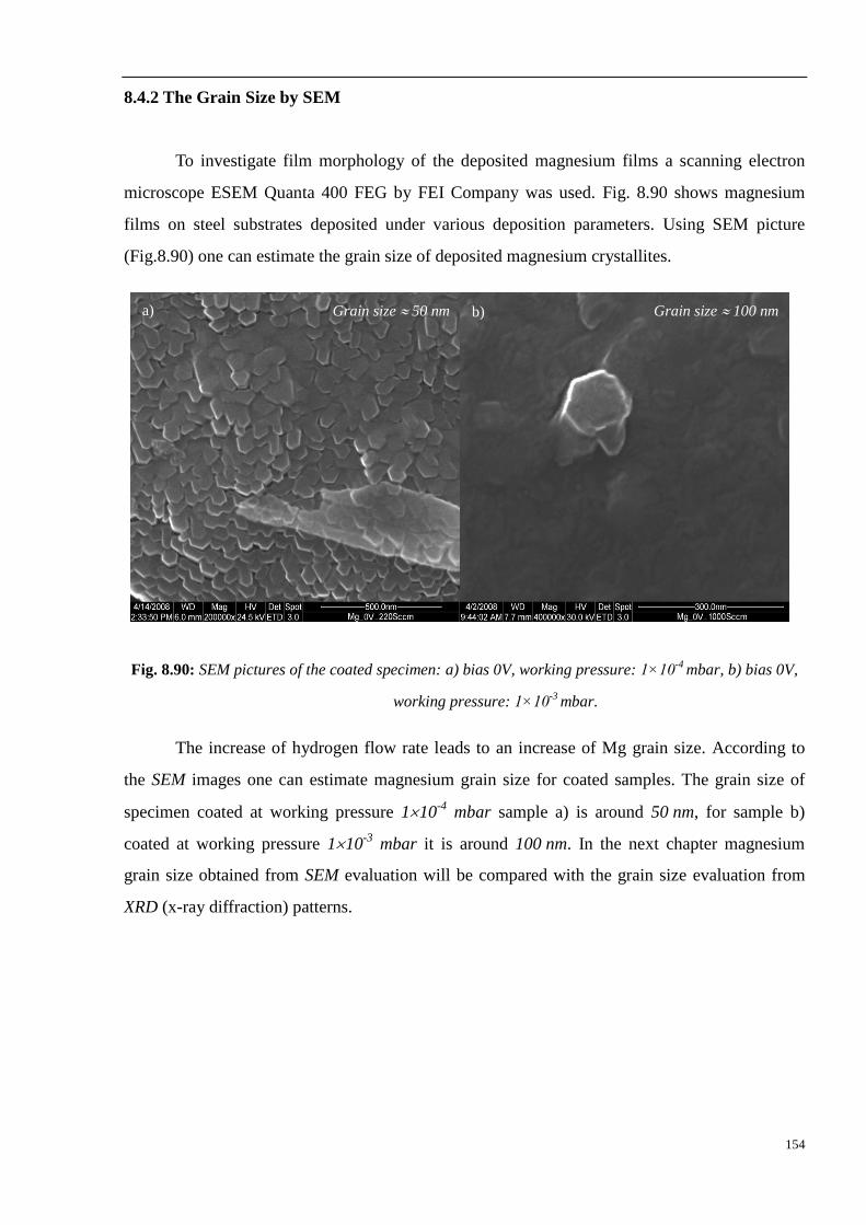
154
8.4.2 The Grain Size by SEM
To investigate film morphology of the deposited magnesium films a scanning electron
microscope ESEM Quanta 400 FEG by FEI Company was used. Fig. 8.90 shows magnesium
films on steel substrates deposited under various deposition parameters. Using SEM picture
(Fig.8.90) one can estimate the grain size of deposited magnesium crystallites.
Fig. 8.90: SEM pictures of the coated specimen: a) bias 0V, working pressure: 1×10⁻⁴
mbar, b) bias 0V,
working pressure: 1×10⁻³
mbar.
The increase of hydrogen flow rate leads to an increase of Mg grain size. According to
the SEM images one can estimate magnesium grain size for coated samples. The grain size of
specimen coated at working pressure 110-4
mbar sample a) is around 50 nm, for sample b)
coated at working pressure 110-3
mbar it is around 100 nm. In the next chapter magnesium
grain size obtained from SEM evaluation will be compared with the grain size evaluation from
XRD (x-ray diffraction) patterns.
a) b) Grain size 50 nm Grain size 100 nm
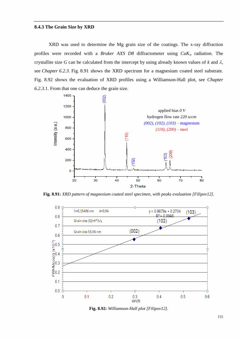
155
8.4.3 The Grain Size by XRD
XRD was used to determine the Mg grain size of the coatings. The x-ray diffraction
profiles were recorded with a Bruker AXS D8 diffractometer using CuK radiation. The
crystallite size G can be calculated from the intercept by using already known values of k and ,
see Chapter 6.2.3. Fig. 8.91 shows the XRD spectrum for a magnesium coated steel substrate.
Fig. 8.92 shows the evaluation of XRD profiles using a Williamson-Hall plot, see Chapter
6.2.3.1. From that one can deduce the grain size.
Fig. 8.91: XRD pattern of magnesium coated steel specimen, with peaks evaluation [Filipov12].
Fig. 8.92: Williamson-Hall plot [Filipov12].
applied bias 0 V
hydrogen flow rate 220 sccm
(002), (102), (103) – magnesium
(110), (200) – steel
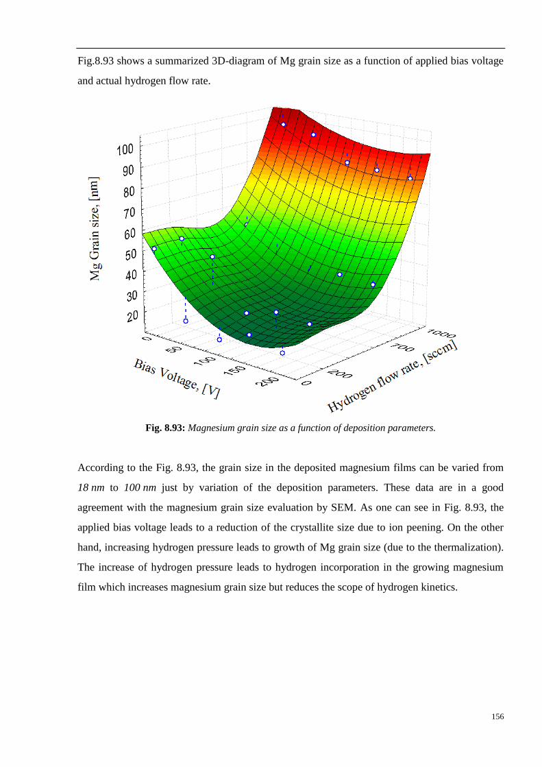
156
Fig.8.93 shows a summarized 3D-diagram of Mg grain size as a function of applied bias voltage
and actual hydrogen flow rate.
Fig. 8.93: Magnesium grain size as a function of deposition parameters.
According to the Fig. 8.93, the grain size in the deposited magnesium films can be varied from
18 nm to 100 nm just by variation of the deposition parameters. These data are in a good
agreement with the magnesium grain size evaluation by SEM. As one can see in Fig. 8.93, the
applied bias voltage leads to a reduction of the crystallite size due to ion peening. On the other
hand, increasing hydrogen pressure leads to growth of Mg grain size (due to the thermalization).
The increase of hydrogen pressure leads to hydrogen incorporation in the growing magnesium
film which increases magnesium grain size but reduces the scope of hydrogen kinetics.
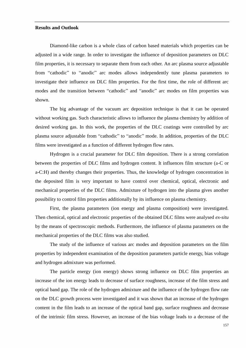
157
Results and Outlook
Diamond-like carbon is a whole class of carbon based materials which properties can be
adjusted in a wide range. In order to investigate the influence of deposition parameters on DLC
film properties, it is necessary to separate them from each other. An arc plasma source adjustable
from “cathodic” to “anodic” arc modes allows independently tune plasma parameters to
investigate their influence on DLC film properties. For the first time, the role of different arc
modes and the transition between “cathodic” and “anodic” arc modes on film properties was
shown.
The big advantage of the vacuum arc deposition technique is that it can be operated
without working gas. Such characteristic allows to influence the plasma chemistry by addition of
desired working gas. In this work, the properties of the DLC coatings were controlled by arc
plasma source adjustable from “cathodic” to “anodic” mode. In addition, properties of the DLC
films were investigated as a function of different hydrogen flow rates.
Hydrogen is a crucial parameter for DLC film deposition. There is a strong correlation
between the properties of DLC films and hydrogen content. It influences film structure (a-C or
a-C:H) and thereby changes their properties. Thus, the knowledge of hydrogen concentration in
the deposited film is very important to have control over chemical, optical, electronic and
mechanical properties of the DLC films. Admixture of hydrogen into the plasma gives another
possibility to control film properties additionally by its influence on plasma chemistry.
First, the plasma parameters (ion energy and plasma composition) were investigated.
Then chemical, optical and electronic properties of the obtained DLC films were analysed ex-situ
by the means of spectroscopic methods. Furthermore, the influence of plasma parameters on the
mechanical properties of the DLC films was also studied.
The study of the influence of various arc modes and deposition parameters on the film
properties by independent examination of the deposition parameters particle energy, bias voltage
and hydrogen admixture was performed.
The particle energy (ion energy) shows strong influence on DLC film properties an
increase of the ion energy leads to decrease of surface roughness, increase of the film stress and
optical band gap. The role of the hydrogen admixture and the influence of the hydrogen flow rate
on the DLC growth process were investigated and it was shown that an increase of the hydrogen
content in the film leads to an increase of the optical band gap, surface roughness and decrease
of the intrinsic film stress. However, an increase of the bias voltage leads to a decrease of the
158
surface roughness and an increase of the residual stress in the film. All these parameters can be
separately adjusted in order to obtain desired film properties. As one can see, the influence of
deposition parameters on film properties is very important for controlled deposition of DLC
films.
By plasma diagnostic, it was shown that each arc mode is characterized by the individual
set of parameters (particle energy, deposition rate) and differs from each other. The “anodic” arc
mode is characterized by the highest deposition rate 5 nm/s but it produces the ions with the
lowest particle energy Ei 7 eV, among other arc modes. The film analysis shows, the DLC
films deposited at this mode have the lowest surface roughness 1.45 nm, moderate intrinsic stress
– 426 MPa, narrow optical band gap 1 eV Bg 2 eV and content of sp3- bonded carbon atoms
around 40%.
In contrast to the “anodic” mode the “cathodic” arc mode has the lowest deposition rate
around 1 nm/s, but the highest measured particle energy Ei 23 eV. DLC films deposited under
such mode show the biggest optical band gap Bg 2 eV highest intrinsic stress 640 MPa and sp3-
content around 70%.
By hydrogen admixture into the plasma, it was possible to change all these parameters
and adjust them in a wide range.
By the help of NRA technique it was possible to calibrate mass-spectroscopic data and to
show that the hydrogen content in the deposited films can be determined without any structural
analysis by using only spectroscopic techniques. The investigation of the UV-VIS spectra
provides information about optical and electronic properties of the deposited DLC films. The
correlation between plasma parameters and film properties is also discussed. As it was shown by
the Raman spectroscopy, the hydrogen admixture into the plasma changes the chemical
composition and the film structure. The content of sp3- hybridized atoms and hydrogen content
growth with the increase of hydrogen admixture in the plasma. It should be mentioned, there are
no reliable sources concerning Raman behaviour for the coatings with hydrogen concentration
around few percents. Therefore application of Raman spectroscopy for the evaluation of
so-called “hydrogen-free” coatings – without confirmation that they are really hydrogen-free – is
not possible.
The correlation between the results obtained from spectroscopic methods is observed.
The data obtained from two independent spectroscopic measurement techniques (Raman
spectroscopy and UV-VIS spectroscopy) are in good agreement with each other.
The stress measurements in the deposited DLC films have shown that the mechanical
159
stress in films can be influenced and adjusted according to the deposition parameters.
In this work, the ability to deposit DLC films in a wide range of film properties and
variation of deposition parameters by arc plasma source adjustable from cathodic to anodic mode
was shown. The influence of deposition parameters on DLC film properties and possibility to
tailor them according to the functional properties was demonstrated.
The arc plasma source adjustable from “cathodic” to “anodic” mode is a promising
deposition technique which is able to deliver DLC films in a wide range of properties with
controlled structure and characteristics. Therefore, it would be interesting to extend the range of
investigated parameters, especially mechanical properties (hardness,...), and produce DLC films
with very low, but controlled hydrogen content; and to continue the research on the topic
discussed in this work.
160
References
[Adamopoulos04] G. Adamopoulos, J. Robertson, N. A. Morrison and C. Godet:
Hydrogen content estimation of hydrogenated amorphous carbon by
visible Raman spectroscopy, Journ. Appl. Phys. Vol. 96, No. 11
(2004).
[Aksenov78] I.I. Aksenov, V.A. Belous, V.G. Padalka and V.M. Khoroshikh:
Transport of Plasma Streams in a Curvilinear Plasma – Optics System,
Sov. J. Plasma Phys. 4 (1978), 425.
[Aksenov93] I. I. Aksenov, S. I. Vakula and V. E. Strel’nitskij: Optical spectra of
diamond-like carbon films in the energy region between 1 and 13 eV,
Diam. Relat. Mater. 2 (1993), 1387-1390.
[Anders99] A. Anders: Approaches to Rid Cathodic Arc Plasmas of Macro- and
Nanoparticles a Review, Surf. Coat. Technol. 120–121 (1999), 319.
[Angus88] J. C. Angus and F. Jansen: Dense “Diamond-like” Hydrocarbons as
Random Covalent Networks, J. Vac. Sci. Tech. A6 (1988), 1778.
[Angus91] J. S. Angus: Diamond and Diamond-like Phases, Diamond Relat.
Mater. 1 (1991), 61.
[Balandin08] A. A. Balandin, S. Ghosh, W. Bao, I. Calizo, D. Teweldebrhan,
F. Miao and C. N. Lau: Extremely High Thermal Conductivity of
Graphene: Experimental Study, Nano Letters, Vol. 8, No. 3, (2008),
902-907.
161
[Bogdanovic85] B. Bogdanovic: Catalytic synthesis of Organolithium and
organomagnesium compounds and of lithium and magnesium hydrides
- applications in organic synthesis and hydrogen storage, Angewandte
Chemie International Edition in English 24 (1985), 262–273.
[Born02] M. Born and E. Wolf: Principles of Optics, 7th
Edition Cambridge
University Press (2002).
[Bovchar73] D. Bovchar and E. Galperin: Academy of Science Reports. 209.
(1973), 610-612.
[Boxman95] R. L. Boxman, D. S. Sanders, P. J. Martin and J. M. Lafferty:
Handbook of Vacuum Arc Science and Technology – Fundamentals
and Applications, Noyes Publications, Park Ridge (1995).
[Bragg13] W. L. Bragg: The Diffraction of Short Electromagnetic Waves by a
Crystal, Proceedings of the Cambridge Philosophical Society 17
(1913), 43–57.
[Buck91] V. Buck, J. Bur am Orde, M. Mausbach: Deposition of Diamondlike
Carbon Films by Anodic Arc Technique, Materials Science and
Engineering A14O, (1991), 770.
[Buck93] V. Buck: Microanalysis and Modelling of Tribological Coatings,
Surface and Coatings Technology 57, (1993), 163.
[Buck06] V. Buck, N. Wöhrl, A. Poukhovoi, O. Filipov, M. Haase and Y.-Ch.
Lee: Adjusting Residual Stress, Adhesion, Tribological Performance
and Wettability of Nanocrystalline and Diamondlike Hard Carbon
Coatings, in: Application of Nanocrystalline Diamond and
Diamondlike Carbon Materials, in N.R. Ray (Ed.): “Application of
Nano-crystalline Diamond and Diamond like Carbon Materials”,
Kolkata (2006), 57.
162
[Buck06] V. Buck: Lecture materials, (2006).
[Bunch07] J. S. Bunch:. Electromechanical Resonators from Graphene Sheets,
Science 315, 490 (2007).
[Casiragi05] C. Casiraghi, A.C. Ferrari and J. Robertson: Raman Spectroscopy of
Hydrogenated Amorphous Carbons, Phys. Rev. B72 (2005), 085401.
[Cowley75] John M. Cowley: Diffraction physics, North-Holland, Amsterdam
(1975).
[Darriet80] B. Darriet, M. Pezal: Application of magnesium rich rare-earth alloys
to hydrogen storage, Int. J. Hydrogen Energy 5(2) (1980), 173.
[Dillon97] A. C. Dillon, K. M. Jones, T. A. Bekkedahl, C. H. Kiang, D. S. Bethune
and M. J. Heben: Storage of hydrogen in single-walled carbon
nanotubes, Nature 386 (6623), (1997), 377-379.
[Dillon01] A. C. Dillon, M. Heben: Hydrogen storage using carbon adsorbents:
past, present and future, J. Appl. Phys. A: Mater. Sci. Process. 72
(2001), 133-142.
[Eaton10] P. Eaton, P. West: Atomic Force Microscopy, Oxford University Press,
(2010), 256.
[Eckhardt75] G. Eckhardt: Interpretation of data on cathode erosion and efflux from
cathode spots of vacuum arcs, J. Appl. Phys. 46, (1975), 3282.
[Ehrich88a] H. Ehrich: The anodic vacuum arc. I. Basic construction and
phenomenology, J. Vac. Sci. Technol. A 6(1) (1988), 134-138.
163
[Ehrich88b] H. Ehrich, B. Hasse, M. Mausbach, K. G. Mueller, R. Schmidt: The
anodic vacuum arc. II. Experimental study of arc plasma, J. Vac. Sci.
Technol. A 6(4) (1988) 2499-2503.
[Ehrich90] H. Ehrich, B. Hasse, M. Mausbach and K. G. Mueller: The anodic
vacuum arc and its application to coating, J. Vac. Sci. Technol. A 8(3)
(1990), 2160-2164.
[Ferrari00] A.C. Ferrari and J. Robertson: Interpretation of Raman Spectra of
Disordered and Amorphous Carbon, Phys. Rev. B61 (2000), 14095.
[Ferrari04] A.C. Ferrari and J. Robertson: Raman Spectroscopy of Amorphous
Nanostructured Diamond-like carbon and Nanodiamond, Phil. Trans.
R. Soc. Lond. A362 (2004), 2477.
[Filipov05] O. Filipov, N. Wöhrl, S. Reuter and V. Buck: Correlation of plasma
parameters and diamond-like carbon films properties, DPG Berlin
spring meeting 2005.
[Filipov09] O. Filipov, V. Buck: Deposition of Magnesium Films Using an Anodic
Arc Plasma Source, XVI Workshop Plasmatechnik, Ilmenau (2009).
[Filipov12] O. Filipov, S. Schipporeit, V. Buck: Anodic arc evaporation of
nanocrystalline Mg films, J. Optoelectron. Adv. Mater. 14 (2012), 418.
[Franta06] D. Franta, D. Necas, L. Zajickova and V. Bursikova: Modelling of
DLC Optical Properties Based on Parametrization od Density of
States, IWAncDLC (2006), 39-50.
[Franta07] D. Franta, D. Necas and L. Zajickova: Models of dielectric response in
disordered solids, Optics Express, Vol. 15, No. 24, (2007).
164
[Gordijn04] A. Gordijn, J. K. Rath, and R. E. I. Schropp: Thickness determination
of very thin amorphous and microcrystalline silicon layers using
reflection/transmission measurements, Appl. Phys. Let. Vol.85, No21
(2004), 5096-5098.
[Grill99a] A. Grill: Diamond-like Carbon: State of the Art, Diamond Relat.
Mater. 8 (1999), 428.
[Grill99b] A. Grill: Electrical and Optical Properties of Diamond-like Carbon,
Thin Solid Films 355-356 (1999), 189.
[Grill03] A. Grill: Diamond-like Carbon Coatings as Biocompatible
Materials-an Overview, Diamond Relat. Mater. 12 (2003), 166.
[Hasse92] B. Hasse: Untersuchung des anodischen Vakuumbogens, PhD thesis,
Essen (1992).
[He11] Y. Y. He, G. F. Zhang, V. Buck: Effects of reactors on the deposition of
DLC films using liquid electrochemical technique, Diam and Relat.
Mater.: Vol 20 2 (2011), 97-100.
[Hirscher01] M. Hirscher, M. Becher, M. Haluska, U. Dettlaff-Weglikowska,
A.Quintel, G. S. Duesberg, Y. M. Choi, P. Downes, M. Hulman,
S.Roth, I. Stepanek, P. Bernier: Hydrogen storage in sonicated carbon
materials, Appl. Phys. A: Mater. Sci. Process. 72 (2001), 129-132.
[Hoffman76] R. W. Hoffman: Stresses in thin films: The relevance of grain
boundaries and impurities, Thin Solid Films 34, (1976), 185.
[Horcas07] Horcas, R. Fernandez, J.M. Gomez-Rodriguez, J. Colchero, J.
Gomez-Herrero, A. M. Baro, Rev. Sci. Instrum. 78, 013705, (2007).
165
[Huot01] J. Huot, G. Liang, R. Schulz: Mechanically alloyed metal hydride
systems, Appl. Phys. A: Mater. Sci. Process. 72 (2001), 187-195.
[Iijima91] S. Iijima: Helical Microtubules of Graphitic Carbon, Nature 354
(1991), 56.
[Imamura10] H. Imamura, S. Nakatomi, K. Tanaka, Y. Hashimoto, Y. Sakata:
Magnesium-based nanocomposites synthesized by high-energy ball
milling for hydrogen storage, Proceedings WHEC2010 (2010),
319-322.
[Ingram88] S. G. Ingram, N. St. J. Braithwaile: Ion and electron energy analysis
at a surface in an RF discharge, J. Phys. D. Appl. Phys. 21 (1988),
1496.
[Irmer05] G. Irmer and A. Dorner-Reisel: MicroRaman Studies on DLC
Coatings, Adv. Eng. Mater. 7, No. 8, (2005).
[Jaeger98] S. Jaeger, B. Szyszka, J. Szczyrbowski, G. Brauuer: Comparison of
transparent conductive oxide thin films prepared by a. c. and d. c.
reactive magnetron sputtering, Surface and Coatings Technology 98
(1998), 1304-1314.
[Jüttner01] B. Jüttner: Cathode spots of electric arcs, J. Phys. D: Appl. Phys. 34,
(2001), 103.
[Kadetov04] V. A. Kadetov: Diagnostics and Modeling of an Iductively Coupled
Radio Frequency Discharge in Hydrogen, PhD thesis, Bochum
(2004).
[Karpov97] D.A. Karpov: Cathodic Arc Sources and Macroparticle Filtering,
Surf. Coat. Technol. 96 (1997), 22.
166
[Khlopyanova12] V. Khlopyanova: Erzeugung und Untersuchung wasserstoffarmer
Kohlenstoffschichten, Dipl. thesis, Duisburg (2012).
[Kramers27] H.A. Kramers :La diffusion de la lumiere par les atomes. Atti Cong.
Intern. Fisica, (Transactions of Volta Centenary Congress) Como 2:
(1927), 545–557.
[Kronig26] R de L. Kronig: On the Theory of Dispersion of X-Rays, JOSA, Vol.
12, Issue 6, (1926), 547-556.
[Kroto85] H. W. Kroto, J. R. Heath, S. C. O’Brien, R. F. Curl and R. E. Smalley:
C60: Buckminsterfullerene, Nature 318 (1985), 162.
[Lanford95] W. A. Lanford: Nuclear Reactions for Hydrogen Analysis, Handbook
of Modern Ion Beam Analysis ed. By J. Tesmer and M. Nastasi,
Materials Research Society (1995), 193.
[Lifshitz99] Y. Lifshitz: Diamond-like carbon – present status, Diam and Relat
Mater 8 (1999), 1659-1676.
[Madronero95] A. Madroñero and M. Verdú: Hydrogen Content Evaluation in
Vapour-grown Carbon Fibres by SIMS, Carbon 33 (1995), 247.
[Musa94] G. S. Musa, H. Ehrich, M. Mausbach: Studies on Thermoionic
Cathode Anodic Vacuum Arcs, J. Vac. Sci. Technol. A 12 (1994), 2887.
[Musa97] G. S. Musa, H. Ehrich, J. Schuhmann: Pure metal vapor plasma
source with controlled energy of ions, IEEE Transactions on Plasma
science 23(2) (1997), 386-391.
[Nijkamp01] M. G. Nijkamp, J. Raaymakers, A. J. van Dillen, K. P. de Jong:
Hydrogen storage using physisorption – materials demands, Appl.
Phys. A: Mater. Sci. Process. 72 (2001), 619-623.
167
[Novoselov04] K. S. Novoselov, A. K. Geim, S. V. Morozov, D. Jiang, Y. Zhang, S. V.
Dubonos, I. V. Grigoriev and A. A. Firsov: Electric Field Effect in
Atomically Thin Carbon Films, Science 306, (2004), 666.
[O’Leary97] S. K. O’leary, S. R. Johnson and P. K. Lim: The Relationship Between
the Distribution of Electronic States and the Optical Absorption
Spectrum of an Amorphous Semiconductor: An Empirical Analysis,
J. Appl. Phys. 82 (1997), 3334.
[Osawa70] E. Osawa, Kagaku, Vol. 25, (1970), 854.
[Paret98] V. Paret, A. Sadki, Y. Bounouh, R. Alameh, C. Naud, M. Zarrabian,
A. Seignac, G. Turban, M. L. Theye: Optical investigations of the
microstructure of hydrogenated amorphous carbon films, Journ
Non-Cryst. Solids 227-230 (1998), 583-587.
[Pierson93] H. O. Pierson: Handbook of Carbon, Graphite, Diamonds and
Fullerenes, Noyes Publications, Park Ridge, (1993).
[Poukhovoi11] A. Poukhovoi: Abscheidung von amorphen wasserstoffhaltigen
Kohlenstoffschichten mittels neuartiger hybrider RF-Plasma-Quelle
und deren spektroskopische Charakterisierung, Phd. thesis, Verlag Dr.
Hut, München (2011).
[Radushkevich52] L.V. Radushkevich, V. M. Lukyanovich, Phys. Chem 26 (1952), 89.
[Raizer01] Y. P. Raizer: Gas discharge Physics, Springler-Verlag, Berlin/New
York (2001).
[Robertson87] J. Robertson and E.P. O'reilly: Electronic and Atomic Structure of
Amorphous Carbon, Phys. Rev. B35 (1987), 2946.
168
[Robertson02] J. Robertson: Diamond-like Amorphous Carbon, Mater. Sci. Eng.,
R37, (2002), 129.
[Rudy05] Rudy W. P. Wagemans, Joop H. van Lenthe, Petra E. de Jongh, A. Jos
van Dillen, and Krijn P. de Jong: Hydrogen storage in magnesium
clusters: quantum chemical study, J. Am. Chem. Soc. 127 (2005),
16675-16680.
[Scherrer18] P. Scherrer: Bestimmung der Groesse und der inneren Struktur von
Kolloidteilchen mittels Röntgenstrahlen, Goettinger Nachrichten
Gesell., 2 (1918), 98.
[Schimmel03] H. G. Schimmel, G. J. Kearley, M. G. Nijkamp, C. T. Visserl, K. P. de
Jong, F. M. Mulder: Hydrogen adsorption in carbon nanostructures:
Comparison of nanotubes, fibers, and coals, Chem.- A Eur. J. 9 (2003),
4764-4770.
[Schlapbach01] L. Schlapbach, A. Zuettel: Hydrogen-storage materials for mobile
applications, Nature 414(6861) (2001) 353-358.
[Schuhmann00] J. Schuhmann: Metallisierung von Polymeren: Einfluss der Teilchen-,
Schicht- und Substrateigenschaften auf die Adhaesion kondensierter
Schichten, Shaker Verlag, Aachen (2000).
[Schunk80] Schunk: Carbon and Graphite, Technical documentation (1980).
[Stamm09] B. Stamm, B. Kuezuen, O. Filipov, S. Reuter, I. Erdmann,
F. Deuerler, D. Krix, K. Huba, H. Nienhaus, V. Buck: Adjustment of
wear particle size distribution of DLC coatings for tribological
metal-on-metal pairing in artificial hip joints, Mat.-wiss. u.
Werkstofftech. No. 1-2, (2009), 40.
169
[Stephanakis68] J. D. Stephanakis, W. H. Bennet: Electrostatic energy analyzer for
studying gas-focused electron beams and their background media, Rev.
Sci. Instrum. 39 (1968), 1714.
[Stern67] E. A. Stern: Ridgid-Band Model of Alloys, Phys. Rev. 157, 544–551
(1967).
[Stoney09] G. G. Stoney: The Tension of Metallic Films Deposited by Electrolysis,
Proc. R. Soc. London, Ser. A, 82, (1909), 172–175.
[Surdu-Bob07] C. Surdu-Bob, G. Musa, V. Buck, I. Mustata, O. Filipov and A.
Poukhovoi: Mass Spectrometry and Ion Energy Analysis of the
Carbon TVA Plasma For the Synthesis of DLC Films, J. Optoelectron.
Adv. Mater. 9 (2007), 2657.
[Suryanarayana98] C. Suryanarayana, M. Grant Norton: X-ray diffraction – a practical
approach, Plenum Press, New York (1998).
[Toll56] J. S. Toll: Causality and the Dispersion Relation: Logical Foundation,
Phys. Rev. 104, (1956), 1760–1770.
[Varin06] R. A.Varin, T. Czujko and Z. Wronski: Particle size, grain size and
g-MgH2 effects on the desorption properties of nanocrystalline
commercial magnesium hydride (MgH2) processed by controlled
mechanical milling, Nanotechnology 17 (2006), 3856–3865.
[Web12] http://upload.wikimedia.org/Wikimedia/commons/f/f8/Lichtbogen
3000 volt. jpg, (20.12.2012).
[Williamson53] G. K. Williamson and W. H. Hall: X-ray line broadening from filed
aluminium and wolfram, Acta Metall. 1 (1953), 22.
170
[Windischmann91] H. Windischmann, G. F. Epps, Y. Cong, R. W. Collins: Intrinsic stress
in diamond films prepared by microwave plasma CVD, J. Appl. Phys.,
Vol. 69, No. 4, (1991), 2231.
[Windischmann92] H. Windischmann: Critical Review in Solid State and Material
Science 17(8) (1992) 547.
[Woehrl06] N. Wöhrl, V. Buck: Zerstörungsfreie Bestimmung mechanischer
Spannungen in nanokristallinen Diamantschichten, Galvanotechnik
12, (2006), 3020-3029.
[Woehrl10] N. Woehrl: Synthesis and Characterization of Nanocrystalline
Diamond Films, PhD thesis, Duisburg (2010).
[Zaluska99] A. Zaluska, L. Zaluski, J. O. Ström–Olsen: Nanocrystalline
magnesium for hydrogen storage, J. Alloys Compd. 288 (1-2) (1999),
217-225.
[Zecchina05] A. Zecchina, S. Bordiga, J. G. Vitillo, G. Ricchiardi, C. Lamberti, G.
Spoto, M. Bjorgen, K. P. Lillerud: Liquid hydrogen in protonic
chabazite, J. Am. Chem. Soc. 127 (2005), 6361-6366.
[Zou89] J.W. Zou, K. Reichelt, K. Schmidt and B. Dischler: The Deposition
and Study of Hard Carbon Films, J. Appl. Phys. 65, (1989), 3914.
[Zuttel04] A. Zuettel: Hydrogen storage methods, Springer-Verlag Heidelberg,
Naturwissenschaften 91(4) (2004), 157-172.
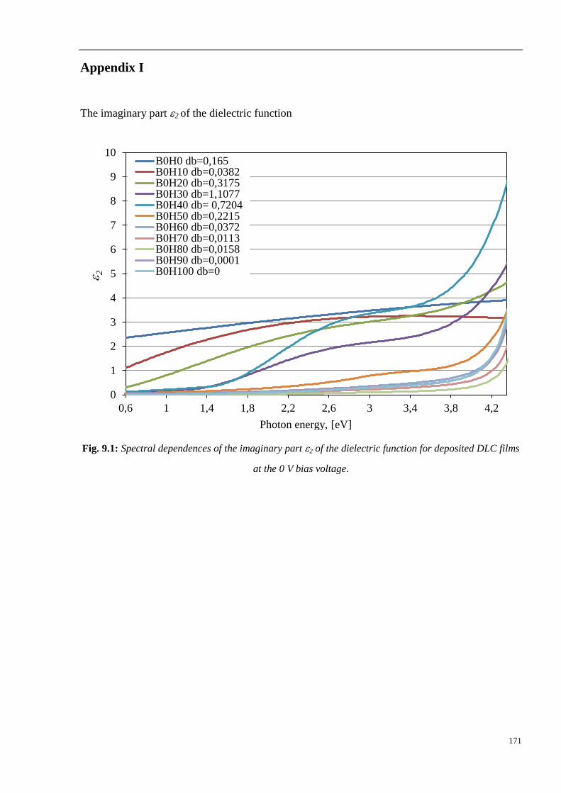
171
Appendix I
The imaginary part 2 of the dielectric function
Fig. 9.1: Spectral dependences of the imaginary part 2 of the dielectric function for deposited DLC films
at the 0 V bias voltage.
0
1
2
3
4
5
6
7
8
9
10
0,6 1 1,4 1,8 2,2 2,6 3 3,4 3,8 4,2
B0H0 db=0,165B0H10 db=0,0382B0H20 db=0,3175B0H30 db=1,1077B0H40 db= 0,7204B0H50 db=0,2215B0H60 db=0,0372B0H70 db=0,0113B0H80 db=0,0158B0H90 db=0,0001B0H100 db=0
Photon energy, [eV]
2
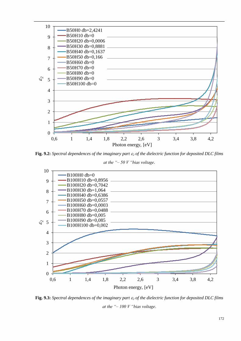
172
Fig. 9.2: Spectral dependences of the imaginary part 2 of the dielectric function for deposited DLC films
at the “– 50 V “bias voltage.
Fig. 9.3: Spectral dependences of the imaginary part 2 of the dielectric function for deposited DLC films
at the “– 100 V “bias voltage.
0
1
2
3
4
5
6
7
8
9
10
0,6 1 1,4 1,8 2,2 2,6 3 3,4 3,8 4,2
B50H0 db=2,4241B50H10 db=0B50H20 db=0,0006B50H30 db=0,8881B50H40 db=0,1637B50H50 db=0,166B50H60 db=0B50H70 db=0B50H80 db=0B50H90 db=0B50H100 db=0
Photon energy, [eV]
2
0
1
2
3
4
5
6
7
8
9
10
0,6 1 1,4 1,8 2,2 2,6 3 3,4 3,8 4,2
B100H0 db=0B100H10 db=0,8956B100H20 db=0,7042B100H30 db=1,064B100H40 db=0,6386B100H50 db=0,0557B100H60 db=0,0003B100H70 db=0,0488B100H80 db=0,005B100H90 db=0,085B100H100 db=0,002 2
Photon energy, [eV]
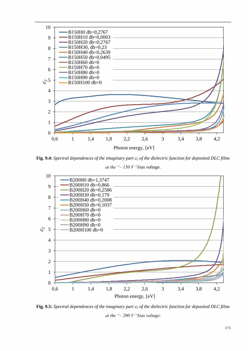
173
Fig. 9.4: Spectral dependences of the imaginary part 2 of the dielectric function for deposited DLC films
at the “– 150 V “bias voltage.
Fig. 9.5: Spectral dependences of the imaginary part 2 of the dielectric function for deposited DLC films
at the “– 200 V “bias voltage.
0
1
2
3
4
5
6
7
8
9
10
0,6 1 1,4 1,8 2,2 2,6 3 3,4 3,8 4,2
B150H0 db=0,2767B150H10 db=0,0003B150H20 db=0,2767B150H30, db=0,23B150H40 db=0,2639B150H50 db=0,0495B150H60 db=0B150H70 db=0B150H80 db=0B150H90 db=0B150H100 db=0
Photon energy, [eV]
2
0
1
2
3
4
5
6
7
8
9
10
0,6 1 1,4 1,8 2,2 2,6 3 3,4 3,8 4,2
B200H0 db=1,3747B200H10 db=0,866B200H20 db=0,2586B200H30 db=0,179B200H40 db=0,2008B200H50 db=0,1037B200H60 db=0B200H70 db=0B200H80 db=0B200H90 db=0B200H100 db=0
Photon energy, [eV]
2
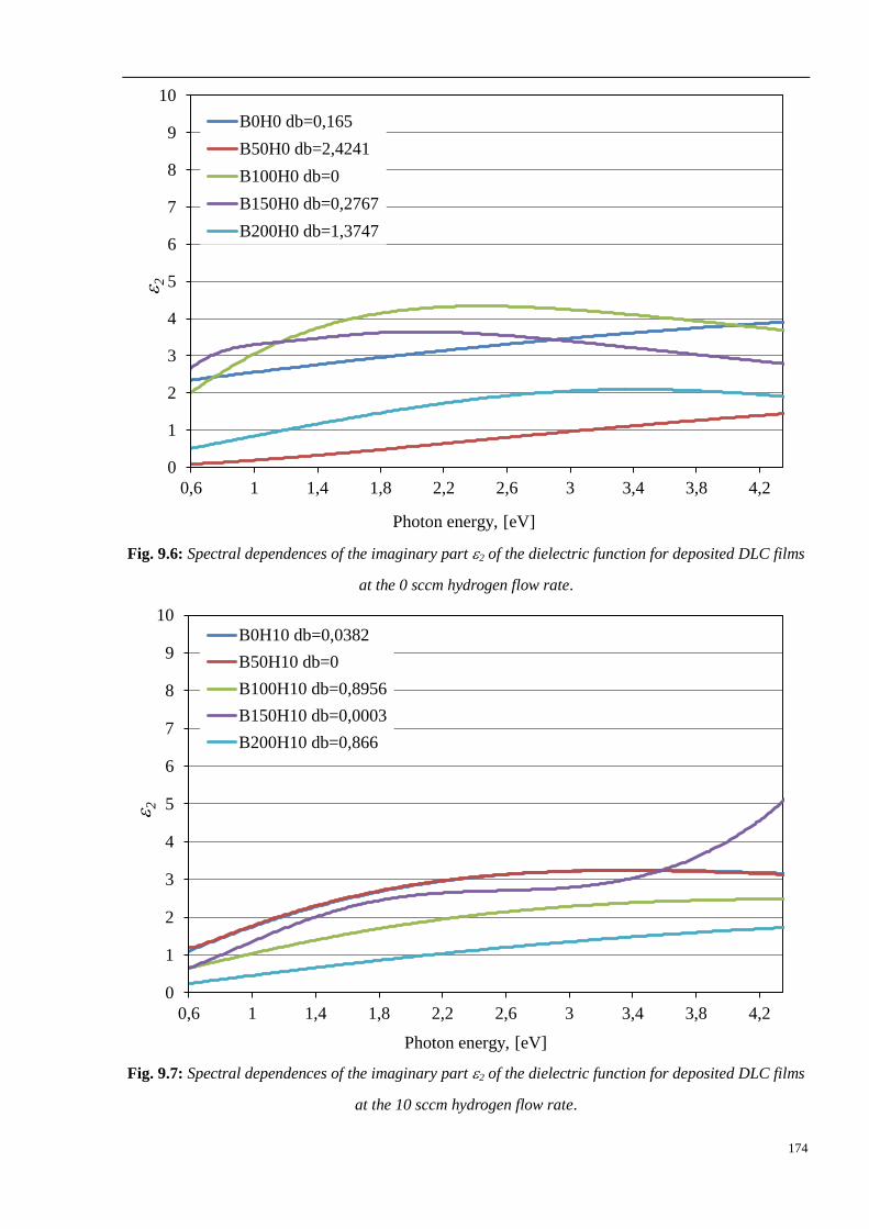
174
Fig. 9.6: Spectral dependences of the imaginary part 2 of the dielectric function for deposited DLC films
at the 0 sccm hydrogen flow rate.
Fig. 9.7: Spectral dependences of the imaginary part 2 of the dielectric function for deposited DLC films
at the 10 sccm hydrogen flow rate.
0
1
2
3
4
5
6
7
8
9
10
0,6 1 1,4 1,8 2,2 2,6 3 3,4 3,8 4,2
B0H0 db=0,165
B50H0 db=2,4241
B100H0 db=0
B150H0 db=0,2767
B200H0 db=1,3747
Photon energy, [eV]
2
0
1
2
3
4
5
6
7
8
9
10
0,6 1 1,4 1,8 2,2 2,6 3 3,4 3,8 4,2
B0H10 db=0,0382
B50H10 db=0
B100H10 db=0,8956
B150H10 db=0,0003
B200H10 db=0,866
Photon energy, [eV]
2
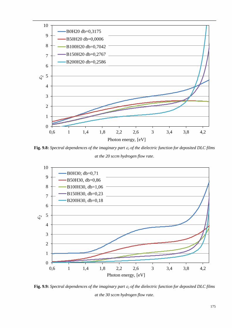
175
Fig. 9.8: Spectral dependences of the imaginary part 2 of the dielectric function for deposited DLC films
at the 20 sccm hydrogen flow rate.
Fig. 9.9: Spectral dependences of the imaginary part 2 of the dielectric function for deposited DLC films
at the 30 sccm hydrogen flow rate.
0
1
2
3
4
5
6
7
8
9
10
0,6 1 1,4 1,8 2,2 2,6 3 3,4 3,8 4,2
B0H20 db=0,3175
B50H20 db=0,0006
B100H20 db=0,7042
B150H20 db=0,2767
B200H20 db=0,2586
Photon energy, [eV]
2
0
1
2
3
4
5
6
7
8
9
10
0,6 1 1,4 1,8 2,2 2,6 3 3,4 3,8 4,2
B0H30; db=0,71
B50H30, db=0,86
B100H30, db=1,06
B150H30, db=0,23
B200H30, db=0,18
Photon energy, [eV]
2
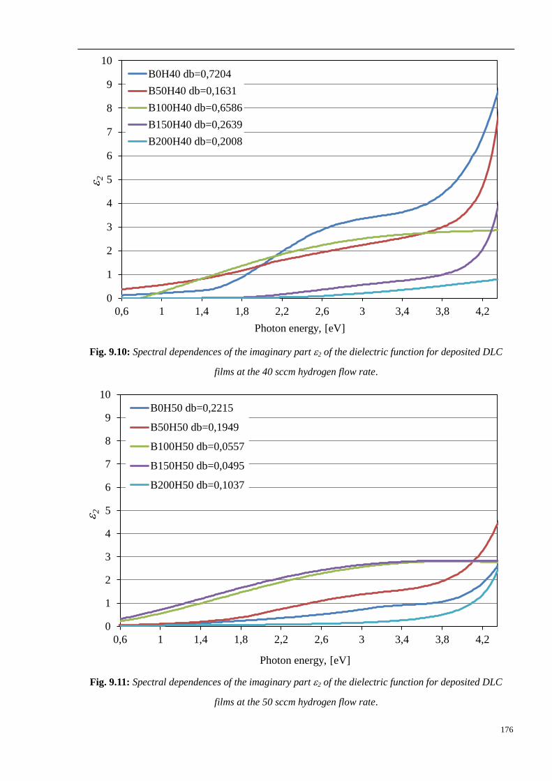
176
Fig. 9.10: Spectral dependences of the imaginary part 2 of the dielectric function for deposited DLC
films at the 40 sccm hydrogen flow rate.
Fig. 9.11: Spectral dependences of the imaginary part 2 of the dielectric function for deposited DLC
films at the 50 sccm hydrogen flow rate.
0
1
2
3
4
5
6
7
8
9
10
0,6 1 1,4 1,8 2,2 2,6 3 3,4 3,8 4,2
B0H40 db=0,7204
B50H40 db=0,1631
B100H40 db=0,6586
B150H40 db=0,2639
B200H40 db=0,2008
Photon energy, [eV]
2
0
1
2
3
4
5
6
7
8
9
10
0,6 1 1,4 1,8 2,2 2,6 3 3,4 3,8 4,2
B0H50 db=0,2215
B50H50 db=0,1949
B100H50 db=0,0557
B150H50 db=0,0495
B200H50 db=0,1037
Photon energy, [eV]
2
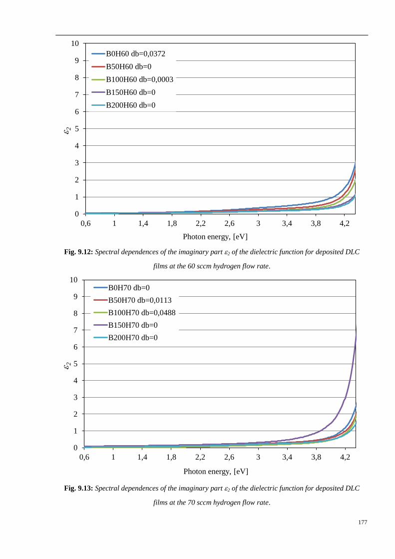
177
Fig. 9.12: Spectral dependences of the imaginary part 2 of the dielectric function for deposited DLC
films at the 60 sccm hydrogen flow rate.
Fig. 9.13: Spectral dependences of the imaginary part 2 of the dielectric function for deposited DLC
films at the 70 sccm hydrogen flow rate.
0
1
2
3
4
5
6
7
8
9
10
0,6 1 1,4 1,8 2,2 2,6 3 3,4 3,8 4,2
B0H60 db=0,0372
B50H60 db=0
B100H60 db=0,0003
B150H60 db=0
B200H60 db=0
Photon energy, [eV]
2
0
1
2
3
4
5
6
7
8
9
10
0,6 1 1,4 1,8 2,2 2,6 3 3,4 3,8 4,2
B0H70 db=0
B50H70 db=0,0113
B100H70 db=0,0488
B150H70 db=0
B200H70 db=0
Photon energy, [eV]
2
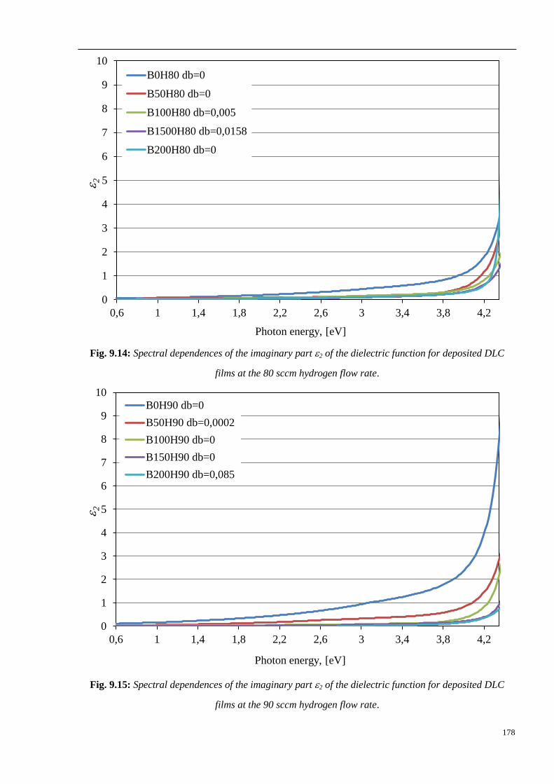
178
Fig. 9.14: Spectral dependences of the imaginary part 2 of the dielectric function for deposited DLC
films at the 80 sccm hydrogen flow rate.
Fig. 9.15: Spectral dependences of the imaginary part 2 of the dielectric function for deposited DLC
films at the 90 sccm hydrogen flow rate.
0
1
2
3
4
5
6
7
8
9
10
0,6 1 1,4 1,8 2,2 2,6 3 3,4 3,8 4,2
B0H80 db=0
B50H80 db=0
B100H80 db=0,005
B1500H80 db=0,0158
B200H80 db=0
Photon energy, [eV]
2
0
1
2
3
4
5
6
7
8
9
10
0,6 1 1,4 1,8 2,2 2,6 3 3,4 3,8 4,2
B0H90 db=0
B50H90 db=0,0002
B100H90 db=0
B150H90 db=0
B200H90 db=0,085
Photon energy, [eV]
2
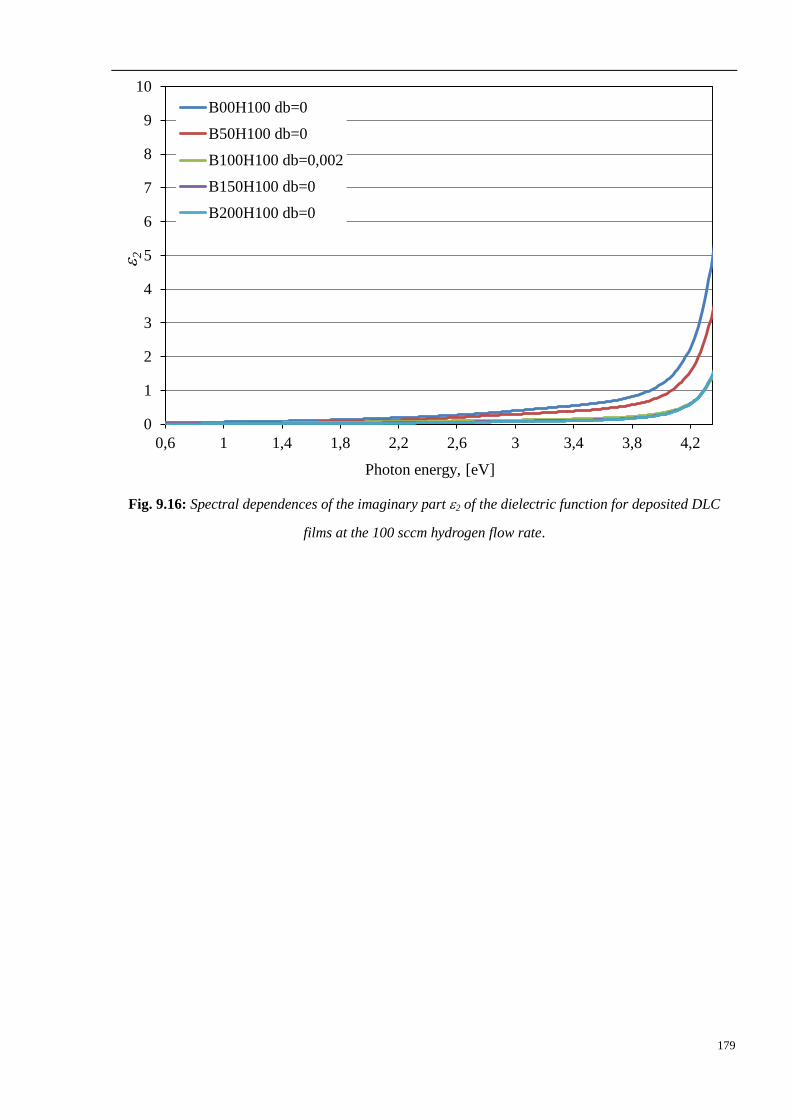
179
Fig. 9.16: Spectral dependences of the imaginary part 2 of the dielectric function for deposited DLC
films at the 100 sccm hydrogen flow rate.
0
1
2
3
4
5
6
7
8
9
10
0,6 1 1,4 1,8 2,2 2,6 3 3,4 3,8 4,2
B00H100 db=0
B50H100 db=0
B100H100 db=0,002
B150H100 db=0
B200H100 db=0
Photon energy, [eV]
2