Crystallization of silicon nanoclusters with inert gas ...knordlun/pub/Zha14a.pdfCrystallization of...
12
PHYSICAL REVIEW B 91, 035419 (2015) Crystallization of silicon nanoclusters with inert gas temperature control Junlei Zhao, 1 Vidyadhar Singh, 2 Panagiotis Grammatikopoulos, 2 Cathal Cassidy, 2 Kengo Aranishi, 2 Mukhles Sowwan, 2, 3 Kai Nordlund, 1 and Flyura Djurabekova 1 1 Department of Physics and Helsinki Institute of Physics, University of Helsinki, P.O. Box 43, FIN-00014 Helsinki, Finland 2 Nanoparticles by Design Unit, Okinawa Institute of Science and Technology (OIST) Graduate University, 1919-1 Onna-Son, Okinawa, 904-0495, Japan 3 Nanotechnology Research Laboratory, Al-Quds University, East Jerusalem, P.O. Box 51000, Palestine (Received 22 September 2014; revised manuscript received 9 December 2014; published 15 January 2015) We analyze the fundamental process of crystallization of silicon nanoclusters by means of molecular dynamics simulations, complemented by magnetron-sputter inert gas condensation, which was used to synthesize polycrystalline silicon nanoclusters with good size control. We utilize two well-established Si interatomic potentials: the Stillinger-Weber and the Tersoff III. Both the simulations and experiments show that upon cooling down by an Ar gas thermal bath, initially liquid, free-standing Si nanocluster can grow multiple crystal nuclei, which drive their transition into polycrystalline solid nanoclusters. The simulations allow detailed analysis of the mechanism, and show that the crystallization temperature is size-dependent and that the probability of crystalline phase nucleation depends on the highest temperature the cluster reaches during the initial condensation and the cooling rate after it. DOI: 10.1103/PhysRevB.91.035419 PACS number(s): 81.07.Bc, 81.10.St I. INTRODUCTION One of the key challenges in nanotechnology today is to control the size and crystallinity of silicon nanoclusters (Si NCs) with a high degree of accuracy, as these parameters have an important impact on uses in specific biomedical and optoelectronic applications [1–3]. Conventional thin-film particle synthesis systems suffer from insufficient simultane- ous control of both particle size and crystallinity, especially in the smaller diameter regime. The inert gas condensation technique, however, can overcome this limitation, providing good control over both of these properties. Research on Si NCs has been very active over the years, given the material’s prevalent position in modern technology. For instance, crystallization of Si NCs from gas phase conden- sation is particularly interesting for the Si-based photovoltaic industry [4–6]. In general, even though it is of course very well known that the same material can exist in liquid, ordered (crystalline) and disordered (amorphous) solid phases depend- ing on temperature and rate of cooling [7], the fundamental atom level mechanisms behind the phase transitions between these are not fully established and are subject to recent research interest [8–14]. Nanosystems provide an interesting addition to these studies as in them, the surface free energy is a significant contribution to the whole, and thus can provide additional insight into the fundamental thermodynamics of melting. To elucidate melting and crystallization mechanisms, the existing experimental tools may not be sufficient, as they cannot track atom motion in a multiphase system at the intrinsic lattice vibration rates around ∼10 13 Hz. Computer simulation methods, which describe the atomic interactions, can be employed instead, since the time and spatial scales Published by the American Physical Society under the terms of the Creative Commons Attribution 3.0 License. Further distribution of this work must maintain attribution to the author(s) and the published article’s title, journal citation, and DOI. involved in the phase transition processes are well within their resolution capabilities. Yet computer simulation results alone cannot give a conclusive understanding of the physics of studied processes, unless the simulation results are validated against experimental observations. Hence, in the current work, we combine simulations and experiments of Si crystal condensation to elucidate the mechanisms of cluster formation, with a particular emphasis on examining the conditions under which the clusters can crystallize. Recrystallization of bulk Si has been successfully studied by using molecular dynamics simulation methods [15,16]. For instance, it was previously shown that crystallization occurs just below the high-density to low-density liquid transition temperature: the Stillinger-Weber potential, which describes well that the low-density liquid phase of Si is thermodynam- ically and structurally contiguous to the amorphous solid, allows for the rapid crystallization at 1050 K [17,18]. A high-density liquid phase did not result in recrystallization, as shown in Ref. [18]. Later on, the same authors did observe recrystallization of bulk Si without going through the low- density liquid phase at 0.75 T melting [19]. The properties of materials at the nanoscale are frequently defined by a high fraction of surface atoms, which makes the behavior of nanosystem different from that of the correspond- ing bulk material. For the study of such nanoscale processes, a special attention must be paid to how the simulations are conducted. For example, special thermo- and barostats are required to control the simulation conditions compared to the conventional ones used to study the bulk materials. The use of the Nos´ e-Hoover thermostat [20,21] or its extension, the Anderson thermostat [22], can cause significant artifacts in the thermodynamic process of an NC system since these methods do not distinguish between surface and bulk atoms. Such artificial scaling of velocities in the nanocluster can be avoided by applying the inert gas temperature control [23], which moreover allows mimicking of the experimental condi- tions in a nanoparticle deposition chamber [24]. The interatomic potential in use must also meet certain re- quirements for realistic description of interatomic interactions. 1098-0121/2015/91(3)/035419(12) 035419-1 Published by the American Physical Society
Transcript of Crystallization of silicon nanoclusters with inert gas ...knordlun/pub/Zha14a.pdfCrystallization of...
PHYSICAL REVIEW B 91, 035419 (2015)
Crystallization of silicon nanoclusters with inert gas temperature control
Junlei Zhao,1 Vidyadhar Singh,2 Panagiotis Grammatikopoulos,2 Cathal Cassidy,2 Kengo Aranishi,2 Mukhles Sowwan,2,3
Kai Nordlund,1 and Flyura Djurabekova1
1Department of Physics and Helsinki Institute of Physics, University of Helsinki, P.O. Box 43, FIN-00014 Helsinki, Finland2Nanoparticles by Design Unit, Okinawa Institute of Science and Technology (OIST) Graduate University,
1919-1 Onna-Son, Okinawa, 904-0495, Japan3Nanotechnology Research Laboratory, Al-Quds University, East Jerusalem, P.O. Box 51000, Palestine
(Received 22 September 2014; revised manuscript received 9 December 2014; published 15 January 2015)
We analyze the fundamental process of crystallization of silicon nanoclusters by means of moleculardynamics simulations, complemented by magnetron-sputter inert gas condensation, which was used to synthesizepolycrystalline silicon nanoclusters with good size control. We utilize two well-established Si interatomicpotentials: the Stillinger-Weber and the Tersoff III. Both the simulations and experiments show that upon coolingdown by an Ar gas thermal bath, initially liquid, free-standing Si nanocluster can grow multiple crystal nuclei,which drive their transition into polycrystalline solid nanoclusters. The simulations allow detailed analysis of themechanism, and show that the crystallization temperature is size-dependent and that the probability of crystallinephase nucleation depends on the highest temperature the cluster reaches during the initial condensation and thecooling rate after it.
DOI: 10.1103/PhysRevB.91.035419 PACS number(s): 81.07.Bc, 81.10.St
I. INTRODUCTION
One of the key challenges in nanotechnology today is tocontrol the size and crystallinity of silicon nanoclusters (SiNCs) with a high degree of accuracy, as these parametershave an important impact on uses in specific biomedicaland optoelectronic applications [1–3]. Conventional thin-filmparticle synthesis systems suffer from insufficient simultane-ous control of both particle size and crystallinity, especiallyin the smaller diameter regime. The inert gas condensationtechnique, however, can overcome this limitation, providinggood control over both of these properties.
Research on Si NCs has been very active over the years,given the material’s prevalent position in modern technology.For instance, crystallization of Si NCs from gas phase conden-sation is particularly interesting for the Si-based photovoltaicindustry [4–6]. In general, even though it is of course verywell known that the same material can exist in liquid, ordered(crystalline) and disordered (amorphous) solid phases depend-ing on temperature and rate of cooling [7], the fundamentalatom level mechanisms behind the phase transitions betweenthese are not fully established and are subject to recent researchinterest [8–14]. Nanosystems provide an interesting addition tothese studies as in them, the surface free energy is a significantcontribution to the whole, and thus can provide additionalinsight into the fundamental thermodynamics of melting.
To elucidate melting and crystallization mechanisms, theexisting experimental tools may not be sufficient, as theycannot track atom motion in a multiphase system at theintrinsic lattice vibration rates around ∼1013 Hz. Computersimulation methods, which describe the atomic interactions,can be employed instead, since the time and spatial scales
Published by the American Physical Society under the terms of theCreative Commons Attribution 3.0 License. Further distribution ofthis work must maintain attribution to the author(s) and the publishedarticle’s title, journal citation, and DOI.
involved in the phase transition processes are well withintheir resolution capabilities. Yet computer simulation resultsalone cannot give a conclusive understanding of the physics ofstudied processes, unless the simulation results are validatedagainst experimental observations. Hence, in the currentwork, we combine simulations and experiments of Si crystalcondensation to elucidate the mechanisms of cluster formation,with a particular emphasis on examining the conditions underwhich the clusters can crystallize.
Recrystallization of bulk Si has been successfully studiedby using molecular dynamics simulation methods [15,16]. Forinstance, it was previously shown that crystallization occursjust below the high-density to low-density liquid transitiontemperature: the Stillinger-Weber potential, which describeswell that the low-density liquid phase of Si is thermodynam-ically and structurally contiguous to the amorphous solid,allows for the rapid crystallization at 1050 K [17,18]. Ahigh-density liquid phase did not result in recrystallization,as shown in Ref. [18]. Later on, the same authors did observerecrystallization of bulk Si without going through the low-density liquid phase at 0.75 Tmelting [19].
The properties of materials at the nanoscale are frequentlydefined by a high fraction of surface atoms, which makes thebehavior of nanosystem different from that of the correspond-ing bulk material. For the study of such nanoscale processes,a special attention must be paid to how the simulations areconducted. For example, special thermo- and barostats arerequired to control the simulation conditions compared tothe conventional ones used to study the bulk materials. Theuse of the Nose-Hoover thermostat [20,21] or its extension,the Anderson thermostat [22], can cause significant artifactsin the thermodynamic process of an NC system since thesemethods do not distinguish between surface and bulk atoms.Such artificial scaling of velocities in the nanocluster can beavoided by applying the inert gas temperature control [23],which moreover allows mimicking of the experimental condi-tions in a nanoparticle deposition chamber [24].
The interatomic potential in use must also meet certain re-quirements for realistic description of interatomic interactions.
1098-0121/2015/91(3)/035419(12) 035419-1 Published by the American Physical Society
JUNLEI ZHAO et al. PHYSICAL REVIEW B 91, 035419 (2015)
The condensation process of Si NCs can be describe properly,if the potential: (i) describes all three phases fairly well,(ii) yields the phase transition temperatures close to theexperimental values, and (iii) reproduces the bond angleenergy and bond angle distribution for solid Si correctly. Thelatter is particularly important for crystallization transitionstage. Unfortunately, none of the empirical potentials devel-oped to date can fully reproduce all three phases of silicon:crystalline, amorphous, and liquid [25–27].
In this paper, we study the crystallization process of amolten Si NC, by combination of simulation and experimentalmethods. We investigate the possible mechanisms that lead tocrystallization by molecular dynamics (MD) simulation meth-ods and propose that the simultaneous growth of multiple seedsexplain the final polycrystalline structure of deposited NCs. Tovalidate the simulation results and their interpretation, we com-pare them to the experimental results of polycrystalline Si NCsgrown by magnetron sputter inert gas condensation method.
II. METHODS
A. Simulation
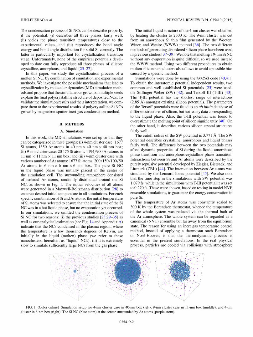
In this work, the MD simulations were set up so that theycan be categorized in three groups: (i) 4-nm cluster case: 1677Si atoms, 1350 Ar atoms in 40 nm × 40 nm × 40 nm box;(ii) 9-nm cluster case: 20 475 Si atoms, 1194/900 Ar atoms in11 nm × 11 nm × 11 nm box; and (iii) 4-nm cluster case withvarious number of Ar atoms: 1677 Si atoms, 200/150/100/50Ar atoms in 6 nm × 6 nm × 6 nm box. The pure Si NCin the liquid phase was initially placed in the center ofthe simulation cell. The surrounding atmosphere consistedof isolated Ar atoms, randomly distributed around the SiNC, as shown in Fig. 1. The initial velocities of all atomswere generated in a Maxwell-Boltzmann distribution [28] toensure a desired initial temperature in all simulations. For eachspecific combination of Si and Ar atoms, the initial temperatureof Si atoms was selected to ensure that the initial state of the SiNC was in a hot liquid phase, but no evaporation yet occurred.In our simulations, we omitted the condensation process ofSi NC for two reasons: (i) the previous studies [23,29–35] aswell as our analytical estimation (see Fig. 14 and Appendix A)indicate that the NCs condensed in the plasma region, wherethe temperature is a few thousands degrees of Kelvin, areinitially in the liquid (molten) phase (we refer to thesenanoclusters, hereafter, as “liquid” NCs); (ii) it is extremelyslow to simulate sufficiently large NCs from the gas phase.
The initial liquid structure of the 4-nm cluster was obtainedby heating the cluster to 2300 K. The 9-nm cluster was cutfrom an amorphous Si thin film generated by the Wooten,Winer, and Weaire (WWW) method [36]. The two differentmethods of generating disordered silicon phase have been usedin previous studies [37–39]. We note that melting a 9-nm Si NCwithout any evaporation is quite difficult, so we used insteadthe WWW method. Using two different procedures to obtainmolten silicon nanoclusters also allows to avoid a possible biascaused by a specific method.
Simulations were done by using the PARCAS code [40,41].To obtain the interatomic potential independent results, twocommon and well-established Si potentials [25] were used,the Stillinger-Weber (SW) [42], and Tersoff III (T-III) [43].The T-III potential has the shortest range of interactions(2.85 A) amongst existing silicon potentials. The parametersof the Tersoff potentials were fitted to an ab initio database ofdifferent structures of silicon, but not to any data correspondingto the liquid phase. Also, the T-III potential was found tooverestimate the melting point of silicon significantly [40]. Onthe other hand, it describes various silicon crystal structuresfairly well.
The cutoff radius of the SW potential is 3.771 A. The SWpotential describes crystalline, amorphous and liquid phasesfairly well. The difference between the two potentials mayaffect dynamic properties of Si during the liquid-amorphousphase transition and amorphous-crystalline phase transition.Interactions between Si and Ar atoms were described by thepurely repulsive potential developed by Ziegler, Biersack, andLittmark (ZBL) [44]. The interaction between Ar atoms wassimulated by the Lennard-Jones potential [45]. We also notethat the time step in the simulations with SW potential was1.079 fs, while in the simulations with T-III potential it was setto 0.270 fs. These were chosen, based on testing in model NVEensemble simulations, to guarantee the energy conservation inpure Si.
The temperature of Ar atoms was constantly scaled to300 K by the Berendsen thermostat, whence the temperatureof the whole system was reduced via the thermal bath ofthe Ar atmosphere. The whole system can be regarded as acanonical (NVT) ensemble but far away from the equilibriumstate. The reason for using an inert gas temperature controlmethod, instead of applying a thermostat such Berendsenor Nose-Hoover, is that the thermodynamic process isessential in the present simulations. In the real physicalprocess, particles are cooled via collisions with atmosphere
FIG. 1. (Color online) Simulation setup for 4-nm cluster case in 40-nm box (left), 9-nm cluster case in 11-nm box (middle), and 4-nmcluster in 6-nm box (right). The Si NC (blue atom) at the center surrounded by Ar atoms (purple atom).
035419-2
CRYSTALLIZATION OF SILICON NANOCLUSTERS WITH . . . PHYSICAL REVIEW B 91, 035419 (2015)
atoms and black-body radiation from the nanoparticle’ssurface. However, the latter process is significant mainlyon microsecond timescales [46] and hence in the currentsimulations, which were run on shorter timescales, it wassufficient to consider the atomic collision cooling.
A conventional thermostat would homogeneously cooldown the cluster, affecting the Maxwell-Boltzmann distribu-tion of thermal velocities and hence, affecting the thermo-dynamics of the cooling process, which is important for thestochastic nature of seed formation for crystallisation process.The cooling rate of the thermal bath of Ar gas fluctuated around10 K/ns in the 4-nm case. Two cooling rates were used for9-nm nanocluster, which are 20 and 30 K/ns (see Appendix A,for the details on cooling rate estimations).
Simulation analysis methods
To quantify the degree of amorphization in a nanosystem, anangular structure factor Pst [47] is calculated for each atom i:
Pst(i) = 1
pu(i)
⎡⎣∑
j
(θi(j ) − θ
p
i (j ))2
⎤⎦
1/2
, (1)
pu(i) =⎡⎣∑
j
(θui (j ) − θ
p
i (j ))2
⎤⎦
1/2
, (2)
where θi(j ) is a list of the angles formed between atomi and its neighbours j . The number of the neighbours isdetermined from the ideal crystal structure, which for thediamond structure (Si) is four. θ
p
i (j ) is the distribution ofangles in a perfect lattice and θu
i (j ) = jπ/[nnb(nnb − 1)/2] isthe uniform angular distribution. nnb is the number of the firstnearest neighbors determined from the ideal crystal structure.Before doing the sum over the angles, the lists of θi(j ) aresorted by magnitude. By averaging the structure factor ofeach atom in combination with a kinetic energy criterion,we can analyze the degree of amorphization as a function ofsimulation time. For the structural factor analysis, we usedthe cutoff radius 3.1 A, which is the average value of the firstand second peaks in the pair distribution function for a regularsilicon crystal structure (also see Fig. 4).
We applied the ring analysis algorithm [48] to detect theprimitive silicon sixfold rings in wurtzite and diamond basicblock. These were used to localize the seeds for the crystallinephase. For this analysis, we reduced somewhat the cutoff radiusfrom 3.1 to 2.39 A, a distance which is slightly larger than theequilibrium interatomic distance in Si structure. This choiceallowed to define the transition point clearly, excluding thenonprimitive rings which unavoidably appeared with largercutoff radii. However, we note that varying the cutoff radius didnot affect the conclusion on the time when the phase transitionoccurred.
B. Experiment
1. Materials
For the experimental studies we used the magnetronsputtering target (Si n-type, purity >99.999%, resistivity<0.001 � m, dimensions: 50 mm diameter × 3 mm thick),
which was purchased from Kurt J. Lesker Company (PA,USA). The Si target was presputtered for 15 minute before de-position on substrates to remove any surface oxide impurities.As substrates for AFM measurements, undoped Si dice with(100) orientation and 5 mm × 5 mm in size were purchasedfrom MTI Corporation (CA, USA). Carbon-coated grids (400mesh) were purchased from Ted Pella Inc. (CA, USA), assubstrates for TEM/HRTEM analysis.
2. Deposition of Si NCs
Size-selected monodispersed Si NCs were synthesizedusing a magnetron-sputtering inert gas-condensation clusterbeam source attached to an inline, quadrupole mass filter(QMF) [Mantis Deposition Ltd.]. Si NC growth was controlledby varying the deposition parameters including magnetronpower (dc), aggregation length, gas pressure, and gas flow.We observed that from all the parameters influencing thegrowth, the Ar/He gas flow rate was the most significant.In this experiment, both Ar and He gas flows were varied,whereas the DC magnetron power, aggregation zone length,and deposition times were kept fixed at 90 W, 125 mm, and10 min, respectively.
For the samples described in this paper, we prepared Si NCswith three different gas flow conditions, namely, Si-1 (Ar: 80sccm and He: 40 sccm), Si-2(Ar: 80 sccm and He: 10 sccm)and Si-3 (Ar: 100 sccm and He: 00 sccm). During deposition,the aggregation zone pressure reading was 3.5 × 10⁻¹ mbarfor Si-1 and Si-2, and reading was 4.5 × 10⁻¹ mbar for Si-3,respectively. The base pressure in the main deposition chamberwas 1.0 × 10⁻⁸ mbar and the substrate table rotation speed wasset at 2 rpm.
3. Characterization
The Si NCs were characterized by atomic force mMi-croscopy (AFM), QMF and transmission electron microscopy(TEM). AFM measurements were performed in a glove-boxfilled with purified nitrogen to avoid the influence of oxygenand moisture. Both the oxygen and water vapour levels insidethe glove-box were kept below 1 ppm. The AFM imagingwas carried out using the Multimode 8 (Bruker, CA) AFMSystem equipped with the NanoScope R©V controller in peakforce tapping mode using triangular silicon-nitride AFM tip(radius <5 nm, force constant of 0.25 N m−1, 60 kHz ofresonant frequency, Bruker). Height distribution curves wereextracted from the AFM images by built-in functions ofthe scanning probe processor software (SPIP 5.1.8, ImageMetrology, Hørsholm, DK). TEM images were obtained usinga 300-kV FEI Titan microscope equipped with image sphericalaberration corrector. In the TEM, energy dispersive x-rayspectrometry (EDX) was performed with an Oxford X-maxsystem, with an 80-mm2 silicon drift detector (SDD) andenergy resolution of 136 eV.
III. RESULTS AND DISCUSSION
A. 4-nm NCs with SW potential
We ran 14 individual cases of cooling process of Si NCsfrom the liquid phase in Ar atmosphere. All the simulationswere stopped after 100 ns when the temperature of the Si
035419-3
JUNLEI ZHAO et al. PHYSICAL REVIEW B 91, 035419 (2015)
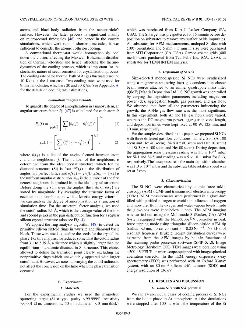
FIG. 2. (Color online) Evolution of the temperature of the Sinanoclusters obtained in four different simulations (top), the fractionof Si atoms in a disordered environment (DE) (middle) and the numberof primitive sixfold rings (bottom). Simulations cases 3, 6, 11 resultedin crystallization of Si NCs. The “case 1” is shown to represent theresults of the runs (including ten other cases not shown here forclarity) in which the Si NCs did not crystallize upon cooling.
nanocluster was about 800 K. Three simulations out of 14 casesshowed the crystallization process. To provide quantitativeinsight into the cooling and crystallization processes, weanalyzed the time evolution of the temperature, the fraction ofSi atoms in a disordered environment (DE) and the topologicalanalysis separately for Si atoms, as shown in Fig. 2. Here weshow all cases (cases 3, 6, and 11) where crystallization wasobserved and one typical case (case 1) of a noncrystallizednanocluster. Each simulation run was given a case number todistinguish between the different runs.
In the cases when crystallization of the Si NC had takenplace, the phase transition process occurred relatively quickly,within a few nanoseconds. The transition temperature wasbetween 950 and 1000 K, which is far below the melting pointof 1350 K for this size nanocrystals. (See the detailed data inAppendix B.) The temperature curve shows a sharp increasefrom 1000 to 1300 K in the case 11 (blue line), indicatinga clear latent heat release at 63 ns, which is consistent withthe structure and the topological curves. We notice that thereare several differences between the simulation case 11 andthe cases 3 and 6. The final structure of Si nanocluster in case11 is more ordered than in the cases 3 and 6, and the phasetransition is more abrupt. All three employed ways of analysisconsistently indicate that: the larger the latent heat release,the more complete transition in the nanoclusters is observed.
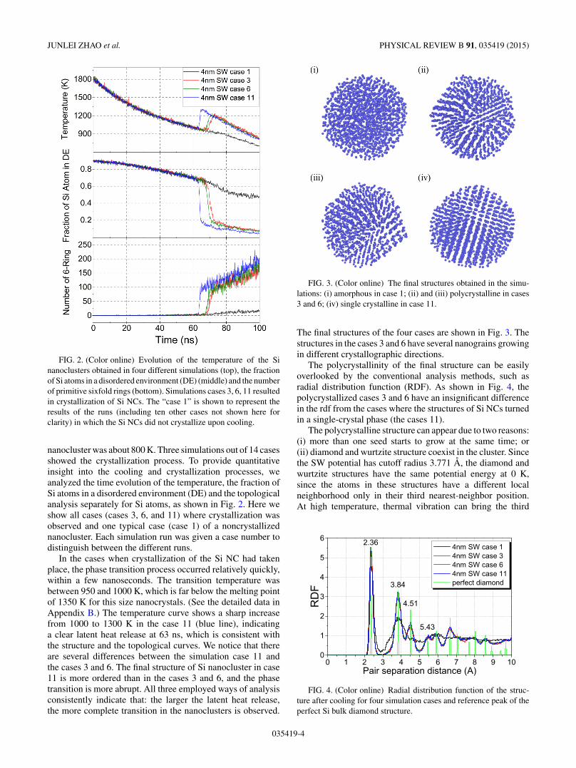
FIG. 3. (Color online) The final structures obtained in the simu-lations: (i) amorphous in case 1; (ii) and (iii) polycrystalline in cases3 and 6; (iv) single crystalline in case 11.
The final structures of the four cases are shown in Fig. 3. Thestructures in the cases 3 and 6 have several nanograins growingin different crystallographic directions.
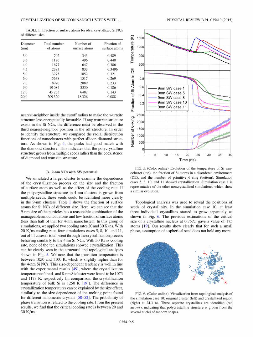
The polycrystallinity of the final structure can be easilyoverlooked by the conventional analysis methods, such asradial distribution function (RDF). As shown in Fig. 4, thepolycrystallized cases 3 and 6 have an insignificant differencein the rdf from the cases where the structures of Si NCs turnedin a single-crystal phase (the cases 11).
The polycrystalline structure can appear due to two reasons:(i) more than one seed starts to grow at the same time; or(ii) diamond and wurtzite structure coexist in the cluster. Sincethe SW potential has cutoff radius 3.771 A, the diamond andwurtzite structures have the same potential energy at 0 K,since the atoms in these structures have a different localneighborhood only in their third nearest-neighbor position.At high temperature, thermal vibration can bring the third
FIG. 4. (Color online) Radial distribution function of the struc-ture after cooling for four simulation cases and reference peak of theperfect Si bulk diamond structure.
035419-4
CRYSTALLIZATION OF SILICON NANOCLUSTERS WITH . . . PHYSICAL REVIEW B 91, 035419 (2015)
TABLE I. Fraction of surface atoms for ideal crystallized Si NCsof different size.
Diameter Total number Number of Fraction of(nm) of atoms surface atoms surface atoms
3.0 702 343 0.4893.5 1126 496 0.4404.0 1677 647 0.3864.5 2383 833 0.34965.0 3275 1052 0.3216.0 5638 1517 0.2697.0 8970 2089 0.2339.0 19 084 3550 0.186
12.0 45 263 6482 0.14320.0 209 320 18 326 0.088
nearest-neighbor inside the cutoff radius to make the wurtzitestructure less energetically favorable. If any wurtzite structureexists in the Si NCs, the difference must be observed in thethird nearest-neighbor position in the rdf structure. In orderto identify the structure, we compared the radial distributionfunctions of nanoclusters with perfect silicon diamond struc-ture. As shown in Fig. 4, the peaks had good match withthe diamond structure. This indicates that the polycrystallinestructure grows from multiple seeds rather than the coexistenceof diamond and wurtzite structure.
B. 9-nm NCs with SW potential
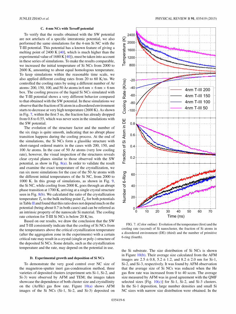
We simulated a larger cluster to examine the dependenceof the crystallization process on the size and the fractionof surface atom as well as the effect of the cooling rate. Ifthe polycrystalline structure in 4-nm clusters is grown frommultiple seeds, these seeds could be identified more clearlyin the 9-nm clusters. Table I shows the fraction of surfaceatoms for Si NCs of different size. Here, we can see that the9-nm size of the particles has a reasonable combination of themanageable amount of atoms and low fraction of surface atoms(less than half of that for 4-nm nanocluster). In this group ofsimulations, we applied two cooling rates 20 and 30 K/ns. With20 K/ns cooling rate, four simulations cases 5, 8, 10, and 11,out of 11 cases in total, went through the crystallization processbehaving similarly to the 4nm Si NCs. With 30 K/ns coolingrate, none of the ten simulations showed crystallization. Thiscan be clearly seen in the structural and topological analysesshown in Fig. 5. We note that the transition temperature isbetween 1050 and 1100 K, which is slightly higher than forthe 4-nm Si NCs. This size-dependent tendency is well in linewith the experimental results [49], where the crystallizationtemperature of the 4- and 8-nm Si cluster were found to be 1073and 1173 K, respectively (in comparison, the crystallizationtemperature of bulk Si is 1250 K [19]). The difference incrystallization temperatures can be explained by the size effect,similarly to the size dependence of the melting point foundfor different nanometric crystals [50–52]. The probability ofphase transition is related to the cooling rate. From the presentresults, we find that the critical cooling rate is between 20 and30 K/ns.
FIG. 5. (Color online) Evolution of the temperature of Si nan-ocluster (top), the fraction of Si atoms in a disordered environment(DE), and the number of primitive 6 ring (bottom). Simulationcases 5, 8, 10, and 11 showed crystallization. Simulation case 1 isrepresentative of the other noncrystallized simulations, which showa similar evolution.
Topological analysis was used to reveal the positions ofseeds of crystallinity. In the simulation case 10, at leastthree individual crystallites started to grow separately asshown in Fig. 6. The previous estimations of the criticalsize of a crystalline nucleus at 0.75Tm gave a value of 175atoms [19]. Our results show clearly that for such a smallphase, assumption of a spherical seed does not hold any more.
FIG. 6. (Color online) Visualization from topological analysis ofthe simulation case 10: original cluster (left) and crystallized region(right) at 24.3 ns. Three separate crystallites are identified (redarrows), indicating that polycrystalline structure is grown from theseveral nuclei of random shapes.
035419-5
JUNLEI ZHAO et al. PHYSICAL REVIEW B 91, 035419 (2015)
C. 4-nm NCs with Tersoff potential
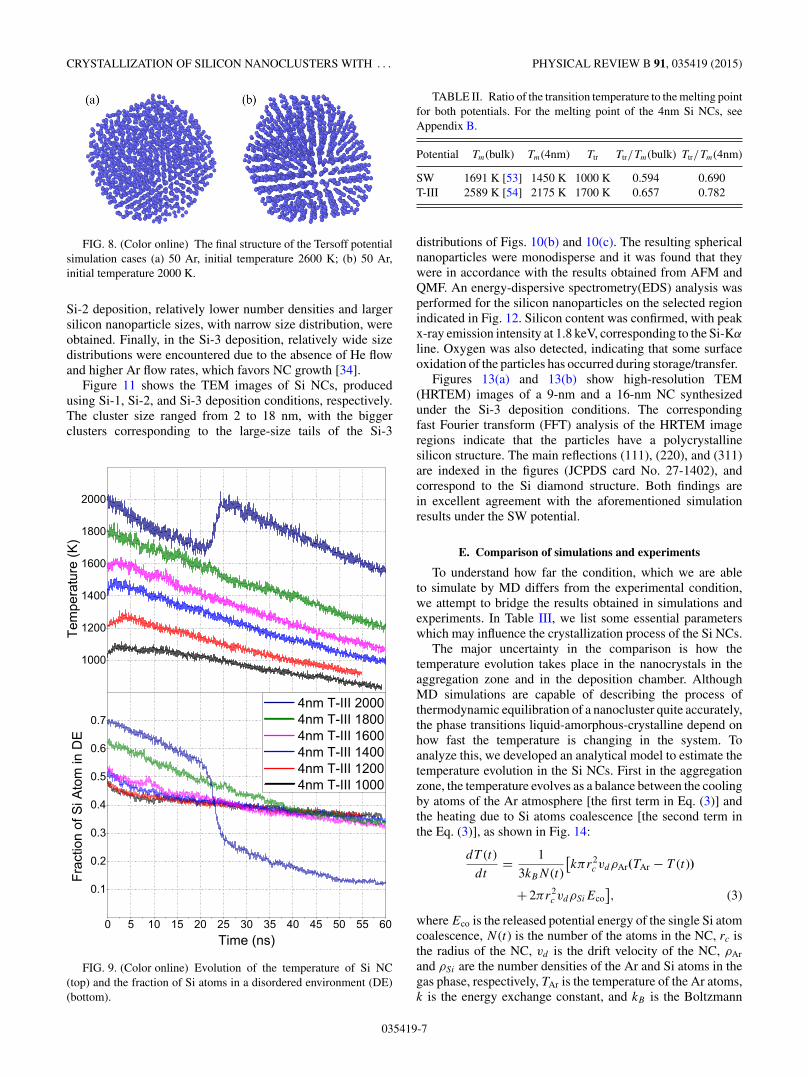
To verify that the results obtained with the SW potentialare not artefacts of a specific interatomic potential, we alsoperformed the same simulations for the 4-nm Si NC with theT-III potential. This potential has a known feature of giving amelting point of 2400 K [40], which is much higher than theexperimental value of 1680 K [40]), must be taken into accountin these series of simulations. To make the results comparable,we increased the initial temperature of Si NCs from 2000 to2600 K, amounting to about equal homologous temperature.To keep simulations within the reasonable time scale, wealso applied different cooling rates from 20 to 60 K/ns. Wecontrolled the cooling rates by using a different number of Aratoms: 200, 150, 100, and 50 Ar atoms in 6 nm × 6 nm × 6 nmbox. The cooling process of the liquid Si NCs simulated withthe T-III potential shows a very different behavior comparedto that obtained with the SW potential. In these simulations weobserve that the fraction of Si atom in a disordered environmentstarts to decrease at very high temperature (2600 K). As shownin Fig. 7, within the first 5 ns, the fraction has already droppedfrom 0.8 to 0.55, which was never seen in the simulations withthe SW potential.
The evolution of the structure factor and the number ofthe six rings is quite smooth, indicating that no abrupt phasetransition happens during the cooling process. At the end ofthe simulations, the Si NCs form a glasslike structure withshort-ranged ordered matrix in the cases with 200, 150, and100 Ar atoms. In the case of 50 Ar atoms (very low coolingrate), however, the visual inspection of the structures revealsclear crystal planes similar to those observed with the SWpotential, as show in Fig. 8(a). In order to validate the resultand examine the exact temperature of the crystallization, weran six more simulations for the case of the 50 Ar atoms withthe different initial temperatures of the Si NC, from 2000 to1000 K. In this group of simulations, as shown in Fig. 9,the Si NC, while cooling from 2000 K, goes through an abruptphase transition at 1700 K, arriving at a single crystal structureseen in Fig. 8(b). We calculated the ratio of the crystallizationtemperature Ttr to the bulk melting point Tm for both potentialsin Table II and found that this ratio does not depend much on thepotential (being about 0.7 in both cases) and can be referred asan intrinsic property of the nanoscale Si material. The coolingrate criterion for T-III Si NCs is below 20 K/ns.
Based on our results, we draw the conclusion that the SWand T-III consistently indicate that the cooling of Si NCs fromthe temperatures above the critical crystallization temperature(after the aggregation zone in the experiments) with a certaincritical rate may result in a crystal (single or poly-) structure ofthe deposited Si NCs. Some details, such as the crystallizationtemperature and the rate, may depend on the potential in use.
D. Experimental growth and deposition of Si NCs
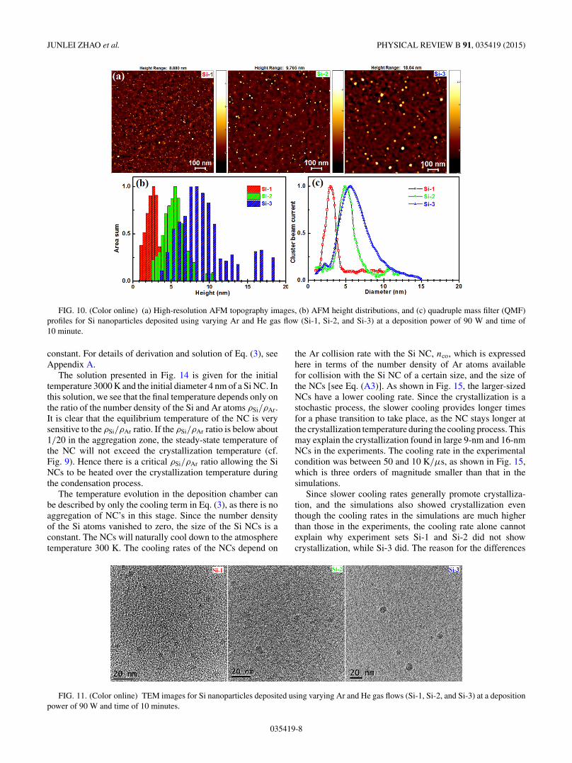
To demonstrate the very good control over NC size ofthe magnetron-sputter inert gas-condensation method, threevarieties of deposited clusters (experiment sets Si-1, Si-2, andSi-3) were observed by AFM and TEM; the images takenshowcase the dependence of both cluster size and crystallinityon the (Ar/He) gas flow rate. Figure 10(a) shows AFMimages of the Si NCs (Si-1, Si-2, and Si-3) deposited on
FIG. 7. (Color online) Evolution of the temperature (first) and thecooling rate (second) of Si nanocluster, the fraction of Si atoms ina disordered environment (DE) (third) and the number of primitive6-ring (fourth).
the Si substrate. The size distribution of Si NCs is shownin Figure 10(b). Their average size calculated from the AFMimages are 2.5 ± 0.8, 5.2 ± 1.2, and 8.2 ± 2.0 nm for Si-1,Si-2, and Si-3, respectively. It was found by AFM observationthat the average size of Si NCs was reduced when the Hegas flow rate was increased from 0 to 40 sccm. The averagesize measured by AFM was in good agreement with the QMFselected sizes [Fig. 10(c)] for Si-1, Si-2, and Si-3 clusters.In the Si-1 deposition, large number densities and small SiNC sizes with narrow size distribution were obtained. In the
035419-6
CRYSTALLIZATION OF SILICON NANOCLUSTERS WITH . . . PHYSICAL REVIEW B 91, 035419 (2015)
FIG. 8. (Color online) The final structure of the Tersoff potentialsimulation cases (a) 50 Ar, initial temperature 2600 K; (b) 50 Ar,initial temperature 2000 K.
Si-2 deposition, relatively lower number densities and largersilicon nanoparticle sizes, with narrow size distribution, wereobtained. Finally, in the Si-3 deposition, relatively wide sizedistributions were encountered due to the absence of He flowand higher Ar flow rates, which favors NC growth [34].
Figure 11 shows the TEM images of Si NCs, producedusing Si-1, Si-2, and Si-3 deposition conditions, respectively.The cluster size ranged from 2 to 18 nm, with the biggerclusters corresponding to the large-size tails of the Si-3
FIG. 9. (Color online) Evolution of the temperature of Si NC(top) and the fraction of Si atoms in a disordered environment (DE)(bottom).
TABLE II. Ratio of the transition temperature to the melting pointfor both potentials. For the melting point of the 4nm Si NCs, seeAppendix B.
Potential Tm(bulk) Tm(4nm) Ttr Ttr/Tm(bulk) Ttr/Tm(4nm)
SW 1691 K [53] 1450 K 1000 K 0.594 0.690T-III 2589 K [54] 2175 K 1700 K 0.657 0.782
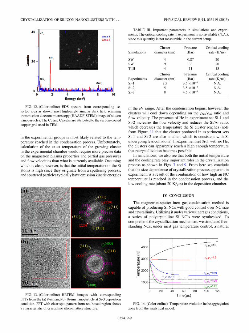
distributions of Figs. 10(b) and 10(c). The resulting sphericalnanoparticles were monodisperse and it was found that theywere in accordance with the results obtained from AFM andQMF. An energy-dispersive spectrometry(EDS) analysis wasperformed for the silicon nanoparticles on the selected regionindicated in Fig. 12. Silicon content was confirmed, with peakx-ray emission intensity at 1.8 keV, corresponding to the Si-Kα
line. Oxygen was also detected, indicating that some surfaceoxidation of the particles has occurred during storage/transfer.
Figures 13(a) and 13(b) show high-resolution TEM(HRTEM) images of a 9-nm and a 16-nm NC synthesizedunder the Si-3 deposition conditions. The correspondingfast Fourier transform (FFT) analysis of the HRTEM imageregions indicate that the particles have a polycrystallinesilicon structure. The main reflections (111), (220), and (311)are indexed in the figures (JCPDS card No. 27-1402), andcorrespond to the Si diamond structure. Both findings arein excellent agreement with the aforementioned simulationresults under the SW potential.
E. Comparison of simulations and experiments
To understand how far the condition, which we are ableto simulate by MD differs from the experimental condition,we attempt to bridge the results obtained in simulations andexperiments. In Table III, we list some essential parameterswhich may influence the crystallization process of the Si NCs.
The major uncertainty in the comparison is how thetemperature evolution takes place in the nanocrystals in theaggregation zone and in the deposition chamber. AlthoughMD simulations are capable of describing the process ofthermodynamic equilibration of a nanocluster quite accurately,the phase transitions liquid-amorphous-crystalline depend onhow fast the temperature is changing in the system. Toanalyze this, we developed an analytical model to estimate thetemperature evolution in the Si NCs. First in the aggregationzone, the temperature evolves as a balance between the coolingby atoms of the Ar atmosphere [the first term in Eq. (3)] andthe heating due to Si atoms coalescence [the second term inthe Eq. (3)], as shown in Fig. 14:
dT (t)
dt= 1
3kBN (t)
[kπr2
c vdρAr(TAr − T (t))
+ 2πr2c vdρSiEco
], (3)
where Eco is the released potential energy of the single Si atomcoalescence, N (t) is the number of the atoms in the NC, rc isthe radius of the NC, vd is the drift velocity of the NC, ρAr
and ρSi are the number densities of the Ar and Si atoms in thegas phase, respectively, TAr is the temperature of the Ar atoms,k is the energy exchange constant, and kB is the Boltzmann
035419-7
JUNLEI ZHAO et al. PHYSICAL REVIEW B 91, 035419 (2015)
FIG. 10. (Color online) (a) High-resolution AFM topography images, (b) AFM height distributions, and (c) quadruple mass filter (QMF)profiles for Si nanoparticles deposited using varying Ar and He gas flow (Si-1, Si-2, and Si-3) at a deposition power of 90 W and time of10 minute.
constant. For details of derivation and solution of Eq. (3), seeAppendix A.
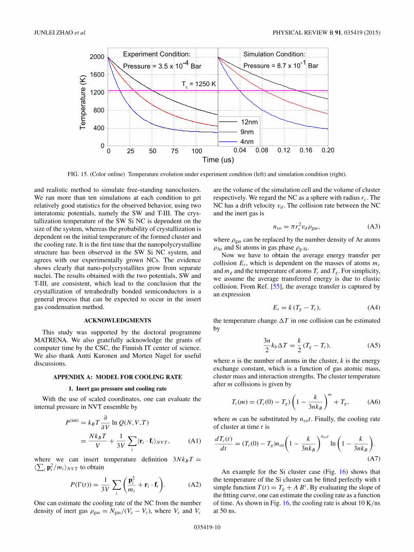
The solution presented in Fig. 14 is given for the initialtemperature 3000 K and the initial diameter 4 nm of a Si NC. Inthis solution, we see that the final temperature depends only onthe ratio of the number density of the Si and Ar atoms ρSi/ρAr.It is clear that the equilibrium temperature of the NC is verysensitive to the ρSi/ρAr ratio. If the ρSi/ρAr ratio is below about1/20 in the aggregation zone, the steady-state temperature ofthe NC will not exceed the crystallization temperature (cf.Fig. 9). Hence there is a critical ρSi/ρAr ratio allowing the SiNCs to be heated over the crystallization temperature duringthe condensation process.
The temperature evolution in the deposition chamber canbe described by only the cooling term in Eq. (3), as there is noaggregation of NC’s in this stage. Since the number densityof the Si atoms vanished to zero, the size of the Si NCs is aconstant. The NCs will naturally cool down to the atmospheretemperature 300 K. The cooling rates of the NCs depend on
the Ar collision rate with the Si NC, nco, which is expressedhere in terms of the number density of Ar atoms availablefor collision with the Si NC of a certain size, and the size ofthe NCs [see Eq. (A3)]. As shown in Fig. 15, the larger-sizedNCs have a lower cooling rate. Since the crystallization is astochastic process, the slower cooling provides longer timesfor a phase transition to take place, as the NC stays longer atthe crystallization temperature during the cooling process. Thismay explain the crystallization found in large 9-nm and 16-nmNCs in the experiments. The cooling rate in the experimentalcondition was between 50 and 10 K/μs, as shown in Fig. 15,which is three orders of magnitude smaller than that in thesimulations.
Since slower cooling rates generally promote crystalliza-tion, and the simulations also showed crystallization eventhough the cooling rates in the simulations are much higherthan those in the experiments, the cooling rate alone cannotexplain why experiment sets Si-1 and Si-2 did not showcrystallization, while Si-3 did. The reason for the differences
FIG. 11. (Color online) TEM images for Si nanoparticles deposited using varying Ar and He gas flows (Si-1, Si-2, and Si-3) at a depositionpower of 90 W and time of 10 minutes.
035419-8
CRYSTALLIZATION OF SILICON NANOCLUSTERS WITH . . . PHYSICAL REVIEW B 91, 035419 (2015)
FIG. 12. (Color online) EDS spectra from corresponding se-lected area as shown inset high-angle annular dark field scanningtransmission electron microscopy (HAADF-STEM) image of siliconnanoparticles. The Cu and C peaks are attributed to the carbon-coatedcopper grid used in TEM.
in the experimental groups is most likely related to the tem-perature reached in the condensation process. Unfortunately,calculation of the exact temperature of the growing clusterin the experimental chamber would require more precise dataon the magnetron plasma properties and partial gas pressuresand flow velocities than what is currently available. One thingwhich is clear, however, is that the initial temperature of the Siatoms is high since they originate from a sputtering process,and sputtered particles typically have emission kinetic energies
FIG. 13. (Color online) HRTEM images with correspondingFFTs from the (a) 9-nm and (b) 16-nm nanoparticle at Si-3 depositioncondition. FFT with clear spot pattern from red boxed region showsa characteristic of crystalline silicon lattice structure.
TABLE III. Important parameters in simulations and experi-ments. The critical cooling rate in experiment is not available (N.A.),since this quantity is not measurable in the current setup.
Cluster Pressure Critical coolingSimulations diameter (nm) (Bar) rate (K/ns)
SW 4 0.87 20SW 9 33 20T-III 4 11 15
Cluster Pressure Critical coolingExperiments diameter (nm) (Bar) rate (K/ns)Si-1 2.5 3.5 ×10⁻⁴ N.A.Si-2 5 3.5 ×10⁻⁴ N.A.Si-3 8 4.5 ×10⁻⁴ N.A.
in the eV range. After the condensation begins, however, theclusters will cool down depending on the ρSi/ρAr ratio andflow velocity. The presence of He in experiment set Si-1 andSi-2 increases the flow velocity and reduces the Si/Ar ratio,which decreases the temperature the Si cluster reaches (notefrom Figure 11 that the cluster produced in experiment setsSi-1 and Si-2 are also smaller, which is consistent with Siundergoing less collisions). In experiment set Si-3, with no He,the clusters can apparently reach a high enough temperaturethat recrystallization becomes possible.
In simulations, we also see that both the initial temperatureand the cooling rate play important roles in the crystallizationprocess as shown in Figs. 7 and 9. From here we concludethat the size dependence of crystallization process apparent inexperiment, is a result of the combination of how high an NCtemperature is reached in the condensation process, and thelow cooling rate (about 20 K/μs) in the deposition chamber.
IV. CONCLUSION
The magnetron-sputter inert gas-condensation method iscapable of producing Si NCs with good control over NC sizeand crystallinity. Utilizing it under various inert gas conditions,a series of polycrystalline Si NC’s were synthesized. Tocomprehend the crystallization mechanism, we simulated free-standing NCs, under inert gas temperature control, a natural
FIG. 14. (Color online) Temperature evolution in the aggregationzone from the analytical model.
035419-9
JUNLEI ZHAO et al. PHYSICAL REVIEW B 91, 035419 (2015)
FIG. 15. (Color online) Temperature evolution under experiment condition (left) and simulation condition (right).
and realistic method to simulate free-standing nanoclusters.We ran more than ten simulations at each condition to getrelatively good statistics for the observed behavior, using twointeratomic potentials, namely the SW and T-III. The crys-tallization temperature of the SW Si NC is dependent on thesize of the system, whereas the probability of crystallization isdependent on the initial temperature of the formed cluster andthe cooling rate. It is the first time that the nanopolycrystallinestructure has been observed in the SW Si NC system, andagrees with our experimentally grown NCs. The evidenceshows clearly that nano-polycrystallites grow from separatenuclei. The results obtained with the two potentials, SW andT-III, are consistent, which lead to the conclusion that thecrystallization of tetrahedrally bonded semiconductors is ageneral process that can be expected to occur in the insertgas condensation method.
ACKNOWLEDGMENTS
This study was supported by the doctoral programmeMATRENA. We also gratefully acknowledge the grants ofcomputer time by the CSC, the Finnish IT center of science.We also thank Antti Kuronen and Morten Nagel for usefuldiscussions.
APPENDIX A: MODEL FOR COOLING RATE
1. Inert gas pressure and cooling rate
With the use of scaled coordinates, one can evaluate theinternal pressure in NVT ensemble by
P (int) = kBT∂
∂Vln Q(N,V,T )
= NkBT
V+ 1
3V
∑i
〈ri · fi〉NV T , (A1)
where we can insert temperature definition 3NkBT =〈∑i p2
i /mi〉NV T to obtain
P (�(t)) = 1
3V
∑i
(p2
i
mi
+ ri · fi
). (A2)
One can estimate the cooling rate of the NC from the numberdensity of inert gas ρgas = Ngas/(Vs − Vc), where Vs and Vc
are the volume of the simulation cell and the volume of clusterrespectively. We regard the NC as a sphere with radius rc. TheNC has a drift velocity vd . The collision rate between the NCand the inert gas is
nco = πr2c vdρgas, (A3)
where ρgas can be replaced by the number density of Ar atomsρAr and Si atoms in gas phase ρg-Si.
Now we have to obtain the average energy transfer percollision Et , which is dependent on the masses of atoms mc
and mg and the temperature of atoms Tc and Tg . For simplicity,we assume the average transferred energy is due to elasticcollision. From Ref. [55], the average transfer is captured byan expression
Et = k (Tg − Tc), (A4)
the temperature change T in one collision can be estimatedby
3n
2kbT = k
2(Tg − Tc), (A5)
where n is the number of atoms in the cluster, k is the energyexchange constant, which is a function of gas atomic mass,cluster mass and interaction strengths. The cluster temperatureafter m collisions is given by
Tc(m) = (Tc(0) − Tg)
(1 − k
3nkB
)m
+ Tg, (A6)
where m can be substituted by ncot . Finally, the cooling rateof cluster at time t is
dTc(t)
dt= (Tc(0) − Tg)nco
(1 − k
3nkB
)ncot
ln
(1 − k
3nkB
).
(A7)
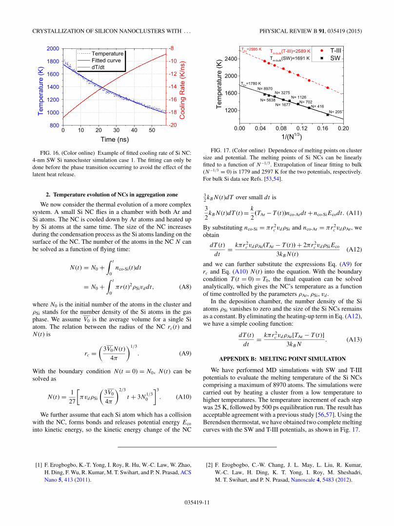
An example for the Si cluster case (Fig. 16) shows thatthe temperature of the Si cluster can be fitted perfectly with tsimple function T (t) = Tg + ABt . By evaluating the slope ofthe fitting curve, one can estimate the cooling rate as a functionof time. As shown in Fig. 16, the cooling rate is about 10 K/nsat 50 ns.
035419-10
CRYSTALLIZATION OF SILICON NANOCLUSTERS WITH . . . PHYSICAL REVIEW B 91, 035419 (2015)
FIG. 16. (Color online) Example of fitted cooling rate of Si NC:4-nm SW Si nanocluster simulation case 1. The fitting can only bedone before the phase transition occurring to avoid the effect of thelatent heat release.
2. Temperature evolution of NCs in aggregation zone
We now consider the thermal evolution of a more complexsystem. A small Si NC flies in a chamber with both Ar andSi atoms. The NC is cooled down by Ar atoms and heated upby Si atoms at the same time. The size of the NC increasesduring the condensation process as the Si atoms landing on thesurface of the NC. The number of the atoms in the NC N canbe solved as a function of flying time:
N (t) = N0 +∫ t
0nco-Si(t)dt
= N0 +∫ t
0πr(t)2ρSivddt, (A8)
where N0 is the initial number of the atoms in the cluster andρSi stands for the number density of the Si atoms in the gasphase. We assume V0 is the average volume for a single Siatom. The relation between the radius of the NC rc(t) andN (t) is
rc =(
3V0N (t)
4π
)1/3
. (A9)
With the boundary condition N (t = 0) = N0, N (t) can besolved as
N (t) = 1
27
[πvdρSi
(3V0
4π
)2/3
t + 3N1/30
]3
. (A10)
We further assume that each Si atom which has a collisionwith the NC, forms bonds and releases potential energy Eco
into kinetic energy, so the kinetic energy change of the NC
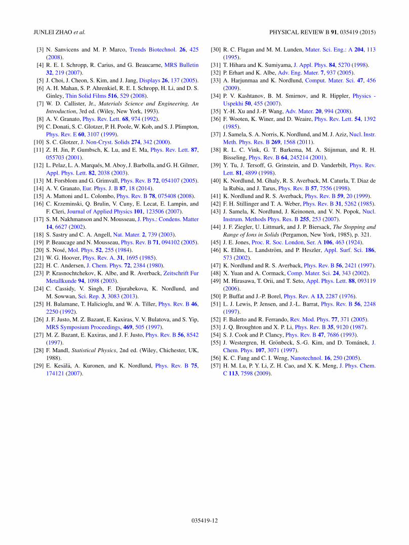
FIG. 17. (Color online) Dependence of melting points on clustersize and potential. The melting points of Si NCs can be linearlyfitted to a function of N−1/3. Extrapolation of linear fitting to bulk(N−1/3 = 0) is 1779 and 2597 K for the two potentials, respectively.For bulk Si data see Refs. [53,54].
32kBN (t)dT over small dt is
3
2kBN (t)dT (t) = k
2(TAr − T (t))nco-Ardt + nco-SiEcodt. (A11)
By substituting nco-Si = πr2c vdρSi and nco-Ar = πr2
c vdρAr, weobtain
dT (t)
dt= kπr2
c vdρAr(TAr − T (t)) + 2πr2c vdρSiEco
3kBN (t)(A12)
and we can further substitute the expressions Eq. (A9) forrc and Eq. (A10) N (t) into the equation. With the boundarycondition T (t = 0) = T0, the final equation can be solvedanalytically, which gives the NC’s temperature as a functionof time controlled by the parameters ρAr, ρSi, vd .
In the deposition chamber, the number density of the Siatoms ρSi vanishes to zero and the size of the Si NCs remainsas a constant. By eliminating the heating-up term in Eq. (A12),we have a simple cooling function:
dT (t)
dt= kπr2
c vdρAr[TAr − T (t)]
3kBN. (A13)
APPENDIX B: MELTING POINT SIMULATION
We have performed MD simulations with SW and T-IIIpotentials to evaluate the melting temperature of the Si NCscomprising a maximum of 8970 atoms. The simulations werecarried out by heating a cluster from a low temperature tohigher temperatures. The temperature increment of each stepwas 25 K, followed by 500 ps equilibration run. The result hasacceptable agreement with a previous study [56,57]. Using theBerendsen thermostat, we have obtained two complete meltingcurves with the SW and T-III potentials, as shown in Fig. 17.
[1] F. Erogbogbo, K.-T. Yong, I. Roy, R. Hu, W.-C. Law, W. Zhao,H. Ding, F. Wu, R. Kumar, M. T. Swihart, and P. N. Prasad, ACSNano 5, 413 (2011).
[2] F. Erogbogbo, C.-W. Chang, J. L. May, L. Liu, R. Kumar,W.-C. Law, H. Ding, K. T. Yong, I. Roy, M. Sheshadri,M. T. Swihart, and P. N. Prasad, Nanoscale 4, 5483 (2012).
035419-11
JUNLEI ZHAO et al. PHYSICAL REVIEW B 91, 035419 (2015)
[3] N. Sanvicens and M. P. Marco, Trends Biotechnol. 26, 425(2008).
[4] R. E. I. Schropp, R. Carius, and G. Beaucarne, MRS Bulletin32, 219 (2007).
[5] J. Choi, J. Cheon, S. Kim, and J. Jang, Displays 26, 137 (2005).[6] A. H. Mahan, S. P. Ahrenkiel, R. E. I. Schropp, H. Li, and D. S.
Ginley, Thin Solid Films 516, 529 (2008).[7] W. D. Callister, Jr., Materials Science and Engineering, An
Introduction, 3rd ed. (Wiley, New York, 1993).[8] A. V. Granato, Phys. Rev. Lett. 68, 974 (1992).[9] C. Donati, S. C. Glotzer, P. H. Poole, W. Kob, and S. J. Plimpton,
Phys. Rev. E 60, 3107 (1999).[10] S. C. Glotzer, J. Non-Cryst. Solids 274, 342 (2000).[11] Z. H. Jin, P. Gumbsch, K. Lu, and E. Ma, Phys. Rev. Lett. 87,
055703 (2001).[12] L. Pelaz, L. A. Marques, M. Aboy, J. Barbolla, and G. H. Gilmer,
Appl. Phys. Lett. 82, 2038 (2003).[13] M. Forsblom and G. Grimvall, Phys. Rev. B 72, 054107 (2005).[14] A. V. Granato, Eur. Phys. J. B 87, 18 (2014).[15] A. Mattoni and L. Colombo, Phys. Rev. B 78, 075408 (2008).[16] C. Krzeminski, Q. Brulin, V. Cuny, E. Lecat, E. Lampin, and
F. Cleri, Journal of Applied Physics 101, 123506 (2007).[17] S. M. Nakhmanson and N. Mousseau, J. Phys.: Condens. Matter
14, 6627 (2002).[18] S. Sastry and C. A. Angell, Nat. Mater. 2, 739 (2003).[19] P. Beaucage and N. Mousseau, Phys. Rev. B 71, 094102 (2005).[20] S. Nose, Mol. Phys. 52, 255 (1984).[21] W. G. Hoover, Phys. Rev. A. 31, 1695 (1985).[22] H. C. Andersen, J. Chem. Phys. 72, 2384 (1980).[23] P. Krasnochtchekov, K. Albe, and R. Averback, Zeitschrift Fur
Metallkunde 94, 1098 (2003).[24] C. Cassidy, V. Singh, F. Djurabekova, K. Nordlund, and
M. Sowwan, Sci. Rep. 3, 3083 (2013).[25] H. Balamane, T. Halicioglu, and W. A. Tiller, Phys. Rev. B 46,
2250 (1992).[26] J. F. Justo, M. Z. Bazant, E. Kaxiras, V. V. Bulatova, and S. Yip,
MRS Symposium Proceedings, 469, 505 (1997).[27] M. Z. Bazant, E. Kaxiras, and J. F. Justo, Phys. Rev. B 56, 8542
(1997).[28] F. Mandl, Statistical Physics, 2nd ed. (Wiley, Chichester, UK,
1988).[29] E. Kesala, A. Kuronen, and K. Nordlund, Phys. Rev. B 75,
174121 (2007).
[30] R. C. Flagan and M. M. Lunden, Mater. Sci. Eng.: A 204, 113(1995).
[31] T. Hihara and K. Sumiyama, J. Appl. Phys. 84, 5270 (1998).[32] P. Erhart and K. Albe, Adv. Eng. Mater. 7, 937 (2005).[33] A. Harjunmaa and K. Nordlund, Comput. Mater. Sci. 47, 456
(2009).[34] P. V. Kashtanov, B. M. Smirnov, and R. Hippler, Physics -
Uspekhi 50, 455 (2007).[35] Y.-H. Xu and J.-P. Wang, Adv. Mater. 20, 994 (2008).[36] F. Wooten, K. Winer, and D. Weaire, Phys. Rev. Lett. 54, 1392
(1985).[37] J. Samela, S. A. Norris, K. Nordlund, and M. J. Aziz, Nucl. Instr.
Meth. Phys. Res. B 269, 1568 (2011).[38] R. L. C. Vink, G. T. Barkema, M. A. Stijnman, and R. H.
Bisseling, Phys. Rev. B 64, 245214 (2001).[39] Y. Tu, J. Tersoff, G. Grinstein, and D. Vanderbilt, Phys. Rev.
Lett. 81, 4899 (1998).[40] K. Nordlund, M. Ghaly, R. S. Averback, M. Caturla, T. Diaz de
la Rubia, and J. Tarus, Phys. Rev. B 57, 7556 (1998).[41] K. Nordlund and R. S. Averback, Phys. Rev. B 59, 20 (1999).[42] F. H. Stillinger and T. A. Weber, Phys. Rev. B 31, 5262 (1985).[43] J. Samela, K. Nordlund, J. Keinonen, and V. N. Popok, Nucl.
Instrum. Methods Phys. Res. B 255, 253 (2007).[44] J. F. Ziegler, U. Littmark, and J. P. Biersack, The Stopping and
Range of Ions in Solids (Pergamon, New York, 1985), p. 321.[45] J. E. Jones, Proc. R. Soc. London, Ser. A 106, 463 (1924).[46] K. Elihn, L. Landstrom, and P. Heszler, Appl. Surf. Sci. 186,
573 (2002).[47] K. Nordlund and R. S. Averback, Phys. Rev. B 56, 2421 (1997).[48] X. Yuan and A. Cormack, Comp. Mater. Sci. 24, 343 (2002).[49] M. Hirasawa, T. Orii, and T. Seto, Appl. Phys. Lett. 88, 093119
(2006).[50] P. Buffat and J.-P. Borel, Phys. Rev. A 13, 2287 (1976).[51] L. J. Lewis, P. Jensen, and J.-L. Barrat, Phys. Rev. B 56, 2248
(1997).[52] F. Baletto and R. Ferrando, Rev. Mod. Phys. 77, 371 (2005).[53] J. Q. Broughton and X. P. Li, Phys. Rev. B 35, 9120 (1987).[54] S. J. Cook and P. Clancy, Phys. Rev. B 47, 7686 (1993).[55] J. Westergren, H. Gronbeck, S.-G. Kim, and D. Tomanek, J.
Chem. Phys. 107, 3071 (1997).[56] K. C. Fang and C. I. Weng, Nanotechnol. 16, 250 (2005).[57] H. M. Lu, P. Y. Li, Z. H. Cao, and X. K. Meng, J. Phys. Chem.
C 113, 7598 (2009).
035419-12