
Design of LCOS Microdisplay Backplanes for Projection Applications
250
Ontwerp van LCOS microbeeldscherm backplanes voor projectietoepassingen Design of LCOS Microdisplay Backplanes for Projection Applications Jean Van den Steen Promotor: prof. dr. ir. H. De Smet Proefschrift ingediend tot het behalen van de graad van Doctor in de Ingenieurswetenschappen: Elektrotechniek Vakgroep Elektronica en Informatiesystemen Voorzitter: prof. dr. ir. J. Van Campenhout Faculteit Ingenieurswetenschappen Academiejaar 2005 - 2006
Transcript of Design of LCOS Microdisplay Backplanes for Projection Applications
Ontwerp van LCOS microbeeldscherm backplanesvoor projectietoepassingen
Design of LCOS Microdisplay Backplanesfor Projection Applications
Jean Van den Steen
Promotor: prof. dr. ir. H. De SmetProefschrift ingediend tot het behalen van de graad van Doctor in de Ingenieurswetenschappen: Elektrotechniek
Vakgroep Elektronica en InformatiesystemenVoorzitter: prof. dr. ir. J. Van CampenhoutFaculteit IngenieurswetenschappenAcademiejaar 2005 - 2006

ISBN 90-8578-062-4NUR 959Wettelijk depot: D/2006/10.500/20

Acknowledgements
motions overwhelm me when thinking about the many efforts, contributions, laughter, hint and help from so many people. Amongst others, the fear not to be
grateful enough for the opportunities that were created. A pretty large number of people effectively contributed to the realization of this book. In particular, I thank Koen Van Laere and my brothers Etienne and Philippe Van den Steen for their reading efforts and constructive comments. This thesis is one written part about the results of teamwork. Not everyone did contribute directly to the technical aspects – neither am I just a cold research machine. Some contributed with a smile, a listening ear, a tasty meal, challenging cycle tours, regular exercising, direct ‘pep-talk’ or with a rough hike through snowy landscapes. To all of you, I hereby whish to express my deepest feelings of gratitude. The research was supported by the University of Gent and IMEC vzw. University projects, extensive european projects and direct bilateral contracts made it possible to conduct research on microdisplays. I am very grateful to live in a society that makes research possible. The cooperation with our project partners has been most enjoyable: Alcatel Microelectronics (now AMIS, Oudenaarde, Belgium), Barco (Kortrijk, Belgium), Merck KgaA (Darmstadt, Germany), Thomson Multimedia (Rennes, France), Thales Avionics LCD (Grenoble, France), Taiwan Micro Display Corporation (tmdc, Hsin-Chu, Taiwan), University College of London (London, United Kingdom), University of Stuttgart (Stuttgart, Germany). Maybe the most enjoyable was the exchange of research results with the world-wide community of display researchers. Four excellent computer engineers patiently provided me with efficient help at times when the computers got tired of me: Ronny Blomme, Marnik Brunfaut, Wim Meeus and Peter Sebrechts thank you so much!
Amongst the research group’s colleagues, special thanks go to Geert Van Doorselaer, Miguel Vermandel, Johan De Baets, Nadine Carchon, Dieter Cuypers, Igor Popov, Miroslav Vrana, Jan Vanfleteren, Joeri De Vos, Jan Doutreloigne, Peter Sebrechts, Katrien Vanneste, André Van Calster and Herbert De Smet. I want to thank Geert in particular, because of his patient elaboration of the system electronics and Dieter for his persistent quest for improved assembly methods. They also provided me with insights in what would otherwise be the ‘dark side’ of microdisplays. Geert and Dieter, your efforts have been most instrumental!
Especially, I want to thank Professor André Van Calster and Professor Herbert De Smet for their guidance and clear-cut analysis, also in the more difficult times. I also thank them for the successful creation of a consistent string of projects, as well as for the many efforts in the sometimes exhausting creation and follow-up of projects. Gentlemen, I cannot say anything else but ‘chapeau’!
���
E
History of my research
n November 1994 the thin-film-components-group (TFCG) started a small feasibility study on crystalline silicon based display systems. In those pioneering
times of liquid-crystal-on-silicon (lcos), the design and manufacturing were indeed questionable. This small-scale experiment included basic possibilities for measurements and provided data about attainable pixel pitches and about the issue of light sensitivity of silicon.
Time window of my research : November 1994 – December 2003 Start End List of projects
11/1994 09/1995 Internal feasability study 01/1995 1998… Internal – REFLEC 09/1997 03/2000 European – MOSAREL, EP25340 04/2000 12/2003 Bilateral – TMDC 04/2002 2005… European – LCOS4LCOS, IST_2001_34591 01/2004 08/2004 Incubation – GEMIDIS … 2003 09/2005 Writing my PhD
Table of projects over the years
Project
Feasibility
REFLECx-Si IWTSigma
MOSAREL
TMDC
LCOS4LCOS
Incubation
Writing my PhD
050198 02 03 0499 0094 95 96 97
Timeline of primary activities
Soon after (beginning of 1995), a full microdisplay project (REFLEC) was born. The standard low-cost foundry process chosen implied the light shielding and top mirror layers had to be processed within laboratory’s clean-room. Assembly into a real display cell and the design and implementation of peripheral electronics also required a lot of precision and effort from a team of colleagues. Two years of chip design, assembly with peripherals and problem-solving allowed to finally reach the first milestone. It consists of a working microdisplay (august 1997) controlled through a personal computer.
I
In the mean time, the author worked on a project on SOI (silicon-on-insulator) based displays and on the Copernicus Sigma project. The purpose of the Sigma project is the development of ‘intelligent gas-sensors’. Next, the European Esprit-IV project MOSAREL (EP-25340) started: 270 times as many pixels as with the REFLEC project. Continued work showed off in march 2000: the consortium was able to see a projected 2560x2048 image. From an organizational and technical perspective, I learned most about silicon design during this project. Basically it allowed me to finetune the design procedures up to a high level of perfection. These successes led a Taiwanese business man to come along and to order a full microdisplay menu. Starting with XGA, development of SXGA and full HDTV formats were the future. This is the cooperation with the Taiwan Micro Display Corporation (tmdc), headed by Mr. L.Y. Tseng. In 2002, TFCG joined the LCOS4LCOS project led by Thomson Multimedia, France and financed by the EC. The last chapter introduces this work. For the LCOS4LCOS project, I did not perform the silicon implementations. My task here was to develop and simulate ‘smart pixel architectures’ – to allow for an implementation of a single-panel system. As such, IMECs’ participation to the project concerned the high-level design of the microdisplay chip. The last years also, a plan has been worked out to throw the GEMIDIS spin-off company into the real world (august 2004) of high-tech companies. My active research work effectively ended at the beginning of 2004. The first months of 2004, I actively participated in the creation of the company; the rest of the year I monitored Gemidis’s first chip design and the LCOS4LCOS project (on a distance) and finally started writing my thesis. Since december 2005 I am with the DSL Experts Team of Alcatel Bell in Antwerp, Belgium.
���
Executive summary
he research work presented in this book concerns the design of lcos microdisplay backplanes. The aim is to clarify the design, because lcos backplanes are not standard chips. Microdisplays are displays with very small
dimensions; this small that optical magnification is required to view the image. The acronym lcos stands for liquid-crystal-on-silicon and is the name of one of the competing technologies. Lcos microdisplays consist of a layer of liquid crystal, encapsulated between a transparent glass plate and a crystalline silicon chip. The term ‘backplane’ refers to this chip. The prime applications of these displays are large-diagonal projection systems. They are however not limited to that. The author believes the research has been very successful considering the publications, the world-wide patent awarded and of course, the team-work that yielded several successful implementations. Mid-august 2004, a spin-off company was born – GEMIDIS, which stands for Gent microdisplays. Its core business is the commercialization of lcos panels.
In the beginning, lcos technology seemed excessively attractive because of its apparent simplicity. The overall system in which lcos microdisplays are applied, is rather complex however and requires the efforts of a team of specialists. It is almost an impossible task to compare lcos with all other innovating display technologies. Maybe because the whole team believes the developed solutions just are the best.… Seriously, the author thought it was thrilling enough to write down a concise story about his own contributions to lcos.
My responsibility covered the entire silicon design of the backplane Ics.
With ‘entire silicon design’ I mean the simulations, the layouting, the functional testing of the chips, the datasheets and specifications – that was my job. Incidentally, I got help from Herbert for measurement setups and had many discussions with him regarding the smart pixel ideas. The desing of the backplanes is the area where I contributed most to. In the technology plane, I developed an original design procedure for stitching. The implementations during the MOSAREL project have shown how well this approach works. In the circuit plane I implemented the classic AM architecture for different display formats. The successes with these design ultimately led to the creation of the GEMIDIS startup company. I also developed smart pixel circuits for multi-million pixel arrays – these ideas form an important part of the patent we were granted. Some of the ideas have been implemented for single-panel HDTV backplanes and have also been tested during the LCOS4LCOS project. The results hereof will be presented at SID’06.
Roughly, the book splits into four parts. Chapter one is the first part and places the work presented in this book, in a broader context. The first paragraph of this chapter recalls three essential facts about human vision; three facts that are fundamental to understand the operation of most display systems. The second paragraph briefly mentions economical aspects and gives an indicative value of the
"real world" market. After all, what's the practical interest in research on displays? The third paragraph is entitled “application specific displays”. It is indeed justified – to some degree – to state that each display type fits a particular application. A classification attempt is made to help distinguishing between the several display technologies, applications, etc, etc. Subsequently, the text focuses on examples of liquid-crystal-on-silicon (lcos) projection architectures. Finally, a glance at the anatomy of an lcos micro-display backplane wraps up this chapter and by then provides more insight in the meaning of the thesis’s title…
Part two – chapters two and three – is about lcos technology, it deals with rules and procedures to ensure first-time-right designs. Lcos technology is restricted here to what is needed from the point of view of the backplane-chip designer.
Chapter two combines the requirements of LC assembly technology with standard IC technology into a set of relatively straightforward design rules. This chapter is a collection of crucial background information concerning the constraints that must be dealt with for the design of a micro-display backplane. A first paragraph called “a designer’s perspective”, summarizes the lcos product chain. The second paragraph called “lcos cell assembly technology highlights”, discusses the constraints from cell assembly technology. The third paragraph “IC processing technology highlights” discusses constraints directly related to the Si processing itself.
Chapter three proposes a solution for the design of very large ICs – with dimensions so large that standard design techniques fall short. It is entirely devoted to stitching. The discussion starts with paragraph 3.1 “three considerations about stitching”, a comparison between three different ways of partitioning the mask sets. Ease of processing and cost of prototyping make that multiple-module reticule sets are the preferred option. The two other though are technically feasible. The second paragraph “implications for ic design” describes the implications of the multiple-module reticule set approach on the way to construct the backplane IC design. Particularly with the mask layout verification there are some difficulties. There are not only consequences at the layout stage of the design cycle, but also at the schematic stage.
Ultimately, the difficulties encountered are addressed by the virtual stitching procedure. It consists of a way to organize the mask layout and of a few simple routines. The reader gets insights in a tool that helps to ensure first time right designs.
The third part about circuits is covered by chapters four and five. Chapter four introduces the classic active matrix and reviews the implementations. The heart of lcos devices is known as ‘the pixel matrix’; it designates the area where the electro-optic signal conversion occurs. Paragraph 4.1 describes the ‘classic’ analog active matrix (AM) architecture. The description starts with the single transistor pixel circuit. A SPICE model is proposed to help with the simulation of the LC capacitor. The addressing of the AM with integrated drivers is looked at on the grounds of speed and redundancy considerations. Paragraph 4.2 summarizes the
implementations, along with the results obtained. It is not the aim to give detailed reports of the optical performance, rather is this chapter limited to the chip’s functionality and peculiarities. As such, it concludes the discussion on micro-display designs that use the classic AM architecture. It also forms the starting ground for chapter five, where improvements to the pixel circuit are presented.
These improvements effectively add a second frame-memory to the AM. These circuit ideas are covered by our patent, essential for both cheaper displays and so-called single panel systems. Paragraph 5.1 covers the CE switching principle, the compatibility with continuous light sources and estimates the maximum transistor count per pixel. Paragraph 5.2 describes a couple of original circuit ideas that effectively implement the functionality of an additional frame memory. The resulting pixels are labeled ‘smart pixels’ maybe because of the functionality offered notwithstanding the limited area available.
The fourth and last part of the book is composed of conclusions and appendices – actually they contain information that is not only useful for the previous chapters. They contain concise datasheets of the designs that were made as well as a beginner's hands-on manual of verification software. This way, I hope this book can also be useful for anyone desiring to learn about IC design, in particular about the design of lcos microdisplays.
���
Nederlandse samenvatting Het werk dat in dit boek neergeschreven staat, behelst het onderzoek van het ontwerp van zogenaamde lcos micro-beeldschermen. De doelstelling van het boek is het toelichten van het ontwerp van lcos microbeeldscherm backplanes. Microbeeldschermen zijn beeldschermen van dermate kleine afmetingen dat optische vergroting noodzakelijk is om het beeld zichtbaar te maken. De afkorting ‘lcos’ staat voor ‘vloeibaar kristal op silicium’ en geldt tevens als naam voor een van de meest competitieve beeldscherm-technologieën. Lcos microbeeldschermen bestaan uit een dun laagje vloeibaar kristal dat ingekapseld is tussen een doorzichtig glasplaatje en een kristallijne silicium chip. De term ‘backplane’ verwijst precies naar deze chip. De voornaamste toepassingen van deze soort beeldschermen zijn projectiesystemen met grote beelddiagonaal. De auteur gelooft dat het onderzoek meer dan geslaagd mag genoemd worden, gezien de vele resultaten, publicaties, het wereldwijde patent en natuurlijk ook gezien het feit dat verscheidene succesvolle implementaties tot stand gekomen zijn. Op 15 augustus 2004 zag zelfs een nieuw spin-off bedrijf het licht: GEMIDIS (staat voor Gent microdisplays). De hoofdaktiviteit van deze spin-off is de commercializatie van lcos micro-beeldschermen. Bij het begin leek lcos technologie bijzonder aantrekkelijk, omwille van diens schijnbare eenvoud. Het systeem waarin dergelijke micro-beeldschermen toegepast worden, is vrij ingewikkeld en vereist inspanningen van een ploeg specialisten. Het is niet eenvoudig om lcos met alle andere vernieuwende technologieën te vergelijken. Misschien komt dit doordat ons team gelooft dat haar eigen oplossingen simpelweg de beste zijn... In elk geval was het voor de auteur spannend genoeg een beknopt verhaal neer te schrijven over de eigen bijdragen tot het hele lcos-gebeuren. Grofweg kan het boek in vier delen opgesplitst worden. Het eerste hoofdstuk plaatst het werk in een bredere context. De eerste paragraaf beschrijft kort drie essentiële feiten over het menselijk gezichtsvermogen; deze liggen aan de basis van de opbouw van de meeste beeldsystemen. De tweede paragraaf haalt kort een paar economische gegevens aan, uit de ‘reële wereld’. Wat zou immers het nut kunnen zijn van intensieve onderzoeksprojecten omtrent nieuwe beeldsystemen. De derde paragraaf heeft als titel “beeldsystemen op maat van de toepassing”. Het is inderdaad min of meer gerechtvaardigd te stellen dat elk type beeldscherm past bij een welbepaald type toepassing. Er wordt een poging ondernomen om een klassificatie tot stand te brengen. Deze heeft tot doel de verschillende technologieën, toepassingen, enz. te helpen onderscheiden. Hierop volgen enkele voorbeelden van lcos projectie architecturen. Ten slotte richt een doorsnede het licht op de interne structuur van lcos microbeeldscherm backplanes. Hopelijk is hiermee dan ook de titel van het proefschrift duidelijk.
Het tweede gedeelte omvat de hoofdstukken twee en drie; deze gaan over lcos technologie. M.a.w. ze beschrijven ontwerpsregels en -procedures die een efficiënt

chip-ontwerp helpen bekomen. Met ‘lcos technologie’ beperkt de auteur zich uiteraard tot hetgeen nodig is voor de microbeeldscherm chip-ontwerpers. Hoofdstuk twee brengt de vereisten samen die voortvloeien uit de vloeibaar kristal (LC) assemblage technologie en de integrated circuit (IC) ofte chip-technologie. Dit resulteert in een vrij eenvoudige lijst ontwerpsregels. Heel beknopt herleidt het tweede hoofdstuk zich dus tot een verzameling informatie die fundamenteel is voor het ontwerp van microbeeldscherm backplanes. Een eerste paragraaf (2.1) vat het productieschema samen, gezien vanuit het perspectief van de chip-ontwerper. In een zelfde perspectief beschrijft de tweede paragraaf een aantal relevante aspecten van de LC assemblage technologie. Tenslotte beschrijft de derde paragraaf de relevante aspecten van de IC technologie. Een beperking treedt op bij het maken van – naar verhouding – zeer grote chips; deze kan omzeild worden met een techniek die in het engels ‘stitching’ genoemd wordt (‘to stitch’ betekent letterlijk: ‘naaien’). Hoofdstuk drie is geheel gewijd aan dit ‘stitchen’ dat dus enkel nodig is voor het ontwerpen en maken van zeer grote chips. Paragraaf 3.1 maakt een vergelijking tussen drie verschillende benaderingen – m.b.t. het stitchen van microbeeldscherm backplanes. Een van de benaderingen ‘multiple module reticule sets’ blijkt de meest interessante, om redenen van kost en productie-eenvoud. De tweede paragraaf geeft een gedetailleerde beschrijving van de gevolgen van deze benadering voor de ontwerpsprocedure. I.h.b. zijn er een aantal delicate punten met betrekking tot de verificatie van het maskerontwerp. Tenslotte beschrijft de ‘virtuele stitching procedure’, een systematische aanpak die de auteur opgezet heeft om op trefzekere wijze de maskersets te ontwerpen.
Het derde gedeelte omvat de hoofdstukken vier en vijf. Op een zeer analoge manier, gaat hoofdstuk vier over de klassieke circuitoplossing en gaat hoofdstuk vijf over uitbreidingen hierop. Hoofdstuk vier bespreekt de klassieke aktieve matrix en geeft een overzicht van de geimplementeerde chips. De verzameling beeldpunten of pixel matrix vormt het kloppend hart van een microbeeldscherm; de pixel matrix is het laatste stukje schakeling dat de electro-optische signaal conversie stuurt. Paragraaf 4.1 handelt uitsluitend over de klassieke, ‘analoge’ aktieve matrix architectuur. Deze architectuur houdt in de praktijk in dat drie microbeeldschermen nodig zijn om alle drie de kleurenbundels te sturen. De analyse van de pixel schakeling wordt verder uitgediept dankzij een origineel computer model voor de LC capaciteit. De geïntegreerde sturing van de aktieve matrix wordt bekeken op grond van snelheidsbeschouwingen en van redundantie. Paragraaf 4.2 geeft dan een overzicht van de realizaties, tezamen met de bekomen resultaten. Het is hier niet de bedoeling een gedetailleerde beschrijving te geven van de optische performanties; het gaat hier eerder om een beschrijving van de bekomen functionaliteit en eventuele bijzonderheden. Als dusdanig legt hoofdstuk vier ook de basis voor hoofdstuk vijf waar zgn. smart pixels als verbeteringen voorgesteld worden. De essentie van deze verbeteringen is dat een tweede beeldgeheugen toegevoegd wordt aan de aktieve matrix. De schakelingen die uitgevonden werden, zijn beschermd door een patent op naam van de auteur. Ondertussen heeft de spin-off GEMIDIS de eigenaarsrechten hierop overgenomen. De uitvinding is cruciaal voor het bekomen van goedkopere chips en voor het implementeren van optische

architecturen die slechts één enkel microbeeldscherm nodig hebben. De eerste paragraaf beschrijft het principe achter de ‘schakelende tegenelektrode’ en diens compatibiliteit met continu-lichtbronnen en geeft tenslotte een schatting van het maximum aantal transistoren per pixel. Deze schatting laat toe in te zien dat het aantal mogelijke pixel-schakelingen eerder beperkt is. Paragraaf 5.2 beschrijft een aantal originele pixel-schakelingen die de idee van een tweede beeldgeheugen implementeren. De resulterende pixels worden ‘smart pixels’ genoemd, allicht omwille van de verhouding functionaliteit tot beschikbare oppervlakte.
Het vierde en laaste gedeelte bevat hetgeen overblijft: het besluit en appendices. Deze laatste bevatten meer informatie dan nodig voor de andere hoofdstukken: ze bevatten beknopte datasheets van de gerealizeerde ontwerpen alsook een handleiding voor het gebruik van de verificatie-software. Hiermee hoopt de auteur dat dit proefschrift als nuttig naslagwerk kan dienen voor eenieder die iets wil leren over chip-ontwerp, i.h.b. over het ontwerp van microbeeldscherm chips.
���

Table of contents
Cover page 1 Dedication 2 Acknowledgements 3 History of my research 4 Executive summary 6 Nederlandse samenvatting 9 Table of contents 12 List of abbreviations 15 Publication list 21 Chapter 1 : Welcome to “Display World” 25 1.1 How we see colored, moving images 25 1.2 Market significance 29 1.3 Application specific displays 31 1.3.1 Classification attempts 31 1.3.2 Lcos systems 32 1.3.3 Lcos micro-displays: definition and physical structure 38 Chapter 2 : Constraints from lcos technology 41 2.1 An IC designer's perspective 41 2.1.1 A system flow and global constraints 41 2.1.2 Assembly flow of lcos panels 42 2.1.3 An (lcos) IC design cycle 42 2.2 Lcos cell assembly technology highlights 45 2.2.1 The lcos cell structure 45 2.2.2 The lcos cell assembly 53 2.3 IC processing technology highlights 59 2.3.1 Synopsis of 4 lcos-IC processing flows 60

2.3.2 Photolithography I: some basics 62 Chapter 3 : Photolithography (II) - stitching 71 3.1 Three considerations about stitching 71 3.1.1 Multiple-reticule reticule sets: cost versus complexity 72 3.1.2 Multiple-module reticule sets: ‘MMI’ tables, multiple
display formats 77 3.1.3 (Stitching)2 or the 1X-5X mix&match 81 3.2 Implications for IC design 85 3.2.1 Anatomy of a module 85 3.2.2 Double exposures 87 3.2.3 Split the schematics as well? 90 3.2.4 Overcoming problems with mask generation 90 3.2.5 Overcoming problems with mask verification 92 3.3 Virtual stitching procedure 94 3.3.1 Module layout organization for virtual stitching 94 3.3.2 Computing stitched patterns 95 Chapter 4 : The pixel matrix(I) – the basics 99 4.1 The pixel matrix (I): the classic AM 100 4.1.1 One, single picture element (pixel) 100 4.1.2 Millions of pixels 109 4.1.3 AM driver circuits 111 4.1.4 VAN pixel design: constraint listing 113 4.2 Micro-display implementations 115 4.2.1 REFLEC chips: 160x120 pixels 115 4.2.2 5Mpix and stitching 122 4.2.3 Tmdc prototypes: XGA, WXGA 128 Chapter 5 : The pixel matrix(II) – smart pixels 133 5.1 Counter electrode switching 134 5.1.1 The need for a second in-pixel frame memory 134
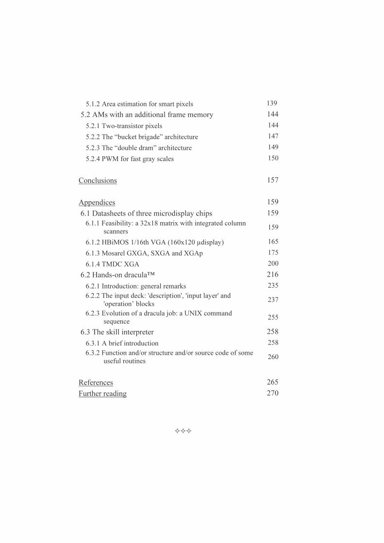
5.1.2 Area estimation for smart pixels 139 5.2 AMs with an additional frame memory 144 5.2.1 Two-transistor pixels 144 5.2.2 The “bucket brigade” architecture 147 5.2.3 The “double dram” architecture 149 5.2.4 PWM for fast gray scales 150 Conclusions 157 Appendices 159 6.1 Datasheets of three microdisplay chips 159 6.1.1 Feasibility: a 32x18 matrix with integrated column
scanners 159 6.1.2 HBiMOS 1/16th VGA (160x120 µdisplay) 165 6.1.3 Mosarel GXGA, SXGA and XGAp 175 6.1.4 TMDC XGA 200 6.2 Hands-on dracula™ 216 6.2.1 Introduction: general remarks 235 6.2.2 The input deck: 'description', 'input layer' and
'operation’ blocks 237 6.2.3 Evolution of a dracula job: a UNIX command
sequence 255 6.3 The skill interpreter 258 6.3.1 A brief introduction 258 6.3.2 Function and/or structure and/or source code of some
useful routines 260 References 265 Further reading 270
���

List of abbreviations
µD micro-display § paragraph µ micro- or micron 1x, 5x 1x, 5x magnification AC alternating current ADC analog-to-digital converter Al Aluminum AM active matrix AMI American Microsystems Incorporated AMIS AMI Semiconductors AMLC active matrix liquid crystal AMLCD active matrix liquid crystal display AR aperture ratio or assembly rule (depending on
context) a-Si amorphous silicon ASIC application-specific integrated circuit AX appendix B bulk terminal of transistor BJT bipolar junction transistor C preferred symbol for capacitance CDL component description language CE counter-electrode CH chapter CIE Commission Internationale de l'Eclairage CMOS complementary MOS CMP chemical-mechanical polishing CMY cyan-magenta-yellow Cr chromium CRT cathode ray tube D drain terminal of transistor DAC digital-to-analog converter DARC Dielectric anti reflective coating; trademark of Brewer
Science DC direct current DF dark field DGXIII Directorate General 13:Information Society and
Media

DLP digital light processor DMD digital mirror device DRAM dynamic random access memory DRC design rule check EC European Commision ELD electro-luminiscent display EO electro-optical ERC electrical rule check ESSDERC European Solid-State Device Research Conference FED field emission display FET field effect transistor FLC ferro-electric LC FPD flat panel display FPTV front projection TV FTW Faculteit Toegepaste Wetenschappen G gate terminal of transistor GDS Generalized Data Stream; here, Calma GDSII stream
format database GEMIDIS Ghent Microdisplays; the TFCG microdisplay spin-off GLV grating light valve GOA Gezamelijke OnderzoeksAktie GXGA G XGA; some call it QSXGA; 2560x2048 pixel array HBiMOS High voltage bipolar MOS technology from AMIS HDTV high definition TV HMD head-mounted device HR holding ratio HTPS high temperature polysilicon Hz Hertz; unit of frequency I prefered symbol for current IBM International Business Machines Corporation IC integrated circuit; 'chip' IDRC International Display Research Conference IDW International Display Workshop IEEE Institute of Electrical and Electronics Engineers IMAPS International Microelectronics And Packaging Society IMEC Interuniversitair Microelektronica Centrum IPS in-plane switching IR infra red ISL independent stitch layouts

IST Information Society Technologies (European Framework Programmes)
IT information technology ITO indium-tin-oxide JVC Japan Victor Company k€ thousands of euros L4L short for LCOS4LCOS LC liquid crystal LCD liquid crystal display LCOS liquid crystal on silicon LCOS4LCOS name of the project on single panel microdisplays LED light emitting diode LEOS Laser and Electro-Optics Society LF light field LPE layout parameter extraction LTPS low temperature polysilicon LUT look-up table LVS layout versus schematic maskgen mask generation MCM multi-chip module MEBES Manufacturing Electron Beam Engraving System MEMS micro electro-mechanical system MMI mask-module-information MOS metal-oxide semiconductor MOSAREL Monocrystalline Silicon Active Matrix Reflective Light
Valve Mpix million pixels MPW multi-project wafers MSA module stitching area MV medium voltage NC not connected NDA Non-disclosure agreement nMOS n-type MOSFET NTE near-to-the-eye OLED organic light emitting diode pA Pico ampere PBS polarizing beam splitter PC personal computer PDA personal digital assistant

PDLC polymer dispersed LC PDP plasma discharge panel pF Pico farad pMOS p-type MOSFET PNLC polymer network LC PWM pulse-width modulation QSXGA quad SXGA; same as GXGA; 2560x2048 pixel array QVGA quarter VGA; 320x240 pixel array QXGA quad-XGA; 2048x1536 pixel array R preferred symbol for resistance RCA Radio Corporation of America REFLEC name of the first project on reflective displays RGB red-green-blue RMS root mean square RPTV rear projection TV RUG Universiteit Gent S source terminal of transistor SDEMOS symmetric drain-extended MOS SEM scanning electron microscope Si Silicon SID Society of Information Displays SID-ME SID Mid-Europe chapter Skill interpreter language proper to the Cadence
electronic design software suite SMD surface-mounted-device SMIC Semiconductor Manufacturing International
Corporation SOA stitching overlap area SOI silicon-on-insulator specs Specifications SPICE Simulation Program with Integrated Circuit Emphasis SPIE The International Society for Optical Engineering STN super TN SXGA Super-XGA; 1280x1024 pixel array SXGA+ SXGA 'plus'; 1400x1050 pixel array Sw Switch
TFCG Thin Film Components Group; the research group the author was with at the Ghent University's Faculty of Engineering, affilated with IMEC vzw., now TFCG Microsystems

TFT thin film transistor TiN Titane nitride TI Texas Instruments inc. TMA tilted mirror arrays tmdc Taiwan MicroDisplay Corporation TN twisted nematic TSMC Taiwan Semiconductor Manufacturing Corporation
Limited TV Television UMC United Microelectronics Corporation UNIX operating system for workstations UV ultra violet UXGA ultra XGA; 1600x1200 pixel array V volt, preferred symbol for voltage VAN vertically aligned nematic; (type of LC arrangement) VFD vacuum fluorescent display Vpp peak-to-peak voltage VGA Video graphics array; 640x480 pixel array Vt threshold voltage WSXGA wide SXGA; 1280x1050 pixel array WUXGA wide UXGA; 1920x1200 pixel array WXGA wide XGA; 1280x768 pixel array WYSIWYG what you see is what you get XGA eXtended Graphics Array; 1024x768 pixel array x-Si crystalline silicon ∆t delta-t or a time difference ∆V delta-V or a voltage difference
���


List of publications 1. J. De Baets, A. Van Calster, J. Van den Steen, G. Van Doorselaer, D. Wojciechowski, G. Schols, and J. Witters, “Design of an x-Si active matrix for high resolution reflective displays,” in Proc. of the 15th Int. Display Research Conf., (Hamamatsu, Japan), pp. 477-479, SID, October 1995.
2. J. Van den Steen, G. Van Doorselaer, J. De Baets, and A. Van Calster, “Custom design and system integration,” in Proc. of the 20th International Spring Seminar on Electronic Technology, Education and Research in Microelectronics (M. Lukaszewicz and M. Kramkowska, eds.), (Szklarska Poreba, Poland), pp. 263-266, June 1997.
3. J. Van den Steen, N. Carchon, G. Van Doorselaer, C. De Backere, J. De Baets, H. De Smet, J. De Vos, J. Lernout, J. Vanfleteren, and A. Van Calster, “Technology and circuit aspects of reflective PNLC microdisplays,” in Proc. of the 1997 International Display Research Conference, (Toronto, Canada), pp. 195-198, SID, September 1997.
4. M. Réczey, R. Dobay, G. Harsanyi, Z. Illyefalvi-Vitéz, J. Van den Steen, A. Vervaet, W. Reinert, J. Urbancik, A. Guljajev, C. Visy, and I. Barsony, “ASIC chip, hybrid multisensor, and package co-design for smart gas monitoring module,” in Proc. of the Intern’l Workshop on Chip Package Co-Design, (Zurich, Switzerland), pp. 132-139, IEEE, March 1998.
5. G. Van Doorselaer, N. Carchon, J. Van den Steen, D. Cuypers, J. Vanfleteren, H. De Smet, and A. Van Calster, “A reflective polymer dispersed information display made on CMOS,” in Proc. of the ICPS, (Antwerpen, Belgium), pp. 222-225, September 1998.
6. G. Van Doorselaer, N. Carchon, J. Van den Steen, J. Vanfleteren, H. De Smet, D. Cuypers, and A. Van Calster, “Characterization of a paper-white reflective PDLC microdisplay for portable IT applications,” in Proc. of the 1998 International Display Research Conference, (Seoul, Korea), pp. 55-58, SID, September 1998.
7. G. Van Doorselaer, B. Dobbelaere, M. Vrana, X. Xie, N. Carchon, J. Van den Steen, J. Vanfleteren, H. De Smet, D. Cuypers, and A. Van Calster, “A paper-white chip-based display MCM package for portable IT products,” in Proc. of the IMAPS'98, (San Diego, USA), pp. 543-547, IMAPS, November 1998.
8. G. Van Doorselaer, N. Carchon, J. Van den Steen, J. Vanfleteren, H. De Smet, D. Cuypers, and A. Van Calster, “A silicon based reflective polymer dispersed LC display for portable low power applications,” in Proc.

of the 11th international symposium on Electronic Imaging, (San Jose, USA), pp. 95-102, SPIE, January 1999.
9. G. Harsanyi, M. Réczey, R. Dobay, I. Lepsényi, Z. Illyefalvi-Vitéz, J. Van den Steen, A. Vervaet, W. Reinert, J. Urbancik, A. Guljajev, C. Visy, G. Inzelt, and I. Barsony, “Combining inorganic and organic sensors elements: a new approach for multi- component sensing,” Sensor Review, vol. 19, no. 2, pp. 128-134, 1999.
10. M. Réczey, I. Lepsényi, A. Reichardt, G. Harsanyi, R. Dobay, A. Schon, Z. Illyefalvi-Vitéz, J. Van den Steen, A. Vervaet, W. Reinert, J. Urbancik, A. Guljajev, C. Visy, G. Inzelt, and I. Barsony, “Combining inorganic and organic gas sensor elements: a new approach for multicomponent sensing,” in Proc. of the 12th European Microelectronics and Packaging Conference, (Harrogate, England), pp. 189-195, IMAPS-Europe, June 1999.
11. H. De Smet, J. Van den Steen, N. Carchon, D. Cuypers, C. De Backere, M. Vermandel, A. Van Calster, A. De Caussemaeker, A. Witvrouw, H. Ziad, K. Baert, P. Colson, G. Schols, and M. Tack, “The design and fabrication of a 2560x2048 pixel microdisplay chip,” in Proc. of the 19th International Display Research Conference (EuroDisplay99), (Berlin, Germany), pp. 493-496, SID, September 1999.
12. C. De Backere, M. Vermandel, J. Van den Steen, H. De Smet, and A. Van Calster, “A silicon backplane technology for microdisplays,” in Proceedings of the 29th European Solid-State Device Research Conference ESSDERC`99, pp. 712-715, 1999.
13. G. Harsanyi, I. Lepsényi, A. Reichardt, R. Réczey, M an Dobay, A. Schon, Z. Illyefalvi-Vitéz, J. Van den Steen, A. Vervaet, W. Reinert, J. Urbancik, L. L, A. Petrikova, A. Guljajev, C. Visy, G. Inzelt, and I. Barsony, “New perspectives of selective gas sensing: Combining electroconducting polymers with thick and thin films,” in Proc. of the IMAPS'99, (Chicago, USA), pp. 207-212, IMAPS, October 1999.
14. J. Doutreloigne, H. De Smet, J. Van den Steen, and G. Van Doorselaer, “Low-power high-voltage CMOS level-shifters for liquid crystal display drivers,” in Proc. of the 11th International Conference on Microelectronics, (State of Kuwait), pp. 213-216, November 1999.
15. J. Van den Steen, H. De Smet, G. Van Doorselaer, A. Van Calster, and Colson, “Cost effective reticule design for very high resolution Si backplane prototypes,” in Proc. of IDW, (Sendai, Japan), pp. 235-238, ITE, December 1999.
16. A. Guljaev, I. Warlashov, O. Muchina, I. Miroshnikova, O. Sarach, A. Titov, J. Van den Steen, A. Vervaet, M. Reczey, R. Dobay, G. Horsanyi, Z. Illjefalvi-Vitez, J. Urbanchik, and W. Reinert, “Sigma sensors intellectual

gas monitoring applications,” in Proc. of the XXX international seminar: Noise and degradation processes in semiconductor devices, (Moscou), pp. 402-407, November-December 1999.
17. P. Colson, F. De Pestel, M. Tack, G. Schols, H. De Smet, J. Van den Steen, and A. Van Calster, “The design and fabrication of a GXGA microdisplay chip,” in Proceedings of SPIE on Micromachining, Micromanufacturing and Microelectronic Manufacturing, Vol.4181, (Santa Clara, California), pp. 315-323, September 2000.
18. G. Van Doorselaer, J. Van den Steen, H. De Smet, D. Cuypers, and A. Van Calster, “Flicker reduction in AMLC displays by individual pixel voltage correction,” in Proceedings of the 20th International Display Research Conference (IDRC), (Palm Beach, Florida), pp. 447-450, September 2000.
19. H. De Smet, J. Van den Steen, and J. Doutreloigne, “Custom display driver design (invited speech),” in Proceedings of the SID-ME Spring meeting, (Delft, The Netherlands), pp. -, April 2001.
20. H. De Smet, J. Van den Steen, and A. Van Calster, “Microdisplays with high pixel counts (invited),” in Proceedings of the International Symposium, Seminar and Exhibition (SID), (San Jose, California), pp. 968-971, June 2001.
21. J. Van den Steen, G. Van Doorselaer, D. Cuypers, H. De Smet, A. Van Calster, F. Chu, and L. Tseng, “A 0.9 XGA LCoS backplane for projection applications,” in Proceedings of the Microdisplay 2001 conference, (Westminster, Colorado), pp. 87-90, August 2001.
22. H. De Smet, J. Van den Steen, D. Cuypers, N. Carchon, and A. Van Calster, “Monocrystalline silicon active matrix reflective light valve (invited speech),” in Proceedings of Microdisplay Conference, (Edinburg), pp. -, September 2001.
23. J. Van den Steen, G. Van Doorselaer, H. De Smet, and A. Van Calster, “On the design of LCoS backplanes for large information content displays,” in Proceedings of the 2nd RUG-FTW PhD Symposium, (Gent, Belgium), p. paper 79, December 2001.
24. H. De Smet, J. Van den Steen, and P. Colson, “Use of stitching in microdisplay fabrication,” in Proc. of SPIE, Vol. 4657: Projection Displays VIII, (San Jose, USA), pp. 23-30, SPIE, January 2002.
25. H. De Smet, D. Cuypers, A. Van Calster, J. Van den Steen, and G. Van Doorselaer, “Design, fabrication and evaluation of a high-performance XGA VAN-LCOS microdisplay,” Displays, vol. 23, no. 3, pp. 89-98, 2002.

26. G. Van Doorselaer, D. Cuypers, H. De Smet, J. Van den Steen, A. Van Calster, K.-S. Ten, and L.-Y. Tseng, “A XGA VAN-LCoS projector,” in Proceedings of Eurodisplay 2002, (Nice, France), pp. 205-208, October 2002.
27. D. Cuypers, G. Van Doorselaer, J. Van den Steen, H. De Smet, and A. Van Calster, “Assembly of an XGA 0.9" LCoS display using inorganic alignment layers for VAN LC,” in Proceedings of Eurodisplay 2002, (Nice, France), pp. 551-554, October 2002.
28. D. Cuypers, G. Van Doorselaer, J. Van den Steen, H. De Smet, and A. Van Calster, “A projection system using vertically aligned nematic liquid crystal on silicon panels,” in Proceedings of IDW 2002, (Hiroshima, Japan), pp. 45-48, December 2002.
29. D. Cuypers, H. De Smet, G. Van Doorselaer, J. Van den Steen, and A. Van Calster, “Measurement methodology for vertically aligned nematic reflective displays,” in Proceedings of SPIE, Vol. 5002, (Santa Clara), pp. 62-72, January 2003.
30. H. De Smet, J. Van den Steen, G. Van Doorselaer, D. Cuypers, N. Carchon, and A. Van Calster, “On the development of VAN LCOS microdisplays (invited),” in Proceedings of the IEEE LEOS Annual Meeting Conference, (Tucson, Arizona), pp. 814-815, October 2003.
31. H. De Smet, J. Van den Steen, and D. Cuypers, “Spice model for a dynamic liquid crystal pixel capacitance,” in Proceedings of the 10th international Display Workshops (IDW), (Fukuoka,Japan), pp. 53-56, December 2003.
32. D. Cuypers, J. Van den Steen, G. Van Doorselaer, H. De Smet, and A. Van Calster, “WXGA LCOS projection panel with vertically aligned nematic LC,” in Proceedings of the 10th international Display Workshops (IDW), (Fukuoka,Japan), pp. 1541-1544, December 2003.
33. H. De Smet, J. Van den Steen, and D. Cuypers, “Electrical model of a liquid crystal pixel with dynamic, voltage history-dependent capacitance value,” Liquid Crystals, vol. 31, no. 5, pp. 705-711, 2004.
34. T. Borel, H. De Smet, J. Van den Steen, et al. , “Report on the results of theLCOS4LCOS project”, SID’06, to be published
���
Chapter 1 : Welcome to “Display World” CH1 - 25
CH1 - 25
Chapter 1 : Welcome to “Display World”
he target of this book is to describe some of the issues concerning the design of liquid-crystal-on-silicon (lcos) micro-display backplanes. This first chapter
introduces the research topic in more detail. An lcos micro-display backplane comprises a special chip. Its behavior is much that of a programmable slide. Essentially, it is an electro-optical device; lcos micro-displays are often referred to as light valves: electrical signals steer the modulation of a beam of light in a few million points. It is useful to place the lcos display case in a broader context and to try to assess the following questions: is this particular system the display system that will conquer our houses, is it meaningful to spend research resources to such a subject and which are the basic principles behind display operation? The first paragraph of this chapter recalls three essential facts about human vision; three facts that are fundamental to understand the operation of most display systems. The second paragraph briefly mentions economical aspects and gives an indicative value of the "real world" market. After all, what's the practical interest in research on displays? The third paragraph is entitled “application specific displays”. It is indeed justified – to some degree – to state that each display type fits a particular application. A classification attempt is made to help distinguishing between the several display technologies, applications, etc, etc. Subsequently, the text focuses on examples of liquid-crystal-on-silicon (lcos) projection architectures. Finally, a glance at the anatomy of an lcos micro-display backplane wraps up this chapter and by then provides more insight in the meaning of the thesis’s title… Welcome to display world!
1.1 How we see colored, moving images The first paragraph recalls three facts about human vision, essential to understand the operation of any display system. Today’s state of evolution is marked by exchanges of increasingly massive quantities of information. In this respect, display systems play a prominent role in everyday communications. But how did mankind come to invent display systems? Let’s look at some historical facts: some 200 years BC, the famous Aristote noted how the sun’s image remained visible for a while, after turning his eyes away from it! Around 1650 the ‘magic chamber’ shows up; it is not clear whether it should be attributed to Athanasius Kircher or Christiaan Huygens. Later, amongst other discoveries in optics, Joseph Plateau (°1801-†1883) studied ‘phenomena of image
T
CH1 - 26 Chapter 1 : Welcome to “Display World”
CH1 - 26
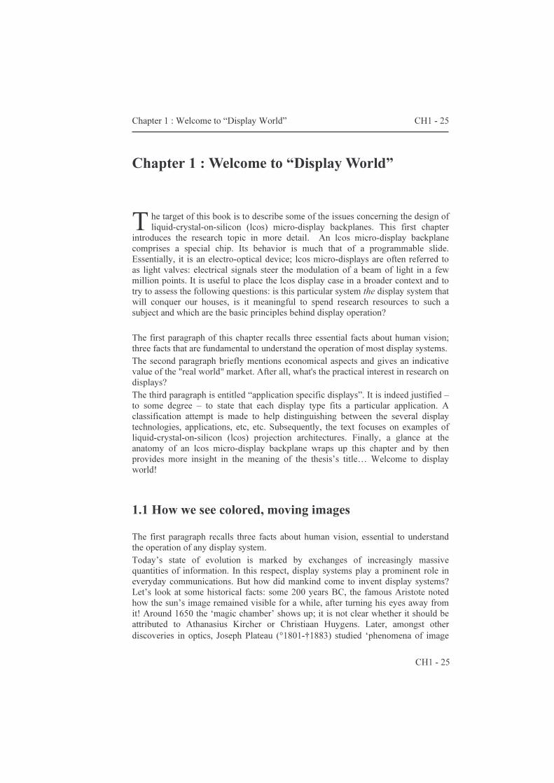
retention by the retina’ and invented a precursor of animated films in 1831: the phenakistiscope. Eventually in 1895, the brothers Lumière came up with the first movie camera. On november 18th 1929 Vladimir Kosma Zworykin demonstrates a TV receiver containing his version of the Braun tube (1897). After the war, David Sarnoff (chairman of RCA) said about color that it “added sight to sound”. Color TV was born somewhere in the fifties. It took mankind to 1965 before color specialization of the retinal cones was demonstrated. In the early 70’s Peter Brody brilliantly demonstrated the concept of active-matrix liquid-crystal displays [1],[2],[3]. In 2000, displays continue to invade and ‘possess’ the entire world. Someone said ‘seeing is believing’ and everyone appears to need to believe in something… Compared to the other physiological senses, the eyesight is maybe the most amazing and probably the most instrumental of our senses. As such, an accordingly important place is to be given to the eye. Honestly, it is hard looking into display systems without a little understanding of our own vision system. The human eye is a marvelous living-tissue optical system. In [4] plenty of information can be found just about the perception of contrast; however, for this introduction, a few facts will suffice. Consider figure 1-1 depicting a cross section of the eye.
Figure 1-1 : the human eye
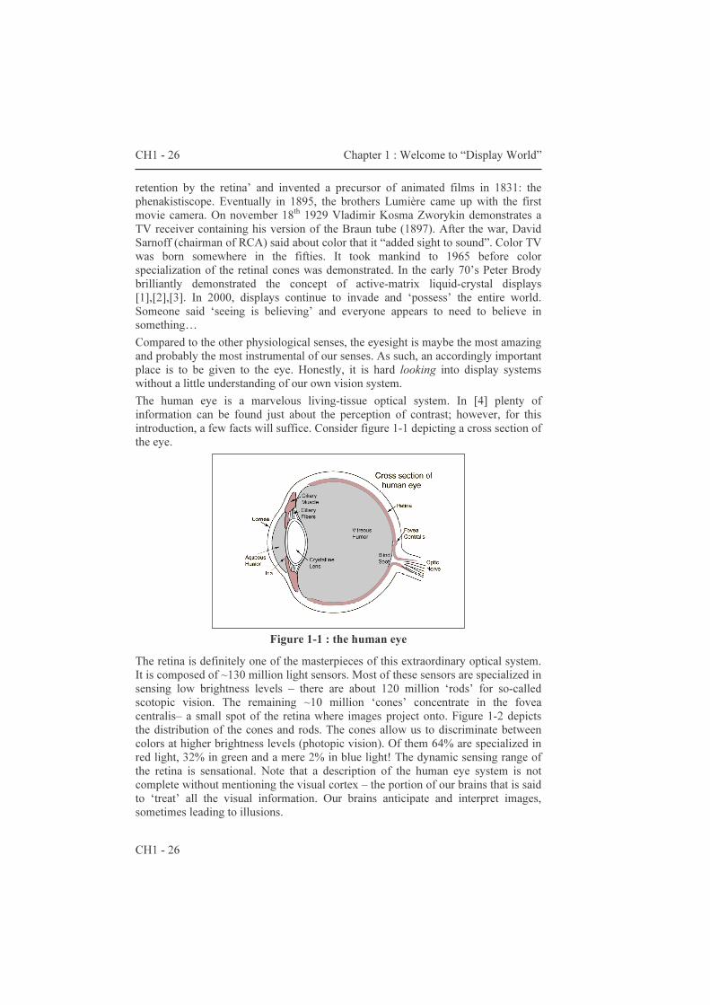
The retina is definitely one of the masterpieces of this extraordinary optical system. It is composed of ~130 million light sensors. Most of these sensors are specialized in sensing low brightness levels – there are about 120 million ‘rods’ for so-called scotopic vision. The remaining ~10 million ‘cones’ concentrate in the fovea centralis– a small spot of the retina where images project onto. Figure 1-2 depicts the distribution of the cones and rods. The cones allow us to discriminate between colors at higher brightness levels (photopic vision). Of them 64% are specialized in red light, 32% in green and a mere 2% in blue light! The dynamic sensing range of the retina is sensational. Note that a description of the human eye system is not complete without mentioning the visual cortex – the portion of our brains that is said to ‘treat’ all the visual information. Our brains anticipate and interpret images, sometimes leading to illusions.
Chapter 1 : Welcome to “Display World” CH1 - 27
CH1 - 27
Figure 1-2 : cone and rod distribution over the retina
Three elements are essential to understand how electronic displays work. It is the eye's capability of mixing colors (1) over time (2) and in space (3) that should retain our attention here. The text below only provides a rough overview and the reader is referred to literature for extensive discussions – see e.g. [5].
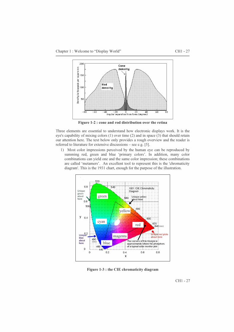
1) Most color impressions perceived by the human eye can be reproduced by summing red, green and blue ‘primary colors’. In addition, many color combinations can yield one and the same color impression; these combinations are called ‘metamers’. An excellent tool to represent this is the 'chromaticity diagram'. This is the 1931 chart, enough for the purpose of the illustration.
Figure 1-3 : the CIE chromaticity diagram
green
blue
red cyan
yellow
magenta
(nm)
(nm)
CH1 - 28 Chapter 1 : Welcome to “Display World”
CH1 - 28
The chromaticity diagram shown in figure 1-3 is a systematic collection of color impressions a standard human eye is able to detect1. It is an instrument that allows to quantify and to compare color display systems. Many color displays use three primary colors (red, green and blue). These points define a triangle of color impressions that can be emulated with weighted combinations of the three primary colors. The larger the triangle, the more color impressions can be reproduced. For different display systems the coordinates of the primary colors can differ and thus are a performance parameter. As a result, one color picture element (color pixel) often contains three sub-pixels (red-green-blue RGB, or sometimes cyan-magenta-yellow CMY). Because of the spatial frequency of the phosphor primaries of a CRT display, one can say the color reproduction is obtained through spatial-multiplexing. Another technique relies on time-multiplexing to reproduce color. With time-multiplexing, our brains interpret quick successions of images as full color images. The latency of the eye is at the basis of color perception and of the perception of video.
2) Sufficiently fast successions of still images are seen as 'moving images' – see e.g. the phenakistiscope mentioned above for a rather ancient example. Later in history one of the first electronic displays shows up, the 'Braun tube'. It is the pre-runner of our everyday, omnipresent television (TV) sets. As electronics enable ever higher switching speeds, the booming of electronic displays is unavoidable. However, even nowadays, flat panel displays reproduce moving images by displaying ... (very) quick successions of still images. The number of images displayed per second is called the frame rate. Note that if the frame rate of a display system is too low, the human eye will detect it. This is just one case of display ‘flicker’. The eye can be fooled with sufficiently high frame rates, and cannot detect flicker. This is easily verified by comparing the images of 100Hz TV sets with their older 50/60Hz variants.
3) Below a threshold viewing angle, intensities and colors will be averaged out. This happens when fine details become too close to each other, or when the magnification level (zoom level) is small enough. It means that details in a small area will be averaged into a single 'spot'. A group of spatially close red, green and blue spots yields a 'white' impression, provided the viewing distance to the spots is large enough. This characteristic is at the very heart of many color display systems. Below a threshold resolution, the eye will detect no extra information. Thus, the viewing distance determines the number of pixels a display must count to make image discretization very hard to detect.
Current color display systems for moving images rely upon each of these features. In particular, this is demonstrated by the single cell color sequential optical architecture (see 1.3.2) and by the color thin-film-transistor (TFT) active matrix displays in laptops. It is nice to know all this; however, as we do have working displays, why does display research still make sense?
1 Note that at most the colors within an cyan-magenta-yellow (CMY) triangle can be correct, because the printer used for the reproduction of this figure is not capable of more. A display or printer produces color impressions limited to the inside of the triangle formed by the so-called ‘color primaries’.
Chapter 1 : Welcome to “Display World” CH1 - 29
CH1 - 29
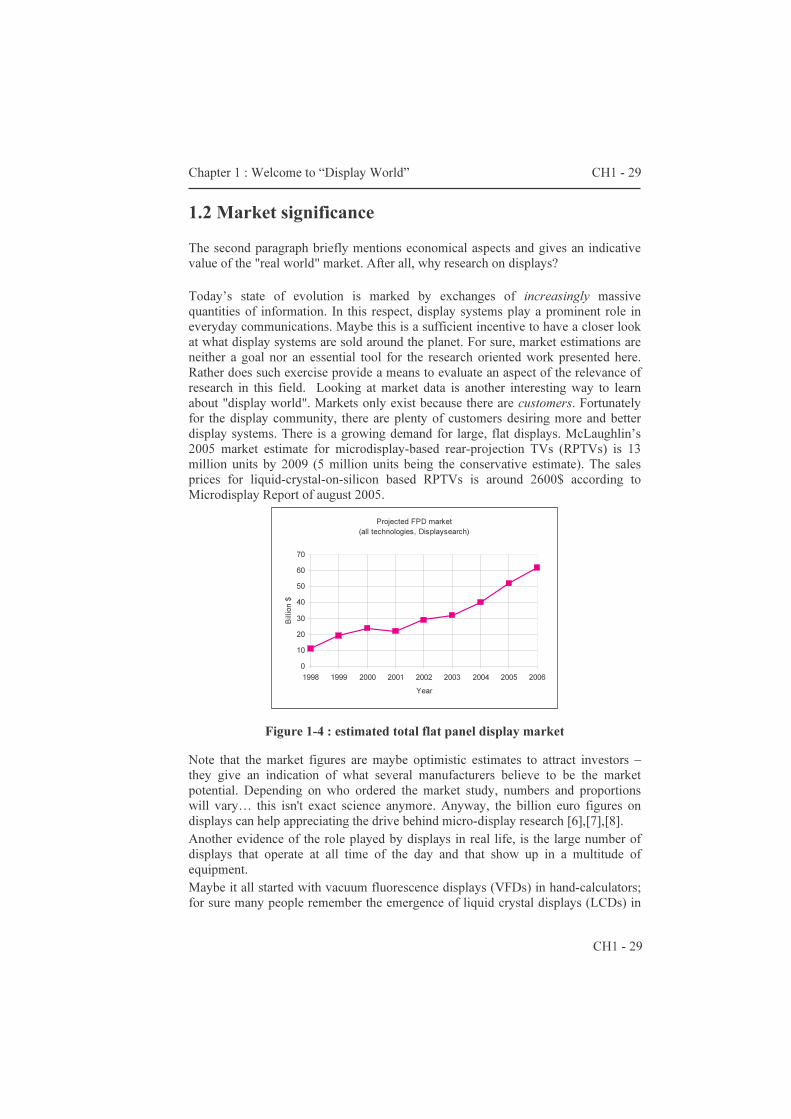
1.2 Market significance The second paragraph briefly mentions economical aspects and gives an indicative value of the "real world" market. After all, why research on displays? Today’s state of evolution is marked by exchanges of increasingly massive quantities of information. In this respect, display systems play a prominent role in everyday communications. Maybe this is a sufficient incentive to have a closer look at what display systems are sold around the planet. For sure, market estimations are neither a goal nor an essential tool for the research oriented work presented here. Rather does such exercise provide a means to evaluate an aspect of the relevance of research in this field. Looking at market data is another interesting way to learn about "display world". Markets only exist because there are customers. Fortunately for the display community, there are plenty of customers desiring more and better display systems. There is a growing demand for large, flat displays. McLaughlin’s 2005 market estimate for microdisplay-based rear-projection TVs (RPTVs) is 13 million units by 2009 (5 million units being the conservative estimate). The sales prices for liquid-crystal-on-silicon based RPTVs is around 2600$ according to Microdisplay Report of august 2005.
Figure 1-4 : estimated total flat panel display market
Note that the market figures are maybe optimistic estimates to attract investors – they give an indication of what several manufacturers believe to be the market potential. Depending on who ordered the market study, numbers and proportions will vary… this isn't exact science anymore. Anyway, the billion euro figures on displays can help appreciating the drive behind micro-display research [6],[7],[8]. Another evidence of the role played by displays in real life, is the large number of displays that operate at all time of the day and that show up in a multitude of equipment. Maybe it all started with vacuum fluorescence displays (VFDs) in hand-calculators; for sure many people remember the emergence of liquid crystal displays (LCDs) in
Projected FPD market (all technologies, Displaysearch)
010203040506070
1998 1999 2000 2001 2002 2003 2004 2005 2006Year
Billio
n $

CH1 - 30 Chapter 1 : Welcome to “Display World”
CH1 - 30
wristwatches. Next to LCDs, various other display technologies exist. Electro-luminescent displays show up in car radio displays, plasma displays show up in airports and luxury living rooms, people want personal digital assistants (PDAs) and mobile phones with color displays, home theatre systems, etc. The more new technologies emerge, the more applications show up. Whether lcos displays will be the global winner remains to be shown... but a trend has definitely been set. Someone even said about liquid crystal materials: "Liquid crystal has a habit, if you look historically, of winning race after race. It does it in a systematic way, and conquers each market completely." [9]. Interestingly, the history of LCDs is reviewed in [10].

Chapter 1 : Welcome to “Display World” CH1 - 31
CH1 - 31
1.3 Application specific displays 1.3.1 Classification attempts Do you speak CRT, LCD, PDP, OLED, (O)EL, FED, VFD, H/LTPS, X-SI, lcos, DMD, DLP, TMA, MEMS, or...? And how do you like VAN, STN, FLC, cholesteric texture LC, TN, IPS,...?
Name of the display technology Abbreviation Amorphous silicon a-Si Cathode ray tube (Braun tube) CRT Digital direct drive image light amplifier D-ILA Digital light processor DLP Digital mirror device DMD (In/organic) electro-luminescent displays (I/O)ELD Field emission displays FED Flat panel display FPD Grating light valve GLV High/low temperature poly-silicon H/LTPS Liquid crystal display LCD Liquid crystal on silicon lcos Micro electro mechanical systems MEMS (Organic) light emitting diodes (O)LED Organic light emitting polymers OLEP OLED on silicon OLEDOS Plasma addressed liquid crystal PALC Plasma discharge panels PDP Tilted mirror array TMA Vacuum fluorescent displays VFD Vacuum fluorescence on silicon VFOS Crystalline silicon x-SI
Table 1-1 : some abbreviations relating to display technologies The following lines attempt to classify the different types of display technologies. It is an attempt, because there is such a variety of differentiating parameters that it is hard to get all of them within a single, simple, comprehensive catalog. In other words, there is no place for a binary classification tree.

CH1 - 32 Chapter 1 : Welcome to “Display World”
CH1 - 32
Classification 1: direct view vs. projection Direct view: a) CRT (TV sets, PC monitors, video walls, measuring equipment…) b) FPD (PDP, LCD, ELD, VFD, FED) Projection: a) NTE or HMD b) Front/rear projectors (MEMS, LCD (HTPS, lcos), CRT) Note: CRTs have been used both in direct view and projection systems. Classification 2: emissive vs. valve Emissive: a) Phosphor excitation: e.g. CRT, FED, VFD, PDP b) Electron excitation: OLED/P, ELD Valve: a) MEMS (reflective: DMD, GLV, TMA) b) LCD (transmissive: LTPS, HTPS, x-Si; reflective: x-Si - lcos) Note: Crystalline silicon (x-Si) technology has the advantage of being mature and is used either for reflective (lcos) or for transmissive panels (Kopin) Note: D-ILA: digital direct drive image light amplifier, originates from a combination of an emissive and a valve display! The thesis focuses on the design of a part of lcos projection systems: the silicon backplane. But what do lcos systems look like; what are they composed of and how can it work?
1.3.2 Lcos systems Near-to-the-eye and projector applications Lcos micro-displays are small, lightweight and very thin displays (~2mm). They enclose a liquid crystal layer – as such, they are quite small LCDs. Typical display diagonals are between 0.5” and 1”; a diagonal of 0.7” is an ‘unofficial standard’. Some people do call them mini-LCDs. They really are very flat and lightweight; the overall system needs magnification optics. As cost increases dramatically with the size of the optical components, it is clear why everyone wants small display diagonals. There is also a lower limit set by diffraction. Diffraction causes the outgoing beam to split into several lobes. The energy lost in these sidelobes reduces the light throughput. This loss in throughput increases with decreasing display2 dimensions and becomes unacceptable at some point. It can only be countered with again larger and thus more expensive optical components or, by imposing a lower limit on the display dimension (see footnote 2 and also [11]).
2 Actually, it is the small dimensions of the pixels that cause diffraction; at equal pixel counts, smaller diagonals imply smaller pixel dimensions.
Chapter 1 : Welcome to “Display World” CH1 - 33
CH1 - 33
Very compact optics are well tailored for use in NTE applications like HMDs. HMDs are used by pilots, firefighters, gamers, maintenance personel, hi-tech freaks,... NTE systems must be very lightweight and indeed do not need high-power, bulky illumination systems. On the other hand, lcos based front/rear projectors allow for high performance optics and much larger brightness levels. From an optical point of view, lcos micro-displays either
a) form real images on a screen (front/rear projectors) or b) form virtual images in so-called near-to-the-eye applications
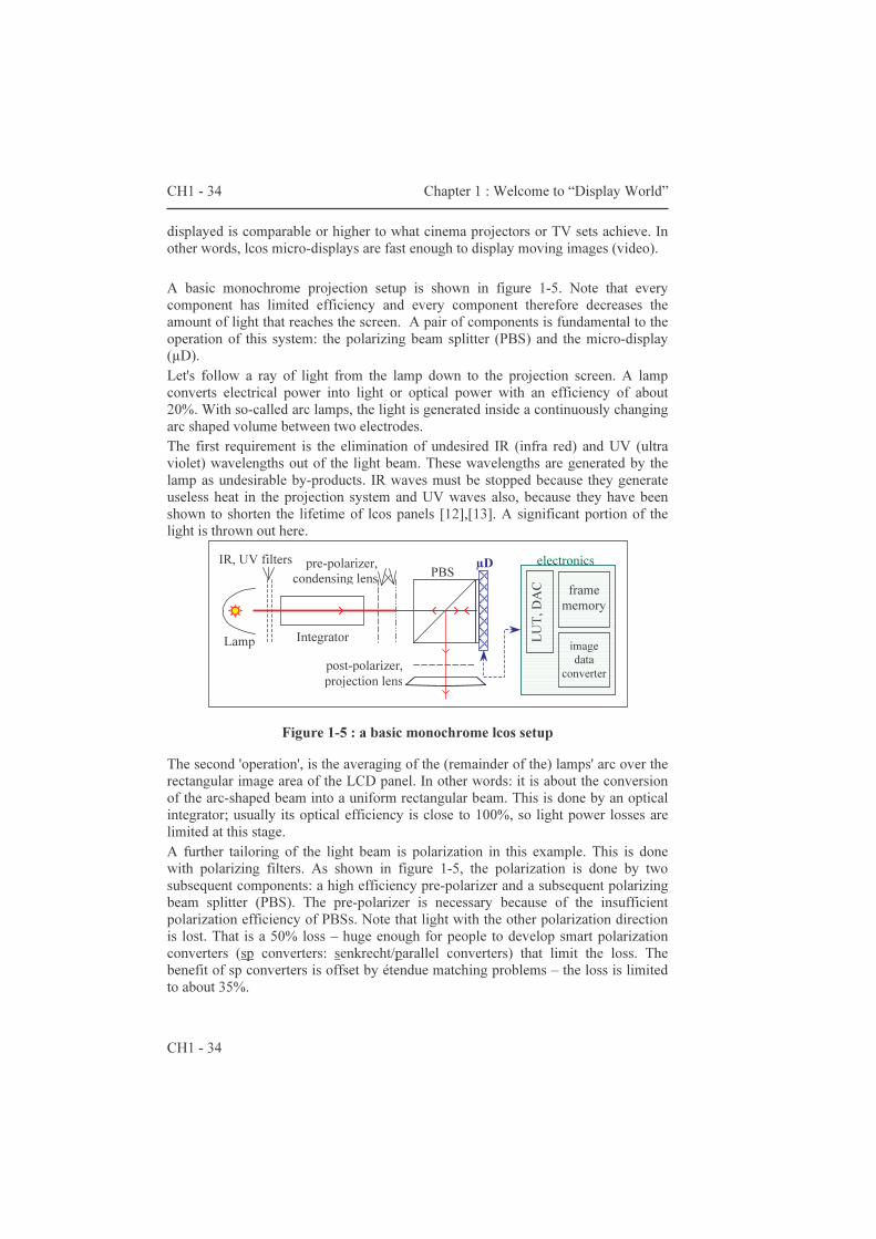
The primary focus of the work presented in the next chapters is on micro-displays for front/rear projection applications. Indeed, at the start of the research, no specific plans were made to tailor the backplane for NTE applications. The next (brief) presentation of the monochrome projection architecture serves as introduction to the more practical color architectures. A single panel monochrome projector The overall system components can be grouped into electronics, optics and an lcos micro-display panel bridging the two. Both the electronics and optics can be decomposed into chains of components. The data input of the projector can be any kind of image source like a video player, TV receiver or computer video card. Because of the wild variety of image formats and the specific requirements of the lcos panel, conversion of the input image data is necessary. Usually, the conversion comprises several operations; it can include (re-)sampling, de-interlacing, frame rate conversion and keystone correction. Specific chipsets must be developed for this and an image memory is necessary. In the examples of this book, the digital data are converted into analog signals by means of DACs and look-up tables. This conversion can be done by the lcos panel, or by the external system electronics. The look-up table is necessary to adjust for the non-linear response of the eye to lower gray shades. One can question whether all electronics should be on a single chip. The advantage of a single chip system is cost, especially with larger volumes. However, as chip technology is tuned to the electronic function to implement, cost effective solutions imply different chips. E.g. Microdisplay Corp. sells lcos chipsets consisting of a few chips. Early micro-display processes are known to suffer from relatively low yields, so additional functionality would imply a further decrease of the yield (except if the extra circuits include redundancy). Any projection system uses some kind of lamp as light source. Let’s try to explain roughly what happens to the light from the lamp. Of course, this does not constitute a manual for the optical design of a projection system. The micro-display (µD) modulates a rectangular-shaped beam of light and thus determines the image displayed. By comparison with a slide projector, the slide is the light modulating element. The speed at which a sequence of images can be
CH1 - 34 Chapter 1 : Welcome to “Display World”
CH1 - 34
displayed is comparable or higher to what cinema projectors or TV sets achieve. In other words, lcos micro-displays are fast enough to display moving images (video). A basic monochrome projection setup is shown in figure 1-5. Note that every component has limited efficiency and every component therefore decreases the amount of light that reaches the screen. A pair of components is fundamental to the operation of this system: the polarizing beam splitter (PBS) and the micro-display (µD). Let's follow a ray of light from the lamp down to the projection screen. A lamp converts electrical power into light or optical power with an efficiency of about 20%. With so-called arc lamps, the light is generated inside a continuously changing arc shaped volume between two electrodes. The first requirement is the elimination of undesired IR (infra red) and UV (ultra violet) wavelengths out of the light beam. These wavelengths are generated by the lamp as undesirable by-products. IR waves must be stopped because they generate useless heat in the projection system and UV waves also, because they have been shown to shorten the lifetime of lcos panels [12],[13]. A significant portion of the light is thrown out here.
Figure 1-5 : a basic monochrome lcos setup
The second 'operation', is the averaging of the (remainder of the) lamps' arc over the rectangular image area of the LCD panel. In other words: it is about the conversion of the arc-shaped beam into a uniform rectangular beam. This is done by an optical integrator; usually its optical efficiency is close to 100%, so light power losses are limited at this stage. A further tailoring of the light beam is polarization in this example. This is done with polarizing filters. As shown in figure 1-5, the polarization is done by two subsequent components: a high efficiency pre-polarizer and a subsequent polarizing beam splitter (PBS). The pre-polarizer is necessary because of the insufficient polarization efficiency of PBSs. Note that light with the other polarization direction is lost. That is a 50% loss – huge enough for people to develop smart polarization converters (sp converters: senkrecht/parallel converters) that limit the loss. The benefit of sp converters is offset by étendue matching problems – the loss is limited to about 35%.
LUT,
DAC
frame memory
image data
converter
Lamp
Integrator
PBS IR, UV filters
post-polarizer, projection lens
µD electronics pre-polarizer, condensing lens
Chapter 1 : Welcome to “Display World” CH1 - 35
CH1 - 35
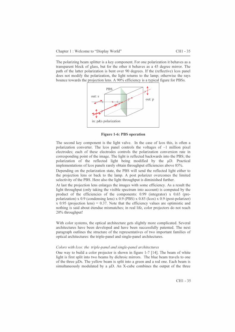
The polarizing beam splitter is a key component. For one polarization it behaves as a transparent block of glass, but for the other it behaves as a 45 degree mirror. The path of the latter polarization is bent over 90 degrees. If the (reflective) lcos panel does not modify the polarization, the light returns to the lamp; otherwise the rays bounce towards the projection lens. A 90% efficiency is a typical figure for PBSs.
Figure 1-6: PBS operation
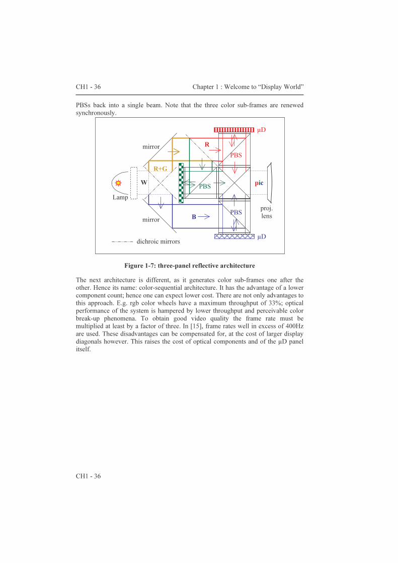
The second key component is the light valve. In the case of lcos this, is often a polarization converter. The lcos panel controls the voltages of ~1 million pixel electrodes; each of these electrodes controls the polarization conversion rate in corresponding point of the image. The light is reflected backwards into the PBS; the polarization of the reflected light being modified by the µD. Practical implementations of lcos panels rarely obtain throughput efficiencies above 85%. Depending on the polarization state, the PBS will send the reflected light either to the projection lens or back to the lamp. A post polarizer overcomes the limited selectivity of the PBS. Here also the light throughput is diminished further. At last the projection lens enlarges the images with some efficiency. As a result the light throughput (only taking the visible spectrum into account) is computed by the product of the efficiencies of the components: 0.99 (integrator) x 0.65 (pre-polarization) x 0.9 (condensing lens) x 0.9 (PBS) x 0.85 (lcos) x 0.9 (post-polarizer) x 0.95 (projection lens) = 0.37. Note that the efficiency values are optimistic and nothing is said about étendue mismatches; in real life, color projectors do not reach 20% throughput! With color systems, the optical architecture gets slightly more complicated. Several architectures have been developed and have been successfully patented. The next paragraph outlines the structure of the representatives of two important families of optical architectures: the triple-panel and single-panel architectures. Colors with lcos: the triple-panel and single-panel architectures One way to build a color projector is shown in figure 1-7 [14]. The beam of white light is first split into two beams by dichroic mirrors. The blue beam travels to one of the three µDs. The yellow beam is split into a green and a red one. Each beam is simultaneously modulated by a µD. An X-cube combines the output of the three
in: p&s polarization
out: p out: s PBS
CH1 - 36 Chapter 1 : Welcome to “Display World”
CH1 - 36
PBSs back into a single beam. Note that the three color sub-frames are renewed synchronously.
Figure 1-7: three-panel reflective architecture
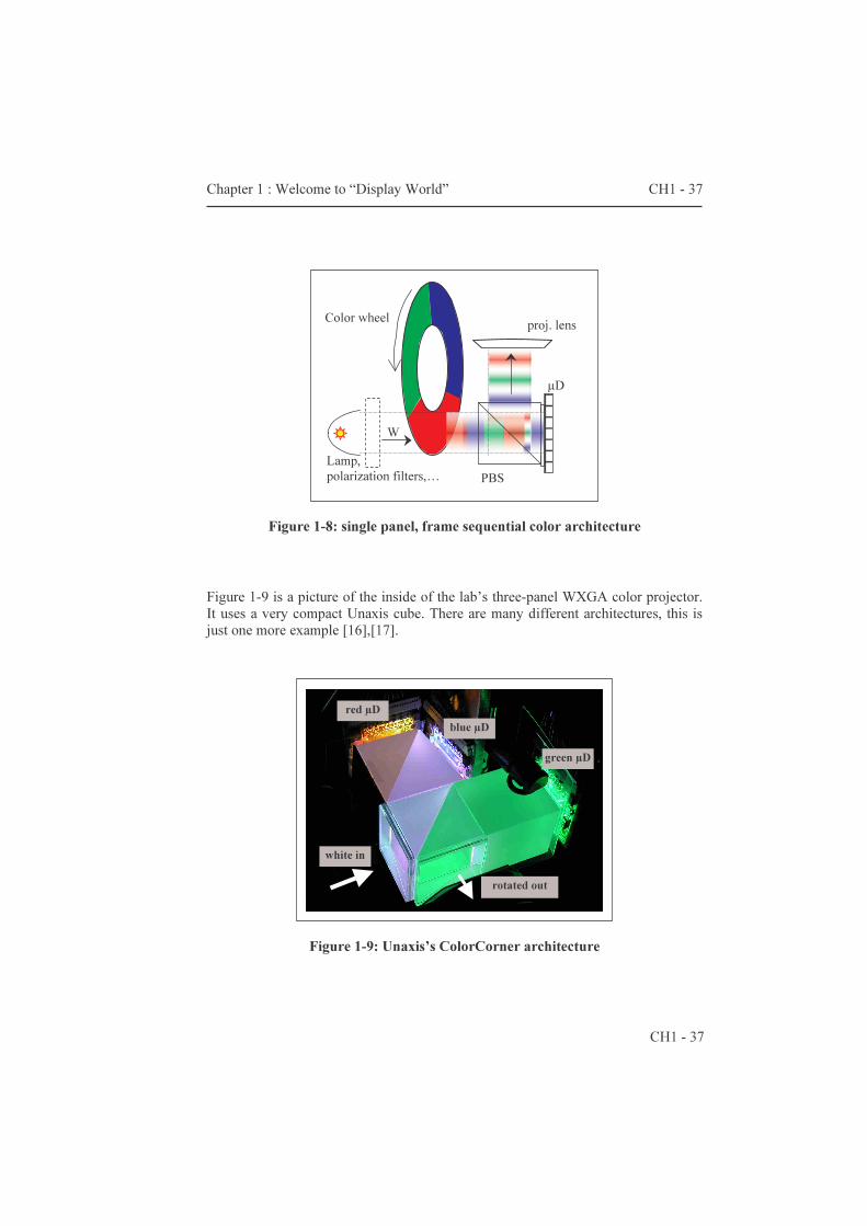
The next architecture is different, as it generates color sub-frames one after the other. Hence its name: color-sequential architecture. It has the advantage of a lower component count; hence one can expect lower cost. There are not only advantages to this approach. E.g. rgb color wheels have a maximum throughput of 33%; optical performance of the system is hampered by lower throughput and perceivable color break-up phenomena. To obtain good video quality the frame rate must be multiplied at least by a factor of three. In [15], frame rates well in excess of 400Hz are used. These disadvantages can be compensated for, at the cost of larger display diagonals however. This raises the cost of optical components and of the µD panel itself.
Lamp PBS
µD
W
B
R+G pic
µD R
mirror
mirror
dichroic mirrors
PBS
PBS
proj. lens
Chapter 1 : Welcome to “Display World” CH1 - 37
CH1 - 37
Figure 1-8: single panel, frame sequential color architecture
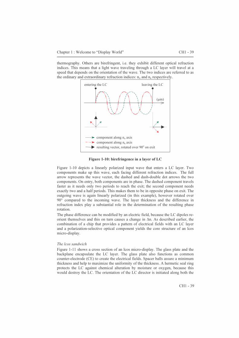
Figure 1-9 is a picture of the inside of the lab’s three-panel WXGA color projector. It uses a very compact Unaxis cube. There are many different architectures, this is just one more example [16],[17].
Figure 1-9: Unaxis’s ColorCorner architecture
Lamp, polarization filters,… PBS
µD
proj. lens
W
Color wheel
red µD blue µD
green µD
white in
rotated out

CH1 - 38 Chapter 1 : Welcome to “Display World”
CH1 - 38
1.3.3 Lcos micro-displays: definition and physical structure A glance at the anatomy of an lcos micro-display backplane wraps up this chapter and provides more insight in the meaning of the thesis’s title. The definition of the term ‘lcos micro-display’ partially reveals the physical structure. Definitions of the terms 'micro-display' and lcos
Micro-displays are displays that have such small dimensions that magnifying optics are needed to use them.
The display device diagonal is typically in the range of a few cm (~ 1 inch). In essence, micro-displays are electro-optical devices: the modulation of beam of light-rays is controlled by electronic signals. The exact nature of the electro-optical effect acts as a differentiator between the several competing micro-display technologies. Each of these technologies has specific advantages, yet none has come out as the sole winning combination.
Lcos or liquid crystal on silicon is one of the competing electro-optical effects.
The many supporters believe it is the cheapest technology. As the name suggests, lcos has two components: a thin layer of liquid crystal and a silicon chip. Just another chip…? Silicon technology is well established (cost, yield, manufacturing techniques ...) and can be used with minor modifications. This fact is important, because there is no need for massive investments in a dedicated processing plant. Chips used in lcos micro-display assembly are just another diversification of ICs (integrated circuits). The micro-display chip or ‘silicon backplane’ produces a pattern of electrical force fields inside the LC layer. This pattern corresponds with the image to be displayed. Often this chip will be referred to as the (micro-display) backplane. The electro-optical interface: liquid crystals The discovery of liquid crystals (LCs) is attributed to an Austrian scientist (Reinitzer, 1898). The aggregation phase of liquid crystals is literally in between liquid and solid phase. This peculiar aggregation phase is referred to as ‘mesophase’. On a macroscopic scale, this phase resembles to the liquid phase; while on a microscopic scale, the molecules show some kind of long range ordering. The type and amount of molecular ordering characterizes LC materials into several classes (nematic phase, smectic phase, cholesteric or chiral nematic phase, …). LCs contain long molecules that try to align to each other. Some LC effects are highly dependent upon temperature, making them applicable in thermometers or for
Chapter 1 : Welcome to “Display World” CH1 - 39
CH1 - 39
thermography. Others are birefringent, i.e. they exhibit different optical refraction indices. This means that a light wave traveling through a LC layer will travel at a speed that depends on the orientation of the wave. The two indices are referred to as the ordinary and extraordinary refraction indices: no and ne respectively.
Figure 1-10: birefringence in a layer of LC
Figure 1-10 depicts a linearly polarized input wave that enters a LC layer. Two components make up this wave, each facing different refraction indices. The full arrow represents the wave vector, the dashed and dash-double dot arrows the two components. On entry, both components are in phase. The dashed component travels faster as it needs only two periods to reach the exit; the second component needs exactly two and a half periods. This makes them to be in opposite phase on exit. The outgoing wave is again linearly polarized (in this example), however rotated over 90° compared to the incoming wave. The layer thickness and the difference in refraction index play a substantial role in the determination of the resulting phase rotation. The phase difference can be modified by an electric field, because the LC dipoles re-orient themselves and this on turn causes a change in ∆n. As described earlier, the combination of a chip that provides a pattern of electrical fields with an LC layer and a polarization-selective optical component yields the core structure of an lcos micro-display. The lcos sandwich Figure 1-11 shows a cross section of an lcos micro-display. The glass plate and the backplane encapsulate the LC layer. The glass plate also functions as common counter-electrode (CE) to create the electrical fields. Spacer balls assure a minimum thickness and help to maximize the uniformity of the thickness. A hermetic seal ring protects the LC against chemical alteration by moisture or oxygen, because this would destroy the LC. The orientation of the LC director is initiated along both the
entering the LC leaving the LC
component along no axis component along ne axis resulting vector, rotated over 90o on exit
(µm)
CH1 - 40 Chapter 1 : Welcome to “Display World”
CH1 - 40
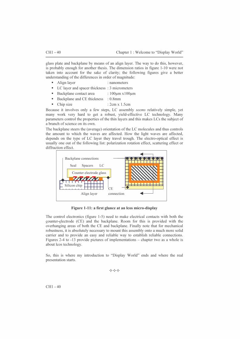
glass plate and backplane by means of an align layer. The way to do this, however, is probably enough for another thesis. The dimension ratios in figure 1-10 were not taken into account for the sake of clarity; the following figures give a better understanding of the differences in order of magnitude:
� Align layer : nanometers � LC layer and spacer thickness : 3 micrometers � Backplane contact area : 100µm x100µm � Backplane and CE thickness : 0.8mm � Chip size : 2cm x 1.5cm
Because it involves only a few steps, LC assembly seems relatively simple, yet many work very hard to get a robust, yield-effective LC technology. Many parameters control the properties of the thin layers and this makes LCs the subject of a branch of science on its own. The backplane steers the (average) orientation of the LC molecules and thus controls the amount to which the waves are affected. How the light waves are affected, depends on the type of LC layer they travel trough. The electro-optical effect is usually one out of the following list: polarization rotation effect, scattering effect or diffraction effect.
Figure 1-11: a first glance at an lcos micro-display
The control electronics (figure 1-5) need to make electrical contacts with both the counter-electrode (CE) and the backplane. Room for this is provided with the overhanging areas of both the CE and backplane. Finally note that for mechanical robustness, it is absolutely necessary to mount this assembly onto a much more solid carrier and to provide an easy and reliable way to establish reliable connections. Figures 2-4 to -13 provide pictures of implementations – chapter two as a whole is about lcos technology. So, this is where my introduction to “Display World” ends and where the real presentation starts.
���
Backplane connections
Silicon chip Cross-section
Counter electrode glass Cross-section
Seal Spacers LC
CE connection Align layer
Chapter 2: Constraints from lcos technology CH2 - 41
CH2 - 41
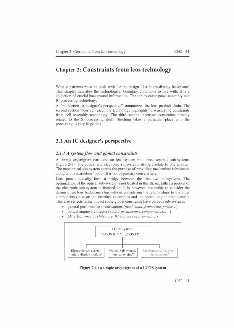
Chapter 2: Constraints from lcos technology What constraints must be dealt with for the design of a micro-display backplane? This chapter describes the technological boundary conditions to live with; it is a collection of crucial background information. The topics cover panel assembly and IC processing technology. A first section “a designer’s perspective” summarizes the lcos product chain. The second section “lcos cell assembly technology highlights” discusses the constraints from cell assembly technology. The third section discusses constraints directly related to the Si processing itself. Stitching takes a particular place with the processing of very large dies. 2.1 An IC designer's perspective 2.1.1 A system flow and global constraints A simple organigram partitions an lcos system into three separate sub-systems (figure 2-1). The optical and electronic subsystems strongly relate to one another. The mechanical sub-system serves the purpose of providing mechanical robustness, along with a marketing ‘body’. It is not of primary concern here. Lcos panels actually form a bridge between the first two subsystems. The optimization of the optical sub-system is not treated in this thesis; rather a portion of the electronic sub-system is focused on. It is however impossible to consider the design of an lcos backplane chip without considering the relationships to the other components (in casu: the interface electronics and the optical engine architecture). This also reflects in the impact some global constraints have on both sub-systems. • general performance specifications (pixel count, frame rate, power…) • optical engine architecture (color architecture, component size…) • LC effect (pixel architecture, IC voltage requirements…)
Figure 2-1 : a simple organigram of a LCOS system
LCOS system: “LCOS RPTV, LCOS FP…”
Optical sub-system: “optical engine”
Mechanical sub-system: “the apparatus”
Electronic sub-system: “micro-display module”
CH2 -42 Chapter 2: Constraints from lcos technology
CH2 - 42
Some system level specs, such as the type of optical architecture, have a direct impact on the specifications of the electrical sub-system. The way the system has to communicate with the outside world (signal sources) will also affect the overall circuit architecture. The interfacing electronics requires a specific signaling 'protocol' for communication with the panel. As a last example, the mechanical construction of the optical system can request the bond pads to be on the short/long side of the chip. Chapter three addresses the electrical specifications and presents the resulting backplane circuits. The current chapter discusses restrictions inherent to lcos panel manufacturing.
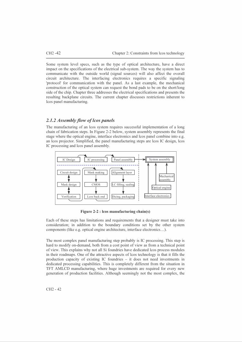
2.1.2 Assembly flow of lcos panels The manufacturing of an lcos system requires successful implementation of a long chain of fabrication steps. In Figure 2-2 below, system assembly represents the final stage where the optical engine, interface electronics and lcos panel combine into e.g. an lcos projector. Simplified, the panel manufacturing steps are lcos IC design, lcos IC processing and lcos panel assembly.
Figure 2-2 : lcos manufacturing chain(s)
Each of these steps has limitations and requirements that a designer must take into consideration; in addition to the boundary conditions set by the other system components (like e.g. optical engine architecture, interface electronics…). The most complex panel manufacturing step probably is IC processing. This step is hard to modify on-demand, both from a cost point of view as from a technical point of view. This explains why not all Si foundries have dedicated lcos process modules in their roadmaps. One of the attractive aspects of lcos technology is that it fills the production capacity of existing IC foundries – it does not need investments in dedicated processing capabilities. This is completely different from the situation in TFT AMLCD manufacturing, where huge investments are required for every new generation of production facilities. Although seemingly not the most complex, the
System assembly
Verification
Mask design
Circuit design Mask making
CMOS processing
Lcos back end
Alignment layer
LC filling, sealing
Dicing, packaging
IC Design Panel assembly IC processing
Optical engine
Interface electronics
Mechanical assembly
Chapter 2: Constraints from lcos technology CH2 - 43
CH2 - 43
panel assembly processes become a major hurdle with volume production ironically [18]-[22].
2.1.3 An (lcos) IC design cycle The design flow is full custom design for the implementations discussed in chapter 3. For sure, full custom design is not the only way to build an lcos mask layout. This paragraph reviews the design flow in six points. The description starts with arrow 6 in Figure 2-3 below as it is common to all IC design cycles. The last step is indeed the transfer of mask data for the mask making; in this dissertation, the transfer data format was always the widely known MEBES1 fracture format. In this format, the data directly steer the electron beam engine for the fabrication of the masks. Note that often some of the mask data like process related alignment markers, testkey patterns, foundry mask identification, etc. are out of control of the IC designer; they are 'transparent' to the designer. As a result, a designer's job usually ends with the creation of an intermediate data file that does not contain these 'transparent' data. The transfer of this intermediate file is referred to as 'the' tape out – the data file format used at this stage is most often GDSII. In other words, the 'mask and chip layout verification' box includes the translation into the fracture format, although this translation is transparent to the designer.
Figure 2-3: an (lcos) IC design cycle
Because of the relatively high cost of the subsequent mask making and IC manufacturing, it is essential for the mask layout to be error free. This is the most critical issue with IC design: mask layouts are so complex that ‘bugs’ can easily hide in them. The problem here compares best with the problem of finding all the needles in a large haystack – without knowing the exact number of needles, unfortunately. Experience shows that, even with the aid of special purpose software, verification does not necessarily guarantee 100% error free layouts. By the way, each manipulation of mask data can induce errors. A simple example is the translation from the GDSII data format into a fracture format!
1 for ETEC electron beam writers
1) spice netlist Schematic circuit
description Simulation of circuit behavior
Physical circuit layout
Mask and chip layout verification
Mask making
5) extracted netlist
3) GDSII and/or Dracula data
6) fractured data
2) full custom
4) CDL netlist
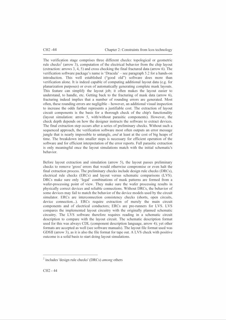
CH2 -44 Chapter 2: Constraints from lcos technology
CH2 - 44
The verification stage comprises three different checks: topological or geometric rule checks2 (arrow 3), computation of the electrical behavior from the chip layout (extraction: arrows 3, 4, 5) and cross checking the final fractured data (arrow 6). The verification software package’s name is ‘Dracula’ – see paragraph 5.2 for a hands-on introduction. This well established (“good old”) software does more than verification alone. It is indeed capable of computing additional layout data (e.g. for planarization purposes) or even of automatically generating complete mask layouts. This feature can simplify the layout job; it often makes the layout easier to understand, to handle, etc. Getting back to the fracturing of mask data (arrow 6), fracturing indeed implies that a number of rounding errors are generated. Most often, these rounding errors are negligible – however, an additional visual inspection to increase the odds further represents a justifiable cost. The extraction of layout circuit components is the basis for a thorough check of the chip's functionality (layout simulation: arrow 5, with/without parasitic components). However, the check depth depends on how the designer instructs the software to extract devices. The final extraction step occurs after a series of preliminary checks. Without such a sequenced approach, the verification software most often outputs an error message jungle that is nearly impossible to untangle, and at least at the cost of big heaps of time. The breakdown into smaller steps is necessary for efficient operation of the software and for efficient interpretation of the error reports. Full parasitic extraction is only meaningful once the layout simulations match with the initial schematic's behavior. Before layout extraction and simulation (arrow 5), the layout passes preliminary checks to remove 'gross' errors that would otherwise compromise or even halt the final extraction process. The preliminary checks include design rule checks (DRCs), electrical rule checks (ERCs) and layout versus schematic comparisons (LVS). DRCs make sure only ‘legal’ combinations of mask patterns are formed from a wafer-processing point of view. They make sure the wafer processing results in physically correct devices and reliable connections. Without DRCs, the behavior of some devices may fail to match the behavior of the device models used by the circuit simulator. ERCs are interconnection consistency checks (shorts, open circuits, device connection...). ERCs require extraction of merely the main circuit components and of electrical conductors; ERCs are pre-runners for LVS. LVS compares the implemented layout circuitry with the originally planned schematic circuitry. The LVS software therefore requires reading in a schematic circuit description to compare with the layout circuit. The schematic description format used for this was always CDL (component description language, arrow 4); yet other formats are accepted as well (see software manuals). The layout file format used was GDSII (arrow 3), as it is also the file format for tape out. A LVS check with positive outcome is a solid basis to start doing layout simulations.
2 includes 'design rule checks' (DRCs) among others
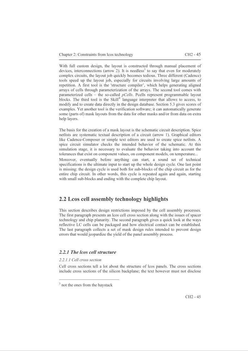
Chapter 2: Constraints from lcos technology CH2 - 45
CH2 - 45
With full custom design, the layout is constructed through manual placement of devices, interconnections (arrow 2). It is needless3 to say that even for moderately complex circuits, the layout job quickly becomes tedious. Three different (Cadence) tools speed up the layout job, especially for circuits involving large amounts of repetition. A first tool is the 'structure compiler’, which helps generating aligned arrays of cells through parameterization of the arrays. The second tool comes with parameterized cells – the so-called pCells. Pcells represent programmable layout blocks. The third tool is the Skill® language interpreter that allows to access, to modify and to create data directly in the design database. Section 5.3 gives scores of examples. Yet another tool is the verification software; it can automatically generate some (parts of) mask layouts from the data for other masks and/or from data on extra help layers. The basis for the creation of a mask layout is the schematic circuit description. Spice netlists are systematic textual description of a circuit (arrow 1). Graphical editors like Cadence-Composer or simple text editors are used to create spice netlists. A spice circuit simulator checks the intended behavior of the schematic. At this simulation stage, it is necessary to evaluate the behavior taking into account the tolerances that exist on component values, on component models, on temperature... Moreover, eventually before anything can start, a sound set of technical specifications is the ultimate input to start up the whole design cycle. One last point is missing: the design cycle is used both for sub-blocks of the chip circuit as for the entire chip circuit. In other words, this cycle is repeated again and again, starting with small sub-blocks and ending with the complete chip layout.
2.2 Lcos cell assembly technology highlights This section describes design restrictions imposed by the cell assembly processes. The first paragraph presents an lcos cell cross section along with the issues of spacer technology and chip planarity. The second paragraph gives a quick look at the ways reflective LC cells can be packaged and how electrical contact can be established. The last paragraph collects a set of mask design rules intended to prevent design errors that would jeopardize the yield of the panel assembly process. 2.2.1 The lcos cell structure 2.2.1.1 Cell cross section Cell cross sections tell a lot about the structure of lcos panels. The cross sections include cross sections of the silicon backplane; the text however must not disclose 3 not the ones from the haystack

CH2 -46 Chapter 2: Constraints from lcos technology
CH2 - 46
details hereof4, so only ‘typical’ drawings are presented. The dimensions in the drawings are for the illustration solely, but still are realistic. With lcos panels, the spacers are necessary for controlling the uniformity and the thickness of the LC layer. The LC layer’s local birefringence variations allow for light modulation. Electrical fields between two electrodes control the birefringence variations. Any additional, uncontrolled birefringence variations are undesirable for evident reasons. The CE glass serves the purpose of common counter electrode, while the Si chip controls the voltages on the individual pixel electrodes. The first item in the cross section (Figure 2-4) is the (common) counter electrode. This electrode is made of a ‘standard’ glass (e.g. Corning 1737F) covered by a transparent conductor (Indium Tin Oxide or ITO). This may very well be the simplest component. It is essential for the thermal expansion coefficient of the CE glass to match with the backplane’s (the chip) thermal expansion coefficient as closely as possible. This conceals part of the mechanical robustness concerns. The ITO conductor layer is at the LC side of the cell.
Figure 2-4 : cell cross section
4 This information is protected by non-disclosure agreements (NDAs)
1 2
3
4
1
3
2
1 : counter electrode 2 : LC layer, seal 3 : silicon backplane 4 : panel carrier board
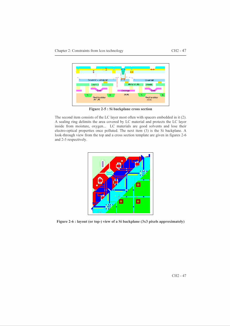
Chapter 2: Constraints from lcos technology CH2 - 47
CH2 - 47
Figure 2-5 : Si backplane cross section The second item consists of the LC layer most often with spacers embedded in it (2). A sealing ring delimits the area covered by LC material and protects the LC layer inside from moisture, oxygen... LC materials are good solvents and lose their electro-optical properties once polluted. The next item (3) is the Si backplane. A look-through view from the top and a cross section template are given in figures 2-6 and 2-5 respectively.
Figure 2-6 : layout (or top-) view of a Si backplane (3x3 pixels approximately)
(N,M)
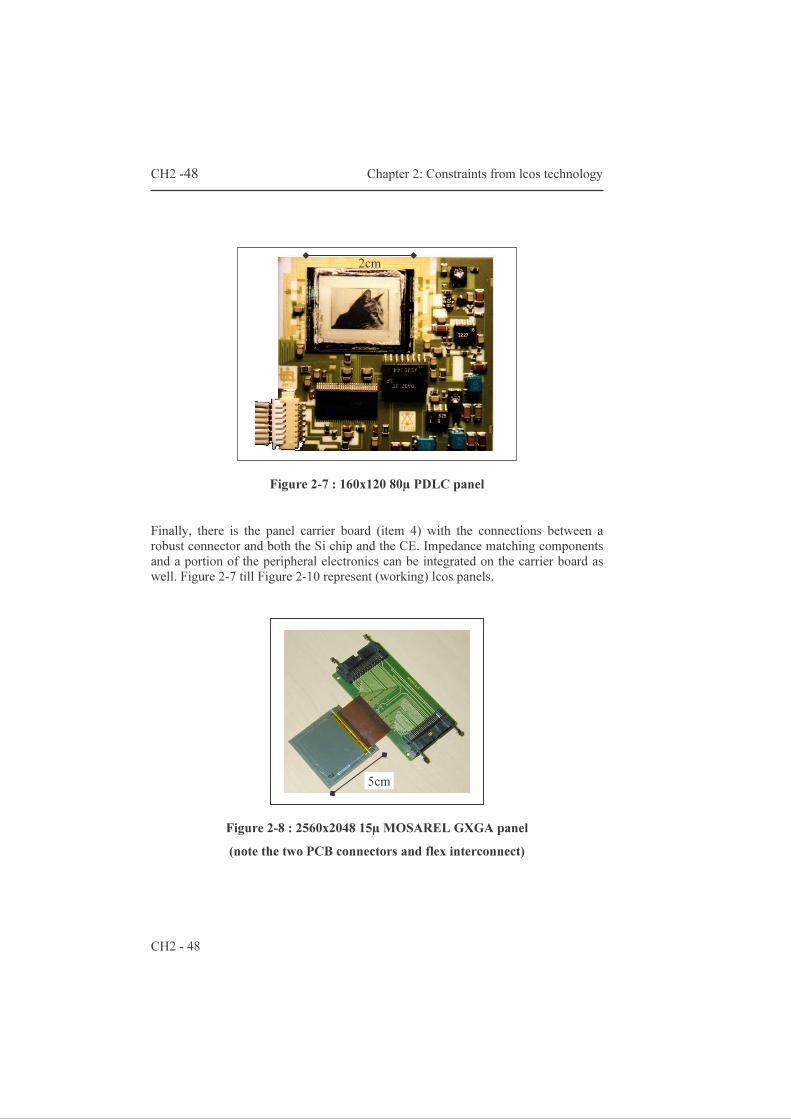
CH2 -48 Chapter 2: Constraints from lcos technology
CH2 - 48
Figure 2-7 : 160x120 80µ PDLC panel
Finally, there is the panel carrier board (item 4) with the connections between a robust connector and both the Si chip and the CE. Impedance matching components and a portion of the peripheral electronics can be integrated on the carrier board as well. Figure 2-7 till Figure 2-10 represent (working) lcos panels.
Figure 2-8 : 2560x2048 15µ MOSAREL GXGA panel (note the two PCB connectors and flex interconnect)
2cm
5cm

Chapter 2: Constraints from lcos technology CH2 - 49
CH2 - 49
Figure 2-9 : 1024x768 17µ engineering panel
Figure 2-10 : commercial 12µ WXGA panel prototype
2cm
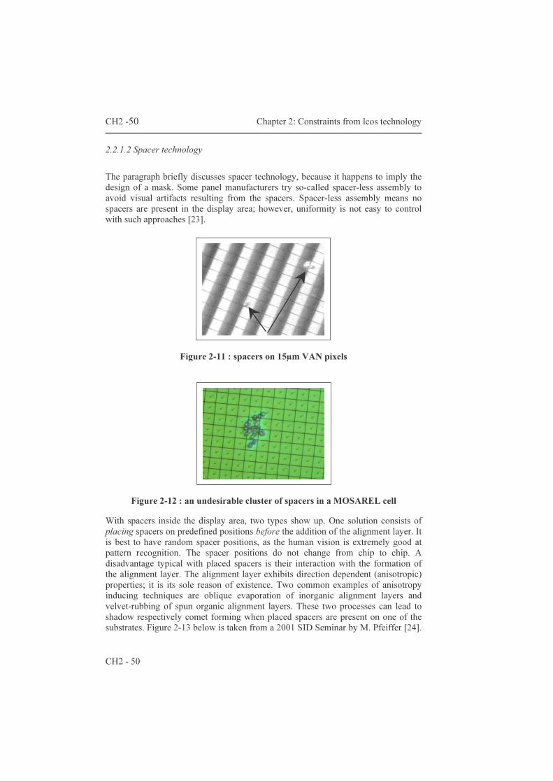
CH2 -50 Chapter 2: Constraints from lcos technology
CH2 - 50
2.2.1.2 Spacer technology The paragraph briefly discusses spacer technology, because it happens to imply the design of a mask. Some panel manufacturers try so-called spacer-less assembly to avoid visual artifacts resulting from the spacers. Spacer-less assembly means no spacers are present in the display area; however, uniformity is not easy to control with such approaches [23].
Figure 2-11 : spacers on 15µm VAN pixels
Figure 2-12 : an undesirable cluster of spacers in a MOSAREL cell
With spacers inside the display area, two types show up. One solution consists of placing spacers on predefined positions before the addition of the alignment layer. It is best to have random spacer positions, as the human vision is extremely good at pattern recognition. The spacer positions do not change from chip to chip. A disadvantage typical with placed spacers is their interaction with the formation of the alignment layer. The alignment layer exhibits direction dependent (anisotropic) properties; it is its sole reason of existence. Two common examples of anisotropy inducing techniques are oblique evaporation of inorganic alignment layers and velvet-rubbing of spun organic alignment layers. These two processes can lead to shadow respectively comet forming when placed spacers are present on one of the substrates. Figure 2-13 below is taken from a 2001 SID Seminar by M. Pfeiffer [24].
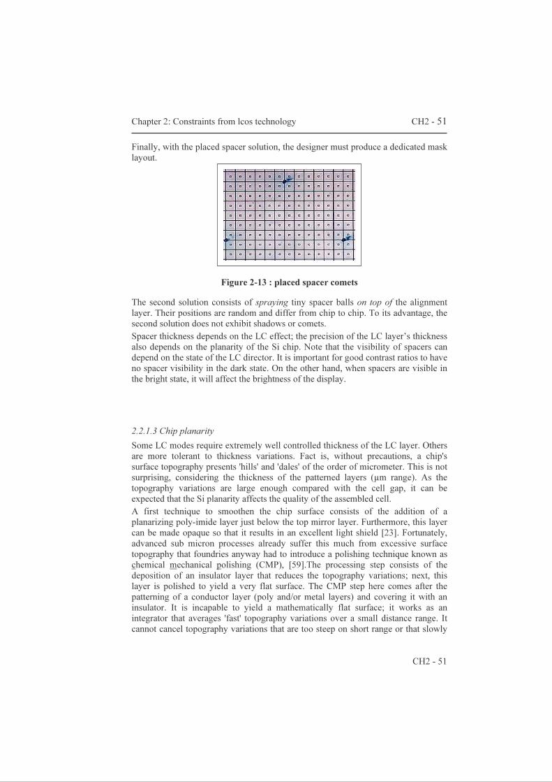
Chapter 2: Constraints from lcos technology CH2 - 51
CH2 - 51
Finally, with the placed spacer solution, the designer must produce a dedicated mask layout.
Figure 2-13 : placed spacer comets
The second solution consists of spraying tiny spacer balls on top of the alignment layer. Their positions are random and differ from chip to chip. To its advantage, the second solution does not exhibit shadows or comets. Spacer thickness depends on the LC effect; the precision of the LC layer’s thickness also depends on the planarity of the Si chip. Note that the visibility of spacers can depend on the state of the LC director. It is important for good contrast ratios to have no spacer visibility in the dark state. On the other hand, when spacers are visible in the bright state, it will affect the brightness of the display.
2.2.1.3 Chip planarity Some LC modes require extremely well controlled thickness of the LC layer. Others are more tolerant to thickness variations. Fact is, without precautions, a chip's surface topography presents 'hills' and 'dales' of the order of micrometer. This is not surprising, considering the thickness of the patterned layers (µm range). As the topography variations are large enough compared with the cell gap, it can be expected that the Si planarity affects the quality of the assembled cell. A first technique to smoothen the chip surface consists of the addition of a planarizing poly-imide layer just below the top mirror layer. Furthermore, this layer can be made opaque so that it results in an excellent light shield [23]. Fortunately, advanced sub micron processes already suffer this much from excessive surface topography that foundries anyway had to introduce a polishing technique known as chemical mechanical polishing (CMP), [59].The processing step consists of the deposition of an insulator layer that reduces the topography variations; next, this layer is polished to yield a very flat surface. The CMP step here comes after the patterning of a conductor layer (poly and/or metal layers) and covering it with an insulator. It is incapable to yield a mathematically flat surface; it works as an integrator that averages 'fast' topography variations over a small distance range. It cannot cancel topography variations that are too steep on short range or that slowly

CH2 -52 Chapter 2: Constraints from lcos technology
CH2 - 52
vary over too long ranges. Figure 2-14 below is the result of a topography measurement after patterning of the last poly and prior to the CMP step.
Figure 2-14 : typical µdisplay chip topography prior to the metal (aluminum)
depositions
Figure 2-15 : dummy polygons and de-coupling of signals with µ-trips
On the mask layout side, homogenizing the fill-factor is meaningful for the conductor layers (i.e. the polys and metals) and gate area layers. It relieves some of the difficulties associated with obtaining a flat surface. Automatic procedures (see chapter 5.2) allow a designer to add ‘dummy polygons’ to the layout. Addition of the dummy polygons is done in the last stages before mask fracturing (tape-out). It does not interfere with the design as far as the signal’s integrity is not affected. For the micro-display design case, the use of micro-strip structures safeguards the integrity for the most sensitive signals. This is most welcome e.g. for the analog video signal lines, the active matrix and long wires. A sample from a real mask-set illustrates this in Figure 2-15.
µ-strips
Dummy polygons
AM region
target planarity figure!
(both axes in arbitrary units)

Chapter 2: Constraints from lcos technology CH2 - 53
CH2 - 53
2.2.2 The lcos cell assembly 2.2.2.1 LC filling and cell sealing LC materials are extremely sensitive to contaminations; therefore, they need a hermetical seal. This protects the LC material from deterioration due to moisture, oxygen… The concept of cell sealing is simple, its implementation however is more delicate than many would expect. The quest for good sealing processes results in ‘cookbook secrets’ – know-how that LC assembly houses are keen to hide. In [18], a description is given of problems with the performance of the alignment layer as a result from the sealing process. The physical dimensions and tolerances of the seal width affect the size of the µd chip. A typical dimension is 1.5mm; smaller dimensions are desirable as this greatly affects the silicon cost (area/chip). In the MOSAREL project [23], a spacer-less assembly process has been developed at the cost of a double sealing ring. This double ring is necessary to help achieving good cell uniformity.
Figure 2-16 : MOSAREL double sealing ring design
The following process steps roughly describe the LC filling and sealing (ordered): - alignment layers on both CE glass and Si backplane chip - processing of sealing ring, spacers; assembly of an empty cell - LC filling in vacuum - sealing of LC fill opening
LC fill openings
Pads for flex interconnect
Double sealing rings

CH2 -54 Chapter 2: Constraints from lcos technology
CH2 - 54
2.2.2.2 Panel interconnection and packaging The second item that affects the size of the backplane chip is the interconnection. With the MOSAREL project, excess Si area was available, because no additional chips would fit onto the wafer. This allowed for flex interconnection. A flexible ‘flat cable’ directly attaches to the Si backplane. Such large Si area surplus rarely occurs; more usual is the situation where wire bonding is used for interconnection to an intermediate carrier substrate [25]. Wire bonding is more area-efficient. The packaging of micro-display panels is special, because high illumination levels must reach the AM (but not the rest of the chip(s)) and because of mounting requirements inside an optical engine. Packaging includes the mounting of a black (illumination-absorbing) cover with a rectangular window just above the AM (see Figure 2-10). To account for positioning tolerances of this cover, the window opening must be slightly larger than the AM and a border electrode all around the AM is foreseen. This ‘AMborder’ electrode allows e.g. to produce a neat black border around the (projected) pixel array. Similarly to other chip designs, there are design rules for the bonding pads. With more conventional chip designs, it is customary to place bondpads all around the periphery of the chip. In the lcos case this would not be the optimal choice for two reasons. First, the bondpad area requirements add up to the sealing area requirements and second, wafer-scale assembly is much easier to do when the CE glass dimensions match those of the Si backplane. Finally note that the number of bondpads is expected to be much lower than the sum of the number of columns and rows. The first micro-display panel developed within TFCG had 80 bondpads for a resolution of 160x120; the 280 busbar connections are reduced to 80 (~29%). With the MOSAREL project 128 connector pins are available for a matrix of 2560x2048 pixels (~3%); with the tmdc XGA panel, still 43 connections are needed (~2.4%)
Figure 2-17 : 120x160 wire bonded to plated substrate
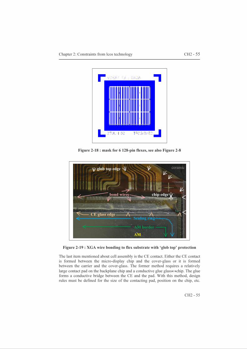
Chapter 2: Constraints from lcos technology CH2 - 55
CH2 - 55
Figure 2-18 : mask for 6 128-pin flexes, see also Figure 2-8
Figure 2-19 : XGA wire bonding to flex substrate with ‘glob top’ protection
The last item mentioned about cell assembly is the CE contact. Either the CE contact is formed between the micro-display chip and the cover-glass or it is formed between the carrier and the cover-glass. The former method requires a relatively large contact pad on the backplane chip and a conductive glue glass↔chip. The glue forms a conductive bridge between the CE and the pad. With this method, design rules must be defined for the size of the contacting pad, position on the chip, etc.
AM
Sealing ring AM border
ceramic
bond wires
CE glass edge
glob top edge
chip edge
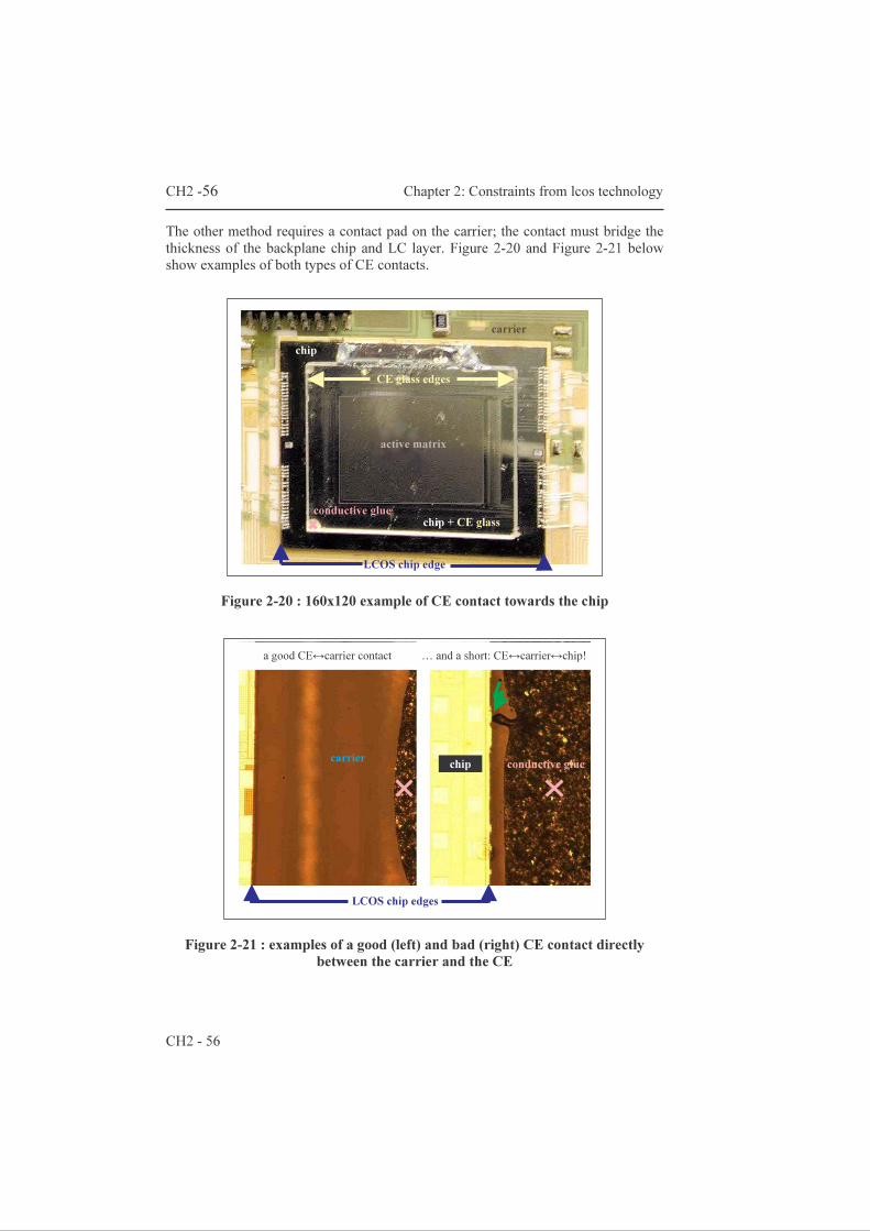
CH2 -56 Chapter 2: Constraints from lcos technology
CH2 - 56
The other method requires a contact pad on the carrier; the contact must bridge the thickness of the backplane chip and LC layer. Figure 2-20 and Figure 2-21 below show examples of both types of CE contacts.
Figure 2-20 : 160x120 example of CE contact towards the chip
Figure 2-21 : examples of a good (left) and bad (right) CE contact directly
between the carrier and the CE
chip carrier
chip + CE glass
CE glass edges
active matrix
conductive glue
LCOS chip edge
a good CE↔carrier contact … and a short: CE↔carrier↔chip!
LCOS chip edges
conductive glue chip carrier
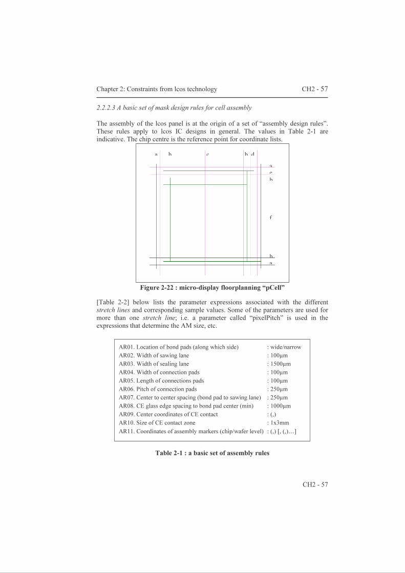
Chapter 2: Constraints from lcos technology CH2 - 57
CH2 - 57
2.2.2.3 A basic set of mask design rules for cell assembly
The assembly of the lcos panel is at the origin of a set of “assembly design rules”. These rules apply to lcos IC designs in general. The values in Table 2-1 are indicative. The chip centre is the reference point for coordinate lists.
Figure 2-22 : micro-display floorplanning “pCell” [Table 2-2] below lists the parameter expressions associated with the different stretch lines and corresponding sample values. Some of the parameters are used for more than one stretch line; i.e. a parameter called “pixelPitch” is used in the expressions that determine the AM size, etc.
Table 2-1 : a basic set of assembly rules
AR01. Location of bond pads (along which side) : wide/narrow AR02. Width of sawing lane : 100µm AR03. Width of sealing lane : 1500µm AR04. Width of connection pads : 100µm AR05. Length of connections pads : 100µm AR06. Pitch of connection pads : 250µm AR07. Center to center spacing (bond pad to sawing lane) : 250µm AR08. CE glass edge spacing to bond pad center (min) : 1000µm AR09. Center coordinates of CE contact : (,) AR10. Size of CE contact zone : 1x3mm AR11. Coordinates of assembly markers (chip/wafer level) : (,) [, (,)…]
a
b c b a
a d
e
f
b
b
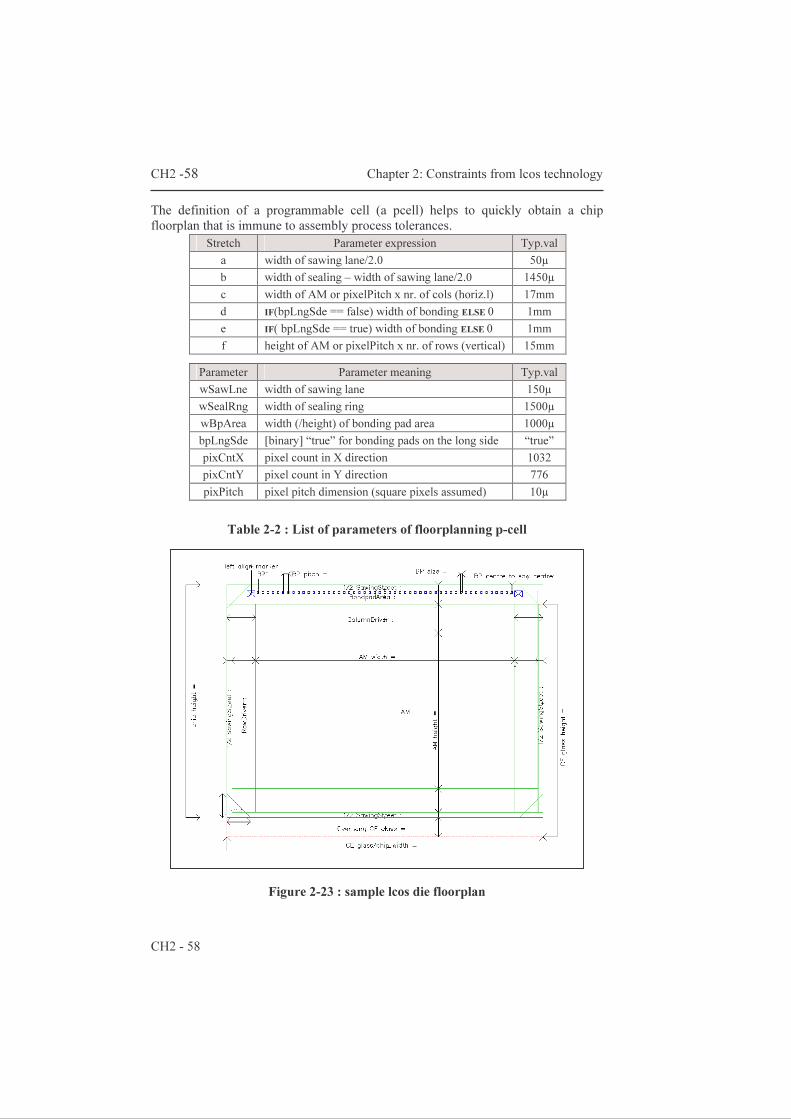
CH2 -58 Chapter 2: Constraints from lcos technology
CH2 - 58
The definition of a programmable cell (a pcell) helps to quickly obtain a chip floorplan that is immune to assembly process tolerances.
Table 2-2 : List of parameters of floorplanning p-cell
Figure 2-23 : sample lcos die floorplan
Stretch Parameter expression Typ.val a width of sawing lane/2.0 50µ b width of sealing – width of sawing lane/2.0 1450µ c width of AM or pixelPitch x nr. of cols (horiz.l) 17mm d IF(bpLngSde == false) width of bonding ELSE 0 1mm e IF( bpLngSde == true) width of bonding ELSE 0 1mm f height of AM or pixelPitch x nr. of rows (vertical) 15mm
Parameter Parameter meaning Typ.val wSawLne width of sawing lane 150µ wSealRng width of sealing ring 1500µ wBpArea width (/height) of bonding pad area 1000µ bpLngSde [binary] “true” for bonding pads on the long side “true” pixCntX pixel count in X direction 1032 pixCntY pixel count in Y direction 776 pixPitch pixel pitch dimension (square pixels assumed) 10µ
Chapter 2: Constraints from lcos technology CH2 - 59
CH2 - 59
2.3 IC processing technology highlights The goal of this section is to give an overview of different IC process flows. These are the flows used for the manufacturing of the lcos panels the author designed. The processing flow determines the mask set and its inherent limitations. One of the limitations is the maximum field size of stepper reticules. It ultimately obliges to the use of a technique called ‘stitching’ which will be introduced in the second paragraph. The subject of stitching is treated in detail in the next chapter (chapter 3). The first paragraph consists of a listing of four flows – the aim is to provide the reader with an overview and a number of difficulties associated with each flow. The flows can be summarized as follows: the first “REFLECI” flow is a lab-scale demonstration flow [26],[27]. The MOSAREL flows are upgrades – applicable at an industrial level. The fourth flow is a virtual flow; it groups the flows available with some of the largest foundries in the world. Planarization of the silicon chips is an important step as it helps with the optimization of the yield of the assembled cells. O’Hara et al. [59] report on chemical-mechanical polishing (CMP) as a method to improve the quality of the mirrors and to improve the efficiency of their spatial light modulators. This article refers also to prior art on how to avoid hillock formation. Hillocks can badly affect the quality of the mirror electrodes. CMP fortunately has become a standard processing step with sub-micron technologies. The reason it is needed relates to the processing of stacks of metallization layers. This fits with what is needed. However, we started with the use of standard cmos chips, i.e. with no microdisplay specific layers whatsoever. Initial work in the lab has been done by Nadine Carchon, as she did the planarization and back-end processing of the ‘REFLEC’ chips. The second paragraph “Photolithography I: some basics” is again a list that provides the reader with an introduction to stitching. Stitching is discussed in detail in section 2.4. The introduction starts with reviewing some essentials of photolithography. The terms light-field and dark-field masks are defined thereafter. Next, 1X and 5X lithography are described; the very last sub-paragraph explains why and in what circumstances stitching is required.

CH2 -60 Chapter 2: Constraints from lcos technology
CH2 - 60
2.3.1 Synopsis of 4 lcos-IC processing flows 2.3.1.1 REFLECI HBiMOS 160x120 The basis is formed by the standard 2.4µm CMOS 2p-2m 18V technology from AMIS-Oudenaarde5 (Belgium). Planarization of the chip is done through spinning of a transparent polyimide. The essential blocking of light is done with Brewer Science DARC. As the upper side of the DARC layer is rather rough, smoothening with an extra (transparent) layer is needed to guarantee smooth pixel surfaces. The mirrors are obtained by Al sputtering and patterning, with an adapted sintering step to avoid hillock formation [28].
Note 1: the lab-scale lithography process has a minimum feature size of about 3~5µm. This seriously affects the maximum pixel aperture ratio and thus the total light throughput.
Note 2: the lcos post-processing (planarization, light blocking and mirror layer) needs to handle rectangular dies, instead of complete wafers. This is because the 160x120 silicon is processed through Europractice multi-project wafer (MPW ) runs: wafers from MPW runs contain chip designs from others and only the lab’s part of the wafer is delivered to us.
Note 3: lab scale developments demonstrate the performance of the planarization and light blocking layers [29]; nevertheless, they are not standard industrial process steps. The very advantage of the approach with the DARC material is that a cheap, standard CMOS process can be used. However, fears for contamination by dye particles from the DARC material itself blocks industrialization by an IC foundry. An alternative could be the investment in a dedicated clean-room facility (expensive).
Note 4: the wafers are only 4 inches in diameter, which significantly limits the number of chips per wafer. It is also a 2µm process which limits the level of integration (the density and/or amount of circuitry).
2.3.1.2 MOSAREL DARC Standard 0.7µm 1p-2m 5V C, DMOS + proprietary SDEMOS pixel switch + proprietary lcos back-end. Planarization (OLIN) + light blocking (DARC) + planarization (polyimide). Mirrors (un-sintered Al)
Note 1: there arefears for fab contamination by particles in DARC material – what is the portability of this approach?
Note 2: the flex interconnection selected, requires patterns only for m1 over a large area Note 3: mix-and-match of wafer and stepper lithography needed [see section 2.4] Note 4: the life expectancy of the SDEMOS gate is unknown
5 previously Alcatel-Mietec, then Alcatel Microelectronics, now AMIS.

Chapter 2: Constraints from lcos technology CH2 - 61
CH2 - 61
Note 5: the die size is very large; only 4 chips fit on the 6” wafers; with 8” wafers the number of chips rises to only seven.
2.3.1.3 MOSAREL TiN Standard i2t 0.7µm CMOS 5V/15V 1p-4m + proprietary SDEMOS pixel switch Planarization (CMP) Light blocking (conductive TiN) Mirrors (un-sintered Al)
Note 1: there is only single CMP step after four conductor layers (after metal2); Note 2: the flex interconnection selected, requires patterns only for m1 over a large area Note 3: lithography of saw lanes is don by ‘blading’ [refer to §2.4.1.3] Note 4: the life expectancy of the SDEMOS gate is unknown Note 5: the die size is very large; only 4 chips fit on the 6” wafers; with 8” wafers the
number of chips rises to only seven.
2.3.1.4 Micro-display foundries in the world E.g. UMC 0.35µm LCOS 3.3V/18V 2p-5m
Note 1: there are specific planarization requirements for cell assembly Note 2: still uses mixed gate oxide thicknesses, is this the most cost effective technology
– what about design portability (to other processes)? Note 3: eventually, stitching is not available. As far as known, only 6” processes allow
for stitching, hereby limiting the overall yield and increasing the cost of the panel assembly.
Known lcos foundries are Amkor, Fujitsu, SMIC, TSMC and UMC. None of these foundries officially offers stitching as option; JVC however, supposedly uses stitching to obtain the large dies needed for their D-ILA product range. As far as known to the author, silicon foundries that offer stitching in their roadmap are limited to AMIS Inc. and TOWER Semiconductor Ltd. TOWER has a roadmap specific for camera chips… the dual counterpart of micro-displays?!

CH2 -62 Chapter 2: Constraints from lcos technology
CH2 - 62
2.3.2 Photolithography I: some basics 2.3.2.1 Stacks of patterned layers Chips are thin (~10-3m) rectangular slices of silicon, covered with stacks of patterned layers. The patterns arise through local modification of the physical properties of the layer (insulator/conductor removal, ion implants e.g.). These ‘treatments’ are applied to a complete batch of wafers at once; therefore, the layer areas to remain unchanged are protected from further processing by means of a ‘resist’ layer. This protection layer is obtained by spinning ‘photo-resist' over the wafers. Patterning of the photo-resist with photolithography defines all the areas on the wafer(s) to undergo processing. Photolithography is the cornerstone of Si technology. A simple etymological breakdown of ‘photolithography’ tells about the exact meaning of it. There are three parts: ϕοτος (genitive form of ϕως) or 'light', λιθος or 'stone' and the verb γραϕειν or 'to write'. It indeed is a technique that yields patterned layers on silicon crystals with the help of light. The photo-sensitive resist layer is patterned by means of light, the layers-to-be-patterned not being photosensitive. The stepper engine copies (by optical projection) the master image on a mask onto the photosensitive layer. Illuminated areas of the resist are (are not6) easy to develop away, making the underlying layer (un-)available for processing. The mask is often a quartz plate that serves as support for a chromium pattern. E.g. the mask making process utilizes electron beam writers to implement the physical copy of the software mask layout. A photolithography sequence could be as follows:
1. Deposit the layer to pattern (by epitaxy, oxidation, spinning, sputtering...) 2. Spin the photo-resist layer 3. Print the mask pattern (illumination) 4. Develop the patterned photo-resist layer (removes illuminated areas) 5. Batch processing (etching, oxidation, ion implantation...) 6. ‘Strip’ or remove the (patterned) photo-resist layer.
The resulting stack of patterned layers quickly yields a rather rough surface. This reduces the reliability of a subsequent layer. Therefore, chemical-mechanical-polishing (CMP) is applied in between layer pairs. CMP flattens the topography before deposition of a subsequent conductor layer (poly-silicon, metal). See also paragraphs 2.2.1.3 and 2.4.1.3.
6 so-called negative resists

Chapter 2: Constraints from lcos technology CH2 - 63
CH2 - 63
2.3.2.2 Layer polarity and other inversions The following discussion originates from the issue of how to interpret mask layouts. A mask layout is a collection of closed polygons; these polygons either represent areas to undergo or not a process treatment. Crudely stated, do the polygon-enclosures correspond with opaque Cr regions on the quartz plate or do they correspond with clear, transparent regions on the quartz plate? Resist sign is theoretically an extra source of confusion, it is easy to eliminate though. Figure 2-24 below depicts the behavior of both positive and negative resists and shows schematically the 'simple' photolithography sequence described previously. A resist material is defined as ‘positive’ when non-illuminated resist areas remain on chip as a (temporary) protection. The inverse is true for negative resists: only illuminated areas remain protected. Submicron technologies only use positive resists, because of their higher patterning performance. One can rather safely assume only positive resists are used. When drawing a mask pattern with design software, one is free to choose whether the area enclosed by a (software) polygon ultimately represents an area to be illuminated or not. The designer makes a choice, so that the mask layout job is easiest. A ‘mask tooling request’ form communicates this information to the mask shop. E.g. when a polygon represents a metal connection (wire), the polygon enclosure corresponds with a metal area that must be left untouched. When a polygon represents a via hole (contact) between two conductor layers, it corresponds with an area in the insulator layer that must be etched away. To make the distinction, software layers have a property called either '(working) field tone' or 'digitized area tone'… these are each other's inverse! For both, the property value is either 'dark' or 'light'. The digitized area tone refers to the areas enclosed by polygons; the (working) field is the area outside of the polygons. The adjectives 'dark field' and 'light field' are abbreviated as DF respectively LF. Layers representing connection wires are usually LF layers (‘dark’ digitized area tone), those representing contacts or vias are usually DF layers (‘light’ digitized area tone). To avoid confusion it is best to always use one of the two properties; the property values LF and DF will be used by convention for the rest of the text. Why bothering about LF/DF layers and layer inversions – one can ask whether this is a problem the mask shop alone should deal with? Isn’t it possible to use a fixed convention? The combination of layer inversions, mask bias and the unconventional stitching is prone to errors. Without special attention, mask bias and layer inversion result in wrong reticule layouts! Nevertheless, let us have a brief look at wafer and stepper lithography, before dealing with stitching in greater detail.
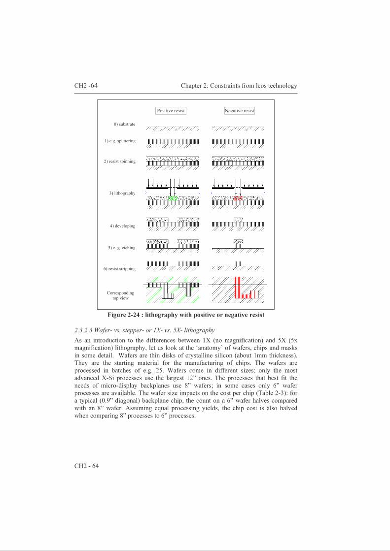
CH2 -64 Chapter 2: Constraints from lcos technology
CH2 - 64
Figure 2-24 : lithography with positive or negative resist
2.3.2.3 Wafer- vs. stepper- or 1X- vs. 5X- lithography As an introduction to the differences between 1X (no magnification) and 5X (5x magnification) lithography, let us look at the ‘anatomy’ of wafers, chips and masks in some detail. Wafers are thin disks of crystalline silicon (about 1mm thickness). They are the starting material for the manufacturing of chips. The wafers are processed in batches of e.g. 25. Wafers come in different sizes; only the most advanced X-Si processes use the largest 12” ones. The processes that best fit the needs of micro-display backplanes use 8” wafers; in some cases only 6” wafer processes are available. The wafer size impacts on the cost per chip (Table 2-3): for a typical (0.9” diagonal) backplane chip, the count on a 6” wafer halves compared with an 8” wafer. Assuming equal processing yields, the chip cost is also halved when comparing 8” processes to 6” processes.
0) substrate
1) e.g. sputtering
3) lithography
2) resist spinning
4) developing
6) resist stripping
Corresponding top view
5) e. g. etching
Positive resist Negative resist
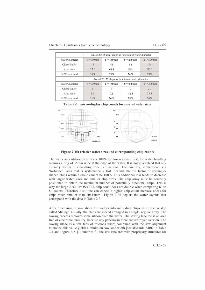
Chapter 2: Constraints from lcos technology CH2 - 65
CH2 - 65
Table 2-3 : micro-display chip counts for several wafer sizes
Figure 2-25: relative wafer sizes and corresponding chip counts
The wafer area utilization is never 100% for two reasons. First, the wafer handling requires a ring of ~5mm wide at the edge of the wafer. It is not guaranteed that any circuitry within this handling zone is functional. For circuitry, it therefore is a ‘forbidden’ area that is systematically lost. Second, the fill factor of rectangle-shaped chips within a circle cannot be 100%. This additional loss tends to decrease with larger wafer sizes and smaller chip sizes. The chip array must be correctly positioned to obtain the maximum number of potentially functional chips. This is why the large 2”x2” MOSAREL chip count does not double when comparing 6” to 8” counts. Therefore also, one can expect a higher chip count increase (>2x) for chips much smaller than 20x15mm2. Figure 2-25 depicts the wafer layouts that correspond with the data in Table 2-3. After processing, a saw slices the wafers into individual chips in a process step called ‘dicing’. Usually, the chips are indeed arranged in a single, regular array. The sawing process removes some silicon from the wafer. The sawing lane too is an area free of electronic circuitry, because any patterns in there are destroyed later on. The sawing blade is a few tens of microns wide; combined with the saw alignment tolerance, this value yields a minimum saw lane width [see also rule AR02 in Table 2-1 and Figure 2-23]. Foundries fill the saw lane area with proprietary structures for
16#
40#
80#
194#
0.9"
20x15mm2
4"
6"
8"
12"
1#
4#
7#
21#
GXGA
2x2 in2
4"
6"
8"
12"
Nr. of 20x15 mm2 chips as function of wafer diameter Wafer diameter 4”=100mm 6”=150mm 8”=200mm 12” =300mm Chips/Wafer 16 40 80 194 Area ratio 27.0 60.8 108.1 243.2 % W area used 59% 65% 74% 79%
Nr. of 2”x2” chips as function of wafer diameter Wafer diameter 4”=100mm 6”=150mm 8”=200mm 12” =300mm Chips/Wafer 1 4 7 21 Area ratio 3.1 7.1 12.6 28.3 % W area used 31% 56% 55% 74%
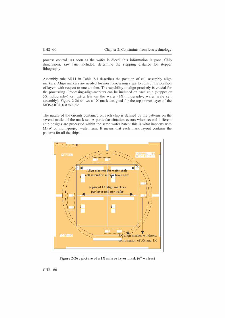
CH2 -66 Chapter 2: Constraints from lcos technology
CH2 - 66
process control. As soon as the wafer is diced, this information is gone. Chip dimensions, saw lane included, determine the stepping distance for stepper lithography. Assembly rule AR11 in Table 2-1 describes the position of cell assembly align markers. Align markers are needed for most processing steps to control the position of layers with respect to one another. The capability to align precisely is crucial for the processing. Processing-align-markers can be included on each chip (stepper or 5X lithography) or just a few on the wafer (1X lithography, wafer scale cell assembly). Figure 2-26 shows a 1X mask designed for the top mirror layer of the MOSAREL test vehicle. The nature of the circuits contained on each chip is defined by the patterns on the several masks of the mask set. A particular situation occurs when several different chip designs are processed within the same wafer batch: this is what happens with MPW or multi-project wafer runs. It means that each mask layout contains the patterns for all the chips.
Figure 2-26 : picture of a 1X mirror layer mask (6” wafers)
5X align marker windows: combination of 5X and 1X
A pair of 1X align markers per layer and per wafer
Align markers for wafer scale cell assembly: mirror layer only
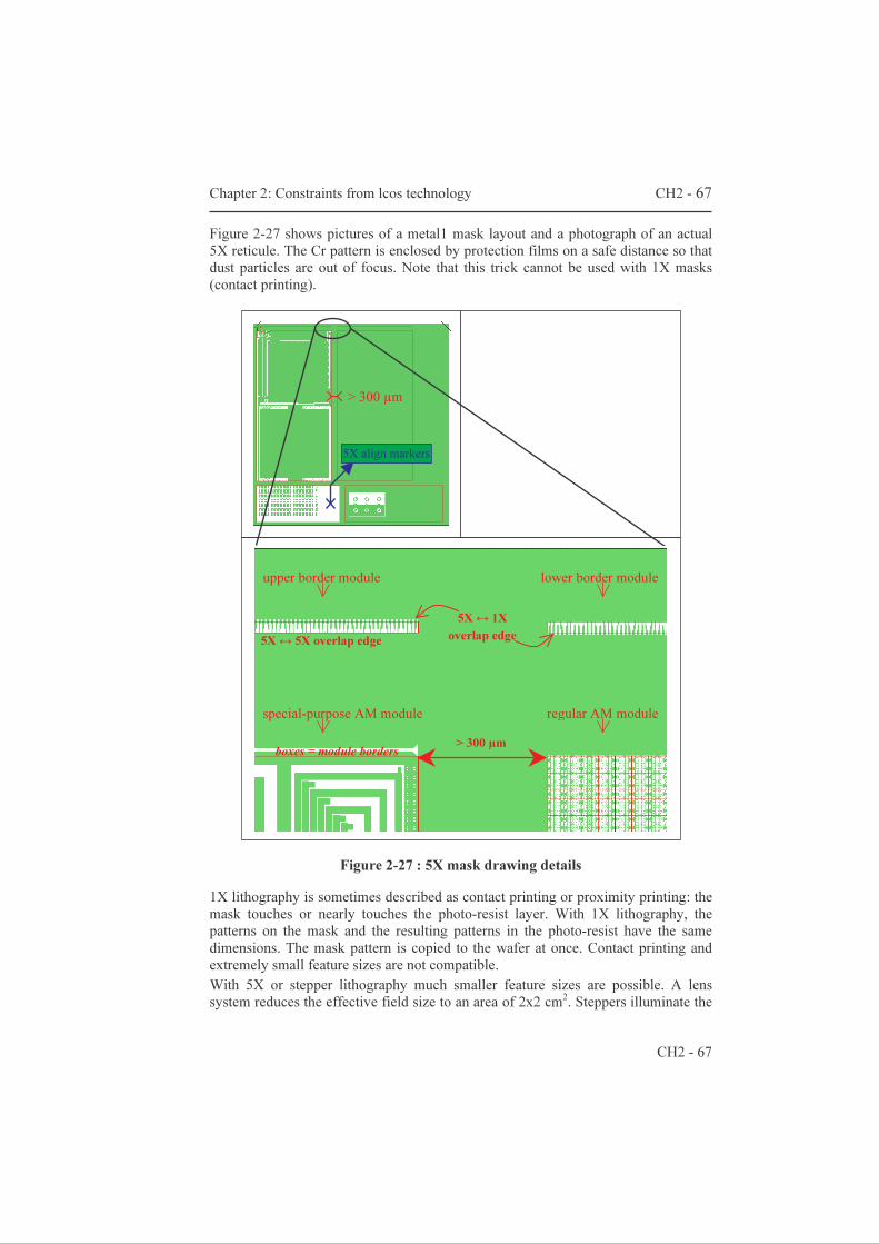
Chapter 2: Constraints from lcos technology CH2 - 67
CH2 - 67
Figure 2-27 shows pictures of a metal1 mask layout and a photograph of an actual 5X reticule. The Cr pattern is enclosed by protection films on a safe distance so that dust particles are out of focus. Note that this trick cannot be used with 1X masks (contact printing).
Figure 2-27 : 5X mask drawing details
1X lithography is sometimes described as contact printing or proximity printing: the mask touches or nearly touches the photo-resist layer. With 1X lithography, the patterns on the mask and the resulting patterns in the photo-resist have the same dimensions. The mask pattern is copied to the wafer at once. Contact printing and extremely small feature sizes are not compatible. With 5X or stepper lithography much smaller feature sizes are possible. A lens system reduces the effective field size to an area of 2x2 cm2. Steppers illuminate the
> 300 µm
5X align markers
boxes = module borders
5X ↔ 1X overlap edge 5X ↔ 5X overlap edge
> 300 µm
upper border module lower border module
regular AM modulespecial-purpose AM module

CH2 -68 Chapter 2: Constraints from lcos technology
CH2 - 68
wafer substrate step by step, one 'shot' at a time. One shot can contain several chips, if at least one chip dimension is smaller than half the maximum shot dimension. Note that the ‘chip’ includes sawing lane, align and testkey patterns.
Figure 2-28 : contact printing and stepper mechanisms
Figure 2-28 compares the mechanisms of both contact printing and stepper lithography. The grids drawn on the wafer show the sawing lane centers. There are no blades with 1X printing; blades allow shielding a portion of a reticule with a precision in the order of 100µm. With 5X printing, it is the wafer that is being stepped in x and y directions. Finally note that the stepping process itself is fast. Up to now, mask polarity and lithography mechanisms have been looked at in more detail. They are important ‘details’ as they serve as a foundation to the coming paragraphs about stitching.
2.3.2.4 The need for stitching With the demand for higher display formats and with optics-imposed minimum pixel dimensions, micro-display backplane chips can grow quite large. In the MOSAREL project a pixel array of 2560x2048 15µ pixels is implemented in a 0.7µm process (stepper lithography). The resulting active matrix size is 38.40mmx30.72mm – way larger than the maximum dimensions of the shot window
1 1
2
3
4
5 5 6
1X or wafer lithography
Legend 1 : light source 3 : mask 5 : spin-coated wafers 2 : blades 4 : lens(es) 6 : step directions
5X or stepper lithography
Chapter 2: Constraints from lcos technology CH2 - 69
CH2 - 69
(20x20mm2 is the maximum field size for many stepper engines). Inclusion of the 5mm LC sealing width, further ‘explodes’ the chip size to 48.4x40.72mm2. The 6” process therefore provides only 4 2”x2” chips per wafer. But, can chip dimensions exceed those from the (projected) reticule? This question of course only applies to processes involving stepper lithography. Current stepper technology allows for extremely high precision at the positioning of ‘shots’. In 2000, steppers achieve positioning accuracies better than ±50nm; in other words, the positioning error between two adjacent shots is less than a mere 100nm. A chip pattern is then obtained by two or more neighboring shots. Because of the high precision, it is technically feasible to accommodate for the sub-micron feature sizes in the overlap areas between two neighboring shots. Usually one tries to minimize the chip area to minimize the cost and maximize the yield. For micro-displays however, a combination of cost, image format, optical efficiency and assembly technology requirements dictates the chip dimensions. To minimize the cost when stitching seems unavoidable, two solutions show up: a) Look for a foundry that uses larger reticules; however, by 2002 the maximum reticule dimensions readily available are… 2cm by 2cm. Even if available, larger reticules are more expensive as well as the corresponding stepper engine. b) Use the stitching technique; however, this requires longer design times and more complex reticule sets. And CMOS foundries accepting to do stitching are more likely to be an exception than a rule. Stitching is… non-standard with many CMOS foundries. Fortunately, lcos micro-display backplanes are not the only application that requires stitching. CMOS-camera chips are also known to require stitching… for the higher pixel counts! [30]-[32]. When stitching is used, it is necessary for the layout to anticipate the effects of stepper positioning inaccuracies. The positioning error is not at all a constant; instead it randomizes the patterns along the stitching lines. As a result, the printed patterns will slightly differ from chip to chip. The next chapter treats the subject of stitching in greater detail.
���

CH2 -70 Chapter 2: Constraints from lcos technology
CH2 - 70

Chapter 3: Photolithography (II) – stitching CH3 - 71
CH3-71
Chapter 3 : Photolithography (II) - stitching This chapter is entirely devoted to stitching and adresses the question “Is it possible to process chips that are larger then the reticule field size?”. The work presented here is original material, as no prior art could be found on stitching for crystalline silicon processing. The work was carried out to meet the targets as defined in the MOSAREL Esprit project EP25340. I developed the stitching procedure, because I felt that a secure design flow is absolutely necessary considering cost aspects as well as the fact that here, the mask layout procedure is not at all standard. The discussion starts with a comparison between three different ways of partitioning the mask sets. Ease of processing and cost of prototyping make multiple-module reticule sets the preferred option, although the two other options are technically feasible as well. Retaining only the preferred option – the multiple-module reticule set approach – has implications on the way to construct the chip design. Particularly with the layout verification there are some difficulties. This impacts both the layout stage of the design cycle, as well as the schematic stage. Ultimately, the difficulties encountered are dealed with by following the virtual stitching procedure, described at the end of this chapter. This procedure consists of a way to organize the mask layout and of a few software routines. The reader will get insights in a tool that helps to ensure first time right designs. 3.1 Three considerations about stitching Paragraph 3.1 compares three different ways of organizing the reticule layouts for stitching. First, §3.1.1 introduces the three approaches and explains why one of them is really not viable. Paragraph 3.1.2 details the preferred multiple-module approach. Here, the introduction of MMI-tables helps with the description of the complexity of the stepper-job. At last, §3.1.3 describes the problems encountered with the mix-and-match approach. Although this last approach works technically, the use of 1X masks reduces the level of circuit integration. The reason to adopt this last approach is that one of the milestones of the MOSAREL project is the ‘testvehicle chip’. The aim of this chip is to evaluate the assembly process. The evaluation is done by addressing blocks of rows and columns in parallel, i.e. there are no integrated row or column drivers. This of course means there are practically no feature size requirements outside the active matrix area. Note by the way that, considering the current evolution of lcos microdisplays towards smaller pixel sizes, 0.35µ technologies are necessary to get the row and column driver circuits integrated. In other words, the mix-and-match approach is unlikely to be adopted for current lcos backplanes.
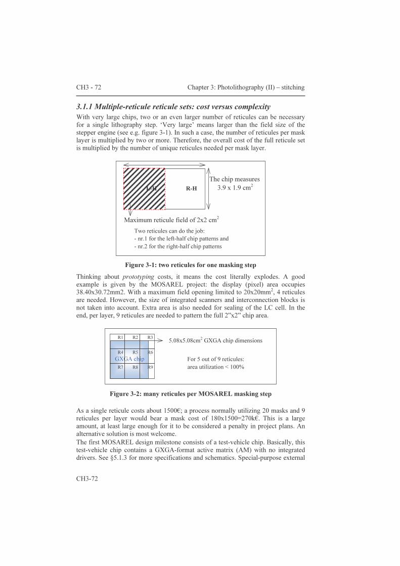
CH3 - 72 Chapter 3: Photolithography (II) – stitching
CH3-72
3.1.1 Multiple-reticule reticule sets: cost versus complexity With very large chips, two or an even larger number of reticules can be necessary for a single lithography step. ‘Very large’ means larger than the field size of the stepper engine (see e.g. figure 3-1). In such a case, the number of reticules per mask layer is multiplied by two or more. Therefore, the overall cost of the full reticule set is multiplied by the number of unique reticules needed per mask layer.
Figure 3-1: two reticules for one masking step Thinking about prototyping costs, it means the cost literally explodes. A good example is given by the MOSAREL project: the display (pixel) area occupies 38.40x30.72mm2. With a maximum field opening limited to 20x20mm2, 4 reticules are needed. However, the size of integrated scanners and interconnection blocks is not taken into account. Extra area is also needed for sealing of the LC cell. In the end, per layer, 9 reticules are needed to pattern the full 2”x2” chip area.
Figure 3-2: many reticules per MOSAREL masking step As a single reticule costs about 1500€; a process normally utilizing 20 masks and 9 reticules per layer would bear a mask cost of 180x1500=270k€. This is a large amount, at least large enough for it to be considered a penalty in project plans. An alternative solution is most welcome. The first MOSAREL design milestone consists of a test-vehicle chip. Basically, this test-vehicle chip contains a GXGA-format active matrix (AM) with no integrated drivers. See §5.1.3 for more specifications and schematics. Special-purpose external
GXGA chip
R1 R2 R3
R4 R5 R6
R7 R8 R9
5.08x5.08cm2 GXGA chip dimensions
For 5 out of 9 reticules: area utilization < 100%
Maximum reticule field of 2x2 cm2
The chip measures 3.9 x 1.9 cm2
Two reticules can do the job: - nr.1 for the left-half chip patterns and - nr.2 for the right-half chip patterns
L-H R-H
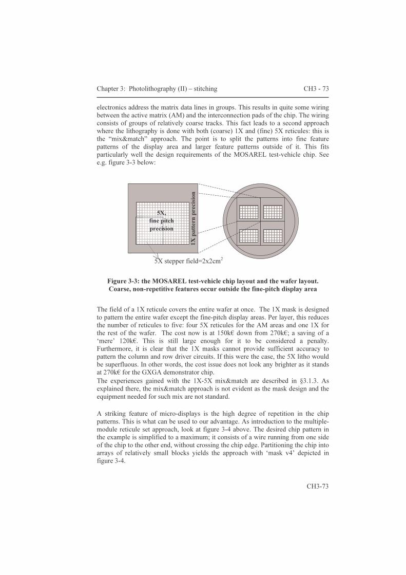
Chapter 3: Photolithography (II) – stitching CH3 - 73
CH3-73
electronics address the matrix data lines in groups. This results in quite some wiring between the active matrix (AM) and the interconnection pads of the chip. The wiring consists of groups of relatively coarse tracks. This fact leads to a second approach where the lithography is done with both (coarse) 1X and (fine) 5X reticules: this is the “mix&match” approach. The point is to split the patterns into fine feature patterns of the display area and larger feature patterns outside of it. This fits particularly well the design requirements of the MOSAREL test-vehicle chip. See e.g. figure 3-3 below:
Figure 3-3: the MOSAREL test-vehicle chip layout and the wafer layout. Coarse, non-repetitive features occur outside the fine-pitch display area
The field of a 1X reticule covers the entire wafer at once. The 1X mask is designed to pattern the entire wafer except the fine-pitch display areas. Per layer, this reduces the number of reticules to five: four 5X reticules for the AM areas and one 1X for the rest of the wafer. The cost now is at 150k€ down from 270k€; a saving of a ‘mere’ 120k€. This is still large enough for it to be considered a penalty. Furthermore, it is clear that the 1X masks cannot provide sufficient accuracy to pattern the column and row driver circuits. If this were the case, the 5X litho would be superfluous. In other words, the cost issue does not look any brighter as it stands at 270k€ for the GXGA demonstrator chip. The experiences gained with the 1X-5X mix&match are described in §3.1.3. As explained there, the mix&match approach is not evident as the mask design and the equipment needed for such mix are not standard. A striking feature of micro-displays is the high degree of repetition in the chip patterns. This is what can be used to our advantage. As introduction to the multiple-module reticule set approach, look at figure 3-4 above. The desired chip pattern in the example is simplified to a maximum; it consists of a wire running from one side of the chip to the other end, without crossing the chip edge. Partitioning the chip into arrays of relatively small blocks yields the approach with ‘mask v4’ depicted in figure 3-4.
interconnection pads 1X
patte
rn pr
ecisio
n
5X stepper field=2x2cm2
5X, fine pitch precision
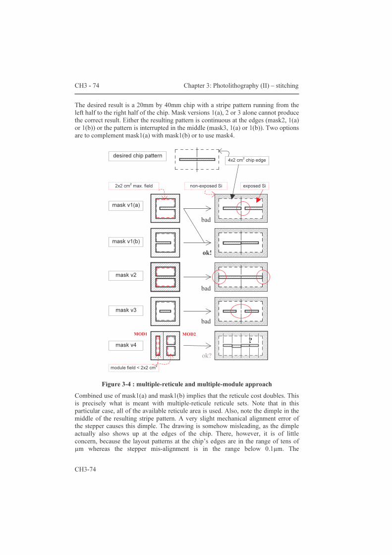
CH3 - 74 Chapter 3: Photolithography (II) – stitching
CH3-74
The desired result is a 20mm by 40mm chip with a stripe pattern running from the left half to the right half of the chip. Mask versions 1(a), 2 or 3 alone cannot produce the correct result. Either the resulting pattern is continuous at the edges (mask2, 1(a) or 1(b)) or the pattern is interrupted in the middle (mask3, 1(a) or 1(b)). Two options are to complement mask1(a) with mask1(b) or to use mask4.
Figure 3-4 : multiple-reticule and multiple-module approach
Combined use of mask1(a) and mask1(b) implies that the reticule cost doubles. This is precisely what is meant with multiple-reticule reticule sets. Note that in this particular case, all of the available reticule area is used. Also, note the dimple in the middle of the resulting stripe pattern. A very slight mechanical alignment error of the stepper causes this dimple. The drawing is somehow misleading, as the dimple actually also shows up at the edges of the chip. There, however, it is of little concern, because the layout patterns at the chip’s edges are in the range of tens of µm whereas the stepper mis-alignment is in the range below 0.1µm. The
mask v1(a)
mask v2
mask v3
mask v4
mask v1(b)
MOD2
2x2 cm2 max. field
4x2 cm2 chip edge desired chip pattern
module field < 2x2 cm2
MOD1
non-exposed Si exposed Si
ok?
ok!
bad
?
bad
bad
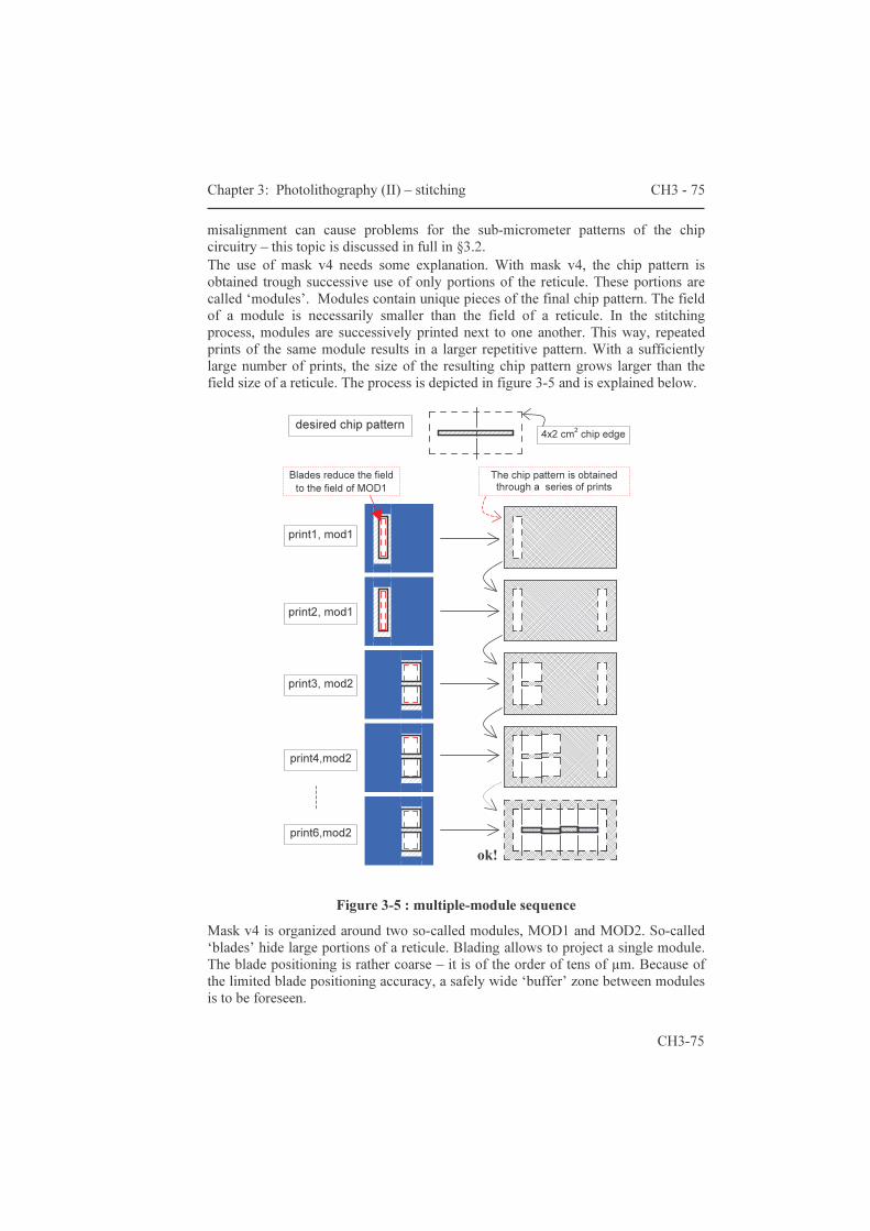
Chapter 3: Photolithography (II) – stitching CH3 - 75
CH3-75
misalignment can cause problems for the sub-micrometer patterns of the chip circuitry – this topic is discussed in full in §3.2. The use of mask v4 needs some explanation. With mask v4, the chip pattern is obtained trough successive use of only portions of the reticule. These portions are called ‘modules’. Modules contain unique pieces of the final chip pattern. The field of a module is necessarily smaller than the field of a reticule. In the stitching process, modules are successively printed next to one another. This way, repeated prints of the same module results in a larger repetitive pattern. With a sufficiently large number of prints, the size of the resulting chip pattern grows larger than the field size of a reticule. The process is depicted in figure 3-5 and is explained below.
Figure 3-5 : multiple-module sequence
Mask v4 is organized around two so-called modules, MOD1 and MOD2. So-called ‘blades’ hide large portions of a reticule. Blading allows to project a single module. The blade positioning is rather coarse – it is of the order of tens of µm. Because of the limited blade positioning accuracy, a safely wide ‘buffer’ zone between modules is to be foreseen.
4x2 cm2 chip edge desired chip pattern
print1, mod1
print3, mod2
print4,mod2
print6,mod2
print2, mod1
ok!
Blades reduce the field to the field of MOD1
The chip pattern is obtained through a series of prints
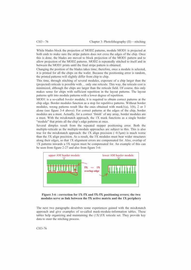
CH3 - 76 Chapter 3: Photolithography (II) – stitching
CH3-76
While blades block the projection of MOD2 patterns, module MOD1 is projected at both ends to make sure the stripe pattern does not cross the edges of the chip. Once this is done, the blades are moved to block projection of the MOD1 pattern and to allow projection of the MOD2 patterns. MOD2 is repeatedly stitched to itself and in between the MOD1 prints until the final stripe pattern is obtained. Changing the position of the blades takes time; therefore, once a module is selected, it is printed for all the chips on the wafer. Because the positioning error is random, the printed patterns will slightly differ from chip to chip. This time, through stitching of several modules, exposure of a chip larger than the (projected) reticule is possible with… only one reticule. This way, the reticule cost is minimized, although the chips are larger than the reticule field. Of course, this only makes sense for chips with sufficient repetition in the layout patterns. The layout patterns split into module patterns with a lower degree of repetition. MOD1 is a so-called border module; it is required to obtain correct patterns at the chip edge. Border modules function as a stop for repetitive patterns. Without border modules, wrong patterns result like the ones obtained with mask1(a), 1(b), 2 or 3 alone (see figure 3-4 above). For correct patterns at the edges of the chip, border modules are a must. Actually, for a correct ‘finish’ of any array, border modules are a must. With the mix&match approach, the 1X mask functions as a single border “module” that prints all the chip’s edge patterns at once. Several dimples result from the repeated stepper positioning error. Both the multiple-reticule as the multiple-module approaches are subject to this. This is also true for the mix&match approach: the 1X align precision (~0.5µm) is much worse than the 5X align precision. As a result, the 5X modules must bear wider structures along their edges, so that 1X alignment errors are compensated for. Also, overlap of 1X patterns inwards a 5X region must be compensated for. An example of this can be seen from figure 2-27 and also from figure 3-6:
Figure 3-6 : correction for 1X-5X and 5X-5X positioning errors; the two modules serve as link between the 5X active matrix and the 1X periphery
The next two paragraphs describes some experiences gained with the mix&match approach and give examples of so-called mask-module-information tables. These tables help organizing and maintaining the (1X/)5X reticule set. They provide key data to steer the stitching process.
5X ↔ 1X overlap edge
upper AM border module lower AM border module
5X-5X overlap edge

Chapter 3: Photolithography (II) – stitching CH3 - 77
CH3-77
3.1.2 Multiple-module reticule sets: ‘MMI’ tables, multiple display formats
Where the multiple-reticule approach is stuck in rather high costs it has the advantage of a relatively simple stepper job: each reticule is stepped as often as there are chips on the wafer. The approach with multiple modules greatly reduces the cost of the reticule set. The price to pay however is the complexity of the stepper-job. A supplementary advantage of working with multiple-modules is that different array dimensions can be realized with the same reticule set. In the micro-display backplane case, this means that several display formats can be printed with the same reticule set: several different chips share the same reticule set [33],[34], [§ 6.1.3]! For prototyping, this means a further reduction in reticule cost per micro-display version. There is a stepper-job per display format. In the specific case of the MOSAREL design, there is even no other option but to still provide two reticules for the metal2 masks. This relates to the layout of the interconnection pads. Additionally, some modules effectively contain data on only a few layers. Thus, for some layers, there are fewer modules than for other layers. A complication to deal with is the fact that the array of printed modules does not cover the entire chip. In other words, some areas are not patterned at all. Because this includes the sawing lanes and because problems can be expected when dicing through metal layers, ‘blading’ shots are used on some layers. These ‘empty modules’ uniformly pattern large areas with a relatively low accuracy. In other words, on some layers, there are more modules than can be seen from the reticule layout! As a result, the stepper program must take the layer into account so that only the necessary modules are printed. Furthermore, any stepper program needs the following inputs: the module field/window size, the position of the module centre on the reticule, the module position(s) with respect to the chip, the module count per chip and the chip count per wafer. Paragraph §3.3 presents more info on how to easily collect all this crucial information. The setup of a mask-module-information table (‘MMI-table’) makes the stepper-job somewhat easier to manage. The MMI-table gives an overview of the use of modules, on a layer-by-layer basis and for each chip variant. The Excel tables below show the MMI tables for the MOSAREL test vehicle and demonstrator reticule sets. Question marks and dummy names have been used to avoid revealing too much ‘classified’ information and still fully illustrating the complexity of the MOSAREL stepper-jobs. In §2.4.1.3 the mix&match of 1X and 5X lithography is reported. Such a mix&match further complicates the stepper-job, because two different litho engines must be made to work together. With the MOSAREL test vehicle, the stepper-job complexity due to mix&match is somewhat eased by two facts: the fact there is only one format for the test vehicle (GXGA format) and the fact the technology route is based on a pure 0.7µ CMOS process (fewer masks). See also §2.3.1.2 and §2.3.1.3.
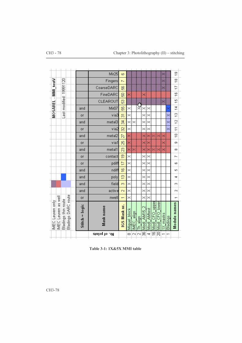
CH3 - 78 Chapter 3: Photolithography (II) – stitching
CH3-78
Table 3-1: 1X&5X MMI table
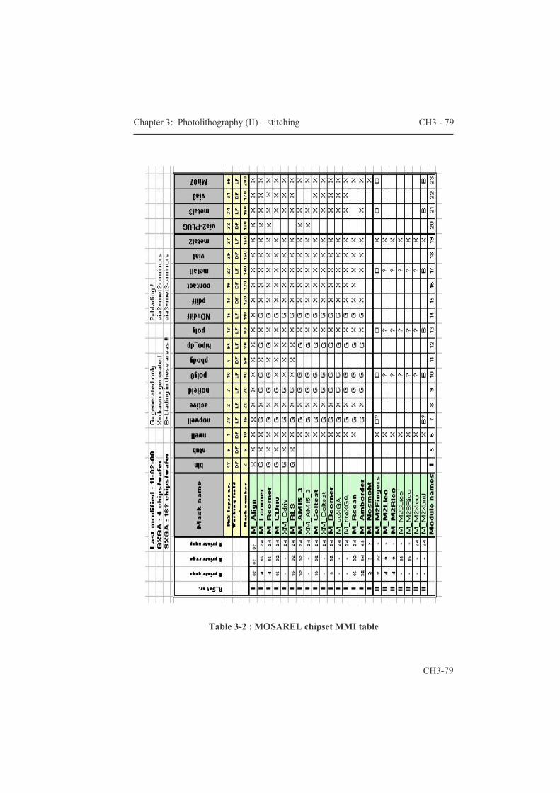
Chapter 3: Photolithography (II) – stitching CH3 - 79
CH3-79
Table 3-2 : MOSAREL chipset MMI table
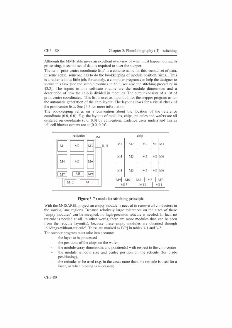
CH3 - 80 Chapter 3: Photolithography (II) – stitching
CH3-80
Although the MMI-table gives an excellent overview of what must happen during Si processing, a second set of data is required to steer the stepper. The term ‘print-centre coordinate lists’ is a concise name for this second set of data. In some sense, someone has to do the bookkeeping of module position, sizes... This is a rather tedious little job; fortunately, a computer program can help the designer to secure this task [see the sample routines in §6.3, see also the stitching procedure in §3.3]. The inputs to this software routine are the module dimensions and a description of how the chip is divided in modules. The output consists of a list of print centre coordinates. This list is used as input both for the stepper program as for the automatic generation of the chip layout. The layout allows for a visual check of the print centre lists. See §3.3 for more information. The bookkeeping relies on a convention about the location of the reference coordinate (0.0, 0.0). E.g. the layouts of modules, chips, reticules and wafers are all centered on coordinate (0.0, 0.0) by convention. Cadence users understand this as ‘all cell bboxes centers are at (0.0, 0.0)’.
Figure 3-7 : modular stitching principle
With the MOSAREL project an empty module is needed to remove all conductors in the sawing lane regions. Because relatively large tolerances on the sizes of these ‘empty modules’ can be accepted, no high-precision reticule is needed. In fact, no reticule is needed at all. In other words, there are more modules than can be seen from the reticule layout(s), because these empty modules are obtained through ‘bladings-without-reticule’. These are marked as B[?] in tables 3-1 and 3-2. The stepper program must take into account:
- the layer to be processed - the positions of the chips on the wafer - the module-array dimensions and position(s) with respect to the chip centre - the module window size and centre position on the reticule (for blade
positioning), - the reticules to be used (e.g. in the cases more than one reticule is used for a
layer, or when blading is necessary)
R-II
R-I chip
M12 M13
M1 M2 M3
M4 M5 M6
M8 M9 M7 M9
M3 M2 M2 M1 M3
M4 M6 M6 M5 M5
M8 M7 M8 M8 M4 M6 M6 M5 M5
M13 M13 M11
reticules
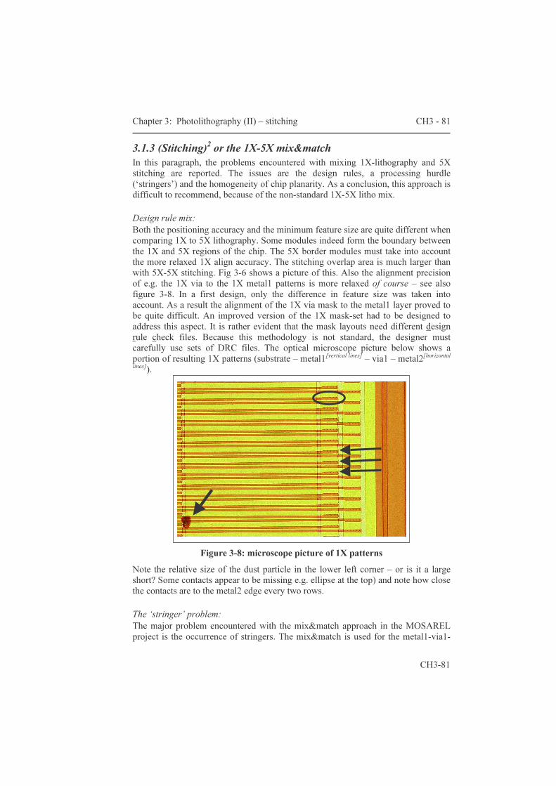
Chapter 3: Photolithography (II) – stitching CH3 - 81
CH3-81
3.1.3 (Stitching)2 or the 1X-5X mix&match In this paragraph, the problems encountered with mixing 1X-lithography and 5X stitching are reported. The issues are the design rules, a processing hurdle (‘stringers’) and the homogeneity of chip planarity. As a conclusion, this approach is difficult to recommend, because of the non-standard 1X-5X litho mix. Design rule mix: Both the positioning accuracy and the minimum feature size are quite different when comparing 1X to 5X lithography. Some modules indeed form the boundary between the 1X and 5X regions of the chip. The 5X border modules must take into account the more relaxed 1X align accuracy. The stitching overlap area is much larger than with 5X-5X stitching. Fig 3-6 shows a picture of this. Also the alignment precision of e.g. the 1X via to the 1X metal1 patterns is more relaxed of course – see also figure 3-8. In a first design, only the difference in feature size was taken into account. As a result the alignment of the 1X via mask to the metal1 layer proved to be quite difficult. An improved version of the 1X mask-set had to be designed to address this aspect. It is rather evident that the mask layouts need different design rule check files. Because this methodology is not standard, the designer must carefully use sets of DRC files. The optical microscope picture below shows a portion of resulting 1X patterns (substrate – metal1[vertical lines] – via1 – metal2[horizontal lines]).
Figure 3-8: microscope picture of 1X patterns Note the relative size of the dust particle in the lower left corner – or is it a large short? Some contacts appear to be missing e.g. ellipse at the top) and note how close the contacts are to the metal2 edge every two rows. The ‘stringer’ problem: The major problem encountered with the mix&match approach in the MOSAREL project is the occurrence of stringers. The mix&match is used for the metal1-via1-
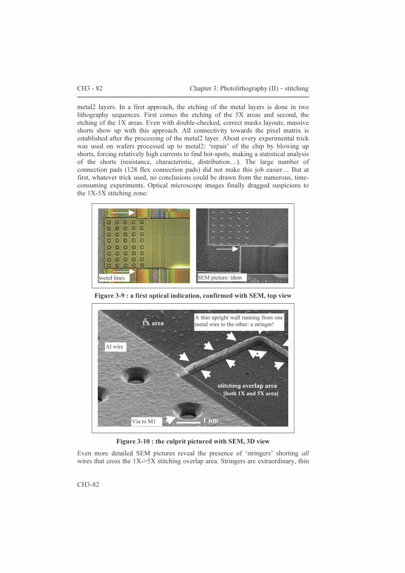
CH3 - 82 Chapter 3: Photolithography (II) – stitching
CH3-82
metal2 layers. In a first approach, the etching of the metal layers is done in two lithography sequences. First comes the etching of the 5X areas and second, the etching of the 1X areas. Even with double-checked, correct masks layouts, massive shorts show up with this approach. All connectivity towards the pixel matrix is established after the processing of the metal2 layer. About every experimental trick was used on wafers processed up to metal2: ‘repair’ of the chip by blowing up shorts, forcing relatively high currents to find hot-spots, making a statistical analysis of the shorts (resistance, characteristic, distribution…). The large number of connection pads (128 flex connection pads) did not make this job easier… But at first, whatever trick used, no conclusions could be drawn from the numerous, time-consuming experiments. Optical microscope images finally dragged suspicions to the 1X-5X stitching zone:
Figure 3-9 : a first optical indication, confirmed with SEM, top view
Figure 3-10 : the culprit pictured with SEM, 3D view
Even more detailed SEM pictures reveal the presence of ‘stringers’ shorting all wires that cross the 1X->5X stitching overlap area. Stringers are extraordinary, thin
1 µm
stitching overlap area [both 1X and 5X area]
1X area A thin upright wall running from one metal wire to the other: a stringer!
Al wire
Via to M1
weird lines SEM picture: idem
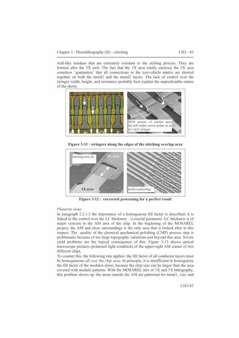
Chapter 3: Photolithography (II) – stitching CH3 - 83
CH3-83
wall-like residues that are extremely resistant to the etching process. They are formed after the 5X etch. The fact that the 1X area totally encloses the 5X area somehow ‘guarantees’ that all connections to the test-vehicle matrix are shorted together on both the metal1 and the metal2 layers. The lack of control over the stringer width, height, and resistance probably best explain the unpredictable nature of the shorts.
Figure 3-11 : stringers along the edges of the stitching overlap area
Figure 3-12 : corrected processing for a perfect result
Planarity issue: In paragraph 2.2.1.3 the importance of a homogenous fill factor is described; it is linked to the control over the LC thickness – a crucial parameter. LC thickness is of major concern in the AM area of the chip. In the beginning of the MOSAREL project, the AM and close surroundings is the only area that is looked after in this respect. The quality of the chemical mechanical polishing (CMP) process step is problematic because of too large topography variations just beyond this area. Severe yield problems are the logical consequence of this. Figure 3-13 shows optical microscope pictures (polarized light condition) of the upper-right AM corner of two different chips. To counter this, the following rule applies: the fill factor of all conductor layers must be homogeneous all over the chip area. In principle, it is insufficient to homogenize the fill factor of the modules alone, because the chip size can be larger than the area covered with module patterns. With the MOSAREL mix of 1X and 5X lithography, this problem shows up: the areas outside the AM are patterned for metal1, via1 and
SEM picture of similar area: the left (right) arrow points at an m1 (m2) stringer.
1X area
5X area stitching area ok:
perfect patterning
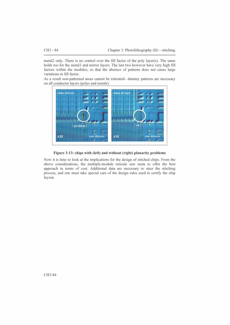
CH3 - 84 Chapter 3: Photolithography (II) – stitching
CH3-84
metal2 only. There is no control over the fill factor of the poly layer(s). The same holds too for the metal3 and mirror layers. The last two however have very high fill factors within the modules, so that the absence of patterns does not cause large variations in fill factor. As a result non-patterned areas cannot be tolerated– dummy patterns are necessary on all conductor layers (polys and metals).
Figure 3-13: chips with (left) and without (right) planarity problems
Now it is time to look at the implications for the design of stitched chips. From the above considerations, the multiple-module reticule sets seem to offer the best approach in terms of cost. Additional data are necessary to steer the stitching process, and one must take special care of the design rules used to certify the chip layout.
AM
video drivers
row drivers AM
video drivers
row drivers
! problem ! ! ok !
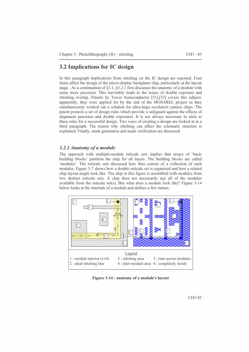
Chapter 3: Photolithography (II) – stitching CH3 - 85
CH3-85
3.2 Implications for IC design In this paragraph implications from stitching on the IC design are reported. Four items affect the design of the micro-display backplane chip, particularly at the layout stage. As a continuation of §3.1, §3.2.1 first discusses the anatomy of a module with some more precision. This inevitably leads to the issues of double exposure and stitching overlap. Patents by Tower Semiconductor [31],[32] covers this subject; apparently, they were applied for by the end of the MOSAREL project as they simultaneously worked out a solution for ultra-large resolution camera chips. The patent protects a set of design rules which provide a safeguard against the effects of alignment precision and double exposures. It is not always necessary to stick to these rules for a successful design. Two ways of creating a design are looked at in a third paragraph. The reason why stitching can affect the schematic structure is explained. Finally, mask generation and mask verification are discussed. 3.2.1 Anatomy of a module The approach with multiple-module reticule sets implies that arrays of ‘basic building blocks’ partition the chip for all layers. The building blocks are called ‘modules’. The reticule sets discussed here thus consist of a collection of such modules. Figure 3-7 shows how a double reticule set is organized and how a related chip layout might look like. The chip in this figure is assembled with modules from two distinct reticule sets. A chip does not necessarily use all of the modules available from the reticule set(s). But what does a module look like? Figure 3-14 below looks at the internals of a module and defines a few names.
Figure 3-14 : anatomy of a module's layout
Legend 1 : module interior (↔4) 3 : stitching area 5 : runs across modules 2 : ideal stitching line 4 : inter-module area 6 : completely inside
1 5
6
1 6 2 2
5
5
5 5
4 4
3 3 { }
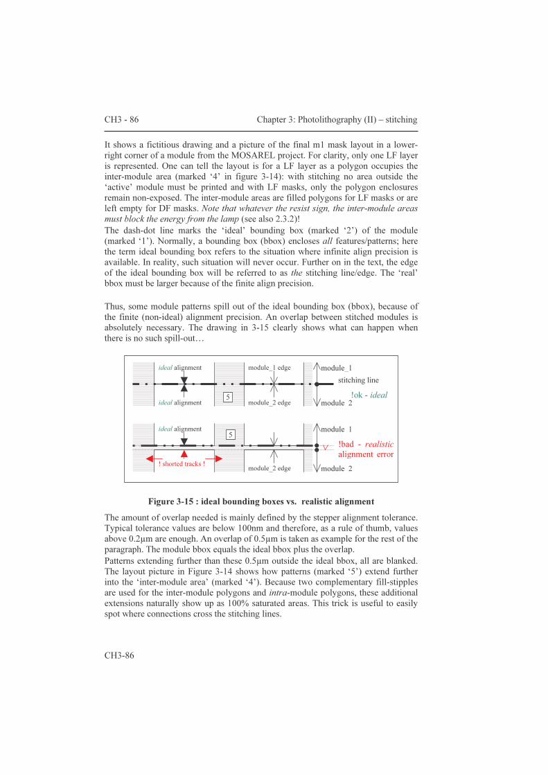
CH3 - 86 Chapter 3: Photolithography (II) – stitching
CH3-86
It shows a fictitious drawing and a picture of the final m1 mask layout in a lower-right corner of a module from the MOSAREL project. For clarity, only one LF layer is represented. One can tell the layout is for a LF layer as a polygon occupies the inter-module area (marked ‘4’ in figure 3-14): with stitching no area outside the ‘active’ module must be printed and with LF masks, only the polygon enclosures remain non-exposed. The inter-module areas are filled polygons for LF masks or are left empty for DF masks. Note that whatever the resist sign, the inter-module areas must block the energy from the lamp (see also 2.3.2)! The dash-dot line marks the ‘ideal’ bounding box (marked ‘2’) of the module (marked ‘1’). Normally, a bounding box (bbox) encloses all features/patterns; here the term ideal bounding box refers to the situation where infinite align precision is available. In reality, such situation will never occur. Further on in the text, the edge of the ideal bounding box will be referred to as the stitching line/edge. The ‘real’ bbox must be larger because of the finite align precision. Thus, some module patterns spill out of the ideal bounding box (bbox), because of the finite (non-ideal) alignment precision. An overlap between stitched modules is absolutely necessary. The drawing in 3-15 clearly shows what can happen when there is no such spill-out…
Figure 3-15 : ideal bounding boxes vs. realistic alignment
The amount of overlap needed is mainly defined by the stepper alignment tolerance. Typical tolerance values are below 100nm and therefore, as a rule of thumb, values above 0.2µm are enough. An overlap of 0.5µm is taken as example for the rest of the paragraph. The module bbox equals the ideal bbox plus the overlap. Patterns extending further than these 0.5µm outside the ideal bbox, all are blanked. The layout picture in Figure 3-14 shows how patterns (marked ‘5’) extend further into the ‘inter-module area’ (marked ‘4’). Because two complementary fill-stipples are used for the inter-module polygons and intra-module polygons, these additional extensions naturally show up as 100% saturated areas. This trick is useful to easily spot where connections cross the stitching lines.
module_1
module_2
stitching line ideal alignment
ideal alignment
module_1 edge
module_2 edge !ok - ideal
ideal alignment module_1
module_2
!bad - realisticalignment error
module_2 edge ! shorted tracks !
5
5
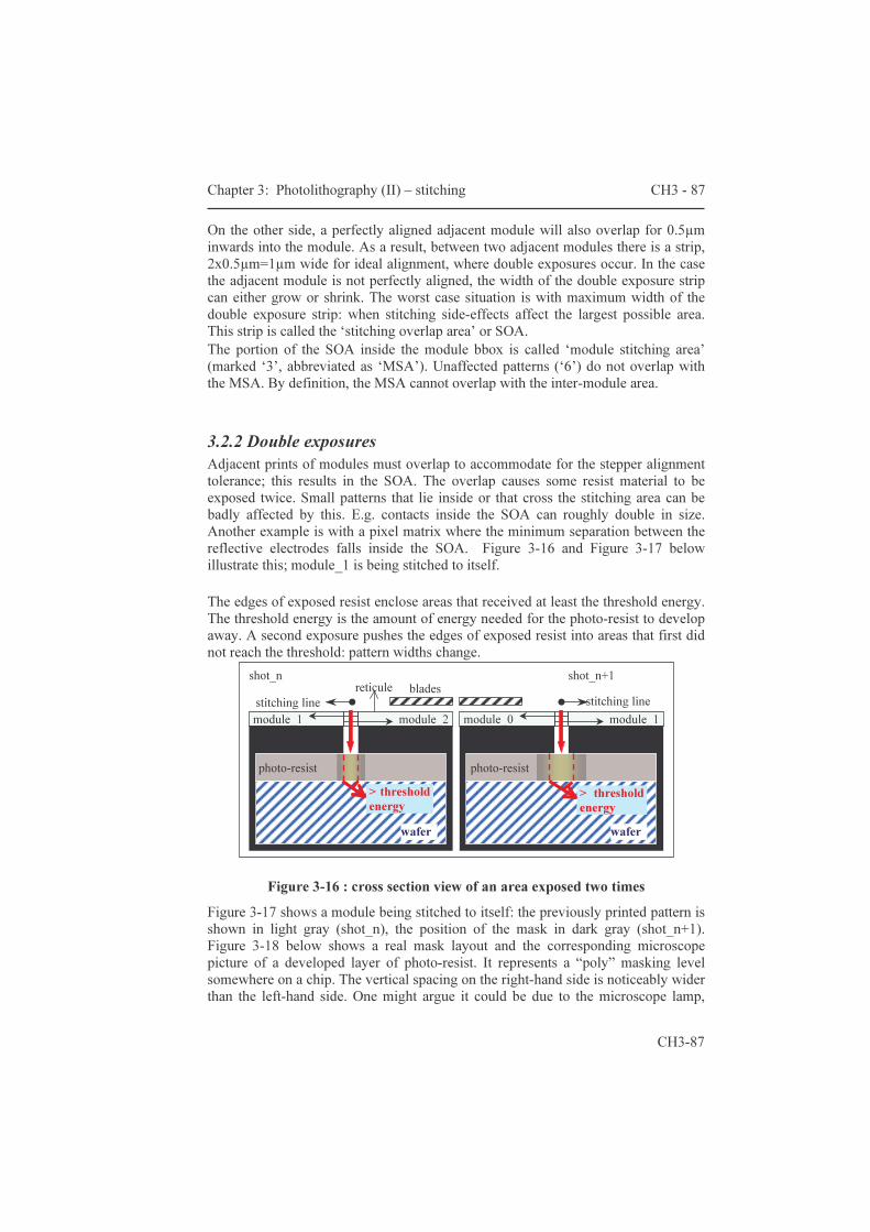
Chapter 3: Photolithography (II) – stitching CH3 - 87
CH3-87
On the other side, a perfectly aligned adjacent module will also overlap for 0.5µm inwards into the module. As a result, between two adjacent modules there is a strip, 2x0.5µm=1µm wide for ideal alignment, where double exposures occur. In the case the adjacent module is not perfectly aligned, the width of the double exposure strip can either grow or shrink. The worst case situation is with maximum width of the double exposure strip: when stitching side-effects affect the largest possible area. This strip is called the ‘stitching overlap area’ or SOA. The portion of the SOA inside the module bbox is called ‘module stitching area’ (marked ‘3’, abbreviated as ‘MSA’). Unaffected patterns (‘6’) do not overlap with the MSA. By definition, the MSA cannot overlap with the inter-module area. 3.2.2 Double exposures Adjacent prints of modules must overlap to accommodate for the stepper alignment tolerance; this results in the SOA. The overlap causes some resist material to be exposed twice. Small patterns that lie inside or that cross the stitching area can be badly affected by this. E.g. contacts inside the SOA can roughly double in size. Another example is with a pixel matrix where the minimum separation between the reflective electrodes falls inside the SOA. Figure 3-16 and Figure 3-17 below illustrate this; module_1 is being stitched to itself. The edges of exposed resist enclose areas that received at least the threshold energy. The threshold energy is the amount of energy needed for the photo-resist to develop away. A second exposure pushes the edges of exposed resist into areas that first did not reach the threshold: pattern widths change.
Figure 3-16 : cross section view of an area exposed two times Figure 3-17 shows a module being stitched to itself: the previously printed pattern is shown in light gray (shot_n), the position of the mask in dark gray (shot_n+1). Figure 3-18 below shows a real mask layout and the corresponding microscope picture of a developed layer of photo-resist. It represents a “poly” masking level somewhere on a chip. The vertical spacing on the right-hand side is noticeably wider than the left-hand side. One might argue it could be due to the microscope lamp,
photo-resist
stitching line module_2
shot_n shot_n+1 blades
stitching line module_1
wafer
photo-resist
reticule
> threshold energy
> threshold energy
module_1 module_0
wafer

CH3 - 88 Chapter 3: Photolithography (II) – stitching
CH3-88
because the right-hand side of the picture is brighter. Look at the horizontal spacing at the top of the picture; they look similar both on the right-hand and the left-hand side!
Figure 3-17 : top view of an area exposed two times
Figure 3-18 : a microscope picture of developed photo-resist shows the clearly noticeable effect of double exposures
pattern pitch shot pitch module bbox/window
stitching overlap causes corresponding changes of the width of some patterns
shot _ n+1 shot _ n
abso
rbs
2x en
ergy
30µm 1µm ~1.3µm
1.5µm
(optical microscope)
(layout drawing)
Chapter 3: Photolithography (II) – stitching CH3 - 89
CH3-89
Double exposure is an issue for the finest patterns only. The finest patterns indeed have dimensions that are only a few multiples of the distance affected by double exposures. Some common pattern structures require attention: the contact/via holes, the pixel electrode spacing and minimum width tracks. As a rule of thumb, the widening by double exposure can be estimated to be within the range of the thickness of the photo-resist layer (~0.5µm). Because contacts/vias are so tiny (typically 0.4x0.4µm2), problems can be expected when they are inside the SOA. The dimensions in the microscope picture in Figure 3-18 are obtained by comparison with the layout. Apparently, the double exposure makes the right-hand spacing widen by an estimated 0.15µm in all directions. This number corresponds with typical minimum metal-contact overlap rules! As a result, contacts/vias that are exposed twice, can fall beside the underlying (stopping) layer. This can have dramatic consequences. The only way to avoid double exposure of contacts, is to make sure only one module prints a given contact/via, at once and only once. E.g. with a module that is stitched to itself, eventual contacts/vias inside the SOA are only permitted in one corner of the SOA and in the two adjacent sides of the SOA. They cannot be allowed along the other edges of the module. Minimum spacing between pixel electrodes can be controlled the same way. The major reason for the spacings to be minimal at all times relates to the minimization of the photo-currents in the active matrix. It is also best to protect fine wires that run across the SOA. The way to do this is to oversize wire widths in the MSA to pre-compensate for the narrowing effect of double exposures and misalignments. One could state a general rule for all layers: LF polygons in the MSA need over-sizing, while DF polygons need under-sizing. This is referred to as “MSA pre-correction”. There is an important exception to this ‘general’ rule. Indeed, note that with ‘undersize’ operations, complete arrays of small patterns can disappear (see also §5.2). Examples of this are arrays of contacts and vias – large under-sizing is not indicated for contact/via layers! The inter-module area does not serve the same purpose as a polygon from a module’s inner layout. The function of the inter-module area does not permit any sizing for this reason! See §3.2.4 ‘problems with maskgen’. To summarize, note that half the SOA width is the sum of three numbers: the distance affected by double exposures, plus the maximum align tolerance plus the distance between the module’s ideal and real bboxes. The MSA width equals the sum of the distance affected by double exposures, plus the maximum align tolerance plus double the distance between the module’s ideal and real bboxes. The implications for IC design go somewhat further than this. Up to here, only the requirements at mask level have been discussed. The following paragraphs present a few issues on why/how to split the entire design into modules –essential for stitching– and a few more issues on how to verify the design of the reticule set. Verification is an operation that is really necessary for any chip design.
CH3 - 90 Chapter 3: Photolithography (II) – stitching
CH3-90
3.2.3 Split the schematics as well? The fact that the chip layout must be split in modules is not a sufficient reason to have a corresponding schematic. Ideally, one could think of a software routine that automatically slices through the layout to create the modules, without taking into account any ‘intelligence’ from the schematic. A concordant split of the schematic hierarchy costs some time; this looks like a reason to keep the schematic structure as it is. In other words, the chip layout alone is partitioned in modules at the end of the design cycle, just before mask fracturing (refer to 2.1.3). Tower Semiconductor even offers such a service to its customers. Foundries like AMIS and X-FABe.g., do not. Three points in particular merit our attention. First, with this method, there are fewer problems with mask generation. Second, the partitioning in modules of the final layout can cost quite some computer resources. It means flattening of the entire design. Usually, the computer available lacks sufficient resources for this kind of job... Third, in the event layout corrections are necessary, there are good chances that the partitioning must be completely re-done. Furthermore, the design hierarchy is lost at layout level; this does not help, neither for the ease of verification tasks nor for saving computer resources. Consequently, there are a few difficulties deserving solutions. The solution proposed consists of planning the module content and size at schematic level already. To some extent, the designer first draws a reticule floorplan by estimating module dimensions. The schematic hierarchy is then arranged in concordance. One advantage is that hierarchy is maintained, even with the reticule layout. Also, several designers can design modules simultaneously. Design verification is possible at module level as well. This can shorten verification cycles significantly. Eventual design upgrades can use existing module layouts; one can realistically envisage libraries of module cells. For these reasons, this approach was used with the MOSAREL project. 3.2.4 Overcoming problems with mask generation Two problems show up with automatic mask generation routines. A first problem is related to the layout of the inter-module areas; actually, mask generation routines are not valid for them, they are only valid for the intra-module areas. The second problem is with some mask generation routines that generate patterns up to a few µm away from existing patterns. As a result, some generated patterns can fall outside a module’s bbox. Mask inversion, mask bias and inter-module areas… The layout of the inter-module area is a source of concern. To understand this, consider the following ‘classic’ mask inversion operation: pwell=not(nwell). Indeed the pwell mask very often is the complement of the nwell. Both however are DF layers. E.g. for the nwell reticule layout, the inter-module area must be empty. So, the same holds for the pwell reticule layout. The empty inter-module area of the nwell layer must not be inverted to get the layout for the pwell layer. Therefore,
Chapter 3: Photolithography (II) – stitching CH3 - 91
CH3-91
there are cases where the inter-module area layout cannot be obtained with a simple mask inversion command. Here, it seems that the inversion operation is valid only inside the module bboxes. There is a second source of concern regarding the layout of the inter-module areas. The standard mask making process performs mask biasing operations just before the mask fracturing (e.g. conversion to MEBES data format). When the bias values are known, pre-correction of the ‘inter-module’ fill is possible and mandatory. Otherwise, the dimensions of the MSAs and SOAs change! The alternative is to steer the mask making process in a way that the inter-module fill is done all at the end – after the mask bias has been applied. The inter-module fill blanks all data outside the module bbox. This seems the easiest approach; it requires cooperation with the foundry or mask house though. A potentially very insidious situation is when the MSA pre-correction and mask bias size operations add up destructively. Alone none of the two harms, but the combined under-sizing/over-sizing can wipe out fine pattern features. Extreme care is recommended! Eventually a few more structures must be banned from overlap with the MSA. E.g. see the example about contacts/vias inside the MSA in paragraph 3.2.2. Micro-summary: � classic mask inversion and mask bias commands are not compatible with the
layout of the inter-module areas. In other words, they are not applicable ‘as is’ on complete reticule layouts.
� the mask bias value can be equal to or an order of magnitude larger than the stepper alignment tolerance; the MSAs thus must be carefully checked for.
� A solution is proposed: the inter-module layout is to be finalized just before the mask fracturing step.
Generated patterns that fall outside the module bbox… From the previous paragraph it is clear that mask generation procedures (maskgen in short) cannot be used to obtain the layout of the inter-module areas. As a result, the mask generation procedures can only apply to the intra-module areas – any patterns falling outside the module bbox must be cleared. This means some of the module patterns are wiped out that otherwise would and should interact with… patterns from an adjacent module! Clearly, there is a problem: patterns inside the inter-module areas are prohibited, the design/process rule based maskgen and the module layout forces the presence of patterns in the inter-module areas. The solution is to clear the inter-module areas just before mask fracturing; this is compatible with the solution to the problem of mask bias on inter-module layout. For a better understanding of the problem, look e.g. at the generation of the p-field implant mask from nwell mask data. Typically, no p-field implant is allowed in nwell areas. For high/medium voltage wells, it is often required to keep the p-field implant at a certain distance (e.g. 10µm). This is essential to safeguard voltage-breakdown thresholds. Imagine e.g. an nwell at 5µm inside distance from a module’s bbox edge. The p-implant must be prohibited up to 5µm outside the bbox.

CH3 - 92 Chapter 3: Photolithography (II) – stitching
CH3-92
This implies no p-implant allowed over 6µm1 inside the modules that will stitched along that edge. Either one has to include a portion of the generated patterns in the adjacent module, or one includes the generating polygons in the adjacent module’s layout. This way, the mask generation procedure can be run on the module layout alone, hereby taking the information needed from other modules into account to produce the right patterns! Fortunately, there are but a few layers for which the maskgen procedure generates patterns out of the module bbox. This means that a clever layout avoids most of the trouble. Micro-summary: � Add a minimum set of ‘artificial’ patterns in the inter-module area to include
patterns generated by data in other modules. Avoid high voltage wells close to the stitching edge, whenever possible. This reduces the number of artificial patterns to add.
� Restrictions are unavoidable when more than one module is stitched along a module’s edge : sometimes the conflict cannot be solved, and patterns must be included in the inter-module area
� The proposed solution is compatible with the previous solution for the mask bias and mask inversion problems.
The solution to the problems with mask generation and mask bias implies that the mask layout process breaks up into several stages: the reticule layouts with and without mask generation must be stored in different files. This is because of the artificial data in the inter-module areas that are wiped out before the mask fracturing process. The artificial data are needed for correct operation of the mask generation routines. Finally, only the generated data that fall inside module bboxes are valid. These valid generated data are the last addition to the module layout before the reticule verification jobs can start.
3.2.5 Overcoming problems with mask verification The logical step after mask generation is mask verification. Reticules designed for stitching have the particularity that there is no matching schematic. Therefore a LVS check at reticule level is not possible. Because of the partitioning into modules of both the layout and schematic, LVS is possible at module level. Nevertheless, LVS-error free module layouts alone do not guarantee chip functionality. And what about DRC? The most basic DRC rules relate to minimum widths of and spacings between patterns on the same layer. One can easily guess what the problem is: when two modules are stitched next to each other, there is no guarantee that the resulting pattern satisfies even the most basic DRC rules. A good hands-on approach is to apply the following rule of thumb: the minimum separation of a polygon edge 1 5µm+1µm because of the stitching overlap; the stitching line is not in the middle between the edges of the nwell and the p-field implant (to be generated).

Chapter 3: Photolithography (II) – stitching CH3 - 93
CH3-93
to the stitching line should be half the minimum width. Very smart mask designers probably are capable of taking slightly more complex rules also into account like e.g. minimum nplus to nwell edge separation, etc… However, here also there is no guarantee that the stitched chip layout is ok. The necessity for verification of stitched chip patterns led to the development of the ‘virtual stitching procedure’: paragraph §3.3 describes this practical tool.

CH3 - 94 Chapter 3: Photolithography (II) – stitching
CH3-94
3.3 Virtual stitching procedure The description splits into three topics. The first topic describes how to organize the mask layout. Second, an automated layout correction procedure for the stitching overlap areas (SOAs) is detailed. At last, a tool is described that predicts the patterns resulting from stitching. The layout is organized to allow for relatively short computing times. This is important for the virtual stitching procedure to be quick and efficient. There is indeed a straightforward way to check the stitched patterns for errors: just look at wafers with developed photo-resist. The sequence of actions is quite simple: first, order the mask set at the mask shop. Next, print the patterns on a wafer covered with photo-resist. Then develop the photo-resist. At last, look at the photo-resist patterns (with a microscope) and more specifically check the SOAs for mistakes. The advantage is that the stepper program is checked for as well. The disadvantages are the masks cost, the long correction cycle and the rather special ‘processing’. There is indeed a need for only one wafer per unique layer pattern and there is no real processing of the wafers. The mask making steps and the stitching of photo-resist patterns must be repeated in the eventual case of a mistake. This eventually takes more time and money than with the virtual stitching procedure. The virtual stitching procedure is the method I developed to perform standard mask verification (DRC, ERC, LVS, and PRE/LPE) on the expected results of the stitching process. 3.3.1 Module layout organization for virtual stitching A fixed cell naming convention is recommended to avoid confusion for the following. A suggestion is to have module cell names starting with ‘M_’; to have the second field pointing at the cell purpose, e.g. ‘prep_’; the last suggestion is to have a meaningful name as third field, e.g. ‘RDblock’ for row-driver block. The layout of a module is organized around two major cells. One cell is the ‘preparation’ cell (the M_prep_ cell), the other is the final cell used for tape out and for the virtual stitching procedure (the M_4TO_ cell). Both share one cell with the main data, say, the data in the intra-module area (the M_mainData_cell). No data in this cell fall outside the intra-module area. It contains e.g. hierarchical data corresponding with a portion of the circuit schematic. The M_prep_ cell contains two more sub-cells: M_prep_MSA_ and M_prepMGen_. M_prep_MSA_ contains MSA data prior to pre-correction; this cell is kept separately in the case the pre-correction routine is to be re-run after correction of a bug. The output of the pre-correction routine is stored in the M_finalMSA_ cell. M_prepMGen_ contains the ‘artificial’ polygons needed to have the mask generation routine work properly. The output splits in data added to M_finalMSA_ and intra-module data stored in M_final_MGen_. MSA pre-correction routines run after maskgen. The tape out cell M_4TO_ additionally contains M_finalMSA_ and M_finalMGen_. In short: M_prep_ ← M_mainData_, M_prepMSA_, M_prepMGen_ M_4TO_ ← M_mainData_, M_finalMSA_, M_finalMGen_
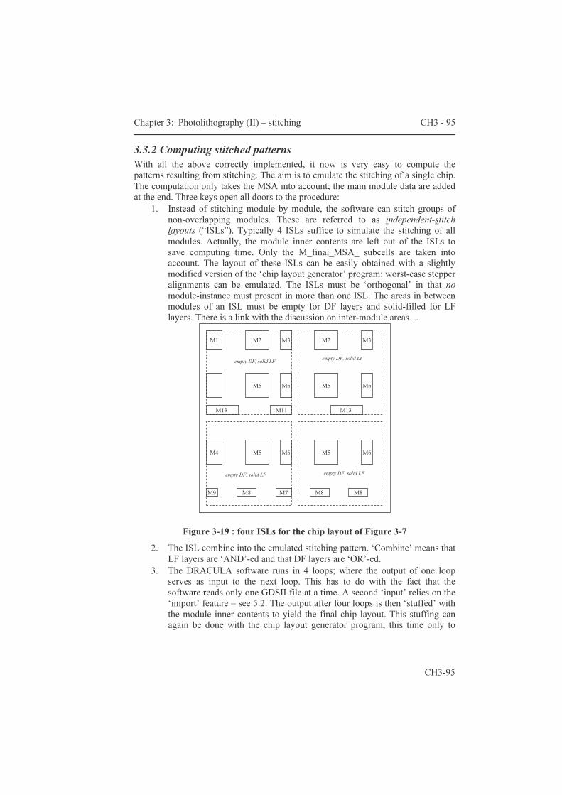
Chapter 3: Photolithography (II) – stitching CH3 - 95
CH3-95
3.3.2 Computing stitched patterns With all the above correctly implemented, it now is very easy to compute the patterns resulting from stitching. The aim is to emulate the stitching of a single chip. The computation only takes the MSA into account; the main module data are added at the end. Three keys open all doors to the procedure:
1. Instead of stitching module by module, the software can stitch groups of non-overlapping modules. These are referred to as independent-stitch layouts (“ISLs”). Typically 4 ISLs suffice to simulate the stitching of all modules. Actually, the module inner contents are left out of the ISLs to save computing time. Only the M_final_MSA_ subcells are taken into account. The layout of these ISLs can be easily obtained with a slightly modified version of the ‘chip layout generator’ program: worst-case stepper alignments can be emulated. The ISLs must be ‘orthogonal’ in that no module-instance must present in more than one ISL. The areas in between modules of an ISL must be empty for DF layers and solid-filled for LF layers. There is a link with the discussion on inter-module areas…
Figure 3-19 : four ISLs for the chip layout of Figure 3-7
2. The ISL combine into the emulated stitching pattern. ‘Combine’ means that LF layers are ‘AND’-ed and that DF layers are ‘OR’-ed.
3. The DRACULA software runs in 4 loops; where the output of one loop serves as input to the next loop. This has to do with the fact that the software reads only one GDSII file at a time. A second ‘input’ relies on the ‘import’ feature – see 5.2. The output after four loops is then ‘stuffed’ with the module inner contents to yield the final chip layout. This stuffing can again be done with the chip layout generator program, this time only to
M2 M1 M3
M6 M5
M13 M11
M3 M2
M6 M5
M13
M9
M4 M6 M5
M7 M8
M6 M5
M8 M8
empty DF, solid LF empty DF, solid LF
empty DF, solid LF empty DF, solid LF
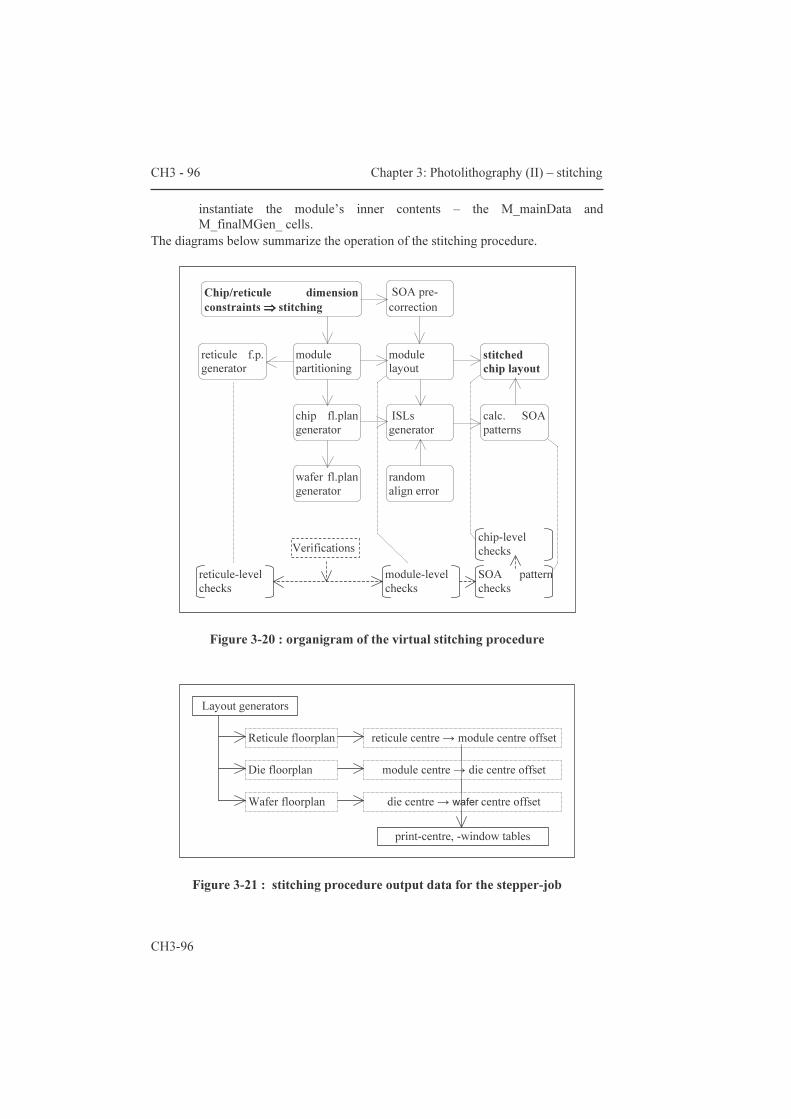
CH3 - 96 Chapter 3: Photolithography (II) – stitching
CH3-96
instantiate the module’s inner contents – the M_mainData and M_finalMGen_ cells.
The diagrams below summarize the operation of the stitching procedure.
Figure 3-20 : organigram of the virtual stitching procedure
Figure 3-21 : stitching procedure output data for the stepper-job
reticule-level checks
module-level checks
chip-level checks SOA pattern checks
Verifications
Chip/reticule dimension constraints ⇒⇒⇒⇒ stitching
module partitioning
reticule f.p. generator
chip fl.plan generator
ISLs generator
module layout
calc. SOA patterns
stitched chip layout
SOA pre- correction
random align error
wafer fl.plan generator
Layout generators
Reticule floorplan
Die floorplan
Wafer floorplan
module centre → die centre offset
die centre → wafer centre offset
reticule centre → module centre offset
print-centre, -window tables

Chapter 3: Photolithography (II) – stitching CH3 - 97
CH3-97
The same procedure can be used to emulate stepper positioning errors by adding random offsets in the print centre coordinate pairs. The patterns printed will indeed slightly differ from chip to chip. Note that it is now possible to perform the classic verifications (DRC, ERC, LVS, LPE/PRE) on the resulting patterns. At last, the layout generators are small pieces of code that produce print-window and print-centre coordinate lists. These numbers are combined to steer the stepper engine.
���

CH3 - 98 Chapter 3: Photolithography (II) – stitching
CH3-98
Chapter 4: The pixel matrix I – the basics CH4 - 99
CH4-99
Chapter 4 : The pixel matrix(I) – the basics
he focus in this fourth chapter is on a classic lcos circuit and on the resulting implementations. The heart of lcos devices is known as ‘the pixel matrix’; it designates the area where the electro-optic signal conversion occurs.
Paragraph 4.1 describes the ‘classic’ analog active matrix (AM) architecture. The aim is to analyze the design of such AMs in detail. The description starts with a single pixel. A SPICE model is proposed to help with the simulation of the LC capacitor. The addressing of the AM with integrated drivers is looked at on the grounds of speed and redundancy considerations. A listing of important design constraints concludes the discussion on the classic AM architecture. Paragraph 4.2 summarizes the implementations, along with the results obtained. It is not the aim to give detailed reports of the optical performance, rather is this chapter limited to the chip’s functionality and peculiarities. As such, it concludes the discussion on micro-display designs that use the classic AM architecture. It also forms the starting ground for chapter five, where improvements to the pixel circuit are presented. As discussed in that chapter, these improvements effectively add a second frame-memory to the AM. In this chapter the implemented chips are described, together with a minimum of measurement results. To prove by measurements that all of the chip’s functionality is ok, is difficult, because of the extremely small size of the electrical charges to be measured in the matrix. As a consequence, the measurements were split in several parts. One part – the part I performed – tests the functionality of the driver blocks. The successful outcome of these measurements formed a milestone; it indeed had no sense to assemble non-functional microdisplay backplanes. The verification of the pixel matrix itself can hardly be done better than by measuring the optical output of the cell. On turn the optical measurements are complex, considering their dependence on the optical architecture used. The main contributors to the matrix evaluations are Geert Van Doorselaer (CTO Gemidis) for the system electronics and Dieter Cuypers who did the cell assembly and optical testing [60]. My work consisted of the definition of the circuit blocks, the spice simulations, the layouting (including the verification and layout simulations).
T

CH4 - 100 Chapter 4: The pixel matrix I – the basics
CH4-100
4.1 The pixel matrix (I): the classic AM
his section describes the ‘classic’ analog AM architecture. The aim is to analyze its design along with integrated drivers. The pixel capacitor is the starting point as it plays a central role. The next point discusses important electro-optical
properties of the pixel. Driving signal characteristics are looked at for VAN-LC in particular. An initial model is proposed to allow for the inclusion of the electrical behavior of the LC capacitor into the spice simulations. After investigating a single pixel, it is natural to look at arrays of pixels. The bandwidth of an array of pixels and subsequent parallelism in the column driver is an important parameter. Next, some topics on circuit redundancy and -testing are discussed. The addressing of the AM is explained with a presentation of scanner circuits and frame speed requirements. A last paragraph systematically lists design constraints in three groups: optical, technological and electrical constraints. It gives an overview of the most important constraints that directly affect the design of a backplane. 4.1.1 One, single picture element (pixel) The pixel capacitor is the starting point as it plays a central role. The roles played by the LC and the storage capacitor are discussed to come to a presentation of the classic AM pixel circuit. The discussion continues with the electro-optical properties of the pixel. The relation between optical output and electrical input is crucial for the design of all of the driving electronics, including the pixel circuit. Important driving signal characteristics are looked at for PDLC and VAN-LC in particular. Finally, an initial model is proposed for more accurate simulation of the electrical behavior of the LC capacitor. The pixel simulations of a-Si TFT pixels in [35] gives a good introduction to the issue. More details can be found in [36],[37], papers that present a well motivated and much more accurate model, that fits the lcos case particularly well. 4.1.1.1 The pixel LC capacitor The term pixel originates from the contraction of the words ‘picture’ and ‘element’; maybe this is the best explanation. Clearly, the pixel is at the heart of the operation of displays in general. Each pixel is capable of adjusting the brightness and color in a corresponding screen spot. Apart from this evidence, what is a pixel composed of in the case of the classic AM architecture? The most basic structure of a LC pixel is a capacitor: two electrodes produce an electrical force field inside a thin, insulating layer of liquid crystal (LC). With lcos, one electrode is provided by the silicon chip, the other is provided by the counter-electrode (CE) common to all pixels. By changing the strength of the force field the orientation of the LC molecules will change accordingly. On turn, light rays that travel through the LC layer see their path modified – see chapter one for an elementary introduction. Two aspects deserve our attention here: we are dealing
T
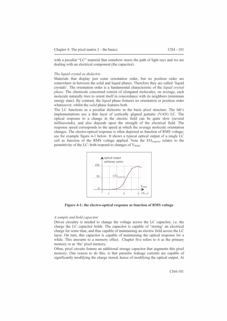
Chapter 4: The pixel matrix I – the basics CH4 - 101
CH4-101
with a peculiar “LC” material that somehow steers the path of light rays and we are dealing with an electrical component (the capacitor). The liquid crystal as dielectric Materials that display just some orientation order, but no position order are somewhere in between the solid and liquid phases. Therefore they are called ‘liquid crystals’. The orientation order is a fundamental characteristic of the liquid crystal phase. The chemicals concerned consist of elongated molecules; on average, each molecule naturally tries to orient itself in concordance with its neighbors (minimum energy state). By contrast, the liquid phase features no orientation or position order whatsoever, whilst the solid phase features both. The LC functions as a peculiar dielectric in the basic pixel structure. The lab’s implementations use a thin layer of vertically aligned nematic (VAN) LC. The optical response to a change in the electric field can be quite slow (several milliseconds), and also depends upon the strength of the electrical field. The response speed corresponds to the speed at which the average molecule orientation changes. The electro-optical response is often depicted as function of RMS voltage; see for example figure 4-1 below. It shows a typical optical output of a single LC cell as function of the RMS voltage applied. Note the EOresponse relates to the permittivity of the LC: both respond to changes of VRMS.
Figure 4-1: the electro-optical response as function of RMS voltage
A sample and hold capacitor Driver circuitry is needed to change the voltage across the LC capacitor, i.e. the charge the LC capacitor holds. The capacitor is capable of ‘storing’ an electrical charge for some time, and thus capable of maintaining an electric field across the LC layer. On turn, this capacitor is capable of maintaining the optical response for a while. This amounts to a memory effect. Chapter five refers to it as the primary memory or as ‘the’ pixel memory. Often, pixel circuits feature an additional storage capacitor that augments this pixel memory. One reason to do this, is that parasitic leakage currents are capable of significantly modifying the charge stored, hence of modifying the optical output. At
optical output (arbitrary units)
VRMS
EOresponse
0
50
100
1 3 5 (VLC)
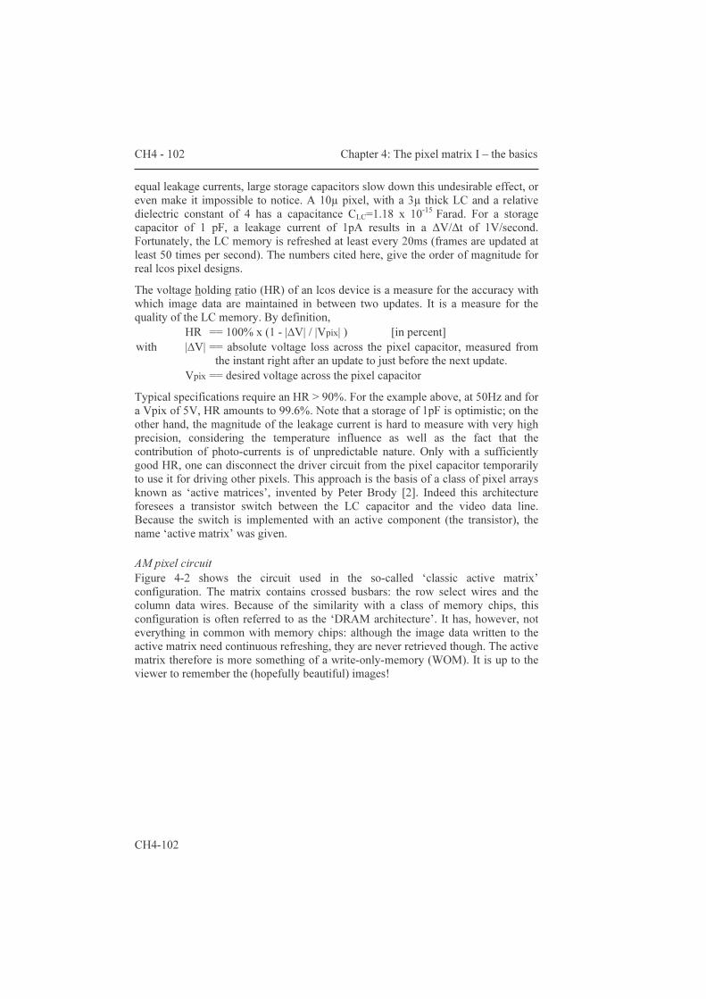
CH4 - 102 Chapter 4: The pixel matrix I – the basics
CH4-102
equal leakage currents, large storage capacitors slow down this undesirable effect, or even make it impossible to notice. A 10µ pixel, with a 3µ thick LC and a relative dielectric constant of 4 has a capacitance CLC=1.18 x 10⁻¹⁵ Farad. For a storage capacitor of 1 pF, a leakage current of 1pA results in a ∆V/∆t of 1V/second. Fortunately, the LC memory is refreshed at least every 20ms (frames are updated at least 50 times per second). The numbers cited here, give the order of magnitude for real lcos pixel designs.
The voltage holding ratio (HR) of an lcos device is a measure for the accuracy with which image data are maintained in between two updates. It is a measure for the quality of the LC memory. By definition, HR == 100% x (1 - |∆V| / |Vpix| ) [in percent] with |∆V| == absolute voltage loss across the pixel capacitor, measured from
the instant right after an update to just before the next update. Vpix == desired voltage across the pixel capacitor
Typical specifications require an HR > 90%. For the example above, at 50Hz and for a Vpix of 5V, HR amounts to 99.6%. Note that a storage of 1pF is optimistic; on the other hand, the magnitude of the leakage current is hard to measure with very high precision, considering the temperature influence as well as the fact that the contribution of photo-currents is of unpredictable nature. Only with a sufficiently good HR, one can disconnect the driver circuit from the pixel capacitor temporarily to use it for driving other pixels. This approach is the basis of a class of pixel arrays known as ‘active matrices’, invented by Peter Brody [2]. Indeed this architecture foresees a transistor switch between the LC capacitor and the video data line. Because the switch is implemented with an active component (the transistor), the name ‘active matrix’ was given. AM pixel circuit Figure 4-2 shows the circuit used in the so-called ‘classic active matrix’ configuration. The matrix contains crossed busbars: the row select wires and the column data wires. Because of the similarity with a class of memory chips, this configuration is often referred to as the ‘DRAM architecture’. It has, however, not everything in common with memory chips: although the image data written to the active matrix need continuous refreshing, they are never retrieved though. The active matrix therefore is more something of a write-only-memory (WOM). It is up to the viewer to remember the (hopefully beautiful) images!
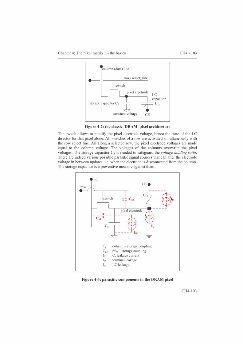
Chapter 4: The pixel matrix I – the basics CH4 - 103
CH4-103
Figure 4-2: the classic 'DRAM' pixel architecture
The switch allows to modify the pixel electrode voltage, hence the state of the LC director for that pixel alone. All switches of a row are activated simultaneously with the row select line. All along a selected row, the pixel electrode voltages are made equal to the column voltage. The voltages of the columns overwrite the pixel voltages. The storage capacitor CS is needed to safeguard the voltage holding ratio. There are indeed various possible parasitic signal sources that can alter the electrode voltage in between updates, i.e. when the electrode is disconnected from the column. The storage capacitor is a preventive measure against them.
Figure 4-3: parasitic components in the DRAM pixel
CS
col row
switch
Cp1
Cp2
Il1
Il2
CLC Il3
pixel electrode
CE
Cp1 : column – storage coupling Cp2 : row – storage coupling Il1 : Cs leakage current Il2 : terminal leakage Il3 : LC leakage
column (data) line
row (select) lineswitch (transistor)
storage capacitor CS
pixel electrode LC capacitor
CLC
CE constant voltage
CH4 - 104 Chapter 4: The pixel matrix I – the basics
CH4-104
The two groups of sources of parasitics are: coupling capacitors and leakage currents. Parasitic couplings come from spatial proximity of signal tracks in and around the pixel, e.g. from overlapping wires. Leakage currents alter the charge stored at the pixel electrode node, hence its voltage. They result from natural imperfections of dielectrics or from light induced photo-currents [38]. The relevant leakage currents show up at the switch terminal, through the insulator of the storage capacitor and through the LC layer. One cannot completely eliminate leakage sources; correct processing minimizes these. The leakage at the switch terminal is a junction or diode leakage. It is highly sensitive to photons and for this reason no light should reach the junction(s). A correctly designed light shield and panel package take care of this (see chapter two). Many of the parasitic couplings between signals can be turned into couplings with ground. This is done by systematically providing guard tracks between signal tracks on the same layer and between layers. A good pixel layout will minimize the overlap between the row and column electrodes; guarding with a metal layer is possible, however at the cost of either an extra metal layer or at the cost of a less optimal light shield (see e.g. the ‘REFLEC’ pixel implementation in figures 4-10 and 4-11). For the dimensions of the two components (the switch and the storage), please see the discussion on transistor count per pixel in paragraph 5.1. In practice, the smallest dimensions possible are chosen for the switch, while the layout of the storage optimizes the usage of the remaining pixel area. 4.1.1.2 Electro-optical properties The laboratory developed polymer dispersed (PDLC) and vertically aligned nematic (VAN) technology for the implementations, respectively a scattering effect and a polarization rotation effect. These two LCs are similar from the point of view of the required voltage range of the driving signals. The VAN mode yields the best optical performance, and therefore much of the text must be placed in the framework of VAN LC. In [12], the intrinsic contrast properties of VAN LCs are studied in detail and compared with those of other LC materials. These papers suggest that VAN LC material represents an excellent, maybe the best, choice for lcos micro-displays. This being said, much of the following relates to VAN LC; similar considerations however, are valid for other LC modes as well. Issues concerning the voltage range, the AC driving and LC response speed are detailed hereunder. Voltage range of driving signals The driving voltage range depends on the LC (effect). E.g. VAN and PDLC need medium voltage ranges (10Vpp is not unusual); others like ferro-electric LCs work with lower voltage levels (0V, 5V). Modern deep sub-micron ICs have limited voltage ranges between 1V and 2.5V (anno 2001); they offer incredible circuit densities (number of transistors per sq. micron). Older technologies rely on larger

Chapter 4: The pixel matrix I – the basics CH4 - 105
CH4-105
transistor structures that withstand higher voltages (e.g. 15V for Alcatel Microelectronics’ 2.4µ CMOS, 100V for AMIS’ I2T 0.7/DMOS). Many foundries do offer double gate processes or processes extended with high/medium voltage devices (e.g. DEMOS, BJT …) so that both low and high voltage range transistors are integrated on one chip. This inevitably comes at the cost of a few extra masks, and thus at the cost of extra processing time. Several circuit techniques exist to convert low-voltage (control) signals to higher voltage (level shifters). There will always be a need for this conversion, as the real world does not shrink while on contrary, transistor dimensions do. It is even more difficult to find foundries that offer dedicated lcos processes. I designed in a 2.4µ-15V and a 0.7µ/15V SDEMOS both from AMIS, Oudenaarde, Belgium and 0.35µ/18V technologies from UMC, Taiwan and SMIC, R.O.China. The reason for 18V and not just 10V lies with the so-called bulk-effect of MOS transistors (see figure 4-4 below). Figure 4-4 shows the evolution of the drain-source current in function of the gate-source voltage, at a fixed drain-source voltage and for the most extreme parameter variations (temperature, transistor models). As explained, a single transistor is used to switch the correct voltage onto a pixel’s electrode. The amplitude of the gate signal minus the threshold voltage determines the maximum voltage that the transistor can pass on. The threshold voltage depends on the voltage switched – this is what the bulk effect is about. Computations and equations of this are found in basic textbooks on MOS circuits; the figure below shows a ‘corner’ simulation of the bulk effect for a typical 3µ technology. It allows to draw conclusions, whatever the IC process variations and within the temperature range of the device.
Figure 4-4: bulk effect simulation for a 3µ NMOS
0.0 18 9.0 3.0 6.0 12 15 10-9
10-6
10-3
0°C →100°C all simulation corners VDB = 18V
I DS (
A)
VGS (V)
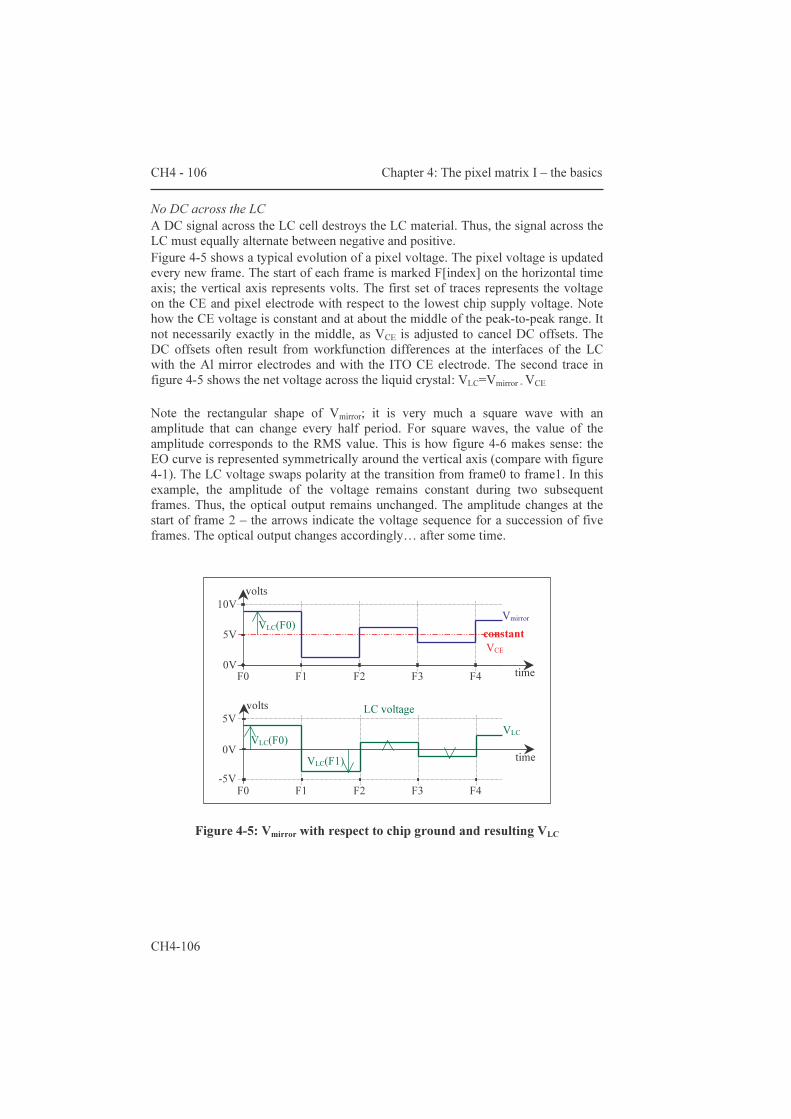
CH4 - 106 Chapter 4: The pixel matrix I – the basics
CH4-106
No DC across the LC A DC signal across the LC cell destroys the LC material. Thus, the signal across the LC must equally alternate between negative and positive. Figure 4-5 shows a typical evolution of a pixel voltage. The pixel voltage is updated every new frame. The start of each frame is marked F[index] on the horizontal time axis; the vertical axis represents volts. The first set of traces represents the voltage on the CE and pixel electrode with respect to the lowest chip supply voltage. Note how the CE voltage is constant and at about the middle of the peak-to-peak range. It not necessarily exactly in the middle, as VCE is adjusted to cancel DC offsets. The DC offsets often result from workfunction differences at the interfaces of the LC with the Al mirror electrodes and with the ITO CE electrode. The second trace in figure 4-5 shows the net voltage across the liquid crystal: VLC=Vmirror - VCE
Note the rectangular shape of Vmirror; it is very much a square wave with an amplitude that can change every half period. For square waves, the value of the amplitude corresponds to the RMS value. This is how figure 4-6 makes sense: the EO curve is represented symmetrically around the vertical axis (compare with figure 4-1). The LC voltage swaps polarity at the transition from frame0 to frame1. In this example, the amplitude of the voltage remains constant during two subsequent frames. Thus, the optical output remains unchanged. The amplitude changes at the start of frame 2 – the arrows indicate the voltage sequence for a succession of five frames. The optical output changes accordingly… after some time.
Figure 4-5: Vmirror with respect to chip ground and resulting VLC
constant VCE
Vmirror
time F0 F1 F2 F3 F4
volts
0V
5V
10VVLC(F0)
VLC
time
5V
0V
-5V
volts
F0 F1 F2 F3 F4
VLC(F0) VLC(F1)
LC voltage
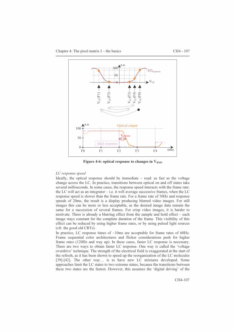
Chapter 4: The pixel matrix I – the basics CH4 - 107
CH4-107
Figure 4-6: optical response to changes in VRMS
LC response speed Ideally, the optical response should be immediate – read: as fast as the voltage change across the LC. In practice, transitions between optical on and off states take several milliseconds. In some cases, the response speed interacts with the frame rate: the LC will act as an integrator – i.e. it will average successive frames, when the LC response speed is slower than the frame rate. For a frame rate of 50Hz and response speeds of 20ms, the result is a display producing blurred video images. For still images this can be more or less acceptable, as the desired image data remain the same for a succession of several frames. For crisp video images, it is harder to motivate. There is already a blurring effect from the sample and hold effect – each image stays constant for the complete duration of the frame. This visibility of this effect can be reduced by using higher frame rates, or by using pulsed light sources (cfr. the good old CRTs). In practice, LC response times of ~10ms are acceptable for frame rates of 60Hz. Frame sequential color architectures and flicker considerations push for higher frame rates (120Hz and way up). In these cases, faster LC response is necessary. There are two ways to obtain faster LC response. One way is called the ‘voltage overdrive’ technique. The strength of the electrical field is exaggerated at the start of the refresh, as it has been shown to speed up the reorganization of the LC molecules [39]-[42]. The other way… is to have new LC mixtures developed. Some approaches limit the LC states to two extreme states, because the transitions between these two states are the fastest. However, this assumes the ‘digital driving’ of the
a.u.
VLC
EOresponse
050
100
VLC
(F0)
VLC
(F1)
VLC
(F2)
VLC
(F3)
VLC
(F4)
timeF0 F1 F2 F3 F4
a.u.
0
50
100 Optical output
ideal response
τresponse

CH4 - 108 Chapter 4: The pixel matrix I – the basics
CH4-108
LC; this has quite some consequences for the overall electronic subsystem. It is not uncommon to see digital systems on display that suffer from contouring. This effect is seen on still images containing e.g. a background with fading colors, but also around a moving object, because of the difficulty to control the spacing between dark gray shades. In the frame of the discussion of the classic AM, digital driving will not be further expanded on. A spice model for the LC response is proposed in the next paragraph. It is a very useful tool, in particular in those cases where the storage capacitance gets about as large as the LC capacitance itself: the peculiar behavior of the LC capacitor can have a significant impact on the optical output. Spice model of the LC capacitor, of the LC response The reaction speed of LC crystals to changes in electrical stress (RMS voltage e.g.) can be characterized by 10%-90% rise/fall times. Remarkably, these response times depend on the start and final gray level. Transitions between middle gray levels are typically the slowest [37][39]. LCs cannot be characterized with a single rise/fall time pair therefore. The transition times are not necessarily symmetrical. The reaction speed depends on the states the LC transits from and to. Some report that transitions to one of the dark/bright states occur faster than to any other. This fact is exploited by pulse-width-modulation (PWM) schemes (see chapter five). From the point of view of the pixel circuit, transitions between gray levels correspond to changes in the capacitance of the LC capacitor. The LC capacitor is voltage-dependent. Like the optical response, the LC capacitor also is non-linear. To emulate the behavior of the LC capacitor, a first spice model was developed that uses ‘ideal’ components and math functions to match gray level transitions with response times. A much better model with a formal physics background has been presented in [36],[37].

Chapter 4: The pixel matrix I – the basics CH4 - 109
CH4-109
4.1.2 Millions of pixels Display formats The display (image) format defines the number of points a display (image respectively) is partitioned in. The table and picture below shows some of the most common standards in use today. Note that for the larger formats, no standards exist(ed) and each manufacturer had the freedom to define one. With defined standards, manufacturers can build sub-system components independent of each other. Of course, manufacturers will try to turn their format into a standard… Note that display format can be described as a sort of maximum, intrinsic display content. E.g. addressing of only a sub-window of the display reduces the effective image content, but not the display format.
Format VGA SVGA XGA SXGA QXGA GXGA … Nr. of rows 480 600 768 1024 1536 2048 Nr. of cols 640 800 1024 1280 2048 2560 Pixel count 307.2k 480.0k 786.4k 1311k 3146k 5243k
Table 4-1 : display formats
Figure 4-7: image format comparison at constant pixel pitch
The term resolution is used to quantify the ability of a device/system to reproduce an image. The ‘resolution’ of a micro-display can be defined as the number of pixels per unit of length. It is clear that the visual appreciation of resolution depends on the distance the display is looked at. In other words a caveat must be issued when display format is used as a display quality criterion. E.g. with lcos projectors, the micro-display’s resolution is an upper limit, because both image processing and the optics can further deteriorate the quality of the perceived image. Again, the image
qvga
vgasvga
xga wxga
xga-p sxgauxga wuxga
wsxga
qxga
gxga
0120240
480600768
10241200
1536
2048
0
160
320
640
768
800
1024
1280
1600
1920
2048
2560
row
coun
t
column count

CH4 - 110 Chapter 4: The pixel matrix I – the basics
CH4-110
can be captured with a lower resolution device... hereby limiting the resolution of any subsequent reproduction. Now that we know how many pixels we should be able to address, let’s look at two peculiarities proper to AMs: polarity inversion schemes and AM bandwidth. Polarity inversion schemes A DC component causes irreversible degradation of the LC material. During one frame, the polarity of the signal VLC can be identical for all pixels (frame inversion scheme), can alternate between rows or columns (row, respectively column inversion scheme), or swaps every next pixel (pixel inversion scheme, following a checkerboard pattern). Each frame refresh is accompanied by a polarity inversion. Frame inversion is often recommended as it minimizes fringe fields, hence throughput losses. At modest frame rates, a viewer will perceive DC components as ‘flicker’ – the amplitude of the driving signal being asymmetrical for positive and negative frames. This leads to a noticeable and sometimes rather irritating variation of the light output. For frame inversion schemes, the flicker base frequency is half the frame frequency. Because the human eye cannot detect frequencies above 30~40Hz, some display manufacturers increase the frame frequency to 100Hz so that the flicker base frequency is well above the detection limit. I.e. the phenomenon cannot be detected by the eye. Cosmetically this is a good trick. Unfortunately, another effect resulting from the DC component mars the cosmetics: image sticking. Image sticking causes a previous image to remain visible during a few frames. Image sticking is much harder to hide. At last, even a small DC offset can considerably shorten the lifetime of the LC material – a scary situation for consumer products. AM bandwidth – column wire model A second property of AM is the maximum addressing speed. The pixel data get to a pixel via the column busbar. It is a wire that connects all pixel transistors on a single row. This wire thus is rather long, thin, and connects to about 1000 transistor terminals1. The model used to estimate the signal propagation delays along this wire is a chain of RC filters. One could model it with 1000 RC filters, where R is the resistance corresponding to a piece of wire as long as one pixel, and C the capacitance of it plus the capacitance of the pixel transistor terminal. Summing all Rs and Cs together yields a lumped model that speeds up the spice simulations. However, the lumped model lacks precision; i.e. the calculated delays are much more important than when a chain of RC filters is used in the model. A better model uses a chain of 10 R’C’ filters, where R’ corresponds to the lumped resistance of a wire 100 pixels long, etc. Simulations indicate there is only a marginal difference with a chain of 100 R’’C’’ 1 This is approximately the number of rows.
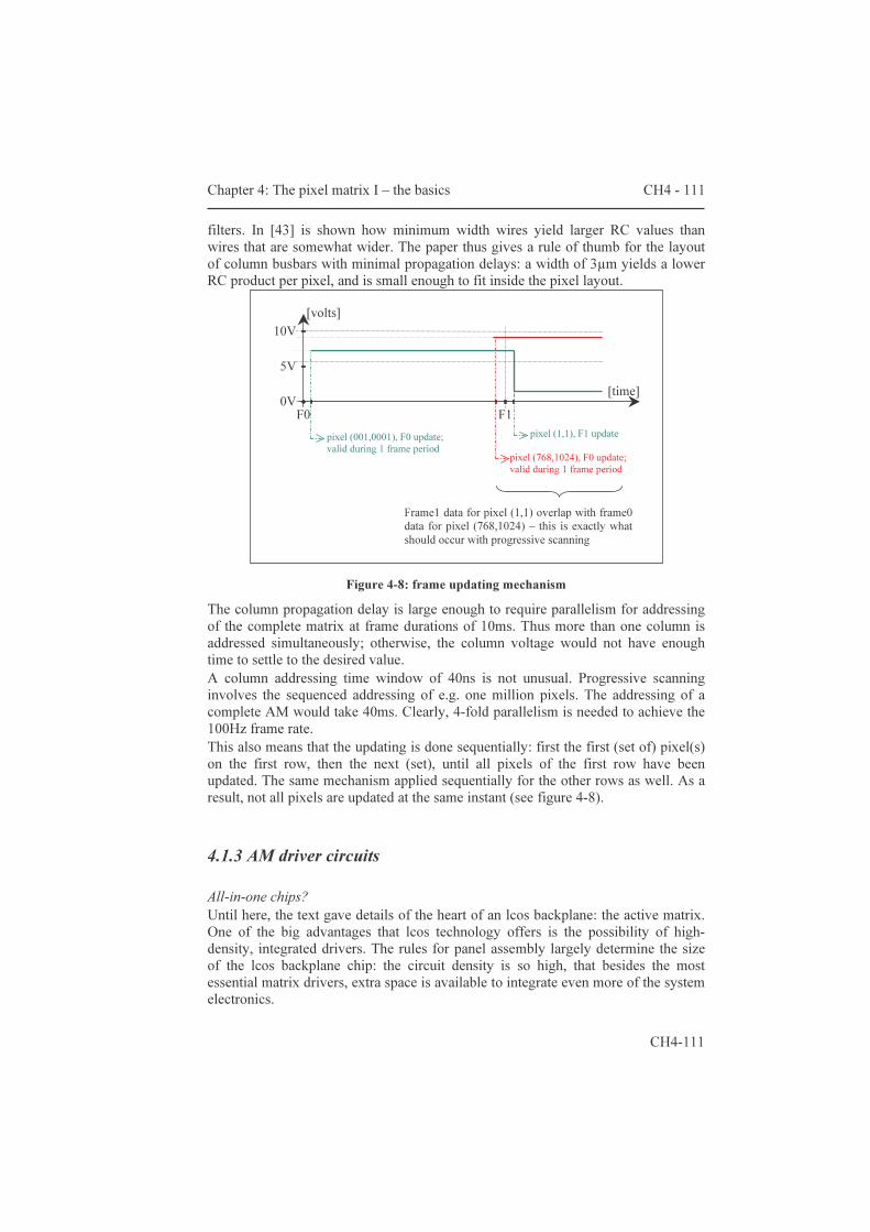
Chapter 4: The pixel matrix I – the basics CH4 - 111
CH4-111
filters. In [43] is shown how minimum width wires yield larger RC values than wires that are somewhat wider. The paper thus gives a rule of thumb for the layout of column busbars with minimal propagation delays: a width of 3µm yields a lower RC product per pixel, and is small enough to fit inside the pixel layout.
Figure 4-8: frame updating mechanism
The column propagation delay is large enough to require parallelism for addressing of the complete matrix at frame durations of 10ms. Thus more than one column is addressed simultaneously; otherwise, the column voltage would not have enough time to settle to the desired value. A column addressing time window of 40ns is not unusual. Progressive scanning involves the sequenced addressing of e.g. one million pixels. The addressing of a complete AM would take 40ms. Clearly, 4-fold parallelism is needed to achieve the 100Hz frame rate. This also means that the updating is done sequentially: first the first (set of) pixel(s) on the first row, then the next (set), until all pixels of the first row have been updated. The same mechanism applied sequentially for the other rows as well. As a result, not all pixels are updated at the same instant (see figure 4-8). 4.1.3 AM driver circuits All-in-one chips? Until here, the text gave details of the heart of an lcos backplane: the active matrix. One of the big advantages that lcos technology offers is the possibility of high-density, integrated drivers. The rules for panel assembly largely determine the size of the lcos backplane chip: the circuit density is so high, that besides the most essential matrix drivers, extra space is available to integrate even more of the system electronics.
[time]F0 F1
[volts]
0V
5V
10V
pixel (001,0001), F0 update; valid during 1 frame period pixel (768,1024), F0 update;
valid during 1 frame period
pixel (1,1), F1 update
Frame1 data for pixel (1,1) overlap with frame0 data for pixel (768,1024) – this is exactly what should occur with progressive scanning
CH4 - 112 Chapter 4: The pixel matrix I – the basics
CH4-112
Many think that the micro-display chip can integrate the entire electronic subsystem. A lot can be integrated onto the backplane chips; however, specific system functions are better implemented in a more adequate IC technology for cost reasons. In particular, the frame memory is best implemented in a dedicated, deep-submicron ‘memory’ technology, rather than in the backplane’s 0.35µ/3µ technology. In other words, there will always be several chips; one should not expect all electronic functions to be stowed onto the micro-display chip. Commercial players very often offer chip-sets to accommodate for most of the system electronics. Furthermore, next to the essential functions, test circuitry can help with the identification of critical assembly steps. This can be quite useful to minimize the production cost, if the test circuitry allows for the elimination of unacceptable backplanes as early as possible in the panel assembly process. Of course, test circuitry also provides a means to monitor the process yield over a longer time. Scanner circuits It is time to expand somewhat on the most essential matrix driver circuits: the row and column drivers. The appendix gives extended examples. In essence, the column and row drivers are scanners; i.e. their combined operation systematically scans the matrix by addressing one pixel after the other. Within the frame time, all of the pixels need to be addressed once. The row scan frequency thus is the frame time divided by the number of rows, assuming there is no ‘dead’ time, or frame porch time. In exactly the same way, the column scan frequency can be determined: row time divided by the number of columns addressed. Note that only one row can be addressed at a time, while several columns or all columns can be addressed simultaneously. This depends on the degree of parallelism that is built into the column driver circuit. Sometimes this is referred to as line-at-a-time addressing – to make the difference with pixel-at-a-time addressing where just one column is addressed per write sequence. There is a lot of similarity between the column and row scanners. The circuits are very similar, for VAN cells both need medium voltage level shifters, the pitch constraint is similar, the loads are similar… there are some important differences of course. Because of the parallelism in the column scanner, the low-voltage part of the column driver will often be less dense compared to the row driver. The scan frequency is higher for the column driver, and the load is actually composed of a bank of video switches. The row driver’s load is composed of the row busbars and all of the pixel transistor gates on one row. See e.g. appendix 1, AX1.3, point d) Schematic of main circuit. The scanners are built using a shift register and level shifters. The length of the shift register relates to the number of rows or number of columns of course. Note that the clock signals that drive the shift registers are buffered using a symmetric buffer tree to avoid differences in signal timing, e.g. differences when writing to the upper side of the AM compared to when writing to the lower side. The level shifters are needed to provide the pixel electrodes with the necessary voltage levels. Note that some extra functionality is necessary: hold logic that force the driver outputs into a given state; bi-directional scanning, so that the image orientation does
Chapter 4: The pixel matrix I – the basics CH4 - 113
CH4-113
not depend on the orientation of the display panel; mode bits for display format selection, etc. Until now, redundancy has not been discussed. Matrix defects are likely to occur considering the physical dimensions of the AM. There are very few defects that are tolerated for commercial displays. As a result, some might dream of pixel redundancy: the idea of pixel replacement does not work for display systems. It works for memory chips, it works for camera chips, because there is no need for an exact match between the physical structure of these arrays and the real world they are supposed to represent. A non-working pixel cannot be replaced by another. Thus, when one has a perfect AM, the drivers should be operational. And at the very start of this research, no information at all was available e.g. to estimate the chances of having a working chip. This is the reason why in the first stages of the research work, as much redundancy as possible was foreseen. As the group gained experience, redundancy lost some of its importance. Another good practice, is to try using somewhat stricter layout rules to lessen the defect probability – wherever possible, and certainly for the design of the highly sensitive AM. A typical example is the minimum separation of wires: keeping long wires further apart from each other where possible seems a good idea. The 160x120 panels have double row and double column drivers; clearly, enable circuits are needed to enable the correctly working drivers and to disconnect the non-working ones from the AM. The five million pixels of the MOSAREL GXGA demonstrator definitely seem to be the most sensitive to defects (considering AM size). However, double column drivers are not possible here considering the interconnection method and timing issues (long connections to the other side of the chip for the most sensitive signals: the video signals). Column and row shift registers are composed of chains of blocks of 32 registers; each block is foreseen twice. As a result, there are two sets of register blocks, setA and setB. One can decide externally which one to use. At least that was the original plan; in practice, a missing buffer does not allow selecting any combination of register blocks, it only allows selecting one of the two sets. The tmdc XGA still had two row drivers; practice shows the second row driver has little impact. Therefore, the later versions bear no more redundancy.
4.1.4 VAN pixel design: constraint listing
Diffraction Less light loss with larger pixels; this requirement is opposite to cost considerations [11]
Optical
Aperture Less light loss with larger pixels; this requirement is opposite to cost considerations [11]
CH4 - 114 Chapter 4: The pixel matrix I – the basics
CH4-114
Photo-conduction
A light shield requires an extra layer in the IC stack. It is also recommendable to use minimum inter-electrode gaps to maximize the aperture, to limit the light beam to the sole AM area and to block light that reaches the back or edges of the chip! This has primarily consequences for the package design.
IC design rules Can sometimes be bent; this is at the designers’ risk and often need agreement from the foundry.
Technological
Assembly design rules
See chapter 2; too stringent and these will greatly affect panel yield
Electrical Fringe losses Minimal for frame inversion and with larger pixels; counter-balanced by cost considerations [11] and dependent upon the LC effect used [45]
V-range Depends on LC, for our VAN developments, 10Vpp signal ranges are more than sufficient
AC-drive Considering the body effect, the Vrange of the pixel transistor further expands to 15-18V
Frame speed Need for parallelism: depends on the drive scheme (analog/digital), on the color scheme (3-valve, 1-valve) and on the AM bandwidth
(Electrical) Cross-talk The use of simple guarding avoids cross-talk from one video signal to the next: take care of the layout of the analog switches and of the AM
Table 4-2: constraint listing Table 4-2 lists the design constraints specific to the design of pixels. In paragraph 4.1 some important issues regarding the design of classic AMs are presented. The next paragraph gives an overview of the three ‘generations’ of micro-display chips I designed and that have been successfully assembled into display demonstrators by a very skilled team of specialists from the TFCGroup.
Chapter 4: The pixel matrix I – the basics CH4 - 115
CH4-115
4.2 Micro-display implementations The section describes the implemented chips, along with the results obtained. Three generations of lcos µdisplays are described. Each implements the classic DRAM described previously; the differences lie with the IC technology, display format, and the amount of circuit redundancy. Along with the research advances, more and more knowledge was gained, also regarding the system electronics and regarding the optical architecture. The first implementation is the result of a thorough, first ‘shot’. The second implementation features three different display formats, one of them resulting in the largest lcos known to date: the GXGA MOSAREL chip. The tmdc prototypes comprise the XGA and WXGA formats. They served the purpose of developing high volume lcos process chains.
4.2.1 REFLEC chips: 160x120 pixels Trading standard cell design versus area cost The development of a digital column driver IC paved the way to the micro-display design activities in the research group. This design1 used standard cells in a 2.4µm CMOS technology from Alcatel, Oudenaarde, Belgium (now AMIS). The most striking disadvantage of the standard cell approach is the size of the digital-to-analog converter (DAC). A test IC with four column outputs needs about 25 sq. mm. At that time, the automatic place and route tools available did not make use of the symmetry in the design schematics and had only two metal layers for routing – manual layout of at least some of the sub-cells appeared to be a necessity. Finally, it was the pitch of the standard cells that determined the pitch of the output pads... which is far larger than any acceptable lcos pixel pitch. Another point is that the standard cells were general purpose cells – not exactly optimized for lcos micro-display backplanes. Eventually, the column outputs can be rewired to match the smaller pixel pitch; the advantage of this idea is thwarted by the area cost of rewiring and by the area cost resulting from stacked driver cells. After a first, successful ‘mini feasibility’ study [AX1.1], a project was born (“REFLEC”) to design a digital quarter-VGA micro-display chip in Alcatel’s 2.5um HBiMOS technology. One of the aims was to compare line-at-a-time and pixel-at-a-time addressing schemes. The former updates the AM row by row, while the latter updates the AM pixel by pixel. Quite unfortunately, redesign resources only allowed for 1/16th VGA format. The experience with the first design showed an area need of pixelPitch x 1000µm per bit. A decent 8-bit digital driver would need at least 8mm x chipWidth of silicon. This is the consequence of the ‘conservative’ 2.5µm feature size and limited routing density. The integration of 8-bit digital drivers with a line-at-a-time addressing scheme just is too costly considering the CMOS technology available. 1 J.-P. Voortman, 1994
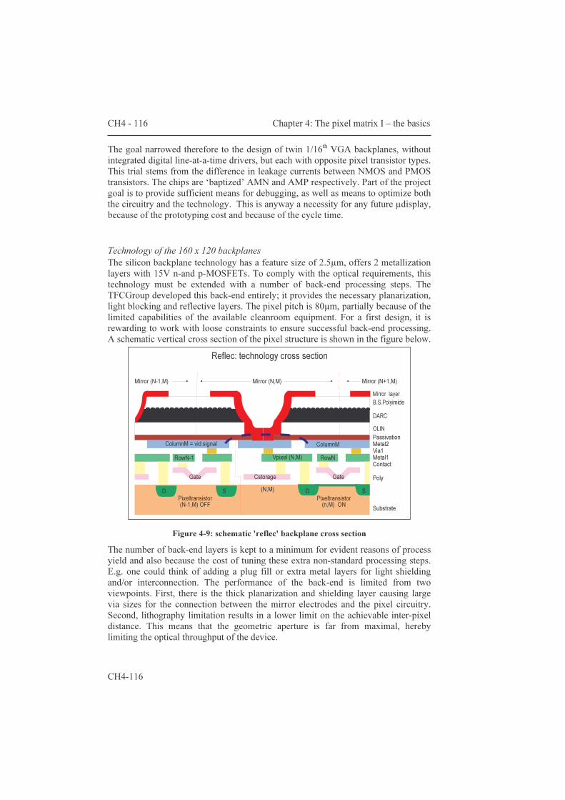
CH4 - 116 Chapter 4: The pixel matrix I – the basics
CH4-116
The goal narrowed therefore to the design of twin 1/16th VGA backplanes, without integrated digital line-at-a-time drivers, but each with opposite pixel transistor types. This trial stems from the difference in leakage currents between NMOS and PMOS transistors. The chips are ‘baptized’ AMN and AMP respectively. Part of the project goal is to provide sufficient means for debugging, as well as means to optimize both the circuitry and the technology. This is anyway a necessity for any future µdisplay, because of the prototyping cost and because of the cycle time. Technology of the 160 x 120 backplanes The silicon backplane technology has a feature size of 2.5µm, offers 2 metallization layers with 15V n-and p-MOSFETs. To comply with the optical requirements, this technology must be extended with a number of back-end processing steps. The TFCGroup developed this back-end entirely; it provides the necessary planarization, light blocking and reflective layers. The pixel pitch is 80µm, partially because of the limited capabilities of the available cleanroom equipment. For a first design, it is rewarding to work with loose constraints to ensure successful back-end processing. A schematic vertical cross section of the pixel structure is shown in the figure below.
Figure 4-9: schematic 'reflec' backplane cross section The number of back-end layers is kept to a minimum for evident reasons of process yield and also because the cost of tuning these extra non-standard processing steps. E.g. one could think of adding a plug fill or extra metal layers for light shielding and/or interconnection. The performance of the back-end is limited from two viewpoints. First, there is the thick planarization and shielding layer causing large via sizes for the connection between the mirror electrodes and the pixel circuitry. Second, lithography limitation results in a lower limit on the achievable inter-pixel distance. This means that the geometric aperture is far from maximal, hereby limiting the optical throughput of the device.
Reflec: technology cross section
Cstorage
RowN-1 Vpixel (N,M) RowNColumnM = vid.signal ColumnM
Substrate
PolyGateGateContactMetal1Via1PassivationMetal2
D SD S (N,M)Pixeltransistor(n,M) ON
Pixeltransistor(N-1,M) OFF
Mirror (N+1,M)Mirror (N,M)Mirror (N-1,M)
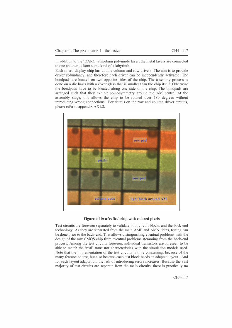
Chapter 4: The pixel matrix I – the basics CH4 - 117
CH4-117
In addition to the ‘DARC’ absorbing polyimide layer, the metal layers are connected to one another to form some kind of a labyrinth. Each micro-display chip has double column and row drivers. The aim is to provide driver redundancy, and therefore each driver can be independently activated. The bondpads are located on two opposite sides of the chip. The assembly process is done on a die basis with a cover glass that is smaller than the chip itself. Otherwise the bondpads have to be located along one side of the chip. The bondpads are arranged such that they exhibit point-symmetry around the AM centre. At the assembly stage, this allows the chip to be rotated over 180 degrees without introducing wrong connections. For details on the row and column driver circuits, please refer to appendix AX1.2.
Figure 4-10: a 'reflec' chip with colored pixels Test circuits are foreseen separately to validate both circuit blocks and the back-end technology. As they are separated from the main AMP and AMN chips, testing can be done prior to the back-end. That allows distinguishing eventual problems with the design of the raw CMOS chip from eventual problems stemming from the back-end process. Among the test circuits foreseen, individual transistors are foreseen to be able to match the ‘real’ transistor characteristics with the simulation models used. Note that the implementation of the test circuits is time consuming, because of the many features to test, but also because each test block needs an adapted layout. And for each layout adaptation, the risk of introducing errors increases. Because the vast majority of test circuits are separate from the main circuits, there is practically no
pixels
row pad
column pads light block around AM
row pad
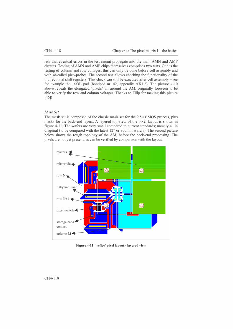
CH4 - 118 Chapter 4: The pixel matrix I – the basics
CH4-118
risk that eventual errors in the test circuit propagate into the main AMN and AMP circuits. Testing of AMN and AMP chips themselves comprises two tests. One is the testing of column and row voltages; this can only be done before cell assembly and with so-called pico-probes. The second test allows checking the functionality of the bidirectional shift registers. This check can still be executed after cell assembly – see for example the _SOL pad (bondpad nr. 42, appendix AX1.2). The picture 4-10 above reveals the elongated ‘pixels’ all around the AM, originally foreseen to be able to verify the row and column voltages. Thanks to Filip for making this picture [46]! Mask Set The mask set is composed of the classic mask set for the 2.5u CMOS process, plus masks for the back-end layers. A layered top-view of the pixel layout is shown in figure 4-11. The wafers are very small compared to current standards; namely 4” in diagonal (to be compared with the latest 12” or 300mm wafers). The second picture below shows the rough topology of the AM, before the back-end processing. The pixels are not yet present, as can be verified by comparison with the layout.
Figure 4-11: 'reflec' pixel layout - layered view
pixel switch
‘labyrinth via’
storage capa contact
row N+1
row N
mirrors
mirror via
column M
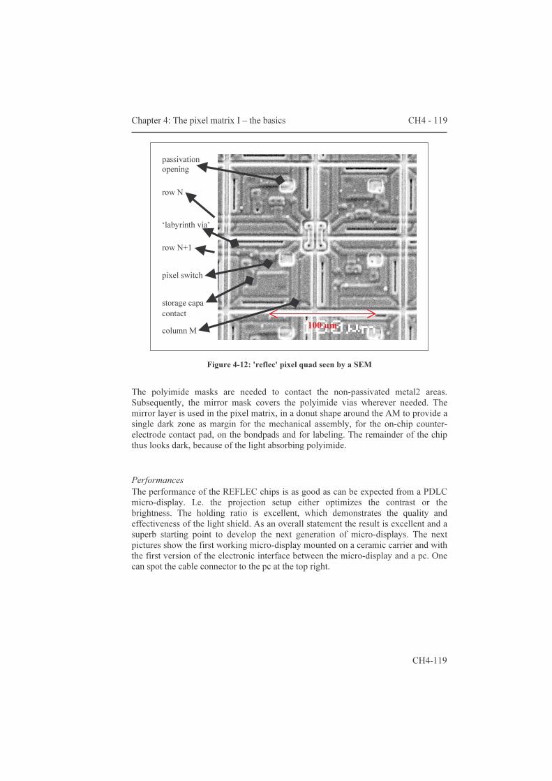
Chapter 4: The pixel matrix I – the basics CH4 - 119
CH4-119
Figure 4-12: 'reflec' pixel quad seen by a SEM The polyimide masks are needed to contact the non-passivated metal2 areas. Subsequently, the mirror mask covers the polyimide vias wherever needed. The mirror layer is used in the pixel matrix, in a donut shape around the AM to provide a single dark zone as margin for the mechanical assembly, for the on-chip counter-electrode contact pad, on the bondpads and for labeling. The remainder of the chip thus looks dark, because of the light absorbing polyimide.
Performances The performance of the REFLEC chips is as good as can be expected from a PDLC micro-display. I.e. the projection setup either optimizes the contrast or the brightness. The holding ratio is excellent, which demonstrates the quality and effectiveness of the light shield. As an overall statement the result is excellent and a superb starting point to develop the next generation of micro-displays. The next pictures show the first working micro-display mounted on a ceramic carrier and with the first version of the electronic interface between the micro-display and a pc. One can spot the cable connector to the pc at the top right.
pixel switch
‘labyrinth via’
storage capa contact
row N+1
row N
passivation opening
column M 100 µm

CH4 - 120 Chapter 4: The pixel matrix I – the basics
CH4-120
Figure 4-13: early version of the 'reflec' demonstrator Slimmed-down versions are shown hereunder. The last carrier version is hardly larger than the micro-display chip. It provides mechanical support for the micro-display chip and for the electronic components that need to be very close. The rest of the driving electronics is located on an intermediate board. This setup is more useful for building a projection setup.
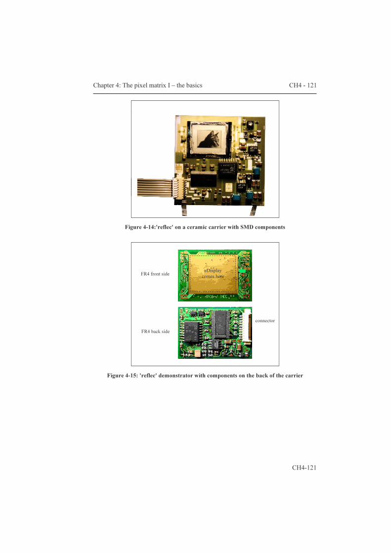
Chapter 4: The pixel matrix I – the basics CH4 - 121
CH4-121
Figure 4-14:'reflec' on a ceramic carrier with SMD components
Figure 4-15: 'reflec' demonstrator with components on the back of the carrier
FR4 back side connector
FR4 front side uDisplay comes here
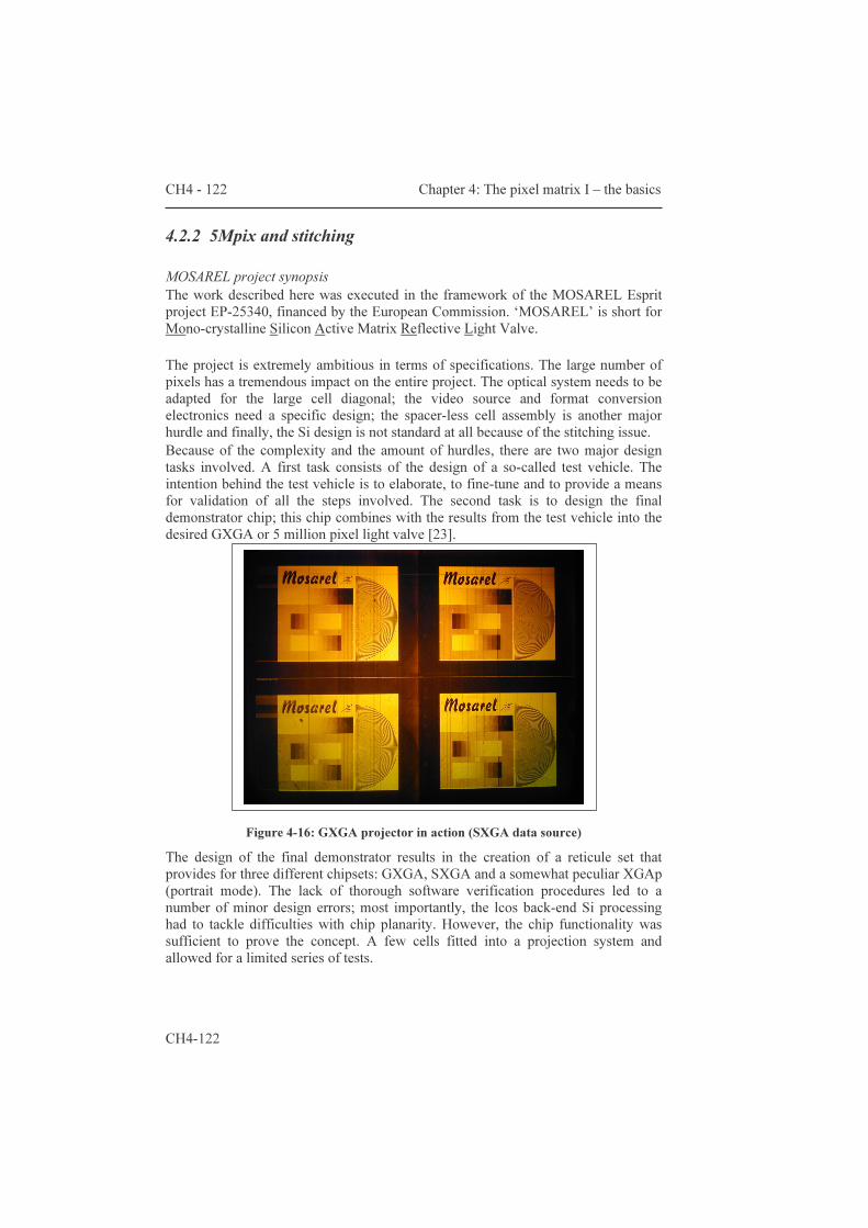
CH4 - 122 Chapter 4: The pixel matrix I – the basics
CH4-122
4.2.2 5Mpix and stitching MOSAREL project synopsis The work described here was executed in the framework of the MOSAREL Esprit project EP-25340, financed by the European Commission. ‘MOSAREL’ is short for Mono-crystalline Silicon Active Matrix Reflective Light Valve. The project is extremely ambitious in terms of specifications. The large number of pixels has a tremendous impact on the entire project. The optical system needs to be adapted for the large cell diagonal; the video source and format conversion electronics need a specific design; the spacer-less cell assembly is another major hurdle and finally, the Si design is not standard at all because of the stitching issue. Because of the complexity and the amount of hurdles, there are two major design tasks involved. A first task consists of the design of a so-called test vehicle. The intention behind the test vehicle is to elaborate, to fine-tune and to provide a means for validation of all the steps involved. The second task is to design the final demonstrator chip; this chip combines with the results from the test vehicle into the desired GXGA or 5 million pixel light valve [23].
Figure 4-16: GXGA projector in action (SXGA data source)
The design of the final demonstrator results in the creation of a reticule set that provides for three different chipsets: GXGA, SXGA and a somewhat peculiar XGAp (portrait mode). The lack of thorough software verification procedures led to a number of minor design errors; most importantly, the lcos back-end Si processing had to tackle difficulties with chip planarity. However, the chip functionality was sufficient to prove the concept. A few cells fitted into a projection system and allowed for a limited series of tests.
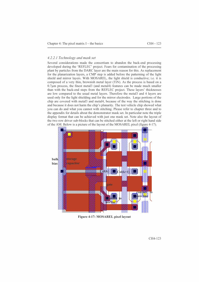
Chapter 4: The pixel matrix I – the basics CH4 - 123
CH4-123
4.2.2.1 Technology and mask set Several considerations made the consortium to abandon the back-end processing developed during the ‘REFLEC’ project. Fears for contamination of the processing plant by particles from the DARC layer are the main reason for this. As replacement for the planarization layers, a CMP step is added before the patterning of the light shield and mirror layers. With MOSAREL, the light shield is conductive; i.e. it is composed of a very thin, brownish metal layer (TiN). As the process is based on a 0.7µm process, the finest metal3 (and metal4) features can be made much smaller than with the back-end steps from the REFLEC project. These layers’ thicknesses are low compared to the usual metal layers. Therefore the metal3 and 4 layers are used only for the light shielding and for the mirror electrodes. Large portions of the chip are covered with metal3 and metal4, because of the way the stitching is done and because it does not harm the chip’s planarity. The test vehicle chip showed what you can do and what you cannot with stitching. Please refer to chapter three and to the appendix for details about the demonstrator mask set. In particular note the triple display format that can be achieved with just one mask set. Note also the layout of the two row driver sub-blocks that can be stitched either at the left or right hand side of the AM. Below is a picture of the layout of the MOSAREL pixel (figure 4-17).
Figure 4-17: MOSAREL pixel layout
storage capacitor
gate contact to row line
Col(k) Col(k+1)
Contact to mirror
bulk bias
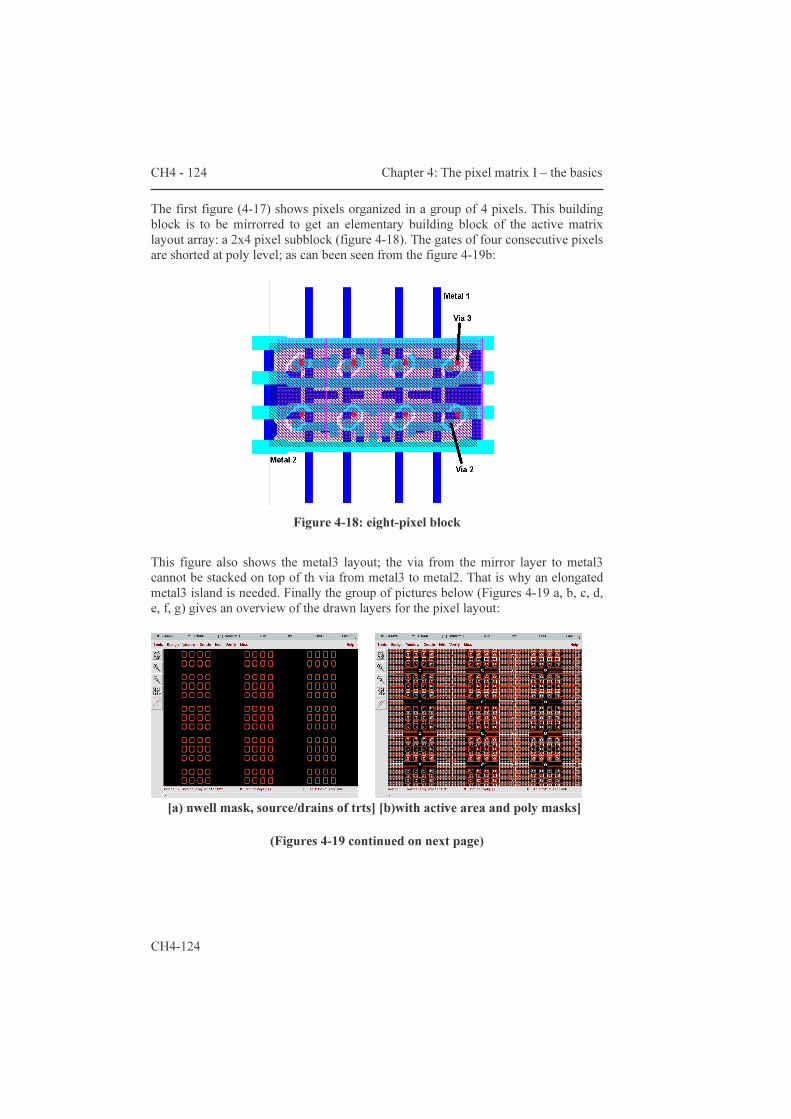
CH4 - 124 Chapter 4: The pixel matrix I – the basics
CH4-124
The first figure (4-17) shows pixels organized in a group of 4 pixels. This building block is to be mirrorred to get an elementary building block of the active matrix layout array: a 2x4 pixel subblock (figure 4-18). The gates of four consecutive pixels are shorted at poly level; as can been seen from the figure 4-19b:
Figure 4-18: eight-pixel block
This figure also shows the metal3 layout; the via from the mirror layer to metal3 cannot be stacked on top of th via from metal3 to metal2. That is why an elongated metal3 island is needed. Finally the group of pictures below (Figures 4-19 a, b, c, d, e, f, g) gives an overview of the drawn layers for the pixel layout:
[a) nwell mask, source/drains of trts] [b)with active area and poly masks]
(Figures 4-19 continued on next page)

Chapter 4: The pixel matrix I – the basics CH4 - 125
CH4-125
[c) metal and via1 layers] [d) metal2 and via2 masks]
[e) light shield and vias to mirror layer, and f) at last the mirror layer]
Figures 4-19: [f) SEM picture of MOSAREL pixel array]

CH4 - 126 Chapter 4: The pixel matrix I – the basics
CH4-126
4.2.2.2 Circuit and evaluation This paragraph just highlights some of the most significant circuit figures and briefly says something about the evaluation of the chipsets. Because of the large pixel count, and because of the wide scanners in the column and row drivers, it is a good idea to foresee some redundancy in the circuits. Redundancy is supposed to help at having chips that pass the acceptance criteria. As the matrix cannot be foreseen with redundant pixels, the only circuits that can bear redundancy are the column and row drivers. This way, the chances that a chip with a perfect AM also has working drivers is maximized. Signal delay considerations push to allow for only one column driver, while two row drivers seem relatively easy to implement. Because of the size of the level shifting circuits (3µ devices), no redundancy can be foreseen. Thus, a fault in the medium-voltage (MV) part of the column driver is fatal; while one in the MV part of the row driver is not, because there are two row drivers. The logic part of the drivers uses much more compact transistors (0.7µ devices), and allows much more easily to incorporate redundancy.
Figure 4-20: MOSAREL backplane under test
Figure 4-21: usage of probe-needles to measure inside the chip

Chapter 4: The pixel matrix I – the basics CH4 - 127
CH4-127
In practice, both the column and row scanners are implemented as double chains of blocks of shift registers (e.g. chain a and b). A block from chain a can be made to connect to a next block from chain b, and so forth. This way a very high degree of redundancy can be achieved. That was the plan; in practice, a problem with signal timings prohibited us to mix both chains (figure 4-22). In the end, the chips thus had double shift registers.
Figure 4-22: functional testing reveals a problem in the clock buffer tree
The measurements we could perform, have been hampered a long time by a planarity issue that resulted in shorts. Functional testing was done by taking wafers out after the processing of metal2. By using the right probes, we had access to virtually all of the chips functions (figures 4-20 till 4-24). Because of the absence of the mirror and light-shielding layers, rather high sensitivity to lighting conditions have been experienced (figure 4-24). When a good chip was finally available, no time and no money were available to continue the project. Figure 4-16 shows an operational GXGA setup. Yield of the complete process could not be evaluated since the markets did not open up to real volume production.
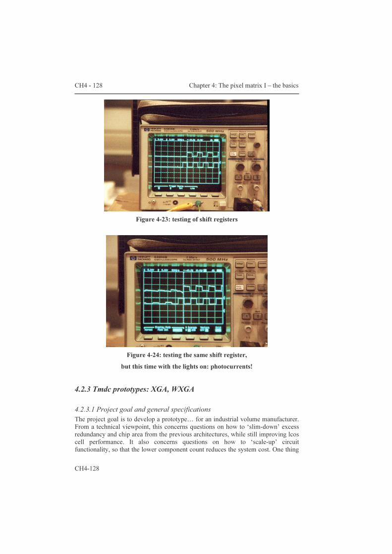
CH4 - 128 Chapter 4: The pixel matrix I – the basics
CH4-128
Figure 4-23: testing of shift registers
Figure 4-24: testing the same shift register,
but this time with the lights on: photocurrents!
4.2.3 Tmdc prototypes: XGA, WXGA 4.2.3.1 Project goal and general specifications The project goal is to develop a prototype… for an industrial volume manufacturer. From a technical viewpoint, this concerns questions on how to ‘slim-down’ excess redundancy and chip area from the previous architectures, while still improving lcos cell performance. It also concerns questions on how to ‘scale-up’ circuit functionality, so that the lower component count reduces the system cost. One thing
Chapter 4: The pixel matrix I – the basics CH4 - 129
CH4-129
though is very clear: because of the link with a volume producer, all must go quick and all must be perfect. Fortunately, the ‘training’ endured with the MOSAREL project, provides some insights on how to achieve that. The display formats aimed for are XGA (1024x768 pixels) and WXGA (1280x768). The panels aimed for, follow the classic AM architecture described above. Several means are foreseen for testing the chip functionality.
Parameter XGA WXGA Chip size (rounded) 21mm x 19mm 19mm x 14mm AM area ( “ ) 14mmx 18mm 9mm x 15mm AM diagonal 0.9” 0.7” Display format 1024 x 768 1280 x 768 Display aspect ratio 4:3 4:3, 16:9 Pixel pitch 17.6µ 11.9µ Inter pixel gap 0.6µ 0.6µ Geometric aperture 93% 90% Frame rate (nominal) 60Hz 75Hz Response speed (off-on-off) <20ms <20ms Contrast ratio >500:1 > 800:1 Chip supply voltages 3.3V, 18V 3.3V, 18V Video driver 4-fold analog 4-fold analog On-chip video clamp Y Y Bidirectional r&c scanners Y Y
4.2.3.2 Technology and mask set The backplane technology relies on a specific lcos route available at the time from UMC. UMC performed a customer screening since, leading our project to drop out of their business scope. Fortunately, other foundries are eager to fill the gap. Anyway, the technology from UMC is fully certified and documented; a fact that somehow lessens the design burden. Essentially, the route offers a double gate technology, with two poly layers and 4 metal layers. See also chapter two. Furthermore, as it concerns an extended 0.35µ technology, the technology includes the CMP processing steps needed for the planarization of the chips. The design kit offered some support. Because code needed to be written to implement all rules. The mask set is characterized by both a simplification and a further refinement compared to the MOSAREL mask sets. No more stitching, because this time the foundry does not allow for it. Most large foundries do not allow for process changes at the wish of small customers. Ten thousand wafers per year is a small volume! With some yield and size factors in mind, this means that 100k display sets per year
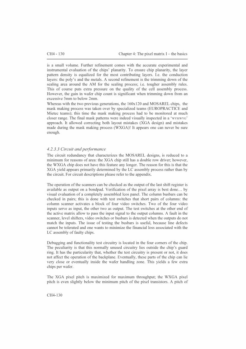
CH4 - 130 Chapter 4: The pixel matrix I – the basics
CH4-130
is a small volume. Further refinement comes with the accurate experimental and instrumental evaluation of the chips’ planarity. To ensure chip planarity, the layer pattern density is equalized for the most contributing layers. I.e. the conduction layers: the poly’s and the metals. A second refinement is the trimming down of the sealing area around the AM for the sealing process; i.e. tougher assembly rules. This of course puts extra pressure on the quality of the cell assembly process. However, the gain in wafer chip count is significant when trimming down from an excessive 5mm to below 2mm. Whereas with the two previous generations, the 160x120 and MOSAREL chips, the mask making process was taken over by specialized teams (EUROPRACTICE and Mietec teams); this time the mask making process had to be monitored at much closer range. The final mask patterns were indeed visually inspected in a ‘WYSIWYG’ approach. It allowed correcting both layout mistakes (XGA design) and mistakes made during the mask making process (WXGA)! It appears one can never be sure enough. 4.2.3.3 Circuit and performance The circuit redundancy that characterizes the MOSAREL designs, is reduced to a minimum for reasons of area: the XGA chip still has a double row driver; however, the WXGA chip does not have this feature any longer. The reason for this is that the XGA yield appears primarily determined by the LC assembly process rather than by the circuit. For circuit descriptions please refer to the appendix. The operation of the scanners can be checked as the output of the last shift register is available as output on a bondpad. Verification of the pixel array is best done… by visual evaluation of a completely assembled lcos panel. The column busbars can be checked in pairs; this is done with test switches that short pairs of columns: the column scanner activates a block of four video switches. Two of the four video inputs serve as input, the other two as output. The test switches at the other end of the active matrix allow to pass the input signal to the output columns. A fault in the scanner, level shifters, video switches or busbars is detected when the outputs do not match the inputs. The issue of testing the busbars is useful, because line defects cannot be tolerated and one wants to minimize the financial loss associated with the LC assembly of faulty chips. Debugging and functionality test circuitry is located in the four corners of the chip. The peculiarity is that this normally unused circuitry lies outside the chip’s guard ring. It has the particularity that, whether the test circuitry is present or not, it does not affect the operation of the backplane. Eventually, these parts of the chip can lie very close or eventually inside the wafer handling zone. This yields a few extra chips per wafer. The XGA pixel pitch is maximized for maximum throughput; the WXGA pixel pitch is even slightly below the minimum pitch of the pixel transistors. A pitch of
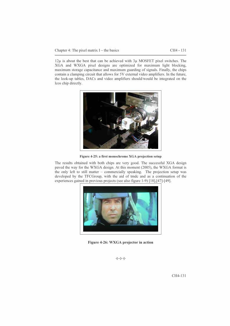
Chapter 4: The pixel matrix I – the basics CH4 - 131
CH4-131
12µ is about the best that can be achieved with 3µ MOSFET pixel switches. The XGA and WXGA pixel designs are optimized for maximum light blocking, maximum storage capacitance and maximum guarding of signals. Finally, the chips contain a clamping circuit that allows for 5V external video amplifiers. In the future, the look-up tables, DACs and video amplifiers should/would be integrated on the lcos chip directly.
Figure 4-25: a first monochrome XGA projection setup
The results obtained with both chips are very good. The successful XGA design paved the way for the WXGA design. At this moment (2005), the WXGA format is the only left to still matter – commercially speaking. The projection setup was developed by the TFCGroup, with the aid of tmdc and as a continuation of the experiences gained in previous projects (see also figure 1-9) [18],[47]-[49].
Figure 4-26: WXGA projector in action
���

CH4 - 132 Chapter 4: The pixel matrix I – the basics
CH4-132
Chapter 5: The pixel matrix II – smart pixels CH5 – 133
CH5-133
Chapter 5 : The pixel matrix(II) – smart pixels
he focus in this fifth chapter is on the development of new pixel circuits. The heart of lcos devices is the pixel matrix, as it is the location where the electro-optical conversion occurs. The classic active matrix circuit suffers from
important drawbacks regarding voltage range and addressing speed. The impact hereof can be significantly reduced with new pixel circuits. Paragraph 5.1 initiates the reader to the CE switching principle, discusses the compatibility with continuous light sources and estimates the maximum transistor count per pixel. Indeed, to use the CE switching approach, more complex pixel circuits are necessary. The reason behind the need for a second in-pixel frame memory is explained. Actually, this is the core of chapter five. A second point is to figure out how complex pixel circuits can grow. The maximum transistor count is estimated in the second part of paragraph 5.1; its purpose is to serve as rule of thumb for the selection of new pixel circuits. Paragraph 5.2 addresses the implementation of AMs with frame memory; it describes a couple of original circuit ideas that effectively implement the functionality of an additional frame memory. The resulting pixels are labeled ‘smart pixels’ maybe because of the functionality offered notwithstanding the limited area available. The authors’ thoughts indeed came across the double-DRAM circuit, not totally ‘by accident’. Along with other original circuit ideas a patent was successfully applied for [50]. This is partially the basis for the creation of the GEMIDIS startup company. At last, a very brief introduction to pulse-width-modulation or PWM addressing is presented. At this point, it is noteworthy that in the mid 80’s, spatial light modulators using LC-on-silicon were developed. The arrays then were relatively small compared to the million-pixel displays described here. Shortly later, the term ‘smart pixel’ probably was coined in 1993, when K.M. Johnson, D.J. McKnight and I. Underwood publish “Smart spatial light modulators using liquid crystals on Silicon” [56]. This article is very interesting as a similar progressive buildup is used for the description of ‘smart ‘ pixels, i.e. with memory. More recently, Lee et al. [58] and Blalock et al. [57] wrote articles about the subject as well. The article from Blalock very accurately describes the combination of dual-memory and PWM circuits as described in paragraph 5.2. Lee et al. describe a very compact frame buffering pixel circuit, starting from the work by Shields and McKnight [54],[55].
T
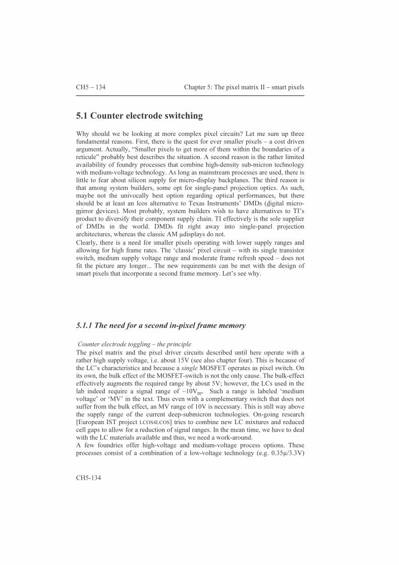
CH5 – 134 Chapter 5: The pixel matrix II – smart pixels
CH5-134
5.1 Counter electrode switching Why should we be looking at more complex pixel circuits? Let me sum up three fundamental reasons. First, there is the quest for ever smaller pixels – a cost driven argument. Actually, “Smaller pixels to get more of them within the boundaries of a reticule” probably best describes the situation. A second reason is the rather limited availability of foundry processes that combine high-density sub-micron technology with medium-voltage technology. As long as mainstream processes are used, there is little to fear about silicon supply for micro-display backplanes. The third reason is that among system builders, some opt for single-panel projection optics. As such, maybe not the univocally best option regarding optical performances, but there should be at least an lcos alternative to Texas Instruments’ DMDs (digital micro-mirror devices). Most probably, system builders wish to have alternatives to TI’s product to diversify their component supply chain. TI effectively is the sole supplier of DMDs in the world. DMDs fit right away into single-panel projection architectures, whereas the classic AM µdisplays do not. Clearly, there is a need for smaller pixels operating with lower supply ranges and allowing for high frame rates. The ‘classic’ pixel circuit – with its single transistor switch, medium supply voltage range and moderate frame refresh speed – does not fit the picture any longer... The new requirements can be met with the design of smart pixels that incorporate a second frame memory. Let’s see why.
5.1.1 The need for a second in-pixel frame memory Counter electrode toggling – the principle The pixel matrix and the pixel driver circuits described until here operate with a rather high supply voltage, i.e. about 15V (see also chapter four). This is because of the LC’s characteristics and because a single MOSFET operates as pixel switch. On its own, the bulk effect of the MOSFET-switch is not the only cause. The bulk-effect effectively augments the required range by about 5V; however, the LCs used in the lab indeed require a signal range of ~10Vpp. Such a range is labeled ‘medium voltage’ or ‘MV’ in the text. Thus even with a complementary switch that does not suffer from the bulk effect, an MV range of 10V is necessary. This is still way above the supply range of the current deep-submicron technologies. On-going research [European IST project LCOS4LCOS] tries to combine new LC mixtures and reduced cell gaps to allow for a reduction of signal ranges. In the mean time, we have to deal with the LC materials available and thus, we need a work-around. A few foundries offer high-voltage and medium-voltage process options. These processes consist of a combination of a low-voltage technology (e.g. 0.35µ/3.3V)
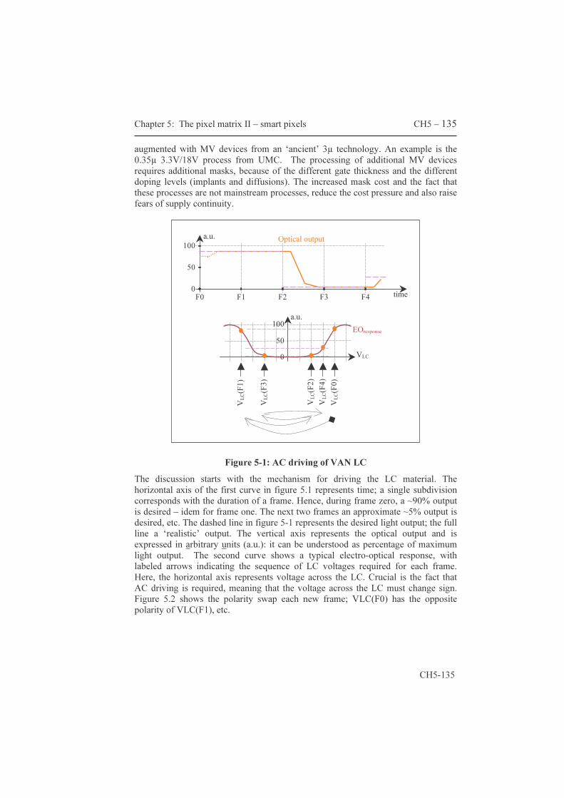
Chapter 5: The pixel matrix II – smart pixels CH5 – 135
CH5-135
augmented with MV devices from an ‘ancient’ 3µ technology. An example is the 0.35µ 3.3V/18V process from UMC. The processing of additional MV devices requires additional masks, because of the different gate thickness and the different doping levels (implants and diffusions). The increased mask cost and the fact that these processes are not mainstream processes, reduce the cost pressure and also raise fears of supply continuity.
Figure 5-1: AC driving of VAN LC
The discussion starts with the mechanism for driving the LC material. The horizontal axis of the first curve in figure 5.1 represents time; a single subdivision corresponds with the duration of a frame. Hence, during frame zero, a ~90% output is desired – idem for frame one. The next two frames an approximate ~5% output is desired, etc. The dashed line in figure 5-1 represents the desired light output; the full line a ‘realistic’ output. The vertical axis represents the optical output and is expressed in arbitrary units (a.u.): it can be understood as percentage of maximum light output. The second curve shows a typical electro-optical response, with labeled arrows indicating the sequence of LC voltages required for each frame. Here, the horizontal axis represents voltage across the LC. Crucial is the fact that AC driving is required, meaning that the voltage across the LC must change sign. Figure 5.2 shows the polarity swap each new frame; VLC(F0) has the opposite polarity of VLC(F1), etc.
time F0 F1 F2 F3 F4
a.u.
0
50
100 Optical output
a.u.
VLC
EOresponse
050
100V L
C(F0)
V LC(F
1)
V LC(F
2)
V LC(F
3)
V LC(F
4)
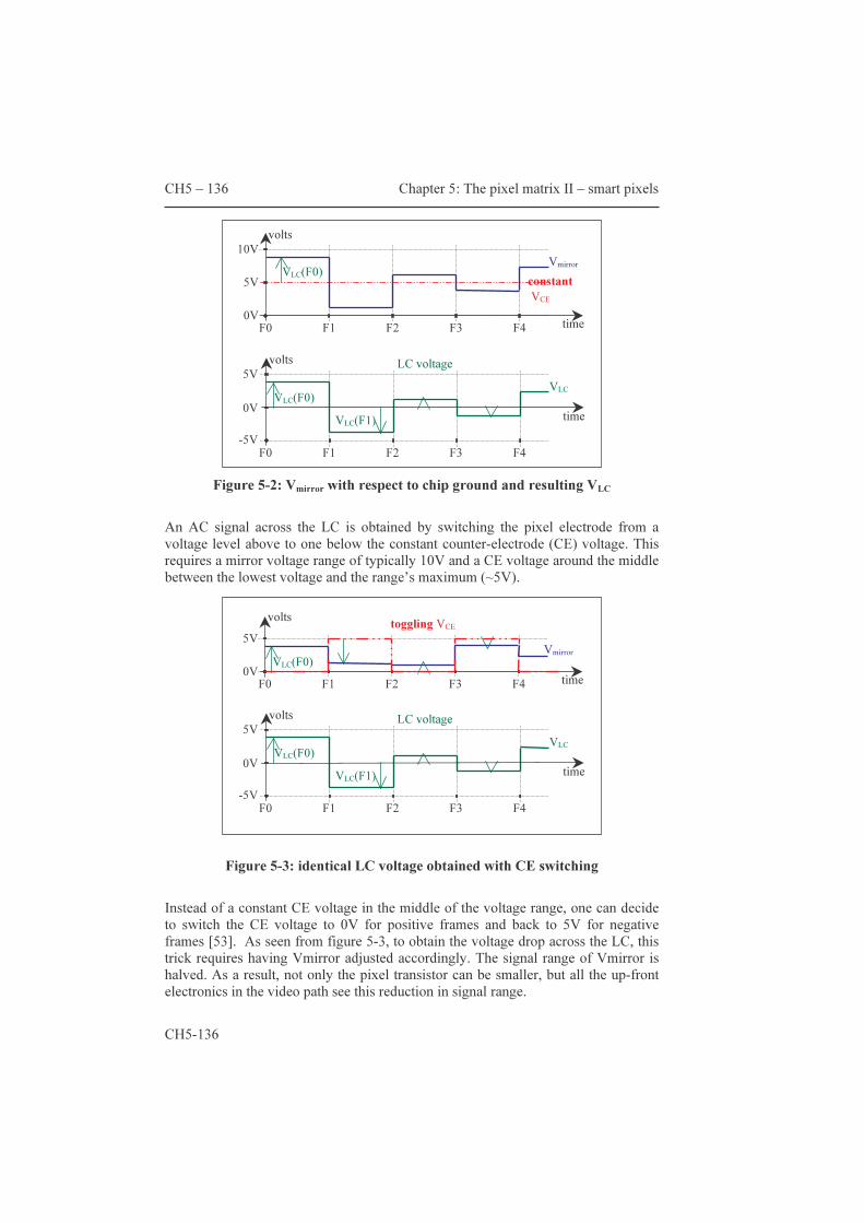
CH5 – 136 Chapter 5: The pixel matrix II – smart pixels
CH5-136
Figure 5-2: Vmirror with respect to chip ground and resulting VLC
An AC signal across the LC is obtained by switching the pixel electrode from a voltage level above to one below the constant counter-electrode (CE) voltage. This requires a mirror voltage range of typically 10V and a CE voltage around the middle between the lowest voltage and the range’s maximum (~5V).
Figure 5-3: identical LC voltage obtained with CE switching
Instead of a constant CE voltage in the middle of the voltage range, one can decide to switch the CE voltage to 0V for positive frames and back to 5V for negative frames [53]. As seen from figure 5-3, to obtain the voltage drop across the LC, this trick requires having Vmirror adjusted accordingly. The signal range of Vmirror is halved. As a result, not only the pixel transistor can be smaller, but all the up-front electronics in the video path see this reduction in signal range.
constant VCE
Vmirror
time F0 F1 F2 F3 F4
volts
0V
5V
10VVLC(F0)
VLC
time
5V
0V
-5V
volts
F0 F1 F2 F3 F4
VLC(F0) VLC(F1)
LC voltage
time F0 F1 F2 F3 F4
volts
0V
5VVLC(F0)
Vmirror
toggling VCE
VLC
time
5V
0V
-5V
volts
F0 F1 F2 F3 F4
VLC(F0) VLC(F1)
LC voltage
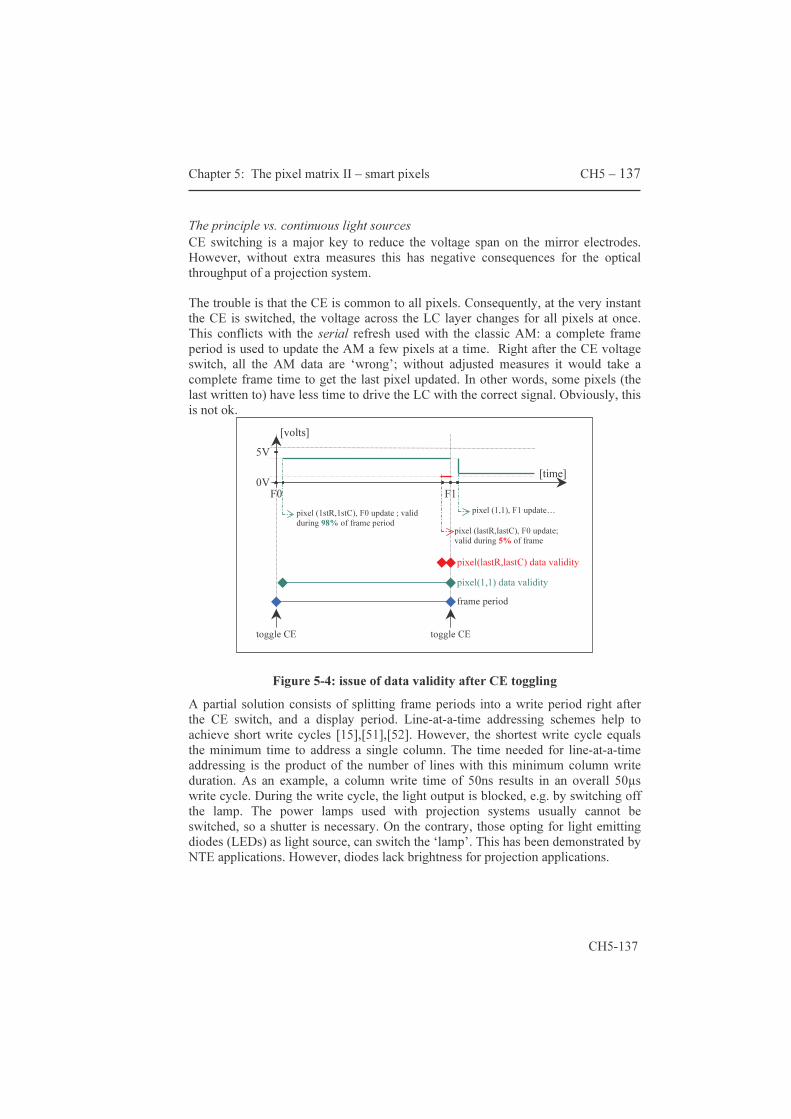
Chapter 5: The pixel matrix II – smart pixels CH5 – 137
CH5-137
The principle vs. continuous light sources CE switching is a major key to reduce the voltage span on the mirror electrodes. However, without extra measures this has negative consequences for the optical throughput of a projection system.
The trouble is that the CE is common to all pixels. Consequently, at the very instant the CE is switched, the voltage across the LC layer changes for all pixels at once. This conflicts with the serial refresh used with the classic AM: a complete frame period is used to update the AM a few pixels at a time. Right after the CE voltage switch, all the AM data are ‘wrong’; without adjusted measures it would take a complete frame time to get the last pixel updated. In other words, some pixels (the last written to) have less time to drive the LC with the correct signal. Obviously, this is not ok.
Figure 5-4: issue of data validity after CE toggling
A partial solution consists of splitting frame periods into a write period right after the CE switch, and a display period. Line-at-a-time addressing schemes help to achieve short write cycles [15],[51],[52]. However, the shortest write cycle equals the minimum time to address a single column. The time needed for line-at-a-time addressing is the product of the number of lines with this minimum column write duration. As an example, a column write time of 50ns results in an overall 50µs write cycle. During the write cycle, the light output is blocked, e.g. by switching off the lamp. The power lamps used with projection systems usually cannot be switched, so a shutter is necessary. On the contrary, those opting for light emitting diodes (LEDs) as light source, can switch the ‘lamp’. This has been demonstrated by NTE applications. However, diodes lack brightness for projection applications.
[time] F0 F1
[volts]
0V
5V
pixel (1stR,1stC), F0 update ; valid during 98% of frame period pixel (lastR,lastC), F0 update;
valid during 5% of frame period
pixel (1,1), F1 update…
toggle CE toggle CE
frame period
pixel(1,1) data validity
pixel(lastR,lastC) data validity
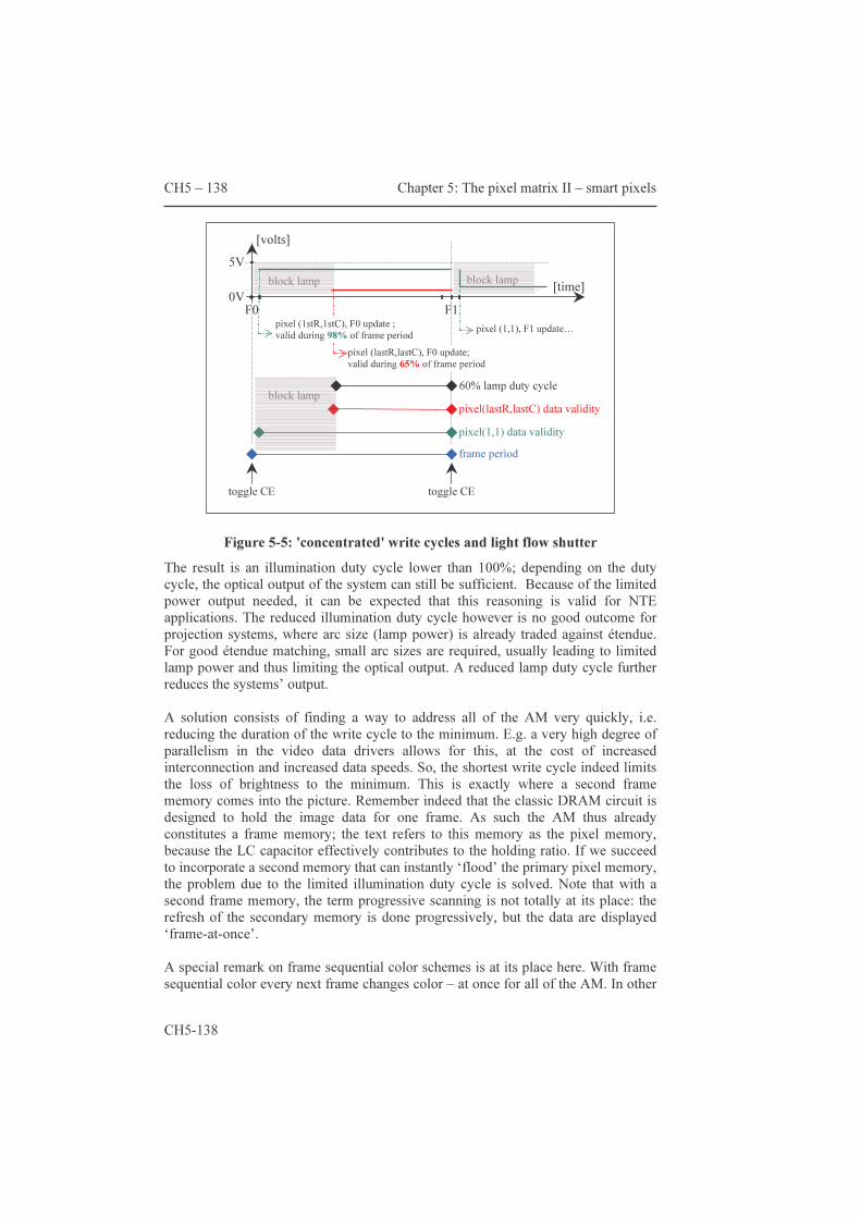
CH5 – 138 Chapter 5: The pixel matrix II – smart pixels
CH5-138
Figure 5-5: 'concentrated' write cycles and light flow shutter
The result is an illumination duty cycle lower than 100%; depending on the duty cycle, the optical output of the system can still be sufficient. Because of the limited power output needed, it can be expected that this reasoning is valid for NTE applications. The reduced illumination duty cycle however is no good outcome for projection systems, where arc size (lamp power) is already traded against étendue. For good étendue matching, small arc sizes are required, usually leading to limited lamp power and thus limiting the optical output. A reduced lamp duty cycle further reduces the systems’ output. A solution consists of finding a way to address all of the AM very quickly, i.e. reducing the duration of the write cycle to the minimum. E.g. a very high degree of parallelism in the video data drivers allows for this, at the cost of increased interconnection and increased data speeds. So, the shortest write cycle indeed limits the loss of brightness to the minimum. This is exactly where a second frame memory comes into the picture. Remember indeed that the classic DRAM circuit is designed to hold the image data for one frame. As such the AM thus already constitutes a frame memory; the text refers to this memory as the pixel memory, because the LC capacitor effectively contributes to the holding ratio. If we succeed to incorporate a second memory that can instantly ‘flood’ the primary pixel memory, the problem due to the limited illumination duty cycle is solved. Note that with a second frame memory, the term progressive scanning is not totally at its place: the refresh of the secondary memory is done progressively, but the data are displayed ‘frame-at-once’. A special remark on frame sequential color schemes is at its place here. With frame sequential color every next frame changes color – at once for all of the AM. In other
[time]F0 F1
[volts]
0V
5V
pixel (1,1), F1 update…
toggle CE toggle CE
frame period pixel(1,1) data validity pixel(lastR,lastC) data validity
pixel (1stR,1stC), F0 update ; valid during 98% of frame period
pixel (lastR,lastC), F0 update; valid during 65% of frame period
60% lamp duty cycle block lamp
block lamp block lamp
Chapter 5: The pixel matrix II – smart pixels CH5 – 139
CH5-139
words, like with CE toggling, when the transition to the next color takes place all image data are corrupt. There thus is a similarity between these two schemes – both with CE toggling and frame sequential color a frame-at-once refresh is necessary. For AMs without a second frame memory, it is necessary to insert ‘dead’ periods or black segments in the color wheel to avoid color blending between successive sub-frames. This leads to an even further reduction of the light output of the optical system. The three arguments given at the start of paragraph 5.1 point in the same direction: CE toggling allows for lower voltage transistors, which cost less area. And more complex pixel circuits can be thought of – e.g. circuits providing the AM with a second frame memory. This is exactly what is needed to implement CE toggling and to implement color sequential schemes… without trading light output. Now that it is clear more transistors are needed underneath the pixel mirror, a good question is: just how many fit within the pixel boundaries? The next paragraph gives an answer to this question. 5.1.2 Area estimation for smart pixels The implementation of CE switching requires the pixel circuit to count more transistors – i.e. pixels get ‘smart’. This paragraph tells how many transistors fit inside the pixel area – hereby defining a practical criterion for the selection of new pixel circuits. Two components occupy the silicon area of a classic DRAM pixel: a switch transistor and a storage capacitor. This is a very small component count considering the fact that the most advanced technologies allow to integrate far more components within the same area. Some people tried estimating the minimum pixel area needed for the circuit to be implemented. A 3µ technology roughly yields MOSFET dimensions of around 3µ x 6µ or 18µ2. Therefore, in a first approach, one could state that a 10µ pixel can hold up to 5 transistors. Apparently, slightly more complex pixel circuits fit into a 10µ pixel. A 0.35µ technology is expected to allow for much denser circuits. The gate length ratio is 3/0.35=8.57; the area ratio would then be the square of this, about 73. This suggests that a monumental 73x as many transistors could fit inside a pixel! Apparently, the pixel circuit complexity can increase quite a bit. Unfortunately, the ‘73x’ figure is a fallacy. Circuit area is not determined by gate area alone. Next to the gate area, there are necessarily spacings and connections. These do not scale at the same rate as the gate length. Area is needed for interconnections; let’s take the example of substrate connections. The area cost of a substrate connection is larger than the area of the contact itself. Not only does one have to respect the minimum spacing rules, but also a metal track is needed to establish the connection throughout the AM. There cannot be an unlimited amount
CH5 – 140 Chapter 5: The pixel matrix II – smart pixels
CH5-140
of metal wires on the metal layers. If the transistors are not of the same type (all NMOS or all PMOS), two wells and corresponding bulk contacts need to be foreseen. Eventually, well contacts can be shared by neighboring pixels; however, the two wells still need different bias voltages. Moreover, each transistor requires three connections (plus the well contact, eventually shared with other transistors). In other words, it could be that the pixel area is determined by the number of metal connections, rather than by the gate count. Additionally, the circuit configuration can make some of the contacts to be common to several transistors, e.g. two transistors connected in series. So, maximum pixel circuit complexity cannot be estimated just with a too simple extrapolation of the number of gate areas per pixel. Therefore, with a 3µ technology, the area effectively occupied by a minimum size transistor is larger than 18 sq.µ, because of the spacings and interconnection requirements to be respected. The text below lists a few assumptions made to come to a much more realistic estimation. It still yields an optimistic figure. However, this already gives a far better insight on how complex the pixel circuit can grow.
• For the calculations, no transistors are shared between adjacent pixels; the figures represent the maximum number of transistors per 10µ pixel
• The wiring on metal1 is not taken into account; this artificially boosts the maximum number of source/drain/gate contacts allowed
• No substrate contacts are accounted for as their impact is minimal for the layers considered; the area estimation counts only the cost on diffusion and poly layers. If the first metal layer is taken into account, the relative importance of substrate contacts would increase
• Only one transistor type is taken into consideration; complementary circuits are less area efficient in this case, because an extra well spacing rule is to be observed. The extra spacing causes a noticeable reduction in the maximum transistor count
• The presence of one or more storage capacitors reduces the pixel area available for transistors. Therefore, two cases are looked at, one with half of the area reserved for capacitors; a second which foresees no capacitors at all
• The number of transistors is computed as a ratio of areas. Their precise shape is not taken into account nor is the way they are stacked. Therefore, one should multiply the net count by a 'packing' efficiency – a number between 0 and 1. The packing efficiency figure depends on the amount of time spent by the layouter and will rarely reach the maximum value
• Common source/drain terminals often show up in MOS circuits; only three cases are studied. The cases with common gate connections are not considered. A common s/d connection eventually connects to the metal1 layer, but this is not always the case. The calculations assume three theoretical circuit configurations. The first has all transistors isolated from one another, i.e. there is no geometric overlap (titled 0% overlap in figure 5-6). This yields the lowest transistor count of the three configurations. The next two assume overlap of source and drain: all transistors are connected in
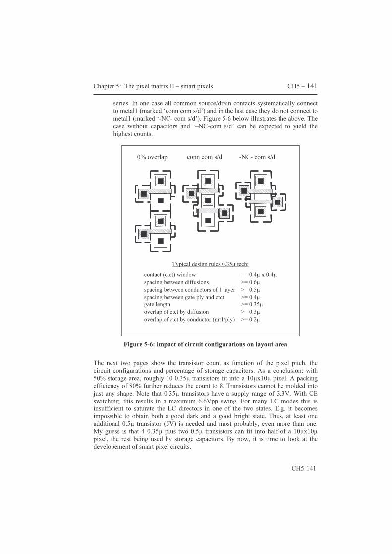
Chapter 5: The pixel matrix II – smart pixels CH5 – 141
CH5-141
series. In one case all common source/drain contacts systematically connect to metal1 (marked ‘conn com s/d’) and in the last case they do not connect to metal1 (marked ‘-NC- com s/d’). Figure 5-6 below illustrates the above. The case without capacitors and ‘–NC-com s/d’ can be expected to yield the highest counts.
Figure 5-6: impact of circuit configurations on layout area
The next two pages show the transistor count as function of the pixel pitch, the circuit configurations and percentage of storage capacitors. As a conclusion: with 50% storage area, roughly 10 0.35µ transistors fit into a 10µx10µ pixel. A packing efficiency of 80% further reduces the count to 8. Transistors cannot be molded into just any shape. Note that 0.35µ transistors have a supply range of 3.3V. With CE switching, this results in a maximum 6.6Vpp swing. For many LC modes this is insufficient to saturate the LC directors in one of the two states. E.g. it becomes impossible to obtain both a good dark and a good bright state. Thus, at least one additional 0.5µ transistor (5V) is needed and most probably, even more than one. My guess is that 4 0.35µ plus two 0.5µ transistors can fit into half of a 10µx10µ pixel, the rest being used by storage capacitors. By now, it is time to look at the developement of smart pixel circuits.
0% overlap conn com s/d -NC- com s/d
Typical design rules 0.35µ tech:
contact (ctct) window == 0.4µ x 0.4µ spacing between diffusions >= 0.6µ spacing between conductors of 1 layer >= 0.5µ spacing between gate ply and ctct >= 0.4µ gate length >= 0.35µ overlap of ctct by diffusion >= 0.3µ overlap of ctct by conductor (mt1/ply) >= 0.2µ
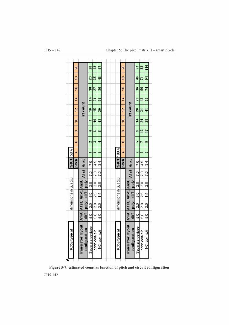
CH5 – 142 Chapter 5: The pixel matrix II – smart pixels
CH5-142 Figure 5-7: estimated count as function of pitch and circuit configuration

Chapter 5: The pixel matrix II – smart pixels CH5 – 143
CH5-143
Figure 5-8: transistor count as function of pixel pitch for 0.35µ tech
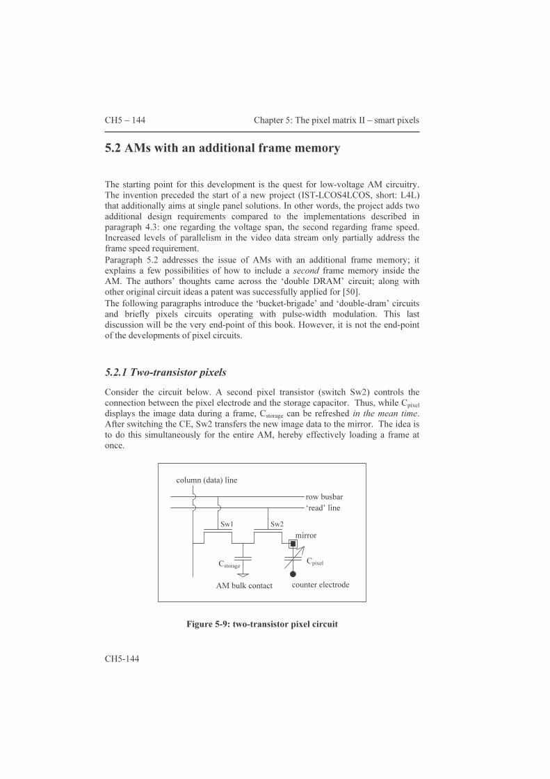
CH5 – 144 Chapter 5: The pixel matrix II – smart pixels
CH5-144
5.2 AMs with an additional frame memory The starting point for this development is the quest for low-voltage AM circuitry. The invention preceded the start of a new project (IST-LCOS4LCOS, short: L4L) that additionally aims at single panel solutions. In other words, the project adds two additional design requirements compared to the implementations described in paragraph 4.3: one regarding the voltage span, the second regarding frame speed. Increased levels of parallelism in the video data stream only partially address the frame speed requirement. Paragraph 5.2 addresses the issue of AMs with an additional frame memory; it explains a few possibilities of how to include a second frame memory inside the AM. The authors’ thoughts came across the ‘double DRAM’ circuit; along with other original circuit ideas a patent was successfully applied for [50]. The following paragraphs introduce the ‘bucket-brigade’ and ‘double-dram’ circuits and briefly pixels circuits operating with pulse-width modulation. This last discussion will be the very end-point of this book. However, it is not the end-point of the developments of pixel circuits. 5.2.1 Two-transistor pixels Consider the circuit below. A second pixel transistor (switch Sw2) controls the connection between the pixel electrode and the storage capacitor. Thus, while Cpixel displays the image data during a frame, Cstorage can be refreshed in the mean time. After switching the CE, Sw2 transfers the new image data to the mirror. The idea is to do this simultaneously for the entire AM, hereby effectively loading a frame at once.
Figure 5-9: two-transistor pixel circuit
row busbar ‘read’ line
column (data) line
Cpixel Cstorage
Sw1 Sw2
counter electrode AM bulk contact
mirror
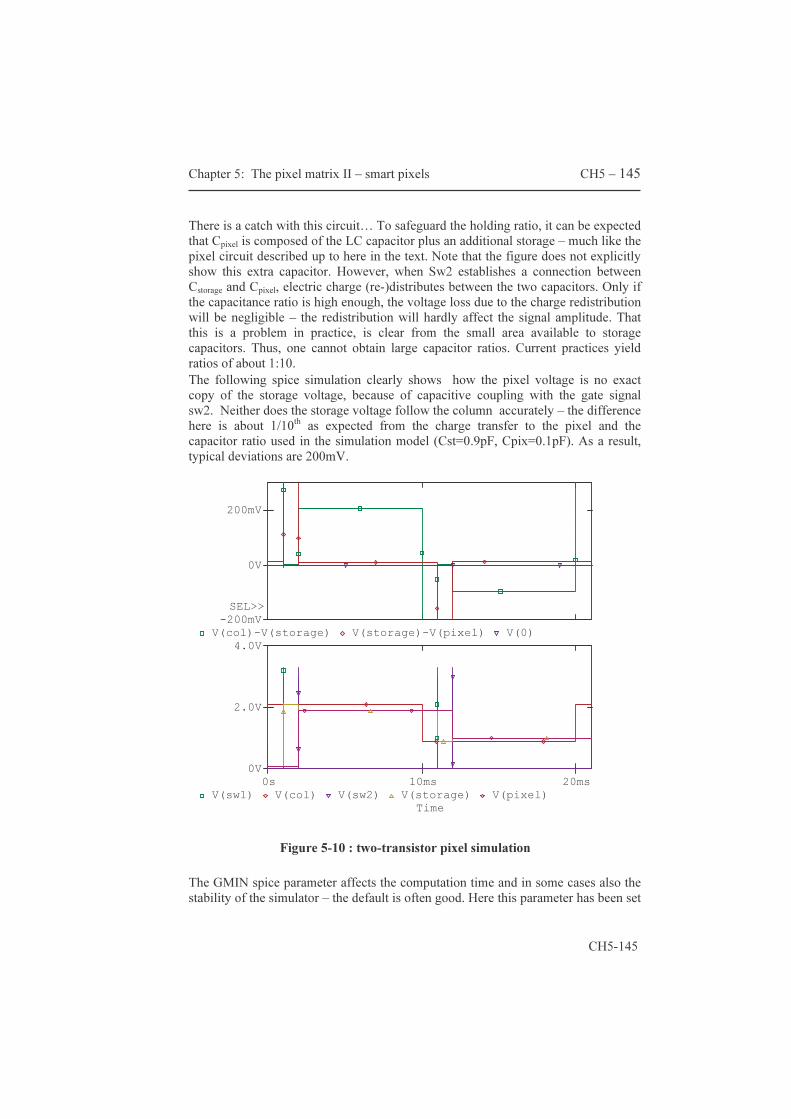
Chapter 5: The pixel matrix II – smart pixels CH5 – 145
CH5-145
There is a catch with this circuit… To safeguard the holding ratio, it can be expected that Cpixel is composed of the LC capacitor plus an additional storage – much like the pixel circuit described up to here in the text. Note that the figure does not explicitly show this extra capacitor. However, when Sw2 establishes a connection between Cstorage and Cpixel, electric charge (re-)distributes between the two capacitors. Only if the capacitance ratio is high enough, the voltage loss due to the charge redistribution will be negligible – the redistribution will hardly affect the signal amplitude. That this is a problem in practice, is clear from the small area available to storage capacitors. Thus, one cannot obtain large capacitor ratios. Current practices yield ratios of about 1:10. The following spice simulation clearly shows how the pixel voltage is no exact copy of the storage voltage, because of capacitive coupling with the gate signal sw2. Neither does the storage voltage follow the column accurately – the difference here is about 1/10th as expected from the charge transfer to the pixel and the capacitor ratio used in the simulation model (Cst=0.9pF, Cpix=0.1pF). As a result, typical deviations are 200mV.
The GMIN spice parameter affects the computation time and in some cases also the stability of the simulator – the default is often good. Here this parameter has been set
Time
0s 10ms 20msV(sw1) V(col) V(sw2) V(storage) V(pixel)
0V
2.0V
4.0VV(col)-V(storage) V(storage)-V(pixel) V(0)-200mV
0V
200mV
SEL>>
Figure 5-10 : two-transistor pixel simulation
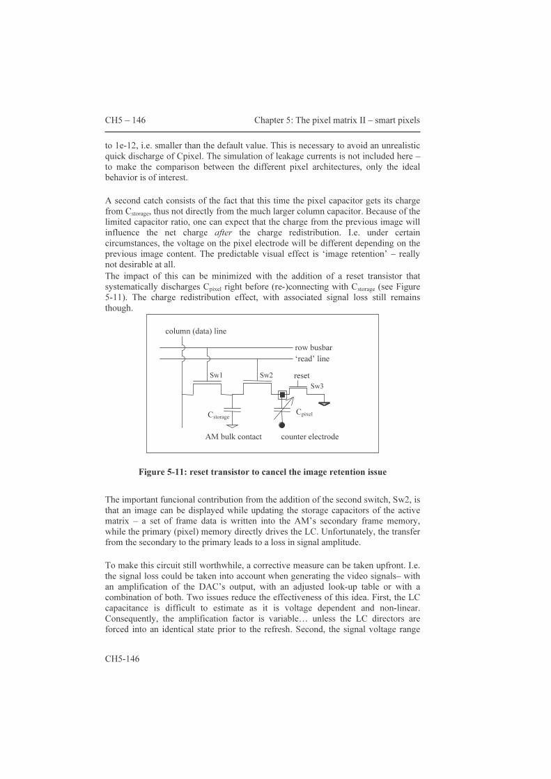
CH5 – 146 Chapter 5: The pixel matrix II – smart pixels
CH5-146
to 1e-12, i.e. smaller than the default value. This is necessary to avoid an unrealistic quick discharge of Cpixel. The simulation of leakage currents is not included here – to make the comparison between the different pixel architectures, only the ideal behavior is of interest. A second catch consists of the fact that this time the pixel capacitor gets its charge from Cstorage, thus not directly from the much larger column capacitor. Because of the limited capacitor ratio, one can expect that the charge from the previous image will influence the net charge after the charge redistribution. I.e. under certain circumstances, the voltage on the pixel electrode will be different depending on the previous image content. The predictable visual effect is ‘image retention’ – really not desirable at all. The impact of this can be minimized with the addition of a reset transistor that systematically discharges Cpixel right before (re-)connecting with Cstorage (see Figure 5-11). The charge redistribution effect, with associated signal loss still remains though.
Figure 5-11: reset transistor to cancel the image retention issue
The important funcional contribution from the addition of the second switch, Sw2, is that an image can be displayed while updating the storage capacitors of the active matrix – a set of frame data is written into the AM’s secondary frame memory, while the primary (pixel) memory directly drives the LC. Unfortunately, the transfer from the secondary to the primary leads to a loss in signal amplitude. To make this circuit still worthwhile, a corrective measure can be taken upfront. I.e. the signal loss could be taken into account when generating the video signals– with an amplification of the DAC’s output, with an adjusted look-up table or with a combination of both. Two issues reduce the effectiveness of this idea. First, the LC capacitance is difficult to estimate as it is voltage dependent and non-linear. Consequently, the amplification factor is variable… unless the LC directors are forced into an identical state prior to the refresh. Second, the signal voltage range
row busbar ‘read’ line
column (data) line
Cpixel Cstorage
Sw1 Sw2
counter electrode AM bulk contact
reset Sw3

Chapter 5: The pixel matrix II – smart pixels CH5 – 147
CH5-147
gets reduced. Indeed, with a 3.3V pixel transistor that can hardly handle the required 2.5V modulation voltage, it will be unable to handle 2.5V x lossCompensatingFactor. Thus larger pixel transistors, capable of passing 5V signals, are required. Because the charge redistribution is the centre of the problem, a smart circuit was devised by Prof. Dr. Ir. A. Van Calster [50]. In its most basic configuration, it counts 3 transistors and two capacitors and is therefore treated next. As can be expected, after this bucket-brigade circuit, a four-transistor circuit will be presented (double DRAM). Finally, even more transistors are used to implement PWM schemes – introduced at the end. 5.2.2 The “bucket brigade” architecture. Consider the circuit in figure 5-12 below. Here also, the row select line connects Cstorage to the column for updating. The two other transistors are operated in sequence to copy the charge on Cstorage to the sum C’bucket + Cpixel ≡ Cbucket (definition of Cbucket). The copying can be done simultaneously for a complete row, a set of rows or even for the entire AM. For a start, one can assume that the bucket and storage capacitors are dimensioned such that Cstorage = Cbucket. The ‘select’, ‘copy’ and ‘pre-charge’ lines are all inactive before the charge copy operation. To start, the pre-charge line is activated to pre-fill the bucket capacitor to the maximum. The growth of Sw3’s Vt limits this maximum. Then, the copy line is activated; i.e. the voltage on Sw2’s gate rises. The mirror potential rises as the charge on Cbucket cannot disappear; at the same time Sw2 establishes a connection between Cstorage and Cbucket, once Vgate(Sw2) reaches the threshold Vt(Sw2). Cbucket will discharge into Cstorage until Sw2’s Vt has grown so large that no more current can flow. Cstorage is filled to the maximum. At this point, the remaining charge in Cbucket equals the charge stored in Cstorage before the start of the transfer.
Figure 5-12: the bucket brigade circuit
column (data) line
Cpixel Cstorage
Sw1 Sw2
counter electrode AM bulk contact
Sw3 C’bucket
Vref
row (select) line copy line precharge line
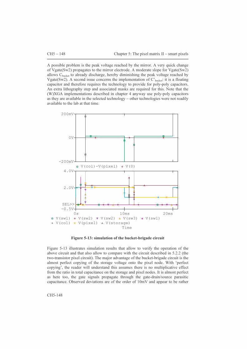
CH5 – 148 Chapter 5: The pixel matrix II – smart pixels
CH5-148
A possible problem is the peak voltage reached by the mirror. A very quick change of Vgate(Sw2) propagates to the mirror electrode. A moderate slope for Vgate(Sw2) allows Cbucket to already discharge, hereby diminishing the peak voltage reached by Vgate(Sw2). A second issue concerns the implementation of C’bucket: it is a floating capacitor and therefore requires the technology to provide for poly-poly capacitors. An extra lithography step and associated masks are required for this. Note that the (W)XGA implementations described in chapter 4 anyway use poly-poly capacitors as they are available in the selected technology – other technologies were not readily available to the lab at that time.
Figure 5-13: simulation of the bucket-brigade circuit Figure 5-13 illustrates simulation results that allow to verify the operation of the above circuit and that also allow to compare with the circuit described in 5.2.2 (the two-transistor pixel circuit). The major advantage of the bucket-brigade circuit is the almost perfect copying of the storage voltage onto the pixel node. With ‘perfect copying’, the reader will understand this assumes there is no multiplicative effect from the ratio in total capacitance on the storage and pixel nodes. It is almost perfect as here too, the gate signals propagate through the gate-drain/source parasitic capacitance. Observed deviations are of the order of 10mV and appear to be rather
Time
0s 10ms 20msV(sw1) V(sw2) V(sw2) V(sw3) V(sw1)V(col) V(pixel) V(storage)
2.0V
4.0V
-0.5VSEL>>
V(col)-V(pixel) V(0)-200mV
0V
200mV
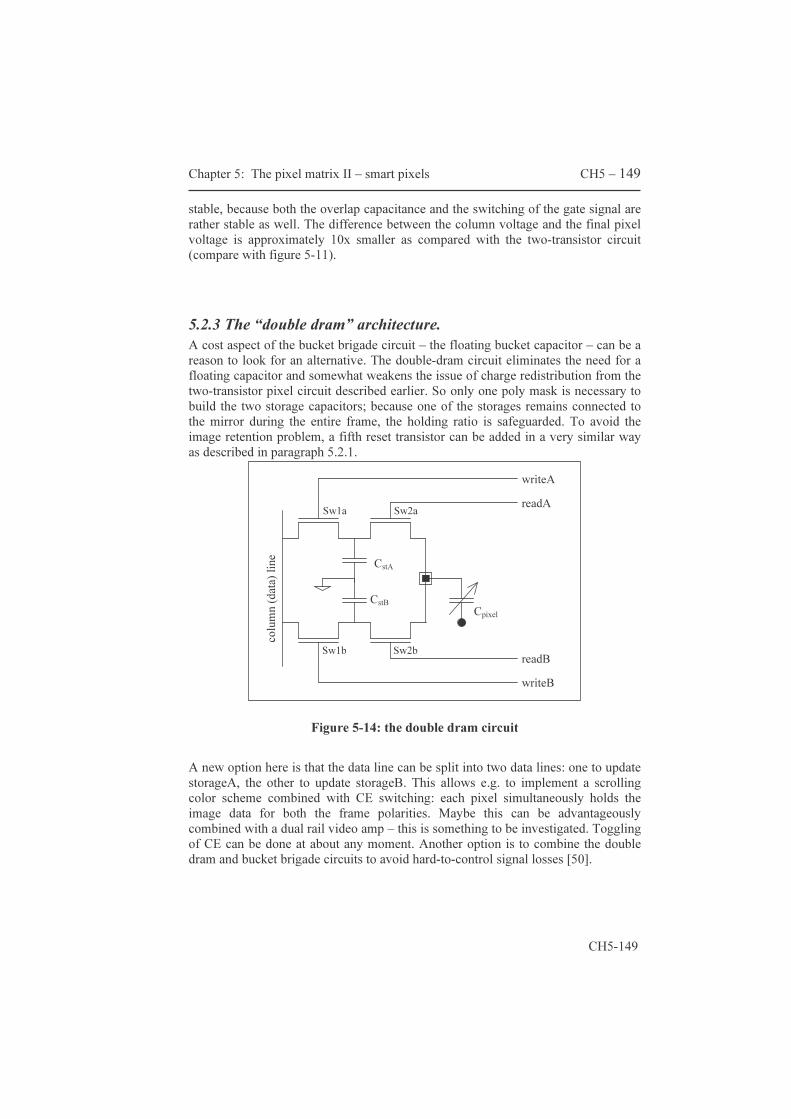
Chapter 5: The pixel matrix II – smart pixels CH5 – 149
CH5-149
stable, because both the overlap capacitance and the switching of the gate signal are rather stable as well. The difference between the column voltage and the final pixel voltage is approximately 10x smaller as compared with the two-transistor circuit (compare with figure 5-11). 5.2.3 The “double dram” architecture. A cost aspect of the bucket brigade circuit – the floating bucket capacitor – can be a reason to look for an alternative. The double-dram circuit eliminates the need for a floating capacitor and somewhat weakens the issue of charge redistribution from the two-transistor pixel circuit described earlier. So only one poly mask is necessary to build the two storage capacitors; because one of the storages remains connected to the mirror during the entire frame, the holding ratio is safeguarded. To avoid the image retention problem, a fifth reset transistor can be added in a very similar way as described in paragraph 5.2.1.
Figure 5-14: the double dram circuit
A new option here is that the data line can be split into two data lines: one to update storageA, the other to update storageB. This allows e.g. to implement a scrolling color scheme combined with CE switching: each pixel simultaneously holds the image data for both the frame polarities. Maybe this can be advantageously combined with a dual rail video amp – this is something to be investigated. Toggling of CE can be done at about any moment. Another option is to combine the double dram and bucket brigade circuits to avoid hard-to-control signal losses [50].
colum
n (da
ta) lin
e
Cpixel
Sw1a
CstA
writeA
Sw2a
Sw1b Sw2b
CstB
readA
writeB readB
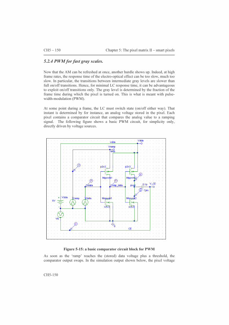
CH5 – 150 Chapter 5: The pixel matrix II – smart pixels
CH5-150
5.2.4 PWM for fast gray scales. Now that the AM can be refreshed at once, another hurdle shows up. Indeed, at high frame rates, the response time of the electro-optical effect can be too slow, much too slow. In particular, the transitions between intermediate gray levels are slower than full on/off transitions. Hence, for minimal LC response time, it can be advantageous to exploit on/off transitions only. The gray level is determined by the fraction of the frame time during which the pixel is turned on. This is what is meant with pulse-width-modulation (PWM). At some point during a frame, the LC must switch state (on/off either way). That instant is determined by for instance, an analog voltage stored in the pixel. Each pixel contains a comparator circuit that compares the analog value to a ramping signal. The following figure shows a basic PWM circuit, for simplicity only, directly driven by voltage sources.
Figure 5-15: a basic comparator circuit block for PWM
As soon as the ‘ramp’ reaches the (stored) data voltage plus a threshold, the comparator output swaps. In the simulation output shown below, the pixel voltage
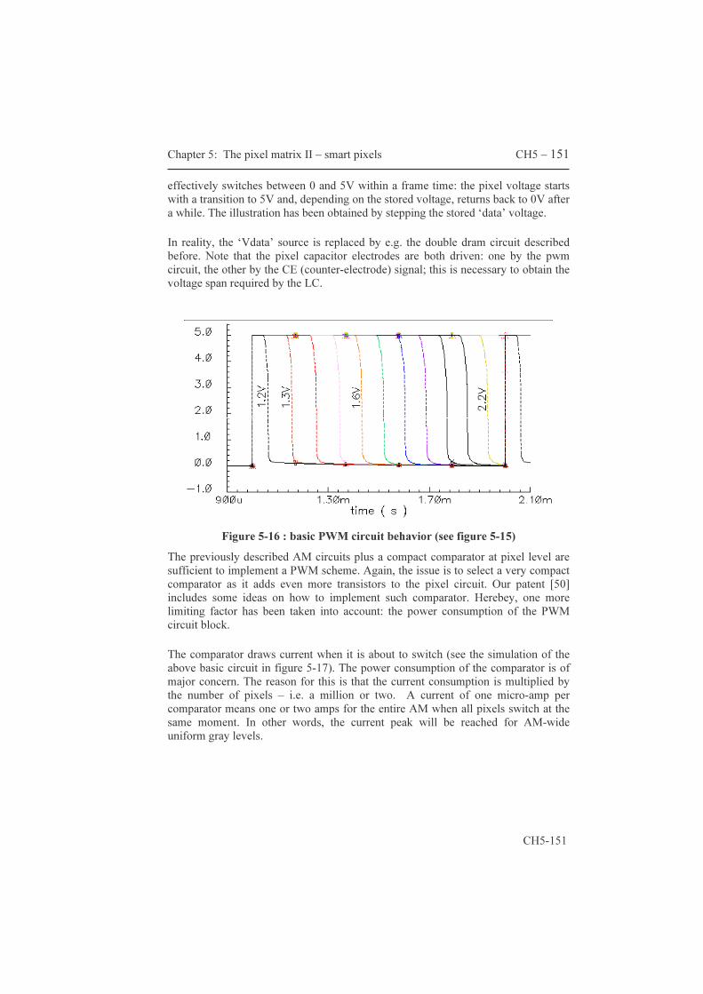
Chapter 5: The pixel matrix II – smart pixels CH5 – 151
CH5-151
effectively switches between 0 and 5V within a frame time: the pixel voltage starts with a transition to 5V and, depending on the stored voltage, returns back to 0V after a while. The illustration has been obtained by stepping the stored ‘data’ voltage. In reality, the ‘Vdata’ source is replaced by e.g. the double dram circuit described before. Note that the pixel capacitor electrodes are both driven: one by the pwm circuit, the other by the CE (counter-electrode) signal; this is necessary to obtain the voltage span required by the LC.
Figure 5-16 : basic PWM circuit behavior (see figure 5-15)
The previously described AM circuits plus a compact comparator at pixel level are sufficient to implement a PWM scheme. Again, the issue is to select a very compact comparator as it adds even more transistors to the pixel circuit. Our patent [50] includes some ideas on how to implement such comparator. Herebey, one more limiting factor has been taken into account: the power consumption of the PWM circuit block. The comparator draws current when it is about to switch (see the simulation of the above basic circuit in figure 5-17). The power consumption of the comparator is of major concern. The reason for this is that the current consumption is multiplied by the number of pixels – i.e. a million or two. A current of one micro-amp per comparator means one or two amps for the entire AM when all pixels switch at the same moment. In other words, the current peak will be reached for AM-wide uniform gray levels.
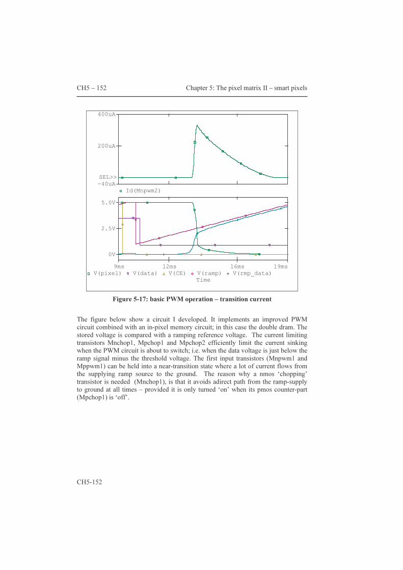
CH5 – 152 Chapter 5: The pixel matrix II – smart pixels
CH5-152
Figure 5-17: basic PWM operation – transition current The figure below show a circuit I developed. It implements an improved PWM circuit combined with an in-pixel memory circuit; in this case the double dram. The stored voltage is compared with a ramping reference voltage. The current limiting transistors Mnchop1, Mpchop1 and Mpchop2 efficiently limit the current sinking when the PWM circuit is about to switch; i.e. when the data voltage is just below the ramp signal minus the threshold voltage. The first input transistors (Mnpwm1 and Mppwm1) can be held into a near-transition state where a lot of current flows from the supplying ramp source to the ground. The reason why a nmos ‘chopping’ transistor is needed (Mnchop1), is that it avoids adirect path from the ramp-supply to ground at all times – provided it is only turned ‘on’ when its pmos counter-part (Mpchop1) is ‘off’.
Time12ms 16ms9ms 19ms
V(pixel) V(data) V(CE) V(ramp) V(rmp_data)
0V
2.5V
5.0VId(Mnpwm2)
200uA
400uA
-40uASEL>>
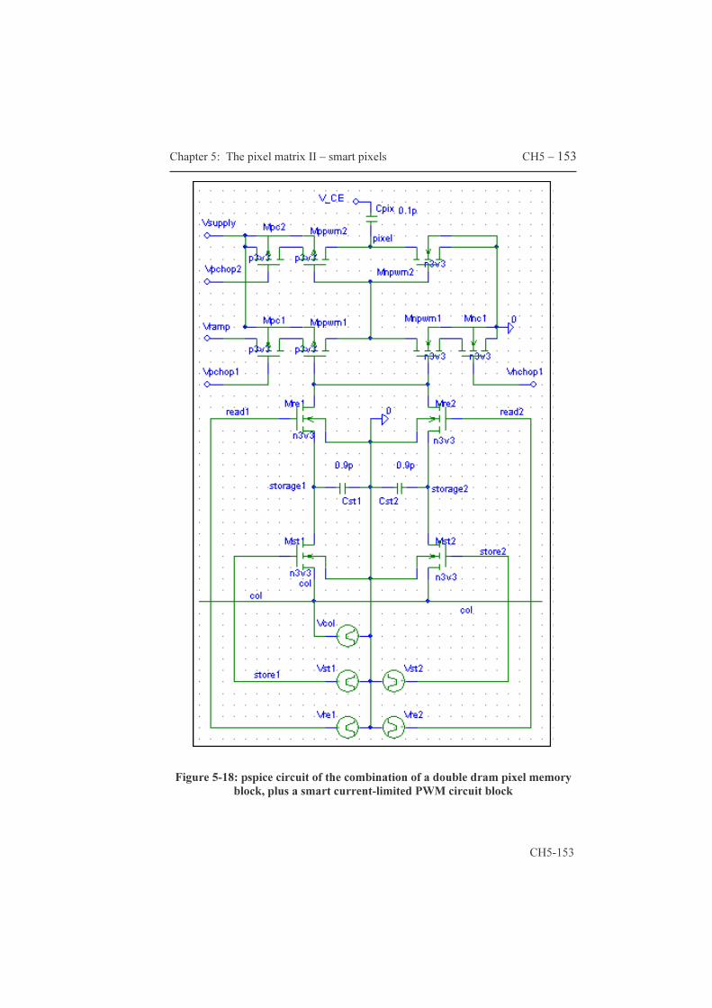
Chapter 5: The pixel matrix II – smart pixels CH5 – 153
CH5-153
Figure 5-18: pspice circuit of the combination of a double dram pixel memory
block, plus a smart current-limited PWM circuit block

CH5 – 154 Chapter 5: The pixel matrix II – smart pixels
CH5-154
Without the current ‘chopping’ transistors, the power consumption of the comparator reaches about 70 micro-amps in simulations. The current-limiting transistors (figure 5-18) Mpchop1, Mpchop2 and Mnchop1 reduce the power consumption to magnitude orders of 50nA.
Figure 5-19: effects of current limiting on the output curve The behaviour of such circuitry is somewhat particular, because the output will ‘stick’ to the previous state as long as two conditions are met: a) the current-limiting transistors are ‘off’ and b) the input voltage is not high enough compared to the ramping signal so that the inverters are out of the transition region. It is as if the power supply is being sampled: The last circuit presented in the text aims at shortening the decision window of the comparator circuit: assume the output is low. As soon as the output starts to rise, one can think about forcing the output to rise further. This is what happens with the circuit in Fig 5-20: the output bypasses the first inverting stage by pulling its output low. Consequently, the PWM output has to rise further. Compared to the previous idea with only current-limiting transistors, one fewer control signal is required. It is an interesting approach, because as the number of control signals rise, less and less area is avaible on the conductor layers. In other words, this idea is attractive. However, detailed analysis during the LCOS4LCOS project reveals that with this circuit not all transistors can have minimal sizes. The area gain resulting from the fewer control signals is mitigated by the required transistor dimensions. As a result this circuit ends up costing more area. During the LCOS4LCOS project this circuit has not been implemented. The testing of this circuit idea hopefully will be done in future.
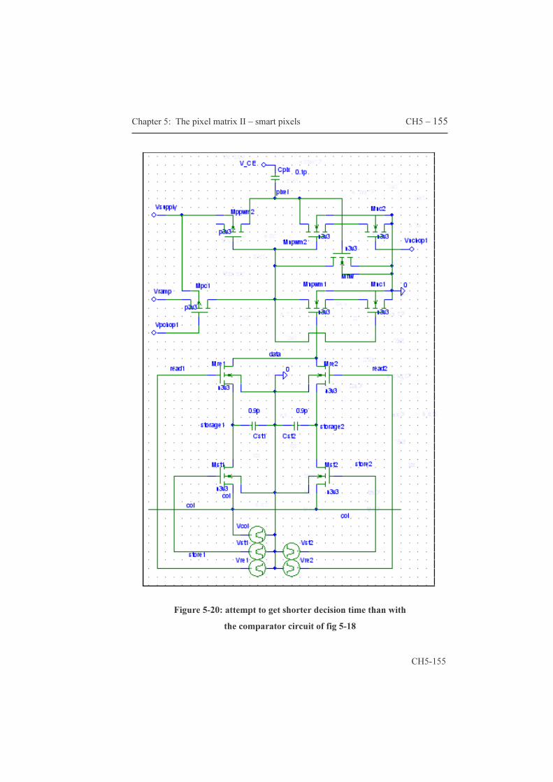
Chapter 5: The pixel matrix II – smart pixels CH5 – 155
CH5-155
Figure 5-20: attempt to get shorter decision time than with
the comparator circuit of fig 5-18

CH5 – 156 Chapter 5: The pixel matrix II – smart pixels
CH5-156
Nice simulations, so what about the implementations? The silicon-implementations have been done by our partners in the LCOS4LCOS project (in particular, Atmel and Thomson). Several publications are associated with the circuit ideas presented in this chapter; aspects concerning the optical architecture and the performance of some of the smart pixel circuits were/will be presented in:
• Eurodisplay ’02: LCOS4LCOS booth (Thomson) o “Rear-Projection Technologies for consumer applications” o “Polarization analysis on LCOS based projection systems”
• IDW '03 conference: Spice Model for a Dynamic Liquid Crystal Pixel Capacitance (IMEC)
• SID ’04 : “Three-dimensional modelling of a projection TV system by dynamic LC simulation and ray tracing ( UCLondon / Thomson)
• SID’06 : report of the results of the LCOS4LCOS project (to be published, co-authored by myself) []
As a final note in this chapter, I would like to re-state my personal contributions: I am the author of two circuit blocks: the double dram and the current-effective PWM scheme presented above. I made several simulations to show the potential advantage of the different circuits. Other ideas, developed by André Van Calster, Herbert De Smet and Geert Van Doorselaer are grouped in our patent. I had many fruitful discussions with Herbert, which I am profoundly grateful for. The ‘real’ implementations of the circuits presented in this chapter have been done during the LCOS4LCOS project. The results of this projects are currently being readied for presentation at SID’06.
���

Conclusion
The work presented in this thesis concerns the design of lcos microdisplay backplanes for projection applications. The aim of the present text is to clarify microdisplay backplane design. Chapter one introduces lcos microdisplays. Chapters two and three discuss design rules – it tells how to design. Chapters four and five describe what circuits to implement. Chapters two and four describe limitations encountered; chapters three and five respectively formulate answers to these limitations.
The rigorously structured design approach is necessary to be able to demonstrate the lcos concept. The design needs for the stitching approach have been carefully analyzed. This analysis results in an original stitching procedure, which is detailed in chapter three. This procedure gives designers full control over the design process and enables first-time-right designs. An advantageous by-product is that this procedure also helps to organize the reticule sets in a way that allows the production of microdisplays with different formats. For prototyping, this is a cost-effective approach. The filing date of TowerSemiconductor’s patent about stitching design rules, coincides with the end of the MOSAREL project and hereby demonstrates the originality of the combination of stitching with x-Si processing.
The successful implementations described in chapter four are limited by low frame speeds and a non-standard medium voltage requirement. Both limitations affect the cost of the backplane. Chapter five describes what circuit concept is needed for the active matrix to operate at higher frame rates and at standard voltage ranges. The ideas developed are protected by a world-wide patent. Some of the resulting circuits are under evaluation by the LCOS4LCOS consortium.
In this thesis little has been said about integration of (a part of) the system electronics onto the microdisplay backplane. Further integration is necessary to reduce the cost of lcos systems. Currently there is a lot of interest for the HDTV format. This format was not implemented by the author; however, all the elements needed for such a design have been described. Battery-powered applications require low power consumption – another area to be investigated eventually. I believe I am right to state that I ‘pioneered’ lcos backplane design – the successful designs served as a basis for the research work performed by several lab colleagues and contributed to many publications and to the creation of a spin-off company. My colleagues Geert Van Doorselaer and Dieter Cuypers had the lead for the system electronics, and for the system optics (cell assembly and projection setup) respectively. My responsibility covered the entire silicon design of several backplane ICs. In the technology plane, I developed an original design procedure for stitching. The

implementations during the MOSAREL project have shown how well this approach works. In the circuit plane I implemented the classic AM architecture for different display formats. The successes with these design ultimately led to the creation of the GEMIDIS startup company. I also developed three smart pixel circuit ideas for multi-million pixel arrays – these ideas form an important part of the patent we were granted. Some of the ideas have been implemented for single-panel HDTV backplanes and have also been tested during the LCOS4LCOS project. The results hereof will be presented at SID’06. Finally I would like to thank again all my lab colleagues and scientific peers for the interesting discussions and fun time during my research. I am also very grateful for the funding of the several projects: national, European and bilateral funding made this research possible – as well as the hard work of the project leaders who wrote several very successful project proposals.
���
Appendices CH6 - 159
CH6-159
Appendices This ‘sixth chapter’ is intended as a collection of useful information. The datasheet section truly deserves the label “appendix” as chapters 3 and 5 refer to parts of it. The last two sections are more introductory manuals for the use of crucial software blocks. There is no way to make the designs described in appendix AX1 without these tools. This is why the datasheet section and the ‘manuals’ were grouped together: for an lcos designer’s reference. The manual sections have a broader scope in that they apply to many full custom design jobs. Although this chapter is the last one, and on first hand the least interesting from a purely scientific point of view, this chapter contains a summary of many, many hours of tedious searching – searching for the way to make this software work, how to make this software do what I wanted. I hope the information herein can shelp help other designers concentrate more efficiently on the real design challenges.
6.1 Datasheets of three microdisplay chips The order in this section roughly sketches the microdisplay design projects’ order over time. The descriptions are kept at a minimum, to contain the essential information without too much overhead. The intended structure of the datasheets is as follows: a) Brief design project description (aim, result) b) Picture of mask design and chip floorplan c) Pin-out of main circuit and eventual application notes d) Schematic of main circuit (down to transistor level) and eventual simulation
results e) Pin-out of test circuits and eventual application notes f) Schematic of test circuits
6.1.1 Feasibility: a 32x18 matrix with integrated column scanner a) Design project description (goals, results) This design project aims primarily at evaluating the feasibility of (a) micro-display design(s) (1994-1995). Assembly of a micro-display panel is not yet one of the goals. The chip measures 3680µm by 2900µm and features a simple shift register, a small active matrix (18x32 pixels) with two different pixel layouts, a limited number of externally addressable row and column bus-bars, sub-block test circuits including
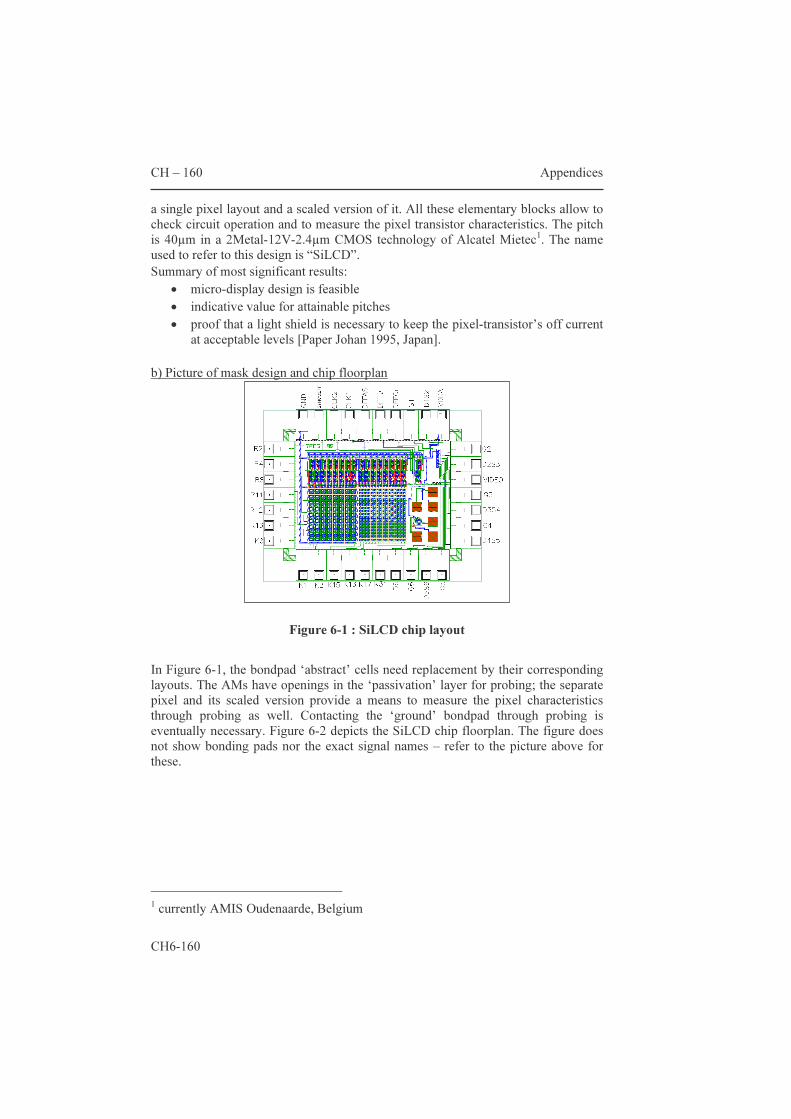
CH – 160 Appendices
CH6-160
a single pixel layout and a scaled version of it. All these elementary blocks allow to check circuit operation and to measure the pixel transistor characteristics. The pitch is 40µm in a 2Metal-12V-2.4µm CMOS technology of Alcatel Mietec1. The name used to refer to this design is “SiLCD”. Summary of most significant results:
• micro-display design is feasible • indicative value for attainable pitches • proof that a light shield is necessary to keep the pixel-transistor’s off current
at acceptable levels [Paper Johan 1995, Japan]. b) Picture of mask design and chip floorplan
Figure 6-1 : SiLCD chip layout
In Figure 6-1, the bondpad ‘abstract’ cells need replacement by their corresponding layouts. The AMs have openings in the ‘passivation’ layer for probing; the separate pixel and its scaled version provide a means to measure the pixel characteristics through probing as well. Contacting the ‘ground’ bondpad through probing is eventually necessary. Figure 6-2 depicts the SiLCD chip floorplan. The figure does not show bonding pads nor the exact signal names – refer to the picture above for these.
1 currently AMIS Oudenaarde, Belgium
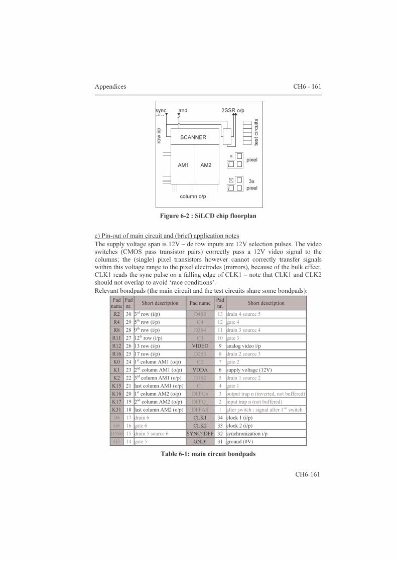
Appendices CH6 - 161
CH6-161
Figure 6-2 : SiLCD chip floorplan
c) Pin-out of main circuit and (brief) application notes The supply voltage span is 12V – de row inputs are 12V selection pulses. The video switches (CMOS pass transistor pairs) correctly pass a 12V video signal to the columns; the (single) pixel transistors however cannot correctly transfer signals within this voltage range to the pixel electrodes (mirrors), because of the bulk effect. CLK1 reads the sync pulse on a falling edge of CLK1 – note that CLK1 and CLK2 should not overlap to avoid ‘race conditions’. Relevant bondpads (the main circuit and the test circuits share some bondpads):
Pad name
Pad nr. Short description Pad name Pad nr. Short description
R2 30 3rd row (i/p) D4S5 13 drain 4 source 5 R4 29 5th row (i/p) G4 12 gate 4 R8 28 9th row (i/p) D3S4 11 drain 3 source 4 R11 27 12th row (i/p) G3 10 gate 3 R12 26 13 row (i/p) VIDEO 9 analog video i/p R16 25 17 row (i/p) D2S3 8 drain 2 source 3 K0 24 1st column AM1 (o/p) G2 7 gate 2 K1 23 2nd column AM1 (o/p) VDDA 6 supply voltage (12V) K2 22 3rd column AM1 (o/p) D1S2 5 drain 1 source 2 K15 21 last column AM1 (o/p) G1 4 gate 1 K16 20 1st column AM2 (o/p) DFFQn 3 output trap n (inverted, not buffered) K17 19 2nd column AM2 (o/p) DFFQ_ 2 input trap n (not buffered) K31 18 last column AM2 (o/p) DFFAS 1 after switch : signal after 1ste switch D6 17 drain 6 CLK1 34 clock 1 (i/p) G6 16 gate 6 CLK2 33 clock 2 (i/p) D5S6 15 drain 5 source 6 SYNC\tDFF 32 synchronization i/p G5 14 gate 5 GND! 31 ground (0V)
Table 6-1: main circuit bondpads
3x pixel
2SSR o/p
pixelAM2AM1
sync and clks
SCANNER
row
i/p
column o/p
test
circ
uits
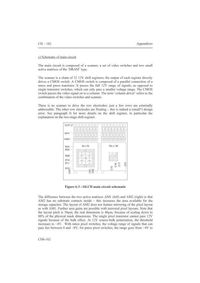
CH – 162 Appendices
CH6-162
c) Schematic of main circuit The main circuit is composed of a scanner, a set of video switches and two small active matrices of the ‘DRAM’ type. The scanner is a chain of 32 12V shift registers; the output of each register directly drives a CMOS switch. A CMOS switch is composed of a parallel connection of a nmos and pmos transistor. It passes the full 12V range of signals; as opposed to single transistor switches, which can only pass a smaller voltage range. The CMOS switch passes the video signal on to a column. The term ‘column driver’ refers to the combination of the video switches and scanner. There is no scanner to drive the row electrodes; just a few rows are externally addressable. The other row electrodes are floating – this is indeed a (small?) design error. See paragraph f) for more details on the shift register, in particular the explanation on the two-stage shift register.
Figure 6-3 : SiLCD main circuit schematic
The difference between the two active matrices AM1 (left) and AM2 (right) is that AM2 has no substrate contacts inside – this increases the area available for the storage capacitor. The layout of AM2 does not feature mirroring of the pixel layout as with AM1. Further area gains are possible with mirrored pixel layouts. Note that the layout pitch is 50µm; the real dimension is 40µm, because of scaling down to 80% of the physical mask dimensions. The single pixel transistor cannot pass 12V signals because of the bulk effect. At 12V source-bulk polarization, the threshold increases to ~4V. With nmos pixel switches, the voltage range of signals that can pass lies between 0 and ~8V; for pmos pixel switches, the range goes from ~4V to
16c x 18r8c x 9r
R10R11R16
R08
R04R02
sync
CLK1,2
video
C00
C01C02 C15 C16C17
C31

Appendices CH6 - 163
CH6-163
12V. Both AM1 and AM2 use nmos pixel switches. Column drivers designed to drive both types of AM need CMOS video switches; usually only one type is used, causing CMOS video switches to be unnecessary. d) Pin-out of test circuits (bonding pads and separate probe pads) Bondpads for testing: [grayed-out fields are for the main circuitry only]
Pad name
Pad nr. Short description Pad name Pad nr. Short description
R2 30 3rd row (i/p) D4S5 13 drain 4 source 5 R4 29 5th row (i/p) G4 12 gate 4 R8 28 9th row (i/p) D3S4 11 drain 3 source 4 R11 27 12th row (i/p) G3 10 gate 3 R12 26 13 row (i/p) VIDEO 9 analog video i/p R16 25 17 row (i/p) D2S3 8 drain 2 source 3 K0 24 1st column AM1 (o/p) G2 7 gate 2 K1 23 2nd column AM1 (o/p) VDDA 6 supply voltage (12V) K2 22 3rd column AM1 (o/p) D1S2 5 drain 1 source 2 K15 21 last column AM1 (o/p) G1 4 gate 1 K16 20 1st column AM2 (o/p) DFFQn 3 output trap n (inverted, not buffered) K17 19 2nd column AM2 (o/p) DFFQ_ 2 input trap n (not buffered) K31 18 last column AM2 (o/p) DFFAS 1 after switch : signal after 1ste switch D6 17 drain 6 CLK1 34 clock 1 (i/p) G6 16 gate 6 CLK2 33 clock 2 (i/p) D5S6 15 drain 5 source 6 SYNC\tDFF 32 synchronization i/p G5 14 gate 5 GND! 31 ground (0V)
Table 6-2 : test circuit (bond-) pads Probe pads: [warning: always contact bondpad 31!] The six test pads outside the AM are 108µ x 108µm (135µm in the layout x 0.8 scaling). Arranged in two groups of three, the function is (clockwise) source, drain, and gate. Substrate connects via pad 31! The other test pads are inside the active matrices. The intention is to allow monitoring of pixel electrode voltages. The storage capacitor is this small compared to the input capacitance of a measurement probe, that precise quantitative measurements are not possible. e) Schematics of test circuits (2-stage shift register, 2 pixel layouts, test transistors) Two-stage shift register: The purpose of this circuit (part) is to locate eventual design problems; the number of measurement points is limited because the chip area significantly increases with the number of bondpads. For this layout, the largest number of bondpads fills the periphery, without ‘exploding’ the chip area.

CH – 164 Appendices
CH6-164
Figure 6-4 : 2-stage shift register schematic
Each shift register must drive a CMOS switch; this requires two complementary control signals. This is why the output is composed of the outputs of two inverters connected in series. Both inverters simultaneously serve the purpose of inversion and of buffering. To meet the 50µm layout pitch condition, it is necessary to ‘stack’ two subsequent registers. If the stacking includes all of the invertors/buffers, then two metal tracks need to be drawn from the top shift register towards the corresponding switch. Placing half of the inverter/buffer below both registers frees the area of one track. This eases the layout job; note that the drawing left does not show the supply (power) lines or clock lines – these need area to of course.. The controlling bondpads are: GND!, VDDA, SYNC\tDFF, CLK1, CLK2 ; the measurable nodes are : DFFAS (dot), DFFQ_ (square) and DFFQn (triangle). Two pixel layouts: The first is a copy of the pixel layout in the matrix; the second is a scaled (x3) version of it. However, the scaling cannot be perfect because the thickness of the layers does not scale. The layer thickness defines the size of stray capacitances – and for this very first design, no data were available to estimate the size of the parasitic (layout) components. The test pads always have the same size (108µm side) and are on a 200µm grid. Test transistors: The aim is to determine the optimal pixel transistor dimensions. The test proved that the smallest transistor is the best choice. With smaller pixel transistors, one has more room for the storage capacitor, smaller s/d junction capacitance and a smaller diode area sensitive to photoconduction. The mobile charge mobility in Si is more than large enough for a speedy charging of the storage capacitor. Here too, that single GND! pad must define the substrate bias voltage.
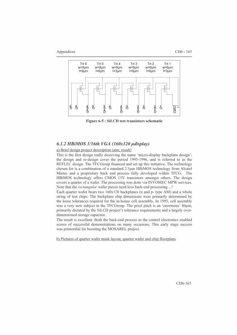
Appendices CH6 - 165
CH6-165
Figure 6-5 : SiLCD test transistors schematic
6.1.2 HBiMOS 1/16th VGA (160x120 µdisplay) a) Brief design project description (aim, result) This is the first design really deserving the name ‘micro-display backplane design’; the design and re-design cover the period 1995-1996, and is referred to as the REFLEC design. The TFCGroup financed and set up this initiative. The technology chosen for is a combination of a standard 2.5µm HBiMOS technology from Alcatel Mietec and a proprietary back end process fully developed within TFCG. The HBiMOS technology offers CMOS 15V transistors amongst others. The design covers a quarter of a wafer. The processing was done via INVOMEC MPW services. Note that the rectangular wafer pieces need lcos back-end processing…! Each quarter wafer bears two 160x120 backplanes (n and p- type AM) and a whole string of test chips. The backplane chip dimensions were primarily determined by the loose tolerances required for the in-house cell assembly. In 1995, cell assembly was a very new subject in the TFCGroup. The pixel pitch is an ‘enormous’ 80µm, primarily dictated by the SiLCD project’s tolerance requirements and a largely over-dimensioned storage capacitor. The result is excellent. Both the back-end process as the control electronics enabled scores of successful demonstrations on many occasions. This early stage success was primordial for boosting the MOSAREL project. b) Pictures of quarter wafer mask layout, quarter wafer and chip floorplans
Trt 6 w=9µm l=9µm
Trt 5 w=9µm l=6µm
Trt 4 w=9µm l=3µm
Trt 3 w=6µm l=9µm
Trt 2 w=6µm l=6µm
Trt 1 w=6µm l=3µm
G N D ! G 1 G 2 D 2 S 3 G 3
D 3 S 4 G 4 D 4 S 5 G 5
D 5 S 6 G 6 D 6 D 1 S 2
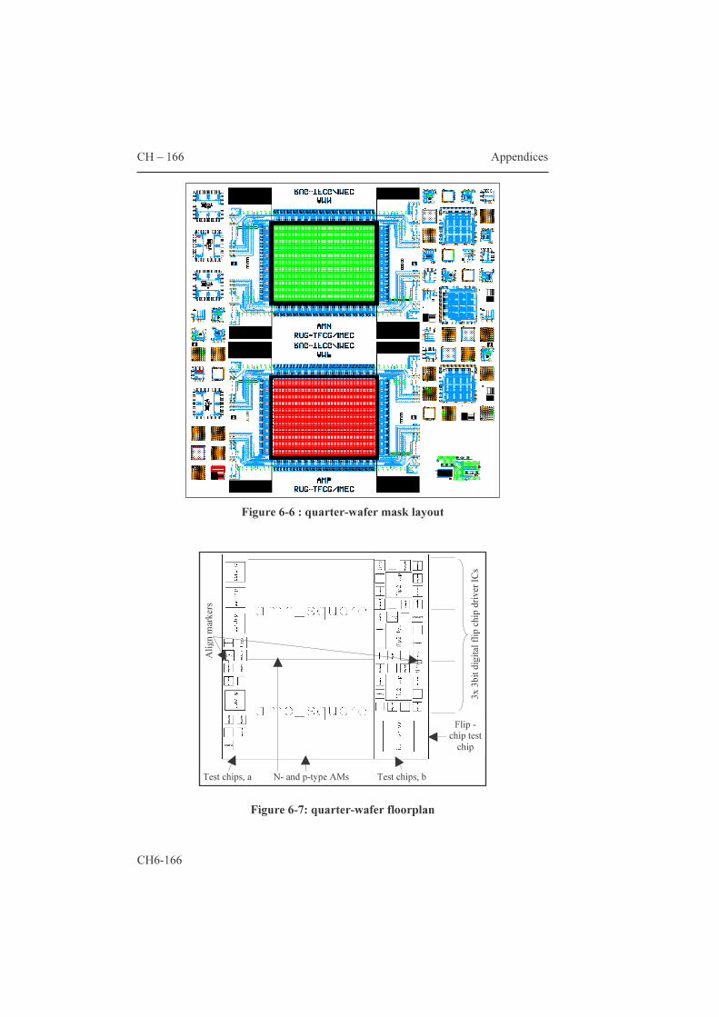
CH – 166 Appendices
CH6-166
Figure 6-6 : quarter-wafer mask layout
Figure 6-7: quarter-wafer floorplan
N- and p-type AMs Test chips, b Test chips, a
3x 3b
it digi
tal fli
p chip
drive
r ICs
Flip -chip test chip
Align
mark
ers
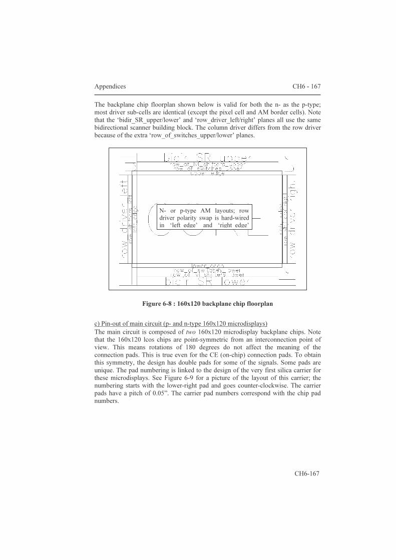
Appendices CH6 - 167
CH6-167
The backplane chip floorplan shown below is valid for both the n- as the p-type; most driver sub-cells are identical (except the pixel cell and AM border cells). Note that the ‘bidir_SR_upper/lower’ and ‘row_driver_left/right’ planes all use the same bidirectional scanner building block. The column driver differs from the row driver because of the extra ‘row_of_switches_upper/lower’ planes.
Figure 6-8 : 160x120 backplane chip floorplan
c) Pin-out of main circuit (p- and n-type 160x120 microdisplays) The main circuit is composed of two 160x120 microdisplay backplane chips. Note that the 160x120 lcos chips are point-symmetric from an interconnection point of view. This means rotations of 180 degrees do not affect the meaning of the connection pads. This is true even for the CE (on-chip) connection pads. To obtain this symmetry, the design has double pads for some of the signals. Some pads are unique. The pad numbering is linked to the design of the very first silica carrier for these microdisplays. See Figure 6-9 for a picture of the layout of this carrier; the numbering starts with the lower-right pad and goes counter-clockwise. The carrier pads have a pitch of 0.05”. The carrier pad numbers correspond with the chip pad numbers.
N- or p-type AM layouts; row driver polarity swap is hard-wired in ‘left_edge’ and ‘right_edge’

CH – 168 Appendices
CH6-168
Figure 6-9 : first version of the backplane carrier layout (5cm x 5cm)
The pad names are not all unique to reflect the fact that pad function is independent from eventual 180-degree rotations. The pin-out list starts with the top left pad and ends with the bottom right pad.
Pad nr.
Con-nects Pad name Brief description
[upper left column driver + upper left row driver connections] 41 _SIR left-hand upper col scanner in (shift right) 42 _SOL left-hand upper col scanner out (shift left) 43 ↔ 40 VddCol upper column driver 5V left supply 44 ↔ 39 VssCol upper column driver 0V left supply 45 ↔ 33 SHr_l upper scanner shifts to the right when Hi 46 ↔ 32 Video upper left Video input 47 ↔ 31 vddaCol upper column driver 15V supply 48 GATE_H forces left row driver output to 0 when LO 49 _ROW__in left row scanner input (downward scan direction) 50 CLK1 left row scanner clock signal1 (read) 51 CLK2 left row scanner clock signal2 (lock) 52 ↔ 69 SH_U_D left row scanner scans downwards when Hi
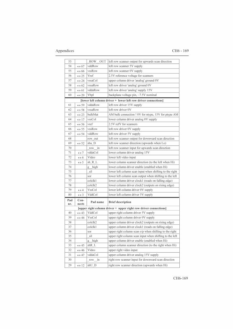
Appendices CH6 - 169
CH6-169
53 _ROW__OUT left row scanner output for upwards scan direction 54 ↔ 67 vddRow left row scanner 5V supply 55 ↔ 66 vssRow left row scanner 0V supply 56 ↔ 25 Vref 2.5V reference voltage for scanners 57 ↔ 24 vssaCol upper column driver 'analog' ground 0V 58 ↔ 62 vssaRow left row driver 'analog' ground 0V 59 ↔ 61 vddaRow left row driver 'analog' supply 15V 60 ↔ 20 Vbpl backplane voltage pin, ~7.5V nominal
[lower left column driver + lower left row driver connections] 61 ↔ 59 vddaRow left row driver 15V supply 62 ↔ 58 vssaRow left row driver 0V 63 ↔ 23 bulkMat AM bulk connection ! 0V for ntype, 15V for ptype AM 64 ↔ 17 vssCol lower column driver analog 0V supply 65 ↔ 56 vref 2.5V refV for scanners 66 ↔ 55 vssRow left row driver 0V supply 67 ↔ 54 vddRow left row driver 5V supply 68 row_out left row scanner output for downward scan direction 69 ↔ 52 shu_D left row scanner direction (upwards when Lo) 70 _row__in left row scanner input for upwards scan direction 71 ↔ 7 vddaCol lower column driver analog 15V 72 ↔ 6 Video lower left video input 73 ↔ 5 sh_R_L lower column scanner direction (to the left when Hi) 74 g__high lower column driver enable (enabled when Hi) 75 _sil lower left column scan input when shifting to the right 76 sor lower left column scan output when shifting to the left 77 colclk1 lower column driver clock1 (reads on falling edge) 78 colclk2 lower column driver clock2 (outputs on rising edge) 79 ↔ 4 VssCol lower left column driver 0V supply 80 ↔ 3 VddCol lower left column driver 5V supply
Pad nr.
Con-nects Pad name Brief description [upper right column driver + upper right row driver connections]
40 ↔ 43 VddCol upper right column driver 5V supply 39 ↔ 44 VssCol upper right column driver 0V supply 38 colclk2 upper column driver clock2 (outputs on rising edge) 37 colclk1 upper column driver clock1 (reads on falling edge) 36 sor upper right column scan o/p when shifting to the right 35 _sil upper right column scan input when shifting to the left 34 g__high upper column driver enable (enabled when Hi) 33 ↔ 45 shR_L upper column scanner direction (to the right when Hi) 32 ↔ 46 Video upper right video input 31 ↔ 47 vddaCol upper column driver analog 15V supply 30 _row__in right row scanner input for downward scan direction 29 ↔ 12 shU_D right row scanner direction (upwards when Hi)
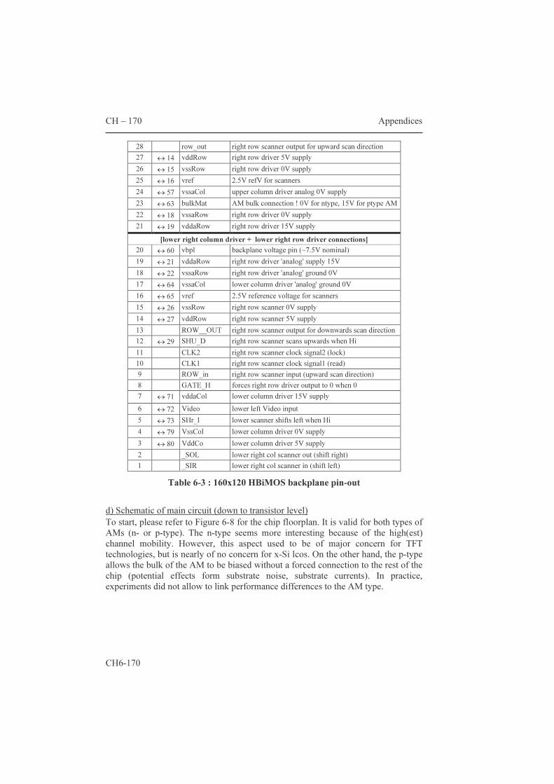
CH – 170 Appendices
CH6-170
28 row_out right row scanner output for upward scan direction 27 ↔ 14 vddRow right row driver 5V supply 26 ↔ 15 vssRow right row driver 0V supply 25 ↔ 16 vref 2.5V refV for scanners 24 ↔ 57 vssaCol upper column driver analog 0V supply 23 ↔ 63 bulkMat AM bulk connection ! 0V for ntype, 15V for ptype AM 22 ↔ 18 vssaRow right row driver 0V supply 21 ↔ 19 vddaRow right row driver 15V supply
[lower right column driver + lower right row driver connections] 20 ↔ 60 vbpl backplane voltage pin (~7.5V nominal) 19 ↔ 21 vddaRow right row driver 'analog' supply 15V 18 ↔ 22 vssaRow right row driver 'analog' ground 0V 17 ↔ 64 vssaCol lower column driver 'analog' ground 0V 16 ↔ 65 vref 2.5V reference voltage for scanners 15 ↔ 26 vssRow right row scanner 0V supply 14 ↔ 27 vddRow right row scanner 5V supply 13 ROW__OUT right row scanner output for downwards scan direction 12 ↔ 29 SHU_D right row scanner scans upwards when Hi 11 CLK2 right row scanner clock signal2 (lock) 10 CLK1 right row scanner clock signal1 (read) 9 ROW_in right row scanner input (upward scan direction) 8 GATE_H forces right row driver output to 0 when 0 7 ↔ 71 vddaCol lower column driver 15V supply 6 ↔ 72 Video lower left Video input 5 ↔ 73 SHr_l lower scanner shifts left when Hi 4 ↔ 79 VssCol lower column driver 0V supply 3 ↔ 80 VddCo lower column driver 5V supply 2 _SOL lower right col scanner out (shift right) 1 _SIR lower right col scanner in (shift left)
Table 6-3 : 160x120 HBiMOS backplane pin-out d) Schematic of main circuit (down to transistor level) To start, please refer to Figure 6-8 for the chip floorplan. It is valid for both types of AMs (n- or p-type). The n-type seems more interesting because of the high(est) channel mobility. However, this aspect used to be of major concern for TFT technologies, but is nearly of no concern for x-Si lcos. On the other hand, the p-type allows the bulk of the AM to be biased without a forced connection to the rest of the chip (potential effects form substrate noise, substrate currents). In practice, experiments did not allow to link performance differences to the AM type.

Appendices CH6 - 171
CH6-171
Figure 6-10 : two 'REFLEC' pixel architectures
The difference between the n- and p-type lcos chips is the transistor type used in the AM pixel circuit. The control signals for both chips are pretty much the same; the difference lies in the voltage range of the video signal and in the polarity of the row signal. The range of the video signal has an upper voltage limitation (below the highest supply voltage) with the nmos version and similarly, has a lower voltage limitation (above the lowest supply voltage) with the pmos version. The peripheral electronics must consider this range difference. Both row signal polarities are hard-wired in the layout of the row driver planes. The on-chip connections between the AM rows and the row-driver are different for the AMP and AMN backplanes – as such, this is polarity issue is transparent for the peripheral electronics. Referring to Figure 6-8, the planes called ‘upper_edge’, ‘lower_edge’, ‘left_edge’ and ‘right_edge’ are different for the AMP and AMN designs, in addition to the AM itself. Altogether, only the AM (core) cells, the AM border cells and the chip identification cells differ. The rest of the circuitry is identical to both the n- and the p-type versions. There are double row and column drivers. The outputs of each column driver can be set to HiZ state (disconnected); the same however, is not true for the outputs of the row driver. Each row driver can independently select the HiZ state for the entire AM; however, without precautions, one row driver’s output can conflict with the other row driver’s output. One drawback the circuit suffers from is the over-dimensioned and serial buffering of all the signals. The excess buffering costs layouting time and area (corner cells ‘ul’, ‘ur’, ‘bl’ and ‘br’ for (upper-left, upper-right, etc.), while the serial nature makes the timing of the signals dependent on the scan direction. The peripheral electronics provide a work-around for this; however, for much larger display formats this work-around may be difficult to find. A clock buffer tree is essential for new(er) designs. The corner cells each provide for 20 bonding pads and signal buffering/wiring. Note that the ‘ul’ and ‘br’ are identical; the same is true for ‘ur’ and ‘bl’. The row and column drivers use the same 10-stage wide library cells to implement the stack of bidirectional shift register, level shifter and video switch (column driver only). Completion of the design of these cells, implies completion of the design of the row and column drivers.
chip bulk
nmos
Row_n
separate AM bulk
pmosRow_n
↔
used within the AMN chip used within the AMP chip

CH – 172 Appendices
CH6-172
Figure 6-11 : 160x120 row and column driver building block
The scanner building cell does not buffer the scan direction signal ‘shDir’. This is ok, as one does not expect the scan direction switching speed to be relevant. To avoid the ‘spilling’ of data from one row to the next, the scan enable signal ‘scEna’ is buffered on the contrary (switches two times per line period). The same buffering mechanism is foreseen for the clock signals ‘c1b’ and ‘c2b’. The scanner inputs are ‘sil’ and ‘sir’ corresponding with a shift direction to the right (scan input left hand side) and to the left respectively (scan input right hand side). The naming of the scanner outputs follows a similar format (sol and sor). The output of the bidirectional scanner is gated by an ‘AND’ gate, before feeding into the bank of level shifters. The output of the level shifters drive the rows of the AM directly (row driver) or drive the bank of video switches (column driver). The video switches simply are 15V CMOS switches. The circuits for the bidirectional shift register element and level shifter are shown below. The ‘shDir’ signal from fignXXX splits into two opposite signals ‘sh_left’ and ‘sh_rite’ for shift left and shift right respectively. The inverters marked with a ‘2’ denote inverters that contain an additional transistor to force the output to ‘VREF’ (see e.g. pad 16 in Table 6-3), this is done each time the back-to-back inverters could change state.
LS
LS
3
2
1
0
9
LS
LS
LS
scanner enable level shifter video switch
video
to rows or to vid. switches
to cols
sil sol c1b c2b
sir sorshDir scEnaScan buffers
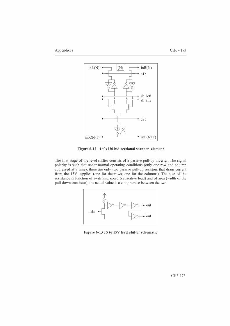
Appendices CH6 - 173
CH6-173
Figure 6-12 : 160x120 bidirectional scanner element
The first stage of the level shifter consists of a passive pull-up inverter. The signal polarity is such that under normal operating conditions (only one row and column addressed at a time), there are only two passive pull-up resistors that drain current from the 15V supplies (one for the rows, one for the columns). The size of the resistance is function of switching speed (capacitive load) and of area (width of the pull-down transistor); the actual value is a compromise between the two.
Figure 6-13 : 5 to 15V level shifter schematic
(N) inR(N)c1b
sh_leftsh_rite
c2b
inL(N+1)
inL(N)
inR(N-1)
2 2
2
out
outlsIn
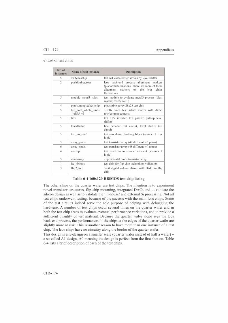
CH – 174 Appendices
CH6-174
e) List of test chips
Nr. of instances Name of test instance Description
5 switcheschip test w/l video switch driven by level shifter 2 positioningcross lcos back-end process alignment markers
(planar/metallization) ; there are more of these alignment markers on the lcos chips themselves
5 module_metal3_rules test module to evaluate metal3 process (vias, widths, resistance...)
4 pmosdrampixeltestchip pmos pixel array 28x28 test chip 5 test_conf_whole_nmos
_juli95_v3 16x16 nmos test active matrix with direct row/column contacts
5 tinv test 15V inverter, test passive pull-up level shifter
5 ldandlschip line decoder test circuit, level shifter test circuit
5 test_an_shr2 test row driver building block (scanner + row logic)
5 array_pmos test transistor array (48 different w/l pmos) 6 array_nmos test transistor array (48 different w/l nmos) 4 ssrchip test row/column scanner element (scanner +
logic) 5 dmosarray experimental dmos transistor array 1 itc_hbimos test chip for flip-chip technology validation 3 flip2_top 3-bit digital column driver with DAC for flip
chip
Table 6-4 160x120 HBiMOS test chip listing The other chips on the quarter wafer are test chips. The intention is to experiment novel transistor structures, flip-chip mounting, integrated DACs and to validate the silicon design as well as to validate the ‘in-house’ and external Si processing. Not all test chips underwent testing, because of the success with the main lcos chips. Some of the test circuits indeed serve the sole purpose of helping with debugging the hardware. A number of test chips occur several times on the quarter wafer and in both the test chip areas to evaluate eventual performance variations, and to provide a sufficient quantity of test material. Because the quarter wafer alone sees the lcos back-end process, the performances of the chips at the edges of the quarter wafer are slightly more at risk. This is another reason to have more than one instance of a test chip. The lcos chips have no circuitry along the border of the quarter wafer. This design is a re-design on a smaller scale (quarter wafer instead of half a wafer) – a so-called A1 design, A0 meaning the design is perfect from the first shot on. Table 6-4 lists a brief description of each of the test chips.

Appendices CH6 - 175
CH6-175
6.1.3 Mosarel GXGA, SXGA and XGAp
a) Brief design project description (aim, result) The name ‘MOSAREL’ is short for Mono-crystalline Silicon Active Matrix Reflective Light Valve. The European Commission financed Mosarel as ‘Esprit IV’ project EP-25340. In this text, the focus is on lcos backplane design solely. Many of the figures shown in the following pages result from patient work of a dear colleague. Project Synopsis (from the public report[]): An ultra-high-resolution projection display system based on reflective light valves (LV) with 2560x2048 pixels is developed. The main applications are graphic workstation displays (end-user Barco, Belgium) and head-up displays (HUD) (end-user Sextant, France; now part of Thales Avionique). Other potential application areas are microdisplays for personal viewing applications and virtual reality headsets. Combining a submicron CMOS technology for self-scanning active matrix addressing with a reflective nematic liquid crystal (LC) technology, the LV can be realized in existing ASIC (Alcatel Microelectronics, Belgium; now AMIS) and LC (Thomson-LCD, France ; now Thales LCD) facilities, without major investments. All necessary design and back-end processing (Imec, Belgium) and LC (Stuttgart, Germany) skills are present in the consortium. Fifteen µm pixels yield small 38x31 mm Light Valves, a requirement in light, compact, cost-effective optical projection systems. Lcos backplane design plan: The project is extremely ambitious in terms of specifications. The large number of pixels has a tremendous impact on the entire project. The optical system needs to be adapted for the large cell diagonal; the video source and format conversion electronics need a specific design; the spacer-less cell assembly is another major hurdle and finally, the Si design is not standard at all because of the stitching issue. Because of the complexity and amount of hurdles, there are two major design tasks involved. A first task consists of the design of a so-called test vehicle. The intention behind the test vehicle is to elaborate, to fine-tune and to provide a means for validation of all the steps involved. The second task is to design the final demonstrator chip; this chip combines with the results from the test vehicle into the desired GXGA or 5 million pixel light valve. Project result(s): At some point during the project, the first task appeared very hard to finalize. The idea of the test vehicle proved essential to build up experience. The test vehicle cell proved hard to get functional. It never fully functioned, because of some design errors and because of difficulties with the lcos backend steps in Si processing (layers after the second metallization). The difficulty lied in localizing the origin of the problems: ?design or ?technology. The design errors consisted of 1) a missing

CH – 176 Appendices
CH6-176
design rule check and 2) errors stemming from a lack of (software) tools to check the theoretical result of both the stitching and the mix and match patterning approach. The mix and match processing sequence proved to be a bad choice: the processing creates shorts at the boundary between 5X litho areas and 1X areas. Solving this technological problem requires stepper lithography for each portion of the die. As the first step already was over time, the complete redesign of the full test vehicle mask set became impossible. Instead, a VGA resolution ‘mini’ test vehicle was to provide a means for testing the technology without the mix&match and stitching tricks. This ‘simple’ design never saw implementation. The design of the final demonstrator resulted in the creation of a reticule set that provides for three different chipsets. The lack of thorough software verification resulted in a number of minor design errors; most importantly, the lcos backend Si processing had major difficulties with chip planarity issues. However, the chip functionality was sufficient to prove the concept. A few cells fitted into a projection system and allowed for a limited series of tests. Lack of investment (time, money and people) led to a premature end of this project. The biggest hurdle with industrial, large scale lcos manufacturing is indeed yield. b) Pictures of mask design and chip floorplans - test vehicle : reticle set, 1X masks and floorplan - demonstrator chipset : reticle set and chip floorplans
[demonstrator chipset]
Figure 6-14 : main reticle set
Appendices CH6 - 177
CH6-177
Figure 6-15 : second nwell and metal2 reticles
Figure 6-16 : main reticle floorplan
CH – 178 Appendices
CH6-178
Figure 6-17 : floorplan for second nwell and metal2 reticles
Figure 6-18 :GXGA chip layout picture
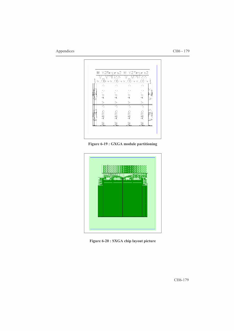
Appendices CH6 - 179
CH6-179
Figure 6-19 : GXGA module partitioning
Figure 6-20 : SXGA chip layout picture

CH – 180 Appendices
CH6-180
Figure 6-21 : SXGA module partitioning
Figure 6-22 : XGAp chip layout picture
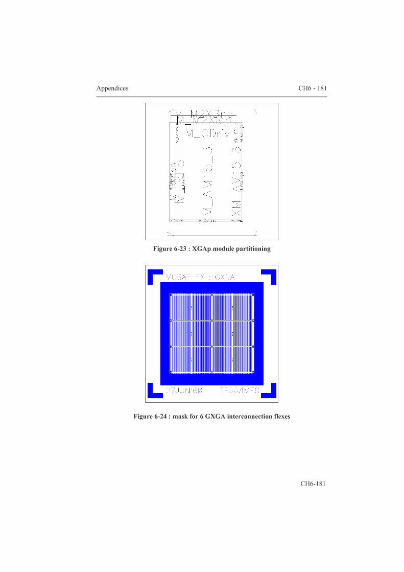
Appendices CH6 - 181
CH6-181
Figure 6-23 : XGAp module partitioning
Figure 6-24 : mask for 6 GXGA interconnection flexes

CH – 182 Appendices
CH6-182
c) Pin-out of GXGA chip and eventual application notes
Left series (pads at the top of the chip) Right series (pads at the top of the chip) Nr Name Description Nr Name Description 1 VBSD1 (sub)block select data input 1 ANWB 15V analog nwell bias 2 VBSC1 row (sub)block select clock 2 BCKPL backplane contact; shorted
to BRGij 3 VSRO1 output of left row shift register 3 DNWB 5V digit nwell bias 4 VGND1 0V digit supply left Rdriver 4 5 VSYN1 left Vsync 5 6 VCLK1 left row clock 6 7 VHLD1 left shift register hold 7 8 VVDD1 5V digit supply left Rdriver 8 9 VGNA1 0V 'analog' supply left Rdriver 9 10 VENA1 enable of left Rdriver 10 11 VVDA1 15V 'analog' supply 11 12 LRTL1 left row test line 1 12 HSYN3 BL3: see block1 (BL1) 13 LRTL2 left row test line 2 13 HCLK3 BL3: " 14 CTST1 column test bar 1 14 HENA3 BL3: " 15 CTST2 column test bar 2 15 HBSC3 BL3: " 16 HSYN1 BL1: Hsync input 16 HBSD3 BL3: " 17 HCLK1 BL1: column driver clock 17 BRG13 BL3: " 18 HENA1 BL1: coldriver enable 18 VID13 BL3: " 19 HBSC1 BL1: (sub)block select clock 19 SRG13 BL3: " 20 HBSD1 BL1: (sub)block select data 20 VID23 BL3: " 21 BRG11 BL1: backplane return ground 1of2 21 SRG23 BL3: " 22 VID11 BL1: video input 1of4 22 VID33 BL3: " 23 SRG11 BL1: substrate return ground 1of3 23 SRG33 BL3: " 24 VID21 BL1: video input 2of4 24 VID43 BL3: " 25 SRG21 BL1: substrate return ground 2of3 25 BRG23 BL3: " 26 VID31 BL1: video input 3of4 26 HVDD3 BL3: " 27 SRG31 BL1: substrate return ground 3of3 27 HVDA3 BL3: " 28 VID41 BL1: video input 4of4 28 HGND3 BL3: " 29 BRG21 BL1: backplane return ground 2of2 29 HGNA3 BL3: " 30 HVDD1 BL1: 5V digit supply 30 HSRO3 BL3: " 31 HVDA1 BL1: 15V analg supply 31 HSYN4 BL4: " 32 HGND1 BL1: 0V digit ground 32 HCLK4 BL4: " 33 HGNA1 BL1: 0V analg ground 33 HENA4 BL4: " 34 HSRO1 BL1: shift register output 34 HBSC4 BL4: " 35 HSYN2 BL2: SEE BL1 DESCR 35 HBSD4 BL4: " 36 HCLK2 BL2: " 36 BRG14 BL4: " 37 HENA2 BL2: " 37 VID14 BL4: " 38 HBSC2 BL2: " 38 SRG14 BL4: " 39 HBSD2 BL2: " 39 VID24 BL4: " 40 BRG12 BL2: " 40 SRG24 BL4: " 41 VID12 BL2: " 41 VID34 BL4: "
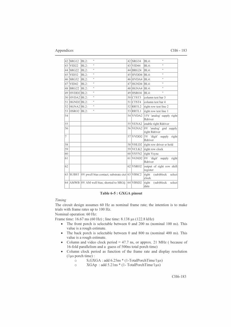
Appendices CH6 - 183
CH6-183
42 SRG12 BL2: " 42 SRG34 BL4: " 43 VID22 BL2: " 43 VID44 BL4: " 44 SRG22 BL2: " 44 BRG24 BL4: " 45 VID32 BL2: " 45 HVDD4 BL4: " 46 SRG32 BL2: " 46 HVDA4 BL4: " 47 VID42 BL2: " 47 HGND4 BL4: " 48 BRG22 BL2: " 48 HGNA4 BL4: " 49 HVDD2 BL2: " 49 HSRO4 BL4: " 50 HVDA2 BL2: " 50 CTST3 column test bar 3 51 HGND2 BL2: " 51 CTST4 column test bar 4 52 HGNA2 BL2: " 52 RRTL2 right row test line 2 53 HSRO2 BL2: " 53 RRTL1 right row test line 1 54 54 VVDA2 15V 'analog' supply right
Rdriver 55 55 VENA2 enable right Rdriver 56 56 VGNA2 0V 'analog' gnd supply
right Rdriver 7 57 VVDD2 5V 'digit' supply right
Rdriver 58 58 VHLD2 right row driver sr hold 59 59 VCLK2 right row clock 60 60 VSYN2 right Vsync 61 61 VGND2 0V 'digit' supply right
Rdriver 62 62 VSRO2 output of right row shift
register 63 SUBST 0V pwell bias contact; substrate ctct 63 VBSC2 right (sub)block select
clock 64 AMWB 0V AM well bias; shorted to SRGij 64 VBSD2 right (sub)block select
data
Table 6-5 : GXGA pinout Timing The circuit design assumes 60 Hz as nominal frame rate; the intention is to make trials with frame rates up to 100 Hz. Nominal operation: 60 Hz: Frame time: 16.67 ms (60 Hz) ; line time: 8.138 µs (122.8 kHz)
• The front porch is selectable between 0 and 200 ns (nominal 100 ns). This value is a rough estimate.
• The back porch is selectable between 0 and 800 ns (nominal 400 ns). This value is a rough estimate.
• Column and video clock period = 47.7 ns, or approx. 21 MHz ( because of 16-fold parallelism and a guess of 500ns total porch time)
• Column clock period as function of the frame rate and display resolution (1µs porch time) : o S,GXGA : add 6.25ns * (1-TotalPorchTime/1µs) o XGAp : add 5.21ns * (1- TotalPorchTime/1µs)
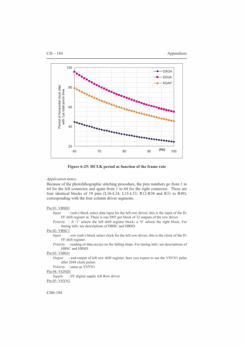
CH – 184 Appendices
CH6-184
Figure 6-25: HCLK period as function of the frame rate
Application notes: Because of the photolithographic stitching procedure, the pins numbers go from 1 to 64 for the left connector and again from 1 to 64 for the right connector. There are four identical blocks of 19 pins (L16-L34; L35-L53; R12-R30 and R31 to R49), corresponding with the four column driver segments. Pin 01: VBSD1 Input : (sub-) block select data input for the left row driver; this is the input of the D-
FF shift register in. There is one DFF per block of 32 outputs of the row driver. Polarity : A ‘1’ selects the left shift register block; a ‘0’ selects the right block. For
timing info: see descriptions of HBSC and HBSD. Pin 02: VBSC1 Input : row (sub-) block select clock for the left row driver; this is the clock of the D-
FF shift register. Polarity : reading of data occurs on the falling slope. For timing info: see descriptions of
HBSC and HBSD. Pin 03: VSRO1 Output : end-output of left row shift register; here you expect to see the VSYN1 pulse
after 2048 clock pulses Polarity : same as VSYN1
Pin 04: VGND1 Supply : 0V digital supply left Row driver
Pin 05: VSYN1
20
40
60
80
100
60 70 80 90 100 (Hz)
Perio
d of h
orizo
ntal c
lock (
ns)
with
1µs t
otal p
orch t
ime
GXGA SXGAXGAP
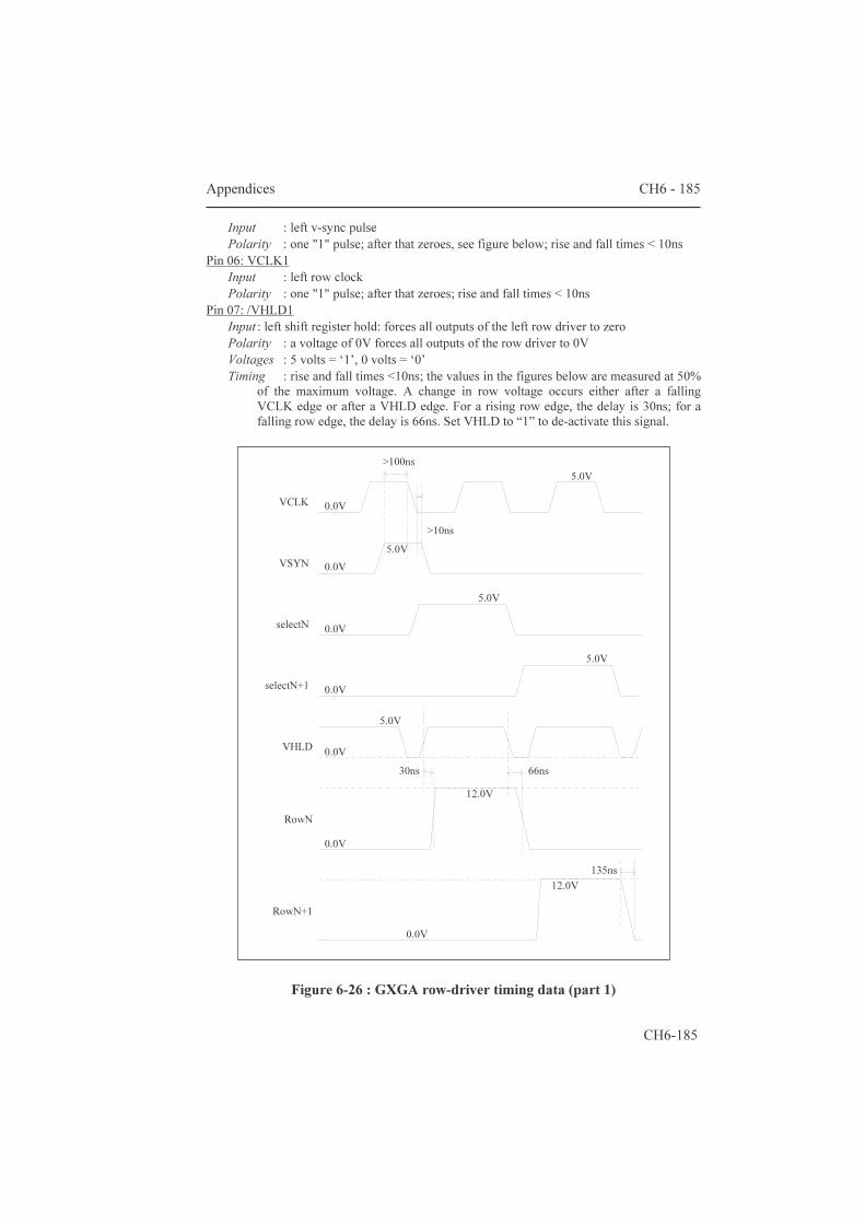
Appendices CH6 - 185
CH6-185
Input : left v-sync pulse Polarity : one "1" pulse; after that zeroes, see figure below; rise and fall times < 10ns
Pin 06: VCLK1 Input : left row clock Polarity : one "1" pulse; after that zeroes; rise and fall times < 10ns
Pin 07: /VHLD1 Input : left shift register hold: forces all outputs of the left row driver to zero Polarity : a voltage of 0V forces all outputs of the row driver to 0V Voltages : 5 volts = ‘1’, 0 volts = ‘0’ Timing : rise and fall times <10ns; the values in the figures below are measured at 50%
of the maximum voltage. A change in row voltage occurs either after a falling VCLK edge or after a VHLD edge. For a rising row edge, the delay is 30ns; for a falling row edge, the delay is 66ns. Set VHLD to “1” to de-activate this signal.
Figure 6-26 : GXGA row-driver timing data (part 1)
30ns
>100ns
>10ns0.0V
5.0V
0.0V5.0V
66ns
135ns
0.0V
5.0V
5.0V
5.0V
0.0V
0.0V
0.0V
0.0V
12.0V
12.0V
VCLK
VSYN
selectN
selectN+1
VHLD
RowN
RowN+1

CH – 186 Appendices
CH6-186
Pin 08: VVDD1 Supply : 5V digit supply left row driver
Pin 09: VGNA1 Supply : 0V 'analog' supply left row driver
Pin 10: /VENA1 Input : block-enable signal of left row driver: This signal is the input of a D-FF shift
register (and clocked simultaneously by the same clock signal as VBSD1: VBSC1). The state of the shift register stages determines if the high voltage outputs of the 32-output driver sub blocks are enabled.
Polarity : A “1” corresponds with a non-enabled output (high Z state) Pin 11: VVDA1 Supply : 15V 'analog' supply left row driver, 15V is absolute maximum and 12V is the
nominal value. Pin 12: LRTL1 Output : (left row-driver test line 1): end output of Block Select static shift register.
Here you expect to find the VBSD1 signal delayed by 64 clock pulses of VBSC1. Polarity : same as VBSD1
Pin 13: LRTL2 Output : (left row-driver test line 2): end output of Enable static shift register. Here you
expect to find /VENA1 signal delayed by 64 clock pulses of VBSC1. [Polarity : same as /VENA1]
Pin 14 : CTST1 HVinput : (column test bar 1) : controls a switch connecting column 1 with column 2,
column 5 with column 6, column 4n+1 with column 4n+2 for testing purposes. This pin also connects to pin R50 (CTST3)
Polarity : a "1" makes the connection. Normally, this signal is "0". Voltages : 15 volts = "1", 0 volts = "0"
Figure 6-27 : MOSAREL timing data (part 2)
~100 ns overlap
30ns 66ns
5.0V
5.0V
0.0V
0.0V
0.0V
0.0V
12.0V
12.0V
RowN
RowN+1
VHLD
VCLK
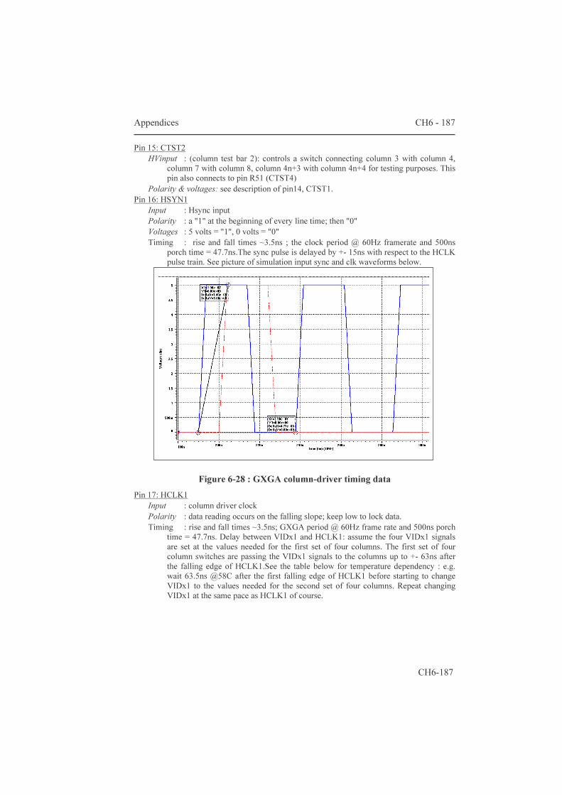
Appendices CH6 - 187
CH6-187
Pin 15: CTST2 HVinput : (column test bar 2): controls a switch connecting column 3 with column 4,
column 7 with column 8, column 4n+3 with column 4n+4 for testing purposes. This pin also connects to pin R51 (CTST4)
Polarity & voltages: see description of pin14, CTST1. Pin 16: HSYN1 Input : Hsync input Polarity : a "1" at the beginning of every line time; then "0" Voltages : 5 volts = "1", 0 volts = "0" Timing : rise and fall times ~3.5ns ; the clock period @ 60Hz framerate and 500ns
porch time = 47.7ns.The sync pulse is delayed by +- 15ns with respect to the HCLK pulse train. See picture of simulation input sync and clk waveforms below.
Figure 6-28 : GXGA column-driver timing data
Pin 17: HCLK1 Input : column driver clock Polarity : data reading occurs on the falling slope; keep low to lock data. Timing : rise and fall times ~3.5ns; GXGA period @ 60Hz frame rate and 500ns porch
time = 47.7ns. Delay between VIDx1 and HCLK1: assume the four VIDx1 signals are set at the values needed for the first set of four columns. The first set of four column switches are passing the VIDx1 signals to the columns up to +- 63ns after the falling edge of HCLK1.See the table below for temperature dependency : e.g. wait 63.5ns @58C after the first falling edge of HCLK1 before starting to change VIDx1 to the values needed for the second set of four columns. Repeat changing VIDx1 at the same pace as HCLK1 of course.
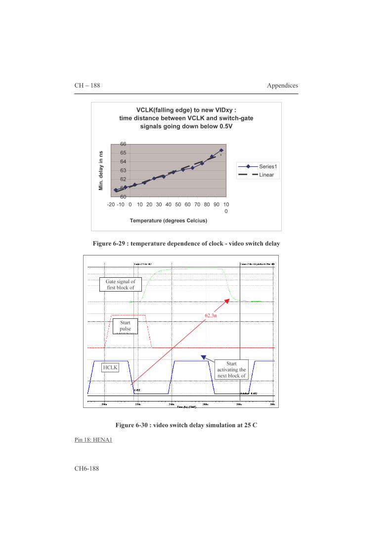
CH – 188 Appendices
CH6-188
VCLK(falling edge) to new VIDxy : time distance between VCLK and switch-gate
signals going down below 0.5V
60616263646566
-20 -10 0 10 20 30 40 50 60 70 80 90 100
Temperature (degrees Celcius)
Min.
delay
in ns
Series1Linear
Figure 6-29 : temperature dependence of clock - video switch delay
Figure 6-30 : video switch delay simulation at 25 C
Pin 18: HENA1
Gate signal of first block of columns
Start pulse
(HSYNC)
HCLK Start activating the next block of columns
62.3ns

Appendices CH6 - 189
CH6-189
Input : column driver segment enable; if this signal is low, the outputs of the segment connect to the on-chip backplane voltage and to each other.
Polarity : "1" = driver enabled; "0" = columns connected to backplane voltage. Set this pin to 5V for normal operation of the column driver.
Timing : when switching this signal, a delay of a few frame periods occurs before an eventual change to come into effect.
Pin 19: HBSC1 Input : (sub-) block select clock for the first column driver segment; this is the clock
of a D-FF static shift register. Polarity : data reading occurs on the falling slope; keep low to lock data. Timing : rise/fall time <1ns, e.g. 100ns cycle time (10Mz); data must not change
during falling HBSC edges. Pin 20: HBSD1 Input : (sub)block select data input for the 1st column driver segment; this is the
input of a D-FF static shift register. There is one DFF per block of 32 outputs of the column shift register; corresponding with 128 columns. Hence, in every column driver segment, there are 5 DFF outputs in total.
Polarity : A “1” selects the bottom shift register; a “0” selects the top one. Timing : 5ns rise/fall time, e.g. 100ns cycle time (10Mz). Data must not change during
falling HBSC edges. Hi->Lo transitions must ONLY occur when HBSC is Hi, take sum of rise and fall times as margin.
Pins 21, 29: BRG1,2 block1 Supply : backplane return ground, shorted to BCKPL
Pins 22, 24, 26, 28: VID1,2,3,4 block 1 Input : video input 1,2,3,4 of4
Pins 23, 25, 27: SRG1,2,3 block 1 Supply : substrate return ground, 0v guard around video input lines
Pins 30-33: HVDD1, HVDA1, HGND1, HGNA1 Supply : respectively 5V, 15V, 0V, 0V
Pin 34: HSRO1 Output : end-output of dynamic shift register for this column driver segment; here you
expect to see the (inverted) HSYN1 pulse after 160 clock pulses. Polarity : inverted with respect to HSYN1
Pins 35-53: see description of pins 16-34 (column driver block 1)
Pins 54-62: not connected Pins 63-64, 1-3 (2nd connector): SUBST, AMWB, ANWB, BCKPL, DNWB Supplies : respectively, 0V pwell bias, 0V AM well bias to be shorted with SRGij, not
connected, backplane contact to be shorted with BRGij, 5V digital nwell bias. Pins 4-22, 23-49 (2nd connector):
column blocks 3 and 4, see corresponding pins 16-34 of block 1 Pins 50-64 (2nd connector):
see corresponding pins 1-15 of first connector

CH – 190 Appendices
CH6-190
d) Schematic of main circuit (down to transistor level) general architecture of the GXGA backplane, redundancy, enable signals, details of the column driver, details of the row driver General architecture of the GXGA backplane: • The driver is integrated around the 2560x2048 active matrix.
Figure 6-31 : GXGA block schematic
• Above the matrix, there is a single column driver, consisting of 4 identical segments each counting 640 outputs. Each of these segments can be disabled, meaning that all 640 outputs are connected to backplane voltage. Every segment receives 4 parallel data lines that are connected to 4 consecutive columns at a time, as shown in Figure 6-32.
Figure 6-32 : schematic of column driver segment
• On the left side of the matrix, there is a complete row driver with 2048 outputs. On the right side, there is another complete row driver with 2048 outputs. These row drivers can be used simultaneously or one of them (or both) can be disabled (meaning that the outputs are put in a ‘hiZ’ state). The enabling can be done per 32 outputs of every row driver (see below)
HCLKHSYNVID1-4SRG1-4BRG HENA HSROHBSC HBSD HGNAHGNDHVDAHVDD
160n321160 bit shift register
Column driver (LV+HV)
Row
driv
er L
V
Row
driv
er L
V
Active Matrix
Row
driv
er H
V
Row
driv
er H
VColumn test
2560 x 2048
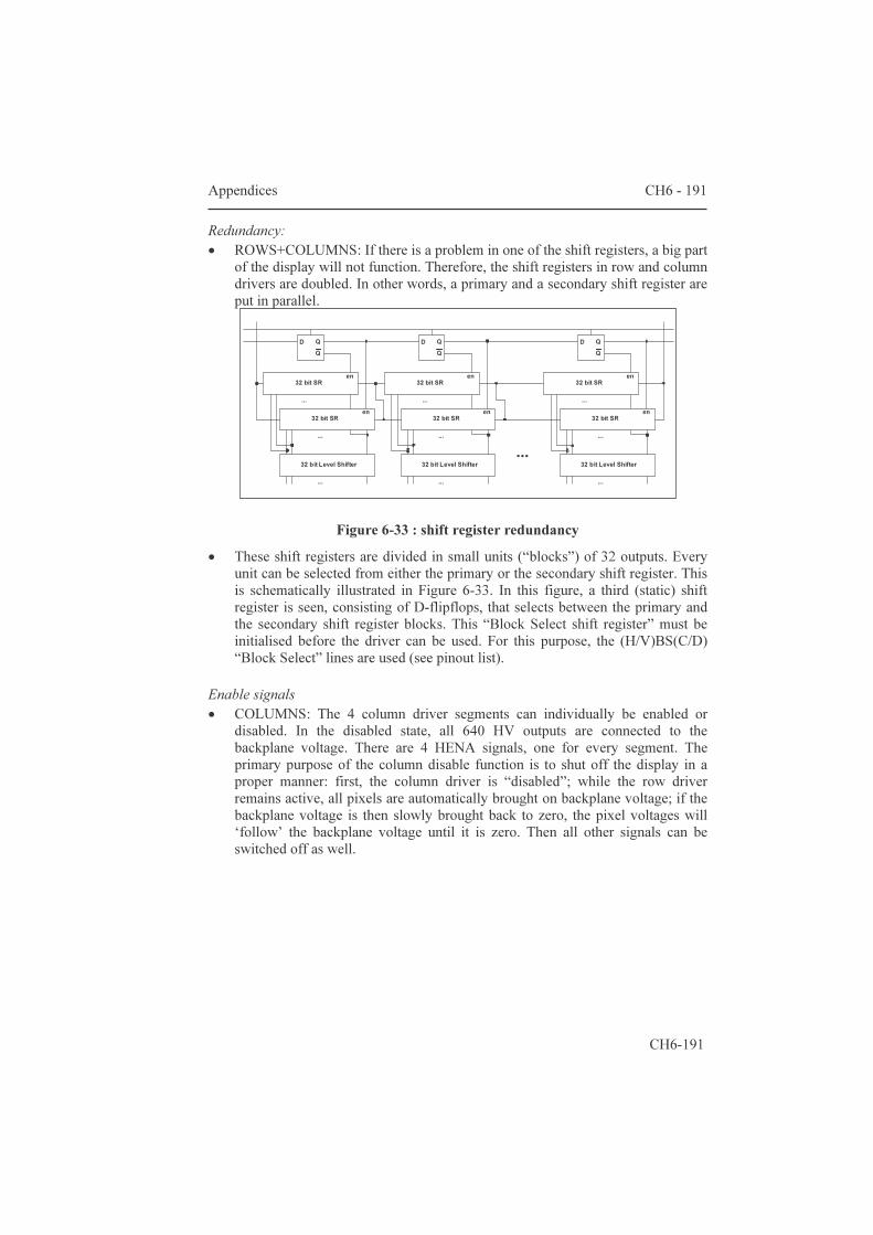
Appendices CH6 - 191
CH6-191
Redundancy: • ROWS+COLUMNS: If there is a problem in one of the shift registers, a big part
of the display will not function. Therefore, the shift registers in row and column drivers are doubled. In other words, a primary and a secondary shift register are put in parallel.
Figure 6-33 : shift register redundancy
• These shift registers are divided in small units (“blocks”) of 32 outputs. Every unit can be selected from either the primary or the secondary shift register. This is schematically illustrated in Figure 6-33. In this figure, a third (static) shift register is seen, consisting of D-flipflops, that selects between the primary and the secondary shift register blocks. This “Block Select shift register” must be initialised before the driver can be used. For this purpose, the (H/V)BS(C/D) “Block Select” lines are used (see pinout list).
Enable signals • COLUMNS: The 4 column driver segments can individually be enabled or
disabled. In the disabled state, all 640 HV outputs are connected to the backplane voltage. There are 4 HENA signals, one for every segment. The primary purpose of the column disable function is to shut off the display in a proper manner: first, the column driver is “disabled”; while the row driver remains active, all pixels are automatically brought on backplane voltage; if the backplane voltage is then slowly brought back to zero, the pixel voltages will ‘follow’ the backplane voltage until it is zero. Then all other signals can be switched off as well.
...
en
D Q
...
en32 bit SR
...
...
32 bit Level Shifter
32 bit SRen
QQD
32 bit SR
QQQD
en32 bit SR
32 bit Level Shifter
...
...
...
en
en
...
...
...
32 bit Level Shifter
32 bit SR
32 bit SR
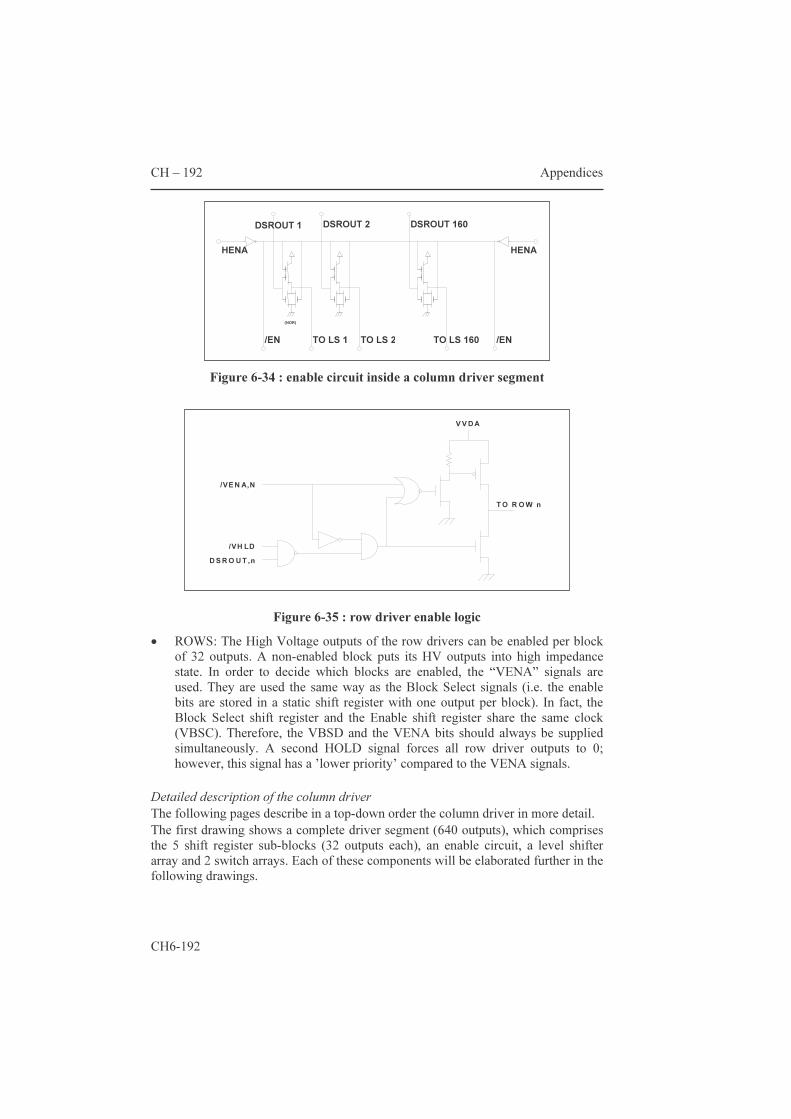
CH – 192 Appendices
CH6-192
Figure 6-34 : enable circuit inside a column driver segment
Figure 6-35 : row driver enable logic
• ROWS: The High Voltage outputs of the row drivers can be enabled per block of 32 outputs. A non-enabled block puts its HV outputs into high impedance state. In order to decide which blocks are enabled, the “VENA” signals are used. They are used the same way as the Block Select signals (i.e. the enable bits are stored in a static shift register with one output per block). In fact, the Block Select shift register and the Enable shift register share the same clock (VBSC). Therefore, the VBSD and the VENA bits should always be supplied simultaneously. A second HOLD signal forces all row driver outputs to 0; however, this signal has a ’lower priority’ compared to the VENA signals.
Detailed description of the column driver The following pages describe in a top-down order the column driver in more detail. The first drawing shows a complete driver segment (640 outputs), which comprises the 5 shift register sub-blocks (32 outputs each), an enable circuit, a level shifter array and 2 switch arrays. Each of these components will be elaborated further in the following drawings.
D S R O U T ,n
/VE N A,N
/VH LD
T O R O W n
V V D A
HENA HENA
DSROUT 160
TO LS 2
DSROUT 2
(NOR)
/EN TO LS 1 /ENTO LS 160
DSROUT 1
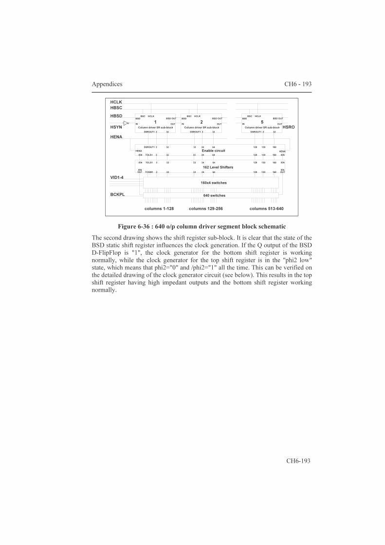
Appendices CH6 - 193
CH6-193
Figure 6-36 : 640 o/p column driver segment block schematic
The second drawing shows the shift register sub-block. It is clear that the state of the BSD static shift register influences the clock generation. If the Q output of the BSD D-FlipFlop is "1", the clock generator for the bottom shift register is working normally, while the clock generator for the top shift register is in the "phi2 low" state, which means that phi2="0" and /phi2="1" all the time. This can be verified on the detailed drawing of the clock generator circuit (see below). This results in the top shift register having high impedant outputs and the bottom shift register working normally.
160 130 129 129 130 160 /EN OUT
HSRO Column driver SR sub-block
HCLK OUT
BSD OUT
32 DSROUT1 2
5
33 34
34
34 64 64
64
Column driver SR sub-block
BSC
2DSROUT1 32
BSD OUT OUT
HCLK BSC
HENA /EN
/EN
160 130 129 129 130 160
/EN
/EN
columns 129-256 columns 513-640
640 switches
32
OUT BSD OUT
32
32
IN BSD
32
32
BSDIN2
160x4 switches
Enable circuit
162 Level Shifters
33 34 64
33
33
2TOSW1
TOLS1 2
DSROUT1 2
2DSROUT1
TOLS1 2
HCLK
Column driver SR sub-block
BCKPL
HENA
BSCBSDIN
/EN OUT
HSYN
HBSD HBSC HCLK
HENA
VID1-4
1
columns 1-128
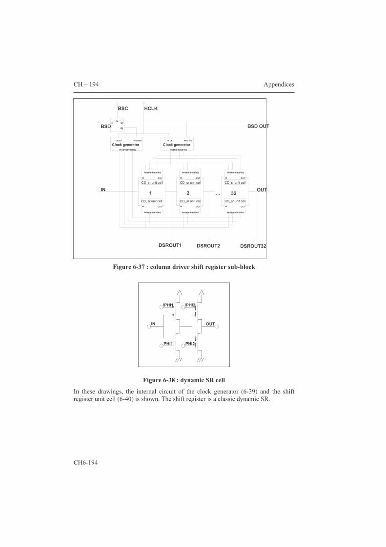
CH – 194 Appendices
CH6-194
Figure 6-37 : column driver shift register sub-block
Figure 6-38 : dynamic SR cell
In these drawings, the internal circuit of the clock generator (6-39) and the shift register unit cell (6-40) is shown. The shift register is a classic dynamic SR.
/PHI1 /PHI2
PHI1 PHI2 IN OUT
PHI2 low
PHI1 /PHI2 /PHI1 PHI2 /PHI2 PHI1
/PHI2 /PHI1 PHI2
/PHI1
OUT
BSD OUT
2
IN OUT
32...
OUTIN PHI2
QD/QBSD
HCLK PHI2 low
IN OUT
C
Clock generator
/PHI1
PHI2/PHI2
PHI1 /PHI2 PHI2
PHI1/PHI1
BSC HCLK
1INCD_sr unit cell
DSROUT32 DSROUT2
PHI2 OUTIN
/PHI1 PHI1 /PHI2 IN OUT
PHI2 /PHI2 PHI1 /PHI1
HCLK
IN /PHI1 PHI1 /PHI2 PHI2
OUT
DSROUT1
PHI1 Clock generator
CD_sr unit cell
CD_sr unit cell
CD_sr unit cell
CD_sr unit cell
CD_sr unit cell
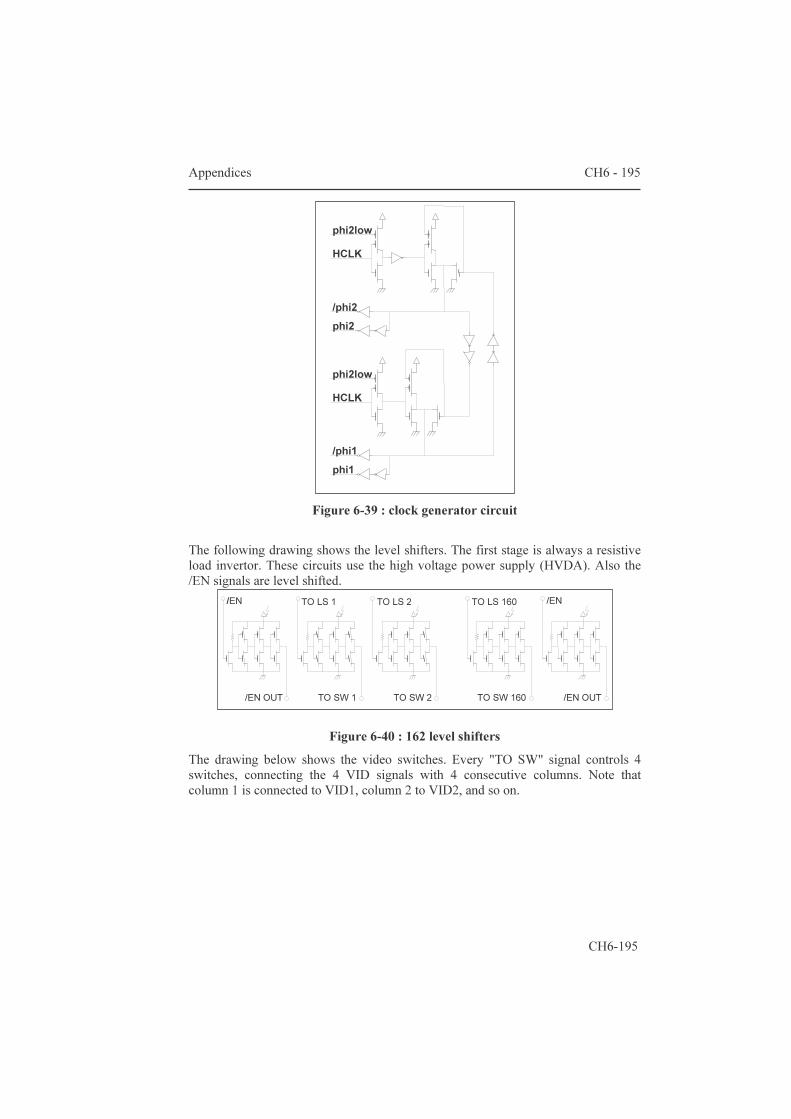
Appendices CH6 - 195
CH6-195
Figure 6-39 : clock generator circuit
The following drawing shows the level shifters. The first stage is always a resistive load invertor. These circuits use the high voltage power supply (HVDA). Also the /EN signals are level shifted.
Figure 6-40 : 162 level shifters
The drawing below shows the video switches. Every "TO SW" signal controls 4 switches, connecting the 4 VID signals with 4 consecutive columns. Note that column 1 is connected to VID1, column 2 to VID2, and so on.
phi2lowHCLK
phi2/phi2
phi2low
/phi1 phi1
HCLK
TO LS 160 /EN
TO SW 2
TO LS 2
/EN OUT TO SW 1
TO LS 1/EN
TO SW 160 /EN OUT
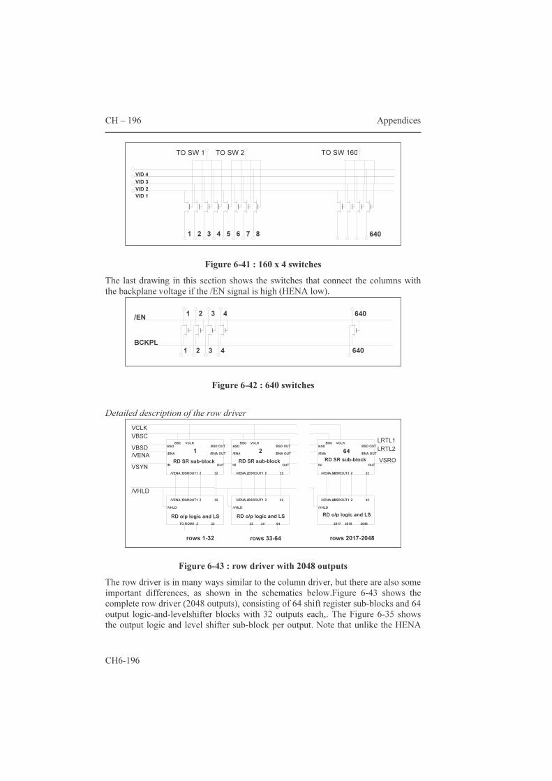
CH – 196 Appendices
CH6-196
Figure 6-41 : 160 x 4 switches
The last drawing in this section shows the switches that connect the columns with the backplane voltage if the /EN signal is high (HENA low).
Figure 6-42 : 640 switches
Detailed description of the row driver
Figure 6-43 : row driver with 2048 outputs
The row driver is in many ways similar to the column driver, but there are also some important differences, as shown in the schematics below.Figure 6-43 shows the complete row driver (2048 outputs), consisting of 64 shift register sub-blocks and 64 output logic-and-levelshifter blocks with 32 outputs each,. The Figure 6-35 shows the output logic and level shifter sub-block per output. Note that unlike the HENA
7
VID 4VID 3VID 2VID 1
TO SW 2TO SW 1
1 2 3 4 5 6
TO SW 160
6408
1
640
640
BCKPL
/EN 2 3 4
4321
/ENA OUT
VCLK BSD OUT BSDBSC
2 LRTL2
IN OUT /ENA OUT BSD OUT
/ENA
32
2
VCLK
IN
/ENA BSDBSC
VSYN
VCLKVBSC VBSD /VENA
VSRO
LRTL1
OUT IN
64BSC
BSD BSD OUT VCLK
/ENA OUT OUT
/ENA
2017
/VENA,64 DSROUT1 2 32
DSROUT1 32 /VHLD
33 34
/VENA,64
322DSROUT1 /VENA,2
32DSROUT1 2/VENA,2/VHLD
64
32
32
RD o/p logic and LS
rows 1-32
2DSROUT1
DSROUT1 2
2
1RD SR sub-block
/VHLD
/VHLD
/VENA,1
/VENA,1
TO ROW1 2048 2018 rows 33-64 rows 2017-2048
RD o/p logic and LS
RD SR sub-block
RD o/p logic and LS
RD SR sub-block
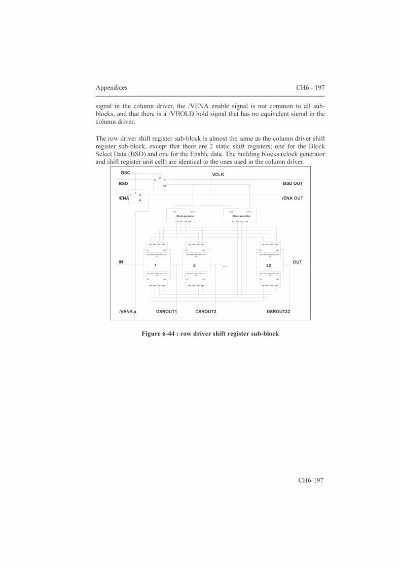
Appendices CH6 - 197
CH6-197
signal in the column driver, the /VENA enable signal is not common to all sub-blocks, and that there is a /VHOLD hold signal that has no equivalent signal in the column driver. The row driver shift register sub-block is almost the same as the column driver shift register sub-block, except that there are 2 static shift registers; one for the Block Select Data (BSD) and one for the Enable data. The building blocks (clock generator and shift register unit cell) are identical to the ones used in the column driver.
Figure 6-44 : row driver shift register sub-block
PHI1 /PHI1 PHI2 /PHI2 /PHI1
IN
32
OUT
D Q
PHI2
/Q
OUT
/PHI1
C
BSD OUT BSC VCLK
C QD/Q
/PHI2 IN
IN OUT
OUT
/PHI1 PHI1
HCLK PHI2 low Clock generator
/PHI1 PHI1 /PHI2 PHI2 IN
PHI1 /PHI2
/PHI2
/PHI1
PHI2 low
PHI1 /PHI2
2 ...
PHI2
Row driver shift register unit cell
Row driver shift register unit cell Row driver shift register unit
cell
Row driver shift register unit cell
Row driver shift register unit cell 1
PHI2
PHI2
OUT
/PHI2
IN OUT
PHI1
Clock generator HCLK
/PHI2 PHI2/PHI1 PHI1
/ENA OUT
PHI2
OUTIN /PHI1 PHI1
/ENA
/VENA,x
IN
BSD
DSROUT2 DSROUT1 DSROUT32
Row driver shift register unit cell
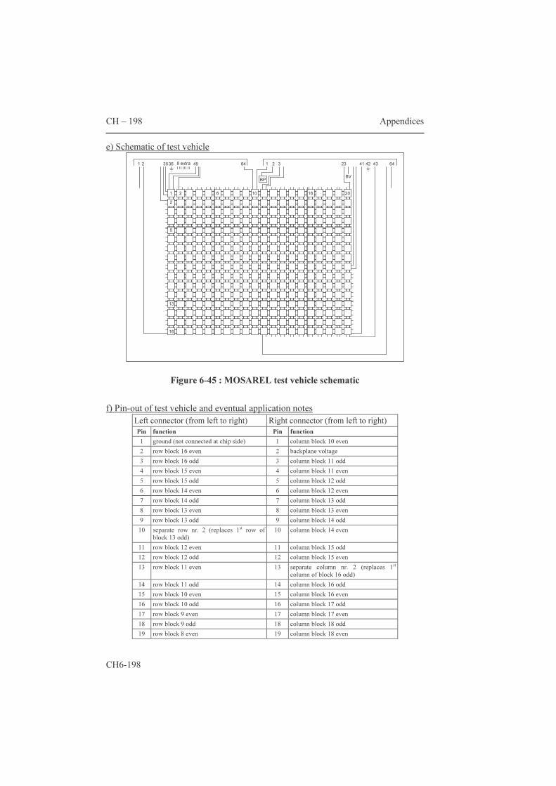
CH – 198 Appendices
CH6-198
e) Schematic of test vehicle
Figure 6-45 : MOSAREL test vehicle schematic
f) Pin-out of test vehicle and eventual application notes
Left connector (from left to right) Right connector (from left to right) Pin function Pin function 1 ground (not connected at chip side) 1 column block 10 even 2 row block 16 even 2 backplane voltage 3 row block 16 odd 3 column block 11 odd 4 row block 15 even 4 column block 11 even 5 row block 15 odd 5 column block 12 odd 6 row block 14 even 6 column block 12 even 7 row block 14 odd 7 column block 13 odd 8 row block 13 even 8 column block 13 even 9 row block 13 odd 9 column block 14 odd 10 separate row nr. 2 (replaces 1st row of
block 13 odd) 10 column block 14 even
11 row block 12 even 11 column block 15 odd 12 row block 12 odd 12 column block 15 even 13 row block 11 even 13 separate column nr. 2 (replaces 1st
column of block 16 odd) 14 row block 11 odd 14 column block 16 odd 15 row block 10 even 15 column block 16 even 16 row block 10 odd 16 column block 17 odd 17 row block 9 even 17 column block 17 even 18 row block 9 odd 18 column block 18 odd 19 row block 8 even 19 column block 18 even
20
4342 644123
BV
2
2
1
8 extra35 4536
16
3
5
106
2
BP
1641 2
13
16
Appendices CH6 - 199
CH6-199
20 row block 8 odd 20 column block 19 odd 21 row block 7 even 21 column block 19 even 22 row block 7 odd 22 column block 20 odd 23 row block 6 even 23 column block 20 even 24 row block 6 odd 24 BV 25 row block 5 even 25 row block 9 odd 26 row block 5 odd 26 row block 9 even 27 separate row nr. 1 (replaces 1st row of
block 5 odd) 27 row block 10 odd
28 row block 4 even 28 row block 10 even 29 row block 4 odd 29 row block 11 odd 30 row block 3 even 30 row block 11 even 31 row block 3 odd 31 row block 12 odd 32 row block 2 even 32 row block 12 even 33 row block 2 odd 33 separate row nr. 2 34 row block 1 even 34 row block 13 odd 35 row block 1 odd 35 row block 13 even 36 ground (connected to chip ground) 36 row block 14 odd 37 extra (diffraction tests…) 37 row block 14 even 38 extra (diffraction tests…) 38 row block 15 odd 39 extra (diffraction tests…) 39 row block 15 even 40 extra (diffraction tests…) 40 row block 16 odd 41 extra (diffraction tests…) 41 row block 16 even 42 extra (diffraction tests…) 42 ground (connected to chip ground) 43 extra (diffraction tests…) 43 column block 20 even 44 extra (diffraction tests…) 44 column block 20 odd 45 column block 1 odd 45 column block 19 even 46 column block 1 even 46 column block 19 odd 47 column block 2 odd 47 column block 18 even 48 column block 2 even 48 column block 18 odd 49 column block 3 odd 49 column block 17 even 50 column block 3 even 50 column block 17 odd 51 column block 4 odd 51 column block 16 even 52 column block 4 even 52 column block 16 odd 53 column block 5 odd 53 separate column nr. 2 (replaces 1st row
of block 13 odd) 54 column block 5 even 54 column block 15 even 55 separate column nr.1 (replaces 1st row of
block 13 odd) 55 column block 15 odd
56 column block 6 odd 56 column block 14 even 57 column block 6 even 57 column block 14 odd 58 column block 7 odd 58 column block 13 even 59 column block 7 even 59 column block 13 odd 60 column block 8 odd 60 column block 12 even 61 column block 8 even 61 column block 12 odd 62 column block 9 odd 62 column block 11 even 63 column block 9 even 63 column block 11 odd 64 column block 10 odd 64 ground (not connected at chip side)
Table 6-6 : MOSAREL test vehicle pin-out
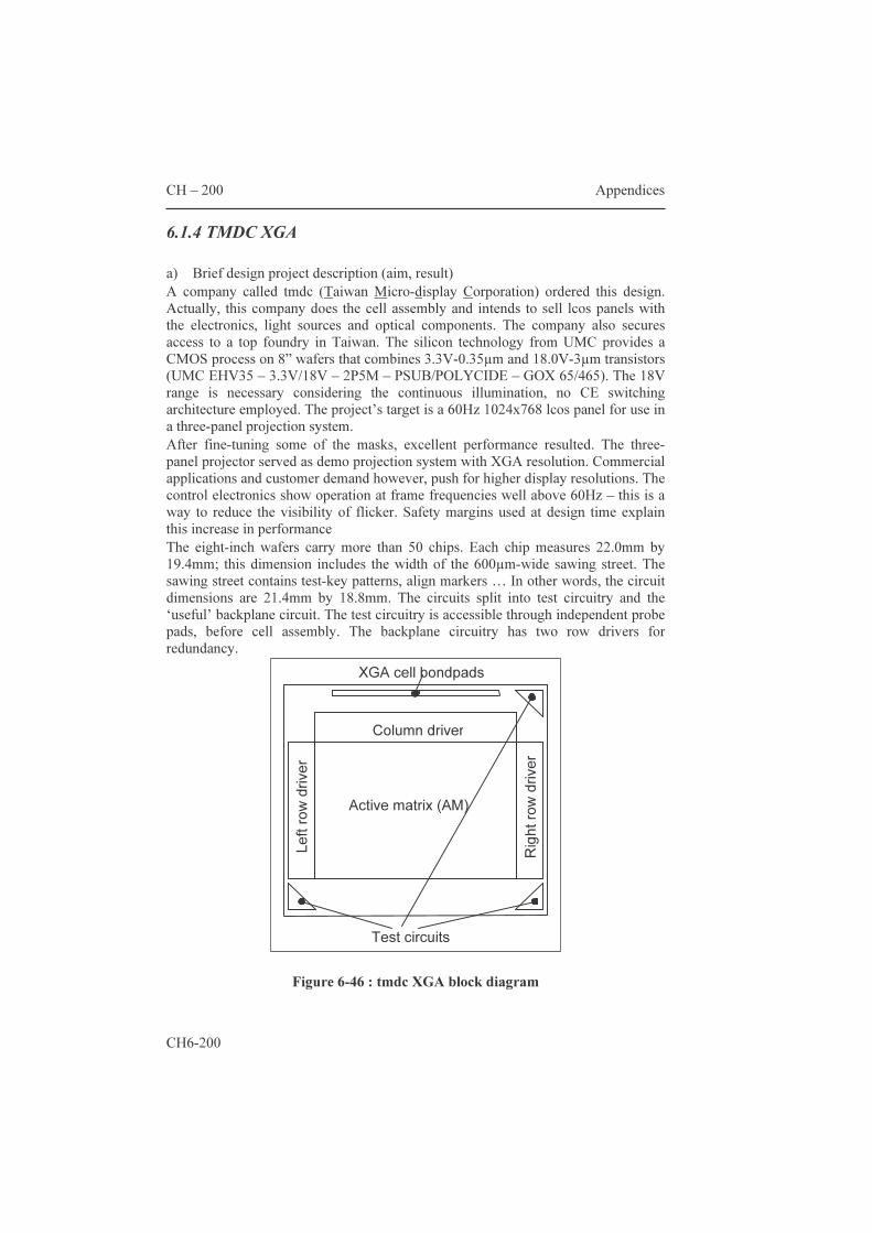
CH – 200 Appendices
CH6-200
6.1.4 TMDC XGA a) Brief design project description (aim, result) A company called tmdc (Taiwan Micro-display Corporation) ordered this design. Actually, this company does the cell assembly and intends to sell lcos panels with the electronics, light sources and optical components. The company also secures access to a top foundry in Taiwan. The silicon technology from UMC provides a CMOS process on 8” wafers that combines 3.3V-0.35µm and 18.0V-3µm transistors (UMC EHV35 – 3.3V/18V – 2P5M – PSUB/POLYCIDE – GOX 65/465). The 18V range is necessary considering the continuous illumination, no CE switching architecture employed. The project’s target is a 60Hz 1024x768 lcos panel for use in a three-panel projection system. After fine-tuning some of the masks, excellent performance resulted. The three-panel projector served as demo projection system with XGA resolution. Commercial applications and customer demand however, push for higher display resolutions. The control electronics show operation at frame frequencies well above 60Hz – this is a way to reduce the visibility of flicker. Safety margins used at design time explain this increase in performance The eight-inch wafers carry more than 50 chips. Each chip measures 22.0mm by 19.4mm; this dimension includes the width of the 600µm-wide sawing street. The sawing street contains test-key patterns, align markers … In other words, the circuit dimensions are 21.4mm by 18.8mm. The circuits split into test circuitry and the ‘useful’ backplane circuit. The test circuitry is accessible through independent probe pads, before cell assembly. The backplane circuitry has two row drivers for redundancy.
Figure 6-46 : tmdc XGA block diagram
XGA cell bondpads
Column driver
Test circuits
Active matrix (AM)
Left r
ow dr
iver
Right
row dr
iver
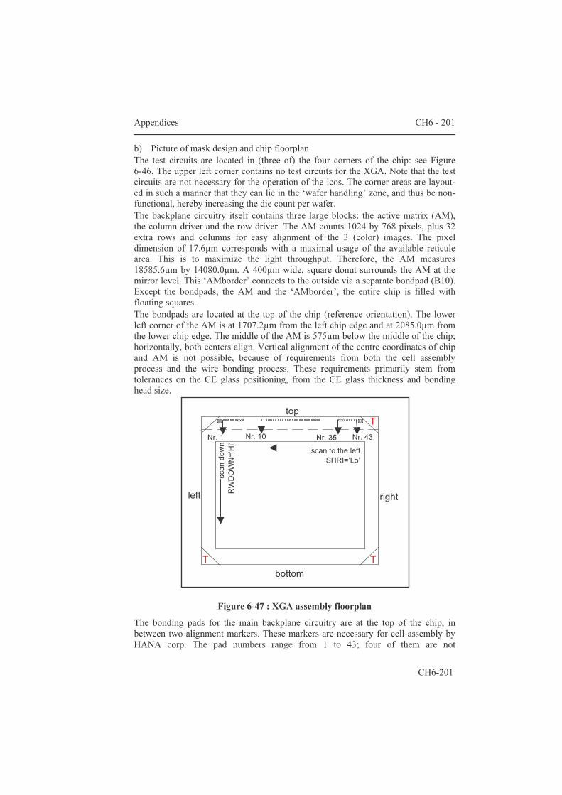
Appendices CH6 - 201
CH6-201
b) Picture of mask design and chip floorplan The test circuits are located in (three of) the four corners of the chip: see Figure 6-46. The upper left corner contains no test circuits for the XGA. Note that the test circuits are not necessary for the operation of the lcos. The corner areas are layout-ed in such a manner that they can lie in the ‘wafer handling’ zone, and thus be non-functional, hereby increasing the die count per wafer. The backplane circuitry itself contains three large blocks: the active matrix (AM), the column driver and the row driver. The AM counts 1024 by 768 pixels, plus 32 extra rows and columns for easy alignment of the 3 (color) images. The pixel dimension of 17.6µm corresponds with a maximal usage of the available reticule area. This is to maximize the light throughput. Therefore, the AM measures 18585.6µm by 14080.0µm. A 400µm wide, square donut surrounds the AM at the mirror level. This ‘AMborder’ connects to the outside via a separate bondpad (B10). Except the bondpads, the AM and the ‘AMborder’, the entire chip is filled with floating squares. The bondpads are located at the top of the chip (reference orientation). The lower left corner of the AM is at 1707.2µm from the left chip edge and at 2085.0µm from the lower chip edge. The middle of the AM is 575µm below the middle of the chip; horizontally, both centers align. Vertical alignment of the centre coordinates of chip and AM is not possible, because of requirements from both the cell assembly process and the wire bonding process. These requirements primarily stem from tolerances on the CE glass positioning, from the CE glass thickness and bonding head size.
Figure 6-47 : XGA assembly floorplan
The bonding pads for the main backplane circuitry are at the top of the chip, in between two alignment markers. These markers are necessary for cell assembly by HANA corp. The pad numbers range from 1 to 43; four of them are not
left
scan to the leftSHRI=’Lo’
bottom
scan
down
RWDO
WN=
’Hi’Nr. 1 Nr. 10 Nr. 35 Nr. 43
top T
T T
right
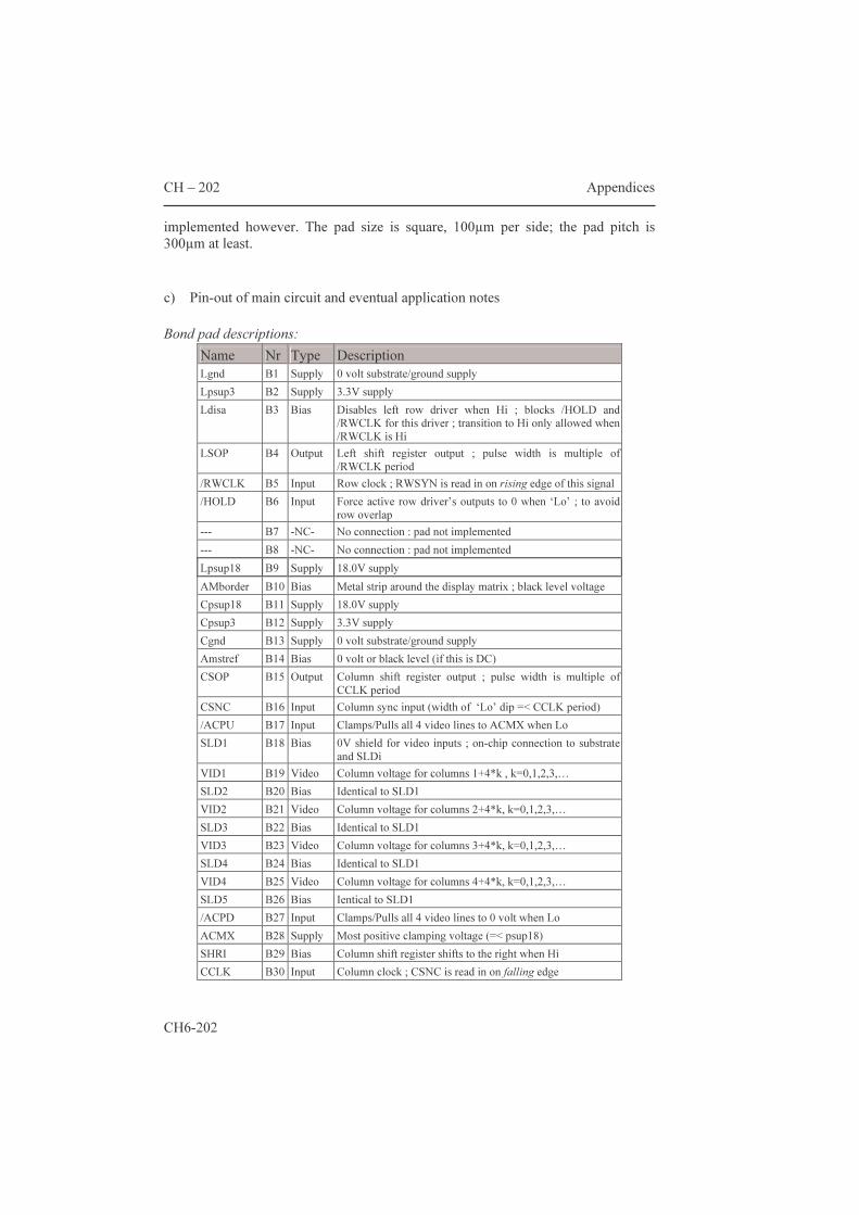
CH – 202 Appendices
CH6-202
implemented however. The pad size is square, 100µm per side; the pad pitch is 300µm at least. c) Pin-out of main circuit and eventual application notes Bond pad descriptions:
Name Nr Type Description Lgnd B1 Supply 0 volt substrate/ground supply Lpsup3 B2 Supply 3.3V supply Ldisa B3 Bias Disables left row driver when Hi ; blocks /HOLD and
/RWCLK for this driver ; transition to Hi only allowed when /RWCLK is Hi
LSOP B4 Output Left shift register output ; pulse width is multiple of /RWCLK period
/RWCLK B5 Input Row clock ; RWSYN is read in on rising edge of this signal /HOLD B6 Input Force active row driver’s outputs to 0 when ‘Lo’ ; to avoid
row overlap --- B7 -NC- No connection : pad not implemented --- B8 -NC- No connection : pad not implemented Lpsup18 B9 Supply 18.0V supply AMborder B10 Bias Metal strip around the display matrix ; black level voltage Cpsup18 B11 Supply 18.0V supply Cpsup3 B12 Supply 3.3V supply Cgnd B13 Supply 0 volt substrate/ground supply Amstref B14 Bias 0 volt or black level (if this is DC) CSOP B15 Output Column shift register output ; pulse width is multiple of
CCLK period CSNC B16 Input Column sync input (width of ‘Lo’ dip =< CCLK period) /ACPU B17 Input Clamps/Pulls all 4 video lines to ACMX when Lo SLD1 B18 Bias 0V shield for video inputs ; on-chip connection to substrate
and SLDi VID1 B19 Video Column voltage for columns 1+4*k , k=0,1,2,3,… SLD2 B20 Bias Identical to SLD1 VID2 B21 Video Column voltage for columns 2+4*k, k=0,1,2,3,… SLD3 B22 Bias Identical to SLD1 VID3 B23 Video Column voltage for columns 3+4*k, k=0,1,2,3,… SLD4 B24 Bias Identical to SLD1 VID4 B25 Video Column voltage for columns 4+4*k, k=0,1,2,3,… SLD5 B26 Bias Ientical to SLD1 /ACPD B27 Input Clamps/Pulls all 4 video lines to 0 volt when Lo ACMX B28 Supply Most positive clamping voltage (=< psup18) SHRI B29 Bias Column shift register shifts to the right when Hi CCLK B30 Input Column clock ; CSNC is read in on falling edge

Appendices CH6 - 203
CH6-203
Cgnd B31 Supply 0 volt substrate/ground supply Cpsup3 B32 Supply 3.3V supply Cpsup18 B33 Supply 18.0V supply LiShield B34 Bias Black level Rpsup18 B35 Supply 18.0V supply Rwdown B36 Bias Active row register shifts down when Hi RWSYN B37 Input Row sync pulse (width less than one /RWCLK period) --- B38 -NC- No connection : pad not implemented --- B39 -NC- No connection : pad not implemented RSOP B40 Output Right shift register output ; pulse width is multiple of
/RWCLK period Rdisa B41 Bias Disable right row driver when Hi ; see B3 Rpsup3 B42 Supply 3.3V supply Rgnd B43 Supply 0 volt substrate/ground supply
Table 6-7 : tmdc XGA main circuit – bondpad description list Application notes: [remarks, qualitative waveforms, timing data] Important remarks:
• Pad numbering starts at the upper left pad from nr. 1 to nr. 43, although there are only 39 pads implemented: pads marked with a ‘x’ in the drawing (paragraph 1.1) are not implemented.
• Signals of type ‘input’ – see pin-out table – are all 3.3V CMOS and have +-5ns rise and fall times; logic low (=0V) is noted as ‘Lo’ and logic high (=3.3V) is noted as ‘Hi’. ‘HiZ’ stands short for the high impedance state.
• There are 3 different supply voltages: logic 3.3V, analog 18V (nominal) and clamping level 11V maximum.
• Clock signals ideally have 50% duty ratio; this is evident for the column clock signal, for the row clock there is a lower limit to the pulse width.
• The column driver has 4-fold parallelism: there are 1056/4=264 column clock pulses during each line period. Therefore, the column scanner is shorter than the row scanner (800 stages without parallelism).
• Depending on the RWDOWN and SHRI signal levels, scanning occurs from top to bottom (RWDOWN=’Hi’) and from left to right (SHRI=’Hi’). Internal multiplexers make sure the scanner input and outputs are rerouted to the corresponding pads. ‘Top’ is at the side of the backplane bondpads. Scan direction is not to change often during operation of the display.
There are two row drivers, each driving all of the 800 rows. The only control input with separate pad is the row driver enable. The other row control signals have common pads. Normally one must not enable both drivers simultaneously. When both row drivers are active simultaneously, there is a risk of conflicting row driver outputs. These conflicts can permanently destroy the cell’s functionality! Especially at startup, one should take care to disable both drivers from the very beginning on (power-up, Ldisa[3] and Rdisa[41] should thus be ‘Hi’). Another solution consists of activating the ‘HOLD’ mode that forces all the row-driver outputs to be ‘Lo’. In a
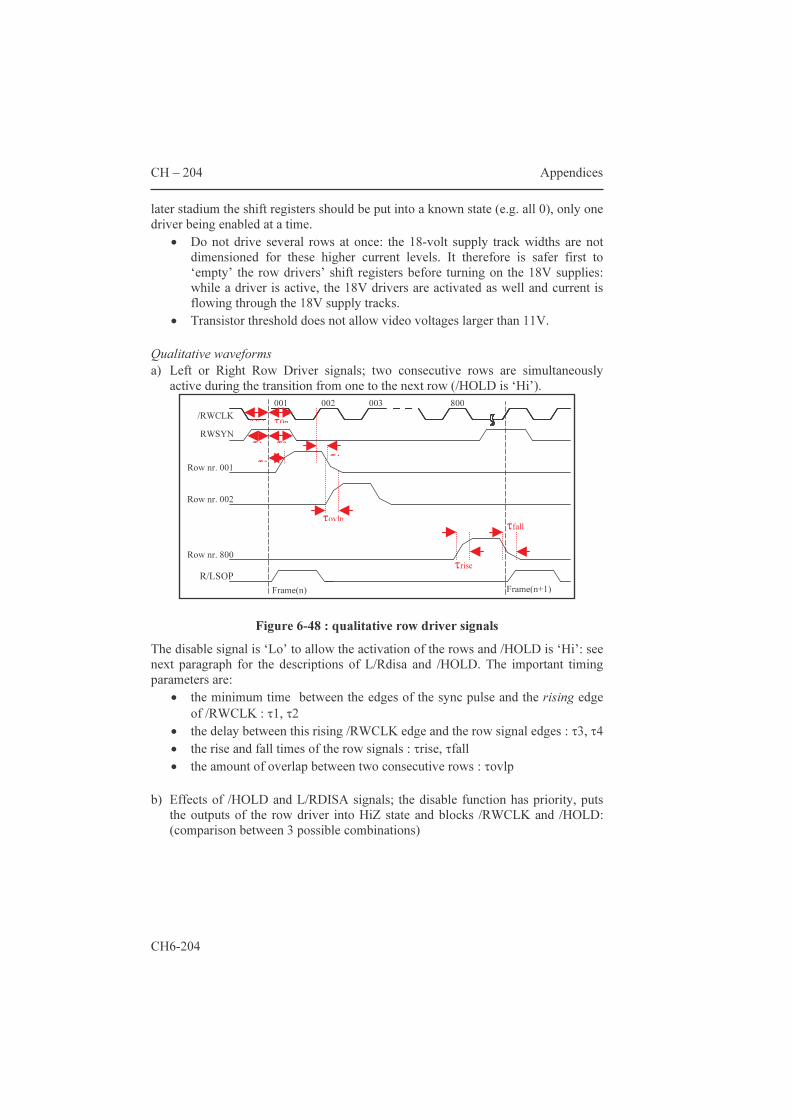
CH – 204 Appendices
CH6-204
later stadium the shift registers should be put into a known state (e.g. all 0), only one driver being enabled at a time.
• Do not drive several rows at once: the 18-volt supply track widths are not dimensioned for these higher current levels. It therefore is safer first to ‘empty’ the row drivers’ shift registers before turning on the 18V supplies: while a driver is active, the 18V drivers are activated as well and current is flowing through the 18V supply tracks.
• Transistor threshold does not allow video voltages larger than 11V. Qualitative waveforms a) Left or Right Row Driver signals; two consecutive rows are simultaneously
active during the transition from one to the next row (/HOLD is ‘Hi’).
Figure 6-48 : qualitative row driver signals
The disable signal is ‘Lo’ to allow the activation of the rows and /HOLD is ‘Hi’: see next paragraph for the descriptions of L/Rdisa and /HOLD. The important timing parameters are:
• the minimum time between the edges of the sync pulse and the rising edge of /RWCLK : τ1, τ2
• the delay between this rising /RWCLK edge and the row signal edges : τ3, τ4 • the rise and fall times of the row signals : τrise, τfall • the amount of overlap between two consecutive rows : τovlp
b) Effects of /HOLD and L/RDISA signals; the disable function has priority, puts
the outputs of the row driver into HiZ state and blocks /RWCLK and /HOLD: (comparison between 3 possible combinations)
Frame(n+1)
/RWCLK
Row nr. 002
Row nr. 800R/LSOP
Row nr. 001
RWSYN
τfall
τrise
τ1 τ2τ3
τovlp
τ4
Frame(n)
001 002 003 800 τ0pτ0d
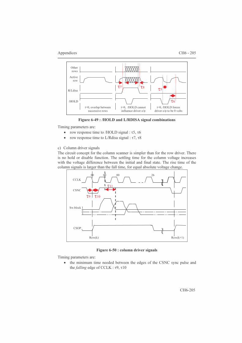
Appendices CH6 - 205
CH6-205
Figure 6-49 : /HOLD and L/RDISA signal combinations
Timing parameters are: • row response time to /HOLD signal : τ5, τ6 • row response time to L/Rdisa signal : τ7, τ8
c) Column driver signals The circuit concept for the column scanner is simpler than for the row driver. There is no hold or disable function. The settling time for the column voltage increases with the voltage difference between the initial and final state. The rise time of the column signals is larger than the fall time, for equal absolute voltage change.
Figure 6-50 : column driver signals
Timing parameters are: • the minimum time needed between the edges of the CSNC sync pulse and
the falling edge of CCLK : τ9, τ10
τ9 τ10
001
002
003
264 CCLK
CSNC
Sw.block
CSOP
τ11
Row(k) Row(k+1)
231
τ5
τ6
τ7 τ8
Other rows
R/Ldisa
/HOLD
Active row
t=0, overlap between successive rows
t=0, /HOLD cannot influence driver o/p
t=0, /HOLD forces driver o/p to be 0 volts
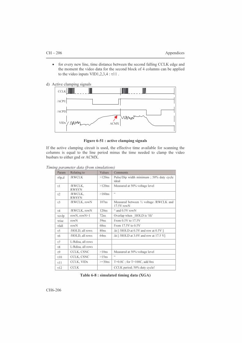
CH – 206 Appendices
CH6-206
• for every new line, time distance between the second falling CCLK edge and the moment the video data for the second block of 4 columns can be applied to the video inputs VID1,2,3,4 : τ11 .
d) Active clamping signals
Figure 6-51 : active clamping signals
If the active clamping circuit is used, the effective time available for scanning the columns is equal to the line period minus the time needed to clamp the video busbars to either gnd or ACMX. Timing parameter data (from simulations)
Param Relating to Values Comments τ0p,d /RWCLK >120ns Pulse/Dip width minimum ; 50% duty cycle
ideal τ1 /RWCLK,
RWSYN >120ns Measured at 50% voltage level
τ2 /RWCLK, RWSYN
>160ns “
τ3 /RWCLK, rowN 107ns Measured between ½ voltage /RWCLK and 17.5V rowN
τ4 /RWCLK, rowN 120ns “ and 0.5V rowN τovlp rowN, rowN+1 72ns Overlap when _HOLD is ‘Hi’ τrise rowN 59ns From 0.5V to 17.5V τfall rowN 68ns From 17.5V to 0.5V τ5 /HOLD, all rows 80ns ∆t [ /HOLD at 0.3V and row at 0.5V ] τ6 /HOLD, all rows 64ns ∆t [ /HOLD at 3.0V and row at 17.5 V] τ7 L/Rdisa, all rows τ8 L/Rdisa, all rows τ9 CCLK, CSNC >10ns Measured at 50% voltage level τ10 CCLK, CSNC >15ns “ τ11 CCLK, VIDx >=30ns T=0.0C ; for T=100C, add 8ns τ12 CCLK CCLK period; 50% duty cycle!
Table 6-8 : simulated timing data (XGA)
CCLK
/ACPU
/ACPD
VIDx ACMX
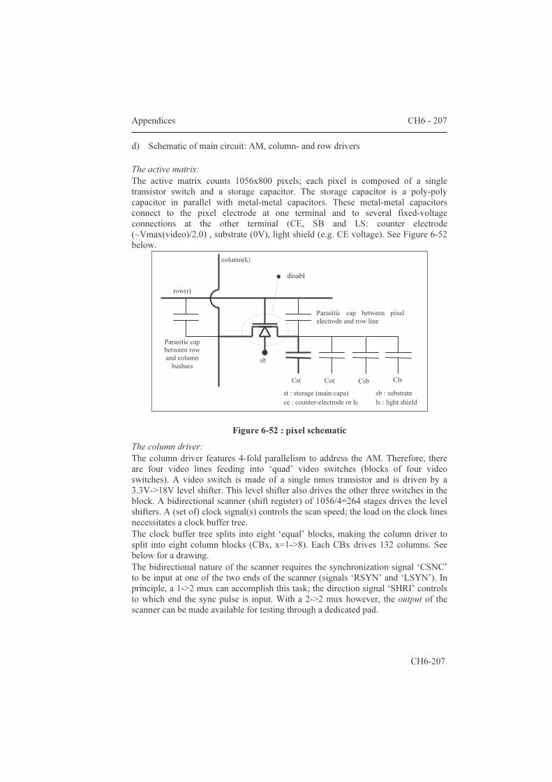
Appendices CH6 - 207
CH6-207
d) Schematic of main circuit: AM, column- and row drivers The active matrix: The active matrix counts 1056x800 pixels; each pixel is composed of a single transistor switch and a storage capacitor. The storage capacitor is a poly-poly capacitor in parallel with metal-metal capacitors. These metal-metal capacitors connect to the pixel electrode at one terminal and to several fixed-voltage connections at the other terminal (CE, SB and LS: counter electrode (~Vmax(video)/2.0) , substrate (0V), light shield (e.g. CE voltage). See Figure 6-52 below.
Figure 6-52 : pixel schematic
The column driver: The column driver features 4-fold parallelism to address the AM. Therefore, there are four video lines feeding into ‘quad’ video switches (blocks of four video switches). A video switch is made of a single nmos transistor and is driven by a 3.3V->18V level shifter. This level shifter also drives the other three switches in the block. A bidirectional scanner (shift register) of 1056/4=264 stages drives the level shifters. A (set of) clock signal(s) controls the scan speed; the load on the clock lines necessitates a clock buffer tree. The clock buffer tree splits into eight ‘equal’ blocks, making the column driver to split into eight column blocks (CBx, x=1->8). Each CBx drives 132 columns. See below for a drawing. The bidirectional nature of the scanner requires the synchronization signal ‘CSNC’ to be input at one of the two ends of the scanner (signals ‘RSYN’ and ‘LSYN’). In principle, a 1->2 mux can accomplish this task; the direction signal ‘SHRI’ controls to which end the sync pulse is input. With a 2->2 mux however, the output of the scanner can be made available for testing through a dedicated pad.
column(k)
row(r)
Parasitic cap between pixel electrode and row line
Cst Cce ClsCsb
Parasitic cap between row and column busbars
disable
sb
st : storage (main capa) sb : substrate ce : counter-electrode or lc ls : light shield
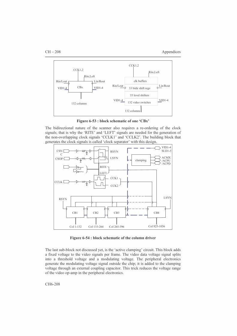
CH – 208 Appendices
CH6-208
Figure 6-53 : block schematic of one ‘CBx’
The bidirectional nature of the scanner also requires a re-ordering of the clock signals; that is why the ‘RITE’ and ‘LEFT’ signals are needed for the generation of the non-overlapping clock signals ‘CCLK1’ and ‘CCLK2’. The building block that generates the clock signals is called ‘clock separator’ with this design.
Figure 6-54 : block schematic of the column driver
The last sub-block not discussed yet, is the ‘active clamping’ circuit. This block adds a fixed voltage to the video signals per frame. The video data voltage signal splits into a threshold voltage and a modulating voltage. The peripheral electronics generate the modulating voltage signal outside the chip; it is added to the clamping voltage through an external coupling capacitor. This trick reduces the voltage range of the video op-amp in the peripheral electronics.
CCK1,2
Lin/Rout
132 columns
CBxVID1-4 VID1-4
Rite,LeftRin/Lout
Rin/Lout
VID1-4 VID1-4
Rite,Left CCK1,2
Lin/Rout33 bidir shift regs
clk buffers
132 columns
132 video switches
33 level shifters
RSYN LSYN
CCK2
CCK1
Col 925-1056 Col 133-264 Col 265-396 Col 1-132
RITE LEFT
CB1 CB2 CB3 CB8
CSNC
CSOP
RSYN LSYN clamping /ACPU
/ACPD ACMX
VID1-4 SLD1-5
CCLK

Appendices CH6 - 209
CH6-209
The two following pages give details on all the sub-blocks. The clock buffer tree:
• ‘dir’ and not-‘dir’ determine the shift direction: the order of clock signals must be adjusted to the scan direction.
• Two tracks distribute CK1 and CK2 over the entire column driver. CK1 and CK2 are buffered and inverted per column block CBx. In below, the portion left of the blue dotted line is the clock separator (one per column driver); the portion to the right are the circuits for buffering, inverting and re-ordering of the clock signals.
• per CBx, the clock signal path is further split up in two; in total there are 16 buffers for each of the signals φ1, φ2 and their respective inverted ‘companions’.
Figure 6-55 : column-clock buffer tree
The ‘active clamping’ circuit: the inputs /ACPU, /ACPD and ACMX are common to the 4 video inputs two nmos transistors can short the video lines to 0V or to ACMX; this last one’s voltage range is low enough to be switched with a single trt switch the level shifter contains a 3.3V buffer/inverter: all control signals are 3.3V signals
CCLK
CCK1
CCK2
φ1
φ2
φ2
φ1 x8 (1 per CB) x2 (2 per CB)
dir dir dir dir dir
dir dir dir dir dir
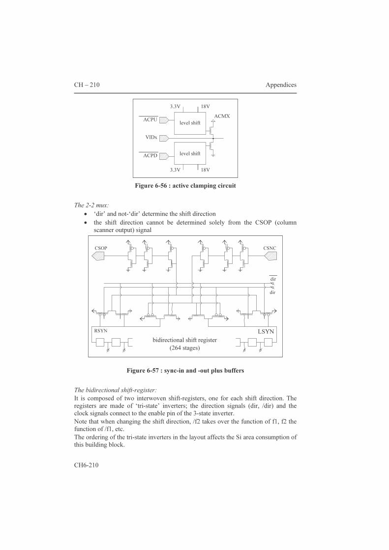
CH – 210 Appendices
CH6-210
Figure 6-56 : active clamping circuit
The 2-2 mux:
• ‘dir’ and not-‘dir’ determine the shift direction • the shift direction cannot be determined solely from the CSOP (column
scanner output) signal
Figure 6-57 : sync-in and -out plus buffers
The bidirectional shift-register: It is composed of two interwoven shift-registers, one for each shift direction. The registers are made of ‘tri-state’ inverters; the direction signals (dir, /dir) and the clock signals connect to the enable pin of the 3-state inverter. Note that when changing the shift direction, /f2 takes over the function of f1, f2 the function of /f1, etc. The ordering of the tri-state inverters in the layout affects the Si area consumption of this building block.
bidirectional shift register (264 stages)
dir
dir
RSYN LSYN
CSOP CSNC
VIDx
level shift
level shift
3.3V
3.3V
18V
18V
ACPU
ACPD
ACMX
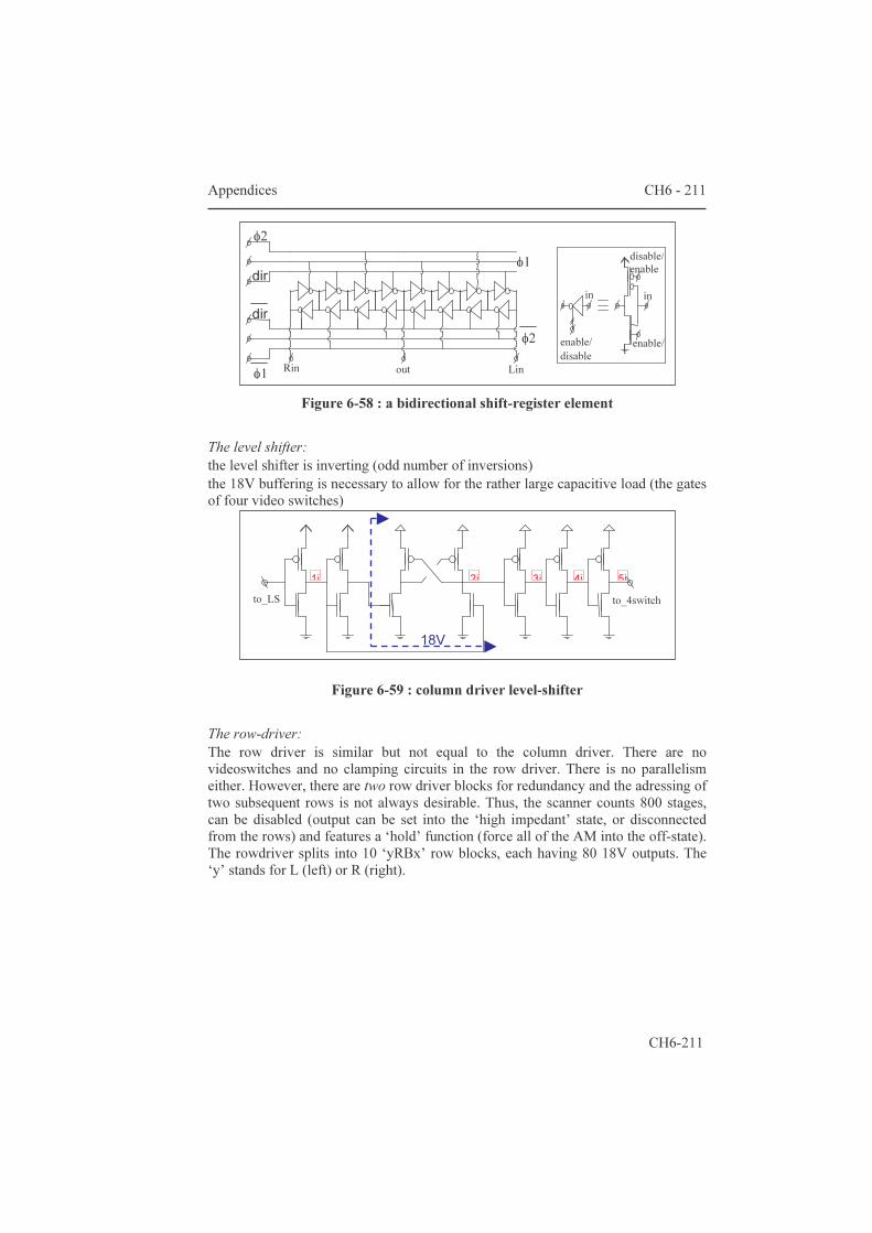
Appendices CH6 - 211
CH6-211
Figure 6-58 : a bidirectional shift-register element
The level shifter: the level shifter is inverting (odd number of inversions) the 18V buffering is necessary to allow for the rather large capacitive load (the gates of four video switches)
Figure 6-59 : column driver level-shifter
The row-driver: The row driver is similar but not equal to the column driver. There are no videoswitches and no clamping circuits in the row driver. There is no parallelism either. However, there are two row driver blocks for redundancy and the adressing of two subsequent rows is not always desirable. Thus, the scanner counts 800 stages, can be disabled (output can be set into the ‘high impedant’ state, or disconnected from the rows) and features a ‘hold’ function (force all of the AM into the off-state). The rowdriver splits into 10 ‘yRBx’ row blocks, each having 80 18V outputs. The ‘y’ stands for L (left) or R (right).
18V
to_4switch to_LS1i 2i 3i 4i 5i
in
enable/
disable/enable
enable/disable
dirφ1
φ2
Rin out Lin
dirφ2
φ1
in
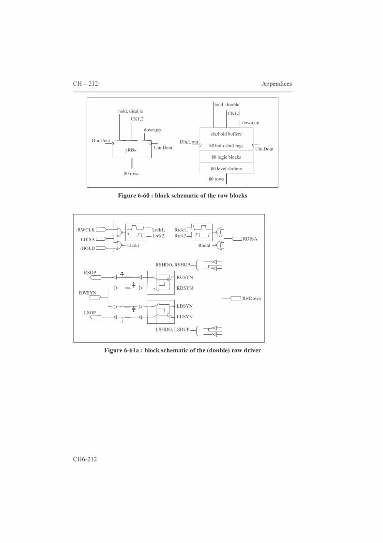
CH – 212 Appendices
CH6-212
Figure 6-60 : block schematic of the row blocks
Figure 6-61a : block schematic of the (double) row driver
Lrck1,Lrck2 RDISA
/HOLD
/RWCLKLDISA
Rhold
Rrck1,Rrck2
Lhold
LSOP
RSOP
RWSYNRwDown
RSHDO, RSHUP
LSHDO, LSHUP
RUSYN RDSYN
LDSYN LUSYN
Din,Uout
CK1,2
Uin,Dout
hold, disable
80 rows
yRBx
down,up
80 bidir shift regs
clk/hold buffersDin,Uout
down,up
Uin,Dout
hold, disableCK1,2
80 rows
80 logic blocks
80 level shifters
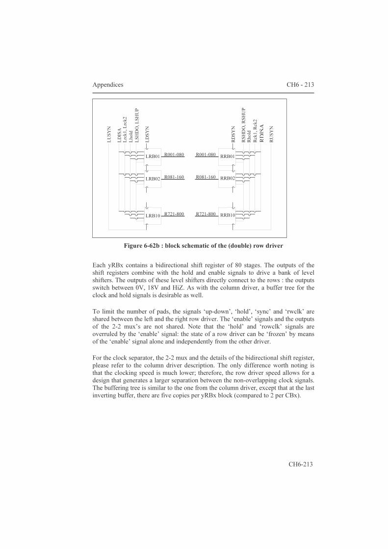
Appendices CH6 - 213
CH6-213
Figure 6-62b : block schematic of the (double) row driver
Each yRBx contains a bidirectional shift register of 80 stages. The outputs of the shift registers combine with the hold and enable signals to drive a bank of level shifters. The outputs of these level shifters directly connect to the rows : the outputs switch between 0V, 18V and HiZ. As with the column driver, a buffer tree for the clock and hold signals is desirable as well. To limit the number of pads, the signals ‘up-down’, ‘hold’, ‘sync’ and ‘rwclk’ are shared between the left and the right row driver. The ‘enable’ signals and the outputs of the 2-2 mux’s are not shared. Note that the ‘hold’ and ‘rowclk’ signals are overruled by the ‘enable’ signal: the state of a row driver can be ‘frozen’ by means of the ‘enable’ signal alone and independently from the other driver. For the clock separator, the 2-2 mux and the details of the bidirectional shift register, please refer to the column driver description. The only difference worth noting is that the clocking speed is much lower; therefore, the row driver speed allows for a design that generates a larger separation between the non-overlapping clock signals. The buffering tree is similar to the one from the column driver, except that at the last inverting buffer, there are five copies per yRBx block (compared to 2 per CBx).
R081-160
R001-080
R721-800R721-800
R081-160
R001-080 RRB01
RRB02
RRB10
LRB01
LRB02
LRB10
LUSY
N LD
ISA
Lrck
1, Lr
ck2
Lhold
LS
HDO,
LSHU
P LD
SYN
RDSY
N RS
HDO,
RSH
UP
Rhold
Rc
k1, R
ck2
RDISA
RU
SYN

CH – 214 Appendices
CH6-214
Figure 6-63 : row driver logic and level shifter
The only big difference is with the ‘logic’ and ‘level shifter’ blocks: by separate driving of the output nmos and pmos, one can obtain the HiZ output of the row driver. This necessitates blocking the shift register output and the hold signal. When enabling the driver, the hold signal overrides the shift register output to force the output to 0V. e) List of test circuits and test pad configuration The table shows the list of test circuits, the corners where they are located and the corresponding probe pad numbers.
Name of test circuit Corner Test bondpad numbers 1 Pixel trt 3/3 LL T01, T02, T09, T10 2 Pixel trt 3/3 + m4 LL T21, T22, T27, T28 3 3.3V inv 56|28 LL T03, T04, T11, T12 4 18V inv 36|12 LL T05, T06, T13, T14 5 Video switch 6x50/3 LL T07, T08, T15, T16 6 HiZ 3st inv 3|1.5 LL T17, T18, T23, T24 7 Active 3st inv 3|1.5 LL T19, T20, T25, T26 8 Row clock separator LL T29, T30, T31, T34, T35 9 Column level shifter LL T37, T38, T39, T41, T42 10 3.3V protection diode (power) LL T33, T40 11 3.3V protection diode (gnd) LL T32, T36 12 18V protection diode (gnd) LR T43, T51 13 2-2 MUX (a) LR T48, T49, T50, T56, T57, T58 14 2-2 MUX (b) LR T67, T68, T69, T70, T71, T72 15 Row logic (disabled) LR T59, T60, T61, T62, T63, T64,
18V
hold
SRo/p
disab
le
toRow

Appendices CH6 - 215
CH6-215
T65, T66 16 Row logic (enabled) LR T44, T45, T46, T47, T52, T53,
T54, T55 17 2NOR gate LR T73, T74, T75, T76, T77 18 3.3nmos 3.5/0.35 UR T78, T79, T80, T81 19 3.3nmos 7.0/0.35 UR T84, T85, T88, T89 20 3.3pmos 7.0/0.35 UR T82, T83, T86, T87 21 3.3pmos 14/0.35 UR T94, T95, T100, T101 22 18nmos 12/3 UR T92, T93, T98, T99 23 18nmos 48/3 UR T90, T91, T96, T97 24 18pmos 36/3 UR T102, T103, T108, T109 25 18pmos 72/3 UR T104, T105, T110, T111 26 18pmos 3.4/6 UR T106, T107, T112, T113
Table 6-9 : XGA test circuits and corresponding pads
Figure 6-64 : corner floorplan and numbered probe pad configuration
107
111 112 113110
104 105 106
96 97 98
83
10099
88
85
87
82
86
102
108 109
103
101
89
9594
78 79
93929190
8180
84
51 5453
43 49 50
72
58
69
75
77
4847464544
63 65 6664
59 60 61 62
57
76
565552
73 74
7170
67 68
12111009
252423
222120191817
16151413
40393837
3332313029
282726
0807060504030201
4241
363534
LOWER RIGHT LOWER LEFT
UPPER RIGHT UPPER LEFT
CH6 - 216 Appendices
CH6 - 216
6.2 Hands-on dracula™ The aim is to introduce swiftly the ‘Dracula’ verification software package. Note that the aim of the text is not completeness, it is rather a guided tour to highlight important points the author came across. Hopefully for the interested reader, this results in shorter learning times and eventually it results in a clearer understanding of layout verification. All the examples assume the so-called 'FLAT' mode. This mode does not take advantage of the casual repetition in the layout. This results in rather large data files (temporary and final), and therefore results most probably in longer computation times ("run times"). On one occasion, a DRC job ran in hierarchical mode. It indeed resulted in shorter run times. However, the job setup time proved to be much longer, partially because of a lack of experience and partially because the layout must be correctly partitioned into two levels. The designer must manually promote some layout cells to so-called 'HCELLs'. Incorrect ‘HCELL’ choices can lead to much longer run-times. Automatic partitioning of the layout data would probably be an excellent tool to make this check mode more attractive and “really" time efficient. Spreading the job over several computers of the network, so-called "distributed processing", has been looked at. However, I could not figure out a correct setup. The other options still have to be tested.
6.2.1 Introduction: general remarks Dracula is the name of a program that automates the verification of IC layouts. Such programs are essential, because manual verification is very time consuming and does not (always) result in a 100% error free design. An in depth check with verification software will require some time anyway, not only because it also requires a thorough understanding of the software. A complete check always splits in a sequence of verification jobs. A typical example of such a sequence could be: (order does matter) mask generation, design rule checks, electrical rule checks, layout versus schematic comparison, layout parameter extraction/parasitic resistance extraction. Often used abbreviations for these steps are MASKGEN, DRC, ERC, LVS and LPE/PRE. This sequenced approach helps untangling heaps of otherwise confusing error messages. Once all checks are successful, the layout data format needs conversion into a so-called fracture format. Eventually this conversion goes together with a mask bias step1. This step is sometimes referred to as MASKPREP. Usually the foundry itself 1 Note that if dracula is used to generate mask layouts for TCAD (MASKGEN), it is necessary to include the mask bias for correct process simulation.
Appendices CH6 - 217
CH6 - 217
or by a mask making company performs this step; furthermore proprietary test key patterns, alignment markers and/or process validation modules (PVMs) need to be added to the mask layout at this stage. The dracula software can do this data conversion (mask fracturing). This text will only mention it, though. After each correction, all of the previous checks have to be re-done: layout verification is an iterative process. As designs often contain repeated cells, one expects repeated error messages. As a result, the verification software sometimes produces a real jungle of error messages. The only efficient way is to tackle the first error message and start over. After some iteration, no more error messages show up. However, this does not imply the design is error free! Indeed, this depends on the completeness of the check sequence and correctness of layout data. As an example, checking the maximum width of polygons on a 'via' layer is insufficient to guarantee all 'vias' are squares of exactly X2 µm2. A badly positioned text label is another example of how to jeopardize the error sensitivity. The wrong position can generate false errors… but can also fail to generate a painfully pertinent open/short circuit error message. Error sensitivity is function of the correctness of both design data and input deck! For each job, the program input consists of design data (layout polygons and/or circuit netlists) and an 'input deck'. The input deck is an ASCII text file containing lists of verification instructions. It is composed of three main blocks:
• a ‘description’ block specifying the name of the layout database, search paths of executables, run directory, a list of program options... ;
• an ‘input layer’ block translating references to layout layers between the different layout databases (GDSII->Dracula) and defining (eventually derived) conduction layers
• an ‘operation’ block containing commands for layer operations, rule checks and netlist extractions.
The foundries distribute the input decks; these files are templates that require some additions/modifications. There are (computer) system dependent variables that must concord with the user’s system. Examples are the search path to the program executables or details of mask definitions. Sub-micron technologies often offer more than five interconnect layers, but not all designs do require all of them. Then the input decks need concordant modifications. Everyday practice has shown input decks assuming an opposite layer tone or that mask X corresponds to some other layer number. Before starting a job, it is mandatory to verify thoroughly… the input decks themselves, and to understand the verification commands. One option is to write the input deck completely from scratch, but then there is a liability issue. It therefore is reasonable to put it this way: it absolutely is no 'click and play' or easy-to-use, user-friendly software. The next paragraph describes the input deck more in detail for the 'FLAT' run mode. The details of other run modes are not treated (e.g. 'HIER' mode). The examples can serve as templates to create new input decks. The third paragraph explains the creation of run files and the evolution of a ‘dracjob’.
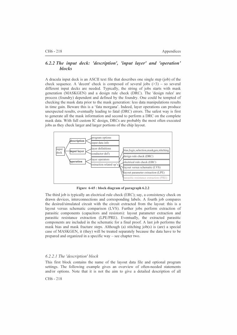
CH6 - 218 Appendices
CH6 - 218
6.2.2 The input deck: 'description', 'input layer' and 'operation’ blocks
A dracula input deck is an ASCII text file that describes one single step (job) of the check sequence. A 'decent' check is composed of several jobs (>3) – so several different input decks are needed. Typically, the string of jobs starts with mask generation (MASKGEN) and a design rule check (DRC). The 'design rules' are process (foundry) dependent and defined by the foundry. One could be tempted of checking the mask data prior to the mask generation: less data manipulations results in time gain. Beware this is a ‘fata morgana’. Indeed, layer operations can produce unexpected results, eventually leading to fatal (DRC) errors. The safest way is first to generate all the mask information and second to perform a DRC on the complete mask data. With full custom IC design, DRCs are probably the most often executed jobs as they check larger and larger portions of the chip layout.
Figure 6-65 : block diagram of paragraph 6.2.2
The third job is typically an electrical rule check (ERC); say, a consistency check on drawn devices, interconnections and corresponding labels. A fourth job compares the desired/simulated circuit with the circuit extracted from the layout: this is a layout versus schematic comparison (LVS). Further jobs perform extraction of parasitic components (capacitors and resistors): layout parameter extraction and parasitic resistance extraction (LPE/PRE). Eventually, the extracted parasitic components are included in the schematic for a final proof. A last job performs the mask bias and mask fracture steps. Although (a) stitching job(s) is (are) a special case of MASKGEN, it (they) will be treated separately because the data have to be prepared and organized in a specific way – see chapter two.
6.2.2.1 The 'description' block This first block contains the name of the layout data file and optional program settings. The following example gives an overview of often-needed statements and/or options. Note that it is not the aim to give a detailed description of all
program options input data info layer definitions conductor def's layer operators extraction related op’s
bias,logic,selection,maskgen,stitching design rule check (DRC) electrical rule check (ERC) layout versus schematic (LVS) layout parameter extraction (LPE) parasitic resistance extraction (PRE)
input deck
description
input layer
operation
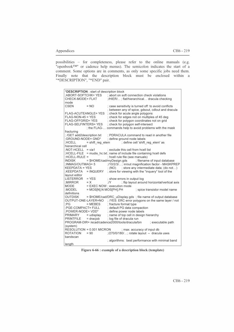
Appendices CH6 - 219
CH6 - 219
possibilities – for completeness, please refer to the online manuals (e.g. "openbook™" or cadence help menus). The semicolon indicates the start of a comment. Some options are in comments, as only some specific jobs need them. Finally note that the description block must be enclosed within a "*DESCRIPTION", "*END" pair.
Figure 6-66 : example of a description block (template)
*DESCRIPTION ; start of description block ;ABORT-SOFTCHK= YES ; abort on soft connection check violations CHECK-MODE = FLAT ;/HIER/... ; flat/hierarchical… dracula checking mode CSEN = NO ; case sensitivity is turned off: to avoid conflicts ; between any of spice, gdsout, cdlout and dracula FLAG-ACUTEANGLE= YES ; check for acute angle polygons FLAG-NON-45 = YES ; check for edges not on multiples of 45 deg FLAG-OFFGRID= YES ; check for polygon coordinates not on grid FLAG-SELFINTERS= YES ; check for polygon self-intersect ; the FLAG-… commands help to avoid problems with the mask fracturing ; /GET add2description.txt ; PDRACULA command to read in another file ;GROUND-NODE= GND* ; define ground node labels ;HCELL = shift_reg_elem ; define cell 'shift_reg_elem' as hierarchical cell ;NOT-HCELL = via1 ; exclude this cell from hcell list ;HCELL-FILE = mudis_hc.txt ; name of include file containing hcell defs ;HCELL-RULE = ; hcell rule file (see manuals) INDISK = $HOME/cad/myDesign.gds ; filename of input database ;INMAG/OUTMAG= 5 ;/10/2/3/…; in/out magnification factor - MASKPREP KEEPDATA = YES ; (NO) ; store any intermediate data; (do not…) ;KEEPDATA = INQUERY ; store for viewing with the "inquery" tool of the layout editor LISTERROR = YES ; show errors in output log ;MIRROR = X ;/Y ; flip layout around horizontal/vertical axis MODE = EXEC NOW ; execution mode ;MODEL = MOS[N],N MOS[PH],PH ; spice transistor model name definitions OUTDISK = $HOME/cad/DRC_uDisplay.gds ; file name of output database OUTPUT-ONE-LAYER=NO ; /YES: ERC error polygons on the same layer / not ;PG = MEBES ; fracture format type ;PGE-COMPACT= FULL ; default PG data compaction ;POWER-NODE= VDD* ; define power node labels PRIMARY = udisplay ; name of top cell in design hierarchy PRINTFILE = dracjob ; log file of dracula run PROGRAM-DIR= /ecad/cadence2000/tools/dracula/bin ; executable path (system) RESOLUTION = 0.001 MICRON ; max. accuracy of input db ROTATION = 90 ;/270/0/180/…; rotate layout – dracula uses bandscan ; algorithms: best performance with minimal band length
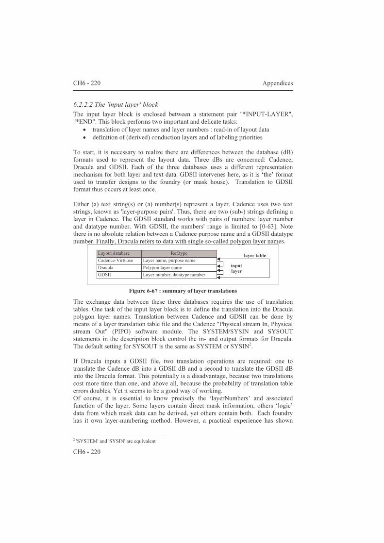
CH6 - 220 Appendices
CH6 - 220
6.2.2.2 The 'input layer' block The input layer block is enclosed between a statement pair "*INPUT-LAYER", "*END". This block performs two important and delicate tasks:
• translation of layer names and layer numbers : read-in of layout data • definition of (derived) conduction layers and of labeling priorities
To start, it is necessary to realize there are differences between the database (dB) formats used to represent the layout data. Three dBs are concerned: Cadence, Dracula and GDSII. Each of the three databases uses a different representation mechanism for both layer and text data. GDSII intervenes here, as it is ‘the’ format used to transfer designs to the foundry (or mask house). Translation to GDSII format thus occurs at least once. Either (a) text string(s) or (a) number(s) represent a layer. Cadence uses two text strings, known as 'layer-purpose pairs'. Thus, there are two (sub-) strings defining a layer in Cadence. The GDSII standard works with pairs of numbers: layer number and datatype number. With GDSII, the numbers' range is limited to [0-63]. Note there is no absolute relation between a Cadence purpose name and a GDSII datatype number. Finally, Dracula refers to data with single so-called polygon layer names.
Figure 6-67 : summary of layer translations
The exchange data between these three databases requires the use of translation tables. One task of the input layer block is to define the translation into the Dracula polygon layer names. Translation between Cadence and GDSII can be done by means of a layer translation table file and the Cadence ''Physical stream In, Physical stream Out" (PIPO) software module. The SYSTEM/SYSIN and SYSOUT statements in the description block control the in- and output formats for Dracula. The default setting for SYSOUT is the same as SYSTEM or SYSIN2. If Dracula inputs a GDSII file, two translation operations are required: one to translate the Cadence dB into a GDSII dB and a second to translate the GDSII dB into the Dracula format. This potentially is a disadvantage, because two translations cost more time than one, and above all, because the probability of translation table errors doubles. Yet it seems to be a good way of working. Of course, it is essential to know precisely the ‘layerNumbers’ and associated function of the layer. Some layers contain direct mask information, others ‘logic’ data from which mask data can be derived, yet others contain both. Each foundry has it own layer-numbering method. However, a practical experience has shown 2 'SYSTEM' and 'SYSIN' are equivalent
Layout database Ref.type Cadence-Virtuoso Layer name, purpose name Dracula Polygon layer name GDSII Layer number, datatype number
input layer block
layer table
Appendices CH6 - 221
CH6 - 221
differences in layer numbers between two input decks from the same foundry for the same technology! Thus, in practice, one must not assume there is a fixed relation between a technology and a set of layer numbers. This would be the most logical situation though. Let the reader guess how much time the author (and probably many others) lost in finding this weird little bug… Dracula can also read a Cadence dB directly; this seems simpler and safer because there seems to be only one translation. Again, practical experience has shown documentation from a foundry assigning mask numbers 13 and 14 to layers with Cadence names 'LYR' and 'noLYR' (a probable heritage from older versions of the technology or of its documentation, it really has nothing to do with number 13). To make 'sure' wrong interpretation would result, it was not all clear whether the mask type was light working field or dark working field… Thus, watch your layers, no matter whether there are one or two layer translations! Another reason to work with GDSII as intermediate format is that transfers of mask data to the mask house are often done by means of GDSII files (personally, I always did). Running checks on the same tape-out files is safer! Additionally, conversion of Cadence format to GDSII allows smashing several layer-purpose pairs onto the same GDSII (layer, datatype) number. The Dracula software can perform such operations too, but it is likely to cost much more time and computing resources. The following layout trick (see Figure 6-70) explains the usefulness of this possibility: connections on a metal1 layer can represent ground, power, signal or floating nodes. Using different purposes in cadence to draw the different connection categories (ground, power, signal or floating) helps avoiding undesirable shorts with full custom design. Each layer-purpose pair can indeed have a distinct visual representation. E.g. blue-blue polygons represent metal1 signal connections, blue polygons with a red border represent power nets on metal1, those with a green border are ground nets on metal1, etc. Finally, the GDSII format is independent from Cadence software/dB versions; this is interesting from the point of view of archiving. For the remainder of the text, it is assumed GDSII is always used as intermediate format. Sometimes it can be necessary to combine the results from a previous dracula job with new layout data. The statements IMPORT and EXPORT serve this purpose. They read in, respectively generate files of the form *.DAT in the dracula run directory (the '*' wildcard stands for any valid polygon layer name). A statement like 'IMPORT prevmask' expects the presence of a file 'prevmask.DAT' in the run directory. For reasons of simplicity, it is best to run a job containing 'IMPORT' statements in the same run directory as the run directory of the job containing the corresponding 'EXPORT' statements. To summarize there are three ways dracula can read in data:
• PLNameA = layerNr datatypeNr. ; reading a GDSII dB file • IMPORT = prevMsk ; reading a polygon layer file • PLNameB = layerName. purposeName ; reading cadence dB
Some of the polygon layers represent conducting layers (conductors). Definition of which polygon layer names represent conductors is done within the CONNECT-LAYER statement. Note that the conductor's name(s) eventually represent the result from (a) layer operation(s). Each set of connected conductors is associated with a
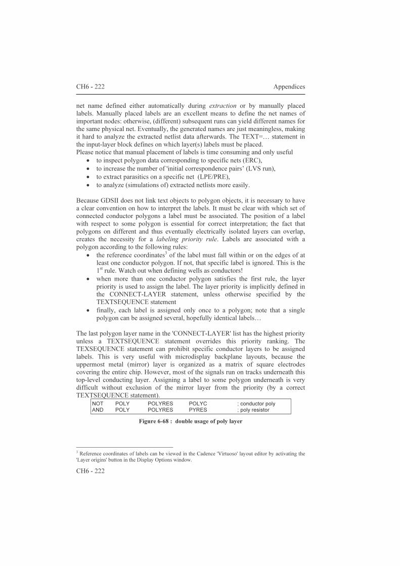
CH6 - 222 Appendices
CH6 - 222
net name defined either automatically during extraction or by manually placed labels. Manually placed labels are an excellent means to define the net names of important nodes: otherwise, (different) subsequent runs can yield different names for the same physical net. Eventually, the generated names are just meaningless, making it hard to analyze the extracted netlist data afterwards. The TEXT=… statement in the input-layer block defines on which layer(s) labels must be placed. Please notice that manual placement of labels is time consuming and only useful
• to inspect polygon data corresponding to specific nets (ERC), • to increase the number of 'initial correspondence pairs’ (LVS run), • to extract parasitics on a specific net (LPE/PRE), • to analyze (simulations of) extracted netlists more easily.
Because GDSII does not link text objects to polygon objects, it is necessary to have a clear convention on how to interpret the labels. It must be clear with which set of connected conductor polygons a label must be associated. The position of a label with respect to some polygon is essential for correct interpretation; the fact that polygons on different and thus eventually electrically isolated layers can overlap, creates the necessity for a labeling priority rule. Labels are associated with a polygon according to the following rules:
• the reference coordinates3 of the label must fall within or on the edges of at least one conductor polygon. If not, that specific label is ignored. This is the 1st rule. Watch out when defining wells as conductors!
• when more than one conductor polygon satisfies the first rule, the layer priority is used to assign the label. The layer priority is implicitly defined in the CONNECT-LAYER statement, unless otherwise specified by the TEXTSEQUENCE statement
• finally, each label is assigned only once to a polygon; note that a single polygon can be assigned several, hopefully identical labels…
The last polygon layer name in the 'CONNECT-LAYER' list has the highest priority unless a TEXTSEQUENCE statement overrides this priority ranking. The TEXSEQUENCE statement can prohibit specific conductor layers to be assigned labels. This is very useful with microdisplay backplane layouts, because the uppermost metal (mirror) layer is organized as a matrix of square electrodes covering the entire chip. However, most of the signals run on tracks underneath this top-level conducting layer. Assigning a label to some polygon underneath is very difficult without exclusion of the mirror layer from the priority (by a correct TEXTSEQUENCE statement).
Figure 6-68 : double usage of poly layer
3 Reference coordinates of labels can be viewed in the Cadence 'Virtuoso' layout editor by activating the 'Layer origins' button in the Display Options window.
NOT POLY POLYRES POLYC ; conductor poly AND POLY POLYRES PYRES ; poly resistor

Appendices CH6 - 223
CH6 - 223
The names of conductor layers do not necessarily have to be one of the layers present in the layout database. Conductor layers can be so-called derived layers, which result from a combination of layers. Figure 6-68 is an example of a conductor layer resulting from a layer operation: the 'POLY' layer in the GDSII file represents connections unless a special 'poly resistor' layer overlaps it. No (portions of) polygons on the poly layer covered by the ‘POLYRES’ layer can be conductors. Below are examples of an input layer block and corresponding lTable.
Figure 6-69 : example of an input layer block
Figure 6-70 : example of a layer translation table
*INPUT-LAYER; start of input layer block – imaginary process CHIP = SUBSTRATE 15 ; rectangle enclosing all data + 15 µm = chip boundary WELL = 1 ; gds layer number 1 is interpreted as well layer DIFF = 2 ; gds nr. 2 is interpreted as thin oxide regions POLY = 3 ; polysilicon gate material layer NINP = 4 ; n+ implant layer PINP = 5 ; p+ implant layer CTCT = 6 ; contact windows in ILD layer MET1 = 7 ; first metal layer VIA1 = 8 ; contact windows in IMD1 layer ';… TEXT = 60 ; layer containing label information TEXT = 61 ATTACH MET1 ; labels on layer 61 attach only to met1 polygons ;EXPORT = WELL ; stores polygon data in a file 'WELL.DAT'(KEEPDATA=YES)' ;IMPORT = WELL ; reading dracula data (file='WELL.DAT') from a previous run ; import & export cmds can be used for 'virtual stitching' CONNECT-LAYER = PWEL NWEL PSD NSD POLY MET1 … ; (4… derived layers) TEXTSEQUENCE = POLY MET1 … ; consider labels only on poly, met1,… *END ; end of input layer block
;*** layer translation table *** ; semicolons start comments ; Cadence GDSII ;Lname Lpurpose Lnumber datatypeNr. nwell drawing 1 0 active drawing 2 0 poly drawing 3 0 polyres drawing 3 0 ; merge if no res extraction is done nplus drawing 4 0 pplus drawing 5 0 contact drawing 6 0 metal1 drawing 7 0 ; metal1 layout data on layerNumber 7 metal1 ground 7 0 ; other boundary color for m1 gnd lines metal1 supply 7 0 ; same for VDD lines drawn on metal1 via1 drawing 8 0 metal2 drawing 9 0 ';... text drawing 60 0 ; text layer for labeling ;m1txt drawing 61 0 ; text attaching to m1 only comm drawing 62 0 ; layer used to add comments ;...

CH6 - 224 Appendices
CH6 - 224
6.2.2.3 The ‘operation’ block • Layer operators (MASKGEN, STITCHING, DRC, MASKPREP) • Extraction related commands (DRC, ERC, LVS, LPE/PRE)
Layer operators (MASKGEN, STITCHING, DRC, MASKPREP)
• Syntax of layer operation statements • Mask biasing : e.g. for maskprep • Layer AND/NOT/OR logic : e.g. for virtual stitching • Maskgen : automatic generation of (additional) mask data • Selection operators : e.g. for design rule checks
Syntax of layer operation statements General form: <operation><[options]> <layerList> <parameter> <derivedLayer>
<OUTPUT pgFileName layerNr> <comments> where:
<operation> : operator name; see the manuals for complete lists <[options]> : they modify the precise effects of <operation> <layerList> : list of (polygon) layer(s) (names) operated on <parameter> : equation/dimension parameter (keyword/number) <derivedLayer> : name of the derived layer (result) <OUTPUT : writes the result to the output in the format defined by the
SYSTEM and/or SYSOUT statements in the description block pgFileName : string of maximum 6 characters defining the first part of the
name of the output cell layerNr> : two-digit numbers defining the second part of the name of the
output cell; the full name thus becomes 'pgFileNamelayerNr' (concatenation). This number also defines the GDSII layerNumber. One topcell contains all output cells. With GDSII as output format, the name of the topcell is given by the concatenation of the string "out" with the name of the input topcell. This input topcell name is defined by the 'PRIMARY' statement in the description block.
<comments> : starts with a semicolon and is very useful as explanation for some of the DRCs (DRC command statements are not always intuitive). ‘INQUERY’ also uses this comment string as description of the error polygons.

Appendices CH6 - 225
CH6 - 225
Figure 6-71 : example of layer operation statements
Mask bias: e.g. for maskprep Usually, the foundry or mask maker performs the mask bias step together with the addition of testkey patterns and alignment markers. The aim of mask biasing can be to anticipate effects from processing. Not all masks necessarily need biasing. A typical example is the compensation of the thermal diffusion of nwells: heat cycles during processing cause the nwell to 'grow'. To obtain nwell contours as the designer wants, an under-sizing (negative bias) of the polygons is required. It is possible that some masks need a positive bias (process/foundry/working field tone dependent).
Figure 6-72 : a basic mask bias operation
Usually, the biasing occurs just before the mask fracturing (i.e. translating into a format used by mask maker) and this step is transparent for the designers. However, when stitching is involved, it is not straightforward to implement biasing correctly. For LF masks that need biasing, the module separating polygons must be pre-biased to make sure the edges end up right. Be aware of the artifacts resulting from sizing of non-orthogonal edges. These artifacts arise when the amount of over-sizing is greater than or equal to half the smallest of the minimum spacing, width or notch dimensions for that particular mask. The layout rules should be such that the usually rather small bias does not lead to these artifacts. The paragraph on maskgen gives more details.
; defines transistor gates: diffusion and gate AND DIFF POLY gates ; error: contact without metal1: CT and (not M1) - output cellName is ‘NOMETC54’ NOT CTCT MET1 badct OUTPUT NOMETC 54 ; merging polygon layers gatePLY and resiPLY into a single allPLY polygon layer OR gatePLY resiPLY allPLY ; oversize via4 by 0.1um in al directions ; the ‘GROW’ command is similar to, but not identical to ‘SIZE’ – see manual for details SIZE VIA4 BY 0.1 VIA4B ; big via4 ; spacing check : find areas between metal1 polygons narrower than 1.2 microns EXT[H] MTL1 LT 1.2 OUTPUT ERR62 45 ; min. space < 1.2
; simple bias statement SIZE NWELLO BY -1.3 NWELL ; nwell undersized into final nwell
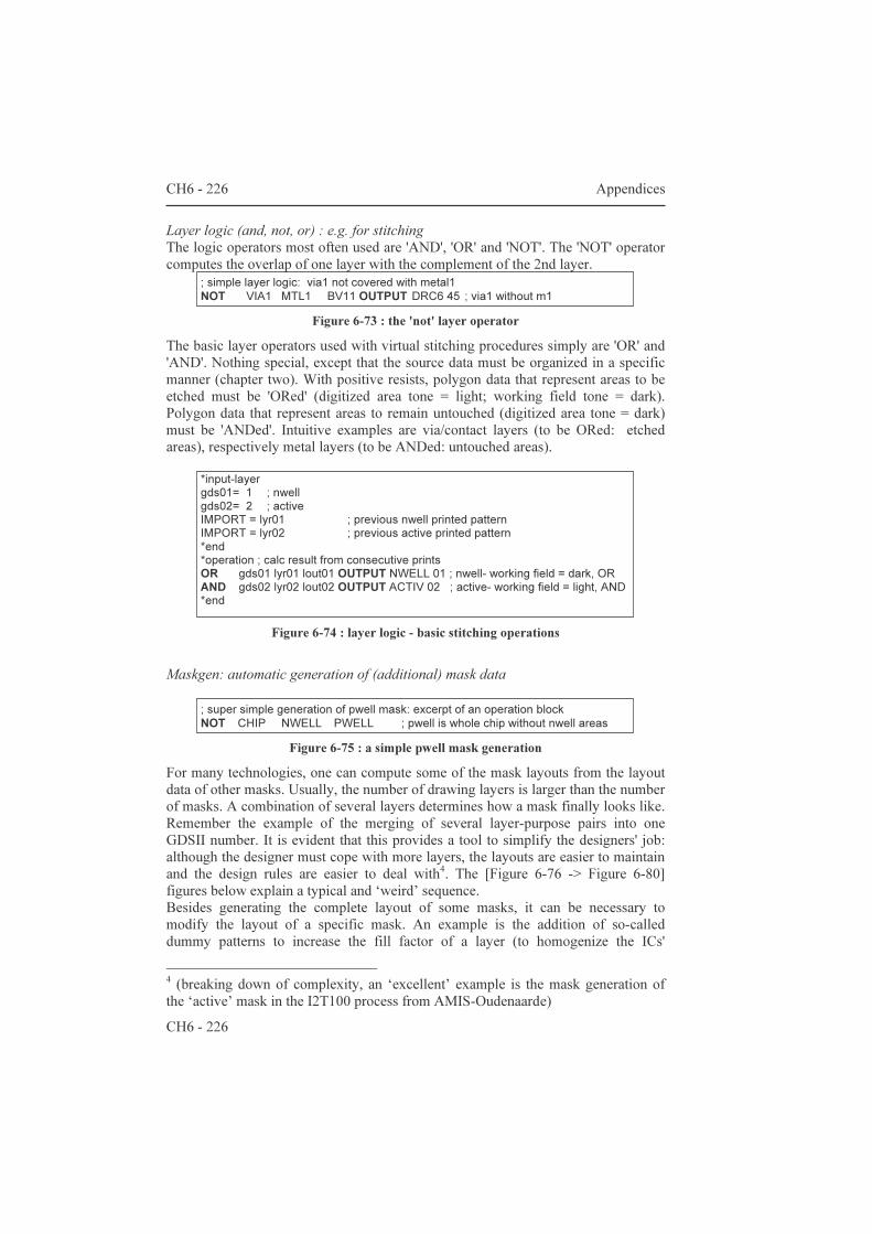
CH6 - 226 Appendices
CH6 - 226
Layer logic (and, not, or) : e.g. for stitching The logic operators most often used are 'AND', 'OR' and 'NOT'. The 'NOT' operator computes the overlap of one layer with the complement of the 2nd layer.
Figure 6-73 : the 'not' layer operator
The basic layer operators used with virtual stitching procedures simply are 'OR' and 'AND'. Nothing special, except that the source data must be organized in a specific manner (chapter two). With positive resists, polygon data that represent areas to be etched must be 'ORed' (digitized area tone = light; working field tone = dark). Polygon data that represent areas to remain untouched (digitized area tone = dark) must be 'ANDed'. Intuitive examples are via/contact layers (to be ORed: etched areas), respectively metal layers (to be ANDed: untouched areas).
Figure 6-74 : layer logic - basic stitching operations
Maskgen: automatic generation of (additional) mask data
Figure 6-75 : a simple pwell mask generation
For many technologies, one can compute some of the mask layouts from the layout data of other masks. Usually, the number of drawing layers is larger than the number of masks. A combination of several layers determines how a mask finally looks like. Remember the example of the merging of several layer-purpose pairs into one GDSII number. It is evident that this provides a tool to simplify the designers' job: although the designer must cope with more layers, the layouts are easier to maintain and the design rules are easier to deal with4. The [Figure 6-76 -> Figure 6-80] figures below explain a typical and ‘weird’ sequence. Besides generating the complete layout of some masks, it can be necessary to modify the layout of a specific mask. An example is the addition of so-called dummy patterns to increase the fill factor of a layer (to homogenize the ICs' 4 (breaking down of complexity, an ‘excellent’ example is the mask generation of the ‘active’ mask in the I2T100 process from AMIS-Oudenaarde)
; super simple generation of pwell mask: excerpt of an operation block NOT CHIP NWELL PWELL ; pwell is whole chip without nwell areas
*input-layer gds01= 1 ; nwell gds02= 2 ; active IMPORT = lyr01 ; previous nwell printed pattern IMPORT = lyr02 ; previous active printed pattern *end *operation ; calc result from consecutive prints OR gds01 lyr01 lout01 OUTPUT NWELL 01 ; nwell- working field = dark, OR AND gds02 lyr02 lout02 OUTPUT ACTIV 02 ; active- working field = light, AND *end
; simple layer logic: via1 not covered with metal1 NOT VIA1 MTL1 BV11 OUTPUT DRC6 45 ; via1 without m1
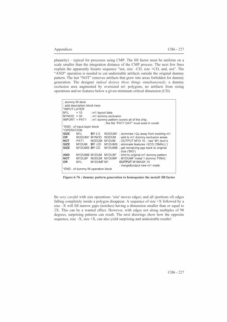
Appendices CH6 - 227
CH6 - 227
planarity) – typical for processes using CMP. The fill factor must be uniform on a scale smaller than the integration distance of the CMP process. The next few lines explain the apparently bizarre sequence "not, size –CD, size +CD, and, not". The “AND" operation is needed to cut undesirable artifacts outside the original dummy pattern. The last “NOT” removes artifacts that grew into areas forbidden for dummy generation. The designer indeed desires three things simultaneously: a dummy exclusion area augmented by oversized m1 polygons, no artifacts from sizing operations and no features below a given minimum critical dimension (CD).
Figure 6-76 : dummy pattern generation to homogenize the metal1 fill factor Be very careful with size operations: 'size' moves edges; and all (portions of) edges falling completely inside a polygon disappear. A sequence of size +X followed by a size –X will fill narrow gaps (notches) having a dimension smaller than or equal to 2X. This can be a wanted effect. However, with edges not along multiples of 90 degrees, surprising patterns can result. The next drawings show how the opposite sequence, size –X, size +X, can also yield surprising and undesirable results!
; dummy fill deck ; add description block here *INPUT-LAYER M1L = 10 ; m1 layout data M1NOD = 30 ; m1 dummy exclusion IMPORT = PAT1 ; m1 dummy pattern covers all of the chip, ; the file "PAT1.DAT" must exist in rundir *END ; of input-layer block *OPERATION SIZE M1L BY 2.0 NODUM1 ; dummies >2µ away from existing m1 OR NODUM1 M1NOD NODUM ; add to m1 dummy exclusion areas NOT PAT1 NODUM M1DUM ; OUTPUT M1D 10 ; ‘raw’ M1 dum’s SIZE M1DUM BY -CD M1DUMS ; eliminate features <2CD ('SMALL') SIZE M1DUMS BY CD M1DUMB ; get remaining pgs back to original ; size ('BIG') AND M1DUMB M1DUM M1DLBF ; limit to original m1 dummy pattern NOT M1DLBF NODUM M1DUMF ; M1DUMF metal 1 dummy 'FINAL' OR M1L M1DUMF M1 OUTPUT M1MASK 10 ; merge&output new m1 mask *END ; of dummy fill operation block

CH6 - 228 Appendices
CH6 - 228
Figure 6-77 : +x, -x fills narrow 'notches', ok
Figure 6-78 : +x, -x results in 'undergrow’; DRC min notch width should be > 2x
Figure 6-79 : -x,+x eliminates too thin (portions of) patterns, ok
Figure 6-80 : -x, +x results in 'overgrow'; solved by 'anding' with the source
+X -X
+X -X
+X -X
+X -X

Appendices CH6 - 229
CH6 - 229
Selection operators: e.g. for design rule checks Often used commands are: 'AREA', 'ENC', 'EXT', 'SELECT', 'WIDTH'. For the detailed description of each operator and all their options, see the manuals. It is good practice to compare the topological rules documentation from the foundry with its implementation. It is also useful to add comments at the end of DRC output sequences as these can be read with the INQUERY tools: when viewing the results of a verification run with INQUERY, error polygons are highlighted and described by either the verification statement or by the comment if present. As a designer might not know the dracula semantics by heart, and as some ‘selection’ operations can be lengthy and referring to meaningless intermediate polygon layer names, comments are most welcome for swift analysis and correction of the errors.
Figure 6-81 : examples of selection operators
SELECT NWELL INSIDE HV HNWEL ; define high voltage nwell WIDTH DIFF LT 3.0 OUTPUT Er09 45 ; min width of mosfet = 3u EXT[H] VI1 LT 2.0 OUTPUT Er10 45 ; via1 spacing < 2u ENC[TOE] VI1 M1 LT 1.0 OUTPUT Er11 45 ; m1 ovlp via1 < 1u AREA METAL1 RANGE 0 0.3 SMT1 OUTPUT Er12 45 ; m1 polygon too small

CH6 - 230 Appendices
CH6 - 230
Extraction related commands (DRC, ERC, LVS, LPE/PRE) • node dependent design rules • establishing connectivity • device extraction • typical ERC commands • typical LVS commands
Node dependent design rules
Figure 6-82 : examples of node dependent rules
The reason why DRC still shows up in this paragraph is the fact that some design rules depend on netlist information. An often recurring example is the minimum separation distance between two nwells (assume p-doped wafers). When the two nwells are always at the same potential (connected nwells), this distance can be shorter than when the wells can be at arbitrarily different potentials. In the example, EXT[H] checks NWELL polygons for an absolute minimum spacing of 2 microns (assuming micron is the database unit, ‘DBU’) and outputs the violation area. The next EXT[N] checks unconnected nwells for a minimum spacing of 4 dB units. The third EXT[NR’] outputs unconnected nwells less than 7u apart to the TCNWL polygon layer. TCNWL polygons in a high voltage region generate an error cell ‘Er1545’. Thus, unconnected, high voltage nwell spacing must be 7 dB units at least; unconnected, low voltage nwell spacing is 4 dB units; otherwise, the minimum spacing is 2u, irrespective of the voltage region. These checks require Dracula to interpret the NWELL layer as a conducting layer. Establishing connectivity Connectivity is established through the ‘CONNECT’,’SCONNECT’ and ‘STAMP’ commands. The first two commands propagate a node name trough a set of conductor polygons that make up a connection. The CONNECT-LAYER statement in the input layer block defines the polygon layer names that represent conductors. ‘STAMP’ forces the node name from one polygon layer onto a second. With ‘CONNECT’, conductor polygons are assigned the same node name whenever they simultaneously overlap the same contact or via. It is essential to note that the node names pass in both directions here – either from a lower to an upper or from an upper to a lower conductor, depending on which one the software comes across first. With ‘SCONNECT’ (soft connect) node names pass in one direction only. Simultaneous overlap of a contact/via by both layers is again required. Often the layers representing the bulk (pwell, nwell …) are defined as soft connect layers to be
EXT[H] NWELL LT 2.0 OUTPUT Er13 45 ; absolute minimum spacing is 2DBU ; the 'N' option bans equipotential wells from following check EXT[N] NWELL LT 4.0 OUTPUT Er14 45 ; 4DBU (disconnected nwells only) EXT[NR'] NWELL LT 7.0 TCNWL ; 7DBU (disconnected nwells) AND... AND TCNWL HNWELL ERHNW OUTPUT Er15 45 ; being Hvoltage nwell = error : HV wells must be connected

Appendices CH6 - 231
CH6 - 231
sure no supply tracks are fed via/through the bulk (‘SOFTCHK’ statement with ERC). The ‘STAMP’ statement copies (overwrites) the node name of one polygon onto a second, overlapping polygon (it does not propagate node names towards the rest of connected polygons!). The connectivity to be established is function of the subsequent verification checks. For the previous paragraph (node dependent DRC), it is enough to define only and but the ways nwells can be electrically connected to each other. E.g. it would be enough to include nwell, metal1 and metal2 in the connect layer statement (e.g. for a double metal process). Of course, this would be far from sufficient to extract full netlists from layouts that include poly conductors/resistors, n(p)plus cross-unders,… or to perform soft connection checks.
Figure 6-83 : connectivity examples
Device extraction Dracula recognizes devices (mosfets, bipolars, diodes, capacitors, resistors…) through the ‘ELEMENT’ statements. Extraction of predefined device types is easy. It is possible to detect more than one sub-type (low voltage nmos, high voltage nmos) and to make the association with an appropriate model name. A device specific layer makes the recognition easy; terminal specific layers define the device terminals. The device/terminal specific layers are often derived layers; sometimes, dedicated device marker layers are used. In such cases, the designer is required to mark the devices in the layout with the appropriate marker layer! With these explanations, the syntax of the ‘ELEMENT’ statements in the example should be easy to understand.
; excerpt showing connectivity commands ; *INPUT-LAYER block… CONNECT-LAYER = NWL NND MT1 MT2 ; *OPERATION block… AND NWL NPL NND ; nwell and nplus = nwell nplus diffusion AND NWL NND NCO ; nwell nplus diffusion = nwell contact ; need diff. polygon layer name for contact AND NWL HV HNW ; high voltage nwell (definition needed for HV ; device extraction) ;… CONNECT MT2 MT1 BY VIA ; via connects metal1 and metal2 polygons CONNECT MT1 NND BY CNT ; cnt (contacts) connects nwell nplus with metal1 SCONNECT NWL NND BY NCO ; NND connects to nwell in 1 direction only STAMP HNW BY NWL ; HNW is a subset of NWL that needs node info ; for HV device extraction ;… *END
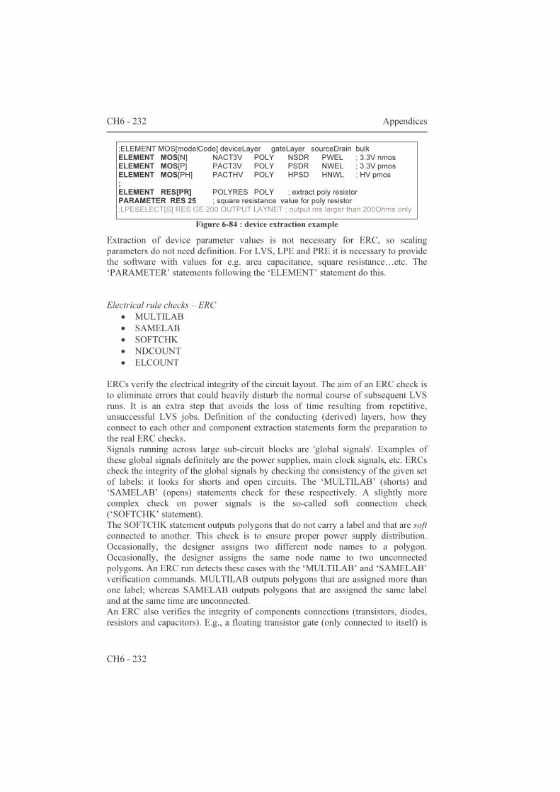
CH6 - 232 Appendices
CH6 - 232
Figure 6-84 : device extraction example
Extraction of device parameter values is not necessary for ERC, so scaling parameters do not need definition. For LVS, LPE and PRE it is necessary to provide the software with values for e.g. area capacitance, square resistance…etc. The ‘PARAMETER’ statements following the ‘ELEMENT’ statement do this. Electrical rule checks – ERC
• MULTILAB • SAMELAB • SOFTCHK • NDCOUNT • ELCOUNT
ERCs verify the electrical integrity of the circuit layout. The aim of an ERC check is to eliminate errors that could heavily disturb the normal course of subsequent LVS runs. It is an extra step that avoids the loss of time resulting from repetitive, unsuccessful LVS jobs. Definition of the conducting (derived) layers, how they connect to each other and component extraction statements form the preparation to the real ERC checks. Signals running across large sub-circuit blocks are 'global signals'. Examples of these global signals definitely are the power supplies, main clock signals, etc. ERCs check the integrity of the global signals by checking the consistency of the given set of labels: it looks for shorts and open circuits. The ‘MULTILAB’ (shorts) and ‘SAMELAB’ (opens) statements check for these respectively. A slightly more complex check on power signals is the so-called soft connection check (‘SOFTCHK’ statement). The SOFTCHK statement outputs polygons that do not carry a label and that are soft connected to another. This check is to ensure proper power supply distribution. Occasionally, the designer assigns two different node names to a polygon. Occasionally, the designer assigns the same node name to two unconnected polygons. An ERC run detects these cases with the ‘MULTILAB’ and ‘SAMELAB’ verification commands. MULTILAB outputs polygons that are assigned more than one label; whereas SAMELAB outputs polygons that are assigned the same label and at the same time are unconnected. An ERC also verifies the integrity of components connections (transistors, diodes, resistors and capacitors). E.g., a floating transistor gate (only connected to itself) is
;ELEMENT MOS[modelCode] deviceLayer gateLayer sourceDrain bulk ELEMENT MOS[N] NACT3V POLY NSDR PWEL ; 3.3V nmos ELEMENT MOS[P] PACT3V POLY PSDR NWEL ; 3.3V pmos ELEMENT MOS[PH] PACTHV POLY HPSD HNWL ; HV pmos ; ELEMENT RES[PR] POLYRES POLY ; extract poly resistor PARAMETER RES 25 ; square resistance value for poly resistor ;LPESELECT[S] RES GE 200 OUTPUT LAYNET ; output res larger than 200Ohms only
Appendices CH6 - 233
CH6 - 233
most probably an error. ELCOUNT and NDCOUNT count the number of devices connected to a net, respectively the number of nets connecting to a device. Layout versus schematics – LVS LVS jobs compare between the intended circuit (from simulations) and the circuit as defined by the mask layout. The presence of devices is checked against, as well as device dimensions like the width and length of mosfets, etc. Because Dracula performs the comparison, it is necessary to translate the circuit description into a compatible format. The LOGLVS command does this translation: it generates the 'LVSLOGIC.DAT' file from e.g. a CDL input netlist. It is not always necessary for the translation to include all devices present in the circuit netlist. The CDL netlist can contain optional statements that steer the comparison process: sometimes it is useful to neglect a specific device type or is it acceptable to allow swapping of input pins of logic gates. Most of these controls are available when creating the CDL netlist in Cadence. Layout parameter & parasitic resistance extraction LPE/PRE This is probably the last of the verification jobs en allows to extract parasitic components significant enough to eventually disturb or at least influence the chip's operation. In other words a more precise spice netlist is extracted that can be used for electrical simulation of the layout. Typically, large chips contain long interconnection wires and thus larger parasitics can be expected with and. A good designer anticipates the influences from parasitics by over-dimensioning components – without excess though. More precise computation of the impact is only possible once the layout is finished. And hopefully, no major modifications are needed as a result from this final computation… Parasitics emerge from the moment a connection wire is drawn: coupling capacitances emerge as well as resistors. With LPE/PRE a minimum threshold can be imposed to reduce excessive computing overhead from parasitics with negligible impact. PRE defines more devices compared to LPE; especially parasitic capacitors and parasitic resistances are looked at.
6.2.3 Evolution of a dracula job: a UNIX command sequence This paragraph describes practical 'software' details on how to execute one type of dracula runs. Most probably there are other ways to run verification tasks. First there is a description of the main executables: function, command line name and output filenames. The second part presents an example of a UNIX command sequence that attempts to mention all the useful steps for a verification run. The dracula preprocessor ("PDRACULA") checks the syntax of the input deck file. This program can be run standalone in some terminal window. Some jobs like LVS also require a netlist file as input. A program called "LOGLVS" translates this netlist into a dracula specific circuit description format. The translation must be finished
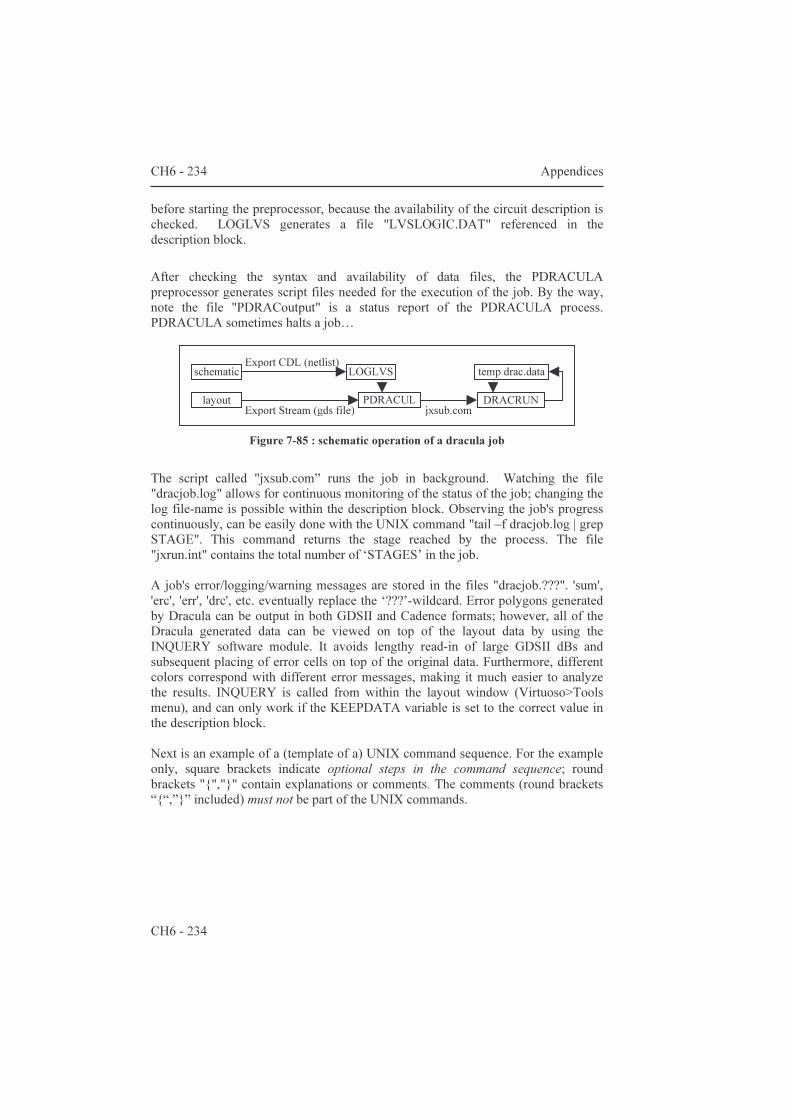
CH6 - 234 Appendices
CH6 - 234
before starting the preprocessor, because the availability of the circuit description is checked. LOGLVS generates a file "LVSLOGIC.DAT" referenced in the description block.
After checking the syntax and availability of data files, the PDRACULA preprocessor generates script files needed for the execution of the job. By the way, note the file "PDRACoutput" is a status report of the PDRACULA process. PDRACULA sometimes halts a job…
Figure 7-85 : schematic operation of a dracula job
The script called "jxsub.com” runs the job in background. Watching the file "dracjob.log" allows for continuous monitoring of the status of the job; changing the log file-name is possible within the description block. Observing the job's progress continuously, can be easily done with the UNIX command "tail –f dracjob.log | grep STAGE". This command returns the stage reached by the process. The file "jxrun.int" contains the total number of ‘STAGES’ in the job. A job's error/logging/warning messages are stored in the files "dracjob.???". 'sum', 'erc', 'err', 'drc', etc. eventually replace the ‘???’-wildcard. Error polygons generated by Dracula can be output in both GDSII and Cadence formats; however, all of the Dracula generated data can be viewed on top of the layout data by using the INQUERY software module. It avoids lengthy read-in of large GDSII dBs and subsequent placing of error cells on top of the original data. Furthermore, different colors correspond with different error messages, making it much easier to analyze the results. INQUERY is called from within the layout window (Virtuoso>Tools menu), and can only work if the KEEPDATA variable is set to the correct value in the description block. Next is an example of a (template of a) UNIX command sequence. For the example only, square brackets indicate optional steps in the command sequence; round brackets "{","}" contain explanations or comments. The comments (round brackets “{“,”}” included) must not be part of the UNIX commands.
Export Stream (gds file)
Export CDL (netlist) LOGLVS
PDRACULA
DRACRUN
schematic
layout jxsub.com
temp drac.data

Appendices CH6 - 235
CH6 - 235
Figure 6-86 : UNIX verification command sequence
[ {START: check search path settings in the .login and/or .cshrc files for correct terminal settings in UNIX: at least "/ecad/cds_2000/tools/dracula/bin" must be part of the search path (anno 2001) to be able to run the Dracula software}
[vi $HOME/.login ;] [vi $HOME/.cshrc] ] {end of terminal settings check} [ CIW~>Export CDL… (cdlout) {generate a CDL netlist: needed for some of the LVS/LPE/PRE jobs} {e.g. cellN == 'udisplay', viewN== 'schematic', o/p fileN == 'udisplay_netlist'} {wait until CDLOUT finishes} vi si.log {check the log file; CDL == Component Description Language} cp microdisplay_netlist $HOME/DRACULA/thisRun/netlist {copy the netlist file to the dracula run dir} LOGLVS << ! /cir <CR> /con <CR> /sum <CR> /x ! <CR> {Compile the network description into Dracula format: 2 files are generated, namely "LVSLOGIC.DAT" and "TREECELL.DAT"} ] { end of eventual CDLout translation and netlist compilation, LVS case } [ CIW~>Export Stream… (gdsout) { e.g. input can systematically be done through a GDSII file format } {wait until GDSOUT terminates} vi PIPO.LOG {check gdsout log file (PIPO == Physical-In,Physical-Out) ; the list of translated layers, warning and error messages must be checked!} ] {end of translation into GDSII format} [ PDRACULA {preprocessor execution} /G $HOME/DRACULA/DRACDECKS/thisRun.txt {get inputDeck} /F {finish} [PDRACULA << ! /G $HOME/DRACULA/DRACDECKS/thisRun.txt /F ! {alternative for use with script files; the text between the exclamation marks is input for the preprocessor} ] vi PDRACoutput {check preprocessor output file} ] {end of preprocessor job} [ cat jxrun.int {view total number of STAGES in the job}] jxsub.com {start verification job} tail –f dracjob.log | grep STAGE {print the STAGE number Dracula reached; the name of the log file depends on the ‘PRINTFILE’ statement in the description block; if the stage number does not change in time, then either:
• the machine is slow (heavy processing load, can be due to large dB size) or • a license is still in use by the/another user.
Note that it can happen that the Dracula license daemon crashes; in this case the user must kill the Dracula processes still running and must re-start the job. } {wait until the Dracula job terminates} vi dracjob.sum {analyze the summary of run results; ‘.log’ for logfile} [vi dracjob.erc or .lvs {analyze the results from eventual ERC or LVS run} ] [vi SPICE01.DAT {analyze the extracted netlist} ] [Virtuoso Layout~>INQUERY {interactive analysis of dracula output} ] ] {end of verification job, end of cmd sequence}

CH6 - 236 Appendices
CH6 - 236
6.3 The skill interpreter The aim is to give an idea of how skill code was used for the designs described in this book. 6.3.1 A brief introduction Usefulness and how it works [implementation of algorithms] [lists as inputs, note on versions] Lisp/C-like code interpreter The skill language has a syntax similar to C and works with lists. It is essential to know that the elementary datastructure is a list item. The language sequentially processes series of lists (hence interpreter); these lists can consist of an instruction name followed by input data. In simple terms, the design data are organized as objects; each object is a list of fields. Each field has a name and points to any kind of datastructure : a list of strings, a number, an object… With objects pointing to other objects, one has the basis for hierarchical data structures – exactly what is needed by IC designs. The design data in cadence are organized as lists that contain series of objects, i.e. data with associated ‘behavior’ (call-back functions). The datafields in these objects can be accessed with the '~>' operator : ‘object235~>field1’ returns the value or object stored in field1 of object235. Customization of cadence sub-menus The file "./menus/layEdit.menus" in the user's home directory allows for customization of the pull-down menus in the Virtuoso layout editor. To add a submenu in e.g. the layout editor's "Options" menu, simply add a previously defined menu item "myMenuItem" to the list in "lecOptionsMenu". A menu item must be a list of three objects – its name, a string defining the text that appears in the pull-down menu and a string containing the name of the associated action(s). E.g. The "cadenceRunDir/.cdsinit" initialization file can contain instructions that customize the keyboard short cuts (so-called bindkey definitions) and mouse strokes. The use of keyboard short cuts can significantly reduce the access times to menu commands. Hands-on skill code For detailed information of course I refer to the manuals; a first study should clarify the most essential notions: literals, datatypes, object identification (ID) and operators, procedures.

Appendices CH6 - 237
CH6 - 237
The list presented below is meant to shorten the time needed to start writing some code. It is intended to help anyone who needs to write code for the first time; of course, this does not help with programming style and certainly does not provide a full documentation of the language. load(), list(), case(), while(), procedure(), strcat(), geGetSelectedSet() geGetWindowCellView(), printf(), sprintf(),csh(), shell(), infile(), outfile(), close(), fscanf(), if(), foreach(), car(), cdr(), cadr(), caar(), caddr(), cadar(), cadadr(), tconc(), hiCreateAppForm(), hiCreateLabel(), hiCreateSeparatorField(), hiCreateMenuItem(), hiCreateStringField() hiDisplayForm(),hiFormCancel( hiCreateRadioField(), hiCreatePUlldownMenu(), hiCreateBBoxField(), hiCreateStringField(), hiCreateFloatField(), hiCreateButton(), hiCreateIntField(), hiSetFormToDefaults() hiGetWindowList(), hiCreateCyclicField(hiGetAppType(), hiDeleteBannerMenu(), hiInsertBannerMenu(), dbOpenCellView(), dbCreatePolygon(), dbCreateLabel(), dbOpenCellViewByType(), dbCreatePolygon(), dbCreateParamInst(), dbSave(), dbClose(), dbCreateInst() , getWorkingDir()

CH6 - 238 Appendices
CH6 - 238
6.3.2 Function and/or structure and/or source code of some useful routines
6.3.2.1 Automating labels for LVS It is obvious that for layouts with many repetitive structures (arrays), it can be an exhausting task to label nets manually. Instead, it is very easy to create a label that has a parameterized name and a parameterized placement coordinate. The following example shows how to label the 768 outputs of a XGA row driver cell. Make sure the active window (the last layout window the user accessed) contains the layout to label and that the layout is saved. Then load the following file called 'fileName' – type 'load("fileName")' in the input line of the CIW.
Figure 6-87: a routine for quick labeling of large designs
After execution, it is good practice to verify the modifications in the layout – bugs do show up from time to time. Thus, avoid immediately saving the cellview, as saving makes it harder to undo the modifications. To undo, click 'Discard edits' in the layout editor's menu 'Design' (does not work if the modified layout has been saved).
; *** fileName = 20020411_XGA013_RD_levelShift_opLabels.ilu ; get the object ID of the active window – it returns a cellView ID ; cv is the ID of the cellView to operate on cv=geGetWindowCellView() ; initialize counter – the rows will be named row<1> to row<768> i=1 ; start loop; at each cycle, create a new string and place the label 11.9u further up while(i<=768 ; variable 'devar' holds the label name ; sprintf prints "row<"+the value of counter+">" into the string variable sprintf(devar "row<%d>" i) ; create the label, the y coordinate is at 400, the x-coord is at -35.95 for 1st label ; labels for LVS are on layer-purpose m1txt-drawing ; the label is centered both in x and y around the x,y coordinate, orientation is 0deg ; the font is 'stick' and the font size is 0.5 dbCreateLabel(cv list("m1txt" "drawing") -35.95+(i-1)*11.9:400.0 devar "centerCenter" "R0" "stick" .5 ) ; end dbCreateLabel ; increment counter i++ ) ; end while and end of file

Appendices CH6 - 239
CH6 - 239
6.3.2.2 Collecting the list of instance coordinates in a layout The next file shows how to build a text file containing the placement coordinates of a given instance in the currently open layout. The instance name and the output file name are hard-coded in the file.
Figure 6-88 : routine to list instance coordinates
The lithography of stitched layouts requires precise location of the different circuit blocks (instances of the different modules) on the reticule, on the die and on the wafer. Usually, the reference coordinate (0.0, 0.0) is at the lower left corner of the reticule layout and in the middle for both the die and wafer layouts. All these data together determine where to ‘flash’ the different modules on the wafer.
; fileName = "Xiaohong.ilu" ; 3mar99 vdsteen ; To get list of placement coordinates of given instance in current layout view ; type 'load("Xiaohong.ilu")' to execute this file. ; ; last layout window selected, is automatically operated on; be careful! ; -> FILL IN INSTANCE NAME (case sensitive, no %$#@... characters) ; OUTPUT file is named 'cList.txt' and is located in the cadence runDir NameOfInstance="bondpad_v1" NameOfOutputFile="cList.txt" ; get ID of current cellview (graphics editor Get Window CellView) CID=geGetWindowCellView() ; get a list of IDs of all instance headers in the current cellview (CID) ; an instance header is a list of parameters of a cell that was placed x times in CID AllHeaders=CID~>instHeaders ; find the desired header (cellName equal to NameOfInstance), build instance list foreach( header AllHeaders if( header~>cellName==NameOfInstance WantedInst=header~>instances)) ; print the xy coordinate pairs 4 each instance from desired header to the output OPF=outfile(NameOfOutputFile) fprintf(OPF ";-------------------------------------------------------------\n") fprintf(OPF "; cList for instance %s in design %s\n" NameOfInstance CID~>cellName) fprintf(OPF ";-------------------------------------------------------------\n") foreach( instnce WantedInst fprintf(OPF "%L\n" instnce~>xy) printf("%L\n" instnce~>xy) ) fprintf(OPF ";-------------------------------------------------------------\n") close(OPF) ;write file to disk ; print message to the CIW window printf("Output in file %s\n" NameOfOutputFile) ; end of file
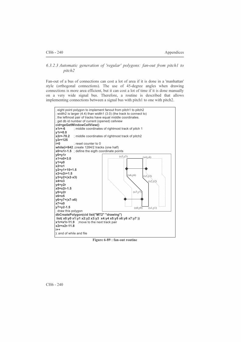
CH6 - 240 Appendices
CH6 - 240
6.3.2.3 Automatic generation of 'regular' polygons: fan-out from pitch1 to pitch2
Fan-out of a bus of connections can cost a lot of area if it is done in a 'manhattan' style (orthogonal connections). The use of 45-degree angles when drawing connections is more area efficient, but it can cost a lot of time if it is done manually on a very wide signal bus. Therefore, a routine is described that allows implementing connections between a signal bus with pitch1 to one with pitch2.
Figure 6-89 : fan-out routine
; eight point polygon to implement fanout from pitch1 to pitch2 ; width2 is larger (4.4) than width1 (3.0) (the track to connect to) ; the leftmost pair of tracks have equal middle coordinates. ; get db id number of current (opened) cellview cid=geGetWindowCellView() x1r=-6 ; middle coordinates of rightmost track of pitch 1 y1r=0.0 x2r=-70.2 ; middle coordinates of rightmost track of pitch2 y2r=125 i=0 ; reset counter to 0 while(i<642 ;create 1284/2 tracks (one half) x0=x1r-1.5 ; define the eigth coordinate points y0=y1r x1=x0+3.0 y1=y0 x2=x1 y2=y1+15+1.5 x3=x2r+1.5 y3=y2+(x2-x3) x4=x3 y4=y2r x5=x2r-1.5 y5=y2r x6=x5 y6=y7+(x7-x6) x7=x0 y7=y2-1.5 ; draw this polygon dbCreatePolygon(cid list("MT2" "drawing") list( x0:y0 x1:y1 x2:y2 x3:y3 x4:y4 x5:y5 x6:y6 x7:y7 )) x1r=x1r-11.9 ;move to the next track pair x2r=x2r-11.8 i++ ) ;end of while and file
(x0,y0) (x1,y1)
(x2,y2) (x3,y3)
(x4,y4) (x5,y5)
(x6,y6)
(x7,y7)
Appendices CH6 - 241
CH6 - 241
6.3.2.4 Automatic generation of wafer and die floorplans Computing the maximum nr. of chips per wafer and associated layouts Automatic generation of reticle/die/wafer layouts for stitching and collecting the list of print centre coordinates The aim of these routines is to be able to easily provide the foundry with print centre coordinate data. This kind of data is essential for stitching jobs. The die layout will determine the wafer layout. Combined with the reticle module location data, this allows to provide the necessary coordinate offsets for the wafer stepper. Additionally, a first impression of the resulting die layout can eventually help to debug the layout. 6.3.2.5 Routines for easier setup of verification jobs, GDSII translation and
maintenance The essence of these routines can be summarized as follows. The translation of layout data into the GDSII format is a common operation. Maintaining the translation table files, archiving them and archiving GDSII data is best done by using some conventions. Most essential is a file naming convention, so that it is easy to find out what the file is/was intended for. The routines provide a file naming mechanism and easy access to fixed/’standard’ locations for these files. The naming convention results in rather long filenames. Therefore the second utility of the routines is to automatically copy the full filenames into the input fields of the 'gds streamOut form or to automatically setup input and output parameters for verification jobs. Altogether, it allows for a quick setup of GDSII translation jobs and of verification jobs.The file naming convention is: yyyymmdd_techname_intention_jobtype.filetype, where
• YYYYMMDD is the date in 'year month day' concatenated format • TECHNAME is a name referring to the technology and/or project • INTENTION is the name of the source data or a comment depending on the
JOBTYPE subgroup: o gds output files: libraryName_cellName_viewName o technology file: libraryName_comment o layer trans. table: comment o dracula i/p deck: comment o unknown: comment
• JOBTYPE is one out of five subgroups: o gds output files: GDS, DRO, ERO, LVO, GEO, STO for GDS
translation, DRC, ERC, LVS, MASKGEN and stitching o/p o technology files: TFD o layer translation table: LTB o dracula i/p deck: DRC, ERC, LVS, LPE, GEN, ST1, ST2 o unknown: ???

CH6 - 242 Appendices
CH6 - 242
• FILETYPE is the file extension depending on the JOBTYPE subgroup: o gds output files: gds o technology file: tf o layer trans. table: ltable o dracula i/p deck: drac o unknown: ???
Besides the file naming, I formalized the file location (directory name):
• ./Projects/ThisProjectDir/ o CDLOUTS/ o DRAC_FILES/ o DRAWINGS/ o GDSOUTS/ o LAYERTAB_FILES/ o SIMULATIONS/ o SKILLS/ o TAPEOUT/ o TECHFILES/
���

References References - 243
References - 243
References
1 A. G. Fisher, T. P. Brody, andW. S. Escott, “Design of a liquid crystal color TV panel,” presented at the IEEE Conf. Display Devices, Oct. 1972
2 T. P. Brody, J. A. Asars, and G. D. Dixon, “A 6x6 in 20 lines-per-inch liquid-crystal display panel,” IEEE Trans. Electron Devices, vol. ED-20, pp. 995–1001, Nov. 1973
3 F. C. Luo, W. A. Hester, and T. P. Brody, “Alphanumeric and video performance of a 6"x6" 30 lines/inch TFT-LC display panel,” in Proc. SID, pp. 94–94, 1978
4 P.G. Barten, "Contrast sensitivity of the human eye and its effects on image quality", SPIE press
5 G. Wyszecki, W.S. Stiles, "Color science: concepts and methods, quantitative data and formula", John Wiley & Sons
6 "Electronic Display Technology: Advanced Materials and Emerging Markets", Technical Insights Inc., 2000
7 C. Chinnock, "Microdisplay report", Insight Media, published monthly
8 C. Chinnock, "Projection monthly", Insight Media, published monthly 9 A. Kitai, (Mc Master University, Ontario, Canada), cited by The New
York Times, Aug 8, 2002 10 H. Kawamoto, "The history of liquid crystal displays", Journal of the
IEEE, Vol. 90, No. 4, 2002 11 B.Verweire, R. Defever, "Limitation of resolution of lcos based
projection displays by diffraction effects", Proc. IDRC '99, pp. 489-492, 1999
12 H.Barna et al, "Liquid crystal alignment degradation induced by photo-irradiation", SID Digest, Vol. 32, pp. 980-, 2001
13 C-H. Wen et al., "Photostability of liquid crystals and alignment layers", Journal of the SID, Vol. 13, no.9, pp. 805-811, 2005
14 M. Bone, "Front-projection optical-system design for reflective lcos technology", Journal of the SID, Vol.9, pp. 227-, 2001
15 M.L. Jepsen et al., "0.9” SXGA Liquid Crystal on Silicon Panel with 450 Hz. field rate", Microdisplay Conference 2001, Westminster (Colorado), pp. 106-, 2001
16 C. Heine, S. Linz-Dittrich, "Color management system for 3-panel lcos projectors", SID Digest, Vol. 32, pp. 1189-, 2001
17 C.W. McLaughlin, "Progress in Projection and Large-Area Displays", Proc. of the IEEE, Vol. 90, No. 4, 2002
References - 244 References
References - 244
18 D. Cuypers, G. Van Doorselaer, J. Van den Steen, H. De Smet, and A. Van Calster, “Assembly of an XGA 0.9" LCoS display using inorganic alignment layers for VAN LC,” in Proceedings of Eurodisplay 2002, (Nice, France), pp. 551-554, October 2002.
19 D. Cuypers, G. Van Doorselaer, J. Van den Steen, H. De Smet, and A. Van Calster, “A projection system using vertically aligned nematic liquid crystal on silicon panels,” in Proceedings of IDW 2002, (Hiroshima, Japan), pp. 45-48, December 2002.
20 D. Cuypers, H. De Smet, G. Van Doorselaer, J. Van den Steen, and A. Van Calster, “Measurement methodology for vertically aligned nematic reflective displays,” in Proceedings of SPIE, Vol. 5002, (Santa Clara), pp. 62-72, January 2003.
21 A. Van Calster and D. Cuypers, “Reflective vertically aligned nematic liquid crystal microdisplays for projection applications (invited paper),” in Proc. of the 2000 international symposium on Electronic Imaging Vol. 3954: Prction Displays 2000: Sixth in a Series, (San Jose, USA), pp. 112-119, SPIE, January 2000.
22 D. Cuypers, H. De Smet, and A. Van Calster, “Fringe-field induced disclinations in van lcos panels,” in Proceedings of 11th Internation Display Workshops (IDW), (Niigata, Japan), December 2004.
23 MOSAREL public report, Esprit-IV project EP-25340, 2001 24 M.T. Pfeiffer, "LC modes for lcos", SID seminar, 2001 25 G. Van Doorselaer, B. Dobbelaere, M. Vrana, X. Xie, N. Carchon,
J. Van den Steen, J. Vanfleteren, H. De Smet, D. Cuypers, and A. Van Calster, “A paper-white chip-based display MCM package for portable IT products,” in Proc. of the IMAPS'98, (San Diego, USA), pp. 543-547, IMAPS, November 1998.
26 J. Van den Steen, N. Carchon, G. Van Doorselaer, C. De Backere, J. De Baets, H. De Smet, J. De Vos, J. Lernout, J. Vanfleteren, and A. Van Calster, “Technology and circuit aspects of reflective PNLC microdisplays,” in Proc. of the 1997 International Display Research Conference, (Toronto, Canada), pp. 195-198, SID, September 1997.
27 G. Van Doorselaer, N. Carchon, J. Van den Steen, D. Cuypers, J. Vanfleteren, H. De Smet, and A. Van Calster, “A reflective polymer dispersed information display made on CMOS,” in Proc. of the ICPS, (Antwerpen, Belgium), pp. 222-225, September 1998.
28 R.L. Melcher et al., "Design and fabrication of a prototype projection data monitor with high information content", IBM J Res Dev, Vol. 42, no. 3/4, pp 321-, 1998
29 C. De Backere, M. Vermandel, and V. C. A, “Light shielding with liquid crystal on silicon displays,” in Proc. of the 1998 International Display Research Conference, (Seoul, Korea), pp. 415-418, SID, September 1998.
References References - 245
References - 245
30 G. Meynants et al., "A 35mm 13.89 million pixel CMOS active pixel image sensor", The PICS Conference, Rochester NY, pp. 58-61, 2003
31 Shacham et al., "Method of forming reticle from larger size reticle information", US. Patent 6194105, 2001
32 D. Cohen et al., "Stitching design rules for forming interconnect layers", US. Patent 6225013, 2001
33 H. De Smet, J. Van den Steen, N. Carchon, D. Cuypers, C. De Backere, M. Vermandel, A. Van Calster, A. De Caussemaeker, A. Witvrouw, H. Ziad, K. Baert, P. Colson, G. Schols, and M. Tack, “The design and fabrication of a 2560x2048 pixel microdisplay chip,” in Proc. of the 19th International Display Research Conference (EuroDisplay99), (Berlin, Germany), pp. 493-496, SID, September 1999.
34 J. Van den Steen, H. De Smet, G. Van Doorselaer, A. Van Calster, and Colson, “Cost effective reticule design for very high resolution Si backplane prototypes,” in Proc. of IDW, (Sendai, Japan), pp. 235-238, ITE, December 1999.
35 Y. Zhu et al., "Simulation of Pixel Voltage Error for a-Si TFT LCD Regarding the Change in LC Pixel Capacitance", IEEE Trans. Electron Dev., Vol. 48, no. 2, 2001
36 H. De Smet, J. Van den Steen, and D. Cuypers, “Spice model for a dynamic liquid crystal pixel capacitance,” in Proceedings of the 10th international Display Workshops (IDW), (Fukuoka,Japan), pp. 53-56, December 2003.
37 H. De Smet, J. Van den Steen, and D. Cuypers, “Electrical model of a liquid crystal pixel with dynamic, voltage history-dependent capacitance value,” Liquid Crystals, vol. 31, no. 5, pp. 705-711, 2004.
38 J. De Baets, A. Van Calster, J. Van Den Steen, G. Van Doorselaer, D. Wojciechowski, G. Schols, and J. Witters, “Design of an x-Si active matrix for high resolution reflective displays,” in Proc. of the 15th Int. Display Research Conf., (Hamamatsu, Japan), pp. 477-479, SID, October 1995.
39 B.Lee, C. Park, S. Kim, M. Jeon, J.Heo, D. Sagong, J. Kim, J. Souk, " Reducing gray-level response to one frame : dynamic capacitance compensation", SID 2001 Digest, pp1260-1263, 2001
40 K. Sekiya, H. Nakamura, "Overdrive method for TN-mode LCDs - Recursive system with capacitance prediction", SID Digest, Vol. 32, pp. 114-117, 2001
41 K. Sekiya et al., "Overdrive for compensating color-shift on field sequential color TFT-LCDs", SID Digest, Vol. 35, pp. 408-, 2004
42 K. Sekiya et al., "Liquid crystal display device", Patent no. US20020175907, 2002

References - 246 References
References - 246
43 J. Van den Steen, G. Van Doorselaer, D. Cuypers, H. De Smet, A. Van Calster, F. Chu, and L. Tseng, “A 0.9 XGA LCoS backplane for projection applications,” in Proceedings of the Microdisplay 2001 conference, (Westminster, Colorado), pp. 87-90, August 2001.
44 H. Aoki, "Timing measurement and simulation of a TFT-LCD panel using pixel macro models", SID Digest, Vol. 30, pp. 524-, 1999
45 K.F. Chiang, S. Wu, S. Chen, "Fringing field effect of the lcos devices", Jpn. J. Appl. Phys., Vol. 41, pp4577-4585, 2002
46 F. Bruyneel et al., "Comparison of reflective PNLCDs and reflective single-polarizer Heilmeier guest-host displays", Journal of the SID, Vol. 9, pp. 313-, 2001
47 H. De Smet, D. Cuypers, A. Van Calster, J. Van den Steen, and G. Van Doorselaer, “Design, fabrication and evaluation of a high-performance XGA VAN-LCOS microdisplay,” Displays, vol. 23, no. 3, pp. 89-98, 2002.
48 G. Van Doorselaer, D. Cuypers, H. De Smet, J. Van den Steen, A. Van Calster, K.-S. Ten, and L.-Y. Tseng, “A XGA VAN-LCoS projector,” in Proceedings of Eurodisplay 2002, (Nice, France), pp. 205-208, October 2002.
49 D. Cuypers, J. Van den Steen, G. Van Doorselaer, H. De Smet, and A. Van Calster, “WXGA LCOS projection panel with vertically aligned nematic LC,” in Proceedings of the 10th international Display Workshops (IDW), (Fukuoka,Japan), pp. 1541-1544, December 2003.
50 H. De Smet, J. Van den Steen, G. Van Doorselaer, A. Van Calster, "Refresh pixel circuit for active matrix", patent no. WO2004001715, 2002
51 G.G. Gilette et al., "Display device drive circuit", Patent no. US4,766,430, 1988
52 A. Dupont et al., "Actuating circuit for a liquid crystal display", Patent no. US5206632, 1993
53 S.C. Tan, X.W. Sun, "Generic design of silicon backplane for lcos microdisplays", SID Digest, Vol. 33, pp. 200-, 2002
54 S.E. Shields, “AC activated liquid crystal display cell employing dual switching devices”, US Patent 4870396, 1989
55 D. McKnight, “Display system having electrode modulation to alter a state of an eletro0optic layer”, US Patent 6329971, 2001
56 K.M. Johnson, D.J. McKnight, I. Underwood, “Smart spatial light modulators using liquid crystals on silicon”, IEEE J. Quantum Electron., Vol. 29, no. 2, pp. 699-714, Feb. 1993
57 T.N. Blalock et al., “True color 1024x768 microdisplay with analog in-pixel pulsewidth modulation and retinal averaging offset correction”, IEEE J. of Solid-State Circuits, vol. 36, pp. 838-845, May 2001

References References - 247
References - 247
58 S. Lee et al, “Novel frame buffer pixel circuits for liquid-crystal-on-silicon microdisplays”, IEEE J. of Solid-State Circuits, vol. 39, pp.132-139, Jan 2004
59 A. O’Hara, J.R. Hannah, I. Underwood, D.G. Vass, and R.J. Holwill, “Mirror quality and efficiency improvements of reflective spatial light modulators by the use of dielectric coatings and chemical-mechanical polishing”, Applied Optics, vol. 32, no.28, Oct 1993
60 Dieter Cuypers, “Vertically aligned nematic liquid crystal microdisplays for projection applications”, Doctoral Thesis, Faculty of Applied Sciences, University of Gent, 2005, ISBN 90-8575-025-X
61 T. Borel, H. De Smet, J. Van den Steen et al., “Report on the results of theLCOS4LCOS project”, SID’06, to be published
���
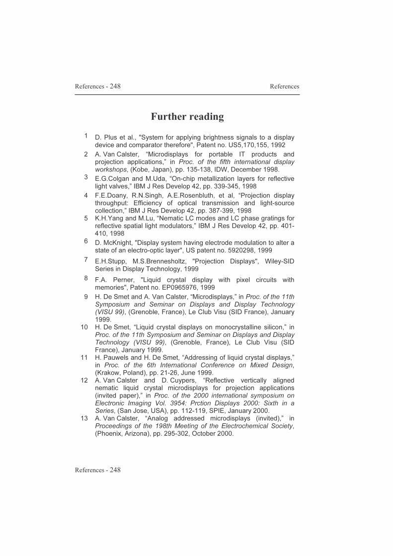
References - 248 References
References - 248
Further reading
1 D. Plus et al., "System for applying brightness signals to a display
device and comparator therefore", Patent no. US5,170,155, 1992 2 A. Van Calster, “Microdisplays for portable IT products and
projection applications,” in Proc. of the fifth international display workshops, (Kobe, Japan), pp. 135-138, IDW, December 1998.
3 E.G.Colgan and M.Uda, “On-chip metallization layers for reflective light valves,” IBM J Res Develop 42, pp. 339-345, 1998
4 F.E.Doany, R.N.Singh, A.E.Rosenbluth, et al, “Projection display throughput: Efficiency of optical transmission and light-source collection,” IBM J Res Develop 42, pp. 387-399, 1998
5 K.H.Yang and M.Lu, “Nematic LC modes and LC phase gratings for reflective spatial light modulators,” IBM J Res Develop 42, pp. 401-410, 1998
6 D. McKnight, "Display system having electrode modulation to alter a state of an electro-optic layer", US patent no. 5920298, 1999
7 E.H.Stupp, M.S.Brennesholtz, "Projection Displays", Wiley-SID Series in Display Technology, 1999
8 F.A. Perner, "Liquid crystal display with pixel circuits with memories", Patent no. EP0965976, 1999
9 H. De Smet and A. Van Calster, “Microdisplays,” in Proc. of the 11th Symposium and Seminar on Displays and Display Technology (VISU 99), (Grenoble, France), Le Club Visu (SID France), January 1999.
10 H. De Smet, “Liquid crystal displays on monocrystalline silicon,” in Proc. of the 11th Symposium and Seminar on Displays and Display Technology (VISU 99), (Grenoble, France), Le Club Visu (SID France), January 1999.
11 H. Pauwels and H. De Smet, “Addressing of liquid crystal displays,” in Proc. of the 6th International Conference on Mixed Design, (Krakow, Poland), pp. 21-26, June 1999.
12 A. Van Calster and D. Cuypers, “Reflective vertically aligned nematic liquid crystal microdisplays for projection applications (invited paper),” in Proc. of the 2000 international symposium on Electronic Imaging Vol. 3954: Prction Displays 2000: Sixth in a Series, (San Jose, USA), pp. 112-119, SPIE, January 2000.
13 A. Van Calster, “Analog addressed microdisplays (invited),” in Proceedings of the 198th Meeting of the Electrochemical Society, (Phoenix, Arizona), pp. 295-302, October 2000.
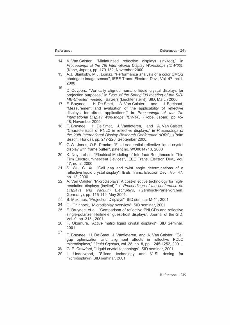
References References - 249
References - 249
14 A. Van Calster, “Miniaturized reflective displays (invited),” in Proceedings of the 7th International Display Workshops (IDW'00), (Kobe, Japan), pp. 179-182, November 2000.
15 A.J. Blanksby, M.J. Loinaz, "Performance analysis of a color CMOS photogate image sensor", IEEE Trans. Electron Dev., Vol. 47, no.1, 2000
16 D. Cuypers, “Vertically aligned nematic liquid crystal displays for projection purposes,” in Proc. of the Spring '00 meeting of the SID-ME-Chapter meeting, (Balzers (Liechtenstein)), SID, March 2000.
17 F. Bruyneel, H. De Smet, A. Van Calster, and J. Egelhaaf, “Measurement and evaluation of the applicability of reflective displays for direct applications,” in Proceedings of the 7th International Display Workshops (IDW'00), (Kobe, Japan), pp. 45-48, November 2000.
18 F. Bruyneel, H. De Smet, J. Vanfleteren, and A. Van Calster, “Characteristics of PNLC in reflective displays,” in Proceedings of the 20th International Display Research Conference (IDRC), (Palm Beach, Florida), pp. 217-220, September 2000.
19 G.W. Jones, O.F. Prache, "Field sequential reflective liquid crystal display with frame buffer", patent no. WO0014713, 2000
20 K. Neyts et al., "Electrical Modeling of Interface Roughness in Thin Film Electroluminescent Devices", IEEE Trans. Electron Dev., Vol. 47, no. 2, 2000
21 S. Wu, G. Xu, "Cell gap and twist angle determinations of a reflective liquid crystal display", IEEE Trans. Electron Dev., Vol. 47, no. 12, 2000
22 A. Van Calster, “Microdisplays: A cost-effective technology for high-resolution displays (invited),” in Proceedings of the conference on Displays and Vacuum Electronics, (Garmisch-Partenkirchen, Germany), pp. 115-119, May 2001.
23 B. Maximus, "Projection Displays", SID seminar M-11, 2001 24 C. Chinnock, "Microdisplay overview", SID seminar, 2001 25 F. Bruyneel et al., "Comparison of reflective PNLCDs and reflective
single-polarizer Heilmeier guest-host displays", Journal of the SID, Vol. 9, pp. 313-, 2001
26 F. Okumura, "Active matrix liquid crystal displays", SID Seminar, 2001
27 F. Bruyneel, H. De Smet, J. Vanfleteren, and A. Van Calster, “Cell gap optimization and alignment effects in reflective PDLC microdisplays,” Liquid Crystals, vol. 28, no. 8, pp. 1245-1252, 2001.
28 G. P. Crawford, "Liquid crystal technology", SID seminar, 2001 29 I. Underwood, "Silicon technology and VLSI desing for
microdisplays", SID seminar, 2001
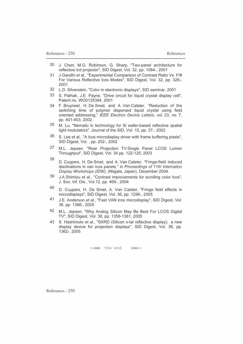
References - 250 References
References - 250
30 J. Chen, M.G. Robinson, G. Sharp, "Two-panel architecture for reflective lcd projector", SID Digest, Vol. 32, pp. 1084-, 2001
31 J.Gandhi et al., "Experimental Comparison of Contrast Ratio Vs. F/# For Various Reflective lcos Modes", SID Digest, Vol. 32, pp. 326-, 2001
32 L.D. Silverstein, "Color in electronic displays", SID seminar, 2001 33 S. Pathak, J.E. Payne, "Drive circuit for liquid crystal display cell",
Patent no. WO0135384, 2001 34 F. Bruyneel, H. De Smet, and A. Van Calster, “Reduction of the
switching time of polymer dispersed liquid crystal using field oriented addressing,” IEEE Electron Device Letters, vol. 23, no. 7, pp. 401-403, 2002.
35 M. Lu, "Nematic lc technology for Si wafer-based reflective spatial light modulators", Journal of the SID, Vol. 10, pp. 37-, 2002
36 S. Lee et al., "A lcos microdisplay driver with frame buffering pixels", SID Digest, Vol. , pp. 202-, 2002
37 M.L. Jepsen, "Rear Projection TV:Single Panel LCOS Lumen Throughput", SID Digest, Vol. 34 pp. 122-125, 2003
38 D. Cuypers, H. De Smet, and A. Van Calster, “Fringe-field induced disclinations in van lcos panels,” in Proceedings of 11th Internation Display Workshops (IDW), (Niigata, Japan), December 2004.
39 J.A.Shimizu et al., "Contrast improvements for scrolling color lcos", J. Soc. Inf. Dis., Vol.12, pp. 469-, 2004
40 D. Cuypers, H. De Smet, A. Van Calster, "Fringe field effects in microdisplays", SID Digest, Vol. 36, pp. 1298-, 2005
41 J.E. Anderson et al., "Fast VAN lcos microdisplay", SID Digest, Vol. 36, pp. 1366-, 2005
42 M.L. Jepsen, "Why Analog Silicon May Be Best For LCOS Digital TV", SID Digest, Vol. 36, pp. 1358-1361, 2005
43 S. Hashimoto et al., "SXRD (Silicon x-tal reflective display); a new display device for projection displays", SID Digest, Vol. 36, pp. 1362-, 2005
---ooo the end ooo---