
Development of Optical Fibre Sensors
38
sensors Review Micro and Nanostructured Materials for the Development of Optical Fibre Sensors Cesar Elosua 1,2, * ID , Francisco Javier Arregui 1,2 , Ignacio Del Villar 1,2 ID , Carlos Ruiz-Zamarreño 1,2 , Jesus M. Corres 1,2 , Candido Bariain 1,2 , Javier Goicoechea 1,2 , Miguel Hernaez 1,2 , Pedro J. Rivero 1,2 , Abian B. Socorro 1,2 ID , Aitor Urrutia 1,2 , Pedro Sanchez 1 , Pablo Zubiate 1 , Diego Lopez-Torres 1 , Nerea De Acha 1 , Joaquin Ascorbe 1 , Aritz Ozcariz 1 and Ignacio R. Matias 1,2 1 Department of Electric and Electronic Engineering, Public University of Navarre, E-31006 Pamplona, Spain; [email protected] (F.J.A.); [email protected] (I.D.V.); [email protected] (C.R.-Z.); [email protected] (J.M.C.); [email protected] (C.B.); [email protected] (J.G.); [email protected] (M.H.); [email protected] (P.J.R.); [email protected] (A.B.S.); [email protected] (A.U.); [email protected] (P.S.); [email protected] (P.Z.); [email protected] (D.L.-T.); [email protected] (N.D.A.); [email protected] (J.A.); [email protected] (A.O.); [email protected] (I.R.M.) 2 Institute of Smart Cities (ISC), Public University of Navarre, E-31006 Pamplona, Spain * Correspondence: [email protected]; Tel.: +34-948-169-328 Received: 28 August 2017; Accepted: 8 October 2017; Published: 11 October 2017 Abstract: The measurement of chemical and biomedical parameters can take advantage of the features exclusively offered by optical fibre: passive nature, electromagnetic immunity and chemical stability are some of the most relevant ones. The small dimensions of the fibre generally require that the sensing material be loaded into a supporting matrix whose morphology is adjusted at a nanometric scale. Thanks to the advances in nanotechnology new deposition methods have been developed: they allow reagents from different chemical nature to be embedded into films with a thickness always below a few microns that also show a relevant aspect ratio to ensure a high transduction interface. This review reveals some of the main techniques that are currently been employed to develop this kind of sensors, describing in detail both the resulting supporting matrices as well as the sensing materials used. The main objective is to offer a general view of the state of the art to expose the main challenges and chances that this technology is facing currently. Keywords: optical fibre sensor; nanotechnology; nanostructured materials; chemical sensing; bio medical sensing 1. Introduction It is well known that optical fibre technology produced a revolution in the telecommunications field during the last decades of the last century. Nowadays, this waveguide provides many homes with lots of services at a high speed. Some of the most relevant features of optical fibre are its high bandwidth, low transmission losses and the possibility of multiplex information. But optical fibre is being employed not only for communications, but also for different applications such the development of endoscopes for medicine thanks to the possibility of carrying light through a probe as well as collecting images by it [1]. It was also thought that the sensing technology could take advantage of optical fibre’s features and replace electronic sensors in many applications; however, electronic sensors were developed and commercialized decades before the use of optical fibre was extended, so that their prices are much more competitive; moreover, the integration of electronic circuits and devices make Sensors 2017, 17, 2312; doi:10.3390/s17102312 www.mdpi.com/journal/sensors
Transcript of Development of Optical Fibre Sensors

sensors
Review
Micro and Nanostructured Materials for theDevelopment of Optical Fibre Sensors
Cesar Elosua 1,2,* ID , Francisco Javier Arregui 1,2, Ignacio Del Villar 1,2 ID ,Carlos Ruiz-Zamarreño 1,2, Jesus M. Corres 1,2, Candido Bariain 1,2, Javier Goicoechea 1,2,Miguel Hernaez 1,2, Pedro J. Rivero 1,2, Abian B. Socorro 1,2 ID , Aitor Urrutia 1,2, Pedro Sanchez 1,Pablo Zubiate 1, Diego Lopez-Torres 1, Nerea De Acha 1, Joaquin Ascorbe 1, Aritz Ozcariz 1 andIgnacio R. Matias 1,2
1 Department of Electric and Electronic Engineering, Public University of Navarre, E-31006 Pamplona, Spain;[email protected] (F.J.A.); [email protected] (I.D.V.); [email protected] (C.R.-Z.);[email protected] (J.M.C.); [email protected] (C.B.); [email protected] (J.G.);[email protected] (M.H.); [email protected] (P.J.R.); [email protected] (A.B.S.);[email protected] (A.U.); [email protected] (P.S.); [email protected] (P.Z.);[email protected] (D.L.-T.); [email protected] (N.D.A.); [email protected] (J.A.);[email protected] (A.O.); [email protected] (I.R.M.)
2 Institute of Smart Cities (ISC), Public University of Navarre, E-31006 Pamplona, Spain* Correspondence: [email protected]; Tel.: +34-948-169-328
Received: 28 August 2017; Accepted: 8 October 2017; Published: 11 October 2017
Abstract: The measurement of chemical and biomedical parameters can take advantage of the featuresexclusively offered by optical fibre: passive nature, electromagnetic immunity and chemical stabilityare some of the most relevant ones. The small dimensions of the fibre generally require that thesensing material be loaded into a supporting matrix whose morphology is adjusted at a nanometricscale. Thanks to the advances in nanotechnology new deposition methods have been developed: theyallow reagents from different chemical nature to be embedded into films with a thickness alwaysbelow a few microns that also show a relevant aspect ratio to ensure a high transduction interface.This review reveals some of the main techniques that are currently been employed to develop thiskind of sensors, describing in detail both the resulting supporting matrices as well as the sensingmaterials used. The main objective is to offer a general view of the state of the art to expose the mainchallenges and chances that this technology is facing currently.
Keywords: optical fibre sensor; nanotechnology; nanostructured materials; chemical sensing;bio medical sensing
1. Introduction
It is well known that optical fibre technology produced a revolution in the telecommunicationsfield during the last decades of the last century. Nowadays, this waveguide provides many homeswith lots of services at a high speed. Some of the most relevant features of optical fibre are its highbandwidth, low transmission losses and the possibility of multiplex information. But optical fibre isbeing employed not only for communications, but also for different applications such the developmentof endoscopes for medicine thanks to the possibility of carrying light through a probe as well ascollecting images by it [1]. It was also thought that the sensing technology could take advantage ofoptical fibre’s features and replace electronic sensors in many applications; however, electronic sensorswere developed and commercialized decades before the use of optical fibre was extended, so that theirprices are much more competitive; moreover, the integration of electronic circuits and devices make
Sensors 2017, 17, 2312; doi:10.3390/s17102312 www.mdpi.com/journal/sensors

Sensors 2017, 17, 2312 2 of 38
them very appealing and easy to manipulate. Therefore, it is necessary to find the target applicationswhere the features that optical fibre offers make a difference compared to the electronic counterpart.
Thanks to its low losses, optical fibre allows remote sensing which is a good property whenpreparing a multi sensor network; moreover, it is made of an inert material, silica, making it immuneto electromagnetic interferences; no electrical biasing is required to guide light, so that the resultingsensors are passive, which is very relevant in environments with an explosion risk. Finally, researchersare developing modulation techniques that allows physical quantities to be measured along the fibreitself, which is called distributed sensing. An application where all these features are required isstructural health monitoring in civil engineering [2]: tunnels, bridges, concrete constructions arecurrently being monitored using optical fibre sensors. The parameters that are commonly registered inthese cases are mechanical vibrations, temperature and strain.
Following with the idea of sensing, the question that arises is if it is also possible to measurechemical entities: to achieve it, a material sensitive to the parameter to be detected has to be depositedon the fibre. In this manner, the guidance of the light is altered by this compound, so that if its opticalproperties change, they will modify the photonic signal traveling through the fibre, which constitutesthe transduction principle of optical fibre sensors for chemical measurements. There is a wide varietyof applications were this type of devices can be used: bio sensing [3], pH measuring [4], detectionof Volatile Organic Compounds (VOCs) [5], monitoring of relative humidity [6] or gas sensing [7],just to mention some important categories. In most of the schemes, the sensing compound has tobe embedded into a supporting matrix, which is almost as important as the sensitive material itself.On one hand, the coating has to keep the reagent attached onto the fibre and, therefore, be robustto chemical attacks as well as to aging; on the other hand, it must allow the target molecules andthe sensing material to interact between them, so the transduction can take place (in some cases,the supporting matrix itself is sensitive to the target parameter). As it can be inferred, the morphologyof the coating plays a relevant role, and it should be adjusted at a micro- or even nanometric level: inother words, micro and nanostructured materials have to be used.
The development of nanotechnology has allowed deposition techniques to be adapted to getcoatings whose morphological parameters can be modulated: volume/surface ratio, porosity, poroussize or chemical adsorption are some examples. Of course, the final thickness of the coating isvery relevant: in the case of optical fibre, is has to be below a few microns because otherwise,the transduction will not reach the light traveling along the fibre. To be able to handle with theserequirements, it is almost compulsory to use nanotechnology: actually, many efforts are being focusedto implement of bio and chemical optical fibre sensors thanks to the synergy between this substrateand nanostructured materials.
This review has been prepared to be accessible to readers that are familiarized with optical fibretechnology and the ones that are not, as well as for researchers that handle optical fibre but are notused to working with chemical reagents or sensing materials. Firstly, the fundamental concepts ofthis kind of sensors are briefly presented to understand how they work as well as the transductionprinciples of the devices described along the section. Thereafter, some construction techniques todevelop chemical and biosensors with optical fibres are described: all of them are referenced at thenext section where sensors are classified depending on the micro- or nanostructured material used toimplement them. This review does not intend to include all the techniques reported in the literaturebut only some of the most significant. The manuscript review ends with a summary of the concepts,techniques and results exposed; some conclusions about the current state of the art are also presented.
2. Fundamentals of Optical Fibre Sensors
This section describes briefly the main concepts about optical fibre sensors to understand themechanism behind their operation. Thereafter, some of the most relevant transduction principles aredescribed. A detailed study about optical fibre sensors theory can be found in [8].

Sensors 2017, 17, 2312 3 of 38
2.1. Theoretical Background and Main Architectures
An optical fibre is a waveguide that transmits light of different wavelengths. The propagationmechanism can be analysed by Maxwell equations as well as by ray theory because the signalwavelength is smaller than the physical dimensions of the waveguide. A standard optical fibre is madeof silica and, more specifically, has two main parts: core and cladding. The core is typically doped toobtain a refractive index slightly higher than the cladding’s one, which guarantees total reflection bySnell law under certain conditions; however, there is always a small energy transmission from the coreto the cladding. Talking in terms of electromagnetic fields, most of the signal is transmitted by coremodes, although a tiny part of it is coupled into the cladding modes, also known as evanescent field(see Figure 1). In the case of sensors, the transduction can take place with the core mode or with thecladding ones depending on the architecture and the sensing material employed.
Sensors 2017, 17, 2312 3 of 39
made of silica and, more specifically, has two main parts: core and cladding. The core is typically doped to obtain a refractive index slightly higher than the cladding’s one, which guarantees total reflection by Snell law under certain conditions; however, there is always a small energy transmission from the core to the cladding. Talking in terms of electromagnetic fields, most of the signal is transmitted by core modes, although a tiny part of it is coupled into the cladding modes, also known as evanescent field (see Figure 1). In the case of sensors, the transduction can take place with the core mode or with the cladding ones depending on the architecture and the sensing material employed.
(a) (b)
Figure 1. (a) On the left hand side, the transversal section of the optical fibre showing core (highlighted) and cladding; (b) on the right hand side, the longitudinal section showing the signals involved in light propagation explained by ray theory (arrows) and electromagnetic field theories.
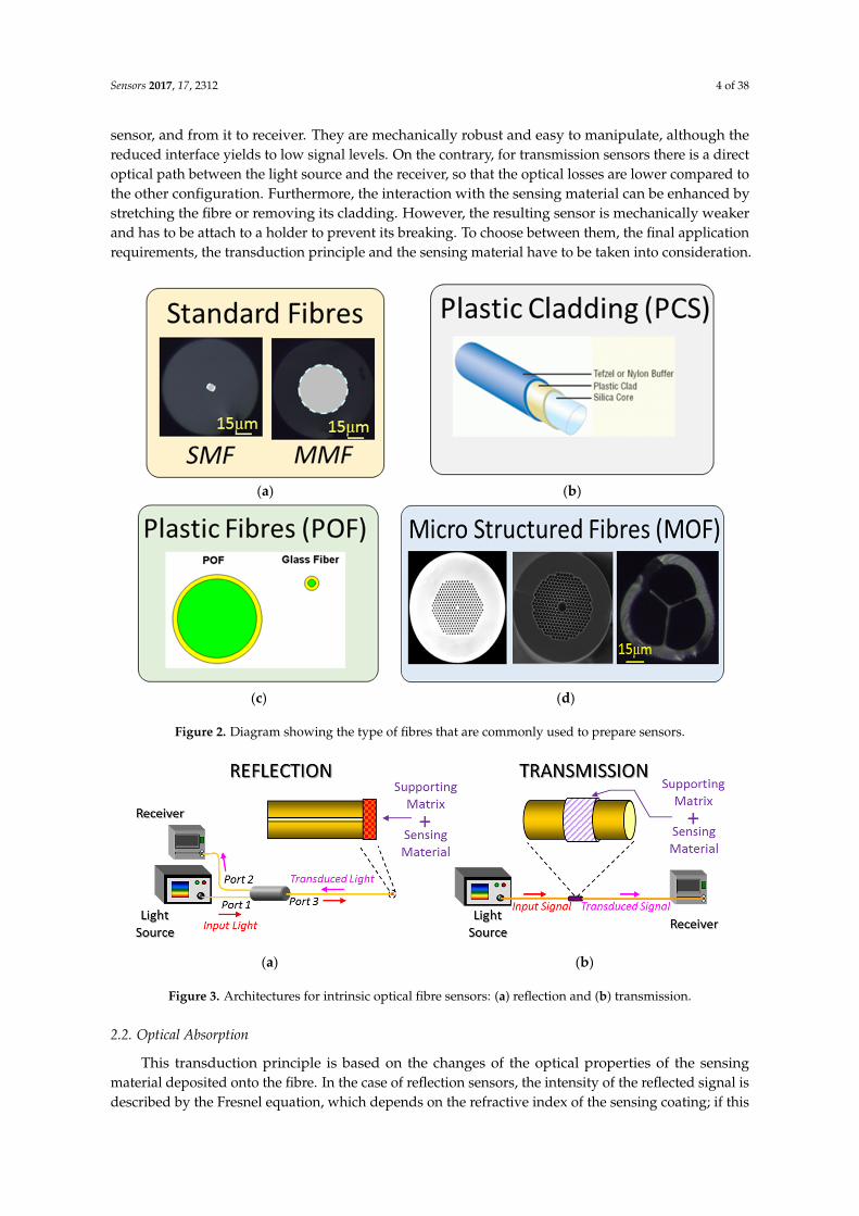
There are several ways to classify optical fibres. The ones used in telecommunication systems are considered as standard by International Telecommunication Union (ITU) and show a cladding diameter of 125 microns. Depending on the core diameter, there are two types of standard fibres: Single Mode Standard Fibre (SMF) and Multi-Mode Standard Fibre (MMF); for the first one, the core diameter below 9 microns, whereas for the second is larger than 50 microns. In both cases, core and cladding are made of SiO2, but not all the fibres are made of this material: some of them have a silica core but a plastic cladding, and are known as Plastic Cladding Silica (PCS) core fibres. This kind of fibres is typically wider, with core diameters ranging from 100 microns up to 1100 microns. Moreover, the plastic cladding is easy to remove, which easies the interaction with the evanescent field. Another type of fibre is completely made of plastic, which is named Plastic or Polymer Optical Fibres (POF): they are commonly wider as SMF or MMF, and have different applications in communications, sensors and in the biomedical field due to the mechanical robustness, the improvement of their transmission properties and the easiness to manipulate them [9–11]. Finally, there are fibres that are fabricated with air holes following a pattern: Microstructured Optical Fibres (MOF). Of course, several subgroups can be made in this category, but they will be detailed further in this paper considering these fibres as microstructured materials. There are other types of fibres, but these are the common ones used for sensors. Figure 2 shows a brief summary.
(a) (b)
Figure 1. (a) On the left hand side, the transversal section of the optical fibre showing core (highlighted)and cladding; (b) on the right hand side, the longitudinal section showing the signals involved in lightpropagation explained by ray theory (arrows) and electromagnetic field theories.
There are several ways to classify optical fibres. The ones used in telecommunication systemsare considered as standard by International Telecommunication Union (ITU) and show a claddingdiameter of 125 microns. Depending on the core diameter, there are two types of standard fibres:Single Mode Standard Fibre (SMF) and Multi-Mode Standard Fibre (MMF); for the first one, the corediameter below 9 microns, whereas for the second is larger than 50 microns. In both cases, core andcladding are made of SiO2, but not all the fibres are made of this material: some of them have a silicacore but a plastic cladding, and are known as Plastic Cladding Silica (PCS) core fibres. This kind offibres is typically wider, with core diameters ranging from 100 microns up to 1100 microns. Moreover,the plastic cladding is easy to remove, which easies the interaction with the evanescent field. Anothertype of fibre is completely made of plastic, which is named Plastic or Polymer Optical Fibres (POF):they are commonly wider as SMF or MMF, and have different applications in communications, sensorsand in the biomedical field due to the mechanical robustness, the improvement of their transmissionproperties and the easiness to manipulate them [9–11]. Finally, there are fibres that are fabricated withair holes following a pattern: Microstructured Optical Fibres (MOF). Of course, several subgroups canbe made in this category, but they will be detailed further in this paper considering these fibres asmicrostructured materials. There are other types of fibres, but these are the common ones used forsensors. Figure 2 shows a brief summary.
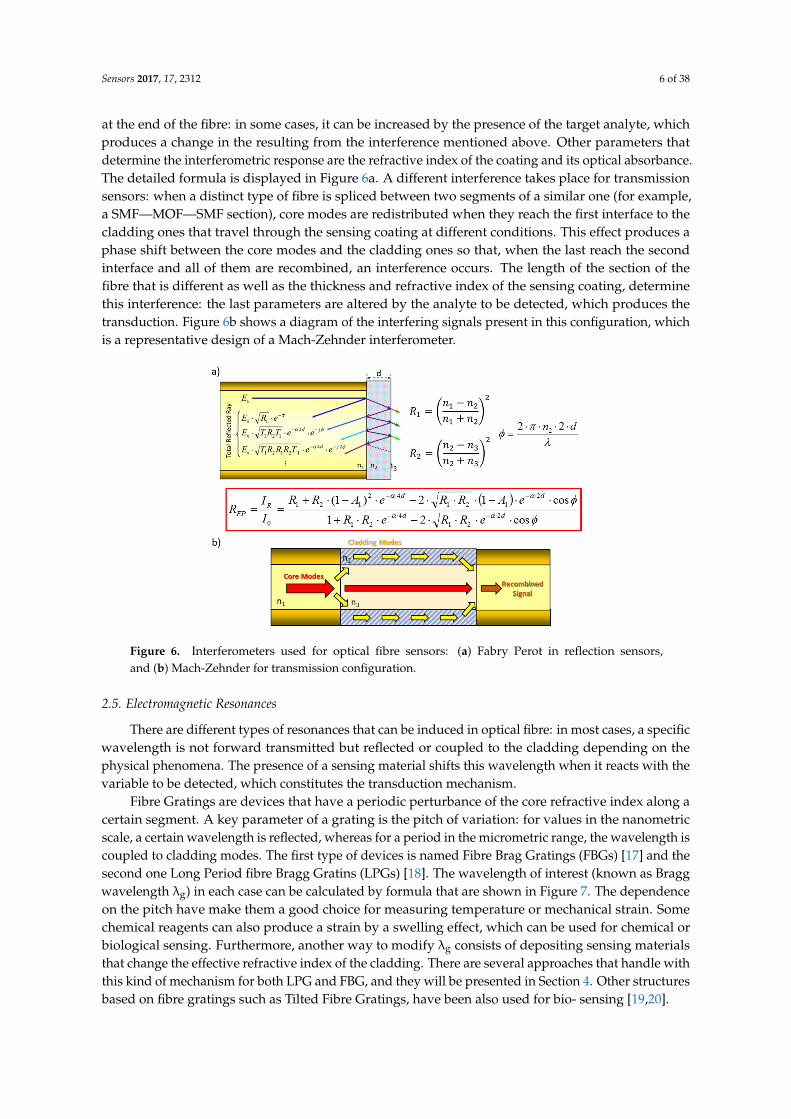
In an optical fibre sensor, the transduction takes place when the target analyte changes theproperties of the light traveling through the waveguide. If the transduction occurs externally to theoptical fibre, the sensor is extrinsic, whereas if it occurs on the fibre it is named intrinsic by someauthors [5]: most of the sensors studied for this review are intrinsic. Depending on the location of thesensing layer, two types of architectures or configurations are considered: transmission and reflection(see Figure 3). In the case of reflection sensors, the sensing material embedded into a supporting matrixis deposited at the end of a pigtail (which can be perpendicularly ended or show other shapes); sensorsprepared with this configuration are known optrodes because they look like electrodes. The keydevice for a reflection set up is the optical coupler which guides the signal from the light source to the
Sensors 2017, 17, 2312 4 of 38
sensor, and from it to receiver. They are mechanically robust and easy to manipulate, although thereduced interface yields to low signal levels. On the contrary, for transmission sensors there is a directoptical path between the light source and the receiver, so that the optical losses are lower compared tothe other configuration. Furthermore, the interaction with the sensing material can be enhanced bystretching the fibre or removing its cladding. However, the resulting sensor is mechanically weakerand has to be attach to a holder to prevent its breaking. To choose between them, the final applicationrequirements, the transduction principle and the sensing material have to be taken into consideration.
Sensors 2017, 17, 2312 3 of 39
made of silica and, more specifically, has two main parts: core and cladding. The core is typically doped to obtain a refractive index slightly higher than the cladding’s one, which guarantees total reflection by Snell law under certain conditions; however, there is always a small energy transmission from the core to the cladding. Talking in terms of electromagnetic fields, most of the signal is transmitted by core modes, although a tiny part of it is coupled into the cladding modes, also known as evanescent field (see Figure 1). In the case of sensors, the transduction can take place with the core mode or with the cladding ones depending on the architecture and the sensing material employed.
(a) (b)
Figure 1. (a) On the left hand side, the transversal section of the optical fibre showing core (highlighted) and cladding; (b) on the right hand side, the longitudinal section showing the signals involved in light propagation explained by ray theory (arrows) and electromagnetic field theories.
There are several ways to classify optical fibres. The ones used in telecommunication systems are considered as standard by International Telecommunication Union (ITU) and show a cladding diameter of 125 microns. Depending on the core diameter, there are two types of standard fibres: Single Mode Standard Fibre (SMF) and Multi-Mode Standard Fibre (MMF); for the first one, the core diameter below 9 microns, whereas for the second is larger than 50 microns. In both cases, core and cladding are made of SiO2, but not all the fibres are made of this material: some of them have a silica core but a plastic cladding, and are known as Plastic Cladding Silica (PCS) core fibres. This kind of fibres is typically wider, with core diameters ranging from 100 microns up to 1100 microns. Moreover, the plastic cladding is easy to remove, which easies the interaction with the evanescent field. Another type of fibre is completely made of plastic, which is named Plastic or Polymer Optical Fibres (POF): they are commonly wider as SMF or MMF, and have different applications in communications, sensors and in the biomedical field due to the mechanical robustness, the improvement of their transmission properties and the easiness to manipulate them [9–11]. Finally, there are fibres that are fabricated with air holes following a pattern: Microstructured Optical Fibres (MOF). Of course, several subgroups can be made in this category, but they will be detailed further in this paper considering these fibres as microstructured materials. There are other types of fibres, but these are the common ones used for sensors. Figure 2 shows a brief summary.
(a) (b)
Sensors 2017, 17, 2312 4 of 39
(c) (d)
Figure 2. Diagram showing the type of fibres that are commonly used to prepare sensors.
In an optical fibre sensor, the transduction takes place when the target analyte changes the properties of the light traveling through the waveguide. If the transduction occurs externally to the optical fibre, the sensor is extrinsic, whereas if it occurs on the fibre it is named intrinsic by some authors [5]: most of the sensors studied for this review are intrinsic. Depending on the location of the sensing layer, two types of architectures or configurations are considered: transmission and reflection (see Figure 3). In the case of reflection sensors, the sensing material embedded into a supporting matrix is deposited at the end of a pigtail (which can be perpendicularly ended or show other shapes); sensors prepared with this configuration are known optrodes because they look like electrodes. The key device for a reflection set up is the optical coupler which guides the signal from the light source to the sensor, and from it to receiver. They are mechanically robust and easy to manipulate, although the reduced interface yields to low signal levels. On the contrary, for transmission sensors there is a direct optical path between the light source and the receiver, so that the optical losses are lower compared to the other configuration. Furthermore, the interaction with the sensing material can be enhanced by stretching the fibre or removing its cladding. However, the resulting sensor is mechanically weaker and has to be attach to a holder to prevent its breaking. To choose between them, the final application requirements, the transduction principle and the sensing material have to be taken into consideration.
(a) (b)
Figure 3. Architectures for intrinsic optical fibre sensors: (a) reflection and (b) transmission.
2.2. Optical Absorption
This transduction principle is based on the changes of the optical properties of the sensing material deposited onto the fibre. In the case of reflection sensors, the intensity of the reflected signal is described by the Fresnel equation, which depends on the refractive index of the sensing coating; if this parameter is alter by the entity to be measure, the reflected signal will be different. Moreover, as the refractive index of the material may depend on the signal wavelength, if a white light source is used to illuminate the sensor, then the colour of the film is reflected and it is possible characterize the whole absorbance spectra of the material: colorimetry measurements can be done this way. Regarding to transmission sensors, the evanescent field can be modified by changes of the sensing
Figure 2. Diagram showing the type of fibres that are commonly used to prepare sensors.
Sensors 2017, 17, 2312 4 of 39
(c) (d)
Figure 2. Diagram showing the type of fibres that are commonly used to prepare sensors.
In an optical fibre sensor, the transduction takes place when the target analyte changes the properties of the light traveling through the waveguide. If the transduction occurs externally to the optical fibre, the sensor is extrinsic, whereas if it occurs on the fibre it is named intrinsic by some authors [5]: most of the sensors studied for this review are intrinsic. Depending on the location of the sensing layer, two types of architectures or configurations are considered: transmission and reflection (see Figure 3). In the case of reflection sensors, the sensing material embedded into a supporting matrix is deposited at the end of a pigtail (which can be perpendicularly ended or show other shapes); sensors prepared with this configuration are known optrodes because they look like electrodes. The key device for a reflection set up is the optical coupler which guides the signal from the light source to the sensor, and from it to receiver. They are mechanically robust and easy to manipulate, although the reduced interface yields to low signal levels. On the contrary, for transmission sensors there is a direct optical path between the light source and the receiver, so that the optical losses are lower compared to the other configuration. Furthermore, the interaction with the sensing material can be enhanced by stretching the fibre or removing its cladding. However, the resulting sensor is mechanically weaker and has to be attach to a holder to prevent its breaking. To choose between them, the final application requirements, the transduction principle and the sensing material have to be taken into consideration.
(a) (b)
Figure 3. Architectures for intrinsic optical fibre sensors: (a) reflection and (b) transmission.
2.2. Optical Absorption
This transduction principle is based on the changes of the optical properties of the sensing material deposited onto the fibre. In the case of reflection sensors, the intensity of the reflected signal is described by the Fresnel equation, which depends on the refractive index of the sensing coating; if this parameter is alter by the entity to be measure, the reflected signal will be different. Moreover, as the refractive index of the material may depend on the signal wavelength, if a white light source is used to illuminate the sensor, then the colour of the film is reflected and it is possible characterize the whole absorbance spectra of the material: colorimetry measurements can be done this way. Regarding to transmission sensors, the evanescent field can be modified by changes of the sensing
Figure 3. Architectures for intrinsic optical fibre sensors: (a) reflection and (b) transmission.
2.2. Optical Absorption
This transduction principle is based on the changes of the optical properties of the sensingmaterial deposited onto the fibre. In the case of reflection sensors, the intensity of the reflected signal isdescribed by the Fresnel equation, which depends on the refractive index of the sensing coating; if this

Sensors 2017, 17, 2312 5 of 38
parameter is alter by the entity to be measure, the reflected signal will be different. Moreover, as therefractive index of the material may depend on the signal wavelength, if a white light source is used toilluminate the sensor, then the colour of the film is reflected and it is possible characterize the wholeabsorbance spectra of the material: colorimetry measurements can be done this way. Regarding totransmission sensors, the evanescent field can be modified by changes of the sensing coating refractiveindex, which increases or decreases the light coupled to the cladding modes. A critical factor is thepenetration depth of the evanescent wave, which depends on both the refractive index of the coreand the coating one. Figure 4 displays and scheme reflection and transmission configurations for thistransduction mechanism. The interaction with the evanescent field can be increased by stretchingthe fibre: this kind of devices are known as tapers. Just to have a general idea, the more the fibre isstretched, the more modes are coupled into the evanescent filed, although there is a trade-off with themechanical robustness of the resulting stretched segment [12–14]. Other propagation parameters, suchas the optical signal polarization, have been used for chemical sensing [15].
Sensors 2017, 17, 2312 5 of 39
coating refractive index, which increases or decreases the light coupled to the cladding modes. A critical factor is the penetration depth of the evanescent wave, which depends on both the refractive index of the core and the coating one. Figure 4 displays and scheme reflection and transmission configurations for this transduction mechanism. The interaction with the evanescent field can be increased by stretching the fibre: this kind of devices are known as tapers. Just to have a general idea, the more the fibre is stretched, the more modes are coupled into the evanescent filed, although there is a trade-off with the mechanical robustness of the resulting stretched segment [12–14]. Other propagation parameters, such as the optical signal polarization, have been used for chemical sensing [15].
Figure 4. Scheme of the optical absorption phenomenon for a reflection sensor (on the left) and a transmission one (on the right); below each one, the Fresnel equation for the reflected power and the expression for the penetration depth of the evanescent field.
2.3. Luminescence
There are luminescent materials whose emission is reversely quenched by the presence of the analyte to measure. To develop sensors, optical fibre can guide the exciting signal towards the supporting matrix loaded with the luminescent compound as well as it couples back the emission signal from the material. The architecture commonly used for luminescence sensors is the reflection one. In order to get a wider interface, fibres are sometimes stretched to get a cone shape. Figure 5 shows the experimental set up used for this transduction and the signals involved together with two common fibre ends.
Figure 5. (a) Reflection set up for a luminescent sensor; (b) perpendicularly ended fibre and (c) a stretched one to get more luminescence emission coupled into the fibre.
2.4. Interferometry
For reflection sensors, interferometry is produced by the interface between the fibre and the sensing coating, and the one formed by the sensing coating and the environment (see Figure 6a). Each one of these interfaces produces a reflection, and both interfere when they reach the fibre core: this nano structure is a type of Fabry Perot (FP) interferometer (more information about optical fibre FP configurations is available in [16]). There are some factors that determine if the interference is destructive or constructive, but the most relevant one, is the thickness of the nanocavity deposited at the end of the fibre: in some cases, it can be increased by the presence of the target analyte, which produces a change in the resulting from the interference mentioned above. Other parameters that determine the interferometric response are the refractive index of the coating and its optical absorbance. The detailed formula is displayed in Figure 6a. A different interference takes place for transmission sensors: when a distinct type of fibre is spliced between two segments of a similar one (for example, a SMF—MOF—SMF section), core modes are redistributed when they reach the first
Figure 4. Scheme of the optical absorption phenomenon for a reflection sensor (on the left) and atransmission one (on the right); below each one, the Fresnel equation for the reflected power and theexpression for the penetration depth of the evanescent field.
2.3. Luminescence
There are luminescent materials whose emission is reversely quenched by the presence of theanalyte to measure. To develop sensors, optical fibre can guide the exciting signal towards thesupporting matrix loaded with the luminescent compound as well as it couples back the emissionsignal from the material. The architecture commonly used for luminescence sensors is the reflectionone. In order to get a wider interface, fibres are sometimes stretched to get a cone shape. Figure 5shows the experimental set up used for this transduction and the signals involved together with twocommon fibre ends.
Sensors 2017, 17, 2312 5 of 39
coating refractive index, which increases or decreases the light coupled to the cladding modes. A critical factor is the penetration depth of the evanescent wave, which depends on both the refractive index of the core and the coating one. Figure 4 displays and scheme reflection and transmission configurations for this transduction mechanism. The interaction with the evanescent field can be increased by stretching the fibre: this kind of devices are known as tapers. Just to have a general idea, the more the fibre is stretched, the more modes are coupled into the evanescent filed, although there is a trade-off with the mechanical robustness of the resulting stretched segment [12–14]. Other propagation parameters, such as the optical signal polarization, have been used for chemical sensing [15].
Figure 4. Scheme of the optical absorption phenomenon for a reflection sensor (on the left) and a transmission one (on the right); below each one, the Fresnel equation for the reflected power and the expression for the penetration depth of the evanescent field.
2.3. Luminescence
There are luminescent materials whose emission is reversely quenched by the presence of the analyte to measure. To develop sensors, optical fibre can guide the exciting signal towards the supporting matrix loaded with the luminescent compound as well as it couples back the emission signal from the material. The architecture commonly used for luminescence sensors is the reflection one. In order to get a wider interface, fibres are sometimes stretched to get a cone shape. Figure 5 shows the experimental set up used for this transduction and the signals involved together with two common fibre ends.
Figure 5. (a) Reflection set up for a luminescent sensor; (b) perpendicularly ended fibre and (c) a stretched one to get more luminescence emission coupled into the fibre.
2.4. Interferometry
For reflection sensors, interferometry is produced by the interface between the fibre and the sensing coating, and the one formed by the sensing coating and the environment (see Figure 6a). Each one of these interfaces produces a reflection, and both interfere when they reach the fibre core: this nano structure is a type of Fabry Perot (FP) interferometer (more information about optical fibre FP configurations is available in [16]). There are some factors that determine if the interference is destructive or constructive, but the most relevant one, is the thickness of the nanocavity deposited at the end of the fibre: in some cases, it can be increased by the presence of the target analyte, which produces a change in the resulting from the interference mentioned above. Other parameters that determine the interferometric response are the refractive index of the coating and its optical absorbance. The detailed formula is displayed in Figure 6a. A different interference takes place for transmission sensors: when a distinct type of fibre is spliced between two segments of a similar one (for example, a SMF—MOF—SMF section), core modes are redistributed when they reach the first
Figure 5. (a) Reflection set up for a luminescent sensor; (b) perpendicularly ended fibre and(c) a stretched one to get more luminescence emission coupled into the fibre.
2.4. Interferometry
For reflection sensors, interferometry is produced by the interface between the fibre and thesensing coating, and the one formed by the sensing coating and the environment (see Figure 6a).Each one of these interfaces produces a reflection, and both interfere when they reach the fibre core:this nano structure is a type of Fabry Perot (FP) interferometer (more information about optical fibreFP configurations is available in [16]). There are some factors that determine if the interference isdestructive or constructive, but the most relevant one, is the thickness of the nanocavity deposited
Sensors 2017, 17, 2312 6 of 38
at the end of the fibre: in some cases, it can be increased by the presence of the target analyte, whichproduces a change in the resulting from the interference mentioned above. Other parameters thatdetermine the interferometric response are the refractive index of the coating and its optical absorbance.The detailed formula is displayed in Figure 6a. A different interference takes place for transmissionsensors: when a distinct type of fibre is spliced between two segments of a similar one (for example,a SMF—MOF—SMF section), core modes are redistributed when they reach the first interface to thecladding ones that travel through the sensing coating at different conditions. This effect produces aphase shift between the core modes and the cladding ones so that, when the last reach the secondinterface and all of them are recombined, an interference occurs. The length of the section of thefibre that is different as well as the thickness and refractive index of the sensing coating, determinethis interference: the last parameters are altered by the analyte to be detected, which produces thetransduction. Figure 6b shows a diagram of the interfering signals present in this configuration, whichis a representative design of a Mach-Zehnder interferometer.
Sensors 2017, 17, 2312 6 of 39
interface to the cladding ones that travel through the sensing coating at different conditions. This effect produces a phase shift between the core modes and the cladding ones so that, when the last reach the second interface and all of them are recombined, an interference occurs. The length of the section of the fibre that is different as well as the thickness and refractive index of the sensing coating, determine this interference: the last parameters are altered by the analyte to be detected, which produces the transduction. Figure 6b shows a diagram of the interfering signals present in this configuration, which is a representative design of a Mach-Zehnder interferometer.
Figure 6. Interferometers used for optical fibre sensors: (a) Fabry Perot in reflection sensors, and (b) Mach-Zehnder for transmission configuration.
2.5. Electromagnetic Resonances
There are different types of resonances that can be induced in optical fibre: in most cases, a specific wavelength is not forward transmitted but reflected or coupled to the cladding depending on the physical phenomena. The presence of a sensing material shifts this wavelength when it reacts with the variable to be detected, which constitutes the transduction mechanism.
Fibre Gratings are devices that have a periodic perturbance of the core refractive index along a certain segment. A key parameter of a grating is the pitch of variation: for values in the nanometric scale, a certain wavelength is reflected, whereas for a period in the micrometric range, the wavelength is coupled to cladding modes. The first type of devices is named Fibre Brag Gratings (FBGs) [17] and the second one Long Period fibre Bragg Gratins (LPGs) [18]. The wavelength of interest (known as Bragg wavelength λg) in each case can be calculated by formula that are shown in Figure 7. The dependence on the pitch have make them a good choice for measuring temperature or mechanical strain. Some chemical reagents can also produce a strain by a swelling effect, which can be used for chemical or biological sensing. Furthermore, another way to modify λg consists of depositing sensing materials that change the effective refractive index of the cladding. There are several approaches that handle with this kind of mechanism for both LPG and FBG, and they will be presented in Section 4. Other structures based on fibre gratings such as Tilted Fibre Gratings, have been also used for bio- sensing [19,20].
Figure 6. Interferometers used for optical fibre sensors: (a) Fabry Perot in reflection sensors,and (b) Mach-Zehnder for transmission configuration.
2.5. Electromagnetic Resonances
There are different types of resonances that can be induced in optical fibre: in most cases, a specificwavelength is not forward transmitted but reflected or coupled to the cladding depending on thephysical phenomena. The presence of a sensing material shifts this wavelength when it reacts with thevariable to be detected, which constitutes the transduction mechanism.
Fibre Gratings are devices that have a periodic perturbance of the core refractive index along acertain segment. A key parameter of a grating is the pitch of variation: for values in the nanometricscale, a certain wavelength is reflected, whereas for a period in the micrometric range, the wavelength iscoupled to cladding modes. The first type of devices is named Fibre Brag Gratings (FBGs) [17] and thesecond one Long Period fibre Bragg Gratins (LPGs) [18]. The wavelength of interest (known as Braggwavelength λg) in each case can be calculated by formula that are shown in Figure 7. The dependenceon the pitch have make them a good choice for measuring temperature or mechanical strain. Somechemical reagents can also produce a strain by a swelling effect, which can be used for chemical orbiological sensing. Furthermore, another way to modify λg consists of depositing sensing materialsthat change the effective refractive index of the cladding. There are several approaches that handle withthis kind of mechanism for both LPG and FBG, and they will be presented in Section 4. Other structuresbased on fibre gratings such as Tilted Fibre Gratings, have been also used for bio- sensing [19,20].

Sensors 2017, 17, 2312 7 of 38Sensors 2017, 17, 2312 7 of 39
Figure 7. Working mechanism from a FBG and a LPG: inset, the formula for each case that determines the Bragg wavelength.
Another kind of resonance is obtained when the cladding is removed and a coating is directly deposited onto the core. Some metals such as gold or silver induce Surface Plasmon Resonances (SPR) that can be used for sensing. This kind of nano-coatings force a certain wavelength to be coupled into the coating and depend on the metal as well as the refractive index of the environment surrounding it [21]; however, the versatility of SPR is restricted to metallic coatings. On the contrary, a coupling to cladding modes can be also obtained by coatings made of metal oxides and even polymers: they are known as Lossy Mode Resonances (LMRs). These resonances appear for a certain coating thickness as well as for a specific refractive index value of the film: if any of these parameters is changed, the spectral location of the resonance is shifted, which can be used to characterize a sensor. LMRs have been reported relatively recently and show a great potential for sensing applications due to the wide range of materials that induce them [22]. Figure 8 summarizes the mechanism of this transduction principle.
Figure 8. Schematic representation of a LMR: the optical resonance expressed as a transmission valley is increased and shifted if the thickness of the coating or its refractive index is modified.
3. Techniques for the Development of Sensors
There are several manners to deposit sensing coatings onto optical fibre. The small dimensions of the fibre is one of its advantages, but it also makes difficult coating films that have to be as uniform as possible. Therefore, different approaches have been adapted to handle with this substrate. In any case, a high reproducibility is compulsory to validate the sensor construction process. The most used procedures are briefly described along this section: there are other such as functionalization by inorganic and even biological molecules that can be found in [23–26].
3.1. Dip Coating
This method is one of the easiest to perform: it just consists of dipping the fibre vertically into the solution or dispersion where the sensing material is dissolved or dispersed and then, the fibre is removed from the solution (see Figure 9). The key parameter is the withdrawal speed: the fastest it is, the thicker is the resulting coating. Other important factor is the viscosity of the solution and also a post curing to ensure that any solvent remains are evaporated. The process can be repeated as many times as required to get the desired thickness. As the fibre is immersed perpendicularly, this procedure is only applicable for reflection configuration or a hybrid one. Moreover, there is no control on the film thickness in the case the material is to be coated at the end of the fibre; actually, the shape of the deposition looks as a matchstick.
Figure 7. Working mechanism from a FBG and a LPG: inset, the formula for each case that determinesthe Bragg wavelength.
Another kind of resonance is obtained when the cladding is removed and a coating is directlydeposited onto the core. Some metals such as gold or silver induce Surface Plasmon Resonances (SPR)that can be used for sensing. This kind of nano-coatings force a certain wavelength to be coupled intothe coating and depend on the metal as well as the refractive index of the environment surroundingit [21]; however, the versatility of SPR is restricted to metallic coatings. On the contrary, a coupling tocladding modes can be also obtained by coatings made of metal oxides and even polymers: they areknown as Lossy Mode Resonances (LMRs). These resonances appear for a certain coating thickness aswell as for a specific refractive index value of the film: if any of these parameters is changed, the spectrallocation of the resonance is shifted, which can be used to characterize a sensor. LMRs have beenreported relatively recently and show a great potential for sensing applications due to the wide rangeof materials that induce them [22]. Figure 8 summarizes the mechanism of this transduction principle.
Sensors 2017, 17, 2312 7 of 39
Figure 7. Working mechanism from a FBG and a LPG: inset, the formula for each case that determines the Bragg wavelength.
Another kind of resonance is obtained when the cladding is removed and a coating is directly deposited onto the core. Some metals such as gold or silver induce Surface Plasmon Resonances (SPR) that can be used for sensing. This kind of nano-coatings force a certain wavelength to be coupled into the coating and depend on the metal as well as the refractive index of the environment surrounding it [21]; however, the versatility of SPR is restricted to metallic coatings. On the contrary, a coupling to cladding modes can be also obtained by coatings made of metal oxides and even polymers: they are known as Lossy Mode Resonances (LMRs). These resonances appear for a certain coating thickness as well as for a specific refractive index value of the film: if any of these parameters is changed, the spectral location of the resonance is shifted, which can be used to characterize a sensor. LMRs have been reported relatively recently and show a great potential for sensing applications due to the wide range of materials that induce them [22]. Figure 8 summarizes the mechanism of this transduction principle.
Figure 8. Schematic representation of a LMR: the optical resonance expressed as a transmission valley is increased and shifted if the thickness of the coating or its refractive index is modified.
3. Techniques for the Development of Sensors
There are several manners to deposit sensing coatings onto optical fibre. The small dimensions of the fibre is one of its advantages, but it also makes difficult coating films that have to be as uniform as possible. Therefore, different approaches have been adapted to handle with this substrate. In any case, a high reproducibility is compulsory to validate the sensor construction process. The most used procedures are briefly described along this section: there are other such as functionalization by inorganic and even biological molecules that can be found in [23–26].
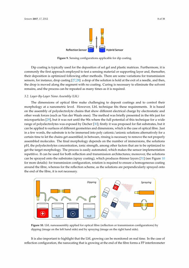
3.1. Dip Coating
This method is one of the easiest to perform: it just consists of dipping the fibre vertically into the solution or dispersion where the sensing material is dissolved or dispersed and then, the fibre is removed from the solution (see Figure 9). The key parameter is the withdrawal speed: the fastest it is, the thicker is the resulting coating. Other important factor is the viscosity of the solution and also a post curing to ensure that any solvent remains are evaporated. The process can be repeated as many times as required to get the desired thickness. As the fibre is immersed perpendicularly, this procedure is only applicable for reflection configuration or a hybrid one. Moreover, there is no control on the film thickness in the case the material is to be coated at the end of the fibre; actually, the shape of the deposition looks as a matchstick.
Figure 8. Schematic representation of a LMR: the optical resonance expressed as a transmission valleyis increased and shifted if the thickness of the coating or its refractive index is modified.
3. Techniques for the Development of Sensors
There are several manners to deposit sensing coatings onto optical fibre. The small dimensions ofthe fibre is one of its advantages, but it also makes difficult coating films that have to be as uniformas possible. Therefore, different approaches have been adapted to handle with this substrate. In anycase, a high reproducibility is compulsory to validate the sensor construction process. The mostused procedures are briefly described along this section: there are other such as functionalization byinorganic and even biological molecules that can be found in [23–26].
3.1. Dip Coating
This method is one of the easiest to perform: it just consists of dipping the fibre vertically intothe solution or dispersion where the sensing material is dissolved or dispersed and then, the fibre isremoved from the solution (see Figure 9). The key parameter is the withdrawal speed: the fastest it is,the thicker is the resulting coating. Other important factor is the viscosity of the solution and also apost curing to ensure that any solvent remains are evaporated. The process can be repeated as manytimes as required to get the desired thickness. As the fibre is immersed perpendicularly, this procedureis only applicable for reflection configuration or a hybrid one. Moreover, there is no control on thefilm thickness in the case the material is to be coated at the end of the fibre; actually, the shape of thedeposition looks as a matchstick.
Sensors 2017, 17, 2312 8 of 38
Sensors 2017, 17, 2312 8 of 39
Figure 9. Sensing configurations applicable for dip coating.
Dip coating is typically used for the deposition of sol gel and plastic matrices. Furthermore, it is commonly the first approach employed to test a sensing material or supporting layer and, thereafter, their deposition is optimized following other methods. There are some variations for transmission sensors, for instance, drop casting [27,28]: a drop of the solution is hold at the exit of a needle, and then, the drop is moved along the segment with no coating. Curing is necessary to eliminate the solvent remains, and the process can be repeated as many times as it is required.
3.2. Layer-By-Layer Nano Assembly (LbL)
The dimensions of optical fibre make challenging to deposit coatings and to control their morphology at a nanometric level. However, LbL technique fits these requirements. It is based on the assembly of polyelectrolyte chains that show different electrical charge by electrostatic and other weak forces (such as Van der Waals ones). The method was briefly presented in the 60s just for microparticles [29], but it was not until the 90s where the full potential of this technique for a wide range of polyelectrolytes was exposed by Decher [30]; firstly it was proposed for flat substrates, but it can be applied to surfaces of different geometries and dimensions, which is the case of optical fibre. Just in a few words, the substrate is to be immersed into poly cationic/anionic solutions alternatively for a certain time to let the chains get assembled; in between, rinsing is necessary to remove the not properly assembled molecules. The final morphology depends on the number of immersions, the solutions pH, the polyelectrolytes concentration, ionic strength, among other factors that are to be optimized to get the target morphology. The process is easily automated, which makes the sensor implementation repetitive. It can be used for both reflection and transmission architectures; moreover, the solutions can be sprayed onto the substrates (spray coating), which produces thinner layers [31] (see Figure 10 for more details): for transmission configuration, rotation is required to ensure a homogeneous coating around the fibre, whereas for the reflection scheme, as the solutions are perpendicularly sprayed onto the end of the fibre, it is not necessary.
Figure 10. LbL nanoassembly applied for optical fibre (reflection or transmission configurations) by dipping (image on the left hand side) and by spraying (image on the right hand side).
It is also important to highlight that the LbL growing can be monitored on real time. In the case of reflection configuration, the nanocating that is growing at the end of the fibre forms a FP interferometer in a way its interferometric response depends critically on its thickness: applying the
Figure 9. Sensing configurations applicable for dip coating.
Dip coating is typically used for the deposition of sol gel and plastic matrices. Furthermore, it iscommonly the first approach employed to test a sensing material or supporting layer and, thereafter,their deposition is optimized following other methods. There are some variations for transmissionsensors, for instance, drop casting [27,28]: a drop of the solution is hold at the exit of a needle, and then,the drop is moved along the segment with no coating. Curing is necessary to eliminate the solventremains, and the process can be repeated as many times as it is required.
3.2. Layer-By-Layer Nano Assembly (LbL)
The dimensions of optical fibre make challenging to deposit coatings and to control theirmorphology at a nanometric level. However, LbL technique fits these requirements. It is basedon the assembly of polyelectrolyte chains that show different electrical charge by electrostatic andother weak forces (such as Van der Waals ones). The method was briefly presented in the 60s just formicroparticles [29], but it was not until the 90s where the full potential of this technique for a widerange of polyelectrolytes was exposed by Decher [30]; firstly it was proposed for flat substrates, but itcan be applied to surfaces of different geometries and dimensions, which is the case of optical fibre. Justin a few words, the substrate is to be immersed into poly cationic/anionic solutions alternatively for acertain time to let the chains get assembled; in between, rinsing is necessary to remove the not properlyassembled molecules. The final morphology depends on the number of immersions, the solutionspH, the polyelectrolytes concentration, ionic strength, among other factors that are to be optimized toget the target morphology. The process is easily automated, which makes the sensor implementationrepetitive. It can be used for both reflection and transmission architectures; moreover, the solutionscan be sprayed onto the substrates (spray coating), which produces thinner layers [31] (see Figure 10for more details): for transmission configuration, rotation is required to ensure a homogeneous coatingaround the fibre, whereas for the reflection scheme, as the solutions are perpendicularly sprayed ontothe end of the fibre, it is not necessary.
Sensors 2017, 17, 2312 8 of 39
Figure 9. Sensing configurations applicable for dip coating.
Dip coating is typically used for the deposition of sol gel and plastic matrices. Furthermore, it is commonly the first approach employed to test a sensing material or supporting layer and, thereafter, their deposition is optimized following other methods. There are some variations for transmission sensors, for instance, drop casting [27,28]: a drop of the solution is hold at the exit of a needle, and then, the drop is moved along the segment with no coating. Curing is necessary to eliminate the solvent remains, and the process can be repeated as many times as it is required.
3.2. Layer-By-Layer Nano Assembly (LbL)
The dimensions of optical fibre make challenging to deposit coatings and to control their morphology at a nanometric level. However, LbL technique fits these requirements. It is based on the assembly of polyelectrolyte chains that show different electrical charge by electrostatic and other weak forces (such as Van der Waals ones). The method was briefly presented in the 60s just for microparticles [29], but it was not until the 90s where the full potential of this technique for a wide range of polyelectrolytes was exposed by Decher [30]; firstly it was proposed for flat substrates, but it can be applied to surfaces of different geometries and dimensions, which is the case of optical fibre. Just in a few words, the substrate is to be immersed into poly cationic/anionic solutions alternatively for a certain time to let the chains get assembled; in between, rinsing is necessary to remove the not properly assembled molecules. The final morphology depends on the number of immersions, the solutions pH, the polyelectrolytes concentration, ionic strength, among other factors that are to be optimized to get the target morphology. The process is easily automated, which makes the sensor implementation repetitive. It can be used for both reflection and transmission architectures; moreover, the solutions can be sprayed onto the substrates (spray coating), which produces thinner layers [31] (see Figure 10 for more details): for transmission configuration, rotation is required to ensure a homogeneous coating around the fibre, whereas for the reflection scheme, as the solutions are perpendicularly sprayed onto the end of the fibre, it is not necessary.
Figure 10. LbL nanoassembly applied for optical fibre (reflection or transmission configurations) by dipping (image on the left hand side) and by spraying (image on the right hand side).
It is also important to highlight that the LbL growing can be monitored on real time. In the case of reflection configuration, the nanocating that is growing at the end of the fibre forms a FP interferometer in a way its interferometric response depends critically on its thickness: applying the
Figure 10. LbL nanoassembly applied for optical fibre (reflection or transmission configurations) bydipping (image on the left hand side) and by spraying (image on the right hand side).
It is also important to highlight that the LbL growing can be monitored on real time. In the case ofreflection configuration, the nanocating that is growing at the end of the fibre forms a FP interferometer
Sensors 2017, 17, 2312 9 of 38
in a way its interferometric response depends critically on its thickness: applying the mathematicalexpression of the FP interference, it is possible to estimate the final width of the coating. On the otherhand, depending on the polymers used, LMRs are induced when LbL is used for the transmissionconfiguration: registering the spectral shift produced by the nanocoating thickness increase permits itsgrowing to be controlled. Any of these methods allows the deposition process to be monitored, beinga way to confirm the repeatability between different devices, as it has been depicted in Figure 11.
Sensors 2017, 17, 2312 9 of 39
mathematical expression of the FP interference, it is possible to estimate the final width of the coating. On the other hand, depending on the polymers used, LMRs are induced when LbL is used for the transmission configuration: registering the spectral shift produced by the nanocoating thickness increase permits its growing to be controlled. Any of these methods allows the deposition process to be monitored, being a way to confirm the repeatability between different devices, as it has been depicted in Figure 11.
Figure 11. Mechanisms to control the nanocoatings growing for reflection and transmissions configurations: the first one is based on interferometry whereas the second on LMRs.
3.3. Sputtering
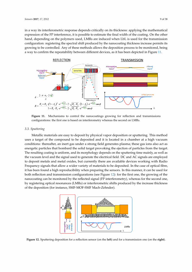
Metallic materials are easy to deposit by physical vapor deposition or sputtering. This method uses a target of the compound to be deposited and it is located in a chamber at a high vacuum conditions: thereafter, an inert gas under a strong field generates plasma; these gas ions also act as energetic particles that bombard the solid target provoking the ejection of particles from the target. The resulting coating is uniform, and its morphology depends on the sputtering time mainly, as well as the vacuum level and the signal used to generate the electrical field. DC and AC signals are employed to deposit metals and metal oxides, but currently there are available devices working with Radio Frequency signals that allow a wider variety of materials to be deposited. In the case of optical fibre, it has been found a high reproducibility when preparing the sensors. In this manner, it can be used for both reflection and transmission configurations (see Figure 12): for the first one, the growing of the nanocoating can be monitored by the reflected signal (FP interferometry), whereas for the second one, by registering optical resonances (LMRs) or interferometric shifts produced by the increase thickness of the deposition (for instance, SMF-MOF-SMF Mach-Zehnder).
Figure 12. Sputtering deposition for a reflection sensor (on the left) and for a transmission one (on the right).
Figure 11. Mechanisms to control the nanocoatings growing for reflection and transmissionsconfigurations: the first one is based on interferometry whereas the second on LMRs.
3.3. Sputtering
Metallic materials are easy to deposit by physical vapor deposition or sputtering. This methoduses a target of the compound to be deposited and it is located in a chamber at a high vacuumconditions: thereafter, an inert gas under a strong field generates plasma; these gas ions also act asenergetic particles that bombard the solid target provoking the ejection of particles from the target.The resulting coating is uniform, and its morphology depends on the sputtering time mainly, as well asthe vacuum level and the signal used to generate the electrical field. DC and AC signals are employedto deposit metals and metal oxides, but currently there are available devices working with RadioFrequency signals that allow a wider variety of materials to be deposited. In the case of optical fibre,it has been found a high reproducibility when preparing the sensors. In this manner, it can be used forboth reflection and transmission configurations (see Figure 12): for the first one, the growing of thenanocoating can be monitored by the reflected signal (FP interferometry), whereas for the second one,by registering optical resonances (LMRs) or interferometric shifts produced by the increase thicknessof the deposition (for instance, SMF-MOF-SMF Mach-Zehnder).
Sensors 2017, 17, 2312 9 of 39
mathematical expression of the FP interference, it is possible to estimate the final width of the coating. On the other hand, depending on the polymers used, LMRs are induced when LbL is used for the transmission configuration: registering the spectral shift produced by the nanocoating thickness increase permits its growing to be controlled. Any of these methods allows the deposition process to be monitored, being a way to confirm the repeatability between different devices, as it has been depicted in Figure 11.
Figure 11. Mechanisms to control the nanocoatings growing for reflection and transmissions configurations: the first one is based on interferometry whereas the second on LMRs.
3.3. Sputtering
Metallic materials are easy to deposit by physical vapor deposition or sputtering. This method uses a target of the compound to be deposited and it is located in a chamber at a high vacuum conditions: thereafter, an inert gas under a strong field generates plasma; these gas ions also act as energetic particles that bombard the solid target provoking the ejection of particles from the target. The resulting coating is uniform, and its morphology depends on the sputtering time mainly, as well as the vacuum level and the signal used to generate the electrical field. DC and AC signals are employed to deposit metals and metal oxides, but currently there are available devices working with Radio Frequency signals that allow a wider variety of materials to be deposited. In the case of optical fibre, it has been found a high reproducibility when preparing the sensors. In this manner, it can be used for both reflection and transmission configurations (see Figure 12): for the first one, the growing of the nanocoating can be monitored by the reflected signal (FP interferometry), whereas for the second one, by registering optical resonances (LMRs) or interferometric shifts produced by the increase thickness of the deposition (for instance, SMF-MOF-SMF Mach-Zehnder).
Figure 12. Sputtering deposition for a reflection sensor (on the left) and for a transmission one (on the right).
Figure 12. Sputtering deposition for a reflection sensor (on the left) and for a transmission one (on the right).
Sensors 2017, 17, 2312 10 of 38
3.4. Electrospun Nano Webs
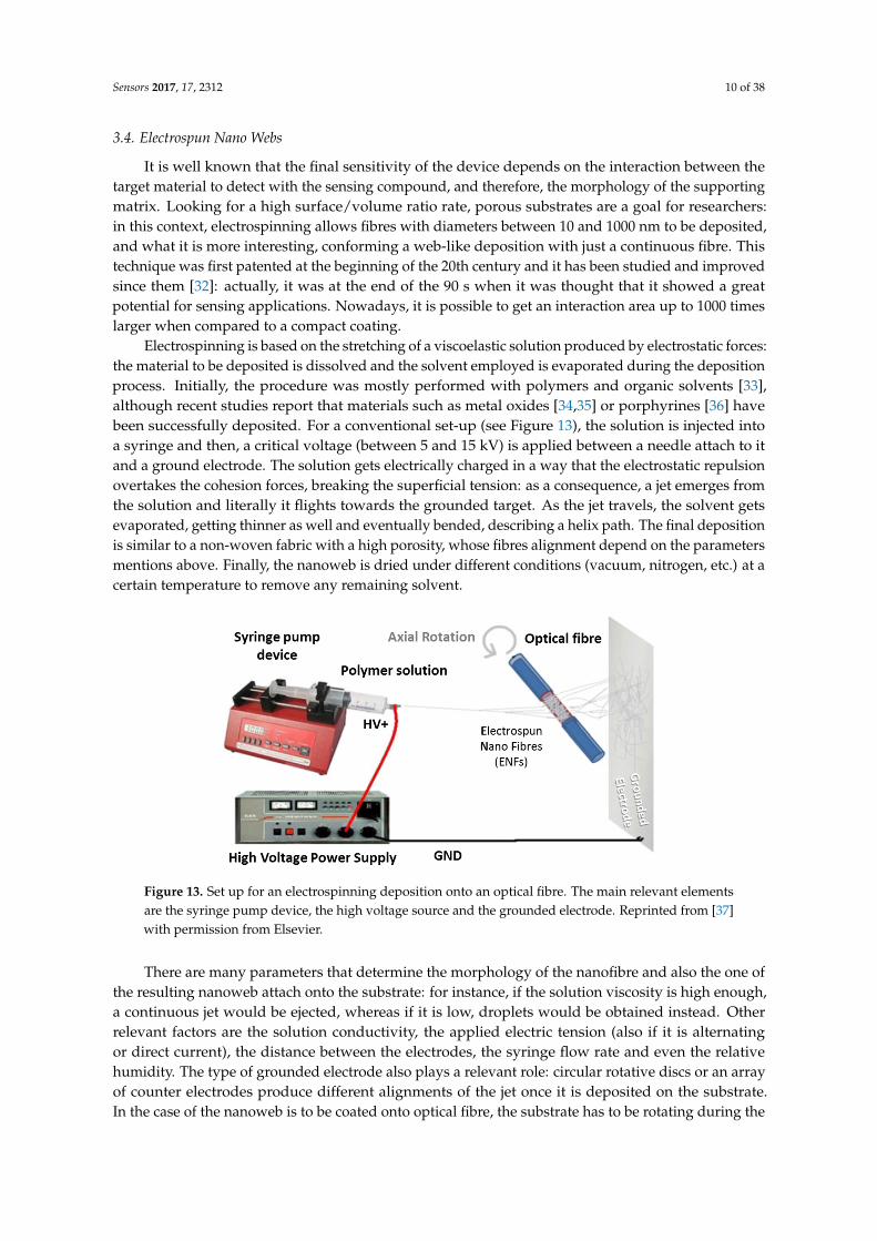
It is well known that the final sensitivity of the device depends on the interaction between thetarget material to detect with the sensing compound, and therefore, the morphology of the supportingmatrix. Looking for a high surface/volume ratio rate, porous substrates are a goal for researchers:in this context, electrospinning allows fibres with diameters between 10 and 1000 nm to be deposited,and what it is more interesting, conforming a web-like deposition with just a continuous fibre. Thistechnique was first patented at the beginning of the 20th century and it has been studied and improvedsince them [32]: actually, it was at the end of the 90 s when it was thought that it showed a greatpotential for sensing applications. Nowadays, it is possible to get an interaction area up to 1000 timeslarger when compared to a compact coating.
Electrospinning is based on the stretching of a viscoelastic solution produced by electrostatic forces:the material to be deposited is dissolved and the solvent employed is evaporated during the depositionprocess. Initially, the procedure was mostly performed with polymers and organic solvents [33],although recent studies report that materials such as metal oxides [34,35] or porphyrines [36] havebeen successfully deposited. For a conventional set-up (see Figure 13), the solution is injected intoa syringe and then, a critical voltage (between 5 and 15 kV) is applied between a needle attach to itand a ground electrode. The solution gets electrically charged in a way that the electrostatic repulsionovertakes the cohesion forces, breaking the superficial tension: as a consequence, a jet emerges fromthe solution and literally it flights towards the grounded target. As the jet travels, the solvent getsevaporated, getting thinner as well and eventually bended, describing a helix path. The final depositionis similar to a non-woven fabric with a high porosity, whose fibres alignment depend on the parametersmentions above. Finally, the nanoweb is dried under different conditions (vacuum, nitrogen, etc.) at acertain temperature to remove any remaining solvent.
Sensors 2017, 17, 2312 10 of 39
3.4. Electrospun Nano Webs
It is well known that the final sensitivity of the device depends on the interaction between the target material to detect with the sensing compound, and therefore, the morphology of the supporting matrix. Looking for a high surface/volume ratio rate, porous substrates are a goal for researchers: in this context, electrospinning allows fibres with diameters between 10 and 1000 nm to be deposited, and what it is more interesting, conforming a web-like deposition with just a continuous fibre. This technique was first patented at the beginning of the 20th century and it has been studied and improved since them [32]: actually, it was at the end of the 90 s when it was thought that it showed a great potential for sensing applications. Nowadays, it is possible to get an interaction area up to 1000 times larger when compared to a compact coating.
Electrospinning is based on the stretching of a viscoelastic solution produced by electrostatic forces: the material to be deposited is dissolved and the solvent employed is evaporated during the deposition process. Initially, the procedure was mostly performed with polymers and organic solvents [33], although recent studies report that materials such as metal oxides [34,35] or porphyrines [36] have been successfully deposited. For a conventional set-up (see Figure 13), the solution is injected into a syringe and then, a critical voltage (between 5 and 15 kV) is applied between a needle attach to it and a ground electrode. The solution gets electrically charged in a way that the electrostatic repulsion overtakes the cohesion forces, breaking the superficial tension: as a consequence, a jet emerges from the solution and literally it flights towards the grounded target. As the jet travels, the solvent gets evaporated, getting thinner as well and eventually bended, describing a helix path. The final deposition is similar to a non-woven fabric with a high porosity, whose fibres alignment depend on the parameters mentions above. Finally, the nanoweb is dried under different conditions (vacuum, nitrogen, etc.) at a certain temperature to remove any remaining solvent.
Figure 13. Set up for an electrospinning deposition onto an optical fibre. The main relevant elements are the syringe pump device, the high voltage source and the grounded electrode. Reprinted from [37] with permission from Elsevier.
There are many parameters that determine the morphology of the nanofibre and also the one of the resulting nanoweb attach onto the substrate: for instance, if the solution viscosity is high enough, a continuous jet would be ejected, whereas if it is low, droplets would be obtained instead. Other relevant factors are the solution conductivity, the applied electric tension (also if it is alternating or direct current), the distance between the electrodes, the syringe flow rate and even the relative humidity. The type of grounded electrode also plays a relevant role: circular rotative discs or an array of counter electrodes produce different alignments of the jet once it is deposited on the substrate. In the case of the nanoweb is to be coated onto optical fibre, the substrate has to be rotating during the process (as it is displayed in Figure 13): rotation speed of the fibre is a relevant factor that determines the morphology of the final supporting matrix.
Figure 13. Set up for an electrospinning deposition onto an optical fibre. The main relevant elementsare the syringe pump device, the high voltage source and the grounded electrode. Reprinted from [37]with permission from Elsevier.
There are many parameters that determine the morphology of the nanofibre and also the one ofthe resulting nanoweb attach onto the substrate: for instance, if the solution viscosity is high enough,a continuous jet would be ejected, whereas if it is low, droplets would be obtained instead. Otherrelevant factors are the solution conductivity, the applied electric tension (also if it is alternatingor direct current), the distance between the electrodes, the syringe flow rate and even the relativehumidity. The type of grounded electrode also plays a relevant role: circular rotative discs or an arrayof counter electrodes produce different alignments of the jet once it is deposited on the substrate.In the case of the nanoweb is to be coated onto optical fibre, the substrate has to be rotating during the
Sensors 2017, 17, 2312 11 of 38
process (as it is displayed in Figure 13): rotation speed of the fibre is a relevant factor that determinesthe morphology of the final supporting matrix.
4. Nano and Microstructured Materials for Sensing
This is the main section of the review. Relevant results for optical fibre sensors will be presentedconsidering the nano- and microstructured materials used to implement them. All the sub sections arebased on the sensors reported in the bibliography along, approximately, the last 17 years. Apart ofthe materials that are to be presented, there are others that, due to their extended used in differentapproaches, are difficult to classify individually: it is the case of nanoparticles (NPs) that are employedto enhance the sensitivity of optical fibre sensors of different architectures and transduction principles.Some of the most used NPs are gold [38] and silver [39], and it has been found that even the shapeof the NP should be considered to get optimized results [40]. More details about the use of NPs todevelop optical fibre sensors can be found in [41].
4.1. Microstructured Optical Fibres
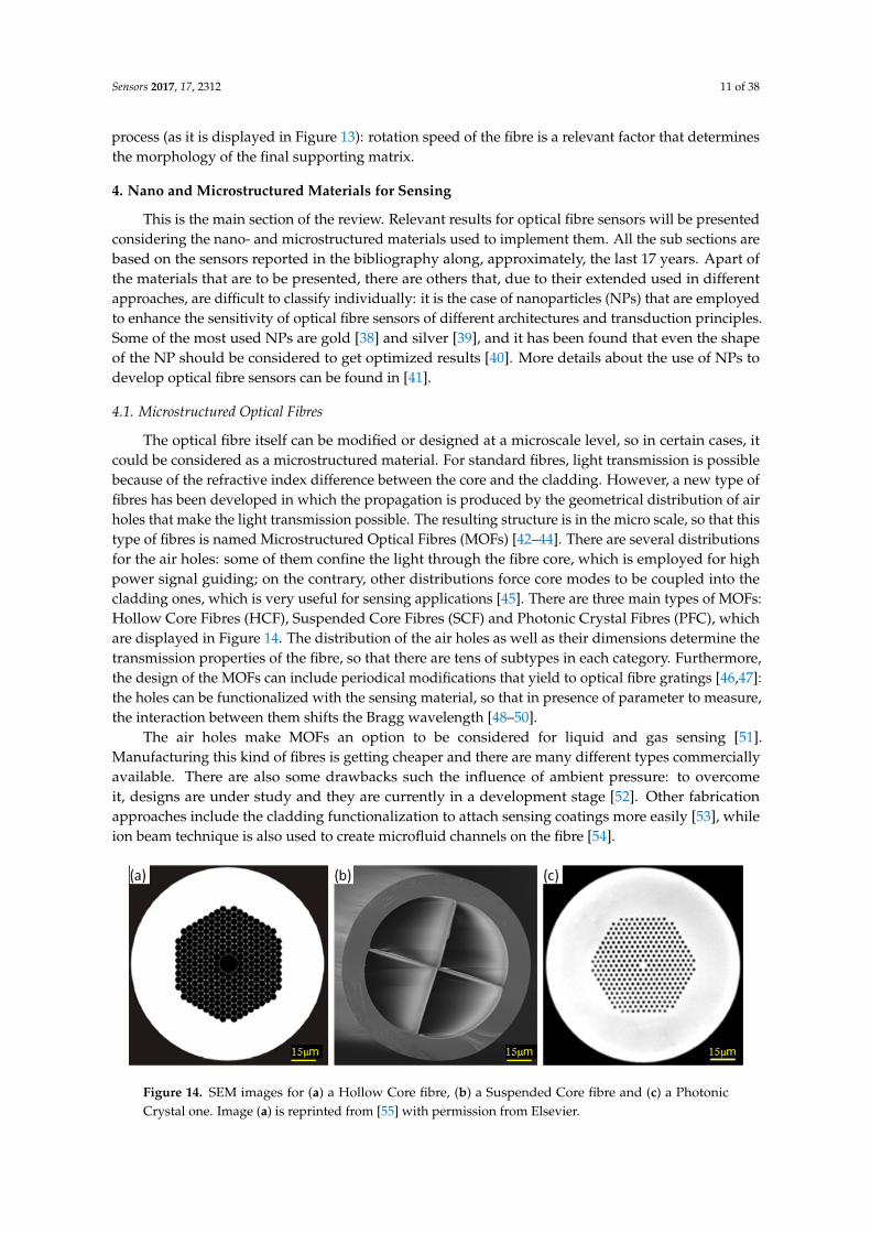
The optical fibre itself can be modified or designed at a microscale level, so in certain cases, itcould be considered as a microstructured material. For standard fibres, light transmission is possiblebecause of the refractive index difference between the core and the cladding. However, a new type offibres has been developed in which the propagation is produced by the geometrical distribution of airholes that make the light transmission possible. The resulting structure is in the micro scale, so that thistype of fibres is named Microstructured Optical Fibres (MOFs) [42–44]. There are several distributionsfor the air holes: some of them confine the light through the fibre core, which is employed for highpower signal guiding; on the contrary, other distributions force core modes to be coupled into thecladding ones, which is very useful for sensing applications [45]. There are three main types of MOFs:Hollow Core Fibres (HCF), Suspended Core Fibres (SCF) and Photonic Crystal Fibres (PFC), whichare displayed in Figure 14. The distribution of the air holes as well as their dimensions determine thetransmission properties of the fibre, so that there are tens of subtypes in each category. Furthermore,the design of the MOFs can include periodical modifications that yield to optical fibre gratings [46,47]:the holes can be functionalized with the sensing material, so that in presence of parameter to measure,the interaction between them shifts the Bragg wavelength [48–50].
The air holes make MOFs an option to be considered for liquid and gas sensing [51].Manufacturing this kind of fibres is getting cheaper and there are many different types commerciallyavailable. There are also some drawbacks such the influence of ambient pressure: to overcomeit, designs are under study and they are currently in a development stage [52]. Other fabricationapproaches include the cladding functionalization to attach sensing coatings more easily [53], whileion beam technique is also used to create microfluid channels on the fibre [54].
Sensors 2017, 17, 2312 11 of 39
4. Nano and Microstructured Materials for Sensing
This is the main section of the review. Relevant results for optical fibre sensors will be presented considering the nano- and microstructured materials used to implement them. All the sub sections are based on the sensors reported in the bibliography along, approximately, the last 17 years. Apart of the materials that are to be presented, there are others that, due to their extended used in different approaches, are difficult to classify individually: it is the case of nanoparticles (NPs) that are employed to enhance the sensitivity of optical fibre sensors of different architectures and transduction principles. Some of the most used NPs are gold [38] and silver [39], and it has been found that even the shape of the NP should be considered to get optimized results [40]. More details about the use of NPs to develop optical fibre sensors can be found in [41].
4.1. Microstructured Optical Fibres
The optical fibre itself can be modified or designed at a microscale level, so in certain cases, it could be considered as a microstructured material. For standard fibres, light transmission is possible because of the refractive index difference between the core and the cladding. However, a new type of fibres has been developed in which the propagation is produced by the geometrical distribution of air holes that make the light transmission possible. The resulting structure is in the micro scale, so that this type of fibres is named Microstructured Optical Fibres (MOFs) [42–44]. There are several distributions for the air holes: some of them confine the light through the fibre core, which is employed for high power signal guiding; on the contrary, other distributions force core modes to be coupled into the cladding ones, which is very useful for sensing applications [45]. There are three main types of MOFs: Hollow Core Fibres (HCF), Suspended Core Fibres (SCF) and Photonic Crystal Fibres (PFC), which are displayed in Figure 14. The distribution of the air holes as well as their dimensions determine the transmission properties of the fibre, so that there are tens of subtypes in each category. Furthermore, the design of the MOFs can include periodical modifications that yield to optical fibre gratings [46,47]: the holes can be functionalized with the sensing material, so that in presence of parameter to measure, the interaction between them shifts the Bragg wavelength [48–50].
The air holes make MOFs an option to be considered for liquid and gas sensing [51]. Manufacturing this kind of fibres is getting cheaper and there are many different types commercially available. There are also some drawbacks such the influence of ambient pressure: to overcome it, designs are under study and they are currently in a development stage [52]. Other fabrication approaches include the cladding functionalization to attach sensing coatings more easily [53], while ion beam technique is also used to create microfluid channels on the fibre [54].
Figure 14. SEM images for (a) a Hollow Core fibre, (b) a Suspended Core fibre and (c) a Photonic Crystal one. Image (a) is reprinted from [55] with permission from Elsevier.
In the case of HCF, they are commonly used for high intensity signals because of their nonlinear coefficient is smaller than the standard fibre’s one. Regarding SCF, the core is hold by tiny silica bridges that make de impression of a hanging one: the narrower it is, the stronger the evanescent field in the air holes is. This type of fibre is very sensitive to changes in the properties of the air holes.
Figure 14. SEM images for (a) a Hollow Core fibre, (b) a Suspended Core fibre and (c) a PhotonicCrystal one. Image (a) is reprinted from [55] with permission from Elsevier.

Sensors 2017, 17, 2312 12 of 38
In the case of HCF, they are commonly used for high intensity signals because of their nonlinearcoefficient is smaller than the standard fibre’s one. Regarding SCF, the core is hold by tiny silicabridges that make de impression of a hanging one: the narrower it is, the stronger the evanescentfield in the air holes is. This type of fibre is very sensitive to changes in the properties of the airholes. Actually, efforts are focused on the development of SCF with cores as small as possible toenhance this effect [56]. Sensing materials can be deposited on the walls of the holes, providing tothe sensor the required sensitivity: depending on the chemical reagent, the transduction is governedby changes in the refractive index and/or in its optical absorbance. Metal nanoparticles have beenfixed by microfluidic methods in order to obtain very high sensitive refractometers [57] and evensputtering can be applied to deposited metallic oxides. HCF is currently showing a great potential forbiomedical sensing: the large air holes can be used as micro fluidic cavities to detect target moleculessuch as proteins or pathological agents (sensing material is previously deposited on the inner walls),so that only micro or even nanolitres are required to make the measurement [58]. Some authors alsoproposed that HCF properly functionalized could be used for distributed sensing in hydrogen leakagesdetection [55].
PCF are named this way because the patterned air holes distribution is similar to a crystal structure(some authors sub divide PCF into solid and hollow core groups): the solid core is surrounded by anarea of lower refractive index due to the air holes, which enhances the coupling to cladding modes.Taking advantage of this effect, a sensing layer can be deposited onto a PCF section with an optimizedthickness (below 1–2 microns approximately) that ensures the interaction with the target analyteand the evanescent wave. This kind of fibre is used to prepare interferometers by splicing a PCFbetween two standard fibres (see Figure 15), which generates an interfering spectral pattern that isshifted by the presence of the entity to measure. Sensors have been developed this way to measurerelative humidity [59,60] and the architecture can be extended to other applications depending on thesensing material.
Sensors 2017, 17, 2312 12 of 39
Actually, efforts are focused on the development of SCF with cores as small as possible to enhance this effect [56]. Sensing materials can be deposited on the walls of the holes, providing to the sensor the required sensitivity: depending on the chemical reagent, the transduction is governed by changes in the refractive index and/or in its optical absorbance. Metal nanoparticles have been fixed by microfluidic methods in order to obtain very high sensitive refractometers [57] and even sputtering can be applied to deposited metallic oxides. HCF is currently showing a great potential for biomedical sensing: the large air holes can be used as micro fluidic cavities to detect target molecules such as proteins or pathological agents (sensing material is previously deposited on the inner walls), so that only micro or even nanolitres are required to make the measurement [58]. Some authors also proposed that HCF properly functionalized could be used for distributed sensing in hydrogen leakages detection [55].
PCF are named this way because the patterned air holes distribution is similar to a crystal structure (some authors sub divide PCF into solid and hollow core groups): the solid core is surrounded by an area of lower refractive index due to the air holes, which enhances the coupling to cladding modes. Taking advantage of this effect, a sensing layer can be deposited onto a PCF section with an optimized thickness (below 1–2 microns approximately) that ensures the interaction with the target analyte and the evanescent wave. This kind of fibre is used to prepare interferometers by splicing a PCF between two standard fibres (see Figure 15), which generates an interfering spectral pattern that is shifted by the presence of the entity to measure. Sensors have been developed this way to measure relative humidity [59,60] and the architecture can be extended to other applications depending on the sensing material.
Figure 15. (a) Scheme of an interferometer based on a PFC segment spliced between two SMF; (b) SEM image of the PFC section; (c) optical microscope capture of the interferometer, delimiting the three different parts. Reprinted from [60] with the permission from Elsevier.
4.2. Nanostructures
Advances in nanotechnology have allowed structures made of different materials to be constructed in the sensor field. Properties such as sensitivity to refractive index changes, large interaction area or periodic patterning are typically required. Materials that are relatively easy to deposit are metals by sputtering or CVD, which produce plasmonic resonances; on the contrary, non-conducting materials produce photonic resonances: both of them can be combined to design structures at a nanometric scale, which are known as hybrid structures [61]. This kind of constructions can be functionalized to detect biological molecules such immunoglobulins taking advantage of the nanoporous morphology that this type of material offers: as it is reported in [62], a polymer layer can act as substrate (for instance, polydimethylsiloxane), and on it, a column based nanostructure prepared with anodic aluminium is deposited; thereafter, the coating of a nano-Au layer yields to a porous surface that is finally functionalized with protein receptors (Figure 16a,b). As a result, variations in the absorption spectra are recorded when the structure is exposed to biological solutions containing the target protein. Gold nanorods (Figure 16c–e) can be also synthetized to detect human immunoglobulins in terms of spectral shifts [63]; gold nanorings have been also been synthetized to
Figure 15. (a) Scheme of an interferometer based on a PFC segment spliced between two SMF; (b) SEMimage of the PFC section; (c) optical microscope capture of the interferometer, delimiting the threedifferent parts. Reprinted from [60] with the permission from Elsevier.
4.2. Nanostructures
Advances in nanotechnology have allowed structures made of different materials to be constructedin the sensor field. Properties such as sensitivity to refractive index changes, large interaction area orperiodic patterning are typically required. Materials that are relatively easy to deposit are metals bysputtering or CVD, which produce plasmonic resonances; on the contrary, non-conducting materialsproduce photonic resonances: both of them can be combined to design structures at a nanometric scale,which are known as hybrid structures [61]. This kind of constructions can be functionalized to detectbiological molecules such immunoglobulins taking advantage of the nanoporous morphology thatthis type of material offers: as it is reported in [62], a polymer layer can act as substrate (for instance,

Sensors 2017, 17, 2312 13 of 38
polydimethylsiloxane), and on it, a column based nanostructure prepared with anodic aluminiumis deposited; thereafter, the coating of a nano-Au layer yields to a porous surface that is finallyfunctionalized with protein receptors (Figure 16a,b). As a result, variations in the absorption spectraare recorded when the structure is exposed to biological solutions containing the target protein. Goldnanorods (Figure 16c–e) can be also synthetized to detect human immunoglobulins in terms of spectralshifts [63]; gold nanorings have been also been synthetized to work on the optical fibre operatingspectral range to prepare a potential refractometer [64]. The transduction principle of these materialsis based on spectral shifts.
Sensors 2017, 17, 2312 13 of 39
work on the optical fibre operating spectral range to prepare a potential refractometer [64]. The transduction principle of these materials is based on spectral shifts.
Figure 16. (a,b) show the nanoporous structure observed from a hybrid polymer—metallic structure; (c–e) images on the right hand side display gold nanorods with aspect ratios to detect immunoglobulins. Reprinted from [62,63] with permission from Elsevier.
Some structures have been successfully constructed onto the optical fibre. By using different masks to deposit the sensing material, cavities or resonators can be used as transducers. Thanks to its plasmonic resonances, gold has been used to prepare concentric circles on the top end of a fibre, in a way the resulting probe is highly sensitive to changes in the external refractive index [65]. Non- conducting materials, such as composites, are also employed to construct microcavites that enhance the interaction between the chemical target to be measured and the optical signal: a microprism has been designed to implement an interferometer at the end of a standard optical fibre to detect chlorinated organic solvents [66], Not only chemical analytes are to be measured by using nanostructures: acoustic waves can also be registered by an optical fibre microphone [67]. The transduction principle of this sensor is based on a microcavity made of IPL-780 photoresist (Nanoscribe GmbH, Baden-Württemberg, Germany), which is placed at the end of a fibre tip. Microlenses are distributed inside the cavity, so that they reflect the optical signal that reaches them from the fibre towards back (see Figure 17b): in the presence of acoustic waves, the lenses are displaced, and so, the reflected signal varies, which constitutes the sensor working principle. Other nanostructures prepared with photo resins have been reported by following nano imprint lithography [68].
Figure 17. (a) 3D design of the microcavity with the micro lenses to implement the optical fibre microphone; (b) detailed of the top view of the cavity and (c) its side view, where the lens can be seen. Images reprinted from [67] with permission of Elsevier.
In addition to these structures, the concept of “lab-on-fibre” is an emergent field to consider in the next years. Some examples of the “lab-on-fibre” potential can be found in works from Cusano and co-workers are, among other achievements, a phase-gradient plasmonic metasurface on the fibre tip; the nanosphere lithography of the optical fibre end facet; even a method for integrating sub-wavelength resonant structures on top of optical fibre tip based on direct milling of the glass on the fibre facet by means of Focused Ion Beam (FIB) have been recently reported [69–71]. FBI technique is very similar to scanning electronic microscope but employing an ion beam instead of an electron one. In this manner, different shapes and structures can be inscribed onto the fibre and, moreover, different materials can be deposited too. This technique is offering very promising results, so that sensors are supposed to be prepared this way in near future [21].
Figure 16. (a,b) show the nanoporous structure observed from a hybrid polymer—metallic structure;(c–e) images on the right hand side display gold nanorods with aspect ratios to detect immunoglobulins.Reprinted from [62,63] with permission from Elsevier.
Some structures have been successfully constructed onto the optical fibre. By using differentmasks to deposit the sensing material, cavities or resonators can be used as transducers. Thanks to itsplasmonic resonances, gold has been used to prepare concentric circles on the top end of a fibre, in a waythe resulting probe is highly sensitive to changes in the external refractive index [65]. Non-conductingmaterials, such as composites, are also employed to construct microcavites that enhance the interactionbetween the chemical target to be measured and the optical signal: a microprism has been designedto implement an interferometer at the end of a standard optical fibre to detect chlorinated organicsolvents [66], Not only chemical analytes are to be measured by using nanostructures: acoustic wavescan also be registered by an optical fibre microphone [67]. The transduction principle of this sensoris based on a microcavity made of IPL-780 photoresist (Nanoscribe GmbH, Baden-Württemberg,Germany), which is placed at the end of a fibre tip. Microlenses are distributed inside the cavity, sothat they reflect the optical signal that reaches them from the fibre towards back (see Figure 17b):in the presence of acoustic waves, the lenses are displaced, and so, the reflected signal varies, whichconstitutes the sensor working principle. Other nanostructures prepared with photo resins have beenreported by following nano imprint lithography [68].
Sensors 2017, 17, 2312 13 of 39
work on the optical fibre operating spectral range to prepare a potential refractometer [64]. The transduction principle of these materials is based on spectral shifts.
Figure 16. (a,b) show the nanoporous structure observed from a hybrid polymer—metallic structure; (c–e) images on the right hand side display gold nanorods with aspect ratios to detect immunoglobulins. Reprinted from [62,63] with permission from Elsevier.
Some structures have been successfully constructed onto the optical fibre. By using different masks to deposit the sensing material, cavities or resonators can be used as transducers. Thanks to its plasmonic resonances, gold has been used to prepare concentric circles on the top end of a fibre, in a way the resulting probe is highly sensitive to changes in the external refractive index [65]. Non- conducting materials, such as composites, are also employed to construct microcavites that enhance the interaction between the chemical target to be measured and the optical signal: a microprism has been designed to implement an interferometer at the end of a standard optical fibre to detect chlorinated organic solvents [66], Not only chemical analytes are to be measured by using nanostructures: acoustic waves can also be registered by an optical fibre microphone [67]. The transduction principle of this sensor is based on a microcavity made of IPL-780 photoresist (Nanoscribe GmbH, Baden-Württemberg, Germany), which is placed at the end of a fibre tip. Microlenses are distributed inside the cavity, so that they reflect the optical signal that reaches them from the fibre towards back (see Figure 17b): in the presence of acoustic waves, the lenses are displaced, and so, the reflected signal varies, which constitutes the sensor working principle. Other nanostructures prepared with photo resins have been reported by following nano imprint lithography [68].
Figure 17. (a) 3D design of the microcavity with the micro lenses to implement the optical fibre microphone; (b) detailed of the top view of the cavity and (c) its side view, where the lens can be seen. Images reprinted from [67] with permission of Elsevier.
In addition to these structures, the concept of “lab-on-fibre” is an emergent field to consider in the next years. Some examples of the “lab-on-fibre” potential can be found in works from Cusano and co-workers are, among other achievements, a phase-gradient plasmonic metasurface on the fibre tip; the nanosphere lithography of the optical fibre end facet; even a method for integrating sub-wavelength resonant structures on top of optical fibre tip based on direct milling of the glass on the fibre facet by means of Focused Ion Beam (FIB) have been recently reported [69–71]. FBI technique is very similar to scanning electronic microscope but employing an ion beam instead of an electron one. In this manner, different shapes and structures can be inscribed onto the fibre and, moreover, different materials can be deposited too. This technique is offering very promising results, so that sensors are supposed to be prepared this way in near future [21].
Figure 17. (a) 3D design of the microcavity with the micro lenses to implement the optical fibremicrophone; (b) detailed of the top view of the cavity and (c) its side view, where the lens can be seen.Images reprinted from [67] with permission of Elsevier.
In addition to these structures, the concept of “lab-on-fibre” is an emergent field to consider in thenext years. Some examples of the “lab-on-fibre” potential can be found in works from Cusano andco-workers are, among other achievements, a phase-gradient plasmonic metasurface on the fibre tip;

Sensors 2017, 17, 2312 14 of 38
the nanosphere lithography of the optical fibre end facet; even a method for integrating sub-wavelengthresonant structures on top of optical fibre tip based on direct milling of the glass on the fibre facet bymeans of Focused Ion Beam (FIB) have been recently reported [69–71]. FBI technique is very similar toscanning electronic microscope but employing an ion beam instead of an electron one. In this manner,different shapes and structures can be inscribed onto the fibre and, moreover, different materials canbe deposited too. This technique is offering very promising results, so that sensors are supposed to beprepared this way in near future [21].
4.3. Plastic Matrices
Mechanical robustness is always required for the sensing coatings as well as a negligible reactivityto aging agents. These are two of the most important features that plastic matrices offer for thedevelopment of optical fibre sensors. The plastic is mixed with an organic solvent together with thesensing material and, in some cases, with other substances such as plastifiers: it is compulsory thatthey do not react with the sensing molecules to preserve their sensitivity. The technique commonlyemployed to deposit them is dip coating, so that depending on the number of immersions and thedipping speed, coatings with different morphologies are obtained. A final curing stage is required toremove the organic solvent and to harden the polymer, which enhances the mechanical properties ofthe resulting supporting matrix.
Most of the polymers employed are hydrophobic, which is also a desirable feature in cases suchas the detection of gaseous ammonia based on pH indicators: hydrous matrices can get degradedunder dry conditions, so that hydrophobic coatings overcome this situation. Bromocresol Purple hasbeen mixed with a polyurethane plastic, Tecoflex®, and ethanol, preparing a solution into which aPCS fibre was dipped several times at a certain speed. The resulting sensor, based on the absorbancespectral changes of the chemical indicator produced by ammonia molecules, shown a repetitive andsensitive response to this agent [72]. Other very well-known plastics such as poly (vinyl chloride) (PVC)have been used to prepare sensors that detect pyridine vapours [73] and europium ions dissolved inwater [74]: it is important to keep in mind that some polymers are opaque, so that there is a trade-offbetween the coating thickness and the signal level that determines the final sensitivity. Polymers thatyield to high porosity matrices that promote gas adsorption are required, for example, in the case ofoxygen sensing: polystyrene (PS) was used to deposit luminescent metallic porphyrines to prepare anoxygen sensor [75]. The coating thickness is critical for most sensors prepared with plastic matrices:if the coating is too thin, there is a low interaction with the evanescent wave, but if it is too high,the transduction might not reach the area where the evanescent field is interacting with the membrane.What is more, the thickness also determines the morphology in terms of porosity. For a cobaltousdeposition into a polyaniline matrix to measure humidity [76], it has been noticed that the thinner thelayer is, the more porous the morphology is, which improves the sensitivity (see Figure 18).
Sensors 2017, 17, 2312 14 of 39
4.3. Plastic Matrices
Mechanical robustness is always required for the sensing coatings as well as a negligible reactivity to aging agents. These are two of the most important features that plastic matrices offer for the development of optical fibre sensors. The plastic is mixed with an organic solvent together with the sensing material and, in some cases, with other substances such as plastifiers: it is compulsory that they do not react with the sensing molecules to preserve their sensitivity. The technique commonly employed to deposit them is dip coating, so that depending on the number of immersions and the dipping speed, coatings with different morphologies are obtained. A final curing stage is required to remove the organic solvent and to harden the polymer, which enhances the mechanical properties of the resulting supporting matrix.
Most of the polymers employed are hydrophobic, which is also a desirable feature in cases such as the detection of gaseous ammonia based on pH indicators: hydrous matrices can get degraded under dry conditions, so that hydrophobic coatings overcome this situation. Bromocresol Purple has been mixed with a polyurethane plastic, Tecoflex®, and ethanol, preparing a solution into which a PCS fibre was dipped several times at a certain speed. The resulting sensor, based on the absorbance spectral changes of the chemical indicator produced by ammonia molecules, shown a repetitive and sensitive response to this agent [72]. Other very well-known plastics such as poly (vinyl chloride) (PVC) have been used to prepare sensors that detect pyridine vapours [73] and europium ions dissolved in water [74]: it is important to keep in mind that some polymers are opaque, so that there is a trade-off between the coating thickness and the signal level that determines the final sensitivity. Polymers that yield to high porosity matrices that promote gas adsorption are required, for example, in the case of oxygen sensing: polystyrene (PS) was used to deposit luminescent metallic porphyrines to prepare an oxygen sensor [75]. The coating thickness is critical for most sensors prepared with plastic matrices: if the coating is too thin, there is a low interaction with the evanescent wave, but if it is too high, the transduction might not reach the area where the evanescent field is interacting with the membrane. What is more, the thickness also determines the morphology in terms of porosity. For a cobaltous deposition into a polyaniline matrix to measure humidity [76], it has been noticed that the thinner the layer is, the more porous the morphology is, which improves the sensitivity (see Figure 18).
Figure 18. SEM images from cobaltous—polyaniline coatings with different thickness: (a) 10.38 μm, (b) 17.26 μm, 21.08 μm (c), 23.57 μm (d), and (e) 26.03 μm. It can be appreciated in the first images (a and b) that the morphology is more porous that for the last ones (d,e). Reprinted from (Vijayan et al., 2008) with permission of Elsevier.
Not only the plastic membrane acts as a supporting element, but sometimes also as the sensing one: depending on its optical properties (such us the refractive index), some plastics have been employed to implement evanescent wave sensors. Polymers with high refractive index promote the coupling of the cladding modes into the sensing membrane: this effect was taken advantage to enhance the sensitivity of LPG based refractometers [77]. Although for this example the deposition technique was dip coating, the plastic—sensing element batch can be also sprayed onto the fibre to get the thin film: a siloxane polymer film with a thickness of just some nanometres was obtained in this manner to implement a device able to detect benzene, toluene and o-xylene [78].
Figure 18. SEM images from cobaltous—polyaniline coatings with different thickness: (a) 10.38 µm,(b) 17.26 µm, 21.08 µm (c), 23.57 µm (d), and (e) 26.03 µm. It can be appreciated in the first images(a and b) that the morphology is more porous that for the last ones (d,e). Reprinted from (Vijayan et al.,2008) with permission of Elsevier.
Not only the plastic membrane acts as a supporting element, but sometimes also as the sensingone: depending on its optical properties (such us the refractive index), some plastics have been
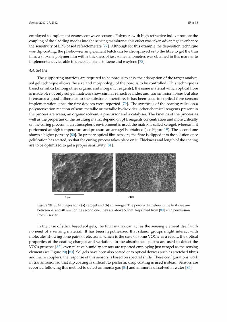
Sensors 2017, 17, 2312 15 of 38
employed to implement evanescent wave sensors. Polymers with high refractive index promote thecoupling of the cladding modes into the sensing membrane: this effect was taken advantage to enhancethe sensitivity of LPG based refractometers [77]. Although for this example the deposition techniquewas dip coating, the plastic—sensing element batch can be also sprayed onto the fibre to get the thinfilm: a siloxane polymer film with a thickness of just some nanometres was obtained in this manner toimplement a device able to detect benzene, toluene and o-xylene [78].
4.4. Sol Gel
The supporting matrices are required to be porous to easy the adsorption of the target analyte:sol gel technique allows the size and morphology of the porous to be controlled. This technique isbased on silica (among other organic and inorganic reagents), the same material which optical fibreis made of: not only sol gel matrices show similar refractive index and transmission losses but alsoit ensures a good adherence to the substrate: therefore, it has been used for optical fibre sensorsimplementation since the first devices were reported [79]. The synthesis of the coating relies on apolymerization reaction of semi metallic or metallic hydroxides: other chemical reagents present inthe process are water, an organic solvent, a precursor and a catalyser. The kinetics of the process aswell as the properties of the resulting matrix depend on pH, reagents concentration and more critically,on the curing process: if an atmospheric environment is used, the matrix is called xerogel, whereas if itperformed at high temperature and pressure an aerogel is obtained (see Figure 19). The second oneshows a higher porosity [80]. To prepare optical fibre sensors, the fibre is dipped into the solution oncegelification has started, so that the curing process takes place on it. Thickness and length of the coatingare to be optimized to get a proper sensitivity [81].
Sensors 2017, 17, 2312 15 of 39
4.4. Sol Gel
The supporting matrices are required to be porous to easy the adsorption of the target analyte: sol gel technique allows the size and morphology of the porous to be controlled. This technique is based on silica (among other organic and inorganic reagents), the same material which optical fibre is made of: not only sol gel matrices show similar refractive index and transmission losses but also it ensures a good adherence to the substrate: therefore, it has been used for optical fibre sensors implementation since the first devices were reported [79]. The synthesis of the coating relies on a polymerization reaction of semi metallic or metallic hydroxides: other chemical reagents present in the process are water, an organic solvent, a precursor and a catalyser. The kinetics of the process as well as the properties of the resulting matrix depend on pH, reagents concentration and more critically, on the curing process: if an atmospheric environment is used, the matrix is called xerogel, whereas if it performed at high temperature and pressure an aerogel is obtained (see Figure 19). The second one shows a higher porosity [80]. To prepare optical fibre sensors, the fibre is dipped into the solution once gelification has started, so that the curing process takes place on it. Thickness and length of the coating are to be optimized to get a proper sensitivity [81].
Figure 19. SEM images for a (a) xerogel and (b) an aerogel. The porous diameters in the first case are between 20 and 40 nm; for the second one, they are above 50 nm. Reprinted from [80] with permission from Elsevier.
In the case of silica based sol gels, the final matrix can act as the sensing element itself with no need of a sensing material. It has been hypothesized that silanol groups might interact with molecules showing lone pairs of electrons, which is the case of some VOCs: as a result, the optical properties of the coating changes and variations in the absorbance spectra are used to detect the VOCs presence [82]; even relative humidity sensors are reported employing just xerogel as the sensing element (see Figure 20) [83]. Sol gels have been also coated onto optical devices such as stretched fibres and micro couplers: the response of this sensors is based on spectral shifts. These configurations work in transmission so that dip coating is difficult to perform: drop coating is used instead. Sensors are reported following this method to detect ammonia gas [84] and ammonia dissolved in water [85].
Figure 20. SEM image from a multimode cleaved ended fibre onto which a xerogel has been deposited to measure humidity changes; the uniformity of the resulting coating once the curing process is finished is remarkable. Reprinted from [83] with permission from Elsevier.
Figure 19. SEM images for a (a) xerogel and (b) an aerogel. The porous diameters in the first case arebetween 20 and 40 nm; for the second one, they are above 50 nm. Reprinted from [80] with permissionfrom Elsevier.
In the case of silica based sol gels, the final matrix can act as the sensing element itself withno need of a sensing material. It has been hypothesized that silanol groups might interact withmolecules showing lone pairs of electrons, which is the case of some VOCs: as a result, the opticalproperties of the coating changes and variations in the absorbance spectra are used to detect theVOCs presence [82]; even relative humidity sensors are reported employing just xerogel as the sensingelement (see Figure 20) [83]. Sol gels have been also coated onto optical devices such as stretched fibresand micro couplers: the response of this sensors is based on spectral shifts. These configurations workin transmission so that dip coating is difficult to perform: drop coating is used instead. Sensors arereported following this method to detect ammonia gas [84] and ammonia dissolved in water [85].

Sensors 2017, 17, 2312 16 of 38
Sensors 2017, 17, 2312 15 of 39
4.4. Sol Gel
The supporting matrices are required to be porous to easy the adsorption of the target analyte: sol gel technique allows the size and morphology of the porous to be controlled. This technique is based on silica (among other organic and inorganic reagents), the same material which optical fibre is made of: not only sol gel matrices show similar refractive index and transmission losses but also it ensures a good adherence to the substrate: therefore, it has been used for optical fibre sensors implementation since the first devices were reported [79]. The synthesis of the coating relies on a polymerization reaction of semi metallic or metallic hydroxides: other chemical reagents present in the process are water, an organic solvent, a precursor and a catalyser. The kinetics of the process as well as the properties of the resulting matrix depend on pH, reagents concentration and more critically, on the curing process: if an atmospheric environment is used, the matrix is called xerogel, whereas if it performed at high temperature and pressure an aerogel is obtained (see Figure 19). The second one shows a higher porosity [80]. To prepare optical fibre sensors, the fibre is dipped into the solution once gelification has started, so that the curing process takes place on it. Thickness and length of the coating are to be optimized to get a proper sensitivity [81].
Figure 19. SEM images for a (a) xerogel and (b) an aerogel. The porous diameters in the first case are between 20 and 40 nm; for the second one, they are above 50 nm. Reprinted from [80] with permission from Elsevier.
In the case of silica based sol gels, the final matrix can act as the sensing element itself with no need of a sensing material. It has been hypothesized that silanol groups might interact with molecules showing lone pairs of electrons, which is the case of some VOCs: as a result, the optical properties of the coating changes and variations in the absorbance spectra are used to detect the VOCs presence [82]; even relative humidity sensors are reported employing just xerogel as the sensing element (see Figure 20) [83]. Sol gels have been also coated onto optical devices such as stretched fibres and micro couplers: the response of this sensors is based on spectral shifts. These configurations work in transmission so that dip coating is difficult to perform: drop coating is used instead. Sensors are reported following this method to detect ammonia gas [84] and ammonia dissolved in water [85].
Figure 20. SEM image from a multimode cleaved ended fibre onto which a xerogel has been deposited to measure humidity changes; the uniformity of the resulting coating once the curing process is finished is remarkable. Reprinted from [83] with permission from Elsevier.
Figure 20. SEM image from a multimode cleaved ended fibre onto which a xerogel has been depositedto measure humidity changes; the uniformity of the resulting coating once the curing process is finishedis remarkable. Reprinted from [83] with permission from Elsevier.
Sol gels can be also doped with a sensing material, in which situation they also act as thesupporting matrix. Depending on the chemical properties of the reagent, it is added at different stagesof the solidification process but always when viscosity is low enough. It is critical that the sensingfeatures of the material are preserved and, of course, that it does not interfere the gelification reaction.Commercially available sol gel solutions have been used to implement sensors using chemical dyesto measure pH [86] and organometallic compounds to detect and identify VOCs [87]. The varietyof materials that can be deposited is remarkable: sol gel matrices successfully doped with zincoxide have been used to implement humidity sensors with coatings showing just some tens ofnanometers width [88]. Moreover, taking advantage of the optical transparency of this kind of thinfilms, luminescent materials can be embedded into them, so that the luminescent emission is coupledto the fibre with low losses. Luminescent materials are chemically complex, so their adding to thegelification process has to be optimized as much as possible in terms of sensing material concentration.Lead detection in water has been achieved by using a fluorophore as sensing element into a solgel matrix [89]; another metal ion, Cu2+, has been successfully monitored by an optical fibre sensorprepared with a sol gel matrix doped by metalloporphyrins and quantum dots [90]. Moreover, the highporosity of sol gel coatings makes them optimal for gas sensing, so that different studies report theuse porphyrins embedded into this supporting matrix to detect oxygen [91–93]. Xerogels can be alsodoped with organometallic materials to detect VOCs taking advantage of their high porosity [94].
Recent works detail the combination of silica and titania (TiO2) to obtain sol gels with a highporosity and mechanical robustness; as before, the matrix can be doped with sensing materials suchas pH indicators to implement sensors [95]; other agents, for instance surfactants, are included toincrease the coating porosity, in which case thickness is between 2 and 4 microns. Figure 21 displaysAFM and SEM images of the thin films with different widths with a noticeable porosity. The ratiobetween SiO2 and TiO2 also determines the final refractive index of the sol gel (from 1.5 up to 1.9): thisparameter can be optimized when preparing sensors based on LPGs. These devices are very sensitiveto refractive index changes in the environment (atmospheric, or liquid), so if the coating is prepared tomaximize the coupling from the optical resonance, a high sensitivity can be obtained. Furthermore,the fibre can be dipped into solutions with a sensing material to functionalize the supporting matrix ina way that compound is trapped into the porous layer once the fibre is removed from the solution [96].As a result, bio sensors concentration have been implemented to measure immunoglobulins in termsof the Bragg wavelength shift produced by the transduction [97]; devices to detect VOCs have beenalso reported using LPGs coated with sol gel functionalized by calixalane [98]. Other hybrid sol gelcompounds that handle with gold nanoparticles are currently be under study for luminescent basedsensing applications [99].
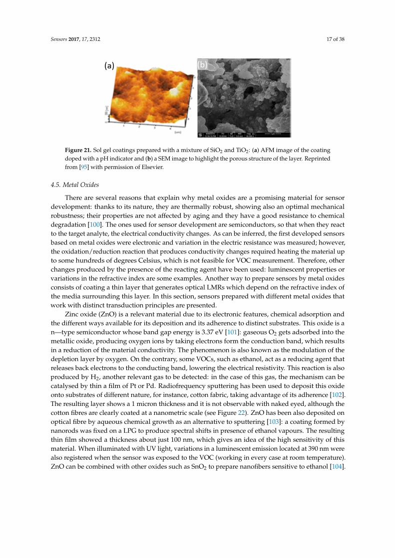
Sensors 2017, 17, 2312 17 of 38
Sensors 2017, 17, 2312 16 of 39
Sol gels can be also doped with a sensing material, in which situation they also act as the supporting matrix. Depending on the chemical properties of the reagent, it is added at different stages of the solidification process but always when viscosity is low enough. It is critical that the sensing features of the material are preserved and, of course, that it does not interfere the gelification reaction. Commercially available sol gel solutions have been used to implement sensors using chemical dyes to measure pH [86] and organometallic compounds to detect and identify VOCs [87]. The variety of materials that can be deposited is remarkable: sol gel matrices successfully doped with zinc oxide have been used to implement humidity sensors with coatings showing just some tens of nanometers width [88]. Moreover, taking advantage of the optical transparency of this kind of thin films, luminescent materials can be embedded into them, so that the luminescent emission is coupled to the fibre with low losses. Luminescent materials are chemically complex, so their adding to the gelification process has to be optimized as much as possible in terms of sensing material concentration. Lead detection in water has been achieved by using a fluorophore as sensing element into a sol gel matrix [89]; another metal ion, Cu2+, has been successfully monitored by an optical fibre sensor prepared with a sol gel matrix doped by metalloporphyrins and quantum dots [90]. Moreover, the high porosity of sol gel coatings makes them optimal for gas sensing, so that different studies report the use porphyrins embedded into this supporting matrix to detect oxygen [91–93]. Xerogels can be also doped with organometallic materials to detect VOCs taking advantage of their high porosity [94].
Recent works detail the combination of silica and titania (TiO2) to obtain sol gels with a high porosity and mechanical robustness; as before, the matrix can be doped with sensing materials such as pH indicators to implement sensors [95]; other agents, for instance surfactants, are included to increase the coating porosity, in which case thickness is between 2 and 4 microns. Figure 21 displays AFM and SEM images of the thin films with different widths with a noticeable porosity. The ratio between SiO2 and TiO2 also determines the final refractive index of the sol gel (from 1.5 up to 1.9): this parameter can be optimized when preparing sensors based on LPGs. These devices are very sensitive to refractive index changes in the environment (atmospheric, or liquid), so if the coating is prepared to maximize the coupling from the optical resonance, a high sensitivity can be obtained. Furthermore, the fibre can be dipped into solutions with a sensing material to functionalize the supporting matrix in a way that compound is trapped into the porous layer once the fibre is removed from the solution [96]. As a result, bio sensors concentration have been implemented to measure immunoglobulins in terms of the Bragg wavelength shift produced by the transduction [97]; devices to detect VOCs have been also reported using LPGs coated with sol gel functionalized by calixalane [98]. Other hybrid sol gel compounds that handle with gold nanoparticles are currently be under study for luminescent based sensing applications [99].
Figure 21. Sol gel coatings prepared with a mixture of SiO2 and TiO2: (a) AFM image of the coating doped with a pH indicator and (b) a SEM image to highlight the porous structure of the layer. Reprinted from [95] with permission of Elsevier.
4.5. Metal Oxides
There are several reasons that explain why metal oxides are a promising material for sensor development: thanks to its nature, they are thermally robust, showing also an optimal mechanical
Figure 21. Sol gel coatings prepared with a mixture of SiO2 and TiO2: (a) AFM image of the coatingdoped with a pH indicator and (b) a SEM image to highlight the porous structure of the layer. Reprintedfrom [95] with permission of Elsevier.
4.5. Metal Oxides
There are several reasons that explain why metal oxides are a promising material for sensordevelopment: thanks to its nature, they are thermally robust, showing also an optimal mechanicalrobustness; their properties are not affected by aging and they have a good resistance to chemicaldegradation [100]. The ones used for sensor development are semiconductors, so that when they reactto the target analyte, the electrical conductivity changes. As can be inferred, the first developed sensorsbased on metal oxides were electronic and variation in the electric resistance was measured; however,the oxidation/reduction reaction that produces conductivity changes required heating the material upto some hundreds of degrees Celsius, which is not feasible for VOC measurement. Therefore, otherchanges produced by the presence of the reacting agent have been used: luminescent properties orvariations in the refractive index are some examples. Another way to prepare sensors by metal oxidesconsists of coating a thin layer that generates optical LMRs which depend on the refractive index ofthe media surrounding this layer. In this section, sensors prepared with different metal oxides thatwork with distinct transduction principles are presented.
Zinc oxide (ZnO) is a relevant material due to its electronic features, chemical adsorption andthe different ways available for its deposition and its adherence to distinct substrates. This oxide is an—type semiconductor whose band gap energy is 3.37 eV [101]: gaseous O2 gets adsorbed into themetallic oxide, producing oxygen ions by taking electrons form the conduction band, which resultsin a reduction of the material conductivity. The phenomenon is also known as the modulation of thedepletion layer by oxygen. On the contrary, some VOCs, such as ethanol, act as a reducing agent thatreleases back electrons to the conducting band, lowering the electrical resistivity. This reaction is alsoproduced by H2, another relevant gas to be detected: in the case of this gas, the mechanism can becatalysed by thin a film of Pt or Pd. Radiofrequency sputtering has been used to deposit this oxideonto substrates of different nature, for instance, cotton fabric, taking advantage of its adherence [102].The resulting layer shows a 1 micron thickness and it is not observable with naked eyed, although thecotton fibres are clearly coated at a nanometric scale (see Figure 22). ZnO has been also deposited onoptical fibre by aqueous chemical growth as an alternative to sputtering [103]: a coating formed bynanorods was fixed on a LPG to produce spectral shifts in presence of ethanol vapours. The resultingthin film showed a thickness about just 100 nm, which gives an idea of the high sensitivity of thismaterial. When illuminated with UV light, variations in a luminescent emission located at 390 nm werealso registered when the sensor was exposed to the VOC (working in every case at room temperature).ZnO can be combined with other oxides such as SnO2 to prepare nanofibers sensitive to ethanol [104].

Sensors 2017, 17, 2312 18 of 38
Sensors 2017, 17, 2312 17 of 39
robustness; their properties are not affected by aging and they have a good resistance to chemical degradation [100]. The ones used for sensor development are semiconductors, so that when they react to the target analyte, the electrical conductivity changes. As can be inferred, the first developed sensors based on metal oxides were electronic and variation in the electric resistance was measured; however, the oxidation/reduction reaction that produces conductivity changes required heating the material up to some hundreds of degrees Celsius, which is not feasible for VOC measurement. Therefore, other changes produced by the presence of the reacting agent have been used: luminescent properties or variations in the refractive index are some examples. Another way to prepare sensors by metal oxides consists of coating a thin layer that generates optical LMRs which depend on the refractive index of the media surrounding this layer. In this section, sensors prepared with different metal oxides that work with distinct transduction principles are presented.
Zinc oxide (ZnO) is a relevant material due to its electronic features, chemical adsorption and the different ways available for its deposition and its adherence to distinct substrates. This oxide is a n—type semiconductor whose band gap energy is 3.37 eV [101]: gaseous O2 gets adsorbed into the metallic oxide, producing oxygen ions by taking electrons form the conduction band, which results in a reduction of the material conductivity. The phenomenon is also known as the modulation of the depletion layer by oxygen. On the contrary, some VOCs, such as ethanol, act as a reducing agent that releases back electrons to the conducting band, lowering the electrical resistivity. This reaction is also produced by H2, another relevant gas to be detected: in the case of this gas, the mechanism can be catalysed by thin a film of Pt or Pd. Radiofrequency sputtering has been used to deposit this oxide onto substrates of different nature, for instance, cotton fabric, taking advantage of its adherence [102]. The resulting layer shows a 1 micron thickness and it is not observable with naked eyed, although the cotton fibres are clearly coated at a nanometric scale (see Figure 22). ZnO has been also deposited on optical fibre by aqueous chemical growth as an alternative to sputtering [103]: a coating formed by nanorods was fixed on a LPG to produce spectral shifts in presence of ethanol vapours. The resulting thin film showed a thickness about just 100 nm, which gives an idea of the high sensitivity of this material. When illuminated with UV light, variations in a luminescent emission located at 390 nm were also registered when the sensor was exposed to the VOC (working in every case at room temperature). ZnO can be combined with other oxides such as SnO2 to prepare nanofibers sensitive to ethanol [104].
Figure 22. Cotton fibres (a) before and (b) after the ZnO deposition; (c) detailed of the coating structure formed by hexagonal shaped columns (see image inside); (d) fabric with no ZnO and another coated one. Reprinted from [102] and used with permission from Elsevier.
Tin dioxide (SnO2) is a widely used metal oxide in electronic sensors for VOCs and moisture measuring. As it discussed previously, these devices required the material to be heated up to promote the oxidation—reduction on its surface, which is not suitable for certain environments. This material shows a relatively high refractive index: this property has been employed to induce LMRs by depositing thin layers of the oxide around optical fibre segments where the cladding has been
Figure 22. Cotton fibres (a) before and (b) after the ZnO deposition; (c) detailed of the coating structureformed by hexagonal shaped columns (see image inside); (d) fabric with no ZnO and another coatedone. Reprinted from [102] and used with permission from Elsevier.
Tin dioxide (SnO2) is a widely used metal oxide in electronic sensors for VOCs and moisturemeasuring. As it discussed previously, these devices required the material to be heated up to promote theoxidation—reduction on its surface, which is not suitable for certain environments. This material shows arelatively high refractive index: this property has been employed to induce LMRs by depositing thinlayers of the oxide around optical fibre segments where the cladding has been removed. The techniquefollowed is sputtering, so that the final thickness of the layer can be controlled mainly by the depositiontime, among other factors (see Figure 23): in any case, the final width is below 1 micron to ensurethe transduction.
Sensors 2017, 17, 2312 18 of 39
removed. The technique followed is sputtering, so that the final thickness of the layer can be controlled mainly by the deposition time, among other factors (see Figure 23): in any case, the final width is below 1 micron to ensure the transduction.
Figure 23. Thickness of sputtered SnO2 thin layers depending on the deposition time: (a) 30 s, (b) 3 min and (c) 4 min (inset, the measured thickness); (d) AFM image of coating (b), which shows a RMS roughness of 1.5 nm. Reprinted from [105] with the permission from Elsevier.
The resulting coating induces lossy cladding modes which are affected by the refractive index of the layer itself and the environment: these changes produce a registrable spectral shift to characterize the sensor. Optical fibre sensors have been reported to detect and measure relative humidity based on LMRs [105,106]; interferometers prepared with photonic crystal fibres were also prepared with SnO2 with this aim [107]. Recent works are reporting its potential use for VOCs and gases detection.
Indium tin oxide (ITO) was one of the first oxides used to prepare sensing devices. This conducting material shares some properties with others but, due to its refractive index, it also induces LMRs. The first studies followed the dip coating procedure to deposit the oxide using a sol gel based mixture: the thickness of the final thin layer was optimized to 170 nm [108]. LMRs are affected by refractive index changes, so, taking that into consideration, coatings sensitive to different materials can be deposited onto the ITO thin layer to implement sensing devices: in this manner, Layer-by-Layer nanostructures [108] were used to develop humidity sensors. Thanks to the chemical nature of the oxide, it can be also deposited by sputtering, which shortens the construction process [109]. Other compounds can be coated around the sputtered ITO film: it is the case of polyvinylidene (PVdF), a conducting polymer that is sandwiched between two ITO layers to get a tuneable optical filter by electric signals: it can be used for electric field sensing too [110]. Another relevant property of ITO coatings is that the morphology can be adjusted not only by the deposition time but also by a post thermal treatment under different conditions. This effect was studied by preparing four different ITO coated surfaces [111]. After the metal oxide sputtering, they were annealed at 500 °C for 4 h under different conditions: vacuum, nitrogen, atmosphere and the forth one was not treated. As a result, the fourth coating was amorphous and show the poorest performance; the morphology of the other three ones is crystalline like, which makes easier the interaction with the environment (see Figure 24 for more details). It is important to remark that refractometers exhibiting giant sensitivity have been prepared by sputtering ITO on D shaped optical fibres [112]: they show a great potentiality in many sensing applications.
Figure 23. Thickness of sputtered SnO2 thin layers depending on the deposition time: (a) 30 s, (b) 3 minand (c) 4 min (inset, the measured thickness); (d) AFM image of coating (b), which shows a RMSroughness of 1.5 nm. Reprinted from [105] with the permission from Elsevier.
The resulting coating induces lossy cladding modes which are affected by the refractive index ofthe layer itself and the environment: these changes produce a registrable spectral shift to characterizethe sensor. Optical fibre sensors have been reported to detect and measure relative humidity based onLMRs [105,106]; interferometers prepared with photonic crystal fibres were also prepared with SnO2
with this aim [107]. Recent works are reporting its potential use for VOCs and gases detection.Indium tin oxide (ITO) was one of the first oxides used to prepare sensing devices. This conducting
material shares some properties with others but, due to its refractive index, it also induces LMRs.The first studies followed the dip coating procedure to deposit the oxide using a sol gel based mixture:the thickness of the final thin layer was optimized to 170 nm [108]. LMRs are affected by refractiveindex changes, so, taking that into consideration, coatings sensitive to different materials can bedeposited onto the ITO thin layer to implement sensing devices: in this manner, Layer-by-Layernanostructures [108] were used to develop humidity sensors. Thanks to the chemical nature of theoxide, it can be also deposited by sputtering, which shortens the construction process [109]. Other

Sensors 2017, 17, 2312 19 of 38
compounds can be coated around the sputtered ITO film: it is the case of polyvinylidene (PVdF), aconducting polymer that is sandwiched between two ITO layers to get a tuneable optical filter byelectric signals: it can be used for electric field sensing too [110]. Another relevant property of ITOcoatings is that the morphology can be adjusted not only by the deposition time but also by a postthermal treatment under different conditions. This effect was studied by preparing four different ITOcoated surfaces [111]. After the metal oxide sputtering, they were annealed at 500 ◦C for 4 h underdifferent conditions: vacuum, nitrogen, atmosphere and the forth one was not treated. As a result,the fourth coating was amorphous and show the poorest performance; the morphology of the otherthree ones is crystalline like, which makes easier the interaction with the environment (see Figure 24for more details). It is important to remark that refractometers exhibiting giant sensitivity have beenprepared by sputtering ITO on D shaped optical fibres [112]: they show a great potentiality in manysensing applications.Sensors 2017, 17, 2312 19 of 39
Figure 24. SEM images from the sputtered ITO samples with annealing under vacuum (sample A), nitrogen (sample B), atmosphere (sample C) and no annealing (sample D); on the second row, AFM images for the similar thermal treatments. Reprinted from [111] with permission from Elsevier.
It has been found that metal oxides with a high refractive index produce LMR for thinner thicknesses and, in some cases, dual peak resonances are induced: they can be referenced between them, which makes the system more robust against undesired fluctuations. More specifically, indium oxide (In2O3) has been used to prepare optical fibre refractometers based on LMRs: compared to other oxides such as ITO, it shows a higher refractive index and not only it produces a double—peak resonance, but also the sensitivity to external refractive index changes is improved by a factor of two [113]. This metal oxide was firstly deposited by dip coating technique in a way the final thickness depended on the number of immersion into the solution were it was dissolved [114]. In order to make the device more selective, different coatings can be deposited onto the In2O3 one: a humidity sensor was implemented by growing a layer-by-layer hydrophilic structure, so that relative humidity determined its refractive index [115]. The metal oxide can be also deposited by sputtering in a faster way if compared with dip coating: it has been observed that coatings below 100 nm yield to higher sensitivities to changes in environment refractive index. The layer morphology is compact but also rod-like (see Figure 25). A sensor prepared this manner was successfully evaluated for monitoring the aging of gear box oil as a function of its refractive index change [116].
Figure 25. SEM images from In2O3 films with different deposition times: 30 s (70 nm), 150 s (300 nm) and 5 min (690 s). The resulting coating is homogeneous and it is formed by compact nanorods. Reprinted [116] from with permission from Springer.
Titania has been also employed to prepare optical fibre sensors. As an alternative to sputtering and dip coating techniques, this oxide can be deposited following a layer-by-layer method. Taking advantage of its refractive index, LMRs were induced for a 500 nm thick coating around an optical
Figure 24. SEM images from the sputtered ITO samples with annealing under vacuum (sample A),nitrogen (sample B), atmosphere (sample C) and no annealing (sample D); on the second row, AFMimages for the similar thermal treatments. Reprinted from [111] with permission from Elsevier.
It has been found that metal oxides with a high refractive index produce LMR for thinnerthicknesses and, in some cases, dual peak resonances are induced: they can be referenced betweenthem, which makes the system more robust against undesired fluctuations. More specifically, indiumoxide (In2O3) has been used to prepare optical fibre refractometers based on LMRs: compared toother oxides such as ITO, it shows a higher refractive index and not only it produces a double—peakresonance, but also the sensitivity to external refractive index changes is improved by a factor oftwo [113]. This metal oxide was firstly deposited by dip coating technique in a way the final thicknessdepended on the number of immersion into the solution were it was dissolved [114]. In order tomake the device more selective, different coatings can be deposited onto the In2O3 one: a humiditysensor was implemented by growing a layer-by-layer hydrophilic structure, so that relative humiditydetermined its refractive index [115]. The metal oxide can be also deposited by sputtering in a fasterway if compared with dip coating: it has been observed that coatings below 100 nm yield to highersensitivities to changes in environment refractive index. The layer morphology is compact but alsorod-like (see Figure 25). A sensor prepared this manner was successfully evaluated for monitoring theaging of gear box oil as a function of its refractive index change [116].

Sensors 2017, 17, 2312 20 of 38
Sensors 2017, 17, 2312 19 of 39
Figure 24. SEM images from the sputtered ITO samples with annealing under vacuum (sample A), nitrogen (sample B), atmosphere (sample C) and no annealing (sample D); on the second row, AFM images for the similar thermal treatments. Reprinted from [111] with permission from Elsevier.
It has been found that metal oxides with a high refractive index produce LMR for thinner thicknesses and, in some cases, dual peak resonances are induced: they can be referenced between them, which makes the system more robust against undesired fluctuations. More specifically, indium oxide (In2O3) has been used to prepare optical fibre refractometers based on LMRs: compared to other oxides such as ITO, it shows a higher refractive index and not only it produces a double—peak resonance, but also the sensitivity to external refractive index changes is improved by a factor of two [113]. This metal oxide was firstly deposited by dip coating technique in a way the final thickness depended on the number of immersion into the solution were it was dissolved [114]. In order to make the device more selective, different coatings can be deposited onto the In2O3 one: a humidity sensor was implemented by growing a layer-by-layer hydrophilic structure, so that relative humidity determined its refractive index [115]. The metal oxide can be also deposited by sputtering in a faster way if compared with dip coating: it has been observed that coatings below 100 nm yield to higher sensitivities to changes in environment refractive index. The layer morphology is compact but also rod-like (see Figure 25). A sensor prepared this manner was successfully evaluated for monitoring the aging of gear box oil as a function of its refractive index change [116].
Figure 25. SEM images from In2O3 films with different deposition times: 30 s (70 nm), 150 s (300 nm) and 5 min (690 s). The resulting coating is homogeneous and it is formed by compact nanorods. Reprinted [116] from with permission from Springer.
Titania has been also employed to prepare optical fibre sensors. As an alternative to sputtering and dip coating techniques, this oxide can be deposited following a layer-by-layer method. Taking advantage of its refractive index, LMRs were induced for a 500 nm thick coating around an optical
Figure 25. SEM images from In2O3 films with different deposition times: 30 s (70 nm), 150 s (300nm) and 5 min (690 s). The resulting coating is homogeneous and it is formed by compact nanorods.Reprinted [116] from with permission from Springer.
Titania has been also employed to prepare optical fibre sensors. As an alternative to sputteringand dip coating techniques, this oxide can be deposited following a layer-by-layer method. Takingadvantage of its refractive index, LMRs were induced for a 500 nm thick coating around an optical fibre:the final device is a refractometer based on spectral shift [117]. A FBG structure was prepared withthis oxide, combining it with AlxOy: alternating layers were deposited onto a cleaved ended fibre byphysical vapor deposition. The last layer of the nanostack can be functionalized with a sensing materialin a way that variations in its refractive index would shift the spectral notch of the grating [118].
4.6. Carbon Nano Tubes (CNTs)
Developed for the first time by Iijima on the early 90s [119,120], CNTs are considered a keynanomaterial, and it encouraged many researches to focus on nanotechnology. Other materials basedon carbon, such as graphene, have also been studied for the development of optical fibre sensors [121].The unique features of CNT are a consequence of their chemical structure: high electrical conductivity,mechanical robustness, near perfect black body characteristics and, regarding to the sensing field, theyshow a high surface/volume ratio (between 100—1800 m2/g). Roughly, there are two types of CNT:single walled (SWCNT), which have a hollow nanostructure where the carbon atoms are organized insingle rolled tubes and multi walled (MWCNT), where several single tubes with different diameters aregrouped in concentrically. The dimensions of CNTs—both diameter and tube length—are always on thenanometric scale; these parameters define properties such as the reactivity or the optical absorbance.
They are normally used separately, although some authors proposed to employ them jointly [122].Both types of CNT have been employed to elaborate optical fibre sensors. SWCNT have beenused to implement VOCs sensors: following Langmuir Blodgett technique, several layers of thesensing material were deposited at the end of a standard optical fibre to build up a Fabry Perotinterferometer [123,124]. Due to the electrical nature of CNT, electrons from VOCs such as toluene reactwith the carbon atoms of the tubes, producing changes in the refractive index and so, a measurablevariation in the reflected optical power. Despite of the interaction surface available, this type ofdeposition for the SWCNT offers a low reproducibility when preparing sensors. Another workproposes incorporating the SWCNT into a cadmium arachidate (CdA) matrix to overcome this issue:following a similar reflection architecture, the resulting device was able to individually distinguishbetween ethanol, ethyl acetate and toluene vapours [125]. Other gases, such hydrogen, have beendetected by optical fibre sensors prepared with SWCNTs: thanks to their molecular morphology,the tubes adsorb the gas molecules, which induces changes in the dielectric constant and thicknessof the sensing material [126]. Sensors based on SWCNTs to detect toluene vapours have been alsoreported [127].

Sensors 2017, 17, 2312 21 of 38
The functionalization of MWCNTs has yielded optical fibre sensors that combine this sensingmaterial with other transduction principles. Luminescent compounds can be attach to MWCTs in away their emission is modified by the entity to be measured: it is the case of fluorescein molecules,which can be linked to the nanotubes walls by covalent bounds [128]; in order to reduce self-quenching,as well as increasing the water solubility, polyether spacers were included between the tubes and thedye. An extrinsic optical sensor was developed with this material: it was able to measure pH changesin a 4.5–8 range.
As it was mentioned before, MWCNTs also show relevant optical properties: when they areilluminated, their structure changes in terms of bending and stretching, but, what is more important,these variations are reversible. Considering their photo-elastic nature, MWCNTs have been coatedby chemical vapor deposition onto fibre Bragg gratings: the resulting layer was just 50 nm thin andabout 60 microns long [129]. Depending on the intensity and wavelength at which the coating isilluminated, the mechanical strain on the grating is different, which is transduced to a shift in thereflected Bragg wavelength. Not only a UV or IR radiation sensor can be implemented, but alsoan optic modulator or filter. CNT can be also combined with PCF to get a refractometer based oninterferometry. Taking advantage of the one dimensional structure, the nanotubes can be dissolvedand sprayed towards a silica surface because they get strongly bonded [130]. When working witha PCF interferometer, the evanescent field is enhanced, so there is a more remarkable interactionwith the sensing coating, in this case, the sprayed CNT (see Figure 26a,b): in this way, the sensitivityto variations in the environment refractive index is increased. Finally, it is also possible to depositMWCNT onto metallic surfaces: in the case of optical fibre, a metallic thin layer can be coated toinduce SPRs, so that the nanotubes would make it sensitive in a manner the wavelength location isshifted in presence of the target analyte; to get selectivity to nitrates, a study proposed to includecopper nanoparticles into the tubes. This metal acts as a catalyst with nitrates to produce ammoniumion, in whose reaction the CNT electrons are required. The resulting material (see Figure 26c), is dipcoated onto the metallic layer deposited on the fibre, and produces shifts in the SPR induced by themetal [131].
Sensors 2017, 17, 2312 21 of 39
variations in the environment refractive index is increased. Finally, it is also possible to deposit MWCNT onto metallic surfaces: in the case of optical fibre, a metallic thin layer can be coated to induce SPRs, so that the nanotubes would make it sensitive in a manner the wavelength location is shifted in presence of the target analyte; to get selectivity to nitrates, a study proposed to include copper nanoparticles into the tubes. This metal acts as a catalyst with nitrates to produce ammonium ion, in whose reaction the CNT electrons are required. The resulting material (see Figure 26c), is dip coated onto the metallic layer deposited on the fibre, and produces shifts in the SPR induced by the metal [131].
Figure 26. Images from an optical microscope (a) of the PCF before and (b) after the CNT deposition; (c) SEM capture of the CNT doped with copper nanoparticles coat deposited on optical fibre. Reprinted from [130,131] with the permission of Elsevier.
4.7. Nanowires
There are different concepts related to nanowires in the literature, where two of them are highlighted: stretched optical fibres with a diameter in the nanometrical range and nanostructures with rod shape that show certain optical properties. The first type of nanowires is prepared by the flame—brushing method or by applying an electrical arch: in this manner, the fibre is heated and pulled to reduce its diameter down to the nanometric range. This procedure can be also applied to other materials such as semiconductors with a crystalline structure or metals. A precise control of the both the mechanical pulling and fibre heating is required to ensure an acceptable reproducibility. To be considered as a nanowire, the final diameter along the stretched section has to be lower than the working wavelength [132]. The resulting device is a 1D nanostructure that exhibits a mechanical robustness typically better than stretched fibres with wider cores and, moreover, it is observable by an optical microscope, which makes easier its manipulation to prepare, for example, nanorings or nanoloops [133]. The evanescent field along the stretched segment is highly increased, which makes it very sensitive to the changes of the surrounding refractive index changes: therefore, many optical fibre nanowires are used as refractometers. The theoretical background is explained by the Maxwell equations and by the H and E components of the propagating signal: there is a clear relationship between the final sensitivity and the stretched fibre diameter, which can be studied by finite element method [134]. The common configuration of this kind of devices is transmission or a Mach Zehnder interferometer: for the second one, a non-functionalized nanowire is used as reference in one of the interferometer arms, whereas another with a sensing coating is connected to the other wire [135]. There are other configurations such as the hybrid one, which consists on a nanowire fused at the end of a cleaved ended fibre [136]: this architecture combines the evanescent field increased interaction with the mechanical properties of reflection sensors. To highlight the versatility of nanowires, they can be combined with MOFs, which allows the resulting device polarization properties to be controlled [137].
Once the fibre is tapered, its surface is functionalized to provide the sensor with the required sensitivity to the target analyte. A simple procedure to do it is silanization: it consists of just dipping the stretched segment into a silanizing solution (for example, methoxysilane), which makes the fibre’s cladding non-sensitive to refractive index changes produced by relative humidity but, for example, to certain apolar gases. An optimized study about the effect of the stretched diameter describes sensors with just of a few millimetres of nanowire and a 800 nm core diameter are enough to detect
Figure 26. Images from an optical microscope (a) of the PCF before and (b) after the CNT deposition;(c) SEM capture of the CNT doped with copper nanoparticles coat deposited on optical fibre. Reprintedfrom [130,131] with the permission of Elsevier.
4.7. Nanowires
There are different concepts related to nanowires in the literature, where two of them arehighlighted: stretched optical fibres with a diameter in the nanometrical range and nanostructureswith rod shape that show certain optical properties. The first type of nanowires is prepared by theflame—brushing method or by applying an electrical arch: in this manner, the fibre is heated andpulled to reduce its diameter down to the nanometric range. This procedure can be also applied toother materials such as semiconductors with a crystalline structure or metals. A precise control ofthe both the mechanical pulling and fibre heating is required to ensure an acceptable reproducibility.To be considered as a nanowire, the final diameter along the stretched section has to be lower thanthe working wavelength [132]. The resulting device is a 1D nanostructure that exhibits a mechanicalrobustness typically better than stretched fibres with wider cores and, moreover, it is observable by

Sensors 2017, 17, 2312 22 of 38
an optical microscope, which makes easier its manipulation to prepare, for example, nanorings ornanoloops [133]. The evanescent field along the stretched segment is highly increased, which makesit very sensitive to the changes of the surrounding refractive index changes: therefore, many opticalfibre nanowires are used as refractometers. The theoretical background is explained by the Maxwellequations and by the H and E components of the propagating signal: there is a clear relationshipbetween the final sensitivity and the stretched fibre diameter, which can be studied by finite elementmethod [134]. The common configuration of this kind of devices is transmission or a Mach Zehnderinterferometer: for the second one, a non-functionalized nanowire is used as reference in one of theinterferometer arms, whereas another with a sensing coating is connected to the other wire [135]. Thereare other configurations such as the hybrid one, which consists on a nanowire fused at the end of acleaved ended fibre [136]: this architecture combines the evanescent field increased interaction withthe mechanical properties of reflection sensors. To highlight the versatility of nanowires, they can becombined with MOFs, which allows the resulting device polarization properties to be controlled [137].
Once the fibre is tapered, its surface is functionalized to provide the sensor with the requiredsensitivity to the target analyte. A simple procedure to do it is silanization: it consists of just dippingthe stretched segment into a silanizing solution (for example, methoxysilane), which makes the fibre’scladding non-sensitive to refractive index changes produced by relative humidity but, for example,to certain apolar gases. An optimized study about the effect of the stretched diameter describes sensorswith just of a few millimetres of nanowire and a 800 nm core diameter are enough to detect propaneleakages [138]. Moreover, some authors presented a reflection sensor based on nanowires that includeda structure to improve its mechanical robustness: the resulting devices can therefore be functionalizedto sense different parameters [136].
Another different concept of nanowires is related to the synthesis of structures with nano rodsgeometrics that can conform arrays around or at the end of optical fibre [139] or to fill, for example,the air holes of MOFs [140]: actually, SPRs can be induced in this way with silver nanowires fillingrandomly PCFs air holes [141]. Furthermore, nanowires can be used to prepare extrinsic opticalfibre sensors. Silicon monoxide can be exposed to high temperatures to obtain, after a gradualcooling rate, silicon nanowires: a sensor to detect methane was reported by adding to the nanowirescryptophane-A [142], yielding to a luminescent sensing membrane (see Figure 27) whose emission isquenched by the target gas.
Sensors 2017, 17, 2312 22 of 39
propane leakages [138]. Moreover, some authors presented a reflection sensor based on nanowires that included a structure to improve its mechanical robustness: the resulting devices can therefore be functionalized to sense different parameters [136].
Another different concept of nanowires is related to the synthesis of structures with nano rods geometrics that can conform arrays around or at the end of optical fibre [139] or to fill, for example, the air holes of MOFs [140]: actually, SPRs can be induced in this way with silver nanowires filling randomly PCFs air holes [141]. Furthermore, nanowires can be used to prepare extrinsic optical fibre sensors. Silicon monoxide can be exposed to high temperatures to obtain, after a gradual cooling rate, silicon nanowires: a sensor to detect methane was reported by adding to the nanowires cryptophane-A [142], yielding to a luminescent sensing membrane (see Figure 27) whose emission is quenched by the target gas.
Figure 27. (a) SEM image of the silica nanowires functionalized with cryptophane-A; (b) luminescent emission of the nanowires when illuminated with UV radiation. Reprinted from [142] with permission from Elsevier.
Finally, the term nanowire can also refer to elements of a grid or pattern with certain optical properties that are affected by variations in electric or magnetic field. The resulting deposited material looks like parallel lines, so that is the reason why they are named nano wires. The materials employed to prepare the grid are transition metals such as platinum or gold (see Figure 28) [143]. To get a better sensitivity, the fibre can be D shaped and, onto the flat surface, layers of metals following a pattern are deposited: the pattern is obtained by using a laser beam through a mask [144]. The device is based on SPR induced by the metallic layers, and they are red shifted by the exposure to UV radiation.
Figure 28. (a) Detail of the gold grid fabricated on the tip of a SMF; (b) SEM image of the sensor head: the square grid is appreciable at the centre of the fibre. Reprinted from [143].
4.8. Molecularly Imprinted Polymers (MIPs)
This kind of materials is molecularly designed to be sensitive to a certain target molecule. Although they are not strictly nanostructured, the possibility of designing them at a molecular level justifies their description in this review. MIPs were developed as an alternative to biological
Figure 27. (a) SEM image of the silica nanowires functionalized with cryptophane-A; (b) luminescentemission of the nanowires when illuminated with UV radiation. Reprinted from [142] with permissionfrom Elsevier.
Finally, the term nanowire can also refer to elements of a grid or pattern with certain opticalproperties that are affected by variations in electric or magnetic field. The resulting deposited materiallooks like parallel lines, so that is the reason why they are named nano wires. The materials employedto prepare the grid are transition metals such as platinum or gold (see Figure 28) [143]. To get a bettersensitivity, the fibre can be D shaped and, onto the flat surface, layers of metals following a pattern are

Sensors 2017, 17, 2312 23 of 38
deposited: the pattern is obtained by using a laser beam through a mask [144]. The device is based onSPR induced by the metallic layers, and they are red shifted by the exposure to UV radiation.
Sensors 2017, 17, 2312 22 of 39
propane leakages [138]. Moreover, some authors presented a reflection sensor based on nanowires that included a structure to improve its mechanical robustness: the resulting devices can therefore be functionalized to sense different parameters [136].
Another different concept of nanowires is related to the synthesis of structures with nano rods geometrics that can conform arrays around or at the end of optical fibre [139] or to fill, for example, the air holes of MOFs [140]: actually, SPRs can be induced in this way with silver nanowires filling randomly PCFs air holes [141]. Furthermore, nanowires can be used to prepare extrinsic optical fibre sensors. Silicon monoxide can be exposed to high temperatures to obtain, after a gradual cooling rate, silicon nanowires: a sensor to detect methane was reported by adding to the nanowires cryptophane-A [142], yielding to a luminescent sensing membrane (see Figure 27) whose emission is quenched by the target gas.
Figure 27. (a) SEM image of the silica nanowires functionalized with cryptophane-A; (b) luminescent emission of the nanowires when illuminated with UV radiation. Reprinted from [142] with permission from Elsevier.
Finally, the term nanowire can also refer to elements of a grid or pattern with certain optical properties that are affected by variations in electric or magnetic field. The resulting deposited material looks like parallel lines, so that is the reason why they are named nano wires. The materials employed to prepare the grid are transition metals such as platinum or gold (see Figure 28) [143]. To get a better sensitivity, the fibre can be D shaped and, onto the flat surface, layers of metals following a pattern are deposited: the pattern is obtained by using a laser beam through a mask [144]. The device is based on SPR induced by the metallic layers, and they are red shifted by the exposure to UV radiation.
Figure 28. (a) Detail of the gold grid fabricated on the tip of a SMF; (b) SEM image of the sensor head: the square grid is appreciable at the centre of the fibre. Reprinted from [143].
4.8. Molecularly Imprinted Polymers (MIPs)
This kind of materials is molecularly designed to be sensitive to a certain target molecule. Although they are not strictly nanostructured, the possibility of designing them at a molecular level justifies their description in this review. MIPs were developed as an alternative to biological
Figure 28. (a) Detail of the gold grid fabricated on the tip of a SMF; (b) SEM image of the sensor head:the square grid is appreciable at the centre of the fibre. Reprinted from [143].
4.8. Molecularly Imprinted Polymers (MIPs)
This kind of materials is molecularly designed to be sensitive to a certain target molecule.Although they are not strictly nanostructured, the possibility of designing them at a molecular leveljustifies their description in this review. MIPs were developed as an alternative to biological moleculeswith a high selectivity, which is the case of enzymes or anti bodies: these molecules have to operatetypically under physiological conditions to prevent their degradation, which sometimes makes difficulttheir use for sensor development. On the contrary, MIPs are synthetic molecules that can be depositedand used with different working conditions. To stablish an analogy, a MIP acts as a lock which can beopen only by a certain target molecule, so that the selectivity is very high: a properly designed MIPcould distinguish even between isomers, for instance, glucose and fructose. In order to synthesize aMIP, different chemical reagents are mixed in a solvent (typically an organic one, although water hasbeen also used) together with the target molecule, which acts as a template. The reagents are in mostcases these ones: a monomer which constitutes the backbone of the resulting MIP; other monomerswith functional groups that guarantee the reaction with the target molecule; chemical dyes that will bealso included in the final reagent whose optical properties (such as luminescence) vary depending onthe presence of the template; a cross-linker that make possible the synthesis of the new polymer anda starter agent. During the reaction, the MIP morphology is determined by the target molecule in away its functional groups are linked with it by weak forces (hydrogen bonding, Van der Waals forces,among others): once the chemical reaction is complete, the template can be removed by a solvent andlinked again to the MIP reversely. Figure 29 shows the process. The selection of the proper reagentsdetermines the final features of the MIP, so it is a critical step: the functional groups, the binding energy tothe template or the hydrophobic behaviour are just some critical parameters that should be considered.Actually, some authors have already computationally design MIPs to get the best results [145].
Sensors 2017, 17, 2312 23 of 39
molecules with a high selectivity, which is the case of enzymes or anti bodies: these molecules have to operate typically under physiological conditions to prevent their degradation, which sometimes makes difficult their use for sensor development. On the contrary, MIPs are synthetic molecules that can be deposited and used with different working conditions. To stablish an analogy, a MIP acts as a lock which can be open only by a certain target molecule, so that the selectivity is very high: a properly designed MIP could distinguish even between isomers, for instance, glucose and fructose. In order to synthesize a MIP, different chemical reagents are mixed in a solvent (typically an organic one, although water has been also used) together with the target molecule, which acts as a template. The reagents are in most cases these ones: a monomer which constitutes the backbone of the resulting MIP; other monomers with functional groups that guarantee the reaction with the target molecule; chemical dyes that will be also included in the final reagent whose optical properties (such as luminescence) vary depending on the presence of the template; a cross-linker that make possible the synthesis of the new polymer and a starter agent. During the reaction, the MIP morphology is determined by the target molecule in a way its functional groups are linked with it by weak forces (hydrogen bonding, Van der Waals forces, among others): once the chemical reaction is complete, the template can be removed by a solvent and linked again to the MIP reversely. Figure 29 shows the process. The selection of the proper reagents determines the final features of the MIP, so it is a critical step: the functional groups, the binding energy to the template or the hydrophobic behaviour are just some critical parameters that should be considered. Actually, some authors have already computationally design MIPs to get the best results [145].
Figure 29. Brief synthesis and reaction processes for a MIP, showing the most relevant molecules involved.
The synergy between MIPs and optical fibre is clear due to the high selectivity and all the very well-known features of the substrate: the most critical step for their combination is the deposition of the sensing material on the fibre due to its small dimensions. Therefore, most works report the use of wide core fibres, such as PCS or POF, which offer an active area where the MIP can be effectively deposited. As it will be explained in the following paragraphs, some authors prefer the polymerization to take place onto the fibre, whereas other deposit the sensing polymer once the reaction is over.In the case one of the monomers included during the polymerization process is, for instance, luminescent, optical fibre can be used to directly measure the changes induced by the presence of the target molecule: this is the case of sensors prepare to detect cocaine with a high selectivity [145,146]. For these devices, the fibre is initially treated to have an anchoring layer where the polymerization will occur: thereafter, the fibre is inserted into a vial where all the reagents are present; once the process is over, the fibre is removed from the vial and the sensor is ready to be used. There are other approaches in which the fibre is immersed into a solution where the polymerization reaction has been completed, so that the MIPs is already dissolved: in this manner, the fibre does not have to be pre-treated and the sensitive film is deposited by dip coating [147,148]; however, depending on the MIP, the resulting sensor is to be used at once because the template cannot be removed from the polymer.
Following the previous idea of depositing the MIP molecules, some authors propose to etch the optical fibre (on its top or around its coating) to create holes where the sensing molecules are to be located. In this manner, an array of fibres with different MIPs can be used to form a bundle and in
Figure 29. Brief synthesis and reaction processes for a MIP, showing the most relevant molecules involved.

Sensors 2017, 17, 2312 24 of 38
The synergy between MIPs and optical fibre is clear due to the high selectivity and all the verywell-known features of the substrate: the most critical step for their combination is the deposition of thesensing material on the fibre due to its small dimensions. Therefore, most works report the use of widecore fibres, such as PCS or POF, which offer an active area where the MIP can be effectively deposited.As it will be explained in the following paragraphs, some authors prefer the polymerization to takeplace onto the fibre, whereas other deposit the sensing polymer once the reaction is over.In the caseone of the monomers included during the polymerization process is, for instance, luminescent, opticalfibre can be used to directly measure the changes induced by the presence of the target molecule: thisis the case of sensors prepare to detect cocaine with a high selectivity [145,146]. For these devices,the fibre is initially treated to have an anchoring layer where the polymerization will occur: thereafter,the fibre is inserted into a vial where all the reagents are present; once the process is over, the fibre isremoved from the vial and the sensor is ready to be used. There are other approaches in which thefibre is immersed into a solution where the polymerization reaction has been completed, so that theMIPs is already dissolved: in this manner, the fibre does not have to be pre-treated and the sensitivefilm is deposited by dip coating [147,148]; however, depending on the MIP, the resulting sensor is to beused at once because the template cannot be removed from the polymer.
Following the previous idea of depositing the MIP molecules, some authors propose to etch theoptical fibre (on its top or around its coating) to create holes where the sensing molecules are to be located.In this manner, an array of fibres with different MIPs can be used to form a bundle and in this manner,a multi parameter device is obtained (also taking advantage of the multiplexing feature of the fibre).Polymers with spherical shapes are easier to locate on the etched surface: fluorescent MIPs have beendeveloped this way to create antibiotic sensors based on the luminescent emission of the polymer [149].
Other works report the combination of SPRs and MIPs: the fibre is firstly coated with ametallic thin layer (gold in most cases due to its plasmon resonance spectral location) and then,the polymerization mixture is drop coated onto it, taking place the MIP synthesis after a curing.The resulting sensor varies the SPR location in presence of the target molecule, which is an alternativeto luminescent emission based schemes: actually, the fibre can be D shaped to enhance the SPR [150] orthe MIP can be located onto polished fibres that form an optical coupler [151]. These devices have beendeveloped to control oil degradation in transformers, detecting the presence of dibenzyl disulphide(DBDS) and furfural.
The polymerization is currently being adapted to the optical fibre in a way it plays an active roleduring the reaction: as before, a metallic coating is sputtered on to the fibre to generate a SPR, butalso, to be used as an electrode. In the case a conducting monomer is used as backbone (polypyrrole)in the reaction, electro-polimerization can be used to induce the MIP synthesis, ensuring that it isproperly attached onto the substrate. The three layers involved (fibre cladding, gold thin coating andMIP) are shown in Figure 30: even with a thickness below 100 nm, a SPR spectral shift of 2 pm performaldehyde ppm has been reported [152].
Sensors 2017, 17, 2312 24 of 39
this manner, a multi parameter device is obtained (also taking advantage of the multiplexing feature of the fibre). Polymers with spherical shapes are easier to locate on the etched surface: fluorescent MIPs have been developed this way to create antibiotic sensors based on the luminescent emission of the polymer [149].
Other works report the combination of SPRs and MIPs: the fibre is firstly coated with a metallic thin layer (gold in most cases due to its plasmon resonance spectral location) and then, the polymerization mixture is drop coated onto it, taking place the MIP synthesis after a curing. The resulting sensor varies the SPR location in presence of the target molecule, which is an alternative to luminescent emission based schemes: actually, the fibre can be D shaped to enhance the SPR [150] or the MIP can be located onto polished fibres that form an optical coupler [151]. These devices have been developed to control oil degradation in transformers, detecting the presence of dibenzyl disulphide (DBDS) and furfural.
The polymerization is currently being adapted to the optical fibre in a way it plays an active role during the reaction: as before, a metallic coating is sputtered on to the fibre to generate a SPR, but also, to be used as an electrode. In the case a conducting monomer is used as backbone (polypyrrole) in the reaction, electro-polimerization can be used to induce the MIP synthesis, ensuring that it is properly attached onto the substrate. The three layers involved (fibre cladding, gold thin coating and MIP) are shown in Figure 30: even with a thickness below 100 nm, a SPR spectral shift of 2 pm per formaldehyde ppm has been reported [152].
The polymerization is currently being adapted to the optical fibre in a way it plays an active role during the reaction: as before, a metallic coating is sputtered on to the fibre to generate a SPR, but also, to be used as an electrode. In the case a conducting monomer is used as backbone (polypyrrole) in the reaction, electropolymerization can be used to induce the MIP synthesis, ensuring that it is properly attached onto the substrate. The three layers involved (fibre cladding, gold thin coating and MIP) are shown in Figure 30: even with a thickness below 100 nm, a SPR spectral shift of 2 pm per formaldehyde ppm has been reported [152].
Figure 30. SEM image for a MIP coated onto an optical fibre by electropolymerization. Reprinted from [152] with permission from Elsevier.
4.9. Layer-By-Layer (LbL) Nanostructures
The small dimensions of optical fibre sometimes make it difficult to deposit coatings, but following LbL, this problem is overcome for both reflection and transmission configuration. The first sensors developed were for the first architecture to prepare nanointerferometers: LbL versatility allows polymers of different types to be used, and as a consequence, different morphologies to be adjusted at a nanometric level. The resulting cavities grown at the end of cleaved ended fibre are commonly prepared to show a thickness below 1 micron to get an interferometric response: if the coating is sensitive to humidity variations in a way its refractive index is modified, the interferometric signal follows this change. Taking this effect into consideration, a humidity sensor was reported by combining a gold colloid mixed with poly (diallyldimethylammonium chloride) (PDDA) and poly (sodium 4-styrene sulfonate) (PSS); the cavity thickness was estimated to be 310 nm, and was one of the first optical fibre sensors prepared by LbL [153]. The hydrophilic nature of most of LbL structures
Figure 30. SEM image for a MIP coated onto an optical fibre by electropolymerization. Reprintedfrom [152] with permission from Elsevier.

Sensors 2017, 17, 2312 25 of 38
4.9. Layer-By-Layer (LbL) Nanostructures
The small dimensions of optical fibre sometimes make it difficult to deposit coatings, but followingLbL, this problem is overcome for both reflection and transmission configuration. The first sensorsdeveloped were for the first architecture to prepare nanointerferometers: LbL versatility allowspolymers of different types to be used, and as a consequence, different morphologies to be adjusted at ananometric level. The resulting cavities grown at the end of cleaved ended fibre are commonly preparedto show a thickness below 1 micron to get an interferometric response: if the coating is sensitive tohumidity variations in a way its refractive index is modified, the interferometric signal follows thischange. Taking this effect into consideration, a humidity sensor was reported by combining a goldcolloid mixed with poly (diallyldimethylammonium chloride) (PDDA) and poly (sodium 4-styrenesulfonate) (PSS); the cavity thickness was estimated to be 310 nm, and was one of the first opticalfibre sensors prepared by LbL [153]. The hydrophilic nature of most of LbL structures helps materialsdissolved in water to be diffused into the supporting matrix: what is more, a wide range of compoundscan be deposited at the same time with the polymers involved, or they can even act as a chargedmolecule. Prussian Blue, a chemical dye, has been deposited with a poly(allylamine hydrocholoride)(PAH) and poly(acrylic acid sodium salt) (PAA) by mixing it with the first reagent to measure H2O2:a [PAH/PAA]2 final coating was found to prevent leaks [154]. Sensors to measure pH have been alsoobtained by including indicators to one of the polymeric solutions: it is the case of HPTS, which isdeposited together with PAH using PAA as polycation. Variations in absorbance spectrum were usedto characterize the sensor response. Furthermore, it was observed that the performance of the sensorcould be improved by firstly depositing layer pairs with a remarked hydrophilic behaviour: AFMimages confirm this phenomenon (see Figure 31) together with the obtained results [155]. It has beenalso observed that the some polymers, specifically, the combination of PAH and PAA, are sensitiveto pH variations, producing a reversible swelling effect that can be registered by the interferometricresponse in this type of reflection configurations [156]. Moreover, [PAH/PAA] nanocavities havebeen embedded with sensing materials to obtain VOCs sensors: the initial morphology showeda high porosity that was altered by the organometallic compounds used to prepared the devices(see Figure 32) [157].
Sensors 2017, 17, 2312 25 of 39
helps materials dissolved in water to be diffused into the supporting matrix: what is more, a wide range of compounds can be deposited at the same time with the polymers involved, or they can even act as a charged molecule. Prussian Blue, a chemical dye, has been deposited with a poly(allylamine hydrocholoride) (PAH) and poly(acrylic acid sodium salt) (PAA) by mixing it with the first reagent to measure H2O2: a [PAH/PAA]2 final coating was found to prevent leaks [154]. Sensors to measure pH have been also obtained by including indicators to one of the polymeric solutions: it is the case of HPTS, which is deposited together with PAH using PAA as polycation. Variations in absorbance spectrum were used to characterize the sensor response. Furthermore, it was observed that the performance of the sensor could be improved by firstly depositing layer pairs with a remarked hydrophilic behaviour: AFM images confirm this phenomenon (see Figure 31) together with the obtained results [155]. It has been also observed that the some polymers, specifically, the combination of PAH and PAA, are sensitive to pH variations, producing a reversible swelling effect that can be registered by the interferometric response in this type of reflection configurations [156]. Moreover, [PAH/PAA] nanocavities have been embedded with sensing materials to obtain VOCs sensors: the initial morphology showed a high porosity that was altered by the organometallic compounds used to prepared the devices (see Figure 32) [157].
Figure 31. (a) AFM image from a [PAH+HTTPS/PAA] coating (left hand side image) and one with a hydrophilic coating deposited below (right hand side image); (b) the second one shows a higher roughness that enhances the sensitivity of the sensor. Reprinted from [155] with permission from Elsevier.
Figure 32. SEM images from [PAH/PAA] nanostructures that have been embedded with organometallic materials that share the [(C6F5)2Ag2Au2L2]n backbone, where L is a ligand molecule. Depending on the ligand, morphologies with different porous size are obtained: (a) 1/2 diphenylacetylene, (b) ammonia, (c) pyridine and (d) 2,2’-bipyridine. Reprinted from [157] with permission from Elsevier.
The sensitivity of devices based in transmission configuration can be functionalized by LbL: as an important example, LPGs are sensitive to the external refractive index, in a way the resonance wavelength is shifted by this parameter. It was theoretically proposed that thin layers could improve this sensitivity significantly, but to achieve that, a precise control of the thickness was required [158]. In this background, LbL proved to be an optical technique to deposit thin films with a resolution at a nanometric level: firstly, the hypothesis was confirmed by a just few nanometers thick mono layer. The wavelength shift was not only affected by the refractive index of the coating but also by its thickness: in this manner, 25-layer pairs of [PAH/PAA] were deposited onto a LPG to get a pH sensor,
Figure 31. (a) AFM image from a [PAH+HTTPS/PAA] coating (left hand side image) and one with ahydrophilic coating deposited below (right hand side image); (b) the second one shows a higher roughnessthat enhances the sensitivity of the sensor. Reprinted from [155] with permission from Elsevier.
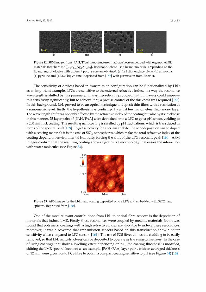
Sensors 2017, 17, 2312 26 of 38
Sensors 2017, 17, 2312 25 of 39
helps materials dissolved in water to be diffused into the supporting matrix: what is more, a wide range of compounds can be deposited at the same time with the polymers involved, or they can even act as a charged molecule. Prussian Blue, a chemical dye, has been deposited with a poly(allylamine hydrocholoride) (PAH) and poly(acrylic acid sodium salt) (PAA) by mixing it with the first reagent to measure H2O2: a [PAH/PAA]2 final coating was found to prevent leaks [154]. Sensors to measure pH have been also obtained by including indicators to one of the polymeric solutions: it is the case of HPTS, which is deposited together with PAH using PAA as polycation. Variations in absorbance spectrum were used to characterize the sensor response. Furthermore, it was observed that the performance of the sensor could be improved by firstly depositing layer pairs with a remarked hydrophilic behaviour: AFM images confirm this phenomenon (see Figure 31) together with the obtained results [155]. It has been also observed that the some polymers, specifically, the combination of PAH and PAA, are sensitive to pH variations, producing a reversible swelling effect that can be registered by the interferometric response in this type of reflection configurations [156]. Moreover, [PAH/PAA] nanocavities have been embedded with sensing materials to obtain VOCs sensors: the initial morphology showed a high porosity that was altered by the organometallic compounds used to prepared the devices (see Figure 32) [157].
Figure 31. (a) AFM image from a [PAH+HTTPS/PAA] coating (left hand side image) and one with a hydrophilic coating deposited below (right hand side image); (b) the second one shows a higher roughness that enhances the sensitivity of the sensor. Reprinted from [155] with permission from Elsevier.
Figure 32. SEM images from [PAH/PAA] nanostructures that have been embedded with organometallic materials that share the [(C6F5)2Ag2Au2L2]n backbone, where L is a ligand molecule. Depending on the ligand, morphologies with different porous size are obtained: (a) 1/2 diphenylacetylene, (b) ammonia, (c) pyridine and (d) 2,2’-bipyridine. Reprinted from [157] with permission from Elsevier.
The sensitivity of devices based in transmission configuration can be functionalized by LbL: as an important example, LPGs are sensitive to the external refractive index, in a way the resonance wavelength is shifted by this parameter. It was theoretically proposed that thin layers could improve this sensitivity significantly, but to achieve that, a precise control of the thickness was required [158]. In this background, LbL proved to be an optical technique to deposit thin films with a resolution at a nanometric level: firstly, the hypothesis was confirmed by a just few nanometers thick mono layer. The wavelength shift was not only affected by the refractive index of the coating but also by its thickness: in this manner, 25-layer pairs of [PAH/PAA] were deposited onto a LPG to get a pH sensor,
Figure 32. SEM images from [PAH/PAA] nanostructures that have been embedded with organometallicmaterials that share the [(C6F5)2Ag2Au2L2]n backbone, where L is a ligand molecule. Depending on theligand, morphologies with different porous size are obtained: (a) 1/2 diphenylacetylene, (b) ammonia,(c) pyridine and (d) 2,2’-bipyridine. Reprinted from [157] with permission from Elsevier.
The sensitivity of devices based in transmission configuration can be functionalized by LbL:as an important example, LPGs are sensitive to the external refractive index, in a way the resonancewavelength is shifted by this parameter. It was theoretically proposed that thin layers could improvethis sensitivity significantly, but to achieve that, a precise control of the thickness was required [158].In this background, LbL proved to be an optical technique to deposit thin films with a resolution ata nanometric level: firstly, the hypothesis was confirmed by a just few nanometers thick mono layer.The wavelength shift was not only affected by the refractive index of the coating but also by its thickness:in this manner, 25-layer pairs of [PAH/PAA] were deposited onto a LPG to get a pH sensor, yielding toa 200 nm thick coating. The resulting nanocoating is swelled by pH fluctuations, which is transduced interms of the spectral shift [159]. To get selectivity for a certain analyte, the nanodeposition can be dopedwith a sensing material: it is the case of SiO2 nanospheres, which make the total refractive index of thecoating depend on environmental humidity, forcing the shift of the LPG resonant peak [160]. AFMimages confirm that the resulting coating shows a grain-like morphology that easies the interactionwith water molecules (see Figure 33).
Sensors 2017, 17, 2312 26 of 39
yielding to a 200 nm thick coating. The resulting nanocoating is swelled by pH fluctuations, which is transduced in terms of the spectral shift [159]. To get selectivity for a certain analyte, the nanodeposition can be doped with a sensing material: it is the case of SiO2 nanospheres, which make the total refractive index of the coating depend on environmental humidity, forcing the shift of the LPG resonant peak [160]. AFM images confirm that the resulting coating shows a grain-like morphology that easies the interaction with water molecules (see Figure 33).
Figure 33. AFM image for the LbL nano coating deposited onto a LPG and embedded with SiO2 nano spheres. Reprinted from [160].
One of the most relevant contributions from LbL to optical fibre sensors is the deposition of materials that induce LMR. Firstly, these resonances were coupled by metallic materials, but it was found that polymeric coatings with a high refractive index are also able to induce these resonances: moreover, it was discovered that transmission sensors based on this transduction show a better sensitivity when compared to LPG sensors [161]. The use of PCS fibres allows the cladding to be easily removed, so that LbL nanostructures can be deposited to operate as transmission sensors. In the case of using coatings that show a swelling effect depending on pH, the coating thickness is modified, shifting the LMR spectral location: as an example, [PAH/PAA] layer pairs, with an averaged thickness of 12 nm, were grown onto PCS fibre to obtain a compact coating sensitive to pH (see Figure 34) [162].
Figure 34. SEM image of a [PAH/PAA]100 coating onto a PCS fibre. Inset, a detail of the thin layer. Reprinted from [162] with permission from Elsevier.
LbL coatings can be also embedded with sensing materials to induce SPRs as well as LMRs, so that a self-referenced device is implemented. It is well known that nanoparticles can be used to dope coatings in a way the resulting refractive index is defined by its concentration. Silver nanoparticles were loaded into a [PAH/PAA] nanostructured for this propose. Two methods are reported: on one hand, the layer pairs are deposited and then immersed into a solution where the nanoparticles are dissolved; on the other hand, the Ag nanoparticles are mixed with PAA and deposited along the LbL growing. The second procedure yields to a more uniform distribution of nanoparticles, and so, a better sensitivity. Results were evaluated and confirmed by relative humidity measurements [163].
Figure 33. AFM image for the LbL nano coating deposited onto a LPG and embedded with SiO2 nanospheres. Reprinted from [160].
One of the most relevant contributions from LbL to optical fibre sensors is the deposition ofmaterials that induce LMR. Firstly, these resonances were coupled by metallic materials, but it wasfound that polymeric coatings with a high refractive index are also able to induce these resonances:moreover, it was discovered that transmission sensors based on this transduction show a bettersensitivity when compared to LPG sensors [161]. The use of PCS fibres allows the cladding to be easilyremoved, so that LbL nanostructures can be deposited to operate as transmission sensors. In the caseof using coatings that show a swelling effect depending on pH, the coating thickness is modified,shifting the LMR spectral location: as an example, [PAH/PAA] layer pairs, with an averaged thicknessof 12 nm, were grown onto PCS fibre to obtain a compact coating sensitive to pH (see Figure 34) [162].

Sensors 2017, 17, 2312 27 of 38
Sensors 2017, 17, 2312 26 of 39
yielding to a 200 nm thick coating. The resulting nanocoating is swelled by pH fluctuations, which is transduced in terms of the spectral shift [159]. To get selectivity for a certain analyte, the nanodeposition can be doped with a sensing material: it is the case of SiO2 nanospheres, which make the total refractive index of the coating depend on environmental humidity, forcing the shift of the LPG resonant peak [160]. AFM images confirm that the resulting coating shows a grain-like morphology that easies the interaction with water molecules (see Figure 33).
Figure 33. AFM image for the LbL nano coating deposited onto a LPG and embedded with SiO2 nano spheres. Reprinted from [160].
One of the most relevant contributions from LbL to optical fibre sensors is the deposition of materials that induce LMR. Firstly, these resonances were coupled by metallic materials, but it was found that polymeric coatings with a high refractive index are also able to induce these resonances: moreover, it was discovered that transmission sensors based on this transduction show a better sensitivity when compared to LPG sensors [161]. The use of PCS fibres allows the cladding to be easily removed, so that LbL nanostructures can be deposited to operate as transmission sensors. In the case of using coatings that show a swelling effect depending on pH, the coating thickness is modified, shifting the LMR spectral location: as an example, [PAH/PAA] layer pairs, with an averaged thickness of 12 nm, were grown onto PCS fibre to obtain a compact coating sensitive to pH (see Figure 34) [162].
Figure 34. SEM image of a [PAH/PAA]100 coating onto a PCS fibre. Inset, a detail of the thin layer. Reprinted from [162] with permission from Elsevier.
LbL coatings can be also embedded with sensing materials to induce SPRs as well as LMRs, so that a self-referenced device is implemented. It is well known that nanoparticles can be used to dope coatings in a way the resulting refractive index is defined by its concentration. Silver nanoparticles were loaded into a [PAH/PAA] nanostructured for this propose. Two methods are reported: on one hand, the layer pairs are deposited and then immersed into a solution where the nanoparticles are dissolved; on the other hand, the Ag nanoparticles are mixed with PAA and deposited along the LbL growing. The second procedure yields to a more uniform distribution of nanoparticles, and so, a better sensitivity. Results were evaluated and confirmed by relative humidity measurements [163].
Figure 34. SEM image of a [PAH/PAA]100 coating onto a PCS fibre. Inset, a detail of the thin layer.Reprinted from [162] with permission from Elsevier.
LbL coatings can be also embedded with sensing materials to induce SPRs as well as LMRs, sothat a self-referenced device is implemented. It is well known that nanoparticles can be used to dopecoatings in a way the resulting refractive index is defined by its concentration. Silver nanoparticleswere loaded into a [PAH/PAA] nanostructured for this propose. Two methods are reported: on onehand, the layer pairs are deposited and then immersed into a solution where the nanoparticles aredissolved; on the other hand, the Ag nanoparticles are mixed with PAA and deposited along the LbLgrowing. The second procedure yields to a more uniform distribution of nanoparticles, and so, a bettersensitivity. Results were evaluated and confirmed by relative humidity measurements [163].
To conclude this section as well as to highlight the versatility of LbL nanostructures, luminescentdyes have been also deposited by this technique in a reflection configuration. An oxygen sensitivemetallic porphyrin (Pt-TFPP) was coated by preparing anionic micelles and combining it withPAH [164]. It was also found that among three different polymers (PDDA and PEI), the PAH preparedcoating showed the highest roughness (21 nm RMS) and a porous morphology optimal for oxygen gasdiffusion (see Figure 35) with a thickness of just 180 nm [165]. In order to minimize self-quenching ofthe luminescent molecules, structures with that included [PAH/PAA] pairs between the luminescentmaterial layers were studied: not only a better sensitivity was registered but also the kinetics wereimproved. The resulting thickness was 147 nm and their roughness 45 nm RMS [166].
Sensors 2017, 17, 2312 27 of 39
To conclude this section as well as to highlight the versatility of LbL nanostructures, luminescent dyes have been also deposited by this technique in a reflection configuration. An oxygen sensitive metallic porphyrin (Pt-TFPP) was coated by preparing anionic micelles and combining it with PAH [164]. It was also found that among three different polymers (PDDA and PEI), the PAH prepared coating showed the highest roughness (21 nm RMS) and a porous morphology optimal for oxygen gas diffusion (see Figure 35) with a thickness of just 180 nm [165]. In order to minimize self-quenching of the luminescent molecules, structures with that included [PAH/PAA] pairs between the luminescent material layers were studied: not only a better sensitivity was registered but also the kinetics were improved. The resulting thickness was 147 nm and their roughness 45 nm RMS [166].
Figure 35. SEM images obtained from sensor heads deposited with Pt-TFPP with 3 different cationic polymers: (a) PDDA, (b) PEI and (c) PAH. A general view of the fibre and a detailed area of the coating is displayed for each coating. Reprinted from [165] with permission from Elsevier.
4.10. Electrospun Nano-Fibres
The nanomembranes obtained by electrospinning exhibit a high surface/volume ratio, which enhances the interaction between the sensing material and the target analyte. Polymers are dissolved to obtain the nanoweb structure. As an example, poly(methyl methacrylate) (PMMA) has been used to detect organic vapours such as triethylamine (TEA) [167]: more specifically, the polymer is dissolved in dimethylformamide (DMF) and electrospun onto glass slides. The resulting matrix is polymerized with aniline to obtain polyaniline (PANI), which is sensitive to TEA: the nanofibres diameters ranged between 900 nm and 250 nm depending on PMMA concentration; once PANI polymerization is over, the final diameter is between 400 and 600 nm (see Figure 36). The sensing matrix is finally deposited onto an electrode because the electrical structure of PANI varies reversely in presence of TEA: a linear relationship between the electrode electrical signal and the VOC concentration was found up to 500 ppm.
Figure 36. SEM images from electrospun nanofibres for PMMA concentrations in DMF solutions of (a) 0.32 mg/mL and (b) 0.18 mg/mL; (c) final fibres when the PMMA/PANI complex is synthetized. Reprinted from [167] with permission from Elsevier.
Figure 35. SEM images obtained from sensor heads deposited with Pt-TFPP with 3 different cationicpolymers: (a) PDDA, (b) PEI and (c) PAH. A general view of the fibre and a detailed area of the coatingis displayed for each coating. Reprinted from [165] with permission from Elsevier.
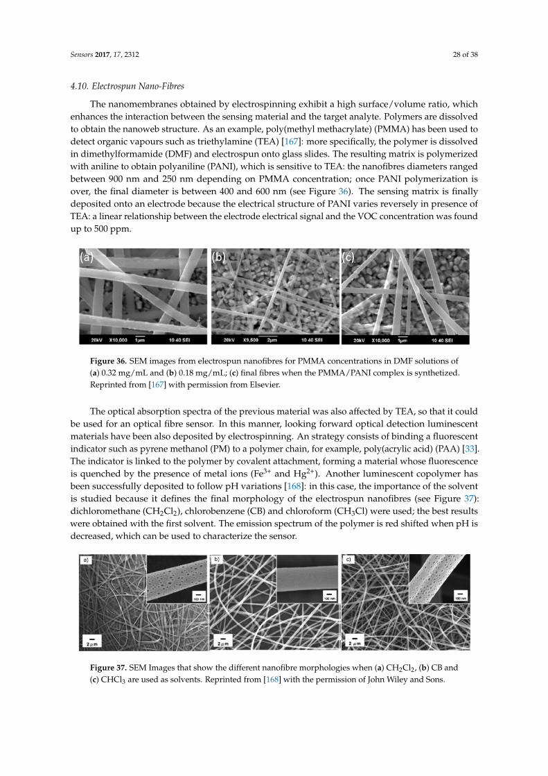
Sensors 2017, 17, 2312 28 of 38
4.10. Electrospun Nano-Fibres
The nanomembranes obtained by electrospinning exhibit a high surface/volume ratio, whichenhances the interaction between the sensing material and the target analyte. Polymers are dissolvedto obtain the nanoweb structure. As an example, poly(methyl methacrylate) (PMMA) has been used todetect organic vapours such as triethylamine (TEA) [167]: more specifically, the polymer is dissolvedin dimethylformamide (DMF) and electrospun onto glass slides. The resulting matrix is polymerizedwith aniline to obtain polyaniline (PANI), which is sensitive to TEA: the nanofibres diameters rangedbetween 900 nm and 250 nm depending on PMMA concentration; once PANI polymerization isover, the final diameter is between 400 and 600 nm (see Figure 36). The sensing matrix is finallydeposited onto an electrode because the electrical structure of PANI varies reversely in presence ofTEA: a linear relationship between the electrode electrical signal and the VOC concentration was foundup to 500 ppm.
Sensors 2017, 17, 2312 27 of 39
To conclude this section as well as to highlight the versatility of LbL nanostructures, luminescent dyes have been also deposited by this technique in a reflection configuration. An oxygen sensitive metallic porphyrin (Pt-TFPP) was coated by preparing anionic micelles and combining it with PAH [164]. It was also found that among three different polymers (PDDA and PEI), the PAH prepared coating showed the highest roughness (21 nm RMS) and a porous morphology optimal for oxygen gas diffusion (see Figure 35) with a thickness of just 180 nm [165]. In order to minimize self-quenching of the luminescent molecules, structures with that included [PAH/PAA] pairs between the luminescent material layers were studied: not only a better sensitivity was registered but also the kinetics were improved. The resulting thickness was 147 nm and their roughness 45 nm RMS [166].
Figure 35. SEM images obtained from sensor heads deposited with Pt-TFPP with 3 different cationic polymers: (a) PDDA, (b) PEI and (c) PAH. A general view of the fibre and a detailed area of the coating is displayed for each coating. Reprinted from [165] with permission from Elsevier.
4.10. Electrospun Nano-Fibres
The nanomembranes obtained by electrospinning exhibit a high surface/volume ratio, which enhances the interaction between the sensing material and the target analyte. Polymers are dissolved to obtain the nanoweb structure. As an example, poly(methyl methacrylate) (PMMA) has been used to detect organic vapours such as triethylamine (TEA) [167]: more specifically, the polymer is dissolved in dimethylformamide (DMF) and electrospun onto glass slides. The resulting matrix is polymerized with aniline to obtain polyaniline (PANI), which is sensitive to TEA: the nanofibres diameters ranged between 900 nm and 250 nm depending on PMMA concentration; once PANI polymerization is over, the final diameter is between 400 and 600 nm (see Figure 36). The sensing matrix is finally deposited onto an electrode because the electrical structure of PANI varies reversely in presence of TEA: a linear relationship between the electrode electrical signal and the VOC concentration was found up to 500 ppm.
Figure 36. SEM images from electrospun nanofibres for PMMA concentrations in DMF solutions of (a) 0.32 mg/mL and (b) 0.18 mg/mL; (c) final fibres when the PMMA/PANI complex is synthetized. Reprinted from [167] with permission from Elsevier.
Figure 36. SEM images from electrospun nanofibres for PMMA concentrations in DMF solutions of(a) 0.32 mg/mL and (b) 0.18 mg/mL; (c) final fibres when the PMMA/PANI complex is synthetized.Reprinted from [167] with permission from Elsevier.
The optical absorption spectra of the previous material was also affected by TEA, so that it couldbe used for an optical fibre sensor. In this manner, looking forward optical detection luminescentmaterials have been also deposited by electrospinning. An strategy consists of binding a fluorescentindicator such as pyrene methanol (PM) to a polymer chain, for example, poly(acrylic acid) (PAA) [33].The indicator is linked to the polymer by covalent attachment, forming a material whose fluorescenceis quenched by the presence of metal ions (Fe3+ and Hg2+). Another luminescent copolymer hasbeen successfully deposited to follow pH variations [168]: in this case, the importance of the solventis studied because it defines the final morphology of the electrospun nanofibres (see Figure 37):dichloromethane (CH2Cl2), chlorobenzene (CB) and chloroform (CH3Cl) were used; the best resultswere obtained with the first solvent. The emission spectrum of the polymer is red shifted when pH isdecreased, which can be used to characterize the sensor.
Sensors 2017, 17, 2312 28 of 39
The optical absorption spectra of the previous material was also affected by TEA, so that it could be used for an optical fibre sensor. In this manner, looking forward optical detection luminescent materials have been also deposited by electrospinning. An strategy consists of binding a fluorescent indicator such as pyrene methanol (PM) to a polymer chain, for example, poly(acrylic acid) (PAA) [33]. The indicator is linked to the polymer by covalent attachment, forming a material whose fluorescence is quenched by the presence of metal ions (Fe3+ and Hg2+). Another luminescent copolymer has been successfully deposited to follow pH variations [168]: in this case, the importance of the solvent is studied because it defines the final morphology of the electrospun nanofibres (see Figure 37): dichloromethane (CH2Cl2), chlorobenzene (CB) and chloroform (CH3Cl) were used; the best results were obtained with the first solvent. The emission spectrum of the polymer is red shifted when pH is decreased, which can be used to characterize the sensor.
Figure 37. SEM Images that show the different nanofibre morphologies when (a) CH2Cl2, (b) CB and (c) CHCl3 are used as solvents. Reprinted from [168] with the permission of John Wiley and Sons.
As another example of the versatility of electrospinning, oxygen-sensitive porphyrins have been successfully deposited following this method: platinum tetra(pentafluorophenyl) porphyrin (PtTFPP) shows a luminescent emission that is reversibly quenched in the presence of oxygen, and it has been used to obtain non-woven sensing matrices [36]. The porphyrin is dissolved together with polystyrene (PS) in 2-butanone with a surfactant: the resulting coating showed a 620 nm thickness and the average fibre diameter was around 100 nm. Other luminescent electrospun nanofibres have been reported for the detection of nitrobenzene [169]; moreover, metallic oxides such as ZnO can be also used to obtain nanofibres by this technique [101] as well as luminescent hybrid composites combining polymers and gold nanoparticles [170].
Poly(vinylidene fluoride) (PVdF) has been electrospun and used as sensing material for relative humidity monitoring [171]. The procedure is similar as in the previous examples: the polymer is dissolved in a mixture of acetone and N,N-dimethylformamide and then, it is injected into a syringe and exposed to an 18.5 kV electric potential differential. The optical fibre was located close to the grounded electrode, and it was rotating at a constant speed of 120 rpm during the process. The final coating had a 6 microns thickness, whereas the diameter of the nanofibres were between 100 and 700 nm: details of the electrospinning process can be observed in Figure 38. The nanofibres were deposited around a HCF to prepare a transmission sensor: it was illuminated with a laser at 1310 nm, registering a decrease in the transmitted signal as the relative humidity increases. This effect is produced by the interaction between the coating and the evanescent field of the light traveling through the area where the mat is deposited. The sensor was also validated for human breath monitoring, taking advantage of the fast response produced by the high surface/volume ratio of the nanoweb.
Figure 37. SEM Images that show the different nanofibre morphologies when (a) CH2Cl2, (b) CB and(c) CHCl3 are used as solvents. Reprinted from [168] with the permission of John Wiley and Sons.

Sensors 2017, 17, 2312 29 of 38
As another example of the versatility of electrospinning, oxygen-sensitive porphyrins have beensuccessfully deposited following this method: platinum tetra(pentafluorophenyl) porphyrin (PtTFPP)shows a luminescent emission that is reversibly quenched in the presence of oxygen, and it has beenused to obtain non-woven sensing matrices [36]. The porphyrin is dissolved together with polystyrene(PS) in 2-butanone with a surfactant: the resulting coating showed a 620 nm thickness and the averagefibre diameter was around 100 nm. Other luminescent electrospun nanofibres have been reported forthe detection of nitrobenzene [169]; moreover, metallic oxides such as ZnO can be also used to obtainnanofibres by this technique [101] as well as luminescent hybrid composites combining polymers andgold nanoparticles [170].
Poly(vinylidene fluoride) (PVdF) has been electrospun and used as sensing material for relativehumidity monitoring [171]. The procedure is similar as in the previous examples: the polymer isdissolved in a mixture of acetone and N,N-dimethylformamide and then, it is injected into a syringeand exposed to an 18.5 kV electric potential differential. The optical fibre was located close to thegrounded electrode, and it was rotating at a constant speed of 120 rpm during the process. The finalcoating had a 6 microns thickness, whereas the diameter of the nanofibres were between 100 and700 nm: details of the electrospinning process can be observed in Figure 38. The nanofibres weredeposited around a HCF to prepare a transmission sensor: it was illuminated with a laser at 1310 nm,registering a decrease in the transmitted signal as the relative humidity increases. This effect isproduced by the interaction between the coating and the evanescent field of the light traveling throughthe area where the mat is deposited. The sensor was also validated for human breath monitoring,taking advantage of the fast response produced by the high surface/volume ratio of the nanoweb.Sensors 2017, 17, 2312 29 of 39
Figure 38. (a) Detail of the needle where the jet emerges and (b) the nanofibre formation, describing a helix path; (c) SEM image of the nanoweb once it is deposited onto a glass slide. Images reprinted from [171] with the permission of IEEE.
There are commercially available polymers that are already dissolved, which can make easier the process: poly(acrylic acid) (PAA), provided in aqueous solution, can be directly used in the electrospinning set-up; this material swells with humidity due to its hydrogel nature: this property has been used to develop an optical fibre humidity sensor [37]. The fibre used is PCS, and the nanoweb is coated around a region where the cladding has been removed; it is again located between the electrodes and it is kept rotating at 30 rpm. The importance of the PAA solution viscosity as well as the electrospinning time is found to be critical for the sensor features: the more viscose is the PAA solution, the smaller is the averaged diameter of the nanofibre and therefore, the higher is the density of the mat deposited; on the other hand, the sensitivity is directly affected by the thickness of the coating, which depends on the deposition time (the longer it is, the thicker is the mat). A summary of the different nanofibres obtained with distinct viscosities and deposition times is displayed in Figure 39. There is a trade-off between all the parameters to get the best sensitivity: the optimal nanofibres should be as thin as possible, and the thickness of the coating as low as possible; for this study, the best results were obtained with the lowest deposition times (5 min) independently of the PAA concentration.
Figure 39. (a) Microscope image of an optical fibre core coated with the PAA electrospun fibres; (b) SEM images for the nano webs obtained with the different electrospun conditions (detailed inset). Reprinted from [37] with the permission of Elsevier.
5. Conclusions
It is evident that there is a synergy between optical fibres and micro/nanostructured materials to develop chemical sensors and biosensors. The construction and deposition methods are critical when defining the morphology of the sensing coating and therefore, its features. The sensing architecture, reflection or transmission, has to be chosen depending on the requirements of the application, and depending on that, the construction technique as well as the materials to be used are
Figure 38. (a) Detail of the needle where the jet emerges and (b) the nanofibre formation, describinga helix path; (c) SEM image of the nanoweb once it is deposited onto a glass slide. Images reprintedfrom [171] with the permission of IEEE.
There are commercially available polymers that are already dissolved, which can make easierthe process: poly(acrylic acid) (PAA), provided in aqueous solution, can be directly used in theelectrospinning set-up; this material swells with humidity due to its hydrogel nature: this property hasbeen used to develop an optical fibre humidity sensor [37]. The fibre used is PCS, and the nanowebis coated around a region where the cladding has been removed; it is again located between theelectrodes and it is kept rotating at 30 rpm. The importance of the PAA solution viscosity as well as theelectrospinning time is found to be critical for the sensor features: the more viscose is the PAA solution,the smaller is the averaged diameter of the nanofibre and therefore, the higher is the density of the matdeposited; on the other hand, the sensitivity is directly affected by the thickness of the coating, whichdepends on the deposition time (the longer it is, the thicker is the mat). A summary of the differentnanofibres obtained with distinct viscosities and deposition times is displayed in Figure 39. There is a

Sensors 2017, 17, 2312 30 of 38
trade-off between all the parameters to get the best sensitivity: the optimal nanofibres should be asthin as possible, and the thickness of the coating as low as possible; for this study, the best results wereobtained with the lowest deposition times (5 min) independently of the PAA concentration.
Sensors 2017, 17, 2312 29 of 39
Figure 38. (a) Detail of the needle where the jet emerges and (b) the nanofibre formation, describing a helix path; (c) SEM image of the nanoweb once it is deposited onto a glass slide. Images reprinted from [171] with the permission of IEEE.
There are commercially available polymers that are already dissolved, which can make easier the process: poly(acrylic acid) (PAA), provided in aqueous solution, can be directly used in the electrospinning set-up; this material swells with humidity due to its hydrogel nature: this property has been used to develop an optical fibre humidity sensor [37]. The fibre used is PCS, and the nanoweb is coated around a region where the cladding has been removed; it is again located between the electrodes and it is kept rotating at 30 rpm. The importance of the PAA solution viscosity as well as the electrospinning time is found to be critical for the sensor features: the more viscose is the PAA solution, the smaller is the averaged diameter of the nanofibre and therefore, the higher is the density of the mat deposited; on the other hand, the sensitivity is directly affected by the thickness of the coating, which depends on the deposition time (the longer it is, the thicker is the mat). A summary of the different nanofibres obtained with distinct viscosities and deposition times is displayed in Figure 39. There is a trade-off between all the parameters to get the best sensitivity: the optimal nanofibres should be as thin as possible, and the thickness of the coating as low as possible; for this study, the best results were obtained with the lowest deposition times (5 min) independently of the PAA concentration.
Figure 39. (a) Microscope image of an optical fibre core coated with the PAA electrospun fibres; (b) SEM images for the nano webs obtained with the different electrospun conditions (detailed inset). Reprinted from [37] with the permission of Elsevier.
5. Conclusions
It is evident that there is a synergy between optical fibres and micro/nanostructured materials to develop chemical sensors and biosensors. The construction and deposition methods are critical when defining the morphology of the sensing coating and therefore, its features. The sensing architecture, reflection or transmission, has to be chosen depending on the requirements of the application, and depending on that, the construction technique as well as the materials to be used are
Figure 39. (a) Microscope image of an optical fibre core coated with the PAA electrospun fibres; (b) SEMimages for the nano webs obtained with the different electrospun conditions (detailed inset). Reprintedfrom [37] with the permission of Elsevier.
5. Conclusions
It is evident that there is a synergy between optical fibres and micro/nanostructured materials todevelop chemical sensors and biosensors. The construction and deposition methods are criticalwhen defining the morphology of the sensing coating and therefore, its features. The sensingarchitecture, reflection or transmission, has to be chosen depending on the requirements of theapplication, and depending on that, the construction technique as well as the materials to be used areto be selected. Regarding the construction techniques, although dip coating is easy to perform, its lowreproducibility, specifically for reflection sensors, makes the other techniques preferable. LbL allowsnot only polyelectrolytes to be deposited, but also reagents from different types such as biomolecules,organometallic materials or even metal oxides. Its versatility and the possibility of applying it for bothtransmission and reflection configurations is extending its use for optical fibre sensor development.Talking about sputtering, it can also be used for both configurations and it guarantees to preparesimilar devices under the same conditions. Initially it was only employed to metallic and metal oxides,but now, the use of RF signals allows materials of different types to be deposited, which will encouragemany researches to follow this method. Finally, nanofibres can be electrospun to prepare transmissiondevices with a relative simple setup easy to adapt to optical fibre sensors. Although there are not manysensors developed this way, this construction technique is very promising.
New materials allow nanostructures to be deposited onto the fibre which enhance the interactionwith the analyte: they show a great aspect ratio, which easies the diffusion of the target molecules. In thecase of plastic matrices and sol gel, the supporting matrix morphology is easy to control, although theyare restricted to transmission configuration to guarantee repetitive sensors. Carbon-based materialssuch as carbon nanotubes are also very promising which have been reinforced by the recent resultsobtained with graphene in the sensors field. Regarding the sensing material rather than the supportingmatrix, MIPs offer a great selectivity and sensitivity: their main inconvenience is the synthesis of thepolymers and their attachment to a supporting matrix that does not alter their sensing properties.The materials that currently show a great applicability are LbL nanostructures and sputtered metaloxides: the first ones are very versatile in terms of the compounds that can be deposited, whereas thesecond ensures a high reproducibility when preparing the sensors; moreover, both are applicable toreflection and transmission configurations. To conclude with nanostructured materials, electrospunnanofibres can be aligned to produce certain patterns that show a great porosity optimal, for instant,to detect gas or vapours. More materials are to be studied in order to obtain sensing layers in this way.

Sensors 2017, 17, 2312 31 of 38
The benefits of optical fibre sensors based on this kind of materials are still to be explored, butthe combination of this substrate and nanostructured materials give them a chance to cover nicheapplications where electronic sensors are not applicable. In any case, the results exposed in this reviewshow a promising future that will be bring into reality in a medium term.
Acknowledgments: This work was supported by the Spanish State Research Agency (AEI) and European RegionalDevelopment Fund (ERDF-FEDER), TEC2016-79367-C2-2-R and TEC2016-78047-R projects.
Conflicts of Interest: The authors declare no conflict of interest.
References
1. Gaab, M.R. Instrumentation: Endoscopes and equipment. World Neurosurg. 2013, 79. [CrossRef] [PubMed]2. Barrias, A.; Casas, J.R.; Villalba, S. A review of distributed optical fiber sensors for civil engineering
applications. Sensors 2016, 16, 748. [CrossRef] [PubMed]3. Pospíšilová, M.; Kuncová, G.; Trögl, J. Fiber-optic chemical sensors and fiber-optic bio-sensors. Sensors 2015,
15. [CrossRef] [PubMed]4. Lin, J. Recent development and applications of optical and fiber-optic pH sensors. TrAC Trends Anal. Chem.
2000, 19. [CrossRef]5. Elosua, C.; Matias, I.R.; Bariain, C.; Arregui, F.J. Volatile organic compound optical fiber sensors: A review.
Sensors 2006, 6, 1440–1465. [CrossRef]6. Kolpakov, S.A.; Gordon, N.T.; Mou, C.; Zhou, K. Toward a new generation of photonic humidity sensors.
Sensors 2014, 14, 3986–4013. [CrossRef] [PubMed]7. Miao, Y.-P.; Jin, W.; Yang, F.; Lin, Y.-C.; Tan, Y.-Z.; Hoi, L.H. Advances in optical fiber photothermal
interferometry for gas detection. Wuli Xuebao/Acta Phys. Sin. 2017, 66. [CrossRef]8. Fang, Z.; Chin, K.K.; Qu, R.; Cai, H. Fundamentals of Optical Fiber Sensors; Wiley: Hoboken, NJ, USA, 2012;
ISBN 9780470575406.9. Koike, Y.; Koike, K. Progress in low-loss and high-bandwidth plastic optical fibers. J. Polym. Sci. Part B Polym.
Phys. 2011, 49. [CrossRef]10. Liehr, S. Polymer Optical Fiber Sensors in Structural Health Monitoring; Springer: New York, NY, USA, 2011;
Volume 96, ISBN 9783642210983.11. Bilro, L.; Alberto, N.; Pinto, J.L.; Nogueira, R. Optical sensors based on plastic fibers. Sensors 2012, 12.
[CrossRef] [PubMed]12. Leung, A.; Mohana Shankar, P.; Mutharasan, R. Evanescent Field Tapered Fiber Optic Biosensors (TFOBS):
Fabrication, Antibody Immobilization and Detection; Nova: New York NY, USA, 2012; ISBN 9781613245057.13. André, R.M.; Marques, M.B.; Frazão, O. New Advances in Tapered Fiber Sensors; Nova: New York NY, USA,
2013; ISBN 9781628084283.14. Punjabi, N.; Satija, J.; Mukherji, S. Evanescent Wave Absorption Based Fiber-Optic Sensor—Cascading of Bend and
Tapered Geometry for Enhanced Sensitivity; Springer: New York, NY, USA, 2015; Volume 11.15. Spillman, W.B. Multimode Polarization Sensors; Wiley: Hoboken, NJ, USA, 2011; ISBN 9780470126844.16. Lee, B.H.; Kim, Y.H.; Park, K.S.; Eom, J.B.; Kim, M.J.; Rho, B.S.; Choi, H.Y. Interferometric fiber optic sensors.
Sensors 2012, 12, 2467–2486. [CrossRef] [PubMed]17. Hill, K.O.; Meltz, G. Fiber Bragg grating technology fundamentals and overview. J. Lightwave Technol. 1997,
15. [CrossRef]18. James, S.W.; Tatam, R.P. Optical fibre long-period grating sensors: Characteristics and application.
Meas. Sci. Technol. 2003, 14. [CrossRef]19. Shevchenko, Y.Y.; Blair, D.A.D.; Derosa, M.C.; Albert, J. DNA target detection using gold-coated tilted fiber
Bragg gratings in aqueous media. In Proceedings of the 2008 Conference on Quantum Electronics and LaserScience Conference on Lasers and Electro-Optics, CLEO/QELS, San Jose, CA, USA, 4–9 May 2008.
20. Candiani, A.; Sozzi, M.; Cucinotta, A.; Selleri, S.; Veneziano, R.; Corradini, R.; Marchelli, R.; Childs, P.;Pissadakis, S. Optical fiber ring cavity sensor for label-free DNA detection. IEEE J. Sel. Top. Quantum Electron.2012, 18. [CrossRef]
21. Gupta, B.D.; Verma, R.K. Surface plasmon resonance-based fiber optic sensors: Principle, probe designs, andsome applications. J. Sensors 2009, 2009. [CrossRef]

Sensors 2017, 17, 2312 32 of 38
22. Del Villar, I.; Arregui, F.J.; Zamarreño, C.R.; Corres, J.M.; Bariain, C.; Goicoechea, J.; Elosua, C.; Hernaez, M.;Rivero, P.J.; Socorro, A.B.; et al. Optical sensors based on lossy-mode resonances. Sens. Actuators B Chem.2017, 240. [CrossRef]
23. Pilevar, S.; DeLisa, M.P.; Zhang, Z.; Davis, C.C.; Bentley, W.E.; Sirkis, J.S. Evanescent wave antibody-antigenbiosensor based on long period fiber Bragg grating. In Proceedings of SPIE—The International Society for OpticalEngineering; Society of Photo-Optical Instrumentation Engineers: Bellingham, WA, USA, 2000; Volume 4185.
24. Chen, X.; Zhang, L.; Zhou, K.; Davies, E.; Sugden, K.; Bennion, I.; Hughes, M.; Hine, A. Real-time detectionof DNA interactions with longperiod fiber-grating-based biosensor. Opt. Lett. 2007, 32. [CrossRef]
25. He, Z.; Tian, F.; Zhu, Y.; Lavlinskaia, N.; Du, H. Long-period gratings in photonic crystal fiber as anoptofluidic label-free biosensor. Biosens. Bioelectron. 2011, 26. [CrossRef] [PubMed]
26. Maguis, S.; Laffont, G.; Ferdinand, P.; Carbonnier, B.; Kham, K.; Mekhalif, T.; Millot, M.-C. Biofunctionalizedtilted Fiber Bragg Gratings for label-free immunosensing. Opt. Express 2008, 16. [CrossRef]
27. González-Sierra, N.; Gómez-Pavón, L.; Pérez-Sánchez, G.; Luis-Ramos, A.; Zaca-Morán, P.;Muñoz-Pacheco, J.; Chávez-Ramírez, F. Tapered Optical Fiber Functionalized with Palladium Nanoparticlesby Drop Casting and Laser Radiation for H2 and Volatile Organic Compounds Sensing Purposes. Sensors2017, 17, 2039. [CrossRef] [PubMed]
28. Shabaneh, A.A.; Girei, S.H.; Arasu, P.T.; Rashid, S.A.; Yunusa, Z.; Mahdi, M.A.; Paiman, S.; Ahmad, M.Z.;Yaacob, M.H. Reflectance Response of Optical Fiber Coated With Carbon Nanotubes for Aqueous EthanolSensing. IEEE Photonics J. 2014, 6. [CrossRef]
29. Iler, R.K. Multilayers of colloidal particles. J. Colloid Interface Sci. 1966, 21, 569–594. [CrossRef]30. Decher, G. Fuzzy nanoassemblies: Toward layered polymeric multicomposites. Science 1997, 277. [CrossRef]31. Elosua, C.; Lopez-Torres, D.; Hernaez, M.; Matias, I.R.; Arregui, F.J. Comparative study of layer-by-layer
deposition techniques for poly(sodium phosphate) and poly(allylamine hydrochloride). Nanoscale Res. Lett.2013, 8. [CrossRef] [PubMed]
32. Teo, W.E.; Ramakrishna, S. A review on electrospinning design and nanofibre assemblies. Nanotechnology2006, 17, R89–R106. [CrossRef] [PubMed]
33. Wang, X.; Drew, C.; Lee, S.H.; Senecal, K.J.; Kumar, J.; Samuelson, L.A. Electrospun Nanofibrous Membranesfor Highly Sensitive Optical Sensors. Nano Lett. 2002, 2, 1273–1275. [CrossRef]
34. Song, X.; Wang, Z.; Liu, Y.; Wang, C.; Li, L. A highly sensitive ethanol sensor based on mesoporous ZnO-SnO2nanofibers. Nanotechnology 2009, 20, 75501. [CrossRef] [PubMed]
35. Son, D.; Kim, S.J.; Lee, S. Electrospun assembly: A nondestructive nanofabrication for transparentphotosensors. Nanotechnology 2017, 28, 155202. [CrossRef]
36. Wolf, C.; Tscherner, M.; Kstler, S. Ultra-fast opto-chemical sensors by using electrospun nanofibers as sensinglayers. Sens. Actuators B Chem. 2015, 209, 1064–1069. [CrossRef]
37. Urrutia, A.; Goicoechea, J.; Rivero, P.J.; Matías, I.R.; Arregui, F.J. Electrospun nanofiber mats for evanescentoptical fiber sensors. Sens. Actuators B Chem. 2013, 176, 569–576. [CrossRef]
38. Tseng, Y.-T.; Chuang, Y.-J.; Wu, Y.-C.; Yang, C.-S.; Wang, M.-C.; Tseng, F.-G. A gold-nanoparticle-enhancedimmune sensor based on fiber optic interferometry. Nanotechnology 2008, 19. [CrossRef] [PubMed]
39. Saikia, R.; Buragohain, M.; Datta, P.; Nath, P.; Barua, K. Fiber-optic pH sensor based on SPR of silvernanostructured film. AIP Conf. Proc. 2009, 1147, 249–255.
40. Mahros, A.M.; Tharwat, M.M.; Elrashidi, A. Exploring the Impact of Nano-Particles Shape on thePerformance of Plasmonic Based Fiber Optics Sensors. Plasmonics 2017, 12. [CrossRef]
41. Urrutia, A.; Goicoechea, J.; Arregui, F.J. Optical fiber sensors based on nanoparticle-embedded coatings.J. Sensors 2015, 2015. [CrossRef]
42. Pagnoux, D.; Peyrilloux, A.; Roy, P.; Fevrier, S.; Labonte, L.; Hilaire, S. Microstructured air-silica fibres: Recentdevelopments in modelling, manufacturing and experiment. Ann. Telecommun. Telecommun. 2003, 58, 9–10.
43. Pissadakis, S.; Selleri, S. Optofluidics, Sensors and Actuators in Microstructured Optical Fibers; Elsevier:Amsterdam, The Netherlands, 2015; ISBN 9781782423478.
44. Pisco, M.; Cusano, A.; Cutolo, A. Photonic Bandgap Structures: Novel Technological Platforms for Physical,Chemical and Biological Sensing; Betham: Potomac, MD, USA, 2012. [CrossRef]
45. Liu, Z.; Tam, H.-Y.; Member, S.; Htein, L.; Vincent Tse, M.-L.; Lu, C. Microstructured Optical Fiber Sensors.J. Lightwave Technol. 2017, 35. [CrossRef]
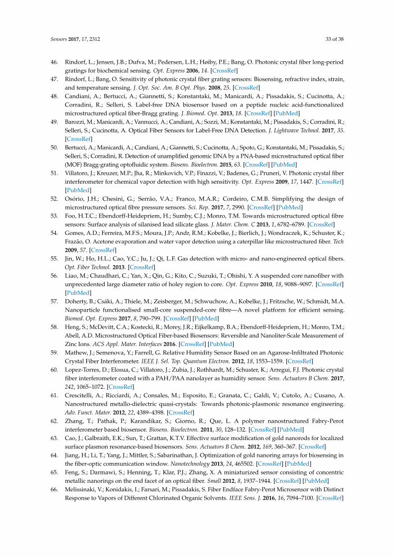
Sensors 2017, 17, 2312 33 of 38
46. Rindorf, L.; Jensen, J.B.; Dufva, M.; Pedersen, L.H.; Høiby, P.E.; Bang, O. Photonic crystal fiber long-periodgratings for biochemical sensing. Opt. Express 2006, 14. [CrossRef]
47. Rindorf, L.; Bang, O. Sensitivity of photonic crystal fiber grating sensors: Biosensing, refractive index, strain,and temperature sensing. J. Opt. Soc. Am. B Opt. Phys. 2008, 25. [CrossRef]
48. Candiani, A.; Bertucci, A.; Giannetti, S.; Konstantaki, M.; Manicardi, A.; Pissadakis, S.; Cucinotta, A.;Corradini, R.; Selleri, S. Label-free DNA biosensor based on a peptide nucleic acid-functionalizedmicrostructured optical fiber-Bragg grating. J. Biomed. Opt. 2013, 18. [CrossRef] [PubMed]
49. Barozzi, M.; Manicardi, A.; Vannucci, A.; Candiani, A.; Sozzi, M.; Konstantaki, M.; Pissadakis, S.; Corradini, R.;Selleri, S.; Cucinotta, A. Optical Fiber Sensors for Label-Free DNA Detection. J. Lightwave Technol. 2017, 35.[CrossRef]
50. Bertucci, A.; Manicardi, A.; Candiani, A.; Giannetti, S.; Cucinotta, A.; Spoto, G.; Konstantaki, M.; Pissadakis, S.;Selleri, S.; Corradini, R. Detection of unamplified genomic DNA by a PNA-based microstructured optical fiber(MOF) Bragg-grating optofluidic system. Biosens. Bioelectron. 2015, 63. [CrossRef] [PubMed]
51. Villatoro, J.; Kreuzer, M.P.; Jha, R.; Minkovich, V.P.; Finazzi, V.; Badenes, G.; Pruneri, V. Photonic crystal fiberinterferometer for chemical vapor detection with high sensitivity. Opt. Express 2009, 17, 1447. [CrossRef][PubMed]
52. Osório, J.H.; Chesini, G.; Serrão, V.A.; Franco, M.A.R.; Cordeiro, C.M.B. Simplifying the design ofmicrostructured optical fibre pressure sensors. Sci. Rep. 2017, 7, 2990. [CrossRef] [PubMed]
53. Foo, H.T.C.; Ebendorff-Heidepriem, H.; Sumby, C.J.; Monro, T.M. Towards microstructured optical fibresensors: Surface analysis of silanised lead silicate glass. J. Mater. Chem. C 2013, 1, 6782–6789. [CrossRef]
54. Gomes, A.D.; Ferreira, M.F.S.; Moura, J.P.; Andr, R.M.; Kobelke, J.; Bierlich, J.; Wondraczek, K.; Schuster, K.;Frazão, O. Acetone evaporation and water vapor detection using a caterpillar like microstructured fiber. Tech2009, 57. [CrossRef]
55. Jin, W.; Ho, H.L.; Cao, Y.C.; Ju, J.; Qi, L.F. Gas detection with micro- and nano-engineered optical fibers.Opt. Fiber Technol. 2013. [CrossRef]
56. Liao, M.; Chaudhari, C.; Yan, X.; Qin, G.; Kito, C.; Suzuki, T.; Ohishi, Y. A suspended core nanofiber withunprecedented large diameter ratio of holey region to core. Opt. Express 2010, 18, 9088–9097. [CrossRef][PubMed]
57. Doherty, B.; Csáki, A.; Thiele, M.; Zeisberger, M.; Schwuchow, A.; Kobelke, J.; Fritzsche, W.; Schmidt, M.A.Nanoparticle functionalised small-core suspended-core fibre—A novel platform for efficient sensing.Biomed. Opt. Express 2017, 8, 790–799. [CrossRef] [PubMed]
58. Heng, S.; McDevitt, C.A.; Kostecki, R.; Morey, J.R.; Eijkelkamp, B.A.; Ebendorff-Heidepriem, H.; Monro, T.M.;Abell, A.D. Microstructured Optical Fiber-based Biosensors: Reversible and Nanoliter-Scale Measurement ofZinc Ions. ACS Appl. Mater. Interfaces 2016. [CrossRef] [PubMed]
59. Mathew, J.; Semenova, Y.; Farrell, G. Relative Humidity Sensor Based on an Agarose-Infiltrated PhotonicCrystal Fiber Interferometer. IEEE J. Sel. Top. Quantum Electron. 2012, 18, 1553–1559. [CrossRef]
60. Lopez-Torres, D.; Elosua, C.; Villatoro, J.; Zubia, J.; Rothhardt, M.; Schuster, K.; Arregui, F.J. Photonic crystalfiber interferometer coated with a PAH/PAA nanolayer as humidity sensor. Sens. Actuators B Chem. 2017,242, 1065–1072. [CrossRef]
61. Crescitelli, A.; Ricciardi, A.; Consales, M.; Esposito, E.; Granata, C.; Galdi, V.; Cutolo, A.; Cusano, A.Nanostructured metallo-dielectric quasi-crystals: Towards photonic-plasmonic resonance engineering.Adv. Funct. Mater. 2012, 22, 4389–4398. [CrossRef]
62. Zhang, T.; Pathak, P.; Karandikar, S.; Giorno, R.; Que, L. A polymer nanostructured Fabry-Perotinterferometer based biosensor. Biosens. Bioelectron. 2011, 30, 128–132. [CrossRef] [PubMed]
63. Cao, J.; Galbraith, E.K.; Sun, T.; Grattan, K.T.V. Effective surface modification of gold nanorods for localizedsurface plasmon resonance-based biosensors. Sens. Actuators B Chem. 2012, 169, 360–367. [CrossRef]
64. Jiang, H.; Li, T.; Yang, J.; Mittler, S.; Sabarinathan, J. Optimization of gold nanoring arrays for biosensing inthe fiber-optic communication window. Nanotechnology 2013, 24, 465502. [CrossRef] [PubMed]
65. Feng, S.; Darmawi, S.; Henning, T.; Klar, P.J.; Zhang, X. A miniaturized sensor consisting of concentricmetallic nanorings on the end facet of an optical fiber. Small 2012, 8, 1937–1944. [CrossRef] [PubMed]
66. Melissinaki, V.; Konidakis, I.; Farsari, M.; Pissadakis, S. Fiber Endface Fabry-Perot Microsensor with DistinctResponse to Vapors of Different Chlorinated Organic Solvents. IEEE Sens. J. 2016, 16, 7094–7100. [CrossRef]

Sensors 2017, 17, 2312 34 of 38
67. Wang, H.; Xie, Z.; Zhang, M.; Cui, H.; He, J.; Feng, S.; Wang, X.; Sun, W.; Ye, J.; Han, P.; Zhang, Y. [INVITED]A miniaturized optical fiber microphone with concentric nanorings grating and microsprings structureddiaphragm. Opt. Laser Technol. 2016, 78, 110–115. [CrossRef]
68. Kostovski, G.; White, D.J.; Mitchell, A.; Austin, M.W.; Stoddart, P.R. Nanoimprinted optical fibres:Biotemplated nanostructures for SERS sensing. Biosens. Bioelectron. 2009, 24, 1531–1535. [CrossRef][PubMed]
69. Ricciardi, A.; Crescitelli, A.; Vaiano, P.; Quero, G.; Consales, M.; Pisco, M.; Esposito, E.; Cusano, A.Lab-on-fiber technology: A new vision for chemical and biological sensing. Analyst 2015, 140. [CrossRef][PubMed]
70. Consales, M.; Pisco, M.; Cusano, A. Lab-on-fiber technology: A new avenue for optical nanosensors.Photonic Sensors 2012, 2. [CrossRef]
71. Ricciardi, A.; Consales, M.; Quero, G.; Crescitelli, A.; Esposito, E.; Cusano, A. Lab-on-Fiber devices as an allaround platform for sensing. Opt. Fiber Technol. 2013, 19. [CrossRef]
72. Moreno, J.; Arregui, F.J.; Matias, I.R. Fiber optic ammonia sensing employing novel thermoplasticpolyurethane membranes. Sens. Actuators B Chem. 2005. [CrossRef]
73. Elosua, C.; Bariain, C.; Matias, I.R.; Rodriguez, A.; Colacio, E.; Salinas-Castillo, A.; Segura-Carretero, A.;Fernandez-Gutiérrez, A. Pyridine Vapors Detection by an Optical Fibre Sensor. Sensors 2008, 8, 847–859.[CrossRef] [PubMed]
74. Sainz-Gonzalo, F.J.; Elosua, C.; Fernández-Sánchez, J.F.; Popovici, C.; Fernández, I.; Ortiz, F.L.; Arregui, F.J.;Matias, I.R.; Fernández-Gutiérrez, A. A novel luminescent optical fibre probe based on immobilized tridentatebis(phosphinic amide)-phosphine oxide for europium(III) ion aqueous detection in situ. Sens. Actuators B Chem.2012, 173, 254–261. [CrossRef]
75. Me, S.; Fe, J.F.; Fe, A. An open and low-cost optical- fiber measurement system for the optical detection ofoxygen using a multifrequency phase-resolved method. Sens. Actuators B Chem. 2013, 176, 1100–1120.
76. Vijayan, A.; Fuke, M.; Hawaldar, R.; Kulkarni, M.; Amalnerkar, D.; Aiyer, R.C. Optical fibre based humiditysensor using Co-polyaniline clad. Sens. Actuators B Chem. 2008, 129, 106–112. [CrossRef]
77. Cusano, A.; Iadicicco, A.; Pilla, P.; Cutolo, A.; Giordano, M.; Campopiano, S. Sensitivity characteristics innanosized coated long period gratings. Appl. Phys. Lett. 2006, 89. [CrossRef]
78. Silva, L.I.B.; M-Costa, A.; Freitas, A.C.; Rocha-Santos, T.A.P.; Duarte, A.C. Polymeric nanofilm-coated opticalfibre sensor for speciation of aromatic compounds. Int. J. Environ. Anal. Chem. 2009, 89, 183–197. [CrossRef]
79. MacCraith, B.D.; McDonagh, C.M.; O’Keeffe, G.; McEvoy, A.K.; Butler, T.; Sheridan, F.R. Sol-gel coatings foroptical chemical sensors and biosensors. Sens. Actuators B Chem. 1995, 29, 51–57. [CrossRef]
80. Estella, J.; Echeverría, J.C.; Laguna, M.; Garrido, J.J. Effects of aging and drying conditions on the structuraland textural properties of silica gels. Microporous Mesoporous Mater. 2007, 102, 274–282. [CrossRef]
81. Zolkapi, M.; Saharudin, S.; Herman, S.H.; Abdullah, W.F.H. The influence of sol-gel coated length andwithdrawal rate on plastic optical fiber core towards oxygen gas sensing sensitivity. J. Teknol. 2015, 3, 87–91.
82. Echeverría, J.C.; Calleja, I.; Moriones, P.; Garrido, J.J. Fiber optic sensors based on hybrid phenyl-silica xerogelfilms to detect n-hexane: Determination of the isosteric enthalpy of adsorption. Beilstein J. Nanotechnol. 2017,8, 475–484. [CrossRef] [PubMed]
83. Estella, J.; De Vicente, P.; Echeverría, J.C.; Garrido, J.J. A fibre-optic humidity sensor based on a porous silicaxerogel film as the sensing element. Sens. Actuators B Chem. 2010, 149, 122–128. [CrossRef]
84. Sun, L.; Semenova, Y.; Wu, Q.; Liu, D.; Yuan, J.; Ma, T.; Sang, X.; Yan, B.; Wang, K.; Yu, C.; Farrell, G. Highsensitivity ammonia gas sensor based on a silica-gel-coated microfiber coupler. J. Lightwave Technol. 2017, 35,2864–2870. [CrossRef]
85. Liu, D.; Han, W.; Mallik, A.K.; Yuan, J.; Yu, C.; Farrell, G.; Semenova, Y.; Wu, Q. High sensitivity sol-gelsilica coated optical fiber sensor for detection of ammonia in water. Opt. Express 2016, 24, 24179. [CrossRef][PubMed]
86. Arregui, F.J.; Otano, M.; Fernandez-valdivielso, C.; Matias, I.R. An experimental study about the utilizationof Liquicoat 1 solutions for the fabrication of pH optical fiber sensors. Sens. Actuators B. Chem. 2002, 87,289–295. [CrossRef]
87. Bariain, C.; Matías, I.R.; Fdez-Valdivielso, C.; Elosúa, C.; Luquin, A.; Garrido, J.; Laguna, M. Optical fibresensors based on vapochromic gold complexes for environmental applications. Sens. Actuators B Chem. 2005,108, 535–541. [CrossRef]

Sensors 2017, 17, 2312 35 of 38
88. Yadav, B.C.; Yadav, R.C.; Dubey, G.C. Optical humidity sensing behaviour of sol-gel processed nanostructuredZnO films. Opt. Appl. 2009, 39, 617–627.
89. Guillemain, H.; Rajarajan, M.; Lin, Y.-C.; Chen, C.-T.; Sun, T.; Grattan, K.T.V. Feasibility studies usingthin sol–gel films doped with a novel lead-selective fluorophore for optical fibre sensing applications.Measurement 2013, 46, 2971–2977. [CrossRef]
90. Chu, C.S.; Chuang, C.Y. Optical fiber sensor for dual sensing of dissolved oxygen and Cu2+ ions based onPdTFPP/CdSe embedded in sol-gel matrix. Sens. Actuators B Chem. 2015, 209, 94–99. [CrossRef]
91. Hajj-Hassan, M.; Kim, S.-J.; Cheung, M.C.; Yao, L.; Chodavarapu, V.; Cartwright, A. Porous silicon andporous polymer substrates for optical chemical sensors. J. Nanophotonics 2010, 4, 43513. [CrossRef]
92. Chu, C.S.; Lo, Y.L.; Sung, T.W. Enhanced oxygen sensing properties of Pt(II) complex and dye entrappedcore-shell silica nanoparticles embedded in sol-gel matrix. Talanta 2010, 82, 1044–1051. [CrossRef] [PubMed]
93. Chu, C.S.; Sung, T.W.; Lo, Y.L. Enhanced optical oxygen sensing property based on Pt(II) complex andmetal-coated silica nanoparticles embedded in sol-gel matrix. Sens. Actuators B Chem. 2013, 185, 287–292.[CrossRef]
94. Bezunartea, M.; Estella, J.; Echeverría, J.C.; Elosúa, C.; Bariáin, C.; Laguna, M.; Luquin, A.; Garrido, J.J.Optical fibre sensing element based on xerogel-supported [Au2Ag2(C6F5)4(C14H10)]n for the detection ofmethanol and ethanol in the vapour phase. Sens. Actuators B Chem. 2008, 134, 966–973. [CrossRef]
95. Islam, S.; Bidin, N.; Riaz, S.; Krishnan, G.; Naseem, S. Sol-gel based fiber optic pH nanosensor: Structuraland sensing properties. Sens. Actuators A Phys. 2016, 238, 8–18. [CrossRef]
96. Biswas, P.; Chiavaioli, F.; Jana, S.; Basumallick, N.; Trono, C.; Giannetti, A.; Tombelli, S.; Mallick, A.; Baldini, F.;Bandyopadhyay, S. Design, fabrication and characterisation of silica-titania thin film coated over coupledlong period fibre gratings: Towards bio-sensing applications. Sens. Actuators B Chem. 2017, 253, 418–427.[CrossRef]
97. Chiavaioli, F.; Biswas, P.; Trono, C.; Jana, S.; Bandyopadhyay, S.; Basumallick, N.; Giannetti, A.; Tombelli, S.;Bera, S.; Mallick, A.; et al. Sol-Gel-Based Titania-Silica Thin Film Overlay for Long Period Fiber Grating-BasedBiosensors. Anal. Chem. 2015, 87, 12024–12031. [CrossRef] [PubMed]
98. Hromadka, J.; Korposh, S.; Partridge, M.; James, S.W.; Davis, F.; Crump, D.; Tatam, R.P. Volatile organiccompounds sensing using optical fibre long period grating with mesoporous nano-scale coating. Sensors2017, 17. [CrossRef] [PubMed]
99. Lundén, H.; Lopes, C.; Lindgren, M.; Liotta, A.; Chateau, D.; Lerouge, F.; Chaput, F.; Désert, A.; Parola, S.Efficient reverse saturable absorption of sol-gel hybrid plasmonic glasses. Opt. Mater. 2017, 69, 134–140.[CrossRef]
100. Tahhan, S.R.; Chen, R.Z.; Huang, S.; Hajim, K.I.; Chen, K.P. Fabrication of Fiber Bragg Grating Coating withTiO 2 Nanostructured Metal Oxide for Refractive Index Sensor. J. Anotechnol. 2017, 2017, 1–9. [CrossRef]
101. Thangavel, K.; Balamurugan, A.; Venkatachalam, T.; Ranjith Kumar, E. Structural, morphological and opticalproperties of ZnO nano-fibers. Superlattices Microstruct. 2016, 90, 45–52. [CrossRef]
102. Lim, Z.H.; Chia, Z.X.; Kevin, M.; Wong, A.S.W.; Ho, G.W. A facile approach towards ZnO nanorods conductivetextile for room temperature multifunctional sensors. Sens. Actuators B Chem. 2010, 151, 121–126. [CrossRef]
103. Konstantaki, M.; Klini, A.; Anglos, D.; Pissadakis, S. An ethanol vapor detection probe based on a ZnOnanorod coated optical fiber long period grating. Opt. Express 2012, 20, 8472. [CrossRef] [PubMed]
104. Hemmati, S.; Anaraki Firooz, A.; Ali Khodadadi, A.; Mortazavi, Y. Nanostrucutred SnO2-ZnO sensors:Highly sensitive and selective to ethanol. Sens. Actuators B Chem 2011, 161, 1298–1303. [CrossRef]
105. Sanchez, P.; Zamarreño, C.R.; Hernaez, M.; Matias, I.R.; Arregui, F.J. Optical fiber refractometers based onLossy Mode Resonances by means of SnO2 sputtered coatings. Sens. Actuators B Chem. 2014. [CrossRef]
106. Ascorbe, J.; Corres, J.M.; Matias, I.R.; Arregui, F.J. High sensitivity humidity sensor based on cladding-etchedoptical fiber and lossy mode resonances. Sens. Actuators B Chem. 2016. [CrossRef]
107. Lopez-torres, D.; Elosua, C.; Villatoro, J.; Zubia, J.; Rothhardt, M.; Schuster, K.; Arregui, F.J. Enhancingsensitivity of photonic crystal fiber interferometric humidity sensor by the thickness of SnO2 thin films. Sens.Actuators B. Chem. 2017, 251, 1059–1067. [CrossRef]
108. Zamarreño, C.R.; Hernaez, M.; Del Villar, I.; Matias, I.R.; Arregui, F.J. Tunable humidity sensor based onITO-coated optical fiber. Sens. Actuators B Chem. 2010. [CrossRef]
109. Lopez, S.; del Villar, I.; Ruiz Zamarreño, C.; Hernaez, M.; Arregui, F.J.; Matias, I.R. Optical fiber refractometersbased on indium tin oxide coatings fabricated by sputtering. Opt. Lett. 2012, 37, 28–30. [CrossRef] [PubMed]
Sensors 2017, 17, 2312 36 of 38
110. Corres, J.M.; Ascorbe, J.; Arregui, F.J.; Matias, I.R. Tunable electro-optic wavelength filter based onlossy-guided mode resonances. Opt. Express 2013, 21, 31668–31677. [CrossRef] [PubMed]
111. Del Villar, I.; Zamarreño, C.R.; Hernaez, M.; Sanchez, P.; Arregui, F.J.; Matias, I.R. Generation of SurfacePlasmon Resonance and Lossy Mode Resonance by thermal treatment of ITO thin-films. Opt. Laser Technol.2015. [CrossRef]
112. Arregui, F.J.; Del Villar, I.; Zamarr, C.R.; Zubiate, P.; Matias, I.R. Giant sensitivity of optical fiber sensors bymeans of lossy mode resonance. Sens. Actuators B. Chem. 2016, 232, 660–665. [CrossRef]
113. Corres, J.M.; Del Villar, I.; Arregui, F.J.; Matias, I.R. Analysis of lossy mode resonances on thin-film coatedcladding removed plastic fiber. Opt. Lett. 2015, 40, 4867–4870. [CrossRef] [PubMed]
114. Del Villar, I.; Zamarreño, C.R.; Hernaez, M.; Fernandez-Valdivielso, C.; Arregui, F.J.; Matias, I.R. Generationof lossy mode resonances by depositino of high-refractive coatings on uncladded multimode optical fibers.J. Opt. 2010, 1–7.
115. Sanchez, P.; Zamarreño, C.R.; Hernaez, M.; Del Villar, I.; Fernandez-Valdivielso, C.; Matias, I.R.; Arregui, F.J.Lossy mode resonances toward the fabrication of optical fiber humidity sensors. Meas. Schience Technol. 2012,23, 1–7. [CrossRef]
116. Sanchez, P.; Mendizabal, D.; Gonzalez, K.; Zamarreño, C.R.; Hernaez, M.; Matias, I.R.; Arregui, F.J. Windturbines lubricant gearbox degradation detection by means of a lossy mode resonance based optical fiberrefractometer. Microsyst. Technol. 2016, 22, 1619–1625. [CrossRef]
117. Hernáez, M.; Del Villar, I.; Zamarreño, C.R.; Arregui, F.J.; Matias, I.R. Optical fiber refractometers based onlossy mode resonances supported by TiO2 coatings. Appl. Opt. 2010, 49, 3980–3985. [CrossRef] [PubMed]
118. Bio-recognition, L.; Koba, M.; Firek, P.; Ro, E.; Radosław, R.; Niedzi, J. Stack of Nano-Films on Optical FiberEnd Face. J. Lightwave Technol. 2016, 34, 5357–5362.
119. Iijima, S.; Ichihashi, T. Single-shell carbon nanotubes of 1-nm diameter. Nature 1993, 363, 603–605. [CrossRef]120. Iijima, S. Helical microtubes of graphitic carbon. Nature 1991, 354, 56–58. [CrossRef]121. Hernaez, M.; Zamarreño, C.R.; Melendi-Espina, S.; Bird, L.R.; Mayes, A.G.; Arregui, F.J. Optical Fibre Sensors
Using Graphene-Based Materials: A Review. J. Sens. 2017, 17, 155. [CrossRef] [PubMed]122. Yang, J.B.; Qu, L.T.; Zhao, Y.; Zhang, Q.H.; Dai, L.M.; Baur, J.W.; Maruyama, B.; Vaia, R.A.; Shin, E.;
Murray, P.T.; et al. Multicomponent and multidimensional carbon nanotube micropatterns by dry contacttransfer. J. Nanosci. Nanotechnol. 2007, 7, 1573–1580. [CrossRef] [PubMed]
123. Consales, M.; Cutolo, A.; Penza, M.; Aversa, P.; Cassano, G.; Giordano, M.; Cusano, A. Carbon nanotubescoated acoustic and optical VOCs sensors: Towards the tailoring of the sensing performances. IEEE Trans.Nanotechnol. 2007, 6, 601–611. [CrossRef]
124. Cusano, A.; Pisco, M.; Consales, M.; Cutolo, A.; Giordano, M.; Penza, M.; Aversa, P.; Capodieci, L.;Campopiano, S. Novel Optochemical Sensors Based on Hollow Fibers and Single Walled Carbon Nanotubes.IEEE Photonics Technol. Lett. 2006, 18, 2431–2433. [CrossRef]
125. Penza, M.; Cassano, G.; Aversa, P.; Cusano, A.; Consales, M.; Giordano, M.; Nicolais, L. Acoustic and opticalVOCs sensors incorporating carbon nanotubes. IEEE Sens. J. 2006, 6, 867–874. [CrossRef]
126. Cusano, A.; Consales, M.; Cutolo, A.; Penza, M.; Aversa, P.; Giordano, M.; Guemes, A. Optical probes basedon optical fibers and single-walled carbon nanotubes for hydrogen detection at cryogenic temperatures.Appl. Phys. Lett. 2006, 89, 1–4. [CrossRef]
127. Consales, M.; Crescitelli, A.; Campopiano, S.; Cutolo, A.; Penza, M.; Aversa, P.; Giordano, M.C.A. Chemicaldetection in water by single-walled carbon nanotubes-based optical fiber sensors. IEEE Sens. J. 2007, 7,1004–1005. [CrossRef]
128. Ghini, G.; Trono, C.; Giannetti, A.; Puleo, G.L.; Luconi, L.; Amadou, J.; Giambastiani, G.; Baldini, F. Carbonnanotubes modified with fluorescein derivatives for pH nanosensing. Sens. Actuators B Chem. 2013, 179,163–169. [CrossRef]
129. Shivananju, B.N.; Suri, A.; Asokan, S.; Misra, A. Carbon nanotube coated fiber Bragg grating forphotomechanical optic modulator. Rev. Sci. Instrum. 2013, 84. [CrossRef] [PubMed]
130. Tan, Y.C.; Tou, Z.Q.; Mamidala, V.; Chow, K.K.; Chan, C.C. Continuous refractive index sensing based oncarbon-nanotube-deposited photonic crystal fibers. Sens. Actuators B Chem. 2014, 202, 1097–1102. [CrossRef]
131. Parveen, S.; Pathak, A.; Gupta, B.D. Fiber optic SPR nanosensor based on synergistic effects ofCNT/Cu-nanoparticles composite for ultratrace sensing of nitrate. Sens. Actuators B Chem. 2017, 246,910–919. [CrossRef]

Sensors 2017, 17, 2312 37 of 38
132. Brambilla, G.; Xu, F. Optical fibre nanowires and related structures. In Proceedings of the 2007 9th InternationalConference on Transparent Optical Networks, ICTON 2007, Rome, Italy, 1–5 July 2007; Volume 2.
133. Guo, X.; Ying, Y.; Tong, L. Photonic nanowires: From subwavelength waveguides to optical sensors.Acc. Chem. Res. 2014, 47. [CrossRef] [PubMed]
134. Themistos, C.; Rajarajan, M.; Rahman, B.M.A.; Grattan, K.T.V. Characterization of silica nanowires for opticalsensing. J. Lightwave Technol. 2009, 27, 5537–5542. [CrossRef]
135. Lou, J.; Tong, L.; Ye, Z. Modeling of silica nanowires for optical sensing. Opt. Express 2005, 13, 2135.[CrossRef] [PubMed]
136. Pevec, S.; Donlagic, D. Nanowire-based refractive index sensor on the tip of an optical fiber. Appl. Phys. Lett.2013, 102, 1–5. [CrossRef]
137. Baili, A.; Cherif, R.; Ben Salem, A.; Saini, T.S.; Kumar, A.; Sinha, R.K.; Zghal, M. Design of single-polarizationsingle-mode photonic nanowire. SPIE 2014, 9170. [CrossRef]
138. Kulkarni, S.; Patrikar, S. Detection of propane gas adsorbed in a nanometer layer on silica nanowire. Optik2016, 127, 465–470. [CrossRef]
139. Mel’nikov, I.V.; Nazarkin, M.Y.; Machnev, A.A.; Shuliatyev, A.S.; Gromov, D.G. Kinetics of ZnO nanowirearray grown on a fiber end face and reflection modification. In Proceedings of the Signal Processing inPhotonic Communications, Rio Grande, Puerto Rico, NM, USA, 14–17 July 2013.
140. Zhou, C. Theoretical analysis of double-microfluidic-channels photonic crystal fiber sensor based on silvernanowires. Opt. Commun. 2013, 288. [CrossRef]
141. Luan, N.; Wang, R.; Lv, W.; Lu, Y.; Yao, J. Surface plasmon resonance temperature sensor based on photoniccrystal fibers randomly filled with silver nanowires. Sensors 2014, 14. [CrossRef] [PubMed]
142. Tao, C.; Li, X.; Yang, J.; Shi, Y. Optical fiber sensing element based on luminescence quenching of silicananowires modified with cryptophane-A for the detection of methane. Sens. Actuators B Chem. 2011, 156,553–558. [CrossRef]
143. Feng, J.; Zhao, Y.; Lin, X.W.; Hu, W.; Xu, F.; Lu, Y.Q. A transflective nano-wire grid polarizer based fiber-opticsensor. Sensors 2011, 11, 2488–2495. [CrossRef] [PubMed]
144. Allsop, T.; Neal, R.; Dvorak, M.; Kalli, K.; Rozhin, A.; Webb, D.J. Physical characteristics of localized surfaceplasmons resulting from nano-scale structured multi-layer thin films deposited on D-shaped optical fiber.Opt. Express 2013, 21, 18765–18776. [CrossRef] [PubMed]
145. Wren, S.P.; Piletsky, S.A.; Karim, K.; Gascoine, P.; Lacey, R.; Sun, T.; Grattan, K.T.V. Computational designand fabrication of optical fibre fluorescent chemical probes for the detection of cocaine. J. Lightwave Technol.2015, 33, 2572–2579. [CrossRef]
146. Nguyen, T.H.; Hardwick, S.A.; Sun, T.; Grattan, K.T.V. Intrinsic fluorescence-based optical fiber sensor forcocaine using a molecularly imprinted polymer as the recognition element. IEEE Sens. J. 2012, 12, 255–260.[CrossRef]
147. Ton, X.A.; Acha, V.; Bonomi, P.; Tse Sum Bui, B.; Haupt, K. A disposable evanescent wave fiber optic sensorcoated with a molecularly imprinted polymer as a selective fluorescence probe. Biosens. Bioelectron. 2015, 64,359–366. [CrossRef] [PubMed]
148. Foguel, M.V.; Ton, X.A.; Zanoni, M.V.B.; Sotomayor, M.D.P.T.; Haupt, K.; Tse Sum Bui, B. A molecularlyimprinted polymer-based evanescent wave fiber optic sensor for the detection of basic red 9 dye.Sens. Actuators B Chem. 2015, 218, 222–228. [CrossRef]
149. Carrasco, S.; Benito-Peña, E.; Walt, D.R.; Moreno-Bondi, M.C. Fiber-optic array using molecularly imprintedmicrospheres for antibiotic analysis. Chem. Sci. 2015, 6, 3139–3147. [CrossRef]
150. Cennamo, N.; De Maria, L.; Chemelli, C.; Profumo, A.; Zeni, L.; Pesavento, M. Markers Detection inTransformer Oil by Plasmonic Chemical Sensor System Based on POF and MIPs. IEEE Sens. J. 2016, 16,7663–7670. [CrossRef]
151. Cennamo, N.; Testa, G.; Marchetti, S.; De Maria, L.; Bernini, R.; Zeni, L.; Pesavento, M. Intensity-based plasticoptical fiber sensor with molecularly imprinted polymer sensitive layer. Sens. Actuators B Chem. 2017, 241,534–540. [CrossRef]
152. González-Vila, Á.; Debliquy, M.; Lahem, D.; Zhang, C.; Mégret, P.; Caucheteur, C. Molecularly imprintedelectropolymerization on a metal-coated optical fiber for gas sensing applications. Sens. Actuators B Chem.2017, 244, 1145–1151. [CrossRef]
Sensors 2017, 17, 2312 38 of 38
153. Arregui, F.J.; Matias, I.R.; Liu, Y.; Lenahan, K.M.; Claus, R.O. Optical fiber nanometer-scale Fabry–Perotinterferometer formed by the ionic self-assembly monolayer process. Opt. Lett. 1999, 24, 596–598. [CrossRef][PubMed]
154. Del Villar, I.; Matias, I.R.; Arregui, F.J.; Echeverría, J.; Claus, R.O. Strategies for fabrication of hydrogenperoxide sensors based on electrostatic self-assembly (ESA) method. Sens. Actuators B: Chem. 2005, 108,751–757. [CrossRef]
155. Zamarreño, C.R.; Bravo, J.; Goicoechea, J.; Matias, I.R.; Arregui, F.J. Response time enhancement of pHsensing films by means of hydrophilic nanostructured coatings. Sens. Actuators B Chem. 2007. [CrossRef]
156. Goicoechea, J.; Zamarreño, C.R.; Matias, I.R.; Arregui, F.J. Utilization of white light interferometry in pHsensing applications by mean of the fabrication of nanostructured cavities. Sens. Actuators B Chem. 2009.[CrossRef]
157. Elosua, C.; Bariain, C.; Luquin, A.; Laguna, M.; Matias, I.R. Optimization of single mode fibre sensors todetect organic vapours. Sens. Actuators B Chem. 2011, 157, 388–394. [CrossRef]
158. Del Villar, I.; Matías, I.; Arregui, F.; Lalanne, P. Optimization of sensitivity in Long Period Fiber Gratingswith overlay deposition. Opt. Express 2005, 13, 56–69. [CrossRef] [PubMed]
159. Corres, J.M.; del Villar, I.; Matias, I.R.; Arregui, F.J. Fiber-optic pH-sensors in long-period fiber gratings usingelectrostatic self-assembly. Opt. Lett. 2007, 32, 29–31. [CrossRef] [PubMed]
160. Viegas, D.; Goicoechea, J.; Santos, J.L.; Arajo, F.M.; Ferreira, L.A.; Arregui, F.J.; Matias, I.R. Sensitivityimprovement of a humidity sensor based on silica nanospheres on a long-period fiber grating. Sensors 2009.[CrossRef] [PubMed]
161. Del Villar, I.; Zamarreño, C.R.; Hernaez, M.; Arregui, F.J.; Matias, I.R.; Kim, D.W.; Zhang, Y.; Cooper, K.L.;Wang, A.; Yang, Y.; et al. Resonances in coated long period fiber gratings and cladding removed multimodeoptical fibers: A comparative study. Opt. Express 2010, 18, 20183–20189. [CrossRef] [PubMed]
162. Zamarreño, C.R.; Hernáez, M.; Del Villar, I.; Matias, I.R.; Arregui, F.J. Optical fiber pH sensor based onlossy-mode resonances by means of thin polymeric coatings. Sens. Actuators B Chem. 2011. [CrossRef]
163. Rivero, P.; Goicoechea, J.; Matias, I.; Arregui, F. A comparative study of two different approaches for theincorporation of silver nanoparticles into layer-by-layer films. Nanoscale Res. Lett. 2014, 9, 301. [CrossRef][PubMed]
164. Elosua, C.; De Acha, N.; Hernaez, M.; Matias, I.R.; Arregui, F.J. Layer-by-Layer assembly of a water-insolubleplatinum complex for optical fiber oxygen sensors. Sens. Actuators B Chem. 2015. [CrossRef]
165. De Acha, N.; Elosua, C.; Martinez, D.; Hernaez, M.; Matias, I.R.; Arregui, F.J. Comparative study ofpolymeric matrices embedding oxygen-sensitive fluorophores by means of Layer-by-Layer nanosassembly.Sens. Actuators B Chem. 2017, 239, 1124–1133. [CrossRef]
166. De Acha, N.; Elosúa, C.; Matías, I.R.; Arregui, F.J. Enhancement of luminescence-based optical fiber oxygensensors by tuning the distance between fluorophore layers. Sens. Actuators B Chem. 2017, 248, 836–847.[CrossRef]
167. Ji, S.; Li, Y.; Yang, M. Gas sensing properties of a composite composed of electrospun poly(methyl methacrylate)nanofibers and in situ polymerized polyaniline. Sens. Actuators B Chem. 2008, 133, 644–649. [CrossRef]
168. Kuo, C.C.; Tung, Y.C.; Chen, W.C. Morphology and pH sensing characteristics of new luminescentelectrospun fibers prepared from poly(phenylquinoline)-block-polystyrene/polystyrene blends. Macromol.Rapid Commun. 2010, 31, 65–70. [CrossRef] [PubMed]
169. Vázquez-Guilló, R.; Calero, A.; Valente, A.J.M.; Burrows, H.D.; Reyes Mateo, C.; Mallavia, R. Novelelectrospun luminescent nanofibers from cationic polyfluorene/cellulose acetate blend. Cellulose 2013,20, 169–177. [CrossRef]
170. Sanfelice, R.C.; Mercante, L.A.; Pavinatto, A.; Tomazio, N.B.; Mendonça, C.R.; Ribeiro, S.J.L.; Mattoso, L.H.C.;Correa, D.S. Hybrid composite material based on polythiophene derivative nanofibers modified with goldnanoparticles for optoelectronics applications. J. Mater. Sci. 2017, 52, 1919–1929. [CrossRef]
171. Corres, J.M.; Garcia, Y.R.; Arregui, F.J.; Matias, I.R. Optical fiber humidity sensors using PVdF electrospunnanowebs. IEEE Sens. J. 2011, 11, 2383–2387. [CrossRef]
© 2017 by the authors. Licensee MDPI, Basel, Switzerland. This article is an open accessarticle distributed under the terms and conditions of the Creative Commons Attribution(CC BY) license (http://creativecommons.org/licenses/by/4.0/).


![[Benchmark Aco]Sensors 09 00909](https://static.fdokument.com/doc/165x107/577d20ad1a28ab4e1e937e2c/benchmark-acosensors-09-00909.jpg)