
Diplomarbeit I S - Universität Leipzighome.uni-leipzig.de/weber/diplomarbeit.pdf · Diplomarbeit I...
77
Diplomarbeit I S S Q D Alexander Weber Physikalisches Institut der Julius-Maximilians-Universit¨ at W¨ urzburg Institut d’ ´ Electronique Fondamentale, Orsay August 1998
-
Upload
truongkien -
Category
Documents
-
view
215 -
download
0
Transcript of Diplomarbeit I S - Universität Leipzighome.uni-leipzig.de/weber/diplomarbeit.pdf · Diplomarbeit I...
Diplomarbeit
I S
S Q D
Alexander Weber
Physikalisches Institut der
Julius-Maximilians-Universitat
Wurzburg
Institut d’Electronique Fondamentale,
Orsay
August 1998

II

Contents
1 Introduction 1
2 Theory 4
2.1 Wavefunction in quantum structures . . . . . . . . . . . . . . . . .. . . . . . 4
2.1.1 3D bulk material . . . . . . . . . . . . . . . . . . . . . . . . . . . . . 4
2.1.2 2D quantum well . . . . . . . . . . . . . . . . . . . . . . . . . . . . . 5
2.1.3 1D quantum wire . . . . . . . . . . . . . . . . . . . . . . . . . . . . . 10
2.1.4 0D quantum dot . . . . . . . . . . . . . . . . . . . . . . . . . . . . . 10
2.2 Density of states . . . . . . . . . . . . . . . . . . . . . . . . . . . . . . . . .. 14
2.3 Optical transitions . . . . . . . . . . . . . . . . . . . . . . . . . . . . . .. . . 15
2.3.1 Dipole moment and selection rules . . . . . . . . . . . . . . . . .. . . 18
2.3.2 Oscillator strength . . . . . . . . . . . . . . . . . . . . . . . . . . . .21
2.3.3 Intraband absorption . . . . . . . . . . . . . . . . . . . . . . . . . . .21
2.3.4 Temperature dependance . . . . . . . . . . . . . . . . . . . . . . . . .22
3 Sample growth and AFM characterization 25
3.1 Stranski Krastanov growth . . . . . . . . . . . . . . . . . . . . . . . . .. . . 25
3.2 Sample description . . . . . . . . . . . . . . . . . . . . . . . . . . . . . . .. 26
3.3 AFM characterization . . . . . . . . . . . . . . . . . . . . . . . . . . . . .. . 27
4 Experimental setup 30
i

ii CONTENTS
4.1 Photoluminescence . . . . . . . . . . . . . . . . . . . . . . . . . . . . . . .. 30
4.2 Photoluminescence excitation . . . . . . . . . . . . . . . . . . . . .. . . . . 32
4.3 Intraband absorption . . . . . . . . . . . . . . . . . . . . . . . . . . . . .. . 32
4.3.1 FTIR spectrometer . . . . . . . . . . . . . . . . . . . . . . . . . . . . 32
4.3.2 Photo-induced experiments . . . . . . . . . . . . . . . . . . . . . .. . 34
4.3.3 Background spectra . . . . . . . . . . . . . . . . . . . . . . . . . . . . 35
5 Photoluminescence results 37
5.1 Photoluminescence . . . . . . . . . . . . . . . . . . . . . . . . . . . . . . .. 37
5.1.1 Uniformity of the sample . . . . . . . . . . . . . . . . . . . . . . . . .39
5.1.2 Influence of excitation power . . . . . . . . . . . . . . . . . . . . .. . 39
5.2 Photoluminescence excitation . . . . . . . . . . . . . . . . . . . . .. . . . . 42
5.3 Conclusion . . . . . . . . . . . . . . . . . . . . . . . . . . . . . . . . . . . . 43
6 Intraband spectroscopy 44
6.1 Photo-induced intraband absorption of the n.i.d. sample . . . . . . . . . . . . . 44
6.1.1 Zigzag configuration . . . . . . . . . . . . . . . . . . . . . . . . . . . 44
6.1.2 Background . . . . . . . . . . . . . . . . . . . . . . . . . . . . . . . . 46
6.1.3 Confirmation of the absorption in different configurations . . . . . . . . 47
6.1.4 Normal incidence . . . . . . . . . . . . . . . . . . . . . . . . . . . . . 48
6.1.5 Conclusion . . . . . . . . . . . . . . . . . . . . . . . . . . . . . . . . 49
6.2 Intraband absorption of the doped samples . . . . . . . . . . . .. . . . . . . . 51
6.2.1 Influence of temperature . . . . . . . . . . . . . . . . . . . . . . . . .53
6.2.2 Polarization-angle dependence . . . . . . . . . . . . . . . . . .. . . . 53
6.2.3 Influence of doping density . . . . . . . . . . . . . . . . . . . . . . .. 54
6.2.4 Conclusion . . . . . . . . . . . . . . . . . . . . . . . . . . . . . . . . 55
6.3 Spontaneous emission . . . . . . . . . . . . . . . . . . . . . . . . . . . . .. . 56
6.4 Conclusion . . . . . . . . . . . . . . . . . . . . . . . . . . . . . . . . . . . . 58

CONTENTS iii
7 Conclusion 59
A Material parameters 61
References 63

List of Figures
2.1 Scheme of the band structure of InAs/ In0.52Al0.48As. . . . . . . . . . . . . . . 5
2.2 Effects of biaxial strain: decrease of the degeneracy of the valence band and
change of the effective masses. . . . . . . . . . . . . . . . . . . . . . . . . . . 9
2.3 Strain distribution in an InAs quantum dot . . . . . . . . . . . .. . . . . . . . 12
2.4 The electronic structure of a strained InAs pyramidal quantum dot embedded
within GaAs. . . . . . . . . . . . . . . . . . . . . . . . . . . . . . . . . . . . 13
2.5 Schematic representation of the energy dependence of the density of states for
3D, 2D, 1D and 0D systems. . . . . . . . . . . . . . . . . . . . . . . . . . . . 15
2.6 Interband and intraband transitions for quantum wells,quantum wires and quan-
tum dots. . . . . . . . . . . . . . . . . . . . . . . . . . . . . . . . . . . . . . 16
3.1 Sample layer schemes. . . . . . . . . . . . . . . . . . . . . . . . . . . . . .. 28
3.2 AFM image of an uncapped InAs/ In0.52Al0.48As sample. . . . . . . . . . . . . 29
4.1 Scheme of the PL experiment setup. . . . . . . . . . . . . . . . . . . .. . . . 31
4.2 Sample in a 45 waveguide configuration. . . . . . . . . . . . . . . . . . . . . 35
4.3 Experimental setup for infrared experiments. . . . . . . . .. . . . . . . . . . 36
5.1 PL of the n.i.d. sample M400 atT = 4.2 K. . . . . . . . . . . . . . . . . . . . 38
5.2 7 PL spectra of the n.i.d. sample M400 atT = 77 K . . . . . . . . . . . . . . . 40
5.3 PL of the n.i.d. sample M400 atT = 77 K and with different excitation intensities. 41
5.4 PL and PLE spectra of the n.i.d. sample M559 atT = 4.2 K. . . . . . . . . . . 42
iv

LIST OF FIGURES v
6.1 Decomposition of the polarizationssx and pyz of the IR beam into the sample
directionsx, y andz. . . . . . . . . . . . . . . . . . . . . . . . . . . . . . . . 45
6.2 Photo-induced intraband absorption the sample M400 (zigzag) atT = 77 K
under different excitation intensities. . . . . . . . . . . . . . . . . . . . . . . . 46
6.3 Infrared transmission of the sample M400 (background).. . . . . . . . . . . . 47
6.4 Decomposition of the polarizationssy and pxz of the IR beam into the sample
directionsx, y andz. . . . . . . . . . . . . . . . . . . . . . . . . . . . . . . . 48
6.5 Infrared absorption of the sample M400. . . . . . . . . . . . . . .. . . . . . . 49
6.6 Photo-induced intraband absorption of the sample M400 in normal incidence
configuration atT = 77 K andT = 300 K. . . . . . . . . . . . . . . . . . . . . 50
6.7 Intraband absorption of the n-doped sample M499. . . . . . .. . . . . . . . . 51
6.8 Polarization-angle dependence of the integrated infrared absorption of the n-
doped sample M499. . . . . . . . . . . . . . . . . . . . . . . . . . . . . . . . 54
6.9 Intraband absorption at normal-incidence of the doped samples M499 and M586
atT = 300 K. . . . . . . . . . . . . . . . . . . . . . . . . . . . . . . . . . . . 55
6.10 Spontaneous emission of the n.i.d. sample M559. . . . . . .. . . . . . . . . . 56
6.11 Experimental setup for the infrared spontaneous emission experiment. . . . . . 57

vi LIST OF FIGURES
Chapter 1
Introduction
Intraband transitions, which occur between confined quantum states or bound-to-continuum
states either in the valence band or in the conduction band, are specific of quantum semicon-
ductor structures. The quantum confinement of the carriers enhances the interaction between
energy levels leading to intraband transitions with a narrow bandwidth (typically 4− 10 meV
in quantum wells and 0.1 meV in quantum dots) along with a large oscillator strength. The
resonance wavelength, which depends on both physical (effective masses) and structural (size,
composition) parameters of the quantum structure, exhibits a large range of tunability from
near-infrared to far-infrared.
Intraband optical transitions were first observed in the 2D electron gas formed in Si inversion
layers [Kam74]. Further evidences of intraband transitions were obtained in GaAs/ AlGaAs
heterostructures [Abs79] and quantum wells [Pin79] using resonant Raman scattering tech-
niques. The first direct observation of IR absorption between conduction subbands of n-doped
GaAs/ AlGaAs quantum wells was reported in 1985 [Wes85]. It was confirmed that intersub-
band transitions between electronic states of quantum wells are strongly polarized along the
confinement potential direction. The polarization selection rule, which states that light must
have a polarization component perpendicular to the quantumwell layers, has strong conse-
quences for practical applications since normal-incidence absorption is usually forbidden. This
imposes strong limitation for the fabrication of infrared photodetectors which rely on intraband
absorption. Quantum wire and quantum dot systems are very attractive for these applications
since normal-incidence absorption is possible there, provided that large quantum efficiencies
can be achieved.
In the past two decades, the fabrication of quantum dots has been attempted using patterning,
etching, layer fluctuations and collodial techniques. However, a breakthrough occured recently
through the employment of self-ordering mechanisms duringepitaxy of lattice-mismatched ma-
1

2 CHAPTER 1. INTRODUCTION
terials for the creation of high-density arrays of quantum dots that exhibit excellent optical prop-
erties. Infrared detector applications with these systemsseem therefore promising, but are just
beginning to be explored.
Intraband spectroscopy with a Fourier transform infrared (FTIR) spectrometer is a sound tech-
nique to explore quantum structures, because a direct measurement of the confinement energies
and of the spatial symmetry of the excited states envelope wavefunctions is possible with it.
Until now, many studies on self-assembled quantum dots havebeen done with the InAs/ GaAs
material system. However, strong in-plane polarized intraband absorption has not been detected
in this system up to now [Sau97]. The transitions in this system present a relatively low oscilla-
tor strength, which is due to the fact that they take place in the valence band. Additionally, the
dot surface density is not yet high enough to observe strong absorption.
During this Diplomarbeit, self-assembled quantum dots of the relatively new InAs/ In0.52Al0.48As
/ InP system have been studied. This system features elongated and aligned quantum dots with
very high surface densities.
The samples have been explored by means of atomic force microscopy (AFM), phololumi-
nescence (PL) spectroscopy, photoluminescence excitation (PLE) spectroscopy and intraband
spectroscopy.
A giant in-plane polarized absorption in the conduction band has been evidenced in the InAs/
In0.52Al0.48As / InP quantum dots. This makes this material system very promising for future
infrared photodetector applications.
This Diplomarbeit is structured as follows:
• Chapter two gives a general introduction into the electronicand optical properties of
semiconductor structures of different dimensions.
• The third chapter describes the Stranski-Krastanov growthprocess of the examined InAs
/ In0.52Al0.48As / InP samples. An AFM image of a typical sample is presented anddis-
cussed.
• The experimental setup of the different methods, which were used to explore the samples,
is presented in the fourth chapter. The principle of a Fourier transformation infrared
(FTIR) spectrometer is also described.
• The results of the PL and PLE experiments are presented in thefifth chapter. The influ-
ence of the dot size distribution on the spectra is examined as well as their dependence on
excitation intensity.

3
• The sixth chapter presents the intraband spectroscopy experiments. Photo-induced mea-
surements on undoped samples as well as absorption measurements on doped samples
permit to identify a strong in-plane polarized intraband absorption in the conduction
band. The influence of temperature, doping density and polarization angle is studied.
Preliminary experiments aiming to demonstrate the existence of intraband emission of
the quantum dots are presented at last.
• Finally, chapter seven gives a conclusion of the results of this Diplomarbeit and an outlook
for future experiments.

Chapter 2
Theory
In this chapter a general introduction into the electronic and optical properties of semiconduc-
tors will be given. First a 3-dimensional (3D) volume is considered, followed by the lower
dimensional structures and their quantum properties. The case of a quantum well (2D) will
be first treated, because the principle of heterostructure properties can be explained with it.
Quantum wire (1D) and quantum dot (0D) properties will then be derived in a similar way.
2.1 Wavefunction in quantum structures
2.1.1 3D bulk material
In a 3-dimensional crystal the movement of carriers (electrons, heavy holes or light holes) near
to the band edge can be described as the motion of a quasi free particle, whose effective mass
m∗ takes into account the interaction with the periodical lattice potential. In first approximation
m∗ does not depend on the direction and a continuous energy spectrum of eigenvalues, which
are isotropically distributed in the~k-space, is obtained:
E3D(~k) =~
2
2m∗(k2
x + k2y + k2
z), (2.1)
wherekx, ky, kz are the wavevectors along thex, y andz-axis.
If the carriers are confined in lower dimensional systems such as 2-dimensional wells or 1-
dimensional wires or 0D quantum dots with sizes of the order of the de Broglie wavelength of
the carriers, a quantum structure in the electronic properties, for example the density of states,
appears.
4
2.1. WAVEFUNCTION IN QUANTUM STRUCTURES 5
2.1.2 2D quantum well
Finite barrier
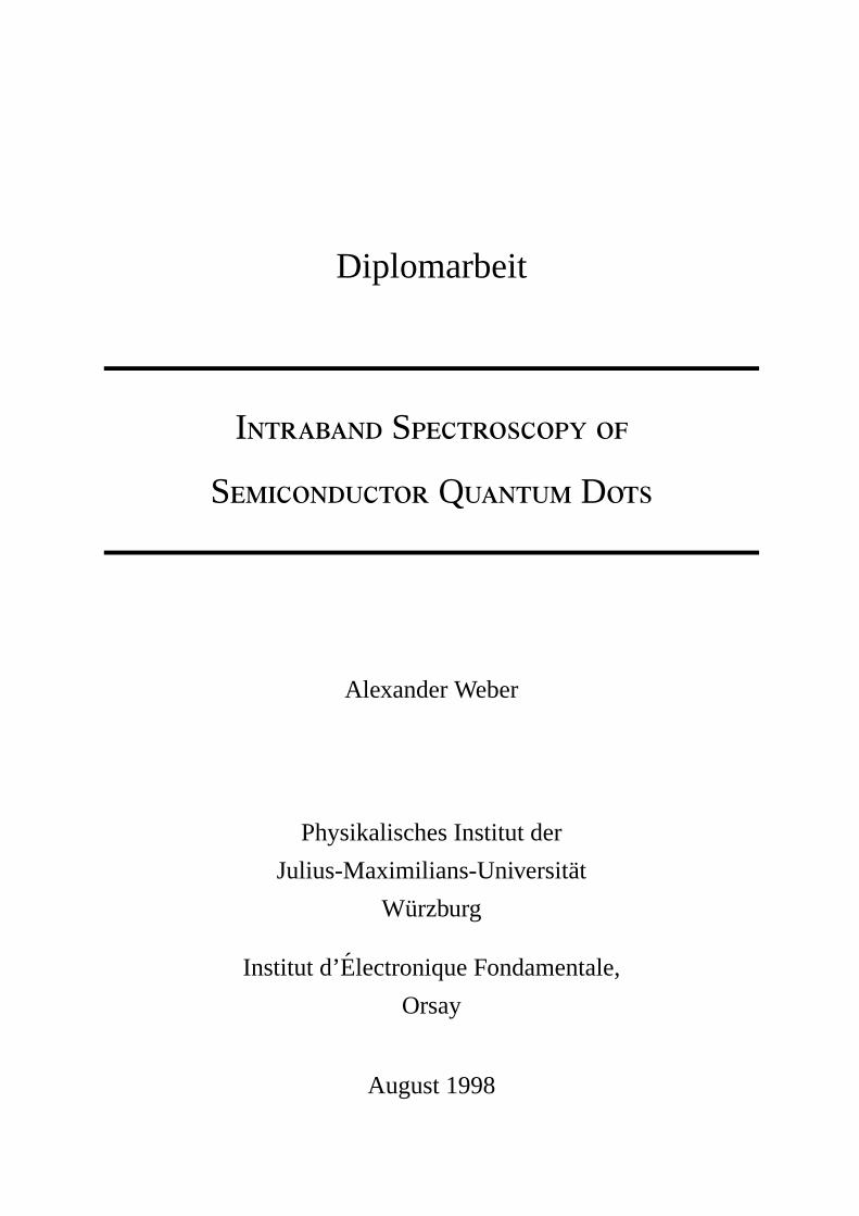
Figure 2.1 shows the bandstructure of an InAs/ In0.52Al0.48As quantum well. Electrons and
holes are trapped in the one dimensional well, but can still move freely in the InAs layer. If
the thickness of the active layer is of the order of the de Broglie wavelength of the carriers
λBroglie =hp (p being the momentum of the carrier andh the Planck constant), quantum effects
will appear, i.e., the quantization of the kinetic energy inthe growth direction leads to discrete
energy levels in thekz direction in both the conduction band and the valence band.
Figure 2.1: Scheme of the band structure ofInAs / In0.52Al0.48As.
The calculation of the eigenenergies in the confined structure using the effective mass approx-
imation is now illustrated. Let’s assume an idealized square, finite and symmetrical potential
well with a thicknessLz and a potential energy
Vwell(z) =
0 |z| > Lz
2
−Vwell |z| ≤ Lz
2 .(2.2)
The Schrodinger equation is:
[
− ~2
2m4 + Vlattice(~r) + Vwell(z)
]
Ψtot(~k,~r) = E(~k)Ψtot(~k,~r), (2.3)

6 CHAPTER 2. THEORY
whereVlattice is the periodical, rapidly oscillating lattice potential,which describes the interac-
tion of the carriers with the crystal lattice. Since it oscillates on a much smaller scale than the
well potentialVwell, it can be separated. This leads to the following wavefunction:
Ψtot(~k,~r) = Ψenv(~k,~r) · ΦBl(~k,~r). (2.4)
The rapidly oscillating Bloch functionΦBl represents the carrier motion in the lattice potential,
which can be handled with the introduction of an effective massm∗. Ψenv is the envelope func-
tion of the Bloch function and is determined by the slowly varying potentialVwell(z). Because
Vwell(z) does not contain any terms inx or y, a second separation can be carried out:
Ψenv(~k,~r) = Φ(~kx,y,~rx,y) · Θ(kz, z), (2.5)
whereΦ(~kx,y,~rx,y) describes the motion in the 2 dimensions of the quantum welland leads to the
energy eigenvalues:
E(~kx,y) =~
2
2m∗x,y(k2
x + k2y), (2.6)
with the effective massm∗x,y for a motion in the layer plane.
In thez-direction a one dimensional Schrodinger equation for the motion of a free carrier with
massm∗z in a symmetric quantum wellVwell(z) has to be solved:
[
− ~2
2m∗z
∂2
∂z2+ Vwell(z)
]
Θ(kz, z) = EzΘ(kz, z). (2.7)
The following boundary conditions must be fulfilled:
1. Θ(kz, z) is continuous everywhere;
2. by integrating equation (2.7) around anyz0, and for the specific potential of the square
quantum well, 1m∗z
dΘdz is continuous everywhere;
3. limz→±∞ |Θ(kz, z)| = 0.
The second condition accounts for the discontinuity ofm∗z at the boundary layers.
The solution of the Schrodinger equation is in this case:
Θ(kz, z) =
Asin
(
√
2m∗zEz,nz
~2z− nz
π2
)
|z| ≤ Lz
2 , nz = 1,2,3 . . .
Bexp
(
−√
2m∗z,barrier(Vwell−Ez,nz)
~2|z|)
|z| > Lz
2 ,
(2.8)

2.1. WAVEFUNCTION IN QUANTUM STRUCTURES 7
with m∗z andm∗z,barrierbeing the effective masses inz-direction inside the quantum well and inside
the barrier, respectively.
In the barrier the wavefunction is exponentially attenuated while it oscillates in the quantum
well. The ground state (nz = 1) is an even function and the higher states are alternately of even
or odd parity.
The boundary conditions lead to a transcendental equation for the discrete energy levelsEz,nz in
kz-direction, which can be solved numerically:
tan
√
2m∗zEz,nz
~2
Lz
2− nzπ
2
= −
√
m∗z,barrier
m∗z
Ez,nz
Vwell − Ez,nz
. (2.9)
In general, it is not possible to calculate analytically thediscrete energy levelsEz,nz. In order to
continue these analytical calculations, an infinite barrier is assumed from now on.
Infinite barrier
For an infinite barrier height (Vwell → ∞) it is possible to get an analytical expression of the
eigenenergies. The right hand side of equation (2.9) disappears and the energy eigenvalues are:
Ez,nz =~
2π2
2m∗z
(
n2z
L2z
)
. (2.10)
The total energy of the two dimensional system is then given by:
E2Dnz
(kx, ky) = Ez,nz + E(~kx,y) = Ez,nz +~
2
2m∗x,y
(
k2x + k2
y
)
Vwell→∞= ~
2π2
2m∗z
(
n2z
L2z
)
+ ~2
2m∗x,y
(
k2x + k2
y
)
.(2.11)
This energy function is the sum of discrete and continuous energy eigenvalues. The continuous
energy bandE ∝ ~k2 of the 3D case splits up in several subbands which are determined by the
quantum numbernz. The lowest energy level in the quantum well has shifted to a value greater
than zero, becausenz ≥ 1. There is always at least one bound energy level in thekz direction of
a quantum well with infinite barriers, even if its thicknessLz is very small.
Non-parabolicity
Equation (2.11) is only valid if the conduction and valence bands are parabolic. The real band
scheme in a semiconductor is different from this ideal model and the actual energy levels are

8 CHAPTER 2. THEORY
shifted with respect to the levels calculated by the parabolic band model. The dispersion relation
E(~kx,y) ∝ ~k2x,y is only valid, if~kx,y→ 0. As~kx,y increases, the value of the effective mass increases
also.
To solve this problem, Kane has proposed a model for small bandgap semiconductors [Kan75],
which takes into account the interaction of the different bands. By retaining solely terms up to
the second order, the dispersion relation of the conductionband can be written as [Vag94]:
E2Dnz
(~kx,y) = Ez,nz +~
2~k2x,y
2m∗+α
Eg
~2~k2
x,y
2m∗
2
, (2.12)
where the non-parabolicity coefficientα is defined as
α = −(1− m∗
m0)2(3E2
g + 4Eg∆so+ 2∆2so)
(Eg + ∆so)(3Eg + 2∆so). (2.13)
Eg is the bandgap energy and∆so the spin-orbit coupling.
Equation (2.12) can be expressed using an energy dependent effective mass:
E2Dnz
(~kx,y) = Ez,nz +~
2~k2x,y
2m∗(E), (2.14)
with
m∗(E) =m∗
1+√
4αE−Ez,nz
Eg
. (2.15)
Similar relations describe the valence band of the light holes. The heavy holes in the valence
band, however, generally do not need a non-parabolicity treatment, as their big effective mass
implies, for a given energy, a high density of states.
Strain
In heterostructures, where the lattice constants of the quantum well material and the barrier
material are not the same, the electronic properties changewith respect to the simple model
developed above. In fact, the lattice constant in the layer plane of the deposited material will be
adapted to that of the substrate (see section 3.1). This adaptation is compensated by a tetragonal
deformation of the unit cell which leads to a reduction (for layers in tension) or to an increase
(for layers in compression) of the lattice constant perpendicular to the layer plane. This causes
2.1. WAVEFUNCTION IN QUANTUM STRUCTURES 9
the presence of strain at the interface of the two materials.The presence of strain in the layers
does not only modify the energy of the bandgap, but also the effective masses of the carriers,
which become strongly anisotropic.
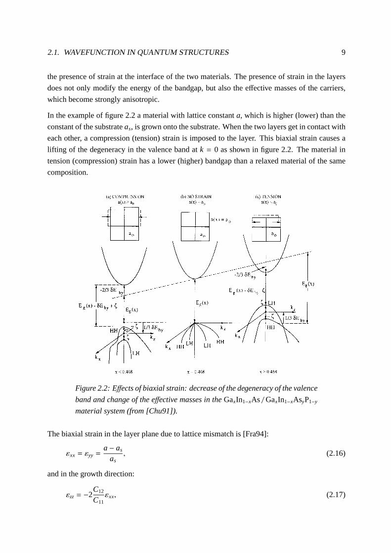
In the example of figure 2.2 a material with lattice constanta, which is higher (lower) than the
constant of the substrateas, is grown onto the substrate. When the two layers get in contact with
each other, a compression (tension) strain is imposed to thelayer. This biaxial strain causes a
lifting of the degeneracy in the valence band atk = 0 as shown in figure 2.2. The material in
tension (compression) strain has a lower (higher) bandgap than a relaxed material of the same
composition.
Figure 2.2: Effects of biaxial strain: decrease of the degeneracy of the valence
band and change of the effective masses in theGaxIn1−xAs / GaxIn1−xAsyP1−y
material system (from [Chu91]).
The biaxial strain in the layer plane due to lattice mismatchis [Fra94]:
εxx = εyy =a− as
as, (2.16)
and in the growth direction:
εzz= −2C12
C11εxx, (2.17)

10 CHAPTER 2. THEORY
whereCi j are the material elastic constants.
For a biaxial strain, the difference of the energies at the bottom of the conduction band and the
subbands in the valence band is in first approximation given by:
∆E0(e− hh) =
[
−2a
(
C11−C12
C11
)
+ b
(
C11+ 2C12
C11
)]
∆aa, (2.18)
∆E0(e− lh) =
[
−2a
(
C11−C12
C11
)
− b
(
C11+ 2C12
C11
)]
∆aa, (2.19)
where∆E0(e− hh), ∆E0(e− lh) are the energy variations of the conduction band–heavy holes
and conduction band–light holes transitions respectively. a andb are the conduction band and
valence band deformation potentials.
Figure 2.2 has been calculated for GaxIn1−xAs grown on a GaxIn1−xAsyP1−y lattice matched to
InP [Chu91]. The dotted line represents the bandgap of the relaxed material (which depends on
the compositionx of the GaxIn1−xAs layer). δEhy andζ represent the first and second term of
equation (2.19), respectively. As the parameters of the InAs / In0.52Al0.48As system, which has
been examined during this Diplomarbeit, are close (appendix A) to those used in figure 2.2, the
influence of biaxial strain for InAs will be similar.
2.1.3 1D quantum wire
If the motion of the carriers is confined in further directions of space, the additional quantization
can be calculated in a way analogous to that of the quantum well. For a one dimensional system
(quantum wire) with infinite barriers the energy eigenvalues are:
E1Dnx,nz
(ky) =~
2π2
2
(
n2x
m∗xL2x
+n2
z
m∗zL2z
)
+~
2k2y
2m∗y. (2.20)
The energy function is again a sum of discrete and continuouseigenvalues, which leads to an
unidimensional subband structure.
2.1.4 0D quantum dot
For a parallelepipedic quantum dot one obtains:
E0Dnx,ny,nz
=~
2π2
2
n2x
m∗xL2x
+n2
y
m∗yL2y
+n2
z
m∗zL2z
, (2.21)
2.1. WAVEFUNCTION IN QUANTUM STRUCTURES 11
where (nx,ny,nz) ∈ (lN3)∗ are the quantum numbers. They are integers, but not all of them
are allowed to be 0.Lx,y,z are the sizes of the structure andm∗x,y,z the effective masses in the
respective directions.
The carriers in a quantum dot are completely localized and only discrete energy levels exist.
In the realistic case of finite potential wells, numerical calculations must be performed to find
an exact solution of the Schrodinger equation.
In real situations, such as self organized quantum dots, exact calculations of the discrete energy
levels proved to be very difficult and have only been performed numerically for the InAs/
GaAs quantum dot system [Mar94, Gru95, Zun98]. First, the exact shape of the dot is usually
not known (facets of pyramids, radii in lens shape,. . .). Second, anisotropic strain largely
influences the electronic properties of 1D and 0D quantum structures.
Strain
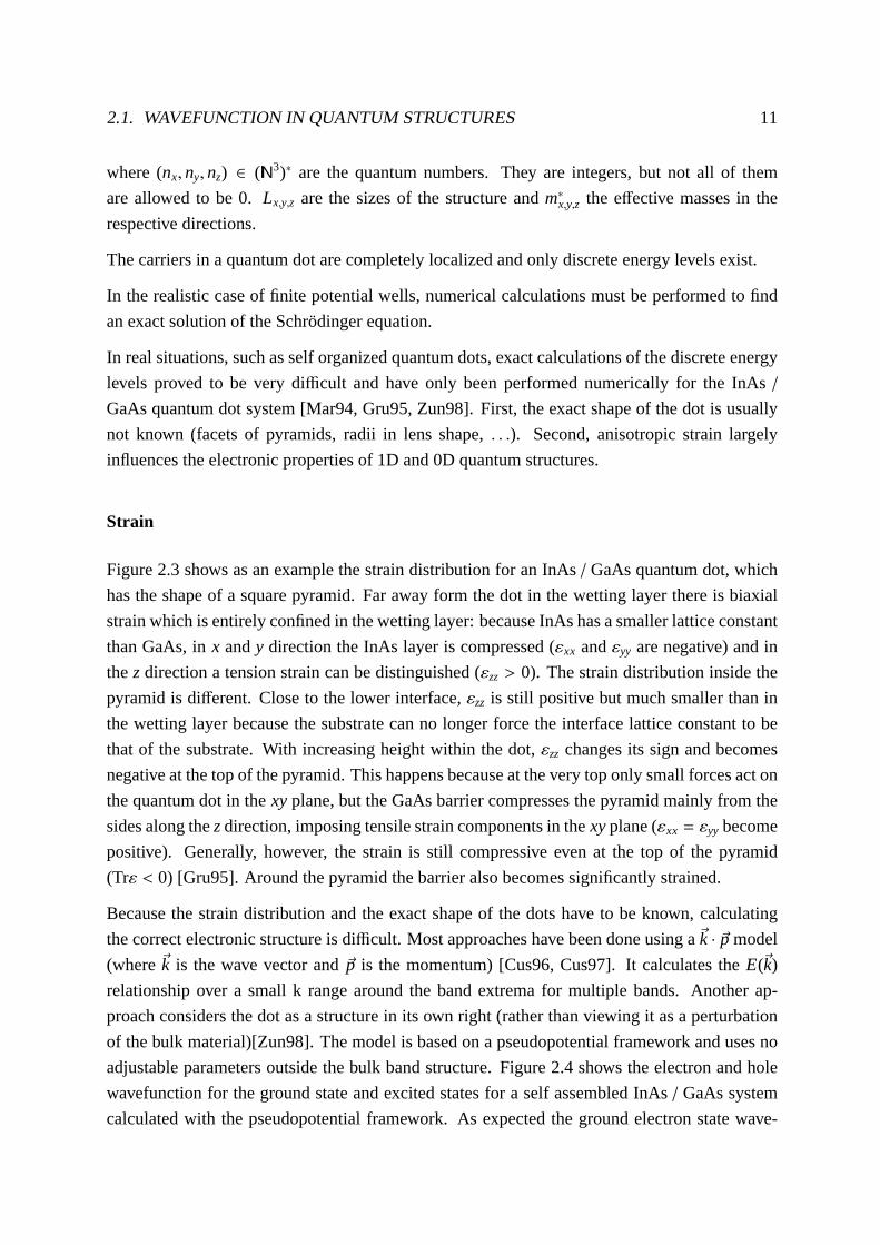
Figure 2.3 shows as an example the strain distribution for anInAs / GaAs quantum dot, which
has the shape of a square pyramid. Far away form the dot in the wetting layer there is biaxial
strain which is entirely confined in the wetting layer: because InAs has a smaller lattice constant
than GaAs, inx andy direction the InAs layer is compressed (εxx andεyy are negative) and in
thez direction a tension strain can be distinguished (εzz > 0). The strain distribution inside the
pyramid is different. Close to the lower interface,εzz is still positive but much smaller than in
the wetting layer because the substrate can no longer force the interface lattice constant to be
that of the substrate. With increasing height within the dot, εzz changes its sign and becomes
negative at the top of the pyramid. This happens because at the very top only small forces act on
the quantum dot in thexy plane, but the GaAs barrier compresses the pyramid mainly from the
sides along thezdirection, imposing tensile strain components in thexyplane (εxx = εyy become
positive). Generally, however, the strain is still compressive even at the top of the pyramid
(Trε < 0) [Gru95]. Around the pyramid the barrier also becomes significantly strained.
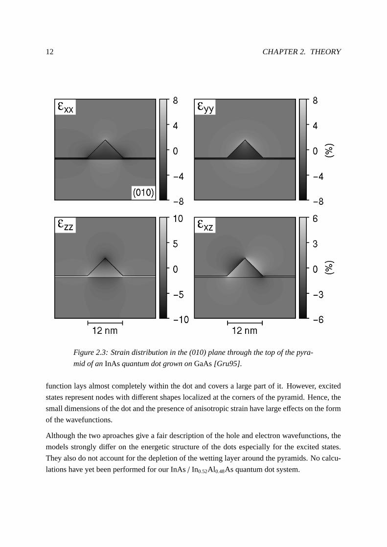
Because the strain distribution and the exact shape of the dots have to be known, calculating
the correct electronic structure is difficult. Most approaches have been done using a~k · ~p model
(where~k is the wave vector and~p is the momentum) [Cus96, Cus97]. It calculates theE(~k)
relationship over a small k range around the band extrema formultiple bands. Another ap-
proach considers the dot as a structure in its own right (rather than viewing it as a perturbation
of the bulk material)[Zun98]. The model is based on a pseudopotential framework and uses no
adjustable parameters outside the bulk band structure. Figure 2.4 shows the electron and hole
wavefunction for the ground state and excited states for a self assembled InAs/ GaAs system
calculated with the pseudopotential framework. As expected the ground electron state wave-
12 CHAPTER 2. THEORY
Figure 2.3: Strain distribution in the (010) plane through the top of the pyra-
mid of anInAs quantum dot grown onGaAs[Gru95].
function lays almost completely within the dot and covers a large part of it. However, excited
states represent nodes with different shapes localized at the corners of the pyramid. Hence,the
small dimensions of the dot and the presence of anisotropic strain have large effects on the form
of the wavefunctions.
Although the two aproaches give a fair description of the hole and electron wavefunctions, the
models strongly differ on the energetic structure of the dots especially for the excited states.
They also do not account for the depletion of the wetting layer around the pyramids. No calcu-
lations have yet been performed for our InAs/ In0.52Al0.48As quantum dot system.
2.1. WAVEFUNCTION IN QUANTUM STRUCTURES 13
Figure 2.4: The electronic structure of a strained InAs (110) pyramidal quan-
tum dot embedded within GaAs. The strain-modified band offsets are shown
above the atomic structure. They exhibit a well for both heavyholes and elec-
trons. Isosurface plots of the four highest hole states and four lowest electron
states, as obtained from pseudopotential calculations, appear on the left and
right. CBM means conduction band minimum and VBM valence bandmini-
mum (from [Zun98]).
14 CHAPTER 2. THEORY
2.2 Density of states
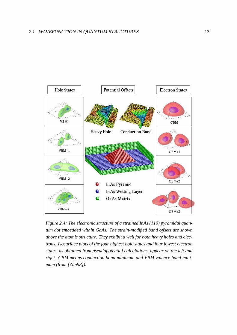
As seen in the previous section, the energy dependence in~k-space changes when the dimen-
sion of free particle motion is decreased. This is why the density of statesρ(ε) is expected to
change as well. In the case of infinite barriersρ(ε) can be evaluated for the systems of different
dimensions using the definition
ρ(ε) = 2∑
n,k
δ(
ε − En(~k))
, (2.22)
which takes the spin degeneracy into account and whereδ represents the Dirac function and
En(~k) the energy eigenvalues for the different systems (equations (2.1),(2.11),(2.20) and (2.21)).
The following energy dependences of the density of states are obtained [Ara82]:
ρ3D(ε) ∝√ε,
ρ2D(ε) ∝∑
nz
H(ε − Enz),
ρ1D(ε) ∝∑
nx,nz
1√
ε − Enx − Enz
,
ρ0D(ε) ∝∑
nx,ny,nz
δ(ε − Enx − Eny − Enz),
(2.23)
with H being the Heavyside function.
Figure 2.5 shows a schematic representation of the density of states for 3D, 2D, 1D and 0D
systems. In the 3-dimensional case a quasicontinuous distribution of the energy eigenlevels is
obtained. The density of states increases with the root of the energy.
For a quantum well, the lowest energy level is, respective tothe 3D case, shifted to higher
energies by the quantization energy of the first 2D subband. This means that the density of
states is zero for energies smaller than those at the beginning of the first subband. If the first
subband is reached, the density of states jumps up to a constant value, which is maintained until
the next subband is reached. The result is a staircase like energy dependence ofρ2D(ε).
For a quantum wire, the density of states also jumps up if a newsubband of higher energy is
reached, but it decreases for increasing energies following anε−12 proportionality, until the next
subband is reached.
In a quantum dot only discrete energy levels exist, and therefore the density of states is a sum of
δ-functions. Only two electrons with spins up and down, respectively, can populate each level.

2.3. OPTICAL TRANSITIONS 15
Figure 2.5: Schematic representation of the energy dependence of the density
of states for 3D, 2D, 1D and 0D systems.
2.3 Optical transitions
In this section, the main optical properties of low dimensional structures are discussed. The
case of a single quantum well is firstly considered and lower dimensional structures are then
treated in a similar way.
Two kinds of optical transitions are considered (figure 2.6). Interband transitions take place
between the conduction band and the valence band and involvetwo kinds of carriers (they
arebipolar), electrons and holes. The energy of the transition is the bandgap energy plus the
confinement energies of the electrons and holes minus the exciton binding energy.Intraband
transitions happen inside either the conduction or the valence band and involve only one type
of carrier (the transition isunipolar). In a quantum dot, intraband transitions occur between
discrete energy levels. In quantum wells and quantum wires there exist subbands inside the
conduction or the valence band. Intraband transitions in these structures between two subbands
are calledintersubbandtransitions. Note that another type of intraband transitions may occur
which involves the transitions of a carrier from one subbandto the same subband with absorp-

16 CHAPTER 2. THEORY
tion of a photon and emission of a phonon (momentum conservation). The latter is the analogue
of free carrier absorption.
Figure 2.6: Interband and intraband transitions for quantum wells, quantum
wires (left) and quantum dots (right). The diagrams show a scheme of the
band/level structure.
To describe the optical properties of several material systems, the absorption coefficient in a
quantum well or a quantum wire is first discussed in the electric dipole approximation [Mou96,
Bas88].
The electrical field of a light wave with frequencyω and wavevector~k (|k| = nωc ) can be ex-
pressed as
~F(~r , t) = F~ε cos(ωt − ~k · ~r), (2.24)
with ~ε being a supposed linear polarization. In the Coulomb gauge (div ~A = 0), the electrical
field depends on the vector potential~A as follows:
~F = −1c∂~A∂t. (2.25)
This leads to
~A(~r , t) = −~εcF2iω
[
exp(
i(ωt − ~k · ~r))
− exp(
−i(ωt − ~k · ~r))]
. (2.26)

2.3. OPTICAL TRANSITIONS 17
The one electron Hamiltonian of a heterostructure in presence of an electromagnetic field is in
first approximation:
H = H0 +e
2m0c
(
~p · ~A+ ~A · ~p)
, (2.27)
with the electron momentum~p and the electron chargee.
The probability of an optical stimulated transition is given by Fermi’s golden rule:
Pi f =2π~|〈 f |V|i〉|2 · δ(ε f − εi − ~ω), (2.28)
whereV is the perturbation term of the HamiltonianH = H0 + V. Under the electric dipole
approximation (exp(−i~k · ~r) ≈ 1), which is valid for visible and infrared wavelengths,V is:
V =ieF
2m0ω~ε · ~p. (2.29)
If the quantum statesi and f are partially occupied, the transition probability has to be weighted
by the occupancy factor given by the Fermi distributionf (ε):
Pi f = Pi f f (εi)[1 − f (ε f )], (2.30)
where the Fermi distribution is the mean occupancy of the state ν:
f (εν) =
[
1+ exp
(
1kBT
(εν − µ))]−1
. (2.31)
When taking into account the transitionsi → f and f → i, the linear absorption coefficient is
given by:
α(ω) = A∑
i, f
1m∗0|~ε · ~pi f |2δ(ε f − εi − ~ω)
[
f (εi) − f (ε f )]
, (2.32)
with ~pi f = 〈i|~p| f 〉, which contains the selection rules information, andA = 4π2e2
ncm0ωΩ. Ω = S L is
the irradiated volume of the sample.

18 CHAPTER 2. THEORY
2.3.1 Dipole moment and selection rules
Quantum well
In the case of a quantum well (QW), the wavefunction of a statei is given by (equation (2.4),
(2.5) and [Bas88]):
Ψi(~r) = ΦBl,i(~r)Ψenv,i(~r) = ΦBl,i(~r)1√
Sexp(i~kx,y · ~rx,y)Θi(z), (2.33)
whereΦBl,i(~r) is the periodic part of the Bloch function at the band extremum,~kx,y and~rx,y are
the wave and position vectors in the quantum well layer plane,Θi(z) is the envelope function for
subbandi in thez confinement direction andS is the area. Accounting for the rapid variations
of the Bloch functions over1kx,yand over the spatial extent of the envelope wave functions
~ε · ~pi f ≈ ~ε〈ΦBl,i |~p|ΦBl, f 〉〈Ψenv,i |Ψenv, f 〉 + 〈ΦBl,i |ΦBl, f 〉〈Ψenv,i |~ε · ~p|Ψenv, f 〉 (2.34)
is obtained. The first term on the right-hand side is the optical matrix element for interband
transitions which gives rise to the band-to-band selectionrules. The second term is the inter-
subband contribution, since by definition the Bloch functions are identical for both subbands
(〈ΦBl,i |ΦBl, f 〉 = δi f and〈ΦBl,i |~p|ΦBl, f 〉 = 0). The intersubband optical matrix element is equal to
〈Ψenv,i(~r)|~ε · ~p|Ψenv, f (~r)〉 =i(ε f − εi)m0
~eµi f (2.35)
with the intersubband dipole moment
µi f = e〈Θi(z)|z|Θ f (z)〉~ε · z. (2.36)
z is the unit vector in thezdirection,εν is the confinement energy andm0 the free electron mass.
As seen, the dipole moment only involves the envelope wave functions for the two subbands. In
symmetric QWs, sincez is odd, only transitions between subbands with opposite parity of the
envelope wave functions are allowed:f − i = ±1,±3, . . ..
For example, transitions from the ground state to the first excited state are allowed but transitions
from the ground state to the second excited state are forbidden. This selection rule is, of course,
not relevant for asymmetric potential profiles, such as stepQWs or DC-biased QWs, for which
all transitions become allowed. The dipole moment is polarized normally to the layer plane, i.e.,
along the ˆz confinement direction. Tables 2.1 and 2.2 show the selectionrules for the different
polarizations of interband transitions and intersubband transitions in a quantum well. Using
2.3. OPTICAL TRANSITIONS 19
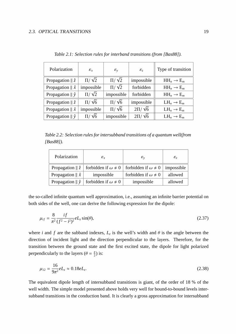
Table 2.1: Selection rules for interband transitions (from[Bas88]).
Polarization εx εy εz Type of transition
Propagation‖ z Π/√
2 Π/√
2 impossible HHn→ Em
Propagation‖ x impossible Π/√
2 forbidden HHn→ Em
Propagation‖ y Π/√
2 impossible forbidden HHn→ Em
Propagation‖ z Π/√
6 Π/√
6 impossible LHn→ Em
Propagation‖ x impossible Π/√
6 2Π/√
6 LHn→ Em
Propagation‖ y Π/√
6 impossible 2Π/√
6 LHn→ Em
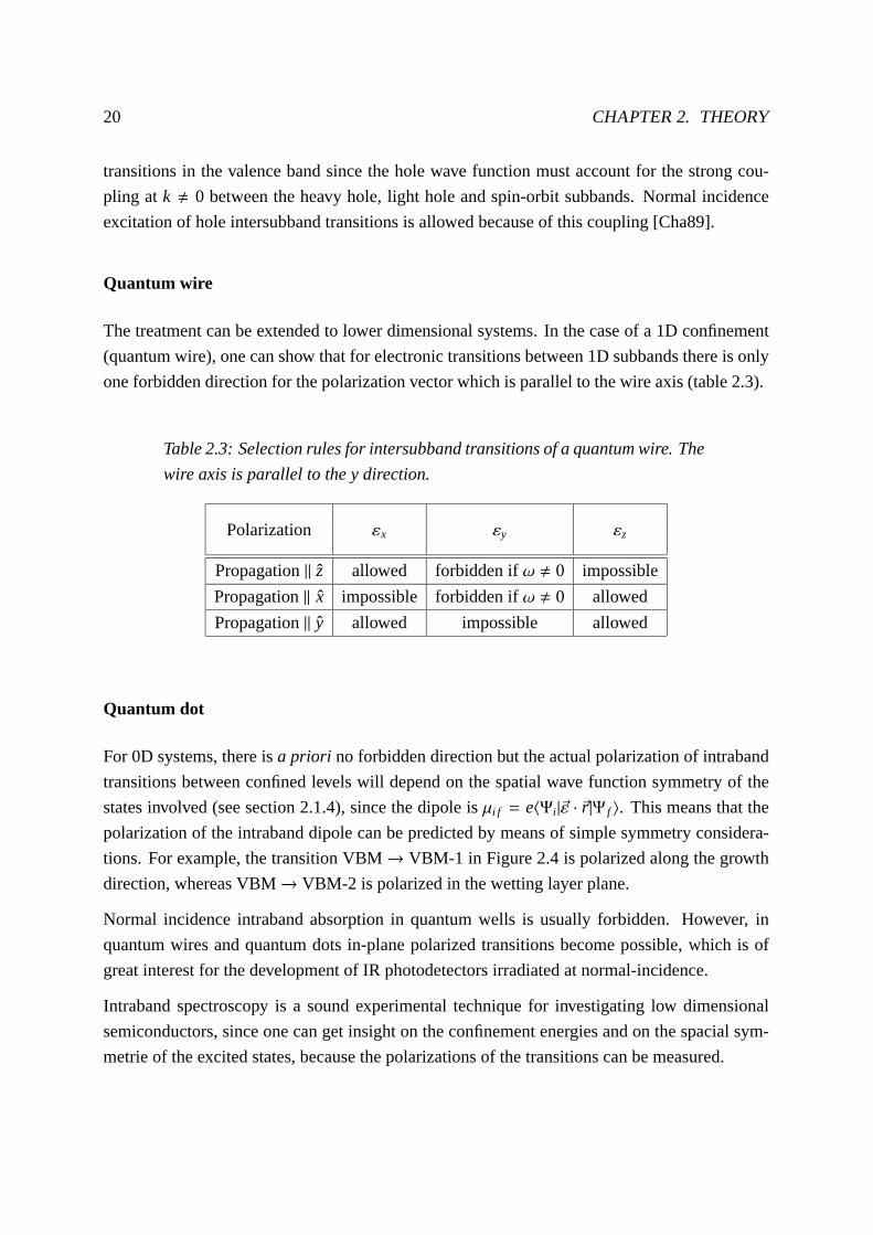
Table 2.2: Selection rules for intersubband transitions ofa quantum well(from
[Bas88]).
Polarization εx εy εz
Propagation‖ z forbidden ifω , 0 forbidden ifω , 0 impossible
Propagation‖ x impossible forbidden ifω , 0 allowed
Propagation‖ y forbidden ifω , 0 impossible allowed
the so-called infinite quantum well approximation, i.e., assuming an infinite barrier potential on
both sides of the well, one can derive the following expression for the dipole:
µi f =8π2
i f( f 2 − i2)2
eLz sin(θ), (2.37)
wherei and f are the subband indexes,Lz is the well’s width andθ is the angle between the
direction of incident light and the direction perpendicular to the layers. Therefore, for the
transition between the ground state and the first excited state, the dipole for light polarized
perpendicularly to the layers (θ = π2) is:
µ12 =169π2
eLz ≈ 0.18eLz. (2.38)
The equivalent dipole length of intersubband transitions is giant, of the order of 18 % of the
well width. The simple model presented above holds very wellfor bound-to-bound levels inter-
subband transitions in the conduction band. It is clearly a gross approximation for intersubband
20 CHAPTER 2. THEORY
transitions in the valence band since the hole wave functionmust account for the strong cou-
pling atk , 0 between the heavy hole, light hole and spin-orbit subbands. Normal incidence
excitation of hole intersubband transitions is allowed because of this coupling [Cha89].
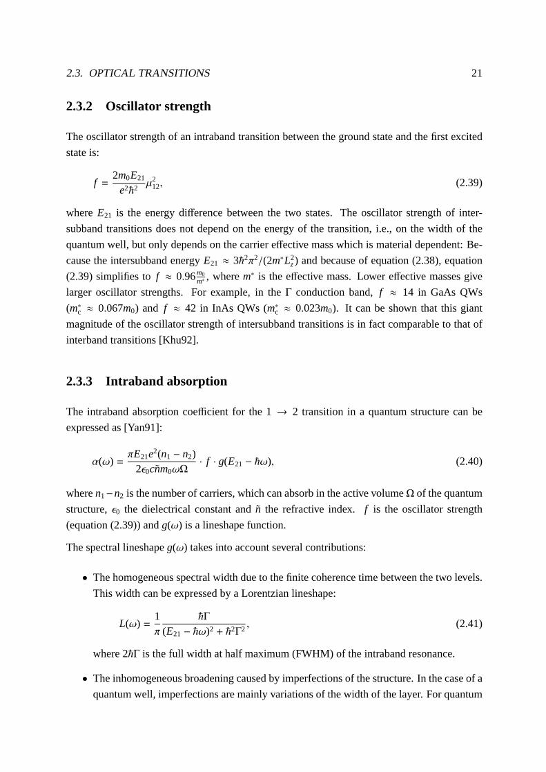
Quantum wire
The treatment can be extended to lower dimensional systems.In the case of a 1D confinement
(quantum wire), one can show that for electronic transitions between 1D subbands there is only
one forbidden direction for the polarization vector which is parallel to the wire axis (table 2.3).
Table 2.3: Selection rules for intersubband transitions ofa quantum wire. The
wire axis is parallel to the y direction.
Polarization εx εy εz
Propagation‖ z allowed forbidden ifω , 0 impossible
Propagation‖ x impossible forbidden ifω , 0 allowed
Propagation‖ y allowed impossible allowed
Quantum dot
For 0D systems, there isa priori no forbidden direction but the actual polarization of intraband
transitions between confined levels will depend on the spatial wave function symmetry of the
states involved (see section 2.1.4), since the dipole isµi f = e〈Ψi |~ε · ~r |Ψ f 〉. This means that the
polarization of the intraband dipole can be predicted by means of simple symmetry considera-
tions. For example, the transition VBM→ VBM-1 in Figure 2.4 is polarized along the growth
direction, whereas VBM→ VBM-2 is polarized in the wetting layer plane.
Normal incidence intraband absorption in quantum wells is usually forbidden. However, in
quantum wires and quantum dots in-plane polarized transitions become possible, which is of
great interest for the development of IR photodetectors irradiated at normal-incidence.
Intraband spectroscopy is a sound experimental technique for investigating low dimensional
semiconductors, since one can get insight on the confinementenergies and on the spacial sym-
metrie of the excited states, because the polarizations of the transitions can be measured.
2.3. OPTICAL TRANSITIONS 21
2.3.2 Oscillator strength
The oscillator strength of an intraband transition betweenthe ground state and the first excited
state is:
f =2m0E21
e2~2µ2
12, (2.39)
whereE21 is the energy difference between the two states. The oscillator strength of inter-
subband transitions does not depend on the energy of the transition, i.e., on the width of the
quantum well, but only depends on the carrier effective mass which is material dependent: Be-
cause the intersubband energyE21 ≈ 3~2π2/(2m∗L2z) and because of equation (2.38), equation
(2.39) simplifies tof ≈ 0.96m0m∗ , wherem∗ is the effective mass. Lower effective masses give
larger oscillator strengths. For example, in theΓ conduction band,f ≈ 14 in GaAs QWs
(m∗c ≈ 0.067m0) and f ≈ 42 in InAs QWs (m∗c ≈ 0.023m0). It can be shown that this giant
magnitude of the oscillator strength of intersubband transitions is in fact comparable to that of
interband transitions [Khu92].
2.3.3 Intraband absorption
The intraband absorption coefficient for the 1→ 2 transition in a quantum structure can be
expressed as [Yan91]:
α(ω) =πE21e2(n1 − n2)
2ε0cnm0ωΩ· f · g(E21− ~ω), (2.40)
wheren1−n2 is the number of carriers, which can absorb in the active volumeΩ of the quantum
structure,ε0 the dielectrical constant and ˜n the refractive index. f is the oscillator strength
(equation (2.39)) andg(ω) is a lineshape function.
The spectral lineshapeg(ω) takes into account several contributions:
• The homogeneous spectral width due to the finite coherence time between the two levels.
This width can be expressed by a Lorentzian lineshape:
L(ω) =1π
~Γ
(E21− ~ω)2 + ~2Γ2, (2.41)
where 2~Γ is the full width at half maximum (FWHM) of the intraband resonance.
• The inhomogeneous broadening caused by imperfections of the structure. In the case of a
quantum well, imperfections are mainly variations of the width of the layer. For quantum
22 CHAPTER 2. THEORY
wires and dots, size distributions of the structures are theorigin of this lineshape broad-
ening. For the example of quantum dots, this can be explainedas followed: Smaller dots
have higher energy levels and also greater differences between two states in one ’band’,
while greater dots possess smaller energy differences between two states. As the absorp-
tion takes place in a huge number of quantum dots, the sum of all their narrow absoption
lines at different energy positions will be observed. The result is that the absorption spec-
trum overtakes the shape of the size distribution function of the dots.
• The inhomogeneous spectral width introduced by the non-parabolicity or, more general,
by the coupling with other levels. This causes an asymmetriclineshape [Iko89].
2.3.4 Temperature dependance
The integrated absorption of an intraband absorption peak is defined as
I =∫ ∞
0
∆t(ω)t(ω)
dω =∫ ∞
0α(ω)L dω, (2.42)
where t(ω) is the sample transmission,∆t(ω) the measured decrease of transmission due to
absorption,α(ω) the absorption coefficient from equation (2.40) andL the length of the IR
beam path through the absorbant material. Equation (2.42) expresses the correlation between
experimental data∆tt and the calculated absorbanceα. I depends on the temperature of the
sample through the carrier density in the initial and final stateni andnf :
I = σ(ni − nf ), (2.43)
whereσ is the absorption cross section. The temperature dependence of ni andnf depends on
the statistic which describes the energy distribution of electrons. In the case of a quantum well
and quantum wire, the Fermi distribution is valid, while forthe population of the discrete energy
levels of a quantum dot the Gibbs distribution for the grand canonical ensemble has to be used.
Quantum wire
In a quantum wire the populationn(ε) of an energy levelε is determined by
n(ε) = ρ(ε)1
1+ exp(
ε−εFkT
) , (2.44)

2.3. OPTICAL TRANSITIONS 23
where the fraction represents the Fermi distribution with the Fermi energyεF, k is the Boltzmann
constant and
ρ(ε) = 2Ly
π~
√
m∗
2
∑
nx,nz
Re
(
1√ε − εnx − εnz
)
(2.45)
is the density of states of a 1D wire.
The Fermi energyεF can be calculated by integrating over all energies, thus by solving the
equation
n =∫ ∞
0ρ(ε)
1
1+ exp(
ε−εFkT
) dε. (2.46)
n is in this case the total carrier density in the quantum wire.
This simple model allows the population of energy levels fordifferent temperatures to be nu-
merically calculated. By using equation (2.43), ratios of integrated absorptions at different
temperatures can be calculated and compared with experimental data.
Quantum dot
Since quantum dots have only discrete energy levels (each occupied at maximum with 2 carriers
with spin up and down) and a limited number of carriers is present in each dot, the Gibbs
distribution in the grand canonical ensemble has to be used to describe the occupation of levels
by the carriers in the dots [Bee91, Ave91]. If the occupation number of carriers in the leveli is
ni (the numberni can take on only the values 0, 1 and 2) andni ≡ n1,n2, . . . are the possible
realizations of occupation numbers of the energy levels in the quantum dot, then the probability
P(ni) of finding the dot in the stateni is given by:
P(ni) = Z−1 exp
− 1kT
∞∑
i=1
εini − NεF
, (2.47)
whereN ≡∑
i ni is the total number of carriers in the dot andZ is the partition function:
Z =∑
ni exp
− 1kT
∞∑
i=1
εini − NεF
. (2.48)
Intraband transitions from a leveli to a level f are only possible in dots, where the leveli is
filled with at least one carrier (ni = 1,2) and the levelf can still take up one carrier (nf = 0,1).

24 CHAPTER 2. THEORY
The probability of finding dots with these occupation conditions can be calculated for different
temperatures. Since the integrated absorption is proportional to the number of dots which fullfil
this condition, the absorption dependence on the temperature can be determined.

Chapter 3
Sample growth and AFM characterization
In this chapter the growth process and first characterization by atomic force microscopy (AFM)
of the samples are described.
3.1 Stranski Krastanov growth
The quantum dots examined during this work were produced using a self-assembly mechanism.
The deposit of a material layer with lattice constanta onto a substrate of lattice constantas
imposes the crystal structure of the substrate to the layer.This causes elastic strain, which can
relax in different ways. In a two dimensional film the lattice constant parallel to the surface will
be matched toa‖ = as (∆a = as − a < 0). Perpendicular to the layer the lattice constant will
be increased toa⊥ = a − 2(as − a) ν(1−ν) ; the result is a tetragonal distortion.ν is the Poisson
number and its value is approximately13 for typical III/V semiconductors. When the thickness
of the layer exceeds a certain critical valuedc ∝ a∆a, then the accumulated elastical distortion
energy becomes greater than the dislocation energy and the strain is relaxed by defects. Typical
values for the critical layer thickness aredc ≈ 20 nm for ∆aa = −1.5 % and only one monolayer
for ∆aa < −6 % [Gru97].
Under appropriate growth conditions the relaxation of the elastic energy can take place with
the development of quite regular 3-dimensional structures. After a critical amount of strained
material is deposited, a morphological instability results in the formation of coherent strained
islands on the wetted surface. This is called the Stranski-Krastanov growth mode. Formation of
3-dimensional islands leads to a reduction of the strain energy and to an increase of the surface
energy as compared to the planar surface case. The first is proportional to the volume of the
island, and the latter is proportional to the surface area ofthe island. If the size of such an island
25
26 CHAPTER 3. SAMPLE GROWTH AND AFM CHARACTERIZATION
exceeds a critical value, further growth becomes energetically unfavorable.
This is why the size of the islands does not depend on the amount of material deposited, if
the material has enough time to form a field of islands. The amount of the deposited material
determines only the surface density of the islands [Gru95].
The size and shape of the island largely depend on the growth conditions (temperature, growth
interruption after deposition of the material, V/III equivalent pressure ratio) and on the materials
used.
3.2 Sample description
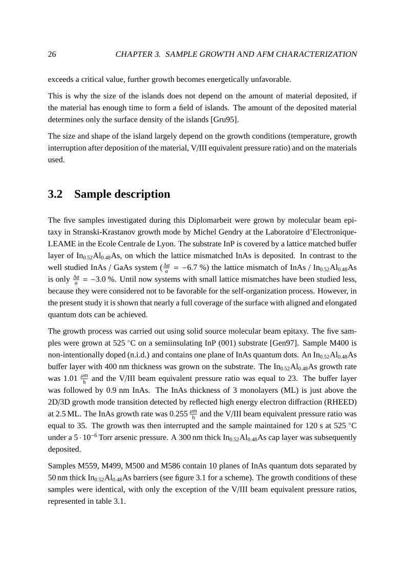
The five samples investigated during this Diplomarbeit weregrown by molecular beam epi-
taxy in Stranski-Krastanov growth mode by Michel Gendry at the Laboratoire d’Electronique-
LEAME in the Ecole Centrale de Lyon. The substrate InP is covered by a lattice matched buffer
layer of In0.52Al0.48As, on which the lattice mismatched InAs is deposited. In contrast to the
well studied InAs/ GaAs system (∆aa = −6.7 %) the lattice mismatch of InAs/ In0.52Al0.48As
is only ∆aa = −3.0 %. Until now systems with small lattice mismatches have been studied less,
because they were considered not to be favorable for the self-organization process. However, in
the present study it is shown that nearly a full coverage of the surface with aligned and elongated
quantum dots can be achieved.
The growth process was carried out using solid source molecular beam epitaxy. The five sam-
ples were grown at 525C on a semiinsulating InP (001) substrate [Gen97]. Sample M400 is
non-intentionally doped (n.i.d.) and contains one plane ofInAs quantum dots. An In0.52Al0.48As
buffer layer with 400 nm thickness was grown on the substrate. TheIn0.52Al0.48As growth rate
was 1.01 µmh and the V/III beam equivalent pressure ratio was equal to 23. The buffer layer
was followed by 0.9 nm InAs. The InAs thickness of 3 monolayers (ML) is just above the
2D/3D growth mode transition detected by reflected high energy electron diffraction (RHEED)
at 2.5 ML. The InAs growth rate was 0.255µmh and the V/III beam equivalent pressure ratio was
equal to 35. The growth was then interrupted and the sample maintained for 120 s at 525C
under a 5·10−6 Torr arsenic pressure. A 300 nm thick In0.52Al0.48As cap layer was subsequently
deposited.
Samples M559, M499, M500 and M586 contain 10 planes of InAs quantum dots separated by
50 nm thick In0.52Al0.48As barriers (see figure 3.1 for a scheme). The growth conditions of these
samples were identical, with only the exception of the V/III beam equivalent pressure ratios,
represented in table 3.1.
3.3. AFM CHARACTERIZATION 27
Sample M559 is, like M400, non intentionally doped. Sample M500 is p-doped with Be while
samples M499 and M586 are n-doped with Si. In all cases delta doping of the InAlAs barriers
is performed 2nm below each InAs quantum dot layer in order toachieve a sheet carrier density
of 5 · 1011 cm−2 for samples M499 and M500 and 2.5 · 1011 cm−2 for sample M586.
Table 3.1: Growth and sample properties.
Sample M400 M559 M499 M500 M586
number of QD layers 1 10
Delta doping type n.i.d n p n
Delta doping density - 5 · 1011 cm−2 2.5 · 1011 cm−2
(V/III) InAs 35 90 60
(V/III) InAlAs 23 32 20
QD surface density ∼ 7 · 1010 cm−2
average length of QD ∼ 50 nm
average width of QD ∼ 25 nm
average height of QD ∼ 1.5 nm
3.3 AFM characterization
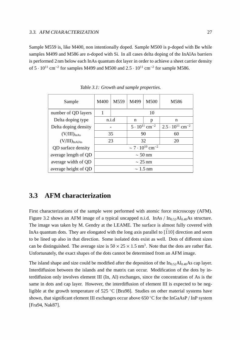
First characterizations of the sample were performed with atomic force microscopy (AFM).
Figure 3.2 shows an AFM image of a typical uncapped n.i.d. InAs / In0.52Al0.48As structure.
The image was taken by M. Gendry at the LEAME. The surface is almost fully covered with
InAs quantum dots. They are elongated with the long axis parallel to [110] direction and seem
to be lined up also in that direction. Some isolated dots exist as well. Dots of different sizes
can be distinguished. The average size is 50× 25× 1.5 nm3. Note that the dots are rather flat.
Unfortunately, the exact shapes of the dots cannot be determined from an AFM image.
The island shape and size could be modified after the deposition of the In0.52Al0.48As cap layer.
Interdiffusion between the islands and the matrix can occur. Modification of the dots by in-
terdiffusion only involves element III (In, Al) exchanges, since the concentration of As is the
same in dots and cap layer. However, the interdiffusion of element III is expected to be neg-
ligible at the growth temperature of 525C [Bra98]. Studies on other material systems have
shown, that significant element III exchanges occur above 650 C for the InGaAsP/ InP system
[Fra94, Nak87].
28 CHAPTER 3. SAMPLE GROWTH AND AFM CHARACTERIZATION
Figure 3.1: Sample layer scheme of the samples M400 (top), M499, M500,
M586 (bottom left) and M559 (bottom right).

3.3. AFM CHARACTERIZATION 29
Figure 3.2: AFM image of an uncappedInAs / In0.52Al0.48As sample.
Chapter 4
Experimental setup
The quantum dot samples have been characterized by photoluminescence spectroscopy (PL),
photoluminescence excitation spectroscopy (PLE) and infrared absorption spectroscopy. The
experimental setup and the principal characteristics of these experiments are described in the
next sections.
4.1 Photoluminescence
The principle of photoluminescence measurements is to create carriers by optical excitation
with a photon energy above the band gap of the quantum structure. Electrons and holes relax
to their respective ground states in the conduction and valence band. They can then recom-
bine radiatively as free carriers or excitons. At low temperatures, it is admitted that exciton
luminescence largely dominates.
PL spectroscopy allows the following properties to be evaluated:
• The energy position of the PL peaks reflect the strained bandgap plus the confinement
energies minus the exciton binding energy.
• The quality of the quantum structure can be evaluated through the width and the intensity
of the luminescence signal.
• Optical transitions between excited states may be detectedfor high excitation intensities.
Figure 4.1 shows the experimental setup for the photoluminescence measurements. The ex-
citation is performed by an Argon-Ion (Ar++) laser, SPECTRA PHYSICS model 2016 at a
wavelength of 514 nm. Its output power can be regulated in therange of∼ 5 mW to 6 W.
30

4.1. PHOTOLUMINESCENCE 31
The beam from the Ar++ laser is chopped by a mechanical chopper and then focussed onto the
sample using a lens (focal lengthf = 10 cm). The minimum laser spot diameter at the focal
point has been determined to be∼ 50µm. The sample is mounted on the cold finger of a liquid
nitrogen cryostat. The quartz window of the cryostat is parallel to the sample surface. As there
are two different lenses used for the incoming beam and the outgoing radiation, the incoming
beam arrives at an angle slightly less than 90 while the outgoing light is recovered at normal
incidence to the sample surface. The lens collecting the PL light has a focal length off = 5 cm
and a focal numberk = f2r = 2 (r being the lens radius). The PL beam is then focalized with the
focal number of the spectrometer (k = 4) onto the input slit of the spectrometer (Jobin Yvon HR
460, with a maximum wavelength of 1.33µm). A nitrogen cooled Ge detector is used for the
detection. Its output signal is detected by a lock-in amplifier at the frequency of the chopper. A
computer serves to read the signal from the lock-in amplifiervia an IEEE interface. Finally, the
spectra are displayed with the Lab-View software package.
Figure 4.1: Scheme of the PL experiment setup.
32 CHAPTER 4. EXPERIMENTAL SETUP
4.2 Photoluminescence excitation
The principle of photoluminescence excitation (PLE) spectroscopy measurements is very sim-
ilar. The detection energyhνdet is set at the ground state luminescence. The excitation energy
hνexc is varied fromhνdet to higher energies. If the intraband scattering times are much shorter
than the interband recombination times, the ground state luminescence evolves as the joint den-
sity of states excited by the excitation source. Under such conditions, the PLE spectrum is
analogous to that obtained using absorption spectroscopy.The PLE signal increases each time
a new interband maximum is excited. Possible sources are tunable Ti:Sapphire lasers or dye
lasers in the 0.4 µm to 1.1 µm range or in longer wavelengths black body sources like halogen
lamps, whose light is filtered by a monochromator.
4.3 Intraband absorption
Infrared (IR) spectroscopy is a sound technique to investigate quantum structures, because the
wavelength of the IR light corresponds to the energy range ofintraband transitions between
confined states belonging to either the conduction band or the valence band. A direct measure-
ment of the confinement energies and of the spatial symmetry of the envelope wavefunctions is
possible with this technique [Dre94, Sau97].
Different experimental approaches allow intraband absorptions to be measured. They can, for
example, be studied with laser spectroscopy (continuous CO2 [Jul91]) or with a Fourier trans-
form infrared spectrometer (FTIR). The latter is appropriate when studying a larger frequency
range. The experiments described here have been carried outwith a FTIR, a Biorad FTS-60A.
4.3.1 FTIR spectrometer
Principle
A Fourier spectrometer’s main components are a Michelson interferometer, an IR source, an IR
detector, electronics and an informatic system.
The Michelson interferometer consists of a fixed mirror, a moving mirror and a beamsplitter
(Figure 4.3). After being reflected or transmitted off the beamsplitter, the two beams recombine
there again after reflection on the mirrors. The recombined beam passes through the sample
chamber and is detected on an IR detector.
If the moving mirror is at the same optical distance from the beamsplitter as the fixed mirror, a
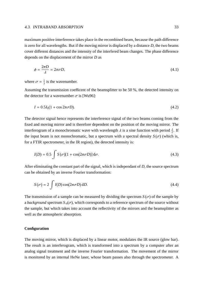
4.3. INTRABAND ABSORPTION 33
maximum positive interference takes place in the recombined beam, because the path difference
is zero for all wavelengths. But if the moving mirror is displaced by a distanceD, the two beams
cover different distances and the intensity of the interfered beam changes. The phase difference
depends on the displacement of the mirrorD as
φ =2πDλ= 2πσD, (4.1)
whereσ = 1λ
is the wavenumber.
Assuming the transmission coefficent of the beamsplitter to be 50 %, the detected intensity on
the detector for a wavenumberσ is [Wu96]:
I = 0.5I0(1+ cos 2πσD). (4.2)
The detector signal hence represents the interference signal of the two beams coming from the
fixed and moving mirror and is therefore dependent on the position of the moving mirror. The
interferogram of a monochromatic wave with wavelengthλ is a sine function with periodλ2. If
the input beam is not monochromatic, but a spectrum with a spectral densityS(σ) (which is,
for a FTIR spectrometer, in the IR region), the detected intensity is:
I (D) = 0.5∫
S(σ)[1 + cos(2πσD)] dσ. (4.3)
After eliminating the constant part of the signal, which is independant ofD, the source spectrum
can be obtained by an inverse Fourier transformation:
S(σ) = 2∫
I (D) cos(2πσD) dD. (4.4)
The transmission of a sample can be measured by dividing the spectrumS(σ) of the sample by
abackgroundspectrumS0(σ), which corresponds to a reference spectrum of the source without
the sample, but which takes into account the reflectivity of the mirrors and the beamsplitter as
well as the atmospheric absorption.
Configuration
The moving mirror, which is displaced by a linear motor, modulates the IR source (glow bar).
The result is an interferogram, which is transformed into a spectrum by a computer after an
analog signal treatment and the inverse Fourier transformation. The movement of the mirror
is monitored by an internal HeNe laser, whose beam passes also through the spectrometer. A

34 CHAPTER 4. EXPERIMENTAL SETUP
photodiode detects the intensity oscillations during the mirror movement and allows the position
of the mirror to be precisely controlled. The spectral rangeof the spectrum depends on the
distance∆D between two sampling positions, where the intensity is measured. Usually an
under sampling ratio UDR= 2 was chosen. This means, that a measurement is taken every two
periods of the HeNe oscillations. The resulting spectral range is from 0 to (2· 632.8 nm)−1 ≈7900 cm−1.
There are two function modes of the FTIR spectrometer: rapidscan and step scan. In the
rapid scan mode, the mirror rapidly oscillates between the limits. The sampling of all points
is done during one pass of the mirror. This means that the measuring time at each point is
quite short and there is much noise in the spectrum. To obtaina better signal to noise ratio, a
mean value of multiple spectra is taken. The rapid scan mode is used for standard spectroscopy
because of the following reasons: reduction of the dynamical range of the interferogram with
electrical filters before the analog-digital conversion, the elimination of low frequency noise
(source fluctuations, electronic and detector deviations,mechanical vibrations etc.) and faster
measurements. In the step scan mode, the mirror is displacedfrom one sampling position to
the next, after being held stationary for the measuring timefor each point. The measuring time
depends on the signal to noise ratio and is usually in the range of 0.1 s/step to 10 s/step. In
addition, it is possible to modulate the signal (either the source or the transmission of the sample
by optical excitation) in the step scan mode with a high frequency, without any interference with
the moving mirror. This permits the use of a lock-in amplifierfor experiments with low signals.
In general, the transmission spectra were achieved in rapidscan mode, while the photo-induced
absorption spectra were performed in step scan mode.
For the signal detection, a broadband MCT (mercury cadmium telluride) detector with a cut-off
wavenumber of 500 cm−1 was used.
4.3.2 Photo-induced experiments
The absorption of undoped samples can be measured if carriers are generated in the conduction
and valence bands through interband excitation. This is performed either with an Ar++ laser or
with a Ti:Sapphire laser for non-resonant pumping below thebandgap of the substrate to pump
just the confined structure.
To increase the absorption and the observed signals, the facets of the sample are optically pol-
ished at a 45 angle in order to permit several passages of the IR beam through the active layers
of the sample (see figure 4.2). It is necessary to polish the back side of the sample (substrate) in
IR optical quality. Instead of just one passage of the IR beamthrough the quantum structures in
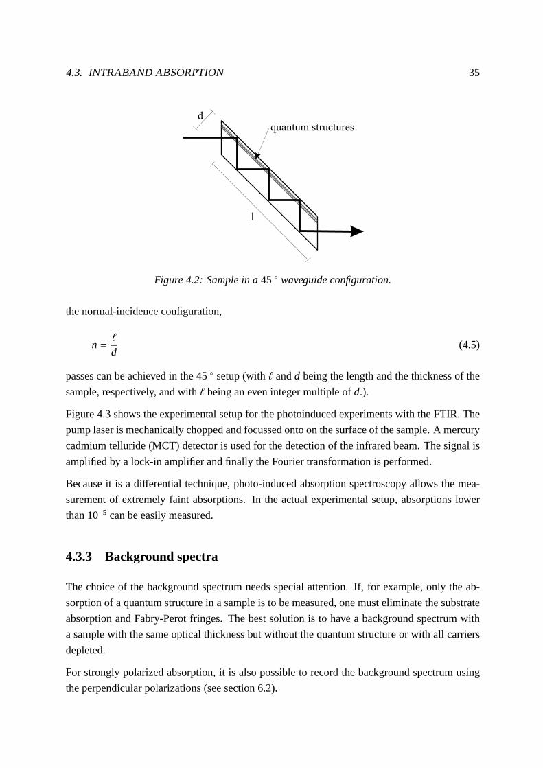
4.3. INTRABAND ABSORPTION 35
Figure 4.2: Sample in a45 waveguide configuration.
the normal-incidence configuration,
n =`
d(4.5)
passes can be achieved in the 45 setup (with` andd being the length and the thickness of the
sample, respectively, and withbeing an even integer multiple ofd.).
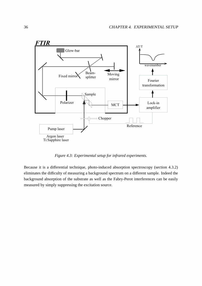
Figure 4.3 shows the experimental setup for the photoinduced experiments with the FTIR. The
pump laser is mechanically chopped and focussed onto on the surface of the sample. A mercury
cadmium telluride (MCT) detector is used for the detection ofthe infrared beam. The signal is
amplified by a lock-in amplifier and finally the Fourier transformation is performed.
Because it is a differential technique, photo-induced absorption spectroscopy allows the mea-
surement of extremely faint absorptions. In the actual experimental setup, absorptions lower
than 10−5 can be easily measured.
4.3.3 Background spectra
The choice of the background spectrum needs special attention. If, for example, only the ab-
sorption of a quantum structure in a sample is to be measured,one must eliminate the substrate
absorption and Fabry-Perot fringes. The best solution is tohave a background spectrum with
a sample with the same optical thickness but without the quantum structure or with all carriers
depleted.
For strongly polarized absorption, it is also possible to record the background spectrum using
the perpendicular polarizations (see section 6.2).
36 CHAPTER 4. EXPERIMENTAL SETUP
Figure 4.3: Experimental setup for infrared experiments.
Because it is a differential technique, photo-induced absorption spectroscopy (section 4.3.2)
eliminates the difficulty of measuring a background spectrum on a different sample. Indeed the
background absorption of the substrate as well as the Fabry-Perot interferences can be easily
measured by simply suppressing the excitation source.

Chapter 5
Photoluminescence results
The photoluminescence (PL) and photoluminescence excitation (PLE) spectroscopic results are
presented in this chapter. The PL experiments serve to obtain information on the confinement
type of the InAs/ In0.52Al0.48As samples. The size distribution of the quantum structurescan also
be tested with this experimental technique. By changing the excitation intensity, information
about excited states and band filling effects can be obtained. In addition, PLE experiments can
be used to identify the excited states of the structure.
5.1 Photoluminescence
Figure 5.1 shows the PL spectrum of the non-intentionally doped (n.i.d.) sample M400 at a
temperature of 4 K. The excitation was performed by a continuous Ar++ laser with an intensity
of 15 Wcm2 . This spectrum was, as well as the PLE spectra shown in figure 5.4, obtained by T.
Benyattou (Laboratoire de Physique de la Matiere-LPM, INSA de Lyon).
A structured PL band is detected between 0.95 eV and 1.3 eV. The full width at half maximum
(FWHM) of the band is about 170 meV. We have fitted the spectrum with five Gaussian peaks
labelled a) to e) (table 5.1 and dotted lines in figure 5.1). The FWHM of these peaks is around
50 meV, except for peak e), where it is 70 meV.
There are two possibilities to interpret the observed PL structure. First, the five peaks can result
from transitions from the ground electron to the ground valence band state for 5 different sizes
of quantum dots. Larger dots have lower energy levels (equation 2.21) and would therefore con-
tribute to the low-energy side of the spectrum, whereas smaller dots contribute to the peaks on
the high-energy side of the spectrum. A second possibility is, that the higher-energy peaks re-
sult from transitions between excited states. This would require complete filling of the electron
37
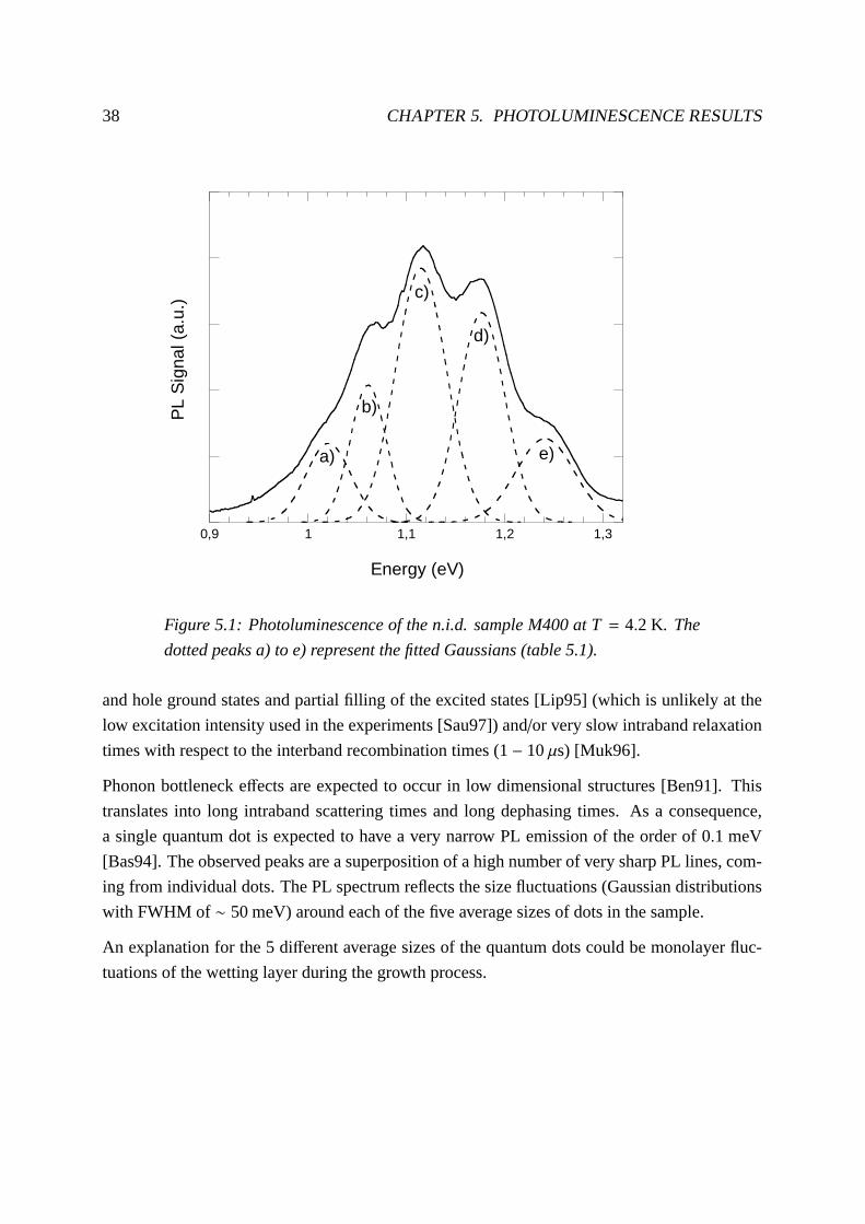
38 CHAPTER 5. PHOTOLUMINESCENCE RESULTS
0,9 1 1,1 1,2 1,3
PL
Sig
nal (
a.u.
)
a)
Energy (eV)
b)
c)
d)
e)
Figure 5.1: Photoluminescence of the n.i.d. sample M400 at T= 4.2 K. The
dotted peaks a) to e) represent the fitted Gaussians (table 5.1).
and hole ground states and partial filling of the excited states [Lip95] (which is unlikely at the
low excitation intensity used in the experiments [Sau97]) and/or very slow intraband relaxation
times with respect to the interband recombination times (1− 10µs) [Muk96].
Phonon bottleneck effects are expected to occur in low dimensional structures [Ben91]. This
translates into long intraband scattering times and long dephasing times. As a consequence,
a single quantum dot is expected to have a very narrow PL emission of the order of 0.1 meV
[Bas94]. The observed peaks are a superposition of a high number of very sharp PL lines, com-
ing from individual dots. The PL spectrum reflects the size fluctuations (Gaussian distributions
with FWHM of ∼ 50 meV) around each of the five average sizes of dots in the sample.
An explanation for the 5 different average sizes of the quantum dots could be monolayer fluc-
tuations of the wetting layer during the growth process.

5.1. PHOTOLUMINESCENCE 39
Table 5.1: Positions of the gaussian peaks fitted in the PL spectrum of figure
5.1.
peak position (meV) FWHM (meV) rel. intensity
a) 1021 54 0.31
b) 1061 43 0.54
c) 1115 61 1.00
d) 1177 55 0.83
e) 1241 70 0.33
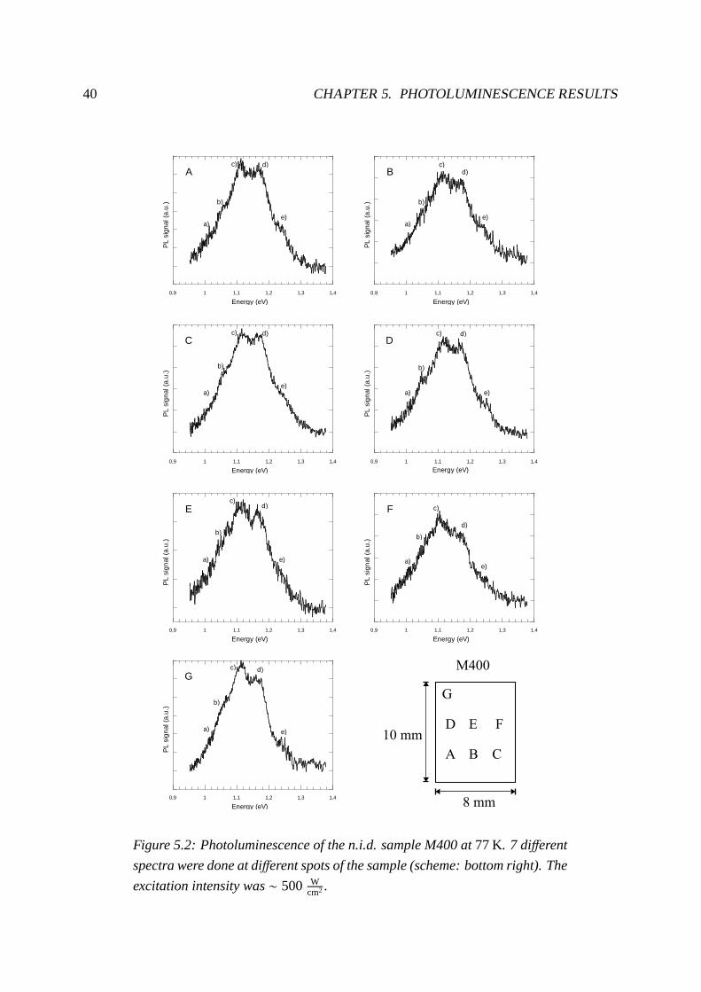
5.1.1 Uniformity of the sample
We have studied the size distribution of the quantum dots andthe uniformity of the sample by
carrying out PL spectra at different locations on the sample M400. The excitation intensity of
the Ar++ laser was∼ 500 Wcm2 and the sample was at a temperature ofT = 77 K. Figure 5.2
shows 7 different PL spectra taken at 7 distinct points (A-G) on the surface of the sample (with
a size of 8× 10 mm). The points are separated about 2 mm from each other. Itcan be seen
that the spectra are similar, but the relative intensities of the peaks change whereas their energy
positions do not. Since the experimental conditions are thesame for all of the spectra, the
differences between the spectra can only be explained by structural differences of the excited
quantum dots.
All the spectra show that the PL size distribution of the quantum dots consists of several Gaus-
sian like peaks, which are centered onpreferreddot sizes.
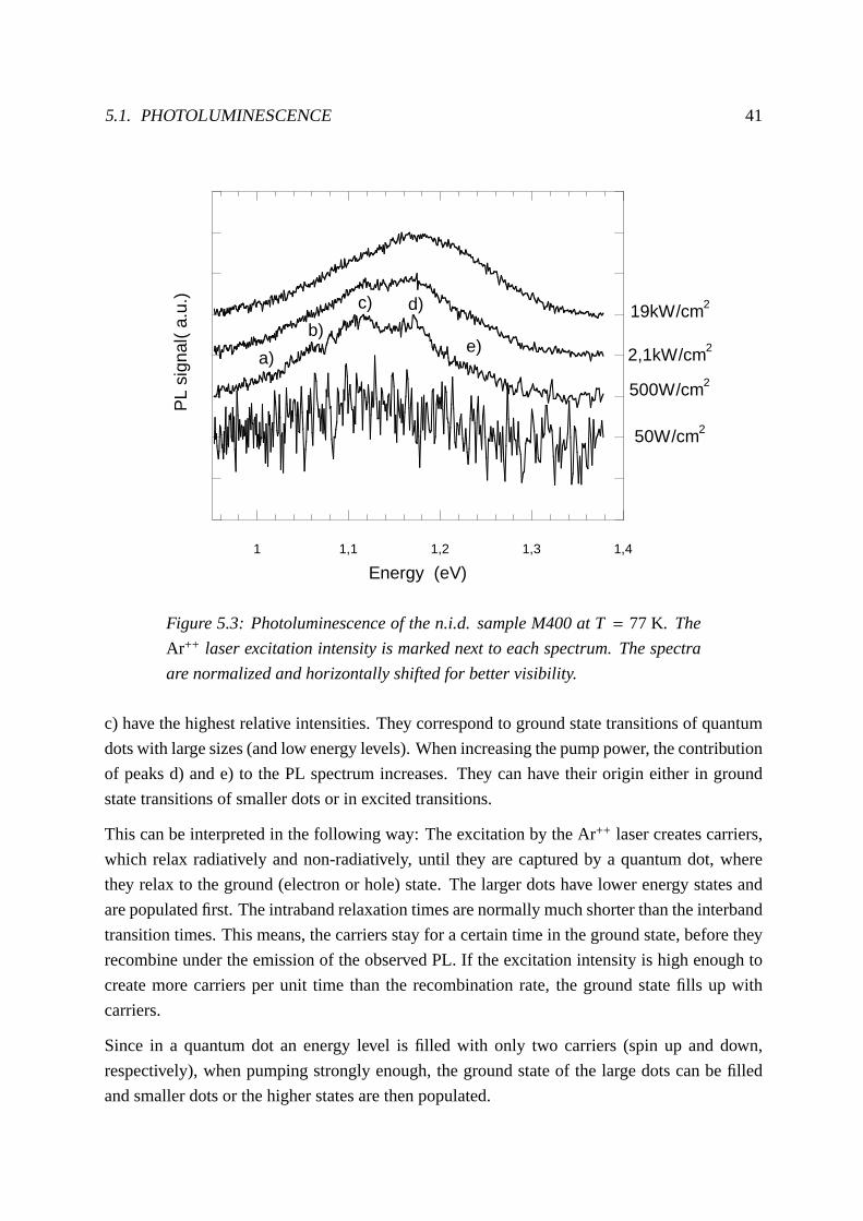
5.1.2 Influence of excitation power
The dependence on excitation intensities have also been measured.
Figure 5.3 shows four PL spectra of the sample M400. They wererecorded at a temperature of
77 K in the configuration shown in figure 4.1. The optical excitation was carried out by an Ar++
laser at a wavelength of 514 nm. The different laser intensities are indicated for each spectrum.
It can clearly be seen that for low excitation intensities the relative intensities of the low-energy
peaks in the spectrum are larger, while the relative intensities of the high-energy peaks increase
with pump power.
When looking at the spectrum with the lowest excitation energy in figure 5.3, peaks a), b) and
40 CHAPTER 5. PHOTOLUMINESCENCE RESULTS
0,9 1 1,1 1,2 1,3 1,4
PL
sig
nal
(a.
u.)
Energy (eV)
A
a)
b)
c)
e)
d)
0,9 1 1,1 1,2 1,3 1,4
PL
sig
nal
(a.
u.)
Energy (eV)
B
a)
b)
c)
e)
d)
0,9 1 1,1 1,2 1,3 1,4
PL
sig
nal
(a.
u.)
Energy (eV)
C
a)
b)
c)
e)
d)
0,9 1 1,1 1,2 1,3 1,4
PL
sig
nal
(a.
u.)
Energy (eV)
D
a)
b)
c)
e)
d)
0,9 1 1,1 1,2 1,3 1,4
PL
sig
nal
(a.
u.)
Energy (eV)
E
a)
b)
c)
e)
d)
0,9 1 1,1 1,2 1,3 1,4
PL
sig
nal
(a.
u.)
Energy (eV)
F
a)
b)
c)
e)
d)
0,9 1 1,1 1,2 1,3 1,4
PL
sig
nal
(a.
u.)
Energy (eV)
G
a)
b)
c)
e)
d)
Figure 5.2: Photoluminescence of the n.i.d. sample M400 at77 K. 7 different
spectra were done at different spots of the sample (scheme: bottom right). The
excitation intensity was∼ 500 Wcm2 .
5.1. PHOTOLUMINESCENCE 41
1 1,1 1,2 1,3 1,4
PL
sign
al(
a.u.
)
a)
50W/cm2
500W/cm2
2,1kW/cm2
19kW/cm2
Energy (eV)
b)
c) d)
e)
Figure 5.3: Photoluminescence of the n.i.d. sample M400 at T= 77 K. The
Ar++ laser excitation intensity is marked next to each spectrum.The spectra
are normalized and horizontally shifted for better visibility.
c) have the highest relative intensities. They correspond to ground state transitions of quantum
dots with large sizes (and low energy levels). When increasing the pump power, the contribution
of peaks d) and e) to the PL spectrum increases. They can have their origin either in ground
state transitions of smaller dots or in excited transitions.
This can be interpreted in the following way: The excitationby the Ar++ laser creates carriers,
which relax radiatively and non-radiatively, until they are captured by a quantum dot, where
they relax to the ground (electron or hole) state. The largerdots have lower energy states and
are populated first. The intraband relaxation times are normally much shorter than the interband
transition times. This means, the carriers stay for a certain time in the ground state, before they
recombine under the emission of the observed PL. If the excitation intensity is high enough to
create more carriers per unit time than the recombination rate, the ground state fills up with
carriers.
Since in a quantum dot an energy level is filled with only two carriers (spin up and down,
respectively), when pumping strongly enough, the ground state of the large dots can be filled
and smaller dots or the higher states are then populated.
42 CHAPTER 5. PHOTOLUMINESCENCE RESULTS
An other phenomenum may take place in quantum dots: the phonon bottleneck [Muk96, Boc90,
Ben91]. It is predicted by this theory that the discrete levels in quantum dots hinder carrier re-
laxation towards the ground state, because it is unlikely that phonon relaxation processes have
just the exact energy difference between the discrete energy levels. Thus phonon relaxation can
not take place. However, there are still debates about the possibility of rapid carrier relaxation
mediated by Auger processes [Boc92], multiphonon processes[Ino92] or electron-hole interac-
tion [Boc93]. Nevertheless, the phonon bottleneck effect would emphasize the observation of
excited transitions in the PL spectra, since the relative number of electrons in the excited states
would be increased.
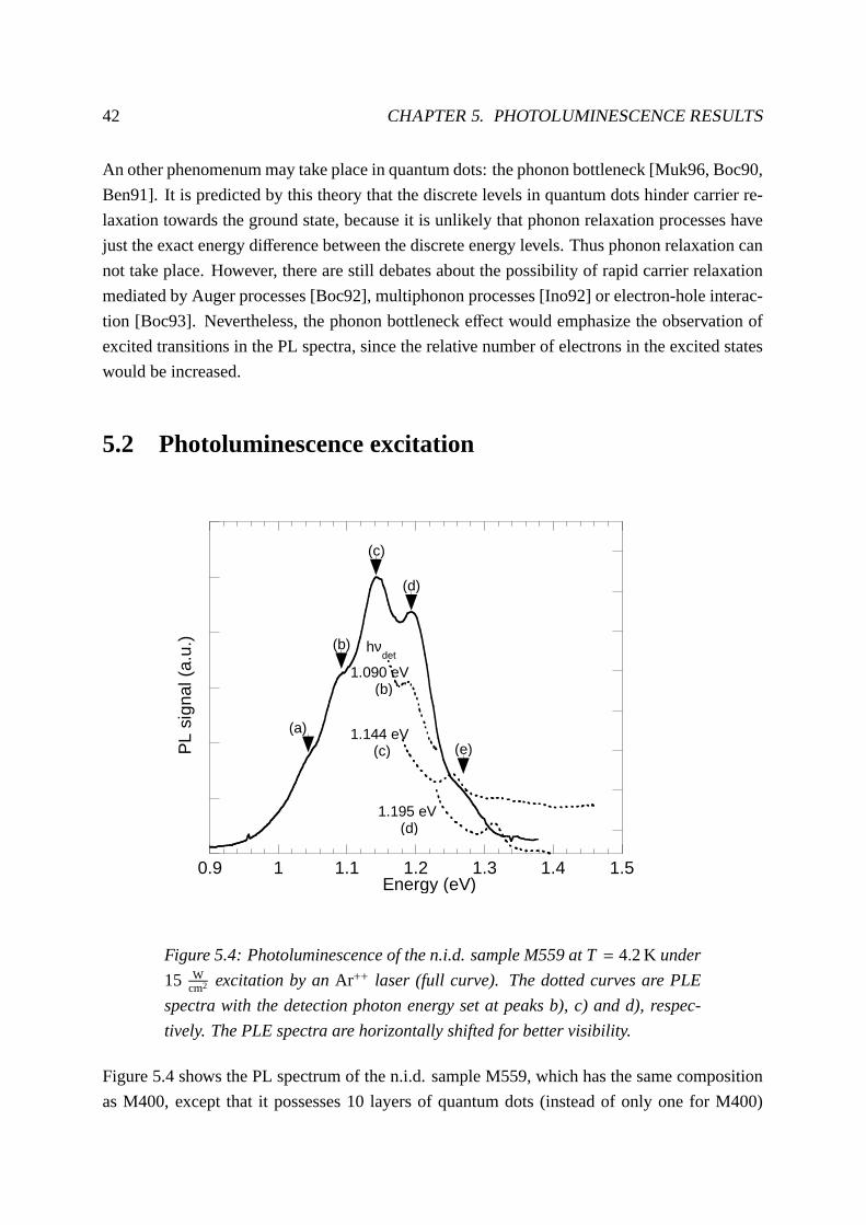
5.2 Photoluminescence excitation
0.9 1 1.1 1.2 1.3 1.4 1.5
PL
sign
al (
a.u.
)
Energy (eV)
hνdet
1.090 eV (b)
1.144 eV(c)
1.195 eV(d)
(a)
(b)
(c)
(d)
(e)
Figure 5.4: Photoluminescence of the n.i.d. sample M559 at T= 4.2 K under
15 Wcm2 excitation by anAr++ laser (full curve). The dotted curves are PLE
spectra with the detection photon energy set at peaks b), c) and d), respec-
tively. The PLE spectra are horizontally shifted for bettervisibility.
Figure 5.4 shows the PL spectrum of the n.i.d. sample M559, which has the same composition
as M400, except that it possesses 10 layers of quantum dots (instead of only one for M400)

5.3. CONCLUSION 43
to achieve higher PL intensities. In the same figure, three PLE spectra with detection photon
energy set at peaks b), c) and d), respectively, are shown. The sample was at a temperature of
4.2 K and the excitation intensity for the PL was 15Wcm2 .
The PL spectrum has the same characteristics as the spectrumof the sample M400 (figure 5.1).
However, the energy positions of the five fitted Gaussian peaks are slightly different, which is
probably due to growth condition differences between the two samples.
The PLE spectra of peaks b), c) and d) clearly show only one excited state absorption peak,
which is shifted to higher energies from the ground state luminescence by 101 meV, 109 meV
and 120 meV, respectively. These values reflect both the electron and the heavy-hole quantum
confinement. The smaller dots have larger energy shifts in agreement with equation (2.21).
PLE spectra of peaks a) and e) were also performed, but they did not clearly reveal any excited
states PL.
It is clear from the PLE results that peaks b), c) and d) arise from the ground state transition of
quantum dots with different sizes. It is also clear that excited states of dots c) and d) contribute
to peak e). This observation is in agreement with the PL evolution with excitation intensity.
5.3 Conclusion
The PL experiments show that
• quantum dots on the sample have different volumes.
• the quantum dot sizes have a distribution, which is composedof five Gaussians.
• when exciting with high intensities, the filling of the larger dots and transitions between
excited states can be observed at high energies.
The PLE experiments show that there is only one excited statefor each dot size and confirm that
there are preferred sizes of the quantum dots. However the high energy peak contains significant
contributions from excited states.
At this point, it would be interesting to compare calculations of the energy levels of the dots
with experimental data. Calculations for the new InAs/ In0.52Al0.48As system have not yet been
performed. Moreover, energy calculations are only valid ifthe exact shape of the dots is known,
which is not the case at the early stage of the research for this material system.
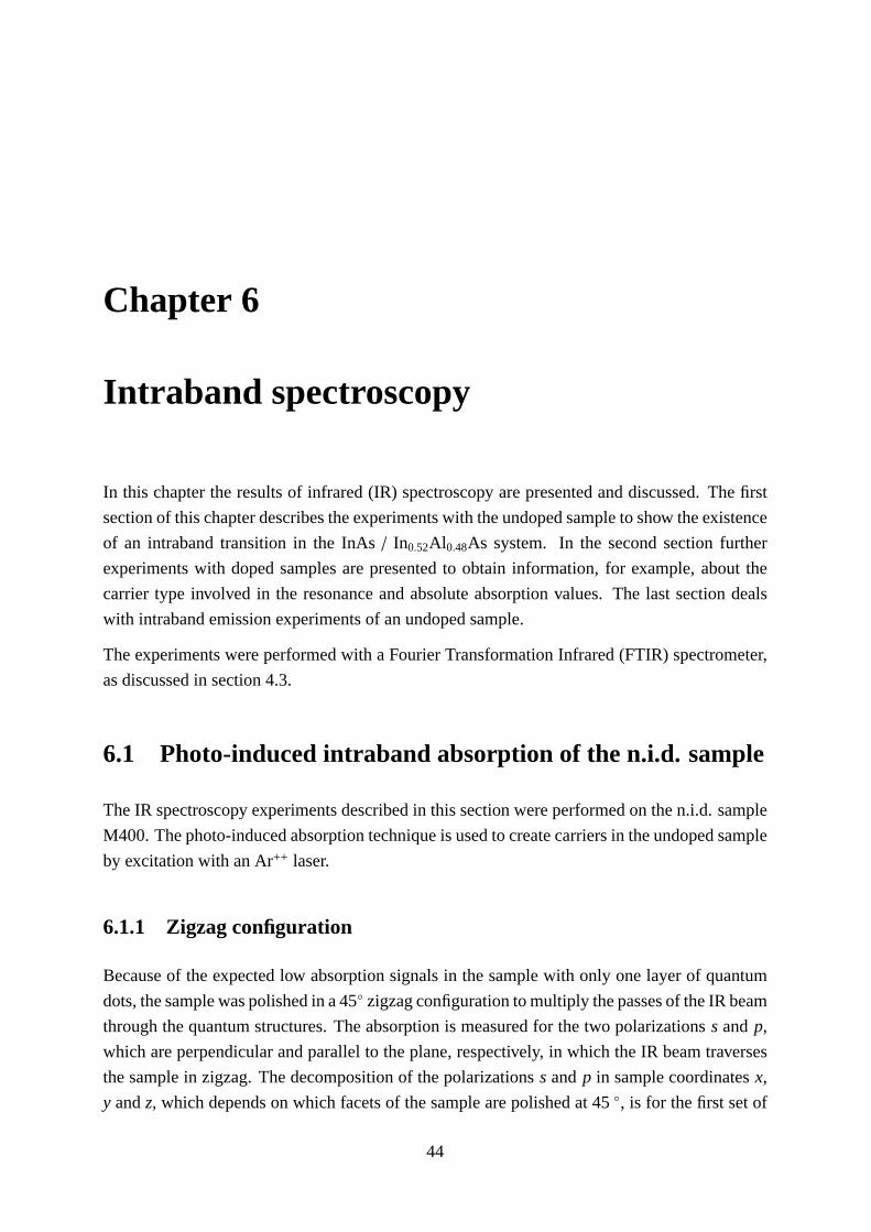
Chapter 6
Intraband spectroscopy
In this chapter the results of infrared (IR) spectroscopy arepresented and discussed. The first
section of this chapter describes the experiments with the undoped sample to show the existence
of an intraband transition in the InAs/ In0.52Al0.48As system. In the second section further
experiments with doped samples are presented to obtain information, for example, about the
carrier type involved in the resonance and absolute absorption values. The last section deals
with intraband emission experiments of an undoped sample.
The experiments were performed with a Fourier Transformation Infrared (FTIR) spectrometer,
as discussed in section 4.3.
6.1 Photo-induced intraband absorption of the n.i.d. sample
The IR spectroscopy experiments described in this section were performed on the n.i.d. sample
M400. The photo-induced absorption technique is used to create carriers in the undoped sample
by excitation with an Ar++ laser.
6.1.1 Zigzag configuration
Because of the expected low absorption signals in the sample with only one layer of quantum
dots, the sample was polished in a 45 zigzag configuration to multiply the passes of the IR beam
through the quantum structures. The absorption is measuredfor the two polarizationss andp,
which are perpendicular and parallel to the plane, respectively, in which the IR beam traverses
the sample in zigzag. The decomposition of the polarizations s andp in sample coordinatesx,
y andz, which depends on which facets of the sample are polished at 45 , is for the first set of
44

6.1. PHOTO-INDUCED INTRABAND ABSORPTION OF THE N.I.D. SAMPLE 45
experiments (figure 6.1):
s = sx = x,
p = pyz =12(y+ z).
(6.1)
This means, that theppolarization of the IR beam contains components of both the polarizations
y, which is parallel to the elongation direction of the dots, andz, which is parallel to the growth
axis of the sample. The length of the sample isl = 3 mm and its thickness isd = 0.3 mm. This
means that the IR beam passes the quantum dot layer about 10 times during its passage through
the sample (equation (4.5)).
Figure 6.1: Decomposition of the polarizations sx and pyz of the IR beam into
the sample directions x, y and z: sx = x and pyz =12(y+ z).
Figure 6.2 shows three photo-induced FTIR absorption spectra of the undoped sample M400
in zigzag configuration atT = 77 K for three different excitation intensities. In each graph the
two spectra for the polarizationssx andpyz are represented. In all three spectra an IR absorption
peak can be distinguished at an energy of 91 meV for thesx polarization. The FWHM of the
peak is about 15meV. In they andzpolarization no resonances can be found. At high excitation
intensities the width of the peak increases towards the highenergy side, which could be caused
by the population of smaller QDs with higher energy states.
At low energies (< 85 meV) all graphs show an increase of the absorption in both polarizations.
These peaks do not have their origin in infrared transitionsinside the sample, but they are
artifically created when the spectra are divided by their backgrounds. This can be explained as
follows when looking at a background spectrum.
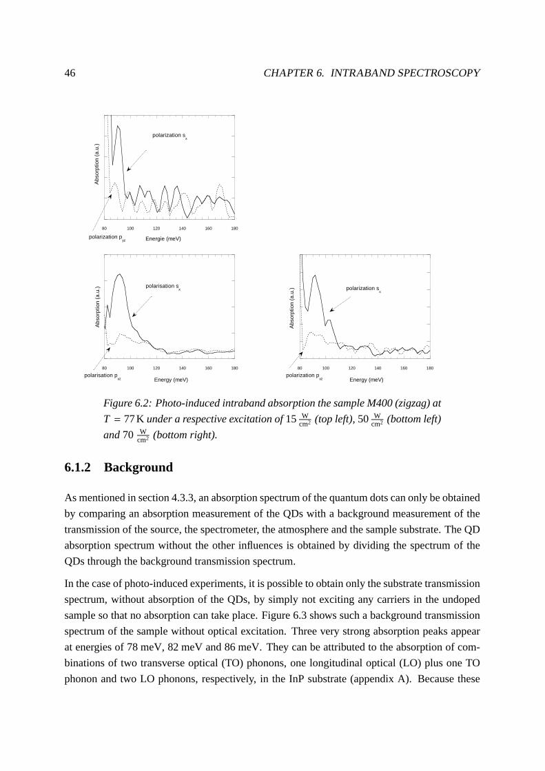
46 CHAPTER 6. INTRABAND SPECTROSCOPY
80 100 120 140 160 180
Abs
orpt
ion
(a.u
.)
Energie (meV)
polarization sx
polarization pyz
80 100 120 140 160 180
Abs
orpt
ion
(a.u
.)
Energy (meV)
polarisation sx
polarisation pyz
80 100 120 140 160 180
Abs
orpt
ion
(a.u
.)
Energy (meV)
polarization sx
polarization pyz
Figure 6.2: Photo-induced intraband absorption the sampleM400 (zigzag) at
T = 77K under a respective excitation of15 Wcm2 (top left),50 W
cm2 (bottom left)
and70 Wcm2 (bottom right).
6.1.2 Background
As mentioned in section 4.3.3, an absorption spectrum of thequantum dots can only be obtained
by comparing an absorption measurement of the QDs with a background measurement of the
transmission of the source, the spectrometer, the atmosphere and the sample substrate. The QD
absorption spectrum without the other influences is obtained by dividing the spectrum of the
QDs through the background transmission spectrum.
In the case of photo-induced experiments, it is possible to obtain only the substrate transmission
spectrum, without absorption of the QDs, by simply not exciting any carriers in the undoped
sample so that no absorption can take place. Figure 6.3 showssuch a background transmission
spectrum of the sample without optical excitation. Three very strong absorption peaks appear
at energies of 78 meV, 82 meV and 86 meV. They can be attributedto the absorption of com-
binations of two transverse optical (TO) phonons, one longitudinal optical (LO) plus one TO
phonon and two LO phonons, respectively, in the InP substrate (appendix A). Because these

6.1. PHOTO-INDUCED INTRABAND ABSORPTION OF THE N.I.D. SAMPLE 47
0
0,02
0,04
0,06
0,08
0,1
0,12
80 100 120 140 160
Tra
nsm
issi
on
Energy / meV
Figure 6.3: Infrared transmission of the sample M400 at T= 77 K in zigzag
configuration (background spectrum).
peaks absorb nearly all of the IR beam, the transmission intensity is nearly zero at the energies
of these phonon combinations. When the quantum dot absorption spectrum is divided through
the background spectrum, a division nearly by zero takes place at the InP phonon peak energies.
This is why at low energies artificial peaks appear in the IR absorption spectrum of the quantum
dots.
6.1.3 Confirmation of the absorption in different configurations
To confirm the existence of ax polarized intraband resonance, separate experiments werecar-
ried out with the sample’s other two opposite facets polished at 45 (figure 6.4). In this con-
figuration no absorption is expected ins = sy = y polarization, but a peak is expected in the
p = pxz =12(x + z) polarization. Figure 6.5 shows the photo-induced absorption spectrum of
the sample M400 in this configuration atT = 300 K. In pxz polarization the resonance can be
distinguished at 90 meV. The signal to noise ratio of the peakis not as good as in figure 6.2 for
the same experimental conditions, which can be explained bytwo reasons: (a) the absorption
from the ground state is less efficient atT = 300 K than atT = 77 K because there are fewer
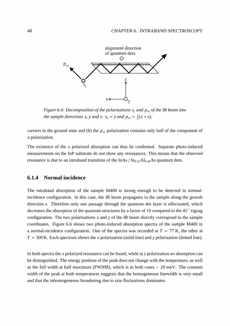
48 CHAPTER 6. INTRABAND SPECTROSCOPY
Figure 6.4: Decomposition of the polarizations sy and pxz of the IR beam into
the sample directions x, y and z: sy = y and pxz =12(x+ z).
carriers in the ground state and (b) thepxz polarization contains only half of the component of
x polarization.
The existence of thex polarized absorption can thus be confirmed. Separate photo-induced
measurements on the InP substrate do not show any resonances. This means that the observed
resonance is due to an intraband transition of the InAs/ In0.52Al0.48As quantum dots.
6.1.4 Normal incidence
The intraband absorption of the sample M400 is strong enoughto be detected in normal-
incidence configuration. In this case, the IR beam propagates in the sample along the growth
directionz. Therefore only one passage through the quantum dot layer iseffectuated, which
decreases the absorption of the quantum structures by a factor of 10 compared to the 45 zigzag
configuration. The two polarizationsx andy of the IR beam directly correspond to the sample
coordinates. Figure 6.6 shows two photo-induced absorption spectra of the sample M400 in
a normal-incidence configuration. One of the spectra was recorded atT = 77 K, the other at
T = 300 K. Each spectrum shows thex polarization (solid line) andy polarization (dotted line).
In both spectra thex polarized resonance can be found, while iny polarization no absorption can
be distinguished. The energy position of the peak does not change with the temperature, as well
as the full width at half maximum (FWHM), which is in both cases∼ 20 meV. The constant
width of the peak at both temperatures suggests that the homogeneous linewidth is very small
and that the inhomogeneous broadening due to size fluctuations dominates.
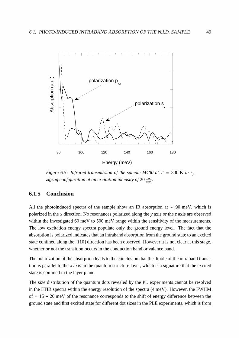
6.1. PHOTO-INDUCED INTRABAND ABSORPTION OF THE N.I.D. SAMPLE 49
80 100 120 140 160 180
Abs
orpt
ion
(a.u
.)
Energy (meV)
polarization sy
polarization pxz
Figure 6.5: Infrared transmission of the sample M400 at T= 300 K in sy
zigzag configuration at an excitation intensity of20 Wcm2 .
6.1.5 Conclusion
All the photoinduced spectra of the sample show an IR absorption at ∼ 90 meV, which is
polarized in thex direction. No resonances polarized along they axis or thezaxis are observed
within the investigated 60 meV to 500 meV range within the sensitivity of the measurements.
The low excitation energy spectra populate only the ground energy level. The fact that the
absorption is polarized indicates that an intraband absorption from the ground state to an excited
state confined along the [110] direction has been observed. However it is not clear at this stage,
whether or not the transition occurs in the conduction band or valence band.
The polarization of the absorption leads to the conclusion that the dipole of the intraband transi-
tion is parallel to thex axis in the quantum structure layer, which is a signature that the excited
state is confined in the layer plane.
The size distribution of the quantum dots revealed by the PL experiments cannot be resolved
in the FTIR spectra within the energy resolution of the spectra (4 meV). However, the FWHM
of ∼ 15− 20 meV of the resonance corresponds to the shift of energy difference between the
ground state and first excited state for different dot sizes in the PLE experiments, which is from

50 CHAPTER 6. INTRABAND SPECTROSCOPY
60 80 100 120 140 160 180
Abs
orpt
ion
(a.u
.)
Energy (meV)
polarization x
polarization y
60 80 100 120 140 160 180
Abs
orpt
ion
(a.u
.)
Energy (meV)
polarization x
polarization y
Figure 6.6: Photo-induced intraband absorption of the sample M400 in nor-
mal incidence configuration at T= 77 K (top) and T= 300 K (bottom). The
excitation intensity was10 Wcm2 .
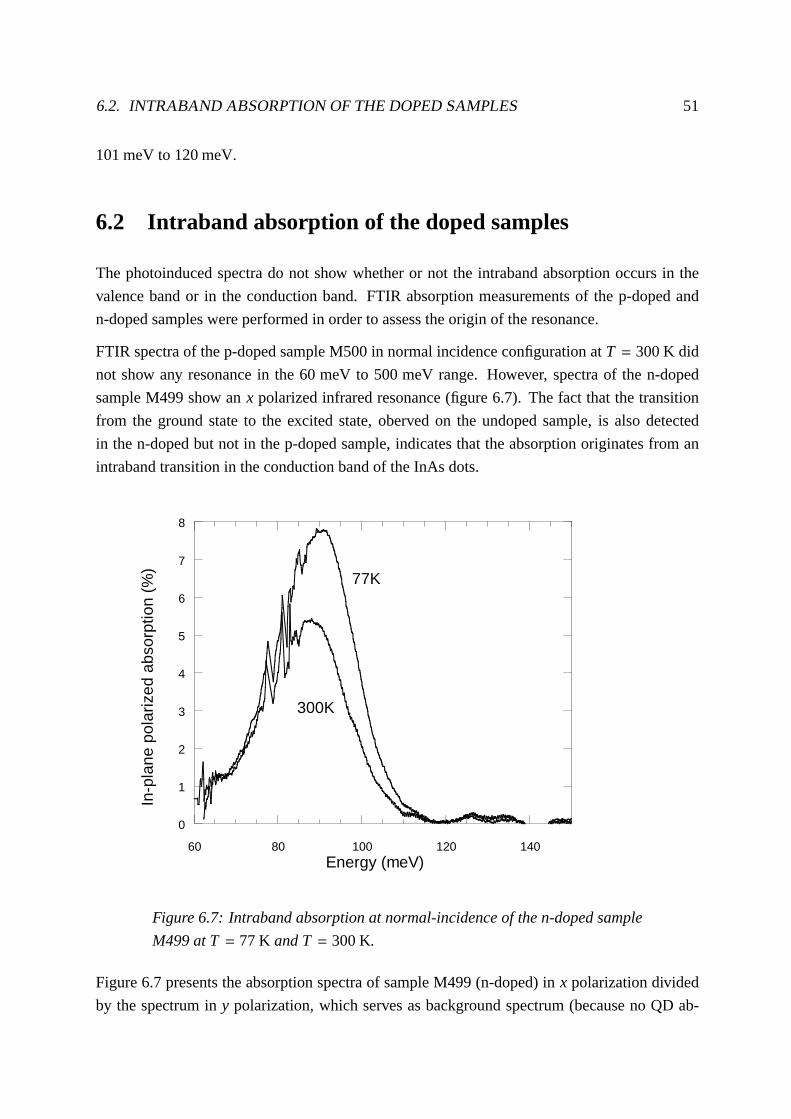
6.2. INTRABAND ABSORPTION OF THE DOPED SAMPLES 51
101 meV to 120 meV.
6.2 Intraband absorption of the doped samples
The photoinduced spectra do not show whether or not the intraband absorption occurs in the
valence band or in the conduction band. FTIR absorption measurements of the p-doped and
n-doped samples were performed in order to assess the originof the resonance.
FTIR spectra of the p-doped sample M500 in normal incidence configuration atT = 300 K did
not show any resonance in the 60 meV to 500 meV range. However,spectra of the n-doped
sample M499 show anx polarized infrared resonance (figure 6.7). The fact that thetransition
from the ground state to the excited state, oberved on the undoped sample, is also detected
in the n-doped but not in the p-doped sample, indicates that the absorption originates from an
intraband transition in the conduction band of the InAs dots.
0
1
2
3
4
5
6
7
8
60 80 100 120 140
In-p
lane
pol
ariz
ed a
bsor
ptio
n (%
)
Energy (meV)
300K
77K
Figure 6.7: Intraband absorption at normal-incidence of the n-doped sample
M499 at T= 77 K and T= 300 K.
Figure 6.7 presents the absorption spectra of sample M499 (n-doped) inx polarization divided
by the spectrum iny polarization, which serves as background spectrum (because no QD ab-

52 CHAPTER 6. INTRABAND SPECTROSCOPY
sorption takes place in this polarization, as shown by the photo-induced experiments). The
spectrum atT = 77 K shows an absorption peak at 91 meV. The absorption at maximum is of
the order of∆tt = 7.7 % (with t being the transmission of the sample). It should be emphasized
that this rather large value is achieved at normal incidencewith a sample containing only 10
layers of dots. The absorpion peak at room temperature is located at 88 meV and has a maxi-
mum absorption of∆tt = 5.3 %. The integrated intensity of the peak drops by 32 % from 77 K
to 300 K. The FWHM is 22± 0.5 meV at both temperatures. This confirms within our resolu-
tion that the linewidth of the absorption is temperature independent and therefore dominated by
inhomogeneous broadening due to a size distribution. The intraband resonance experiences a
slight red-shift of 3meV when the temperature is increased from 77K to 300K, which is typical
of intraband transitions [All88].
Assuming all impurities in the delta-doping layer are ionized and accounting for the measured
absorption and linewidth, the equivalent absorption cross-sectionσ at normal incidence for one
plane of InAs dots is deduced to be
σ =α
n≈
∆tt
n2DN≈ 1.5 · 10−14 cm2, (6.2)
whereα ≈ ∆ttL is the absorption coefficient,n = n2D
L the carrier density in the absorbing volume,
n2D the surface density of carriers (delta doping density),N the number of quantum dot layers
andL the thickness of the absorbing volume (which disappears in equation (6.2)).
The average dipole length〈x〉 associated with the intraband transition is estimated to be
〈x〉 = µe≈ 21.3 Å, (6.3)
where
µ =
√
Iε0c~nπEn2DN
(6.4)
is the intraband dipole moment.I is the integrated absorption intensity,ε0 the dielectric con-
stant,~ the Planck constant, ˜n the refractive index of the quantum dots andE the energy differ-
ence of the transition.
The oscillator strengthf is then estimated to be
f =2m0E~2〈x〉 ≈ 10.7, (6.5)
wherem0 is the free electron mass. This large value for the oscillator strength is comparable
to the value achieved for an intersubband transition in the conduction band of GaAs quantum
wells (f ≈ 14) [Wes85].
6.2. INTRABAND ABSORPTION OF THE DOPED SAMPLES 53
6.2.1 Influence of temperature
At this stage it is not clear if the type of confinement in the aligned and elongated dots is
that of a quantum wire or a quantum dot. Coupling between the dots could form a quantum
wire structure [Pry98]. An approach to test the confinement type is to estimate the population
difference between the upper and the ground state assuming either unidimensional subbands or
discrete energy levels.
As seen in section 2.3.4, quantum wires and quantum dots are described by different statistics.
A Fermi distribution is used for the first, while the latter isdescribed by the Gibbs distribution
in the grand canonical ensemble.
The numerical calculations were performed for both systems. For the quantum wires, the cal-
culated decrease of the absorption betweenT = 77 K andT = 300 K for an absorption between
two levels is 27 %, which is in excellent agreement with the experimental value of 32 %.
However, simulations with the Gibbs distribution for quantum dots can also give a close esti-
mate if one assumes that there are 5 energy levels and 7 electrons in a dot (this value is the
electron density divided by the average surface of a dot for the sample M499) and the observed
transition occurs between the ground state and the fourth excited level. The problem with these
calculations is, that on behalf of the two known energy levels (the ground state and an excited
state at∼ 90 meV) the energies of the other three supposed states are unknown. By changing
the energy position of these levels, a big range of absorption decrease can be covered.
A clear conclusion cannot be drawn from the performed simulations. However, it is convincing
that the simple simulation of the quantum wire with no adjustable parameters gives a very good
result.
6.2.2 Polarization-angle dependence
The previous experiments show, that the confinement direction of the excited state is along the
x axis, which is perpendicular to the direction of elongationof the dots. Because it has been
also shown that the dots present size fluctuations, it would be interesting to test, if fluctuations
of the confinement direction of the exited states can be foundas well.
Figure 6.8 shows the integrated absorption of the n-doped sample M499 atT = 300 K as a
function of the light polarization angleθ, with θ = 0 for light polarized along thex axis and
θ = 90 for y polarized light. A spectrum of the p-doped sample M500 with same thickness,
which has no infrared resonance, served in this case as the background spectrum. The evolution
is well fitted by a cos2(θ) law, as it would be expected for dipoles which are aligned parallel

54 CHAPTER 6. INTRABAND SPECTROSCOPY
0 20 40 60 80
Abs
orpt
ion
(a.u
.)
Angle of polarization (° )(x-polarized) (y-polarized)
Figure 6.8: Polarization-angle dependence of the integrated infrared absorp-
tion of the n-doped sample M499 at T= 300 K. The solid line is a calculated
cos2 θ curve.
to thex axis. It can be concluded that within the experimental precision of±15 the dots are
aligned in the same direction and no other confinement direction thanx can be found.
6.2.3 Influence of doping density
The question, if the confinement type in the elongated and aligned InAs dots is that of quantum
wires or quantum dots, has not been answered until this stage. Assuming the shape and density
of quantum dots measured by AFM, there should be an average number of 7 electrons in each
dot of sample M499 and 3.5 electrons in each dot of sample M586, based on their respective
doping densities. In the case of a quantum dot confinement onewould expect the intraband
absorption from the ground state to be the same for the samples M499 and M586 because the
ground state is already filled by 2 electrons with spin up and spin down.
Figure 6.9 shows the FTIR absorption spectra inx polarization for the two samples in normal
incidence configuration at room temperature. The respective spectra iny polarization served as
background. The maximum absorption of the sample M499 is∆tt = 5.3 % at 88 meV. Sample
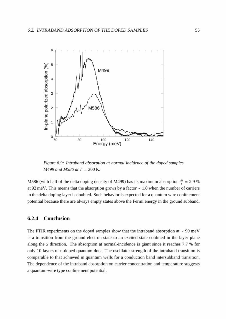
6.2. INTRABAND ABSORPTION OF THE DOPED SAMPLES 55
0
1
2
3
4
5
6
60 80 100 120 140
In-p
lane
pol
ariz
ed a
bsor
ptio
n (%
)
Energy (meV)
M499
M586
Figure 6.9: Intraband absorption at normal-incidence of the doped samples
M499 and M586 at T= 300 K.
M586 (with half of the delta doping density of M499) has its maximum absorption∆tt = 2.9 %
at 92 meV. This means that the absorption grows by a factor∼ 1.8 when the number of carriers
in the delta doping layer is doubled. Such behavior is expected for a quantum wire confinement
potential because there are always empty states above the Fermi energy in the ground subband.
6.2.4 Conclusion
The FTIR experiments on the doped samples show that the intraband absorption at∼ 90 meV
is a transition from the ground electron state to an excited state confined in the layer plane
along thex direction. The absorption at normal-incidence is giant since it reaches 7.7 % for
only 10 layers of n-doped quantum dots. The oscillator strength of the intraband transition is
comparable to that achieved in quantum wells for a conduction band intersubband transition.
The dependence of the intraband absorption on carrier concentration and temperature suggests
a quantum-wire type confinement potential.
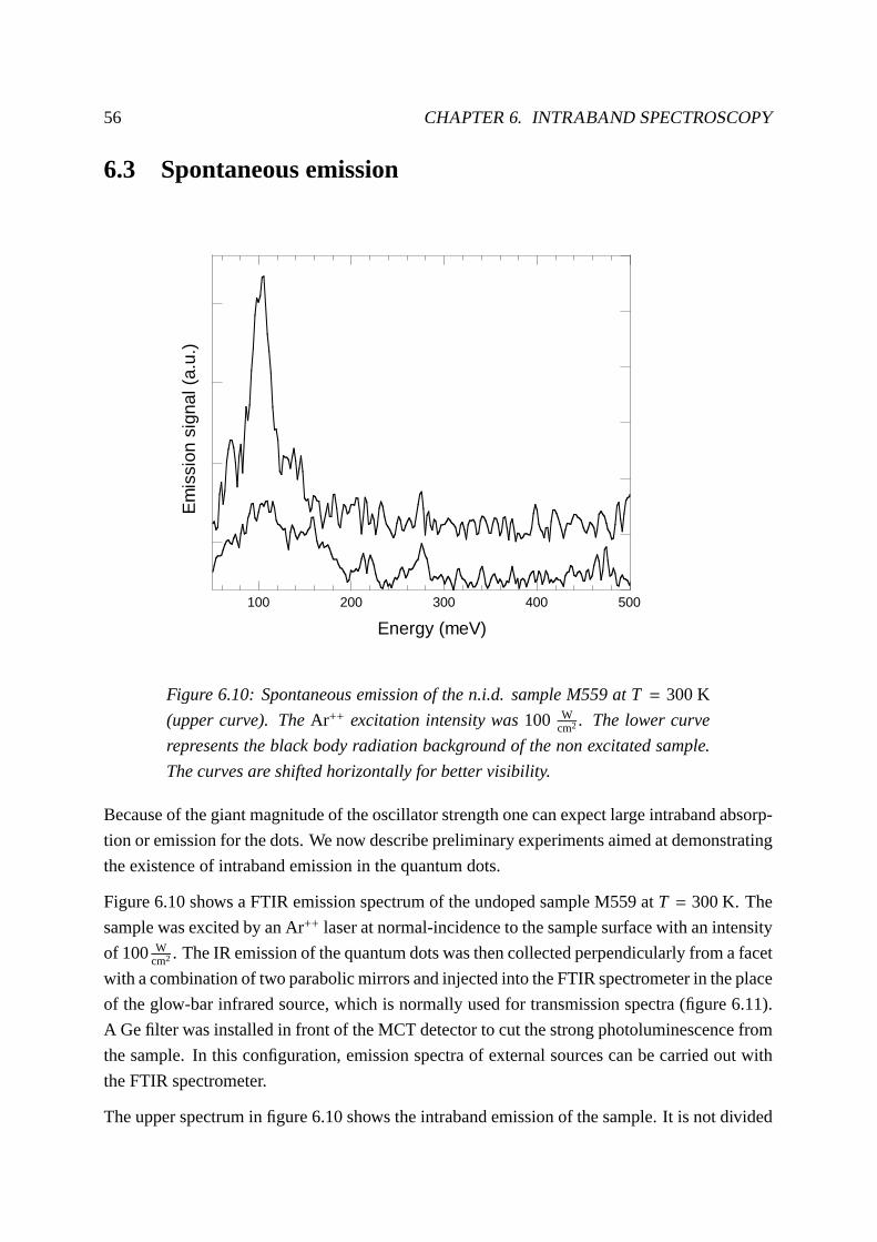
56 CHAPTER 6. INTRABAND SPECTROSCOPY
6.3 Spontaneous emission
100 200 300 400 500
Energy (meV)
Em
issi
on s
igna
l (a.
u.)
Figure 6.10: Spontaneous emission of the n.i.d. sample M559at T = 300 K
(upper curve). TheAr++ excitation intensity was100 Wcm2 . The lower curve
represents the black body radiation background of the non excitated sample.
The curves are shifted horizontally for better visibility.
Because of the giant magnitude of the oscillator strength onecan expect large intraband absorp-
tion or emission for the dots. We now describe preliminary experiments aimed at demonstrating
the existence of intraband emission in the quantum dots.
Figure 6.10 shows a FTIR emission spectrum of the undoped sample M559 atT = 300 K. The
sample was excited by an Ar++ laser at normal-incidence to the sample surface with an intensity
of 100 Wcm2 . The IR emission of the quantum dots was then collected perpendicularly from a facet
with a combination of two parabolic mirrors and injected into the FTIR spectrometer in the place
of the glow-bar infrared source, which is normally used for transmission spectra (figure 6.11).
A Ge filter was installed in front of the MCT detector to cut the strong photoluminescence from
the sample. In this configuration, emission spectra of external sources can be carried out with
the FTIR spectrometer.
The upper spectrum in figure 6.10 shows the intraband emission of the sample. It is not divided
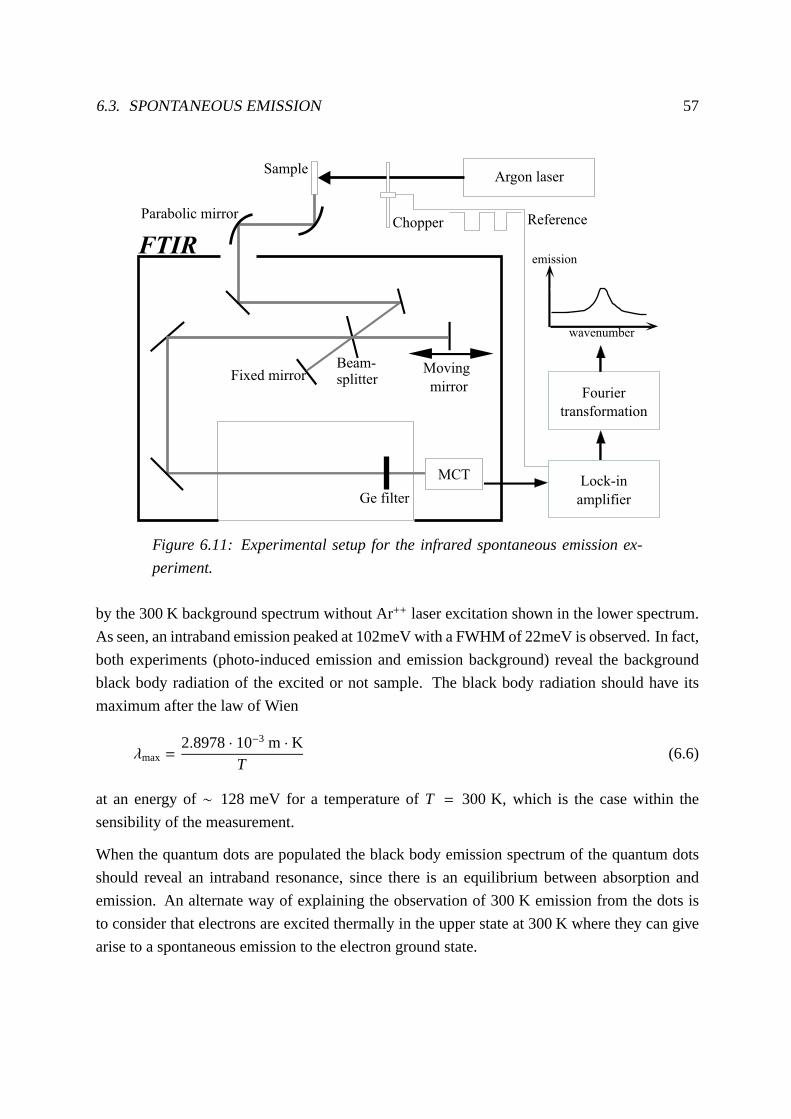
6.3. SPONTANEOUS EMISSION 57
Figure 6.11: Experimental setup for the infrared spontaneous emission ex-
periment.
by the 300 K background spectrum without Ar++ laser excitation shown in the lower spectrum.
As seen, an intraband emission peaked at 102meV with a FWHM of 22meV is observed. In fact,
both experiments (photo-induced emission and emission background) reveal the background
black body radiation of the excited or not sample. The black body radiation should have its
maximum after the law of Wien
λmax =2.8978· 10−3 m · K
T(6.6)
at an energy of∼ 128 meV for a temperature ofT = 300 K, which is the case within the
sensibility of the measurement.
When the quantum dots are populated the black body emission spectrum of the quantum dots
should reveal an intraband resonance, since there is an equilibrium between absorption and
emission. An alternate way of explaining the observation of300 K emission from the dots is
to consider that electrons are excited thermally in the upper state at 300 K where they can give
arise to a spontaneous emission to the electron ground state.

58 CHAPTER 6. INTRABAND SPECTROSCOPY
6.4 Conclusion
We have evidenced for the first time a giant intraband absorption in the InAs/ In0.52Al0.48As
quantum dots. The transition occurs from the ground state tothe first excited state confined in
the [110] direction in the conduction band. The oscillator strength of the intraband transition
is comparable to that achieved in quantum wells for a conduction band intersubband transition.
The dependence on carrier density shows the electron confinement type is that of a quantum
wire, at least for temperatures above 77 K. This can be explained by the coupling of the elon-
gated and aligned quantum dots in the [110] direction.
Finally, we have demonstrated for the first time that intraband spontaneous emission also does
occur.
The InAs / In0.52Al0.48As system may be of great interest for infrared photodetection applica-
tions because large absorption quantum efficiencies can be achieved at normal incidence. The
fact that intraband emission does occur is extremely promising for the further development of
unipolar lasers relying on intraband emission in quantum dots.
Chapter 7
Conclusion
During this Diplomarbeit, self-assemled InAs/ In0.52Al0.48As / InP quantum dots have been
characterized by atomic force microscopy (AFM), photoluminescene (PL), photoluminescence
excitation (PLE) and infrared spectroscopy.
The dots were grown in the Stranski-Krastanov growth mode. The AFM image shows that the
wetting layer is almost fully covered with InAs elongated islands of different sizes, which are
aligned in the [110] direction. The average size of the dots is 50 nm along [110] and 25 nm
along [110] with an average height of only 1.5 nm.
PL spectroscopy confirmes, that the sample contains dots of different volumes. The size dis-
tribution of the quantum dots shows fivepreferreddot sizes, each represented by a Gaussian
distribution. The origin of thepreferredsizes could be monolayer fluctuations of the wetting
layer during the growth process. High exciting energies show the filling of larger dots and
transitions between excited states.
PLE spectra show, that there is only one excited state for each dot size.
Infrared spectroscopy with a Fourier transform infrared (FTIR) spectrometer evidences, for the
first time in the InAs/ In0.52Al0.48As / InP system, a strong normal-incidence absorption in the
quantum dots. The absorption at∼ 90 meV is found to be a transition from the ground electron
state to the first excited state confined in the layer plane along the [110] axis. The absorption
at normal-incidence reaches 7.7 % for only 10 layers of quantum dots. The oscillator strength
is giant and comparable to that of intersubband transitionsin quantum wells. The dependence
of the intraband absorption on carrier concentration and temperature suggests a quantum wire
type confinement potential, which could be formed by coupling of the aligned quantum dots.
Preliminary emission spectroscopy experiments have also been carried out. They reveal the
existence of the intraband spontaneous emission from the first excited state to the ground state
59

60 CHAPTER 7. CONCLUSION
in the conduction band.
However, there are still many open questions. Detailed numerical simulations accounting for
size and shape of the quantum structure have to be performed to be able to compare experimental
data with these simulations.
To confirm whether or not the phonon bottleneck effect takes place in this quantum structure,
intraband relaxation time measurements have to be carried out. This could be done either by
spatial resolved spectroscopy, where the linewidth of single dots is measured, or by time re-
solved infrared absorption measurements to directly measure the scattering times.
The normal-incidence intraband absorption of the InAs/ In0.52Al0.48As quantum dots is very
promising for the future construction of infrared photodetectors with this material system be-
cause of the strong oscillator strength of the absorption. The next experiments, which have
to be carried out for the development of photodetectors, arephotoconduction spectroscopy ex-
periments. This implies the growth of n-i-n structures containing multiple layers of n-doped
quantum dots, followed by mesa etched structures.
Because of the large oscillator strength associated with theintraband transition in the InAs/
In0.52Al0.48As system, strong infrared emission is possible. Further experiments will be aimed
at the demonstration of an intraband population inversion,which is the first step towards the
realization of unipolar lasers relying on quantum dots.

Appendix A
Material parameters
The most important material parameters for the InAs/ In0.52Al0.48As / InP system are [Cas84,
Fra94, Gen97, Bas95]:
InAs In0.52Al0.48As InP
lattice constanta 6.05 Å 5.87 Å 5.87 Å
Energy gapEg(300 K) 0.354 eV 1.415 eV 1.344 eV
Energy gapEg(0 K) 0.417 eV 1.520 eV 1.424 eV
Effective massm∗e 0.027m0 0.084m0
Effective massm∗hh 0.6 m0 0.68m0
Effective massm∗lh 0.027m0 0.086m0
Elastic constantc11 8.33 · 106 Ncm2
Elastic constantc12 4.53 · 106 Ncm2
Elastic constantc44 3.99 · 106 Ncm2
Conduction band deformation potentiala −5.9 · 105 eV·cm2
N
Valence band deformation potentialb −1.8 · 105 eV·cm2
N
Refractive index ˜n at Eg ∼ 3.52 ∼ 3.36 3.450
The energy band discontinuity atT = 300 K between strained InAs and In0.52Al0.48As is
[Gen97]:
∆Econduction = 0.63 eV,
∆Evalence = 0.43 eV.
61

62 APPENDIX A. MATERIAL PARAMETERS
The phonon energies of InP atT = 77 K are [Sti64]:
~ωTO = 38.5 meV,
~ωLO = 42.0 meV.

Bibliography
[Abs79] G. Abstreiter, K. Ploog,Phys. Rev. Lett.42, p. 1308 (1979). 1
[All88] P. von Allmen, M. Berz, G. Petrocelli, F.-K. Reinhart,G. Harbeke,Semicond. Sci.
Technol.3, p. 1211 (1988). 52
[Ara82] Y. Arakawa, H. Sakaki,Appl. Phys. Lett.40, p. 939 (1982). 14
[Ave91] D.V. Averin, A.N. Korotkov, K.K. Likharev,Phys. Rev. B44, p. 6199 (1991). 23
[Bas88] G. Bastard,Wave mechanics applied to semiconductor heterostructures, leseditions
de physique, France (1988). 16, 18, 19
[Bas94] G. Bastard,Phys. Rev. Lett.73, p. 716 (1994). 38
[Bas95] M. Bass,Handbook of Optics, 2. edition, Volume II (1995). 61
[Ben91] H. Benisty, C.M. Sotomayor-Torres, C. Weisbuch,Phys. Rev. B44, p. 10945 (1991).
38, 42
[Boc90] U. Bockelmann, G. Bastard,Phys. Rev. B42, p. 8947 (1990). 42
[Boc92] U. Bockelmann, T. Egeler,Phys. Rev. B46, p. 15574 (1992). 42
[Boc93] U. Bockelmann,Phys. Rev. B48, p. 17637 (1993). 42
[Bee91] C.W.J. Beenakker,Phys. Rev. B44, p. 1646 (1991). 23
[Bra98] J. Brault, M. Gendry, G. Grenet, G. Hollinger, Y. Desieres, T. Benyattou, to be pub-
lished (1998). 27
[Cas84] H.C. Casey, M.B. Panish,Heterostructure Lasers, Part B: Materials and Operating
Characteristics, Academic Press, United States (1984). 61
[Cha89] Y.C. Chang, R.B. James,Phys. Rev. B39, p. 12672 (1989). 20
63

64 BIBLIOGRAPHY
[Chu91] S.L. Chuang,Phys. Rev. B43, p. 9649 (1991). 9, 10
[Cus96] M.A. Cusack, P.R. Briddon, M. Jaros,Phys. Rev. B54, p. R2300 (1996). 11
[Cus97] M.A. Cusack, P.R. Briddon, M. Jaros,Phys. Rev. B56, p. 4047 (1997). 11
[Dre94] H. Drexler, D. Leonard, W. Hansen, J.P. Kotthaus andP.M. Petroff, Phys. Rev. Lett.
73, p. 2252 (1994). 32
[Fra94] C. Francis,These, Universite de Paris-Sud (1994). 9, 27, 61
[Gen97] M. Gendry,Data sheets of sample growth parameters, furnished with the samples
(1997). 26, 61
[Gru95] M. Grundmann, O.Stier, D. BimbergPhys. Rev. B52, p. 11969 (1995). 11, 12, 26
[Gru97] M. Grundmann, D. Bimberg,Phys. Bl.53, Nr. 6, p. 517 (1997). 25
[Iko89] Z. Ikonic, V. Milanovic, D. Tjapkin,Solid State Comm.72, p. 835 (1989). 22
[Ino92] T. Inoshita, H. Sakaki,Phys. Rev. B46, p. 7620 (1992). 42
[Jul91] F.H. Julien, P. Vagos, J.-M. Lourtioz, D.D. Yang, R. Planel,Appl. Phys. Lett.59, p.
2645 (1991). 32
[Kam74] A. Kamgar, P. Kneschaurek, G. Dorda, J.F. Koch,Phys. Rev. Lett.32, p. 1251 (1974).
1
[Kan75] E.O. Kane,J. Phys. Chem. Solids1, p. 249 (1975). 8
[Khu92] J. Khurgin,Appl. Phys. Lett.62, p. 1390 (1992). 21
[Lip95] H. Lipsanen, M. Sopanen, J. Ahopelto,Phys. Rev. B51, p. 13868 (1995). 38
[Mar94] J.-Y. Marzin, G. Bastard,Solid State Commun.92, p. 437 (1994). 11
[Mou96] Z. Moussa,These, Universite de Paris-Sud (1996). 16
[Muk96] K. Mukai, N. Ohtsuka, H. Shoji, M. Sugawara,Appl. Phys. Lett.68, p. 3013 (1996).
38, 42
[Nak87] K. Nakashima, Y. Kawaguchi, Y. Kawamura, H. Asahi, Y. Imamura,Japn. J. Appl.
Phys.26, p. L1620 (1987). 27
[Pin79] A. Pinczuk, H.L. Stormer, R. Dingle, J.M. Worlock, W. Wiegmann, A.C. Gossard,
Solid State Commun.32, p. 1001 (1979). 1

BIBLIOGRAPHY 65
[Pry98] C. Pryor,Phys. Rev. Lett.80, p. 3579 (1998). 53
[Sau97] S. Sauvage, P. Boucaud, F.H. Julien, J.M. Gerard and J.-Y. Marzin,J. Appl. Phys.82,
p. 3392 (1997). 2, 32, 38
[Sti64] D.L. Stierwalt, R.F. Potter,Physics of semiconductors: proceedings of the 7th inter-
national conference, Dunod, Paris, p.1073 (1964). 62
[Vag94] P. Vagos,These, Universite de Paris-Sud (1994). 8
[Wes85] L.C. West, S.J. Eglash,Appl. Phys. Lett.46, p. 1156 (1985). 1, 52
[Wu96] L. Wu,These, Universite de Paris-Sud (1996). 33
[Yan91] D. Yang,These, Universite de Paris-Sud (1991). 21
[Zun98] A. Zunger,MRS BulletinVol. 23 No. 2, p. 35 (1998). 11, 13

66 BIBLIOGRAPHY

Acknowledgements
I would like to thank all the persons who supported me during this Diplomarbeit:
• Dr. Francois H. Julien for giving me the great opportunity to work in his group at the IEF
and for his always available support and care of me.
• Prof. Dr. A. Forchel for making this external Diplomarbeit possible and for helping me
whenever I asked.
• Olivier Gauthier-Lafaye for many discussions, explanations and help whenever needed.
• Dr. J.M. Lourtioz for welcoming me in CROQ.
• Stephane Cabaret for always quickly finding the right solution for all mechanical and
electrical problems.
• All the other staff and Ph.D. students in CROQ for always supporting me and for our
fruitful discussions during coffee breaks.
• Dr. M. Gendry for extensive collaboration as well as growingthe samples and making
the AFM images.
• Dr. T. Benyattou for carrying out the PLE and some high resolution PL spectra.
67

68

Erkl arung
Hiermit erklare ich, daß ich die vorliegende Arbeit selbstandig verfaßt und keine anderen als
die angegebenen Quellen und Hilfsmittel benutzt habe.
Wurzburg, den 14. August 1998,
Alexander Weber
69


![Softwareproduktlinien-Entwicklung – Domain Engineering ...berger/Diplomarbeit.pdf · kleinen und mittelgroßen Unternehmen verfügbar sind [Kn00, VK05], ist mittlerweile noch keine](https://static.fdokument.com/doc/165x107/5f10906c7e708231d449bac4/softwareproduktlinien-entwicklung-a-domain-engineering-bergerdiplomarbeitpdf.jpg)