Electrical Characterisation of Poly(vinyl alcohol) based ... · iii ACKNOWLEDGEMENT First and...
88
Johannes Kepler Universität Linz, Altenberger Straße 69, 4040 Linz, Österreich, www.jku.at, DVR 0093696 Electrical Characterisation of Poly(vinyl alcohol) based Organic Field Effect Transistors Dissertation zur Erlangung des akademischen Grades Doktor der technischen Wissenschaften Angefertigt am Institut für Physikalische Chemie Eingereicht von: Dipl.-Ing. Martin Egginger Betreuung: o. Univ. Prof. Dr. Mag. Niyazi Serdar Sariciftci Beurteilung: Erstbeurteiler: o. Univ. Prof. Dr. Mag. Niyazi Serdar Sariciftci Zweitbeurteiler: o. Univ. Prof. Dr. Siegfried Bauer Linz, Mai 2009
Transcript of Electrical Characterisation of Poly(vinyl alcohol) based ... · iii ACKNOWLEDGEMENT First and...

Johannes Kepler Universität Linz, Altenberger Straße 69, 4040 Linz, Österreich, www.jku.at, DVR 0093696
Electrical Characterisation of Poly(vinyl alcohol) based
Organic Field Effect Transistors
Dissertation zur Erlangung des akademischen Grades
Doktor der technischen Wissenschaften
Angefertigt am Institut für Physikalische Chemie
Eingereicht von:
Dipl.-Ing. Martin Egginger
Betreuung:
o. Univ. Prof. Dr. Mag. Niyazi Serdar Sariciftci
Beurteilung:
Erstbeurteiler: o. Univ. Prof. Dr. Mag. Niyazi Serdar Sariciftci
Zweitbeurteiler: o. Univ. Prof. Dr. Siegfried Bauer
Linz, Mai 2009

für July
in inniger Liebe

iii
ACKNOWLEDGEMENT
First and foremost I want to thank Professor Niyazi Serdar Sariciftci who enabled and supervised this
dissertation.
I am also very grateful to Professor Siegfried Bauer for his supervision, his ideas and his humour. Thanks to all
members of the SoMaP group, especially Reinhard Schwödiauer and Mihai Irimia-Vladu for the good
collaboration and Francisco Camacho-Gonzales and Johann Leonhartsberger who helped me foaming some
polymers.
I want to thank my “Physics-Primer” Robert Köppe for endless discussions, Philipp Stadler for always critically
questioning my theories and Helmut Neugebauer, whos comments are always dead-on.
Special thanks go to Gilles Dennler, Anita Fuchsbauer, Christoph Lungenschmied, Nenad Marjanovic,
Beatriz Meana Esteban and Barbara Stadlober for all the fruitful discussions and to Serpil Tekoglu and Johanna
Novacek who contributed some OFET measurements during their visits at LIOS.
I want to show my apprecitation to the most important people of the institute: Petra Neumaier and Birgit Paulik
who smoothen all administrative waves in the secretariat, Manfred Lipp for excellent technical assistance and
Gerda Kalab who is taking care of the LIOS labs.
Andreas Tanda from plastic electronic is thanked for the good collaboration and Alberto Montaigne Ramil for
providing AFM images.
X-ray measurements were done in Graz by Heinz-Georg Flesch from Roland Resel’s group: many thanks!
Markus Himmelsbach and Wolfgang Buchberger are acknowledged for helping me with the AAS measurements.
Robert Fuss (Kuraray Specialities Europe KSE GmbH, Germany) is thanked for providing PVA.
Enn Mellikov, Dieter Meissner und Tiit Varema enabled my visit at the Tallinn University of Technology.
I want to express my gratitude to the people that nowadays share their office with me and that work together
with me in the quickly growing CO2 project: Ercan Avci, Martin Kruijen, Edina Mujcinovic, Kerstin Oppelt,
Engelbert Portenkirchner and Peter Trefflinger. I want to thank all the other members of LIOS (some of them left
already) for the good collaboration: Elif Arici-Bogner, Erika Bradt, Daniel Egbe, Pinar Frank,
Jacek Gasiorowski, Serap Gunes, Wolfgang Huber, Sandro Lattante, Shengli Lu, Gebi Matt, Farideh Meghdadi,
Le Huong Nguyen, Almantas Pivrikas, Hans Jürgen Prall, Adem Sahin, Stefan Schaur, Birendra Singh,
Andreas Spiegel, Patchanita Thamyongkit and especially everybody who is not on this list, but should be there!
Last but not least I want to thank my family for all their support, especially July for her love and her patience
when I was in the labs till late at nights.
domo arigato gozaimasu
iv
ZUSAMMENFASSUNG
Eine Vielzahl an wissenschaftlichen Erkenntnissen und technologischen Fortschritten bei der
Herstellung und Charakterisierung organischer Feldeffekt-Transistoren (OFETs) während den
letzten zwei Jahrzehnten hat es ermöglicht, dass erste Produkte mit organischer Elektronik am
Markt sind. Gedruckte organische Elektronik umfasst Widerstände, Dioden und Transistoren
und kann eine billige Alternative zu Silizium-basierten Systemen sein, im Speziellen bei
großflächigen und flexiblen Anwendungen.
Neben der Langzeitstabilität ist eine gute Reproduzierbarkeit der Strom-Spannungs (I-V)
Kennlinien ein essentieller Parameter für die Verwendung dieser Bauteile. Diese I-V
Kennlinien können eine Hysterese zeigen, was bei OFETs sehr häufig beim Messen einer
Transfer Charakteristik [einer Variation der Gatespannung (VGS)] beobachtet wird. Es gibt
vielfältige physikalische Gründe, die eine derartige Hysterese verursachen können, aber
vergleichende wissenschaftliche Untersuchungen zu den unterschiedlichen Hysterese
Phänomenen sind rar und ein umfassendes Bild der „Hysterese in OFETs“ fehlt in der
Literatur.
Das erste Kapitel dieser Dissertation gibt einen ausführlichen Überblick zu verschiedensten
physikalischen Effekten, die Hysterese verursachen können und exemplarische Beispiele aus
der Literatur werden diskutiert.
Detaillierte experimentelle Untersuchungen an OFETs, die Poly(vinyl alkohol) (PVA) als
Dielektrikum verwenden, zeigen, wie die - aus der Literatur bekannte - Hysterese in diesen
Bauteilen durch einen einstufigen Reinigungsschritt des PVAs minimiert werden kann.
Temperaturabhängige Messungen, dielektrische Spektroskopie und Röntgen-Messungen
vervollständigen das Bild der Hysterese in PVA basierten OFETs.
Die unterschiedlichen Bauweisen hysterese-freier OFETs werden im letzten Kapitel
untersucht und verglichen: top gate versus bottom gate und coplanar versus staggered. Im
Rahmen dieser Untersuchungen wurden erstmals top gate OFETs, die PVA, das aus wässriger
Lösung auf den organischen Halbleiter aufgetragen wird, verwenden, hergestellt und
charakterisiert.

v
ABSTRACT
Research on Organic Field Effect Transistors (OFETs) has made significant advances both
scientifically and technologically during the last decade with first products soon entering the
market. Printed electronic circuits using organic resistors, diodes and transistors may become
cheap alternatives to silicon based systems, especially in large area and flexible applications.
A key parameter for device operation is, besides long term stability, the reproducibility in the
current-voltage behaviour, which may be affected by hysteresis phenomena. Hysteresis
effects are often observed in organic transistors during sweeps of the gate voltage (VGS). The
origin of such hysteresis can be manifold, but comparative scientific investigations are rare
and a comprehensive picture of “hysteresis phenomena” in OFETs is still missing.
The first section of this thesis gives a detailed overview on physical effects that can cause
hysteresis and comparatively discusses the importance of such effects in OFETs.
Detailed experimental investigations on hysteresis in poly(vinyl alcohol) (PVA) based OFETs
show how hysteresis in these devices can be minimized by a one step cleaning procedure.
Temperature dependent measurements, dielectric spectroscopy and x-ray measurements
complete the picture of hysteresis in PVA based OFETs.
Finally hysteresis free OFETs are used to investigate various OFET structures: top gate or
bottom gate and coplanar or staggered, respectively. This is the first report on top gate OFETs
using PVA (deposited from aqueous solution) as dielectric.

vi
TABLE OF CONTENTS
1 INTRODUCTION.............................................................................................................. 1
1.1. OFET Basics .............................................................................................................. 3
1.2. Hysteresis ................................................................................................................. 10
1.2.1. Examples from Inorganic Transistors .............................................................. 10
1.2.2. Hysteresis in OFETs......................................................................................... 11
1.2.3. Hysteresis mechanisms .................................................................................... 15
1.3. Dielectric Spectroscopy............................................................................................ 29
2 EXPERIMENTAL ........................................................................................................... 35
2.1. Materials................................................................................................................... 35
2.1.1. Poly(vinyl alcohol) ........................................................................................... 35
2.1.2. Organic Semiconductors .................................................................................. 38
2.2. Device Preparation ................................................................................................... 38
2.3. Current voltage measurements ................................................................................. 39
2.4. Dielectric spectroscopy ............................................................................................ 40
2.5. AFM measurements ................................................................................................. 40
2.6. X-ray measurements................................................................................................. 41
3 RESULTS and DISCUSSION ......................................................................................... 42
3.1. Hysteresis in PVA based OFETs ............................................................................. 42
3.1.1. Ions in PVA...................................................................................................... 42
3.1.2. Temperature dependent hysteresis ................................................................... 50
3.1.3. PVA crystallinity.............................................................................................. 53
3.2. Device geometry ...................................................................................................... 58
3.2.1. Staggered versus Coplanar Geometries............................................................ 58
3.2.2. Top Gate OFETs .............................................................................................. 63
4 SUMMARY and CONCLUSION.................................................................................... 67
5 REFERENCES / BIBLIOGRAPHY................................................................................ 70
CURRICULUM VITAE .............................................................................................................I
Eidesstattliche Erklärung.......................................................................................................... IV

1
1 INTRODUCTION
The first thin-film transistor (TFT) was reported in 1962 by Paul K. Weimer [1]. Twenty
years later the first reports on organic field effect transistors (OFETs) using organic
semiconductors on inorganic dielectrics appeared [2, 3, 4]. Pioneering work towards all-
organic OFETs testing various organic dielectrics was done by Peng and coworkers [5].
Various examples for the applications of OFETs, e.g. large area electronic applications,
printed electronics, electronic paper (e-paper) [6], electronic skin, etc. are documented in Ref.
[7]. For many applications, speed is no more a limiting issue, since up to 2 MHz operation has
been demonstrated in OFET circuits [8]. Companies presented printed logic circuits for RFID
tags [9], for a cell phone with an electrophoretic display, addressed by an active matrix OFET
backplane [10], and a backplane OFET array for e-paper [11].
The enormous interest in the field of OFETs [7, 12] is documented by various scientific
review articles on charge transport [13, 14], on semiconductors for OFETs [15], on gate
dielectrics [16,17], on progress in plastic electronic devices [18] and on OFETs as sensors
[19, 20].
Although first products using OFET technology are already entering the market, a number of
issues still needs basic scientific investigations: Device stability is a very important topic,
closely related to hysteresis and threshold voltage shifts due to bias stress. Also some details
of the fundamental working principle of OFETs like gate voltage dependent contact
2
resistance, access resistance, mobility and others are still under discussion. These parameters
are closely related to device architecture and material processing.
In the following subsections of the introduction an overview on the basic parameters
describing an OFET is given, followed by a review on hysteresis in OFET literature. This
chapter is based on an invited review that has been published in Monatshefte der Chemie –
Chemical Monthly [21]. A short introduction to dielectric spectroscopy, a powerful tool to
investigate the electrical properties of dielectric materials, completes the introduction. After
the experimental section, detailed investigations on ions in poly(vinyl alcohol) and their
influence on OFET characteristics are presented. The results from that section show how
hysteresis free OFETs can be produced. Such OFETs are used in the last section to investigate
different OFET geometries and their influence on device parameters, before finishing with a
short summary and conclusions.

3
1.1. OFET Basics
An OFET is a three terminal device, where one electrode (the gate) is separated from the other
two electrodes (the source and the drain) by an insulating layer (the dielectric). The source
and the drain electrodes are connected via an organic (n- or p-type) semiconductor with a
defined geometry, the width W and the length L. The layers of the OFET are usually too thin
to form a stable freestanding device, therefore OFETs are built on a substrate (e.g. glass, Si
wafer or plastic foil). Depending on the layer deposition sequence, four different OFET
structures can be realized, as shown in Figure 1.
DE
SCS D
G
DE
SCS D
G
DE
SCS D
G
DE
SCS D
G(a)
(c)
(b)
(d)
Figure 1: Different structures of OFETs: (a) top gate staggered (top gate bottom
contacts), (b) top gate coplanar (top gate top contacts), (c) bottom gate
staggered (bottom gate top contacts) and (d) bottom gate coplanar (bottom
gate bottom contacts). Source (S), drain (D), gate (G), semiconductor (SC)
and dielectric (DE).
Two different nomenclatures are commonly used do describe the different OFET structures.
One nomenclature focuses on the layer sequence, e.g. bottom gate bottom contact, which
underscores the device production. The other nomenclature stresses the “active part” of the
OFET: “staggered” or “coplanar”. Important effects, e.g. “access resistance” or “current
crowding”, that will be described and discussed later, are emphasized by these names.
Current flows from the source electrode (S) to the drain electrode (D), upon applying a
voltage between S and D (VDS). This current can be influenced by a voltage applied to a third
electrode (gate). Applying a voltage to the gate (VGS) induces charges at the interface between
4
the dielectric and the semiconductor. The layer of accumulated charges at the semiconductor /
dielectric interface is called channel. This channel enables current flow between source and
drain (IDS). The conductive channel is formed in a few nm thin layer [22, 23, 24] at the
semiconductor / dielectric interface. FETs are characterized by measuring transfer (IDS versus
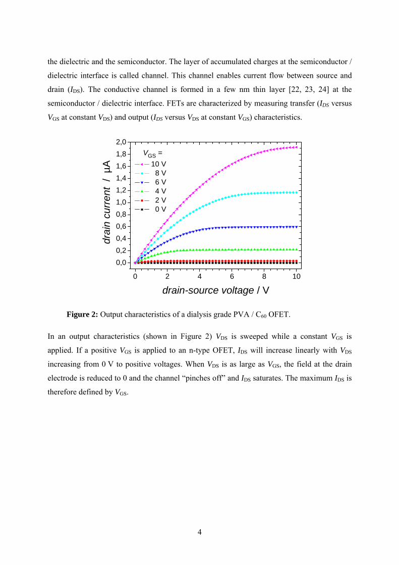
VGS at constant VDS) and output (IDS versus VDS at constant VGS) characteristics.
0 2 4 6 8 10
0,00,20,40,60,81,01,21,41,61,82,0
VGS = 10 V 8 V 6 V 4 V 2 V 0 V
drai
n cu
rren
t /
µA
drain-source voltage / V
Figure 2: Output characteristics of a dialysis grade PVA / C60 OFET.
In an output characteristics (shown in Figure 2) VDS is sweeped while a constant VGS is
applied. If a positive VGS is applied to an n-type OFET, IDS will increase linearly with VDS
increasing from 0 V to positive voltages. When VDS is as large as VGS, the field at the drain
electrode is reduced to 0 and the channel “pinches off” and IDS saturates. The maximum IDS is
therefore defined by VGS.
5
-15 -10 -5 0 5 10 1510-13
10-12
10-11
10-10
10-9
10-8
10-7
10-6
10-5
sweep 1 sweep 2 sweep 3 sweep 4 sweep 5
drai
n cu
rren
t / A
gate-source voltage / V
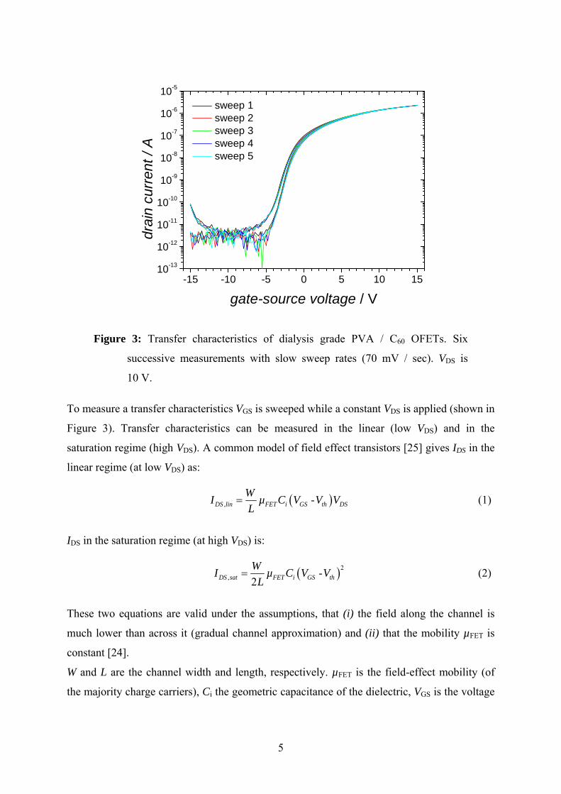
Figure 3: Transfer characteristics of dialysis grade PVA / C60 OFETs. Six
successive measurements with slow sweep rates (70 mV / sec). VDS is
10 V.
To measure a transfer characteristics VGS is sweeped while a constant VDS is applied (shown in
Figure 3). Transfer characteristics can be measured in the linear (low VDS) and in the
saturation regime (high VDS). A common model of field effect transistors [25] gives IDS in the
linear regime (at low VDS) as:
( ), -DS lin FET i GS th DSWI µ C V V VL
= (1)
IDS in the saturation regime (at high VDS) is:
( )2, -
2DS sat FET i GS thWI µ C V V
L= (2)
These two equations are valid under the assumptions, that (i) the field along the channel is
much lower than across it (gradual channel approximation) and (ii) that the mobility µFET is
constant [24].
W and L are the channel width and length, respectively. µFET is the field-effect mobility (of
the majority charge carriers), Ci the geometric capacitance of the dielectric, VGS is the voltage

6
applied to the gate, VDS is the voltage applied to the drain (both VGS and VDS are defined
versus the source potential, which is usually grounded) and Vth is the threshold voltage, as will
be explained later. The charge carrier mobility is calculated in either the saturation or in the
linear regime from the above equations. The differential /DS GSI V∂ ∂ is called the
transconductance. In an ideal device, the mobilities calculated in the linear and saturation
regime are the same and the mobility depends on the the charge carrier density which is
defined by the applied VGS. Also the contact resistance (RC) can influence the measured
mobility [26]. The mobility in the linear regime is less affected by VGS and RC, therefore
equation 1 is used in this work to determine the mobility, as is also done for MOSFETs [23].
The threshold voltage Vth can be extracted by determining the x-axis intercept of (IDS)1/2
versus VGS in the saturation regime [27], as shown in Figure 4, or by the maximum in a
second derivation of IDS versus VGS at low drain voltage [28]. Vth is the voltage where the
conducting channel is formed. In the accumulation mode Vth is given by [29]:
0th fb
i
qn dV VC
= ± + (3)
where Vfb is the flat-band potential which accounts for any work-function difference between
the semiconductor and the gate metal, q is the elementary charge, n0 is the density of free
carriers, and d is the thickness of the semiconductor. The sign of the right-hand side in the
equation corresponds to the sign of the charge carriers [29]. From this equation a change in
Vth between the forward and the reverse scan and thereby a hysteresis can be expected, if: (i)
n0 changes (e.g. due to trapping of free charge carriers), (ii) Ci changes (e.g. charge injection
from the gate into the dielectric or polarisation of the dielectric) and (iii) Vfb changes (e.g.
structural changes in the semiconductor).
The basic concept of an OFET is that of an electrical switch, that can turn a current on and
off. The ratio between these two currents (the on/off ratio) is a measure for the performance of
the OFET.
In general organic semiconductors are intrinsically nondoped and therefore non conducting
without an applied gate field (“normally off”). Field effect transistors using nondoped organic
semiconductors work in the accumulation mode (the gate field accumulates charges at the
semiconductor / dielectric interface that form the channel).
7
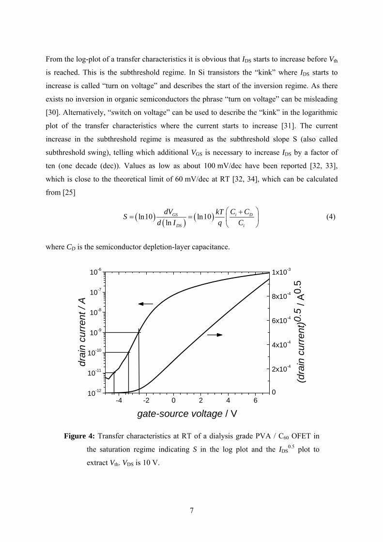
From the log-plot of a transfer characteristics it is obvious that IDS starts to increase before Vth
is reached. This is the subthreshold regime. In Si transistors the “kink” where IDS starts to
increase is called “turn on voltage” and describes the start of the inversion regime. As there
exists no inversion in organic semiconductors the phrase “turn on voltage” can be misleading
[30]. Alternatively, “switch on voltage” can be used to describe the “kink” in the logarithmic
plot of the transfer characteristics where the current starts to increase [31]. The current
increase in the subthreshold regime is measured as the subthreshold slope S (also called
subthreshold swing), telling which additional VGS is necessary to increase IDS by a factor of
ten (one decade (dec)). Values as low as about 100 mV/dec have been reported [32, 33],
which is close to the theoretical limit of 60 mV/dec at RT [32, 34], which can be calculated
from [25]
( ) ( ) ( )ln10 ln10ln
GS i D
DS i
dV C CkTSd I q C
⎛ ⎞+= = ⎜ ⎟
⎝ ⎠ (4)
where CD is the semiconductor depletion-layer capacitance.
-4 -2 0 2 4 610-12
10-11
10-10
10-9
10-8
10-7
10-6
0
2x10⁻⁴
4x10⁻⁴
6x10⁻⁴
8x10⁻⁴
1x10⁻³
drai
n cu
rren
t / A
gate-source voltage / V
(dra
in c
urre
nt)0
.5 /
A0.5
Figure 4: Transfer characteristics at RT of a dialysis grade PVA / C60 OFET in
the saturation regime indicating S in the log plot and the IDS0.5 plot to
extract Vth. VDS is 10 V.

8
The extraction of Vth and µFET is important, because a “good” OFET is defined having a low
Vth and a high µFET. A problem is that ohmic injecting and extracting contacts at source and
drain, respectively, are assumed. The overall device resistance Ron can be extracted from the
linear regime of the output characteristics as the conductance /DS DSI V∂ ∂ . Ron is the sum of
the resistances that influence IDS: charges are injected from the source (RS), traverse the
device (Rchannel) and are extracted at the drain (RD):
on S channel D C channelR R R R R R= + + = + (5)
Ohmic contacts are defined such that Rchannel >> RC [12]. Rchannel scales with L, meaning that a
short L causes a small Rchannel. Therefore short channel OFETs are often contact limited. This
is especially a problem for high speed OFETs, because the switching speed (the cut of
frequency) scales with 1/L2 [25, 34], making a short L necessary.
The reasons for non-ohmic contacts can be manifold [35]: Electrode surface contamination
can increase RC and there is a difference between organic-on-metal and metal-on-organic
interfaces. The resulting dipoles at the metal semiconductor interface can cause an increased
RC [12, 35] and several models are used that can describe such organic / metal and
organic / organic interfaces [36]. Methods to improve charge injection to overcome problems
with RC have very recently been reviewed by Braga and Horowitz [23].
If there is a resistance to inject holes at the source, e.g., one might intuitively conclude that
there is no contact resistance at the drain, because the energy levels are the same as at the
source, but now holes are extracted from the semiconductor. Interestingly, measurements
show that RS and RD are more or less equal and in general gate voltage dependent [12].
Therefore it can be concluded that RC is the sum of two resistances
C inj accR R R= + (6)
where Rinj is the injection resistance (due to non-Ohmic contacts) and Racc is the access
resistance. In staggered geometries Racc can be caused by the thickness of the semiconductor
layer: Injected charges have to move through this layer before they reach the channel
(compare Figure 35). For coplanar geometries it has been shown that the resistance of the
(usually) disordered organic semiconductor close to the metal contact is the limiting factor
[12]. This Racc drastically reduces the mobility. It has been shown that a plasma treatment of
Au electrodes improves the morphology of pentacene, which is grown onto Au S and D

9
electrodes. This improved morphology finally reduces Racc in the investigated coplanar OFET
drastically and increases the mobility by 1 to 2 orders of magnitude [37].
A commonly used method to extract RC is the Transfer Line Method (TLM) [38]. A series of
OFETs has to be built where all device parameters, except a decreasing L, are the same. After
measuring Ron of these transistors one can plot Ron versus L. Under the assumption that Rchannel
vanishes for very small L, one can extrapolate RC = Ron (L=0). The TLM was introduced for
a-Si TFTs [39]. Rchannel decreases with increasing VGS, but also the value of the extracted RC
depends on VGS [40, 41].

10
1.2. Hysteresis
In papers dealing with OFETs statements like “hysteresis must be avoided” or “only
negligible hysteresis is observed” can be found frequently. Hysteresis is a bistability in the
operational transistor current. It appears as a difference in the IDS values observed during
forward and backward sweeping of VGS. As such it is not “per se” an unwanted feature, it
could be useful in non-volatile memory devices, but it has to be avoided in standard integrated
circuits.
Brown stated already in 1997 that “hysteresis is noticable by its absence in literature” [42].
Recently Mijalkovic declared, that for the modelling of OFETs and the corresponding circuit
design, memory effects (bias stress effects and hysteresis) turned out to be the biggest
challenge [43]. Threshold voltage shifts due to bias stress have been reported more frequently,
but detailed investigations of hysteresis effects are rare and a complete picture of the physical
background that may cause hysteresis in OFETs is still missing.
1.2.1. Examples from Inorganic Transistors
Some of the mechanisms causing hysteresis in OFETs are already quite well described in the
literature on inorganic field effect transistor devices. Important hysteresis-related charge
properties in silicon-silicon oxide MOS-FET transistors can be found also in OFETs, even if
their description is generally more complex there. In Si-SiO2 systems four general types of
charges are known [44]:
(i) Interface trapped charges (also called surface state, interface state or fast state) are
defects or impurities at the interface that can be charged or discharged.
(ii) Fixed charges in oxide is a positive charge due to structural defects close to the
channel (2 nm) which does not communicate with the underlaying Si.
(iii) Trapped charges in oxide are electrons or holes trapped in the bulk of the oxide. These
traps can be introduced during device fabrication or charges (electrons or holes) are
injected during device operation.
11
(iv) Mobile charges in oxide are mainly small alkali metal cations and H+, but can also be
larger cations or anions, e.g. copper ions diffuse through germanium [45]. Flexodes
(p-n junction devices with a variable I-V characteristics resulting from reversible Li+
ion drift) were suggested in 1963 [46]. Mobile Na+ ions in SiO2 gate dielectrics cause
threshold voltage shifts in MOSFETs [47].
The occurrence of charges (i) to (iv) in the Si-SiO2 system is leading to hysteresis phenomena
in inorganic transistor devices. Interestingly, the practical application of Si MOSFETs was
delayed in the early 1960s because of severe gate bias instability problems caused by mobile
ionic charges like Na+, Li+, K+ and perhaps H+ [44]. Water is known to diffuse into not
densely packed SiO2. A small amount dissociates into H+ and OH-. These ions can drift in an
electric field to the channel and cause threshold voltage shifts [48].
Hysteresis phenomena have also been used as advantage in field effect devices with a
polarizable gate. The first ferroelectric field effect memory resistor has been reported in 1963
[49] and the first field effect transistor with a ferroelectric gate in 1974 [50]. Problems in
ferroelectric field effect memories (e.g. due to the depolarization field), investigated in detail
by Würfel et al. [51, 52], caused companies to leave the field. The revival in the 90s [53]
brought ferroelectric memories onto the market [54, 55].
In most other cases besides memory applications even small hysteresis is an unwanted effect.
Its occurrence has been described in a number of publications. Hysteresis in a-Si TFTs
increases with increasing temperature [56]. Leroux et al. report that high k dielectrics increase
the number of traps and thereby the size of the hysteresis [57]. In the silicon transistor
literature Fleetwood et al. suggested to distinguish between the physical location of the
defects (oxide traps, border traps and interface traps) and how such defects respond during the
measurement [58]. Powell termed the effects due to reversible trapping “dynamic Vth shift”
and the degradation effect “Vth instability” [59]. For references on bias stress effects in a-Si
investigated during two decades see Ref. [60].
1.2.2. Hysteresis in OFETs
Cyclic transfer characteristics (IDS vs VGS) where IDS depends on the sweep direction of VGS
are called to show a “hysteresis”, as schematically depicted in Figure 5. These reversible
electrical bistabilities are frequently observed in organic field effect transistors. Depending on

12
the microscopic effect the hysteresis can result in a back sweep current (the sweep from on to
off) that is either higher or lower than the forward sweep current (the sweep from off to on).
A hysteresis is sometimes called “clockwise” or “anti-clockwise”. However, these notations
can be misleading, because the direction of the hysteresis also depends on the p- or n-type
character of the investigated OFET, as demonstrated in Figure 5:
- VGS 0 V + VGS
log
(ID
S )
- VGS 0 V + VGS
log
(-I D
S )
(c) (d)
- VGS 0 V + VGS
log
(ID
S )
- VGS 0 V + VGS
log
(-I D
S )
(a) (b)
Figure 5: Schematic transfer characteristics (IDS versus VGS) of p-type (a), (c) and
of n-type (b), (d) OFETs. (a) and (b) show higher BSC hysteresis. For p-
type OFETs (a) this higher BSC hysteresis turns “clockwise” whereas for
n-type OFETs (b) this hysteresis turns “counterclockwise”. (c) and (d)
show lower BSC hysteresis. Reproduced with kind permission from
Springer Science+Business Media: Ref. [21].

13
Figure 5 (a) and (b) show schematic transfer characteristics where the back sweep current is
higher than the forward sweep current. For p-type OFETs the direction of this hysteresis is
“clockwise” whereas for n-type OFETs the turning direction is “anti-clockwise”. Figure 5 (c)
and (d) show schematic transfer characteristics where the back sweep current is lower than the
forward sweep current. To avoid ambiguities, the notation higher back sweep current
hysteresis (higher BSC hysteresis) or lower BSC hysteresis is used in this paper. Lower BSC
hysteresis is very often attributed to charge carrier trapping close to the channel, whereas
higher BSC hysteresis is usually caused by mobile ions in the dielectric or by (ferroelectric-)
polarization of the dielectric.
Threshold voltage shifts are frequently reported in literature due to bias stress [61, 62, 63].
Bias stress is the application of a (usually) constant VGS for an extended time. Such bias stress
causes instabilities which may lead either to hysteresis, if the bias stress effect occurs to a
large extent reversibly with VGS, or to degradation, if the bias stress effect is irreversible.
Hysteresis and degradation might have the same physical origin [64]. The direction of the
shift is such that a fully turned on OFET slowly turns itself off and vice versa [63, 65].
Recovery is sometimes possible; it follows a power law time dependence and may take a few
days in the dark [63]. Investigating the threshold voltage shift under illumination suggests that
traps at the interface may be responsible for the observed shift [65, 66, 67].
Bias stress in an OFET can also cause a change in effective field effect mobility, which is
attributed to an irreversible structural change in the semiconductor due to the electrostrictive
effect [68]. The change is independent on the trapping and detrapping of mobile charge
carriers caused by bias stress. Such electric field induced mechanical strains are also
discussed as failure mode in inorganic high-electron mobility transistors [69].
1.2.2.1. Measuring hysteresis
For the characterisation of organic transistors and materials, a collection of IEEE Standard
Test Methods has been published [30]. In this standard it is recommended to measure the
forward and the reverse sweep to make sure that no hysteresis is present to prevent wrong
calculations of OFET parameters. However, currently there is no generally accepted
procedure how to measure hysteresis in OFETs.
The hysteresis can be characterized by the transfer characteristics of OFETs or by
capacitance-voltage (C(V)) characteristics of corresponding metal-insulator-semiconductor

14
(MIS) structures. C(V) characteristics are used to distinguish between p- and n-type
semiconductors: The depletion layer acts as a capacitance in series to the dielectric changing
the total capacitance, so a high capacitance is measured in the accumulation regime. In this
paper, hysteresis effects are discussed mainly by evaluating the transfer characteristics of
OFETs.
As shown above, the hysteresis can be interpreted as a shift of the threshold voltage
depending on the gate voltage sweep direction. Therefore a simple definition of Vth in an
OFET with hysteresis cannot be given. Both values, the Vth in the off-to-on sweep and the Vth
in the on-to-off sweep and the size of the hysteresis often depend on the sweep rate, the
starting and end voltage of the sweep, the step width, the delay time, the hold time and the
step delay time [70]. A comparison of different devices is therefore difficult or impossible, if
these parameters are not given.
Hysteresis due to reversible effects can only be seen in the transfer characteristics when
changing the sign of VGS during the measurement, preferentially with a symmetric sweep
around VGS = 0 V (e.g. sweep – VGS to + VGS and back). Otherwise, without changing the sign
of VGS, the measurement may only reveal degradation due to bias stress effects.
Reversible hysteresis effects as described in this article cannot be measured with output
characteristics (IDS versus VDS) [71]. During such a measurement VGS is changed in steps from
Vth (ideally 0 V) to the on-state (e.g. + VGS for n-type OFETs). The sign of the applied VGS
usually does not change during an output measurement. If differences between the forward
and the backward scan are observed in the output characteristics this reflects in most cases a
continuous increase or decrease of IDS due to bias stress.
The pulsed measurement method [66, 72, 73] is a way to measure hysteresis-free
characteristics of OFETs even if the OFET would normally show hysteresis: The idea of the
gate pulse method is to apply off-voltage (depletion voltage) to the device under test after
each measurement point. The measurement voltage (Vx) is applied for a certain short time. At
the end of the pulse IDS is measured, followed by the application of the off voltage for a
longer period. During this long off-pulse the changes due to the measurement pulse
(polarization, (de-)trapping, …) are usually reversed. This procedure is repeated for each step.
OFET characteristics measured with this pulse method do not show hysteresis, if the pulse
lengths are chosen properly. However such investigated OFETs may show hysteretic
characteristics in a normal sweep measurement of the transfer characteristics. Though the
15
pulsed method may be used for obtaining device parameters like mobilities, it should be
accompanied by conventional symmetric sweeps with different sweep rates to rule out
memory effects.
1.2.2.2. Quantifying Hysteresis
Several quantifications for the magnitude of the hysteresis were suggested: Half width at mid
capacitance [74], the maximum gate voltage shift at a given IDS [75], or the average IDS for a
given VGS [76]. Quantifying the hysteresis as a shift of Vth for a given sweep rate may be also
a measure to compare different devices. Hysteresis phenomena are based on dynamic
processes depending heavily on the time of the measurement and on the duration of the
applied voltage. These parameters can change the size of the hysteresis and also the slope of
the curves. Therefore strict rules (e.g. a refined IEEE standard [30]) may be useful to ensure a
comparable quantification.
1.2.3. Hysteresis mechanisms
Many physical effects causing hysteresis in OFETs are mentioned in the literature. Some of
these effects are identical to those already explained for inorganic transistors. Given the
complex nature of hysteresis in OFETs, the underlying effects, as shown in Figure 6, can be
grouped related to the location within the device where the effect acts [77]:
o Effects of mobile charges close to or in the semiconductor channel (near the
semiconductor / dielectric interface): A1) Trapped majority or minority charges in the
channel close to the semiconductor / dielectric interface, A2) Charge injection from
the semiconductor into the dielectric, A3) Slow reactions (e.g. bipolaron formation) of
mobile charge carriers in the polymeric semiconductor and A4) mobile ions in the
semiconductor
o Effects resulting in a bulk polarization of the gate dielectric: B1) polarisation of the
dielectric (ferroelectrics as dielectric or metastable “quasi-ferroelectric” polarization in
the dielectric) and B2) mobile ions in the dielectric
o Charge injection from the gate electrode into the dielectric
How to distinguish between different mechanisms? The most obvious difference is the
direction of the hysteresis: Charge injection from the semiconductor into the dielectric, for
example, causes lower BSC hysteresis, whereas polarization of the dielectric causes higher

16
BSC hysteresis. If the direction is the same, investigating the sweep rate dependence can
clarify which type of hysteresis is present, because different hysteresis mechanisms have
different sweep rate dependences [44]. Mobile ions in the dielectric, e.g., move slowly,
therefore slow sweep rates can cause a large hysteresis, whereas fast sweep rates reduce the
size of this hysteresis. Charges injected from the gate into the dielectric (trap like injection)
cause the opposite effect: Metastable shallow traps can only cause a hysteresis when the
sweep rate is faster than the lifetime of the trapped charge carrier. Such different dependences
on the sweep rate can be used to determine which hysteresis mechanism is dominant in a
device.
The reported mechanisms are schematically categorized and summarized in Figure 6:
Gate
Source Drain
+ + +A1 A2
A3 A4
B1 B2
C
VDS
VGS
+ ++ + +
+ + +
LW
Semiconductor
Dielectric
Figure 6: Scheme of a staggered bottom gate OFET illustrating the described
mechanisms causing hysteresis. A detailed description of the mechanisms
can be found in the text. In general, each effect is independent of the sign
of the charge. For simplicity only one type of charge is shown in the
figure. Reproduced with kind permission from Springer Science+Business
Media: Ref. [21].

17
1.2.3.1. Trapped majority or minority charges at the channel
Traps at the semiconductor / dielectric interface can cause lower BSC hysteresis. There are
various traps in organic layers such as impurities, structural defects (e.g. the effective
conjugation length of a polymer can slightly change its HOMO – LUMO levels) and self
trapping (the charge creates a polarization of its surrounding which again stabilizes the
position of the charge) [65, 78, 79]. If the release rate of charges out of such a trap is
sufficiently low, the sweep rate may be faster than the time necessary to reach
thermal equilibrium, which results in hysteresis effects in the electric characteristics of
the device [79].
Various material combinations show lower BSC hysteresis due to traps [75], examples are
pentacene transistors on thermally grown SiO2 [80] as well as on sol-gel cast SiO2 [81],
pentacene on various organic dielectrics [82] or C60 on a triple layer of SiO2 / zirconium-
silicon oxide / SiO2 [83]. Oxygen or water can influence such trap caused hysteresis [42, 84,
85, 86, 87, 88] and oxygen or water can also change the bias stress effect [89, 90, 91, 92, 93].
OH groups are presumed to act as electron traps [94, 95, 96]. Self assembled monolayers
(SAMs) [83, 94, 97, 98] and dielectrics without OH groups [99] are known to reduce these
traps and change the mobility [100, 101, 102]. In ambipolar OFETs, hysteresis due to charge
carrier trapping is frequently observed. [72, 103, 104, 105, 106, 107]
Dielectrics with low k values (“low k dielectrics”) increase the mobility and reduce the
hysteresis [16, 108, 109, 110]. High k dielectrics covered with a thin flat layer of a low k
dielectric result in OFETs with low voltage and high mobility [33, 111], whereas a rough
interface causes additional traps resulting in increased hysteresis [112, 113].
Both types of charge carriers (holes and electrons) can be trapped (as shown by modelling and
second harmonic generation measurements [114, 115]). For a p-type semiconductor holes are
the majority carriers and electrons are the minority carriers. Trapping of majority and
minority carriers both cause lower BSC hysteresis, as schematically shown in Figure 7:

18
- VGS 0 V + VGS
log
(ID
S )
DP - TYPE +–S
+ VGS
+ + + + G + + + +
DE
P - TYPES D– +
++
DE
– VGS
– – – G – – –
+ + ++
P - TYPES D– +
– – – G – – –
+++
++
+DE
– VGS
– – – G – – –
P - TYPES D– +
+ +++
++
++
+ +++ +
++
– – VGS
DE
- VGS 0 V + VGS
log
(ID
S )
DP - TYPE +–S
+ VGS
–– –
––
–
+ + + G + + +
DE
P - TYPES D– +
G0 V
–– –
––
–++
+ ++
+
DE
– – – – G – – – –
P - TYPES D
– VGS
– +++ + +
++ + +
DE
P - TYPES D– +
0 VG
DE
Figure 7: Lower BSC hysteresis for p-type OFETs caused by trapping of minority
charge carriers (top) or caused by trapping of majority charge carriers
(bottom). The circles indicate the situation of the respective cartoon.
Meaning of the symbols: empty trap, trapped hole, trapped
electron, cation, anion, + hole, – electron, S source, D drain, G
gate, DE dielectric, dipole orientation. Reproduced with kind
permission from Springer Science+Business Media: Ref. [21].
–+

19
1.2.3.1.1. Minority Traps
Long lifetime minority traps (e.g. electron traps in pentacene) that fill fast and empty slowly
can cause hysteresis, as shown in Figure 7. For pentacene on SiO2 long lifetime deep electron
traps are suggested [60, 88, 116]. When starting the sweep in the on-state (negative VGS for
pentacene) all electron traps are empty. Upon applying an off voltage (positive VGS), the traps
are quickly filled. When sweeping fast from off-to-on, the negatively charged traps induce
more (mobile) positive charges than corresponding to the given VGS field. These excess holes
cause higher IDS in the forward sweep. In the on-state all traps are emptied causing lower IDS
in the back sweep. The faster the forward sweep, the more traps are still filled and the higher
is IDS. This explains why the size of this hysteresis increases for fast sweeps.
Gu et al. discuss whether negative or positive charges are trapped in pentacene /
octadecyltrichlorosilane / SiO2 OFETs [116]. They conclude that stored negative charges,
most likely electrons, in pentacene dominate the observed shift in Vth. The first hint to this
conclusion was given by comparing the different sweep directions in the transfer
characteristics for high negative VGS: Sweeping in the off-to-on direction, the electron traps
are slowly emptied, causing a VGS-dependent mobility and non-linear transfer characteristics.
During the on-to-off sweep the electron traps are already empty. For negative VGS this does
not change and therefore IDS versus VGS is linear. To confirm this mechanism, time domain
measurements were performed. First a predefined starting voltage VGS0 was applied. After
quickly changing to VGS = -20 V the change in IDS with time (at fixed VGS = -20 V and
VDS = -10 V) was monitored. Depending on the applied voltages VGS0 (before the
measurement) IDS was either constant or decreased with time. If electron acceptor states
dominate the observed effect, these states are initially filled when a positive gate voltage VGS0
is applied. The trapped electron population slowly decays by detrapping after VGS is switched
from positive VGS0 to -20 V. In the same manner IDS decays, since the decaying trapped
electron population results in a decaying extra hole population that balances it. Accordingly,
when starting with a more negative VGS0 (e.g. -50 V), all traps are emptied. After switching to
-20 V still all traps are empty and no change in IDS vs time due to slow detrapping is expected.
If hole traps cause the observed hysteresis, the opposite behaviour is expected [60, 88, 116].
Also scanning Kelvin-probe microscopy can show which type of charge carriers are trapped at
the channel [117].

20
1.2.3.1.2. Majority Traps
Also majority traps (e.g. hole traps in pentacene) that fill fast and empty slowly can cause a
lower BSC hysteresis, as shown in Figure 7. When starting the scan from the off-state, the
traps are empty. During the off-to-on sweep, the traps get filled. E.g. for pentacene OFETs, a
certain number of field induced holes correspond to each negative VGS. Some of the holes are
quickly trapped. During the on-to-off sweep the trapped holes are slowly released (much
slower than the sweep rate), therefore less mobile holes are in the channel at a given VGS and
the resulting IDS is lower [60, 116]. The release rate of the traps must be slower than the scan
rate, meaning that fast sweeps show larger hysteresis than slow sweeps. This dependence on
the scan rate is important to distinguish between different hysteresis mechanisms.
From measurements on pentacene / SiO2 OFETs it has been concluded that trapped holes
(majority charge carriers) cause the hysteresis. An eqivalent circuit PSpice model has been
developed which is able to simulate the observed hysteresis and the observed time
dependence assuming trapped holes [118, 119].
Investigations on four n-type and two p-type semiconductors, each on four different
substrates, show various trapping-type hysteresis effects [75]. However, the hysteresis could
not be directly correlated to a certain dielectric or to a certain semiconductor. Trap caused
hysteresis in OFETs is determined by the semiconductor / dielectric material combination and
not by just one material (semiconductor or dielectric) alone.
Bias stress effects and hysteresis are closely related [71]. Deep and shallow traps at the
interface of the dielectric with the semiconductor (e.g. pentacene on SiO2) are emptied on
different time scales: Shallow traps are emptied fast causing hysteresis, whereas deep traps
emptied on a much longer time scale (e.g. hours) cause a shift in Vth known as bias stress
effect [70, 71].
1.2.3.2. Charge injection from the semiconductor into the
dielectric
This mechanism is very similar to the charge trapping mechanism. The only difference is the
location of the “traps”: Charges are injected from the semiconductor into the dielectric. From
the device point of view these injected charges can also be seen as traps that cause lower BSC
hysteresis [120, 121, 122, 123]. Katz et al. proposed electrets that show reversible hysteresis
due to charge injection as memories [124]. Baeg et al. put a chargeable electret (e.g. poly(α-

21
methylstyrene) (PαMS)) between the SiO2 dielectric and the pentacene to build a memory
device. A critical voltage is needed to switch the device. Characterising the OFET with
voltages below this critical switching voltage results in hysteresis free characteristics [125,
126].
Charge injection from the semiconductor into the dielectric is very similar to floating gate
memory transistors, where an additional metal layer (the floating gate) is inserted into the
dielectric [127]. Floating gate transistors are well known in inorganic technology [25]. The
injected charges are quasi permanently stored in the floating metal layer and influence the
gate field. This additional polarization contributing to the gate field can be seen as a change of
the threshold voltage of the transistor. Floating gate OFETs have a certain threshold voltage
that is necessary to inject charges into the floating gate. An ideal floating gate shows no
hysteresis measuring the transfer characteristics below this threshold, whereas cyclic sweeps
above this threshold show hysteresis. Only recently floating gate OFETs [120] and all organic
floating gate OFETs [128] have been demonstrated [127].
1.2.3.3. Slow reactions of mobile charge carriers
In general lower BSC hysteresis is attributed to trapping of charge carriers (A1), but there are
examples which contradict the trapping mechanism: Reducing the sweep rate (slower
measurements) caused an increase of the hysteresis, pointing to species with low mobility.
Measuring at increased temperature increases the hysteresis and also shifts the curves. Ions
(e.g. iodine) influence this hysteresis, but the complexity suggests that a second mechanism is
present in the device [129, 130]. Simulations show that traps cannot explain the observed
hysteresis [131]. As the subthreshold slope is closely related to interface traps [31, 114, 132],
hysteresis in OFETs with high subthreshold slope cannot be explained by traps [34].
A polaronic/bipolaronic mechanism has been suggested to explain these observed lower BSC
hysteresis in OFETs using conjugated polymers [133, 134, 135]. In the on-state of an OFET a
high charge carrier density is induced in the semiconductor close to the dielectric interface.
Charge carriers in conjugated polymers can be described as polarons or bipolarons. It is
suggested that due to the very high polaron density some polarons overcome the coulomb
repulsion and form double charged bipolarons. If mobile counterions (e.g. charged impurities)
are present, these might stabilize the polaron or bipolaron due to neutralization of their
charge. Different properties of polarons and bipolarons, their slow formation and

22
complexation with counterions might cause lower BSC hysteresis [133, 135, 136, 137, 138].
Theoretical predictions have been presented and verified experimentally [134, 139].
It has to be mentioned that there is still an ongoing discussion in literature whether bipolarons
do exist or not in organic semiconductors. All the theoretical conciderations can be explained
by a polaron-polaron complex formation other than bipolarons, e.g. a dimerisation [140]. This
dimerisation would lead to σ-bonds that should be detectable.
1.2.3.4. Mobile ions in the semiconductor
Ions in the semiconductor can also cause lower BSC hysteresis. This is the opposite effect
than mobile ions in the dielectric would cause. Mobile ions in the semiconductor that have the
same polarity as majority carriers move slowly to the channel. As the total number of charges
at the channel is fixed (determined by the applied voltages and the device parameters), ions
reduce the number of mobile charges at the channel. This mechanism also decreases the IDS
causing lower BSC hysteresis [141]. As ions move slowly, this hysteresis is expected to be
larger for slower sweep rates, which gives the opportunity to distinguish between traps and
mobile ions. In principle, also ions in the semiconductor with opposite sign to majority charge
carriers could cause lower BSC hysteresis (majority and minority traps both cause lower BSC
hysteresis), but no example in the literature could be found.
Li ions diffuse in and out of the depletion layer of a poly(3-hexylthiophene (P3HT) / Al
Schottky contact causing a stable hysteresis in the I-V characteristics of the diode. The
polymer layer is mixed with ethylene carbonate, a plasticizer that is known [142, 143] to
increase the mobility of inorganic ions [144]. Mobile Na+ ions diffuse under the influence of
an applied voltage from a substrate underneath into an organic semiconductor where the ions
cause hysteresis in the I-V characteristics [145]. Nanotube based OFETs coated with a layer
containing Na+ ions show lower BSC hysteresis, because the ions can diffuse to the channel
and thereby decrease the “on” current. The authors observed that humidity increases the
hysteresis while evacuating the device drastically decreases the hysteresis [141].

23
1.2.3.5. Polarisation of the dielectric
1.2.3.5.1. Ferroelectrics as dielectric
Ferroelectric dielectrics are materials that show a remanent polarisation due to an externally
applied electric field. This remanent polarisation causes an electric field in addition to the gate
field, therefore ferroelectric dielectrics cause higher BSC hysteresis, as shown in Figure 8:
- VGS 0 V + VGS
log
(ID
S )
DP - TYPE +–S
+ VGS
+ + + + G + + + +
DE
– – – – G – – – –
P - TYPES D– +
+ + + + + + + ++ + + + + + + +
– VGS
DE
G
P - TYPES D
0 V
– +
DE
P - TYPES D
0 V
– +
– – – – G – – – –
+ + + + + + + +DE
Figure 8: Higher BSC Hysteresis for p-type OFETs caused by (ferroelectric)
polarization. For a guide to the symbols see the caption of Figure 7.
Reproduced with kind permission from Springer Science+Business Media:
Ref. [21].
A coercive voltage has to be applied to reduce the polarization (the charge displacement) to
zero. This transition voltage scales with the thickness of the ferroelectric: the thicker the layer,
the higher the coercive voltage [146]. The hysteresis loop saturates when the whole material
is polarized [147].
In general a ferroelectric material placed between two electrodes (metal-insulator-metal
(MIM) structure) can be polarized in both directions, only depending on the applied field. The
strong electric field of the remanent polarisation is stabilized by neutralizing charges in the
metal electrodes, which reduce the depolarizing field [51, 52, 148]. In a metal-insulator-

24
semiconductor (MIS) structure this can be different: In general only one type of charge carrier
is mobile in an organic semiconductor, therefore the ferroelectric can be polarized only in one
direction, as shown in Figure 8. Higher BSC hysteresis due to ferroelectric gate dielectrics
seems promising for memory elements, but problems with long term stability of the induced
polarisation, a known problem for inorganic ferroelectrics, have not been addressed yet.
The first ferroelectric OFET (FerrOFET) using an inorganic ferroelectric has been
demonstrated in 2001 [149]. Other materials [150] and the first all-organic FerrOFET
followed [151, 152]. The material used by Schroeder is not strictly ferroelectric, but
ferroelectric-like with molecular dipoles that are quasipermanently oriented in an external
electric field. Devices have been improved [153] and a solution processed FerrOFET using
poly(vinylidene fluoride/trifluoroethylene) P(VDF/TrFE)) as organic ferroelectric insulator
and poly[2-methoxy,5-(2’-ethyl-hexyloxy)-p-phenylene-vinylene] (MEH-PPV) as organic
semiconductor has been demostrated [154]. The annealing temperature of P(VDF/TrFE) is
140°C, which makes it compatible to processing on organic substrates. The on-off ratio after a
week (programming once and reading the data for a week) was still 104. The required
programming time to achieve an on-off ratio of 103 was 0.5 ms [154]. Similar results were
obtained for p-type and n-type FerrOFETs using P(VDF/TrFE) as ferroelectric insulator and
MEH-PPV and PCBM as semiconductor, respectively [155]. Further improved devices [146,
156, 157], ambipolar FerrOFETs [158] and FerrOFET arrays [159] have been demonstrated,
but products using FerrOFETs as memory element are not yet on the market [127].
1.2.3.5.2. “Quasi-ferroelectric” polarisation of the dielectric
If the dielectric contains polar groups (e.g. polar side groups, short polymer chains, residual
solvent) that can slowly move or reorient due to an external electric field, these dielectrics
cause an effect very similar to ferroelectric materials, therefore often called “quasi-
ferroelectric” (in ferroelectric materials the polarisation is a thermodynamically stable state).
Slow metastable polarisation of the dielectric also causes higher BSC hysteresis [60, 124] as
shown in Figure 8.
Poly(vinyl phenol) (PVP) is known to cause hysteresis due to polarisation in the dielectric,
resulting in higher BSC hysteresis [160]. As this is an effect due to mobile dipoles in the bulk,
the size of the hysteresis scales with the thickness of the PVP layer [77]. Furthermore the size
of the hysteresis heavily depends on the sweep rate, showing larger hysteresis for slower

25
sweep rates [161]. In addition, the water content, especially when working under ambient
conditions, influences the hysteresis [74]. The size of the hysteresis can be decreased or even
removed by thermally cross linking the PVP [77, 80, 161, 162]. However different cross
linking procedures may have different effects on the hysteresis: extended cross linking time or
reducing the amount of volatile species by vacuum treatment reduce the hysteresis, whereas
UV exposure causes an increase in hysteresis [161].
Other materials than PVP, even without polarising dipoles, can be electrostatically charged
during device fabrication to influence the device properties. In the case, when the charging is
not changed during device operation, the OFET shows no hysteresis, whereas if standard
device operation changes the charging of the dielectric, hysteresis may be observed [163].
1.2.3.6. Mobile ions in the dielectric
Mobile ions in the dielectric also cause higher BSC hysteresis. The effect in the device is very
similar to polarization of the dielectric (Figure 8), as can be seen from Figure 9, schematically
showing higher BSC hysteresis due to mobile ions in the dielectric for a n-type OFET.
- VGS 0 V + VGS
log
(ID
S )
D
DE
N - TYPE+ –S
+ + + + G + + + +
– – – – – – – –– – – – – – – –
+ VGSN - TYPE+ –
S D
– VGS
– – – – G – – – –
DE
+ + + + G + + + +
– – – – – – – –N - TYPE+ –
S D
0 V
DE
G
N - TYPE+ –S D
0 V
DE
Figure 9: Higher BSC hysteresis for n-type OFETs caused by mobile ions in the
dielectric. For a guide to the symbols see the caption of Figure 7.
Reproduced with kind permission from Springer Science+Business Media:
Ref. [21].
26
Applying an “on” voltage (in this case a positive VGS) to the gate, the cations move towards
the semiconductor. When VGS is sweeped back to 0 V (backward sweep) the ions stay close to
the semiconductor, thereby retaining the diminishing field and causing higher BSC hysteresis
[164]. More ions accumulate close to the semiconductor when the on-voltage is applied for
longer time, therefore hysteresis phenomena increase with decreasing sweep rate.
As already pointed out, ions are known to cause threshold voltage shifts in inorganic
transistors [45, 46, 47]. In general ions are at least as mobile in organic materials as in SiO2,
therefore it is expected that they cause even more pronounced effects in organic materials:
Ions in PMMA [165], in cyanoethylpullulane [16, 166] and in desoxyribonucleic acid (DNA)
[167, 168] are proposed to cause the observed hysteresis. Na+ ions diffusing from soda lime
glass into the dielectric cause higher BSC hysteresis [161]. Water influences the ionic
hysteresis in devices using poly(vinylcinnamate) / poly(vinylidene-fluoride/
tetrafluoroethylene/ hexafluoropropylene) double layers [111] or PVP [169] as dielectrics.
Typical dielectrics with mobile ions are polyelectrolytes. They are expected to reduce the
operation voltage of OFETs due to their strong polarizability, but these OFETs show higher
BSC hysteresis [170]. Detailed investigations of OFETs with poly(vinyl alcohol) (PVA) as
dielectric and methanofullerene [6,6]-phenyl C61-butyricacidmethylester (PCBM) [171, 172]
or MDMO-PPV [106] as semiconductors showed pronounced hysteresis in the transfer
characterisitics. The hysteresis decreased with decreasing temperature, indicating that mobile
ions are the reason for the hysteresis [173]. The situation is even more complex when
ambipolar charge transport processes are investigated. Hysteresis effects from mobile ions
have been observed in addition to ambipolar charge transport [174]. Detailed investigations
on hysteresis in PVA based OFETs due to ions in the PVA will be discussed in section 3.1.1
of this dissertation.
It has been reported very recently, that mobile Na+ in PVA may be the reason for the observed
n-type transport in PVA / Pentacene OFETs [175]. It was known that the n-type transport is
only observed after a thermal treatment of the finished OFET [174]. During the thermal
treatment Na+ ions diffuse from the PVA through the pentacene to the Au / pentacene
interface. There these ions change the energy levels and enable electron injection.
For most applications mobile ions have to be avoided in organic integrated circuits to
minimize device instability. However, immobilized ions at the semiconductor / metal
interface can improve charge injection [176]. Electroluminescence and photovoltaic effect in

27
ionic junctions have been demonstrated [177], and recently nanoionic resistive switching for
memory application has been reviewed [178].
1.2.3.7. charge injection from the gate
If charges can be injected from the gate electrode into the dielectric these charges also cause
higher BSC hysteresis. This mechanism is shown in Figure 10 for a p-type semiconductor and
for electrons injected from the gate into the dielectric.
- VGS 0 V + VGS
log
(ID
S )
DP - TYPE +–S
+ VGS
+ + + + G + + + +
DE
G
P - TYPES D
0 V
– +
DE
– – – – G – – – –
P - TYPES D– +
+ + + + + + + ++ + + + + + + +
– – – – – – – –
– VGS
DE
P - TYPES D
0 V
– +
G
+ + + + + + + +
– – – – – – – –DE
Figure 10: Charge injection from the gate into the dielectric causing higher BSC
hysteresis in p-type OFETs. For a guide to the symbols see the caption of
Figure 7. Reproduced with kind permission from Springer
Science+Business Media: Ref. [21].
In the on-state (negative VGS) electrons are injected from the gate into the dielectric. Upon
reducing VGS to 0 V, the electrons stay in the dielectric thereby stabilizing the accumulated
holes forming the channel. In most cases the electrons stay only for a short time, therefore fast
sweep rates cause large hysteresis whereas slower sweep rates decrease the higher BSC
hysteresis [179]. The size of the hysteresis also strongly depends on the maximum gate
voltage. Inserting a blocking layer between the gate electrode and the dielectric reduces the
observed hysteresis [77, 169, 179, 180, 181].

28
Usually, floating gate transistors use charge injection from the semiconductor into the
dielectric [25, 127] (compare mechanism A2), but in some transistor systems it is also
possible to inject charges from the gate to the floating gate [182, 183].
1.2.3.8. Combined mechanisms
Using zirconium-silicon oxide as gate insulator, electrons can be injected from the
semiconductor into the dielectric causing lower BSC hysteresis, or electrons can be injected
from the gate into the dielectric causing higher BSC hysteresis [184]. In addition, the solvent
used for casting the semiconductor can drastically influence the size of the hysteresis [185].
The strongest effect determines the direction and the size of the hysteresis, if more than one
hysteresis mechanism is present [77]. It has been suggested to neutralize one hysteresis by an
additional effect causing hysteresis in the other direction. Experimentally, the total hysteresis
was reduced by balancing the effects [186]. However, problems with long term stability of the
device operation will most probably occur.

29
1.3. Dielectric Spectroscopy
1.3.1. MIM structures
The main focus discussing the characteristics of OFETs is usually on the semiconductor and
its properties. Ongoing research showed that the dielectric has major influences on the device
properties: The necessary voltage to form the channel is determined by the capacitance of the
dielectric. Traps, dipoles and the surface roughness of the dielectric have a strong influence
on OFET performances. Furthermore, the dielectric can influence the morphology of the
semiconductor. Therefore electrical characterisations of the dielectric are becoming more and
more important [187, 188, 189].
Dielectric spectroscopy is a powerful tool to investigate the electronic properties of insulating
materials (dielectrics) [190, 191]. Dielectric spectroscopy measures the real and the imaginary
part of the capacitance at various frequencies. The device geometry influences the
capacitance, as can be seen from
( )* *0 0 0 0' '' ' '' ' ''A A A AC i i C iC
d d d dε ε ε ε ε ε ε ε ε= = − = − = − (7)
where *C is the complex geometric capacitance, *ε is the complex relative static permittivity
(the “dielectric constant”) of the dielectric, ε0 is the permittivity of free space
(ε0 = 8.854x10⁻¹² F/m), A is the area of the overlapping electrodes and d is the thickness of the
dielectric. The real part ( 'C and 'ε ) represents the capacity and is directly related to the
polarization of the material, whereas the imaginary part ( ''C and ''ε ) represents the dielectric
loss.
At sufficiently low frequencies any polar species (dipols, ions, etc.) can move and follow the
changing electric field. This movement consumes energy and is therefore described by a loss
mechanism. The dielectric loss angle (tan δ), defined as
'' ''tan' '
CC
εδε
= = (8)
giving a geometry independent measure for the dielectric loss. As can be seen from Figure 11
the capacitance of three devices that are namely “the same” (built the same way with the same

30
parameters) shows a slightly different absolute value, which is attributed to small thickness
variations of the PVA film due to the spin coating process. As tan δ is the ratio of the real and
the imaginary part of the capacitance (both of which depend on the geometry), tan δ is
geometry independent, as can also be seen from Figure 11. From these measurements the
dielectric permittivity of PVA has been calculated via equation (7): ' 6.1PVAε = at 100 Hz.
1m 10m 100m 1 10 100 1k 10k400,0p
500,0p
600,0p
700,0p
1m 10m 100m 1 10 100 1k 10k0,0
0,1
0,2
0,3
frequency / Hz
capa
cita
nce
/ F
frequency / Hz
sample 352 sample 353 sample 354
tan
δ
sample 352 sample 353 sample 354
Figure 11: Frequency dependent dielectric spectroscopy of a MIM
(Al / PVA / Al) device.
The basic equation to describe dipolar relaxation processes in an harmonically alternating
electric field j tmE E e ω= is the Debye relaxation equation [190]:
*( ) '( ) ''( )1
sii
ε εε ω ε ω ε ω εωτ
∞∞
−= − = +
+ (9)
where sε is the static permittivity ( 0ω → ) and ε∞ is the permittivity at high frequencies
(ω → ∞ ). This equation can be split into the real and the imaginary part [190]:
2 2'( )1
sε εε ω εω τ
∞∞
−= +
+ (10)

31
( )2 2''( )
1sε ε ωτ
ε ωω τ
∞−=
+ (11)
''( )ε ω scales with 2 21ωτω τ+
, which has a maximum for 1ωτ = . Therefore a single dipole
gives a peak in ''( )ε ω and a dipole distribution may give a broader peak. An additional loss
mechanism besides moving dipoles comes from electrical conductivity σ, which has to be
added to *( )ε ω [190]:
*( )1
s ii
ε ε σε ω εωτ ω
∞∞
−= + −
+ (12)
As PVA has an amorphous and a polycristalline phase, it can be described as a two phase
system with two phases with a certain volume fraction and different ionic conductivity. Such
a system can be described as a matrix material with a complex permittivity * ( )mε ω where
“filler particles” (crystalline phase) are dispersed in the matrix with a complex, frequency-
dependent permittivity * ( )fε ω and volume fraction fϕ . According to the Maxwell-Wagner-
Sillars (MWS) theory *( )ε ω of such a heterogenous mixture can be described by [192]:
* ( , , , )( )
1f m fni
ε ϕ σ σε ω ε
ωτ∞
Δ= +
+ (13)
In this equation εΔ is a function of the shape factor, n, which describes the geometry of the
filler particles. The conductivities fσ and mσ account for the conductivity of mobile charge
carriers (e.g. electrons, holes, ions) in the matrix and in the filler region, respectively. A
similar model has been suggested for microcrystalline Si TFTs, which consist of a
heterogenous mixture of amorphous and crystalline Si [193].
In addition mobile charges in a multicomponent dielectric with different conductivities result
in a drastic increase of 'ε by several orders of magnitude at low frequencies. In such systems
the dielectric loss drastically depends on the shape factor of the filler particles, as
schematically shown in Figure 12. Mixing the two materials to a heterogenous system causes
an increased loss according to the MWS theory [194, 195, 196], where moving charges cause
an additional interfacial polarization (Pi) between matrix and filler material. Pi is low in case
of a single interface (a) or flat lense like particles (not shown). Pi grows for spherical particles

32
(b) and increases further for upright ellipsoids (c). In case of interfaces parallel to the electric
field E there is no interfacial polarization, but only Ohmic conduction resulting in an 1/ω
behaviour (d) according to equation (12) and equation (7).
(b)ta
n δ
ω
(a)
(d)(c)
ba
c
d
E
E
Figure 12: Influence of the shape of conducting filler particles on tan δ according
to MWS polarization. E indicates the direction of the electric field.
An additional parameter that can influence dielectric spectroscopy results is temperature (T):
The conductivity, in general, is temperature dependent, because the mobility of charge

33
carriers in the electric field is temperature dependent. If T approaches the glass transistion
temperature Tg, also fϕ , mσ , fσ and n become T dependent:
* ( ( ), ( ), ( ), ( ))( )
1f m fn T T T T
iε ϕ σ σ
ε ω εωτ∞
Δ= +
+ (14)
One more effect may occur for mobile ions in a dielectric when the dielectric is sandwiched
between two metal electrodes: electrode polarization [196, 197, 198]. Electrode polarization is
the phenomenon by which ions buildup at electrodes during low frequency measurements,
assuming ion-blocking and non-injecting electrodes. Electrode polarization can be represented
by a single Debye relaxation, similar to MWS polarization (compare equations (9) and (13)).
For the case of fixed negative charges and mobile positive charges, the diffusion time
relaxation τ for electrode polarization is defined by
0 0
mat mat
p qε ετσ μ
= = (15)
where matε is the matrix dielectric constant, 0p is the equilibrium number density of free
positive charges with mobility μ and 0σ is the dc conductivity. Equation 15 shows that the
ion concentration ( 0p ) is proportional to the conductivity and inverse proportional to τ. From
this and equation 11 follows that an increased ion concentration causes a shift of the tan δ
peak to higher frequencies.
1.3.2. MIS structures
Dielectric spectroscopy is not limited to MIM structures. Also MIS structures, which are one
step closer to the OFET geometry, can be investigated:
Voltage dependent dielectric spectroscopy of MIS structures can be used to distinguish
between n-type and p-type semiconductors. When charges are injected into the
semiconductor, the effective thickness of the capacitor decreases which causes an increase in
the capacitance. Figure 13 shows an increase in the capacitance for positive “gate” voltages,
because electrons can be injected from the other electrode into the C60 layer. These charges
accumulate at the semiconductor / dielectric interface. Furthermore, if hysteresis is observed
34
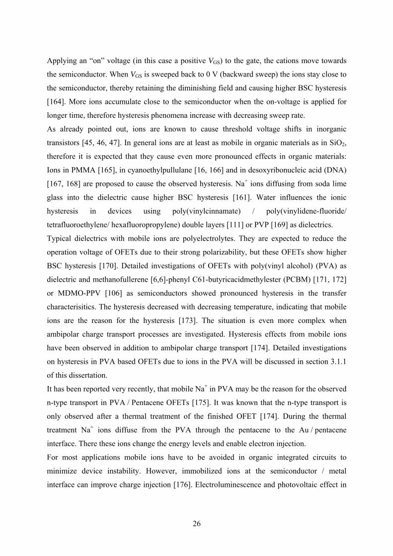
in the transfer characteristics of an OFET, it must also be observed in the voltage dependent
capacitance of a corresponding MIS structure, as shown in Figure 13.
-20 -10 0 10 200,4
0,5
0,6
0,7
0,8
0,9
1,0ca
paci
tanc
e / n
F
gate-source voltage / V
Figure 13: Dielectric spectroscopy of a MIS device:
Al / 500 nm PVA / 100 nm C60 / Al at 0.1 Hz showing an increase in
capacitance at positive voltages due to the n-type semiconducting
behaviour of C60. Also present is hysteresis due to ions in the PVA.

35
2 EXPERIMENTAL
2.1. Materials
2.1.1. Poly(vinyl alcohol)
Poly(vinyl alcohol) (PVA) is a white-yellowish non-toxic solid. Depending on the degree of
polymerization the molecular weight (Mw) is between 20000 and 200000 g/mol. Products with
different degree of hydrolysis (depending on the degree of conversion during the
transesterification, see below) are available. Standard products have 98-99 or 87-89 Mol-% of
hydroxyl groups, with glass transition temperatures (Tg) of 85°C and 58°C, and with melting
points (Tm) of 228°C and 186°C, respectively [199, 200]. PVA is hygroscopic and can take up
to 25 % of water from humid ambient air [201, 202]. Furthermore, the tendency of PVA to
crystallize is well documented [200].
Several grades of PVA were investigated. The “normal grade” was bought from Sigma
Aldrich (Mowiol 40-88). Sigma Aldrich re-sells the normal grade produced by Kuraray. PVA
is produced via poly(vinyl acetate), because vinylalcohol does not exist in large quantitites
due to the keto-enol-tautomerism:

36
OH OOH O
Vinylacetate is polymerized to poly(vinyl acetate):
OAcn *
OAc
*n
OAcn *
OAc
*n
To convert the acetate into the alcohol the polymer has to be heated in methanol (MeOH) with
NaOH. The methanolysis (a transesterification, reaction 1) leads to PVA and methylacetate
(MeAc). After the methanolysis the basic solution has to be neutralized (reaction 2):
*OAc
*n
*OH
*n
+ +O
O
Na+
1.) ΔT, NaOH
2.) CH3COOH
+ +MeOH
MeOH n MeAc H2O*OAc
*n
*OH
*n
+ +O
O
Na+
1.) ΔT, NaOH
2.) CH3COOH
+ +MeOH
MeOH n MeAc H2O
The neutralization of NaOH with acetic acid (CH3COOH) results in sodium acetate (NaAc or
CH3COO-Na+). Both NaAc and PVA are water soluble, therefore it is not straightforward to
separate them. The residual amount of NaAc in the “normal grade” PVA is specified to be
< 0.5 mass% (usually around 0.3 mass%).
As it is known [200] that mobile ions in PVA cause problems in some electronic applications,
an “electronic grade” PVA (Mowiol®40-88) with a reduced amount of NaAc is also available
from Kuraray Specialities Europe KSE GmbH, Germany. The NaAc concentration in this
“electronic grade” (also known as “low ash” grade) PVA is specified to be < 0.09 mass%.
The as received “electronic grade” PVA was further cleaned by dialysis giving the “dialysis
grade” PVA: An aqueous PVA solution was filled into a dialysis tubing (high retention
cellulose tubing, Sigma Aldrich, D0530). This membrane tubing is specified to retain >99%
of Cytochrome C (Mw = 12400 g/mol) over a 10 hour period. As Mw(PVA) ~ 205000 g/mol it
can be assumed that also >99 % of the PVA is retained. The filled and closed dialysis tubing
is submerged in ultra pure water („18 MΩ water“) which is stirred over night. Due to the
concentration difference small ions and small molecules (also very short PVA chains) diffuse

37
from the PVA solution through the membrane into the water. As most of the PVA chains are
too large to diffuse through the membrane, the PVA solution is purified. It is worth taking
into account that osmosis can cause a dilution of the PVA solution.
The residual ion concentration in the PVA could be determined by quantifying the residual
amount of ash after burning the whole PVA, but this method needs large amounts of material.
Another useful method is atomic absorption spectroscopy (AAS), which can analyze dilute
PVA solutions. The measurements confirmed the specifications for the “normal grade”
(<0.5 mass% NaAc in the PVA) and the “electronic grade” (<0.09 mass% NaAc in the PVA)
PVA. The “dialysis grade” was below the detection limit (~0.01 mass% NaAc in the PVA).
With x-ray photoelectron spectroscopy (XPS) not even traces of sodium could be
detected [203].
As stated above, PVA is hygroscopic and can take up to 25 % of water from humid ambient
air [204, 205]. The high dielectric constant of water (εH2O ~ 80 at RT [206]) causes a strong
increase in the capacitance, as shown in Figure 14.
100k 1M100p
1n
10n
capa
cita
nce
/ F
frequency / Hz
in humid nitrogen under dry nitrogen
Figure 14: Dielectric spectroscopy of an Al / PVA / Al MIM device showing the
increase in capacitance due to exposure to humidity.
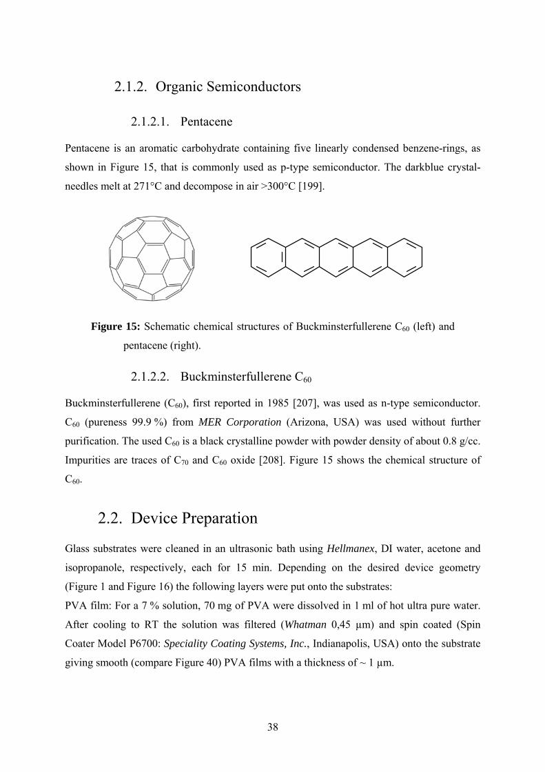
38
2.1.2. Organic Semiconductors
2.1.2.1. Pentacene
Pentacene is an aromatic carbohydrate containing five linearly condensed benzene-rings, as
shown in Figure 15, that is commonly used as p-type semiconductor. The darkblue crystal-
needles melt at 271°C and decompose in air >300°C [199].
Figure 15: Schematic chemical structures of Buckminsterfullerene C60 (left) and
pentacene (right).
2.1.2.2. Buckminsterfullerene C60
Buckminsterfullerene (C60), first reported in 1985 [207], was used as n-type semiconductor.
C60 (pureness 99.9 %) from MER Corporation (Arizona, USA) was used without further
purification. The used C60 is a black crystalline powder with powder density of about 0.8 g/cc.
Impurities are traces of C70 and C60 oxide [208]. Figure 15 shows the chemical structure of
C60.
2.2. Device Preparation
Glass substrates were cleaned in an ultrasonic bath using Hellmanex, DI water, acetone and
isopropanole, respectively, each for 15 min. Depending on the desired device geometry
(Figure 1 and Figure 16) the following layers were put onto the substrates:
PVA film: For a 7 % solution, 70 mg of PVA were dissolved in 1 ml of hot ultra pure water.
After cooling to RT the solution was filtered (Whatman 0,45 µm) and spin coated (Spin
Coater Model P6700: Speciality Coating Systems, Inc., Indianapolis, USA) onto the substrate
giving smooth (compare Figure 40) PVA films with a thickness of ~ 1 µm.

39
C60 or pentacene were thermally evaporated in an Univex 350 (Leybold Vacuum, Cologne,
Germany) high vacuum (p < 5x10⁻⁶ mbar) system at a rate of 0.16 nm/s resulting in 100 nm
thick films.
For the electrodes 100 nm thick aluminium films were thermally evaporated in an evaporation
system (Leybold Vacuum, Cologne, Germany) inside a nitrogen glovebox (M. Braun,
Garching, Germany). Shadow masks defined the electrode geometry: MIM structures had
active areas of 2.5 mm². For OFETs the channel length (L) and the channel width (W) were
100 μm and 1 mm, respectively.
DE
SCS D
G
(a)
(c)
(b)
DE
SC
E2
E1
DE
E2
E1
Figure 16: Different device geometries investigated in this work: (a) MIM,
(b) MIS and (c) bottom gate staggered OFET structure. Source (S), drain
(D), gate (G), electrode 1 (E1), electrode 2 (E2), semiconductor (SC) and
dielectric (DE).
2.3. Current voltage measurements
An Agilent E5273A instrument was used for steady state current voltage (I-V) measurements.
All electrical characterizations were performed in an inert nitrogen atmosphere.

40
2.4. Dielectric spectroscopy
Dielectric spectroscopy on MIM and MIS structures was done using a NovocontrolTechnologies
Alpha-A High Performance Frequency Analyzer (NovocontrolTechnologies, Hundsangen,
Germany). The applied voltages for frequency scans were 0 V DC and 0.5 V AC,
respectively. Dielectric spectroscopy measurements were done in close collaboration with
Mihai Irimia-Vladu.
2.5. AFM measurements
Atomic force microscope (AFM) measurements were done with a Dimension 3100’’
instrument from Digital Instruments (Santa Barbara, CA) in the tapping mode. During an
AFM measurement the cantilever (the AFM tip) scans the surface and records the topology
(the height profile). Usually the three-dimensional topology information is shown as a two
dimensional image with a colour code for the height scale.
In order to measure the thickness the film was mechanically scratched and afterwards the step
height was measured at one edge of the scratch, as shown in Figure 17. The step height, which
is defined as the difference between the averaged height between the red bars (at 1.5 and 5.5
µm, respectively) and the average height between the green bars (at 10.0 and 12.5 µm,
respectively), is calculated to be 545 nm in this example.
0 2.5 5.0 7.5 10.0 12.5x-direction / µm
z-di
rect
ion
/ nm
-250
025
0
0 2.5 5.0 7.5 10.0 12.5x-direction / µm
z-di
rect
ion
/ nm
-250
025
0
Figure 17: Thickness measurement of a scratched PVA film (from a filtered 5 %
aqueous “normal grade” PVA solution) on glass measured by AFM.
41
2.6. X-ray measurements
X-ray diffraction (XRD) measurements were performed by Heinz-Georg Flesch and Roland
Resel using a Bruker D8 Discover diffractometer (Bruker AXS GmbH, Karlsruhe, Germany)
in Bragg - Brentano geometry. The copper x-ray radiation is provided by a sealed x-ray tube.
The sample is mounted vertically on an Eulerian craddle. Measurements were performed on
PVA films on SiOx wafers under rough vacuum using a domed heating stage (DHS-1100
provided by Anton Paar GmbH, Graz, Austria). Measurements at elevated temperatures have
been done after careful alignment in the primary beam after 60 minutes to avoid
measurements of dynamical effects.

42
3 RESULTS and DISCUSSION
3.1. Hysteresis in PVA based OFETs
3.1.1. Ions in PVA
It is well known that PVA based OFETs show hysteresis in their transfer characteristics.
Mobile ions in the dielectric were supposed to cause the higher BSC hysteresis in these
OFETs, as already pointed out in section 1.2.3.6. The suggestion of mobile ionic impurities in
PVA raises the question how PVA is produced. As described above, PVA is produced by a
transesterification of poly(vinyl acetate) in MeOH, which only takes place in the presence of
acetic acid. After this reaction the acid is neutralized with NaOH, giving sodium acetate
(NaAc). The water soluble “byproduct” NaAc (PVA is also water soluble) is not completely
removed from the PVA polymer in the cleaning steps after synthesis. Dialysis is a method to
remove the residual amounts of NaAc from the PVA solution. Figure 18 compares an OFET
built with the as received electronic grade PVA (a) with an OFET using the cleaned (dialysis
grade) PVA (b):
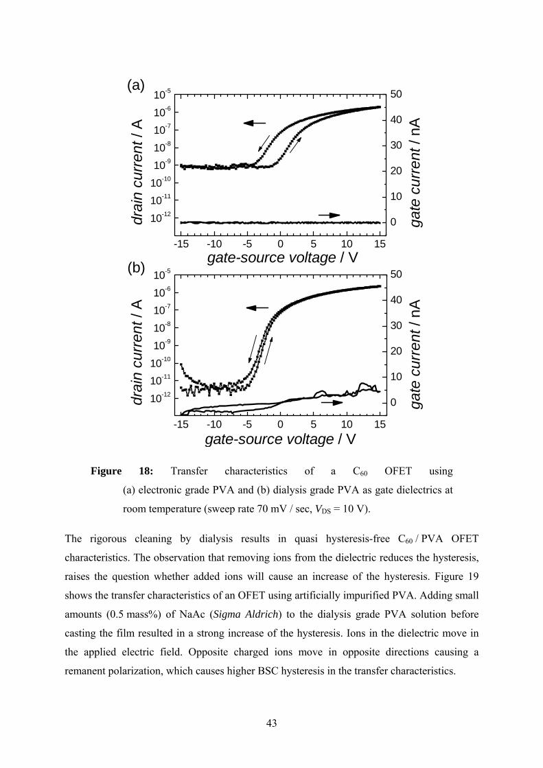
43
-15 -10 -5 0 5 10 15
10-12
10-11
10-10
10-9
10-8
10-7
10-6
10-5
0
10
20
30
40
50
gate-source voltage / V
dra
in c
urre
nt /
A
gat
e cu
rrent
/ nA
(a)
-15 -10 -5 0 5 10 15
10-12
10-11
10-10
10-9
10-8
10-7
10-6
10-5
0
10
20
30
40
50
gate-source voltage / V
dra
in c
urre
nt /
A
(b)
ga
te c
urre
nt /
nA
Figure 18: Transfer characteristics of a C60 OFET using
(a) electronic grade PVA and (b) dialysis grade PVA as gate dielectrics at
room temperature (sweep rate 70 mV / sec, VDS = 10 V).
The rigorous cleaning by dialysis results in quasi hysteresis-free C60 / PVA OFET
characteristics. The observation that removing ions from the dielectric reduces the hysteresis,
raises the question whether added ions will cause an increase of the hysteresis. Figure 19
shows the transfer characteristics of an OFET using artificially impurified PVA. Adding small
amounts (0.5 mass%) of NaAc (Sigma Aldrich) to the dialysis grade PVA solution before
casting the film resulted in a strong increase of the hysteresis. Ions in the dielectric move in
the applied electric field. Opposite charged ions move in opposite directions causing a
remanent polarization, which causes higher BSC hysteresis in the transfer characteristics.

44
-15 -10 -5 0 5 10 15
10-12
10-11
10-10
10-9
10-8
10-7
10-6
10-5
drai
n cu
rren
t / A
gate-source voltage / V
Figure 19: Transfer characteristics of a C60 OFET using artificially impurified
(with 0.5 mass% of sodium acetate added) PVA at room temperature
(sweep rate 70 mV / sec, VDS = 10 V).
The influence of ionic impurities on the electrical behaviour of PVA films was also
investigated by dielectric spectroscopy. Moving charges consume energy from the applied
electric field. This energy loss is measured as tan δ. Figure 20 shows the frequency dependent
tan δ for different Al / PVA / Al MIM structures using PVA grades with varying NaAc
concentration:

45
1m 10m 100m 1 10 100 1k 10k0,0
0,5
1,0
1,5
tan
δ
frequency / Hz
1 % NaAc 0.35 % NaAc (normal grade) 0.1 % NaAc 0.01 % NaAc (electronic grade) 0.00 % NaAc (dialysis grade)
Figure 20: Frequency dependence of the dielectric loss angle of Al / PVA / Al
MIM structures using different grades of PVA.
According to the theories of electrode polarization and MWS polarization (compare section
1.3), the increased ion concentration results in a shift of tan δ to higher frequencies. This is
clearly seen in Figure 20. It would be interesting to measure at even lower frequencies to
observe the peak maximum, but such measurements take a very long time.
Frequency dependent dielectric spectroscopy reveals that ions in PVA move very slowly.
With increasing frequencies the ions cannot follow the electric field variations and so tan δ
decreases. The frequency dependent tan δ in dielectric spectroscopy corresponds to the sweep
rate in OFETs: At sufficiently slow sweep rates the ions can follow the electric field causing
an additional polarization that is measured as an additional IDS in the backsweep of the
transfer characteristics. Consequently, for fast sweep rates the ions cannot follow and the
hysteresis disappears. Such a sweep rate dependence of the higher BSC hysteresis of an
electronic grade PVA OFET is shown in Figure 21:

46
-10 -5 0 5 10
10-12
10-11
10-10
10-9
10-8
10-7
10-6 500 mV / sec 250 mV / sec 125 mV / sec 60 mV / sec
drai
n cu
rren
t / A
gate-source voltage / V
Figure 21: Transfer characteristics of an electronic grade PVA / C60 OFET
measured at sweep rates of 500, 250, 125 and 60 mV/sec, respectively.
In this section it has been shown that the concentration of NaAc is related to the size of the
hysteresis. Na+ is a quite small ion (although it is very large with respect to H+ or even larger
with respect to an electron), while acetate (Ac-), consisting of 4 atoms, is significantly larger.
An interesting question is whether Na+ or Ac- or both move in the electric field. Therefore
other, larger ions were mixed into the PVA, because of the assumption that larger ions might
have a lower mobility causing a smaller hysteresis. Figure 22 investigates the influence of
tetrabutylammoniumacetate+ (TBA) and 2,4-dihydroxybenzoicacetate- (DBA) in combination
with Ac- and Na+, respectively.

47
-10 -5 0 5 1010-12
10-11
10-10
10-9
10-8
10-7
10-6
10-5
drai
n cu
rren
t / A
gate-source voltage / V
Na+
OO
-10 -5 0 5 1010-12
10-11
10-10
10-9
10-8
10-7
10-6
10-5
drai
n cu
rren
t / A
gate-source voltage / V
-10 -5 0 5 1010-12
10-11
10-10
10-9
10-8
10-7
10-6
10-5
drai
n cu
rren
t / A
gate-source voltage / V
Na+
OO
OH
OH
DialysisGrade
-10 -5 0 5 1010-12
10-11
10-10
10-9
10-8
10-7
10-6
10-5
drai
n cu
rren
t / A
gate-source voltage / V
OO
N+
(a)
(c) (d)
(b)
Figure 22: C60 OFETs with different ionic impurities mixed into the PVA
dielectric: no impurities (a), Na+ / Ac- (b), Na+ / DBA- (c) and
TBA+ / Ac- (d). The insets show the chemical structures of the ionic
impurities.
Interestingly, the ion combinations Na+ / DBA- and TBA+ / Ac- show very similar hysteresis
as Na+ / Ac-. Even the two larger molecular ions TBA+ / DBA- together cause similar
hysteresis, as can be seen from Figure 23. Knowing that also larger ions can cause hysteresis
and keeping in mind MWS polarization of phase boundaries in the matrix of the dielectric,
one might speculate that the ions do not have to move far in the electric field to cause
hysteresis. This could explain why also larger ions cause similar hysteresis as NaAc. Another
explanation would be that the cation (Na+ or TBA+) exchanges with a proton (H+) from an OH
group. Protons are known to have a higher mobility, they can move through SiO2, but the fact
that OH groups are practically not dissociated makes this option unlikely.
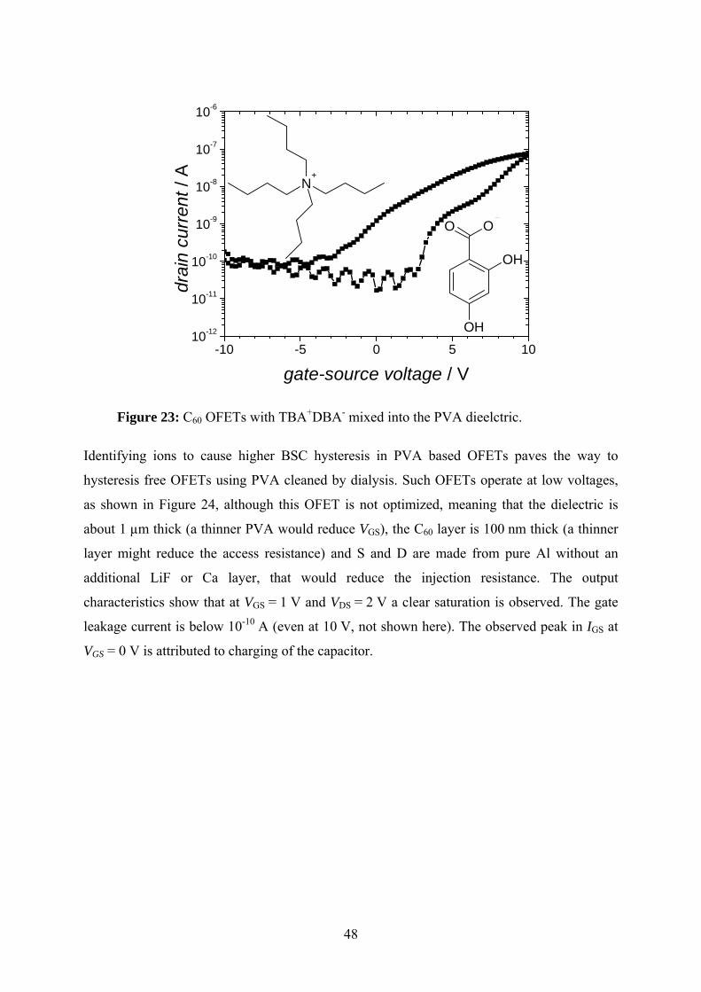
48
-10 -5 0 5 1010-12
10-11
10-10
10-9
10-8
10-7
10-6
drai
n cu
rren
t / A
gate-source voltage / V
N+
OO
OH
OH
Figure 23: C60 OFETs with TBA+DBA- mixed into the PVA dieelctric.
Identifying ions to cause higher BSC hysteresis in PVA based OFETs paves the way to
hysteresis free OFETs using PVA cleaned by dialysis. Such OFETs operate at low voltages,
as shown in Figure 24, although this OFET is not optimized, meaning that the dielectric is
about 1 µm thick (a thinner PVA would reduce VGS), the C60 layer is 100 nm thick (a thinner
layer might reduce the access resistance) and S and D are made from pure Al without an
additional LiF or Ca layer, that would reduce the injection resistance. The output
characteristics show that at VGS = 1 V and VDS = 2 V a clear saturation is observed. The gate
leakage current is below 10-10 A (even at 10 V, not shown here). The observed peak in IGS at
VGS = 0 V is attributed to charging of the capacitor.

49
0 1 2 30,0
2,0x10⁻⁸
4,0x10⁻⁸
6,0x10⁻⁸
8,0x10⁻⁸
1,0x10⁻⁷
1,2x10⁻⁷
VGS = 3 V 2 V 1 V 0 V
drai
n cu
rren
t /
A
drain-source voltage / V
(a)
-3 -2 -1 0 1 2 310-13
10-12
10-11
10-10
10-9
10-8
10-7
-0,2
0,0
0,2
0,4
0,6
0,8
1,0
VDS = 3 V
drai
n cu
rren
t / A
gate-source voltage / V
gate
cur
rent
/ nA
(b)
Figure 24: C60 / PVA OFET using dialysis grade PVA operating at low voltages.

50
3.1.2. Temperature dependent hysteresis
As explained in the introduction the mobility of charged species, e.g. ions, usually depends on
temperature. Therefore the PVA / C60 OFETs shown in Figure 18 were investigated at
elevated and reduced temperatures, respectively.
10-12
10-10
10-8
10-6
10-4
0
10
20
30
40
50
-15 -10 -5 0 5 10 15
10-12
10-10
10-8
10-6
10-4
0
10
20
30
40
50
-15 -10 -5 0 5 10 15
10-12
10-10
10-8
10-6
10-4
0
10
20
30
40
50
10-12
10-10
10-8
10-6
10-4
0
10
20
30
40
50
dra
in c
urre
nt /
A
gat
e cu
rren
t / n
A
dra
in c
urre
nt /
A
gate-source voltage / V
gat
e cu
rren
t / n
A
(d)
(c)
(b)
gate-source voltage / V
dra
in c
urre
nt /
A
(a)
gat
e cu
rren
t / n
A
dra
in c
urre
nt /
A
gat
e cu
rren
t / n
A
Figure 25: Transfer characteristics of the OFETs characterized in Figure 18,
measured at different temperatures: (a) electronic grade at 273 K,
(b) electronic grade at 253 K, (c) dialysis grade at 313 K and
(d) dialysis grade at 323 K. (sweep rate = 70 mV / sec, VDS = 10 V)
Figure 25 (a) and (b) show that the hysteresis of the OFET with the electronic grade PVA is
significantly reduced at 273 K (a) and quasi disappears at 253 K (b). Cooling “freezes” the
ions and thereby drastically decreases the hysteresis. The effect is fully reversible: Heating to
RT reveals the same characteristics as before the cooling.
The same effect is shown in Figure 25 (c) and (d) for the dialysis grade OFET: The transfer
characteristics opens up and shows a distinct hysteresis at 313 K (c) which becomes very
broad at 323 K (d). This hysteresis indicates that traces of ions are left, even in the dialysis
grade PVA. Also this change is reversible and cooling to RT results again in a quasi
hysteresis-free transfer characteristics. (Further heating causes a irreversible degradation.)
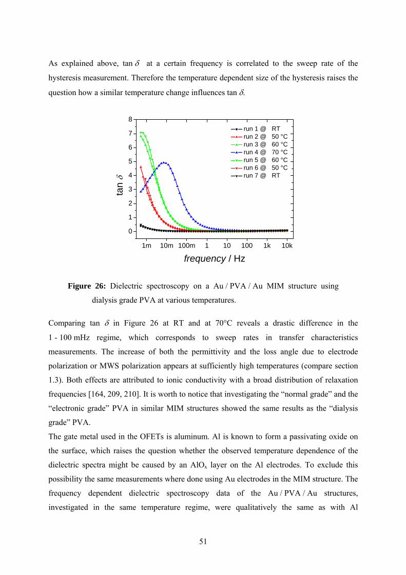
51
As explained above, tan δ at a certain frequency is correlated to the sweep rate of the
hysteresis measurement. Therefore the temperature dependent size of the hysteresis raises the
question how a similar temperature change influences tan δ.
1m 10m 100m 1 10 100 1k 10k
0
1
2
3
4
5
6
7
8ta
n δ
frequency / Hz
run 1 @ RT run 2 @ 50 °C run 3 @ 60 °C run 4 @ 70 °C run 5 @ 60 °C run 6 @ 50 °C run 7 @ RT
Figure 26: Dielectric spectroscopy on a Au / PVA / Au MIM structure using
dialysis grade PVA at various temperatures.
Comparing tan δ in Figure 26 at RT and at 70°C reveals a drastic difference in the
1 - 100 mHz regime, which corresponds to sweep rates in transfer characteristics
measurements. The increase of both the permittivity and the loss angle due to electrode
polarization or MWS polarization appears at sufficiently high temperatures (compare section
1.3). Both effects are attributed to ionic conductivity with a broad distribution of relaxation
frequencies [164, 209, 210]. It is worth to notice that investigating the “normal grade” and the
“electronic grade” PVA in similar MIM structures showed the same results as the “dialysis
grade” PVA.
The gate metal used in the OFETs is aluminum. Al is known to form a passivating oxide on
the surface, which raises the question whether the observed temperature dependence of the
dielectric spectra might be caused by an AlOx layer on the Al electrodes. To exclude this
possibility the same measurements where done using Au electrodes in the MIM structure. The
frequency dependent dielectric spectroscopy data of the Au / PVA / Au structures,
investigated in the same temperature regime, were qualitatively the same as with Al

52
electrodes (compare Figure 26 and Figure 28). Therefore it can be excluded that a possibly
existing AlOx layer at the Al electrodes influences the dielectric spectroscopy measurements.

53
3.1.3. PVA crystallinity
PVA films are spin coated from aqueous solutions. As water is suspected to cause electrical
instabilities the films are carefully dried before finishing the OFET. The standard drying
conditions are 60°C in vacuum (see experimental section). The influence of the PVA drying
temperature on the OFET characteristics is shown in Figure 27. Some measurements for this
study were done by Johanna Novacek during her practicum at LIOS.
-10 -5 0 5 1010-12
10-11
10-10
10-9
10-8
10-7
10-6
10-5
drai
n cu
rren
t / A
gate-source voltage / V-10 -5 0 5 10
10-12
10-11
10-10
10-9
10-8
10-7
10-6
10-5
drai
n cu
rren
t / A
gate-source voltage / V
(a) (b)
Figure 27: Transfer characteristics of C60 OFETs using PVA dried in vacuum at
60°C (a) and at 115°C (b).
Figure 27 (a) shows that drying PVA at 60°C in vacuum results in the known transfer
characteristics. Interestingly, when drying the PVA film at temperatures above Tg (before
depositing the C60 layer), e.g. at 115°C, the size of the hysteresis drastically increases (b).
This effect is independent on cooling rates in the range of a few minutes to 10 hours. Also
these measurements were correlated with dielectric spectroscopy measurements, as will be
discussed in the following.

54
1m 10m 100m 1 10 100 1k 10k
0
1
2
3
4
5 run 1 @ RT run 2 @ 50 °C run 3 @ 60 °C run 4 @ 70 °C run 5 @ 85 °C run 6 @ 100 °C run 7 @ 115 °C
tan
δ
frequency / Hz
Figure 28: Dielectric loss spectra of an Al / PVA / Al MIM structure using
dialysis grade PVA at various temperatures (from RT to 115°C).
1m 10m 100m 1 10 100 1k 10k
0
1
2
3
4
5 run 1 @ RT run 2 @ 50 °C run 3 @ 60 °C run 4 @ 70 °C run 5 @ 85 °C run 6 @ 100 °C
run 7 @ 115 °C run 8 @ 100 °C run 9 @ 85 °C run 10 @ 70 °C run 11 @ 60 °C run 12 @ 50 °C run 13 @ RT
tan
δ
frequency / Hz
Figure 29: Dielectric loss spectra of the MIM structure investigated in Figure 28
at various temperatures (from RT to 115°C and back to RT).

55
Figure 28 shows that the tan δ peak shifts to higher frequencies with increasing temperature.
This effect was already discussed in the previous subsection. To explain the hysteresis
increase at RT (after heating to 115°C) the behaviour of the tan δ peak during cooling was
investigated, as shown in Figure 29. After cooling the tan δ peak moves back to lower
frequencies, but not completely: a small overall shift of the tan δ peak to higher frequencies
remains. Furthermore the amplitude of the peak decreases.
The remaining shift of the peak to higher frequencies can be explained by an enhanced MWS
polarization, as schematically explained in Figure 12. This means that the volume ratio of the
two phases in the heterogenous PVA matrix and/or the shape of the homogenous clusters
and/or the conductivity of one of the phases must have changed due to the thermal treatment.
The frequencies of the peak maxima versus the temperature can be fitted with an Arrhenius fit
0
aEkTeτ τ= , where τ is the relaxation time and k is the Boltzmann constant. Figure 30 shows
such a fit. Calculated activation energies (Ea) are in the range of 2.1 to 2.6 eV and calculated
relaxation times for infinite temperature (τ0) are in the range of 10-32 to 10-37 s.
0,0024 0,0026 0,0028 0,0030 0,0032
-1x10¹⁰
-8x10⁹
-6x10⁹
-4x10⁹
-2x10⁹
02x109
4x10⁹
6x10⁹
8x10⁹
1x10¹⁰
ln(τ
)
1/T / K-1
Ea = 2.27 eV
τ0 = 5.95*10-34 s
Figure 30: Arrhenius fit of the temperature dependence of the peak maxima
shown in Figure 28.

56
One might suspect that AlOx on the Al surface causes such effects, as explained above. To
exclude this possibilty the measurements shown in Figure 28 and Figure 29 were repeated
using Au electrodes in the MIM structrues. The measurements were qualitatively the same;
therefore effects due to AlOx can be excluded.
The facts that PVA is known to have crystalline domains [200] and that the thermal treatment
exceeded the glass transition temperature of PVA (Tg(PVA) ~ 70°C) suggest that a changed
crystallinity might cause the increased hysteresis and the remaining shift of the tan δ peak.
Therefore, x-ray diffraction (XRD) measurements were performed at various temperatures to
evaluate the temperature dependence of the crystallinity of the PVA matrix. The XRD
measurements were done by Heinz-Georg Flesch and Roland Resel. Figure 32 shows x-ray
measurements of a dialysis grade PVA film on a SiOx wafer (004) as substrate. A clear PVA
peak at 2θ = 19.3° (d = 4.59 Å) is observed, which corresponds well to literature values [211].
XRD measurements are done after 1 hour at the same temperature, to ensure thermal
equilibrium and a stable measurement.
14 16 18 20 22 2410
15
20
25
30
35
40
45
50 as prepared 50°C 60°C 70°C
inte
nsity
/ cp
s
2θ / deg.
Figure 31: XRD pattern of a thin dialysis grade PVA film on a SiOx wafer at
various temperatures. Thanks to Heinz-Georg Flesch and Roland Resel for
supplying this image.
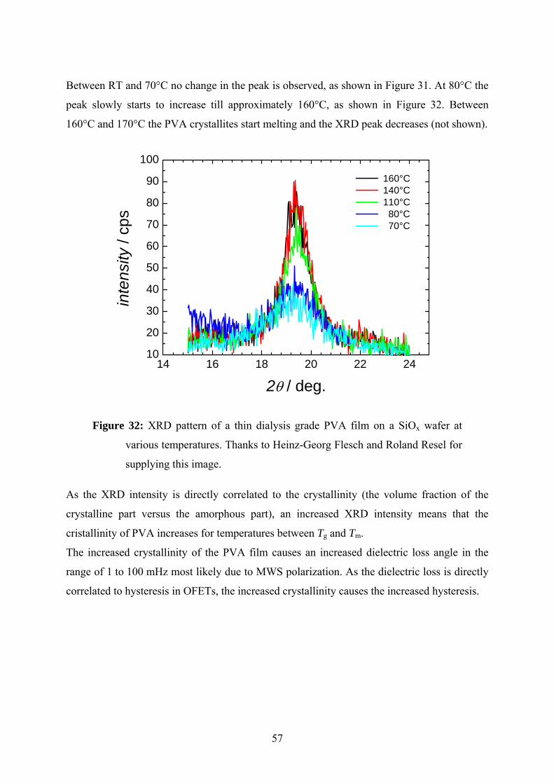
57
Between RT and 70°C no change in the peak is observed, as shown in Figure 31. At 80°C the
peak slowly starts to increase till approximately 160°C, as shown in Figure 32. Between
160°C and 170°C the PVA crystallites start melting and the XRD peak decreases (not shown).
14 16 18 20 22 2410
20
30
40
50
60
70
80
90
100 160°C 140°C 110°C 80°C 70°C
inte
nsity
/ cp
s
2θ / deg.
Figure 32: XRD pattern of a thin dialysis grade PVA film on a SiOx wafer at
various temperatures. Thanks to Heinz-Georg Flesch and Roland Resel for
supplying this image.
As the XRD intensity is directly correlated to the crystallinity (the volume fraction of the
crystalline part versus the amorphous part), an increased XRD intensity means that the
cristallinity of PVA increases for temperatures between Tg and Tm.
The increased crystallinity of the PVA film causes an increased dielectric loss angle in the
range of 1 to 100 mHz most likely due to MWS polarization. As the dielectric loss is directly
correlated to hysteresis in OFETs, the increased crystallinity causes the increased hysteresis.

58
3.2. Device geometry
3.2.1. Staggered versus Coplanar Geometries
All OFETs shown in the previous sections were bottom gate staggered OFETs. This is the
most common device geometry, when W and L are structured using shadow masks. The other
commonly used geometries are bottom gate coplanar OFETs, taking advantage of lithography
to realize short channels. Looking at the schematic device structures in Figure 1, coplanar
geometries might be expected to perform better, because the S and D electrodes are in direct
contact to the channel. To check this possibility, bottom gate coplanar OFETs have been
investigated. All device parameters were the same as for the OFETs shown in the previous
sections, except the layer sequence.
-10 -5 0 5 1010-12
10-11
10-10
10-9
10-8
0
1
2
3
4
5
drai
n cu
rren
t / A
gate-source voltage / V
gate
cur
rent
/ nA
Figure 33: Transfer characteristics of a coplanar bottom gate PVA / C60 / Al
OFET using dialysis grade PVA. VDS = 10 V.

59
0 5 100,0
0,5
1,0
1,5 VGS =
10 V 8 V 6 V 4 V 2 V 0 V
drai
n cu
rren
t /
nA
drain-source voltage / V
Figure 34: Output characteristics of the OFET described in Figure 33.
Figure 33 and Figure 34 show that coplanar bottom gate PVA / C60 OFETs are working, i.e.
they show a small on/off ratio and IDS saturates in the output characteristics, albeit with very
low IDS. In the following, several differences between coplanar and staggered geometries, that
might influence device performance, are discussed:
(i) Bottom contacts can have non-ideal film morphology close to the contacts. Such a
structurally disordered region with a low mobility and maybe a high concentration of
traps [12, 212, 213, 214] can cause an additional resistance called access resistance
Racc [213].
(ii) If there is an injection barrier at the S and D electrodes, respectively, the staggered
geometry may be advantageous over the coplanar geometry, as suggested by the
current crowding model and a disruptive potential drop in the channel, as will be
explained in the following.
(iii) Top contact devices (in this case the staggered OFET) have a higher effective contact
area due to the rough semiconductor surface. This higher effective area causes a
reduced Rinj [12, 40].
(iv) Similarly, top contact devices might also have a lower Rinj, because during
evaporation, the metal diffuses into the semiconductor, causing a mixing of the
materials and a higher effective contact area.

60
Staggered OFETs can take advantage of the current crowding model: According to the current
crowding model [215, 216, 217], the effective contact area in staggered OFETs with
overlaping S-G and D-G electrodes is self regulating, as shown in Figure 35: When Rinj
increases with respect to Racc, charges will also be injected from parts of the source that are
further away from the channel, to reach the required charge density in the channel. This
increase of the contact area causes an increasing effective channel length Leff. Due to this
current crowding effect and because Racc depends on VGS, also the total effective RC depends
on VGS [216].
RinjRinj RinjRinj RinjRinj
RaccRaccRaccRaccRaccRacc
SOURCE
SEMICONDUCTOR
DIELECTRIC
RchannelRchannel
GATE
RchannelRchannel RchannelRchannel RchannelRchannel RchannelRchannel
Figure 35: Schematic description of the current crowding model of charge
injection in staggered OFETs with overlapping electrodes.
Another explanation why an injection barrier at the S and D electrodes favours the staggered
geometry is a disruptive potential drop in the channel. A high Rinj causes a potential drop. In
the coplanar geometry this potential drop is situated in the channel [40]. Therefore this barrier
reduces the effective VGS [217], as shown in Figure 36:

61
(a)
(b)
Figure 36: Scheme of the possible potential drop in the channel with (a) and
without (b) a barrier at the source contact.
All these arguments may contribute that staggered PVA / C60 OFETs have a larger IDS than
coplanar OFETs: The rough C60 surface (compare also Figure 41) and the diffusion of Al
atoms into the C60 cause an increased effective contact area. As a thin AlOx layer is expected
on the Al surface, a Rinj can be assumed that reduces the potential in the coplanar geometry to
a higher degree than in the staggered geometry due to the current crowding.
As Rinj seems to play an important role, OFETs with an expected lower Rinj were also
investigated, in order to generalize the comparison of staggered and coplanar OFET
geometries. Again PVA is used as dielectric, but pentacene is used as semiconductor. The
small molecule pentacene is also thermally evaporated, as is C60, but pentacene is a p-type
semiconductor. Figure 37 shows transfer and output characteristics of coplanar and staggered
bottom gate Au / pentacene / PVA OFETs. No drastic difference between the coplanar and the
staggered geometry is observed for these OFETs. As Au is expected to make quasi Ohmic
contacts to pentacene, a small Rinj and thereby a small RC can be expected. The different RC
might explain why the coplanar and the staggered geometries show similar characteristics for
pentacene / Au and not for C60 / Al devices.

62
-1,0x10⁻⁸
-8,0x10⁻⁹
-6,0x10⁻⁹
-4,0x10⁻⁹
-2,0x10⁻⁹
0,0
-10 -5 0
VGS = 0 V -3 V -6 V -9 V -12 V -15 V
dr
ain
curr
ent
/ A
-10 -5 0
-1,0x10⁻⁸
-8,0x10⁻⁹
-6,0x10⁻⁹
-4,0x10⁻⁹
-2,0x10⁻⁹
0,0
VGS = 0 V -3 V -6 V -9 V -12 V -15 V
drai
n cu
rren
t /
A
drain-source voltage / V
10-13
10-12
10-11
10-10
10-9
10-8
-15 -10 -5 0 5 10 15
-2,0x10⁻¹⁰
0,0
2,0x10⁻¹⁰
4,0x10⁻¹⁰
6,0x10⁻¹⁰
8,0x10⁻¹⁰
1,0x10⁻⁹
drai
n cu
rren
t / A
gate
cur
rent
/ A
-15 -10 -5 0 5 10 15
10-13
10-12
10-11
10-10
10-9
10-8
-2,0x10⁻¹⁰
0,0
2,0x10⁻¹⁰
4,0x10⁻¹⁰
6,0x10⁻¹⁰
8,0x10⁻¹⁰
1,0x10⁻⁹
drai
n cu
rren
t / A
gate-source voltage / V
gate
cur
rent
/ A
(a) (b)
(c) (d)
Figure 37: Comparison of coplanar (a, b) with staggered (c, d) bottom gate
Au / pentacene / PVA OFETs showing transfer (b, d) and output (a, c)
characteristics.
The shown pentacene OFETs have lower currents than reported in literature [174, 218].
Pentacene OFETs have to be heat-treated at the end of the production process to improve
device performance. Such thermal treatment causes a morphological change at the interface,
that e.g. raises the mobility. As shown above, PVA is very sensitive to thermal treatments,
therefore the reported OFETs have not been thermally treated to make them comparable to the
C60 OFETs.
Another interesting fact is that no ambipolar transport is observed in these PVA / pentacene
OFETs. As described above, this might be explained by the absence of mobile Na+ ions in
PVA, which are claimed to diffuse during thermal treatments of the device to the
Au / pentacene interface where they enable electron injection [175].

63
3.2.2. Top Gate OFETs
Top gate OFETs were built by spincoating an aqueous PVA solution on top of the organic
semiconductors C60 and pentacene, respectively. Figure 38 shows the transfer and output
characteristics of a top gate staggered PVA / C60 / Al OFET:
-10 -5 0 5 1010-12
10-11
10-10
10-9
10-8
10-7
-2
0
2
4
6
8
10 VDS = 10 V
drai
n cu
rren
t / A
gate-source voltage / V
gate
cur
rent
/ nA
0 5 10
0
10
20
30
40
50VGS =
15 V 10 V 5 V 0 V
drai
n cu
rren
t / n
A
drain-source voltage / V
Figure 38: Transfer (top) and output (bottom) characteristics of a top gate
staggered PVA / C60 / Al OFET.
Figure 39 shows the transfer and output characteristics of a top gate staggered
PVA / pentacene / Au OFET:

64
-15 -10 -5 0 5 10 1510-11
10-10
10-9
10-8
0,0
0,5
1,0
1,5
2,0
2,5
3,0
drai
n cu
rren
t / A
gate-source voltage / V
gate
cur
rent
/ nA
-10 -5 0-6
-5
-4
-3
-2
-1
0
VGS = 0 V -2 V -4 V -6 V -8 V -10 V
drai
n cu
rren
t /
nA
drain-source voltage / V
Figure 39: Transfer (top) and output (bottom) characteristics of a top gate
coplanar PVA / pentacene / Au OFET.
Comparing staggered C60 OFETs with top and bottom gate geometry (Figure 2, Figure 3 and
Figure 38) shows that the current in the top gate OFETs is lower by one order of magnitude.
A rougher semiconductor / dielectric interface can explain this effect: The channel is formed
in the first few nm of the semiconductor, therefore a rough interface causes a rough channel.
This is the case for C60 top gate devices: Figure 40 and Figure 41 show the surface topology
of spincoated PVA and evaporated C60, respectively. The C60 film is much rougher than the
PVA film. It is known that C60 grows very similar on metals like Al, Ag and Cu. Also RC is
expected to be larger for Al top gate devices because Al is in contact with air before
depositing the semiconductor, therefore it is likely that the surface is oxidized, causing an
increased Rinj.
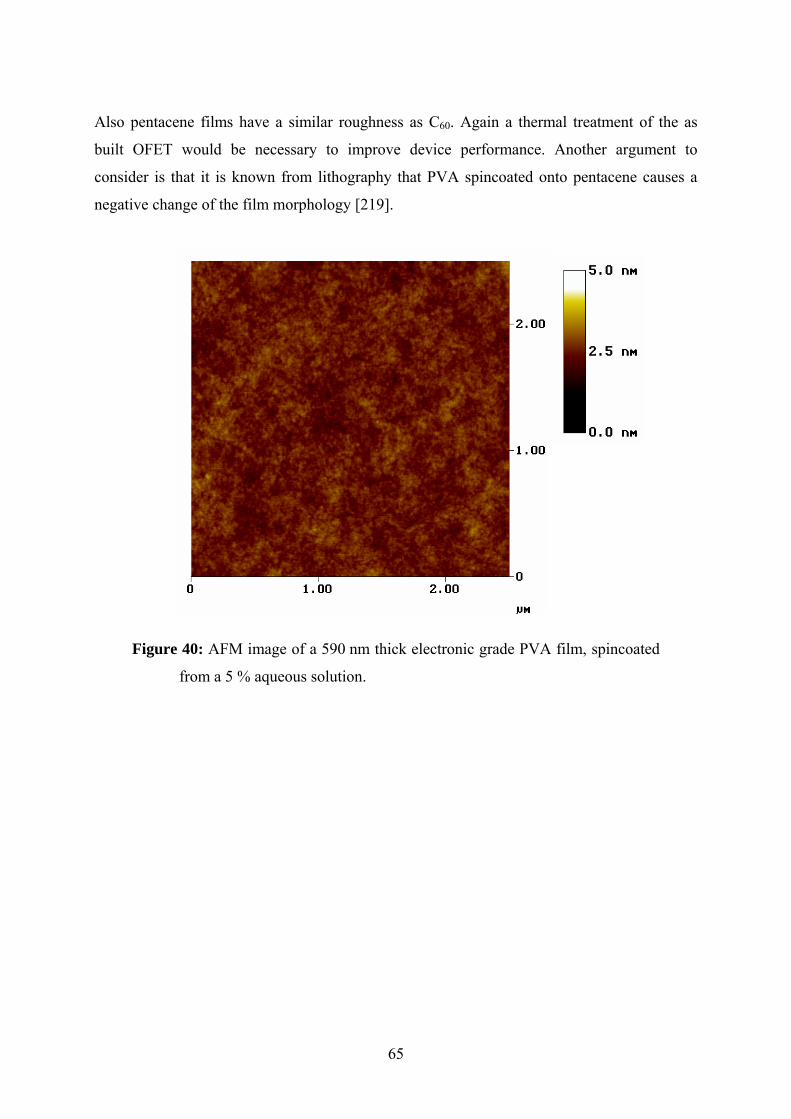
65
Also pentacene films have a similar roughness as C60. Again a thermal treatment of the as
built OFET would be necessary to improve device performance. Another argument to
consider is that it is known from lithography that PVA spincoated onto pentacene causes a
negative change of the film morphology [219].
Figure 40: AFM image of a 590 nm thick electronic grade PVA film, spincoated
from a 5 % aqueous solution.

66
1.0µm
27.16 nm
0.00 nm
Figure 41: AFM image of a 100 nm thick C60 film evaporated onto an Ag film at
RT with a rate of about 0.16 nm/s. Thanks to Alberto Montaigne Ramil
and plastic electronic GmbH for supplying this image.
PVA / C60 top gate coplanar OFETs did not show any transistor behaviour. A possible
explanation is that PVA is spin coated onto the Al S and D electrodes and oxidizes the Al.
Another influence is that in this geometry PVA is between the S and D electrodes (compare
Figure 1), leading to an even lower injection area.
OFETs can be built in 4 different geometries (compare Figure 1). The possibility to build all
of them with one and the same material combination enables three-dimensional device
integration, because it is possible to build one OFET on top of the other.
For bottom contact OFETs (top gate staggered or bottom gate coplanar), lithography can be
used to achieve small dimensions, which is difficult in the top contact geometries, because
usually lithography on the semiconductor causes strong degradation. Therefore the top gate
staggered OFET offers the possibility to combine the advantages of lithography with the
advantage of the staggered OFET geometry.

67
4 SUMMARY and CONCLUSION
Research on OFETs is enormously growing with many promising product applications.
Although first products are entering the market, there are still some problems to be solved,
like stability and degradation or some open questions on how to extract device parameters.
The science and development of OFETs is a rather young field and OFETs have various
similarities with Si/SiO2 and a-Si transistors. There are numerous documentations in OFET
literature, that authors found a solution for an OFET problem in the “inorganic literature”, e.g.
mobile ions caused also problems in Si transistors, the current crowding model was developed
for a-Si transistors, also the influence of the access resistance on the contact resistance, and
many others.
This thesis starts with an introduction to OFETs and a detailed review on hysteresis in
OFETs. The topic “hysteresis” is widespread, because there are at least seven different
mechanisms that can cause hysteresis in OFETs: charge trapping at the semiconductor /
dielectric interface, charge injection from the semiconductor into the dielectric, slow reaction
of mobile charge carriers, mobile ions in the semiconductor, polarization of the dielectric,
mobile ions in the dielectric or charge injection from the gate into the dielectric. Bias stress
effects complicate the picture, because they can have the same origin as hysteresis effects.
Therefore it is not possible to strictly separate these topics. Another fact is that hysteresis is an
unwanted effect, and unwanted effects are often not discussed in publications, because the

68
primary intention is to optimize the device. That is why detailed reports on hysteresis are rare,
even though hysteresis is very often observed. A common standard how to measure hysteresis
would help to gain a detailed understanding of hysteresis, which will be necessary to
minimize instabilities and degradation in future organic electronics.
The only exeption where hysteresis is a wanted effect is the possible use in memory elements
[127]. However, for memory devices based on hysteresis effects stringent requirements [220]
have to be fulfilled, which so far none of the proposed organic systems have succeeded to
show.
This thesis investigated hysteresis effects in C60 based OFETs with PVA as gate dielectric.
PVA is a material with a number of advantages: It is water soluble (no hazardous solvent
needed) and non-toxic (can even be used as coating for kitchenware). PVA films can easily be
produced by spin coating, resulting in smooth surfaces, which is important for OFET
interfaces, and many other deposition processes are available for PVA film production, e.g.
inkjet printing. Furthermore, the high dielectric constant of PVA enables low operating
voltages.
Until recently, PVA based OFETs had the disadvantage of a large and uncontrollable
hysteresis. Here it is documented that ions cause this hysteresis and that by a one step
cleaning procedure the hysteresis can be avoided. The resulting PVA / C60 OFETs have high
on/off ratios up to 6 orders of magnitude, mobilities in the range of 1 cm2V-1s-1, subthreshold
slopes of 1 V/decade and small Vth close to 0 V. A problem that still needs to be solved is the
temperature dependent hysteresis, because even OFETs that are nearly hysteresis free at RT,
show a clear hysteresis at slightly elevated temperatures.
Finally various OFET geometries using PVA as dielectric and C60 or pentacene as
semiconductor have been investigated. To the best of the authors knowledge, this is the first
report on top gate OFETs using PVA spincoated onto an organic semiconductor. The top gate
OFETs show lower currents than their bottom gate counterparts, but as they were not
optimized there seems to be potential for device improvement. In general, top gate OFETs can
have several advantages:
(i) the dielectric acts as sealing and protects the underlying layers from environmental
influences,
(ii) a short channel length can be realized by lithography while still taking advantage of the
staggered geometry and

69
(iii) the combination of top gate and bottom gate structures with the same materials enables
more opportunities when designing integrated circuits.
All these advantages of PVA based OFETs demonstrate the potential of the reported devices
with small operating voltages in low cost organic electronics for large area applications.

70
5 REFERENCES / BIBLIOGRAPHY
1 Weimer PK (1962) Proc IRE 50: 1462
2 Ebisawa F, Kurokawa T, Nara S (1983) J Appl Phys 54: 3255
3 Kudo K, Yamashina M, Moriizumi T (1984) Jpn J Appl Phys 23: 130
4 Tsumura A, Koezuka H, Ando T (1986) Appl Phys Lett 49: 1210
5 Peng X, Horowitz G, Fichou D, Garnier F (1990) Appl Phys Lett 57: 2013
6 Gelinck GH, Edzer H, Huitema A, van Veenendaal E, Cantatore E, Schrijnemakers L, van der Putten JB, Geuns TC, Beenhakkers M, Giesbers JB (2004) Nat Mater 3: 106
7 Klauk H (ed) Organic Electronics, Materials, Manufacturing and Applications (2006) Wiley-VCH, Weinheim, Germany
8 Hoppe A, Balster T, Muck T, Wagner V (2008) Phys Status Solidi A 205: 612
9 www.polyic.com/en/press-images.php (Feb 2009)
10 www.polymervision.com (Feb 2009)
11 www.plasticlogic.com (Feb 2009)
12 Bao Z, Locklin J (eds) Organic Field-Effect Transistors (2007) CRC Press, Boca Raton, USA
13 Salleo A (2007) Mater Today 10: 38
14 Zaumseil J, Sirringhaus H (2007) Chem Rev 107: 1296
15 Facchetti A (2007) Mater Today 10: 28
16 Veres J, Ogier S, Lloyd G, de Leeuw D (2004) Chem Mater 16: 4543
17 Facchetti A, Yoon MH, Marks TJ (2005) Adv Mater 17: 1705
71
18 Singh TB, Sariciftci NS (2006) Annu Rev Mater Res 36: 199
19 Torsi L, Farinola GM, Marinelli F, Tanese MC, Omar OH, Valli L, Babudri F, Palmisano F, Zambonini PG, Naso F (2008) Nat Mater 7: 412
20 Someya T, Pal B, Huang J, Katz HE (2008) MRS Bulletin 33: 690
21 Egginger M, Bauer S, Schwödiauer R, Neugebauer H, Sariciftci NS (2009) Monatsh Chem – Chem Monthly, published online, DOI 10.1007/s00706-009-0149-z
22 Horowitz G, Hajlaoui R, Bourguiga R, Hajlaoui M (1999) Synth Met 101: 401
23 Braga D, Horowitz G (2009) Adv Mat 21: 1473
24 Horowitz G (2006) Organic Transitors. In Klauk H (ed) Organic Electronics, Materials, Manufacturing and Applications, Wiley-VCH, Weinheim, Germany, Ch. 1
25 Sze SM, Ng KK (2007) Physics of Semiconductor Devices, Third Edition, Wiley, New Jersey
26 Horowitz G, Hajlaoui ME, Hajlaoui R (2000) J Appl Phys 87: 4456
27 Horowitz G, Hajlaoui R, Bouchriha H, Bourguiga R, Hajlaoui M (1998) Adv Mat 10: 923
28 Mottaghi M, Horowitz G (2006) Org Electron 7: 528
29 Horowitz G (1999) Physics of Organic Field-Effect Transistors. In Hadziioannou G, van Hutten PF (ed) Semiconducting Polymers: Chemistry, Physic and Engineering, Wiley-VCH, Weinheim, Germany, Ch. 14
30 IEEE Standard 1620TM (2004) IEEE Standard Test Methods for the Characterization of Organic Transistors and Materials (IEEE, New York, 2004)
31 Pernstich KP, Haas S, Oberhoff D, Goldmann C, Gundlach DJ, Batlogg B, Rashid AN, Schitter G (2004) J Appl Phys 96: 6431
32 Halik M, Klauk H, Zschieschang U, Schmid G, Dehm C, Schütz M, Maisch S, Effenberger F, Brunnbauer M, Stellacci F (2004) Nature 431: 963
33 Zirkl M, Haase A, Fian A, Schön H, Sommer C, Jakopic G, Leising G, Stadlober B, Graz I, Gaar N, Schwödiauer R, Bauer-Gogonea S, Bauer S (2007) Adv Mat 19: 2241
34 Scheinert S, Paasch G (2004) Phys Stat Sol (a) 201: 1263
35 Hwang J, Wan A, Kahn A (2009) Mat Sci Eng R 64: 1
36 Braun S, Salaneck WR, Fahlman M (2009) Adv Mater 21: 1450
37 Stadlober B, Haas U, Gold H, Haase A, Jakopic G, Leising G, Koch N, Rentenberger S, Zojer E (2007) Adv Funct Mat 17: 2687
38 Horowitz G, Lang P, Mottaghi M, Aubin H (2004) Adv Funct Mat 14: 1069
39 Luan S, Neudeck GW (1992) J Appl Phys 72: 766
40 Street RA, Salleo A (2002) Appl Phys Lett 81: 2887
41 Zaumseil J, Baldwin KW, Rogers JA (2003) J Appl Phys 93: 6117
42 Brown AR, Jarrett CP, de Leeuw DM, Matters M (1997) Synth Met 88: 37
43 Mijalkovic S, Green D, Nejim A, Whiting G, Rankov A, Smith E, Halls J, Murphy C (2008) Proc Int Conf Microelectr IEEE 26
44 Schroder DK, Semiconductor Material and Device Characterization (2006) Wiley, New York
45 Fuller CS, Severiens JC (1954) Phys Rev 92: 1322

72
46 Kessler JO, Tomkins BE, Blanc J (1963) Solid-State Electron 6: 297
47 Snow EH, Grove AS, Deal BE, Sah CT (1965) J Appl Phys 36: 1664
48 Young ND, Gill A (1992) Semicond Sci Technol 7: 1103
49 Moll JL, Tarui Y (1963) IEEE T Electron Dev 10 : 338
50 Wu SY (1974) IEEE T Electron Dev 21, 499
51 Würfel P, Batra IP (1973) Phys Rev B 8: 5126
52 Batra IP, Würfel P, Silverman BD (1973) Phys Rev B 8: 3257
53 Scott JF (2000) Ferroelectric Memories, Springer, Berlin
54 www.fujitsu.com/sg/services/micro/semiconductor/memory/fram/ (Feb 2009)
55 www.eetasia.com/SEARCH/ART/ferroelectric+RAM.HTM (Feb 2009)
56 Lustig N, Kanicki J (1989) J Appl Phys 65: 3951
57 Leroux C, Mitard J, Ghibaudo G, Garros X, Reimbold G, Guillaumot B, Martin F (2004) IEDM Tech Dig p737-740
58 Fleetwood DM, Winokur PS, Reber RA, Meisenheimer TL, Schwank JR, Shaneyfelt MR, Riewe LC (1993) J Appl Phys 73: 5058
59 Powell MJ (1989) IEEE Tran Electron Devices 36: 2753
60 Gu G, Kane MG, Mau SC (2007) J Appl Phys 101: 014504
61 Lang DV, Chi X, Sergent AM, Ramirez AP (2003) arXiv:cond-mat/0312721
62 Salleo A, Endicott F, Street RA (2005) Appl Phys Lett 86: 263505
63 Knipp D, Street RA, Völkel A, Ho J (2003) J Appl Phys 93: 347
64 Kane MG (2007) Organic Thin-Film Transistors for Flat-Panel Displays. In Bao Z, Locklin J (eds) Organic Field-Effect Transistors, CRC Press, Boca Raton, USA, Ch. 6.4
65 Taylor DM (2006) IEEE T Dielect El In 13: 1063
66 Salleo A, Street RA (2003) J Appl Phys 94: 471
67 Andersson LM, Inganäs O (2007) Organ Electr 8: 423
68 Street RA (2008) Phys Rev B 77: 165311
69 Rivera C, Munoz E (2009) Appl Phys Lett 94: 053501
70 Goldmann C, Haas S, Krellner C, Pernstich KP, Grundlach DJ, Batlogg B (2004) J Appl Phys 96: 2080
71 Goldmann C, Krellner C, Pernstich KP, Haas S, Grundlach DJ, Batlogg B (2006) J Appl Phys 99: 034507
72 Santato C, Capelli R, Loi MA, Murgia M, Cicoira F, Roy VAL, Stallinga P, Zamboni R, Rost C, Karg SF, Muccini M (2004) Synth Met 146: 329
73 Petit C, Zander D, Lmimouni K, Ternisien M, Tondelier D, Lenfant S, Vuillaume D (2008) Org Electr 9: 979
74 Noh YH, Park SY, Seo SM, Lee HH (2006) Org Electron 7: 271
75 Yoon MH, Kim C, Facchetti A, Marks TJ (2006) J Amer Chem Soc 128: 12851
76 Stallinga P, Gomes HL, Biscarini F, Murgia M, de Leeuw DM (2004) J Appl Phys 96: 5277
77 Hwang DK, Oh MS, Hwang JM, Kim JH, Im S (2008) Appl Phys Lett 92: 013304

73
78 Schwödiauer R, Neugschandtner GS, Bauer-Gogonea S, Bauer S (1999) Appl Phys Lett 75: 3998
79 Schmechel R, von Seggern H (2005) Electronic Traps in Organic Transport Layers. In Brütting W (ed) Physics of Organic Semiconductors, Wiley-VCH, Weinheim, Germany, Ch. 10
80 Hwang DK, Lee K, Kim JH, Im S, Park JH, Kim E (2006) Appl Phys Lett 89: 093507
81 Cayadi T, Tan HS, Namdas EB, Mhaisalkar SG, Lee PS, Chen ZK, Ng CM, Boey FYC (2007) Organ Electr 8: 455
82 Madec MB, Crouch D, Llorente GR, Whittle TJ, Geoghegan M, Yeates SG (2008) J Mater Chem 18: 3230
83 Kitamura M, Kuzumoto Y, Kamura M, Aomori S, Arakawa Y (2007) Appl Phys Lett 91: 183514
84 Kim W, Javey A, Vermesh O, Wang Q, Li Y, Dai H (2003) Nano Lett 3: 193
85 Kim SH, Yang H, Yang SY, Hong K, Choi D, Yang C, Chung DS, Park CE (2008) Org Electron 9: 673
86 Jung T, Dodabalapur A, Wenz R, Mohapatra S (2005) Appl Phys Lett 87: 182109
87 Dinelli F, Murgia M, Biscarini F, de Leeuw DM (2004) Synthet Met 146: 373
88 Gu G, Kane MG (2008) Appl Phys Lett 92: 053305
89 Zilker SJ, Detcheverry C, Cantatore E, de Leeuw DM (2001) Appl Phys Lett 79: 1124
90 Mathijssen SGJ, Cölle M, Gomes H, Smits ECP, de Boer B, McCulloch I, Bobbert PA, de Leeuw DM (2007) Adv Mater 19: 2785
91 Sekitani T, Iba S, Kato Y, Noguchi Y, Someya T, Sakurai T (2005) Appl Phys Lett 87: 073505
92 Benor A, Knipp D, Northrup J, Völkel AR, Street RA (2008) J Non-Cryst Solids 354: 2875
93 Gomes HL, Stallinga P, Cölle M, de Leeuw DM, Biscarini F (2006) Appl Phys Lett 88: 082101
94 Chua LL, Zaumseil J, Chang JF, Ou ECW, Ho PKH, Sirringhaus H, Friend RH (2005) Nature 434: 194
95 Lee S, Koo B, Shin J, Lee E, Park H, Kim H (2006) Appl Phys Lett 88: 162109
96 Cai X, Gerlach CP, Frisbie CD (2007) J Phys Chem C 111: 452
97 Ogawa S, Kimura Y, Niwano M, Ishii H (2007) Appl Phys Lett 90: 33504
98 Kim WJ, Kim CS, Jo SJ, Lee SW, Lee SJ, Baik HK (2007) Electrochem Solid St 10: H1
99 Zhang XH, Domercq B, Kippelen B (2007) Appl Phys Lett 91: 092114
100 Salleo A, Chabinyc ML, Yang MS, Street RA (2002) Appl Phys Lett 81: 4383
101 Kim SC, Kim SH, Lee JH, Kim MK, Kim DJ, Zyung T (2005) Synth Met 148: 75
102 Yagi I, Tsukagoshi K, Aoyagi Y (2005) Appl Phys Lett 86: 103502
103 Zaumseil J, Friend RH, Sirringhaus H (2006) Nat Mater 5: 69
104 Pal BN, Trottman P, Sun J, Katz HE (2008) Adv Funct Mater 18: 1832
105 Marjanovic N (2005) PhD Dissertation, Johannes Kepler University, Linz
106 Marjanovic N, Singh TB, Dennler G, Günes S, Neugebauer H, Sariciftci NS, Schwödiauer R, Bauer S (2006) Organ Electr 7: 188
107 Saragi TPI, Salbeck J (2006) Appl Phys Lett 89: 253516
108 Veres J, Ogier SD, Leeming SW, Cupertino DC, Khaffaf SM (2003) Adv Funct Mater 13: 199
109 Veres J, Ogier S, Leeming S, Cupertino D, Khaffaf SM, G Lloyd (2003) Proc SPIE 5217: 147
74
110 Stassen AF, de Boer RWI, Iosad NN, Morpurgo AF (2004) Appl Phys Lett 85: 3899
111 Stadlober B, Zirkl M, Beutl M, Leising G, Bauer-Gogonea S, Bauer S (2005) Appl Phys Lett 86: 242902
112 Haas U, Gold H, Haase A, Jakopic G, Stadlober B (2007) Appl Phys Lett 91: 043511
113 Irimia-Vladu M, Marjanovic N, Vlad A, Montaigne Ramil A, Hernandez-Soso G, Schwödiauer R, Bauer S, Sariciftci SN (2008) Adv Mat 20: 3887
114 Scheinert S, Pernstich KP, Batlogg B, Paasch G (2007) J Appl Phys 102: 104503
115 Lim E, Manaka T, Tamura R, Iwamoto M (2007) J Appl Phys 101: 094505
116 Gu G, Kane MG, Doty JE, Firester AH (2005) Appl Phys Lett 87: 243512
117 Siol C, Melzer C, von Seggern H (2008) Appl Phys Lett 93: 133303
118 Ucurum C, Goebel H, Ylidimir FA, Bauhofer W, Krautschneider W (2008) J Appl Phys 104 : 084501
119 Ucurum C, Siemund H, Goebel H (2008) Portable Information Devices, 2008 and the 2008 7th IEEE Conference on Polymers and Adhesives in Microelectronics and Photonics. PORTABLE-POLYTRONIC 2008. 2nd IEEE International Interdisciplinary Conference on, page 1-3, ISBN: 978-1-4244-2141-1
120 Liu Z, Xue F, Su Y, Lvov YM, Varahramyan K (2006) IEEE T Nanotech 5: 379
121 Wu W, Zhang H, Wang Y, Ye S, Guo Y, Di C, Yu G, Zhu D, Liu Y (2008) Adv Funct Mater 18: 2593
122 Mushrush M, Facchetti A, Lefenfeld M, Katz HE, Marks TJ (2003) J Am Chem Soc 125: 9414
123 Facchetti A, Letizia J, Yoon MH, Mushrush M, Katz HE, Marks TJ (2004) Chem Mater 16: 4715
124 Katz EH, Hong XM, Dodabalapur A, Sarpeshkar R (2002) J Appl Phys 91: 1572
125 Baeg KJ, Noh YY, Ghim J, Kang SJ, Lee H, Kim DY (2006) Adv Mater 18: 3179
126 Baeg KJ, Noh YY, Ghim J, Lim B, Kim DY (2008) Adv Funct Mater 18: 3678
127 Ling QD, Liaw DJ, Zhu C, Chan DSH, Kang ET, Neoh KG (2008) Prog Polym Sci 33: 917
128 Zhen L, Guan W, Shang L, Liu M, Liu G (2008) J Phys D: Appl Phys 41: 135111
129 Scheinert S, Paasch G, Pohlmann S, Hörhold HH, Stockmann R (2000) Solid State Electron 44: 845
130 Scheinert S, Schliefke W (2003) Synth Metals 139: 501
131 Lindner T, Paasch G, Scheinert S (2005) J Appl Phys 98: 114505
132 Swensen J, Kanicki J, Heeger AJ (2003) Proc SPIE-Int Soc Opt Eng 5217: 159
133 Kirova N, Brazovskii S (1996) Synthet Metals 76: 229
134 Salleo A, Street RA (2004) Phys Rev B 70: 235324
135 Paasch G, Scheinert S, Herasimovich A, Hörselmann I, Lindner T (2008) Phys Stat Sol (a) 205: 534
136 Paasch G (2004) Sol State Ionics 169: 87
137 Paasch G, Scheinert S, Petr A, Dunsch L (2006) Russian J Electrochem 42: 1161
138 Paasch G (2007) J Electroanalyt Chem 600: 131
139 Street RA, Salleo A, Chabinyc ML (2003) Phys Rev B 68: 085316
140 Vorotyntsev MA, Heinze J (2001) Electrochim Acta 46: 3309
141 Bradley K, Cumings J, Star A, Gabriel JCP, Grunder G (2003) Nano Lett 3: 639
142 Castriota M, Cazzanelli E, Nicotera I, Coppola IL, Oliviero C, Ranieri GA (2003) J Chem Phys 118: 5537
143 Chintapalli S, Frech R (1996) Macromol 29: 3499

75
144 Smits JHA, Meskers SCJ, Janssen RAJ, Marsman AW, de Leeuw DM (2005) Adv Mater 17: 1169
145 Rep DBA, Morpurgo AF, Sloof WG, Klapwijk TM (2003) J Appl Phys 93: 2082
146 Naber RCG (2006) PhD Dissertation, University of Groningen, The Netherlands
147 Miller SL, McWhorter PJ (1992) J Appl Phys 72: 5999
148 Naber RCG, Massolt J, Spijkman M, Asadi K, Blom PWM, de Leeuw DM (2007) Appl Phys Lett 90: 113509
149 Velu G, Legrand C, Tharaud O, Chapoton A, Remiens D, Horowitz G (2001) Appl Phys Lett 79: 659
150 Kodzasa T, Yoshida M, Uemura S, Kamata T (2003) Synth Met 137: 943
151 Schroeder R, Majewski LA, Grell M (2004) Adv Mater 16: 633
152 Schroeder R, Majewski LA, Voigt M, Grell M (2005) IEEE Electr Device L 26: 69
153 Unni KNN, de Bettignies R, Dabos-Seignon S, Nunzi JM (2004) Appl Phys Lett 85: 1823
154 Naber RCG, Tanase C, Blom PWM, Gelinck GH, Marsman AW, Touwslager FJ, Setayesh S, de LeeuwDM (2005) Nat Mater 4: 243
155 Naber RCG, Blom PWM, Gelinck GH, Marsman AW, de Leeuw DM (2005) Adv Mater 17: 2692
156 Müller K, Paloumpa I, Henkel K, Schmeißler D (2006) Mater Sci Eng C 26: 1028
157 Tamura R, Lim E, Yoshita S, Manaka T, Iwamoto M (2008) Thin Sol Films 516: 2753
158 Mizuno E, Taniguchi M, Kawai T (2005) Appl Phys Lett 86: 143513
159 Sekitani T, Nogitchi Y, Nakano S, Zaitsu K, Kato Y, Takamiya M, Sakurai T, Someya T (2007) Electron Devices Meeting, IEDM 2007. IEEE, p. 221
160 Park SY, Park M, Lee HH (2004) Appl Phys Lett 85: 2283
161 Halik M (2006) Gate Dielectrics. In Klauk H (ed) Organic Electronics, Materials, Manufacturing and Applications, Wiley-VCH, Weinheim, Germany, Ch. 6
162 Lim SC, Kim SH, Koo JB, Lee JH, Ku Ch, Yang YS, Zyung T (2007) Appl Phys Lett 90: 173512
163 Huang C, West JE, Katz HE (2007) Adv Funct Mater 17: 142
164 Egginger M, Irimia-Vladu M, Schwödiauer R, Tanda A, Frischauf I, Bauer S, Sariciftci NS (2008) Adv Mater 20: 1018
165 Uemura S, Yoshida M, Hoshino S, Kodzaza T, Kamata T (2003) Thin Sol Films 438-439: 378
166 Horowitz G, Deloffre F, Garnier F, Hajlaoui R, Hmyene M, Yassar A (1993) Synthet Metals 54: 435
167 Stadler P, Oppelt K, Singh TB, Grote JG, Schwödiauer R, Bauer S, Piglmayer-Brezina H, Bäuerle D, Sariciftci NS (2007) Org Electron 8: 648
168 Singh B, Sariciftci NS, Grote JG, Hopkins FK (2006) J Appl Phys 100: 024514
169 Ng TN, Daniel JH, Sambandan S, Arias AC, Chabinyc ML, Street RA (2008) J Appl Phys 103: 044506
170 Panzer MJ, Newman CR, Frisbie CD (2005) Appl Phys Lett 86: 103503
171 Singh TB, Marjanovic N, Matt GJ, Sariciftci NS, Schwödiauer R, Bauer S (2004) Appl Phys Lett 85: 5409
172 Singh TB, Marjanovic N, Sariciftci NS, Schwödiauer R, Bauer S (2006) IEEE T Dielectr Electr Insul 13: 1082
173 Singh TB, Marjanovic N, Stadler P, Auinger M, Matt GJ, Günes S, Sariciftci NS, Schwödiauer R, Bauer S (2005) J Appl Phys 97: 083714

76
174 Singh TB, Meghdadi F, Günes S, Marjanovic N, Horowitz G, Lang P, Bauer S, Sariciftci NS (2005) Adv Mat 17: 2315
175 Takebayashi S, Abe S, Saiki K, Ueno K (2009) Appl Phys Lett 94: 083305
176 Edman L, Swensen J, Moses D, Heeger AJ (2004) Appl Phys Lett 84: 3744
177 Bernards DA, Flores-Torres S, Abruna HD, Malliaras GG (2006) Science 313: 1416
178 Waser R, Aono M (2007) Nat Mater 6: 833
179 Cayadi T, Tan HS, Mhaisalkar SG, Lee PS, Boey FYC, Chen ZK, Ng CM, Rao VR Qi GJ (2007) Appl Phys Lett 91: 242107
180 Lee CA, Park DW, Jin SH, Park IH, Lee JD, Park BG (2006) Appl Phys Lett 88: 252102
181 Lee CA, Park DW, Jung KD, Kim BJ, Kim YC, Lee JD, Park BG (2006) Appl Phys Lett 89: 262120
182 Kolliopoulou S, Dimitrakis P, Normand P, Zhang HL, Cant N, Evans SD, Paul S, Pearson C, Molloy A, Petty MC, Tsoukalas D (2003) J Appl Phys 94: 5234
183 Kolliopoulou S, Dimitrakis P, Normand P, Zhang HL, Cant N, Evans SD, Paul S, Pearson C, Molloy A, Petty MC, Tsoukalas D (2004) Microelectron Eng 73-74: 725
184 Kitamura M, Arakawa Y (2007) Appl Phys Lett 91: 053505
185 Horie M, Luo Y, Morrison JJ, Majewski LA, Song A, Saunders BR, Turner ML (2008) J Mater Chem 18: 5230
186 Park DW, Lee CA, Jung KD, Park BG, Shin H, Lee JD (2006) Appl Phys Lett 89: 263507
187 Benson N, Melzer C, Schmechel R, von Seggern H (2008) Phys Stat Sol A 205 : 475
188 Maliakal A (2007) Dielectric Materials: Selection and Design. In Bao Z, Locklin J (eds) Organic Field-Effect Transistors, CRC Press, Boca Raton, USA, Ch. 3.2
189 Halik M (2006) Gate Dielectrics. In Klauk H (ed) Organic Electronics, Materials, Manufacturing and Applications, Wiley-VCH, Weinheim, Germany, Ch. 6
190 Runt JP, Fitzgerald JJ (eds.) Dielectric Spectroscopy of Polymeric Materials. (1997) ACS, Washington, DC, US
191 Kremer F, Schönhals A (ed) Broadband Dielectric Spectroscopy. (2003) Springer, Berlin, Germany
192 Steeman PAM, van Turnhout J (2003) Dielectric Properties of Inhomogeneous Media. In Kremer F, Schönhals A (ed) Broadband Dielectric Spectroscopy, Springer, Berlin, Germany, Ch 13
193 Meaudre R, Meaudre M, Vignoli S (2002) Mat Sci Eng B 94: 264
194 Frübing P, Wegener M, Gerhard-Multhaupt R, Buchsteiner A, Neumann W, Brehmer L (1999) Polymer 40: 3413
195 Wegener M (2001) IEEE Trans Dielectr Electr Insul 8: 494
196 Kremer F, Schönhals A (2003) Analysis of Dielectric Spectra. In Kremer F, Schönhals A (ed) Broadband Dielectric Spectroscopy, Springer, Berlin, Germany, Ch 3
197 Coelho R (1991) J Non-Cryst Solids 131: 1136
198 Klein RJ, Zhang S, Dou S, Jones BH, Colby RH, Runt J (2006) J Chem Phys 124: 144903
199 CD Römpp Chemie Lexikon (1995) Georg Thieme Verlag, Stuttgart, Deutschland
200 Kuraray Specialities Europe KSE GmbH (2003) Mowiol Polyvinyl Alcohol, information brochure, Germany
201 Creutz E, Wilson RR (1946) J Chem Phys 14: 725

77
202 Finch CA, Polyvinyl Alcohol: Properties and Applications (1973) Wiley, London
203 Philipp Stadler, private communication
204 Creutz E, Wilson RR (1946) J Chem Phys 14: 725
205 Finch CA, Polyvinyl Alcohol: Properties and Applications (1973) Wiley, London, UK
206 Lide RD (Ed) Handbook of Chemistry and Physics (1995) CRC Press, London, UK
207 H.W. Kroto, J.R. Heath, S.C. O’Brien, R.F. Curl, R.E. Smalley, Nature, 318, 1985, 162-163
208 www.mercorp.com/mercorp/fullbro.pdf (28.03.2009)
209 Mauritz KA (1989) Macromolecules 22: 4483
210 Martin B, Kliem H (2005) J Appl Phys 98: 74102
211 Hodge RM, Edward GH, Simon GP (1996) Polymer 37 : 1371
212 Kymissis I, Dimitrakopoulos CD, Purushothaman S (2001) IEEE Trans Elec Dev 48: 1060
213 Stadlober B, Haas U, Gold H, Haase A, Jakopic G, Leising G, Koch N, Rentenberger S, Zojer E (2007) Adv Funct Mat 17: 2687
214 Li T, Ruden PP, Campbell IH, Smith DL (2003) J Appl Phys 93: 4017
215 Richards TJ, Sirringhaus H (2007) J Appl Phys 102: 094510
216 Chiang CS, Martin S, Kanicki J, Ugai Y, Yukawa T, Takeuchi S (1998) Jpn J Appl Phys, Part 1, 37: 5914
217 Tessler N, Roichman Y (2001) Appl Phys Lett 79: 2987
218 Singh TB, Senkarabacak P, Sariciftci NS, Tanda A, Lackner C, Hagelauer R, Horowitz G (2006) Appl Phys Lett 89 : 033512
219 Barbara Stadlober, private communication
220 Scott JC, Bozano LD (2007) Adv Mater 19: 1452


I
CURRICULUM VITAE name Martin Egginger adress Schumpeterstr. 9, 4040 Linz phone +43 (0) 650 2 29 10 77 e-mail [email protected] place, date of birth Salzburg , 29th October 1977 nationality Austrian marital status Cohabitation children Laura, 5th March 2004 Anna, 30th May 2006 military service Supply unit Schwarzenbergkaserne Salzburg (10 / 1996 - 05 / 1997)
Education 06 / 2005 – 05 / 2009 PhD Studies, physical chemistry, Prof. Dr. Mag. S. N. Sariciftci 05 / 2005 Graduation: “Diplom-Ingenieur” (passed with distinction) 09 / 2003 – 05 / 2005 Diploma Thesis “Zn-Phthalocyanine / C60 Solar Cells”, institute for physical chemistry, Prof. Dr. Mag. Serdar N. Sariciftci 10 / 1997 – 05 / 2005 Studies at the university of Linz: economical engineering of technical chemistry (Wirtschaftsingenieurwesen der Technischen Chemie) 06 / 1996 School leaving exam (passed with distinction) 1984-88 / 1988-96 Primary / Grammar school in Grödig / Salzburg, Austria
Languages since 1987 English: business fluent since 1992 French in word and language 1990-1996 Latin
Award 11 / 2006 Preis des VDI (Verein Deutscher Ingenieure) „für eine
hervorragende Leistung“ (for the master-thesis / Diplomarbeit)
Special skills and competences 07 / 2008 ”NLP – Eine Einführung” (Seminar, JK University, 2 days) 06 / 2008 „Motivation, Kommunikation, Improvisation“ (Seminar, JK Univ., 4 Ects) 12 / 2007 „Project Mangement“ (Seminar, JK University) 12 / 2007 „Change Management“ (Seminar, JK University) 03 / 2007 “Unternehmerisches Know How für wissenschaftliche MitarbeiterInnen“
(Seminar, JK University) 12 / 2006 „Maßnahmen der Ersten Hilfe im Vergiftungsfall“ (ÖRK) 10 / 2006 „Ausbildung zum Laserschutzbeauftragten“ (ARC Seibersdorf research) 12 / 2005 „Kommunikation und Interaktion” (Seminar, JK University, 3 Ects) 11 / 2005 „Keep talking english“ (Seminar, JK University) 11 / 2005 „Besprechungen leiten – gestalten – moderieren“ (Seminar, JK University)

II
2002 – 2004 „Angewandte Ökologie und Umweltplanung” (Seminars, JK Univ., 12Ects) 12 / 2003 „Umweltrichtlinien für den Betrieb von Industrieanlagen“ (Sem., JKU, 6 Ects) Driver’s license (A, B); Skilled Win-Computer User; Yacht Masters Licence (FB3 – 200 sm); Maritime Radio Operator: Short Range Certificate (Royal Yachting Association)
Related Experience 2003 - present Scientific employee at the institute for physical chemistry (www.lios.at) 01 / 2007 Winterschool “Organic Electronics”, Planneralm, Austria 09 / 2003 Summerschool “Basic principles and new concepts in quantum solar energy conversion”, Hirschegg, Austria 08 / 2003 – 09 / 2004 project collaborator at the institute for physical chemistry 07 – 09 / 2002 project collaborator at the institute for physical chemistry 03 – 06 / 2002 Tutor at the institute of inorganic chemistry 10 / 2001 – 01 / 2002 Tutor at the institute of inorganic chemistry Summer 2000, 2001 Electro-chemical process optimization at Sony DADC Austria PLC (www.sonydadc.com)
Contributions to conferences 05 / 2008 “Effects of the Device Geometry in Organic Field Effect Transistors”, M.
Egginger, M. Irimia-Vladu, A. Tanda, R. Schwödiauer, S. Bauer and N. S. Sariciftci, E-MRS 2008 Spring Meeting, Strasbourg, France (talk)
05 / 2008 “Sodium acetate in polyvinylalcohol: How to control the hysteresis in organic field effect transistors?”, M. Egginger, M. Irimia-Vladu, A. Tanda, R. Schwödiauer, S. Bauer and N. S. Sariciftci, Technologies For Polymer Electronics TPE 08, Rudolstadt, Germany (poster)
03 / 2008 “Ionic Impurities in Polyvinylalcohol Gate Dielectrics and Hysteresis effects in organic field effect transistors”, M. Egginger, M. Irimia-Vladu, A. Tanda, R. Schwödiauer, S. Bauer and N. S. Sariciftci, MRS Spring Meeting 2008, San Francisco, USA (poster)
02 / 2008 “How to adjust or avoid hysteresis in poly(vinyl alcohol) based organic field effect transistors”, M. Egginger, M. Irimia-Vladu, A. Tanda, R. Schwödiauer, S. Bauer and N. S. Sariciftci, DPG Frühjahrstagung 2008, Berlin, Deutschland (talk)
06 / 2007 “Hysteresis in organic field effect transistors investigated by dielectric spectroscopy”, M. Egginger, M. Irimia-Vladu, A. Tanda, R. Schwödiauer, S. Bauer and N. S. Sariciftci, Optical Probes 2007, Turku, Finland (poster)
05 / 2007 “Sodium acetate in polyvinylalcohol: Origin of hysteresis effects in organic field effect transistors”, M. Egginger, M. Irimia-Vladu, A. Tanda, R. Schwödiauer, S. Bauer and N. S. Sariciftci, E-MRS 2007 Spring Meeting, Strasbourg, France (talk)
03 / 2007 “Polyvinylalcohol Dielectrics in Metal-Insulator-Metal, Metal-Insulator-Semiconductor and Organic Field Effect Transistor Structures”, M. Egginger, M. Irimia-Vladu, A. Tanda, R. Schwödiauer, S. Bauer and N. S. Sariciftci, DPG Frühjahrstagung 2007, Regensburg, Deutschland (poster)
01 / 2007 “Ionic impurities in PVA gate dielectrics cause hysteresis in organic field effet transistors”, M. Egginger, M. Irimia-Vladu, A. Tanda, R. Schwödiauer, S.

III
Bauer and N. S. Sariciftci, Winterschool on Organic Electronics, Planneralm, Austria (poster)
04 / 2006 “Comparative studies on solar cell structures using zinc phthalocyanine and fullerenes”, M. Egginger, R. Koeppe, F. Meghdadi, P. A. Troshin, R. N. Lyubovskaya, D. Meissner, N. S. Sariciftci, SPIE Photonics Europe 2006, Strasbourg, France (poster)
10 / 2004 “Investigating the Space Charge Region in Organic Solar Cells”, M. Egginger, D. Meissner, S. N. Sariciftci, EUROPV 2004, Kranjska Gora, Slovenia (poster)
Publications (1) “Zn-Phthalocyanine / C60 Solar Cells” Diploma Thesis, M. Egginger, Johannes Kepler
University, Linz (2005) (2) “Comparative studies on solar cell structures using zinc phthalocyanine and fullerenes“ M.
Egginger, R. Koeppe, F. Meghdadi, P. A. Troshin, R. N. Lyubovskaya, D. Meissner, N. S. Sariciftci, Organic Optoelectronics and Photonics II, edited by Paul L. Heremans, Michele Muccini, Eric A. Meulenkamp, Proc. of SPIE Vol. 6192, 61921Y, (2006)
(3) “Enhanced spectral coverage in tandem organic solar cells” G. Dennler, H.-J. Prall, R. Koeppe, M. Egginger, R. Autengruber, and N. S. Sariciftci, Appl. Phys. Lett. 89, 073502 (2006)
(4) “From evaporation to solution processed organic tandem solar cells”, H.-J. Prall, R. Koeppe, R. Autengruber, M. Egginger, G. Dennler and N. S. Sariciftci, Photonics for Solar Energy Systems, edited by Andreas Gombert, Proc. of SPIE Vol. 6197, 61970F (2006)
(5) “Supramolecular Association of Pyrrolidinofullerenes Bearing Chelating Pyridyl Groups and Zinc Phthalocyanine for Organic Solar Cells”, P. A. Troshin, R. Koeppe, A. S. Peregudov, M. Egginger, R. N. Lyubovskaya, N. S. Sariciftci, Chem. Mater. 19 (22), 5363-5372 (2007)
(6) “Mobile Ionic Impurities in Poly(vinyl alcohol) Gate Dielectric: Possible Source of the Hysteresis in Organic Field-Effect Transistors“ M. Egginger, M. Irimia-Vladu, R. Schwödiauer, A. Tanda, I. Frischauf, S. Bauer and N. S. Sariciftci, Advanced Materials 20, 1018 (2008)
(7) “Ionic Impurities in Poly(vinyl alcohol) Gate Dielectrics and Hysteresis Effects in Organic Field Effect Transistors” M. Egginger, M. Irimia-Vladu, R. Schwödiauer, A. Tanda, S. Bauer and N. S. Sariciftci, MRS Symp. Proc. 1091, AA11-46 (2008)
(8) “Material Solubility-Photovoltaic Performance Relationship in the Design of Novel Fullerene Derivatives for Bulk Heterojunction Solar Cells” P.A. Troshin, H. Hoppe, J. Renz, M. Egginger, J.Y. Mayorova, A.E. Goryachev, A.S. Peregudov, R.N. Lyubovskaya, G. Gobsch, N.S. Sariciftcic and V.F. Razumova, Adv. Funct. Mat. 19, 779 (2009)
(9) Invited Review: “Current versus Gate Voltage Hysteresis in Organic Field Effect Transistors” M. Egginger, S. Bauer, R. Schwödiauer, H. Neugebauer, S.N. Sariciftci, Monatshefte für Chemie - Chemical Monthly, DOI 10.1007/s00706-009-0149-z (2009)
(10) “Thiophene- and furan-appended methanofullerenes as novel materials for organic solar cells” P. A. Troshin, E. A. Khakina, M. Egginger, A. E. Goryachev, S. I. Troyanov, A. Fuchsbauer, A. S. Peregudov, R. N. Lyubovskaya, V. F. Razumov and N. S. Sariciftci (submitted)
IV
Eidesstattliche Erklärung Ich erkläre an Eides statt, dass ich die vorliegende Dissertation selbstständig und ohne fremde
Hilfe verfasst, andere als die angegebenen Quellen und Hilfsmittel nicht benutzt bzw. die
wörtlich oder sinngemäß entnommenen Stellen als solche kenntlich gemacht habe.
Linz, im Mai 2009 …………………………………………
(DI Martin Egginger)