
FRAUNHOFER-INSTITUT FÜR MIkROElEkTRONIScHE ScHAlTUNgEN · PDF fileFRAUNHOFER-INSTITUT...
98
2008 ANNUAL REPORT FRAUNHOFER-INSTITUT FÜR MIKROELEKTRONISCHE SCHALTUNGEN UND SYSTEME IMS
-
Upload
nguyenhanh -
Category
Documents
-
view
224 -
download
1
Transcript of FRAUNHOFER-INSTITUT FÜR MIkROElEkTRONIScHE ScHAlTUNgEN · PDF fileFRAUNHOFER-INSTITUT...
2008ANNUAL REPORT
F R A U N H O F E R - I N S T I T U T F Ü R M I k R O E l E k T R O N I S c H E S c H A lT U N g E N U N d S y S T E M E I M S

Annual Report of theFraunhofer-Institutfür MikroelektronischeSchaltungen und Systeme IMSDuisburg 2008

2 Fraunhofer IMS Annual Report 2008
Preface
In its 24th year, the Fraunhofer IMSunderwent a strategy process. Newdepartments such as the Department of Sensors and Actuators were estab -lished. Contract volume showed a verypositive trend, particularly with respectto the development of medical implantsand transponder systems.
The operating budget increased by 16%over the previous year to 19,9 million u.The slowdown of the global economyhad small effect in 2008. Although theupheavals on the national and interna-tional markets are not yet over, theFraunhofer IMS has long-term contractsbut it is a challenge to make a safeassumption of the revenues in 2009.
We expect to see growth in revenuesand in the number of projects as aresult of inHaus2, which we inaugu -rated on November 5, 2008. Directedby Mr. Scherer, nine Fraunhofer Insti -tutes are working at the FraunhoferinHaus Center to define the future ofcommercial properties. NextHotelLab,nextHealth&CareLab and next -Office Lab are the central applicationlaboratories for the hotel and eventsector, for the hospital and nursinghome sector, and for the office and ser-vice sector respectively. Prototypes arebeing developed, tested, optimized andmarketed in Duisburg in collaborationwith our commercial partners, whilemarket research and consumer accep-tance research is also being conducted.

3Fraunhofer IMS Annual Report 2008
The planned extension to the CMOSproduction facility is almost completed,and the number of wafer starts wassignificantly increased from 70 in 2007to over 100 in 2008. The productioncapacity linked to our cooperation withELMOS AG has thus been sustainablyimproved.
The ongoing development of newapplications produced three spin-offsfrom the IMS in 2008, following theusual Fraunhofer model. “TriDiCam” isa company that develops robust 3-Dsensor modules. “Angiocam” producescameras that can see through opaqueliquids such as blood. The third start-upcompany, “Future Chemistry”, workson microreactors used in the chemicaland other industries and is located inNijmegen (Netherland).
IMS researchers were awarded the2008 Joseph-von-Fraunhofer prize for aunique eye implant. The wireless andbattery-free optical prosthesis, which isfully implanted in the eye, gives blindpatients the ability to perceive simplevisual impressions. This developmenttakes us a significant step closer to realizing the vision of enabling blindpeople to recover their sight. The planfor 2009 is to develop the implant toproduction readiness for our industrialpartners.
The international IMS CMOS ImagingWorkshop – which was attended by
researchers, developers and image sensor experts from all over the world –took place at the Fraunhofer IMS forthe fourth time in 2008. The exchangeof technical experience between partici-pants was a primary focus of the bien-nial meeting.
Particulary I would like to thank ourhighly motivated employees who con-tributed to these remarkable results in 2008 by their dedicated work andtheir outstanding knowhow. They havehelped to lay the foundations for futuresuccess in a time of rapidly changingmarkets.
Anton Grabmaier

4 Fraunhofer IMS Annual Report 2008

5Fraunhofer IMS Annual Report 2008
Profile of the Fraunhofer Institute IMS 7
Fraunhofer IMS Business Fields and Core Competencies 11
Development of the IMS 19
Selected Projects of the Year 2008
I CMOS Devices and Technology
Modeling of High-Voltage Transistors 24J. Pieczynski, I. Doncov
CMOS processes for optical devices 27D. Durini, A.Spickermann, M. Jung
II Silicon Sensors and Microsystems
Intravascular monitoring system for hypertension 33P. Fürst, M. Görtz, H. K. Trieu
Nanopotentiostat for portable electrochemical measurements 35T. van den Boom, P. Fürst
III CMOS Circuits
Microelectronics for High Temperature Applications 39R. Lerch
Analog and Mixed-Signal ASICs 42H. Kappert, R. Kokozinski
Readout concepts for uncooled microbolometers 44D. Weiler, D. Würfel
IV Wireless Chips and Systems
Wireless Sensor and Actuator Networks 48H.-C. Müller
Feasibility of Deeply Implanted Passive Sensor Transponders in Human Bodies 50A. Henning, G. vom Bögel
Contents

6 Fraunhofer IMS Annual Report 2008
Contents
V Systems and Applications
Micro-Reactor Systems 56R. Klieber, B. Heidemann, H. K. Trieu
inHaus2 – Intelligent construction site logistics 58F. Meyer, G. vom Bögel
List of Projects IMS 65
List of Publications and Scientific Theses 2008 71
Chronicle
New Trends in CMOS Imaging at Fraunhofer IMS 81C. Metz
Opening Inhaus II 82S. van Kempen,
Fraunhofer Preis 2008 – Retina Implantat 85H. K. Trieu
Trade Fair Sensor und Test 86C. Metz, Trieu
New Trade Fair Presentation 87W. Brockherde, C. Metz
inHaus at the Federal Chancellery of Germany 88S. van Kempen
Press Review 91

7Fraunhofer IMS Annual Report 2008
Profile of the Fraunhofer IMS
The Fraunhofer Institute of Microelec-tronic Circuits and Systems (IMS) wasestablished in Duisburg in 1984. TheFraunhofer IMS is, through continuedgrowth and innovative research anddevelopment, one of the leading insti-tutes in Germany for applied researchand development in micro electronicand CMOS-technology.
8 Fraunhofer IMS Annual Report 2008
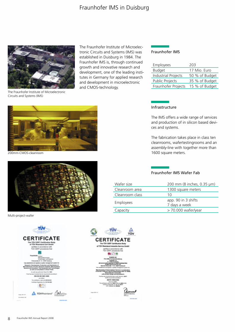
Fraunhofer IMS in Duisburg
Employees 203Budget 17 Mio. EuroIndustrial Projects 50 % of BudgetPublic Projects 35 % of BudgetFraunhofer Projects 15 % of Budget
200mm-CMOS-cleanroom
Multi-project-wafer
Wafer size 200 mm (8 inches, 0.35 µm)Cleanroom area 1300 square metersCleanroom class 10
Employeesapp. 90 in 3 shifts 7 days a week
Capacity > 70.000 wafer/year
The Fraunhofer Institute of Micro electronic Circuits and Systems (IMS)
Fraunhofer IMS
Infrastructure
The IMS offers a wide range of servicesand production of in silicon based devi-ces and systems.
The fabrication takes place in class tencleanrooms, wafertestingrooms and anassembly-line with together more than1600 square meters.
Fraunhofer IMS Wafer Fab
9Fraunhofer IMS Annual Report 2008
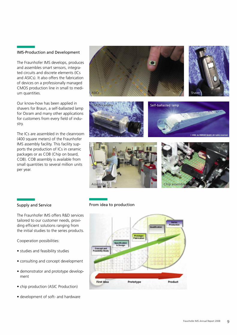
IMS-Production and Development
The Fraunhofer IMS develops, producesand assembles smart sensors, integra-ted circuits and discrete elements (ICsand ASICs). It also offers the fabricationof devices on a professionally managedCMOS production line in small to medi-um quantities.
Our know-how has been applied inshavers for Braun, a self-ballasted lampfor Osram and many other applicationsfor customers from every field of indu-stry.
The ICs are assembled in the cleanroom(400 square meters) of the FraunhoferIMS assembly facility. This facility sup-ports the production of ICs in ceramicpackages or as COB (Chip on board,COB). COB assembly is available fromsmall quantities to several million unitsper year.
Supply and Service
The Fraunhofer IMS offers R&D servicestailored to our customer needs, provi-ding efficient solutions ranging fromthe initial studies to the series products.
Cooperation possibilities:
• studies and feasibility studies
• consulting and concept development
• demonstrator and prototype develop-ment
• chip production (ASIC Production)
• development of soft- and hardware
ASICs
Self-ballasted lampSelf-ballasted lamp
Shaver
CMOS-cameraCMOS-camera
AssemblyAssembly Chip assemblyChip assembly
From idea to production

10 Fraunhofer IMS Annual Report 2008

11Fraunhofer IMS Annual Report 2008
Fraunhofer IMS BusinessFields and Core Competencies
12 Fraunhofer IMS Annual Report 2008
The Fraunhofer IMS conducts researchand development in many differentapplication areas of including• Automotive• Medical• Consumer• Smart Buildings• Communication• Aero Space• Logistics• Industrial Automation• Semiconductor Industry
Research and Development at the Fraunhofer Institutefor Microelectronic Circuits and Systems
Automotive MedicalApplications
SmartBuildings Aero Space
Logistics
IndustrialAutomation
SemiconductorIndustry
ConsumerElectronic
Markets
These applications are served by ourbusiness fields: • CMOS process and assembly• CMOS sensors (image, pressure and
temperature sensors)• Smart Buildings• Embedded systems hardware and
software• ASIC design und development• Wireless systems, ICs and
transponders
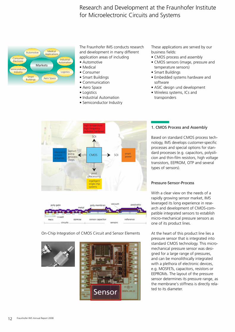
1. CMOS Process and Assembly
Based on standard CMOS process tech-nology, IMS develops customer-specificprocesses and special options for stan-dard processes (e.g. capacitors, polysili-cion and thin-film resistors, high voltagetransistors, EEPROM, OTP and severaltypes of sensors).
Pressure-Sensor-Process
With a clear view on the needs of arapidly growing sensor market, IMSleveraged its long experience in rese-arch and development of CMOS-com-patible integrated sensors to establishmicro-mechanical pressure sensors asone of its product lines.
At the heart of this product line lies apressure sensor that is integrated intostandard CMOS technology. This micro-mechanical pressure sensor was desi-gned for a large range of pressures,and can be monolithically integratedwith a plethora of electronic devices,e.g. MOSFETs, capacitors, resistors orEEPROMs. The layout of the pressuresensor determines its pressure range, asthe membrane's stiffness is directly rela-ted to its diameter.
CMOS SOI
SOI
postprocessing
layout,extraprocesssteps
high temperaturehigh frequencyradiation hardened
ingelligentsingle chipsystems
smartpower
integratedsensorsactuators
On-Chip Integration of CMOS Circuit and Sensor Elements
13Fraunhofer IMS Annual Report 2008
High Temperature SOI CMOS Process
The high temperature SOI CMOS processuses SOI substrates for the production ofASICs that operate at temperatures ofup to 250° C.
Only fully CMOS compatible processsteps are used to manufacture not onlystandard CMOS circuit elements, inclu-ding EEPROM, but also silicon basedsensors, actuators and power devices.
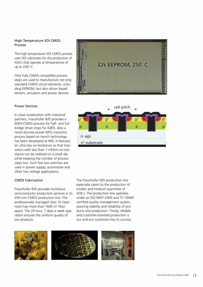
Power Devices
In close cooperation with industrialpartners, Fraunhofer IMS provides a600V-CMOS-process for half- and fullbridge driver chips for IGBTs. Also anovel discrete power MOS transistorprocess based on trench technologyhas been developed at IMS. It featuresan ultra low on-resistance so that tran-sistors with less than 1 mOhm on-resi-stance can be realized on a small die,while keeping the number of processsteps low. Such low loss switches areused in power supply, automotive andother low voltage applications.
CMOS Fabrication
Fraunhofer IMS provides numeroussemiconductor production services in its200 mm CMOS production line. Theprofessionally managed class 10 cleanroom has more than 1600 m2 floorspace. The 24 hour, 7 days a week ope-ration ensures the uniform quality ofour products.
The Fraunhofer IMS production lineespecially caters to the production ofsmaller and medium quantities ofASICs. The production line operatesunder an ISO 9001:2000 and TS 16949certified quality management system,assuring stability and reliability of pro-ducts and production. Timely, reliableand customer-orien ted production isour and our customers key to success.
n+
p
n+ n+n+ n+n+
cell pitch
p p p
n+-substrate
n--epi
p+p+p+ p+
14 Fraunhofer IMS Annual Report 2008
2. Sensors
Pressure and Temperature Sensors
The basic element of our pressure sen-sors is a micromechanical sensor that isfabricated using standard CMOS proces-sing equipment. These sensors can berealized for a wide range of pressures,sharing a single chip with all electronicdevices available in a CMOS process,e.g. MOSFETs, capacitors or EEPROMs.The sensors can be configured as abso-lute or as differential pressure sensors,both with capacitive readout. Thenecessary signal conversion, linearizati-on and amplification circuits are realizedon the same chip, effectively elimina-ting interference on sensor wiring thatis a major issue for discrete solutions.We have already created a variety ofinnovative products using this mono -lithic integration of sensors and signalprocessing functions like programmableamplifiers, sensor linearization, tempe-rature compensation or wireless inter -faces.
The layout of the sensor element deter-mines its pressure range, which may besituated between 0.5 to 250 bar, as thesensor diameter controls the stiffness ofthe membrane: Smaller and stiffermembranes shift the pressure range tohigher pressures. Thus the sensors aresuitable for the measurement of pres-sures ranging from blood, air, and tirepressure all the way to hydraulic oilpressure. The small size of the sensor
and its associated electronics enablesinnovative medical applications for thein vivo measurement of the pressures ofblood, brain, eye or other body fluids.
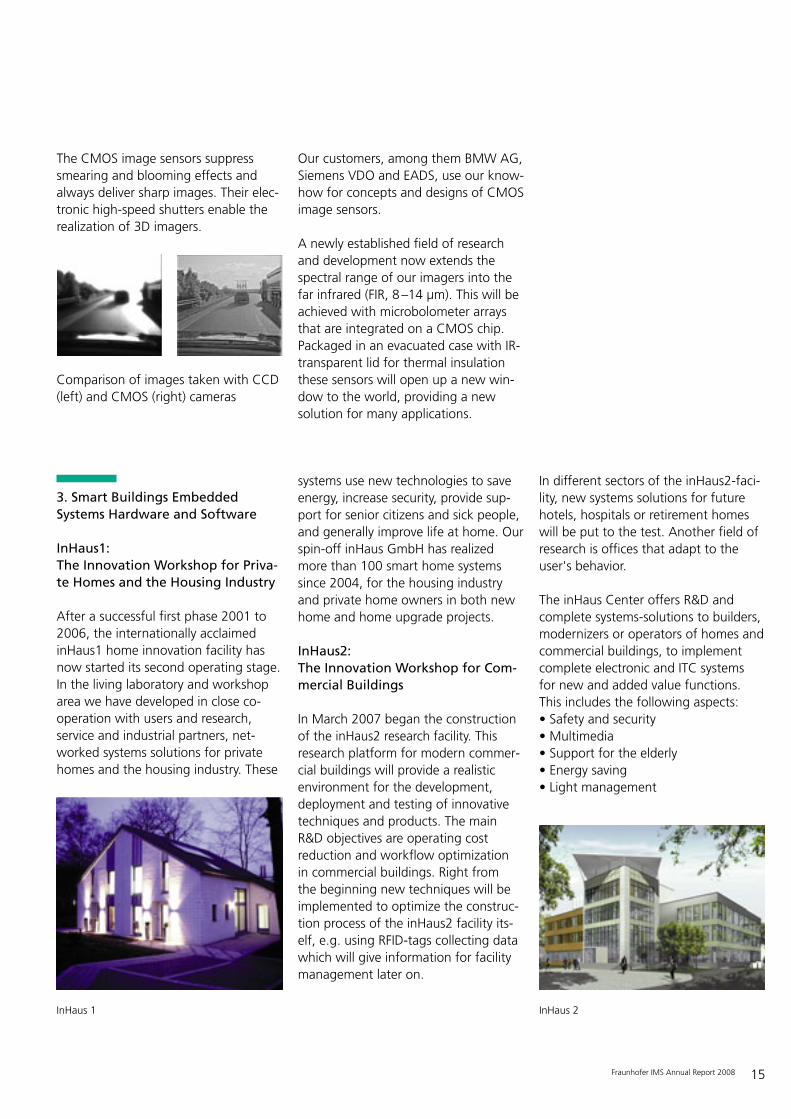
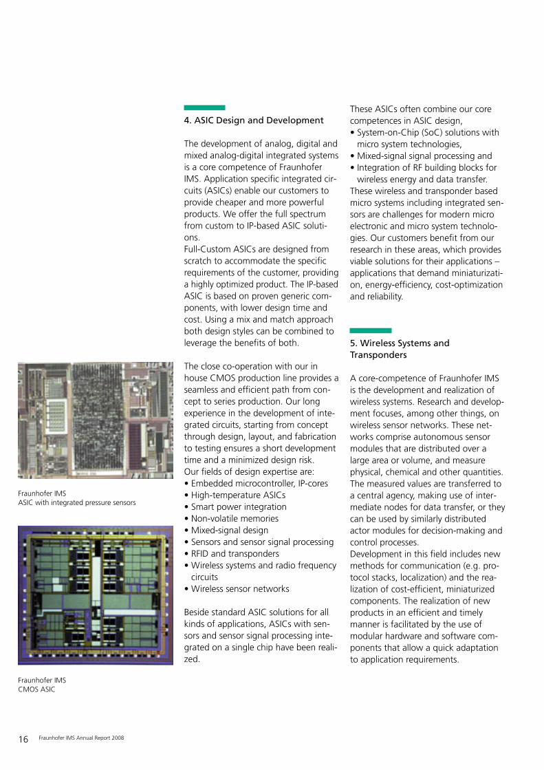
CMOS Image-Sensors and SensorSystem
Fraunhofer IMS image sensors arebased on CMOS technology, whichenables the monolithic integration ofsensor and circuit elements on a singlechip. This integration is used e.g. tocontrol the sensitivity of each individualpixel to avoid blooming.
CMOS Camera
CMOS Image sensor
A wide range of CMOS image sensorshas been developed for our customersand in research projects. The realizedsensors include high dynamic rangesensors, high speed sensors – whichdeliver 1000 high quality images persecond – low power sensors with lessthan 40 mW of power consumptionand high-resolution sensors with “regi-on of interest” function for faster read-out of subsections of the pixel array.
15Fraunhofer IMS Annual Report 2008
The CMOS image sensors suppresssmearing and blooming effects andalways deliver sharp images. Their elec-tronic high-speed shutters enable therealization of 3D imagers.
Comparison of images taken with CCD(left) and CMOS (right) cameras
Our customers, among them BMW AG,Siemens VDO and EADS, use our know-how for concepts and designs of CMOSimage sensors.
A newly established field of researchand development now extends thespectral range of our imagers into thefar infrared (FIR, 8–14 µm). This will beachieved with microbolometer arraysthat are integrated on a CMOS chip.Packaged in an evacuated case with IR-transparent lid for thermal insulationthese sensors will open up a new win-dow to the world, providing a newsolution for many applications.
3. Smart Buildings EmbeddedSystems Hardware and Software
InHaus1: The Innovation Workshop for Priva-te Homes and the Housing Industry
After a successful first phase 2001 to2006, the internationally acclaimedinHaus1 home innovation facility hasnow started its second operating stage.In the living laboratory and workshoparea we have developed in close co -opera tion with users and research, service and industrial partners, net -worked systems solutions for privatehomes and the housing industry. These
systems use new technologies to saveenergy, increase security, provide sup-port for senior citizens and sick people,and generally improve life at home. Ourspin-off inHaus GmbH has realizedmore than 100 smart home systemssince 2004, for the housing industryand private home owners in both newhome and home upgrade projects.
InHaus2:The Innovation Workshop for Com-mercial Buildings
In March 2007 began the constructionof the inHaus2 research facility. Thisresearch platform for modern commer-cial buildings will provide a realisticenvironment for the development,deployment and testing of innovativetechniques and products. The mainR&D objectives are operating costreduction and workflow optimization in commercial buildings. Right from the beginning new techniques will beimplemented to optimize the construc-tion process of the inHaus2 facility its-elf, e.g. using RFID-tags collecting datawhich will give information for facilitymanagement later on.
In different sectors of the inHaus2-faci-lity, new systems solutions for futurehotels, hospitals or retirement homeswill be put to the test. Another field ofresearch is offices that adapt to theuser's behavior.
The inHaus Center offers R&D andcomplete systems-solutions to builders,modernizers or operators of homes andcommercial buildings, to implementcomplete electronic and ITC systems for new and added value functions.This includes the following aspects:• Safety and security• Multimedia • Support for the elderly• Energy saving• Light management
InHaus 1 InHaus 2
16 Fraunhofer IMS Annual Report 2008
4. ASIC Design and Development
The development of analog, digital andmixed analog-digital integrated systemsis a core competence of FraunhoferIMS. Application specific integrated cir-cuits (ASICs) enable our customers toprovide cheaper and more powerfulproducts. We offer the full spectrumfrom custom to IP-based ASIC soluti-ons.Full-Custom ASICs are designed fromscratch to accommodate the specificrequirements of the customer, providinga highly optimized product. The IP-basedASIC is based on proven generic com-ponents, with lower design time andcost. Using a mix and match approachboth design styles can be combined toleverage the benefits of both.
The close co-operation with our inhouse CMOS production line provides aseamless and efficient path from con-cept to series production. Our longexperience in the development of inte-grated circuits, starting from conceptthrough design, layout, and fabricationto testing ensures a short developmenttime and a minimized design risk. Our fields of design expertise are:• Embedded microcontroller, IP-cores• High-temperature ASICs• Smart power integration• Non-volatile memories• Mixed-signal design• Sensors and sensor signal processing• RFID and transponders• Wireless systems and radio frequency
circuits• Wireless sensor networks
Beside standard ASIC solutions for allkinds of applications, ASICs with sen-sors and sensor signal processing inte-grated on a single chip have been reali-zed.
These ASICs often combine our corecompetences in ASIC design, • System-on-Chip (SoC) solutions with
micro system technologies, • Mixed-signal signal processing and • Integration of RF building blocks for
wireless energy and data transfer. These wireless and transponder basedmicro systems including integrated sen-sors are challenges for modern microelectronic and micro system technolo-gies. Our customers benefit from ourresearch in these areas, which providesviable solutions for their applications –applications that demand miniaturizati-on, energy-efficiency, cost-optimizationand reliability.
5. Wireless Systems and Transponders
A core-competence of Fraunhofer IMSis the development and realization ofwireless systems. Research and develop-ment focuses, among other things, onwireless sensor networks. These net-works comprise autonomous sensormodules that are distributed over alarge area or volume, and measure physical, chemical and other quantities.The measured values are transferred toa central agency, making use of inter-mediate nodes for data transfer, or theycan be used by similarly distributedactor modules for decision-making andcontrol processes. Development in this field includes newmethods for communication (e.g. pro-tocol stacks, localization) and the rea-lization of cost-efficient, miniaturizedcomponents. The realization of newproducts in an efficient and timelymanner is facilitated by the use ofmodular hardware and software com-ponents that allow a quick adaptationto application requirements.
Fraunhofer IMSASIC with integrated pressure sensors
Fraunhofer IMSCMOS ASIC
17Fraunhofer IMS Annual Report 2008
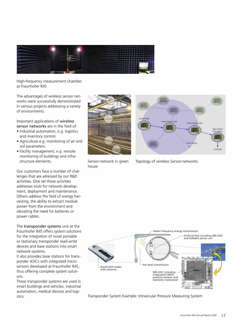
High-frequency measurement chamberat Fraunhofer IMS
The advantages of wireless sensor net-works were successfully demonstratedin various projects addressing a varietyof environments.
Important applications of wireless sensor networks are in the field of:• Industrial automation, e.g. logistics
and inventory control.• Agriculture e.g. monitoring of air and
soil parameters.• Facility management, e.g. remote
monitoring of buildings and infra-structure elements.
Our customers face a number of chal-lenges that are adressed by our R&Dactivities. One set these activitiesaddresses tools for network develop-ment, deployment and maintenance.Others address the field of energy har-vesting, the ability to extract modulepower from the environment andobviating the need for batteries orpower cables.
The transponder systems unit at theFraunhofer IMS offers system solutionsfor the integration of novel portable or stationary transponder read-writedevices and base stations into smartnetwork-systems. It also provides base stations for trans-ponder ASICs with integrated microsensors developed at Fraunhofer IMS,thus offering complete system soluti-ons.These transponder systems are used insmart buildings and vehicles, industrialautomation, medical devices and logi-stics.
Hand-held readerwith antenna
Radio frequency energy transmission
Artificial lens including IMS-ASICand foldable planar coil
Ask data transmission
IMS-ASIC includingintegrated CMOS-pressure senseor andtelemetry transceiver
Transponder System Example: Intraocular Pressure Measuring System
Sensor-network in greenhouse
Topology of wireless Sensor-networks

18 Fraunhofer IMS Annual Report 2008

19Fraunhofer IMS Annual Report 2008
Development of the IMS

20 Fraunhofer IMS Annual Report 2008

21Fraunhofer IMS Annual Report 2008
Development of the IMS
6
24
08
22 Fraunhofer IMS Annual Report 2008
6 08
6 08

23Fraunhofer IMS Annual Report 2008
Selected Projectsof the Year 2008
24 Fraunhofer IMS Annual Report 2008
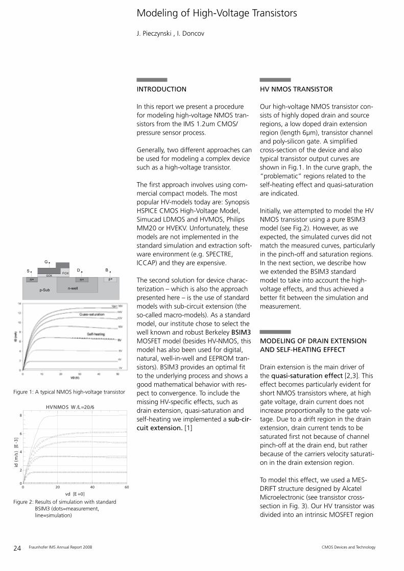
INTRODUCTION
In this report we present a procedurefor modeling high-voltage NMOS tran-sistors from the IMS 1.2um CMOS/pressure sensor process.
Generally, two different approaches canbe used for modeling a complex devicesuch as a high-voltage transistor.
The first approach involves using com-mercial compact models. The mostpopular HV-models today are: SynopsisHSPICE CMOS High-Voltage Model,Simucad LDMOS and HVMOS, PhilipsMM20 or HVEKV. Unfortunately, thesemodels are not implemented in thestandard simulation and extraction soft-ware environment (e.g. SPECTRE,ICCAP) and they are expensive.
The second solution for device charac-terization – which is also the approachpresented here – is the use of standardmodels with sub-circuit extension (theso-called macro-models). As a standardmodel, our institute chose to select thewell known and robust Berkeley BSIM3MOSFET model (besides HV-NMOS, thismodel has also been used for digital,natural, well-in-well and EEPROM tran-sistors). BSIM3 provides an optimal fitto the underlying process and shows agood mathematical behavior with res-pect to convergence. To include themissing HV-specific effects, such asdrain extension, quasi-saturation andself-heating we implemented a sub-cir-cuit extension. [1]
HV NMOS TRANSISTOR
Our high-voltage NMOS transistor con-sists of highly doped drain and sourceregions, a low doped drain extensionregion (length 6µm), transistor channeland poly-silicon gate. A simplifiedcross-section of the device and alsotypical transistor output curves areshown in Fig.1. In the curve graph, the“problematic” regions related to theself-heating effect and quasi-saturationare indicated.
Initially, we attempted to model the HVNMOS transistor using a pure BSIM3model (see Fig.2). However, as weexpected, the simulated curves did notmatch the measured curves, particularlyin the pinch-off and saturation regions.In the next section, we describe howwe extended the BSIM3 standardmodel to take into account the high-voltage effects, and thus achieved abetter fit between the simulation andmeasurement.
MODELING OF DRAIN EXTENSIONAND SELF-HEATING EFFECT
Drain extension is the main driver ofthe quasi-saturation effect [2,3]. Thiseffect becomes particularly evident forshort NMOS transistors where, at highgate voltage, drain current does notincrease proportionally to the gate vol-tage. Due to a drift region in the drainextension, drain current tends to besaturated first not because of channelpinch-off at the drain end, but ratherbecause of the carriers velocity saturati-on in the drain extension region.
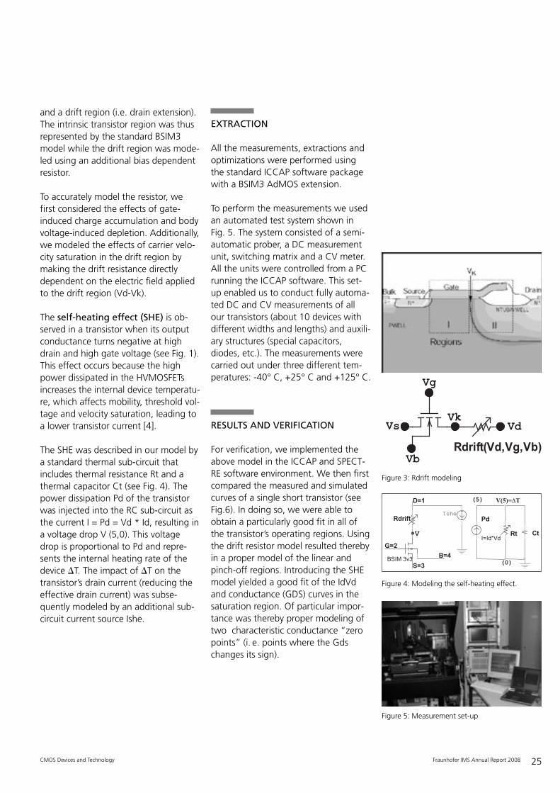
To model this effect, we used a MES-DRIFT structure designed by AlcatelMicroelectronic (see transistor cross-section in Fig. 3). Our HV transistor wasdivided into an intrinsic MOSFET region
Modeling of High-Voltage Transistors
J. Pieczynski , I. Doncov
CMOS Devices and Technology
S
G
D B
n+ n+ p+
p-Sub
GOX
n-well
FOX
Figure 1: A typical NMOS high-voltage transistor
HVNMOS W /L=20/6
vd [E +0]
id
(m/s
) [E
-3]
0 20 40 600
2
4
6
8
Figure 2: Results of simulation with standardBSIM3 (dots=measurement,line=simulation)
25Fraunhofer IMS Annual Report 2008
and a drift region (i.e. drain extension).The intrinsic transistor region was thusrepresented by the standard BSIM3model while the drift region was mode-led using an additional bias dependentresistor.
To accurately model the resistor, wefirst considered the effects of gate-induced charge accumulation and bodyvoltage-induced depletion. Additionally,we modeled the effects of carrier velo-city saturation in the drift region bymaking the drift resistance directlydependent on the electric field appliedto the drift region (Vd-Vk).
The self-heating effect (SHE) is ob -served in a transistor when its outputconductance turns negative at highdrain and high gate voltage (see Fig. 1).This effect occurs because the highpower dissipated in the HVMOSFETsincreases the internal device temperatu-re, which affects mobility, threshold vol-tage and velocity saturation, leading toa lower transistor current [4].
The SHE was described in our model bya standard thermal sub-circuit thatincludes thermal resistance Rt and athermal capacitor Ct (see Fig. 4). Thepower dissipation Pd of the transistorwas injected into the RC sub-circuit asthe current I = Pd = Vd * Id, resulting ina voltage drop V (5,0). This voltagedrop is proportional to Pd and repre-sents the internal heating rate of thedevice �T. The impact of �T on thetransistor’s drain current (reducing theeffective drain current) was subse-quently modeled by an additional sub-circuit current source Ishe.
EXTRACTION
All the measurements, extractions andoptimizations were performed usingthe standard ICCAP software packagewith a BSIM3 AdMOS extension.
To perform the measurements we usedan automated test system shown inFig. 5. The system consisted of a semi-automatic prober, a DC measurementunit, switching matrix and a CV meter.All the units were controlled from a PCrunning the ICCAP software. This set-up enabled us to conduct fully automa-ted DC and CV measurements of allour transistors (about 10 devices withdifferent widths and lengths) and auxili-ary structures (special capacitors,diodes, etc.). The measurements werecarried out under three different tem-peratures: -40° C, +25° C and +125° C.
RESULTS AND VERIFICATION
For verification, we implemented theabove model in the ICCAP and SPECT-RE software environment. We then firstcompared the measured and simulatedcurves of a single short transistor (seeFig.6). In doing so, we were able toobtain a particularly good fit in all ofthe transistor’s operating regions. Usingthe drift resistor model resulted therebyin a proper model of the linear andpinch-off regions. Introducing the SHEmodel yielded a good fit of the IdVdand conductance (GDS) curves in thesaturation region. Of particular impor-tance was thereby proper modeling oftwo characteristic conductance “zeropoints” (i. e. points where the Gdschanges its sign).
CMOS Devices and Technology
Figure 3: Rdrift modeling
IsheRdrift
V(5)=ΔT
S=3
D=1
V Rt
B=4G=2
Pd
I=Id*Vd
BSIM 3v3
(5)
Ct
(0)
Figure 4: Modeling the self-heating effect.
Rdrift(Vd,Vg,Vb)
Vd
Vg
Vs
Vb
Vk
Figure 5: Measurement set-up
26 Fraunhofer IMS Annual Report 2008 CMOS Devices and Technology
CONCLUSIONS
In this paper, we showed that success -ful modeling of the HV NMOS transis -tors is possible with an extended BSIM3model. All known HV problems, such asquasi-saturation and self-heating, couldbe resolved using the presented sub-cir-cuit extension. Our approach is simplein implementation, inexpensive and canbe used in a range of commercialmodels.
REFERENCES
[1] J.Pieczynski, I.Doncov, “Modeling ofHigh-Voltage NMOS Transistorsusing Extended BSIM3 Model”,MIXDES 2008, pp.75-80, Poznan,Poland, Juni 2008.
[2] E.Seebacher, “HV MOS Modeling”,MOS-AK, Böblingen, 2006, Ger-many.
[3] E.Gondro, P.Klein and F.Schuler, “AnAnalytical Source-And-Drain SeriesResistance Model of Quarter MicronMosfets and its Influence on CircuitSimulation”, p.VI206-VI2009, IEEE1999.
[4] C. Anghel, “High Voltage Devicesfor Standard MOS Technologies –Characterisation and Modeling”,These No 3116 (2004), EPFL, Lau-sanne, 2004.
HVNMOS W /L=20/6
vd [E +0]
id
(m
/s)
[E
-3]
0 20 40 600
2
4
6HVNMOS s ymmetric W /L=20/12
vd [E +0]
d
Id/d
Vd
(m
/s)
[L
OG
]
0 20 40 601E -10
1E -9
1E -8
1E -7
1E -6
1E -5
1E -4
1E -3
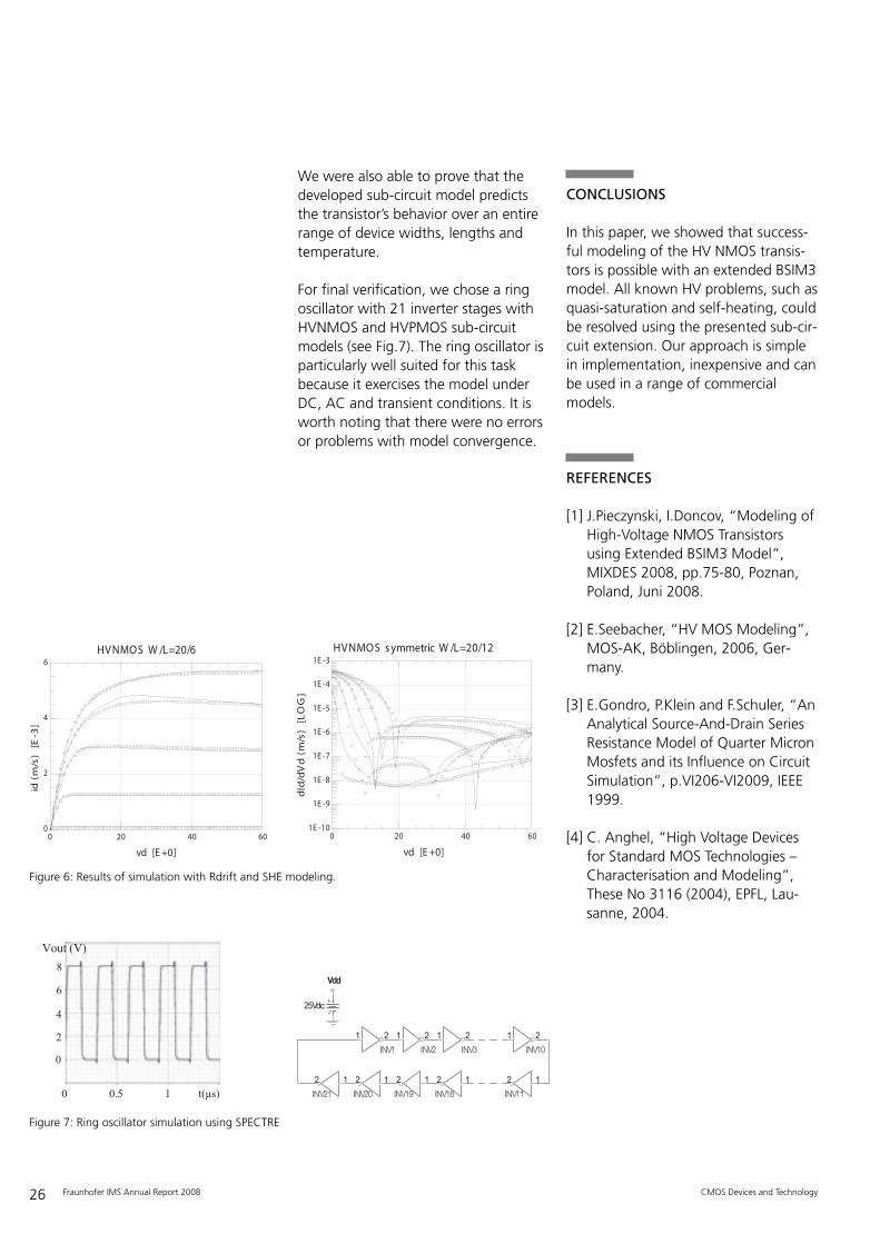
Figure 6: Results of simulation with Rdrift and SHE modeling.
Figure 7: Ring oscillator simulation using SPECTRE
Vdd
INV11
12
INV10
1 2
INV2
1 2
INV1
1 2
INV21
12
INV20
12
INV18
12
INV3
1 2
INV19
12
25Vdc
0 0.5 1 t(μs)
0
2
4
6
8
Vout (V)
We were also able to prove that thedeveloped sub-circuit model predictsthe transistor’s behavior over an entirerange of device widths, lengths andtemperature.
For final verification, we chose a ringoscillator with 21 inverter stages withHVNMOS and HVPMOS sub-circuitmodels (see Fig.7). The ring oscillator isparticularly well suited for this taskbecause it exercises the model underDC, AC and transient conditions. It isworth noting that there were no errorsor problems with model convergence.
27Fraunhofer IMS Annual Report 2008
I Introduction
Charge-coupled devices (CCD) havebeen the dominant technology in thefield of solid-state imaging for a coupleof decades due to their capability toperform very efficiently and uniformlyover large areas, the collection andtransfer of photogenerated charge carriers and their measurement at lownoise [1]. But today, the maturity ofcomplementary metal-oxide-semicon-ductor (CMOS) technology basedphoto detectors is established, and theadvantages of their specific featureswhich allow x-y pixel addressing, in-pixel amplification and signal proces-sing, the “camera-on-a-chip” [2]approach, and the use of deep sub-micron standard CMOS processes makethem a perfect candidate for an increa-sing number of imaging applications.The frontiers are to be pushed furtherin what signal and spatial resolutionspresent in CMOS imagers are concer-ned, considering their application inautomotive or medicine oriented indu-stries, basic science, or telecommunica-tions. In this sense, the need for con-stant optimization of photodetectorsand entire imager systems has becomefor the CMOS Imaging group at theFraunhofer IMS evident with time.
In the year 2008, the industry availablestandard CMOS process minimum fea-ture dimensions are to be found be -tween the 120 nm and 65 nm. The latter, driven by the desire of smallerdevice area, lower power consumption,higher operation speed, and increasedfunctionality. Nevertheless, as expressedby Wong [3] back in 1996, while “stan-dard” CMOS technologies were provi-ding adequate imaging performance atthe 2 �m–0.8 �m generations withoutany process changes, some modificati-ons to the fabrication process and inno-vations of the pixel architecture are
needed to enable CMOS processes forgood quality imaging at the 0.5 �mtechnology generation and below.Regarding the pixel size, Wong [3] sug-gested that CMOS imagers wouldbenefit from further scaling after the0.25 �m generation only in terms ofincreased fill-factor and/or increasedsignal processing functionality within apixel. The latter proved true, and anincreased number of imager manufac-turers are introducing special imagingenhanced CMOS processes, departingfrom “standard” CMOS logic andmemory processes at the 0.35 �m–0.25 �m and below technology gene-rations. In this context, the 0.35 �mstandard CMOS process available at theFraunhofer IMS for fabrication of ima-ger systems will be investigated in thispaper to understand its real imagingperformance capabilities. Following,different additional process steps deve-loped and other improvements under-taken so far will be described, as wellas a couple of examples of current rese-arch lines followed for its further opti-mization.
II Phototransduction
High doping profiles, thin gate-oxidesand low bias voltages affect adverselythe performance of CMOS imagers,and can still cause problems if standardsolutions to some of the issues affec-ting the photodetector pixel perfor-mances are to be applied. This includesusing separated photoactive and read-out node areas (e.g., floating n+ diffusi-ons (FD) separated from photodiodes orphotogates), where charge-couplingbetween the two regions [4] is notalways possible. On the other hand, the reduced SCR widths (of around0.16 �m to 0.55 �m) degrade the photo detector quantum efficiencies,especially in the NIR part of the spectra.
CMOS Process for Optical Devices
Daniel Durini, Andreas Spickermann, Melanie Jung
CMOS Devices and Technology
28 Fraunhofer IMS Annual Report 2008
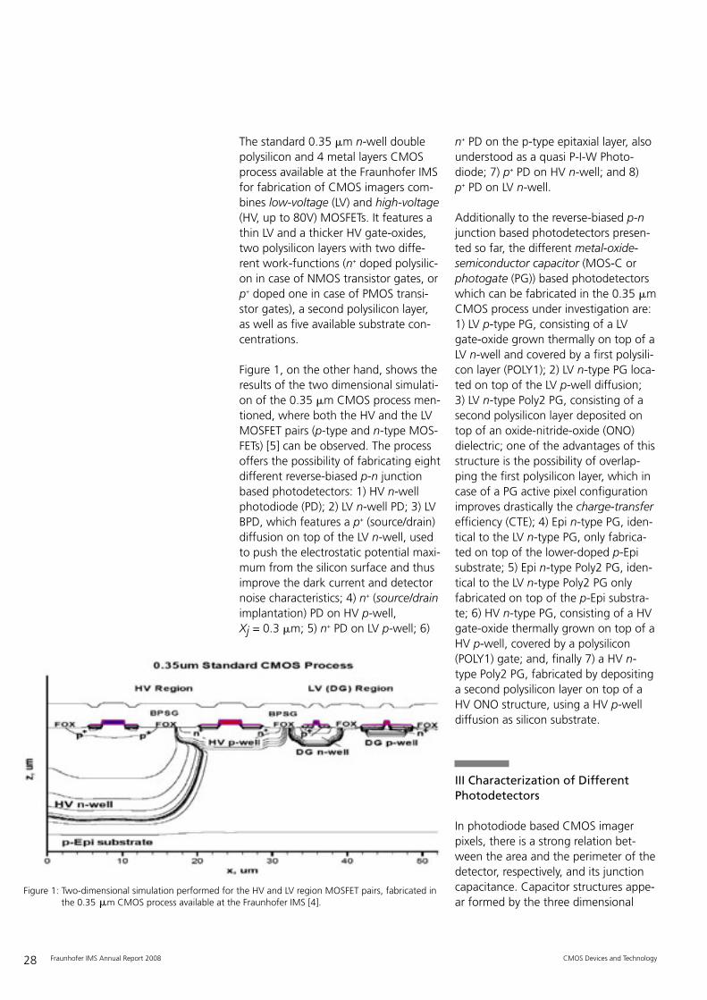
The standard 0.35 �m n-well doublepolysilicon and 4 metal layers CMOSprocess available at the Fraunhofer IMSfor fabrication of CMOS imagers com-bines low-voltage (LV) and high-voltage(HV, up to 80V) MOSFETs. It features athin LV and a thicker HV gate-oxides,two polysilicon layers with two diffe-rent work-functions (n+ doped polysilic-on in case of NMOS transistor gates, orp+ doped one in case of PMOS transi-stor gates), a second polysilicon layer,as well as five available substrate con-centrations.
Figure 1, on the other hand, shows theresults of the two dimensional simulati-on of the 0.35 �m CMOS process men-tioned, where both the HV and the LVMOSFET pairs (p-type and n-type MOS-FETs) [5] can be observed. The processoffers the possibility of fabricating eightdifferent reverse-biased p-n junctionbased photodetectors: 1) HV n-wellphoto diode (PD); 2) LV n-well PD; 3) LVBPD, which features a p+ (source/drain)diffusion on top of the LV n-well, usedto push the electrostatic potential maxi-mum from the silicon surface and thusimprove the dark current and detectornoise characteristics; 4) n+ (source/drainimplantation) PD on HV p-well,Xj = 0.3 �m; 5) n+ PD on LV p-well; 6)
n+ PD on the p-type epitaxial layer, alsounderstood as a quasi P-I-W Photo -diode; 7) p+ PD on HV n-well; and 8) p+ PD on LV n-well.
Additionally to the reverse-biased p-njunction based photodetectors presen-ted so far, the different metal-oxide-semiconductor capacitor (MOS-C orphotogate (PG)) based photodetectorswhich can be fabricated in the 0.35 �mCMOS process under investigation are:1) LV p-type PG, consisting of a LVgate-oxide grown thermally on top of aLV n-well and covered by a first polysili-con layer (POLY1); 2) LV n-type PG loca-ted on top of the LV p-well diffusion; 3) LV n-type Poly2 PG, consisting of asecond polysilicon layer deposited ontop of an oxide-nitride-oxide (ONO)dielectric; one of the advantages of thisstructure is the possibility of overlap-ping the first polysilicon layer, which incase of a PG active pixel configurationimproves drastically the charge-transferefficiency (CTE); 4) Epi n-type PG, iden-tical to the LV n-type PG, only fabrica-ted on top of the lower-doped p-Episubstrate; 5) Epi n-type Poly2 PG, iden-tical to the LV n-type Poly2 PG onlyfabricated on top of the p-Epi substra-te; 6) HV n-type PG, consisting of a HVgate-oxide thermally grown on top of aHV p-well, covered by a polysilicon(POLY1) gate; and, finally 7) a HV n-type Poly2 PG, fabricated by depositinga second polysilicon layer on top of aHV ONO structure, using a HV p-welldiffusion as silicon substrate.
III Characterization of DifferentPhotodetectors
In photodiode based CMOS imagerpixels, there is a strong relation bet-ween the area and the perimeter of thedetector, respectively, and its junctioncapacitance. Capacitor structures appe-ar formed by the three dimensional
CMOS Devices and Technology
Figure 1: Two-dimensional simulation performed for the HV and LV region MOSFET pairs, fabricated inthe 0.35 �m CMOS process available at the Fraunhofer IMS [4].
29Fraunhofer IMS Annual Report 2008
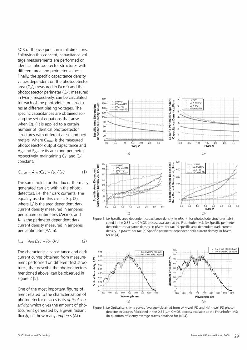
SCR of the p-n junction in all directions.Following this concept, capacitance-vol-tage measurements are performed onidentical photodetector structures withdifferent area and perimeter values.Finally, the specific capacitance densityvalues dependent on the photodetectorarea (CA’, measured in F/cm2) and thephotodetector perimeter (CP’, measuredin F/cm), respectively, can be calculatedfor each of the photodetector structu-res at different biasing voltages. Thespecific capacitances are obtained sol-ving the set of equations that arisewhen Eq. (1) is applied to a certainnumber of identical photodetectorstructures with different areas and peri-meters, where CTOTAL is the measuredphotodetector output capacitance andAPD and PPD are its area and perimeter, respectively, maintaining CA’ and CP’constant.
CTOTAL = APD (CA’) + PPD (CP’) (1)
The same holds for the flux of thermallygenerated carriers within the photo-detectors, i.e. their dark currents. Theequality used in this case is Eq. (2),where JA’ is the area dependent darkcurrent density measured in amperesper square centimetres (A/cm2), and JP’ is the perimeter dependent dark current density measured in amperesper centimetre (A/cm).
Idark = APD (JA’) + PPD (JP’) (2)
The characteristic capacitance and darkcurrent curves obtained from measure-ment performed on different test struc-tures, that describe the photodetectorsmentioned above, can be observed inFigure 2 [5].
One of the most important figures ofmerit related to the characterization ofphotodetector devices is its optical sen-sitivity, which gives the amount of pho-tocurrent generated by a given radiantflux �, i.e. how many amperes (A) of
CMOS Devices and Technology
0.0 0.5 1.0 1.5 2.0 2.5 3.00
20
40
60
80
100
120
140
160
180 LV BPD LV n-well PD LV n+ PD HV n-well PD
Sp
ecif
ic A
rea
Dep
end
ent
Cap
acit
ance
Den
sity
, nF
/cm
2
BIAS, V0.0 0.5 1.0 1.5 2.0 2.5 3.0
0
1
2
3
4
5
6
7 LV BPD LV n-wellPD LV n+ PD HV n-wellPD
Sp
ecif
ic P
erim
eter
Dep
end
ent
Cap
acit
ance
Den
sity
, pF
/cm
BIAS, V
(a) (b)
0.0 0.5 1.0 1.5 2.0 2.5 3.0 3.5
0
50
100
150
200
250
300
350
Sp
ecif
ic A
rea
Dep
end
ent
Dar
k C
urr
ent
Den
sity
JA',
pA
/cm
2
LV BPD LV n-well PD LV n+ PD HV n-well PD
0.0 0.5 1.0 1.5 2.0 2.5 3.0 3.5
0
100
200
300
400
500 LV BPD LV n-well PD LV n+ PD HV n-well PD
BIAS, V
Sp
ecif
ic P
erim
eter
Dep
end
ent
Dar
k C
urr
ent
Den
sity
JP',
fA/c
m
(c) (d)
Figure 2: (a) Specific area dependent capacitance density, in nF/cm2, for photodiode structures fabri -cated in the 0.35 �m CMOS process available at the Fraunhofer IMS; (b) Specific perimeterdependent capacitance density, in pF/cm, for (a); (c) specific area dependent dark currentdensity, in pA/cm2 for (a); (d) Specific perimeter dependent dark current density, in fA/cm, for (c) [4].
300 400 500 600 700 800 900 1000 11000.00
0.05
0.10
0.15
0.20
0.25
0.30
0.35
0.40
0.45
Op
tica
l Sen
siti
vity
, A/W
Wavelength, nm
LV n-well PD (0.35μm) HV n-well PD (0.35μm)
300 400 500 600 700 800 900 1000 11000
10
20
30
40
50
60
70
80
90
Qu
antu
m E
ffic
ien
cy, %
Wavelength, nm
LV n-well PD (0.35μm) HV n-well PD (0.35μm)
(a) (b)
Figure 3: (a) Optical sensitivity curves (average) obtained from LV n-well PD and HV n-well PD photo-detector structures fabricated in the 0.35 �m CMOS process available at the Fraunhofer IMS;(b) quantum efficiency average curves obtained for (a) [4].
30 Fraunhofer IMS Annual Report 2008
photocurrent are generated by a singleimpinging watt (W) of irradiation, inA/W. On the other hand, the spectralresponsivity provides the response ofthe entire pixel, measured in V/�J/cm2
for a certain charge-collection (photo-current integration) time. Finally, thequantum efficiency of a photodetectoressentially indicates how many elec-tron-hole pairs (ehp) are generated foreach photon impinging on the detec-tor, or the probability of a single pho-ton to produce one ehp. Figure 3 (a) [5]shows the wavelength dependent opti-cal sensitivity of the photodiode basedstructures fabricated in the 0.35 �mCMOS process at the Fraunhofer IMS,for wavelengths ranging from 300 nmto 1100 nm. Figure 3 (b), on the otherhand shows the quantum efficiencycurves measured for the same photo-detectors [5].
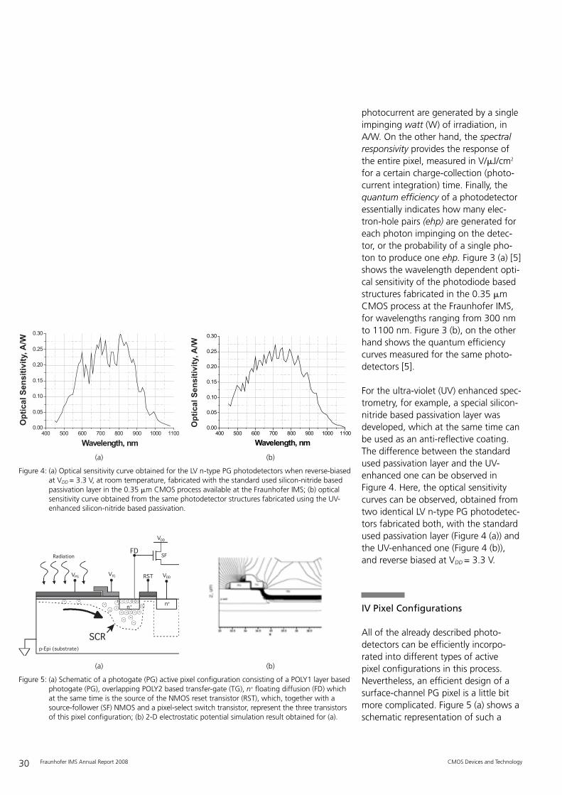
For the ultra-violet (UV) enhanced spec-trometry, for example, a special silicon-nitride based passivation layer wasdeveloped, which at the same time canbe used as an anti-reflective coating.The difference between the standardused passivation layer and the UV-enhanced one can be observed in Figure 4. Here, the optical sensitivitycurves can be observed, obtained fromtwo identical LV n-type PG photodetec-tors fabricated both, with the standardused passivation layer (Figure 4 (a)) andthe UV-enhanced one (Figure 4 (b)),and reverse biased at VDD = 3.3 V.
IV Pixel Configurations
All of the already described photo-detectors can be efficiently incorpo -rated into different types of active pixel configurations in this process.Nevertheless, an efficient design of asurface-channel PG pixel is a little bitmore complicated. Figure 5 (a) shows aschematic representation of such a
CMOS Devices and Technology
400 500 600 700 800 900 1000 11000.00
0.05
0.10
0.15
0.20
0.25
0.30
Op
tica
l Sen
siti
vity
, A/W
Wavelength, nm400 500 600 700 800 900 1000 1100
0.00
0.05
0.10
0.15
0.20
0.25
0.30
Op
tica
l Sen
siti
vity
, A/W
Wavelength, nm
(a) (b)
Figure 4: (a) Optical sensitivity curve obtained for the LV n-type PG photodetectors when reverse-biasedat VDD = 3.3 V, at room temperature, fabricated with the standard used silicon-nitride basedpassivation layer in the 0.35 �m CMOS process available at the Fraunhofer IMS; (b) opticalsensitivity curve obtained from the same photodetector structures fabricated using the UV-enhanced silicon-nitride based passivation.
p-Epi (substrate)
Radiation
VPG VTG RST VDD
n+ n+- --
--
-
-
- -
--
- - - --
FDSF
VDD
- - - - -
SCR
(a) (b)
Figure 5: (a) Schematic of a photogate (PG) active pixel configuration consisting of a POLY1 layer basedphotogate (PG), overlapping POLY2 based transfer-gate (TG), n+ floating diffusion (FD) whichat the same time is the source of the NMOS reset transistor (RST), which, together with asource-follower (SF) NMOS and a pixel-select switch transistor, represent the three transistorsof this pixel configuration; (b) 2-D electrostatic potential simulation result obtained for (a).
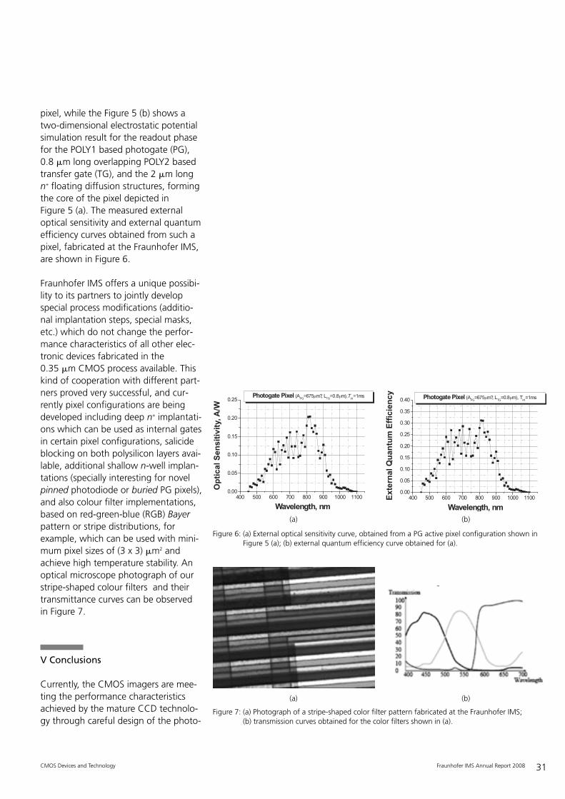
31Fraunhofer IMS Annual Report 2008
pixel, while the Figure 5 (b) shows atwo-dimensional electrostatic potentialsimulation result for the readout phasefor the POLY1 based photogate (PG),0.8 �m long overlapping POLY2 basedtransfer gate (TG), and the 2 �m longn+ floating diffusion structures, formingthe core of the pixel depicted inFigure 5 (a). The measured externaloptical sensitivity and external quantumefficiency curves obtained from such apixel, fabricated at the Fraunhofer IMS,are shown in Figure 6.
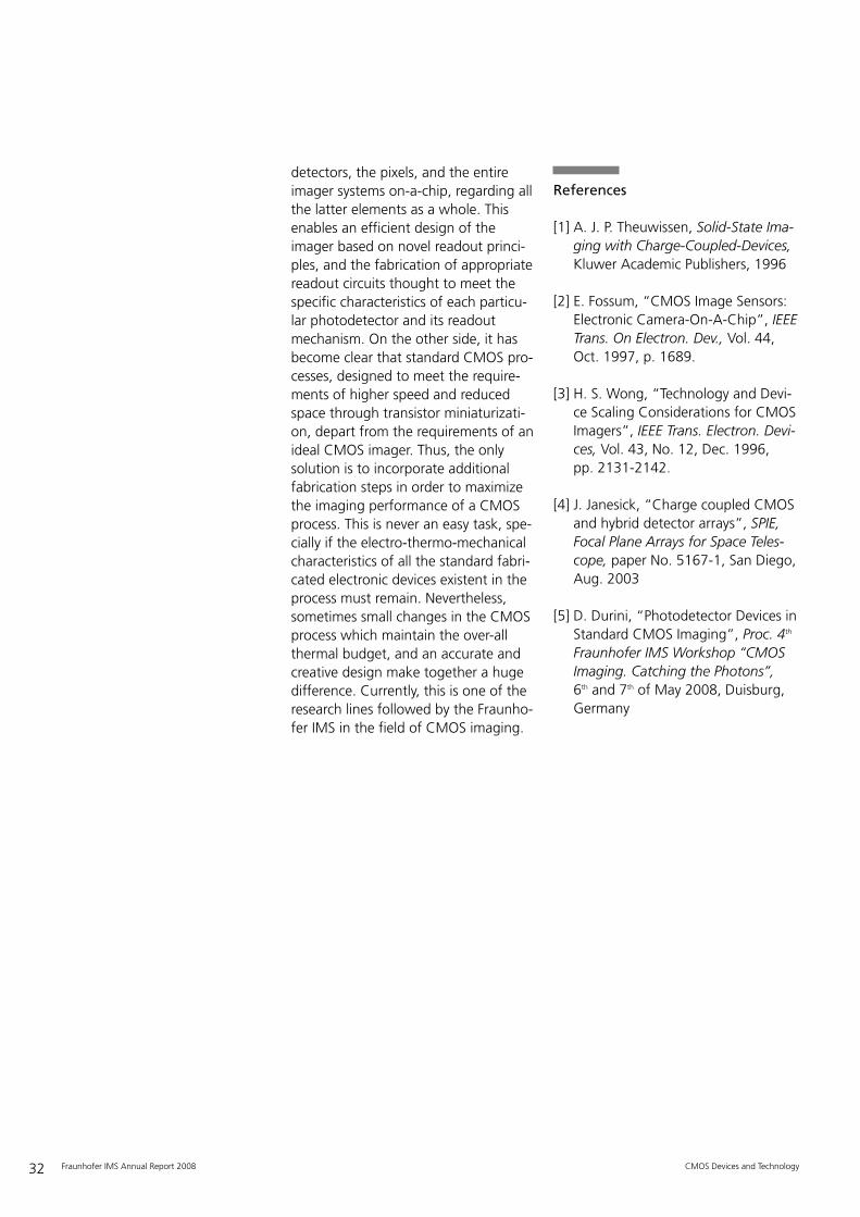
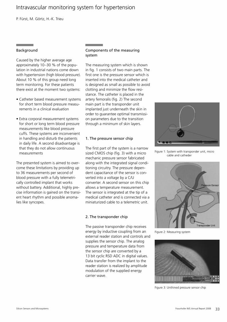
Fraunhofer IMS offers a unique possibi-lity to its partners to jointly developspecial process modifications (additio-nal implantation steps, special masks,etc.) which do not change the perfor-mance characteristics of all other elec-tronic devices fabricated in the0.35 �m CMOS process available. Thiskind of cooperation with different part-ners proved very successful, and cur-rently pixel configurations are beingdeveloped including deep n+ implantati-ons which can be used as internal gatesin certain pixel configurations, salicideblocking on both polysilicon layers avai-lable, additional shallow n-well implan-tations (specially interesting for novelpinned photodiode or buried PG pixels),and also colour filter implementations,based on red-green-blue (RGB) Bayerpattern or stripe distributions, forexample, which can be used with mini-mum pixel sizes of (3 x 3) �m2 andachieve high temperature stability. Anoptical microscope photograph of ourstripe-shaped colour filters and theirtransmittance curves can be observedin Figure 7.
V Conclusions
Currently, the CMOS imagers are mee-ting the performance characteristicsachieved by the mature CCD technolo-gy through careful design of the photo-
CMOS Devices and Technology
400 500 600 700 800 900 1000 11000.00
0.05
0.10
0.15
0.20
0.25Photogate Pixel (A
PG=675μm?, L
TG=0.8μm),T
int=1ms
Op
tica
l Sen
siti
vity
, A/W
Wavelength, nm400 500 600 700 800 900 1000 1100
0.00
0.05
0.10
0.15
0.20
0.25
0.30
0.35
0.40 Photogate Pixel (APG
=675μm?, LTG
=0.8μm), Tint
=1ms
Ext
ern
al Q
uan
tum
Eff
icie
ncy
Wavelength, nm
(a) (b)
Figure 6: (a) External optical sensitivity curve, obtained from a PG active pixel configuration shown inFigure 5 (a); (b) external quantum efficiency curve obtained for (a).
(a) (b)
Figure 7: (a) Photograph of a stripe-shaped color filter pattern fabricated at the Fraunhofer IMS; (b) transmission curves obtained for the color filters shown in (a).
32 Fraunhofer IMS Annual Report 2008
detectors, the pixels, and the entireimager systems on-a-chip, regarding allthe latter elements as a whole. Thisenables an efficient design of the imager based on novel readout princi-ples, and the fabrication of appropriatereadout circuits thought to meet thespecific characteristics of each particu-lar photodetector and its readoutmechanism. On the other side, it hasbecome clear that standard CMOS pro-cesses, designed to meet the require-ments of higher speed and reducedspace through transistor miniaturizati-on, depart from the requirements of anideal CMOS imager. Thus, the onlysolution is to incorporate additionalfabrication steps in order to maximizethe imaging performance of a CMOSprocess. This is never an easy task, spe-cially if the electro-thermo-mechanicalcharacteristics of all the standard fabri-cated electronic devices existent in theprocess must remain. Nevertheless,sometimes small changes in the CMOSprocess which maintain the over-allthermal budget, and an accurate andcreative design make together a hugedifference. Currently, this is one of theresearch lines followed by the Fraunho-fer IMS in the field of CMOS imaging.
References
[1] A. J. P. Theuwissen, Solid-State Ima-ging with Charge-Coupled-Devices,Kluwer Academic Publishers, 1996
[2] E. Fossum, “CMOS Image Sensors:Electronic Camera-On-A-Chip”, IEEETrans. On Electron. Dev., Vol. 44,Oct. 1997, p. 1689.
[3] H. S. Wong, “Technology and Devi-ce Scaling Considerations for CMOSImagers”, IEEE Trans. Electron. Devi-ces, Vol. 43, No. 12, Dec. 1996, pp. 2131-2142.
[4] J. Janesick, “Charge coupled CMOSand hybrid detector arrays”, SPIE,Focal Plane Arrays for Space Teles -cope, paper No. 5167-1, San Diego,Aug. 2003
[5] D. Durini, “Photodetector Devices inStandard CMOS Imaging”, Proc. 4th
Fraunhofer IMS Workshop “CMOSImaging. Catching the Photons”,6th and 7th of May 2008, Duisburg,Germany
CMOS Devices and Technology
33Fraunhofer IMS Annual Report 2008
Background
Caused by the higher average ageapproximately 10–30 % of the popu -lation in industrial nations come downwith hypertension (high blood pressure).About 10 % of this group need longterm monitoring. For these patientsthere exist at the moment two systems:
• Catheter based measurement systemsfor short term blood pressure measu-rements in a clinical evaluation
• Extra corporal measurement systemsfor short or long term blood pressuremeasurements like blood pressurecuffs. These systems are inconvenientin handling and disturb the patientsin daily life. A second disadvantage isthat they do not allow continuousmeasurements
The presented system is aimed to over-come these limitations by providing upto 36 measurements per second ofblood pressure with a fully telemetri -cally controlled implant that workswithout battery. Additional, highly pre-cise information is gained on the transi-ent heart rhythm and possible anoma-lies like syncopes.
Components of the measuringsystem
The measuring system which is shownin fig. 1 consists of two main parts. Thefirst one is the pressure sensor which isinserted into the medical catheter andis designed as small as possible to avoidclotting and minimize the flow resi-stance. The catheter is placed in theartery femoralis (fig. 2) The secondmain part is the transponder unitimplanted just underneath the skin inorder to guarantee optimal transmissi-on parameters due to the transitionthrough a minimum of skin layers.
1. The pressure sensor chip
The first part of the system is a narrowsized CMOS chip (fig. 3) with a micromechanic pressure sensor fabricatedalong with the integrated signal condi-tioning circuitry. The pressure depen-dent capacitance of the sensor is con-verted into a voltage by a C/Uconverter. A second sensor on this chipallows a temperature measurement.The sensor is integrated at the tip of amedical catheter and is connected via aminiaturized cable to a telemetric unit.
2. The transponder chip
The passive transponder chip receivesenergy by inductive coupling from anexternal reader station and controls andsupplies the sensor chip. The analogpressure and temperature data fromthe sensor chip are converted by a13 bit cyclic RSD ADC in digital values.Data transfer from the implant to thereader station is realized by amplitudemodulation of the supplied energy carrier wave.
Intravascular monitoring system for hypertension
P. Fürst, M. Görtz, H.-K. Trieu
Silicon Sensors and Microsystems
Figure 1: System with transponder unit, microcable and catheder
Figure 2: Measuring system
Figure 3: Unthined pressure sensor chip
34 Fraunhofer IMS Annual Report 2008
Calibration and sensor performance
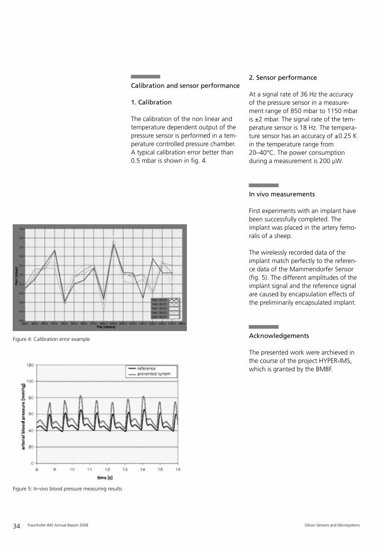
1. Calibration
The calibration of the non linear andtemperature dependent output of thepressure sensor is performed in a tem-perature controlled pressure chamber.A typical calibration error better than0.5 mbar is shown in fig. 4.
2. Sensor performance
At a signal rate of 36 Hz the accuracyof the pressure sensor in a measure-ment range of 850 mbar to 1150 mbaris ±2 mbar. The signal rate of the tem-perature sensor is 18 Hz. The tempera-ture sensor has an accuracy of ±0.25 Kin the temperature range from20–40°C. The power consumptionduring a measurement is 200 µW.
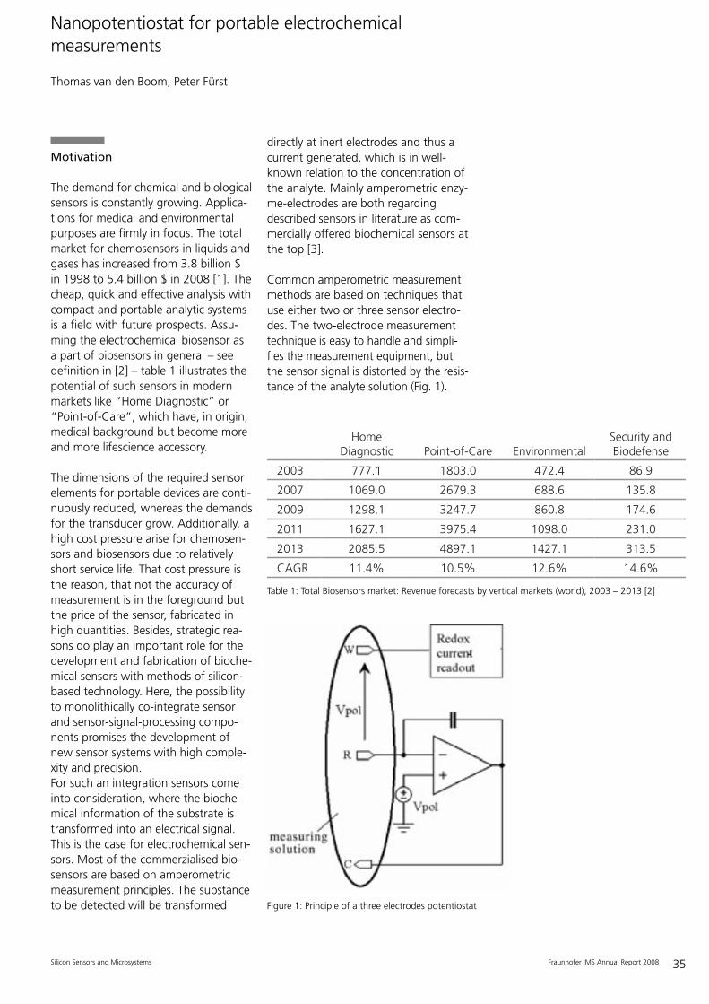
In vivo measurements
First experiments with an implant havebeen successfully completed. Theimplant was placed in the artery femo-ralis of a sheep.
The wirelessly recorded data of theimplant match perfectly to the referen-ce data of the Mammendorfer Sensor(fig. 5). The different amplitudes of theimplant signal and the reference signalare caused by encapsulation effects ofthe preliminarily encapsulated implant.
Acknowledgements
The presented work were archieved inthe course of the project HYPER-IMS,which is granted by the BMBF.
Silicon Sensors and Microsystems
Figure 4: Calibration error example
Figure 5: In-vivo blood pressure measuring results
35Fraunhofer IMS Annual Report 2008
Motivation
The demand for chemical and biologicalsensors is constantly growing. Applica-tions for medical and environmentalpurposes are firmly in focus. The totalmarket for chemosensors in liquids andgases has increased from 3.8 billion $in 1998 to 5.4 billion $ in 2008 [1]. Thecheap, quick and effective analysis withcompact and portable analytic systemsis a field with future prospects. Assu-ming the electrochemical biosensor as a part of biosensors in general – seedefinition in [2] – table 1 illustrates thepotential of such sensors in modernmarkets like “Home Diagnostic” or“Point-of-Care”, which have, in origin,medical background but become moreand more lifescience accessory.
The dimensions of the required sensorelements for portable devices are conti-nuously reduced, whereas the demandsfor the transducer grow. Additionally, ahigh cost pressure arise for chemosen-sors and biosensors due to relativelyshort service life. That cost pressure isthe reason, that not the accuracy ofmeasurement is in the foreground butthe price of the sensor, fabricated inhigh quantities. Besides, strategic rea-sons do play an important role for thedevelopment and fabrication of bioche-mical sensors with methods of silicon-based technology. Here, the possibilityto monolithically co-integrate sensorand sensor-signal-processing compo-nents promises the development ofnew sensor systems with high comple-xity and precision.For such an integration sensors comeinto consideration, where the bioche-mical information of the substrate istransformed into an electrical signal.This is the case for electrochemical sen-sors. Most of the commerzialised bio-sensors are based on amperometricmeasurement principles. The substanceto be detected will be transformed
directly at inert electrodes and thus acurrent generated, which is in well-known relation to the concentration ofthe analyte. Mainly amperometric enzy-me-electrodes are both regardingdescribed sensors in literature as com-mercially offered biochemical sensors atthe top [3].
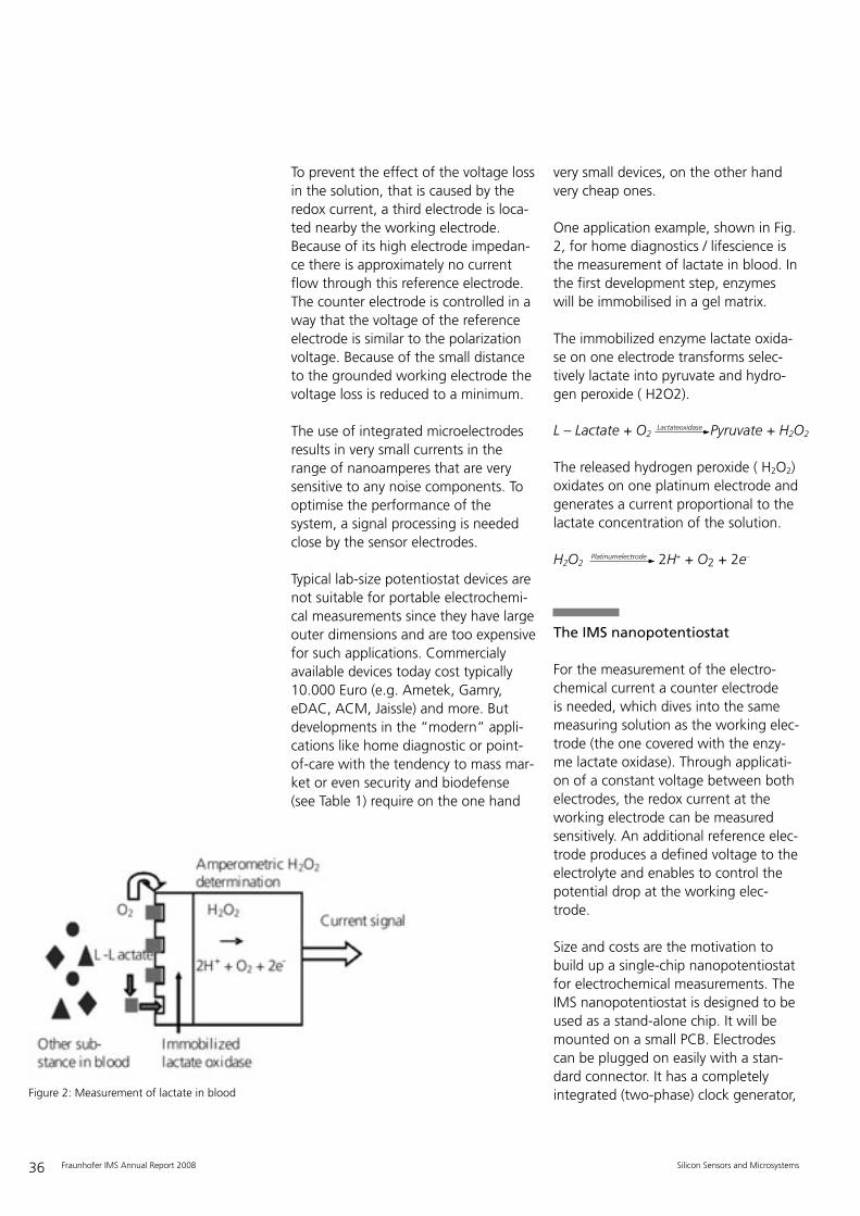
Common amperometric measurementmethods are based on techniques thatuse either two or three sensor electro-des. The two-electrode measurementtechnique is easy to handle and simpli-fies the measurement equipment, butthe sensor signal is distorted by the resis -tance of the analyte solution (Fig. 1).
Silicon Sensors and Microsystems
Nanopotentiostat for portable electrochemical measurements
Thomas van den Boom, Peter Fürst
Home Diagnostic Point-of-Care Environmental
Security and Biodefense
2003 777.1 1803.0 472.4 86.9
2007 1069.0 2679.3 688.6 135.8
2009 1298.1 3247.7 860.8 174.6
2011 1627.1 3975.4 1098.0 231.0
2013 2085.5 4897.1 1427.1 313.5
CAGR 11.4% 10.5% 12.6% 14.6%
Table 1: Total Biosensors market: Revenue forecasts by vertical markets (world), 2003 – 2013 [2]
Figure 1: Principle of a three electrodes potentiostat
36 Fraunhofer IMS Annual Report 2008
To prevent the effect of the voltage lossin the solution, that is caused by theredox current, a third electrode is loca-ted nearby the working electrode.Because of its high electrode impedan-ce there is approximately no currentflow through this reference electrode.The counter electrode is controlled in away that the voltage of the referenceelectrode is similar to the polarizationvoltage. Because of the small distanceto the grounded working electrode thevoltage loss is reduced to a minimum.
The use of integrated microelectrodesresults in very small currents in therange of nanoamperes that are verysensitive to any noise components. Tooptimise the performance of thesystem, a signal processing is neededclose by the sensor electrodes.
Typical lab-size potentiostat devices arenot suitable for portable electrochemi-cal measurements since they have largeouter dimensions and are too expensivefor such applications. Commercialyavailable devices today cost typically10.000 Euro (e.g. Ametek, Gamry,eDAC, ACM, Jaissle) and more. Butdevelopments in the “modern” appli-cations like home diagnostic or point-of-care with the tendency to mass mar-ket or even security and biodefense(see Table 1) require on the one hand
very small devices, on the other handvery cheap ones.
One application example, shown in Fig.2, for home diagnostics / lifescience isthe measurement of lactate in blood. Inthe first development step, enzymeswill be immobilised in a gel matrix.
The immobilized enzyme lactate oxida-se on one electrode transforms selec-tively lactate into pyruvate and hydro-gen peroxide ( H2O2).
Silicon Sensors and Microsystems
Figure 2: Measurement of lactate in blood
The released hydrogen peroxide ( H2O2)oxidates on one platinum electrode andgenerates a current proportional to thelactate concentration of the solution.
L – Lactate + O2Lactateoxidase Pyruvate + H2O2
H2O2Platinumelectrode 2H+ + O2 + 2e–
The IMS nanopotentiostat
For the measurement of the electro -chemical current a counter electrode is needed, which dives into the samemeasuring solution as the working elec-trode (the one covered with the enzy-me lactate oxidase). Through applicati-on of a constant voltage between bothelectrodes, the redox current at theworking electrode can be measuredsensitively. An additional reference elec-trode produces a defined voltage to theelectrolyte and enables to control thepotential drop at the working elec -trode.
Size and costs are the motivation tobuild up a single-chip nanopotentiostatfor electrochemical measurements. TheIMS nanopotentiostat is designed to beused as a stand-alone chip. It will bemounted on a small PCB. Electrodescan be plugged on easily with a stan-dard connector. It has a completelyintegrated (two-phase) clock generator,
37Fraunhofer IMS Annual Report 2008
a completely integrated current biasand a selectable analog or digital out-put of the redox current. For the digitaloutput, a second-order one-bit sigma-delta-modulator has been implemen-ted.
The functionality of the nanopoten-tiostat can be divided into two parts: 1) The control part measures the poten-tial of the reference electrode and con-trols the counter electrode in a waythat the reference electrode has thepolarization voltage. The main part ofthe electrode control is a three stageoperational amplifier which works witha capacitive feed back.2) The redox current at the workingelectrode is converted by a SC-integra-tor into an internal voltage. When thenanopotentiostat is in analog modusthis voltage is amplified by the S&Hamplification part. In case of the digitalmodus is selected, the result of the cur-rent voltage conversion is converted bya second-order one-bit sigma-delta-modulator.The current range of the nanopoten-tiostat is by variation of the SC integra-tor capacitor adjustable. By using theinternal clock frequency of 2.5 KHz the minimum redox current range is–1.5 nA to +1.5 nA, the maximum current range is –250 nA to +250 nA,respectively. The integrator capacitor is thereby adjustable in 255 steps. Another way to control the currentrange is the usage of an external clock.The maximum current range can beincreased up to 20 µA with an externalclock frequency of 200 KHz. The accu-racy of the redox current is 10.5 bit.This results in an accuracy of 1 pA inthe current range from –1.5 nA to+1.5 nA.
The nanopotentiostat is small enoughto be co-integrated with the micro- ornanoelectrodes monolithically on onechip for all applications, where thesystem is used as disposable because of
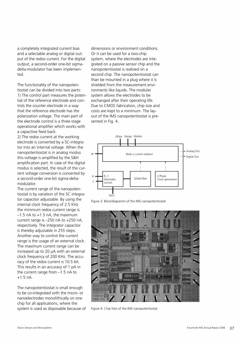
dimensions or environment conditions.Or it can be used for a two-chipsystem, where the electrodes are inte-grated on a passive sensor chip and thenanopotentiostat is realized on asecond chip. The nanopotentiostat canthan be mounted in a plug where it isshielded from the measurement envi-ronments like liquids. The modularsystem allows the electrodes to beexchanged after their operating life.Due to CMOS fabrication, chip size andcosts are kept to a minimum. The lay-out of the IMS nanopotentiostat is pre-sented in Fig. 4.
Silicon Sensors and Microsystems
R
C
W
Vpo l
Offset Range Modus
Redo x current readoutDigital Out
Analog Out
2 PhaseClock generationGlobal Bias
R, CElectrodes control
Figure 3: Blockdiagramm of the IMS nanopotentiostat
Figure 4: Chip foto of the IMS nanopotentiostat
38 Fraunhofer IMS Annual Report 2008
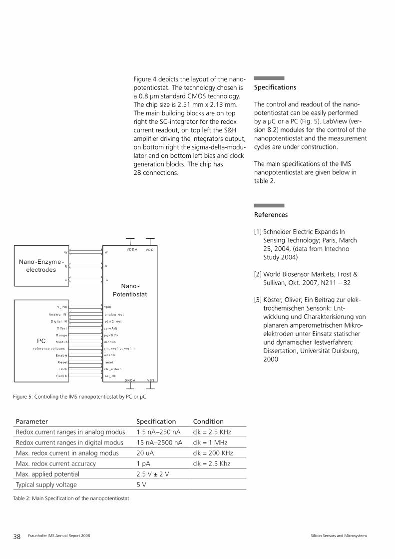
Figure 4 depicts the layout of the nano-potentiostat. The technology chosen isa 0.8 µm standard CMOS technology.The chip size is 2.51 mm x 2.13 mm.The main building blocks are on topright the SC-integrator for the redoxcurrent readout, on top left the S&Hamplifier driving the integrators output,on bottom right the sigma-delta-modu-lator and on bottom left bias and clockgeneration blocks. The chip has28 connections.
Specifications
The control and readout of the nano-potentiostat can be easily performed by a µC or a PC (Fig. 5). LabView (ver -sion 8.2) modules for the control of thenanopotentiostat and the measurementcycles are under construction.
The main specifications of the IMSnanopotentiostat are given below intable 2.
References
[1] Schneider Electric Expands In Sensing Technology; Paris, March25, 2004, (data from Intechno Study 2004)
[2] World Biosensor Markets, Frost &Sullivan, Okt. 2007, N211 – 32
[3] Köster, Oliver; Ein Beitrag zur elek-trochemischen Sensorik: Ent -wicklung und Charakterisierung vonplanaren amperometrischen Mikro-elektroden unter Einsatz statischerund dynamischer Testverfahren; Dissertation, Universität Duisburg,2000
Silicon Sensors and Microsystems
Nano -Enzym e -electrodes
W
R
C
PC
sd m 2 _ o u t
ze ro A d j
p g < 0 :7 >
a n a lo g _ o u t
D ig ita l_ IN
O ffse t
R a n g e
A n a lo g _ IN
V _ P o l vp o l
W
R
C
V D D A V D D
G N D A V S S
Nano -Potentiostat
M o d u s m o d u s
vm , v re f_ p , vr e f_ m r e fe r e n ce vo lt a g e s
e n a b le
r e se t
clk _ e xte r n
se l_ clk
E n a b le
R e se t
clo ck
S e lC lk
Figure 5: Controling the IMS nanopotentiostat by PC or µC
Parameter Specifi cation Condition
Redox current ranges in analog modus 1.5 nA–250 nA clk = 2.5 KHz
Redox current ranges in digital modus 15 nA–2500 nA clk = 1 MHz
Max. redox current in analog modus 20 uA clk = 200 KHz
Max. redox current accuracy 1 pA clk = 2.5 Khz
Max. applied potential 2.5 V ± 2 V
Typical supply voltage 5 V
Table 2: Main Specification of the nanopotentiostat
39Fraunhofer IMS Annual Report 2008
Introduction
In more than fifteen years of researchand development in high-temperatureCMOS SOI technology, the Institute ofMicroelectronic Circuits and Systems(IMS) has realized many circuits fortemperatures of up to 250°C andbeyond. IMS made several pioneeringcontributions to this field, like tungstenmetallization and high-temperatureEEPROM devices.
With the “Hochtemperaturelektronik”project, funded by the state of NorthRhine-Westphalia until 2006, a newchapter of our high temperature elec-tronics history was started with thetransfer of our know how to the new200mm production facility of IMS, andthe establishment of an infrastructurethat enables the design and productionof commercial-grade high temperatureCMOS (HTCMOS) integrated circuits.This work has been continued andexpanded, and some of the results aredetailed in the following pages.
High Temperature Pressure Sensors
Micromachined pressure sensors havebeen pursued for a long time at IMS,usually integrated into a standardCMOS process on silicon bulk wafers.This process module was also integratedinto the new 1 µm high-temperatureCMOS SOI process. The pressure sensorconsists of a polysilicon membrane overan active area, together forming acapacitor whose capacitance dependson the deformation of the membraneby the ambient pressure. As only mate-rials and processing steps are used thatare also present in CMOS processes,the sensor can be built wholly in ourstandard CMOS fabrication facility.
For a high resolution of the pressuresignal, very small changes in sensorcapacitance, in the order of a few tensor hundreds of Attofarads (10–18F) mustbe resolved. In order to eliminate theinfluence of long bond wires connec-ting the pressure sensor to a conditio-ning circuit, the conditioning circuitmust be integrated on the same die asthe sensor. This, of course, can easily bedone in the IMS high-temperatureCMOS SOI process.
The capacitive readout circuits, thecapacitance/voltage (C/V) converter andamplifiers, were realized as Switched-Capacitor (SC) circuits. The SC-circuitsuse discrete-time processing of analogvalues so that the common analog fun-ctions based on operational amplifiersand resistors can be realized by substi-tuting switches and capacitors for theresistors. This technique is easily imple-mented in CMOS ICs, and is well-mat-ched to both the sensor and high temperature operation: as the sensoralready is a capacitor, it naturally inte-grates into an SC-circuit. The characte-ristics of the SC-circuits mainly dependon the capacitors used. Like the vacu-um used as the sensor "dielectric", thesilicon dioxide used as dielectric in theintegrated capacitors has a very smalldependence on temperature. Thevarious types of resistors used in a typi-cal CMOS technology usually havewidely varying temperature coefficients,which make it difficult to design circuitswhich must work over a temperaturerange spanning up to 300K.
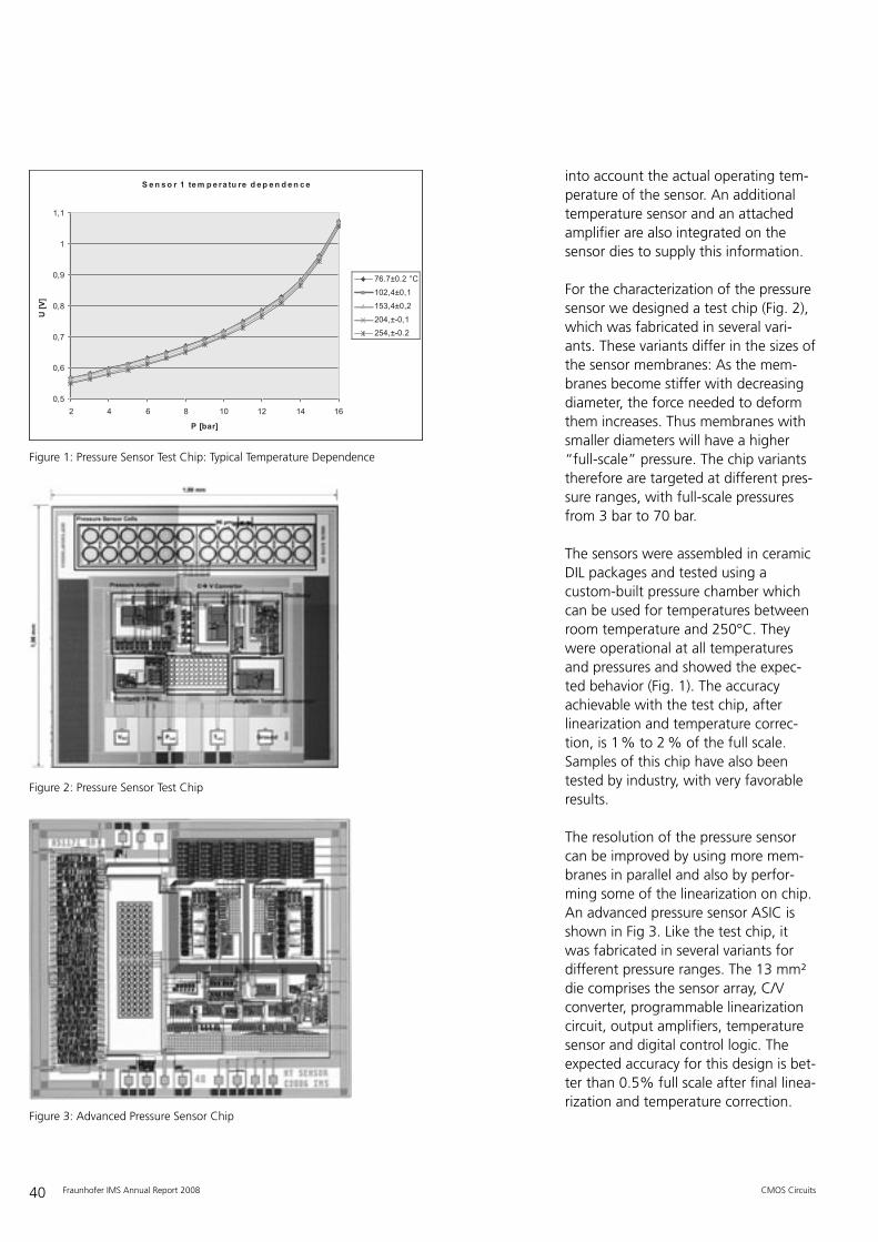
Nevertheless there is still a temperaturedependence present in the final pressu-re signal. Figure 1 shows this depen-dence for the pressure output signal.Especially for low pressures it will incura large error on the displayed pressurevalue after linearization of the signal.Therefore signal linearization must take
CMOS Circuits
Microelectronics for High Temperature Applications
Reneé Lerch
40 Fraunhofer IMS Annual Report 2008
into account the actual operating tem-perature of the sensor. An additionaltemperature sensor and an attachedamplifier are also integrated on thesensor dies to supply this information.
For the characterization of the pressuresensor we designed a test chip (Fig. 2),which was fabricated in several vari-ants. These variants differ in the sizes ofthe sensor membranes: As the mem-branes become stiffer with decreasingdiameter, the force needed to deformthem increases. Thus membranes withsmaller diameters will have a higher“full-scale” pressure. The chip variantstherefore are targeted at different pres-sure ranges, with full-scale pressuresfrom 3 bar to 70 bar.
The sensors were assembled in ceramicDIL packages and tested using acustom-built pressure chamber whichcan be used for temperatures betweenroom temperature and 250°C. Theywere operational at all temperaturesand pressures and showed the expec-ted behavior (Fig. 1). The accuracyachievable with the test chip, afterlinearization and temperature correc-tion, is 1% to 2 % of the full scale.Samples of this chip have also beentested by industry, with very favorableresults.
The resolution of the pressure sensorcan be improved by using more mem-branes in parallel and also by perfor-ming some of the linearization on chip.An advanced pressure sensor ASIC isshown in Fig 3. Like the test chip, itwas fabricated in several variants fordifferent pressure ranges. The 13 mm²die comprises the sensor array, C/Vconverter, programmable linearizationcircuit, output amplifiers, temperaturesensor and digital control logic. Theexpected accuracy for this design is bet-ter than 0.5% full scale after final linea-rization and temperature correction.
CMOS Circuits
S e n s o r 1 te m p e ra tu re d e p e n d e n c e
0,5
0,6
0,7
0,8
0,9
1
1,1
2 4 6 8 10 12 14 16
P [bar]
U [
V]
76.7±0.2 °C
102,4±0,1
153,4±0,2
204,±-0,1
254,±-0.2
Figure 1: Pressure Sensor Test Chip: Typical Temperature Dependence
Figure 2: Pressure Sensor Test Chip
Figure 3: Advanced Pressure Sensor Chip
41Fraunhofer IMS Annual Report 2008
These pressure sensor chips can beused in a variety of applications. Due totheir small size they can be used insmall spaces where cooled “traditional”sensors cannot be used. This appliese.g. to chemical microreactor or auto-motive applications.
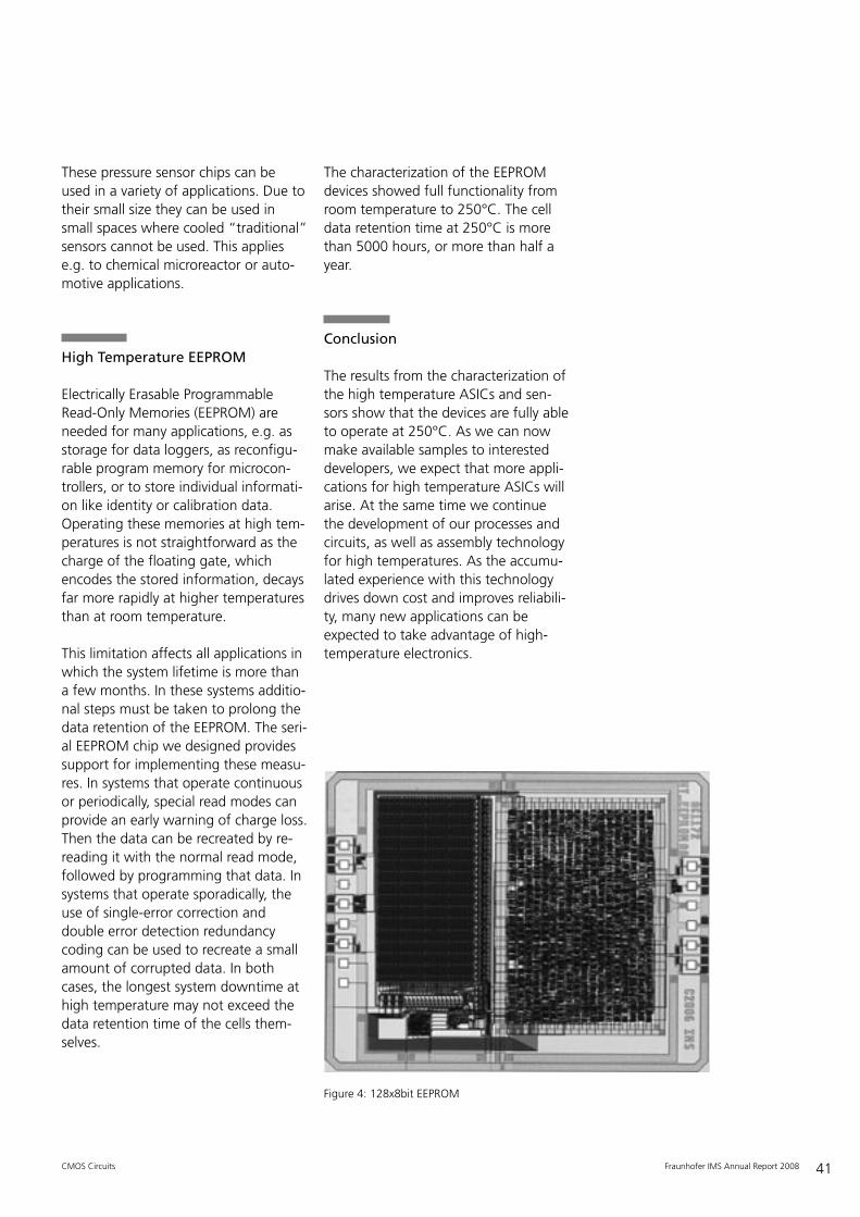
High Temperature EEPROM
Electrically Erasable ProgrammableRead-Only Memories (EEPROM) areneeded for many applications, e.g. asstorage for data loggers, as reconfigu-rable program memory for microcon-trollers, or to store individual informati-on like identity or calibration data.Operating these memories at high tem-peratures is not straightforward as thecharge of the floating gate, whichencodes the stored information, decaysfar more rapidly at higher temperaturesthan at room temperature.
This limitation affects all applications inwhich the system lifetime is more thana few months. In these systems additio-nal steps must be taken to prolong thedata retention of the EEPROM. The seri-al EEPROM chip we designed providessupport for implementing these measu-res. In systems that operate continuousor periodically, special read modes canprovide an early warning of charge loss.Then the data can be recreated by re-reading it with the normal read mode,followed by programming that data. Insystems that operate sporadically, theuse of single-error correction anddouble error detection redundancycoding can be used to recreate a smallamount of corrupted data. In bothcases, the longest system downtime athigh temperature may not exceed thedata retention time of the cells them-selves.
The characterization of the EEPROMdevices showed full functionality fromroom temperature to 250°C. The celldata retention time at 250°C is morethan 5000 hours, or more than half ayear.
Conclusion
The results from the characterization ofthe high temperature ASICs and sen-sors show that the devices are fully ableto operate at 250°C. As we can nowmake available samples to interesteddevelopers, we expect that more appli-cations for high temperature ASICs willarise. At the same time we continuethe development of our processes andcircuits, as well as assembly technologyfor high temperatures. As the accumu-lated experience with this technologydrives down cost and improves reliabili-ty, many new applications can beexpected to take advantage of high-temperature electronics.
CMOS Circuits
Figure 4: 128x8bit EEPROM
42 Fraunhofer IMS Annual Report 2008
Research, Development and Productionof customer specific analog, digital andmixed signal integrated circuits is oneof the core competences of FraunhoferIMS in Duisburg.
Technology
Fraunhofer IMS operates a series pro-duction capable CMOS fabrication line.Besides standard CMOS processesdown to 0.35µm, special processes areoffered providing e.g. integrated sen-sors like pressure, temperature orimage sensors. In addition a high tem-perature SOI based CMOS process isavailable. Based on this process, hightemperature capable integrated circuitsoperating at temperatures up to 250° Care feasible. Besides the CMOS fabrica-tion line, the institute operates a Micro-systems technology lab. Inside this labadditional processing steps and materi-als beyond standard CMOS are availa-ble offering innovative capabilities forfurther miniaturization and integration.
Applications
Fraunhofer IMS offers turn key ASICsolutions including supply chain servicesbased on the in house CMOS technolo-gy. Integrated MEMS/sensors with ana-log and digital functions towards com-plex system on a chip (SoC) solutions isa goal for many customers, since itoffers the possibility of minimum costand increased reliability. A wide rangeof applications has been addressed byIMS ASICs. The variety of developedASICs ranges from dedicated pure ana-log or digital ASIC solutions up to com-plex mixed signal SoC solutions, consi-dering various constraints like lowpower for battery powered or even RFpowered devices, on chip embeddedmemories or integration of sensors oractuators. Besides the standard CMOSintegration, IMS offers solutions forharsh environments based on the hightemperature process.
Mixed signal ASICs
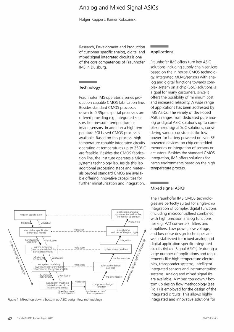
The Fraunhofer IMS CMOS technolo-gies are perfectly suited for single-chipintegration of complex digital functions(including microcontrollers) combinedwith high precision analog functionslike e.g. A/D converters, filters andamplifiers. Low power, low voltage,and low noise design techniques arewell established for mixed analog anddigital application specific integratedcircuits (Mixed Signal ASICs) featuring alarge number of applications and requi-rements like high temperature electro-nics, transponder systems, intelligentintegrated sensors and instrumentationsystems. Analog and mixed signal IPsare available. A mixed top down / bot-tom up design flow methodology (seeFig 1) is employed for the design of theintegrated circuits. This allows highlyintegrated and innovative solutions for
Analog and Mixed Signal ASICs
Holger Kappert, Rainer Kokozinski
CMOS Circuits
Figure 1: Mixed top down / bottom up ASIC design flow methodology
wrttten specification
executable specification(behavioral model)
system modeling(structural model of the
partitioned system)
subsystem modeling (successive partitioningand
refinement of the system model)
component modeling(detailed model of the system components)
component design and test
sub-system design and test
prototypingand test of the prototype
application analysis/system optimizations for
the follow-up product
model-based top-dow
n design
Bott
om-u
p de
sign
(sys
tem
inte
grat
ion)
Validation
Verification
Verification
Verification
Validation
Validation
Validation
Partitioning/Modeling
Modeling
Modeling/Refinement
Modeling/Refinement
Integration
Specification of the components
Implementation
Implementation ofthe components
Implementation
Validation
system design and test
Production
43Fraunhofer IMS Annual Report 2008
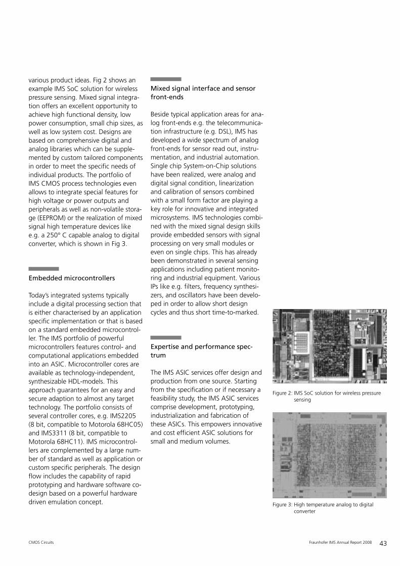
various product ideas. Fig 2 shows anexample IMS SoC solution for wirelesspressure sensing. Mixed signal integra-tion offers an excellent opportunity toachieve high functional density, lowpower consumption, small chip sizes, aswell as low system cost. Designs arebased on comprehensive digital andanalog libraries which can be supple-mented by custom tailored componentsin order to meet the specific needs ofindividual products. The portfolio ofIMS CMOS process technologies evenallows to integrate special features forhigh voltage or power outputs andperipherals as well as non-volatile stora-ge (EEPROM) or the realization of mixedsignal high temperature devices likee.g. a 250° C capable analog to digitalconverter, which is shown in Fig 3.
Embedded microcontrollers
Today’s integrated systems typicallyinclude a digital processing section thatis either characterised by an applicationspecific implementation or that is basedon a standard embedded microcontrol-ler. The IMS portfolio of powerfulmicrocontrollers features control- andcomputational applications embeddedinto an ASIC. Microcontroller cores areavailable as technology-independent,synthesizable HDL-models. Thisapproach guarantees for an easy andsecure adaption to almost any targettechnology. The portfolio consists ofseveral controller cores, e.g. IMS2205(8 bit, compatible to Motorola 68HC05)and IMS3311 (8 bit, compatible toMotorola 68HC11). IMS microcontrol-lers are complemented by a large num-ber of standard as well as application orcustom specific peripherals. The designflow includes the capability of rapidprototyping and hardware software co-design based on a powerful hardwaredriven emulation concept.
Mixed signal interface and sensorfront-ends
Beside typical application areas for ana-log front-ends e.g. the telecommunica-tion infrastructure (e.g. DSL), IMS hasdeveloped a wide spectrum of analogfront-ends for sensor read out, instru-mentation, and industrial automation.Single chip System-on-Chip solutionshave been realized, were analog anddigital signal condition, linearizationand calibration of sensors combinedwith a small form factor are playing akey role for innovative and integratedmicrosystems. IMS technologies combi-ned with the mixed signal design skillsprovide embedded sensors with signalprocessing on very small modules oreven on single chips. This has alreadybeen demonstrated in several sensingapplications including patient monito-ring and industrial equipment. VariousIPs like e.g. filters, frequency synthesi-zers, and oscillators have been develo-ped in order to allow short designcycles and thus short time-to-marked.
Expertise and performance spec-trum
The IMS ASIC services offer design andproduction from one source. Startingfrom the specification or if necessary afeasibility study, the IMS ASIC servicescomprise development, prototyping,industrialization and fabrication ofthese ASICs. This empowers innovativeand cost efficient ASIC solutions forsmall and medium volumes.
CMOS Circuits
Figure 2: IMS SoC solution for wireless pressuresensing
Figure 3: High temperature analog to digital converter
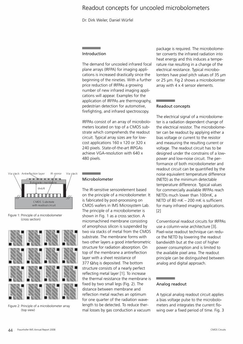
44 Fraunhofer IMS Annual Report 2008
Introduction
The demand for uncooled infrared focalplane arrays (IRFPA) for imaging appli-cations is increased drastically since thebeginning of the nineties. With a fur therprice reduction of IRFPAs a growingnumber of new infrared imaging appli-cations will appear. Examples for theapplication of IRFPAs are thermography,pedestrian detection for automotive,firefighting, and infrared spectroscopy.
IRFPAs consist of an array of microbolo-meters located on top of a CMOS sub-strate which comprehends the readoutcircuit. Typical array sizes are for low-cost applications 160 x 120 or 320 x240 pixels. State-of-the-art IRPGAsachieve VGA-resolution with 640 x480 pixels.
Microbolometer
The IR-sensitive sensorelement basedon the principle of a microbolometer. Itis fabricated by post-processing onCMOS wafers in IMS Microsystem Lab.The principle of a microbolometer isshown in Fig. 1 as a cross section. Amicromachined membrane consistingof amorphous silicon is suspended bytwo via stacks of metal from the CMOSsubstrate. The membrane forms withtwo other layers a good interferometricstructure for radiation absorption. Ontop of the membrane a antireflectionlayer with a sheet resistance of377 Ω/sq is deposited. The bottomstructure consists of a nearly perfectreflecting metal layer [1]. To increasethe thermal resistance the membrane isfixed by two small legs (Fig. 2). Thedistance between membrane andreflection metal reaches an optimumfor one quarter of the radiation wave-length to be detected. To reduce ther-mal losses by gas conduction a vacuum
package is required. The microbolome-ter converts the infrared radiation intoheat energy and this induces a tempe-rature rise resulting in a change of theelectrical resistance. Typical microbo-lomters have pixel pitch values of 35 µmor 25 µm. Fig 2 shows a microbolomterarray with 4 x 4 sensor elements.
Readout concepts
The electrical signal of a microbolome-ter is a radiation dependent change ofthe electrical resistor. The microbolome-ter can be readout by applying either abias voltage or current to the resistorand measuring the resulting current orvoltage. The readout circuit has to bedesigned under the constrains of a low-power and low-noise circuit. The per-formance of both microbolometer andreadout circuit can be quantified by thenoise equivalent temperature difference(NETD) as the minimum detectabletemperature difference. Typical valuesfor commercially available IRFPAs reachNETDs much lower than 100mK, aNETD of 80 mK – 200 mK is sufficientfor many infrared imaging applications.[2]
Conventional readout circuits for IRFPAsuse a column-wise architecture [3].Pixel-wise readout technique can redu-ce the NETD by lowering the readoutbandwidth but at the cost of higherpower consumption and is limited tothe available pixel area. The readoutprinciple can be distinguished betweenanalog and digital approach.
Analog readout
A typical analog readout circuit appliesa bias voltage pulse to the microbolo-meters and integrates the current flo-wing over a fixed period of time. Fig. 3
Readout concepts for uncooled microbolometers
Dr. Dirk Weiler, Daniel Würfel
CMOS Circuits
Figure 1: Principle of a microbolometer (cross section)
CMOS S ubstratewith readout circuit
Bolometer membrane
Antireflection layer IR -mirror
d=λ/4
Via stackVia s tack
Figure 2: Principle of a microbolometer array (top view)
45Fraunhofer IMS Annual Report 2008
shows a time-continuous integrator asa readout circuit. The pixel to be read-out is selected by a select transistor.The current flowing throw the microbo-lometer resistor will be integrated usinga operational transconductance ampli-fier (OTA) and an integrating capaci-tance Cint. A reset switch connected inparallel with the integration capacitordetermines the integration time of themicrobolometer current and limits thebandwidth of the readout circuit. Thecurrent of the microbolometer consistsof a constant and a radiation depen-dent part. For the integration of onlythe radiation dependent part the con-stant part has to be subtracted. Thiswill be done by a digital adjustable cur-rent source at the inverting input of theOTA. The voltage source Voffset at thenon-inverting input of the OTA willdefine the bias voltage applied to themicrobolometer. A sequencer controlsthe selection of the columns and rowsto be readout. The output voltage ofthe integrators are fed to correlated-double sampling (CDS) stages. The CDSreduces the 1/f-noise of the readout cir-cuit. Finally the output is sampled andhold, multiplexed, and fed to the out-put buffer.
Fig. 4 depicts a chip photo of an in-house development IRFPA with 160 x120 pixel array with a pixel pitch of35 µm. The chip has been fabricated ina standard 0.35 µm CMOS process andoccupies a die area of 121 mm2. Thechip area is not optimized because thecomplete readout architecture is loca-ted besides the microbolometer array.The chip has been electrically characte-rized without the microbolometer postprocessing steps. For the calibration ofthe IRFPA four additional temperaturesensors based on diodes are integrated.
Digital readout
A straight-forward IRFPA with digitaloutput can be realized by using theanalog readout principle and combineit with a column-wise or serial-wiseADC instead of an analog output buf-fer. A more sophisticated solution is tointegrate the readout principle directlyinto the ADC. This can be done byusing the principle of a sigma-delta (��)modulator. A �� modulator achieves ahigh signal to noise ratio (SNR) by com-bining oversampling, interpolation, andnoise shaping while dispensing with theneed of high precision analog compo-nents. It relies on the noise spectrum ofcoarsely quantized input signal being
CMOS Circuits
Figure 3: Analog readout principle: Integrator
Cint
+
-R Bolo
CL
CDS / Sample & Hold
Ibias Vbias
select 2
select 1
reset
Pixel Integrator
Figure 4: Chip photo of a 160 x 120 pixel IRFPA
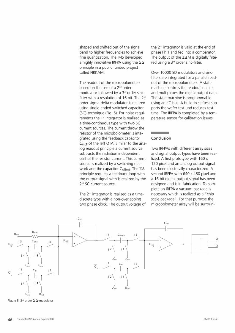
46 Fraunhofer IMS Annual Report 2008
shaped and shifted out of the signalband to higher frequencies to achievefine quantization. The IMS developed a highly innovative IRFPA using the ��principle in a public funded project called FIRKAM.
The readout of the microbolometersbased on the use of a 2nd order modulator followed by a 3rd order sinc-filter with a resolution of 16 bit. The 2nd
order sigma-delta modulator is realizedusing single-ended switched capacitor(SC)-technique (Fig. 5). For noise requi-rements the 1st integrator is realized asa time-continuous type with two SCcurrent sources. The current throw theresistor of the microbolometer is inte-grated using the feedback capacitorCint1 of the left OTA. Similar to the ana-log readout principle a current sourcesubtracts the radiation independentpart of the resistor current. This currentsource is realized by a switching net-work and the capacitor Coffset. The ��principle requires a feedback loop withthe output signal with is realized by the2nd SC current source.
The 2nd integrator is realized as a time-discrete type with a non-overlappingtwo phase clock. The output voltage of
the 2nd integrator is valid at the end ofphase Phi1 and fed into a comparator.The output of the ��M is digitally filte-red using a 3rd order sinc-filter.
Over 10000 SD modulators and sinc-filters are integrated for a parallel read-out of the microbolometers. A statemachine controls the readout circuitsand multiplexes the digital output data.The state machine is programmableusing an I2C bus. A build-in selftest sup-ports the wafer test und reduces testtime. The IRFPA is completed by a tem-perature sensor for calibration issues.
Conclusion
Two IRFPAs with different array sizesand signal output types have been rea-lized. A first prototype with 160 x120 pixel and an analog output signalhas been electrically characterized. Asecond IRFPA with 640 x 480 pixel anda 16 bit digital output signal has beendesigned and is in fabrication. To com-plete an IRFPA a vacuum package isnecessary which is realized as a “chipscale package”. For that purpose themicrobolometer array will be surroun-
CMOS Circuits
+
-
R BoloUbias
+
-Umid
Umid
Umid Umid
Umid Umid
Q
Cint2
Csample
Cfb2
j 2j 1
j 1 j 2
j 2
j 2 j 1
j 1
Umid Umid
Umid Umid
Q
Coffset
Cfb1
j 3
j 1
Uref-
j 1 j 2
j 2
j 4
j 1
j 3 j 4
Cint1
Q
Q
Figure 5: 2nd order ��-modulator
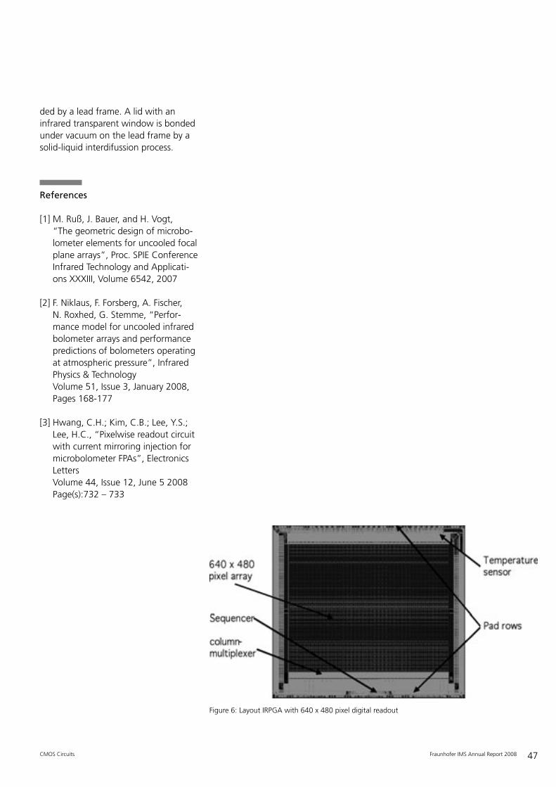
47Fraunhofer IMS Annual Report 2008
ded by a lead frame. A lid with aninfrared transparent window is bondedunder vacuum on the lead frame by asolid-liquid interdifussion process.
References
[1] M. Ruß, J. Bauer, and H. Vogt, “The geometric design of microbo-lometer elements for uncooled focalplane arrays”, Proc. SPIE ConferenceInfrared Technology and Applicati-ons XXXIII, Volume 6542, 2007
[2] F. Niklaus, F. Forsberg, A. Fischer,N. Roxhed, G. Stemme, “Perfor -mance model for uncooled infraredbolometer arrays and performancepredictions of bolometers operatingat atmospheric pressure”, InfraredPhysics & TechnologyVolume 51, Issue 3, January 2008,Pages 168-177
[3] Hwang, C.H.; Kim, C.B.; Lee, Y.S.;Lee, H.C., “Pixelwise readout circuitwith current mirroring injection formicrobolometer FPAs”, ElectronicsLettersVolume 44, Issue 12, June 5 2008Page(s):732 – 733
CMOS Circuits
Figure 6: Layout IRPGA with 640 x 480 pixel digital readout
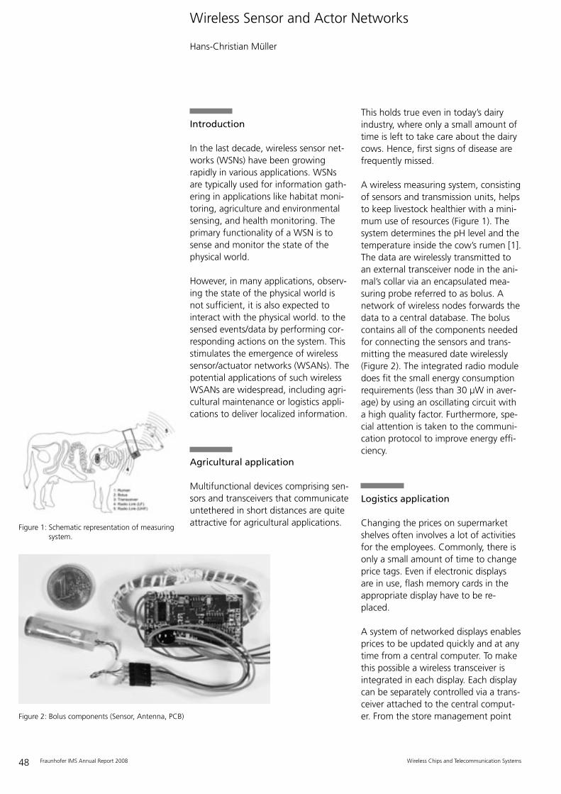
48 Fraunhofer IMS Annual Report 2008
Introduction
In the last decade, wireless sensor net-works (WSNs) have been growingrapidly in various applications. WSNsare typically used for information gath-ering in applications like habitat moni-toring, agriculture and environmentalsensing, and health monitoring. Theprimary functionality of a WSN is tosense and monitor the state of thephysical world.
However, in many applications, observ-ing the state of the physical world isnot sufficient, it is also expected tointeract with the physical world. to thesensed events/data by performing cor-responding actions on the system. Thisstimulates the emergence of wirelesssensor/actuator networks (WSANs). Thepotential applications of such wirelessWSANs are widespread, including agri-cultural maintenance or logistics appli-cations to deliver localized information.
Agricultural application
Multifunctional devices comprising sen-sors and transceivers that communicateuntethered in short distances are quiteattractive for agricultural applications.
This holds true even in today’s dairyindustry, where only a small amount oftime is left to take care about the dairycows. Hence, first signs of disease arefrequently missed.
A wireless measuring system, consistingof sensors and transmission units, helpsto keep livestock healthier with a mini-mum use of resources (Figure 1). Thesystem determines the pH level and thetemperature inside the cow’s rumen [1].The data are wirelessly transmitted toan external transceiver node in the ani-mal’s collar via an encapsulated mea-suring probe referred to as bolus. Anetwork of wireless nodes forwards thedata to a central database. The boluscontains all of the components neededfor connecting the sensors and trans-mitting the measured date wirelessly(Figure 2). The integrated radio moduledoes fit the small energy consumptionrequirements (less than 30 µW in aver-age) by using an oscillating circuit witha high quality factor. Furthermore, spe-cial attention is taken to the communi-cation protocol to improve energy effi-ciency.
Logistics application
Changing the prices on supermarketshelves often involves a lot of activitiesfor the employees. Commonly, there isonly a small amount of time to changeprice tags. Even if electronic displaysare in use, flash memory cards in theappropriate display have to be re -placed.
A system of networked displays enablesprices to be updated quickly and at anytime from a central computer. To makethis possible a wireless transceiver isintegrated in each display. Each displaycan be separately controlled via a trans-ceiver attached to the central comput-er. From the store management point
Wireless Sensor and Actor Networks
Hans-Christian Müller
Wireless Chips and Telecommunication Systems
Figure 2: Bolus components (Sensor, Antenna, PCB)
Figure 1: Schematic representation of measuringsystem.
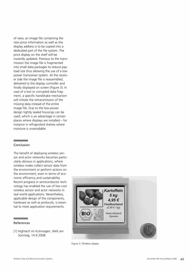
49Fraunhofer IMS Annual Report 2008
of view, an image file containing thenew price information as well as thedisplay address is to be copied into adedicated part of the file system. Theprice display on the shelf will beinstantly updated. Previous to the trans-mission the image file is fragmentedinto small data packages to reduce pay-load size thus allowing the use of a lowpower transceiver system. At the receiv-er side the image file is reassembled,delivered to the display controller andfinally displayed on screen (Figure 3). Incase of a lost or corrupted data frag-ment, a specific handshake mechanismwill initiate the retransmission of themissing data instead of the entireimage file. Due to the low-powerdesign tightly sealed housings can beused, which is an advantage in certainplaces where displays are installed – forinstance in refrigerated shelves wheremoisture is unavoidable.
Conclusion
The benefit of deploying wireless sen-sor and actor networks becomes partic-ularly obvious in applications, wherewireless nodes collect sensor data fromthe environment or perform actions onthe environment, even in terms of eco-nomic efficiency and sustainability.Recent progress in semiconductor tech-nology has enabled the use of low costwireless sensor and actor networks inreal world applications. Nevertheless,applicable design of the components,hardware as well as protocols, is essen-tial to meet application requirements.
References
[1] Hightech im Kuhmagen, Welt amSonntag, 14.9.2008
Wireless Chips and Telecommunication Systems
Figure 3: Wireless display
50 Fraunhofer IMS Annual Report 2008
Abstract
The use of sensor transponder techno-logies in medicine opens valuable possi-bilities in therapy of human cardiovas-cular system diseases, for examplecardiac insufficiency. This paper dealswith the question, what relevant effectsexist concerning energy transmissionthrough the human body and how theycan be considered during the systemdesign process. Parasitic effects in thetransponder antenna are analysed.Finally, a combination of all effects istaken into account to analyse the fre-quency behaviour of the whole system.Practical examinations confirm the fea-sibility with a HF transmission system.
1 Introduction
Medical studies [1] have shown that thetreatment of cardiovascular diseasescan be significantly improved by conti-nuous monitoring of parameters suchas blood pressure, temperature, etc. Forsuch diseases, only rigid drug treat-ments are available yet. The administe-red doses can not be adapted to arapidly changing demand. This leads toa drastic reduction of the quality of life.A continuous monitoring of cardiac andcirculatory functions can optimise theadjustment of drug dosage. Sensortransponders implanted into the humanbody can improve a therapy significant-ly. These transponders can be located indifferent places in the body, monitoringthe performance of the heart circulati-on system. Such transponders make acabling of the whole body unnecessary.The dimensions of the transpondershould make a catheter-implantationpossible. Especially so-called passivetransponder systems are of interrest,because such implants normally stayinside the body for a longer period.Thus, a supply by a local battery is not
possible. In such systems, the transpon-der is contactlessly supplied by a fieldfrom the reader located outside thebody. The maximum possible distancebetween the reader and the implantedtransponder is of interrest, e.g. to makesuch a system suitable for corpulentpatients.
One of the most important tasks is tofind the best carrier frequency for theenergy transmission.
2 Limitations and Requirements
The dimensions of an implantabletransponder should not be more thanseveral millimetres. Otherwise animplantation by a catheter is not possi-ble. From this it follows, that only smallantennas in the shape of a stick aresupposed. The induced voltage is pro-portional to the size of the area encirc-led from the windings. Losses in theenergy transmission through human tissue determine the available energy.Transponders with additional sensorsconsume significantly more energy thansimple id transponders. These factsreduces the maximum possibledistance. For this application, thedistance can exceed half a meter.
3 Preliminary Considerations
Transponder systems usually work withISM frequencies [4]. For LF and HFtransponder systems, the distance ofseveral decimeters is much smaller thanthe wavelength. This situation is callednear field communication. In contrastto LF and HF, the distance for UHF isgreater than the wavelength and thuselectromagnetic waves exist. Thedimensions of an antenna for UHFwould be greater than the alloweddimensions. Thus, only LF or HF trans-
Feasibility of Deeply Implanted Passive Sensor Transponders in Human Bodies
Andreas Hennig, Gerd vom Bögel
Wireless Chips and Telecommunication Systems
51Fraunhofer IMS Annual Report 2008
ponder systems are of interest here. Insuch systems, only the magnetic com-ponent is used for transmission of ener-gy and data. The antennas for LF andHF systems are made of coils. Theycould be designed as air coils or ferritecoils. For this application ferrite coils areof interest because they can be made inthe shape of a stick and higher induc-tivities with less space are possible. Fer-rite materials with usable parametersup to 13,56 MHz are available.
To lighten the energy supply for thetransponder it is essential to find outthe optimal frequency. The followingfrequencies are preferably considered:133 kHz, 6.78 MHz and 13.56 MHz.
4 Energy transmission throughhuman tissue
In this chapter, the energy transmissionto a passive sensor transponder deeplyimplanted in human body is analysed.Figure 1 shows an example of a modelfor an implanted sensor transpondernear to the heart and a correspondingreader.
The coil of the reader produces analternating magnetic field. A small partof the magnetic flux couples with thetransponder coil. In consequence, a vol-tage is induced in this coil. With thisvoltage the electronic of the transpon-der is supplied with power.
4.1 Absorption Effects in Human Tissue
The reader consist of a transmitter thatproduces an alternating magnetic fieldwith an antenna and a receiver for thetransponder data. Figure 2 shows ansimplified circuit of the transmitter part.A power amplifier produces a sinusoi-dal voltage with the carrier frequency.
A parallel resonant circuit composed ofa coil and a resonant capacitor is drivenby this voltage. In case of ideal lossleselements, no current flow between theamplifier and the resonant circuit takesplace during oscillation. The currentflow between the coil and the capacitoris called idle current and is causer ofthe magnetic field around the coil.When a transponder or conductivematerial is placed near to the coil, theoscillation of the resonant circuit isdamped. To keep the oscillation alive,the power amplifier has to provideenergy and balances the losses in theresonant circuit. Normally, the energyconsumption of the transponder is insi-gnificant compared to the losses inconductive environment and in unidealelectrical elements.
Wireless Chips and Telecommunication Systems
Figure 1: Model of an inductive sensor transponder system for medical appli-cations (X-ray picture: Deutsches Röntgen-Museum)
Figure 2: Eddy Current in tissue caused by magnetic field changing in time
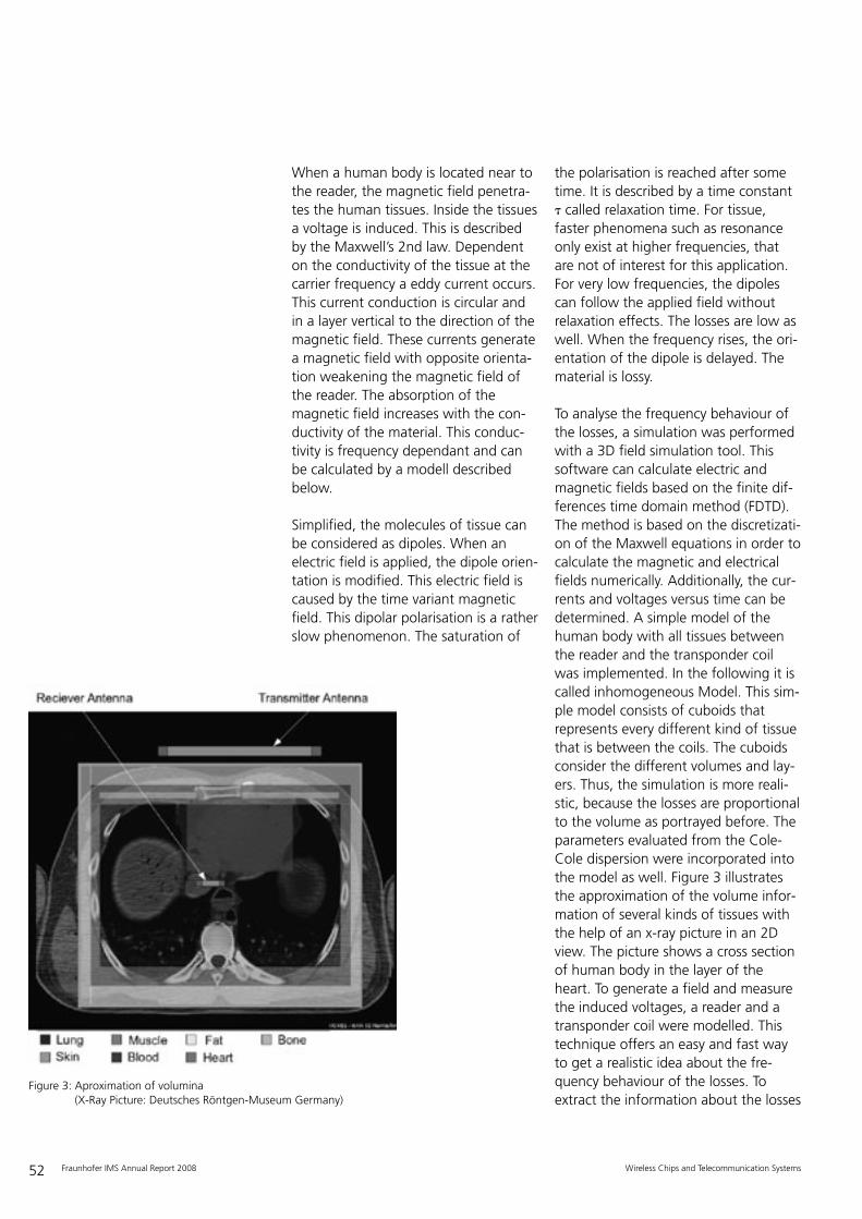
52 Fraunhofer IMS Annual Report 2008
When a human body is located near tothe reader, the magnetic field penetra-tes the human tissues. Inside the tissuesa voltage is induced. This is describedby the Maxwell’s 2nd law. Dependenton the conductivity of the tissue at thecarrier frequency a eddy current occurs.This current conduction is circular andin a layer vertical to the direction of themagnetic field. These currents generatea magnetic field with opposite orienta-tion weakening the magnetic field ofthe reader. The absorption of themagnetic field increases with the con-ductivity of the material. This conduc-tivity is frequency dependant and canbe calculated by a modell describedbelow.
Simplified, the molecules of tissue canbe considered as dipoles. When anelectric field is applied, the dipole orien-tation is modified. This electric field iscaused by the time variant magneticfield. This dipolar polarisation is a ratherslow phenomenon. The saturation of
the polarisation is reached after sometime. It is described by a time constant� called relaxation time. For tissue,faster phenomena such as resonanceonly exist at higher frequencies, thatare not of interest for this application.For very low frequencies, the dipolescan follow the applied field withoutrelaxation effects. The losses are low aswell. When the frequency rises, the ori-entation of the dipole is delayed. Thematerial is lossy.
To analyse the frequency behaviour ofthe losses, a simulation was performedwith a 3D field simulation tool. Thissoftware can calculate electric andmagnetic fields based on the finite dif-ferences time domain method (FDTD).The method is based on the discretizati-on of the Maxwell equations in order tocalculate the magnetic and electricalfields numerically. Additionally, the cur-rents and voltages versus time can bedetermined. A simple model of thehuman body with all tissues betweenthe reader and the transponder coilwas implemented. In the following it iscalled inhomogeneous Model. This sim-ple model consists of cuboids thatrepresents every different kind of tissuethat is between the coils. The cuboidsconsider the different volumes and lay-ers. Thus, the simulation is more reali-stic, because the losses are proportionalto the volume as portrayed before. Theparameters evaluated from the Cole-Cole dispersion were incorporated intothe model as well. Figure 3 illustratesthe approximation of the volume infor-mation of several kinds of tissues withthe help of an x-ray picture in an 2Dview. The picture shows a cross sectionof human body in the layer of theheart. To generate a field and measurethe induced voltages, a reader and atransponder coil were modelled. Thistechnique offers an easy and fast wayto get a realistic idea about the fre-quency behaviour of the losses. Toextract the information about the losses
Wireless Chips and Telecommunication Systems
Figure 3: Aproximation of volumina (X-Ray Picture: Deutsches Röntgen-Museum Germany)
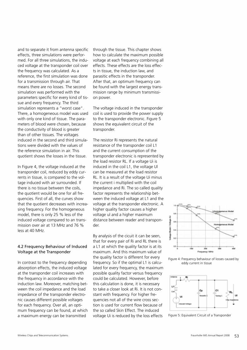
53Fraunhofer IMS Annual Report 2008
and to separate it from antenna specificeffects, three simulations were perfor-med. For all three simulations, the indu-ced voltage at the transponder coil overthe frequency was calculated. As areference, the first simulation was donefor a transmission through air. Thatmeans there are no losses. The secondsimulation was performed with theparameters specific for every kind of tis-sue and every frequency. The thirdsimulation represents a “worst case“.There, a homogeneous model was usedwith only one kind of tissue. The para-meters of blood were chosen, becausethe conductivity of blood is greaterthan of other tissues. The voltagesinduced in the second and third simula-tions were divided with the values ofthe reference simulation in air. Thisquotient shows the losses in the tissue.
In Figure 4, the voltage induced at thetransponder coil, reduced by eddy cur-rents in tissue, is compared to the vol-tage induced with air surrounded. Ifthere is no tissue between the coils, the quotient would be one for all fre-quencies. First of all, the curves showthat the quotient decreases with increa-sing frequency. For the homogeneousmodel, there is only 25 % less of theinduced voltage compared to an trans-mission over air at 13 MHz and 76 %less at 40 MHz.
4.2 Frequency Behaviour of InducedVoltage at the Transponder
In contrast to the frequency dependingabsorption effects, the induced voltageat the transponder coil increases withthe frequency in accordance with theinduction law. Moreover, matching bet-ween the coil impedance and the loadimpedance of the transponder electro-nic causes different possible voltagesfor each frequency. Over all, an opti-mum frequency can be found, at whicha maximum energy can be transmitted
through the tissue. This chapter showshow to calculate the maximum possiblevoltage at each frequency combining alleffects. These effects are the loss effec-ts in tissue, the induction law, andparasitic effects in the transponder.After that, an optimum frequency canbe found with the largest energy trans-mission range by minimum transmissi-on power.
The voltage induced in the transpondercoil is used to provide the power supplyto the transponder electronic. Figure 5shows the equivalent circuit of thetransponder.
The resistor Ri represents the naturalresistance of the transponder coil L1and the current consumption of thetransponder electronic is represented bythe load resistor RL. If a voltage Ui isinduced in the coil L1, the voltage Ulcan be measured at the load resistorRL. It is a result of the voltage Ui minusthe current i multiplied with the coilimpedance and Ri. The so called qualityfactor represents the relationship bet-ween the induced voltage at L1 and thevoltage at the transponder electronic. Ahigher quality factor causes a highervoltage ul and a higher maximumdistance between reader and transpon-der.
By analysis of the cicuit it can be seen,that for every pair of Ri and RL there isa L1 at which the quality factor is at itsmaximum. And this maximum value ofthe quality factor is different for everyfrequency. So if the optimal L1 is calcu-lated for every frequency, the maximumpossible quality factor versus frequencycould be calculated. However, beforethis calculation is done, it is necessaryto take a closer look at Ri. It is not con-stant with frequency. For higher fre-quencies not all of the wire cross sec-tion is used for current flow because ofthe so called Skin Effect. The inducedvoltage Ui is reduced by the loss effects
Wireless Chips and Telecommunication Systems
Figure 5: Equivalent Circuit of a Transponder
Figure 4: Frequency behaviour of losses caused byeddy current in tissue

54 Fraunhofer IMS Annual Report 2008
described in chapter 4.1. Because Ui isproportional to the quality factor, it isallowed to multiply the quality factorcalculated with 4 together with theresults of the graph’s in figure 4.Figure 6 shows the evaluation of equa-tion 4 considering the effects describedbefore. The parameters of an antennawith the required dimensions and aload resistor RL of 100 kOhm was used,that is an empirical value.
First of all, a great difference in indu-ceable voltages between LF and HF frequencies can be seen. For low fre-quencies, the quality factor is much
smaller than for the HF case. The simu-lation shows a maximum quality factorfor all simulations between 7 MHz and9 MHz. If the coils are sourrounded byair, there will be an optimal frequencyof about 9 MHz. This optimal frequencybecomes lower, when human tissue isbetween the coils. For the homoge-neous model, in worst case, an optimalfrequency is about 7 MHz. It can besaid, that the human tissue reduces theoptimal frequency value, at which themost voltage can be induced respec-tively the highest transmission rangecould be achieved. The optimal fre-quency can be observed near to the6,78 MHz ISM band. A carrier frequen-cy around 6,78 MHz is optimal for ourconstraints, if an ISM Band shell beused.
5 Experimental examination
An experimental measurement shallshow, that a sensor transponder can beprovided with enough energy insidehuman body tissue and shall determinethe maximum achievable distance. Forthis experiment, a circular coil with asingle winding and an aperture of 26cm was used to produce the magneticfield. A frequency of 13,56 MHz waschosen. A test transponder was develo-ped to measure the energy that can beprovided to an implanted transponder.To create a substitute that simulates theelectric properties of the human body, aphantom substance was prepared follo-wing a recipe described in [2]. The maingoal of the experiment is to measurethe voltage induced at the transpondercoil when it is placed inside this sub-stance at different distances from thereader coil. It was placed in a containerlarge enough to allow the transponderto be placed in a similar position as in ahuman body. The chip used in sensortransponders usually works with volta-ges greater than 3 V. Therefore, the
Wireless Chips and Telecommunication Systems
Figure 7: Distance measurement
Figure 6: Influence of the human tissue to the optimum frequency

55Fraunhofer IMS Annual Report 2008
transponder would be provided withenough energy at a distance where thevoltage is still higher than this voltage.Figure 7 shows the measurementresults.
The measurement was performed withan idle current of about Ieff = 5 A inthe reader coil and a load resistor in thetest transponder of 60 kOhm and100 kOhm. These values were chosenempirically. The voltage is grater than3 V for distances up to 48 cm.
The experimental measurement showsthat a sensor transponder can workinside human tissue up to a distance of48 cm.
6 Conclusion
Passive sensor transponders, deeplyimplanted in human bodies, are feasi-ble. For the given constraints to thetransponder antenna, an optimal fre-quency could be found. The loss effectsdecrease this optimum frequency. Acarrier frequency around 6,78 MHz isan optimal choice for our constraints.
References
[1] Priv.Doz. Dr. Andreas J. Morguet,Paul Kühnelt, Antje Kallel, Dirk Russ,Marcus Wähner, Prof. Dr. Heinz-Peter Schulteiss; TelemedizinischeBetreuung und Überwachung vonPatienten mit gering bis mittel gra -diger chronischer Herzinsuffizienz in der häuslichen Umgebung; AAL-Kongress 2008
[2] S Gabriel, R W Lau und C Gabriel;The dielectric properties of biological tissue; Phys. Med. Biol. 41 (1996) PP2271-2293
[3] A. V. Vorst, A. Rosen, Y. Kotsuka;RF/Microwave Interaction with bio-logical Tissues; John Wiley & SonsInc.; Canada USA; 2006
[4] Klaus Finkenzeller; RFID-Handbook;Hanser; München Wien; 2006
[5] Standard Test Method for measure-ment of radio frequency inducedheating near passive implants duringmagnetic resonance imaging; ASTMInternational; West Conshohocken,PA, 2002
Wireless Chips and Telecommunication Systems
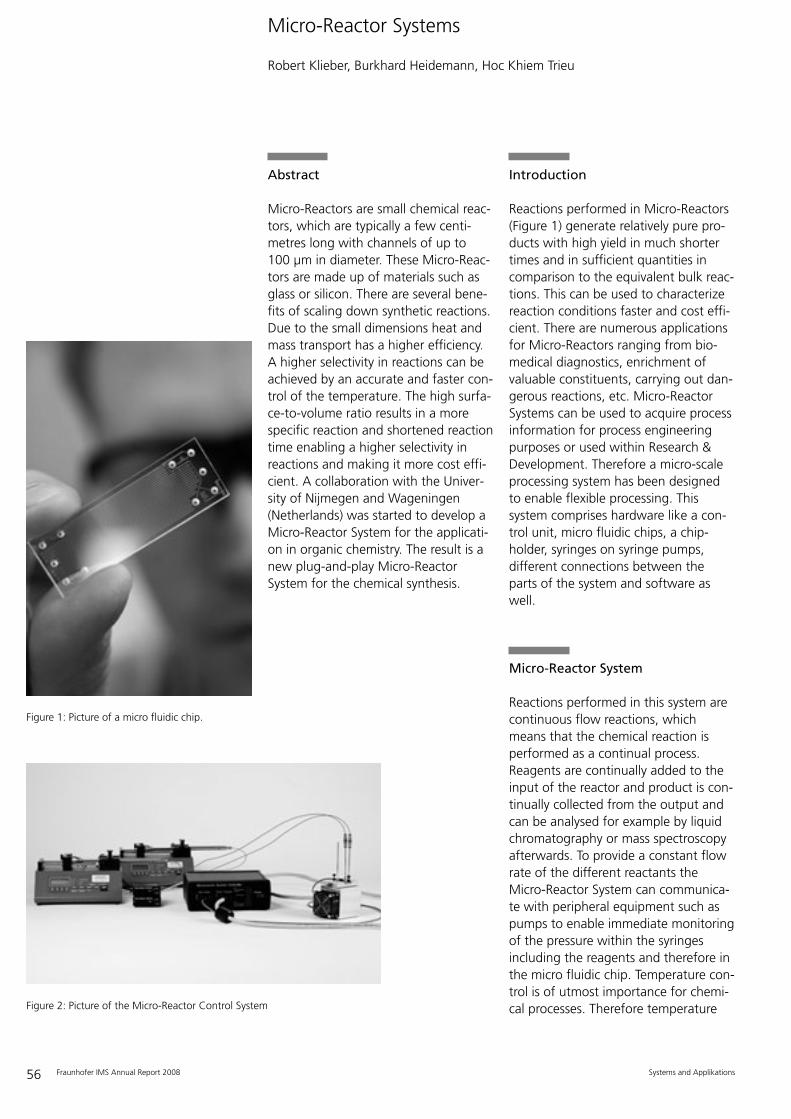
56 Fraunhofer IMS Annual Report 2008
Abstract
Micro-Reactors are small chemical reac-tors, which are typically a few centi -metres long with channels of up to100 µm in diameter. These Micro-Reac-tors are made up of materials such asglass or silicon. There are several bene-fits of scaling down synthetic reactions.Due to the small dimensions heat andmass transport has a higher efficiency.A higher selectivity in reactions can beachieved by an accurate and faster con-trol of the temperature. The high surfa-ce-to-volume ratio results in a morespecific reaction and shortened reactiontime enabling a higher selectivity inreactions and making it more cost effi-cient. A collaboration with the Univer -sity of Nijmegen and Wageningen(Netherlands) was started to develop aMicro-Reactor System for the applicati-on in organic chemistry. The result is anew plug-and-play Micro-ReactorSystem for the chemical synthesis.
Introduction
Reactions performed in Micro-Reactors(Figure 1) generate relatively pure pro-ducts with high yield in much shortertimes and in sufficient quantities incomparison to the equivalent bulk reac-tions. This can be used to characterizereaction conditions faster and cost effi-cient. There are numerous applicationsfor Micro-Reactors ranging from bio-medical diagnostics, enrichment ofvaluable constituents, carrying out dan-gerous reactions, etc. Micro-ReactorSystems can be used to acquire processinformation for process engineeringpurposes or used within Research &Development. Therefore a micro-scaleprocessing system has been designedto enable flexible processing. Thissystem comprises hardware like a con-trol unit, micro fluidic chips, a chip-holder, syringes on syringe pumps, different connections between theparts of the system and software aswell.
Micro-Reactor System
Reactions performed in this system arecontinuous flow reactions, whichmeans that the chemical reaction isperformed as a continual process.Reagents are continually added to theinput of the reactor and product is con-tinually collected from the output andcan be analysed for example by liquidchromatography or mass spectroscopyafterwards. To provide a constant flowrate of the different reactants theMicro-Reactor System can communica-te with peripheral equipment such aspumps to enable immediate monitoringof the pressure within the syringesincluding the reagents and therefore inthe micro fluidic chip. Temperature con-trol is of utmost importance for chemi-cal processes. Therefore temperature
Micro-Reactor Systems
Robert Klieber, Burkhard Heidemann, Hoc Khiem Trieu
Systems and Applikations
Figure 1: Picture of a micro fluidic chip.
Figure 2: Picture of the Micro-Reactor Control System
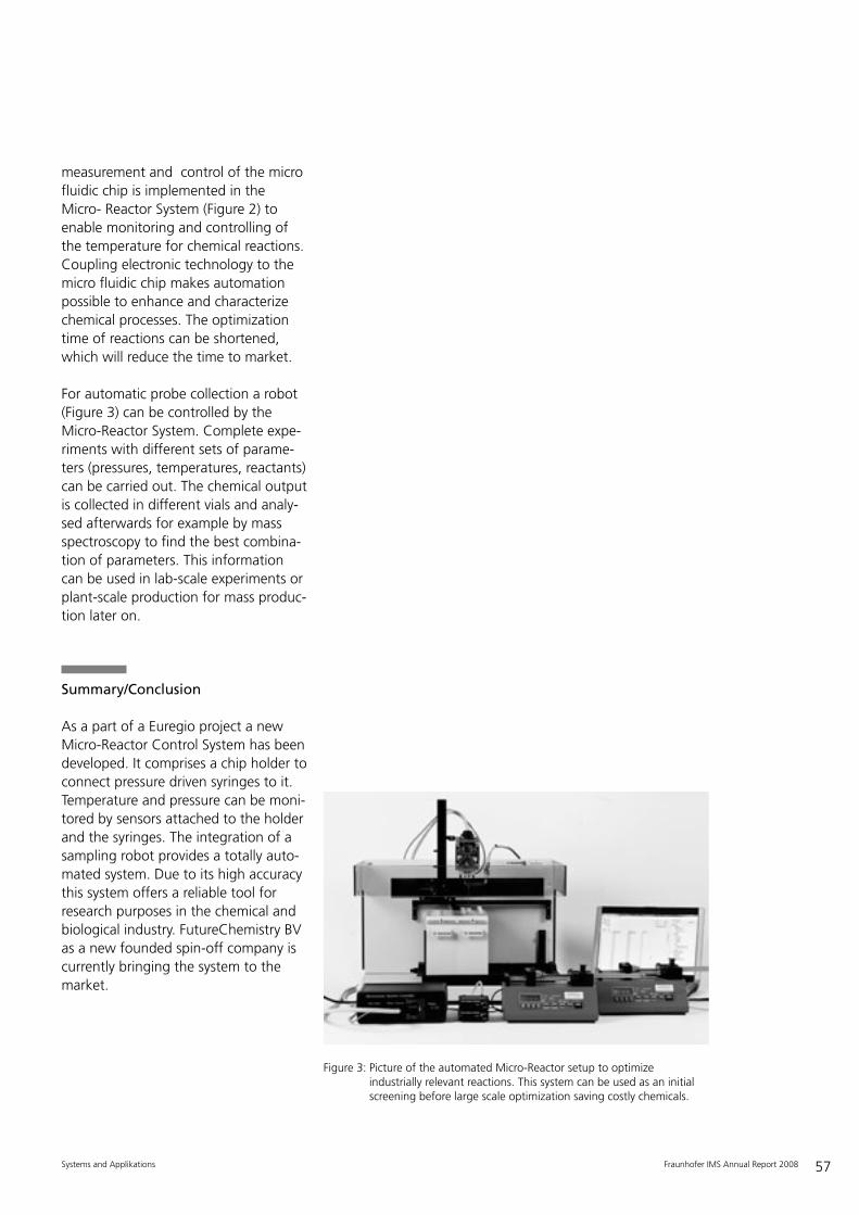
57Fraunhofer IMS Annual Report 2008
measurement and control of the microfluidic chip is implemented in theMicro- Reactor System (Figure 2) toenable monitoring and controlling ofthe temperature for chemical reactions.Coupling electronic technology to themicro fluidic chip makes automationpossible to enhance and characterizechemical processes. The optimizationtime of reactions can be shortened,which will reduce the time to market.
For automatic probe collection a robot(Figure 3) can be controlled by theMicro-Reactor System. Complete expe-riments with different sets of parame-ters (pressures, temperatures, reactants)can be carried out. The chemical outputis collected in different vials and analy-sed afterwards for example by massspectroscopy to find the best combina-tion of parameters. This informationcan be used in lab-scale experiments orplant-scale production for mass produc-tion later on.
Summary/Conclusion
As a part of a Euregio project a newMicro-Reactor Control System has beendeveloped. It comprises a chip holder toconnect pressure driven syringes to it.Temperature and pressure can be moni-tored by sensors attached to the holderand the syringes. The integration of asampling robot provides a totally auto-mated system. Due to its high accuracythis system offers a reliable tool forresearch purposes in the chemical andbiological industry. FutureChemistry BVas a new founded spin-off company iscurrently bringing the system to themarket.
Systems and Applikations
Figure 3: Picture of the automated Micro-Reactor setup to optimize indus trially relevant reactions. This system can be used as an initialscreening before large scale optimization saving costly chemicals.
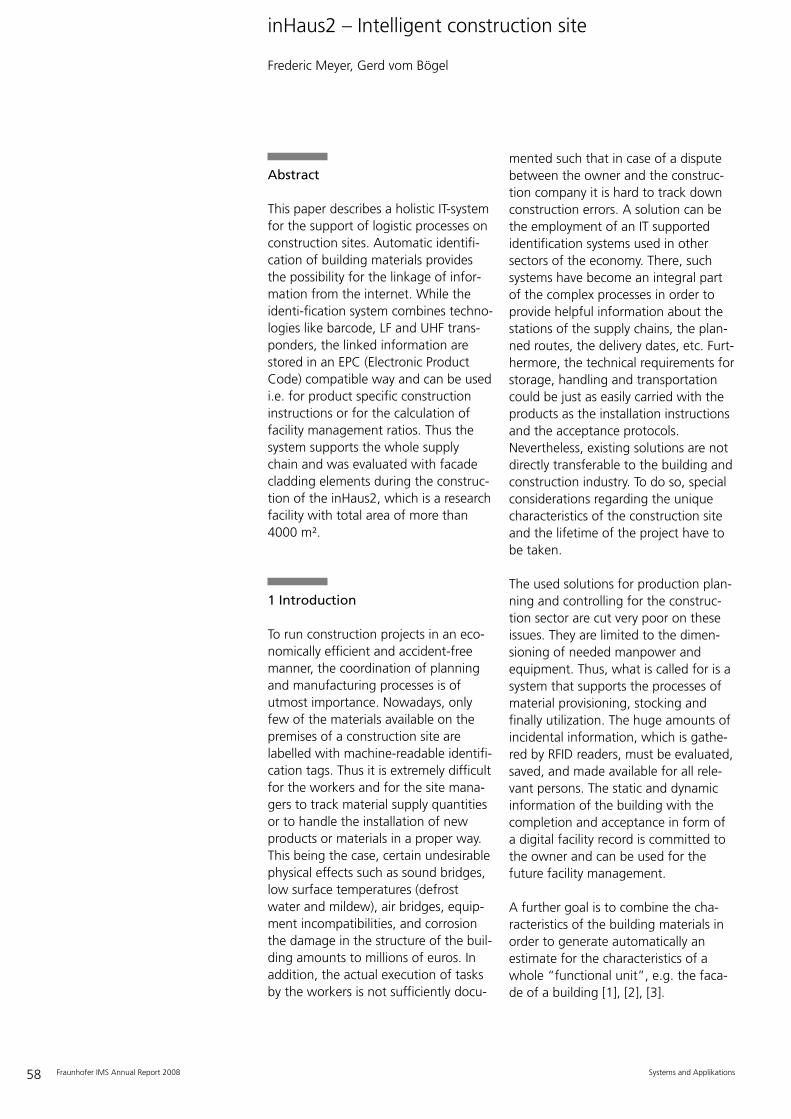
58 Fraunhofer IMS Annual Report 2008
Abstract
This paper describes a holistic IT-systemfor the support of logistic processes onconstruction sites. Automatic identifi-cation of building materials providesthe possibility for the linkage of infor-mation from the internet. While theidenti-fication system combines techno-logies like barcode, LF and UHF trans-ponders, the linked information are stored in an EPC (Electronic ProductCode) compatible way and can be usedi.e. for product specific constructioninstructions or for the calculation offacility management ratios. Thus thesystem supports the whole supply chain and was evaluated with facadecladding elements during the construc-tion of the inHaus2, which is a researchfacility with total area of more than4000 m².
1 Introduction
To run construction projects in an eco-nomically efficient and accident-freemanner, the coordination of planningand manufacturing processes is ofutmost importance. Nowadays, onlyfew of the materials available on thepremises of a construction site arelabelled with machine-readable identifi-cation tags. Thus it is extremely difficultfor the workers and for the site mana-gers to track material supply quantitiesor to handle the installation of newproducts or materials in a proper way.This being the case, certain undesirablephysical effects such as sound bridges,low surface temperatures (defrostwater and mildew), air bridges, equip-ment incompatibilities, and corrosionthe damage in the structure of the buil-ding amounts to millions of euros. Inaddition, the actual execution of tasksby the workers is not sufficiently docu-
mented such that in case of a disputebetween the owner and the construc-tion company it is hard to track downconstruction errors. A solution can bethe employment of an IT supportedidentification systems used in other sectors of the economy. There, suchsystems have become an integral partof the complex processes in order toprovide helpful information about thestations of the supply chains, the plan-ned routes, the delivery dates, etc. Furt-hermore, the technical requirements forstorage, handling and transportationcould be just as easily carried with theproducts as the installation instructionsand the acceptance protocols.Neverthe less, existing solutions are notdirectly transferable to the building andconstruction industry. To do so, specialconsiderations regarding the uniquecharacteristics of the construction siteand the lifetime of the project have tobe taken.
The used solutions for production plan-ning and controlling for the construc-tion sector are cut very poor on theseissues. They are limited to the dimen-sioning of needed manpower andequipment. Thus, what is called for is asystem that supports the processes ofmaterial provisioning, stocking andfinally utilization. The huge amounts ofincidental information, which is gathe-red by RFID readers, must be evaluated,saved, and made available for all rele-vant persons. The static and dynamicinformation of the building with thecompletion and acceptance in form ofa digital facility record is committed tothe owner and can be used for thefuture facility management.
A further goal is to combine the cha-racteristics of the building materials inorder to generate automatically an estimate for the characteristics of awhole “functional unit”, e.g. the faca-de of a building [1], [2], [3].
inHaus2 – Intelligent construction site
Frederic Meyer, Gerd vom Bögel
Systems and Applikations
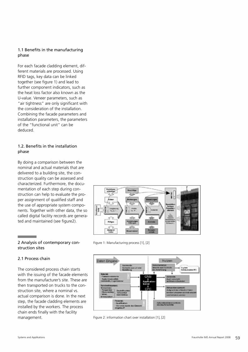
59Fraunhofer IMS Annual Report 2008
1.1 Benefits in the manufacturingphase
For each facade cladding element, dif-ferent materials are processed. UsingRFID tags, key data can be linkedtogether (see figure 1) and lead to further component indicators, such asthe heat loss factor also known as theU-value. Veneer parameters, such as“air tightness” are only significant withthe consideration of the installation.Combining the facade parameters andinstallation parameters, the parametersof the “functional unit" can be deduced.
1.2. Benefits in the installationphase
By doing a comparison between thenominal and actual materials that aredelivered to a building site, the con-struction quality can be assessed andcharacterized. Furthermore, the docu-mentation of each step during con-struction can help to evaluate the pro-per assignment of qualified staff andthe use of appropriate system compo-nents. Together with other data, the socalled digital facility records are genera-ted and maintained (see figure2).
2 Analysis of contemporary con-struction sites
2.1 Process chain
The considered process chain startswith the issuing of the facade elementsfrom the manufacturer’s site. These arethen transported on trucks to the con-struction site, where a nominal vs.actual comparison is done. In the nextstep, the facade cladding elements areinstalled by the workers. The processchain ends finally with the facilitymanagement.
Systems and Applikations
Figure 1: Manufacturing process [1], [2]
Figure 2: information chart over installation [1], [2]
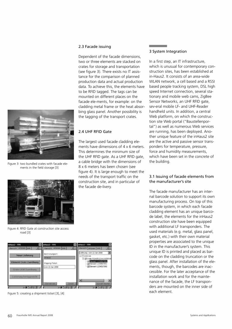
60 Fraunhofer IMS Annual Report 2008
2.3 Facade issuing
Dependent of the facade dimensions,two or three elements are stacked oncrates for storage and transportation(see figure 3). There exists no IT assis -tance for the comparison of plannedproduction data and actual productiondata. To achieve this, the elements haveto be RFID tagged. The tags can bemounted on different places on thefacade ele-ments, for example: on thecladding metal frame or the heat absor-bing glass panel. Another possibility isthe tagging of the transport crates.
2.4 UHF RFID Gate
The largest used facade cladding ele-ments have dimensions of 4 x 6 meters.This determines the minimum size ofthe UHF RFID gate. As a UHF RFID gate,a cable bridge with the dimensions of8 x 6 meters has been chosen (see figure 4). It is large enough to meet theneeds of the transport traffic on theconstruction site, and in particular ofthe facade de-livery.
3 System Integration
In a first step, an IT infrastructure,which is unusual for contemporary con-struction sites, has been established atin-Haus2. It consists of an area-wideWLAN network, a cell based and a RSSIbased people tracking system, DSL highspeed Internet connection, several sta-tionary and mobile web cams, ZigBeeSensor Networks, an UHF RFID gate,sev-eral mobile LF- and UHF-Readerhandheld units. In addition, a centralWeb platform, on which the construc-tion site Web portal (“Baustellenpor-tal”) as well as numerous Web servicesare running, has been deployed. Ano-ther unique feature of the inHaus2 siteare the active and passive sensor trans-ponders for temperature, pressure,force and humidity measurements,which have been set in the concrete ofthe building.
3.1 Issuing of facade elements fromthe manufacturer’s site
The facade manufacturer has an inter-nal barcode solution to support its ownmanufacturing process. On top of thisbarcode system, in which each facadecladding element has an unique barco-de label, the elements for the inHaus2construction site have been equippedwith additional LF transponders. Theused materials (e.g. metal, glass panel,gasket, etc.) with their own materialproperties are associated to the uniqueID in the manufacturer’s system. Thisunique ID is printed and placed as bar-code on the cladding truncation or theglass panel. After installation of the ele-ments, though, the barcodes are inac-cessible. For the later acceptance of theinstallation work and for the mainte-nance of the facade, the LF transpon-ders are mounted on the inner side ofeach element.
Systems and Applikations
Figure 3: two bundled crates with facade ele-ments in the field storage [3]
Figure 4: RFID Gate at construction site accessroad [3]
Figure 5: creating a shipment ticket [3], [4]

61Fraunhofer IMS Annual Report 2008
A carrier, also called, crate can carry upto four facade elements. The LF trans-ponders and/or barcodes of the ele-ments that have been loaded on thecrate are linked to the UHF transponder,which is mounted on the crate. Thus, amapping between the crate and its car-ried elements is created. This is donewith the help of the application depictedin figure 5. It runs on a mobile readerunit, which is equipped with a barcodescanner, LF-Reader and UHF-Reader. Thefollowing figures show the bundling ofelements at the manufacturer’s sitebefore these are shipped. First a newdelivery is opened, and using theaddress a shipment ticket is created.
Then, the barcode or LF transpondersfrom the facade elements are scannedand linked to the UHF transponder ofthe crate.
Each truck that is involved in the ship-ping process is equipped with a GPS-Box, which has been additionally tag-ged with an UHF transponder. After allcrates have been loaded on the truck, amapping between the trucks GPS trans-ponder id and the loaded crates is sto-red in the system. By doing this, theconstruction site manager and themanufac-turer are able to track thelocations of the shipments.
The completed shipment informationconsists of the planned delivery date,the delivery address, the loaded crateswith the corresponding cladding ele-ments and the GPS id of the truck. Thisinformation is send over the Internet tothe in-Haus2 construction site portal.
3.2 Facade delivery at inHaus2
The Reader from the UHF gate isconnected over the area wide WLAN tothe construction site Web portal. Upondelivery, the ids of the detected crate
UHF transponders are persisted in thesystem. In addition, the constructionsite manager is automatically notifiedabout the delivery of the shipment withthe help of an SMS message.
3.4 Acceptance of facade installationand generation of the functionalunit
After installation, the acceptance pro-cedure is carried out by the construc-tion site manager. The facade elementsare scanned with the handheld unitand he/she is able to accomplish thenominal vs. actual comparison. Theconstruction manager gets direct accessto installation details, manufacturerinformation, function coat, edge bond,glazing assembly etc. and he/she canjudge the quality of the installationwork. Remarks and considerations arewritten in the digital facility record.Having information about the pro-perties of the installed materials as wellas the grade of the installation quality,the parameters for the functional unit(e.g. the facade as a whole) can be cal-culated.
3.5 Facility management
For documentation, the facility mana-ger uses a handheld LF reader unit withWLAN access. Available maintenanceinformation, which is retrieved from thedigital facility record, is displayed onthe handheld. To enter new informati-on, the facility manager has to identifyhimself/herself. This is done with thehelp of an identification badge. Afterlogin, the LF transponder of the facadeelement, which is being serviced, isscanned. Remarks regarding the main-tenance procedure can be entered orinformation from previous service routi-nes can be retrieved from the digitalfacility record and displayed.
Systems and Applikations
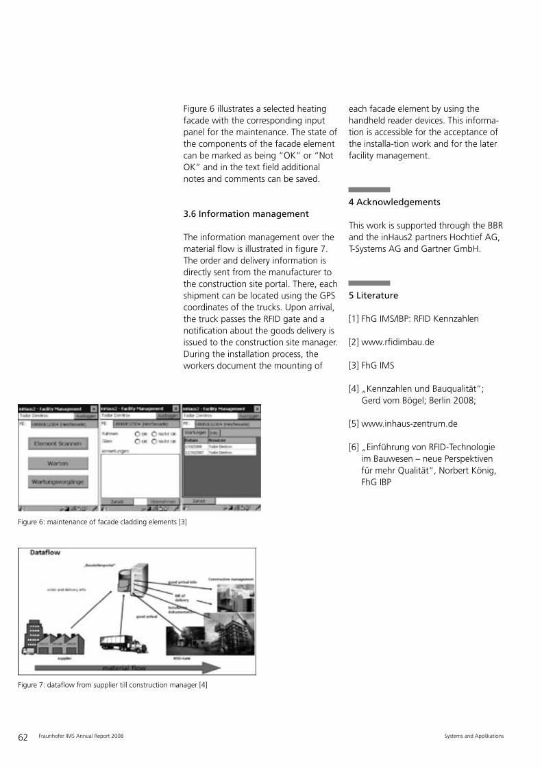
62 Fraunhofer IMS Annual Report 2008
Figure 6 illustrates a selected heatingfacade with the corresponding inputpanel for the maintenance. The state ofthe components of the facade elementcan be marked as being “OK” or “NotOK” and in the text field additionalnotes and comments can be saved.
3.6 Information management
The information management over thematerial flow is illustrated in figure 7.The order and delivery information isdirectly sent from the manufacturer tothe construction site portal. There, eachshipment can be located using the GPScoordinates of the trucks. Upon arrival,the truck passes the RFID gate and anotification about the goods delivery isissued to the construction site manager.During the installation process, theworkers document the mounting of
each facade element by using thehandheld reader devices. This informa-tion is accessible for the acceptance ofthe installa-tion work and for the laterfacility management.
4 Acknowledgements
This work is supported through the BBRand the inHaus2 partners Hochtief AG,T-Systems AG and Gartner GmbH.
5 Literature
[1] FhG IMS/IBP: RFID Kennzahlen
[2] www.rfidimbau.de
[3] FhG IMS
[4] „Kennzahlen und Bauqualität“;Gerd vom Bögel; Berlin 2008;
[5] www.inhaus-zentrum.de
[6] „Einführung von RFID-Technologieim Bauwesen – neue Perspektivenfür mehr Qualität“, Norbert König,FhG IBP
Systems and Applikations
Figure 6: maintenance of facade cladding elements [3]
Figure 7: dataflow from supplier till construction manager [4]

63Fraunhofer IMS Annual Report 2008Systems and Applikations

64 Fraunhofer IMS Annual Report 2008

65Fraunhofer IMS Annual Report 2008
List of ProjectsIMS Duisburg

66 Fraunhofer IMS Annual Report 2008
List of ProjectsIMS Duisburg
Project Title Partner Project Period
Pulse Generator Industry 07/1996–07/2010
Production High Voltage SOI-CMOS Industry 01/2003–09/2009
Foundry IVTMX Industry 04/2004–12/2008
Delivery CMOS Imager Industry 05/2004–07/2008
Delivery REOS Industry 10/2004–12/2008
ASIC Production Industry 01/2005–12/2014
Development of technology robust IP cores Industry 05/2005–04/2008
Quartz Wafer Industry 05/2005–12/2008
CMOS Technology R&D Industry 01/2005–12/2014
CMOS Production Industry 01/2005–12/2014
Spectroscopy CMOS Sensors Industry 08/2005–03/2009
ASIC Development Pressure Sensor Industry 03/2006–06/2009
Delivery of Memory Tag III Industry 10/2005–12/2008
Delivery OA32 Industry 09/2005–12/2009
MILDS Sensor Industry 08/2007–08/2009
MILDS Sensor Development Industry 02/2004–11/2008
IP Exchange Industry 07/2006–06/2008
Consulting for Heating Systems Industry 09/2006–12/2008
Foundry IODS P2 Industry 09/2006–12/2008
Foundry Service Industry 12/2006–12/2008
inHaus Basis Contacts Industry 01/2007–12/2010
TADS Industry 02/2007–12/2008
MIMOS II Industry 02/2007–12/2008
Sensor Transponder Industry 03/2007–11/2008
UTSD Modul Industry 03/2007–08/2008

67Fraunhofer IMS Annual Report 2008
SOI-CMOS Process Industry 04/2007–03/2009
Concept High Frame Rate Imager Industry 05/2007–02/2008
Development RFID Reader Industry 05/2007–01/2008
Development Smart Home Controller Industry 11/2007–06/2008
Reader for Pressure Sensor Tag Industry 07/2007–12/2008
Demonstrator RF Industry 07/2007–10/2007
ADC Self Test Industry 08/2007–11/2008
EEPROM Technology Development Industry 09/2007–11/2009
Infrastructure inHaus 2 Industry 03/2007–07/2008
Production RF ASIC For Longer Range Industry 09/2007–06/2008
Study High Frame Rate Imager Industry 08/2006–01/2007
LON Interface for Heating Systems Industry 08/2006–04/2007
Production RF ASIC For Longer Range Industry 09/2007–02/2008
Production Triangulation Sensor Industry 01/2005–12/2009
SOI-CMOS Production Industry 06/2007–12/2008
Process Documentation inHaus Industry 08/2007–12/2007
Development Software MOD 3000 I Industry 03/2008–09/2008
Pressure Sensor Tag Industry 10/2007–12/2008
Smart Meter Hardware Industry 04/2008–05/2008
Development CMOS Imager PROVIPS Industry 10/2008–09/2010
People Trecking Industry 11/2007–08/2008
Study Imager Pixel Industry 11/2007–04/2008
Wireless Displays Industry 11/2007–03/2008
Study Strain Gauges Industry 11/2007–03/2008
Development High Frame Rate CMOS Imager Industry 12/2007–05/2010
4th CMOS Imaging Workshop Industry 01/2007–12/2008

68 Fraunhofer IMS Annual Report 2008
Backendprocess Industry 12/2007–12/2008
MPS Transponder System Industry 01/2008–12/2008
Demonstrator LON Pyxos Industry 01/2007–02/2008
Delivery CMOS Imager Industry 01/2008–11/2008
Study Specification MUC Industry 01/2008–02/2008
Study 3D Sensor Industry 03/2008–11/2008
Development Cash Box Transponder Industry 03/2008–11/2008
Flexray Conformance Test II Industry 03/2008–04/2008
Development SoC Demonstrator Industry 06/2008–11/2008
Study Intelligent Work Place Industry 06/2008–11/2008
Piezo Resistive High Pressure Sensor Industry 07/2008–08/2009
Study SRAM IV Industry 07/2008–12/2008
Building Front Tracking Industry 01/2008–11/2008
Development Of Technology Robust IP Cores II Industry 08/2008–12/2008
Consulting for Heating Systems Industry 08/2008–11/2008
Development Retina Implant Industry 08/2008–05/2011
Development Software MOD 3000 II Industry 08/2008–09/2009
Terra Hertz Imaging Industry 07/2008–06/2009
Study SRAM V Industry 09/2008–11/2008
inHaus II Energy Efficiency UC Industry 09/2008–11/2008
Support Amorphous Silicion 2 Industry 10/2008–12/2008
Process Development CMOS 3D Industry 10/2008–02/2010
Support Layout Industry 10/2008–12/2008
Development Master Modification for Heating Systems Industry 11/2008–12/2008
Development Master Modification for Heating Systems Industry 10/2008–12/2008

69Fraunhofer IMS Annual Report 2008
Patent Funding Authority 01/2004–06/2008EC
Micro Reactors Funding Authority: 01/2008–09/2008Investions-Bank NRW
Amigo Funding Authority 09/2004–02/2008EC
Development of CMOS process integration for MRAM Funding Authority 09/2005–11/2008EMAC EC
Wireless Stabling - WISTAB Funding Authority: 07/2006–07/2008Investions-Bank NRW
Sensor Data Fusion of 2D/3D Imager Funding Authority: 06/2006–05/2009MIDIAS VDI/VDE
RFID Operation Function Funding Authority: 10/2006–02/2008BBR
Smart pipe Funding Authority 01/2006–06/2008Projektträger Jülich
RFID IMS encoding Funding Authority: 10/2006–02/2008BBR
Inhaus II Funding Authority 10/2006–06/2008Projektträger Jülich
Sensor Platform for Molecular Medical Sensors Funding Authority: 06/2006–05/2009IMIKRID VDI/VDE
IMKA Funding Authority: 04/2007–07/2008VDI/VDE
Gender Mainstreaming Funding Authority: 04/2007–06/2008Investions-Bank NRW
IR Camera Funding Authority: 11/2007–10/2010FIRCAM VDI TZ
Smart Forest Funding Authority: 11/2007–10/2010BLE
EMSIS Funding Authority: 09/2007–12/2008BMBF
MiniSurg Funding Authority 06/2008–05/2010Miniaturised Stereoscopic Distal Imaging Sensor EC

70 Fraunhofer IMS Annual Report 2008
Amigo Funding Authority 09/2004–02/2008EC
Jutta Funding Authority: 10/2008–09/2011Just in Time Assistance DLR
COMPASS Funding Authority: 09/2008–08/2011Transponder for Blood Pressure Measurement VDI/VDE
Consulting LDS Funding Authority: 08/2008–07/2009Local Government NRW,
FFM Super Cam Funding Authority: 09/2008–12/2009DLR
FFM Angiocam Funding Authority: 09/2008–12/2009DLR
BIOPROM Funding Authority: 01/2008–12/200Development of marker free biological detection BMBF
Blood Camera FhG defined Project 01/2007–12/2008
Assistant Systems FhG defined Project 10/2007–09/2012
RF Object Localisation FhG defined Project 10/2005–06/2008
Distributed Smart Objects for logistic Applictaions FhG defined Project 01/2006–12/2008
Future Chemistry FhG defined Project 03/2008–08/2009
Simulation for Process Variation FhG defined Project 02/2008–01/2011
Development of Indoor Localizations System FhG defined Project 10/2008–09/2010

71Fraunhofer IMS Annual Report 2008
List of Publications andScientific Theses 2008
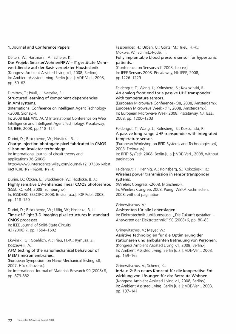
72 Fraunhofer IMS Annual Report 2008
Fassbender, H.; Urban, U.; Görtz, M.; Trieu, H.-K.; Mokwa, W.; Schmitz-Rode, T.:Fully implantable blood pressure sensor for hypertonicpatients.(Conference on Sensors <7, 2008, Lecce>).In: IEEE Sensors 2008. Piscataway, NJ: IEEE, 2008,pp.1226–1229
Feldengut, T.; Wang, J.; Kolnsberg, S.; Kokozinski, R.:An analog front end for a passive UHF transponderwith temperature sensors.(European Microwave Conference <38, 2008, Amsterdam>;European Microwave Week <11, 2008, Amsterdam>).In: European Microwave Week 2008. Piscataway, NJ: IEEE,2008, pp. 1200–1203
Feldengut, T.; Wang, J.; Kolnsberg, S.; Kokozinski, R.:A passive long-range UHF transponder with integratedtemperature sensor.(European Workshop on RFID Systems and Technologies <4,2008, Freiburg>).In: RFID SysTech 2008. Berlin [u.a.]: VDE-Verl., 2008, withoutpagination
Feldengut, T.; Hennig, A.; Kolnsberg, S.; Kokozinski, R.:Wireless power transmission in sensor transpondersystems.(Wireless Congress <2008, München>).In: Wireless Congress 2008. Poing: WEKA Fachmedien,2008, without pagination
Grinewitschus, V.:Assistenten für alle Lebenslagen.In: Elektrotechnik Jubiläumsausg. „Die Zukunft gestalten –Antworten der Elektrotechnik“ 90 (2008) 6, pp. 80–83
Grinewitschus, V.; Meyer, W.:Assistive Technologien für die Optimierung der stationären und ambulanten Betreuung von Personen.(Kongress Ambient Assisted Living <1, 2008, Berlin>).In: Ambient Assisted Living. Berlin [u.a.]: VDE-Verl., 2008,pp. 159–162
Grinewitschus, V.; Scherer, K.:inHaus-2: Ein neues Konzept für die kooperative Ent-wicklung von Lösungen für das Betreute Wohnen.(Kongress Ambient Assisted Living <1, 2008, Berlin>).In: Ambient Assisted Living. Berlin [u.a.]: VDE-Verl., 2008,pp. 137–141
1. Journal and Conference Papers
Deiters, W.; Hartmann, A.; Scherer, K.:Das Projekt SmarterWohnenNRW – IT gestützte Mehr-wertdienste auf der Basis vernetzter Haustechnik.(Kongress Ambient Assisted Living <1, 2008, Berlin>).In: Ambient Assisted Living. Berlin [u.a.]: VDE-Verl., 2008,pp. 59–62
Dimitrov, T.; Pauli, J.; Naroska, E.:Structured learning of component dependencies in AmI systems.(International Conference on Intelligent Agent Technology<2008, Sidney>).In: 2008 IEEE WIC ACM International Conference on WebIntelligence and Intelligent Agent Technology. Piscataway, NJ: IEEE, 2008, pp.118–124
Durini, D.; Brockherde, W.; Hosticka, B. J.:Charge-injection photogate pixel fabricated in CMOSsilicon-on-insulator technology.In: International journal of circuit theory and applications 36 (2008)http://www3.interscience.wiley.com/journal/121375861/abstract?CRETRY=1&SRETRY=0
Durini, D.; Özkan, E.; Brockherde, W.; Hosticka, B. J.:Highly sensitive UV-enhanced linear CMOS photosensor.(ESSCIRC <34, 2008, Edinburgh>).In: ESSDERC ESSCIRC 2008. Bristol [u.a.]: IOP Publ. 2008,pp. 118–120
Durini, D.; Brockherde, W.; Ulfig, W.; Hosticka, B. J.:Time-of-Flight 3-D imaging pixel structures in standardCMOS processes.In: IEEE Journal of Solid-State Circuits43 (2008) 7, pp. 1594–1602
Ekwinski, G.; Goehlich, A.; Trieu, H.-K.; Rymuza, Z.; Koszewski, A.:AFM testing of the nanomechanical behaviour ofMEMS micromembranes.(European Symposium on Nano-Mechanical Testing <8,2007, Hückelhoven>).In: International Journal of Materials Research 99 (2008) 8,pp. 879-882
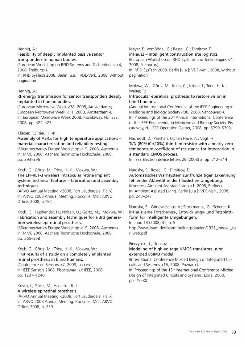
73Fraunhofer IMS Annual Report 2008
Hennig, A.:Feasibility of deeply implanted passive sensor transponders in human bodies.(European Workshop on RFID Systems and Technologies <4,2008, Freiburg>).In: RFID SysTech 2008. Berlin [u.a.]: VDE-Verl., 2008, withoutpagination
Hennig, A.:RF energy transmission for sensor transponders deeplyimplanted in human bodies.(European Microwave Week <38, 2008, Amsterdam>; European Microwave Week <11, 2008, Amsterdam>).In: European Microwave Week 2008. Piscataway, NJ: IEEE,2008, pp. 424–427
Klieber, R.; Trieu, H.-K.:Assembly of ASICs for high temperature applications –material characterization and reliability testing.(Micromechanics Europe Workshop <19, 2008, Aachen>).In: MME 2008. Aachen: Technische Hochschule, 2008, pp. 393–396
Koch, C.; Görtz, M.; Trieu, H.-K.; Mokwa, W.:The EPI-RET-3 wireless intraocular retina implantsystem: technical features – fabrication and assemblytechniques.(ARVO Annual Meeting <2008, Fort Lauderdale, Fla.>).In: ARVO 2008 Annual Meeting. Rockville, Md.: ARVO Office, 2008, p.154
Koch, C.; Fassbender, H.; Nolten, U.; Görtz, M.; Mokwa, W.:Fabrication and assembly techniques for a 3rd genera -tion wireless epiretinal prosthesis.(Micromechanics Europe Workshop <19, 2008, Aachen>).In: MME 2008. Aachen: Technische Hochschule, 2008, pp. 365–368
Koch, C.; Görtz, M.; Trieu, H.-K.; Mokwa, W.:First results of a study on a completely implanted retinal prosthesis in blind humans.(Conference on Sensors <7, 2008, Lecce>).In: IEEE Sensors 2008. Piscataway, NJ: IEEE, 2008, pp. 1237–1240
Krisch, I.; Görtz, M.; Hosticka, B. J.:A wireless epiretinal prosthesis.(ARVO Annual Meeting <2008, Fort Lauderdale, Fla.>).In: ARVO 2008 Annual Meeting. Rockville, Md.: ARVO Office, 2008, p. 230
Meyer, F.; VomBögel, G.; Ressel, C.; Dimitrov, T.:inHaus2 – Intelligent construction site logistics.(European Workshop on RFID Systems and Technologies <4,2008, Freiburg>).In: RFID SysTech 2008. Berlin [u.a.]: VDE-Verl., 2008, withoutpagination
Mokwa, W.; Görtz, M.; Koch, C.; Krisch, I.; Trieu, H.-K.; Walter, P.:Intraocular epiretinal prosthesis to restore vision inblind humans.(Annual International Conference of the IEEE Engineering inMedicine and Biology Society <30, 2008, Vancouver>).In: Proceedings of the 30th Annual International Conferenceof the IEEE Engineering in Medicine and Biology Society. Pis-cataway, NJ: IEEE Operation Center, 2008, pp. 5790–5793
Nachrodt, D.; Paschen, U.; ten Have, A.; Vogt, H.:Ti/Ni(80%)Cr(20%) thin-film resistor with a nearly zerotemperature coefficient of resistance for integration ina standard CMOS process.In: IEEE Electron device letters 29 (2008) 3, pp. 212–214
Naroska, E.; Ressel, C.; Dimitrov, T.:Automatisches Warnsystem zur frühzeitigen Erkennungfehlender Aktivität in der häuslichen Umgebung.(Kongress Ambient Assisted Living <1, 2008, Berlin>).In: Ambient Assisted Living. Berlin [u.a.]: VDE-Verl., 2008,pp. 243–247
Naroska, E.; Grinewitschus, V.; Stockmanns, G.; Scherer, K.:inHaus: eine Forschungs-, Entwicklungs- und Tetsplatt-form für intelligente Umgebungen.In: Inno 13 (2008) 41, p. 5http://www.ivam.de/files/mitteilungsdateien/1321_inno41_for_web.pdf
Pieczynski, J.; Doncov, I.:Modeling of high-voltage NMOS transistors usingextended BSIM3 model.(International Conference Mixded Design of Integrated Cir-cuits and Systems <15, 2008, Poznan>).In: Proceedings of the 15th International Conference MixdedDesign of Integrated Circuits and Systems. Łódz, 2008, pp. 75–80

74 Fraunhofer IMS Annual Report 2008
Sommer, S. P.; Paschen, U.; Vogt, H.:Positive charge trapping induced by plasma chargingdamage in NMOS transistors.(ESSDERC <38, 2008, Edinburgh>). In: ESSDERC ESSCIRC 2008. Bristol [u.a.]: IOP Publ. 2008,Fringe session P28, without pagination
Uhrmann, T.; Dimopoulos, T.; Brückl, H.; Lazarov, V. K.; Kohn, A.; Paschen, U.; Weyers, S.; Bar, L.; Rührig, M.:Characterization of embedded MgO/ferromagnetcontacts for spin injection in silicon.In: Journal of applied physics 103 (2008) 6, pp. 063709-1–063709-5
Urban, U.; Fassbender, H.; Görtz, M.; Trieu, H.-K.; Steinseifer, U.; Schmitz-Rode, T.; Schnakenberg, U.:CHF-Monitoring – Bewertung von zwei alternativenImplantatkonzepten.(Kongress Ambient Assisted Living <1, 2008, Berlin>).In: Ambient Assisted Living. Berlin [u.a.]: VDE-Verl., 2008,pp. 363–365
Vogt, H.:Films – Ein Programm zur Simulation von AR-Schichten.(Thüringer Kolloquium Dünne Schichten in der Optik <1,2008, Jena>).In: 4. Thüringer Grenz- und Oberflächentage & 1. ThüringerKolloquium „Dünne Schichten in der Optik“. Jena: INNO-VENT e.V., 2008, pp. 282–283
VomBögel, G.:Grundlagen der RFID-Technologie und anwendungs -spezifische Eigenschaften im Bauwesen.(Kongress RFID im Bau <2008, Berlin>).In: RFID im Bau. Dresden: ARGE RFID, 2008, without pagination
VomBögel, G.:Moderne Baustellenlogistik durch Einsatz neuer Infor-mations- und Kommunikations-Technologien.(Fachtagung Praxis Transportbeton <2008, Magdeburg>).In: Beton 58 (2008) 9, Sonderteil Fachtagung, p. 9
Wang, J.; Feldengut, T.; Kolnsberg, S.; Kokozinski, R.:A concept for the analysis of cross sensitivities inmodern RFID systems.(European Workshop on RFID Systems and Technologies <4,2008, Freiburg>).In: RFID SysTech 2008. Berlin [u.a.]: VDE-Verl., 2008, withoutpagination
2. Oral Presentations
Grinewitschus, V.:Intelligente Umgebungen: Anwendungen und Einsatz-möglichkeiten für mobile Roboter.Fraunhofer IPA, 2. Technologieforum, Stuttgart, November 14, 2008
Grinewitschus, V.:Wired and smart: embedded internet systems.Amigo Symposium, Eindhoven, February 28, 2008
Naroska, E.:Sicher Wohnen durch smarte Haustechnik – Chancenund Risiken des Bewohner-Monitorings.REHACARE Kongress, Düsseldorf, October 17, 2008
Scherer, K.:Making smart environments real.Rostocker Assistenztage <RASTA>, February 21, 2008
Scherer, K.:Der schlaue Raum als Freund und Helfer: Smart Home &Building – aktuelle Trends innovativer Technik in Räu-men und Gebäuden.REHACARE Kongress, Düsseldorf, October 17, 2008
Scherer, K.:Smart Building – Mehrwert durch Breitband -kommunikation.BREKO Bundesverband Breitbandkommunikation Jahresta-gung „Ein Netz für die Zukunft“, Berlin, November 13, 2008
Scherer, K.:Wie helfen Industrie und Forschung das effizienteHotel zu bauen?ITB Hospitality Day, Berlin, March 6, 2008
Schrey, O.:Custom CMOS image sensors, architecture and design.Image Sensors Europe, London, March 19, 2008
Stevens, T.:Integrierte Haussteuerung: Komfort in den eigenen vierWänden durch ganzheitliche Steuerkonzepte für Haus-geräte und Hausinfrastruktur.Fraunhofer-ISST Veranstaltung „Service-Wohnen zur Mieter-bindung: Lösungskonzepte für die Wohnungswirtschaft undneue Potenziale für Dienstleister“, Dortmund, March 11,2008
75Fraunhofer IMS Annual Report 2008
Stockmanns, G.:Intelligent analysis of monitoring signals.21st Annual Congress European Society of Intensive CareMedicine, Lissabon, August 29, 2008
Stockmanns, G.:Signal analysis in neuromonitoring.21st Annual Congress European Society of Intensive CareMedicine, Lissabon, August 29, 2008
Stockmanns, G.:Die Zukunft des Wohnens für Jung und Alt – AmbientIntelligence und aktuelle Forschungstrends am Beispielvon inHaus2.REHACARE Kongress, Düsseldorf, October 17, 2008
Thoß, S.:Neuartiges Ausleseverfahren für induktive Näherungs-sensoren auf Basis von Sigma-Delta Modulation.10. Workshop „Integrierte Analogschaltungen“, Berlin,March 10, 2008
VomBögel, G.:RFID im Bauwesen: Evaluierung der RFID-Technologiezur Optimierung von logistischen Prozessen an ver-schiedenen Bauprodukten.Euro-ID, Köln, May 15, 2008
VomBögel, G.:RFID und Sensornetzwerke für die dezentrale Steue-rung von Materialfluss und Kommissionierung.RFID-Praxistag Logistik, IHK, Dortmund, June 19, 2008
3. Patents
3.1 Granted Patents
Jung, P.; Sappok, S.:Vorrichtung und Verfahren zum Abwärtsmischen einesEingangssignals in ein Ausgangssignal.February 29, 2008JP 4087850
Krisch, I.; Brockherde, W.; Hosticka, B. J.:Video endoscopy device.March 6, 2008JP 506478
Müller, H.-C.; Greifendorf, D.; Lörcks, M.; Jansen, A.; Kokozinski, R.; Holzapfel, M.:Datenübertragung zwischen mehreren Sendern undeinem Empfänger.November 19, 2008EP 1 835 664 B1
Nehrig, O.:Apparatus and method for reading out a differentialcapacity with a first and second partial capacity.April 8, 2008US 7,356,423 B2
3.2 Laid Open Patent Documents
Boom, T. van den; Hosticka, B.-J.; Trieu, H.-K.:Vorrichtung und Verfahren zum geregelten Transportmikrofluidischer Proben.October 30, 2008DE 10 2007 018752 A1
Fritsch, D.; VomBögel, G.; Ledermann, T.; Wolfelschneider, H.:Concept for determining the position of a passive trans-ponder in a radio system.May 2, 2008PCT/EP2007/009145
Fritsch, D.; VomBögel, G.; Ledermann, T.; Wolfelschneider, H.:Konzept zur Positionsbestimmung eines passiven Trans-ponders in einem Funksystem.April 30, 2008DE 10 2006 049 862 A1
Grabmaier, A.; Boom, T. van den; Dahmen, U.; Dirsch, O.;Stockmanns, G.; Viga, R.; Balzani, D.; Brands, D.:Vorrichtung und Verfahren zum Erfassen eines druck-abhängigen Parameters.December 24, 2008DE 10 2007 0384402 A1
Krisch, I.; Brockherde, W.; Hosticka, B. J.:Videoendoskopievorrichtung.March 6, 2008JP 2008-506478
Trieu, H.-K.; Slotkowski, J.; Klieber, R.; Van Heest, J. C. M.;Koch, K.; Rutjes, F. P. J. T.; Nieuwland, P.J.; Wiebe, P.:Chip holder, fluidic system and chip holder system.May 2, 2008PCT/EP2006/010299
76 Fraunhofer IMS Annual Report 2008
Trieu, H.-K.; Wiebe, P.; Klieber, R.:Device and method for checking and monitoring thepressure in pressure pipes and/or conduits.July 17, 2008PCT/EP2006/012513
Trieu, H.-K.; Schelle, B.; Slotkowski, J.; Ünlübayir, S.:Elektrische Drucksensorvorrichtung.July 16, 2008EP 1 944 597 A1
Vogt, H.; Russ, M.:Bolometer and method for producting a bolometer.March 13, 2008PCT/EP2006/008790
4. Theses
4.1 Dissertations
Bechen, B.:Systematischer Entwurf analoger Low-power Schaltungen in CMOS anhand einer kapazitiven Sensorauslese.In: Stuttgart: Fraunhofer IRB Verl., 2008Zugl.: Duisburg-Essen, Campus Duisburg Univ., Diss., 2008ISBN 978-3-8167-7579-9
4.2 Diploma Theses
Eiker, A.:Analyse und Optimierung der Genauigkeit eines opto-elektronischen Testsystems für die Charakterisierungvon rauscharmen CMOS-BildsensorenKrefeld-Mönchengladbach, Campus Krefeld, Hochsch., Dipl.-Arb., 2008
Eschke, J.:Entwurf, Aufbau und Verifikation von modularen Leistungs verstärkern für einen RFID-Reader im UHFISM-Band.Dortmund, Fachhochsch., Dipl.-Arb., 2008
Faber, D.:Entwurf und Optimierung eines Demodulators für einpassives UHF Transponder Front-End.Duisburg-Essen, Campus Duisburg, Univ., Dipl.-Arb., 2008
Sänger, S.:Optimierung der Trench-Isolation für einen SOI-CMOS-Prozess.Darmstadt, Techn. Univ., Dipl.-Arb., 2008
Wösten, S.Analyse, Aufbau und Implementierung eines aktivenlow-power Testtransponders im europäischen UHF-Band nach EPC Class 1 Gen 2-Standard (ISO 18000-6c).Osnabrück, Fachhochsch., Dipl.-Arb., 2008
4.3 Master Theses
Emre, E.:Camera system for an infrared sensitive microbolo -meter array.Duisburg-Essen, Campus Duisburg, Univ., Master Thesis,2008
Lehmann, B.:Entwicklung eines optimierten Protokollstacks für HF-Sensortranspondersysteme in medizinischen An wendungen.Wuppertal, Univ., Master Thesis, 2008
4.4 Bachelor Theses
Beier, T.:Optimierung von Reinigungsprozessen im CMP Bereich.Düsseldorf, Fachhochsch., Bachelor Thesis, 2008
Doncov, I.:BSIM3 Modellparameterextraktion eines 1,2 µm Prozesses mit Drucksensor- und Hochvoltoptionen mit Hilfe des IC-CAP Softwarepakets.Düsseldorf, Fachhochsch., Bachelor Thesis, 2008
Feberwee, N.:Charakterisierung von Packagingmaterialien fürHochtemperatur-Halbleiterbauelemente.Düsseldorf, Fachhochsch., Bachelor Thesis, 2008
Gawlik, C.:Parasitäre Feldeffekttransistoren in einer 0.35 µmCMOS Technologie.Düsseldorf, Fachhochsch., Bachelor Thesis, 2008
77Fraunhofer IMS Annual Report 2008
Gerbecks, J.:Konzeption und Implementation einer mobilen, Senioren unterstützenden Infrastruktur für die häus -liche Pflege.Duisburg-Essen, Campus Essen, Univ., Bachelor Thesis, 2008
Ghoshdastider, U.:Implementation of an application specific digital inter-face to control a high frame rate image array sensor ina 0,35 µm CMOS technology.Duisburg-Essen, Campus Duisburg, Univ., Bachelor Thesis,2008
Gorski, D.:Entwicklung einer Plattform zur Evaluierung von Proto-kollstacks für HF Sensortranspondersysteme.Duisburg-Essen, Campus Duisburg, Univ., Bachelor Thesis,2008
Hanhan, K.:Analysis and enhancement of a force sensor for adecentralized system architecture.Duisburg-Essen, Campus Duisburg, Univ., Bachelor Thesis,2008
Haverkamp, S.:Development of a passive RFID sensor transponder forhumidity measurement.Duisburg-Essen, Campus Duisburg, Univ., Bachelor Thesis,2008
Huypen, T.:Entwicklung einer generischen Regelsprache fürambiente Systeme.Venlo, Hogeschool, Bachelor-Thesis, 2008
Jawo, M.-O.:Development of a 3D-Laser scanner to acquire roomgeometry based on the Ethernut 3 platform and thegeneration of 3D models deploying object-orientedprogramming languages to simplify navigation in homeautomation.Duisburg-Essen, Campus Duisburg, Univ., Bachelor Thesis,2008
Lessner, N.:Entwicklung eines Beschleunigungssensormoduls zurVerbesserung der Ortsauflösung von Lokalisierungs -systemen.Duisburg-Essen, Campus Duisburg, Univ., Bachelor Thesis,2008
Mertens, M.:Entwicklung eines automatisierten Testsystems für dieCharakterisierung eines 0.35 µm CMOS-Prozesses aufWaferebene.Düsseldorf, Fachhochsch., Bachelor Thesis, 2008
Nguyen, T.:Installation und Charakterisierung eines Trenchmodulsin einer 0,35 µm SOI CMOS Technologie.Düsseldorf, Fachhochsch., Bachelor Thesis, 2008
Süss, A.:Full-Custom-Design eines skalierbaren, Self-timed, Low-Power SRAMs für ein Generatorsystem in einerSubmicron-Technologie.Düsseldorf, Fachhochsch., Bachelor Thesis, 2008
Waoh, J.:Implementation of a transponder functionality of asensor transponder with the function for humidity andtemperature measurement.Duisburg-Essen, Campus Duisburg, Univ., Bachelor Thesis,2008
4.5 Project Theses
Brockners, C.:Aufbau eines ultrasensitiven Rauschmessplatzes zurCharakterisierung des Rauschverhaltens von amorphenWiderständen und SOI-Zehner-Dioden.Duisburg-Essen, Campus Duisburg, Univ., Project Thesis,2008
Gawlik, C.:Charakterisierung von Prozessschwankungen.Düsseldorf, Fachhochsch., Project Thesis, 2008
Kisters, C.:Entwicklung einer Benutzerschnittstelle für eine Simulationsumgebung der Ambienten Systeme.Duisburg-Essen, Campus Duisburg, Univ., Project Thesis,2008
Ragunathan, D.; Fettane, A.:Untersuchung der Anbindungs- und Kommunikations-möglichkeit von CAN Bus an einem drahtlosen Sensor-knoten (ZigBee).Dortmund, Fachhochsch., Project Thesis, 2008

78 Fraunhofer IMS Annual Report 2008
Süss, A.:Chipentwicklung und Layout für ein Generatorsystemzur skalierbaren Erzeugung von Submicron-Speicher-chips.Düsseldorf, Fachhochsch., Project Thesis, 2008
Zhou, H.:Entwurf und Optimierung eines UHF Gleichrichters fürpassive Transponder.Duisburg-Essen, Campus Duisburg, Univ., Project Thesis,2008
5. Product Information Sheets
Drahtloses Messen – Beispiel Fahrrad-ComputerIMS-Duisburg, 2008
FlexRay™ ProtocolConformance Test SystemIMS-Duisburg, 2008
Passive UHF Transponder with Integrated SensorsIMS-Duisburg, 2008
Passiver UHF Transponder mit integriertem TemperatursensorIMS-Duisburg, 2008
Sensor NetworkWireless DisplaysIMS-Duisburg, 2008
Sensornetzwerkdrahtlose DisplaysIMS-Duisburg, 2008

79Fraunhofer IMS Annual Report 2008
Chronicle 2008

80 Fraunhofer IMS Annual Report 2008

81Fraunhofer IMS Annual Report 2008
New Trends in CMOS Imaging atFraunhofer IMS
What will be the design of imager chipsin the future? Which technique are sen-sors and cameras going to have? The4th Fraunhofer IMS Workshop on CMOSImaging (6th and 7th May, 2008) tried togive ideas about it and worked underthe motto “Catching the Photons”.Reknown speakers from Europeanindustry and specialists from universitiestalked about state of the art and possi-ble developments of technology, sensorsand imagers. One of the new topicsintroduced this time were imagers forLife Sciences which is an interestingnew branch in the field of imaging.Again the programme with speakerslike e.g. Johannes Solhusvik/MicronNorway and Koichi Mizobuchi/TexasInstruments succeded in being inte-resting to the experts in Europe and
also Japan, Israel and U.S.A. Togetherwith the preceding workhops in the lastyears Fraunhofer IMS established a wellknown forum on topics all arounddesign, application which is takingplace every two years. Very special thistime was the location at the Tectrum inDuisburg which was designed by sket-ches of Sir Norman Foster. Because ofits interesting architecture and alsobecause of the great support at thisplace through the sponsors Helion,Aspect System, and ELMOS the partici-pants were invited to participate discus-sion in a very special surrounding. Allguests were delighted and promised tocome back at the occasion of the nextworkshop!
For more information please have alook at our programm in the internetunder www.ims.fraunhofer.de in thecategory events.
81
4th Fraunhofer IMS Workshop
CMOS Imaging Catching the Photons
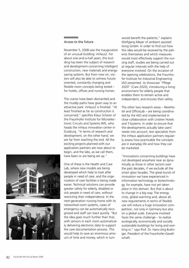
82 Fraunhofer IMS Annual Report 2008
Access to the future
November 5, 2008 saw the inaugurationof an unusual building: inHaus2. Forabout one-and-a-half years, this buil-ding has been the subject of researchand development concerning intelligentconstruction, new materials and energy-saving systems. But from now on, visi-tors will also be able to witness future-oriented, constantly changing andflexible room concepts being tested –for hotels, offices and nursing homes.
The cranes have been dismantled andthe muddy paths have given way to anattractive park: inHaus2 is finished. “Atleast finished as far as construction isconcerned,” specifies Klaus Scherer ofthe Fraunhofer Institute for Microelec-tronic Circuits and Systems IMS, whoheads the inHaus innovation center inDuisburg. “In terms of research anddevelopment, on the other hand, weare far from reaching the end. All theexciting projects planned with ourapplication partners are now about tobegin, and the labs, as we call them,have been or are being set up.”
One of these is the Health and CareLab, where new models are beingdeveloped which help to look afterpeople in need of care, and the orga-nization of care facilities is being madeeasier. Technical solutions can providegreater safety for elderly, disabled orsick people in need of care, withoutrestricting their independence. In thenext-generation nursing home with itsnetworked room systems, cases ofemergency can be automatically reco-gnized and staff can react quickly. “Butthe idea goes much further than that,with sensors in each room automatical-ly delivering electronic data to supportthe care documentation process. Thiswould help to save an enormous amo-unt of time and money, which in turn
would benefit the patients,” explainsWolfgang Meyer of ambient assistedliving GmbH. In order to find out howthis idea would be received by the pati-ents themselves and which measureswould most effectively support the nur-sing staff, studies are being carried outat regular intervals with the help ofeveryone involved. On the occasion ofthe opening celebrations, the Fraunho-fer Institute for Industrial EngineeringIAO presented its showcase “Pflege2020” (Care 2020), introducing a livingenvironment for elderly people thatenables them to remain active andindependent, and ensures their safety.
The other two research areas – NextHo-tel and OfficeLab – are being coordina-ted by the IAO and implemented inclose collaboration with Lindner Hotelsand T-Systems. In order to ensure thatthe developments actually take users’needs into account, test specialists fromthe inHaus application partners regular-ly assess how practicable the conceptsare in everyday life and how they canbe marketed.
“Innovations concerning buildings havenot developed anywhere near as dyna-mically as those in other sectors overthe past decades, if we exclude all thesmart glass facades. The great bursts ofinnovation we have experienced ininformation technology or biotechnolo-gy, for example, have not yet takenplace in this domain. But that is aboutto change in a big way. The energy crisis, global warming and, above all,new requirements in terms of flexibleuse will induce a huge innovation com-petition, not only in Germany but alsoon a global scale. Everyone involvedfaces the same challenge – to realizeecologically, economically and sociallysustainable buildings for living and wor-king in,” says Prof. Dr. Hans-Jörg Bullin-ger, President of the Fraunhofer-Gesell-schaft.
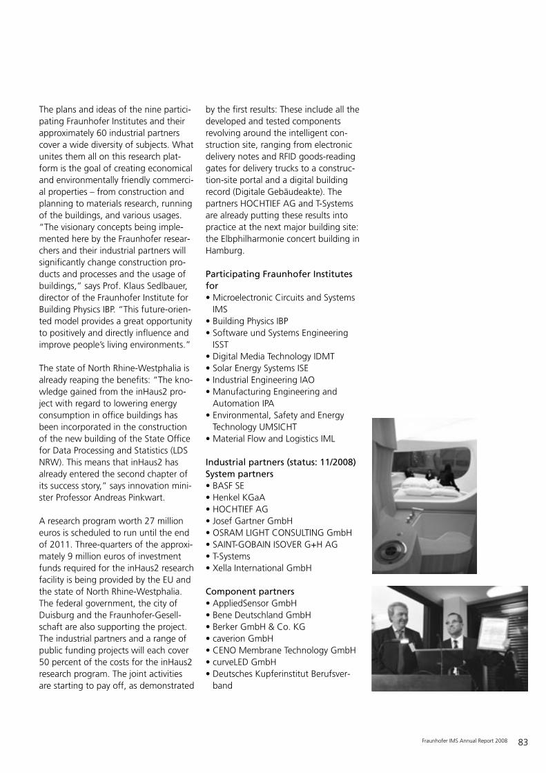
83Fraunhofer IMS Annual Report 2008
The plans and ideas of the nine partici-pating Fraunhofer Institutes and theirapproximately 60 industrial partnerscover a wide diversity of subjects. Whatunites them all on this research plat-form is the goal of creating economicaland environmentally friendly commerci-al properties – from construction andplanning to materials research, runningof the buildings, and various usages.“The visionary concepts being imple-mented here by the Fraunhofer resear-chers and their industrial partners willsignificantly change construction pro-ducts and processes and the usage ofbuildings,” says Prof. Klaus Sedlbauer,director of the Fraunhofer Institute forBuilding Physics IBP. “This future-orien-ted model provides a great opportunityto positively and directly influence andimprove people’s living environments.”
The state of North Rhine-Westphalia isalready reaping the benefits: “The kno-wledge gained from the inHaus2 pro-ject with regard to lowering energyconsumption in office buildings hasbeen incorporated in the constructionof the new building of the State Officefor Data Processing and Statistics (LDSNRW). This means that inHaus2 hasalready entered the second chapter ofits success story,” says innovation mini-ster Professor Andreas Pinkwart.
A research program worth 27 millioneuros is scheduled to run until the endof 2011. Three-quarters of the approxi-mately 9 million euros of investmentfunds required for the inHaus2 researchfacility is being provided by the EU andthe state of North Rhine-Westphalia.The federal government, the city ofDuisburg and the Fraunhofer-Gesell-schaft are also supporting the project.The industrial partners and a range ofpublic funding projects will each cover50 percent of the costs for the inHaus2research program. The joint activitiesare starting to pay off, as demonstrated
by the first results: These include all thedeveloped and tested componentsrevolving around the intelligent con-struction site, ranging from electronicdelivery notes and RFID goods-readinggates for delivery trucks to a construc-tion-site portal and a digital buildingrecord (Digitale Gebäudeakte). Thepartners HOCHTIEF AG and T-Systemsare already putting these results intopractice at the next major building site:the Elbphilharmonie concert building inHamburg.
Participating Fraunhofer Institutesfor• Microelectronic Circuits and Systems
IMS • Building Physics IBP • Software und Systems Engineering
ISST • Digital Media Technology IDMT • Solar Energy Systems ISE • Industrial Engineering IAO • Manufacturing Engineering and
Automation IPA • Environmental, Safety and Energy
Technology UMSICHT • Material Flow and Logistics IML
Industrial partners (status: 11/2008)System partners• BASF SE • Henkel KGaA • HOCHTIEF AG • Josef Gartner GmbH • OSRAM LIGHT CONSULTING GmbH • SAINT-GOBAIN ISOVER G+H AG • T-Systems • Xella International GmbH
Component partners• AppliedSensor GmbH • Bene Deutschland GmbH • Berker GmbH & Co. KG • caverion GmbH • CENO Membrane Technology GmbH • curveLED GmbH • Deutsches Kupferinstitut Berufsver-
band

84 Fraunhofer IMS Annual Report 2008
• DORMA GmbH + Co. KG • e:cue GmbH & Co. KG • EBV Elektronik GmbH & Co. KG • Elabo GmbH • ESYLUX GmbH • Gesellschaft für audiovisuelle Erleb -
nisse mbH • HAFI Beschläge GmbH • Hager Tehalit Vertriebs GmbH • HANSA Metallwerke AG • Intermundien GmbH • KERMI GmbH • Kieback&Peter GmbH & Co KG • Klafs GmbH & Co. KG • KRANTZ KOMPONENTEN caverion
GmbH • Lancom Systems GmbH • LightLife • Mauser Einrichtungssysteme
GmbH&KoKG • Menerga Apparatebau GmbH • MLR System GmbH • OBO BETTERMANN GmbH & Co. KG • Odenwald OWA Faserplattenwerk
GmbH • Planet Digital GmbH & Co KG • protel hotelsoftware GmbH (via
Fraunhofer IAO) • Ratioplast-Optoelectronics GmbH • scemtec automation GmbH • Schindler Lifts. Ltd. • UNIPOR-Ziegel Marketing GmbH • Vaillant GmbH • VESTAMATIC GmbH • Viega GmbH & Co. KG • Villeroy & Boch AG • Wilo AG • WINI Büromöbel Georg Schmidt
GmbH & Co KG • Wirtschaftsbetriebe Duisburg - AöR • Wolf Heiztechnik GmbH • Zent-Frenger Gesellschaft für Gebäu-
detechnik mbH
Application partners• ambient assisted living GmbH • Duisburger Versorgungs- und Ver-
kehrsgesellschaft mbH • DüsseldorfCongress Veranstaltungs-
gesellschaft mbH • Lindner Hotels AG
Sponsors ad notam GmbH, Baulmann Leuchten,bimos-Sitztechnik, BRUCK GmbH &Co.KG, Crestron Germany GmbH,Deckendesign Redmer, Dometic GmbH,Drumm & Partner, Facet, FBF bed&more, FEIG ELECTRONIC GmbH, FreudenbergBausysteme KG, Future-Shape GmbH,Geohaus Meßbild Engineering & Con-trol GmbH, GP Acoustics GmbH,inHaus GmbH, Markus-Diedenhofen,Media Agentur Kepnik, nora systemsGmbH, Rosink GmbH, Shure Distributi-on GmbH, Starmix, Stockheim GmbH & Co. KG, Stockmanns GmbH & Co.KG, t+t netcom, TOMBUSCH & BRUMANN, Vorwerk & Co. Teppich -werke GmbH & Co. KG
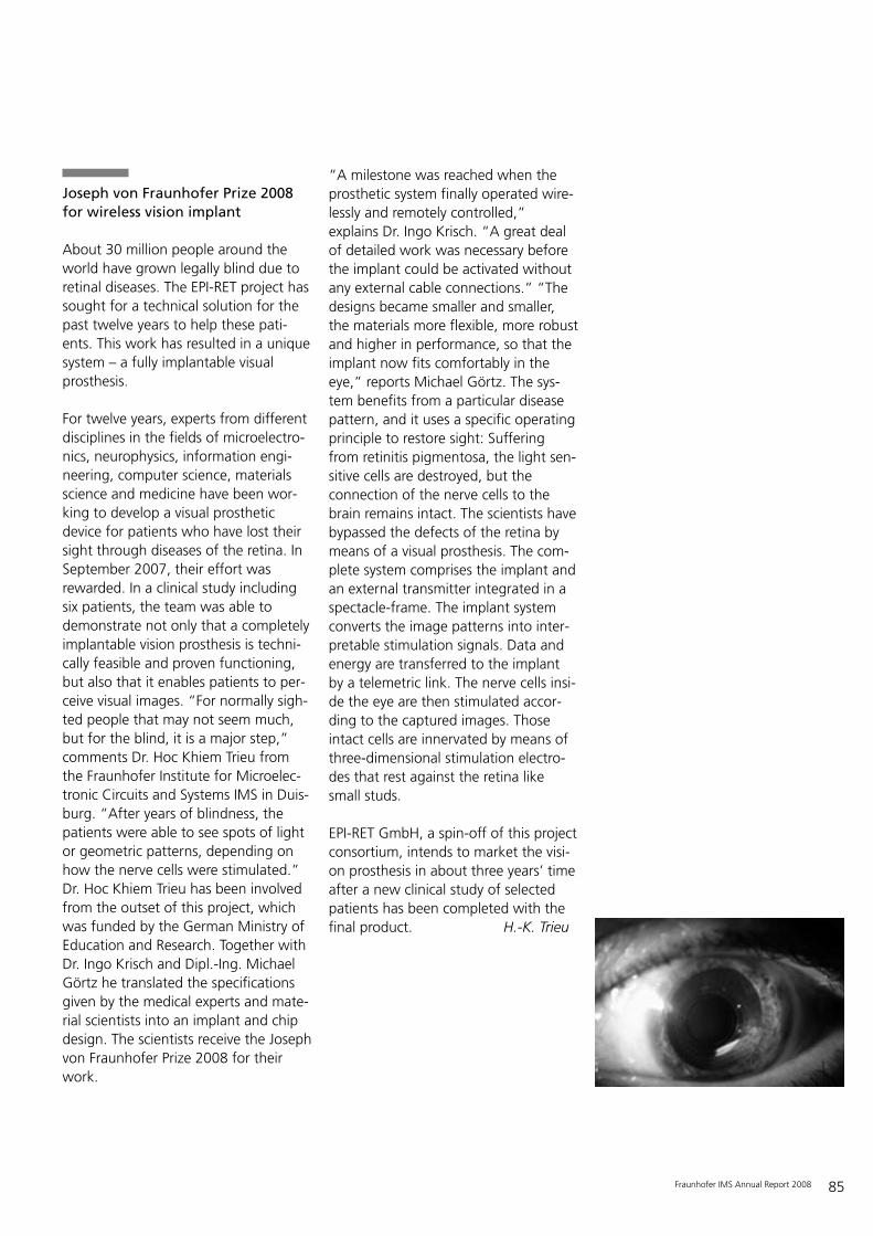
85Fraunhofer IMS Annual Report 2008
Joseph von Fraunhofer Prize 2008for wireless vision implant
About 30 million people around theworld have grown legally blind due toretinal diseases. The EPI-RET project hassought for a technical solution for thepast twelve years to help these pati-ents. This work has resulted in a uniquesystem – a fully implantable visualprosthesis.
For twelve years, experts from differentdisciplines in the fields of microelectro-nics, neurophysics, information engi -neering, computer science, materialsscience and medicine have been wor-king to develop a visual prosthetic device for patients who have lost theirsight through diseases of the retina. InSeptember 2007, their effort wasrewarded. In a clinical study includingsix patients, the team was able todemonstrate not only that a completelyimplantable vision prosthesis is techni-cally feasible and proven functioning,but also that it enables patients to per-ceive visual images. “For normally sigh-ted people that may not seem much,but for the blind, it is a major step,”comments Dr. Hoc Khiem Trieu fromthe Fraunhofer Institute for Microelec-tronic Circuits and Systems IMS in Duis-burg. “After years of blindness, thepatients were able to see spots of lightor geometric patterns, depending onhow the nerve cells were stimulated.”Dr. Hoc Khiem Trieu has been involvedfrom the outset of this project, whichwas funded by the German Ministry ofEducation and Research. Together withDr. Ingo Krisch and Dipl.-Ing. MichaelGörtz he translated the specificationsgiven by the medical experts and mate-rial scientists into an implant and chipdesign. The scientists receive the Josephvon Fraunhofer Prize 2008 for theirwork.
“A milestone was reached when theprosthetic system finally operated wire-lessly and remotely controlled,”explains Dr. Ingo Krisch. “A great dealof detailed work was necessary beforethe implant could be activated withoutany external cable connections.” “Thedesigns became smaller and smaller,the materials more flexible, more robustand higher in performance, so that theimplant now fits comfortably in theeye,” reports Michael Görtz. The sys -tem benefits from a particular diseasepattern, and it uses a specific operatingprinciple to restore sight: Sufferingfrom retinitis pigmentosa, the light sen-sitive cells are destroyed, but theconnection of the nerve cells to thebrain remains intact. The scientists havebypassed the defects of the retina bymeans of a visual prosthesis. The com-plete system comprises the implant andan external transmitter integrated in aspectacle-frame. The implant systemconverts the image patterns into inter-pretable stimulation signals. Data andenergy are transferred to the implantby a telemetric link. The nerve cells insi-de the eye are then stimulated accor-ding to the captured images. Thoseintact cells are innervated by means ofthree-dimensional stimulation electro-des that rest against the retina likesmall studs.
EPI-RET GmbH, a spin-off of this projectconsortium, intends to market the visi-on prosthesis in about three years’ timeafter a new clinical study of selectedpatients has been completed with thefinal product. H.-K. Trieu
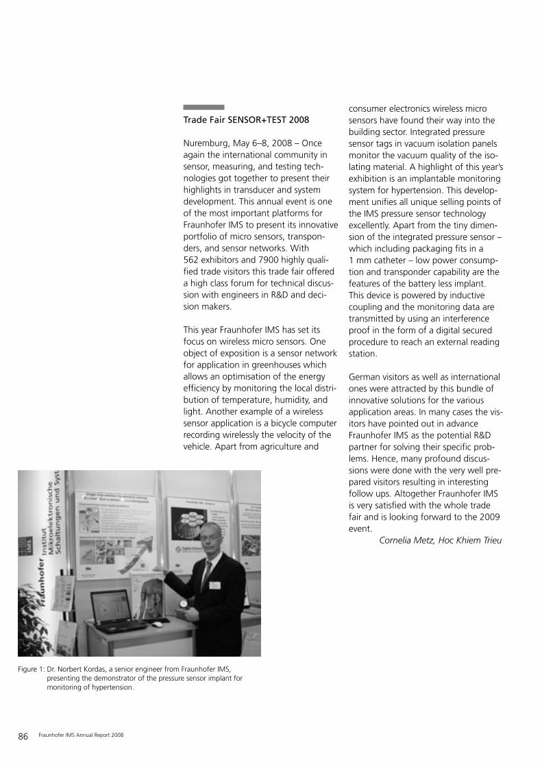
86 Fraunhofer IMS Annual Report 2008
Trade Fair SENSOR+TEST 2008
Nuremburg, May 6–8, 2008 – Onceagain the international community insensor, measuring, and testing tech-nologies got together to present theirhighlights in transducer and systemdevelopment. This annual event is oneof the most important platforms forFraunhofer IMS to present its innovativeportfolio of micro sensors, transpon-ders, and sensor networks. With562 exhibitors and 7900 highly quali-fied trade visitors this trade fair offereda high class forum for technical discus-sion with engineers in R&D and deci-sion makers.
This year Fraunhofer IMS has set itsfocus on wireless micro sensors. Oneobject of exposition is a sensor networkfor application in greenhouses whichallows an optimisation of the energyefficiency by monitoring the local distri-bution of temperature, humidity, andlight. Another example of a wirelesssensor application is a bicycle computerrecording wirelessly the velocity of thevehicle. Apart from agriculture and
consumer electronics wireless microsensors have found their way into thebuilding sector. Integrated pressure sensor tags in vacuum isolation panelsmonitor the vacuum quality of the iso-lating material. A highlight of this year’sexhibition is an implantable monitoringsystem for hypertension. This develop-ment unifies all unique selling points ofthe IMS pressure sensor technologyexcellently. Apart from the tiny dimen-sion of the integrated pressure sensor –which including packaging fits in a1 mm catheter – low power consump-tion and transponder capability are thefeatures of the battery less implant.This device is powered by inductivecoupling and the monitoring data aretransmitted by using an interferenceproof in the form of a digital securedprocedure to reach an external readingstation.
German visitors as well as internationalones were attracted by this bundle ofinnovative solutions for the variousapplication areas. In many cases the vis-itors have pointed out in advanceFraunhofer IMS as the potential R&Dpartner for solving their specific prob-lems. Hence, many profound discus-sions were done with the very well pre-pared visitors resulting in interestingfollow ups. Altogether Fraunhofer IMSis very satisfied with the whole tradefair and is looking forward to the 2009event.
Cornelia Metz, Hoc Khiem Trieu
Figure 1: Dr. Norbert Kordas, a senior engineer from Fraunhofer IMS, presenting the demonstrator of the pressure sensor implant for monitoring of hypertension.
87Fraunhofer IMS Annual Report 2008
New Trade Fair Presentation
For the first time Fraunhofer IMS hadan exhibition on the international tradefair for optical technologies OPTATEC2008 from June 17. – 20 in Frankfurt.On a shared booth of the OptecNetDeutschland e.V. the newest researchand development results were presen-ted. With more than 500 exhibitingcompanies from 28 countries, morethan 5500 expert visitors, the trade fairfor future optical technologies, compo-nents, systems and manufacturing con-firmed its reputation as an industrymeeting place with worldwide partici-pation and standing.
One of the highlights at the IMS boothwas the time-of-flight camera demon-strator, a result of the European rese-arch project “PReVENT”. This cameratakes three-dimensional images (2Dimages plus range image) at real-timevideo rates. The heart of the camera isthe IMS CMOS imager with extremelyfast electronic shutter and very lownoise. Another important highlight wasthe announcement of the new 0.35µmCMOS opto process which enables IMS to fulfil many demands for customimage sensors and other optical devices.Fraunhofer IMS develops and runs thisprocess in its own semiconductor fab inDuisburg.
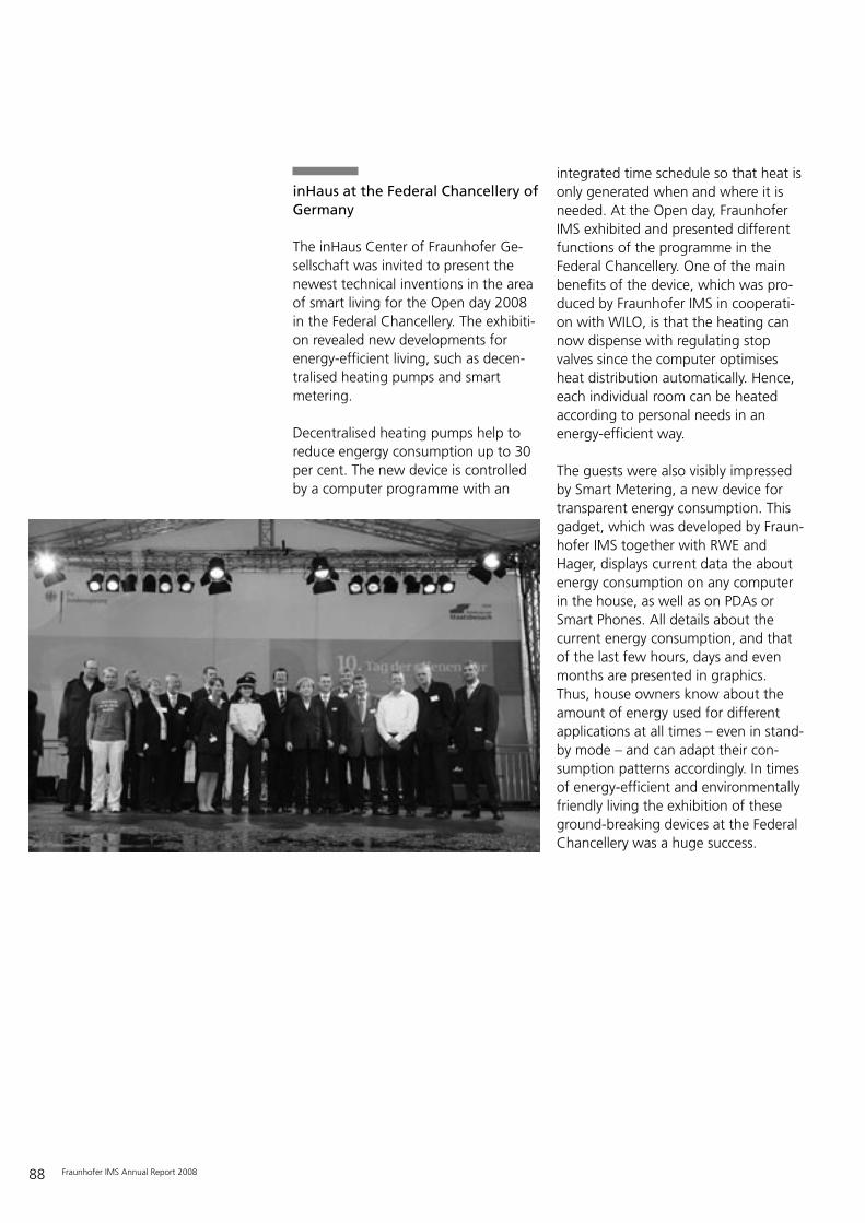
88 Fraunhofer IMS Annual Report 2008
inHaus at the Federal Chancellery ofGermany
The inHaus Center of Fraunhofer Ge -sellschaft was invited to present thenewest technical inventions in the areaof smart living for the Open day 2008in the Federal Chancellery. The exhibiti-on revealed new developments forenergy-efficient living, such as decen-tralised heating pumps and smartmetering.
Decentralised heating pumps help toreduce engergy consumption up to 30per cent. The new device is controlledby a computer programme with an
integrated time schedule so that heat isonly generated when and where it isneeded. At the Open day, FraunhoferIMS exhibited and presented differentfunctions of the programme in theFederal Chancellery. One of the mainbenefits of the device, which was pro-duced by Fraunhofer IMS in cooperati-on with WILO, is that the heating cannow dispense with regulating stop valves since the computer optimisesheat distribution automatically. Hence,each individual room can be heatedaccording to personal needs in an energy-efficient way.
The guests were also visibly impressedby Smart Metering, a new device fortransparent energy consumption. Thisgadget, which was developed by Fraun-hofer IMS together with RWE andHager, displays current data the aboutenergy consumption on any computerin the house, as well as on PDAs orSmart Phones. All details about the current energy consumption, and thatof the last few hours, days and evenmonths are presented in graphics.Thus, house owners know about theamount of energy used for differentapplications at all times – even in stand-by mode – and can adapt their con-sumption patterns accordingly. In timesof energy-efficient and environmentallyfriendly living the exhibition of theseground-breaking devices at the FederalChancellery was a huge success.

89Fraunhofer IMS Annual Report 2008

90 Fraunhofer IMS Annual Report 2008

91Fraunhofer IMS Annual Report 2008
Press Review
92 Fraunhofer IMS Annual Report 2008
93Fraunhofer IMS Annual Report 2008
94 Fraunhofer IMS Annual Report 2008
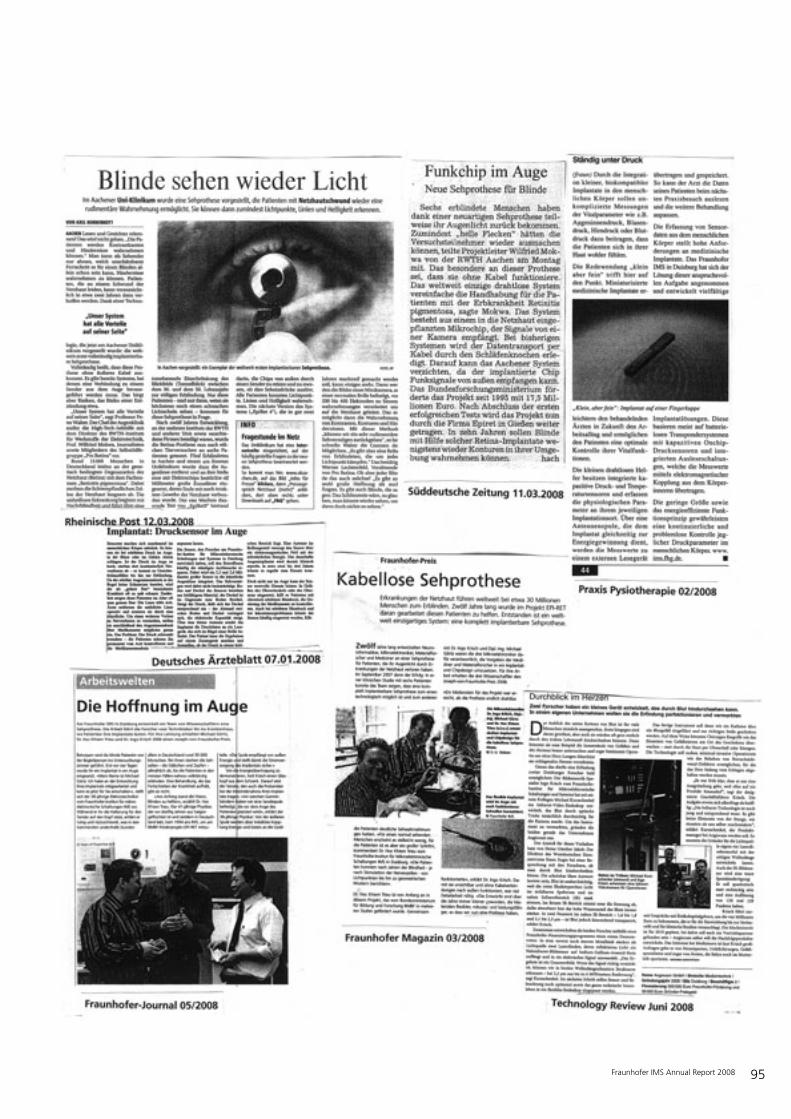
95Fraunhofer IMS Annual Report 2008

96 Fraunhofer IMS Annual Report 2008
Copyright 2008 by Fraunhofer-GesellschaftHansastraße 27 c 80686 München
ISSN 1435-0874Annual ReportFraunhofer-Institut fürMikroelektronischeSchaltungen und Systeme
Director:Prof. Dr. rer. nat. A. Grabmaier
Adresses:IMS DuisburgFinkenstraße 61 47057 DuisburgPhone +49 (0) 2 03/37 83-0Fax +49 (0) 2 03/37 83-2 66E-mail [email protected] www.ims.fraunhofer.de
Editorial Staff: Martin van Ackeren
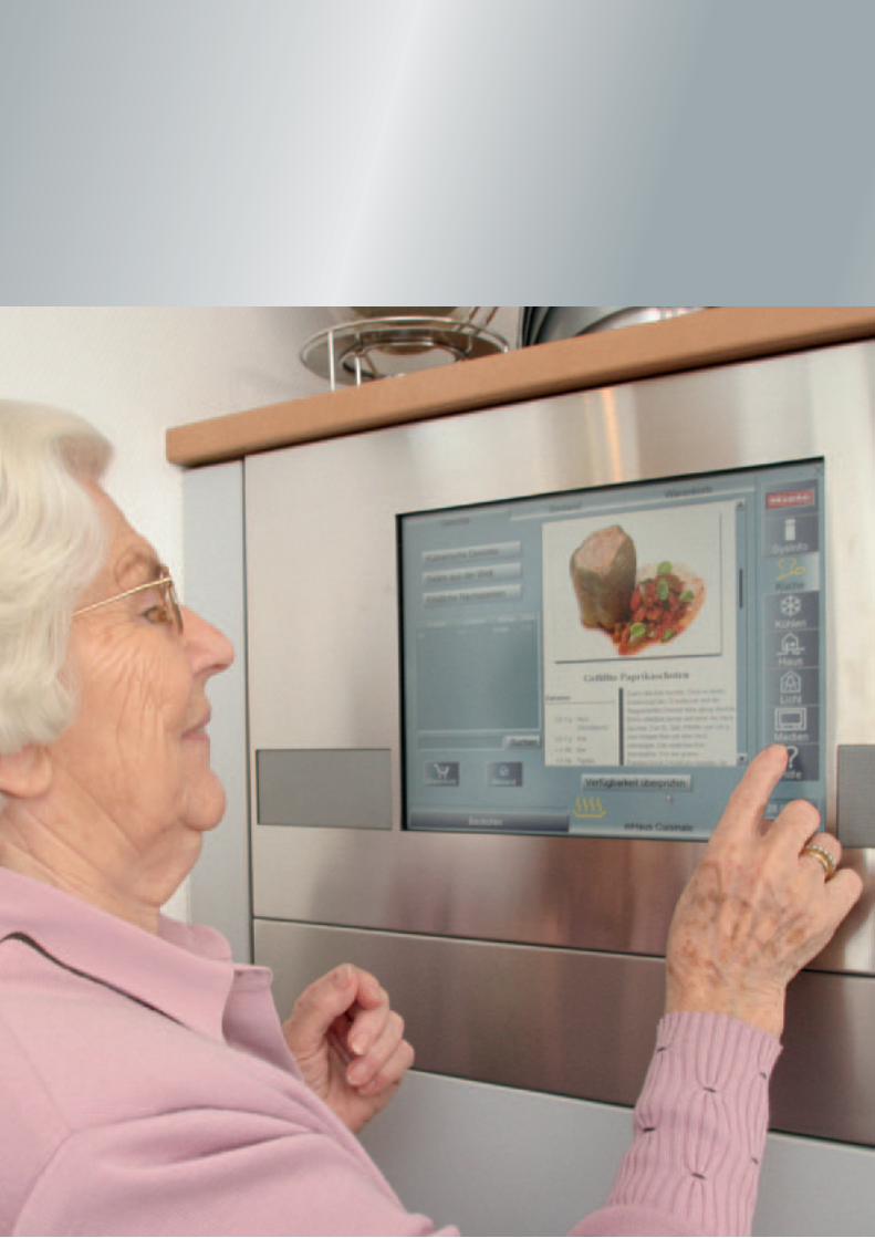
2008ANNUAL REPORT
F R A U N H O F E R - I N S T I T U T F Ü R M I k R O E l E k T R O N I S c H E S c H A lT U N g E N U N d S y S T E M E I M S