
Jahresbericht 2015 2016 - ipv.uni- · PDF fileJahresbericht Annual Report 2015 I 2016 Liebe...
92
Jahresbericht Annual Report 2015 2016 Institut für Photovoltaik Institute for Photovoltaics
Transcript of Jahresbericht 2015 2016 - ipv.uni- · PDF fileJahresbericht Annual Report 2015 I 2016 Liebe...

JahresberichtAnnual Report
20152016
Institut für PhotovoltaikInstitute for Photovoltaics
Jahresbericht Annual Report 2015 I 2016
InhaltsverzeichnisTable of Contents
VorwortPreface
ArbeitsgruppenResearch Groups
Wissenschaftliche BeiträgeScientific Contributions
PublikationenPublications
LehrveranstaltungenLectures
AbschlüsseDegrees
Was sonst noch warBeyond Science
MitarbeiterlisteStaff Members
Gäste & ausländische StipendiatenGuests
LageplanLocation Map
3
4
15
54
59
67
79
86
89
90
1
Institut für Photovoltaik Institute for Photovoltaics
Institutsleitung und VerwaltungHead of the Institute and Administration(Leitung / Head: Jürgen H. Werner)
Jürgen H. Werner Irmy Kerschbaum
Freymut Hilscher Sabine Ost
2

Jahresbericht Annual Report 2015 I 2016
Liebe Freunde des ipv,nach den schwierigen Jahren 2013/14 geht es dem ipvinzwischen wieder richtig gut: Im Jahr 2016 haben wir soviele Drittmittel wie nie zuvor für unsere Photovoltaik-,Lasertechnik- und Medizintechnikforschung eingewor-ben. Hinzu kommt, dass der neu berufene ProfessorPeter Birke, der seit Anfang 2015 die neue Forschungs-gruppe „Elektrische Energiespeichersysteme“ leitet,ebenfalls gut vorankommt beim Einwerben von For-schungsmitteln und Aufbau seiner Labore. Seit einigerZeit ist es deshalb nicht nur möglich, dass wirhöchsteffiziente Solarzellen, sondern auch Batteriezellenherstellen. Auch der Umbau des Reinraums verbessertunsere technischen Möglichkeiten und Arbeitsbedin-gungen. Aus diesen Gründen und wegen des großenEngagements und der Begeisterung unserer Mitarbei-ter/innen blicken wir optimistisch in die Zukunft.-------------------------------------------------------------------------------Dear friends of the ipv,After the difficult years 2013/14, the ipv is doing quitewell again: In the year 2016 we raised more money forour research in the fields of photovoltaics, laserprocessing, and medical technologies than ever before.In addition, Professor Peter Birke, the new head of thenew research group „Electrical Energy Storage Sys-tems“ proceeds very well with raising money as well aswith establishing his lab. Therefore, we are now not onlyable to fabricate highly efficient solar cells, but alsobattery cells. The retrofitting of the cleanroom improvesour technical abilities and working conditions evenfurther. For these reasons, as well as due to theenthusiasm of all members of the institute, I amconfident that the ipv will bloom in the coming years.
Stuttgart, Juli/July 2017
Jürgen H. Werner
3

Institut für Photovoltaik Institute for Photovoltaics
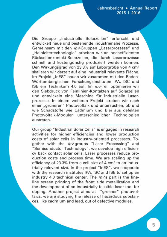
Industrielle SolarzellenIndustrial Solar Cells(Gruppenleiterin / Group Leader: Renate Zapf-Gottwick)
Renate Zapf-Gottwick Osama Tobail
Erik HoffmannKai Carstens
Simon Huber Sabrina Lang
Jessica Nover Sabine Schreiber
4
Jahresbericht Annual Report 2015 I 2016
Die Gruppe „Industrielle Solarzellen“ erforscht undentwickelt neue und bestehende industrienahe Prozesse.Gemeinsam mit den ipv-Gruppen „Laserprozesse“ und„Halbleitertechnologie“ arbeiten wir an hocheffizientenRückseitenkontakt-Solarzellen, die durch Laserprozesseschnell und kostengünstig produziert werden können.Den Wirkungsgrad von 23,3% auf Laborgröße von 4 cm²skalieren wir derzeit auf eine industriell relevante Fläche.Im Projekt „InES“ bauen wir zusammen mit den Baden-Württembergischen Forschungsinstituten IPA, ISC undISE ein Technikum 4.0 auf. Im ipv-Teil optimieren wirden Siebdruck von Feinlinien-Kontakten auf Solarzellenund entwickeln eine Maschine für industrielle Laser-prozesse. In einem weiteren Projekt streben wir nacheiner „grüneren“ Photovoltaik und untersuchen, ob undwie Schadstoffe wie Cadmium und Blei aus defektenPhotovoltaik-Modulen unterschiedlicher Technologienaustreten.-------------------------------------------------------------------------------Our group “Industrial Solar Cells” is engaged in researchactivities for higher efficiencies and lower productioncosts of solar cells in industry-oriented processes. To-gether with the ipv-groups “Laser Processing” and“Semiconductor Technology”, we develop high efficien-cy back contact solar cells. Laser processes reduce pro-duction costs and process time. We are scaling up theefficiency of 23.3% from a cell size of 4 cm2 to an indus-trially relevant size. In the project “InES”, we cooperatewith the research institutes IPA, ISC and ISE to set up anindustry 4.0 technical center. The ipv’s part is the fine-line screen printing of the front side metallization andthe development of an industrially feasible laser tool fordoping. Another project aims at “greener” photovol-taics: we are studying the release of hazardous substan-ces, like cadmium and lead, out of defective modules.
5

Institut für Photovoltaik Institute for Photovoltaics
HalbleitertechnologieSemiconductor Technology(Gruppenleiterin / Group Leader: Birgitt Winter)
Birgitt Winter
Leo Bauer
Brigitte Lutz Hendrik Moldenhauer
Anton Riß
Birgitt Winter
Lydia Beisel
6

Jahresbericht Annual Report 2015 I 2016
Die Gruppe „Halbleitertechnologie“ setzt sich aus dentechnischen Mitarbeiterinnen und Mitarbeitern desgesamten Instituts zusammen. Damit sind verschiedeneAufgabenstellungen zur Absicherung der Instituts-infrastruktur zusammengefasst. Die interdisziplinäreVernetzung im technischen Bereich ermöglicht eine guteKoordinierung aller anfallenden Arbeiten. Im Jahr 2016unterbrach die Erneuerung des Lüftungssystems imReinraum die routinemäßige Durchführung von Prozess-schritten wie Oxidationen, Diffusionen, Plasmadeposi-tionen, nasschemisches Reinigen und Ätzen, Lithogra-phie, Metallisierung, Laserdotieren und vieles andere.Deshalb standen am Ende des Jahres die Wiederinbe-triebnahme aller Anlagen und das Validieren aller Pro-zesse im Vordergrund.
-------------------------------------------------------------------------------
The group “Semiconductor Technology” includes alltechnical assistants and engineers of the institute. Byjoining forces, we are able to secure the entireinfrastructure of the institute. The interdisciplinarycomposition of the technical team permits optimumcoordination of all tasks. Last year, our regular operationof processes, such as oxidation, diffusion, plasmaenhanced deposition, wet chemical cleaning andetching, lithography, metallization, laser doping, etc. wasinterrupted by the replacement of the ventilation systemin the cleanroom. At the end of the year, our focus wastherefore put on restarting all systems and validating allprocesses.
7
Institut für Photovoltaik Institute for Photovoltaics
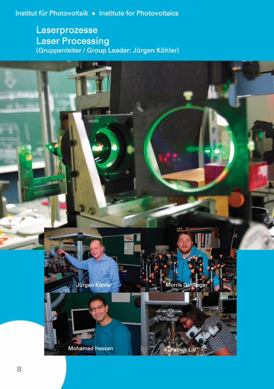
LaserprozesseLaser Processing(Gruppenleiter / Group Leader: Jürgen Köhler)
Patrick LillMohamed Hassan
Jürgen Köhler Morris Dahlinger
8

Jahresbericht Annual Report 2015 I 2016
Die Gruppe „Laserprozesse“ entwickelt neue Techno-logien zum Laserprozessieren von Materialien für dieElektrotechnik. Neben dem Laser-Prozessieren kristalli-ner Silizium-Scheiben für Solarzellen und Halbleiterbau-elemente, bildet die Herstellung poröser Anoden aus Si-lizium für Lithium-Ionen Batterien einen weiterenSchwerpunkt. Im Vordergrund unserer Arbeiten stehendie Weiterentwicklung unseres Laserdotier-Prozesses fürrückseitenkontaktierte Solarzellen, sowie die Ablationdielektrischer Schichten. Weiterhin untersuchen wir dasDotieren und Aktivieren von Dotieratomen in einkristalli-nem Germanium für Halbleiterbauelemente sowie dasLaser-Porosieren gesputterter Silizium-Schichten. Inenger Zusammenarbeit mit den Gruppen „IndustrielleSolarzellen“ und „Halbleitertechnologie“ am ipvoptimieren wir unsere Laserprozesse zur Herstellunghocheffizienter, rückseitenkontaktierter Solarzellen mitWirkungsgraden über 23%.-------------------------------------------------------------------------------The “Laser Processing” group explores new techno-logies for laser processing of materials for electricalengineering applications. Porous anodes for lithium ionbatteries are a new focus of our research, in addition tolaser processing of crystalline silicon wafers for solarcells and semiconductor components. The mainemphasis of our research lies on pulsed laser doping forhigh-efficiency back-contact solar cells, and the ablationof dielectric layers. Furthermore, we analyze the dopingand dopant-atom activation of mono-crystallinegermanium for semiconductor elements, as well as laserporosification of sputtered silicon layers. A close collab-oration with the research groups “Industrial Solar Cells”and “Semiconductor Technology” at ipv optimizes ourlaser processes for the fabrication of high-efficiencyback-contact solar cells with efficiencies above 23%.
9

Institut für Photovoltaik Institute for Photovoltaics
SensorikSensor Technology(Gruppenleiter / Group Leader: Markus Schubert)
Timo Kropp Christian Sämann
Markus Schubert
10
Jahresbericht Annual Report 2015 I 2016
Die Arbeitsgruppe „Sensorik“ entwickelt Mess- undModellierungsmethoden für Photovoltaikmodule undSolarparks, um deren aktuellen Zustand zu ermitteln undzukünftige Erträge abzuschätzen. Im Vorhaben PARKarbeiten wir dazu eng mit dem Solarzentrum Stuttgartzusammen. Hochempfindliche Dünnschichtphotodiodendienen im EU-Verbund NANODEM der kontinuierlichenÜberwachung der Medikamentierung von Patientennach Organtransplantationen. Unsere Begleitung undAuswertung des Praxistests eines elektrischen Quartier-speichers im Landesprojekt STROMBANK ist inzwischenabgeschlossen und die Weiterentwicklung poröser Si-Anoden für Lithium-Ionen-Batterien liefert vielverspre-chende Ergebnisse.
-------------------------------------------------------------------------------
The "Sensor Technology" group at ipv developsmethods for the characterization and modelling ofphotovoltaic modules and solar power plants in order tomonitor their condition and to forecast their futureenergy yield. In the research project called PARK, wecooperate closely with the Solarzentrum Stuttgart. In theEU project NANODEM, high-sensitivity thin filmphotodiodes enable continuous monitoring of theimmunosuppressant levels of patients after organtransplantation. Data acquisition and evaluation of theoperation of a Li- ion battery container, called STROM-BANK, i.e. Electricity Bank, has been finished. Thedevelopment of porous Si anodes for Li-ion batteriesshows promising results.
11
Institut für Photovoltaik Institute for Photovoltaics
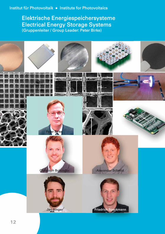
Elektrische EnergiespeichersystemeElectrical Energy Storage Systems(Gruppenleiter / Group Leader: Peter Birke)
Alexander Schmid
Jan Singer
Christoph Bolsinger
Friedrich Speckmann
Christoph Bolsinger
Friedrich SpeckmannJan Singer
Alexander Schmid
Peter Birke
12

Jahresbericht Annual Report 2015 I 2016
Elektrische Energiespeichersysteme (EES) umfassen einsehr weites Feld, denn darunter fallen im Prinzip alleSysteme, die elektrische Energie bidirektional in eineandere Energieform umwandeln können. Die GruppeEES fokussiert sich bei der Zelle auf Lithium-basiertegalvanische Elemente mit den Schwerpunkten festeIonenleiter, Phasengrenzen und Strukturierung metalli-scher Li-Anoden. Systemseitig (Batterie) stehen Energie-dichteerhöhung, elektrisches und thermisches Manage-ment sowie Batteriemodelle im Vordergrund der For-schung. Der Bereich Power to X (X=gas, liquid, solid)deckt Speicher ab, die als Batterie mit einer einmaligenAufladung und anschließender Lagerung der Anodeverstanden werden können. Die Lagerzeit ist beliebiglange, und die Anode kann danach in einer galvanischenZelle wieder elektrische Energie liefern. Immer da, wokonventionelle Batterien an Kostengrenzen stoßen, kön-nen solche Systeme eine entscheidende Lücke füllen.-------------------------------------------------------------------------------Electrical Energy Storage Systems (EES) cover a widefield of applications since they are systems able toconvert electrical energy bidirectionally into anotherform of energy. On cell level, the group EES focusses onLithium-based galvanic elements with research on solidion conductors, phase boundaries and structures formetallic Li-anodes. On system level (battery), the focusof research is on energy density enhancement, electricaland thermal battery management and involved batterymodels. The field of power to X (X=gas, liquid, solid)covers energy storage systems, which are basically areserve battery with a single charge step. The anodescan be separated, stored for an arbitrary time and theyprovide energy when reassembled in a galvanic cellafterwards. These systems can replace large cost-intensive batteries.
13

Institut für Photovoltaik Institute for Photovoltaics
14
Jahresbericht Annual Report 2015 I 2016
Wissenschaftliche BeiträgeScientific Contributions
Publikationen I Publications
15
Institut für Photovoltaik Institute for Photovoltaics
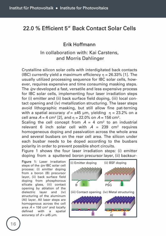
22.0 % Efficient 5“ Back Contact Solar Cells
Erik Hoffmann
In collaboration with: Kai Carstens, and Morris Dahlinger
Crystalline silicon solar cells with interdigitated back contacts(IBC) currently yield a maximum efficiency = 26.33% [1]. Theusually utilized processing sequence for IBC solar cells, how-ever, requires expensive and time consuming masking steps.The ipv developed a fast, versatile and less expensive processfor IBC solar cells, implementing four laser irradiation stepsfor (i) emitter and (ii) back surface field doping, (iii) local con-tact opening and (iv) metallization structuring. The laser stepsavoid lithographic masking, but still allow fine pat-terningwith a spatial accuracy d = ±45 m, yielding = 23.2% on acell area A = 4 cm² [2], and = 22.0% on A = 156 cm².Scaling the cell concept from A = 4 cm² to an industrialrelevant 6 inch solar cell with A = 239 cm² requireshomogeneous doping and passivation across the whole areaand several busbars on the rear cell area. The silicon undereach busbar needs to be doped according to the busbarspolarity in order to prevent possible short circuits.Figure 1 shows the four laser irradiation steps: (i) emitterdoping from a sputtered boron precursor layer, (ii) backsur-Figure 1: Laser irradiationsteps of the ipv IBC solar cellprocess: (i) emitter dopingfrom a boron (B) precursorlayer, (ii) back surface fielddoping from phosphoroussilicate glass, (iii) contactopening by ablation of thedielectric layer and (iv)structuring of the aluminum(Al) layer. All laser steps arehomogenous across the cellarea A = 156 cm² and locallydefined with a spatialaccuracy of d = ±45 m.
B PSG
Al
1 2
3 4
(iii) Contact opening (iv) Metal structuring
(i) Emitter doping (ii) BSF doping
16
Jahresbericht Annual Report 2015 I 2016
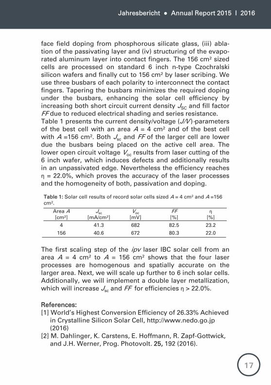
face field doping from phosphorous silicate glass, (iii) abla-tion of the passivating layer and (iv) structuring of the evapo-rated aluminum layer into contact fingers. The 156 cm² sizedcells are processed on standard 6 inch n-type Czochralskisilicon wafers and finally cut to 156 cm² by laser scribing. Weuse three busbars of each polarity to interconnect the contactfingers. Tapering the busbars minimizes the required dopingunder the busbars, enhancing the solar cell efficiency byincreasing both short circuit current density JSC and fill factorFF due to reduced electrical shading and series resistance.Table 1 presents the current density/voltage (J/V )-parametersof the best cell with an area A = 4 cm² and of the best cellwith A =156 cm². Both Jsc and FF of the larger cell are lowerdue the busbars being placed on the active cell area. Thelower open circuit voltage Voc results from laser cutting of the6 inch wafer, which induces defects and additionally resultsin an unpassivated edge. Nevertheless the efficiency reaches
= 22.0%, which proves the accuracy of the laser processesand the homogeneity of both, passivation and doping.
The first scaling step of the ipv laser IBC solar cell from anarea A = 4 cm² to A = 156 cm² shows that the four laserprocesses are homogenous and spatially accurate on thelarger area. Next, we will scale up further to 6 inch solar cells.Additionally, we will implement a double layer metallization,which will increase Jsc and FF for efficiencies > 22.0%.
References:[1] World’s Highest Conversion Efficiency of 26.33% Achieved
in Crystalline Silicon Solar Cell, http://www.nedo.go.jp (2016)
[2] M. Dahlinger, K. Carstens, E. Hoffmann, R. Zapf Gottwick, and J.H. Werner, Prog. Photovolt. 25, 192 (2016).
Table 1: Solar cell results of record solar cells sized A = 4 cm² and A =156 cm².
Area A[cm²]
Jsc[mA/cm²]
Voc[mV]
FF[%] [%]
4 41.3 682 82.5 23.2156 40.6 672 80.3 22.0
17

Institut für Photovoltaik Institute for Photovoltaics
Laser-Induced Capillary Waves in Liquid Silicon
Jürgen Köhler
In collaboration with: Mohamed Hassan
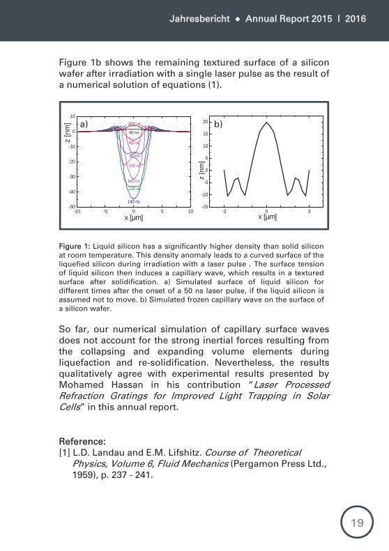
During laser doping a pulsed laser melts the surface of asilicon wafer. Our patented defect free laser doping processuses a line-focused laser beam. Each laser pulse melts thesilicon on an area about 7 m wide and 0.8 mm long.In contrast to most other materials, liquid silicon has adensity significantly higher than solid silicon at roomtemperature, similar to the densities of water and ice. Thisdensity anomaly leads to a strongly curved surface of theliquefied silicon when the melt reaches its maximum depth ofabout 500 nm.Figure 1a shows the simulated surface of liquid silicon,molten by a 50 ns long laser pulse, if the liquid silicon isassumed not to move. The strong curvature of the liquidsilicon surface, together with the surface tension, leads to theformation of a so-called capillary surface wave, travellingthrough the liquid silicon until it freezes during re-solidification. The result is a periodically textured surface ona laser processed silicon wafer.The following three differential equations describe thetemporal and spatial development of capillary waves [1]:
(1)
Here, is the velocity potential, with beingthe velocity of the liquid silicon in x- / z-direction (parallel /perpendicular to the wafer surface), is the density of liquidsilicon, is the surface tension, and denotes the location ofthe surface of the liquid silicon.
,2
2
xt,02
2
2
2
zx.
zt
zxv zx ,/,
18
Jahresbericht Annual Report 2015 I 2016
Figure 1b shows the remaining textured surface of a siliconwafer after irradiation with a single laser pulse as the result ofa numerical solution of equations (1).
Reference:[1] L.D. Landau and E.M. Lifshitz. Course of Theoretical
Physics, Volume 6, Fluid Mechanics (Pergamon Press Ltd., 1959), p. 237 - 241.
So far, our numerical simulation of capillary surface wavesdoes not account for the strong inertial forces resulting fromthe collapsing and expanding volume elements duringliquefaction and re-solidification. Nevertheless, the resultsqualitatively agree with experimental results presented byMohamed Hassan in his contribution “Laser ProcessedRefraction Gratings for Improved Light Trapping in SolarCells” in this annual report.
Figure 1: Liquid silicon has a significantly higher density than solid siliconat room temperature. This density anomaly leads to a curved surface of theliquefied silicon during irradiation with a laser pulse . The surface tensionof liquid silicon then induces a capillary wave, which results in a texturedsurface after solidification. a) Simulated surface of liquid silicon fordifferent times after the onset of a 50 ns laser pulse, if the liquid silicon isassumed not to move. b) Simulated frozen capillary wave on the surface ofa silicon wafer.
-10 -5 0 5 10-50
-40
-30
-20
-10
0
10200 ns
160 ns
140 ns
120 ns
100 ns
80 ns
60 nsz [n
m]
x [ m]
40 ns
-3 0 3-15
-10
-5
0
5
10
15
20
z [n
m]
x [ m]
a) b)
19
Institut für Photovoltaik Institute for Photovoltaics
Porous Silicon Thin Film Anodes forLithium Ion Batteries
Christian Sämann
In collaboration with: Jürgen Köhler, Mario Wachtler (ZSW Ulm), Peter Birke, Markus Schubert, and Jürgen Werner
Extending the range of electric vehicles with equal weightrequires further improvement of the specific energy of theirbatteries. Thus, research on new materials for batteries aimsat increasing the specific capacity for portable applications.One promising approach towards this end replaces the activematerial graphite of the negative electrode (anode) in con-ventional lithium ion batteries with silicon. Silicon has thehighest known specific capacity CSi = 1856 mAh/g (Li15Si4) forlithium, often erroneously reported as CSi = 3579 mAh/g byneglecting the Li mass. Hence, Si theoretically promises afivefold capacity when compared with the specific capacity ofgraphite CC = 339 mAh/g.Silicon, unfortunately, expands up to 270% in volume duringlithiation. This volume expansion causes mechanical damageof silicon during lithiation and delithiation by cracking orfracturing. The damage occurs especially during the firstcycle, and often results in the loss of electrical contact to thecurrent collector. Therefore, to prevent capacity fading duringlithiation/delithiation, the microscopic morphology of siliconmust change to accommodate such volume changes. Poroussilicon, for example, meets these requirements. By allocatingspace for the expansion, pores in Si improve its ability tonon-destructively change its volume. The pores reduce theinduced stress and mechanical load, thus enabling a morestable capacity retention.For forming porous silicon, we first deposit several 100 nmthick amorphous Si layers on metal foil current collectors byradio frequency sputtering.
20
Jahresbericht Annual Report 2015 I 2016
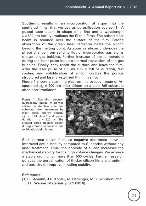
Sputtering results in an incorporation of argon into thesputtered films, that we use as porosification source [1]. Apulsed laser beam in shape of a line and a wavelength
= 532 nm locally irradiates the Si thin films. The pulsed laserbeam is scanned over the surface of the film. Strongabsorption of the green laser radiation heats the siliconbeyond the melting point. As soon as silicon undergoes thephase change from solid to liquid, incorporated gas atomsmerge to gas bubbles. Further increase of the temperatureduring the laser pulse induces thermal expansion of the gasbubbles. Finally, they reach the surface and leave the film.After the laser pulse of 100 ns P 250 ns duration, fastcooling and solidification of silicon creates the porousstructured and laser crystallized thin film silicon.Figure 1 shows a scanning electron microscopy image of Ar-sputtered dSi = 200 nm thick silicon on a steel foil substrateafter laser irradiation.
Such porous silicon films as negative electrodes show animproved cyclic stability compared to Si anodes without anylaser treatment. Thus, the porosity of silicon increases themechanical stability for the high volume changes. We achievea stable cycling for more than 500 cycles. Further researchpursues the porosification of thicker silicon films and optimi-zed porosity for improved cycling stabilty.
Figure 1: Scanning electronmicroscopy image of poroussilicon on stainless steel foilsubstrate after treatment bylaser pulse energy densityHP = 0.64 Jcm-2 and pulseduration P = 220 ns. Thecreated pores stabilize siliconduring volume expansion dueto lithiation/delithiation.
References:[1] C. Sämann, J.R. Köhler, M. Dahlinger, M.B. Schubert, and
J.H. Werner, Materials 99, 509 (2016).
21

Institut für Photovoltaik Institute for Photovoltaics
Electrochemical Balancing of Lithium-Ion Cells
Alexander Schmid
In collaboration with: Kai Peter Birke, Ludwig Ehringer, and Ioannis Lambidis
Balancing of serially connected electrochemical cells iscrucial. Imbalanced states of charge of electrochemical cellslead to lower storage capabilities in comparison to a systemconsisting of homogeneous electrochemical cells [1]. Thisstudy presents a new, cost-effective way to balance lithium-ion cells. The idea is to bypass charged lithium ironphosphate (LFP) or lithium titanate (LTO) cells by connectingthem in parallel to nickel-based cells, which have differentinherent electrochemical behavior. For this method, calledelectrochemical balancing, three major advantages arise:First, in the case of imbalanced states, electrochemicalbalancing does not only transform the energy into heat suchas dissipative balancing methods, but also stores the energyneeded for balancing in nickel-based cells by electrochemicalreaction. Second, there is no need for additional activeelectrical components and complex balancing strategies [2].Third, the safe system: the lithium-ion cells can not beovercharged due to the nickel-based cells' reversible gassingat moderate charging rates.
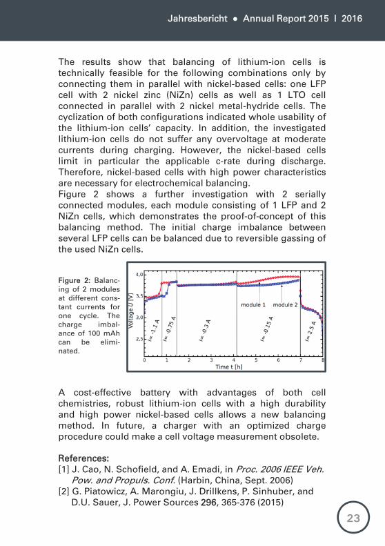
Figure 1: Electrochemical balancing oftwo serially connected modules. Amodule consists of two lithium-ion cellsand one nickel-based cell. The lithium-ion cells of the upper module (module1) are already fully charged. In contrast,the lithium-ion cells of the lowermodule (module 2) are partiallycharged.
22
Jahresbericht Annual Report 2015 I 2016
The results show that balancing of lithium-ion cells istechnically feasible for the following combinations only byconnecting them in parallel with nickel-based cells: one LFPcell with 2 nickel zinc (NiZn) cells as well as 1 LTO cellconnected in parallel with 2 nickel metal-hydride cells. Thecyclization of both configurations indicated whole usability ofthe lithium-ion cells’ capacity. In addition, the investigatedlithium-ion cells do not suffer any overvoltage at moderatecurrents during charging. However, the nickel-based cellslimit in particular the applicable c-rate during discharge.Therefore, nickel-based cells with high power characteristicsare necessary for electrochemical balancing.Figure 2 shows a further investigation with 2 seriallyconnected modules, each module consisting of 1 LFP and 2NiZn cells, which demonstrates the proof-of-concept of thisbalancing method. The initial charge imbalance betweenseveral LFP cells can be balanced due to reversible gassing ofthe used NiZn cells.
A cost-effective battery with advantages of both cellchemistries, robust lithium-ion cells with a high durabilityand high power nickel-based cells allows a new balancingmethod. In future, a charger with an optimized chargeprocedure could make a cell voltage measurement obsolete.
Figure 2: Balanc-ing of 2 modulesat different cons-tant currents forone cycle. Thecharge imbal-ance of 100 mAhcan be elimi-nated.
References:[1] J. Cao, N. Schofield, and A. Emadi, in Proc. 2006 IEEE Veh.
Pow. and Propuls. Conf. (Harbin, China, Sept. 2006) [2] G. Piatowicz, A. Marongiu, J. Drillkens, P. Sinhuber, and
D.U. Sauer, J. Power Sources 2296, 365-376 (2015)
23
Institut für Photovoltaik Institute for Photovoltaics
Long Term Leaching of Photovoltaic Modules
Jessica Nover
In collaboration with: Renate Zapf-Gottwick, Carolin Feifel1, Michael Koch1, and Jürgen Werner
1Institute for Sanitary Engineering, Water Quality, and Solid Waste Management, University of Stuttgart, Germany
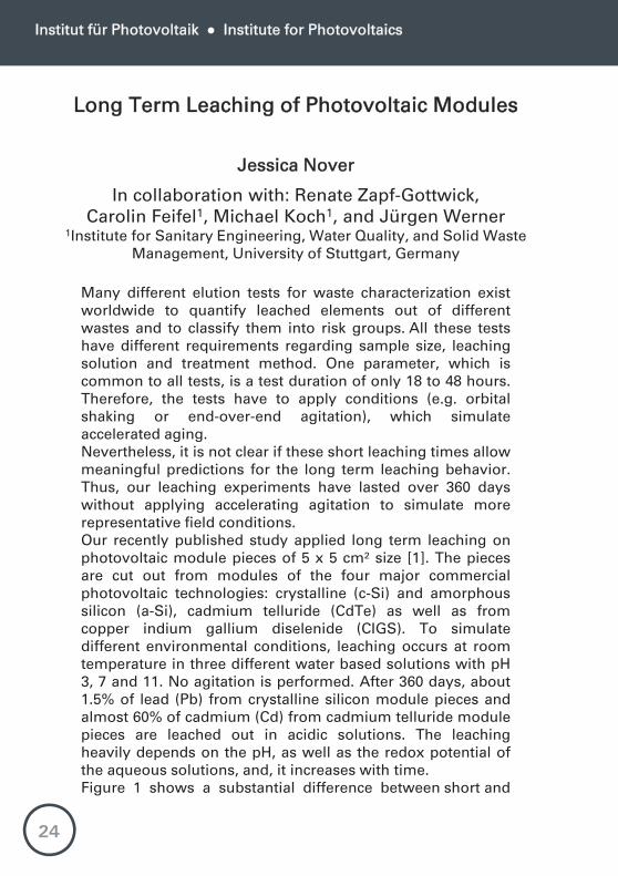
Many different elution tests for waste characterization existworldwide to quantify leached elements out of differentwastes and to classify them into risk groups. All these testshave different requirements regarding sample size, leachingsolution and treatment method. One parameter, which iscommon to all tests, is a test duration of only 18 to 48 hours.Therefore, the tests have to apply conditions (e.g. orbitalshaking or end-over-end agitation), which simulateaccelerated aging.Nevertheless, it is not clear if these short leaching times allowmeaningful predictions for the long term leaching behavior.Thus, our leaching experiments have lasted over 360 dayswithout applying accelerating agitation to simulate morerepresentative field conditions.Our recently published study applied long term leaching onphotovoltaic module pieces of 5 x 5 cm² size [1]. The piecesare cut out from modules of the four major commercialphotovoltaic technologies: crystalline (c-Si) and amorphoussilicon (a-Si), cadmium telluride (CdTe) as well as fromcopper indium gallium diselenide (CIGS). To simulatedifferent environmental conditions, leaching occurs at roomtemperature in three different water based solutions with pH3, 7 and 11. No agitation is performed. After 360 days, about1.5% of lead (Pb) from crystalline silicon module pieces andalmost 60% of cadmium (Cd) from cadmium telluride modulepieces are leached out in acidic solutions. The leachingheavily depends on the pH, as well as the redox potential ofthe aqueous solutions, and, it increases with time.Figure 1 shows a substantial difference between short and
24
Jahresbericht Annual Report 2015 I 2016
long term leaching. Under all conditions, acid rain (pH3),groundwater (pH7) and alkaline landfilling (pH11), theamounts of eluted toxic elements as Pb, Cd and tellurium (Te)out of PV module pieces are much higher after one year thanafter one day. In neutral solutions, the long term results showan increase of nearly two orders of magnitude and for alka-line conditions an increase of more than one order of magni-tude is found. For Cd and Te under acid rain conditions, thedifference between short and long term is almost three or-ders of magnitude. For the leaching of Pb out of c-Si modulepieces under acid rain conditions, an increase of more than2000% is obtained.Figure 1: Amount ofeluted toxic elementsas Pb, released fromc-Si module pieces,and Cd and Te out ofCdTe module piecesafter t = 1 day(hatched bars) andafter t = 360 days(solid bars) insolutions with pH3,pH7 and pH11.
Reference:[1] J. Nover, R. Zapf-Gottwick, C. Feifel, M. Koch, J.W.
Metzger, and J.H. Werner, submitted to: Jpn. J. Appl. Phys. (2016)
Consequently, if the leaching amounts of the toxicsubstances Pb, Cd and Te from PV modules are low at thefirst day of leaching or lower than the regulatory limitsaccording to standard tests, it is not likely that these valuesstay constant with ongoing leaching. Our study clearly provesthat it is important to consider the long term behavior ofleaching and the possibility that, after a certain time, 100% ofthe toxic material is leached out. To prevent environmentalpollution due to a release of toxic heavy metals by dumpingor landfilling broken PV modules, strict recycling policies andregulations are needed worldwide. Alternatively, toxicmaterials in PV modules simply could be omitted.
25
Institut für Photovoltaik Institute for Photovoltaics
Laser Doping Approaches Auger Limit
Morris Dahlinger
In collaboration with: Kai Carstens
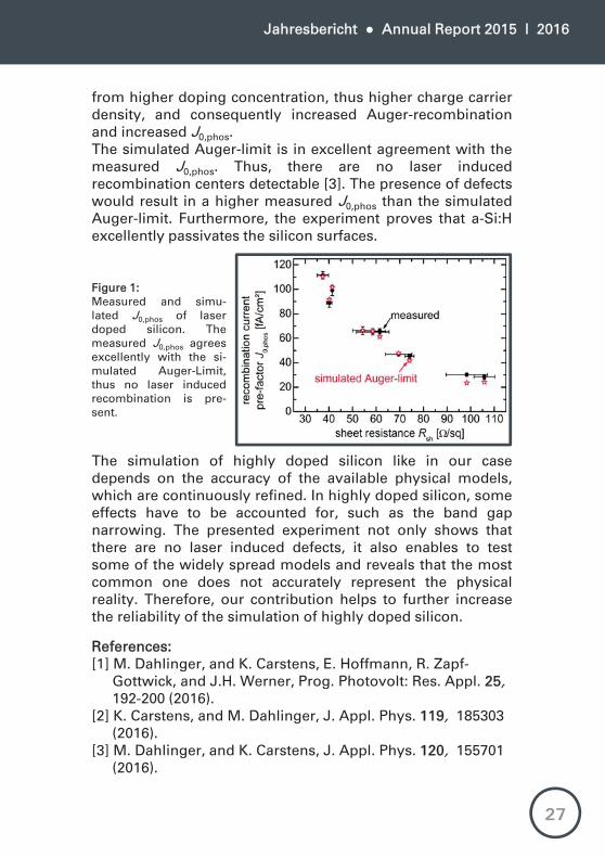
Laser doping of silicon is often linked to the formation ofcrystal defects or to the incorporation of impurities. Theserecombination centers could limit the performance of siliconmicroelectronic devices or the efficiency of solar cells. Weshow that there are no such recombination centers present inour laser doped silicon.The ipv developed a laser doping process using phosphorusin a furnace grown phosphorus silicate glass (PSG) as dopantsource. With this process, we reach the so called Auger-recombination limit in the doped regions. Symmetricallylaser doped silicon samples are processed in a way thatincludes all relevant steps which we use for our laserprocessed back contact solar cells with efficiencies = 23.24%[1]. The recipe during the PSG growth and the pulse energydensity during laser doping adjust the sheet resistance Rsh ofthe phosphorus doping. Both sample surfaces are passivatedby hydrogenated amorphous silicon a-Si:H [2]. Therecombination parameter J0,phos of the laser doped samples isthen extracted from photo conductance measurements.Electrochemical capacitance/voltage measurements deter-mine the doping profiles of the same samples. Thesimulation tool PC1Dmod6.2 utilizes these doping profiles tosimulate the recombination in the doped areas. The surfaceand the doped volume are assumed to be free of anyShockley Read Hall recombination (SRH), no defects arepresent. Since silicon is a semiconductor with indirect bandgap, the radiative recombination is much less pronouncedthan the Auger-recombination, in particular for highly dopedsilicon. Therefore, this situation is called the Auger-limit.Figure 1 shows the measured and simulated recombinationcurrent pre-factor J0,phos. A reduced sheet resistance results.
26
Jahresbericht Annual Report 2015 I 2016
from higher doping concentration, thus higher charge carrierdensity, and consequently increased Auger-recombinationand increased J0,phos.The simulated Auger-limit is in excellent agreement with themeasured J0,phos. Thus, there are no laser inducedrecombination centers detectable [3]. The presence of defectswould result in a higher measured J0,phos than the simulatedAuger-limit. Furthermore, the experiment proves that a-Si:Hexcellently passivates the silicon surfaces.
The simulation of highly doped silicon like in our casedepends on the accuracy of the available physical models,which are continuously refined. In highly doped silicon, someeffects have to be accounted for, such as the band gapnarrowing. The presented experiment not only shows thatthere are no laser induced defects, it also enables to testsome of the widely spread models and reveals that the mostcommon one does not accurately represent the physicalreality. Therefore, our contribution helps to further increasethe reliability of the simulation of highly doped silicon.
References:[1] M. Dahlinger, and K. Carstens, E. Hoffmann, R. Zapf-
Gottwick, and J.H. Werner, Prog. Photovolt: Res. Appl. 225, 192-200 (2016).
[2] K. Carstens, and M. Dahlinger, J. Appl. Phys. 1119, 185303 (2016).
[3] M. Dahlinger, and K. Carstens, J. Appl. Phys. 1120, 155701 (2016).
Figure 1:Measured and simu-lated J0,phos of laserdoped silicon. Themeasured J0,phos agreesexcellently with the si-mulated Auger-Limit,thus no laser inducedrecombination is pre-sent.
27
Institut für Photovoltaik Institute for Photovoltaics
Between Infection and Rejection –Point-of-Care Testing of Immunosuppressants
Marcel Berner
In collaboration with: Sergej Vollmer, Markus Schubert
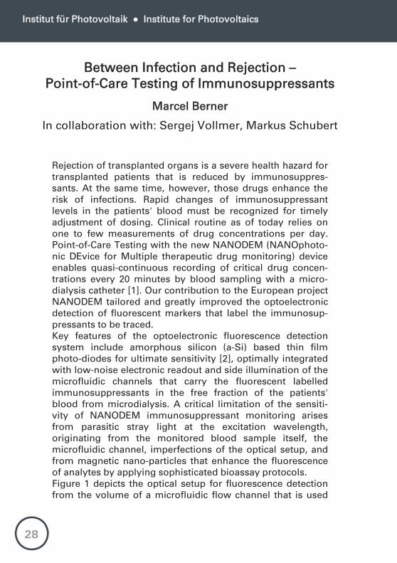
Rejection of transplanted organs is a severe health hazard fortransplanted patients that is reduced by immunosuppres-sants. At the same time, however, those drugs enhance therisk of infections. Rapid changes of immunosuppressantlevels in the patients' blood must be recognized for timelyadjustment of dosing. Clinical routine as of today relies onone to few measurements of drug concentrations per day.Point-of-Care Testing with the new NANODEM (NANOphoto-nic DEvice for Multiple therapeutic drug monitoring) deviceenables quasi-continuous recording of critical drug concen-trations every 20 minutes by blood sampling with a micro-dialysis catheter [1]. Our contribution to the European projectNANODEM tailored and greatly improved the optoelectronicdetection of fluorescent markers that label the immunosup-pressants to be traced.Key features of the optoelectronic fluorescence detectionsystem include amorphous silicon (a-Si) based thin filmphoto-diodes for ultimate sensitivity [2], optimally integratedwith low-noise electronic readout and side illumination of themicrofluidic channels that carry the fluorescent labelledimmunosuppressants in the free fraction of the patients'blood from microdialysis. A critical limitation of the sensiti-vity of NANODEM immunosuppressant monitoring arisesfrom parasitic stray light at the excitation wavelength,originating from the monitored blood sample itself, themicrofluidic channel, imperfections of the optical setup, andfrom magnetic nano-particles that enhance the fluorescenceof analytes by applying sophisticated bioassay protocols.Figure 1 depicts the optical setup for fluorescence detectionfrom the volume of a microfluidic flow channel that is used.
28
Jahresbericht Annual Report 2015 I 2016
for homogeneous bioassays in the NANODEM project. Inaddition to photodiode manufacturing, ipv contributes theoptical design of the side excitation, overall noise reductionand stray light rejection. Moreover, a very simple method forforming microfluidic channels from laser cut double-adhesivetape was developed with our project partners at theUniversity of Tübingen.
Since the analyte concentration and fluorescence signals areextremely low in this application, we measure a maximumphotocurrent density Jphoto = 10 nA cm-2 in the a-Si photo-diodes due to fluorescence from the flow channel. Darkcurrent density of 11 x 3.3 mm2 sized a-Si detectors is as lowas Jd = 100 fA cm-2, close to the thermal background limit.Taking into account the available sampling time of ts = 100 s,an overall assessment of the limit of detection of the finalNANODEM Analyser reveals a minimum detectable fluores-cence intensity Imin = 4.5 pW cm-2 with a dynamic range of 78dB. Thereby, a minimum concentration of 26 nmol/L of ourreference dye DY-636 can be traced in pure water by thisdirect optical test format.First clinical tests of the NANODEM Point-of-Care Testingsystem will start in Munich in early 2017, after successfulapproval by the ethics committee in December 2016.
Figure 1: Optical setupfor fluorescence detec-tion with laser excita-tion from the side of thechannel. The absorptionfilter blocks remainingstray light from enteringthe a-Si photodiode atthe bottom.
References:[1] http://nanodem.ifac.cnr.it/index.php/project-overview[2] M. Berner, R. Rothemund, S. Vollmer, M. Schubert, U.
Hilbig, and G. Gauglitz, phys. stat. sol. AA , 1862-6319 (2016), DOI: 10.1002/pssa.201532953.
29

Institut für Photovoltaik Institute for Photovoltaics
Electrical Contact Resistance of Clamped Battery Cells
Christoph Bolsinger
In collaboration with: Matthias Zorn, and Kai Peter Birke
The electrical contact resistance (ECR), which occurs at thecontact interface, is one of the crucial criteria to design abattery cell joint. A poor connection with an increasedcontact resistance leads to a significant heat generation andsubsequently causes a heat transfer into the battery cell.Currently, welding processes such as resistance spot,ultrasonic or laser beam welding are commonly used tointerconnect battery cells [1]. Besides the heat input duringthe welding process a huge drawback of welded battery cellconnections is the complex disassembling process. An easyway to assemble and dissemble battery cells withoutdamaging is the use of clamped cell connectors.The present study investigates the ECR of clamped cellconnectors for 18650 battery cells. A positive terminal of aPanasonic NCR18650B Li-Ion cell is used for ECRmeasurements and for an investigation of the mechanicalproperties. A load test indicates that the positive terminalundergoes an elastic deformation up to a force of about 400N and can therefore be used for clamped joints without anydamage. To investigate the dependencies of ECR, the appliedforce on the joint is varied from 25 to 400 N. Five differentmaterials with three different surface roughnesses are usedas cell connectors. Furthermore, the influence of agedsurfaces are investigated. The obtained data show, that theECR of clamped cell connectors is reduced to about 50 .Thus, the ECR is in the range or even lower than for weldedcontacts [2].Figure 1 shows the mean values of the measured electricalcontact resistances Rc,mean in dependence of the applied forceF and the surface treatments with different grit size of theabrasive paper.
30

Jahresbericht Annual Report 2015 I 2016
The specific lines describe the ECR as a function of theresistivity, hardness and surface roughness of the material aswell as the contact area and the applied force. For all gritsizes, CrNiMoTi shows the highest resistance compared tothe remaining materials. The contact elements made ofcopper show for all grit sizes the lowest ECR. The ECR slightlyvaries with the roughness of the surface. For all materialsexcept copper, the ECR increases with increasing roughnessRa in range of F > 100 N. The lowest ECR is obtained by anapplied force of F = 400 N.
Figure 1: Electrical contactresistances Rc,mean fordifferent contact materials.The surface treatment isdone with an abrasivepaper with a grit size of 80and 800. For all contactmaterials (except Cu) theresistances slightly in-crease with increasingsurface roughness Ra. At aforce of 400 N the ECR ofall contact materials is inthe range or even lowerthan for welded contacts.
force F [N]102
102
103 CrNiMoTi
Al
CuNiCuZn
fresh surface800 80
References:[1] S.S. Lee, T.H. Kim, and S.J. Hu, ASME 2010 Int. Manuf.
Sci. Eng. Conf. Proc. 11, 541–549 (2010).[2] M.J. Brand, P.A. Schmidt, and M.F. Zaeh, J. Energy
Storage 11, 7–14 (2015).
Furthermore, the influence of the contact area and the filmresistance due to oxidation on the ECR are investigated. Thecontaminant films strongly increase the ECR for low contactforces. The measurement results show that the selection ofthe contact material (low resistivity and low hardness) iscrucial to achieve low ECR. Surface roughness as well as theclamping area have less influence.
31
Institut für Photovoltaik Institute for Photovoltaics
23.3% Back Contact Solar Cells with Amorphous Silicon Passivation
Kai Carstens
In collaboration with: Morris Dahlinger, Erik Hoffmann, Renate Zapf-Gottwick, and Jürgen Werner
High efficiency solar cells like interdigitated back contact (IBC)solar cells feature both doping types on the rear side of thecell: the phosphorus doped back surface field (BSF) as well asthe boron doped emitter. High quality passivation of heavilyboron doped p-type crystalline silicon (c-Si) is usuallyachieved with aluminum oxide, via low interface state densityand a high amount of negative fixed charges [1]. For heavilyphosphorus doped n-type surfaces silicon nitride, withpositive fixed charges, is used [2]. Applying e.g. onlyaluminum oxide to both doping types, will result in adetrimental passivation of the phosphorus doped backsurface field; therefore the phosphorus doped area needs tobe reduced [3]. In any case, the passivation of heavily p-typeand n-type doped surfaces is a challenge on the way toachieve high efficiencies. One possibility is to use twodifferent passivation layers and structure them according tothe surface doping. However, the ultimate solution lies inusing a universal passivation layer for both doping types.We use amorphous silicon (a-Si:H) as passivation layer forboth, heavily phosphorus, and boron doped surfaces. a-Si:Happlied to our IBC solar cells, yields an efficiency = 23.3%.Excellent passivation of boron and phosphorus doped sur-faces is achieved by optimization of the deposition conditions[4]. The recombination parameter J0,Em = 29 fA/cm2 is typicalfor a boron doped emitter with sheet resistance Rsh,Em = 82
/sq. The phosphorus back sur-face field with sheet resis-tance Rsh,BSF = 54 /sq yields a recombination parameter J0,BSF= 44 fA/cm2. Both values are close to the Auger-limit.We integrate the a-Si:H passivation into our laser processedIBC solar cells. Both doping types are prepared using laserdoping [5]. For the passivation we remove the silicon oxide
32

Jahresbericht Annual Report 2015 I 2016
(which is usually used as rear side passivation) in hydro-fluoric acid. Then, we deposit 30 nm a-Si:H at optimized de-position conditions. Laser ablation locally removes the pas-sivation layer for contact formation. Finally, structuring of thealuminium metallization is also done with a laser process.Figure 1 shows the distribution of the efficiency of 136 laserprocessed solar cells with an area A = 4 cm2. The best solarcell has an efficiency = 23.3% with open circuit voltage Voc =684 mV, short circuit current density Jsc = 41.5 mA/cm2 andfill factor FF = 81.9%.
The excellent passivation of heavily doped boron emitter andphosphorous back surface field with undoped amorphoussilicon helps to increase the solar cell area. Additionally to thesmall area cells, we also manufactured a large solar cell with
= 22.6% on an area A = 156 cm2. Next, we will scale up thecell size further to A = 239 cm², continuing to fabricatemodules made of these cells.
References:[1] B. Hoex, J. Schmidt, R. Bock, P.P. Altermatt, M.C.M. van de
Sanden, and W.M.M. Kessels, Appl. Phys. Lett. 991,112107 (2007).
[2] M.J. Kerr, J. Schmidt, A. Cuevas, and J.H. Bultman, J. Appl. Phys. 889, 3821 (2001).
[3] R. Müller, C. Reichel, J. Schrof, M. Padilla, M. Selinger, I. Geisemeyer, J. Benick, and M. Hermle, Sol. Energ. Mat. Sol. Cells. 1142, 54 (2015).
[4] K. Carstens, and M. Dahlinger, J. Appl. Phys. 1119, 185303-1 (2016).
[5] M. Dahlinger, K. Carstens, E. Hoffmann, R. Zapf-Gottwick, and J. H. Werner, Prog. Photovolt: Res. Appl. 225, 192 (2016).
Figure 1: Efficiencyhistogram for 136laser processed IBCsolar cells. Maximumefficiency = 23.3%,median efficiency
= 22.1%
33

Institut für Photovoltaik Institute for Photovoltaics
Laser Processed Refraction Gratings for Improved Light Trapping in Solar Cells
Mohamed Hassan
In collaboration with: Morris Dahlinger,and Jürgen Köhler
Refractions gratings on the rear side of solar cells improvethe light trapping properties of solar cells. The longer thewavelength of radiation becomes, the more the diffractionangle increases. Therefore, photons with energy near theband gap of a semiconducting material have the longestoptical path length. Different one- [1] and two-dimensional[2] diffractive grating structures were already studied. Thedisadvantage of those structures is the costly and timeconsuming manufacturing process using photo-lithography.This work presents a new, cost-efficient method for thegeneration of a periodic back surface texture on the rear sideof crystalline silicon solar cells.Figure 1 shows a laser microscope picture of a periodic backsurface texture using a nanosecond-pulsed laser ofwavelength = 532 nm. Here, a purpose designed focusingoptics transforms the laser beam to a top-hat line focus ofsize 10 m x 800 m. The absorption of the laser radiationleads to rapid heating and subsequent melting of the siliconsurface. The line focus melts an about 7 m wide and 500 nmdeep stripe of silicon. Liquid silicon has a significantly largerdensity than solid silicon. This density anomaly leads to astrongly curved surface of the liquefied silicon stripe. Thestrong curvature of the liquid surface, together with thesurface tension, leads to the formation of a so-called capillarysurface wave, travelling through the liquid until it freezeswhen re-solidifying. The result is a periodically texturedsurface on a laser processed silicon wafer. The “wavelength”of the periodic structure is easily adjusted by varying thepulse repetition frequency and/or the scanning speed of thelaser beam focus.
34
Jahresbericht Annual Report 2015 I 2016
References:[1] A. Mellor, H. Hauser, C. Wellens, J. Benick, J. Eisenlohr, M.
Peters, A. Guttowski, I. Tobías, A. Martí, A. Luque, and B. Bläsi, Optics Express 221, A295 (2013).
[2] M. Peters, M. Rüdiger, H. Hauser, M. Hermle, and B. Bläsi, Prog. Photovolt: Res. Appl. 220, 862 (2012).
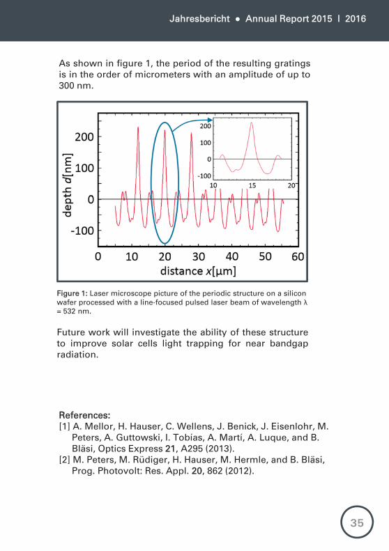
As shown in figure 1, the period of the resulting gratingsis in the order of micrometers with an amplitude of up to300 nm.
Figure 1: Laser microscope picture of the periodic structure on a silicon wafer processed with a line-focused pulsed laser beam of wavelength = 532 nm.
Future work will investigate the ability of these structureto improve solar cells light trapping for near bandgapradiation.
35

Institut für Photovoltaik Institute for Photovoltaics
High Resolution Carrier Lifetime Imaging
Timo Kropp
In collaboration with: Markus Schubert and Jürgen Werner
Over the last years, minority carrier lifetime imaging hasbecome a standard tool for solar cell characterization [1,2].High spatial resolution of such images and fast throughputare contradictory requirements for quality control inphotovoltaic production. To solve this conflict, we present anovel technique for high resolution mapping for the effectiveminority carrier lifetime eff of solar cells.The technique relies on using electroluminescence (EL)measurements with two different modulations. The intensitydifference between two differently modulated EL imagesdepends on the minority carrier lifetime. A Si CCD (chargecoupled device) camera takes one image during a pulsedcurrent modulation a) with a step-function change fromforward- to reverse-bias conditions. A second image is takenduring the modulation with a step-function change from b)forward-bias to open-circuit. By calculating the intensitydifference between these two images, we find a solutionfor the effective minority carrier lifetime
with the intensity difference , the period length of thecurrent modulations and the modulation given bythe ratio of the forward-bias current and the reverse-biascurrent .The luminescence intensity in the image, while modulatingthe current injecting under forward-bias, is based on freecarrier recombination. In contrast, images taken while active-ly extracting excess charge carriers in reverse-bias showreduced intensity due to the increased fall time of the signal.This mode of operation leads to asymmetric luminescence
(1)
36

Jahresbericht Annual Report 2015 I 2016
rise and decay times, which allows to determine the carrierlifetime from EL images acquired over several modulationperiods.Instead of averaging multiple high speed images, taken fromone modulation period within microseconds, single imageswith long exposure times up to minutes prove to be usefulfor lifetime mapping. Therefore, low-cost and “slow” Si CCDcameras can be used for imaging and deducing the minoritycarrier lifetime map.Figures 1a,b show first results of the novel lifetime mappingtechnique calculated by eq. (1). The enhanced view in Fig. 1b)is cropped from the original image in Fig. 1a). Usually, thissort of detailed analysis is only possible by changing theoptics of a measurement setup.
However, in our case, the high resolution of Fig. 1a) allows toidentify defects over the total cell area in only one imagewithout changing the optics.
References:[1] S. Herlufsen, K. Bothe, J. Schmidt, R. Brendel, and S.
Siegmund, Sol. En. Mat. Sol. Cells 1106, 42 (2012) [2] K. Ramspeck, K. Bothe, J. Schmidt, and R. Brendel, J.
Appl. Phys. 1106, 114506 (2009)
Figure 1: Highresolution effectivecarrier lifetime image(a) of a SunpowerIBC (interdigitatedback contact) solarcell, and (b)enhanced view of adamaged area. Thehigh resolution of (a)allows to characterizedefects over the totalcell area in only oneimage without takingmultiple high speedimages.
37
Institut für Photovoltaik Institute for Photovoltaics
Low Pressure Glow-Discharge Methanation
Friedrich-Wilhelm Speckmann
In collaboration with: Jürgen Köhler, Daniel Müller and Kai Peter Birke
Plasma technology is gaining increasing interest for thereduction of carbon dioxide (CO2) to carbon monoxide (CO)and oxygen (O2) [1]. The CO gas and hydrogen (H2) are idealreaction partners to produce hydrocarbons, like gas and fuel.The aim of our research is to investigate a new method toproduce methane (CH4) by plasma induced dissociation ofCO2 and H2 in a single setup. A low pressure glow dischargeplasma dissociates CO2 into CO and O2 and a cathode-integrated zirconia based ion conductor transports oxygenions (O2-) in or out of the reaction chamber, depending on thedirection of the applied “transport voltage”. The bi-directional transport properties of zirconia enables twounique features: i) transporting oxygen ions into the reactionchamber enables to control the partial pressure of watervapor in the reaction chamber, ii) a transport of oxygenatoms in the opposite direction reduces the amount ofoxygen molecules and, consequently decreases therecombination of CO and O2, resulting in an improved CO2conversion rate. The operating temperature of the ion-conducting zirconia can be varied using an electric heater. Weobserve a strong influence of operating temperature on theconversion rates of CH4 and CO. Increasing the zirconiatemperature results in lower CO but higher CH4 conversionrates [2].The applied voltage VPr to our zirconia ion conductor, -7.5 V <VPr < 7.5 V, and the magnitude of the discharge current havea major impact on the amount of O2- ions flowing into or outof the reaction chamber. Increasing the discharge current IPLleads to more extracted O2- ions and, at the same time, toincreased CO production.
38

Jahresbericht Annual Report 2015 I 2016
The correlation between IPL and amount of gas can also beobserved for the CH4. We analyze the composition of the gasin our reaction chamber using a gas-phase chromatograph.Figure 1 shows a linear dependency of the CH4 peak area onthe discharge current IPL. The amount of synthesized methaneincreases by a factor of two between 100 mA < IPL < 150 mA.The higher yield of methane is caused by the biggerdischarge plasma volume leading to more ionized CO2 and H2gas.
Especially, the combination between the optimal zirconiatemperature needed for the methanation and thesimultaneous water electrolysis by an oxygen ion conductorare of future interest and can further boost the amount ofsynthesized methane from hydrogen.Future research will also focus on the pre-required hydrogengeneration. Experiments with a newly designed, transistor-based power source aim to increase the performance of analkaline electrolyzer. Improved performance is expected withrespect to maximum throughput and partial load operation,using modified current profiles.
References:[1] R. Aerts, W. Somers, and A. Bogaerts, ChemSusChem 88,
702-716 (2015).[2] F. Speckmann, D. Müller, J.R. Köhler, and K.P. Birke
submitted to: J. CO2 Util. (2016).
Figure 1: Methane con-centration in the reactionchamber with dischargecurrents IPL = 100 mA, 125mA and 150 mA, mea-sured using a gas-phasechromatograph.
39
Institut für Photovoltaik Institute for Photovoltaics
Series Resistance Mapping of Back Contact Solar Cells
Osama Tobail
In collaboration with: Erik Hoffmann, Renate Zapf-Gottwick, and Jürgen Werner
We determine the spatial distribution of the series resistanceof interdigitated back contact (IBC) solar cells as a
function of the coordinates by means of luminescenceimaging . A cooled silicon CCD camera captures theelectroluminescence (EL) images of the solar cell in the darkat variable terminal voltages 0.55 V > V > 0.7 V in steps V =10 mV. In addition, we use a high pass filter ( c = 815 nm) tosuppress any stray light. Before we calculate the seriesresistance from the EL images, we subtract a backgroundimage. The camera has a 1024 1040 pixel array used toimage a solar cell with an area of 12.5 12.5 cm2, which resultsin an area a = 120 122 m2 of the cell imaged by each pixel.The exposure time of the camera in this experiment equals2.5 s for each EL-Image, while four Peltier elements and aPeltronTM controller keeps the cell temperature Tcell = 25 °Cconstant during the whole experiment. Each measurement isrepeated four times and averaged to minimize errors.We use the analysis developed by Hinken et al. [1] andinspired by the Werner plot [2]. The advantage of this methodis that it is based on the linear fit of the equation
(1)
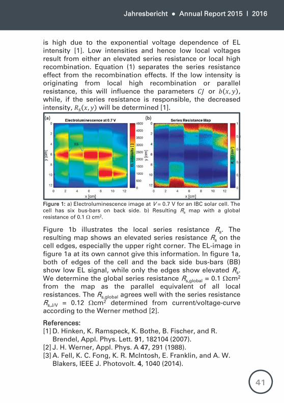
with Vt = 26 mV, the thermal voltage at room temperature,and the fit-parameters and . We determine for eachpixel , and as in Ref [1].This method is applied for the first time for IBC cells,therefore, we validated it on the three dimensional Quokka [3]simulation of our IBC cells.Figure 1a shows the EL-image at V = 0.7 V as an example.Regions with high EL intensity indicate that the local voltage
40
Jahresbericht Annual Report 2015 I 2016
is high due to the exponential voltage dependence of ELintensity [1]. Low intensities and hence low local voltagesresult from either an elevated series resistance or local highrecombination. Equation (1) separates the series resistanceeffect from the recombination effects. If the low intensity isoriginating from local high recombination or parallelresistance, this will influence the parameters or ,while, if the series resistance is responsible, the decreasedintensity, will be determined [1].
Figure 1b illustrates the local series resistance Rs. Theresulting map shows an elevated series resistance Rs on thecell edges, especially the upper right corner. The EL-image infigure 1a at its own cannot give this information. In figure 1a,both of edges of the cell and the back side bus-bars (BB)show low EL signal, while only the edges show elevated Rs.We determine the global series resistance Rs,global = 0.1 cm2
from the map as the parallel equivalent of all localresistances. The Rs,global agrees well with the series resistanceRs,J/V = 0.12 cm2 determined from current/voltage-curveaccording to the Werner method [2].
Figure 1: a) Electroluminescence image at V = 0.7 V for an IBC solar cell. Thecell has six bus-bars on back side. b) Resulting Rs map with a globalresistance of 0.1 cm2.
References:[1] D. Hinken, K. Ramspeck, K. Bothe, B. Fischer, and R.
Brendel, Appl. Phys. Lett. 991, 182104 (2007).[2] J. H. Werner, Appl. Phys. A 447, 291 (1988). [3] A. Fell, K. C. Fong, K. R. McIntosh, E. Franklin, and A. W.
Blakers, IEEE J. Photovolt. 44, 1040 (2014).
41
Institut für Photovoltaik Institute for Photovoltaics
Anomalous Boron Segregation in Liquid Silicon
Patrick Lill
In collaboration with: Morris Dahlinger, and Jürgen Köhler
Pulsed laser melting, which is the key feature of the patentedipv laser doping process, is also valuable for fundamentalresearch on rapid solidification of silicon (Si) with dopantincorporation. Laser doping bases on the diffusion of dopantatoms in locally laser-melted Si, which form doped regionsvia epitaxial re-crystallization after the laser irradiation.Due to the localized heat input during laser doping, largetemperature gradients between the Si melt and thesurrounding solid develop, which lead to high solidificationvelocities. The rapid solidification leads to non-equilibriumcrystallization at the advancing liquid/solid phase interface,causing dopant concentrations in the just formed Si solidwhich do not match their equilibrium values. The ratio ofdopant concentrations directly at the liquid/solid interfacedefines the partitioning (or segregation) coefficient kp = Cs/Cl ,with the concentrations in the Si crystal Cs and melt Cl.We investigate the boron (B) incorporation and redistributionduring repeated laser melting and observe a distinct B pile-uparound the maximum melt depth for repeated laser meltingcycles. The equilibrium values of the partitioning coefficientfor B in Si is keq = 0.8, which means that B atoms segregateinto the melt at the advancing liquid/solid interface.In contrast, we determine a partitioning coefficient value kp =1.25 by means of a numerical model which reproduces theexperimental boron profiles remarkably well. For highsolidification (interface) velocities, the segregation/partitioning of dopants into the melt can be suppressed, thisphenomenon is denoted solute trapping with kp approachingunity (kp = 1 for complete solute trapping). In the classicalsolute trapping models, a partitioning/segregation coefficient
42

Jahresbericht Annual Report 2015 I 2016
above unity is not possible, thus we term this behavioranomalous segregation.Figure 1 shows the B concentration profiles measured withsecondary ion mass spectroscopy (SIMS) for three pulseenergies Ep1 = 192 J, Ep2 = 237 J, Ep3 = 264 J and constantnumber of laser scans Ns = 40, together with the respectedsimulated profiles.
Our approach offers a simple and straightforward procedureto determine the partitioning coefficient from experimentalresults. A partitioning coefficient above unity is consistentwith the assumption of an adsorptive liquid/solid interfacewhich attracts B atoms and, in conjunction with a highsolidification velocity leads to an increased B concentration inthe just formed Si right behind the interface. Repeated re-crystallization cycles enhance this effect and cause thereported pile-up near the maximum melt depth.These results [1] indicate the requirement for an extendedmodel to describe the boron pile-up within the solutetrapping framework.
Reference:[1] P.C. Lill, M. Dahlinger, and J.R. Köhler, submitted to:
mdpi Materials (2016).
Figure 1: Measured(open symbols) andsimulated (lines)boron concentra-tion profiles forthree laser pulseenergies Ep1 = 192
J, Ep2 = 237 J, Ep3= 264 J andconstant number oflaser scans Ns = 40.The simulation fitsthe data remarkablywell for a partition-ing coefficient kpabove unity with kp= 1.25.
43

Institut für Photovoltaik Institute for Photovoltaics
STROMBANK: Innovation for Local Energy Storage
Timo Kropp
In collaboration with: Markus Schubert, Thomas Wurster, Jürgen Werner,
and Thomas Speidel (ads-tec)
The economic model of a bank that manages financial trans-actions in money accounts is well-known. This bankingapproach serves as a model for the "Electricity Bank"(STROMBANK) research project [1]. The STROMBANKmanages the increasing amount of renewable anddecentralized electricity generation in the low-voltage grid bycustomers, who are consumers as well as producers at thesame time, so-called prosumers. At best, renewableelectricity is consumed or temporarily stored in the vicinity ofits generation site. As a consequence, load and losses ofelectricity distribution grids go down, since the amount ofenergy transformed and transmitted is lowering.The innovative STROMBANK approach enables time-shiftingand temporal matching of each prosumer's own productionand consumption. All account holders are able to share andtrade their banked electricity among each other, withneighbors, or even to the electricity stock exchange.The main incentives for sharing a neighborhood battery stor-age are economic benefits for the prosumers as well as theoperators of such battery containers. Consequently, they gainthe ability of providing grid services like balancing reserve.Figure 1 outlines the system layout of the STROMBANK testinstallation. The STROMBANK is a 100 kWh Li-ion batterystorage [2] connected to the local low-voltage grid. Genera-tion and consumption meters record the data of thirteenphotovoltaic (PV) and three combined heat and power (CHP)systems, all with nominal output powers around 5 kW. The100 kWh Li-ion battery storage is connected to the local grid,being charged and discharged with the residual energy flowof all STROMBANK prosumers. We evaluate the individualelectricity consumption and production data, plus the overallSTROMBANK traffic, and model the complete system.44
Jahresbericht Annual Report 2015 I 2016
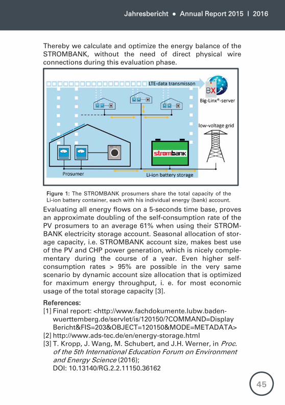
Thereby we calculate and optimize the energy balance of theSTROMBANK, without the need of direct physical wireconnections during this evaluation phase.
Evaluating all energy flows on a 5-seconds time base, provesan approximate doubling of the self-consumption rate of thePV prosumers to an average 61% when using their STROM-BANK electricity storage account. Seasonal allocation of stor-age capacity, i.e. STROMBANK account size, makes best useof the PV and CHP power generation, which is nicely comple-mentary during the course of a year. Even higher self-consumption rates > 95% are possible in the very samescenario by dynamic account size allocation that is optimizedfor maximum energy throughput, i. e. for most economicusage of the total storage capacity [3].
Figure 1: The STROMBANK prosumers share the total capacity of theLi-ion battery container, each with his individual energy (bank) account.
References:[1] Final report: <http://www.fachdokumente.lubw.baden-
wuerttemberg.de/servlet/is/120150/?COMMAND=DisplayBericht&FIS=203&OBJECT=120150&MODE=METADATA>
[2] http://www.ads-tec.de/en/energy-storage.html[3] T. Kropp, J. Wang, M. Schubert, and J.H. Werner, in Proc.
of the 5th International Education Forum on Environment and Energy Science (2016); DOI: 10.13140/RG.2.2.11150.36162
45
Institut für Photovoltaik Institute for Photovoltaics
Mechanical Stress in Lithium-Ion Batteries
Jan Patrick Singer
In collaboration with: Kai Peter Birke
Lithium-ion cells are state of the art technology for electricalenergy storage in mobile as well as stationary batterysystems. They offer high power and energy densities, lowself-discharge rates, high efficiencies, low toxicities and highlifetimes. Considering the lifetime, not all ageing mechanismsare fully understood.During the charging process of a lithium-ion cell, positiveionic charge carriers Li+ intercalate into the negative electrode(anode). The common anode material is graphite C6 showinga volume strain V/V0 = 12.8 % during Li-insertion [1]. At thesame time, the positive electrode (cathode) releases the Li+-ions under a negative volume strain V/V0= -6.6 % for lithiumiron phosphate LiFePO4 [1]. The total volume strain ismeasured as a change of force which is applied externally onthe cell. Ageing investigations show, that the cyclic lifetime ofa pouch cell extends by applying an external force [2].Additionally, measuring the cell’s pressure can be used forState of Charge (SoC) prediction and State of Health (SoH)diagnostics. For both, SoC prediction and SoH diagnostics,pressure change processes and their variation over thelifetime of the cell need to be understood.Figure 1 shows one charge and discharge cycle of a LiFePO4/C6 cell. Since LiFePO4 follows a two-phase transitionmechanism for lithiation, the voltage characteristic (blue line)shows a flat plateau over a wide range of SoC. The red linerepresents the charge, respectively discharge current. Incharge direction, the force F in green follows the trend ofvoltage V. However, in discharge direction, an non-monotonic slope of F is noticeable.During the discharge process, the LiFePO4 transforma-
46

Jahresbericht Annual Report 2015 I 2016
References:[1] W.H. Woodford, W.C. Carter, and Y.-M. Chiang, Energy
Environ. Sci. 55, 8014 (2012).[2] J. Cannarella, and C.B. Arnold, J. Pow. Source 2245, 745
(2014).[3] R. Malik, A. Abdellahi, and G. Ceder, Electrochem. Soc.
160, A3179 (2013).
tion follows the equation. (1)
When the concentration of transformed particles reaches acritical state with a concentration instability the chemicalpotential of Lithium drops [3]. The drop of results in aflat voltage plateau and a intermediate rise of the measuredforce F.
Figure 1: Voltage characteristic of LiFePO4/C6 pouch cell measured duringone charge and discharge cycle (blue line). The cell is charged respectivelydischarged with a constant current ICC = 1C until the cut-off voltage isreached followed by constant voltage charging until the currents dropsbelow ICV < 1/100 C. The red line shows the corresponding current I and thegreen line the measured Force F with an initial Force Fint = 350 N at SoC =100 %. The nominal capacity of the cell is CN = 1.3 Ah.
The phase transition, influencing the external force andthereby the aging process is still not completely explained bycommon theories and recently studied at the ipv. Based onparticle models, we describe the trend of and predict theaging process of LiFePO4 /C6 cells as a function of force F.
47
Institut für Photovoltaik Institute for Photovoltaics
Chemical Stability of Cadmium Telluride Powder
Renate Zapf-Gottwick
In collaboration with: Jessica Nover, Matthias Zorn, Caroline Feifel1, Michael Koch1, and Jürgen Werner
1Institute for Sanitary Engineering, Water Quality, and Solid Waste Management, University of Stuttgart, Germany
The crystalline compound cadmium telluride (CdTe) is knownas a direct II-VI semiconductor and as material for solar cellsand optical detectors. However, cadmium is highly toxic andforbidden in most products (still not in photovoltaics).Cadmium telluride usually is assumed to be chemicallystable. Only strong acids should be able to decompose thebonding of CdTe. Our recently published study showed anelution of cadmium and tellurium out of CdTe photovoltaicmodule pieces not only in acidic solutions [1]. Here, wepresent elution experiments for different grain sizes of CdTepowder. The result is: the smaller the grain size, the higherthe instability and the decomposition of CdTe. However, thethickness of the CdTe layer in modules is smaller and showsthe highest elution out of milled CdTe modules [2].Our experiments are carried out on commercially availableCdTe powder. We use powder with different given maximumparticle sizes (due to sieving) characterized by their diameterd : (i) CdTe250 with d250 250 m, (ii) CdTe840 with d840 840
m, and (iii) CdTe3000 with d3000 3000 m. We compare theresults with leaching results of a former study on milled CdTemodules Cd3,m with a thickness dCdTe,m 3 m.The leaching experiments are carried out at room tempera-ture. To secure constant pH values, we utilize bufferedsolutions. We leach the different CdTe powder in three waterbased solutions with pH4, pH7, and pH10. Inductively coupledplasma mass spectroscopy analyzes the amount of dissolvedsubstances but no precipitations. We carry out theexperiments three times and show the results as meanvalues. The measurement uncertainty is around +/-10%.
48
Jahresbericht Annual Report 2015 I 2016
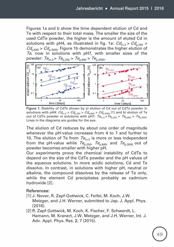
Figures 1a and b show the time dependent elution of Cd andTe with respect to their total mass. The smaller the size of theused CdTe powder, the higher is the amount of eluted Cd insolutions with pH4, as illustrated in fig. 1a: Cdm,3 > Cdp,250 >Cdp,840 > Cdp,3000. Figure 1b demonstrates the higher elution ofTe, now in solutions with pH7, with smaller sizes of thepowder: Tem,3 > Tep,250 > Tep,840 > Tep,3000.
The elution of Cd reduces by about one order of magnitudewhenever the pH-value increases from 4 to 7 and further to10. The elution of Te from Tem,3 is more or less independentfrom the pH-value while Tep,250, Tep,840, and Tep,3000 out ofpowder becomes smaller with higher pH.Our experiments prove the chemical instability of CdTe todepend on the size of the CdTe powder and the pH values ofthe aqueous solutions. In more acidic solutions, Cd and Tedissolve. In contrast, in solutions with higher pH, neutral oralkaline, the compound dissolves by the release of Te only,while the element Cd precipitates probably as cadmiumhydroxide [2].
References:[1] J. Nover, R. Zapf-Gottwick, C. Feifel, M. Koch, J.W.
Metzger, and J.H. Werner, submitted to Jap. J. Appl. Phys. (2016).
[2] R. Zapf-Gottwick, M. Koch, K. Fischer, F. Schwerdt, L. Hamann, M. Kranert, J.W. Metzger, and J.H. Werner, Int. J. Adv. Appl. Phys. Res. 22, 7 (2015).
Figure 1: Stability of CdTe shown by a) elution of Cd out of CdTe powder insolutions with pH4: Cdm,3 > Cdp,250 > Cdp,840 > Cdp,3000 [1] and b) elution of Teout of CdTe powder in solutions with pH7: Tem,3 >Tep,250 > Tep,840 > Tep,3000.Lines in the diagrams are guides for the eye.
49

Institut für Photovoltaik Institute for Photovoltaics
Illumination Changes Leaching of Photovoltaic Modules
Simon Huber
In collaboration with: Jessica Nover, Renate Zapf-Gottwick, Carolin Feifel1, Michael Koch1,
and Jürgen Werner1Institute for Sanitary Engineering, Water Quality, and Solid Waste
Management, University of Stuttgart, Germany
Leaching of hazardous and toxic substances out ofphotovoltaic (PV) modules is a topic of great interest. Ifmodules are dumped or landfilled, they will remain there fora long time. For this reason, it is important to have soundknowledge about long term leaching behavior. Up to now,there were no results considering the influence ofillumination on the long term leaching of PV modules.We perform leaching experiments in aqueous solutions ofthree different pH on 5x5 cm² module pieces, cut out from thefour major PV modules: (i) crystalline silicon (c-Si), (ii)amorphous silicon (a-Si), (iii) cadmium telluride (CdTe), and(iv) copper indium gallium diselenide (CIGS). The leachingoccurs at a temperature T = 40 °C with agitation. A sunsimulator illuminates with an irradiance Popt = 1000 Wm-2. Thethree different leaching solutions simulate the environmentalconditions of acidic rain (pH3), groundwater (pH7) andalkaline landfills (pH11).Inductively coupled plasma mass spectrometry (ICP-MS)measures the amount of eluted elements according to ISO17294-2 [3]. We investigate: silver (Ag), aluminum (Al),cadmium (Cd), copper (Cu), gallium (Ga), indium (In),molybdenum (Mo), nickel (Ni), lead (Pb), selenium (Se), tin(Sn), tellurium (Te), and zinc (Zn).All leaching data are given with respect to the total mass inone module piece. To determine the total mass by ICP-MS,we mill the module piece to powder, digest it with nitric acidand hydrogen peroxide, and use microwave irradiation.
50

Jahresbericht Annual Report 2015 I 2016
Under illumination, we observe a higher leaching for theelements Cd, In, Mo, Se, Te, Zn. In contrast, Sn shows lessleaching under illumination. As an example, figure 1 showsthe leached amount of zinc ZnCIGS out of the front contact ofCIGS module pieces with and without illumination.
Illumination changes the leaching of the PV module pieces.Some elements show substantial higher leaching mainlywithin the first few days only. We suppose that the effect ofillumination is caused by the voltage induced in the solarcells. With progressing elution, the cells are more and moredamaged and the voltage drops. Considering this effect,elution rates under illumination are higher in the beginningand become lower when leaching proceeds.Currently, we are developing a model, which includesthermo-dynamic properties, redox potential, pH value, andthe illumination induced voltage. This model will help toqualitatively understand the exact leaching mechanisms.
Figure 1: Leachedamount of zinc ZnCIGSfrom CIGS modulepieces in pH3solution. With illumi-nation, ZnCIGS isapproximately twiceas much as withoutillumination.
References:[1] K. Huang, G. Zhuang, C. Xu, Y. Wang, and A. Tang,
Atmos. Res. 889, 146 (2008). [2] A. Dellantonio, W. Fitz, H. Custovic, F. Repmann, B.
Schneider, H. Grünewald, V. Gruber, Z. Zgorelec, N.Zerem, C. Carter, M. Markovic, M. Puschenreiter, and W. Wenzel, Environ. Pollut. 1153, 677 (2008).
[3] ISO 17294-2: Water quality - Application of inductivelycoupled plasma mass spectrometry (ICP-MS) - Part 2: Determination of 62 elements (2003).
51
Institut für Photovoltaik Institute for Photovoltaics
Fineline- and Double-Printing on Selective Emitter
Sabrina Lang
In collaboration with: Sabine Schreiber and Renate Zapf-Gottwick
The metallization of industrial solar cells is mostly based onscreen printing of pastes containing silver or aluminum. Forinterconnecting the cells in a module by soldering, the frontcontacts form a grid of small fingers and busbars. This frontmetallization shadows part of the incoming radiation andcauses optical losses [1]. To reduce these losses, the area ofthe front grid should be as small as possible compared to thearea of the cell. In current manufacturing, the grid area takesapprox. 8% of the cell with around 90 fingers of width 60 m< wF < 70 m and height hF = 15 m. New printing technolo-gies and silver pastes enable the reduction of the finger widthto wF = 30 m. However, printing of 30 m fingers suffersfrom a small finger height. A low resistivity of the fingersrequires an aspect ratio a = hF/wF 0.5. The necessary heighthF can not be achieved with a single printing step. Therefore,we use double-printing of the fingers ensuring a sufficientfinger height. The first printing step includes the grid with thedesired finger width, the second printing step uses 20%smaller fingers. The second print has to be placed exactly ontop of the first print. Therefore, a precise alignment of thetwo printing steps is critical.To ensure an exact positioning of the second print on top ofthe first print, a new screen printer together with a connectedupstream adjustment unit called SAS (both from thecompany ASYS) was acquired. The SAS controls thepositioning of the wafer in the screen printer by an AOI-system (automated optical inspection) with four cameras.Every camera takes a picture from the area in each corner ofthe wafer. The fingers in the recorded pictures appearbrighter, than the background of the wafer. Based on thisbrightness difference, the AOI is able to recognize the first-print-structure. The SAS sends this information about
52
Jahresbericht Annual Report 2015 I 2016
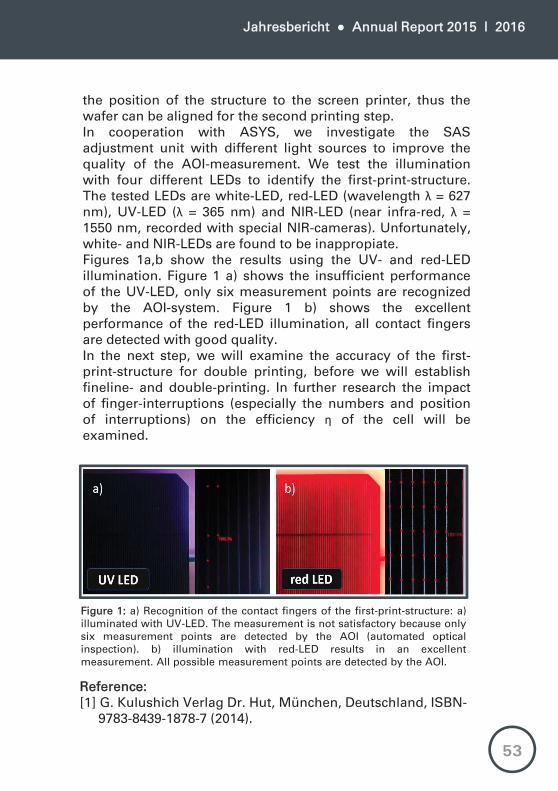
Figure 1: a) Recognition of the contact fingers of the first-print-structure: a)illuminated with UV-LED. The measurement is not satisfactory because onlysix measurement points are detected by the AOI (automated opticalinspection). b) illumination with red-LED results in an excellentmeasurement. All possible measurement points are detected by the AOI.
Reference: [1] G. Kulushich Verlag Dr. Hut, München, Deutschland, ISBN-
9783-8439-1878-7 (2014).
the position of the structure to the screen printer, thus thewafer can be aligned for the second printing step.In cooperation with ASYS, we investigate the SASadjustment unit with different light sources to improve thequality of the AOI-measurement. We test the illuminationwith four different LEDs to identify the first-print-structure.The tested LEDs are white-LED, red-LED (wavelength = 627nm), UV-LED ( = 365 nm) and NIR-LED (near infra-red, =1550 nm, recorded with special NIR-cameras). Unfortunately,white- and NIR-LEDs are found to be inappropiate.Figures 1a,b show the results using the UV- and red-LEDillumination. Figure 1 a) shows the insufficient performanceof the UV-LED, only six measurement points are recognizedby the AOI-system. Figure 1 b) shows the excellentperformance of the red-LED illumination, all contact fingersare detected with good quality.In the next step, we will examine the accuracy of the first-print-structure for double printing, before we will establishfineline- and double-printing. In further research the impactof finger-interruptions (especially the numbers and positionof interruptions) on the efficiency of the cell will beexamined.
53
Institut für Photovoltaik Institute for Photovoltaics
PublikationenPublications
Silicon thin film photodetectors for multi-channel fluorescence detection in a microfluidic point-of-care testing deviceM. Berner, R. Rothemund, S. Vollmer, M.B. Schubert, U. Hilbig, and G. Gauglitz, Phys. Status Solidi A , 1862-6319 (2016); DOI: 10.1002/pssa.201532953
Amorphous Silicon Passivation for p ++ and n ++ Areas on IBC Solar CellsK. Carstens, M. Dahlinger, E. Hoffmann, J.R. Köhler, R. Zapf-Gottwick, and J.H. Werner, in Proc. of the 4th International Education Forum on Environment and Energy Science (2015); DOI: 10.13140/RG.2.2.13666.94407
Universal Passivation for p++ and n++ Areas on IBC Solar CellsK. Carstens, M. Dahlinger, E. Hoffmann, J.R. Köhler, R. Zapf-Gottwick, and J.H. Werner, Energy Procedia 777, 779 (2015); http://dx.doi.org/10.1016/j.egypro.2015.07.110
Surface passivation of heavily boron or phosphorus doped crystalline silicon utilizing amorphous siliconK. Carstens, and M. Dahlinger, J. Appl. Phys. 1119 (18), 185303 (2016); DOI: http://dx.doi.org/10.1063/1.4948945
Laser-Doped Back-Contact Solar CellsM. Dahlinger, B. Bazer-Bachi, T.C. Röder, J.R. Köhler, R. Zapf-Gottwick, and J.H. Werner, IEEE J. Photovoltaics 55, 812 (2015).
23.2% Efficiency with Laser Processed IBC Solar CellsM. Dahlinger, K. Carstens, E. Hoffmann, S. Wansleben, J.R. Köhler, R. Zapf-Gottwick, and J.H. Werner, in Proc. 31st Europ. Photovolt. Solar Energy Conf., (WIP, München, 2015), p. 462, DOI: 10.4229/EUPVSEC20152015-2DO.2.4
54

Jahresbericht Annual Report 2015 I 2016
Laser Processed Silicon Back Contact Solar Cells Exceeding 23% EfficiencyM. Dahlinger, K. Carstens, E. Hoffmann, R. Zapf-Gottwick, and J.H. Werner, in Proc. of the 4th International Education Forum on Environment and Energy Science (2015),DOI: 10.13140/RG.2.2.26149.91365
23.2% laser processed back contact solar cell: Fabrication, characterization and modelingM. Dahlinger, K. Carstens, E. Hoffmann, R. Zapf-Gottwick, andJ.H. Werner, Prog. Photovolt: Res. Appl. 225, 192 (2016).
Band gap narrowing models tested on low recombination phosphorus laser doped siliconM. Dahlinger, and K. Carstens, J. Appl. Phys. 1120, 155701 (2016).
Optimized Laser Doped Back Surface Field for IBC Solar CellsM. Dahlinger and K. Carstens, Energy Procedia 992, 450 (2016).
Silberreduktion in der PhotovoltaikL. Hamann, Verlag Dr. Hut, München, Deutschland, ISBN 978-3-8439-2379-9, (2015)
Selbstdotierende Laser-transferierte Kontakte für Silizium-solarzellenE. Hoffmann, Verlag Dr. Hut, München, Deutschland, ISBN 978-3-8439-2472-6, (2016)
5” Laser-IBC Solar Cells with 22.0% EfficiencyE. Hoffmann, M. Dahlinger, K. Carstens, S. Wansleben, R. Zapf-Gottwick, and J.H. Werner, in Proc . 32nd Euro. Photovolt. Solar Energy Conf., edited by M. Topic, N. Taylor and P. Helm (WIP, Munic, 2016), p. 580; DOI: 10.4229/EUPVSEC20162016-2DO.16.5
55
Institut für Photovoltaik Institute for Photovoltaics
Enhanced Leaching of Photovoltaic Modules by IlluminationS. Huber, J. Nover, R. Zapf-Gottwick, C. Feifel, M. Koch, J.W. Metzger, and J.H. Werner, in Proc. of the 5th International Education Forum on Environment and Energy Science (2016);DOI: 10.13140/RG.2.2.16293.29923
Phosphorus out-diffusion in laser molten siliconJ.R. Köhler, and S.J. Eisele, J. Appl. Phys. 1117, 145701 (2015); DOI: 10.1063/1.4917048
The Electricity Bank: Innovative operating model for local energy storageT. Kropp, J. Wang, M.B. Schubert, and J.H. Werner, in Proc. of the 5th International Education Forum on Environment and Energy Science (2016); DOI: 10.13140/RG.2.2.11150.36162
Infrared backwards laser melting of a silicon waferP.C. Lill, and J.R. Köhler, Eur. Phys. J. Appl. Phys. 772, 2 (2015); DOI: 10.1051/epjap/2015150248
Boron Partitioning Coefficient above Unity in Laser Crystallized SiliconP.C. Lill, M. Dahlinger, and J.R. Köhler, submitted to: Materials, (2016)
Analysis of photovoltaic system performance time series: Seasonality and performance lossA.Phinikarides, G. Makrides, B. Zinßer, M. B. Schubert and G. E. Georghiou, Renew Energ 777, 51-63 (2015); DOI: 10.1016/j.renene.2014.11.091
56
Jahresbericht Annual Report 2015 I 2016
Porous Silicon Thin Film Anodes for Lithium Ion BatteriesC. Sämann, K. Kelesiadou, S.S. Hosseinioun, M. Wachtler, J.R. Köhler, P. Birke, M. Schubert, and J.H. Werner, in Proc. of the 5th
International Education Forum on Environment and Energy Science (2016); DOI: 10.13140/RG.2.2.35267.60962
Pulsed laser porosification of silicon thin filmsC. Sämann, J.R. Köhler, M. Dahlinger, M.B. Schubert, and J.H. Werner, Materials 99, 509 (2016); DOI: 10.3390/ma9070509
Reversible capacity fade in lithium-ion cells at low temperaturesJ.P. Singer, and K.P. Birke, in Proc. of the 5th International Education Forum on Environment and Energy Science (2016);DOI: 10.13140/RG.2.2.15244.72326
Leaching Hazardous Substances out of Photovoltaic ModulesR. Zapf-Gottwick, M. Koch, K. Fischer, F. Schwerdt, L. Hamann, M. Kranert, J. Metzger, and J.H. Werner, Int. j. adv. appl. phys. res. 22, 7, (2015); DOI: 10.15379/2408-977X.2015.02.02.2
57

Institut für Photovoltaik Institute for Photovoltaics
58

Jahresbericht Annual Report 2015 I 2016
LehrveranstaltungenLectures
59
Institut für Photovoltaik Institute for Photovoltaics
Mikroelektronik I(Bachelor, Wintersemester)J.H. Werner• Energiebänder und Leitfähigkeit• Silizium - der Werkstoff der Mikroelektronik• Elektronen und Löcher in Halbleitern• Ströme in Halbleitern• Nichtgleichgewicht, Injektion, Extraktion• Elektrostatik des pn-Übergangs• Ströme im pn-Übergang
Einführung in die Elektrotechnik für Kybernetik und Verkehrsingenieurwesen(Bachelor, Sommersemester)K.P. Birke• Elektrischer Gleichstrom• Wechselstrom• Elektrische und magnetische Felder
Photovoltaik I (Bachelor, Sommersemester)J.H. Werner• Der Photovoltaische Effekt: Solarzelle, -modul, -anlage• Sonnenspektrum und -leistung,
Energieverbrauch in Deutschland• Maximaler Wirkungsgrad von Solarzellen• Ersatzschaltbilder• Photovoltaik-Materialien und -Technologien• Modultechnik• Photovoltaische Systemtechnik
60
Jahresbericht Annual Report 2015 I 2016
Optoelectronic Devices and Circuits I (Bachelor, Sommersemester)J.H. Werner• Basic physics, thermal radiation• Coherence• Semiconductor basics• Excitation and recombination processes• Light emitting diodes• Semiconductor lasers• Glass fibers• Photodetectors
Laser and Light Sources (Master, Wintersemester)J.H. Werner and J.R. Köhler• The Human Eye• Light and Color• Photometry• Incoherent Light Sources• Light Emitting Diodes• Lasers• Laser Processing
Photovoltaik III (Master, semester)J.H. Werner• Technologie einkristalliner Zellen• Rekombinationsmechanismen• Theorie der maximalen Wirkungsgrade• Optimierungsstrategien• Zweite und Dritte Generation Photovoltaik
61
Institut für Photovoltaik Institute for Photovoltaics
Battery Modelling and Energy Management(Master Infotech, Wintersemester)K.P. Birke• Electrical battery models• Aging effects in batteries• Thermal battery models• Implementation of battery models• Energy management• Sustainable energy chains• Future concepts for battery modelling and energy
management
Energiewandlung (Master, Sommersemester)J.H. Werner• Thermodynamik• Direkte Nutzung der Sonnenenergie (Solarthermie,
Photovoltaik)• Indirekte Nutzung der Sonnenenergie (Wasserkraft,
Windenergie)• Chemische Wandlung und Speicherung elektrischer
Energie (Batterien, Brennstoffzellen)
Photovoltaik II (Master, ersemester)J.H. Werner• Solarstrahlung• Alternativen zu konventionellen Siliziumzellen• Komponenten von Photovoltaikanlagen• Planung, Installation, Betrieb und Monitoring von
Photovoltaikanlagen• Photovoltaische Messtechnik• Markt und Wirtschaftlichkeit der Photovoltaik
62

Jahresbericht Annual Report 2015 I 2016
Werkstoffe der Elektrotechnik(Master, Wintersemester)K.P. Birke• Allgemeine Übersicht über Werkstoffe der
Elektrotechnik, ihre Eigenschaften sowie Methoden derUnterteilung in verschiedene Werkstoffklassen
• Herleitung makroskopischer Eigenschaften aus dematomaren und mikroskopischen Aufbau
• Berechnungsverfahren, Kenngrößen• Herstellungsverfahren• Anwendungsgebiete
Speichertechnik für elektrische Energie II(Master/Bachelor, Wintersemester)K.P. Birke• Vertieftes Verständnis der mikroskopischen Abläufe in
elektrochemischen Energiespeichern• Messverfahren von ausgewählten Batterieparametern• Elektrische Speichertechniken zur nachhaltigen
elektrischen Energieversorgung• Auslegungsverfahren für elektrische Energiespeicher in
unterschiedlichen aktuellen und zukünftigenAnwendungsgebieten
Mobile Energiespeicher(Master/Bachelor, Wintersemester)K.P. Birke• Anforderungen• Aufbau• Architekturen• Auslegung mobiler Energiespeicher• Einfache Berechnungsverfahren von Batteriegrößen• Einführung in das Batteriemanagement für automotive
Energiespeicher
63

Institut für Photovoltaik Institute for Photovoltaics
Wissenschaftliches Vortragen und Schreiben I (Master/Bachelor, Wintersemester)J.H. Werner• Kernbotschaften• Aufbau eines Vortrags• Standardfehler (Strukturfehler, Technikfehler, Fehler• im Auftreten)• Praktische Schritte zum Vortrag• Präsentation eines wissenschaftlichen Vortrages von
12 min. (mit Videoaufzeichnung)• Selbst- und Fremdbeurteilung
Wissenschaftliches Vortragen und Schreiben II (Master/Bachelor, Sommersemester)J.H. Werner• Kernbotschaften• Aufbau und Elemente einer Publikation• Bilder, Tabellen, Gleichungen und Referenzen• Verfassen eines eigenen wissenschaftlichen
Kurzberichts von 4 bis 6 Seiten
Speichertechnik für elektrische Energie I(Master/Bachelor, Sommersemester)K.P. Birke• Aufbau und Funktionsweise von elektrischen
Energiespeichersystemen• Beschreibung der Speicher anhand charakteristischer
Größen • Überblick über die wichtigsten Messverfahren• Einführung in Ersatzschaltbilder und Modellierung
64
Jahresbericht Annual Report 2015 I 2016
Photovoltaische Inselsysteme(Master/Bachelor, Wintersemester) B. Zinßer• Typen von Inselsystemen• Komponenten• Auslegung• Simulation• Praxis• Wirtschaftlichkeit
Teamarbeit ipv(Bachelor, Sommersemester)J.R. Köhler• Herstellung eines Moduls aus einkristallinen Mini-
Solarzellen• Konfigurieren eines Solarladereglers und
Speicherakkus• Charakterisierung Minimodul und Solarladeregler
Praktische Übungen im Labor „Photovoltaik“ (Bachelor, Sommersemester)R. Zapf-Gottwick• Herstellung von industriellen, kristallinen Si-Solarzellen• Messung und Auswertung der IV-Kennlinie• Quanteneffizienz und Reflexionsmessung• PV-Modulherstellung mit kristallinen Si-Solarzellen
Praktische Übungen im Labor „Messtechnik für Energiewandler und -speicher“ (Master, Wintersemester)R. Zapf-Gottwick und J.R. Köhler• Herstellung von Passivierschichten• Charakterisierung der Schichten: Reflexion und
Ellipsometrie• Charakterisierung der Passivierschichten:
Lebensdauermessungen mit PL und QSSPC• Elektrische Charakterisierung von
elektrochemischen Zellen• Elektrochemische Charakterisierung• Aufbau einer Li-Ionen Pouch-Zelle 65

Institut für Photovoltaik Institute for Photovoltaics
66
Jahresbericht Annual Report 2015 I 2016
AbschlüsseDegrees
67
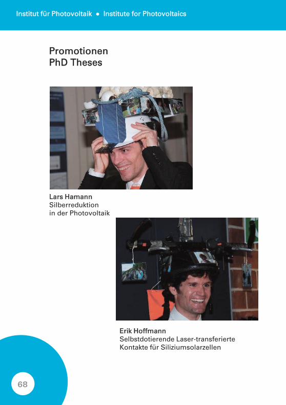
Institut für Photovoltaik Institute for Photovoltaics
Lars HamannSilberreduktion in der Photovoltaik
Erik HoffmannSelbstdotierende Laser-transferierte Kontakte für Siliziumsolarzellen
PromotionenPhD Theses
68

Jahresbericht Annual Report 2015 I 2016
Yasin AtasTeststand für Photovoltaikmodule
Sebastian BartelsHerstellung von Strukturelementen für Li-Ionen-Zellen mit dem 3D-Drucker
Sebastian BilCharakterisierung von negativen Elektroden für Lithium-basierte Hochenergiezellen
Lukas BüchnerJahresenergieerträge von PV-Anlagen mit Laser-Rückseiten-kontaktsolarzellen
Rafael ConradtAuslegung und energetische Betrachtung von Peltier-Elementen zur thermischen Regulierung von Lithium-Ionen-Akkumulatoren
Zübeyr CosgunLangzeitdegradation von Photovoltaikmodulen
Christian Dias GrauerAufbau einer Alkali-Mangan-Zelle mit Nickelschaum als Ableit-elektrode
Philipp DressUntersuchung von Kohlenstoffbeschichtungen auf Nickel-schäumen für den Einsatz in elektrischen Energiespeichern
Julian EgleErstellung und Umsetzung eines PV-Laderegelungskonzepts für Luftschiffe
Richard FichteElektrotechnisches Balancing von Lithium-Ionen-Zellen
Dennis GerberAuslegung und Konstruktion eines alkalischen Elektrolyseurs
BachelorarbeitenBachelor Theses
69

Institut für Photovoltaik Institute for Photovoltaics
Tobias GösslOptisches Simulationsmodell eines Mikrofluidikkanals für bioanalytische Fluoreszenzmessungen
Marvin HaagUntersuchung der Aufspaltung von CO2 über ein Plasma-verfahren und einen Festkörper-Hochtemperatur-Elektrolyseur
Jacob HampelEntwicklung eines Modems zur Powerline-Kommunikation in Automotive-Batteriesystemen
Anya HeiderCharacterisation of an Organic-Inorganic Perovskite Material and Its Application to Solar Cells
Julian HeydgenSeparator mit besonderen Strukturelementen für Lithium-Zellen
Friederike HuberEinfluss von Alkali-Metallen auf Kesterit-Solarzellen
Pascal HugAuswahl und Charakterisierung von Lithium-Ionen-Zellen für den Modulaufbau von selbsttragenden und leichten Einheiten
Clemens Jurgschat3D-Druck von Lithium-Ionen-Batterien mit horizontalen Verbindungen
Tijen KarimaniFeuchtigkeitsmessung in EVA-laminierten Schichten
Katerina KelesiadouLaserinduzierte Porositätsvariation von Siliziumanoden in Lithium-Ionen-Batterien
70

Jahresbericht Annual Report 2015 I 2016
Mike KoppKonzeption und Aufbau eines Messplatzes zur lokalen Druck-bestimmung an Lithium-Ionen-Zellen
Simon KosteleckyEnergiebedarf eines Foodsharing-Kühlschranks
Matthias KraftDelamination von PV-Modulen durch Lösen von Rückseiten-Metallkontakten
Maximilian KraftFlexibles Solarmodul zur photovoltaischen Stromversorgung eines Luftschiffs
Daniel KrügerSolarzellen im Magnetfeld
Thomas ReinhartLaserstrukturierung von Aluminium für Rückseitenkontakt-solarzellen
Jacob v. RömerAblation von Passivierschichten auf Rückseitenkontakt-solarzellen
Shima SasanpourMetalloxid Oberflächenbeschichtungen für Siliziumanoden in Lithium-Ionen-Batterien
Tobias SchmidtUntersuchung von Netz-kontaktierten TiO2-Elektroden für Li-Ionen Zellen mit elektrochemischen und optischen Methoden
Eugen SchwarzkopfEntwicklung eines Messchucks für 5-Zoll und 6-Zoll Rück-kontaktsolarzellen
71
Institut für Photovoltaik Institute for Photovoltaics
Dominik StellerZweilagige Aluminiummetallisierung durch Laserschweißen für Rückseitenkontaktsolarzellen
Gernot TuschewitzkiDrone Ready DaySy
Johannes WannerErweiterung eines Versuchsaufbaus zur Untersuchung einer plasmabasierten CO2-Zerlegung
German WieselEntwicklung und Parametrierung eines thermischen Modells füreine Lithium-Ionen Zelle
Fabian WinterEvaluierung und Optimierung der DaySy-Messmethodik
Matthias ZornLöslichkeit von Cadmiumtellurid
72

Jahresbericht Annual Report 2015 I 2016
Kayvan AzariEvaluierung der Bilderzeugungsalgorithmen für die DaySyTageslichtlumineszenz
Lukas BillingerErstellung einer Auswertungssoftware für Bilder von Photo-voltaikanlagen
Tim BuchaliEntwicklung von Ein- und Ausschaltstrategien für Hochvolt-Lithium-Ionen-Akkumulatoren mit Einzelzellschaltertopologie
Lei ChenInvestigations on the Operation of the Strombank
Simon FleischerSpannungsbetriebsfenster einer Lambdasonde abhängig von der Temperatur
Tobias GösslZyklisierbarkeit von Lithium-Metall-Elektroden bei Verwendung unterschiedlicher Elektrolyte
Sema GüleryüzStickstoff-gesputtertes Lithiumphosphat als künstlicheDeckschicht
Fabian HeimUntersuchung der Zyklisierbarkeit von Lithium-Metall-Elektroden
Fabian HöderathKonstruktion einer Elektrolytrückführung für einen alkalischen Elektrolyseur und Ermittlung der charakteristischen Zellkenn-linien
Pascal KölblinParameter der Bildqualität zur Optimierung der Elektrolumines-zenzmessung im Feld
ForschungsarbeitenResearch Theses
73

Institut für Photovoltaik Institute for Photovoltaics
Martin KynastModulkonzeption/-konstruktion von selbsttragenden und leichten Einheiten aus Li-Ionen-Zellen
Ioannis LambidisProjekt Strombank Datenanalyse der ersten Messwerte aus der Praxis
Alexander MöllerMessaufbau zur Bestimmung von Kleinsignaldetektionsgrenzenvon Dünnschichtphotodioden
Daniel MüllerOptimierung des Ladeprofils einer EV-Flotte im Rahmen einer Micro Smart Grid Simulation
Patrick PascherEntwicklung eines parametrischen Modells zur thermischen Modellierung eines Batteriemoduls aus Lithium-Ionen-Zellen
Hannes SchneiderExperimental Parameter Estimation for a High Frequency Battery Model and Analysing Its Operation in Connection with a DC/DC Converter
Thomas SchusterWasserstofferzeugung mittels Umsetzung von Metallen, Halbmetallen und Halbleitern
Christian SeidlerEntwicklung und Implementierung einer Methode zur Lade-zustandserkennung von Li-Ionen-Zellen
Marcel WaldhofGraphical User Interface – Annotierung und statistische Auswertung von Messbildern mit Matlab
Juncheng WangSupply of Balancing Energy by the Strombank
74
Jahresbericht Annual Report 2015 I 2016
Felix WenzlerEntwicklung von Lehrinhalten zu erneuerbaren Energien in ländlichen Regionen Indonesiens und deren praktische Anwendung
Yi YiDC-Netze in Nichtwohngebäuden
Ruyin ZhangMaterialcharakterisierung von n-Typ Wafern
Matthias ZornDruckkontaktierte Zellverbinder für Li-Ionen-Rundzellen
75
Institut für Photovoltaik Institute for Photovoltaics
Markus Botey-JuncaOberflächenbearbeitung von Metallen durch Laserlegieren
Ludwig EringerAufbau und Modellierung einer Energiespeichereinheit mit unterschiedlichen elektrochemischen Zellen
Anja HeinzelmannInfrarot Laserporosieren von Dünnschichtsilizium als Anode in Lithium-Ionen-Akkumulatoren
Simon HuberMessplatzaufbau: Elektrochemisches Auslaugen von PV-Modul-stücken unter Beleuchtung
Terpsithea KaradaliSynthese und Modifikation sauerstoffhaltiger Elektroden-materialien für Lithium-Ionen-Zellen durch elektromagnetische Strahlung
Sascha KochMachbarkeitsnachweis des Fourier Transform Imagers
Martin KynastKonzeption und Konstruktion zweier Batteriemodule mit Rund-und Pouchzellen und Vergleiche der wichtigsten KPIs
Ioannis LambidisAufbau und Lademanagement einer Energiespeichereinheit mit unterschiedlichen elektrochemischen Zellen
Alexander MöllerAufbau und Implementierung eines optisch entkoppelten Batteriemanagementsystems
Daniel MüllerPlasmabasierte Methanisierung von Kohlendioxid mit zusätzlichem Sauerstoff-Ionenleiter
MasterarbeitenMaster Theses
76

Jahresbericht Annual Report 2015 I 2016
Thomas NauhauserEntwicklung einer passiven Impedanzmessmethode für Akkumulatoren
Andre PfeifferEntwicklung und Aufbau einer Batteriemanagement-Workbench
Fabian PuntigamEntwicklung eines Messsystems zur parallelen, synchronen Kennlinienmessung räumlich verteilter Solarzellen
Aref SamadiImplementation and Characterization of an IV MeasurementSetup for Interdigitated Back Contact Solar Cells
Bernd SchrettleAufbau und Inbetriebnahme eines Messplatzes für elektrochemische Zellen
Ismail ShokryBifacial Modules – Simulation and Experiment
Juncheng WangScaled Simulation of a 100 kWh Lithium-Ion Battery Storage
Yi WangDevelopment and Parameterization of Lithium-Ion-Battery Cell Models
Felix Wenzler24-Stunden-Solarmodul
Daniel WolpertPotential automotiver Li-Ionen-Batterien in stationären Anwendungen
He YangCharakterisierung und Modellierung des Alterungsverhaltens von Lithium-Ionen-Batterien
77

Institut für Photovoltaik Institute for Photovoltaics
Lea ZeinerZellverbindung im Modul durch Laserschweißen
Junying ZhaoRunge-Kutta Solver for the Numerical Simulation of the Laser-Doping Process
78
Jahresbericht Annual Report 2015 I 2016
Was sonst noch war …Beyond Science …
79
Institut für Photovoltaik Institute for Photovoltaics
40-jähriges DienstjubiläumLeonhard Bauer hat es geschafft! 40 Jahre seinesArbeitslebens hat er der Universität Stuttgart gewidmet.Wir hoffen alle, dass uns Leo noch möglichst langeerhalten bleibt. Herzlichen Glückwunsch, Leo!Professor Dr.-Ing. Kai Peter Birke kommt ans ipvZum 01.02.2015 wurde Kai Peter Birke ans ipv berufen.Er leitet unsere neue Forschungsgruppe ElektrischeEnergiespeichersysteme.ACEEES Forum 2015Beim 4th International Education Forum on Environmentand Energy Science erhielt Marcel Berner den Preis fürden besten wissenschaftlichen Vortrag. Dieses Forumwird von der Academy for Co-creative Education ofEnvironment and Energy Science (ACEEES) des TokyoInstitute of Technology veranstaltet.-------------------------------------------------------------------------------40th AnniversaryLeonhard Bauer made it! He has dedicated 40 years ofhis working life to the University of Stuttgart. We allhope that Leo will stay with us for as long as possible!Congratulations, Leo!Professor Dr.-Ing. Kai Peter Birke joins the ipvOn February 2nd in 2015, Kai Peter Birke was appointedprofessor at the ipv. He is the head of our new researchgroup Electrical Energy Storage Systems.ACEEES Forum 2015At the 4th International Education Forum on Environmentand Energy Science, Marcel Berner won the award forthe best scientific presentation. This forum is organizedby the Academy for Co-creative Education ofEnvironment and Energy Science (ACEEES) of the TokyoInstitute of Technology.
80

Jahresbericht Annual Report 2015 I 2016
Sommerfeste 2015 und 2016Auch in den letzten beiden Jahren haben wir zum Endedes Sommersemesters ein Grillfest veranstaltet, bei demdie Studenten der Vorlesung Energiewandlung dieGelegenheit nutzten, ihre Projekte und Prototypenvorzustellen.ACEEES Forum 2016Beim 5th International Education Forum on Environmentand Energy Science erhielt Simon Huber den Preis fürden besten wissenschaftlichen Vortrag.ReinraumumbauSeit November 2015 wird der Reinraum des ipvumgebaut: Erneuerung aller Zu- und Abluftkanäle, neueRegelungstechnik für Abluftüberwachung. Die Kostenhierfür sind mit 975.000,- € veranschlagt. Die Arbeitensollen bis Mitte April 2017 abgeschlossen sein.-------------------------------------------------------------------------------Summer Barbecues 2015 and 2016At our traditional barbecues at the end of the summerterms of 2015 and 2016, the students of the lectureEnergy Conversion had the opportunity to present theirprojects and prototypes.ACEEES Forum 2016At the 5th International Education Forum on Environmentand Energy Science, Simon Huber obtained the awardfor the best scientific presentation.Retrofit of the CleanroomSince November 2015, the cleanroom of the ipv is beingretrofitted: replacement of all air supply ducts andexhaust air ducts, new technology for the monitoringand control of exhaust air. Estimated costs amount to975,000 €. The construction works are supposed to befinished by the middle of April 2017.
81
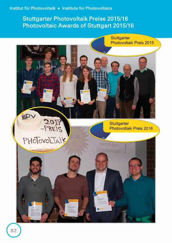
Institut für Photovoltaik Institute for Photovoltaics
Stuttgarter Photovoltaik Preise 2015/16Photovoltaic Awards of Stuttgart 2015/16
82

Jahresbericht Annual Report 2015 I 2016
Stuttgarter Photovoltaik Preise 2015 und 2016Der Förderverein der Freunde des Instituts fürPhotovoltaik (VF-ipv) hat im Januar 2016 und Februar2017 acht herausragende studentische Arbeiten prämiertund die Stuttgarter Photovoltaik Preise im Rahmen einesFest-Kolloquiums an die Studierenden verliehen.Der gemeinnützige Förderverein VF-ipv unterstützt seitseiner Gründung im Juli 2010 die wissenschaftlicheForschung und Arbeit am ipv und fördert denwissenschaftlichen Nachwuchs.-------------------------------------------------------------------------------Die Preisträger 2015 und 2016 sind:The 2015 and 2016 award winners are:Bachelorarbeiten/Bachelor Theses:Tobias Gössl, Julian EgleProjektarbeit/Project Work:Richard Fichte, Marvin Haag, Tobias Schmidt,Julia SchnaarsForschungsarbeiten/Research Theses:Felix Wenzler, Pascal KölblinMasterarbeiten/Master Theses:Anja Heinzelmann, Fabian Puntigam, Andre Pfeiffer-------------------------------------------------------------------------------Photovoltaic Awards of Stuttgart 2015 and 2016The association „Freunde des Instituts für Photovoltaik“(VF-ipv) awarded prizes to eight excellent studentstheses during colloquium ceremonies in January 2016and February 2017.Since its foundation in 2010, the nonprofit associationVF-ipv has supported scientific research and work at theipv and encouraged young scientists.
83

Institut für Photovoltaik Institute for Photovoltaics
84

Jahresbericht Annual Report 2015 I 2016
MitarbeiterlisteStaff Members
Gäste I Guests
Lageplan I Location Map
85
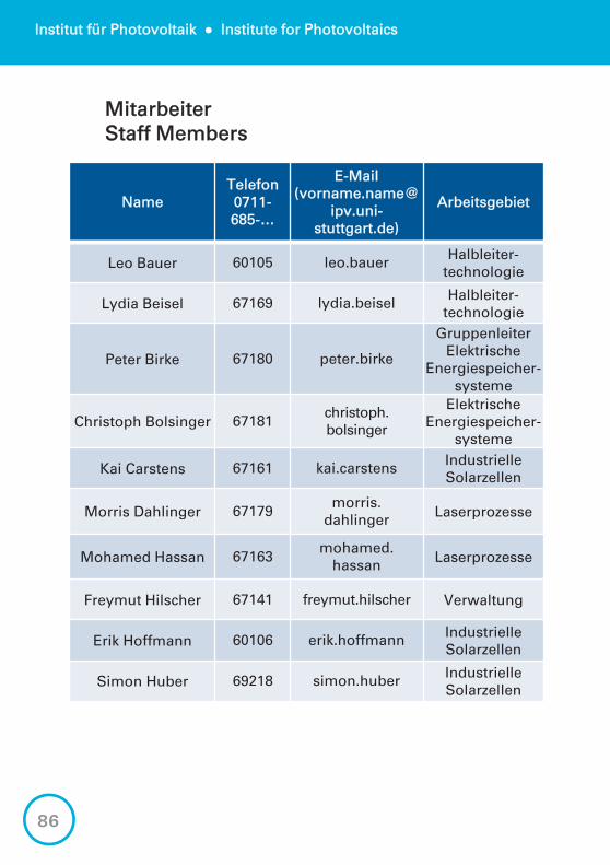
Institut für Photovoltaik Institute for Photovoltaics
NameTelefon0711-685-…
E-Mail(vorname.name@
ipv.uni-stuttgart.de)
Arbeitsgebiet
Leo Bauer 60105 leo.bauer Halbleiter-technologie
Lydia Beisel 67169 lydia.beisel Halbleiter-technologie
Peter Birke 67180 peter.birke
GruppenleiterElektrische
Energiespeicher-systeme
Christoph Bolsinger 67181 christoph.bolsinger
ElektrischeEnergiespeicher-
systeme
Kai Carstens 67161 kai.carstens IndustrielleSolarzellen
Morris Dahlinger 67179 morris.dahlinger Laserprozesse
Mohamed Hassan 67163 mohamed.hassan Laserprozesse
Freymut Hilscher 67141 freymut.hilscher Verwaltung
Erik Hoffmann 60106 erik.hoffmann IndustrielleSolarzellen
Simon Huber 69218 simon.huber IndustrielleSolarzellen
MitarbeiterStaff Members
86
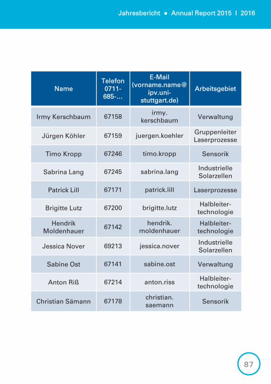
Jahresbericht Annual Report 2015 I 2016
NameTelefon0711-685-…
E-Mail(vorname.name@
ipv.uni-stuttgart.de)
Arbeitsgebiet
Irmy Kerschbaum 67158 irmy.kerschbaum Verwaltung
Jürgen Köhler 67159 juergen.koehler GruppenleiterLaserprozesse
Timo Kropp 67246 timo.kropp Sensorik
Sabrina Lang 67245 sabrina.lang IndustrielleSolarzellen
Patrick Lill 67171 patrick.lill Laserprozesse
Brigitte Lutz 67200 brigitte.lutz Halbleiter-technologie
Hendrik Moldenhauer 67142 hendrik.
moldenhauerHalbleiter-
technologie
Jessica Nover 69213 jessica.nover IndustrielleSolarzellen
Sabine Ost 67141 sabine.ost Verwaltung
Anton Riß 67214 anton.riss Halbleiter-technologie
Christian Sämann 67178 christian. saemann Sensorik
87

Institut für Photovoltaik Institute for Photovoltaics
NameTelefon0711-685-…
E-Mail(vorname.name@
ipv.uni-stuttgart.de)
Arbeitsgebiet
Alexander Schmid 69223 alexander. schmid
ElektrischeEnergiespeicher-
systeme
Sabine Schreiber 67231 sabine.schreiber IndustrielleSolarzellen
Markus Schubert 67145 markus. schubert
GruppenleiterSensorik
Jan Singer 69217 jan.singerElektrische
Energiespeicher-systeme
Friedrich Speckmann 67182 friedrich.
speckmann
ElektrischeEnergiespeicher-
systeme
Osama Tobail 69216 osama.tobail IndustrielleSolarzellen
Jürgen Werner 67140 juergen.werner Institutsleiter
Birgitt Winter 67162 birgitt.winterGruppenleiterin
Halbleiter-technologie
Renate Zapf-Gottwick 69225 renate.zapf-
gottwick
GruppenleiterinIndustrielleSolarzellen
88

Jahresbericht Annual Report 2015 I 2016
Felipe Batista e Batist oUFSJ-Universidade Federal De S o Jo o Del Rei, S o Jo o Del Rei / Brasilien
Paulo Henrique Duarte GonçalvesUFSJ-Universidade Federal De S o Jo o Del Rei, S o Jo o Del Rei / Brasilien
Takahito NishimuraTokyo Institute of Technology, Tokio / Japan
Worabhorn PathanatechaChulalongkorn University, Bangkok / Thailand
Guru Raghav RamanNational Institute of Technology, Tiruchirappalli / Indien
Kanta SugimotoTokyo Institute of Technology, Tokio / Japan
Dr. Khaled EbnalwaledSouth Valley University, Qena / Ägypten
Gäste & ausländische StipendiatenGuests
89
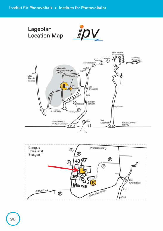
Institut für Photovoltaik Institute for Photovoltaics
LageplanLocation Map
90
Institut für PhotovoltaikUniversität Stuttgart
Paffenwaldring 4770569 Stuttgart
Phone: +49 711 685 67141 Fax: +49 711 685 67143
www.ipv.uni-stuttgart.de