![8 International Meeting of the Institute of Metals in Biology of … · 2020. 1. 6. · [1] A. D’Aléo, C. Andraud, O Maury, in “Luminescence of Lanthanide Ions in Coordination](https://static.fdokument.com/doc/165x107/5fd6a9ac466ef565831c0e66/8-international-meeting-of-the-institute-of-metals-in-biology-of-2020-1-6-1.jpg)
Molecular plating of thin lanthanide layers with improved ... · Alessio Vascon geboren in Padova...
188
Molecular plating of thin lanthanide layers with improved material properties for nuclear applications Dissertation zur Erlangung des Grades “Doktor der Naturwissenschaften” im Promotionsfach Chemie am Fachbereich Chemie, Pharmazie und Geowissenschaften der Johannes Gutenberg-Universität in Mainz vorgelegt von Alessio Vascon geboren in Padova -Italien- Mainz 2013
Transcript of Molecular plating of thin lanthanide layers with improved ... · Alessio Vascon geboren in Padova...
Molecular plating of thin lanthanide layers with
improved material properties for
nuclear applications
Dissertation
zur Erlangung des Grades
“Doktor der Naturwissenschaften”
im Promotionsfach Chemie
am Fachbereich Chemie, Pharmazie und Geowissenschaften
der
Johannes Gutenberg-Universität
in Mainz
vorgelegt von
Alessio Vascon geboren in Padova -Italien-
Mainz 2013

D77

Hiermit versichere ich gemäss § 10 Abs. 3d der Promotionsordnung vom 24.07.2007,
dass ich die jetzt als Dissertation vorgelegte Arbeit selbst angefertigt und alle benutzten
Hilfsmittel (Literatur, Apparaturen, Material) in der Arbeit angegeben habe.
Mainz, den 26.06.2013

Zusammenfassung In der vorliegenden Arbeit werden Experimente beschrieben, die zu einem vertieften Verständnis fundamentaler Prozesse bei der elektrochemischen Herstellung von Dünnschichten, sog. Targets, für kernphysikalische und -chemische Studien führten. Targets wurden mittels 'Molecular Plating' (MP) hergestellt, indem eine Elektrodeposition aus organischem Medium in der Regel bei konstantem Strom in Zwei-Elektroden-Zellen. Die Resultate erlaubten, optimierte Herstellungs-bedingungen zu ermitteln, welche die Produktion deutlich verbesserter Targets erlaubten. MP bei konstantem Strom ist ein massentransportkontrollierter Prozess. Der angelegte Strom wird durch einen konstanten Fluss elektroaktiver Spezies zur Kathode – auf der die Schicht wächst – und Anode aufrechterhalten. Die Untersuchungen zeigten, dass das Zellenpotential des Elektrodepositionsystems immer durch den Ohm'schen Spannungsabfall auf Grund des Widerstandes der verwendeten Lösung dominiert wurde. Dies erlaubte die Herleitung einer Beziehung zwischen dem Zellenpotential und der Konzentration der elektroaktiven Spezies. Die Beziehung erlaubt die Erklärung des gemessenen zeitlichen Verlaufs des Zellenpotentials während der Abscheidung als Funktion der Elektrolytkonzentration. Dies dient als Basis, auf der nun ein umfassenderes Bild der Prozesse, die für die charakteristischen Minima im Potentialverlauf einer Abscheidung verantwortlich sind, gewonnen werden kann. Es konnte gezeigt werden, dass die Minima mit der fast vollständigen Entfernung (durch Abscheidung) der aus einem gelösten Salz erzeugten Nd-Ionen korrespondieren. Die abgeschiedene Spezies wurde als Nd3+ identifiziert, vermutlich als Carboxylat, Oxid oder Hydroxid, was auf Grund der hohen negative Werte des Standardredoxpotentials der Lanthanide verständlich erscheint. Von den vorliegenden elektroaktiven Spezies tragen die Nd3+ Ionen nur zu knapp 20% zum Gesamtstrom bei. Durch Elektrolyse tragen auch die Lösungsmittelkomponenten zu diese Strom bei. Die Gegenwart von elektrolysiertem Lösungsmittel wurde in Analysen der Dünnschichten bestätigt. Diese waren immer mit chemi- und physisorbierten Lösungsmittelmolekülen bedeckt. Die Analyse der Dünnschichten zeigte, dass die Oberflächen von einem furchenartiges Netz durchzogen waren, und dass diese während des Trocknen der Schichten nach dem MP entstanden. Ob die Schichten an Luft oder in inerter Atmosphäre trockneten, hatte keinen Einfluss. Es wurden Experimente mit mehreren Lösungsmitteln durchgeführt, die sich deutlich in ihren physikalischen Eigenschaften, v.a. dem Siedepunkt, unterschieden. Furchenfreie Dünnschichten konnten insbesondere bei MP in N,N-dimethylformamide (DMF) erzeugt werden. Die Verwendung von DMF in Kombination mit einer Abscheidung auf sehr glatten Substraten erlaubte die Produktion von sehr homogenen, glatten und defektfreien Schichten. Diese waren vermutlich geringeren inneren Spannungen während des Trocknens ausgesetzt, als Schichten auf raueren Substraten oder solche, die aus flüchtigeren Lösungsmitteln hergestellt wurden. Die Oberflächenrauigkeit des Substrats und das gewählte Lösungsmittel wurden so als Schlüsselfaktoren für die Produktion hochqualitativer Schichten identifiziert. Es konnte gezeigt werden, dass mit MP eine sehr effiziente Methode zur Herstellung homogener Schichten mit exzellenter Ausbeute ist. In weiteren Experimenten mit dem primordialen -Emitter 147Sm als Modellisotop wurde die Eignung solcher Schichten als -Quelle untersucht. Sowohl die Energieauflösung als auch der Anteil der -Teilchen, die den Detektor erreichten, waren von den Quelleneigenschaften abhängig. Die Effekte wurden verschiedenen Variablen der Dünnschicht zugeordnet, welche die -Spektren beeinflussten. Dominant war die Wahl des Lösungsmittels und die Rauigkeit des Substrats. Dies beeinflusste Schichtdicke und -morphologie sowie die Art des Schichtwachstums und veränderte die Detektionseffizienz in -Messungen bis zu 15%. Nur homogene, ebene Schichten, die aus DMF auf glatten Substraten abgeschieden wurden, eignen sich optimal als -Quelle. Die gewonnenen Ergebnisse erlauben die optimierte Herstellung nuklearer Targets durch MP. Künftige Anwendungen beinhalten insbesondere die Herstellung von Targets für neutroneninduzierte Spaltexperimente und untergrundarme -Messungen sehr kleiner Aktivitäten.

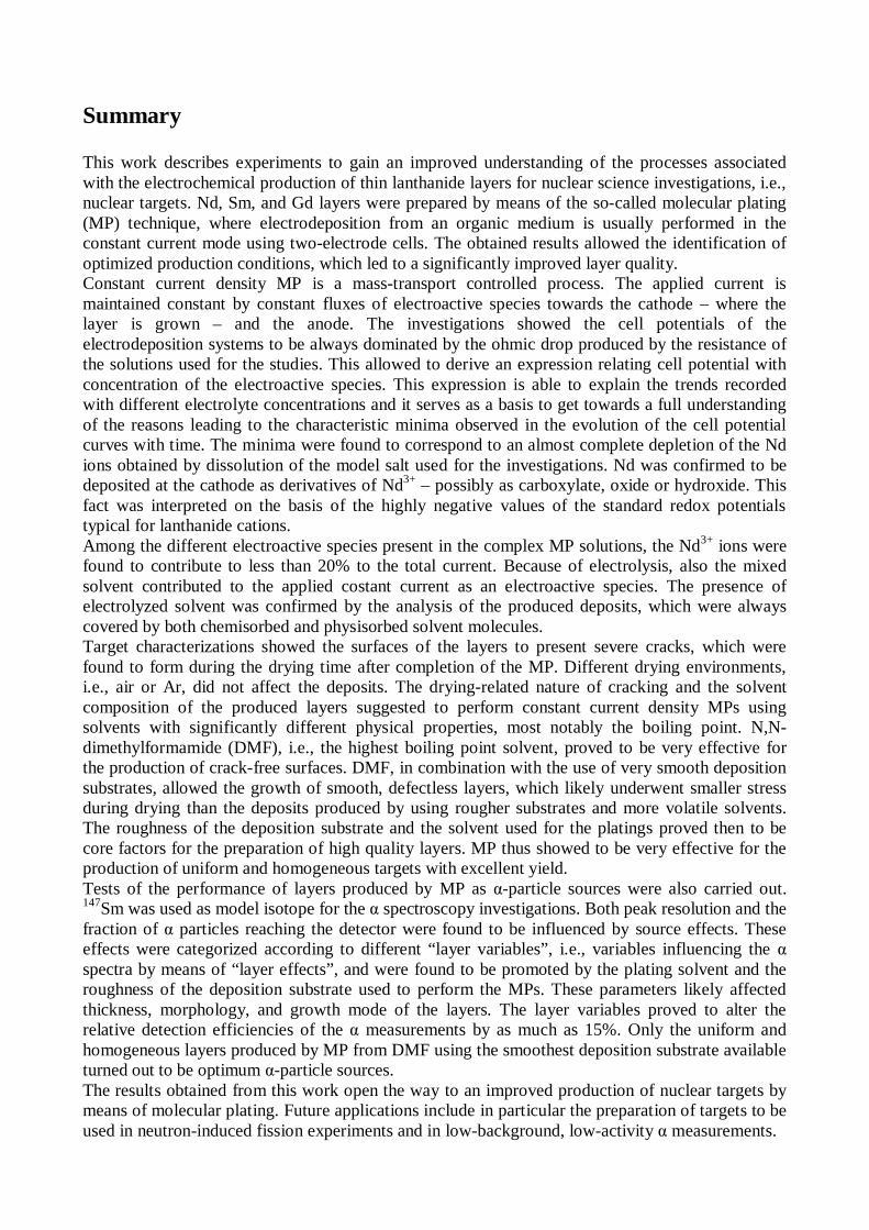
Summary This work describes experiments to gain an improved understanding of the processes associated with the electrochemical production of thin lanthanide layers for nuclear science investigations, i.e., nuclear targets. Nd, Sm, and Gd layers were prepared by means of the so-called molecular plating (MP) technique, where electrodeposition from an organic medium is usually performed in the constant current mode using two-electrode cells. The obtained results allowed the identification of optimized production conditions, which led to a significantly improved layer quality. Constant current density MP is a mass-transport controlled process. The applied current is maintained constant by constant fluxes of electroactive species towards the cathode – where the layer is grown – and the anode. The investigations showed the cell potentials of the electrodeposition systems to be always dominated by the ohmic drop produced by the resistance of the solutions used for the studies. This allowed to derive an expression relating cell potential with concentration of the electroactive species. This expression is able to explain the trends recorded with different electrolyte concentrations and it serves as a basis to get towards a full understanding of the reasons leading to the characteristic minima observed in the evolution of the cell potential curves with time. The minima were found to correspond to an almost complete depletion of the Nd ions obtained by dissolution of the model salt used for the investigations. Nd was confirmed to be deposited at the cathode as derivatives of Nd3+ – possibly as carboxylate, oxide or hydroxide. This fact was interpreted on the basis of the highly negative values of the standard redox potentials typical for lanthanide cations. Among the different electroactive species present in the complex MP solutions, the Nd3+ ions were found to contribute to less than 20% to the total current. Because of electrolysis, also the mixed solvent contributed to the applied costant current as an electroactive species. The presence of electrolyzed solvent was confirmed by the analysis of the produced deposits, which were always covered by both chemisorbed and physisorbed solvent molecules. Target characterizations showed the surfaces of the layers to present severe cracks, which were found to form during the drying time after completion of the MP. Different drying environments, i.e., air or Ar, did not affect the deposits. The drying-related nature of cracking and the solvent composition of the produced layers suggested to perform constant current density MPs using solvents with significantly different physical properties, most notably the boiling point. N,N-dimethylformamide (DMF), i.e., the highest boiling point solvent, proved to be very effective for the production of crack-free surfaces. DMF, in combination with the use of very smooth deposition substrates, allowed the growth of smooth, defectless layers, which likely underwent smaller stress during drying than the deposits produced by using rougher substrates and more volatile solvents. The roughness of the deposition substrate and the solvent used for the platings proved then to be core factors for the preparation of high quality layers. MP thus showed to be very effective for the production of uniform and homogeneous targets with excellent yield. Tests of the performance of layers produced by MP as -particle sources were also carried out. 147Sm was used as model isotope for the spectroscopy investigations. Both peak resolution and the fraction of particles reaching the detector were found to be influenced by source effects. These effects were categorized according to different “layer variables”, i.e., variables influencing the spectra by means of “layer effects”, and were found to be promoted by the plating solvent and the roughness of the deposition substrate used to perform the MPs. These parameters likely affected thickness, morphology, and growth mode of the layers. The layer variables proved to alter the relative detection efficiencies of the measurements by as much as 15%. Only the uniform and homogeneous layers produced by MP from DMF using the smoothest deposition substrate available turned out to be optimum -particle sources. The results obtained from this work open the way to an improved production of nuclear targets by means of molecular plating. Future applications include in particular the preparation of targets to be used in neutron-induced fission experiments and in low-background, low-activity measurements.


Table of contents 1. Introduction...............................................................................................1
1.1 The TRAKULA project........................................................................ 2 1.1.1 Spent nuclear fuel, the role of partitioning and transmutation,
and the physics of transmutation................................................................... 2 1.1.2 Neutrino science and the SNO+ experiment................................................. 5
1.2 Targets for TRAKULA........................................................................ 6 1.2.1 Targets for fission cross-section measurements............................................ 6 1.2.2 Targets for 144Nd half-life determination....................................................... 8
1.2.2.1 144Nd and the half-life measurements of long-lived -particle emitters............................................................................. 9
1.3 Lanthanide and actinide elements....................................................... 11 1.3.1 Chemistry of the lanthanides....................................................................... 11 1.3.2 Chemistry of the actinides........................................................................... 13
1.4 Target preparation............................................................................... 14 1.4.1 General target requirements and main production techniques.................... 14 1.4.2 Molecular plating......................................................................................... 15
1.5 Target characterization techniques...................................................... 17 1.5.1 Neutron activation analysis and -ray spectroscopy....................................17 1.5.2 Radiographic imaging.................................................................................. 21 1.5.3 Scanning electron microscopy..................................................................... 22 1.5.4 Atomic force microscopy............................................................................ 24 1.5.5 X-ray photoelectron spectroscopy................................................................ 27
1.6 Outline of the thesis............................................................................ 31
2. Toward large-area targets for “TRAKULA”....................................... 39
2.1 Introduction......................................................................................... 40
2.2 Experimental....................................................................................... 42 2.2.1 Target preparation....................................................................................... 42 2.2.2 Target characterization................................................................................ 43
2.3 Results and discussion........................................................................ 44 2.3.1 Gd-targets.................................................................................................... 44
2.3.1.1 Comparison between magnetic and ultrasonic stirring at low current density................................................................................ 44
2.3.1.2 Application of ultrasonic stirring at high current density.............. 46 2.3.2 Nd-targets.................................................................................................... 47
2.3.2.1 Application of ultrasonic stirring at low and high current density................................................................................ 47
2.3.3 Time-resolved progress of the plating process............................................ 49
2.4 Layout of the new electrochemical cell.............................................. 53
2.5 Summary..................................................................................................... 54
3. Elucidation of constant current density molecular plating................. 56
3.1 Introduction......................................................................................... 57
3.2 Experimental details............................................................................58 3.2.1 Deposition cells........................................................................................... 58 3.2.2 Molecular plating at constant current density............................................. 59 3.2.3 Deposition substrates................................................................................... 60 3.2.4 Conductivity tests........................................................................................ 60 3.2.5 Atomic Force Microscopy (AFM) studies.................................................. 61 3.2.6 X-ray Photoelectron Spectroscopy (XPS) studies....................................... 62 3.2.7 Gamma-ray spectroscopy studies................................................................ 63
3.3 Experimental results and analysis....................................................... 63 3.3.1 Analysis of the conductivity tests................................................................ 63 3.3.2 AFM analysis............................................................................................... 64 3.3.3 XPS analysis................................................................................................ 66 3.3.4 Molecular plating performed with Cell A................................................... 71 3.3.5 Molecular plating performed with Cell B................................................... 73 3.3.6 Molecular plating on a smaller deposition area in Cell B........................... 75 3.3.7 Deposition yield evaluation of the molecular plating realized using
Cell B........................................................................................................... 77 3.3.8 Kinetics of molecular plating...................................................................... 79 3.3.9 Evaluation of charge consumption for Nd plating...................................... 80
3.4 Discussion........................................................................................... 80
3.5 Conclusion.......................................................................................... 84
3.6 Appendix A. Supplementary Material................................................ 86
4. Fundamental aspects of molecular plating and production of smooth crack-free Nd targets................................................................. 99
4.1 Introduction....................................................................................... 100
4.2 Experimental..................................................................................... 101 4.2.1 Target production...................................................................................... 101 4.2.2 Target characterization.............................................................................. 102
4.3 Results and discussion...................................................................... 103
4.4 Conclusions....................................................................................... 109
5. Smooth crack-free targets for nuclear applications produced by molecular plating............................................................................. 112
5.1 Introduction....................................................................................... 113
5.2 Experiments and results.................................................................... 114 5.2.1 Deposition cell.......................................................................................... 114 5.2.2 Solvents used for molecular plating.......................................................... 114 5.2.3 Deposition substrates................................................................................ 115 5.2.4 Molecular plating at constant current density........................................... 116 5.2.5 Atomic force microscopy (AFM) studies................................................. 116
5.2.5.1 Experiments.................................................................................. 116 5.2.5.2 Results........................................................................................... 117
5.2.5.2.1 Layer-growth studies from DMF solution...................... 117 5.2.5.2.2 Influence of the plating solvent and of the
drying environment........................................................ 118 5.2.5.2.3 Influence of the electrolyte concentration...................... 120 5.2.5.2.4 Influence of the current density...................................... 120 5.2.5.2.5 Liquid AFM study from IP+IB solution......................... 122
5.2.6 Scanning electron microscopy (SEM) studies.......................................... 123 5.2.6.1 Experiments.................................................................................. 123 5.2.6.2 Results........................................................................................... 123
5.2.7 Radiographic imaging (RI) studies........................................................... 124 5.2.7.1 Experiments.................................................................................. 124 5.2.7.2 Results........................................................................................... 124
5.2.8 X-ray photoelectron spectroscopy (XPS) studies..................................... 125 5.2.8.1 Experiments.................................................................................. 125 5.2.8.2 Results........................................................................................... 127
5.2.8.2.1 Samples prepared from IP+IB....................................... 127 5.2.8.2.2 Samples prepared from DMF......................................... 129 5.2.8.2.3 Samples prepared from pyridine.................................... 131
5.2.9 Molecular plating from DMF solution...................................................... 133 5.2.9.1 Cell potential trends..................................................................... 133 5.2.9.2 Kinetics derived from -ray spectroscopy.................................... 134 5.2.9.3 Conductivity measurements.......................................................... 136 5.2.9.4 Temperature measurements.......................................................... 136
5.3 Discussion......................................................................................... 136
5.4 Conclusion........................................................................................ 140
6. The performance of thin layers produced by molecular plating as -particle sources................................................................. 144
6.1 Introduction....................................................................................... 145
6.2 Sample production and characterization........................................... 148 6.2.1 Deposition cell.......................................................................................... 148 6.2.2 Deposition substrates................................................................................ 148 6.2.3 Molecular plating at constant current density........................................... 149 6.2.4 X-ray photoelectron spectroscopy (XPS) studies..................................... 150
6.2.4.1 Experiments.................................................................................. 150 6.2.4.2 Results........................................................................................... 151
6.2.4.2.1 Sm samples..................................................................... 151 6.2.4.2.2 Sm-free samples.............................................................. 152
6.2.5 Scanning electron microscopy (SEM) studies.......................................... 154 6.2.5.1 Experiments.................................................................................. 154 6.2.5.2 Results........................................................................................... 154
6.2.6 Atomic force microscopy (AFM) studies................................................. 156 6.2.6.1 Experiments.................................................................................. 156 6.2.6.2 Results........................................................................................... 156
6.2.7 Radiographic imaging (RI) studies........................................................... 158 6.2.7.1 Experiments.................................................................................. 158 6.2.7.2 Results........................................................................................... 158
6.2.8 Gamma-ray spectroscopy studies.............................................................. 160 6.2.8.1 Experiments.................................................................................. 160 6.2.8.2 Results........................................................................................... 160
6.3 Alpha-particle spectroscopy investigation........................................ 161 6.3.1 Experiments............................................................................................... 161 6.3.2 Results....................................................................................................... 162
6.3.2.1 Experiment A: influence of the plating solvent............................. 162 6.3.2.2 Experiment B: influence of the roughness of the
deposition substrate....................................................................... 163 6.3.2.3 Experiment C: influence of surface cracks in the
DMF samples................................................................................ 164 6.3.2.4 Experiment D: influence of the deposition time used to produce
the DMF samples...........................................................................164
6.4 Discussion......................................................................................... 165
6.5 Conclusion........................................................................................ 169
7. Outlook and closing remarks............................................................... 172
1
1. Introduction Lanthanide and actinide thin layers play a central role in nuclear sciences. They are used
in both nuclear physics and nuclear chemistry experiments, and they are planned to be
key components in future nuclear applications. In experimental nuclear physics and
chemistry, lanthanide and actinide layers serve mainly as sources of stationary nuclei,
i.e., targets, to be used in several nuclear research fields. In nuclear spectroscopy, for
example, targets are frequently used to search for unknown decay branches in different
nuclides [1,2] or to evaluate with precision the half-lives of specific isotopes, especially
of the very long-lived ones [2,3]. In nuclear reaction studies lanthanide and actinide
targets are instead commonly used to measure nuclear data, e.g., nuclear reaction cross
sections to improve the existing databases [4,5]. In particular, thin actinide targets have
long since found large application in nuclear fusion reaction studies aiming at the
production of superheavy elements [6,7].
In recent years, the possible use of thin actinide layers in fields other than the ones of
nuclear physics and nuclear chemistry research has aroused much interest [8,9]. For
example, theoretical studies have shown that ultra-thin (i.e., < 1 m [10]) 242mAm (t1/2 ~
1.4 · 102 y [11]) layers may be successfully applied for the future construction of nuclear
engines with suitable propulsion for manned deep space travels (e.g., travel to Mars
[12]). The same actinide thin layers may also be used for the construction of small-core
reactors [13], nuclear batteries [14], and nuclear pumped lasers [14]. Unfortunately, the
poor availability of many of the isotopes suitable for nuclear applications and also the
lack of effective, well-established techniques for the production of thin layers of such
isotopes are among the reasons why the proposed projects have not yet been realized.

2
1.1 The TRAKULA project TRAKULA (transmutationsrelevante kernphysikalische Untersuchungen langlebiger
Aktinide, i.e., nuclear physical investigations of long-lived actinides with relevance to
transmutation) is a joint research project of the German Federal Ministry of Science and
Education (BMBF). The main focus of the project is on the transmutation of radioactive
waste to be studied with nuclear physics experiments. Several are the partners of the
collaboration: the Helmholtz-Zentrum Dresden-Rossendorf (HZDR), the Technical
University of Dresden (TU Dresden), the Johannes Gutenberg University of Mainz
(JGU), the Physikalisch Technische Bundesanstalt of Braunschweig (PTB), the Technical
University of Munich (TUM), and the University of Cologne [15].
The long-term role of the University of Mainz within the collaboration is to produce
actinide and lanthanide targets. Targets of 235U, 238U, and 242Pu will be used by HZDR
and PTB to perform transmutation-related studies. Targets of 144Nd will be instead
investigated by TU Dresden in low-background measurements relevant to neutrino
science.
On the way to the future production of targets for TRAKULA, investigations elucidating
the fundamental aspects of one of the most widely applied target production techniques,
i.e., molecular plating (MP), have been carried out. The experiments have been
performed using the lanthanide elements Nd, Sm, and Gd. Targets of these elements have
been characterized with different analytical techniques and the obtained results have been
used to improve the properties of the layers themselves. The performance of the
produced samples as radioactive sources has also been tested.
The present thesis describes the experiments carried out during this research activity.
1.1.1 Spent nuclear fuel, the role of partitioning and transmutation, and the physics
of transmutation
Most of the hazards in dealing with spent fuel stem from isotopes of the following
chemical elements: Pu, the so-called minor actinides (MAs) Np, Am, Cm, and some
long-lived fission products (FPs) such as I and Tc at concentration levels of kilograms
per ton [16]. These radioactive by-products, although present at relatively low
concentrations in the spent fuel, are hazardous to life forms when released into the
environment. As such, their final disposal requires isolation from the biosphere in stable,
deep geological formations for long periods of time. A measure of the hazards of these
elements is provided by the toxicity and, in particular, the radiotoxicity arising from their

3
radioactive nature rather than their chemical form [16]. A reference point is the
radiotoxicity associated with the raw material used to fabricate one ton of enriched U,
including not only the U isotopes, but also all of their radioactive daughter products. The
reference radiotoxicity level is reached by spent nuclear fuel only after periods of more
than 105 years (Figure 1-1 [17]). In more detail, the radiotoxicity of FPs dominates the
first 102 years after discharge and it decreases to the natural reference level in about 3 ·
102 years. However, in the longer term, the main radiotoxicity is that of the transuranics
(TRUs, i.e., elements with Z > 92), particularly Pu isotopes and the decay products of 241Pu. Approximately 102-103 years after fuel discharge, the radiotoxicity is dominated by 241Am, the radioactive daughter of 241Pu, and between 103 and 104 years by 240Pu.
Thereafter, 239Pu is the main contributor to radiotoxicity. Beyond 105 years the main
sources of radiotoxicity come from the descendants of 241Am [16].
Figure 1-1 Radiotoxicity evolution in time of spent nuclear fuel and its radioactive components [17].
According to the Generation IV initiative, i.e., the international forum on new reactor
concepts, partitioning and transmutation (P&T) must be included in the strategies for the
development of future nuclear power systems [18]. P&T has indeed been considered as a
way of reducing the burden on a geological disposal. As Pu and MAs are mainly
responsible for the long-term radiotoxicity, when these nuclides are removed from the
waste (partitioning) and then “burned” in a neutron field (transmutation), the remaining
waste loses most of its long-term radiotoxicity. The radiotoxicity inventory can be

4
reduced up to a factor of 10 if all the Pu is recycled and burned, and up to a factor of 100
or more if, in addition to Pu, the MAs are transmuted [19].
Any type of transmutation is a function of the neutron cross sections ( ) and their energy
dependence [19]. In the transmutation of nuclear waste, the essential mechanism is to
transform the TRUs via fission into much shorter-lived or even stable FPs. However, the
fission process is always in competition with other processes, in particular with neutron
capture, which yields heavier --decaying isotopes leading to the build-up of higher
activities [16]. The competition between the capture and fission processes is then of high
relevance. From the inspection of ratios = fc of the average capture and fission
cross section of different isotopes (Table 1-1 [19]), it is obvious that fast neutron spectra
give smaller values than thermal neutron spectra as delivered from pressurized water
reactors (PWRs).
Table 1-1 Average fission and capture cross sections and corresponding values for different isotopes in
both thermal (PWR) and fast neutron spectra [19].
Therefore, in a fast spectrum actinides are preferentially fissioned, not transmuted into
higher actinides. This implies that fast systems are more “efficient” – from the point of
view of neutron economy – in destroying actinides because fewer neutrons are lost to
capture reactions before eventual fission.
Fast neutron fields can be provided by either fast fission reactors, i.e., breeder reactors, or
accelerator-driven systems (ADS) [19]. In the first case, fast neutrons sustain the fission
chain reaction without the use of a neutron moderator. In the second case, an accelerator
5
delivers a high energy proton beam (0.6-1.6 GeV) which strikes a target, e.g., of liquid
lead producing spallation neutrons. These neutrons are then multiplied to achieve high
flux values in the surrounding fissionable fuel. Both irradiation systems can be loaded
with fuels with potentially very different mixtures of Pu and MAs, according to the
chosen approach and the objective of the P&T strategy.
1.1.2 Neutrino science and the SNO+ experiment SNO+ is a deep underground facility focused on the study of neutrino physics. It is based
on a kilo-tonne scale liquid scintillator detector primarily filled with linear alkylbenzene,
which is used as scintillating solvent. SNO+ is meant to detect neutrinos when they
interact with electrons and nuclei in the detector to produce charged particles which, in
turn, create light as they pass through the scintillator. The flash of light is then detected
by an array of photomultiplier tubes [20].
One of the most important open questions in the field of neutrino physics which SNO+
tries to answer is the following: are neutrinos so-called Majorana or Dirac particles? In
the latter case, particles are distinct from antiparticles, whereas for Majorana particles the
opposite is true. Attempts to detect the (possible) Majorana nature of neutrinos focus
around the double- decay processes. We describe here as one example the case of
double- - decay, where two neutrons in the same nucleus decay simultaneously to emit
two antineutrinos and two electrons:
AZN A(Z+2)N-2 + 2e + 2 e + Q (1)
If neutrinos are Majorana particles, the antineutrino emitted by one of the neutrons can be
absorbed as a neutrino by the other. The resulting process, in which no neutrinos are
emitted, is called neutrinoless double- decay [20]:
AZN A(Z+2)N-2 + 2e + Q (2)
Analogue scenarios occur for double- + and double-EC decays [21,22].
If neutrinoless double- decay was observed, it would not only prove that neutrinos are
Majorana particles, but it would also provide a measurement of the neutrino mass, since
the rate of neutrinoless double- decay is related to the square of the neutrino mass [23].
6
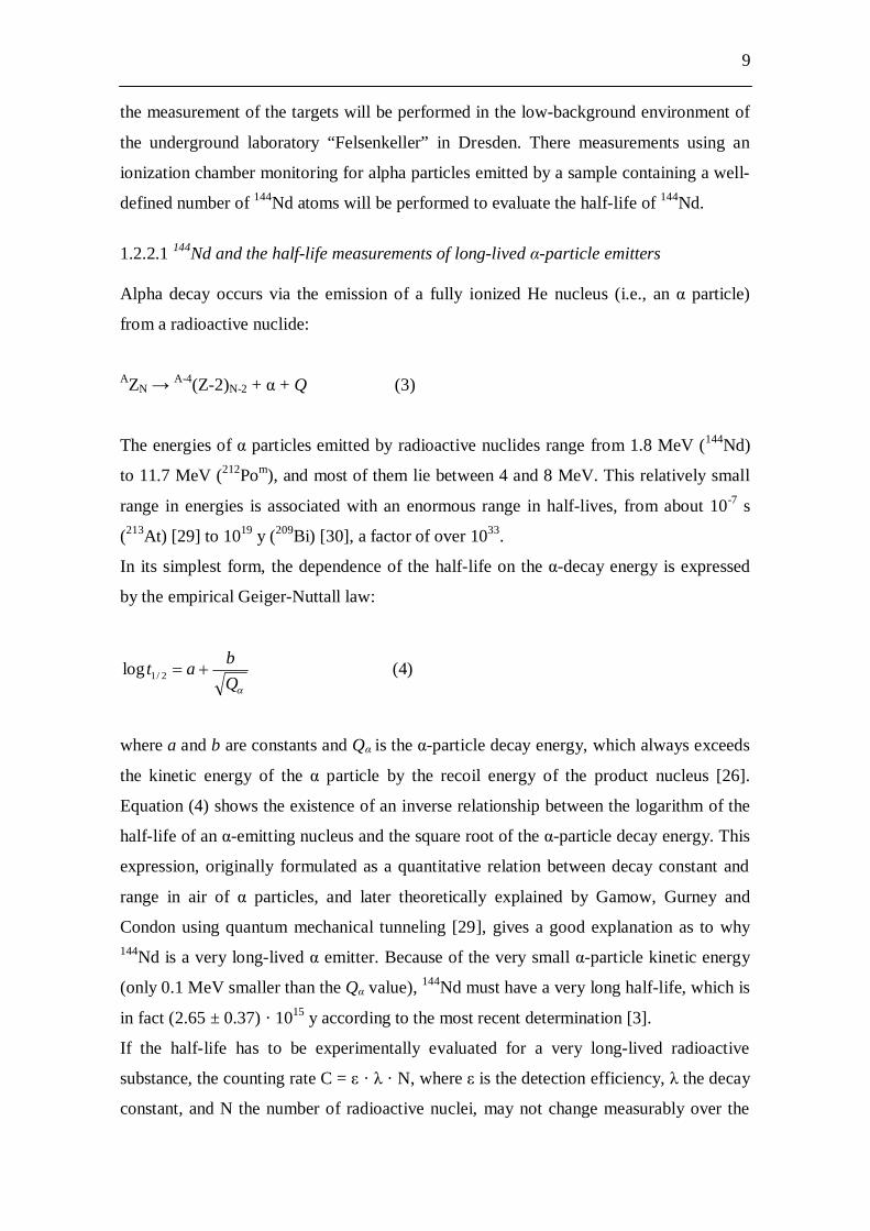
In case (1) the energy spectrum from the two electrons has similar features to that from
single- decay: a continuous spectrum ending at a well-defined end point determined
from the Q value of the reaction. In case (2) the summed energy of the two emitted
electrons is exactly equal to the Q value of the reaction [24]. The SNO+ experimental
concept is then to observe an isotope capable of decaying via double- decay and to
search for a peak at the end point of the spectrum [24]. Among the several candidate
isotopes to perform this experiment, 150Nd has been regarded as the most appropriate one
(Figure 1-2 [25]).
Figure 1-2 Simulated SNO+ energy spectrum for 150Nd. The double- decay dominates at low energies,
while the neutrinoless double- decay is present as a small peak at the high-energy end of the spectrum.
Further shown are expected backgrounds from solar pep neutrinos [26, see chapter 12], CNO neutrinos [26,
see chapter 12], and the natural decay chains (U, Th). No Nd-related background components are included
[25].
1.2 Targets for TRAKULA 1.2.1 Targets for fission cross-section measurements Both reliable predictions of the nuclear physical processes relevant to transmutation and
the optimization of the fast nuclear energy systems (i.e., fast reactors and ADS) depend
on the availability of accurate values of neutron-induced cross sections. While these cross
sections are well-known in the energy range of the thermal neutrons (En < 0.05 eV), in
the range of the fast neutrons (0.1 < En < 10 MeV) the inaccuracy is significant.
7
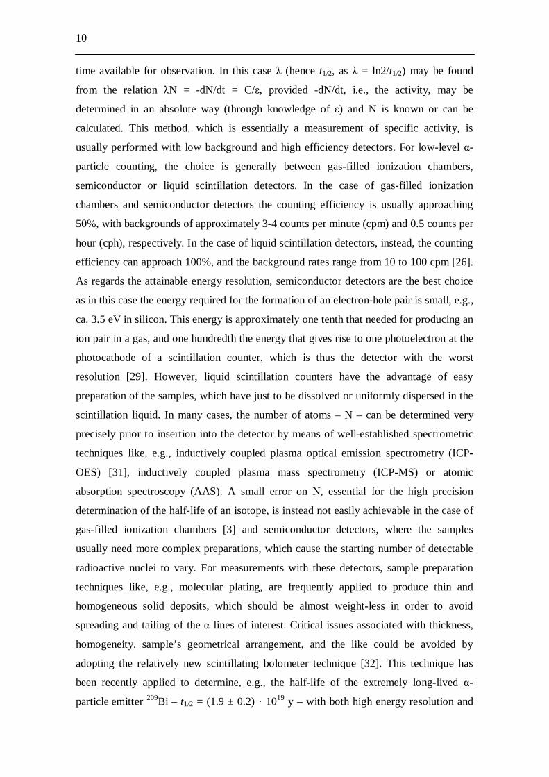
Recently, two major sources of the uncertainty impact have been identified [27]: (i)
uncertainties of the neutron-induced fission cross sections of Pu isotopes and MAs, and
(ii) uncertainties of the inelastic scattering cross sections of fast neutrons on structural
and cooling materials of the reactors (e.g., Fe, Pb, Na). Consequently, a set of the highest
priority target accuracies for fast reactors has been defined in order to improve the
existing databases (Table 1-2 [27]).
Table 1-2 Summary of the highest priority target accuracies for fast reactors (where SFR = sodium-cooled
fast reactor, GFR = gas-cooled fast reactor, LFR = lead-cooled fast reactor, ABTR = advanced breeder test
reactor, and EFR = European fast reactor) [27].
At HZDR the neutron-time-of-flight source nELBE produces neutrons by means of a
liquid lead radiator. The electron beam of the superconducting electron accelerator ELBE
hits the lead radiator creating intense bremsstrahlung, which generates neutrons in ( ,n)
reactions inside the lead [28]. As the kinetic energy of the released neutrons ranges from
few tens of keV to some MeV, nELBE is suitable for neutron-induced cross section
measurements relevant to transmutation research.

8
Within the frame of the TRAKULA project, large-area targets (i.e., ca. 40 cm2) of 235U, 238U, and 242Pu are needed to set up ionization chambers for fission cross section
measurements relevant to the development of fast reactors. 238U is feasible as test
material to develop fission chambers because of its relatively low specific activity. 235U,
whose fission cross section for both thermal and fast neutrons is very well known, can
instead be used as a standard to build reference ionization chambers. These chambers
will be built at both HZDR and PTB. At PTB measurements with reference neutron
fields will allow the determination of the density of the 235U targets. The knowledge of
this value will permit the calibration of the neutron beam intensity of the nELBE source
of HZDR. After calibration, the Pu targets will be used to set up a parallel-plate fission
chamber at HZDR for the neutron-induced fission cross section measurement of 242Pu,
which is an important isotope for transmutation research as shown in Table 1-2.
1.2.2 Targets for 144Nd half-life determination Even if neutrinoless double- decay is allowed, it occurs at only a small fraction of the
rate of two neutrino double- decay. One of the main challenges of the double- decay
searches, then, is to distinguish the small number of monoenergetic electron pairs
produced by neutrinoless double- decay from the large continuum of electron pairs
produced by two neutrino double- decay. In order to ensure that these signals can be
separated, good energy resolution and statistics are demanding. If on the one hand the
resolution achievable with a scintillator detector cannot be high, on the other hand the
amount of Nd isotope that can be suspended in the SNO+ scintillator is very large, this
assuring good statistics. Indeed, as the natural abundance of 150Nd is 5.6%, just 1%
natural Nd-loading in the 1000 t of the scintillator would correspond to 560 kg of this
isotope [25]. However, at the same time the 1% Nd-loading in the scintillator system
would also correspond to 2380 kg of 144Nd (natural abundance 23.8%) [25]. As 144Nd is a
long-lived emitter it may contribute to the background of the SNO+ experiment both
directly and via ( ,n) reactions, hence requiring a good understanding of the background
radiation produced from its decay. To infer its contribution to the background, the
activity produced by 144Nd has to be known, which requires a very precise knowledge of
the half-life (t1/2) of this isotope.
For this reason, TU Dresden, which is partner in the SNO+ collaboration, needs small-
area, i.e., ca. 9 cm2, 144Nd targets within the frame of the TRAKULA project. Because of
the long half-life (t1/2 ~ 2.7 · 1015 y [3]) and corresponding low specific activity of 144Nd,
9
the measurement of the targets will be performed in the low-background environment of
the underground laboratory “Felsenkeller” in Dresden. There measurements using an
ionization chamber monitoring for alpha particles emitted by a sample containing a well-
defined number of 144Nd atoms will be performed to evaluate the half-life of 144Nd.
1.2.2.1 144Nd and the half-life measurements of long-lived -particle emitters Alpha decay occurs via the emission of a fully ionized He nucleus (i.e., an particle)
from a radioactive nuclide:
AZN A-4(Z-2)N-2 + + Q (3)
The energies of particles emitted by radioactive nuclides range from 1.8 MeV (144Nd)
to 11.7 MeV (212Pom), and most of them lie between 4 and 8 MeV. This relatively small
range in energies is associated with an enormous range in half-lives, from about 10-7 s
(213At) [29] to 1019 y (209Bi) [30], a factor of over 1033.
In its simplest form, the dependence of the half-life on the -decay energy is expressed
by the empirical Geiger-Nuttall law:
Qbat 2/1log (4)
where a and b are constants and Q is the -particle decay energy, which always exceeds
the kinetic energy of the particle by the recoil energy of the product nucleus [26].
Equation (4) shows the existence of an inverse relationship between the logarithm of the
half-life of an -emitting nucleus and the square root of the -particle decay energy. This
expression, originally formulated as a quantitative relation between decay constant and
range in air of particles, and later theoretically explained by Gamow, Gurney and
Condon using quantum mechanical tunneling [29], gives a good explanation as to why 144Nd is a very long-lived emitter. Because of the very small -particle kinetic energy
(only 0.1 MeV smaller than the Q value), 144Nd must have a very long half-life, which is
in fact (2.65 ± 0.37) · 1015 y according to the most recent determination [3].
If the half-life has to be experimentally evaluated for a very long-lived radioactive
substance, the counting rate C = · · N, where is the detection efficiency, the decay
constant, and N the number of radioactive nuclei, may not change measurably over the
10
time available for observation. In this case (hence t1/2, as = ln2/t1/2) may be found
from the relation N = -dN/dt = C/ , provided -dN/dt, i.e., the activity, may be
determined in an absolute way (through knowledge of ) and N is known or can be
calculated. This method, which is essentially a measurement of specific activity, is
usually performed with low background and high efficiency detectors. For low-level -
particle counting, the choice is generally between gas-filled ionization chambers,
semiconductor or liquid scintillation detectors. In the case of gas-filled ionization
chambers and semiconductor detectors the counting efficiency is usually approaching
50%, with backgrounds of approximately 3-4 counts per minute (cpm) and 0.5 counts per
hour (cph), respectively. In the case of liquid scintillation detectors, instead, the counting
efficiency can approach 100%, and the background rates range from 10 to 100 cpm [26].
As regards the attainable energy resolution, semiconductor detectors are the best choice
as in this case the energy required for the formation of an electron-hole pair is small, e.g.,
ca. 3.5 eV in silicon. This energy is approximately one tenth that needed for producing an
ion pair in a gas, and one hundredth the energy that gives rise to one photoelectron at the
photocathode of a scintillation counter, which is thus the detector with the worst
resolution [29]. However, liquid scintillation counters have the advantage of easy
preparation of the samples, which have just to be dissolved or uniformly dispersed in the
scintillation liquid. In many cases, the number of atoms – N – can be determined very
precisely prior to insertion into the detector by means of well-established spectrometric
techniques like, e.g., inductively coupled plasma optical emission spectrometry (ICP-
OES) [31], inductively coupled plasma mass spectrometry (ICP-MS) or atomic
absorption spectroscopy (AAS). A small error on N, essential for the high precision
determination of the half-life of an isotope, is instead not easily achievable in the case of
gas-filled ionization chambers [3] and semiconductor detectors, where the samples
usually need more complex preparations, which cause the starting number of detectable
radioactive nuclei to vary. For measurements with these detectors, sample preparation
techniques like, e.g., molecular plating, are frequently applied to produce thin and
homogeneous solid deposits, which should be almost weight-less in order to avoid
spreading and tailing of the lines of interest. Critical issues associated with thickness,
homogeneity, sample’s geometrical arrangement, and the like could be avoided by
adopting the relatively new scintillating bolometer technique [32]. This technique has
been recently applied to determine, e.g., the half-life of the extremely long-lived -
particle emitter 209Bi – t1/2 = (1.9 ± 0.2) · 1019 y – with both high energy resolution and
11
high detection efficiency (100%) [30]. Unfortunately, the bolometer technique can be
applied only if a massive crystal containing the element of interest is made available by
specific production methods.
As regards the half-life determination of 144Nd, several have been the measurements
performed in the past using different detection techniques. Here, the most recent one
dates back to more than twenty-five years ago (Table 1-3).
Table 1-3 Literature values of the half-life of 144Nd and corresponding applied methods of detection.
Reference Year of publication Method Half-life (y) [33] 1954 Nuclear emulsion 1.5 · 1015 * [34] 1954 Nuclear emulsion 5 · 1015 * [35] 1956 Nuclear emulsion 2.2 · 1015 * [36] 1959 Liquid scintillation counter 2 · 1013 * [37] 1960 Ionization chamber 2.1 · 1015 * [2] 1961 Ionization chamber (2.4 ± 0.3) · 1015
[38] 1965 Ionization chamber (2.1 ± 0.4) · 1015 [3] 1987 Ionization chamber (2.65 ± 0.37) · 1015
* Error bar not reported in the original publication.
The analysis of the data listed in Table 1-3 clearly shows a significant spread among the
determined half-life values. Precision is therefore lacking. A new measurement of the 144Nd half-life is thus irrevocable to achieve the goals established within the SNO+
collaboration [20].
The use of an ionization chamber for the future determination of 144Nd activity is
consistent with the choices made in the last fifty years of measurements of this isotope.
Nonetheless, as stated above, this method of detection requires thin and uniform targets,
possibly weight-less, not easy to produce. The preparation of the targets plays then a
central role in the half-life evaluation of 144Nd.
1.3 Lanthanide and actinide elements Targets for TRAKULA consist of lanthanide and actinide elements. The chemistry of
these elements is briefly reviewed.
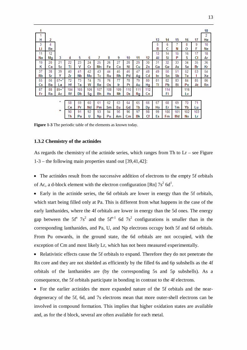
1.3.1 Chemistry of the lanthanides When analyzing the chemistry of the lanthanide series, which ranges from Ce to Lu – see
Figure 1-3 – the following main properties stand out [39-41]:
12
The lanthanides are characterized by the filling of the 4f orbitals after La, a d-block
element with the electron configuration [Xe] 6s2 5d1.
The 4f orbitals penetrate the Xe core appreciably. The 4f electrons are then “inside”
the 5s and 5p electrons of Xe and are core-like in their behaviour, being shielded from
the ligands, and thus taking no part in bonding.
As the series Ce-Lu is traversed, the 4f orbitals do not shield effectively the 5s and 5p
orbitals from the increasing nuclear charge, hence causing a smooth decrease in the
atomic radii with increasing Z, which is known as lanthanide contraction.
The elementhal lanthanides are highly electropositive and easily oxidized, primarily to
the +3 state, which is the characteristic state of all lanthanides both in solid compounds
and in solutions in water and other solvents. Additional oxidation states are the +4 states
in Ce4+ and Tb4+ because of the stabilizing effects of the noble gas configuration – [Xe] –
and of the half-filled configuration – [Xe] 4f7 – respectively. Also known are the +2
states in Eu2+ and Yb2+ because of half-filled – [Xe] 4f7 – and filled – [Xe] 4f14 –
configurations, respectively.
Because of the lanthanide contraction, the radii of the +3 ions are smoothly decreasing
while the coordination number, basicity, and ease of oxidation decrease along the series.
The lanthanide ions exhibit a very wide range of coordination numbers (generally 6-
12, but numbers of 2, 3 or 4 are also known).
Because of the large size, each lanthanide cation has minimized covalent interactions
with ligands and reduced electrostatic interactions. This brings to form labile ionic
complexes that undergo facile and rapid exchange of ligand (e.g., water). This situation
limits the number of isolable lanthanide complexes.
Both isolable and solution-stable lanthanide complexes are derived from ligands
containing oxygen donors.
The lanthanides are then quite unique among the elements of the periodic table (except
for the closely similar late actinides). They resemble each other so markedly both in the
elemental state and in compounds that changes in properties for a given oxidation state
with increasing atomic number are largely changes in degree rather than in kind.
All lanthanide elements but Pm are stable and occur in nature. Some natural lanthanides
consist of stable as well as primordial -decaying isotopes.
13
Figure 1-3 The periodic table of the elements as known today.
1.3.2 Chemistry of the actinides As regards the chemistry of the actinide series, which ranges from Th to Lr – see Figure
1-3 – the following main properties stand out [39,41,42]:
The actinides result from the successive addition of electrons to the empty 5f orbitals
of Ac, a d-block element with the electron configuration [Rn] 7s2 6d1.
Early in the actinide series, the 6d orbitals are lower in energy than the 5f orbitals,
which start being filled only at Pa. This is different from what happens in the case of the
early lanthanides, where the 4f orbitals are lower in energy than the 5d ones. The energy
gap between the 5fn 7s2 and the 5fn-1 6d 7s2 configurations is smaller than in the
corresponding lanthanides, and Pa, U, and Np electrons occupy both 5f and 6d orbitals.
From Pu onwards, in the ground state, the 6d orbitals are not occupied, with the
exception of Cm and most likely Lr, which has not been measured experimentally.
Relativistic effects cause the 5f orbitals to expand. Therefore they do not penetrate the
Rn core and they are not shielded as efficiently by the filled 6s and 6p subshells as the 4f
orbitals of the lanthanides are (by the corresponding 5s and 5p subshells). As a
consequence, the 5f orbitals participate in bonding in contrast to the 4f electrons.
For the earlier actinides the more expanded nature of the 5f orbitals and the near-
degeneracy of the 5f, 6d, and 7s electrons mean that more outer-shell electrons can be
involved in compound formation. This implies that higher oxidation states are available
and, as for the d block, several are often available for each metal.
14
As the actinide series is traversed and the atomic number increases, the 5f electrons do
not shield each other from the increasing nuclear charge effectively, hence causing a
rapid drop of both energies and dimensions (i.e., actinide contraction) of the 5f orbitals.
As a consequence, the electronic structure and the ions of the later actinides from Am
onwards become like those of the lanthanides, whose chemistry they thus resemble.
For the elements Th, Pa, and U the most stable oxidation states are the highest
possible states, i.e., +4, +5, and +6, respectively, which correspond to the noble gas
configuration [Rn]. For the elements Np, Pu, and Am the highest oxidation states are +7,
+7, and +6, respectively, but the most stable states are +5, +4, and +3, respectively. From
Am to Lr the most stable oxidation state becomes +3, with the exception of No where
also the +2 state appears to be extremely stable because of the stabilizing effects of the
filled – [Rn] 5f14 – configuration.
In compounds of the +2, +3, and +4 oxidation states, the metals – M – are usually
present as the simple M2+, M3+, and M4+ cations or as species derived from these ions.
For the higher oxidation states the most common species from U onwards, both in solid
compounds and in aqueous solution, are those formed with anions such as F- or O2-.
The chemistry of the early actinides therefore is quite different from that of the
lanthanides, whereas the late actinides resemble the lanthanides quite well.
All actinide elements are radioactive. Only Th, U, and trace amounts of Np and Pu in U
ores – formed in interaction of neutrons with 238U [43] – occur in nature. All the other
actinides have half-lives short compared to the age of the earth and thus, if formed in
primordial nucleosynthesis, they have decayed.
1.4 Target preparation 1.4.1 General target requirements and main production techniques Lanthanide and actinide layers to be used as nuclear targets should be thin,
homogeneous, chemically/radiochemically pure, crack-free, and structurally rigid (i.e.,
with a good adherence to the deposition substrate). Moreover, due to the scarcity of most
of the used isotopes and – in some cases – their high specific activity, the applied
preparation methods should give high deposition yields and should be rather simple in
order to allow handling in glove-boxes without too much expense. Finally, an easy and
complete recovery of the target material should be possible especially if exotic isotopes
are used [44].
15
All of these requirements are valid for both targets to be used as radioactive sources for,
e.g., nuclear spectroscopy investigations and targets to be applied in accelerator
experiments. Thickness and homogeneity are important in targets to be used for, e.g.,
activity measurements in order to reduce scattering and absorption of radiations (i.e.,
back-scattering, self-scattering, and self-absorption) in the sample and in its support. At
the same time, targets to be used in accelerator experiments need to be thin and uniform
to allow various charged particles to pass through the deposit without undue energy loss.
Chemical and radiochemical purities are of course important as interfering radioactive
background has always to be avoided. As regards the cracking of the layers, this usually
gains more attention in the case of irradiation experiments as cracks and other aberrations
in the target result in an increased tendency to break under the thermal stress of the beam
[45]. This can lead to material flaking off the target backing, resulting in dead spots on
the target face, the wasting of isotopically pure materials and contamination of the
experimental area [45]. Further, the target and its backing experience an increase in
temperature due to irradiation, which results in warping and often breaking of the
deposited layer [46]. Therefore structural rigidity of the produced targets is another
fundamental requirement.
Among the large variety of methods available for target preparation conventional ones
include: cold rolling [47], vacuum evaporation [48], molecular plating [49],
painting/sedimentation [50], electrodeposition [51], die compaction [52], and more
recently polymer-assisted deposition [53]. Each method has advantages and
disadvantages with regard to the general target requirements.
1.4.2 Molecular plating Molecular plating is one of the most widely applied target production methods for
radioactive isotopes or isotopically enriched material. This technique is based on the
electrodeposition of an element either in the constant current or in the constant voltage
mode. It uses two-electrode cells (i.e., cathode and anode) where very small volumes
(i.e., tens to hundreds of microliters) of an acqueous solution of the element of interest
are inserted and mixed with an organic solvent.
MP was first introduced by Parker and Falk [54] in 1962 as an alternative to
electrodeposition from acqueous solutions. The original article introduced the new
method as follows:
16
“The most significant difference between the method to be described and ordinary
electrodeposition is that electrolytic dissociation does not occur to any comparable
degree during the passage of current. Also, in the present instance, the same chemical
compound, chloride or nitrate as the case may be, is deposited at the cathode as that
originally dissolved in the electrolyte. Thus we have coined the name “molecular
plating” for this particular method. Other differences are the use of high voltages (50-
2000 V) and the use of an organic solution” [54].
Less than ten years after its introduction, MP had already made a name for itself by
producing a very wide range of targets: targets of nuclides employed as reference
samples for the calibration of detection systems, e.g., 137Cs, 60Co [55], targets of
lanthanides [56], and targets of actinides [57-59]. All the targets produced by MP were
characterized by common properties: quantitative deposition yields, thinness,
homogeneity, and structural rigidity of the produced layers. Moreover, the technique
stood for its simplicity. In particular, the comparison with ordinary electrodeposition
from acqueous solutions showed that despite quantitative deposition yields attainable
with both techniques, MP did not require high current densities (mA/cm2 instead of
A/cm2), thus avoiding disruption of the layer deposit (or the substrate) by means of
hydrogen evolution at the cathode [60].
All these positive features have led MP to become one of the most successfully applied
methods for the production of targets to be used in nuclear research fields like, e.g.,
nuclear spectroscopy [3], nuclear reaction studies [4], and also in the research on the
physics and chemistry of the superheavy elements [6,7]. Despite this, little has been the
development of the technique over time in terms of both characterization of the produced
layers and knowledge of the electrochemical processes underlying plating – the only
noteworthy result being that the element of interest is usually not deposited as the
original chemical compound [61,62]. Definitely, one of the main disadvantages of
working with two-electrode cells without reference electrode is that the working potential
of the electrode of interest – usually the cathode – is not known, this implying no
information about the processes taking place at that electrode. Moreover, the study of the
electrochemistry in non-aqueous solutions has a more recent history than that in aqueous
solutions, this being additionally complicated by the unique chemistry of the elements
usually involved in target preparation, i.e., lanthanides and actinides, some of which are
also poorly available and highly radioactive. All this has caused work to focus mainly on
17
gaining empirical evidence on how to further improve the properties of the produced
layers [63].
This situation has recently led Garcia et al. [53] and Ali et al. [46] to doubt the suitability
of MP especially for the production of targets to be used with the high intensity beams of
future generation accelerators. In the last years there has in fact been a push for higher-
intensity (i.e., a tenfold intensity increase) beams to further study nuclear structure,
nuclear reactions and nuclear astrophysics [see, e.g., 64-66]. A current question in the
nuclear target production and application community is then the following: is MP still the
ideal technique for target preparation? One of the aims of the present thesis is to give an
answer to this question.
1.5 Target characterization techniques Several analytical techniques were used to characterize the targets produced by molecular
plating. They are: neutron activation analysis (NAA), -ray spectroscopy, radiographic
imaging (RI), scanning electron microscopy (SEM), atomic force microscopy (AFM),
and X-ray photoelectron spectroscopy (XPS). In this section the main theoretical and
technical aspects of the different techniques are described in order to allow a full
understanding of the experiments described in the following chapters. For clarity, NAA
and -ray spectroscopy are discussed together as their use was always interdependent.
Alpha-particle spectroscopy was also used, but not as a target characterization technique.
Therefore, general information on spectroscopy is not reported here, but can be found
in Section 1.2.2.1 and later in Chapter 6.
1.5.1 Neutron activation analysis and -ray spectroscopy The activation analyses are a set of elemental analytical techniques characterized by high
sensitivity, selectivity, accuracy and precision. Their main drawback is the lack of
speciation information, i.e., no information about the chemical form of the element, any
attached ligands, and the like is obtained [67]. These analyses allow determining the
amount of a given element contained in some material by means of nuclear reactions
[26]. Neutrons are the predominant activation particles and nuclear reactors are
frequently used for activation analysis as intense sources of such particles. In many
reactors of the so-called swimming pool type, e.g., the TRIGA research reactors (Figure
1-4a), the neutrons are generated inside the reactor core, which is situated at the bottom
of a water tank. The neutron spectra of nuclear reactors have always shapes similar to
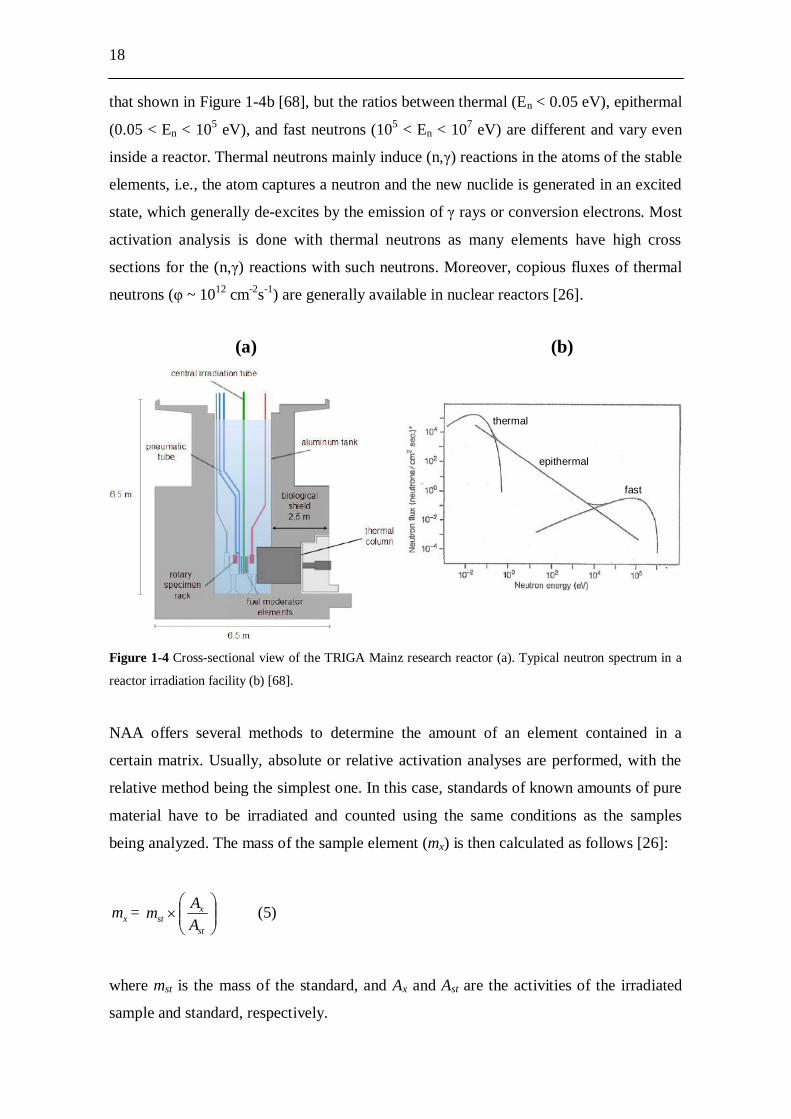
18
that shown in Figure 1-4b [68], but the ratios between thermal (En < 0.05 eV), epithermal
(0.05 < En < 105 eV), and fast neutrons (105 < En < 107 eV) are different and vary even
inside a reactor. Thermal neutrons mainly induce (n, ) reactions in the atoms of the stable
elements, i.e., the atom captures a neutron and the new nuclide is generated in an excited
state, which generally de-excites by the emission of rays or conversion electrons. Most
activation analysis is done with thermal neutrons as many elements have high cross
sections for the (n, ) reactions with such neutrons. Moreover, copious fluxes of thermal
neutrons ( ~ 1012 cm-2s-1) are generally available in nuclear reactors [26].
Figure 1-4 Cross-sectional view of the TRIGA Mainz research reactor (a). Typical neutron spectrum in a
reactor irradiation facility (b) [68].
NAA offers several methods to determine the amount of an element contained in a
certain matrix. Usually, absolute or relative activation analyses are performed, with the
relative method being the simplest one. In this case, standards of known amounts of pure
material have to be irradiated and counted using the same conditions as the samples
being analyzed. The mass of the sample element (mx) is then calculated as follows [26]:
xm = st
xst A
Am (5)
where mst is the mass of the standard, and Ax and Ast are the activities of the irradiated
sample and standard, respectively.
(a) (b)
thermal
epithermal
fast
19
The first step of a relative activation analysis is the preparation of the standard and the
sample, which should have the same size, geometry, composition and homogeneity to
ensure that any attenuation of the incoming radiation, or the sample radiation before
counting, or any count rate-dependent effects, are exactly the same. The cross section of
the (n, ) reaction, the isotopic abundancy of the target nucleus, and the half-life of the
formed isotope should be large enough to allow measurement of the emitted radiation.
The irradiation conditions involve the determination of the flux and irradiation duration.
The activation analyses performed in the framework of the present thesis always adopted
the relative method and used the rotary specimen rack (see Figure 1-4a) as irradiation
position inside the reactor, where a thermal neutron flux of 7 · 1011 cm-2s-1 was delivered.
The samples were liquid solutions contained in sealed polyethylene test-tubes, which
were used because of their purity, low cross section for thermal neutrons, little or no
long-lived activity by activation, and resistance to radiation [67]. The isolation of the
activity of interest and its counting were always performed without any previous
radiochemical treatment. Indeed, a high-purity Ge (HPGe) detector was used to identify
the radionuclides in the radioactive sample from the characteristic energies of their
delayed rays, and the measurement of the corresponding activities could thus be
performed.
The HPGe detector is a PIN diode detector where the n-type region is prepared by Li
diffusion without drifting and the p-type region is prepared by implanting B ions. The
absence of Li drifting allows this detector to be stored at room temperature, and to be
cooled only when in use [69]. HPGe detectors are therefore normally housed in vacuum-
tight cryostats, which are mounted on liquid nitrogen dewars. To reduce natural
background, most -ray detectors are operated within a shielded enclosure. A -ray
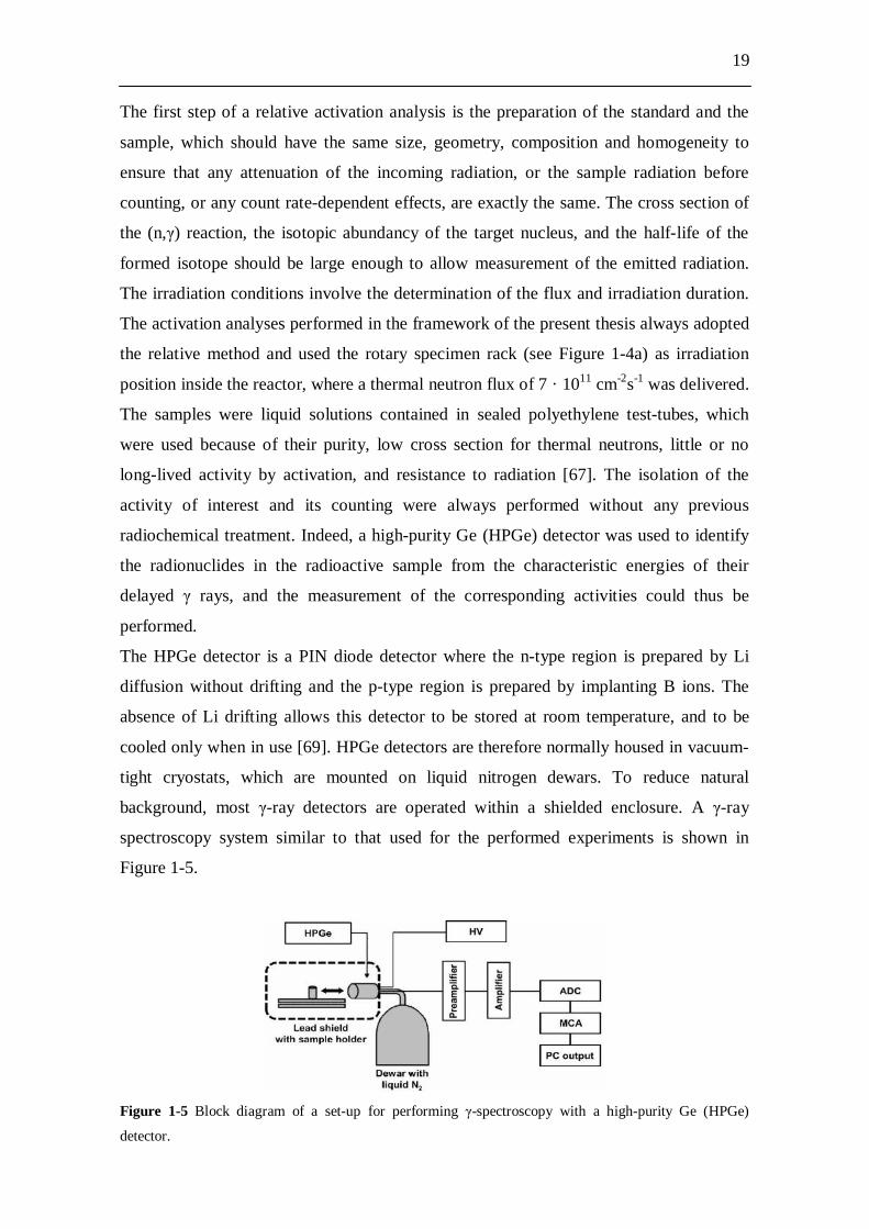
spectroscopy system similar to that used for the performed experiments is shown in
Figure 1-5.
Figure 1-5 Block diagram of a set-up for performing -spectroscopy with a high-purity Ge (HPGe)
detector.
20
The sample is always placed at a certain distance from the HPGe detector, which is
connected to a high-voltage (HV) power supply. The initial signal is very small and the
preamplifier, attached directly to the detector, amplifies this signal. The signal is shaped
by the spectroscopy amplifier and then converted from analog to digital by the analog-to-
digital converter (ADC). The results are stored in digital form in the multi-channel
analyzer (MCA). The output of the analysis is a plot of signal intensity (i.e., number of
counts per channel) vs channel number, which can be readily converted into signal
intensity vs -ray energy after calibration of the detector.
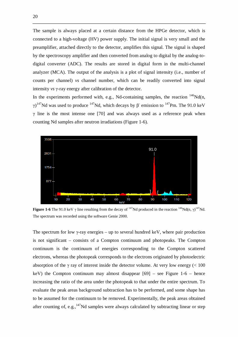
In the experiments performed with, e.g., Nd-containing samples, the reaction 146Nd(n,
)147Nd was used to produce 147Nd, which decays by - emission to 147Pm. The 91.0 keV
line is the most intense one [70] and was always used as a reference peak when
counting Nd samples after neutron irradiations (Figure 1-6).
Figure 1-6 The 91.0 keV line resulting from the decay of 147Nd produced in the reaction 146Nd(n, )147Nd.
The spectrum was recorded using the software Genie 2000.
The spectrum for low -ray energies – up to several hundred keV, where pair production
is not significant – consists of a Compton continuum and photopeaks. The Compton
continuum is the continuum of energies corresponding to the Compton scattered
electrons, whereas the photopeak corresponds to the electrons originated by photoelectric
absorption of the ray of interest inside the detector volume. At very low energy (< 100
keV) the Compton continuum may almost disappear [69] – see Figure 1-6 – hence
increasing the ratio of the area under the photopeak to that under the entire spectrum. To
evaluate the peak areas background subtraction has to be performed, and some shape has
to be assumed for the continuum to be removed. Experimentally, the peak areas obtained
after counting of, e.g.,147Nd samples were always calculated by subtracting linear or step
91.0

21
continuum backgrounds (see [71] for details on peak area calculations). According to (5),
these areas were then used to evaluate the amount of the element of interest and hence
the deposition yields obtained after the perfomed MP experiments.
1.5.2 Radiographic imaging Radiographic imaging is based on the effect of photostimulated luminescence (PSL) and
the use of an imaging plate (IP), which is a two-dimensional detector of ionizing
radiation utilizing a photostimulable phosphor [72]. Powdery materials capable of
emitting light when stimulated by, e.g., electromagnetic radiation, are commonly referred
to as phosphors. Photostimulated luminescence involves a phosphor, commonly a
BaFX:Eu2+ (X = Cl, Br, or I) ionic crystal. The crystal is doped with a trace amount of
Eu2+, which acts as luminescence center by replacing Ba to create a solid solution. When
BaFX:Eu2+ is irradiated with ionizing radiation, e.g., rays, Eu2+ centers become Eu3+
and electron-hole pairs are produced, the number of which is proportional to the absorbed
radiation energy. These pairs create quasi-stable F-centers, which can be of two types:
F(F-) and F(X-) [73]. An F-center, or color center, consists of an electron occupying a
halogen ion vacancy. The F-centers and corresponding hole traps can thus store energy of
absorbed ionizing radiation. The mechanism of the release of this absorbed energy is
mainly interpreted according to the theory from Takahashi et al. [72,73], which can be
explained as follows: once the F-centers have been formed, the irradiation with a lower-
frequency light source, e.g. red light, than that used to create the Eu3+ ions raises the
trapped electrons to their excited states, where they are thermally excited to the
conduction band. At this point, the electrons recombine with holes trapped by Eu2+ ions,
producing an excited Eu2+ ion, which de-excites by emitting light corresponding to the
5d-4f transitions. The light intensity is proportional to the number of trapped electrons,
and thus to the absorbed radiation energy. Using two-dimensional position sensitive
imaging plates, RI can be applied to investigate the distribution of, e.g., radioactive
material on a sample surface. In this work, the surface homogeneity of radioactive targets
produced by MP using -emitting tracers, e.g., 147Nd, was analyzed by RI. The spatial
resolution of the technique was < 200 m [74]. Experimentally, the RI analyses were
carried out as follows: a flexible IP, in which bunches of 5- m large crystals of
BaFBr:Eu2+ were uniformly coated on a polyester support film, was exposed for a
definite amount of time to the radiation emitted from the produced target. The exposed
IP was then scanned with a laser beam of red light while being conveyed with high
22
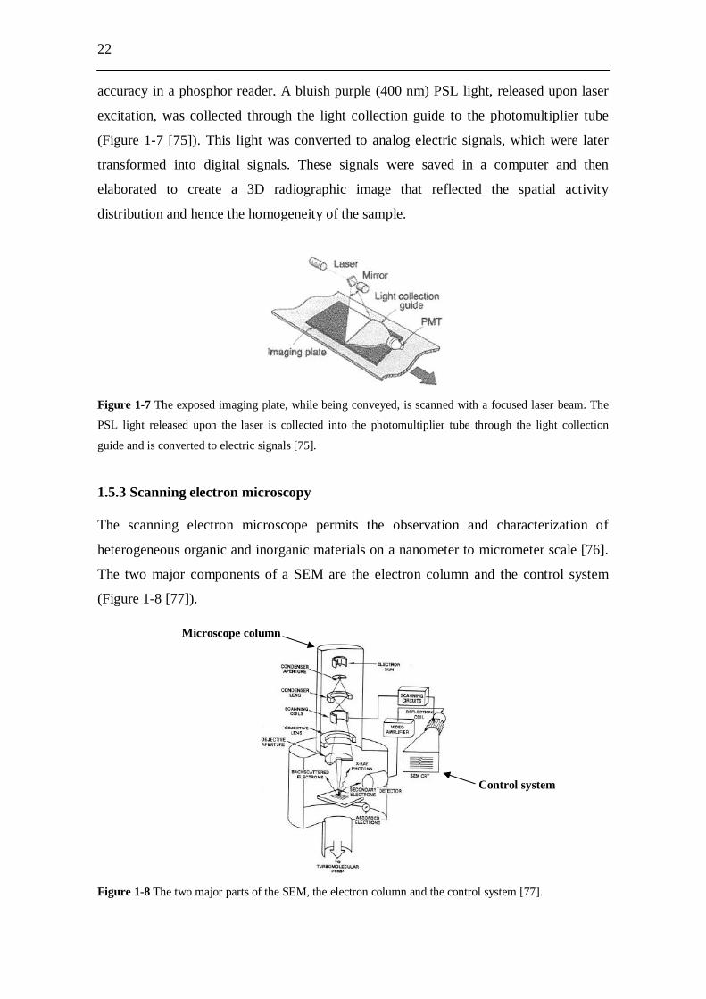
accuracy in a phosphor reader. A bluish purple (400 nm) PSL light, released upon laser
excitation, was collected through the light collection guide to the photomultiplier tube
(Figure 1-7 [75]). This light was converted to analog electric signals, which were later
transformed into digital signals. These signals were saved in a computer and then
elaborated to create a 3D radiographic image that reflected the spatial activity
distribution and hence the homogeneity of the sample.
Figure 1-7 The exposed imaging plate, while being conveyed, is scanned with a focused laser beam. The
PSL light released upon the laser is collected into the photomultiplier tube through the light collection
guide and is converted to electric signals [75].
1.5.3 Scanning electron microscopy The scanning electron microscope permits the observation and characterization of
heterogeneous organic and inorganic materials on a nanometer to micrometer scale [76].
The two major components of a SEM are the electron column and the control system
(Figure 1-8 [77]).
Figure 1-8 The two major parts of the SEM, the electron column and the control system [77].
Microscope column
Control system
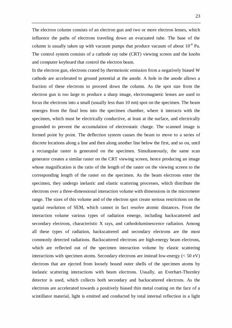
23
The electron column consists of an electron gun and two or more electron lenses, which
influence the paths of electrons traveling down an evacuated tube. The base of the
column is usually taken up with vacuum pumps that produce vacuum of about 10-4 Pa.
The control system consists of a cathode ray tube (CRT) viewing screen and the knobs
and computer keyboard that control the electron beam.
In the electron gun, electrons crated by thermoionic emission from a negatively biased W
cathode are accelerated to ground potential at the anode. A hole in the anode allows a
fraction of these electrons to proceed down the column. As the spot size from the
electron gun is too large to produce a sharp image, electromagnetic lenses are used to
focus the electrons into a small (usually less than 10 nm) spot on the specimen. The beam
emerges from the final lens into the specimen chamber, where it interacts with the
specimen, which must be electrically conductive, at least at the surface, and electrically
grounded to prevent the accumulation of electrostatic charge. The scanned image is
formed point by point. The deflection system causes the beam to move to a series of
discrete locations along a line and then along another line below the first, and so on, until
a rectangular raster is generated on the specimen. Simultaneously, the same scan
generator creates a similar raster on the CRT viewing screen, hence producing an image
whose magnification is the ratio of the length of the raster on the viewing screen to the
corresponding length of the raster on the specimen. As the beam electrons enter the
specimen, they undergo inelastic and elastic scattering processes, which distribute the
electrons over a three-dimensional interaction volume with dimensions in the micrometer
range. The sizes of this volume and of the electron spot create serious restrictions on the
spatial resolution of SEM, which cannot in fact resolve atomic distances. From the
interaction volume various types of radiation emerge, including backscattered and
secondary electrons, characteristic X rays, and cathodoluminescence radiation. Among
all these types of radiation, backscattered and secondary electrons are the most
commonly detected radiations. Backscattered electrons are high-energy beam electrons,
which are reflected out of the specimen interaction volume by elastic scattering
interactions with specimen atoms. Secondary electrons are instead low-energy (< 50 eV)
electrons that are ejected from loosely bound outer shells of the specimen atoms by
inelastic scattering interactions with beam electrons. Usually, an Everhart-Thornley
detector is used, which collects both secondary and backscattered electrons. As the
electrons are accelerated towards a positively biased thin metal coating on the face of a
scintillator material, light is emitted and conducted by total internal reflection in a light
24
guide to a photomultiplier, where photons are converted back into electrons and
multiplied. The amplified electrical signal is first subjected to analog-to-digital
conversion and then displayed and saved as a digital image. Backscattered and secondary
electrons are the principal signals used to form images in scanning electron microscopy,
because they are capable of carrying information about the specimen in terms of image
contrast, which arises when the signal collected from the beam-specimen interaction
varies from one location to another. The most frequent application of the SEM is the
visualization of the topography of three-dimensional objects. Topographic contrast
includes all those effects by which the morphology of the specimen can be imaged. This
contrast arises because the number of the detected secondary and backscattered electrons
depends on the angle of incidence between the beam and the specimen surface, which
varies only according to the local inclination of the specimen. As the angle of incidence
increases, the escape distance of one side of the beam will decrease, and more electrons
will be emitted. Thus steep surfaces and edges tend to be brighter than flat surfaces,
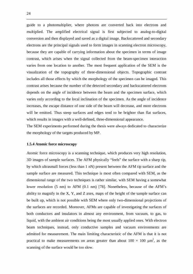
which results in images with a well-defined, three-dimensional appearance.
The SEM experiments performed during the thesis were always dedicated to characterize
the morphology of the targets produced by MP.
1.5.4 Atomic force microscopy Atomic force microscopy is a scanning technique, which produces very high resolution,
3D images of sample surfaces. The AFM physically “feels” the surface with a sharp tip,
by which ultrasmall forces (less than 1 nN) present between the AFM tip surface and the
sample surface are measured. This technique is most often compared with SEM, as the
dimensional range of the two techniques is rather similar, with SEM having a somewhat
lower resolution (5 nm) to AFM (0.1 nm) [78]. Nonetheless, because of the AFM’s
ability to magnify in the X, Y, and Z axes, maps of the height of the sample surface can
be built up, which is not possible with SEM where only two-dimensional projections of
the surfaces are recorded. Moreover, AFMs are capable of investigating the surfaces of
both conductors and insulators in almost any environment, from vacuum, to gas, to
liquid, with the ambient air conditions being the most usually applied ones. With electron
beam techniques, instead, only conductive samples and vacuum environments are
admitted for measurement. The main limiting characteristic of the AFM is that it is not
practical to make measurements on areas greater than about 100 × 100 m2, as the
scanning of the surface would be too slow.
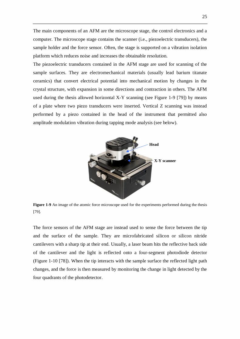
25
The main components of an AFM are the microscope stage, the control electronics and a
computer. The microscope stage contains the scanner (i.e., piezoelectric transducers), the
sample holder and the force sensor. Often, the stage is supported on a vibration isolation
platform which reduces noise and increases the obtainable resolution.
The piezoelectric transducers contained in the AFM stage are used for scanning of the
sample surfaces. They are electromechanical materials (usually lead barium titanate
ceramics) that convert electrical potential into mechanical motion by changes in the
crystal structure, with expansion in some directions and contraction in others. The AFM
used during the thesis allowed horizontal X-Y scanning (see Figure 1-9 [79]) by means
of a plate where two piezo transducers were inserted. Vertical Z scanning was instead
performed by a piezo contained in the head of the instrument that permitted also
amplitude modulation vibration during tapping mode analysis (see below).
Figure 1-9 An image of the atomic force microscope used for the experiments performed during the thesis
[79].
The force sensors of the AFM stage are instead used to sense the force between the tip
and the surface of the sample. They are microfabricated silicon or silicon nitride
cantilevers with a sharp tip at their end. Usually, a laser beam hits the reflective back side
of the cantilever and the light is reflected onto a four-segment photodiode detector
(Figure 1-10 [78]). When the tip interacts with the sample surface the reflected light path
changes, and the force is then measured by monitoring the change in light detected by the
four quadrants of the photodetector.
X-Y scanner
Head
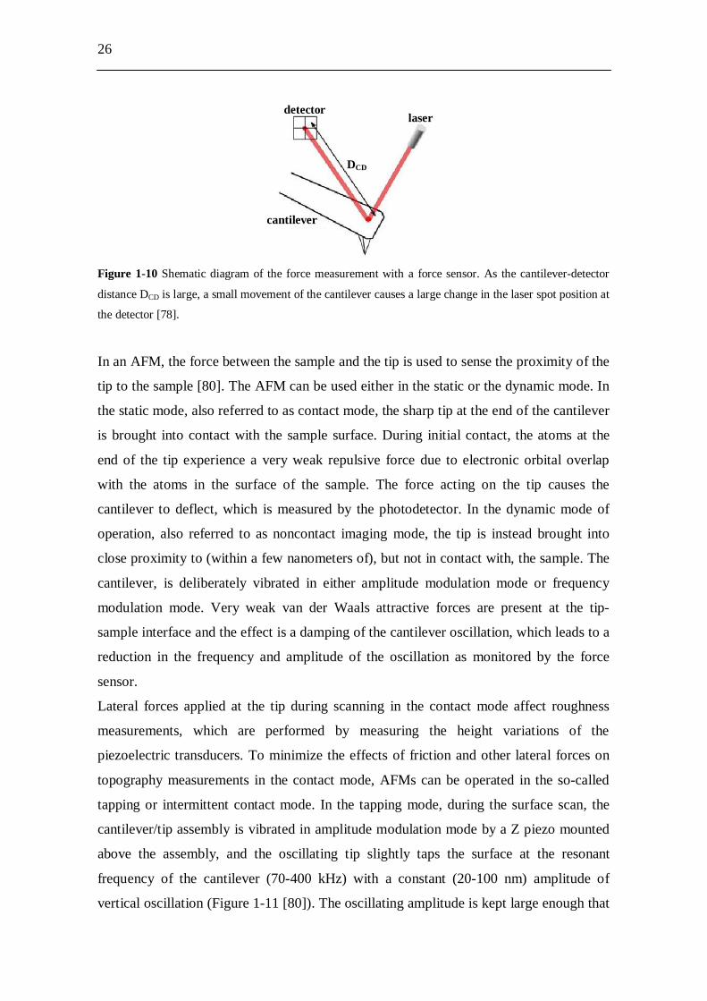
26
Figure 1-10 Shematic diagram of the force measurement with a force sensor. As the cantilever-detector
distance DCD is large, a small movement of the cantilever causes a large change in the laser spot position at
the detector [78].
In an AFM, the force between the sample and the tip is used to sense the proximity of the
tip to the sample [80]. The AFM can be used either in the static or the dynamic mode. In
the static mode, also referred to as contact mode, the sharp tip at the end of the cantilever
is brought into contact with the sample surface. During initial contact, the atoms at the
end of the tip experience a very weak repulsive force due to electronic orbital overlap
with the atoms in the surface of the sample. The force acting on the tip causes the
cantilever to deflect, which is measured by the photodetector. In the dynamic mode of
operation, also referred to as noncontact imaging mode, the tip is instead brought into
close proximity to (within a few nanometers of), but not in contact with, the sample. The
cantilever, is deliberately vibrated in either amplitude modulation mode or frequency
modulation mode. Very weak van der Waals attractive forces are present at the tip-
sample interface and the effect is a damping of the cantilever oscillation, which leads to a
reduction in the frequency and amplitude of the oscillation as monitored by the force
sensor.
Lateral forces applied at the tip during scanning in the contact mode affect roughness
measurements, which are performed by measuring the height variations of the
piezoelectric transducers. To minimize the effects of friction and other lateral forces on
topography measurements in the contact mode, AFMs can be operated in the so-called
tapping or intermittent contact mode. In the tapping mode, during the surface scan, the
cantilever/tip assembly is vibrated in amplitude modulation mode by a Z piezo mounted
above the assembly, and the oscillating tip slightly taps the surface at the resonant
frequency of the cantilever (70-400 kHz) with a constant (20-100 nm) amplitude of
vertical oscillation (Figure 1-11 [80]). The oscillating amplitude is kept large enough that
detector laser
cantilever
DCD
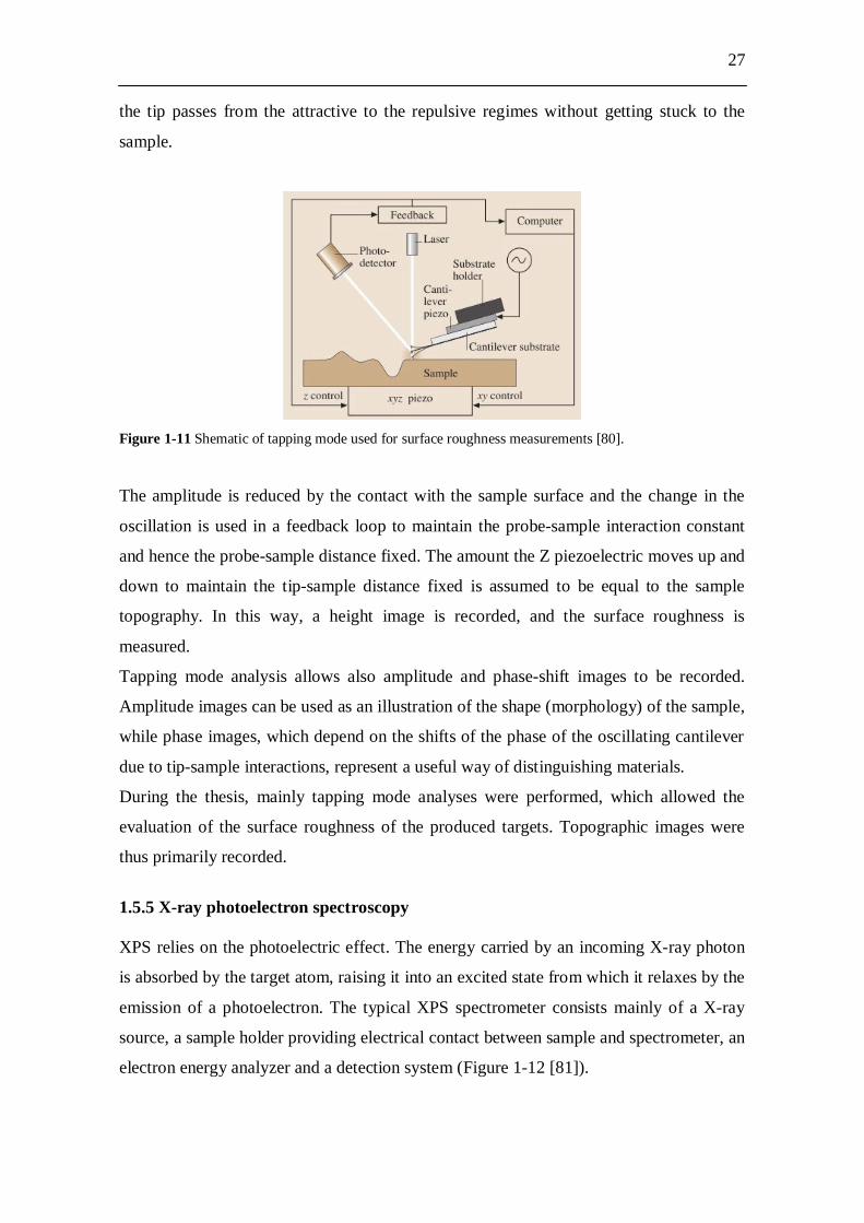
27
the tip passes from the attractive to the repulsive regimes without getting stuck to the
sample.
Figure 1-11 Shematic of tapping mode used for surface roughness measurements [80].
The amplitude is reduced by the contact with the sample surface and the change in the
oscillation is used in a feedback loop to maintain the probe-sample interaction constant
and hence the probe-sample distance fixed. The amount the Z piezoelectric moves up and
down to maintain the tip-sample distance fixed is assumed to be equal to the sample
topography. In this way, a height image is recorded, and the surface roughness is
measured.
Tapping mode analysis allows also amplitude and phase-shift images to be recorded.
Amplitude images can be used as an illustration of the shape (morphology) of the sample,
while phase images, which depend on the shifts of the phase of the oscillating cantilever
due to tip-sample interactions, represent a useful way of distinguishing materials.
During the thesis, mainly tapping mode analyses were performed, which allowed the
evaluation of the surface roughness of the produced targets. Topographic images were
thus primarily recorded.
1.5.5 X-ray photoelectron spectroscopy XPS relies on the photoelectric effect. The energy carried by an incoming X-ray photon
is absorbed by the target atom, raising it into an excited state from which it relaxes by the
emission of a photoelectron. The typical XPS spectrometer consists mainly of a X-ray
source, a sample holder providing electrical contact between sample and spectrometer, an
electron energy analyzer and a detection system (Figure 1-12 [81]).

28
Figure 1-12 Schematic representation of the main components of a XPS spectrometer [81].
In order to avoid any possible interference during the analysis, the spectrometer is always
operated in ultra-high vacuum (UHV) conditions, i.e., with pressures around 10-6 Pa. In
the X-ray source thermoionic electrons emitted from a W filament are accelerated and
focused onto water-cooled Mg or Al anodes [82]. The twin-anode design enables to
distinguish photoelectron and Auger lines present in the spectra. The impact of the high
energy electrons causes the emission of K X-rays of characteristic energies: 1253.6 eV
for Mg and 1486.6 eV for Al. Other contributions to the X-ray spectrum are due to
double ionization phenomena, transitions from the valence band, and bremsstrahlung
background. All these contributions lead to “satellite” peaks in the spectra by means of
induced photoemission. The peaks are removed by the use of a monochromator, which
helps also to enhance the resolution of the analysis by focusing and monochromatizing
the K X-rays.
Once the K X-rays hit the surface of the sample, photoelectrons are emitted from all
energy levels (i.e., core and valence levels) of the target atom (Figure 1-13a [81]). As
energy is conserved, the following relationship is valid for the emitted photoelectron:
K.E. = h – B.E. – sample (6)
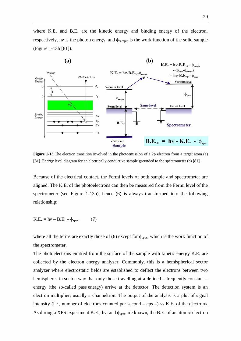
29
where K.E. and B.E. are the kinetic energy and binding energy of the electron,
respectively, h is the photon energy, and sample is the work function of the solid sample
(Figure 1-13b [81]).
Figure 1-13 The electron transition involved in the photoemission of a 2p electron from a target atom (a)
[81]. Energy level diagram for an electrically conductive sample grounded to the spectrometer (b) [81].
Because of the electrical contact, the Fermi levels of both sample and spectrometer are
aligned. The K.E. of the photoelectrons can then be measured from the Fermi level of the
spectrometer (see Figure 1-13b), hence (6) is always transformed into the following
relationship:
K.E. = h – B.E. – spec (7)
where all the terms are exactly those of (6) except for spec, which is the work function of
the spectrometer.
The photoelectrons emitted from the surface of the sample with kinetic energy K.E. are
collected by the electron energy analyzer. Commonly, this is a hemispherical sector
analyzer where electrostatic fields are established to deflect the electrons between two
hemispheres in such a way that only those travelling at a defined – frequently constant –
energy (the so-called pass energy) arrive at the detector. The detection system is an
electron multiplier, usually a channeltron. The output of the analysis is a plot of signal
intensity (i.e., number of electrons counted per second – cps –) vs K.E. of the electrons.
As during a XPS experiment K.E., h , and spec are known, the B.E. of an atomic electron
(a) (b)
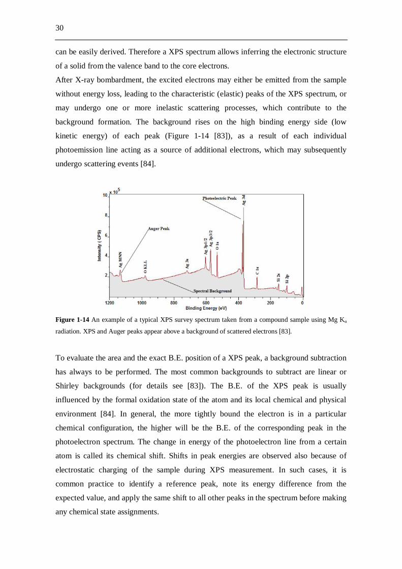
30
can be easily derived. Therefore a XPS spectrum allows inferring the electronic structure
of a solid from the valence band to the core electrons.
After X-ray bombardment, the excited electrons may either be emitted from the sample
without energy loss, leading to the characteristic (elastic) peaks of the XPS spectrum, or
may undergo one or more inelastic scattering processes, which contribute to the
background formation. The background rises on the high binding energy side (low
kinetic energy) of each peak (Figure 1-14 [83]), as a result of each individual
photoemission line acting as a source of additional electrons, which may subsequently
undergo scattering events [84].
Figure 1-14 An example of a typical XPS survey spectrum taken from a compound sample using Mg K
radiation. XPS and Auger peaks appear above a background of scattered electrons [83].
To evaluate the area and the exact B.E. position of a XPS peak, a background subtraction
has always to be performed. The most common backgrounds to subtract are linear or
Shirley backgrounds (for details see [83]). The B.E. of the XPS peak is usually
influenced by the formal oxidation state of the atom and its local chemical and physical
environment [84]. In general, the more tightly bound the electron is in a particular
chemical configuration, the higher will be the B.E. of the corresponding peak in the
photoelectron spectrum. The change in energy of the photoelectron line from a certain
atom is called its chemical shift. Shifts in peak energies are observed also because of
electrostatic charging of the sample during XPS measurement. In such cases, it is
common practice to identify a reference peak, note its energy difference from the
expected value, and apply the same shift to all other peaks in the spectrum before making
any chemical state assignments.
31
While the Al and Mg K radiations normally used for the XPS analyses penetrate into the
samples up to some micrometers, only the electrons emitted from the first atomic layers
reach the detector without undergoing inelastic scattering. For an electron of intensity I0
emitted at a depth d below the surface, the intensity is attenuated according to the Beer-
Lambert law. Therefore, the intensity Is of the same electron as it reaches the surface is:
dIIs exp0 (8)
where is the inelastic mean free path of an electron in a solid. According to this
exponential law, 95% of the photoelectronic signal is made by electrons which have
covered a distance smaller than 3 . In the case of, e.g., Al K radiation most ’s are in the
range of 1 – 3.5 nm, hence the sampling depth (3 ) for XPS under these conditions is
only 3 – 10 nm [84]. For these reasons XPS is widely used as a very sensitive surface
analysis technique, which can convey both compositional and quantitative surface
information.
In the experiments performed in this thesis, XPS was always used to carry out
compositional surface analyses of the targets produced by MP.
1.6 Outline of the thesis On the way to the production of targets for TRAKULA, first molecular plating
experiments using Gd and Nd as test elements were performed. Special focus was on the
search for optimal deposition conditions for small-area targets that could be also
applicable to the large-area targets needed for the project. In particular, mixing the
plating solutions with an ultrasonic stirrer was found to be suitable for the future
production of the large-area U and Pu targets. This mixing technique avoids the use of
large volumes of solution, which are disadvantageous for the recovery of rare and
expensive isotopes in case of incomplete depositions and are difficult to cool down. First
attempts to explain the MP process were also made. This work, a contribution to the
proceedings of the 25th World Conference of the International Nuclear Target
Development Society (INTDS), is published in “Nuclear Instruments and Methods in
Physics Research A” and is presented in Chapter 2.
To understand how to produce better quality layers for nuclear science experiments,
thorough, systematic investigations of the fundamental aspects of the molecular plating
32
process were carried out. The elucidation of the method required performing constant
current density MPs, which used a Nd salt as model electrolyte for the tests and a mixture
of isopropanol and isobutanol as plating solvent. Several MP parameters were varied to
investigate the process and cell potential curves were recorded to monitor the response of
the process to the variables. Different analytical techniques were used to investigate the
produced Nd layers and the results of these investigations allowed interpreting the
observed behaviours of the MPs. A theoretical description of important basic features of
constant current density MP was formulated. This work is published in “Nuclear
Instruments and Methods in Physics Research A” and it is presented in Chapter 3.
Chapter 4 resumes the main conclusions reported in Chapter 3 and presents new,
preliminary results obtained by changing the plating solvent from the mixture of
isopropanol and isobutanol to the low-volatility N,N-dimethylformamide. The use of this
solvent and of smooth deposition substrates – suggested by the MP elucidation study and
by new layer characterizations – allowed the production of the first smooth and crack-
free Nd layers. This work is a contribution to the proceedings of the 26th World
Conference of the International Nuclear Target Development Society (INTDS) and it is
accepted for publication in “Journal of Radioanalytical and Nuclear Chemistry”.
A full account of the experiments with N,N-dimethylformamide and with solvents other
than isopropanol/isobutanol, also under conditions beyond the ones described in Chapter
4, is reported in Chapter 5. Here, the core factors playing a decisive role for the
production of smooth and crack-free Nd layers by means of molecular plating are
outlined and explained. A comparison with the polymer-assisted deposition method [53]
is made. This work has been published in “Nuclear Instruments and Methods in Physics
Research A”.
Towards the future determination of the precise half-life of 144Nd (t1/2 ~ 2.7 · 1015 y [3]),
constant current density MPs were carried out to prepare different 147Sm layers, whose
performance as -particle sources was investigated. 147Sm (t1/2 ~ 1.1 · 1011 y [31]) was
selected as model isotope for the investigations because of its relatively high specific
activity. The MP parameters that most significantly affected the quality of the produced
sources were identified, and optimum conditions were determined. This work has been
published in “Nuclear Instruments and Methods in Physics Research A” and it is
presented in Chapter 6.
Chapter 7 contains concluding remarks and a short outlook.
33
References [1] R.F. Sperlein, R.L. Wolke, A search for alpha instability in 184Os, J. Inorg. Nucl.
Chem. 38 (1976) 27-29.
[2] R.D. Macfarlane, T.P. Kohman, Natural alpha radioactivity in medium-heavy
elements, Phys. Rev. 121 (1961) 1758-1769.
[3] B. Al-Bataina, J. Jänecke, Half-lives of long-lived alpha emitters, Radiochim. Acta,
42 (1987) 159-164.
[4] J.E. Evans, R.W. Lougheed, M.S. Coops, R.W. Hoff, E.K. Hulet, The use of
electrodeposition methods to prepare actinide targets for cross-section measurements
and accelerator bombardments, Nucl. Instrum. Methods 102 (1972) 389-401.
[5] H. Sakane, Y. Kasugai, M. Shibata, Y. Ikeda, K. Kawade, Measurement of the
activation cross-sections of (n,np+d) reactions for lanthanide isotopes in the energy
range between 13.4 and 14.9 MeV, Ann. Nucl. Energy 29 (2002) 1209-1224.
[6] K. Eberhardt, M. Schädel, E. Schimpf, P. Thörle, N. Trautmann, Preparation of
targets by electrodeposition for heavy element studies, Nucl. Instrum. Meth. A 521
(2004) 208-213.
[7] Yu.V. Lobanov, G.V. Buklanov, F.Sh. Abdullin, A.N. Polyakov, I.V. Shirokovsky,
Yu.S. Tsyganov, V.K. Utyonkov, Targets of uranium, plutonium, and curium for heavy-
element research, Nucl. Instrum. Meth. A 397 (1997) 26-29.
[8] G. Chapline, Fission fragment rocket concept, Nucl. Instrum. Meth. A 271 (1988)
134-140.
[9] C. Rubbia, Neutrons in a highly diffusive, transparent medium: an effective neutron
storage device, Emerging Nuclear Energy Systems ICENES’98, Proceedings of the
Ninth International Conference on Emerging Nuclear Energy Systems, Herzliya, Israel,
Vol. 1(4), June 28-July 2, 1998.
[10] Y. Ronen, E. Shwageraus, Ultra-thin 242mAm fuel elements in nuclear reactors,
Nucl. Instrum. Meth. A 455 (2000) 442-451.
[11] Y.A. Akovali, Nuclear data sheets for A = 242, Nucl. Data Sheets 96 (2002) 177-
239.
[12] C. Rubbia, Report of the working group on a preliminary assessment of a new
fission fragment heated propulsion concept and its applicability to manned missions to
the planet Mars, Italian Space Agency, Rome, April 1999.
[13] Y. Ronen, M. Aboudy, D. Regev, A novel method for energy production using 242mAm as a nuclear fuel, Nucl. Technol. 129 (2000) 407-417.
34
[14] P. Benetti, A. Cesana, L. Cinotti, G.L. Raselli, M. Terrani, 242mAm and its potential
use in space applications, EPS Euroconference XIX Nuclear Physics Divisional
Conference, Journal of Physics: Conference Series 41 (2006) 161-168.
[15] TRAKULA website (www.hzdr.de/TRAKULA).
[16] M. Salvatores, G. Palmiotti, Radioactive waste partitioning and transmutation
within advanced fuel cycles: achievements and challenges, Prog. Part. Nucl. Phys. 66
(2011) 144-166.
[17] A.R. Junghans, Transmutation of high-level radioactive waste: basics, methods,
perspectives, Nuclear Physics Data for the Transmutation of Nuclear Waste, WE-
Heraeus-Seminar, Bad Honnef, Germany, February 25-27, 2013.
[18] Potential benefits and impacts of advanced nuclear fuel cycles with actinide
partitioning and transmutation, NEA status report 6894, 2011.
[19] Physics and safety of transmutation systems, NEA status report 6090, 2006.
[20] C. Kraus, S.J.M. Peeters, The rich neutrino programme of the SNO+ experiment,
Prog. Part. Nucl. Phys. 64 (2010) 273-277, and SNO+ website
(http://snoplus.phy.queenssu.ca).
[21] J. Dawson, R. Ramaswamy, C. Reeve, J.R. Wilson, K. Zuber, A search for various
double beta decay modes of tin isotopes, Nucl. Phys. A 799 (2008) 167-180.
[22] C. Droese, K. Blaum, M. Block, S. Eliseev, F. Herfurth, E.M. Ramirez, Yu.N.
Novikov, L. Schweikhard, V.M. Shabaev, I.I. Tupitsyn, S. Wycech, K. Zuber, N.A.
Zubova, Probing the nuclide 180W for neutrinoless double-electron capture exploration,
Nucl. Phys. A 875 (2012) 1-7.
[23] S.R. Elliott, P. Vogel, Double beta decay, Annu. Rev. Nucl. Part. Sci. 52 (2002)
115-151.
[24] J. Dawson, D. Degering, M. Köhler, R. Ramaswamy, C. Reeve, J.R. Wilson, K.
Zuber, Search for double- decays of tin isotopes with enhanced sensitivity, Phy. Rev. C
78 (2008) 035503 (6).
[25] K. Zuber, Nd double- decay search with SNO+, AIP Conf. Proc. 942 (2007) 101-
104.
[26] W. Loveland, D.J. Morrissey, G.T. Seaborg, Modern Nuclear Chemistry, first ed.,
Wiley, New Jersey, 2006.
[27] Uncertainty and target accuracy assessment for innovative systems using recent
covariance data evaluations, NEA status report 6410, 2008.

35
[28] E. Altstadt, C. Beckert, H. Freiesleben, V. Galindo, E. Grosse, A.R. Junghans, J.
Klug, B. Naumann, S. Schneider, R. Schlenk, A. Wagner, F.P. Weiss, A photo-neutron
source for time-of-flight measurements at the radiation source ELBE, Nucl. Instrum.
Meth. A 34 (2007) 36-50.
[29] G. Friedlander, J.W Kennedy, E.S. Macias, J.M. Miller, Nuclear and
Radiochemistry, third ed., Wiley, New York, 1981.
[30] P. de Marcillac, N. Coron, G. Dambier, J. Leblanc, J.P. Moalic, Experimental
detection of -particles from the radioactive decay of natural bismuth, Nature 422 (2003)
876-878.
[31] K. Kossert, G. Jörg, O. Nähle, C.L.V. Gostomski, High-precision measurement of
the half life of 147Sm, Appl. Radiat. Isot. 67 (2009) 1702-1706.
[32] N. Coron, G. Dambier, G.J. Focker, P.G. Hansen, G. Jegoudez, B. Jonson, J.
Leblanc, J.P. Moalic, H.L. Ravn, H.H. Stroke, O. Testard, A composite bolometer as a
charged-particle spectrometer, Nature 314 (1985) 75-76.
[33] E.C. Waldron, V.A. Schultz, T.P. Kohman, Natural alpha activity of Neodymium,
Phys. Rev. 93 (1954) 254-255.
[34] W. Porschen, W. Riezler, Natürliche Radioaktivität von Platin und Neodym, Z.
Naturforsch. 9 (1954) 701-703.
[35] W. Porschen, W. Riezler, Sehr langlebige natürliche -Strahler, Z. Naturforsch. 11
(1956) 143-151.
[36] W.H. Kelly, G.B. Beard, Bull. Am. Phys. Soc. 4 (1959) 324-325.
[37] F.J. Bradley, J.D. Kurbatov, Bull. Am. Phys. Soc. 5 (1960) 20-21.
[38] A. Isola, M. Nurmia, Alpha activity of natural neodymium, Z. Naturforsch. 20
(1965) 541-542.
[39] J.D. Lee, Concise inorganic chemistry, fifth ed., Chapman & Hall, London, 1996.
[40] J.C. Bailar, H.J. Emelèus, R. Nyholm, A.F. Trotman-Dickenson, Comprehensive
inorganic chemistry, Volume 4: Lanthanides-Transition metal compounds, first ed.,
Pergamon, Oxford, 1973.
[41] S. Cotton, Lanthanide and actinide chemistry, first ed., Wiley, West Sussex, 2007.
[42] J.C. Bailar, H.J. Emelèus, R. Nyholm, A.F. Trotman-Dickenson, Comprehensive
inorganic chemistry, Volume 5: Actinides, first ed., Pergamon, Oxford, 1973.
[43] G.T. Seaborg, The transuranium elements, New Haven, Yale University Press,
1958.
36
[44] N. Trautmann, H. Folger, Preparation of actinide targets by electrodeposition, Nucl.
Instrum. Meth. A 282 (1989) 102-106.
[45] J.P. Greene, A. Heinz, J. Falout, R.V.F. Janssens, Rotating target wheel system for
super-heavy element production at ATLAS, Nucl. Instrum. Meth. A 521 (2004) 214-221.
[46] M.N. Ali, M.A. Garcia, T. Parsons-Moss, H. Nitsche, Polymer-assisted deposition
of homogeneous metal oxide films to produce nuclear targets, Nat. Protoc. 5 (2010)
1440-1446.
[47] S. Clifford, X. Guo-ji, C. Ingelbrecht, M.J. Pomeroy, Processes for the production
of ultra-pure metals from oxide and their cold rolling to ultra-thin foils for use as targets
and as reference materials, Nucl. Instrum. Meth. A 480 (2002) 29-35.
[48] R. Grossmann, H.J. Maier, H.U. Friebel, D. Frischke, Preparation of radioactive
targets for tandem accelerator experiments by high vacuum evaporation-condensation,
Nucl. Instrum. Meth. A 480 (2002) 209-213.
[49] K. Eberhardt, W. Brüchle, Ch.E. Düllmann, K.E. Gregorich, W. Hartmann, A.
Hübner, E. Jäger, B. Kindler, J.V. Kratz, D. Liebe, B. Lommel, H.-J. Maier, M. Schädel,
B. Schausten, E. Schimpf, A. Semchenkov, J. Steiner, J. Szerypo, P. Thörle, A. Türler,
A. Yakushev, Preparation of targets for the gas-filled recoil separator TASCA by
electrochemical deposition and design of the TASCA target wheel assembly, Nucl.
Instrum. Meth. A 590 (2008) 134-140.
[50] L.V. Drapchinsky, T.E. Kuzmina, S.M. Soloviev, Practice of using the multiple
painting method, Nucl. Instrum. Meth. A 438 (1999) 116-118.
[51] S. Chakrabarty, B.S. Tomar, A. Goswami, V.A. Raman, S.B. Manohar, Preparation
of thin osmium targets by electrodeposition, Nucl. Instrum. Meth. B 174 (2001) 212-214.
[52] K.M. Glover, F.J.G. Rogers, T.A. Tuplin, Techniques used at Harwell in the
preparation of stable and active nuclide targets, Nucl. Instrum. Meth. A 102 (1972) 443-
450.
[53] M.A. Garcia, M.N. Ali, T. Parsons-Moss, P.D. Ashby, H. Nitsche, Metal oxide films
produced by polymer-assisted deposition (PAD) for nuclear science applications, Thin
Soild Films, 516 (2008) 6261-6265.
[54] W. Parker, R. Falk, Molecular plating: a method for the electrolytic formation of
thin inorganic films, Nucl. Instrum. Methods 16 (1962) 355-357.
[55] W. Parker, H. Bildstein, N. Getoff, Molecular plating III the rapid preparation of
radioactive reference samples, Nucl. Instrum. Methods 26 (1964) 314-316.

37
[56] W. Parker, H. Bildstein, N. Getoff, H. Fischer-Colbrie, H. Regal, Molecular plating
II a rapid and quantitative method for the electrodeposition of rare-earth elements, Nucl.
Instrum. Methods 26 (1964) 61-65.
[57] W. Parker, H. Bildstein, N. Getoff, Molecular plating I, a rapid and quantitative
method for the electrodeposition of Thorium and Uranium, Nucl. Instrum. Methods 26
(1964) 55-60.
[58] N. Getoff, H. Bildstein, Molecular plating IV, a rapid and quantitative method for
the electrodeposition of Plutonium, Nucl. Instrum. Methods 36 (1965) 173-175.
[59] N. Getoff, H. Bildstein, Molecular plating VI. Quantitative electrodeposition of
Americium, Nucl. Instrum. Methods 70 (1969) 352-354.
[60] C. Ingelbrecht, A. Moens, R. Eykens, A. Dean, Improved electrodeposited actinide
layers, Nucl. Instrum. Methods 397 (1997) 34-38.
[61] M.V. Ramaniah, R.J. Singh, S.K. Awasthi, S. Prakash, Studies on electrodeposition
of actinide elements from non-aqueous medium, Int. J. Appl. Radiat. Is. 26 (1975) 648-
650.
[62] A. Ölcer, J. Drebert, T. Reich, in: [R] Seventh International Conference on Nuclear
and Radiochemistry, Budapest, Hungary, 24-29 August, 2008.
[63] N. Getoff, H. Bildstein, E. Proksch, Molecular plating V. The influence of some
experimental factors on the deposition yield, Nucl. Instrum. Methods 46 (1967) 305-308.
[64] G. Savard, R. Janssens, Proposed ATLAS efficiency and intensity upgrade, ATLAS
Workshop (CERN – European Center for Particle Physics – Geneva, 2009).
[65] H. Stoecker, C. Sturm, The FAIR start, Nucl. Phys. A 855 (2011) 506-509.
[66] S. Gales, SPIRAL2 at GANIL: next generation of ISOL facility for intense secondary
radioactive ion beams, Nucl. Phys. A 834 (2010) 717c-723c.
[67] D. De Soete, R. Gijbels, J. Hoste, Neutron activation analysis, first ed., Wiley,
London, 1972.
[68] G. Erdtmann, Neutron activation analysis: techniques and relevant nuclear data,
revised and extended manuscript of a lecture held at the “International Atomic Energy
Agency advanced interregional training course on sampling, sample preparation and data
evaluation, for trace analysis of elements and radionuclides by nuclear and instrumental
methods” at the Research Center Jülich, November 6-December 2, 1989.
[69] G.F. Knoll, Radiation detection and measurement, second ed., Wiley, Singapore,
1989.
[70] N. Nica, Nuclear data sheets for A = 147, Nucl. Data Sheets 110 (2009) 749-997.

38
[71] Genie 2000, Customization tools manual, Canberra Industries, 2009.
[72] K. Takahashi, Progress in science and technology on photostimulable BaFX:Eu2+
(X = Cl, Br, I) and imaging plates, J. Lumin. 100 (2002) 307-315.
[73] K. Takahashi, K. Kohda, J. Miyahara, Mechanism of photostimulated luminescence
in BaFX:Eu2+ (X = Cl, Br) phosphors, J. Lumin. 31 (1984) 266-268.
[74] D. Liebe, K. Eberhardt, W. Hartmann, T. Häger, A. Hübner, J.V. Kratz, B. Kindler,
B. Lommel, P. Thörle, M. Schädel, J. Steiner, The application of neutron activation
analysis, scanning electron microscope, and radiographic imaging for the
characterization of electrochemically deposited layers of lanthanide and actinide
elements, Nucl. Instrum. Meth. A 590 (2008) 145-150.
[75] Fuji Photo Film Co. Ltd., Operational guide multi-gauge software, Version 1.0,
2004.
[76] J. Goldstein, D. Newbury, D. Joy, C. Lyman, P. Echlin, E. Lifshin, L. Sawyer, J.
Michael, Scanning electron microscopy and X-ray microanalysis, third ed., Springer,
New York, 2007.
[77] University of Torino, Solid state physics website (www.dfs.unito.it/solid/SEM).
[78] P. Eaton, P. West, Atomic force microscopy, first ed., Oxford University Press, New
York, 2010.
[79] Asylum Research website (www.asylumresearch.com/MFP-3D).
[80] B. Bhushan, Handbook of nanotechnology, second ed., Springer, Würzburg, 2007.
[81] California Institute of Technology, Molecular materials research center website
(mmrc.caltech.edu/XPS).
[82] D. Briggs, M.P. Seah, Practical surface analysis – by Auger and X-ray
photoelectron spectroscopy, Wiley, Chichester, 1988.
[83] CasaXPS, User’s Manual, Casa Software Ltd., 2013.
[84] G.C. Smith, Surface analysis by electron spectroscopy – measurement and
interpretation, Plenum Press, New York, 1994.
39
2. Toward large-area targets for “TRAKULA”
A. Vascon1, Ch.E. Düllmann1,2,3, K. Eberhardt1, B. Kindler4, B. Lommel4, J. Runke2
1Institute of Nuclear Chemistry, Johannes Gutenberg University Mainz, 55099 Mainz,
Germany 2Nuclear Chemistry Department, GSI Helmholtzzentrum für Schwerionenforschung
GmbH, 64291 Darmstadt, Germany 3Helmholtz Institut Mainz, Johannes Gutenberg University Mainz, 55099 Mainz,
Germany 4Target Laboratory, GSI Helmholtzzentrum für Schwerionenforschung GmbH, 64291
Darmstadt, Germany
Published in:
Nuclear Instruments and Methods in Physics Research A 655 (2011) 72-79.
This paper is a contribution to the proceedings of the 25th World Conference of the
International Nuclear Target Development Society (INTDS), held September 12-17,
2010, at TRIUMF, Vancouver, Canada.
40
Abstract TRAKULA (Transmutationsrelevante kernphysikalische Untersuchungen langlebiger
Aktinide, i.e., nuclear physical investigations of long-lived actinides with relevance to
transmutation) is a joint research project of the German Federal Ministry of Science and
Education (BMBF) on nuclear physics investigations with modern scientific,
technological and numerical methods. Experiments concerning the transmutation of
radioactive waste are a central topic of the project. For this, large-area samples ( 40
cm2) of 235,238U and 239,242Pu compounds are required for the calibration of fission
chambers and for fission yield measurements. Another topic within the project requires
large-area targets for precise measurements of the half-life, t1/2, of very long-lived -
particle emitters like 144Nd (t1/2 2 1015 y). Here, we report on electrodeposition tests
with Gd and Nd (used as chemical homologues of the actinides), which were performed
to find optimal deposition conditions for small-area targets that should be applicable to
future large-area targets.
The layers were produced by molecular plating. A new stirring technique, ultrasonic
stirring, was adopted and found to be suitable for producing large-area targets. Moreover,
two different current densities (namely 0.7 mA/cm2 and 1.4 mA/cm2) were studied and
found appropriate for target preparation. Characterization of the layers with different
analytical techniques played a major role in these studies to gain a deeper understanding
of the deposition process itself: neutron activation analysis and -spectroscopy were used
for yield measurements, radiographic imaging for homogeneity studies, scanning electron
microscopy for morphology studies and atomic force microscopy for roughness studies.
According to the obtained results, a new electrochemical cell for the production of large-
area targets was designed.
PACS: 29.25.Pj; 81.15.Pq; 82.45.-h; 28.65.+a Keywords: Large-area target, Electrodeposition, Characterization of target 2.1 Introduction The civilian use of nuclear energy for electricity production produces long-lived
radioactive waste, whose radiotoxicity is dominated by plutonium and other minor
actinides. New nuclear reactor types like the generation IV reactors with a closed fuel
cycle will produce significantly smaller amounts of long-lived radioactive waste than
earlier models. While this may lead to a smaller increase in the amount of nuclear waste,
41
the challenges to a safe storage over very long times remain. Therefore, the transmutation
of long-lived isotopes into shorter-lived ones, via bombardment with fast neutrons as
delivered from a generation IV reactor, is being studied as one possibility to reduce the
storage time of radioactive waste.
The knowledge of precise cross sections for nuclear reactions with fast neutrons is
necessary for the development of generation IV reactors. In particular, precise data for
inelastic neutron scattering on reactor materials (iron) and fission cross sections for
plutonium and minor actinides are needed. For this reason, TRAKULA
(Transmutationsrelevante kernphysikalische Untersuchungen langlebiger Aktinide, i.e.,
nuclear physical investigations of long-lived actinides with relevance to transmutation)
started in fall 2009 as a joint research project of the German Federal Ministry of Science
and Education (BMBF). Among the different partners of this collaboration, the Institute
of Nuclear Chemistry of the Johannes Gutenberg University (JGU) Mainz plays the key
role for the preparation of monoisotopic targets of 235U, 238U, 239Pu, and 242Pu, which will
be used for measuring of the neutron induced fission cross sections, which are relevant
for transmutation. Furthermore, also within the project, targets of the long-lived -emitter 144Nd will be produced. All these targets must be circularly shaped large-area targets (
40 cm2) and must meet specific requirements of stability, homogeneity, roughness, and
thickness. Especially, the lowest possible roughness is required for all the targets.
Moreover, due to the small amounts in which many actinide isotopes are available, all
steps involved in target preparation and characterization have to be optimized to be
performed with the highest yield possible. Among the different techniques frequently
applied for target preparation, e.g., Physical Vapour Deposition (PVD), Chemical Vapour
Deposition (CVD) and Electrochemical Deposition (ED), the last one is usually used at
JGU for the production of lanthanide and actinide targets with areas mostly ranging from
0.3 to 3 cm2 [1,2]. Applying this technique to Gd and Nd (used as chemical homologues
of the actinides) and characterizing the small-area targets produced with different
analytical techniques, we searched for optimal deposition conditions that can be expected
to be applicable to large-area targets as well. Using the obtained results from this
research, we designed a new electrochemical cell for large-area samples.
The present paper reports on the target preparation and characterization methods (Section
2.2), the results concerning the optimization process (Section 2.3), and describes the
layout of the new electrochemical cell (Section 2.4).
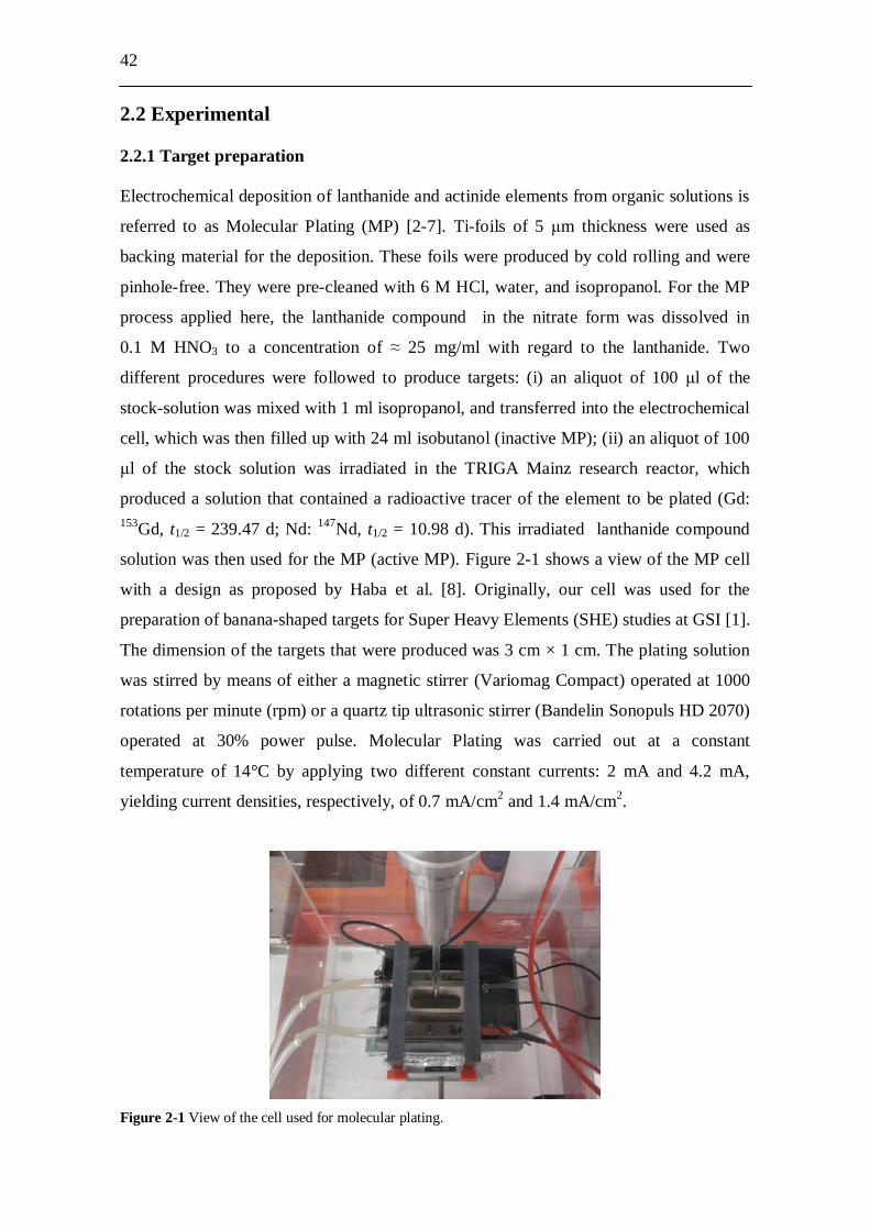
42
2.2 Experimental 2.2.1 Target preparation Electrochemical deposition of lanthanide and actinide elements from organic solutions is
referred to as Molecular Plating (MP) [2-7]. Ti-foils of 5 m thickness were used as
backing material for the deposition. These foils were produced by cold rolling and were
pinhole-free. They were pre-cleaned with 6 M HCl, water, and isopropanol. For the MP
process applied here, the lanthanide compound in the nitrate form was dissolved in
0.1 M HNO3 to a concentration of 25 mg/ml with regard to the lanthanide. Two
different procedures were followed to produce targets: (i) an aliquot of 100 l of the
stock-solution was mixed with 1 ml isopropanol, and transferred into the electrochemical
cell, which was then filled up with 24 ml isobutanol (inactive MP); (ii) an aliquot of 100
l of the stock solution was irradiated in the TRIGA Mainz research reactor, which
produced a solution that contained a radioactive tracer of the element to be plated (Gd: 153Gd, t1/2 = 239.47 d; Nd: 147Nd, t1/2 = 10.98 d). This irradiated lanthanide compound
solution was then used for the MP (active MP). Figure 2-1 shows a view of the MP cell
with a design as proposed by Haba et al. [8]. Originally, our cell was used for the
preparation of banana-shaped targets for Super Heavy Elements (SHE) studies at GSI [1].
The dimension of the targets that were produced was 3 cm × 1 cm. The plating solution
was stirred by means of either a magnetic stirrer (Variomag Compact) operated at 1000
rotations per minute (rpm) or a quartz tip ultrasonic stirrer (Bandelin Sonopuls HD 2070)
operated at 30% power pulse. Molecular Plating was carried out at a constant
temperature of 14°C by applying two different constant currents: 2 mA and 4.2 mA,
yielding current densities, respectively, of 0.7 mA/cm2 and 1.4 mA/cm2.
Figure 2-1 View of the cell used for molecular plating.
43
2.2.2 Target characterization The deposition yield of the MP process applied was determined by an indirect and a
direct method, respectively: Neutron Activation Analysis (NAA) and -spectroscopy.
NAA was used after inactive MPs. This analytical technique, performed at the TRIGA
Mainz Research Reactor, was used to determine the residual concentration of the
lanthanide element in the supernatant solution after neutron irradiation in the reactor and
measurement via -spectroscopy of a standard sample and an aliquot of the supernatant
solution itself (indirect yield measurement) [9]. Gamma-spectroscopy was used after
active MPs. This technique employed a high-purity germanium detector (HPGe) (GEM
series HPGe Detector Model No. GEM 23158 P-Plus, ORTEC Company) to measure the
active samples (direct yield measurement). To obtain quantitative data, reference sources
with known amounts of the tracer were prepared. They consisted of filter papers with the
same geometry as the targets, soaked with the tracer-containing solution. To avoid any
kind of contamination inside the -spectrometer, the active samples were sealed before
being inserted into the sample holder.
The homogeneity of the radioactive targets was inspected by using Radiographic Imaging
(RI), using a FUJIFILM FLA 7000 equipped with reusable imaging plates (IP) and a 650
nm laser for the reading process. The amount of emerging luminescence light during this
process is converted to an arbitrary unit that is proportional to the amount of radiation
exposed within a single record [10]. To verify the homogeneity of the target, the image
was overlaid by a grid of square spots with an area of 0.25 mm2 each. The spatial
resolution for -emitting nuclides was < 200 m as determined by Liebe et al. [9].
The morphology of the targets was studied by using a Scanning Electron Microscope
(SEM) (Philips XL30), operated at 20 kV. Secondary electrons were detected,
magnification factors of 150×, 500×, 1000×, and 2500× were used.
The surface roughness of the targets, i.e., the measure of the texture of the surface
quantified by the vertical deviations of the real surface from its ideal form, was
investigated by using an Atomic Force Microscope (AFM) (MFP 3D, Asylum Research).
For these investigations, a high-resolution image of a 15 × 15 m2 representative section
of the target surface was recorded. For each 15 × 15 m2 section, a square mask of
variable dimensions was used to determine the surface roughness as a root mean square
(RMS) value. The AFM used cantilevers with a resonance frequency of 283 kHz for
imaging in the AC mode (tapping mode).
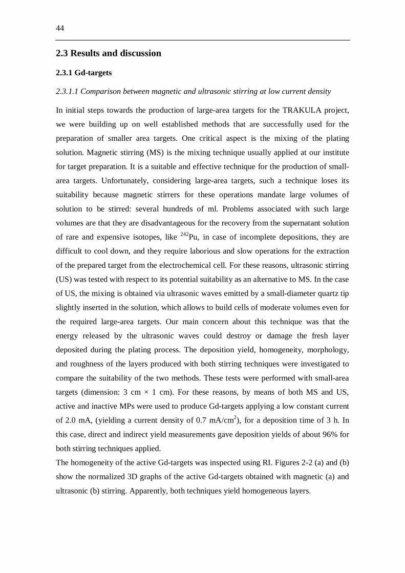
44
2.3 Results and discussion 2.3.1 Gd-targets 2.3.1.1 Comparison between magnetic and ultrasonic stirring at low current density In initial steps towards the production of large-area targets for the TRAKULA project,
we were building up on well established methods that are successfully used for the
preparation of smaller area targets. One critical aspect is the mixing of the plating
solution. Magnetic stirring (MS) is the mixing technique usually applied at our institute
for target preparation. It is a suitable and effective technique for the production of small-
area targets. Unfortunately, considering large-area targets, such a technique loses its
suitability because magnetic stirrers for these operations mandate large volumes of
solution to be stirred: several hundreds of ml. Problems associated with such large
volumes are that they are disadvantageous for the recovery from the supernatant solution
of rare and expensive isotopes, like 242Pu, in case of incomplete depositions, they are
difficult to cool down, and they require laborious and slow operations for the extraction
of the prepared target from the electrochemical cell. For these reasons, ultrasonic stirring
(US) was tested with respect to its potential suitability as an alternative to MS. In the case
of US, the mixing is obtained via ultrasonic waves emitted by a small-diameter quartz tip
slightly inserted in the solution, which allows to build cells of moderate volumes even for
the required large-area targets. Our main concern about this technique was that the
energy released by the ultrasonic waves could destroy or damage the fresh layer
deposited during the plating process. The deposition yield, homogeneity, morphology,
and roughness of the layers produced with both stirring techniques were investigated to
compare the suitability of the two methods. These tests were performed with small-area
targets (dimension: 3 cm × 1 cm). For these reasons, by means of both MS and US,
active and inactive MPs were used to produce Gd-targets applying a low constant current
of 2.0 mA, (yielding a current density of 0.7 mA/cm2), for a deposition time of 3 h. In
this case, direct and indirect yield measurements gave deposition yields of about 96% for
both stirring techniques applied.
The homogeneity of the active Gd-targets was inspected using RI. Figures 2-2 (a) and (b)
show the normalized 3D graphs of the active Gd-targets obtained with magnetic (a) and
ultrasonic (b) stirring. Apparently, both techniques yield homogeneous layers.
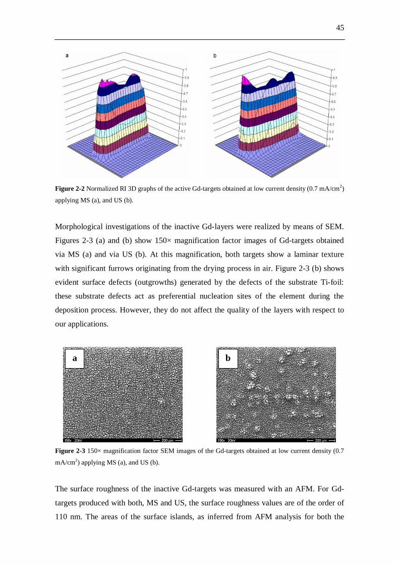
45
Figure 2-2 Normalized RI 3D graphs of the active Gd-targets obtained at low current density (0.7 mA/cm2)
applying MS (a), and US (b).
Morphological investigations of the inactive Gd-layers were realized by means of SEM.
Figures 2-3 (a) and (b) show 150× magnification factor images of Gd-targets obtained
via MS (a) and via US (b). At this magnification, both targets show a laminar texture
with significant furrows originating from the drying process in air. Figure 2-3 (b) shows
evident surface defects (outgrowths) generated by the defects of the substrate Ti-foil:
these substrate defects act as preferential nucleation sites of the element during the
deposition process. However, they do not affect the quality of the layers with respect to
our applications.
Figure 2-3 150× magnification factor SEM images of the Gd-targets obtained at low current density (0.7
mA/cm2) applying MS (a), and US (b).
The surface roughness of the inactive Gd-targets was measured with an AFM. For Gd-
targets produced with both, MS and US, the surface roughness values are of the order of
110 nm. The areas of the surface islands, as inferred from AFM analysis for both the
a b
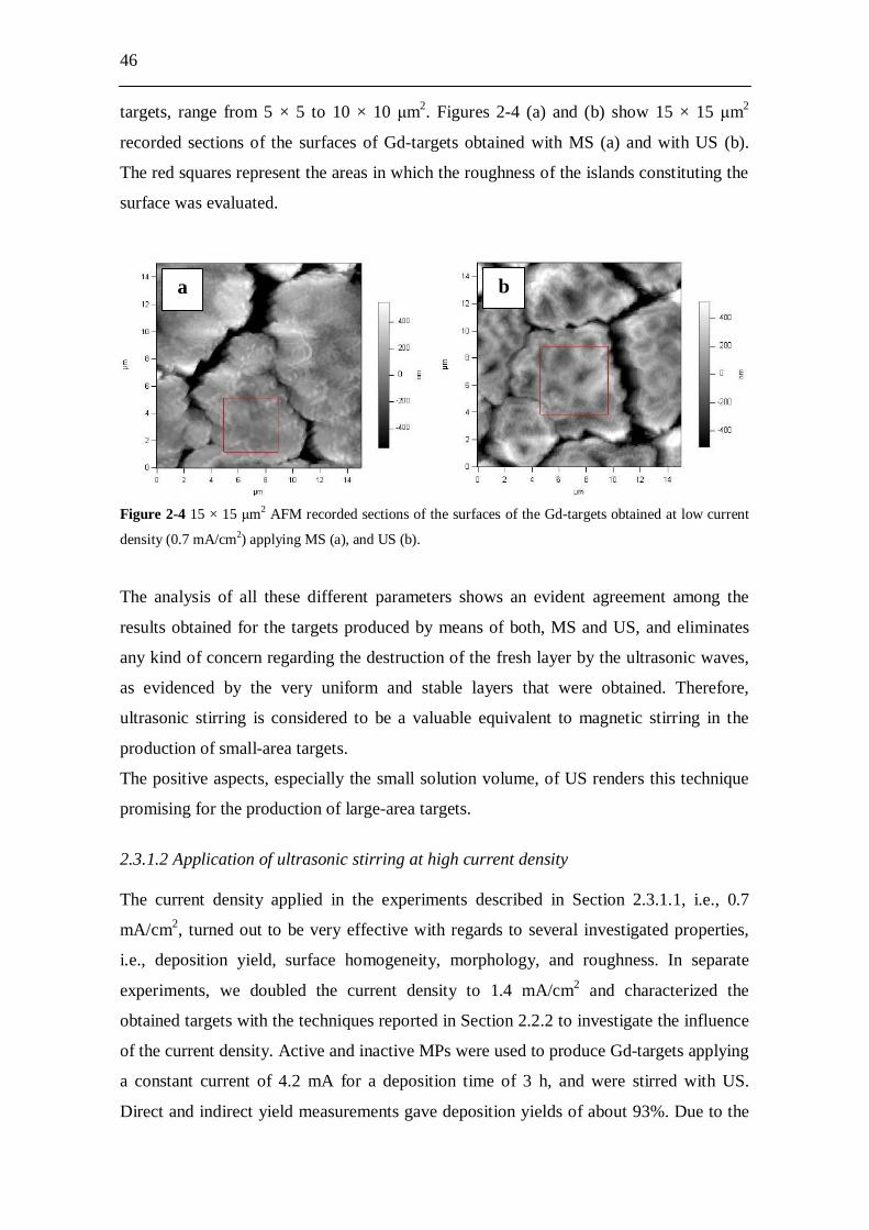
46
targets, range from 5 × 5 to 10 × 10 m2. Figures 2-4 (a) and (b) show 15 × 15 m2
recorded sections of the surfaces of Gd-targets obtained with MS (a) and with US (b).
The red squares represent the areas in which the roughness of the islands constituting the
surface was evaluated.
Figure 2-4 15 × 15 m2 AFM recorded sections of the surfaces of the Gd-targets obtained at low current
density (0.7 mA/cm2) applying MS (a), and US (b).
The analysis of all these different parameters shows an evident agreement among the
results obtained for the targets produced by means of both, MS and US, and eliminates
any kind of concern regarding the destruction of the fresh layer by the ultrasonic waves,
as evidenced by the very uniform and stable layers that were obtained. Therefore,
ultrasonic stirring is considered to be a valuable equivalent to magnetic stirring in the
production of small-area targets.
The positive aspects, especially the small solution volume, of US renders this technique
promising for the production of large-area targets.
2.3.1.2 Application of ultrasonic stirring at high current density The current density applied in the experiments described in Section 2.3.1.1, i.e., 0.7
mA/cm2, turned out to be very effective with regards to several investigated properties,
i.e., deposition yield, surface homogeneity, morphology, and roughness. In separate
experiments, we doubled the current density to 1.4 mA/cm2 and characterized the
obtained targets with the techniques reported in Section 2.2.2 to investigate the influence
of the current density. Active and inactive MPs were used to produce Gd-targets applying
a constant current of 4.2 mA for a deposition time of 3 h, and were stirred with US.
Direct and indirect yield measurements gave deposition yields of about 93%. Due to the
a b
47
higher applied current density, a faster deposition process was expected. Indeed, the
deposition yield approached 93% already after 2 h. Nevertheless, to allow a direct
comparison to the low current density measurements, plating times of 3 h were chosen
for these tests, too.
The homogeneity of the active Gd-targets was verified with RI. The morphology was
studied with SEM and showed a laminar texture similar to that described in Section
2.3.1.1.
The surface roughness of the inactive targets was measured with an AFM. For these
higher current density Gd-targets the surface roughness value is about 120 nm, similar to
that of the targets prepared at the low current density. The surface islands have areas that
range from 5 × 5 to 10 × 10 m2, again similar to those obtained at the low current
density.
Overall, taking into account both the deposition yields and the surface roughnesses, a
current density of 0.7 mA/cm2 appears favorable for the TRAKULA project. A value of
1.4 mA/cm2 should not be exceeded for effective target preparations.
Table 2-1 summarizes the conditions applied for the deposition and the results obtained
from the characterization of the targets produced for these Gd-tests.
Table 2-1 Experimental conditions and results obtained for the tests with Gd-targets on Ti-backings. The
plating time was always 3 h.
Stirring technique
Current [mA]
Current density
[mA/cm2]
Deposition yield [%]
Surface roughness
(RMS) [nm]
Island dimension
m2]
magnetic stirring 2.0 0.7 96 110 5 × 5 – 10 × 10
ultrasonic stirring 2.0 0.7 96 110 5 × 5 – 10 × 10
ultrasonic stirring 4.2 1.4 93 120 5 × 5 – 10 × 10
2.3.2 Nd-targets 2.3.2.1 Application of ultrasonic stirring at low and high current density Based on the results obtained in 2.3.1.1 and 2.3.1.2, Nd-targets were produced at current
densities of 0.7 mA/cm2 and 1.4 mA/cm2. The deposition time was 3 h, US was used.
Direct and indirect yield measurements gave slightly different deposition yields for the
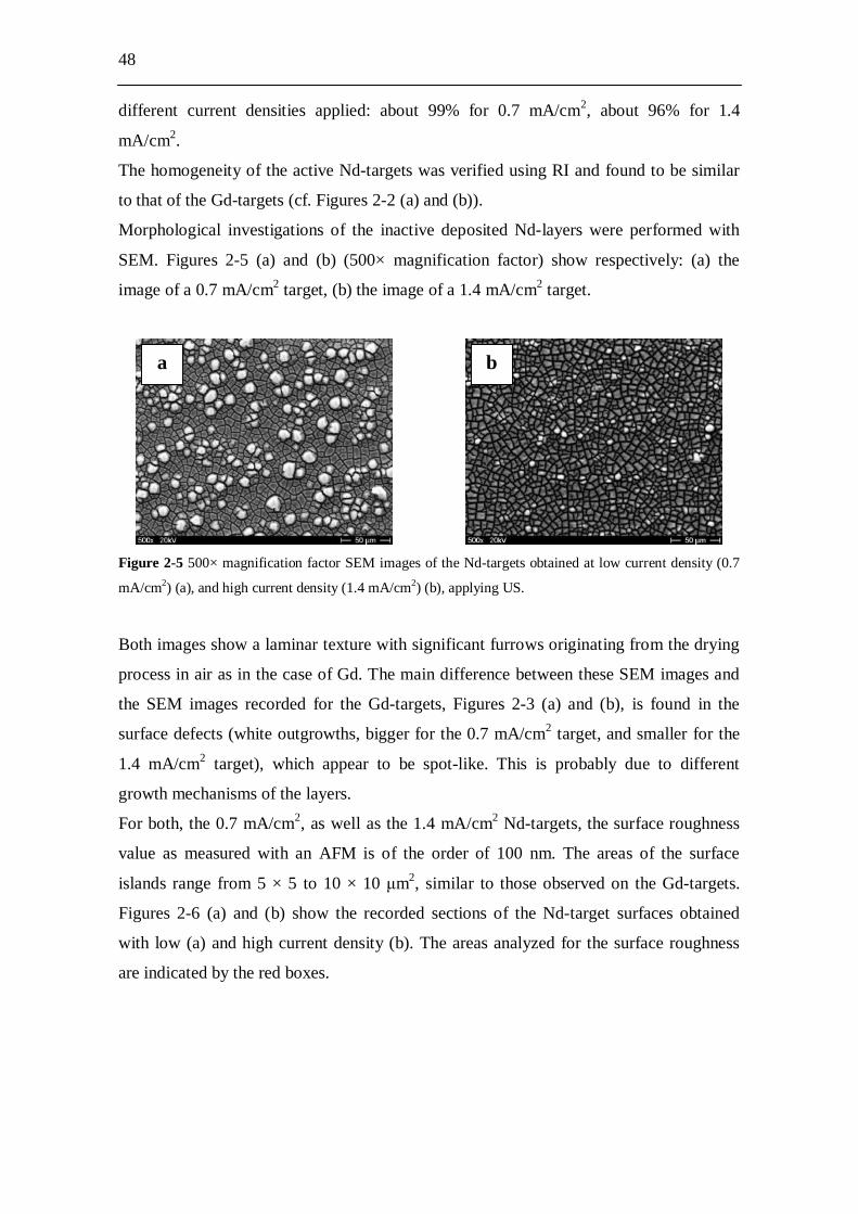
48
different current densities applied: about 99% for 0.7 mA/cm2, about 96% for 1.4
mA/cm2.
The homogeneity of the active Nd-targets was verified using RI and found to be similar
to that of the Gd-targets (cf. Figures 2-2 (a) and (b)).
Morphological investigations of the inactive deposited Nd-layers were performed with
SEM. Figures 2-5 (a) and (b) (500× magnification factor) show respectively: (a) the
image of a 0.7 mA/cm2 target, (b) the image of a 1.4 mA/cm2 target.
Figure 2-5 500× magnification factor SEM images of the Nd-targets obtained at low current density (0.7
mA/cm2) (a), and high current density (1.4 mA/cm2) (b), applying US.
Both images show a laminar texture with significant furrows originating from the drying
process in air as in the case of Gd. The main difference between these SEM images and
the SEM images recorded for the Gd-targets, Figures 2-3 (a) and (b), is found in the
surface defects (white outgrowths, bigger for the 0.7 mA/cm2 target, and smaller for the
1.4 mA/cm2 target), which appear to be spot-like. This is probably due to different
growth mechanisms of the layers.
For both, the 0.7 mA/cm2, as well as the 1.4 mA/cm2 Nd-targets, the surface roughness
value as measured with an AFM is of the order of 100 nm. The areas of the surface
islands range from 5 × 5 to 10 × 10 m2, similar to those observed on the Gd-targets.
Figures 2-6 (a) and (b) show the recorded sections of the Nd-target surfaces obtained
with low (a) and high current density (b). The areas analyzed for the surface roughness
are indicated by the red boxes.
a b
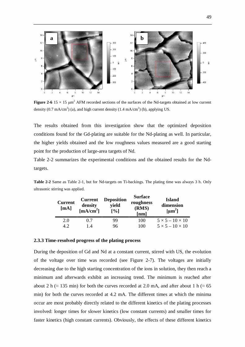
49
Figure 2-6 15 × 15 m2 AFM recorded sections of the surfaces of the Nd-targets obtained at low current
density (0.7 mA/cm2) (a), and high current density (1.4 mA/cm2) (b), applying US.
The results obtained from this investigation show that the optimized deposition
conditions found for the Gd-plating are suitable for the Nd-plating as well. In particular,
the higher yields obtained and the low roughness values measured are a good starting
point for the production of large-area targets of Nd.
Table 2-2 summarizes the experimental conditions and the obtained results for the Nd-
targets.
Table 2-2 Same as Table 2-1, but for Nd-targets on Ti-backings. The plating time was always 3 h. Only
ultrasonic stirring was applied.
Current [mA]
Current density
[mA/cm2]
Deposition yield [%]
Surface roughness
(RMS) [nm]
Island dimension
m2]
2.0 0.7 99 100 5 × 5 – 10 × 10 4.2 1.4 96 100 5 × 5 – 10 × 10
2.3.3 Time-resolved progress of the plating process During the deposition of Gd and Nd at a constant current, stirred with US, the evolution
of the voltage over time was recorded (see Figure 2-7). The voltages are initially
decreasing due to the high starting concentration of the ions in solution, they then reach a
minimum and afterwards exhibit an increasing trend. The minimum is reached after
about 2 h ( 135 min) for both the curves recorded at 2.0 mA, and after about 1 h ( 65
min) for both the curves recorded at 4.2 mA. The different times at which the minima
occur are most probably directly related to the different kinetics of the plating processes
involved: longer times for slower kinetics (low constant currents) and smaller times for
faster kinetics (high constant currents). Obviously, the effects of these different kinetics
a b
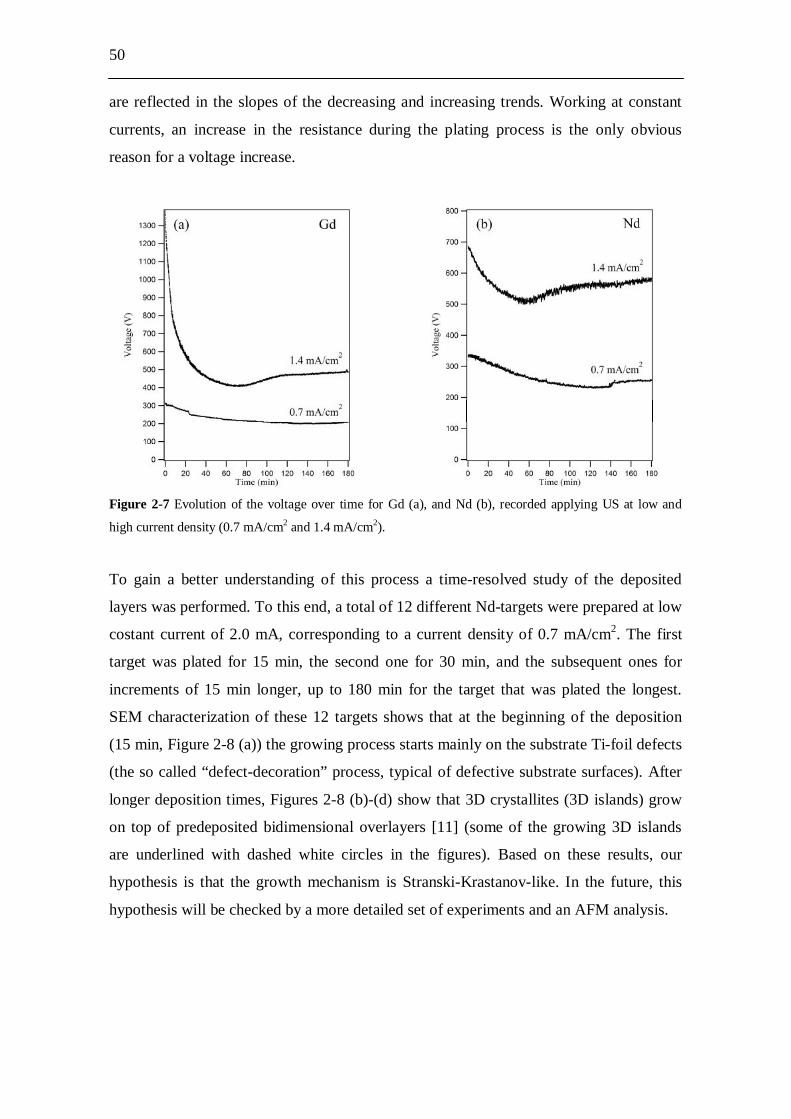
50
are reflected in the slopes of the decreasing and increasing trends. Working at constant
currents, an increase in the resistance during the plating process is the only obvious
reason for a voltage increase.
Figure 2-7 Evolution of the voltage over time for Gd (a), and Nd (b), recorded applying US at low and
high current density (0.7 mA/cm2 and 1.4 mA/cm2).
To gain a better understanding of this process a time-resolved study of the deposited
layers was performed. To this end, a total of 12 different Nd-targets were prepared at low
costant current of 2.0 mA, corresponding to a current density of 0.7 mA/cm2. The first
target was plated for 15 min, the second one for 30 min, and the subsequent ones for
increments of 15 min longer, up to 180 min for the target that was plated the longest.
SEM characterization of these 12 targets shows that at the beginning of the deposition
(15 min, Figure 2-8 (a)) the growing process starts mainly on the substrate Ti-foil defects
(the so called “defect-decoration” process, typical of defective substrate surfaces). After
longer deposition times, Figures 2-8 (b)-(d) show that 3D crystallites (3D islands) grow
on top of predeposited bidimensional overlayers [11] (some of the growing 3D islands
are underlined with dashed white circles in the figures). Based on these results, our
hypothesis is that the growth mechanism is Stranski-Krastanov-like. In the future, this
hypothesis will be checked by a more detailed set of experiments and an AFM analysis.
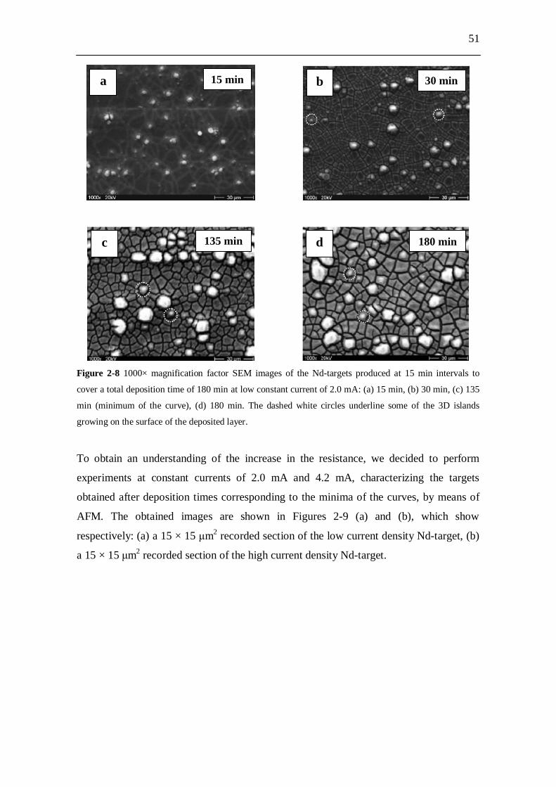
51
Figure 2-8 1000× magnification factor SEM images of the Nd-targets produced at 15 min intervals to
cover a total deposition time of 180 min at low constant current of 2.0 mA: (a) 15 min, (b) 30 min, (c) 135
min (minimum of the curve), (d) 180 min. The dashed white circles underline some of the 3D islands
growing on the surface of the deposited layer.
To obtain an understanding of the increase in the resistance, we decided to perform
experiments at constant currents of 2.0 mA and 4.2 mA, characterizing the targets
obtained after deposition times corresponding to the minima of the curves, by means of
AFM. The obtained images are shown in Figures 2-9 (a) and (b), which show
respectively: (a) a 15 × 15 m2 recorded section of the low current density Nd-target, (b)
a 15 × 15 m2 recorded section of the high current density Nd-target.
a 15 min b 30 min
c d 135 min 180 min
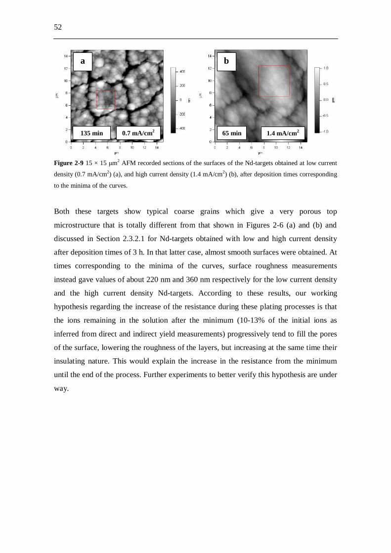
52
Figure 2-9 15 × 15 m2 AFM recorded sections of the surfaces of the Nd-targets obtained at low current
density (0.7 mA/cm2) (a), and high current density (1.4 mA/cm2) (b), after deposition times corresponding
to the minima of the curves.
Both these targets show typical coarse grains which give a very porous top
microstructure that is totally different from that shown in Figures 2-6 (a) and (b) and
discussed in Section 2.3.2.1 for Nd-targets obtained with low and high current density
after deposition times of 3 h. In that latter case, almost smooth surfaces were obtained. At
times corresponding to the minima of the curves, surface roughness measurements
instead gave values of about 220 nm and 360 nm respectively for the low current density
and the high current density Nd-targets. According to these results, our working
hypothesis regarding the increase of the resistance during these plating processes is that
the ions remaining in the solution after the minimum (10-13% of the initial ions as
inferred from direct and indirect yield measurements) progressively tend to fill the pores
of the surface, lowering the roughness of the layers, but increasing at the same time their
insulating nature. This would explain the increase in the resistance from the minimum
until the end of the process. Further experiments to better verify this hypothesis are under
way.
a
135 min 0.7 mA/cm2
b
65 min 1.4 mA/cm2
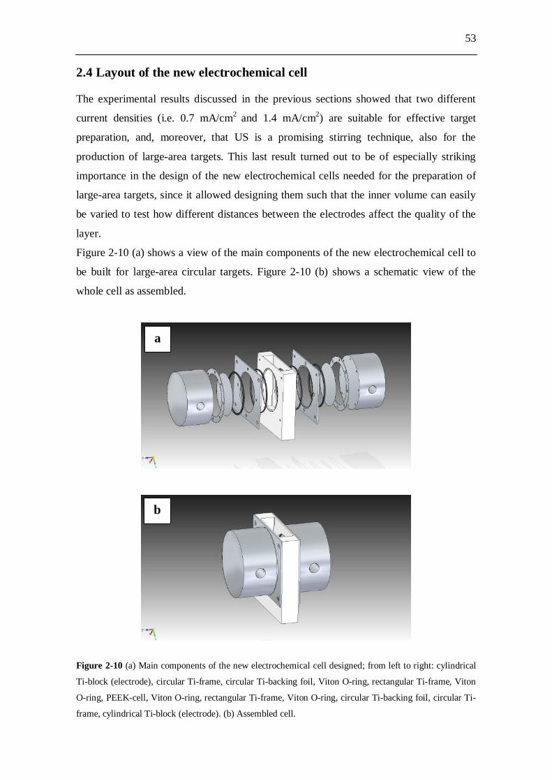
53
2.4 Layout of the new electrochemical cell The experimental results discussed in the previous sections showed that two different
current densities (i.e. 0.7 mA/cm2 and 1.4 mA/cm2) are suitable for effective target
preparation, and, moreover, that US is a promising stirring technique, also for the
production of large-area targets. This last result turned out to be of especially striking
importance in the design of the new electrochemical cells needed for the preparation of
large-area targets, since it allowed designing them such that the inner volume can easily
be varied to test how different distances between the electrodes affect the quality of the
layer.
Figure 2-10 (a) shows a view of the main components of the new electrochemical cell to
be built for large-area circular targets. Figure 2-10 (b) shows a schematic view of the
whole cell as assembled.
Figure 2-10 (a) Main components of the new electrochemical cell designed; from left to right: cylindrical
Ti-block (electrode), circular Ti-frame, circular Ti-backing foil, Viton O-ring, rectangular Ti-frame, Viton
O-ring, PEEK-cell, Viton O-ring, rectangular Ti-frame, Viton O-ring, circular Ti-backing foil, circular Ti-
frame, cylindrical Ti-block (electrode). (b) Assembled cell.
a
b

54
According to the circular shape of the targets and in order to get homogeneous electric
fields, both, the cathode and the anode have been designed as cylindrical Ti-blocks,
which can be water-cooled. On one side of both electrodes a circular Ti-frame is
screwed. In the case of the cathode, this frame holds a 50- m thick circular Ti-backing
foil perfectly in the center of the electrode during the deposition process. At the end of
the deposition, this frame can be unscrewed to easily remove the target avoiding
mechanical stress, which would be dangerous for the layer stability. At the anode, the
circular frame also keeps the Ti-backing foil centered. However, the foil is used only as
an interchangeable system of protection of the anode from impurities. A Viton O-ring is
used to define the area of deposition of the cathode. For both, the cathode and the anode,
this same O-ring serves as a means of sealing between the electrodes and the rectangular
Ti-frame. This frame connects the electrode assembly with the cell. For this reason,
another Viton O-ring is used to seal the rectangular frame to the cell. The cell is made of
PEEK and acts as a container for the alcohol solution.
2.5 Summary According to the requirement of the production of large-area targets ( 40 cm2) for the
TRAKULA project, constant current-MP tests were performed to find optimal deposition
conditions for small-area targets that are likely applicable as well to large-area targets.
These tests were based on the use of Gd and Nd as chemical homologues of the actinides.
The targets were characterized by means of direct and indirect yield measurement, RI,
SEM and AFM. A new stirring technique, ultrasonic stirring, was adopted and found
superior to mechanical stirring, especially for the production of large-area targets.
Deposition at two different current densities (i.e. 0.7 mA/cm2 and 1.4 mA/cm2) was
studied and both conditions were found to be suitable for target preparation. Investigation
of the trend of the voltage curves recorded during the plating processes was made. Two
working hypotheses were given: one about the Nd-growth mechanism at 2.0 mA (i.e.
Stranski-Krastanov growth mechanism), the other about the rise in resistance during the
deposition. According to the results obtained from these tests, a new electrochemical cell
for the production of large-area targets was designed.
55
Acknowledgements The authors would like to thank H. Adam from the institute of physical chemistry of the
Johannes Gutenberg University Mainz for his assistance with the AFM measurements
and the staff of the TRIGA Mainz for performing the irradiations. We acknowledge
financial support by the Research Center “Elementary Forces and Mathematical
Foundations” (EMG). One of us (A.V.) aknowledges financial support from the German
Federal Ministry of Science and Education (BMBF) under contract number 02NUK013E.
References [1] K. Eberhardt et al., Nucl. Instrum. Meth. A 590 (2008) 134.
[2] K. Eberhardt et al., in: J.L. Duggan, I.L. Morgan (Eds.), AIP Conference Proceedings,
vol. 576, (2001) p. 1144.
[3] W. Parker et al., Nucl. Instrum. Methods 16 (1962) 355.
[4] W. Parker et al., Nucl. Instrum. Methods 26 (1964) 55.
[5] W. Parker et al., Nucl. Instrum. Methods 26 (1964) 61.
[6] N. Getoff et al., Nucl. Instrum. Methods 36 (1965) 173.
[7] B.W. Filippone et al., Nucl. Instrum. Meth. A 243 (1986) 41.
[8] H. Haba et al., TASCA05 Workshop, www-w2.gsi.de/tasca05.
[9] D. Liebe et al., Nucl. Instrum. Meth. A 590 (2008) 145.
[10] Fuji Photo Film Co., Ltd, Operational Guide Multi-Gauge Software, Version 1.0,
2004.
[11] M. Paunovic, M. Schlesinger, Fundamentals of Electrochemical Deposition, second
ed., Wiley, New Jersey, 2006.
56
3. Elucidation of constant current density molecular plating
A. Vascon1, S. Santi2, A.A. Isse2, T. Reich1, J. Drebert1, H. Christ3, Ch.E. Düllmann1,4,5,
K. Eberhardt1,5 1Institute of Nuclear Chemistry, Johannes Gutenberg University Mainz, 55099 Mainz,
Germany 2Department of Chemical Sciences, University of Padova, 35131 Padova, Italy 3Institute of Physical Chemistry, Johannes Gutenberg University Mainz, 55099 Mainz,
Germany 4SHE Chemistry department, GSI Helmholtzzentrum für Schwerionenforschung GmbH,
64291 Darmstadt, Germany 5SHE Chemistry research section, Helmholtz Institute Mainz, 55099 Mainz, Germany
Published in:
Nuclear Instruments and Methods in Physics Research A 696 (2012) 180-191.
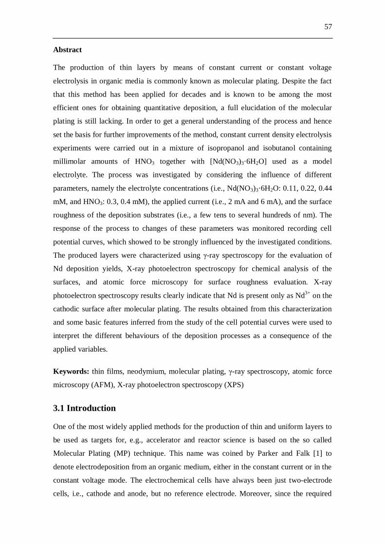
57
Abstract The production of thin layers by means of constant current or constant voltage
electrolysis in organic media is commonly known as molecular plating. Despite the fact
that this method has been applied for decades and is known to be among the most
efficient ones for obtaining quantitative deposition, a full elucidation of the molecular
plating is still lacking. In order to get a general understanding of the process and hence
set the basis for further improvements of the method, constant current density electrolysis
experiments were carried out in a mixture of isopropanol and isobutanol containing
millimolar amounts of HNO3 together with [Nd(NO3)3·6H2O] used as a model
electrolyte. The process was investigated by considering the influence of different
parameters, namely the electrolyte concentrations (i.e., Nd(NO3)3·6H2O: 0.11, 0.22, 0.44
mM, and HNO3: 0.3, 0.4 mM), the applied current (i.e., 2 mA and 6 mA), and the surface
roughness of the deposition substrates (i.e., a few tens to several hundreds of nm). The
response of the process to changes of these parameters was monitored recording cell
potential curves, which showed to be strongly influenced by the investigated conditions.
The produced layers were characterized using -ray spectroscopy for the evaluation of
Nd deposition yields, X-ray photoelectron spectroscopy for chemical analysis of the
surfaces, and atomic force microscopy for surface roughness evaluation. X-ray
photoelectron spectroscopy results clearly indicate that Nd is present only as Nd3+ on the
cathodic surface after molecular plating. The results obtained from this characterization
and some basic features inferred from the study of the cell potential curves were used to
interpret the different behaviours of the deposition processes as a consequence of the
applied variables.
Keywords: thin films, neodymium, molecular plating, -ray spectroscopy, atomic force
microscopy (AFM), X-ray photoelectron spectroscopy (XPS)
3.1 Introduction One of the most widely applied methods for the production of thin and uniform layers to
be used as targets for, e.g., accelerator and reactor science is based on the so called
Molecular Plating (MP) technique. This name was coined by Parker and Falk [1] to
denote electrodeposition from an organic medium, either in the constant current or in the
constant voltage mode. The electrochemical cells have always been just two-electrode
cells, i.e., cathode and anode, but no reference electrode. Moreover, since the required
58
target thicknesses are usually in the range of g/cm2-mg/cm2 and the areas of the deposits
can span several square centimeters (according to the particular beam diameters), the
concentrations of the electrolytes inside the cells are usually very small. Despite the
limitation of using two-electrode cells, MP has been successfully applied since its
introduction, half a century ago, for the production of, e.g., lanthanide and actinide
targets [2-6], and nowadays targets produced by MP are widely used, e.g., for atomic and
nuclear spectroscopy, nuclear reaction studies, or nuclear measurements [7-11]. The
method is well-known to have many desirable properties, like a quantitative deposition
yield of the produced layers, which usually show acceptable uniformity and good
stability to the bombardments with intense particle beams [11]. Despite MP to be widely
used, there are, however, rather few attempts reported where a characterization of the
layers by standard analytical techniques was performed [12,13], and a detailed
elucidation of even some main features of the process is still largely lacking. Work has
focused rather on gaining empirical evidence on how to further improve the properties of
the produced layers. Nonetheless, there is nowadays the common feeling that to increase
the efficiency of the method to yet improve the obtained targets, e.g., with respect to
radiation hardness, and before stepping to alternative target production techniques
[14,15], it is highly desirable to reduce the knowledge gap between MP and well
established electrochemical methods via an investigation and elucidation of such
electrodepositions. For this reason, following a previous publication [16], an extensive
investigation of the molecular plating process was carried out: constant current density
electrolysis experiments in organic media using a neodymium salt as a model electrolyte
were performed. Electrolyte concentration, applied current and surface roughness of the
deposition substrates were varied to investigate the process. Cell potential curves were
recorded to monitor the response of the process to the variables and several analytical
techniques were applied to characterize the produced layers. The results of these
measurements were used to interpret the different behaviours of the MPs. Elucidation of
the process including a theoretical description of important basic features of constant
current density MP is presented.
3.2 Experimental details 3.2.1 Deposition cells Two different types of cells were used: a deposition cell [17] for the production of
banana-shaped targets [11] for superheavy element (SHE) studies at the GSI
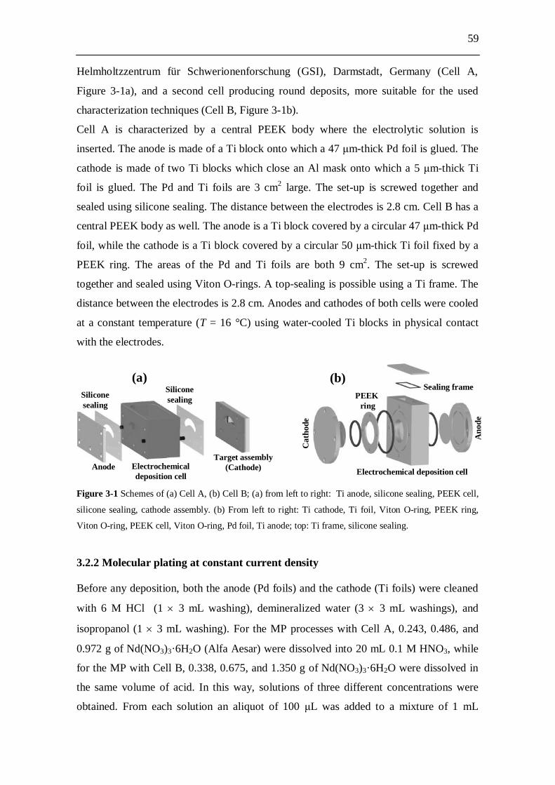
59
Helmholtzzentrum für Schwerionenforschung (GSI), Darmstadt, Germany (Cell A,
Figure 3-1a), and a second cell producing round deposits, more suitable for the used
characterization techniques (Cell B, Figure 3-1b).
Cell A is characterized by a central PEEK body where the electrolytic solution is
inserted. The anode is made of a Ti block onto which a 47 m-thick Pd foil is glued. The
cathode is made of two Ti blocks which close an Al mask onto which a 5 m-thick Ti
foil is glued. The Pd and Ti foils are 3 cm2 large. The set-up is screwed together and
sealed using silicone sealing. The distance between the electrodes is 2.8 cm. Cell B has a
central PEEK body as well. The anode is a Ti block covered by a circular 47 m-thick Pd
foil, while the cathode is a Ti block covered by a circular 50 m-thick Ti foil fixed by a
PEEK ring. The areas of the Pd and Ti foils are both 9 cm2. The set-up is screwed
together and sealed using Viton O-rings. A top-sealing is possible using a Ti frame. The
distance between the electrodes is 2.8 cm. Anodes and cathodes of both cells were cooled
at a constant temperature (T = 16 °C) using water-cooled Ti blocks in physical contact
with the electrodes.
Figure 3-1 Schemes of (a) Cell A, (b) Cell B; (a) from left to right: Ti anode, silicone sealing, PEEK cell,
silicone sealing, cathode assembly. (b) From left to right: Ti cathode, Ti foil, Viton O-ring, PEEK ring,
Viton O-ring, PEEK cell, Viton O-ring, Pd foil, Ti anode; top: Ti frame, silicone sealing.
3.2.2 Molecular plating at constant current density Before any deposition, both the anode (Pd foils) and the cathode (Ti foils) were cleaned
with 6 M HCl (1 3 mL washing), demineralized water (3 3 mL washings), and
isopropanol (1 3 mL washing). For the MP processes with Cell A, 0.243, 0.486, and
0.972 g of Nd(NO3)3·6H2O (Alfa Aesar) were dissolved into 20 mL 0.1 M HNO3, while
for the MP with Cell B, 0.338, 0.675, and 1.350 g of Nd(NO3)3·6H2O were dissolved in
the same volume of acid. In this way, solutions of three different concentrations were
obtained. From each solution an aliquot of 100 L was added to a mixture of 1 mL
Cat
hode
Ano
de
Electrochemical deposition cell
Sealing frame PEEK ring
Anode
Silicone sealing
Electrochemical deposition cell
Silicone sealing
Target assembly (Cathode)
(a) (b)

60
isopropanol (Fisher Chemical) and 24 mL isobutanol (Applichem) in the case of Cell A,
and to a mixture of 1 mL isopropanol and 34 mL isobutanol in the case of the Cell B.
This yielded three different solutions of Nd3+ in the used cell; these are referred to as low
concentration (LC, 0.11 mM), medium concentration (MC, 0.22 mM) and high
concentration (HC, 0.44 mM). In the case of Cell A the concentration of HNO3 was 0.4
mM, while it was 0.3 mM in the case of Cell B. In both cells the plating solutions were
stirred by means of a quartz tip ultrasonic stirrer (Bandelin Sonopuls HD 2070) operated
at 30% power pulse. MP experiments were carried out for 3 hours at 16 °C by applying
two different constant currents: 2 mA (Cell A) and 6 mA (Cell B). The current density,
0.7 mA/cm2 , was the same in both cases.
3.2.3 Deposition substrates The deposition substrates used in the present work are listed in Table 3-1. Table 3-1 Deposition substrates used for the MPs performed with Cell A and Cell B.
Substrate type Cell Production technique Ti1 A cold rolling Ti2 A cold rolling Ti3 B rolling Ti4 B etching Ti5 B magnetron sputtering
All the substrates used for deposition in Cell A were 5 m-thick Ti foils from Advent
(Ti1) and Lebow (Ti2) produced via cold-rolling. A second set of experiments aimed at
studying the influence of the substrate surface roughness. Therefore, the substrates used
for deposition in Cell B were produced with different roughness: medium (Ti3), high
(Ti4), and low roughness (Ti5). Ti3 was a circular 50 m-thick Ti foil cut from a bigger
rolled foil (Goodfellow). Ti4 was obtained by etching a Ti3 foil with concentrated HCl
(~36%) for 45 min under IR lamp. Ti5 was produced by magnetron sputtering a 300- m
thick mechanically-polished Si wafer with 100 nm metallic Ti.
3.2.4 Conductivity tests Conductivity tests were performed using an Inolab Cond 720 conductometer connected
to a TetraCon 325 standard conductivity cell. The measurements were performed in
stirred 0.4 and 0.3 mM HNO3 solutions, i.e., the acid solutions typically contained in Cell
A and Cell B, respectively. These solutions were prepared using the mixed solvent
isopropanol/isobutanol as described in Section 3.2.2.
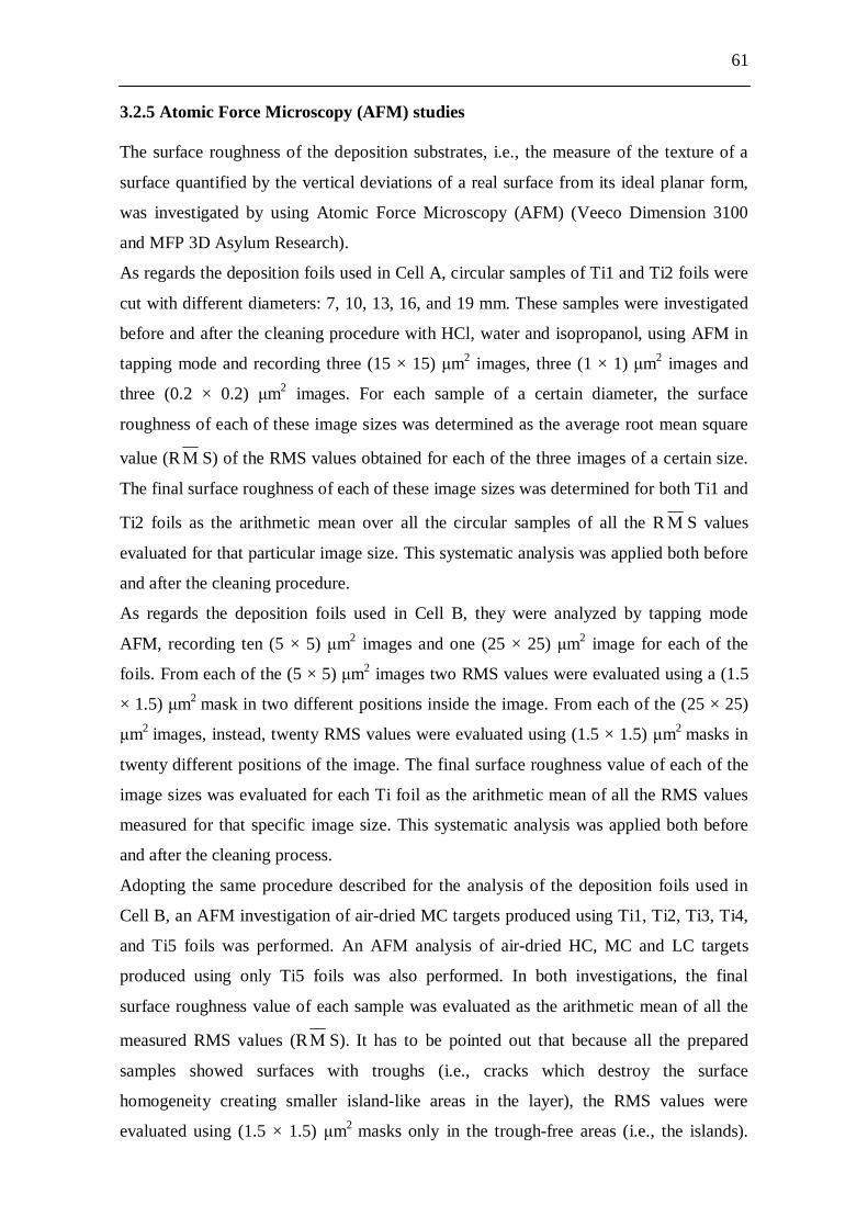
61
3.2.5 Atomic Force Microscopy (AFM) studies The surface roughness of the deposition substrates, i.e., the measure of the texture of a
surface quantified by the vertical deviations of a real surface from its ideal planar form,
was investigated by using Atomic Force Microscopy (AFM) (Veeco Dimension 3100
and MFP 3D Asylum Research).
As regards the deposition foils used in Cell A, circular samples of Ti1 and Ti2 foils were
cut with different diameters: 7, 10, 13, 16, and 19 mm. These samples were investigated
before and after the cleaning procedure with HCl, water and isopropanol, using AFM in
tapping mode and recording three (15 × 15) m2 images, three (1 × 1) m2 images and
three (0.2 × 0.2) m2 images. For each sample of a certain diameter, the surface
roughness of each of these image sizes was determined as the average root mean square
value (R S) of the RMS values obtained for each of the three images of a certain size.
The final surface roughness of each of these image sizes was determined for both Ti1 and
Ti2 foils as the arithmetic mean over all the circular samples of all the R S values
evaluated for that particular image size. This systematic analysis was applied both before
and after the cleaning procedure.
As regards the deposition foils used in Cell B, they were analyzed by tapping mode
AFM, recording ten (5 × 5) m2 images and one (25 × 25) m2 image for each of the
foils. From each of the (5 × 5) m2 images two RMS values were evaluated using a (1.5
× 1.5) m2 mask in two different positions inside the image. From each of the (25 × 25)
m2 images, instead, twenty RMS values were evaluated using (1.5 × 1.5) m2 masks in
twenty different positions of the image. The final surface roughness value of each of the
image sizes was evaluated for each Ti foil as the arithmetic mean of all the RMS values
measured for that specific image size. This systematic analysis was applied both before
and after the cleaning process.
Adopting the same procedure described for the analysis of the deposition foils used in
Cell B, an AFM investigation of air-dried MC targets produced using Ti1, Ti2, Ti3, Ti4,
and Ti5 foils was performed. An AFM analysis of air-dried HC, MC and LC targets
produced using only Ti5 foils was also performed. In both investigations, the final
surface roughness value of each sample was evaluated as the arithmetic mean of all the
measured RMS values (R S). It has to be pointed out that because all the prepared
samples showed surfaces with troughs (i.e., cracks which destroy the surface
homogeneity creating smaller island-like areas in the layer), the RMS values were
evaluated using (1.5 × 1.5) m2 masks only in the trough-free areas (i.e., the islands).
62
This is justified, because the troughs do not belong to the surface and hence do not define
the real roughness of the deposited layers.
3.2.6 X-ray Photoelectron Spectroscopy (XPS) studies The XPS characterization of the samples was performed using Al K and Mg K
radiations. The X-ray source was operated at 10 kV anode voltage and a current of 10
mA. The pass-energy of the hemispherical energy analyzer was 50 eV. The pressure
inside the ultra-high vacuum chamber was in the range of (1.2-2.0)·10-9 mbar. The
analyzed samples were the cathode (Ti3 foil) and the anode of Cell B after a MC
experiment. At the end of the deposition time, Cell B was top-sealed and inserted into a
glove-box, where an inert environment was assured by a constant Ar pressure (0.5 mbar,
O2 < 1 ppm, H2O < 1 ppm). The cell was opened, the solvent extracted, and the cathode
and anode foils were dried. Drying in an inert environment allowed performing a
chemical surface analysis with unaltered products of reduction and oxidation obtained
during the plating process. The samples were then sealed in special air-tight containers
and transported under Ar atmosphere to the XPS spectrometer for the analysis. A special
lock chamber filled with Ar was used to introduce the samples into the spectrometer:
hence they were never exposed to air. After the first surface investigation, both samples
underwent two ten-minute sputtering cycles using 4 kV Ar+ ions (i.e., total sputtering
time: 20 min). After each ten-minute sputtering cycle, the surface of the samples was
analyzed by XPS.
By fitting the XPS spectra, the binding energies and peak areas of the XPS lines of
interest were determined. As it was not the aim of the present work to perform a detailed
chemical surface analysis of the deposits, but mainly to understand, which elements can
be found on the electrodes after a constant current density MP, the individual
components of the XPS lines obtained by peak fitting were not analyzed in detail. The
reported spectra are therefore shown without multicomponent fitting analysis. For the
cathode deposit that was analyzed before sputtering, the measured binding energies were
corrected for the surface charging using the C 1s line of hydrocarbons with a binding
energy of 285.0 eV [18]. After sputtering, the imprecise fittings of the 285.0 eV peaks
required the use of a higher binding energy peak (ca. 289 eV) present in the same C 1s
spectra to correct for the surface charge effect. For the anode deposit, instead, the
correction of the binding energies was realized both before and after sputtering using
63
only the C 1s line at 285.0 eV. The experimental uncertainty of the binding energies is ±
0.1 eV.
3.2.7 Gamma-ray spectroscopy studies Gamma-ray spectroscopy was used after MP of Nd solution containing radioactive 147Nd
tracer. For this, an aliquot of 100 L of the stock solution was irradiated with thermal
neutrons in the TRIGA research reactor of Mainz University, producing in this way a
solution that contained a radioactive tracer of the element to be plated (Nd: 147Nd, -, t1/2
= 10.98 d, E = 91 keV). For this technique a high-purity germanium detector (HPGe)
(GEM series HPGe Detector Model No. GEM 23158P-Plus, ORTEC Company) was
employed to measure the active samples and to determine the deposition yield of the MP
process. To obtain quantitative data, reference sources with known amounts of the tracer
were prepared. They consisted of filter papers with the same geometry as the targets,
soaked with the tracer-containing solution. To avoid any kind of contamination of the -
spectrometer, the active samples were sealed with plastic foils before insertion into the
sample holder. The yield values evaluated at the different times of interest were always
obtained as the average value calculated from three distinct measurements.
3.3 Experimental results and analysis 3.3.1 Analysis of the conductivity tests The conductivity ( ) measured for the 0.4 mM HNO3 solution (Cell A acid solution) was
2.8 ± 0.1 S/cm. The conductivity measured for the 0.3 mM HNO3 solution (Cell B acid
solution) was instead 2.0 ± 0.1 S/cm. To evaluate the solution resistances in Cells A and
B, the expression R = ·l/S was applied, where is the resistivity of the system (i.e., the
inverse of the conductivity), l is the distance between the electrodes, and S is the surface
area of the electrodes [19]. For Cell A, where = 357 ± 13 k ·cm, l = 2.8 ± 0.01 cm, S =
3 ± 0.1 cm2, the cell resistance is 333 ± 12 k . For Cell B, instead, where = 500 ± 25
·cm, l = 2.8 ± 0.01 cm, S = 9 ± 0.1 cm2, the cell resistance is 156 ± 8 k . Cell A has a
higher cell resistance than Cell B. If Ohm’s first law, V = RI, where R is the cell
resistance and I is the applied current, can be considered valid for the investigated MPs,
then the previously calculated solution resistances can be used to estimate the
contribution of the ohmic drop to the overall cell potential. For Cell A (I = 2 mA) the
obtained value of V is ca. 660 V, whereas for Cell B (I = 6 mA) it is ca. 930 V. Both
64
values are quite close to the experimentally recorded values (Cell A ca. 500 V, Cell B ca.
900 V).
3.3.2 AFM analysis The results of the AFM analysis of the Ti1 and Ti2 foils described in Section 3.2.5 are
summarized in Table 3-2, both before and after the cleaning procedure.
Table 3-2 Average root mean square values obtained after the AFM analysis of the Ti1, Ti2, Ti3, Ti4, and
Ti5 foils.
Before cleaning
Scan size m2)
Ti1 R S (nm)
Ti2 R S (nm)
Ti3 R S (nm)
Ti4 R S (nm)
Ti5 R S (nm)
(0.2 × 0.2) 1.4 ± 0.5 0.52 ± 0.16 - - - (1 × 1) 5.5 ± 0.8 2.4 ± 0.6 - - - (15 × 15) 29 ± 3 20.1 ± 1.8 - - - (5 × 5) - - 26 ± 7 330 ± 100 5.8 ± 2.7 (25 × 25) - - 23 ± 8 330 ± 110 3.9 ± 0.5
After cleaning
Scan size m2)
Ti1 R S (nm)
Ti2 R S (nm)
Ti3 R S (nm)
Ti4 R S (nm)
Ti5 R S (nm)
(0.2 × 0.2) 0.93 ± 0.12 0.63 ± 0.11 - - - (1 × 1) 4.5 ± 0.6 2.5 ± 0.9 - - - (15 × 15) 31 ± 3 20.6 ± 2.2 - - - (5 × 5) - - 21 ± 5 350 ± 140 14.9 ± 2.6 (25 × 25) - - 24 ± 7 340 ± 140 12.8 ± 0.7
The results shown in Table 3-2 clearly demonstrate that Ti1 foils are rougher than Ti2
foils both before and after the cleaning procedure. The cleaning does not affect their
R S values.
The results of the AFM analysis of the Ti3, Ti4 and Ti5 foils described in Section 3.2.5
are summarized in Table 3-2 as well. They clearly indicate that the three deposition foils
used in Cell B have very different surface roughness, around one order of magnitude of
difference one from the other. The Ti4 foil is the roughest one, Ti3 has an intermediate
roughness, while Ti5 is the smoothest foil, whose roughness is slightly increased after the
cleaning procedure.
The results of the AFM analysis of the air-dried MC targets produced using Ti1, Ti2, Ti3,
Ti4, and Ti5 foils are summarized in Table 3-3. They clearly demonstrate that rougher
deposition foils grow rougher layers, the smoothest ones being the Ti2-grown MC layer
in Cell A, and the Ti5-grown MC layer in Cell B.
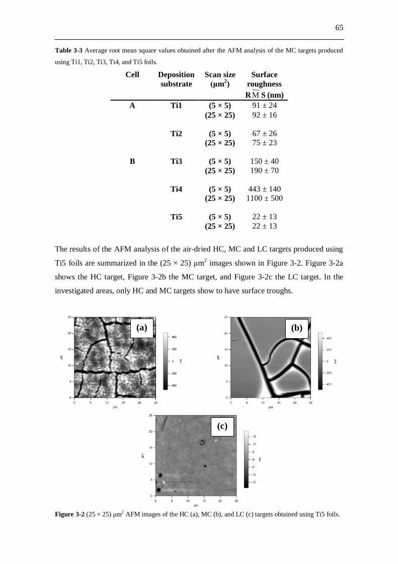
65
(c)
Table 3-3 Average root mean square values obtained after the AFM analysis of the MC targets produced
using Ti1, Ti2, Ti3, Ti4, and Ti5 foils.
Cell Deposition substrate
Scan size m2)
Surface roughnessR S (nm)
A Ti1 (5 × 5) 91 ± 24 (25 × 25) 92 ± 16 Ti2 (5 × 5) 67 ± 26 (25 × 25) 75 ± 23
B Ti3 (5 × 5) 150 ± 40 (25 × 25) 190 ± 70 Ti4 (5 × 5) 443 ± 140 (25 × 25) 1100 ± 500 Ti5 (5 × 5) 22 ± 13 (25 × 25) 22 ± 13
The results of the AFM analysis of the air-dried HC, MC and LC targets produced using
Ti5 foils are summarized in the (25 × 25) m2 images shown in Figure 3-2. Figure 3-2a
shows the HC target, Figure 3-2b the MC target, and Figure 3-2c the LC target. In the
investigated areas, only HC and MC targets show to have surface troughs.
Figure 3-2 (25 × 25) m2 AFM images of the HC (a), MC (b), and LC (c) targets obtained using Ti5 foils.
(a) (b)
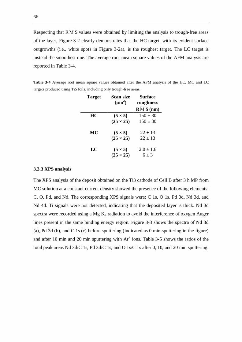
66
Respecting that R S values were obtained by limiting the analysis to trough-free areas
of the layer, Figure 3-2 clearly demonstrates that the HC target, with its evident surface
outgrowths (i.e., white spots in Figure 3-2a), is the roughest target. The LC target is
instead the smoothest one. The average root mean square values of the AFM analysis are
reported in Table 3-4.
Table 3-4 Average root mean square values obtained after the AFM analysis of the HC, MC and LC
targets produced using Ti5 foils, including only trough-free areas.
Target Scan size m2)
Surface roughnessR S (nm)
HC (5 × 5) 150 ± 30 (25 × 25) 150 ± 30
MC (5 × 5) 22 ± 13 (25 × 25) 22 ± 13
LC (5 × 5) 2.0 ± 1.6 (25 × 25) 6 ± 3
3.3.3 XPS analysis The XPS analysis of the deposit obtained on the Ti3 cathode of Cell B after 3 h MP from
MC solution at a constant current density showed the presence of the following elements:
C, O, Pd, and Nd. The corresponding XPS signals were: C 1s, O 1s, Pd 3d, Nd 3d, and
Nd 4d. Ti signals were not detected, indicating that the deposited layer is thick. Nd 3d
spectra were recorded using a Mg K radiation to avoid the interference of oxygen Auger
lines present in the same binding energy region. Figure 3-3 shows the spectra of Nd 3d
(a), Pd 3d (b), and C 1s (c) before sputtering (indicated as 0 min sputtering in the figure)
and after 10 min and 20 min sputtering with Ar+ ions. Table 3-5 shows the ratios of the
total peak areas Nd 3d/C 1s, Pd 3d/C 1s, and O 1s/C 1s after 0, 10, and 20 min sputtering.
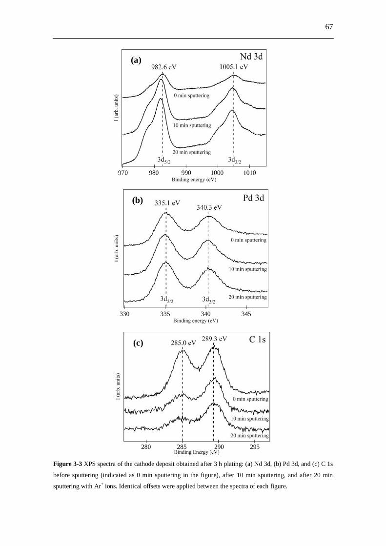
67
Figure 4
Figure 3-3 XPS spectra of the cathode deposit obtained after 3 h plating: (a) Nd 3d, (b) Pd 3d, and (c) C 1s
before sputtering (indicated as 0 min sputtering in the figure), after 10 min sputtering, and after 20 min
sputtering with Ar+ ions. Identical offsets were applied between the spectra of each figure.
(a)
(b)
970 980 990 1000 1010
330 335 340 345
280 285 290 295
(b)
(c)
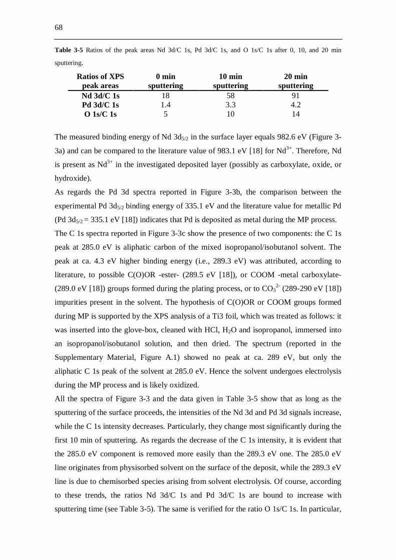
68
Table 3-5 Ratios of the peak areas Nd 3d/C 1s, Pd 3d/C 1s, and O 1s/C 1s after 0, 10, and 20 min
sputtering.
Ratios of XPS peak areas
0 min sputtering
10 min sputtering
20 min sputtering
Nd 3d/C 1s 18 58 91 Pd 3d/C 1s 1.4 3.3 4.2 O 1s/C 1s 5 10 14
The measured binding energy of Nd 3d5/2 in the surface layer equals 982.6 eV (Figure 3-
3a) and can be compared to the literature value of 983.1 eV [18] for Nd3+. Therefore, Nd
is present as Nd3+ in the investigated deposited layer (possibly as carboxylate, oxide, or
hydroxide).
As regards the Pd 3d spectra reported in Figure 3-3b, the comparison between the
experimental Pd 3d5/2 binding energy of 335.1 eV and the literature value for metallic Pd
(Pd 3d5/2 = 335.1 eV [18]) indicates that Pd is deposited as metal during the MP process.
The C 1s spectra reported in Figure 3-3c show the presence of two components: the C 1s
peak at 285.0 eV is aliphatic carbon of the mixed isopropanol/isobutanol solvent. The
peak at ca. 4.3 eV higher binding energy (i.e., 289.3 eV) was attributed, according to
literature, to possible C(O)OR -ester- (289.5 eV [18]), or COOM -metal carboxylate-
(289.0 eV [18]) groups formed during the plating process, or to CO32- (289-290 eV [18])
impurities present in the solvent. The hypothesis of C(O)OR or COOM groups formed
during MP is supported by the XPS analysis of a Ti3 foil, which was treated as follows: it
was inserted into the glove-box, cleaned with HCl, H2O and isopropanol, immersed into
an isopropanol/isobutanol solution, and then dried. The spectrum (reported in the
Supplementary Material, Figure A.1) showed no peak at ca. 289 eV, but only the
aliphatic C 1s peak of the solvent at 285.0 eV. Hence the solvent undergoes electrolysis
during the MP process and is likely oxidized.
All the spectra of Figure 3-3 and the data given in Table 3-5 show that as long as the
sputtering of the surface proceeds, the intensities of the Nd 3d and Pd 3d signals increase,
while the C 1s intensity decreases. Particularly, they change most significantly during the
first 10 min of sputtering. As regards the decrease of the C 1s intensity, it is evident that
the 285.0 eV component is removed more easily than the 289.3 eV one. The 285.0 eV
line originates from physisorbed solvent on the surface of the deposit, while the 289.3 eV
line is due to chemisorbed species arising from solvent electrolysis. Of course, according
to these trends, the ratios Nd 3d/C 1s and Pd 3d/C 1s are bound to increase with
sputtering time (see Table 3-5). The same is verified for the ratio O 1s/C 1s. In particular,

69
the ratio Nd 3d/C 1s will be the fastest growing one because of the higher amount of Nd
present in the system. These trends show very clearly that the obtained target is
characterized by an outer layer of solvent which covers the Nd and Pd deposit.
The XPS analysis of a Ti3 MC target, obtained with a plating time of 30 minutes, showed
that after small deposition times only Nd is deposited on the cathode and is covered by a
solvent layer. No signals of Pd were found. Figure 3-4 shows the spectra of Nd 3d (a)
and C 1s (b) before sputtering and after 10 and 20 min sputtering with Ar+ ions.
Figure 3-4 XPS spectra of the cathode deposit obtained after 30 min plating: (a) Nd 3d, and (b) C 1s before
sputtering (indicated as 0 min sputtering in the figure), after 10 min sputtering, and after 20 min sputtering
with Ar+ ions. Identical offsets were applied between the spectra of each figure.
(b)
280 285 290 295
970 980 990 1000 1010
(a)
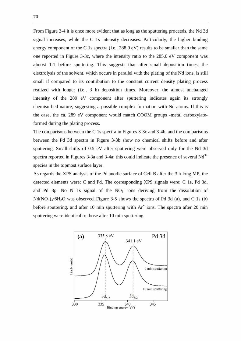
70
From Figure 3-4 it is once more evident that as long as the sputtering proceeds, the Nd 3d
signal increases, while the C 1s intensity decreases. Particularly, the higher binding
energy component of the C 1s spectra (i.e., 288.9 eV) results to be smaller than the same
one reported in Figure 3-3c, where the intensity ratio to the 285.0 eV component was
almost 1:1 before sputtering. This suggests that after small deposition times, the
electrolysis of the solvent, which occurs in parallel with the plating of the Nd ions, is still
small if compared to its contribution to the constant current density plating process
realized with longer (i.e., 3 h) deposition times. Moreover, the almost unchanged
intensity of the 289 eV component after sputtering indicates again its strongly
chemisorbed nature, suggesting a possible complex formation with Nd atoms. If this is
the case, the ca. 289 eV component would match COOM groups -metal carboxylate-
formed during the plating process.
The comparisons between the C 1s spectra in Figures 3-3c and 3-4b, and the comparisons
between the Pd 3d spectra in Figure 3-3b show no chemical shifts before and after
sputtering. Small shifts of 0.5 eV after sputtering were observed only for the Nd 3d
spectra reported in Figures 3-3a and 3-4a: this could indicate the presence of several Nd3+
species in the topmost surface layer.
As regards the XPS analysis of the Pd anodic surface of Cell B after the 3 h-long MP, the
detected elements were: C and Pd. The corresponding XPS signals were: C 1s, Pd 3d,
and Pd 3p. No N 1s signal of the NO3- ions deriving from the dissolution of
Nd(NO3)3·6H2O was observed. Figure 3-5 shows the spectra of Pd 3d (a), and C 1s (b)
before sputtering, and after 10 min sputtering with Ar+ ions. The spectra after 20 min
sputtering were identical to those after 10 min sputtering.
330 335 340 345
(a)
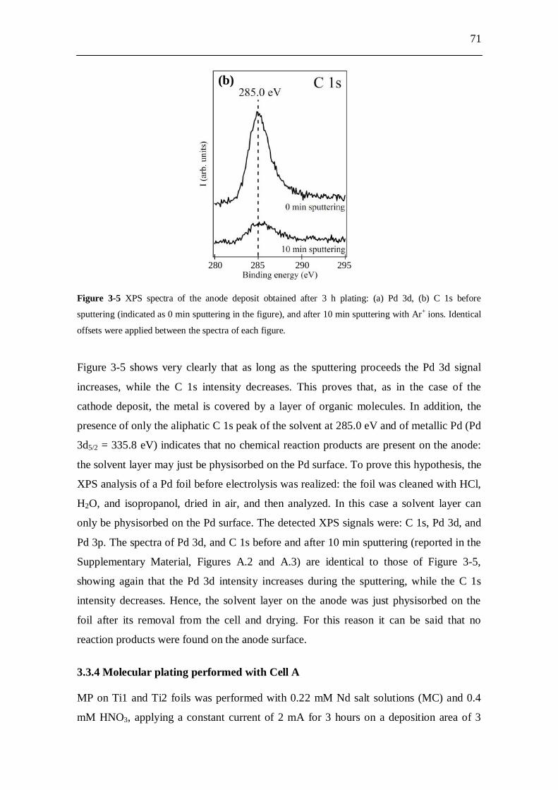
71
Figure 3-5 XPS spectra of the anode deposit obtained after 3 h plating: (a) Pd 3d, (b) C 1s before
sputtering (indicated as 0 min sputtering in the figure), and after 10 min sputtering with Ar+ ions. Identical
offsets were applied between the spectra of each figure.
Figure 3-5 shows very clearly that as long as the sputtering proceeds the Pd 3d signal
increases, while the C 1s intensity decreases. This proves that, as in the case of the
cathode deposit, the metal is covered by a layer of organic molecules. In addition, the
presence of only the aliphatic C 1s peak of the solvent at 285.0 eV and of metallic Pd (Pd
3d5/2 = 335.8 eV) indicates that no chemical reaction products are present on the anode:
the solvent layer may just be physisorbed on the Pd surface. To prove this hypothesis, the
XPS analysis of a Pd foil before electrolysis was realized: the foil was cleaned with HCl,
H2O, and isopropanol, dried in air, and then analyzed. In this case a solvent layer can
only be physisorbed on the Pd surface. The detected XPS signals were: C 1s, Pd 3d, and
Pd 3p. The spectra of Pd 3d, and C 1s before and after 10 min sputtering (reported in the
Supplementary Material, Figures A.2 and A.3) are identical to those of Figure 3-5,
showing again that the Pd 3d intensity increases during the sputtering, while the C 1s
intensity decreases. Hence, the solvent layer on the anode was just physisorbed on the
foil after its removal from the cell and drying. For this reason it can be said that no
reaction products were found on the anode surface.
3.3.4 Molecular plating performed with Cell A MP on Ti1 and Ti2 foils was performed with 0.22 mM Nd salt solutions (MC) and 0.4
mM HNO3, applying a constant current of 2 mA for 3 hours on a deposition area of 3
280 285 290 295
(b)
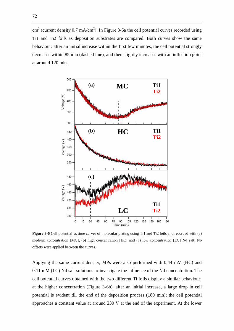
72
cm2 (current density 0.7 mA/cm2). In Figure 3-6a the cell potential curves recorded using
Ti1 and Ti2 foils as deposition substrates are compared. Both curves show the same
behaviour: after an initial increase within the first few minutes, the cell potential strongly
decreases within 85 min (dashed line), and then slightly increases with an inflection point
at around 120 min.
Figure 3-6 Cell potential vs time curves of molecular plating using Ti1 and Ti2 foils and recorded with (a)
medium concentration [MC], (b) high concentration [HC] and (c) low concentration [LC] Nd salt. No
offsets were applied between the curves.
Applying the same current density, MPs were also performed with 0.44 mM (HC) and
0.11 mM (LC) Nd salt solutions to investigate the influence of the Nd concentration. The
cell potential curves obtained with the two different Ti foils display a similar behaviour:
at the higher concentration (Figure 3-6b), after an initial increase, a large drop in cell
potential is evident till the end of the deposition process (180 min); the cell potential
approaches a constant value at around 230 V at the end of the experiment. At the lower
(c)
Ti1 Ti2
Ti1 Ti2
(a)
(b)
MC
HC
LC Ti1 Ti2
(c)

73
concentration (Figure 3-6c), the cell potential curves obtained using Ti1 and Ti2 cathodes
display several common features: after an initial increase, the cell potential slightly
decreases within 30 min (dashed line), afterwards it increases, reaching a maximum
value at around 105 min. Additional cell potential vs time curves from repetitions
performed as reproducibility tests are reported in the Supplementary Material (Figures
A.4-A.9) and confirm that the data shown in Figure 3-6 are typical.
By comparing the curves recorded at different concentrations of Nd salt (Figure 3-6), we
notice that the cell potential profile is very sensitive to the Nd3+ concentration. In
addition, the curves obtained with Ti1 and Ti2 foils display no significant difference in
cell potential behaviour, despite the different surface roughness of the deposition
substrates employed in the molecular plating (see Table 3-2).
3.3.5 Molecular plating performed with Cell B MPs on Ti3, Ti4 and Ti5 foils were performed using solutions with 0.22 mM Nd salt
(MC) and applying a 6 mA constant current for 3 hours on a deposition area of 9 cm2
(current density 0.7 mA/cm2). The cell potential curves obtained for the three electrodes
(Figure 3-7a) display similar behaviour: after the initial increase, the cell potential
decreases within 45 min (dashed line), and then increases to a maximum value. In the
case of Ti3 and Ti5 substrates the maximum forms a wide plateau, ranging from around
90 min to 120 min, with the maximum located at around 110 min. In the case of Ti4
foils, instead, the formed plateau shows its maximum at around 75 min. After the
maximum, all of the cell potential curves tend to slightly decrease with time. Figure 3-7b
shows the variations of the cell potential with time during MP in 0.44 mM Nd salt
solutions (HC). Again the three substrates display similar behaviour: after the initial
increase (zoom in Figure 3-7b), the cell potential strongly decreases within 80 min
(dashed line) and then slightly increases. Under the same conditions, the cell potential
profiles recorded during the molecular plating with 0.11 mM Nd salt solutions (LC),
display similar behaviour: after the initial increase, the cell potential decreases
exponentially within 20 min (no minimum is present), and then decreases almost linearly
with time with a very small slope (Figure 3-7c). Repeated cell potential vs time curves as
reproducibility tests are reported in the Supplementary Material (Figures A.10-A.18) and
confirm that the data shown in Figure 3-7 are typical.
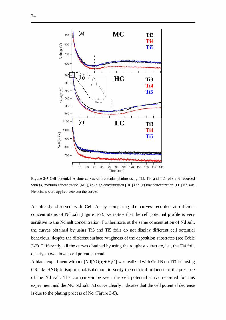
74
Figure 3-7 Cell potential vs time curves of molecular plating using Ti3, Ti4 and Ti5 foils and recorded
with (a) medium concentration [MC], (b) high concentration [HC] and (c) low concentration [LC] Nd salt.
No offsets were applied between the curves.
As already observed with Cell A, by comparing the curves recorded at different
concentrations of Nd salt (Figure 3-7), we notice that the cell potential profile is very
sensitive to the Nd salt concentration. Furthermore, at the same concentration of Nd salt,
the curves obtained by using Ti3 and Ti5 foils do not display different cell potential
behaviour, despite the different surface roughness of the deposition substrates (see Table
3-2). Differently, all the curves obtained by using the roughest substrate, i.e., the Ti4 foil,
clearly show a lower cell potential trend.
A blank experiment without [Nd(NO3)3·6H2O] was realized with Cell B on Ti3 foil using
0.3 mM HNO3 in isopropanol/isobutanol to verify the crititical influence of the presence
of the Nd salt. The comparison between the cell potential curve recorded for this
experiment and the MC Nd salt Ti3 curve clearly indicates that the cell potential decrease
is due to the plating process of Nd (Figure 3-8).
(a) MC
(b) HC
(c) LC
Ti3 Ti4 Ti5
Ti3 Ti4 Ti5
Ti3 Ti4 Ti5
3 6 9 12 15 Time (s)
(b)

75
Figure 3-8 Comparison between the curves obtained using Ti3 foil and recorded without Nd salt (upper
curve) and with a MC Nd salt solution (lower curve).
It is interesting to notice that, even when only the acid is present, the curve displays a
minimum at around 5 min, but during the overall experiment the cell potential is higher
than that observed in the presence of the Nd salt.
3.3.6 Molecular plating on a smaller deposition area in Cell B Minima in the cell potential profiles obtained with Cell A and Cell B are given in Table
3-6. They occur at different times, although the same current density (0.7 mA/cm2) was
used.
Table 3-6 Minima time positions of the MC, HC and LC Nd salt cell potential curves recorded using Ti1,
Ti2, Ti3, Ti4, and Ti5 foils.
Cell A (2mA/3cm2)
Cathode MC minimum position (min)
HC minimum position (min)
LC minimum position (min)
Ti1 85 180 30 Ti2 85 180 30
Cell B (6mA/9cm2)
Cathode MC minimum position (min)
HC minimum position (min)
LC minimum position (min)
Ti3 45 80 - Ti4 45 80 - Ti5 45 80 -
The minima in the cell potential vs time curves obtained with Cell B (I = 6 mA, cathode
area = 9 cm2) occurred earlier than those recorded using Cell A (2 mA, 3 cm2).
A plot of time position of the cell potential minima vs concentration is reported in Figure
3-9. A linear correlation of the time positions of the minima with the initial Nd
concentration is found for both cells, suggesting that the position of the cell potential
minima is directly correlated with the initial Nd concentration.
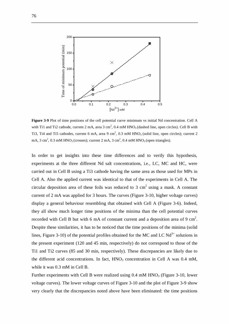
76
0
50
100
150
200
0.0 0.1 0.2 0.3 0.4 0.5
[Nd3+] mM
Tim
e of
min
imum
pot
entia
l (m
in)
Figure 3-9 Plot of time positions of the cell potential curve minimum vs initial Nd concentration. Cell A
with Ti1 and Ti2 cathode, current 2 mA, area 3 cm2, 0.4 mM HNO3 (dashed line, open circles). Cell B with
Ti3, Ti4 and Ti5 cathodes, current 6 mA, area 9 cm2, 0.3 mM HNO3 (solid line, open circles); current 2
mA, 3 cm2, 0.3 mM HNO3 (crosses); current 2 mA, 3 cm2, 0.4 mM HNO3 (open triangles).
In order to get insights into these time differences and to verify this hypothesis,
experiments at the three different Nd salt concentrations, i.e., LC, MC and HC, were
carried out in Cell B using a Ti3 cathode having the same area as those used for MPs in
Cell A. Also the applied current was identical to that of the experiments in Cell A. The
circular deposition area of these foils was reduced to 3 cm2 using a mask. A constant
current of 2 mA was applied for 3 hours. The curves (Figure 3-10, higher voltage curves)
display a general behaviour resembling that obtained with Cell A (Figure 3-6). Indeed,
they all show much longer time positions of the minima than the cell potential curves
recorded with Cell B but with 6 mA of constant current and a deposition area of 9 cm2.
Despite these similarities, it has to be noticed that the time positions of the minima (solid
lines, Figure 3-10) of the potential profiles obtained for the MC and LC Nd3+ solutions in
the present experiment (120 and 45 min, respectively) do not correspond to those of the
Ti1 and Ti2 curves (85 and 30 min, respectively). These discrepancies are likely due to
the different acid concentrations. In fact, HNO3 concentration in Cell A was 0.4 mM,
while it was 0.3 mM in Cell B.
Further experiments with Cell B were realized using 0.4 mM HNO3 (Figure 3-10, lower
voltage curves). The lower voltage curves of Figure 3-10 and the plot of Figure 3-9 show
very clearly that the discrepancies noted above have been eliminated: the time positions
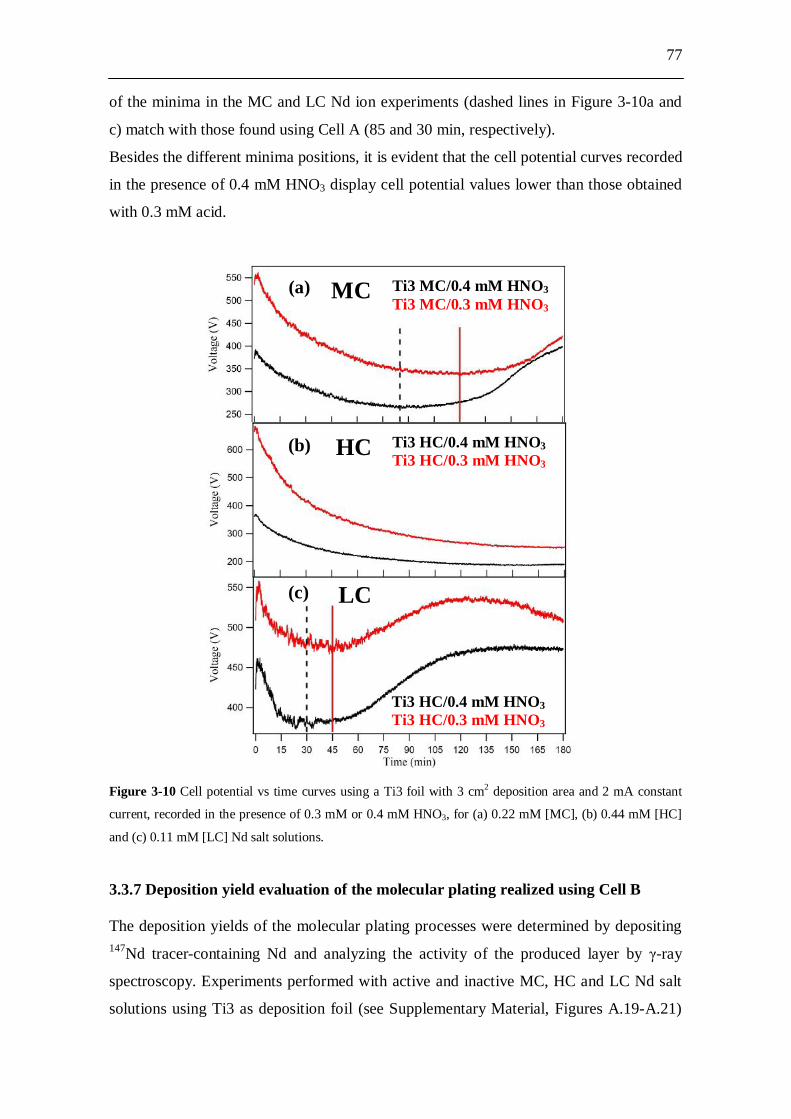
77
of the minima in the MC and LC Nd ion experiments (dashed lines in Figure 3-10a and
c) match with those found using Cell A (85 and 30 min, respectively).
Besides the different minima positions, it is evident that the cell potential curves recorded
in the presence of 0.4 mM HNO3 display cell potential values lower than those obtained
with 0.3 mM acid.
Figure 3-10 Cell potential vs time curves using a Ti3 foil with 3 cm2 deposition area and 2 mA constant
current, recorded in the presence of 0.3 mM or 0.4 mM HNO3, for (a) 0.22 mM [MC], (b) 0.44 mM [HC]
and (c) 0.11 mM [LC] Nd salt solutions.
3.3.7 Deposition yield evaluation of the molecular plating realized using Cell B The deposition yields of the molecular plating processes were determined by depositing 147Nd tracer-containing Nd and analyzing the activity of the produced layer by -ray
spectroscopy. Experiments performed with active and inactive MC, HC and LC Nd salt
solutions using Ti3 as deposition foil (see Supplementary Material, Figures A.19-A.21)
Ti3 MC/0.4 mM HNO3 Ti3 MC/0.3 mM HNO3
MC (a)
Ti3 HC/0.4 mM HNO3 Ti3 HC/0.3 mM HNO3
HC (b)
(c) LC
Ti3 HC/0.4 mM HNO3 Ti3 HC/0.3 mM HNO3

78
show the cell potential behaviours of the active and inactive Nd salt solutions to be
almost identical, indicating that the radiolysis of the solution induced by the - and -
radiation can be neglected.
The deposition yields (Table 3-7) were evaluated as average values at the characteristic
times of the cell potential curves recorded at the different Nd salt concentrations, using
Ti3, Ti4, and Ti5 cathodes in Cell B. As characteristic times, the end of the deposition
process (180 min) and the occurrence of minima (if present) and maxima in the cell
potential profiles were chosen.
Table 3-7 Average deposition yield values measured at different times for the MC, HC, and LC Nd salt
experiments using Ti3, Ti4, and Ti5 foils.
Experiment Time (min)
Ti3 yield value (%)
Ti4 yield value (%)
Ti5 yield value (%)
MC 45 83.7 ± 2.2 89.2 ± 2.0 71 ± 3 75 - 98.5 ± 1.2 - 90 98.3 ± 1.1 - 93.2 ± 2.7 180 95.6 ± 2.7 99.6 ± 0.4 98.7 ± 0.8
HC 80 87 ± 3 86 ± 5 84.5 ± 2.0 180 97 ± 4 98.3 ± 1.6 95 ± 5
LC 20 66 ± 3 66 ± 3 71 ± 6 180 99.1 ± 0.9 98.3 ± 1.7 98.1 ± 0.9
As regards the MC Nd salt experiments, after only 45 min the deposition yield is already
very high, over 70%. The highest yield is obtained with the Ti4 foils and the lowest one
with the Ti5 foils. At 90 min the yield values approach 100%. Notably, by using the Ti4
cathode, only 75 min of deposition are sufficient to obtain a deposition yield almost
identical to the final one.
Experiments at higher Nd concentration (HC) show that there is no real spread in yield
values at the time of minimum cell potential (80 min) as in the case of the MC Nd salt
experiments, and that all the values are similar and high. At the end of the deposition
process, almost all the yield values approach 100% (see Table 3-7). These high yields are
in line with earlier observations and confirm that MP is ideally suited for quantitatively
depositing Nd, which represents many trivalent elements like the lanthanides and the late
actinides. Concerning the lower Nd concentration measurements (LC), the times at which
the deposition yields were evaluated are the end of the process (180 min) and the time
corresponding to a major change in the slope of the cell potential curves (20 min),
because no minimum is found in these experiments. The yield values after 20 min are
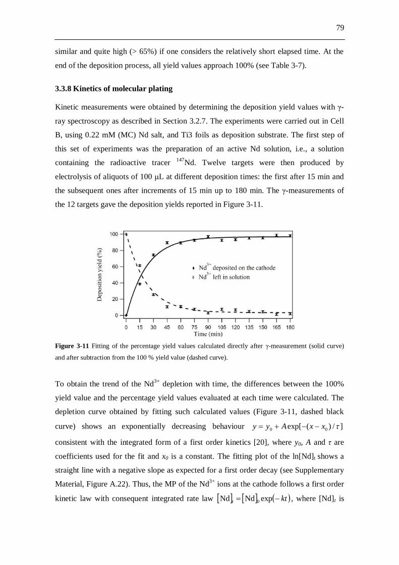
79
similar and quite high (> 65%) if one considers the relatively short elapsed time. At the
end of the deposition process, all yield values approach 100% (see Table 3-7).
3.3.8 Kinetics of molecular plating Kinetic measurements were obtained by determining the deposition yield values with -
ray spectroscopy as described in Section 3.2.7. The experiments were carried out in Cell
B, using 0.22 mM (MC) Nd salt, and Ti3 foils as deposition substrate. The first step of
this set of experiments was the preparation of an active Nd solution, i.e., a solution
containing the radioactive tracer 147Nd. Twelve targets were then produced by
electrolysis of aliquots of 100 L at different deposition times: the first after 15 min and
the subsequent ones after increments of 15 min up to 180 min. The -measurements of
the 12 targets gave the deposition yields reported in Figure 3-11.
Figure 3-11 Fitting of the percentage yield values calculated directly after -measurement (solid curve)
and after subtraction from the 100 % yield value (dashed curve).
To obtain the trend of the Nd3+ depletion with time, the differences between the 100%
yield value and the percentage yield values evaluated at each time were calculated. The
depletion curve obtained by fitting such calculated values (Figure 3-11, dashed black
curve) shows an exponentially decreasing behaviour ]/)(exp[ 00 xxAyy
consistent with the integrated form of a first order kinetics [20], where y0, A and are
coefficients used for the fit and x0 is a constant. The fitting plot of the ln[Nd]t shows a
straight line with a negative slope as expected for a first order decay (see Supplementary
Material, Figure A.22). Thus, the MP of the Nd3+ ions at the cathode follows a first order
kinetic law with consequent integrated rate law ktt expNdNd 0 , where [Nd]t is
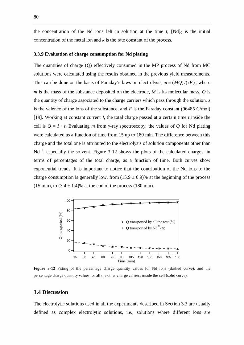
80
the concentration of the Nd ions left in solution at the time t, [Nd]0 is the initial
concentration of the metal ion and k is the rate constant of the process.
3.3.9 Evaluation of charge consumption for Nd plating The quantities of charge (Q) effectively consumed in the MP process of Nd from MC
solutions were calculated using the results obtained in the previous yield measurements.
This can be done on the basis of Faraday’s laws on electrolysis, )/()( zFMQm , where
m is the mass of the substance deposited on the electrode, M is its molecular mass, Q is
the quantity of charge associated to the charge carriers which pass through the solution, z
is the valence of the ions of the substance, and F is the Faraday constant (96485 C/mol)
[19]. Working at constant current I, the total charge passed at a certain time t inside the
cell is Q = I · t. Evaluating m from -ray spectroscopy, the values of Q for Nd plating
were calculated as a function of time from 15 up to 180 min. The difference between this
charge and the total one is attributed to the electrolysis of solution components other than
Nd3+, especially the solvent. Figure 3-12 shows the plots of the calculated charges, in
terms of percentages of the total charge, as a function of time. Both curves show
exponential trends. It is important to notice that the contribution of the Nd ions to the
charge consumption is generally low, from (15.9 ± 0.9)% at the beginning of the process
(15 min), to (3.4 ± 1.4)% at the end of the process (180 min).
Figure 3-12 Fitting of the percentage charge quantity values for Nd ions (dashed curve), and the
percentage charge quantity values for all the other charge carriers inside the cell (solid curve).
3.4 Discussion The electrolytic solutions used in all the experiments described in Section 3.3 are usually
defined as complex electrolytic solutions, i.e., solutions where different ions are

81
contemporarily dissolved. The electrolytes present in our electrolytic solutions,
Nd(NO3)3·6H2O and HNO3, are strong electrolytes. Moreover, they are both present in
very small concentrations ranging from 0.11 up to 0.44 mM for Nd(NO3)3·6H2O, and
from 0.3 to 0.4 mM for HNO3. Thus, both the electrolytes inside the solution are
reasonably totally dissociated. All the ions deriving from these dissociations contribute,
according to their mobility, to the current flow inside the cell. If we consider only the
cathode of the system, the XPS results shown in Section 3.3.3 clearly indicate that Nd is
present as Nd3+ on the layer deposited after molecular plating. In addition, reduction of
H+ originating from HNO3 and H2O occurs. This conclusion can be inferred also from the
results shown in Section 3.3.6, especially looking at the curves of the Figures 3-10a and
c, where it is evident that an increase in HNO3 concentration (from 0.3 to 0.4 mM)
lowers the cell potential trends of the curves and shifts the minima of the curves to lower
time values. Moreover, because of the undivided cells used, the oxidation of the Pd anode
creates Pd ions which are reduced at the cathode, as proved by the XPS Pd 3d lines
(Figure 3-3). Nevertheless, the reduction of these ions does not start at the beginning of
the deposition process as follows from the XPS analysis of the 30-min plating time
samples, which showed no indication of Pd. Finally, at the very high cell potential values
applied during all MPs, electrolysis of the solvent occurs, as suggested by the C 1s
spectra recorded via XPS analysis of the deposited surfaces.
The flux Ji of an electroactive species towards an electrode, i.e., the moles of the ith
species per unit of surface of the electrode and per unit of time, is expressed by the
Nernst-Planck equation. For a one-dimensional flux, this is
xvCx
CDRT
FzxCDxJ iii
iiii [21], where
xCD i
i represents the diffusive
term, x
CDRT
Fzii
i the migration term, and xvCi the convective term; Di, Ci and zi
are the diffusion coefficient, the concentration and charge number of the ith species,
respectively, the Galvani potential, and v the convective velocity. In a MP experiment,
the description of the flux of an electroactive species reaching the cathode involves all
three terms. The migration term has to be taken into account because no support
electrolyte is present in solution. The convective term has to be considered since the
solutions are constantly mixed by ultrasonic stirring.
Once the current has been fixed for a certain constant current density MP, the ionic flux
towards an electrode is constant. In a MP cell, where different electroactive species are
deposited, the total ionic flux will be the sum of the fluxes of all electroactive ions

82
involved in the plating process. An increase (or decrease) of the concentration of one of
the electroactive species inside the cell solution, increases (or decreases) the
corresponding flux of its ions towards the cathode, but the total flux stays constant. In the
case of the HC, MC and LC experiments performed with both Cells A and B, the flux of
Nd ions was then the highest in the HC experiments and the lowest in the LC
experiments. This means that a higher Nd3+ concentration yields a higher number of Nd3+
ions per unit cathode area and unit time. This may explain why HC targets were found to
be rougher than both MC and LC targets, as reported in Table 3-4 and shown by the
AFM images in Figure 3-2. A higher number of ions reaching the cathode per unit area
and unit time will not find place and time to organize themselves in an orderly fashion
and hence will promote a disordered layer growth. The opposite will happen with a lower
number of ions.
All cell potential curves reported in Section 3.3 show a steep increase for a short time at
the very beginning of each deposition process. A likely explanation for such an increase
is that constant current density MPs, implying electrolysis, create a high polarization of
the electrodes, which causes a change in cell potential inside the electrochemical system
and hence a starting increase in all the recorded curves.
The shape of the cell potential curves strongly depends on the concentrations of the
electrolytes present in solution. Changing the concentrations of Nd(NO3)3·6H2O (LC,
MC and HC), and/or HNO3 (0.3 and 0.4 mM) tends to change not only the cell potential
trends (lower cell potential at higher concentrations) but also the time positions of the
cell potential minima. It is then evident that there must be a relationship between cell
potential and electrolyte concentrations. A simple relationship can be obtained if the cell
potential is mainly controlled by the ohmic drop IR, or in other words, if Ohm’s first law
can be applied to the systems. When a current passes through an electrochemical cell, the
overall cell potential is given by the difference between the equilibrium potential of the
two semi-reactions occurring at the cathode and anode, plus a series of overpotentials
(e.g., activation, concentration, crystallization, etc.) characteristic of the electrode
reaction and the ohmic drop due to the solution resistance. If the process occurs in a
highly resistive medium (i.e., very low electrolyte concentration and/or low conductivity
medium) the ohmic drop may dominate the overall cell potential. This seems to be the
case in the systems studied here. In fact, in both Cell A and Cell B the total electrolyte
concentration (< 1 mM) was at least two orders of magnitude smaller than those typically
used in electrochemical systems. On the other hand, both cells have shown extremely
83
high (500-1000 V) cell potentials, not compatible with the usual overpotential values
involved in electrode reactions.
This assumption was checked for both Cell A and Cell B, evaluating the IR contribution
from the values of the cell resistances R and the applied constant currents (Section 3.3.1).
In both cases, the calculated IR values were close to the experimental cell potentials
measured at different Nd(NO3)3·6H2O and HNO3 concentrations, clearly indicating that
in all experimental conditions V is dominated by the ohmic drop. Since the current is
transported by all the ions present in solution, the conductivity depends on the total
concentration of the electrolytes. Neglecting all other contributions except IR, the cell
potential can be easily expressed as i iii c
ljV 1103 , where j is the applied
current density, l is the distance between the electrodes, and i, ci and i are the number
of equivalents, concentration and equivalent conductivity of any ith electrolyte,
respectively. This expression explains why at higher electrolyte concentrations lower cell
potential trends are observed (and vice versa). From such an expression, however, it does
not yet follow why minima are observed in almost all of the cell potential curves shown
in Section 3.3. Nonetheless, it is significant to notice that the yield measurements
performed in the experiments with Cell B always showed the different minima of the
recorded cell potential curves to correspond to almost complete depletion of Nd3+ ions.
This result was especially well shown by the MP kinetics derived in Section 3.3.8 and
can help to understand why lower time minima were observed with lower Nd salt
concentrations, while higher time minima were observed with higher Nd salt
concentrations. Specifically, as reported in Table 3-6 and clearly shown in Figure 3-9,
HC experiments, characterized by Nd salt concentrations twice as high as in the MC
experiments, have time positions of the minima almost twice those of the MC
experiments. Conversely, LC experiments, characterized by Nd salt concentrations half
those of the MC experiments, have time positions of the minima almost half those of the
MC experiments (except for the LC experiments in Cell B where no significant minimum
was found). In fact, once a certain constant current has been fixed inside a cell, the
depletion kinetics of Nd ions is fixed as well (even if different Nd salt concentrations
imply different Nd ion fluxes to the cathode). For this reason, with a double amount of
Nd ions, the almost complete depletion of such ions will be reached at times almost the
double of the times of the MC experiments. Conversely, with half the amount of Nd ions,
almost complete depletion of such ions will be reached at times about half those of the
84
MC experiments. In the same perspective, if a comparison is made between the
experiments realized with Cell A and Cell B where the current density was the same, but
the applied constant currents were different, it can be explained why the time positions of
the minima of the cell potential curves recorded with Cell A are always higher than those
recorded with Cell B. A lower constant current (2 mA, Cell A) will imply a slower
depletion kinetics of the Nd ions, while a higher constant current (6 mA, Cell B) will
imply a faster depletion kinetics of the same ions.
All cell potential curves recorded during constant current density MPs realized with Cell
A and Cell B also proved to have shapes strongly influenced by the surface roughness of
the electrodes, as shown by the different behaviours of the curves recorded using
different cathodes. Deposition substrates with different surface roughness were indeed
used in all MPs realized with both Cells A and B. In the experiments performed using
Cell A, where Ti1 and Ti2 foils had similar surface roughness, no differences in the cell
potential curve behaviours were noted among all curves recorded at the different Nd salt
concentrations (HC, MC and LC). In the experiments performed using Cell B, instead,
the foils Ti3, Ti4, and Ti5 had different surface roughness. No significant differences in
cell potential behaviour were noted for the LC, MC and HC cell potential curves
recorded using Ti3 and Ti5 foils. The main difference was instead shown by the curves
recorded using Ti4 foils: all these curves, in fact, showed a lower cell potential trend at
each of the Nd salt concentrations. This fact can be explained considering the expression
for the cell resistance, i.e., R = ·l/S, where l/S is the inverse of the cell constant. With
smooth electrodes like Ti1, Ti2, Ti3, and Ti5 the exposed surface area, i.e., the real
surface, is not significantly different from the geometric surface. Instead, in the case of
highly rough surfaces like Ti4 (see Table 3-2), the real surface area is much larger than
the geometric one. This causes the cell constant (S/l) to increase and the solution
resistance (R= ·l/S) to decrease, resulting in a decrease of the cell potential, according
to Ohm’s first law.
3.5 Conclusion In order to understand and improve the molecular plating technique for the production of
targets to be applied in nuclear science, several constant current density MPs were
performed using Nd as model element. The variables chosen for these investigations
were: concentration of the electrolytes, applied current, and surface roughness of the
deposition substrates. The influence of changes in these variables on the deposition
85
processes was monitored recording cell potential vs time, and the obtained deposits were
analyzed using -ray spectroscopy, XPS, and AFM.
In the complex electrolytic solutions used to perform the MPs, the electroactive species
involved in the cathodic processes were Nd3+ and H+ ions deriving from the dissociations
of the starting strong electrolytes. Additional electroactive species were proved to be Pd
ions from the oxidation of the Pd anode, as well as the electrolyzed mixed solvent.
Noteworthy, XPS results clearly show that, after MP, Nd is deposited on the cathodic
surface as derivatives of Nd3+, possibly as carboxylate, oxide or hydroxide. This
important outcome, that elucidates the fate of Nd3+ after MP, is reasonable on the basis of
the high negative value of the Nd3+/Nd standard redox potential (E° = -2.323 V), typical
of lanthanide cations [22].
The cell potentials in the investigated systems were found to be mainly affected by the
solution resistance. An expression which relates cell potential with conductance and
hence electrolyte concentration was therefore derived. This approach allows for
explaining the cell potential trends recorded using different concentrations of the
electrolytes. We notice that the performed yield measurements always showed an almost
complete depletion of the Nd ions at the minima of the different cell potential curves.
This result was especially well shown by the derived first order kinetics of the MP.
According to these experimental results, reasonable explanations were given to the
recorded trends of the cell potential curves when different Nd salt concentrations and
different currents are applied during the investigated MPs. However, our derived
expression is not sufficient to fully interpret the reasons leading to the minima in the cell
potential curves.
The trends of the cell potential curves were found to be also influenced by the roughness
of the deposition substrates, because this implies different cell constants. Moreover, the
roughness of the starting substrates, together with the initial concentration of the
electrolyte to be plated, proved to strongly influence the final surface roughness of the
MP-grown layers.
Our work, which exploits a variety of analytical techniques and combines this with a
theoretical approach on the MP process, has yielded a better understanding of important
basic features of constant current density MP.
86
Acknowledgements The authors would like to thank the staff of the TRIGA Mainz for performing the
irradiations, the GSI target laboratory for providing the ADVENT and LEBOW Ti foils,
and Dr. T. Lauer for performing the coating of the Si wafers. A. Vascon would like to
thank Fu-Kai Chang from the Institute of Mathematics of Mainz University for the
fruitful discussions had together. Moreover A. Vascon would like to acknowledge
financial support from the German Federal Ministry of Science and Education (BMBF)
under Contract number 02NUK013E.
3.6 Appendix A. Supplementary Material Figure Captions: Figure A.1 C 1s XPS spectrum of a Ti 3 foil, inserted into the glove-box, cleaned with
HCl, H2O and isopropanol, immersed into an isopropanol/isobutanol solution and then
dried.
Figure A.2 XPS spectra of the washed and air-dried Pd foil: Pd 3d before sputtering
(indicated as 0 min sputtering in the figure), and after 10 min sputtering with Ar+ ions.
Figure A.3 XPS spectra of the washed and air-dried Pd foil: C 1s before sputtering
(indicated as 0 min sputtering in the figure), and after 10 min sputtering with Ar+ ions.
Figure A.4 Voltage vs Time curves recorded as reproducility tests in the MC Nd salt
MPs realized using Ti1 foils. The minimum of the curves is indicated by a vertical
dashed blue line.
Figure A.5 Voltage vs Time curves recorded as reproducility tests in the MC Nd salt
MPs realized using Ti2 foils. The minimum of the curves is indicated by a vertical
dashed blue line.
Figure A.6 Voltage vs Time curves recorded as reproducility tests in the HC Nd salt
MPs realized using Ti1 foils.
Figure A.7 Voltage vs Time curves recorded as reproducility tests in the HC Nd salt
MPs realized using Ti2 foils.
Figure A.8 Voltage vs Time curves recorded as reproducility tests in the LC Nd salt MPs
realized using Ti1 foils. The minimum of the curves is indicated by a vertical dashed blue
line.
Figure A.9 Voltage vs Time curves recorded as reproducility tests in the LC Nd salt MPs
realized using Ti2 foils. The minimum of the curves is indicated by a vertical dashed blue
line.
87
Figure A.10 Voltage vs Time curves recorded as reproducility tests in the MC Nd salt
MPs realized using Ti3 foils. The minimum of the curves is indicated by a vertical
dashed blue line.
Figure A.11 Voltage vs Time curves recorded as reproducility tests in the MC Nd salt
MPs realized using Ti4 foils. The minimum of the curves is indicated by a vertical
dashed blue line.
Figure A.12 Voltage vs Time curves recorded as reproducility tests in the MC Nd salt
MPs realized using Ti5 foils. The minimum of the curves is indicated by a vertical
dashed blue line.
Figure A.13 Voltage vs Time curves recorded as reproducility tests in the HC Nd salt
MPs realized using Ti3 foils. The minimum of the curves is indicated by a vertical
dashed blue line.
Figure A.14 Voltage vs Time curves recorded as reproducility tests in the HC Nd salt
MPs realized using Ti4 foils. The minimum of the curves is indicated by a vertical
dashed blue line.
Figure A.15 Voltage vs Time curves recorded as reproducility tests in the HC Nd salt
MPs realized using Ti5 foils. The minimum of the curves is indicated by a vertical
dashed blue line.
Figure A.16 Voltage vs Time curves recorded as reproducility tests in the LC Nd salt
MPs realized using Ti3 foils.
Figure A.17 Voltage vs Time curves recorded as reproducility tests in the LC Nd salt
MPs realized using Ti4 foils.
Figure A.18 Voltage vs Time curves recorded as reproducility tests in the LC Nd salt
MPs realized using Ti5 foils.
Figure A.19 comparisons between Ti3 cell potential curves recorded using active and
inactive MC Nd salt solutions.
Figure A.20 comparisons between Ti3 cell potential curves recorded using active and
inactive HC Nd salt solutions.
Figure A.21 comparisons between Ti3 cell potential curves recorded using active and
inactive LC Nd salt solutions.
Figure A.22 ln[Nd]t values against time (dashed black line).
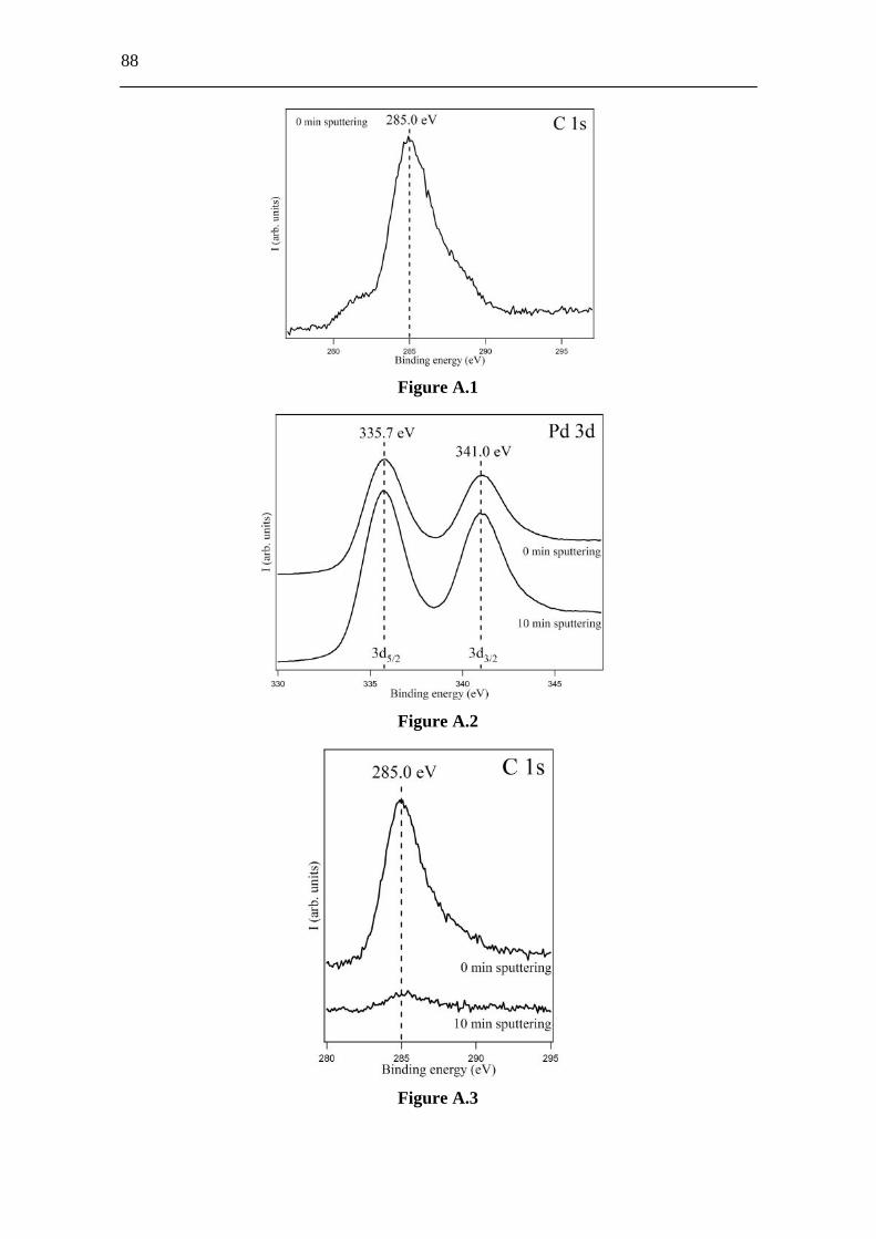
88
Figure A.1
Figure A.2
Figure A.3
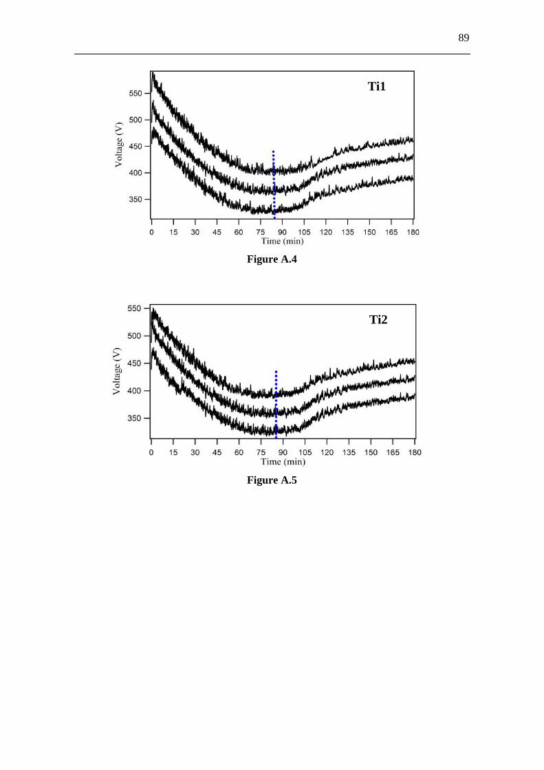
89
Figure A.4
Figure A.5
Ti1
Ti2
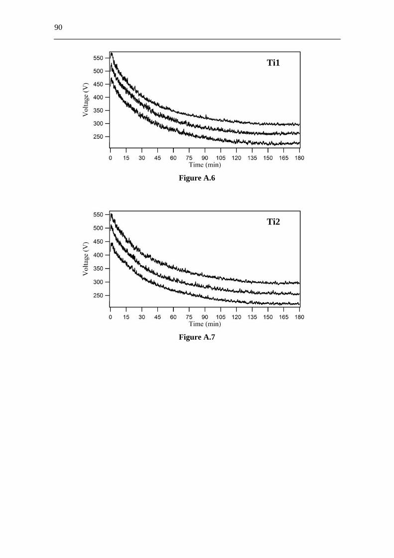
90
Figure A.6
Figure A.7
Ti1
Ti2
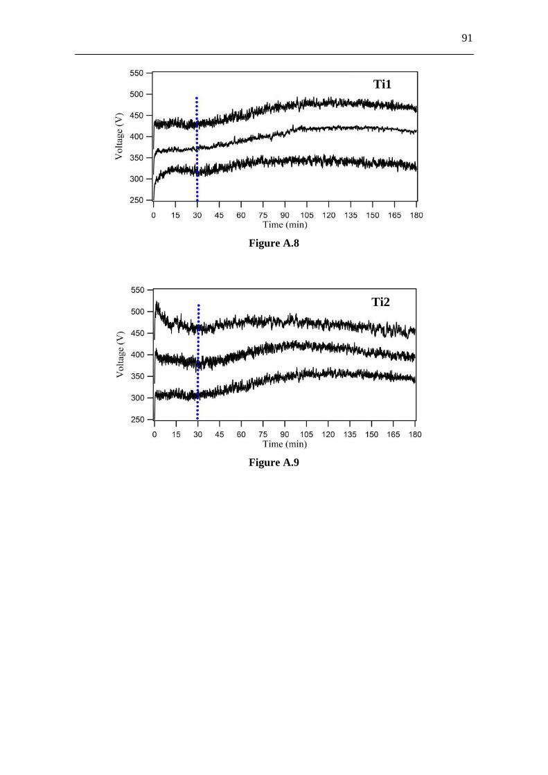
91
Figure A.8
Figure A.9
Ti1
Ti2

92
Figure A.10
Figure A.11
Figure A.12
Ti3
Ti4
Ti5
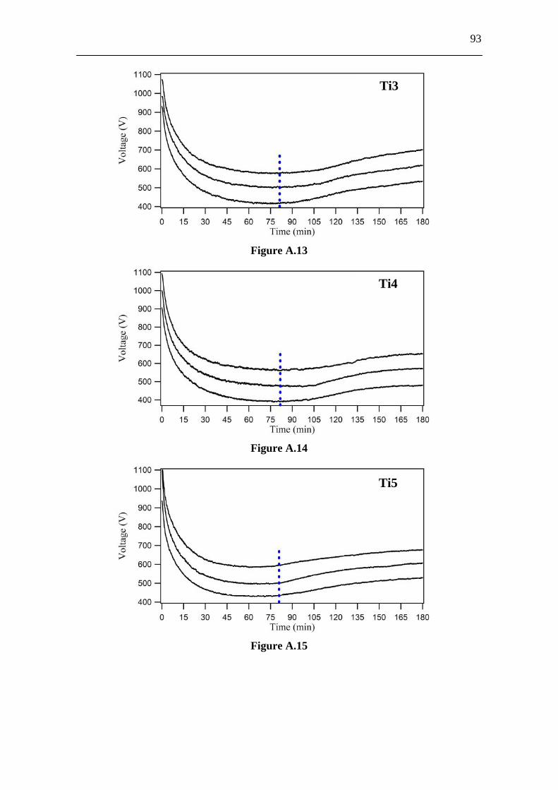
93
Figure A.13
Figure A.14
Figure A.15
Ti3
Ti4
Ti5
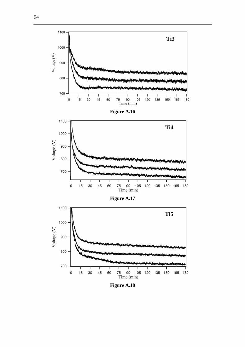
94
Figure A.16
Figure A.17
Figure A.18
Ti3
Ti4
Ti5
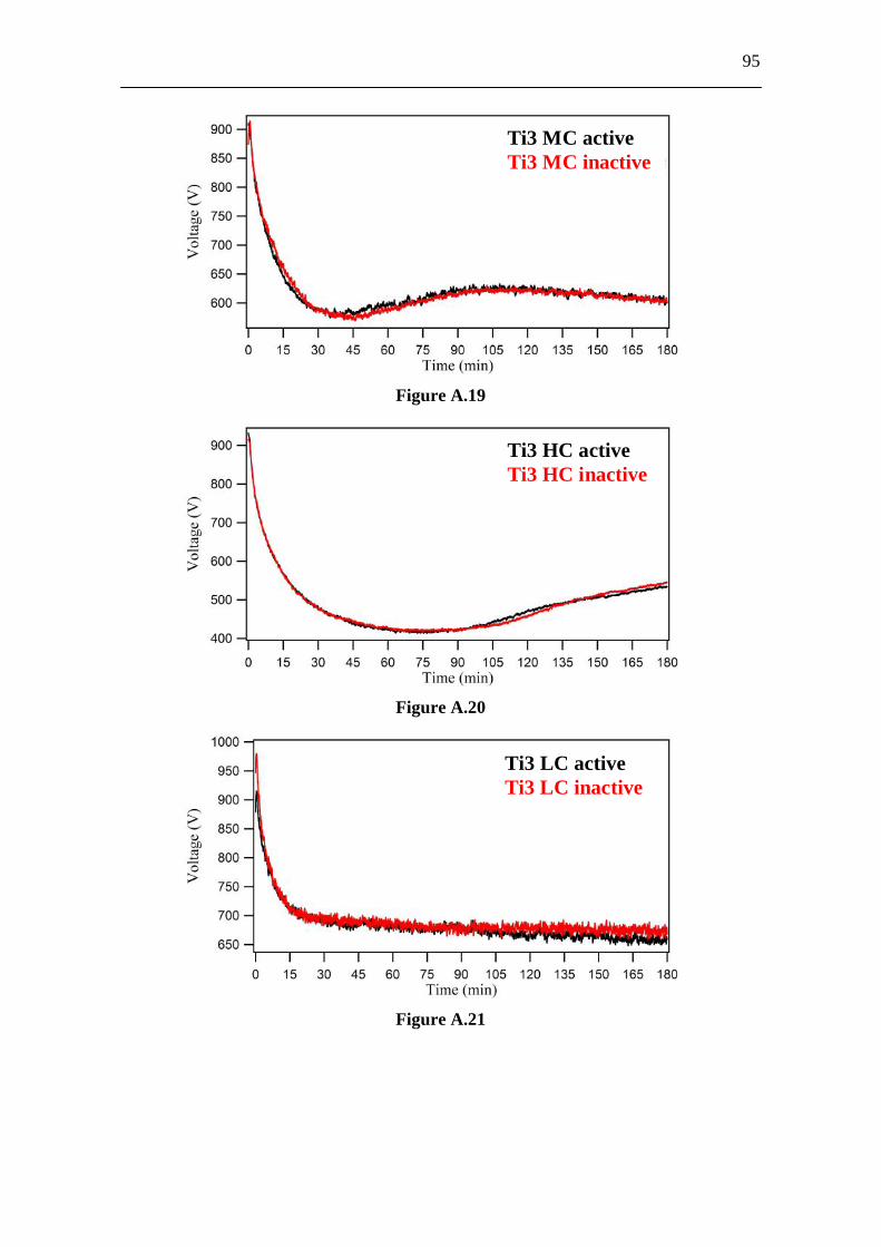
95
Figure A.19
Figure A.20
Figure A.21
Ti3 MC active Ti3 MC inactive
Ti3 HC active Ti3 HC inactive
Ti3 LC active Ti3 LC inactive
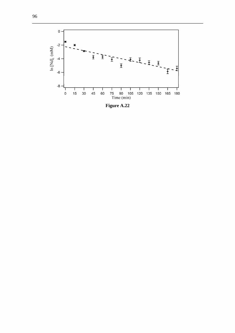
96
Figure A.22

97
References [1] W. Parker, R. Falk, Nucl. Instrum. Methods 16 (1962) 355-357.
[2] W. Parker, H. Bildstein, N. Getoff, Nucl. Instrum. Methods 26 (1964) 55-60.
[3] W. Parker, H. Bildstein, N. Getoff, H. Fischer-Colbrie, H. Regal, Nucl. Instrum.
Methods 26 (1964) 61-65.
[4] W. Parker, H. Bildstein, N. Getoff, Nucl. Instrum. Methods 26 (1964) 314-316.
[5] N. Getoff, H. Bildstein, Nucl. Instrum. Methods 36 (1965) 173-175.
[6] N. Getoff, H. Bildstein, Nucl. Instrum. Methods 70 (1969) 352-354.
[7] A. Becerril-Vilchis, A. Cortès, F. Dayras, J. De Sanoit, Nucl. Instrum. Meth. A 369
(1996) 613-616.
[8] N. Trautmann, H. Folger, Nucl. Instrum. Meth. A 282 (1989) 102-106.
[9] B.W. Filippone, M. Wahlgren, Nucl. Instrum. Meth. A 243 (1986) 41-44.
[10] J.E. Evans, R.W. Lougheed, M.S. Coops, R.W. Hoff, E.K. Hulet, Nucl. Instrum.
Methods 102 (1972) 389-401.
[11] K. Eberhardt, W. Brüchle, Ch.E. Düllmann, K.E. Gregorich, W. Hartmann, A.
Hübner, E. Jäger, B. Kindler, J.V. Kratz, D. Liebe, B. Lommel, H.-J. Maier, M. Schädel,
B. Schausten, E. Schimpf, A. Semchenkov, J. Steiner, J. Szerypo, P. Thörle, A. Türler,
A. Yakushev, Nucl. Instrum. Meth. A 590 (2008) 134-140.
[12] S. Sadi, A. Paulenova, P.R. Watson, W. Loveland, Nucl. Instrum. Meth. A 655
(2011) 80-84.
[13] P.R. Watson, W. Loveland, P.M. Zielinski, K.E. Gregorich, H. Nitsche, Nucl.
Instrum. Meth. B 226 (2004) 543-548.
[14] Q.X. Jia, T.M. McCleskey, A.K. Burrell, Y. Lin, G.E. Collis, H.Wang, A.D.Q. Li,
S.R. Foltyn, Nat. Mater. 3 (2004) 529-532.
[15] M.A. Garcia, M.N. Ali, T. Parsons-Moss, P.D. Ashby, H. Nitsche, Thin Soild Films,
516 (2008) 6261-6265.
[16] A. Vascon, Ch.E. Düllmann, K. Eberhardt, B. Kindler, B. Lommel, J. Runke, Nucl.
Instrum. Meth. A 655 (2011) 72-79.
[17] H. Haba, D. Kaji, T. Takabe, H. Kikunaga, RIKEN, Accel. Prog. Rep. 39 (2006)
109.
[18] C.D. Wagner, W.M. Riggs, L.E. Davis, J.F. Moulder, G.E. Muilenberg, Handbook
of X-Ray Photoelectron Spectroscopy, Perkin-Elmer Corporation, Physical Electronics
Division, Eden Prairie, Minn. 55344 (1979).

98
[19] S. Glasstone, An Introduction to Eletrochemistry, first ed., Litton Educational
Publishing, Inc., New York, 1942.
[20] K. J. Laidler, Chemical Kinetics, third ed., Prentice Hall, New York, 1987.
[21] P. Atkins, J. De Paula, Atkins’ Physical Chemistry, seventh ed., Oxford University
Press, Oxford, 2002.
[22] CRC Handbook of Chemistry and Physics, 87th ed., D. R. Lide Ed., 2006.
99
4. Fundamental aspects of molecular plating and production of
smooth crack-free Nd targets
A. Vascon1, S. Santi2, A.A. Isse2, T. Reich1, J. Drebert1, H. Christ3, K. Eberhardt1,5,
Ch.E. Düllmann1,4,5
1Institute of Nuclear Chemistry, Johannes Gutenberg University Mainz, 55099 Mainz,
Germany 2Department of Chemical Sciences, University of Padova, 35131 Padova, Italy 3Institute of Physical Chemistry, Johannes Gutenberg University Mainz, 55099 Mainz,
Germany 4SHE Chemistry Department, GSI Helmholtzzentrum für Schwerionenforschung GmbH,
64291 Darmstadt, Germany 5SHE Chemistry Research Section, Helmholtz Institute Mainz, 55099 Mainz, Germany
Accepted for publication in:
Journal of Radioanalytical and Nuclear Chemistry (2012).
This paper is a contribution to the proceedings of the 26th World Conference of the
International Nuclear Target Development Society (INTDS), held August 19-24, 2012, in
Mainz, Germany.
100
Abstract A general understanding of the molecular plating process was obtained recently, which
serves as a first step towards further improvements of the method aiming, for example, at
the production of smooth, crack-free targets for nuclear physics applications. Constant
current density electrolysis experiments were performed in organic media containing the
model electrolyte [Nd(NO3)3·6H2O]. The process was investigated by considering
influences of the electrolyte concentration (0.11, 0.22, 0.44 mM), the surface roughness
of the deposition substrates (a few tens of nm), and the plating solvent (an
isopropanol/isobutanol mixture, and N,N-dimethylformamide). The response of the
process to changes of these parameters was monitored by recording cell potential curves
and by characterizing the obtained deposits with -ray spectroscopy, X-ray photoelectron
spectroscopy, and atomic force microscopy. By changing the solvent from
isopropanol/isobutanol mixtures to N,N-dimethylformamide, we have succeeded in
producing smooth, crack-free Nd targets.
Keywords: thin layers, neodymium, molecular plating, -ray spectroscopy, X-ray
photoelectron spectroscopy (XPS), atomic force microscopy (AFM)
4.1 Introduction Molecular Plating (MP) is one of the most widely applied methods for the production of
thin layers to be used as sources of stationary nuclei, i.e., targets, for accelerator and
reactor science. The term of molecular plating was coined by Parker and Falk [1] to
denote either a constant current or a constant voltage electrodeposition in an organic
medium. The method is well-known to quickly produce deposits of acceptable uniformity
and adherence with quantitative yield [2,3]. Despite the wide use of MP, few are the
attempts reported where a microscopic characterization of the layers was performed
[4,5], investigating for example the common effect of cracking of the produced surfaces
[6]. Moreover, an exhaustive elucidation of even some main features of the process is
still largely lacking. To date, the focus of MP experiments has almost exlusively been on
empirically improving the produced layers. In this situation we have chosen a systematic
approach, studying basic features of MP with the aim of reducing the knowledge gap
between MP and well established electrochemical methods, and to exploit the better
insight to further increase the efficiency of the method and to improve the obtained
targets. An extensive investigation of the molecular plating process was hence carried out
101
by performing constant current density electrolysis experiments in organic media, where
a neodymium salt was used as a model electrolyte [7]. Electrolyte concentration and
surface roughness of the deposition substrates were varied to investigate the process. In
addition, we report here on experiments where the solvent was changed from
isopropanol/isobutanol mixtures to N,N-dimethylformamide (DMF). Cell potential
curves were recorded to monitor the response of the process to the variables and a
theoretical description of important basic features of constant current density MP was
formulated. Several analytical techniques were applied to characterize the produced
layers and the results were used to define the best parameters to produce smooth and
crack-free Nd targets. A full account of our studies including further MPs under
conditions not described in this article can be found in [7]. Here, we rather present some
of the most interesting aspects of this work and give new results on experiments in DMF.
These will be presented in more detail in a forthcoming publication [8].
4.2 Experimental 4.2.1 Target production All constant current density MPs were performed in a cell (see Figure 3-1 in [7])
characterized by a central polyether ether ketone (PEEK) body where the electrolytic
solution was inserted. The Ti anode of the cell was covered by a circular Pd foil, and the
Ti cathode by a circular Ti foil. The Pd anode and Ti cathode had an area of 9 cm2, and
they were in physical contact with water-cooled Ti blocks used to maintain a constant
temperature (T = 16 °C). Two different Ti foils, hereafter called Ti-A and Ti-B, were
used as backing material for the MPs. These foils had different surface roughnesses,
which, after the cleaning procedure, were: 24 ± 7 nm for Ti-A, and 12.8 ± 0.7 nm for Ti-
B. Ti-A was a circular 50 m-thick Ti foil cut from a bigger foil (Goodfellow). Ti-B was
produced by coating a 300- m thick mechanically-polished Si wafer onto which 100 nm
of metallic Ti were sputtered. For more details about the MP cell and the deposition
substrates we refer to [7].
Before any deposition, both the Pd anode and the cathode (Ti foils) were cleaned with
6 M HCl, water, and isopropanol. For the MPs, solutions with three different
concentrations were prepared dissolving increasing amounts of Nd(NO3)3·6H2O in 0.1 M
HNO3. From each solution an aliquot of 100 L was added to a mixture of 1 mL
isopropanol (Fisher Chemical) and 34 mL isobutanol (Applichem), or to 35 mL of N,N-
dimethylformamide -DMF- (Merck), finally obtaining three different solutions of Nd3+ in

102
both solvents. These solutions are referred to as low concentration (LC, 0.11 mM),
medium concentration (MC, 0.22 mM) and high concentration (HC, 0.44 mM). Inside
the cell the concentration of HNO3 was 0.3 mM and the solutions were stirred by means
of a quartz tip ultrasonic stirrer (Bandelin Sonopuls HD 2070) operated at 30% power
pulse, which was previously shown to be as efficient as mechanical stirring [6]. MP
experiments were carried out for 3 hours by applying a constant current of 6 mA. The
current density was 0.7 mA/cm2.
4.2.2 Target characterization The surface roughness of the deposited layers, i.e., the measure of the texture of a surface
quantified by the vertical deviations of a real surface from its ideal planar form, was
investigated by using Atomic Force Microscopy (AFM) (MFP 3D Asylum Research).
AFM investigations were performed in air and in liquid.
The AFM analysis was the same for all the produced targets: (5 × 5) m2 and (25 × 25)
m2 images were recorded for each target and (1.5 × 1.5) m2 masks were used to
evaluate root mean square (RMS) values in different positions inside the images. For
those samples which showed surfaces with cracks, the RMS values were evaluated using
masks only in the crack-free areas, as the cracks do not belong to the surface and hence
do not define the real roughness of the deposited layers. The final surface roughness
value of each of the image sizes was evaluated as the arithmetic mean of all the RMS
values (i.e., RMS ). More details about the AFM analysis can be found in [7].
A chemical surface characterization of a Ti-A sample after an isobutanol/isopropanol MC
experiment was performed using X-ray Photoelectron Spectroscopy (XPS). Al K and
Mg K radiations were employed. The X-ray source was operated at a 10 kV anode
voltage and a current of 10 mA. The pass-energy of the hemispherical energy analyzer
was 50 eV. The pressure inside the ultra-high vacuum chamber was in the range of (1.2-
2.0)·10-9 mbar. At the end of the deposition time, the cell was top-sealed and inserted
into a glove-box, where an inert environment was assured by a constant Ar pressure (0.5
mbar, O2 < 1 ppm, H2O < 1 ppm). The solvent was extracted from the cell and the
sample dried. Drying in an inert environment allowed performing a chemical surface
analysis with unaltered products of reduction and oxidation obtained during the plating
process. After the first surface investigation, the sample underwent two ten-minute
sputtering cycles using 4 kV Ar+ ions. After each ten-minute sputtering cycle, the surface
of the sample was analyzed by XPS. By fitting the XPS spectra, the binding energies of
103
the XPS lines of interest were determined. The experimental uncertainty of the binding
energies is ± 0.1 eV.
The deposition yield of the MP process was determined via -ray spectroscopy (GEM
series HPGe Detector Model No. GEM 23158 P-Plus, ORTEC Company). This
technique was used after MP of Nd solution containing radioactive 147Nd tracer. For this,
an aliquot of 100 L of the stock solution was irradiated with thermal neutrons in the
TRIGA research reactor at the Institute of Nuclear Chemistry at the University of Mainz;
the irradiation produced a solution that contained a radioactive tracer of the element to be
plated (Nd: 147Nd, -, t1/2 = 10.98 d, E = 91 keV). To obtain quantitative data, reference
sources with known amounts of the tracer were prepared. Absolute yields were evaluated
at different times of interest as the average value calculated from three distinct -ray
measurements.
4.3 Results and discussion MPs on Ti-A and Ti-B foils were performed using isopropanol/isobutanol solutions
containing 0.22 mM Nd salt (MC) and applying a current density of 0.7 mA/cm2 for
three hours. Despite the different surface roughness of the two deposition substrates, the
obtained cell potential curves display a similar behaviour (Figure 4-1a): after an initial
increase within the first few minutes, the cell potential decreases within 45 min (dashed
line), and then increases to a maximum value. The maximum is not very pronounced but
forms a wide plateau, ranging from around 90 min to 120 min, with the highest value
located at around 110 min. After the maximum, the two cell potential curves tend to
slightly decrease with time. The cell potentials display again similar behaviour during
MP in 0.44 mM Nd salt solutions (HC) (Figure 4-1b): after the initial increase (zoom in
Figure 4-1b), the cell potential strongly decreases within 80 min (dashed line) and then
slightly increases. Similar behaviour of the cell potential profiles was also recorded
during the molecular plating with 0.11 mM Nd salt solutions (LC): after the initial
increase, the cell potential decreases exponentially within 20 min (no minimum is
present), and then decreases almost linearly with time (Figure 4-1c).
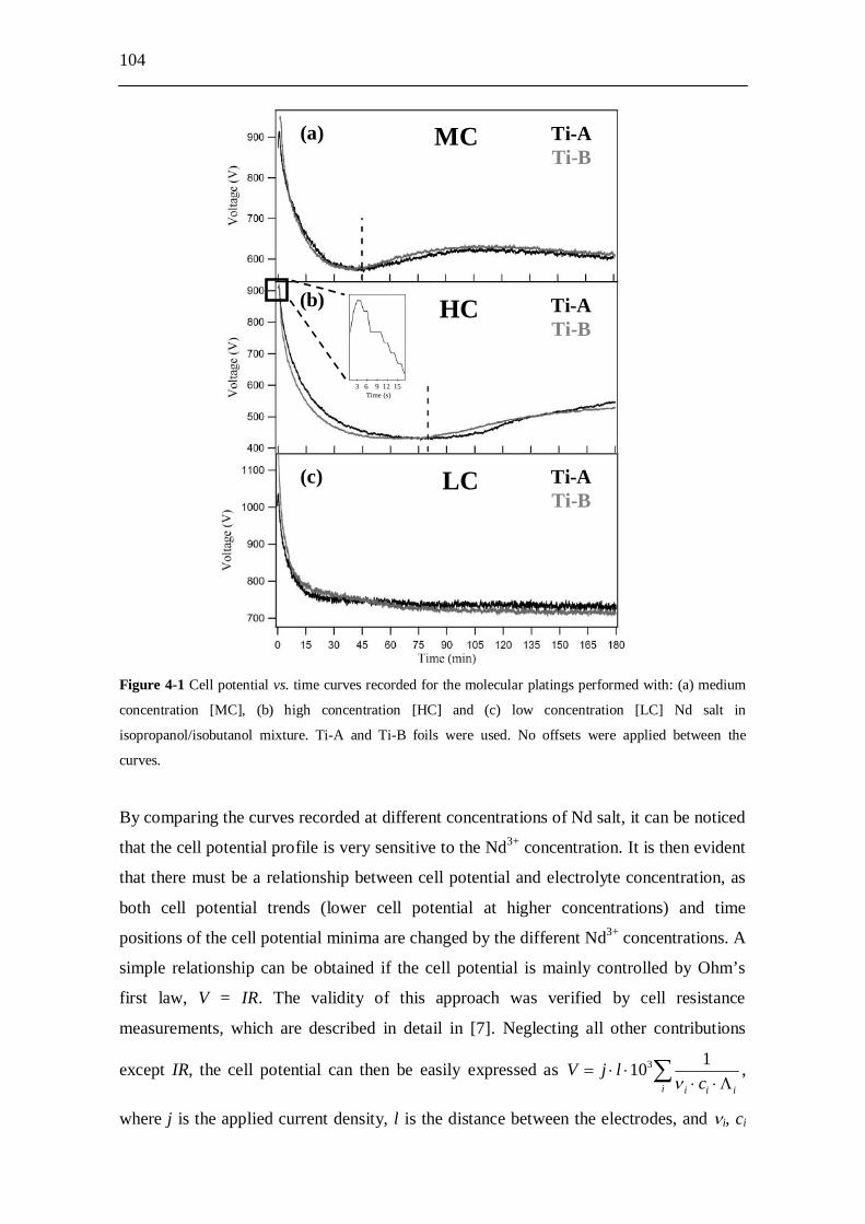
104
Figure 4-1 Cell potential vs. time curves recorded for the molecular platings performed with: (a) medium
concentration [MC], (b) high concentration [HC] and (c) low concentration [LC] Nd salt in
isopropanol/isobutanol mixture. Ti-A and Ti-B foils were used. No offsets were applied between the
curves.
By comparing the curves recorded at different concentrations of Nd salt, it can be noticed
that the cell potential profile is very sensitive to the Nd3+ concentration. It is then evident
that there must be a relationship between cell potential and electrolyte concentration, as
both cell potential trends (lower cell potential at higher concentrations) and time
positions of the cell potential minima are changed by the different Nd3+ concentrations. A
simple relationship can be obtained if the cell potential is mainly controlled by Ohm’s
first law, V = IR. The validity of this approach was verified by cell resistance
measurements, which are described in detail in [7]. Neglecting all other contributions
except IR, the cell potential can then be easily expressed as i iii c
ljV 1103 ,
where j is the applied current density, l is the distance between the electrodes, and i, ci
3 6 9 12 15 Time (s)
Ti-A Ti-B
Ti-A Ti-B
Ti-A Ti-B
(a)
(b)
(c)
MC
HC
LC
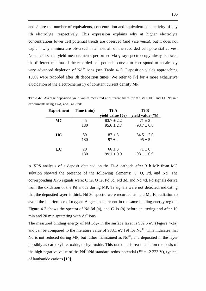
105
and i are the number of equivalents, concentration and equivalent conductivity of any
ith electrolyte, respectively. This expression explains why at higher electrolyte
concentrations lower cell potential trends are observed (and vice versa), but it does not
explain why minima are observed in almost all of the recorded cell potential curves.
Nonetheless, the yield measurements performed via -ray spectroscopy always showed
the different minima of the recorded cell potential curves to correspond to an already
very advanced depletion of Nd3+ ions (see Table 4-1). Deposition yields approaching
100% were recorded after 3h deposition times. We refer to [7] for a more exhaustive
elucidation of the electrochemistry of constant current density MP.
Table 4-1 Average deposition yield values measured at different times for the MC, HC, and LC Nd salt
experiments using Ti-A, and Ti-B foils.
Experiment Time (min) Ti-A yield value (%)
Ti-B yield value (%)
MC 45 83.7 ± 2.2 71 ± 3 180 95.6 ± 2.7 98.7 ± 0.8
HC 80 87 ± 3 84.5 ± 2.0 180 97 ± 4 95 ± 5
LC 20 66 ± 3 71 ± 6 180 99.1 ± 0.9 98.1 ± 0.9
A XPS analysis of a deposit obtained on the Ti-A cathode after 3 h MP from MC
solution showed the presence of the following elements: C, O, Pd, and Nd. The
corresponding XPS signals were: C 1s, O 1s, Pd 3d, Nd 3d, and Nd 4d. Pd signals derive
from the oxidation of the Pd anode during MP. Ti signals were not detected, indicating
that the deposited layer is thick. Nd 3d spectra were recorded using a Mg K radiation to
avoid the interference of oxygen Auger lines present in the same binding energy region.
Figure 4-2 shows the spectra of Nd 3d (a), and C 1s (b) before sputtering and after 10
min and 20 min sputtering with Ar+ ions.
The measured binding energy of Nd 3d5/2 in the surface layer is 982.6 eV (Figure 4-2a)
and can be compared to the literature value of 983.1 eV [9] for Nd3+. This indicates that
Nd is not reduced during MP, but rather maintained as Nd3+, and deposited in the layer
possibly as carboxylate, oxide, or hydroxide. This outcome is reasonable on the basis of
the high negative value of the Nd3+/Nd standard redox potential (E° = -2.323 V), typical
of lanthanide cations [10].
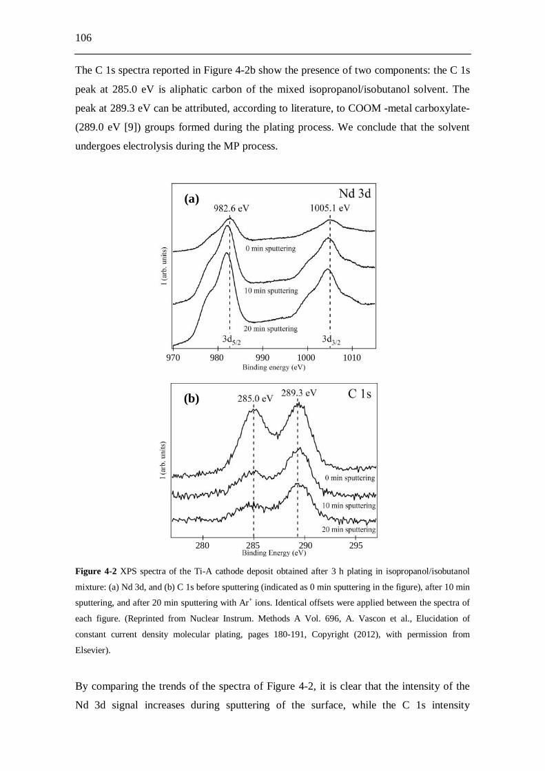
106
The C 1s spectra reported in Figure 4-2b show the presence of two components: the C 1s
peak at 285.0 eV is aliphatic carbon of the mixed isopropanol/isobutanol solvent. The
peak at 289.3 eV can be attributed, according to literature, to COOM -metal carboxylate-
(289.0 eV [9]) groups formed during the plating process. We conclude that the solvent
undergoes electrolysis during the MP process.
Figure 4-2 XPS spectra of the Ti-A cathode deposit obtained after 3 h plating in isopropanol/isobutanol
mixture: (a) Nd 3d, and (b) C 1s before sputtering (indicated as 0 min sputtering in the figure), after 10 min
sputtering, and after 20 min sputtering with Ar+ ions. Identical offsets were applied between the spectra of
each figure. (Reprinted from Nuclear Instrum. Methods A Vol. 696, A. Vascon et al., Elucidation of
constant current density molecular plating, pages 180-191, Copyright (2012), with permission from
Elsevier).
By comparing the trends of the spectra of Figure 4-2, it is clear that the intensity of the
Nd 3d signal increases during sputtering of the surface, while the C 1s intensity
(a)
970 980 990 1000 1010
(b)
280 285 290 295
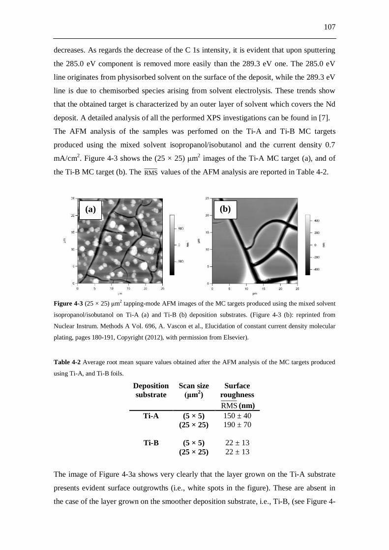
107
decreases. As regards the decrease of the C 1s intensity, it is evident that upon sputtering
the 285.0 eV component is removed more easily than the 289.3 eV one. The 285.0 eV
line originates from physisorbed solvent on the surface of the deposit, while the 289.3 eV
line is due to chemisorbed species arising from solvent electrolysis. These trends show
that the obtained target is characterized by an outer layer of solvent which covers the Nd
deposit. A detailed analysis of all the performed XPS investigations can be found in [7].
The AFM analysis of the samples was perfomed on the Ti-A and Ti-B MC targets
produced using the mixed solvent isopropanol/isobutanol and the current density 0.7
mA/cm2. Figure 4-3 shows the (25 × 25) m2 images of the Ti-A MC target (a), and of
the Ti-B MC target (b). The RMS values of the AFM analysis are reported in Table 4-2.
Figure 4-3 (25 × 25) m2 tapping-mode AFM images of the MC targets produced using the mixed solvent
isopropanol/isobutanol on Ti-A (a) and Ti-B (b) deposition substrates. (Figure 4-3 (b): reprinted from
Nuclear Instrum. Methods A Vol. 696, A. Vascon et al., Elucidation of constant current density molecular
plating, pages 180-191, Copyright (2012), with permission from Elsevier).
Table 4-2 Average root mean square values obtained after the AFM analysis of the MC targets produced
using Ti-A, and Ti-B foils.
Deposition substrate
Scan size m2)
Surface roughness RMS (nm)
Ti-A (5 × 5) 150 ± 40 (25 × 25) 190 ± 70
Ti-B (5 × 5) 22 ± 13 (25 × 25) 22 ± 13
The image of Figure 4-3a shows very clearly that the layer grown on the Ti-A substrate
presents evident surface outgrowths (i.e., white spots in the figure). These are absent in
the case of the layer grown on the smoother deposition substrate, i.e., Ti-B, (see Figure 4-
(a) (b)

108
3b). Recalling that RMS values were obtained by limiting the analysis to crack-free areas
of the layers, the data reported in Table 4-2 confirm what is observed in Figure 4-3,
showing that the rougher deposit is the one grown on the rougher substrate, i.e., Ti-A,
while the smoother deposit is the one grown on the smoother substrate, i.e., Ti-B. These
results suggest that for the production of very smooth targets, deposition substrates that
are as smooth as possible are advantageous.
Despite the achievement of a reduced surface roughness of the layers, both images of
Figure 4-3 show the presence of severe cracking of the produced surfaces. We tested
whether these cracks were a result of the plating process or if they developed afterwards,
during the drying of the produced samples. For this, AFM images of a MC Ti-A target
produced using the mixed isopropanol/isobutanol solvent were taken immediately after
the end of the plating process, but with the solvent still present (Figure 4-4a) and once the
liquid was removed and the target dried in air for a few minutes (Figure 4-4b). From the
absence of cracks in Figure 4-4a we conclude that these are not associated with the MP,
but develop during the post-deposition phase, i.e., during the drying of the targets.
Figure 4-4 3D (25 × 25) m2 AFM images of the MC target produced using Ti-A and
isopropanol/isobutanol solvent before (a) (i.e., contact-mode AFM analysis in liquid), and after (b) (i.e.,
tapping-mode AFM analysis in air) solvent removal and drying. Both images were elaborated using the
WSxM 5.0 version developed by Nanotech Electronica [12]. (Reprinted from Nuclear Instrum. Methods A
Vol. 714, A. Vascon et al., Smooth crack-free targets for nuclear applications produced by molecular
plating, pages 163-175, Copyright (2013), with permission from Elsevier).
This observation, together with the fact that the produced targets contain solvent (see
Figure 4-2b), opened a possibility to study whether a change of the solvent, away from
the traditional mixture of isopropanol and isobutanol, towards a less volatile solvent,
(a) (b)

109
would allow production of crack-free targets. The use of DMF (boiling point, Bp =
153.0°C [11], compared to isopropanol, Bp = 82.2°C [11], and isobutanol, Bp =
107.66°C [11]) allowed production of crack-free targets. The layers produced using DMF
with Ti-A and Ti-B as deposition substrates were characterized by means of AFM.
Figure 4-5 shows the (25 × 25) m2 images of the Ti-A MC target (a), and of the Ti-B
MC target (b).
Figure 4-5 (25 × 25) m2 AFM tapping-mode images of the MC targets produced using the DMF solvent
and applying Ti-A (a) and Ti-B (b) deposition substrates. (Figure 4-5 (a): reprinted from Nuclear Instrum.
Methods A Vol. 714, A. Vascon et al., Smooth crack-free targets for nuclear applications produced by
molecular plating, pages 163-175, Copyright (2013), with permission from Elsevier).
Interestingly, the sample shown in Figure 4-5a features almost no cracks, except for those
mostly deriving from the surface defects (i.e., white outgrowths in the figure). In
addition, as proved by Figure 4-5b, the use of Ti-B as deposition substrate not only
reduces the surface roughness, as shown by the one-order of magnitude smaller RMS
range (compare Figures 4-5a and b), but also eliminates completely the cracks in the
layer. Ultimately, the combined use of the Ti-coated Si wafer and less volatile DMF
solvent yields smooth and crack-free Nd targets. A full account of the experiments with
solvents other than isopropanol/isobutanol will be given in [8].
4.4 Conclusions To elucidate some main features of the MP process, several constant current density MPs
were performed in order to better understand and to improve the technique. Neodymium
was used as the model electrolyte for the experiments. The variables chosen for these
investigations were: concentration of the electrolyte, surface roughness of the deposition
substrates, and plating solvent. The influence of changes in these variables on the
(a) (b)

110
deposition processes was monitored recording cell potential vs. time, and the obtained
deposits were analyzed using -ray spectroscopy, XPS, and AFM.
As detailed in [7], the cell potentials recorded during the performed constant current
density MPs are mainly affected by the solution resistance. An expression relating cell
potential with conductance and hence electrolyte concentration was therefore derived.
This expression explains the cell potential trends recorded using different electrolyte
concentrations, but it does not yet allow for interpreting the reasons leading to the
minima in the cell potential curves. However, we notice that the performed yield
measurements always showed an advanced depletion of the Nd ions already at the times
of the minima of the different curves.
The XPS investigation of the produced targets showed that Nd is not reduced during the
MP process, but rather deposited on the cathodic surface as derivatives of Nd3+, possibly
as carboxylate, oxide or hydroxide. This outcome is reasonable on the basis of the
typically high negative values of the standard redox potentials of the lanthanide cations.
Moreover, XPS proved that the produced targets are made up of both physisorbed as well
as chemisorbed solvent. The presence of products of chemisorption, i.e., metal
carboxylate groups, shows that the solvent undergoes electrolysis during the MP process.
This contradicts the initial interpretation of Parker and Falk in [1], where MP was
described as an electrodeposition with no electrolytic dissociation occurring during the
passage of current.
Finally, the AFM investigation of the targets showed that smooth layers can be grown
only using smooth deposition substrates. Moreover, the MP production of smooth and
crack-free layers proved to be possible only when smooth substrates like Ti-coated Si
wafer, and low-volatility plating solvents like DMF are used. The cracking of the
surfaces seems to be connected to the drying process in air of the samples. Investigations
to give reasonable explanations for these results are still underway and will be presented
in a future publication [8].
Acknowledgements The authors thank the staff of the TRIGA Mainz for performing the irradiations, and Dr.
T. Lauer for performing the coating of the Si wafers. A. Vascon acknowledges financial
support from the German Federal Ministry of Science and Education (BMBF) under
Contract number 02NUK013E.

111
References [1] Parker W, Falk R (1962) Nucl Instrum Methods 16:355-357
[2] Trautmann N, Folger H (1989) Nucl Instrum Meth A 282:102-106
[3] Eberhardt K, Schädel M, Schimpf E, Thörle P, Trautmann N (2004) Nucl Instrum
Meth A 521:208-213
[4] Sadi S, Paulenova A, Watson PR, Loveland W (2011) Nucl Instrum Meth A 655:80-
84
[5] Watson PR, Loveland W, Zielinski PM, Gregorich KE, Nitsche H (2004) Nucl
Instrum Meth B 226:543-548
[6] Vascon A, Düllmann ChE, Eberhardt K, Kindler B, Lommel B, Runke J (2011) Nucl
Instrum Meth A 655:72-79
[7] Vascon A, Santi S, Isse AA, Reich T, Drebert J, Christ H, Düllmann ChE, Eberhardt
K (2012) Nucl Instrum Meth A 696:180-191
[8] Vascon A, Santi S, Isse AA, Kühle A, Reich T, Drebert J, Eberhardt K, Düllmann
ChE (2012) submitted to Thin Solid Films
[9] Wagner CD, Riggs WM, Davis LE, Moulder JF, Muilenberg GE (1979) Handbook of
X-ray photoelectron spectroscopy. Perkin-Elmer Corporation, Physical Electronics
Division, Eden Prairie, Minn. 55344
[10] Lide DR Ed. (2006) CRC Handbook of Chemistry and Physics, 87th edn.
[11] Izutsu K (2002) Electrochemistry in nonacqueous solutions. Darmstadt, Germany
[12] Horcas R, Fernandez JM, Gomez-Rodriguez J, Colchero J, Gomez-Herrero AM,
Baro W (2007) Rev Sci Instrum 78:013705-1

112
5. Smooth crack-free targets for nuclear applications produced
by molecular plating
A. Vascon1, S. Santi2, A. A. Isse2, A. Kühnle3, T. Reich1, J. Drebert1, K. Eberhardt1,4,
Ch.E. Düllmann1,4,5 1Institute of Nuclear Chemistry, Johannes Gutenberg University Mainz, 55099 Mainz,
Germany 2Department of Chemical Sciences, University of Padova, 35131 Padova, Italy 3Institute of Physical Chemistry, Johannes Gutenberg University Mainz, 55099 Mainz,
Germany 4SHE Chemistry Research Section, Helmholtz Institute Mainz, 55099 Mainz, Germany 5SHE Chemistry Department, GSI Helmholtzzentrum für Schwerionenforschung GmbH,
64291 Darmstadt, Germany
Published in:
Nuclear Instruments and Methods in Physics Research A 714 (2013) 163-175.
113
Abstract The production process of smooth and crack-free targets by means of constant current
electrolysis in organic media, commonly known as molecular plating, was optimized.
Using a Nd salt, i.e., [Nd(NO3)3·6H2O], as model electrolyte several constant current
density electrolysis experiments were carried out to investigate the effects of different
parameters, namely the plating solvent (isopropanol and isobutanol mixed together,
pyridine, and N,N-dimethylformamide), the electrolyte concentration (0.11, 0.22, 0.44
mM), the applied current density (0.17, 0.3, 0.7, and 1.3 mA/cm2), and the surface
roughness of the deposition substrates (12 and 24 nm). Different environments (air and
Ar) were used to dry the samples and the effects on the produced layers were
investigated. The obtained deposits were characterized using -ray spectroscopy for
determining Nd deposition yields, X-ray photoelectron spectroscopy for chemical
analysis of the produced surfaces, radiographic imaging for surface homogeneity
inspection, atomic force microscopy for surface roughness evaluation, and scanning
electron microscopy for surface morphology investigation. The results allowed
identifying the optimum parameters for the production of smooth and crack-free targets
by means of molecular plating. The smoothest layers, which had an average RMS
roughness of ca. 20 nm and showed no cracks, were obtained using 0.22 mM
[Nd(NO3)3·6H2O] plated from N,N-dimethylformamide at current densities in the range
of 0.3-0.7 mA/cm2 on the smoothest deposition substrate available.
Keywords: smooth crack-free targets, molecular plating, neodymium, -ray
spectroscopy, atomic force microscopy (AFM), X-ray photoelectron spectroscopy (XPS)
5.1 Introduction Targets are an essential component in experimental nuclear science as a source of
stationary nuclei, e.g., for atomic and nuclear spectroscopy or nuclear reaction studies [1-
3]. Generally, targets should be chemically pure, uniform, homogeneous, crack-free over
the area of interest, and well adherent to the deposition substrate. Among the several
techniques available to prepare thin layers to be used as nuclear targets [4-8], molecular
plating (MP) is one of the most effective and most successfully applied ones [9,10]. This
technique, based on the electrodeposition of the element of interest from an organic
medium either in the constant current or in the constant voltage mode, is usually chosen
because of the possibility to quickly produce deposits of acceptable uniformity and
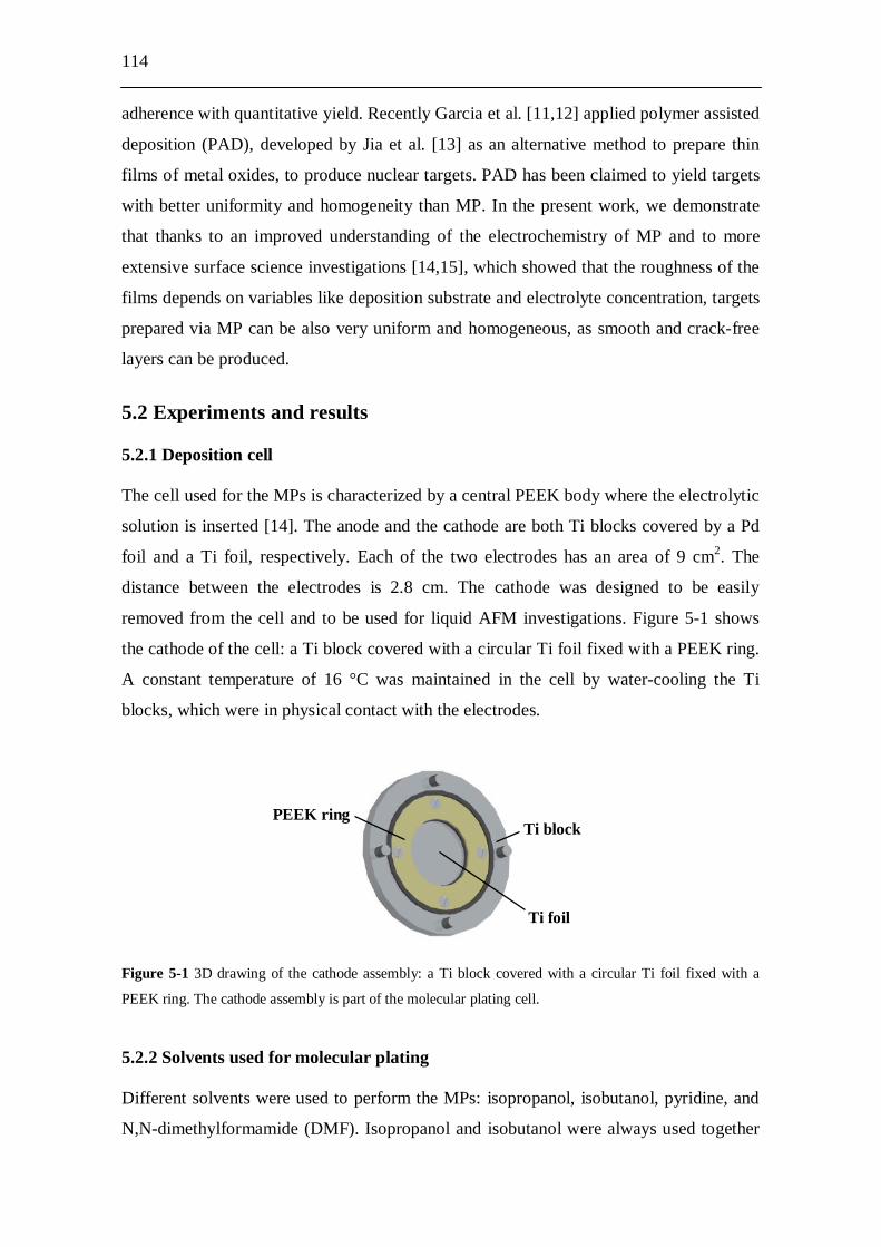
114
adherence with quantitative yield. Recently Garcia et al. [11,12] applied polymer assisted
deposition (PAD), developed by Jia et al. [13] as an alternative method to prepare thin
films of metal oxides, to produce nuclear targets. PAD has been claimed to yield targets
with better uniformity and homogeneity than MP. In the present work, we demonstrate
that thanks to an improved understanding of the electrochemistry of MP and to more
extensive surface science investigations [14,15], which showed that the roughness of the
films depends on variables like deposition substrate and electrolyte concentration, targets
prepared via MP can be also very uniform and homogeneous, as smooth and crack-free
layers can be produced.
5.2 Experiments and results 5.2.1 Deposition cell The cell used for the MPs is characterized by a central PEEK body where the electrolytic
solution is inserted [14]. The anode and the cathode are both Ti blocks covered by a Pd
foil and a Ti foil, respectively. Each of the two electrodes has an area of 9 cm2. The
distance between the electrodes is 2.8 cm. The cathode was designed to be easily
removed from the cell and to be used for liquid AFM investigations. Figure 5-1 shows
the cathode of the cell: a Ti block covered with a circular Ti foil fixed with a PEEK ring.
A constant temperature of 16 °C was maintained in the cell by water-cooling the Ti
blocks, which were in physical contact with the electrodes.
Figure 5-1 3D drawing of the cathode assembly: a Ti block covered with a circular Ti foil fixed with a
PEEK ring. The cathode assembly is part of the molecular plating cell.
5.2.2 Solvents used for molecular plating Different solvents were used to perform the MPs: isopropanol, isobutanol, pyridine, and
N,N-dimethylformamide (DMF). Isopropanol and isobutanol were always used together
Ti block PEEK ring
Ti foil
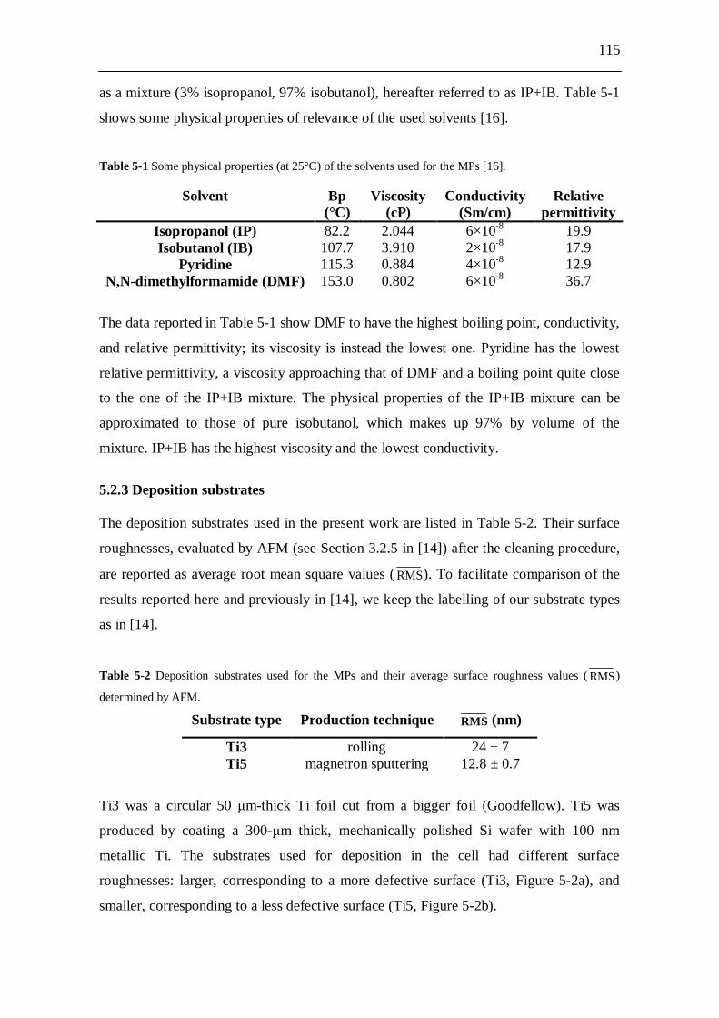
115
as a mixture (3% isopropanol, 97% isobutanol), hereafter referred to as IP+IB. Table 5-1
shows some physical properties of relevance of the used solvents [16].
Table 5-1 Some physical properties (at 25°C) of the solvents used for the MPs [16].
Solvent Bp (°C)
Viscosity (cP)
Conductivity (Sm/cm)
Relative permittivity
Isopropanol (IP) 82.2 2.044 6×10⁻⁸ 19.9 Isobutanol (IB) 107.7 3.910 2×10⁻⁸ 17.9
Pyridine 115.3 0.884 4×10⁻⁸ 12.9 N,N-dimethylformamide (DMF) 153.0 0.802 6×10⁻⁸ 36.7
The data reported in Table 5-1 show DMF to have the highest boiling point, conductivity,
and relative permittivity; its viscosity is instead the lowest one. Pyridine has the lowest
relative permittivity, a viscosity approaching that of DMF and a boiling point quite close
to the one of the IP+IB mixture. The physical properties of the IP+IB mixture can be
approximated to those of pure isobutanol, which makes up 97% by volume of the
mixture. IP+IB has the highest viscosity and the lowest conductivity.
5.2.3 Deposition substrates The deposition substrates used in the present work are listed in Table 5-2. Their surface
roughnesses, evaluated by AFM (see Section 3.2.5 in [14]) after the cleaning procedure,
are reported as average root mean square values ( RMS). To facilitate comparison of the
results reported here and previously in [14], we keep the labelling of our substrate types
as in [14].
Table 5-2 Deposition substrates used for the MPs and their average surface roughness values ( RMS)
determined by AFM.
Substrate type Production technique RMS (nm)
Ti3 rolling 24 ± 7 Ti5 magnetron sputtering 12.8 ± 0.7
Ti3 was a circular 50 m-thick Ti foil cut from a bigger foil (Goodfellow). Ti5 was
produced by coating a 300- m thick, mechanically polished Si wafer with 100 nm
metallic Ti. The substrates used for deposition in the cell had different surface
roughnesses: larger, corresponding to a more defective surface (Ti3, Figure 5-2a), and
smaller, corresponding to a less defective surface (Ti5, Figure 5-2b).
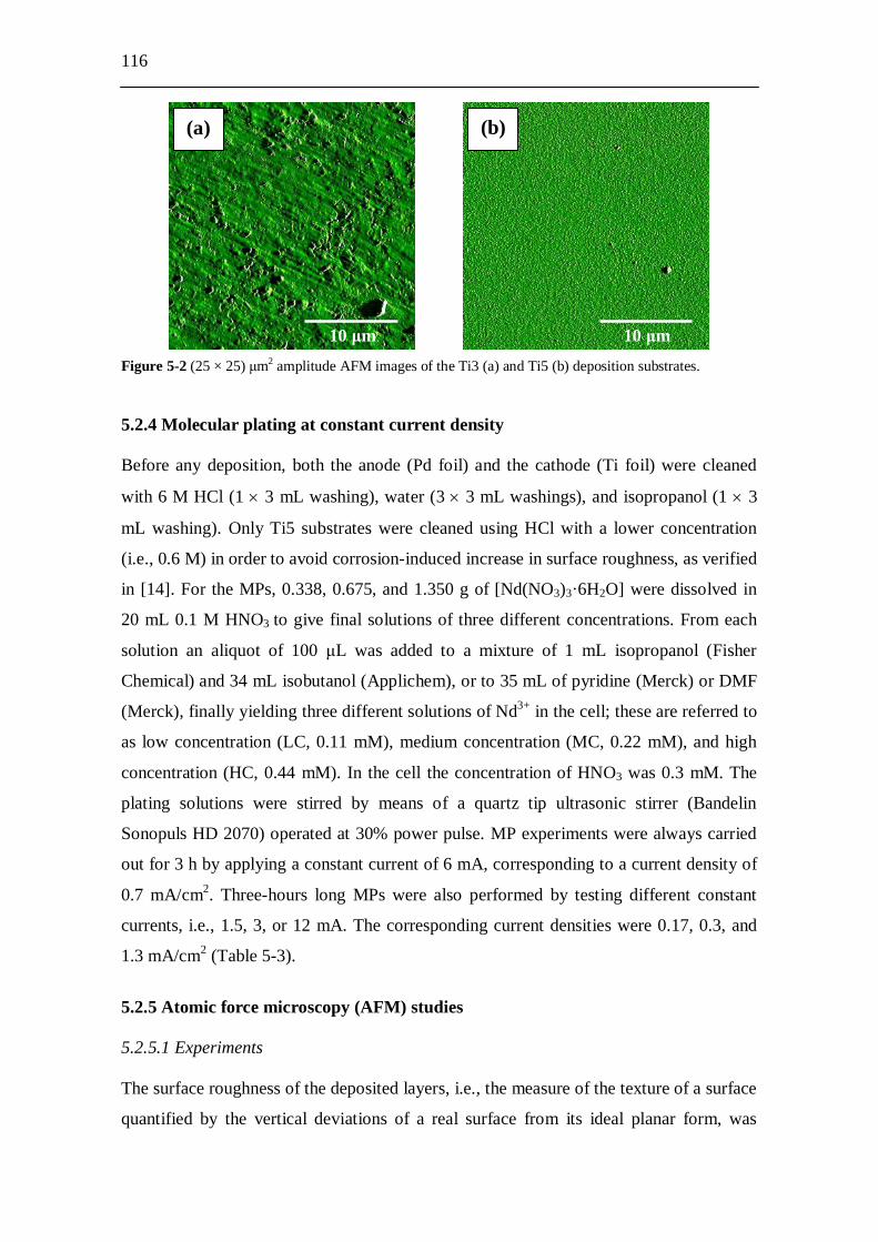
116
Figure 5-2 (25 × 25) m2 amplitude AFM images of the Ti3 (a) and Ti5 (b) deposition substrates.
5.2.4 Molecular plating at constant current density Before any deposition, both the anode (Pd foil) and the cathode (Ti foil) were cleaned
with 6 M HCl (1 3 mL washing), water (3 3 mL washings), and isopropanol (1 3
mL washing). Only Ti5 substrates were cleaned using HCl with a lower concentration
(i.e., 0.6 M) in order to avoid corrosion-induced increase in surface roughness, as verified
in [14]. For the MPs, 0.338, 0.675, and 1.350 g of [Nd(NO3)3·6H2O] were dissolved in
20 mL 0.1 M HNO3 to give final solutions of three different concentrations. From each
solution an aliquot of 100 L was added to a mixture of 1 mL isopropanol (Fisher
Chemical) and 34 mL isobutanol (Applichem), or to 35 mL of pyridine (Merck) or DMF
(Merck), finally yielding three different solutions of Nd3+ in the cell; these are referred to
as low concentration (LC, 0.11 mM), medium concentration (MC, 0.22 mM), and high
concentration (HC, 0.44 mM). In the cell the concentration of HNO3 was 0.3 mM. The
plating solutions were stirred by means of a quartz tip ultrasonic stirrer (Bandelin
Sonopuls HD 2070) operated at 30% power pulse. MP experiments were always carried
out for 3 h by applying a constant current of 6 mA, corresponding to a current density of
0.7 mA/cm2. Three-hours long MPs were also performed by testing different constant
currents, i.e., 1.5, 3, or 12 mA. The corresponding current densities were 0.17, 0.3, and
1.3 mA/cm2 (Table 5-3).
5.2.5 Atomic force microscopy (AFM) studies 5.2.5.1 Experiments The surface roughness of the deposited layers, i.e., the measure of the texture of a surface
quantified by the vertical deviations of a real surface from its ideal planar form, was
10 m 10 m
(a) (b)
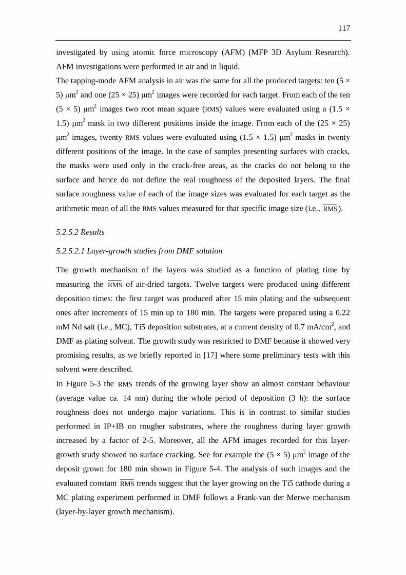
117
investigated by using atomic force microscopy (AFM) (MFP 3D Asylum Research).
AFM investigations were performed in air and in liquid.
The tapping-mode AFM analysis in air was the same for all the produced targets: ten (5 ×
5) m2 and one (25 × 25) m2 images were recorded for each target. From each of the ten
(5 × 5) m2 images two root mean square (RMS) values were evaluated using a (1.5 ×
1.5) m2 mask in two different positions inside the image. From each of the (25 × 25)
m2 images, twenty RMS values were evaluated using (1.5 × 1.5) m2 masks in twenty
different positions of the image. In the case of samples presenting surfaces with cracks,
the masks were used only in the crack-free areas, as the cracks do not belong to the
surface and hence do not define the real roughness of the deposited layers. The final
surface roughness value of each of the image sizes was evaluated for each target as the
arithmetic mean of all the RMS values measured for that specific image size (i.e., RMS).
5.2.5.2 Results 5.2.5.2.1 Layer-growth studies from DMF solution The growth mechanism of the layers was studied as a function of plating time by
measuring the RMS of air-dried targets. Twelve targets were produced using different
deposition times: the first target was produced after 15 min plating and the subsequent
ones after increments of 15 min up to 180 min. The targets were prepared using a 0.22
mM Nd salt (i.e., MC), Ti5 deposition substrates, at a current density of 0.7 mA/cm2, and
DMF as plating solvent. The growth study was restricted to DMF because it showed very
promising results, as we briefly reported in [17] where some preliminary tests with this
solvent were described.
In Figure 5-3 the RMS trends of the growing layer show an almost constant behaviour
(average value ca. 14 nm) during the whole period of deposition (3 h): the surface
roughness does not undergo major variations. This is in contrast to similar studies
performed in IP+IB on rougher substrates, where the roughness during layer growth
increased by a factor of 2-5. Moreover, all the AFM images recorded for this layer-
growth study showed no surface cracking. See for example the (5 × 5) m2 image of the
deposit grown for 180 min shown in Figure 5-4. The analysis of such images and the
evaluated constant RMS trends suggest that the layer growing on the Ti5 cathode during a
MC plating experiment performed in DMF follows a Frank-van der Merwe mechanism
(layer-by-layer growth mechanism).
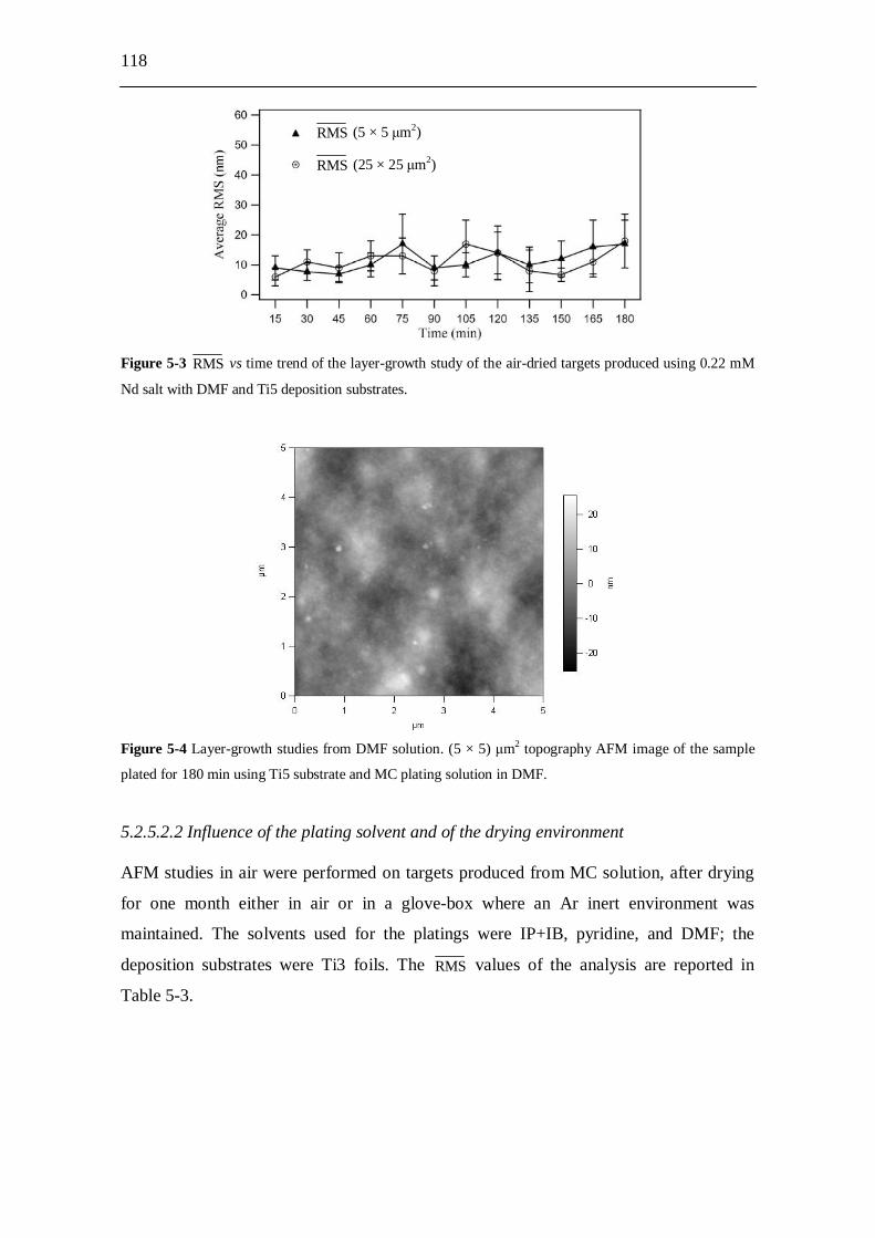
118
Figure 5-3 RMS vs time trend of the layer-growth study of the air-dried targets produced using 0.22 mM
Nd salt with DMF and Ti5 deposition substrates.
Figure 5-4 Layer-growth studies from DMF solution. (5 × 5) m2 topography AFM image of the sample
plated for 180 min using Ti5 substrate and MC plating solution in DMF.
5.2.5.2.2 Influence of the plating solvent and of the drying environment AFM studies in air were performed on targets produced from MC solution, after drying
for one month either in air or in a glove-box where an Ar inert environment was
maintained. The solvents used for the platings were IP+IB, pyridine, and DMF; the
deposition substrates were Ti3 foils. The RMS values of the analysis are reported in
Table 5-3.
RMS (5 × 5 m2) RMS (25 × 25 m2)

119
Table 5-3 Overview of relevant molecular plating parameters. Average root mean square ( RMS) values
obtained from the AFM analyses of the samples investigating the influence of plating solvent, drying
environment, electrolyte concentration, and current density on the surface roughness of the produced
layers.
Substrate type
Solvent Drying environment
Concentration Current density
(mA/cm2)
Scan size m2)
RMS (nm)
Ti3 Pyridine Air MC 0.7 (5 × 5) 242 ± 140 (25 × 25) 372 ± 190
Ti3 Pyridine Ar MC 0.7 (5 × 5) 320 ± 160 (25 × 25) 350 ± 180
Ti3 IP+IB Air MC 0.7 (5 × 5) 150 ± 40 (25 × 25) 190 ± 70
Ti3 IP+IB Ar MC 0.7 (5 × 5) 140 ± 60 (25 × 25) 180 ± 80
Ti3 DMF Air MC 0.7 (5 × 5) 61 ± 24 (25 × 25) 130 ± 40
Ti3 DMF Ar MC 0.7 (5 × 5) 52 ± 23 (25 × 25) 110 ± 50
Ti5 DMF Air HC 0.7 (5 × 5) 70 ± 21 (25 × 25) 79 ± 14
Ti5 DMF Air MC 0.7 (5 × 5) 17 ± 8 (25 × 25) 18 ± 9
Ti5 DMF Air LC 0.7 (5 × 5) 17 ± 3 (25 × 25) 18 ± 8
Ti5 DMF Air MC 0.17 (5 × 5) 110 ± 35 (25 × 25) 130 ± 25
Ti5 DMF Air MC 0.3 (5 × 5) 10 ± 4 (25 × 25) 12 ± 5
Ti5 DMF Air MC 1.3 (5 × 5) 70 ± 30 (25 × 25) 80 ± 22
Table 5-3 clearly demonstrates that, independently of the chosen drying environment, the
roughest samples are those obtained using pyridine, whereas those produced in DMF are
the smoothest. No differences in RMS values within experimental uncertainties were
found for each kind of sample dried in air or in Ar. The analysis of the recorded AFM
images showed that samples characterized by cracking of the layers present surface
troughs regardless of whether they were dried in air or Ar.
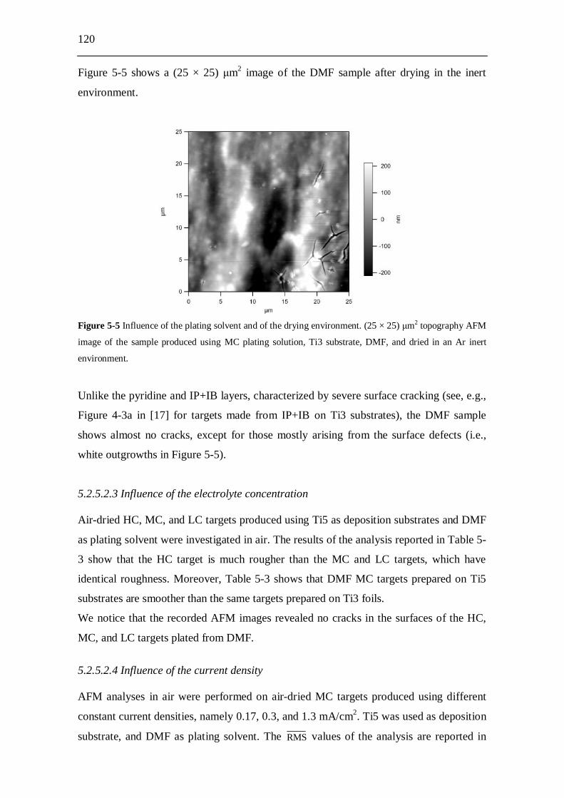
120
Figure 5-5 shows a (25 × 25) m2 image of the DMF sample after drying in the inert
environment.
Figure 5-5 Influence of the plating solvent and of the drying environment. (25 × 25) m2 topography AFM
image of the sample produced using MC plating solution, Ti3 substrate, DMF, and dried in an Ar inert
environment.
Unlike the pyridine and IP+IB layers, characterized by severe surface cracking (see, e.g.,
Figure 4-3a in [17] for targets made from IP+IB on Ti3 substrates), the DMF sample
shows almost no cracks, except for those mostly arising from the surface defects (i.e.,
white outgrowths in Figure 5-5).
5.2.5.2.3 Influence of the electrolyte concentration Air-dried HC, MC, and LC targets produced using Ti5 as deposition substrates and DMF
as plating solvent were investigated in air. The results of the analysis reported in Table 5-
3 show that the HC target is much rougher than the MC and LC targets, which have
identical roughness. Moreover, Table 5-3 shows that DMF MC targets prepared on Ti5
substrates are smoother than the same targets prepared on Ti3 foils.
We notice that the recorded AFM images revealed no cracks in the surfaces of the HC,
MC, and LC targets plated from DMF.
5.2.5.2.4 Influence of the current density AFM analyses in air were performed on air-dried MC targets produced using different
constant current densities, namely 0.17, 0.3, and 1.3 mA/cm2. Ti5 was used as deposition
substrate, and DMF as plating solvent. The RMS values of the analysis are reported in

121
Table 5-3, whereas the corresponding (25 × 25) m2 images of the deposits are shown in
Figure 5-6.
Figure 5-6 Influence of the current density. (25 × 25) m2 topography AFM images of samples produced
using MC plating solution in DMF and a Ti5 substrate; deposits obtained after galvanostatic electrolysis at
current densities of 0.17 mA/cm2 (a), 0.3 mA/cm2 (b), or 1.3 mA/cm2 (c).
Table 5-3 shows that only the intermediate current density of 0.3 mA/cm2 gives RMS
values similar to those recorded for the 0.7 mA/cm2 experiments. Both higher (i.e., 1.3
mA/cm2) and lower (i.e., 0.17 mA/cm2) constant current densities result in much rougher
final deposits. In particular, the roughest deposit is obtained with 0.17 mA/cm2. These
results are well evidenced by the (25 × 25) m2 images of the 0.17 and 1.3 mA/cm2
(a)
(b)
(c)
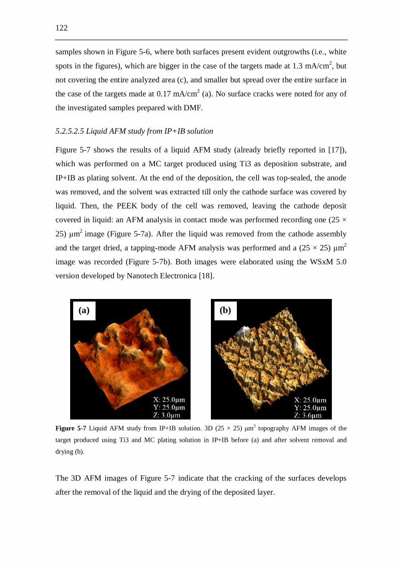
122
samples shown in Figure 5-6, where both surfaces present evident outgrowths (i.e., white
spots in the figures), which are bigger in the case of the targets made at 1.3 mA/cm2, but
not covering the entire analyzed area (c), and smaller but spread over the entire surface in
the case of the targets made at 0.17 mA/cm2 (a). No surface cracks were noted for any of
the investigated samples prepared with DMF.
5.2.5.2.5 Liquid AFM study from IP+IB solution Figure 5-7 shows the results of a liquid AFM study (already briefly reported in [17]),
which was performed on a MC target produced using Ti3 as deposition substrate, and
IP+IB as plating solvent. At the end of the deposition, the cell was top-sealed, the anode
was removed, and the solvent was extracted till only the cathode surface was covered by
liquid. Then, the PEEK body of the cell was removed, leaving the cathode deposit
covered in liquid: an AFM analysis in contact mode was performed recording one (25 ×
25) m2 image (Figure 5-7a). After the liquid was removed from the cathode assembly
and the target dried, a tapping-mode AFM analysis was performed and a (25 × 25) m2
image was recorded (Figure 5-7b). Both images were elaborated using the WSxM 5.0
version developed by Nanotech Electronica [18].
Figure 5-7 Liquid AFM study from IP+IB solution. 3D (25 × 25) m2 topography AFM images of the
target produced using Ti3 and MC plating solution in IP+IB before (a) and after solvent removal and
drying (b).
The 3D AFM images of Figure 5-7 indicate that the cracking of the surfaces develops
after the removal of the liquid and the drying of the deposited layer.
(a) (b)
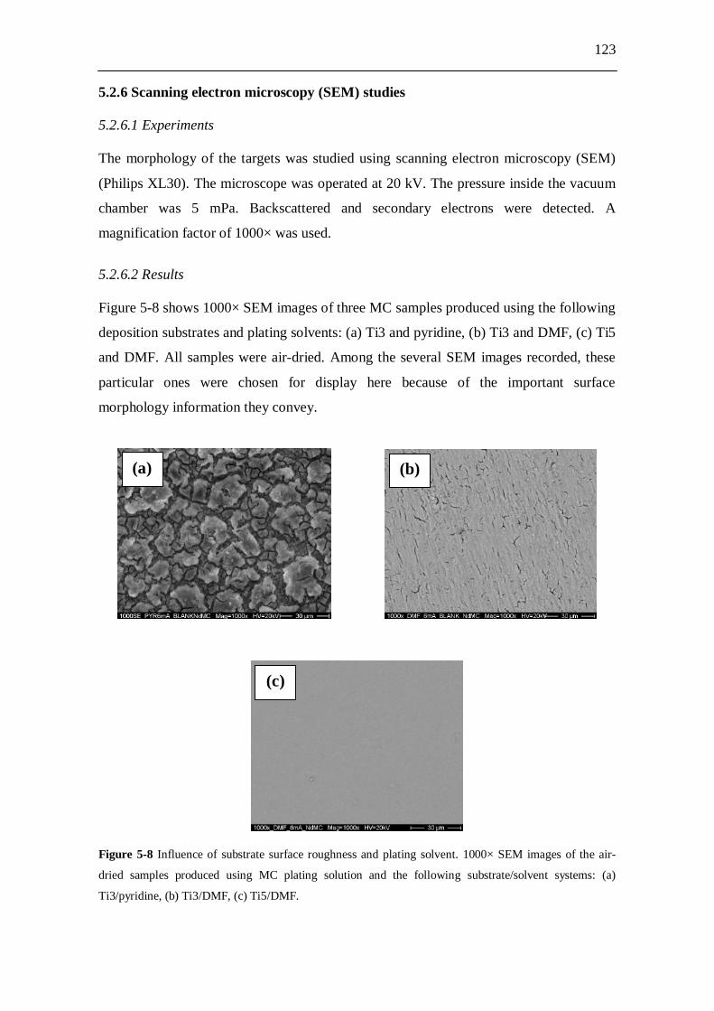
123
5.2.6 Scanning electron microscopy (SEM) studies 5.2.6.1 Experiments The morphology of the targets was studied using scanning electron microscopy (SEM)
(Philips XL30). The microscope was operated at 20 kV. The pressure inside the vacuum
chamber was 5 mPa. Backscattered and secondary electrons were detected. A
magnification factor of 1000× was used.
5.2.6.2 Results Figure 5-8 shows 1000× SEM images of three MC samples produced using the following
deposition substrates and plating solvents: (a) Ti3 and pyridine, (b) Ti3 and DMF, (c) Ti5
and DMF. All samples were air-dried. Among the several SEM images recorded, these
particular ones were chosen for display here because of the important surface
morphology information they convey.
Figure 5-8 Influence of substrate surface roughness and plating solvent. 1000× SEM images of the air-
dried samples produced using MC plating solution and the following substrate/solvent systems: (a)
Ti3/pyridine, (b) Ti3/DMF, (c) Ti5/DMF.
(b)
(c)
(a)

124
Figure 5-8a shows a large-area image of an air-dried pyridine MC target. The surface of
the sample suffers from severe cracking and it is visibly rough.
Figures 5-8b and c show an important effect of the deposition substrate (Ti3 vs Ti5) on
the surface morphology of the deposits. These images indicate that MC targets prepared
using DMF and a Ti3 substrate (Figure 5-8b) exhibit cracks in the layer, caused mainly
by the grown surface defects, as already shown in Figure 5-5. If, instead, a smoother
deposition substrate is used, i.e., Ti5, MC targets produced using DMF (Figure 5-8c)
show no surface cracks (see also Figure 5-4). In constrast, MC experiments using IP+IB
(see Figure 3-2b in [14]) or pyridine showed the presence of cracks in the deposited
layers also when Ti5 substrates were used.
5.2.7 Radiographic imaging (RI) studies 5.2.7.1 Experiments Radioactive targets were produced by performing MPs of Nd solutions containing a
radioactive tracer of the element to be plated (Nd: 147Nd, -, t1/2 = 10.98 d, E = 91 keV).
The tracer was produced in a neutron capture reaction (n, ) on 146Nd present in the used
Nd of natural isotopic composition (natNd) by irradiating an aliquot of 100 L of the
stock solution with thermal neutrons in the TRIGA Mainz research reactor. The
homogeneity of such targets was inspected by using radiographic imaging (RI),
employing a FUJIFILM FLA 7000 equipped with reusable imaging plates and a 650 nm
laser for the reading process. To verify the homogeneity of the target, the image was
overlaid by a grid of square spots with an area of 0.25 mm2 each. The spatial resolution
for -emitting nuclides was < 200 m [19].
5.2.7.2 Results Figure 5-9a shows the 3D graph of a sample obtained using IP+IB as plating solvent and
Ti3 as deposition substrate. Figure 5-9b displays the graph of a sample obtained using
DMF and Ti5.

125
Figure 5-9 Influence of substrate surface roughness and plating solvent. RI 3D graphs of samples produced
using MC plating solution and the following substrate/solvent systems: (a) Ti3/IP+IB, (b) Ti5/DMF.
The images show a definite improvement in surface homogeneity of the deposited layers
once DMF is chosen as plating solvent and Ti5 as deposition substrate. Experiments
showed that better homogeneity of the surfaces is achieved also when DMF is used
instead of pyridine in the preparation of MC targets on Ti3 foils.
5.2.8 X-ray photoelectron spectroscopy (XPS) studies 5.2.8.1 Experiments X-ray photoelectron spectroscopy (XPS) was used to perform the chemical surface
characterization of the samples by applying Al K and Mg K radiations. The X-ray
(a)
(b)
0
34 mm
34 mm
0
34 mm
34 mm
126
source was operated at 10 kV anode voltage and a current of 10 mA. The pass-energy of
the hemispherical energy analyzer was 50 eV. The pressure inside the ultra-high vacuum
chamber was in the range of (1.2-2.0)·10-7 Pa. The analyzed samples were six MC targets
produced using IP+IB, pyridine, and DMF as plating solvents, and Ti3 foils as deposition
substrates. Two targets were produced in each solvent; one was dried in air, while the
other was dried inside a glove-box, where an inert environment was assured by a
constant Ar pressure (50 Pa below atmospheric pressure, O2 < 1 ppm, H2O < 1 ppm). We
refer to [14] for details about the drying procedure in an inert environment and the
subsequent XPS analysis. Drying in different environments was investigated to probe
whether reactive or inert environments like, respectively, air or Ar cause different surface
chemical reactions to take place, the products of which might be identified by XPS.
After the first surface investigation, the samples underwent 10 min sputtering using 4 kV
Ar+ ions, followed by further XPS analysis.
The binding energies of the XPS lines of interest were determined by fitting the recorded
XPS spectra. The analyses were performed using the CasaXPS software (version 2.3.15),
with which the background was subtracted adopting the Shirley algorithm, and the peaks
were fitted using the Gaussian/Lorentzian product formula. As the aim of the present
work was mainly to investigate the surface chemistry of the samples after drying in
different environments, a detailed chemical surface analysis of the deposits was
performed only for C, which was known from [14] to be the main element composing the
outer layer of the produced samples. The C 1s spectra are therefore the only ones to be
shown with multicomponent fitting analysis, which was always modelled by fixing the
separations in binding energy, the intensity ratios, and the full widths at half maxima
(FWHM) of the different C 1s components of IP+IB, DMF, and pyridine. For the IP+IB
and DMF samples dried both in air and in Ar environment, the analysis before sputtering
required correcting the binding energies for the surface charging using one of the
components of the C 1s lines: the 284.9 eV component [20] for IP+IB, and the 285.8 eV
component [21] for DMF. After sputtering, the imprecise fittings of the reference C 1s
peaks required the use of a higher binding energy peak (ca. 289 eV) present in the same
C 1s spectra to correct for the surface charge effect. For the air- and Ar-dried pyridine
samples, instead, the correction of the binding energies was performed both before and
after sputtering using the intense N 1s line of pyridine at 400.2 eV [22]. The experimental
uncertainty of the binding energies is ± 0.1 eV.
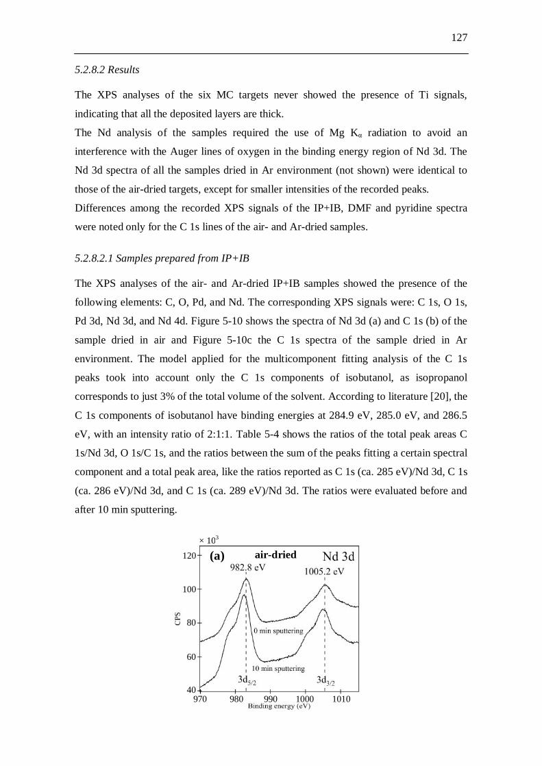
127
5.2.8.2 Results The XPS analyses of the six MC targets never showed the presence of Ti signals,
indicating that all the deposited layers are thick.
The Nd analysis of the samples required the use of Mg K radiation to avoid an
interference with the Auger lines of oxygen in the binding energy region of Nd 3d. The
Nd 3d spectra of all the samples dried in Ar environment (not shown) were identical to
those of the air-dried targets, except for smaller intensities of the recorded peaks.
Differences among the recorded XPS signals of the IP+IB, DMF and pyridine spectra
were noted only for the C 1s lines of the air- and Ar-dried samples.
5.2.8.2.1 Samples prepared from IP+IB The XPS analyses of the air- and Ar-dried IP+IB samples showed the presence of the
following elements: C, O, Pd, and Nd. The corresponding XPS signals were: C 1s, O 1s,
Pd 3d, Nd 3d, and Nd 4d. Figure 5-10 shows the spectra of Nd 3d (a) and C 1s (b) of the
sample dried in air and Figure 5-10c the C 1s spectra of the sample dried in Ar
environment. The model applied for the multicomponent fitting analysis of the C 1s
peaks took into account only the C 1s components of isobutanol, as isopropanol
corresponds to just 3% of the total volume of the solvent. According to literature [20], the
C 1s components of isobutanol have binding energies at 284.9 eV, 285.0 eV, and 286.5
eV, with an intensity ratio of 2:1:1. Table 5-4 shows the ratios of the total peak areas C
1s/Nd 3d, O 1s/C 1s, and the ratios between the sum of the peaks fitting a certain spectral
component and a total peak area, like the ratios reported as C 1s (ca. 285 eV)/Nd 3d, C 1s
(ca. 286 eV)/Nd 3d, and C 1s (ca. 289 eV)/Nd 3d. The ratios were evaluated before and
after 10 min sputtering.
(a)
970 980 990 1000 1010
air-dried × 103
120
100
80
60
40
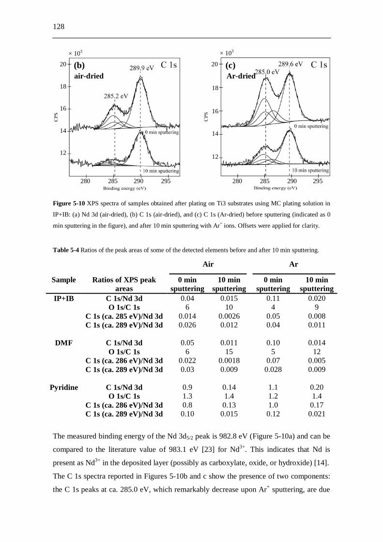
128
Figure 5-10 XPS spectra of samples obtained after plating on Ti3 substrates using MC plating solution in
IP+IB: (a) Nd 3d (air-dried), (b) C 1s (air-dried), and (c) C 1s (Ar-dried) before sputtering (indicated as 0
min sputtering in the figure), and after 10 min sputtering with Ar+ ions. Offsets were applied for clarity.
Table 5-4 Ratios of the peak areas of some of the detected elements before and after 10 min sputtering.
Air Ar
Sample Ratios of XPS peak areas
0 min sputtering
10 min sputtering
0 min sputtering
10 min sputtering
IP+IB C 1s/Nd 3d 0.04 0.015 0.11 0.020 O 1s/C 1s 6 10 4 9 C 1s (ca. 285 eV)/Nd 3d 0.014 0.0026 0.05 0.008 C 1s (ca. 289 eV)/Nd 3d 0.026 0.012 0.04 0.011
DMF C 1s/Nd 3d 0.05 0.011 0.10 0.014 O 1s/C 1s 6 15 5 12 C 1s (ca. 286 eV)/Nd 3d 0.022 0.0018 0.07 0.005 C 1s (ca. 289 eV)/Nd 3d 0.03 0.009 0.028 0.009
Pyridine C 1s/Nd 3d 0.9 0.14 1.1 0.20 O 1s/C 1s 1.3 1.4 1.2 1.4 C 1s (ca. 286 eV)/Nd 3d 0.8 0.13 1.0 0.17 C 1s (ca. 289 eV)/Nd 3d 0.10 0.015 0.12 0.021
The measured binding energy of the Nd 3d5/2 peak is 982.8 eV (Figure 5-10a) and can be
compared to the literature value of 983.1 eV [23] for Nd3+. This indicates that Nd is
present as Nd3+ in the deposited layer (possibly as carboxylate, oxide, or hydroxide) [14].
The C 1s spectra reported in Figures 5-10b and c show the presence of two components:
the C 1s peaks at ca. 285.0 eV, which remarkably decrease upon Ar+ sputtering, are due
(b)
280 285 290 295
air-dried 20
18
16
14
12
× 103
280 285 290 295
× 103
20
18
16
14
12
(c) Ar-dried
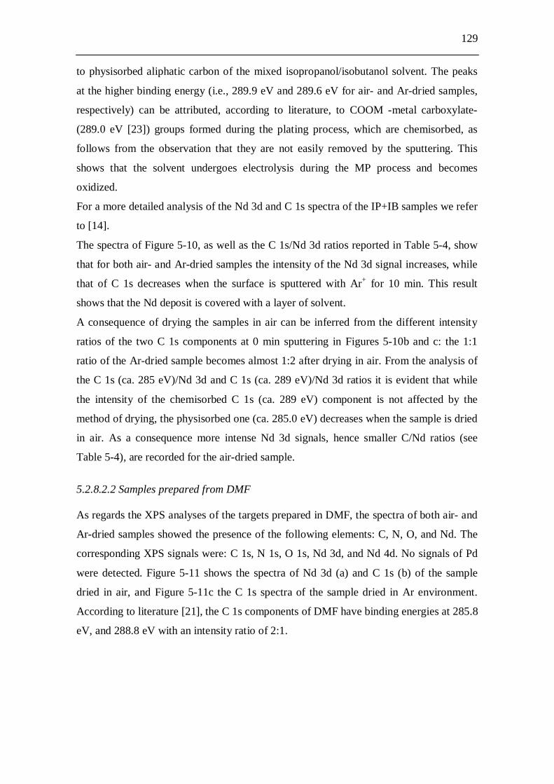
129
to physisorbed aliphatic carbon of the mixed isopropanol/isobutanol solvent. The peaks
at the higher binding energy (i.e., 289.9 eV and 289.6 eV for air- and Ar-dried samples,
respectively) can be attributed, according to literature, to COOM -metal carboxylate-
(289.0 eV [23]) groups formed during the plating process, which are chemisorbed, as
follows from the observation that they are not easily removed by the sputtering. This
shows that the solvent undergoes electrolysis during the MP process and becomes
oxidized.
For a more detailed analysis of the Nd 3d and C 1s spectra of the IP+IB samples we refer
to [14].
The spectra of Figure 5-10, as well as the C 1s/Nd 3d ratios reported in Table 5-4, show
that for both air- and Ar-dried samples the intensity of the Nd 3d signal increases, while
that of C 1s decreases when the surface is sputtered with Ar+ for 10 min. This result
shows that the Nd deposit is covered with a layer of solvent.
A consequence of drying the samples in air can be inferred from the different intensity
ratios of the two C 1s components at 0 min sputtering in Figures 5-10b and c: the 1:1
ratio of the Ar-dried sample becomes almost 1:2 after drying in air. From the analysis of
the C 1s (ca. 285 eV)/Nd 3d and C 1s (ca. 289 eV)/Nd 3d ratios it is evident that while
the intensity of the chemisorbed C 1s (ca. 289 eV) component is not affected by the
method of drying, the physisorbed one (ca. 285.0 eV) decreases when the sample is dried
in air. As a consequence more intense Nd 3d signals, hence smaller C/Nd ratios (see
Table 5-4), are recorded for the air-dried sample.
5.2.8.2.2 Samples prepared from DMF As regards the XPS analyses of the targets prepared in DMF, the spectra of both air- and
Ar-dried samples showed the presence of the following elements: C, N, O, and Nd. The
corresponding XPS signals were: C 1s, N 1s, O 1s, Nd 3d, and Nd 4d. No signals of Pd
were detected. Figure 5-11 shows the spectra of Nd 3d (a) and C 1s (b) of the sample
dried in air, and Figure 5-11c the C 1s spectra of the sample dried in Ar environment.
According to literature [21], the C 1s components of DMF have binding energies at 285.8
eV, and 288.8 eV with an intensity ratio of 2:1.
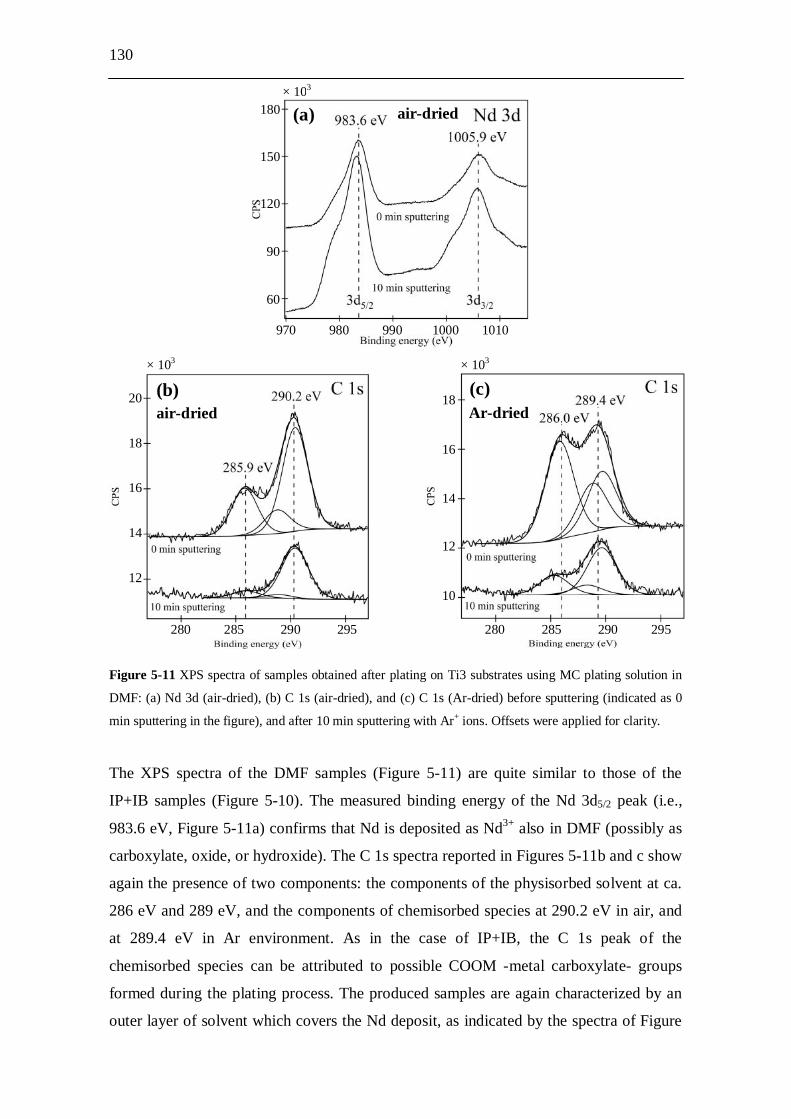
130
Figure 5-11 XPS spectra of samples obtained after plating on Ti3 substrates using MC plating solution in
DMF: (a) Nd 3d (air-dried), (b) C 1s (air-dried), and (c) C 1s (Ar-dried) before sputtering (indicated as 0
min sputtering in the figure), and after 10 min sputtering with Ar+ ions. Offsets were applied for clarity.
The XPS spectra of the DMF samples (Figure 5-11) are quite similar to those of the
IP+IB samples (Figure 5-10). The measured binding energy of the Nd 3d5/2 peak (i.e.,
983.6 eV, Figure 5-11a) confirms that Nd is deposited as Nd3+ also in DMF (possibly as
carboxylate, oxide, or hydroxide). The C 1s spectra reported in Figures 5-11b and c show
again the presence of two components: the components of the physisorbed solvent at ca.
286 eV and 289 eV, and the components of chemisorbed species at 290.2 eV in air, and
at 289.4 eV in Ar environment. As in the case of IP+IB, the C 1s peak of the
chemisorbed species can be attributed to possible COOM -metal carboxylate- groups
formed during the plating process. The produced samples are again characterized by an
outer layer of solvent which covers the Nd deposit, as indicated by the spectra of Figure
(a)
(b)
280 285 290 295
970 980 990 1000 1010
air-dried
air-dried
× 103 180
150
120
90
60
× 103
20
18
16
14
12
Ar-dried
× 103
(c)
280 285 290 295
18
16
14
12
10
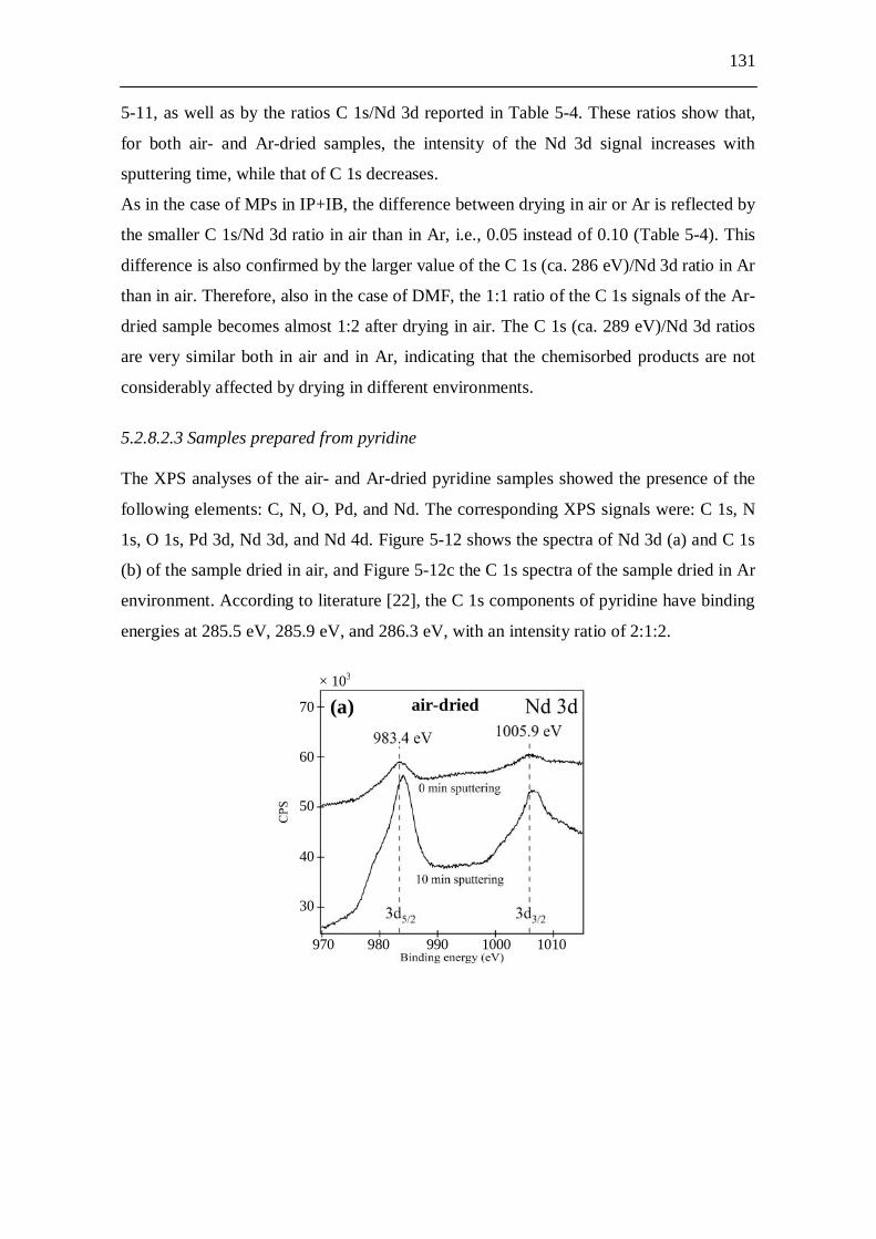
131
5-11, as well as by the ratios C 1s/Nd 3d reported in Table 5-4. These ratios show that,
for both air- and Ar-dried samples, the intensity of the Nd 3d signal increases with
sputtering time, while that of C 1s decreases.
As in the case of MPs in IP+IB, the difference between drying in air or Ar is reflected by
the smaller C 1s/Nd 3d ratio in air than in Ar, i.e., 0.05 instead of 0.10 (Table 5-4). This
difference is also confirmed by the larger value of the C 1s (ca. 286 eV)/Nd 3d ratio in Ar
than in air. Therefore, also in the case of DMF, the 1:1 ratio of the C 1s signals of the Ar-
dried sample becomes almost 1:2 after drying in air. The C 1s (ca. 289 eV)/Nd 3d ratios
are very similar both in air and in Ar, indicating that the chemisorbed products are not
considerably affected by drying in different environments.
5.2.8.2.3 Samples prepared from pyridine The XPS analyses of the air- and Ar-dried pyridine samples showed the presence of the
following elements: C, N, O, Pd, and Nd. The corresponding XPS signals were: C 1s, N
1s, O 1s, Pd 3d, Nd 3d, and Nd 4d. Figure 5-12 shows the spectra of Nd 3d (a) and C 1s
(b) of the sample dried in air, and Figure 5-12c the C 1s spectra of the sample dried in Ar
environment. According to literature [22], the C 1s components of pyridine have binding
energies at 285.5 eV, 285.9 eV, and 286.3 eV, with an intensity ratio of 2:1:2.
air-dried (a)
970 980 990 1000 1010
× 103
70
60
50
40
30

132
Figure 5-12 XPS spectra of samples obtained after plating on Ti3 substrates using MC plating solution in
pyridine: (a) Nd 3d (air-dried), (b) C 1s (air-dried), and (c) C 1s (Ar-dried) before sputtering (indicated as 0
min sputtering in the figure), and after 10 min sputtering with Ar+ ions. Offsets were applied for clarity.
The spectra of Figure 5-12a show that the Nd 3d signal before sputtering is quite low. It
is much lower than the Nd 3d signals of the corresponding (unsputtered) IP+IB and DMF
samples (compare Figure 5-12a with Figures 5-10a and 5-11a). As shown by Figure 5-
12a and by the C 1s/Nd 3d ratios reported in Table 5-4, the intensity of the Nd 3d signal
increases considerably after 10 min sputtering with Ar+ ions. Therefore, the produced
sample is characterized by a thicker solvent layer covering the deposit compared to
IP+IB and DMF. The measured binding energy of the Nd 3d5/2 peak (i.e., 983.4 eV,
Figure 5-12a) confirms that Nd is deposited as Nd3+ as previously found in the case of
IP+IB and DMF (possibly as carboxylate, oxide, or hydroxide). The C 1s spectra
reported in Figures 5-12b and c show the presence of two components, which are visible
only after multicomponent fitting analysis: the components of physisorbed pyridine at ca.
286 eV, and the components of chemisorbed species at ca. 289 eV (i.e., air: 289.3 eV, Ar:
289.4 eV). These higher binding energy components can be attributed to possible COOM
-metal carboxylate- groups formed during the plating process. This indicates that the
solvent undergoes electrolysis during the MP process and becomes oxidized.
Nonetheless, the very small intensities of the chemisorbed components suggest that
pyridine undergoes electrolysis only to a smaller degree than IP+IB or DMF.
Slight differences between drying in air or Ar are shown by the smaller C 1s/Nd 3d ratio
in air (i.e., 0.9 instead of 1.1), and by the larger value of the C 1s (ca. 286 eV)/Nd 3d
ratio in Ar than in air. These differences are smaller than in the case of IP+IB and DMF.
(b)
280 285 290 295 280 285 290 295
air-dried 25
20
15
10
5
× 103
Ar-dried (c)
× 103
25
20
15
10
5
133
The C 1s (ca. 289 eV)/Nd 3d ratios are very similar both in air and in the Ar
environment.
It has to be noticed that all the values of the ratios reported in Table 5-4 for the deposits
prepared in pyridine are quite different from the corresponding values determined for
IP+IB or DMF deposits, irrespective of the methods of sample drying. This follows from
the large intensities of the C 1s signals in pyridine, as evidenced by the C 1s spectra
reported in Figures 5-12b and c, where even after 10 min sputtering the intensities of the
physisorbed components are only slightly decreased.
The comparisons between the C 1s spectra in Figures 5-10b, c, 5-11b, c, and 5-12b, c
show no chemical shifts before and after sputtering. Small shifts of ca. - 0.5 eV after
sputtering were observed for the Nd 3d spectra of the IP+IB and DMF samples (see
Figure 5-10a for IP+IB, and Figure 5-11a for DMF). Shifts of ca. + 0.5 eV after
sputtering were observed for the Nd 3d spectra of the pyridine samples (see Figure 5-
12a). This could indicate the presence of different Nd3+ species in the topmost surface
layers of the samples produced from the different solvents.
From the analysis of all the obtained XPS results, the main difference which appears to
occur between samples dried in air and in a controlled inert environment, such as Ar in a
glove-box, is related to the higher intensities of the peaks of the physisorbed solvent
components when the drying is performed in Ar. Besides this, a slightly larger amount of
O adsorbed on the surfaces of all the samples dried in air can be noticed (see O 1s/C 1s
ratios in Table 5-4). Nonetheless, no strong indication for the presence of surface
chemical reaction products promoted by the drying in air instead of Ar was found.
5.2.9 Molecular plating from DMF solution 5.2.9.1 Cell potential trends Figure 5-13 shows trends of cell potential vs time recorded during preparation of targets,
using 0.22 mM [Nd(NO3)3·6H2O] solution (MC), Ti3 as deposition foil, and DMF (a) or
IP+IB (b) as plating solvent. The applied constant current was 6 mA for 3 h (current
density 0.7 mA/cm2). IP+IB cell potential curves were already discussed in detail in [14].
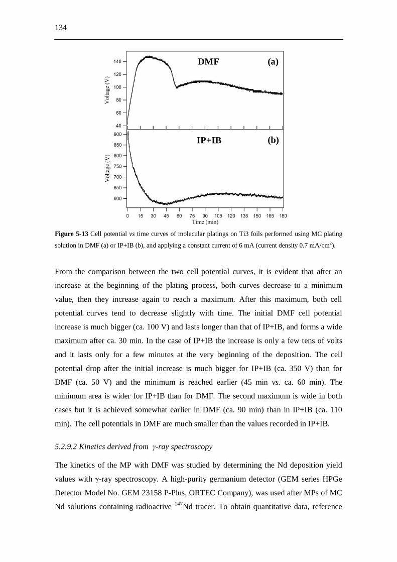
134
Figure 5-13 Cell potential vs time curves of molecular platings on Ti3 foils performed using MC plating
solution in DMF (a) or IP+IB (b), and applying a constant current of 6 mA (current density 0.7 mA/cm2).
From the comparison between the two cell potential curves, it is evident that after an
increase at the beginning of the plating process, both curves decrease to a minimum
value, then they increase again to reach a maximum. After this maximum, both cell
potential curves tend to decrease slightly with time. The initial DMF cell potential
increase is much bigger (ca. 100 V) and lasts longer than that of IP+IB, and forms a wide
maximum after ca. 30 min. In the case of IP+IB the increase is only a few tens of volts
and it lasts only for a few minutes at the very beginning of the deposition. The cell
potential drop after the initial increase is much bigger for IP+IB (ca. 350 V) than for
DMF (ca. 50 V) and the minimum is reached earlier (45 min vs. ca. 60 min). The
minimum area is wider for IP+IB than for DMF. The second maximum is wide in both
cases but it is achieved somewhat earlier in DMF (ca. 90 min) than in IP+IB (ca. 110
min). The cell potentials in DMF are much smaller than the values recorded in IP+IB.
5.2.9.2 Kinetics derived from -ray spectroscopy The kinetics of the MP with DMF was studied by determining the Nd deposition yield
values with -ray spectroscopy. A high-purity germanium detector (GEM series HPGe
Detector Model No. GEM 23158 P-Plus, ORTEC Company), was used after MPs of MC
Nd solutions containing radioactive 147Nd tracer. To obtain quantitative data, reference
(a)
(b)
DMF
IP+IB
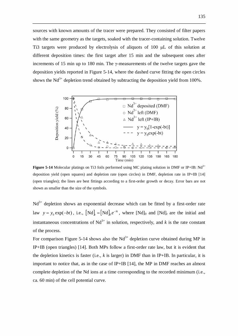
135
sources with known amounts of the tracer were prepared. They consisted of filter papers
with the same geometry as the targets, soaked with the tracer-containing solution. Twelve
Ti3 targets were produced by electrolysis of aliquots of 100 L of this solution at
different deposition times: the first target after 15 min and the subsequent ones after
increments of 15 min up to 180 min. The -measurements of the twelve targets gave the
deposition yields reported in Figure 5-14, where the dashed curve fitting the open circles
shows the Nd3+ depletion trend obtained by subtracting the deposition yield from 100%.
Figure 5-14 Molecular platings on Ti3 foils performed using MC plating solution in DMF or IP+IB: Nd3+
deposition yield (open squares) and depletion rate (open circles) in DMF, depletion rate in IP+IB [14]
(open triangles); the lines are best fittings according to a first-order growth or decay. Error bars are not
shown as smaller than the size of the symbols.
Nd3+ depletion shows an exponential decrease which can be fitted by a first-order rate
law )exp(0 btyy , i.e., ktt e0NdNd , where [Nd]0 and [Nd]t are the initial and
instantaneous concentrations of Nd3+ in solution, respectively, and k is the rate constant
of the process.
For comparison Figure 5-14 shows also the Nd3+ depletion curve obtained during MP in
IP+IB (open triangles) [14]. Both MPs follow a first-order rate law, but it is evident that
the depletion kinetics is faster (i.e., k is larger) in DMF than in IP+IB. In particular, it is
important to notice that, as in the case of IP+IB [14], the MP in DMF reaches an almost
complete depletion of the Nd ions at a time corresponding to the recorded minimum (i.e.,
ca. 60 min) of the cell potential curve.
136
5.2.9.3 Conductivity measurements The conductivity was measured using an inoLab Cond 720 conductometer connected to a
TetraCon 325 standard conductivity cell. These measurements were performed only in a
stirred DMF solution containing 0.22 mM [Nd(NO3)3·6H2O] and 0.3 mM HNO3. The
conductivity ( ) was measured to be 46.5 ± 0.1 S/cm. This value was used to evaluate
the solution resistance, R, in the cell. The expression used for this evaluation is R = ·l/S
[24], where is the resistivity of the system (i.e., the inverse of the conductivity, =
21.50 ± 0.05 k ·cm), l is the distance between the electrodes (2.80 ± 0.01 cm), and S is
the surface area of the electrodes (9.0 ± 0.1 cm2). The obtained cell resistance is 6.691 ±
0.011 k . Using Ohm’s first law, V = RI , where R is the cell resistance and I is the
applied current (I = 6.00 ± 0.01 mA), the contribution of the ohmic drop to the overall
cell potential was estimated to 40.15 ± 0.09 V. This value is in perfect agreement with
the initial experimental value in Figure 5-13a. The cell potential during the MP process
is, however, at least twice as high as the initial value. The voltage increase during the
first 15 min of the electroplating is probably due to an increase of the overall resistance
of the cell. Indeed, during MP the concentration of the electrolyte decreases as Nd3+ is
deposited on the cathode, resulting in a decrease of conductivity. Also the formation and
growth of the deposit, which is principally composed of Nd salts and complexes, presents
an additional resistance. It appears reasonable that the cell potential observed during MPs
is dominated by the ohmic drop.
5.2.9.4 Temperature measurements Temperature measurements of the DMF plating solutions were performed using a TFK
150 thermometer connected to an inoLab pH 720 pH meter. The temperature was
measured immediately before and after 3 h constant current density MP experiments at
0.17, 0.3 and 1.3 mA/cm2. In all cases the MP experiments started after the solutions
were cooled down to 16 °C. The measurements showed temperature increases of 0.4 ±
0.1 °C, 0.7 ± 0.1 °C, and 2.0 ± 0.1 °C, respectively. These results indicate that despite
constant cooling during the experiments, a higher current density leads to a more
pronounced temperature increase inside the system.
5.3 Discussion Among various experimental parameters that may affect constant current density MP,
two were found to be of crucial importance for the preparation of smooth and crack-free
137
layers to be used as nuclear targets. These are the roughness of the deposition substrate
and the solvent used for the platings. The different RMS values of the DMF MC targets
grown on Ti3 and Ti5 substrates confirm that even small differences in surface roughness
between the deposition substrates can influence the RMS of the growing layers [14].
Indeed, if the deposition substrate is rough (i.e., defective), the surface mobility of the
deposited atoms will be reduced by trapping in the defects, and the produced layer will
be of very low quality. Therefore, to produce smooth targets, deposition substrates as
smooth as possible are required.
As regards the solvent, its importance does not only derive from being the medium in
which the process is performed and hence the major factor influencing the
electrochemistry of the MP, but also from the fact that the produced layers are mainly
composed of physisorbed as well as chemisorbed solvent molecules. Hence, the role of
the solvent in MP is twofold: it influences the electrochemistry of the process, but also
the properties of the layer to be produced. Reasonable physical properties to be taken into
account when choosing a solvent for MP are boiling point, viscosity, conductivity, and
relative permittivity [16]. The boiling point determines the volatility of the solvent. The
viscosity influences the rate of mass transfer in the solvent and is important in mass-
transport controlled electrolytic processes like MP [14]. In turn, the rate of mass transfer
influences the conductivity of the electrolyte solutions, which is fundamental for constant
current density electrolysis experiments. Finally, the relative permittivity of a solvent has
a decisive influence on the electrostatic solute-solute and solute-solvent interactions as
well as on the dissolution and dissociation of electrolytes. In this study, pyridine and
DMF were preferred over the more commonly used IP+IB mixture [9,10], after a careful
analysis of these physical and chemical properties. All the samples produced using
IP+IB, pyridine, and DMF as plating solvents and Ti3 foils as deposition substrates
showed the presence of surface cracks. The liquid AFM analysis of the IP+IB sample
suggested that the drying of the layer is at the basis of the surface cracking. To rule out
the possibility that cracking may be connected to eventual layer-destructive chemical
surface reactions occurring during the drying in air of the samples, XPS investigations
were performed. The results of these investigations give no indications for the occurrence
of such reactions, as air- and Ar-dried samples presented the same XPS signals. The
absence of reactivity made then possible the AFM analysis in air of all these samples.
These analyses confirmed the hypothesis of the drying-related nature of cracking. Indeed,
the layers presenting surface cracks after drying in air also underwent cracking in Ar
138
environment. More important than the drying environment is the boiling point of the
solvent. Samples prepared in solvents with low boiling point (i.e., IP+IB and pyridine)
showed the most severe surface cracking and the highest roughness. In contrast, films
produced in DMF on Ti3 foils showed much smaller surface cracks and roughness. The
reason why solvents with lower boiling point produce layers with severe surface cracking
is very likely connected to the drying process. During drying in air, removal of solvent by
evaporation implies solvent diffusion to the surface, conversion at the interface from the
fluid phase to the vapour phase, and finally diffusion through the boundary layer into the
distant air surrounding [25]. Because solvent evaporation diminishes the volume of the
stress-free state of the coating, the current state shrinks to the maximum possible extent.
Ahead of the solidification front, i.e., the front indicating the transition from liquid to
solid, the shrinkage produces flow in the still liquid coating; behind, it produces in-plane
stress in the solid coating because its in-plane shrinkage is frustrated by adhesion to the
substrate [26,27]. The difference between the current state and the stress-free state of the
coating is elastic strain to which stress is proportional via the elastic modulus (i.e., =
stress/strain, where is the elastic modulus). Experimental and theoretical investigations
[27,28] have shown that high elastic modulus and high yield-stress raise the level of
stress and in-plane stress gradients, making the coatings susceptible to cracking and
delamination. It is then reasonable to argue that because the high volatility IP+IB and
pyridine solvents evaporate faster than the less volatile DMF (as we experimentally
observed), the big volume decrease of the stress-free state of the coatings produced with
such solvents will bring to a considerable difference between the current state and the
stress-free one. The consequent large elastic modulus will then make these layers more
likely to crack. In the “slow evaporation” regime achieved with DMF, instead, the
difference between the states during the drying and the consequent elastic modulus will
unlikely be as high as to create cracks. Cracking will mainly occur where a larger
fragility of the layer is dictated by higher surface stress, i.e., where the surface defects
have grown from the deposition foil. Once such defects are eliminated by using smoother
deposition substrates, like Ti5, no cracks are observed in the surfaces of the produced
DMF layers anymore. In particular, the layer growing on the Ti5 substrate during a MC
plating experiment performed in DMF is assigned to follow a Frank-van der Merwe
mechanism (layer-by-layer growth mechanism). In this growth mode a new layer is
nucleated only after completion of the layer below and can spread over macroscopic
distances creating very homogeneous surfaces, as demonstrated also by the RI studies.

139
The surface roughness and the morphology of the layers produced using DMF as plating
solvent and Ti5 as deposition substrate can be considerably varied by changing some
basic variables of the MP, like the concentration of the electrolyte to be plated and the
applied current density. In the first case, the higher concentration of the electrolyte
increases the flux of Nd3+ ions to the cathode, and hence the deposition rate onto the
substrate. Because a high deposition rate causes the system to grow disorderly, the final
surface roughness of the produced layer will be large [14]. In the case of the layers
obtained applying different constant current densities, this simple interpretation is no
longer sufficient to explain the changes observed in both roughness and morphology of
the surfaces. In fact, if on the one hand, as expected, the current density of 1.3 mA/cm2
increases the surface roughness of the layer produced with 0.3 mA/cm2, on the other
hand, the decrease to 0.17 mA/cm2 increases the roughness even more. A possible
explanation for these results comes from the fact that good epitaxial growths require not
only low deposition rates, but also high surface mobility of the deposited species. In the
case of the deposit obtained with the highest current density, the big outgrowths not
covering the entire analyzed area may in fact suggest that the deposited species had a
high surface mobility, which allowed them to condensate. In contrast, as regards the
lowest current density sample, the rather small outgrowths spread over the entire surface
area may indicate low surface mobility. The different mobilities could be related to the
different temperatures of the substrates, which influence the ability of the deposited
species to pass the activation barrier of diffusion. As the MP performed in DMF is
controlled by Ohm’s first law, the preservation of a certain constant current density for a
definite period of time implies the resistance of the solution to undergo several changes.
If the global trend is that of an increase in the solution resistance, the temperature of the
solution may increase as well, despite thermostatation of the system. As a consequence,
the temperature of the cathode may also increase. This seems to be the case, as evidenced
by the temperature measurements of the DMF MC solutions immediately before and
after constant current density MPs at 0.17, 0.3 and 1.3 mA/cm2. The combination of the
effects of both deposition rate and surface mobility, dictated by the specific constant
current density applied to the system, leads then to only few of the tested current
densities being effective for defectless layer growths via MP. This is apparently the case
of current densities in the range of 0.3-0.7 mA/cm2.
Cell potential curves recorded during constant current density MPs in DMF showed to
have common features with MPs in IP+IB [14]. As regards the initial increase of the

140
potential at the beginning of the process and the different starting behaviours of the
curves, we hypothesize that constant current density MPs, including electrolysis, create a
high polarization of the electrodes, which causes the initial increase of the cell potential
[14]. The smaller cell potential drop achieved with DMF than with IP+IB can be
explained in terms of the larger conductivity of DMF. As both the constant current
density MPs performed in IP+IB and DMF proved to be controlled by Ohm’s first law, V
= RI, it is easy to understand that the range of cell potential values must be smaller in
DMF, because this solvent, having a larger conductivity, implies a smaller resistance. It
is important to notice that in both solvents the deposition yield at the minimum of the cell
potential curves is already high, with the depletion kinetics being faster in DMF than in
IP+IB.
Finally, we like to stress that in none of the MPs performed from any of the used solvents
metallic Nd was deposited. Rather, Nd is deposited on the cathodic surfaces as Nd3+
derivatives, and this is reasonable on the basis of the highly negative value of the
Nd3+/Nd standard redox potential (E° = -2.323 V [29]), typical of lanthanide cations.
5.4 Conclusion To optimize the production of smooth and crack-free layers to be used as nuclear targets,
several constant current density MPs were performed using Nd as a model element. The
variables chosen for these investigations were: plating solvent, electrolyte concentration,
applied current density, and surface roughness of the deposition substrate. Different
environments were also used to dry the produced samples. The obtained deposits were
analyzed using -ray spectroscopy, XPS, RI, AFM, and SEM. The results obtained from
the characterization were used to identify the key parameters controlling the molecular
plating of smooth and crack-free layers. The roughness of the deposition substrate and
the solvent used for the platings proved to be two core factors playing a decisive role for
the production of high quality layers. Surface cracking in fact occurred by means of
drying only when volatile solvents and deposition substrates that were not smooth
enough, were used. Different drying environments like air and Ar did not show to have
any effect on the deposited layers.
Molecular platings from DMF proved to be superior over the widely performed IP+IB
platings [9,10]. Indeed, despite being also governed by Ohm’s first law and by similar
depletion kinetics, DMF MPs performed on Ti5 substrates produced targets showing
complete elimination of the surface cracks as well as high smoothness and homogeneity.

141
Moreover, no Pd impurities from the oxidation of the Pd anode were found on the
cathode deposit when MPs were performed in DMF. The absence of such impurities may
be of importance in nuclear science investigations as they could give rise to unwanted
background in accelerator-based experiments.
Finally, the surface roughness and morphology of the layers produced using DMF and
Ti5 substrates proved to be very sensitive to changes in, e.g., electrolyte concentration
and current density.
The present work demonstrates that molecular plating can be applied to produce layers
that are as smooth and crack-free as those produced by PAD, and suitable as nuclear
targets. An important advantage of MP over PAD is that it is a faster deposition process,
as it needs just one plating cycle to reach almost 100% deposition yield. With PAD, in
contrast, coating efficiencies for one single application of ca. 33% are reported [11];
hence several deposition cycles need to be performed to obtain quantitative yields.
The results obtained in this study may also be applied for the production of smooth and
crack-free lanthanide targets other than Nd, and also for the preparation of heavier
actinide targets with an oxidation state of 3+ (e.g., americium and curium), for which Nd
is a good model element.
Acknowledgements The authors would like to thank the staff of the TRIGA Mainz for performing the
irradiations and Dr. T. Lauer for performing the coating of the Si wafers. A. Vascon
would like to thank V. Yakusheva from the GSI target laboratory for her assistance
during the SEM measurements and acknowledges financial support from the German
Federal Ministry of Science and Education (BMBF) under Contract number
02NUK013E.
142
References [1] A. Becerril-Vilchis, A. Cortès, F. Dayras, J. De Sanoit, Nucl. Instrum. Meth. A 369
(1996) 613-616.
[2] B.W. Filippone, M. Wahlgren, Nucl. Instrum. Meth. A 243 (1986) 41-44.
[3] K.M. Glover, L. Bint, D.B. Gayther, M. King, B. Whittaker, R.A.P. Wiltshire, Nucl.
Instrum. Methods 200 (1982) 151-160.
[4] S. Clifford, X. Guo-jj, C. Ingelbrecht, M.J. Pomeroy, Nucl. Instrum. Meth. A 480
(2002) 29-35.
[5] R. Grossmann, H.J. Maier, H.U. Friebel, D. Frischke, Nucl. Instrum. Meth. A 480
(2002) 209-213.
[6] L.V. Drapchinsky, T.E. Kuzmina, S.M. Soloviev, Nucl. Instrum. Meth. A 438 (1999)
116-118.
[7] S. Chakrabarty, B.S. Tomar, A. Goswami, V.A. Raman, S.B. Manohar, Nucl.
Instrum. Meth. B 174 (2001) 212-214.
[8] K.M. Glover, F.J.G. Rogers, T.A. Tuplin, Nucl. Instrum. Methods 102 (1972) 443-
450.
[9] N. Trautmann, H. Folger, Nucl. Instrum. Meth. A 282 (1989) 102-106.
[10] K. Eberhardt, M. Schädel, E. Schimpf, P. Thörle, N. Trautmann, Nucl. Instrum.
Meth. A 521 (2004) 208-213.
[11] M.A. Garcia, M.N. Ali, T. Parsons-Moss, P.D. Ashby, H. Nitsche, Thin Soild Films
516 (2008) 6261-6265.
[12] M.A. Garcia, M.N. Ali, N.N. Chang, T. Parsons-Moss, P.D. Ashby, J.M. Gates, L.
Stavsetra, K.E. Gregorich, H. Nitsche, Nucl. Instrum. Meth. A 592 (2008) 483-485.
[13] Q.X. Jia, T.M. McCleskey, A.K. Burrell, Y. Lin, G.E. Collis, H. Wang, A.D.Q. Li,
S.R. Foltyn, Nat. Mater. 3 (2004) 529-532.
[14] A. Vascon, S. Santi, A.A. Isse, T. Reich, J. Drebert, H. Christ, Ch.E. Düllmann, K.
Eberhardt, Nucl. Instrum. Meth. A 696 (2012) 180-191.
[15] A. Vascon, Ch.E. Düllmann, K. Eberhardt, B. Kindler, B. Lommel, J. Runke, Nucl.
Instrum. Meth. A 655 (2011) 72-79.
[16] K. Izutsu, Electrochemistry in Nonaqueous Solutions, first ed., Wiley-VCH,
Darmstadt, Germany, 2002.
[17] A. Vascon, S. Santi, A.A. Isse, T. Reich, J. Drebert, H. Christ, K. Eberhardt, Ch.E.
Düllmann, J. Radioanal. Nucl. Chem. (2012) accepted.
143
[18] R. Horcas, J.M. Fernandez, J. Gomez-Rodriguez, J. Colchero, A.M. Gomez-Herrero,
W. Baro, Rev. Sci. Instrum. 78 (2007) 013705-1.
[19] D. Liebe, K. Eberhardt, W. Hartmann, T. Häger, A. Hübner, J.V. Kratz, B. Kindler,
B. Lommel, P. Thörle, M. Schädel, J. Steiner, Nucl. Instrum. Meth. A 590 (2008) 145-
150.
[20] U. Gelius, P.F. Hedèn, J. Hedman, B.J. Lindberg, R. Manne, R. Nordberg, C.
Nordling, K. Siegbahn, Phys. Scr. 2 (1970) 70-80.
[21] R.C. Gray, J.C. Carver, D.M. Hercules, J. Electron Spectrosc. 8 (1976) 343-358.
[22] D.T. Clark, R.D. Chambers, D. Kilcast, W.K.R. Musgrave, J. Chem. Soc., Faraday
Trans. 2, 68 (1972) 309-319.
[23] C.D. Wagner, W.M. Riggs, L.E. Davis, J.F. Moulder, G.E. Muilenberg, Handbook
of X-Ray Photoelectron Spectroscopy, Perkin-Elmer Corporation, Physical Electronics
Division, Eden Prairie, Minn. 55344, 1979.
[24] S. Glasstone, An Introduction to Eletrochemistry, first ed., Litton Educational
Publishing, Inc., New York, 1942.
[25] D.E. Haas, J.N. Quijada, S.J. Picone, D.P. Birnie, SPIE Proc., Sol-Gel Optics V, B.
Dunn, E. Pope, H.K. Schmidt, M. Yamane, Editors, 3943 (2000) 280-284.
[26] H. Lei, L.F. Francis, W.W. Gerberich, L.E. Scriven, AIChE J. 48 (2002) 437-451.
[27] H. Radhakrishnan, Ph.D. Thesis, University of Minnesota, Minneapolis, MN, USA,
2006.
[28] J. Malzbender, G. De With, J. Mater. Sci. 35 (2000) 4809-4814.
[29] D. R. Lide (Ed.), CRC Handbook of Chemistry and Physics, 87th ed., 2006.
144
6. The performance of thin layers produced by molecular
plating as -particle sources
A. Vascon1, N. Wiehl1,2, T. Reich1, J. Drebert1, K. Eberhardt1,2, Ch.E. Düllmann1,2,3
1Institute of Nuclear Chemistry, Johannes Gutenberg University Mainz, 55099 Mainz,
Germany 2SHE Chemistry Research Section, Helmholtz Institute Mainz, 55099 Mainz, Germany 3SHE Chemistry Department, GSI Helmholtzzentrum für Schwerionenforschung GmbH,
64291 Darmstadt, Germany
Published in:
Nuclear Instruments and Methods in Physics Research A 721 (2013) 35-44.
145
Abstract Sources for -spectroscopy studies were prepared. Constant current density molecular
plating was used to produce layers containing the -particle emitter 147Sm. Different
parameters of the molecular plating process were varied, namely the plating solvent (an
isopropanol/isobutanol mixture, pyridine, and N,N-dimethylformamide), the applied
deposition time (90, 180, and 360 min), and the surface roughness of the deposition
substrate (ca. 10, 20, and 300 nm). Using different analytical techniques, Sm deposition
yields, chemical composition of the produced surfaces, surface homogeneity, roughness
and morphology were investigated. Alpha spectra were recorded with a Si solid-state
detector for samples belonging to the different types of characterized sources, and big
differences in the peak shape and position of the peak maximum were observed, as well
as significant differences in the fraction of particles reaching the detector positioned
above the samples. An explanation for the observed features is presented. The results of
these studies led to the identification of the key plating parameters, namely the plating
solvent and the roughness of the deposition substrate, which most affect the quality of the
spectra.
Keywords: -particle spectroscopy, 147Sm, molecular plating, atomic force microscopy
(AFM), scanning electron microscopy (SEM), X-ray photoelectron spectroscopy (XPS)
6.1 Introduction Alpha-particle sources find wide use in the nuclear sciences. Important parameters,
which characterize the quality of an -particle source, include the energy distribution of
particles of a given line – which should be as small as possible – or the accuracy with
which the absolute content of the emitter contained in the source is known. The first
feature depends critically on the quality of the thin film containing the emitter – ideally
a weight-less sample, or at least a homogeneous and smooth layer. The second feature is
often evaluated from spectroscopic measurements of the source. For this, generally a
homogeneous distribution of the emitter throughout the whole source is assumed.
Among the methods to produce high-quality thin films, electrodeposition from aqueous
or organic media is widely used. An example for the former is the production of Os
targets to search for an branch in 184Os [1]. The latter method is commonly referred to
as molecular plating (MP) [2]. It is prominently used to produce targets of long-lived
transuranium isotopes for accelerator experiments in the research on superheavy
146
elements [3]. There, in the case of decaying isotopes like 249Cf the deposition yield or
total activity of the layer may be assayed by spectroscopy [4]. Another current
example, where the production of high-quality sources is required, concerns a planned
precise half-life (t1/2) measurement of the very long-lived low energy -emitter 144Nd (t1/2
= (2.65 ± 0.37) · 1015 y, E = 1.85 MeV [5]), which is of interest in the context of an
envisaged search for neutrinoless double-beta decay of 150Nd, where 144Nd is one of the
unwanted background radioactivities [6]. As a first step towards the production of well-
characterized Nd targets produced by MP, where the Nd content is known with high
accuracy, we have recently performed systematic studies of Nd-containing layers
produced by MP [7-10]. In our studies, we characterized the layers by different analytical
methods (X-ray photoelectron spectroscopy, atomic force microscopy, scanning electron
microscopy, or radiographic imaging) to investigate the surface chemistry, the roughness,
the morphology, and the homogeneity of the produced layers. We found the plating
variables to critically influence the layer properties, including the homogeneity of the Nd
distribution throughout the targets, their surface roughness, and morphology. As key
parameters affecting the target properties, we identified the surface roughness of the
substrate onto which the target was deposited, the solvent (in our studies: N,N-
dimethylformamide -DMF-, an isopropanol/isobutanol mixture -IP+IB-, and pyridine)
from which the Nd was electroplated, the Nd concentration in the plating solution, and
the applied current density. It turned out that in general the Nd ions contribute to less
than 20% to the total current established during MPs (see Figure 3-12 in [8]), with the
remainder of the current being mainly due to electrolysis of the solvent, the products of
which are directly incorporated into the Nd-containing layer. Also, kinetic studies
showed the Nd to deposit relatively quickly. In many cases, quantitative deposition of Nd
was achieved significantly before the end of the plating process, which lasted up to
several hours. Accordingly, the Nd is always covered by a Nd-free layer consisting
purely of elements other than that of interest. As the energy distribution of the particles
leaving the source is determined by electronic energy loss and energy-loss straggling,
such effects can be expected to directly influence the quality of the spectra. This issue
is of importance when low specific activities of very long-lived, low energy -emitters
have to be measured, because in this case, if the -peak resolution is low, particles may
be degraded to an extent that they fall within the region of electronic background and
hence be lost. By careful optimization of all experimental parameters of the MP process,
147
we recently achieved in [10] the production of very homogeneous, smooth and crack-free
Nd layers.
In the current work, we focused on the properties of the spectra obtained from samples
produced 1) on substrates of different roughness, 2) from three different solvents (IP+IB,
DMF, pyridine), and 3) during different deposition times. We also studied the properties
of pure solvent layers, as they cover many of the targets produced by MP under these
conditions, and performed MP experiments where the element of interest was absent in
the plating solution. While Nd containing layers could serve as -particle sources due to
the high natural abundance of radioactive 144Nd, such studies suffer from the long half-
life of this isotope. To perform reasonably quick investigations of the sources, in this
work Sm was preferred over Nd and 147Sm ( , t1/2 = (1.070 ± 0.009) · 1011 y, E = 2.24
MeV [11]) was chosen as model isotope for the investigations because of its significantly
shorter half-life and hence higher specific activity, and the very high precision, with
which the half-life is known. We note that Sm is also a tri-valent lanthanide like Nd, and
therefore its electrodeposition chemistry may be expected to be similar. To verify this
assumption, and to characterize the Sm samples, several MP experiments were performed
where the above mentioned parameters 1-3 were varied and the layers characterized in
the same manner as the Nd layers described in [10] (Section 6.2). Alpha spectra were
recorded from the different samples. From the determined amount of Sm present in the
produced layers, the measured number of particles within our detector in a given time,
and the precisely known half-life of 147Sm we calculated the efficiency of our source-
detector setup (hereafter referred to as experimental efficiency). This efficiency was
compared to the estimated geometric efficiency of our detection system, obtained using a
Monte Carlo simulation (hereafter referred to as simulated efficiency). (Section 6.3). As
the geometry of the source was always identical (same source- and detector diameter;
same source-detector distance) the experimental efficiencies might naively be expected
to be identical for all sources. This however is not the case, and the differences are likely
associated with the quality of the sample and the parameters used in its preparation.

148
6.2 Sample production and characterization 6.2.1 Deposition cell The cell used for the MPs was already shown and described in detail in [8]. This cell is
characterized by a central polyether ether ketone (PEEK) body where the electrolytic
solution is inserted. The anode and the cathode are both Ti blocks covered by circular Pd
and Ti foils, respectively. Each of the two electrodes has an effective deposition area of
9.0 ± 0.1 cm2. A constant temperature (T = 16 °C) was maintained in the cell by water-
cooling the Ti blocks in physical contact with the electrodes. As was noted in [10], the
temperature during plating may be slightly higher due to ohmic heating of the solution,
despite the water-cooling.
6.2.2 Deposition substrates The deposition substrates used in the present work were already described in detail in [8].
Due to the critical influence of the surface roughness on the effects studied in this work,
we give in Table 6-1 their average root mean square ( RMS) surface roughnesses,
evaluated by AFM after a cleaning procedure (see Section 3.2.5 in [8]). To facilitate
comparison between the results reported here and previously in [8,10], we keep the
labelling of our substrate types as in [8,10].
Table 6-1 Deposition substrates used for the MPs performed and their average surface roughness values
( RMS) determined by AFM.
Substrate type Production technique RMS (nm)
Ti3 rolling 24 ± 7 Ti4 etching 340 ± 140 Ti5 magnetron sputtering 12.8 ± 0.7
Substrates with different surface roughness were used for deposition: medium (Ti3), high
(Ti4), and low roughness (Ti5). Ti3 was a circular 50 m-thick Ti foil cut from a bigger
rolled foil (Goodfellow). Ti4 was obtained by etching a Ti3 foil with concentrated HCl
(~36%) for 45 min under an IR lamp. Figure 6-1 shows an AFM image of a Ti4
substrate: the etching of the Ti foil creates evident surface defects. Ti5 was produced by
magnetron sputtering a 300- m thick mechanically-polished Si wafer with 100 nm
metallic Ti. AFM images of Ti3 and Ti5 foils were already shown in Figures 5-2a and b
in [10], respectively.

149
Figure 6-1 (25 × 25) m2 amplitude AFM image of the Ti4 deposition substrate. The dashed white arrows
show some of the surface defects created by etching of the Ti3 foil.
6.2.3 Molecular plating at constant current density Before any deposition, both the anode (Pd foil) and the cathode (Ti foil) were cleaned
with 6 M HCl (1 3 mL washing), water (3 3 mL washings), and isopropanol (1 3
mL washing). The Ti5 foils were cleaned using HCl with a lower concentration (i.e., 0.6
M) to avoid corrosion-induced increase in surface roughness, which was observed at 6 M
HCl concentration in [8]. For the MP processes, 147Sm-enriched Sm2O3 (Isoflex USA)
was used. The isotopic composition was: 0.13% 144Sm, 96.4% 147Sm, 2.18% 148Sm,
0.53% 149Sm, 0.17% 150Sm, 0.36% 152Sm, and 0.23% 154Sm. The Sm oxide, Sm2O3, was
transformed into the nitrate, Sm(NO3)3, via dissolution in 15 M HNO3. The liquid was
evaporated by heating under an IR lamp and the obtained solid was redissolved with 0.1
M HNO3 to produce a Sm nitrate solution. Three Sm stock solutions were prepared
following this procedure. From the solution an aliquot of 100 L was added to a mixture
of 1 mL isopropanol (Fisher Chemical) and 34 mL isobutanol (Applichem) (i.e., IP+IB:
3% isopropanol, 97% isobutanol), or to 35 mL of pyridine (Merck) or DMF (Merck),
finally yielding a 0.22 mM solution of Sm3+ in the cell. The concentration of HNO3 in the
cell was always 0.3 mM. The plating solutions were stirred by means of a quartz tip
ultrasonic stirrer (Bandelin Sonopuls HD 2070) operated at 30% power pulse. MP
experiments were carried out for 90, 180 or 360 min by applying a constant current of 6
mA. The current density, 0.7 mA/cm2, was the same in all cases. Once the MP process
was over, each of the produced samples was extracted from the cell and let dry in air. The
10 m
150
thickness of the deposits would be 125.6 ± 1.6 g/cm2, if 100% deposition yields were
obtained.
6.2.4 X-ray photoelectron spectroscopy (XPS) studies 6.2.4.1 Experiments The surface chemistry of the samples was investigated by using X-ray photoelectron
spectroscopy (XPS) with an Al K radiation. The X-ray source was operated at 10 kV
anode voltage and a current of 10 mA. The pass-energy of the hemispherical energy
analyzer was 50 eV. The pressure inside the ultra-high vacuum chamber was in the range
of (1.2-2.0)·10-9 mbar. A total of five samples was investigated. Two samples were
targets produced from DMF on Ti3 foils using deposition times of 180 min, which was
previously used in experiments with Nd [10], and 360 min. Only DMF was chosen as
reference plating solvent for these deposits because of the excellent results previously
obtained in the preparation of Nd targets [10]. The 180 min-long plated sample was
produced to understand whether the surface chemistry of the Sm layers is similar or
differs from the chemistry of the DMF Nd layers. A deposition time of 360 min was
instead chosen to investigate potential differences in the surface chemistry of the samples
when long plating times are adopted. After the initial surface investigation, these two
samples underwent 10 min sputtering using 4 kV Ar+ ions, and further XPS analyses
were then performed. The other three targets were produced from Sm-free solutions to
simulate and understand the electrochemistry of the MP process when no Sm3+ ions are
present in solution anymore, i.e., when the Sm3+ ions have all been deposited on the
cathode. These targets were produced by adding 100 l of 0.1 M HNO3 to the deposition
cell, and then by plating for 180 min with IP+IB, DMF, or pyridine as solvents, and Ti3
foils as deposition substrates. After the first surface investigation, only the pyridine
sample underwent Ar+ sputtering.
The procedure adopted to determine the binding energies of the XPS lines of interest was
identical to that described in Section 5.2.8 in [10]. As the aim of the present work was
mainly to investigate the surface chemistry of the samples, a detailed chemical surface
analysis of the deposits was performed only for C, which was known from [8] and [10] to
be the main element composing the outer layer of the produced samples. The C 1s
spectra are therefore the only ones to be shown with multicomponent fitting analysis.
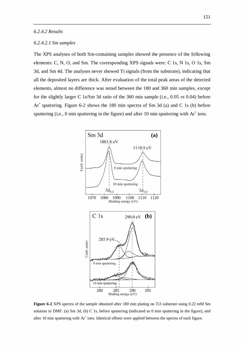
151
6.2.4.2 Results 6.2.4.2.1 Sm samples The XPS analyses of both Sm-containing samples showed the presence of the following
elements: C, N, O, and Sm. The corresponding XPS signals were: C 1s, N 1s, O 1s, Sm
3d, and Sm 4d. The analyses never showed Ti signals (from the substrate), indicating that
all the deposited layers are thick. After evaluation of the total peak areas of the detected
elements, almost no difference was noted between the 180 and 360 min samples, except
for the slightly larger C 1s/Sm 3d ratio of the 360 min sample (i.e., 0.05 vs 0.04) before
Ar+ sputtering. Figure 6-2 shows the 180 min spectra of Sm 3d (a) and C 1s (b) before
sputtering (i.e., 0 min sputtering in the figure) and after 10 min sputtering with Ar+ ions.
Figure 6-2 XPS spectra of the sample obtained after 180 min plating on Ti3 substrate using 0.22 mM Sm
solution in DMF: (a) Sm 3d, (b) C 1s, before sputtering (indicated as 0 min sputtering in the figure), and
after 10 min sputtering with Ar+ ions. Identical offsets were applied between the spectra of each figure.
1070 1080 1090 1100 1110 1120
280 285 290 295
(a)
(b)
152
The measured binding energy of Sm 3d5/2 in the surface layer is 1083.8 eV (Figure 6-2a),
which is close to the literature value of 1084.3 eV [12] for Sm3+. Therefore, Sm is present
as Sm3+ in the investigated deposited layer (possibly as carboxylate, oxide, or hydroxide),
and this is reasonable on the basis of the highly negative value of the Sm3+/Sm standard
redox potential (E° = -2.41 V) [13]. A small shift of ca. - 0.6 eV after sputtering could
indicate the presence of different Sm3+ species in the topmost surface layer of the sample.
The C 1s spectra reported in Figure 6-2b show the presence of two XPS lines centered at
285.9 eV and 290.0 eV, respectively. These lines are fitted by three peaks: the peaks at
ca. 286 eV and 289 eV are carbon of the DMF solvent [14]. The peak at ca. 4 eV higher
binding energy (i.e., 290.0 eV) can be attributed, according to literature, to COOM -metal
carboxylate- (289.0 eV [12]) groups formed during the plating process. No chemical
shifts are observed after sputtering.
Both spectra of Figure 6-2 show that as long as the sputtering of the surface proceeds, the
intensity of the Sm 3d signal increases, while the C 1s intensity decreases. Particularly,
as regards the decrease of the C 1s intensity, it is evident that the 285.9 eV component is
removed more easily than the 290.0 eV one. We attribute the 285.9 eV line to originate
from physisorbed solvent on the surface of the deposit, while the 290.0 eV line is due to
chemisorbed COOM species arising from solvent electrolysis. These trends clearly show
the obtained sample to be characterized by an outer layer of solvent, which covers the Sm
deposit. This is similar to the observation we made previously with DMF Nd samples
[10], and we conclude the MP behaviour of both elements to be similar.
6.2.4.2.2 Sm-free samples The XPS analyses of the three Sm-free samples always showed the presence of Na+,
Ca2+, or K+ ions in the investigated layers. These ions likely derive from the aqueous
HNO3 solutions used for the platings, and because of the highly negative values of their
standard redox potentials, i.e., E°Na+/Na = -2.71 V [15], E°Ca2+/Ca = -2.76 V [15], and
E°K+/K = -2.92 V [15], they are not reduced.
The recorded C 1s spectra of the samples (not shown) were similar to those of the air-
dried Nd samples produced in IP+IB, DMF, and pyridine (see Figures 5-10b, 5-11b, and
5-12b in [10], respectively). Indeed, the samples showed peaks at 285.3 eV, 285.9 eV,
and 286.4 eV, which match the peaks of the physisorbed carbon of the IP+IB, DMF, and
pyridine solvents investigated in Section 5.2.8 of [10], respectively. Moreover, peaks at
288.5 eV (IP+IB), 289.6 eV (DMF), and 288.4 eV (pyridine) were detected, and can be
153
attributed to chemisorbed COOM -metal carboxylate- (289.0 eV [12]) groups formed
during the plating process. Therefore, we conclude the solvents to undergo electrolysis
also in the absence of Sm electrolyte.
Among all the produced samples only Sm-free IP+IB and DMF deposits showed Ti
signals. In the case of the pyridine layer the absence of a Ti signal led us to perform 10
min sputtering with Ar+ ions to check whether Ti would then appear in the spectra. Even
after this sputtering time, no Ti peaks were recorded. This indicates that in the case of the
sample produced from pyridine the deposited layer is much thicker than the layers
obtained from DMF or IP+IB applying the same deposition times (i.e., 180 min). Table
6-2 shows the ratios of the total peak areas C 1s/Ti 2p, and the ratios between the sum of
the peaks fitting a certain spectral component and a total peak area, like the ratios
reported as C 1s (ca. 285 eV)/C 1s, C 1s (ca. 286 eV)/C 1s, and C 1s (ca. 289 eV)/C 1s.
Table 6-2 Ratios of the peak areas of some of the detected elements.
Sample Ratios of XPS peak areas
Ratio value
DMF C 1s/Ti 2p 0.5 C 1s (ca. 286 eV)/C 1s 0.46 C 1s (ca. 289 eV)/C 1s 0.54
IP+IB C 1s/Ti 2p 0.4 C 1s (ca. 285 eV)/C 1s 0.65 C 1s (ca. 289 eV)/C 1s 0.35
Pyridine C 1s/Ti 2p - C 1s (ca. 286 eV)/C 1s 0.76 C 1s (ca. 289 eV)/C 1s 0.24
Table 6-2 shows that the C 1s/Ti 2p ratio of the DMF sample is only slightly larger than
the corresponding one of the IP+IB sample. This suggests the thicknesses of the
deposited solvent layers to be similar. The ratios reported in Table 6-2 also show that the
fraction of physisorbed solvent tends to increase from the DMF sample to the pyridine
one, which is the sample with the most physisorbed solvent. This is in line with results
obtained in [10], which suggested the electrochemistry of the three MP processes to be
quite different.
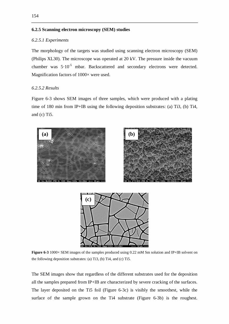
154
6.2.5 Scanning electron microscopy (SEM) studies 6.2.5.1 Experiments The morphology of the targets was studied using scanning electron microscopy (SEM)
(Philips XL30). The microscope was operated at 20 kV. The pressure inside the vacuum
chamber was 5·10-5 mbar. Backscattered and secondary electrons were detected.
Magnification factors of 1000× were used.
6.2.5.2 Results Figure 6-3 shows SEM images of three samples, which were produced with a plating
time of 180 min from IP+IB using the following deposition substrates: (a) Ti3, (b) Ti4,
and (c) Ti5.
Figure 6-3 1000× SEM images of the samples produced using 0.22 mM Sm solution and IP+IB solvent on
the following deposition substrates: (a) Ti3, (b) Ti4, and (c) Ti5.
The SEM images show that regardless of the different substrates used for the deposition
all the samples prepared from IP+IB are characterized by severe cracking of the surfaces.
The layer deposited on the Ti5 foil (Figure 6-3c) is visibly the smoothest, while the
surface of the sample grown on the Ti4 substrate (Figure 6-3b) is the roughest.
(a) (b)
(c)

155
Particularly, Figure 6-3b shows sharp outgrowths which indicate preferential growth of
the layer along the edges of the defects created by etching of the Ti3 surface (see also
Figure 6-1).
Figure 6-4 shows SEM images of the three samples that were produced with a plating
time of 180 min using pyridine on a Ti5 deposition substrate (a), and DMF on Ti3 (b) or
Ti5 (c) foils.
Figure 6-4 1000× SEM images of the samples produced using 0.22 mM Sm solution and the following
substrate/solvent systems: (a) Ti5/pyridine, (b) Ti3/DMF, (c) Ti5/DMF.
The images of these samples are identical to Figures 5-8a, b, and c, respectively, of Nd
layers investigated in [10]. The similar morphology is confirmed by pyridine samples
being heavily cracked and rough (Figure 6-4a), whereas the DMF layers gain higher
homogeneity and complete removal of the surface cracks upon going from the rougher
Ti3 deposition substrate (Figure 6-4b) to the smoother Ti5 one (Figure 6-4c). In
particular, Ti5 DMF samples plated for 90 and 360 min (not shown here) had both
smooth and crack-free surfaces.
(a) (b)
(c)

156
6.2.6 Atomic force microscopy (AFM) studies 6.2.6.1 Experiments The surface roughness of the samples, i.e., the measure of the texture of a surface
quantified by the vertical deviations of a real surface from its ideal planar form, was
investigated by using atomic force microscopy (AFM) (MFP 3D Asylum Research).
AFM investigations were performed in air aiming at verifying whether the layer growth
mode defined in [10] for Nd layers is the same also for Sm layers.
The AFM analysis allowed studying the layer-growth mechanism with progressing time
of the plating process using targets produced with DMF and Ti5 deposition foils. This
was limited to samples produced from DMF on Ti5 foils due to the low quality of the
layers grown from IP+IB or pyridine on different deposition substrates, which prevents
an unambiguous assignment of the layer-growth to a specific mechanism in these cases.
A total of six targets was prepared using different deposition times: the first target was
produced by plating for 30 min and the subsequent ones after increments of 30 min up to
180 min. The tapping-mode AFM analysis was the same for all the targets: ten (5 × 5)
m2 images were recorded for each target in ten different positions. From each of the ten
images two root mean square (RMS) values were evaluated using a (1.5 × 1.5) m2 mask
in two different positions inside the image. The final surface roughness value of each
target was evaluated as the arithmetic mean of the twenty RMS values measured for that
target (i.e., RMS).
6.2.6.2 Results Figure 6-5 shows the RMS trend of the growing layer to have an almost constant
behaviour during the whole period of deposition (180 min): the surface roughness does
not undergo major variations, maintaining an average value of about 10 nm.
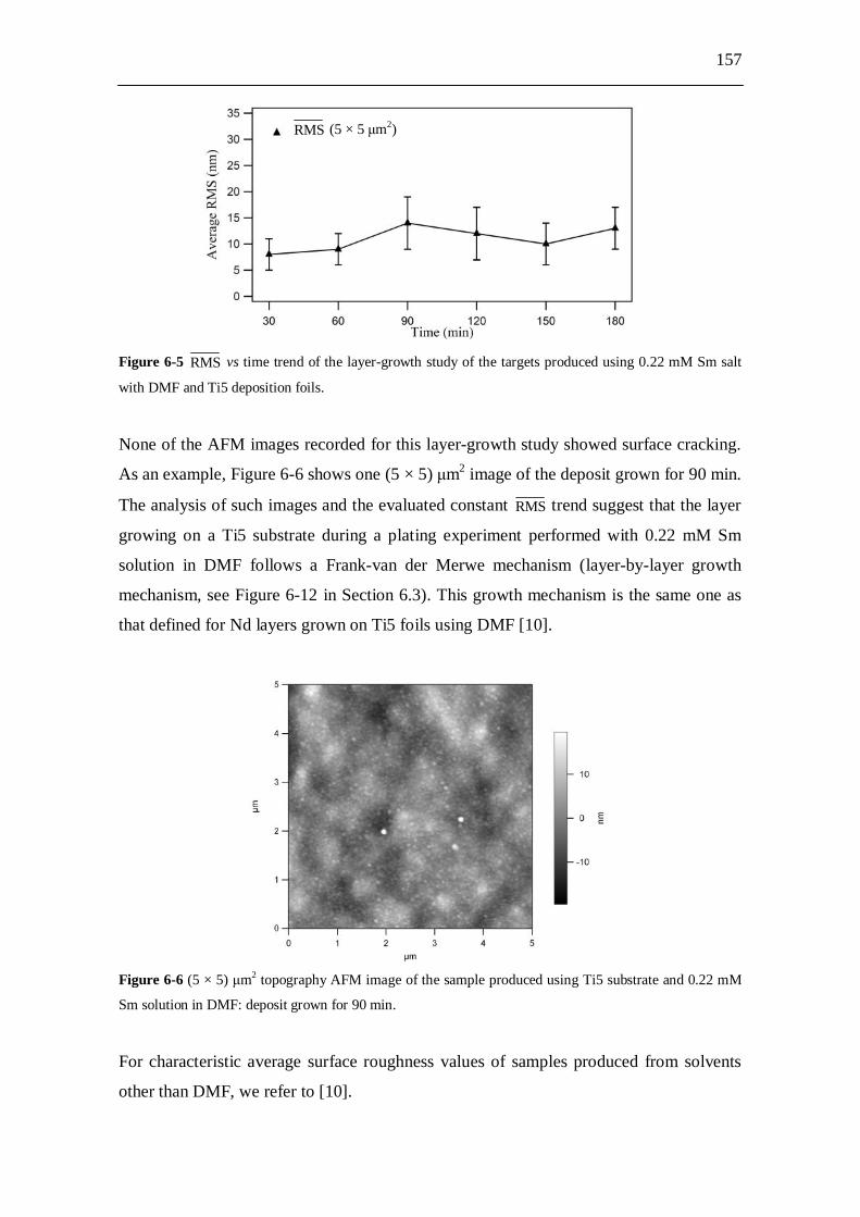
157
Figure 6-5 RMS vs time trend of the layer-growth study of the targets produced using 0.22 mM Sm salt
with DMF and Ti5 deposition foils.
None of the AFM images recorded for this layer-growth study showed surface cracking.
As an example, Figure 6-6 shows one (5 × 5) m2 image of the deposit grown for 90 min.
The analysis of such images and the evaluated constant RMS trend suggest that the layer
growing on a Ti5 substrate during a plating experiment performed with 0.22 mM Sm
solution in DMF follows a Frank-van der Merwe mechanism (layer-by-layer growth
mechanism, see Figure 6-12 in Section 6.3). This growth mechanism is the same one as
that defined for Nd layers grown on Ti5 foils using DMF [10].
Figure 6-6 (5 × 5) m2 topography AFM image of the sample produced using Ti5 substrate and 0.22 mM
Sm solution in DMF: deposit grown for 90 min.
For characteristic average surface roughness values of samples produced from solvents
other than DMF, we refer to [10].
RMS (5 × 5 m2)
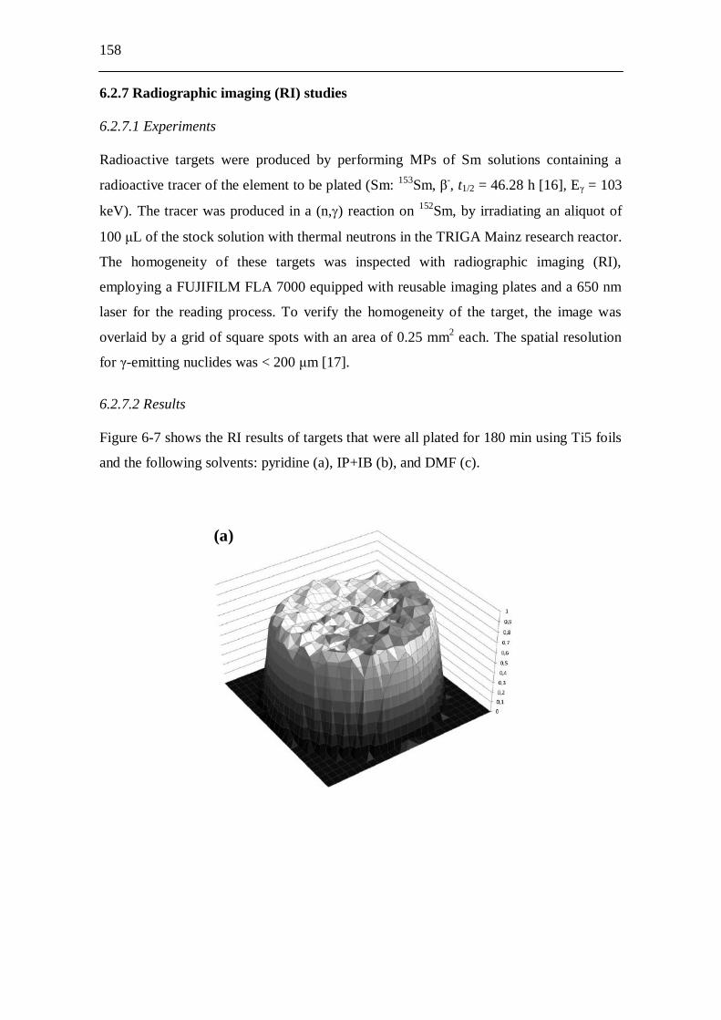
158
6.2.7 Radiographic imaging (RI) studies 6.2.7.1 Experiments Radioactive targets were produced by performing MPs of Sm solutions containing a
radioactive tracer of the element to be plated (Sm: 153Sm, -, t1/2 = 46.28 h [16], E = 103
keV). The tracer was produced in a (n, ) reaction on 152Sm, by irradiating an aliquot of
100 L of the stock solution with thermal neutrons in the TRIGA Mainz research reactor.
The homogeneity of these targets was inspected with radiographic imaging (RI),
employing a FUJIFILM FLA 7000 equipped with reusable imaging plates and a 650 nm
laser for the reading process. To verify the homogeneity of the target, the image was
overlaid by a grid of square spots with an area of 0.25 mm2 each. The spatial resolution
for -emitting nuclides was < 200 m [17].
6.2.7.2 Results Figure 6-7 shows the RI results of targets that were all plated for 180 min using Ti5 foils
and the following solvents: pyridine (a), IP+IB (b), and DMF (c).
(a)
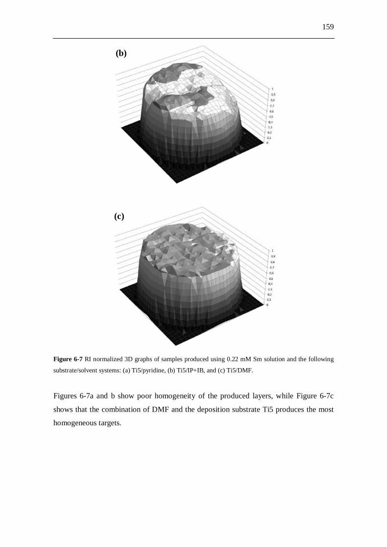
159
Figure 6-7 RI normalized 3D graphs of samples produced using 0.22 mM Sm solution and the following
substrate/solvent systems: (a) Ti5/pyridine, (b) Ti5/IP+IB, and (c) Ti5/DMF.
Figures 6-7a and b show poor homogeneity of the produced layers, while Figure 6-7c
shows that the combination of DMF and the deposition substrate Ti5 produces the most
homogeneous targets.
(b)
(c)

160
6.2.8 Gamma-ray spectroscopy studies 6.2.8.1 Experiments Gamma-ray spectroscopy was performed after MP of Sm solution containing radioactive 153Sm tracer. A high-purity germanium detector (GEM series HPGe Detector Model No.
GEM 23158 P-Plus, ORTEC Company) was used to determine the Sm deposition yield.
To obtain quantitative data, reference sources with known amounts of the tracer were
prepared. They consisted of filter papers with the same geometry as the targets, soaked
with the tracer-containing solution. The yield values were always obtained as the average
value calculated from three distinct -ray measurements. To avoid - pileup from 153Sm
in the low energy region (i.e., 0-1.5 MeV) of the spectrum, the evaluation of the yields
was never performed on the samples from which spectra were recorded, but only on
analog samples.
6.2.8.2 Results In Table 6-3 we list the deposition yields obtained from the -ray analysis. The evaluated
data clearly show the deposition yield to be quantitative for all different types of samples
produced for spectroscopy. In particular, the identical deposition yields of the DMF Ti5
samples plated for 90, 180, and 360 min suggest relatively quick depositions of the Sm3+
ions, as it was also observed for the Nd3+ ions in [10].
Table 6-3 Characteristic data of the different types of samples investigated by -particle spectroscopy. The
geometric efficiency of the detector was calculated by Monte Carlo simulation to be (15.7 ± 0.8)%. Exp. Solvent Foil Plating
time (min)
Yield* (%)
147Sm layer density
g/cm2)
Area (counts)
FWHM (keV)
Detection efficiency
(%) A Pyridine Ti5 180 98.8 ± 1.1 119.6 ± 2.0 20160 ± 220 406 12.88 ± 0.24 IP+IB Ti5 180 99.5 ± 2.1 120 ± 3 23750 ± 190 263 15.1 ± 0.4 DMF Ti5 180 99.1 ± 2.2 120 ± 3 23920 ± 150 189 15.2 ± 0.4
B IP+IB Ti3 180 99.2 ± 1.4 120.1 ± 2.3 23370 ± 180 248 14.88 ± 0.29 IP+IB Ti4 180 99.8 ± 1.2 120.8 ± 2.1 20960 ± 190 152 13.26 ± 0.24 IP+IB Ti5 180 99.5 ± 2.1 120 ± 3 23750 ± 190 263 15.1 ± 0.4
C DMF Ti3 180 98.7 ± 2.8 119 ± 4 21010 ± 190 157 13.4 ± 0.4 DMF Ti5 180 99.1 ± 2.2 120 ± 3 22100 ± 150 169 14.1 ± 0.4
D DMF Ti5 90 99.9 ± 0.6 120.9 ± 1.7 21970 ± 150 163 13.89 ± 0.19 DMF Ti5 360 99.6 ± 1.1 120.6 ± 2.0 21510 ± 180 173 13.64 ± 0.24
* Determined by -ray spectroscopy of 153Sm.
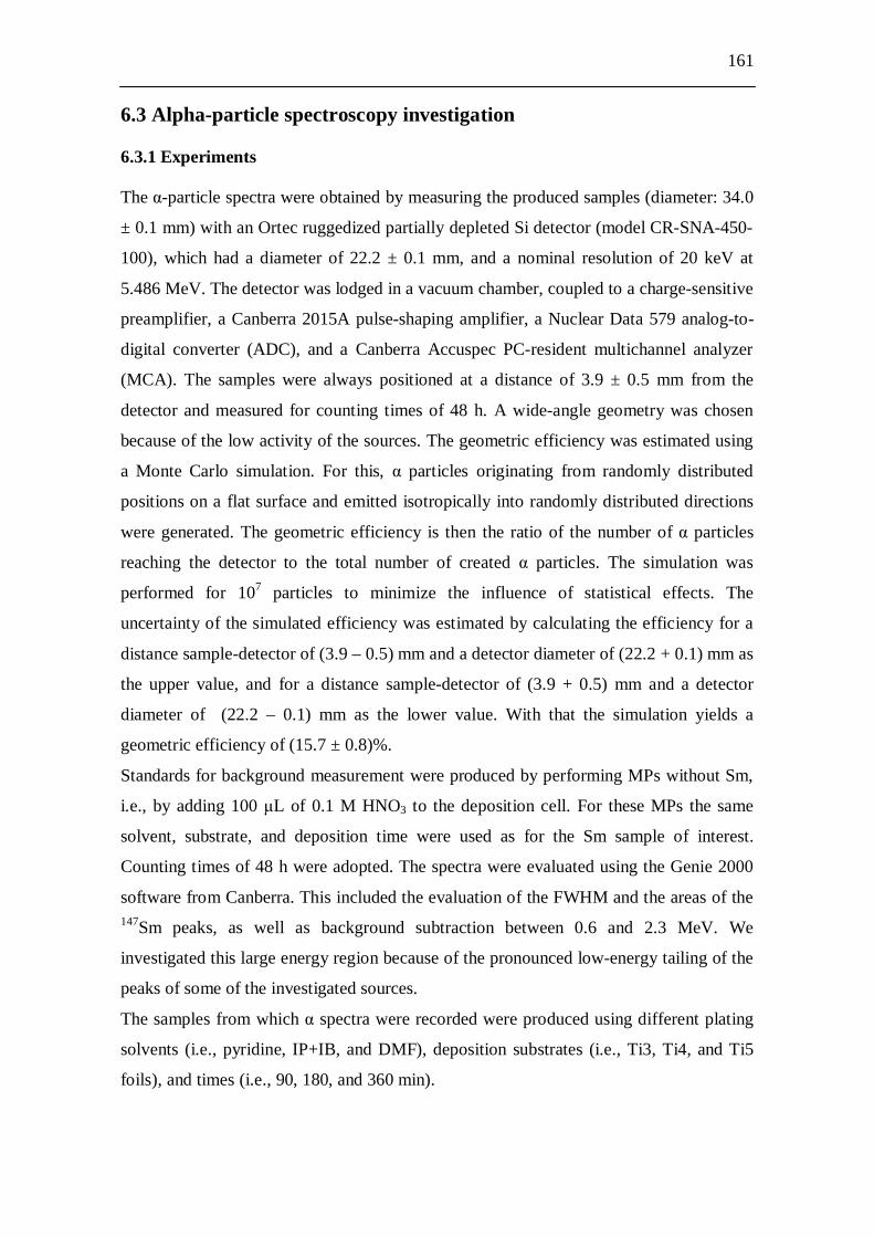
161
6.3 Alpha-particle spectroscopy investigation 6.3.1 Experiments The -particle spectra were obtained by measuring the produced samples (diameter: 34.0
± 0.1 mm) with an Ortec ruggedized partially depleted Si detector (model CR-SNA-450-
100), which had a diameter of 22.2 ± 0.1 mm, and a nominal resolution of 20 keV at
5.486 MeV. The detector was lodged in a vacuum chamber, coupled to a charge-sensitive
preamplifier, a Canberra 2015A pulse-shaping amplifier, a Nuclear Data 579 analog-to-
digital converter (ADC), and a Canberra Accuspec PC-resident multichannel analyzer
(MCA). The samples were always positioned at a distance of 3.9 ± 0.5 mm from the
detector and measured for counting times of 48 h. A wide-angle geometry was chosen
because of the low activity of the sources. The geometric efficiency was estimated using
a Monte Carlo simulation. For this, particles originating from randomly distributed
positions on a flat surface and emitted isotropically into randomly distributed directions
were generated. The geometric efficiency is then the ratio of the number of particles
reaching the detector to the total number of created particles. The simulation was
performed for 107 particles to minimize the influence of statistical effects. The
uncertainty of the simulated efficiency was estimated by calculating the efficiency for a
distance sample-detector of (3.9 – 0.5) mm and a detector diameter of (22.2 + 0.1) mm as
the upper value, and for a distance sample-detector of (3.9 + 0.5) mm and a detector
diameter of (22.2 – 0.1) mm as the lower value. With that the simulation yields a
geometric efficiency of (15.7 ± 0.8)%.
Standards for background measurement were produced by performing MPs without Sm,
i.e., by adding 100 L of 0.1 M HNO3 to the deposition cell. For these MPs the same
solvent, substrate, and deposition time were used as for the Sm sample of interest.
Counting times of 48 h were adopted. The spectra were evaluated using the Genie 2000
software from Canberra. This included the evaluation of the FWHM and the areas of the 147Sm peaks, as well as background subtraction between 0.6 and 2.3 MeV. We
investigated this large energy region because of the pronounced low-energy tailing of the
peaks of some of the investigated sources.
The samples from which spectra were recorded were produced using different plating
solvents (i.e., pyridine, IP+IB, and DMF), deposition substrates (i.e., Ti3, Ti4, and Ti5
foils), and times (i.e., 90, 180, and 360 min).
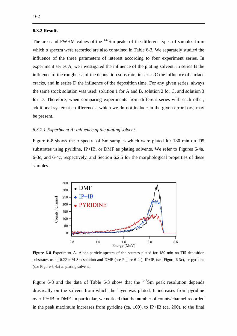
162
6.3.2 Results The area and FWHM values of the 147Sm peaks of the different types of samples from
which spectra were recorded are also contained in Table 6-3. We separately studied the
influence of the three parameters of interest according to four experiment series. In
experiment series A, we investigated the influence of the plating solvent, in series B the
influence of the roughness of the deposition substrate, in series C the influence of surface
cracks, and in series D the influence of the deposition time. For any given series, always
the same stock solution was used: solution 1 for A and B, solution 2 for C, and solution 3
for D. Therefore, when comparing experiments from different series with each other,
additional systematic differences, which we do not include in the given error bars, may
be present.
6.3.2.1 Experiment A: influence of the plating solvent Figure 6-8 shows the spectra of Sm samples which were plated for 180 min on Ti5
substrates using pyridine, IP+IB, or DMF as plating solvents. We refer to Figures 6-4a,
6-3c, and 6-4c, respectively, and Section 6.2.5 for the morphological properties of these
samples.
Figure 6-8 Experiment A. Alpha-particle spectra of the sources plated for 180 min on Ti5 deposition
substrates using 0.22 mM Sm solution and DMF (see Figure 6-4c), IP+IB (see Figure 6-3c), or pyridine
(see Figure 6-4a) as plating solvents.
Figure 6-8 and the data of Table 6-3 show that the 147Sm peak resolution depends
drastically on the solvent from which the layer was plated. It increases from pyridine
over IP+IB to DMF. In particular, we noticed that the number of counts/channel recorded
in the peak maximum increases from pyridine (ca. 100), to IP+IB (ca. 200), to the final
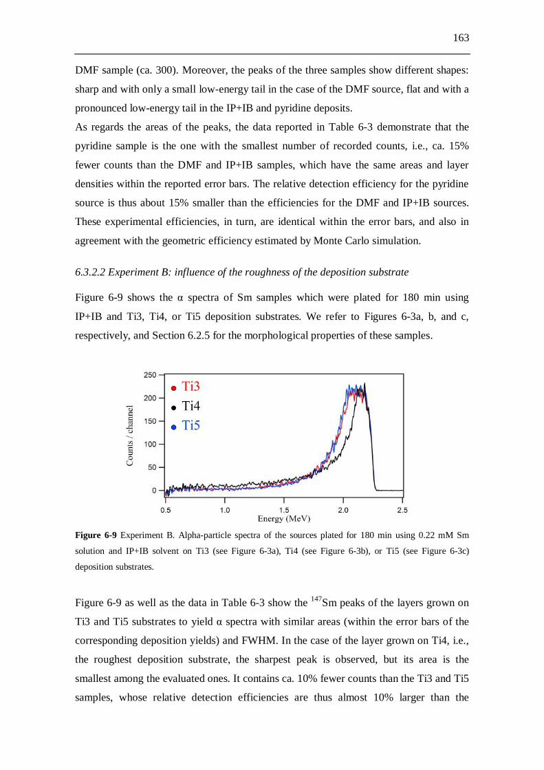
163
DMF sample (ca. 300). Moreover, the peaks of the three samples show different shapes:
sharp and with only a small low-energy tail in the case of the DMF source, flat and with a
pronounced low-energy tail in the IP+IB and pyridine deposits.
As regards the areas of the peaks, the data reported in Table 6-3 demonstrate that the
pyridine sample is the one with the smallest number of recorded counts, i.e., ca. 15%
fewer counts than the DMF and IP+IB samples, which have the same areas and layer
densities within the reported error bars. The relative detection efficiency for the pyridine
source is thus about 15% smaller than the efficiencies for the DMF and IP+IB sources.
These experimental efficiencies, in turn, are identical within the error bars, and also in
agreement with the geometric efficiency estimated by Monte Carlo simulation.
6.3.2.2 Experiment B: influence of the roughness of the deposition substrate Figure 6-9 shows the spectra of Sm samples which were plated for 180 min using
IP+IB and Ti3, Ti4, or Ti5 deposition substrates. We refer to Figures 6-3a, b, and c,
respectively, and Section 6.2.5 for the morphological properties of these samples.
Figure 6-9 Experiment B. Alpha-particle spectra of the sources plated for 180 min using 0.22 mM Sm
solution and IP+IB solvent on Ti3 (see Figure 6-3a), Ti4 (see Figure 6-3b), or Ti5 (see Figure 6-3c)
deposition substrates.
Figure 6-9 as well as the data in Table 6-3 show the 147Sm peaks of the layers grown on
Ti3 and Ti5 substrates to yield spectra with similar areas (within the error bars of the
corresponding deposition yields) and FWHM. In the case of the layer grown on Ti4, i.e.,
the roughest deposition substrate, the sharpest peak is observed, but its area is the
smallest among the evaluated ones. It contains ca. 10% fewer counts than the Ti3 and Ti5
samples, whose relative detection efficiencies are thus almost 10% larger than the
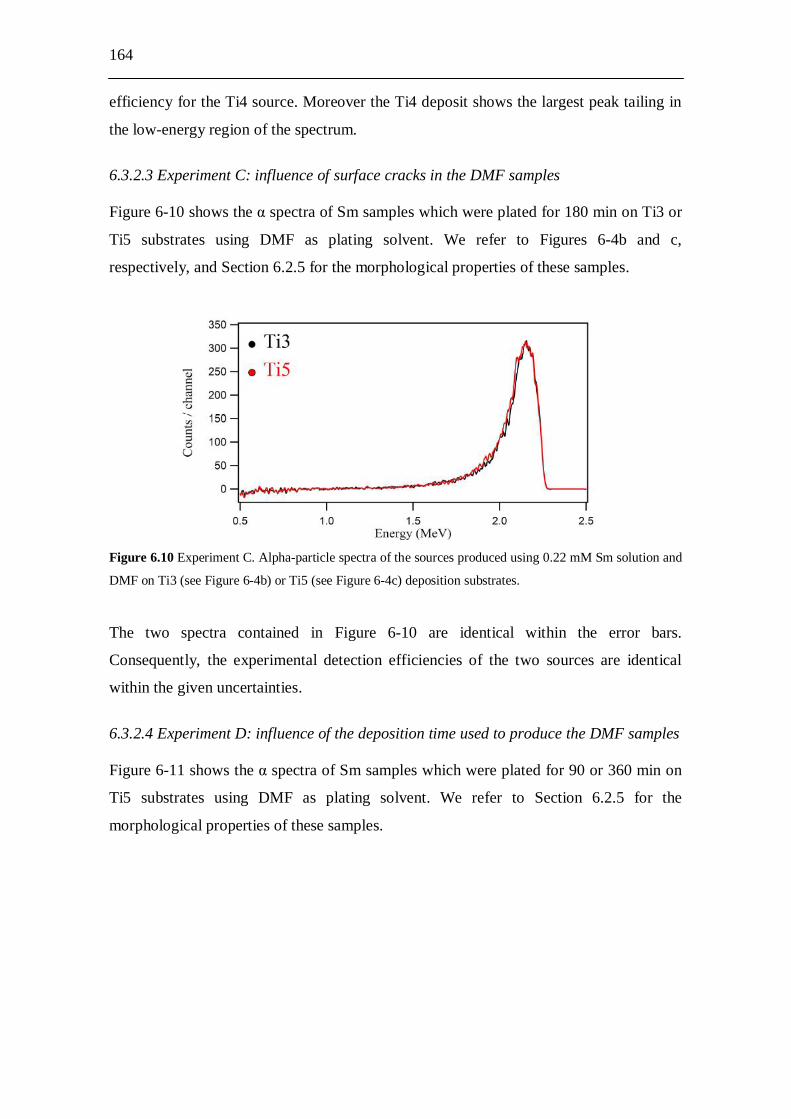
164
efficiency for the Ti4 source. Moreover the Ti4 deposit shows the largest peak tailing in
the low-energy region of the spectrum.
6.3.2.3 Experiment C: influence of surface cracks in the DMF samples Figure 6-10 shows the spectra of Sm samples which were plated for 180 min on Ti3 or
Ti5 substrates using DMF as plating solvent. We refer to Figures 6-4b and c,
respectively, and Section 6.2.5 for the morphological properties of these samples.
Figure 6.10 Experiment C. Alpha-particle spectra of the sources produced using 0.22 mM Sm solution and
DMF on Ti3 (see Figure 6-4b) or Ti5 (see Figure 6-4c) deposition substrates.
The two spectra contained in Figure 6-10 are identical within the error bars.
Consequently, the experimental detection efficiencies of the two sources are identical
within the given uncertainties.
6.3.2.4 Experiment D: influence of the deposition time used to produce the DMF samples Figure 6-11 shows the spectra of Sm samples which were plated for 90 or 360 min on
Ti5 substrates using DMF as plating solvent. We refer to Section 6.2.5 for the
morphological properties of these samples.
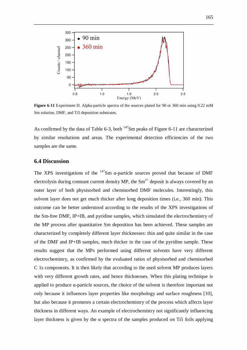
165
Figure 6-11 Experiment D. Alpha-particle spectra of the sources plated for 90 or 360 min using 0.22 mM
Sm solution, DMF, and Ti5 deposition substrates.
As confirmed by the data of Table 6-3, both 147Sm peaks of Figure 6-11 are characterized
by similar resolutions and areas. The experimental detection efficiencies of the two
samples are the same.
6.4 Discussion The XPS investigations of the 147Sm -particle sources proved that because of DMF
electrolysis during constant current density MP, the Sm3+ deposit is always covered by an
outer layer of both physisorbed and chemisorbed DMF molecules. Interestingly, this
solvent layer does not get much thicker after long deposition times (i.e., 360 min). This
outcome can be better understood according to the results of the XPS investigations of
the Sm-free DMF, IP+IB, and pyridine samples, which simulated the electrochemistry of
the MP process after quantitative Sm deposition has been achieved. These samples are
characterized by completely different layer thicknesses: thin and quite similar in the case
of the DMF and IP+IB samples, much thicker in the case of the pyridine sample. These
results suggest that the MPs performed using different solvents have very different
electrochemistry, as confirmed by the evaluated ratios of physisorbed and chemisorbed
C 1s components. It is then likely that according to the used solvent MP produces layers
with very different growth rates, and hence thicknesses. When this plating technique is
applied to produce -particle sources, the choice of the solvent is therefore important not
only because it influences layer properties like morphology and surface roughness [10],
but also because it promotes a certain electrochemistry of the process which affects layer
thickness in different ways. An example of electrochemistry not significantly influencing
layer thickness is given by the spectra of the samples produced on Ti5 foils applying

166
DMF and deposition times of 90 and 360 min (Figure 6-11). In this case the peaks
show similar resolutions and areas. Another example, showing instead electrochemistry
with opposite influence, is given by the spectra of Figure 6-8, where the 147Sm peak of
the Ti5 sample plated for 180 min using pyridine is characterized by fewer counts and
worse resolution than the DMF and IP+IB Ti5 samples, despite having identical
deposition yields. These differences are likely explained by self-absorption of the emitted
particles promoted by the thick pyridine layer grown on top of the Sm deposit during
the applied plating time. Moreover, it is probable that the rough and heavily cracked
surface of the pyridine sample causes varying particle path lengths inside the layer with
varying energy losses which contribute to an increased spread of the peak and its tailing.
As regards instead the spectra of the IP+IB and DMF Ti5 samples of Figure 6-8, the
similar areas of the 147Sm peaks are not surprising as the solvent layer thickness and
deposition yields are similar. Nonetheless, the DMF peak has a better resolution than the
IP+IB one. According to the SEM results, these two layers are mainly different in terms
of the cracking of the produced surfaces: absent in the case of the DMF sample, quite
severe and extended, instead, in the IP+IB source. It seems reasonable to argue that the
cracks may play a role in favouring more scattering in the IP+IB sample than in the DMF
one, hence lowering the resolution of the IP+IB peak. Despite this obvious interpretation,
the spectra of the DMF samples plated for 180 min on both Ti3 and Ti5 substrates
(Figure 6-10), do not seem to confirm this as the main possible conclusion. Indeed, as the
DMF sample grown on the Ti3 substrate was characterized by cracks present over the
whole surface, while the Ti5 deposit was not, spectra of such sources were compared in
order to investigate the potential influence of the cracks on the investigated spectra. We
realize that this may not be an ideal model, as the cracks present in the IP+IB layer are
much more severe and extended than those formed in the DMF samples. Nonetheless, we
chose this as the best approach to reality, and it showed that the spectra of the DMF
samples with or without cracks are similar. Therefore, the different resolutions of the
IP+IB and DMF peaks do not seem to be explicable in terms of layer inhomogeneities
like surface cracks, even if this cannot be totally excluded. An additional explanation
may be found in the shapes of the two peaks: sharp and with only a small low-energy tail
in the case of the DMF source, flat and with a pronounced low-energy tail in the IP+IB
deposit. The shape of the IP+IB peak resembles that of the pyridine peak, which is
probably flat because of the large source thickness. A reasonable explanation to the
apparent increase of the thickness of the IP+IB sample may derive from the particular
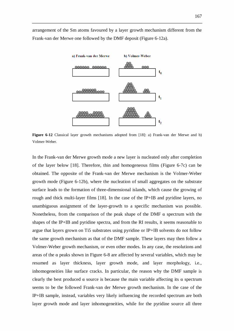
167
arrangement of the Sm atoms favoured by a layer growth mechanism different from the
Frank-van der Merwe one followed by the DMF deposit (Figure 6-12a).
Figure 6-12 Classical layer growth mechanisms adopted from [18]: a) Frank-van der Merwe and b)
Volmer-Weber.
In the Frank-van der Merwe growth mode a new layer is nucleated only after completion
of the layer below [18]. Therefore, thin and homogeneous films (Figure 6-7c) can be
obtained. The opposite of the Frank-van der Merwe mechanism is the Volmer-Weber
growth mode (Figure 6-12b), where the nucleation of small aggregates on the substrate
surface leads to the formation of three-dimensional islands, which cause the growing of
rough and thick multi-layer films [18]. In the case of the IP+IB and pyridine layers, no
unambiguous assignment of the layer-growth to a specific mechanism was possible.
Nonetheless, from the comparison of the peak shape of the DMF spectrum with the
shapes of the IP+IB and pyridine spectra, and from the RI results, it seems reasonable to
argue that layers grown on Ti5 substrates using pyridine or IP+IB solvents do not follow
the same growth mechanism as that of the DMF sample. These layers may then follow a
Volmer-Weber growth mechanism, or even other modes. In any case, the resolutions and
areas of the peaks shown in Figure 6-8 are affected by several variables, which may be
resumed as layer thickness, layer growth mode, and layer morphology, i.e.,
inhomogeneities like surface cracks. In particular, the reason why the DMF sample is
clearly the best produced source is because the main variable affecting its spectrum
seems to be the followed Frank-van der Merwe growth mechanism. In the case of the
IP+IB sample, instead, variables very likely influencing the recorded spectrum are both
layer growth mode and layer inhomogeneities, while for the pyridine source all three
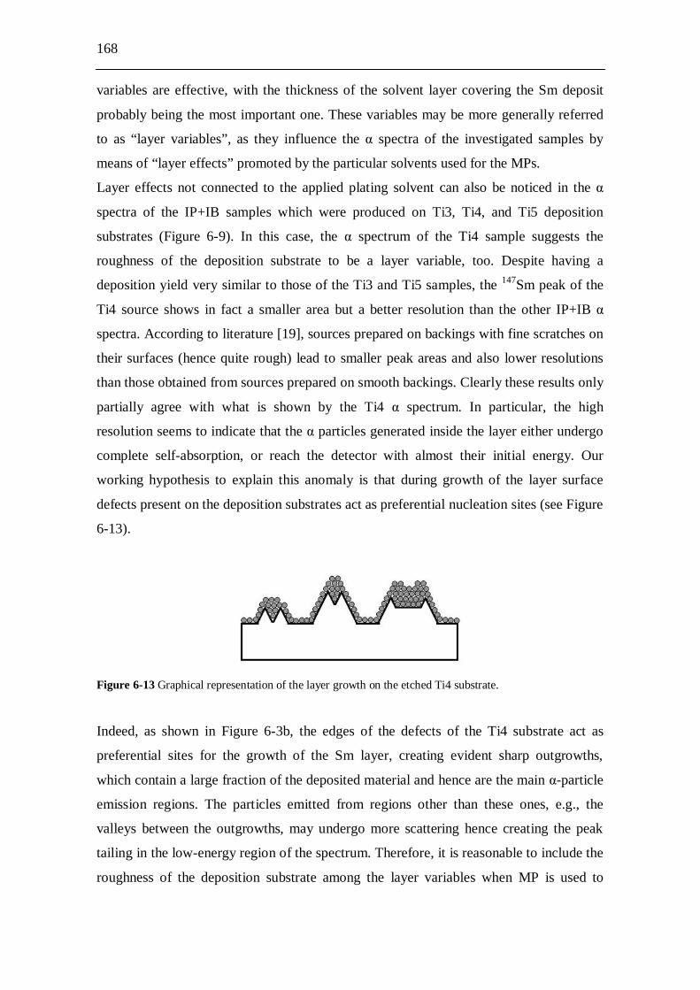
168
variables are effective, with the thickness of the solvent layer covering the Sm deposit
probably being the most important one. These variables may be more generally referred
to as “layer variables”, as they influence the spectra of the investigated samples by
means of “layer effects” promoted by the particular solvents used for the MPs.
Layer effects not connected to the applied plating solvent can also be noticed in the
spectra of the IP+IB samples which were produced on Ti3, Ti4, and Ti5 deposition
substrates (Figure 6-9). In this case, the spectrum of the Ti4 sample suggests the
roughness of the deposition substrate to be a layer variable, too. Despite having a
deposition yield very similar to those of the Ti3 and Ti5 samples, the 147Sm peak of the
Ti4 source shows in fact a smaller area but a better resolution than the other IP+IB
spectra. According to literature [19], sources prepared on backings with fine scratches on
their surfaces (hence quite rough) lead to smaller peak areas and also lower resolutions
than those obtained from sources prepared on smooth backings. Clearly these results only
partially agree with what is shown by the Ti4 spectrum. In particular, the high
resolution seems to indicate that the particles generated inside the layer either undergo
complete self-absorption, or reach the detector with almost their initial energy. Our
working hypothesis to explain this anomaly is that during growth of the layer surface
defects present on the deposition substrates act as preferential nucleation sites (see Figure
6-13).
Figure 6-13 Graphical representation of the layer growth on the etched Ti4 substrate.
Indeed, as shown in Figure 6-3b, the edges of the defects of the Ti4 substrate act as
preferential sites for the growth of the Sm layer, creating evident sharp outgrowths,
which contain a large fraction of the deposited material and hence are the main -particle
emission regions. The particles emitted from regions other than these ones, e.g., the
valleys between the outgrowths, may undergo more scattering hence creating the peak
tailing in the low-energy region of the spectrum. Therefore, it is reasonable to include the
roughness of the deposition substrate among the layer variables when MP is used to
169
produce sources with a certain solvent. In this case the substrate favours in fact a
particular layer growth which also promotes layer effects influencing the spectra.
From the determined experimental efficiencies follows that indeed, layer variables of a
sample affect the obtained spectra in different ways. In some spectra, the low-energy
tail is much more pronounced than in others, which is reflected also in the FWHM values
reported in Table 6-3. Furthermore, also the fraction of particles that reaches the
detector depends on the properties of the sample, even if nominally all samples have the
same areal density of 147Sm and the same size. Non-ideal samples – like those prepared
from pyridine or on the very rough substrate Ti4 – lead to detection efficiencies which
are significantly smaller than in the case of, e.g., the samples prepared in DMF on ideally
flat Ti5 substrates, where experimentally determined efficiency and simulated geometric
efficiency are identical. Such effects should then be taken into account and studied,
especially in experiments aiming at the determination of half-lives of primordial nuclides
using samples produced by MP.
6.5 Conclusion Constant current density MP was applied to produce layers containing the long lived -
particle emitter 147Sm. Several samples were prepared by varying different parameters,
namely the plating solvent, the applied deposition time, and the surface roughness of the
deposition substrate. The sources were analyzed using -ray spectroscopy, RI, XPS,
SEM, and AFM. The results obtained from these characterizations confirmed the
prepared Sm samples and the Nd layers produced in [10] to have similar properties.
Alpha spectra were recorded for samples belonging to the different types of characterized
sources by using small source-to-detector distance. Under the adopted wide-angle
geometry, the peak shapes were mainly determined by source effects [20]. Thanks to the
different applied characterization techniques, the source effects could be categorized
according to what we called “layer variables”, as variables influencing the spectra of
the samples to be investigated by means of “layer effects” promoted by specific MP
parameters. In particular, two parameters were found effective for layer effects: the
plating solvent and the roughness of the deposition substrate. The solvent affects
thickness, morphology, and growth mode of the layer to produce, while the substrate
roughness influences mainly the growth of the deposit, and only as a consequence its
thickness and morphology. These layer variables proved to influence the relative
detection efficiencies of the measurements by as much as 15%. Despite this, to our
170
knowledge these variables have not been considered so far, e.g., as systematic effects in
the evaluation of half-lives determined from such measurements. In particular, computer
simulations, which are frequently used to calculate counting efficiencies, often do not
adequately take these effects into account.
Acknowledgements The authors would like to thank the staff of the TRIGA Mainz for performing the
irradiations, Prof. A. Kühnle for providing the AFM microscope, Dr. T. Lauer for
performing the coating of the Si wafers, and V. Yakusheva from the GSI target
laboratory for her assistance during the SEM measurement. A.V. acknowledges financial
support from the German Federal Ministry of Science and Education (BMBF) under
Contract number 02NUK013E.
References [1] R.F. Sperlein, R.L. Wolke, J. Inorg. Nucl. Chem. 38 (1976) 27-29.
[2] W. Parker, R. Falk, Nucl. Instrum. Methods 16 (1962) 355-357.
[3] K. Eberhardt, W. Brüchle, Ch.E. Düllmann, K.E. Gregorich, W. Hartmann, A.
Hübner, E. Jäger, B. Kindler, J.V. Kratz, D. Liebe, B. Lommel, H.-J. Maier, M. Schädel,
B. Schausten, E. Schimpf, A. Semchenkov, J. Steiner, J. Szerypo, P. Thörle, A. Türler,
A. Yakushev, Nucl. Instrum. Meth. A 590 (2008) 134-140.
[4] J. Runke, Ch.E. Düllmann, K. Eberhardt, P.A. Ellison, K.E. Gregorich, S. Hofmann,
E. Jäger, B. Kindler, J.V. Kratz, J. Krier, B. Lommel, C. Mokry, H. Nitsche, J.B.
Roberto, K.P. Rykaczewski, M. Schädel, P. Thörle-Pospiech, N. Trautmann, A.
Yakushev, J. Radioanal. Nucl. Chem. (2012) submitted.
[5] B. Al-Bataina, J. Jänecke, Radiochim. Acta 42 (1987) 159-164.
[6] K. Zuber, AIP Conf. Proc. 942 (2007) 101-104.
[7] A. Vascon, Ch.E. Düllmann, K. Eberhardt, B. Kindler, B. Lommel, J. Runke, Nucl.
Instrum. Meth. A 655 (2011) 72-79.
[8] A. Vascon, S. Santi, A.A. Isse, T. Reich, J. Drebert, H. Christ, Ch.E. Düllmann, K.
Eberhardt, Nucl. Instrum. Meth. A 696 (2012) 180-191.
[9] A. Vascon, S. Santi, A.A. Isse, T. Reich, J. Drebert, H. Christ, K. Eberhardt, Ch.E.
Düllmann, J. Radioanal. Nucl. Chem. (2012) accepted.
[10] A. Vascon, S. Santi, A.A. Isse, A. Kühnle, T. Reich, J. Drebert, K. Eberhardt, Ch.E.
Düllmann, Nucl. Instrum. Meth. A 714 (2013) 163-175.
171
[11] K. Kossert, G. Jörg, O. Nähle, C.L.V. Gostomski, Appl. Radiat. Isot. 67 (2009)
1702-1706.
[12] C.D. Wagner, W.M. Riggs, L.E. Davis, J.F. Moulder, G.E. Muilenberg, Handbook
of X-Ray Photoelectron Spectroscopy, Perkin-Elmer Corporation, Physical Electronics
Division, Eden Prairie, Minn. 55344 (1979).
[13] T. Moeller, J.C. Bailar, H.J. Emeleus, R. Nyholm, A.F. Trotman-Dickenson,
Comprehensive Inorganic Chemistry, Pergamon, Oxford, 1973.
[14] R.C. Gray, J.C. Carver, D.M. Hercules, J. Electron Spectrosc. 8 (1976) 343-358.
[15] D. R. Lide (Ed.), CRC Handbook of Chemistry and Physics, 87th ed., 2006.
[16] R.G. Helmer, Nucl. Data Sheets 107 (2006) 507-788.
[17] D. Liebe, K. Eberhardt, W. Hartmann, T. Häger, A. Hübner, J.V. Kratz, B. Kindler,
B. Lommel, P. Thörle, M. Schädel, J. Steiner, Nucl. Instrum. Meth. A 590 (2008) 145-
150.
[18] M. Paunovic, M. Schlesinger, Fundamentals of Electrochemical Deposition, second
ed., Wiley, New Jersey, 2006.
[19] D.E. Watt, D. Ramsden, High Sensitivity Counting Techniques, MacMillan and Co.,
New York, 1964.
[20] A. Martìn Sànchez, A. Fernàndez Timòn, M.P. Rubio Montero, Appl. Radiat. Isot.
56 (2002) 51-55.
172
7. Outlook and closing remarks The performed experiments yielded relevant improvements in the preparation of targets
for nuclear investigations by means of molecular plating (MP).
MP was confirmed to be very effective for target production and smooth, crack-free
layers were prepared.
The question about the suitability of MP or PAD [1] to the production of targets for the
higher intensity beams of the future generation [2,3] cannot yet be answered. In principle,
the removal of cracks and other aberrations from both types of targets implies a reduced
tendency of the layers to break under the thermal stress of the beam and thus an increased
structural rigidity. Nonetheless, significant comparisons will be possible only when these
beams are made available and the first tests are performed.
Research in the MP field is interdisciplinary, involving aspects from electrochemistry,
materials science, and radiochemistry. The experiments performed during the thesis have
shown in fact that investigations in these fields are needed not only to improve the
quality of the layers but also to interpret unexpected scientific results (see, e.g., the
different recorded spectra).
The study of the electrochemistry of MP is that of an electrodeposition process.
Electrodepositions are usually carried out from aqueous solutions because of the great
practical importance of water solvents and also because of the greater experimental
difficulties in working with organic solutions [4]. Moreover, the performance of these
depositions is always affected by several variables, which are often optimized by
empirical approach [5]. MP is thus the alternate version of an already complex process,
which is further complicated by the use of non-aqueous solutions and elements like, e.g.,
the lanthanides or the actinides, whose chemistry is rather peculiar.
The use of a reference electrode in the typical two-electrode cells of MP would facilitate
the investigation of the electrochemistry by allowing the study of the processes taking
place at the electrode of interest, i.e., the working electrode. Information about the
species being consumed and produced at, e.g., the cathode could in fact explain how the
plating evolves over time. Nonetheless, the method of measuring electrode potentials in
non-aqueous solutions has not yet been well established. The most serious problem is the
reference electrode; there is no primary reference electrode like the standard hydrogen
electrode (SHE) in aqueous solutions and no reference electrode as reliable as the
aqueous Ag/AgCl electrode. Thus, various electrodes are usually employed in practical
measurements, making the comparison of potential data difficult [4]. Moreover, standard
173
redox potentials of lanthanide and actinide elements have been mainly determined in
aqueous solutions [6,7].
An additional drawback of the study of electrodepositions like MP is the common use of
undivided cells, i.e., cells with no physical separation system, e.g., a porous membrane,
between anode and cathode. This causes the possibility that species generated at one
electrode are consumed at the other electrode and vice versa, hence significantly
complicating the electrode processes – the presence of reduced Pd in the deposits of
some of the performed MPs is a direct evidence of this effect.
The general complexity of MP and the difficulty of measuring electrochemical data are
the main reasons why the derived expression for the cell potential at constant current
density is not sufficient to interpret the experimental behaviour beyond the different
voltage trends recorded with various electrolyte concentrations. If this expression had
also described the evolution of the potential over time it would have probably given
insight into the reasons of the minima in the curves. As this was not possible, the cell
potential minima can currently be identified with only the advanced depletion of the ions
of interest.
Despite the incomplete understanding of the electrochemistry underlying MP, it is worth
pointing out two achievements of the performed experiments, which reshape the concept
of MP itself. First of all, the original statement of no electrolytic dissociation occurring
during MP [8] was disproved. Secondly, it was confirmed that the species of interest is
not deposited as the chemical compound initially dissolved in solution [9,10]. The
absence of the reduced element in the deposit can be explained with the unique chemistry
of both lanthanide and actinide elements. Thus, the main features which led to the name
“molecular plating” are wrong and the technique is rather just a common
electrodeposition from an organic medium.
Much of the information about the nature of MP was obtained with characterization
experiments exploiting analytical techniques used in materials science. These techniques
showed to be suitable for the research in the MP field. In particular, the use of AFM in
liquid environments proved to be effective to answer the question about the origin of
cracking in the produced surfaces. AFM experiments in liquid would have also allowed
inferring the layer growth mechanisms of the samples produced with the very volatile
IP+IB and pyridine solvents. An analysis of the deposits before drying – hence in the
liquid phase – would have in fact avoided the surfaces to be damaged by the cracks, thus
giving the experimental proof of the correctness (or incorrectness) of the inclusion of the
174
growth mechanism among the layer variables influencing -spectroscopy measurements.
Unfortunately, as liquid AFM investigations are very time-consuming they could be
performed only on few occasions. Future experiments should exploit more this type of
analysis to get direct information about the surfaces before any modification induced by
the drying process.
Concerning the use of MP produced layers as -particle sources, forthcoming
investigations should be also combined with computer simulations to get a better
understanding of the way the layer variables affect the experimental spectra. The
simulations could be very helpful to reproduce the behaviour of particles emitted from
sources which are characterized by, e.g., different layer thickness, growth mechanism, or
morphology. The effects of the layer variables could be simulated with, e.g., Monte Carlo
codes using measured values of specific properties of the sources. Important parameters
are usually the thickness of the layers, their density – or eventually just the areal density
– and the stoichiometry of the produced deposits. Cross-sectional SEM images of the
targets [1] could be used to measure thickness values – even if not very accurately. Other,
more complex but precise approaches include Rutherford scattering [11] and X-ray
diffraction analysis [12]. Weighing could be also applied but only if the ratio of target
weight to backing weight is not too small [11]. As regards instead the determination of
the stoichiometry of the deposits, XPS could be used to evaluate the atomic ratios of the
elements present in the produced layers.
The results obtained during this work open the way to the production of the lanthanide
and actinide targets required within the frame of the TRAKULA project. The half-life
determination of 144Nd will definitely benefit from the high quality of the sources
producible with DMF and the very smooth Ti-coated Si wafers. The production of the U
and Pu targets will also benefit from the controlled use of those MP parameters which
have been found to influence the quality of the deposits. The electrolyte concentration,
the applied current density, and the roughness of the deposition substrate will also play a
role in this case. As regards instead the solvent, the optimum one might be different from
DMF, which was mainly tested with the lanthanides Nd and Sm. The very special nature
of U and Pu, with their higher oxidation states (+6 and +4 the most stable ones,
respectively) than Nd and Sm (+3), could in fact favour MPs with completely different
electrochemistry. For this reason, no model elements can be reliably used to perform
deposition test experiments. U and Pu themselves have thus to be used, with all the
limitations resulting from working with these radioactive elements.

175
With this thesis, the hope is to have started a more scientific approach to the research in
the field of target preparation by means of MP. The work to be done is still a lot, but it
may be rewarded with unexpected outcomes.
176
References [1] M.N. Ali, M.A. Garcia, T. Parsons-Moss, H. Nitsche, Polymer-assisted deposition of
homogeneous metal oxide films to produce nuclear targets, Nat. Protoc. 5 (2010) 1440-
1446.
[2] H. Stoecker, C. Sturm, The FAIR start, Nucl. Phys. A 855 (2011) 506-509.
[3] G. Savard, R. Janssens, Proposed ATLAS efficiency and intensity upgrade, ATLAS
Workshop (CERN – European Center for Particle Physics – Geneva, 2009).
[4] K. Izutsu, Electrochemistry in Nonaqueous Solutions, first ed., Wiley-VCH,
Darmstadt, Germany, 2002.
[5] M. Paunovic, M. Schlesinger, Fundamentals of Electrochemical Deposition, second
ed., Wiley, New Jersey, 2006.
[6] J.C. Bailar, H.J. Emelèus, R. Nyholm, A.F. Trotman-Dickenson, Comprehensive
inorganic chemistry, Volume 4: Lanthanides-Transition metal compounds, first ed.,
Pergamon, Oxford, 1973.
[7] J.C. Bailar, H.J. Emelèus, R. Nyholm, A.F. Trotman-Dickenson, Comprehensive
inorganic chemistry, Volume 5: Actinides, first ed., Pergamon, Oxford, 1973.
[8] W. Parker, R. Falk, Molecular plating: a method for the electrolytic formation of thin
inorganic films, Nucl. Instrum. Methods 16 (1962) 355-357.
[9] M.V. Ramaniah, R.J. Singh, S.K. Awasthi, S. Prakash, Studies on electrodeposition
of actinide elements from non-aqueous medium, Int. J. Appl. Radiat. Is. 26 (1975) 648-
650.
[10] A. Ölcer, J. Drebert, T. Reich, in: [R] Seventh International Conference on Nuclear
and Radiochemistry, Budapest, Hungary, 24-29 August, 2008.
[11] G. Friedlander, J.W Kennedy, E.S. Macias, J.M. Miller, Nuclear and
Radiochemistry, third ed., Wiley, New York, 1981.
[12] A. Eisenstein, An X-ray method for measuring the thickness of thin crystalline films,
J. Appl. Phys. 17 (1946) 874-878.