
NANOMATERIALS Bottom-up synthesisof multifunctional … · NANOMATERIALS Bottom-up synthesisof...
6
NANOMATERIALS Bottom-up synthesis of multifunctional nanoporous graphene César Moreno, 1 * Manuel Vilas-Varela, 2 † Bernhard Kretz, 3 † Aran Garcia-Lekue, 3,4 Marius V. Costache, 1 Markos Paradinas, 1 Mirko Panighel, 1 Gustavo Ceballos, 1 Sergio O. Valenzuela, 1,5 Diego Peña, 2 * Aitor Mugarza 1,5 * Nanosize pores can turn semimetallic graphene into a semiconductor and, from being impermeable, into the most efficient molecular-sieve membrane. However, scaling the pores down to the nanometer, while fulfilling the tight structural constraints imposed by applications, represents an enormous challenge for present top-down strategies. Here we report a bottom-up method to synthesize nanoporous graphene comprising an ordered array of pores separated by ribbons, which can be tuned down to the 1-nanometer range. The size, density, morphology, and chemical composition of the pores are defined with atomic precision by the design of the molecular precursors. Our electronic characterization further reveals a highly anisotropic electronic structure, where orthogonal one-dimensional electronic bands with an energy gap of ∼1 electron volt coexist with confined pore states, making the nanoporous graphene a highly versatile semiconductor for simultaneous sieving and electrical sensing of molecular species. N anoporous graphene (NPG) has recently attracted great attention owing to its po- tential application as an active compo- nent of field-effect transistors (FET) (1, 2) and as an atom-thick selective nanosieve for sequencing (3, 4), ion transport (5, 6), gas separation (7–9), and water purification (10, 11). Selectivity in molecular sieving is achieved by reducing the pore size to the scale of single mol- ecules, that is, in the nanometer range, for rel- evant greenhouse gases, amino acids, or single ions. This has been achieved in several studies at the single-pore level (6) or through the cre- ation of randomly distributed pores (9, 11), where graphene remains semimetallic. Similarly, induc- ing semiconducting gaps for room-temperature gate actuation requires the generation of sub- 10-nm ribbons between pores (1, 12). In this range, atomic-scale disorder and width fluctuations have substantial effect on gap uniformity. Hence, com- bining semiconducting and sieving functionalities in a single NPG material is a challenging task that requires the simultaneous generation of nanometer-sized pores and ribbons that have to be carved with atomic precision. Inspired by successful on-surface routes to synthesize covalent carbon-based nanostructures (13–20), we have devised a strategy that leads to the formation of NPG that exhibits both semi- conducting and nanosieving functionalities. Our method relies on the hierarchical control of three thermally activated reaction steps, labeled T1 to T3 in Fig. 1. Nanoribbons and pores with nano- meter size, atomic-scale uniformity, and long-range order are formed in separate steps. Graphene nanoribbons (GNRs) are first synthesized by fol- lowing a previously used route (17, 20), consist- ing of the surface-assisted Ullmann coupling of aromatic dihalide monomers into polymer chains (T1) and the cyclodehydrogenative aromatization of the intermediate polymeric chains into GNRs (T2). The final step (T3) interconnects GNRs lat- erally in a reproducible manner by means of a highly selective dehydrogenative cross-coupling (21). This step requires a careful design of the monomer precursor, which defines the edge to- pology of the resulting GNR that is necessary for a high yield and selectivity of the cross-coupling reaction. The monomer precursor synthesized in this work, labeled DP-DBBA (diphenyl–10,10′- dibromo-9,9′-bianthracene), is a derivative of the DBBA used in the synthesis of seven–carbon atom–wide armchair GNRs (7-AGNR) (17), with phenyl substituents added at (2,2′) sites. The latter is the key element for the promotion of the inter-GNR connections that lead to the NPG structure shown in Fig. 1D (see supple- mentary materials for details of the monomer synthesis) (22). The choice of catalytic surface is also relevant for the selection of the reaction paths that define the intermediates and for the separation of thermal windows that lead to their hierarchical control. Here we use the Au(111) surface, where each reaction step has a differ- ent thermal activation onset, as shown below. The NPG can then be transferred to suitable substrates in which its functionalities can be exploited (22). The structures obtained in each step of the hierarchical synthetic route are characterized using scanning tunneling microscopy (STM). Representative topographic images are shown in Fig. 2. After deposition at room temperature and annealing to temperature T = 200°C, mono- mers undergo debromination to form the cor- responding aryl radicals, which are subsequently coupled by means of C–C bond formation (step T1) (17, 20). The resulting polymeric chains ex- hibit the characteristic protrusion pairs with a periodicity of 0.84 nm and an apparent height of 0.31 nm, which arises from probing the high ends of the staggered bis-anthracene units of the monomer with STM (Fig. 2, A and D) (17, 20). The chains, with lengths of up to 150 nm, pre- dominantly align in close-packed ensembles along the zigzag orientation of the herringbone recon- struction of the Au(111) surface. Both the extraor- dinary length of the polymeric intermediates and their parallel alignment are crucial ingredients for the high yield and long-range order observed in the final step T3. Annealing to T = 400°C triggers the intra- molecular cyclodehydrogenation (step T2), giving rise to the aromatization of the chain and the corresponding reduction of the apparent height to 0.18 nm, which is characteristic of GNRs (Fig. 2, B and E) ( 17, 20). The nanoribbons appear dis- persed as individual stripes, yet they maintain a predominantly parallel alignment along the zigzag orientation. As can be seen in the high-resolution image of Fig. 2E, the catafused benzene rings that arise from the cyclization of the phenyl substitu- ent result in a periodic modulation of the width. Consecutive pairs of 7 and 13 carbon atoms define multibay regions made of three conjoined bays (yellow lines in Fig. 1, C and D). This particular edge structure of the nanoribbons, referred to as 7-13–AGNR hereafter, will define both the mor- phology and size of the corresponding pores in the NPG, as well as its electronic structure. The aryl-aryl interribbon connection is in- duced by further annealing to T = 450°C (step T3). Figure 2C shows how GNRs tend to merge, connecting laterally from each of the fused ben- zene rings and forming a nanomesh (indicated with a green rectangle). The submolecular struc- ture, observed in the high-resolution image of Fig. 2F, coincides with the NPG structure de- picted in Fig. 1D, which reveals that the inter- ribbon coupling occurs by means of a selective C–H bond activation. The activation of specific C–H bonds in polycyclic aromatic hydrocarbons is nontrivial because of the presence of multiple quasi-energetic bonds (three in the case of the 7-13–AGNR, labeled as H 1 to H 3 in Fig. 1). In step T3, the selectivity in the C–C bond formation between adjacent GNRs is driven by the easy accessibility to the radical formed after the C–H 3 bond cleavage, as opposed to the steric hindrance associated with the radicals formed after the C–H 1 or C–H 2 bond cleavage. Another remarkable mile- stone is the long-range order achieved. To date, the observation of selective intermolecular aryl- aryl coupling has been limited to small supra- molecular structures (19, 23–28). The hierarchical RESEARCH Moreno et al., Science 360, 199–203 (2018) 13 April 2018 1 of 5 1 Catalan Institute of Nanoscience and Nanotechnology (ICN2), Consejo Superior de Investigaciones Científicas (CSIC) and The Barcelona Institute of Science and Technology, Campus UAB, Bellaterra, 08193 Barcelona, Spain. 2 Centro Singular de Investigación en Química Biolóxica e Materiais Moleculares (CIQUS) and Departamento de Química Orgánica, Universidade de Santiago de Compostela, 15782 Santiago de Compostela, Spain. 3 Donostia International Physics Center (DIPC), 20018 San Sebastian, Spain. 4 Ikerbasque, Basque Foundation for Science, 48013 Bilbao, Spain. 5 ICREA–Institució Catalana de Recerca i Estudis Avançats, 08010 Barcelona, Spain. *Corresponding author. Email: [email protected] (C.M.); [email protected] (D.P.); [email protected] (A.M.) †These authors contributed equally to this work. on April 7, 2020 http://science.sciencemag.org/ Downloaded from
Transcript of NANOMATERIALS Bottom-up synthesisof multifunctional … · NANOMATERIALS Bottom-up synthesisof...
NANOMATERIALS
Bottom-up synthesis of multifunctionalnanoporous grapheneCésar Moreno,1* Manuel Vilas-Varela,2† Bernhard Kretz,3† Aran Garcia-Lekue,3,4
Marius V. Costache,1 Markos Paradinas,1 Mirko Panighel,1 Gustavo Ceballos,1
Sergio O. Valenzuela,1,5 Diego Peña,2* Aitor Mugarza1,5*
Nanosize pores can turn semimetallic graphene into a semiconductor and, from beingimpermeable, into the most efficient molecular-sieve membrane. However, scaling thepores down to the nanometer, while fulfilling the tight structural constraints imposed byapplications, represents an enormous challenge for present top-down strategies. Here wereport a bottom-up method to synthesize nanoporous graphene comprising an orderedarray of pores separated by ribbons, which can be tuned down to the 1-nanometer range.The size, density, morphology, and chemical composition of the pores are defined withatomic precision by the design of the molecular precursors. Our electronic characterizationfurther reveals a highly anisotropic electronic structure, where orthogonal one-dimensionalelectronic bands with an energy gap of ∼1 electron volt coexist with confined pore states,making the nanoporous graphene a highly versatile semiconductor for simultaneous sievingand electrical sensing of molecular species.
Nanoporous graphene (NPG) has recentlyattracted great attention owing to its po-tential application as an active compo-nent of field-effect transistors (FET) (1, 2)and as an atom-thick selective nanosieve
for sequencing (3, 4), ion transport (5, 6), gasseparation (7–9), and water purification (10, 11).Selectivity in molecular sieving is achieved byreducing the pore size to the scale of single mol-ecules, that is, in the nanometer range, for rel-evant greenhouse gases, amino acids, or singleions. This has been achieved in several studiesat the single-pore level (6) or through the cre-ation of randomly distributed pores (9, 11), wheregraphene remains semimetallic. Similarly, induc-ing semiconducting gaps for room-temperaturegate actuation requires the generation of sub-10-nm ribbons between pores (1, 12). In this range,atomic-scale disorder and width fluctuations havesubstantial effect on gap uniformity. Hence, com-bining semiconducting and sieving functionalitiesin a single NPG material is a challenging taskthat requires the simultaneous generation ofnanometer-sized pores and ribbons that have tobe carved with atomic precision.Inspired by successful on-surface routes to
synthesize covalent carbon-based nanostructures
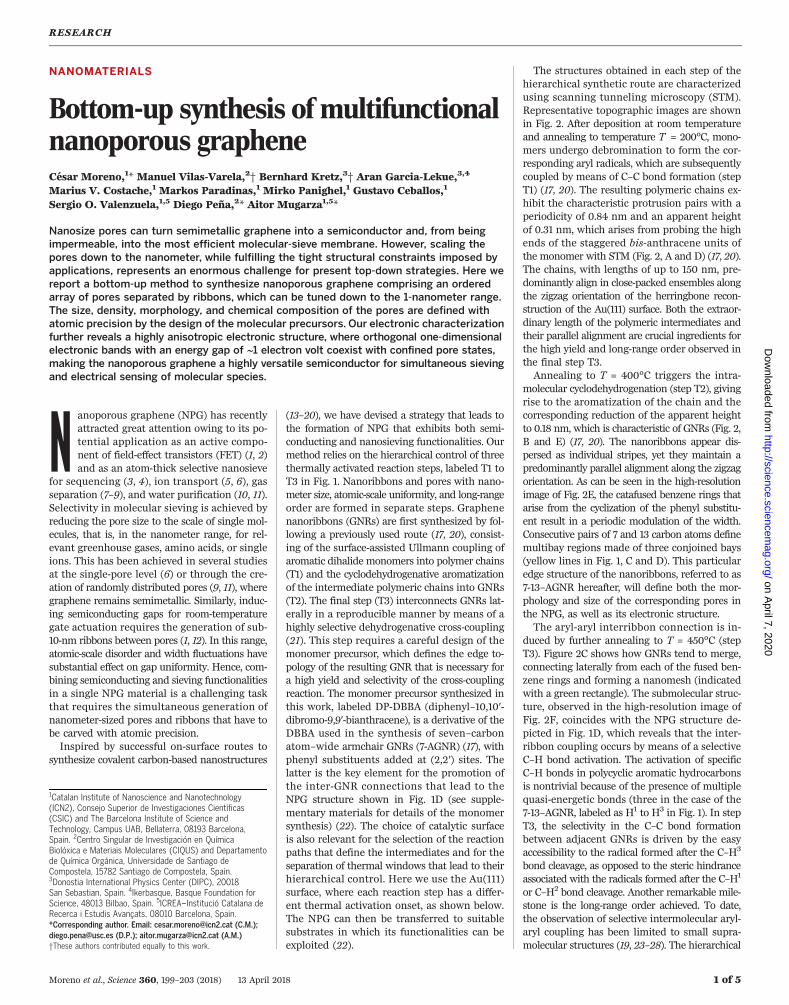
(13–20), we have devised a strategy that leads tothe formation of NPG that exhibits both semi-conducting and nanosieving functionalities. Ourmethod relies on the hierarchical control of threethermally activated reaction steps, labeled T1 toT3 in Fig. 1. Nanoribbons and pores with nano-meter size, atomic-scale uniformity, and long-rangeorder are formed in separate steps. Graphenenanoribbons (GNRs) are first synthesized by fol-lowing a previously used route (17, 20), consist-ing of the surface-assisted Ullmann coupling ofaromatic dihalide monomers into polymer chains(T1) and the cyclodehydrogenative aromatizationof the intermediate polymeric chains into GNRs(T2). The final step (T3) interconnects GNRs lat-erally in a reproducible manner by means of ahighly selective dehydrogenative cross-coupling(21). This step requires a careful design of themonomer precursor, which defines the edge to-pology of the resulting GNR that is necessary fora high yield and selectivity of the cross-couplingreaction. The monomer precursor synthesized inthis work, labeled DP-DBBA (diphenyl–10,10′-dibromo-9,9′-bianthracene), is a derivative of theDBBA used in the synthesis of seven–carbonatom–wide armchair GNRs (7-AGNR) (17), withphenyl substituents added at (2,2′) sites. Thelatter is the key element for the promotion ofthe inter-GNR connections that lead to theNPG structure shown in Fig. 1D (see supple-mentary materials for details of the monomersynthesis) (22). The choice of catalytic surfaceis also relevant for the selection of the reactionpaths that define the intermediates and for theseparation of thermal windows that lead to theirhierarchical control. Here we use the Au(111)surface, where each reaction step has a differ-ent thermal activation onset, as shown below.The NPG can then be transferred to suitablesubstrates in which its functionalities can beexploited (22).
The structures obtained in each step of thehierarchical synthetic route are characterizedusing scanning tunneling microscopy (STM).Representative topographic images are shownin Fig. 2. After deposition at room temperatureand annealing to temperature T = 200°C, mono-mers undergo debromination to form the cor-responding aryl radicals, which are subsequentlycoupled by means of C–C bond formation (stepT1) (17, 20). The resulting polymeric chains ex-hibit the characteristic protrusion pairs with aperiodicity of 0.84 nm and an apparent heightof 0.31 nm, which arises from probing the highends of the staggered bis-anthracene units ofthe monomer with STM (Fig. 2, A and D) (17, 20).The chains, with lengths of up to 150 nm, pre-dominantly align in close-packed ensembles alongthe zigzag orientation of the herringbone recon-struction of the Au(111) surface. Both the extraor-dinary length of the polymeric intermediates andtheir parallel alignment are crucial ingredients forthe high yield and long-range order observed inthe final step T3.Annealing to T = 400°C triggers the intra-
molecular cyclodehydrogenation (step T2), givingrise to the aromatization of the chain and thecorresponding reduction of the apparent heightto 0.18 nm, which is characteristic of GNRs (Fig. 2,B and E) (17, 20). The nanoribbons appear dis-persed as individual stripes, yet they maintain apredominantly parallel alignment along the zigzagorientation. As can be seen in the high-resolutionimage of Fig. 2E, the catafused benzene rings thatarise from the cyclization of the phenyl substitu-ent result in a periodic modulation of the width.Consecutive pairs of 7 and 13 carbon atoms definemultibay regions made of three conjoined bays(yellow lines in Fig. 1, C and D). This particularedge structure of the nanoribbons, referred to as7-13–AGNR hereafter, will define both the mor-phology and size of the corresponding pores inthe NPG, as well as its electronic structure.The aryl-aryl interribbon connection is in-
duced by further annealing to T = 450°C (stepT3). Figure 2C shows how GNRs tend to merge,connecting laterally from each of the fused ben-zene rings and forming a nanomesh (indicatedwith a green rectangle). The submolecular struc-ture, observed in the high-resolution image ofFig. 2F, coincides with the NPG structure de-picted in Fig. 1D, which reveals that the inter-ribbon coupling occurs by means of a selectiveC–H bond activation. The activation of specificC–H bonds in polycyclic aromatic hydrocarbonsis nontrivial because of the presence of multiplequasi-energetic bonds (three in the case of the7-13–AGNR, labeled as H1 to H3 in Fig. 1). In stepT3, the selectivity in the C–C bond formationbetween adjacent GNRs is driven by the easyaccessibility to the radical formed after the C–H3
bond cleavage, as opposed to the steric hindranceassociated with the radicals formed after the C–H1
or C–H2 bond cleavage. Another remarkable mile-stone is the long-range order achieved. To date,the observation of selective intermolecular aryl-aryl coupling has been limited to small supra-molecular structures (19, 23–28). The hierarchical
RESEARCH
Moreno et al., Science 360, 199–203 (2018) 13 April 2018 1 of 5
1Catalan Institute of Nanoscience and Nanotechnology(ICN2), Consejo Superior de Investigaciones Científicas(CSIC) and The Barcelona Institute of Science andTechnology, Campus UAB, Bellaterra, 08193 Barcelona,Spain. 2Centro Singular de Investigación en QuímicaBiolóxica e Materiais Moleculares (CIQUS) and Departamentode Química Orgánica, Universidade de Santiago deCompostela, 15782 Santiago de Compostela, Spain.3Donostia International Physics Center (DIPC), 20018San Sebastian, Spain. 4Ikerbasque, Basque Foundation forScience, 48013 Bilbao, Spain. 5ICREA–Institució Catalana deRecerca i Estudis Avançats, 08010 Barcelona, Spain.*Corresponding author. Email: [email protected] (C.M.);[email protected] (D.P.); [email protected] (A.M.)†These authors contributed equally to this work.
on April 7, 2020
http://science.sciencem
ag.org/D
ownloaded from
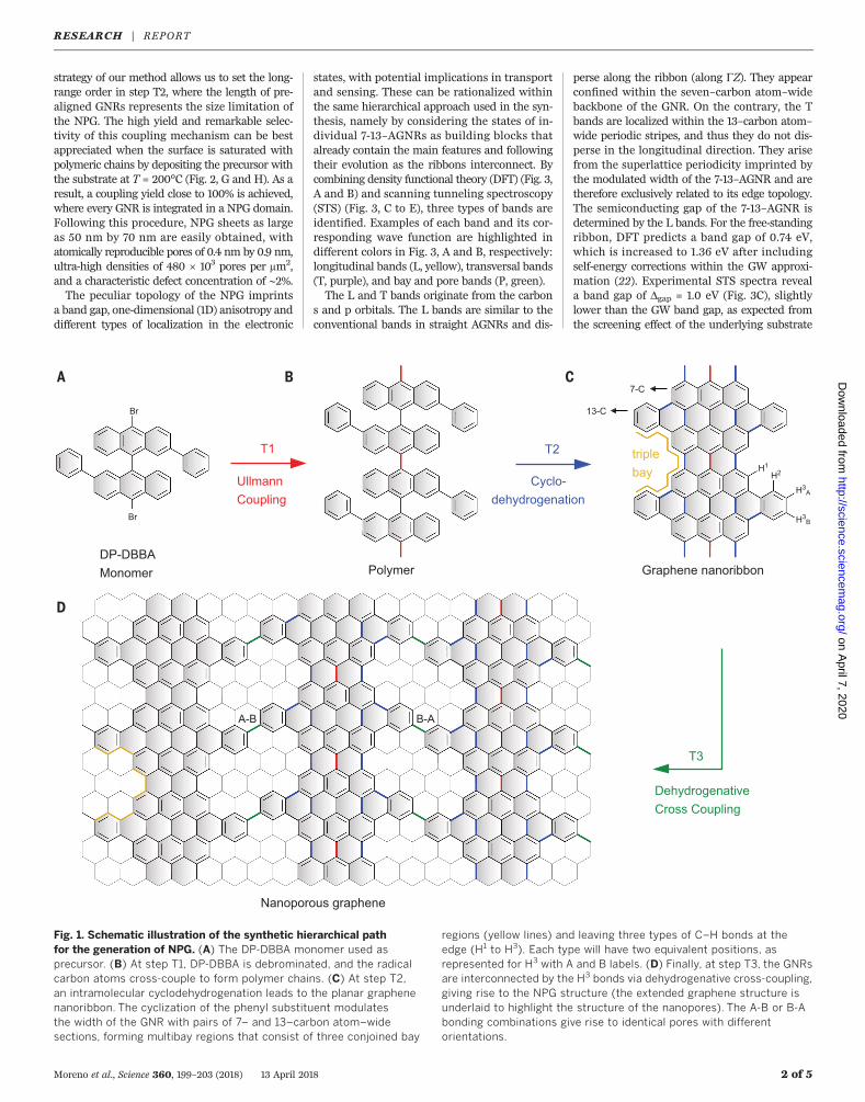
strategy of our method allows us to set the long-range order in step T2, where the length of pre-aligned GNRs represents the size limitation ofthe NPG. The high yield and remarkable selec-tivity of this coupling mechanism can be bestappreciated when the surface is saturated withpolymeric chains by depositing the precursor withthe substrate at T = 200°C (Fig. 2, G and H). As aresult, a coupling yield close to 100% is achieved,where every GNR is integrated in a NPG domain.Following this procedure, NPG sheets as largeas 50 nm by 70 nm are easily obtained, withatomically reproducible pores of 0.4 nm by 0.9 nm,ultra-high densities of 480 × 103 pores per mm2,and a characteristic defect concentration of ∼2%.The peculiar topology of the NPG imprints
a band gap, one-dimensional (1D) anisotropy anddifferent types of localization in the electronic
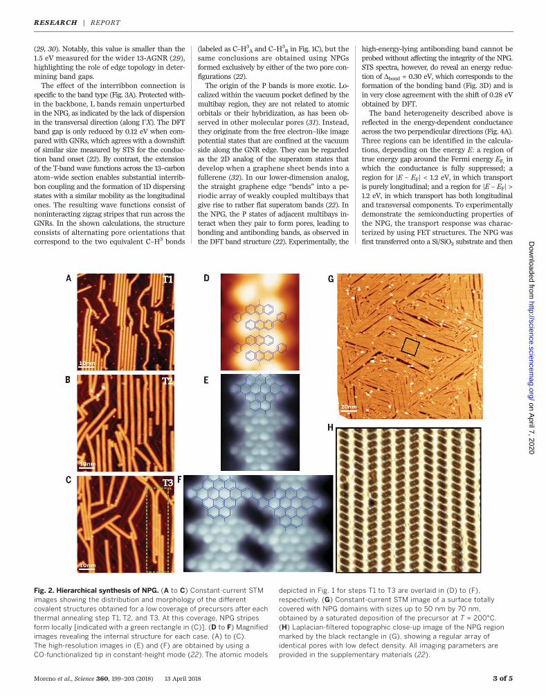
states, with potential implications in transportand sensing. These can be rationalized withinthe same hierarchical approach used in the syn-thesis, namely by considering the states of in-dividual 7-13–AGNRs as building blocks thatalready contain the main features and followingtheir evolution as the ribbons interconnect. Bycombining density functional theory (DFT) (Fig. 3,A and B) and scanning tunneling spectroscopy(STS) (Fig. 3, C to E), three types of bands areidentified. Examples of each band and its cor-responding wave function are highlighted indifferent colors in Fig. 3, A and B, respectively:longitudinal bands (L, yellow), transversal bands(T, purple), and bay and pore bands (P, green).The L and T bands originate from the carbon
s and p orbitals. The L bands are similar to theconventional bands in straight AGNRs and dis-
perse along the ribbon (along GZ). They appearconfined within the seven–carbon atom–widebackbone of the GNR. On the contrary, the Tbands are localized within the 13–carbon atom–wide periodic stripes, and thus they do not dis-perse in the longitudinal direction. They arisefrom the superlattice periodicity imprinted bythe modulated width of the 7-13–AGNR and aretherefore exclusively related to its edge topology.The semiconducting gap of the 7-13–AGNR isdetermined by the L bands. For the free-standingribbon, DFT predicts a band gap of 0.74 eV,which is increased to 1.36 eV after includingself-energy corrections within the GW approxi-mation (22). Experimental STS spectra reveala band gap of Dgap = 1.0 eV (Fig. 3C), slightlylower than the GW band gap, as expected fromthe screening effect of the underlying substrate
Moreno et al., Science 360, 199–203 (2018) 13 April 2018 2 of 5
H3A
H3B
H2H1
Br
Br
T1
UllmannCoupling
T2
Cyclo-dehydrogenation
Polymer Graphene nanoribbon
Nanoporous graphene
T3
Dehydrogenative Cross Coupling
13-C
A-B B-A
7-CA B C
D
triplebay
DP-DBBAMonomer
Fig. 1. Schematic illustration of the synthetic hierarchical pathfor the generation of NPG. (A) The DP-DBBA monomer used asprecursor. (B) At step T1, DP-DBBA is debrominated, and the radicalcarbon atoms cross-couple to form polymer chains. (C) At step T2,an intramolecular cyclodehydrogenation leads to the planar graphenenanoribbon. The cyclization of the phenyl substituent modulatesthe width of the GNR with pairs of 7– and 13–carbon atom–widesections, forming multibay regions that consist of three conjoined bay
regions (yellow lines) and leaving three types of C–H bonds at theedge (H1 to H3). Each type will have two equivalent positions, asrepresented for H3 with A and B labels. (D) Finally, at step T3, the GNRsare interconnected by the H3 bonds via dehydrogenative cross-coupling,giving rise to the NPG structure (the extended graphene structure isunderlaid to highlight the structure of the nanopores). The A-B or B-Abonding combinations give rise to identical pores with differentorientations.
RESEARCH | REPORTon A
pril 7, 2020
http://science.sciencemag.org/
Dow
nloaded from
(29, 30). Notably, this value is smaller than the1.5 eV measured for the wider 13-AGNR (29),highlighting the role of edge topology in deter-mining band gaps.The effect of the interribbon connection is
specific to the band type (Fig. 3A). Protected with-in the backbone, L bands remain unperturbedin the NPG, as indicated by the lack of dispersionin the transversal direction (along GX). The DFTband gap is only reduced by 0.12 eV when com-pared with GNRs, which agrees with a downshiftof similar size measured by STS for the conduc-tion band onset (22). By contrast, the extensionof the T-band wave functions across the 13–carbonatom–wide section enables substantial interrib-bon coupling and the formation of 1D dispersingstates with a similar mobility as the longitudinalones. The resulting wave functions consist ofnoninteracting zigzag stripes that run across theGNRs. In the shown calculations, the structureconsists of alternating pore orientations thatcorrespond to the two equivalent C–H3 bonds
(labeled as C–H3A and C–H3
B in Fig. 1C), but thesame conclusions are obtained using NPGsformed exclusively by either of the two pore con-figurations (22).The origin of the P bands is more exotic. Lo-
calized within the vacuum pocket defined by themultibay region, they are not related to atomicorbitals or their hybridization, as has been ob-served in other molecular pores (31). Instead,they originate from the free electron–like imagepotential states that are confined at the vacuumside along the GNR edge. They can be regardedas the 2D analog of the superatom states thatdevelop when a graphene sheet bends into afullerene (32). In our lower-dimension analog,the straight graphene edge “bends” into a pe-riodic array of weakly coupled multibays thatgive rise to rather flat superatom bands (22). Inthe NPG, the P states of adjacent multibays in-teract when they pair to form pores, leading tobonding and antibonding bands, as observed inthe DFT band structure (22). Experimentally, the
high-energy-lying antibonding band cannot beprobed without affecting the integrity of the NPG.STS spectra, however, do reveal an energy reduc-tion of Dbond = 0.30 eV, which corresponds to theformation of the bonding band (Fig. 3D) and isin very close agreement with the shift of 0.28 eVobtained by DFT.The band heterogeneity described above is
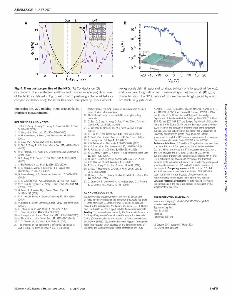
reflected in the energy-dependent conductanceacross the two perpendicular directions (Fig. 4A).Three regions can be identified in the calcula-tions, depending on the energy E: a region oftrue energy gap around the Fermi energy EF, inwhich the conductance is fully suppressed; aregion for |E – EF| < 1.2 eV, in which transportis purely longitudinal; and a region for |E – EF| >1.2 eV, in which transport has both longitudinaland transversal components. To experimentallydemonstrate the semiconducting properties ofthe NPG, the transport response was charac-terized by using FET structures. The NPG wasfirst transferred onto a Si/SiO2 substrate and then
Moreno et al., Science 360, 199–203 (2018) 13 April 2018 3 of 5
Fig. 2. Hierarchical synthesis of NPG. (A to C) Constant-current STMimages showing the distribution and morphology of the differentcovalent structures obtained for a low coverage of precursors after eachthermal annealing step T1, T2, and T3. At this coverage, NPG stripesform locally [indicated with a green rectangle in (C)]. (D to F) Magnifiedimages revealing the internal structure for each case, (A) to (C).The high-resolution images in (E) and (F) are obtained by using aCO-functionalized tip in constant-height mode (22). The atomic models
depicted in Fig. 1 for steps T1 to T3 are overlaid in (D) to (F),respectively. (G) Constant-current STM image of a surface totallycovered with NPG domains with sizes up to 50 nm by 70 nm,obtained by a saturated deposition of the precursor at T = 200°C.(H) Laplacian-filtered topographic close-up image of the NPG regionmarked by the black rectangle in (G), showing a regular array ofidentical pores with low defect density. All imaging parameters areprovided in the supplementary materials (22).
RESEARCH | REPORTon A
pril 7, 2020
http://science.sciencemag.org/
Dow
nloaded from
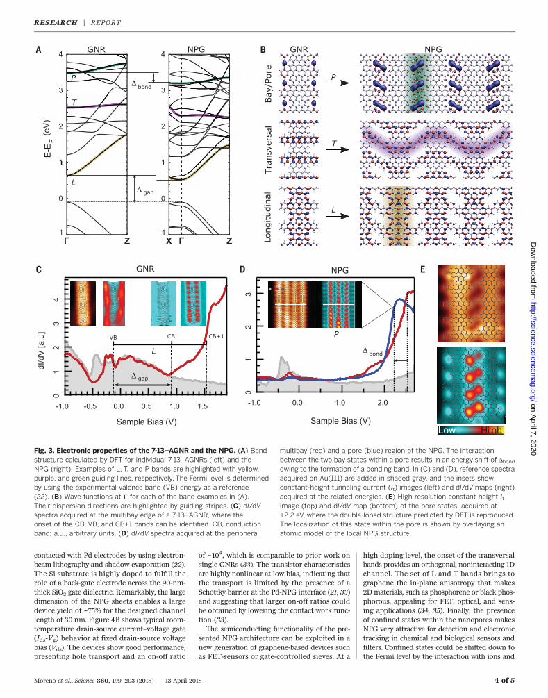
contacted with Pd electrodes by using electron-beam lithography and shadow evaporation (22).The Si substrate is highly doped to fulfill therole of a back-gate electrode across the 90-nm-thick SiO2 gate dielectric. Remarkably, the largedimension of the NPG sheets enables a largedevice yield of ~75% for the designed channellength of 30 nm. Figure 4B shows typical room-temperature drain-source current–voltage gate(Ids-Vg) behavior at fixed drain-source voltagebias (Vds). The devices show good performance,presenting hole transport and an on-off ratio
of ~104, which is comparable to prior work onsingle GNRs (33). The transistor characteristicsare highly nonlinear at low bias, indicating thatthe transport is limited by the presence of aSchottky barrier at the Pd-NPG interface (21, 33)and suggesting that larger on-off ratios couldbe obtained by lowering the contact work func-tion (33).The semiconducting functionality of the pre-
sented NPG architecture can be exploited in anew generation of graphene-based devices suchas FET-sensors or gate-controlled sieves. At a
high doping level, the onset of the transversalbands provides an orthogonal, noninteracting 1Dchannel. The set of L and T bands brings tographene the in-plane anisotropy that makes2D materials, such as phosphorene or black phos-phorous, appealing for FET, optical, and sens-ing applications (34, 35). Finally, the presenceof confined states within the nanopores makesNPG very attractive for detection and electronictracking in chemical and biological sensors andfilters. Confined states could be shifted down tothe Fermi level by the interaction with ions and
Moreno et al., Science 360, 199–203 (2018) 13 April 2018 4 of 5
Fig. 3. Electronic properties of the 7-13–AGNR and the NPG. (A) Bandstructure calculated by DFT for individual 7-13–AGNRs (left) and theNPG (right). Examples of L, T, and P bands are highlighted with yellow,purple, and green guiding lines, respectively. The Fermi level is determinedby using the experimental valence band (VB) energy as a reference(22). (B) Wave functions at G for each of the band examples in (A).Their dispersion directions are highlighted by guiding stripes. (C) dI/dVspectra acquired at the multibay edge of a 7-13–AGNR, where theonset of the CB, VB, and CB+1 bands can be identified. CB, conductionband; a.u., arbitrary units. (D) dI/dV spectra acquired at the peripheral
multibay (red) and a pore (blue) region of the NPG. The interactionbetween the two bay states within a pore results in an energy shift of Dbondowing to the formation of a bonding band. In (C) and (D), reference spectraacquired on Au(111) are added in shaded gray, and the insets showconstant-height tunneling current (It) images (left) and dI/dV maps (right)acquired at the related energies. (E) High-resolution constant-height Itimage (top) and dI/dV map (bottom) of the pore states, acquired at+2.2 eV, where the double-lobed structure predicted by DFT is reproduced.The localization of this state within the pore is shown by overlaying anatomic model of the local NPG structure.
RESEARCH | REPORTon A
pril 7, 2020
http://science.sciencemag.org/
Dow
nloaded from
molecules (36, 37), making them detectable intransport measurements.
REFERENCES AND NOTES
1. J. Bai, X. Zhong, S. Jiang, Y. Huang, X. Duan, Nat. Nanotechnol.5, 190–194 (2010).
2. X. Liang et al., Nano Lett. 10, 2454–2460 (2010).3. B. M. Venkatesan, R. Bashir, Nat. Nanotechnol. 6, 615–624
(2011).4. S. Garaj et al., Nature 467, 190–193 (2010).5. K. Sint, B. Wang, P. Král, J. Am. Chem. Soc. 130, 16448–16449
(2008).6. R. C. Rollings, A. T. Kuan, J. A. Golovchenko, Nat. Commun. 7,
11408 (2016).7. D. E. Jiang, V. R. Cooper, S. Dai, Nano Lett. 9, 4019–4024
(2009).8. S. Blankenburg et al., Small 6, 2266–2271 (2010).9. S. P. Koenig, L. Wang, J. Pellegrino, J. S. Bunch, Nat.
Nanotechnol. 7, 728–732 (2012).10. D. Cohen-Tanugi, J. C. Grossman, Nano Lett. 12, 3602–3608
(2012).11. S. P. Surwade et al., Nat. Nanotechnol. 10, 459–464 (2015).12. M. Y. Han, B. Özyilmaz, Y. Zhang, P. Kim, Phys. Rev. Lett. 98,
206805 (2007).13. G. Franc, A. Gourdon, Phys. Chem. Chem. Phys. 13,
14283–14292 (2011).14. P. A. Held, H. Fuchs, A. Studer, Chemistry 23, 5874–5892
(2017).15. M. Bieri et al., Chem. Commun. (Camb.) 2009 (45), 6919–6921
(2009).16. L. Lafferentz et al., Nat. Chem. 4, 215–220 (2012).17. J. Cai et al., Nature 466, 470–473 (2010).18. A. Basagni et al., J. Am. Chem. Soc. 137, 1802–1808 (2015).19. A. Floris et al., J. Am. Chem. Soc. 138, 5837–5847 (2016).20. Y. C. Chen et al., ACS Nano 7, 6123–6128 (2013).21. The presence of two equivalent C–H3 bonds, labeled as A
and B in Fig. 1C, leads to either A-B or B-A bonding
configurations, resulting in upward- and downward-orientedpores of identical morphology.
22. Materials and methods are available as supplementarymaterials.
23. Q. Sun, C. Zhang, H. Kong, Q. Tan, W. Xu, Chem. Commun.(Camb.) 50, 11825–11828 (2014).
24. C. Sánchez-Sánchez et al., ACS Nano 10, 8006–8011(2016).
25. Q. Li et al., J. Am. Chem. Soc. 138, 2809–2814 (2016).26. N. Kocić et al., J. Am. Chem. Soc. 138, 5585–5593 (2016).27. H. Huang et al., Sci. Rep. 2, 983 (2012).28. J. D. Teeter et al., Nanoscale 9, 18835–18844 (2017).29. Y.-C. Chen et al., Nat. Nanotechnol. 10, 156–160 (2015).30. P. Ruffieux et al., ACS Nano 6, 6930–6935 (2012).31. Y. Q. Zhang, J. Björk, J. V. Barth, F. Klappenberger, Nano Lett.
16, 4274–4281 (2016).32. M. Feng, J. Zhao, H. Petek, Science 320, 359–362 (2008).33. J. P. Llinas et al., Nat. Commun. 8, 633 (2017).34. F. Xia, H. Wang, Y. Jia, Nat. Commun. 5, 4458 (2014).35. L. Kou, T. Frauenheim, C. Chen, J. Phys. Chem. Lett. 5,
2675–2681 (2014).36. M. Feng, J. Zhao, T. Huang, X. Zhu, H. Petek, Acc. Chem. Res.
44, 360–368 (2011).37. G. Csányi, P. B. Littlewood, A. H. Nevidomskyy, C. J. Pickard,
B. D. Simons, Nat. Phys. 1, 42–45 (2005).
ACKNOWLEDGMENTS
We acknowledge thoughtful discussions with E. Guitián andD. Pérez for the synthesis of the monomer precursors. We thankP. Brandimarte and D. Sanchez-Portal for useful discussionsrelated to the calculations. We thank E. Del Corro, C. J. J. Hebert,and J. A. Garrido for their support with the Raman measurements.Funding: This research was funded by the Centres de Recerca deCatalunya Programme–Generalitat de Catalunya, the Xunta deGalicia (Centro singular de investigacion de Galicia accreditation2016–2019, ED431G/09), and the European Regional DevelopmentFund. This research was supported by the Spanish Ministry ofEconomy and Competitiveness (under contract no. MAT2016-
78293-C6-2-R, MAT2016-78293-C6-3-R, MAT2016-78293-C6-4-R,and MAT2016-75952-R and Severo Ochoa no. SEV-2013-0295);the Secretariat for Universities and Research, KnowledgeDepartment of the Generalitat de Catalunya 2014 SGR 715, 2014SGR 56, and 2017 SGR 827; the Basque Department of Education(contract no. PI-2016-1-0027); and the European Union’s Horizon2020 research and innovation program under grant agreement696656. C.M. was supported by the Agency for Management ofUniversity and Research grants (AGAUR) of the Catalangovernment through the FP7 framework program of the EuropeanCommission under Marie Curie COFUND action 600385.Author contributions: D.P. and M.V.-V. synthesized the monomerprecursor. B.K. and A.G.-L. performed the ab initio calculations.C.M. and M.Pan. performed the STM measurements. C.M., G.C.,and A.M. analyzed the STM data. M.Par. and C.M. carriedout the sample transfer and Raman characterization. M.V.C. andS.O.V. fabricated the devices and carried out the transportmeasurements. All authors discussed the results and participatedin writing the manuscript. D.P. and A.M. initiated and directedthis research. Competing interests: C.M., M.V.-V., G.C., D.P.,and A.M. are inventors on patent application EP18382088.5submitted by the Catalan Institute of Nanoscience andNanotechnology, which covers the reported NPG material.Data and materials availability: All data needed to evaluatethe conclusions in the paper are present in the paper or thesupplementary materials.
SUPPLEMENTARY MATERIALS
www.sciencemag.org/content/360/6385/199/suppl/DC1Materials and MethodsSupplementary TextFigs. S1 to S12Table S1References (38–57)
19 October 2017; accepted 7 March 201810.1126/science.aar2009
Moreno et al., Science 360, 199–203 (2018) 13 April 2018 5 of 5
Fig. 4. Transport properties of the NPG. (A) Conductance (G)calculated in the longitudinal (yellow) and transversal (purple) directionsof the NPG, as defined in Fig. 3, with that of pristine graphene added as acomparison (black line); the latter has been multiplied by 0.55. Colored
backgrounds delimit regions of total gap (white), only longitudinal (yellow),and combined longitudinal and transversal (purple) transport. (B) Ids-Vgcharacteristics of a NPG device of 30-nm-channel length gated by a 90-nm-thick SiO2 gate oxide.
RESEARCH | REPORTon A
pril 7, 2020
http://science.sciencemag.org/
Dow
nloaded from
Bottom-up synthesis of multifunctional nanoporous graphene
Panighel, Gustavo Ceballos, Sergio O. Valenzuela, Diego Peña and Aitor MugarzaCésar Moreno, Manuel Vilas-Varela, Bernhard Kretz, Aran Garcia-Lekue, Marius V. Costache, Markos Paradinas, Mirko
DOI: 10.1126/science.aar2009 (6385), 199-203.360Science
, this issue p. 199; see also p. 154Sciencebands with an energy gap of 1 electron volt coexist with localized states created by the pores.sizes of about 1 nanometer. Scanning tunneling spectroscopy revealed an electronic structure in which semiconductor
poreproduced graphene nanoribbons, and cross-coupling of these structures created a nanoporous graphene sheet with polymerdiphenylbianthracene on a gold surface (see the Perspective by Sinitskii). Cyclodehydrogenation of the resulting
. used Ullmann coupling to polymerize a dibromo-substitutedet alalso be useful for molecular separations. Moreno Nanosize pores in graphene can make its electronic properties more favorable for transistor applications and may
Synthesizing graphene nanopores
ARTICLE TOOLS http://science.sciencemag.org/content/360/6385/199
MATERIALSSUPPLEMENTARY http://science.sciencemag.org/content/suppl/2018/04/11/360.6385.199.DC1
CONTENTRELATED http://science.sciencemag.org/content/sci/360/6385/154.full
REFERENCES
http://science.sciencemag.org/content/360/6385/199#BIBLThis article cites 54 articles, 1 of which you can access for free
PERMISSIONS http://www.sciencemag.org/help/reprints-and-permissions
Terms of ServiceUse of this article is subject to the
is a registered trademark of AAAS.ScienceScience, 1200 New York Avenue NW, Washington, DC 20005. The title (print ISSN 0036-8075; online ISSN 1095-9203) is published by the American Association for the Advancement ofScience
Science. No claim to original U.S. Government WorksCopyright © 2018 The Authors, some rights reserved; exclusive licensee American Association for the Advancement of
on April 7, 2020
http://science.sciencem
ag.org/D
ownloaded from

![COnnecting REpositories · contributions of technical professionals in cross-functional teams [1]. 1.2 Factors Affecting Multifunctional Teams Building an effective multi functional](https://static.fdokument.com/doc/165x107/6076da0160ae274f5765f16c/connecting-repositories-contributions-of-technical-professionals-in-cross-functional.jpg)