
Coordinated regulation of synthesis and stability of RNA ...
Optimizing performance and
understanding stability issues
in polymer:fullerene solar cells
Von der Fakultat fur Mathematik und Naturwissenschaften
der Carl von Ossietzky Universitat Oldenburg
zur Erlangung des Grades und Titels eines
Doktors der Naturwissenschaften (Dr. rer. nat.)
angenommene Dissertation von
Antonietta De Sio
geboren am 17. Juni 1981
in Salerno, Italien

Erstgutachter: Prof.Dr. Jurgen Parisi (Universitat Oldenburg)
Zweitgutachterin: Prof.Dr. Elizabeth von Hauff (Universitat Freiburg)
Drittgutachter: Prof.Dr. Carsten Agert (NEXT ENERGY, Oldenburg)
Tag der Disputation: 24. April 2012

Contents
Contents i
Abstract iii
Kurzfassung v
1 Introduction 1
1.1 Conjugated polymers . . . . . . . . . . . . . . . . . . . . . . . . . . 1
1.2 Polymer:fullerene donor acceptor systems . . . . . . . . . . . . . . 2
1.3 Photophysical processes . . . . . . . . . . . . . . . . . . . . . . . . 5
1.3.1 Luminescence quenching . . . . . . . . . . . . . . . . . . . . 5
1.3.2 Photoinduced charge transfer . . . . . . . . . . . . . . . . . 6
1.3.3 Resonance energy transfer . . . . . . . . . . . . . . . . . . . 7
1.4 Bulk heterojunction concept . . . . . . . . . . . . . . . . . . . . . . 8
1.4.1 The role of morphology . . . . . . . . . . . . . . . . . . . . 9
1.5 Solar cell performance . . . . . . . . . . . . . . . . . . . . . . . . . 9
1.6 Stability . . . . . . . . . . . . . . . . . . . . . . . . . . . . . . . . . 10
1.7 Outline of the thesis . . . . . . . . . . . . . . . . . . . . . . . . . . 11
2 Materials and methods 13
2.1 Sample preparation . . . . . . . . . . . . . . . . . . . . . . . . . . . 13
2.1.1 Solar cell preparation . . . . . . . . . . . . . . . . . . . . . 14
2.2 Characterization techniques . . . . . . . . . . . . . . . . . . . . . . 15
2.3 ZnO:Al preparation and characterization . . . . . . . . . . . . . . . 21
2.4 Degradation experiments . . . . . . . . . . . . . . . . . . . . . . . . 22
3 Molecular doping 23
i
ii
3.1 Low bandgap copolymers for increased light harvesting . . . . . . . 24
3.2 Molecular doping of PCPDTBT . . . . . . . . . . . . . . . . . . . . 25
3.3 Effect of molecular doping in PCPDTBT:PCBM blends . . . . . . 28
3.3.1 Bulk heterojunction solar cells with molecularly doped ac-
tive layers . . . . . . . . . . . . . . . . . . . . . . . . . . . . 30
3.4 Summary . . . . . . . . . . . . . . . . . . . . . . . . . . . . . . . . 33
4 Controlling morphology with solvent mixtures 35
4.1 Effect of solvent on the optical properties of the blend . . . . . . . 35
4.2 Effect of solvent on the structural properties of the blend . . . . . 39
4.3 Effect of solvent on the electrical properties of the blend . . . . . . 41
4.4 Effect of solvent on the photovoltaic performance . . . . . . . . . . 41
4.5 Summary . . . . . . . . . . . . . . . . . . . . . . . . . . . . . . . . 43
5 Optimization of the device architecture 45
5.1 ZnO:Al as TCO for polymer:fullerene solar cells . . . . . . . . . . . 46
5.2 ITO-free polymer:fullerene solar cells . . . . . . . . . . . . . . . . . 49
5.3 Summary . . . . . . . . . . . . . . . . . . . . . . . . . . . . . . . . 53
6 Effect of degradation on the optoelectronic properties of P3HT
and P3HT:PCBM blends 55
6.1 The influence of the processing atmosphere . . . . . . . . . . . . . 56
6.1.1 Optical and photophysical properties . . . . . . . . . . . . . 56
6.1.2 Photovoltaic performance . . . . . . . . . . . . . . . . . . . 59
6.2 Effect of oxygen and light exposure . . . . . . . . . . . . . . . . . . 62
6.2.1 Irreversible degradation studied combining PL and PIA
spectroscopy . . . . . . . . . . . . . . . . . . . . . . . . . . 63
6.3 Summary . . . . . . . . . . . . . . . . . . . . . . . . . . . . . . . . 68
7 Conclusions 69
Bibliography 71
Acknowledgments 85
Erklarung 87

Abstract
In this thesis, different approaches will be pursued, in order to control the
performance of polymer:fullerene solar cells. First, a brief introduction of the ba-
sic working principle of polymer solar cells and details on the sample preparation
and the characterization methods are given. Next, molecular doping is proposed
to tune the electronic properties of a novel low bandgap copolymer. The effect
of doping in the corresponding polymer:fullerene solar cells will also be analyzed.
The role of the active layer morphology in the reference P3HT:PCBM material
system is investigated by exploring the influence of a combination of solvents
with different boiling points on the optical, electrical and structural properties
of the blend films and solar cells. The effect of the device architecture on the
performance will be addressed. In particular, inverted devices containing no
indium-tin-oxide, no water based buffer layers and no low work function metals
will be fabricated and compared to the standard forward architecture. The effect
of processing the devices in ambient air instead of in a nitrogen-filled glovebox
as well as the degradation of the active layer induced by exposure to oxygen and
light on the optoelectronic properties of the P3HT:PCBM model system will be
investigated.
iii


Kurzfassung
In dieser Arbeit werden verschiedene Ansatze verfolgt, um das Verhalten von
Polymer:Fulleren Solarzellen zu beeinflussen. Zuerst wird eine kurze Beschrei-
bung der grundlegenden Arbeitsprinzipien von Polymer-Solarzellen gegeben und
Details der Probenherstellung und -Charakterisierung werden vorgestellt. Als
nachstes wird molekulares Dotieren als Moglichkeit vorgeschlagen, die elektron-
ischen Eigenschaften eines neuartigen low-bandgap-Copolymers zu modifizieren.
Der Effekt dieser Dotierung in den zugehorigen Polymer:Fulleren-Solarzellen wird
ebenfalls analysiert. Die Rolle der Morphologie der aktiven Schicht wird erforscht,
indem der Einfluss der Verwendung einer Kombination von Losungsmitteln mit
unterschiedlichen Siedepunkten auf die optischen, elektrischen und strukturellen
Eigenschaften eines P3HT:PCBM-Referenzsystems untersucht wird. Der Effekt
der Architektur auf die Leistung der Zelle wird besprochen. Insbesondere werden
invertierte Zellen unter Verzicht auf Indium-Zinn-Oxid, wasserbasierte Puffer-
schichten und Metalle mit niedrigen Austrittsarbeiten hergstellt und mit solchen
basierend auf der Standardstruktur verglichen. Zuletzt wird der Einfluss sowohl
der Herstellung der Zellen in Umgebungsluft statt in einer Glovebox unter Stick-
stoffatmosphre als auch der Degradation durch Sauerstoff und Licht auf die op-
toelektronischen Eigenschaften des P3HT:PCBM-Referenzsystems untersucht.
v

Chapter 1
Introduction
In this chapter, a brief overview of the fundamental processes regulating the
photovoltaic action of the active materials as well as the operational principle of
polymer solar cells is given.
1.1 Conjugated polymers
Conjugated polymers are a class of carbon based macromolecules that de-
rive their semiconducting properties from having delocalized π-electron bonding
along the polymer chain. The π bonding and π* antibonding orbitals form de-
localized wavefunctions, which support mobile charge carriers [1]. The filled π
band is called the highest occupied molecular orbital (HOMO), while the empty
π* band is called the lowest unoccupied molecular orbital (LUMO). The energy
difference between the HOMO and LUMO defines the bandgap and depends on
the conjugation length [2]. Thus, disruption of the conjugation along the polymer
backbone affects the local HOMO and LUMO positions, hence, the bandgap.
Absorption of a photon with appropriate energy promotes an electron from
the filled π-band to the empty π*-band, i.e., from the HOMO to the LUMO.
This excitation creates a Coulomb bound hole-electron pair, called exciton. In a
three-dimensional semiconductor, like, for example, crystalline silicon, the exci-
tons are weakly bound due to the high dielectric constants and dissociate there-
fore into free electron-hole pairs. These are called Wannier excitons. Due to their
strong intramolecular electronic interactions and relatively weak intermolecular
electronic interactions, conjugated polymers behave as quasi-one-dimensional sys-
1
2
tems [3]. Spatial and energetic disorder leads to localization of the excitations [4]
on small conjugated segments [5, 6]. Due to the localization and the low dielec-
tric constants of polymers, the excited species are strongly bound electron-hole
pairs similar to Frenkel excitons [7] in molecular crystals. Therefore the exciton
is unlikely to separate at room temperature [8].
Moreover, the charge transport proceeds by hopping, i.e., inelastic tunneling
between localized states [9], and the energy required to jump from one state to
the other is provided by the interaction with phonons. Hence, in contrast to
conduction by electrons in bands, like in a three-dimensional crystal, where the
interaction with phonons reduces the mobility due to the increased lattice scatter-
ing [10], in disordered semiconductors such interactions stimulate hopping, and
the mobility shows a positive trend with the temperature. The charge transport
properties of conjugated polymers depend on the packing of the chains and the
ordering in the solid films, as well as on the density of impurities and structural
defects. Therefore, the mobility values of the same polymer show large variations,
depending on the quality of the sample [11].
Conjugated polymers gained huge scientific interest in the last decades, be-
cause of their ability to combine the optoelectronic properties of the inorganic
semiconductors and the technological advantages of the polymers [12], such as
the possibility of fine tailoring of the optoelectronic properties by chemical ma-
nipulation and solution processing at low temperatures. Furthermore, they are
characterized by high absorption coefficients of the order of 105 cm−1 at the max-
imum of the absorption spectrum [13], making it possible to use a layer thickness
at the nanometer scale. Conjugated polymers represent, therefore, a promis-
ing class of materials to develop flexible, light weight and low cost photovoltaic
applications [14, 15].
1.2 Polymer:fullerene donor acceptor systems
Upon light absorption, an exciton is created on the polymer chain. The
exciton has a low diffusion length, of the order of few tens of nanometers [16],
therefore, it tends to recombine resulting in a relatively poor photocurrent. This
is the reason why the early studied single layer cells based on a Schottky organic
diode [17] are not interesting for applications. By providing an acceptor with
higher electron affinity, like a fullerene, the dissociation of excitons created close
3
to the donor-acceptor interface is favored via charge transfer to the acceptor.
However, only the excitons created within a distance lower than the diffusion
length from a donor-acceptor interface will have the chance to reach the interface
and separate into a free electron-hole pair. Once the exciton is dissociated, the
electron and hole must be transported through the acceptor and donor paths
to the respective electrodes, in order to be collected. For this to happen, well
defined and continuous donor and acceptor paths are necessary.
Donor Acceptor LWF HWF
Figure 1.1: Sketch of the working principle of a donor-acceptor solar cell
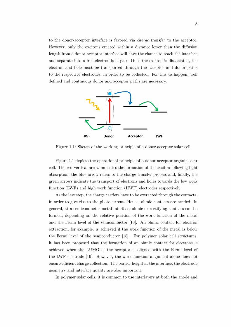
Figure 1.1 depicts the operational principle of a donor-acceptor organic solar
cell. The red vertical arrow indicates the formation of the exciton following light
absorption, the blue arrow refers to the charge transfer process and, finally, the
green arrows indicate the transport of electrons and holes towards the low work
function (LWF) and high work function (HWF) electrodes respectively.
As the last step, the charge carriers have to be extracted through the contacts,
in order to give rise to the photocurrent. Hence, ohmic contacts are needed. In
general, at a semiconductor-metal interface, ohmic or rectifying contacts can be
formed, depending on the relative position of the work function of the metal
and the Fermi level of the semiconductor [18]. An ohmic contact for electron
extraction, for example, is achieved if the work function of the metal is below
the Fermi level of the semiconductor [18]. For polymer solar cell structures,
it has been proposed that the formation of an ohmic contact for electrons is
achieved when the LUMO of the acceptor is aligned with the Fermi level of
the LWF electrode [19]. However, the work function alignment alone does not
ensure efficient charge collection. The barrier height at the interface, the electrode
geometry and interface quality are also important.
In polymer solar cells, it is common to use interlayers at both the anode and
4
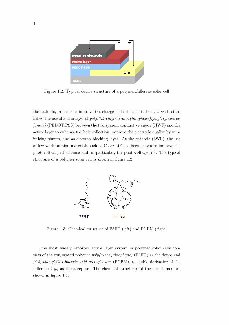
Figure 1.2: Typical device structure of a polymer:fullerene solar cell
the cathode, in order to improve the charge collection. It is, in fact, well estab-
lished the use of a thin layer of poly(3,4-ethylene-dioxythiophene):poly(styrenesul-
fonate) (PEDOT:PSS) between the transparent conductive anode (HWF) and the
active layer to enhance the hole collection, improve the electrode quality by min-
imizing shunts, and as electron blocking layer. At the cathode (LWF), the use
of low workfunction materials such as Ca or LiF has been shown to improve the
photovoltaic performance and, in particular, the photovoltage [20]. The typical
structure of a polymer solar cell is shown in figure 1.2.
Figure 1.3: Chemical structure of P3HT (left) and PCBM (right)
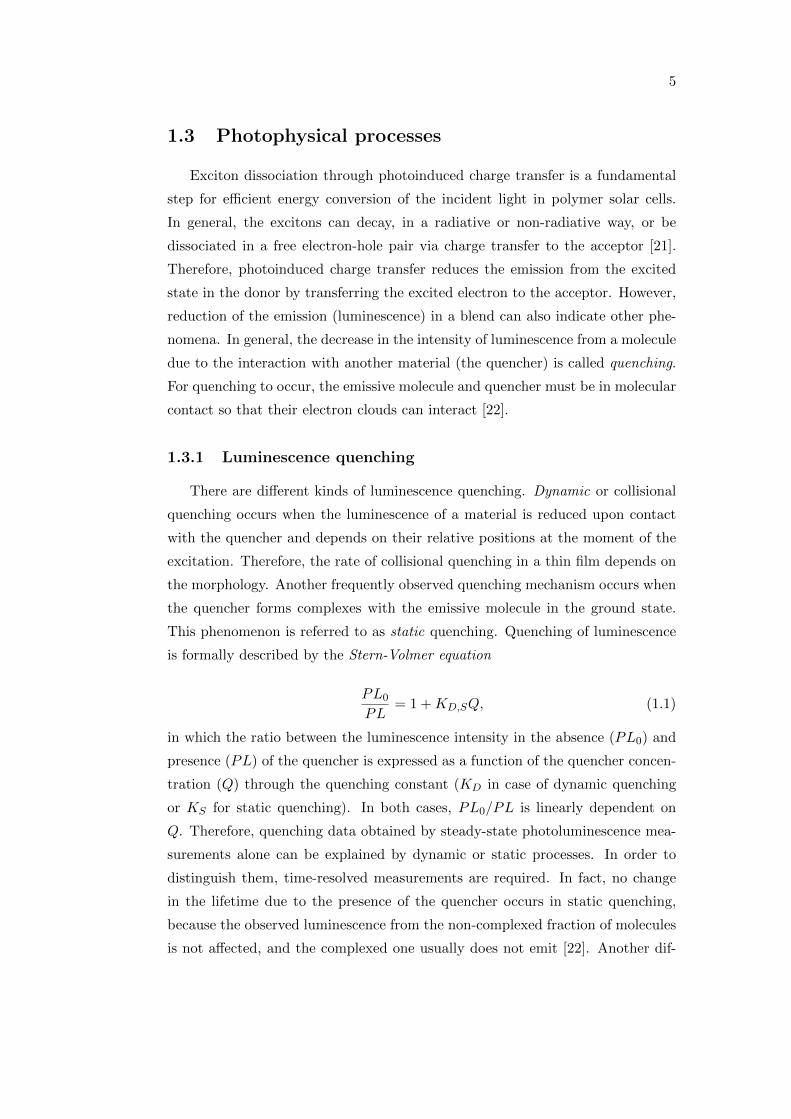
The most widely reported active layer system in polymer solar cells con-
sists of the conjugated polymer poly(3-hexylthiophene) (P3HT) as the donor and
[6,6]-phenyl-C61-butyric acid methyl ester (PCBM), a soluble derivative of the
fullerene C60, as the acceptor. The chemical structures of these materials are
shown in figure 1.3.
5
1.3 Photophysical processes
Exciton dissociation through photoinduced charge transfer is a fundamental
step for efficient energy conversion of the incident light in polymer solar cells.
In general, the excitons can decay, in a radiative or non-radiative way, or be
dissociated in a free electron-hole pair via charge transfer to the acceptor [21].
Therefore, photoinduced charge transfer reduces the emission from the excited
state in the donor by transferring the excited electron to the acceptor. However,
reduction of the emission (luminescence) in a blend can also indicate other phe-
nomena. In general, the decrease in the intensity of luminescence from a molecule
due to the interaction with another material (the quencher) is called quenching.
For quenching to occur, the emissive molecule and quencher must be in molecular
contact so that their electron clouds can interact [22].
1.3.1 Luminescence quenching
There are different kinds of luminescence quenching. Dynamic or collisional
quenching occurs when the luminescence of a material is reduced upon contact
with the quencher and depends on their relative positions at the moment of the
excitation. Therefore, the rate of collisional quenching in a thin film depends on
the morphology. Another frequently observed quenching mechanism occurs when
the quencher forms complexes with the emissive molecule in the ground state.
This phenomenon is referred to as static quenching. Quenching of luminescence
is formally described by the Stern-Volmer equation
PL0
PL= 1 +KD,SQ, (1.1)
in which the ratio between the luminescence intensity in the absence (PL0) and
presence (PL) of the quencher is expressed as a function of the quencher concen-
tration (Q) through the quenching constant (KD in case of dynamic quenching
or KS for static quenching). In both cases, PL0/PL is linearly dependent on
Q. Therefore, quenching data obtained by steady-state photoluminescence mea-
surements alone can be explained by dynamic or static processes. In order to
distinguish them, time-resolved measurements are required. In fact, no change
in the lifetime due to the presence of the quencher occurs in static quenching,
because the observed luminescence from the non-complexed fraction of molecules
is not affected, and the complexed one usually does not emit [22]. Another dif-
6
ference is that ground-state complex formation results in modifications of the
absorption spectrum of the luminescent molecule, while for collisional quenching
only the excited states are affected, and thus no changes in the absorption are
expected upon contact with the quencher. In many cases, quenching is the result
of both collisions and ground-state complex formation with the same quencher.
The Stern-Volmer equation, in this case, results in a parabolic behavior with
upwards curvature and can be expressed as follows:
PL0
PL= (1 +KDQ)(1 +KSQ). (1.2)
1.3.2 Photoinduced charge transfer
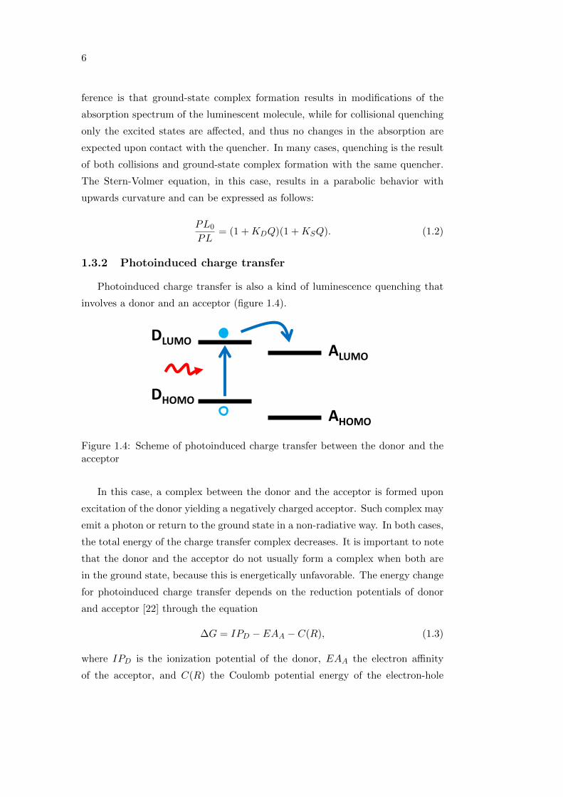
Photoinduced charge transfer is also a kind of luminescence quenching that
involves a donor and an acceptor (figure 1.4).
DLUMO
DHOMO
ALUMO
AHOMO
Figure 1.4: Scheme of photoinduced charge transfer between the donor and theacceptor
In this case, a complex between the donor and the acceptor is formed upon
excitation of the donor yielding a negatively charged acceptor. Such complex may
emit a photon or return to the ground state in a non-radiative way. In both cases,
the total energy of the charge transfer complex decreases. It is important to note
that the donor and the acceptor do not usually form a complex when both are
in the ground state, because this is energetically unfavorable. The energy change
for photoinduced charge transfer depends on the reduction potentials of donor
and acceptor [22] through the equation
∆G = IPD − EAA − C(R), (1.3)
where IPD is the ionization potential of the donor, EAA the electron affinity
of the acceptor, and C(R) the Coulomb potential energy of the electron-hole
7
pair. The energy of the charge transfer state is, therefore, lower than the energy
before electron transfer. This charge transfer is reported to be extremely fast in
conjugated polymers, on the order of tens of femtoseconds [21, 23, 24].
In polymer:fullerene blends, photoinduced charge transfer between the donor
and the acceptor is a fundamental step for the operation of the solar cells.
1.3.3 Resonance energy transfer
Another process that can take place in the excited state between a donor and
an acceptor is resonance energy transfer. This process manifests itself whenever
the emission spectrum of the donor overlaps with the absorption spectrum of the
acceptor, and the rate of energy transfer is determined by the distance between
the donor and the acceptor over the Forster distance [25]. The latter is defined
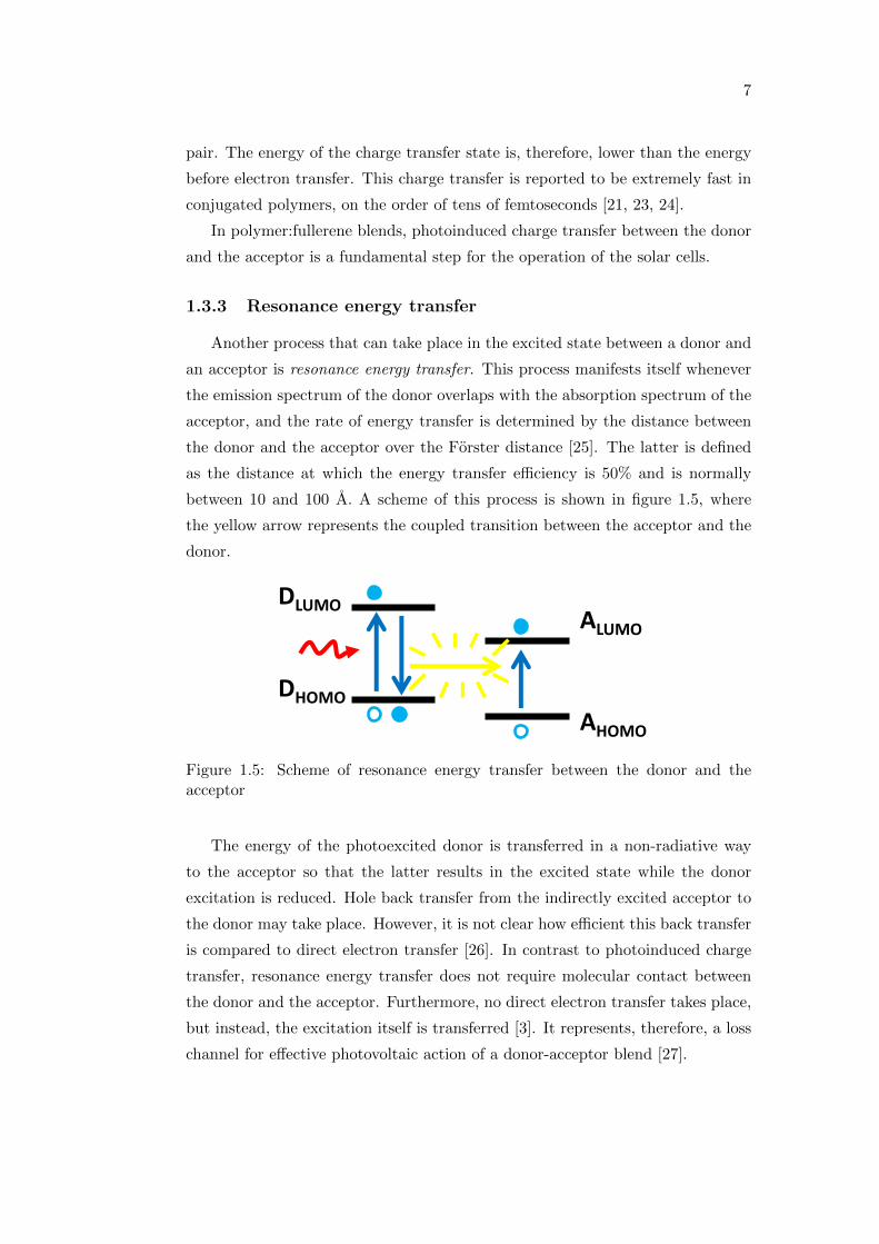
as the distance at which the energy transfer efficiency is 50% and is normally
between 10 and 100 A. A scheme of this process is shown in figure 1.5, where
the yellow arrow represents the coupled transition between the acceptor and the
donor.
DLUMO
DHOMO
ALUMO
AHOMO
Figure 1.5: Scheme of resonance energy transfer between the donor and theacceptor
The energy of the photoexcited donor is transferred in a non-radiative way
to the acceptor so that the latter results in the excited state while the donor
excitation is reduced. Hole back transfer from the indirectly excited acceptor to
the donor may take place. However, it is not clear how efficient this back transfer
is compared to direct electron transfer [26]. In contrast to photoinduced charge
transfer, resonance energy transfer does not require molecular contact between
the donor and the acceptor. Furthermore, no direct electron transfer takes place,
but instead, the excitation itself is transferred [3]. It represents, therefore, a loss
channel for effective photovoltaic action of a donor-acceptor blend [27].
8
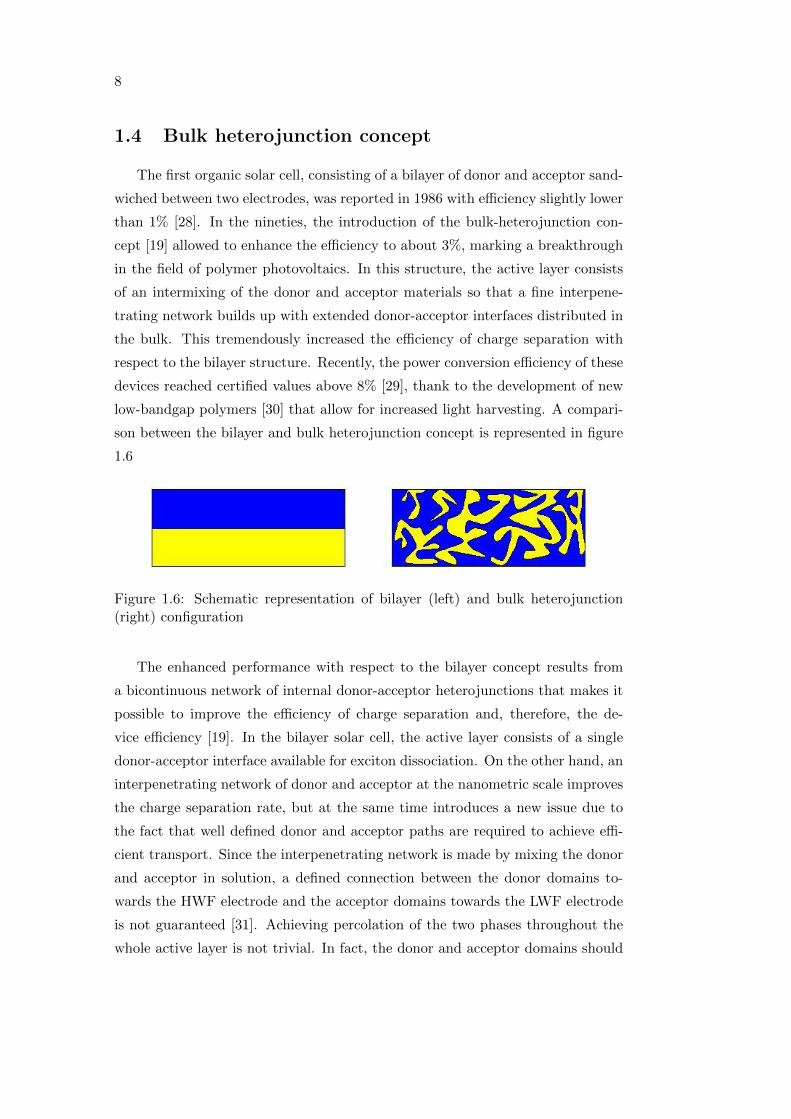
1.4 Bulk heterojunction concept
The first organic solar cell, consisting of a bilayer of donor and acceptor sand-
wiched between two electrodes, was reported in 1986 with efficiency slightly lower
than 1% [28]. In the nineties, the introduction of the bulk-heterojunction con-
cept [19] allowed to enhance the efficiency to about 3%, marking a breakthrough
in the field of polymer photovoltaics. In this structure, the active layer consists
of an intermixing of the donor and acceptor materials so that a fine interpene-
trating network builds up with extended donor-acceptor interfaces distributed in
the bulk. This tremendously increased the efficiency of charge separation with
respect to the bilayer structure. Recently, the power conversion efficiency of these
devices reached certified values above 8% [29], thank to the development of new
low-bandgap polymers [30] that allow for increased light harvesting. A compari-
son between the bilayer and bulk heterojunction concept is represented in figure
1.6
Figure 1.6: Schematic representation of bilayer (left) and bulk heterojunction(right) configuration
The enhanced performance with respect to the bilayer concept results from
a bicontinuous network of internal donor-acceptor heterojunctions that makes it
possible to improve the efficiency of charge separation and, therefore, the de-
vice efficiency [19]. In the bilayer solar cell, the active layer consists of a single
donor-acceptor interface available for exciton dissociation. On the other hand, an
interpenetrating network of donor and acceptor at the nanometric scale improves
the charge separation rate, but at the same time introduces a new issue due to
the fact that well defined donor and acceptor paths are required to achieve effi-
cient transport. Since the interpenetrating network is made by mixing the donor
and acceptor in solution, a defined connection between the donor domains to-
wards the HWF electrode and the acceptor domains towards the LWF electrode
is not guaranteed [31]. Achieving percolation of the two phases throughout the
whole active layer is not trivial. In fact, the donor and acceptor domains should
9
be small enough so that the highest amount of photogenerated excitons can be
dissociated and, at the same time, provide continuous percolating networks to-
wards the respective electrodes to avoid transport related losses. It is therefore
evident that, for an efficient bulk heterojunction solar cell, a good control of the
morphology is important [32, 26].
1.4.1 The role of morphology
The morphology of the active layer is sensitive to the processing conditions,
such as the donor to acceptor ratio [33], solvent [34, 35] and post-processing
steps, like thermal annealing or solvent swelling [36, 37]. Several studies [32, 38,
39, 40, 41, 42, 43] have shown that the solvent has a strong influence on the film
formation and can favor or inhibit a preferential phase segregation in the active
layer. In the case of semicristalline polymers like regioregular (rr-) P3HT, the
deposition conditions have a large impact on the ordering of the polymer and
consequently alterate its optical and electrical properties. In P3HT:PCBM based
bulk heterojunction solar cells, the crystallization of the polymer phase can be
restrained by the clustering of the fullerene during drying [44]. Solvents with
selective solubility for the fullerene can avoid this phenomenon by minimizing
the fullerene clustering. The role of the casting solvent in the control of the
morphology will be investigated in more detail in chapter 4.
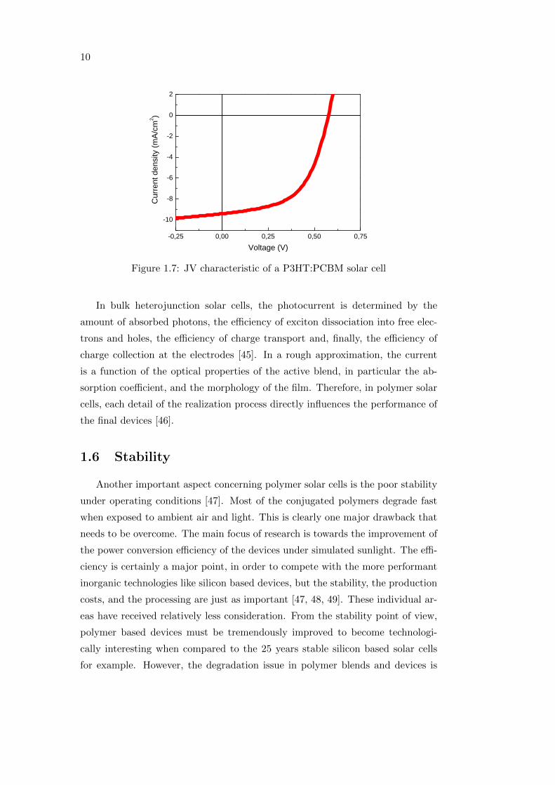
1.5 Solar cell performance
The current-voltage characteristic of a solar cell can be described by the equa-
tion
I = Is(eq(V −IRs)
nkT − 1) +V − IRs
Rp− Iph, (1.4)
where Is is the dark or reverse saturation current, n the ideality factor of the
diode, Rs the series resistance, Rp the shunt resistance, and Iph the photocur-
rent. The power conversion efficiency is the commonly used figure of merit for
photovoltaic devices and is calculated as
η =JscVocFF
Pin, (1.5)
where Jsc is the short circuit current density, Voc the open circuit voltage, and
FF the fill factor. An example of the current density-voltage (JV) characteristic
of a sample polymer:fullerene solar cell is reported in figure 1.7.
10
- 0 , 2 5 0 , 0 0 0 , 2 5 0 , 5 0 0 , 7 5- 1 0
- 8
- 6
- 4
- 2
0
2
Curre
nt de
nsity
(mA/c
m2 )
V o l t a g e ( V )
Figure 1.7: JV characteristic of a P3HT:PCBM solar cell
In bulk heterojunction solar cells, the photocurrent is determined by the
amount of absorbed photons, the efficiency of exciton dissociation into free elec-
trons and holes, the efficiency of charge transport and, finally, the efficiency of
charge collection at the electrodes [45]. In a rough approximation, the current
is a function of the optical properties of the active blend, in particular the ab-
sorption coefficient, and the morphology of the film. Therefore, in polymer solar
cells, each detail of the realization process directly influences the performance of
the final devices [46].
1.6 Stability
Another important aspect concerning polymer solar cells is the poor stability
under operating conditions [47]. Most of the conjugated polymers degrade fast
when exposed to ambient air and light. This is clearly one major drawback that
needs to be overcome. The main focus of research is towards the improvement of
the power conversion efficiency of the devices under simulated sunlight. The effi-
ciency is certainly a major point, in order to compete with the more performant
inorganic technologies like silicon based devices, but the stability, the production
costs, and the processing are just as important [47, 48, 49]. These individual ar-
eas have received relatively less consideration. From the stability point of view,
polymer based devices must be tremendously improved to become technologi-
cally interesting when compared to the 25 years stable silicon based solar cells
for example. However, the degradation issue in polymer blends and devices is

11
rather complicated and not yet fully understood [50]. Indeed, estimations on the
costs of production and device lifetime indicate that organic photovoltaics can
be competitive with other technologies if a lifetime around 10 years is achieved
[15, 14, 51].
1.7 Outline of the thesis
In order to control the performance of polymer:fullerene solar cells, different
approaches will be pursued in this thesis. Details on the sample preparation and
the characterization techniques used will be given in the second chapter. In the
third chapter, molecular doping will be explored as a means to control the elec-
tronic properties of a low bandgap copolymer. Doping of the pristine copolymer
via co-solution and the effect of doped active layers in the corresponding poly-
mer:fullerene solar cells will be demonstrated. In the fourth chapter, the role of
the morphology of the active layer in a P3HT:PCBM blend will be investigated
by analyzing the effect of a combination of solvents with different boiling points
on the optical, electrical, and structural properties of the blend and solar cells.
In the fifth chapter, the effect of the device architecture on the performance will
be probed. In particular, inverted device structures containing no indium-tin-
oxide, no water based buffer layers, and no low work function metals will be
fabricated and characterized. The effect of degradation due to processing the
devices in ambient air as well as the irreversible degradation in the active layer
induced by exposure to oxygen and light on the optoelectronic properties of the
P3HT:PCBM model system will be investigated in the last chapter.

Chapter 2
Materials and methods
In this chapter, the details of the sample preparation as well as a brief de-
scription of the setups used for characterization are given.
2.1 Sample preparation
In this thesis, two kinds of polymers are investigated. In chapter 3, poly[2,6-
(4,4-bis-(2-ethylhexyl)-4H-cyclopenta[2,1-b;3,4-b’]dithiophene)-alt-4,7-(2,1,3-
benzothiadiazole)] (PCPDTBT) is employed to demonstrate molecular doping
via co-solution. PCPDTBT was supplied by Konarka Technologies GmbH (Ger-
many). Tetrafluoro-tetracyanoquinodimethane (F4-TCNQ), from Sigma-Aldrich,
was used as p-dopant. F4-TCNQ and PCPDTBT were separately dissolved
in chlorobenzene (CB anhydrous 99.8% from Aldrich), in a concentration of 1
mg/mL and 10 mg/mL, respectively. A set of solar cells was prepared from
chlorobenzene solutions obtained by blending the doped PCPDTBT with PCBM,
purchased from Solenne BV, in a weight ratio of 1:1. For other blend solutions,
PCBM was added to achieve a donor to acceptor ratio of 1:2 in weight, and
diiodooctane 3% in volume was used as solvent additive to improve the perfor-
mance. Doping concentrations between 0 and 0.3% and up to 1% were investi-
gated. All the solutions were left stirring overnight at 80C before deposition.
The semiconducting layers were then spin coated in a nitrogen filled glovebox
onto pre-cleaned substrates. Further details regarding the preparation procedure
of the solar cells is reported in a following section.
In the remaining chapters, a reference system based on rr-P3HT is investi-
13
14
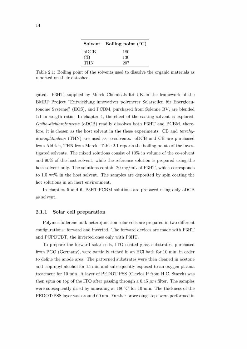
Solvent Boiling point (C)
oDCB 180CB 130THN 207
Table 2.1: Boiling point of the solvents used to dissolve the organic materials asreported on their datasheet
gated. P3HT, supplied by Merck Chemicals ltd UK in the framework of the
BMBF Project ”Entwicklung innovativer polymerer Solarzellen fur Energieau-
tonome Systeme” (EOS), and PCBM, purchased from Solenne BV, are blended
1:1 in weigth ratio. In chapter 4, the effect of the casting solvent is explored.
Ortho-dichlorobenzene (oDCB) readily dissolves both P3HT and PCBM, there-
fore, it is chosen as the host solvent in the these experiments. CB and tetrahy-
dronaphthalene (THN) are used as co-solvents. oDCB and CB are purchased
from Aldrich, THN from Merck. Table 2.1 reports the boiling points of the inves-
tigated solvents. The mixed solutions consist of 10% in volume of the co-solvent
and 90% of the host solvent, while the reference solution is prepared using the
host solvent only. The solutions contain 20 mg/mL of P3HT, which corresponds
to 1.5 wt% in the host solvent. The samples are deposited by spin coating the
hot solutions in an inert environment.
In chapters 5 and 6, P3HT:PCBM solutions are prepared using only oDCB
as solvent.
2.1.1 Solar cell preparation
Polymer:fullerene bulk heterojunction solar cells are prepared in two different
configurations: forward and inverted. The forward devices are made with P3HT
and PCPDTBT, the inverted ones only with P3HT.
To prepare the forward solar cells, ITO coated glass substrates, purchased
from PGO (Germany), were partially etched in an HCl bath for 10 min, in order
to define the anode area. The patterned substrates were then cleaned in acetone
and isopropyl alcohol for 15 min and subsequently exposed to an oxygen plasma
treatment for 10 min. A layer of PEDOT:PSS (Clevios P from H.C. Starck) was
then spun on top of the ITO after passing through a 0.45 µm filter. The samples
were subsequently dried by annealing at 180C for 10 min. The thickness of the
PEDOT:PSS layer was around 60 nm. Further processing steps were performed in
15
a nitrogen filled glove box. The active layer was spun on top of the PEDOT:PSS.
When P3HT:PCBM was used, an annealing step at 150C for 10 min was done
before transferring the samples into the chamber of a thermal evaporator. The
solar cells containing PCPDTBT as the active layer were not annealed. The
cathode was formed by evaporating 20 nm of Ca and 130 nm of Al through a
shadow mask at a rate of 0.1 nm/s. The film thickness was determined using a
Veeco Dektak 6M stylus profiler. The active area of the devices ranged between
0.10 and 0.25 cm2.
For the preparation of the inverted solar cells, sputtered ZnO:Al were used
as substrate instead of ITO. A description of the preparation of the ZnO:Al sub-
strates is given later. The substrates were first cleaned in isopropyl alcohol before
being transferred to a nitrogen filled glovebox where the other processing steps
were performed. The active layer, consisting of a blend of P3HT and PCBM,
1:1 in weight ratio, dissolved in oDCB at a concentration of 2wt%, was spun
directly on top of the ZnO:Al to obtain films with a thickness of about 230 nm.
The samples were then annealed at 150C for 10 min. The anode was thermally
evaporated through a shadow mask. The thickness of the evaporated layers was
determined using a calibrated quartz crystal microbalance during evaporation.
The active area of the devices was 0.56 cm2. Solar cells in the standard for-
ward configuration on commercial ITO substrates with the same active layer
thickness and the same active area as the inverted cells were prepared as control
devices as explained before. The layer sequence for the standard devices was
glass/ITO/PEDOT:PSS/P3HT:PCBM/Ca/Al.
2.2 Characterization techniques
Optical, electrical and structural characterization was performed on thin films
and complete devices. In this section, a short overview of the methods used is
given.
UV-Vis spectrophotometry
The absorption spectrum of a semiconductor is important for its applica-
tion in photovoltaic devices. The absorption spectra were calculated from the
transmittance T and reflectance R of the thin films spun on glass. The T and R
spectra of each sample were measured using a Varian Cary 5000 spectrophotome-
16
ter equipped with an integrating sphere available at the EWE Research Center
Next Energy, Oldenburg.
Photoluminescence spectroscopy (PL)
PL spectroscopy is a contactless, nondestructive method to probe the elec-
tronic structure of a semiconductor. A laser is used to photoexcite the sample
and the radiative relaxation (luminescence) is detected. The PL is collected with
a series of mirrors focusing on the entrance slit of a monochromator, and the
signal is recorded using a lock-in amplifier. Analysis of the intensity and spectral
content of the PL is a direct measure of various important material properties
and can help in the determination of the bandgap, the impurity levels, and the
detection of defects. By employing time-resolved measurements, the recombina-
tion mechanisms can be investigated. In this thesis, steady-state PL is performed
on thin films spun on sapphire or quartz. PL spectra are recorded at low and
room temperature in vacuum. The samples are mounted in a cryostat and are
excited with lasers at 532 nm or 660 nm, depending on the bandgap of the ma-
terial. The laser beam is directed on the sample through the sapphire windows
of the cryostat.
Photoinduced absorption spectroscopy (PIA)
PIA is a kind of pump-probe spectroscopy, because it employs a pump beam,
usually a laser, to excite the sample and a probe beam (a halogen lamp for
example) to monitor the excited population. From the previous discussion in
section 1.3 it is evident that the observation of PL quenching, upon mixing a
polymer with a fullerene for example, is only an indirect method of detecting
charge transfer between the donor and the acceptor. To directly investigate
photoinduced charge transfer in a blend, PIA spectroscopy is a more accurate
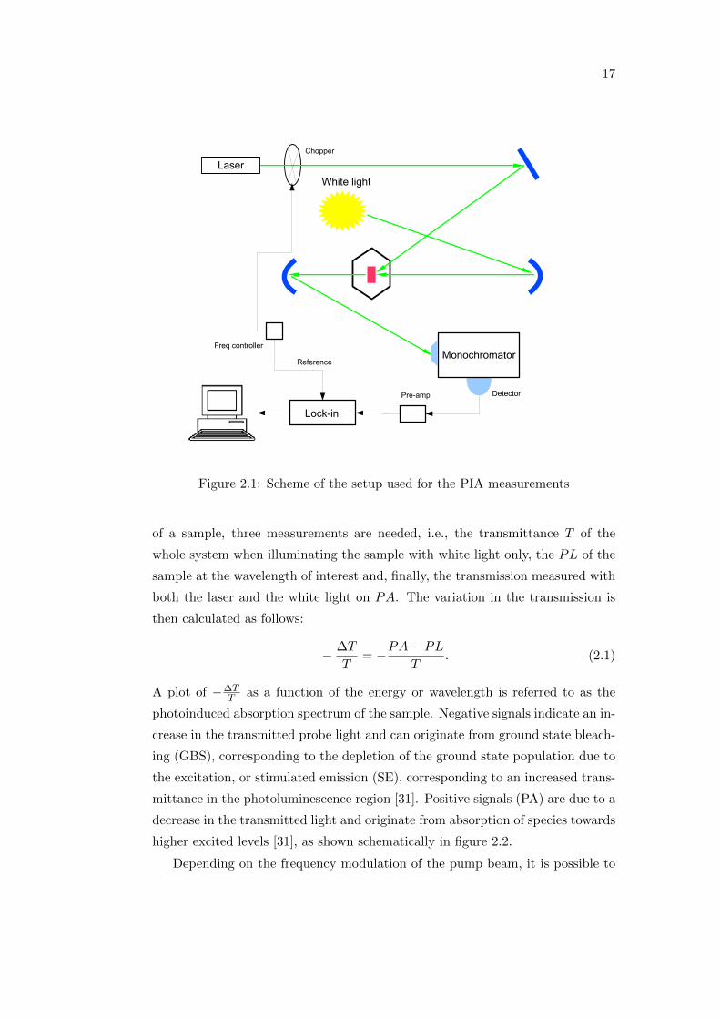
and reliable technique. A scheme of the PIA setup used for the investigation is
shown in figure 2.1.
The sample is mounted in a cryostat with sapphire windows that allows to
control the atmosphere during the measurements. A halogen lamp is used as
the probe beam, while a laser is used as the pump. As in the case of the PL
measurements, lasers at 532 nm or 660 nm are used for P3HT based samples and
for PCPDTBT based ones, respectively. Furthermore, measurements at room
temperature as well as at 80K are performed. In order to get the PIA spectrum
17
Laser
Monochromator
DetectorPre-amp
Lock-in
Freq controller
Chopper
White light
Reference
Figure 2.1: Scheme of the setup used for the PIA measurements
of a sample, three measurements are needed, i.e., the transmittance T of the
whole system when illuminating the sample with white light only, the PL of the
sample at the wavelength of interest and, finally, the transmission measured with
both the laser and the white light on PA. The variation in the transmission is
then calculated as follows:
− ∆T
T= −PA− PL
T. (2.1)
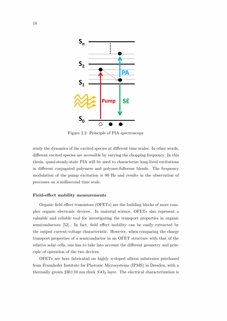
A plot of −∆TT as a function of the energy or wavelength is referred to as the
photoinduced absorption spectrum of the sample. Negative signals indicate an in-
crease in the transmitted probe light and can originate from ground state bleach-
ing (GBS), corresponding to the depletion of the ground state population due to
the excitation, or stimulated emission (SE), corresponding to an increased trans-
mittance in the photoluminescence region [31]. Positive signals (PA) are due to a
decrease in the transmitted light and originate from absorption of species towards
higher excited levels [31], as shown schematically in figure 2.2.
Depending on the frequency modulation of the pump beam, it is possible to
18
S0
S1
S2
Sn
Pump
PA
SE
Figure 2.2: Principle of PIA spectroscopy
study the dynamics of the excited species at different time scales. In other words,
different excited species are accessible by varying the chopping frequency. In this
thesis, quasi-steady-state PIA will be used to characterize long-lived excitations
in different conjugated polymers and polymer:fullerene blends. The frequency
modulation of the pump excitation is 80 Hz and results in the observation of
processes on a millisecond time scale.
Field-effect mobility measurements
Organic field effect transistors (OFETs) are the building blocks of more com-
plex organic electronic devices. In material science, OFETs also represent a
valuable and reliable tool for investigating the transport properties in organic
semiconductors [52]. In fact, field effect mobility can be easily extracted by
the output current-voltage characteristic. However, when comparing the charge
transport properties of a semiconductor in an OFET structure with that of the
relative solar cells, one has to take into account the different geometry and prin-
ciple of operation of the two devices.
OFETs are here fabricated on highly n-doped silicon substrates purchased
from Fraunhofer Institute for Photonic Microsystems (IPMS) in Dresden, with a
thermally grown 230±10 nm thick SiO2 layer. The electrical characterization is
19
carried out in a cryostat at 1×10⁻⁶ mbar in the dark. The output (source-drain)
current-voltage characteristics are recorded using a Keithley 236 source measure-
ment unit, while the gate voltage is regulated with a Keithley 2400 source mea-
surement unit. OFET preparation and characterization were performed by Ali
Veysel Tunc (Energy and Semiconductor Research Laboratory, Uni Oldenburg).
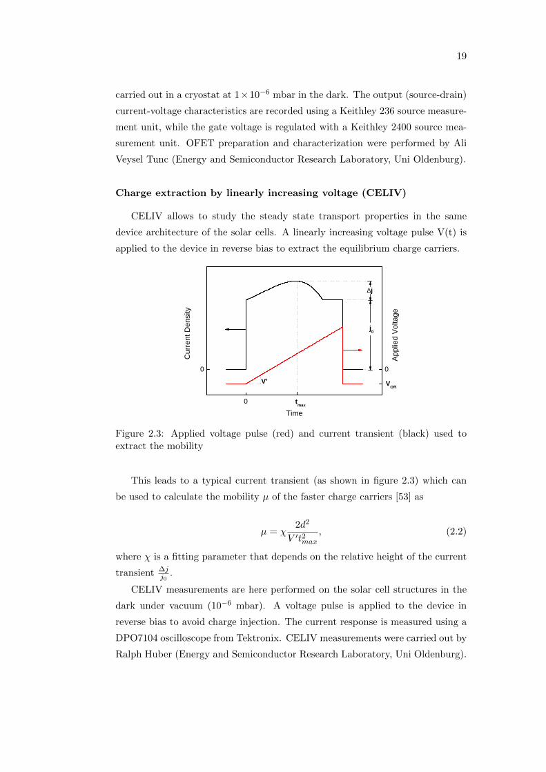
Charge extraction by linearly increasing voltage (CELIV)
CELIV allows to study the steady state transport properties in the same
device architecture of the solar cells. A linearly increasing voltage pulse V(t) is
applied to the device in reverse bias to extract the equilibrium charge carriers.
0
0 0V ’
t m a x
V O f f
j 0
Applie
d Volt
age
Curre
nt De
nsity
T i m e
∆j
Figure 2.3: Applied voltage pulse (red) and current transient (black) used toextract the mobility
This leads to a typical current transient (as shown in figure 2.3) which can
be used to calculate the mobility µ of the faster charge carriers [53] as
µ = χ2d2
V ′t2max
, (2.2)
where χ is a fitting parameter that depends on the relative height of the current
transient ∆jj0
.
CELIV measurements are here performed on the solar cell structures in the
dark under vacuum (10−6 mbar). A voltage pulse is applied to the device in
reverse bias to avoid charge injection. The current response is measured using a
DPO7104 oscilloscope from Tektronix. CELIV measurements were carried out by
Ralph Huber (Energy and Semiconductor Research Laboratory, Uni Oldenburg).
20
Photovoltaic performance
The JV characteristics of the photovoltaic devices under illumination are mea-
sured with a Keithley 4200 semiconductor characterization system. The standard
reference spectrum AM 1.5G is provided by a SS100AAA class A solar simulator
from P.E.T. Inc. A reference silicon solar cell, from Fraunhofer Institute for Solar
Energy Systems (ISE) in Freiburg, is used to calibrate the light. The efficiency
is calculated according to the equation (1.5).
External quantum efficiency (EQE) spectra of the solar cells are also mea-
sured. EQE gives information on the spectral response of the device. The solar
cell is illuminated with monochromatic light and the resulting photocurrent is
measured. EQE is, therefore, defined as the ratio of the number of collected elec-
trons divided by the amount of incident photons for each wavelength of interest
EQE =IscP0
hc
λq, (2.3)
where P0 is the incident optical power, h the Planck’s constant, c the speed of
light in vacuum, and λ the wavelength of interest.
In this work, EQE is measured with a Xe-Hg tandem lamp as the light source
and a 2 grating monochromator to scan the wavelength. A calibrated silicon
photodetector is employed to monitor the incident photon flux, while a lock-in
amplifier is used to measure the photocurrent of the sample.
Transmission electron microscopy (TEM)
TEM is a kind of electron microscopy. It exploits the interaction between
an electron beam transmitted through a thin film sample and the sample itself
to build images. In this work, TEM is used to get insights into the morphol-
ogy of the active layer. The semiconducting solutions are deposited on PE-
DOT:PSS coated ITO substrates, as described above. Free standing films are
then obtained using the floatation technique. The samples are placed in deion-
ized water (18.2 MΩ/cm) in a Petri dish and the free floating films are col-
lected using suitable copper grids. All measurements are performed with a JEOL
JEM-1011 transmission electron microscope operated at 100 kV. TEM images
of the P3HT:PCBM samples were taken by Shany Neyshtadt, whereas the ones
of the doped PCPDTBT:PCBM samples by Daniel Riedel (both at the Ludwig-
Maximilians-Universitat Munchen).
21
Atomic force microscopy (AFM) and Kelvin probe force microscopy
(KPFM)
AFM allows to obtain topographic images of a surface. A cantilever termi-
nating in a sharp tip is used to scan the surface of the sample. When the tip
approaches the surface of the sample, forces between the tip and the sample lead
to a deflection of the cantilever. Typically, the deflection is measured using a laser
spot reflected from the top surface of the cantilever into an array of photodiodes.
KPFM is a recently developed technique based on AFM. It allows to obtain
both topographic and potential images. The potential is obtained by detecting
the deflection of the cantilever caused by an electrostatic force between the tip
and the sample. The contact potential difference between the tip and the sample
is measured. This corresponds to the work function difference between the tip
and the sample.
AFM and KPFM measurements of the P3HT:PCBM samples with various
solvents are here performed with a UHV-STM/AFM system from Omicron at a
pressure below 5 × 10⁻¹⁰ mbar to avoid the effects of oxygen and humidity on
the surface of the sample. Pt/Ir cantilevers are calibrated using a gold single
crystal as reference. The lateral resolution of the microscope in KPFM mode is
20 nm. AFM and KPFM measurements were done by Thomas Madena (Energy
and Semiconductor Research Laboratory, Uni Oldenburg).
2.3 ZnO:Al preparation and characterization
ZnO:Al thin films were deposited onto pre-cleaned Corning R©glass substrates
by dc-magnetron sputtering. ZnO ceramic targets containing 2 wt% Al2O3 were
used. The temperature of the substrates during deposition was 400C. The thick-
ness of the layers was determined with a Veeco Dektak 150 profilometer. A four
point probing bridge from Jandel Engineering was used to measure the sheet re-
sistance, while UV-VIS optical characterizations were performed with a Varian
Cary 5000 spectrophotometer equipped with an integrating sphere. The surface
roughness of the films was measured with a Nanosurf Mobile S atomic force mi-
croscope. The composition of the ZnO:Al films after deposition was analyzed by
energy dispersed X-ray spectroscopy (EDX), using an X-Max silicon drift detec-
tor from Oxford Instruments. ITO substrates, purchased from PGO (Germany),
were also characterized in the same way. The ZnO:Al thin films were fabricated
22
and characterized by Kambulakwao Chakanga (EWE Research Center Next En-
ergy, Oldenburg).
2.4 Degradation experiments
In the last chapter, the effect of degradation on the reference P3HT:PCBM
system is investigated. In the first part, the influence of the processing atmo-
sphere is studied on the solar cells as well as on the active layer only by means
of optical techniques. For the latter, rr-P3HT dissolved in oDCB is spun on sap-
phire substrates from hot solutions and annealed at 150C for 10 min as for the
solar cells. Absorption, PL and PIA spectra of the samples are measured. The
corresponding solar cells in the forward structure are fabricated and characterized
according to the procedure already explained in section 2.1.1. Reference samples
are prepared entirely in a nitrogen filled glovebox, while the samples for the in-
vestigations of the effect of the processing atmosphere are prepared by spinning
and annealing the active layer in ambient air.
In the second part of chapter 6, the effect of the irreversible degradation
induced from light irradiation in presence of oxygen is investigated. The samples
for these experiments are provided by Konarka Technologies GmbH, Nurnberg.
Thin blend films are obtained by doctor-blading onto pre-cleaned glass substrates.
The samples are annealed at 140C in the glovebox for 2 min and then degraded
under AM 1.5G light while kept in synthetic air. In order to remove the reversible
component, the samples are annealed in the glovebox at 130C for 10 min after
the degradation and before being encapsulated. The samples are then sealed
using a glass slab on top of the films and epoxy resin. PL and PIA measurements
are performed with the setup described in the previous sections. Due to the epoxy
resin, it is not possible to work at low temperature, therefore, the experiments
are carried out at room temperature while keeping the samples under dynamic
vacuum.
Chapter 3
Molecular doping
Doping of semiconductors using impurities with appropriate electronic prop-
erties is a general concept that does not depend on the nature of the semicon-
ductor, but is common to both inorganic and organic materials. The ability to
fine tune the electrical properties of a semiconductor by controlling the type and
the concentration of the charge carriers with doping is one of the key techniques
to develop efficient optoelectronic devices. For what deals with organic electron-
ics, the discovery in 1977 that p-doping in polyacetylene dramatically increases
its conductivity [54] boosted the research in this relatively new field and opened
the way for the development of organic optoelectronic devices, like light emitting
diodes and solar cells.
In small molecule based devices, prepared by evaporation of the organic pre-
cursors, the introduction of doped transport layers led to a reduced operating
voltage [55] in organic light emitting diodes and allowed efficient p-i-n solar cells
[56]. In such devices, the main contribution of doping is the modification of the
energy barriers at the metal-organic interfaces which are well known to have a
strong impact on the carrier injection and extraction efficiency [57, 58].
On the other hand, studies on conjugated polymer thin films demonstrated
that molecular doping can lead to an increase in the conductivity and the mobility
[59, 60]. In particular, it has been shown that doping affects the mobility in
MEH-PPV [59], MDMO-PPV and P3HT [61] polymer films. Higher mobility due
to controlled doping was demonstrated in both polymer diodes and field effect
transistors [60]. However, the effect of molecular doping in polymer based solar
23
24
cells has not been investigated up to now. Therefore, in this chapter molecular
doping will be explored in both polymer layers and bulk heterojunction solar cell
devices based on a novel low bandgap copolymer. Part of the results presented
here are adapted from A.V. Tunc, A. De Sio, D. Riedel, F. Deschler, E. Da Como,
J. Parisi, E. von Hauff, Molecular doping of polymer:fullerene solar cells: effects
on transport and solar cells, Organic Electronics 13, 290-296, 2012.
3.1 Low bandgap copolymers for increased light har-
vesting
Conjugated low bandgap polymers are able to absorb light in the near in-
frared range of the spectrum enhancing therefore light harvesting [62]. It is thus
not surprising that design, synthesis and application of such novel materials are
nowadays one of the hot topics in polymer photovoltaics [63, 64, 65].
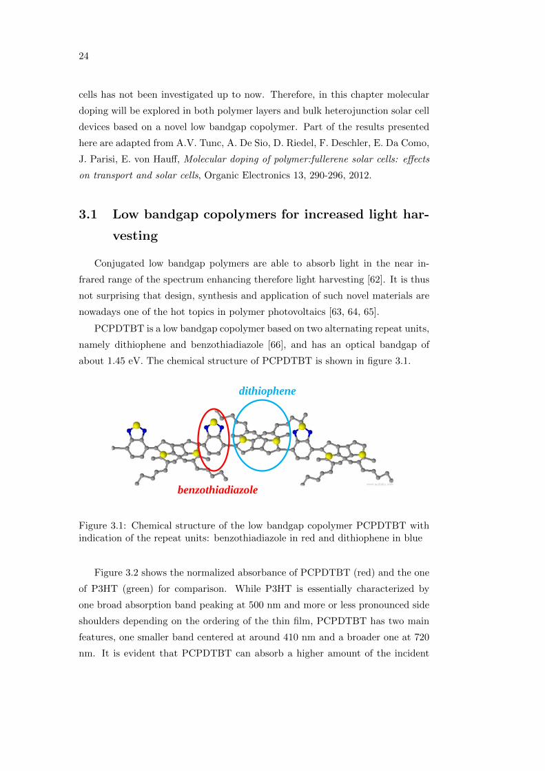
PCPDTBT is a low bandgap copolymer based on two alternating repeat units,
namely dithiophene and benzothiadiazole [66], and has an optical bandgap of
about 1.45 eV. The chemical structure of PCPDTBT is shown in figure 3.1.
dithiophene
benzothiadiazole
Figure 3.1: Chemical structure of the low bandgap copolymer PCPDTBT withindication of the repeat units: benzothiadiazole in red and dithiophene in blue
Figure 3.2 shows the normalized absorbance of PCPDTBT (red) and the one
of P3HT (green) for comparison. While P3HT is essentially characterized by
one broad absorption band peaking at 500 nm and more or less pronounced side
shoulders depending on the ordering of the thin film, PCPDTBT has two main
features, one smaller band centered at around 410 nm and a broader one at 720
nm. It is evident that PCPDTBT can absorb a higher amount of the incident
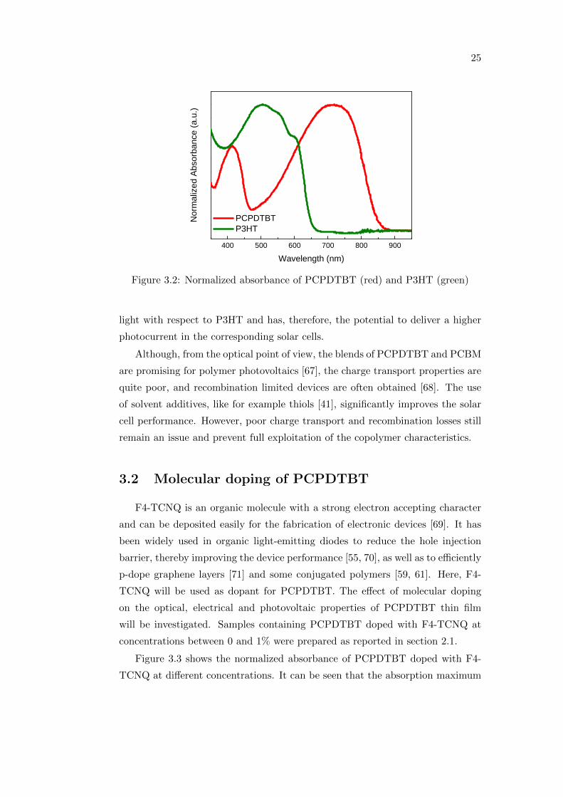
25
4 0 0 5 0 0 6 0 0 7 0 0 8 0 0 9 0 0
P C P D T B T P 3 H T
Norm
alized
Abso
rbanc
e (a.u
.)
W a v e l e n g t h ( n m )Figure 3.2: Normalized absorbance of PCPDTBT (red) and P3HT (green)
light with respect to P3HT and has, therefore, the potential to deliver a higher
photocurrent in the corresponding solar cells.
Although, from the optical point of view, the blends of PCPDTBT and PCBM
are promising for polymer photovoltaics [67], the charge transport properties are
quite poor, and recombination limited devices are often obtained [68]. The use
of solvent additives, like for example thiols [41], significantly improves the solar
cell performance. However, poor charge transport and recombination losses still
remain an issue and prevent full exploitation of the copolymer characteristics.
3.2 Molecular doping of PCPDTBT
F4-TCNQ is an organic molecule with a strong electron accepting character
and can be deposited easily for the fabrication of electronic devices [69]. It has
been widely used in organic light-emitting diodes to reduce the hole injection
barrier, thereby improving the device performance [55, 70], as well as to efficiently
p-dope graphene layers [71] and some conjugated polymers [59, 61]. Here, F4-
TCNQ will be used as dopant for PCPDTBT. The effect of molecular doping
on the optical, electrical and photovoltaic properties of PCPDTBT thin film
will be investigated. Samples containing PCPDTBT doped with F4-TCNQ at
concentrations between 0 and 1% were prepared as reported in section 2.1.
Figure 3.3 shows the normalized absorbance of PCPDTBT doped with F4-
TCNQ at different concentrations. It can be seen that the absorption maximum
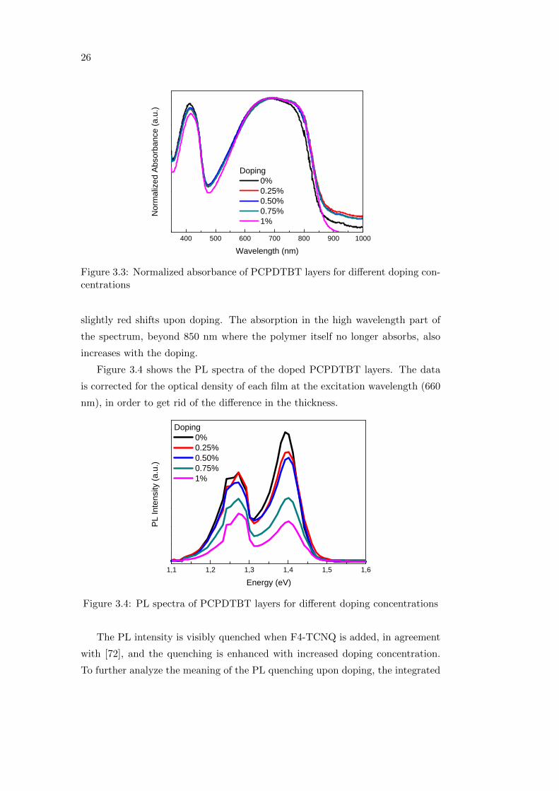
26
4 0 0 5 0 0 6 0 0 7 0 0 8 0 0 9 0 0 1 0 0 0
Norm
alized
Abso
rbanc
e (a.u
.)
W a v e l e n g t h ( n m )
D o p i n g 0 % 0 . 2 5 % 0 . 5 0 % 0 . 7 5 % 1 %
Figure 3.3: Normalized absorbance of PCPDTBT layers for different doping con-centrations
slightly red shifts upon doping. The absorption in the high wavelength part of
the spectrum, beyond 850 nm where the polymer itself no longer absorbs, also
increases with the doping.
Figure 3.4 shows the PL spectra of the doped PCPDTBT layers. The data
is corrected for the optical density of each film at the excitation wavelength (660
nm), in order to get rid of the difference in the thickness.
1 , 1 1 , 2 1 , 3 1 , 4 1 , 5 1 , 6
PL In
tensity
(a.u.
)
E n e r g y ( e V )
D o p i n g 0 % 0 . 2 5 % 0 . 5 0 % 0 . 7 5 % 1 %
Figure 3.4: PL spectra of PCPDTBT layers for different doping concentrations
The PL intensity is visibly quenched when F4-TCNQ is added, in agreement
with [72], and the quenching is enhanced with increased doping concentration.
To further analyze the meaning of the PL quenching upon doping, the integrated
27
PL difference is shown in figure 3.5 in a Stern-Volmer plot. PL0 indicates the
integrated PL of the reference (undoped) sample, while PL is the one of the
doped samples. The non-linear behavior with upwards curvature of the PL0/PL
with respect to the doping concentration indicates a combined dynamic and static
quenching (see section 1.3). This means that F4-TCNQ and PCPDTBT are in
molecular contact. Static quenching means that ground-state complexes between
the polymer and the F4-TCNQ are formed upon doping. Moreover, the occur-
rence of static quenching is confirmed by the slight increase in the sub-bandgap
absorption [22], seen in figure 3.3.
0 , 0 0 0 , 2 5 0 , 5 0 0 , 7 5 1 , 0 00 , 8
1 , 2
1 , 6
2 , 0
2 , 4
2 , 8
PL0/PL
D o p i n g ( % )
Figure 3.5: Stern-Volmer plot of doped PCPDTBT layers
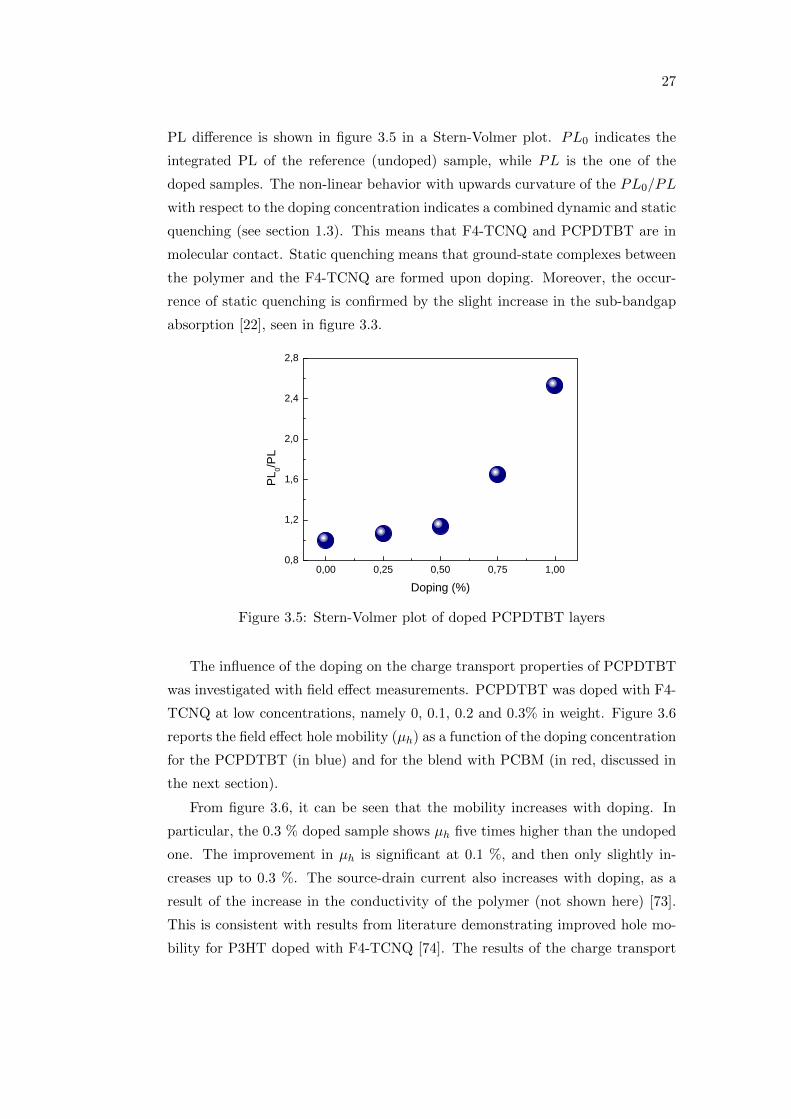
The influence of the doping on the charge transport properties of PCPDTBT
was investigated with field effect measurements. PCPDTBT was doped with F4-
TCNQ at low concentrations, namely 0, 0.1, 0.2 and 0.3% in weight. Figure 3.6
reports the field effect hole mobility (µh) as a function of the doping concentration
for the PCPDTBT (in blue) and for the blend with PCBM (in red, discussed in
the next section).
From figure 3.6, it can be seen that the mobility increases with doping. In
particular, the 0.3 % doped sample shows µh five times higher than the undoped
one. The improvement in µh is significant at 0.1 %, and then only slightly in-
creases up to 0.3 %. The source-drain current also increases with doping, as a
result of the increase in the conductivity of the polymer (not shown here) [73].
This is consistent with results from literature demonstrating improved hole mo-
bility for P3HT doped with F4-TCNQ [74]. The results of the charge transport
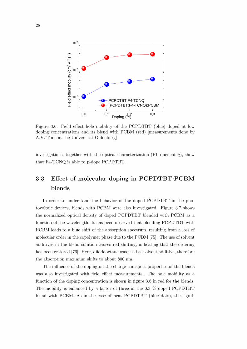
28
0 , 0 0 , 1 0 , 2 0 , 3
1 0 - 5
1 0 - 4
1 0 - 3
P C P D T B T : F 4 - T C N Q ( P C P D T B T : F 4 - T C N Q ) : P C B MFie
ld eff
ect m
obility
(cm2 V -1
s-1 )
D o p i n g ( % )Figure 3.6: Field effect hole mobility of the PCPDTBT (blue) doped at lowdoping concentrations and its blend with PCBM (red) [measurements done byA.V. Tunc at the Universitat Oldenburg]
investigations, together with the optical characterization (PL quenching), show
that F4-TCNQ is able to p-dope PCPDTBT.
3.3 Effect of molecular doping in PCPDTBT:PCBM
blends
In order to understand the behavior of the doped PCPDTBT in the pho-
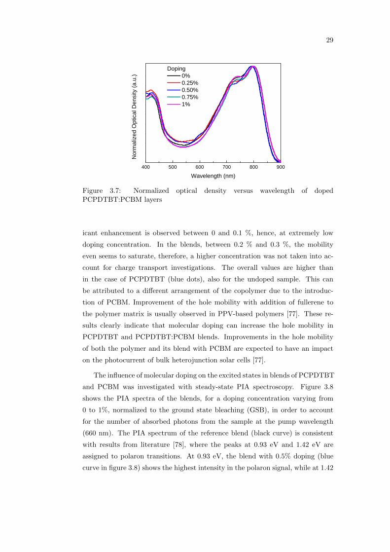
tovoltaic devices, blends with PCBM were also investigated. Figure 3.7 shows
the normalized optical density of doped PCPDTBT blended with PCBM as a
function of the wavelength. It has been observed that blending PCPDTBT with
PCBM leads to a blue shift of the absorption spectrum, resulting from a loss of
molecular order in the copolymer phase due to the PCBM [75]. The use of solvent
additives in the blend solution causes red shifting, indicating that the ordering
has been restored [76]. Here, diiodooctane was used as solvent additive, therefore
the absorption maximum shifts to about 800 nm.
The influence of the doping on the charge transport properties of the blends
was also investigated with field effect measurements. The hole mobility as a
function of the doping concentration is shown in figure 3.6 in red for the blends.
The mobility is enhanced by a factor of three in the 0.3 % doped PCPDTBT
blend with PCBM. As in the case of neat PCPDTBT (blue dots), the signif-
29
4 0 0 5 0 0 6 0 0 7 0 0 8 0 0 9 0 0
Norm
alized
Opti
cal D
ensity
(a.u.
)
W a v e l e n g t h ( n m )
D o p i n g 0 % 0 . 2 5 % 0 . 5 0 % 0 . 7 5 % 1 %
Figure 3.7: Normalized optical density versus wavelength of dopedPCPDTBT:PCBM layers
icant enhancement is observed between 0 and 0.1 %, hence, at extremely low
doping concentration. In the blends, between 0.2 % and 0.3 %, the mobility
even seems to saturate, therefore, a higher concentration was not taken into ac-
count for charge transport investigations. The overall values are higher than
in the case of PCPDTBT (blue dots), also for the undoped sample. This can
be attributed to a different arrangement of the copolymer due to the introduc-
tion of PCBM. Improvement of the hole mobility with addition of fullerene to
the polymer matrix is usually observed in PPV-based polymers [77]. These re-
sults clearly indicate that molecular doping can increase the hole mobility in
PCPDTBT and PCPDTBT:PCBM blends. Improvements in the hole mobility
of both the polymer and its blend with PCBM are expected to have an impact
on the photocurrent of bulk heterojunction solar cells [77].
The influence of molecular doping on the excited states in blends of PCPDTBT
and PCBM was investigated with steady-state PIA spectroscopy. Figure 3.8
shows the PIA spectra of the blends, for a doping concentration varying from
0 to 1%, normalized to the ground state bleaching (GSB), in order to account
for the number of absorbed photons from the sample at the pump wavelength
(660 nm). The PIA spectrum of the reference blend (black curve) is consistent
with results from literature [78], where the peaks at 0.93 eV and 1.42 eV are
assigned to polaron transitions. At 0.93 eV, the blend with 0.5% doping (blue
curve in figure 3.8) shows the highest intensity in the polaron signal, while at 1.42
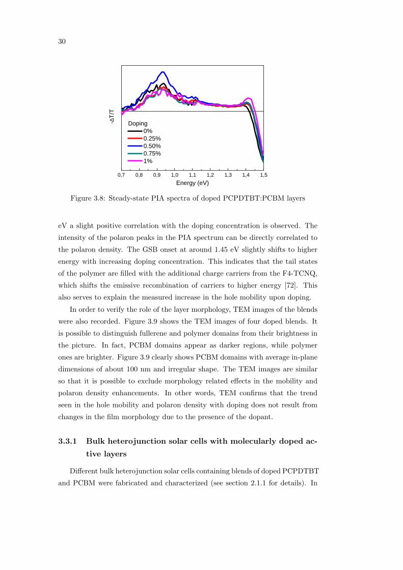
30
0 , 7 0 , 8 0 , 9 1 , 0 1 , 1 1 , 2 1 , 3 1 , 4 1 , 5
-∆T/T
E n e r g y ( e V )
D o p i n g 0 % 0 . 2 5 % 0 . 5 0 % 0 . 7 5 % 1 %
Figure 3.8: Steady-state PIA spectra of doped PCPDTBT:PCBM layers
eV a slight positive correlation with the doping concentration is observed. The
intensity of the polaron peaks in the PIA spectrum can be directly correlated to
the polaron density. The GSB onset at around 1.45 eV slightly shifts to higher
energy with increasing doping concentration. This indicates that the tail states
of the polymer are filled with the additional charge carriers from the F4-TCNQ,
which shifts the emissive recombination of carriers to higher energy [72]. This
also serves to explain the measured increase in the hole mobility upon doping.
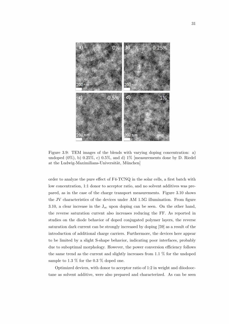
In order to verify the role of the layer morphology, TEM images of the blends
were also recorded. Figure 3.9 shows the TEM images of four doped blends. It
is possible to distinguish fullerene and polymer domains from their brightness in
the picture. In fact, PCBM domains appear as darker regions, while polymer
ones are brighter. Figure 3.9 clearly shows PCBM domains with average in-plane
dimensions of about 100 nm and irregular shape. The TEM images are similar
so that it is possible to exclude morphology related effects in the mobility and
polaron density enhancements. In other words, TEM confirms that the trend
seen in the hole mobility and polaron density with doping does not result from
changes in the film morphology due to the presence of the dopant.
3.3.1 Bulk heterojunction solar cells with molecularly doped ac-
tive layers
Different bulk heterojunction solar cells containing blends of doped PCPDTBT
and PCBM were fabricated and characterized (see section 2.1.1 for details). In
31
Figure 3.9: TEM images of the blends with varying doping concentration: a)undoped (0%), b) 0.25%, c) 0.5%, and d) 1% [measurements done by D. Riedelat the Ludwig-Maximilians-Universitat, Munchen]
order to analyze the pure effect of F4-TCNQ in the solar cells, a first batch with
low concentration, 1:1 donor to acceptor ratio, and no solvent additives was pre-
pared, as in the case of the charge transport measurements. Figure 3.10 shows
the JV characteristics of the devices under AM 1.5G illumination. From figure
3.10, a clear increase in the Jsc upon doping can be seen. On the other hand,
the reverse saturation current also increases reducing the FF. As reported in
studies on the diode behavior of doped conjugated polymer layers, the reverse
saturation dark current can be strongly increased by doping [59] as a result of the
introduction of additional charge carriers. Furthermore, the devices here appear
to be limited by a slight S-shape behavior, indicating poor interfaces, probably
due to suboptimal morphology. However, the power conversion efficiency follows
the same trend as the current and slightly increases from 1.1 % for the undoped
sample to 1.3 % for the 0.3 % doped one.
Optimized devices, with donor to acceptor ratio of 1:2 in weight and diiodooc-
tane as solvent additive, were also prepared and characterized. As can be seen
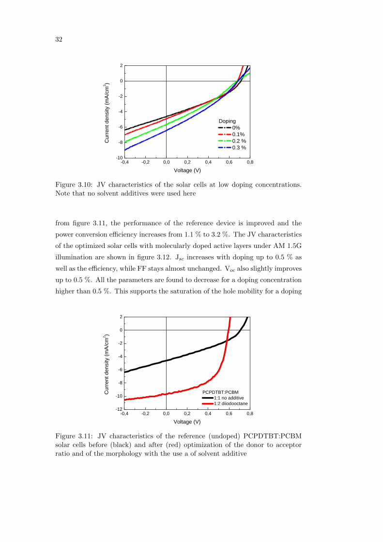
32
- 0 , 4 - 0 , 2 0 , 0 0 , 2 0 , 4 0 , 6 0 , 8- 1 0
- 8
- 6
- 4
- 2
0
2
Curre
nt de
nsity
(mA/c
m2 )
V o l t a g e ( V )
D o p i n g 0 % 0 . 1 % 0 . 2 % 0 . 3 %
Figure 3.10: JV characteristics of the solar cells at low doping concentrations.Note that no solvent additives were used here
from figure 3.11, the performance of the reference device is improved and the
power conversion efficiency increases from 1.1 % to 3.2 %. The JV characteristics
of the optimized solar cells with molecularly doped active layers under AM 1.5G
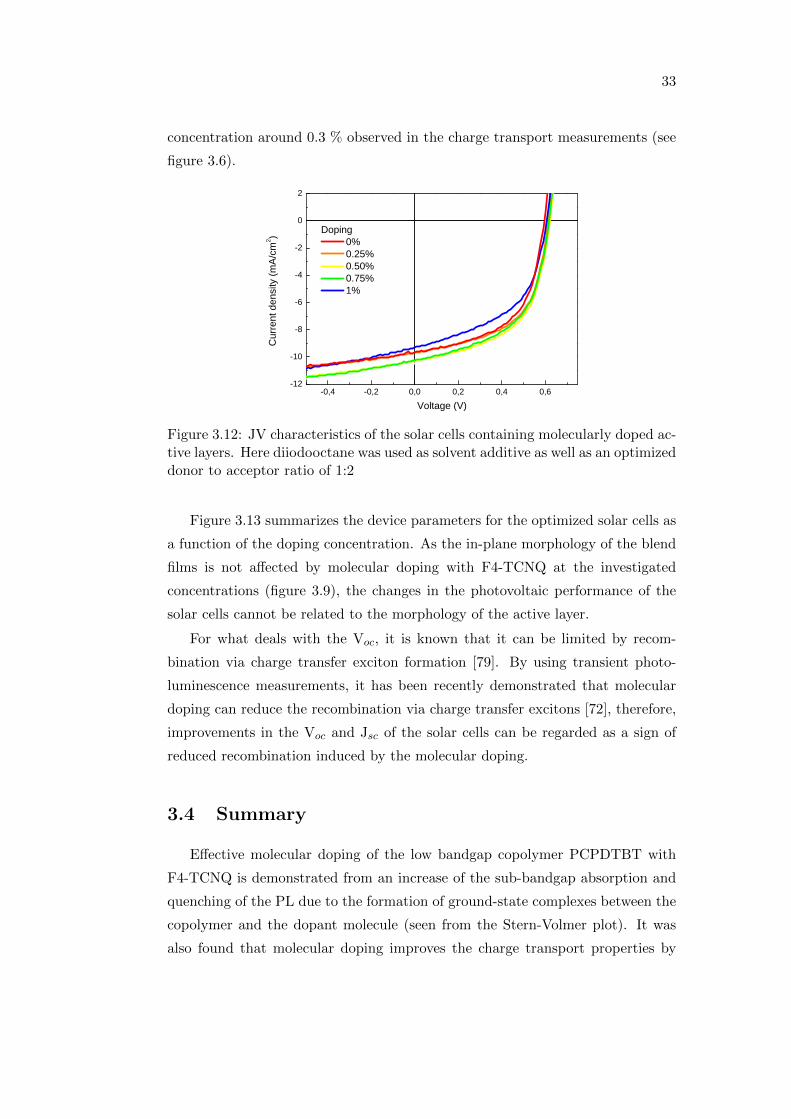
illumination are shown in figure 3.12. Jsc increases with doping up to 0.5 % as
well as the efficiency, while FF stays almost unchanged. Voc also slightly improves
up to 0.5 %. All the parameters are found to decrease for a doping concentration
higher than 0.5 %. This supports the saturation of the hole mobility for a doping
- 0 , 4 - 0 , 2 0 , 0 0 , 2 0 , 4 0 , 6 0 , 8- 1 2
- 1 0
- 8
- 6
- 4
- 2
0
2
Curre
nt de
nsity
(mA/c
m2 )
V o l t a g e ( V )
P C P D T B T : P C B M 1 : 1 n o a d d i t i v e 1 : 2 d i i o d o o c t a n e
Figure 3.11: JV characteristics of the reference (undoped) PCPDTBT:PCBMsolar cells before (black) and after (red) optimization of the donor to acceptorratio and of the morphology with the use a of solvent additive
33
concentration around 0.3 % observed in the charge transport measurements (see
figure 3.6).
- 0 , 4 - 0 , 2 0 , 0 0 , 2 0 , 4 0 , 6- 1 2
- 1 0
- 8
- 6
- 4
- 2
0
2
Curre
nt de
nsity
(mA/c
m2 )
V o l t a g e ( V )
D o p i n g 0 % 0 . 2 5 % 0 . 5 0 % 0 . 7 5 % 1 %
Figure 3.12: JV characteristics of the solar cells containing molecularly doped ac-tive layers. Here diiodooctane was used as solvent additive as well as an optimizeddonor to acceptor ratio of 1:2
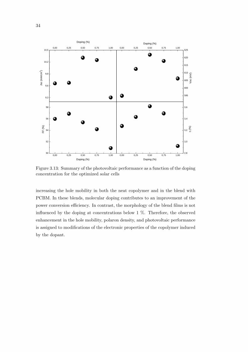
Figure 3.13 summarizes the device parameters for the optimized solar cells as
a function of the doping concentration. As the in-plane morphology of the blend
films is not affected by molecular doping with F4-TCNQ at the investigated
concentrations (figure 3.9), the changes in the photovoltaic performance of the
solar cells cannot be related to the morphology of the active layer.
For what deals with the Voc, it is known that it can be limited by recom-
bination via charge transfer exciton formation [79]. By using transient photo-
luminescence measurements, it has been recently demonstrated that molecular
doping can reduce the recombination via charge transfer excitons [72], therefore,
improvements in the Voc and Jsc of the solar cells can be regarded as a sign of
reduced recombination induced by the molecular doping.
3.4 Summary
Effective molecular doping of the low bandgap copolymer PCPDTBT with
F4-TCNQ is demonstrated from an increase of the sub-bandgap absorption and
quenching of the PL due to the formation of ground-state complexes between the
copolymer and the dopant molecule (seen from the Stern-Volmer plot). It was
also found that molecular doping improves the charge transport properties by
34
9 , 3
9 , 6
9 , 9
1 0 , 2
1 0 , 5 0 , 0 0 0 , 2 5 0 , 5 0 0 , 7 5 1 , 0 0 0 , 0 0 0 , 2 5 0 , 5 0 0 , 7 5 1 , 0 0
5 9 5
6 0 0
6 0 5
6 1 0
6 1 5
6 2 0
6 2 5
0 , 0 0 0 , 2 5 0 , 5 0 0 , 7 5 1 , 0 05 0
5 2
5 4
5 6
5 8
0 , 0 0 0 , 2 5 0 , 5 0 0 , 7 5 1 , 0 0 2 , 8
3 , 0
3 , 2
3 , 4
3 , 6
D o p i n g ( % )
Jsc (m
A/cm2 )
Voc (
mV)
D o p i n g ( % )FF
(%)
D o p i n g ( % )
η (%
)
D o p i n g ( % )
Figure 3.13: Summary of the photovoltaic performance as a function of the dopingconcentration for the optimized solar cells
increasing the hole mobility in both the neat copolymer and in the blend with
PCBM. In these blends, molecular doping contributes to an improvement of the
power conversion efficiency. In contrast, the morphology of the blend films is not
influenced by the doping at concentrations below 1 %. Therefore, the observed
enhancement in the hole mobility, polaron density, and photovoltaic performance
is assigned to modifications of the electronic properties of the copolymer induced
by the dopant.
Chapter 4
Controlling morphology with
solvent mixtures
In this chapter, the effect of the solvent induced ordering on the optoelec-
tronic, structural, and photovoltaic properties of P3HT:PCBM absorbers will be
investigated using solvent mixtures. oDCB was chosen as the host solvent for all
investigated blends and the relative devices as reference. CB and THN were used
as co-solvents. PCBM is more soluble in both CB and THN than P3HT [44] and
the use of the co-solvents is, therefore, expected to avoid PCBM clustering and
allow for better arrangement of the polymer domains. More details on the sample
preparation have been already presented in sections 2.1 and 2.1.1. The results
presented here are adapted from A. De Sio, T. Madena, R. Huber, J. Parisi, S.
Neyshtadt, F. Deschler, E. Da Como, S. Esposito, E. von Hauff, Solvent addi-
tives for tuning the photovoltaic properties of polymer-fullerene solar cells, Solar
Energy Materials and Solar Cells 95, 3536-3542, 2011.
4.1 Effect of solvent on the optical properties of the
blend
Figure 4.1 shows the normalized absorbance of the three investigated blends
spun on glass. The spectra are in agreement with results found in literature
for P3HT:PCBM blends, where the absorption spectrum is dominated by the
π − π∗ absorption band of the P3HT [80], in this case peaking at about 500 nm.
35
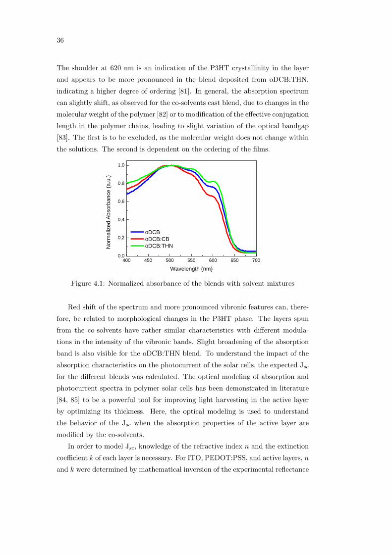
36
The shoulder at 620 nm is an indication of the P3HT crystallinity in the layer
and appears to be more pronounced in the blend deposited from oDCB:THN,
indicating a higher degree of ordering [81]. In general, the absorption spectrum
can slightly shift, as observed for the co-solvents cast blend, due to changes in the
molecular weight of the polymer [82] or to modification of the effective conjugation
length in the polymer chains, leading to slight variation of the optical bandgap
[83]. The first is to be excluded, as the molecular weight does not change within
the solutions. The second is dependent on the ordering of the films.
4 0 0 4 5 0 5 0 0 5 5 0 6 0 0 6 5 0 7 0 00 , 0
0 , 2
0 , 4
0 , 6
0 , 8
1 , 0
Norm
alized
Abso
rbanc
e (a.u
.)
W a v e l e n g t h ( n m )
o D C B o D C B : C B o D C B : T H N
Figure 4.1: Normalized absorbance of the blends with solvent mixtures
Red shift of the spectrum and more pronounced vibronic features can, there-
fore, be related to morphological changes in the P3HT phase. The layers spun
from the co-solvents have rather similar characteristics with different modula-
tions in the intensity of the vibronic bands. Slight broadening of the absorption
band is also visible for the oDCB:THN blend. To understand the impact of the
absorption characteristics on the photocurrent of the solar cells, the expected Jsc
for the different blends was calculated. The optical modeling of absorption and
photocurrent spectra in polymer solar cells has been demonstrated in literature
[84, 85] to be a powerful tool for improving light harvesting in the active layer
by optimizing its thickness. Here, the optical modeling is used to understand
the behavior of the Jsc when the absorption properties of the active layer are
modified by the co-solvents.
In order to model Jsc, knowledge of the refractive index n and the extinction
coefficient k of each layer is necessary. For ITO, PEDOT:PSS, and active layers, n
and k were determined by mathematical inversion of the experimental reflectance
37
R and transmittance T , while for Ca and Al, used for the cathode of the solar
cells, they were taken from literature [86, 87, 88]. The model of the structure
used for the mathematical inversion is shown in figure 4.2.
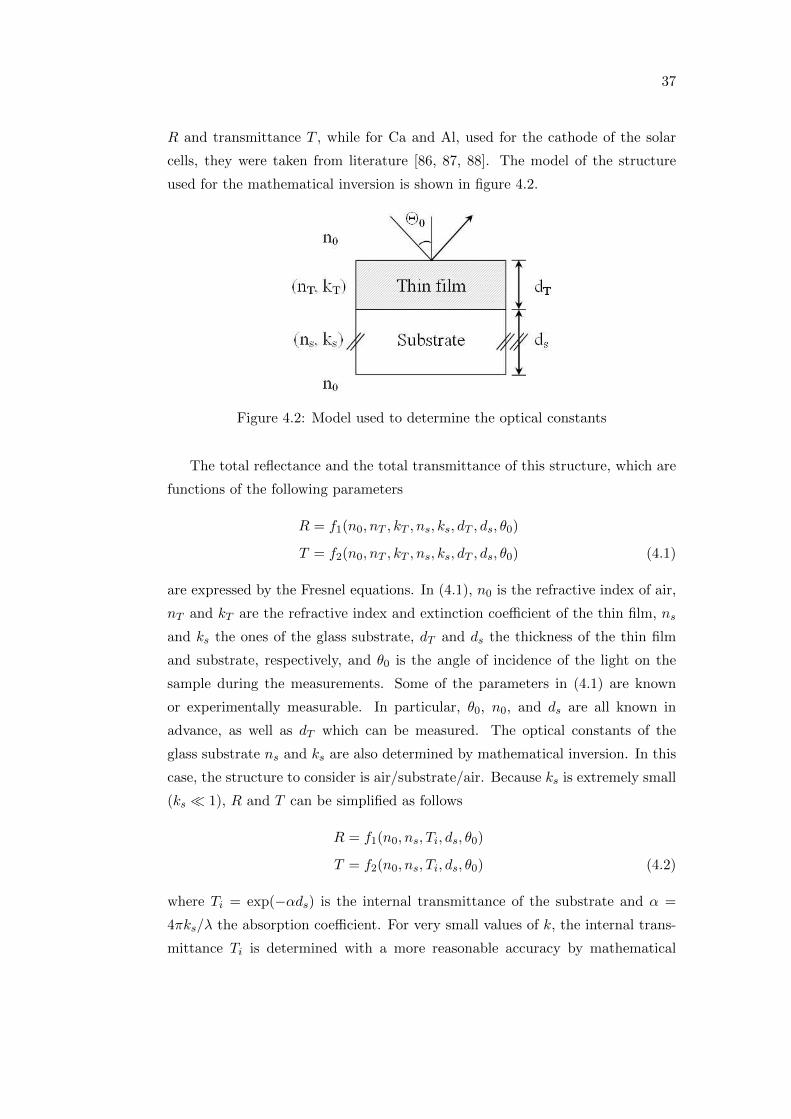
Figure 4.2: Model used to determine the optical constants
The total reflectance and the total transmittance of this structure, which are
functions of the following parameters
R = f1(n0, nT , kT , ns, ks, dT , ds, θ0)
T = f2(n0, nT , kT , ns, ks, dT , ds, θ0) (4.1)
are expressed by the Fresnel equations. In (4.1), n0 is the refractive index of air,
nT and kT are the refractive index and extinction coefficient of the thin film, ns
and ks the ones of the glass substrate, dT and ds the thickness of the thin film
and substrate, respectively, and θ0 is the angle of incidence of the light on the
sample during the measurements. Some of the parameters in (4.1) are known
or experimentally measurable. In particular, θ0, n0, and ds are all known in
advance, as well as dT which can be measured. The optical constants of the
glass substrate ns and ks are also determined by mathematical inversion. In this
case, the structure to consider is air/substrate/air. Because ks is extremely small
(ks 1), R and T can be simplified as follows
R = f1(n0, ns, Ti, ds, θ0)
T = f2(n0, ns, Ti, ds, θ0) (4.2)
where Ti = exp(−αds) is the internal transmittance of the substrate and α =
4πks/λ the absorption coefficient. For very small values of k, the internal trans-
mittance Ti is determined with a more reasonable accuracy by mathematical
38
inversion than the extinction coefficient. Thus, the glass substrate was charac-
terized by ns and Ti. R and T of the whole structure are measured experimentally.
Therefore, the equations (4.1) are solved to get nT and kT . A linear regression
method based on the interior-reflective Newton algorithm [89, 90] is employed to
extract n and k of the thin film layer.
0 5 0 1 0 0 1 5 0 2 0 0 2 5 0 3 0 00
3
6
9
1 2
1 5
Calcu
lated
Jsc (
mA/cm
2 )
A c t i v e l a y e r t h i c k n e s s ( n m )
o D C B o D C B : C B o D C B : T H N
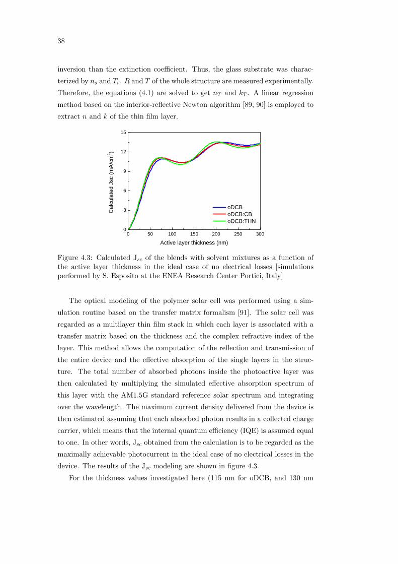
Figure 4.3: Calculated Jsc of the blends with solvent mixtures as a function ofthe active layer thickness in the ideal case of no electrical losses [simulationsperformed by S. Esposito at the ENEA Research Center Portici, Italy]
The optical modeling of the polymer solar cell was performed using a sim-
ulation routine based on the transfer matrix formalism [91]. The solar cell was
regarded as a multilayer thin film stack in which each layer is associated with a
transfer matrix based on the thickness and the complex refractive index of the
layer. This method allows the computation of the reflection and transmission of
the entire device and the effective absorption of the single layers in the struc-
ture. The total number of absorbed photons inside the photoactive layer was
then calculated by multiplying the simulated effective absorption spectrum of
this layer with the AM1.5G standard reference solar spectrum and integrating
over the wavelength. The maximum current density delivered from the device is
then estimated assuming that each absorbed photon results in a collected charge
carrier, which means that the internal quantum efficiency (IQE) is assumed equal
to one. In other words, Jsc obtained from the calculation is to be regarded as the
maximally achievable photocurrent in the ideal case of no electrical losses in the
device. The results of the Jsc modeling are shown in figure 4.3.
For the thickness values investigated here (115 nm for oDCB, and 130 nm
39
for oDCB:CB and oDCB:THN), only a minimal difference in Jsc is expected,
with oDCB:THN showing the lowest current. The oDCB:CB system is optically
similar to the oDCB reference system. The oDCB:THN system, on the other
hand, has the potential to deliver a higher photocurrent if thicker layers are
employed. Thicker absorber layers, however, can lead to recombination losses
due to the low diffusion lengths of the charge carriers.
4.2 Effect of solvent on the structural properties of
the blend
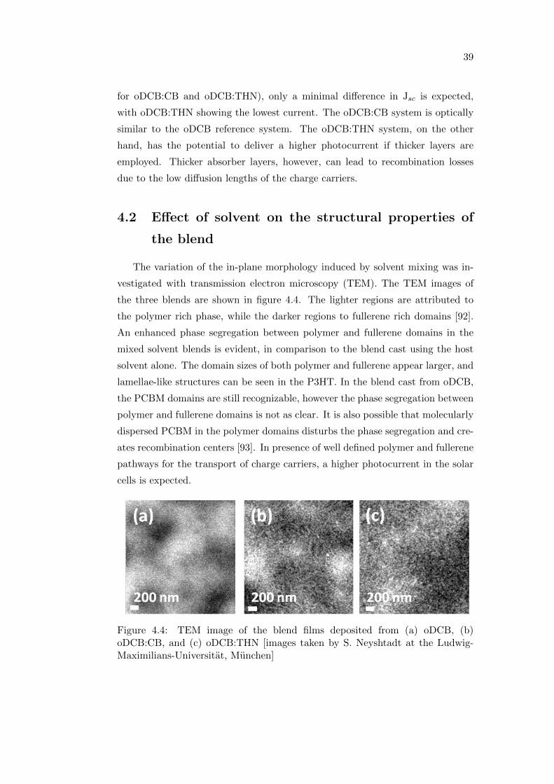
The variation of the in-plane morphology induced by solvent mixing was in-
vestigated with transmission electron microscopy (TEM). The TEM images of
the three blends are shown in figure 4.4. The lighter regions are attributed to
the polymer rich phase, while the darker regions to fullerene rich domains [92].
An enhanced phase segregation between polymer and fullerene domains in the
mixed solvent blends is evident, in comparison to the blend cast using the host
solvent alone. The domain sizes of both polymer and fullerene appear larger, and
lamellae-like structures can be seen in the P3HT. In the blend cast from oDCB,
the PCBM domains are still recognizable, however the phase segregation between
polymer and fullerene domains is not as clear. It is also possible that molecularly
dispersed PCBM in the polymer domains disturbs the phase segregation and cre-
ates recombination centers [93]. In presence of well defined polymer and fullerene
pathways for the transport of charge carriers, a higher photocurrent in the solar
cells is expected.
Figure 4.4: TEM image of the blend films deposited from (a) oDCB, (b)oDCB:CB, and (c) oDCB:THN [images taken by S. Neyshtadt at the Ludwig-Maximilians-Universitat, Munchen]
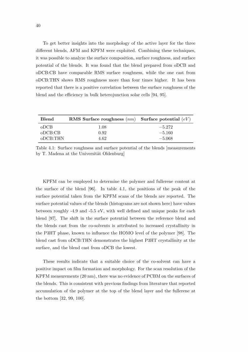
40
To get better insights into the morphology of the active layer for the three
different blends, AFM and KPFM were exploited. Combining these techniques,
it was possible to analyze the surface composition, surface roughness, and surface
potential of the blends. It was found that the blend prepared from oDCB and
oDCB:CB have comparable RMS surface roughness, while the one cast from
oDCB:THN shows RMS roughness more than four times higher. It has been
reported that there is a positive correlation between the surface roughness of the
blend and the efficiency in bulk heterojunction solar cells [94, 95].
Blend RMS Surface roughness (nm) Surface potential (eV )
oDCB 1.08 −5.272oDCB:CB 0.92 −5.160oDCB:THN 4.62 −5.068
Table 4.1: Surface roughness and surface potential of the blends [measurementsby T. Madena at the Universitat Oldenburg]
KPFM can be employed to determine the polymer and fullerene content at
the surface of the blend [96]. In table 4.1, the positions of the peak of the
surface potential taken from the KPFM scans of the blends are reported. The
surface potential values of the blends (histograms are not shown here) have values
between roughly -4.9 and -5.5 eV, with well defined and unique peaks for each
blend [97]. The shift in the surface potential between the reference blend and
the blends cast from the co-solvents is attributed to increased crystallinity in
the P3HT phase, known to influence the HOMO level of the polymer [98]. The
blend cast from oDCB:THN demonstrates the highest P3HT crystallinity at the
surface, and the blend cast from oDCB the lowest.
These results indicate that a suitable choice of the co-solvent can have a
positive impact on film formation and morphology. For the scan resolution of the
KPFM measurements (20 nm), there was no evidence of PCBM on the surfaces of
the blends. This is consistent with previous findings from literature that reported
accumulation of the polymer at the top of the blend layer and the fullerene at
the bottom [32, 99, 100].
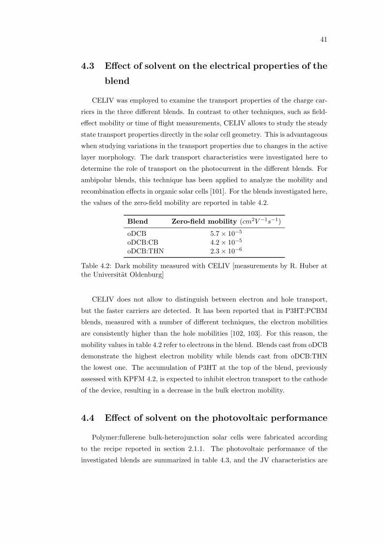
41
4.3 Effect of solvent on the electrical properties of the
blend
CELIV was employed to examine the transport properties of the charge car-
riers in the three different blends. In contrast to other techniques, such as field-
effect mobility or time of flight measurements, CELIV allows to study the steady
state transport properties directly in the solar cell geometry. This is advantageous
when studying variations in the transport properties due to changes in the active
layer morphology. The dark transport characteristics were investigated here to
determine the role of transport on the photocurrent in the different blends. For
ambipolar blends, this technique has been applied to analyze the mobility and
recombination effects in organic solar cells [101]. For the blends investigated here,
the values of the zero-field mobility are reported in table 4.2.
Blend Zero-field mobility (cm2V −1s−1)
oDCB 5.7 × 10⁻⁵
oDCB:CB 4.2 × 10⁻⁵
oDCB:THN 2.3 × 10⁻⁶
Table 4.2: Dark mobility measured with CELIV [measurements by R. Huber atthe Universitat Oldenburg]
CELIV does not allow to distinguish between electron and hole transport,
but the faster carriers are detected. It has been reported that in P3HT:PCBM
blends, measured with a number of different techniques, the electron mobilities
are consistently higher than the hole mobilities [102, 103]. For this reason, the
mobility values in table 4.2 refer to electrons in the blend. Blends cast from oDCB
demonstrate the highest electron mobility while blends cast from oDCB:THN
the lowest one. The accumulation of P3HT at the top of the blend, previously
assessed with KPFM 4.2, is expected to inhibit electron transport to the cathode
of the device, resulting in a decrease in the bulk electron mobility.
4.4 Effect of solvent on the photovoltaic performance
Polymer:fullerene bulk-heterojunction solar cells were fabricated according
to the recipe reported in section 2.1.1. The photovoltaic performance of the
investigated blends are summarized in table 4.3, and the JV characteristics are
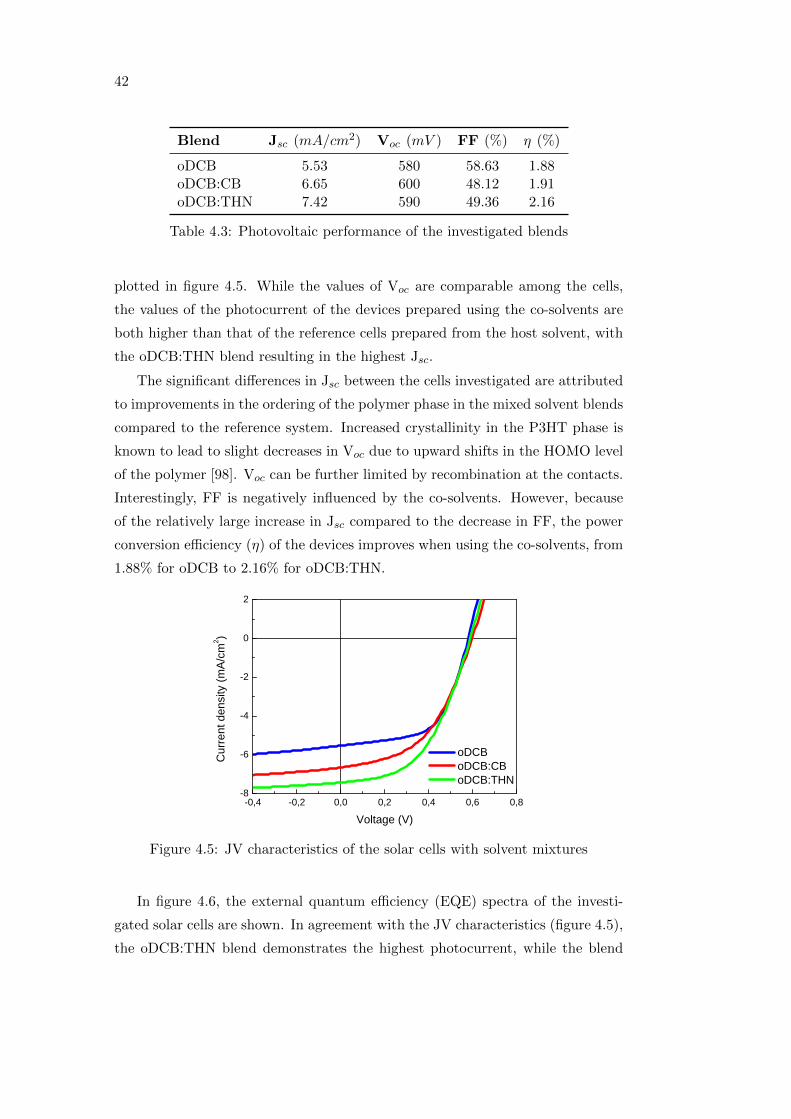
42
Blend Jsc (mA/cm2) Voc (mV ) FF (%) η (%)
oDCB 5.53 580 58.63 1.88oDCB:CB 6.65 600 48.12 1.91oDCB:THN 7.42 590 49.36 2.16
Table 4.3: Photovoltaic performance of the investigated blends
plotted in figure 4.5. While the values of Voc are comparable among the cells,
the values of the photocurrent of the devices prepared using the co-solvents are
both higher than that of the reference cells prepared from the host solvent, with
the oDCB:THN blend resulting in the highest Jsc.
The significant differences in Jsc between the cells investigated are attributed
to improvements in the ordering of the polymer phase in the mixed solvent blends
compared to the reference system. Increased crystallinity in the P3HT phase is
known to lead to slight decreases in Voc due to upward shifts in the HOMO level
of the polymer [98]. Voc can be further limited by recombination at the contacts.
Interestingly, FF is negatively influenced by the co-solvents. However, because
of the relatively large increase in Jsc compared to the decrease in FF, the power
conversion efficiency (η) of the devices improves when using the co-solvents, from
1.88% for oDCB to 2.16% for oDCB:THN.
- 0 , 4 - 0 , 2 0 , 0 0 , 2 0 , 4 0 , 6 0 , 8- 8
- 6
- 4
- 2
0
2
Curre
nt de
nsity
(mA/c
m2 )
V o l t a g e ( V )
o D C B o D C B : C B o D C B : T H N
Figure 4.5: JV characteristics of the solar cells with solvent mixtures
In figure 4.6, the external quantum efficiency (EQE) spectra of the investi-
gated solar cells are shown. In agreement with the JV characteristics (figure 4.5),
the oDCB:THN blend demonstrates the highest photocurrent, while the blend
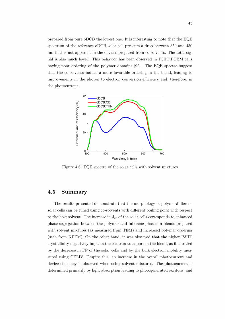
43
prepared from pure oDCB the lowest one. It is interesting to note that the EQE
spectrum of the reference oDCB solar cell presents a drop between 350 and 450
nm that is not apparent in the devices prepared from co-solvents. The total sig-
nal is also much lower. This behavior has been observed in P3HT:PCBM cells
having poor ordering of the polymer domains [92]. The EQE spectra suggest
that the co-solvents induce a more favorable ordering in the blend, leading to
improvements in the photon to electron conversion efficiency and, therefore, in
the photocurrent.
3 0 0 4 0 0 5 0 0 6 0 0 7 0 00
2 0
4 0
6 0
Exter
nal q
uantu
m eff
icienc
y (%)
W a v e l e n g t h ( n m )
o D C B o D C B : C B o D C B : T H N
Figure 4.6: EQE spectra of the solar cells with solvent mixtures
4.5 Summary
The results presented demonstrate that the morphology of polymer:fullerene
solar cells can be tuned using co-solvents with different boiling point with respect
to the host solvent. The increase in Jsc of the solar cells corresponds to enhanced
phase segregation between the polymer and fullerene phases in blends prepared
with solvent mixtures (as measured from TEM) and increased polymer ordering
(seen from KPFM). On the other hand, it was observed that the higher P3HT
crystallinity negatively impacts the electron transport in the blend, as illustrated
by the decrease in FF of the solar cells and by the bulk electron mobility mea-
sured using CELIV. Despite this, an increase in the overall photocurrent and
device efficiency is observed when using solvent mixtures. The photocurrent is
determined primarily by light absorption leading to photogenerated excitons, and
44
subsequently by the separation and transport of charge. Therefore, the results
reflect improvements in charge separation between the donor and the acceptor
due to improved morphology. While improvements to the in-plane morphology
are important for charge separation, an optimal vertical segregation [104] of the
blend is required for efficient charge collection. Structural investigations with
TEM, KPFM, and AFM indicate that the solvent mixtures lead to preferential
in-plane phase segregation between the polymer and fullerene and to increased
P3HT ordering in the blends. The trend in the electron mobility between the
blends is consistent with the KPFM data and the drop in the FF resulting from
the increased crystallinity in blends cast from mixed solvents. It is interesting
that while the electron mobility decreases with increasing P3HT ordering, the
overall photocurrent in the solar cells is improved.
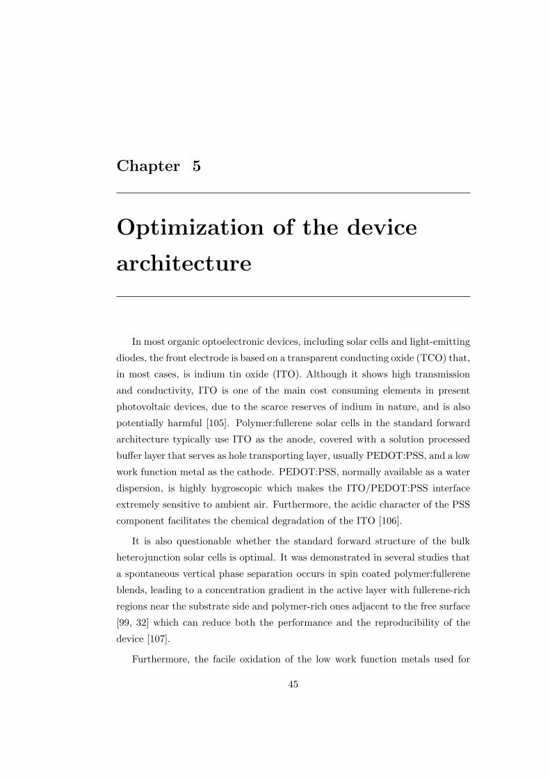
Chapter 5
Optimization of the device
architecture
In most organic optoelectronic devices, including solar cells and light-emitting
diodes, the front electrode is based on a transparent conducting oxide (TCO) that,
in most cases, is indium tin oxide (ITO). Although it shows high transmission
and conductivity, ITO is one of the main cost consuming elements in present
photovoltaic devices, due to the scarce reserves of indium in nature, and is also
potentially harmful [105]. Polymer:fullerene solar cells in the standard forward
architecture typically use ITO as the anode, covered with a solution processed
buffer layer that serves as hole transporting layer, usually PEDOT:PSS, and a low
work function metal as the cathode. PEDOT:PSS, normally available as a water
dispersion, is highly hygroscopic which makes the ITO/PEDOT:PSS interface
extremely sensitive to ambient air. Furthermore, the acidic character of the PSS
component facilitates the chemical degradation of the ITO [106].
It is also questionable whether the standard forward structure of the bulk
heterojunction solar cells is optimal. It was demonstrated in several studies that
a spontaneous vertical phase separation occurs in spin coated polymer:fullerene
blends, leading to a concentration gradient in the active layer with fullerene-rich
regions near the substrate side and polymer-rich ones adjacent to the free surface
[99, 32] which can reduce both the performance and the reproducibility of the
device [107].
Furthermore, the facile oxidation of the low work function metals used for
45
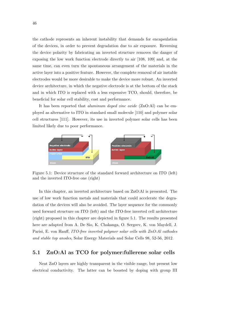
46
the cathode represents an inherent instability that demands for encapsulation
of the devices, in order to prevent degradation due to air exposure. Reversing
the device polarity by fabricating an inverted structure removes the danger of
exposing the low work function electrode directly to air [108, 109] and, at the
same time, can even turn the spontaneous arrangement of the materials in the
active layer into a positive feature. However, the complete removal of air instable
electrodes would be more desirable to make the device more robust. An inverted
device architecture, in which the negative electrode is at the bottom of the stack
and in which ITO is replaced with a less expensive TCO, should, therefore, be
beneficial for solar cell stability, cost and performance.
It has been reported that aluminum doped zinc oxide (ZnO:Al) can be em-
ployed as alternative to ITO in standard small molecule [110] and polymer solar
cell structures [111]. However, its use in inverted polymer solar cells has been
limited likely due to poor performance.
Figure 5.1: Device structure of the standard forward architecture on ITO (left)and the inverted ITO-free one (right)
In this chapter, an inverted architecture based on ZnO:Al is presented. The
use of low work function metals and materials that could accelerate the degra-
dation of the devices will also be avoided. The layer sequence for the commonly
used forward structure on ITO (left) and the ITO-free inverted cell architecture
(right) proposed in this chapter are depicted in figure 5.1. The results presented
here are adapted from A. De Sio, K. Chakanga, O. Sergeev, K. von Maydell, J.
Parisi, E. von Hauff, ITO-free inverted polymer solar cells with ZnO:Al cathodes
and stable top anodes, Solar Energy Materials and Solar Cells 98, 52-56, 2012.
5.1 ZnO:Al as TCO for polymer:fullerene solar cells
Neat ZnO layers are highly transparent in the visible range, but present low
electrical conductivity. The latter can be boosted by doping with group III
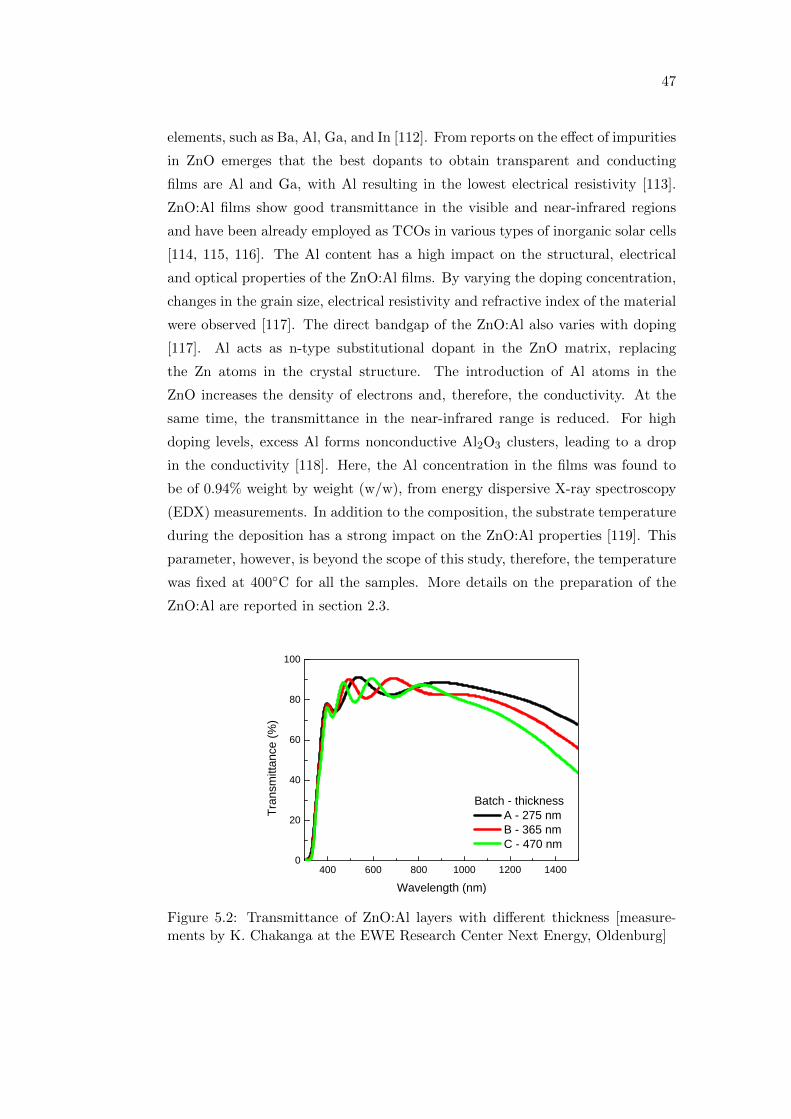
47
elements, such as Ba, Al, Ga, and In [112]. From reports on the effect of impurities
in ZnO emerges that the best dopants to obtain transparent and conducting
films are Al and Ga, with Al resulting in the lowest electrical resistivity [113].
ZnO:Al films show good transmittance in the visible and near-infrared regions
and have been already employed as TCOs in various types of inorganic solar cells
[114, 115, 116]. The Al content has a high impact on the structural, electrical
and optical properties of the ZnO:Al films. By varying the doping concentration,
changes in the grain size, electrical resistivity and refractive index of the material
were observed [117]. The direct bandgap of the ZnO:Al also varies with doping
[117]. Al acts as n-type substitutional dopant in the ZnO matrix, replacing
the Zn atoms in the crystal structure. The introduction of Al atoms in the
ZnO increases the density of electrons and, therefore, the conductivity. At the
same time, the transmittance in the near-infrared range is reduced. For high
doping levels, excess Al forms nonconductive Al2O3 clusters, leading to a drop
in the conductivity [118]. Here, the Al concentration in the films was found to
be of 0.94% weight by weight (w/w), from energy dispersive X-ray spectroscopy
(EDX) measurements. In addition to the composition, the substrate temperature
during the deposition has a strong impact on the ZnO:Al properties [119]. This
parameter, however, is beyond the scope of this study, therefore, the temperature
was fixed at 400C for all the samples. More details on the preparation of the
ZnO:Al are reported in section 2.3.
4 0 0 6 0 0 8 0 0 1 0 0 0 1 2 0 0 1 4 0 00
2 0
4 0
6 0
8 0
1 0 0
B a t c h - t h i c k n e s s A - 2 7 5 n m B - 3 6 5 n m C - 4 7 0 n m
Trans
mitta
nce (
%)
W a v e l e n g t h ( n m )
Figure 5.2: Transmittance of ZnO:Al layers with different thickness [measure-ments by K. Chakanga at the EWE Research Center Next Energy, Oldenburg]
48
The basic requirements for a TCO to be suitable for electronic applications are
high transmittance over a broad spectral range and low sheet resistance. These
two parameters follow opposite trends. Therefore, a trade-off has to be accepted.
In order to obtain a good compromise between sheet resistance and transmit-
tance, three ZnO:Al batches (A, B, C) with varying thickness were fabricated
and characterized. The transmittance of a representative sample for each batch
is shown in figure 5.2 together with the respective thickness.
With increasing layer thickness, the sheet resistance of the layers decreases
from 20 to 13 Ω/ and, at the same time, the average transmittance decreases
and more interference fringes appear in the visible range of the spectrum. The
average surface roughness also increases with the thickness, from 1.5 nm for batch
A to 4.5 nm for batch C. The batch with the highest transmittance and the lower
number of fringes, i.e., the one with the thinnest and smoothest layers, was chosen
as the best compromise. To summarize, the ZnO:Al layers used to fabricate the
polymer:fullerene solar cells are 275 nm thick, have an average sheet resistance of
20 Ω/ and a surface roughness RMS of 1.5 nm. The commercial ITO thin films
used in this study are instead 180 nm thick, have an average sheet resistance of 8
Ω/ and an RMS roughness of 3.9 nm. Thus, in comparison to the commercial
ITO, the sheet resistance of the ZnO:Al is higher, but its surface is smoother.
4 0 0 6 0 0 8 0 0 1 0 0 0 1 2 0 0 1 4 0 00
2 0
4 0
6 0
8 0
1 0 0
I T O Z n O : A l
Trans
mitta
nce (
%)
W a v e l e n g t h ( n m )0
5 x 1 0 4
1 x 1 0 5
2 x 1 0 5
P 3 H T : P C B M
Abso
rption
coeff
icient
(cm-1 )
Figure 5.3: Transmittance of the ITO and ZnO:Al layers compared to the ab-sorption coefficient of the P3HT:PCBM
In figure 5.3, the transmittance of ITO and ZnO:Al together with the absorp-
tion coefficient of the active layer are depicted. The average transmittance in
the range where the polymer:fullerene blend absorbs is 78% for ITO and 85% for
ZnO:Al. Therefore, the transmittance of the ZnO:Al matches better the absorp-
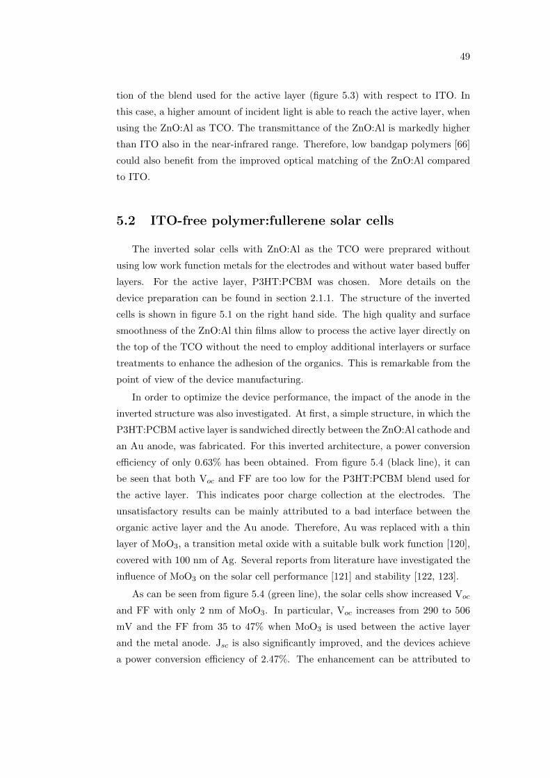
49
tion of the blend used for the active layer (figure 5.3) with respect to ITO. In
this case, a higher amount of incident light is able to reach the active layer, when
using the ZnO:Al as TCO. The transmittance of the ZnO:Al is markedly higher
than ITO also in the near-infrared range. Therefore, low bandgap polymers [66]
could also benefit from the improved optical matching of the ZnO:Al compared
to ITO.
5.2 ITO-free polymer:fullerene solar cells
The inverted solar cells with ZnO:Al as the TCO were preprared without
using low work function metals for the electrodes and without water based buffer
layers. For the active layer, P3HT:PCBM was chosen. More details on the
device preparation can be found in section 2.1.1. The structure of the inverted
cells is shown in figure 5.1 on the right hand side. The high quality and surface
smoothness of the ZnO:Al thin films allow to process the active layer directly on
the top of the TCO without the need to employ additional interlayers or surface
treatments to enhance the adhesion of the organics. This is remarkable from the
point of view of the device manufacturing.
In order to optimize the device performance, the impact of the anode in the
inverted structure was also investigated. At first, a simple structure, in which the
P3HT:PCBM active layer is sandwiched directly between the ZnO:Al cathode and
an Au anode, was fabricated. For this inverted architecture, a power conversion
efficiency of only 0.63% has been obtained. From figure 5.4 (black line), it can
be seen that both Voc and FF are too low for the P3HT:PCBM blend used for
the active layer. This indicates poor charge collection at the electrodes. The
unsatisfactory results can be mainly attributed to a bad interface between the
organic active layer and the Au anode. Therefore, Au was replaced with a thin
layer of MoO3, a transition metal oxide with a suitable bulk work function [120],
covered with 100 nm of Ag. Several reports from literature have investigated the
influence of MoO3 on the solar cell performance [121] and stability [122, 123].
As can be seen from figure 5.4 (green line), the solar cells show increased Voc
and FF with only 2 nm of MoO3. In particular, Voc increases from 290 to 506
mV and the FF from 35 to 47% when MoO3 is used between the active layer
and the metal anode. Jsc is also significantly improved, and the devices achieve
a power conversion efficiency of 2.47%. The enhancement can be attributed to
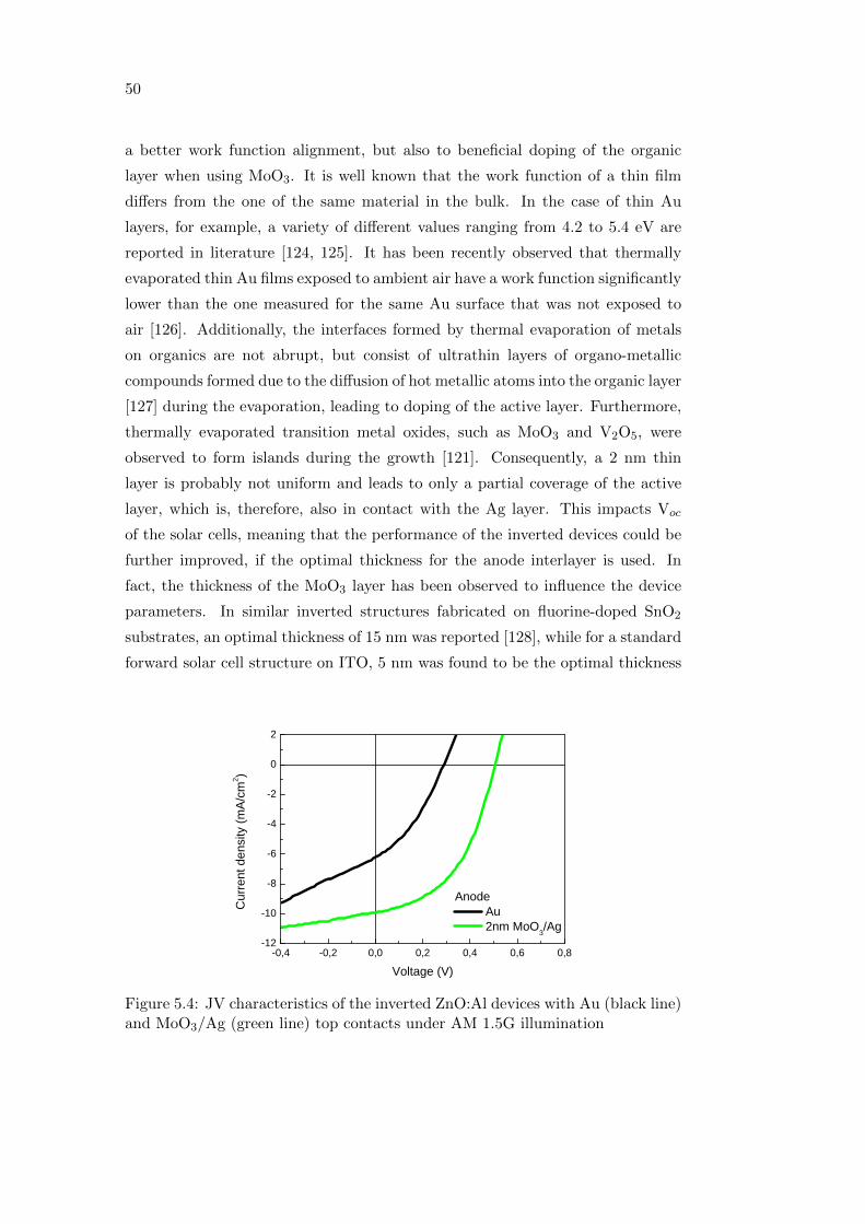
50
a better work function alignment, but also to beneficial doping of the organic
layer when using MoO3. It is well known that the work function of a thin film
differs from the one of the same material in the bulk. In the case of thin Au
layers, for example, a variety of different values ranging from 4.2 to 5.4 eV are
reported in literature [124, 125]. It has been recently observed that thermally
evaporated thin Au films exposed to ambient air have a work function significantly
lower than the one measured for the same Au surface that was not exposed to
air [126]. Additionally, the interfaces formed by thermal evaporation of metals
on organics are not abrupt, but consist of ultrathin layers of organo-metallic
compounds formed due to the diffusion of hot metallic atoms into the organic layer
[127] during the evaporation, leading to doping of the active layer. Furthermore,
thermally evaporated transition metal oxides, such as MoO3 and V2O5, were
observed to form islands during the growth [121]. Consequently, a 2 nm thin
layer is probably not uniform and leads to only a partial coverage of the active
layer, which is, therefore, also in contact with the Ag layer. This impacts Voc
of the solar cells, meaning that the performance of the inverted devices could be
further improved, if the optimal thickness for the anode interlayer is used. In
fact, the thickness of the MoO3 layer has been observed to influence the device
parameters. In similar inverted structures fabricated on fluorine-doped SnO2
substrates, an optimal thickness of 15 nm was reported [128], while for a standard
forward solar cell structure on ITO, 5 nm was found to be the optimal thickness
- 0 , 4 - 0 , 2 0 , 0 0 , 2 0 , 4 0 , 6 0 , 8- 1 2
- 1 0
- 8
- 6
- 4
- 2
0
2
Curre
nt de
nsity
(mA/c
m2 )
V o l t a g e ( V )
A n o d e A u 2 n m M o O 3 / A g
Figure 5.4: JV characteristics of the inverted ZnO:Al devices with Au (black line)and MoO3/Ag (green line) top contacts under AM 1.5G illumination
51
[129]. This indicates that the thickness of the MoO3 layer should be optimized
when changing the device architecture. For these reasons, the effect of a thickness
variation of the MoO3 interlayer was investigated.
8 , 0
8 , 4
8 , 8
9 , 2
9 , 6
1 0 , 0
0 5 1 0 1 5 2 0 2 5 0 5 1 0 1 5 2 0 2 5
5 0 0
5 2 0
5 4 0
5 6 0
5 8 0
6 0 0
6 2 0
6 4 0
0 5 1 0 1 5 2 0 2 54 5
4 8
5 1
5 4
5 7
0 5 1 0 1 5 2 0 2 5 2 , 2
2 , 4
2 , 6
2 , 8
3 , 0
M o O 3 t h i c k n e s s
Jsc (m
A/cm2 )
M o O 3 t h i c k n e s s
Voc (
mV)
FF (%
)
M o O 3 t h i c k n e s s
η (%
)
M o O 3 t h i c k n e s s
Figure 5.5: Effect of the thickness of the MoO3 anode interlayer on Jsc, Voc, FFand η of the inverted ZnO:Al solar cells
Inverted solar cells on ZnO:Al substrates with an anode interlayer thickness
ranging from 2 to 25 nm were prepared and characterized. Figure 5.5 summarizes
the solar cell parameters with different MoO3 interlayer thickness. An evident
trend with a maximum at 15 nm thick MoO3 is shown for FF and the power
conversion efficiency. Jsc shows a kind of slight oscillation, probably as a result
of interference effects upon thickness variation. It is possible that the MoO3
interlayer also acts as an optical spacer, redistributing the optical field in the solar
cell. This behavior is thickness dependent and has already been demonstrated
for TiOx [130] and ZnO [85] optical spacers in forward device architectures based
on ITO. For an interlayer thickness above 5 nm, Voc slightly decreases. This can
result from increased potential drop across the thicker MoO3 interlayer. The low
initial value of 506 mV for a 2 nm thick MoO3 is attributed to a poor contact
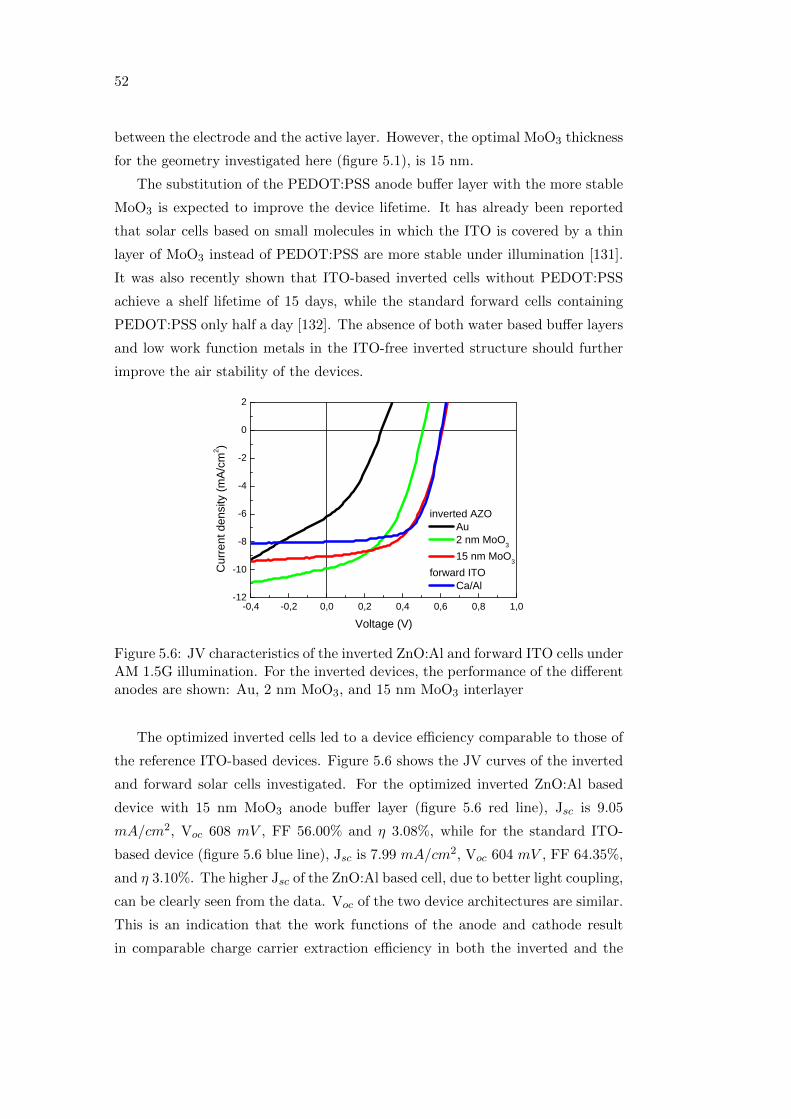
52
between the electrode and the active layer. However, the optimal MoO3 thickness
for the geometry investigated here (figure 5.1), is 15 nm.
The substitution of the PEDOT:PSS anode buffer layer with the more stable
MoO3 is expected to improve the device lifetime. It has already been reported
that solar cells based on small molecules in which the ITO is covered by a thin
layer of MoO3 instead of PEDOT:PSS are more stable under illumination [131].
It was also recently shown that ITO-based inverted cells without PEDOT:PSS
achieve a shelf lifetime of 15 days, while the standard forward cells containing
PEDOT:PSS only half a day [132]. The absence of both water based buffer layers
and low work function metals in the ITO-free inverted structure should further
improve the air stability of the devices.
- 0 , 4 - 0 , 2 0 , 0 0 , 2 0 , 4 0 , 6 0 , 8 1 , 0- 1 2
- 1 0
- 8
- 6
- 4
- 2
0
2
i n v e r t e d A Z O A u 2 n m M o O 3 1 5 n m M o O 3
f o r w a r d I T O C a / A l
Curre
nt de
nsity
(mA/c
m2 )
V o l t a g e ( V )
Figure 5.6: JV characteristics of the inverted ZnO:Al and forward ITO cells underAM 1.5G illumination. For the inverted devices, the performance of the differentanodes are shown: Au, 2 nm MoO3, and 15 nm MoO3 interlayer
The optimized inverted cells led to a device efficiency comparable to those of
the reference ITO-based devices. Figure 5.6 shows the JV curves of the inverted
and forward solar cells investigated. For the optimized inverted ZnO:Al based
device with 15 nm MoO3 anode buffer layer (figure 5.6 red line), Jsc is 9.05
mA/cm2, Voc 608 mV , FF 56.00% and η 3.08%, while for the standard ITO-
based device (figure 5.6 blue line), Jsc is 7.99 mA/cm2, Voc 604 mV , FF 64.35%,
and η 3.10%. The higher Jsc of the ZnO:Al based cell, due to better light coupling,
can be clearly seen from the data. Voc of the two device architectures are similar.
This is an indication that the work functions of the anode and cathode result
in comparable charge carrier extraction efficiency in both the inverted and the
53
standard forward devices. The lower FF of the inverted cells, however, could
be attributed to surface recombination at the ZnO:Al/active layer interface. In
fact, while in the forward structure buffer layers are used at both the ITO anode
(PEDOT:PSS) and the Al cathode (Ca), in the inverted structure, there is a
MoO3 buffer layer at the anode, but no buffer layer at the cathode, where the
ZnO:Al is in direct contact with the active layer. In this case, surface defects due
to the deposition process and recombination at the interface can adversely affect
FF. Regarding the TCO features, it is interesting to note that the higher sheet
resistance of the ZnO:Al, compared to the one of the ITO, is not a limiting factor
for the solar cell performance. This is an important result when considering the
optimization of TCOs for use in organic solar cells.
5.3 Summary
Efficient ITO-free inverted solar cells with ZnO:Al cathodes and MoO3/Ag an-
odes were produced and optimized. Efficiencies comparable to ITO based devices
prepared in the standard forward structure were achieved. This demonstrates
that ZnO:Al is a convenient and valid alternative to ITO. The thickness of the
ZnO:Al was optimized so that a good compromise between sheet resistance and
transmittance was obtained. The MoO3 buffer layer was also optimized to further
improve the efficiency of the photvoltaic devices. The inverted polymer:fullerene
solar cells show a higher photocurrent than the standard ITO devices due to the
higher transmittance of ZnO:Al in the spectral region where the P3HT:PCBM
blend absorbs. The higher sheet resistance of the ZnO:Al compared to the one
of ITO does not adversely affect the device performance. From the point of view
of the device stability and manufacturing, the inverted architecture is more at-
tractive, because water-based transport layers and low work function metals are
avoided without sacrificing the device efficiency.

Chapter 6
Effect of degradation on the
optoelectronic properties of
P3HT and P3HT:PCBM
blends
The literature about the stability of polymer solar cells mainly focuses on
the complete devices [50, 133, 134, 135, 136]. Although the effect of degradation
on the whole photovoltaic device is important, it is sometimes not possible to
determine the effect on the single layers. For example, it is not always possible
to distinguish the role of the active layer from that of the electrodes [137]. It has
been shown that the device structure plays also a role and that some structures
are more prone to degradation than others. Whereas in forward devices the
degradation of the low work function metal used as the top electrode limits the
lifetime [135], it has been recently shown that in inverted structures the electrodes
do not play the same crucial role [138]. An important issue is the understanding
of the degradation mechanisms in the active layer. Therefore, in this chapter,
the degradation of P3HT layers and its blend with PCBM will be investigated.
Although there are new promising conjugated polymers, P3HT has still high
relevance in the field of polymer photovoltaics. In fact, P3HT is one of the most
investigated polymers in literature and is often regarded as a model system. From
the point of view of the device lifetime, deep understanding of the degradation
55
56
mechanisms in P3HT will open the way for the design and synthesis of new
polymers with enhanced stability.
Part of the results presented in the second part of this chapter are adapted
from F. Deschler, A. De Sio, E. von Hauff, P. Kutka, T. Sauermann, H.-J. Egel-
haaf, J. Hauch, E. Da Como, Effect of ageing on exciton dynamics, charge sepa-
ration and recombination in P3HT/PCBM photovoltaic blends, Advanced Func-
tional Materials, 2012, accepted.
6.1 The influence of the processing atmosphere
It is assessed that most polymers experience more or less rapid degradation
when exposed to air and light [50]. For this reason, when investigating new ma-
terial combinations and new device architectures, the experiments are mainly
performed on samples prepared in an inert atmosphere, such as nitrogen filled
gloveboxes. This is of course not convenient for industrial production of pho-
tovoltaic devices based on conjugated polymers. In fact, while the preparation
of the solutions or inks in an inert atmosphere is feasible, processing the whole
devices in a glovebox is clearly time and cost consuming when dealing with large
scale manufacture. On the other hand, in order to understand the fundamental
mechanisms that rule the photovoltaic action of conjugated polymers, the effect
of degradation has to be first neglected. Therefore, most studies report investi-
gations and findings based on samples prepared, and sometimes even measured,
in the glovebox. Once the polymer behavior under inert conditions has been as-
sessed and the devices have been optimized, the next step towards the design of
more robust materials, as well as device architectures, should be the understand-
ing of the material and device behavior when exposed to ambient air. Therefore,
in this section, the effect of the processing environment on the optoelectronic
properties of the reference polymer P3HT and on the relative devices is investi-
gated. For this purpose, pristine rr-P3HT layers and blends with PCBM were
prepared under nitrogen atmosphere and in ambient air, using solutions prepared
in the glovebox. More details on the samples preparation can be found in 2.4.
6.1.1 Optical and photophysical properties
Figure 6.1 shows the absorption coefficient of two P3HT samples prepared
inside and outside the glovebox as a function of the wavelength. It can be seen
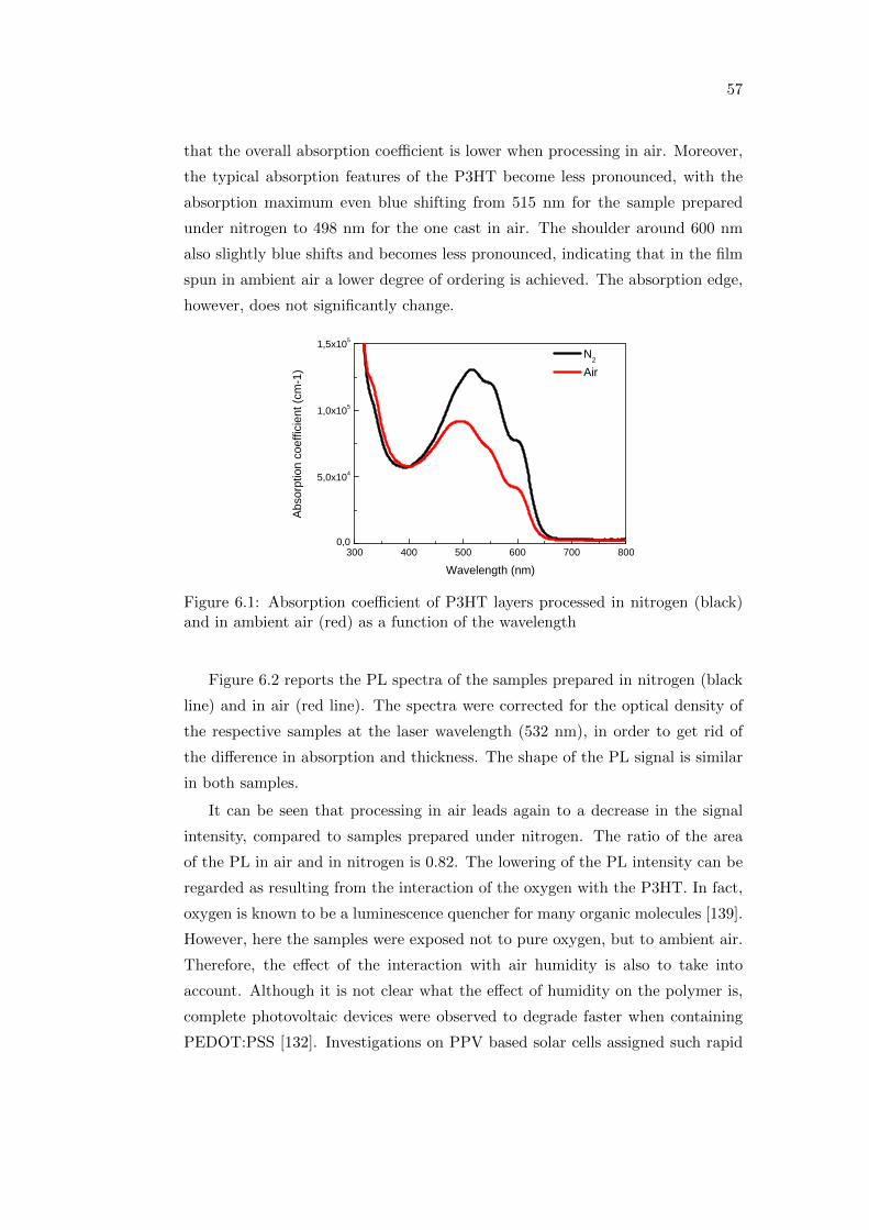
57
that the overall absorption coefficient is lower when processing in air. Moreover,
the typical absorption features of the P3HT become less pronounced, with the
absorption maximum even blue shifting from 515 nm for the sample prepared
under nitrogen to 498 nm for the one cast in air. The shoulder around 600 nm
also slightly blue shifts and becomes less pronounced, indicating that in the film
spun in ambient air a lower degree of ordering is achieved. The absorption edge,
however, does not significantly change.
3 0 0 4 0 0 5 0 0 6 0 0 7 0 0 8 0 00 , 0
5 , 0 x 1 0 4
1 , 0 x 1 0 5
1 , 5 x 1 0 5
Abso
rption
coeff
icient
(cm-1)
W a v e l e n g t h ( n m )
N 2 A i r
Figure 6.1: Absorption coefficient of P3HT layers processed in nitrogen (black)and in ambient air (red) as a function of the wavelength
Figure 6.2 reports the PL spectra of the samples prepared in nitrogen (black
line) and in air (red line). The spectra were corrected for the optical density of
the respective samples at the laser wavelength (532 nm), in order to get rid of
the difference in absorption and thickness. The shape of the PL signal is similar
in both samples.
It can be seen that processing in air leads again to a decrease in the signal
intensity, compared to samples prepared under nitrogen. The ratio of the area
of the PL in air and in nitrogen is 0.82. The lowering of the PL intensity can be
regarded as resulting from the interaction of the oxygen with the P3HT. In fact,
oxygen is known to be a luminescence quencher for many organic molecules [139].
However, here the samples were exposed not to pure oxygen, but to ambient air.
Therefore, the effect of the interaction with air humidity is also to take into
account. Although it is not clear what the effect of humidity on the polymer is,
complete photovoltaic devices were observed to degrade faster when containing
PEDOT:PSS [132]. Investigations on PPV based solar cells assigned such rapid
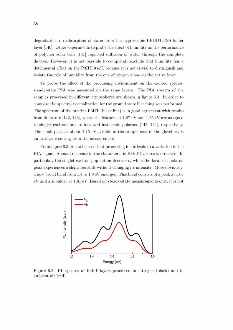
58
degradation to reabsorption of water from the hygroscopic PEDOT:PSS buffer
layer [140]. Other experiments to probe the effect of humidity on the performance
of polymer solar cells [141] reported diffusion of water through the complete
devices. However, it is not possible to completely exclude that humidity has a
detrimental effect on the P3HT itself, because it is not trivial to distinguish and
isolate the role of humidity from the one of oxygen alone on the active layer.
To probe the effect of the processing environment on the excited species,
steady-state PIA was measured on the same layers. The PIA spectra of the
samples processed in different atmospheres are shown in figure 6.3. In order to
compare the spectra, normalization for the ground state bleaching was performed.
The spectrum of the pristine P3HT (black line) is in good agreement with results
from literature [142, 143], where the features at 1.07 eV and 1.25 eV are assigned
to singlet excitons and to localized intrachain polarons [142, 144], respectively.
The small peak at about 1.15 eV, visible in the sample cast in the glovebox, is
an artifact resulting from the measurement.
From figure 6.3, it can be seen that processing in air leads to a variation in the
PIA signal. A small decrease in the characteristic P3HT features is observed. In
particular, the singlet exciton population decreases, while the localized polaron
peak experiences a slight red shift without changing its intensity. More obviously,
a new broad band from 1.4 to 1.9 eV emerges. This band consists of a peak at 1.68
eV and a shoulder at 1,81 eV. Based on steady-state measurements only, it is not
1 , 2 1 , 4 1 , 6 1 , 8 2 , 0
PL In
tensity
(a.u.
)
E n e r g y ( e V )
N 2 A i r
Figure 6.2: PL spectra of P3HT layers processed in nitrogen (black) and inambient air (red)
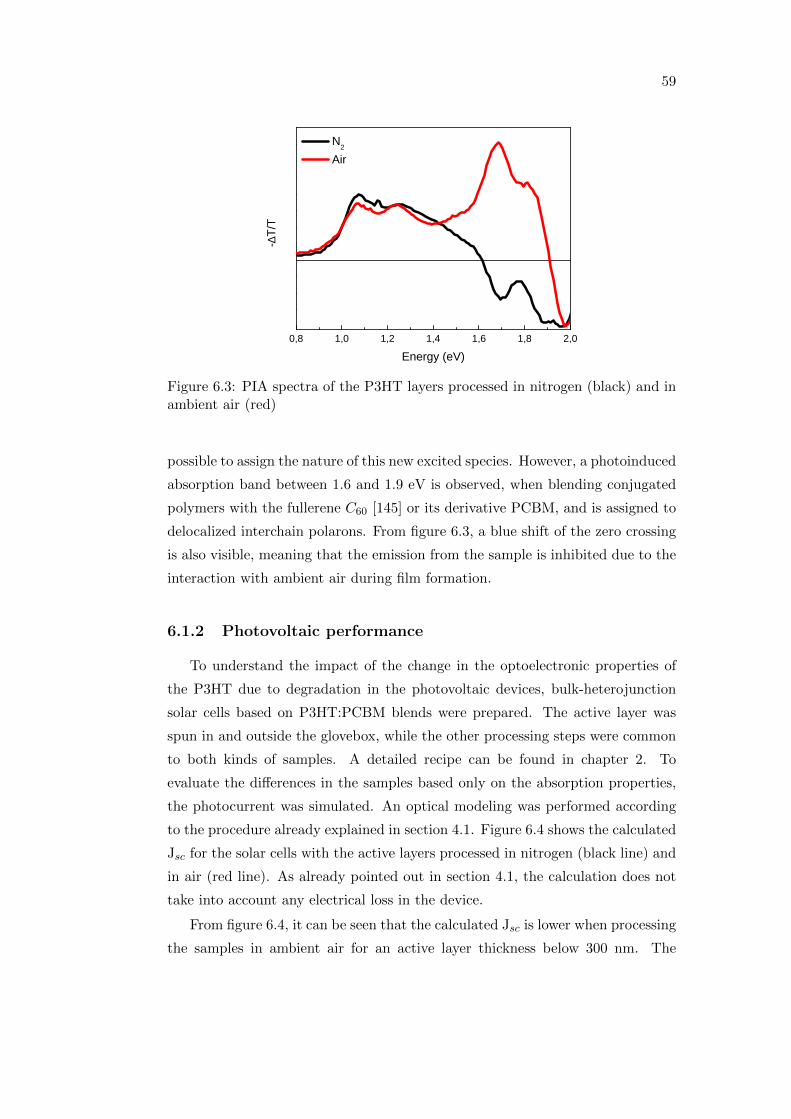
59
0 , 8 1 , 0 1 , 2 1 , 4 1 , 6 1 , 8 2 , 0
-∆T/T
E n e r g y ( e V )
N 2 A i r
Figure 6.3: PIA spectra of the P3HT layers processed in nitrogen (black) and inambient air (red)
possible to assign the nature of this new excited species. However, a photoinduced
absorption band between 1.6 and 1.9 eV is observed, when blending conjugated
polymers with the fullerene C60 [145] or its derivative PCBM, and is assigned to
delocalized interchain polarons. From figure 6.3, a blue shift of the zero crossing
is also visible, meaning that the emission from the sample is inhibited due to the
interaction with ambient air during film formation.
6.1.2 Photovoltaic performance
To understand the impact of the change in the optoelectronic properties of
the P3HT due to degradation in the photovoltaic devices, bulk-heterojunction
solar cells based on P3HT:PCBM blends were prepared. The active layer was
spun in and outside the glovebox, while the other processing steps were common
to both kinds of samples. A detailed recipe can be found in chapter 2. To
evaluate the differences in the samples based only on the absorption properties,
the photocurrent was simulated. An optical modeling was performed according
to the procedure already explained in section 4.1. Figure 6.4 shows the calculated
Jsc for the solar cells with the active layers processed in nitrogen (black line) and
in air (red line). As already pointed out in section 4.1, the calculation does not
take into account any electrical loss in the device.
From figure 6.4, it can be seen that the calculated Jsc is lower when processing
the samples in ambient air for an active layer thickness below 300 nm. The
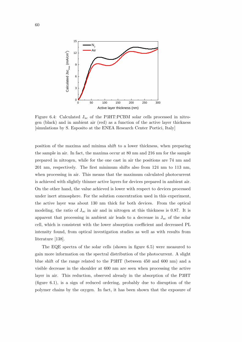
60
0 5 0 1 0 0 1 5 0 2 0 0 2 5 0 3 0 00
3
6
9
1 2
1 5
Calcu
lated
Jsc ma
x (mA/c
m2 )
A c t i v e l a y e r t h i c k n e s s ( n m )
N 2 A i r
Figure 6.4: Calculated Jsc of the P3HT:PCBM solar cells processed in nitro-gen (black) and in ambient air (red) as a function of the active layer thickness[simulations by S. Esposito at the ENEA Research Center Portici, Italy]
position of the maxima and minima shift to a lower thickness, when preparing
the sample in air. In fact, the maxima occur at 80 nm and 216 nm for the sample
prepared in nitrogen, while for the one cast in air the positions are 74 nm and
201 nm, respectively. The first minimum shifts also from 124 nm to 113 nm,
when processing in air. This means that the maximum calculated photocurrent
is achieved with slightly thinner active layers for devices prepared in ambient air.
On the other hand, the value achieved is lower with respect to devices processed
under inert atmosphere. For the solution concentration used in this experiment,
the active layer was about 130 nm thick for both devices. From the optical
modeling, the ratio of Jsc in air and in nitrogen at this thickness is 0.87. It is
apparent that processing in ambient air leads to a decrease in Jsc of the solar
cell, which is consistent with the lower absorption coefficient and decreased PL
intensity found, from optical investigation studies as well as with results from
literature [138].
The EQE spectra of the solar cells (shown in figure 6.5) were measured to
gain more information on the spectral distribution of the photocurrent. A slight
blue shift of the range related to the P3HT (between 450 and 600 nm) and a
visible decrease in the shoulder at 600 nm are seen when processing the active
layer in air. This reduction, observed already in the absorption of the P3HT
(figure 6.1), is a sign of reduced ordering, probably due to disruption of the
polymer chains by the oxygen. In fact, it has been shown that the exposure of
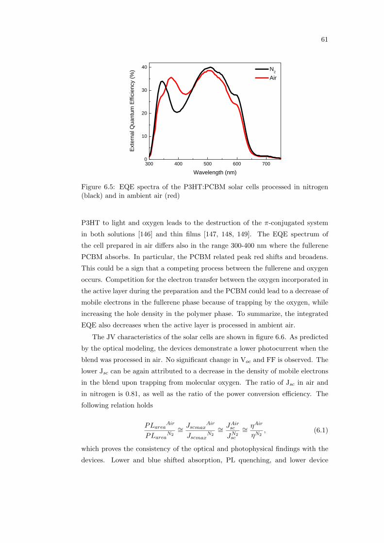
61
3 0 0 4 0 0 5 0 0 6 0 0 7 0 00
1 0
2 0
3 0
4 0
Exter
nal Q
uantu
m Eff
icienc
y (%)
W a v e l e n g t h ( n m )
N 2 A i r
Figure 6.5: EQE spectra of the P3HT:PCBM solar cells processed in nitrogen(black) and in ambient air (red)
P3HT to light and oxygen leads to the destruction of the π-conjugated system
in both solutions [146] and thin films [147, 148, 149]. The EQE spectrum of
the cell prepared in air differs also in the range 300-400 nm where the fullerene
PCBM absorbs. In particular, the PCBM related peak red shifts and broadens.
This could be a sign that a competing process between the fullerene and oxygen
occurs. Competition for the electron transfer between the oxygen incorporated in
the active layer during the preparation and the PCBM could lead to a decrease of
mobile electrons in the fullerene phase because of trapping by the oxygen, while
increasing the hole density in the polymer phase. To summarize, the integrated
EQE also decreases when the active layer is processed in ambient air.
The JV characteristics of the solar cells are shown in figure 6.6. As predicted
by the optical modeling, the devices demonstrate a lower photocurrent when the
blend was processed in air. No significant change in Voc and FF is observed. The
lower Jsc can be again attributed to a decrease in the density of mobile electrons
in the blend upon trapping from molecular oxygen. The ratio of Jsc in air and
in nitrogen is 0.81, as well as the ratio of the power conversion efficiency. The
following relation holds
PLareaAir
PLareaN2
∼=Jscmax
Air
JscmaxN2
∼=JAirsc
JN2sc
∼=ηAir
ηN2, (6.1)
which proves the consistency of the optical and photophysical findings with the
devices. Lower and blue shifted absorption, PL quenching, and lower device
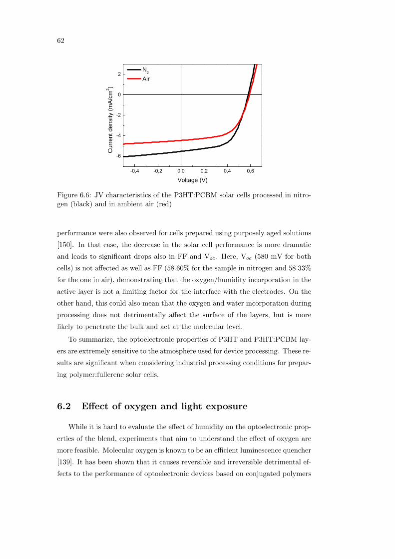
62
- 0 , 4 - 0 , 2 0 , 0 0 , 2 0 , 4 0 , 6
- 6
- 4
- 2
0
2
N 2 A i r
Curre
nt de
nsity
(mA/c
m2 )
V o l t a g e ( V )Figure 6.6: JV characteristics of the P3HT:PCBM solar cells processed in nitro-gen (black) and in ambient air (red)
performance were also observed for cells prepared using purposely aged solutions
[150]. In that case, the decrease in the solar cell performance is more dramatic
and leads to significant drops also in FF and Voc. Here, Voc (580 mV for both
cells) is not affected as well as FF (58.60% for the sample in nitrogen and 58.33%
for the one in air), demonstrating that the oxygen/humidity incorporation in the
active layer is not a limiting factor for the interface with the electrodes. On the
other hand, this could also mean that the oxygen and water incorporation during
processing does not detrimentally affect the surface of the layers, but is more
likely to penetrate the bulk and act at the molecular level.
To summarize, the optoelectronic properties of P3HT and P3HT:PCBM lay-
ers are extremely sensitive to the atmosphere used for device processing. These re-
sults are significant when considering industrial processing conditions for prepar-
ing polymer:fullerene solar cells.
6.2 Effect of oxygen and light exposure
While it is hard to evaluate the effect of humidity on the optoelectronic prop-
erties of the blend, experiments that aim to understand the effect of oxygen are
more feasible. Molecular oxygen is known to be an efficient luminescence quencher
[139]. It has been shown that it causes reversible and irreversible detrimental ef-
fects to the performance of optoelectronic devices based on conjugated polymers
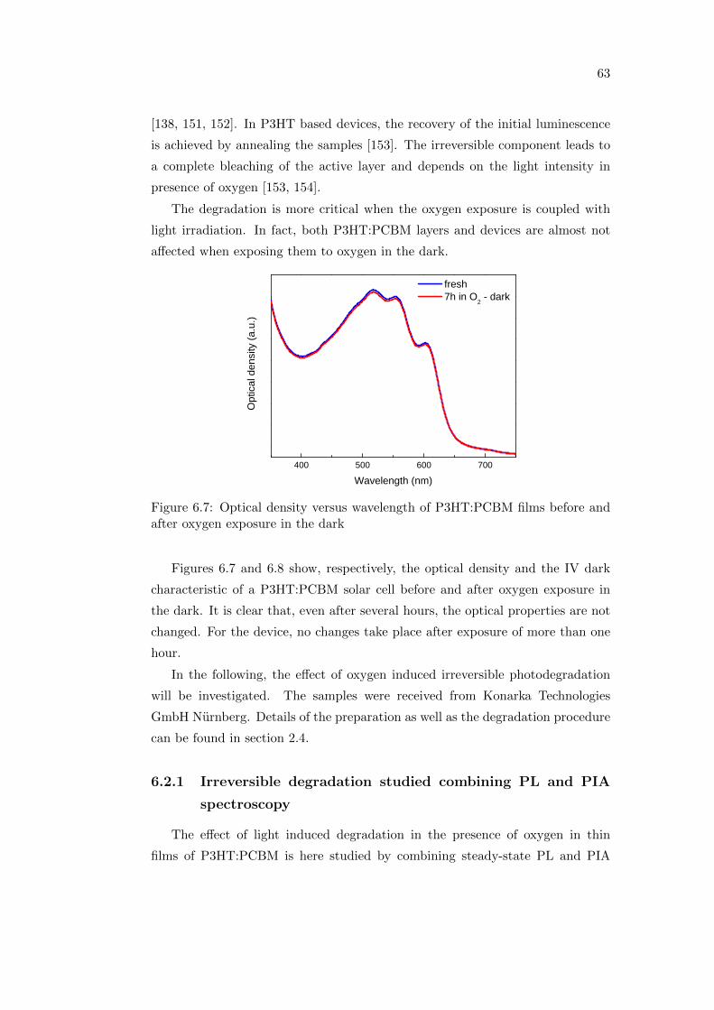
63
[138, 151, 152]. In P3HT based devices, the recovery of the initial luminescence
is achieved by annealing the samples [153]. The irreversible component leads to
a complete bleaching of the active layer and depends on the light intensity in
presence of oxygen [153, 154].
The degradation is more critical when the oxygen exposure is coupled with
light irradiation. In fact, both P3HT:PCBM layers and devices are almost not
affected when exposing them to oxygen in the dark.
4 0 0 5 0 0 6 0 0 7 0 0
Op
tical d
ensity
(a.u.
)
W a v e l e n g t h ( n m )
f r e s h 7 h i n O 2 - d a r k
Figure 6.7: Optical density versus wavelength of P3HT:PCBM films before andafter oxygen exposure in the dark
Figures 6.7 and 6.8 show, respectively, the optical density and the IV dark
characteristic of a P3HT:PCBM solar cell before and after oxygen exposure in
the dark. It is clear that, even after several hours, the optical properties are not
changed. For the device, no changes take place after exposure of more than one
hour.
In the following, the effect of oxygen induced irreversible photodegradation
will be investigated. The samples were received from Konarka Technologies
GmbH Nurnberg. Details of the preparation as well as the degradation procedure
can be found in section 2.4.
6.2.1 Irreversible degradation studied combining PL and PIA
spectroscopy
The effect of light induced degradation in the presence of oxygen in thin
films of P3HT:PCBM is here studied by combining steady-state PL and PIA
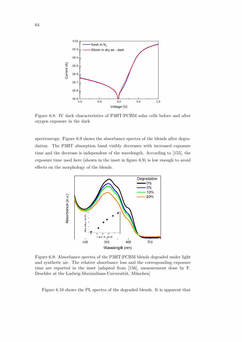
64
- 1 , 0 - 0 , 5 0 , 0 0 , 5 1 , 01 E - 9
1 E - 8
1 E - 7
1 E - 6
1 E - 5
1 E - 4
1 E - 3
0 , 0 1
Curre
nt (A)
V o l t a g e ( V )
f r e s h i n N 2 6 5 m i n i n d r y a i r - d a r k
Figure 6.8: IV dark characteristics of P3HT:PCBM solar cells before and afteroxygen exposure in the dark
spectroscopy. Figure 6.9 shows the absorbance spectra of the blends after degra-
dation. The P3HT absorption band visibly decreases with increased exposure
time and the decrease is independent of the wavelength. According to [155], the
exposure time used here (shown in the inset in figure 6.9) is low enough to avoid
effects on the morphology of the blends.
Figure 6.9: Absorbance spectra of the P3HT:PCBM blends degraded under lightand synthetic air. The relative absorbance loss and the corresponding exposuretime are reported in the inset [adapted from [156], measurement done by F.Deschler at the Ludwig-Maximilians-Universitat, Munchen]
Figure 6.10 shows the PL spectra of the degraded blends. It is apparent that
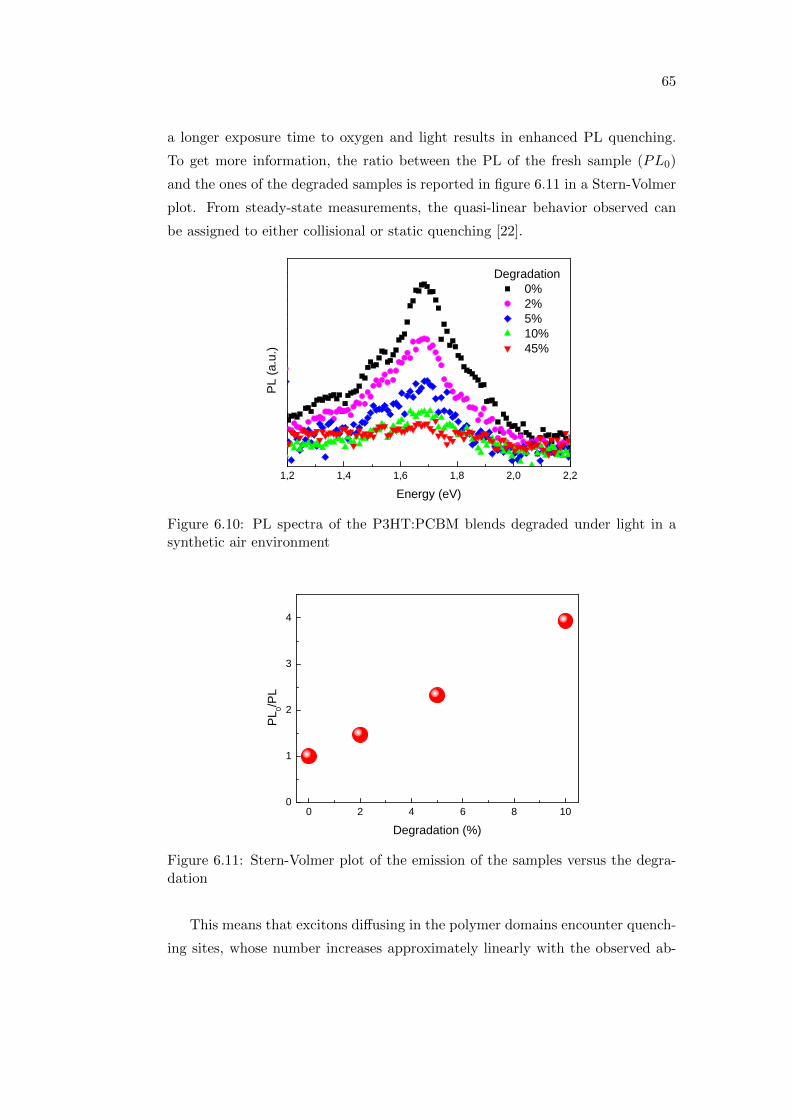
65
a longer exposure time to oxygen and light results in enhanced PL quenching.
To get more information, the ratio between the PL of the fresh sample (PL0)
and the ones of the degraded samples is reported in figure 6.11 in a Stern-Volmer
plot. From steady-state measurements, the quasi-linear behavior observed can
be assigned to either collisional or static quenching [22].
1 , 2 1 , 4 1 , 6 1 , 8 2 , 0 2 , 2
D e g r a d a t i o n 0 % 2 % 5 % 1 0 % 4 5 %
PL (a
.u.)
E n e r g y ( e V )Figure 6.10: PL spectra of the P3HT:PCBM blends degraded under light in asynthetic air environment
0 2 4 6 8 1 00
1
2
3
4
PL0/PL
D e g r a d a t i o n ( % )Figure 6.11: Stern-Volmer plot of the emission of the samples versus the degra-dation
This means that excitons diffusing in the polymer domains encounter quench-
ing sites, whose number increases approximately linearly with the observed ab-
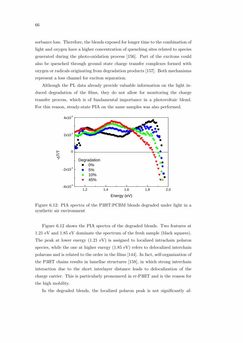
66
sorbance loss. Therefore, the blends exposed for longer time to the combination of
light and oxygen have a higher concentration of quenching sites related to species
generated during the photo-oxidation process [156]. Part of the excitons could
also be quenched through ground state charge transfer complexes formed with
oxygen or radicals originating from degradation products [157]. Both mechanisms
represent a loss channel for exciton separation.
Although the PL data already provide valuable information on the light in-
duced degradation of the films, they do not allow for monitoring the charge
transfer process, which is of fundamental importance in a photovoltaic blend.
For this reason, steady-state PIA on the same samples was also performed.
1 , 2 1 , 4 1 , 6 1 , 8 2 , 0- 4 x 1 0 - 5
- 2 x 1 0 - 5
0
2 x 1 0 - 5
4 x 1 0 - 5
D e g r a d a t i o n 0 % 5 % 1 0 % 4 5 %
-∆T/T
E n e r g y ( e V )Figure 6.12: PIA spectra of the P3HT:PCBM blends degraded under light in asynthetic air environment
Figure 6.12 shows the PIA spectra of the degraded blends. Two features at
1.21 eV and 1.85 eV dominate the spectrum of the fresh sample (black squares).
The peak at lower energy (1.21 eV) is assigned to localized intrachain polaron
species, while the one at higher energy (1.85 eV) refers to delocalized interchain
polarons and is related to the order in the films [144]. In fact, self-organization of
the P3HT chains results in lamellae structures [158], in which strong interchain
interaction due to the short interlayer distance leads to delocalization of the
charge carrier. This is particularly pronounced in rr-P3HT and is the reason for
the high mobility.
In the degraded blends, the localized polaron peak is not significantly af-
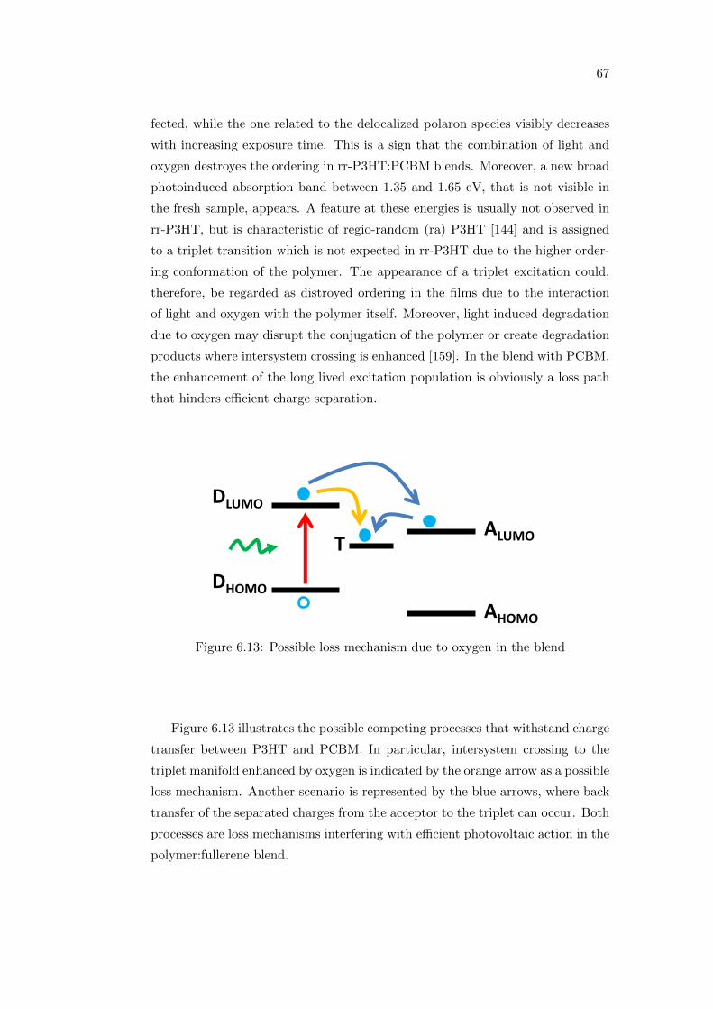
67
fected, while the one related to the delocalized polaron species visibly decreases
with increasing exposure time. This is a sign that the combination of light and
oxygen destroyes the ordering in rr-P3HT:PCBM blends. Moreover, a new broad
photoinduced absorption band between 1.35 and 1.65 eV, that is not visible in
the fresh sample, appears. A feature at these energies is usually not observed in
rr-P3HT, but is characteristic of regio-random (ra) P3HT [144] and is assigned
to a triplet transition which is not expected in rr-P3HT due to the higher order-
ing conformation of the polymer. The appearance of a triplet excitation could,
therefore, be regarded as distroyed ordering in the films due to the interaction
of light and oxygen with the polymer itself. Moreover, light induced degradation
due to oxygen may disrupt the conjugation of the polymer or create degradation
products where intersystem crossing is enhanced [159]. In the blend with PCBM,
the enhancement of the long lived excitation population is obviously a loss path
that hinders efficient charge separation.
DLUMO
DHOMO
ALUMO
AHOMO
T
Figure 6.13: Possible loss mechanism due to oxygen in the blend
Figure 6.13 illustrates the possible competing processes that withstand charge
transfer between P3HT and PCBM. In particular, intersystem crossing to the
triplet manifold enhanced by oxygen is indicated by the orange arrow as a possible
loss mechanism. Another scenario is represented by the blue arrows, where back
transfer of the separated charges from the acceptor to the triplet can occur. Both
processes are loss mechanisms interfering with efficient photovoltaic action in the
polymer:fullerene blend.

68
6.3 Summary
It has been demonstrated that investigation of the degradation mechanism
of the active layer is of fundamental importance to understand the degradation
of the complete solar cells and to enable the design of more robust conjugated
polymers as well as device structures. Furthermore, it is shown that PIA spec-
troscopy is a valuable tool which gives unique insights into the population dy-
namics of excitons and polarons and enables to study the effect of degradation
on the optoelectronic properties of conjugated polymers.
Chapter 7
Conclusions
Different methods to enhance the performance of polymer:fullerene bulk het-
erojunction solar cells were shown by using two different kinds of donor polymers.
Both fundamental and application-oriented aspects were investigated.
For the low bandgap copolymer PCPDTBT, molecular doping with F4-TCNQ
was proposed as an effective method to control the electronic properties. Improve-
ments of the charge transport by increasing the hole mobility in both the neat
copolymer and in the blend with PCBM are demonstrated. In the blend with
PCBM, in particular, increased polaron density and enhancement of the photo-
voltaic performance are achieved without a significant change in the morphology.
This means that the improvements are due to the modification of the electronic
properties of the copolymer upon doping.
For the semicrystalline P3HT polymer, a route to fine tuning of the morphol-
ogy via combination of solvents with different boiling points has been proposed.
Enhanced phase segregation between the polymer and fullerene phases and higher
ordering of the polymer phase is induced by the introduction of a high boiling
point co-solvent and results in higher photocurrents.
The influence of the device architecture was also addressed. In this direction,
ITO and PEDOT:PSS free solar cells in the inverted structure were fabricated
and optimized. ZnO:Al was used as the TCO, and it was demonstrated that it
is a valid alternative to ITO. From the point of view of the device stability and
manufacturing, the inverted architecture is more attractive, because water-based
transport layers and low work function metals are avoided without sacrificing the
69

70
device efficiency.
In the last part, the degradation issue in P3HT:PCBM was addressed. The
improved understanding of the degradation mechanisms of a model polymer like
P3HT is essential in increasing the intrinsic stability of new conjugated polymers
for photovoltaic applications. Here it was demonstrated, by using steady-state
PIA spectroscopy combined with PL, that the loss of photocurrent and perfor-
mance generally observed upon degradation results from the appearance of a
long-lived population of triplet excitons.

Bibliography
[1] R.H. Friend. Pure and Applied Chemistry, 73:425, 2001. [cited at p. 1]
[2] R. Hoffmann, C. Janiak, and C. Kollmar. Macromolecules, 24:3725, 1991.
[cited at p. 1]
[3] W. Barford. Electronic and Optical Properties of Conjugated Polymers.
Oxford University Press, Oxford, 2009. [cited at p. 2, 7]
[4] S. Baranovski. Charge Transport in Disordered Solids with Applications in
Electronics. Wiley, UK, 2006. [cited at p. 2]
[5] S.C. Graham, D.D.C. Bradley, R.H. Friend, and C. Spangler. Synthetic
Metals, 41:1277, 1991. [cited at p. 2]
[6] N.S. Sariciftci. Primary Photoexcitations in Conjugated Polymers: Molecu-
lar Exciton versus Semiconductor Band Model. World Scientific, Singapore,
1998. [cited at p. 2]
[7] R. Loudon. American Journal of Physics, 27:649, 1959. [cited at p. 2]
[8] K. Pakbaz, C.H. Lee, A.J. Heeger, T.W. Hagler, and D. McBranch. Syn-
thetic Metals, 64:295, 1994. [cited at p. 2]
[9] D. Chirvase, Z. Chiguvare, M. Knipper, J. Parisi, V. Dyakonov, and J.C.
Hummelen. Journal of Applied Physics, 93:3376, 2003. [cited at p. 2]
[10] S.M. Sze and K.K. Ng. Physics of Semiconductor Devices. Wiley, New
York, 2007. [cited at p. 2]
[11] D. Fichou. Journal of Materials Chemistry, 10:571, 2000. [cited at p. 2]
71
72
[12] G. Hadziioannou and P.F. van Putten. Semiconducting Polymers. Wiley-
VCH, Weinheim, 2000. [cited at p. 2]
[13] M. Schwoerer and H.C. Wolf. Organic Molecular Solids. Wiley-VCH, Wein-
heim, 2005. [cited at p. 2]
[14] G. Dennler, M. C. Scharber, and C. J. Brabec. Advanced Materials, 21:1323,
2009. [cited at p. 2, 11]
[15] R. Gaudiana and C.J. Brabec. Nature Photonics, 2:287, 2008. [cited at p. 2,
11]
[16] D.E. Markov, E. Amsterdam, P.W.M. Blom, A.B. Sieval, and J.C. Hum-
melen. Journal of Physical Chemistry A, 109:5266, 2005. [cited at p. 2]
[17] G.A. Chamberlain. Solar Cells, 8:47, 1983. [cited at p. 2]
[18] P. Bhattacharya. Semiconductor Optoelectronic Devices. Prentice Hall,
New Jersey, 1997. [cited at p. 3]
[19] G. Yu, J. Gao, J. C. Hummelen, F. Wudl, and A. J. Heeger. Science,
270:1789, 1995. [cited at p. 3, 8]
[20] C.J. Brabec, S.E. Shaheen, C. Winder, N.S. Sariciftci, and P. Denk. Applied
Physics Letters, 80:1288, 2002. [cited at p. 4]
[21] N.S. Sariciftci, L. Smilowitz, A.J. Heeger, and F. Wudl. Science, 258:1474,
1992. [cited at p. 5, 7]
[22] J.R. Lakowicz. Principles of Fluorescence Spectroscopy. Springer, New
York, 2006. [cited at p. 5, 6, 27, 65]
[23] C.J. Brabec, G. Zerza, G. Cerullo, S. De Silvestri, S. Luzzati, J.C. Humme-
len, and N.S. Sariciftci. Chemical Physics Letters, 340:232, 2001. [cited at p. 7]
[24] I.W. Hwang, D. Moses, and A.J. Heeger. Journal of Physical Chemistry C,
112:4350, 2008. [cited at p. 7]
[25] T. Forster. Annalen der Physik, 437:55, 1948. [cited at p. 7]
[26] C. Deibel and V. Dyakonov. Reports on Progress in Physics, 73:096401,
2010. [cited at p. 7, 9]
73
[27] Y.W. Soon, T.M. Clarke, W. Zhang, T. Agostinelli, J. Kirkpatrick, C. Dyer-
Smith, I. McCulloch, J. Nelson, and J.R. Durrant. Chemical Science,
2:1111, 2011. [cited at p. 7]
[28] C.W. Tang. Applied Physics Letters, 48:183, 1986. [cited at p. 8]
[29] M.A. Green, K. Emery, Y. Hishikawa, and W. Warta. Progress in Photo-
voltaics: Research and Applications, 19:84, 2011. [cited at p. 8]
[30] Y. Liang, Z. Xu, J. Xia, S.T. Tsai, Y. Wu, and L. Yu G. Li, C. Ray.
Advanced Materials, 22:E135, 2010. [cited at p. 8]
[31] C.J. Brabec, V. Dyakonov, J. Parisi, and N.S. Sariciftci. Organic Pho-
tovoltaics: Concepts and Realization. Springer, Berlin, 2003. [cited at p. 8,
17]
[32] L.M. Chen, Z. Hong, G. Li, and Y. Yang. Advanced Materials, 21:1434,
2009. [cited at p. 9, 40, 45]
[33] J.K.J. van Duren, X.N. Yang, J. Loos, C.W.T. Bulle-Lieuwma, A.B. Sieval,
J.C. Hummelen, and R.A.J. Janssen. Advanced Functional Materials,
14:425, 2004. [cited at p. 9]
[34] S.E. Shaheen, C.J. Brabec, N.S. Sariciftci, F. Padinger, T. Fromherz, and
J. Hummelen. Applied Physics Letters, 78:841, 2001. [cited at p. 9]
[35] H. Hoppe, T. Glatzel, M. Niggemann, W. Schwinger, F. Schaeffler, A. Hin-
sch, M.Ch. Lux-Steiner, and N.S. Sariciftci. Thin Solid Films, 511:587,
2006. [cited at p. 9]
[36] H.F. Padinger, R. Rittberger, and N.S. Sariciftci. Advanced Functional
Materials, 13:1, 2003. [cited at p. 9]
[37] Y. Kim, S. Cook, S.M. Tuladhar, S.A. Choulis, J. Nelson, J.R. Durrant,
D.D.C. Bradley, M. Giles, I. McCulloch, C.S. Ha, and M. Ree. Nature
Materials, 5:197, 2006. [cited at p. 9]
[38] F.C. Chen, H.C. Tseng, and C.J. Ko. Applied Physics Letters, 92:103316,
2008. [cited at p. 9]
[39] C.V. Hoven, X.D. Dang, R.C. Coffin, J. Peet, T.Q. Nguyen, and G.C.
Bazan. Advanced Materials, 22:E63, 2010. [cited at p. 9]
74
[40] J. Peet, C. Soci, R.C. Coffin, T.Q. Nguyen, A. Mikhailovsky, D. Moses, and
G.C. Bazan. Applied Physics Letters, 89:252105, 2006. [cited at p. 9]
[41] J. Peet, J.Y. Kim, N.E. Coates, W.L. Ma, D. Moses, A.J. Heeger, and G.C.
Bazan. Nature Materials, 6:497, 2007. [cited at p. 9, 25]
[42] J.K. Lee, W.L. Ma, C.J. Brabec, J. Yuen, J.S. Moon, J.Y. Kim, K. Lee,
G.C. Bazan, and A.J. Heeger. Journal of the American Chemical Society,
130:3619, 2008. [cited at p. 9]
[43] A. Pivrikas, P. Stadler, H. Neugebauer, and N.S. Sariciftci. Organic Elec-
tronics, 9:775, 2008. [cited at p. 9]
[44] L. Li, H. Tang, H. Wu, G. Lu, and X. Yang. Organic Electronics, 10:1334,
2009. [cited at p. 9, 35]
[45] H. Hoppe and N.S. Sariciftci. Journal of Materials Research, 19:1924, 2004.
[cited at p. 10]
[46] A.J. Heeger, W. Ma, X. Gong, C. Yang, and K. Lee. Advanced Functional
Materials, 15:1617, 2005. [cited at p. 10]
[47] C.J. Brabec. Solar Energy Materials and Solar Cells, 83:273, 2004.
[cited at p. 10]
[48] C.J. Brabec, J.A. Hauch, P. Schilinsky, and C. Waldauf. MRS Bulletin,
30:50, 2005. [cited at p. 10]
[49] F.C. Krebs. Refocus, 6:38, 2005. [cited at p. 10]
[50] M. Jørgensen, K. Norrman, and F. C. Krebs. Solar Energy Materials and
Solar Cells, 92:686, 2008. [cited at p. 11, 55, 56]
[51] J.Y. Kim, K. Lee, N.E. Coates, D. Moses, T.Q. Nguyen, M. Dante, and
A.J. Heeger. Science, 317:222, 2007. [cited at p. 11]
[52] E. von Hauff, J. Parisi, and V. Dyakonov. Thin Solid Films, 511-512:506,
2006. [cited at p. 18]
[53] S. Bange, M. Schubert, and D. Neher. Physical Review B, 81:035209, 2010.
[cited at p. 19]
75
[54] C.K. Chiang, C.R. Fincher, Y.W. Park, A.J. Heeger, H. Shirakawa, E.J.
Louis, S.C. Gau, and A.G. MacDiarmid. Physical Review Letters, 39:1098,
1977. [cited at p. 23]
[55] J. Blochwitz, M. Pfeiffer, T. Fritz, and K. Leo. Applied Physics Letters,
73:729, 1998. [cited at p. 23, 25]
[56] C. Falkenberg, C. Uhrich, S. Olthof, B. Maennig, M.K. Riede, and K. Leo.
Journal of Applied Physics, 104:034506, 2008. [cited at p. 23]
[57] C. K. Chan, W. Zhao, A. Kahn, and I.G. Hill. Applied Physics Letters,
94:203306, 2009. [cited at p. 23]
[58] W.Y. Gao and A. Kahn. Journal of Applied Physics, 94:359, 2003.
[cited at p. 23]
[59] Y. Zhang, B. de Boer, and P.W.M. Blom. Advanced Functional Materials,
19:1901, 2009. [cited at p. 23, 25, 31]
[60] Y.A. Zhang and P.W.M. Blom. Applied Physics Letters, 97:083303, 2010.
[cited at p. 23]
[61] C. Tanase, E.J. Meijer, P.W.M. Blom, and D.M. de Leeuw. Physical Review
Letters, 91:216601, 2003. [cited at p. 23, 25]
[62] H.Y. Chen, J.H. Hou, S.Q. Zhang, Y.Y. Liang, G.W. Yang, Y. Yang, L.P.
Yu, Y. Wu, and G. Li. Nature Photonics, 3:649, 2009. [cited at p. 24]
[63] A. Dhanabalan, J.K.J. van Duren, P.A. van Hal, J.L.J. van Dongen, and
R.A.J. Janssen. Advanced Functional Materials, 11:255, 2001. [cited at p. 24]
[64] M. Svensson, F. Zhang, O. Inganas, and M.R. Andersson. Synthetic Metals,
135:137, 2003. [cited at p. 24]
[65] N. Blouin, A. Michaud, and M. Leclerc. Advanced Materials, 19:2295, 2007.
[cited at p. 24]
[66] Z. Zhu, D. Waller, R. Gaudiana, M. Morana, D. Muhlbacher, M. Scharber,
and C.J. Brabec. Macromolecules, 40:1981, 2007. [cited at p. 24, 49]
[67] D. Muhlbacher, M. Scharber, M. Morana, Z.G. Zhu, D. Waller, R. Gaudi-
ana, and C.J. Brabec. Advanced Materials, 18:2884, 2006. [cited at p. 25]
76
[68] M. Lenes, M. Morana, C.J. Brabec, and P.W.M. Blom. Advanced Func-
tional Materials, 19:1106, 2009. [cited at p. 25]
[69] G.M. Rangger, O.T. Hofmann, L. Romaner, G. Heimel, B. Broker, R.P.
Blum, R.L. Johnson, N. Koch, and E. Zojer. Physical Review B, 79:165306,
2009. [cited at p. 25]
[70] W.Y. Gao and A. Kahn. Applied Physics Letters, 79:4040, 2001. [cited at p. 25]
[71] W. Chen, S. Chen, D.C. Qi, X.Y. Gao, and A.T.S. Wee. Journal of the
American Chemical Society, 129:10418, 2007. [cited at p. 25]
[72] F. Deschler, E. Da Como, T. Limmer, R. Trautz, T. Godde, M. Bayer,
E. von Hauff, S. Yilmaz, S. Allard, U. Scherf, and J. Feldmann. Physical
Review Letters, 107:127402, 2011. [cited at p. 26, 30, 33]
[73] A.V. Tunc, A. De Sio, D. Riedel, F. Deschler, E. Da Como, J. Parisi, and
E. von Hauff. Organic Electronics, 13:290, 2012. [cited at p. 27]
[74] L. Ma, W.H. Lee, Y.D. Park, J.S. Kim, H.S. Lee, and K. Choa. Applied
Physics Letters, 92:063310, 2008. [cited at p. 27]
[75] M. Morana, M. Wegscheider, A. Bonanni, N. Kopidakis, S. Shaheen,
M. Scharber, Z. Zhu, D. Waller, R. Gaudiana, and C.J. Brabec. Advanced
Functional Materials, 18:1757, 2008. [cited at p. 28]
[76] T. Clarke, A. Ballantyne, F. Jamieson, C.J. Brabec, J. Nelson, and J. Dur-
rant. Chemical Communications, 1:89, 2009. [cited at p. 28]
[77] C. Melzer, E.J. Koop, V.D. Mihailetchi, and P.W.M. Blom. Advanced
Functional Materials, 14:865, 2004. [cited at p. 29]
[78] D. Di Nuzzo, A. Aguirre, M. Shahid, V.S. Gevaerts, S.C.J. Meskers, and
R.A.J. Janssen. Advanced Materials, 22:4321, 2010. [cited at p. 29]
[79] K. Vandewal, K. Tvingstedt, A. Gadisa, O. Inganas, and J.V. Manca. Na-
ture Materials, 8:904, 2009. [cited at p. 33]
[80] V. Shrotriya, J. Ouyang, R.J. Tseng G. Li, and Y. Yang. Chemical Physics
Letters, 411:138, 2005. [cited at p. 35]
77
[81] P.J. Brown, D.S. Thomas, A. Kohler, J.S. Wilson, J.S. Kim, C.M. Rams-
dale, H. Sirringhaus, and R.H. Friend. Physical Review B, 67:064203, 2003.
[cited at p. 36]
[82] A. Zen, J. Pflaum, S. Hirschmann, W. Zhuang, F. Jaiser, U. Asawapirom,
J.P. Rabe, U. Scherf, and D. Neher. Advanced Functional Materials, 14:757,
2004. [cited at p. 36]
[83] M. Johnsen, M.J. Paterson, J. Arnbjerg, O. Christiansen, C.B. Nielsen,
M. Jørgensen, and P.R. Ogilby. Physical Chemistry Chemical Physics,
10:1177, 2008. [cited at p. 36]
[84] H. Hoppe, N. Arnold, D. Meissner, and N. S. Sariciftci. Thin Solid Films,
451-452:589, 2004. [cited at p. 36]
[85] J. Gilot, I. Barbu, M.M. Wienk, and R.A.J. Janssen. Applied Physics
Letters, 91:113520, 2007. [cited at p. 36, 51]
[86] R. Blanc, R. Rivoira, and P. Rouard. Comptes Rendus de l’Academie des
Sciences, B264:634, 1967. [cited at p. 37]
[87] R. Blanc, R. Rivoira, and P. Rouard. Comptes Rendus de l’Academie des
Sciences, B265:1044, 1967. [cited at p. 37]
[88] G. Hass and L. Hadley. Optical Constants of Metals. In D.E. Gray, editor,
American Institute of Physics Handbook, page 6.124. McGraw Hill, New
York, 1972. [cited at p. 37]
[89] T.F. Coleman and Y. Li. Mathematical Programming, 67:189, 1994.
[cited at p. 38]
[90] T.F. Coleman and Y. Li. SIAM Journal on Optimization, 6:418, 1996.
[cited at p. 38]
[91] O.S. Heavens. Optical Properties of Thin Solid Films. Dover, New York,
1991. [cited at p. 38]
[92] X.N. Yang, J. Loos, S.C. Veenstra, W.J.H. Verhees, M.M. Wienk, J.M.
Kroon, M.A.J. Michels, and R.A.J. Janssen. Nano Letters, 5:579, 2005.
[cited at p. 39, 43]
78
[93] M. Hallermann, I. Kriegel, E. Da Como, J.M. Berger, E. von Hauff, and
J. Feldmann. Advanced Functional Materials, 19:3662, 2009. [cited at p. 39]
[94] G. Li, V. Shrotriya, J. Huang, Y. Yao, T. Moriarty, K. Emery, and Y. Yang.
Nature Materials, 4:864, 2005. [cited at p. 40]
[95] Y. Yao, J. Hou, Z. Xu, G. Li, and Y. Yang. Advanced Functional Materials,
18:1783, 2008. [cited at p. 40]
[96] T. Glatzel, H. Hoppe, N.S. Sariciftci, M.Ch. Lux-Steiner, and
M. Komiyama. Japanese Journal of Applied Physics, 44:5370, 2005.
[cited at p. 40]
[97] A. De Sio, T. Madena, R. Huber, J. Parisi, S. Neyshtadt, F. Deschler, E. Da
Como, S. Esposito, and E. von Hauff. Solar Energy Materials and Solar
Cells, 95:3536, 2011. [cited at p. 40]
[98] K. Vandewal, A. Gadisa, W.D. Oosterbaan, S. Bertho, F. Banishoeib, I. Van
Severen, L. Lutsen, T.J. Cleij, D. Vanderzande, and J.V. Manca. Advanced
Functional Materials, 18:2064, 2008. [cited at p. 40, 42]
[99] M. Campoy-Quiles, T. Ferenczi, T. Agostinelli, P.G. Etchegoin, Y. Kim,
T.D. Anthopoulos, P.N. Stavrinou, D.D.C. Bradley, and J. Nelson. Nature
Materials, 7:158, 2008. [cited at p. 40, 45]
[100] S.S. Lee and Y.L. Loo. Annual Reviews: Chemical and Biomolecular En-
gineering, 1:59, 2010. [cited at p. 40]
[101] A.J. Mozer, G. Dennler, N.S. Sariciftci, M. Westerling, A. Pivrikas,
R. Osterbacka, and G. Juska. Physical Review B, 72:35217, 2005.
[cited at p. 41]
[102] A. Pivrikas, N.S. Sariciftci, G. Juska, and R. Osterbacka. Progress in Pho-
tovoltaics: Research and Applications, 15:677, 2007. [cited at p. 41]
[103] J. Lorrmann, B.H. Badada, O. Inganas, V. Dyakonov, and C. Deibel. Jour-
nal of Applied Physics, 108:113705, 2010. [cited at p. 41]
[104] F. Zhang, K. G. Jespersen, C. Bjorstrom, M. Svensson, M. R. Anders-
son, V. Sundstrom, K. Magnusson, E. Moons, A. Yartsev, and O. Inganas.
Advanced Functional Materials, 16:667, 2006. [cited at p. 44]
79
[105] A. Tanaka, M. Hirata, Y. Kiyohara, M. Nakano, K. Omae, M. Shiratani,
and K. Koga. Thin Solid Films, 518:2934, 2009. [cited at p. 45]
[106] K. Norrman and F.C. Krebs. Progess in Photovoltaics: Research and Ap-
plications, 15:697, 2007. [cited at p. 45]
[107] B. Tremolet de Villers, C.J. Tassone, S.H. Tolbert, and B.J. Schwarz. Jour-
nal of Physical Chemistry C, 113:18978, 2009. [cited at p. 45]
[108] M.Y. Song, K.J. Kim, and D.Y. Kim. Solar Energy Materials and Solar
Cells, 85:31, 2005. [cited at p. 46]
[109] A. Watanabe and A. Kasuya. Thin Solid Films, 483:358, 2005. [cited at p. 46]
[110] G.B. Murdoch, S. Hinds, E.H. Sargent, S.W. Tsang, L. Mordoukhovski,
and Z.H. Lub. Applied Physics Letters, 94:213301, 2009. [cited at p. 46]
[111] H.K. Park, J.W. Kang, S.I. Na, D.Y. Kim, and H.K. Kim. Solar Energy
Materials and Solar Cells, 93:1994, 2009. [cited at p. 46]
[112] T. Minami, H. Sato, H. Nanto, and S. Takata. Japanese Journal of Applied
Physics, 24:L781, 1985. [cited at p. 47]
[113] T. Minami, T. Yamamoto, and T. Miyata. Thin Solid Films, 366:63, 2000.
[cited at p. 47]
[114] H.L. Hartnagel, A.L. Dawar, A.K. Jain, and C. Jagadish. Semiconducting
Transparent Thin Films. Institute of Physics Publishing, Bristol, 1995.
[cited at p. 47]
[115] M. Berginski, J. Hupkes, M. Schulte, G. Schope, H. Stiebig, B. Rech, and
M. Wuttig. Journal of Applied Physics, 101:074903, 2007. [cited at p. 47]
[116] M.A. Martınez, J. Herrero, and M.T. Gutierrez. Solar Energy Materials
and Solar Cells, 45:75, 1997. [cited at p. 47]
[117] H. Kim, A. Pique, J.S. Horwitz, H. Murata, Z.H. Kafafi, C.M. Gilmore,
and D.B. Chrisey. Thin Solid Films, 377-378:798, 2000. [cited at p. 47]
[118] J. Hu and R.G. Gordon. Journal of Applied Physics, 71:880, 1992.
[cited at p. 47]
80
[119] C. Fournier, O. Bamiduro, H. Mustafa, R. Mundle, R.B. Konda,
F. Williams, and A.K. Pradhan. Semiconductor Science and Technology,
23:085019, 2008. [cited at p. 47]
[120] K.J. Reynolds, J.A. Barker, N.C. Greenham, R.H. Friend, and G.L. Frey.
Journal of Applied Physics, 92:7556, 2002. [cited at p. 49]
[121] V. Shrotriya, G. Li, Y. Yao, C.W. Chu, and Y. Yang. Applied Physics
Letters, 88:073508, 2006. [cited at p. 49, 50]
[122] T. Yamanari, T. Taima, J. Sakai, J. Tsukamoto, and Y. Yoshida. Japanese
Journal of Applied Physics, 49:01AC02, 2010. [cited at p. 49]
[123] E. Voroshazi, B. Verreet, A. Buri, R. Mller, D. Di Nuzzo, and P. Heremans.
Organic Electronics, 12:736, 2011. [cited at p. 49]
[124] H.B. Michaelson. Journal of Applied Physics, 48:4729, 1977. [cited at p. 50]
[125] W.N. Hansen and K.B. Johnson. Surface Science, 316:373, 1994.
[cited at p. 50]
[126] T.M. Brown, G.M. Lazzerini, L.J. Parrott, V. Bodrozic, L. Burgi, and
F. Cacialli. Organic Electronics, 12:623, 2011. [cited at p. 50]
[127] S. Scholz, Q. Huang, M. Thomschke, S. Olthof, P. Sebastian, K. Walzer,
K. Leo, S. Oswald, C. Corten, and D. Kuckling. Journal of Applied Physics,
104:104502, 2008. [cited at p. 50]
[128] A.K.K. Kyaw, X.W. Sun, C.Y. Jiang, G.Q. Lo, D.W. Zhao, and D.L.
Kwong. Applied Physics Letters, 93:221107, 2008. [cited at p. 50]
[129] D.W Zhao, S.T. Tan, L. Ke, P. Liu, A.K.K. Kyaw, X.W. Sun, G.Q. Lo,
and D.L. Kwong. Solar Energy Materials and Solar Cells, 94:985, 2010.
[cited at p. 51]
[130] J.Y. Kim, S.H. Kim, H.H. Lee, K. Lee, W. Ma, X. Gong, and A.J. Heeger.
Advanced Materials, 18:572, 2006. [cited at p. 51]
[131] Y. Kanai, T. Matsushima, and H. Murata. Thin Solid Films, 518:537, 2009.
[cited at p. 52]
81
[132] C.Y. Jiang, X.W. Sun, D.W. Zhao, A.K.K. Kyaw, and Y.N. Li. Solar
Energy Materials and Solar Cells, 94:1618, 2010. [cited at p. 52, 57]
[133] R. Lessmann, Z. Hong, S. Scholz, B. Maennig, M.K. Riede, and K. Leo.
Organic Electronics, 11:539, 2010. [cited at p. 55]
[134] C. Lin, E.Y. Lin, and F.Y. Tsai. Advanced Functional Materials, 20:834,
2010. [cited at p. 55]
[135] M.O. Reese, A.J. Morfa, M.S. White, N. Kopidakis, S.E. Shaheen, G. Rum-
bles, and D.S. Ginley. Solar Energy Materials and Solar Cells, 92:746, 2008.
[cited at p. 55]
[136] T. Tromholt, E.A. Katz, B. Hirsch, A. Vossier, and F.C. Krebs. Applied
Physics Letters, 96:073501, 2010. [cited at p. 55]
[137] R. Steim, S.A. Choulis, P. Schilinsky, U. Lemmer, and C.J. Brabec. Applied
Physics Letters, 94:043304, 2009. [cited at p. 55]
[138] A. Seemann, T. Sauermann, C. Lungenschmied, O. Armbruster, S. Bauer,
H.J. Egelhaaf, and J. Hauch. Solar Energy, 85:1238, 2011. [cited at p. 55, 60,
63]
[139] H. Kautsky. Transactions of the Faraday Society, 35:216, 1939. [cited at p. 57,
62]
[140] K. Kawano, R. Pacios, D. Poplavskyy, J. Nelson, D.D.C. Bradley, and
J.R. Durrant. Solar Energy Materials and Solar Cells, 90:3520, 2006.
[cited at p. 58]
[141] K. Norrman, S.A. Gevorgyan, and F.C. Krebs. ACS Applied Materials and
Interfaces, 1:102, 2009. [cited at p. 58]
[142] R. Osterbacka, C.P. An, X.M. Jiang, and Z.V. Vardeny. Science, 287:839,
2000. [cited at p. 58]
[143] T. Kobayashi, K. Kinoshita, T. Nagase, and H. Naito. Physical Review B,
83:035305, 2011. [cited at p. 58]
[144] O.J. Korovyanko, R. Osterbacka, X.M. Jiang, Z.V. Vardeny, and R.A.J.
Janssen. Physical Review B, 64:235122, 2001. [cited at p. 58, 66, 67]
82
[145] L. Smilowitz, N.S. Sariciftci, R. Wu, C. Gettinger, A.J. Heeger, and
F. Wudl. Physical Review B, 47:13835, 1993. [cited at p. 59]
[146] M. Koch, R. Nicolaescu, and P.V. Kamat. Journal of Physical Chemistry
C, 113:11507, 2009. [cited at p. 61]
[147] H. Hintz, H.J. Egelhaaf, H. Peisert, and T. Chasse. Polymer Degradation
and Stability, 95:818, 2010. [cited at p. 61]
[148] N. Ljungqvist and T. Hjertberg. Macromolecules, 28:5993, 1995.
[cited at p. 61]
[149] M.S.A. Abdou, F.P. Orfino, Z.W. Xie, M.J. Deen, and S. Holdcroft. Ad-
vanced Materials, 6:838, 1994. [cited at p. 61]
[150] Y.M. Chang, W.F. Su, and L. Wang. Solar Energy Materials and Solar
Cells, 92:761, 2008. [cited at p. 62]
[151] H. Hintz, H.J. Egelhaaf, L. Luer, J. Hauch, H. Peisert, and T. Chasse.
Chemistry of Materials, 23:145, 2011. [cited at p. 63]
[152] A. Sperlich, H. Kraus, C. Deibel, H. Blok, J. Schmidt, and V. Dyakonov.
Journal of Physical Chemistry B, 115:13513, 2011. [cited at p. 63]
[153] L. Luer, H.J. Egelhaaf, D. Oelkrug, G. Cerullo, G. Lanzani, B.H. Huisman,
and D. de Leeuw. Organic Electronics, 5:83, 2004. [cited at p. 63]
[154] M.S.A. Abdou and S. Holdcroft. Canadian Journal of Chemistry, 73:1893,
1995. [cited at p. 63]
[155] M.O. Reese, A.M. Nardes, B.L. Rupert, R.E. Larsen, D.C. Olson, M.T.
Lloyd, S.E. Shaheen, D.S. Ginley, G. Rumbles, and N. Kopidakis. Advanced
Functional Materials, 20:3476, 2010. [cited at p. 64]
[156] F. Deschler, A. De Sio, E. von Hauff, P. Kutka, T. Sauermann, H.J. Egel-
haaf, J. Hauch, and E. Da Como. Advanced Functional Materials, 2012.
accepted. [cited at p. 64, 66]
[157] H. Hintz, H. Peisert, H.J. Egelhaaf, and T. Chasse. Journal of Physical
Chemistry C, 115:13373, 2011. [cited at p. 66]

83
[158] H. Sirringhaus, P.J. Brown, R.H. Friend, M.M. Nielsen, K. Bechgaard,
B.M.W. Langeveld-Voss, A.J.H. Spiering, R.A.J. Janssen, E.W. Meijer,
P. Herwig, and D.M. de Leeuw. Nature, 401:685, 1999. [cited at p. 66]
[159] N. Turro. Modern Molecular Photochemistry. University Science Books,
Palo Alto, 1991. [cited at p. 67]


Acknowledgments
Many people have contributed to the realization of this work. I want to take the opportunity
to thank them all:
• Prof Jurgen Parisi for giving me the possibility to work in his group, for his experience
and fruitful discussions, and Prof Elizabeth von Hauff for the valuable guidance in the
last three years, support and long enlightening discussions
• the staff of the Energy and Semiconductor Research Laboratory at the Uni Oldenburg,
and in particular: Thomas Madena for the AFM and KPFM measurements; Ali Veysel
Tunc for the OFET measurements; Ralph Huber for the CELIV measurements and for
many helpful discussions; my long-time office collegues Marta Kruszynska and Bernhard
Ecker; Florian Witt, Elena Selishcheva, Nikolay Radychev and Ivan Chernov for the
nice time at and after work; Martin Knipper for introducing me to the PIA setup; Ulf
Mikolajczak for valuable and experienced technical support; Janet Neerken for assistance
during the EQE measurements; Matthias Macke for his always kind helpfulness with
everything concerning the lab supplies; Elzbieta Chojnowski for taking care of all the
administrative stuff
• the group of Dr Enrico Da Como at the Ludwig-Maximilians-Universitat (Munchen) for
fruitful cooperation and discussion, specially Felix Deschler, Daniel Riedel and Shany
Neyshtadt
• Kambulakwao Chakanga at the EWE Research Center Next Energy (Oldenburg) for the
fabrication of the ZnO:Al substrates and the nice cooperation
• Salvatore Esposito at the ENEA Research Center in Portici (Italy) for the optical mod-
eling
• financial support from the Bundesministerium fur Bildung und Forschung through the
”EOS Project” (03X3516E)
• Merck Chemicals ltd (UK) for supplying the P3HT and Dr Hans-Joachim Egelhaaf and
its team at Konarka Technologies GmbH in Nurnberg for the PCPDTBT and part of the
samples for the degradation experiments
• my parents and my sister in Italy for their support and confidence in me
• Max for warm encouragement, fruitful discussion and for bearing my moods.
85


Erklarung
Hiermit erklare ich, dass ich diese Arbeit selbstandig verfasst und nur die
angegebenen Hilfsmittel benutzt habe.
Oldenburg, den 01.02.2012
Antonietta De Sio
87

Curriculum vitaeAntonietta De Sio
Date of Birth June 17th, 1981Place of Birth Salerno, Italy
Gender femaleNationality Italian
Educationsince 01.2009 PhD candidate,
Energy and Semiconductor Research Laboratory,Carl von Ossietzky University of Oldenburg, Germany.Research field: Organic photovoltaics
2000 - 2008 Master’s degree in Electronic Engineering,University of Salerno, Italy,Specialization: Microelectronics.Final thesis: study of the optoelectronic properties of semiconductingpolymers for application in organic solar cellsThesis performed at the ENEA Research Center in Portici, Italy
1995 - 2000 High school,Institute Basilio Focaccia, Salerno, Italy.
Schools13.09 - 20.09
2009Quantsol Summer School 2009Hirschegg, Austria
21.09 - 25.092008
1st European School on Spectroscopic EllipsometryOstuni, ItalyParticipation with scholarship from NanoCharM
07.08 - 29.092006
Summer Student Programme 2006Hahn-Meitner-Institut Berlin, GermanyTopic: optical, electrical and structural characterization of CuInS2absorber layers and solar cells