Region of interest synchrotron nanotomography and nanodi … · 2015-07-06 · Region of interest...
170
Region of interest synchrotron nanotomography and nanodiffraction with FIB/SEM characterisation on engineering materials Dissertation zur Erlangung des Doktorgrades des Department Physik der Universität Hamburg vorgelegt von Daniel Laipple aus Hamburg Hamburg 2015
Transcript of Region of interest synchrotron nanotomography and nanodi … · 2015-07-06 · Region of interest...
Region of interest synchrotronnanotomography and nanodiffraction
with FIB/SEM characterisation onengineering materials
Dissertationzur Erlangung des Doktorgrades
des Department Physikder Universität Hamburg
vorgelegt von
Daniel Laipple
aus Hamburg
Hamburg2015
Gutachter der Dissertation: Prof. Dr. Andreas SchreyerProf. Dr. Florian Pyczak
Gutachter der Disputation: Prof. Dr. Andreas SchreyerProf. Dr. Martin Müller
Datum der Disputation: 26. Mai 2015
Vorsitzender des Prüfungsausschusses: Dr. Georg Steinbrück
Vorsitzender des Promotionsausschusses: Prof. Dr. Jan Louis
Dekan des Fachbereichs Physik: Prof. Dr. Heinrich H. Graener
Region of interest synchrotron nanotomography and nanodiffrac-tion with FIB/SEM characterisation on engineering materials
Daniel Laipple
Abstract
The new Beam Lines of the Helmholtz-Zentrum Geesthacht (HZG, Germany)at the PETRA III storage ring at the Deutsche Elektronen Synchrotron (DESY,Hamburg, Germany) for imaging (IBL/P05) and nanofocus X-ray scattering (Mi-NaXS/P03 endstation) are providing non-destructive insight on the nm scale tomost kinds of materials by synchrotron radiation using computed nanotomog-raphy (SRnCT) and nanofocus X-ray Scattering (NaXS) respectively. To obtainthe high-resolution µm scaled samples are required, e.g. for the imaging beamline (IBL) of about 50µm. Therefore, in the present work a FIB based region ofinterest specimen processing method was developed matching primarily the re-quirements of IBL. It was complemented with SEM characterisation techniquesusing the cross beam device Auriga from Zeiss (Oberkochen, Germany). TheAuriga stage holder had to be slightly modified to fit the IBL sample holderswhich can be used similarly at the MiNaXS endstation. Several sample typesproposed for SRnCT were characterised by FIB/SEM and X-ray techniques dur-ing development and first application of this new sample preparation method.By laboratory-CT measurements of a sintered Ti-6Al-4V alloy an ideal porosityfor cell ingrowth of 30% was detected while surface and internal cell colonisa-tion was confirmed by using SEM. Different FIB/SEM techniques were applied tostudy the corrosion of Mg alloys developed as implant material for medical pur-poses. A homogeneous dispersion of MgH2 and LiBH4 inside of a carbon aerogelscaffold dedicated to hydrogen storage could be characterised by FIB/SEM crosssectioning. The phase composition of a spherical gas-atomised Ti-45Al- 5 and10Nb powder alloy, which was produced by the PIGA technique at HZG, wasdetermined by X-ray scattering at the HEMS side station (beamline P07b, PETRAIII) as well as by successful 2D and FIB based 3D electron back scatter diffraction(EBSD) measurements. Different wood lamellae were precisely prepared withperpendicular orientation of the tracheids for the subsequent nanodiffraction atthe MiNaXS endstation. Finally a FIB processed specimen pillar from a photonicglass sample composed of ZrO2 spheres was investigated for the first time bySRnCT at IBL. Additionally a FIB tomography was performed of this specimenpillar. It was found that this technique is less reliable to arbitrary sample geome-tries compared to SRnCT while its resolution is definitely higher. In the future thetechniques established within this work by combining FIB/SEM with SRnCT andNaXS will provide the basis for sample preparation and investigation on the nmscale for a wide range of materials.
Zusammenfassung
Die neuen Synchrotron-Strahlungs-Messplätze des Helmholtz-Zentrums Geest-hacht (HZG, Deutschland) am Speicherring der dritten Generation PETRA III desDeutschen Elektronen Synchrotrons (DESY, Hamburg, Deutschland) für Bildge-bung (IBL/P05) und Nano-Röntgenstreuung (MiNaXS/P03 Endmessplatz) ermög-lichen die zerstörungsfreie Untersuchung fast aller Materialien durch Synchrotron-Strahlung, unter Verwendung von Computer Nanotomographie (SRnCT) einer-seits und nanofokaler Röntgenstreuung (NaXS) andererseits. Um dabei Hochauf-lösung im Nanometer-Bereich zu ermöglichen müssen die zu untersuchendenProben in der Größenordnung von µm vorliegen, für den Bildgebungs-MessplatzIBL ist beispielsweise eine Probengröße von 50µm erforderlich. Um insbesonderedie Vorgaben des IBL Messplatzes zu erfüllen wurde in dieser Arbeit mit der Auri-ga cross beam Anlage von Zeiss (Oberkochen, Deutschland) eine Ionenfeinstrahlan-lage (FIB) basierte probenbereichsselektive Herstellungsmethode entwickelt undmit Analysetechniken der Rasterelektronenmikroskopie (SEM) komplementiert.Um die Adaption der IBL Probenhalter zu ermöglichen, welche gleichermaßen amMiNaXS Endmessplatz verwendet werden können, wurde der Auriga Probenhal-ter leicht modifiziert. Diverse Probenkategorien für SRnCT wurden bei der Metho-denentwicklung und ersten Anwendungen der Kombination dieser Probenpräpa-rationsmethode mit der FIB/SEM Einheit und den Röntgentechniken untersucht.Durch Messungen mit einem Labor-Computertomographen an einer gesintertenTi-6Al-4V Legierung konnte eine für Zelleinwachstum ideale Porosität von 30%festgestellt werden, während mittels SEM oberflächliche und interne Zellpopu-lationen nachgewiesen werden konnten. Verschiedene FIB/SEM Untersuchungenbezüglich der Korrosion von Mg Legierungen, die für den Einsatz als Biomate-rialien für medizinische Zwecke entwickelt wurden, wurden durchgeführt. Einehomogene Verteilung von MgH2 und LiBH4 in einem Kohlenstoff-Aerogel-Gerüstfür Wasserstoffspeicher konnte mit FIB/SEM Querschnitten bestimmt werden. DiePhasenzusammensetzung einer sphärisch pulververdüsten Ti-45Al- 5 and 10NbLegierung, die mit der PIGA Technik im HZG produziert wurde, konnte durchRöntgendiffraktion an der HEMS-Seitenstation (P07b, PETRA III) genauso wiedurch 2D und FIB basierte 3D Elektronenrückstreudiffraktion (EBSD) Messungenbestimmt werden. Mehrere Holzlamellen konnten mit rechtwinkliger Ausrich-tung der Tracheiden präzise für die nachfolgende nanofokale Diffraktion an demMiNaXS Endmessplatz präpariert werden. Letztendlich konnte ein mit FIB her-gestellter Probenzylinder aus einer Photonischen-Glas-Probe, welche aus ZrO2
Kugeln besteht, erstmals mit SRnCT an IBL untersucht werden. Hiernach wurdeeine FIB Tomographie an diesem Probenzylinder durchgeführt. Dabei zeigte sich,dass diese Methode für beliebige Probengeometrien weniger verlässlich ist alsSRnCT. In Zukunft bereiten die in dieser Arbeit durch Kombination von FIB/SEMmit SRnCT und NaXS entwickelten Techniken die Basis für Probenpräperationund Untersuchungen im nm Bereich vieler verschiedener Materialklassen.

Contents
1 Introduction 1
2 Instruments and methods: synchrotron experiments 32.1 Development of the storage rings . . . . . . . . . . . . . . . . . . . . 32.2 X-ray generation by synchrotrons . . . . . . . . . . . . . . . . . . . . 4
2.2.1 Petra III of DESY . . . . . . . . . . . . . . . . . . . . . . . . . 72.3 Synchrotron-radiation-based computed tomography . . . . . . . . . 9
2.3.1 X-ray imaging . . . . . . . . . . . . . . . . . . . . . . . . . . . 92.3.2 The tomographic method . . . . . . . . . . . . . . . . . . . . 12
2.4 Nanotomography at IBL . . . . . . . . . . . . . . . . . . . . . . . . . 162.4.1 X-ray source and front end . . . . . . . . . . . . . . . . . . . . 172.4.2 Beamline optics . . . . . . . . . . . . . . . . . . . . . . . . . . 172.4.3 X-ray optics . . . . . . . . . . . . . . . . . . . . . . . . . . . . 182.4.4 Nanotomography setup . . . . . . . . . . . . . . . . . . . . . 192.4.5 Sample requirements . . . . . . . . . . . . . . . . . . . . . . . 23
2.5 Synchrotron-radiation-based X-ray scattering . . . . . . . . . . . . . 252.5.1 Introduction to X-ray diffraction . . . . . . . . . . . . . . . . 252.5.2 Nanodiffraction at Petra III . . . . . . . . . . . . . . . . . . . 26
3 Instruments and methods: SEM and FIB 273.1 Introduction to SEM techniques . . . . . . . . . . . . . . . . . . . . . 28
3.1.1 Electron scattering . . . . . . . . . . . . . . . . . . . . . . . . 293.1.2 Imaging signals . . . . . . . . . . . . . . . . . . . . . . . . . . 303.1.3 Energy dispersive X-ray spectroscopy . . . . . . . . . . . . . 323.1.4 Electron backscatter diffraction . . . . . . . . . . . . . . . . . 333.1.5 Introduction to FIB . . . . . . . . . . . . . . . . . . . . . . . . 34
3.2 The Auriga crossbeam workstation at HZG . . . . . . . . . . . . . . 363.2.1 Detectors . . . . . . . . . . . . . . . . . . . . . . . . . . . . . . 393.2.2 FIB apparatus . . . . . . . . . . . . . . . . . . . . . . . . . . . 413.2.3 FIB tomography techniques . . . . . . . . . . . . . . . . . . . 43
3.3 FIB specimen preparation method for nanotomography at IBL . . . 443.3.1 Modifications to the Auriga . . . . . . . . . . . . . . . . . . . 443.3.2 Specimen processing for SRnCT . . . . . . . . . . . . . . . . . 463.3.3 Specimen transport . . . . . . . . . . . . . . . . . . . . . . . . 49
v
vi CONTENTS
4 Applications: Porous Ti-6Al-4V implant material for cell ingrowth 514.1 The porous substrate material . . . . . . . . . . . . . . . . . . . . . . 52
4.1.1 Material characterisation by tomography . . . . . . . . . . . 534.1.2 Phospholipid coating . . . . . . . . . . . . . . . . . . . . . . . 55
4.2 Cell colonisation . . . . . . . . . . . . . . . . . . . . . . . . . . . . . . 564.3 Cell ingrowth investigation by SEM techniques . . . . . . . . . . . . 58
4.3.1 SEM imaging of the phospholipid coating . . . . . . . . . . . 594.4 Incorporation of Fe nanoparticles by cells . . . . . . . . . . . . . . . 614.5 SRµCT on porous implant material with cells . . . . . . . . . . . . . 644.6 Summary . . . . . . . . . . . . . . . . . . . . . . . . . . . . . . . . . . 65
5 Applications: Degradable magnesium based implants 675.1 Corrosion of different Mg alloys in physiological solutions . . . . . 67
5.1.1 Sample preparation and corrosion environment . . . . . . . 675.1.2 Scanning electron microscopy . . . . . . . . . . . . . . . . . . 685.1.3 Results by SEM . . . . . . . . . . . . . . . . . . . . . . . . . . 695.1.4 Summary . . . . . . . . . . . . . . . . . . . . . . . . . . . . . . 71
5.2 Element distribution in the corrosion layer of Mg-10Dy . . . . . . . 725.2.1 Sample preparation . . . . . . . . . . . . . . . . . . . . . . . . 725.2.2 Results by SEM . . . . . . . . . . . . . . . . . . . . . . . . . . 745.2.3 Summary . . . . . . . . . . . . . . . . . . . . . . . . . . . . . . 77
6 Applications: Nanoconfined materials for reversible hydrogen storage 786.1 Introduction . . . . . . . . . . . . . . . . . . . . . . . . . . . . . . . . 786.2 Sample preparation . . . . . . . . . . . . . . . . . . . . . . . . . . . . 796.3 Combined FIB/SEM investigation . . . . . . . . . . . . . . . . . . . . 806.4 Summary . . . . . . . . . . . . . . . . . . . . . . . . . . . . . . . . . . 81
7 Applications: Ti-45Al-5Nb and 10Nb powder 837.1 Introduction . . . . . . . . . . . . . . . . . . . . . . . . . . . . . . . . 83
7.1.1 Powder preparation . . . . . . . . . . . . . . . . . . . . . . . 837.1.2 Estimation of the critical growth rate for planar solidification 84
7.2 Characterisation by SEM imaging techniques & EDX . . . . . . . . . 857.3 Phase composition by Powder diffraction . . . . . . . . . . . . . . . 877.4 EBSD on Ti-45Al-5Nb and 10Nb powder . . . . . . . . . . . . . . . . 89
7.4.1 2D & 3D EBSD on single particles . . . . . . . . . . . . . . . . 897.4.2 EBSD on embedded powder fractions . . . . . . . . . . . . . 90
7.5 Sample preparation for IBL . . . . . . . . . . . . . . . . . . . . . . . 947.6 Summary . . . . . . . . . . . . . . . . . . . . . . . . . . . . . . . . . . 95
8 Applications: Preparation of Norway spruce for X-ray investigation 978.1 Introduction to cellulose . . . . . . . . . . . . . . . . . . . . . . . . . 988.2 Cellular structure of soft wood . . . . . . . . . . . . . . . . . . . . . 998.3 Introduction to X-ray scattering on wood . . . . . . . . . . . . . . . 100
8.3.1 Preliminary results by diffraction on wood . . . . . . . . . . 100
CONTENTS vii
8.4 Results by FIB sample preparation . . . . . . . . . . . . . . . . . . . 1018.4.1 Tracheid preparation for SRnCT . . . . . . . . . . . . . . . . . 104
8.5 Diffraction results and FIB damage . . . . . . . . . . . . . . . . . . . 1068.6 Summary . . . . . . . . . . . . . . . . . . . . . . . . . . . . . . . . . . 108
9 Applications: SRnCT on photonic glass 1099.1 Photonic glass of zirconium dioxide spheres . . . . . . . . . . . . . . 1099.2 Specimen preparation by FIB . . . . . . . . . . . . . . . . . . . . . . 1109.3 SRnCT experiment at IBL . . . . . . . . . . . . . . . . . . . . . . . . . 1129.4 FIB tomography on the photonic glass pillar . . . . . . . . . . . . . . 1159.5 Summary . . . . . . . . . . . . . . . . . . . . . . . . . . . . . . . . . . 118
10 Summary and conclusions 119
A Introduction to phase contrast imaging 125
B Tables and procedures for sample preparation including cells 127B.1 Critical point drying . . . . . . . . . . . . . . . . . . . . . . . . . . . 127B.2 Phospholipid coating . . . . . . . . . . . . . . . . . . . . . . . . . . . 130B.3 Sample preparation with different stainings for tomography . . . . 130
B.3.1 Attenuation enhancing staining sample row with and with-out POPE coating . . . . . . . . . . . . . . . . . . . . . . . . . 132
C FIB tomography on glioblastoma cell 135
D Powder diffraction data 137
List of Figures 139
Bibliography 143List of publications . . . . . . . . . . . . . . . . . . . . . . . . . . . . . . . 156

List of acronyms and symbols
BSD back scattered electrons detectorCBP convoluted back projectionCRL compound refractive lensCT computed tomographyDCM double crystal monochromatorEBSD electron back scatter diffractionEDX energy dispersive x-ray spectroscopyEsB energy selective back scatter detector (in lens position, Auriga)FBP filtered back projectionFIB focused ion beamGIS gas injection system (Auriga)IBL imaging beamline P05 at PETRA IIIInLens secondary electrons detector at in lens position (Auriga)LMIS liquid metal ion sourceMIM metal injection mouldingMiNaXS micro- and nanofocus X-ray scattering (beam line) P03 at PETRA
IIINaXS nanofocus X-ray scatteringPOPE 1-palmitoyl-2-oleoyl-sn-glycero-3-phosphoethanolamineRMS root mean squareSaos-2 sarcoma osteogenic, a non-transformed cell line derived from
primary osteosarcomaPE primary electrons coming from the SEM gunSE, BSE secondary electrons, back scattered electronsSEM scanning electron microscopySE2 secondary electrons (Auriga)STEM scanning transmission electron microscopySRµCT synchrotron radiation based computed microtomographySRnCT synchrotron radiation based computed nanotomographyTEM transmission electron microscopyUHV ultra high vacuumWD working distance
Au,C,P... element symbolsdσ, dΩ cross section and opening angle of elastic scatteringe elemental chargef (x, y, ) representation of the tomographic slice, in our case also µ(x,y)F(u, v) two dimensional Fourier transform of f (x, y)I, I0 quantitative attenuationmec2 rest energy of the electron
viii

µ attenuation coefficientp projected attenuationPθ(w) one dimensional Fourier transform of pθ(t)θ deflection angle of scattered electrons by SEMt, z, θ horizontal, vertical coordinates and projection angle on the x-ray
detector plane; t is also used for stage tilt of the AurigaUEHT electronic high tension in [kV]x, y coordinates on a tomographic slice; horizontal stage coordinates
of the Auriga
ix

x
Chapter 1
Introduction
The development of modern innovative engineering materials and the progressin medicine makes the exploration of nano structures necessary determining thecharacteristic properties of the material. Computed tomography (CT) using X-rays is a suitable technique to achieve a non-destructive three-dimensional insightinto most kinds of materials, devices and also living beings. This is the reasonfor the high availability of laboratory X-ray CT instruments. X-ray scattering(XS) or diffraction enables in a similar way statistical material composition andcharacteristics.Starting as side product of particle accelerators, synchrotron-radiation is the mostbrilliant X-ray radiation in the world, providing fascinating new possibilities toall kinds of X-ray experiments.Synchrotron-radiation based computed microtomography (SRµCT) was devel-oped to achieve three-dimensional images of objects, resolving features with sizesof a few µm [14].For improving the resolution of this technique additional X-ray optics are re-quired. Since it is possible to achieve a resolution on the nm scale the method isnamed Synchrotron-radiation-based Computed nanotomography (SRnCT). Op-tical and geometric considerations demand a smaller sample size of about 50µmto obtain a high-resolution of down to 50 nm.The Imaging Beam Line (IBL) P05 of the Helmholtz-Zentrum Geesthacht1 (HZG)at the PETRA III2 storage ring at DESY3 was designed to provide a small beamwith a high brilliance which is necessary for SRµCT and SRnCT experiments [52].Tomographic investigations with a larger field of view can be performed withSRµCT, while SRnCT offers the possibility to perform tomography in a regionof interest of a previously selected sample region, featuring highest resolution.Together with the beam lines 26-ID-C & 32-ID-C of the Advanced Photon Source(Argonne National Laboratory, Illinois, USA) [141; 108; 86], ID22 of the European
1former GKSS, renamed in October 20102Positron-Elektron-Tandem-Ring-Anlage providing 3rd generation synchrotron-radiation3Deutsches Elektronen-Synchrotron
1
2 CHAPTER 1. INTRODUCTION
Synchrotron Radiation Facility (ESRF, Grenoble, France) [15; 12] and U41-TXM4
of the Berliner Elektronenspeicherring für Synchrotronstrahlung (BESSY, Berlin, Ger-many) [115; 54], IBL at Petra III is one of the four facilities in the world providingSRnCT.To prepare a small sample out of the material according to the requirements ofSRnCT, the Focussed Ion Beam (FIB) technique, once developed in the field ofsemi-conductors industry, is most suited. The Auriga crossbeam workstationfrom Zeiss (Oberkochen, Germany) situated at HZG as a part of the German En-gineering Materials Science Centre (GEMS) is designed for sample preparationfor SRnCT and for additional analysis. It is providing both related techniques,scanning electron microscopy (SEM) and FIB. The Auriga is equipped with sev-eral different SEM detectors, enabling the imaging of the sample surface, energydispersive X-ray spectroscopy and electron backscatter diffraction.To perform the X-ray scattering technique at highest resolution a nanofocus X-raybeam is mandatory. This technique is then called nanodiffraction.Regarding synchrotron X-ray scattering the endstations of the beam lines ID13of the European Synchrotron Radiation Facility (ESRF, Grenoble, France) and of theMicro- and Nanofocus X-ray Scattering (MiNaXS) beam line (P03) of the HZGand the Kiel University at PETRA III (DESY) are providing this highly resolvingtechnique.Nanodiffraction requires the preparation of small specimen similar to SRnCT, inparticular sample lamellae with some µm thickness.The aim of this thesis is the method development from complementary pre-analysis and sample processing that fits the criteria for X-ray nanotomographyand nanodiffraction by selective FIB-milling around a region of interest to thecharacterisation of the 3D-nanostructure by performing first experiments at IBLand MiNaXS (P03) endstation (PETRA III, DESY).The related thesis of M. Ogurreck [104] was created in parallel and deals with theconstruction of IBL from scratch. To accomplish first experiments was similarlythe main target. IBL (P05) was still under construction until completion of thisthesis, therefore not all experiments which were considered to be available in thefuture could be performed entirely.During this work different samples with scientific questions were investigatedand analysed by SEM and FIB techniques.For highly resolving X-ray tomography a region of interest was selected to be cutout by FIB, and was processed to a µm ranged specimen. The final step is thethree dimensional characterisation by SRnCT with an ideal resolution of below100 nm.In parallel, nanodiffraction at MiNaXS was accomplished by a slightly modifiedFIB/SEM sample processing procedure.
4providing full-field Transmission soft X-ray Microscopy (TXM), biological samples
Chapter 2
Instruments and methods:synchrotron experiments
In 1894 P. Lenard developed a gas discharge tube from which a cathode ray couldpenetrate through a 2,65 µm thick aluminium window [77]. Hardly one yearlater W. C. Röntgen detected the existence of the so far unknown electromagneticradiation by experiments with this cathode rays. He named this radiation X-rays. Since then X-rays became essential in many fields of research as well as inmedical treatment. Since the development of computers, tomography images canbe calculated out of many radiographic projections, which are taken of one objectfrom different angles. Today computed tomography is well known, especiallyfrom the widespread medical applications.For this work not only classically generated X-rays by tubes emitting bremsstrah-lung were used. Mainly X-rays emitted from a new generation source givenby storage rings such as PETRA III1 were utilised to perform highly resolvingtomographic experiments on engineering materials.
2.1 Development of the storage rings
The first attempts to describe orbiting charges and its radiation were alreadydone before the invention of Bohr’s atom model, by the classical treatment ofelectromagnetic radiation by accelerated charged point sources [76; 83], and theattempts to model the atomic spectra by circular orbits [116]. The revival onthis physical effect came when the first linear, circular and electrostatic particleaccelerators were built in the end of the 1920s, motivated by a strong connectionto the evolution of nuclear physics. After World War II, step by step higheracceleration energies could be realised, enabled by new technical achievementslike the synchro-cyclotron and finally superconductive magnets, HF-resonators
1Positron-Elektron-Tandem-Ring-Anlage at the Deutsches Elektronen-Synchrotron (DESY),Germany
3
4 CHAPTER 2. INSTRUMENTS AND METHODS: SYNCHROTRON EXPERIMENTS
as well as computer-controlling and computer based calculating of acceleratordevices.To gain the whole accessible energy for the collision of particles in their centre ofmass system, storage rings or colliders were developed, in which particle bunchescontrarily circulate and collide in special interaction points. With establishing the(LEP)2 at CERN3 the so far biggest storage ring was built with a circumference of27 km, dedicated to prove the existence of the Higgs-Boson [58].For more details on the history of accelerators, a review can be e.g. found in [59].
2.2 X-ray generation by synchrotrons
In synchrotrons charged particles, e.g. electrons, are accelerated almost to thespeed of light by an high-frequent electromagnetic field which is synchronisedto the acceleration trajectory of the particles. These particles are stabilised inbunches by strong magnetic fields in a tube system in ultra-high vacuum (UHV).Even though the name synchrotron is derived by the synchro-cyclotron, it is nowused for all kind of particle accelerators or storage rings.Due to lower costs and feasibility reasons, these synchrotrons were normally con-structed in ring and not linear shape, with large radius of curvature, i.e. quantumeffects are negligible. To make the charged particle bunches orbiting, deflect-ing magnetic fields, so called bending magnets, are used. Hence, this bunchesare permanently accelerated perpendicular to their flight direction, and as anycharged particles forced to loose energy by emitting electromagnetic radiation.Because of this significant energy loss the achievable energy is limited in circularsynchrotrons [66]. The power of this so called synchrotron radiation per particlewith elementary charge e is
P ≃ 2e2c3ρ2 · β
4·γ4, while ρ = 3, 34E[GeV]
B[T](2.1)
is the orbit radius. Further the relativistic dilatation factor γ = 1/√
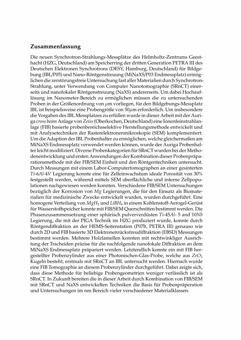
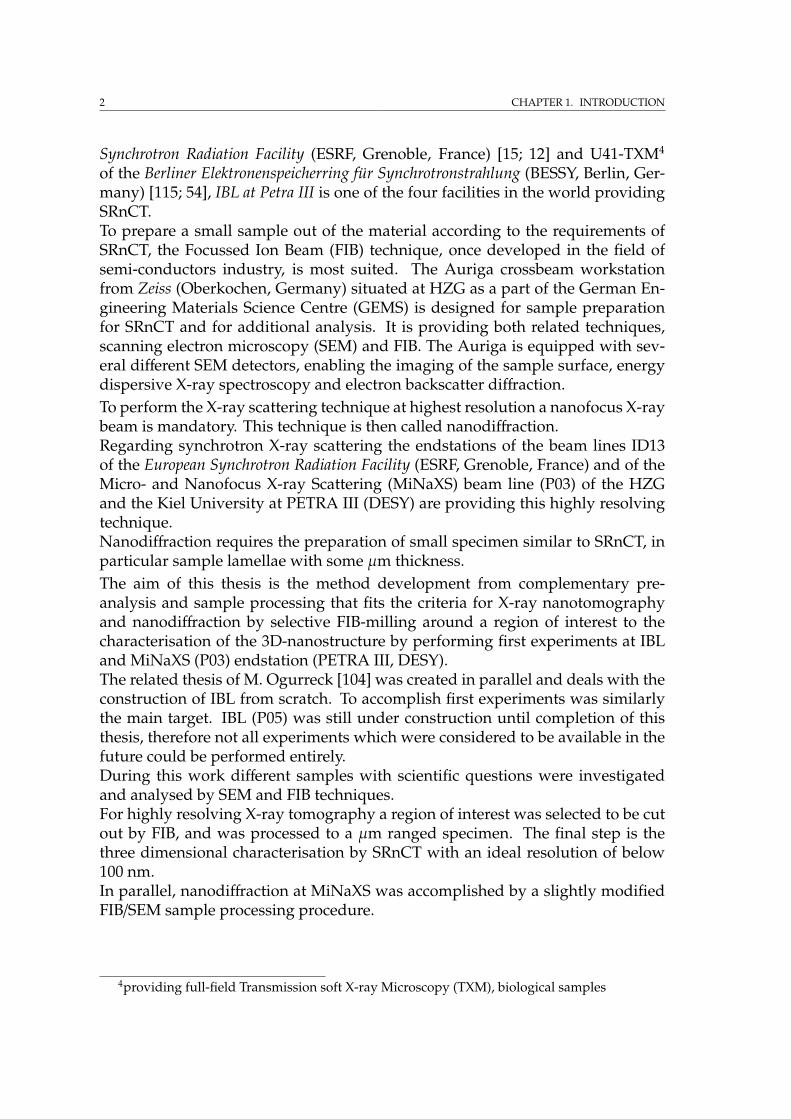
1 − β2 and thevelocity of the particle is used with respect to the speed of light β = v/c [112].Obviously the loss of energy is negligible for proton synchrotron accelerators, dueto their much higher mass to charge ratio compared to electrons or positrons.This energy loss, a disadvantage to the particle physicists, found usage by materialand fundamental researchers of any kind, due to the unique properties of theemitted synchrotron radiation. The wavelength λ of this radiation has a rangeof 103 to < 10−1 Å. This is similar to chemical bond lengths, and the associatedphoton energies are similar to the binding energies of core and valence electrons,as shown in Figure 2.1. The wavelength and the energy E are connected via the
2Large Electron-Positron Collider3Conseil Européen pour la Recherche Nucléaire, Switzerland
2.2. X-RAY GENERATION BY SYNCHROTRONS 5
Figure 2.1: Distribution of photon density by synchrotron radiation compared toenergies and distances on molecular level [87]; the characterising average frequencyis ωc.
de Broglie wavelength of a particle with rest mass zero as λ = h· c/E, where h isPlanck’s constant.The average or critical frequency ωc of a charged particle passing a curvature(marked in Figure 2.1) is defined by
ωc =3cγ3
2R, (2.2)
whereat γ is again the relativistic dilatation factor, c the speed of light and R theradius of curvature [137]. ωc characterises the radiation by the variables of thesynchrotron experiment v and R.In its system the accelerated particle emits radiation as usual, but due to therelativistic speed it appears in our system that the synchrotron radiation is directedin flight direction of the particle. This is causal for the typical alignment ofthe experimental hutches of synchrotron beam lines, linked to storage rings intangential direction.For relativistic reasons, the angle between a photon, emitted perpendicular to theflight direction of a charged particle, and the flight direction itself4 is given by
Θ(rad) ≈1γ. (2.3)
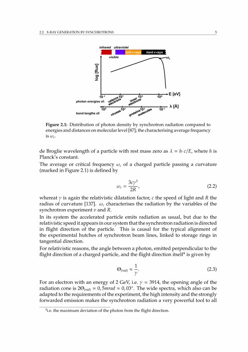
For an electron with an energy of 2 GeV, i.e. γ = 3914, the opening angle of theradiation cone is 2Θ(rad) = 0, 5mrad ≈ 0, 03°. The wide spectra, which also can beadapted to the requirements of the experiment, the high intensity and the stronglyforwarded emission makes the synchrotron radiation a very powerful tool to all
4i.e. the maximum deviation of the photon from the flight direction.
6 CHAPTER 2. INSTRUMENTS AND METHODS: SYNCHROTRON EXPERIMENTS
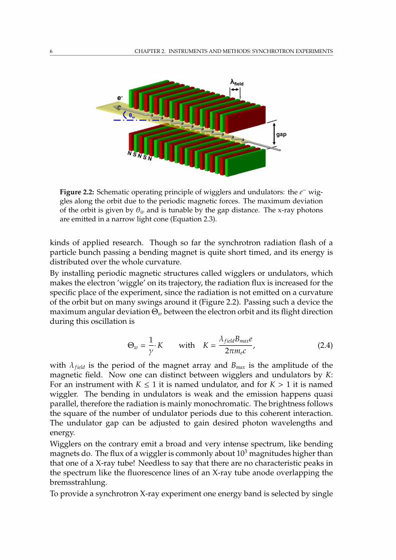
Figure 2.2: Schematic operating principle of wigglers and undulators: the e− wig-gles along the orbit due to the periodic magnetic forces. The maximum deviationof the orbit is given by θw and is tunable by the gap distance. The x-ray photonsare emitted in a narrow light cone (Equation 2.3).
kinds of applied research. Though so far the synchrotron radiation flash of aparticle bunch passing a bending magnet is quite short timed, and its energy isdistributed over the whole curvature.By installing periodic magnetic structures called wigglers or undulators, whichmakes the electron ’wiggle’ on its trajectory, the radiation flux is increased for thespecific place of the experiment, since the radiation is not emitted on a curvatureof the orbit but on many swings around it (Figure 2.2). Passing such a device themaximum angular deviationΘw between the electron orbit and its flight directionduring this oscillation is
Θw =1γ·K with K =
λ f ieldBmaxe2πmec
, (2.4)
with λ f ield is the period of the magnet array and Bmax is the amplitude of themagnetic field. Now one can distinct between wigglers and undulators by K:For an instrument with K ≤ 1 it is named undulator, and for K > 1 it is namedwiggler. The bending in undulators is weak and the emission happens quasiparallel, therefore the radiation is mainly monochromatic. The brightness followsthe square of the number of undulator periods due to this coherent interaction.The undulator gap can be adjusted to gain desired photon wavelengths andenergy.Wigglers on the contrary emit a broad and very intense spectrum, like bendingmagnets do. The flux of a wiggler is commonly about 103 magnitudes higher thanthat one of a X-ray tube! Needless to say that there are no characteristic peaks inthe spectrum like the fluorescence lines of an X-ray tube anode overlapping thebremsstrahlung.To provide a synchrotron X-ray experiment one energy band is selected by single
2.2. X-RAY GENERATION BY SYNCHROTRONS 7
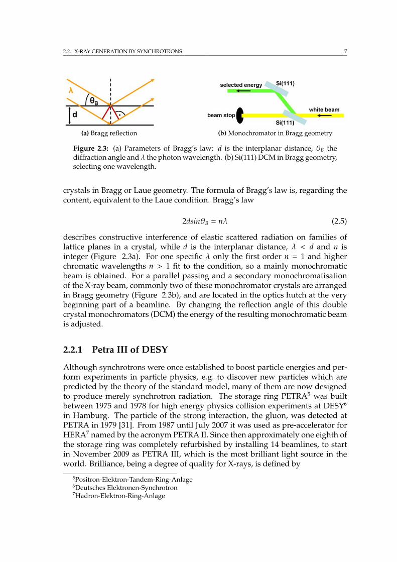
(a) Bragg reflection (b) Monochromator in Bragg geometry
Figure 2.3: (a) Parameters of Bragg’s law: d is the interplanar distance, θB thediffraction angle and λ the photon wavelength. (b) Si(111) DCM in Bragg geometry,selecting one wavelength.
crystals in Bragg or Laue geometry. The formula of Bragg’s law is, regarding thecontent, equivalent to the Laue condition. Bragg’s law
2dsinθB = nλ (2.5)
describes constructive interference of elastic scattered radiation on families oflattice planes in a crystal, while d is the interplanar distance, λ < d and n isinteger (Figure 2.3a). For one specific λ only the first order n = 1 and higherchromatic wavelengths n > 1 fit to the condition, so a mainly monochromaticbeam is obtained. For a parallel passing and a secondary monochromatisationof the X-ray beam, commonly two of these monochromator crystals are arrangedin Bragg geometry (Figure 2.3b), and are located in the optics hutch at the verybeginning part of a beamline. By changing the reflection angle of this doublecrystal monochromators (DCM) the energy of the resulting monochromatic beamis adjusted.
2.2.1 Petra III of DESY
Although synchrotrons were once established to boost particle energies and per-form experiments in particle physics, e.g. to discover new particles which arepredicted by the theory of the standard model, many of them are now designedto produce merely synchrotron radiation. The storage ring PETRA5 was builtbetween 1975 and 1978 for high energy physics collision experiments at DESY6
in Hamburg. The particle of the strong interaction, the gluon, was detected atPETRA in 1979 [31]. From 1987 until July 2007 it was used as pre-accelerator forHERA7 named by the acronym PETRA II. Since then approximately one eighth ofthe storage ring was completely refurbished by installing 14 beamlines, to startin November 2009 as PETRA III, which is the most brilliant light source in theworld. Brilliance, being a degree of quality for X-rays, is defined by
5Positron-Elektron-Tandem-Ring-Anlage6Deutsches Elektronen-Synchrotron7Hadron-Elektron-Ring-Anlage
8 CHAPTER 2. INSTRUMENTS AND METHODS: SYNCHROTRON EXPERIMENTS
B =N/t
dΩ· dF· (dλ/λ)(2.6)
with N/t, the number of emitted photons passing in the time of t, in relation to thearea of the source dF, the solid angle dΩ, in which the radiation is emitted, and therelative wavelength bandwidth dλ/λ. In common, synchrotron sources have a∼ 1012 times higher Brilliance than X-ray tubes [9]. For 3rd generation synchrotronsources the Brilliance is again significantly increased. The photon flux on one mm2
of the 3rd generation source PETRA III is the same as at the 2nd generation sourceDORIS III8 on some cm2.To date PETRA III is using electrons, starting their acceleration with 450 MeVby passing a linear pre-accelerator. Afterwards the electron beam is bunchedby an intensity accumulator, that is affecting the electrons with a high frequentfield. Now these bunches are inserted to the DESY ring, which is the only realsynchrotron left on this compound, and are accelerated to their final energy of6 GeV. Subsequently they are transferred to the 2304 m long PETRA ring toconstitute a 100 mA strong electron current. To compensate the loss of energy bythe synchrotron radiation at every turn on the orbit, as well as by the insertiondevices, radio frequent cavities are applied to boost the electron’s energy.Due to the fact that focussing optics generate always some kind of source image,the electron beam source size and the synchrotron beam divergence should beas small as possible to provide a nanofocused X-ray beam at the experiment.The quality of the created nanofocused beam is limited by the source and thehorizontal and vertical emittance:
ϵx = σx· σx′ ϵy = σy· σy′
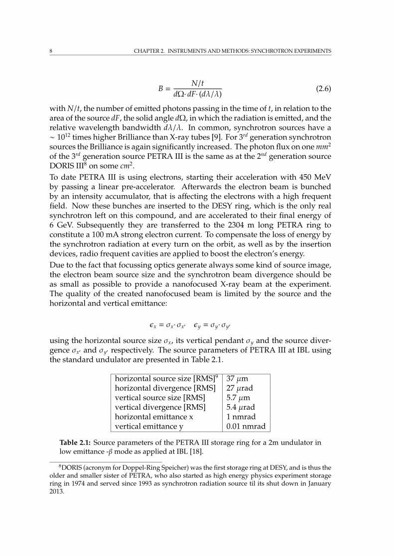
using the horizontal source size σx, its vertical pendant σy and the source diver-gence σx′ and σy′ respectively. The source parameters of PETRA III at IBL usingthe standard undulator are presented in Table 2.1.
horizontal source size [RMS]9 37 µmhorizontal divergence [RMS] 27 µradvertical source size [RMS] 5.7 µmvertical divergence [RMS] 5.4 µradhorizontal emittance x 1 nmradvertical emittance y 0.01 nmrad
Table 2.1: Source parameters of the PETRA III storage ring for a 2m undulator inlow emittance -βmode as applied at IBL [18].
8DORIS (acronym for Doppel-Ring Speicher) was the first storage ring at DESY, and is thus theolder and smaller sister of PETRA, who also started as high energy physics experiment storagering in 1974 and served since 1993 as synchrotron radiation source til its shut down in January2013.
2.3. SYNCHROTRON-RADIATION-BASED COMPUTED TOMOGRAPHY 9
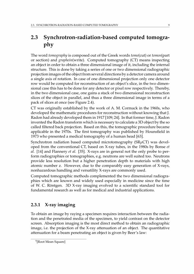
2.3 Synchrotron-radiation-based computed tomogra-phy
The word tomography is composed out of the Greek words tome(cut) or tomos(partor section) and graphein(write). Computed tomography (CT) means inspectingan object in order to obtain a three dimensional image of it, including the internalstructure. This is done by taking a series of one or two dimensional radiographicprojection images of the object from several directions by a detector camera arounda single axis of rotation. In case of one dimensional projection only one detectorrow would be computed for reconstruction of an object’s slice, in the two dimen-sional case this has to be done for any detector or pixel row respectively. Thereby,in the two dimensional case, one gains a stack of two dimensional reconstructionslices of the object in parallel, and thus a three dimensional image in terms of apack of slices at once (see Figure 2.4).CT was originally established by the work of A. M. Cormack in the 1960s, whodeveloped the mathematic procedures for reconstruction without knowing that J.Radon had already developed them in 1917 [109; 24]. In that former time, J. Radoninvented the Radon transform which is necessary to calculate a 3D object by the socalled filtered back projection. Based on this, the tomographic procedure becameapplicable in the 1970s. The first tomography was published by Hounsfield in1973 who presented a medical tomography of a human head [63].Synchrotron radiation based computed microtomography (SRµCT) was devel-oped from the conventional CT, based on X-ray tubes, in the 1980s by Bonse etal. [14] and Flannery et al. [35]. X-rays are in general not the only probe to per-form radiographies or tomographies, e.g. neutrons are well suited too. Neutronsprovide less resolution but a higher penetration depth to materials with highatomic number z. However, due to the comparably easy generation of X-rays,nonhazardous handling and versatility X-rays are commonly used.Computed tomographic methods complemented the two dimensional radiogra-phies which are known and widely used especially in medicine since the timeof W. C. Röntgen. 3D X-ray imaging evolved to a scientific standard tool forfundamental research as well as for medical and industrial applications.
2.3.1 X-ray imaging
To obtain an image by raying a specimen requires interaction between the radia-tion and the penetrated media of the specimen, to yield contrast on the detectorscreen. Absorption imaging is the most direct method to obtain an radiographicimage, i.e. the projection of the X-ray attenuation of an object. The quantitativeattenuation for a beam penetrating an object is given by Beer’s law:
9[Root Mean Square]
10 CHAPTER 2. INSTRUMENTS AND METHODS: SYNCHROTRON EXPERIMENTS
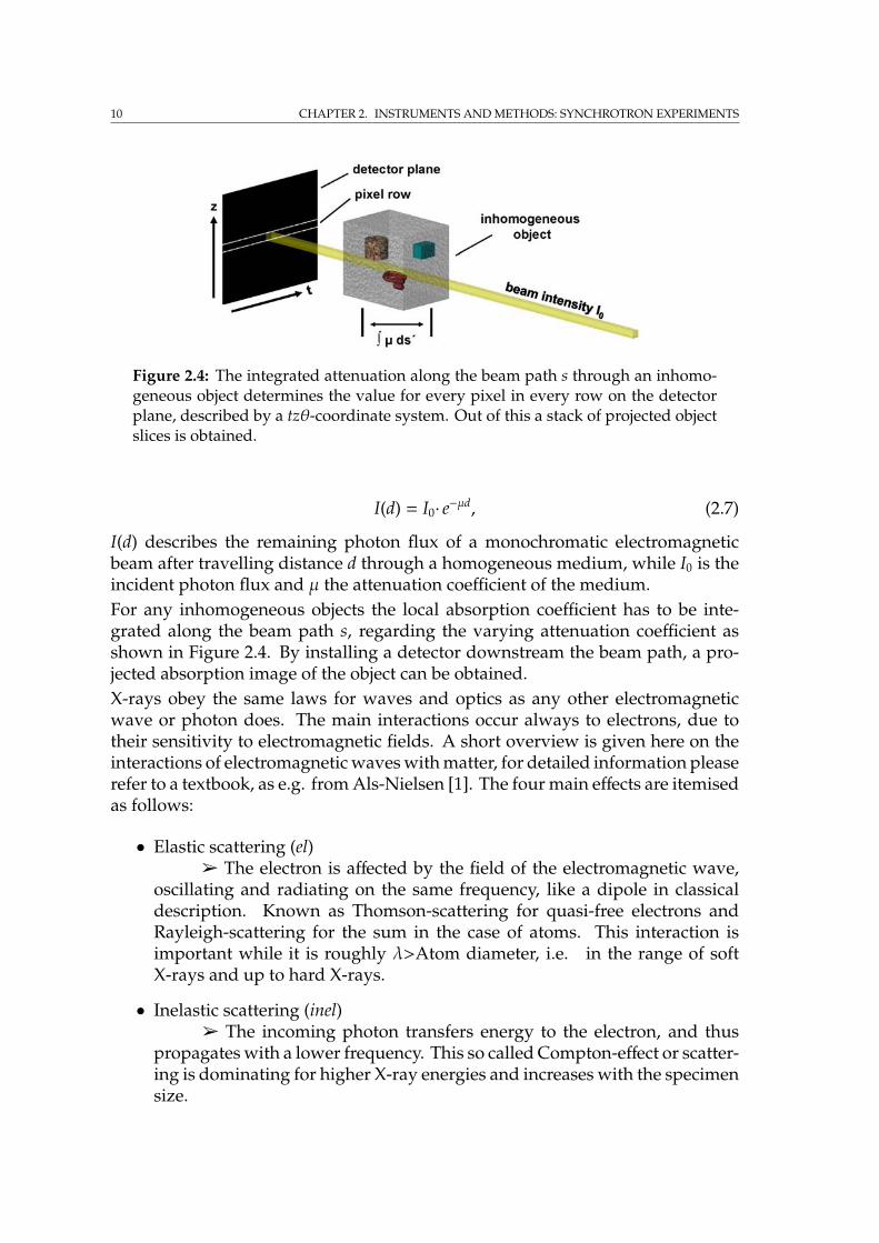
Figure 2.4: The integrated attenuation along the beam path s through an inhomo-geneous object determines the value for every pixel in every row on the detectorplane, described by a tzθ-coordinate system. Out of this a stack of projected objectslices is obtained.
I(d) = I0· e−µd, (2.7)
I(d) describes the remaining photon flux of a monochromatic electromagneticbeam after travelling distance d through a homogeneous medium, while I0 is theincident photon flux and µ the attenuation coefficient of the medium.For any inhomogeneous objects the local absorption coefficient has to be inte-grated along the beam path s, regarding the varying attenuation coefficient asshown in Figure 2.4. By installing a detector downstream the beam path, a pro-jected absorption image of the object can be obtained.X-rays obey the same laws for waves and optics as any other electromagneticwave or photon does. The main interactions occur always to electrons, due totheir sensitivity to electromagnetic fields. A short overview is given here on theinteractions of electromagnetic waves with matter, for detailed information pleaserefer to a textbook, as e.g. from Als-Nielsen [1]. The four main effects are itemisedas follows:
• Elastic scattering (el)â The electron is affected by the field of the electromagnetic wave,
oscillating and radiating on the same frequency, like a dipole in classicaldescription. Known as Thomson-scattering for quasi-free electrons andRayleigh-scattering for the sum in the case of atoms. This interaction isimportant while it is roughly λ>Atom diameter, i.e. in the range of softX-rays and up to hard X-rays.
• Inelastic scattering (inel)â The incoming photon transfers energy to the electron, and thus
propagates with a lower frequency. This so called Compton-effect or scatter-ing is dominating for higher X-ray energies and increases with the specimensize.
2.3. SYNCHROTRON-RADIATION-BASED COMPUTED TOMOGRAPHY 11
• Photoelectric effect (pe)â An electron absorbs a photon with minimum binding energy of the
electron’s state. By ionising the atom, the electron is released and dissipatesthe energy by inelastic collision. This effect is dominant but decreases athigher energy.
• Pair production (pp)â For energies higher than 1.022 MeV, photons can split in a electron-
positron pair: ν Õ e− + e+. Due to the conservation of momentum this isimpossible in vacuum.
The atomic interaction cross sections σ of the four attenuation effects can becalculated as a sum. It is
µtotal = σtotal·n with σtotal = σel + σinel + σpe + σpp (2.8)
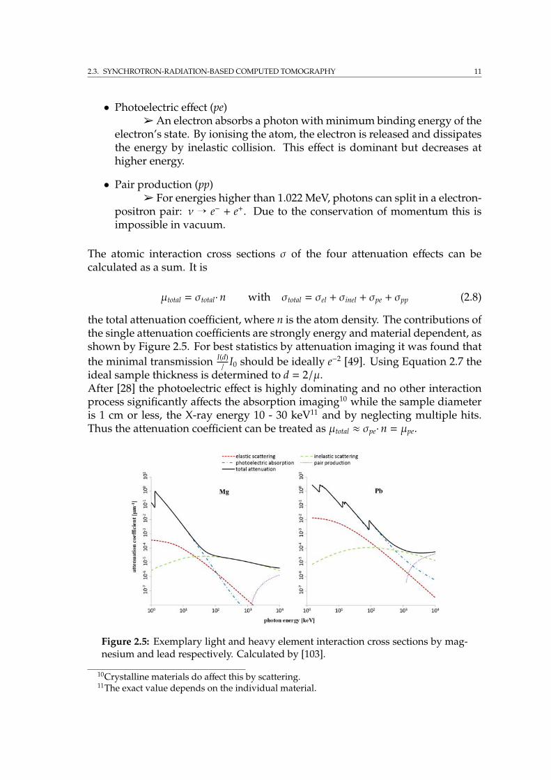
the total attenuation coefficient, where n is the atom density. The contributions ofthe single attenuation coefficients are strongly energy and material dependent, asshown by Figure 2.5. For best statistics by attenuation imaging it was found thatthe minimal transmission I(d)
/ I0 should be ideally e−2 [49]. Using Equation 2.7 theideal sample thickness is determined to d = 2/µ.After [28] the photoelectric effect is highly dominating and no other interactionprocess significantly affects the absorption imaging10 while the sample diameteris 1 cm or less, the X-ray energy 10 - 30 keV11 and by neglecting multiple hits.Thus the attenuation coefficient can be treated as µtotal ≈ σpe·n = µpe.
Figure 2.5: Exemplary light and heavy element interaction cross sections by mag-nesium and lead respectively. Calculated by [103].
10Crystalline materials do affect this by scattering.11The exact value depends on the individual material.
12 CHAPTER 2. INSTRUMENTS AND METHODS: SYNCHROTRON EXPERIMENTS
Experimentally derived, for the energy range from 10 to 100 keV, and apart fromabsorption edges, the photoelectric attenuation coefficient µpe is approximatelydetermined by
µpe ≈ kn·Z4
E3 . (2.9)
With E being the photon energy, n the density in atoms, Z the material’s atomicnumber and a constant k which is depending on the atomic shell [6]. Again, the in-dividual attenuation varies strongly with energy and the elementary compositionof the investigated objects.Furthermore it can be useful for imaging to exploit the photoelectric absorptionedge of an element within the sample to obtain increased contrast on the densityallocation of this element. The element dependent absorption edges are definedby the energy of the electron shells, resulting in a suddenly increased attenuationwhen exceeding the individual energy threshold.Despite the method of imaging by attenuation effects, phase contrast imagingis an important method too. Phase contrast imaging can be especially used forspecimen which material composition has quite similar attenuation coefficients,for its sensitivity on different refractive indexes. A short introduction is given inAppendix A.The desired resolution of a specimen by radiography is basically determined bythe number of detector pixels. The maximum possible resolution in one dimensionis given by sample size
pixel number . For example, to achieve a resolution of 50 nm with a 4096× 4096 pixel CCD detector, a theoretical sample size of approximately 200 µm isneeded.Practically, as a common rule of thumb, 2-3 detector pixels correlate to 1
1000 of thesample size, which defines the realistic achievable resolution. Out of this followsa sample size of about 50 µm to obtain a 50 nm resolution.
2.3.2 The tomographic method
A tomography is a 3D image of an object, reconstructed out of X-ray projectionstaken from different angles of an object, as introduced in section 2.3. The pre-sented reconstruction theory in the following is based on the most usual caseof parallel X-ray illumination and, as for the exemplarily described projectionimages, attenuation imaging. Besides this it is also possible and common to useother geometries as e.g. cone beam.Based on Beer’s law (Equation 2.7) the attenuation of the specimen along the beampath s is integrated and defines the projected attenuation p:
I = I0· e−p with p =∫
sµ(s′)ds′, (2.10)
2.3. SYNCHROTRON-RADIATION-BASED COMPUTED TOMOGRAPHY 13
while I is again the intensity of the beam. Now one can calculate the projectedattenuation by
p = −lnII0
(2.11)
for each pixel of the X-ray detector camera. Practically this is realised by recordingradiographic projection images of the specimen i, reference images of the beam rand dark images d during absence of radiation. Out of this p is calculated as
p = −lni − dr − d
, (2.12)
with the same camera exposure time for all images i and r.Further on, the spatial system response of the whole X-ray camera in terms ofthe point spread function has to be considered for the projected attenuation p bymeasuring the so called edge spread function. The latter is practically obtainedby imaging an object which covers half of the viewing field of the camera. Thecalculation procedure is described in [28].
Tomographic reconstruction
The taken radiographic projection images have to be transferred in mathemati-cally projected images in order to reconstruct them to a tomography image. Themathematical basics for this are well known, and e.g. described by Natterer [97]and Kak [69]. The used nomenclature in the following has been adopted from Kak[69]. For cone beam geometry a three dimensional calculation would be needed,as e.g. described by Feldkamp et al. [33] and Wang et al. [134].In a xyz-coordinate system let the physical properties on a tomographic slice ofan object be described by f (x, y), that is in our case determined by the attenuationcoefficient µ(x,y) (see subsection 2.3.1). As introduced in Figure 2.4, a relatedtzθ-coordinate12 system is used to determine the position on the detector camerascreen while images are taken at different angles θ regarding the object. For X-rays penetrating the object perpendicular to the detector plane (Figure 2.6) onecan define the projection along one line s of the penetrating beam on an objectslice as
pθ(t) =∫
line(t)f (x(s, t), y(s, t))ds while t = constant = x cosθ + y sinθ. (2.13)
The integral is thus evaluated for projections along lines of constant t, whichmeans parallel lines along the beam ray.By using the Dirac δ function, Equation 2.13 for pθ(t) can be rewritten as
12z is identical in both coordinate systems and constant while considering one individual slice.
14 CHAPTER 2. INSTRUMENTS AND METHODS: SYNCHROTRON EXPERIMENTS
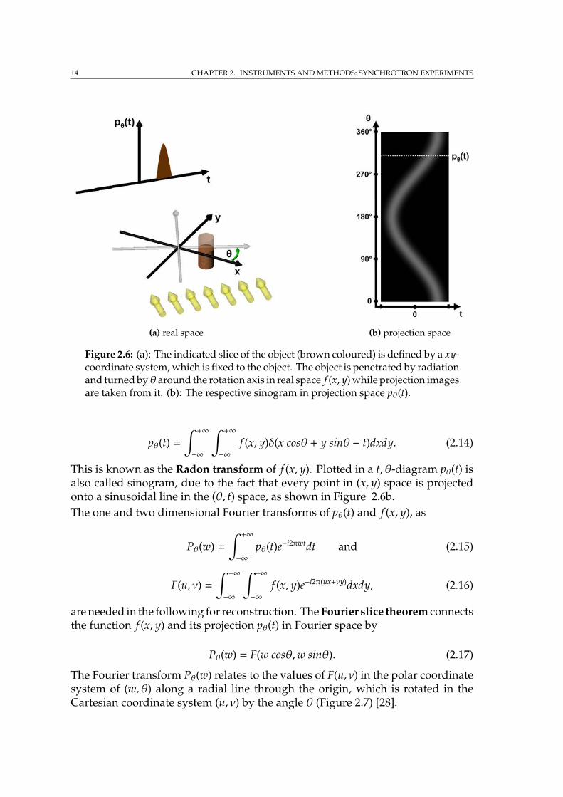
(a) real space (b) projection space
Figure 2.6: (a): The indicated slice of the object (brown coloured) is defined by a xy-coordinate system, which is fixed to the object. The object is penetrated by radiationand turned byθ around the rotation axis in real space f (x, y) while projection imagesare taken from it. (b): The respective sinogram in projection space pθ(t).
pθ(t) =∫ +∞
−∞
∫ +∞
−∞f (x, y)δ(x cosθ + y sinθ − t)dxdy. (2.14)
This is known as the Radon transform of f (x, y). Plotted in a t, θ-diagram pθ(t) isalso called sinogram, due to the fact that every point in (x, y) space is projectedonto a sinusoidal line in the (θ, t) space, as shown in Figure 2.6b.The one and two dimensional Fourier transforms of pθ(t) and f (x, y), as
Pθ(w) =∫ +∞
−∞pθ(t)e−i2πwtdt and (2.15)
F(u, ν) =∫ +∞
−∞
∫ +∞
−∞f (x, y)e−i2π(ux+νy)dxdy, (2.16)
are needed in the following for reconstruction. The Fourier slice theorem connectsthe function f (x, y) and its projection pθ(t) in Fourier space by
Pθ(w) = F(w cosθ,w sinθ). (2.17)
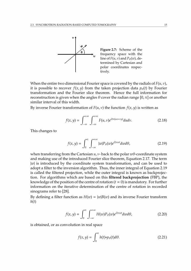
The Fourier transform Pθ(w) relates to the values of F(u, ν) in the polar coordinatesystem of (w, θ) along a radial line through the origin, which is rotated in theCartesian coordinate system (u, ν) by the angle θ (Figure 2.7) [28].
2.3. SYNCHROTRON-RADIATION-BASED COMPUTED TOMOGRAPHY 15
Figure 2.7: Scheme of thefrequency space with theline of F(u, ν) and Pθ(w), de-termined by Cartesian andpolar coordinates respec-tively.
When the entire two dimensional Fourier space is covered by the radials of F(u, ν),it is possible to recover f (x, y) from the taken projection data pθ(t) by Fouriertransformation and the Fourier slice theorem. Hence the full information forreconstruction is given when the angles θ cover the radian range [0, π] or anothersimilar interval of this width.By inverse Fourier transformation of F(u, ν) the function f (x, y) is written as
f (x, y) =∫ +∞
−∞
∫ +∞
−∞F(u, ν)ei2π(ux+νy)dudν. (2.18)
This changes to
f (x, y) =∫ π
0
∫ +∞
−∞|w|Pθ(w)ei2πwtdwdθ, (2.19)
when transferring from the Cartesian u, ν- back to the polar wθ-coordinate systemand making use of the introduced Fourier slice theorem, Equation 2.17. The term|w| is introduced by the coordinate system transformation, and can be used toadopt a filter to the inversion algorithm. Thus, the inner integral of Equation 2.19is called the filtered projection, while the outer integral is known as backprojec-tion. For algorithms which are based on this filtered backprojection (FBP), theknowledge of the position of the centre of rotation (t = 0) is mandatory. For furtherinformation on the iterative determination of the centre of rotation in recordedsinograms refer to [28].By defining a filter function as H(w) = |w|B(w) and its inverse Fourier transformh(t)
f (x, y) =∫ π
0
∫ +∞
−∞H(w)Pθ(w)ei2πwtdwdθ, (2.20)
is obtained, or as convolution in real space
f (x, y) =∫ π
0h(t)∗pθ(t)dθ. (2.21)
16 CHAPTER 2. INSTRUMENTS AND METHODS: SYNCHROTRON EXPERIMENTS
In this equation ∗ marks the one dimensional convolution operation. Using theterm B(w) in the filter function, a filter can be applied that suppresses the noise athigh frequencies at the cost of a lower spatial resolution. There are many possi-bilities to design algorithms with additional filter functions, due to the varietiesof desired accented results.
Although convolution in real space as filtering in frequency space are mathe-matically the same, one often refers to reconstruction algorithms based on Equa-tion 2.21 as convoluted backprojection (CBP) algorithms and those based on Equa-tion 2.20 as FBP algorithms.
In contrast to the mentioned reconstruction algorithms which are based on thepresented filtered backprojection, there exist others that make use of algebraic[43] or statistical techniques [110].
2.4 Nanotomography at IBL
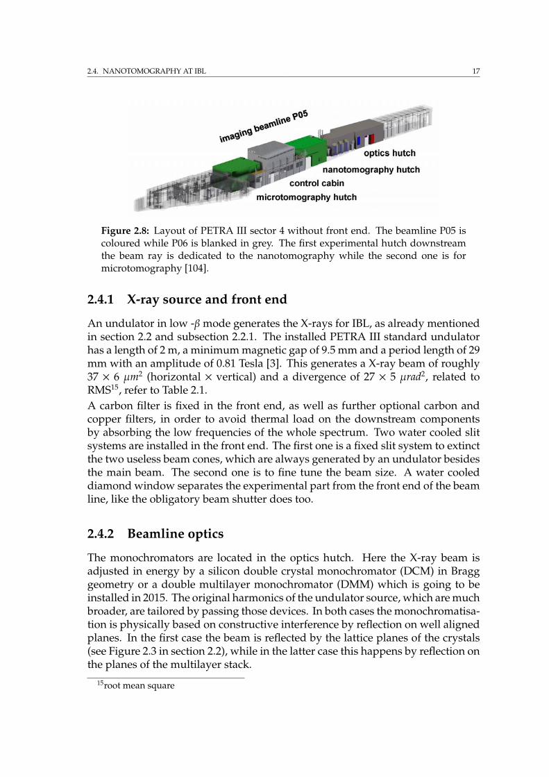
In the following the nanotomographic experiment at the imaging beamline P05(IBL) at the storage ring PETRA III13, will be described. The beamline P05 islocated in sector 4 in the PETRA III experimental hall, and shares the sector withthe Hard X-ray micro/nano-probe beamline P06. The imaging beamline is housingthe micro- and the nanotomography as well, and some general devices as e.g. themonochromators which are used by both experiments.Caused by the small beam size and divergence (see Table 2.1), the microtomog-raphy hutch had to be installed subsequent to the nanotomography hutch (Fig-ure 2.8). The more diverged and thus bigger beam is needed by the microtomog-raphy experiment for dealing with bigger samples. This geometry additionallyallows to use the detector camera of the microtomography experiment in thesecond hutch downstream the beam in combination with the nanotomographicexperiment.A beam pipe changer is mounted in the nanotomography hutch to enable either acontinuous vacuum for the beam if the microtomography is running, or to switcheasily to nanotomography by lifting the pipe.
The microtomography in the second hutch works according to Figure 2.4 withoutX-ray optics. Here the detector consists of a scintillator screen from which theimage is magnified by visible light optics to a 60 mm × 60 mm14 camera plane.The optics are fitted to provide magnifications of M = 5×, 10×, 20× or 40× [104].This allows sample sizes of roughly 1 to 7 mm for the microtomography.
13introduced in subsection 2.2.114corresponding to a 4096 × 4096 pixel CCD
2.4. NANOTOMOGRAPHY AT IBL 17
Figure 2.8: Layout of PETRA III sector 4 without front end. The beamline P05 iscoloured while P06 is blanked in grey. The first experimental hutch downstreamthe beam ray is dedicated to the nanotomography while the second one is formicrotomography [104].
2.4.1 X-ray source and front end
An undulator in low -βmode generates the X-rays for IBL, as already mentionedin section 2.2 and subsection 2.2.1. The installed PETRA III standard undulatorhas a length of 2 m, a minimum magnetic gap of 9.5 mm and a period length of 29mm with an amplitude of 0.81 Tesla [3]. This generates a X-ray beam of roughly37 × 6 µm2 (horizontal × vertical) and a divergence of 27 × 5 µrad2, related toRMS15, refer to Table 2.1.A carbon filter is fixed in the front end, as well as further optional carbon andcopper filters, in order to avoid thermal load on the downstream componentsby absorbing the low frequencies of the whole spectrum. Two water cooled slitsystems are installed in the front end. The first one is a fixed slit system to extinctthe two useless beam cones, which are always generated by an undulator besidesthe main beam. The second one is to fine tune the beam size. A water cooleddiamond window separates the experimental part from the front end of the beamline, like the obligatory beam shutter does too.
2.4.2 Beamline optics
The monochromators are located in the optics hutch. Here the X-ray beam isadjusted in energy by a silicon double crystal monochromator (DCM) in Bragggeometry or a double multilayer monochromator (DMM) which is going to beinstalled in 2015. The original harmonics of the undulator source, which are muchbroader, are tailored by passing those devices. In both cases the monochromatisa-tion is physically based on constructive interference by reflection on well alignedplanes. In the first case the beam is reflected by the lattice planes of the crystals(see Figure 2.3 in section 2.2), while in the latter case this happens by reflection onthe planes of the multilayer stack.
15root mean square
18 CHAPTER 2. INSTRUMENTS AND METHODS: SYNCHROTRON EXPERIMENTS
For the Bragg geometry there are two facilities present, one silicon 111 DCM setand one silicon 311 DCM set. This double DCM is the standard DESY monochro-mator layout for PETRA III, and provides a small energy bandpass, i.e. it isδE/E ≈ 10−4. This enables very defined energy settings, which are e.g. requiredfor absorption edge imaging and tomography.The DMM shall cover an energy range of 5 to 50 keV, there are different coatingsto be done inhouse at HZG [129]. The main advantage of the DMM is the high re-flectivity and the large energy bandpass of δE/E ≈ 10−2, resulting in an increasedphoton flux by two orders of magnitude compared to the DCMs (δE/E ≈ 10−4)[104].
2.4.3 X-ray optics
To achieve nanoscale resolution by the nanotomography experiment, focussingand magnifying X-ray optics are needed. The real part 1 − δ of the complexrefractive index
n = 1 − δ + iβ, (2.22)
is responsible for refraction of an electromagnetic beam at a boundary, physicallycaused by different group velocities in different media.
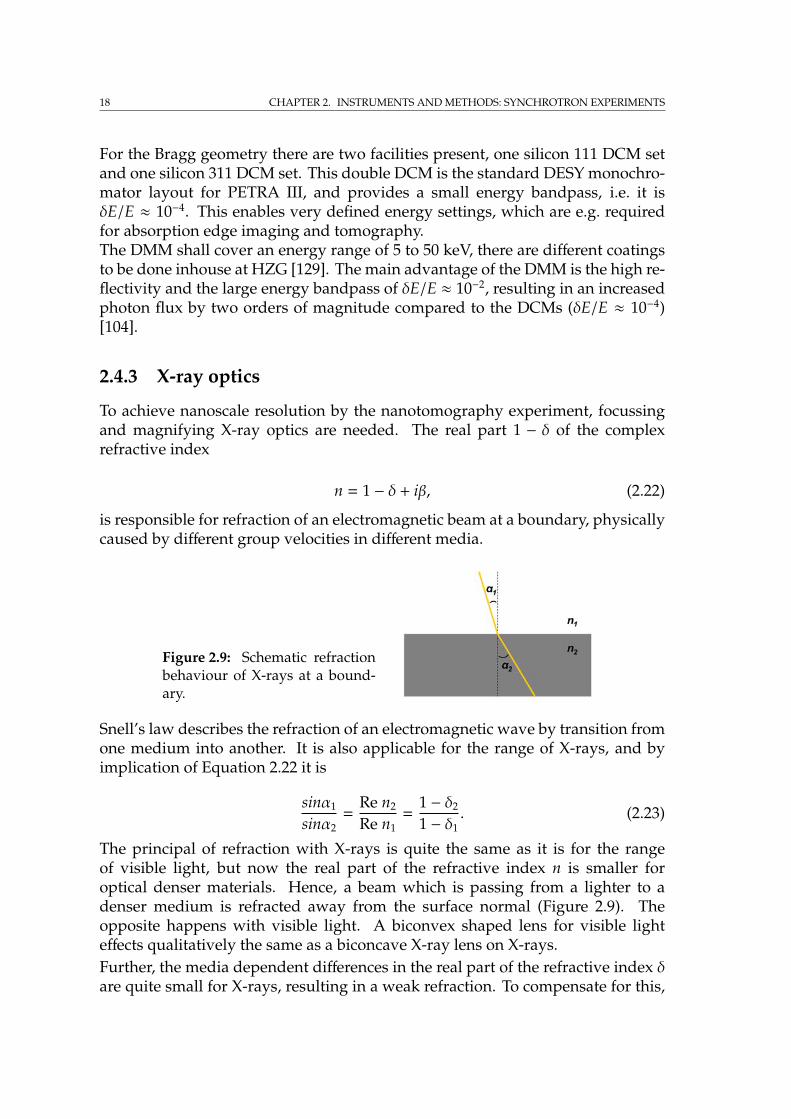
Figure 2.9: Schematic refractionbehaviour of X-rays at a bound-ary.
Snell’s law describes the refraction of an electromagnetic wave by transition fromone medium into another. It is also applicable for the range of X-rays, and byimplication of Equation 2.22 it is
sinα1
sinα2=
Re n2
Re n1=
1 − δ2
1 − δ1. (2.23)
The principal of refraction with X-rays is quite the same as it is for the rangeof visible light, but now the real part of the refractive index n is smaller foroptical denser materials. Hence, a beam which is passing from a lighter to adenser medium is refracted away from the surface normal (Figure 2.9). Theopposite happens with visible light. A biconvex shaped lens for visible lighteffects qualitatively the same as a biconcave X-ray lens on X-rays.Further, the media dependent differences in the real part of the refractive index δare quite small for X-rays, resulting in a weak refraction. To compensate for this,
2.4. NANOTOMOGRAPHY AT IBL 19
(a) X-ray lens pack (b) X-ray lens pack inbeam direction
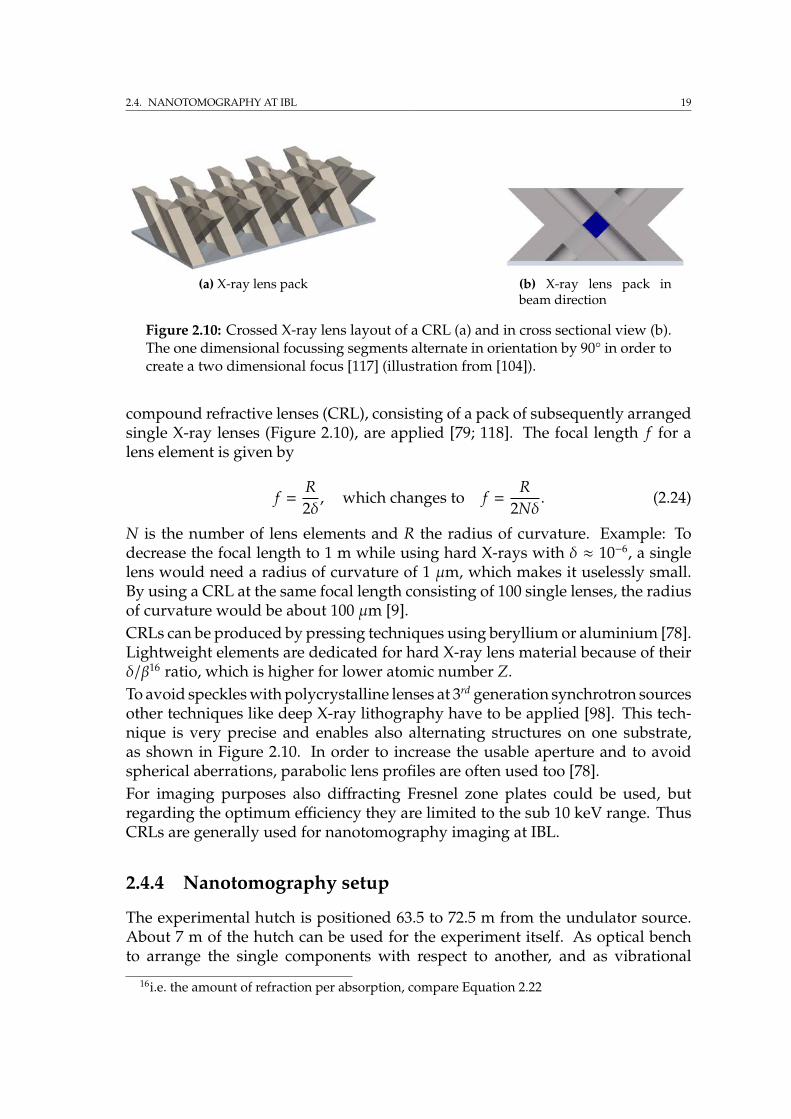
Figure 2.10: Crossed X-ray lens layout of a CRL (a) and in cross sectional view (b).The one dimensional focussing segments alternate in orientation by 90° in order tocreate a two dimensional focus [117] (illustration from [104]).
compound refractive lenses (CRL), consisting of a pack of subsequently arrangedsingle X-ray lenses (Figure 2.10), are applied [79; 118]. The focal length f for alens element is given by
f =R2δ, which changes to f =
R2Nδ. (2.24)
N is the number of lens elements and R the radius of curvature. Example: Todecrease the focal length to 1 m while using hard X-rays with δ ≈ 10−6, a singlelens would need a radius of curvature of 1 µm, which makes it uselessly small.By using a CRL at the same focal length consisting of 100 single lenses, the radiusof curvature would be about 100 µm [9].CRLs can be produced by pressing techniques using beryllium or aluminium [78].Lightweight elements are dedicated for hard X-ray lens material because of theirδ/β16 ratio, which is higher for lower atomic number Z.To avoid speckles with polycrystalline lenses at 3rd generation synchrotron sourcesother techniques like deep X-ray lithography have to be applied [98]. This tech-nique is very precise and enables also alternating structures on one substrate,as shown in Figure 2.10. In order to increase the usable aperture and to avoidspherical aberrations, parabolic lens profiles are often used too [78].For imaging purposes also diffracting Fresnel zone plates could be used, butregarding the optimum efficiency they are limited to the sub 10 keV range. ThusCRLs are generally used for nanotomography imaging at IBL.
2.4.4 Nanotomography setup
The experimental hutch is positioned 63.5 to 72.5 m from the undulator source.About 7 m of the hutch can be used for the experiment itself. As optical benchto arrange the single components with respect to another, and as vibrational
16i.e. the amount of refraction per absorption, compare Equation 2.22
20 CHAPTER 2. INSTRUMENTS AND METHODS: SYNCHROTRON EXPERIMENTS
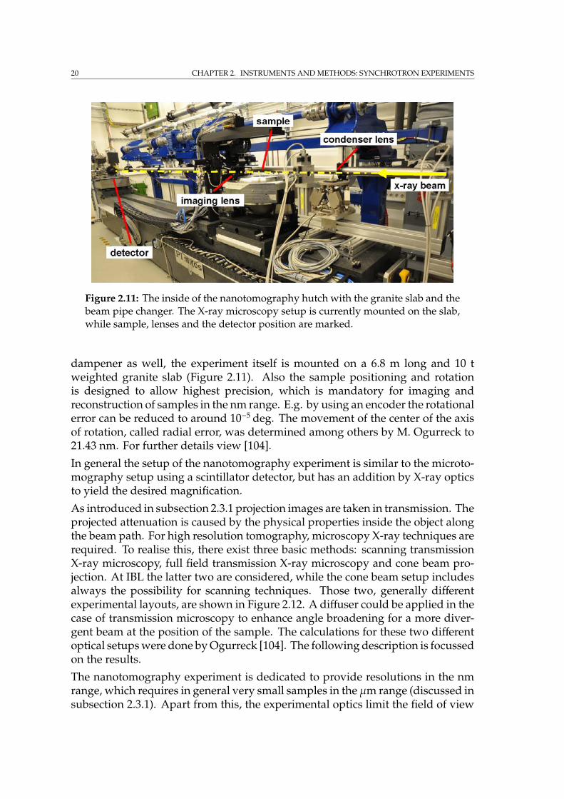
Figure 2.11: The inside of the nanotomography hutch with the granite slab and thebeam pipe changer. The X-ray microscopy setup is currently mounted on the slab,while sample, lenses and the detector position are marked.
dampener as well, the experiment itself is mounted on a 6.8 m long and 10 tweighted granite slab (Figure 2.11). Also the sample positioning and rotationis designed to allow highest precision, which is mandatory for imaging andreconstruction of samples in the nm range. E.g. by using an encoder the rotationalerror can be reduced to around 10−5 deg. The movement of the center of the axisof rotation, called radial error, was determined among others by M. Ogurreck to21.43 nm. For further details view [104].
In general the setup of the nanotomography experiment is similar to the microto-mography setup using a scintillator detector, but has an addition by X-ray opticsto yield the desired magnification.
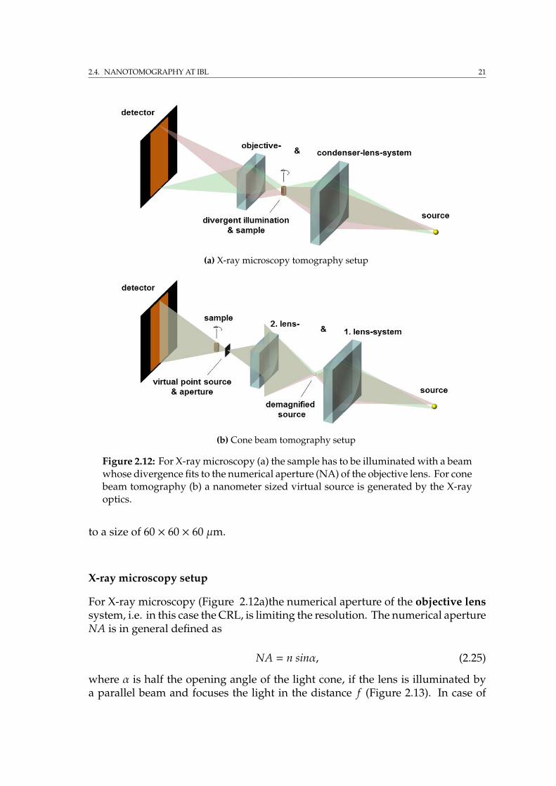
As introduced in subsection 2.3.1 projection images are taken in transmission. Theprojected attenuation is caused by the physical properties inside the object alongthe beam path. For high resolution tomography, microscopy X-ray techniques arerequired. To realise this, there exist three basic methods: scanning transmissionX-ray microscopy, full field transmission X-ray microscopy and cone beam pro-jection. At IBL the latter two are considered, while the cone beam setup includesalways the possibility for scanning techniques. Those two, generally differentexperimental layouts, are shown in Figure 2.12. A diffuser could be applied in thecase of transmission microscopy to enhance angle broadening for a more diver-gent beam at the position of the sample. The calculations for these two differentoptical setups were done by Ogurreck [104]. The following description is focussedon the results.
The nanotomography experiment is dedicated to provide resolutions in the nmrange, which requires in general very small samples in the µm range (discussed insubsection 2.3.1). Apart from this, the experimental optics limit the field of view
2.4. NANOTOMOGRAPHY AT IBL 21
(a) X-ray microscopy tomography setup
(b) Cone beam tomography setup
Figure 2.12: For X-ray microscopy (a) the sample has to be illuminated with a beamwhose divergence fits to the numerical aperture (NA) of the objective lens. For conebeam tomography (b) a nanometer sized virtual source is generated by the X-rayoptics.
to a size of 60 × 60 × 60 µm.
X-ray microscopy setup
For X-ray microscopy (Figure 2.12a)the numerical aperture of the objective lenssystem, i.e. in this case the CRL, is limiting the resolution. The numerical apertureNA is in general defined as
NA = n sinα, (2.25)
where α is half the opening angle of the light cone, if the lens is illuminated bya parallel beam and focuses the light in the distance f (Figure 2.13). In case of
22 CHAPTER 2. INSTRUMENTS AND METHODS: SYNCHROTRON EXPERIMENTS
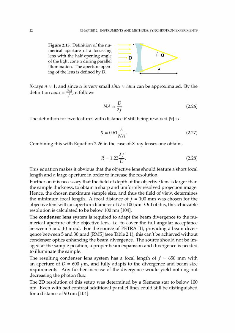
Figure 2.13: Definition of the nu-merical aperture of a focussinglens with the half opening angleof the light cone α during parallelillumination. The aperture open-ing of the lens is defined by D.
X-rays n ≈ 1, and since α is very small sinα ≈ tanα can be approximated. By thedefinition tanα = D/2
f , it follows
NA ≈ D2 f. (2.26)
The definition for two features with distance R still being resolved [9] is
R = 0.61λ
NA. (2.27)
Combining this with Equation 2.26 in the case of X-ray lenses one obtains
R = 1.22λ fD. (2.28)
This equation makes it obvious that the objective lens should feature a short focallength and a large aperture in order to increase the resolution.Further on it is necessary that the field of depth of the objective lens is larger thanthe sample thickness, to obtain a sharp and uniformly resolved projection image.Hence, the chosen maximum sample size, and thus the field of view, determinesthe minimum focal length. A focal distance of f = 100 mm was chosen for theobjective lens with an aperture diameter of D= 100 µm. Out of this, the achievableresolution is calculated to be below 100 nm [104].The condenser lens system is required to adapt the beam divergence to the nu-merical aperture of the objective lens, i.e. to cover the full angular acceptancebetween 5 and 10 mrad. For the source of PETRA III, providing a beam diver-gence between 5 and 30 µrad [RMS] (see Table 2.1), this can’t be achieved withoutcondenser optics enhancing the beam divergence. The source should not be im-aged at the sample position, a proper beam expansion and divergence is neededto illuminate the sample.The resulting condenser lens system has a focal length of f = 650 mm withan aperture of D = 600 µm, and fully adapts to the divergence and beam sizerequirements. Any further increase of the divergence would yield nothing butdecreasing the photon flux.The 2D resolution of this setup was determined by a Siemens star to below 100nm. Even with bad contrast additional parallel lines could still be distinguishedfor a distance of 90 nm [104].
2.4. NANOTOMOGRAPHY AT IBL 23
Cone beam setup
Cone beam tomography (Figure 2.12b) means to ray a specimen by a light conewith an ideal point source origin. The sample size itself and the distance to thedetector define the magnification.Besides the limitations to the resolution discussed in subsection 2.3.1 the resolutionis now given by the expansion of the source. The size of the sample features beingresolved is equivalent to the source spot size. To provide a proper approach to apoint source the expansion of the original PETRA III beam has to be demagnified.Classical lenses provide an image magnified or demagnified by M, defined by therelation
M =dsource−lens
dlens− f ocus. (2.29)
Since a resolution and thus a target spot size of 50 nm is considered, a demagni-fication of M ≈ 1800 is needed (referred to the beam dimensions given in subsec-tion 2.4.1). In order to preserve simple handling of the sample, there should beenough space between lens, sample and detector. Hence, the divergence ought tobe kept moderate.In practice the source demagnification is realised in two steps, i.e. for the de-magnification it is M1 × M2 ≈ 1800. Hereby the source to the second lens is thedemagnified image spot provided by the first lens.An aperture of which the opening was prepared by the later discussed focussedion beam (FIB) device of HZG (section 3.2) is installed at the position of the virtualsource to suppress strayed X-rays.
2.4.5 Sample requirements
Due to the required nano scaled resolution the samples have to be µm scaled(subsection 2.3.1). As mentioned in subsection 2.3.2, the sample can only be fullyreconstructed if the angle of sample rotation θ covers not less than the range of[0, π]. Cylindrical shaped specimens would provide a homogenous attenuationrange during the applied rotation.A pillar shaped specimen with the maximum lateral diameter of 40 µm fits allrequirements (Figure 2.14). The sample would be positioned in the very heartof the beam where it is most stable. By this shape it is guaranteed that at everyangle θ the sample is fully imaged, even if beam variation occurs or the centre ofrotation does not fit perfectly. If the height of the pillar is longer than the viewingfield, the tomography could be performed in several height steps. Once the datais taken it could be reconstructed to one 3D object.IBL is equipped with a sample holder system providing automatic sample identi-fication and handling (Figure 2.14). For nanotomography these holders had to be
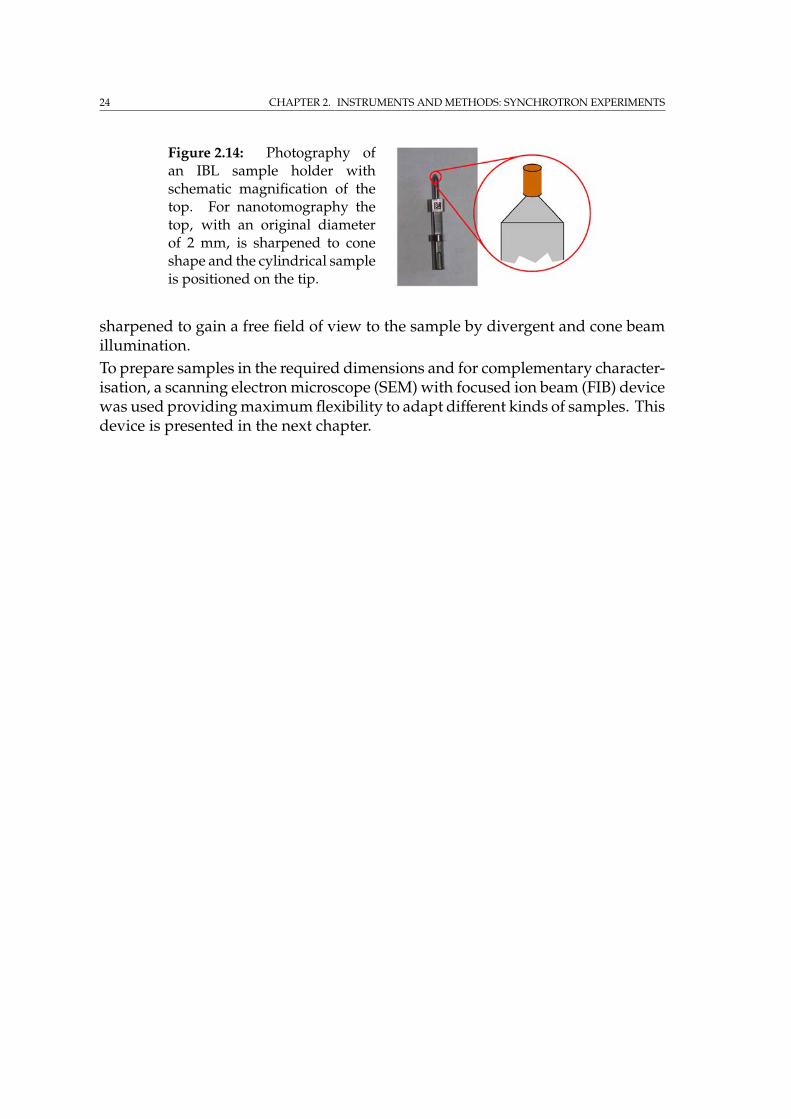
24 CHAPTER 2. INSTRUMENTS AND METHODS: SYNCHROTRON EXPERIMENTS
Figure 2.14: Photography ofan IBL sample holder withschematic magnification of thetop. For nanotomography thetop, with an original diameterof 2 mm, is sharpened to coneshape and the cylindrical sampleis positioned on the tip.
sharpened to gain a free field of view to the sample by divergent and cone beamillumination.To prepare samples in the required dimensions and for complementary character-isation, a scanning electron microscope (SEM) with focused ion beam (FIB) devicewas used providing maximum flexibility to adapt different kinds of samples. Thisdevice is presented in the next chapter.
2.5. SYNCHROTRON-RADIATION-BASED X-RAY SCATTERING 25
2.5 Synchrotron-radiation-based X-ray scattering
2.5.1 Introduction to X-ray diffraction
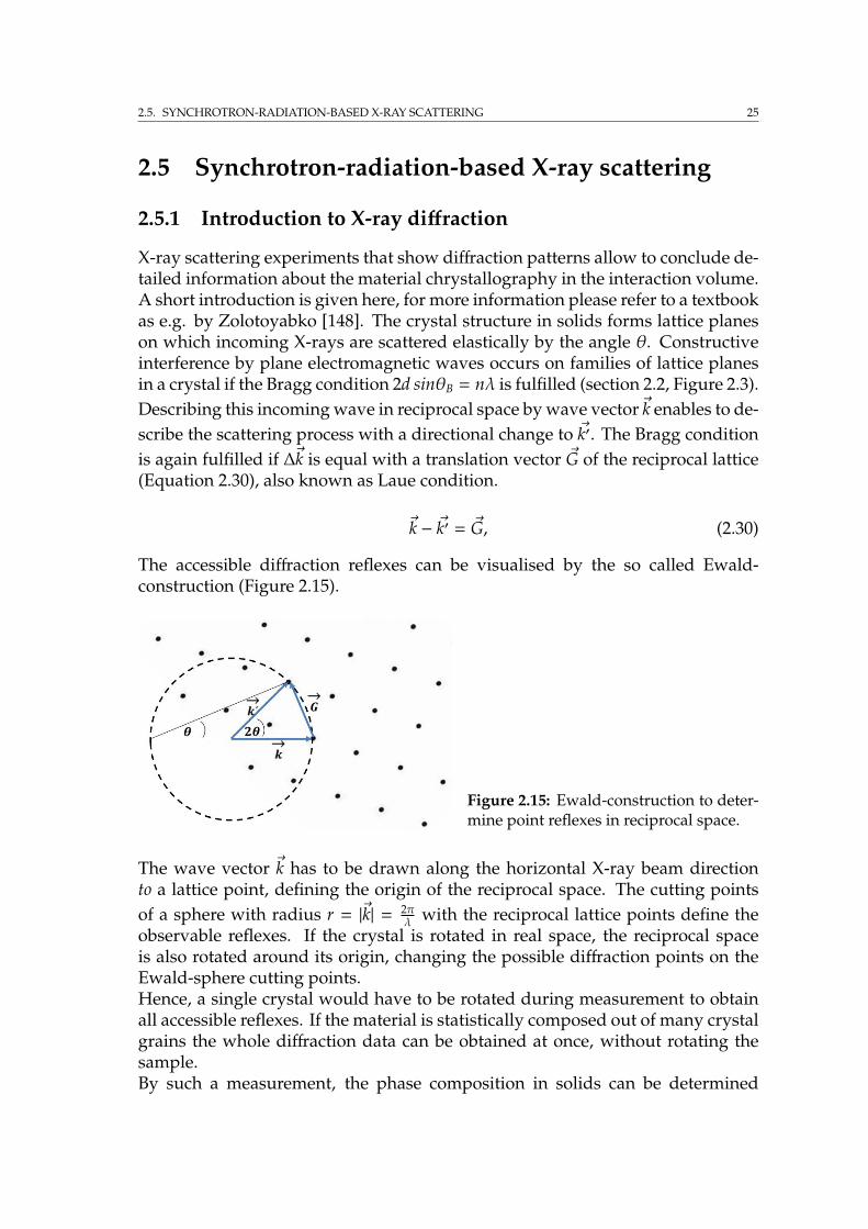
X-ray scattering experiments that show diffraction patterns allow to conclude de-tailed information about the material chrystallography in the interaction volume.A short introduction is given here, for more information please refer to a textbookas e.g. by Zolotoyabko [148]. The crystal structure in solids forms lattice planeson which incoming X-rays are scattered elastically by the angle θ. Constructiveinterference by plane electromagnetic waves occurs on families of lattice planesin a crystal if the Bragg condition 2d sinθB = nλ is fulfilled (section 2.2, Figure 2.3).Describing this incoming wave in reciprocal space by wave vector k enables to de-scribe the scattering process with a directional change to k′. The Bragg conditionis again fulfilled if ∆k is equal with a translation vector G of the reciprocal lattice(Equation 2.30), also known as Laue condition.
k − k′ = G, (2.30)
The accessible diffraction reflexes can be visualised by the so called Ewald-construction (Figure 2.15).
Figure 2.15: Ewald-construction to deter-mine point reflexes in reciprocal space.
The wave vector k has to be drawn along the horizontal X-ray beam directionto a lattice point, defining the origin of the reciprocal space. The cutting pointsof a sphere with radius r = |k| = 2π
λ with the reciprocal lattice points define theobservable reflexes. If the crystal is rotated in real space, the reciprocal spaceis also rotated around its origin, changing the possible diffraction points on theEwald-sphere cutting points.Hence, a single crystal would have to be rotated during measurement to obtainall accessible reflexes. If the material is statistically composed out of many crystalgrains the whole diffraction data can be obtained at once, without rotating thesample.By such a measurement, the phase composition in solids can be determined
26 CHAPTER 2. INSTRUMENTS AND METHODS: SYNCHROTRON EXPERIMENTS
statistically by comparing the resulting data with calculated diffraction pattern ofcrystal models.
2.5.2 Nanodiffraction at Petra III
Nanodiffraction describes a diffraction experiment using a nanofocused X-raybeam in combination with thin samples, which is therefore providing a muchhigher resolution.In the following the nanofocus endstation of the MiNaXS beam line (P03) atPETRA III at DESY (Hamburg, Germany) was mainly used for nanodiffraction.A horizontal emittance of about 1 nm rad as provided by PETRA III is crucial togenerate a beam in the range of nanometers. CRLs generate a virtual point sourceand subsequent installed Kirkpatrick-Baez mirrors enable a beam size of to date250 × 350 nm2 [93].The sample preparation follows in general the same steps as for nanotomography,described in the following chapter. However, instead of cylindrical specimensome µm thick lamella shaped specimens are processed for this experiment bythe FIB device.
Chapter 3
Instruments and methods: SEM andFIB
In contrary to X-ray microscopy techniques classical microscopy is constrictedto the characterisation of the surface. By using visible light this technique isaccessible at low costs and established as a basic laboratory tool. However, theresolution for visible light is limited by the wavelength and the numerical apertureof the microscope. The most modern microscopes of this kind reach a resolutionbetween 300 and 200 nm. A scanning electron microscope (SEM) yet enables toimage nanometer sized features due to the shorter electron wavelength.Since H. Busch invented magnetic lenses for electrons in 1925, in analogy to lensesfor visible light made of glass, it was possible to build electron microscopes. Thevery first electron microscope was built in 1931 by E. Ruska and M. Knoll, but itcould only image a single spot on the surface of the specimen [73]. Four yearslater, the theoretical basics for a scanning electron microscope were again laid byKnoll [72].The first scanning electron microscope was made by M. von Ardenne in 1937,with a spot size and thus resolution of 10 nm. The aim was to build an electronmicroscope that extincts the chromatic aberration. This aberration is inherent tothe so far established not scanning electron microscopes which obtain the imageas a whole.Based on the work of McMullan [91; 92], Smith & Oatley [124; 102] and Wells [136]Stereoscan (Cambridge Instruments Ltd.) offered the first commercial SEM in 1965."Since this commercialization in the mid-1960s the SEM has revolutionised thestudy of fracture surfaces and, more recently, made crucial contributions to thescience and engineering of microelectronic devices to the point where it is anessential presence on commercial fabrication lines" [99]. A complete historicalbibliography with publications on developments in the field of SEM since thistime can be found in [123].The focussed ion beam (FIB) technique uses generally the same function princi-ple as scanning electron microscopy. In addition ion beam milling and surface
27
28 CHAPTER 3. INSTRUMENTS AND METHODS: SEM AND FIB
structuring is possible due to the much heavier ions, compared to electrons. Thecrossbeam device used for this thesis in order to perform specimen preparationand pre analysis for nanotomography at IBL and nanodiffraction at MiNaXS(see section 2.4 and subsection 2.5.2) is the workstation Auriga 40 from Zeiss(Oberkochen, Germany) of the Helmholtz-Zentrum Geesthacht (HZG). The Au-riga is providing both, electron microscopy and focused ion beam using galliumions. All kinds of SEM or FIB investigations in this thesis were done with thisdevice.
3.1 Introduction to SEM techniques
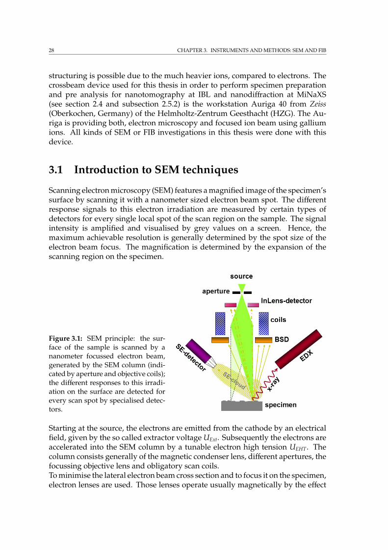
Scanning electron microscopy (SEM) features a magnified image of the specimen’ssurface by scanning it with a nanometer sized electron beam spot. The differentresponse signals to this electron irradiation are measured by certain types ofdetectors for every single local spot of the scan region on the sample. The signalintensity is amplified and visualised by grey values on a screen. Hence, themaximum achievable resolution is generally determined by the spot size of theelectron beam focus. The magnification is determined by the expansion of thescanning region on the specimen.
Figure 3.1: SEM principle: the sur-face of the sample is scanned by ananometer focussed electron beam,generated by the SEM column (indi-cated by aperture and objective coils);the different responses to this irradi-ation on the surface are detected forevery scan spot by specialised detec-tors.
Starting at the source, the electrons are emitted from the cathode by an electricalfield, given by the so called extractor voltage UExt. Subsequently the electrons areaccelerated into the SEM column by a tunable electron high tension UEHT. Thecolumn consists generally of the magnetic condenser lens, different apertures, thefocussing objective lens and obligatory scan coils.To minimise the lateral electron beam cross section and to focus it on the specimen,electron lenses are used. Those lenses operate usually magnetically by the effect

3.1. INTRODUCTION TO SEM TECHNIQUES 29
of the Lorentz force F = eν×B. This is forcing the different electrons to helix paths,which are crossing in a focus. Hereby also an image rotation occurs.The SEM lens system is not used for direct imaging but its only purpose is to focusthe electron beam to the smallest possible point.The errors of electron lenses are as follows [111]:
• spherical error; if the beam incidence is too far from the optical axis a shorterfocal length results. This error is generally increasing with focal length.
• chromatic error; occurs by varying electron energy. Can be avoided by sta-bilised UEHT and lens currents.
• axial astigmatism; caused by magnetic inhomogeneities, mechanic asymme-tries of lens drill holes as well as charging of drill holes or apertures, and isresulting in two line foci. This error can be corrected by cylindrical electric ormagnetic correction fields, providing the desired rotationally symmetricalfocus spot.
• diffraction error; due to the aperture boundary, the electron waves close tothe focus maximum cannot annihilate by interfering.
A major benefit of SEM is the large depth of focus, due to the comparably smallnumerical aperture of NA1 < sin(1) [119].Beside the smallest possible spot size the main parameters determining a SEMmeasurement are the electronic high tension, the working distance (WD) or focallength, and the type of response electrons caught by the applied detector.To enable the operation of the gun, and to avoid collisions between electrons andgas molecules, the whole SEM system is evacuated to UHV.
3.1.1 Electron scattering
In general two different mechanisms explain the scattering of the electrons in thespecimen.Elastic scattering occurs when an electron beam with a lateral cut of dσ passes anatomic core with charge+Ze2. The Coulomb force K = −e2Z/r2 affects a hyperbolicdeflection of the electrons with deflection angle θ. By this, the incoming parallelbeam with cross section dσ dissociate with opening angle dΩ. The differentialcross section is given by Rutherford:
dσdΩ=
e4Z2
16E20 sin4θ/2
(mec2 + E0
mec2 + E0/2
)2
, with E0 = eUEHT. (3.1)
1definition of NA in section 2.4.42In every single case the shielding of the electron shells has to be considered.
30 CHAPTER 3. INSTRUMENTS AND METHODS: SEM AND FIB
In case of big scattering angles θ the electron spin has to be considered too. Thenmuch bigger values as given by Equation 3.1 can occur, as it is the case for electronbackscattering [111].Inelastic scattering happens by electron - electron scattering, and causes a lossof energy. This happens by ionisation, excitation of shell electrons to higherenergetic states, as well as excitation of plasmons. Inelastic interaction occursmainly at small scattering angles. Hence, one can neglect the scattering angle θand concentrate on the energy loss along the trajectory [111].Compared to heavy particles as e.g. protons which steadily loose energy alongtheir path, electrons have a less defined penetration depth. All ionisation energiesof the atom shells have to be known to calculate an average energy loss dE perpath element dx = ρds3. Bethe introduced in 1933 a standardised decelerationformula, using an average ionisation potential I of the atom, with I = 11, 5 Z ineV and NL/A the amount of atoms per area[11]:
dEdx=
2π NL e4 ZA E0
logE0
I. (3.2)
Summing up both scattering mechanisms, the penetration depth can only bedetermined experimentally by the approach
R = a (E0)n in [µg/cm2], (3.3)
with the energy and material dependent constants a and n4.
3.1.2 Imaging signals
Generally two different types of electron responses to the electron beam on theinvestigated surface occur: backscattered electrons (BSE) and secondary electrons(SE). The former came directly from the electron gun and penetrated the mate-rial, interacted elastically or inelastically with the atomic cores which scatteredthem back, in direction of the electron gun. If elements with a higher atomicnumber Z are present in the specimen’s material at the electron beam spot, moreelectrons are scattered back than at spots with lower Z value composition. Theintensity is visualised by the backscattered electrons detector (BSE-detector). TheBSE-detector is situated directly under the outlet port of the electron column (Fig-ure 3.1), providing material contrast.The SE are generated by interaction with the primary electron (PE) beam. The SEwhich are generated by PE are called SEI. The BSE generate additional SE alongtheir path, which are called SEII. Due to the lower energy of BSE compared toPE their ionisation probability is higher. Hence, a single BSE generates more SEIIthan a single PE releases SEI [111].
3ρ is material density.4n is typically varying between 1,3 and 1,67 [111].
3.1. INTRODUCTION TO SEM TECHNIQUES 31
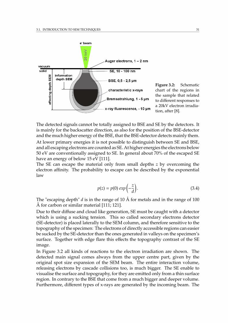
Figure 3.2: Schematicchart of the regions inthe sample that relatedto different responses toa 20kV electron irradia-tion, after [8].
The detected signals cannot be totally assigned to BSE and SE by the detectors. Itis mainly for the backscatter direction, as also for the position of the BSE-detectorand the much higher energy of the BSE, that the BSE-detector detects mainly them.At lower primary energies it is not possible to distinguish between SE and BSE,and all escaping electrons are counted as SE. At higher energies the electrons below50 eV are conventionally assigned to SE. In general about 70% of the escaped SEhave an energy of below 15 eV [111].The SE can escape the material only from small depths z by overcoming theelectron affinity. The probability to escape can be described by the exponentiallaw
p(z) = p(0) exp(−z
d
). (3.4)
The "escaping depth" d is in the range of 10 Å for metals and in the range of 100Å for carbon or similar material [111; 121].Due to their diffuse and cloud like generation, SE must be caught with a detectorwhich is using a sucking tension. This so called secondary electrons detector(SE-detector) is placed laterally to the SEM column, and therefore sensitive to thetopography of the specimen: The electrons of directly accessible regions can easierbe sucked by the SE-detector than the ones generated in valleys on the specimen’ssurface. Together with edge flare this effects the topography contrast of the SEimage.In Figure 3.2 all kinds of reactions to the electron irradiation are shown. Thedetected main signal comes always from the upper centre part, given by theoriginal spot size expansion of the SEM beam. The entire interaction volume,releasing electrons by cascade collisions too, is much bigger. The SE enable tovisualise the surface and topography, for they are emitted only from a thin surfaceregion. In contrary to the BSE that come from a much bigger and deeper volume.Furthermore, different types of x-rays are generated by the incoming beam. The
32 CHAPTER 3. INSTRUMENTS AND METHODS: SEM AND FIB
exploitation of characteristic x-rays will be discussed in subsection 3.1.3.High resolution is possible if the interaction volume in the sample is either big andhomogeneous enough, merely contributing to the signal as a constant backgroundnoise, or if it is about the same size as the beam spot size. In both cases the mainsignal, coming from the beam spot region on the surface, has enough contrast tothe surrounding and is not significantly affected.If scanning transmission electron microscopy (STEM) is applied, the sample has tobe as thin as for transmission electron microscopy (TEM) - providing a thicknessof less than 100 nm. Now interaction volume is respectively limited and theresolution is no longer limited by the signal noise.By comparing the amount of charge which is given by the SEM gun to the spec-imen, and that one leaving the sample again - directly or as a cloud of SE - itis found that the incoming fraction is much higher. To avoid a charging of thesample it is mandatory to fix the sample on the respective holder by a conductiveconnection, e.g. by silver glue (solvent: n-butylacetate).In case of insufficient internal specimen conductivity the sample is charged whichleads to a locally deflection of SE, generating annoying effects in the SEM image.For those samples surface conductivity can be achieved by sputtering a conduc-tive coating to the specimen. During this thesis a sputter device SCD 030 fromBalzers Union (Balzer, Liechtenstein) with gold-palladium target was used forthis. To achieve an equal deposition thickness of the coating, each sample wasexposed for 50 - 60 s at 30 mA.
3.1.3 Energy dispersive X-ray spectroscopy
The irradiation by SEM generates SE and causes holes in the electron shells ofthe atoms in the specimen. This happens directly by electrons from the gun,kicking out electrons from the atom shells, and indirectly via already generatedX-rays or higher energetic secondary electrons and BSE from the surrounding.This empty electron place in lower energetic shells is filled with an electron froma higher energetic shell. The energetic difference is radiated by a characteristicX-ray which can be assigned to the respective atom shell (Figure 3.3).The energy of this X-ray photon can be measured by a detector, which is eithera lithium drifted silicon detector (Si(Li)) or a silicon drift detector (SDD). Theolder Si(Li) detector type consists of a cylindrical silicon crystal, while the SDDis made out of silicon wafers and enables a 10 times faster measurement. Thefunction principle is basically similar: incoming X-rays generate electron-holepairs which are separated and drifted by a voltage to the electrodes. The amountof generated electron-hole pairs is proportional to the energy of the X-ray photon.By this energy dispersive X-ray spectroscopy (called EDX or EDS), the elementarycomposition of the specimen can be detected with an energetic resolution of upto 100 eV.As presented in Figure 3.2, the entire volume from where the EDX signal is
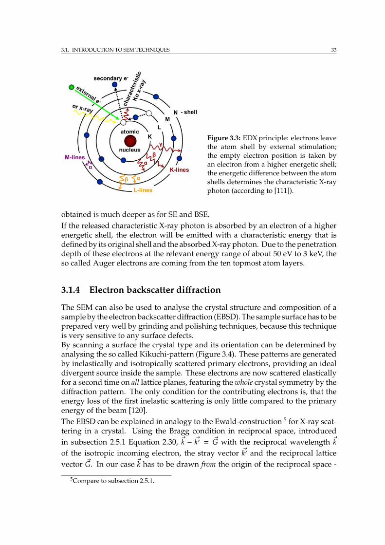
3.1. INTRODUCTION TO SEM TECHNIQUES 33
Figure 3.3: EDX principle: electrons leavethe atom shell by external stimulation;the empty electron position is taken byan electron from a higher energetic shell;the energetic difference between the atomshells determines the characteristic X-rayphoton (according to [111]).
obtained is much deeper as for SE and BSE.If the released characteristic X-ray photon is absorbed by an electron of a higherenergetic shell, the electron will be emitted with a characteristic energy that isdefined by its original shell and the absorbed X-ray photon. Due to the penetrationdepth of these electrons at the relevant energy range of about 50 eV to 3 keV, theso called Auger electrons are coming from the ten topmost atom layers.
3.1.4 Electron backscatter diffraction
The SEM can also be used to analyse the crystal structure and composition of asample by the electron backscatter diffraction (EBSD). The sample surface has to beprepared very well by grinding and polishing techniques, because this techniqueis very sensitive to any surface defects.By scanning a surface the crystal type and its orientation can be determined byanalysing the so called Kikuchi-pattern (Figure 3.4). These patterns are generatedby inelastically and isotropically scattered primary electrons, providing an idealdivergent source inside the sample. These electrons are now scattered elasticallyfor a second time on all lattice planes, featuring the whole crystal symmetry by thediffraction pattern. The only condition for the contributing electrons is, that theenergy loss of the first inelastic scattering is only little compared to the primaryenergy of the beam [120].The EBSD can be explained in analogy to the Ewald-construction 5 for X-ray scat-tering in a crystal. Using the Bragg condition in reciprocal space, introducedin subsection 2.5.1 Equation 2.30, k − k′ = G with the reciprocal wavelength kof the isotropic incoming electron, the stray vector k′ and the reciprocal latticevector G. In our case k has to be drawn from the origin of the reciprocal space -
5Compare to subsection 2.5.1.
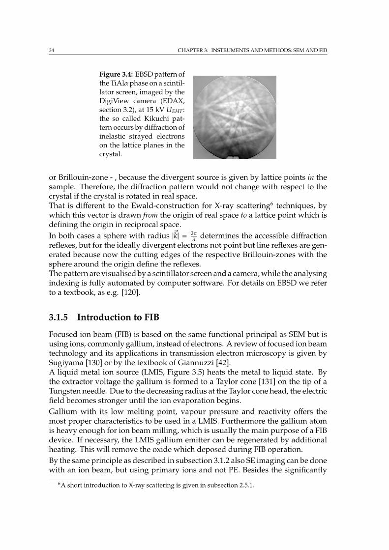
34 CHAPTER 3. INSTRUMENTS AND METHODS: SEM AND FIB
Figure 3.4: EBSD pattern ofthe TiAlαphase on a scintil-lator screen, imaged by theDigiView camera (EDAX,section 3.2), at 15 kV UEHT:the so called Kikuchi pat-tern occurs by diffraction ofinelastic strayed electronson the lattice planes in thecrystal.
or Brillouin-zone - , because the divergent source is given by lattice points in thesample. Therefore, the diffraction pattern would not change with respect to thecrystal if the crystal is rotated in real space.That is different to the Ewald-construction for X-ray scattering6 techniques, bywhich this vector is drawn from the origin of real space to a lattice point which isdefining the origin in reciprocal space.In both cases a sphere with radius |k| = 2π
λ determines the accessible diffractionreflexes, but for the ideally divergent electrons not point but line reflexes are gen-erated because now the cutting edges of the respective Brillouin-zones with thesphere around the origin define the reflexes.The pattern are visualised by a scintillator screen and a camera, while the analysingindexing is fully automated by computer software. For details on EBSD we referto a textbook, as e.g. [120].
3.1.5 Introduction to FIB
Focused ion beam (FIB) is based on the same functional principal as SEM but isusing ions, commonly gallium, instead of electrons. A review of focused ion beamtechnology and its applications in transmission electron microscopy is given bySugiyama [130] or by the textbook of Giannuzzi [42].A liquid metal ion source (LMIS, Figure 3.5) heats the metal to liquid state. Bythe extractor voltage the gallium is formed to a Taylor cone [131] on the tip of aTungsten needle. Due to the decreasing radius at the Taylor cone head, the electricfield becomes stronger until the ion evaporation begins.Gallium with its low melting point, vapour pressure and reactivity offers themost proper characteristics to be used in a LMIS. Furthermore the gallium atomis heavy enough for ion beam milling, which is usually the main purpose of a FIBdevice. If necessary, the LMIS gallium emitter can be regenerated by additionalheating. This will remove the oxide which deposed during FIB operation.By the same principle as described in subsection 3.1.2 also SE imaging can be donewith an ion beam, but using primary ions and not PE. Besides the significantly
6A short introduction to X-ray scattering is given in subsection 2.5.1.
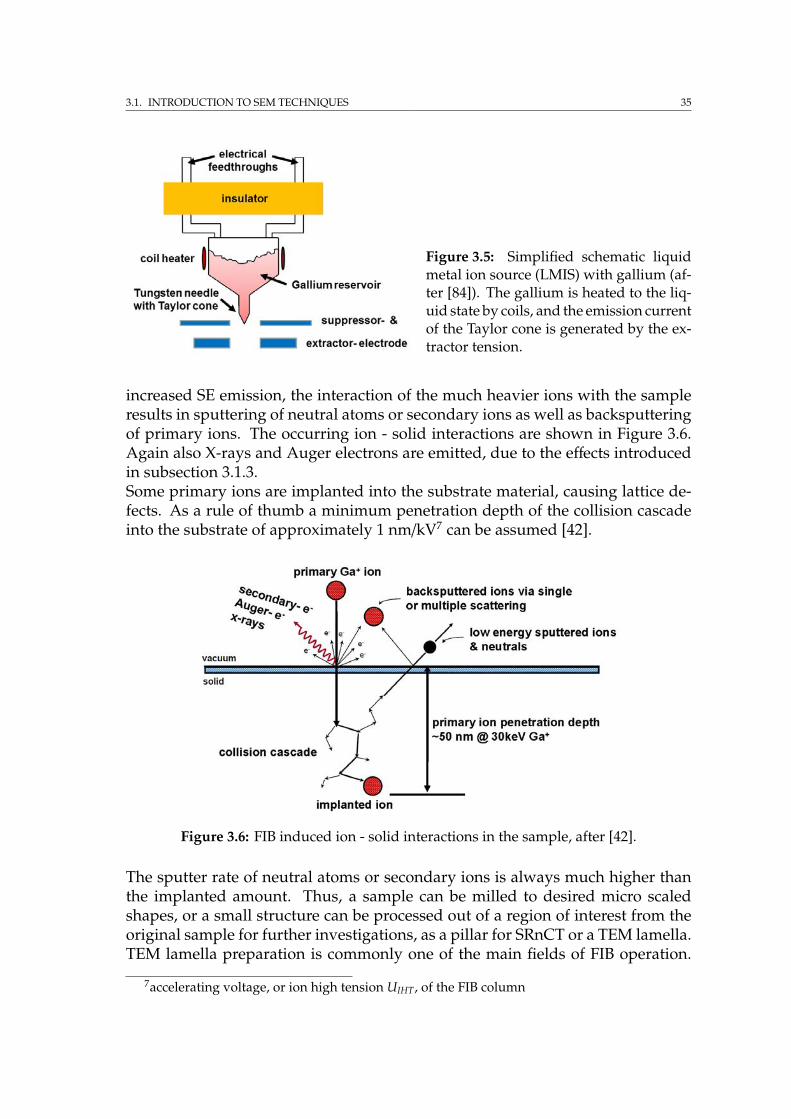
3.1. INTRODUCTION TO SEM TECHNIQUES 35
Figure 3.5: Simplified schematic liquidmetal ion source (LMIS) with gallium (af-ter [84]). The gallium is heated to the liq-uid state by coils, and the emission currentof the Taylor cone is generated by the ex-tractor tension.
increased SE emission, the interaction of the much heavier ions with the sampleresults in sputtering of neutral atoms or secondary ions as well as backsputteringof primary ions. The occurring ion - solid interactions are shown in Figure 3.6.Again also X-rays and Auger electrons are emitted, due to the effects introducedin subsection 3.1.3.Some primary ions are implanted into the substrate material, causing lattice de-fects. As a rule of thumb a minimum penetration depth of the collision cascadeinto the substrate of approximately 1 nm/kV7 can be assumed [42].
Figure 3.6: FIB induced ion - solid interactions in the sample, after [42].
The sputter rate of neutral atoms or secondary ions is always much higher thanthe implanted amount. Thus, a sample can be milled to desired micro scaledshapes, or a small structure can be processed out of a region of interest from theoriginal sample for further investigations, as a pillar for SRnCT or a TEM lamella.TEM lamella preparation is commonly one of the main fields of FIB operation.
7accelerating voltage, or ion high tension UIHT, of the FIB column
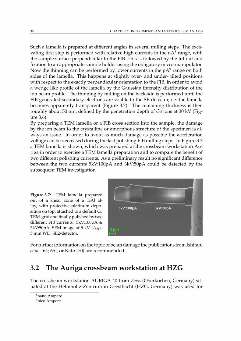
36 CHAPTER 3. INSTRUMENTS AND METHODS: SEM AND FIB
Such a lamella is prepared at different angles in several milling steps. The exca-vating first step is performed with relative high currents in the nA8 range, withthe sample surface perpendicular to the FIB. This is followed by the lift out andfixation to an appropriate sample holder using the obligatory micro-manipulator.Now the thinning can be performed by lower currents in the pA9 range on bothsides of the lamella. This happens at slightly over- and under- tilted positionswith respect to the exactly perpendicular orientation to the FIB, in order to avoida wedge like profile of the lamella by the Gaussian intensity distribution of theion beam profile. The thinning by milling on the backside is performed until theFIB generated secondary electrons are visible to the SE-detector, i.e. the lamellabecomes apparently transparent (Figure 3.7). The remaining thickness is thenroughly about 50 nm, defined by the penetration depth of Ga ions at 30 kV (Fig-ure 3.6).By preparing a TEM lamella or a FIB cross section into the sample, the damageby the ion beam to the crystalline or amorphous structure of the specimen is al-ways an issue. In order to avoid as much damage as possible the accelerationvoltage can be decreased during the last polishing FIB milling steps. In Figure 3.7a TEM lamella is shown, which was prepared at the crossbeam workstation Au-riga in order to exercise a TEM lamella preparation and to compare the benefit oftwo different polishing currents. As a preliminary result no significant differencebetween the two currents 5kV:100pA and 3kV:50pA could be detected by thesubsequent TEM investigation.
Figure 3.7: TEM lamella preparedout of a shear zone of a TiAl al-loy, with protective platinum depo-sition on top, attached to a default CuTEM-grid and finally polished by twodifferent FIB currents: 5kV:100pA &3kV:50pA. SEM image at 5 kV UEHT,5 mm WD, SE2-detector.
For further information on the topic of beam damage the publications from Ishitaniet al. [64; 65], or Kato [70] are recommended.
3.2 The Auriga crossbeam workstation at HZG
The crossbeam workstation AURIGA 40 from Zeiss (Oberkochen, Germany) sit-uated at the Helmholtz-Zentrum in Geesthacht (HZG, Germany) was used for
8nano Ampere9pico Ampere
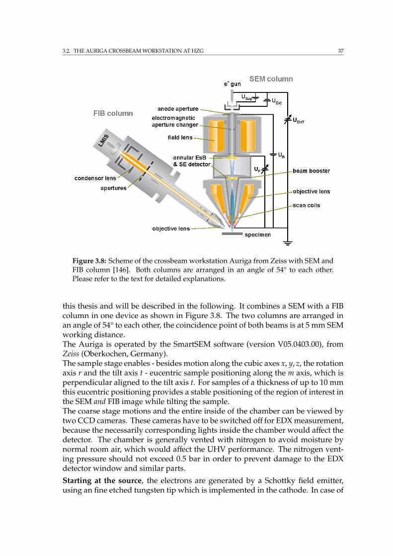
3.2. THE AURIGA CROSSBEAM WORKSTATION AT HZG 37
Figure 3.8: Scheme of the crossbeam workstation Auriga from Zeiss with SEM andFIB column [146]. Both columns are arranged in an angle of 54° to each other.Please refer to the text for detailed explanations.
this thesis and will be described in the following. It combines a SEM with a FIBcolumn in one device as shown in Figure 3.8. The two columns are arranged inan angle of 54° to each other, the coincidence point of both beams is at 5 mm SEMworking distance.The Auriga is operated by the SmartSEM software (version V05.0403.00), fromZeiss (Oberkochen, Germany).The sample stage enables - besides motion along the cubic axes x, y, z, the rotationaxis r and the tilt axis t - eucentric sample positioning along the m axis, which isperpendicular aligned to the tilt axis t. For samples of a thickness of up to 10 mmthis eucentric positioning provides a stable positioning of the region of interest inthe SEM and FIB image while tilting the sample.The coarse stage motions and the entire inside of the chamber can be viewed bytwo CCD cameras. These cameras have to be switched off for EDX measurement,because the necessarily corresponding lights inside the chamber would affect thedetector. The chamber is generally vented with nitrogen to avoid moisture bynormal room air, which would affect the UHV performance. The nitrogen vent-ing pressure should not exceed 0.5 bar in order to prevent damage to the EDXdetector window and similar parts.
Starting at the source, the electrons are generated by a Schottky field emitter,using an fine etched tungsten tip which is implemented in the cathode. In case of
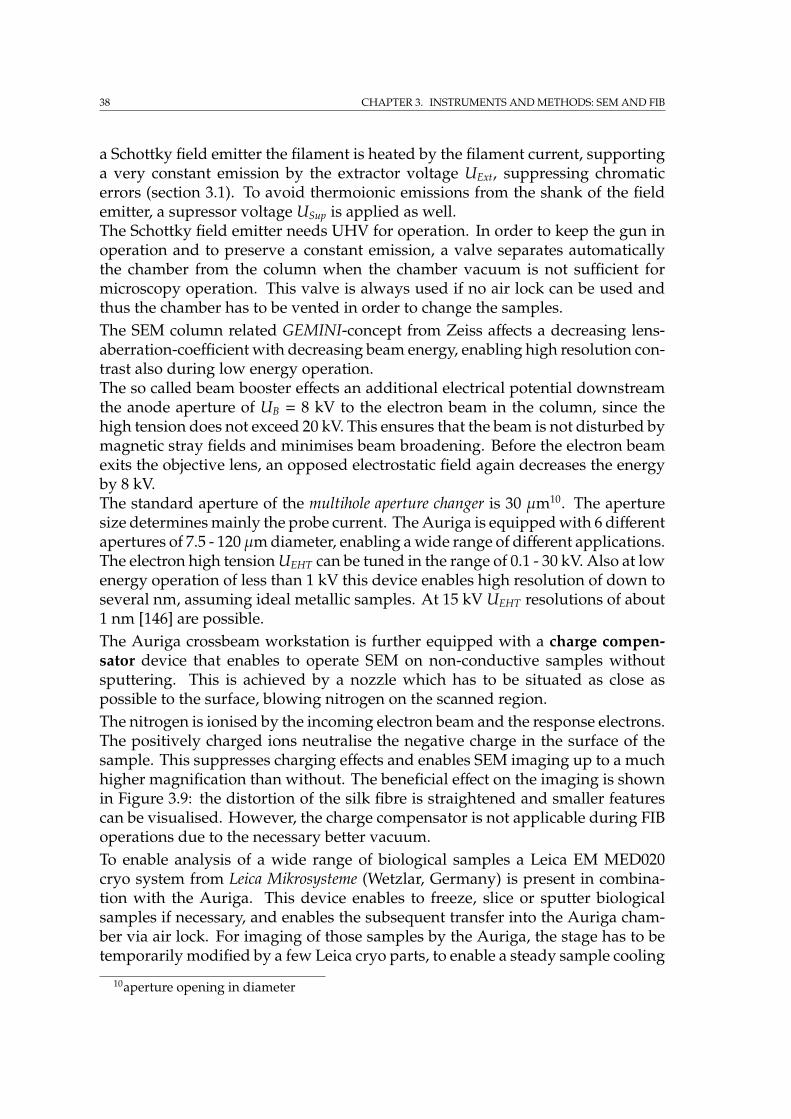
38 CHAPTER 3. INSTRUMENTS AND METHODS: SEM AND FIB
a Schottky field emitter the filament is heated by the filament current, supportinga very constant emission by the extractor voltage UExt, suppressing chromaticerrors (section 3.1). To avoid thermoionic emissions from the shank of the fieldemitter, a supressor voltage USup is applied as well.The Schottky field emitter needs UHV for operation. In order to keep the gun inoperation and to preserve a constant emission, a valve separates automaticallythe chamber from the column when the chamber vacuum is not sufficient formicroscopy operation. This valve is always used if no air lock can be used andthus the chamber has to be vented in order to change the samples.The SEM column related GEMINI-concept from Zeiss affects a decreasing lens-aberration-coefficient with decreasing beam energy, enabling high resolution con-trast also during low energy operation.The so called beam booster effects an additional electrical potential downstreamthe anode aperture of UB = 8 kV to the electron beam in the column, since thehigh tension does not exceed 20 kV. This ensures that the beam is not disturbed bymagnetic stray fields and minimises beam broadening. Before the electron beamexits the objective lens, an opposed electrostatic field again decreases the energyby 8 kV.The standard aperture of the multihole aperture changer is 30 µm10. The aperturesize determines mainly the probe current. The Auriga is equipped with 6 differentapertures of 7.5 - 120 µm diameter, enabling a wide range of different applications.The electron high tension UEHT can be tuned in the range of 0.1 - 30 kV. Also at lowenergy operation of less than 1 kV this device enables high resolution of down toseveral nm, assuming ideal metallic samples. At 15 kV UEHT resolutions of about1 nm [146] are possible.The Auriga crossbeam workstation is further equipped with a charge compen-sator device that enables to operate SEM on non-conductive samples withoutsputtering. This is achieved by a nozzle which has to be situated as close aspossible to the surface, blowing nitrogen on the scanned region.The nitrogen is ionised by the incoming electron beam and the response electrons.The positively charged ions neutralise the negative charge in the surface of thesample. This suppresses charging effects and enables SEM imaging up to a muchhigher magnification than without. The beneficial effect on the imaging is shownin Figure 3.9: the distortion of the silk fibre is straightened and smaller featurescan be visualised. However, the charge compensator is not applicable during FIBoperations due to the necessary better vacuum.To enable analysis of a wide range of biological samples a Leica EM MED020cryo system from Leica Mikrosysteme (Wetzlar, Germany) is present in combina-tion with the Auriga. This device enables to freeze, slice or sputter biologicalsamples if necessary, and enables the subsequent transfer into the Auriga cham-ber via air lock. For imaging of those samples by the Auriga, the stage has to betemporarily modified by a few Leica cryo parts, to enable a steady sample cooling
10aperture opening in diameter
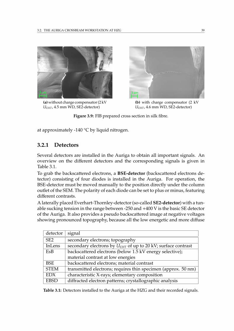
3.2. THE AURIGA CROSSBEAM WORKSTATION AT HZG 39
(a) without charge compensator (2 kVUEHT, 4.5 mm WD, SE2-detector)
(b) with charge compensator (2 kVUEHT, 4.6 mm WD, SE2-detector)
Figure 3.9: FIB prepared cross section in silk fibre.
at approximately -140 °C by liquid nitrogen.
3.2.1 Detectors
Several detectors are installed in the Auriga to obtain all important signals. Anoverview on the different detectors and the corresponding signals is given inTable 3.1.To grab the backscattered electrons, a BSE-detector (backscattered electrons de-tector) consisting of four diodes is installed in the Auriga. For operation, theBSE-detector must be moved manually to the position directly under the columnoutlet of the SEM. The polarity of each diode can be set to plus or minus, featuringdifferent contrasts.A laterally placed Everhart-Thornley-detector (so-called SE2-detector) with a tun-able sucking tension in the range between -250 and +400 V is the basic SE detectorof the Auriga. It also provides a pseudo backscattered image at negative voltagesshowing pronounced topography, because all the low energetic and more diffuse
detector signalSE2 secondary electrons; topographyInLens secondary electrons by UEHT of up to 20 kV; surface contrastEsB backscattered electrons (below 1.5 kV energy selective);
material contrast at low energiesBSE backscattered electrons; material contrastSTEM transmitted electrons; requires thin specimen (approx. 50 nm)EDX characteristic X-rays; elementary compositionEBSD diffracted electron patterns; crystallographic analysis
Table 3.1: Detectors installed to the Auriga at the HZG and their recorded signals.
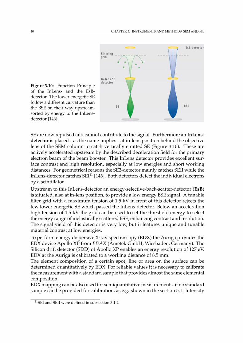
40 CHAPTER 3. INSTRUMENTS AND METHODS: SEM AND FIB
Figure 3.10: Function Principleof the InLens- and the EsB-detector. The lower energetic SEfollow a different curvature thanthe BSE on their way upstream,sorted by energy to the InLens-detector [146].
SE are now repulsed and cannot contribute to the signal. Furthermore an InLens-detector is placed - as the name implies - at in-lens position behind the objectivelens of the SEM column to catch vertically emitted SE (Figure 3.10). These areactively accelerated upstream by the described deceleration field for the primaryelectron beam of the beam booster. This InLens detector provides excellent sur-face contrast and high resolution, especially at low energies and short workingdistances. For geometrical reasons the SE2-detector mainly catches SEII while theInLens-detector catches SEI11 [146]. Both detectors detect the individual electronsby a scintillator.Upstream to this InLens-detector an energy-selective-back-scatter-detector (EsB)is situated, also at in-lens position, to provide a low energy BSE signal. A tunablefilter grid with a maximum tension of 1.5 kV in front of this detector rejects thefew lower energetic SE which passed the InLens-detector. Below an accelerationhigh tension of 1.5 kV the grid can be used to set the threshold energy to selectthe energy range of inelastically scattered BSE, enhancing contrast and resolution.The signal yield of this detector is very low, but it features unique and tunablematerial contrast at low energies.To perform energy dispersive X-ray spectroscopy (EDX) the Auriga provides theEDX device Apollo XP from EDAX (Ametek GmbH, Wiesbaden, Germany). TheSilicon drift detector (SDD) of Apollo XP enables an energy resolution of 127 eV.EDX at the Auriga is calibrated to a working distance of 8.5 mm.The element composition of a certain spot, line or area on the surface can bedetermined quantitatively by EDX. For reliable values it is necessary to calibratethe measurement with a standard sample that provides almost the same elementalcomposition.EDX mapping can be also used for semiquantitative measurements, if no standardsample can be provided for calibration, as e.g. shown in the section 5.1. Intensity
11SEI and SEII were defined in subsection 3.1.2
3.2. THE AURIGA CROSSBEAM WORKSTATION AT HZG 41
maps of each desired element on the surface can be obtained in parallel, i.e. alateral intensity map of the respective regions of interest in the EDX spectrum.The existing automatic drift correction of the Auriga was applied for mappingsand all long term measurements in this thesis to guarantee image quality.EBSD at the Auriga is provided by the DigiView detector, again from EDAX(Ametek GmbH, Wiesbaden, Germany). The detector camera is able to indexdiffraction patterns with a rate of up to 150 per second. Data acquisition andanalysis is accomplished by the EDAX software TSL-OIM12 for data-collectionand -analysis respectively.Furthermore, the Auriga provides also the possibility to perform scanning trans-mission electron microscopy (STEM). For this a special detector is installed onthe SEM chamber, which has to be driven in manually for measurement. Thepresent STEM sample holder must be used to obtain the signal below the sample,also providing the mounting of the default 3 mm Cu grids known from TEM. Thesample must fulfil similar restrictions as a TEM sample regarding thickness andsize, like e.g. a FIB prepared TEM lamella.
3.2.2 FIB apparatus
The crossbeam workstation Auriga is equipped with the Canion column fromOrsay physics (Fuveau, France). The Canion is providing 7 different sized me-chanically positioned apertures with diameters of usually 10, 30, 50, 100, 200, 400,and 600 µm to feature a variety of ion currents. The acceleration voltage, or ionhigh tension UIHT, of the Canion column is by default set to 30 kV. Though alsolower voltages are adjustable, especially to enable custom polishing currents.The Auriga is using a gallium LMIS13 for ion generation, which is the commonFIB layout. The emission current is generated by the extractor tension, and is keptconstant by an automatic regulation of the suppressor voltage (in analogy to thescheme of the SEM column in Figure 3.8). The FIB currents have to be adjusted bythe user to the desired values if necessary [146]. The character of the individualLMIS defines the highest possible currents in the >10 nA range. Not all currentsare possible with each LMIS.To ensure a constant high quality of the desired FIB currents, they have to be read-justed frequently in current value (by tuning the condensor14 voltage), apertureposition, focus, stigmation and beam shift correction.By using the 50 pA standard current for sample adjustments and determination ofthe milling region, an increased damage by the higher milling currents is avoided.However, the default use of the 50 pA current requires an adjusted beam shiftcorrection of the milling current, i.e. by the beam shift correction the millingcurrents image exactly the same area as the standard 50 pA current does.
12orientation imaging microscopy (OIM)13liquid metal ion source, introduced in subsection 3.1.514The value of the condensor voltage is inverse proportional to the FIB current value.
42 CHAPTER 3. INSTRUMENTS AND METHODS: SEM AND FIB
The FIB extends the surface limited SEM techniques to deep matter investiga-tions. By combination of both techniques the structure of a fine polished FIBprepared cross section, up to a depth of several 10 µm, can be analysed by theSEM component.The gas injection system (GIS) of the Auriga enables in combination with the FIBamorphous deposition of different materials as tungsten, platinum, carbon and aninsulator material. Each of these materials is a component of a special precursorgas15 that can be blown inside the SEM chamber onto the specimen’s surface. Toenable a deposition, the nozzles of the GIS have to be placed as close as possibleto the surface of the specimen in order to gain a high gas concentration at thededicated deposition region.The deposition process itself takes place by decomposing the precursor moleculesby the secondary electrons, which are emitted by the ion beam. The volatile by-products are pumped away while the desired material is deposited amorphously.The deposition layer contains about 10-20% implanted gallium and 10-20% im-planted carbon from the precursor or residual contamination [147].The deposition is essential for lift out procedures of FIB processed specimens asalso for the attachment to adequate sample holders. Furthermore, it is useful tocover a region of interest - that is dedicated to FIB cross sectioning or similar -with a deposition in order to avoid FIB damage and curtaining. This curtainingwould be induced by the beam deflecting on the edge of a bumpy sample surfaceand can be avoided by smoothing it with a deposition layer.The GIS also enables etching by use of the installed fluorine or water precursor.Etching happens in a similar way as the deposition procedure: The precursor isdecomposed by the secondary electrons, creating a volatile compound which isagain pumped away while the chemical active part reacts with the surface. Theetching can be used to increase the FIB milling yield and performance. It is de-pendent on the reactivity of sample and the active etching part of the precursor.During the usage of the GIS the precursors and the corresponding nozzles have tobe heated at individual temperatures to enable the gas flow. To guarantee a goodperformance of the GIS precursors the heating should be started some hours oreven a day before the application is scheduled.To move a FIB prepared specimen, as e.g. a TEM lamella, to an appropriate sampleholder like a TEM grid, the micro-manipulator Autoprobe 200 from Omniprobe16
(Texas, US) is installed to the Auriga. This device provides a long needle witha tip diameter of only some hundred nanometers. The needle can be positionedwith an accuracy of 100 nm, in order to attach the FIB prepared specimen to it, byusing the FIB/GIS technique. Subsequently the processed specimen is transferredto the sample holder and must be fixed to it, again by using the FIB/GIS technique.Some samples can also be welded by redeposition to the manipulator needle or asample holder. For this a FIB current in the nA range should be used, dependent
15details can be found in [147]16distributed by Oxford Instruments
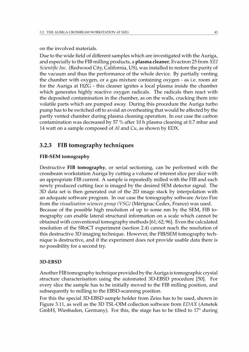
3.2. THE AURIGA CROSSBEAM WORKSTATION AT HZG 43
on the involved materials.Due to the wide field of different samples which are investigated with the Auriga,and especially to the FIB milling products, a plasma cleaner, Evactron 25 from XEIScientific Inc. (Redwood City, California, US), was installed to restore the purity ofthe vacuum and thus the performance of the whole device. By partially ventingthe chamber with oxygen, or a gas mixture containing oxygen - as i.e. room airfor the Auriga at HZG - this cleaner ignites a local plasma inside the chamberwhich generates highly reactive oxygen radicals. The radicals then react withthe deposited contamination in the chamber, as on the walls, cracking them intovolatile parts which are pumped away. During this procedure the Auriga turbopump has to be switched off to avoid an overheating that would be affected by thepartly vented chamber during plasma cleaning operation. In our case the carboncontamination was decreased by 57 % after 10 h plasma cleaning at 0.7 mbar and14 watt on a sample composed of Al and Cu, as shown by EDX.
3.2.3 FIB tomography techniques
FIB-SEM tomography
Destructive FIB tomography, or serial sectioning, can be performed with thecrossbeam workstation Auriga by cutting a volume of interest slice per slice withan appropriate FIB current. A sample is repeatedly milled with the FIB and eachnewly produced cutting face is imaged by the desired SEM detector signal. The3D data set is then generated out of the 2D image stack by interpolation withan adequate software program. In our case the tomography software Avizo Firefrom the visualisation sciences group (VSG) (Mérignac Cedex, France) was used.Because of the possible high resolution of up to some nm by the SEM, FIB to-mography can enable lateral structural information on a scale which cannot beobtained with conventional tomography methods [61; 62; 96]. Even the calculatedresolution of the SRnCT experiment (section 2.4) cannot reach the resolution ofthis destructive 3D imaging technique. However, the FIB/SEM tomography tech-nique is destructive, and if the experiment does not provide usable data there isno possibility for a second try.
3D-EBSD
Another FIB tomography technique provided by the Auriga is tomographic crystalstructure characterisation using the automated 3D-EBSD procedure [50]. Forevery slice the sample has to be initially moved to the FIB milling position, andsubsequently to milling to the EBSD-scanning position.For this the special 3D-EBSD sample holder from Zeiss has to be used, shown inFigure 3.11, as well as the 3D TSL-OIM collection software from EDAX (AmetekGmbH, Wiesbaden, Germany). For this, the stage has to be tilted to 17° during
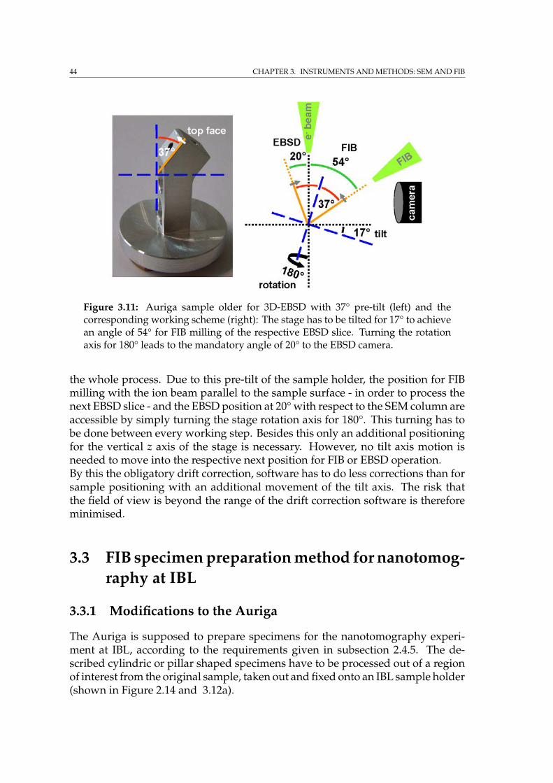
44 CHAPTER 3. INSTRUMENTS AND METHODS: SEM AND FIB
Figure 3.11: Auriga sample older for 3D-EBSD with 37° pre-tilt (left) and thecorresponding working scheme (right): The stage has to be tilted for 17° to achievean angle of 54° for FIB milling of the respective EBSD slice. Turning the rotationaxis for 180° leads to the mandatory angle of 20° to the EBSD camera.
the whole process. Due to this pre-tilt of the sample holder, the position for FIBmilling with the ion beam parallel to the sample surface - in order to process thenext EBSD slice - and the EBSD position at 20° with respect to the SEM column areaccessible by simply turning the stage rotation axis for 180°. This turning has tobe done between every working step. Besides this only an additional positioningfor the vertical z axis of the stage is necessary. However, no tilt axis motion isneeded to move into the respective next position for FIB or EBSD operation.By this the obligatory drift correction, software has to do less corrections than forsample positioning with an additional movement of the tilt axis. The risk thatthe field of view is beyond the range of the drift correction software is thereforeminimised.
3.3 FIB specimen preparation method for nanotomog-raphy at IBL
3.3.1 Modifications to the Auriga
The Auriga is supposed to prepare specimens for the nanotomography experi-ment at IBL, according to the requirements given in subsection 2.4.5. The de-scribed cylindric or pillar shaped specimens have to be processed out of a regionof interest from the original sample, taken out and fixed onto an IBL sample holder(shown in Figure 2.14 and 3.12a).
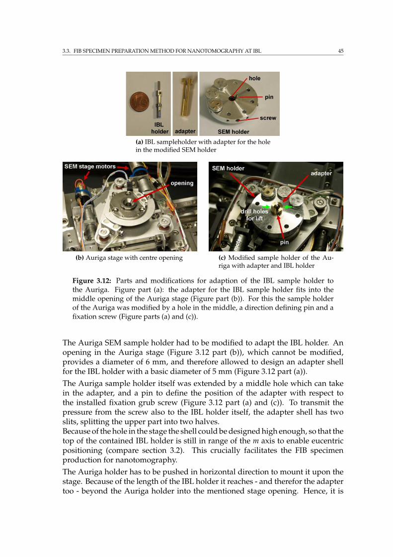
3.3. FIB SPECIMEN PREPARATION METHOD FOR NANOTOMOGRAPHY AT IBL 45
(a) IBL sampleholder with adapter for the holein the modified SEM holder
(b) Auriga stage with centre opening (c) Modified sample holder of the Au-riga with adapter and IBL holder
Figure 3.12: Parts and modifications for adaption of the IBL sample holder tothe Auriga. Figure part (a): the adapter for the IBL sample holder fits into themiddle opening of the Auriga stage (Figure part (b)). For this the sample holderof the Auriga was modified by a hole in the middle, a direction defining pin and afixation screw (Figure parts (a) and (c)).
The Auriga SEM sample holder had to be modified to adapt the IBL holder. Anopening in the Auriga stage (Figure 3.12 part (b)), which cannot be modified,provides a diameter of 6 mm, and therefore allowed to design an adapter shellfor the IBL holder with a basic diameter of 5 mm (Figure 3.12 part (a)).The Auriga sample holder itself was extended by a middle hole which can takein the adapter, and a pin to define the position of the adapter with respect tothe installed fixation grub screw (Figure 3.12 part (a) and (c)). To transmit thepressure from the screw also to the IBL holder itself, the adapter shell has twoslits, splitting the upper part into two halves.Because of the hole in the stage the shell could be designed high enough, so that thetop of the contained IBL holder is still in range of the m axis to enable eucentricpositioning (compare section 3.2). This crucially facilitates the FIB specimenproduction for nanotomography.The Auriga holder has to be pushed in horizontal direction to mount it upon thestage. Because of the length of the IBL holder it reaches - and therefor the adaptertoo - beyond the Auriga holder into the mentioned stage opening. Hence, it is
46 CHAPTER 3. INSTRUMENTS AND METHODS: SEM AND FIB
mandatory to insert the shell with the IBL holder subsequently to the mountingof the Auriga holder.To enable a safe lift out of the IBL holder inclusive specimen pillar on top, theadaptive shell was designed with a drill hole on both sides of the top - where noslit is - to enable insertion of a small tool driver or similar to lift it initially fromthe Auriga holder. Then it can be grabbed carefully by hands.
3.3.2 Specimen processing for SRnCT
In the following the specimen preparation method by FIB for the nanotomographyexperiment at IBL is introduced including the optimised parameters which werefound during the general development of this method. The whole process issimilar to the fabrication of a TEM lamella.When the region of interest is chosen by appropriate SEM techniques, as e.g. theuse of material contrast by the BSE-detector, the original sample has to be tiltedby the stage to 54° in order to enable a perpendicular milling to excavate the pillarout of the material (Figure 3.13a and 3.13b).The structure itself is excavated by several FIB milling steps from the bulk mate-rial, in minimum one circular and two trapezoid shaped ones. The trapezoid onesenable a cut off from both sides. This saves time during the excavation procedure,because for geometric reasons a cut off from only one side would effort a deepercircular milling. Additionally, an excavating milling with increased depth con-sumes more time, caused by the higher energy which is needed for the sputteredparticles to leave the hole.Depending on the individual material and whether the depth milling is performedonly in one or very few layers, redeposition leads to a wedge like shaped trape-zoid excavation hole. If this does not restrict the cut off, this is acceptable. Incontrast, the circular milling has to be performed in at least 10 layers to guaranteea free standing pillar without wedge shaped redeposition.For the excavating FIB mill steps, currents of at least >10 nA should be used.For an optional partially cut off from the back side, the stage should be tilted asclose as possible to 0° or even a slight negative tilt. The vertical milling positionis dependent on the previously chosen trapezoid depth on the front side. In anycase it should be tried to cut off as flat and deep as possible, first partially fromthe back side and then finally from the front side. Before the second and finalcut off, the GIS operation has to be prepared, because it is mandatory to attachthe pillar by the FIB to the micro-manipulator needle tip before the final cut off isdone. Otherwise the pillar would be charged by the electron beam and attractedby the SE2-detector’s sucking tension, or another source of attraction, and wouldget lost.
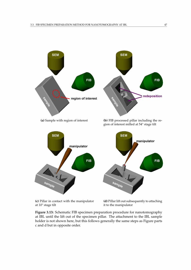
3.3. FIB SPECIMEN PREPARATION METHOD FOR NANOTOMOGRAPHY AT IBL 47
(a) Sample with region of interest (b) FIB processed pillar including the re-gion of interest milled at 54° stage tilt
(c) Pillar in contact with the manipulatorat 10° stage tilt
(d) Pillar lift out subsequently to attachingit to the manipulator
Figure 3.13: Schematic FIB specimen preparation procedure for nanotomographyat IBL until the lift out of the specimen pillar. The attachment to the IBL sampleholder is not shown here, but this follows generally the same steps as Figure partsc and d but in opposite order.
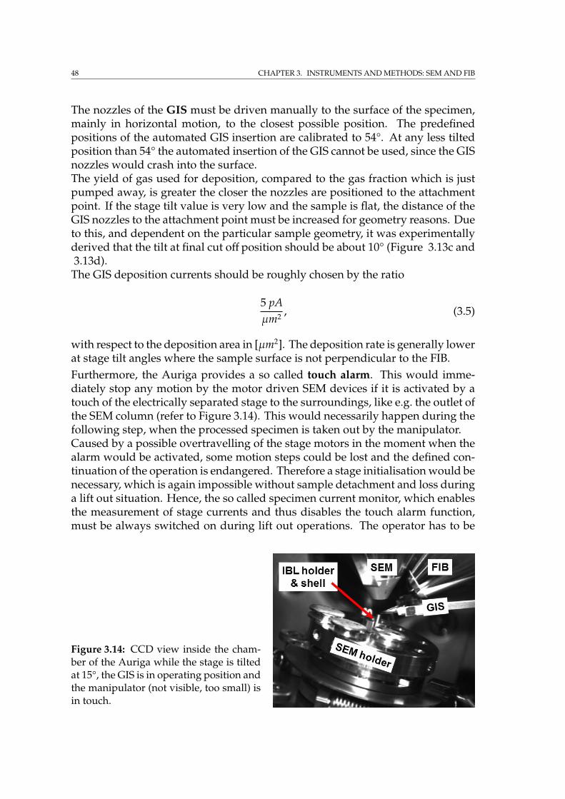
48 CHAPTER 3. INSTRUMENTS AND METHODS: SEM AND FIB
The nozzles of the GIS must be driven manually to the surface of the specimen,mainly in horizontal motion, to the closest possible position. The predefinedpositions of the automated GIS insertion are calibrated to 54°. At any less tiltedposition than 54° the automated insertion of the GIS cannot be used, since the GISnozzles would crash into the surface.The yield of gas used for deposition, compared to the gas fraction which is justpumped away, is greater the closer the nozzles are positioned to the attachmentpoint. If the stage tilt value is very low and the sample is flat, the distance of theGIS nozzles to the attachment point must be increased for geometry reasons. Dueto this, and dependent on the particular sample geometry, it was experimentallyderived that the tilt at final cut off position should be about 10° (Figure 3.13c and3.13d).
The GIS deposition currents should be roughly chosen by the ratio
5 pAµm2 , (3.5)
with respect to the deposition area in [µm2]. The deposition rate is generally lowerat stage tilt angles where the sample surface is not perpendicular to the FIB.Furthermore, the Auriga provides a so called touch alarm. This would imme-diately stop any motion by the motor driven SEM devices if it is activated by atouch of the electrically separated stage to the surroundings, like e.g. the outlet ofthe SEM column (refer to Figure 3.14). This would necessarily happen during thefollowing step, when the processed specimen is taken out by the manipulator.Caused by a possible overtravelling of the stage motors in the moment when thealarm would be activated, some motion steps could be lost and the defined con-tinuation of the operation is endangered. Therefore a stage initialisation would benecessary, which is again impossible without sample detachment and loss duringa lift out situation. Hence, the so called specimen current monitor, which enablesthe measurement of stage currents and thus disables the touch alarm function,must be always switched on during lift out operations. The operator has to be
Figure 3.14: CCD view inside the cham-ber of the Auriga while the stage is tiltedat 15°, the GIS is in operating position andthe manipulator (not visible, too small) isin touch.
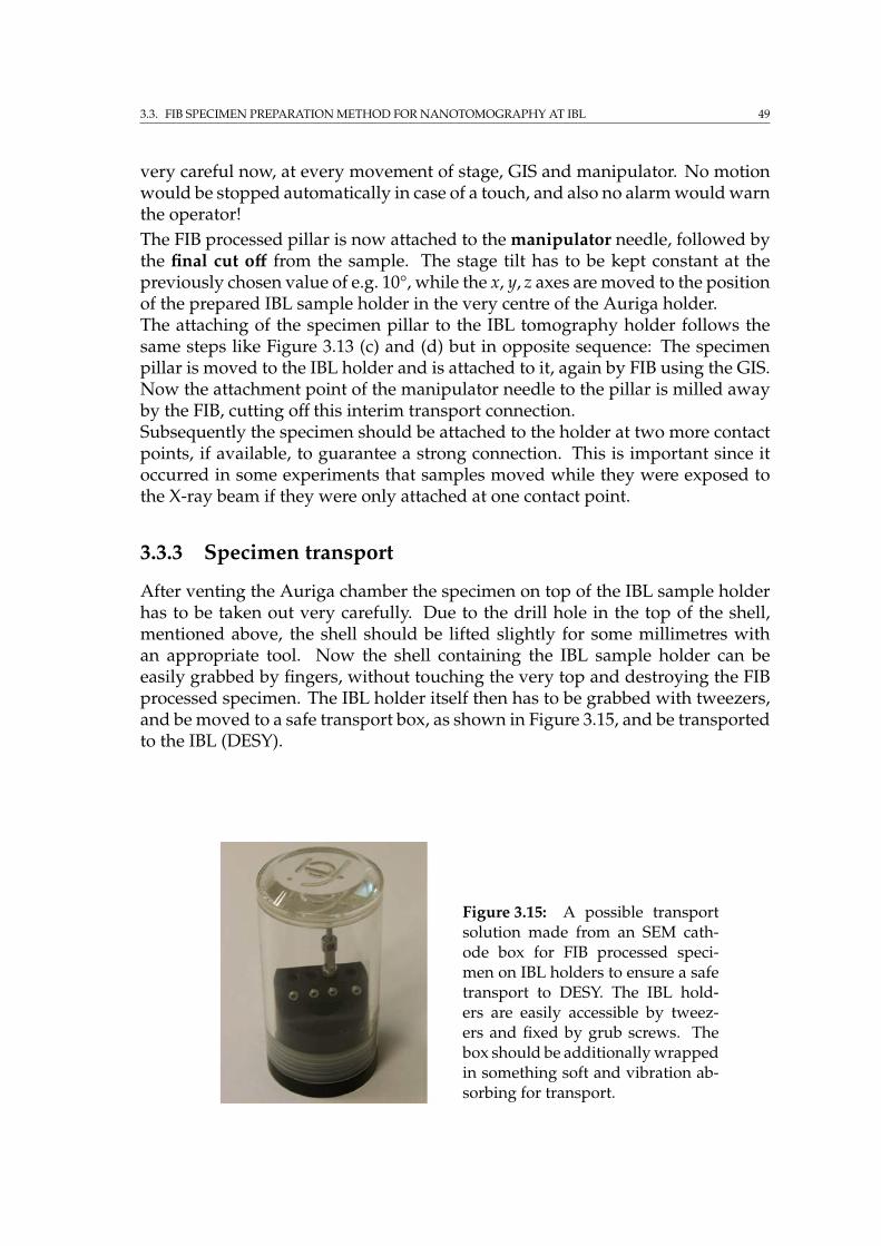
3.3. FIB SPECIMEN PREPARATION METHOD FOR NANOTOMOGRAPHY AT IBL 49
very careful now, at every movement of stage, GIS and manipulator. No motionwould be stopped automatically in case of a touch, and also no alarm would warnthe operator!The FIB processed pillar is now attached to the manipulator needle, followed bythe final cut off from the sample. The stage tilt has to be kept constant at thepreviously chosen value of e.g. 10°, while the x, y, z axes are moved to the positionof the prepared IBL sample holder in the very centre of the Auriga holder.The attaching of the specimen pillar to the IBL tomography holder follows thesame steps like Figure 3.13 (c) and (d) but in opposite sequence: The specimenpillar is moved to the IBL holder and is attached to it, again by FIB using the GIS.Now the attachment point of the manipulator needle to the pillar is milled awayby the FIB, cutting off this interim transport connection.Subsequently the specimen should be attached to the holder at two more contactpoints, if available, to guarantee a strong connection. This is important since itoccurred in some experiments that samples moved while they were exposed tothe X-ray beam if they were only attached at one contact point.
3.3.3 Specimen transport
After venting the Auriga chamber the specimen on top of the IBL sample holderhas to be taken out very carefully. Due to the drill hole in the top of the shell,mentioned above, the shell should be lifted slightly for some millimetres withan appropriate tool. Now the shell containing the IBL sample holder can beeasily grabbed by fingers, without touching the very top and destroying the FIBprocessed specimen. The IBL holder itself then has to be grabbed with tweezers,and be moved to a safe transport box, as shown in Figure 3.15, and be transportedto the IBL (DESY).
Figure 3.15: A possible transportsolution made from an SEM cath-ode box for FIB processed speci-men on IBL holders to ensure a safetransport to DESY. The IBL hold-ers are easily accessible by tweez-ers and fixed by grub screws. Thebox should be additionally wrappedin something soft and vibration ab-sorbing for transport.

50
Chapter 4
Applications: Porous Ti-6Al-4Vimplant material for cell ingrowth
Due to the necessity of fast healing and mechanical stability there is still a need forfurther development of implants. The characteristics of titanium alloys regard-ing bio-compatibility, mechanical properties and corrosion resistance make thema very suited material for orthopaedic or dental implants. Since the late 1930’sthis led to the natural choice of titanium or related alloys as major material forimplants, like e.g. bone screws, hip replacements or parts of artificial heart valves.Regarding the still proceeding increase of human lifetime, it becomes necessaryto develop long lasting implants to avoid multiple revision surgeries. To enablea proper adaption and long lasting stability of the bone implanted devices, it isessential that the Young’s modulus1 of the implant is similar to the one of corti-cal bone [125]. A further improvement of stability can be achieved by bone-cellingrowth into the implant [20]. It is known that the topography of prostheticdevices can directly influence the cellular response. Thus, assuming a direct con-nection between material pore size and bone formation [88], it becomes necessaryto find the most proper porosity, enabling cell migration and in vivo blood vesselformation.Metal injection moulding (MIM) provides the advantage of processing net-shapedand rather complex parts at comparably low production costs, as well as adjustingthe porosity by using different sizes of metal powder or tuning the sinteringtemperature. This includes also Ti alloys [30].Control of the porosity gradient allows to mimick the structure of natural bone.This should be ideal to enable ingrowth of new bone tissues and vascularisation.Moreover, the mechanical properties of porous titanium are very close to those ofnatural bone. This characteristic is mandatory for osteoinduction.Four different porous sample categories were produced by A. Deing within thescope of his thesis, by using different sized Ti-6Al-4V2 powders. Those were
1also known as tensile or elastic modulus2composition in mass percent
51
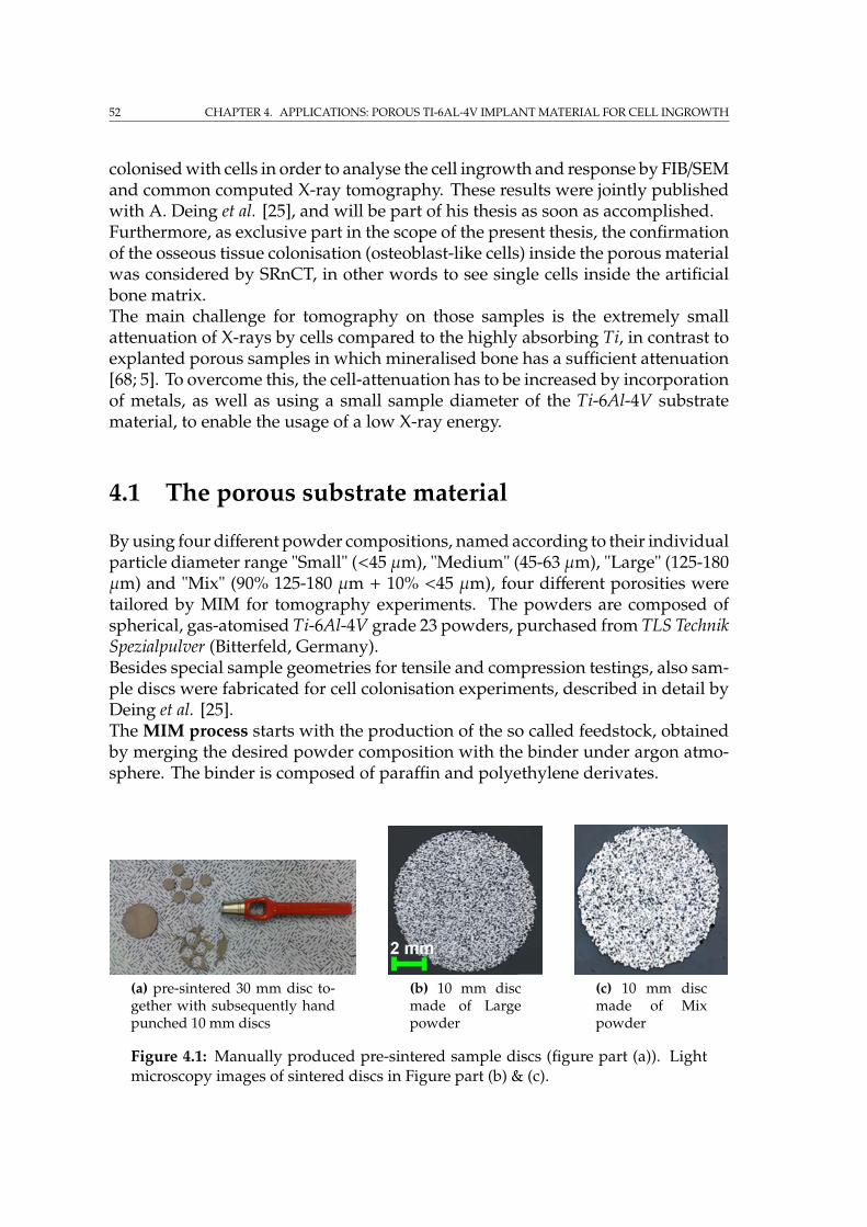
52 CHAPTER 4. APPLICATIONS: POROUS TI-6AL-4V IMPLANT MATERIAL FOR CELL INGROWTH
colonised with cells in order to analyse the cell ingrowth and response by FIB/SEMand common computed X-ray tomography. These results were jointly publishedwith A. Deing et al. [25], and will be part of his thesis as soon as accomplished.Furthermore, as exclusive part in the scope of the present thesis, the confirmationof the osseous tissue colonisation (osteoblast-like cells) inside the porous materialwas considered by SRnCT, in other words to see single cells inside the artificialbone matrix.The main challenge for tomography on those samples is the extremely smallattenuation of X-rays by cells compared to the highly absorbing Ti, in contrast toexplanted porous samples in which mineralised bone has a sufficient attenuation[68; 5]. To overcome this, the cell-attenuation has to be increased by incorporationof metals, as well as using a small sample diameter of the Ti-6Al-4V substratematerial, to enable the usage of a low X-ray energy.
4.1 The porous substrate material
By using four different powder compositions, named according to their individualparticle diameter range "Small" (<45 µm), "Medium" (45-63 µm), "Large" (125-180µm) and "Mix" (90% 125-180 µm + 10% <45 µm), four different porosities weretailored by MIM for tomography experiments. The powders are composed ofspherical, gas-atomised Ti-6Al-4V grade 23 powders, purchased from TLS TechnikSpezialpulver (Bitterfeld, Germany).Besides special sample geometries for tensile and compression testings, also sam-ple discs were fabricated for cell colonisation experiments, described in detail byDeing et al. [25].The MIM process starts with the production of the so called feedstock, obtainedby merging the desired powder composition with the binder under argon atmo-sphere. The binder is composed of paraffin and polyethylene derivates.
(a) pre-sintered 30 mm disc to-gether with subsequently handpunched 10 mm discs
(b) 10 mm discmade of Largepowder
(c) 10 mm discmade of Mixpowder
Figure 4.1: Manually produced pre-sintered sample discs (figure part (a)). Lightmicroscopy images of sintered discs in Figure part (b) & (c).
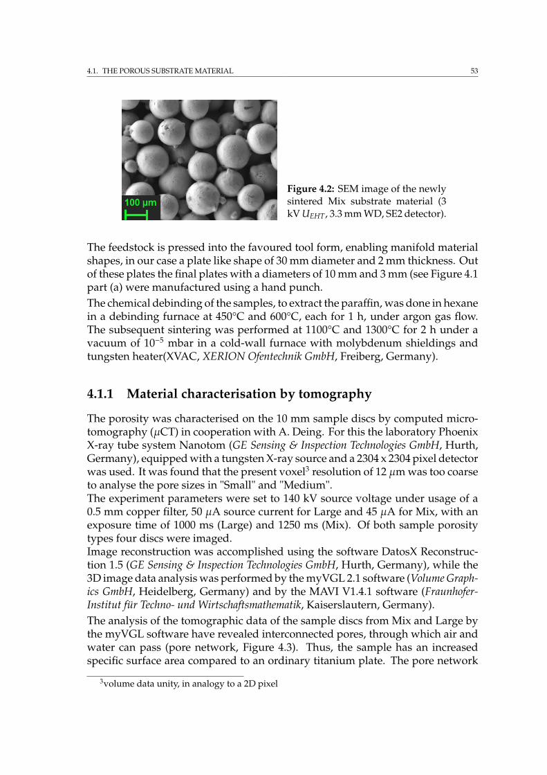
4.1. THE POROUS SUBSTRATE MATERIAL 53
Figure 4.2: SEM image of the newlysintered Mix substrate material (3kV UEHT, 3.3 mm WD, SE2 detector).
The feedstock is pressed into the favoured tool form, enabling manifold materialshapes, in our case a plate like shape of 30 mm diameter and 2 mm thickness. Outof these plates the final plates with a diameters of 10 mm and 3 mm (see Figure 4.1part (a) were manufactured using a hand punch.The chemical debinding of the samples, to extract the paraffin, was done in hexanein a debinding furnace at 450°C and 600°C, each for 1 h, under argon gas flow.The subsequent sintering was performed at 1100°C and 1300°C for 2 h under avacuum of 10−5 mbar in a cold-wall furnace with molybdenum shieldings andtungsten heater(XVAC, XERION Ofentechnik GmbH, Freiberg, Germany).
4.1.1 Material characterisation by tomography
The porosity was characterised on the 10 mm sample discs by computed micro-tomography (µCT) in cooperation with A. Deing. For this the laboratory PhoenixX-ray tube system Nanotom (GE Sensing & Inspection Technologies GmbH, Hurth,Germany), equipped with a tungsten X-ray source and a 2304 x 2304 pixel detectorwas used. It was found that the present voxel3 resolution of 12 µm was too coarseto analyse the pore sizes in "Small" and "Medium".The experiment parameters were set to 140 kV source voltage under usage of a0.5 mm copper filter, 50 µA source current for Large and 45 µA for Mix, with anexposure time of 1000 ms (Large) and 1250 ms (Mix). Of both sample porositytypes four discs were imaged.Image reconstruction was accomplished using the software DatosX Reconstruc-tion 1.5 (GE Sensing & Inspection Technologies GmbH, Hurth, Germany), while the3D image data analysis was performed by the myVGL 2.1 software (Volume Graph-ics GmbH, Heidelberg, Germany) and by the MAVI V1.4.1 software (Fraunhofer-Institut für Techno- und Wirtschaftsmathematik, Kaiserslautern, Germany).The analysis of the tomographic data of the sample discs from Mix and Large bythe myVGL software have revealed interconnected pores, through which air andwater can pass (pore network, Figure 4.3). Thus, the sample has an increasedspecific surface area compared to an ordinary titanium plate. The pore network
3volume data unity, in analogy to a 2D pixel
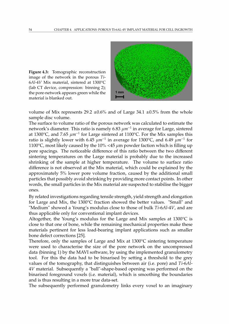
54 CHAPTER 4. APPLICATIONS: POROUS TI-6AL-4V IMPLANT MATERIAL FOR CELL INGROWTH
Figure 4.3: Tomographic reconstructionimage of the network in the porous Ti-6Al-4V Mix material, sintered at 1300°C(lab CT device, compression: binning 2);the pore-network appears green while thematerial is blanked out.
volume of Mix represents 29.2 ±0.6% and of Large 34.1 ±0.5% from the wholesample disc volume.The surface to volume ratio of the porous network was calculated to estimate thenetwork’s diameter. This ratio is namely 6.83 µm−1 in average for Large, sinteredat 1300°C, and 7.65 µm−1 for Large sintered at 1100°C. For the Mix samples thisratio is slightly lower with 6.45 µm−1 in average for 1300°C, and 6.49 µm−1 for1100°C, most likely caused by the 10% <45 µm powder faction which is filling uppore spacings. The noticeable difference of this ratio between the two differentsintering temperatures on the Large material is probably due to the increasedshrinking of the sample at higher temperature. The volume to surface ratiodifference is not observed at the Mix material, which could be explained by theapproximately 5% lower pore volume fraction, caused by the additional smallparticles that possibly avoid shrinking by providing more contact points. In otherwords, the small particles in the Mix material are suspected to stabilise the biggerones.By related investigations regarding tensile strength, yield strength and elongationfor Large and Mix, the 1300°C fraction showed the better values. "Small" and"Medium" showed a Young’s modulus close to those of bulk Ti-6Al-4V, and arethus applicable only for conventional implant devices.Altogether, the Young’s modulus for the Large and Mix samples at 1300°C isclose to that one of bone, while the remaining mechanical properties make thesematerials pertinent for less load-bearing implant applications such as smallerbone defect corrections [25].Therefore, only the samples of Large and Mix at 1300°C sintering temperaturewere used to characterise the size of the pore network on the uncompresseddata (binning 1) by the MAVI software, by using the implemented granulometrytool. For this the data had to be binarised by setting a threshold to the greyvalues of the tomography, that distinguishes between air (i.e. pore) and Ti-6Al-4V material. Subsequently a "ball"-shape-based opening was performed on thebinarised foreground voxels (i.e. material), which is smoothing the boundariesand is thus resulting in a more true data-set.The subsequently performed granulometry links every voxel to an imaginary
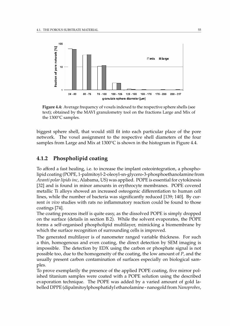
4.1. THE POROUS SUBSTRATE MATERIAL 55
Figure 4.4: Average frequency of voxels indexed to the respective sphere shells (seetext); obtained by the MAVI granulometry tool on the fractions Large and Mix ofthe 1300°C samples.
biggest sphere shell, that would still fit into each particular place of the porenetwork. The voxel assignment to the respective shell diameters of the foursamples from Large and Mix at 1300°C is shown in the histogram in Figure 4.4.
4.1.2 Phospholipid coating
To afford a fast healing, i.e. to increase the implant osteointegration, a phospho-lipid coating (POPE, 1-palmitoyl-2-oleoyl-sn-glycero-3-phosphoethanolamine fromAvanti polar lipids inc, Alabama, US) was applied. POPE is essential for cytokinesis[32] and is found in minor amounts in erythrocyte membranes. POPE coveredmetallic Ti alloys showed an increased osteogenic differentiation to human celllines, while the number of bacteria was significantly reduced [139; 140]. By cur-rent in vivo studies with rats no inflammatory reaction could be found to thosecoatings [74].The coating process itself is quite easy, as the dissolved POPE is simply droppedon the surface (details in section B.2). While the solvent evaporates, the POPEforms a self-organised phospholipid multilayer, mimicking a biomembrane bywhich the surface recognition of surrounding cells is improved.The generated multilayer is of nanometer ranged variable thickness. For sucha thin, homogenous and even coating, the direct detection by SEM imaging isimpossible. The detection by EDX using the carbon or phosphate signal is notpossible too, due to the homogeneity of the coating, the low amount of P, and theusually present carbon contamination of surfaces especially on biological sam-ples.To prove exemplarily the presence of the applied POPE coating, five mirror pol-ished titanium samples were coated with a POPE solution using the describedevaporation technique. The POPE was added by a varied amount of gold la-belled DPPE (dipalmitoylphosphatidyl ethanolamine - nanogold from Nanoprobes,
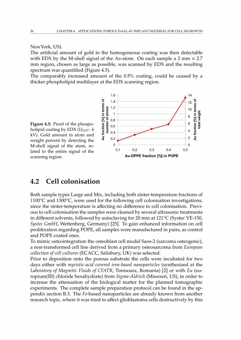
56 CHAPTER 4. APPLICATIONS: POROUS TI-6AL-4V IMPLANT MATERIAL FOR CELL INGROWTH
NewYork, US).The artificial amount of gold in the homogeneous coating was then detectablewith EDX by the M-shell signal of the Au-atom. On each sample a 2 mm × 2.7mm region, chosen as large as possible, was scanned by EDX and the resultingspectrum was quantified (Figure 4.5).The comparably increased amount of the 0.5% coating, could be caused by athicker phospholipid multilayer at the EDX scanning region.
Figure 4.5: Proof of the phospo-holipid coating by EDX (UEHT: 6kV). Gold amount in atom andweight percent by detecting theM-shell signal of the atom, re-lated to the entire signal of thescanning region.
4.2 Cell colonisation
Both sample types Large and Mix, including both sinter-temperature fractions of1100°C and 1300°C, were used for the following cell colonisation investigations,since the sinter-temperature is affecting no difference to cell colonisation. Previ-ous to cell colonisation the samples were cleaned by several ultrasonic treatmentsin different solvents, followed by autoclaving for 20 min at 121°C (Systec VE-150,Systec GmbH, Wettenberg, Germany) [25]. To gain enhanced information on cellproliferation regarding POPE, all samples were manufactured in pairs, as controland POPE coated ones.To mimic osteointegration the osteoblast cell model Saos-2 (sarcoma osteogenic),a non-transformed cell line derived from a primary osteosarcoma from Europeancollection of cell cultures (ECACC, Salisbury, UK) was selected.Prior to deposition onto the porous substrate the cells were incubated for twodays either with myristic-acid covered iron-based nanoparticles (synthesized at theLaboratory of Magnetic Fluids of CFATR, Timisoara, Romania) [2] or with Eu (eu-ropium(III) chloride hexahydrate) from Sigma-Aldrich (Missouri, US), in order toincrease the attenuation of the biological matter for the planned tomographicexperiments. The complete sample preparation protocol can be found in the ap-pendix section B.3. The Fe-based nanoparticles are already known from anotherresearch topic, where it was tried to affect glioblastoma cells destructively by this

4.2. CELL COLONISATION 57
nanoparticles [2]. Glioblastoma cells4 are typical malicious brain-cancerous cells.After two days culture in growth medium the samples were stabilised for SEM aswell as for SRnCT with OsO4
5, dehydrated by an alcoholic row using isopropanoland were supercritical dried in order to maintain the cell natural shape and sta-bility under vacuum conditions.Besides the described incorporation of Fe and Eu, the obligatory osmiumtetroxide(OsO4) fixation stain is now in charge to contribute additionally to the cell atten-uation regarding SRnCT.Supercritical drying by CO2
6 was performed with a Leica EM CPD030 from LeicaMikrosysteme (Wetzlar, Germany) (the detailed procedure is given in section B.1).
4As proof of principle a FIB tomography on a single glioblastoma cell is given in Appendix C.5osmiumtetroxide6CO2 critical point @ 73,9 bar and 31.1 °C
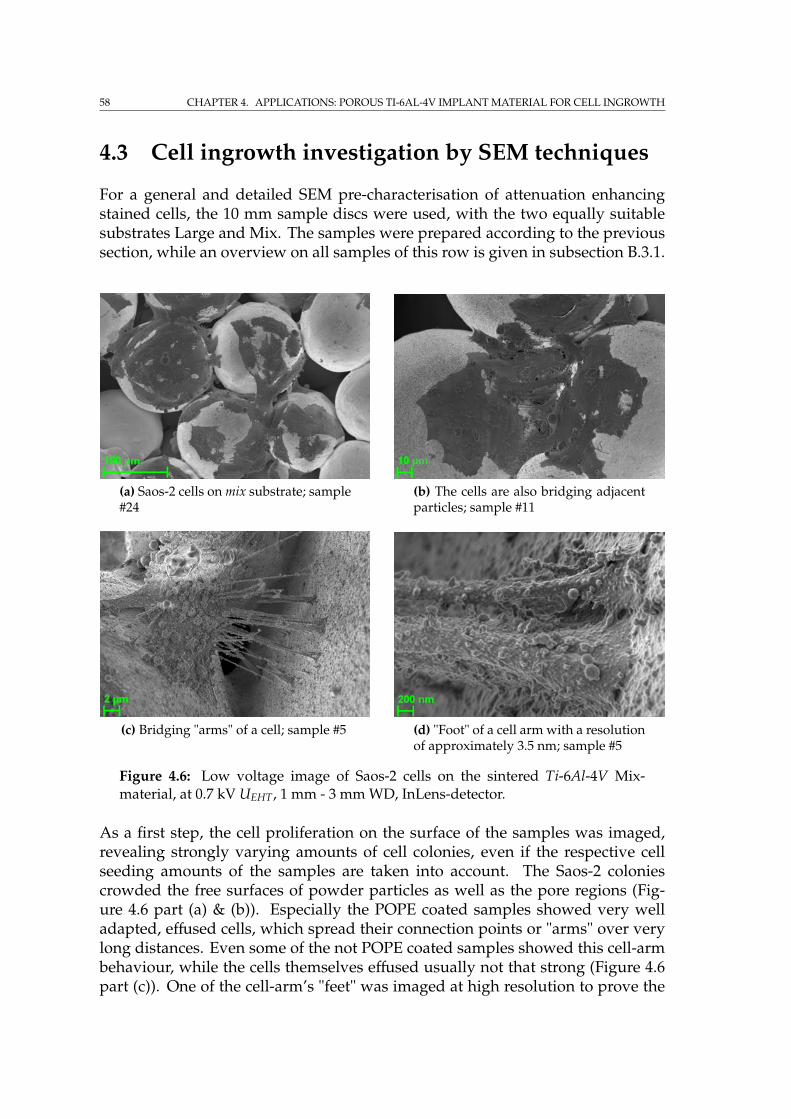
58 CHAPTER 4. APPLICATIONS: POROUS TI-6AL-4V IMPLANT MATERIAL FOR CELL INGROWTH
4.3 Cell ingrowth investigation by SEM techniques
For a general and detailed SEM pre-characterisation of attenuation enhancingstained cells, the 10 mm sample discs were used, with the two equally suitablesubstrates Large and Mix. The samples were prepared according to the previoussection, while an overview on all samples of this row is given in subsection B.3.1.
(a) Saos-2 cells on mix substrate; sample#24
(b) The cells are also bridging adjacentparticles; sample #11
(c) Bridging "arms" of a cell; sample #5 (d) "Foot" of a cell arm with a resolutionof approximately 3.5 nm; sample #5
Figure 4.6: Low voltage image of Saos-2 cells on the sintered Ti-6Al-4V Mix-material, at 0.7 kV UEHT, 1 mm - 3 mm WD, InLens-detector.
As a first step, the cell proliferation on the surface of the samples was imaged,revealing strongly varying amounts of cell colonies, even if the respective cellseeding amounts of the samples are taken into account. The Saos-2 coloniescrowded the free surfaces of powder particles as well as the pore regions (Fig-ure 4.6 part (a) & (b)). Especially the POPE coated samples showed very welladapted, effused cells, which spread their connection points or "arms" over verylong distances. Even some of the not POPE coated samples showed this cell-armbehaviour, while the cells themselves effused usually not that strong (Figure 4.6part (c)). One of the cell-arm’s "feet" was imaged at high resolution to prove the
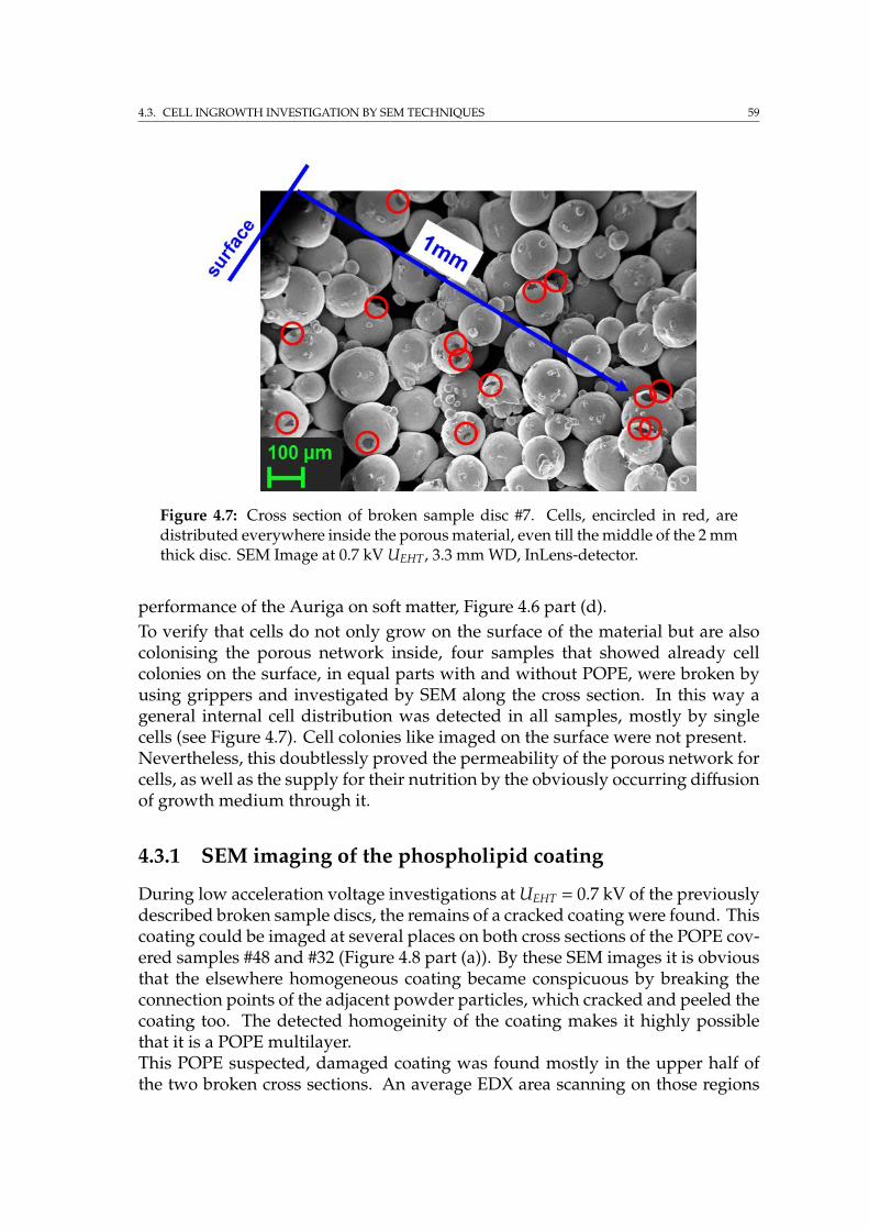
4.3. CELL INGROWTH INVESTIGATION BY SEM TECHNIQUES 59
Figure 4.7: Cross section of broken sample disc #7. Cells, encircled in red, aredistributed everywhere inside the porous material, even till the middle of the 2 mmthick disc. SEM Image at 0.7 kV UEHT, 3.3 mm WD, InLens-detector.
performance of the Auriga on soft matter, Figure 4.6 part (d).To verify that cells do not only grow on the surface of the material but are alsocolonising the porous network inside, four samples that showed already cellcolonies on the surface, in equal parts with and without POPE, were broken byusing grippers and investigated by SEM along the cross section. In this way ageneral internal cell distribution was detected in all samples, mostly by singlecells (see Figure 4.7). Cell colonies like imaged on the surface were not present.Nevertheless, this doubtlessly proved the permeability of the porous network forcells, as well as the supply for their nutrition by the obviously occurring diffusionof growth medium through it.
4.3.1 SEM imaging of the phospholipid coating
During low acceleration voltage investigations at UEHT = 0.7 kV of the previouslydescribed broken sample discs, the remains of a cracked coating were found. Thiscoating could be imaged at several places on both cross sections of the POPE cov-ered samples #48 and #32 (Figure 4.8 part (a)). By these SEM images it is obviousthat the elsewhere homogeneous coating became conspicuous by breaking theconnection points of the adjacent powder particles, which cracked and peeled thecoating too. The detected homogeinity of the coating makes it highly possiblethat it is a POPE multilayer.This POPE suspected, damaged coating was found mostly in the upper half ofthe two broken cross sections. An average EDX area scanning on those regions
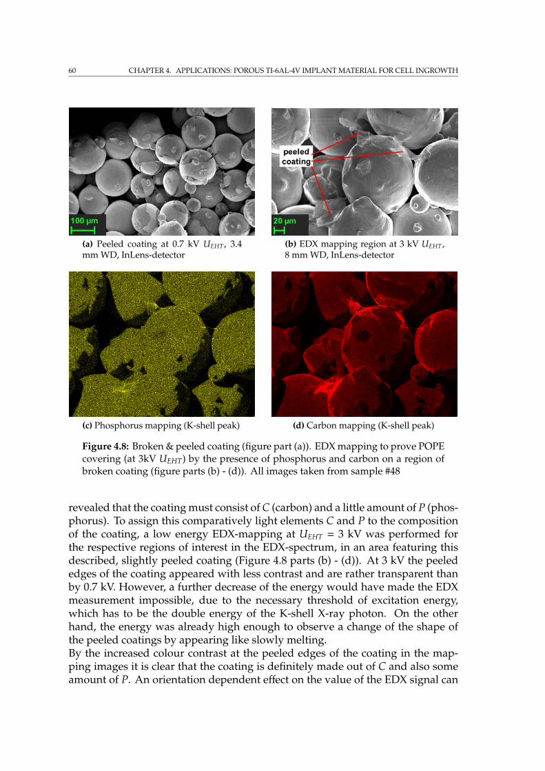
60 CHAPTER 4. APPLICATIONS: POROUS TI-6AL-4V IMPLANT MATERIAL FOR CELL INGROWTH
(a) Peeled coating at 0.7 kV UEHT, 3.4mm WD, InLens-detector
(b) EDX mapping region at 3 kV UEHT,8 mm WD, InLens-detector
(c) Phosphorus mapping (K-shell peak) (d) Carbon mapping (K-shell peak)
Figure 4.8: Broken & peeled coating (figure part (a)). EDX mapping to prove POPEcovering (at 3kV UEHT) by the presence of phosphorus and carbon on a region ofbroken coating (figure parts (b) - (d)). All images taken from sample #48
revealed that the coating must consist of C (carbon) and a little amount of P (phos-phorus). To assign this comparatively light elements C and P to the compositionof the coating, a low energy EDX-mapping at UEHT = 3 kV was performed forthe respective regions of interest in the EDX-spectrum, in an area featuring thisdescribed, slightly peeled coating (Figure 4.8 parts (b) - (d)). At 3 kV the peelededges of the coating appeared with less contrast and are rather transparent thanby 0.7 kV. However, a further decrease of the energy would have made the EDXmeasurement impossible, due to the necessary threshold of excitation energy,which has to be the double energy of the K-shell X-ray photon. On the otherhand, the energy was already high enough to observe a change of the shape ofthe peeled coatings by appearing like slowly melting.By the increased colour contrast at the peeled edges of the coating in the map-ping images it is clear that the coating is definitely made out of C and also someamount of P. An orientation dependent effect on the value of the EDX signal can
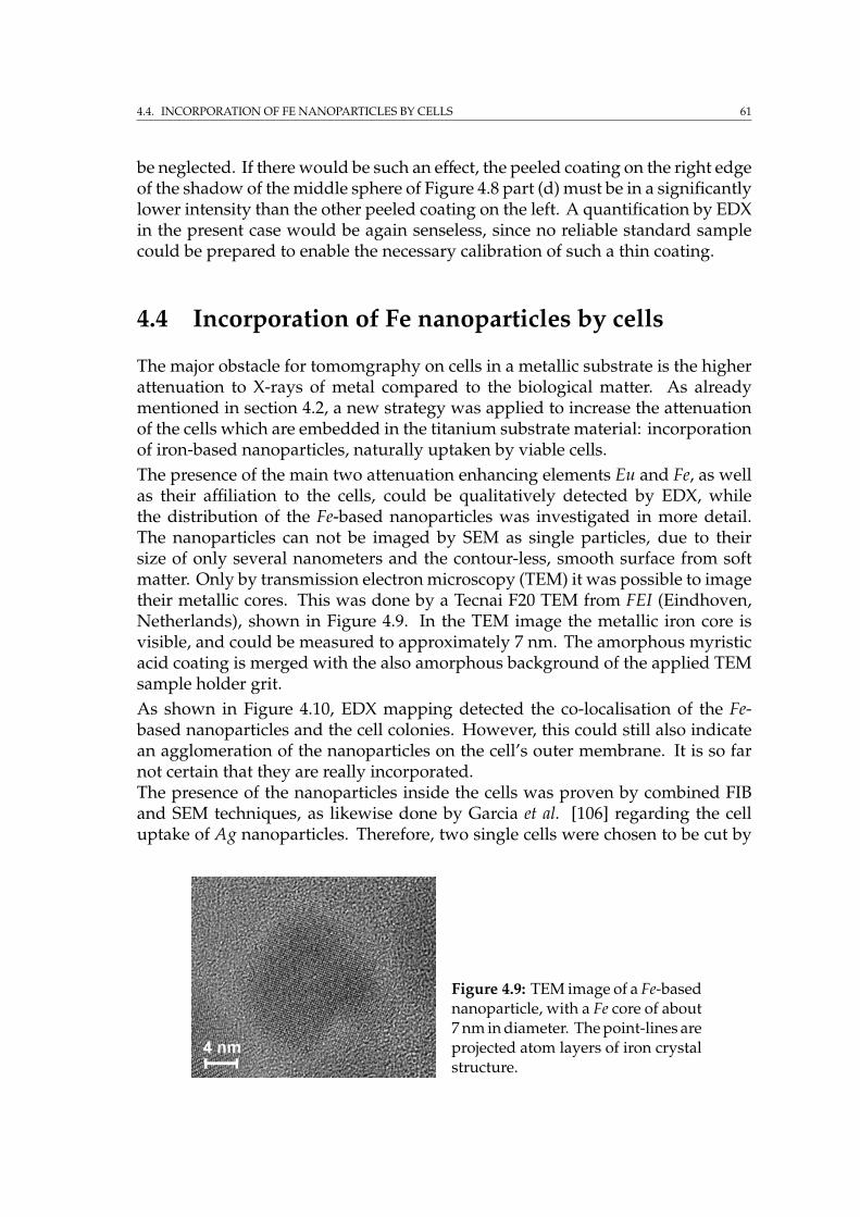
4.4. INCORPORATION OF FE NANOPARTICLES BY CELLS 61
be neglected. If there would be such an effect, the peeled coating on the right edgeof the shadow of the middle sphere of Figure 4.8 part (d) must be in a significantlylower intensity than the other peeled coating on the left. A quantification by EDXin the present case would be again senseless, since no reliable standard samplecould be prepared to enable the necessary calibration of such a thin coating.
4.4 Incorporation of Fe nanoparticles by cells
The major obstacle for tomomgraphy on cells in a metallic substrate is the higherattenuation to X-rays of metal compared to the biological matter. As alreadymentioned in section 4.2, a new strategy was applied to increase the attenuationof the cells which are embedded in the titanium substrate material: incorporationof iron-based nanoparticles, naturally uptaken by viable cells.The presence of the main two attenuation enhancing elements Eu and Fe, as wellas their affiliation to the cells, could be qualitatively detected by EDX, whilethe distribution of the Fe-based nanoparticles was investigated in more detail.The nanoparticles can not be imaged by SEM as single particles, due to theirsize of only several nanometers and the contour-less, smooth surface from softmatter. Only by transmission electron microscopy (TEM) it was possible to imagetheir metallic cores. This was done by a Tecnai F20 TEM from FEI (Eindhoven,Netherlands), shown in Figure 4.9. In the TEM image the metallic iron core isvisible, and could be measured to approximately 7 nm. The amorphous myristicacid coating is merged with the also amorphous background of the applied TEMsample holder grit.As shown in Figure 4.10, EDX mapping detected the co-localisation of the Fe-based nanoparticles and the cell colonies. However, this could still also indicatean agglomeration of the nanoparticles on the cell’s outer membrane. It is so farnot certain that they are really incorporated.The presence of the nanoparticles inside the cells was proven by combined FIBand SEM techniques, as likewise done by Garcia et al. [106] regarding the celluptake of Ag nanoparticles. Therefore, two single cells were chosen to be cut by
Figure 4.9: TEM image of a Fe-basednanoparticle, with a Fe core of about7 nm in diameter. The point-lines areprojected atom layers of iron crystalstructure.
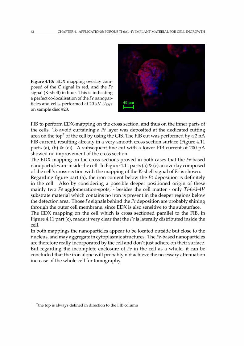
62 CHAPTER 4. APPLICATIONS: POROUS TI-6AL-4V IMPLANT MATERIAL FOR CELL INGROWTH
Figure 4.10: EDX mapping overlay com-posed of the C signal in red, and the Fesignal (K-shell) in blue. This is indicatinga perfect co-localisation of the Fe nanopar-ticles and cells, performed at 20 kV UEHTon sample disc #23.
FIB to perform EDX-mapping on the cross section, and thus on the inner parts ofthe cells. To avoid curtaining a Pt layer was deposited at the dedicated cuttingarea on the top7 of the cell by using the GIS. The FIB cut was performed by a 2 nAFIB current, resulting already in a very smooth cross section surface (Figure 4.11parts (a), (b) & (c)). A subsequent fine cut with a lower FIB current of 200 pAshowed no improvement of the cross section.The EDX mapping on the cross sections proved in both cases that the Fe-basednanoparticles are inside the cell. In Figure 4.11 parts (a) & (c) an overlay composedof the cell’s cross section with the mapping of the K-shell signal of Fe is shown.Regarding figure part (a), the iron content below the Pt deposition is definitelyin the cell. Also by considering a possible deeper positioned origin of thesemainly two Fe agglomeration-spots, - besides the cell matter - only Ti-6Al-4Vsubstrate material which contains no iron is present in the deeper regions belowthe detection area. Those Fe signals behind the Pt deposition are probably shiningthrough the outer cell membrane, since EDX is also sensitive to the subsurface.The EDX mapping on the cell which is cross sectioned parallel to the FIB, inFigure 4.11 part (c), made it very clear that the Fe is laterally distributed inside thecell.In both mappings the nanoparticles appear to be located outside but close to thenucleus, and may aggregate in cytoplasmic structures. The Fe-based nanoparticlesare therefore really incorporated by the cell and don’t just adhere on their surface.But regarding the incomplete enclosure of Fe in the cell as a whole, it can beconcluded that the iron alone will probably not achieve the necessary attenuationincrease of the whole cell for tomography.
7the top is always defined in direction to the FIB column
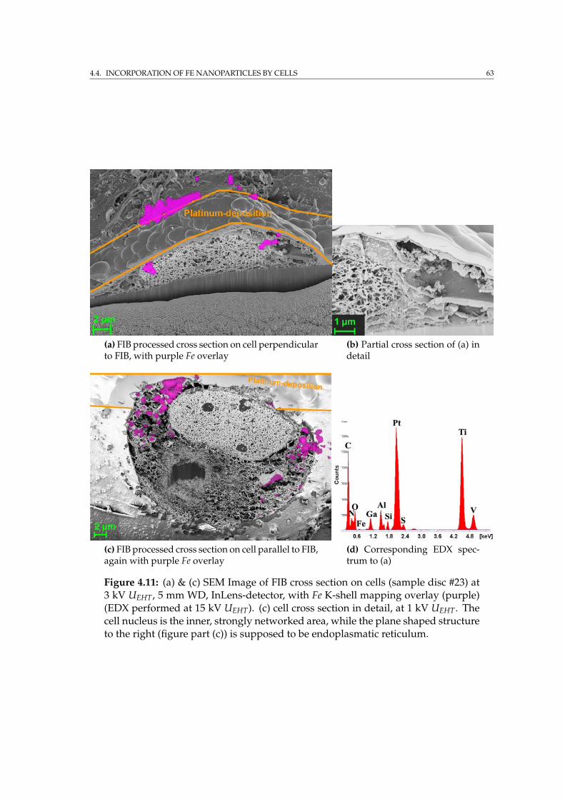
4.4. INCORPORATION OF FE NANOPARTICLES BY CELLS 63
(a) FIB processed cross section on cell perpendicularto FIB, with purple Fe overlay
(b) Partial cross section of (a) indetail
(c) FIB processed cross section on cell parallel to FIB,again with purple Fe overlay
(d) Corresponding EDX spec-trum to (a)
Figure 4.11: (a) & (c) SEM Image of FIB cross section on cells (sample disc #23) at3 kV UEHT, 5 mm WD, InLens-detector, with Fe K-shell mapping overlay (purple)(EDX performed at 15 kV UEHT). (c) cell cross section in detail, at 1 kV UEHT. Thecell nucleus is the inner, strongly networked area, while the plane shaped structureto the right (figure part (c)) is supposed to be endoplasmatic reticulum.
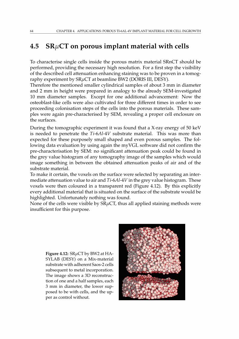
64 CHAPTER 4. APPLICATIONS: POROUS TI-6AL-4V IMPLANT MATERIAL FOR CELL INGROWTH
4.5 SRµCT on porous implant material with cells
To characterise single cells inside the porous matrix material SRnCT should beperformed, providing the necessary high resolution. For a first step the visibilityof the described cell attenuation enhancing staining was to be proven in a tomog-raphy experiment by SRµCT at beamline BW2 (DORIS III, DESY).Therefore the mentioned smaller cylindrical samples of about 3 mm in diameterand 2 mm in height were prepared in analogy to the already SEM-investigated10 mm diameter samples. Except for one additional advancement: Now theosteoblast-like cells were also cultivated for three different times in order to seeproceeding colonisation steps of the cells into the porous materials. These sam-ples were again pre-characterised by SEM, revealing a proper cell enclosure onthe surfaces.
During the tomographic experiment it was found that a X-ray energy of 50 keVis needed to penetrate the Ti-6Al-4V substrate material. This was more thanexpected for these purposely small shaped and even porous samples. The fol-lowing data evaluation by using again the myVGL software did not confirm thepre-characterisation by SEM: no significant attenuation peak could be found inthe grey value histogram of any tomography image of the samples which wouldimage something in between the obtained attenuation peaks of air and of thesubstrate material.To make it certain, the voxels on the surface were selected by separating an inter-mediate attenuation value to air and Ti-6Al-4V in the grey value histogram. Thesevoxels were then coloured in a transparent red (Figure 4.12). By this explicitlyevery additional material that is situated on the surface of the substrate would behighlighted. Unfortunately nothing was found.None of the cells were visible by SRµCT, thus all applied staining methods wereinsufficient for this purpose.
Figure 4.12: SRµCT by BW2 at HA-SYLAB (DESY) on a Mix-materialsubstrate with adherent Saos-2 cellssubsequent to metal incorporation.The image shows a 3D reconstruc-tion of one and a half samples, each3 mm in diameter, the lower sup-posed to be with cells, and the up-per as control without.
4.6. SUMMARY 65
4.6 Summary
The characterisation of the material substrate by tomography provided detailedknowledge on the porous network structure inside, and the pore size distributionby the granulometry calculation.External in vivo studies revealed a crucial role on material porosity for tissue in-growth, highlighting a 30% porosity provides an excellent tissue ingrowth [4].It could be shown by the tomographic characterisation that this precondition istotally fulfilled by the two porosities Large and Mix.Evaluating the granulometry data, both sample types Large and Mix exhibit asimilar and high pore size variability of up to basically 200 µm pores in diameter,proposing to be well suitable for cell ingrowth [17; 68].The SEM imaging of the cell colonisation could successfully clarify the ingrowthof cells into the porous network. Independent of the porosity types Large andMix the viability for cells through the entire sample was proven, which was co-operatively published by Deing et al. [25].The presence of the phospholipid coating is indicated by Au-labelled phospho-lipids on polished surfaces as well as by SEM imaging and EDX on the internalsurface of the respective broken samples.The incorporation of iron nanoparticles was verified by EDX inside of two singleSaos-2 cells, enabled by a FIB cross section.None of the cells was visible by SRµCT, therefore the staining can be expected tobe insufficient for SRnCT too.Therefore, in the next step the tomographic phase contrast8 method should beapplied in the scope of SRnCT future experiments on such samples as soon as thismethod is available at IBL.
8For background information on phase contrast please refer to Appendix A.

66
Chapter 5
Applications: Degradablemagnesium based implants
5.1 Corrosion of different Mg alloys in physiologicalsolutions
In a proof of concept study Mg already showed favourable properties for medicalapplications [142]. But besides of stent applications there is so far no other clinicalusage. Although orthopaedic and paediatric applications are of high interest, thenecessary approaches are hindered by the deficit of proper and predictive in vitrosystems. A first step was done by recent studies regarding Mg degradation undercell culture conditions, which revealed a change in the formed corrosion productscompared to technical setups [138; 132].To explore further aspects of the corrosion environment the availability of oxygenand proteins was studied within this work, jointly published by F. Feyerabend etal. [34]. Since it is known that the type of alloy and the preparation of the sampleshave an influence on the corrosion properties of the material, three differentalloys (pure Mg, WE43 (Mg4Y0.5Gd2Nd0.5Dy) and E11 (Mg10Gd1Nd)) underfour surface conditions were analysed.The relevant parts of the sample preparation, which was done by Feyerabend[34], are shortly outlined in the following.
5.1.1 Sample preparation and corrosion environment
The Magnesium casting was prepared by pure Mg (99.95 wt.%) and pure alloyingelements in a mild steel crucible under a cover gas mixture of Ar2 and 0.3% SF6.After mixing at 730°C for 1.5 h, the alloy was cast to the preheated mould at 500°C.The filled mould was held at 670°C for 1 h under protective gas (Ar + 0.3% SF6).Afterwards, the steel crucible with the melt was immersed continuously into thecooling water with a speed of 10 mm/s. When the bottom of the steel crucible
67
68 CHAPTER 5. APPLICATIONS: DEGRADABLE MAGNESIUM BASED IMPLANTS
touched the water it was stopped for 1 s. As soon as the liquid level of the melt atthe inside was in alignment with the height of the water outside, the solidificationprocess was finished.The ingots were cut by electrical discharge machining into plates (20 cm × 12 cm× 2 cm). Cylindrical samples (5 mm diameter) were prepared by laser cutting.The sample surfaces were treated by three different methods: (1) as cut; (2) electropolished, and (3) etched. The samples were cleaned in ethanol after every processstep.Sonificated was done with the samples for 20 min in dry isopropanol, dried andgamma-sterilized at the In core irradiation (ICI) facility of the Geesthacht neutronfacility with a total dosage of 29 kGy.The corrosion tests were performed by using two different solutions: I. Hanksbalanced salt solution without calcium and magnesium (HBSS, Invitrogen Corpora-tion, Karlsruhe, Germany) and II. Dulbecco’s modified eagle medium Glutamax-I(DMEM, Invitrogen Corporation, Karlsruhe, Germany). An additional experimentwas performed by supplementing all solutions with standardized 10% fetal bovineserum (FBS, PAA Laboratories, Linz, Austria), to determine the influence of pro-teins.Corrosion experiments were done at 37°C, 5% CO2, and 95% humidity in an in-cubator (Heraeus BBD 6620, Thermo Fisher Scientific, Schwerte, Germany). Theoxygen content was either set to 20 or 5%, while the exposition time of the sam-ples was at maximum 72 h. Subsequently the samples were rinsed for 1 min indistilled water, followed by drying in a vacuum oven for 24 h.The specimens were cross sectioned by a diamond wire, embedded in a resin andpolished in two steps: with alumina and finally with a 0.1 µm colloidal silicasuspension.
5.1.2 Scanning electron microscopy
The surface imaging of the corroded samples was performed at 5 kV UEHT accel-erating voltage using the secondary electron detector (SE2-detector). The voltagewas chosen comparably low to avoid charging effects by the less conductive cor-rosion layer.Due to the epoxide resin the cross sectioned samples had to be coated with a gold-palladium alloy, by the sputter device introduced in subsection 3.1.2, to allowSEM investigations. These embedded and coated samples could be imaged at 20kV UEHT using the back scattered electrons detector (BSE-detector) in order to gainmaterial contrast along the cross section. The influence of the thin gold-palladiumcoating did not seriously bother the BSE imaging.EDX-mappings were performed at again 20 kV UEHT on every sample for therespective regions of Mg, N, Na, C, Ca, Cl, K, O, and P in the EDX spectrumto identify qualitatively1 the lateral element distribution of the corrosion layer.
1without calibration standard sample
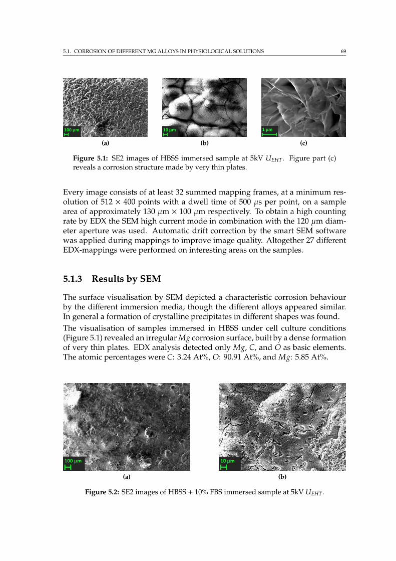
5.1. CORROSION OF DIFFERENT MG ALLOYS IN PHYSIOLOGICAL SOLUTIONS 69
(a) (b) (c)
Figure 5.1: SE2 images of HBSS immersed sample at 5kV UEHT. Figure part (c)reveals a corrosion structure made by very thin plates.
Every image consists of at least 32 summed mapping frames, at a minimum res-olution of 512 × 400 points with a dwell time of 500 µs per point, on a samplearea of approximately 130 µm × 100 µm respectively. To obtain a high countingrate by EDX the SEM high current mode in combination with the 120 µm diam-eter aperture was used. Automatic drift correction by the smart SEM softwarewas applied during mappings to improve image quality. Altogether 27 differentEDX-mappings were performed on interesting areas on the samples.
5.1.3 Results by SEM
The surface visualisation by SEM depicted a characteristic corrosion behaviourby the different immersion media, though the different alloys appeared similar.In general a formation of crystalline precipitates in different shapes was found.The visualisation of samples immersed in HBSS under cell culture conditions(Figure 5.1) revealed an irregular Mg corrosion surface, built by a dense formationof very thin plates. EDX analysis detected only Mg, C, and O as basic elements.The atomic percentages were C: 3.24 At%, O: 90.91 At%, and Mg: 5.85 At%.
(a) (b)
Figure 5.2: SE2 images of HBSS + 10% FBS immersed sample at 5kV UEHT.
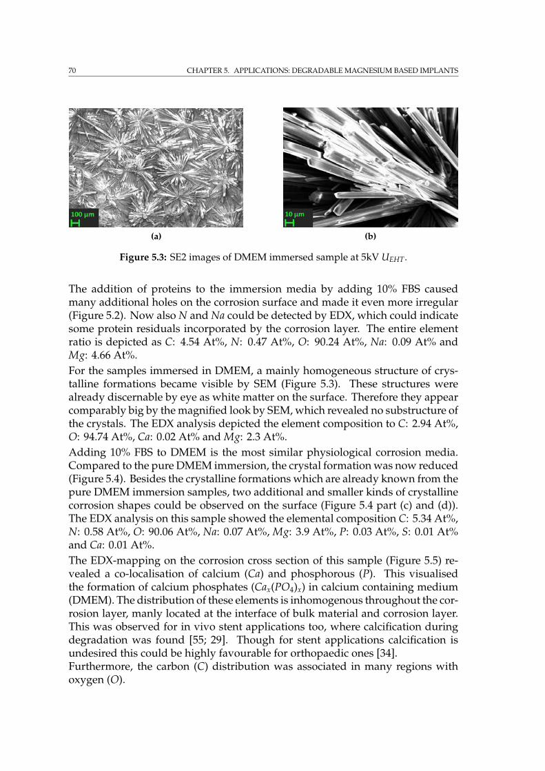
70 CHAPTER 5. APPLICATIONS: DEGRADABLE MAGNESIUM BASED IMPLANTS
(a) (b)
Figure 5.3: SE2 images of DMEM immersed sample at 5kV UEHT.
The addition of proteins to the immersion media by adding 10% FBS causedmany additional holes on the corrosion surface and made it even more irregular(Figure 5.2). Now also N and Na could be detected by EDX, which could indicatesome protein residuals incorporated by the corrosion layer. The entire elementratio is depicted as C: 4.54 At%, N: 0.47 At%, O: 90.24 At%, Na: 0.09 At% andMg: 4.66 At%.For the samples immersed in DMEM, a mainly homogeneous structure of crys-talline formations became visible by SEM (Figure 5.3). These structures werealready discernable by eye as white matter on the surface. Therefore they appearcomparably big by the magnified look by SEM, which revealed no substructure ofthe crystals. The EDX analysis depicted the element composition to C: 2.94 At%,O: 94.74 At%, Ca: 0.02 At% and Mg: 2.3 At%.Adding 10% FBS to DMEM is the most similar physiological corrosion media.Compared to the pure DMEM immersion, the crystal formation was now reduced(Figure 5.4). Besides the crystalline formations which are already known from thepure DMEM immersion samples, two additional and smaller kinds of crystallinecorrosion shapes could be observed on the surface (Figure 5.4 part (c) and (d)).The EDX analysis on this sample showed the elemental composition C: 5.34 At%,N: 0.58 At%, O: 90.06 At%, Na: 0.07 At%, Mg: 3.9 At%, P: 0.03 At%, S: 0.01 At%and Ca: 0.01 At%.The EDX-mapping on the corrosion cross section of this sample (Figure 5.5) re-vealed a co-localisation of calcium (Ca) and phosphorous (P). This visualisedthe formation of calcium phosphates (Cax(PO4)x) in calcium containing medium(DMEM). The distribution of these elements is inhomogenous throughout the cor-rosion layer, manly located at the interface of bulk material and corrosion layer.This was observed for in vivo stent applications too, where calcification duringdegradation was found [55; 29]. Though for stent applications calcification isundesired this could be highly favourable for orthopaedic ones [34].Furthermore, the carbon (C) distribution was associated in many regions withoxygen (O).
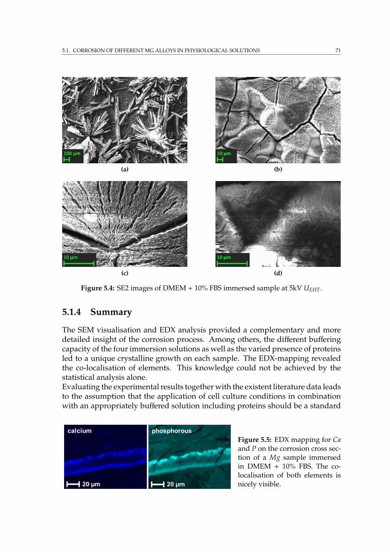
5.1. CORROSION OF DIFFERENT MG ALLOYS IN PHYSIOLOGICAL SOLUTIONS 71
(a) (b)
(c) (d)
Figure 5.4: SE2 images of DMEM + 10% FBS immersed sample at 5kV UEHT.
5.1.4 Summary
The SEM visualisation and EDX analysis provided a complementary and moredetailed insight of the corrosion process. Among others, the different bufferingcapacity of the four immersion solutions as well as the varied presence of proteinsled to a unique crystalline growth on each sample. The EDX-mapping revealedthe co-localisation of elements. This knowledge could not be achieved by thestatistical analysis alone.Evaluating the experimental results together with the existent literature data leadsto the assumption that the application of cell culture conditions in combinationwith an appropriately buffered solution including proteins should be a standard
Figure 5.5: EDX mapping for Caand P on the corrosion cross sec-tion of a Mg sample immersedin DMEM + 10% FBS. The co-localisation of both elements isnicely visible.
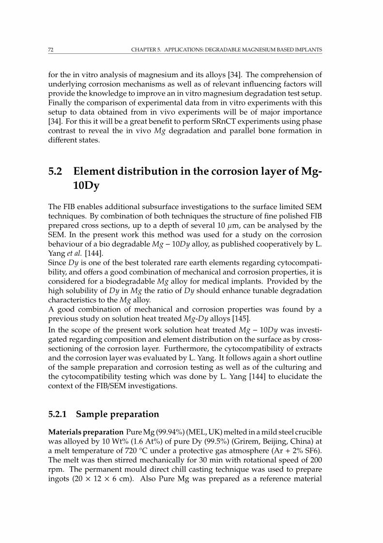
72 CHAPTER 5. APPLICATIONS: DEGRADABLE MAGNESIUM BASED IMPLANTS
for the in vitro analysis of magnesium and its alloys [34]. The comprehension ofunderlying corrosion mechanisms as well as of relevant influencing factors willprovide the knowledge to improve an in vitro magnesium degradation test setup.Finally the comparison of experimental data from in vitro experiments with thissetup to data obtained from in vivo experiments will be of major importance[34]. For this it will be a great benefit to perform SRnCT experiments using phasecontrast to reveal the in vivo Mg degradation and parallel bone formation indifferent states.
5.2 Element distribution in the corrosion layer of Mg-10Dy
The FIB enables additional subsurface investigations to the surface limited SEMtechniques. By combination of both techniques the structure of fine polished FIBprepared cross sections, up to a depth of several 10 µm, can be analysed by theSEM. In the present work this method was used for a study on the corrosionbehaviour of a bio degradable Mg − 10Dy alloy, as published cooperatively by L.Yang et al. [144].Since Dy is one of the best tolerated rare earth elements regarding cytocompati-bility, and offers a good combination of mechanical and corrosion properties, it isconsidered for a biodegradable Mg alloy for medical implants. Provided by thehigh solubility of Dy in Mg the ratio of Dy should enhance tunable degradationcharacteristics to the Mg alloy.A good combination of mechanical and corrosion properties was found by aprevious study on solution heat treated Mg-Dy alloys [145].In the scope of the present work solution heat treated Mg − 10Dy was investi-gated regarding composition and element distribution on the surface as by cross-sectioning of the corrosion layer. Furthermore, the cytocompatibility of extractsand the corrosion layer was evaluated by L. Yang. It follows again a short outlineof the sample preparation and corrosion testing as well as of the culturing andthe cytocompatibility testing which was done by L. Yang [144] to elucidate thecontext of the FIB/SEM investigations.
5.2.1 Sample preparation
Materials preparation Pure Mg (99.94%) (MEL, UK) melted in a mild steel cruciblewas alloyed by 10 Wt% (1.6 At%) of pure Dy (99.5%) (Grirem, Beijing, China) ata melt temperature of 720 °C under a protective gas atmosphere (Ar + 2% SF6).The melt was then stirred mechanically for 30 min with rotational speed of 200rpm. The permanent mould direct chill casting technique was used to prepareingots (20 × 12 × 6 cm). Also Pure Mg was prepared as a reference material
5.2. ELEMENT DISTRIBUTION IN THE CORROSION LAYER OF MG-10DY 73
for corrosion rate and cytocompatibility tests, using the same melting process.Solution treatment was performed on the Mg − 10Dy alloy at 520 °C for 24 h.
Corrosion tests The specimens for the corrosion tests were prepared by grindingeach side of the sample with 2400 grit emery paper, followed by degreasingwith ethanol and drying in room air. Three samples were used for each sterilecorrosion condition. The samples were sterilised in a solution of 70% ethanolfor 15 min. After drying each sample was immersed in a cell culture medium(CCM) consisting of Dulbecco’s modified Eagle’s medium (DMEM) Glutamax-I(Life Technologies, Darmstadt, Germany) and 10% fetal bovine serum (FBS) (PAALaboratories, Linz, Austria). The samples were then incubated in an incubator(Heraeus BBD 6620, Thermo Fisher Scientific, Schwerte, Germany) under cell cultureconditions (37 °C, 21% O2, 5% CO2, 95% relative humidity). The ratio of corrosionmedium to surface area of sample was 1.5 ml/cm2. After immersion for up to 28days without changing the medium the samples were rinsed in distilled water,dried and kept in a vacuum drying chamber.
Cell isolation and culturing Osteoblasts were taken from bone chips donated bya patient of total hip arthroplasty following the protocol of Gallagher [36]. Briefly,cancellous bone was removed from the femoralhead with bone rongeurs as piecesof about 5 mm diameter. Bone marrow and non-bone components were removedby thorough vortexing in phosphate-buffered saline (PBS) repeatedly for 30 s,while exchanging continuously the PBS. As bone fragments became white andivory-like they were cultured in DMEM Glutamax-I with 10% FBS, 1% penicillin,and 100 mg l−1 streptomycin (Life Technologies, Darmstadt, Germany) for 10 dayswithout changing the medium. Thereafter the medium was changed every 2-3days. Passage was at 70-80% confluence, and for the experiments cells in passage2 were used.
Cytocompatibility of the corrosion layer Cylindrical specimens with a diameterof 10 mm and a height of 1.5 mm were cut by electrical discharge machining.These specimens were ground all around with 2400 grit emery paper, followed byultrasonic cleaning in 100% ethanol and drying in room air. Before experimentsthe specimens were sterilized by immersion in 70% ethanol for 15 min.The evaluation of the cytocompatibility of the Mg − 10Dy alloy’s corrosion layerwas done by cell adhesion and Live/Dead staining tests, while Pure Mg specimensserved as reference samples. Prior to cell seeding the specimens were preincu-bated for 2 h (cell adhesion test) or 3 days (Live/Dead staining) in CCM under cellculture conditions. To avoid growth of cells on the 12-well plates agarose coatingswere used (Nunc, Wiesbaden, Germany). The Osteoblasts were seeded with adensity of 100,000 cells per specimen on the top of them, lying in the 12-wellplates immersed in 50 µl of solution. Subsequently this was incubated for 40 minto allow the cells to settle down, followed by 3 ml of CCM which was added toeach well and was then refreshed every 3 days.After incubation of 3 and 7 days the specimens were rinsed with PBS and thenimmersed overnight in 2.5% glutaraldehyde solution achieving cell fixation. Af-
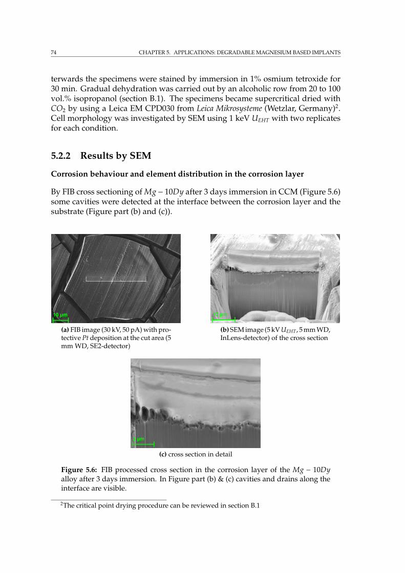
74 CHAPTER 5. APPLICATIONS: DEGRADABLE MAGNESIUM BASED IMPLANTS
terwards the specimens were stained by immersion in 1% osmium tetroxide for30 min. Gradual dehydration was carried out by an alcoholic row from 20 to 100vol.% isopropanol (section B.1). The specimens became supercritical dried withCO2 by using a Leica EM CPD030 from Leica Mikrosysteme (Wetzlar, Germany)2.Cell morphology was investigated by SEM using 1 keV UEHT with two replicatesfor each condition.
5.2.2 Results by SEM
Corrosion behaviour and element distribution in the corrosion layer
By FIB cross sectioning of Mg− 10Dy after 3 days immersion in CCM (Figure 5.6)some cavities were detected at the interface between the corrosion layer and thesubstrate (Figure part (b) and (c)).
(a) FIB image (30 kV, 50 pA) with pro-tective Pt deposition at the cut area (5mm WD, SE2-detector)
(b) SEM image (5 kV UEHT, 5 mm WD,InLens-detector) of the cross section
(c) cross section in detail
Figure 5.6: FIB processed cross section in the corrosion layer of the Mg − 10Dyalloy after 3 days immersion. In Figure part (b) & (c) cavities and drains along theinterface are visible.
2The critical point drying procedure can be reviewed in section B.1
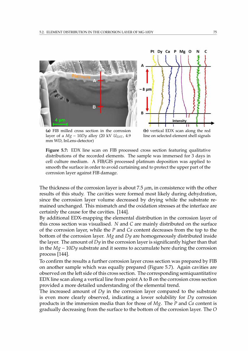
5.2. ELEMENT DISTRIBUTION IN THE CORROSION LAYER OF MG-10DY 75
(a) FIB milled cross section in the corrosionlayer of a Mg − 10Dy alloy (20 kV UEHT, 4.9mm WD, InLens-detector)
(b) vertical EDX scan along the redline on selected element shell signals
Figure 5.7: EDX line scan on FIB processed cross section featuring qualitativedistributions of the recorded elements. The sample was immersed for 3 days incell culture medium. A FIB/GIS processed platinum deposition was applied tosmooth the surface in order to avoid curtaining and to protect the upper part of thecorrosion layer against FIB damage.
The thickness of the corrosion layer is about 7.5 µm, in consistence with the otherresults of this study. The cavities were formed most likely during dehydration,since the corrosion layer volume decreased by drying while the substrate re-mained unchanged. This mismatch and the oxidation stresses at the interface arecertainly the cause for the cavities. [144].By additional EDX-mapping the elemental distribution in the corrosion layer ofthis cross section was visualised. N and C are mainly distributed on the surfaceof the corrosion layer, while the P and Ca content decreases from the top to thebottom of the corrosion layer. Mg and Dy are homogeneously distributed insidethe layer. The amount of Dy in the corrosion layer is significantly higher than thatin the Mg − 10Dy substrate and it seems to accumulate here during the corrosionprocess [144].To confirm the results a further corrosion layer cross section was prepared by FIBon another sample which was equally prepared (Figure 5.7). Again cavities areobserved on the left side of this cross section. The corresponding semiquantitativeEDX line scan along a vertical line from point A to B on the corrosion cross sectionprovided a more detailed understanding of the elemental trend.The increased amount of Dy in the corrosion layer compared to the substrateis even more clearly observed, indicating a lower solubility for Dy corrosionproducts in the immersion media than for those of Mg. The P and Ca content isgradually decreasing from the surface to the bottom of the corrosion layer. The O
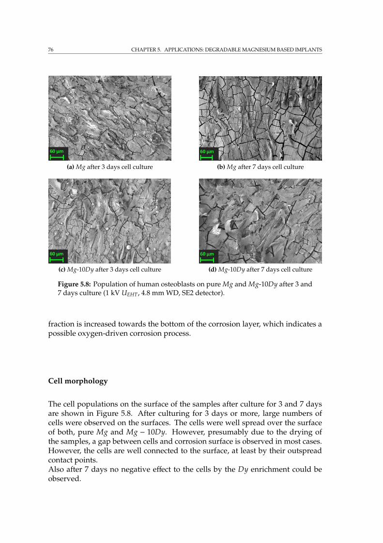
76 CHAPTER 5. APPLICATIONS: DEGRADABLE MAGNESIUM BASED IMPLANTS
(a) Mg after 3 days cell culture (b) Mg after 7 days cell culture
(c) Mg-10Dy after 3 days cell culture (d) Mg-10Dy after 7 days cell culture
Figure 5.8: Population of human osteoblasts on pure Mg and Mg-10Dy after 3 and7 days culture (1 kV UEHT, 4.8 mm WD, SE2 detector).
fraction is increased towards the bottom of the corrosion layer, which indicates apossible oxygen-driven corrosion process.
Cell morphology
The cell populations on the surface of the samples after culture for 3 and 7 daysare shown in Figure 5.8. After culturing for 3 days or more, large numbers ofcells were observed on the surfaces. The cells were well spread over the surfaceof both, pure Mg and Mg − 10Dy. However, presumably due to the drying ofthe samples, a gap between cells and corrosion surface is observed in most cases.However, the cells are well connected to the surface, at least by their outspreadcontact points.Also after 7 days no negative effect to the cells by the Dy enrichment could beobserved.

5.2. ELEMENT DISTRIBUTION IN THE CORROSION LAYER OF MG-10DY 77
5.2.3 Summary
The primary human osteoblast morphology could be observed by SEM on allcultured samples.The FIB cross sectioning provided the characterisation of the corrosion layer withEDX in order to obtain information about the element distribution. The elementdistribution is inhomogeneous from the surface to the bottom of the corrosionlayer. Dy is enriched in the corrosion layer, and is supposed to exist as a mixture ofDy2O3 and Dy(OH)3. The content of Ca and P decreases gradually from the surfaceto the bottom. Due to the buffering effect of CO2, MgCO3· 3H2O forms duringcorrosion and accumulates in the corrosion layer after the corrosion solutionbecomes saturated. Both extracts, as well as the Dy-enriched corrosion layer ofalloy Mg − 10Dy, are not resulting in cytotoxicity to human osteoblasts [144].By SRnCT, again in combination with the phase contrast method, it will be possiblein the future to achieve the 3D imaging of a much bigger corrosion layer region.Especially the statistical data evaluation regarding the corrosion determinationwould be provided by this.
Chapter 6
Applications: Nanoconfinedmaterials for reversible hydrogenstorage
Hydrogen is considered as one of the most suitable energy carriers for sustainableenergies in the future. A crucial issue for the use of hydrogen is to find a safeand high-density storage solution. Reversible storage by using metal hydrides isa promising approach [114].
6.1 Introduction
Particularly, lithium borohydride (LiBH4) is interesting for providing the highesthydrogen storage capacity of 18.5 Wt% [16]. However, unfavorable kinetics andthermodynamics for dehydrogenation and rehydrogenation, as high desorptiontemperatures above 380 °C and slow rehydrogenation at 600 °C under 150 bar H2,reduced its practical applications as a hydrogen storage medium. To improve thischaracteristics different approaches, as e.g. catalytic doping and Reactive HydrideComposites (RHCs) are explored. The LiBH4-MgH2 system showed a reductionin de-/rehydrogenation enthalpy (see Equation 7.11) due to the formation of MgB2
upon dehydrogenation [48].
2LiBH4(l) +MgH2(s) ←→ 2LiH(s) +MgB2(s) + 4H2(g) (6.1)
Furthermore, the required temperature and pressure conditions are milder com-pared to pure LiBH4. Since there are still obstacles for practical applications furtherimprovements are needed. Therefore, nanoengineering by reducing the particlesize of the metal hydrides is considered as an meaningful strategy to improve thehydrogen release and uptake kinetics.
1s: solid-; l: fluid-; g: gas- phase
78
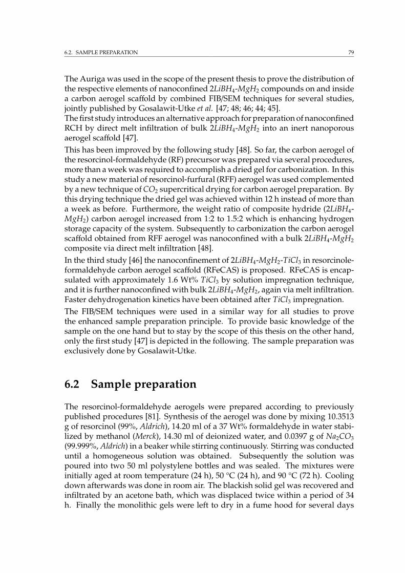
6.2. SAMPLE PREPARATION 79
The Auriga was used in the scope of the present thesis to prove the distribution ofthe respective elements of nanoconfined 2LiBH4-MgH2 compounds on and insidea carbon aerogel scaffold by combined FIB/SEM techniques for several studies,jointly published by Gosalawit-Utke et al. [47; 48; 46; 44; 45].The first study introduces an alternative approach for preparation of nanoconfinedRCH by direct melt infiltration of bulk 2LiBH4-MgH2 into an inert nanoporousaerogel scaffold [47].This has been improved by the following study [48]. So far, the carbon aerogel ofthe resorcinol-formaldehyde (RF) precursor was prepared via several procedures,more than a week was required to accomplish a dried gel for carbonization. In thisstudy a new material of resorcinol-furfural (RFF) aerogel was used complementedby a new technique of CO2 supercritical drying for carbon aerogel preparation. Bythis drying technique the dried gel was achieved within 12 h instead of more thana week as before. Furthermore, the weight ratio of composite hydride (2LiBH4-MgH2) carbon aerogel increased from 1:2 to 1.5:2 which is enhancing hydrogenstorage capacity of the system. Subsequently to carbonization the carbon aerogelscaffold obtained from RFF aerogel was nanoconfined with a bulk 2LiBH4-MgH2
composite via direct melt infiltration [48].In the third study [46] the nanoconfinement of 2LiBH4-MgH2-TiCl3 in resorcinole-formaldehyde carbon aerogel scaffold (RFeCAS) is proposed. RFeCAS is encap-sulated with approximately 1.6 Wt% TiCl3 by solution impregnation technique,and it is further nanoconfined with bulk 2LiBH4-MgH2, again via melt infiltration.Faster dehydrogenation kinetics have been obtained after TiCl3 impregnation.The FIB/SEM techniques were used in a similar way for all studies to provethe enhanced sample preparation principle. To provide basic knowledge of thesample on the one hand but to stay by the scope of this thesis on the other hand,only the first study [47] is depicted in the following. The sample preparation wasexclusively done by Gosalawit-Utke.
6.2 Sample preparation
The resorcinol-formaldehyde aerogels were prepared according to previouslypublished procedures [81]. Synthesis of the aerogel was done by mixing 10.3513g of resorcinol (99%, Aldrich), 14.20 ml of a 37 Wt% formaldehyde in water stabi-lized by methanol (Merck), 14.30 ml of deionized water, and 0.0397 g of Na2CO3
(99.999%, Aldrich) in a beaker while stirring continuously. Stirring was conducteduntil a homogeneous solution was obtained. Subsequently the solution waspoured into two 50 ml polystylene bottles and was sealed. The mixtures wereinitially aged at room temperature (24 h), 50 °C (24 h), and 90 °C (72 h). Coolingdown afterwards was done in room air. The blackish solid gel was recovered andinfiltrated by an acetone bath, which was displaced twice within a period of 34h. Finally the monolithic gels were left to dry in a fume hood for several days
80 CHAPTER 6. APPLICATIONS: NANOCONFINED MATERIALS FOR REVERSIBLE HYDROGEN STORAGE
and were then cut into smaller pieces (ca. 0.4 cm3) and pyrolyzed in a tube ovenunder a nitrogen flow at 800 °C (heating rate 2.6 °C/min) and dwelling for 6 h at800 °C. After switching off the furnace the samples were cooled down to roomtemperature naturally. The obtained gels were again dried at 500 °C for 16 h undervacuum, and are called RF now. The powders of LiBH4 (>95.0%, Sigma-Aldrich)and MgH2 (Alfa Aesar GmbH & Co KG) were milled under argon atmosphere for 5h in the molar ratio of 2:1 respectively, using a Spex 8000 M Mixer Mill placed ina glovebox. The mixture of RF aerogel and bulk 2LiBH4-MgH2 was ground at aweight ratio of 2:1 in a mortar, resulting in mortar-mixed RF-2LiBH4-MgH2 [47].
6.3 Combined FIB/SEM investigation
The nanoconfined 2LiBH4-MgH2 was prepared for FIB/SEM experiments by meltinfiltration in a Sievert-type apparatus at 310 °C and p(H2) = 60 bar. The powdersample was conductively fixed onto the sample holder by using silver glue (sol-vent: n-butylacetate). The sample was coated by gold-palladium sputtering, thistime with a current of 30 mA for 30 s. Without conductive coating the specimenwere unstable in the SEM image, even at low voltages the electron beam destroyedthe surface structure.
The morphology of the material was investigated with SEM (Figure 6.1 part (a)),depicting the nanoporous structure of the RF aerogel. An internal view of thespecimen (approximately 12 × 7 × 5 µm) was prepared by FIB (Figure 6.1 part(b)), to unravel the elemental composition inside this highly reactive material, be-cause the surface was assumed to be oxidised by the necessary sample mountingfor SEM.In the area of the red frame EDX-mapping was performed for Mg and B. Bothsignals were combined in one image (Figure 6.1 part (d)) by photoshop from Adobesystems (San Jose, California, US).The energy of the B signal is adjacent to that of C. Furthermore EDX is not reallysensitive to lighter elements than C. Therefore, the B peak in Figure 6.1 part (c)is not significant. However, the infiltration of LiBH4 was previously confirmedby SR-PXD2 and DSC-TG-MS3 results. The mapping showed homogeneous dis-persion of Mg (from MgH2) and B (from LiBH4) atoms inside the carbon aerogelscaffold. This confirms that both, LiBH4 and MgH2, were successfully nanocon-fined in the aerogel.
2In situ synchrotron radiation powder X-ray diffraction3Differential scanning calorimetry-thermogravimetric analysis-mass spectrometry
6.4. SUMMARY 81
(a) surface morphology (15 kV UEHT,5.3 mm WD, SE2-detector)
(b) FIB generated hole (FIB image (30kV, 50 pA), 5 mm WD, SE2-detector)
(c) spectrum of the correspondingEDX mapping
(d) EDX mapping overlay for Mg(yellow) and B (white dots)
Figure 6.1: Surface morphology of the nanoconfined 2LiBH4 − MgH2 specimen(a); FIB generated hole in the specimen with EDX mapping frame (red) (b); EDXspectrum (c); EDX mapping (d).
6.4 Summary
SEM micrographs as well as EDX-mappings revealed a homogeneous dispersionof MgH2 and LiBH4 inside the carbon aerogel scaffold. The FIB method providedaccess to the not oxidised underground of this highly reactive material and henceresults were not altered by oxidation or other environmental effects.By this study it was furthermore proved that the simple preparation of nanocon-fined 2LiBH4−MgH2 by direct melt infiltration of the bulk 2LiBH4−MgH2 into thecarbon aerogel scaffold resulted in the generation of the nanoconfined materialtogether with the improvement in hydrogen desorption kinetics. The hydro-gen desorption kinetics of the nanoconfined 2LiBH4 −MgH2 is significantly im-proved compared to bulk 2LiBH4 −MgH2. To give an example, the nanoconfined2LiBH4−MgH2 releases 90% of the total hydrogen storage capacity within 90 min,whereas the bulk material releases only 34% (at T = 425 °C and p(H2) = 3.4 bar).A reversible gravimetric hydrogen storage capacity of 10.8 WT% H2, calculated

82 CHAPTER 6. APPLICATIONS: NANOCONFINED MATERIALS FOR REVERSIBLE HYDROGEN STORAGE
with respect to the metal hydride content, is preserved over four hydrogen releaseand uptake cycles [47].The low density of the nanoconfined 2LiBH4 −MgH2 material makes it again aperfect candidate for future phase contrast SRnCT at IBL as soon as this methodis introduced.
Chapter 7
Applications: Ti-45Al-5Nb and 10Nbpowder
7.1 Introduction
Gas-atomised spherical powders of Ti-45Al- 5Nb and 10Nb1 alloys (from now ontermed 5Nb and 10Nb) were produced in-house by HZG using the plasma meltinginduction guided gas atomisation (PIGA) technique.In the scope of this thesis it was planned to image the distribution of the differentphases in the powder particle interior by SRnCT, imaging the locally differentattenuation originating from the local variations in chemical compositions. The10Nb powder should show higher material attenuation for X-rays due to thehigher Nb content, and therefore a possibly better contrast for SRnCT. Further-more, the smaller powder particle fractions of up to 40µm fulfil the size restrictionsby the SRnCT experiment at IBL and allow the imaging of a complete particle.Regarding the amount of Al in both alloys and the high cooling rates, it is ex-pected that the phase composition will consist of hexagonal-close-packed α- andbody-centred-cubic β-phase [22].
7.1.1 Powder preparation
First a melt is generated by means of a Ar-operated plasma torch in a water cooledCu crucible. Subsequently the melt is guided by a funnel to the center of a gasnozzle where it becomes atomised with Ar gas [40].By this technique varying amounts of different sized particles are generated(shown in Table 7.1).
1composition in atom percent
83
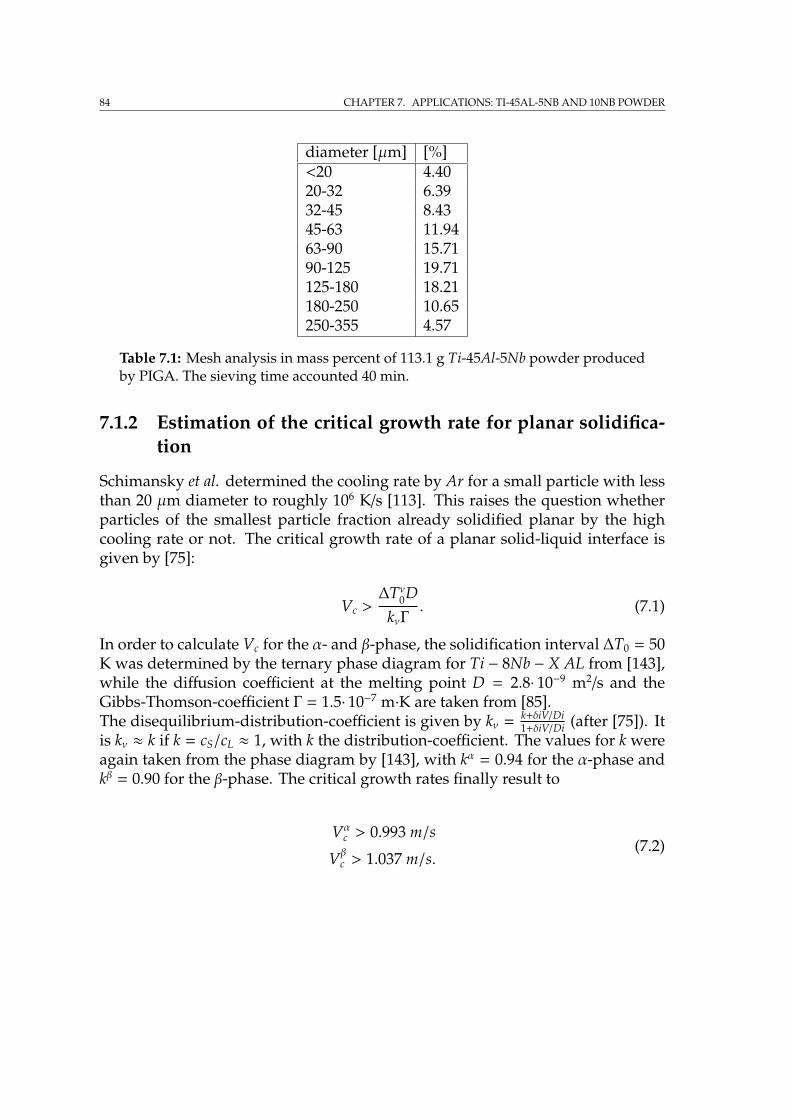
84 CHAPTER 7. APPLICATIONS: TI-45AL-5NB AND 10NB POWDER
diameter [µm] [%]<20 4.4020-32 6.3932-45 8.4345-63 11.9463-90 15.7190-125 19.71125-180 18.21180-250 10.65250-355 4.57
Table 7.1: Mesh analysis in mass percent of 113.1 g Ti-45Al-5Nb powder producedby PIGA. The sieving time accounted 40 min.
7.1.2 Estimation of the critical growth rate for planar solidifica-tion
Schimansky et al. determined the cooling rate by Ar for a small particle with lessthan 20 µm diameter to roughly 106 K/s [113]. This raises the question whetherparticles of the smallest particle fraction already solidified planar by the highcooling rate or not. The critical growth rate of a planar solid-liquid interface isgiven by [75]:
Vc >∆Tν0D
kνΓ. (7.1)
In order to calculate Vc for the α- and β-phase, the solidification interval ∆T0 = 50K was determined by the ternary phase diagram for Ti − 8Nb − X AL from [143],while the diffusion coefficient at the melting point D = 2.8· 10−9 m2/s and theGibbs-Thomson-coefficient Γ = 1.5· 10−7 m·K are taken from [85].The disequilibrium-distribution-coefficient is given by kν = k+δiV/Di
1+δiV/Di (after [75]). Itis kν ≈ k if k = cS/cL ≈ 1, with k the distribution-coefficient. The values for k wereagain taken from the phase diagram by [143], with kα = 0.94 for the α-phase andkβ = 0.90 for the β-phase. The critical growth rates finally result to
Vαc > 0.993 m/s
Vβc > 1.037 m/s.(7.2)
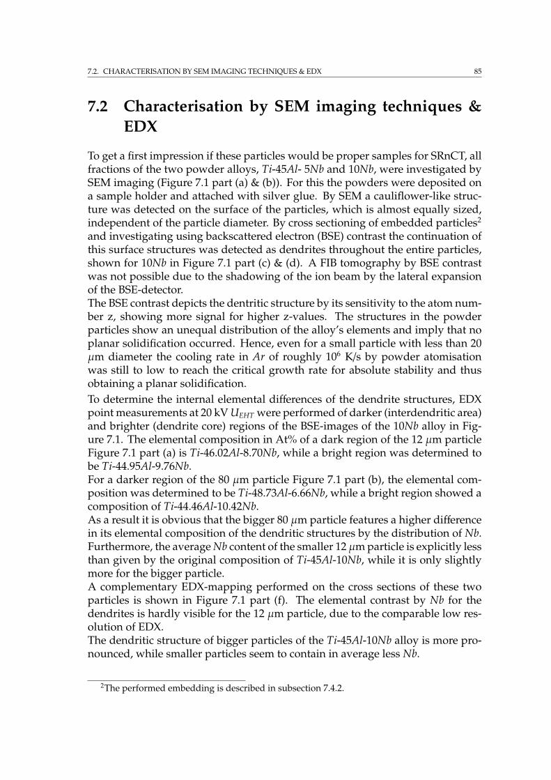
7.2. CHARACTERISATION BY SEM IMAGING TECHNIQUES & EDX 85
7.2 Characterisation by SEM imaging techniques &EDX
To get a first impression if these particles would be proper samples for SRnCT, allfractions of the two powder alloys, Ti-45Al- 5Nb and 10Nb, were investigated bySEM imaging (Figure 7.1 part (a) & (b)). For this the powders were deposited ona sample holder and attached with silver glue. By SEM a cauliflower-like struc-ture was detected on the surface of the particles, which is almost equally sized,independent of the particle diameter. By cross sectioning of embedded particles2
and investigating using backscattered electron (BSE) contrast the continuation ofthis surface structures was detected as dendrites throughout the entire particles,shown for 10Nb in Figure 7.1 part (c) & (d). A FIB tomography by BSE contrastwas not possible due to the shadowing of the ion beam by the lateral expansionof the BSE-detector.The BSE contrast depicts the dentritic structure by its sensitivity to the atom num-ber z, showing more signal for higher z-values. The structures in the powderparticles show an unequal distribution of the alloy’s elements and imply that noplanar solidification occurred. Hence, even for a small particle with less than 20µm diameter the cooling rate in Ar of roughly 106 K/s by powder atomisationwas still to low to reach the critical growth rate for absolute stability and thusobtaining a planar solidification.To determine the internal elemental differences of the dendrite structures, EDXpoint measurements at 20 kV UEHT were performed of darker (interdendritic area)and brighter (dendrite core) regions of the BSE-images of the 10Nb alloy in Fig-ure 7.1. The elemental composition in At% of a dark region of the 12 µm particleFigure 7.1 part (a) is Ti-46.02Al-8.70Nb, while a bright region was determined tobe Ti-44.95Al-9.76Nb.For a darker region of the 80 µm particle Figure 7.1 part (b), the elemental com-position was determined to be Ti-48.73Al-6.66Nb, while a bright region showed acomposition of Ti-44.46Al-10.42Nb.As a result it is obvious that the bigger 80 µm particle features a higher differencein its elemental composition of the dendritic structures by the distribution of Nb.Furthermore, the average Nb content of the smaller 12 µm particle is explicitly lessthan given by the original composition of Ti-45Al-10Nb, while it is only slightlymore for the bigger particle.A complementary EDX-mapping performed on the cross sections of these twoparticles is shown in Figure 7.1 part (f). The elemental contrast by Nb for thedendrites is hardly visible for the 12 µm particle, due to the comparable low res-olution of EDX.The dendritic structure of bigger particles of the Ti-45Al-10Nb alloy is more pro-nounced, while smaller particles seem to contain in average less Nb.
2The performed embedding is described in subsection 7.4.2.
86 CHAPTER 7. APPLICATIONS: TI-45AL-5NB AND 10NB POWDER
(a) (b)
(c) (d)
(e) (f)
Figure 7.1: SEM images of Ti-45Al-10Nb powder on the fractions 20-32 µm (a) and180-250 µm (b); 15 kV UEHT, 5 mm WD, SE2-detector. Cross sections with dendritesstructures of (c) 12 µm and (d) 80 µm particles in diameter, with correspondingEDX-mappings (e) & (f) respectively; 20 kV UEHT, 8.5 mm WD, BSE-detector, EDXwas performed at 20 kV UEHT.
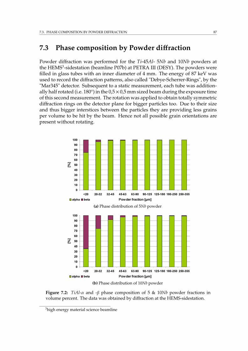
7.3. PHASE COMPOSITION BY POWDER DIFFRACTION 87
7.3 Phase composition by Powder diffraction
Powder diffraction was performed for the Ti-45Al- 5Nb and 10Nb powders atthe HEMS3-sidestation (beamline P07b) at PETRA III (DESY). The powders werefilled in glass tubes with an inner diameter of 4 mm. The energy of 87 keV wasused to record the diffraction patterns, also called "Debye-Scherrer-Rings", by the"Mar345" detector. Subsequent to a static measurement, each tube was addition-ally half rotated (i.e. 180°) in the 0,5× 0,5 mm sized beam during the exposure timeof this second measurement. The rotation was applied to obtain totally symmetricdiffraction rings on the detector plane for bigger particles too. Due to their sizeand thus bigger interstices between the particles they are providing less grainsper volume to be hit by the beam. Hence not all possible grain orientations arepresent without rotating.
(a) Phase distribution of 5Nb powder
(b) Phase distribution of 10Nb powder
Figure 7.2: TiAl-α and -β phase composition of 5 & 10Nb powder fractions involume percent. The data was obtained by diffraction at the HEMS-sidestation.
3high energy material science beamline
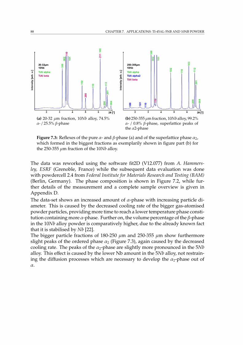
88 CHAPTER 7. APPLICATIONS: TI-45AL-5NB AND 10NB POWDER
(a) 20-32 µm fraction, 10Nb alloy, 74.5%α- / 25.5% β-phase
(b) 250-355µm fraction, 10Nb alloy, 99.2%α- / 0.8% β-phase, superlattice peaks ofthe α2-phase
Figure 7.3: Reflexes of the pure α- and β-phase (a) and of the superlattice phase α2,which formed in the biggest fractions as exemplarily shown in figure part (b) forthe 250-355 µm fraction of the 10Nb alloy.
The data was reworked using the software fit2D (V12.077) from A. Hammers-ley, ESRF (Grenoble, France) while the subsequent data evaluation was donewith powdercell 2.4 from Federal Institute for Materials Research and Testing (BAM)(Berlin, Germany). The phase composition is shown in Figure 7.2, while fur-ther details of the measurement and a complete sample overview is given inAppendix D.The data-set shows an increased amount of α-phase with increasing particle di-ameter. This is caused by the decreased cooling rate of the bigger gas-atomisedpowder particles, providing more time to reach a lower temperature phase consti-tution containing more α-phase. Further on, the volume percentage of the β-phasein the 10Nb alloy powder is comparatively higher, due to the already known factthat it is stabilised by Nb [22].The bigger particle fractions of 180-250 µm and 250-355 µm show furthermoreslight peaks of the ordered phase α2 (Figure 7.3), again caused by the decreasedcooling rate. The peaks of the α2-phase are slightly more pronounced in the 5Nballoy. This effect is caused by the lower Nb amount in the 5Nb alloy, not restrain-ing the diffusion processes which are necessary to develop the α2-phase out ofα.
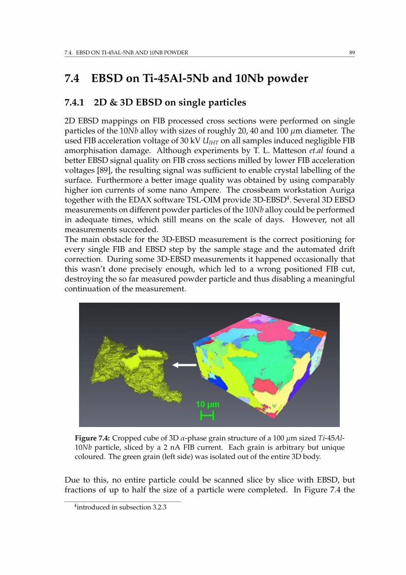
7.4. EBSD ON TI-45AL-5NB AND 10NB POWDER 89
7.4 EBSD on Ti-45Al-5Nb and 10Nb powder
7.4.1 2D & 3D EBSD on single particles
2D EBSD mappings on FIB processed cross sections were performed on singleparticles of the 10Nb alloy with sizes of roughly 20, 40 and 100 µm diameter. Theused FIB acceleration voltage of 30 kV UIHT on all samples induced negligible FIBamorphisation damage. Although experiments by T. L. Matteson et.al found abetter EBSD signal quality on FIB cross sections milled by lower FIB accelerationvoltages [89], the resulting signal was sufficient to enable crystal labelling of thesurface. Furthermore a better image quality was obtained by using comparablyhigher ion currents of some nano Ampere. The crossbeam workstation Aurigatogether with the EDAX software TSL-OIM provide 3D-EBSD4. Several 3D EBSDmeasurements on different powder particles of the 10Nb alloy could be performedin adequate times, which still means on the scale of days. However, not allmeasurements succeeded.The main obstacle for the 3D-EBSD measurement is the correct positioning forevery single FIB and EBSD step by the sample stage and the automated driftcorrection. During some 3D-EBSD measurements it happened occasionally thatthis wasn’t done precisely enough, which led to a wrong positioned FIB cut,destroying the so far measured powder particle and thus disabling a meaningfulcontinuation of the measurement.
Figure 7.4: Cropped cube of 3D α-phase grain structure of a 100 µm sized Ti-45Al-10Nb particle, sliced by a 2 nA FIB current. Each grain is arbitrary but uniquecoloured. The green grain (left side) was isolated out of the entire 3D body.
Due to this, no entire particle could be scanned slice by slice with EBSD, butfractions of up to half the size of a particle were completed. In Figure 7.4 the
4introduced in subsection 3.2.3
90 CHAPTER 7. APPLICATIONS: TI-45AL-5NB AND 10NB POWDER
α-phase grain structure of a powder particle with 100 µm diameter is presentedin three dimensions. The measurement was performed at 20 kV UEHT and default70° sample tilt. The EBSD slices as also the scan points of the measurementare both distanced by 600 nm. In this Figure the scan points are interpolatedbetween the slices, done with the tomographic Avizo software. The isolation ofthe bright green α-phase grain was done by a so called watershed transformation onaccordingly selected, grey valued voxels, again performed with Avizo. It shows acompound of an apparently arbitrary grown α-phase grain. A preferred growthdirection could not be determined and the grains even grew partially around eachother. The grains are not arranged in accordance to the cauliflower-like structuresdetected by BSE inside the particles.
7.4.2 EBSD on embedded powder fractions
To enhance the statistics of the phase composition measurements by EBSD, embed-ding and cross sectioning was performed, featuring a larger scan area with manysingle particle cross sections at once. The powder diffraction already revealed anincreased β-phase amount for the smaller particle size fractions. Therefore thepowder fractions <20 µm, 20 - 32 µm and 90 - 125 µm of the 10Nb alloy wereselected and embedded in a conductive epoxy resin, consecutively grinded with1200 and 2500 µm grained paper and finally polished by hand using a SiO2 solu-tion on a polishing disc wheel. The EBSD measurements were done at 20 kV UEHT
and default 70° sample tilt with respect to the beam. The mapping of the 20-32µm fraction was done on a larger region to obtain a comparable particle statisticregarding the <20 µm fraction.The ratio of α- to β- phase in the EBSD phase images was determined. For this thenoise in the area between the particles had to be set to a homogeneous value likeblack, to read out the remaining pixels of the two colours green (α-phase) and red(β-phase) in the pixel-histograms of the images.This was done on the one hand by using the EDAX software TSL-OIM-Analysis5.31. All pixels of the respective EBSD scan were indexed by a so called cleanupwith a confidence value, calculated from the misorientations of the surroundingpixels. Subsequently a partitioning of the data was performed by setting a thresh-old to the confidence index, which resulted in an phase image without noise.This determination of the phase fractions was proved in parallel by using photo-shop from Adobe systems (San Jose, California, US), by tailoring masks out of thecorresponding quality-images of the EBSD mappings. This masks were then usedto cut off the noise between the powder particles. By changing the so called RGBcolours to indexed ones, and by applying a subsequent colour-tone-separation toonly one green and one red hue, the image pixel-histograms contained only threebars: one for the amount of black pixels, one for the green and one for the red.The frequency values were used to determine the phase composition in percent.The resulting image, from which the phase fractions were determined, is shown
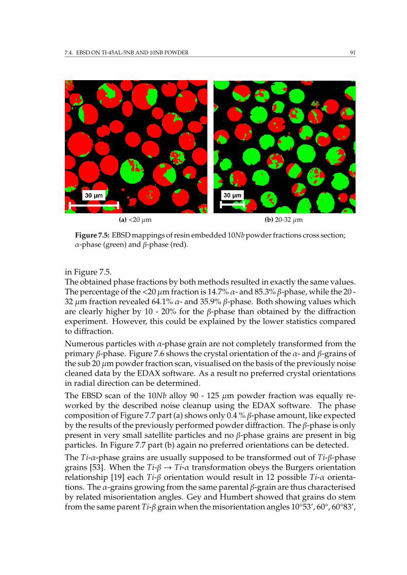
7.4. EBSD ON TI-45AL-5NB AND 10NB POWDER 91
(a) <20 µm (b) 20-32 µm
Figure 7.5: EBSD mappings of resin embedded 10Nb powder fractions cross section;α-phase (green) and β-phase (red).
in Figure 7.5.The obtained phase fractions by both methods resulted in exactly the same values.The percentage of the<20µm fraction is 14.7%α- and 85.3% β-phase, while the 20 -32 µm fraction revealed 64.1% α- and 35.9% β-phase. Both showing values whichare clearly higher by 10 - 20% for the β-phase than obtained by the diffractionexperiment. However, this could be explained by the lower statistics comparedto diffraction.Numerous particles with α-phase grain are not completely transformed from theprimary β-phase. Figure 7.6 shows the crystal orientation of the α- and β-grains ofthe sub 20µm powder fraction scan, visualised on the basis of the previously noisecleaned data by the EDAX software. As a result no preferred crystal orientationsin radial direction can be determined.The EBSD scan of the 10Nb alloy 90 - 125 µm powder fraction was equally re-worked by the described noise cleanup using the EDAX software. The phasecomposition of Figure 7.7 part (a) shows only 0.4 % β-phase amount, like expectedby the results of the previously performed powder diffraction. The β-phase is onlypresent in very small satellite particles and no β-phase grains are present in bigparticles. In Figure 7.7 part (b) again no preferred orientations can be detected.The Ti-α-phase grains are usually supposed to be transformed out of Ti-β-phasegrains [53]. When the Ti-β→ Ti-α transformation obeys the Burgers orientationrelationship [19] each Ti-β orientation would result in 12 possible Ti-α orienta-tions. The α-grains growing from the same parental β-grain are thus characterisedby related misorientation angles. Gey and Humbert showed that grains do stemfrom the same parent Ti-β grain when the misorientation angles 10°53’, 60°, 60°83’,
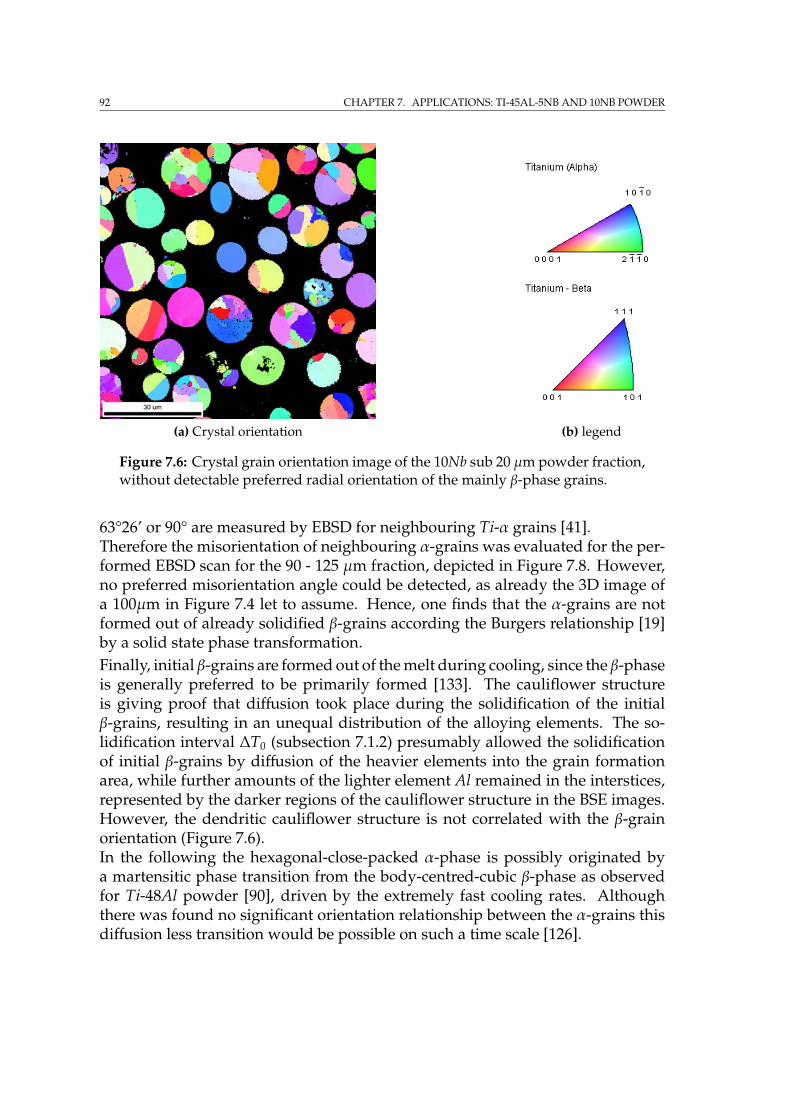
92 CHAPTER 7. APPLICATIONS: TI-45AL-5NB AND 10NB POWDER
(a) Crystal orientation (b) legend
Figure 7.6: Crystal grain orientation image of the 10Nb sub 20 µm powder fraction,without detectable preferred radial orientation of the mainly β-phase grains.
63°26’ or 90° are measured by EBSD for neighbouring Ti-α grains [41].Therefore the misorientation of neighbouring α-grains was evaluated for the per-formed EBSD scan for the 90 - 125 µm fraction, depicted in Figure 7.8. However,no preferred misorientation angle could be detected, as already the 3D image ofa 100µm in Figure 7.4 let to assume. Hence, one finds that the α-grains are notformed out of already solidified β-grains according the Burgers relationship [19]by a solid state phase transformation.Finally, initial β-grains are formed out of the melt during cooling, since the β-phaseis generally preferred to be primarily formed [133]. The cauliflower structureis giving proof that diffusion took place during the solidification of the initialβ-grains, resulting in an unequal distribution of the alloying elements. The so-lidification interval ∆T0 (subsection 7.1.2) presumably allowed the solidificationof initial β-grains by diffusion of the heavier elements into the grain formationarea, while further amounts of the lighter element Al remained in the interstices,represented by the darker regions of the cauliflower structure in the BSE images.However, the dendritic cauliflower structure is not correlated with the β-grainorientation (Figure 7.6).In the following the hexagonal-close-packed α-phase is possibly originated bya martensitic phase transition from the body-centred-cubic β-phase as observedfor Ti-48Al powder [90], driven by the extremely fast cooling rates. Althoughthere was found no significant orientation relationship between the α-grains thisdiffusion less transition would be possible on such a time scale [126].
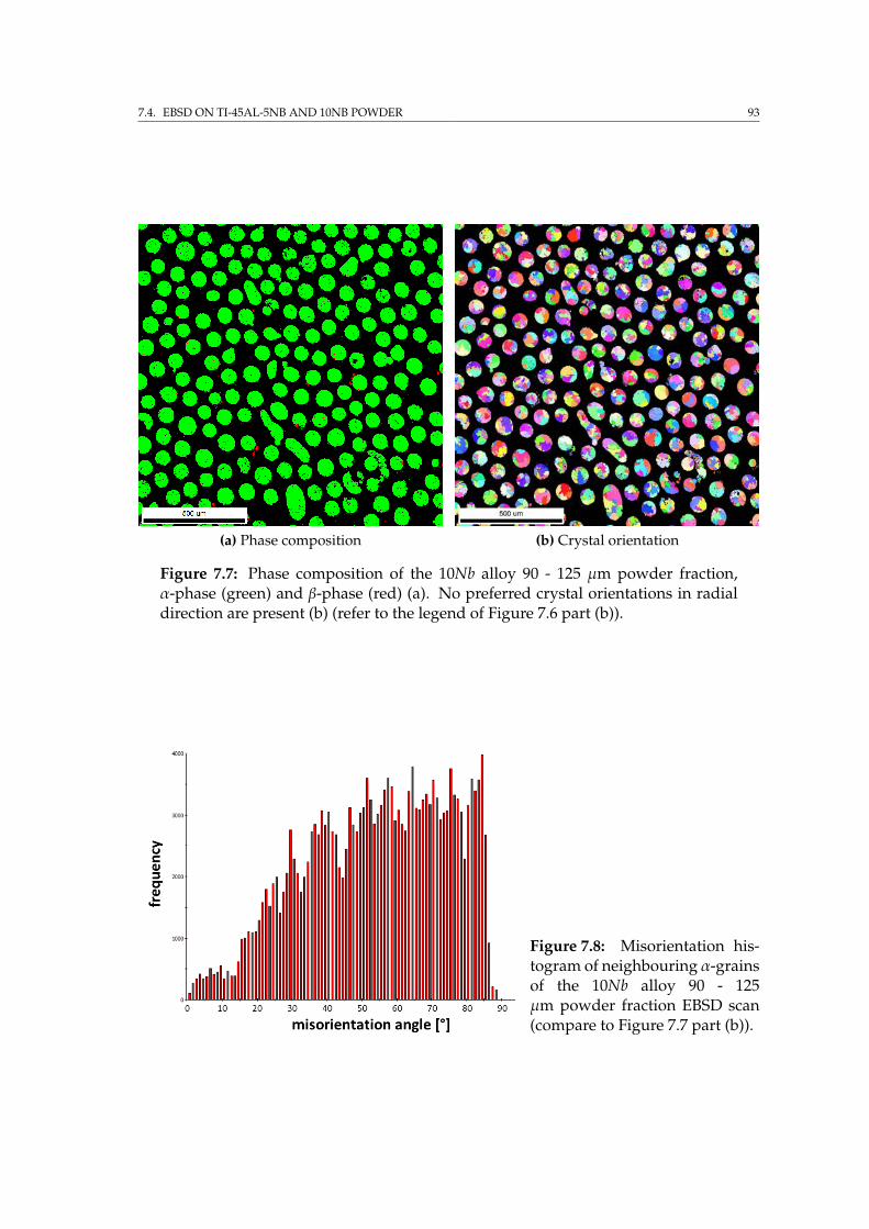
7.4. EBSD ON TI-45AL-5NB AND 10NB POWDER 93
(a) Phase composition (b) Crystal orientation
Figure 7.7: Phase composition of the 10Nb alloy 90 - 125 µm powder fraction,α-phase (green) and β-phase (red) (a). No preferred crystal orientations in radialdirection are present (b) (refer to the legend of Figure 7.6 part (b)).
Figure 7.8: Misorientation his-togram of neighbouring α-grainsof the 10Nb alloy 90 - 125µm powder fraction EBSD scan(compare to Figure 7.7 part (b)).
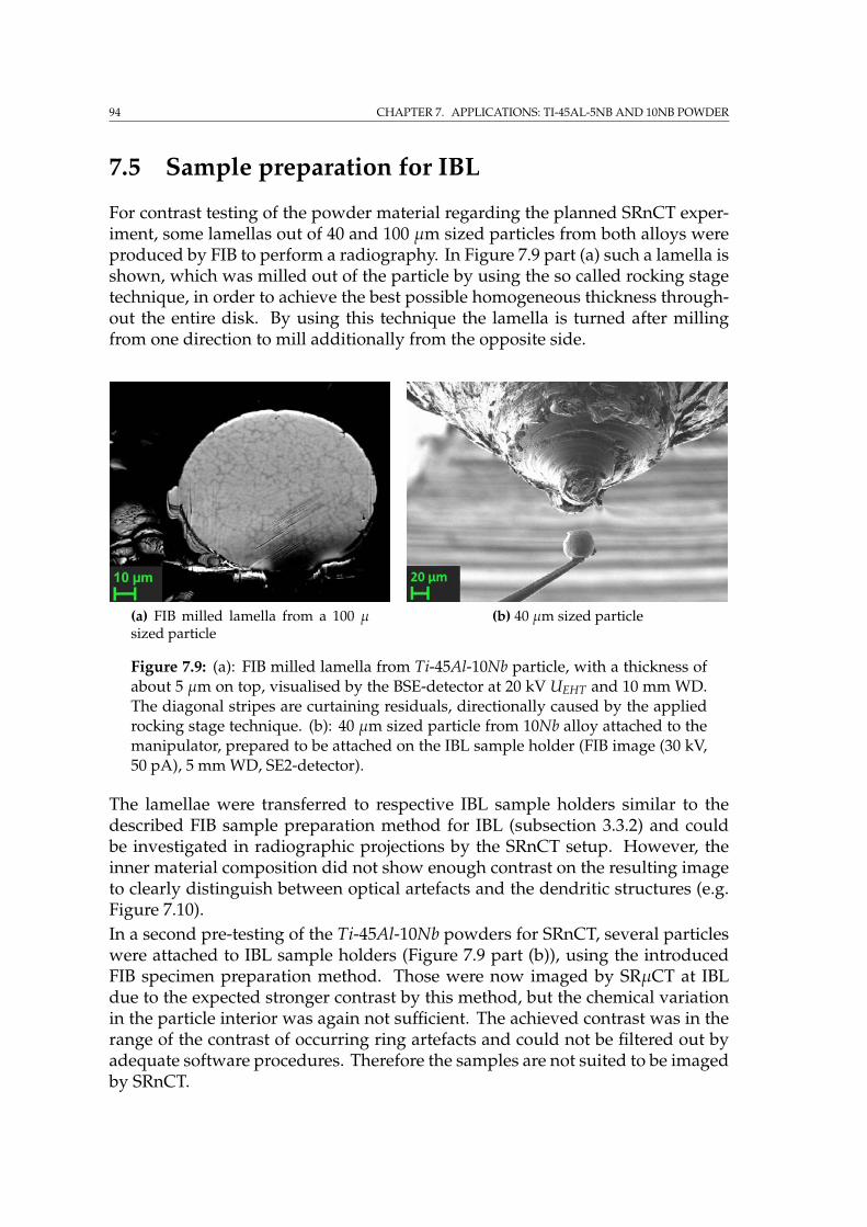
94 CHAPTER 7. APPLICATIONS: TI-45AL-5NB AND 10NB POWDER
7.5 Sample preparation for IBL
For contrast testing of the powder material regarding the planned SRnCT exper-iment, some lamellas out of 40 and 100 µm sized particles from both alloys wereproduced by FIB to perform a radiography. In Figure 7.9 part (a) such a lamella isshown, which was milled out of the particle by using the so called rocking stagetechnique, in order to achieve the best possible homogeneous thickness through-out the entire disk. By using this technique the lamella is turned after millingfrom one direction to mill additionally from the opposite side.
(a) FIB milled lamella from a 100 µsized particle
(b) 40 µm sized particle
Figure 7.9: (a): FIB milled lamella from Ti-45Al-10Nb particle, with a thickness ofabout 5 µm on top, visualised by the BSE-detector at 20 kV UEHT and 10 mm WD.The diagonal stripes are curtaining residuals, directionally caused by the appliedrocking stage technique. (b): 40 µm sized particle from 10Nb alloy attached to themanipulator, prepared to be attached on the IBL sample holder (FIB image (30 kV,50 pA), 5 mm WD, SE2-detector).
The lamellae were transferred to respective IBL sample holders similar to thedescribed FIB sample preparation method for IBL (subsection 3.3.2) and couldbe investigated in radiographic projections by the SRnCT setup. However, theinner material composition did not show enough contrast on the resulting imageto clearly distinguish between optical artefacts and the dendritic structures (e.g.Figure 7.10).In a second pre-testing of the Ti-45Al-10Nb powders for SRnCT, several particleswere attached to IBL sample holders (Figure 7.9 part (b)), using the introducedFIB specimen preparation method. Those were now imaged by SRµCT at IBLdue to the expected stronger contrast by this method, but the chemical variationin the particle interior was again not sufficient. The achieved contrast was in therange of the contrast of occurring ring artefacts and could not be filtered out byadequate software procedures. Therefore the samples are not suited to be imagedby SRnCT.
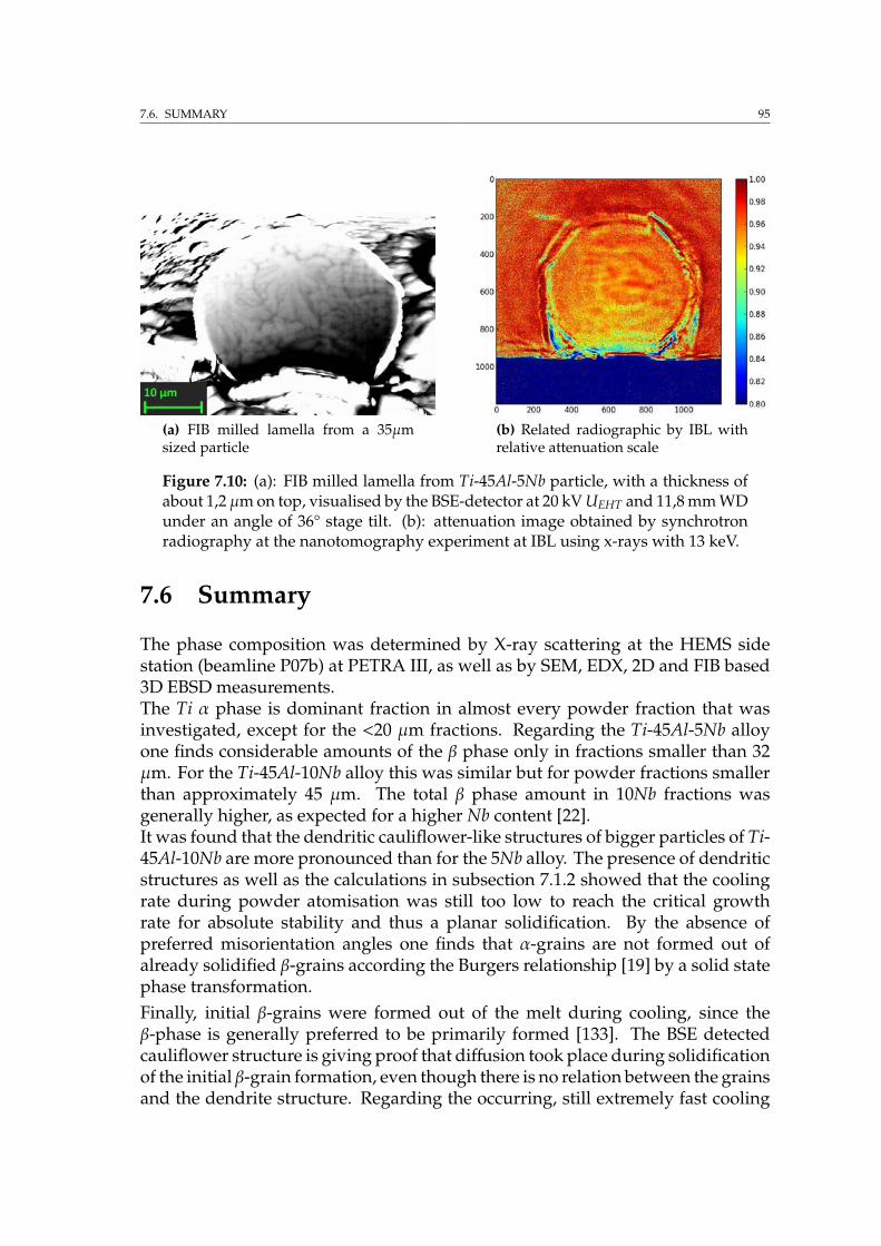
7.6. SUMMARY 95
(a) FIB milled lamella from a 35µmsized particle
(b) Related radiographic by IBL withrelative attenuation scale
Figure 7.10: (a): FIB milled lamella from Ti-45Al-5Nb particle, with a thickness ofabout 1,2 µm on top, visualised by the BSE-detector at 20 kV UEHT and 11,8 mm WDunder an angle of 36° stage tilt. (b): attenuation image obtained by synchrotronradiography at the nanotomography experiment at IBL using x-rays with 13 keV.
7.6 Summary
The phase composition was determined by X-ray scattering at the HEMS sidestation (beamline P07b) at PETRA III, as well as by SEM, EDX, 2D and FIB based3D EBSD measurements.The Ti α phase is dominant fraction in almost every powder fraction that wasinvestigated, except for the <20 µm fractions. Regarding the Ti-45Al-5Nb alloyone finds considerable amounts of the β phase only in fractions smaller than 32µm. For the Ti-45Al-10Nb alloy this was similar but for powder fractions smallerthan approximately 45 µm. The total β phase amount in 10Nb fractions wasgenerally higher, as expected for a higher Nb content [22].It was found that the dendritic cauliflower-like structures of bigger particles of Ti-45Al-10Nb are more pronounced than for the 5Nb alloy. The presence of dendriticstructures as well as the calculations in subsection 7.1.2 showed that the coolingrate during powder atomisation was still too low to reach the critical growthrate for absolute stability and thus a planar solidification. By the absence ofpreferred misorientation angles one finds that α-grains are not formed out ofalready solidified β-grains according the Burgers relationship [19] by a solid statephase transformation.Finally, initial β-grains were formed out of the melt during cooling, since theβ-phase is generally preferred to be primarily formed [133]. The BSE detectedcauliflower structure is giving proof that diffusion took place during solidificationof the initial β-grain formation, even though there is no relation between the grainsand the dendrite structure. Regarding the occurring, still extremely fast cooling

96 CHAPTER 7. APPLICATIONS: TI-45AL-5NB AND 10NB POWDER
rates of 106 K/s [113], the hexagonal-close-packed α-phase is possibly originatedby a martensitic phase transition from the body-centred-cubic β-phase. However,a significant orientation relationship of the α-grains is missing.Regarding SRnCT the specimen could be successfully prepared by the describedFIB method, but the preliminary SRnCT and SRµCT experiments revealed aninsufficient attenuation. However, this samples are also appropriate to performphase contrast experiments at IBL in the future.To enable a FIB tomography by BSE contrast the BSE-detector of the Auriga shouldbe slightly modified by a wedge shaped cutout of the frame scaffold, if possible, toallow the in situ usage with the FIB. Otherwise a pneumatic BSE-detector wouldbe needed to provide an automated detector insertion to enable this.
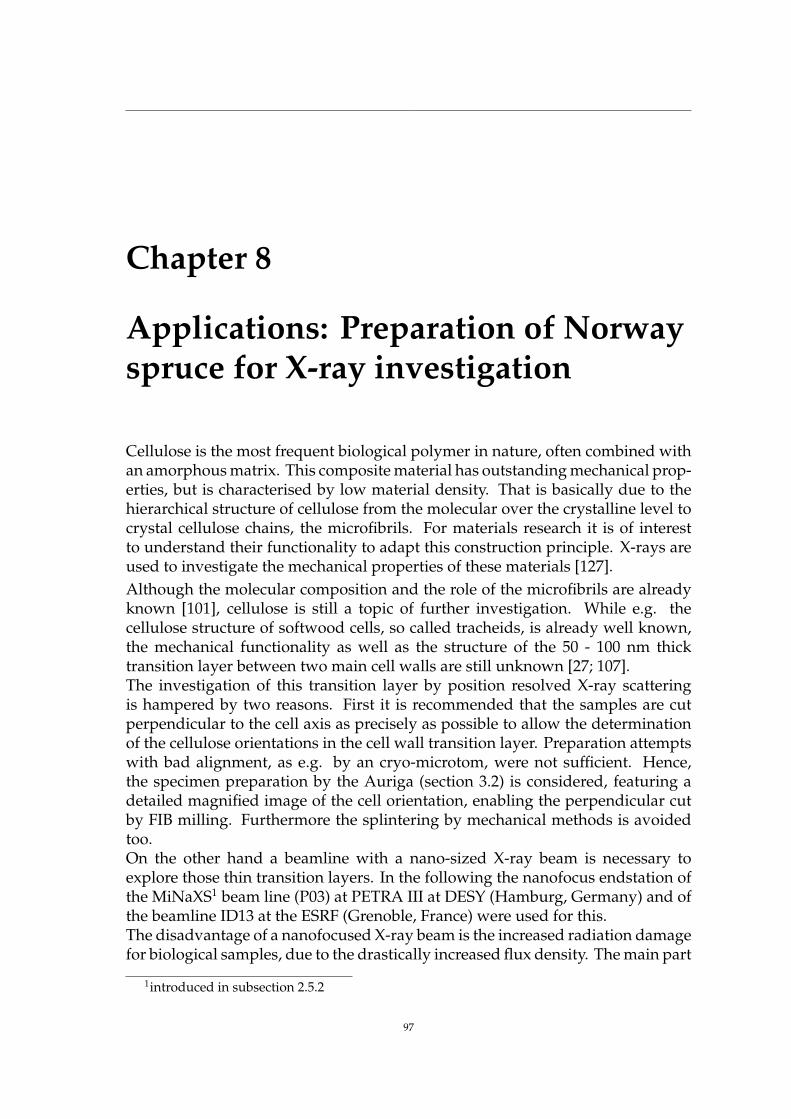
Chapter 8
Applications: Preparation of Norwayspruce for X-ray investigation
Cellulose is the most frequent biological polymer in nature, often combined withan amorphous matrix. This composite material has outstanding mechanical prop-erties, but is characterised by low material density. That is basically due to thehierarchical structure of cellulose from the molecular over the crystalline level tocrystal cellulose chains, the microfibrils. For materials research it is of interestto understand their functionality to adapt this construction principle. X-rays areused to investigate the mechanical properties of these materials [127].Although the molecular composition and the role of the microfibrils are alreadyknown [101], cellulose is still a topic of further investigation. While e.g. thecellulose structure of softwood cells, so called tracheids, is already well known,the mechanical functionality as well as the structure of the 50 - 100 nm thicktransition layer between two main cell walls are still unknown [27; 107].The investigation of this transition layer by position resolved X-ray scatteringis hampered by two reasons. First it is recommended that the samples are cutperpendicular to the cell axis as precisely as possible to allow the determinationof the cellulose orientations in the cell wall transition layer. Preparation attemptswith bad alignment, as e.g. by an cryo-microtom, were not sufficient. Hence,the specimen preparation by the Auriga (section 3.2) is considered, featuring adetailed magnified image of the cell orientation, enabling the perpendicular cutby FIB milling. Furthermore the splintering by mechanical methods is avoidedtoo.On the other hand a beamline with a nano-sized X-ray beam is necessary toexplore those thin transition layers. In the following the nanofocus endstation ofthe MiNaXS1 beam line (P03) at PETRA III at DESY (Hamburg, Germany) and ofthe beamline ID13 at the ESRF (Grenoble, France) were used for this.The disadvantage of a nanofocused X-ray beam is the increased radiation damagefor biological samples, due to the drastically increased flux density. The main part
1introduced in subsection 2.5.2
97
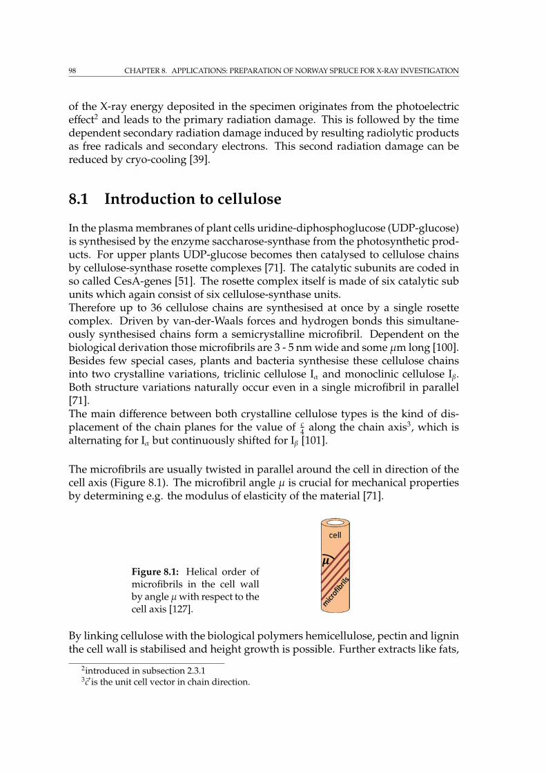
98 CHAPTER 8. APPLICATIONS: PREPARATION OF NORWAY SPRUCE FOR X-RAY INVESTIGATION
of the X-ray energy deposited in the specimen originates from the photoelectriceffect2 and leads to the primary radiation damage. This is followed by the timedependent secondary radiation damage induced by resulting radiolytic productsas free radicals and secondary electrons. This second radiation damage can bereduced by cryo-cooling [39].
8.1 Introduction to cellulose
In the plasma membranes of plant cells uridine-diphosphoglucose (UDP-glucose)is synthesised by the enzyme saccharose-synthase from the photosynthetic prod-ucts. For upper plants UDP-glucose becomes then catalysed to cellulose chainsby cellulose-synthase rosette complexes [71]. The catalytic subunits are coded inso called CesA-genes [51]. The rosette complex itself is made of six catalytic subunits which again consist of six cellulose-synthase units.Therefore up to 36 cellulose chains are synthesised at once by a single rosettecomplex. Driven by van-der-Waals forces and hydrogen bonds this simultane-ously synthesised chains form a semicrystalline microfibril. Dependent on thebiological derivation those microfibrils are 3 - 5 nm wide and some µm long [100].Besides few special cases, plants and bacteria synthesise these cellulose chainsinto two crystalline variations, triclinic cellulose Iα and monoclinic cellulose Iβ.Both structure variations naturally occur even in a single microfibril in parallel[71].The main difference between both crystalline cellulose types is the kind of dis-placement of the chain planes for the value of c
4 along the chain axis3, which isalternating for Iα but continuously shifted for Iβ [101].
The microfibrils are usually twisted in parallel around the cell in direction of thecell axis (Figure 8.1). The microfibril angle µ is crucial for mechanical propertiesby determining e.g. the modulus of elasticity of the material [71].
Figure 8.1: Helical order ofmicrofibrils in the cell wallby angle µwith respect to thecell axis [127].
By linking cellulose with the biological polymers hemicellulose, pectin and ligninthe cell wall is stabilised and height growth is possible. Further extracts like fats,
2introduced in subsection 2.3.13c is the unit cell vector in chain direction.
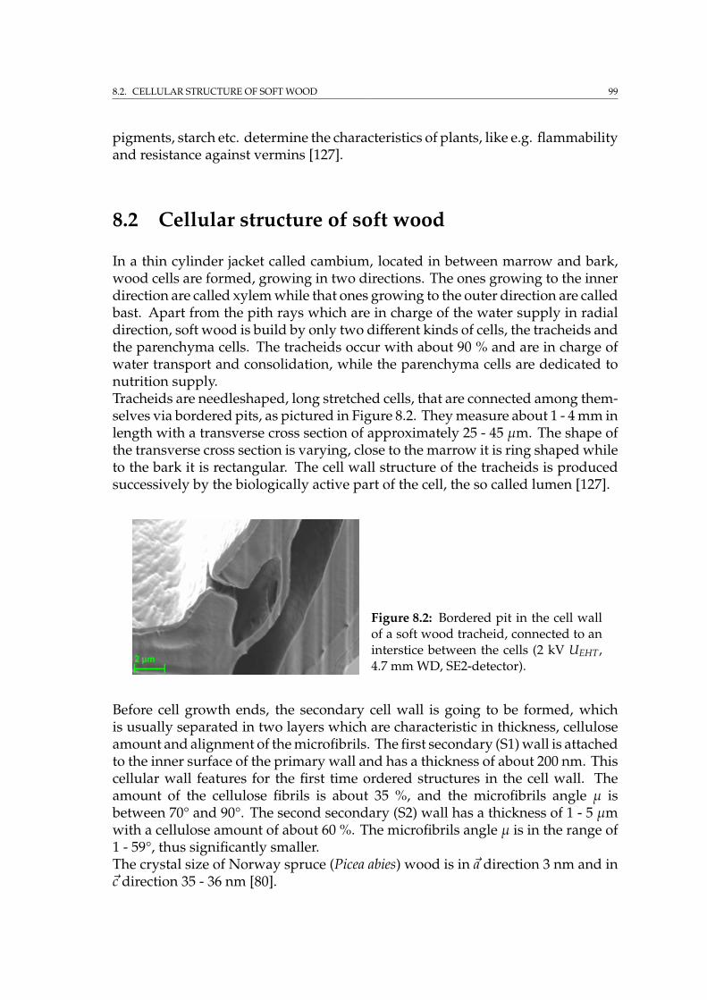
8.2. CELLULAR STRUCTURE OF SOFT WOOD 99
pigments, starch etc. determine the characteristics of plants, like e.g. flammabilityand resistance against vermins [127].
8.2 Cellular structure of soft wood
In a thin cylinder jacket called cambium, located in between marrow and bark,wood cells are formed, growing in two directions. The ones growing to the innerdirection are called xylem while that ones growing to the outer direction are calledbast. Apart from the pith rays which are in charge of the water supply in radialdirection, soft wood is build by only two different kinds of cells, the tracheids andthe parenchyma cells. The tracheids occur with about 90 % and are in charge ofwater transport and consolidation, while the parenchyma cells are dedicated tonutrition supply.Tracheids are needleshaped, long stretched cells, that are connected among them-selves via bordered pits, as pictured in Figure 8.2. They measure about 1 - 4 mm inlength with a transverse cross section of approximately 25 - 45 µm. The shape ofthe transverse cross section is varying, close to the marrow it is ring shaped whileto the bark it is rectangular. The cell wall structure of the tracheids is producedsuccessively by the biologically active part of the cell, the so called lumen [127].
Figure 8.2: Bordered pit in the cell wallof a soft wood tracheid, connected to aninterstice between the cells (2 kV UEHT,4.7 mm WD, SE2-detector).
Before cell growth ends, the secondary cell wall is going to be formed, whichis usually separated in two layers which are characteristic in thickness, celluloseamount and alignment of the microfibrils. The first secondary (S1) wall is attachedto the inner surface of the primary wall and has a thickness of about 200 nm. Thiscellular wall features for the first time ordered structures in the cell wall. Theamount of the cellulose fibrils is about 35 %, and the microfibrils angle µ isbetween 70° and 90°. The second secondary (S2) wall has a thickness of 1 - 5 µmwith a cellulose amount of about 60 %. The microfibrils angle µ is in the range of1 - 59°, thus significantly smaller.The crystal size of Norway spruce (Picea abies) wood is in a direction 3 nm and inc direction 35 - 36 nm [80].
100 CHAPTER 8. APPLICATIONS: PREPARATION OF NORWAY SPRUCE FOR X-RAY INVESTIGATION
8.3 Introduction to X-ray scattering on wood
Constructive interference patterns of fibres can be obtained by X-ray scatteringif a fibre texture is given by any crystal axis which is aligned to the longitudinalaxis of the fibre. In our case this is given by the c axis of the cellulose crystals.The other crystal axes are therefore rotationally directed to the main axis and arealigned in arbitrary directions. X-ray scattering on a fibre generates a typical fibrepattern which can be well illustrated by using the Ewald-construction [127].To detect the orientation of the microfibrils in the cell wall layers it is recommendedto align the longitudinal cell axis in parallel to the beam. By this the scatteringsignals of front- and backside-microfibrils of the cell do not superimpose [82]. Thecylindrical microfibrils appear ringshaped in reciprocal space, tilted by the angleµ. The diffraction reflexes are formed where the Ewald sphere cuts these rings.For details on the microfibrils diffraction patterns please refer to Paris and Müller[105].
8.3.1 Preliminary results by diffraction on wood
In order to elucidate the context of the FIB sample preparation presented here,first results of specimens prepared and measured in a similar way as planned hereby S. Storm at the nanofocus endstation of the MiNaXS beam line (P03, DESY) arepresented [127].
Figure 8.3: Normalised cellulose re-flex intensity of mesh scan on woodin real space [127].
It was originally planned by Storm to attach a FIB processed wood lamella to a 50nm silicon-nitride-membrane using the manipulator. This membrane is extremelysensitive to any touch, and even to interaction with the ion beam. That made itimpossible to bring the sample to the membrane by the manipulator directly.Hence, a fixation on the membrane by GIS and FIB was not possible. ThereforeStorm finally had to use non-FIB prepared samples for a first beam time at theMiNaXS endstation. Those samples had been already cut by the Finnish woodresearch institute METLA, by using a cryo-microtom, featuring a thickness of 25
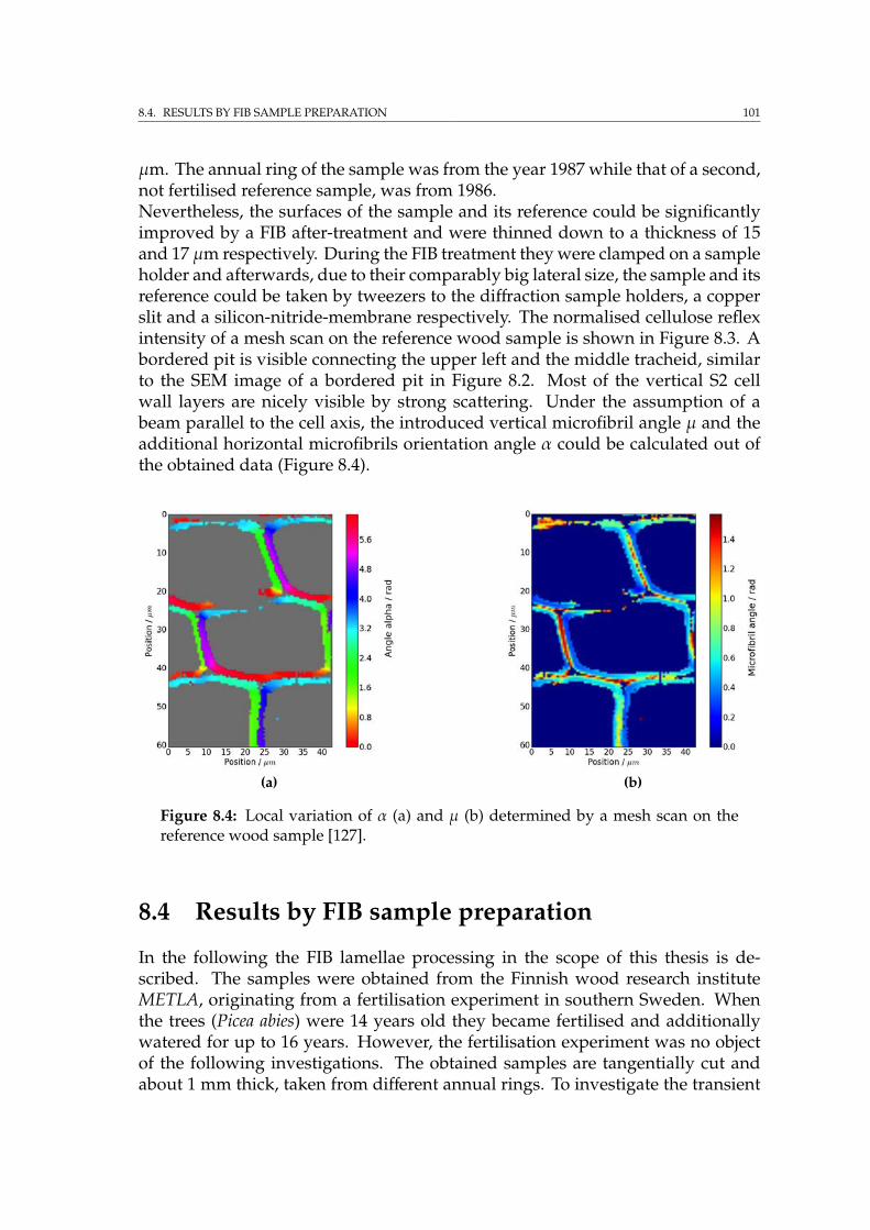
8.4. RESULTS BY FIB SAMPLE PREPARATION 101
µm. The annual ring of the sample was from the year 1987 while that of a second,not fertilised reference sample, was from 1986.Nevertheless, the surfaces of the sample and its reference could be significantlyimproved by a FIB after-treatment and were thinned down to a thickness of 15and 17 µm respectively. During the FIB treatment they were clamped on a sampleholder and afterwards, due to their comparably big lateral size, the sample and itsreference could be taken by tweezers to the diffraction sample holders, a copperslit and a silicon-nitride-membrane respectively. The normalised cellulose reflexintensity of a mesh scan on the reference wood sample is shown in Figure 8.3. Abordered pit is visible connecting the upper left and the middle tracheid, similarto the SEM image of a bordered pit in Figure 8.2. Most of the vertical S2 cellwall layers are nicely visible by strong scattering. Under the assumption of abeam parallel to the cell axis, the introduced vertical microfibril angle µ and theadditional horizontal microfibrils orientation angle α could be calculated out ofthe obtained data (Figure 8.4).
(a) (b)
Figure 8.4: Local variation of α (a) and µ (b) determined by a mesh scan on thereference wood sample [127].
8.4 Results by FIB sample preparation
In the following the FIB lamellae processing in the scope of this thesis is de-scribed. The samples were obtained from the Finnish wood research instituteMETLA, originating from a fertilisation experiment in southern Sweden. Whenthe trees (Picea abies) were 14 years old they became fertilised and additionallywatered for up to 16 years. However, the fertilisation experiment was no objectof the following investigations. The obtained samples are tangentially cut andabout 1 mm thick, taken from different annual rings. To investigate the transient
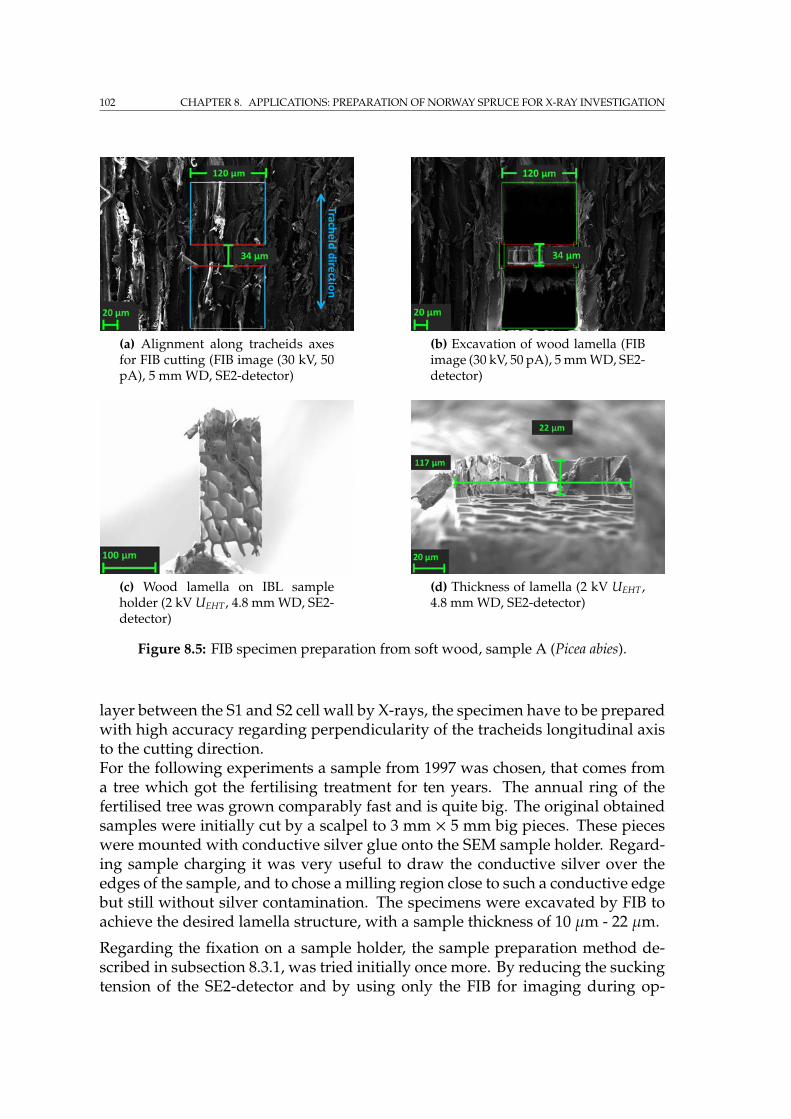
102 CHAPTER 8. APPLICATIONS: PREPARATION OF NORWAY SPRUCE FOR X-RAY INVESTIGATION
(a) Alignment along tracheids axesfor FIB cutting (FIB image (30 kV, 50pA), 5 mm WD, SE2-detector)
(b) Excavation of wood lamella (FIBimage (30 kV, 50 pA), 5 mm WD, SE2-detector)
(c) Wood lamella on IBL sampleholder (2 kV UEHT, 4.8 mm WD, SE2-detector)
(d) Thickness of lamella (2 kV UEHT,4.8 mm WD, SE2-detector)
Figure 8.5: FIB specimen preparation from soft wood, sample A (Picea abies).
layer between the S1 and S2 cell wall by X-rays, the specimen have to be preparedwith high accuracy regarding perpendicularity of the tracheids longitudinal axisto the cutting direction.For the following experiments a sample from 1997 was chosen, that comes froma tree which got the fertilising treatment for ten years. The annual ring of thefertilised tree was grown comparably fast and is quite big. The original obtainedsamples were initially cut by a scalpel to 3 mm × 5 mm big pieces. These pieceswere mounted with conductive silver glue onto the SEM sample holder. Regard-ing sample charging it was very useful to draw the conductive silver over theedges of the sample, and to chose a milling region close to such a conductive edgebut still without silver contamination. The specimens were excavated by FIB toachieve the desired lamella structure, with a sample thickness of 10 µm - 22 µm.
Regarding the fixation on a sample holder, the sample preparation method de-scribed in subsection 8.3.1, was tried initially once more. By reducing the suckingtension of the SE2-detector and by using only the FIB for imaging during op-
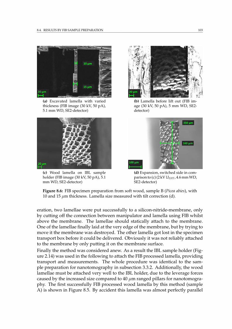
8.4. RESULTS BY FIB SAMPLE PREPARATION 103
(a) Excavated lamella with variedthickness (FIB image (30 kV, 50 pA),5.1 mm WD, SE2-detector)
(b) Lamella before lift out (FIB im-age (30 kV, 50 pA), 5 mm WD, SE2-detector)
(c) Wood lamella on IBL sampleholder (FIB image (30 kV, 50 pA), 5.1mm WD, SE2-detector)
(d) Expansion, switched side in com-parison to (c) (2 kV UEHT, 4.6 mm WD,SE2-detector)
Figure 8.6: FIB specimen preparation from soft wood, sample B (Picea abies), with10 and 15 µm thickness. Lamella size measured with tilt correction (d).
eration, two lamellae were put successfully to a silicon-nitride-membrane, onlyby cutting off the connection between manipulator and lamella using FIB whilstabove the membrane. The lamellae should statically attach to the membrane.One of the lamellae finally laid at the very edge of the membrane, but by trying tomove it the membrane was destroyed. The other lamella got lost in the specimentransport box before it could be delivered. Obviously it was not reliably attachedto the membrane by only putting it on the membrane surface.Finally the method was considered anew. As a result the IBL sample holder (Fig-ure 2.14) was used in the following to attach the FIB processed lamella, providingtransport and measurements. The whole procedure was identical to the sam-ple preparation for nanotomography in subsection 3.3.2. Additionally, the woodlamellae must be attached very well to the IBL holder, due to the leverage forcescaused by the increased size compared to 40 µm ranged pillars for nanotomogra-phy. The first successfully FIB processed wood lamella by this method (sampleA) is shown in Figure 8.5. By accident this lamella was almost perfectly parallel
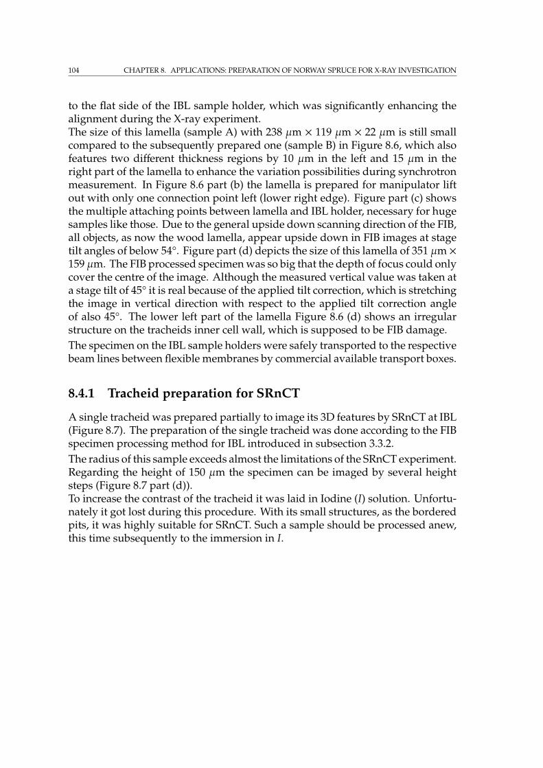
104 CHAPTER 8. APPLICATIONS: PREPARATION OF NORWAY SPRUCE FOR X-RAY INVESTIGATION
to the flat side of the IBL sample holder, which was significantly enhancing thealignment during the X-ray experiment.The size of this lamella (sample A) with 238 µm × 119 µm × 22 µm is still smallcompared to the subsequently prepared one (sample B) in Figure 8.6, which alsofeatures two different thickness regions by 10 µm in the left and 15 µm in theright part of the lamella to enhance the variation possibilities during synchrotronmeasurement. In Figure 8.6 part (b) the lamella is prepared for manipulator liftout with only one connection point left (lower right edge). Figure part (c) showsthe multiple attaching points between lamella and IBL holder, necessary for hugesamples like those. Due to the general upside down scanning direction of the FIB,all objects, as now the wood lamella, appear upside down in FIB images at stagetilt angles of below 54°. Figure part (d) depicts the size of this lamella of 351 µm ×159 µm. The FIB processed specimen was so big that the depth of focus could onlycover the centre of the image. Although the measured vertical value was taken ata stage tilt of 45° it is real because of the applied tilt correction, which is stretchingthe image in vertical direction with respect to the applied tilt correction angleof also 45°. The lower left part of the lamella Figure 8.6 (d) shows an irregularstructure on the tracheids inner cell wall, which is supposed to be FIB damage.The specimen on the IBL sample holders were safely transported to the respectivebeam lines between flexible membranes by commercial available transport boxes.
8.4.1 Tracheid preparation for SRnCT
A single tracheid was prepared partially to image its 3D features by SRnCT at IBL(Figure 8.7). The preparation of the single tracheid was done according to the FIBspecimen processing method for IBL introduced in subsection 3.3.2.The radius of this sample exceeds almost the limitations of the SRnCT experiment.Regarding the height of 150 µm the specimen can be imaged by several heightsteps (Figure 8.7 part (d)).To increase the contrast of the tracheid it was laid in Iodine (I) solution. Unfortu-nately it got lost during this procedure. With its small structures, as the borderedpits, it was highly suitable for SRnCT. Such a sample should be processed anew,this time subsequently to the immersion in I.
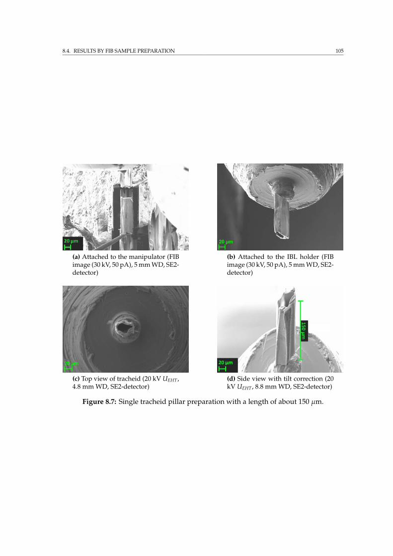
8.4. RESULTS BY FIB SAMPLE PREPARATION 105
(a) Attached to the manipulator (FIBimage (30 kV, 50 pA), 5 mm WD, SE2-detector)
(b) Attached to the IBL holder (FIBimage (30 kV, 50 pA), 5 mm WD, SE2-detector)
(c) Top view of tracheid (20 kV UEHT,4.8 mm WD, SE2-detector)
(d) Side view with tilt correction (20kV UEHT, 8.8 mm WD, SE2-detector)
Figure 8.7: Single tracheid pillar preparation with a length of about 150 µm.
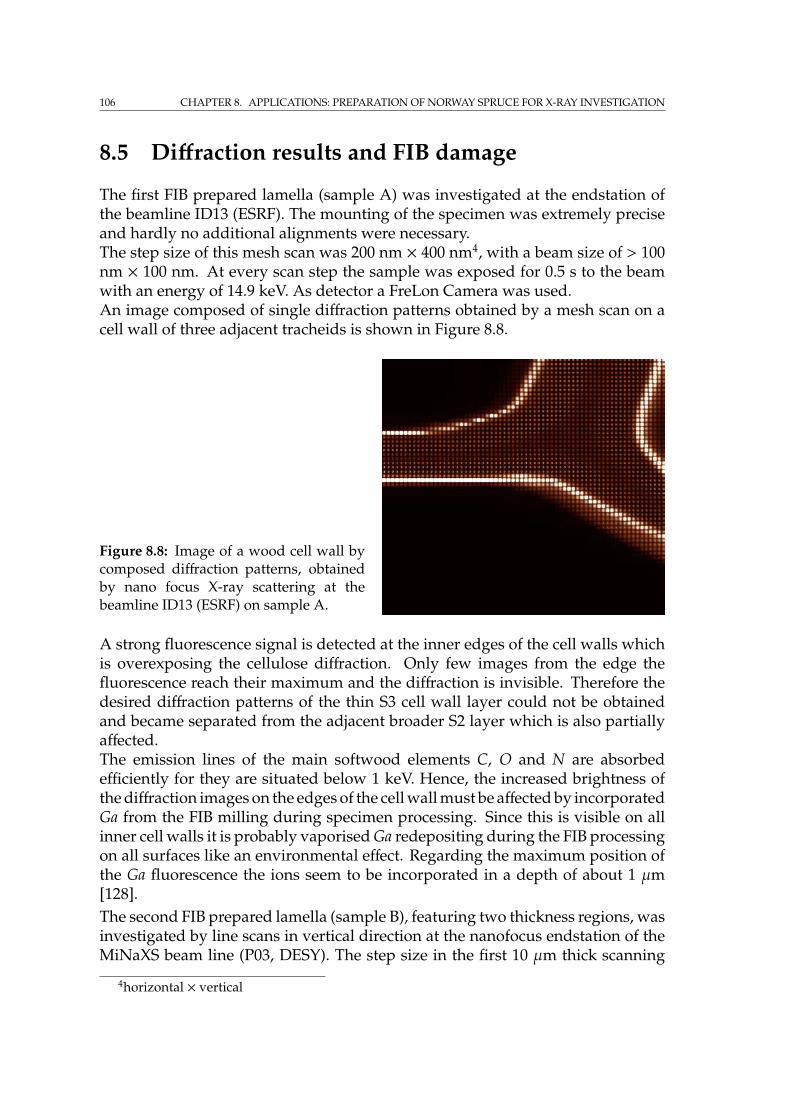
106 CHAPTER 8. APPLICATIONS: PREPARATION OF NORWAY SPRUCE FOR X-RAY INVESTIGATION
8.5 Diffraction results and FIB damage
The first FIB prepared lamella (sample A) was investigated at the endstation ofthe beamline ID13 (ESRF). The mounting of the specimen was extremely preciseand hardly no additional alignments were necessary.The step size of this mesh scan was 200 nm × 400 nm4, with a beam size of > 100nm × 100 nm. At every scan step the sample was exposed for 0.5 s to the beamwith an energy of 14.9 keV. As detector a FreLon Camera was used.An image composed of single diffraction patterns obtained by a mesh scan on acell wall of three adjacent tracheids is shown in Figure 8.8.
Figure 8.8: Image of a wood cell wall bycomposed diffraction patterns, obtainedby nano focus X-ray scattering at thebeamline ID13 (ESRF) on sample A.
A strong fluorescence signal is detected at the inner edges of the cell walls whichis overexposing the cellulose diffraction. Only few images from the edge thefluorescence reach their maximum and the diffraction is invisible. Therefore thedesired diffraction patterns of the thin S3 cell wall layer could not be obtainedand became separated from the adjacent broader S2 layer which is also partiallyaffected.The emission lines of the main softwood elements C, O and N are absorbedefficiently for they are situated below 1 keV. Hence, the increased brightness ofthe diffraction images on the edges of the cell wall must be affected by incorporatedGa from the FIB milling during specimen processing. Since this is visible on allinner cell walls it is probably vaporised Ga redepositing during the FIB processingon all surfaces like an environmental effect. Regarding the maximum position ofthe Ga fluorescence the ions seem to be incorporated in a depth of about 1 µm[128].The second FIB prepared lamella (sample B), featuring two thickness regions, wasinvestigated by line scans in vertical direction at the nanofocus endstation of theMiNaXS beam line (P03, DESY). The step size in the first 10 µm thick scanning
4horizontal × vertical
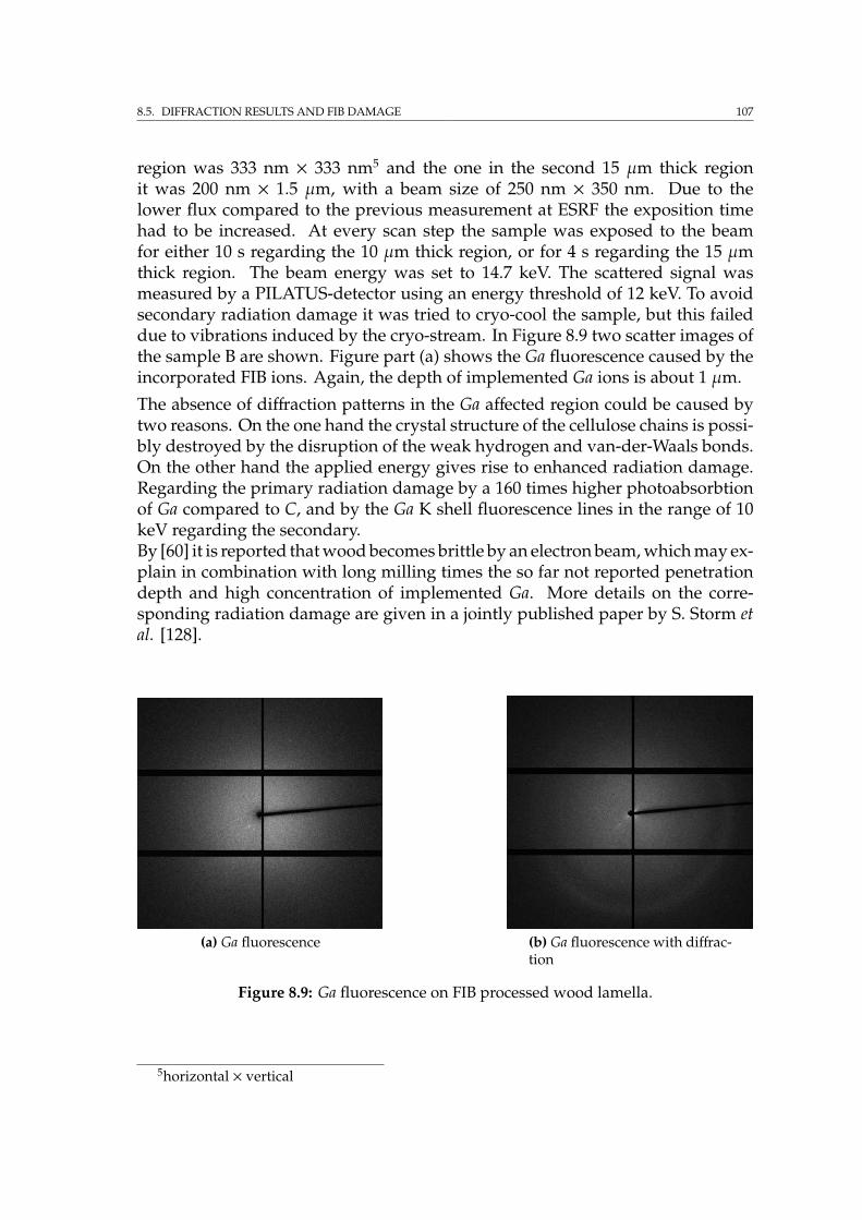
8.5. DIFFRACTION RESULTS AND FIB DAMAGE 107
region was 333 nm × 333 nm5 and the one in the second 15 µm thick regionit was 200 nm × 1.5 µm, with a beam size of 250 nm × 350 nm. Due to thelower flux compared to the previous measurement at ESRF the exposition timehad to be increased. At every scan step the sample was exposed to the beamfor either 10 s regarding the 10 µm thick region, or for 4 s regarding the 15 µmthick region. The beam energy was set to 14.7 keV. The scattered signal wasmeasured by a PILATUS-detector using an energy threshold of 12 keV. To avoidsecondary radiation damage it was tried to cryo-cool the sample, but this faileddue to vibrations induced by the cryo-stream. In Figure 8.9 two scatter images ofthe sample B are shown. Figure part (a) shows the Ga fluorescence caused by theincorporated FIB ions. Again, the depth of implemented Ga ions is about 1 µm.
The absence of diffraction patterns in the Ga affected region could be caused bytwo reasons. On the one hand the crystal structure of the cellulose chains is possi-bly destroyed by the disruption of the weak hydrogen and van-der-Waals bonds.On the other hand the applied energy gives rise to enhanced radiation damage.Regarding the primary radiation damage by a 160 times higher photoabsorbtionof Ga compared to C, and by the Ga K shell fluorescence lines in the range of 10keV regarding the secondary.By [60] it is reported that wood becomes brittle by an electron beam, which may ex-plain in combination with long milling times the so far not reported penetrationdepth and high concentration of implemented Ga. More details on the corre-sponding radiation damage are given in a jointly published paper by S. Storm etal. [128].
(a) Ga fluorescence (b) Ga fluorescence with diffrac-tion
Figure 8.9: Ga fluorescence on FIB processed wood lamella.
5horizontal × vertical
108 CHAPTER 8. APPLICATIONS: PREPARATION OF NORWAY SPRUCE FOR X-RAY INVESTIGATION
8.6 Summary
The jointly published paper [128] reports for the first time the investigation of aFIB-processed biological sample by scanning X-ray nanodiffraction.The introduced FIB specimen processing method for IBL (subsection 3.3.2) wassuccessfully applied to the wood lamella preparation. The perpendicular orien-tation of the tracheids in the wood lamellae could be precisely achieved by thissample preparation method. The ability of the Auriga workstation to image lessconductive material at low voltages was a benefit too. The parallel orientationof a lamella to the flat side of the IBL sample holder, as experienced for sampleA, should be applied in future to enhance the alignment procedure during thesubsequent X-ray experiment.At the measured energies the obtained diffraction images prove a strong Ga in-corporation on the inner edges of the cell walls by a strong fluorescence signal.Even though the FIB milling enabled a very defined cross sectioning and surfacepreparation of the FIB-processed specimen, the Ga incorporation hindered theinvestigation of the affected cell wall layer S3.To lower the penetration depth of Ga the milling process could be performedat lower voltage or even be followed by subsequent polishing with an inert gasbeam. Furthermore, the cryo-cooling should be enabled by appropriate samplefixation and connection to avoid secondary radiation damage.Finally, despite the damage in the S3 and partially the S2 cell wall layer the re-maining cell wall seems to be intact and this method can still be used nicely toinvestigate the S1 and main parts of the S2 layer.
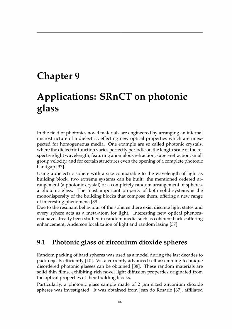
Chapter 9
Applications: SRnCT on photonicglass
In the field of photonics novel materials are engineered by arranging an internalmicrostructure of a dielectric, effecting new optical properties which are unex-pected for homogeneous media. One example are so called photonic crystals,where the dielectric function varies perfectly periodic on the length scale of the re-spective light wavelength, featuring anomalous refraction, super-refraction, smallgroup velocity, and for certain structures even the opening of a complete photonicbandgap [37].Using a dielectric sphere with a size comparable to the wavelength of light asbuilding block, two extreme systems can be built: the mentioned ordered ar-rangement (a photonic crystal) or a completely random arrangement of spheres,a photonic glass. The most important property of both solid systems is themonodispersity of the building blocks that compose them, offering a new rangeof interesting phenomena [38].Due to the resonant behaviour of the spheres there exist discrete light states andevery sphere acts as a meta-atom for light. Interesting new optical phenom-ena have already been studied in random media such as coherent backscatteringenhancement, Anderson localization of light and random lasing [37].
9.1 Photonic glass of zirconium dioxide spheres
Random packing of hard spheres was used as a model during the last decades topack objects efficiently [10]. Via a currently advanced self-assembling techniquedisordered photonic glasses can be obtained [38]. These random materials aresolid thin films, exhibiting rich novel light diffusion properties originated fromthe optical properties of their building blocks.Particularly, a photonic glass sample made of 2 µm sized zirconium dioxidespheres was investigated. It was obtained from Jean do Rosario [67], affiliated
109
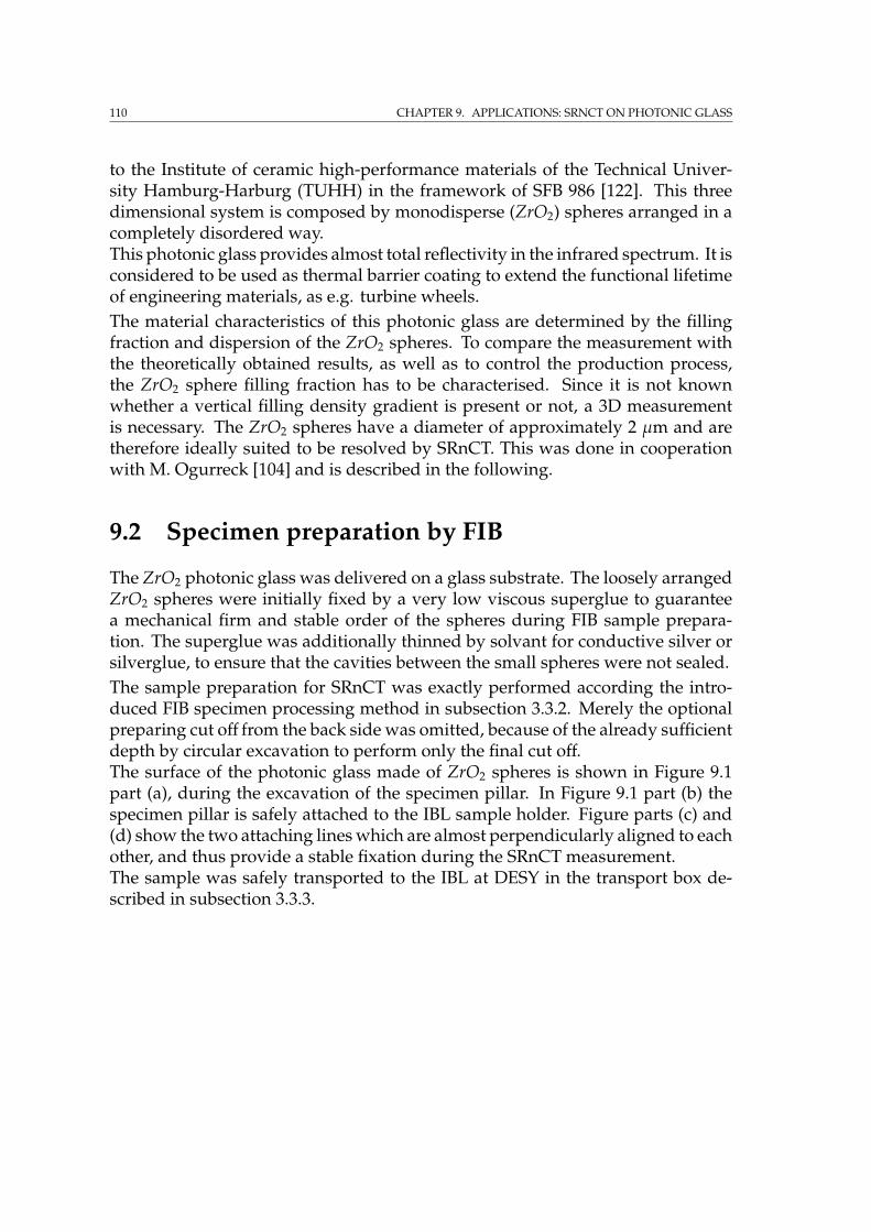
110 CHAPTER 9. APPLICATIONS: SRNCT ON PHOTONIC GLASS
to the Institute of ceramic high-performance materials of the Technical Univer-sity Hamburg-Harburg (TUHH) in the framework of SFB 986 [122]. This threedimensional system is composed by monodisperse (ZrO2) spheres arranged in acompletely disordered way.This photonic glass provides almost total reflectivity in the infrared spectrum. It isconsidered to be used as thermal barrier coating to extend the functional lifetimeof engineering materials, as e.g. turbine wheels.The material characteristics of this photonic glass are determined by the fillingfraction and dispersion of the ZrO2 spheres. To compare the measurement withthe theoretically obtained results, as well as to control the production process,the ZrO2 sphere filling fraction has to be characterised. Since it is not knownwhether a vertical filling density gradient is present or not, a 3D measurementis necessary. The ZrO2 spheres have a diameter of approximately 2 µm and aretherefore ideally suited to be resolved by SRnCT. This was done in cooperationwith M. Ogurreck [104] and is described in the following.
9.2 Specimen preparation by FIB
The ZrO2 photonic glass was delivered on a glass substrate. The loosely arrangedZrO2 spheres were initially fixed by a very low viscous superglue to guaranteea mechanical firm and stable order of the spheres during FIB sample prepara-tion. The superglue was additionally thinned by solvant for conductive silver orsilverglue, to ensure that the cavities between the small spheres were not sealed.The sample preparation for SRnCT was exactly performed according the intro-duced FIB specimen processing method in subsection 3.3.2. Merely the optionalpreparing cut off from the back side was omitted, because of the already sufficientdepth by circular excavation to perform only the final cut off.The surface of the photonic glass made of ZrO2 spheres is shown in Figure 9.1part (a), during the excavation of the specimen pillar. In Figure 9.1 part (b) thespecimen pillar is safely attached to the IBL sample holder. Figure parts (c) and(d) show the two attaching lines which are almost perpendicularly aligned to eachother, and thus provide a stable fixation during the SRnCT measurement.The sample was safely transported to the IBL at DESY in the transport box de-scribed in subsection 3.3.3.
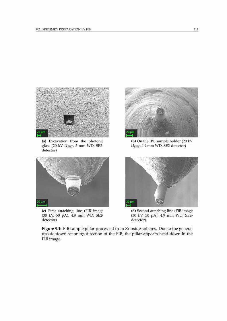
9.2. SPECIMEN PREPARATION BY FIB 111
(a) Excavation from the photonicglass (20 kV UEHT, 5 mm WD, SE2-detector)
(b) On the IBL sample holder (20 kVUEHT, 4.9 mm WD, SE2-detector)
(c) First attaching line (FIB image(30 kV, 50 pA), 4.9 mm WD, SE2-detector)
(d) Second attaching line (FIB image(30 kV, 50 pA), 4.9 mm WD, SE2-detector)
Figure 9.1: FIB sample pillar processed from Zr oxide spheres. Due to the generalupside down scanning direction of the FIB, the pillar appears head-down in theFIB image.
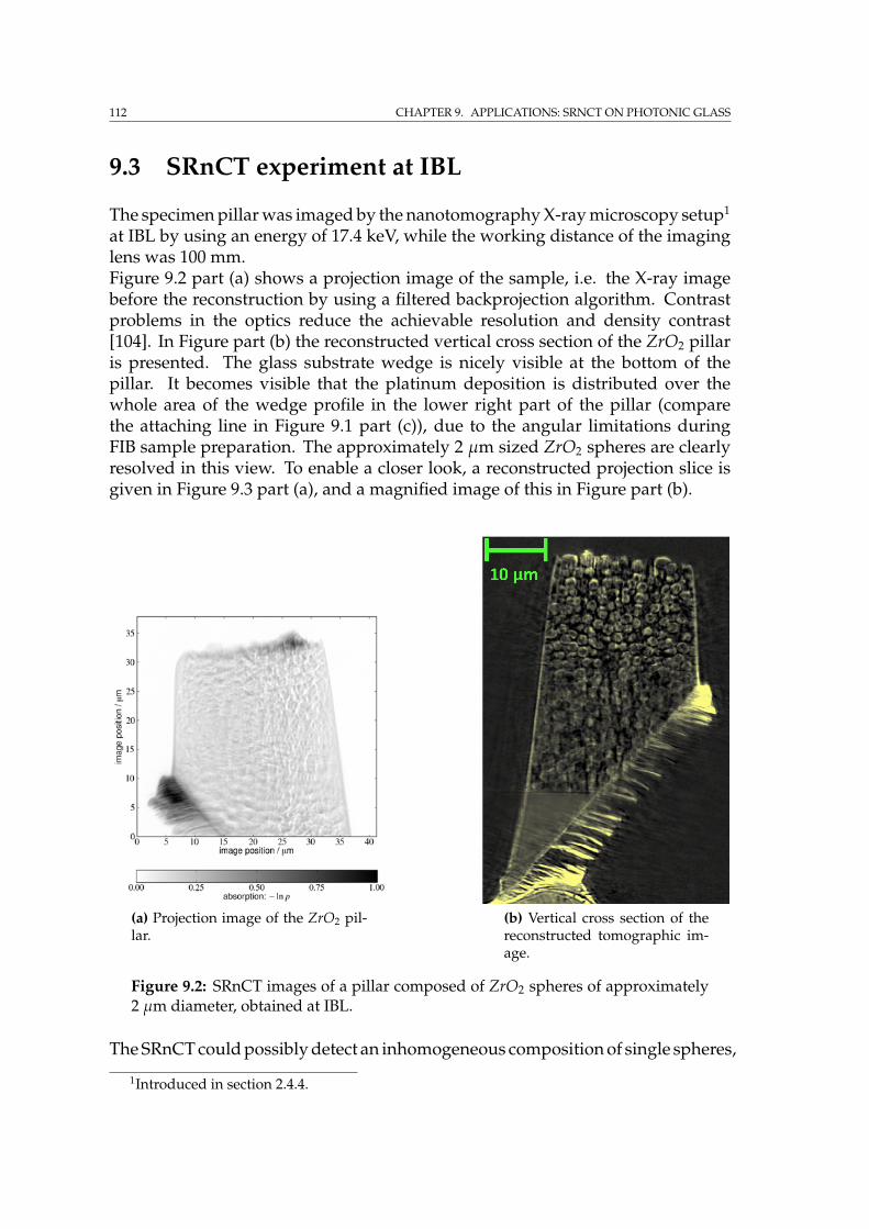
112 CHAPTER 9. APPLICATIONS: SRNCT ON PHOTONIC GLASS
9.3 SRnCT experiment at IBL
The specimen pillar was imaged by the nanotomography X-ray microscopy setup1
at IBL by using an energy of 17.4 keV, while the working distance of the imaginglens was 100 mm.Figure 9.2 part (a) shows a projection image of the sample, i.e. the X-ray imagebefore the reconstruction by using a filtered backprojection algorithm. Contrastproblems in the optics reduce the achievable resolution and density contrast[104]. In Figure part (b) the reconstructed vertical cross section of the ZrO2 pillaris presented. The glass substrate wedge is nicely visible at the bottom of thepillar. It becomes visible that the platinum deposition is distributed over thewhole area of the wedge profile in the lower right part of the pillar (comparethe attaching line in Figure 9.1 part (c)), due to the angular limitations duringFIB sample preparation. The approximately 2 µm sized ZrO2 spheres are clearlyresolved in this view. To enable a closer look, a reconstructed projection slice isgiven in Figure 9.3 part (a), and a magnified image of this in Figure part (b).
(a) Projection image of the ZrO2 pil-lar.
(b) Vertical cross section of thereconstructed tomographic im-age.
Figure 9.2: SRnCT images of a pillar composed of ZrO2 spheres of approximately2 µm diameter, obtained at IBL.
The SRnCT could possibly detect an inhomogeneous composition of single spheres,
1Introduced in section 2.4.4.
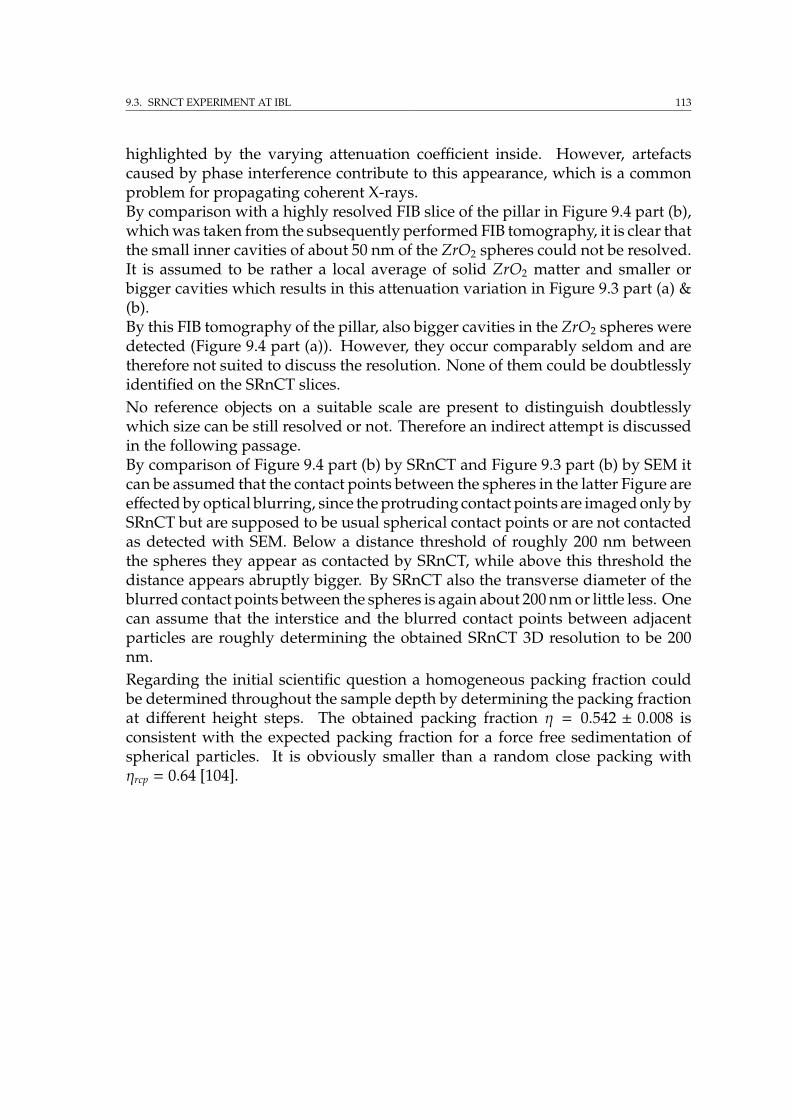
9.3. SRNCT EXPERIMENT AT IBL 113
highlighted by the varying attenuation coefficient inside. However, artefactscaused by phase interference contribute to this appearance, which is a commonproblem for propagating coherent X-rays.By comparison with a highly resolved FIB slice of the pillar in Figure 9.4 part (b),which was taken from the subsequently performed FIB tomography, it is clear thatthe small inner cavities of about 50 nm of the ZrO2 spheres could not be resolved.It is assumed to be rather a local average of solid ZrO2 matter and smaller orbigger cavities which results in this attenuation variation in Figure 9.3 part (a) &(b).By this FIB tomography of the pillar, also bigger cavities in the ZrO2 spheres weredetected (Figure 9.4 part (a)). However, they occur comparably seldom and aretherefore not suited to discuss the resolution. None of them could be doubtlesslyidentified on the SRnCT slices.No reference objects on a suitable scale are present to distinguish doubtlesslywhich size can be still resolved or not. Therefore an indirect attempt is discussedin the following passage.By comparison of Figure 9.4 part (b) by SRnCT and Figure 9.3 part (b) by SEM itcan be assumed that the contact points between the spheres in the latter Figure areeffected by optical blurring, since the protruding contact points are imaged only bySRnCT but are supposed to be usual spherical contact points or are not contactedas detected with SEM. Below a distance threshold of roughly 200 nm betweenthe spheres they appear as contacted by SRnCT, while above this threshold thedistance appears abruptly bigger. By SRnCT also the transverse diameter of theblurred contact points between the spheres is again about 200 nm or little less. Onecan assume that the interstice and the blurred contact points between adjacentparticles are roughly determining the obtained SRnCT 3D resolution to be 200nm.Regarding the initial scientific question a homogeneous packing fraction couldbe determined throughout the sample depth by determining the packing fractionat different height steps. The obtained packing fraction η = 0.542 ± 0.008 isconsistent with the expected packing fraction for a force free sedimentation ofspherical particles. It is obviously smaller than a random close packing withηrcp = 0.64 [104].
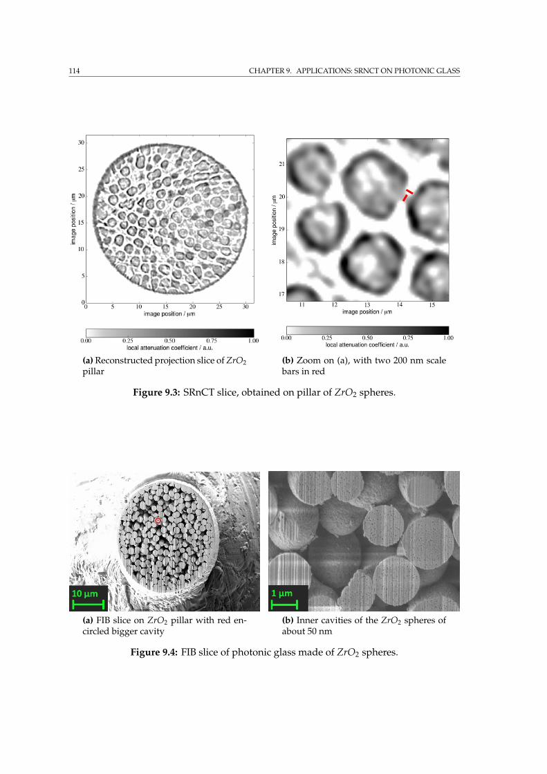
114 CHAPTER 9. APPLICATIONS: SRNCT ON PHOTONIC GLASS
(a) Reconstructed projection slice of ZrO2pillar
(b) Zoom on (a), with two 200 nm scalebars in red
Figure 9.3: SRnCT slice, obtained on pillar of ZrO2 spheres.
(a) FIB slice on ZrO2 pillar with red en-circled bigger cavity
(b) Inner cavities of the ZrO2 spheres ofabout 50 nm
Figure 9.4: FIB slice of photonic glass made of ZrO2 spheres.
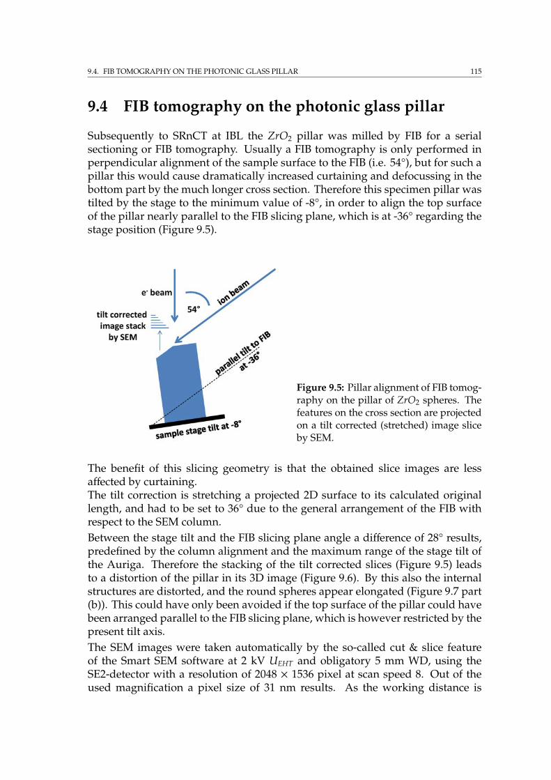
9.4. FIB TOMOGRAPHY ON THE PHOTONIC GLASS PILLAR 115
9.4 FIB tomography on the photonic glass pillar
Subsequently to SRnCT at IBL the ZrO2 pillar was milled by FIB for a serialsectioning or FIB tomography. Usually a FIB tomography is only performed inperpendicular alignment of the sample surface to the FIB (i.e. 54°), but for such apillar this would cause dramatically increased curtaining and defocussing in thebottom part by the much longer cross section. Therefore this specimen pillar wastilted by the stage to the minimum value of -8°, in order to align the top surfaceof the pillar nearly parallel to the FIB slicing plane, which is at -36° regarding thestage position (Figure 9.5).
Figure 9.5: Pillar alignment of FIB tomog-raphy on the pillar of ZrO2 spheres. Thefeatures on the cross section are projectedon a tilt corrected (stretched) image sliceby SEM.
The benefit of this slicing geometry is that the obtained slice images are lessaffected by curtaining.The tilt correction is stretching a projected 2D surface to its calculated originallength, and had to be set to 36° due to the general arrangement of the FIB withrespect to the SEM column.Between the stage tilt and the FIB slicing plane angle a difference of 28° results,predefined by the column alignment and the maximum range of the stage tilt ofthe Auriga. Therefore the stacking of the tilt corrected slices (Figure 9.5) leadsto a distortion of the pillar in its 3D image (Figure 9.6). By this also the internalstructures are distorted, and the round spheres appear elongated (Figure 9.7 part(b)). This could have only been avoided if the top surface of the pillar could havebeen arranged parallel to the FIB slicing plane, which is however restricted by thepresent tilt axis.The SEM images were taken automatically by the so-called cut & slice featureof the Smart SEM software at 2 kV UEHT and obligatory 5 mm WD, using theSE2-detector with a resolution of 2048 × 1536 pixel at scan speed 8. Out of theused magnification a pixel size of 31 nm results. As the working distance is
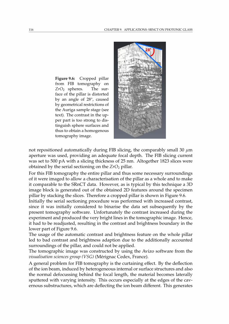
116 CHAPTER 9. APPLICATIONS: SRNCT ON PHOTONIC GLASS
Figure 9.6: Cropped pillarfrom FIB tomography onZrO2 spheres. The sur-face of the pillar is distortedby an angle of 28°, causedby geometrical restrictions ofthe Auriga sample stage (seetext). The contrast in the up-per part is too strong to dis-tinguish sphere surfaces andthus to obtain a homogenoustomography image.
not repositioned automatically during FIB slicing, the comparably small 30 µmaperture was used, providing an adequate focal depth. The FIB slicing currentwas set to 500 pA with a slicing thickness of 25 nm. Altogether 1823 slices wereobtained by the serial sectioning on the ZrO2 pillar.For this FIB tomography the entire pillar and thus some necessary surroundingsof it were imaged to allow a characterisation of the pillar as a whole and to makeit comparable to the SRnCT data. However, as is typical by this technique a 3Dimage block is generated out of the obtained 2D features around the specimenpillar by stacking the slices. Therefore a cropped pillar is shown in Figure 9.6.Initially the serial sectioning procedure was performed with increased contrast,since it was initially considered to binarise the data set subsequently by thepresent tomography software. Unfortunately the contrast increased during theexperiment and produced the very bright lines in the tomographic image. Hence,it had to be readjusted, resulting in the contrast and brightness boundary in thelower part of Figure 9.6.The usage of the automatic contrast and brightness feature on the whole pillarled to bad contrast and brightness adaption due to the additionally accountedsurroundings of the pillar, and could not be applied.The tomographic image was constructed by using the Avizo software from thevisualisation sciences group (VSG) (Mérignac Cedex, France).A general problem for FIB tomography is the curtaining effect. By the deflectionof the ion beam, induced by heterogeneous internal or surface structures and alsothe normal defocussing behind the focal length, the material becomes laterallysputtered with varying intensity. This occurs especially at the edges of the cav-ernous substructures, which are deflecting the ion beam different. This generates
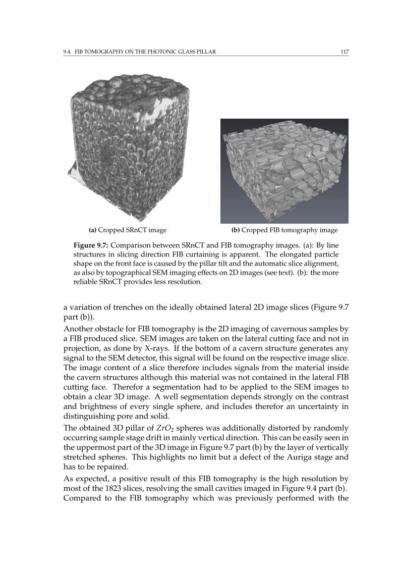
9.4. FIB TOMOGRAPHY ON THE PHOTONIC GLASS PILLAR 117
(a) Cropped SRnCT image (b) Cropped FIB tomography image
Figure 9.7: Comparison between SRnCT and FIB tomography images. (a): By linestructures in slicing direction FIB curtaining is apparent. The elongated particleshape on the front face is caused by the pillar tilt and the automatic slice alignment,as also by topographical SEM imaging effects on 2D images (see text). (b): the morereliable SRnCT provides less resolution.
a variation of trenches on the ideally obtained lateral 2D image slices (Figure 9.7part (b)).Another obstacle for FIB tomography is the 2D imaging of cavernous samples bya FIB produced slice. SEM images are taken on the lateral cutting face and not inprojection, as done by X-rays. If the bottom of a cavern structure generates anysignal to the SEM detector, this signal will be found on the respective image slice.The image content of a slice therefore includes signals from the material insidethe cavern structures although this material was not contained in the lateral FIBcutting face. Therefor a segmentation had to be applied to the SEM images toobtain a clear 3D image. A well segmentation depends strongly on the contrastand brightness of every single sphere, and includes therefor an uncertainty indistinguishing pore and solid.The obtained 3D pillar of ZrO2 spheres was additionally distorted by randomlyoccurring sample stage drift in mainly vertical direction. This can be easily seen inthe uppermost part of the 3D image in Figure 9.7 part (b) by the layer of verticallystretched spheres. This highlights no limit but a defect of the Auriga stage andhas to be repaired.As expected, a positive result of this FIB tomography is the high resolution bymost of the 1823 slices, resolving the small cavities imaged in Figure 9.4 part (b).Compared to the FIB tomography which was previously performed with the
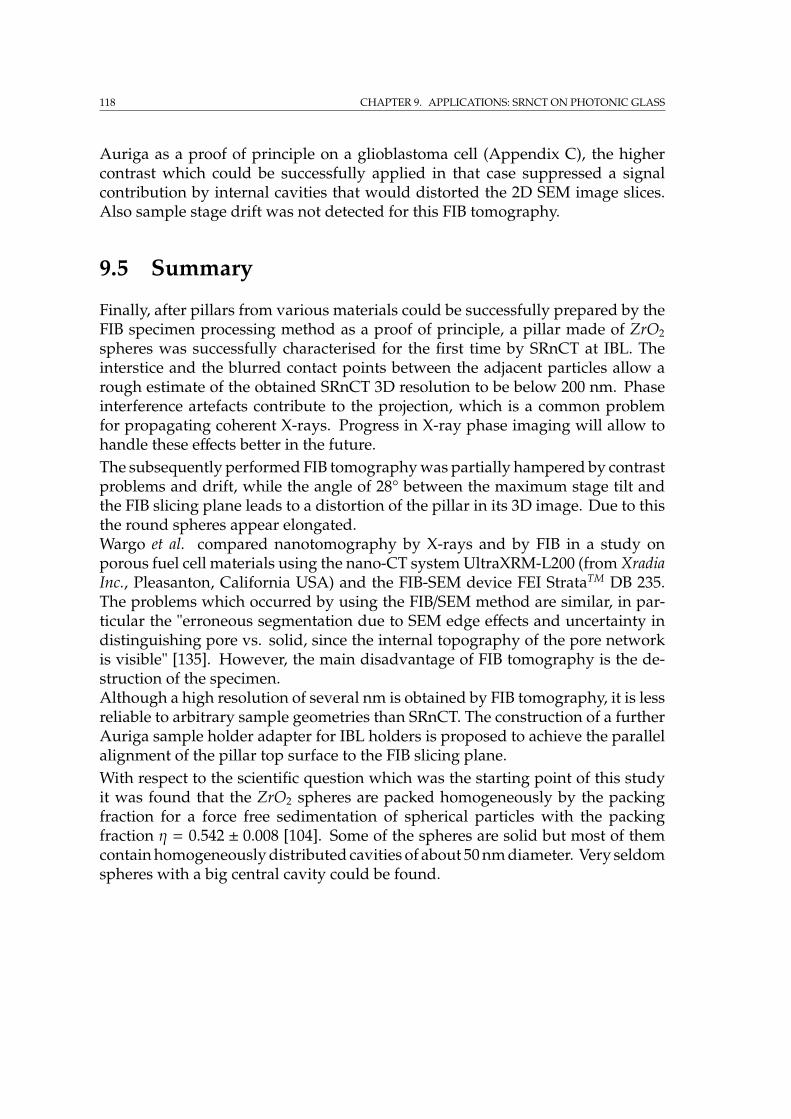
118 CHAPTER 9. APPLICATIONS: SRNCT ON PHOTONIC GLASS
Auriga as a proof of principle on a glioblastoma cell (Appendix C), the highercontrast which could be successfully applied in that case suppressed a signalcontribution by internal cavities that would distorted the 2D SEM image slices.Also sample stage drift was not detected for this FIB tomography.
9.5 Summary
Finally, after pillars from various materials could be successfully prepared by theFIB specimen processing method as a proof of principle, a pillar made of ZrO2
spheres was successfully characterised for the first time by SRnCT at IBL. Theinterstice and the blurred contact points between the adjacent particles allow arough estimate of the obtained SRnCT 3D resolution to be below 200 nm. Phaseinterference artefacts contribute to the projection, which is a common problemfor propagating coherent X-rays. Progress in X-ray phase imaging will allow tohandle these effects better in the future.The subsequently performed FIB tomography was partially hampered by contrastproblems and drift, while the angle of 28° between the maximum stage tilt andthe FIB slicing plane leads to a distortion of the pillar in its 3D image. Due to thisthe round spheres appear elongated.Wargo et al. compared nanotomography by X-rays and by FIB in a study onporous fuel cell materials using the nano-CT system UltraXRM-L200 (from XradiaInc., Pleasanton, California USA) and the FIB-SEM device FEI StrataTM DB 235.The problems which occurred by using the FIB/SEM method are similar, in par-ticular the "erroneous segmentation due to SEM edge effects and uncertainty indistinguishing pore vs. solid, since the internal topography of the pore networkis visible" [135]. However, the main disadvantage of FIB tomography is the de-struction of the specimen.Although a high resolution of several nm is obtained by FIB tomography, it is lessreliable to arbitrary sample geometries than SRnCT. The construction of a furtherAuriga sample holder adapter for IBL holders is proposed to achieve the parallelalignment of the pillar top surface to the FIB slicing plane.With respect to the scientific question which was the starting point of this studyit was found that the ZrO2 spheres are packed homogeneously by the packingfraction for a force free sedimentation of spherical particles with the packingfraction η = 0.542 ± 0.008 [104]. Some of the spheres are solid but most of themcontain homogeneously distributed cavities of about 50 nm diameter. Very seldomspheres with a big central cavity could be found.
Chapter 10
Summary and conclusions
The specimen processing method for region of interest SRnCT and nanodiffractionwas achieved by selective FIB milling and the utilisation of a micromanipulatorto take the excavated specimen from the bulk material and mount it by FIB/GISattaching on a sample holder. The procedure was performed many times on vari-ous materials and complemented by the application of SEM techniques. To enablethe adaption of the IBL sample holders the Auriga stage holder was improvedby several modifications, without any resulting restrictions to the functionality ofthe entire cross beam device and its components.After establishing this novel method several kinds of sample applications pro-posed for SRnCT were characterised by the cross beam workstation Auriga andX-ray techniques.
The 3D characterisation of a sintered Ti-6Al-4V material by a laboratory-CT de-vice provided detailed knowledge on the porous network structure inside, andfeatured the pore size distribution by granulometry calculation. Regarding in vivostudies the detected 30% porosity of the material provides ideal conditions fortissue ingrowth. This study was jointly published by A. Deing et al. [25].SEM imaging of the cell colonisation could successfully confirm the ingrowth ofcells into the porous network. The applied phospholipid coating could be provedby SEM imaging and EDX on the edges of intended broken sample plates.To enhance the attenuation of the colonised cell tissue for SRnCT staining by Euand the incorporation of iron nanoparticles was applied and verified by EDX.The cell uptake was furthermore proved inside of two single cells by combinedFIB/SEM techniques. Finally the cells were not visible in the Ti-6Al-4V matrixby performing SRµCT. The staining was insufficient and therefore the implemen-tation of the tomographic phase contrast method is necessary at IBL, to providesuitable contrast for this kind of samples.
Selected applications of combined FIB/SEM techniques regarding the corrosion ofMg alloys developed as implant materials for medical purposes were presented.The SEM images showed that the different immersion solutions as well as thevaried presence of proteins led to a unique crystalline growth on each sample.
119
120 CHAPTER 10. SUMMARY AND CONCLUSIONS
The EDX mapping proved the co-localisation of the elements Ca and P as well asC and O. The results were jointly published by F. Feyerabend et al. [34].In the framework of this thesis the Auriga was used frequently to prepare crosssections of different materials by FIB in order to analyse the inner structure andthe elementary composition below the surface, as presented for the cooperativelypublished study of a Mg − 10Dy alloy by L. Yang et al. [144]. It was found thatthe corrosion layer is enriched by Dy, which likely exists as a mixture of Dy2O3
and Dy(OH)3. The content of Ca and P decreases gradually from the surface tothe bottom of the corrosion layer. By using SEM the osteoblast morphology couldbe observed on all cultured samples and no cytotoxicity could be found.The FIB/SEM cross sectioning method was furthermore applied to confirm ahomogeneous dispersion of MgH2 and LiBH4 inside the carbon aerogel scaffoldof a hydrogen storage system, which is highly suited to investigate the porestructure by SRnCT phase contrast in future experiments. Out of this cooperationfive studies [47; 48; 46; 44; 45] were jointly published by R. Gosalawit-Utke et al..The phase composition of a spherical gas-atomised Ti-45Al- 5 and 10Nb powderalloy which was produced by the plasma melting induction guided gas atomisa-tion (PIGA) technique at HZG was determined by X-ray scattering at the HEMSside station (beamline P07b) at PETRA III, as well as by 2D and FIB based 3D EBSDmeasurements. By SEM investigations it was found that the dendritic structuresof bigger particles of Ti-45Al-10Nb are more pronounced than for the 5Nb fraction,while smaller particles contain in average less Nb. Due to the presence of dendriticstructures the cooling rate during powder atomisation was still to low to reachthe critical growth rate for absolute stability and thus a planar solidification.Since the β-phase is primarily formed during solidification, the BSE detectedcauliflower structure gave proof that diffusion took place during solidification ofthe initial β-grain formation, even though there is no relation between the grainsand the dendrite structure. By the absence of preferred misorientation angles onefinds that α-grains are not formed out of already solidified β-grains according theBurgers relationship by a solid state phase transformation.Regarding the occurring, still extremely fast cooling rates, the hexagonal-close-packed α-phase is possibly originated by a martensitic phase transition from thebody-centred-cubic β-phase.Regarding SRnCT the Ti-45Al-10Nb specimen could successfully be prepared bythe described FIB specimen processing method, but preliminary SRµCT experi-ments at IBL revealed too weak material contrast of the inner dendritic structures.Therefore the phase contrast technique is proposed for this material as soon asavailable at IBL.To enable also a FIB tomography by using BSE contrast the BSE-detector of the Au-riga should be slightly modified, if feasible, by a little cutout of the detector framescaffold to allow the in situ usage with the FIB. Otherwise a commonly availablepneumatic BSE-detector from Zeiss would be needed, providing an automateddetector insertion, to enable this.Scanning nanodiffraction at the MiNaXS endstation at PETRA III was enabled by
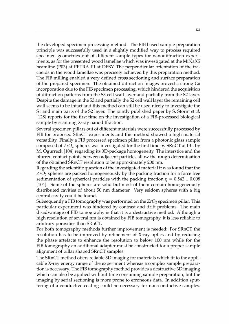
121
the developed specimen processing method. The FIB based sample preparationprinciple was successfully used in a slightly modified way to process requiredspecimen geometries out of different sample types for nanodiffraction experi-ments, as for the presented wood lamellae which was investigated at the MiNaXSbeamline (P03) at PETRA III at DESY. The perpendicular orientation of the tra-cheids in the wood lamellae was precisely achieved by this preparation method.The FIB milling enabled a very defined cross sectioning and surface preparationof the prepared specimen. The obtained diffraction images proved a strong Gaincorporation due to the FIB specimen processing, which hindered the acquisitionof diffraction patterns from the S3 cell wall layer and partially from the S2 layer.Despite the damage in the S3 and partially the S2 cell wall layer the remaining cellwall seems to be intact and this method can still be used nicely to investigate theS1 and main parts of the S2 layer. The jointly published paper by S. Storm et al.[128] reports for the first time on the investigation of a FIB-processed biologicalsample by scanning X-ray nanodiffraction.Several specimen pillars out of different materials were successfully processed byFIB for proposed SRnCT experiments and this method showed a high materialversatility. Finally a FIB processed specimen pillar from a photonic glass samplecomposed of ZrO2 spheres was investigated for the first time by SRnCT at IBL byM. Ogurreck [104] regarding its 3D-package homogeneity. The interstice and theblurred contact points between adjacent particles allow the rough determinationof the obtained SRnCT resolution to be approximately 200 nm.Regarding the scientific question of the investigated material it was found that theZrO2 spheres are packed homogeneously by the packing fraction for a force freesedimentation of spherical particles with the packing fraction η = 0.542 ± 0.008[104]. Some of the spheres are solid but most of them contain homogeneouslydistributed cavities of about 50 nm diameter. Very seldom spheres with a bigcentral cavity could be found.Subsequently a FIB tomography was performed on the ZrO2 specimen pillar. Thisparticular experiment was hindered by contrast and drift problems. The maindisadvantage of FIB tomography is that it is a destructive method. Although ahigh resolution of several nm is obtained by FIB tomography, it is less reliable toarbitrary porosities than SRnCT.For both tomography methods further improvement is needed: For SRnCT theresolution has to be improved by refinement of X-ray optics and by reducingthe phase artefacts to enhance the resolution to below 100 nm while for theFIB tomography an additional adapter must be constructed for a proper samplealignment of pillar shaped SRnCT samples.The SRnCT method offers reliable 3D imaging for materials which fit to the appli-cable X-ray energy range of the experiment whereas a complex sample prepara-tion is necessary. The FIB tomography method provides a destructive 3D imagingwhich can also be applied without time consuming sample preparation, but theimaging by serial sectioning is more prone to erroneous data. In addition sput-tering of a conductive coating could be necessary for non-conductive samples.
122 CHAPTER 10. SUMMARY AND CONCLUSIONS
SRnCT requires X-ray contrast of the internal structures and FIB tomographydemands materials providing contrast to the applicable SEM detectors.Regarding the combination of FIB/SEM methods with the synchrotron utilisationas well as the material versatility the present work is one of the first in this field.Only few different publications with a similar intention were found. In the studyof Wargo et al. [135] the differences of FIB tomography and X-ray nanotomographyusing a laboratory CT device are exemplified on a fuel cell material. Lombardo etal. [86] on the other hand investigated the feasibility of different specimen shapesby the FIB sample preparation for SRnCT at the Advanced Photon Source at theArgonne National Laboratory (Illinois, USA), without mentioning the achievedresolution of the final measurement. Again exclusively one fuel cell material isinvestigated. In both studies the discussion of the attachment requirements fordifferent specimens and materials in varying shapes, especially for bigger ones,as well as the discussion of the specimen transport is missing. Beside of this, thedescribed procedures are in general similar to those ones presented here.Finally, the presented method of specimen processing that fits the criteria forX-ray nanotomography and nanodiffraction by selectively FIB-milling around aregion of interest and the utilisation of a micromanipulator for taking the exca-vated sample from the bulk material and mounting it on a sample holder is ofincreasing importance for the ongoing development of nano X-ray techniques incommon. Samples with multiple µm scaled shapes and sizes are demanded bysynchrotron and laboratory X-ray experiments as well. The characterisation andsample preparation for synchrotron experiments presented in this work providessignificant advances in a wide field of applications ranging from engineeringmaterials science to soft tissue research.

123

124
Appendix A
Introduction to phase contrastimaging
The complex refractive index of a medium is given by Equation 2.22:
n = 1 − δ + iβ, (A.1)
with the imaginary part β linked to the absorption, or attenuation respectively,and the real part δ linked to the phase shift. Apart from the absorption, 1 − δtogether with the travel distance d of an electromagnetic wave, travelling througha medium, and its wavelength λ determines the phase shift by
∆Φ =2πδdλ. (A.2)
δ itself depends on the wavelength λ and the density of the sample. Only in-direct methods are possible to measure the phase shift, due to the fact that onlyintensities are accessible on images and the phase information is lost. Thereforinterferometric methods are applied to attain this information. A review on thecommon phase contrast methods is given by Momose et al. [95]. Outlining thiswe can separate the methods in three main divisions, extracted from [56] and [7]:
• Most direct phase-contrast projections, measuring the phase shift with re-spect to the self reference beam (Bonse-Hart interferometer [13]). This tech-nique is based on the principal of splitting a coherent beam by a crystalinterferometer in two different paths. One path is used to ray the specimen,while the other stays unaffected or is shifted for a calculated value, to visu-alise the refractive information extracted by the first path in an interferencepattern on the detector plane [94]. The Phase shift ϕ is given by
ϕ ∝ σE, (A.3)
125
126 APPENDIX A. INTRODUCTION TO PHASE CONTRAST IMAGING
with the electron density σ and the applied X-ray energy E. As only anarrow spectral width of the beam is used by the interferometer, a brilliantsynchrotron source is mandatory to yield enough flux.
• Differential method, measuring the 1st derivative of the phase shift. Thespecimen illuminated by a parallel monochromatised X-ray beam becomesimaged on a detector by an upstream analyser crystal. The image onlycontains information on that part of the transmitted and refracted beamthat satisfies the Bragg condition of the analyser crystal. Scanning the anal-yser crystal angulary provides analysis of different refractive indexes ase.g. shown by Chapman et al. [21] or Dilmanian et al. [26]. Here againa brilliant synchrotron source is mandatory to yield enough flux, causedto the two monochromatising crystals. The monochromator and the anal-yser crystal can be exchanged by a beam-splitter grating and an analysergrating. This grating-based phase-contrast methods can also be applied onpolychromatic sources, as done by Herzen et al. [57].
• Indirect phase-contrast projections are Propagation based methods, mea-suring the 2nd derivative of the phase shift. By using spatially coherentillumination without any optical components Fresnel resp. Fraunhoferdiffraction happens while the beam propagates to the detector after pen-etrating the specimen. This technique enables holotomography by varyingthe specimen-detector distance and gaining a complete phase map of thespecimen, as Cloetens et al. presented [23]. By requiring a spatially coherentbeam, this is only feasible at 3rd generation synchrotron radiation sources.
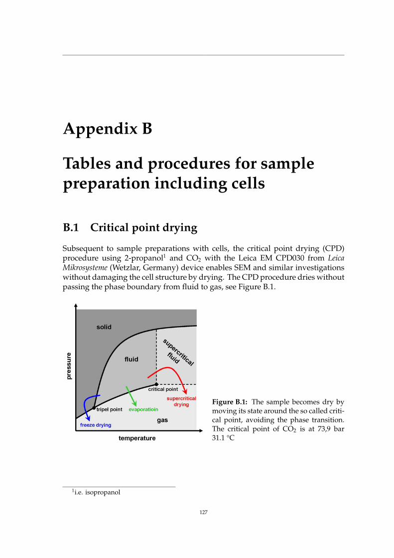
Appendix B
Tables and procedures for samplepreparation including cells
B.1 Critical point drying
Subsequent to sample preparations with cells, the critical point drying (CPD)procedure using 2-propanol1 and CO2 with the Leica EM CPD030 from LeicaMikrosysteme (Wetzlar, Germany) device enables SEM and similar investigationswithout damaging the cell structure by drying. The CPD procedure dries withoutpassing the phase boundary from fluid to gas, see Figure B.1.
Figure B.1: The sample becomes dry bymoving its state around the so called criti-cal point, avoiding the phase transition.The critical point of CO2 is at 73,9 bar31.1 °C
1i.e. isopropanol
127

128 APPENDIX B. TABLES AND PROCEDURES FOR SAMPLE PREPARATION INCLUDING CELLS
The critical point drying procedure:2
Fixation, staining and dehydration
1 Take samples out of culture, wash with PBS3
2 Immerse samples in 2.5 % glutaraldehyde solution in well plates, onesample per well for at least 2 hours - normally over night
3 Transfer sample to new well plate with 1 % osmium tetroxide, stain for30 min.
4 Transfer sample to new well plate with 20 % 2-propanol, immerse for1-2 hours
5 Transfer sample to new well plate with 40 % 2-propanol, immerse for1-2 hours
6 Transfer sample to new well plate with 60 % 2-propanol, immerse for1-2 hours
7 Transfer sample to new well plate with 80 % 2-propanol, immerse for1-2 hours
8 Transfer sample to new well plate with 100 % 2-propanol, immerse for1-2 hours
9 Store samples in 100 % 2-propanol by covering the plate with adhesivefoil, storage of up to one week is possible. Make sure that the solventis always covering the sample
Critical point drying (CDP)
10 Put a proper critical point drying sample holder basket in beaker with2-propanol, so the sample holder is fully covered.
11 Transfer samples from the well plate the sample holder basket.12 Open the lid of the CDP sample chamber.13 Make sure that the magnetic stir bar is in the sample chamber.14 Fill it with 2-propanol to half level.15 Transfer sample holder into sample chamber. Make sure that the cavity
of the sample holder fits to the gas inlet tube.16 Fill the chamber with 2-propanol up to the upper part of the viewing
window.17 Close the lid of the sample chamber tightly.18 Make sure that the Metering valve is closed.19 Press Buttons "Cooling" & "Stirrer".20 Wait until the temperature has reached 4°C & open the valve of the
CO2-bottle.
2applied in common for all samples with cells mentioned in this thesis3phosphate buffered saline

B.1. CRITICAL POINT DRYING 129
21 Press Button "Medium out" until the fluid level is slightly beyond thetop of the sample holder, then press button "Medium out" again to stopmedium outlet.
22 Press button "Medium in" to fill the chamber with CO2, observe themixture of solvent and CO2 (schlieren), press button "Medium in" againwhen the upper part of the viewing window is reached.
23 Repeat step 21 and 22 until no schlieren are visible anymore (at least 6times).
24 During step 21 control that the outlet tube is not frozen.25 After no schlieren are visible anymore, fill the sample chamber with
CO2 to ¾ of the visible area, and close the valve of the CO2-bottle.26 Press Button "Cooling" to stop the cooling process.27 Press Button "Heating" to start the heating process. Heating should be
performed up to 40°C - the sublimation point of CO2 is at 31°C at 75.5Bar (observe the pressure meter!)
28 When 40°C are reached, press button "Stirrer" to stop stirring themedium
29 Press button "Gas out" and adjust the gas flow rate with the "Gas Meter-ing valve", Flow rate should be adjusted to the scale of 1.5 (Maximum!)in the flow meter on top of the instrument
30 The degassing process may take up to 1.5 hours, if not observed. Ifthe flow rate is kept constant, it takes about 30 minutes. The process isfinished, when the pressure meter reaches "0" and the "Gas Meteringvalve" is fully open.
31 Press Button "Heating" to stop the heating process.32 Open the lid of the sample chamber & Remove the sample holder from
the CDP.33 Remove samples from sample holders and mount it to SEM sample
holders with carbon contact foils or use silver glue.34 CPD samples can be stored for at least half a year in an appropriate
environment (no humidity/desiccator or argon atmosphere) withoutquality loss.

130 APPENDIX B. TABLES AND PROCEDURES FOR SAMPLE PREPARATION INCLUDING CELLS
B.2 Phospholipid coating
Phospholipid coating for samples with POPE:
•Solve phospholipids POPE in a chloroform:methanol (80:20) solution to afinal concentration of 1 mM4, e.g.:
40 ml chloroform10 ml methanol35.8998 mg POPE
•Put 50 µl of this solution on the top of the sample discs•Let evaporate and dry for 30 min at room temperature•Incubate for 2 h in cell culture medium
Au-labeled headgroups, Au-DPPE
•0.1 to 1% Nanogold-DPPE (Au-DPPE) with an unlabeled lipid is usuallyappropriate to prepare labeled liposome, e.g.:ä For a 0.1% Nanogold-DPPE in 1mM POPE: 2µl Au-DPPE in 1980 µl POPEä For a 1% Nanogold-DPPE in 1mM POPE: 2µl Au-DPPE in 198 µl POPE
B.3 Sample preparation with different stainings fortomography
Cell staining for tomography with europium
Goal: prepare porous titanium samples with different amount of cells (Saos-2; 50,000 and 100,000 cells) with different concentrations of europium (0 µM(control), 1 µM, 20 µM, and 50 µM).
•use 203254 Aldrich Europium (III) chloride hexahydrate- 99.99% trace met-als basis
ä Formula: Cl3Eu · 6H2Oä Molecular weight: 366.41 g/mol
•Prepare a 1 mM stock-solution: Dissolve 3.66 mg in 10 ml ddH2O. Filtratewith a 0.2 µm filter•In 25 cm2 cell culture flasks:
ä Seed 0.5 million Saos-2 cells in four flasks labelled "control", "1 µM","20 muM" and "50 µM" (n. b.: during the procedure, the media is alwayscomplemented with 10% FBS5).•Cultivate them either with:
4mM =milli molar5i.e. fetal bovine serum
B.3. SAMPLE PREPARATION WITH DIFFERENT STAININGS FOR TOMOGRAPHY 131
ä 12 mL media (flask labelled control)ä 12 mL media + 12 µl europium solution (flask labelled 1 µM)ä 12 mL media + 240 µl europium solution (flask labelled 20 µM)ä 12 mL media + 600 µl europium solution (flask labelled 50 µM)
•Incubate for two days
•After these two days, prepare from each flask (i.e., 16 samples in total):ä 2 porous-titanium plates with 50,000 cells (duplicate)ä 2 porous-titanium plates with 100,000 cells (duplicate)
•Coat wells with 1% agarose; when the agar gets hard, place the titaniumplates on.•Prepare a 1 million cells/ml solution (media without europium).•Deposit one drop of cell +media (50 µl: 50,000 cells or 100µl: 100,000 cells)on the top of the Ti-plate.•Let the cells adhere for 45 min under the bench before complementing thewell with the appropriate volume of media.
•Let the cells grow for two days and prepare them for SEM pre-characterisation and subsequent tomography with the critical point dryertechnique.
Cell staining for tomography with Fe-nanoparticles
Goal: prepare porous titanium samples with different amount of cells (Saos-2;50,000 and 100,000 cells) with different concentrations of nanoparticles (NP-MA;0.25 µl/ml and 0.5 µl/ml).
•In 25 cm2 cell culture flasks: ä Seed 0.5 million Saos-2 cells in twoflasks labelled "0.25" and "0.5" (n. b.: during the procedure the media isalways complemented with 10% FBS).•Cultivate them either with:
ä 12 ml media + 3 µl NP-MA-Birte’s solution (flask labelled 0.25)ä 12 mL media + 6 µl NP-MA-Birte’s solution (flask labelled 0.5)
•Incubate for two days
•After these two days, prepare from each flask (i.e., 8 samples in total):ä 2 porous-titanium plates with 50,000 cells (duplicate)ä 2 porous-titanium plates with 100,000 cells (duplicate)
•Coat wells with 1% agarose; when the agar gets hard, place the titaniumplates on.•Prepare a 1 million cells/ml solution.•Deposit one drop of cell +media (50 µl: 50,000 cells or 100µl: 100,000 cells)on the top of the Ti-plate.
132 APPENDIX B. TABLES AND PROCEDURES FOR SAMPLE PREPARATION INCLUDING CELLS
•Let the cells adhere for 45 min under the bench before complementing thewell with the appropriate volume of media.
•Let the cells grow for two days and prepare them for SEM pre-characterisation and subsequent tomography with the critical point dryertechnique.
B.3.1 Attenuation enhancing staining sample row with and with-out POPE coating
Table B.6: Sample row for SEM investigations with and without POPE and Saos-2cells, treated with europium (Eu) or myristic-acid covered Fe-nanoparticles (NP)respectively.
label POPE Cell Incorporated Inc. mat. commentsamount material concentration
#1 no 50000 - 0 shortly mounted onthe wrong side
#2 no 100000 - 0 strange surface con-tamination
#3 no 50000 Eu 1 µM6 hardly cells#4 no 50000 Eu 1 µM#5 no 100000 Eu 1 µM#6 no 100000 Eu 1 µM#7 no 50000 Eu 20 µM investigation of back-
side too; broken forinsight, cells every-where
#8 no 50000 Eu 20 µM hardly cells; strangesurface contamination
#9 no 100000 Eu 20 µM#10 no 100000 Eu 20 µM#11 no 50000 Eu 50 µM#12 no 50000 Eu 50 µM#13 no 100000 Eu 50 µM#14 no 100000 Eu 50 µM EDX; broken for in-
sight, less cells in up-per half
#15 no 50000 - 0#16 no 100000 - 0#17 no 50000 NP 0.25 µl/ml
continue next page ...
6µM =micro molar
B.3. SAMPLE PREPARATION WITH DIFFERENT STAININGS FOR TOMOGRAPHY 133
label POPE Cell Incorporated Inc. mat. specialamount material concentration comments
#18 no 50000 NP 0.25 µl/ml#19 no 100000 NP 0.25 µl/ml#20 no 100000 NP 0.25 µl/ml#21 no 50000 NP 0.5 µl/ml#22 no 50000 NP 0.5 µl/ml#23 no 100000 NP 0.5 µl/ml EDX; FIB cross section
on cell#24 no 100000 NP 0.5 µl/ml EDX#25 yes 50000 - 0#26 yes 100000 - 0#27 yes 50000 NP 0.25 µl/ml#28 yes 50000 NP 0.25 µl/ml#29 yes 0 NP 0.25 µl/ml#30 yes 0 NP 0.25 µl/ml#31 yes 50000 NP 0.5 µl/ml#32 yes 50000 NP 0.5 µl/ml EDX; hardly cells
on top; broken forinsight, POPE like,cracked covering inthe upper middle
#33 yes 0 NP 0.5 µl/ml#34 yes 0 NP 0.5 µl/ml EDX#35 yes 50000 Eu 50 µM#36 yes 50000 Eu 50 µM#37 yes 100000 Eu 50 µM EDX; hardly cells#38 yes 100000 Eu 50 µM no cells#39 yes 50000 - 0 µM#40 yes 100000 - 0 µM#41 yes 50000 Eu 1 µM#42 yes 50000 Eu 1 µM#43 yes 100000 Eu 1 µM#44 yes 100000 Eu 1 µM#45 yes 50000 Eu 20 µM#46 yes 50000 Eu 20 µM investigated only
backside; no cells#47 yes 100000 Eu 20 µM EDX
continue next page ...

134 APPENDIX B. TABLES AND PROCEDURES FOR SAMPLE PREPARATION INCLUDING CELLS
label POPE Cell Incorporated Inc. mat. specialamount material concentration comments
#48 yes 100000 Eu 20 µM EDX; investigation ofbackside; broken forinsight, cells mainlyin lower half; POPElike, cracked coveringmainly in upper half
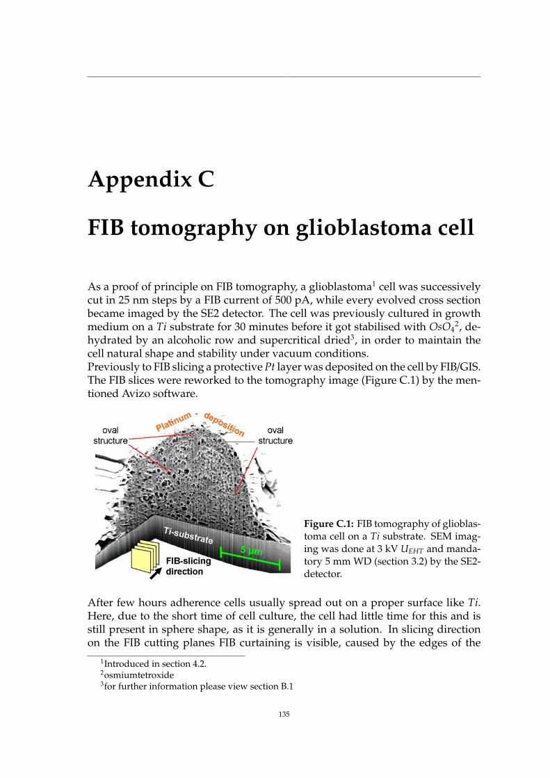
Appendix C
FIB tomography on glioblastoma cell
As a proof of principle on FIB tomography, a glioblastoma1 cell was successivelycut in 25 nm steps by a FIB current of 500 pA, while every evolved cross sectionbecame imaged by the SE2 detector. The cell was previously cultured in growthmedium on a Ti substrate for 30 minutes before it got stabilised with OsO4
2, de-hydrated by an alcoholic row and supercritical dried3, in order to maintain thecell natural shape and stability under vacuum conditions.Previously to FIB slicing a protective Pt layer was deposited on the cell by FIB/GIS.The FIB slices were reworked to the tomography image (Figure C.1) by the men-tioned Avizo software.
Figure C.1: FIB tomography of glioblas-toma cell on a Ti substrate. SEM imag-ing was done at 3 kV UEHT and manda-tory 5 mm WD (section 3.2) by the SE2-detector.
After few hours adherence cells usually spread out on a proper surface like Ti.Here, due to the short time of cell culture, the cell had little time for this and isstill present in sphere shape, as it is generally in a solution. In slicing directionon the FIB cutting planes FIB curtaining is visible, caused by the edges of the
1Introduced in section 4.2.2osmiumtetroxide3for further information please view section B.1
135

136 APPENDIX C. FIB TOMOGRAPHY ON GLIOBLASTOMA CELL
cavernous substructure which is differentially deflecting the ion beam. The innerstructure is too inhomogeneous, and effects additional curtaining besides that onegenerated by the surface edge. By another attempt it was also tried to performa FIB tomography on an not coated cell. This revealed that the FIB melts the cellsuccessively, ahead to the active slicing plane.By scrolling through the tomographic slices of this cell different structures becomevisible. Unfortunately they could not be separated by contrast reworking on thetomographic slices, they are too strong connected by the intracellular network.
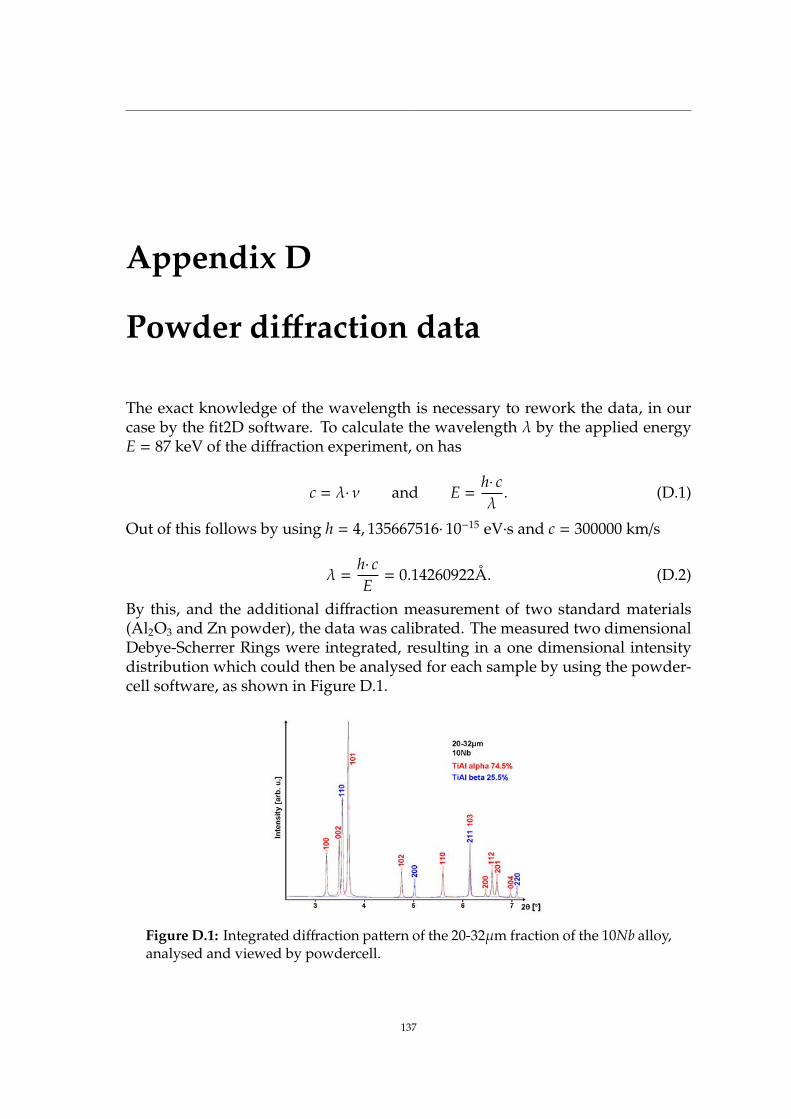
Appendix D
Powder diffraction data
The exact knowledge of the wavelength is necessary to rework the data, in ourcase by the fit2D software. To calculate the wavelength λ by the applied energyE = 87 keV of the diffraction experiment, on has
c = λ· ν and E =h· cλ. (D.1)
Out of this follows by using h = 4, 135667516· 10−15 eV·s and c = 300000 km/s
λ =h· cE= 0.14260922Å. (D.2)
By this, and the additional diffraction measurement of two standard materials(Al2O3 and Zn powder), the data was calibrated. The measured two dimensionalDebye-Scherrer Rings were integrated, resulting in a one dimensional intensitydistribution which could then be analysed for each sample by using the powder-cell software, as shown in Figure D.1.
Figure D.1: Integrated diffraction pattern of the 20-32µm fraction of the 10Nb alloy,analysed and viewed by powdercell.
137
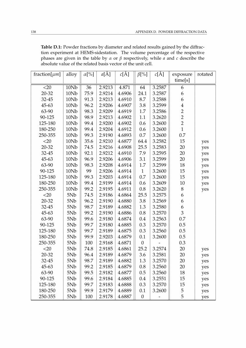
138 APPENDIX D. POWDER DIFFRACTION DATA
Table D.1: Powder fractions by diameter and related results gained by the diffrac-tion experiment at HEMS-sidestation. The volume percentage of the respectivephases are given in the table by α or β respectively, while a and c describe theabsolute value of the related basis vector of the unit cell.
fraction[µm] alloy α[%] a[Å] c[Å] β[%] c[Å] exposure rotatedtime[s]
<20 10Nb 36 2.9213 4.871 64 3.2587 620-32 10Nb 75.9 2.9214 4.6906 24.1 3.2587 632-45 10Nb 91.3 2.9213 4.6910 8.7 3.2588 645-63 10Nb 96.2 2.9206 4.6907 3.8 3.2599 463-90 10Nb 98.3 2.9209 4.6919 1.7 3.2586 290-125 10Nb 98.9 2.9213 4.6902 1.1 3.2620 2
125-180 10Nb 99.4 2.9200 4.6902 0.6 3.2600 2180-250 10Nb 99.4 2.9204 4.6912 0.6 3.2600 1250-355 10Nb 99.3 2.9190 4.6893 0.7 3.2600 0.7<20 10Nb 35.6 2.9210 4.6877 64.4 3.2582 15 yes
20-32 10Nb 74.5 2.9216 4.6908 25.5 3.2583 20 yes32-45 10Nb 92.1 2.9212 4.6910 7.9 3.2595 20 yes45-63 10Nb 96.9 2.9206 4.6906 3.1 3.2599 20 yes63-90 10Nb 98.3 2.9208 4.6914 1.7 3.2599 18 yes90-125 10Nb 99 2.9206 4.6914 1 3.2600 15 yes
125-180 10Nb 99.3 2.9203 4.6914 0.7 3.2600 15 yes180-250 10Nb 99.4 2.9199 4.6914 0.6 3.2609 10 yes250-355 10Nb 99.2 2.9195 4.6911 0.8 3.2620 8 yes<20 5Nb 74.5 2.9186 4.6864 25.5 3.2575 6
20-32 5Nb 96.2 2.9190 4.6880 3.8 3.2569 632-45 5Nb 98.7 2.9189 4.6882 1.3 3.2580 645-63 5Nb 99.2 2.9190 4.6886 0.8 3.2570 363-90 5Nb 99.6 2.9180 4.6874 0.4 3.2563 0.790-125 5Nb 99.7 2.9180 4.6885 0.3 3.2570 0.5
125-180 5Nb 99.7 2.9189 4.6875 0.3 3.2560 0.5180-250 5Nb 99.9 2.9203 4.6879 0.1 3.2600 0.5250-355 5Nb 100 2.9168 4.6871 0 - 0.3<20 5Nb 74.8 2.9185 4.6861 25.2 3.2574 20 yes
20-32 5Nb 96.4 2.9189 4.6879 3.6 3.2581 20 yes32-45 5Nb 98.7 2.9189 4.6882 1.3 3.2570 20 yes45-63 5Nb 99.2 2.9185 4.6879 0.8 3.2560 20 yes63-90 5Nb 99.5 2.9182 4.6877 0.5 3.2560 18 yes90-125 5Nb 99.6 2.9184 4.6885 0.4 3.2551 15 yes
125-180 5Nb 99.7 2.9183 4.6888 0.3 3.2570 15 yes180-250 5Nb 99.9 2.9179 4.6889 0.1 3.2600 5 yes250-355 5Nb 100 2.9178 4.6887 0 - 5 yes

List of Figures
2.1 Distribution of photon density by synchrotron radiation . . . . . . . 52.2 Operating principle of wigglers and undulators . . . . . . . . . . . . 62.3 Bragg’s law and geometry . . . . . . . . . . . . . . . . . . . . . . . . 72.4 Attenuation of the X-ray beam path by an object . . . . . . . . . . . 102.5 interaction cross section . . . . . . . . . . . . . . . . . . . . . . . . . 112.6 Radon transform and Sinogram . . . . . . . . . . . . . . . . . . . . . 142.7 Radon transform in frequency space . . . . . . . . . . . . . . . . . . 152.8 Imaging beamline P05 . . . . . . . . . . . . . . . . . . . . . . . . . . 172.9 Schematic refraction of X-rays at a boundary . . . . . . . . . . . . . 182.10 Compound of alternating structured refractive X-ray lenses . . . . . 192.11 Hutch of the nanotomography experiment at P05 (IBL) . . . . . . . 202.12 Microscopy and cone beam tomography setup . . . . . . . . . . . . 212.13 Numerical aperture . . . . . . . . . . . . . . . . . . . . . . . . . . . . 222.14 IBL sample holder & requirements for nanotomography . . . . . . . 242.15 Ewald construction . . . . . . . . . . . . . . . . . . . . . . . . . . . . 25
3.1 SEM principle . . . . . . . . . . . . . . . . . . . . . . . . . . . . . . . 283.2 Bulb of different responses to the electron beam in the material . . . 313.3 Schematic principle of EDX . . . . . . . . . . . . . . . . . . . . . . . 333.4 EBSD Kikuchi pattern . . . . . . . . . . . . . . . . . . . . . . . . . . . 343.5 Liquid metal ion source . . . . . . . . . . . . . . . . . . . . . . . . . . 353.6 Ion - solid interactions by FIB . . . . . . . . . . . . . . . . . . . . . . 353.7 TEM lamella, fabricated by the Auriga . . . . . . . . . . . . . . . . . 363.8 Crossbeam workstation Auriga from Zeiss . . . . . . . . . . . . . . . 373.9 FIB prepared cross section in silk fibre with charge compensator . . 393.10 Function scheme of the detectors at in lens position . . . . . . . . . 403.11 3D-EBSD sample holder and working scheme . . . . . . . . . . . . . 443.12 Parts and modifications for adaption of the IBL sample holder to
the Auriga . . . . . . . . . . . . . . . . . . . . . . . . . . . . . . . . . 453.13 FIB sample preparation procedure for nanotomography at IBL . . . 473.14 Auriga CCD chamber view while operating . . . . . . . . . . . . . . 483.15 Transport box for IBL sample holder with FIB processed nanoto-
mography specimen . . . . . . . . . . . . . . . . . . . . . . . . . . . 49
4.1 Production of sample discs for cell colonisation experiments . . . . 524.2 SEM image of the sintered Mix substrate material . . . . . . . . . . 53
139
140 LIST OF FIGURES
4.3 Tomography on the porous network of the Mix material . . . . . . . 544.4 Granulometry by MAVI on the sample discs Large & Mix . . . . . . 554.5 EDX proof of phospholipid coating by Au-DPPE . . . . . . . . . . . 564.6 SEM imaging of cells on porous mix material . . . . . . . . . . . . . 584.7 Broken sample disc #7 with cells in the cross section . . . . . . . . . 594.8 Suspected POPE coating; EDX mapping . . . . . . . . . . . . . . . . 604.9 TEM image of a myristic acid covered Fe-based nanoparticle . . . . 614.10 Mapping on Fe and C on Saos-2 cells . . . . . . . . . . . . . . . . . . 624.11 EDX mapping of Fe nanoparticles on cell cross sections prepared
by FIB . . . . . . . . . . . . . . . . . . . . . . . . . . . . . . . . . . . . 634.12 SRµCT by BW2 at HASYLAB (DESY) on a Mix-material with Saos-2
cells . . . . . . . . . . . . . . . . . . . . . . . . . . . . . . . . . . . . . 64
5.1 Mg degraddation of HBSS immersed sample . . . . . . . . . . . . . 695.2 Mg degraddation of HBSS+FBS immersed sample . . . . . . . . . . 695.3 Mg degraddation of DMEM immersed sample . . . . . . . . . . . . 705.4 Mg degraddation of DMEM+FBS immersed sample . . . . . . . . . 715.5 EDX mapping for Ca and P on a corrosion cross section of Mg . . . 715.6 FIB processed cross section in the corrosion layer of a Mg − 10Dy
alloy . . . . . . . . . . . . . . . . . . . . . . . . . . . . . . . . . . . . . 745.7 EDX line scan on FIB milled cross section in the corrosion layer of
a Mg − 10Dy alloy . . . . . . . . . . . . . . . . . . . . . . . . . . . . . 755.8 Cell culture on Mg and Mg − 10Dy . . . . . . . . . . . . . . . . . . . 76
6.1 Nanoconfined 2LiBH4 −MgH2 investigation by FIB/SEM techniques 81
7.1 SEM images of Ti − 45Al − 10Nb powder . . . . . . . . . . . . . . . . 867.2 Phase distribution of 5Nb & 10Nb powder by diffraction . . . . . . . 877.3 Reflexes of the superlattice phase α2 . . . . . . . . . . . . . . . . . . 887.4 3D EBSD by FIB tomography technique on a Ti-45Al-10Nb particle 897.5 Phase images of EBSD mappings on 10Nb powder fractions . . . . . 917.6 Crystal orientation image of the 10Nb sub 20 µm powder fraction . 927.7 Phase composition and crystal orientation of the 10Nb alloy 90 - 125
µm powder fraction . . . . . . . . . . . . . . . . . . . . . . . . . . . . 937.8 Misorientation histogram of neighbouredα-grains of the 10Nb alloy
90 - 125 µm powder fraction . . . . . . . . . . . . . . . . . . . . . . . 937.9 FIB milled lamella and particle on manipulator, Ti-45Al-10Nb powder 947.10 FIB milled lamella from 35µm particle and related radiographic by
IBL, Ti-45Al-5Nb alloy . . . . . . . . . . . . . . . . . . . . . . . . . . 95
8.1 Helical order of microfibrils in the cell wall . . . . . . . . . . . . . . 988.2 Bordered pit in the cell wall . . . . . . . . . . . . . . . . . . . . . . . 998.3 Normalised scattering intensity of mesh scan . . . . . . . . . . . . . 1008.4 Local variation of α and µ in tracheid cell wall . . . . . . . . . . . . 1018.5 FIB specimen preparation from soft wood . . . . . . . . . . . . . . . 102

LIST OF FIGURES 141
8.6 FIB specimen preparation from soft wood, varied thickness . . . . . 1038.7 Single tracheid pillar . . . . . . . . . . . . . . . . . . . . . . . . . . . 1058.8 Image of wood cell wall by composed diffraction patterns . . . . . . 1068.9 Strong Ga fluorescence on FIB processed wood lamella . . . . . . . 107
9.1 Pillar preparation from Zr oxide spheres . . . . . . . . . . . . . . . . 1119.2 Nanotomography on pillar of ZrO2 spheres . . . . . . . . . . . . . . 1129.3 SRnCT 3D resolution on pillar of ZrO2 spheres . . . . . . . . . . . . 1149.4 FIB slice on photonic glass . . . . . . . . . . . . . . . . . . . . . . . . 1149.5 Pillar alignment of FIB tomography on pillar of ZrO2 spheres . . . . 1159.6 Cropped pillar from FIB tomography on ZrO2 spheres . . . . . . . . 1169.7 Comparison between SRnCT and FIB tomography images . . . . . 117
B.1 Super critical drying principle . . . . . . . . . . . . . . . . . . . . . . 127
C.1 FIB tomography on cell . . . . . . . . . . . . . . . . . . . . . . . . . . 135
D.1 Integrated diffraction pattern of the 20-32µm fraction, 10Nb alloy . 137

142
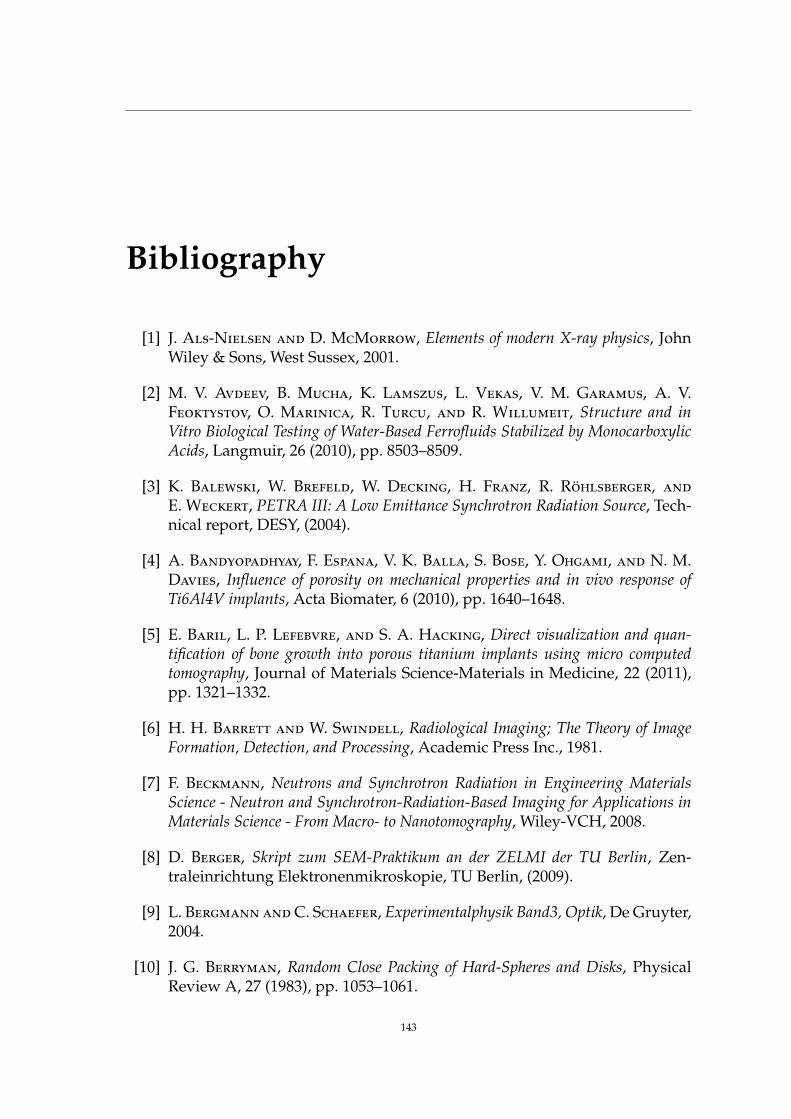
Bibliography
[1] J. Als-Nielsen and D. McMorrow, Elements of modern X-ray physics, JohnWiley & Sons, West Sussex, 2001.
[2] M. V. Avdeev, B. Mucha, K. Lamszus, L. Vekas, V. M. Garamus, A. V.Feoktystov, O. Marinica, R. Turcu, and R. Willumeit, Structure and inVitro Biological Testing of Water-Based Ferrofluids Stabilized by MonocarboxylicAcids, Langmuir, 26 (2010), pp. 8503–8509.
[3] K. Balewski, W. Brefeld, W. Decking, H. Franz, R. Rohlsberger, andE. Weckert, PETRA III: A Low Emittance Synchrotron Radiation Source, Tech-nical report, DESY, (2004).
[4] A. Bandyopadhyay, F. Espana, V. K. Balla, S. Bose, Y. Ohgami, and N. M.Davies, Influence of porosity on mechanical properties and in vivo response ofTi6Al4V implants, Acta Biomater, 6 (2010), pp. 1640–1648.
[5] E. Baril, L. P. Lefebvre, and S. A. Hacking, Direct visualization and quan-tification of bone growth into porous titanium implants using micro computedtomography, Journal of Materials Science-Materials in Medicine, 22 (2011),pp. 1321–1332.
[6] H. H. Barrett and W. Swindell, Radiological Imaging; The Theory of ImageFormation, Detection, and Processing, Academic Press Inc., 1981.
[7] F. Beckmann, Neutrons and Synchrotron Radiation in Engineering MaterialsScience - Neutron and Synchrotron-Radiation-Based Imaging for Applications inMaterials Science - From Macro- to Nanotomography, Wiley-VCH, 2008.
[8] D. Berger, Skript zum SEM-Praktikum an der ZELMI der TU Berlin, Zen-traleinrichtung Elektronenmikroskopie, TU Berlin, (2009).
[9] L. Bergmann andC. Schaefer, Experimentalphysik Band3, Optik, De Gruyter,2004.
[10] J. G. Berryman, Random Close Packing of Hard-Spheres and Disks, PhysicalReview A, 27 (1983), pp. 1053–1061.
143
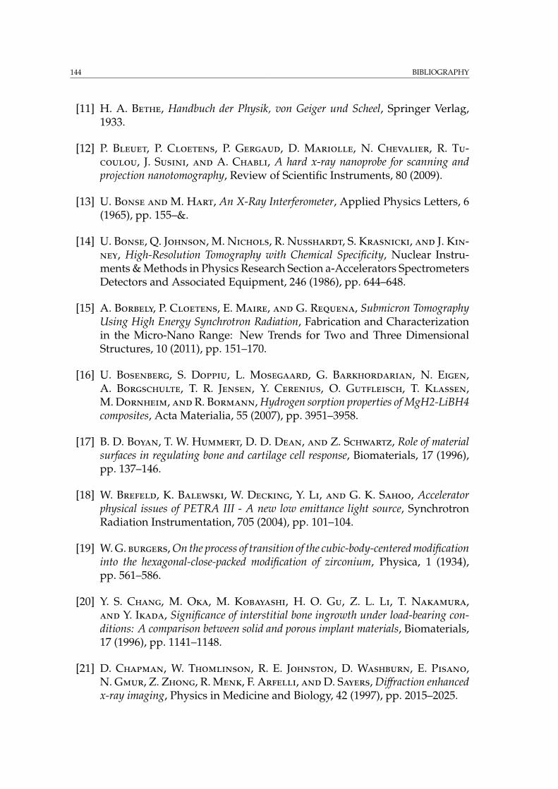
144 BIBLIOGRAPHY
[11] H. A. Bethe, Handbuch der Physik, von Geiger und Scheel, Springer Verlag,1933.
[12] P. Bleuet, P. Cloetens, P. Gergaud, D. Mariolle, N. Chevalier, R. Tu-coulou, J. Susini, and A. Chabli, A hard x-ray nanoprobe for scanning andprojection nanotomography, Review of Scientific Instruments, 80 (2009).
[13] U. Bonse andM. Hart, An X-Ray Interferometer, Applied Physics Letters, 6(1965), pp. 155–&.
[14] U. Bonse, Q. Johnson, M. Nichols, R. Nusshardt, S. Krasnicki, and J. Kin-ney, High-Resolution Tomography with Chemical Specificity, Nuclear Instru-ments & Methods in Physics Research Section a-Accelerators SpectrometersDetectors and Associated Equipment, 246 (1986), pp. 644–648.
[15] A. Borbely, P. Cloetens, E. Maire, and G. Requena, Submicron TomographyUsing High Energy Synchrotron Radiation, Fabrication and Characterizationin the Micro-Nano Range: New Trends for Two and Three DimensionalStructures, 10 (2011), pp. 151–170.
[16] U. Bosenberg, S. Doppiu, L. Mosegaard, G. Barkhordarian, N. Eigen,A. Borgschulte, T. R. Jensen, Y. Cerenius, O. Gutfleisch, T. Klassen,M. Dornheim, andR. Bormann, Hydrogen sorption properties of MgH2-LiBH4composites, Acta Materialia, 55 (2007), pp. 3951–3958.
[17] B. D. Boyan, T. W. Hummert, D. D. Dean, and Z. Schwartz, Role of materialsurfaces in regulating bone and cartilage cell response, Biomaterials, 17 (1996),pp. 137–146.
[18] W. Brefeld, K. Balewski, W. Decking, Y. Li, and G. K. Sahoo, Acceleratorphysical issues of PETRA III - A new low emittance light source, SynchrotronRadiation Instrumentation, 705 (2004), pp. 101–104.
[19] W. G. burgers, On the process of transition of the cubic-body-centered modificationinto the hexagonal-close-packed modification of zirconium, Physica, 1 (1934),pp. 561–586.
[20] Y. S. Chang, M. Oka, M. Kobayashi, H. O. Gu, Z. L. Li, T. Nakamura,and Y. Ikada, Significance of interstitial bone ingrowth under load-bearing con-ditions: A comparison between solid and porous implant materials, Biomaterials,17 (1996), pp. 1141–1148.
[21] D. Chapman, W. Thomlinson, R. E. Johnston, D. Washburn, E. Pisano,N. Gmur, Z. Zhong, R. Menk, F. Arfelli, andD. Sayers, Diffraction enhancedx-ray imaging, Physics in Medicine and Biology, 42 (1997), pp. 2015–2025.
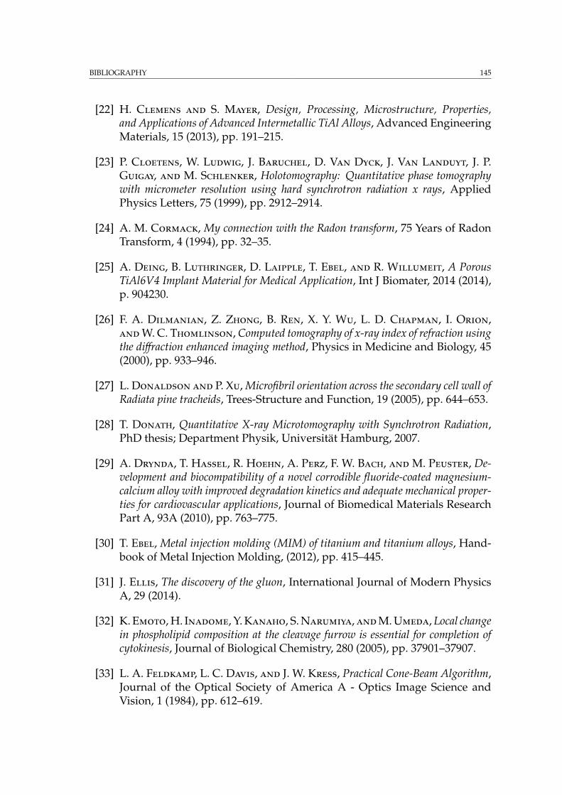
BIBLIOGRAPHY 145
[22] H. Clemens and S. Mayer, Design, Processing, Microstructure, Properties,and Applications of Advanced Intermetallic TiAl Alloys, Advanced EngineeringMaterials, 15 (2013), pp. 191–215.
[23] P. Cloetens, W. Ludwig, J. Baruchel, D. Van Dyck, J. Van Landuyt, J. P.Guigay, and M. Schlenker, Holotomography: Quantitative phase tomographywith micrometer resolution using hard synchrotron radiation x rays, AppliedPhysics Letters, 75 (1999), pp. 2912–2914.
[24] A. M. Cormack, My connection with the Radon transform, 75 Years of RadonTransform, 4 (1994), pp. 32–35.
[25] A. Deing, B. Luthringer, D. Laipple, T. Ebel, and R. Willumeit, A PorousTiAl6V4 Implant Material for Medical Application, Int J Biomater, 2014 (2014),p. 904230.
[26] F. A. Dilmanian, Z. Zhong, B. Ren, X. Y. Wu, L. D. Chapman, I. Orion,andW. C. Thomlinson, Computed tomography of x-ray index of refraction usingthe diffraction enhanced imaging method, Physics in Medicine and Biology, 45(2000), pp. 933–946.
[27] L. Donaldson and P. Xu, Microfibril orientation across the secondary cell wall ofRadiata pine tracheids, Trees-Structure and Function, 19 (2005), pp. 644–653.
[28] T. Donath, Quantitative X-ray Microtomography with Synchrotron Radiation,PhD thesis; Department Physik, Universität Hamburg, 2007.
[29] A. Drynda, T. Hassel, R. Hoehn, A. Perz, F. W. Bach, andM. Peuster, De-velopment and biocompatibility of a novel corrodible fluoride-coated magnesium-calcium alloy with improved degradation kinetics and adequate mechanical proper-ties for cardiovascular applications, Journal of Biomedical Materials ResearchPart A, 93A (2010), pp. 763–775.
[30] T. Ebel, Metal injection molding (MIM) of titanium and titanium alloys, Hand-book of Metal Injection Molding, (2012), pp. 415–445.
[31] J. Ellis, The discovery of the gluon, International Journal of Modern PhysicsA, 29 (2014).
[32] K. Emoto, H. Inadome, Y. Kanaho, S. Narumiya, andM. Umeda, Local changein phospholipid composition at the cleavage furrow is essential for completion ofcytokinesis, Journal of Biological Chemistry, 280 (2005), pp. 37901–37907.
[33] L. A. Feldkamp, L. C. Davis, and J. W. Kress, Practical Cone-Beam Algorithm,Journal of the Optical Society of America A - Optics Image Science andVision, 1 (1984), pp. 612–619.
146 BIBLIOGRAPHY
[34] F. Feyerabend, H. Drucker, D. Laipple, C. Vogt, M. Stekker, N. Hort,and R. Willumeit, Ion release from magnesium materials in physiological solu-tions under different oxygen tensions, Journal of Materials Science-Materialsin Medicine, 23 (2012), pp. 9–24.
[35] B. P. Flannery, H. W. Deckman, W. G. Roberge, and K. L. Damico, 3-Dimensional X-Ray Microtomography, Science, 237 (1987), pp. 1439–1444.
[36] J. A. Gallagher, Human osteoblast culture, Methods Mol Med, 80 (2003),pp. 3–18.
[37] P. D. Garcia, R. Sapienza, A. Blanco, and C. Lopez, Photonic glass: A novelrandom material for light, Advanced Materials, 19 (2007), pp. 2597–+.
[38] P. D. Garcia, R. Sapienza, and C. Lopez, Photonic Glasses: A Step BeyondWhite Paint, Advanced Materials, 22 (2010), pp. 12–19.
[39] E. F. Garman and T. R. Schneider, Macromolecular cryocrystallography, Jour-nal of Applied Crystallography, 30 (1997), pp. 211–237.
[40] R. Gerling, H. Clemens, and F. P. Schimansky, Power metallurgical processingof intermetallic gamma titanium aluminides, Advanced Engineering Materials,6 (2004), pp. 23–38.
[41] N. Gey and M. Humbert, Characterization of the variant selection occurringduring the alpha ->beta ->alpha phase transformations of a cold rolled titaniumsheet, Acta Materialia, 50 (2002), pp. 277–287.
[42] L. A. Giannuzzi and F. A. Stevie, Introduction to Focused Ion Beams, Springer,2005.
[43] R. Gordon, R. Bender, andG. T. Herman, Algebraic Reconstruction Techniques(Art) for 3-Dimensional Electron Microscopy and X-Ray Photography, Journal ofTheoretical Biology, 29 (1970), pp. 471–&.
[44] R. Gosalawit-Utke, S. Meethom, C. Pistidda, C. Milanese, D. Laipple,T. Saisopa, A. Marini, T. Klassen, andM. Dornheim, Destabilization of LiBH4by nanoconfinement in PMMA-co-BM polymer matrix for reversible hydrogenstorage, International Journal of Hydrogen Energy, 39 (2014), pp. 5019–5029.
[45] R. Gosalawit-Utke, C. Milanese, P. Javadian, A. Girella, D. Laipple,J. Puszkiel, A. S. Cattaneo, C. Ferrara, J. Wittayakhun, J. Skibsted,T. R. Jensen, A. Marini, T. Klassen, and M. Dornheim, 2LiBH(4)-MgH2-0.13TiCl(4) confined in nanoporous structure of carbon aerogel scaffold for re-versible hydrogen storage, Journal of Alloys and Compounds, 599 (2014),pp. 78–86.
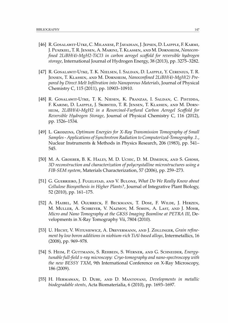
BIBLIOGRAPHY 147
[46] R. Gosalawit-Utke, C. Milanese, P. Javadian, J. Jepsen, D. Laipple, F. Karmi,J. Puszkiel, T. R. Jensen, A. Marini, T. Klassen, andM. Dornheim, Nanocon-fined 2LiBH(4)-MgH2-TiCl3 in carbon aerogel scaffold for reversible hydrogenstorage, International Journal of Hydrogen Energy, 38 (2013), pp. 3275–3282.
[47] R. Gosalawit-Utke, T. K. Nielsen, I. Saldan, D. Laipple, Y. Cerenius, T. R.Jensen, T. Klassen, andM. Dornheim, Nanoconfined 2LiBH(4)-MgH(2) Pre-pared by Direct Melt Infiltration into Nanoporous Materials, Journal of PhysicalChemistry C, 115 (2011), pp. 10903–10910.
[48] R. Gosalawit-Utke, T. K. Niesen, K. Pranzas, I. Saldan, C. Pistidda,F. Karimi, D. Laipple, J. Skibsted, T. R. Jensen, T. Klassen, and M. Dorn-heim, 2LiBH(4)-MgH2 in a Resorcinol-Furfural Carbon Aerogel Scaffold forReversible Hydrogen Storage, Journal of Physical Chemistry C, 116 (2012),pp. 1526–1534.
[49] L. Grodzins, Optimum Energies for X-Ray Transmission Tomography of SmallSamples - Applications of Synchrotron Radiation to Computerized-Tomography .1.,Nuclear Instruments & Methods in Physics Research, 206 (1983), pp. 541–545.
[50] M. A. Groeber, B. K. Haley, M. D. Uchic, D. M. Dimiduk, and S. Ghosh,3D reconstruction and characterization of polycrystalline microstructures using aFIB-SEM system, Materials Characterization, 57 (2006), pp. 259–273.
[51] G. Guerriero, J. Fugelstad, and V. Bulone, What Do We Really Know aboutCellulose Biosynthesis in Higher Plants?, Journal of Integrative Plant Biology,52 (2010), pp. 161–175.
[52] A. Haibel, M. Ogurreck, F. Beckmann, T. Dose, F. Wilde, J. Herzen,M. Muller, A. Schreyer, V. Nazmov, M. Simon, A. Last, and J. Mohr,Micro and Nano Tomography at the GKSS Imaging Beamline at PETRA III, De-velopments in X-Ray Tomography Vii, 7804 (2010).
[53] U. Hecht, V. Witusiewicz, A. Drevermann, and J. Zollinger, Grain refine-ment by low boron additions in niobium-rich TiAl-based alloys, Intermetallics, 16(2008), pp. 969–978.
[54] S. Heim, P. Guttmann, S. Rehbein, S. Werner, and G. Schneider, Energy-tunable full-field x-ray microscopy: Cryo-tomography and nano-spectroscopy withthe new BESSY TXM, 9th International Conference on X-Ray Microscopy,186 (2009).
[55] H. Hermawan, D. Dube, and D. Mantovani, Developments in metallicbiodegradable stents, Acta Biomaterialia, 6 (2010), pp. 1693–1697.
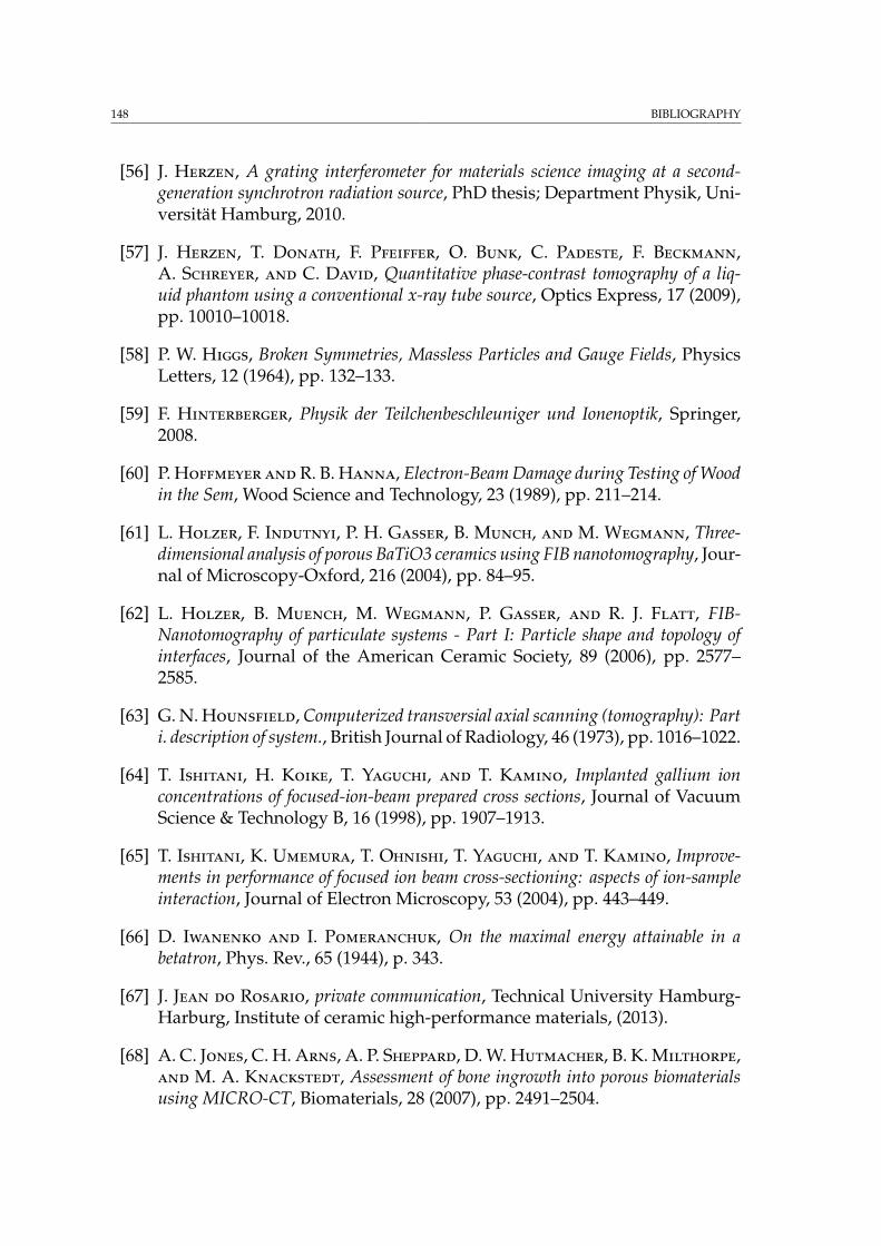
148 BIBLIOGRAPHY
[56] J. Herzen, A grating interferometer for materials science imaging at a second-generation synchrotron radiation source, PhD thesis; Department Physik, Uni-versität Hamburg, 2010.
[57] J. Herzen, T. Donath, F. Pfeiffer, O. Bunk, C. Padeste, F. Beckmann,A. Schreyer, and C. David, Quantitative phase-contrast tomography of a liq-uid phantom using a conventional x-ray tube source, Optics Express, 17 (2009),pp. 10010–10018.
[58] P. W. Higgs, Broken Symmetries, Massless Particles and Gauge Fields, PhysicsLetters, 12 (1964), pp. 132–133.
[59] F. Hinterberger, Physik der Teilchenbeschleuniger und Ionenoptik, Springer,2008.
[60] P. Hoffmeyer andR. B. Hanna, Electron-Beam Damage during Testing of Woodin the Sem, Wood Science and Technology, 23 (1989), pp. 211–214.
[61] L. Holzer, F. Indutnyi, P. H. Gasser, B. Munch, and M. Wegmann, Three-dimensional analysis of porous BaTiO3 ceramics using FIB nanotomography, Jour-nal of Microscopy-Oxford, 216 (2004), pp. 84–95.
[62] L. Holzer, B. Muench, M. Wegmann, P. Gasser, and R. J. Flatt, FIB-Nanotomography of particulate systems - Part I: Particle shape and topology ofinterfaces, Journal of the American Ceramic Society, 89 (2006), pp. 2577–2585.
[63] G. N. Hounsfield, Computerized transversial axial scanning (tomography): Parti. description of system., British Journal of Radiology, 46 (1973), pp. 1016–1022.
[64] T. Ishitani, H. Koike, T. Yaguchi, and T. Kamino, Implanted gallium ionconcentrations of focused-ion-beam prepared cross sections, Journal of VacuumScience & Technology B, 16 (1998), pp. 1907–1913.
[65] T. Ishitani, K. Umemura, T. Ohnishi, T. Yaguchi, and T. Kamino, Improve-ments in performance of focused ion beam cross-sectioning: aspects of ion-sampleinteraction, Journal of Electron Microscopy, 53 (2004), pp. 443–449.
[66] D. Iwanenko and I. Pomeranchuk, On the maximal energy attainable in abetatron, Phys. Rev., 65 (1944), p. 343.
[67] J. Jean do Rosario, private communication, Technical University Hamburg-Harburg, Institute of ceramic high-performance materials, (2013).
[68] A. C. Jones, C. H. Arns, A. P. Sheppard, D. W. Hutmacher, B. K. Milthorpe,and M. A. Knackstedt, Assessment of bone ingrowth into porous biomaterialsusing MICRO-CT, Biomaterials, 28 (2007), pp. 2491–2504.
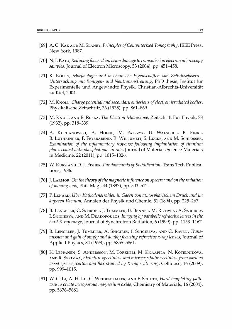
BIBLIOGRAPHY 149
[69] A. C. Kak andM. Slaney, Principles of Computerized Tomography, IEEE Press,New York, 1987.
[70] N. I. Kato, Reducing focused ion beam damage to transmission electron microscopysamples, Journal of Electron Microscopy, 53 (2004), pp. 451–458.
[71] K. Kolln, Morphologie und mechanische Eigenschaften von Zellulosefasern -Untersuchung mit Röntgen- und Neutronenstreuung, PhD thesis; Institut fürExperimentelle und Angewandte Physik, Christian-Albrechts-Universitätzu Kiel, 2004.
[72] M. Knoll, Charge potential and secondary emissions of electron irradiated bodies,Physikalische Zeitschrift, 36 (1935), pp. 861–869.
[73] M. Knoll and E. Ruska, The Electron Microscope, Zeitschrift Fur Physik, 78(1932), pp. 318–339.
[74] A. Kochanowski, A. Hoene, M. Patrzyk, U. Walschus, B. Finke,B. Luthringer, F. Feyerabend, R. Willumeit, S. Lucke, and M. Schlosser,Examination of the inflammatory response following implantation of titaniumplates coated with phospholipids in rats, Journal of Materials Science-Materialsin Medicine, 22 (2011), pp. 1015–1026.
[75] W. Kurz and D. J. Fisher, Fundamentals of Solidification, Trans Tech Publica-tions, 1986.
[76] J. Larmor, On the theory of the magnetic influence on spectra; and on the radiationof moving ions, Phil. Mag., 44 (1897), pp. 503–512.
[77] P. Lenard, Über Kathodenstrahlen in Gasen von atmosphärischem Druck und imäußeren Vacuum, Annalen der Physik und Chemie, 51 (1894), pp. 225–267.
[78] B. Lengeler, C. Schroer, J. Tummler, B. Benner, M. Richwin, A. Snigirev,I. Snigireva, andM. Drakopoulos, Imaging by parabolic refractive lenses in thehard X-ray range, Journal of Synchrotron Radiation, 6 (1999), pp. 1153–1167.
[79] B. Lengeler, J. Tummler, A. Snigirev, I. Snigireva, and C. Raven, Trans-mission and gain of singly and doubly focusing refractive x-ray lenses, Journal ofApplied Physics, 84 (1998), pp. 5855–5861.
[80] K. Leppanen, S. Andersson, M. Torkkeli, M. Knaapila, N. Kotelnikova,andR. Serimaa, Structure of cellulose and microcrystalline cellulose from variouswood species, cotton and flax studied by X-ray scattering, Cellulose, 16 (2009),pp. 999–1015.
[81] W. C. Li, A. H. Lu, C. Weidenthaler, and F. Schuth, Hard-templating path-way to create mesoporous magnesium oxide, Chemistry of Materials, 16 (2004),pp. 5676–5681.
150 BIBLIOGRAPHY
[82] H. Lichtenegger, M. Muller, O. Paris, C. Riekel, and P. Fratzl, Imaging ofthe helical arrangement of cellulose fibrils in wood by synchrotron X-ray microd-iffraction, Journal of Applied Crystallography, 32 (1999), pp. 1127–1133.
[83] A. Lienard, Champ électrique et magnétique, produit par une charge électriqueconcentrée en un point et animée d’un mouvement quelconque, L’Éclairage Élec.,16 (1898), pp. 5–14, 53–59, 106–112.
[84] N. C. Lindquist, P. Nagpal, K. M. McPeak, D. J. Norris, and S. H. Oh,Engineering metallic nanostructures for plasmonics and nanophotonics, Reportson Progress in Physics, 75 (2012).
[85] Y. C. Liu, G. C. Yang, and Y. H. Zhou, High-velocity banding structure in thelaser-resolidified hypoperitectic Ti47Al53 alloy, Journal of Crystal Growth, 240(2002), pp. 603–610.
[86] J. J. Lombardo, R. A. Ristau, W. M. Harris, andW. K. S. Chiu, Focused ionbeam preparation of samples for X-ray nanotomography, Journal of SynchrotronRadiation, 19 (2012), pp. 789–796.
[87] G. Margaritondo, Introduction to Synchrotron Radiation, Oxford UniversityPress, 1988.
[88] M. Mastrogiacomo, S. Scaglione, R. Martinetti, L. Dolcini, F. Beltrame,R. Cancedda, and R. Quarto, Role of scaffold internal structure on in vivobone formation in macroporous calcium phosphate bioceramics, Biomaterials, 27(2006), pp. 3230–3237.
[89] T. L. Matteson, S. W. Schwarz, E. C. Houge, B. W. Kempshall, and L. A.Giannuzzi, Electron backscattering diffraction investigation of focused ion beamsurfaces, Journal of Electronic Materials, 31 (2002), pp. 33–39.
[90] C. Mccullough, J. J. Valencia, C. G. Levi, and R. Mehrabian, Microstruc-tural Analysis of Rapidly Solidified Ti-Al-X Powders, Materials Science andEngineering a-Structural Materials Properties Microstructure and Process-ing, 124 (1990), pp. 83–101.
[91] D. McMullan, Investigations relating to the design of electron microscopes, PhDthesis, University of Cambridge, 1952.
[92] D. Mcmullan, J. Thewlis, A. W. Agar, D. Gabor, M. E. Haine, H. G.Lubszynski, R. Feinberg, and D. Mcmullan, An Improved Scanning ElectronMicroscope for Opaque Specimens, Proceedings of the Institution of ElectricalEngineers-London, 100 (1953), pp. 245–259.
[93] MiNaXS-beamline, photon-science.desy.de/facilities/petra_iii/beamlines/p03_ mi-naxs/index_eng.html, (accessed Januar 8, 2015).
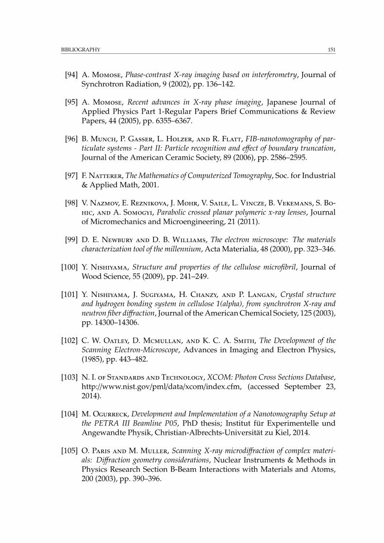
BIBLIOGRAPHY 151
[94] A. Momose, Phase-contrast X-ray imaging based on interferometry, Journal ofSynchrotron Radiation, 9 (2002), pp. 136–142.
[95] A. Momose, Recent advances in X-ray phase imaging, Japanese Journal ofApplied Physics Part 1-Regular Papers Brief Communications & ReviewPapers, 44 (2005), pp. 6355–6367.
[96] B. Munch, P. Gasser, L. Holzer, and R. Flatt, FIB-nanotomography of par-ticulate systems - Part II: Particle recognition and effect of boundary truncation,Journal of the American Ceramic Society, 89 (2006), pp. 2586–2595.
[97] F. Natterer, The Mathematics of Computerized Tomography, Soc. for Industrial& Applied Math, 2001.
[98] V. Nazmov, E. Reznikova, J. Mohr, V. Saile, L. Vincze, B. Vekemans, S. Bo-hic, and A. Somogyi, Parabolic crossed planar polymeric x-ray lenses, Journalof Micromechanics and Microengineering, 21 (2011).
[99] D. E. Newbury and D. B. Williams, The electron microscope: The materialscharacterization tool of the millennium, Acta Materialia, 48 (2000), pp. 323–346.
[100] Y. Nishiyama, Structure and properties of the cellulose microfibril, Journal ofWood Science, 55 (2009), pp. 241–249.
[101] Y. Nishiyama, J. Sugiyama, H. Chanzy, and P. Langan, Crystal structureand hydrogen bonding system in cellulose 1(alpha), from synchrotron X-ray andneutron fiber diffraction, Journal of the American Chemical Society, 125 (2003),pp. 14300–14306.
[102] C. W. Oatley, D. Mcmullan, and K. C. A. Smith, The Development of theScanning Electron-Microscope, Advances in Imaging and Electron Physics,(1985), pp. 443–482.
[103] N. I. of Standards and Technology, XCOM: Photon Cross Sections Database,http://www.nist.gov/pml/data/xcom/index.cfm, (accessed September 23,2014).
[104] M. Ogurreck, Development and Implementation of a Nanotomography Setup atthe PETRA III Beamline P05, PhD thesis; Institut für Experimentelle undAngewandte Physik, Christian-Albrechts-Universität zu Kiel, 2014.
[105] O. Paris and M. Muller, Scanning X-ray microdiffraction of complex materi-als: Diffraction geometry considerations, Nuclear Instruments & Methods inPhysics Research Section B-Beam Interactions with Materials and Atoms,200 (2003), pp. 390–396.
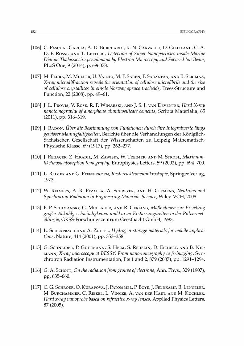
152 BIBLIOGRAPHY
[106] C. Pascual Garcia, A. D. Burchardt, R. N. Carvalho, D. Gilliland, C. A.D, F. Rossi, and T. Lettieri, Detection of Silver Nanoparticles inside MarineDiatom Thalassiosira pseudonana by Electron Microscopy and Focused Ion Beam,PLoS One, 9 (2014), p. e96078.
[107] M. Peura, M. Muller, U. Vainio, M. P. Saren, P. Saranpaa, and R. Serimaa,X-ray microdiffraction reveals the orientation of cellulose microfibrils and the sizeof cellulose crystallites in single Norway spruce tracheids, Trees-Structure andFunction, 22 (2008), pp. 49–61.
[108] J. L. Provis, V. Rose, R. P. Winarski, and J. S. J. van Deventer, Hard X-raynanotomography of amorphous aluminosilicate cements, Scripta Materialia, 65(2011), pp. 316–319.
[109] J. Radon, Über die Bestimmung von Funktionen durch ihre Integralwerte längsgewisser Mannigfaltigkeiten, Berichte über die Verhandlungen der Königlich-Sächsischen Gesellschaft der Wissenschaften zu Leipzig Mathematisch-Physische Klasse, 69 (1917), pp. 262–277.
[110] J. Rehacek, Z. Hradil, M. Zawisky, W. Treimer, andM. Strobl, Maximum-likelihood absorption tomography, Europhysics Letters, 59 (2002), pp. 694–700.
[111] L. Reimer andG. Pfefferkorn, Rasterelektronenmikroskopie, Springer Verlag,1973.
[112] W. Reimers, A. R. Pyzalla, A. Schreyer, and H. Clemens, Neutrons andSynchrotron Radiation in Engineering Materials Science, Wiley-VCH, 2008.
[113] F.-P. Schimansky, G. Mullauer, and R. Gerling, Maßnahmen zur Erzielunggroßer Abkühlgeschwindigkeiten und kurzer Erstarrungszeiten in der Pulvermet-allurgie, GKSS-Forschungszentrum Geesthacht GmbH, 1993.
[114] L. Schlapbach and A. Zuttel, Hydrogen-storage materials for mobile applica-tions, Nature, 414 (2001), pp. 353–358.
[115] G. Schneider, P. Guttmann, S. Heim, S. Rehbein, D. Eichert, and B. Nie-mann, X-ray microscopy at BESSY: From nano-tomography to fs-imaging, Syn-chrotron Radiation Instrumentation, Pts 1 and 2, 879 (2007), pp. 1291–1294.
[116] G. A. Schott, On the radiation from groups of electrons, Ann. Phys., 329 (1907),pp. 635–660.
[117] C. G. Schroer, O. Kurapova, J. Patommel, P. Boye, J. Feldkamp, B. Lengeler,M. Burghammer, C. Riekel, L. Vincze, A. van der Hart, andM. Kuchler,Hard x-ray nanoprobe based on refractive x-ray lenses, Applied Physics Letters,87 (2005).
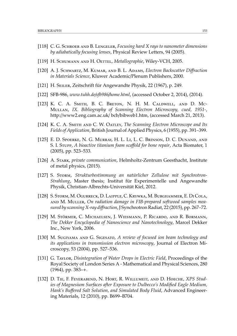
BIBLIOGRAPHY 153
[118] C. G. Schroer and B. Lengeler, Focusing hard X rays to nanometer dimensionsby adiabatically focusing lenses, Physical Review Letters, 94 (2005).
[119] H. Schumann and H. Oettel, Metallographie, Wiley-VCH, 2005.
[120] A. J. Schwartz, M. Kumar, and B. L. Adams, Electron Backscatter Diffractionin Materials Science, Kluwer Academic/Plenum Publishers, 2000.
[121] H. Seiler, Zeitschrift für Angewandte Physik, 22 (1967), p. 249.
[122] SFB-986, www.tuhh.de/sfb986/home.html, (accessed October 2, 2014), (2014).
[123] K. C. A. Smith, B. C. Breton, N. H. M. Caldwell, and D. Mc-Mullan, IX. Bibliography of Scanning Electron Microscopy, cued, 1951-,http://www2.eng.cam.ac.uk/ bcb/bibweb1.htm, (accessed March 21, 2013).
[124] K. C. A. Smith and C. W. Oatley, The Scanning Electron Microscope and ItsFields of Application, British Journal of Applied Physics, 6 (1955), pp. 391–399.
[125] E. D. Spoerke, N. G. Murray, H. L. Li, L. C. Brinson, D. C. Dunand, andS. I. Stupp, A bioactive titanium foam scaffold for bone repair, Acta Biomater, 1(2005), pp. 523–533.
[126] A. Stark, private communication, Helmholtz-Zentrum Geesthacht, Instituteof metal physics, (2015).
[127] S. Storm, Strukturbestimmung an natürlicher Zellulose mit Synchrotron-Strahlung, Master thesis; Institut für Experimentelle und AngewandtePhysik, Christian-Albrechts-Universität Kiel, 2012.
[128] S. Storm, M. Ogurreck, D. Laipple, C. Krywka, M. Burghammer, E. DiCola,and M. Muller, On radiation damage in FIB-prepared softwood samples mea-sured by scanning X-ray diffraction, J Synchrotron Radiat, 22 (2015), pp. 267–72.
[129] M. Stormer, C. Michaelsen, J. Wiesmann, P. Ricardo, and R. Bormann,The Dekker Encyclopedia of Nanoscience and Nanotechnology, Marcel DekkerInc., New York, 2006.
[130] M. Sugiyama and G. Sigesato, A review of focused ion beam technology andits applications in transmission electron microscopy, Journal of Electron Mi-croscopy, 53 (2004), pp. 527–536.
[131] G. Taylor, Disintegration of Water Drops in Electric Field, Proceedings of theRoyal Society of London Series A - Mathematical and Physical Sciences, 280(1964), pp. 383–+.
[132] D. Tie, F. Feyerabend, N. Hort, R. Willumeit, and D. Hoeche, XPS Stud-ies of Magnesium Surfaces after Exposure to Dulbecco’s Modified Eagle Medium,Hank’s Buffered Salt Solution, and Simulated Body Fluid, Advanced Engineer-ing Materials, 12 (2010), pp. B699–B704.
154 BIBLIOGRAPHY
[133] J. J. Valencia, C. Mccullough, C. G. Levi, and R. Mehrabian, SolidificationMicrostructure of Supercooled Ti-Al Alloys Containing Intermetallic Phases, ActaMetallurgica, 37 (1989), pp. 2517–2530.
[134] G. Wang, T. H. Lin, P. C. Cheng, andD. M. Shinozaki, A General Cone-BeamReconstruction Algorithm, Ieee Transactions on Medical Imaging, 12 (1993),pp. 486–496.
[135] E. A. Wargo, T. Kotaka, Y. Tabuchi, and E. C. Kumbur, Comparison offocused ion beam versus nano-scale X-ray computed tomography for resolving 3-D microstructures of porous fuel cell materials, Journal of Power Sources, 241(2013), pp. 608–618.
[136] O. C. Wells, The construction of a scanning electron microscope and its applicationto the study of fibres, PhD thesis, University of Cambridge, 1957.
[137] K. Wille, Physik der Teilchenbeschleuniger und Synchrotronstrahlungsquellen,Teubner, 1992.
[138] R. Willumeit, J. Fischer, F. Feyerabend, N. Hort, U. Bismayer, S. Heidrich,and B. Mihailova, Chemical surface alteration of biodegradable magnesium ex-posed to corrosion media, Acta Biomaterialia, 7 (2011), pp. 2704–2715.
[139] R. Willumeit, M. Schossig, H. Clemens, and F. Feyerabend, In-vitro in-teractions of human chondrocytes and mesenchymal stem cells, and of mousemacrophages with phospholipid-covered metallic implant materials, EuropeanCells & Materials, 13 (2007), pp. 11–24.
[140] R. Willumeit, A. Schuster, P. Iliev, S. Linser, and F. Feyerabend, Phospho-lipids as implant coatings, Journal of Materials Science-Materials in Medicine,18 (2007), pp. 367–380.
[141] R. P. Winarski, M. V. Holt, V. Rose, P. Fuesz, D. Carbaugh, C. Benson,D. M. Shu, D. Kline, G. B. Stephenson, I. McNulty, and J. Maser, A hardX-ray nanoprobe beamline for nanoscale microscopy, Journal of SynchrotronRadiation, 19 (2012), pp. 1056–1060.
[142] F. Witte, The history of biodegradable magnesium implants: A review, ActaBiomaterialia, 6 (2010), pp. 1680–1692.
[143] V. T. Witusiewicz, A. A. Bondar, U. Hecht, and T. Y. Velikanova, The Al-B-Nb-Ti system. IV. Experimental study and thermodynamic re-evaluation of thebinary Al-Nb and ternary Al-Nb-Ti systems, Journal of Alloys and Compounds,472 (2009), pp. 133–161.
[144] L. Yang, N. Hort, D. Laipple, D. Hoche, Y. Huang, K. U. Kainer,R. Willumeit, and F. Feyerabend, Element distribution in the corrosion layer
BIBLIOGRAPHY 155
and cytotoxicity of alloy Mg-10Dy during in vitro biodegradation, Acta Biomater,(2012).
[145] L. Yang, Y. D. Huang, Q. M. Peng, F. Feyerabend, K. U. Kainer,R. Willumeit, and N. Hort, Mechanical and corrosion properties of binaryMg-Dy alloys for medical applications, Materials Science and Engineering B-Advanced Functional Solid-State Materials, 176 (2011), pp. 1827–1834.
[146] Zeiss, Instruction manual AURIGA, Carl Zeiss NTS GmbH, Oberkochen,Germany, 2009.
[147] Zeiss, Instruction manual Zeiss multi GIS, Carl Zeiss NTS GmbH,Oberkochen, Germany, 2009.
[148] E. Zolotoyabko, Basic Concepts of X-Ray Diffraction, Wiley-VCH, 2014.
156 BIBLIOGRAPHY
List of cooperated publications
A. Deing, B. Luthringer, D. Laipple, T. Ebel and R. Willumeit, A Porous TiAl6V4Implant Material for Medical Application, Int J Biomater, (2014).[25] (Refer to chapter 4)
F. Feyerabend, H. Drucker, D. Laipple, C. Vogt, M. Stekker, N. Hort, and R.Willumeit, Ion release from magnesium materials in physiological solutions un-der different oxygen tensions, Journal of Materials Science-Materials in Medicine,23 (2012), pp. 9-24.[34] (Refer to section 5.1)
R. Gosalawit-Utke, S. Meethom, C. Pistidda, C. Milanese, D. Laipple, T. Saisopa, A.Marini, T. Klassen, M. Dornheim, Destabilization of LiBH4 by nanoconfinementin PMMA-co-BM polymer matrix for reversible hydrogen storage, InternationalJournal of Hydrogen Energy, 39 (2014), pp. 5019-5029.[44] (Refer to chapter 6)
R. Gosalawit-Utke, C. Milanese, P. Javadian, A. Girella, D. Laipple, J. Puszkiel,A. S. Cattaneo, C. Ferrara, J. Wittayakhun, J. Skibsted, T. R. Jensen, A. Marini,T. Klassen, M. Dornheim, 2LiBH(4)-MgH2-0.13TiCl(4) confined in nanoporousstructure of carbon aerogel scaffold for reversible hydrogen storage, Journal ofAlloys and Compounds, 599 (2014), pp. 78-86.[45] (Refer to chapter 6)
R. Gosalawit-Utke, C. Milanese, P. Javadian, J. Jepsen, D. Laipple, F. Karmi, J.Puszkiel, T. R. and Jensen, A. Marini, T. Klassen, M. Dornheim, Nanoconfined2LiBH(4)-MgH2-TiCl3 in carbon aerogel scaffold for reversible hydrogen storage,International Journal of Hydrogen Energy, 38 (2013), pp. 3275-3282.[46] (Refer to chapter 6)
R. Gosalawit-Utke, T. K. Nielsen, I. Saldan, D. Laipple, Y. Cerenius, T. R. Jensen, T.Klassen, and M. Dornheim, Nanoconfined 2LiBH(4)-MgH(2) Prepared by DirectMelt Infiltration into Nanoporous Materials, Journal of Physical Chemistry C, 115(2011), pp. 10903-10910.[47] (Refer to chapter 6)
R. Gosalawit-Utke, T. K. Nielsen, K. Pranzas, I. Saldan, C. Pistidda, F. Karimi, D.Laipple, J. Skibsted, T. R. Jensen, T. Klassen, and M. Dornheim, 2LiBH(4)-MgH(2)in a Resorcinol-Furfural Carbon Aerogel Scaffold for Reversible Hydrogen Stor-age, Journal of Physical Chemistry C, 116 (2012), pp. 1526-1534.[48] (Refer to chapter 6)
BIBLIOGRAPHY 157
S. Storm, M. Ogurreck, D. Laipple, C. Krywka, M. Burghammer, E. Di Cola,M. Muller, On radiation damage in FIB-prepared softwood samples measured byscanning X-ray diffraction, J Synchrotron Radiat, 22 (2015), pp. 267-272.[128] (Refer to chapter 8)
L. Yang, N. Hort, D. Laipple, D. Hoche, Y. Huang, K. U. Kainer, R. Willumeit,and F. Feyerabend, Element distribution in the corrosion layer and cytotoxicityof alloy Mg-10Dy during in vitro biodegradation, Acta Biomater, 9 (2012), pp.8475-8487.[144] (Refer to section 5.2)
Conferences
D. Laipple, B. Luthringer, A. Deing, R. Willumeit, A. Schreyer, Osteoblast-like cellingrowth assessment by means of SEM techniques & Tomography, Poster, NeueHorizonte für metallische Biomaterialien, Geesthacht (2011).(Refer to chapter 4)
D. Laipple, B. Luthringer, A. Deing, T. Ebel, R. Willumeit, A. Schreyer, Osteoblast-like cell ingrowth assessment by means of SEM techniques, Talk, European Cross-Beam User Meeting, Stuttgart (2012).(Refer to chapter 4)
D. Laipple, B. Luthringer, A. Deing, T. Ebel, R. Willumeit, A. Schreyer, Localisa-tion of cells in a porous Ti alloy by SEM techniques, Talk, PNI1 in-house research:2nd Soft Matter & Life Science Workshop, Potsdam (2012).(Refer to chapter 4)
D. Laipple, B. Luthringer, A. Deing, T. Ebel, R. Willumeit, A. Schreyer, Local-isation of cells in a porous Ti alloy by SEM techniques, Oral-Poster, MaterialsScience and Engineering Conference (MSE), Darmstadt (2012).(Refer to chapter 4)
1PNI = Photons, Neutrons and Ions

158
Acknowledgement / Danksagung
Ich möchte hier meinen besonderen Dank aussprechen, bei meinem Betreuer Prof.Dr. Andreas Schreyer sowie bei meinem Abteilungsleiter Prof. Dr. Martin Müllerfür das interessante und vielseitige Thema meiner Doktorarbeit im Helmholtz-Zentrum Geesthacht sowie die gute Zusammenarbeit. Außerdem möchte ich michbei Prof. Dr. Florian Pyczak bedanken, der mit seiner Abteilung WPM der Aurigaeinen Raum gab bis das EMSC2 einmal am DESY steht, für alle Hilfen und Ideenzum Thema und das freundliche Arbeitsklima.Weiterhin danke ich Prof. Dr. Regine Willumeit-Römer, die mit den biologischenProben und Fragestellungen den ersten praktischen Teil dieser Arbeit maßgeblichmotivierte. Bérengère Luthringer und Axel Deing gilt mein besonderer Dank fürdas Vorbereiten der Implantatwerkstoffe und die belebenden Gespräche. MeinDank gilt hier auch Gabriele Salomon, die im Wesentlichen die umfangreicheZellpräparation für diese Proben durchführte.Frank Feyerabend und Lei Yang danke ich für die freundliche und fruchtbare Zu-sammenarbeit im Themenbereich abbaubarer Implantate, sowie Rapee Gosalawit-Utke im Bereich der Wasserstoffspeichermaterialien. Die ersten gemeinsamen Ver-öffentlichungen waren eine gute Motivation.Bei Malte Ogurreck möchte ich mich für die Röntgentomographien und die pri-ma Zusammenarbeit insgesamt bedanken. Vor allem aber auch dafür das zurFertigstellung unserer beider Arbeiten schlussendlich die finale Nanotomogra-phie gelang!Ich danke Uwe Lorenz für die erstklassige freundschaftliche Betreuung und Un-terstützung bei allen Fragen und Problemen rund um die Elektronenmikroskopie,sowie Selina Storm und Christina Krywka für die erfolgreiche Zusammenarbeitbezüglich der Holzproben und der Nanodiffraktion.Bernd Schwebke danke ich für die Hilfe bei der Durchführung der Diffraktionan den Pulverfraktionen sowie Marcus Rackel für die Tips bei der Auswertung.Michael Oehring, Andreas Stark und Frank-Peter Schimansky danke ich diesbe-züglich für die hilfreichen Diskussionen zur Interpretation der Messergebinsse.Mein Dank gilt auch allen weiteren Kollegen in Geesthacht und an der Außenstelleam DESY die mir in freundschaftlicher Atmosphäre halfen und mich unterstütz-ten!Ganz besonders möchte ich meiner Familie danken, meiner Frau Marina, meinenMädels Cecilia, Leora, Nediva und seit über einem Jahr auch dem kleinen Arkin,dass ihr hinter mir standet und mich unterstützt habt und ihr zu guter Letzt dankGottes Liebe ein Teil meines Lebens seid!
2Engineering Materials Science Centre
159