


Sprachen
Seiten
Rechtliche

Atomic-scale observation of parallel development of super elasticity and reversibleplasticity in GaAs nanowiresPeite Bao, Yanbo Wang, Xiangyuan Cui, Qiang Gao, Hung-Wei Yen, Hongwei Liu, Wai Kong Yeoh, Xiaozhou
Liao, Sichao Du, H. Hoe Tan, Chennupati Jagadish, Jin Zou, Simon P. Ringer, and Rongkun Zheng Citation: Applied Physics Letters 104, 021904 (2014); doi: 10.1063/1.4861846 View online: http://dx.doi.org/10.1063/1.4861846 View Table of Contents: http://scitation.aip.org/content/aip/journal/apl/104/2?ver=pdfcov Published by the AIP Publishing
This article is copyrighted as indicated in the article. Reuse of AIP content is subject to the terms at: http://scitation.aip.org/termsconditions. Downloaded to IP:
130.56.107.193 On: Fri, 14 Mar 2014 01:06:17
Atomic-scale observation of parallel development of super elasticityand reversible plasticity in GaAs nanowires
Peite Bao,1 Yanbo Wang,2 Xiangyuan Cui,2,3 Qiang Gao,4 Hung-Wei Yen,2,3 Hongwei Liu,3
Wai Kong Yeoh,2,3 Xiaozhou Liao,2,a) Sichao Du,1 H. Hoe Tan,4 Chennupati Jagadish,4
Jin Zou,5 Simon P. Ringer,2,3 and Rongkun Zheng1,b)
1School of Physics, The University of Sydney, Sydney, NSW 2006, Australia2School of Aerospace, Mechanical and Mechatronic Engineering, The University of Sydney, Sydney,NSW 2006, Australia3Australian Centre for Microscopy & Microanalysis, The University of Sydney, Sydney, NSW 2006, Australia4Department of Electronic Materials Engineering, Research School of Physics and Engineering,The Australian National University, Canberra, ACT 0200, Australia5Materials Engineering and Centre for Microscopy and Microanalysis, The University of Queensland,Brisbane, QLD 4072, Australia
(Received 5 December 2013; accepted 27 December 2013; published online 14 January 2014)
We report the atomic-scale observation of parallel development of super elasticity and reversible
dislocation-based plasticity from an early stage of bending deformation until fracture in GaAs
nanowires. While this phenomenon is in sharp contrast to the textbook knowledge, it is expected to
occur widely in nanostructures. This work indicates that the super recoverable deformation in
nanomaterials is not simple elastic or reversible plastic deformation in nature, but the coupling of
both. VC 2014 AIP Publishing LLC. [http://dx.doi.org/10.1063/1.4861846]
Conventional theory and experiments in plasticity dem-
onstrate that when a load is applied to metals and ceramics,
they undergo first elastic deformation, followed by plastic de-
formation, and finally fracture.1 Elastic deformation is self-
recoverable and mediated by stretching of the bonds, but
where the atoms do not slip past each other. In contrast, plas-
tic deformation is usually irrecoverable or permanent and is
mediated by discrete dislocation activity, displacive deforma-
tion twinning, stress-induced phase transformations, or frac-
ture associated with flaws.2–4 Furthermore, it is well known
that in ceramic crystals such as GaAs, the directional nature
of the bonding makes dislocation movement and therefore
plastic deformation very difficult.5 Therefore, bulk crystalline
ceramic materials fracture after only a very small elastic
strain of �0.1%, and dislocation-mediated plastic strain is
almost non-existent.6
On the other hand, nanowires (NWs) are known to sup-
port large elastic strains primarily because of the constrained
size and number of grains across the NW diameter, which
serves to greatly reduce the number of crystalline defects in
the individual NWs and effectively prevents the initiation
and propagation of cracks.7–9 Semiconductor NWs with
recoverable strains of between �3% and 10% have been
reported, and this strain is primarily elastic in nature.10–13
Recent research using computational simulations14,15 and
nanoindentation experiments16,17 has revealed that non-
linear dislocation-mediated plasticity can also be reversible
in some nanocrystalline materials.
To reveal the microscopic mechanisms of NWs deforma-
tion, atomic-scale characterization is indispensable. In this
work, we developed an experimental method that enables
atomic-scale microscopy of NWs under any particular level
of bending deformation. We report the atomic-scale observa-
tion of parallel development of super elasticity and reversible
plasticity throughout the whole range of bending deformation
in GaAs nanowires. Although the dislocation density is
extremely high, most of the plastic deformation spontane-
ously recovers upon the release of the external loading.
Twin-free GaAs NWs were grown by using metalor-
ganic chemical vapor deposition (MOCVD) via the vapor-
liquid-solid mechanism using Au nanoparticles as catalyst.18
Trimethylgallium and AsH3 were used as the Ga and As
sources, respectively. A two-temperature procedure, which
consists an 1 min high-temperature (450 �C) nucleation step
followed by a 30 min low-temperature (375 �C) growth step,
was used and ensured samples were minimum tapered and of
perfect crystalline quality 28. NWs were vertically aligned
on (111)B GaAs substrate and uniform in diameter of
�50–60 nm. NWs studied were �4–6 lm in length.
High-resolution transmission electron microscopy
(HRTEM) investigation was performed on a JEOL 2200FS
field-emission TEM operating at 200 kV and a JEOL 3000F
field-emission TEM operating at 300 kV with a standard
double-tilt mechanism. (111) d-spacing before, during, and af-
ter deformation are averaged values from three separate
regions, each contains 15–20 lattices. Dislocation lines were
identified via using inverse fast Fourier transformation (IFFT)
of the HRTEM images. TEM sample preparation was done
simply by scratching the growth substrate using copper grids
with holey carbon supporting film.
Deformation experiments were performed in a Zeiss
Auriga dual-beam scanning electron microscopy (SEM)
equipped with a platinum gas injection system (GIS), and a
Kleindiek Nanotechnik nanopositioning system connected
with an electro-polished tungsten tip as the micro-
manipulator inside of the SEM chamber. GIS enables to affix
the NW to the carbon supporting film by depositing platinum
a)Electronic mail: [email protected])Electronic mail: [email protected]
0003-6951/2014/104(2)/021904/4/$30.00 VC 2014 AIP Publishing LLC104, 021904-1
APPLIED PHYSICS LETTERS 104, 021904 (2014)
This article is copyrighted as indicated in the article. Reuse of AIP content is subject to the terms at: http://scitation.aip.org/termsconditions. Downloaded to IP:
130.56.107.193 On: Fri, 14 Mar 2014 01:06:17
patches onto selected areas. Controllable strain can then be
applied to a single NW with the tungsten manipulator and
maintained on the TEM sample with deposition. The releas-
ing of the strain can be done by breaking either the deposi-
tion or the surrounded supporting film. Note that the SEM
stage had been adjusted in order to find the largest curvature
radius to obtain an accurate total strain value.
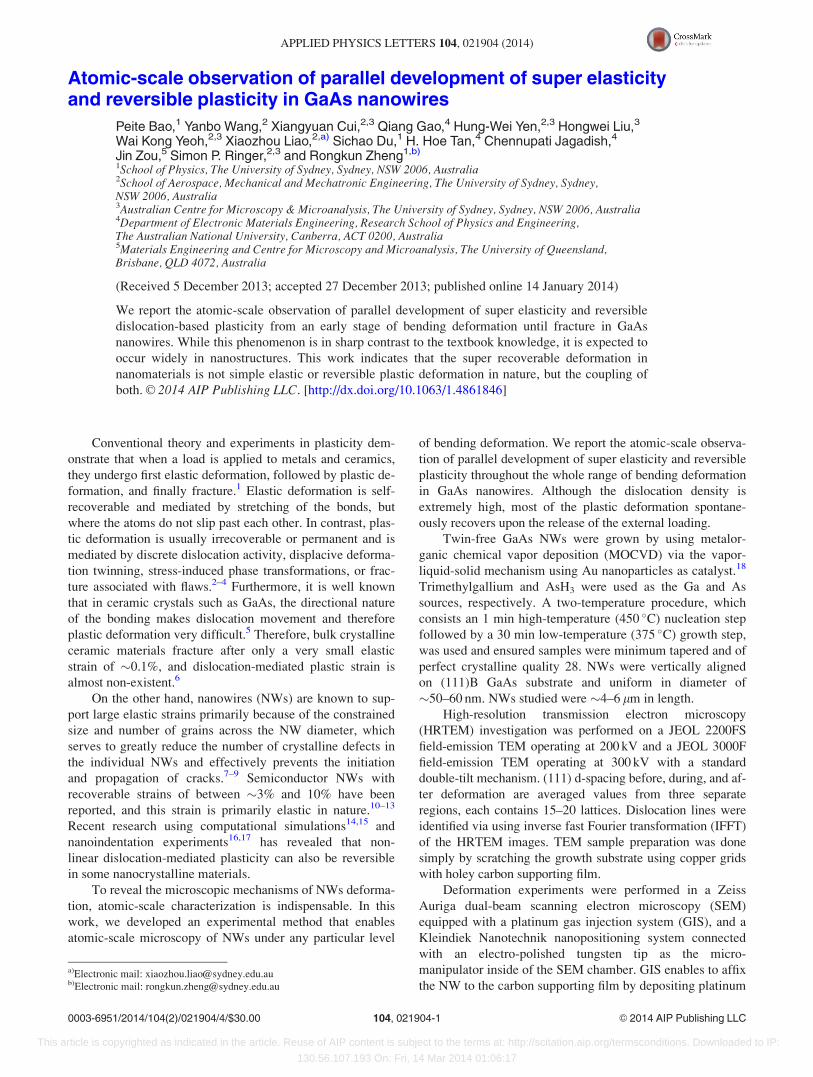
A typical complete bending deformation process of a
NW is shown by series of SEM images in Figures 1(a)–1(d).
A twin-free GaAs NW with a diameter of �50 nm was
affixed to a supporting carbon film on a copper grid by a
small patch of platinum. A tungsten nano-manipulator was
then used to progressively apply a torque to bend the NW in
a controlled manner. The radius of the bending curvature, R,
was measured in real-time and the total strain at edge, eedgetotal ,
was calculated using the formula eedgetotal ¼ D=ðDþ 2RÞ, where
D is the NW diameter.19,20 As marked in Figure 1(c), the
largest strain reached �6% when the NW was bent almost
180�. When the external load was released, the NW nearly
returned to its original shape, as shown in Figure 1(d), with
very little residual strain (eresidual < 0:1%). The finite resid-
ual strain is proof positive that plastic deformation was acti-
vated during the deformation process. It was also observed
that the GaAs NWs were very fragile after exposure to the
6% strain and slight external turbulence, such as the gas flow
from the platinum gas injection system, or movement of the
micro-manipulator could trigger fracture at the region which
was most deformed. Deformation can be completely released
in our method, offering the capability to study atomic-scale
structure before deformation, during deformation, and after
release.
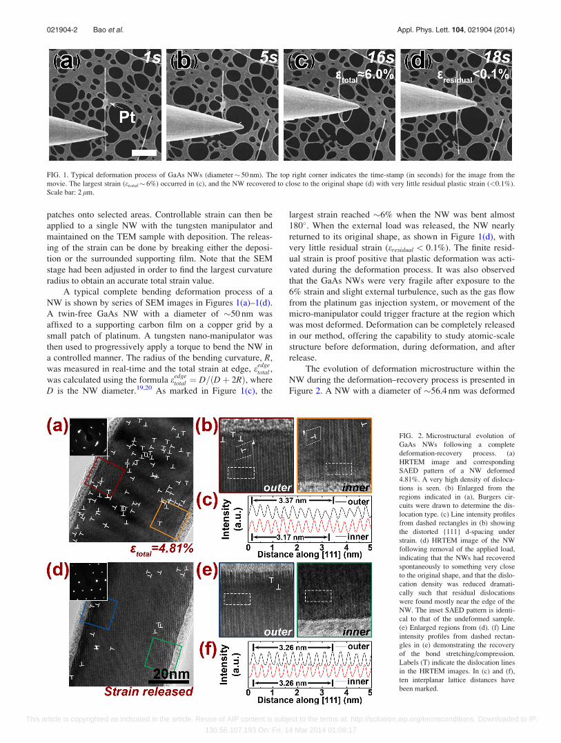
The evolution of deformation microstructure within the
NW during the deformation–recovery process is presented in
Figure 2. A NW with a diameter of �56.4 nm was deformed
FIG. 1. Typical deformation process of GaAs NWs (diameter� 50 nm). The top right corner indicates the time-stamp (in seconds) for the image from the
movie. The largest strain (etotal� 6%) occurred in (c), and the NW recovered to close to the original shape (d) with very little residual plastic strain (<0.1%).
Scale bar: 2 lm.
FIG. 2. Microstructural evolution of
GaAs NWs following a complete
deformation-recovery process. (a)
HRTEM image and corresponding
SAED pattern of a NW deformed
4.81%. A very high density of disloca-
tions is seen. (b) Enlarged from the
regions indicated in (a), Burgers cir-
cuits were drawn to determine the dis-
location type. (c) Line intensity profiles
from dashed rectangles in (b) showing
the distorted {111} d-spacing under
strain. (d) HRTEM image of the NW
following removal of the applied load,
indicating that the NWs had recovered
spontaneously to something very close
to the original shape, and that the dislo-
cation density was reduced dramati-
cally such that residual dislocations
were found mostly near the edge of the
NW. The inset SAED pattern is identi-
cal to that of the undeformed sample.
(e) Enlarged regions from (d). (f) Line
intensity profiles from dashed rectan-
gles in (e) demonstrating the recovery
of the bond stretching/compression.
Labels (T) indicate the dislocation lines
in the HRTEM images. In (c) and (f),
ten interplanar lattice distances have
been marked.
021904-2 Bao et al. Appl. Phys. Lett. 104, 021904 (2014)
This article is copyrighted as indicated in the article. Reuse of AIP content is subject to the terms at: http://scitation.aip.org/termsconditions. Downloaded to IP:
130.56.107.193 On: Fri, 14 Mar 2014 01:06:17

to a strain of �4.81%, representing the case of high strain de-
formation. The HRTEM image in Figure 2(a) reveals a super-
position of strain contrast and lattice fringe contrast. A
selected-area electron diffraction (SAED) pattern along the
1�10 zone axis in the inset of Figure 2(a) reveals that the dif-
fraction spots were elongated into arcs due to the continuous
pure bending deformation of the NW. Careful examination of
the crystal lattice fringes reveals an expansion at the outer-
side of the NW, and a compression at the inner-side, indicat-
ing the presence of elastic strain eelastic. The regions near the
inner and outer edges of the NW are enlarged in Figure 2(b)
and were used to measure the d-spacings of the {111} planes
along the NW axial direction. The line profiles extracted
from Fig. 2(b) are displayed in Figure 2(c). The spacing for
these {111} planes deviated substantially from the standard
(undeformed) value of 0.326 nm. At least 20 regions near ei-
ther the inner or outer edges at the most deformed regions
were measured to obtain reliable average values for the inner
and outer {111} plane d-spacing, dinner and douter, respec-
tively. These values were then used to calculate the elastic
strain eelastic caused by the lattice distortion using the equa-
tion: eelastic ¼ ðdouter � dinnerÞ=ðdouter þ dinnerÞ.12 This calcu-
lation revealed a key insight into the deformation
mechanism: the calculated elastic strain eelastic was �3.06%,
which is significantly smaller than the effective total strain at
d-spacing measurement regions, edtotal �3.61%. The differ-
ence must be made up by plastic deformation mediated by
discrete dislocation activity, displacive deformation twinning,
or stress-induced phase transformations.4
In fact, dislocations were observed extensively across the
deformed GaAs NW, as labelled (?) in Figure 2(a), and this
is clear evidence of dislocation-based deformation. Detailed
Burgers circuit analysis (Figure 2(b)) indicated that the dislo-
cations were all 1/2h110i type perfect dislocations. No nano-
twins, extended dislocation/stacking faults, or phase transfor-
mations were observed in the deformed NWs. It has been
reported that the nucleation and gliding of perfect disloca-
tions is responsible for plastic deformation in bulk GaAs21,22
and we propose that similar mechanisms dominate in the
present work. Therefore, the difference between total strain
and elastic stain made up by dislocation-based plastic strain
eplastic was determined by eplastic ¼ edtotal � eelastic. Hence,
eplastic is �0.6% for the NW when edtotal �3.61%. Therefore,
remarkably, Figure 2 provides direct evidence for the parallel
development of lattice- and dislocation-based deformation.
Figure 2(d) is a HRTEM image of the NW microstruc-
ture after the stress was released. The dislocation density
was observed to dramatically reduce, such that only a low
density of dislocations close to the edge region of the NW
remained, which is believed to be responsible for the small
residual strain eresidual(<0.1%) in the NW. The inset SAED
pattern reveals that the diffraction arcs transformed back to
diffraction spots and our HRTEM images, such as those pro-
vided in Figure 2(e), reveal that the crystal was restored to
high quality. Measurements of the {111} planar spacing,
illustrated by the line profile in Figure 2(f), confirmed that
the elastic deformation had fully recovered. Surprisingly, the
data indicate that the dislocation-based deformation has
almost completely recovered spontaneously, resembling an
elastic deformation process.
To further investigate the behaviour and interaction
between the elastic and plastic deformation, a number of
NWs were deformed to different strain levels. The structural
information was quantified and summarized in Table I. The
proportions of elastic and plastic strain components as a
function of total strain were presented in Figure 3. It is evi-
dent and striking that plastic strain eplastic develops in parallel
with elastic strain eelastic throughout the whole deformation
range.23 It is in sharp contrast to the conventional theory that
dislocation-based deformation is plastic and irreversible,1
and it is also in direct contradiction to the previous reports
that NWs are free of dislocations within the elastic regime.24
We propose that the nanoscale dimensions of the NWs
and the bending deformation mode are responsible for the si-
multaneous development of significant elastic and plastic
components of deformation from very low strains through to
fracture. The NW surface provides abundant sources for dis-
location nucleation due to the high surface to volume ratio in
these nanostructured materials, and this makes it possible to
produce a very high density of dislocations during deforma-
tion. The nucleation of dislocations at the surface or at grain
boundaries usually requires much lower stress than the self-
multiplication of dislocations by, e.g., Frank-Read sources in
nanocrystalline materials.25,26 For bending deformation of a
TABLE I. Summary of the microstructures and strains of NWs that have been deformed to or released from different strain levels.
(111) d-spacing (nm)
Total strain
at edge eedgetotal (%)
Total strain
at douter , dinner edtotal (%)
Elastic strain
eelastic (%)
Plastic
strain eplastic (%)
Outer
douter
Inner
dinner
Amount of dislocations/area
of measurement (nm2)
Dislocation
density q (1016 m�2)
1.50 1.13 0.79 0.34 0.3286 0.3234 21/2909.41 0.72
2.02 1.52 1.08 0.44 0.3293 0.322 29/2786.15 1.04
2.68 2.01 1.48 0.53 0.3292 0.3196 43/3091.46 1.39
3.23 2.42 1.83 0.59 0.332 0.3201 45/2874.24 1.57
3.88 2.91 2.36 0.55 0.3347 0.3193 64/2793.54 2.29
4.46 3.34 2.86 0.48 0.3366 0.3178 104/3158.81 3.29
4.81 3.61 3.06 0.55 0.3372 0.3174 106/2892.21 3.67
5.53 4.15 3.16 0.99 0.3376 0.3169 180/2980.54 6.04
Released from 2.02 <0.1% <0.1% <0.1% 0.3261 0.326 21/2853.69 0.74
Released from 4.81 <0.1% <0.1% <0.1% 0.3261 0.3259 11/2794.51 0.39
021904-3 Bao et al. Appl. Phys. Lett. 104, 021904 (2014)
This article is copyrighted as indicated in the article. Reuse of AIP content is subject to the terms at: http://scitation.aip.org/termsconditions. Downloaded to IP:
130.56.107.193 On: Fri, 14 Mar 2014 01:06:17

NW, the strain type changes from tension at one side to com-
pression at the other. The magnitude of strain gradually
decreases from the edge to centre, so that the stress mini-
mizes somewhere around the geometric axial centre of the
NW. Such a low stress area acts as a barrier to prevent dislo-
cations from passing through the whole NW. Therefore, dis-
locations generated on the crystalline surface and by
multiplication at regions with large strains build up rapidly
in the NW, reaching an extremely high dislocation density
on the order of 1016 m�2, which is nine orders of magnitude
higher than those usually observed in high-quality bulk
GaAs single crystals (105 m�2).27 Consequently, very signifi-
cant work hardening occurs because of the repulsive force
between dislocations with the same Burgers vectors and the
tangling of dislocations that glide on different slip systems.
This leads to a very rapid increase in the flow stress during
deformation, which is distinctive from conventional defor-
mation in coarse-grained materials where the increase in
flow stress is limited. The dramatic increase in flow stress
results in further increases in significant elastic strain after
the initiation of plastic deformation.
When the applied stress was removed, the large internal
stress was released through the recovery of elastic strain. The
internal stress is opposite in direction and approximately
equivalent in magnitude to the applied stress during the initial
recovery process. This internal stress spontaneously activated
and drove the dislocation motion backwards. It is known that
surfaces or grain boundaries of nanomaterials act as both the
source and sink of dislocations.26,28 Hence, the reverse
motion of the dislocations led to the reversal of the plasticity,
which has been described by molecular dynamics simula-
tions.14 In this study, it was shown that, at the point whereby
most of the dislocations had been annihilated at the surface,
the plastic strain was largely recovered, and so the process
resembled that of the recovery of elastic deformation.29
In summary, we have discovered the simultaneous oper-
ation of super elastic and dislocation-based plastic strain dur-
ing the bending deformation process of GaAs NWs, which is
in sharp contrast to deformation theory. It indicates that the
observed super-recoverable deformation10–17 is neither sim-
ply elastic nor reversibly plastic in nature, but the coupling
of both modes. In future, strain-stress curves need to be
measured, at the same time of the atomic-scale observation.
This work was supported in part by the Australian
Research Council. The authors acknowledge the facilities
and technical assistance from staff at the Australian
Microscopy & Microanalysis Research Facility node
(Sydney Microscopy & Microanalysis) at the University of
Sydney. Growth facilities used in this work were supported
by the Australian National Fabrication Facility (ANFF) at
the Australian National University.
1J. Lubliner, Plasticity Theory (DOVER Publication, Inc., 2008).2J. Li, K. J. Van Vliet, T. Zhu, S. Yip, and S. Suresh, Nature 418(6895),
307 (2002).3Y. Champion, C. Langlois, S. Gu�erin-Mailly, P. Langlois, J.-L.
Bonnentien, and M. J. H€ytch, Science 300(5617), 310 (2003).4L. Wang, P. Liu, P. Guan, M. Yang, J. Sun, Y. Cheng, A. Hirata, Z.
Zhang, E. Ma, M. Chen, and X. Han, Nat. Commun 4, 2413 (2013).5N. W. Moore, J. Luo, J. Y. Huang, S. X. Mao, and J. E. Houston, Nano
Lett. 9(6), 2295 (2009).6W. D. Callister and D. G. Rethwisch, Materials Science and Engineering:An Introduction, 6th ed. (Wiley India Pvt. Limited, 2009).
7B. Wu, A. Heidelberg, and J. J. Boland, Nature Mater. 4(7), 525 (2005).8M.-Feng Yu, B. S. Files, S. Arepalli, and R. S. Ruoff, Phys. Rev. Lett.
84(24), 5552 (2000).9C. Q. Chen and J. Zhu, Appl. Phys. Lett. 90(4), 043105 (2007).
10X. D. Han, K. Zheng, Y. F. Zhang, X. N. Zhang, Z. Zhang, and Z. L.
Wang, Adv. Mater. 19(16), 2112 (2007).11X. D. Han, Y. F. Zhang, K. Zheng, X. N. Zhang, Z. Zhang, Y. J. Hao, X.
Y. Guo, J. Yuan, and Z. L. Wang, Nano Lett. 7(2), 452 (2007).12X. Han, L. Kou, X. Lang, J. Xia, N. Wang, R. Qin, J. Lu, J. Xu, Z. Liao,
X. Zhang, X. Shan, X. Song, J. Gao, W. Guo, and D. Yu, Adv. Mater.
21(48), 4937 (2009).13Y.-B. Wang, L.-F. Wang, H. J. Joyce, Q. Gao, X.-Z. Liao, Y.-W. Mai, H.
H. Tan, J. Zou, S. P. Ringer, H.-J. Gao, and C. Jagadish, Adv. Mater.
23(11), 1356 (2011).14X. Li, Y. Wei, W. Yang, and H. Gao, Proc. Natl. Acad. Sci. U.S.A.
106(38), 16108 (2009).15G. Ziegenhain and H. M. Urbassek, Philos. Mag. Lett. 89(11), 717 (2009).16M. W. Barsoum, T. Zhen, S. R. Kalidindi, M. Radovic, and A. Murugaiah,
Nature Mater. 2(2), 107 (2003).17E. Demir and D. Raabe, Acta Mater. 58(18), 6055 (2010).18H. J. Joyce, Q. Gao, H. Hoe Tan, C. Jagadish, Y. Kim, X. Zhang, Y. Guo,
and J. Zou, Nano Lett. 7(4), 921 (2007).19L. L. D. Landau, E. M. Lifshits, A. M. Kosevitch, and L. P. Pitaevski K%,
Theory of Elasticity (Butterworth-Heinemann, 1986), Vol. 7.20L. Wang, K. Zheng, Z. Zhang, and X. Han, Nano Lett. 11(6), 2382 (2011).21T. Suzki, T. Yasutomi, T. Tokuoka, and I. Yonenaga, Philos. Mag. A
79(11), 2637 (1999).22S. Wang and P. Pirouz, Acta Mater. 55(16), 5500 (2007).23C. R. Weinberger and W. Cai, J. Mater. Chem. 22(8), 3277 (2012).24K. Zheng, X. Han, L. Wang, Y. Zhang, Y. Yue, Yan Qin, X. Zhang, and
Z. Zhang, Nano Lett. 9(6), 2471 (2009).25H. Van Swygenhoven, Science 296(5565), 66 (2002).26X. Z. Liao, Y. H. Zhao, S. G. Srinivasan, Y. T. Zhu, R. Z. Valiev, and D.
V. Gunderov, Appl. Phys. Lett. 84(4), 592 (2004).27P. Rudolph, Cryst. Res. Technol. 40(1-2), 7 (2005).28Z. Budrovic, H. Van Swygenhoven, P. M. Derlet, S. Van Petegem, and B.
Schmitt, Science 304(5668), 273 (2004).29J. Rajagopalan, J. H. Han, M. Taher, and A. Saif, Science 315(5820), 1831
(2007).
FIG. 3. Elastic and plastic strain components with respect to the total
strain, illustrating that elastic deformation and plastic deformation occur
simultaneously.
021904-4 Bao et al. Appl. Phys. Lett. 104, 021904 (2014)
This article is copyrighted as indicated in the article. Reuse of AIP content is subject to the terms at: http://scitation.aip.org/termsconditions. Downloaded to IP:
130.56.107.193 On: Fri, 14 Mar 2014 01:06:17
Top Related