


Sprachen
Seiten
Rechtliche

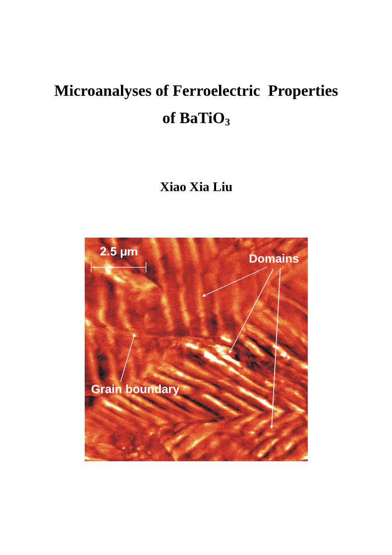
Microanalyses of Ferroelectric Properties
of BaTiO3
Xiao Xia Liu
Grain boundary
Domains
Microanalyses of Ferroelectric Properties of BaTiO3
Im Fachbereich Elektrotechnik und Informationstechnik der
Bergischen Universität-Gesamthochschule Wuppertal
Zur Erlangen des akademischen Grades eines
Doktor-Ingenieurs
eingereichte Dissertation
von
M.Sc. Eng. Xiao Xia Liu
aus
Chengdu, Sichuan
Volksrepublik China
Referent: Prof. Dr. rer. nat. Ludwig Josef Balk
Korreferenten: Prof. Dr.-Ing. Wolfgang Mathis und Prof. Qingrui Yin
Tag der mündlichen Prüfung: 27. 06. 2001
Acknowledgements___________________________________________________________________________
I
Acknowledgements
I would like to express my gratitude to Professor Dr. rer. nat. Ludwig Josef Balk for the
opportunity to carry out this work in Lehrstuhl für Elektronik, Bergische Universität
Gesamthochschule Wuppertal under his supervision. His continual interesting in my work, his
helpful discussions and encouragement, and his strict scientific point of view have
substantially contributed to the success of this work. Through his kindly help, I have obtained
the chance to cooperate and discuss with many other scientists in the areas of ferroelectric
materials and acoustic near-field imaging. I am very grateful for all the help which he has
given me during my stay in his Lehrstuhl.
I like to thank Prof. Dr.-Ing. Wolfgang Mathis and Prof. Qingrui Yin for co-examining this
work and much helpful advice. I am also very grateful to Prof. emeritus Dr. Klaus Dransfeld,
Fachbereich Physik, Universität Konstanz, who has read all the work carefully and gave me
much valuable advice.
The fruitful cooperation between the Lehrstuhl für Elektronik, BUGH Wuppertal and Lab. of
function ceramics, Shanghai Institute of Ceramics helps me a great deal to begin present work
and I am very grateful for all the help which Prof. Yin has given me.
I would like specially to thank Prof. Dr.-Ing. Volkert Hansen, Lehrstuhl für theoretische
Elektrotechnik, BUGH Wuppertal, for the theoretical support of the dissertation.
For the help from Dr. Ralf Heiderhoff, who has helped me to complete the whole work, I
would express my special thanks.
Many thanks also to Mrs. Mechthild Knippschild, who has continually help me in all the
respects.
I am also very grateful to my dear colleagues from the Lehrstuhl für Elektronik for the active
cooperation and support.
This work is partly aided from DFG (Deutsche Forschungsgemeinschaft) project
‘Nanocharakterisierung ferroelektrischer Domänen mittels Nahfeld-akustischer-
Rastermikroskopien’. I am grateful for this financial aid.
The encouragement and help from my family and, especially, from my wife Zhang Yuan,
have certainly contributed a great deal to the success of this work and I would like to express
my thanks wholeheartedly.
Contents___________________________________________________________________________
II
Microanalyses of ferroelectric properties of BaTiO3
Acknowledgements I
Contents II
Abbreviations, variables, symbols and constants VI
1 Introduction 1
1.1 Possible use of BaTiO3 as high density memory material 1
1.2 Present research of ferroelectric domains 2
1.3 Aim of present work 4
1.4 Structure 4
2 Theoretic description of electric and ferroelectric properties of BaTiO3 6
2.1 Definition of ferroelectric domain 6
2.2 State equations and thermodynamics of materials 6
2.2.1 The state equations 6
2.2.2 Linear state equations and Maxwell relations 8
2.2.3 Non-linear state and approximations 9
2.3 Theoretical description of BaTiO3 materials 9
2.3.1 Crystal symmetry and ferroelectric phases of BaTiO3 single crystal 9
2.3.2 General domain structures of BaTiO3 single crystal in tetragonal phase 11
2.3.3 General domain structures of BaTiO3 ceramics 13
2.4 Standard methods to image ferroelectric domains 16
2.4.1 Chemical etching 16
2.4.2 Powder methods 16
2.4.3 Optical polarizing microscopy 16
Contents___________________________________________________________________________
III
2.4.4 X-ray diffraction and topography 17
2.4.5 SEM 17
2.4.6 TEM 17
2.5 New methods and works to image ferroelectric domains 17
2.5.1 Optical methods based on the second-harmonic generation 17
2.5.2 Scanning electron environment microscopy 18
2.5.3 SEAM 18
2.5.4 Scanning near-field acoustic microscopy based on SPM techniques 18
2.6 Limitations 18
3 Electric mechanic coupling in typical Near-field Acoustic Microscopy 19
3.1 General equations of electric and mechanical couplings in solids 19
3.2 Direct imaging of electric and mechanic coupling 20
3.3 Combination of coupling methods to near-field methods 24
4 Scanning electron acoustic microscopy 33
4.1 Physical background, signal generation, and contrast mechanism 33
4.2 Experiment set-up 37
4.3 Discussion of signal to noise 38
5 Scanning near-field Acoustic Microscopy based on SPM 40
5.1 Physical background, signal generation, and contrast mechanism 40
5.1.1 Green´s function of the model 42
5.1.2 Modeling of thick samples 45
5.1.3 Modeling of thin samples or films 49
5.2 Experiment set-up 51
5.3 Discussion of signal to noise in SNAM 54
Contents___________________________________________________________________________
IV
6 Experiment procedure 56
6.1 Description of Specimen 56
6.2 Specimen preparation and treatment 56
6.3 Schemes of measurements 57
6.3.1 Choice of frequency 57
6.3.2 Amplitude and phase imaging 57
6.3.3 Variation of parameters 57
6.3.4 Dynamic imaging 58
7 Results 59
7.1 Single crystal 59
7.2 Ceramics 60
7.3 Films 62
7.4 The image mode comparison by SNAM 63
7.5 Dynamic study of ferroelectric domains structures 64
8 Discussion of both near-field acoustic techniques 70
8.1 Quality of imaging compared to other techniques 70
8.1.1 Speed of experiment 70
8.1.2 How quantitative 70
8.2 Comparison of SEAM and SNAM developed 71
8.2.1 Image comparison and analyses 71
8.2.2 Explanation by the present theory 76
9 Conclusions 80
10 Future aspect 82
11 Appendix 84

Contents___________________________________________________________________________
V
12 Reference 103
Publications and presentations 110
Abbreviations, variables, symbols and constants___________________________________________________________________________
VI
Abbreviations, variables, symbols and constants
AE Helmholtz free energy
+ia , −ia Amplitude of +z and -z transmitted longitudinal acoustic wave at ith medium
(i=1, 2, 3, which means near-field in the sample, area in the sample but outside
the near-field, and in the PZT transducer)
B�
, iB Magnetic flux density and its i´th component (i=1,2, 3 or x, y, z)
PZTPc , Pc Stiffened stiffness constant of PZT transducer and BaTiO3 single crystal
c�
, JIc , Elastic stiffness tensor, and its component with simplified suffix (I=1 to 6 and
J=1 to 6)
d Depth of near-field
d�
, Jid , Piezoelectric strain constant tensor, and its component with simplified suffix
(i=1,2, 3 or x, y, z and J=1 to 6)
wd , ´wd The domain width of fine and coarse grains in BaTiO3 ceramics
1D Sample thickness
2D Thickness of PZT transducer
D�
, D , iD Electric displacement, its magnitude, and its i´th component (i=1,2, 3 or x, y, z)
PZTze 3 Piezoelectric stress constant of PZT in z-direction.
e�
, Jie , Piezoelectric stress constant tensor, and the tensor component with simplified
suffix (i=1,2, 3 or x, y, z and J=1 to 6)
E�
, E , iE Electric field, its magnitude, and its i´th component (i=1,2, 3 or x, y, z)
sE Source electric field in near-field
F�
Body force
g Grain size in ceramics
Gb Gibbs energy
1Gb Elastic Gibbs energy
2Gb Electric Gibbs energy
G�
, iG Body torque and its i´th component,( i=1,2, 3 or x, y, z)
H�
, iH Magnetic field and its i´th component,( i=1,2, 3 or x, y, z)
HE Enthalpy
Abbreviations, variables, symbols and constants___________________________________________________________________________
VII
1HE Elastic enthalpy
2HE Electric enthalpy
cJ�
Conducting current
sJ�
Source currents
k Stiffened acoustic longitudinal wave number in BaTiO3 material
3k Stiffened acoustic longitudinal wave number in PZT transducer
P�
, P , iP Polarization vector, its magnitude, and its i´th component, (i=1,2, 3 or x, y, z)
Q Heat
esQ Electrostrictive coefficient
R Reflection constant at the boundary between the transducer and the back
electrode
s�
, JIs , Elastic compliance tensor, and its component with simplified suffix (I=1 to 6
and J=1 to 6)
S Entropy
T Temperature
t),(ru��
, iU Displacement field of a particle and its i´th components (i=1,2, 3 or x, y, z)
U Internal energy
v�
, iv Velocity of a particle and its i´th components (i=1,2, 3 or x, y, z)
outputV Output signal of the PZT transducer in near-field acoustic microscopy system
EW Electric work
mW Elastic work
x�
, ijx , Ix Strain tensor, its component, and component with simplified suffix (I=1 to 6)
X�
, ijX , IX Stress tensor, its component, and component with simplified suffix (I=1 to 6)
0Z Characteristic resistance of stiffened acoustic longitudinal wave in BaTiO3
single crystal with a monodomain
3Z Characteristic resistance of stiffened acoustic longitudinal wave in PZT
transducer
β Spatial periodical constant in z direction for Bessel´s function.
aβ The ratio of acoustic characteristic resistances in the sample and in PZT
Abbreviations, variables, symbols and constants___________________________________________________________________________
VIII
transducer (3
0
Z
Z).
ε�
, ji ,ε Permitivity tensor, and its component (i=1,2, 3 or x, y, z)
0ε Permitivity in vacuum (8.85418*10-12 As/Vm)
rε , riε Relative permittivity and relative permittivity of i´th layer of multilayer devices
PZTzzε Permittivity of PZT transducer in z-direction
Eη Backscattering coefficient
0µ Magnetic permeability in vacuum
ρ Density of a material (Kg/m3)
σ Noise of an equipment
ω Angular frequency of the system
EAI Electron Acoustic Image
SEM Scanning Electron Microscopy
SEAM Scanning Electron Acoustic Microscopy
SEI Secondary Electron Image
SNAM Scanning Near-field Acoustic Microscopy based on SPM
SIAM Scanning Ion Acoustic Microscopy
SPM Scanning Probe Microscopy
SPAM Scanning Photo Acoustic Microscopy
TEM Transmission Electron Microscopy
1. Introduction___________________________________________________________________________
1
1 Introduction
1.1 Possible use of BaTiO3 as a high density memory material
As early as 1950s when the demand for high-capacity computer memories came, ferroelectric
materials were intensively studied in the world, as they seemed to be prime candidates of new
materials for binary memories [1~3]. Later in the period of 1965 to 1975, tremendous efforts
were taken to develop ferroelectric-semiconductor memories by the use of a thin film of
semiconductors deposited on a bulk ferroelectric single crystal or ceramics materials. Though
the basic concept was valid, the instability of semiconductor thin films at that time did not
permit a viable memory to be built. In recent years, ferroelectric materials have attracted
much more attention because of the combination of their unique properties of spontaneous
polarization, i.e. the so-called ferroelectric domains of the materials, to CMOS techniques of
microelectronic industry [4, 5]. This combination has led to a large variety of new devices in
computer technology and transducing devices in electromechanic, electrochemic, electrooptic,
and acoustooptic fields.
Among all the ferroelectrics used during the development of modern memory devices, Barium
titanate (BaTiO3) material system is one of the most interesting ferroelectric material systems
up to now [2]. BaTiO3 single crystal has ferroelectric structures which are far simpler than
those of any other ferroelectrics known and thus provides a good base for the research and
understanding of whole ferroelectric phenomena. It is chemically and mechanically stable and
has a Curie temperature at about 120°C. Its hysteresis loop has rather sharp corners and a
good rectangular appearance. The value of its coercive field, measured at room temperature,
varies from a minimum of 5 kV/m to a maximum of 200 kV/m. The dielectric constant in the
direction of polarization ( 160≈ε rzz ) is much smaller than that perpendicular to it
( 2920≈ε rxx ) and they exhibit pronounced anomalies at the transitions from tetragonal to
orthorhombic and from orthorhombic to rhombohedral states. BaTiO3 polycrystalline
materials, the so-called ceramics, and their modifications offer even more applications in
various fields of engineering. It is easy to produce a hard BaTiO3 ceramics body by standard
sintering process and its body form can also be easily modified according to the industry
applications. The polarization direction of ceramics can be chosen as required. BaTiO3 thin
films, and other perovskite-type films such as Lead Zirconate Titanate (PZT), Strontium
Bismuth Titanate film (SBT) and so on, are intensively studied recently due to the integration
of these kind of films to CMOS circuits to produce various novel devices [4, 5]. In general,
1. Introduction___________________________________________________________________________
2
BaTiO3 and other perovskite type ferroelectric materials provide today an intensively active
research and application field. Even though its technical and commercial importance is
substantial, many breakthrough applications may still lie ahead of us.
1.2 Present research on ferroelectric domains
Although present applications of ferroelectric materials in the modern microelectronic
industry provide a great prospect and almost unlimited opportunities, there is much work to be
done [5~13]. Under macroscopic view, problems associated with application of BaTiO3 and
other current ferroelectrics are that their properties are often controlled by the contributions
from the so-called extrinsic effects which are responsible for polarization fatigue, aging,
frequency and field dependence of piezoelectric, elastic and dielectric properties. These
contributions are generally described as domain-wall effects [11~13]. The theoretical
treatment and experimental study on all these contributions present us a big challenge since
long time. Although substantial insights into the nature of ferroelectrics have been achieved,
all the theoretical models, most of which are phenomenological in nature, and experiment
results provide only a global or macroscopic view of the ferroelectrics. The present
application of ferroelectric materials combined with CMOS integrated circuits requires that
such problems be further studied under micrometer or even in difficult cases in nanometer
range. To keep pace with this new technological trend, non-destructive techniques to
investigate the ferroelectric domains under such spatial resolution must be developed.
Whereas the resolution of conventional optical microscopy is limited by the diffraction limit,
a number of non-destructive methods have been developed to study ferroelectric domains
[14~17]. Scanning electron microscopy (SEM) [14] is non-destructive but has a disadvantage
that contrast and resolution are dependent on time. In combination with acoustics, a non-
destructive technique with resolution and contrast independent of time, scanning electron
acoustic microscopy (SEAM), is used to visualize ferroelectric domains [15, 16].
Unfortunately, SEAM has only a resolution down to several micrometers due to the
interaction area formed by primary electrons injected into the sample. Although transmission
electron microscopy (TEM) [17] has a resolution down to nanometer range, this technique
needs a difficult sample preparation. Whether the preparation process would affect
ferroelectric domains is not clear. With the invention of scanning probe microscopy (SPM)
[18], non-destructive methods to image ferroelectric domains with submicrometer or
nanometer spatial resolutions have emerged recently [19~31]. F. Saurenbach, et. al. [19]
imaged the ferroelectric domain of GMO ( 342 )(MoOGd ) material system by the use of SPM
1. Introduction___________________________________________________________________________
3
in non-contact topography mode. R. Lüthi et. al. [20] presented ferroelectric contrast of
GASH ( OHSOAlNHC 22432 6)()( ⋅ ) and M.-K. Bae et. al. [21] of TGS
( 42322 )( SOHCOOHCHNH ⋅ ) materials by the use of contact topography mode of SPM
respectively. By applying an ac voltage and measuring of the first harmonic signal from
topography feedback, K. Franke et. al. [22] introduced imaging and modification of domains
in PZT film. For BaTiO3 material system, S.-I. Hamazaki et. al. [23] presented results by the
use of SPM contact topography mode on ferroelectric BaTiO3 single crystal and suggested
that the topography image of SPM is also ferroelectric domain image. L. M. Eng et. al. [24]
also showed results of domain contrast of ferroelectric BaTiO3 single crystal by the use of the
non-contact mode as well as the friction mode of SPM. Thereafter, there were mainly two
kinds of modes of SPM which were used frequently to image ferroelectric domains of BaTiO3
material system in the literatures. One is the so-called topography mode [23] and the other
piezoresponse mode [19, 22]. To study the contrast mechanism of both methods, A.
Gruverman et. al. [25] explained the contrast of topography mode of SPM on BaTiO3
revealed the difference of a-c domain boundary and piezoelectric response mode imaged the
c-c domain boundary.
Based on the principle of topography mode of SPM, some literatures [26-29] presented the
comparison of domain contrast from topography mode of SPM with the results from optical
microscopy, SEM, and surface potential microscopy based on SPM respectively. As the
topography mode of SPM requires an absolutely flat sample surface, this mode is impossible
to apply to image ferroelectric domains of samples with rough surface such as ceramics or
electronic devices non-destructively. A systematic analysis of contrast mechanism of this
mode and the contrast comparison to other techniques are also difficult.
At the base of the piezoelectric response mode of SPM, U. Rabe et. al. studied ferroelectric
domains from PZT ceramics [30]. L. Eng. et. al. presented the domain imaging on PZT and
BaTiO3 ceramics, writing and switching on a bulk BaTiO3 single crystal [31]. C. Harnagea
studied the domain imaging and switching on BaBi4Ti4O15 thin films [32]. In order to analyze
the ferroelectric domains by SPM quantitatively, C. Durkan et. al. presented a theoretical
model for the calculation of the electric field in the system of the piezoelectric response mode
of SPM [33]. Although the work [31] has made a comparison of the results by piezoelectric
response mode of SPM on BaTiO3 ceramics with results by chemical etching method, the
chemical etching method is actually a destructive method and an explanation of the contrast
difference between these two methods would be difficult. Meanwhile, although the theoretical
model [33] for the piezoelectric response mode of SPM on ferroelectric films has been
1. Introduction___________________________________________________________________________
4
introduced, from our point of view, the theoretical treatment of the model can not be the right
theoretical analytic method. Neither can the model be used systematically to analyze electric
field distributions in different samples, such as bulk materials, thin films or multilayered
films. Electric and mechanic field distributions and the energy exchange between them in the
system of piezoelectric response mode of SPM remain unsolved up to today.
1.3 Aim of present work
In this work, a new set-up, Scanning near-field Acoustic Microscopy based on SPM (SNAM),
is developed to image ferroelectric domains of both single crystal and ceramics of BaTiO3
material system [34, 35, 36]. The results of ceramics are compared to the results at identical
areas of the same ceramics by another established non-destructive acoustic technique,
Scanning Electron Acoustic Microscopy (SEAM) [15, 16, 37]. Based on the classic
phenomenological theory, a theoretical model for both the SNAM set-up developed and the
SEAM on ferroelectric BaTiO3 materials is grounded. The ferroelectric domains are analyzed
quantitatively according to the model established. Different modes based on SPM are also
compared. The ferroelectric domains of BaTiO3 ceramics are imaged temporally, thermally
dynamically, and electrically dynamically [37].
As shown at the end of this work, both SEAM and SNAM techniques are complementary
tools for the future research and application of ferroelectric materials and devices. The
theoretical and experimental methods presented can further be applied to other near-field
acoustic microscopy techniques and other ferroelectric materials.
1.4 Structure
This work is mainly divided into the following chapters: Chapter 2 will mention briefly main
theories on electric and ferroelectric properties of BaTiO3 crystal and ceramics. The typical
methods and new works to image ferroelectric domains are also discussed. From the
discussion, two near-field techniques, SEAM and SNAM, are chosen as examples for the
further discussion. Chapter 3 is concentrated to electric and mechanic coupling of near-field
acoustic microscopy and a BaTiO3 single crystal with a monodomain structure is chosen as an
example to simplify the discussion. The contrast mechanism for both near-field acoustic
microscopy techniques is analyzed. Chapter 4 treats the physical background, signal
generation, contrast mechanism, and experiment set-up of SEAM on BaTiO3 material system.
Chapter 5 discusses the physical background, signal generation, contrast mechanism, and
experiment set-up of SNAM developed in this work on BaTiO3 material system. Then the
comparison of the contrast of the developed system to that of another mode of SPM, the so-
1. Introduction___________________________________________________________________________
5
called piezoelectric response mode, is studied. Finally the domain structures of BaTiO3
ceramics are studied dynamically. Chapter 6 discusses the experimental details in this work
and Chapter 7 presents some typical experiment results. Chapter 8 discusses the
complementary study by both near-field techniques on identical areas and presents an
explanation for the study at the base of the theoretical model grounded. A small summary will
be given in Chapter 9 and future prospects will be briefly mentioned in Chapter 10. All
theoretical calculations will be presented in the Appendix in detail.
2. Theoretic description of electric and ferroelectric properties of BaTiO3
___________________________________________________________________________
6
2 Theoretic description of electric and ferroelectric properties of BaTiO3
2.1 Definition of ferroelectric domains
Ferroelectric domains are referred to as volumes of spontaneous polarization in ferroelectrics
whose polarization can be changed by an electric field [1, 3]. The boundaries separating
domains are referred as domain walls. If a ferroelectric crystal is brought to the ferroelectric
state from paraelectric phase by decreasing temperature, the electrostatic interaction on the
surface and the inhomogeneity of stress in the materials affect the internal energy and thus
result in ferroelectric domains in ferroelectric phase. As for the polycrystal materials, the
domain equilibrium size [5~7] in any case is determined by the minimum in energy which is
necessary to preserve the shape of the grain when passing from the paraelectric to
ferroelectric states. As this ferroelectric phase change is related to electric, elastic, and
thermal energy changes, it is necessary to discuss energy functions and state equations of
materials at first.
2.2 State equations and thermodynamics of materials
2.2.1 The state equations
According to the thermodynamics, it is assumed that the thermal, elastic, and dielectric
behavior of a homogeneous dielectric is fully described by six variables: temperature T ,
entropy S, Strain x�
, Stress X�
, electric field E�
, and electric displacement D�
.
According to the first law of thermodynamics, the change in internal energy U (per unit
volume) when an infinitesimal quantity of heat dQ is received by a unit volume of dielectric
is given by:
dWdQdU += Eq.2-1
where dW is the work done on this same volume during the resulting quasi-static
transformation.
Assuming reversibility, the second law of thermodynamics relates dQ to the absolute
temperature and entropy in the form:
TdSdQ = Eq.2-2
2. Theoretic description of electric and ferroelectric properties of BaTiO3
___________________________________________________________________________
7
If only the mechanic and electric work are related, the first law of thermodynamics is:
mE dWdWdQdU ++= Eq.2-3
Where EdW and mdW are electric and elastic works, which can be written as:
EdW = iidDE
mdW = II dxX Eq.2-4
Here the Voigt´s notations (‘I’ means the tensor suffix and is from 1 to 6; ‘i’ means vector
suffix and is from 1 to 3.) are used to express tensors and vectors [39]. This method provides
some briefness for the expression of tensors and vectors. Some work used the same simplified
notation for tensor but different notations for vectors (‘i’ means vector suffix and is x, y, or z.)
[53] and this notation method is closer to the custom of electrical engineers. For the
discussion of the present work, both notation methods are used interchangeably, as the
notation of ‘i’ from both notation methods gives the same physical meaning. The Einstein
notation for the summation of vectors and tensors is also used.
To describe a system, eight different thermodynamic potentials are defined:
Helmholtz free energy: TSUAE −=
Enthalpy: iiII DExXUHE −−=
Elastic enthalpy: II xXUHE −=1
Electric enthalpy: ii DEUHE −=2
Gibbs free energy: iiII DExXTSUGb −−−=
Elastic Gibbs energy: II xXTSUGb −−=1
Electric Gibbs energy: ii DETSUGb −−=2 Eq.2-5
The elastic Gibbs energy 1Gb is frequently used in the literatures on ferroelectric phase
transitions. By choosing ),,( iI DXT as independent variables, the differential form of elastic
Gibbs energy can be written as:
2. Theoretic description of electric and ferroelectric properties of BaTiO3
___________________________________________________________________________
8
1dGb = iiII dDEdXxSdT +−− Eq.2-6
The other variables can be calculated as:
DXT
GbS
��
,
1
∂
∂−= , =IxDTIX
Gb�
,
1
∂∂− , iE
XTiD
Gb�
,
1
∂∂= Eq.2-7
2.2.2 Linear state equations of materials and Maxwell relations
If only linear forms will be calculated, the other variables of state can be calculated as:
dTT
SdS
XD��
,
∂∂= I
TDI
dXX
S
,�
∂∂+ i
TXi
dDD
S
,�
∂∂+ Eq.2-8
dTT
xdx
XD
II
��
,
∂∂
= I
TDI
I dXX
x
,�
∂∂
+ i
TXi
I dDD
x
,�
∂∂
+ Eq.2-9
dTT
EdE
XD
ii
��
,
∂∂
= I
TDI
i dXX
E
,�
∂∂
+ i
TXi
i dDD
E
,�
∂∂
+ Eq.2-10
The coefficients in the above equations are called compliances. In the same way, by choosing
different variables, different coefficients can be obtained. For the cases of isothermal (or
adiabatic), the equations can be generally described as:
TDJII cdX ,
,
�
= Jdx TjIh ,
~− jdD Eq.2-11
=idE TJih ,− Jdx +
Txjik ,
,
�
jdD Eq.2-12
TDJII sdx ,
,
�
= JdX +T
jIg ,~
jdD Eq.2-13
=idE TJig ,− JdX +
TXjik ,
,
�
jdD Eq.2-14
TEJII sdx ,
,
�
= JdX +T
jId ,
~jdE Eq.2-15
=idD TJid , JdX +
TXji,
,
�
ε jdE Eq.2-16
TEJII cdX ,
,
�
= Jdx TjIe ,
~− jdE Eq.2-17
2. Theoretic description of electric and ferroelectric properties of BaTiO3
___________________________________________________________________________
9
=idD TJie , Jdx +
TXji,
,
�
ε jdE Eq.2-18
The last four equations are called piezoelectric stain and stress equations. As the isothermal
(or adiabatic process) will be usually discussed, the sign of constant T in the expression above
is omitted in the following discussion.
2.2.3 Non-linear state and approximations
The linear state equations above are described by the linear differential equations. But some
of the most important characteristics of ferroelectrics such as hysteresis loop, electrostriction,
polarization reverse and so on are fundamentally non-linear effects and hence require an
extension of the theory to higher orders. Generally the nonlinear state of materials can be
described by expansion of the state equations to arbitrarily high orders to define the non-linear
compliances, but the practical difficulties of tensor mathematics at high orders make it almost
impossible. In order to show the physical meanings more clearly, some approximations have
to be added:
• The prototype state is iD = IX =0, which means the original state has neither polarization
nor stress;
• The state with polarization has its polarization along one of the crystallographic axes;
• Non-polar state is centrosymmetric.
Under the assumption above, the elastic free energy can be expanded as Taylor series [5, 40]:
+α+α+α+= 63
42
21101 6
1
4
1
2
1)( DDDTGbGb 2
2
1sX + �+2XDQes Eq.2-19
Here, for the sake of simplicity, the suffixes of vectors and tensors are omitted as it will not
change the physical meaning of the expression. In the following discussion, the same
simplicity is also used until it is necessary to analyze the components of vectors and tensors.
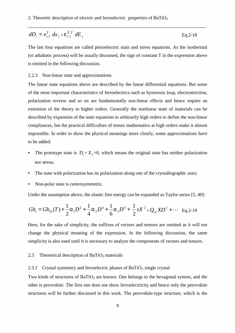
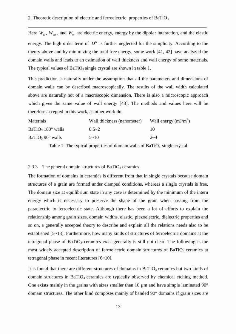
2.3 Theoretical description of BaTiO3 materials
2.3.1 Crystal symmetry and ferroelectric phases of BaTiO3 single crystal
Two kinds of structures of BaTiO3 are known. One belongs to the hexagonal system, and the
other is perovskite. The first one does not show ferroelectricity and hence only the perovskite
structures will be further discussed in this work. The perovskite-type structure, which is the
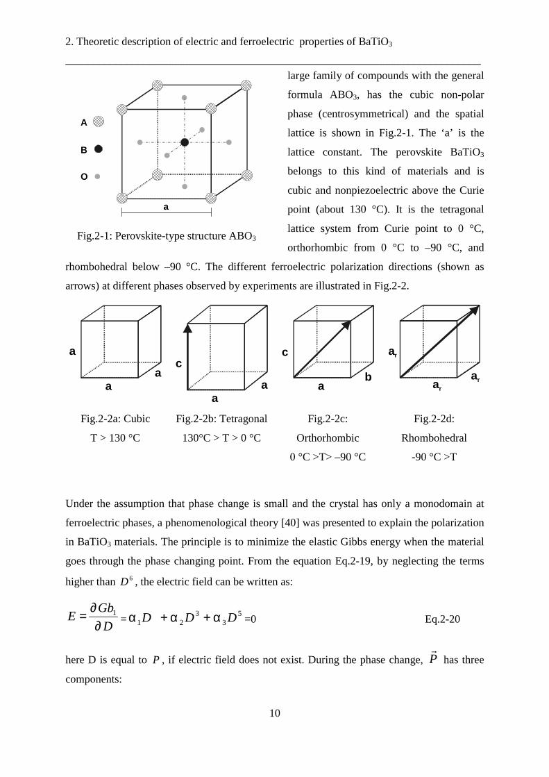
2. Theoretic description of electric and ferroelectric properties of BaTiO3
___________________________________________________________________________
10
large family of compounds with the general
formula ABO3, has the cubic non-polar
phase (centrosymmetrical) and the spatial
lattice is shown in Fig.2-1. The ‘a’ is the
lattice constant. The perovskite BaTiO3
belongs to this kind of materials and is
cubic and nonpiezoelectric above the Curie
point (about 130 °C). It is the tetragonal
lattice system from Curie point to 0 °C,
orthorhombic from 0 °C to –90 °C, and
rhombohedral below –90 °C. The different ferroelectric polarization directions (shown as
arrows) at different phases observed by experiments are illustrated in Fig.2-2.
a
a
a
a
c
a a
c
b
ar
ar
ar
Fig.2-2a: Cubic
T > 130 °C
Fig.2-2b: Tetragonal
130°C > T > 0 °C
Fig.2-2c:
Orthorhombic
0 °C >T> –90 °C
Fig.2-2d:
Rhombohedral
-90 °C >T
Under the assumption that phase change is small and the crystal has only a monodomain at
ferroelectric phases, a phenomenological theory [40] was presented to explain the polarization
in BaTiO3 materials. The principle is to minimize the elastic Gibbs energy when the material
goes through the phase changing point. From the equation Eq.2-19, by neglecting the terms
higher than 6D , the electric field can be written as:
D
GbE
∂∂= 1
=5
33
21 DDD α+α+α =0 Eq.2-20
here D is equal to P , if electric field does not exist. During the phase change, P�
has three
components:
A
B
O
a
Fig.2-1: Perovskite-type structure ABO3
2. Theoretic description of electric and ferroelectric properties of BaTiO3
___________________________________________________________________________
11
== PD��
xP xa�
+ yP ya�
+ zP za�
Eq.2-21
According to the Eq.2-20, the ( xP , yP , zP ) can be solved for four possibilities:
a) ( xP , yP , zP )=0, aGb =0
b) xP = yP =0, zP ≠ 0, bGb ≠ 0 Tetragonal state, 130°>T>0°
c) xP =0, yP = zP ≠ 0, cGb ≠ 0 Orthorhombic state, 0°>T>-90°
d) xP = yP = zP ≠ 0, dGb ≠ 0 Rhombohedral state, -90°>T
Here aGb , bGb , cGb , and dGb are the Gibbs energy at the corresponding states. These
four states before and after spontaneous polarization describe the facts which have been
observed in experiments, as shown above in Fig.2-2.
To the same approximation, if X and E do not exist during the phase change, according to
Eq.2-7 and Eq.2-19, it must be noted that the spontaneous strain:
x =X
Gb
∂∂ 1
=2PQes Eq.2-22
Here esQ is the electrostrictive coefficient. Because the electrostrictive effect exists in all
materials, it means that spontaneous strain always accompanies spontaneous polarization.
The piezoelectric voltage coefficient is:
DX
Gbg
∂∂∂= 1
2
=2 esQ P Eq.2-23
The piezoelectric strain constant in the direction of polarization can be written as [5]:
PQd esz ε= 23 Eq.2-24
That means that piezoelectric effect of ferroelectric materials at monodomain state is
proportional to spontaneous polarization through electrostrictive constant.
2.3.2 The general domain structures of BaTiO3 single crystal in tetragonal phase
In reality, the monodomain state of material at ferroelectric phase, which is assumed above
2. Theoretic description of electric and ferroelectric properties of BaTiO3
___________________________________________________________________________
12
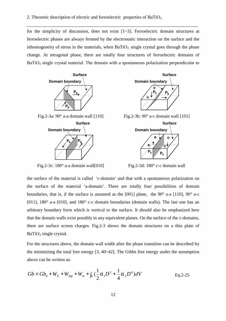
for the simplicity of discussion, does not exist [1~3]. Ferroelectric domain structures at
ferroelectric phases are always formed by the electrostatic interaction on the surface and the
inhomogeneity of stress in the materials, when BaTiO3 single crystal goes through the phase
change. At tetragonal phase, there are totally four structures of ferroelectric domains of
BaTiO3 single crystal material. The domain with a spontaneous polarization perpendicular to
the surface of the material is called ‘c-domain’ and that with a spontaneous polarization on
the surface of the material ‘a-domain’. There are totally four possibilities of domain
boundaries, that is, if the surface is assumed as the [001] plane, the 90° a-a [110], 90° a-c
[011], 180° a-a [010], and 180° c-c domain boundaries (domain walls). The last one has an
arbitrary boundary form which is vertical to the surface. It should also be emphasized here
that the domain walls exist possibly in any equivalent planes. On the surface of the c-domains,
there are surface screen charges. Fig.2-3 shows the domain structures on a thin plate of
BaTiO3 single crystal.
For the structures above, the domain wall width after the phase transition can be described by
the minimizing the total free energy [3, 40~42]. The Gibbs free energy under the assumption
above can be written as:
∫ α+α++++= VmdipE dVDDWWWGbGb )4
1
2
1( 4
22
10 Eq.2-25
Pa
Pa
Surface
Domain boundary
Pc Pa
Surface
Domain boundary
Fig.2-3a: 90° a-a domain wall [110] Fig.2-3b: 90° a-c domain wall [101]
Surface
Domain boundary
Pa Pa
Surface
Domain boundary
Pc Pc
Fig.2-3c: 180° a-a domain wall[010] Fig.2-3d: 180° c-c domain wall
2. Theoretic description of electric and ferroelectric properties of BaTiO3
___________________________________________________________________________
13
Here EW , dipW , and mW are electric energy, energy by the dipolar interaction, and the elastic
energy. The high order term of 6D is further neglected for the simplicity. According to the
theory above and by minimizing the total free energy, some work [41, 42] have analyzed the
domain walls and leads to an estimation of wall thickness and wall energy of some materials.
The typical values of BaTiO3 single crystal are shown in table 1.
This prediction is naturally under the assumption that all the parameters and dimensions of
domain walls can be described macroscopically. The results of the wall width calculated
above are naturally not of a macroscopic dimension. There is also a microscopic approach
which gives the same value of wall energy [43]. The methods and values here will be
therefore accepted in this work, as other work do.
Materials Wall thickness (nanometer) Wall energy (mJ/m2)
BaTiO3 180° walls 0.5~2 10
BaTiO3 90° walls 5~10 2~4
Table 1: The typical properties of domain walls of BaTiO3 single crystal
2.3.3 The general domain structures of BaTiO3 ceramics
The formation of domains in ceramics is different from that in single crystals because domain
structures of a grain are formed under clamped conditions, whereas a single crystals is free.
The domain size at equilibrium state in any case is determined by the minimum of the intern
energy which is necessary to preserve the shape of the grain when passing from the
paraelectric to ferroelectric state. Although there has been a lot of efforts to explain the
relationship among grain sizes, domain widths, elastic, piezoelectric, dielectric properties and
so on, a generally accepted theory to describe and explain all the relations needs also to be
established [5~13]. Furthermore, how many kinds of structures of ferroelectric domains at the
tetragonal phase of BaTiO3 ceramics exist generally is still not clear. The following is the
most widely accepted description of ferroelectric domain structures of BaTiO3 ceramics at
tetragonal phase in recent literatures [6~10].
It is found that there are different structures of domains in BaTiO3 ceramics but two kinds of
domain structures in BaTiO3 ceramics are typically observed by chemical etching method.
One exists mainly in the grains with sizes smaller than 10 µm and have simple laminated 90°
domain structures. The other kind composes mainly of banded 90° domains if grain sizes are
2. Theoretic description of electric and ferroelectric properties of BaTiO3
___________________________________________________________________________
14
larger than 20 µm [6, 7].
For the first kind of domains in BaTiO3 ceramics, according to the same phenomenological
theory above, some work to calculate the relationship between the domain width and the grain
size is presented. The domain width ( wd ) with respect to the grain size g is calculated as [7]:
2/1)(gd w ∝ Eq.2-26
The typical width of 90° domains is several hundred nanometers.
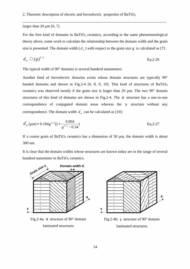
Another kind of ferroelectric domains exists whose domain structures are typically 90°
banded domains and shown in Fig.2-4 [6, 8, 9, 10]. This kind of structures of BaTiO3
ceramics was observed mostly if the grain size is larger than 20 µm. The two 90° domain
structures of this kind of domains are shown in Fig.2-4. The α structure has a one-to-one
correspondence of conjugated domain areas whereas the γ structure without any
correspondence. The domain width ´wd can be calculated as [10]:
´wd (µm) )
34.0
004.01(104.0
3/13/1
−+≈
gg Eq.2-27
If a coarse grain of BaTiO3 ceramics has a dimension of 50 µm, the domain width is about
300 nm.
It is clear that the domain widths whose structures are known today are in the range of several
hundred nanometer in BaTiO3 ceramics.
X
Y
Grain size g Domain width dw
X
Y
Fig.2-4a: α structure of 90° domain
laminated structures
Fig.2-4b: γ structure of 90° domain
laminated structures
2. Theoretic description of electric and ferroelectric properties of BaTiO3
___________________________________________________________________________
15
Other types of domains of ferroelectric BaTiO3 ceramics, such as those with no relationship to
grain sizes, because of their complex natures and P�
⋅∇ 0≠ in the bulk materials, are less
studied and little documented. The complicated relationships among domain structures,
temperatures, electric and ferroelectric properties, and grain sizes are usually studied
experimentally.
In recent literatures, domains and their effects on macroscopic properties of ferroelectric
ceramics are studied experimentally. The dielectric, elastic, piezoelectric properties of
ferroelectric ceramics are described by recent studies as the sum of intrinsic and extrinsic
properties [11~13]. The intrinsic property of ferroelectric materials is defined as properties of
the material with a monodomain and the extrinsic property the contribution from other parts
of the material, such as domain wall movements. The dielectric constant ε , piezoelectric
constant d , and elastic compliance s , are therefore written as follows:
ε�
exin ε+ε=��
d�
exin dd��
+=
s�
exin ss�� += Eq.2-28
The subscripts ‘in’ and ‘ex’ denote the intrinsic and extrinsic contributions.
Although a model for ferroelectric ceramics to describe the relationship between the intrinsic
and extrinsic contributions under weak fields has only been presented recently, a generally
accepted theory even by phenomenological methods is still not well developed [13]. The
piezoelectric relation of Rayleigh model for ferroelectric ceramics will be accepted in this
work [12]:
max1103 7.112 XPQd zrzzz +εε= Eq.2-29
where 3zd is the actual piezoelectric constant for ferroelectric ceramics; 11Q , zP , and maxX
are the electrostrictive constant, spontaneous polarization, and the maximum value of
periodical stress by external fields. The first term is the so-called intrinsic piezoelectric effect.
The detailed discussion of Rayleigh model and the dielectric and elastic relations will not be
mentioned here for the simplicity of our discussion of the near-field acoustic imaging in this
work.
2. Theoretic description of electric and ferroelectric properties of BaTiO3
___________________________________________________________________________
16
2.4 Standard methods to image ferroelectric domains
The microscopic characterization of ferroelectric domains is always a challenge for scientists
in this area. The classic work will be shortly mentioned here.
2.4.1 Chemical etching
This is the earliest way to visualize ferroelectric domains in ferroelectrics. Concentrated HCl
etches the a- and c-domains of BaTiO3 at different rates, and also +c and –c ends of the
domains, so that a different texture or shade appears when the etched specimen is examined
under a microscope [3]. It is a destructive method and how such an etching process influences
subsequent domains is also not documented.
2.4.2 Powder methods
This method uses colloidal suspensions of charged particles, which deposit preferentially on
either positive or negative ends of domains. It is a nondestructive method, but the difficult
choice of powders and the limited resolution and contrast makes it not feasible for industry.
Furthermore it is also very difficult to use it on materials with rough surfaces because the
surface topography will add to the contrast of powder contrast.
2.4.3 Optical polarising microscopy
To observe ferroelectric domians, the usual method is the optical microscopy with a polariser
and an analyzer. When the polariser and analyzer of the optical microscope are crossed at 90°
orientations, no light is transmitted through microscope unless the specimen inserted produces
a phase change between two differently polarized light rays passing through it. If it is
assumed that the optical axis is also polar axis, for BaTiO3, the c-domains will not change the
phase of the light and appear dark. The a-domains will change the phase of the light and
appear bright. It is also shown that one can image +c and –c domains by studying the strain-
induced biaxial material along each domain wall [44]. Unfortunately, the optical method is
limited by the diffraction limit of the focused light beam and the resolution is only about half
of the light wavelength used. It will be difficult to obtain the resolution in submicrometer or
nanometer range. Moreover, although this technique is the most common method to image
ferroelectric domains of single crystals, it is very difficult to image ferroelectric domains of
ceramics non-destructively, as the surface has to be polished to get sufficient contrast. To
what extend the polishing process changes the domain structures is still not well studied.
2. Theoretic description of electric and ferroelectric properties of BaTiO3
___________________________________________________________________________
17
2.4.4 X-ray diffraction and topography
Both methods require the polishing of the surface to increase the image contrast. The X-ray
diffraction method is a typical method for the research of single crystals and films. It is an
indirect method and by analyzing the diffraction angle, the surface polarization can be
indirectly shown [44].
The contrast mechanism of X-ray topography [3, 45, 46] is that the anomalous dispersion of
X-rays causes a difference between the X-ray intensity reflected from the positive and
negative ends of domains. By using wavelengths close to an absorption edge of a constituent
element this difference can be maximized. The domains in BaTiO3 have been successfully
observed by this methods. Although it is a classic method to analyze ferroelectric domains, its
resolution and requirement of surface roughness limit its application.
2.4.5 SEM
Methods using SEM to observe domains are also presented [14]. The principle is based on
changes of surface electric potential from domains to domains which will be imaged in
secondary electron image. It has only a resolution of about several µm. The stability of the
contrast of this method and its comparison with other techniques needs to be studied.
2.4.6 TEM
This method is the most powerful method to observe ferroelectric domains [15, 47, 48]. It
presents a good resolution down to several nanometers or lower. But the sample preparation
of this method is difficult and destructive, and whether the sample preparation would change
the domains on the sample surface requires further investigation.
2.5 New methods and works to image ferroelectric domains
There are a large amount of literature which reported new techniques to image ferroelectric
domains. It is but impossible to mention all the techniques here. Only some typical techniques
will be briefly discussed in the followings.
2.5.1 Optical methods based on the second-harmonic generation
This technique can be used in principle for any crystal which can be matched in phase for
second-harmonic generation with light propagation close to the polar axis [3, 49, 50]. Some
work have also combined this technique with near-field optical methods [51]. Although some
results on single crystals are presented, this method has no advantages for the analyses of
2. Theoretic description of electric and ferroelectric properties of BaTiO3
___________________________________________________________________________
18
BaTiO3 ceramics which are usually very rough at the surface and opaque.
2.5.2 Scanning Electron Environment Microscopy
This is a relatively new methods [52] and the principle is almost similar as that of SEM to
image ferroelectric domains. But, because it uses a special environment in the vacuum
chamber in SEM, the image contrast can be held for several hours. For crystal materials, some
results have been obtained but those on ceramics have not been presented up to now. Its
resolution is also in the range of several micrometer.
2.5.3 SEAM
This method uses a very thin gold film on the surface of the material to avoid surface charging
effects and the results of both single crystal and ceramics are shown [16, 17, 37, 38]. The
detailed description of the method will be discussed later in Chapter 4.
2.5.4 Scanning near-field acoustic microscopy based on SPM techniques
The name, Scanning near-field acoustic microscopy (SNAM), was introduced in 1989 [64]
and there are a lot of developments with this technique up to today. For the sake of simplicity
of the present work, the name SNAM would be used to mean all the systems based on SPM
techniques to image acoustic properties. These methods are new and there is still a lot of
discussion on it. To characterize the contrast of SNAM techniques on BaTiO3 materials,
although different set-ups and different results have been presented as discussed in Chapter 1,
a new nondestructive method with nanometer resolution based on the combination of SPM
and acoustic microscopy is introduced in this work [34~37]. This method provides a
possibility to compare contrast of SEAM and SNAM techniques both theoretically and
experimentally. A detailed description of this set-up of SNAM to image ferroelectric domain
structures of BaTiO3 will be presented later in Chapter 5.
2.6 Limitation: quasi-static
For all the discussion above, one of the most fundamental assumption is used. The discussion
and imaging of ferroelectric domains are only discussed quasi-statically. The high frequency
properties of ferroelectric domains will not be discussed here because the imaging mechanism
of SEAM and SNAM will be mainly concerned in this work.
3. Electric and acoustic coupling in Scanning Near-field Acoustic Microscopy___________________________________________________________________________
19
3 Electric and acoustic coupling in Scanning Near-field Acoustic Microscopy
3.1 General equations of electric and acoustic couplings in solids
Electrical and acoustic coupling equations are briefly discussed in Chapter 2. Their
application combined with the classic electromagnetic and acoustic theories in actual near-
field acoustic microscopy systems is discussed here. From Eq.2-15 to Eq.2-18, the
piezoelectric strain and stress equations can be obtained by integration under the assumption
of zero values of all the field components at equilibrium state:
EJII sx
�
,= JX + jId ,
~jE Eq.3-1
=iD Jid , JX +X
ji
�
,ε jE Eq.3-2
EJII cX
�
,= Jx - jIe ,~
jE Eq.3-3
=iD Jie , Jx +X
ji
�
,ε jE Eq.3-4
Eq.3-1 and Eq.3-2 are piezoelectric strain equations and Eq.3-3 and Eq.3-4 stress equation.
The constant Jid , ( jId ,
~ constants of the transposed matrix) is piezoelectric strain constant and
Jie , ( jIe ,~ constants of the transposed matrix) piezoelectric stress constant.
The Maxwell equations to describe general electric and magnetic phenomena are [53]:
×∇ E�
= t
B
∂∂−�
Eq.3-5
×∇ H�
= t
E
∂∂�
+ cJ�
+ sJ�
Eq.3-6
where E�
and H�
are electric and magnetic field; D�
and B�
are electric displacement and
magnetic flux density; cJ�
and sJ�
are conducting and source currents.
Acoustic vibrations or waves in solid materials are governed by the Newton´s law for
dynamic motion under the classic view. Motions can be classified into two kinds: translational
and rotational motions.
For translational motions, the Newton´s law can be written as:
Fu
X���
−∂∂ρ=⋅∇
2
2
tEq.3-7
where u�
is the displacement field of particles in materials and F�
is an external body force.
3. Electric and acoustic coupling in Scanning Near-field Acoustic Microscopy___________________________________________________________________________
20
For the simplicity of discussion below, the velocity of particles ( v�
=t
u
∂∂ �
) is used and Eq.3-7
can be written as:
Fv
X���
−∂∂ρ=⋅∇
tEq.3-8
For rotational motions, the Newton´s law can be written as:
0=+− kijji GXX Eq.3-9
ijX and ijX are stress components and kG is body torque.
Under the small signal and weak piezoelectric coupling approximations, the body torque can
be neglected even if most of the materials of piezoelectric transducers are frequently
ferroelectric, so that the stress tensor is always a symmetric tensor. Combining the
electromagnetic and acoustic equations with the piezoelectric equations, one can obtain the
general coupled equations for fields and waves in piezoelectric materials as [53]:
2
2
t
v
∂∂ρ
�
( )vc s
�� ⋅∇⋅∇= :
∂∂⋅⋅∇−
t
Ee
��
t
F
∂∂+�
Eq.3-9
2
2
0 t
Es ∂
∂⋅εµ�
�E�
×∇×−∇=t
ve s ∂
∂∇µ−�
�:0 t
J s
∂∂µ−�
0 t
J c
∂∂µ−�
0 Eq.3-10
The equations above are theoretically brief but physical meanings are not easy to see directly.
In order to study the contrast mechanism in near-field acoustic systems clearly, it is easier to
analyze the coupling by separating Eq.3-9 and Eq.3-10 to different coupled groups. It is also
necessary that the system be simplified so that analytical methods can be used.
3.2 Direct imaging of the coupling by a transducer
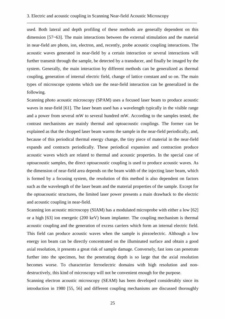
A general set-up of near-field acoustic microscopy is shown in Fig.3-1. In near-field area, if
there is a certain stimulation which produces acoustic vibrations, the vibrations will transmit
to a transducer which is in solid contact with the sample and will change the acoustic
vibrations into electric signals. To understand the system systematically, we must study how
the stimulation produces acoustic vibrations, how the vibrations transmit to the transducer,
and how the transducer changes the acoustic waves into electric signals in the typical set-up.
At first, the electric and acoustic signal change in the transducer will be discussed. The
acoustic waves in near-field and their transmission in the sample, as they are more
complicated, will be discussed in the next section.
Some typical data about this set-up are: the thickness of the sample is usually 2~5 mm and the
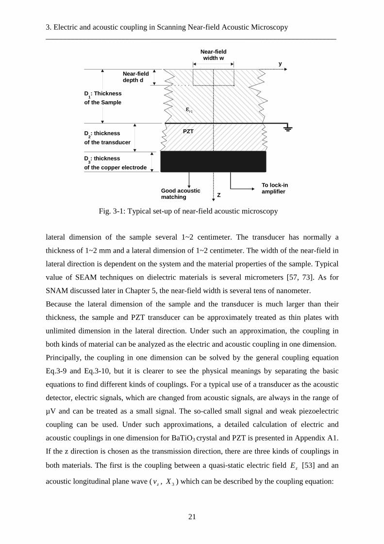
3. Electric and acoustic coupling in Scanning Near-field Acoustic Microscopy___________________________________________________________________________
21
lateral dimension of the sample several 1~2 centimeter. The transducer has normally a
thickness of 1~2 mm and a lateral dimension of 1~2 centimeter. The width of the near-field in
lateral direction is dependent on the system and the material properties of the sample. Typical
value of SEAM techniques on dielectric materials is several micrometers [57, 73]. As for
SNAM discussed later in Chapter 5, the near-field width is several tens of nanometer.
Because the lateral dimension of the sample and the transducer is much larger than their
thickness, the sample and PZT transducer can be approximately treated as thin plates with
unlimited dimension in the lateral direction. Under such an approximation, the coupling in
both kinds of material can be analyzed as the electric and acoustic coupling in one dimension.
Principally, the coupling in one dimension can be solved by the general coupling equation
Eq.3-9 and Eq.3-10, but it is clearer to see the physical meanings by separating the basic
equations to find different kinds of couplings. For a typical use of a transducer as the acoustic
detector, electric signals, which are changed from acoustic signals, are always in the range of
µV and can be treated as a small signal. The so-called small signal and weak piezoelectric
coupling can be used. Under such approximations, a detailed calculation of electric and
acoustic couplings in one dimension for BaTiO3 crystal and PZT is presented in Appendix A1.
If the z direction is chosen as the transmission direction, there are three kinds of couplings in
both materials. The first is the coupling between a quasi-static electric field zE [53] and an
acoustic longitudinal plane wave ( zv , 3X ) which can be described by the coupling equation:
Good acousticmatching
To lock-inamplifier
Z
y
PZT
D : Thickness
of the Sample1
Near-fielddepth d
Near-fieldwidth w
D : thickness
of the transducer2
D : thickness
of the copper electrode3
1εr
Fig. 3-1: Typical set-up of near-field acoustic microscopy
3. Electric and acoustic coupling in Scanning Near-field Acoustic Microscopy___________________________________________________________________________
22
02
2
2
2
=∂∂ρ−
∂∂
t
v
cz
v z
p
z, and zE =
ε
−szz
ze 33x , Eq.3-11
( zv , 3X ) are the velocity of particles and the stress in z direction; 3x is the strain in z
direction. The quasi-static electric field zE is coupled to acoustic wave ( zv , 3X ) through
strain component 3x .
The other two types of couplings are coupling between two electromagnetic plane waves
( xE , yH ) and ( yE , xH ) and two shear acoustic plane waves ( xv , 5X ) and ( yv , 4X ):
zt
ve
t
E
z
E xx
xsxx
x
∂∂∂µ=
∂∂εµ−
∂∂ 2
502
2
02
2
Eq.3-12
zt
ve
t
E
z
E yx
ysyy
y
∂∂∂
µ=∂
∂εµ−
∂∂ 2
502
2
02
2
(syyε =
sxxε for BaTiO3) Eq.3-13
The physical meaning of Eq.3-11 is that, if a quasi-static electric field in a certain material is
given, the electric and acoustic stiffened coupling can be detected by measuring the acoustic
longitudinal plane wave produced by the electric field in that material; Or, if an acoustic
longitudinal plane wave is given, there exists certainly a quasi-static electric field in z
direction and by measuring this electric field, the coupling can be detected as well. Because a
longitudinal transducer of the developed system is used to detect the longitudinal waves
produced in the system in z direction, only the first coupling of Eq.3-11 will be further
discussed in this work.
In the transducer, the harmonic acoustic longitudinal plane wave ( 3zv , 3
3X ) can be written by
the use of normal mode as [53]:
2/)( 3333
tjeaaX ω−+ +−= Eq.3-14
3333 2/)( Zeaav tj
zω−+ −= Eq.3-15
+3a = )( 13 Da + )( 13 Dzjke −−
Eq.3-16
−3a = )( 13 Da − )( 13 Dzjke −
Eq.3-17
in which )( 13 Da + and )( 1
3 Da − are amplitudes, 3Z the characteristic resistance, and 3k the
wave number of the acoustic longitudinal wave in z direction in the transducer. The suffix ‘3’
at the right top corner means waves in the transducer, and ‘+’ and ‘-’ indicate the wave
transmission directions.
At the interface between the PZT transducer and the copper electrode, if the acoustic reflect
3. Electric and acoustic coupling in Scanning Near-field Acoustic Microscopy___________________________________________________________________________
23
constant at the boundary between the transducer and the back electrode is R , the wave forms
+3a and −3a must satisfy the condition:
23
23
)(
)(
13
13
Djk
Djk
eDa
eDaR −+
−
= Eq.3-18
)( 13 Da −
= 2321
3 )( DjkeDRa −+Eq.3-19
The electric field in the transducer in z direction under the open circuit condition can be
expressed as [Appendix A1]:
zE =
ε
−PZTzz
PZTze 3
3x Eq.3-20
Here PZTPc , PZT
zzε , and PZTze 3 are stiffened stiffness, dielectric, and piezoelectric constants of
PZT in z-direction; 3x is the strain in z-direction of longitudinal waves and has the form:
3x =z
v
jz
∂∂
ω
31=
32
1
Z−
pV
1)( 33 −+ + aa )( 13 Dzjke −−
Eq.3-21
From Eq.3-19 and Eq.3-20, the quasi-static electric field in the transducer is:
zE =
ε
−PZTzz
PZTze 3
3x
=
εPZT
zz
PZTze 3
32
1
Z pV
1)Re1( 232 Djk−+ )( 1
3 Da + )( 13 Dzjke −−Eq.3-22
The voltage between two electrodes of the transducer under the open circuit condition is:
outputV = ∫+ 21
1
DD
D
z dzE
32
1
jk=
εPZT
zzPZTP
PZTz
c
e 3 )( 13 Da + )Re1( 232 Djk−+ (1- 23Djke− ) Eq.3-23
In all the equations above, )( 13 Da + is a constant determined by both the system boundary
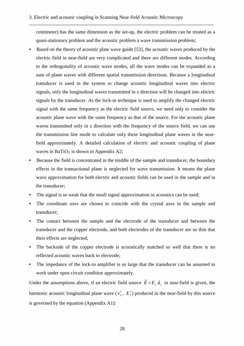
condition and the stimulation in near-field.
If the acoustic wave amplitude )( 13 Da + equals to one unit, which means that a homogenous
acoustic longitudinal plane wave with unit amplitude transmits to the transducer, the
amplitude and phase response of the transducer output signal to the frequency of the typical
set-up shown in Fig.3-1 can be obtained. The amplitude and phase signal responses of the
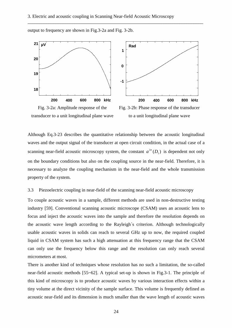
3. Electric and acoustic coupling in Scanning Near-field Acoustic Microscopy___________________________________________________________________________
24
output to frequency are shown in Fig.3-2a and Fig. 3-2b.
Although Eq.3-23 describes the quantitative relationship between the acoustic longitudinal
waves and the output signal of the transducer at open circuit condition, in the actual case of a
scanning near-field acoustic microscopy system, the constant )( 13 Da + is dependent not only
on the boundary conditions but also on the coupling source in the near-field. Therefore, it is
necessary to analyze the coupling mechanism in the near-field and the whole transmission
property of the system.
3.3 Piezoelectric coupling in near-field of the scanning near-field acoustic microscopy
To couple acoustic waves in a sample, different methods are used in non-destructive testing
industry [59]. Conventional scanning acoustic microscope (CSAM) uses an acoustic lens to
focus and inject the acoustic waves into the sample and therefore the resolution depends on
the acoustic wave length according to the Rayleigh´s criterion. Although technologically
usable acoustic waves in solids can reach to several GHz up to now, the required coupled
liquid in CSAM system has such a high attenuation at this frequency range that the CSAM
can only use the frequency below this range and the resolution can only reach several
micrometers at most.
There is another kind of techniques whose resolution has no such a limitation, the so-called
near-field acoustic methods [55~62]. A typical set-up is shown in Fig.3-1. The principle of
this kind of microscopy is to produce acoustic waves by various interaction effects within a
tiny volume at the direct vicinity of the sample surface. This volume is frequently defined as
acoustic near-field and its dimension is much smaller than the wave length of acoustic waves
µV
200 400 600 800 kHz
18
19
20
21
200 400 600 800 kHz
Rad
-1
0
1
Fig. 3-2a: Amplitude response of the
transducer to a unit longitudinal plane wave
Fig. 3-2b: Phase response of the transducer
to a unit longitudinal plane wave
3. Electric and acoustic coupling in Scanning Near-field Acoustic Microscopy___________________________________________________________________________
25
used. Both lateral and depth profiling of these methods are generally dependent on this
dimension [57~63]. The main interactions between the external stimulation and the material
in near-field are photo, ion, electron, and, recently, probe acoustic coupling interactions. The
acoustic waves generated in near-field by a certain interaction or several interactions will
further transmit through the sample, be detected by a transducer, and finally be imaged by the
system. Generally, the main interaction by different methods can be generalized as thermal
coupling, generation of internal electric field, change of lattice constant and so on. The main
types of microscope systems which use the near-field interaction can be generalized in the
following.
Scanning photo acoustic microscopy (SPAM) uses a focused laser beam to produce acoustic
waves in near-field [61]. The laser beam used has a wavelength typically in the visible range
and a power from several mW to several hundred mW. According to the samples tested, the
contrast mechanisms are mainly thermal and optoacoustic couplings. The former can be
explained as that the chopped laser beam warms the sample in the near-field periodically, and,
because of this periodical thermal energy change, the tiny piece of material in the near-field
expands and contracts periodically. These periodical expansion and contraction produce
acoustic waves which are related to thermal and acoustic properties. In the special case of
optoacoustic samples, the direct optoacoustic coupling is used to produce acoustic waves. As
the dimension of near-field area depends on the beam width of the injecting laser beam, which
is formed by a focusing system, the resolution of this method is also dependent on factors
such as the wavelength of the laser beam and the material properties of the sample. Except for
the optoacoustic structures, the limited laser power presents a main drawback to the electric
and acoustic coupling in near-field.
Scanning ion acoustic microscopy (SIAM) has a modulated microprobe with either a low [62]
or a high [63] ion energetic (200 keV) beam implanter. The coupling mechanism is thermal
acoustic coupling and the generation of excess carriers which form an internal electric field.
This field can produce acoustic waves when the sample is piezoelectric. Although a low
energy ion beam can be directly concentrated on the illuminated surface and obtain a good
axial resolution, it presents a great risk of sample damage. Conversely, fast ions can penetrate
further into the specimen, but the penetrating depth is so large that the axial resolution
becomes worse. To characterize ferroelectric domains with high resolution and non-
destructively, this kind of microscopy will not be convenient enough for the purpose.
Scanning electron acoustic microscopy (SEAM) has been developed considerably since its
introduction in 1980 [55, 56] and different coupling mechanisms are discussed thoroughly
3. Electric and acoustic coupling in Scanning Near-field Acoustic Microscopy___________________________________________________________________________
26
[16, 55~60]. It is principally a near-field technique which uses a tiny volume at the injecting
point to generate acoustic waves. The acoustic coupling mechanisms are mainly classified as
thermal acoustic coupling, piezoelectric acoustic coupling, and excess carrier acoustic
coupling. Which contrast mechanism plays the most important role during the imaging is
naturally dependent on the materials imaged [16]. For most metals, thermal coupling is the
dominant effect [55~59]. If semiconductor materials concerned, the excess carrier coupling
plays a main role by SEAM [16]. When piezoelectric materials are imaged, the piezoelectric
coupling in the near-field has main effects on sound generation [16, 60]. During the last
twenty years, different theories for the calculation of diffusion depth and lateral resolution of
this technique have been developed [57, 58] and different results on different materials have
also been presented. However, although much effort has also been given to image
ferroelectric materials by SEAM [16, 60], the contrast mechanism of SEAM on ferroelectric
materials is still not well understood because of the complexity of ferroelectric materials and
SEAM technique. It is therefore necessary to analyze the contrast mechanism of SEAM on
ferroelectric materials further. Moreover, as SEAM is a non-destructive acoustic method with
a resolution in micrometer range, it presents itself as a perfect tool for a complementary
analysis and an experimental basis for the development of new kinds of near-field microscopy
with a resolution of submicrometer or nanometer range.
With the invention of Scanning probe microscope (SPM) in 1986 [18], different principles
and experimental set-ups of Scanning near-field acoustic microscopy (SNAM) based on SPM
have been developed recently [19~37, 64~70]. The principle of all the SNAM bases on
coupling acoustic waves in near-field and detecting them by various methods. According to
the set-ups developed, the main work can be roughly classified into two classes. One class
uses a tunnel fork as an acoustic coupling source [64, 67, 68]. The other uses a common tip to
couple or detect acoustic waves [19, 30~37]. According to the operation modes, SNAM can
then be classified as SNAM with direct acoustic vibration coupling [64, 67, 68], direct contact
force coupling [30, 34~35, 65, 66, 69, 70], or piezoelectric coupling [19, 22, 30, 31~33, 36,
37]. A detailed discussion on all the work is beyond the range of this work. Only the
technique which is developed by the use of a transducer to detect the acoustic longitudinal
waves produced in near-field for the analysis of ferroelectric materials [36, 37] will be
discussed in detail in this work. The resolution of this mode of SNAM is basically dependent
on the dimension of the near-field which is formed just beneath the contact point of a
scanning probe by an applied ac voltage. Because the scanning probe has a very sharp form
and a diameter down to 10 nm at the very tip, the lateral dimension of the near-field under the
3. Electric and acoustic coupling in Scanning Near-field Acoustic Microscopy___________________________________________________________________________
27
probe has also a lateral resolution with almost the same order. This provides an ideal
condition to study ferroelectric domains and material properties at submicrometer or
nanometer resolution. Furthermore, the use of an acoustic transducer at the backside of the
sample for the detection of acoustic vibrations produced in near-field provides a solid base for
the comparison of contrast among different near-field acoustic microscopy systems both
experimentally and theoretically.
For the comparison of the contrast in this work, two typical near-field techniques which have
the highest resolution among all the near-field acoustic microscopy techniques, the developed
SNAM set-up and SEAM, will be chosen and discussed. For the analysis of ferroelectric
properties of BaTiO3 materials by both techniques, only the mechanism of the generation of
internal electric field in near-field will be discussed here, as both techniques rely on this
mechanism to generate acoustic vibrations in near-field. For SEAM, the electric field in near-
field is produced by the trapped charges in the sample. For SNAM system developed, the
electric field is concentrated just under the tip because of the very sharp form of the tip and
will be discussed in Chapter 5 in detail. Naturally, for the reliability of complementary
analyses, both techniques use the same experiment set-up, such as the same transducer and
sample holder, to investigate the same sample at identical areas.
Although it is necessary to make a thin gold film (about several nanometer thick) on the
sample for SEAM study, this film is so thin that it will not change the acoustic boundary
conditions and therefore has no effect on the harmonic acoustic wave solutions. In the same
way, although the tip of SNAM is in contact with the sample surface, the contact force
between the tip and the sample surface is kept constant during the scanning by the
topographical feedback control unit of SPM. For the harmonic acoustic waves, this constant
force has no effect on the harmonic acoustic wave solutions either.
Based on the discussion above and from the point view of acoustic transmission, we can
generalize both systems on ferroelectric BaTiO3 materials as one typical set-up shown in
Fig.3-1 with an electric field stimulation in near-field.
In this typical near-field acoustic system with an electric field stimulation in near-field, some
basic assumptions have to be introduced in order to analyze the system quantitatively:
• The working frequency is usually in the range from several kHz to several hundred kHz.
The wave length of electromagnetic waves is several kilometers and that of acoustic
waves several centimeters. The set-up has a typical dimension of several centimeters.
Because the wavelength of electromagnetic wave (several km) in the system is much
greater than the dimension of the set-up and the wavelength of an acoustic waves (several
3. Electric and acoustic coupling in Scanning Near-field Acoustic Microscopy___________________________________________________________________________
28
centimeter) has the same dimension as the set-up, the electric problem can be treated as a
quasi-stationary problem and the acoustic problem a wave transmission problem;
• Based on the theory of acoustic plate wave guide [53], the acoustic waves produced by the
electric field in near-field are very complicated and there are different modes. According
to the orthogonality of acoustic wave modes, all the wave modes can be expanded as a
sum of plane waves with different spatial transmission directions. Because a longitudinal
transducer is used in the system to change acoustic longitudinal waves into electric
signals, only the longitudinal waves transmitted in z direction will be changed into electric
signals by the transducer. As the lock-in technique is used to amplify the changed electric
signal with the same frequency as the electric field source, we need only to consider the
acoustic plane wave with the same frequency as that of the source. For the acoustic plane
waves transmitted only in z direction with the frequency of the source field, we can use
the transmission line mode to calculate only these longitudinal plane waves in the near-
field approximately. A detailed calculation of electric and acoustic coupling of plane
waves in BaTiO3 is shown in Appendix A2;
• Because the field is concentrated in the middle of the sample and transducer, the boundary
effects in the transactional plane is neglected for wave transmission. It means the plane
wave approximation for both electric and acoustic fields can be used in the sample and in
the transducer;
• The signal is so weak that the small signal approximation in acoustics can be used;
• The coordinate axes are chosen to coincide with the crystal axes in the sample and
transducer;
• The contact between the sample and the electrode of the transducer and between the
transducer and the copper electrode, and both electrodes of the transducer are so thin that
their effects are neglected;
• The backside of the copper electrode is acoustically matched so well that there is no
reflected acoustic waves back to electrode;
• The impedance of the lock-in amplifier is so large that the transducer can be assumed to
work under open circuit condition approximately.
Under the assumptions above, if an electric field source E�
= sE za�
in near-field is given, the
harmonic acoustic longitudinal plane wave ( 1zv , 1
3X ) produced in the near-field by this source
is governed by the equation (Appendix A1):
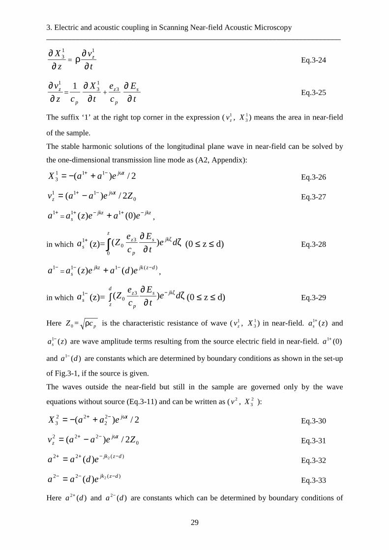
3. Electric and acoustic coupling in Scanning Near-field Acoustic Microscopy___________________________________________________________________________
29
z
X
∂∂ 1
3 = t
vz
∂∂ρ
1
Eq.3-24
z
vz
∂∂ 1
=pc
1
t
X
∂∂ 1
3 +p
z
c
e 3
t
Es
∂∂
Eq.3-25
The suffix ‘1’ at the right top corner in the expression ( 1zv , 1
3X ) means the area in near-field
of the sample.
The stable harmonic solutions of the longitudinal plane wave in near-field can be solved by
the one-dimensional transmission line mode as (A2, Appendix):
2/)( 1113
tjeaaX ω−+ +−= Eq.3-26
0111 2/)( Zeaav tj
zω−+ −= Eq.3-27
+1a =jkzjkz
s eaeza −+−+ + )0()( 11,
in which +1
sa (z)= ∫ ζ∂
∂ ζz
jks
p
z det
E
c
eZ
0
30 )( (0 ≤ z ≤ d) Eq.3-28
−1a =)(11 )()( dzjkjkz
s edaeza −−− + ,
in which −1
sa (z)= ∫ ζ∂
∂ ζ−d
z
jks
p
z det
E
c
eZ )( 3
0 (0 ≤ z ≤ d) Eq.3-29
Here 0Z = pcρ is the characteristic resistance of wave ( 1zv , 1
3X ) in near-field. )(1 zas+ and
)(1 zas− are wave amplitude terms resulting from the source electric field in near-field. )0(1+a
and )(1 da − are constants which are determined by boundary conditions as shown in the set-up
of Fig.3-1, if the source is given.
The waves outside the near-field but still in the sample are governed only by the wave
equations without source (Eq.3-11) and can be written as ( 2v , 23X ):
2/)( 22
223
tjeaaX ω−+ +−= Eq.3-30
0222 2/)( Zeaav tj
zω−+ −= Eq.3-31
)(22 2)( dzjkedaa −−++ = Eq.3-32
)(22 2)( dzjkedaa −−− = Eq.3-33
Here )(2 da + and )(2 da − are constants which can be determined by boundary conditions of
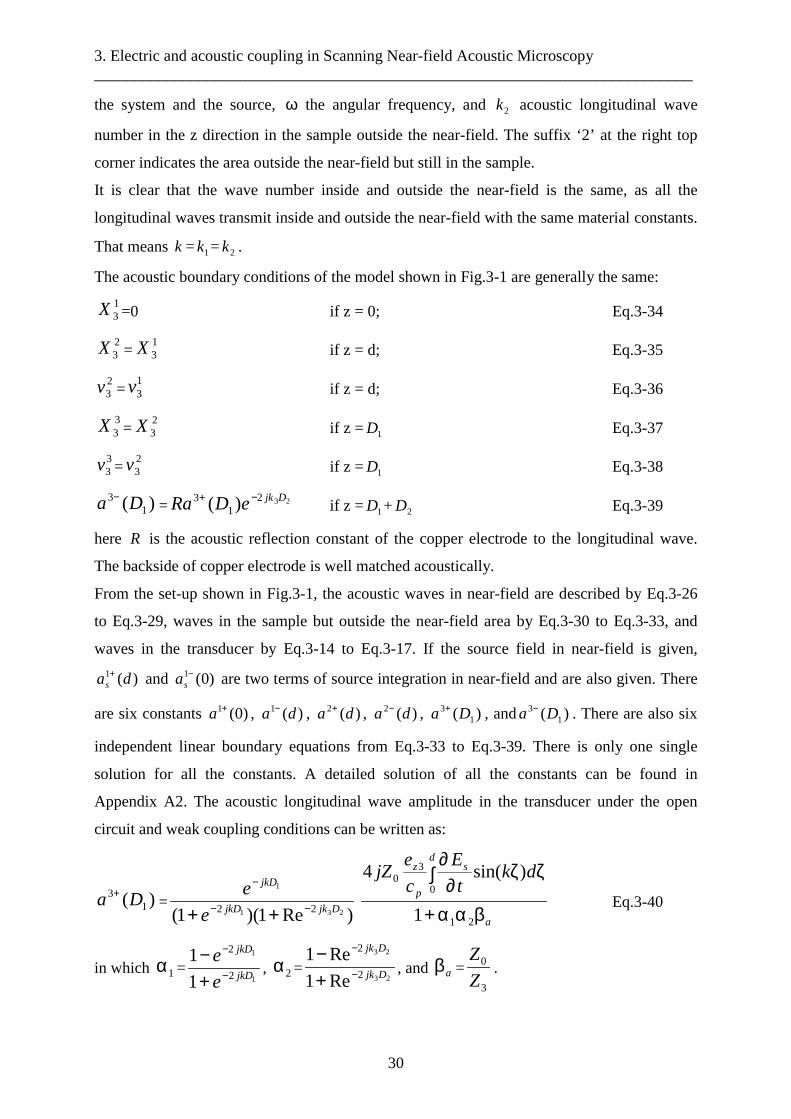
3. Electric and acoustic coupling in Scanning Near-field Acoustic Microscopy___________________________________________________________________________
30
the system and the source, ω the angular frequency, and 2k acoustic longitudinal wave
number in the z direction in the sample outside the near-field. The suffix ‘2’ at the right top
corner indicates the area outside the near-field but still in the sample.
It is clear that the wave number inside and outside the near-field is the same, as all the
longitudinal waves transmit inside and outside the near-field with the same material constants.
That means k = 1k = 2k .
The acoustic boundary conditions of the model shown in Fig.3-1 are generally the same:
13X =0 if z = 0; Eq.3-34
23X =
13X if z = d; Eq.3-35
23v =
13v if z = d; Eq.3-36
33X =
23X if z = 1D Eq.3-37
33v =
23v if z = 1D Eq.3-38
)( 13 Da −
= 2321
3 )( DjkeDRa −+if z = 1D + 2D Eq.3-39
here R is the acoustic reflection constant of the copper electrode to the longitudinal wave.
The backside of copper electrode is well matched acoustically.
From the set-up shown in Fig.3-1, the acoustic waves in near-field are described by Eq.3-26
to Eq.3-29, waves in the sample but outside the near-field area by Eq.3-30 to Eq.3-33, and
waves in the transducer by Eq.3-14 to Eq.3-17. If the source field in near-field is given,
)(1 das+ and )0(1−
sa are two terms of source integration in near-field and are also given. There
are six constants )0(1+a , )(1 da − , )(2 da + , )(2 da − , )( 13 Da + , and )( 1
3 Da − . There are also six
independent linear boundary equations from Eq.3-33 to Eq.3-39. There is only one single
solution for all the constants. A detailed solution of all the constants can be found in
Appendix A2. The acoustic longitudinal wave amplitude in the transducer under the open
circuit and weak coupling conditions can be written as:
)( 13 Da +
=)Re1)(1( 231
1
22 DjkjkD
jkD
e
e−−
−
++ a
ds
p
z dkt
E
c
ejZ
βαα+
∫ ζζ∂
∂
21
0
30
1
)sin(4
Eq.3-40
in which 1α =1
1
2
2
1
1jkD
jkD
e
e−
−
+−
, 2α =23
23
2
2
Re1
Re1Djk
Djk
−
−
+−
, and aβ =3
0
Z
Z.
3. Electric and acoustic coupling in Scanning Near-field Acoustic Microscopy___________________________________________________________________________
31
The expression is very complicated but the physical meaning is very clear. The term
∫ ζζ∂
∂ds dk
t
E
0
)sin( at the right side of Eq.3-40 is the source coupling in near-field. The rest at
the right side of Eq.3-40 is the system transmission function which is determined by the
boundary conditions of the system. The acoustic wave amplitude )( 13 Da + is dependent on
both the coupling source in near-field and the transmission function of the system. From Eq.3-
40, the output signal of the transducer under the open circuit and weak coupling conditions
can be easily found from Eq.3-23:
outputV32
1
jk=
εPZT
zzPZTP
PZTz
c
e 3 )( 13 Da + )Re1( 232 Djk−+ (1- 23Djke− )
The final output signal of the transducer is:
outputV =2(p
z
c
e 3 )( ∫ ζζ∂
∂ds dk
t
E
0
)sin( )
εPZT
zz
PZTze 3
( ω1
)(1
23
211
jkD
Djk
e
e−
−
+−
)(a
a
βαα+β
211) 1jkDe−
Eq.3-41
The first term at the right side of Eq.3-41 is only related to the material properties in near-
field; the second term is the term determined by source electric field in near-field; the third
term is the parameter of PZT transducer; The rest is dependent on the detecting system shown
in Fig.3-1.
Eq.3-41 means that if the source E�
= sE za�
in near-field is given, the output signal of the
transducer at the open circuit condition for set-up shown in Fig.3-1 can be obtained. For a
given system, if the source field sE is kept constant during the scanning, the change of outputV
is only related to material properties (p
e
c
e 3 ) in near-field. As it is shown in Eq.2-24, the
piezoelectric constant 3zd (i.e. 3ze in Eq.3-41) is dependent on polarization. Therefore, if the
coupled source electric field in near-field can be kept constant during the scanning and there
is difference of polarization in near-field of every scanning point, the final acoustic image of
experiment set-up Fig.3-1 is an image of the change of ferroelectric polarization in near-field.
This is the contrast mechanism of near-field set-up shown in Fig.3-1 to image ferroelectric
domains in BaTiO3 material systems. It can be seen later that this is also the theoretical
background for the complementary study on ferroelectric domains of BaTiO3 materials by
SEAM and SNAM techniques, as the contrast mechanism of both techniques is the same. If,
however, the coupled source electric field distribution is scattered by a defect in near-field,
3. Electric and acoustic coupling in Scanning Near-field Acoustic Microscopy___________________________________________________________________________
32
the output signal of the transducer will be naturally dependent on the scattering source and the
average piezoelectric effect in near-field. This is also the contrast origin of defects in near-
field which can be imaged by SEAM and SNAM.
Furthermore, for the development of experimental set-ups of both near-field techniques based
on the theory above, it is also necessary to estimate the value of output signal from the
transducer. From the Eq.3-41, the value of piezoelectric constants 3ze of piezoelectric BaTiO3
and PTZ transducer have almost the same value. The stiffened piezoelectric constant in near-
field is about 1011 for BaTiO3 and dielectric constant of PZT PZTzzε is about 10-12. The near-
field depth is usually in the range of µm. The thickness of the sample and transducer is also in
millimeter range. If it is assumed that the typical electric field in the near-field is smaller than
10 kV/m, which is small enough not to change the domain structures in near-field, the output
signal of the transducer is in the range of µV. This signal is naturally in the background of
white noise. We have to use the lock-in amplifier to detect such a small signal submerged in
the white noise background.
How these two kinds of near-field microscopy techniques couple the source electric field in
near-field, how the detailed experiment set-ups for both systems are established based on the
theory above, and how large is the near-field depth of both systems will be discussed in a
parallel way in the following chapter 4 and 5.
4. Scanning Electron Acoustic Microscopy
___________________________________________________________________________
33
4 Scanning Electron Acoustic Microscopy
4.1 Physical background, signal generation, and contrast mechanism
The physical processes by injecting electrons in Scanning electron microscopy (SEM) are
discussed thoroughly by some work [55~60, 71~73]. The Scanning electron acoustic
microscopy (SEAM) was developed from the commercial SEM to analyze the acoustic
properties of materials [55, 56]. According to different applications, the mechanisms can be
generally classified into thermal acoustic coupling, piezoelectric coupling, and excess carrier
coupling [16]. For the thermal acoustic coupling, some authors introduced a detailed
discussion of coupling equation and output signal of the transducer in SEAM [58, 75] which
will not be discussed in this work.
For the piezoelectric coupling mechanism, although some work has been done to analyze the
coupling mechanism [16], a detailed explanation of this kind of mechanism for the imaging of
ferroelectric domains in SEAM has not been introduced until recently [60]. In that work, the
authors have discussed the piezoelectric coupling effect in the ferroelectric BaTiO3 material
by SEAM, but the acoustic solutions were assumed the same inside and outside the near-field.
It was an assumption which did not satisfy the acoustic wave equation Eq.3-11 in the area
outside the near-field but still in the sample.
For the future analysis of ferroelectric materials by near-field acoustic microscopy techniques,
it is obligatory to study this mechanism further. As this kind of mechanism concerns the
coupling of mechanic and electric phenomena in near-field, a detailed analysis of physical
process of electron injection in near-field by primary electrons (PE) is also necessary.
If only the insulating materials are concerned, some authors introduced some models to
describe field distributions in the insulating materials bombarded by PE [71~74]. Most of the
models have assumed that the electric field in electron injecting area is uniform in the
injection direction. This is naturally against Gauss´s theorem. A more accurate model to
calculate electric field formed by injection electrons was introduced [74]. Although this model
is impossible to explain all the actual phenomena of bombardment on insulating materials by
PE, it is the most accepted model in this aspect today. Therefore this model is chosen as the
base for the analyses of the contrast mechanism of SEAM on ferroelectric BaTiO3 materials.
According to the model, the PE injects into a sample and forms a trapped charge distribution.
For a typical set-up of SEAM system, the charge distribution in an insulator by a
bombardment of primary electrons is shown in Fig. 4-1. The charge accumulating area has
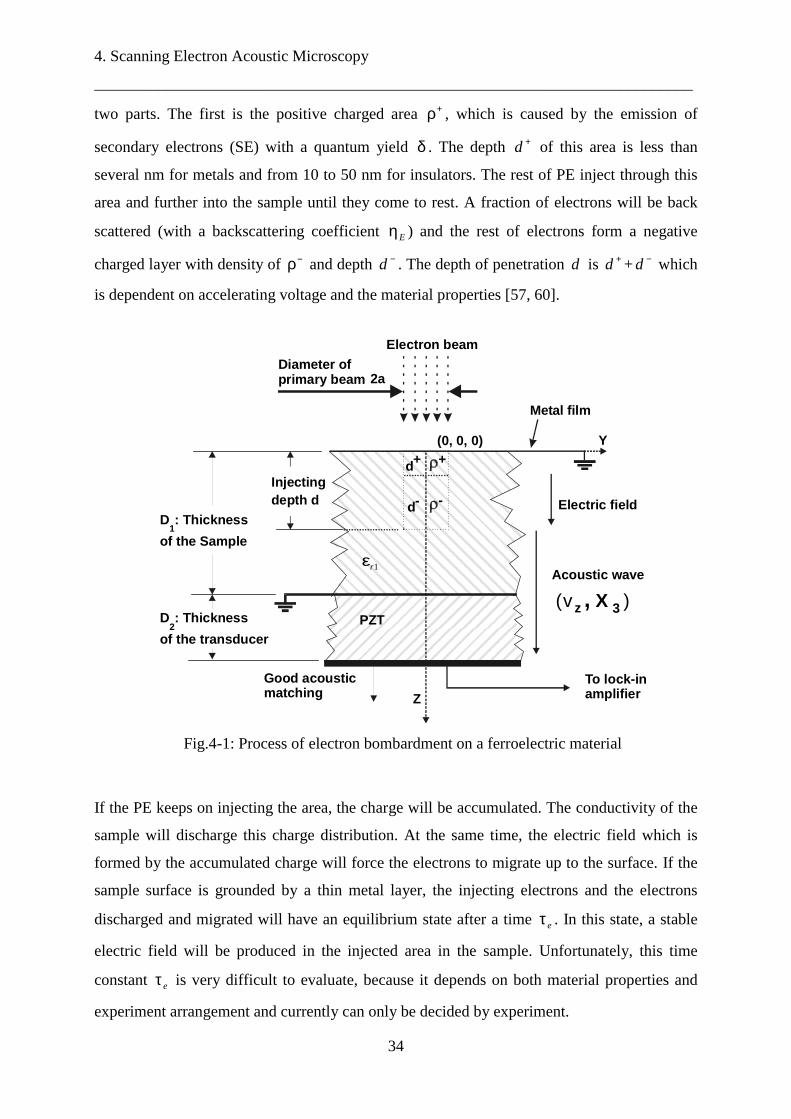
4. Scanning Electron Acoustic Microscopy
___________________________________________________________________________
34
two parts. The first is the positive charged area +ρ , which is caused by the emission of
secondary electrons (SE) with a quantum yield δ . The depth +d of this area is less than
several nm for metals and from 10 to 50 nm for insulators. The rest of PE inject through this
area and further into the sample until they come to rest. A fraction of electrons will be back
scattered (with a backscattering coefficient Eη ) and the rest of electrons form a negative
charged layer with density of −ρ and depth −d . The depth of penetration d is +d + −d which
is dependent on accelerating voltage and the material properties [57, 60].
If the PE keeps on injecting the area, the charge will be accumulated. The conductivity of the
sample will discharge this charge distribution. At the same time, the electric field which is
formed by the accumulated charge will force the electrons to migrate up to the surface. If the
sample surface is grounded by a thin metal layer, the injecting electrons and the electrons
discharged and migrated will have an equilibrium state after a time eτ . In this state, a stable
electric field will be produced in the injected area in the sample. Unfortunately, this time
constant eτ is very difficult to evaluate, because it depends on both material properties and
experiment arrangement and currently can only be decided by experiment.
Electron beam
2aDiameter ofprimary beam
Good acousticmatching
Injectingdepth d
Metal film
Electric field
Acoustic wave
To lock-inamplifierZ
Y(0, 0, 0)
PZT
D : Thickness
of the Sample1
D : Thickness
of the transducer2
1εr
+
-
+d
-d
zv( ) 3X,
Fig.4-1: Process of electron bombardment on a ferroelectric material
4. Scanning Electron Acoustic Microscopy
___________________________________________________________________________
35
If the intensity of PE is modulated with an angular frequency ω, the electric field distribution
can also be established after a delay time factor longer than eτ . In this case, the electric field
formed has also an angular frequency of ω. To study the problem further, some
approximations have to be made. As it can be seen later, even under such approximations, the
solution of piezoelectric mechanism in SEAM has a very complicated form.
Besides the fundamental approximations to analyze near-field microscopy systems in Chapter
3, some special approximations for SEAM must be assumed here:
• The dimension of near-field of SEAM is so small compared to sample and wavelength,
that the anisotropic properties for the calculation of electric field in near-field can be
neglected;
• The emission of SE takes place mainly at the surface of the metallic layer, so that there is
only a negatively charged area in the sample with a density of −ρ ;
• The penetration charge will be assumed that it is a charge cylinder (diameter 2a and length
d ) in the sample with defocus condition, so that the electric field component in radial
direction is neglected and the electric field component zE is uniform and equals the
electric field in the middle of the near-field;
• The illumination time of PE at every scan point is greater than the discharge delay time eτ
of the materials, so that a stable harmonic field distribution is established.
From Fig. 4-1, if the sample has a thin layer of metal on the surface, the stable electric field
distribution can be calculated by the use of an image charge distribution. With the
approximations above, the electric field along the z axis is [74]:
sE =tjedzA ω− )´( ( 0 <z<d , 222 ayx ≤+ )
sE =0 ( z >d and z<0, 222 ayx ≥+ ) Eq.4-1
where −ρ is the density of stable charge distribution in near-field and zzε is the dielectric
constant in z direction of BaTiO3 materials. The x, and y components of electric field are
neglected as they are small compared to z component. The electric field distribution of Eq.4-1
is the source field sE in near-field of SEAM.
The electric field source in near-field with harmonic time variation is:
sE =tjedzA ω− )´( = ee τ−
da
I
zz
E
επη−2
0)1( tjedz ω− )( Eq.4-2
The acoustic source in near-field for BaTiO3:
4. Scanning Electron Acoustic Microscopy
___________________________________________________________________________
36
p
z
c
e 3
t
Es
∂∂
= )( dzA − tje ω
in which A = ωjp
z
c
e 3 eeda
I
zz
E τ−
επη−2
0)1( Eq.4-3
The output signal of a PZT transducer under the open circuit condition is [A3, appendix]:
outputV =2 j ( szz
ze
ρε3 )( ee
da
IE τ−
πη−
20)1(
)
εPZT
zz
PZTze 3 .
(2
)sin(
ω− kdkd
)(1
23
21
1jkD
Djk
e
e−
−
+−
)(a
a
βαα+β
211) 1jkDe−
Eq.4-4
In Eq.4-4, 1α =1
1
2
2
1
1jkD
jkD
e
e−
−
+−
, 2α =23
23
2
2
Re1
Re1Djk
Djk
−
−
+−
, and aβ =3
0
Z
Z.
The term in the first bracket of Eq.4-4 is directly related to the material properties in near-
field; The term in the second bracket is about the charge distribution in near-field; The term in
the third bracket is related to the properties of the PZT transducer; The remaining four terms
are related to detecting set-up and have a very complicated frequency dependence.
As it is explained in chapter 2, if the extrinsic contribution of the domain walls to the
piezoelectric effect in ferroelectric materials is neglected, the constant of 3ze (or 3zd ) is
directly related to ferroelectric polarization [see Eq.2-24]. If there are c- and a- domains on
the two areas on the surface of BaTiO3 materials, the area of c-domains has polarization
parallel to the z direction and has a non-zero value of 3ze in near-field. Whereas the area of a-
domains, which has a polarization perpendicular to the z direction, will have zero value of
3ze . This is the contrast mechanism of SEAM on the ferroelectric BaTiO3 single crystal.
Eq.4-4 has a very complicated frequency dependence, which is proved by SEAM experiments
[34, 38]. This dependence results from the frequency term in Eq.4-4 and can only be analyzed
by computer simulation. The computer simulation is completed by the use of the free Linux
software Octave Ver. 2.0.13 and the result is shown in Fig.4-2. As the typical frequency range
of most lock-in amplifier is from several Hz to 200 kHz, the amplitude and phase response of
the output signal of the transducer in this frequency range has a dependence of frequency
shown in Fig.4-2. Early experimental work [38] revealed the same tendency of the acoustic
output signal in SEAM in this frequency range.
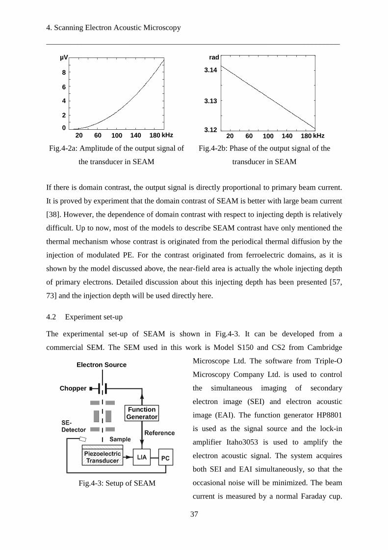
4. Scanning Electron Acoustic Microscopy
___________________________________________________________________________
37
If there is domain contrast, the output signal is directly proportional to primary beam current.
It is proved by experiment that the domain contrast of SEAM is better with large beam current
[38]. However, the dependence of domain contrast with respect to injecting depth is relatively
difficult. Up to now, most of the models to describe SEAM contrast have only mentioned the
thermal mechanism whose contrast is originated from the periodical thermal diffusion by the
injection of modulated PE. For the contrast originated from ferroelectric domains, as it is
shown by the model discussed above, the near-field area is actually the whole injecting depth
of primary electrons. Detailed discussion about this injecting depth has been presented [57,
73] and the injection depth will be used directly here.
4.2 Experiment set-up
The experimental set-up of SEAM is shown in Fig.4-3. It can be developed from a
commercial SEM. The SEM used in this work is Model S150 and CS2 from Cambridge
Microscope Ltd. The software from Triple-O
Microscopy Company Ltd. is used to control
the simultaneous imaging of secondary
electron image (SEI) and electron acoustic
image (EAI). The function generator HP8801
is used as the signal source and the lock-in
amplifier Itaho3053 is used to amplify the
electron acoustic signal. The system acquires
both SEI and EAI simultaneously, so that the
occasional noise will be minimized. The beam
current is measured by a normal Faraday cup.
0
2
4
6
8
µV
6020 100 140 180 kHz3.12
3.13
3.14
rad
20 60 100 140 180 kHz
Fig.4-2a: Amplitude of the output signal of
the transducer in SEAM
Fig.4-2b: Phase of the output signal of the
transducer in SEAM
Electron Source
Chopper
FunctionGenerator
Fig.4-3: Setup of SEAM
4. Scanning Electron Acoustic Microscopy
___________________________________________________________________________
38
The piezoelectric transducer is PX5 piezoelectric ceramics from Company Valvo [76]. Some
of the typical results are presented [34, 36, 37, 38].
4.3 Discussion of the signal and noise
To evaluate an imaging system, it is always to analyze some important parameters, such as
time resolution and bandwidth, lateral and depth resolution, sensitivity and signal-noise ratio,
stability, and the test time.
As discussed above, The illumination time of PE at every scan point is greater than the
discharge delay time eτ of the materials, so that a stable harmonic field distribution is
established. This discharge delay time eτ is dependent on both the injecting beam and the
sample studied. A typical value for insulating materials under the bombardment of the PE
with current density of 1µA/mm2 is 0.1 ms [74]. For a typical image of 400*400 resolution
scanned by a computer controlled SEM, the scanning beam can stay for 10 ms at every pixel.
That means this delay time has no significant effect on the typical SEAM imaging process.
As presented by other work [55~61], the lateral and depth resolution of SEAM are mainly
dependent on the interaction volume of PE penetration, which is defined as the volume of
near-field for SEAM in this work. Whereas the near-field volume has the dimension of the
thermal diffusion volume in case of thermal mechanism, the near-field volume by
piezoelectric mechanism has a depth resolution of the whole PE penetration depth. Typical
value of penetration depth of SEAM image with 20 keV primary electrons is about 2~3 µm
[55] which is dependent on the materials studied.
The lateral resolution is also dependent on the dimension of the near-field. For the imaging of
ferroelectric material, if there is a surface polarization in near-field, this polarization will
naturally affect the lateral distribution of electrons of injecting PE. As a result, the dimension
of the near-field is changed. Because the piezoelectric vibration mode change and lateral
electric field distribution in near-field are very complicated and little documented in the
literatures up till today, it can only be estimated experimentally. Unfortunately, from the
experiment results this effect is little documented too.
The signal to noise ratio can also be estimated. If the noise from function generator, SEM, and
the measuring circuit and lock-in amplifier are Gσ , SEMσ , and mσ , it is necessary to add the
noise of acoustic detecting system Aσ which is composed of thermal noise in near-field, the
acoustic transmission noise, and the thermal noise of transducer. The total noise totalσ is:
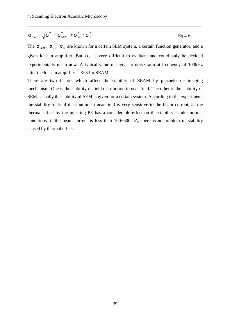
4. Scanning Electron Acoustic Microscopy
___________________________________________________________________________
39
totalσ =2222AmSEMG
σ+σ+σ+σ Eq.4-6
The SEMσ , Gσ , mσ are known for a certain SEM system, a certain function generator, and a
given lock-in amplifier. But Aσ is very difficult to evaluate and could only be decided
experimentally up to now. A typical value of signal to noise ratio at frequency of 100kHz
after the lock-in amplifier is 3~5 for SEAM.
There are two factors which affect the stability of SEAM by piezoelectric imaging
mechanism. One is the stability of field distribution in near-field. The other is the stability of
SEM. Usually the stability of SEM is given for a certain system. According to the experiment,
the stability of field distribution in near-field is very sensitive to the beam current, as the
thermal effect by the injecting PE has a considerable effect on the stability. Under normal
conditions, if the beam current is less than 100~500 nA, there is no problem of stability
caused by thermal effect.
5. Scanning Near-field Acoustic Microscopy based on SPM (SNAM)
___________________________________________________________________________
40
5 Scanning Near-field Acoustic Microscopy based on SPM (SNAM)
5.1 Physical background, signal generation, and contrast mechanism
To analyze the ferroelectric properties by SPM, much work has been done and different
experiment SNAM set-ups based on SPM have been developed [19~37]. Only recently, a
model for the study of ferroelectric thin films by piezoelectric response mode of SNAM is
presented [33, 77]. Even in that model, the electric field solutions could not satisfy the electric
boundary conditions of the presented model. Neither could the introduced theoretical method
be used as a systematic theoretical technique even only to analyze the quasi-stationary
electric field for different samples such as bulk materials or thin films. For a systematic
analysis of the electric and acoustic coupling fields in ferroelectric samples studied by SNAM
systems, no other work has been documented because of the complexity. The first difficulty is
that the electric and mechanical fields in the near-field in the sample is very difficult to
calculate in SNAM systems [77, 78]. The second difficulty results from surfaces of
ferroelectric materials which are also unknown to us. Although experiment results are
presented from both piezoelectric response mode [19,33] and the system developed in this
work [34, 37], an explanation of contrast of SNAM can only be qualitative, as the electric and
mechanical coupling in near-field is still under study. Although there have been a lot of
numerical solutions of the electric field distribution under the tip, it would be difficult to use
the numerical solutions to study the contrast mechanism of SNAM systems. Therefore, a
simple analytical solution of electric and mechanical coupling will be important for both the
analysis of contrast mechanism and the estimation of properties of ferroelectric materials
studied by SNAM systems.
As briefly discussed in the introduction, a new set-up of SNAM based on SPM for the
characterization of BaTiO3 material system is developed in this work. To characterize the
system developed, a systematic theoretical model based on classical electromagnetic and
acoustic theories for the set-up is presented in this chapter. Detailed theoretical calculations
can be found in Appendix A4.
The SNAM system to be introduced in the following is developed from a commercial SPM
system. The SPM works in contact mode and an alternating voltage is applied between the tip
and the backside of the sample. A transducer is used to detected acoustic vibrations produced
by the converse piezoelectric effect of the sample [34~37]. As briefly discussed in Chapter 3,
the use of the transducer provides a solid base for a theoretical and experimental comparison
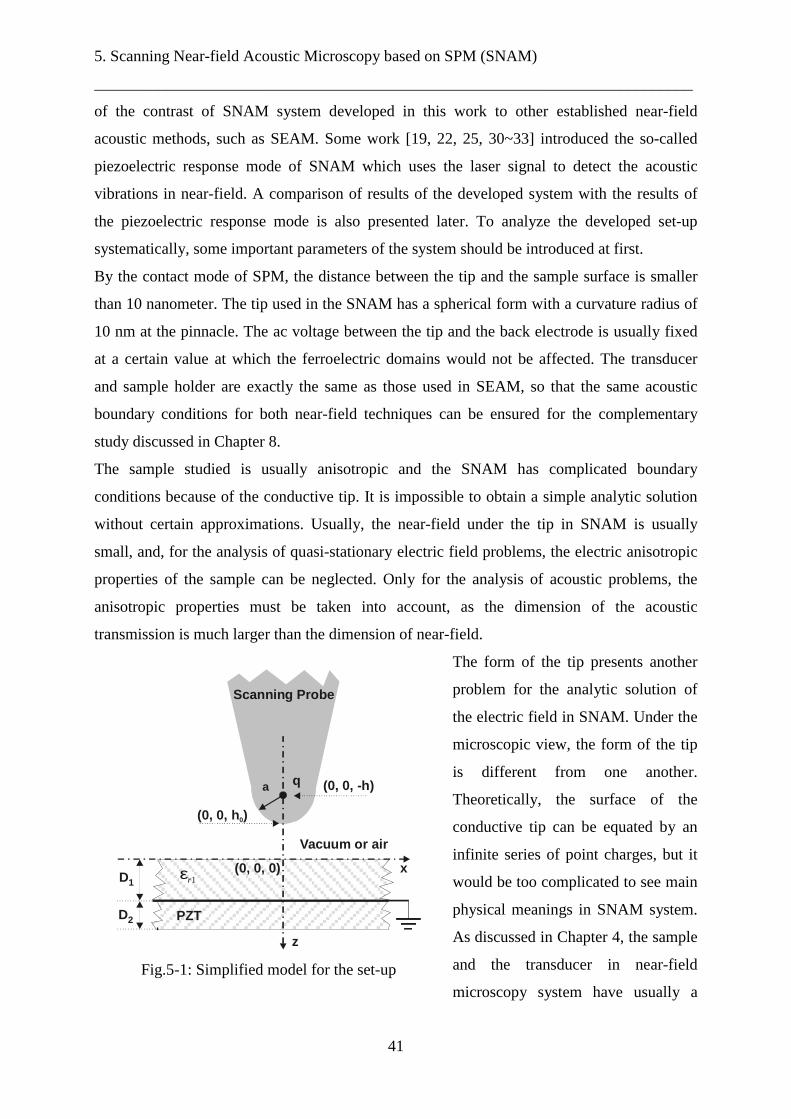
5. Scanning Near-field Acoustic Microscopy based on SPM (SNAM)
___________________________________________________________________________
41
of the contrast of SNAM system developed in this work to other established near-field
acoustic methods, such as SEAM. Some work [19, 22, 25, 30~33] introduced the so-called
piezoelectric response mode of SNAM which uses the laser signal to detect the acoustic
vibrations in near-field. A comparison of results of the developed system with the results of
the piezoelectric response mode is also presented later. To analyze the developed set-up
systematically, some important parameters of the system should be introduced at first.
By the contact mode of SPM, the distance between the tip and the sample surface is smaller
than 10 nanometer. The tip used in the SNAM has a spherical form with a curvature radius of
10 nm at the pinnacle. The ac voltage between the tip and the back electrode is usually fixed
at a certain value at which the ferroelectric domains would not be affected. The transducer
and sample holder are exactly the same as those used in SEAM, so that the same acoustic
boundary conditions for both near-field techniques can be ensured for the complementary
study discussed in Chapter 8.
The sample studied is usually anisotropic and the SNAM has complicated boundary
conditions because of the conductive tip. It is impossible to obtain a simple analytic solution
without certain approximations. Usually, the near-field under the tip in SNAM is usually
small, and, for the analysis of quasi-stationary electric field problems, the electric anisotropic
properties of the sample can be neglected. Only for the analysis of acoustic problems, the
anisotropic properties must be taken into account, as the dimension of the acoustic
transmission is much larger than the dimension of near-field.
The form of the tip presents another
problem for the analytic solution of
the electric field in SNAM. Under the
microscopic view, the form of the tip
is different from one another.
Theoretically, the surface of the
conductive tip can be equated by an
infinite series of point charges, but it
would be too complicated to see main
physical meanings in SNAM system.
As discussed in Chapter 4, the sample
and the transducer in near-field
microscopy system have usually a
D1
q
(0, 0, h )0
(0, 0, -h)
(0, 0, 0)
PZT
a
Scanning Probe
z
x
Vacuum or air
1εr
D2
Fig.5-1: Simplified model for the set-up
5. Scanning Near-field Acoustic Microscopy based on SPM (SNAM)
___________________________________________________________________________
42
lateral dimension of 1-2 centimeter. The thickness of the bulk ceramics or crystal samples is
normally 2 millimeter and a typical thin film sample 1000 nm. The scanning tip has only a
diameter of 10 nm at the pinnacle. Because of this difference of the geometrical dimension
between the sample and the tip, the tip can be normally simplified as a point charge which is
at the curvature center of the pinnacle of the tip [33, 77, 79]. The sample and transducer, as
discussed in chapter 3 for a typical near-field acoustic system, are simplified as plates with an
unlimited lateral dimension. The simplified model to characterize the electric field
distribution of the set-up developed in this work is shown in Fig.5-1. The approximations for
SNAM system developed, as in the case of SEAM, are generalized as:
• For the calculation of quasi-stationary electric field in near-field, the anisotropic of
electric property of the sample is neglected; Only by the treatment of acoustic
transmission problem, the anisotropic properties of materials will be taken into account;
• The tip will be equivalent as a point charge at the curvature center of the pinnacle of the
tip;
• At the pinnacle point of the tip )h,0,0( 0 , the potential will be given as the voltage of the
tip, because it is the nearest point to the sample and has the strongest effect on the field
distribution [77, 79].
According to the model and under the approximations above, the electric and mechanic
coupling in the system can be analyzed. The analytic solution of the quasi-stationary electric
field in the SNAM system developed should be a solution of the Poisson´s equation with a
point source under the given boundary condition shown in Fig.5-1. The most effective way to
solve this quasi-stationary field is the solution of the Green´s function of the system.
5.1.1 Green´s function of the model
The electric field distribution can be analyzed by the use of Green´s function. The field
distribution of a point charge q at (0,0,-h) in cylindrical coordinate system can be obtained by
separating variables as [80~82]:
V=04πε
q∫ ββ∞ +β−
00 )( derJ hz
Eq.5-1
The Green´s function for the model shown in Fig.5-1 can be written as:
In the region - ∞ <z<0;
V0=04πε
q[ ∫ ββ
∞ +β−
00 )( derJ hz
+ ∫ βββ∞
β
00 )()( derJA z
] Eq.5-2
5. Scanning Near-field Acoustic Microscopy based on SPM (SNAM)
___________________________________________________________________________
43
In the region 0<z<D1;
V1=04πε
q[ ∫ βββ
∞β−
00 )()( derJB z
+ ∫ βββ∞
β
00 )()( derJC z
] Eq.5-3
At z = D1, the metal interface is earthed, so the voltage at the interface:
V1=0 Eq.5-4
As the interface between the sample and PZT transducer is earthed, it is only necessary to
characterize the electric field distribution in two regions above. By solving the boundary
conditions of the system, the constants can be decided [Appendix A4.2].
The Green´s function V0 in the region of - ∞ <z<0 is divided into three terms:
The first term:
04πεq
∫ ββ∞ +β−
00 )( derJ hz
Eq.5-4
It can be treated as a point charge at (0, 0, -h)
The second term:
04πεq
∫∞
0(- 1η ) he β−2
1211
1De β−η+
ββ β derJ z)(0
=04πε
q∫∞
0(- 1η ) )(0 rJ β β−β de hz )(
+04πε
q∫∞
0
21η ββ +−β derJ hDz )]2([
01)(
+04πε
q∫∞
0(
31η )4( 1 hDe +β− +...) ββ β derJ z)(0 Eq.5-5
Here 1η =1
1
1
1
+ε−ε
r
r.
The terms at the right side of Eq.5-5 can be treated as image charges 0mQ = - 1η q, 1mQ = 21η q ,
... at the position of (h, 2D1+h, 4D1+h,...) at z axis.
The third term:
04πεq
∫∞
0(-1) )2( 1 hDe +β−
12
11
1De β−η+
ββ β derJ z)(0
=04πε
q∫∞
0(-1) ββ +−β derJ hDz )]2([
01)( +
04πεq
∫∞
01η ββ +−β derJ hDz )]4([
01)(
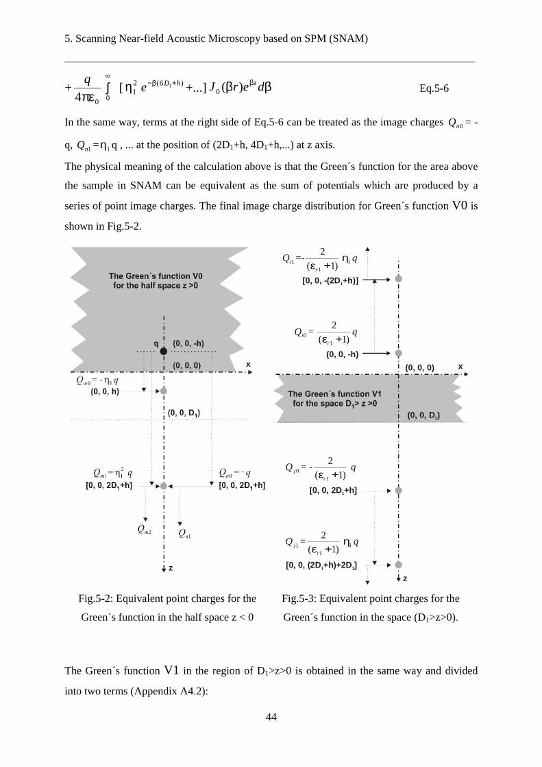
5. Scanning Near-field Acoustic Microscopy based on SPM (SNAM)
___________________________________________________________________________
44
+04πε
q∫∞
0[ 2
1η )6( 1 hDe +β− +...] ββ β derJ z)(0 Eq.5-6
In the same way, terms at the right side of Eq.5-6 can be treated as the image charges 0nQ = -
q, 1nQ = 1η q , ... at the position of (2D1+h, 4D1+h,...) at z axis.
The physical meaning of the calculation above is that the Green´s function for the area above
the sample in SNAM can be equivalent as the sum of potentials which are produced by a
series of point image charges. The final image charge distribution for Green´s function V0 is
shown in Fig.5-2.
The Green´s function V1 in the region of D1>z>0 is obtained in the same way and divided
into two terms (Appendix A4.2):
x
z
(0, 0, 0)
(0, 0, -h)
(0, 0, D )1
z
x
0iQ = )1(
2
1 +εr
q
1iQ =-)1(
2
1 +εr1η q
0jQ = -)1(
2
1 +εr
q
1jQ =)1(
2
1 +εr
1η q
[0, 0, 2D +h]1
[0, 0, -(2D +h)]1
[0, 0, (2D +h)+2D ]1 1
Fig.5-2: Equivalent point charges for the
Green´s function in the half space z < 0
Fig.5-3: Equivalent point charges for the
Green´s function in the space (D1>z>0).
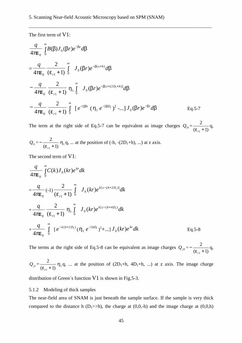
5. Scanning Near-field Acoustic Microscopy based on SPM (SNAM)
___________________________________________________________________________
45
The first term of V1:
04πεq
∫ βββ∞
β−
00 )()( derJB z
=04πε
q)1(
2
1 +εr
∫∞
0ββ +β− derJ hz )(
0 )(
04πε− q
)1(
2
1 +ε r1η ∫
∞
0ββ ++β− derJ hDz )]2([
01)(
04πε− q
)1(
2
1 +ε r
∫∞
0[ he β−2 ( 1η 12 De β− )2 -...] ββ β− derJ z)(0 Eq.5-7
The term at the right side of Eq.5-7 can be equivalent as image charges 0iQ =)1(
2
1 +ε r
q,
1iQ =)1(
2
1 +ε−
r1η q, ... at the position of (-h, -(2D1+h), ...) at z axis.
The second term of V1:
04πεq
∫∞
00 )()( dkekrJkC kz
=04πε
q(-1)
)1(
2
1 +εr
∫∞
0dkekrJ Dhzk )]2([
01)( +−
+04πε
q)1(
2
1 +εr1η ∫
∞
0dkekrJ Dhzk )4([
01)( +−
+04πε
q ∫
∞
0[
)2( 1Dhke +−( 1η 12kDe−
)2+...] dkekrJ kz)(0 Eq.5-8
The terms at the right side of Eq.5-8 can be equivalent as image charges 0jQ =)1(
2
1 +ε−
r
q,
1jQ =)1(
2
1 +ε r1η q, ... at the position of (2D1+h, 4D1+h, ...) at z axis. The image charge
distribution of Green´s function V1 is shown in Fig.5-3.
5.1.2 Modeling of thick samples
The near-field area of SNAM is just beneath the sample surface. If the sample is very thick
compared to the distance h (D1>>h), the charge at (0,0,-h) and the image charge at (0,0,h)
5. Scanning Near-field Acoustic Microscopy based on SPM (SNAM)
___________________________________________________________________________
46
with charge qQm 10 η−= have the greatest contribution to the Green´s function of V0 in the
vicinity of the tip contact area and the contribution of other image charges can be further
neglected (see Fig.5-2). In the same way and under the same approximation above, the field
distribution in near-field in the sample can also be calculated by the image charge at (0, 0, -h)
with a charge of qQr
i 1
20 +ε
= (see Fig.5-3). The physical meaning of the approximation is
that the sample is treated as an infinite half space with dielectric constant rε approximately.
Under the approximation above and from the Green´s function, if the rectangular Cartesian
coordinate system is used for the sake of further analyses of acoustic problems, the electric
potential under the approximation above can be written as:
V0=04
1
πε(
222 )( hzyx
q
+++ 222
0
)( hzyx
Qm
−+++ ), for z<0 Eq.5-9
in which 0mQ = - 1η q; Eq.5-10
V1=04
1
πε 222
0
)( hzyx
Qi
+++, for z>0 Eq.5-11
in which qQr
i 1
20 +ε
= . Eq.5-12
The system capacitance can be calculated by the Green´s function above. To make the best
approximation for the tip, the point )h,0,0( 0 at the pinnacle point of the tip will be given the
voltage of Vs. The equivalent charge, as mentioned above, is at the curvature center at the
pinnacle point with a curvature radius of 10 nm. The equivalent charge q :
q = eqC Vs = 04πε1
011
0 )()(
1−− +η−− hhhh
Vs Eq.5-13
From Eq.5-73, the source field distribution in the sample can be written as:
sE�
= xax
�
∂∂− V1
( + yay
�
∂∂ V1
+ )V1
zaz
�
∂∂
The x and y and z components of sE�
have the forms:
sxE =04
1
πε 3222 ))(( hzyx
x
+++0iQ Eq.5-14
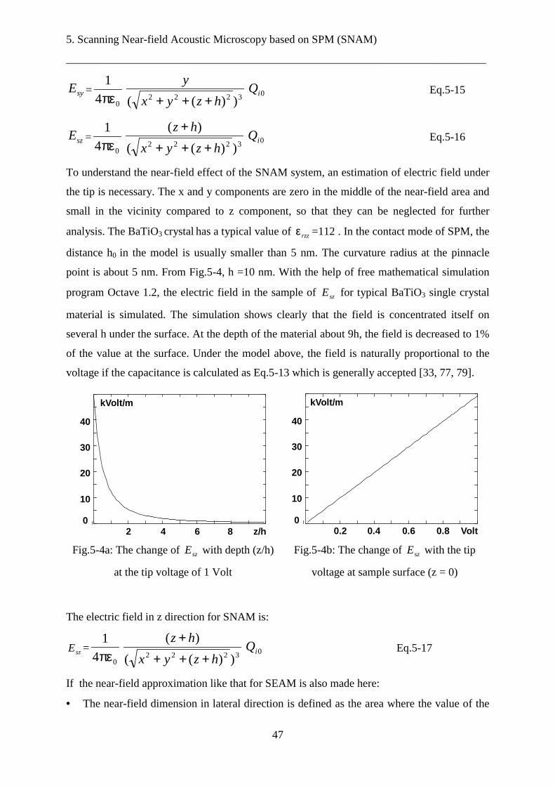
5. Scanning Near-field Acoustic Microscopy based on SPM (SNAM)
___________________________________________________________________________
47
syE =04
1
πε 3222 ))(( hzyx
y
+++0iQ Eq.5-15
szE =04
1
πε 3222 ))((
)(
hzyx
hz
++++
0iQ Eq.5-16
To understand the near-field effect of the SNAM system, an estimation of electric field under
the tip is necessary. The x and y components are zero in the middle of the near-field area and
small in the vicinity compared to z component, so that they can be neglected for further
analysis. The BaTiO3 crystal has a typical value of rzzε =112 . In the contact mode of SPM, the
distance h0 in the model is usually smaller than 5 nm. The curvature radius at the pinnacle
point is about 5 nm. From Fig.5-4, h =10 nm. With the help of free mathematical simulation
program Octave 1.2, the electric field in the sample of szE for typical BaTiO3 single crystal
material is simulated. The simulation shows clearly that the field is concentrated itself on
several h under the surface. At the depth of the material about 9h, the field is decreased to 1%
of the value at the surface. Under the model above, the field is naturally proportional to the
voltage if the capacitance is calculated as Eq.5-13 which is generally accepted [33, 77, 79].
The electric field in z direction for SNAM is:
szE =04
1
πε 3222 ))((
)(
hzyx
hz
++++
0iQ Eq.5-17
If the near-field approximation like that for SEAM is also made here:
• The near-field dimension in lateral direction is defined as the area where the value of the
kVolt/m
2 4 6 8 z/h0
10
20
30
40
kVolt/m
0.2 0.4 0.6 0.8 Volt0
10
20
30
40
Fig.5-4a: The change of szE with depth (z/h)
at the tip voltage of 1 Volt
Fig.5-4b: The change of szE with the tip
voltage at sample surface (z = 0)
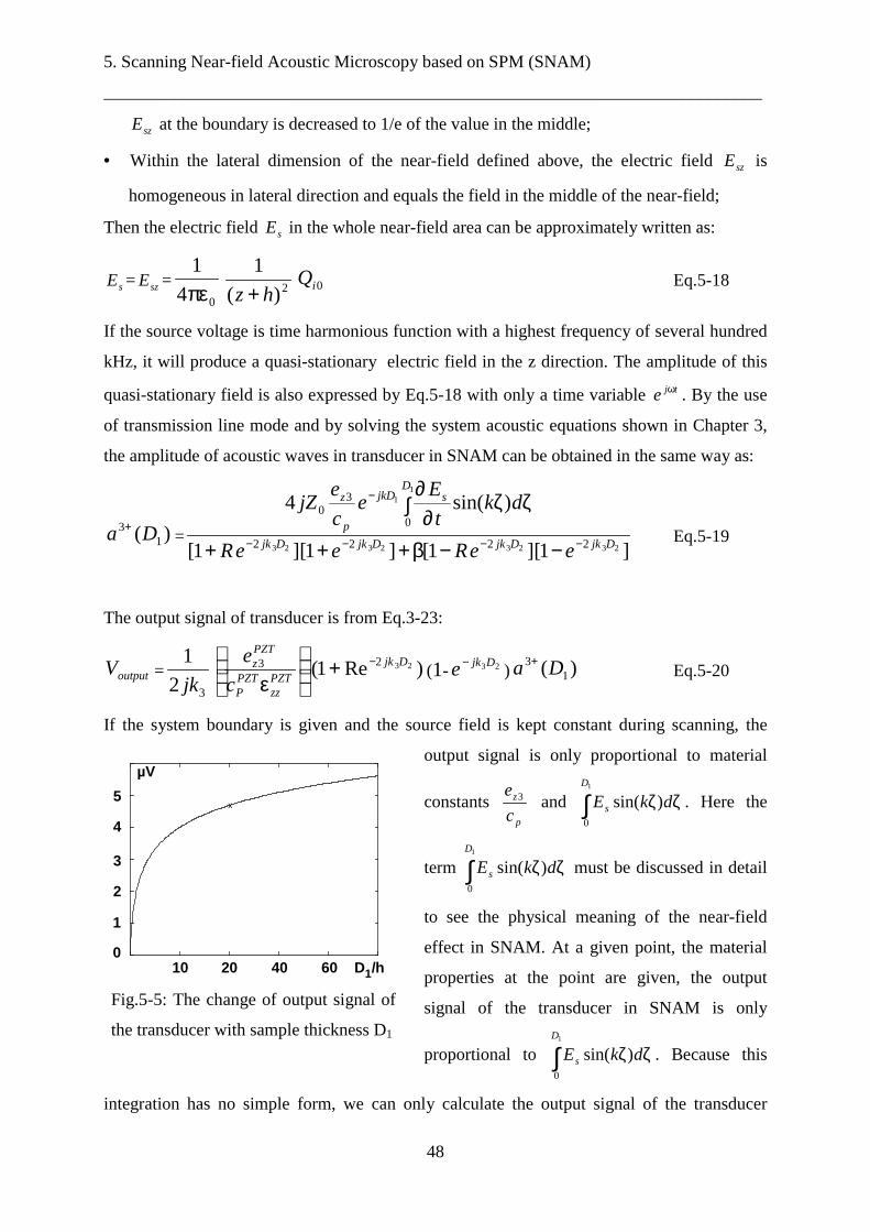
5. Scanning Near-field Acoustic Microscopy based on SPM (SNAM)
___________________________________________________________________________
48
szE at the boundary is decreased to 1/e of the value in the middle;
• Within the lateral dimension of the near-field defined above, the electric field szE is
homogeneous in lateral direction and equals the field in the middle of the near-field;
Then the electric field sE in the whole near-field area can be approximately written as:
sE = szE =04
1
πε 2)(
1
hz + 0iQ Eq.5-18
If the source voltage is time harmonious function with a highest frequency of several hundred
kHz, it will produce a quasi-stationary electric field in the z direction. The amplitude of this
quasi-stationary field is also expressed by Eq.5-18 with only a time variable tje ω . By the use
of transmission line mode and by solving the system acoustic equations shown in Chapter 3,
the amplitude of acoustic waves in transducer in SNAM can be obtained in the same way as:
)( 13 Da +
=]1][1[]1][1[
)sin(4
23232323
11
2222
0
30
DjkDjkDjkDjk
DsjkD
p
z
eeReeR
dkt
Ee
c
ejZ
−−−−
−
−−β+++
∫ ζζ∂
∂
Eq.5-19
The output signal of transducer is from Eq.3-23:
outputV =32
1
jk
εPZT
zzPZTP
PZTz
c
e 3 )Re1( 232 Djk−+ (1- 23Djke−) )( 1
3 Da + Eq.5-20
If the system boundary is given and the source field is kept constant during scanning, the
output signal is only proportional to material
constants p
z
c
e 3 and ∫ ζζ1
0
)sin(D
s dkE . Here the
term ∫ ζζ1
0
)sin(D
s dkE must be discussed in detail
to see the physical meaning of the near-field
effect in SNAM. At a given point, the material
properties at the point are given, the output
signal of the transducer in SNAM is only
proportional to ∫ ζζ1
0
)sin(D
s dkE . Because this
integration has no simple form, we can only calculate the output signal of the transducer
10 20 40 60 D /h1
0
1
2
3
4
5x
µV
Fig.5-5: The change of output signal of
the transducer with sample thickness D1
5. Scanning Near-field Acoustic Microscopy based on SPM (SNAM)
___________________________________________________________________________
49
through the Octave mathematical program. The output signal of the transducer at a certain
frequency (f=100kHz) with the change of thickness of the sample is shown in Fig.5-5. It is
clear that, after D1 = 20h, the signal changes very slowly and reaches almost the final value.
That means that the contrast of SNAM comes from the surface layer in the range from the
surface to several hundred nanometer deep. The reason is that most of the source electric field
in the model is concentrated in this area because of the form of the tip, as shown in Fig.5-4a.
After the discussion of near-field area in the thick sample, the contrast of ferroelectric
domains can be explained in the same way as in the case of SEAM. If the extrinsic
contribution of the domain walls to the piezoelectric effect in ferroelectric materials is
neglected, the constants of 3ze (or 3zd ) is directly related to ferroelectric polarization [see
Eq.2-24]. If there are two areas of c- and a-domains on the surface of BaTiO3 materials, the
area of c-domains has polarization in the z direction and has a non-zero value of 3ze in near-
field. When the scanning tip is on this area, the output signal of the transducer has a certain
value. Whereas the area of a-domains, which has a polarization perpendicular to the z
direction, will have zero value of 3ze . When the tip is on this a-domain area, the output signal
of the transducer, will have a zero value (or more accurately, very small value). As the
amplitude signal is used as the imaging signal, the c-domain will appear bright and a-domain
will appear black in acoustic image of SNAM system. This is the contrast mechanism of
SNAM on ferroelectric BaTiO3 single crystals. Here we must notice that the near-field
dimension is much smaller than that of SEAM.
5.1.3 Modeling of thin samples or films
If the sample is not so thick compared to the distance h (D1 ≅ h), or the sample is a
ferroelectric thin film which usually has a thickness of several hundreds to several thousands
nanometers, the condition D1>> h is not satisfied in this case. According to the Green´s
function of Eq.5-4 to Eq.5-8, the electric fields above the sample and in the sample are
dependent on series of image charges. The final field distribution is the sum of field
contributions from every single image point charge. How many image charges should be used
to decide the Green´s function of the system, is naturally dependent on the thickness of the
sample and the accuracy of the calculation. The typical thin film studied in this work has a
thickness of 1 µm and the distance of h is 10 nm. For this typical thin film system with the
first order of approximation, only the field contribution of the image point charges at the
distance to the surface in the range of (2D1+h) will be considered. The contribution of other
image charges at the distance outside this range is assumed so small that the contribution can
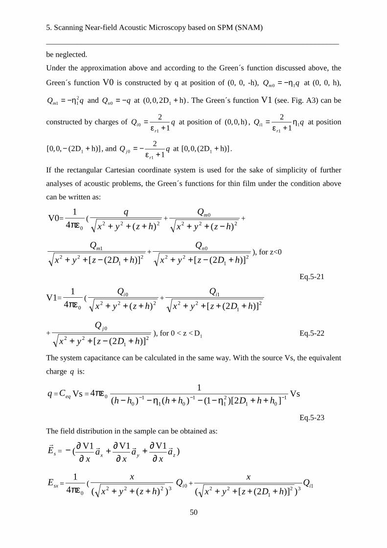
5. Scanning Near-field Acoustic Microscopy based on SPM (SNAM)
___________________________________________________________________________
50
be neglected.
Under the approximation above and according to the Green´s function discussed above, the
Green´s function V0 is constructed by q at position of (0, 0, -h), qQm 10 η−= at (0, 0, h),
qQm211 η−= and qQn −=0 at h)D2,0,0( 1 + . The Green´s function V1 (see. Fig. A3) can be
constructed by charges of qQr
i 1
2
10 +ε
= at position of h),0,0( , qQr
i 11
1 1
2 η+ε
= at position
h)]D2(,0,0[ 1 +− , and qQr
j 1
2
10 +ε
−= at h)]D2(,0,0[ 1 + .
If the rectangular Cartesian coordinate system is used for the sake of simplicity of further
analyses of acoustic problems, the Green´s functions for thin film under the condition above
can be written as:
V0=04
1
πε(
222 )( hzyx
q
++++
222
0
)( hzyx
Qm
−+++
21
22
1
)]2([ hDzyx
Qm
+−+++
21
22
0
)]2([ hDzyx
Qn
+−++), for z<0
Eq.5-21
V1=04
1
πε(
222
0
)( hzyx
Qi
++++
21
22
1
)]2([ hDzyx
Qi
++++
+2
122
0
)]2([ hDzyx
Q j
+−++), for 0 < z < 1D Eq.5-22
The system capacitance can be calculated in the same way. With the source Vs, the equivalent
charge q is:
q = eqC Vs = 04πε1
0121
101
10 ]2)[1()()(
1−−− ++η−−+η−− hhDhhhh
Vs
Eq.5-23
The field distribution in the sample can be obtained as:
sE�
= xa
x
�
∂∂− V1
( yax
�
∂∂+ V1
)V1
zax
�
∂∂+
sxE =04
1
πε(
3222 ))(( hzyx
x
+++0iQ + 132
122 ))]2([(
iQhDzyx
x
++++
5. Scanning Near-field Acoustic Microscopy based on SPM (SNAM)
___________________________________________________________________________
51
+ 0321
22 ))]2([(jQ
hDzyx
x
+−++Eq.5-24
syE =04
1
πε(
3222 ))(( hzyx
y
+++0iQ + 132
122 ))]2([(
iQhDzyx
y
++++
+ 0321
22 ))]2([(jQ
hDzyx
y
+−++Eq.5-25
szE =04
1
πε(
3222 ))((
)(
hzyx
hz
++++
0iQ + 1321
22
1
))]2([(
)2(iQ
hDzyx
hDz
++++++
+ 0321
22
1
))]2([(
)2(jQ
hDzyx
hDz
+−+++−
Eq.5-26
If the near-field approximation like that of SEAM is also made here:
• The near-field dimension in lateral direction is defined as the area where the value of the
zE at the boundary is decreased to 1/e of the value in the middle;
• Within the lateral dimension of the near-field defined above, the electric field zE is
homogeneous in lateral direction and equals the field in the middle of the near-field;
Then the electric field in the whole near-field can be approximately written as:
sE = szE =04
1
πε( 2)(
1
hz + 0iQ + 21 )]2([
1
hDz ++ 1iQ2
1 )]2([
1
hDz +−− 0jQ )
Eq.5-27
in which qQr
i 1
2
10 +ε
= , 1iQ = qr
11 1
2 η+ε
, and 0jQ = qr 1
2
1 +ε− .
The output signal of the transducer can also be obtained by Eq.5-19 and Eq.5-20. It must be
noted that, if the thickness of the film is D1=1 µm, the electric field in z direction in near-field
has little change according to Eq.5-27 as the last two terms in Eq.5-27 are much smaller than
the first one. That means that the two image charges 1iQ and 0jQ have so small an effect to
the electric field distribution in the near-field that the effect can be neglected as well. Only if
the thickness of the film is comparable to the parameter h, the field distribution should be
estimated according to different order of approximation to the Green´s function Eq.5-4 and
Eq.5-8, and finally the equivalent image charges can be decided.
5.2 Experiment set-up
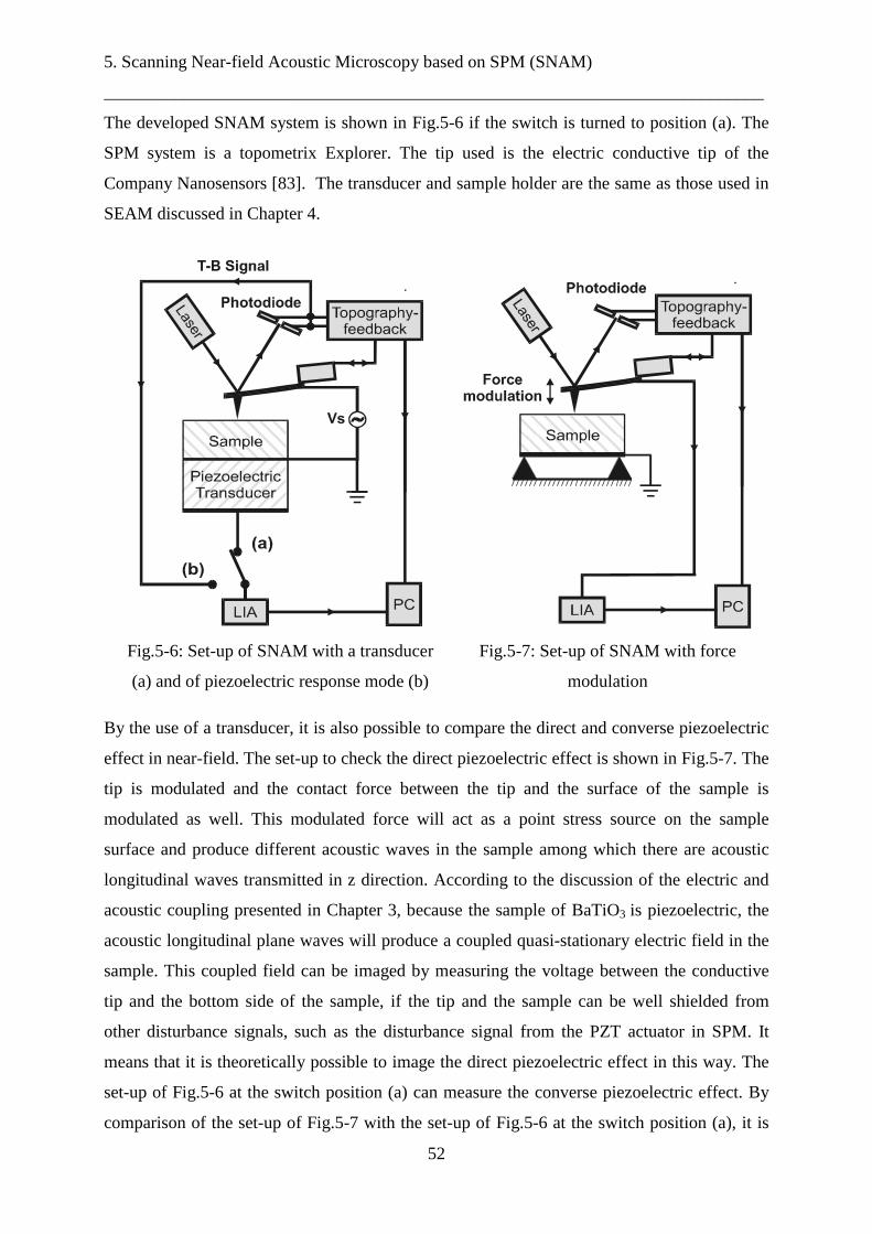
5. Scanning Near-field Acoustic Microscopy based on SPM (SNAM)
___________________________________________________________________________
52
The developed SNAM system is shown in Fig.5-6 if the switch is turned to position (a). The
SPM system is a topometrix Explorer. The tip used is the electric conductive tip of the
Company Nanosensors [83]. The transducer and sample holder are the same as those used in
SEAM discussed in Chapter 4.
By the use of a transducer, it is also possible to compare the direct and converse piezoelectric
effect in near-field. The set-up to check the direct piezoelectric effect is shown in Fig.5-7. The
tip is modulated and the contact force between the tip and the surface of the sample is
modulated as well. This modulated force will act as a point stress source on the sample
surface and produce different acoustic waves in the sample among which there are acoustic
longitudinal waves transmitted in z direction. According to the discussion of the electric and
acoustic coupling presented in Chapter 3, because the sample of BaTiO3 is piezoelectric, the
acoustic longitudinal plane waves will produce a coupled quasi-stationary electric field in the
sample. This coupled field can be imaged by measuring the voltage between the conductive
tip and the bottom side of the sample, if the tip and the sample can be well shielded from
other disturbance signals, such as the disturbance signal from the PZT actuator in SPM. It
means that it is theoretically possible to image the direct piezoelectric effect in this way. The
set-up of Fig.5-6 at the switch position (a) can measure the converse piezoelectric effect. By
comparison of the set-up of Fig.5-7 with the set-up of Fig.5-6 at the switch position (a), it is
Fig.5-6: Set-up of SNAM with a transducer
(a) and of piezoelectric response mode (b)
Fig.5-7: Set-up of SNAM with force
modulation
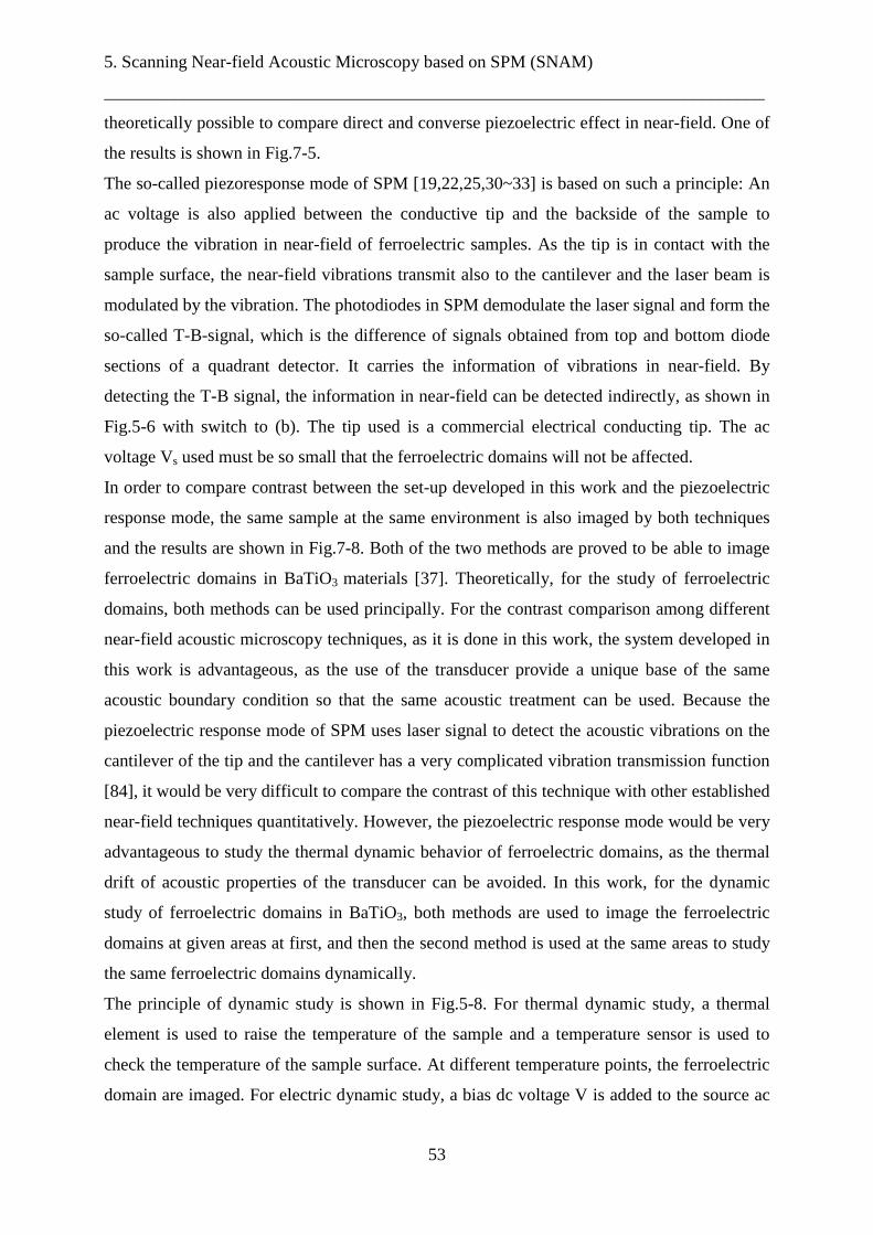
5. Scanning Near-field Acoustic Microscopy based on SPM (SNAM)
___________________________________________________________________________
53
theoretically possible to compare direct and converse piezoelectric effect in near-field. One of
the results is shown in Fig.7-5.
The so-called piezoresponse mode of SPM [19,22,25,30~33] is based on such a principle: An
ac voltage is also applied between the conductive tip and the backside of the sample to
produce the vibration in near-field of ferroelectric samples. As the tip is in contact with the
sample surface, the near-field vibrations transmit also to the cantilever and the laser beam is
modulated by the vibration. The photodiodes in SPM demodulate the laser signal and form the
so-called T-B-signal, which is the difference of signals obtained from top and bottom diode
sections of a quadrant detector. It carries the information of vibrations in near-field. By
detecting the T-B signal, the information in near-field can be detected indirectly, as shown in
Fig.5-6 with switch to (b). The tip used is a commercial electrical conducting tip. The ac
voltage Vs used must be so small that the ferroelectric domains will not be affected.
In order to compare contrast between the set-up developed in this work and the piezoelectric
response mode, the same sample at the same environment is also imaged by both techniques
and the results are shown in Fig.7-8. Both of the two methods are proved to be able to image
ferroelectric domains in BaTiO3 materials [37]. Theoretically, for the study of ferroelectric
domains, both methods can be used principally. For the contrast comparison among different
near-field acoustic microscopy techniques, as it is done in this work, the system developed in
this work is advantageous, as the use of the transducer provide a unique base of the same
acoustic boundary condition so that the same acoustic treatment can be used. Because the
piezoelectric response mode of SPM uses laser signal to detect the acoustic vibrations on the
cantilever of the tip and the cantilever has a very complicated vibration transmission function
[84], it would be very difficult to compare the contrast of this technique with other established
near-field techniques quantitatively. However, the piezoelectric response mode would be very
advantageous to study the thermal dynamic behavior of ferroelectric domains, as the thermal
drift of acoustic properties of the transducer can be avoided. In this work, for the dynamic
study of ferroelectric domains in BaTiO3, both methods are used to image the ferroelectric
domains at given areas at first, and then the second method is used at the same areas to study
the same ferroelectric domains dynamically.
The principle of dynamic study is shown in Fig.5-8. For thermal dynamic study, a thermal
element is used to raise the temperature of the sample and a temperature sensor is used to
check the temperature of the sample surface. At different temperature points, the ferroelectric
domain are imaged. For electric dynamic study, a bias dc voltage V is added to the source ac
5. Scanning Near-field Acoustic Microscopy based on SPM (SNAM)
___________________________________________________________________________
54
voltage Vs. This bias dc voltage will add a
bias static electric field in near-field
besides the quasi-stationary field. By
changing the bias dc voltage, the change
of domains at different bias field can be
imaged dynamically [37].
5.3 Discussion of the signal and noise inSNAM developed
As the SNAM is mainly used as an
imaging technique, spatial resolutions play
an important role. As discussed above,
both the lateral resolution and depth
penetration of SNAM are decided by the
parameter h which is the distance of the
equivalent charge of the tip to the surface. From the approximation in this work, this distance
is about 10 nm. According to the assumption of near-field for SNAM above, the lateral
dimension of the defined near-field can be calculated theoretically according to the field
distribution Eq. 5-17. At the surface 0=z , the dimension of near-field in lateral direction has
a radius of ≈−13eh 4.3h nm. That means the lateral resolution of the SNAM developed can
reach 86 nm, which is verified by the experiment results very well [36, 37]. The depth of
imaging would be the integration of the electric field in z direction in near-field for thick
samples and, according to Eq.5-20 and Fig.5-5, the depth of imaging by SNAM on thick bulk
BaTiO3 sample is about 200 nm.
The imaging time of the system is mainly dependent on the scanning speed of SPM. In order
to get a good topography, the scanning speed is usually slow, smaller than 1200 pixel/second.
For an image of 400X400 pixel, it takes about 1~2 minutes to take a picture.
The signal to noise ratio can also be estimated. Like in the case of SEAM, If the noise from
function generator, SPM, and the measuring circuit and lock-in amplifier are Gσ , SPMσ , and
mσ , it is necessary to add the signal to noise ratio of acoustic detecting system Aσ which is
composed of the acoustic transmission noise and the thermal noise of transducer. The total
noise totalσ is:
Fig.5-8: Set-up of SNAM for dynamic study
5. Scanning Near-field Acoustic Microscopy based on SPM (SNAM)
___________________________________________________________________________
55
totalσ =2222AmSPMG
σ+σ+σ+σ Eq.5-28
The Gσ , SEMσ , mσ are given for a certain SEM system. Principally, because there is no
thermal noise in the near-field of Aσ compared to SEAM, the signal to noise ratio of SNAM
would be much better than that SEAM. But Aσ is also very difficult to evaluate and can only
be decided experimentally. According to our experiments, typical values of signal to noise
ratio of the acoustic signal imaged after the lock-in amplifier can be measured by the line
measurement of the software of SPM. At 100 kHz, a typical value is in the range of 7~10
[36]. It can be expected that the contrast of SNAM acoustic images would be better than that
of SEAM under the same experiment condition.
6. Experiment procedure___________________________________________________________________________
56
6 Experiment procedure
6.1 Description of Specimen
As it is explained in chapter 2, ferroelectric BaTiO3 materials has the typical a- and c- domain
structures. BaTiO3 ceramics samples AC0 was fabricated by the Institut für Anorganische
Chemie, Martin-Luther-Universität Halle-Wittenberg. One of a sample of single crystal for
SEAM study was provided by Lab. of function ceramics, Shanghai Institute of ceramics. The
single crystal sample for SNAM study was provided by Department of Applied Physics,
University of Electronic Science and Technology of China. The film sample for the SEAM
study was provided by Institut für Schicht- und Ionentechnik (ISI), Forschungszentrum Jülich,
Germany. The other BaTiO3 film was provided by Max-Planck-Institut für Mikrostruktur-
physik, Germany. All the samples had crude surface and no treatment was required for both
SEAM and SNAM studies. The ceramics sample AC0 was sintered with excess 1 % mol of
TiO2 and had an average grain size from 10 to 50 micrometer [86].
6.2 Specimen preparation and treatment
As both techniques, SEAM and SNAM, are nondestructive techniques, the surface of a
sample needs no handling and treatment. In order to study the same area of a sample with two
kinds of microscopy techniques, it is necessary that the surface topography and the other
properties of the sample be kept unchanged during the study. Furthermore, to make the
comparison study of two microscopes, the same sample must be studied in one of the
microscope, then be moved to the other microscope. As the area studied is usually smaller
than 100 micrometer and the samples have almost no peculiar surface characters, it results in
a very difficult task to find the same area after the change of microscopes. For SEAM, in
order to avoid the charge effect, a thin gold layer of about 10 to 50 nanometer is usually
coated on the surface of the sample.
To solve the problems above, the SEAM experiment is arranged at first. There are two
advantages to do so. Firstly, the SEAM is a relative stable and established technique.
Although it has a resolution of micrometers, its large scan range, which can reach several
hundred micrometers, provides a useful way to image the ferroelectric domains broadly.
Secondly, by the use of the strong interaction between the sample and electron beam, it is
possible to make some surface characters, such as orientation lines outside the studied area, so
that the same area can be located precisely for the later SNAM experiment.
There is but one problem with this procedure. For SEAM, to avoid the surface charge effect
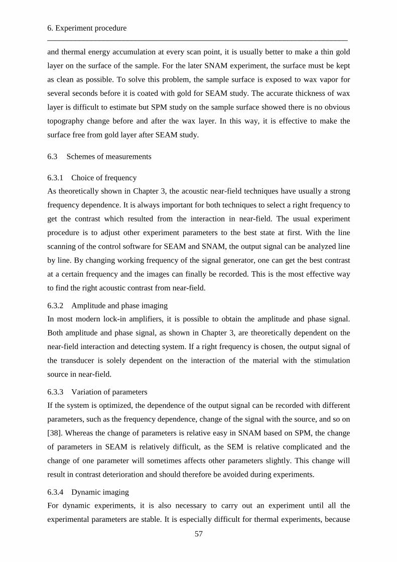
6. Experiment procedure___________________________________________________________________________
57
and thermal energy accumulation at every scan point, it is usually better to make a thin gold
layer on the surface of the sample. For the later SNAM experiment, the surface must be kept
as clean as possible. To solve this problem, the sample surface is exposed to wax vapor for
several seconds before it is coated with gold for SEAM study. The accurate thickness of wax
layer is difficult to estimate but SPM study on the sample surface showed there is no obvious
topography change before and after the wax layer. In this way, it is effective to make the
surface free from gold layer after SEAM study.
6.3 Schemes of measurements
6.3.1 Choice of frequency
As theoretically shown in Chapter 3, the acoustic near-field techniques have usually a strong
frequency dependence. It is always important for both techniques to select a right frequency to
get the contrast which resulted from the interaction in near-field. The usual experiment
procedure is to adjust other experiment parameters to the best state at first. With the line
scanning of the control software for SEAM and SNAM, the output signal can be analyzed line
by line. By changing working frequency of the signal generator, one can get the best contrast
at a certain frequency and the images can finally be recorded. This is the most effective way
to find the right acoustic contrast from near-field.
6.3.2 Amplitude and phase imaging
In most modern lock-in amplifiers, it is possible to obtain the amplitude and phase signal.
Both amplitude and phase signal, as shown in Chapter 3, are theoretically dependent on the
near-field interaction and detecting system. If a right frequency is chosen, the output signal of
the transducer is solely dependent on the interaction of the material with the stimulation
source in near-field.
6.3.3 Variation of parameters
If the system is optimized, the dependence of the output signal can be recorded with different
parameters, such as the frequency dependence, change of the signal with the source, and so on
[38]. Whereas the change of parameters is relative easy in SNAM based on SPM, the change
of parameters in SEAM is relatively difficult, as the SEM is relative complicated and the
change of one parameter will sometimes affects other parameters slightly. This change will
result in contrast deterioration and should therefore be avoided during experiments.
6.3.4 Dynamic imaging
For dynamic experiments, it is also necessary to carry out an experiment until all the
experimental parameters are stable. It is especially difficult for thermal experiments, because
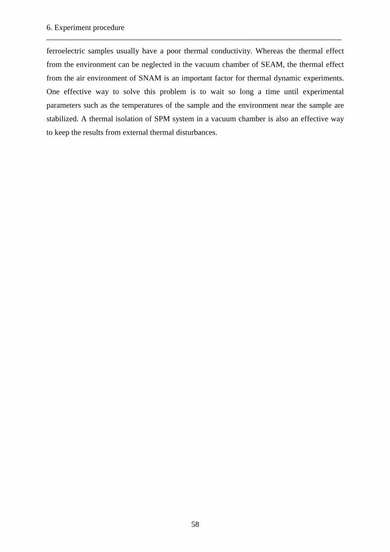
6. Experiment procedure___________________________________________________________________________
58
ferroelectric samples usually have a poor thermal conductivity. Whereas the thermal effect
from the environment can be neglected in the vacuum chamber of SEAM, the thermal effect
from the air environment of SNAM is an important factor for thermal dynamic experiments.
One effective way to solve this problem is to wait so long a time until experimental
parameters such as the temperatures of the sample and the environment near the sample are
stabilized. A thermal isolation of SPM system in a vacuum chamber is also an effective way
to keep the results from external thermal disturbances.
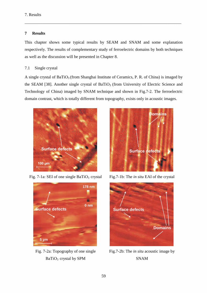
7. Results
___________________________________________________________________________
59
7 Results
This chapter shows some typical results by SEAM and SNAM and some explanation
respectively. The results of complementary study of ferroelectric domains by both techniques
as well as the discussion will be presented in Chapter 8.
7.1 Single crystal
A single crystal of BaTiO3 (from Shanghai Institute of Ceramics, P. R. of China) is imaged by
the SEAM [38]. Another single crystal of BaTiO3 (from University of Electric Science and
Technology of China) imaged by SNAM technique and shown in Fig.7-2. The ferroelectric
domain contrast, which is totally different from topography, exists only in acoustic images.
Fig. 7-1a: SEI of one single BaTiO3 crystal Fig.7-1b: The in situ EAI of the crystal
178 nm
0 nm
5 µm
Surface defects Surface defects
Domains
Fig. 7-2a: Topography of one single
BaTiO3 crystal by SPM
Fig.7-2b: The in situ acoustic image by
SNAM
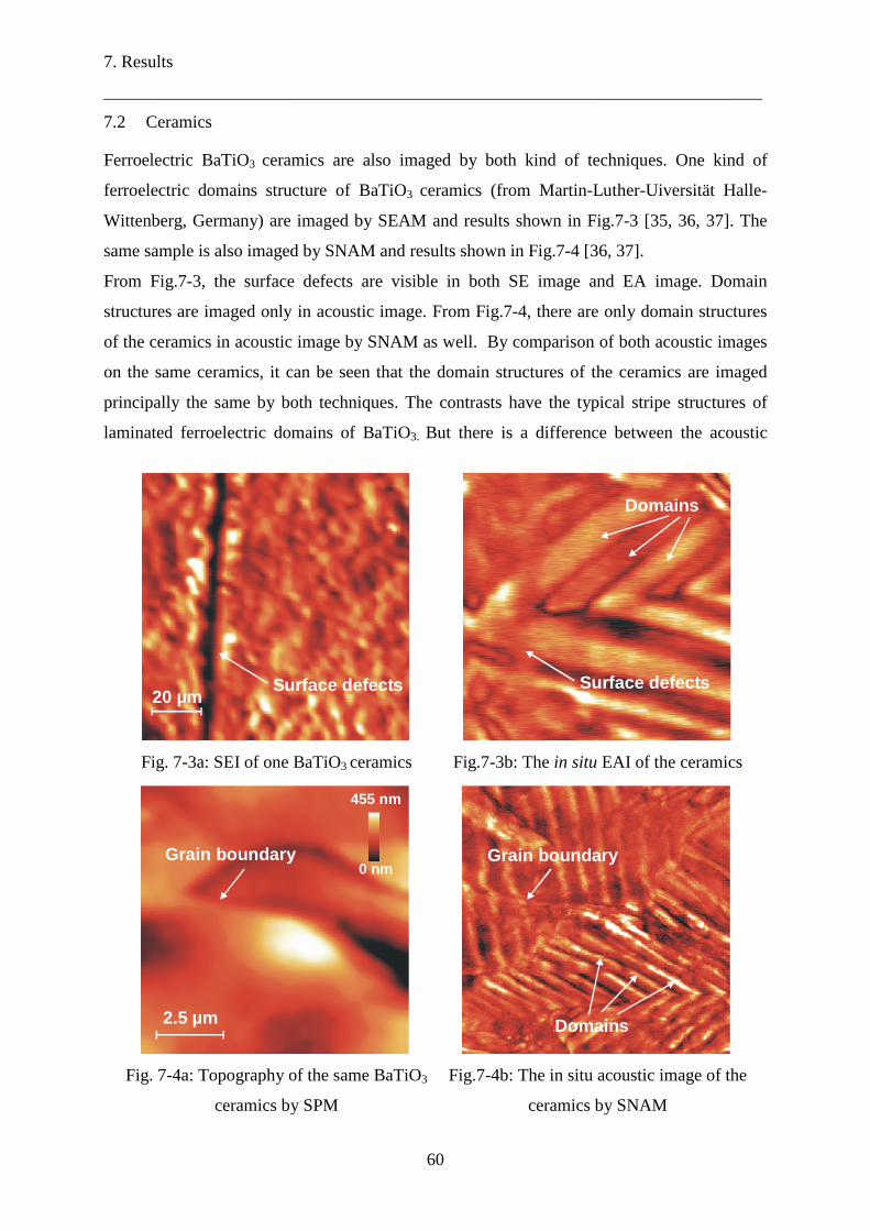
7. Results
___________________________________________________________________________
60
7.2 Ceramics
Ferroelectric BaTiO3 ceramics are also imaged by both kind of techniques. One kind of
ferroelectric domains structure of BaTiO3 ceramics (from Martin-Luther-Uiversität Halle-
Wittenberg, Germany) are imaged by SEAM and results shown in Fig.7-3 [35, 36, 37]. The
same sample is also imaged by SNAM and results shown in Fig.7-4 [36, 37].
From Fig.7-3, the surface defects are visible in both SE image and EA image. Domain
structures are imaged only in acoustic image. From Fig.7-4, there are only domain structures
of the ceramics in acoustic image by SNAM as well. By comparison of both acoustic images
on the same ceramics, it can be seen that the domain structures of the ceramics are imaged
principally the same by both techniques. The contrasts have the typical stripe structures of
laminated ferroelectric domains of BaTiO3. But there is a difference between the acoustic
20 µmSurface defects
Domains
Surface defects
Fig. 7-3a: SEI of one BaTiO3 ceramics Fig.7-3b: The in situ EAI of the ceramics
455 nm
0 nm
2.5 µm
Grain boundary Grain boundary
Domains
Fig. 7-4a: Topography of the same BaTiO3
ceramics by SPM
Fig.7-4b: The in situ acoustic image of the
ceramics by SNAM
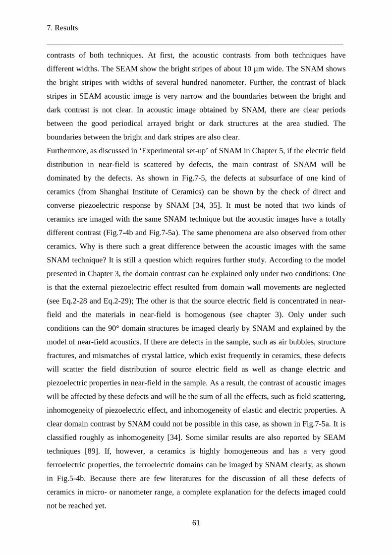
7. Results
___________________________________________________________________________
61
contrasts of both techniques. At first, the acoustic contrasts from both techniques have
different widths. The SEAM show the bright stripes of about 10 µm wide. The SNAM shows
the bright stripes with widths of several hundred nanometer. Further, the contrast of black
stripes in SEAM acoustic image is very narrow and the boundaries between the bright and
dark contrast is not clear. In acoustic image obtained by SNAM, there are clear periods
between the good periodical arrayed bright or dark structures at the area studied. The
boundaries between the bright and dark stripes are also clear.
Furthermore, as discussed in ‘Experimental set-up’ of SNAM in Chapter 5, if the electric field
distribution in near-field is scattered by defects, the main contrast of SNAM will be
dominated by the defects. As shown in Fig.7-5, the defects at subsurface of one kind of
ceramics (from Shanghai Institute of Ceramics) can be shown by the check of direct and
converse piezoelectric response by SNAM [34, 35]. It must be noted that two kinds of
ceramics are imaged with the same SNAM technique but the acoustic images have a totally
different contrast (Fig.7-4b and Fig.7-5a). The same phenomena are also observed from other
ceramics. Why is there such a great difference between the acoustic images with the same
SNAM technique? It is still a question which requires further study. According to the model
presented in Chapter 3, the domain contrast can be explained only under two conditions: One
is that the external piezoelectric effect resulted from domain wall movements are neglected
(see Eq.2-28 and Eq.2-29); The other is that the source electric field is concentrated in near-
field and the materials in near-field is homogenous (see chapter 3). Only under such
conditions can the 90° domain structures be imaged clearly by SNAM and explained by the
model of near-field acoustics. If there are defects in the sample, such as air bubbles, structure
fractures, and mismatches of crystal lattice, which exist frequently in ceramics, these defects
will scatter the field distribution of source electric field as well as change electric and
piezoelectric properties in near-field in the sample. As a result, the contrast of acoustic images
will be affected by these defects and will be the sum of all the effects, such as field scattering,
inhomogeneity of piezoelectric effect, and inhomogeneity of elastic and electric properties. A
clear domain contrast by SNAM could not be possible in this case, as shown in Fig.7-5a. It is
classified roughly as inhomogeneity [34]. Some similar results are also reported by SEAM
techniques [89]. If, however, a ceramics is highly homogeneous and has a very good
ferroelectric properties, the ferroelectric domains can be imaged by SNAM clearly, as shown
in Fig.5-4b. Because there are few literatures for the discussion of all these defects of
ceramics in micro- or nanometer range, a complete explanation for the defects imaged could
not be reached yet.
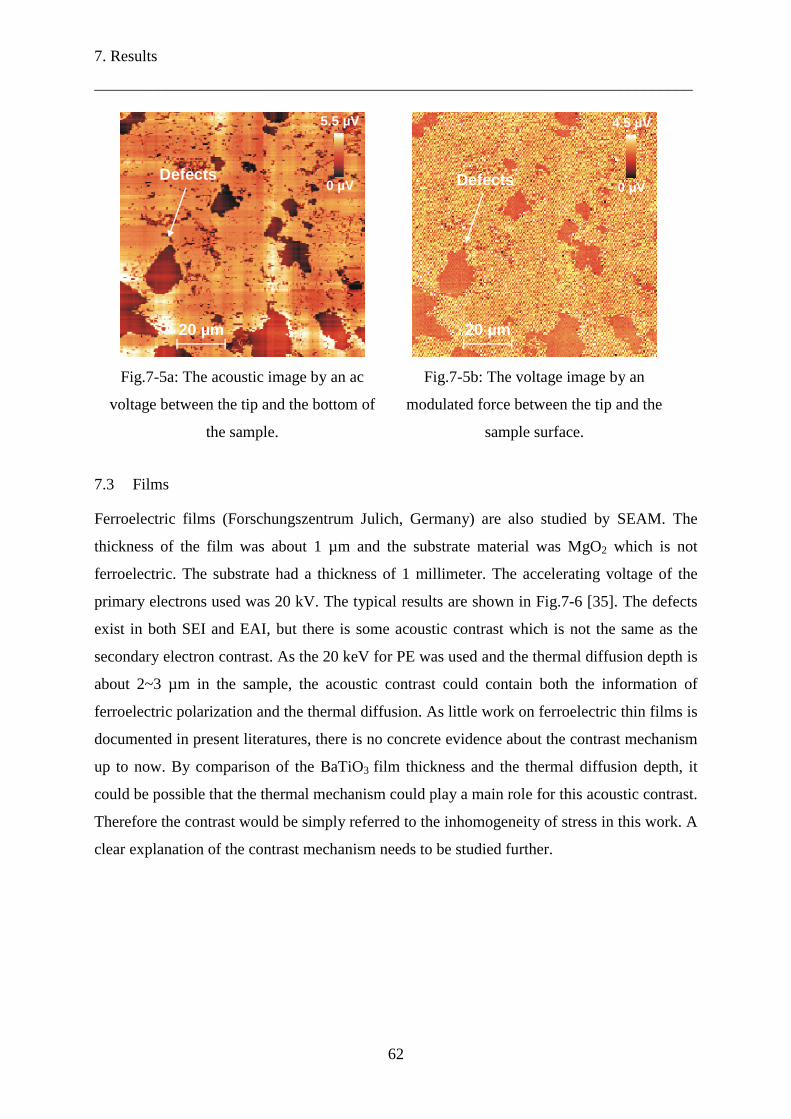
7. Results
___________________________________________________________________________
62
7.3 Films
Ferroelectric films (Forschungszentrum Julich, Germany) are also studied by SEAM. The
thickness of the film was about 1 µm and the substrate material was MgO2 which is not
ferroelectric. The substrate had a thickness of 1 millimeter. The accelerating voltage of the
primary electrons used was 20 kV. The typical results are shown in Fig.7-6 [35]. The defects
exist in both SEI and EAI, but there is some acoustic contrast which is not the same as the
secondary electron contrast. As the 20 keV for PE was used and the thermal diffusion depth is
about 2~3 µm in the sample, the acoustic contrast could contain both the information of
ferroelectric polarization and the thermal diffusion. As little work on ferroelectric thin films is
documented in present literatures, there is no concrete evidence about the contrast mechanism
up to now. By comparison of the BaTiO3 film thickness and the thermal diffusion depth, it
could be possible that the thermal mechanism could play a main role for this acoustic contrast.
Therefore the contrast would be simply referred to the inhomogeneity of stress in this work. A
clear explanation of the contrast mechanism needs to be studied further.
5.5 µV
0 µVDefects
20 µm
4.5 µV
0 µVDefects
20 µm
Fig.7-5a: The acoustic image by an ac
voltage between the tip and the bottom of
the sample.
Fig.7-5b: The voltage image by an
modulated force between the tip and the
sample surface.
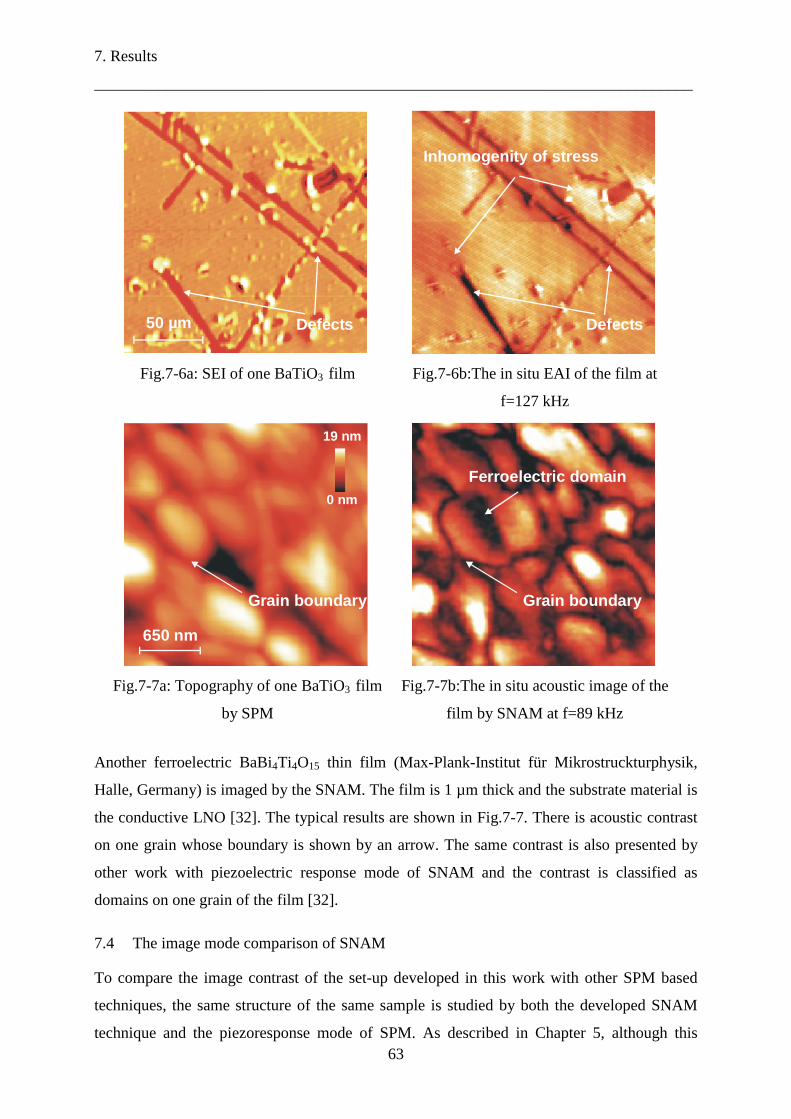
7. Results
___________________________________________________________________________
63
Another ferroelectric BaBi4Ti4O15 thin film (Max-Plank-Institut für Mikrostruckturphysik,
Halle, Germany) is imaged by the SNAM. The film is 1 µm thick and the substrate material is
the conductive LNO [32]. The typical results are shown in Fig.7-7. There is acoustic contrast
on one grain whose boundary is shown by an arrow. The same contrast is also presented by
other work with piezoelectric response mode of SNAM and the contrast is classified as
domains on one grain of the film [32].
7.4 The image mode comparison of SNAM
To compare the image contrast of the set-up developed in this work with other SPM based
techniques, the same structure of the same sample is studied by both the developed SNAM
technique and the piezoresponse mode of SPM. As described in Chapter 5, although this
50 µm Defects
Inhomogenity of stress
Defects
Fig.7-6a: SEI of one BaTiO3 film Fig.7-6b:The in situ EAI of the film at
f=127 kHz
650 nm
19 nm
0 nm
Grain boundary
Ferroelectric domain
Grain boundary
Fig.7-7a: Topography of one BaTiO3 film
by SPM
Fig.7-7b:The in situ acoustic image of the
film by SNAM at f=89 kHz
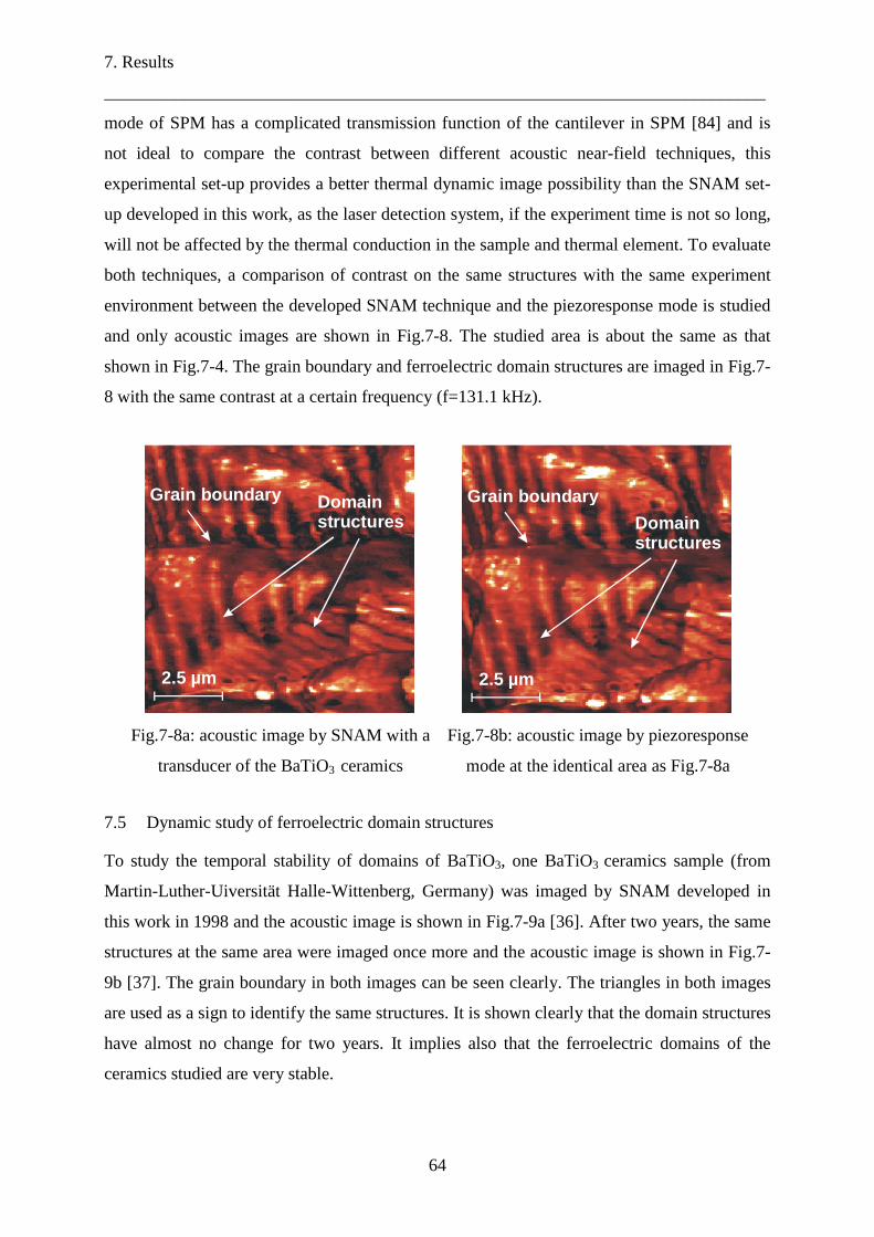
7. Results
___________________________________________________________________________
64
mode of SPM has a complicated transmission function of the cantilever in SPM [84] and is
not ideal to compare the contrast between different acoustic near-field techniques, this
experimental set-up provides a better thermal dynamic image possibility than the SNAM set-
up developed in this work, as the laser detection system, if the experiment time is not so long,
will not be affected by the thermal conduction in the sample and thermal element. To evaluate
both techniques, a comparison of contrast on the same structures with the same experiment
environment between the developed SNAM technique and the piezoresponse mode is studied
and only acoustic images are shown in Fig.7-8. The studied area is about the same as that
shown in Fig.7-4. The grain boundary and ferroelectric domain structures are imaged in Fig.7-
8 with the same contrast at a certain frequency (f=131.1 kHz).
7.5 Dynamic study of ferroelectric domain structures
To study the temporal stability of domains of BaTiO3, one BaTiO3 ceramics sample (from
Martin-Luther-Uiversität Halle-Wittenberg, Germany) was imaged by SNAM developed in
this work in 1998 and the acoustic image is shown in Fig.7-9a [36]. After two years, the same
structures at the same area were imaged once more and the acoustic image is shown in Fig.7-
9b [37]. The grain boundary in both images can be seen clearly. The triangles in both images
are used as a sign to identify the same structures. It is shown clearly that the domain structures
have almost no change for two years. It implies also that the ferroelectric domains of the
ceramics studied are very stable.
2.5 µm
Grain boundary Domainstructures
2.5 µm
Domainstructures
Grain boundary
Fig.7-8a: acoustic image by SNAM with a
transducer of the BaTiO3 ceramics
Fig.7-8b: acoustic image by piezoresponse
mode at the identical area as Fig.7-8a
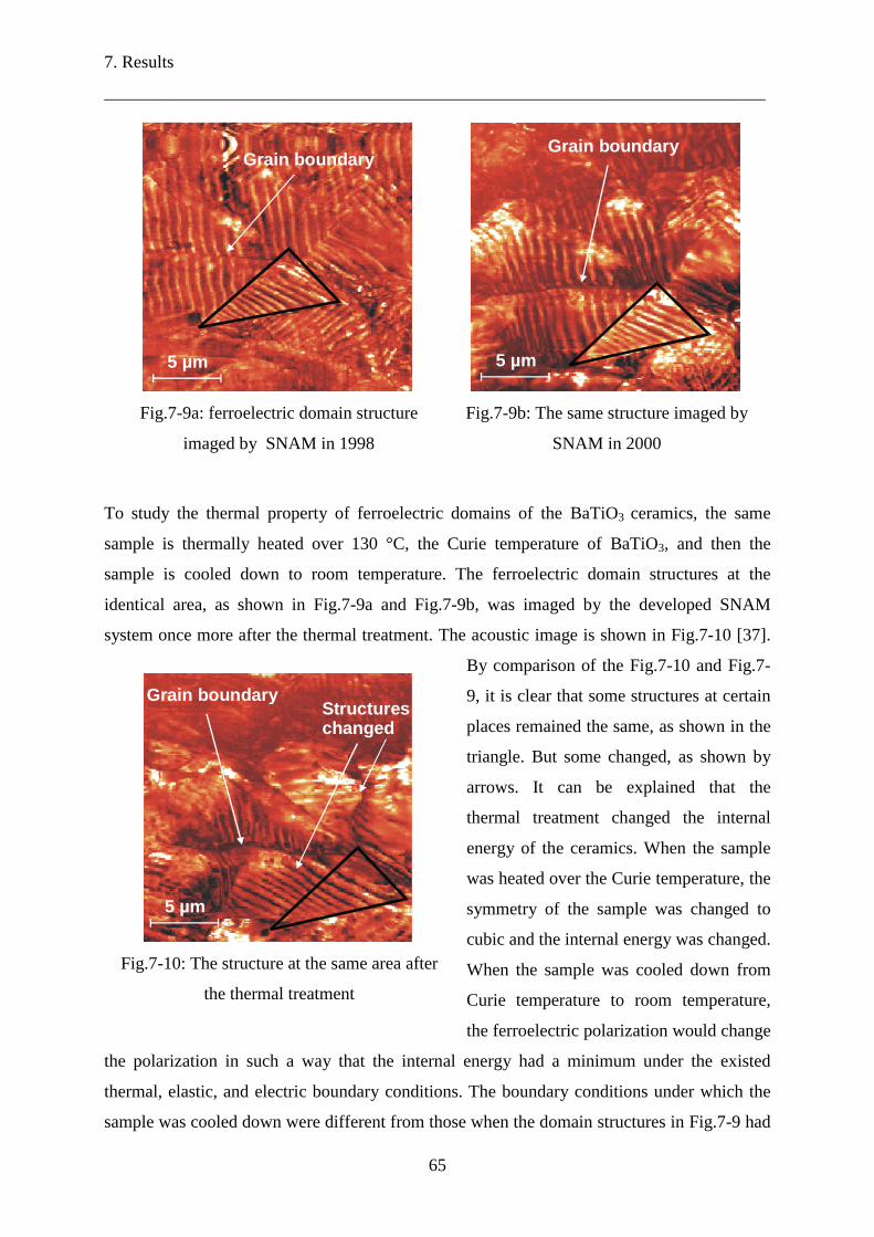
7. Results
___________________________________________________________________________
65
To study the thermal property of ferroelectric domains of the BaTiO3 ceramics, the same
sample is thermally heated over 130 °C, the Curie temperature of BaTiO3, and then the
sample is cooled down to room temperature. The ferroelectric domain structures at the
identical area, as shown in Fig.7-9a and Fig.7-9b, was imaged by the developed SNAM
system once more after the thermal treatment. The acoustic image is shown in Fig.7-10 [37].
By comparison of the Fig.7-10 and Fig.7-
9, it is clear that some structures at certain
places remained the same, as shown in the
triangle. But some changed, as shown by
arrows. It can be explained that the
thermal treatment changed the internal
energy of the ceramics. When the sample
was heated over the Curie temperature, the
symmetry of the sample was changed to
cubic and the internal energy was changed.
When the sample was cooled down from
Curie temperature to room temperature,
the ferroelectric polarization would change
the polarization in such a way that the internal energy had a minimum under the existed
thermal, elastic, and electric boundary conditions. The boundary conditions under which the
sample was cooled down were different from those when the domain structures in Fig.7-9 had
5 µm
Grain boundaryGrain boundary
5 µm
Fig.7-9a: ferroelectric domain structure
imaged by SNAM in 1998
Fig.7-9b: The same structure imaged by
SNAM in 2000
5 µm
Structureschanged
Grain boundary
Fig.7-10: The structure at the same area after
the thermal treatment
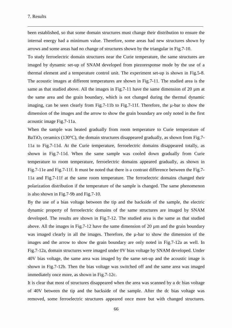
7. Results
___________________________________________________________________________
66
been established, so that some domain structures must change their distribution to ensure the
internal energy had a minimum value. Therefore, some areas had new structures shown by
arrows and some areas had no change of structures shown by the triangular in Fig.7-10.
To study ferroelectric domain structures near the Curie temperature, the same structures are
imaged by dynamic set-up of SNAM developed from piezoresponse mode by the use of a
thermal element and a temperature control unit. The experiment set-up is shown in Fig.5-8.
The acoustic images at different temperatures are shown in Fig.7-11. The studied area is the
same as that studied above. All the images in Fig.7-11 have the same dimension of 20 µm at
the same area and the grain boundary, which is not changed during the thermal dynamic
imaging, can be seen clearly from Fig.7-11b to Fig.7-11f. Therefore, the µ-bar to show the
dimension of the images and the arrow to show the grain boundary are only noted in the first
acoustic image Fig.7-11a.
When the sample was heated gradually from room temperature to Curie temperature of
BaTiO3 ceramics (130°C), the domain structures disappeared gradually, as shown from Fig.7-
11a to Fig.7-11d. At the Curie temperature, ferroelectric domains disappeared totally, as
shown in Fig.7-11d. When the same sample was cooled down gradually from Curie
temperature to room temperature, ferroelectric domains appeared gradually, as shown in
Fig.7-11e and Fig.7-11f. It must be noted that there is a contrast difference between the Fig.7-
11a and Fig.7-11f at the same room temperature. The ferroelectric domains changed their
polarization distribution if the temperature of the sample is changed. The same phenomenon
is also shown in Fig.7-9b and Fig.7-10.
By the use of a bias voltage between the tip and the backside of the sample, the electric
dynamic property of ferroelectric domains of the same structures are imaged by SNAM
developed. The results are shown in Fig.7-12. The studied area is the same as that studied
above. All the images in Fig.7-12 have the same dimension of 20 µm and the grain boundary
was imaged clearly in all the images. Therefore, the µ-bar to show the dimension of the
images and the arrow to show the grain boundary are only noted in Fig.7-12a as well. In
Fig.7-12a, domain structures were imaged under 0V bias voltage by SNAM developed. Under
40V bias voltage, the same area was imaged by the same set-up and the acoustic image is
shown in Fig.7-12b. Then the bias voltage was switched off and the same area was imaged
immediately once more, as shown in Fig.7-12c.
It is clear that most of structures disappeared when the area was scanned by a dc bias voltage
of 40V between the tip and the backside of the sample. After the dc bias voltage was
removed, some ferroelectric structures appeared once more but with changed structures.
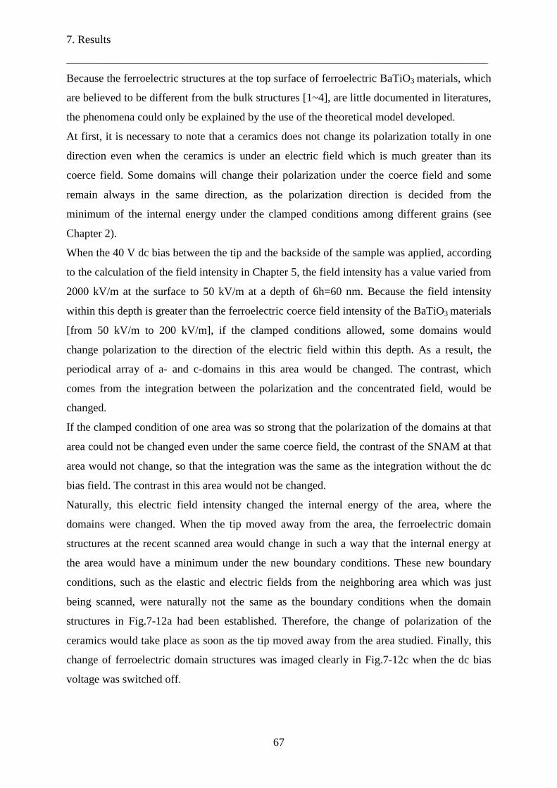
7. Results
___________________________________________________________________________
67
Because the ferroelectric structures at the top surface of ferroelectric BaTiO3 materials, which
are believed to be different from the bulk structures [1~4], are little documented in literatures,
the phenomena could only be explained by the use of the theoretical model developed.
At first, it is necessary to note that a ceramics does not change its polarization totally in one
direction even when the ceramics is under an electric field which is much greater than its
coerce field. Some domains will change their polarization under the coerce field and some
remain always in the same direction, as the polarization direction is decided from the
minimum of the internal energy under the clamped conditions among different grains (see
Chapter 2).
When the 40 V dc bias between the tip and the backside of the sample was applied, according
to the calculation of the field intensity in Chapter 5, the field intensity has a value varied from
2000 kV/m at the surface to 50 kV/m at a depth of 6h=60 nm. Because the field intensity
within this depth is greater than the ferroelectric coerce field intensity of the BaTiO3 materials
[from 50 kV/m to 200 kV/m], if the clamped conditions allowed, some domains would
change polarization to the direction of the electric field within this depth. As a result, the
periodical array of a- and c-domains in this area would be changed. The contrast, which
comes from the integration between the polarization and the concentrated field, would be
changed.
If the clamped condition of one area was so strong that the polarization of the domains at that
area could not be changed even under the same coerce field, the contrast of the SNAM at that
area would not change, so that the integration was the same as the integration without the dc
bias field. The contrast in this area would not be changed.
Naturally, this electric field intensity changed the internal energy of the area, where the
domains were changed. When the tip moved away from the area, the ferroelectric domain
structures at the recent scanned area would change in such a way that the internal energy at
the area would have a minimum under the new boundary conditions. These new boundary
conditions, such as the elastic and electric fields from the neighboring area which was just
being scanned, were naturally not the same as the boundary conditions when the domain
structures in Fig.7-12a had been established. Therefore, the change of polarization of the
ceramics would take place as soon as the tip moved away from the area studied. Finally, this
change of ferroelectric domain structures was imaged clearly in Fig.7-12c when the dc bias
voltage was switched off.
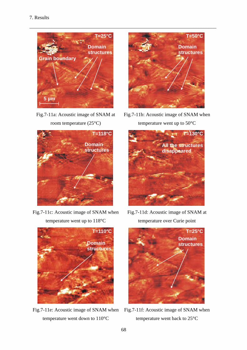
7. Results
___________________________________________________________________________
68
5 µm
T=25°C
Domainstructures
Grain boundary
T=50°C
Domainstructures
Fig.7-11a: Acoustic image of SNAM at
room temperature (25°C)
Fig.7-11b: Acoustic image of SNAM when
temperature went up to 50°C
T=118°C
Domainstructures
T=130°C
All the structuresdisappeared
Fig.7-11c: Acoustic image of SNAM when
temperature went up to 118°C
Fig.7-11d: Acoustic image of SNAM at
temperature over Curie point
T=110°C
Domainstructures
T=25°CDomainstructures
Fig.7-11e: Acoustic image of SNAM when
temperature went down to 110°C
Fig.7-11f: Acoustic image of SNAM when
temperature went back to 25°C
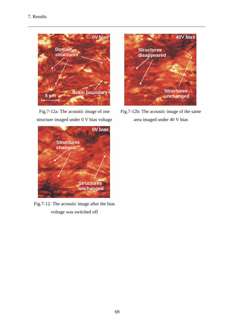
7. Results
___________________________________________________________________________
69
5 µm
0V bias
Domainstructures
Grain boundary
40V bias
Structuresdisappeared
Structuresunchanged
Fig.7-12a: The acoustic image of one
structure imaged under 0 V bias voltage
Fig.7-12b: The acoustic image of the same
area imaged under 40 V bias
0V bias
Structureschanged
Structuresunchanged
Fig.7-12: The acoustic image after the bias
voltage was switched off
8. Discussion of both near-field acoustic techniques___________________________________________________________________________
70
8 Discussion of both near-field acoustic techniques
8.1 Quality of imaging compared to other techniques
The SNAM and SEAM imaging techniques have many advantages over other techniques to
image ferroelectric domains. The most exciting characteristics of both techniques are the
nondestructive imaging of ferroelectric domains with no sample preparation. The easy
development from commercial SPM or SEM systems is another advantage. SNAM has further
advantages over SEAM in these respects, such as no vacuum system, better resolution down
to nanometer, and flexibility of dynamic imaging of ferroelectric domains of materials. On the
other hand, SEAM has such peculiarities as large imaging depth and broad imaging area
which are also not so easy to obtain only by the use of SNAM. Therefore, both techniques
will be applied complementarily to study ferroelectric materials in the future.
8.1.1 Speed of experiment
The imaging speed of SEAM is limited by the near-field establishing time in ferroelectric
materials. As it is discussed in Chapter 4, the time required to established the electric field in
near-field in SEAM depends on the charge accumulation in near-field and the properties of
materials. typical values for semiconductor and ceramics are in the range of 10-4 second. To
ensure good acoustic image of SEAM, the time at every pixel is usually chosen as 1 ms. For
one typical image with 400X400 pixels, it would take about 1~2 minutes to take one image.
SNAM technique has to scan the tip (or sample) by a piezoelectric scanning unit. Unlike
SEAM, it needs almost no delay time to establish the electric field in near-field. The imaging
time of the system is mainly dependent on the scanning speed of SPM. In order to ensure a
good topography, the scanning speed is usually slow, smaller than 1200 pixel/second. For an
image of 400X400 pixels, it takes about 1~2 minutes to take a picture. It is clear that both
techniques have almost the same image speed.
8.1.2 How quantitative
Generally speaking, the SEAM and SNAM are both scanning imaging techniques which
record the relative variation among scanning pixels in a given scanned area. If physical
properties of one scan pixel or one area can be determined quantitatively, the rest of scan
pixels can hereafter be imaged quantitatively.
SEAM technique has a very complicated interaction on the surface of ferroelectric materials,
when the primary electrons bombard the surface. Although much effort has been paid to
analyze interactions of primary electrons bombarding on metal materials, semiconductors, and
8. Discussion of both near-field acoustic techniques___________________________________________________________________________
71
some dielectric materials, both experimental and theoretical work on ferroelectric materials
are little documented in present literatures. A quantitative analysis requires the estimation of
parameters of experimental environments and their errors. If some basic parameters of SEAM
on ferroelectric materials, such as the accurate electric field intensity in near-field, the
accurate penetration depth of PE, the calculable relationship of different imaging mechanisms
and so on, are not quantitatively determined, the quantitative analysis of ferroelectric
polarization by SEAM would be impossible. Unfortunately, these important factors have been
sparsely documented in the present literatures. Therefore, the SEAM technique remains in
principle a qualitative imaging technique up till today.
Whether the SNAM or the related techniques are quantitative tools, is still a recent study
which is heavily debated today [31~33, 85]. To analyze the problem, it would be better to
review some basic approximations which are often used in the present literatures to
characterize ferroelectric materials by SNAM systems. Firstly, as discussed in Chapter 2, the
piezoelectric constant of ferroelectric ceramics depends on spontaneous polarization only
under the condition that external piezoelectric effect is neglected and polarization will not be
affected during the imaging; Secondly, to determine the electric field in the sample, all the
literatures assume that the sample is isotropic; Thirdly, only the main mode of the vibrations
in near-field is calculated and the acoustic mode conversions and nonlinear effects in near-
field are neglected; Finally, by detecting the near-field vibration through laser beam and
photodiodes in piezoelectric response mode, there exists a very complicated vibration
transmission function of the cantilever [84, 85] from which an accurate estimation of errors
would be difficult. On the other hand, by detecting the near-field vibrations through a
transducer, as it is done in this work, all the theoretical calculation must be under the
approximation of acoustic plane wave. Possible errors incurred under so many
approximations by the modeling of SNAM would be difficult to estimate at present as well. It
would be necessary to say that under all the approximations above, the theoretical model
developed for both SEAM and SNAM in this work can be used to calibrate the acoustic
contrast or domain structures quantitatively.
8.2 Comparison of SEAM and developed SNAM system
8.2.1 Image comparison and analyses
To compare the image of two kinds of microscopy techniques, it is necessary to compare the
properties at identical areas. As it is concerned with the nondestructive study of the
ferroelectric domains, the domain structures should not be damaged during the change of
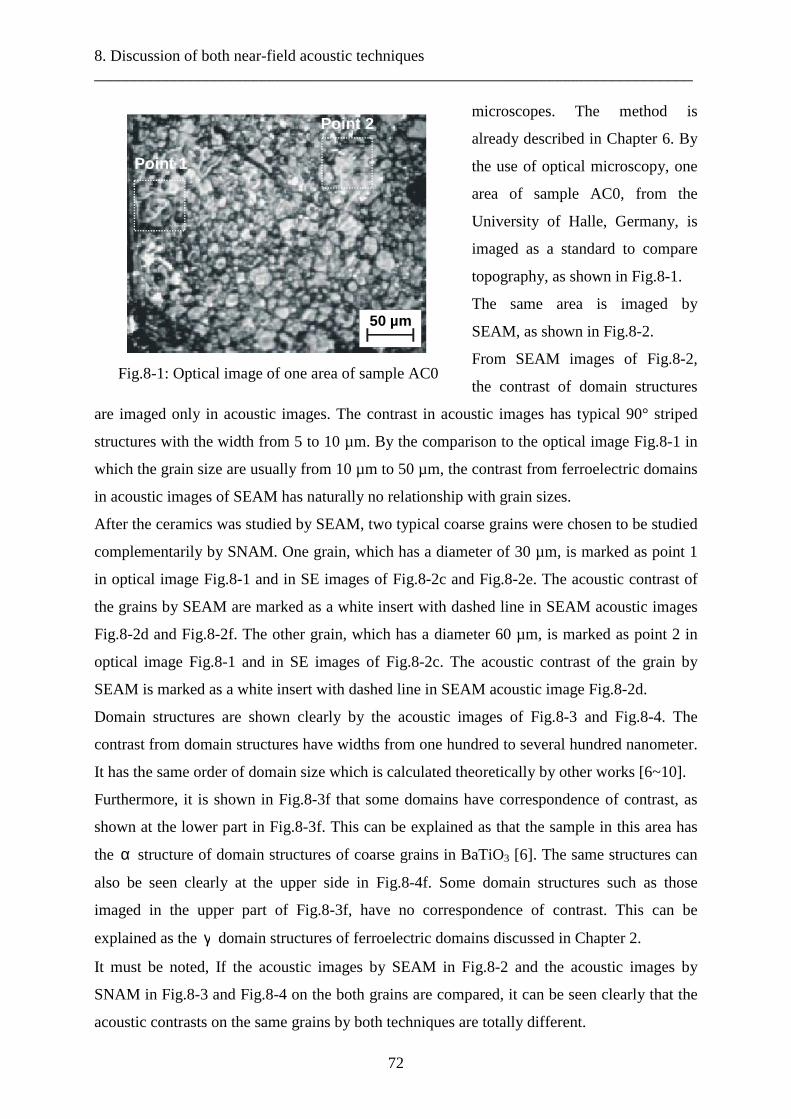
8. Discussion of both near-field acoustic techniques___________________________________________________________________________
72
microscopes. The method is
already described in Chapter 6. By
the use of optical microscopy, one
area of sample AC0, from the
University of Halle, Germany, is
imaged as a standard to compare
topography, as shown in Fig.8-1.
The same area is imaged by
SEAM, as shown in Fig.8-2.
From SEAM images of Fig.8-2,
the contrast of domain structures
are imaged only in acoustic images. The contrast in acoustic images has typical 90° striped
structures with the width from 5 to 10 µm. By the comparison to the optical image Fig.8-1 in
which the grain size are usually from 10 µm to 50 µm, the contrast from ferroelectric domains
in acoustic images of SEAM has naturally no relationship with grain sizes.
After the ceramics was studied by SEAM, two typical coarse grains were chosen to be studied
complementarily by SNAM. One grain, which has a diameter of 30 µm, is marked as point 1
in optical image Fig.8-1 and in SE images of Fig.8-2c and Fig.8-2e. The acoustic contrast of
the grains by SEAM are marked as a white insert with dashed line in SEAM acoustic images
Fig.8-2d and Fig.8-2f. The other grain, which has a diameter 60 µm, is marked as point 2 in
optical image Fig.8-1 and in SE images of Fig.8-2c. The acoustic contrast of the grain by
SEAM is marked as a white insert with dashed line in SEAM acoustic image Fig.8-2d.
Domain structures are shown clearly by the acoustic images of Fig.8-3 and Fig.8-4. The
contrast from domain structures have widths from one hundred to several hundred nanometer.
It has the same order of domain size which is calculated theoretically by other works [6~10].
Furthermore, it is shown in Fig.8-3f that some domains have correspondence of contrast, as
shown at the lower part in Fig.8-3f. This can be explained as that the sample in this area has
the α structure of domain structures of coarse grains in BaTiO3 [6]. The same structures can
also be seen clearly at the upper side in Fig.8-4f. Some domain structures such as those
imaged in the upper part of Fig.8-3f, have no correspondence of contrast. This can be
explained as the γ domain structures of ferroelectric domains discussed in Chapter 2.
It must be noted, If the acoustic images by SEAM in Fig.8-2 and the acoustic images by
SNAM in Fig.8-3 and Fig.8-4 on the both grains are compared, it can be seen clearly that the
acoustic contrasts on the same grains by both techniques are totally different.
Point 1
Point 2
50 µm
Fig.8-1: Optical image of one area of sample AC0
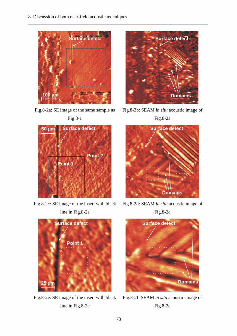
8. Discussion of both near-field acoustic techniques___________________________________________________________________________
73
100 µm
Surface defect
Domains
Surface defect
Fig.8-2a: SE image of the same sample as
Fig.8-1
Fig.8-2b: SEAM in situ acoustic image of
Fig.8-2a
50 µm
Point 2
Point 1
Surface defect
Domains
Surface defect
Fig.8-2c: SE image of the insert with black
line in Fig.8-2a
Fig.8-2d: SEAM in situ acoustic image of
Fig.8-2c
Point 1
Surface defect
Domains
Surface defect
Fig.8-2e: SE image of the insert with black
line in Fig.8-2c
Fig.8-2f: SEAM in situ acoustic image of
Fig.8-2e
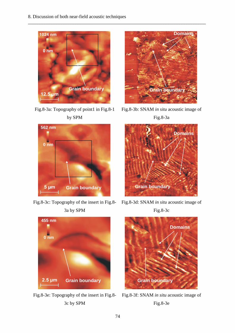
8. Discussion of both near-field acoustic techniques___________________________________________________________________________
74
Grain boundary Grain boundary
Domains
Fig.8-3a: Topography of point1 in Fig.8-1
by SPM
Fig.8-3b: SNAM in situ acoustic image of
Fig.8-3a
562 nm
0 nm
Grain boundary Grain boundary
Domains
Fig.8-3c: Topography of the insert in Fig.8-
3a by SPM
Fig.8-3d: SNAM in situ acoustic image of
Fig.8-3c
455 nm
0 nm
Grain boundary Grain boundary
Domains
Fig.8-3e: Topography of the insert in Fig.8-
3c by SPM
Fig.8-3f: SNAM in situ acoustic image of
Fig.8-3e
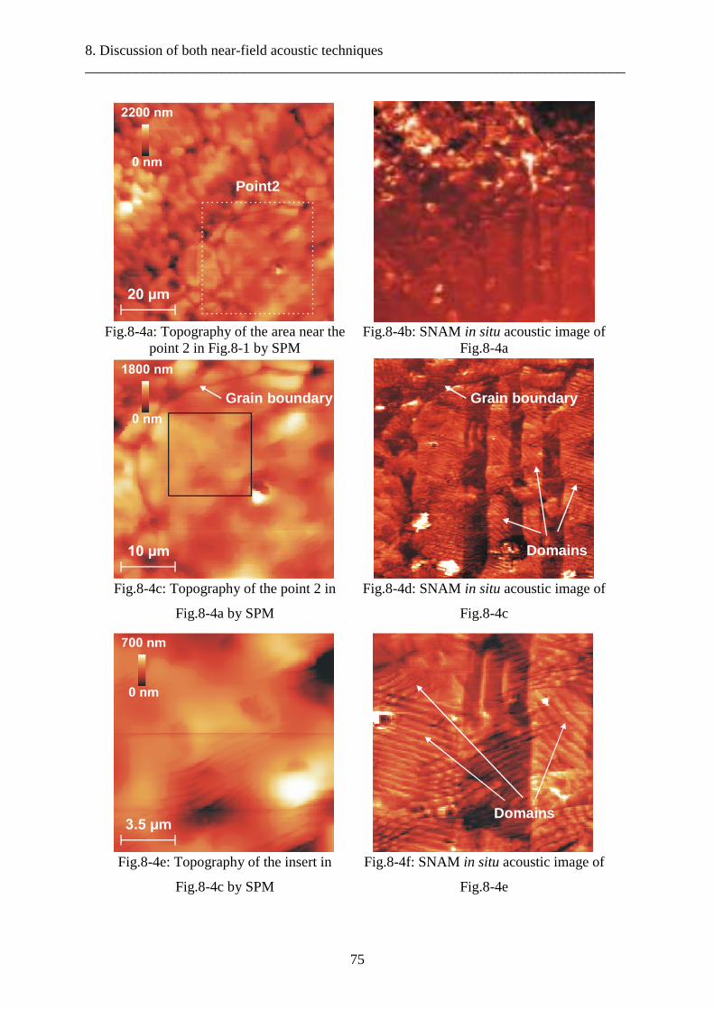
8. Discussion of both near-field acoustic techniques___________________________________________________________________________
75
Point2
Fig.8-4a: Topography of the area near thepoint 2 in Fig.8-1 by SPM
Fig.8-4b: SNAM in situ acoustic image ofFig.8-4a
Grain boundary Grain boundary
Domains
Fig.8-4c: Topography of the point 2 in
Fig.8-4a by SPM
Fig.8-4d: SNAM in situ acoustic image of
Fig.8-4c
Domains
Fig.8-4e: Topography of the insert in
Fig.8-4c by SPM
Fig.8-4f: SNAM in situ acoustic image of
Fig.8-4e
8. Discussion of both near-field acoustic techniques___________________________________________________________________________
76
8.2.2 Explanation of the results
The contrast difference of acoustic images by SEAM and SNAM at the identical areas (point
1 and point 2) can be explained as the depth difference of near-fields of both techniques. As it
is explained in Chapter 4 and Chapter 5 theoretically, the contrast of both near-field acoustic
imaging techniques (SEAM or SNAM) comes from interaction between the average
piezoelectric effect in near-field and the electric field formed by injecting electrons (SEAM)
or the concentrated field of the scanning tip (SNAM). As it is not well understood up to now
how the domain wall movements contribute to the piezoelectric, elastic and dielectric
properties of ferroelectric ceramics extrinsically [8, 11~13] and how many kinds of domain
structures of BaTiO3 ceramics exist totally [9, 10], an accurate theory of average piezoelectric
effects in near-field area for both techniques on BaTiO3 materials would be impossible. As a
result, a clear explanation of contrast of both near-field acoustic methods seems also difficult
at present. The following would be an explanation which bases solely on the present theory
and experimental facts:
• The typical domain structures in ceramics have the typical width of several hundred
nanometers for coarse grains, as predicated by present theories and experimental methods
[9, 10];
• The electric field in the near-field is so weak that it produces only vibration through
intrinsic converse piezoelectric effect and small movements of domain walls but no
change of the whole domain structures [13];
By SEAM, the near-field dimension is almost 1-2 µm wide and 2-3 µm deep at 20 keV
accelerating voltage for PE, and the interaction area is not homogeneous [57]. For the typical
domain structures which are clear to us [9], such as shown in Chapter 2, the domain width is
usually several hundred nanometer. Here, we would take a coarse grains of BaTiO3 ceramics
as an example. The typical domain structures have been studied [9, 10]. The domains have
typically four structures, shown as structure 1-4 in Fig.8-5.
As shown in Chapter 4, the acoustic amplitude contrast of SEAM of every scan point comes
from the average interaction between the electric field formed by injecting electrons and the
average piezoelectric effect in the whole interaction area. For scan point N and any other scan
points in area of structure 1, there is no difference of the average integration in near-field.
That means that there is no contrast difference by SEAM in the area of structure 1. With the
same argument, there is no contrast difference for any scan point M in the area of structure 2.
Similarly, any scan point in the areas of structure 3 or 4 has no contrast difference with any
other points in the same structure respectively.
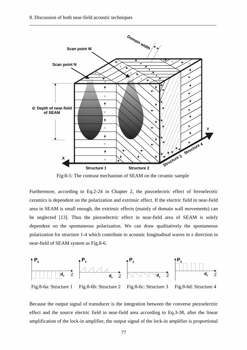
8. Discussion of both near-field acoustic techniques___________________________________________________________________________
77
Furthermore, according to Eq.2-24 in Chapter 2, the piezoelectric effect of ferroelectric
ceramics is dependent on the polarization and extrinsic effect. If the electric field in near-field
area in SEAM is small enough, the extrinsic effects (mainly of domain wall movements) can
be neglected [13]. Thus the piezoelectric effect in near-field area of SEAM is solely
dependent on the spontaneous polarization. We can draw qualitatively the spontaneous
polarization for structure 1-4 which contribute to acoustic longitudinal waves in z direction in
near-field of SEAM system as Fig.8-6.
Zdp
Pz
Zdp
Pz
Zdp
Pz
Zdp
Pz
Fig.8-6a: Structure 1 Fig.8-6b: Structure 2 Fig.8-6c: Structure 3 Fig.8-6d: Structure 4
Because the output signal of transducer is the integration between the converse piezoelectric
effect and the source electric field in near-field area according to Eq.3-38, after the linear
amplification of the lock-in amplifier, the output signal of the lock-in amplifier is proportional
Scan point M
Y
X
Scan point N
Structure 1 Structure 2Stru
cture 3Stru
cture 4
Domain width
d: Depth of near-fieldof SEAM
Fig:8-5: The contrast mechanism of SEAM on the ceramic sample
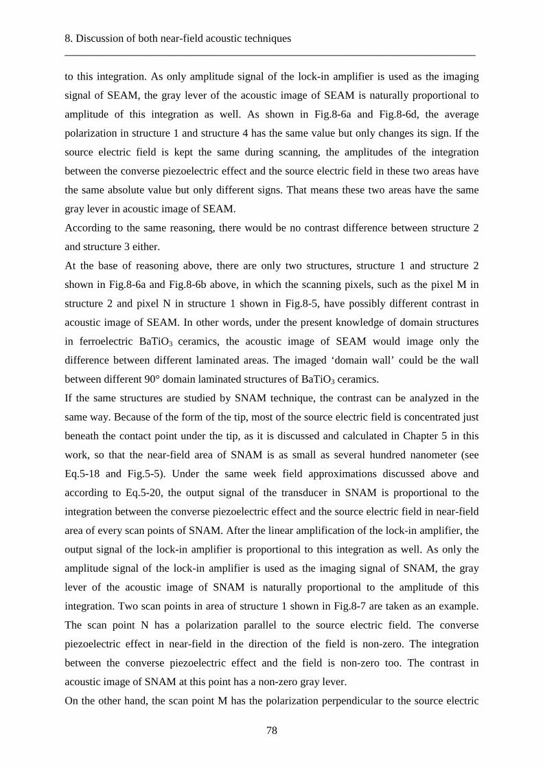
8. Discussion of both near-field acoustic techniques___________________________________________________________________________
78
to this integration. As only amplitude signal of the lock-in amplifier is used as the imaging
signal of SEAM, the gray lever of the acoustic image of SEAM is naturally proportional to
amplitude of this integration as well. As shown in Fig.8-6a and Fig.8-6d, the average
polarization in structure 1 and structure 4 has the same value but only changes its sign. If the
source electric field is kept the same during scanning, the amplitudes of the integration
between the converse piezoelectric effect and the source electric field in these two areas have
the same absolute value but only different signs. That means these two areas have the same
gray lever in acoustic image of SEAM.
According to the same reasoning, there would be no contrast difference between structure 2
and structure 3 either.
At the base of reasoning above, there are only two structures, structure 1 and structure 2
shown in Fig.8-6a and Fig.8-6b above, in which the scanning pixels, such as the pixel M in
structure 2 and pixel N in structure 1 shown in Fig.8-5, have possibly different contrast in
acoustic image of SEAM. In other words, under the present knowledge of domain structures
in ferroelectric BaTiO3 ceramics, the acoustic image of SEAM would image only the
difference between different laminated areas. The imaged ‘domain wall’ could be the wall
between different 90° domain laminated structures of BaTiO3 ceramics.
If the same structures are studied by SNAM technique, the contrast can be analyzed in the
same way. Because of the form of the tip, most of the source electric field is concentrated just
beneath the contact point under the tip, as it is discussed and calculated in Chapter 5 in this
work, so that the near-field area of SNAM is as small as several hundred nanometer (see
Eq.5-18 and Fig.5-5). Under the same week field approximations discussed above and
according to Eq.5-20, the output signal of the transducer in SNAM is proportional to the
integration between the converse piezoelectric effect and the source electric field in near-field
area of every scan points of SNAM. After the linear amplification of the lock-in amplifier, the
output signal of the lock-in amplifier is proportional to this integration as well. As only the
amplitude signal of the lock-in amplifier is used as the imaging signal of SNAM, the gray
lever of the acoustic image of SNAM is naturally proportional to the amplitude of this
integration. Two scan points in area of structure 1 shown in Fig.8-7 are taken as an example.
The scan point N has a polarization parallel to the source electric field. The converse
piezoelectric effect in near-field in the direction of the field is non-zero. The integration
between the converse piezoelectric effect and the field is non-zero too. The contrast in
acoustic image of SNAM at this point has a non-zero gray lever.
On the other hand, the scan point M has the polarization perpendicular to the source electric
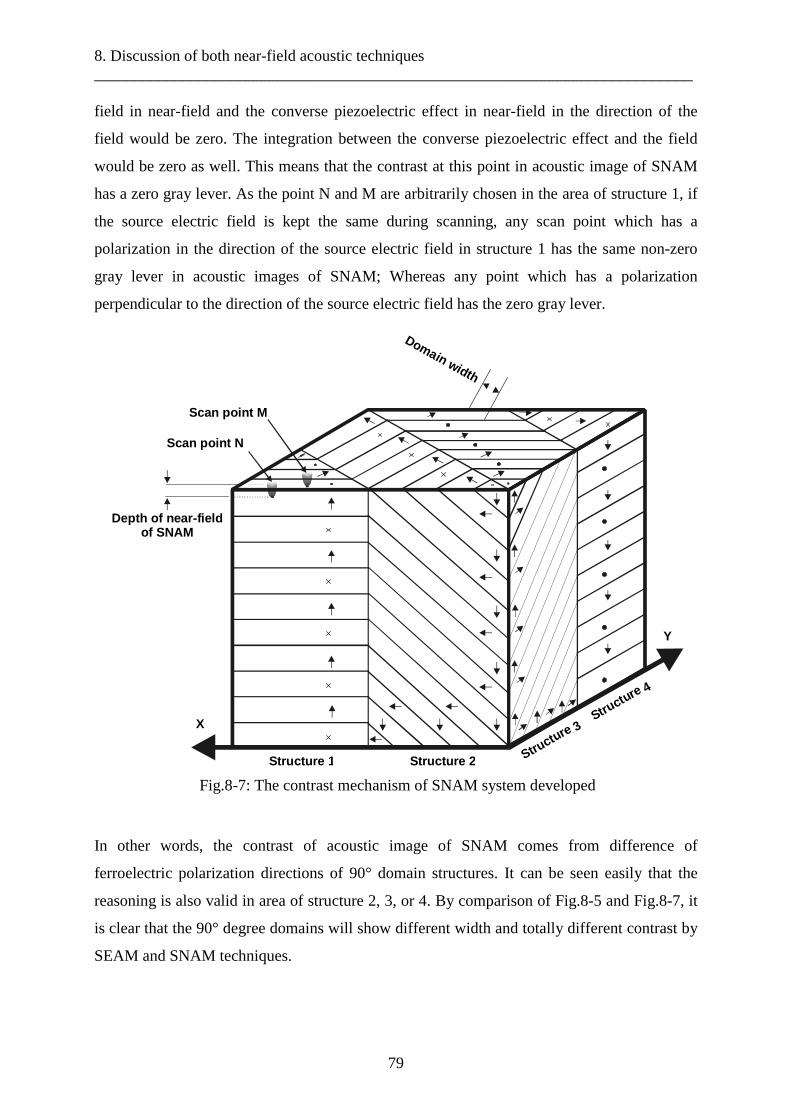
8. Discussion of both near-field acoustic techniques___________________________________________________________________________
79
field in near-field and the converse piezoelectric effect in near-field in the direction of the
field would be zero. The integration between the converse piezoelectric effect and the field
would be zero as well. This means that the contrast at this point in acoustic image of SNAM
has a zero gray lever. As the point N and M are arbitrarily chosen in the area of structure 1, if
the source electric field is kept the same during scanning, any scan point which has a
polarization in the direction of the source electric field in structure 1 has the same non-zero
gray lever in acoustic images of SNAM; Whereas any point which has a polarization
perpendicular to the direction of the source electric field has the zero gray lever.
In other words, the contrast of acoustic image of SNAM comes from difference of
ferroelectric polarization directions of 90° domain structures. It can be seen easily that the
reasoning is also valid in area of structure 2, 3, or 4. By comparison of Fig.8-5 and Fig.8-7, it
is clear that the 90° degree domains will show different width and totally different contrast by
SEAM and SNAM techniques.
X
Y
Scan point N
Scan point M
Structure 1 Structure 2 Structure 3
Structure 4
Depth of near-fieldof SNAM
Domain width
Fig.8-7: The contrast mechanism of SNAM system developed
9. Conclusions___________________________________________________________________________
80
9 Conclusions
Investigations of ferroelectric domain structures are essential for both fundamental and
applied perspectives since they determine, to a large extend, the macroscopic response of
ferroelectric materials. In microscopic range, they dominate the behavior of almost all
ferroelectric devices in the microelectronic industry. The results presented in this work on
ferroelectric BaTiO3 materials show the fascinating world of this kind of materials. The
dimension of the imaged ferroelectric domain structures by SNAM provides experimental
evidence for the theory of these structures in coarse grained BaTiO3 ceramics, which are only
proved by destructive methods such as the chemical etching techniques before now.
Temporal behavior of ferroelectric domain structures at an identical area of BaTiO3 ceramics
has been imaged at submicrometer range for the first time. The domain structures of the
ceramics remain unchanged for two years. It implies that ferroelectric polarization of this kind
of ceramics is very stable and it would be an ideal medium for applications such as memory
devices.
Thermal dynamical properties of ferroelectric domain structures at an identical area of
BaTiO3 ceramics are imaged by SNAM at submicrometer range. When the temperature of the
ceramics is over Curie temperature, the domain structures disappear totally. The ferroelectric
domains change their polarization distribution if the temperature of the sample changes.
Electrical dynamical study of ferroelectric domains at an identical area of BaTiO3 ceramics
has also been studied. With a bias voltage, the change of the same structures are imaged
clearly. Based on the developed theoretical model, the field intensity under the tip and the
physical process of polarization change on the sample surface are analyzed. These dynamic
investigations lays the foundations for future dynamic analysis of ferroelectric domains of
other materials by SNAM.
The system developed for dynamic research of ferroelectric domain structures in this work
can be easily modified from a commercial SPM system. For the further study of other
ferroelectric materials and devices, this system is easy to use, with submicrometer or
nanometer resolution, and high thermal and electric stability if simple control units are used.
It presents an ideal tool for the non-destructive dynamic testing and modeling of both
ferroelectric materials in material engineering and ferroelectric devices in microelectronic
industry.
The explanation of the contrast from acoustic non-destructive imaging systems remains
always a challenge for researchers in this area. The SNAM system developed by the use of an
acoustic transducer provides a base for both theoretical and experimental complementary
9. Conclusions___________________________________________________________________________
81
analyses of the acoustic contrast among different kinds of acoustic near-field systems. As an
example, the complementary analysis of SEAM and SNAM reveals the acoustic contrast
mechanisms of both near-field techniques. The different contrast which are revealed by
complementary analysis at identical areas can be well-explained using the current theory for
BaTiO3 ceramics. The experimental methods developed for the complementary analysis can
be further applied to analyze other properties of materials and devices among different
microscopy systems.
The theoretical modeling of SNAM analysis, i.e. the Green´s function to determine the quasi-
stationary fields in the system and the transmission line mode of acoustic longitudinal waves
within the sample, is applied successfully for the first time to characterize electrical and
mechanical field distributions of BaTiO3 materials studied by SNAM. Based on the theoretical
solutions presented in this work, other ferroelectric materials can be analyzed similarly.
Under the same theoretical approximations as those of SNAM system, the contrast of SEAM
system on ferroelectric materials has been characterized by these theoretical techniques as
well. Although only acoustic plane wave modes are analyzed, the simple solution reveals
some basic behavior of SEAM system on ferroelectric materials. The modelling technique
would be also applicable to other beam injecting acoustic imaging systems.
10. Future aspect___________________________________________________________________________
82
10 Future aspect
The characterization of ferroelectric materials at submicrometer or even in nanometer range,
both in lateral direction and in depth profiling, is of vital importance for the development of
future ferroelectric materials and integrated devices. Unfortunately, the present knowledge of
ferroelectric domains at this resolution range is not enough to predict the so-called ‘domain’
influence on the materials. Whereas common methods have different limitations for this
purpose, the non-destructive methods based on SPM provide a new breakthrough for this
goal. Although much effort on this technique has been given and many results are presented
for different ferroelectric materials by different techniques based on SPM, from our point of
view, a clear relationship between these domain effects and properties of ferroelectric
materials require further investigations.
The quantitative description of energy change of ferroelectric domains during switching
processes is not well understood. As discussed in many literatures [1~13], this energy change
is a process including thermal, electrical, and elastic energy. Although this work has shown
some changes of domain structures by external thermal and electrical influences, the accurate
relationship among the thermal, elastic, and electrical energy changes should be further
investigated. To understand this process as accurately as possible, different non-destructive
methods at this resolution range, such as thermal and acoustic near-field techniques, should be
used complementarily.
The thermal behavior of ferroelectric domains of BaTiO3 is another problem which needs
further study as well. Although current literatures present many theoretical and experimental
results on this effect [1~5], a quantitative study of thermal behavior of domain structures of
BaTiO3 at submicrometer or nanometer resolution is still not reached. Even though some
thermal dynamic investigation has been presented in this work, a quantitative relationship
between ferroelectric domain structures and the external thermal energy change has not been
obtained yet. To achieve this goal, a complementary analysis on ferroelectric BaTiO3 by
thermal and acoustic near-field techniques would be ideal.
The metal-doped BaTiO3 is widely used in industry for different purposes [86]. Although
some work has been done to reveal the relationship among grain sizes, electrical, elastic, and
piezoelectric properties, ferroelectric domain structures from doped BaTiO3 materials are little
studied. The theoretical relationship between grain sizes and ferroelectric domain structures
for doped BaTiO3 is not achieved either. The presented SEAM and SNAM techniques are the
best non-destructive tools for experimental investigations and basis for the modeling and
manufacturing of this kind of materials.
10. Future aspect___________________________________________________________________________
83
Ferroelectric thin films are used intensively in the micro-electronic industry and some
properties of thin films are also intensively studied [4, 22, 31~35]. But, from our point of
view, ferroelectric domain structures and their formation process under external influences
needs to be studied further. Problems such as how the domains change their structures during
switching processes, how much is the switching time of different structures, what are the main
sources of the fatigue of the ferroelectric polarization and so on require further study. To
answer all the questions, a thorough understanding and modeling of ferroelectric thin films,
both experimentally and theoretically, would be necessary.
Although this work has presented a systematic theoretical method to study the electrical and
acoustical field distributions from different sample structures in SNAM system, there is still a
lot of work to do to characterize all the field components quantitatively. Whereas the electric
field distributions in the system can be determined by the Green´s functions, the acoustic field
solutions are only based on plane wave modes. For quantitative characterization of
ferroelectric materials by SNAM, it is necessary to analyze the acoustic fields more
accurately. The acoustic field mode conversion in near-field and the non-linear effects of
ferroelectric materials should be further studied.
Recent literature [87] points out that modern chip industries face severe problems for
modeling of devices and failure analysis as multilayered systems are used intensively in the
nanometer regime. The characterization of electrical, thermal, and acoustical field
distributions in these systems is of vital importance to develop new devices. As the structures
of these devices have nanometer dimensions, some basic conditions for present
phenomenological theories cannot be fulfilled any more. New basic theoretical backgrounds
including a combination of quantum-mechanics and quantum-electronics for the
characterization of these devices must be thoroughly developed. However, the systematic
phenomenological methods are foundations for this future advancement.
11. Appendix
___________________________________________________________________________
84
11 Appendix
A1: Solution of one-dimensional piezoelectric stiffened plan wave in BaTiO3 and PZT
The piezoelectric strain and stress relationships are:
EJII sx
�
,= JX + jId ,
~jE Eq.A-1
=iD Jid , JX +X
ji
�
,ε jE Eq.A-2
EJII cX
�
,= Jx jIe ,~− jE Eq.A-3
=iD Jie , Jx +x
ji
�
,ε jE Eq.A-4
To characterize the typical near-field acoustic system of present work on BaTiO3, it is
necessary to discuss at first the coupling between electric and acoustic fields generally in both
PZT transducer and BaTiO3 sample in one dimension. The polarized PZT ceramics can be
analyzed by a crystal lattice of 6mm and the crystal lattice of single BaTiO3 with only c-
monodomain is 4mm [53]. The piezoelectric tensor and dielectric tensor for both material
systems have the same form but different values of components. This allows us to treat the
coupling in transducer as well as in near-field theoretically together. Only if quantitative
values of each material are concerned, actual values of the tensor components will be used
respectively.
If z direction is chosen as the transmission direction, the differential x∂
∂ and
y∂∂
are equal to
zero if the lateral dimension is unlimited. Only z∂
∂ is non-zero for every electric and
mechanic field components.
From Maxwell equation Eq.3-1, if there are no conducting and source currents ( cJ�
and sJ�
) in
a given material, electromagnetic fields and waves which transmit only in z direction will be
described as [53]:
E�
×∇ =
×
∂∂
∂∂−
∂∂−
∂∂
∂∂
∂∂−
z
y
x
E
E
E
xy
xz
yz
0
0
0
= t
H
∂∂
µ−
�
0 ,
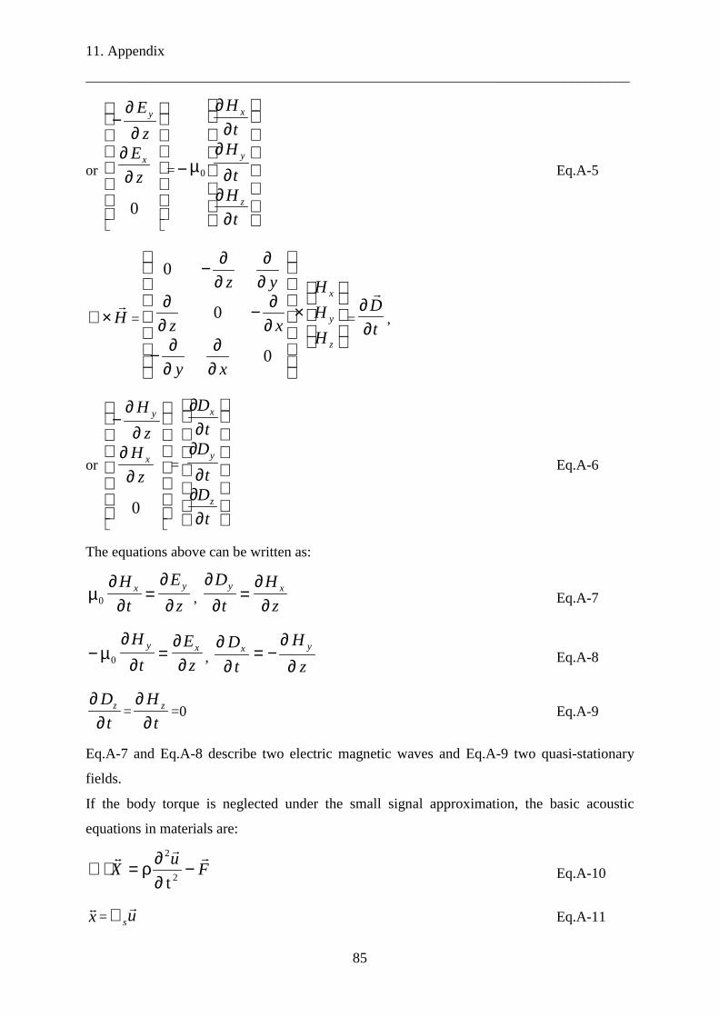
11. Appendix
___________________________________________________________________________
85
or
∂∂
∂∂
−
0
z
Ez
E
x
y
=
∂∂∂
∂∂
∂
µ−
t
Ht
Ht
H
z
y
x
0 Eq.A-5
H�
×∇ =
×
∂∂
∂∂−
∂∂−
∂∂
∂∂
∂∂−
z
y
x
H
H
H
xy
xz
yz
0
0
0
=t
D
∂∂�
,
or
∂∂
∂∂
−
0
z
Hz
H
x
y
=
∂∂∂
∂∂
∂
t
Dt
Dt
D
z
y
x
Eq.A-6
The equations above can be written as:
z
E
t
H yx
∂∂
=∂
∂µ0 , z
H
t
Dxy
∂∂
=∂
∂Eq.A-7
z
E
t
Hxy
∂∂
=∂
∂µ− 0 ,
z
H
t
D yx
∂∂
−=∂
∂ Eq.A-8
t
Dz
∂∂
=t
H z
∂∂
=0 Eq.A-9
Eq.A-7 and Eq.A-8 describe two electric magnetic waves and Eq.A-9 two quasi-stationary
fields.
If the body torque is neglected under the small signal approximation, the basic acoustic
equations in materials are:
Fu
X���
−∂∂ρ=⋅∇
2
2
tEq.A-10
x�
= us
�∇ Eq.A-11
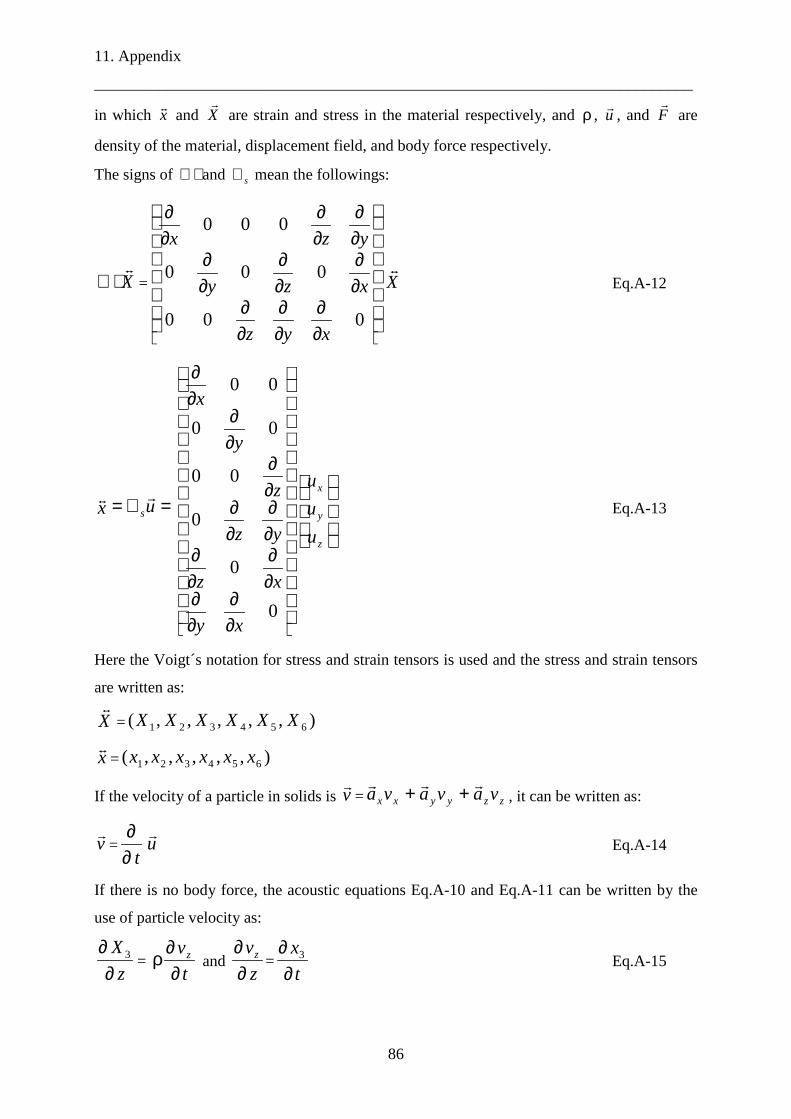
11. Appendix
___________________________________________________________________________
86
in which x�
and X�
are strain and stress in the material respectively, and ρ , u�
, and F�
are
density of the material, displacement field, and body force respectively.
The signs of ⋅∇ and s∇ mean the followings:
X�
⋅∇ =
∂∂
∂∂
∂∂
∂∂
∂∂
∂∂
∂∂
∂∂
∂∂
000
000
000
xyz
xzy
yzx
X�
Eq.A-12
x� =∇= us
�
∂∂
∂∂
∂∂
∂∂
∂∂
∂∂
∂∂
∂∂
∂∂
0
0
0
00
00
00
xy
xz
yz
z
y
x
z
y
x
u
u
u
Eq.A-13
Here the Voigt´s notation for stress and strain tensors is used and the stress and strain tensors
are written as:
X�
= ),,,,,( 654321 XXXXXX
x�
= ),,,,,( 654321 xxxxxx
If the velocity of a particle in solids is v�
= zzyyxx vavava��� ++ , it can be written as:
v�
=t∂
∂u�
Eq.A-14
If there is no body force, the acoustic equations Eq.A-10 and Eq.A-11 can be written by the
use of particle velocity as:
z
X
∂∂ 3 =
t
vz
∂∂ρ and
z
vz
∂∂
=t
x
∂∂ 3 Eq.A-15
11. Appendix
___________________________________________________________________________
87
z
X
∂∂ 4 =
t
vy
∂∂
ρ and z
vy
∂∂
=t
x
∂∂ 4 Eq.A-16
z
X
∂∂ 5 =
t
vx
∂∂ρ and
z
vx
∂∂
=t
x
∂∂ 5 Eq.A-17
Eq.A-15 describes one longitudinal acoustic plan wave; Eq.A-16 and Eq.A-17 describe two
shear acoustic waves.
According to piezoelectric coupling equations Eq.A-1 to Eq.A-4 and piezoelectric tensor of
BaTiO3, the electric and acoustic coupling can be written as:
zD =szzε zE + 3ze 3x Eq.A-18
yD =syyε yE + 5xe 4x Eq.A-19
xD =sxxε xE + 5xe 5x Eq.A-20
3X = 33c 3x 3ze− zE Eq.A-21
4X = 44c 4x 5xe− yE Eq.A-22
5X = 44c 5x 5xe− xE Eq.A-23
From electromagnetic wave equations Eq.A-7 to Eq.A-9, acoustic equations Eq.A-15 to
Eq.A-17, and electric and acoustic coupling Eq.A-18 to Eq.A-23, the general coupling of
electric and mechanic field components in BaTiO3 can be analyzed. The acoustic longitudinal
wave described by Eq.A-15 will be studied with detail in the following.
According to Eq.A-9, the electric displacement zD is a constant. For a harmonic study of
fields, zD can be treated as zero. From Eq.A-18, the quasi-static electric field [53] in z
direction is:
zE =
ε
− szz
ze 33x Eq.A-24
Form Eq.A-24 and Eq.A-21, the stress in z direction is:
3X =( 33c + szz
ze
ε
23 ) 3x Eq.A-25
The constant pc = 33c +szz
ze
ε
23 is the so-called piezoelectric stiffened stiffness. If Eq.A-25 is
combined with Eq.A-15, the so-called piezoelectric stiffened wave equations for the stiffened
11. Appendix
___________________________________________________________________________
88
longitudinal wave ( zv , 3X ) are:
z
X
∂∂ 3 =
t
vz
∂∂ρ Eq.A-26
z
vz
∂∂
=pc
1
t
X
∂∂ 3 Eq.A-27
Eq.A-26 and Eq.A-27 describe a stiffened acoustic wave in BaTiO3 single crystal without
source. It can be rewritten as the wave equation:
02
2
2
2
=∂∂ρ−
∂∂
t
v
cz
v z
p
zEq.A-28
The physical meaning of the equation above can be explained by piezoelectric theory as the
stiffened effect [53]. It seems that this wave behaves as if the elastic stiffness 33c were
increased to pc = 33c +sz
ze
3
23
ε. The electric and acoustic coupling for this wave is the coupling of
the quasi-static electric field and the acoustic longitudinal wave ( zv , 3X ).
The coupling of longitudinal waves in PZT transducer is the same, if only the material
constants in all the expressions above should be changed to material constants of PZT
ceramics.
If there is a harmonic source electric field in z direction sE�
= sE za�
, the total electric field in z
direction in the BaTiO3 crystal studied can be written as:
sztotal EEE += Eq.A-29
zE is the coupled stiffened electric field in the crystal. Because only the harmonic stable state
will be studied and the acoustic field ( zv , 3X ) must satisfy the same stiffened condition, the
coupled stiffened electric field in the crystal is the same as the field without source.
Form Eq.A-18 and Eq.A-21, the stress in the crystal with source:
3X =( 33c + sz
ze
3
23
ε ) 3x - 3ze sE Eq.A-30
in which the constant pc = 33c +sz
ze
3
23
ε is the piezoelectric stiffened stiffness.
Because of the source electric field sE , the wave equations for acoustic longitudinal waves
can be obtained in the same way:
11. Appendix
___________________________________________________________________________
89
z
X
∂∂ 3 =
t
vz
∂∂ρ Eq.A-31
z
vz
∂∂
=pc
1 +∂
∂t
X 3
p
z
c
e 3
t
Es
∂∂
Eq.A-32
Eq.A-31 and Eq.A-32 can also be written as the wave equation with source:
2
2
2
2
t
v
cz
v z
p
z
∂∂ρ−
∂∂
=p
z
c
e 3
t
Es
∂∂
Eq.A-33
The same process can be applied to the other two coupled waves Eq.A-16 and Eq.A-17 in the
crystal studied. The coupling equations are:
zt
ve
t
E
z
E xx
xsxx
x
∂∂∂µ=
∂∂εµ−
∂∂ 2
502
2
02
2
Eq.A-34
zt
ve
t
E
z
E yx
ysyy
y
∂∂∂
µ=∂
∂εµ−
∂∂ 2
502
2
02
2
(syyε =
sxxε for BaTiO3) Eq.A-35
At the first sight, the coupling mechanism seems almost the same as the coupling discussed
above. But a detailed discussion [53] shows that these kinds of coupling are much more
complex than the stiffened electric and mechanic coupling. A detailed discussion is beyond
the scope of the present work and some discussion can be found in other works [53, 54].
A2: Transmission line mode of acoustic waves in near-field
In near-field of piezoelectric materials, the electromagnetic and acoustic coupling phenomena
are even more complicated than the coupling in the transducer, because the acoustic wave
here is the piezoelectric acoustic wave with source electric field szz EaE��
= . Under the
assumption described in Chapter 3, the acoustic transmission can be compared to the
transmission of voltage waves in a transmission line with source [53].
If there are plane longitudinal harmonic acoustic waves ( 1zv , 1
3X ) produced in the near-field in
the crystal studied, the equations according to Eq.A-31 and Eq.A-32 are written as the
followings:
z
X
∂∂ 1
3 = t
vz
∂∂ρ
1
Eq.A-36
z
vz
∂∂ 1
=pc
1
t
X
∂∂ 1
3 +p
z
c
e 3
t
Es
∂∂
Eq.A-37
11. Appendix
___________________________________________________________________________
90
Here, the suffix ‘1’ at the top right corner indicates the near-field area in the sample.
As a comparison, the equations of transmission line with sources sV and sI will be discussed:
z
tzV
∂∂ ),(
= t
tzIL
∂∂− ),(
sV+ ),( tzRI+ Eq.A-38
z
tzI
∂∂ ),(
= C−t
tzV
∂∂ ),(
sI+ ),( tzGV+ Eq.A-39
Here ( ),( tzV , ),( tzI ) is a solution of a voltage or current wave of a one-dimensional
transmission line and has the form:
),( tzV =)( kztj
meV −ωEq.A-40
),( tzI =)( kztj
meI −ω Eq.A-41
where mV and mI are amplitudes of the voltage and current wave which are decided by the
source and boundary conditions.
In the case of a transmission line without loss, the equations can be written as:
z
tzV
∂∂ ),(
= t
tzIL
∂∂− ),(
sV+ Eq.A-42
z
tzI
∂∂ ),(
= C−t
tzV
∂∂ ),(
sI+ Eq.A-43
If the one-dimensional transmission line with a source limited in the area 1z < z < 2z , a general
solution of the equations Eq.A-42 and Eq.A-43 above is:
),( tzV =( )(za+ + )(za− )/2 Eq.A-44
),( tzI =( )(za+ )(za−− )/2Z0 Eq.A-45
)(za+ )(10
1
1
)()( zzjkz
z
jkss
jkz eZadeIZVe −−+ζ− +∫ ζ+= ( z > 1z ) Eq.A-46
)(za−=
)(20
22
)()( zzjkz
z
jkss
jkz eZadeIZVe −−ζ− +∫ ζ−− ( z < 2z ) Eq.A-47
where TR =C
L is the characteristic resistance of voltage wave of transmission line.
By comparison of Eq.A-42 and Eq.A-43 with Eq.A-36 and Eq.A-37, if the following
comparison is made:
),( tzV = 3X− : the voltage wave is compared to negative stress in z direction of the
11. Appendix
___________________________________________________________________________
91
longitudinal wave;
),( tzI = zv : the current wave is compared to velocity of the particle;
L =ρ : the inductance is compared to density of the sample;
C =1/ pc =1/ )/( 2333 zzzec ε+ : the capacitance is compared to reciprocal of the stiffened
elastic stiffness;
sI =p
z
c
e 3
t
Es
∂∂
: the current source is compared to the time differential of source electric field;
Eq.A-36 and Eq.A-37 will have the same solution as that of Eq.A-42 and Eq.A-43.
For the near-field system shown in Fig.5-1 with an electric field source in near-field, the
stable harmonic solutions of the longitudinal wave in near-field can be written from above
comparison as:
2/)( 1113
tjeaaX ω−+ +−= Eq.A-48
0111 2/)( Zeaav tj
zω−+ −= Eq.A-49
+1a =jkzjkz
s eaeza −+−+ + )0()( 11,
in which +1
sa (z)= ∫ ζ∂
∂ ζz
jks
p
z det
E
c
eZ
0
30 )( (0 ≤ z ≤ d) Eq.A-50
−1a =)(11 )()( dzjkjkz
s edaeza −−− + ,
in which −1
sa (z)= ∫ ζ∂
∂ ζ−d
z
jks
p
e det
E
c
eZ )( 3
0 (0 ≤ z ≤ d) Eq.A-51
Here +1sa (z) and −1
sa (z) are terms resulted from source in near-field. 0Z = pcρ is the acoustic
characteristic resistance of wave ( 1zv , 1
3X ) in near-field and )0(1+a and )(1 da − are constants
which can be determined by boundary conditions in Fig.5-1.
The acoustic waves outside the source area can be compared to the transmission line mode
without source. The acoustic wave outside the near-field but still in the sample is governed
only by the wave equations without source Eq.A-26 and Eq.A-27, and the solution can be
written as ( 2v , 23X ):
2/)( 22
223
tjeaaX ω−+ +−= Eq.A-52
2222 2/)( Zeaav tj
zω−+ −= Eq.A-53
11. Appendix
___________________________________________________________________________
92
)(22 2)( dzjkedaa −−++ = Eq.A-54
)(22 2)( dzjkedaa −−− = Eq.A-55
Where )(2 da + and )(2 da − are constants which can be decided by the boundary condition of
the system, ω the angular frequency, and 2k acoustic longitudinal wave number in z direction
in the sample outside the near-field. It is clear that the wave number and acoustic
characteristic resistance inside and outside the near-field in the sample are the same, that is
k = 2k and 20 ZZ = . The suffix ‘2’ at the top right corner indicates the area outside the near-
field but still in the sample.
The final solution of the acoustic waves can be obtained by matching of boundary conditions
in different areas. The acoustic boundary conditions for the typical system shown in Fig.3-1
are generally the same.
13X =0 if z = 0; Eq.A-56
23X =
13X if z = d; Eq.A-57
2zv =
1zv if z = d; Eq.A-58
33X =
23X if z = 1D Eq.A-59
3zv =
2zv if z = 1D Eq.A-60
)( 13 Da −
= 2321
3 )( DjkeDRa −+if z = 1D + 2D Eq.A-61
here R is the acoustic reflect constant of the longitudinal wave at the interface between PZT
transducer and the copper electrode. The backside of copper electrode is well matched
acoustically so that there is no more reflection after the copper electrode.
Although the SNAM based on SPM technique has a constant force of the tip at z =0, for the
discussion of harmonic solutions of acoustic waves, it plays no role for the harmonic
solutions. At this base, a generally discussion of solutions of different scanning near-field
acoustic microscopy systems is possible.
At boundary z=0, there is only one boundary condition Eq.A-56 for 13X ,
)0()0( 11 ++ + aas +jkd
s edaa −−− + )()0( 11=0
)0(1+sa =0
)0(1+a + )0(1−sa +
jkdeda −− )(1=0 Eq.A-62
11. Appendix
___________________________________________________________________________
93
At the boundary z = d, there are boundary conditions Eq.A-57 and Eq.A-58 for both ( 1zv , 1
3X )
and ( 2v , 23X ):
jkdjkds eaeda −+−+ + )0()( 11
+ )()( 11 daeda jkds
−− + = )(2 da ++ )(2 da −
)(1 das−
=0
)(1 das+ jkde−
+jkdea −+ )0(1
+ )(1 da −= )(2 da +
+ )(2 da −Eq.A-63
0
1
Z{[ jkdjkd
s eaeda −+−+ + )0()( 11 ] - [ )()( 11 daeda jkds
−− + ]}=0
1
Z{ )(2 da + - )(2 da − }
jkdjkds eaeda −+−+ + )0()( 11
- )(1 da −= )(2 da +
- )(2 da −Eq.A-64
At boundary z= 1D , the boundary conditions Eq.A-59 and Eq.A-60 are
)( 13 Da + {1 + 232 DjkeR − }= )(2 1)( dDjkeda −−+ + )(2 1)( dDjkeda −−
Eq.A-65
3
0
Z
Z)( 1
3 Da + { 1- 232 DjkeR − }= )(2 1)( dDjkeda −−+ - )(2 1)( dDjkeda −−Eq.A-66
If the source field in near-field is given, )(1 das+ and )0(1−
sa are two source integration terms
in near-field and are given from Eq.A-50 and Eq.A-51 respectively.
There are six constants )0(1+a , )(1 da − , )(2 da + , )(2 da − , )( 13 Da + , and )( 1
3 Da − . There are
six independent linear equations from Eq.A-61 to Eq.A-66. There is only one single solution
for all the constants. All the constants can be written as the functions of )(1 das+ and )0(1−
sa .
Let 1α =1
1
2
2
11
jkD
jkD
e
e−
−
+−
, 2α =23
23
2
2
Re1Re1
Djk
Djk
−
−
+−
, The final expression of )( 13 Da + can be calculated as
the following:
From Eq.A-59: +1
sa (z)= ∫ ζ∂
∂ ζz
jks
p
z det
E
c
eZ
0
30 )( (0 ≤ z ≤ d),
we can get the expression of )(1 das+
:
)(1 das+
= ∫ ζ∂
∂ ζd
jks
p
z det
E
c
eZ
0
30 )(
11. Appendix
___________________________________________________________________________
94
From Eq.A-60, −1
sa (z)= ∫ ζ∂
∂ ζ−d
z
jks
p
z det
E
c
eZ )( 3
0 (0 ≤ z ≤ d),
we can get the expression of )0(1−sa :
)0(1−sa = ∫ ζ
∂∂ ζ−
djks
p
z det
E
c
eZ
0
30 )( .
If the source field is given, the term )(1 das+
and )0(1−sa are obtained.
From Eq.A-71, we can get the term )0(1+a :
)0(1+a = )0([ 1−− sa + ])(1 jkdeda −−
If we add and subtract Eq.A-72 with Eq.A-73, we can get the term )(2 da + and )(2 da −
:
)(2 da += )(1 das
+ jkde−+
jkdea −+ )0(1
)(2 da −= )(1 da −
If we put the term )0(1+a into the term )(2 da + above, we get the following expression:
)(2 da ++ )(2 da − jkde 2−
=[ )(1 das+
- )0(1−sa ]
jkde−
The term at the right side of the equation above is the source integration in near-field.
If we add and subtract Eq.A-74 with Eq.A-75, we can get the following expression:
)( 13 Da + {[1 + 232 DjkeR − ]+ aβ [1- 232 DjkeR − ]}=2 )(2 da + )( 1 dDjke −−
)( 13 Da + {[1 + 232 DjkeR − ]- aβ [1- 232 DjkeR − ]}=2 )(2 da − )( 1 dDjke −
We can eliminate the )(2 da + and )(2 da −
terms in the equations above and get the
relationship between the term )( 13 Da + and the source term:
)( 13 Da +
=)Re1)(1(
1231 22 DjkjkDe −− ++ a
jkDss eada
βαα+− −−+
21
11
1
)]0()([2 1
1jkDe−
Eq.A-67
Here 1α =1
1
2
2
11
jkD
jkD
e
e−
−
+−
, 2α =23
23
2
2
Re1Re1
Djk
Djk
−
−
+−
, and aβ =3
0
Z
Z=
3
2
Z
Z.
Eq.A-67 can be simplified as the followings:
11. Appendix
___________________________________________________________________________
95
1)]0()([2 11 jkDss eada −−+ − = 4
p
z
c
eZ 3
01jkDe− ∫ ζ−
∂∂ ζ−ζd jkjk
s dee
t
E
0 2
= 4jp
z
c
eZ 3
01jkDe− ∫ ζ−
∂∂ ζ−ζd jkjk
s dj
ee
t
E
0 2= 4j
p
z
c
eZ 3
01jkDe− ∫ ζζ
∂∂d
s dkt
E
0
)sin(
)( 13 Da +
)Re1)(1(
1231 22 DjkjkDe −− ++
=a
ds
p
z dkt
E
c
ejZ
βαα+
∫ ζζ∂
∂
21
0
30
1
)sin(4
The output signal of the transducer under the open circuit condition is:
outputV =2(p
z
c
e 3)( ∫ ζζ
∂∂d
s dkt
E
0
)sin( )
εPZT
zz
PZTze 3 ( ω
1)(
1
23
211
jkD
Djk
e
e−
−
+−
)(a
jkDae
βαα+β −
211
1
)
Eq.A-68
A3: Solution of SEAM
A3.1 The acoustic boundary condition of SEAM can be written as:13X =0 if z = 0; Eq.A-69
23X =
13X if z = d; Eq.A-70
2zv =
1zv if z = d; Eq.A-71
33X =
23X if z = 1D Eq.A-72
3zv =
2zv if z = 1D Eq.A-73
)( 13 Da −
= 2321
3 )( DjkeDRa −+if z = 1D + 2D Eq.A-74
A3.2 The source electric field in the near-field of SEAM and output signal of transducer
The source electric field in the near-field of SEAM can be obtained by using the image charge
and solving the Possion´s equation at the given electric boundary conditions in the sample.
Based on the assumption in Chapter 4.1, the electric field under every scanning point can be
written as [74]:
sE = tjedzA ω− )´( ( 0 <z<d , 222 ayx ≤+ )
sE =0 ( z >d and z<0, 222 ayx ≥+ ) Eq.A-75
here ´A =ee
da
I
zz
E τ−
επη−2
0)1(
11. Appendix
___________________________________________________________________________
96
in which Eη is the backscattering constant, 0I the beam current, eτ the charge accumulation
time, a is the radius of the primary electron beam.
p
z
c
e 3
t
Es
∂∂
= )( dzA − tje ω, and A = ωj
p
z
c
e 3´A = ωj
p
z
c
e 3 eeda
I
zz
E τ−
επη−2
0)1(
Eq.A-76
The source term in near-field of SEAM is:
p
z
c
e 3 ∫ ζζ∂
∂ds dk
t
E
0
)sin( =A ])[sin(1
2kdkd
k−
The output signal of PZT transducer under open circuit condition is:
outputV =2A ])[sin(1
2kdkd
k−
εPZT
zz
PZTze 3 ( ω
1)(
1
23
211
jkD
Djk
e
e−
−
+−
)(a
a
βαα+β
211) 1jkDe−
=2 jp
z
c
e 3 eeda
Iszz
E τ−
επη−2
0)1(])[sin(
12
kdkdk
−
εPZT
zz
PZTze 3 (
1
23
211
jkD
Djk
e
e−
−
+−
)(a
a
βαα+β
211) 1jkDe−
=2 j szz
ze
ρε3 ee
da
IE τ−
πη−
20)1(
εPZT
zz
PZTze 3 )
)sin((
2ω− kdkd
(1
23
211
jkD
Djk
e
e−
−
+−
)(a
jkDae
βαα+β −
211
1
)
Eq.A-77
in which ρ is the density of BaTiO3 material, 1α =1
1
2
2
11
jkD
jkD
e
e−
−
+−
, 2α =23
23
2
2
Re1Re1
Djk
Djk
−
−
+−
and
aβ =3
0
Z
Z.
A4: Solution of SNAM developed from SPM
A4.1 The acoustic boundary conditions of the system
The boundary conditions for SNAM developed in this work are almost the same as those of
SEAM system. The only difference is at z=0 plane. The actual acoustic boundary conditions
are:
13X = tipF if z = 0; Eq.A-78
23X =
13X if z = d; Eq.A-79
2zv =
1zv if z = d; Eq.A-80
11. Appendix
___________________________________________________________________________
97
33X =
23X if z = 1D Eq.A-81
3zv =
2zv if z = 1D Eq.A-82
)( 13 Da −
= 2321
3 )( DjkeDRa −+if z = 1D + 2D Eq.A-83
here R has the same meaning as that discussed before. The contact force tipF is kept constant
by the feedback control unit of SPM and has a typical value from several nN to several mN. It
is actually a constant force which acted on the z =0 boundary of the near-field. For the
harmonic solutions of near-field acoustics, it plays no role in the solution, as the time
differential is zero.
A4.2 Green´s function of the model
The electric field distribution of the system can be obtained by solving the Poisson´s equation
with a point charge under the given electric field boundary condition of the simplified model
shown in Fig.5-1.
If the potential in the region - ∞ <z<0 is V0 and in the region 0<z<D1 is V1, the electric field
boundary condition can be written as:
At z = 0:
V0=V1 Eq.A-84
z
V1
z
V0
∂∂=
∂∂
Eq.A-85
At z = D1:
V1=0 Eq.A-86
The field distribution of a point charge at (0,0,-h) in cylindrical coordinate system can be
obtained as [80~82]:
V=04πε
q∫ ββ∞
+β−
00 )( derJ hz
Eq.A-87
Here the )(0 rJ β is the Bessel´s function of zero order. β is the spatial periodical constant in z
direction. The potential V is also called the Green´s function of a point charge in cylindrical
coordinate system. The Green´s function for the simplified SNAM system can be written as:
In the region - ∞ <z<0;
V0=04πε
q[ ∫ ββ
∞ +β−
00 )( derJ hz
+ ∫ βββ∞
β
00 )()( derJA z
] Eq.A-88
In the region 0<z<D1;
11. Appendix
___________________________________________________________________________
98
V1=04πε
q[ ∫ βββ
∞β−
00 )()( derJB z
+ ∫ βββ∞
β
00 )()( derJC z
] Eq.A-89
In Eq.A-88 and Eq.A-89, )(βA , )(βB , and )(βC are constants which are only dependent
on the system geometry and variable β . These constants can be solved by the three
independent equations from electric boundary conditions Eq.A-84, Eq.A-85, and Eq.A-86.
The constants are solved in the following way.
According to Eq.A-84 and Eq.A-85:
At z =0:
he β−+ )(βA = )(βB + )(βC Eq.A-90
-he β−
+ )(βA =[- )(βB + )(βC ] 1rε Eq.A-91
According to Eq.A-86, at z = D1:
)(βB 1De β−+ )(βC 1Deβ
=0 Eq.A-92
If we let 1η =)1(
)1(
1
1
+ε−ε
r
r, the constants )(βA , )(βB , and )(βC can be obtained by solving
Eq.A-90, Eq.A-91, and Eq.A-92. The constants are:
)(βA 1η−= he β−12
11
1De β−η+
)2( 1 hDe +β−−12
11
1De β−η+ Eq.A-93
)(βB)1(
2
1 +ε=
β−
r
he12
11
1De β−η+ Eq.A-94
)(βC = 12 De β−−)1(
2
1 +ε
β−
r
he12
11
1De β−η+ Eq.A-95
The Green functions for the system shown in Fig.5-1 are obtained according to Eq.A-88 and
Eq.A-89 if all the constants are known.
To see the physical meanings of the Green´s function more clearly, we can discuss the
Green´s function in the following way.
The Green´s function in region - ∞ <z<0, according to Eq.A-88:
V0 =04πε
q∫ ββ∞ +β−
00 )( derJ hz
+04πε
q∫ βββ∞
β
00 )()( derJA z
The first term of V0 is the potential of a point charge q at (0, 0, -h).
The second term of V0 is further composed of two terms:
11. Appendix
___________________________________________________________________________
99
The first part of 04πε
q∫ βββ∞
β
00 )()( derJA z
is:
04πεq
∫∞
0(- 1η ) he β−2
1211
1De β−η+
ββ β derJ z)(0
According Taylor series x±1
1=1� x � 2x � 3x � ..., Eq.A-96
The term 12
11
1De β−η+ can be expanded into Taylor series [88]:
12
11
1De β−η+ = [1 1η− −β− 12 De ( 1η 12 De β− )2
1(η− 12 De β− )3...] Eq.A-97
Then, the first part of 04πε
q∫ βββ∞
β
00 )()( derJA z
is:
04πεq
∫∞
0(- 1η ) he β−2
1211
1De β−η+
ββ β derJ z)(0
=04πε
q∫∞
0(- 1η ) )(0 rJ β β−β de hz )( +
04πεq
∫∞
0
21η ββ +−β derJ hDz )]2([
01)(
+04πε
q∫∞
0(
31η )4( 1 hDe +β−
+...) ββ β derJ z)(0 Eq.A-98
The terms at the right side of Eq.A-98 can be treated as image charges 0mQ = - 1η q, 1mQ = 21η q
, ... at the position of (h, 2D1+h, 4D1+h,...) at z axis.
The second part of 04πε
q∫ βββ∞
β
00 )()( derJA z
is:
04πεq
∫∞
0(-1) )2( 1 hDe +β−
12
11
1De β−η+
ββ β derJ z)(0
According to Eq.A-97, it can be written as the following:
=04πε
q∫∞
0(-1) ββ +−β derJ hDz )]2([
01)( +
04πεq
∫∞
01η ββ +−β derJ hDz )]4([
01)(
+04πε
q∫∞
0[ 2
1η )6( 1 hDe +β− +...] ββ β derJ z)(0 Eq.A-99
11. Appendix
___________________________________________________________________________
100
In the same way, terms at the right side of Eq.A-99 can be treated as the image charges 0nQ =
-q, 1nQ = 1η q ..., at the position of (2D1+h, 4D1+h,...) at z axis. The distribution of image
charges for the Green´s function of V0 is shown in Fig.5-2.
The Green´s function V1 in the region 0<z<D1 according to Eq.A-89 is:
V1=04πε
q∫ βββ∞
β−
00 )()( derJB z
+04πε
q∫ βββ∞
β
00 )()( derJC z
From Eq.A-97, the first term of V1 can be written as:
04πεq
∫ βββ∞
β−
00 )()( derJB z
=04πε
q)1(
2
1 +ε r
∫∞
0−ββ +β− derJ hz )(
0 )(
04πεq
)1(
2
1 +ε r1η ∫
∞
0−ββ ++β− derJ hDz )]2([
01)(
04πεq
)1(
2
1 +ε r
∫∞
0[ he β−2 ( 1η 12 De β− )2 -...] ββ β− derJ z)(0 Eq.A-100
The image charges are 0iQ = )1(
2
1 +ε r
q, 1iQ =-)1(
2
1 +ε r1η q, ... at the position of (-h, -(h+2D1),
...) at z axis.
From Eq.A-97, the second term of V1 can be written as:
04πεq
∫ βββ∞
β
00 )()( derJC z
=04πε
q(-1)
)1(
2
1 +ε r
∫∞
0ββ +−β derJ Dhz )]2([
01)( +
04πεq
)1(
2
1 +ε r1η ∫
∞
0ββ +−β derJ Dhz )4([
01)( +
04πεq
∫∞
0[ )2( 1Dhe +β− ( 1η 12 De β− )2+...] ββ β derJ z)(0 Eq.A-101
The image charges are 0jQ =)1(
2
1 +ε−
r
q, 1jQ =)1(
2
1 +ε r1η q, ... at the position of (2D1+h,
4D1+h, ...) at z axis. The distribution of image charges for the Green´s function of V1 is
shown in Fig.5-3.
A5: Material constants of PZT and BaTiO3
The elastic tensor of BaTiO3 single crystal with a monodomain:
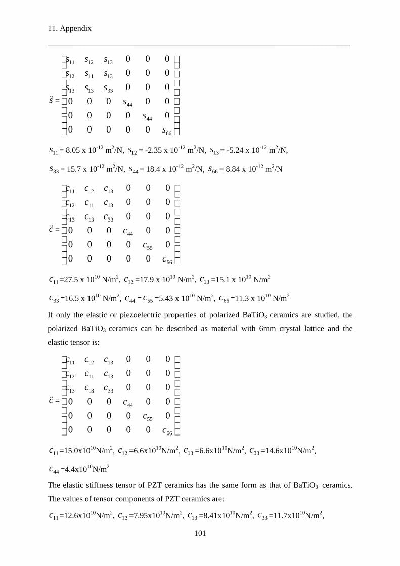
11. Appendix
___________________________________________________________________________
101
s�
=
66
44
44
331313
131112
131211
00000
00000
00000
000
000
000
s
s
s
sss
sss
sss
11s = 8.05 x 10⁻¹² m2/N, 12s = -2.35 x 10⁻¹² m2/N, 13s = -5.24 x 10⁻¹² m2/N,
33s = 15.7 x 10⁻¹² m2/N, 44s = 18.4 x 10⁻¹² m2/N, 66s = 8.84 x 10⁻¹² m2/N
c�
=
66
55
44
331313
131112
131211
00000
00000
00000
000
000
000
c
c
c
ccc
ccc
ccc
11c =27.5 x 10¹⁰ N/m2, 12c =17.9 x 10¹⁰ N/m2, 13c =15.1 x 10¹⁰ N/m2
33c =16.5 x 10¹⁰ N/m2, 44c = 55c =5.43 x 10¹⁰ N/m2, 66c =11.3 x 10¹⁰ N/m2
If only the elastic or piezoelectric properties of polarized BaTiO3 ceramics are studied, the
polarized BaTiO3 ceramics can be described as material with 6mm crystal lattice and the
elastic tensor is:
c�
=
66
55
44
331313
131112
131211
00000
00000
00000
000
000
000
c
c
c
ccc
ccc
ccc
11c =15.0x10¹⁰N/m2, 12c =6.6x10¹⁰N/m2, 13c =6.6x10¹⁰N/m2, 33c =14.6x10¹⁰N/m2,
44c =4.4x10¹⁰N/m2
The elastic stiffness tensor of PZT ceramics has the same form as that of BaTiO3 ceramics.
The values of tensor components of PZT ceramics are:
11c =12.6x10¹⁰N/m2, 12c =7.95x10¹⁰N/m2, 13c =8.41x10¹⁰N/m2, 33c =11.7x10¹⁰N/m2,
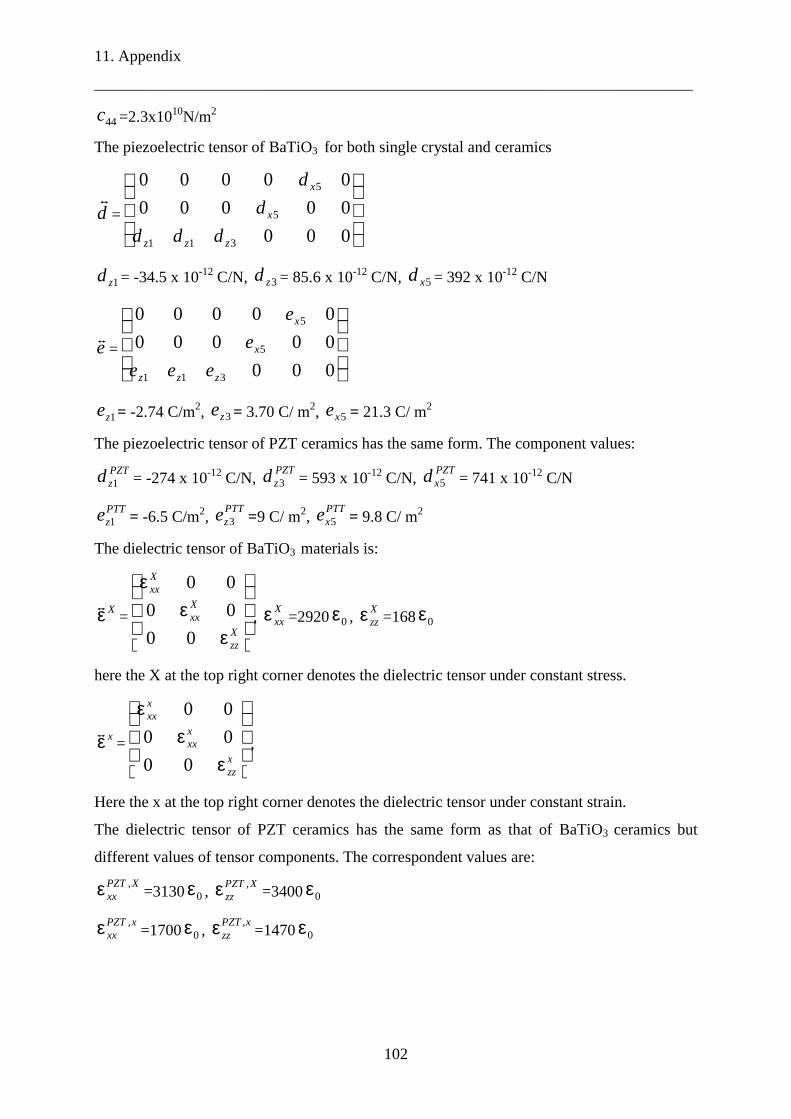
11. Appendix
___________________________________________________________________________
102
44c =2.3x10¹⁰N/m2
The piezoelectric tensor of BaTiO3 for both single crystal and ceramics
d�
=
000
00000
00000
311
5
5
zzz
x
x
ddd
d
d
1zd = -34.5 x 10⁻¹² C/N, 3zd = 85.6 x 10⁻¹² C/N, 5xd = 392 x 10-12 C/N
e�
=
000
00000
00000
311
5
5
zzz
x
x
eee
e
e
1ze = -2.74 C/m2, 3ze = 3.70 C/ m2, 5xe = 21.3 C/ m2
The piezoelectric tensor of PZT ceramics has the same form. The component values:
PZTzd 1 = -274 x 10-12 C/N,
PZTzd 3 = 593 x 10-12 C/N,
PZTxd 5 = 741 x 10-12 C/N
PTTze 1 = -6.5 C/m2,
PTTze 3 =9 C/ m2,
PTTxe 5 = 9.8 C/ m2
The dielectric tensor of BaTiO3 materials is:
Xε�
=
εε
ε
Xzz
Xxx
Xxx
00
00
00
, Xxxε =2920 0ε ,
Xzzε =168 0ε
here the X at the top right corner denotes the dielectric tensor under constant stress.
xε�
=
εε
ε
xzz
xxx
xxx
00
00
00
,
Here the x at the top right corner denotes the dielectric tensor under constant strain.
The dielectric tensor of PZT ceramics has the same form as that of BaTiO3 ceramics but
different values of tensor components. The correspondent values are:
XPZTxx
,ε =3130 0ε , XPZT
zz,ε =3400 0ε
xPZTxx
,ε =1700 0ε , xPZT
zz,ε =1470 0ε
12. Reference
___________________________________________________________________________
103
12 Reference
1. T. Mitsui, I. Tatsuzaki, E, Nakamura: An introduction to the physics of ferroelectrics.
Gordon and Breach Science Publishers, Ltd. 1976
2. F. Jona: Ferroelectric Crystals, Pergamon Press 1992
3. M. E. Lines and A. M. Glass: Principles and applications of ferroelectrics and related
materials. Oxford University Press 1996
4. C. Paz de Araujo, J. F. Scott, and G. W. Taylor, Ferroelectric thin films: synthesis and
basic properties, Gordon and Breach Science Publishers, Ltd. 1996
5. D. Damjanovic: Ferro, dielectric, piezoelectric properties of ferroelectric thin films and
ceramics, Rep. Prog. Phys. 61 (1998), 1267-1324
6. G. Arlt and P. Sasko: Domain configuration and equilibrium size of domains in BaTiO3
ceramics, J. Appl. Phys. 51 (1980) No.9, 4956-4960
7. G. Arlt: The role of domain walls on the dielectric, elastic and piezoelectric properties of
ferroelectrtic ceramics, Ferroelectrics 76 (1987), 451-358
8. G. Arlt: The influence of microstructure on the properties of ferroelectric ceramics,
Ferroelectrics, 104 (1990), 217-227
9. G. Arlt: Twinning of ferroelectric and ferroelastic ceramics: stress relief, J. Mat. Sci. 25
(1990), 2655-2666
10. N. A. Pertsev and G. Arlt: Theory of the banded domain structure in coarse-grained
ferroelectric ceramics, Ferroelectrics, 132 (1992), 27-40
11. Q. M. Zhang, H. Wang, N. Kim, and L. E. Cross: Direct evaluation of domain-wall and
intrinsic contributions to the dielectric and piezoelectric response and their temperature
dependence on lead zirconate-titanate ceramics, J. Appl. Phys. 75 (1994) No. 1, 454-459
12. M. Demartin, and D. Damjanovic: Dependence of the direct piezoelectric effect in coarse
and fine grain batium titanate ceramics on dynamic and static pressure, Appl. Phys. Lett.
68 (1996) No. 21, 3046-3048
13. D. Damjanovic: Stress and frequency dependence of the direct piezoelectric effect in
ferroelectric ceramics, J. Appl. Phys. 82 (1997), 1788-1797
14. G. Y. Robinson and R. M . White, Scanning electron microscopy of ferroelectric domains
in Barium Titanate, Appl. Phys. Lett. 10 (1967), 320-323
12. Reference
___________________________________________________________________________
104
15. N. Kultscher and L. J. Balk, Signal generation and contrast mechanisms in scanning
electron acoustic microscopy, Scanning Electron Microscopy, 1, (1986), 33-43
16. B. Y. Zhang, F. M. Jiang, Q. R. Yin, Electron acoustic microscopy of BaTiO3 single
crystal, J. Appl. Phys., 80(3) (1996), 1916-1918
17. T. Malis and H. Gleiter, Investigation of the structure of ferroelectric domain boundaries
by transmission electron microscopy, Journal of Applied Physics, 47(12), (1976), 5195-
5200
18. G. Binnig, C. F. Quate, and Ch. Gerber, Atomic Force Microscope, Physical Review
Letters, 56(9), (1986), 930-933
19. F. Saurenbach and B. D. Terris: Imaging of ferroelectric domain walls by force
microscopy, Applied Physics Letters, 56(17), (1990), 1703-1705
20. R. Lüthi, H. Haefke, K.-P. Meyer, E. Meyer, L. Howald, and H.-J. Güntherodt: Surface
and domain structures of ferroelectric crystals studied with scanning force microscopy,
Journal of Applied Physics, 74(12), (1993), 7461-7471
21. M.-K. Bae, T. Horiuchi, K. Hara, Y. Ishibashi, and K. Matsushige: Direct observation of
domain structures in Triglycine Sulfate by atomic force microscope, Jpn. J. Appl. Phys.,
33, (1994), 1390-1393
22. K. Franke, J. Besold, W. Haessler, and C. Seegebarth; Modification and detection of
domains on ferroelectric PZT films by scanning force microscopy, Surface Science
Letters, 302, (1994), L283-L288
23. S.-I. Hamazaki, F. Shimizu, S. Kojima, and M. Takashige: AFM observation of 90°
domains of BaTiO3 butterfly crystals, Journal of the Physical Society of Japan, 64(10),
(1995), 3660-3663
24. L. M. Eng, M. Friedrich , J. Fouisek, and P. Günter: Deconvolution of topographic and
ferroelectric contrast by noncontact and friction force microscopy, J. Vac. Sci. Technol.
B14(2), (1996), 1191-1196
25. A. Gruverman, J. Hatano, and H. Tokumoto: Scanning force microscopy studies of
domain structure in BaTiO3 Single Crystal, Jpn. J. Appl. Phys., 36, (1997), 2207-2211
26. S. Balakumar, J. B. Xu, J. X. Ma, S. Ganesamoorthy, and I. H. Wilson: Surface
morphology of ferroelectric domains in BaTiO3 Single Crystals: an atomic force
microscope study, Jpn. J. Appl. Phys., 36, (1997), 5566-5569
12. Reference
___________________________________________________________________________
105
27. G. K. H. Pang and K. Z. Baba-Kishi: Characterization of butterfly single crystals of
BaTiO3 by atomic force, optical and scanning electron microscopy techniques: J. Phys. D:
Appl. Phys., 31, (1998), 2846-2853
28. S. Tsunekawa, T. Fukuda, T. Ozaki, Y. Yoneda, T. Okabe, and H. Terauchi: Study on
ferroelectric domains in BaTiO3 crystalline films and bulk crystals by atomic force and
scanning electron microscopies, Journal of Applied Physics, 84(2), (1998), 999-1002
29. S. V. Kalinin and D. A. Bonnell: Effect of phase transition on the surface potential of the
BaTiO3(100) surface by variable temperature scanning surface potential microscopy,
Journal of Applied Physics, 87(8), 2000
30. U. Rabe, S. Amelio, E. Kester, V. Scherer, S. Hirsekorn, and W. Arnold: Quantitative
determination of contact stiffness using atomic force acoustic microscopy, Ultrasonics, 38,
(2000), 430-437
31. L. M. Eng, M. Bammerlin, Ch. Loppacher, M. Guggisberg, R, Bennewitz, R. Lüthi, E.
Meyer, Th. Huser, H. Heinzelmann, and H.-J. Güntherodt: Ferroelectric domain
characterisation and manipulation: a challenge for scanning probe microscopy,
Ferroelectrics, 222, (1999), 153-162
32. C. Harnagea, A. Pignolet, M. Alexe, K. M. Satyalakshmi, D. Hesse, and U. Gösele:
Nanoscale switching and domain structure of ferroelectric BaBi4Ti4O15 thin films, Jpn. J.
Appl. Phys., 38, (1999), L1251-L1257
33. C. Durkan, M.E. Welland, D. P. Chu, and P, Migliorato: Probing domains at the
nanometer scale in piezoelectric thin films, Physical Review B, 60(23), 1999, 16198-
16204
34. B. Y. Zhang, X. X. Liu, Q. R. Yin, and L. J. Balk: Scanning near field acoustic
microscopies for the evaluation of polycrystalline materials, Acoustical Imaging, 23,
(1997) 19-24
35. X. X. Liu, L. J. Balk, H.-P. Abicht, A. Eckau, and Q. R. Yin: Scanning acoustic
microscopes for the investigation of ferroelectric properties of ferroelectric materials,
Solid State Phenomena, 63-64, (1998), 361-368
36. X. X. Liu and L. J. Balk: Scanning Acoustic Microscopes for the Investigation of
Ferroelectrical Materials, presented at the "3rd Conference on Development and
Technological Application of Scanning Probe Methods" (SXM3), (14.-17.9.1998, Basel,
12. Reference
___________________________________________________________________________
106
Schweiz)
37. X. X. Liu, R. Heiderhoff, H.-P. Abicht, and L. J. Balk: Characterization of ferroelectric
domains by the use of scanning near-field acoustic microscopies, Analytical Science,
accepted for publication
38. X. X. Liu, B. Y. Zhang, Q. R. Yin, and L. J. Balk: Scanning electron acoustic microscopy
for the evaluation of domain structures in BaTiO3 single crystal and ceramics, Journal of
Material Science, 33 (1998) 4543-4549
39. J. F. Nye: Physical of crystals, Oxford University Press.
40. A. F. Devonshire, Theory of Barium Titanate - Part 1, Phil. Mag. 40 (1949) 1040-1063
41. V. A. Zhirnov: Sov. Phys. JETP 35 (1959), 1175-1180
42. E. V. Chenski: Sov. Phys.-Solid St. 14 (1973), 1940-1950
43. J. Bouillot and R. Machel: Proc. Europ. Mtg on Ferroelectricity, Saarbrücken, Wiss.
Verlags, Stuttgart 1969, 111-119
44. J. C. Burfoot and G. W. Taylor: Polar dielectrics and their applications, 1979 Macmillan
Press Ltd.
45. V. Holy U. Pietsch, and T. Baumbach: High resolution X-ray scattering from thin films
and multilayers, Springer Verlag, 1999
46. B. M. Park, S. J. Chung, H. S. Kim, W. Si, and M. Dudley, Synchrotron white-beam X-
ray topography of ferroelectric domains in a BaTiO3 single crystal, Philosophical Magzine
A, 75 (3), 1997, 611-620
47. C. L. Jia, K. Urban, M. Mertin, S. Hoffmann, and R. Wasser, The structure and formation
of nanotwins in BaTiO3 thin films, Philosophical Magazine A, 77(4) (1998), 923-939
48. I. T. Kim, J. W. Jang, H. J. Youn, C. H. Kim, and K. S. Hong, 180° ferroelectric domains
in polycrystalline BaTiO3 thin films, Appl. Phys. Lett. 72(3) (1998), 308-310
49. R. C. Miller: Optical Harmonic Generation in Single Crystal BaTiO[sub3], Phys. Rev.
134 (1964), A1313-A1318
50. M. Flörsheimer, R. Paschotta, U. Kubitscheck, Ch. Brillert, D. Hofmann, L. Heuer, G.
Schreiber, C. Verbeek, W. Sohler, and H. Fucks: Second-harmonic imaging of
ferroelectric domains in LiNbO3 with micron resolution in lateral and axial directions,
Appl. Phys. B 67 (1998) 593-599
12. Reference
___________________________________________________________________________
107
51. I. I. Smolyaninov and C.C. Davis: Near-field optical study of photorefractive surface
waves in BaTiO3, Optics Letters, 24 No.19, (1999), 13671369
52. S. N. Zhu and W. Cao, Imaging of ferroelectric domains in LiTiO3 by environment
scanning electron microscopy, Ferroelectrics, 222 (1999), 257-262
53. B. A. Auld: Acoustic fields and waves in solids, John Wiley & Sons, Inc. 1973
54. S. W. Meeks and B. A. Auld: Optical and acoustic device applications of ferroelastic
crystals, Advances in electronics and electron physics, 71 (1998) 250-355
55. E. Brandis and A. Rosencwaig, Thermal-wave microscopy with electron beams, Applied
Physics Letters, 37, (1980), 98-100
56. G. S. Cargill, Nature, 286, (1980), 691-695
57. L. J. Balk: Advances in Electronics and Electronic Physics, 71, (1988) 1-73
58. J. Cantrell and M. Qian, Piezoelectric detection of signals in scanning electron acoustic
microscopy, Materials Science and Engineering, A122 (1989) 47-52
59. L. J. Balk: Scanning Acoustic Microscopy, Analysis of Microelectronic Materials and
Devices, Ed. by M. Grasserbauer and H. W. Werner, John Wiley & Sons Ltd. (1991) 742-
769
60. B. Y. Zhang and Q. R. Yin: Piezoelectric coupling effect of ferroelectrics in scanning
electron acoustic imaging, Progress in natural science 6(supplement), 1996, S-123~S-126
61. S. W. Fu, S. Y. Zhang, Z.S. Wu, L. B. Luo, Z. Zhang, and H. I Chen, Photoacoustic
investigation of chemical reactions by piezoelectric cylindrical tube transducer, Progress
in natural science 6(supplement), 1996, S-54~S-57
62. F. G. Satkiewicz, J. C. Murphy and L. C. Aamodt: in Techical digest of the Fourth
International Topical Meeting on Photoacoustic, Thermal, and Related Science (Montreal,
1985)
63. D. N. Rose, H. R. Turner, K. Legg: in Techical digest of the Fourth International Topical
Meeting on Photoacoustic, Thermal, and Related Science (Montreal, 1985)
64. P. Günther, U. Ch. Fischer, and K. Dransfeld: Scanning near-field acoustic microscopy,
Applied Physics, B48, (1989), 89-92
65. U. Rabe and W. Arnold: Acoustic Microscopy by atomic force microscopy, Applied
Physics Letters, 64(12), (1994), 1493-1495
12. Reference
___________________________________________________________________________
108
66. M. Maywald, G. Brockt, and L. J. Balk: Scanning Probe Acoustic Microscopy, Inst. of
Phys. Conf. Ser. No. 146 (1995) 667-670
67. U. Grunewald, K. Bartzke, T. Antrack, Application of the needle sensor for microstructure
measurements and atomic force microscopy, Thin Solid Films, 264, (1995), 169-171
68. A. Michels, F. Meinen, T. Murdfield, W. Göhde, U. C. Fischer, E. Beckmann, and H.
Fuchs: 1 MHz quartz length extension resonator as a probe for scanning near-field
acoustic microscopy, Thin Solid Films, 264, (1995), 172-175
69. T. Hesjedal, E. Chilla, and H. J. Fröhlich: Scanning acoustic force microscope
investigations of surface acoustic waves, Surface and Interface Analysis, 25, (1997), 569-
572
70. R. M. Cramer, V. Biletzki, P. Lepidis, L. J. Balk: Subsurface analyses of defects in
integrated devices by scanning probe acoustic microscopy, Microelectronics Reliability 39
(1999) 947-950
71. F. Ohuchi, D. E. Clark, L. L. Hench: Effect of crystallization on the Auger electron signal
decay in an Li2Ox 2 SiO2 glass and glass-ceramic, J. Am. Ceram. Soc., 62 (1979), 500-
503
72. F. Ohuchi and P. H. Holloway. General model of sodium desorption and diffusion during
electron bombardment of glass. Journal of Vacuum Science and Technology, 20 (1982),
863-867
73. L. Reimer: Scanning Electron Microscopy, Springe-Verlag, 1985
74. J. Cazaux: Some considerations on the electric field induced in insulators by electron
bombardment, Journal of Applied Physics, 59(5), 1986, 1418-1430
75. S. G. Qian, S. Y. Zhang, J. C. Cheng, and Z. Q. Wang, Three dimensional theory of
scanning electron-acoustic imaging, 6(supplement), 1996, S-127~S-130
76. Valvo: Piezooxide (PXE), Photo Copie Gmbh, Hamburg, (1984)
77. C. Durkan and M. E. Welland: Investigations into local ferroelectric properties by atomic
force microscopy, Ultramicroscopy, 82, (2000), 141-148
78. C. H. Ahn, T. Tybell, L. Antognazza, K. Char, R. H. Hammond, M. R. Beasley, Ø.
Fischer, and J.-M. Triscone: Local, nonvolatile electronic writing of epitaxial
Pb(Zr0.52Ti0.48)O3/SrRuO3 heterostructures, Science 276, (1997), 1100-1103
12. Reference
___________________________________________________________________________
109
79. S. Belaidi, P. Girard, and G. Leveque: Electrostatic forces acting on the tip in atomic force
microscopy: Modulization and comparison with analytic expressions, Journal of applied
Physics, 81(3), 1997, 1023-1030
80. J. A. Stratton: Electromagnetic theory, McGraw-Hill Book company, Inc. 1941
81. W. R. Smythe: Static and dynamic electricity, McGraw-Hill Book company, Inc. 1968
82. V. W. Hansen: Numerical solution of antennas in layered media, John Wiley & Sons Inc.
1989
83. Nanosensors Dr. Olaf Wolter GmbH, Wetzlar-Blankenfeld, Germany
84. S. Hirsekorn, U. Rabe, and W. Arnold: Theoretical description of the transfer of vibration
from a sample to the cantilever of an atomic force microscope, Nanotechnology, 8 (1997),
57-66
85. U. Rabe, S. A. Melio, E. Kester, V. Scherer, S. Hirsekorn, W. Arnold: Quantitative
determination of contact stiffness using atomic force acoustic microscopy, Ultrasonic 38
(2000), 430-437
86. H. T. Langhammer, T. Müller, A. Polity, K.-H. Felgner, and H.-P. Abicht: On the crystal
and defect structure of Manganese-doped barium titanate ceramics, Materials Letters, 26,
1996, 205-210
87. National technology roadmap for semiconductors, Austin: SEMATECH Inc. 1997
88. I. N. Bronstein and K. A. Semendjajew: Taschenbuch der Mathematik, 1991
89. Q. R. Yin, J. Liao, B. Y. Zhang, Y. Yang, and F. M .Jiang, Electron acoustic imaging of
ferroelectric domain and mechanism analysis on BaTiO3 ceramics, Ferroelectrics 231
(1999), 11-18
Publications and presentations___________________________________________________________________________
110
Publications and presentations
Parts of this work have been published in international journals or presented at the
international conference, scientific seminars, and invited scientific talks. The following is a
list of the publications and presentations of the author in recent years.
1. B. Y. Zhang, X. X. Liu, Q. R. Yin, and L. J. Balk,: Scanning near field acoustic
microscopies for the evaluation of polycrystalline materials, Acoustical Imaging, 23,
(1997) 19-24
2. X. X. Liu, L. J. Balk, H.-P. Abicht, A. Eckau, and Q. R. Yin: Scanning acoustic
microscopes for the investigation of ferroelectric properties of ferroelectric materials,
Solid State Phenomena, 63-64, (1998), 361-368
3. X. X. Liu, B. Y. Zhang, Q. R. Yin, and L. J. Balk: Scanning electron acoustic microscopy
for the evaluation of domain structures in BaTiO3 single crystal and ceramics, Journal of
Material Science, 33 (1998) 4543-4549
4. X. X. Liu, R. Heiderhoff, H.-P. Abicht, and L. J. Balk: Characterization of ferroelectric
domains by the use of scanning near-field acoustic microscopies, Analytical Science,
Vol.17, Special Issue No.107 2001
5. X. X. Liu, R. Heiderhoff, H.-P. Abicht, and L. J. Balk: "Dynamic characterization of
ferroelectric domains of BaTiO3 by the use of scanning near-field acoustic microscopy",
accepted for presentation at "International Conference on Materials for Advanced
Technologies" (ICMAT 2001, 1.-6.7.2001, Singapore), to be published in Materials
Chemistry and Physics
Presentations
6. L. J. Balk, G. Fiege, and X. X. Liu: Imaging of Thermal and Mechanical Structures by
Scanning Force Microscopy, Invited Talk at "SPMM’97, International Conference on
Scanning Probe Microscopy as a Microsystem" (5.-7.6.1997, Wroclaw, Poland)
7. X. X. Liu and L. J. Balk: Scanning acoustic microscopes for the investigation of
ferroelectric material, presented at "3th Conference on Development and Technological
Application of Scanning Probe Methods (SXM3)", from Sep. 14 to 17, 1998.
8. X. X. Liu: Characterization of ferroelectric domains by the use of scanning near-field
acoustic microscopy, Presented on Jan. 17, 2000, in Fachbereich Elektrotechnik und
Informationstechnik, BUGH Wuppertal
Publications and presentations___________________________________________________________________________
111
9. X. X. Liu: Characterization of ferroelectric domains by the use of scanning near-field
acoustic microscopy, Presented on Feb. 4, 2000, in Fachbereich Physik, Martin-Luther-
Universität Halle-Wittenberg
10. X. X. Liu: Characterization of ferroelectric domains by the use of scanning near-field
acoustic microscopy, Presented on Feb. 5, 2000, in Bundesanstalt für Materialsforschung
und –Prüfung, Berlin
11. X. X. Liu: Characterization of ferroelectric domains by the use of scanning near-field
acoustic microscopy, Presented on Jul. 15, 2000, in Department of Electrical Engineering
and Information, National University of Singapore
12. X. X. Liu: Characterization of ferroelectric domains by the use of scanning near-field
acoustic microscopy, Presented on Jul. 21, 2000, in Shanghai Institute of Ceramics,
Chinese Academy of Science
Top Related