13 12 05 Operationsverstaerker - LMU
11
228 ELEKTRONIK ELEKTRONIK SS 2001 SS 2001 Prof. Dr. Klaus Wille Prof. Dr. Klaus Wille 8 Operationsverstärker In der Analogtechnik werden häufig Operationsverstärker eingesetzt. Schaltsymbol nach DIN Diese Verstärker haben folgende Eigenschaften: 1. Sehr hohe Spannungsverstärkung ) 10 10 ( 6 U 4 < < v 2. Die erste Stufe ist als Differenzver- stärker ausgebildet. 3. Hohe Gleichtaktunterdrückung der Eingangssignale 4. Sehr großer Eingangswiderstand 5. Alle Verstärkerstufen sind gleich- spannungsgekoppelt. 6. Sehr kleiner Ausgangswiderstand 229 ELEKTRONIK ELEKTRONIK SS 2001 SS 2001 Prof. Dr. Klaus Wille Prof. Dr. Klaus Wille 8.1 Aufbau eines mehrstufigen Operationsverstärkers
Transcript of 13 12 05 Operationsverstaerker - LMU
228
ELEKTRONIKELEKTRONIK SS 2001SS 2001 Prof. Dr. Klaus WilleProf. Dr. Klaus Wille
8 OperationsverstärkerIn der Analogtechnik werden häufigOperationsverstärker eingesetzt.
Schaltsymbol nachDIN
Diese Verstärker haben folgendeEigenschaften:
1. Sehr hohe Spannungsverstärkung)1010( 6
U4 << v
2. Die erste Stufe ist als Differenzver-stärker ausgebildet.
3. Hohe Gleichtaktunterdrückung derEingangssignale
4. Sehr großer Eingangswiderstand
5. Alle Verstärkerstufen sind gleich-spannungsgekoppelt.
6. Sehr kleiner Ausgangswiderstand
229
ELEKTRONIKELEKTRONIK SS 2001SS 2001 Prof. Dr. Klaus WilleProf. Dr. Klaus Wille
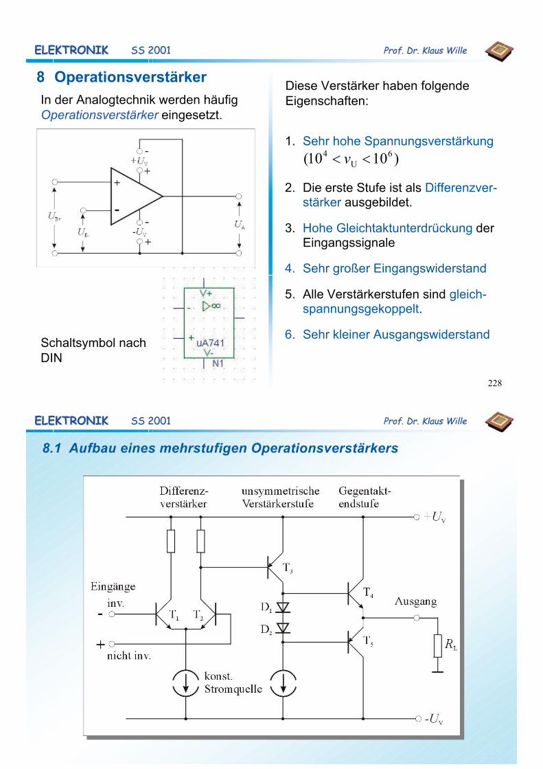
8.1 Aufbau eines mehrstufigen Operationsverstärkers
Eberhard
Schreibmaschinentext
E. Riedle LMU 18.12.17
LM
741
Opera
tionalA
mplifie
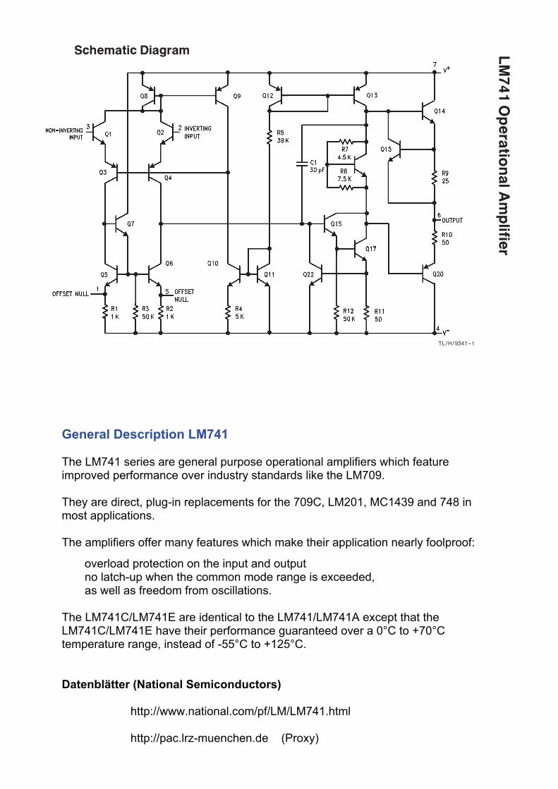
rSchematic Diagram
TL�H�9341–1
General Description LM741 The LM741 series are general purpose operational amplifiers which feature improved performance over industry standards like the LM709. They are direct, plug-in replacements for the 709C, LM201, MC1439 and 748 in most applications. The amplifiers offer many features which make their application nearly foolproof:
overload protection on the input and output no latch-up when the common mode range is exceeded, as well as freedom from oscillations.
The LM741C/LM741E are identical to the LM741/LM741A except that the LM741C/LM741E have their performance guaranteed over a 0°C to +70°C temperature range, instead of -55°C to +125°C. Datenblätter (National Semiconductors)
http://www.national.com/pf/LM/LM741.html
http://pac.lrz-muenchen.de (Proxy)
General Description TL082 These devices are low cost, high speed, dual JFET input operational amplifiers with an internally trimmed input offset voltage (BI-FET II™ technology). They require low supply current yet maintain a large gain bandwidth product and fast slew rate. In addition, well matched high voltage JFET input devices provide very low input bias and offset currents. The TL082 is pin compatible with the standard LM1558 allowing designers to immediately upgrade the overall performance of existing LM1558 and most LM358 designs. These amplifiers may be used in applications such as high speed integrators, fast D/A converters sample and hold circuits and many other circuits requiring low input offset voltage, low input bias current, high input impedance, high slew rate and wide bandwidth. The devices also exhibit low noise and offset voltage drift. Datenblätter (National Semiconductors)
http://www.national.com/pf/TL/TL082.html
General Description LF157 LF155/LF156/LF157 Series Monolithic JFET Input Operational Amplifier These are the first monolithic JFET input operational amplifiers to incorporate well matched, high voltage JFETs on the same chip with standard bipolar transistors (BI-FET™ Technology). These amplifiers feature low input bias and offset currents/low offset voltage and offset voltage drift, coupled with offset adjust which does not degrade drift or common-mode rejection. The devices are also designed for high slew rate, wide bandwidth, extremely fast settling time, low voltage and current noise and a low 1/f noise corner. Applications Precision high speed integrators
Fast D/A and A/D converters High impedance buffers Wideband, low noise, low drift amplifiers Logarithmic amplifiers Photocell amplifiers Sample and Hold circuits
Datenblätter (National Semiconductors)
http://www.national.com/pf/LF/LF157.html

232
ELEKTRONIKELEKTRONIK SS 2001SS 2001 Prof. Dr. Klaus WilleProf. Dr. Klaus Wille
Das einfachste Beispiel ist der invertierendeVerstärker mit Gegenkoppelung:
E21 III +=
E
EE
2
AE2
1
EE1
,
,
rUI
RUUI
RUUI
Δ=
−Δ=
Δ−=
Der Eingangsstrom ist
(8.1)
Mit dem Eingangswiderstand rE des OP wird
(8.2)
E
E
2
AE
1
EE
rU
RUU
RUU Δ
+−Δ
=Δ−
EE211
E
2
A 111 UrRRR
URU Δ⎟
⎠
⎞⎜⎝
⎛+++−=
Damit folgt
und
(8.4)
(8.3)
233
ELEKTRONIKELEKTRONIK SS 2001SS 2001 Prof. Dr. Klaus WilleProf. Dr. Klaus Wille
vUU A
E =Δ
⎟⎠
⎞⎜⎝
⎛+++−=
E21
A
1
E
2
A 111rRRv
URU
RU
⎥⎦
⎤⎢⎣
⎡⎟⎠
⎞⎜⎝
⎛++−
−=
E2121
EA 11111
rRRvRR
UU
Die Differenzspannung zwischen denbeiden Eingängen wird
Setzt man das in (8.4) ein, erhält man
Die Ausgangsspannung wird dann
(8.5)
(8.6)
(8.7)
Da die Verstärkung v >>> 1 ist, verein-facht sich diese Beziehung auf
E1
2A U
RRU −= (8.8)
Die Verstärkung hängt nicht mehr vonden individuellen Eigenschaften desOperationsverstärkers ab. Sie wird nurnoch vom Verhältnis der Widerständeder äußeren Beschaltung bestimmt.Die Verstärkerschaltung ist daherextrem linear.
.
E. Riedle PhysikLMU
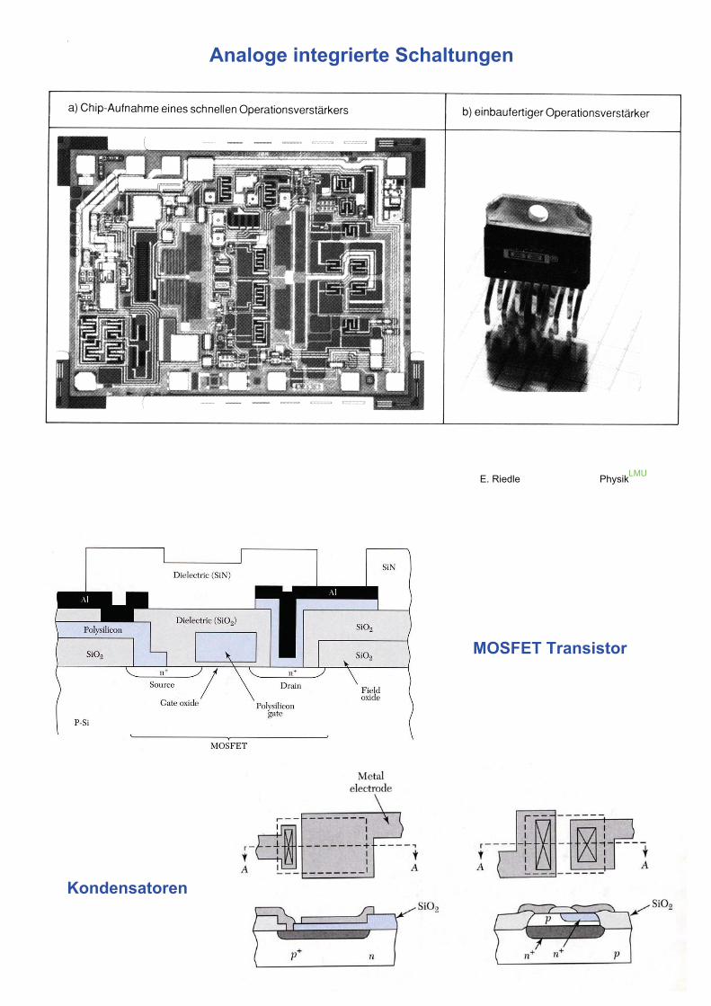
Analoge integrierte Schaltungen
.
E. Riedle PhysikLMU
MOSFET Transistor
Kondensatoren

.
E. Riedle PhysikLMU
Widerstand
Spule
WIR
BE
LSC
HIC
HT
RE
AK
TO
RF
LUID
IZE
D B
ED
RE
AC
TO
R
AB
SC
HE
IDU
NG
VO
NP
OLY
KR
ISTA
LLIN
EM
RE
INS
TS
ILIC
IUM
CH
EM
ICA
L V
AP
OR
DE
PO
SIT
ION
OF
PO
LYC
RY
STA
LLIN
E S
ILIC
ON
Gas
förm
iger
Chlo
rwas
sers
toff
Hyd
rogen
Chl
ori
de
Met
allu
rgis
ches
Silic
ium
Met
allu
rgic
al S
ilico
n
Tric
hlor
sila
nTr
ichlo
rosi
lane
Düs
enbo
den
Nozz
le G
roun
d
SiH
Cl 3
H2
Si
HC
l
Rea
ktor
Bel
l Jar
Poly
kris
talli
nes
Silic
ium
Poly
crys
talli
ne S
ilico
n
Tric
hlor
sila
nun
d W
asse
rsto
ffTr
ichlo
rosi
lane
and H
ydro
gen
SiH
Cl/H
32
TIE
GE
LZIE
HE
NC
ZO
CH
RA
LSK
I PU
LLIN
G
ZO
NE
NZ
IEH
EN
FLO
AT
ZO
NE
PU
LLIN
G
Silic
ium
schm
elze
Sili
con
Mel
t
Qua
rztie
gel
Qua
rtz
Cru
cible
Impf
kris
tall
See
d C
ryst
al
Wid
erst
ands
heiz
erR
esis
tivity
Hea
ter
Poly
kris
talli
nes
Silic
ium
Poly
crys
talli
ne S
ilico
n
Indu
ktio
nssp
ule
Induc
tion
Coil
Eink
rist
all
Mono
crys
tal
RU
ND
SC
HLE
IFE
NIN
GO
T G
RIN
DIN
G
INN
EN
LOC
HS
ÄG
EN
INN
ER
DIA
ME
TE
R S
LIC
ING
DR
AH
TS
ÄG
ET
EC
HN
IKM
ULT
I WIR
E S
LIC
ING
Aufg
ekitt
etes
Sta
bstü
ckM
oun
ted Ing
ot
Slur
rydü
seS
lurr
y N
ozz
le
Dra
htfü
hrun
gsro
llen
Wir
e G
uide
Rolle
rs
Säge
gatte
rW
ire
Web
Inne
nloc
h Sä
gebl
att
Inne
r D
iam
eter
Saw
ing B
lade
Dia
man
tbel
agD
iam
ond
Lay
er
Stab
stüc
kIn
got
Sec
tion
KA
NT
EN
VE
RR
UN
DE
NE
DG
E R
OU
ND
ING
LÄP
PE
NLA
PP
ING
Unv
erru
ndet
eSi
liciu
msc
heib
eA
s S
awn
Waf
er
Schl
eifc
huck
Gri
ndin
g C
huc
k
Prof
ilsch
leifs
chei
beEdge
Roun
din
g W
hee
l
RE
INIG
EN
UN
D Ä
TZ
EN
CLE
AN
ING
AN
D E
TC
HIN
G
Rei
nigu
ngsb
ecke
nC
lean
ing B
ath
Ätzb
ecke
nEtc
h B
ath
Troc
knun
gD
ryer
Obe
re u
ndun
tere
Läp
psch
eibe
Upper
and
Low
erLa
ppin
g P
late
Silic
ium
sche
ibe
Sili
con
Waf
er
Läuf
ersc
heib
eLa
ppin
g C
arri
er
OX
ID-B
ES
CH
ICH
TU
NG
OX
IDE
DE
PO
SIT
ION
PO
LY-B
ES
CH
ICH
TU
NG
PO
LY D
EP
OS
ITIO
N
Qua
rzgl
ocke
Qua
rtz
Tube
Qua
rzbo
otQ
uart
z
Boat
Silic
ium
sche
ibe
Sili
con
Waf
er
SiH
4
Dus
chko
pfS
how
er H
ead
Silic
ium
sche
ibe
Sili
con
Waf
er
Hei
zblo
ckH
eate
r B
lock
SiH
/NO
42
PO
LIE
RE
NP
OLI
SH
ING
EP
ITA
XIE
EP
ITA
XY
Lam
penh
eizu
ngLa
mp H
eatin
g
Susz
epto
rS
usce
pto
r
Proz
essg
asst
röm
ung
Pro
cess
Gas
Flo
w
Silic
ium
sche
ibe
Sili
con
Waf
er
© 2
00
4 S
iltr
on
icw
ww
.sil
tro
nic
.co
m
HO
W T
O P
RO
DU
CE
A S
ILIC
ON
W
AF
ER
WIE
E
INE
S
ILIC
IUM
S
CH
EIB
E E
NT
ST
EH
T
Topf
schl
eifs
chei
beG
rind
ing W
hee
l
Stab
stüc
kIn
got
Sec
tion
Polie
rtuc
hPolis
hing
Pad
Träg
erpl
atte
Cer
amic
Pla
te
Polie
rtel
ler
Polis
hing
Pla
ten

WIRBELSCHICHTREAKTORFLUIDIZED BED REACTOR
ABSCHEIDUNG VONPOLYKRISTALLINEMREINSTSILICIUMCHEMICAL VAPORDEPOSITION OFPOLYCRYSTALLINE SILICON
GasförmigerChlorwasserstoffHydrogen Chloride
MetallurgischesSiliciumMetallurgical Silicon
TrichlorsilanTrichlorosilane
DüsenbodenNozzle Ground
SiHCl3
H2
Si
HCl
ReaktorBell Jar
Polykristallines SiliciumPolycrystalline Silicon
Trichlorsilanund WasserstoffTrichlorosilaneand Hydrogen
SiHCl /H3 2
TIEGELZIEHENCZOCHRALSKI PULLING
ZONENZIEHENFLOAT ZONE PULLING
SiliciumschmelzeSilicon Melt
QuarztiegelQuartz Crucible
ImpfkristallSeed Crystal
WiderstandsheizerResistivity Heater
Polykristallines SiliciumPolycrystalline Silicon
InduktionsspuleInduction Coil
EinkristallMonocrystal
RUNDSCHLEIFENINGOT GRINDING
TopfschleifscheibeGrinding Wheel
StabstückIngot Section

INNENLOCHSÄGENINNER DIAMETER SLICING
DRAHTSÄGETECHNIKMULTI WIRE SLICING
Aufgekittetes StabstückMounted Ingot
SlurrydüseSlurry Nozzle
DrahtführungsrollenWire Guide Rollers
SägegatterWire Web
Innenloch SägeblattInner DiameterSawing Blade
DiamantbelagDiamond Layer
StabstückIngot Section
KANTENVERRUNDENEDGE ROUNDING
UnverrundeteSiliciumscheibeAs Sawn Wafer
SchleifchuckGrinding Chuck
ProfilschleifscheibeEdge Rounding Wheel
KANTENVERRUNDENEDGE ROUNDING
LÄPPENLAPPING
UnverrundeteSiliciumscheibeAs Sawn Wafer
SchleifchuckGrinding Chuck
ProfilschleifscheibeEdge Rounding Wheel
Obere unduntere LäppscheibeUpper and LowerLapping Plate
SiliciumscheibeSilicon Wafer
LäuferscheibeLapping Carrier

REINIGEN UND ÄTZENCLEANING AND ETCHING
ReinigungsbeckenCleaning Bath
ÄtzbeckenEtch Bath
TrocknungDryer
OXID-BESCHICHTUNGOXIDE DEPOSITION
POLY-BESCHICHTUNGPOLY DEPOSITION
QuarzglockeQuartz Tube
QuarzbootQuartz
Boat
SiliciumscheibeSilicon Wafer
SiH4
DuschkopfShower Head
SiliciumscheibeSilicon Wafer
HeizblockHeater Block
SiH /N O4 2
POLIERENPOLISHING
EPITAXIEEPITAXY
LampenheizungLamp Heating
SuszeptorSusceptor
ProzessgasströmungProcess Gas Flow
SiliciumscheibeSilicon Wafer
PoliertuchPolishing Pad
TrägerplatteCeramic Plate
PoliertellerPolishing Platen

.
E. Riedle PhysikLMU
Ausgangsmaterial: p-dotiertes Silizium
Oxidation zu Siliziumdioxid
Aufbringen des Fotolacks
Belichten über eine Fotomaske
Entfernen des nicht belichteten Foto-lacks
.
E. Riedle PhysikLMU
Wegätzen des SiO2 an den nicht beschichteten Stellen --> Maske
Eindiffundieren von n+
Entfernen der Maske
Auswachsen einer n-Epitaxie-Schicht
.
E. Riedle PhysikLMU
Erzeugen, Maskieren, Ätzen und Reinigen einer SiO2-Schicht
Eindiffundierung eines p+-dotierten Ringes um das zukünftige Bauteil
Erzeugen, Maskieren, Ätzen und Reinigen einer SiO2-Maske für den Basisbereich
Diffundieren der Basiszone
.
E. Riedle PhysikLMU
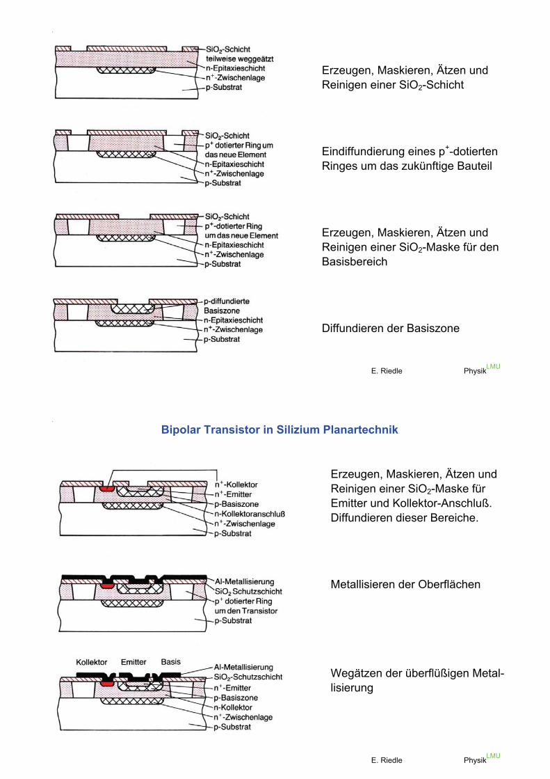
Bipolar Transistor in Silizium Planartechnik
Erzeugen, Maskieren, Ätzen und Reinigen einer SiO2-Maske für Emitter und Kollektor-Anschluß. Diffundieren dieser Bereiche.
Metallisieren der Oberflächen
Wegätzen der überflüßigen Metal-lisierung