AMOLED displays OLED TVs - uni-muenchen.de · 2016-06-27 · AMOLED displays OLED TVs Sony 10 Mio....
19
• Introduction: Organic electronics • Fabrication and characterization of organic thin films • Devices: solar cells, OLEDs, OFETs blackboard part: OFET Organic Electronics MatWi II summer term 2016 Priv. Doz. Bert Nickel ([email protected]) Organic Electronics AMOLED displays OLED TVs Sony 10 Mio. :1 Kontrastverhältnis 0,1ms Reaktionszeit Freier Betrachtungswinkel 15 Zoll / 38 cm Diagonale 40 Watt 1.6 kg 1400 EUR (14.10.2010)
Transcript of AMOLED displays OLED TVs - uni-muenchen.de · 2016-06-27 · AMOLED displays OLED TVs Sony 10 Mio....
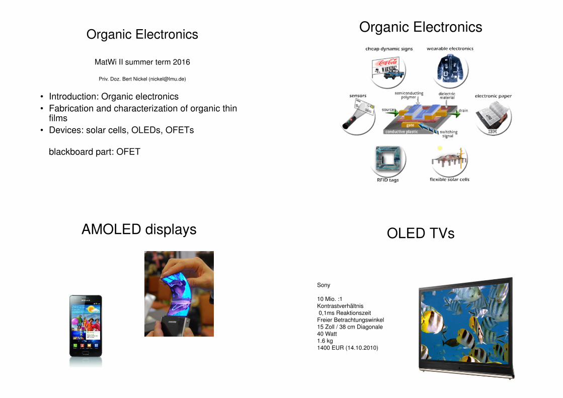
• Introduction: Organic electronics
• Fabrication and characterization of organic thinfilms
• Devices: solar cells, OLEDs, OFETs
blackboard part: OFET
Organic Electronics
MatWi II summer term 2016
Priv. Doz. Bert Nickel ([email protected])
Organic Electronics
AMOLED displays OLED TVs
Sony
10 Mio. :1 Kontrastverhältnis0,1ms Reaktionszeit
Freier Betrachtungswinkel15 Zoll / 38 cm Diagonale40 Watt1.6 kg1400 EUR (14.10.2010)

OLED TV … 15 years R&D55 Zoll (140 cm)
OLEDs for lightening
AP photo
Anil Duggal, who heads up GE Global
Research's Organic Electronics Project, says
sheets of organic light-emitting diodes, such as
the one above, might be the future of lighting.
O-Solar cells
Alan Heeger / University of California -
Santa Barbara
Science 2007
"The result is six and a half percent
efficiency," said Heeger. "This is
the highest level achieved for solar
cells made from organic materials.
I am confident that we can make
additional improvements that will
yield efficiencies sufficiently high
for commercial products." He
expects this technology to be on
the market in about three years.
Note: Today we are at 12%. After
using more than 150 Mil USD
investment capital, Konarka filed
bankruptcy.
Wikipedia: Solar cell
Grätzel
CIGS: Kupfer-Indium-(Gallium)-Schwefel-Selen
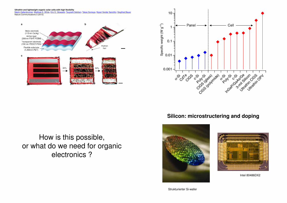
Ultrathin and lightweight organic solar cells with high flexibilityMartin Kaltenbrunner, Matthew S. White, Eric D. Głowacki, Tsuyoshi Sekitani, Takao Someya, Niyazi Serdar Sariciftci, Siegfried BauerNature Communications 3 (2012)
How is this possible,or what do we need for organic
electronics ?
Silicon: microstructering and doping
Intel 80486DX2
Strukturierter Si-wafer
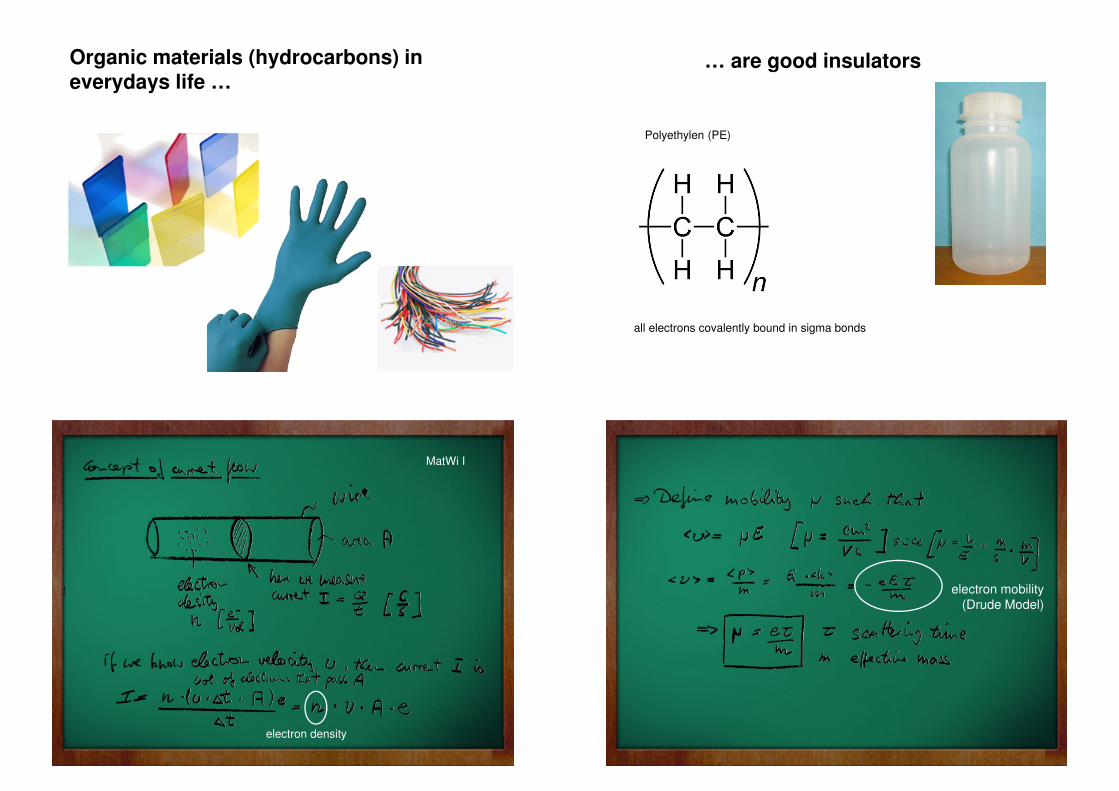
Organic materials (hydrocarbons) in everydays life …
… are good insulators
all electrons covalently bound in sigma bonds
Polyethylen (PE)
electron density
MatWi I
electron mobility(Drude Model)

sp2 hybridisation (C2H4):
π−orbital
σ
σ
σ
σ
σ
conjugated and aromatic molecules:ππππ-electrons
molecular orbitals (MO) of aromaticmolecules: Benzol
Naming orbitals: HOMO and LUMO
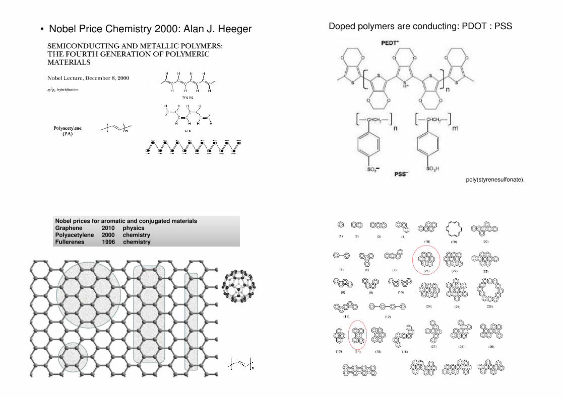
• Nobel Price Chemistry 2000: Alan J. Heeger
poly(styrenesulfonate),
Doped polymers are conducting: PDOT : PSS
Nobel prices for aromatic and conjugated materialsGraphene 2010 physicsPolyacetylene 2000 chemistryFullerenes 1996 chemistry
Nobel prices for aromatic and conjugated materialsGraphene 2010 physicsPolyacetylene 2000 chemistryFullerenes 1996 chemistry

Linear acenes: HOMO – LUMO band gap
Bsp. Pentacene: Absorption
Translation
valence band, conduction band, electron-hole pair, doping, traps for charge carriers, phonons, energy bands, Drude model, electroluminescence, surface states
LUMO, HOMO, excitonic states, chemical impurities, vibrations, hopping, fluorescence and phosphorescence, singulets, triplets, anhilation, oxidation, reduction
The vision of organic electronics: mass printing

Status Quo
• ... 90% of OLEDs, by far the most important application of organic electronics at the moment, are produced by vapor deposition of small molecules[Source: ICB 10 July 2008 ]
Organic materials deposition andgrowth
1422HC
Properties:
•hole mobility larger than electron
mobility
•forms well-ordered layers when
evaporated in vacuum at RT
•gold contact are reasonably well
matched
Record material: PentacenePentacene-deposition by vacuum sublimation, accuracy ca. 0.1 nm (QMC)
0
10 µµµµm
0
10 µµµµm
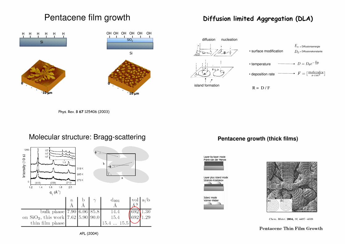
H HH H H H
Si
OH OHOH OH OH OH
Si
SiO2
Pentacene film growth
Phys. Rev. B 67 125406 (2003)
diffusion nucleation
island formation
= Diffusionsenergie
= Diffusionskonstante
• temperature
• surface modification
• deposition rate
Diffusion limited Aggregation (DLA)
R = D / F
Molecular structure: Bragg-scattering
APL (2004)
Pentacene growth (thick films)

Comparison: Coronene films
M. Huth (LMU), diploma thesis (2006)
3µm
1.5
µm
surface energy determines growth mode (Wulf construction)
Summary: Deposition and structure
• Growth mode of small molecules largely determined by molecular shape and surface energy
• molecular arrangement can be determined by x-ray experiments
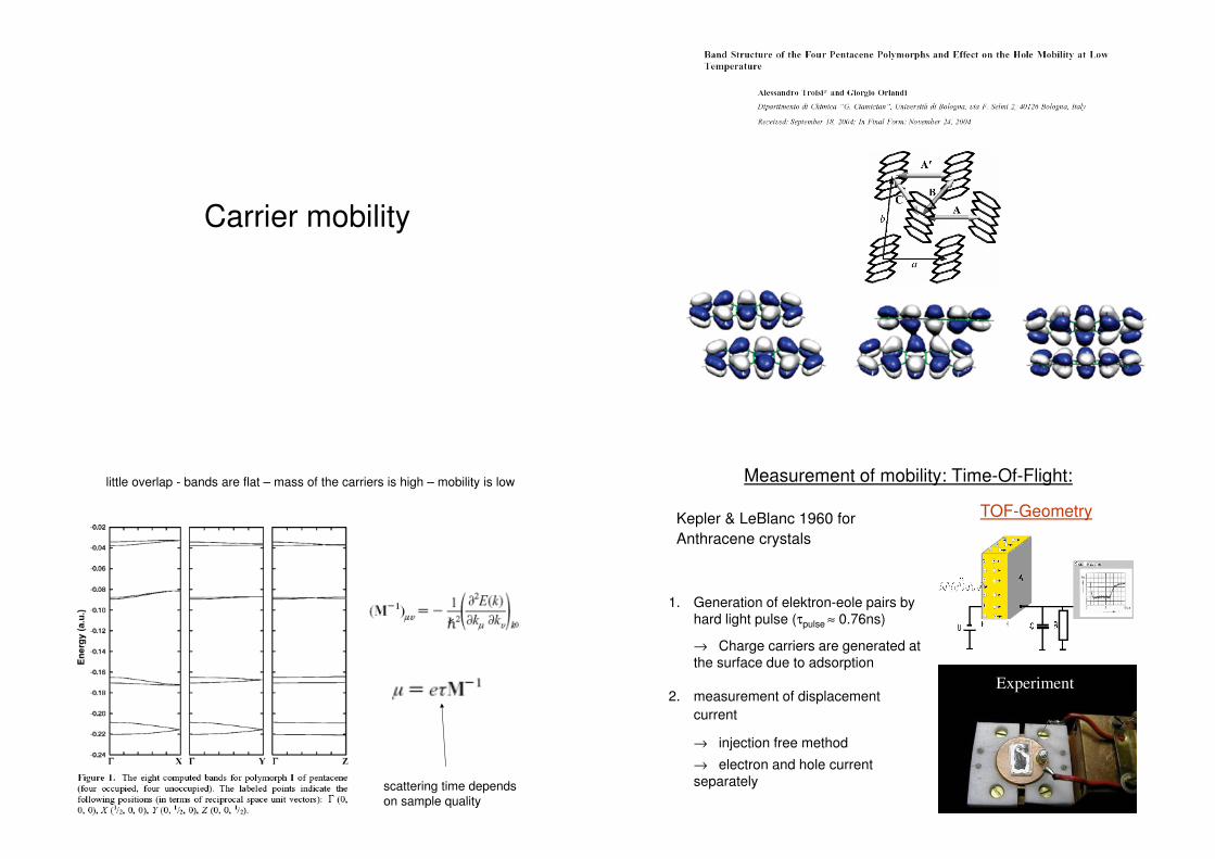
Carrier mobility
scattering time depends on sample quality
little overlap - bands are flat – mass of the carriers is high – mobility is low Measurement of mobility: Time-Of-Flight:
1. Generation of elektron-eole pairs by hard light pulse (τpulse ≈ 0.76ns)
→ Charge carriers are generated at the surface due to adsorption
2. measurement of displacement
current
→ injection free method
→ electron and hole current separately
Experiment
TOF-GeometryKepler & LeBlanc 1960 for
Anthracene crystals
typicalmobilityfor organicsµ = 1 cm2/Vs
same as amorphousSi
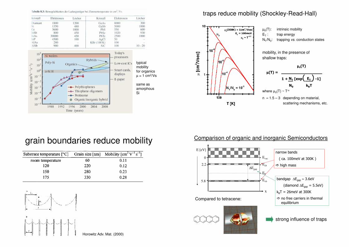
traps reduce mobility (Shockley-Read-Hall)
mobility, in the presence of
shallow traps:
where µ0(T) ~ T-n
n ≈ 1.5 – 3 depending on material,
scattering mechanisms, etc.
µµµµ(T) =
µµµµ0(T)
1 + [exp( ) -1]NT
N0
ET
kBT
µ0(T): intrinsic mobility
ET : trap energy
NT/N0: trapping vs. conduction states
grain boundaries reduce mobility
Horowitz Adv. Mat. (2000)
Comparison of organic and inorganic Semiconductors
Evac
Ecb
Evb
∆Egap
0
E [eV]
2.2
5.8
EF
x
narrow bands
( ca. 100meV at 300K )
� high mass
bandgap ∆Egap ≈ 3.6eV
(diamond ∆Egap = 5.5eV)
kBT = 26meV at 300K
� no free carriers in thermal
equilibriumCompared to tetracene:
strong influence of traps
Summary – electronic properties• conjugated and aromatic molecules have delocalized
electrons (π electrons)
• small organic molecules form highly ordered crystals, while polymer films are only partially ordered
• Details of the arrangement of the molecular orbitals and symmetry determine the electronic properties of organic crystals
• organic molecules have large band gaps (typically 2 eV), few or no intrinsic carriers at RT
• bands are flat, dispersion typically 100 meV
• crystal quality matters for mobility (grain boundaries, traps)
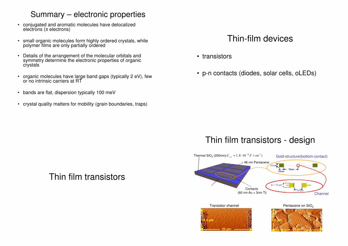
Thin-film devices
• transistors
• p-n contacts (diodes, solar cells, oLEDs)
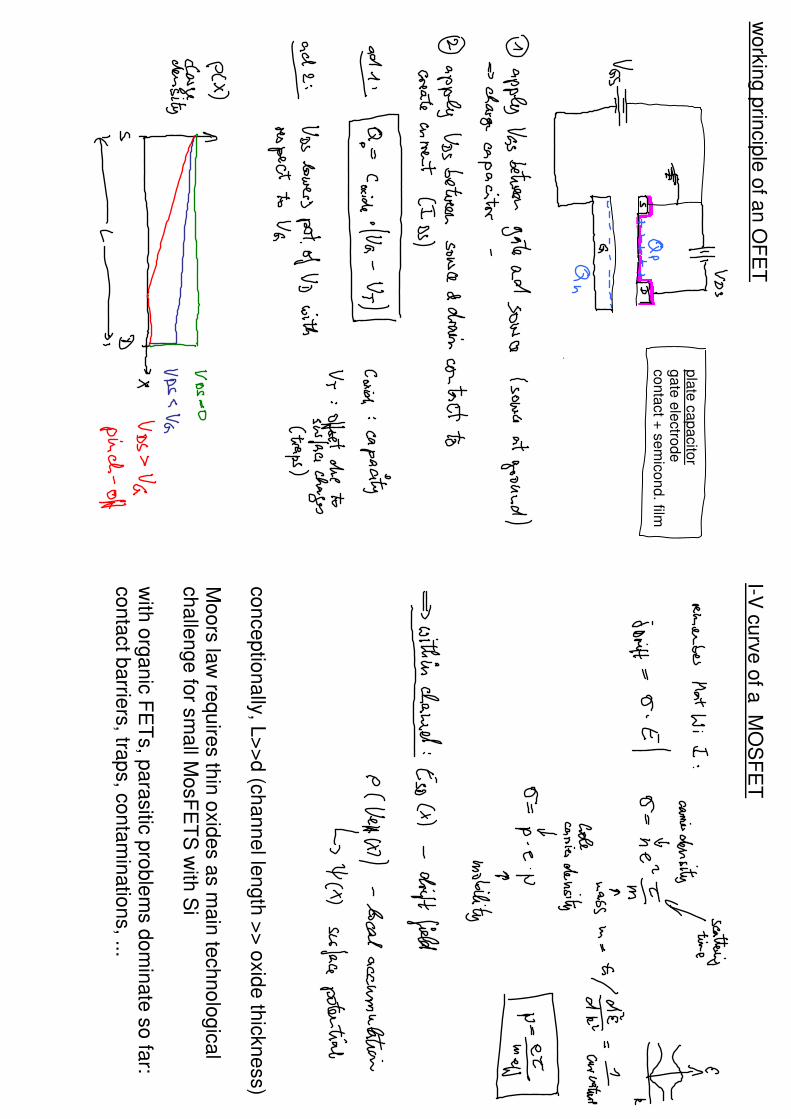
Thin film transistors
Thin film transistors - design
Contacts
(60 nm Au + 3nm Ti)
Thermal SiO2 (200nm) )/108.1( 28cmFC
ox
−⋅=
~ 48 nm Pentacene
Gold-structure(bottom-contact)
250 µm
200 µm
750 µm250 µm
m
750 µm250 µm
m
750 µm
Channel
w = 10 µm
l = 20 µm
2.5 µm
5 µm25 µm
12.5 µm
Transistor channel Pentacene on SiO2
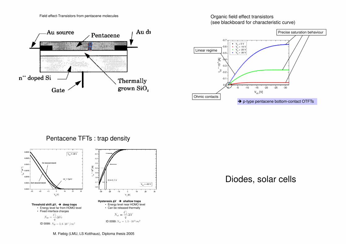
Field effect-Transistors from pentacene molecules
0 -5 -10 -15 -20 -25 -300.0
-0.1
-0.2
-0.3
-0.4
-0.5
-0.6
-0.7
VG = 0 V
VG = -10 V
VG = -20 V
VG = -30 V
I SD *
10
-5 [A
]
VSD
[V]
Precise saturation behaviour
Ohmic contacts
Linear regime
� p-type pentacene bottom-contact OTFTs
Organic field effect transistors(see blackboard for characteristic curve)
Pentacene TFTs : trap density
Hysteresis ∆∆∆∆V � shallow traps• Energy level near HOMO level• Can be released thermally
ID 0099:
Threshold shift ∆∆∆∆VT � deep traps• Energy level far from HOMO level• Fixed interface charges
ID 0099:
1st measurement
last measurement
M. Fiebig (LMU, LS Kotthaus), Diploma thesis 2005
Diodes, solar cells

Si – the p/n- junction energy band deformation by doping
Singlet excitons diffuse within the organic crystal until they decay fluorescent or radiationless . Lifetime is very short (fs-ps) , therefore diffusion length is only 10-20 nm.
Optical excitations in organic crystals
Exciton splitting at hetero-junctions
Appl. Phys. Lett. 48, 183 (1986) Two‐‐‐‐layer organic photovoltaic cell C. W. Tang
Modellsystem: Pentacene/C60(C60 erst ab 1985 bekannt)
p n
Organic solar cells
http://www.adsdyes.com/solarcells.html
e
h
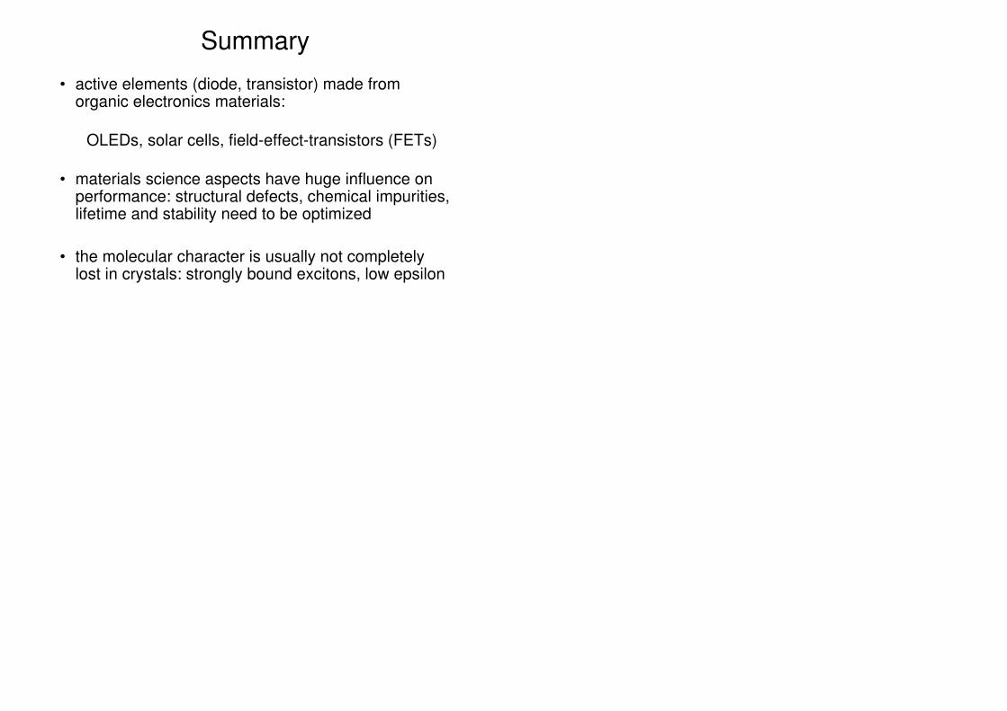
Summary
• active elements (diode, transistor) made from organic electronics materials:
OLEDs, solar cells, field-effect-transistors (FETs)
• materials science aspects have huge influence on performance: structural defects, chemical impurities, lifetime and stability need to be optimized
• the molecular character is usually not completely lost in crystals: strongly bound excitons, low epsilon
Org
an
ic E
lectro
nic
ssum
mer te
rm 1
6
Pe
nta
ce
ne
Lin
ea
r Ace
ne
s:
Co
mp
aris
on
Pe
nta
ce
ne
-Go
ld
MO
SF
ET
Me
tal-O
xid
e-S
em
ico
nd
ucto
rfie
ld-e
ffect-tra
nsis
tor
he
re: p
-typ
e, n
orm
ally
off
sim
ilar: M
ISF
ET
(me
tal in
su
lato
r...) IG
FE
T (in
su
lato
r-ga
te...)
wo
rkin
g p
rincip
le o
f an
OF
ET
pla
te c
ap
acito
rg
ate
ele
ctro
de
co
nta
ct +
se
mic
on
d. film
I-V c
urv
e o
f a M
OS
FE
T
co
nce
ptio
na
lly, L
>>
d (c
ha
nn
el le
ng
th >
> o
xid
e th
ickn
ess)
Mo
ors
law
req
uire
s th
in o
xid
es a
s m
ain
tech
no
log
ica
lch
alle
ng
e fo
r sm
all M
osF
ET
S w
ith S
i
with
org
an
ic F
ET
s, p
ara
sitic
pro
ble
ms d
om
ina
te s
o fa
r:co
nta
ct b
arrie
rs, tra
ps, c
on
tam
ina
tion
s, ...
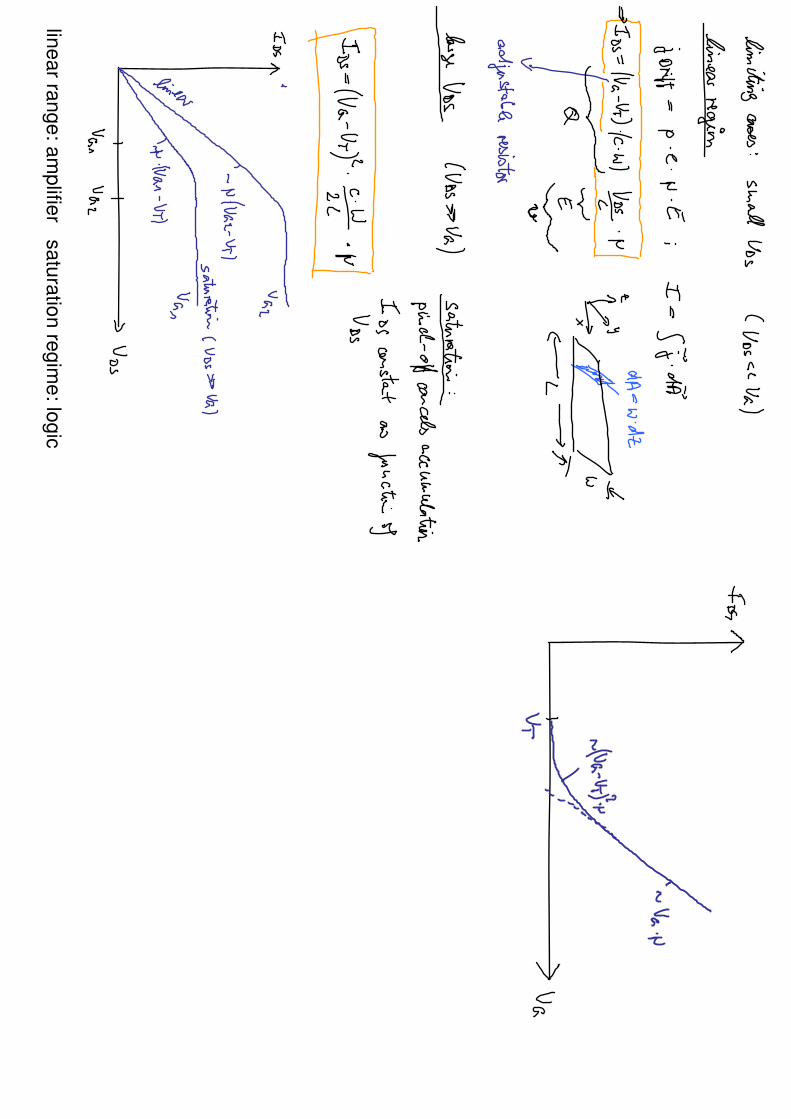
line
ar ra
ng
e: a
mp
lifier s
atu
ratio
n re
gim
e: lo
gic