Daya elektronik
16
http://en.wikipedia.org/w/index.php?titl http://en.wikipedia.org/w/index.php?title=thyristors http://en.wikipedia.org/w/index.php?title=Transistors http://en.wikipedia.org/w/index.php?title=Computer http://en.wikipedia.org/w/index.php?title=Battery_charger http://en.wikipedia.org/w/index.php?title=Adjustable-speed_drive http://en.wikipedia.org/w/index.php?title=Induction_motor http://en.wikipedia.org/w/index.php?title=John_Bardeen http://en.wikipedia.org/w/index.php?title=William_Shockley http://en.wikipedia.org/w/index.php?title=Vacuum_tube Daya elektronik 1 Daya elektronik HVDC thyristor katup menara setinggi di 16.8 m Hall di Baltik kabel AB di Swedia Pengisi baterai adalah contoh dari sepotong daya elektronik Sebuah PC power supply adalah contoh dari sepotong daya elektronik, apakah di dalam atau di luar Kabinet Daya elektronik penerapan solid-state elektronik untuk kontrol dan konversi tenaga listrik. Ia juga merujuk kepada subjek penelitian dalam elektronik dan teknik listrik yang berkaitan dengan Desain, kontrol, perhitungan dan integrasi dari berbagai nonlinier, waktu pengolahan elektronik sistem dengan cepat dinamika energi. Perangkat elektronik daya tinggi pertama adalah katup mercury-arc. Dalam modern sistem konversi dilakukan dengan semikonduktor switching seperti dioda, thyristors, dan transistor, merintis oleh R. D. Middlebrook dan lain-lain awal tahun 1950-an. Sebaliknya sistem elektronik yang berkaitan dengan transmisi dan pengolahan sinyal dan data, dalam jumlah besar elektronik daya listrik energi diproses. AC/DC converter (rectifier) adalah yang paling perangkat elektronik daya khas yang ditemukan di banyak konsumen elektronik set perangkat, misalnya televisi, komputer pribadi, pengisi daya baterai, dll. Berbagai daya adalah biasanya dari puluhan watt untuk beberapa ratus watt. Dalam industri aplikasi umum adalah variabel kecepatan drive (VSD) yang digunakan untuk mengontrol motor induksi. Berbagai daya VSDs mulai dari beberapa ratus watt dan berakhir pada puluhan megawatt. Sistem konversi daya dapat diklasifikasikan menurut tipe Power input dan output • AC ke DC (rectifier) • DC ke AC (inverter) • DC ke DC (DC-to-DC converter) • AC-AC (AC-untuk-AC Konverter) Sejarah Daya elektronik dimulai dengan perkembangan busur Merkurius rectifier. Diciptakan oleh Peter Cooper Hewitt pada tahun 1902, itu digunakan untuk mengkonversi arus bolak-balik (AC) ke dalam arus searah (DC). Dari 1920-an pada, penelitian terus menerapkan thyratrons dan grid-dikontrol Merkurius busur katup untuk transmisi daya. Uno Lamm mengembangkan sebuah katup dengan penilaian elektroda membuat Merkurius katup dapat digunakan untuk tegangan tinggi arus searah transmisi. 1933 selenium Penyearah diciptakan. Pada tahun 1947 titik-kontak transistor dwikutub diciptakan oleh Walter H. Brattain dan John Bardeen di bawah bimbingan William Shockley pada Bell telepon laboratorium. Pada tahun 1948 penemuan Shockley di bipolar Transistor pertemuan dwikutub peningkatan stabilitas dan kinerja transistor, dan mengurangi biaya. Tahun 1950-an, semikonduktor daya dioda menjadi tersedia dan mulai menggantikan tabung vakum. Pada tahun 1956 Silikon dikendalikan Rectifier (SCR) diperkenalkan oleh Jenderal Listrik, sangat meningkatkan berbagai aplikasi elektronik power. Multilizer PDF Translator Free version - translation is limited to ~ 3 pages per translation. Multilizer PDF Translator Free version - translation is limited to ~ 3 pages per translation.
Transcript of Daya elektronik
http://en.wikipedia.org/w/index.php?title=THYRISTOR
http://en.wikipedia.org/w/index.php?title=thyristorshttp://en.wikipedia.org/w/index.php?title=Transistors
http://en.wikipedia.org/w/index.php?title=Computerhttp://en.wikipedia.org/w/index.php?title=Battery_charger
http://en.wikipedia.org/w/index.php?title=Adjustable-speed_drivehttp://en.wikipedia.org/w/index.php?title=Induction_motor
http://en.wikipedia.org/w/index.php?title=John_Bardeenhttp://en.wikipedia.org/w/index.php?title=William_Shockley
http://en.wikipedia.org/w/index.php?title=Vacuum_tube
Daya elektronik 1
Daya elektronik
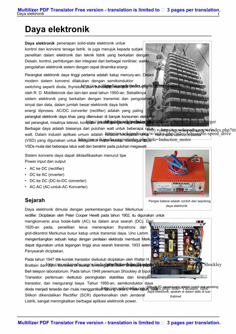
HVDC thyristor katup menara setinggi di 16.8 mHall di Baltik kabel AB di Swedia
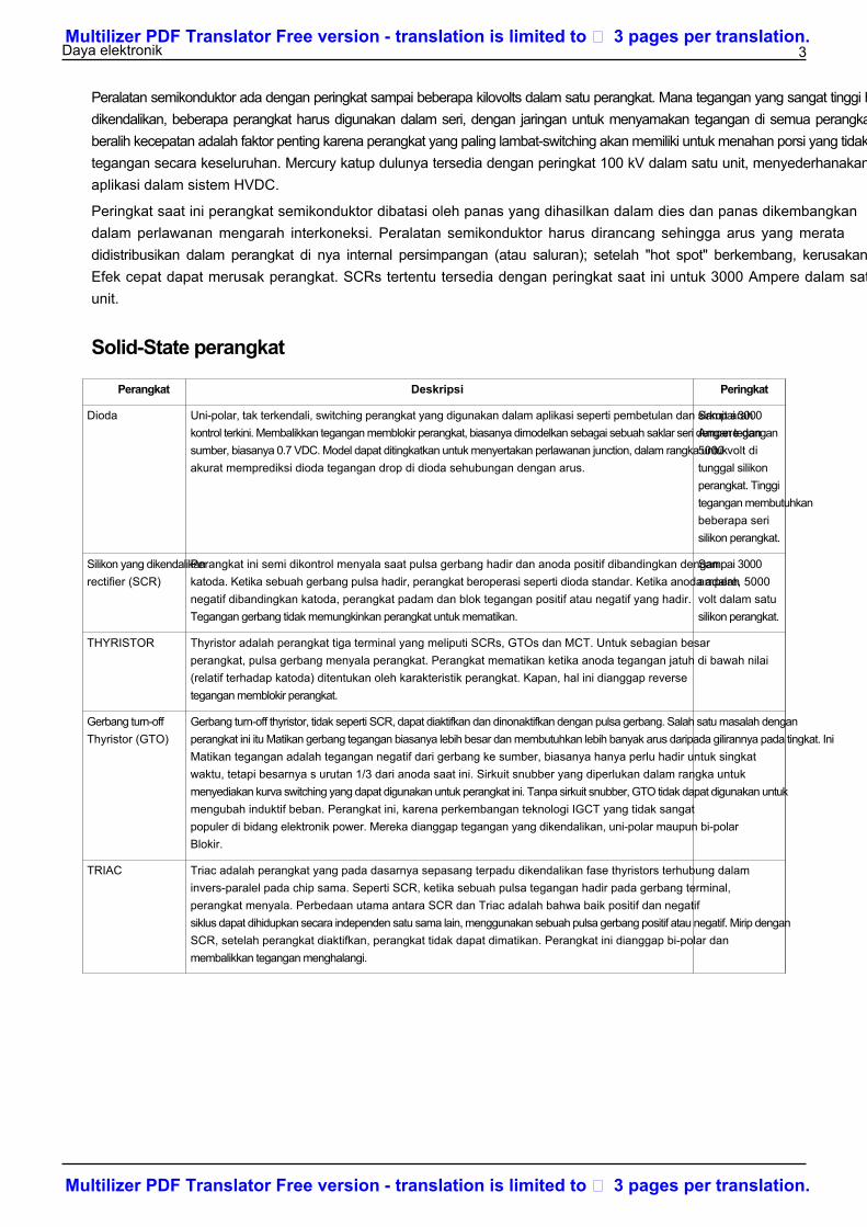
Pengisi baterai adalah contoh dari sepotongdaya elektronik
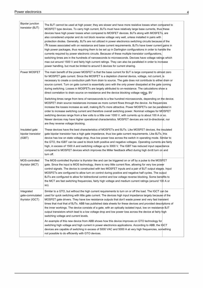
Sebuah PC power supply adalah contoh dari sepotongdaya elektronik, apakah di dalam atau di luar
Kabinet
Daya elektronik penerapan solid-state elektronik untukkontrol dan konversi tenaga listrik. Ia juga merujuk kepada subjekpenelitian dalam elektronik dan teknik listrik yang berkaitan denganDesain, kontrol, perhitungan dan integrasi dari berbagai nonlinier, waktupengolahan elektronik sistem dengan cepat dinamika energi.
Perangkat elektronik daya tinggi pertama adalah katup mercury-arc. Dalammodern sistem konversi dilakukan dengan semikonduktorswitching seperti dioda, thyristors, dan transistor, merintisoleh R. D. Middlebrook dan lain-lain awal tahun 1950-an. Sebaliknyasistem elektronik yang berkaitan dengan transmisi dan pengolahansinyal dan data, dalam jumlah besar elektronik daya listrikenergi diproses. AC/DC converter (rectifier) adalah yang palingperangkat elektronik daya khas yang ditemukan di banyak konsumen elektronikset perangkat, misalnya televisi, komputer pribadi, pengisi daya baterai, dll.Berbagai daya adalah biasanya dari puluhan watt untuk beberapa ratuswatt. Dalam industri aplikasi umum adalah variabel kecepatan drive(VSD) yang digunakan untuk mengontrol motor induksi. Berbagai dayaVSDs mulai dari beberapa ratus watt dan berakhir pada puluhan megawatt.
Sistem konversi daya dapat diklasifikasikan menurut tipePower input dan output
• AC ke DC (rectifier)• DC ke AC (inverter)• DC ke DC (DC-to-DC converter)• AC-AC (AC-untuk-AC Konverter)
SejarahDaya elektronik dimulai dengan perkembangan busur Merkuriusrectifier. Diciptakan oleh Peter Cooper Hewitt pada tahun 1902, itu digunakan untukmengkonversi arus bolak-balik (AC) ke dalam arus searah (DC). Dari1920-an pada, penelitian terus menerapkan thyratrons dangrid-dikontrol Merkurius busur katup untuk transmisi daya. Uno Lammmengembangkan sebuah katup dengan penilaian elektroda membuat Merkurius katupdapat digunakan untuk tegangan tinggi arus searah transmisi. 1933 seleniumPenyearah diciptakan.
Pada tahun 1947 titik-kontak transistor dwikutub diciptakan oleh Walter H.Brattain dan John Bardeen di bawah bimbingan William Shockley padaBell telepon laboratorium. Pada tahun 1948 penemuan Shockley di bipolarTransistor pertemuan dwikutub peningkatan stabilitas dan kinerjatransistor, dan mengurangi biaya. Tahun 1950-an, semikonduktor dayadioda menjadi tersedia dan mulai menggantikan tabung vakum. Pada tahun 1956Silikon dikendalikan Rectifier (SCR) diperkenalkan oleh JenderalListrik, sangat meningkatkan berbagai aplikasi elektronik power.
Multilizer PDF Translator Free version - translation is limited to ~ 3 pages per translation.
Multilizer PDF Translator Free version - translation is limited to ~ 3 pages per translation.

http://en.wikipedia.org/w/index.php?title=IGBT
http://en.wikipedia.org/w/index.php?title=Ignitron
http://en.wikipedia.org/w/index.php?title=Thyratron
Daya elektronik 2
Pada 1960-an kecepatan pensakelaran bipolar junction transistor diperbolehkan untuk frekuensi tinggi DC DC converters. Dalam1976 power MOSFET menjadi tersedia secara komersial. Pada tahun 1982 terisolasi Gate Bipolar Transistor (IGBT) adalahdiperkenalkan.
PerangkatKemampuan dan ekonomi daya elektronik sistem ditentukan oleh perangkat aktif yang tersedia.Mereka karakteristik dan batasan ini merupakan elemen kunci dalam desain sistem elektronik power. Sebelumnya,Mercury busur katup, tinggi vacuum dan berisi gas-dioda Penyearah thermionic dan memicu perangkat sepertithyratron dan ignitron secara luas digunakan dalam daya elektronik. Sebagai peringkat solid-state perangkat meningkat di keduategangan dan arus-penanganan kapasitas, vakum perangkat telah hampir sepenuhnya diganti oleh solid-state perangkat.
Daya perangkat elektronik dapat digunakan sebagai switch, atau sebagai penguat.[1] Sakelar yang ideal baik terbuka atau tertutup dan begitumemboroskan daya tidak; withstands tegangan dan melewati tidak ada arus, atau melewati jumlah saat ini tanpapenurunan tegangan. Peralatan semikonduktor yang digunakan sebagai switch dapat perkiraan properti ini ideal dan kekuatan sehingga sebagianaplikasi elektronik mengandalkan beralih perangkat dan mematikan, yang membuat sistem yang sangat efisien sebagai sangat sedikit dayayang terbuang di switch. Sebaliknya, dalam kasus penguat, arus yang melalui perangkat bervariasi secara terus menerusMenurut masukan dikendalikan. Tegangan dan arus perangkat terminal mengikuti garis beban, dan kekuatanpembuangan dalam perangkat ini besar dibandingkan dengan daya yang dikirim ke beban.
Beberapa atribut mendikte bagaimana perangkat yang digunakan. Perangkat seperti dioda melakukan ketika diterapkan pada tegangan yang majudan tidak ada kontrol eksternal awal konduksi. Daya perangkat seperti silicon dikendalikan Penyearah danthyristors (serta katup merkuri dan thyratron) memungkinkan kontrol awal konduksi, tetapi bergantung pada periodikpembalikan arus untuk mematikannya. Perangkat seperti gerbang turn-off thyristors, BJT dan MOSFET transistormemberikan kendali penuh switching dan dapat diaktifkan atau dinonaktifkan tanpa arus yang mengalir melalui mereka. Transistorperangkat juga memungkinkan amplifikasi sebanding, tetapi hal ini jarang digunakan untuk sistem yang dinilai lebih dari beberapa ratuswatt. Kontrol masukan karakteristik perangkat juga sangat mempengaruhi desain; kadang-kadang kontrol masukan ialah pada sangattegangan tinggi dengan menghormati ke tanah dan harus didorong oleh sumber terisolasi.
Sebagai efisiensi pada premi di daya elektronik converter, kerugian yang menghasilkan daya perangkat elektronikharus serendah mungkin.
Perangkat bervariasi di switching kecepatan. Beberapa dioda dan thyristors yang cocok untuk kecepatan relatif lambat dan berguna untuktenaga frekuensi switching dan kontrol; thyristors tertentu berguna di beberapa kilohertz. Perangkat seperti MOSFETdan BJT dapat beralih puluhan kilohertz hingga beberapa megahertz dalam aplikasi listrik, tetapi dengan penurunan dayatingkat. Tabung vakum perangkat mendominasi daya tinggi (ratusan kilowatt) di frekuensi sangat tinggi (ratusan atauribuan megahertz) aplikasi. Perangkat lebih cepat switching meminimalkan energi yang hilang dalam transisi dari ke offdan kembali, tetapi dapat membuat masalah dengan memancarkan interferensi elektromagnetik. Sirkuit gerbang drive (atau setara)harus dirancang untuk memasok cukup berkendara saat ini untuk mencapai kecepatan pensakelaran yang penuh mungkin dengan perangkat. Aperangkat tanpa drive cukup untuk beralih cepat mungkin akan hancur oleh pemanasan berlebih.
Praktis perangkat memiliki bukan nol tegangan drop dan mengusir kekuatan ketika pada, dan mengambil beberapa waktu untuk melewatidaerah aktif sampai mereka mencapai "on" atau "off" negara. Kerugian ini adalah bagian penting dari total kehilangan kekuasaan diConverter.
Penanganan daya dan disipasi perangkat juga merupakan faktor penting dalam desain. Perangkat elektronik kekuasaan mungkin harusmengusir puluhan atau ratusan watt limbah panas, bahkan switching seefisien mungkin antara melakukan dannegara-negara non-melakukan. Dalam modus switching, kekuatan dikendalikan jauh lebih besar dari daya yang dihamburkan diberalih. Drop tegangan maju dalam negara melakukan diterjemahkan ke dalam panas yang harus dihamburkan. Daya tinggisemikonduktor membutuhkan khusus heat sink atau sistem pendingin aktif untuk mengelola suhu persimpangan mereka; eksotissemikonduktor seperti silikon karbida memiliki keuntungan atas silikon lurus dalam hal ini, dan germanium, sekaliutama-tinggal solid-state elektronik kini sedikit digunakan karena sifat suhu tinggi yang tidak menguntungkan.
Multilizer PDF Translator Free version - translation is limited to ~ 3 pages per translation.
Multilizer PDF Translator Free version - translation is limited to ~ 3 pages per translation.
Daya elektronik 3
Peralatan semikonduktor ada dengan peringkat sampai beberapa kilovolts dalam satu perangkat. Mana tegangan yang sangat tinggi harusdikendalikan, beberapa perangkat harus digunakan dalam seri, dengan jaringan untuk menyamakan tegangan di semua perangkat. Sekali lagi,beralih kecepatan adalah faktor penting karena perangkat yang paling lambat-switching akan memiliki untuk menahan porsi yang tidak proporsionaltegangan secara keseluruhan. Mercury katup dulunya tersedia dengan peringkat 100 kV dalam satu unit, menyederhanakan merekaaplikasi dalam sistem HVDC.
Peringkat saat ini perangkat semikonduktor dibatasi oleh panas yang dihasilkan dalam dies dan panas dikembangkandalam perlawanan mengarah interkoneksi. Peralatan semikonduktor harus dirancang sehingga arus yang meratadidistribusikan dalam perangkat di nya internal persimpangan (atau saluran); setelah "hot spot" berkembang, kerusakanEfek cepat dapat merusak perangkat. SCRs tertentu tersedia dengan peringkat saat ini untuk 3000 Ampere dalam satuunit.
Solid-State perangkat
Perangkat Deskripsi Peringkat
Dioda Uni-polar, tak terkendali, switching perangkat yang digunakan dalam aplikasi seperti pembetulan dan sirkuit arahkontrol terkini. Membalikkan tegangan memblokir perangkat, biasanya dimodelkan sebagai sebuah saklar seri dengan tegangansumber, biasanya 0.7 VDC. Model dapat ditingkatkan untuk menyertakan perlawanan junction, dalam rangka untukakurat memprediksi dioda tegangan drop di dioda sehubungan dengan arus.
Sampai 3000Ampere dan5000 volt ditunggal silikonperangkat. Tinggitegangan membutuhkanbeberapa serisilikon perangkat.
Silikon yang dikendalikanrectifier (SCR)
Perangkat ini semi dikontrol menyala saat pulsa gerbang hadir dan anoda positif dibandingkan dengankatoda. Ketika sebuah gerbang pulsa hadir, perangkat beroperasi seperti dioda standar. Ketika anoda adalahnegatif dibandingkan katoda, perangkat padam dan blok tegangan positif atau negatif yang hadir.Tegangan gerbang tidak memungkinkan perangkat untuk mematikan.
Sampai 3000ampere, 5000volt dalam satusilikon perangkat.
THYRISTOR Thyristor adalah perangkat tiga terminal yang meliputi SCRs, GTOs dan MCT. Untuk sebagian besarperangkat, pulsa gerbang menyala perangkat. Perangkat mematikan ketika anoda tegangan jatuh di bawah nilai(relatif terhadap katoda) ditentukan oleh karakteristik perangkat. Kapan, hal ini dianggap reversetegangan memblokir perangkat.
Gerbang turn-offThyristor (GTO)
Gerbang turn-off thyristor, tidak seperti SCR, dapat diaktifkan dan dinonaktifkan dengan pulsa gerbang. Salah satu masalah denganperangkat ini itu Matikan gerbang tegangan biasanya lebih besar dan membutuhkan lebih banyak arus daripada gilirannya pada tingkat. IniMatikan tegangan adalah tegangan negatif dari gerbang ke sumber, biasanya hanya perlu hadir untuk singkatwaktu, tetapi besarnya s urutan 1/3 dari anoda saat ini. Sirkuit snubber yang diperlukan dalam rangka untukmenyediakan kurva switching yang dapat digunakan untuk perangkat ini. Tanpa sirkuit snubber, GTO tidak dapat digunakan untukmengubah induktif beban. Perangkat ini, karena perkembangan teknologi IGCT yang tidak sangatpopuler di bidang elektronik power. Mereka dianggap tegangan yang dikendalikan, uni-polar maupun bi-polarBlokir.
TRIAC Triac adalah perangkat yang pada dasarnya sepasang terpadu dikendalikan fase thyristors terhubung dalaminvers-paralel pada chip sama. Seperti SCR, ketika sebuah pulsa tegangan hadir pada gerbang terminal,perangkat menyala. Perbedaan utama antara SCR dan Triac adalah bahwa baik positif dan negatifsiklus dapat dihidupkan secara independen satu sama lain, menggunakan sebuah pulsa gerbang positif atau negatif. Mirip denganSCR, setelah perangkat diaktifkan, perangkat tidak dapat dimatikan. Perangkat ini dianggap bi-polar danmembalikkan tegangan menghalangi.
Multilizer PDF Translator Free version - translation is limited to ~ 3 pages per translation.
Multilizer PDF Translator Free version - translation is limited to ~ 3 pages per translation.
Power electronics 4
Bipolar junctiontransistor (BJT)
The BJT cannot be used at high power; they are slower and have more resistive losses when compared toMOSFET type devices. To carry high current, BJTs must have relatively large base currents, thus thesedevices have high power losses when compared to MOSFET devices. BJTs along with MOSFETs, arealso considered unipolar and do not block reverse voltage very well, unless installed in pairs withprotection diodes. Generally, BJTs are not utilized in power electronics switching circuits because of theI R losses associated with on resistance and base current requirements. BJTs have lower current gains in2
high power packages, thus requiring them to be set up in Darlington configurations in order to handle thecurrents required by power electronic circuits. Because of these multiple transistor configurations,switching times are in the hundreds of nanoseconds to microseconds. Devices have voltage ratings whichmax out around 1500 V and fairly high current ratings. They can also be paralleled in order to increasepower handling, but must be limited to around 5 devices for current sharing.
Power MOSFET The main benefit of the power MOSFET is that the base current for BJT is large compared to almost zerofor MOSFET gate current. Since the MOSFET is a depletion channel device, voltage, not current, isnecessary to create a conduction path from drain to source. The gate does not contribute to either drain orsource current. Turn on gate current is essentially zero with the only power dissipated at the gate comingduring switching. Losses in MOSFETs are largely attributed to on-resistance. The calculations show adirect correlation to drain source on-resistance and the device blocking voltage rating, BVdss.
Switching times range from tens of nanoseconds to a few hundred microseconds, depending on the device.MOSFET drain source resistances increase as more current flows through the device. As frequenciesincrease the losses increase as well, making BJTs more attractive. Power MOSFETs can be paralleled inorder to increase switching current and therefore overall switching power. Nominal voltages for MOSFETswitching devices range from a few volts to a little over 1000 V, with currents up to about 100 A or so.Newer devices may have higher operational characteristics. MOSFET devices are not bi-directional, norare they reverse voltage blocking.
Insulated gatebipolar transistor(IGBT)
These devices have the best characteristics of MOSFETs and BJTs. Like MOSFET devices, the insulatedgate bipolar transistor has a high gate impedance, thus low gate current requirements. Like BJTs, thisdevice has low on state voltage drop, thus low power loss across the switch in operating mode. Similar tothe GTO, the IGBT can be used to block both positive and negative voltages. Operating currents are fairlyhigh, in excess of 1500 A and switching voltage up to 3000 V. The IGBT has reduced input capacitancecompared to MOSFET devices which improves the Miller feedback effect during high dv/dt turn on andturn off.
MOS-controlledthyristor (MCT)
The MOS-controlled thyristor is thyristor like and can be triggered on or off by a pulse to the MOSFETgate. Since the input is MOS technology, there is very little current flow, allowing for very low powercontrol signals. The device is constructed with two MOSFET inputs and a pair of BJT output stages. InputMOSFETs are configured to allow turn on control during positive and negative half cycles. The outputBJTs are configured to allow for bidirectional control and low voltage reverse blocking. Some benefits tothe MCT are fast switching frequencies, fairly high voltage and medium current ratings (around 100 A orso).
Integratedgate-commutatedthyristor (IGCT)
Similar to a GTO, but without the high current requirements to turn on or off the load. The IGCT can beused for quick switching with little gate current. The devices high input impedance largely because of theMOSFET gate drivers. They have low resistance outputs that don't waste power and very fast transienttimes that rival that of BJTs. ABB has published data sheets for these devices and provided descriptions ofthe inner workings. The device consists of a gate, with an optically isolated input, low on resistance BJToutput transistors which lead to a low voltage drop and low power loss across the device at fairly highswitching voltage and current levels.
An example of this new device from ABB shows how this device improves on GTO technology forswitching high voltage and high current in power electronics applications. According to ABB, the IGCTdevices are capable of switching in excess of 5000 VAC and 5000 A at very high frequencies, somethingnot possible to do efficiently with GTO devices.
Power electronics 5
DC/AC converters (inverters)DC to AC converters produce an AC output waveform from a DC source. Applications include adjustable speeddrives (ASD), uninterruptable power supplies (UPS), active filters, Flexible AC transmission systems (FACTS),voltage compensators, and photovoltaic generators. Topologies for these converters can be separated into twodistinct categories: voltage source inverters and current source inverters. Voltage source inverters (VSIs) are namedso because the independently controlled output is a voltage waveform. Similarly, current source inverters (CSIs) aredistinct in that the controlled AC output is a current waveform.
Being static power converters, the DC to AC power conversion is the result of power switching devices, which arecommonly fully controllable semiconductor power switches. The output waveforms are therefore made up ofdiscrete values, producing fast transitions rather than smooth ones. The ability to produce near sinusoidal waveformsaround the fundamental frequency is dictated by the modulation technique controlling when, and for how long, thepower valves are on and off. Common modulation techniques include the carrier-based technique, or pulse widthmodulation, space-vector technique, and the selective-harmonic technique.
Voltage source inverters have practical uses in both single-phase and three-phase applications. Single-phase VSIsutilize half-bridge and full-bridge configurations, and are widely used for power supplies, single-phase UPSs, andelaborate high-power topologies when used in multicell configurations. Three-phase VSIs are used in applicationsthat require sinusoidal voltage waveforms, such as ASDs, UPSs, and some types of FACTS devices such as theSTATCOM. They are also used in applications where arbitrary voltages are required as in the case of active filtersand voltage compensators.
Current source inverters are used to produce an AC output current from a DC current supply. This type of inverter ispractical for three-phase applications in which high-quality voltage waveforms are required.
A relatively new class of inverters, called multilevel inverters, has gained widespread interest. Normal operation ofCSIs and VSIs can be classified as two-level inverters, due to the fact that power switches connect to either thepositive or to the negative DC bus. If more than two voltage levels were available to the inverter output terminals,the AC output could better approximate a sine wave. It is for this reason that multilevel inverters, although morecomplex and costly, offer higher performance.
Each inverter type differs in the DC links used, and in whether or not they require freewheeling diodes. Either can bemade to operate in square-wave or pulse-width modulation (PWM) mode, depending on its intended usage.Square-wave mode offers simplicity, while PWM can be implemented several different ways and produces higherquality waveforms.
Voltage Source Inverters (VSI) feed the output inverter section from an approximately constant-voltage source.
The desired quality of the current output waveform determines which modulation technique needs to be selected fora given application. The output of a VSI is composed of discrete values. In order to obtain a smooth currentwaveform, the loads need to be inductive at the select harmonic frequencies. Without some sort of inductive filteringbetween the source and load, a capacitive load will cause the load to receive a choppy current waveform, with largeand frequent current spikes.
There are three main types of VSIs:
1.1. Single-phase half-bridge inverter2.2. Single-phase full-bridge inverter3.3. Three-phase voltage source inverter
Power electronics 6
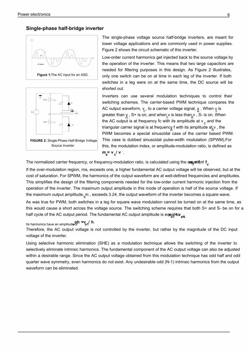
Single-phase half-bridge inverter
Figure 1: The AC input for an ASD.
FIGURE 2: Single-Phase Half-Bridge VoltageSource Inverter
The single-phase voltage source half-bridge inverters, are meant forlower voltage applications and are commonly used in power supplies.Figure 2 shows the circuit schematic of this inverter.
Low-order current harmonics get injected back to the source voltage bythe operation of the inverter. This means that two large capacitors areneeded for filtering purposes in this design. As Figure 2 illustrates,only one switch can be on at time in each leg of the inverter. If bothswitches in a leg were on at the same time, the DC source will beshorted out.
Inverters can use several modulation techniques to control theirswitching schemes. The carrier-based PWM technique compares theAC output waveform, v , to a carrier voltage signal, v . When v isc Δ c greater than v , S+ is on, and when v is less than v , S- is on. WhenΔ c Δthe AC output is at frequency fc with its amplitude at v , and thectriangular carrier signal is at frequency f with its amplitude at v , theΔ ΔPWM becomes a special sinusoidal case of the carrier based PWM.This case is dubbed sinusoidal pulse-width modulation (SPWM).Forthis, the modulation index, or amplitude-modulation ratio, is defined asm = v / va c ∆.
The normalized carrier frequency, or frequency-modulation ratio, is calculated using the equation m = f / ff ∆ c.
If the over-modulation region, ma, exceeds one, a higher fundamental AC output voltage will be observed, but at thecost of saturation. For SPWM, the harmonics of the output waveform are at well-defined frequencies and amplitudes.This simplifies the design of the filtering components needed for the low-order current harmonic injection from theoperation of the inverter. The maximum output amplitude in this mode of operation is half of the source voltage. Ifthe maximum output amplitude, m , exceeds 3.24, the output waveform of the inverter becomes a square wave.aAs was true for PWM, both switches in a leg for square wave modulation cannot be turned on at the same time, asthis would cause a short across the voltage source. The switching scheme requires that both S+ and S- be on for ahalf cycle of the AC output period. The fundamental AC output amplitude is equal to vo1 = vaN.
Its harmonics have an amplitude ofvoh =v / ho1 .
Therefore, the AC output voltage is not controlled by the inverter, but rather by the magnitude of the DC inputvoltage of the inverter.
Using selective harmonic elimination (SHE) as a modulation technique allows the switching of the inverter toselectively eliminate intrinsic harmonics. The fundamental component of the AC output voltage can also be adjustedwithin a desirable range. Since the AC output voltage obtained from this modulation technique has odd half and oddquarter wave symmetry, even harmonics do not exist. Any undesirable odd (N-1) intrinsic harmonics from the outputwaveform can be eliminated.
Power electronics 7
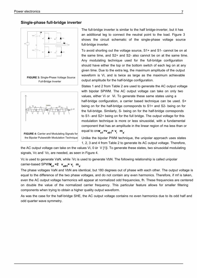
Single-phase full-bridge inverter
FIGURE 3: Single-Phase Voltage SourceFull-Bridge Inverter
FIGURE 4: Carrier and Modulating Signals forthe Bipolar Pulsewidth Modulation Technique
The full-bridge inverter is similar to the half bridge-inverter, but it hasan additional leg to connect the neutral point to the load. Figure 3shows the circuit schematic of the single-phase voltage sourcefull-bridge inverter.
To avoid shorting out the voltage source, S1+ and S1- cannot be on atthe same time, and S2+ and S2- also cannot be on at the same time.Any modulating technique used for the full-bridge configurationshould have either the top or the bottom switch of each leg on at anygiven time. Due to the extra leg, the maximum amplitude of the outputwaveform is Vi, and is twice as large as the maximum achievableoutput amplitude for the half-bridge configuration.
States 1 and 2 from Table 2 are used to generate the AC output voltagewith bipolar SPWM. The AC output voltage can take on only twovalues, either Vi or Vi. To generate these same states using a–half-bridge configuration, a carrier based technique can be used. S+being on for the half-bridge corresponds to S1+ and S2- being on forthe full-bridge. Similarly, S- being on for the half-bridge correspondsto S1- and S2+ being on for the full bridge. The output voltage for thismodulation technique is more or less sinusoidal, with a fundamentalcomponent that has an amplitude in the linear region of ma less than orequal to one vo1 =vab1= v mi
• a.
Unlike the bipolar PWM technique, the unipolar approach uses states1, 2, 3 and 4 from Table 2 to generate its AC output voltage. Therefore,
the AC output voltage can take on the values Vi, 0 or V [1]i. To generate these states, two sinusoidal modulating–signals, Vc and Vc, are needed, as seen in Figure 4.–
Vc is used to generate VaN, while Vc is used to generate VbN. The following relationship is called unipolar–carrier-based SPWM v =2 vo1
• aN1= v mi
• a.
The phase voltages VaN and VbN are identical, but 180 degrees out of phase with each other. The output voltage isequal to the difference of the two phase voltages, and do not contain any even harmonics. Therefore, if mf is taken,even the AC output voltage harmonics will appear at normalized odd frequencies, fh. These frequencies are centeredon double the value of the normalized carrier frequency. This particular feature allows for smaller filteringcomponents when trying to obtain a higher quality output waveform.
As was the case for the half-bridge SHE, the AC output voltage contains no even harmonics due to its odd half andodd quarter wave symmetry.
Power electronics 8
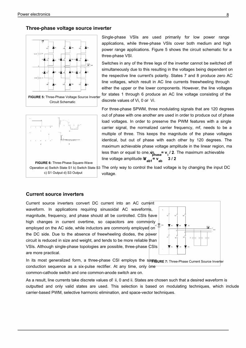
Three-phase voltage source inverter
FIGURE 5: Three-Phase Voltage Source InverterCircuit Schematic
FIGURE 6: Three-Phase Square-WaveOperation a) Switch State S1 b) Switch State S3
c) S1 Output d) S3 Output
Single-phase VSIs are used primarily for low power rangeapplications, while three-phase VSIs cover both medium and highpower range applications. Figure 5 shows the circuit schematic for athree-phase VSI.
Switches in any of the three legs of the inverter cannot be switched offsimultaneously due to this resulting in the voltages being dependent onthe respective line current's polarity. States 7 and 8 produce zero ACline voltages, which result in AC line currents freewheeling througheither the upper or the lower components. However, the line voltagesfor states 1 through 6 produce an AC line voltage consisting of thediscrete values of Vi, 0 or Vi.–
For three-phase SPWM, three modulating signals that are 120 degreesout of phase with one another are used in order to produce out of phaseload voltages. In order to preserve the PWM features with a singlecarrier signal, the normalized carrier frequency, mf, needs to be amultiple of three. This keeps the magnitude of the phase voltagesidentical, but out of phase with each other by 120 degrees. Themaximum achievable phase voltage amplitude in the linear region, maless than or equal to one, is vphase = v / 2i . The maximum achievableline voltage amplitude is Vab1 = vab • √3 / 2
The only way to control the load voltage is by changing the input DCvoltage.
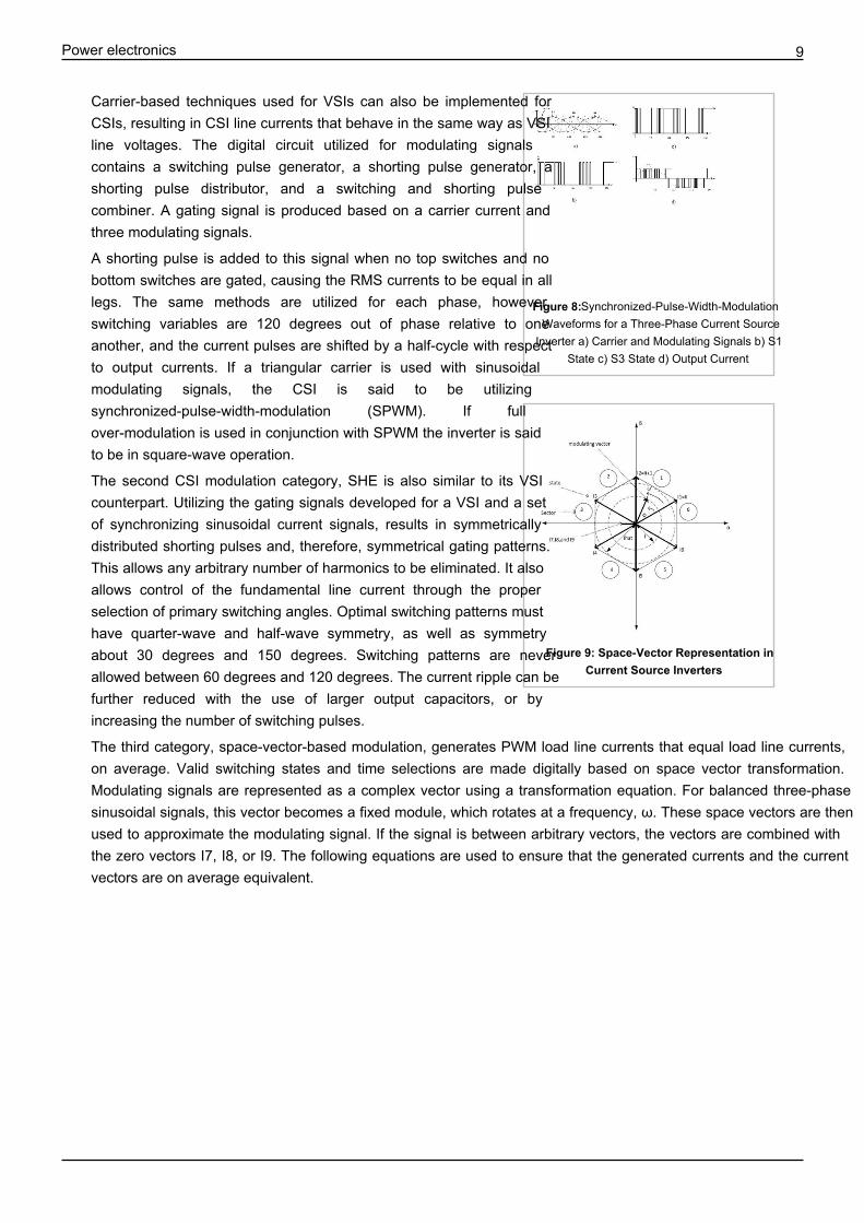
Current source inverters
FIGURE 7: Three-Phase Current Source Inverter
Current source inverters convert DC current into an AC currentwaveform. In applications requiring sinusoidal AC waveforms,magnitude, frequency, and phase should all be controlled. CSIs havehigh changes in current overtime, so capacitors are commonlyemployed on the AC side, while inductors are commonly employed onthe DC side. Due to the absence of freewheeling diodes, the powercircuit is reduced in size and weight, and tends to be more reliable thanVSIs. Although single-phase topologies are possible, three-phase CSIsare more practical.
In its most generalized form, a three-phase CSI employs the sameconduction sequence as a six-pulse rectifier. At any time, only onecommon-cathode switch and one common-anode switch are on.
As a result, line currents take discrete values of ii, 0 and ii. States are chosen such that a desired waveform is–outputted and only valid states are used. This selection is based on modulating techniques, which includecarrier-based PWM, selective harmonic elimination, and space-vector techniques.
Power electronics 9
Figure 8: Synchronized-Pulse-Width-ModulationWaveforms for a Three-Phase Current Source
Inverter a) Carrier and Modulating Signals b) S1State c) S3 State d) Output Current
Figure 9: Space-Vector Representation inCurrent Source Inverters
Carrier-based techniques used for VSIs can also be implemented forCSIs, resulting in CSI line currents that behave in the same way as VSIline voltages. The digital circuit utilized for modulating signalscontains a switching pulse generator, a shorting pulse generator, ashorting pulse distributor, and a switching and shorting pulsecombiner. A gating signal is produced based on a carrier current andthree modulating signals.
A shorting pulse is added to this signal when no top switches and nobottom switches are gated, causing the RMS currents to be equal in alllegs. The same methods are utilized for each phase, however,switching variables are 120 degrees out of phase relative to oneanother, and the current pulses are shifted by a half-cycle with respectto output currents. If a triangular carrier is used with sinusoidalmodulating signals, the CSI is said to be utilizingsynchronized-pulse-width-modulation (SPWM). If fullover-modulation is used in conjunction with SPWM the inverter is saidto be in square-wave operation.
The second CSI modulation category, SHE is also similar to its VSIcounterpart. Utilizing the gating signals developed for a VSI and a setof synchronizing sinusoidal current signals, results in symmetricallydistributed shorting pulses and, therefore, symmetrical gating patterns.This allows any arbitrary number of harmonics to be eliminated. It alsoallows control of the fundamental line current through the properselection of primary switching angles. Optimal switching patterns musthave quarter-wave and half-wave symmetry, as well as symmetryabout 30 degrees and 150 degrees. Switching patterns are neverallowed between 60 degrees and 120 degrees. The current ripple can befurther reduced with the use of larger output capacitors, or byincreasing the number of switching pulses.
The third category, space-vector-based modulation, generates PWM load line currents that equal load line currents,on average. Valid switching states and time selections are made digitally based on space vector transformation.Modulating signals are represented as a complex vector using a transformation equation. For balanced three-phasesinusoidal signals, this vector becomes a fixed module, which rotates at a frequency, ω. These space vectors are thenused to approximate the modulating signal. If the signal is between arbitrary vectors, the vectors are combined withthe zero vectors I7, I8, or I9. The following equations are used to ensure that the generated currents and the currentvectors are on average equivalent.
Power electronics 10
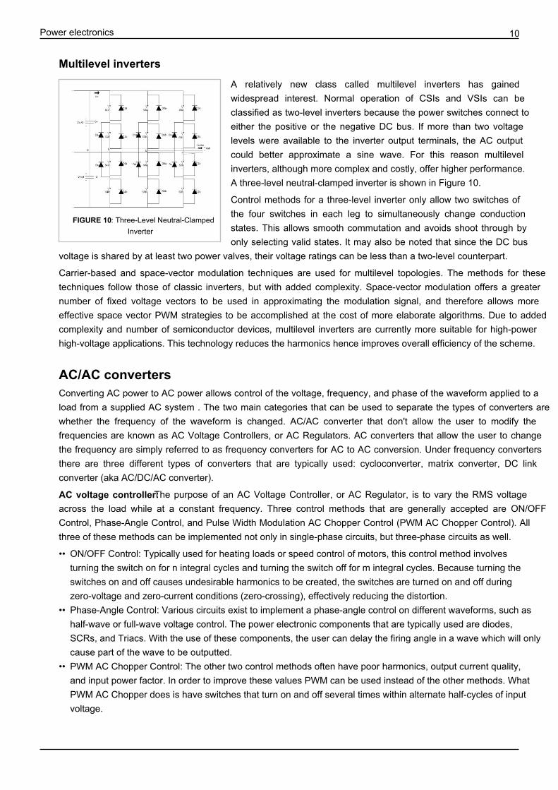
Multilevel inverters
FIGURE 10: Three-Level Neutral-ClampedInverter
A relatively new class called multilevel inverters has gainedwidespread interest. Normal operation of CSIs and VSIs can beclassified as two-level inverters because the power switches connect toeither the positive or the negative DC bus. If more than two voltagelevels were available to the inverter output terminals, the AC outputcould better approximate a sine wave. For this reason multilevelinverters, although more complex and costly, offer higher performance.A three-level neutral-clamped inverter is shown in Figure 10.
Control methods for a three-level inverter only allow two switches ofthe four switches in each leg to simultaneously change conductionstates. This allows smooth commutation and avoids shoot through byonly selecting valid states. It may also be noted that since the DC bus
voltage is shared by at least two power valves, their voltage ratings can be less than a two-level counterpart.
Carrier-based and space-vector modulation techniques are used for multilevel topologies. The methods for thesetechniques follow those of classic inverters, but with added complexity. Space-vector modulation offers a greaternumber of fixed voltage vectors to be used in approximating the modulation signal, and therefore allows moreeffective space vector PWM strategies to be accomplished at the cost of more elaborate algorithms. Due to addedcomplexity and number of semiconductor devices, multilevel inverters are currently more suitable for high-powerhigh-voltage applications. This technology reduces the harmonics hence improves overall efficiency of the scheme.
AC/AC convertersConverting AC power to AC power allows control of the voltage, frequency, and phase of the waveform applied to aload from a supplied AC system . The two main categories that can be used to separate the types of converters arewhether the frequency of the waveform is changed. AC/AC converter that don't allow the user to modify thefrequencies are known as AC Voltage Controllers, or AC Regulators. AC converters that allow the user to changethe frequency are simply referred to as frequency converters for AC to AC conversion. Under frequency convertersthere are three different types of converters that are typically used: cycloconverter, matrix converter, DC linkconverter (aka AC/DC/AC converter).
AC voltage controller: The purpose of an AC Voltage Controller, or AC Regulator, is to vary the RMS voltageacross the load while at a constant frequency. Three control methods that are generally accepted are ON/OFFControl, Phase-Angle Control, and Pulse Width Modulation AC Chopper Control (PWM AC Chopper Control). Allthree of these methods can be implemented not only in single-phase circuits, but three-phase circuits as well.
•• ON/OFF Control: Typically used for heating loads or speed control of motors, this control method involvesturning the switch on for n integral cycles and turning the switch off for m integral cycles. Because turning theswitches on and off causes undesirable harmonics to be created, the switches are turned on and off duringzero-voltage and zero-current conditions (zero-crossing), effectively reducing the distortion.
•• Phase-Angle Control: Various circuits exist to implement a phase-angle control on different waveforms, such ashalf-wave or full-wave voltage control. The power electronic components that are typically used are diodes,SCRs, and Triacs. With the use of these components, the user can delay the firing angle in a wave which will onlycause part of the wave to be outputted.
•• PWM AC Chopper Control: The other two control methods often have poor harmonics, output current quality,and input power factor. In order to improve these values PWM can be used instead of the other methods. WhatPWM AC Chopper does is have switches that turn on and off several times within alternate half-cycles of inputvoltage.
Power electronics 11
Matrix converters and cycloconverters: Cycloconverters are widely used in industry for ac to ac conversion,because they are able to be used in high-power applications. They are commutated direct frequency converters thatare synchronised by a supply line. The cycloconverters output voltage waveforms have complex harmonics with thehigher order harmonics being filtered by the machine inductance. Causing the machine current to have fewerharmonics, while the remaining harmonics causes losses and torque pulsations. Note that in a cycloconverter, unlikeother converters, there are no inductors or capacitors, i.e. no storage devices. For this reason, the instantaneous inputpower and the output power are equal.
• Single-Phase to Single-Phase Cycloconverters: Single-Phase to Single-Phase Cycloconverters started drawingmore interest recently Wikipedia:Manual of Style/Dates and numbers#Chronological items because of thedecrease in both size and price of the power electronics switches. The single-phase high frequency ac voltage canbe either sinusoidal or trapezoidal. These might be zero voltage intervals for control purpose or zero voltagecommutation.
• Three-Phase to Single-Phase Cycloconverters: There are two kinds of three-phase to single-phasecycloconverters: 3φ to 1φ half wave cycloconverters and 3φ to 1φ bridge cycloconverters. Both positive andnegative converters can generate voltage at either polarity, resulting in the positive converter only supplyingpositive current, and the negative converter only supplying negative current.
With recent device advances, newer forms of cycloconverters are being developed, such as matrix converters. Thefirst change that is first noticed is that matrix converters utilize bi-directional, bipolar switches. A single phase to asingle phase matrix converter consists of a matrix of 9 switches connecting the three input phases to the tree outputphase. Any input phase and output phase can be connected together at any time without connecting any two switchesfrom the same phase at the same time; otherwise this will cause a short circuit of the input phases. Matrix convertersare lighter, more compact and versatile than other converter solutions. As a result, they are able to achieve higherlevels of integration, higher temperature operation, broad output frequency and natural bi-directional power flowsuitable to regenerate energy back to the utility.
The matrix converters are subdivided into two types: direct and indirect converters. A direct matrix converter withthree-phase input and three-phase output, the switches in a matrix converter must be bi-directional, that is, they mustbe able to block voltages of either polarity and to conduct current in either direction. This switching strategy permitsthe highest possible output voltage and reduces the reactive line-side current. Therefore the power flow through theconverter is reversible. Because of its commutation problem and complex control keep it from being broadly utilizedin industry.
Unlike the direct matrix converters, the indirect matrix converters has the same functionality, but uses separate inputand output sections that are connected through a dc link without storage elements. The design includes afour-quadrant current source rectifier and a voltage source inverter. The input section consists of bi-directionalbipolar switches. The commutation strategy can be applied by changing the switching state of the input section whilethe output section is in a freewheeling mode. This commutation algorithm is significantly less complexity and higherreliability as compared to a conventional direct matrix converter.
DC link converters: DC Link Converters, also referred to as AC/DC/AC converters, convert an AC input to an ACoutput with the use of a DC link in the middle. Meaning that the power in the converter is converted to DC from ACwith the use of a rectifier, and then it is converted back to AC from DC with the use of an inverter. The end result isan output with a lower voltage and variable (higher or lower) frequency. Due to their wide area of application, theAC/DC/AC converters are the most common contemporary solution. Other advantages to AC/DC/AC converters isthat they are stable in overload and no-load conditions, as well as they can be disengaged from a load withoutdamage.
Hybrid matrix converter: Hybrid matrix converters are relatively new for AC/AC converters. These converters combine the AC/DC/AC design with the matrix converter design. Multiple types of hybrid converters have been developed in this new category, an example being a converter that uses uni-directional switches and two converter
Power electronics 12
stages without the dc-link; without the capacitors or inductors needed for a dc-link, the weight and size of theconverter is reduced. Two sub-categories exist from the hybrid converters, named hybrid direct matrix converter(HDMC) and hybrid indirect matrix converter (HIMC). HDMC convert the voltage and current in one stage, whilethe HIMC utilizes separate stages, like the AC/DC/AC converter, but without the use of an intermediate storageelement.
Applications: Below is a list of common applications that each converter is used in.
•• AC Voltage Controller: Lighting Control; Domestic and Industrial Heating; Speed Control of Fan,Pump or HoistDrives, Soft Starting of Induction Motors, Static AC Switches (Temperature Control, Transformer Tap Changing,etc.)
•• Cycloconverter: High-Power Low-Speed Reversible AC Motor Drives; Constant Frequency Power Supply withVariable Input Frequency; Controllable VAR Generators for Power Factor Correction; AC System IntertiesLinking Two Independent Power Systems.
•• Matrix Converter: Currently the application of matrix converters are limited due to non-availability of bilateralmonolithic switches capable of operating at high frequency, complex control law implementation, commutationand other reasons. With these developments, matrix converters could replace cycloconverters in many areas.
•• DC Link: Can be used for individual or multiple load applications of machine building and construction.
Simulations of power electronic systems
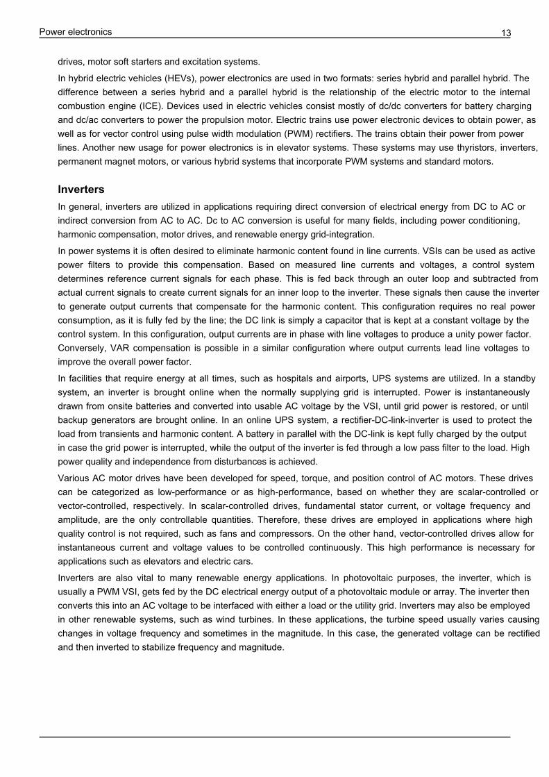
Output voltage of a full-wave rectifier withcontrolled thyristors
Power electronic circuits are simulated using computer simulationprograms such as PSIM and MATLAB/simulink. Circuits aresimulated before they are produced to test how the circuits respondunder certain conditions. Also, creating a simulation is both cheaperand faster than creating a prototype to use for testing.
ApplicationsApplications of power electronics range in size from a switched modepower supply in an AC adapter, battery chargers, fluorescent lampballasts, through variable frequency drives and DC motor drives usedto operate pumps, fans, and manufacturing machinery, up to gigawatt-scale high voltage direct current powertransmission systems used to interconnect electrical grids. Power electronic systems are found in virtually everyelectronic device. For example:
• DC/DC converters are used in most mobile devices (mobile phones, PDA etc.) to maintain the voltage at a fixedvalue whatever the voltage level of the battery is. These converters are also used for electronic isolation andpower factor correction.
• AC/DC converters (rectifiers) are used every time an electronic device is connected to the mains (computer,television etc.). These may simply change AC to DC or can also change the voltage level as part of theiroperation.
• AC/AC converters are used to change either the voltage level or the frequency (international power adapters, lightdimmer). In power distribution networks AC/AC converters may be used to exchange power between utilityfrequency 50 Hz and 60 Hz power grids.
• DC/AC converters (inverters) are used primarily in UPS or renewable energy systems or emergency lightingsystems. Mains power charges the DC battery. If the mains fails, an inverter produces AC electricity at mainsvoltage from the DC battery.
Motor drives are found in pumps, blowers, and mill drives for textile, paper, cement and other such facilities. Drives may be used for power conversion and for motion control. For AC motors, applications include variable-frequency
Power electronics 13
drives, motor soft starters and excitation systems.
In hybrid electric vehicles (HEVs), power electronics are used in two formats: series hybrid and parallel hybrid. Thedifference between a series hybrid and a parallel hybrid is the relationship of the electric motor to the internalcombustion engine (ICE). Devices used in electric vehicles consist mostly of dc/dc converters for battery chargingand dc/ac converters to power the propulsion motor. Electric trains use power electronic devices to obtain power, aswell as for vector control using pulse width modulation (PWM) rectifiers. The trains obtain their power from powerlines. Another new usage for power electronics is in elevator systems. These systems may use thyristors, inverters,permanent magnet motors, or various hybrid systems that incorporate PWM systems and standard motors.
InvertersIn general, inverters are utilized in applications requiring direct conversion of electrical energy from DC to AC orindirect conversion from AC to AC. Dc to AC conversion is useful for many fields, including power conditioning,harmonic compensation, motor drives, and renewable energy grid-integration.
In power systems it is often desired to eliminate harmonic content found in line currents. VSIs can be used as activepower filters to provide this compensation. Based on measured line currents and voltages, a control systemdetermines reference current signals for each phase. This is fed back through an outer loop and subtracted fromactual current signals to create current signals for an inner loop to the inverter. These signals then cause the inverterto generate output currents that compensate for the harmonic content. This configuration requires no real powerconsumption, as it is fully fed by the line; the DC link is simply a capacitor that is kept at a constant voltage by thecontrol system. In this configuration, output currents are in phase with line voltages to produce a unity power factor.Conversely, VAR compensation is possible in a similar configuration where output currents lead line voltages toimprove the overall power factor.
In facilities that require energy at all times, such as hospitals and airports, UPS systems are utilized. In a standbysystem, an inverter is brought online when the normally supplying grid is interrupted. Power is instantaneouslydrawn from onsite batteries and converted into usable AC voltage by the VSI, until grid power is restored, or untilbackup generators are brought online. In an online UPS system, a rectifier-DC-link-inverter is used to protect theload from transients and harmonic content. A battery in parallel with the DC-link is kept fully charged by the outputin case the grid power is interrupted, while the output of the inverter is fed through a low pass filter to the load. Highpower quality and independence from disturbances is achieved.
Various AC motor drives have been developed for speed, torque, and position control of AC motors. These drivescan be categorized as low-performance or as high-performance, based on whether they are scalar-controlled orvector-controlled, respectively. In scalar-controlled drives, fundamental stator current, or voltage frequency andamplitude, are the only controllable quantities. Therefore, these drives are employed in applications where highquality control is not required, such as fans and compressors. On the other hand, vector-controlled drives allow forinstantaneous current and voltage values to be controlled continuously. This high performance is necessary forapplications such as elevators and electric cars.
Inverters are also vital to many renewable energy applications. In photovoltaic purposes, the inverter, which isusually a PWM VSI, gets fed by the DC electrical energy output of a photovoltaic module or array. The inverter thenconverts this into an AC voltage to be interfaced with either a load or the utility grid. Inverters may also be employedin other renewable systems, such as wind turbines. In these applications, the turbine speed usually varies causingchanges in voltage frequency and sometimes in the magnitude. In this case, the generated voltage can be rectifiedand then inverted to stabilize frequency and magnitude.
Power electronics 14
"Smart grid"A smart grid is a modernized electrical grid that uses information and communications technology to gather and acton information, such as information about the behaviors of suppliers and consumers, in an automated fashion toimprove the efficiency, reliability, economics, and sustainability of the production and distribution of electricity.
Electric power generated by wind turbines and hydroelectric turbines by using induction generators can causevariances in the frequency at which power is generated. Power electronic devices are utilized in these systems toconvert the generated ac voltages into high-voltage direct current (HVDC). The HVDC power can be more easilyconverted into three phase power that is coherent with the power associated to the existing power grid. Throughthese devices, the power delivered by these systems is cleaner and has a higher associated power factor. Wind powersystems optimum torque is obtained either through a gearbox or direct drive technologies that can reduce the size ofthe power electronics device.
Electric power can be generated through photovoltaic cells by using power electronic devices. The produced poweris usually then transformed by inverters. Inverters are divided into three different types: central, module-integratedand string. Central converters can be connected either in parallel or in series on the DC side of the system. Forphotovoltaic "farms", a single central converter is used for the entire system. Module-integrated converters areconnected in series on either the DC or AC side. Normally several modules are used within a photovoltaic system,since the system requires these converters on both DC and AC terminals. A string converter is used in a system thatutilizes photovoltaic cells that are facing different directions. It is used to convert the power generated to each string,or line, in which the photovoltaic cells are interacting.
Grid voltage regulation
Power electronics can be used to help utilities adapt to the rapid increase in distributed residential/commercial solarpower generation. Germany and parts of Hawaii, California and New Jersey require costly studies to be conductedbefore approving new solar installations. Relatively small-scale ground- or pole-mounted devices create the potentialfor a distributed control infrastructure to monitor and manage the flow of power. Traditional electromechanicalsystems, such as capacitor banks or voltage regulators at substations, can take minutes to adjust voltage and can bedistant from the solar installations where the problems originate. If voltage on a neighborhood circuit goes too high,it can endanger utility crews and cause damage to both utility and customer equipment. Further, a grid fault causesphotovoltaic generators to shut down immediately, spiking demand for grid power. Smart grid-based regulators aremore controllable than far more numerous consumer devices.
In another approach, a group of 16 western utilities called the Western Electric Industry Leaders called formandatory use of "smart inverters". These devices convert DC to household AC and can also help with powerquality. Such devices could eliminate the need for expensive utility equipment upgrades at a much lower total cost.
Notes[1] Muhammad H. Rashid,POWER ELECTRONICS HANDBOOK DEVICES, CIRCUITS, AND APPLICATIONS Third Edition
Butterworth-Heinemann,2007 ISBN 978-0-12-382036-5
References•• Issa Batarseh, "Power Electronic Circuits" by John Wiley, 2003.•• S.K. Mazumder, "High-Frequency Inverters: From Photovoltaic, Wind, and Fuel-Cell based Renewable- and
Alternative-Energy DER/DG Systems to Battery based Energy-Storage Applications", Book Chapter in PowerElectronics handbook, Editor M.H. Rashid, Academic Press, Burlington, Massachusetts, 2010.
•• V. Gureich "Electronic Devices on Discrete Components for Industrial and Power Engineering", CRC Press, NewYork, 2008, 418 p.
Power electronics 15
• Editor: Semikron, Authors: Dr. Ulrich Nicolai, Dr. Tobias Reimann, Prof. Jürgen Petzoldt, Josef Lutz:Application Manual IGBT- and MOSFET-power modules, 1. edition, ISLE Verlag, 1998, ISBN 3-932633-24-5online version (http://www.sindopower.com/Application-Manual-oxid/)
• R. W. Erickson, D. Maksimovic, Fundamentals of Power Electronics, 2nd Ed., Springer, 2001, ISBN0-7923-7270-0 (http://ecee.colorado.edu/copec/book/SecEd.html)
• Arendt Wintrich, Ulrich Nicolai, Werner Tursky, Tobias Reimann (2010) (in German), [ PDF-Version (http://www.powerguru.org/wordpress/wp-content/uploads/2012/12/SEMIKRON_Applikationshandbuch_Leistungshalbleiter.pdf) Applikationshandbuch 2010] (2. ed.), ISLEVerlag, ISBN 978-3-938843-56-7
• Arendt Wintrich, Ulrich Nicolai, Werner Tursky, Tobias Reimann (2011) (in German), [ PDF-Version (http://www.powerguru.org/wordpress/wp-content/uploads/2012/12/SEMIKRON_application_manual_power_semiconductors.pdf) Application Manual 2011] (2. ed.), ISLE Verlag,ISBN 978-3-938843-66-6
External links• Interactive Power Electronics Seminar (iPES) (http://www.ipes.ethz.ch/ipes/e_index.html)• Powerguru.org (http://www.powerguru.org) – power electronics knowledge base with training material
(PowerGuru)• Load Power Sources for Peak Efficiency, by James Colotti, published in EDN 1979 October 5 (http://www.ieee.
li/pdf/essay/load_power_sources_for_peak_efficiency_edn_1979_10_05.pdf)

Article Sources and Contributors 16
Article Sources and ContributorsPower electronics Source: http://en.wikipedia.org/w/index.php?oldid=597270276 Contributors: 2001:db8, 2sb18, AJP, AdventurousSquirrel, Afhoke, Alan Liefting, Amiruddin 85, Amunich,Anonymous Dissident, Arthena, Asav, Auntof6, Bearcat, C J Cowie, CalumH93, Canaima, Cffrost, Chris the speller, Clampower, Crazypower, Cruiserbmw, CunningWizard, CyrilB,DaCozyMan, DabMachine, DavidCary, Diluvien, EncMstr, Fraggle81, Gang65, Giraffedata, Glenn, GorillaWarfare, Grunt4Ever, Gurch, I B Wright, Imroy, Ioannes Pragensis, Jaberwocky6669,Jeanenawhitney, Jivi, Jondel, Jusdafax, Juzaf, Kellyprice, Ketiltrout, Lfstevens, Lindosland, MGA73, Materialscientist, Michael Hardy, Mini-Geek, Nomi12892, North8000, Northamerica1000,Odje, Orzetto, P-Tronics, Pelstech.sathy, Pinethicket, Pion, PowerDidi, Powersys, Qwfp, Ratherbeskiing, Reedy, Regancy42, Rjwilmsi, Robert Weemeyer, Samarth shah, SchreyP, Shekure,Slightsmile, Spacemoose, SteamboatBilly, Sun Creator, Svancina, Synergitronix, Taxisfolder, UweD, VdSV9, Vegaswikian, Wbm1058, WereSpielChequers, Widr, Wiki alf, Wtshymanski, ÄDA- DÄP, 150 anonymous edits
Image Sources, Licenses and ContributorsFile:Baltic Cable Thyristorturm.jpg Source: http://en.wikipedia.org/w/index.php?title=File:Baltic_Cable_Thyristorturm.jpg License: GNU Free Documentation License Contributors: BalticCable AB. Original uploader was LeoLöwe2 at de.wikipedia
File:Absaar Batterie Ladegerät.jpg Source: http://en.wikipedia.org/w/index.php?title=File:Absaar_Batterie_Ladegerät.jpg License: Creative Commons Attribution-Sharealike 3.0 Germany Contributors: Thiemo Schuff
File:ATX power supply interior-1000px transparent.png Source: http://en.wikipedia.org/w/index.php?title=File:ATX_power_supply_interior-1000px_transparent.png License: PublicDomain Contributors: ATX_power_supply_interior.jpg: Alan Liefting derivative work: Silverxxx (talk)
File:The AC Input for a Standard Adjustable Speed Drive.jpg Source: http://en.wikipedia.org/w/index.php?title=File:The_AC_Input_for_a_Standard_Adjustable_Speed_Drive.jpg License:GNU Free Documentation License Contributors: P-Tronics
File:Single-Phase Half-Bridge Voltage Source Inverter.jpg Source: http://en.wikipedia.org/w/index.php?title=File:Single-Phase_Half-Bridge_Voltage_Source_Inverter.jpg License: GNUFree Documentation License Contributors: P-Tronics
File:Phase Voltage Source Full-Bridge Inverter.jpg Source: http://en.wikipedia.org/w/index.php?title=File:Phase_Voltage_Source_Full-Bridge_Inverter.jpg License: GNU FreeDocumentation License Contributors: P-Tronics
File:Carrier and Modulating Signals for the Bipolar Pulsewidth Modulation Technique.jpg Source:http://en.wikipedia.org/w/index.php?title=File:Carrier_and_Modulating_Signals_for_the_Bipolar_Pulsewidth_Modulation_Technique.jpg License: GNU Free Documentation License Contributors: P-Tronics
File:Three-Phase Voltage Source Inverter Circuit Schematic.jpg Source: http://en.wikipedia.org/w/index.php?title=File:Three-Phase_Voltage_Source_Inverter_Circuit_Schematic.jpg License: GNU Free Documentation License Contributors: P-Tronics
File:Three-Phase Square-Wave Operation a) Switch State S1 b) Switch State S3 c) S1 Output d) S3 Output.jpg Source:http://en.wikipedia.org/w/index.php?title=File:Three-Phase_Square-Wave_Operation_a)_Switch_State_S1_b)_Switch_State_S3_c)_S1_Output_d)_S3_Output.jpg License: GNU FreeDocumentation License Contributors: P-Tronics
File:Three-Phase Current Source Inverter.jpg Source: http://en.wikipedia.org/w/index.php?title=File:Three-Phase_Current_Source_Inverter.jpg License: GNU Free Documentation License Contributors: P-Tronics
File:Synchronized-Pulse-Width-Modulation Waveforms for a Three-Phase Current Source Inverter a) Carrier and Modulating Signals b) S1 State c) S3 State d) Output Current.jpg Source:http://en.wikipedia.org/w/index.php?title=File:Synchronized-Pulse-Width-Modulation_Waveforms_for_a_Three-Phase_Current_Source_Inverter_a)_Carrier_and_Modulating_Signals_b)_S1_State_c)_S3_State_d)_Output_Current.jpg License: GNU Free Documentation License Contributors: P-Tronics
File:Space-Vector Representation in Current Source Inverters.jpg Source: http://en.wikipedia.org/w/index.php?title=File:Space-Vector_Representation_in_Current_Source_Inverters.jpg License: GNU Free Documentation License Contributors: P-Tronics
File:Regulated rectifier.gif Source: http://en.wikipedia.org/w/index.php?title=File:Regulated_rectifier.gif License: Creative Commons Attribution-ShareAlike 3.0 Unported Contributors:Gloumouth1, WikipediaMaster, Zureks, 3 anonymous edits
LicenseCreative Commons Attribution-Share Alike 3.0//creativecommons.org/licenses/by-sa/3.0/