
Development of Nanofocusing Refractive X-Ray Lenses
108
Development of Nanofocusing Refractive X-Ray Lenses Von der Fakultät für Mathematik, Informatik und Naturwissenschaften der Rheinisch-Westfälischen Technischen Hochschule Aachen zur Erlangung des akademischen Grades einer Doktorin der Naturwissenschaften genehmigte Dissertation vorgelegt von Diplom-Physikerin Olga Kurapova aus Taschkent Berichter: Professor B. Lengeler Professor U. Klemradt Tag der mündlichen Prüfung: 02.11.2005 Diese Dissertation ist auf den Internetseiten der Hochschulbibliothek online verfügbar
Transcript of Development of Nanofocusing Refractive X-Ray Lenses
Development of Nanofocusing Refractive X-Ray Lenses
Von der Fakultät für Mathematik, Informatik und Naturwissenschaften der Rheinisch-Westfälischen Technischen Hochschule Aachen zur
Erlangung des akademischen Grades einer Doktorin der Naturwissenschaften genehmigte Dissertation
vorgelegt von
Diplom-Physikerin Olga Kurapova aus Taschkent
Berichter: Professor B. Lengeler Professor U. Klemradt
Tag der mündlichen Prüfung: 02.11.2005
Diese Dissertation ist auf den Internetseiten der Hochschulbibliothek online verfügbar

- 1 -
Table of contents 1. Introduction……………………………..…………………………...… 4
1.1 Scientific background……………..……………………………… 4
1.2 Objectives………………………….……………………………... 6
1.3 Research strategy.………………………………………………… 7
2. Theoretical background …...………….…………………...…………. 9
2.1 Refractive optics……………….………………………...……….. 9
2.1.1 Absorption……………………………………………..…… 9
2.1.2 Refractive index…………………………………………..... 12
2.1.3 Focusing optics for hard x-rays…………………………...... 14
2.1.4 Refractive x-ray lenses………….………………………...... 16
2.1.5 Focal length……………………….……………………...… 18
2.1.6 Generation of a small focal spot…………………....…....… 20
2.1.7 Effective aperture……………….………………...……..…. 21
2.1.8 Numerical aperture…………….…………………......…...... 22
2.1.9 Diffraction limit……………………….………………….... 22
2.1.10 Adiabatically focusing lenses…………………….………... 23
2.1 Main steps and methods in microfabrication process…..……..….. 27
2.2.1 Typical process outline……….……………………………. 27
2.2.2 Electron beam evaporation…….……………………..……. 31
2.2.3 Electron beam lithography…………….……………...……. 32
2.2.4 Methods of etching…………….………………………..…. 34
3. Optimised fabrication of silicon parabolic nanofocusing x-ray 37
TABLE OF CONTENTS ____________________________________________________________________
- 2 -
lenses (NFLs)
3.1 Design of silicon NFLs……………………….…………………... 37
3.2 Fabrication of silicon NFLs……………………….……………… 40
3.3 Analysis of radius of curvature of lenses……………………….... 44
3.4 Lens setup …....……………………….………………………….. 47
3.5 Focusing properties of Si NFLs……………………….………….. 48
4. Application of silicon nanofocusing x-ray lenses ………….……….... 52
4.1 Nanodiffraction from the laser modified films……...……….…… 52
4.1.1 Experimental procedure………..…………………………… 54
4.1.2 Results……………….……………………………………… 56
4.1.3 Discussion………………….……………………………….. 59
4.1.4 Conclusion………………….………………………………. 59
4.2 X-ray stress analysis for free standing Al-mirror…………….……. 60
4.2.1 Experimental procedure…………….………………………. 61
4.2.2 Results………………….…………………………………… 63
4.2.3 Discussion and conclusion………………….………………. 63
5 Fabrication of nanofocusing lenses made of boron, diamond,
pyrolitic graphite, and sapphire…………………………….…………
65
5.1 Boron NFLs…………………………….……………..………….. 66
5.1.1 Structure of boron layer………………………….…………. 66
5.1.2 Optimisation of the microfabrication process of boron
NFLs...
67
5.2 Etching of diamond…………………………………………….… 77
5.3 Pyrolitic graphite NFLs………………………………….……….. 80
TABLE OF CONTENTS ____________________________________________________________________
- 3 -
5.4 Etching of sapphire…………………………………………….…. 82
6. Summary and outlook……………………………………………….… 84
Appendix I. X-ray diffraction (XRD)..…………………………………….…. 88
List of Figures…………………………………………………………………. 90
List of Tables……………………………………………………………….….. 96
Bibliography………………………………………………………….………... 97
Acknowledgements…………………………………………………………..… 104
Curriculum Vitae……………………………………………………………… 106
- 4 -
Chapter 1
Introduction
1.1 Scientific background
Large penetration depth in matter and small wavelengths make hard x–rays attractive
for microanalysis, such as x-ray diffraction, fluorescence analysis, and absorption
spectroscopy. These methods are powerful tools in semiconductor technology, in
material science, geology, biology, or medicine, and are particularly useful for
investigating non-destructively structures inside a specimen. To perform x-ray analysis
techniques with spatial resolution well below 100 nm, synchrotron radiation from a
third generation source with its outstanding properties, such as brilliance and flux, and
high quality optical components are needed. For focusing purposes in the micrometer
and sub-micrometer range highly sophisticated components like Kirkpatrick – Baez
mirrors [Kirk], [Haya], [Hign1], Fresnel zone plates [Yun] and refractive x-ray lenses
[Len1], [Aris], [Schr1] have been developed in the last years.
The typical synchrotron radiation source size is a few hundred µm (e.g., European
Synchrotron Radiation Facility (ESRF), high-β undulator source size: 900×60 µm2,
low-β undulator source 150×60 µm2). To achieve a microbeam size in the 100 nm
range a demagnification by a factor of 1000 is required. At a typical distance of 40-
70 m from the radiation source most x-ray optics with a focal distance larger than
INTRODUCTION _________________________________________________________________
- 5 -
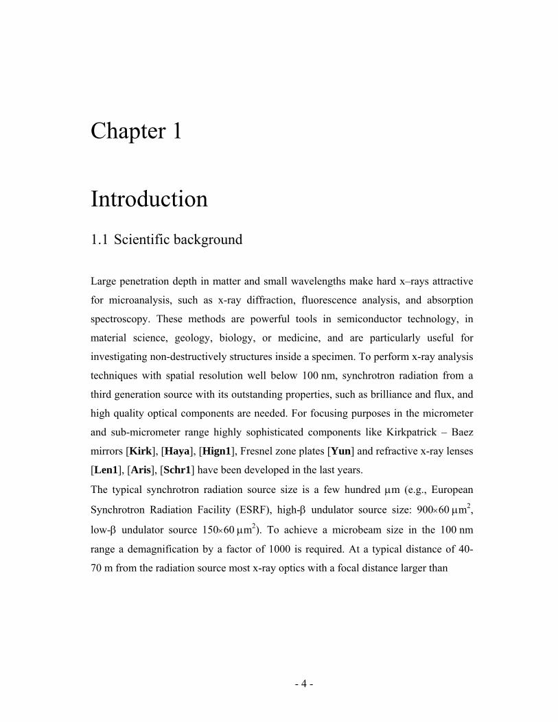
Figure 1.1. Scanning electron micrograph of planar parabolic refractive nanofocusing
lenses made of silicon.
10 cm can not reach this demagnification. One possibility to reach this limit (100 nm)
is making a smaller secondary source by placing a pinhole between source and
microbeam setup [Yun]. Another possibility is to place the microprobe at a large
distance from the source, e.g. at 145 m [Hign1] or 1 km [Yam], if this space is
available. At Aachen University a third alternative was pursued. Nanofocusing
refractive lenses (NFLs) were developed with focal distance f of a few mm [Schr1]
that allows for demagnification of several thousand even at short beamlines. This small
focal distance and strong demagnification can only be realised with a lens curvature R
in the range of few µm. Because fabrication techniques for rotationally parabolic
refractive lenses developed at Aachen University [Len1] are not well suited to
fabricate such strongly curved lenses, a new microfabrication process for the lenses
INTRODUCTION _________________________________________________________________
- 6 -
with a cylindrically parabolic profile and extremely small R is required. For this
purpose, a lithographic techniques such as electron beam lithography combined with
deep reactive ion etching was used. Silicon nanofocusing refractive lenses are made by
etching a series of parabolic cylinders into the lens material (Figure 1.1). These one-
dimensionally focusing lenses require vertical sidewalls to be generated in the etching
process. Deviations from the ideal shape lead to aberrations and thus to a blurred
focus. Using nanofocusing refractive x-ray lenses, a nanobeam with a lateral resolution
of 50 nm has been generated [Schr2], that is in good agreement with the calculated
value for ideal lenses.
1.2 Objectives
In this work the microfabrication process of nanofocusing x-ray refractive lenses made
by lithographic techniques has been investigated. The goal was to contribute towards
understanding the etching process, lens shape, and focus properties.
This thesis is concerned with:
• the optimisation of the fabrication process for nanofocusing x-ray
lenses made of silicon;
• characterization of the silicon NFLs;
• application of the NFLs;
• microfabrication processes for nanofocusing x-ray lenses made of
boron, diamond, graphite, and sapphire.
For the microfabrication process electron beam evaporation and electron beam
lithography were used. Different methods of etching, such as wet etching, reactive ion
etching, and deep reactive ion etching were applied. Analytic techniques for the
INTRODUCTION _________________________________________________________________
- 7 -
determination of lens shapes were scanning electron microscopy (SEM), optical
microscopy (OM), profilometer (MicroProfR). The lenses were tested at the low-β
beamline ID13 of ESRF.
1.3 Research strategy
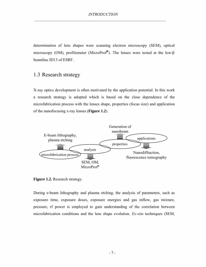
X-ray optics development is often motivated by the application potential. In this work
a research strategy is adopted which is based on the close dependence of the
microfabrication process with the lenses shape, properties (focus size) and application
of the nanofocusing x-ray lenses (Figure 1.2).
microfabrication processanalysis
propertiesapplications
E-beam lithography, plasma etching
Generation of nanobeam
SEM, OM, MicroProfR
Nanodiffraction, fluorescence tomography
Figure 1.2. Research strategy.
During e-beam lithography and plasma etching, the analysis of parameters, such as
exposure time, exposure doses, exposure energies and gas inflow, gas mixture,
pressure, rf power is employed to gain understanding of the correlation between
microfabrication conditions and the lens shape evolution. Ex-situ techniques (SEM,
INTRODUCTION _________________________________________________________________
- 8 -
OM, MicroProfR) are used for the lens shape analysis as well as for the
characterization of the radius of curvature. Nanofocusing refractive lenses with lens
shapes close to optimal (parabolic shape and vertical sidewalls) are employed to
generate monochromatic hard x-ray beams well below 100 nm. Based on these lenses,
microanalysis in the range of 100 nm and below, such as x-ray diffraction,
fluorescence analysis, and absorption spectroscopy can be successful carried out.
- 9 -
Chapter 2
Theoretical background 2.1 Refractive optics
2.1.1 Absorption
When x-rays pass through matter, they are attenuated. This behaviour is described by
Lambert-Beer’s law: xeIxI µ−= 0)( . (2.1)
Here, I0 is the intensity before the sample, and I(x) is the remaining intensity after a
homogeneous slice of material of the thickness x.
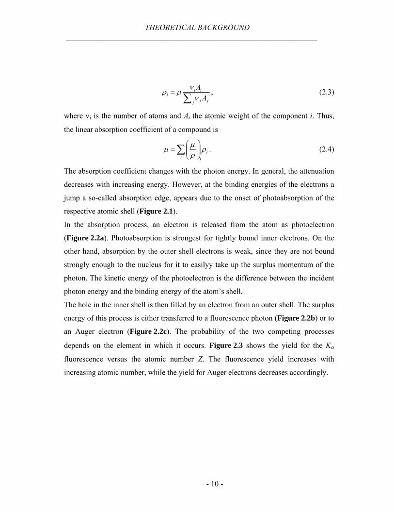
The linear absorption coefficient µ (Figure 2.1) contains contributions from
photoabsorption τ, elastic scattering σR (Raleigh scattering), inelastic scattering σC
(Compton scattering), and pair production σpair for x-rays above 1,022 MeV.
)( pairCR σσστµ +++= . (2.2)
Values for the mass absorption coefficient µ/ρ, where ρ is the density, can be found in
the literature for almost all elements and for a wide range of x-ray energies [Veig]. For
compound materials, the mass absorption coefficient of the elements are weighted with
the relative density
THEORETICAL BACKGROUND _________________________________________________________________
- 10 -
∑=
j jj
iii A
Aν
νρρ , (2.3)
where νi is the number of atoms and Ai the atomic weight of the component i. Thus,
the linear absorption coefficient of a compound is
ii i
ρρµµ ∑ ⎟⎟
⎠
⎞⎜⎜⎝
⎛= . (2.4)
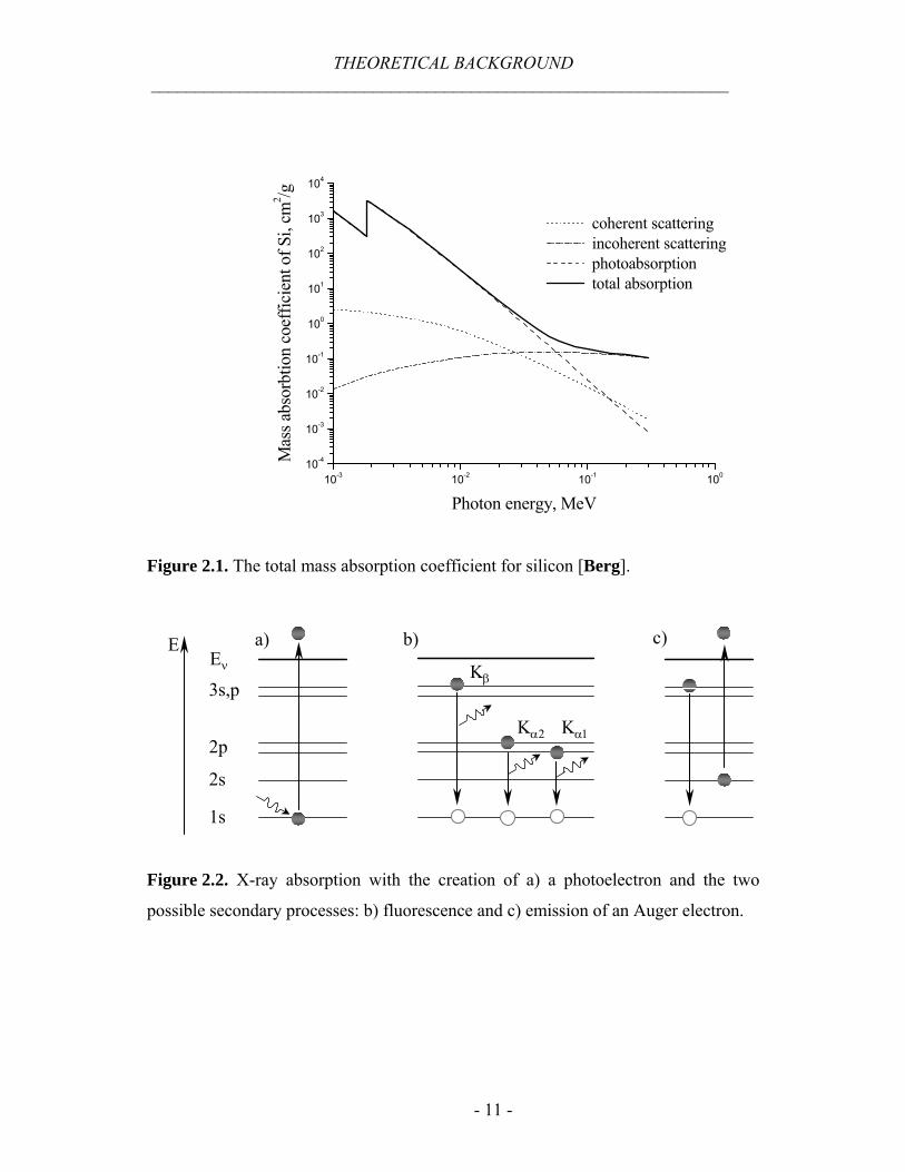
The absorption coefficient changes with the photon energy. In general, the attenuation
decreases with increasing energy. However, at the binding energies of the electrons a
jump a so-called absorption edge, appears due to the onset of photoabsorption of the
respective atomic shell (Figure 2.1).
In the absorption process, an electron is released from the atom as photoelectron
(Figure 2.2a). Photoabsorption is strongest for tightly bound inner electrons. On the
other hand, absorption by the outer shell electrons is weak, since they are not bound
strongly enough to the nucleus for it to easilyy take up the surplus momentum of the
photon. The kinetic energy of the photoelectron is the difference between the incident
photon energy and the binding energy of the atom’s shell.
The hole in the inner shell is then filled by an electron from an outer shell. The surplus
energy of this process is either transferred to a fluorescence photon (Figure 2.2b) or to
an Auger electron (Figure 2.2c). The probability of the two competing processes
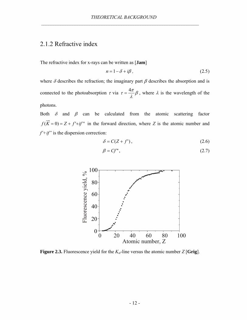
depends on the element in which it occurs. Figure 2.3 shows the yield for the Kα
fluorescence versus the atomic number Z. The fluorescence yield increases with
increasing atomic number, while the yield for Auger electrons decreases accordingly.
THEORETICAL BACKGROUND _________________________________________________________________
- 11 -
10-3 10-2 10-1 10010-4
10-3
10-2
10-1
100
101
102
103
104
Mas
s abs
orbt
ion
coef
ficie
nt o
f Si,
cm2 /g
Photon energy, MeV
coherent scattering incoherent scattering photoabsorption total absorption
Figure 2.1. The total mass absorption coefficient for silicon [Berg].
1s
2p
3s,p
2s
EνE с)b)a)
Kβ
Kα2 Kα1
Figure 2.2. X-ray absorption with the creation of a) a photoelectron and the two
possible secondary processes: b) fluorescence and c) emission of an Auger electron.
THEORETICAL BACKGROUND _________________________________________________________________
- 12 -
2.1.2 Refractive index
The refractive index for x-rays can be written as [Jam]
βδ in +−= 1 , (2.5)
where δ describes the refraction; the imaginary part β describes the absorption and is
connected to the photoabsorption τ via βλπτ 4
= , where λ is the wavelength of the
photons.
Both δ and β can be calculated from the atomic scattering factor
''')0( iffZKf ++== in the forward direction, where Z is the atomic number and
f’+if” is the dispersion correction:
)'( fZС +=δ , (2.6)
"Cf=β , (2.7)
0 20 40 60 80 100Atomic number, Z
Fluo
resc
ence
yie
ld, %
100
80
60
40
20
0
Figure 2.3. Fluorescence yield for the Kα-line versus the atomic number Z [Grig].
THEORETICAL BACKGROUND _________________________________________________________________
- 13 -
ArNС a 1
22
0 ρλπ
= . (2.8)
For compound materials, δ and β are also calculated in analogy to the relative density
(Equation 2.4). Thus, δ can be written as
∑∑∑ ==
j jj
i ii
i
ai
i
ia
AvZrN
AZrN ν
πρλρ
πλδ
22
20
20 , (2.9)
away from the absorption edges. Similarly, β or τ can be written as
∑ ∑ ⎟⎟⎠
⎞⎜⎜⎝
⎛===
i ii
ii
i
ia
AfrN ρ
ρτρ
πλ
λπβ
λπτ "
244 2
0 . (2.10)
The refractive index for x-rays deviates only very little from unity, since both δ and β
are very small. δ is of the order of 10-6 for most materials at photon energies around
10 keV; β is even smaller by two or three orders of magnitude. Hence, the refraction is
only very small. Since δ is positive, the real part of the refractive index n is smaller
than unit. Thus, according to Snell’s law [Hech]
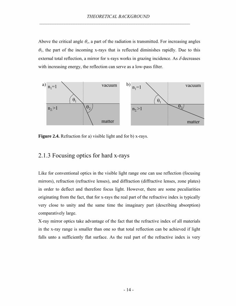
)cos()cos( 2211 θθ nn = , (2.11)
the x-rays that pass from vacuum (or air) into matter are refracted away from the
surface normal (Figure 2.4b). For visible light, the refraction is towards the surface
normal (Figure 2.4a), since n2 is larger than 1.
For the angle θ1 in figure 2.4b, which is smaller than a certain critical angle θc, the x-
rays are totally reflected from the sample surface. According to equation 2.11, the
critical angle θc can be calculated from
δθδθθ 212
1)cos(2
2 ≅→−≅−→= cc
c n . (2.12)
THEORETICAL BACKGROUND _________________________________________________________________
- 14 -
Above the critical angle θc, a part of the radiation is transmitted. For increasing angles
θ1, the part of the incoming x-rays that is reflected diminishes rapidly. Due to this
external total reflection, a mirror for x-rays works in grazing incidence. As δ decreases
with increasing energy, the reflection can serve as a low-pass filter.
n1=1
n2.>1
θ1
θ2
vacuum
matter
n1=1
n2.>1
θ1θ2
vacuum
matter
a) b)
Figure 2.4. Refraction for a) visible light and for b) x-rays.
2.1.3 Focusing optics for hard x-rays
Like for conventional optics in the visible light range one can use reflection (focusing
mirrors), refraction (refractive lenses), and diffraction (diffractive lenses, zone plates)
in order to deflect and therefore focus light. However, there are some peculiarities
originating from the fact, that for x-rays the real part of the refractive index is typically
very close to unity and the same time the imaginary part (describing absorption)
comparatively large.
X-ray mirror optics take advantage of the fact that the refractive index of all materials
in the x-ray range is smaller than one so that total reflection can be achieved if light
falls unto a sufficiently flat surface. As the real part of the refractive index is very
THEORETICAL BACKGROUND _________________________________________________________________
- 15 -
close to unity, a grazing incidence of the x-rays, almost parallel to the mirror surface,
is required in order to obtain total reflection. Due to these small working angles x-ray
mirrors are relatively hard to align and often suffer from strong aberrations. In addition
very long mirrors with high shape accuracy are required making high performance
mirror systems difficult to build and comparatively expensive. In consequence, a spot
size of about 1 µm can be obtained in routine operation, although spot-sizes down to
100 nm FWHM have been reported recently [Hign2], [Cloe], [Ice]. As x-ray mirrors
have the advantage of being achromatic and show comparatively high efficiency, they
are quite often used as x-ray focusing devices.
Refractive lenses for x-rays are a relatively new development and in fact have been
considered impractical for a long time due to the small refraction effects and the strong
absorption of materials in the x-ray range. Nevertheless, using many lenses in series it
is possible to obtain a sufficient deflection of the beam, and therefore reasonable focal
lengths [Snig]. And going to high photon energies, using lens materials with low
atomic number and utilizing alternative approaches for the lens fabrication and design
[Len2], [Aris] it is possible to keep absorption losses small. Refractive lenses for x-
rays are strongly chromatic – the focal length is found to be proportional to the square
of the used photon energy. However, many applications require monochromatized x-
rays of a fixed energy, so that chromatic aberrations are normally negligible and do not
significantly limit the applicability of refractive lenses. A short overview of
microfocusing theory for different types of refractive x-ray lenses can be found below.
Diffractive lenses (zone plates) for x-rays offer the advantage that the diffractive
structures together with the support membrane can be kept very thin, so that even for
soft x-rays, where absorption plays a dominant role, a sufficiently high x-ray
transmission can be realized. The diffractive structures can be fabricated with high
THEORETICAL BACKGROUND _________________________________________________________________
- 16 -
accuracy down to very small structure sizes and as a consequence zone plates achieve
by far the highest resolution of all x-ray lenses [Schn], [Spec], [And], [Dav]. Similar
to refractive lenses diffractive x-ray lenses have the disadvantage of being chromatic –
the focal length is directly proportional to the photon energy. Another drawback of
diffractive lenses is, that it is very difficult to obtain sufficient diffraction efficiency in
the hard x-ray range. This results from the fact, that good efficiencies require structure
heights, which are often much larger than the periods of the diffracting structures,
making the fabrication of zone plates with the demanded aspect ratios a non-trivial
task.
There are also many other alternative methods to achieve a small spot of x-rays, like
Bragg-Fresnel lenses, capillary optics and wave-guides. Consequently, many books
and several reviews can be found in the literature, discussing in the detail the
advantages and disadvantages of all these methods and the fields of their application
(see for example [Mich]).
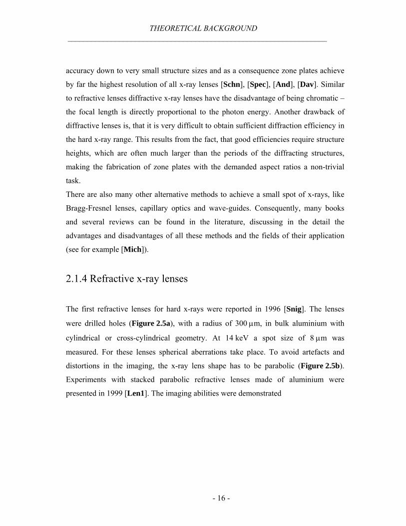
2.1.4 Refractive x-ray lenses
The first refractive lenses for hard x-rays were reported in 1996 [Snig]. The lenses
were drilled holes (Figure 2.5a), with a radius of 300 µm, in bulk aluminium with
cylindrical or cross-cylindrical geometry. At 14 keV a spot size of 8 µm was
measured. For these lenses spherical aberrations take place. To avoid artefacts and
distortions in the imaging, the x-ray lens shape has to be parabolic (Figure 2.5b).
Experiments with stacked parabolic refractive lenses made of aluminium were
presented in 1999 [Len1]. The imaging abilities were demonstrated
THEORETICAL BACKGROUND _________________________________________________________________
- 17 -
a) Refractive x-ray lens
b) Compound refractive x-ray lens
c) Nanofocusing refractive x-ray lens
d) Adiabatically focusing refractive x-ray lens
d
R≈300 µm
d
R≈200 µm
d
R≈3 µm
d
R≈10 µm R≈500 nm
Figure 2.5. Sketch of types of parabolic refractive lenses: a) first refractive lenses;
b) compound refractive x-ray lenses; c) nanofocusing refractive x-ray lenses;
d) adiabatically focusing refractive x-ray lens.
THEORETICAL BACKGROUND _________________________________________________________________
- 18 -
with crossed gold meshes. Later, tomographic and microprobing application were
implemented. Beryllium parabolic refractive lenses were first manufactured in 2001.
The typical radius of curvature of these lenses is about 200 µm. For the focusing in the
range of 100 nm and below, nanofocusing refractive lenses with crossed parabolic
cylinder symmetry were developed (Figure 2.5.c). The first publication about
nanofocusing refractive x-ray lens made of silicon can be found in [Schr1]. The most
outstanding feature of these lenses is their small radius of curvature R, that lies in the
micrometer range and leads to focal distances in the centimetre range for hard x-rays.
The concept of special refractive lenses for focusing in range of few nanometers has
been a new approach since 2005 [Schr2]. The principal difference between
nanofocusing refractive lenses and adiabatically refractive lenses is in the fact, that the
second have continuously decreasing radius of curvature (Figure 2.5d). The properties
of compound refractive x-ray lenses have in details been described in [Schr3].
Characteristic properties of adiabatically focusing refractive lenses are given in
section 2.10.
2.1.5 Focal length
The refraction of x-rays in matter has already been discussed above. On this basis,
refractive lenses for x-rays can be constructed in an analogous manner to the well-
known glass lenses for visible light. The focal length for both cases can be described
by the lens maker’s formula
Rn
f)1(21 −
= , (2.13)
THEORETICAL BACKGROUND _________________________________________________________________
- 19 -
where n is the real part of the refractive index and R is the radius of curvature of the
lens. However, some differences have to be noticed.
First, the refractive index for x-rays in matter is < 1, as can be seen from equation 2.5.
Thus, a focusing lens has to be concave for x-rays, while it is convex for visible light.
Second, since δ in equation 2.5 is very small, the refractive index is close to 1. Thus,
as can be seen from equation 2.13, the radius of curvature of an x-ray lens has to be
very small to achieve a manageable focal length. To reduce the focal length of
nanofocusing x-ray refractive lenses to a few millimetres, a radius of curvature in the
range of several micrometers is required. Moreover, the focal length can be reduced by
using a set of lenses with the individual focal lengths fi. The system of several lenses
can be realized by etching single lenses behind each other into the lens material. As
long as the focal length of such a system is still long compared to the thickness of the
stack, the system can be treated as a thin lens and the focal length can be calculated as
∑=i iff
11 . (2.14)
Thus, for N identical lenses, where each has two surfaces with radius of curvature R,
the focal length is
δNRf
20 = , (2.15)
where δ is the refractive index decrement (Equation 2.5).
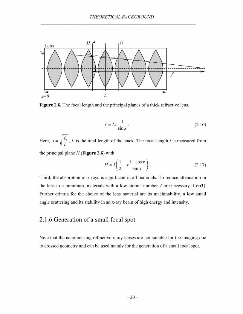
If the total length of the lens has comparable size to the focal length (Figure 2.6), then
the thin lens approximation is no longer valid. The correction to f has been calculated
[Schr3]. It turns out that for thick lenses f is given by
THEORETICAL BACKGROUND _________________________________________________________________
- 20 -
L
H H
z=0
Lensx0
f
Figure 2.6. The focal length and the principal planes of a thick refractive lens.
xLxf
sin1
= . (2.16)
Here, Lfx 0= , L is the total length of the stack. The focal length f is measured from
the principal plane H (Figure 2.6) with
⎟⎠⎞
⎜⎝⎛ −
−=x
xxLHsin
cos121 . (2.17)
Third, the absorption of x-rays is significant in all materials. To reduce attenuation in
the lens to a minimum, materials with a low atomic number Z are necessary [Len3].
Further criteria for the choice of the lens material are its machinability, a low small
angle scattering and its stability in an x-ray beam of high energy and intensity.
2.1.6 Generation of a small focal spot
Note that the nanofocusing refractive x-ray lenses are not suitable for the imaging due
to crossed geometry and can be used mainly for the generation of a small focal spot.

THEORETICAL BACKGROUND _________________________________________________________________
- 21 -
lens
f
h2
h1
L2L1
optical axis
Figure 2.7. Generation of a small focal spot. For nanofocusing refractive lenses: L2≈f.
The demagnification factor can be written as
fLfm−
=1
, (2.18)
where f is focal distance, L1 the distance between source and lenses, (Figure 2.7). The
demagnification of the source in the range of several thousand can be obtained.
2.1.7 Effective aperture
The aperture of a glass lens for visible light is only limited by its size, since almost no
light is absorbed in the lens. However, the absorption of x-rays in matter can not be
neglected, and thus, the transmission of an x-ray lens decreases for rays away from the
optical axis, since it is concave and the thickness of the lens material that these rays
have to pass through increases rapidly due to the very small radius of curvature.
For refractive x-ray lenses with N single lenses, the effective aperture can be written as
THEORETICAL BACKGROUND _________________________________________________________________
- 22 -
NRDeff µ
22= , (2.19)
provided that the geometric aperture is so large that the attenuation of the lens material
dominates Deff. Here, R is the radius of curvature of the parabola, and µ is linear
absorption coefficient of the lens material.
2.1.8 Numerical aperture
Connected with the effective aperture Deff is the concept of the numerical aperture
N.A.. Photons that come from an object can only contribute to an image, if they pass
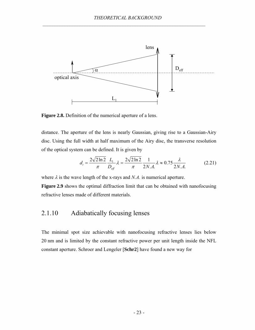
through the effective aperture Deff of the lens. As can be seen from figure 2.8 there is a
maximum effective angle α that rays coming from the object at L1 can have with the
optical axis, so that they can still pass through the effective aperture of the lens. Rays
with a larger angle would most likely be absorbed in the lens material. The numerical
aperture N.A. is defined as the sine of that maximum effective angle and can be written
for small angles α as
12
sin..L
DAN eff≈= α . (2.20)
2.1.9 Diffraction limit
In addition to the demagnification of the source, the microbeam can also be limted by
diffraction at the aperture of the lens. As described above the effective aperture is
dominated by attenuation in the outer parts of the lens for most lenses with short focal
THEORETICAL BACKGROUND _________________________________________________________________
- 23 -
lens
L1
optical axisα Deff
Figure 2.8. Definition of the numerical aperture of a lens.
distance. The aperture of the lens is nearly Gaussian, giving rise to a Gaussian-Airy
disc. Using the full width at half maximum of the Airy disc, the transverse resolution
of the optical system can be defined. It is given by
..275.0
..212ln222ln22 1
ANANDLd
efft
λλπ
λπ
≈== (2.21)
where λ is the wave length of the x-rays and N.A. is numerical aperture.
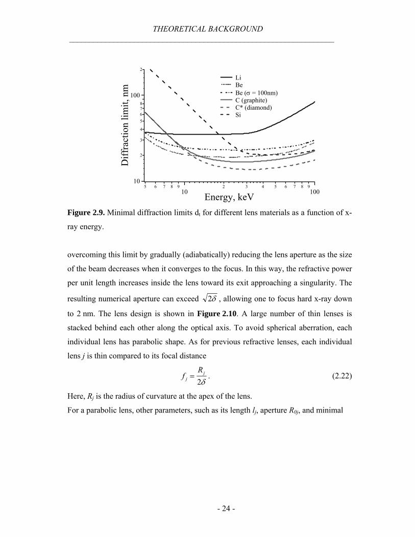
Figure 2.9 shows the optimal diffraction limit that can be obtained with nanofocusing
refractive lenses made of different materials.
2.1.10 Adiabatically focusing lenses
The minimal spot size achievable with nanofocusing refractive lenses lies below
20 nm and is limited by the constant refractive power per unit length inside the NFL
constant aperture. Schroer and Lengeler [Schr2] have found a new way for
THEORETICAL BACKGROUND _________________________________________________________________
- 24 -
10
2
3
4
5678
100
2
Diff
ract
ion
limit,
nm
5 6 7 8 910
2 3 4 5 6 7 8 9100Energy, keV
Li Be Be (σ = 100nm) C (graphite) C* (diamond) Si
Figure 2.9. Minimal diffraction limits dt for different lens materials as a function of x-
ray energy.
overcoming this limit by gradually (adiabatically) reducing the lens aperture as the size
of the beam decreases when it converges to the focus. In this way, the refractive power
per unit length increases inside the lens toward its exit approaching a singularity. The
resulting numerical aperture can exceed δ2 , allowing one to focus hard x-ray down
to 2 nm. The lens design is shown in Figure 2.10. A large number of thin lenses is
stacked behind each other along the optical axis. To avoid spherical aberration, each
individual lens has parabolic shape. As for previous refractive lenses, each individual
lens j is thin compared to its focal distance
δ2j
j
Rf = . (2.22)
Here, Rj is the radius of curvature at the apex of the lens.
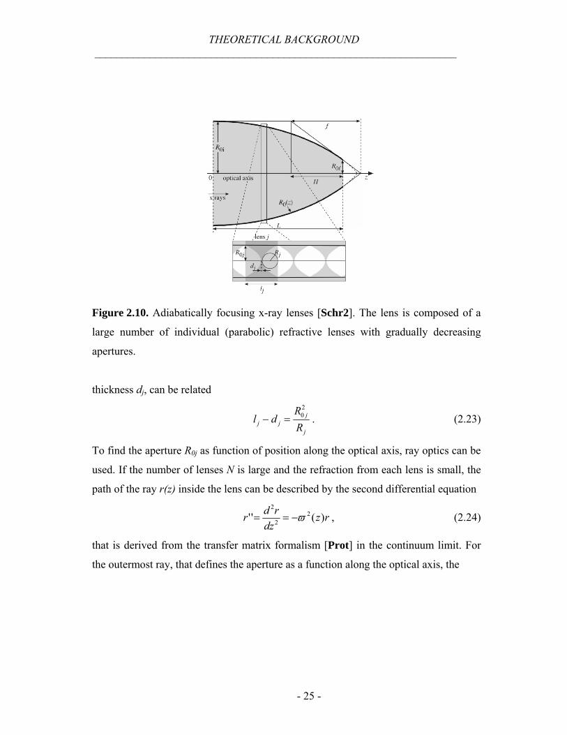
For a parabolic lens, other parameters, such as its length lj, aperture R0j, and minimal
THEORETICAL BACKGROUND _________________________________________________________________
- 25 -
Figure 2.10. Adiabatically focusing x-ray lenses [Schr2]. The lens is composed of a
large number of individual (parabolic) refractive lenses with gradually decreasing
apertures.
thickness dj, can be related
j
jjj R
Rdl
20=− . (2.23)
To find the aperture R0j as function of position along the optical axis, ray optics can be
used. If the number of lenses N is large and the refraction from each lens is small, the
path of the ray r(z) inside the lens can be described by the second differential equation
rzdz
rdr )('' 22
2
ϖ−== , (2.24)
that is derived from the transfer matrix formalism [Prot] in the continuum limit. For
the outermost ray, that defines the aperture as a function along the optical axis, the
THEORETICAL BACKGROUND _________________________________________________________________
- 26 -
differential equation (2.24) can be written as
( )0
0
/12''
Rld
R jj δ−−= . (2.25)
For a parallel beam incident on the first lens, the initial conditions are R0(0)=R0i and
'0R =0, yielding the first order differential equation
0
00 log'4'
RRR iδ= , (2.26)
where δδ )/1(' jj ld−= .
Figure 2.10 shows R0(z) as a solution of Equation 2.26. For a given exit aperture R0f,
the lens properties can be calculated, such as the focal distance f, the secondary
principal plane H, the effective Deff and the numerical aperture NA in analogy to that of
a thin refractive x-ray lens [Len1].
f
i
i
RR
Rf
0
0
0
log4δ= ,
f
i
if
RR
RRH
0
0'
00
log4δ
−= , (2.27)
⎟⎟⎠
⎞⎜⎜⎝
⎛⎥⎦⎤
⎢⎣⎡−−=
2'exp1
'22 0
LL
RD ieffµ
µ, (2.28)
where ( )µµ jj ld /1' −= and µ is the attenuation coefficient.
f
i
i RR
aR
RaNA i
0
0
0
0logexp14' ⎥⎦
⎤⎢⎣
⎡⎟⎠⎞
⎜⎝⎛−−= δ , (2.29)
where ''4
µπδ
=a is a material specific characteristic aperture. The larger a yields the
larger numerical aperture, favouring materials with low atomic number Z. The
numerical aperture is proportional to 'δ , favouring a lens material with large mass
THEORETICAL BACKGROUND _________________________________________________________________
- 27 -
density ρ. The largest numerical apertures are therefore expected for high density low
Z materials, such as diamond or sapphire.
2.2 Main steps and methods in microfabrication process
Lithography for integrated circuit manufacturing is analogous to the lithography in
the art world. The slab correspond to masks for the various circuit levels, the press
corresponds to the exposure system, the ink may be compared to either the exposing
radiation or the radiation-sensitive resist, the paper can represent the wafer into which
the pattern will be etched, using the resist as a stencil.
A wide variety of lithographic techniques is used in modern microtechnology to
create structures in the micrometer and sub-micrometers range. Here, the basics of
microfabrication will be discussed together with some of the techniques.
2.2.1 Typical process outline
Independent of the specific technique, a microfabrication process contains a number
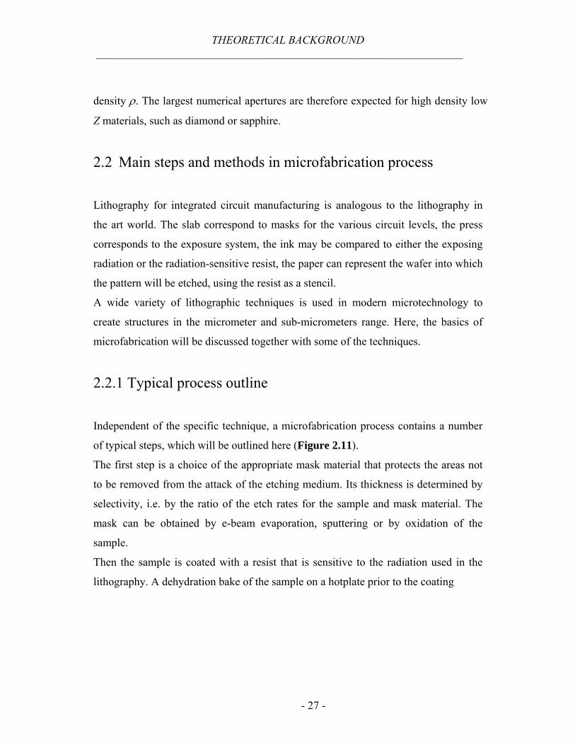
of typical steps, which will be outlined here (Figure 2.11).
The first step is a choice of the appropriate mask material that protects the areas not
to be removed from the attack of the etching medium. Its thickness is determined by
selectivity, i.e. by the ratio of the etch rates for the sample and mask material. The
mask can be obtained by e-beam evaporation, sputtering or by oxidation of the
sample.
Then the sample is coated with a resist that is sensitive to the radiation used in the
lithography. A dehydration bake of the sample on a hotplate prior to the coating
THEORETICAL BACKGROUND _________________________________________________________________
- 28 -
ResistMask
Substrate
2) Lithography
3) Development
1) Sample preparation
4) Mask etching
5) Substrate etching
Figure 2.11. Principle steps of a microfabrication process.
enhances the adhesion of the resist on the substrate. After this, the sample is
transferred to a spin-coater, where the liquid resist is spread homogeneously onto the
surface. The thickness of the layer depends on the viscosity of the liquid and on the
rotary frequency of the sample. The resist is finally baked on a hotplate or in an oven
to drive out all remaining solvent.
The second step is the exposure of the resist (actual lithographic step). Here, the
structure is defined in the resist. This can be done by either moving the beam only
over selected parts of the resist (e-beam lithography, figure 2.12a) or by a mask
shadowing some areas of the resist from the radiation (optical or x-ray lithography,
figure 2.12b).
THEORETICAL BACKGROUND _________________________________________________________________
- 29 -
a) Moving beam
ResistSubstrate
b) Radiation
MaskResist
Substrate
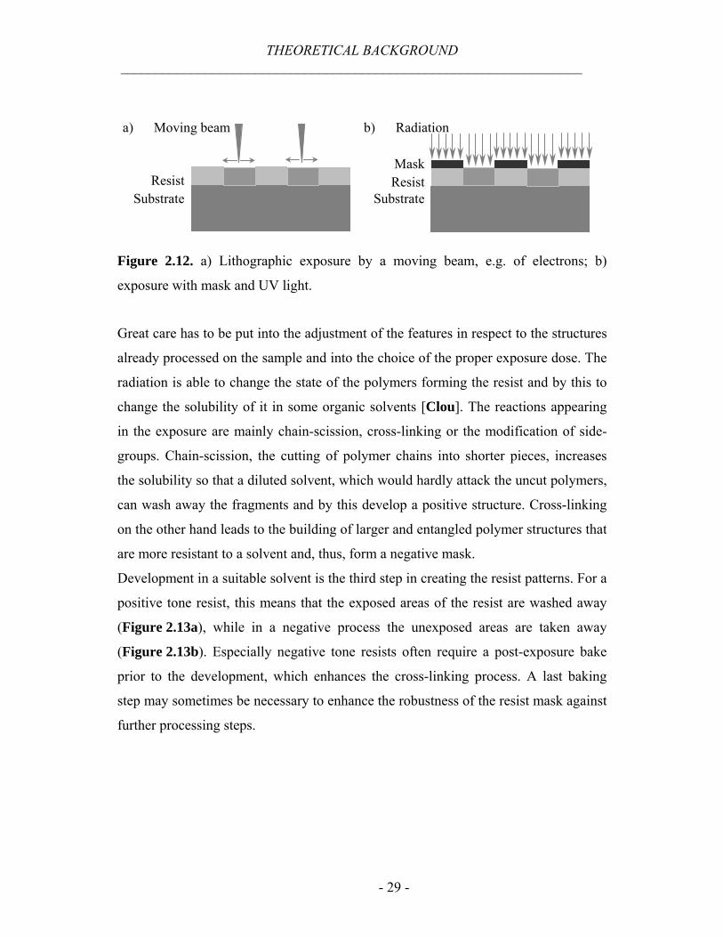
Figure 2.12. a) Lithographic exposure by a moving beam, e.g. of electrons; b)
exposure with mask and UV light.
Great care has to be put into the adjustment of the features in respect to the structures
already processed on the sample and into the choice of the proper exposure dose. The
radiation is able to change the state of the polymers forming the resist and by this to
change the solubility of it in some organic solvents [Clou]. The reactions appearing
in the exposure are mainly chain-scission, cross-linking or the modification of side-
groups. Chain-scission, the cutting of polymer chains into shorter pieces, increases
the solubility so that a diluted solvent, which would hardly attack the uncut polymers,
can wash away the fragments and by this develop a positive structure. Cross-linking
on the other hand leads to the building of larger and entangled polymer structures that
are more resistant to a solvent and, thus, form a negative mask.
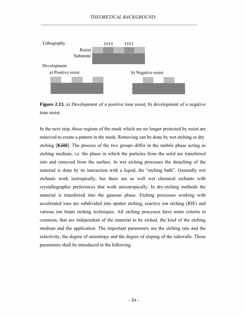
Development in a suitable solvent is the third step in creating the resist patterns. For a
positive tone resist, this means that the exposed areas of the resist are washed away
(Figure 2.13a), while in a negative process the unexposed areas are taken away
(Figure 2.13b). Especially negative tone resists often require a post-exposure bake
prior to the development, which enhances the cross-linking process. A last baking
step may sometimes be necessary to enhance the robustness of the resist mask against
further processing steps.
THEORETICAL BACKGROUND _________________________________________________________________
- 30 -
LithographyResist
Substrate
Developmenta) Positive resist b) Negative resist
Figure 2.13. a) Development of a positive tone resist; b) development of a negative
tone resist.
In the next step, those regions of the mask which are no longer protected by resist are
removed to create a pattern in the mask. Removing can be done by wet etching or dry
etching [Köhl]. The process of the two groups differ in the mobile phase acting as
etching medium, i.e. the phase in which the particles from the solid are transferred
into and removed from the surface. In wet etching processes the detaching of the
material is done by its interaction with a liquid, the “etching bath”. Generally wet
etchants work isotropically, but there are as well wet chemical etchants with
crystallographic preferences that work anisotropically. In dry-etching methods the
material is transferred into the gaseous phase. Etching processes working with
accelerated ions are subdivided into sputter etching, reactive ion etching (RIE) and
various ion beam etching techniques. All etching processes have some criteria in
common, that are independent of the material to be etched, the kind of the etching
medium and the application. The important parameters are the etching rate and the
selectivity, the degree of anisotropy and the degree of sloping of the sidewalls. These
parameters shall be introduced in the following.
THEORETICAL BACKGROUND _________________________________________________________________
- 31 -
Target
Vacuum pump
Cathode
Electron beamVapour
Crucible
Vacuum
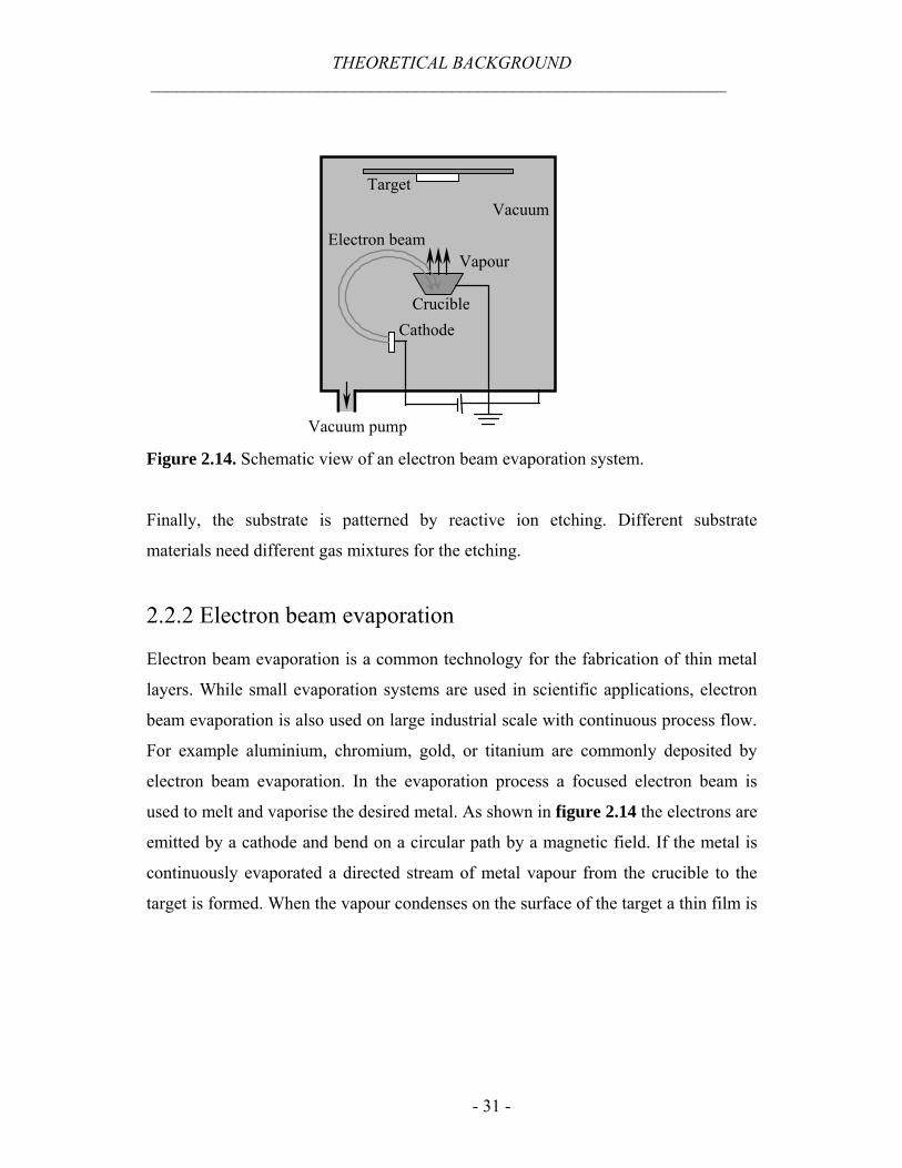
Figure 2.14. Schematic view of an electron beam evaporation system.
Finally, the substrate is patterned by reactive ion etching. Different substrate
materials need different gas mixtures for the etching.
2.2.2 Electron beam evaporation Electron beam evaporation is a common technology for the fabrication of thin metal
layers. While small evaporation systems are used in scientific applications, electron
beam evaporation is also used on large industrial scale with continuous process flow.
For example aluminium, chromium, gold, or titanium are commonly deposited by
electron beam evaporation. In the evaporation process a focused electron beam is
used to melt and vaporise the desired metal. As shown in figure 2.14 the electrons are
emitted by a cathode and bend on a circular path by a magnetic field. If the metal is
continuously evaporated a directed stream of metal vapour from the crucible to the
target is formed. When the vapour condenses on the surface of the target a thin film is
THEORETICAL BACKGROUND _________________________________________________________________
- 32 -
created. Thus the three steps of electron beam evaporation process are: evaporation,
transportation and condensation. The whole evaporation system has to be maintained
under vacuum (10-5 to 10-9 mbar depending on the deposited material) to prevent
contamination of the evaporated layers. Two different evaporation system have been
used for this work. One of them was designed and build at II. Physikalisches Institut
and is mainly used for the evaporation of chromium, gold, and titanium films. The
other one was built at the Forschungszentrum Jülich. This system is suitable for the
evaporation of thicker films and was hence used for the deposition of aluminium
layers with thickness up to 1 µm.
2.2.3 Electron beam lithography
Electron beam lithography has the possibility of higher resolution than optical
lithography because of the small wavelength of the 10-50 keV electrons. The
resolution in electron lithography system is not limited by diffraction but rather by
electron scattering in the target materials including the resist and by various
aberration of the electron optics. Scanning electron beam pattern generators have
been under development for more than 30 years and were derived from the scanning
electron microscope. Because of the serial nature of the pattern writing, throughput is
much lower than for optical systems. However, a wide variety of applications is
available in the pattern-generating function for electron beam lithography, such as
mask fabrication for optical or x-ray lithography, direct writing on the wafers, and
direct reaction with some materials on the substrate. A short outline of the electron
beam lithography will be given here. More details can be found in [Chan]. The whole
setup used for generation, focusing and targeting of the electrons is usually referred to
THEORETICAL BACKGROUND _________________________________________________________________
- 33 -
Sample chamber
Electron gun
Condenser lenses
Beam blanking
Objective lens
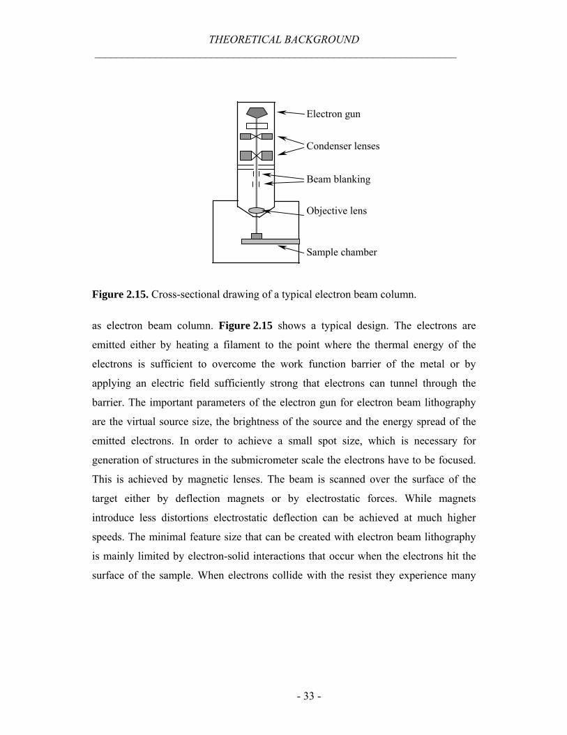
Figure 2.15. Cross-sectional drawing of a typical electron beam column.
as electron beam column. Figure 2.15 shows a typical design. The electrons are
emitted either by heating a filament to the point where the thermal energy of the
electrons is sufficient to overcome the work function barrier of the metal or by
applying an electric field sufficiently strong that electrons can tunnel through the
barrier. The important parameters of the electron gun for electron beam lithography
are the virtual source size, the brightness of the source and the energy spread of the
emitted electrons. In order to achieve a small spot size, which is necessary for
generation of structures in the submicrometer scale the electrons have to be focused.
This is achieved by magnetic lenses. The beam is scanned over the surface of the
target either by deflection magnets or by electrostatic forces. While magnets
introduce less distortions electrostatic deflection can be achieved at much higher
speeds. The minimal feature size that can be created with electron beam lithography
is mainly limited by electron-solid interactions that occur when the electrons hit the
surface of the sample. When electrons collide with the resist they experience many
THEORETICAL BACKGROUND _________________________________________________________________
- 34 -
small angle scattering events, which broaden the initial beam diameter. Electrons
even penetrate through the resist into the substrate where large angle scattering
(backscattering) takes place. Therefore, the electron dose impinging on a given
feature is dependent on the scattering from other features nearby. Larger features
receive higher doses than smaller features. This effect is known as proximity effect.
As the amount of scattering is dependent on the energy of the impinging electrons the
proximity effect is energy dependent. Different methods have been developed,
ranging from simply adjusting the overall dose, changing the electron energy to
sophisticated dose modulation or mask adjustment techniques. Today, there is a large
number of electron beam lithography (EBL) systems available. Modifications range
from scanning electron microscopes with integrated EBL to dedicated EBL systems
which are mainly used in industry. In this work two different EBL systems were used.
One of them is a Philips XL30 scanning electron microscope with an EBL system
from Raith Elphy. The other one is a Leica EBPG-5HR designed for high resolution
fabrication.
2.2.4 Methods of etching
Wet chemical etching
Wet chemical etching methods for pattering play a key role in microtechniques. They
are distinguished from dry etching methods by essentially greater selectivity. This
selectivity is due to the specific interactions between components of the liquid and the
solid, determining the reaction rate. When dissolving a solid material in a liquid, the
components of the solid are transferred into the liquid phase. For this the binding
forces between the particles of the solid have to be overcome. The components of the
THEORETICAL BACKGROUND _________________________________________________________________
- 35 -
solid are changed into soluble chemical compounds, which are transported by
diffusion and convection off the surface into the interior of the solution. In many
cases the solvent molecules themselves form a shell, the solvate shell around the
dissolved particles. The solvated particles formed in that way are very mobile by
diffusion in the solvent. Three factors, temperature, viscosity, and convection of the
liquid, are unspecific parameters influencing all etching rates of a system in the same
direction, in contrast to the specifically reacting components of an etchant. By
varying the concentration of the rate determining components the etch rate can be
adapted in a wide range.
Dry etching – reactive ion etching (RIE) The particle densities and hence the concentration of reactive chemical components
are much lower in the gas phase than in the liquid phase. On the other hand, there are
more efficient transport mechanisms in the gas phase. In the RIE-process cations are
produced from reactive gases, which are accelerated with high energy to the substrate
and which can react chemically with substrate material. Choosing adequate etching
gases and excitation conditions, the specific advantages of plasma etching (high
selectivity) and of sputter-etching (anisotropic removal) can be combined in the RIE-
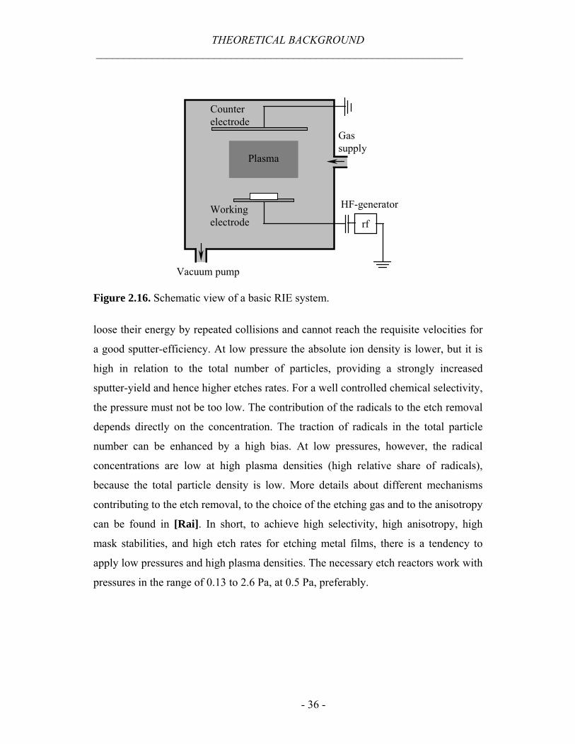
process. The RIE-plasma can be generated in a planar reactor. The typical
construction of the planar plate reactor is shown in figure 2.16. The total power is
determined by the high frequency-amplitudes, and the removal conditions in the RIE
can be influenced by a superimposed direct current-voltage. By this voltage the
electrical field can be enhanced in front of the working electrode. In this field the
electrons are accelerated to higher energies. The ion energy is limited by collisions in
the gas volume. At too high particle densities (higher working pressure) the ions
THEORETICAL BACKGROUND _________________________________________________________________
- 36 -
Vacuum pump
Counterelectrode
Gas supply
Workingelectrode rf
HF-generator
Plasma
Figure 2.16. Schematic view of a basic RIE system.
loose their energy by repeated collisions and cannot reach the requisite velocities for
a good sputter-efficiency. At low pressure the absolute ion density is lower, but it is
high in relation to the total number of particles, providing a strongly increased
sputter-yield and hence higher etches rates. For a well controlled chemical selectivity,
the pressure must not be too low. The contribution of the radicals to the etch removal
depends directly on the concentration. The traction of radicals in the total particle
number can be enhanced by a high bias. At low pressures, however, the radical
concentrations are low at high plasma densities (high relative share of radicals),
because the total particle density is low. More details about different mechanisms
contributing to the etch removal, to the choice of the etching gas and to the anisotropy
can be found in [Rai]. In short, to achieve high selectivity, high anisotropy, high
mask stabilities, and high etch rates for etching metal films, there is a tendency to
apply low pressures and high plasma densities. The necessary etch reactors work with
pressures in the range of 0.13 to 2.6 Pa, at 0.5 Pa, preferably.
- 37 -
Chapter 3
Optimised fabrication of silicon parabolic nanofocusing x-ray lenses (NFLs) In the last years several papers have been published addressing the question of an
ultimate limit of the focal size which can be achieved in x-ray optics [Schr2], [Ber].
Up to now, the theoretical limit has not yet be reached experimentally. For refractive
lenses in the form of parabolic cylinders, etching of trenches often results in not
perfectly vertical sidewalls and this implies a blurred focus. For Fresnel zone plates,
the resolution is given by the width of the smallest outer zone, values under 60 nm are
difficult to achieve. This chapter describes a significantly improved deep reactive ion
etching process for the fabrication of nanofocusing parabolic refractive lenses made of
silicon.
3.1 Design of silicon NFLs For the purpose of imaging with hard x-rays in the energy range from 10 to 100 keV
parabolic refractive beryllium and aluminium lenses are excellently suited because
OPTIMISED FABRICATION OF Si NFLs _________________________________________________________________
- 38 -
500 µm
100 µm
a) b)
c) d) slits
NFLs
d
l
R
single lens
NFL
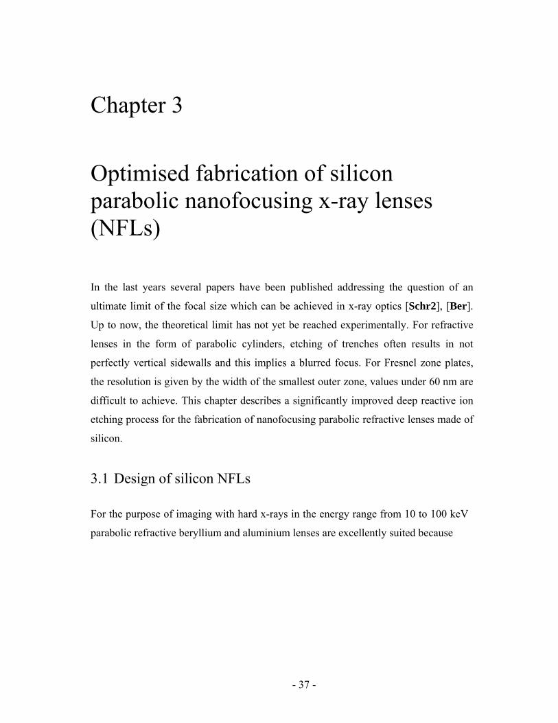
Figure 3.1. Nanofocusing refractive x-ray lenses made of silicon: a) 4 inch silicon
wafer with 60 lens blocks. Horizontally, the number N of single lenses in one NFL is
varied. Starting from the right, the blocks contain NFLs with 35, 50, 71, 100, and 142
single lenses each. From the bottom to the top, different mask corrections from 0 to
500 nm in steps of 100 nm are applied; b) SEM micrograph of one block. Each block
has 21 NFLs with different radii of curvature from 1.0 µm to 5.0 µm in steps of
0.2 µm; c) SEM micrograph of a part of a block. Different numbers of trenches
between two lenses are used to identify a lens with a given curvature; d) Using a high
resolution x-ray camera one is able to easily find and align a given lens.
OPTIMISED FABRICATION OF Si NFLs _________________________________________________________________
- 39 -
they have rotational symmetry about the optical axis [Len2]. This results in images
free of spherical aberration and other distortions. However, for the generation of a
very small focal spot, nanofocusing refractive lenses (NFLs) with crossed parabolic
cylinder symmetry are more appropriate [Schr1]. They are made of a number single
parabolic cylinder lenses etched behind each other into the lens material (Figure 3.1).
The most outstanding feature of these lenses is their small radius of curvature R,
(Figure 3.1c) that lies in the micrometer range and leads to focal distances in the
centimetre range for hard x-rays [Schr1]. In order to provide flexibility concerning
the choice of the focal length and of the photon energy, different numbers of single
lenses in one nanofocusing lens (NFL) and different radii of curvatures are required.
Figure 3.1 shows typical NFLs made of silicon. The number of single lenses in
different NFLs was 35, 50, 71, 100, 142 (Figure 3.1a). The radius of curvature R
varies between NFLs in a block from 1 µm to 5 µm with steps of 0.2 µm, resulting in
21 different NFLs per block (Figure 3.1 b). The thickness d of a single lens on the
optical axis (cf. Fig. 1c) is about 5 µm and its overall length l is 85 µm. Different
numbers of trenches between two NFLs are used to identify a lens with a given
curvature (Figures 3.1c and 3.1d.). Due to a proximity effect by e-beam lithography
and underetching of the mask in the deep reactive ion etching step the lithographic
process leads to slight deviations between the electronic mask for electron beam
lithography and the resulting final shape of the lenses. This deviation was modeled as
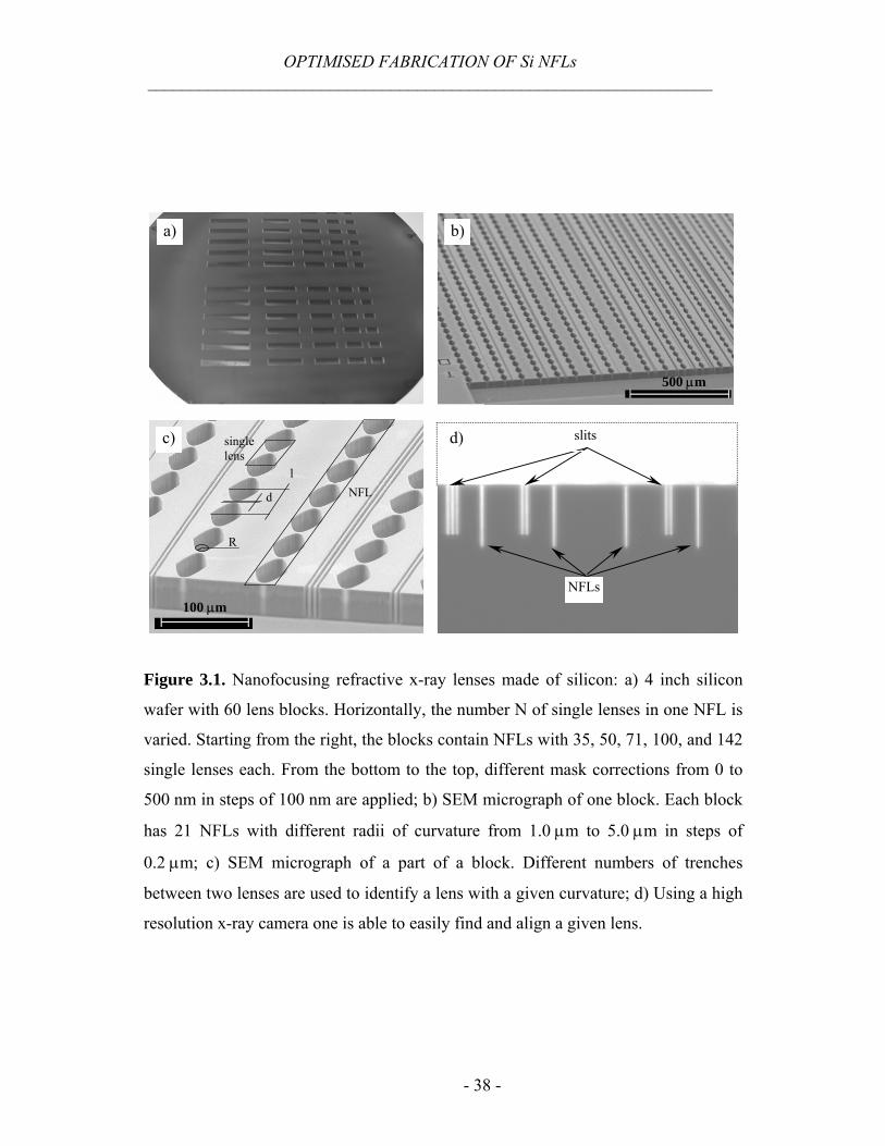
a homogeneous shift (Figure 3.2). As the size of this shift was not apriori known, six
sets of lens blocks with different corrections were written (Figure 3.1a). The mask
corrections were varied from 0 to 500 nm in steps of 100 nm.
OPTIMISED FABRICATION OF Si NFLs _________________________________________________________________
- 40 -
correction
corre
ctio
n
Written mask Desired parabolas
Figure 3.2. Schematic representation of the correction of a written mask for e-beam
lithography. For exposure each point on the parabola was transferred to the inside by
an amount equal to the correction. Corrections were 0, 100, 200, 300, 400 and
500 nm.
3.2 Fabrication of silicon NFLs
The main fabrication process for NFLs made of silicon is deep trench reactive ion
etching. The process used here is a switched process, known as Bosch process, time
multiplexed deep etching [Ayón] or gas chopping etching technique [Vol]. In general,
it consists of a cyclic repetition of a passivation phase, which protects sidewalls from
being etched, and an etch phase which is isotropic. Cryogenic etching [Boer] could
be an alternative, but was not available. Nowadays, the multiplex process is
successfully used in MEMS industry, however its application for the fabrication of x-
ray optics needs careful selection of process parameters which are described below.
OPTIMISED FABRICATION OF Si NFLs _________________________________________________________________
- 41 -
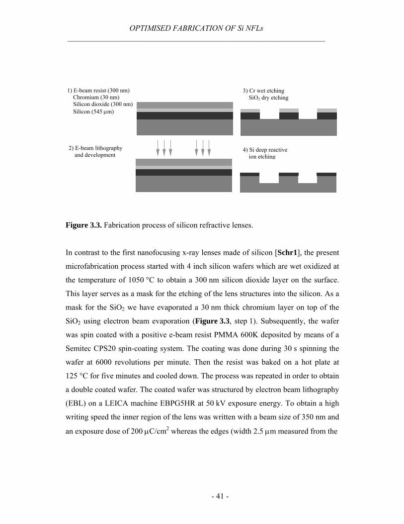
1) E-beam resist (300 nm) Chromium (30 nm) Silicon dioxide (300 nm) Silicon (545 µm)
2) E-beam lithography and development
3) Cr wet etching SiO2 dry etching
4) Si deep reactive ion etching
Figure 3.3. Fabrication process of silicon refractive lenses.
In contrast to the first nanofocusing x-ray lenses made of silicon [Schr1], the present
microfabrication process started with 4 inch silicon wafers which are wet oxidized at
the temperature of 1050 °C to obtain a 300 nm silicon dioxide layer on the surface.
This layer serves as a mask for the etching of the lens structures into the silicon. As a
mask for the SiO2 we have evaporated a 30 nm thick chromium layer on top of the
SiO2 using electron beam evaporation (Figure 3.3, step 1). Subsequently, the wafer
was spin coated with a positive e-beam resist PMMA 600K deposited by means of a
Semitec CPS20 spin-coating system. The coating was done during 30 s spinning the
wafer at 6000 revolutions per minute. Then the resist was baked on a hot plate at
125 °C for five minutes and cooled down. The process was repeated in order to obtain
a double coated wafer. The coated wafer was structured by electron beam lithography
(EBL) on a LEICA machine EBPG5HR at 50 kV exposure energy. To obtain a high
writing speed the inner region of the lens was written with a beam size of 350 nm and
an exposure dose of 200 µC/cm2 whereas the edges (width 2.5 µm measured from the
OPTIMISED FABRICATION OF Si NFLs _________________________________________________________________
- 42 -
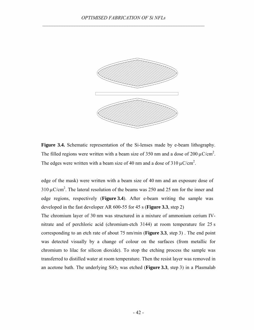
Figure 3.4. Schematic representation of the Si-lenses made by e-beam lithography.
The filled regions were written with a beam size of 350 nm and a dose of 200 µC/cm2.
The edges were written with a beam size of 40 nm and a dose of 310 µC/cm2.
edge of the mask) were written with a beam size of 40 nm and an exposure dose of
310 µC/cm2. The lateral resolution of the beams was 250 and 25 nm for the inner and
edge regions, respectively (Figure 3.4). After e-beam writing the sample was
developed in the fast developer AR 600-55 for 45 s (Figure 3.3, step 2)
The chromium layer of 30 nm was structured in a mixture of ammonium cerium IV-
nitrate and of perchloric acid (chromium-etch 3144) at room temperature for 25 s
corresponding to an etch rate of about 75 nm/min (Figure 3.3, step 3) . The end point
was detected visually by a change of colour on the surfaces (from metallic for
chromium to lilac for silicon dioxide). To stop the etching process the sample was
transferred to distilled water at room temperature. Then the resist layer was removed in
an acetone bath. The underlying SiO2 was etched (Figure 3.3, step 3) in a Plasmalab
OPTIMISED FABRICATION OF Si NFLs _________________________________________________________________
- 43 -
System 100 ICP180 etch tool from Oxford Instruments. In this step, a pressure of 0.43
Pa, ICP power of 1300 W and rf bias of 50 W were used. The process gas mixture
contained 15 sccm trifluormethane (CHF3) and 18 sccm tetraflourmethane (CF4). The
etch time was 6 min.
Next, the silicon etch requires careful selection of process parameters in order to
achieve vertical sidewalls with minimum sidewall roughness, minimum underetch and
high etch depths. Various attempts for obtaining smooth vertical sidewalls are known:
additional flow of argon during the etch phase, reduced cycle time, variation in
switching between passivation and etching (overlap) [Liu], etch depth dependent
changing parameters (multi step process, parameter ramping) [Chab], [Hop]. To
obtain a large trench depth a high selectivity is essential. Known possibilities to
increase the mask selectivity are higher etch pressure (promoting micrograss), reduced
ion energy, reduced substrate temperature (affecting passivation film quality) or
shifting the etch balance towards passivation (leading to vertical striations on the
sidewalls). Another possibility is the use of an aperture inside the reaction chamber
which mainly alters the ion flux thereby enabling higher etch selectivity. Prediction of
etch results in dependence of the process parameters is difficult as substrate properties
change, such as the amount of silicon area to be etched or the trench width.
Due to a limited number of samples the starting point within parameter space should
be a robust recipe and, at the same time, as close as possible to the optimum to be
achieved. Therefore, a proven recipe with relatively short cycle time and good
selectivity was chosen. Deep silicon etches (Figure 3.3, step 4) were performed at a
Multiplex ICP standard rate etch tool from Surface Technology Instruments equipped
with an aperture of 120 mm diameter. Conditioning runs were performed before the
main etches. Process parameters used were 6 s etch phase duration, 130 sccm
OPTIMISED FABRICATION OF Si NFLs _________________________________________________________________
- 44 -
a)
0
50
100
150
µm150100 50 0 µm
80
60
40
20
0
b)
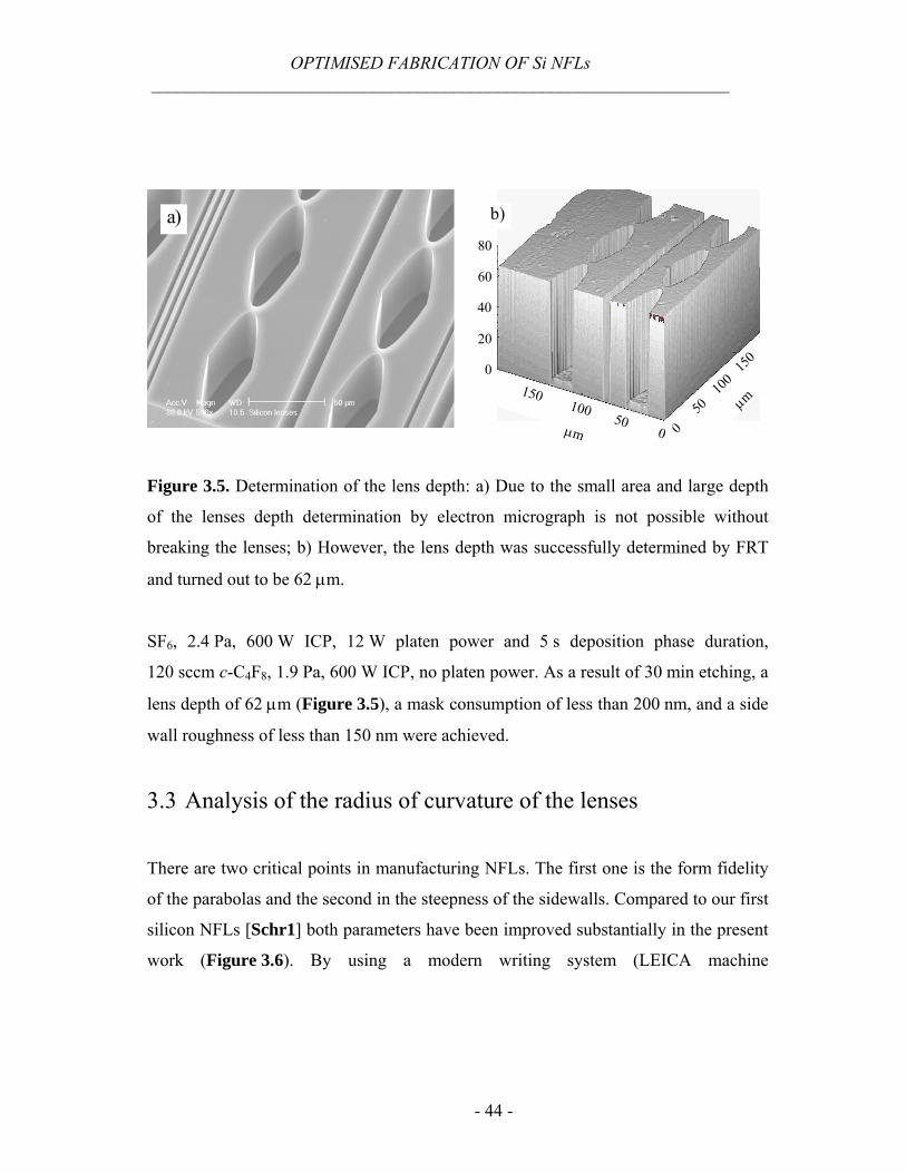
Figure 3.5. Determination of the lens depth: a) Due to the small area and large depth
of the lenses depth determination by electron micrograph is not possible without
breaking the lenses; b) However, the lens depth was successfully determined by FRT
and turned out to be 62 µm.
SF6, 2.4 Pa, 600 W ICP, 12 W platen power and 5 s deposition phase duration,
120 sccm c-C4F8, 1.9 Pa, 600 W ICP, no platen power. As a result of 30 min etching, a
lens depth of 62 µm (Figure 3.5), a mask consumption of less than 200 nm, and a side
wall roughness of less than 150 nm were achieved.
3.3 Analysis of the radius of curvature of the lenses
There are two critical points in manufacturing NFLs. The first one is the form fidelity
of the parabolas and the second in the steepness of the sidewalls. Compared to our first
silicon NFLs [Schr1] both parameters have been improved substantially in the present
work (Figure 3.6). By using a modern writing system (LEICA machine
OPTIMISED FABRICATION OF Si NFLs _________________________________________________________________
- 45 -
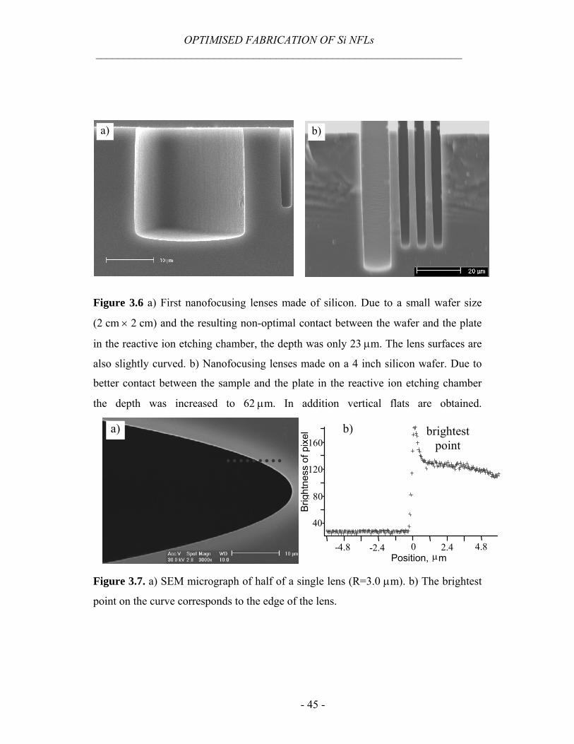
a) b)
Figure 3.6 a) First nanofocusing lenses made of silicon. Due to a small wafer size
(2 cm × 2 cm) and the resulting non-optimal contact between the wafer and the plate
in the reactive ion etching chamber, the depth was only 23 µm. The lens surfaces are
also slightly curved. b) Nanofocusing lenses made on a 4 inch silicon wafer. Due to
better contact between the sample and the plate in the reactive ion etching chamber
the depth was increased to 62 µm. In addition vertical flats are obtained.
Brig
htne
ss o
f pix
el
- -Position, µm
80
120
160
40
-4.8 -2.4 0 2.4 4.8
a) b) brightest point
Figure 3.7. a) SEM micrograph of half of a single lens (R=3.0 µm). b) The brightest
point on the curve corresponds to the edge of the lens.
OPTIMISED FABRICATION OF Si NFLs _________________________________________________________________
- 46 -
EBPG5HR) the 4 inch wafer processing has become possible. A replacement of small
samples (sample size of 2 cm x 2 cm) by 10 cm wafers led to an increased etching
depth (from 23 µm to 62 µm) and an improved steepness of the sidewalls.
In order to determine any deviation between the electronic mask for e-beam
lithography and the resulting final shape of the lenses as well as to quantify the quality
of the new NFLs we have made SEM micrographs. From these micrographs, the lens
shape was extracted by a series of line scans across the edge of the lens, as indicated in
figure 3.7. The intensity of the reflected electrons increases drastically when going
from the bottom to the top of a trench. We observe a distinct intensity peak at the edge
itself (Figure 3.7b). The position of this peak was identified with the position of the
edge. The shape of a parabola in the vicinity of the apex is shown in fig. 3.8a, together
with a parabola fitted to the data. In this way, from the e-beam lithography data the
radius of curvature R of 3.0 µm was expected. The lenses with the corresponding value
of radius of curvature were identified. The deviation between the electronic mask for
e-beam lithography and the resulting final shape of the lenses is close to 270 nm.
R=3.0 µm
-4.8 -2.4 0 2.4 4.8Position, µm
-4.8 -2.4 0 2.4 4.8Position, µm
0
-60
-120
60
120
Diff
eren
ce, n
m
36
37.2
38.4
39.6
40.8
Posi
tion,
µm
a) b)
edge of lens fit of parabola
Figure 3.8. a) Fit of the lens shape to a parabolic function. b) The difference between
the lens shape and parabolic function shows minimal discrepancy.
OPTIMISED FABRICATION OF Si NFLs _________________________________________________________________
- 47 -
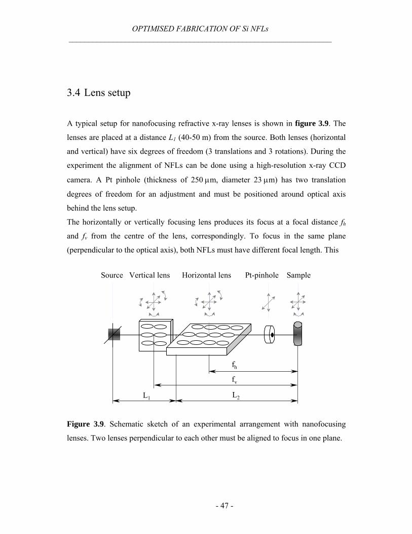
3.4 Lens setup
A typical setup for nanofocusing refractive x-ray lenses is shown in figure 3.9. The
lenses are placed at a distance L1 (40-50 m) from the source. Both lenses (horizontal
and vertical) have six degrees of freedom (3 translations and 3 rotations). During the
experiment the alignment of NFLs can be done using a high-resolution x-ray CCD
camera. A Pt pinhole (thickness of 250 µm, diameter 23 µm) has two translation
degrees of freedom for an adjustment and must be positioned around optical axis
behind the lens setup.
The horizontally or vertically focusing lens produces its focus at a focal distance fh
and fv from the centre of the lens, correspondingly. To focus in the same plane
(perpendicular to the optical axis), both NFLs must have different focal length. This
Source Vertical lens Horizontal lens Pt-pinhole Sample
fh
fv
L2L1
Figure 3.9. Schematic sketch of an experimental arrangement with nanofocusing
lenses. Two lenses perpendicular to each other must be aligned to focus in one plane.
OPTIMISED FABRICATION OF Si NFLs _________________________________________________________________
- 48 -
is achieved by NFLs with a different number of lenses, e.g N=70 for the vertically
and N=100 for the horizontally focusing lenses. Then the fine alignment is done by
the different radii of curvature R for the lens arrays. The specific values to be chosen
depend on the x-ray energy and other experimental details.
The sample is placed at a distance L1+L2 from the source. At the same time, this
distance L1+L2 serves as focal plane for both lenses. The sample stage needs three
translational degrees of freedom for the experiments with nanofocusing or
nanodiffraction and an extra rotational degree of freedom for experiments with
fluorescence tomography.
3.5 Focusing properties of Si NFLs
The silicon nanofocusing lenses were tested at the low-β beamline ID13 of the
European Synchrotron Radiation Facility (ESRF). The synchrotron source size was
≈ 150 µm x 60 µm full width at half maximum (FWHM) and the distance between
the source and the lens setup was 47 m. Two different energies were used. In the first
case, at 21 keV, an NFL with N=100, a total length of 8.4 mm and a radius of
curvature R=2.0 µm was used to focus the beam horizontally. The image distance L2h
from the centre of the NFL to the focal spot was 10.7 mm. For the vertical focusing a
NFL with N=71 was used what corresponds to a lens length of 6.0 mm. The radius of
curvature R for the vertical direction was determined to be 2.86 µm. This yields an
image distance L2v of 19.4 mm.
The vertically focusing NFL was placed in front of the horizontally focusing one to
get the same focal plane for both lenses (Figure 3.10). In the focus, at 200 mA ring
current, a flux Φf=1.7⋅108 ph/s and a lateral size of 47 nm by 55 nm were measured as
OPTIMISED FABRICATION OF Si NFLs _________________________________________________________________
- 49 -
(1)(1)
(2)(2)(3)(3)
(4)(4)
(5)(5) (6)(6)(7)(7) (8)(8)
X-rays
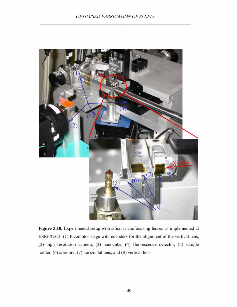
Figure 3.10. Experimental setup with silicon nanofocusing lenses as implemented at
ESRF/ID13. (1) Picomotor stage with encoders for the alignment of the vertical lens,
(2) high resolution camera, (3) nanocube, (4) fluorescence detector, (5) sample
holder, (6) aperture, (7) horizontal lens, and (8) vertical lens.
OPTIMISED FABRICATION OF Si NFLs _________________________________________________________________
- 50 -
vertical position, nm horizontal position, nm
inte
nsity
, a.u
.
inte
nsity
, a.u
.
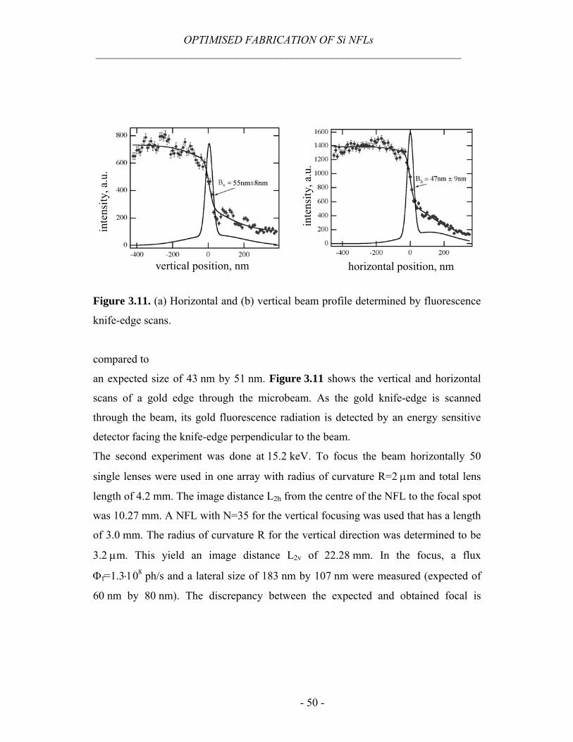
5555nmnm±±8nm8nm
Figure 3.11. (a) Horizontal and (b) vertical beam profile determined by fluorescence
knife-edge scans.
compared to
an expected size of 43 nm by 51 nm. Figure 3.11 shows the vertical and horizontal
scans of a gold edge through the microbeam. As the gold knife-edge is scanned
through the beam, its gold fluorescence radiation is detected by an energy sensitive
detector facing the knife-edge perpendicular to the beam.
The second experiment was done at 15.2 keV. To focus the beam horizontally 50
single lenses were used in one array with radius of curvature R=2 µm and total lens
length of 4.2 mm. The image distance L2h from the centre of the NFL to the focal spot
was 10.27 mm. A NFL with N=35 for the vertical focusing was used that has a length
of 3.0 mm. The radius of curvature R for the vertical direction was determined to be
3.2 µm. This yield an image distance L2v of 22.28 mm. In the focus, a flux
Φf=1.3⋅108 ph/s and a lateral size of 183 nm by 107 nm were measured (expected of
60 nm by 80 nm). The discrepancy between the expected and obtained focal is
OPTIMISED FABRICATION OF Si NFLs _________________________________________________________________
- 51 -
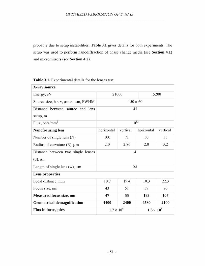
probably due to setup instabilities. Table 3.1 gives details for both experiments. The
setup was used to perform nanodiffraction of phase change media (see Section 4.1)
and micromirrors (see Section 4.2).
Table 3.1. Experimental details for the lenses test.
X-ray source
Energy, eV 21000 15200
Source size, h × v, µm × µm, FWHM 150 × 60
Distance between source and lens
setup, m
47
Flux, ph/s/mm2 1012
Nanofocusing lens horizontal vertical horizontal vertical
Number of single lens (N) 100 71 50 35
Radius of curvature (R), µm 2.0 2.86 2.0 3.2
Distance between two single lenses
(d), µm
4
Length of single lens (w), µm 85
Lens properties
Focal distance, mm 10.7 19.4 10.3 22.3
Focus size, nm 43 51 59 80
Measured focus size, nm 47 55 183 107
Geometrical demagnification 4400 2400 4580 2100
Flux in focus, ph/s 1.7 × 10⁸ 1.3 × 10⁸
- 52 -
Chapter 4 Application of silicon nanofocusing x-ray lenses The main applications of silicon nanofocusing x-ray lenses lie in scanning
microscopy and microanalysis with hard x-rays [Schr4]. They allow one to perform
x-ray analytical techniques, such as diffraction, fluorescence analysis, and absorption
spectroscopy with high spatial resolution [Schr5]. While nanofocusing lenses are
ideal for microbeam applications, they are not well suited for high quality full field
imaging because of distortions in the image due to the crossing of two cylinder lenses
with different focal lengths [Len4].
4.1 Nanodiffraction from laser modified films
Ge2Sb2Te5 is one of the materials currently used for phase change recording [Ich]. In
these materials a reversible phase change is used for rewritable optical data storage.
To write a bit, the crystalline material is locally molten by a laser beam of appropriate
intensity. Subsequent quenching into the amorphous phase can be achieved by
avoiding recrystallization due to rapid cooling. To erase a bit, the amorphous area has
APPLICATION OF Si NFLs _________________________________________________________________
- 53 -
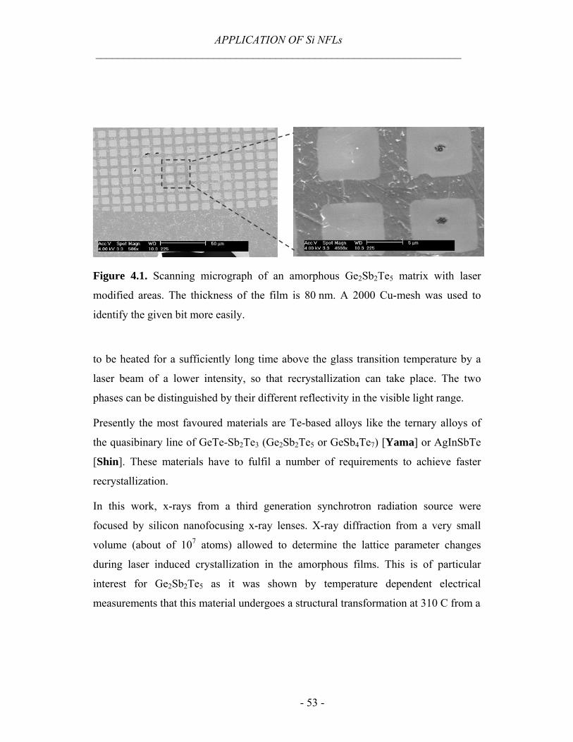
Figure 4.1. Scanning micrograph of an amorphous Ge2Sb2Te5 matrix with laser
modified areas. The thickness of the film is 80 nm. A 2000 Cu-mesh was used to
identify the given bit more easily.
to be heated for a sufficiently long time above the glass transition temperature by a
laser beam of a lower intensity, so that recrystallization can take place. The two
phases can be distinguished by their different reflectivity in the visible light range.
Presently the most favoured materials are Te-based alloys like the ternary alloys of
the quasibinary line of GeTe-Sb2Te3 (Ge2Sb2Te5 or GeSb4Te7) [Yama] or AgInSbTe
[Shin]. These materials have to fulfil a number of requirements to achieve faster
recrystallization.
In this work, x-rays from a third generation synchrotron radiation source were
focused by silicon nanofocusing x-ray lenses. X-ray diffraction from a very small
volume (about of 107 atoms) allowed to determine the lattice parameter changes
during laser induced crystallization in the amorphous films. This is of particular
interest for Ge2Sb2Te5 as it was shown by temperature dependent electrical
measurements that this material undergoes a structural transformation at 310 C from a
APPLICATION OF Si NFLs _________________________________________________________________
- 54 -
a) b)
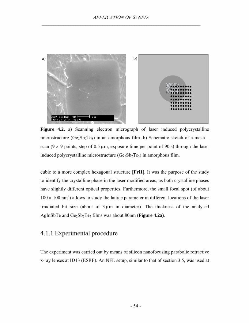
Figure 4.2. a) Scanning electron micrograph of laser induced polycrystalline
microstructure (Ge2Sb2Te5) in an amorphous film. b) Schematic sketch of a mesh –
scan (9 × 9 points, step of 0.5 µm, exposure time per point of 90 s) through the laser
induced polycrystalline microstructure (Ge2Sb2Te5) in amorphous film.
cubic to a more complex hexagonal structure [Fri1]. It was the purpose of the study
to identify the crystalline phase in the laser modified areas, as both crystalline phases
have slightly different optical properties. Furthermore, the small focal spot (of about
100 × 100 nm2) allows to study the lattice parameter in different locations of the laser
irradiated bit size (about of 3 µm in diameter). The thickness of the analysed
AgInSbTe and Ge2Sb2Te5 films was about 80nm (Figure 4.2a).
4.1.1 Experimental procedure
The experiment was carried out by means of silicon nanofocusing parabolic refractive
x-ray lenses at ID13 (ESRF). An NFL setup, similar to that of section 3.5, was used at
APPLICATION OF Si NFLs _________________________________________________________________
- 55 -
15.2 keV photon energy in the present investigation. The irradiated volume had a size
of 100 nm x 180 nm x 80 nm (0.0016 µm3) what corresponds to about 107 atoms. To
investigate the crystallization - induced changes in the interplanar spacing of the
films, two modifications of the samples were used: a polycrystalline film and a laser
induced crystalline microstructure in an amorphous film. To compare the interplanar
spacing of Ge2Sb2Te5 in the centre and along the edges of a laser induced
polycrystalline microstructure, a mesh-scan (9 x 9 points, step of 0.5 µm, exposure
time of 90 s per point) was carried out (Figure 4.2b). The diffraction patterns were
analysed with the program FIT2D [FIT2D], which was calibrated with a silicon
standard sample. The calibration of FIT2D was verified by diffraction from a
polycrystalline copper sample. Note that there are several reflexes in the centre of the
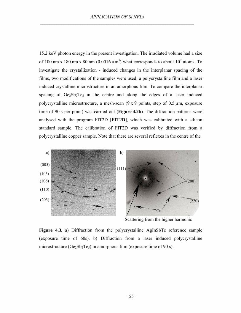
(111)
(200)
(220)
Cu
b)a)
(005)
(103)
(106)
(110)
(203)
Scattering from the higher harmonic
Figure 4.3. a) Diffraction from the polycrystalline AgInSbTe reference sample
(exposure time of 60s). b) Diffraction from a laser induced polycrystalline
microstructure (Ge2Sb2Te5) in amorphous film (exposure time of 90 s).
APPLICATION OF Si NFLs _________________________________________________________________
- 56 -
diffraction pattern (Fig. 4.3b). They are due to higher harmonic in the beam and are
neglected in the sample analysis.
4.1.2 Results Diffraction from the polycrystalline AgInSbTe reference sample (a hexagonal
structure, similar to that of Sb2Te, exposure time of 60 s) is shown in Figure 4.3a.
Corresponding interplanar spacings d are given in the Table 4.1. The experimental
and theoretical d values show reasonable agreement.
Table 4.1. Interplanar spacing for analysed samples.
AgInSbTe Ge2Sb2Te5
(hkl) d (Å)* d (Å) (hkl) d (Å)* d (Å)
005 3.44 3.43 111 3.47 3.46
103 3.10 3.06 200 3.00 3.00
106 2.25 2.24 220 2.12 2.10
110 2.14 2.10 311 1.81 1.82
*-expected value for bulk samples
The typical diffraction pattern for the laser induced crystallization samples
(Ge2Sb2Te5, exposure time of 90 s) is shown in Figure 4.3b. The corresponding d
values are listed in Table 4.1. Measurement of the diffracted intensities shows that
the crystal structure has cubic symmetry and that the corresponding interplanar
spacing are close to the theoretical ones. Moreover, only several reflections
(Figure 4.4)
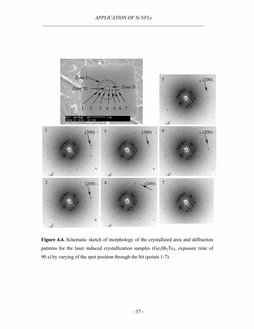
APPLICATION OF Si NFLs _________________________________________________________________
- 57 -
……. Zone IIZone III
1 2 3 4 5 6 7
6
7
Zone I
1
2
3
4
5
6
7
(200)
(200)
(200)
(200)
(200)
(200)
Figure 4.4. Schematic sketch of morphology of the crystallized area and diffraction
patterns for the laser induced crystallization samples (Ge2Sb2Te5, exposure time of
90 s) by varying of the spot position through the bit (points 1-7).
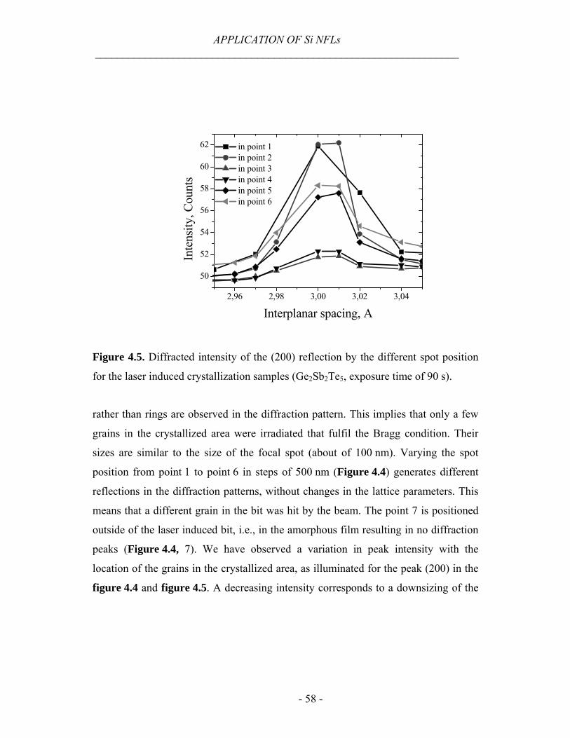
APPLICATION OF Si NFLs _________________________________________________________________
- 58 -
2,96 2,98 3,00 3,02 3,04
50
52
54
56
58
60
62 in point 1 in point 2 in point 3 in point 4 in point 5 in point 6
Inte
nsity
, Cou
nts
Interplanar spacing, A
Figure 4.5. Diffracted intensity of the (200) reflection by the different spot position
for the laser induced crystallization samples (Ge2Sb2Te5, exposure time of 90 s).
rather than rings are observed in the diffraction pattern. This implies that only a few
grains in the crystallized area were irradiated that fulfil the Bragg condition. Their
sizes are similar to the size of the focal spot (about of 100 nm). Varying the spot
position from point 1 to point 6 in steps of 500 nm (Figure 4.4) generates different
reflections in the diffraction patterns, without changes in the lattice parameters. This
means that a different grain in the bit was hit by the beam. The point 7 is positioned
outside of the laser induced bit, i.e., in the amorphous film resulting in no diffraction
peaks (Figure 4.4, 7). We have observed a variation in peak intensity with the
location of the grains in the crystallized area, as illuminated for the peak (200) in the
figure 4.4 and figure 4.5. A decreasing intensity corresponds to a downsizing of the
APPLICATION OF Si NFLs _________________________________________________________________
- 59 -
irradiated polycrystals and the smallest polycrystalline size is observed in the points 3
and 4.
4.1.4 Discussion
The results (Figure 4.5) agree with the morphology of the crystallized area where
three different zones can be distinguished [Fri2]. Zone I consists of small crystalline
grains located at the border of the surrounding amorphous matrix. This zone could be
not defined in our experiment due to the minute amount of these grains and their
small size (about of 5-25 nm). Zone II is characterized by elongated radially arranged
crystalline grains (between 0.1 and 1 µm), and Zone III with grain sizes below 0.1 µm
was qualitatively identified (Figure 4.4, top).
4.1.5 Conclusion
The applied technique makes possible an analysis of the structural transformations in
thin films of the phase change media. The illuminated volume was reduced to
180 nm × 100 nm × 80 nm, which corresponds to ~107 atoms. In general, more
diffraction patterns should be made for a reliable analysis of the experimental data. In
future, nanofocusing x-ray lenses allow for the investigation of the time dependence
of the crystallization process and for the influence of the temperature – time variation
in the laser modified areas.
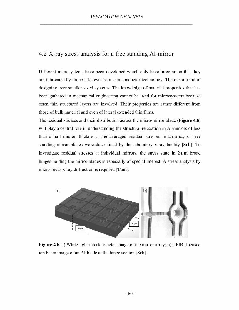
APPLICATION OF Si NFLs _________________________________________________________________
- 60 -
4.2 X-ray stress analysis for a free standing Al-mirror
Different microsystems have been developed which only have in common that they
are fabricated by process known from semiconductor technology. There is a trend of
designing ever smaller sized systems. The knowledge of material properties that has
been gathered in mechanical engineering cannot be used for microsystems because
often thin structured layers are involved. Their properties are rather different from
those of bulk material and even of lateral extended thin films.
The residual stresses and their distribution across the micro-mirror blade (Figure 4.6)
will play a central role in understanding the structural relaxation in Al-mirrors of less
than a half micron thickness. The averaged residual stresses in an array of free
standing mirror blades were determined by the laboratory x-ray facility [Sch]. To
investigate residual stresses at individual mirrors, the stress state in 2 µm broad
hinges holding the mirror blades is especially of special interest. A stress analysis by
micro-focus x-ray diffraction is required [Tam].
a) b)
Figure 4.6. a) White light interferometer image of the mirror array; b) a FIB (focused
ion beam image of an Al-blade at the hinge section [Sch].
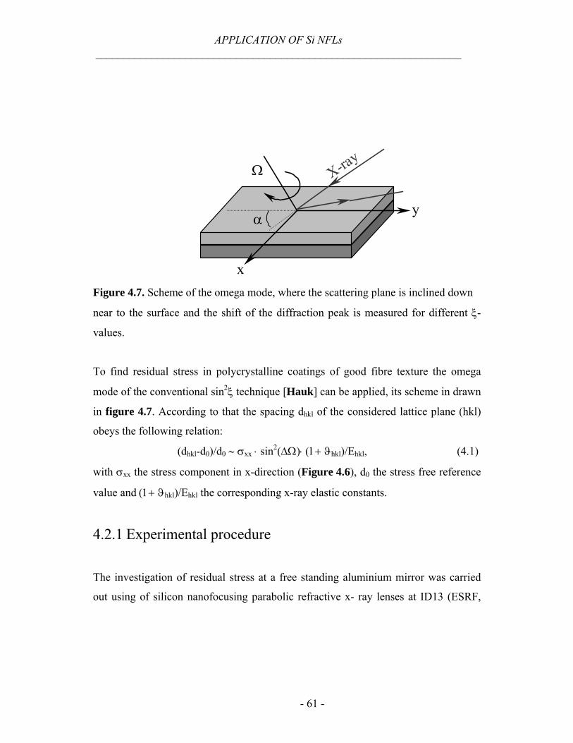
APPLICATION OF Si NFLs _________________________________________________________________
- 61 -
Ω
x
yα
X-ray
Figure 4.7. Scheme of the omega mode, where the scattering plane is inclined down
near to the surface and the shift of the diffraction peak is measured for different ξ-
values.
To find residual stress in polycrystalline coatings of good fibre texture the omega
mode of the conventional sin2ξ technique [Hauk] can be applied, its scheme in drawn
in figure 4.7. According to that the spacing dhkl of the considered lattice plane (hkl)
obeys the following relation:
(dhkl-d0)/d0 ∼ σxx ⋅ sin2(∆Ω)⋅ (1+ ϑhkl)/Ehkl, (4.1)
with σxx the stress component in x-direction (Figure 4.6), d0 the stress free reference
value and (1+ ϑhkl)/Ehkl the corresponding x-ray elastic constants.
4.2.1 Experimental procedure
The investigation of residual stress at a free standing aluminium mirror was carried
out using of silicon nanofocusing parabolic refractive x- ray lenses at ID13 (ESRF,
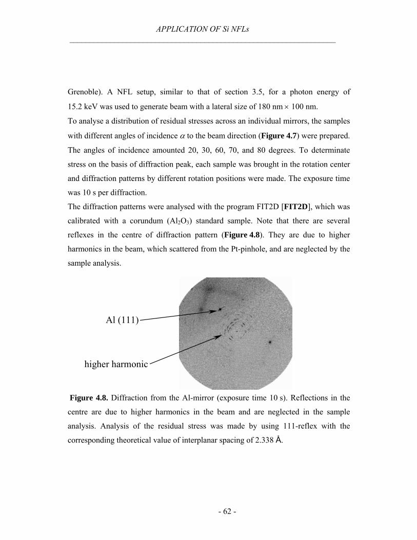
APPLICATION OF Si NFLs _________________________________________________________________
- 62 -
Grenoble). A NFL setup, similar to that of section 3.5, for a photon energy of
15.2 keV was used to generate beam with a lateral size of 180 nm × 100 nm.
To analyse a distribution of residual stresses across an individual mirrors, the samples
with different angles of incidence α to the beam direction (Figure 4.7) were prepared.
The angles of incidence amounted 20, 30, 60, 70, and 80 degrees. To determinate
stress on the basis of diffraction peak, each sample was brought in the rotation center
and diffraction patterns by different rotation positions were made. The exposure time
was 10 s per diffraction.
The diffraction patterns were analysed with the program FIT2D [FIT2D], which was
calibrated with a corundum (Al2O3) standard sample. Note that there are several
reflexes in the centre of diffraction pattern (Figure 4.8). They are due to higher
harmonics in the beam, which scattered from the Pt-pinhole, and are neglected by the
sample analysis.
higher harmonic
Al (111)
Figure 4.8. Diffraction from the Al-mirror (exposure time 10 s). Reflections in the
centre are due to higher harmonics in the beam and are neglected in the sample
analysis. Analysis of the residual stress was made by using 111-reflex with the
corresponding theoretical value of interplanar spacing of 2.338 Å.
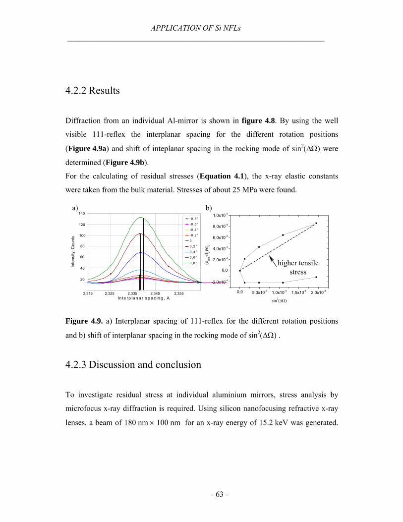
APPLICATION OF Si NFLs _________________________________________________________________
- 63 -
4.2.2 Results
Diffraction from an individual Al-mirror is shown in figure 4.8. By using the well
visible 111-reflex the interplanar spacing for the different rotation positions
(Figure 4.9a) and shift of inteplanar spacing in the rocking mode of sin2(∆Ω) were
determined (Figure 4.9b).
For the calculating of residual stresses (Equation 4.1), the x-ray elastic constants
were taken from the bulk material. Stresses of about 25 MPa were found.
a) b)
0
2 0
4 0
6 0
8 0
1 0 0
1 2 0
1 4 0
2 ,3 2 2 ,3 3 2 ,3 4 2 ,3 5 2 ,3 6 2 ,3 7
In te rp la n a r sp a c in g , A
Inte
nsity
, Cou
nts
-0 ,8 °
-0 ,6 °
-0 ,4 °
-0 ,2 °
0
0 ,2 °
0 ,4 °
0 ,6 °
0 ,8 °
2,315 2,325 2,335 2,345 2,355
140
120
100
80
60
40
20
0,0 5,0x10⁻⁵ 1,0x10⁻⁴ 1,5x10⁻⁴ 2,0x10⁻⁴
-2,0x10⁻⁴
0,0
2,0x10⁻⁴
4,0x10⁻⁴
6,0x10⁻⁴
8,0x10⁻⁴
1,0x10⁻³
(dhk
l-d0)/
d 0
sin2(∆Ω)
higher tensile stress
Figure 4.9. a) Interplanar spacing of 111-reflex for the different rotation positions
and b) shift of interplanar spacing in the rocking mode of sin2(∆Ω) .
4.2.3 Discussion and conclusion
To investigate residual stress at individual aluminium mirrors, stress analysis by
microfocus x-ray diffraction is required. Using silicon nanofocusing refractive x-ray
lenses, a beam of 180 nm × 100 nm for an x-ray energy of 15.2 keV was generated.

APPLICATION OF Si NFLs _________________________________________________________________
- 64 -
The experiment was successful carried out, stress of a free standing aluminium mirror
was calculated to be 25 MPa.
- 65 -
Chapter 5 Fabrication of nanofocusing lenses made of boron, diamond, pyrolitic graphite, and sapphire The well known microfabrication process for silicon makes this material attractive for
nanofocusing x-ray refractive lenses. On the other hand, the relatively large atomic
number (Z=14) and, as a consequence, the high absorption allow one to reach a
diffraction limit below 30 nm only for energies above 20 keV (Figure 2.9). Using a
weakly absorbing lens material (low atomic number Z), a diffraction limit below
20 nm is already conceivable at 10 keV. However, for low absorbing materials, the
numerical aperture is dominated by the geometrical aperture for the lenses with a
short focal distance and not by absorption in the outer parts of the lens, which is
usually the case for refractive lenses with large focal distance. Therefore, lithium
(Z=3), the material with lowest Z which is solid at room temperature, that is often
quoted as the best lens material due to its superior ratio σ/µ, is not well suited for this
short lens design due to its low density (0.53 g/cm3) and weak refraction. Moreover,
the handling of this material is very difficult due to its strong tendency for oxidation
[Duf]. The next suitable candidate for the fabrication of the x-ray lenses is beryllium
with the atomic number of 4 (Figure 2.9). In our group, beryllium lenses with radii of
curvature of about 200 mm [Len1] have been successfully produced. However,
beryllium may cause a health risk when Be powder is generated during the lens
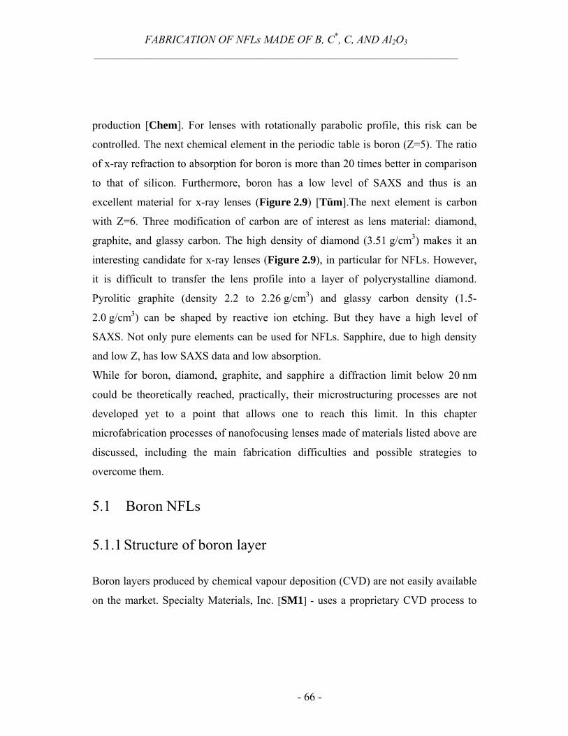
FABRICATION OF NFLs MADE OF B, C*, C, AND Al2O3
__________________________________________________________________________________________________
- 66 -
production [Chem]. For lenses with rotationally parabolic profile, this risk can be
controlled. The next chemical element in the periodic table is boron (Z=5). The ratio
of x-ray refraction to absorption for boron is more than 20 times better in comparison
to that of silicon. Furthermore, boron has a low level of SAXS and thus is an
excellent material for x-ray lenses (Figure 2.9) [Tüm].The next element is carbon
with Z=6. Three modification of carbon are of interest as lens material: diamond,
graphite, and glassy carbon. The high density of diamond (3.51 g/cm3) makes it an
interesting candidate for x-ray lenses (Figure 2.9), in particular for NFLs. However,
it is difficult to transfer the lens profile into a layer of polycrystalline diamond.
Pyrolitic graphite (density 2.2 to 2.26 g/cm3) and glassy carbon density (1.5-
2.0 g/cm3) can be shaped by reactive ion etching. But they have a high level of
SAXS. Not only pure elements can be used for NFLs. Sapphire, due to high density
and low Z, has low SAXS data and low absorption.
While for boron, diamond, graphite, and sapphire a diffraction limit below 20 nm
could be theoretically reached, practically, their microstructuring processes are not
developed yet to a point that allows one to reach this limit. In this chapter
microfabrication processes of nanofocusing lenses made of materials listed above are
discussed, including the main fabrication difficulties and possible strategies to
overcome them.
5.1 Boron NFLs
5.1.1 Structure of boron layer
Boron layers produced by chemical vapour deposition (CVD) are not easily available
on the market. Specialty Materials, Inc. [SM1] - uses a proprietary CVD process to
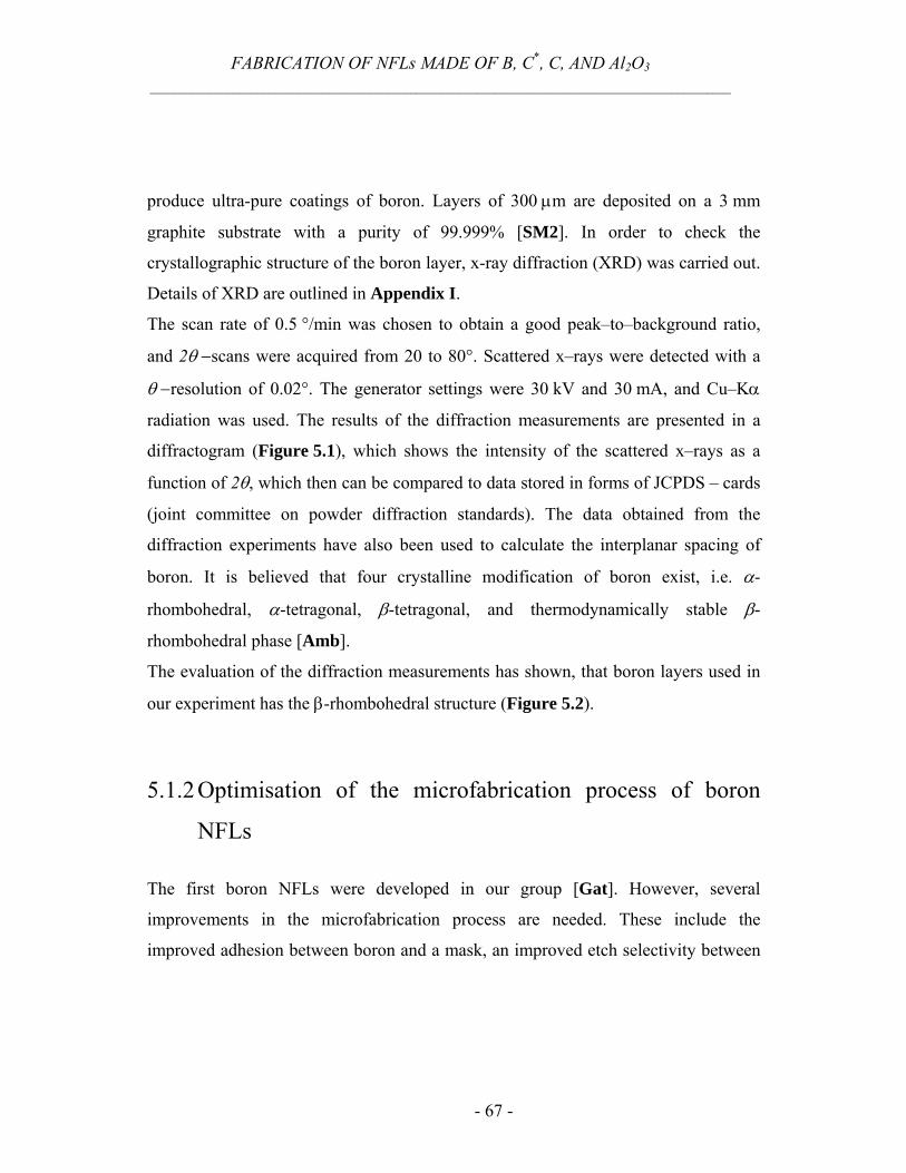
FABRICATION OF NFLs MADE OF B, C*, C, AND Al2O3
__________________________________________________________________________________________________
- 67 -
produce ultra-pure coatings of boron. Layers of 300 µm are deposited on a 3 mm
graphite substrate with a purity of 99.999% [SM2]. In order to check the
crystallographic structure of the boron layer, x-ray diffraction (XRD) was carried out.
Details of XRD are outlined in Appendix I.
The scan rate of 0.5 °/min was chosen to obtain a good peak–to–background ratio,
and 2θ −scans were acquired from 20 to 80°. Scattered x–rays were detected with a
θ −resolution of 0.02°. The generator settings were 30 kV and 30 mA, and Cu–Kα
radiation was used. The results of the diffraction measurements are presented in a
diffractogram (Figure 5.1), which shows the intensity of the scattered x–rays as a
function of 2θ, which then can be compared to data stored in forms of JCPDS – cards
(joint committee on powder diffraction standards). The data obtained from the
diffraction experiments have also been used to calculate the interplanar spacing of
boron. It is believed that four crystalline modification of boron exist, i.e. α-
rhombohedral, α-tetragonal, β-tetragonal, and thermodynamically stable β-
rhombohedral phase [Amb].
The evaluation of the diffraction measurements has shown, that boron layers used in
our experiment has the β-rhombohedral structure (Figure 5.2).
5.1.2 Optimisation of the microfabrication process of boron
NFLs
The first boron NFLs were developed in our group [Gat]. However, several
improvements in the microfabrication process are needed. These include the
improved adhesion between boron and a mask, an improved etch selectivity between
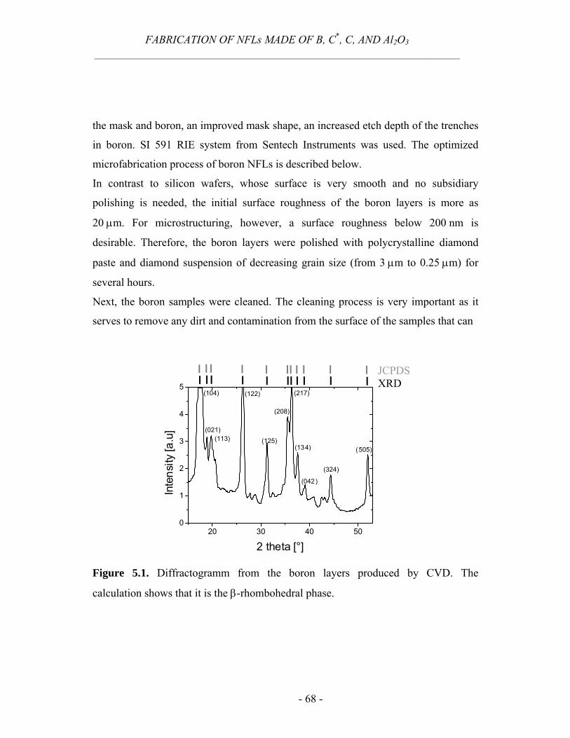
FABRICATION OF NFLs MADE OF B, C*, C, AND Al2O3
__________________________________________________________________________________________________
- 68 -
the mask and boron, an improved mask shape, an increased etch depth of the trenches
in boron. SI 591 RIE system from Sentech Instruments was used. The optimized
microfabrication process of boron NFLs is described below.
In contrast to silicon wafers, whose surface is very smooth and no subsidiary
polishing is needed, the initial surface roughness of the boron layers is more as
20 µm. For microstructuring, however, a surface roughness below 200 nm is
desirable. Therefore, the boron layers were polished with polycrystalline diamond
paste and diamond suspension of decreasing grain size (from 3 µm to 0.25 µm) for
several hours.
Next, the boron samples were cleaned. The cleaning process is very important as it
serves to remove any dirt and contamination from the surface of the samples that can
20 30 40 500
1
2
3
4
5
(505)
(324)
(042)
(134)
(217)
(208)
(125)
(122)
(113)(021)
(104)
Inte
nsity
[a.u
]
2 theta [°]
JCPDS XRD
Figure 5.1. Diffractogramm from the boron layers produced by CVD. The
calculation shows that it is the β-rhombohedral phase.
FABRICATION OF NFLs MADE OF B, C*, C, AND Al2O3
__________________________________________________________________________________________________
- 69 -
Figure 5.2. The rhombohedral β-boron (R-105) structure.
negatively influence the adhesion of the mask. The samples were immersed in
acetone in an ultrasonic bath for ten minutes at a temperature of 60 °C. Then the
cleaning process was continued in propanol and dried with a N2-ion gun. To finally
remove organic contaminants such as dust, grease and polishing agent from the
surface, the boron layers were etched in a pure oxygen plasma at the gas inflow of
10 sccm, a total pressure of 20 Pa, and rf power of 100 W. The plasma was switched
off after 2 min.
By the interaction with oxygen boron is oxidized to boron trioxide (Equation 5.1)
which is in turn converted to the boric acid by the interaction with water in air
(Equation 5.2)
4B+3O2 → 2B2O3, 5.1
B2O3+3H2O → 2H3BO3. 5.2
The thin liquid boric acid layer (the thickness of 2-3 nm) is removed from the surface
by an SF6 plasma. The etching was done using a gas inflow of 10 sccm, a total Figure
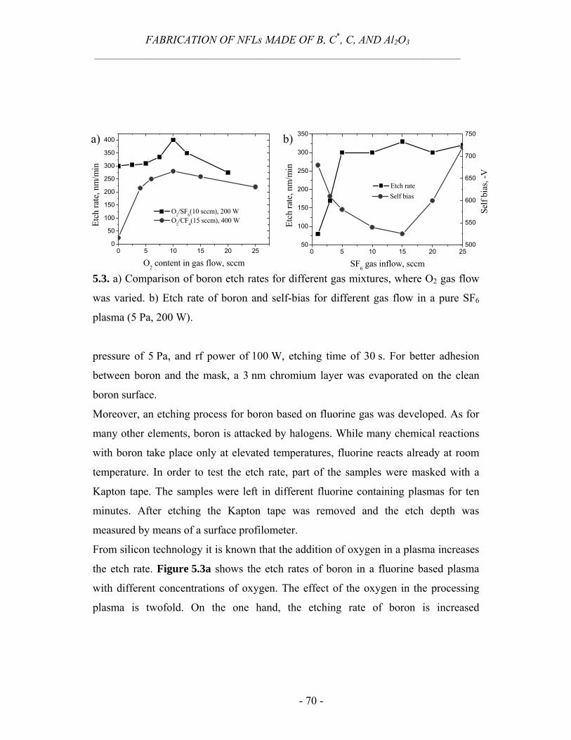
FABRICATION OF NFLs MADE OF B, C*, C, AND Al2O3
__________________________________________________________________________________________________
- 70 -
5.3. a) Comparison of boron etch rates for different gas mixtures, where O2 gas flow
was varied. b) Etch rate of boron and self-bias for different gas flow in a pure SF6
plasma (5 Pa, 200 W).
pressure of 5 Pa, and rf power of 100 W, etching time of 30 s. For better adhesion
between boron and the mask, a 3 nm chromium layer was evaporated on the clean
boron surface.
Moreover, an etching process for boron based on fluorine gas was developed. As for
many other elements, boron is attacked by halogens. While many chemical reactions
with boron take place only at elevated temperatures, fluorine reacts already at room
temperature. In order to test the etch rate, part of the samples were masked with a
Kapton tape. The samples were left in different fluorine containing plasmas for ten
minutes. After etching the Kapton tape was removed and the etch depth was
measured by means of a surface profilometer.
From silicon technology it is known that the addition of oxygen in a plasma increases
the etch rate. Figure 5.3a shows the etch rates of boron in a fluorine based plasma
with different concentrations of oxygen. The effect of the oxygen in the processing
plasma is twofold. On the one hand, the etching rate of boron is increased
0 5 10 15 20 250
50
100
150
200
250
300
350
400
Etch
rate
, nm
/min
O2 content in gas flow, sccm
O2/SF6(10 sccm), 200 W O2/CF4(15 sccm), 400 W
0 5 10 15 20 2550
100
150
200
250
300
350
500
550
600
650
700
750
Etch rate
Etch
rate
, nm
/min
SF6 gas inflow, sccm
Self bias
Self
bias
, -V
a) b)
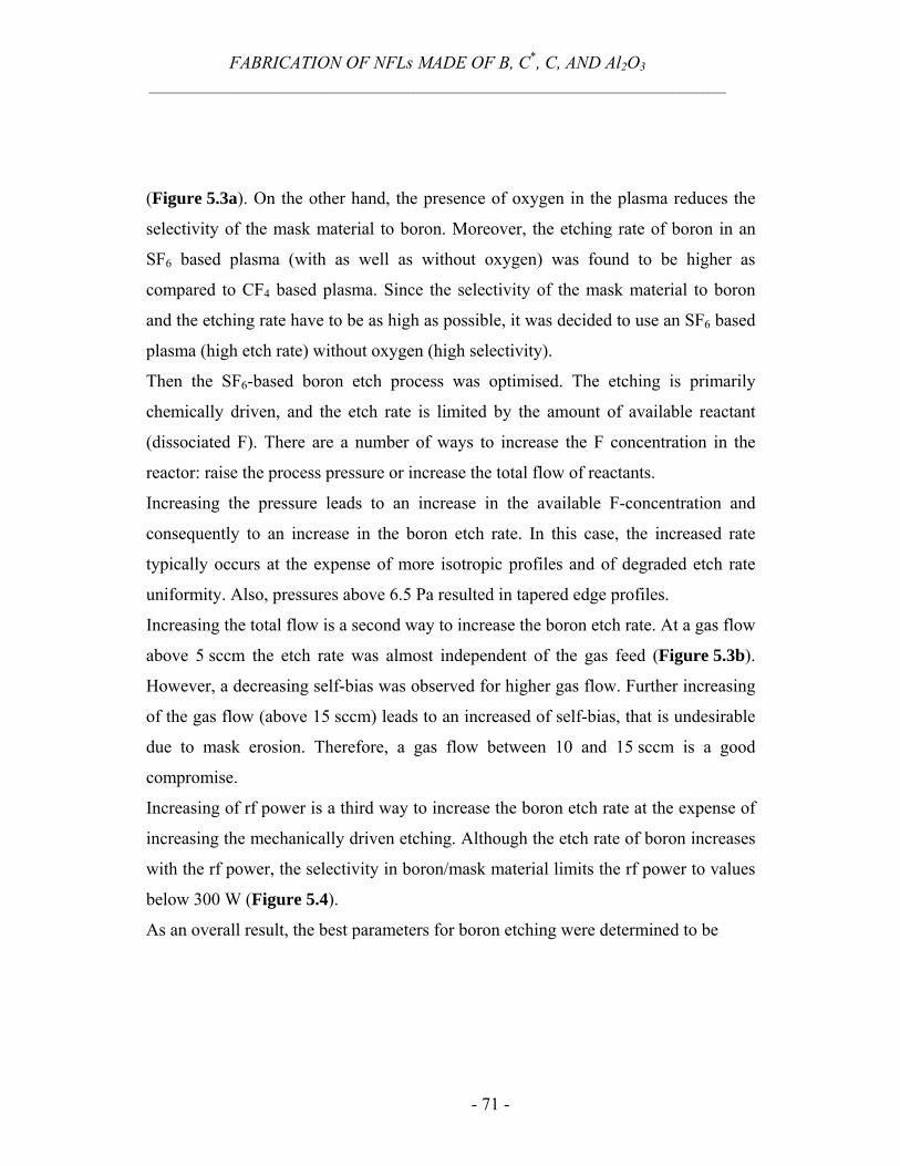
FABRICATION OF NFLs MADE OF B, C*, C, AND Al2O3
__________________________________________________________________________________________________
- 71 -
(Figure 5.3a). On the other hand, the presence of oxygen in the plasma reduces the
selectivity of the mask material to boron. Moreover, the etching rate of boron in an
SF6 based plasma (with as well as without oxygen) was found to be higher as
compared to CF4 based plasma. Since the selectivity of the mask material to boron
and the etching rate have to be as high as possible, it was decided to use an SF6 based
plasma (high etch rate) without oxygen (high selectivity).
Then the SF6-based boron etch process was optimised. The etching is primarily
chemically driven, and the etch rate is limited by the amount of available reactant
(dissociated F). There are a number of ways to increase the F concentration in the
reactor: raise the process pressure or increase the total flow of reactants.
Increasing the pressure leads to an increase in the available F-concentration and
consequently to an increase in the boron etch rate. In this case, the increased rate
typically occurs at the expense of more isotropic profiles and of degraded etch rate
uniformity. Also, pressures above 6.5 Pa resulted in tapered edge profiles.
Increasing the total flow is a second way to increase the boron etch rate. At a gas flow
above 5 sccm the etch rate was almost independent of the gas feed (Figure 5.3b).
However, a decreasing self-bias was observed for higher gas flow. Further increasing
of the gas flow (above 15 sccm) leads to an increased of self-bias, that is undesirable
due to mask erosion. Therefore, a gas flow between 10 and 15 sccm is a good
compromise.
Increasing of rf power is a third way to increase the boron etch rate at the expense of
increasing the mechanically driven etching. Although the etch rate of boron increases
with the rf power, the selectivity in boron/mask material limits the rf power to values
below 300 W (Figure 5.4).
As an overall result, the best parameters for boron etching were determined to be
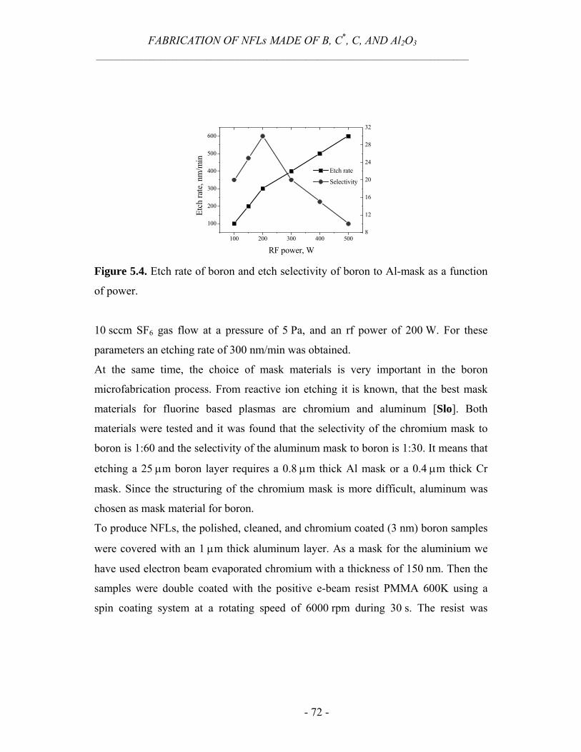
FABRICATION OF NFLs MADE OF B, C*, C, AND Al2O3
__________________________________________________________________________________________________
- 72 -
100 200 300 400 500
100
200
300
400
500
600
8
12
16
20
24
28
32
Etch
rate
, nm
/min
RF power, W
Etch rate
Selectivity
Figure 5.4. Etch rate of boron and etch selectivity of boron to Al-mask as a function
of power.
10 sccm SF6 gas flow at a pressure of 5 Pa, and an rf power of 200 W. For these
parameters an etching rate of 300 nm/min was obtained.
At the same time, the choice of mask materials is very important in the boron
microfabrication process. From reactive ion etching it is known, that the best mask
materials for fluorine based plasmas are chromium and aluminum [Slo]. Both
materials were tested and it was found that the selectivity of the chromium mask to
boron is 1:60 and the selectivity of the aluminum mask to boron is 1:30. It means that
etching a 25 µm boron layer requires a 0.8 µm thick Al mask or a 0.4 µm thick Cr
mask. Since the structuring of the chromium mask is more difficult, aluminum was
chosen as mask material for boron.
To produce NFLs, the polished, cleaned, and chromium coated (3 nm) boron samples
were covered with an 1 µm thick aluminum layer. As a mask for the aluminium we
have used electron beam evaporated chromium with a thickness of 150 nm. Then the
samples were double coated with the positive e-beam resist PMMA 600K using a
spin coating system at a rotating speed of 6000 rpm during 30 s. The resist was
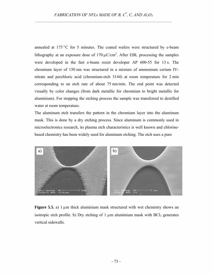
FABRICATION OF NFLs MADE OF B, C*, C, AND Al2O3
__________________________________________________________________________________________________
- 73 -
annealed at 175 °C for 5 minutes. The coated wafers were structured by e-beam
lithography at an exposure dose of 170 µC/cm2. After EBL processing the samples
were developed in the fast e-beam resist developer AP 600-55 for 13 s. The
chromium layer of 150 nm was structured in a mixture of ammonium cerium IV-
nitrate and perchloric acid (chromium-etch 3144) at room temperature for 2 min
corresponding to an etch rate of about 75 nm/min. The end point was detected
visually by color changes (from dark metallic for chromium to bright metallic for
aluminium). For stopping the etching process the sample was transferred to destilled
water at room temperature.
The aluminum etch transfers the pattern in the chromium layer into the aluminum
mask. This is done by a dry etching process. Since aluminum is commonly used in
microelectronics research, its plasma etch characteristics is well known and chlorine-
based chemistry has been widely used for aluminum etching. The etch uses a pure
a) b)
Figure 5.5. a) 1 µm thick aluminium mask structured with wet chemistry shows an
isotropic etch profile. b) Dry etching of 1 µm aluminium mask with BCl3 generates
vertical sidewalls.
FABRICATION OF NFLs MADE OF B, C*, C, AND Al2O3
__________________________________________________________________________________________________
- 74 -
BCl3 gas (10 sccm) at a pressure of 5 Pa and an rf power of 200 W. The etch time was
30 min corresponding to an etch rate of 35 nm/min. In comparison to wet etching, dry
etching allows to improve the quality of the mask (Figure 5.5).
The underlying boron is structured in a reactive ion etching system using pure SF6
plasma at a gas inflow of 10 sccm, a pressure of a 5 Pa and an rf power of 200 W. To
obtain vertical sidewalls, the wafer was cooled by switching off the plasma for 30 s
every 30 s. After etching, the wafer was placed in an ultrasonic bath for 30 s to
remove RIE grass (Figure 5.6a). After a total effective etching time of around
1.5 hour an etch depth of 25 µm was obtained (Figure 5.6b).
As in the case of silicon NFLs (Chapter 3), in order to provide flexibility concerning
the choice of the focal length and of the photon energy, different numbers of single
lenses in one NFL and different radii of curvatures are required. The number of single
lenses in a boron NFL was 30 and 60. The radius of curvature, R, varies from 2.0 µm
b)a)
Figure 5.6. Scanning electron micrograph of a) RIE grass by the etching of boron in
the SF6 plasma; b) planar parabolic refractive nanofocusing lenses made of boron.
FABRICATION OF NFLs MADE OF B, C*, C, AND Al2O3
__________________________________________________________________________________________________
- 75 -
to 4.0 µm in steps of 0.5 µm, resulting in 5 different NFLs per block. The distance, d,
between the apices of a single lens is about 5 µm and the length of a single lens is
145 µm. Different numbers of trenches between two NFLs are used to identity a lens
with a given curvature. The mask and the final result of the etching may vary form.
Hence, three sets of blocks were written. The mask corrections vary from 0 to 400 nm
in steps of 200 nm.
The experiment was performed at 13 keV photon energy, at beamline ID13 of the
ESRF in Grenoble, France. The lens system sketched in figure 3.9 was mounted at
L1=47 m from the source. The horizontally placed lens (N=60) had a radius of
curvature of R=3.0 µm. The vertically placed lens (N=30) had a radius of 4.0 µm.
The resolution of the lenses was determined by knife-edge scans with a gold test
sample, which is commonly used for this purpose. The FWHM of the line focus of
about 2.0 µm was derived from the horizontal fit which is a factor 40 larger than
theoretically expected.
The most possible reason conceivable for the observed discrepancy between the
theoretical and experimentally determined focal size of a boron lens is the boron
surface. The great hardness of boron enables to make the surface smooth but not flat.
The consequence of the surface curvature in the range of 10 µm is that not all lenses
in one nanofocusing lens can take part in the focusing of x-rays. In this case, the
boron lenses can be adjusted so that either some of the first and some of the last
lenses in one nanofocusing lens (Figure 5.7a) can focus together. Another possibility
for the creation of a focus is that an arbitrary fraction of the lenses in an NFL are
illuminated (Figure 5.7b). The ideal case would be very flat surfaces from the
beginning of the microfabrication process as for the silicon lenses (Figure 5.7c).
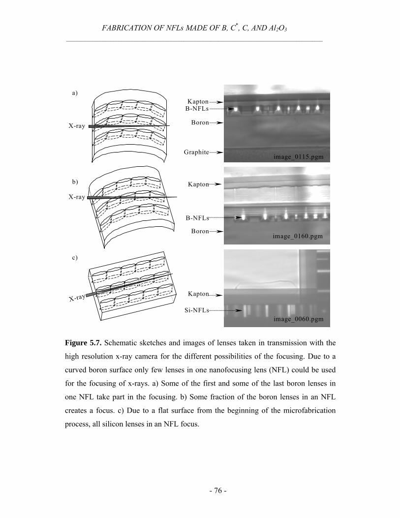
FABRICATION OF NFLs MADE OF B, C*, C, AND Al2O3
__________________________________________________________________________________________________
- 76 -
image_0115.pgm
image_0160.pgm
image_0060.pgm
X-ray
X-ray
X-ray
a)
c)
b)
KaptonB-NFLs
Boron
Graphite
Kapton
B-NFLs
Boron
Kapton
Si-NFLs
Figure 5.7. Schematic sketches and images of lenses taken in transmission with the
high resolution x-ray camera for the different possibilities of the focusing. Due to a
curved boron surface only few lenses in one nanofocusing lens (NFL) could be used
for the focusing of x-rays. a) Some of the first and some of the last boron lenses in
one NFL take part in the focusing. b) Some fraction of the boron lenses in an NFL
creates a focus. c) Due to a flat surface from the beginning of the microfabrication
process, all silicon lenses in an NFL focus.
FABRICATION OF NFLs MADE OF B, C*, C, AND Al2O3
__________________________________________________________________________________________________
- 77 -
In future, using boron layer with the flat surface, lenses with better focusing
properties can be obtained.
5.2 Etching of diamond
For the fabrication of diamond nanofocusing lenses we have started with diamond
layers, 200 µm thick, which were deposited by chemical vapor deposition (CVD).
The films were optically polished to a surface roughness of 15 nm. Reactive ion
etching of diamond was done in O2/CF4 and in O2/Ar mixtures. The mask materials
were e-beam evaporated Al, Au and Ti as well as CVD deposited Al2O3 and AlN.
The highest etching rates of diamond were achieved by using an O2+CF4 gas mixture
(Figure 5.8). The etching rate of 65 nm/min was obtained at the gas inflow of
40 sccm of O2 and 6 sccm of CF4 at the total pressure of 6.5 Pa and at an rf power of
350 W. With a O2+Ar gas mixture an etching rate of 25 nm/min was achieved at the
gas inflow of 40 sccm of O2 and 10 sccm of Ar at the total pressure of 6.5 Pa and at
an rf power of 500 W. The etching rate was found to decrease significantly to
13 nm/min when the gas inflow was changed to 8 sccm of O2 and 7 sccm of Ar at a
pressure of 0.33 Pa and at an rf power of 300 W. A subsequent increasing of the rf
power to 400 or 500 W does not lead to increase etching rate.
The selectivity of the etching process was investigated by using Al, Al2O3 AlN, Au,
SiO2 and Ti as mask materials. The etching of the Al, Al2O3, AlN, Au and SiO2
masks was realized in an O2+CF4 gas mixture with the gas inflow of 40 sccm of O2
and 6 sccm of CF4 at the total pressure of 6.5 Pa. The etching experiments were done
at an rf power of 100, 250 and 350 W. It was found, that Al has the best selectivity to
diamond. The etching rate of Al was 10 nm/min, which corresponds to a selectivity of
6.5. In other words, for etching a diamond layer of 20 µm the mask should be least
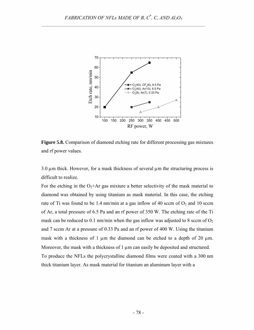
FABRICATION OF NFLs MADE OF B, C*, C, AND Al2O3
__________________________________________________________________________________________________
- 78 -
100 150 200 250 300 350 400 450 50010
20
30
40
50
60
70
RF power, W
Etch
rate
, nm
/min
O2(40), CF4(6), 6.5 Pa O2(40), Ar(10), 6.5 Pa O2(8), Ar(7), 0.33 Pa
Figure 5.8. Comparison of diamond etching rate for different processing gas mixtures
and rf power values.
3.0 µm thick. However, for a mask thickness of several µm the structuring process is
difficult to realize.
For the etching in the O2+Ar gas mixture a better selectivity of the mask material to
diamond was obtained by using titanium as mask material. In this case, the etching
rate of Ti was found to be 1.4 nm/min at a gas inflow of 40 sccm of O2 and 10 sccm
of Ar, a total pressure of 6.5 Pa and an rf power of 350 W. The etching rate of the Ti
mask can be reduced to 0.1 nm/min when the gas inflow was adjusted to 8 sccm of O2
and 7 sccm Ar at a pressure of 0.33 Pa and an rf power of 400 W. Using the titanium
mask with a thickness of 1 µm the diamond can be etched to a depth of 20 µm.
Moreover, the mask with a thickness of 1 µm can easily be deposited and structured.
To produce the NFLs the polycrystalline diamond films were coated with a 300 nm
thick titanium layer. As mask material for titanium an aluminum layer with a
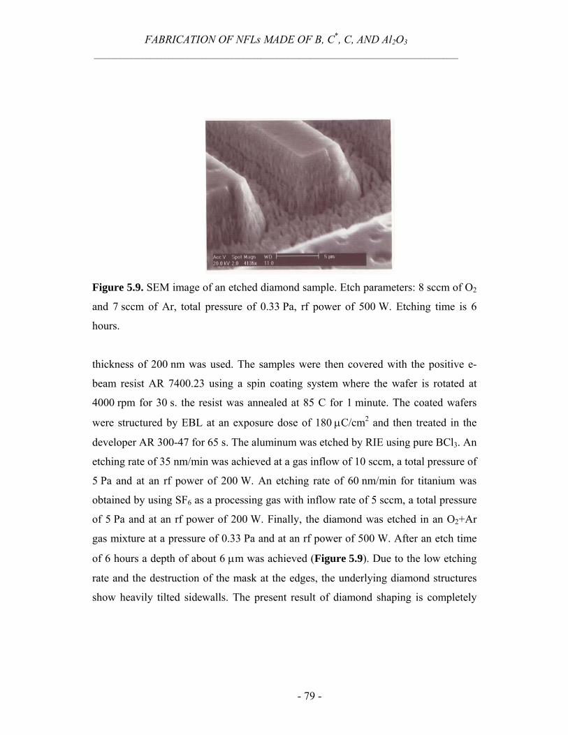
FABRICATION OF NFLs MADE OF B, C*, C, AND Al2O3
__________________________________________________________________________________________________
- 79 -
Figure 5.9. SEM image of an etched diamond sample. Etch parameters: 8 sccm of O2
and 7 sccm of Ar, total pressure of 0.33 Pa, rf power of 500 W. Etching time is 6
hours.
thickness of 200 nm was used. The samples were then covered with the positive e-
beam resist AR 7400.23 using a spin coating system where the wafer is rotated at
4000 rpm for 30 s. the resist was annealed at 85 C for 1 minute. The coated wafers
were structured by EBL at an exposure dose of 180 µC/cm2 and then treated in the
developer AR 300-47 for 65 s. The aluminum was etched by RIE using pure BCl3. An
etching rate of 35 nm/min was achieved at a gas inflow of 10 sccm, a total pressure of
5 Pa and at an rf power of 200 W. An etching rate of 60 nm/min for titanium was
obtained by using SF6 as a processing gas with inflow rate of 5 sccm, a total pressure
of 5 Pa and at an rf power of 200 W. Finally, the diamond was etched in an O2+Ar
gas mixture at a pressure of 0.33 Pa and at an rf power of 500 W. After an etch time
of 6 hours a depth of about 6 µm was achieved (Figure 5.9). Due to the low etching
rate and the destruction of the mask at the edges, the underlying diamond structures
show heavily tilted sidewalls. The present result of diamond shaping is completely
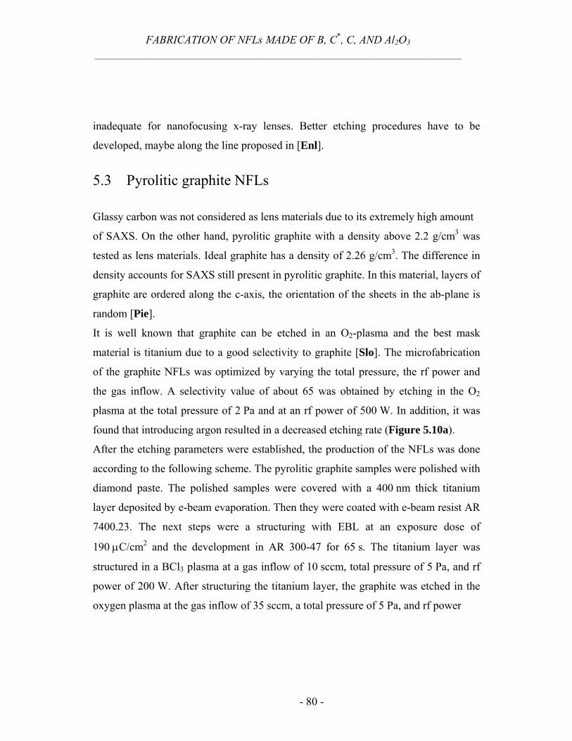
FABRICATION OF NFLs MADE OF B, C*, C, AND Al2O3
__________________________________________________________________________________________________
- 80 -
inadequate for nanofocusing x-ray lenses. Better etching procedures have to be
developed, maybe along the line proposed in [Enl].
5.3 Pyrolitic graphite NFLs
Glassy carbon was not considered as lens materials due to its extremely high amount
of SAXS. On the other hand, pyrolitic graphite with a density above 2.2 g/cm3 was
tested as lens materials. Ideal graphite has a density of 2.26 g/cm3. The difference in
density accounts for SAXS still present in pyrolitic graphite. In this material, layers of
graphite are ordered along the c-axis, the orientation of the sheets in the ab-plane is
random [Pie].
It is well known that graphite can be etched in an O2-plasma and the best mask
material is titanium due to a good selectivity to graphite [Slo]. The microfabrication
of the graphite NFLs was optimized by varying the total pressure, the rf power and
the gas inflow. A selectivity value of about 65 was obtained by etching in the O2
plasma at the total pressure of 2 Pa and at an rf power of 500 W. In addition, it was
found that introducing argon resulted in a decreased etching rate (Figure 5.10a).
After the etching parameters were established, the production of the NFLs was done
according to the following scheme. The pyrolitic graphite samples were polished with
diamond paste. The polished samples were covered with a 400 nm thick titanium
layer deposited by e-beam evaporation. Then they were coated with e-beam resist AR
7400.23. The next steps were a structuring with EBL at an exposure dose of
190 µC/cm2 and the development in AR 300-47 for 65 s. The titanium layer was
structured in a BCl3 plasma at a gas inflow of 10 sccm, total pressure of 5 Pa, and rf
power of 200 W. After structuring the titanium layer, the graphite was etched in the
oxygen plasma at the gas inflow of 35 sccm, a total pressure of 5 Pa, and rf power
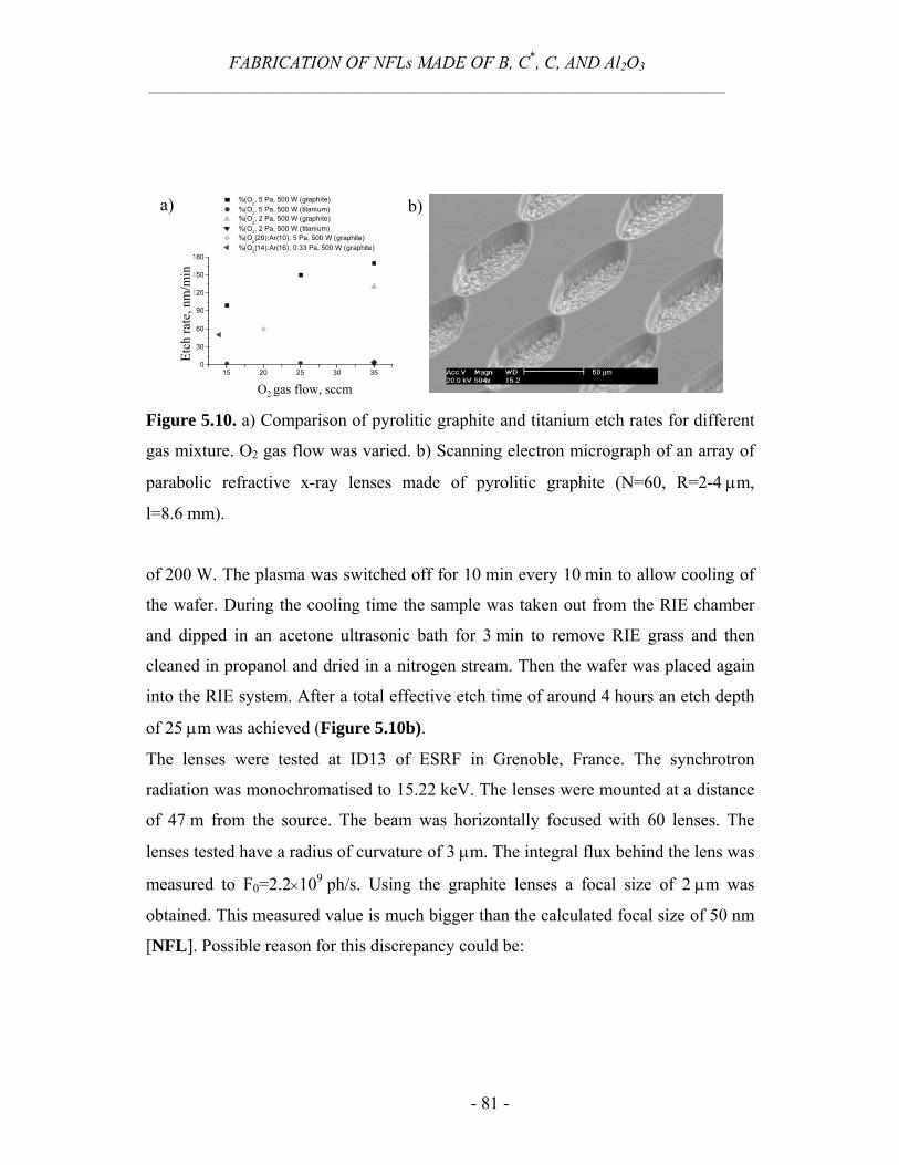
FABRICATION OF NFLs MADE OF B, C*, C, AND Al2O3
__________________________________________________________________________________________________
- 81 -
15 20 25 30 350
30
60
90
120
150
180
Etch
rate
, nm
/min
O2 gas flow, sccm
%(O2, 5 Pa, 500 W (graphite)
%(O2, 5 Pa, 500 W (titanium) %(O
2, 2 Pa, 500 W (graphite)
%(O2, 2 Pa, 500 W (titanium) %(O
2(20):Ar(10), 5 Pa, 500 W (graphite)
%(O2(14):Ar(16), 0.33 Pa, 500 W (graphite)
O2 gas flow, sccm
Etch
rate
, nm
/min
a) b)
Figure 5.10. a) Comparison of pyrolitic graphite and titanium etch rates for different
gas mixture. O2 gas flow was varied. b) Scanning electron micrograph of an array of
parabolic refractive x-ray lenses made of pyrolitic graphite (N=60, R=2-4 µm,
l=8.6 mm).
of 200 W. The plasma was switched off for 10 min every 10 min to allow cooling of
the wafer. During the cooling time the sample was taken out from the RIE chamber
and dipped in an acetone ultrasonic bath for 3 min to remove RIE grass and then
cleaned in propanol and dried in a nitrogen stream. Then the wafer was placed again
into the RIE system. After a total effective etch time of around 4 hours an etch depth
of 25 µm was achieved (Figure 5.10b).
The lenses were tested at ID13 of ESRF in Grenoble, France. The synchrotron
radiation was monochromatised to 15.22 keV. The lenses were mounted at a distance
of 47 m from the source. The beam was horizontally focused with 60 lenses. The
lenses tested have a radius of curvature of 3 µm. The integral flux behind the lens was
measured to F0=2.2×10⁹ ph/s. Using the graphite lenses a focal size of 2 µm was
obtained. This measured value is much bigger than the calculated focal size of 50 nm
[NFL]. Possible reason for this discrepancy could be:
FABRICATION OF NFLs MADE OF B, C*, C, AND Al2O3
__________________________________________________________________________________________________
- 82 -
1) The sidewalls (tilt around 3-5 degrees) were not vertical, thus destroying the
focusing properties of the graphite NFLs.
2) SAXS, due to the voids responsible for the reduced density, generates a strong
blur of the focal spot.
5.4 Etching of sapphire
Sapphire is a very hard aluminium oxide, single crystalline, non-porous, unaffected
by weathering and hydration, its density is 3.98 g/cm3. These and other properties
offer many advantages to the optical designer. In the last years, optical components
including windows, lenses and mirrors made of sapphire have been fabricated. Due to
a small atomic number, and as consequence, to a weak absorption and low level of
SAXS data, sapphire is an attractive material for nanofocusing refractive x-ray lenses.
It has been reported that it is difficult to etch Al2O3 films because of its high chemical
and physical stability. In contrast to silicon (Chapter 3), the etching process of
sapphire has not been developed, so far. High sapphire etch rates with high etch
selectivity over mask materials are required. Recently, research on the various etching
of sapphire such as ion beam etching [Hay], chemical wet etching after ion
implantation [Don], reactive ion etching [Fed], [Kim], laser-assisted etching and
inductively coupled plasma [Sung] have been carried out.
In order to test the application of RIE for fabrication of nanofocusing lenses made of
sapphire, several etch experiments were carried out. The highest etching rates of
sapphire were achieved using pure BCl3. The etching rate of 25 nm/min was obtained
at the gas inflow of 20 sccm, at the total pressure of 2 Pa and at an rf power of 590 W.
The etching rate was found to decrease significantly to 13 nm/min when the gas
FABRICATION OF NFLs MADE OF B, C*, C, AND Al2O3
__________________________________________________________________________________________________
- 83 -
inflow was changed to 10 sccm. With a pure SF6 gas an etching rate of 10 nm/min
was achieved at the gas inflow of 25 sccm, at the total pressure of 2 Pa and at an rf
power of 500 W. Due to these low etching rates structures in sapphire with vertical
sidewalls and a depth over 20 µm can be not obtained. Based on the experimental
results it is proposed that the significant improvement of the etching rate can be
obtained by using ICP etching system [Sam].
- 84 -
Chapter 6 Summary and outlook In this research, an optimised deep reactive ion etching process for the fabrication of
refractive lenses with a cylindrically parabolic profile made of silicon is presented. As
compared to the first silicon NFLs [Schr1], the contact between sample and reactive
ion etching (RIE) chamber was improved. As a consequence, steeper sidewalls were
obtained. Deep silicon etching was applied using a thin silicon dioxide mask. Due to
the high selectivity between silicon and silicon dioxide (about 300) a lens depth of
62 µm was obtained. Based on the results of the shape analysis, the lenses with the
best parabolic profile and vertical sidewalls were selected for the experiments. As a
result of the significantly improved lens shape, the lateral resolution achieved with
these lenses approaches the theoretical limit. The silicon lenses described in this work
are very useful optical components for nanofluorescence tomography, nanodiffraction
and other techniques done at third generation synchrotron radiation sources.
In a recent experiment made at the European Synchrotron Radiation Facility (ESRF) in
Grenoble, France, these lenses were used to generate a nanobeam of 47 nm × 55 nm
for an x-ray energy of 21 keV [Schr6]. The performance of the silicon lenses was
proved in several application oriented experiments.
Silicon nanofocusing refractive x-ray lenses make possible an analysis of the structural
transformations in thin films of phase change media. The illuminated volume was
reduced to 180 nm × 100 nm × 80 nm, which corresponds to ~107 atoms. In general,
more diffraction patterns should be made for a reliable analysis of the
SUMMARY AND OUTLOOK ____________________________________________________________________
- 85 -
experimental data. In future, nanofocusing x-ray lenses may allow for the investigation
of the time dependence of the crystallization process and for the influence of the
temperature – time variation in the laser modified areas.
To investigate residual stress at individual aluminium mirrors, stress analysis by
microfocus x-ray diffraction is required. Using silicon nanofocusing refractive x-ray
lenses, a beam of 180 nm × 100 nm for an x-ray energy of 15.2 keV was generated.
The experiment was successfully carried out, stress of a free standing aluminium
mirror was calculated to be 25 Mpa.
To achieve a lateral focal size under 20 nm nanofocusing refractive x-ray lenses made
of diamond, graphite, sapphire or boron are required. Up to now, microfabrication
processes for these elements are not well developed. Using a RIE system from
Sentech, the microfabrication process of boron NFLs was optimised. This includes the
improved adhesion between boron and a mask, an improved etch selectivity between
the mask and boron, an improved mask shape, an increased etch depth of the trenches
in boron. Further improving of the roughness of boron layers, i.e. the smoothness and
the flatness is expected to lead to boron nanofocusing lenses with focusing properties
approaching the theoretical value.
To develop a mictofabrication process for diamond, a RIE system was used. Different
gas mixtures and mask materials were investigated to find the highest etch rate of
diamond and the maximum selectivity of diamond to the mask material. The best mask
material for diamond was found to be titanium with a selectivity of about 20. Using an
O2+Ar gas mixture an etch rate of 1 µm/hour was achieved. Due to the low etching
rate, the underlying diamond structures show heavily tilted sidewalls, that make them
completely inadequate for nanofocusing x-ray lenses. Using a modern etching
SUMMARY AND OUTLOOK ____________________________________________________________________
- 86 -
equipment, i.e. an inductively coupled plasma (ICP) system, better diamond shaping
can be obtained.
To produce nanofocusing refractive lenses made of pyrolitic graphite, an etching
procedure similar to that for diamond etching was developed. Using a pure oxygen
plasma an etch rate of up to 6.5 µm/hour was obtained. Relatively high etch rates make
it possible to control the tilt of the sidewalls. The lenses were tested at ID13 of ESRF
in Grenoble, France. A focal size of 2 µm was obtained. This measured value is much
bigger than the calculated focal size of 50 nm [NFL]. A possible reason for this
discrepancy could be scattering, which generates a strong blur of the focal spot, due to
the voids responsible for the reduced density.
Furthermore, some experiments of sapphire etching were performed in order to test
the applicability of a RIE system for production of sapphire nanofocusing lenses.
Etching rate of 25 nm/min was found. Due to this low etching rate in sapphire no
vertical sidewalls could be obtained. Based on the experimental results it is proposed
that a significant improvement of the etching rate can be obtained by using ICP
etching system.
According to the results of this work the following conclusions can be made:
• The microfabrication process of silicon nanofocusing lenses is optimised.
With these lenses a lateral resolution of 50 nm was achieved and this
resolution approaches the theoretical limit. Using the same process for the
fabrication of silicon adiabatically focusing lenses (AFL), described in section
2.10, a lateral resolution of 20 nm and below can be reached.
• Silicon nanofocusing refractive x-ray lenses are useful optical components for
nanofluorescence tomography, nanodiffraction and other techniques done at
third generation synchrotron radiation sources. Using these lenses, the
SUMMARY AND OUTLOOK ____________________________________________________________________
- 87 -
analysis of structural transformations in thin films of phase change media and
the investigation of residual stress in aluminium mirrors were made. In future,
fluorescence tomography experiments with a resolution in the range of
100 nm are feasible.
• To fabricate nanofocusing x-ray lenses made of boron, sapphire or diamond,
improved microfabrication techniques are required. In the case of boron, a
polishing machine is needed, which allows the boron surface to be smooth and
flat, simultaneously. For the etching of sapphire and diamond, a ICP etching
system is required. Using such a system, vertical sidewalls of the etched
structures may be at hand.
- 88 -
Appendix I. X–ray diffraction (XRD)
X–ray diffraction is a non–destructive analytical technique for the identification and
quantitative determination of various crystalline forms.
When a polycrystalline (powder) sample is irradiated with monochromatic x–rays, in
addition to absorption and other phenomena, elastic x–ray scattering may occur. The
intensity and angular distribution of the scattered x–rays from a crystalline sample
allow one to determine the lattice structure and the position of the atoms in the unit
cell. Bragg's law defines where reflections can be expected:
θλ sin2dn = , (1)
where λ is the wavelength, d is the distance between the atomic planes in the crystal,
and θ is the Bragg angle at which a diffraction peak is observed.
The results of the diffraction measurements are presented in a diffractogram, which
shows the intensity of the scattered x–rays as a function of 2θ, which then can be
compared to data stored in forms of JCPDS (joint committee on powder diffraction
standards) – cards. The data obtained from the diffraction experiments can also be
used to calculate the interplanar spacing of the sample.
X–ray diffraction using conventional Bragg–Brentano geometry is only partially
suitable for the analysis of the thin films due to the unfavorable peak–to–background
ratio. A grazing incidence attachment is designed for the measurements of thin films,
surfaces and multilayers. Applying small incidence angles (0.1 to 3°) of the x–ray
beam leads to strongly reduced penetration depths and an increased size of the
irradiation area. Soller slits help to define the direction of the incoming and diffracted
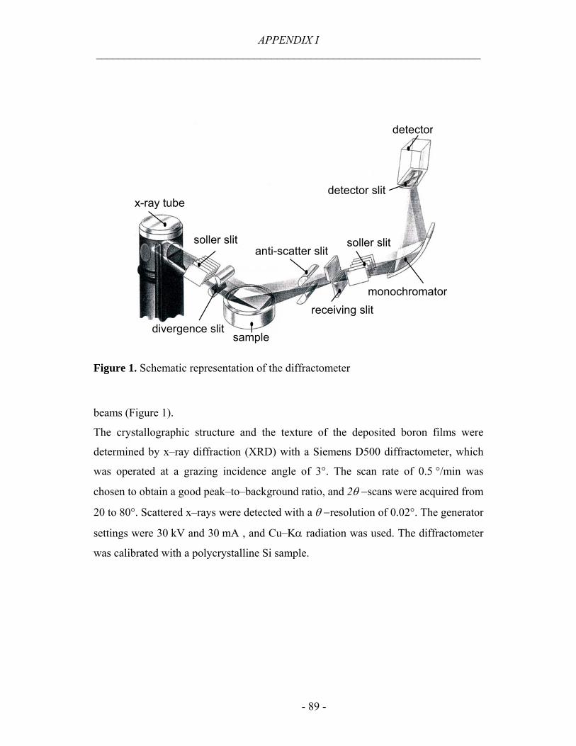
APPENDIX I ____________________________________________________________________
- 89 -
x-ray tube
soller slit
sample
receiving slit
anti-scatter slit
detector
monochromator
detector slit
soller slit
divergence slit
Figure 1. Schematic representation of the diffractometer
beams (Figure 1).
The crystallographic structure and the texture of the deposited boron films were
determined by x–ray diffraction (XRD) with a Siemens D500 diffractometer, which
was operated at a grazing incidence angle of 3°. The scan rate of 0.5 °/min was
chosen to obtain a good peak–to–background ratio, and 2θ −scans were acquired from
20 to 80°. Scattered x–rays were detected with a θ −resolution of 0.02°. The generator
settings were 30 kV and 30 mA , and Cu–Kα radiation was used. The diffractometer
was calibrated with a polycrystalline Si sample.
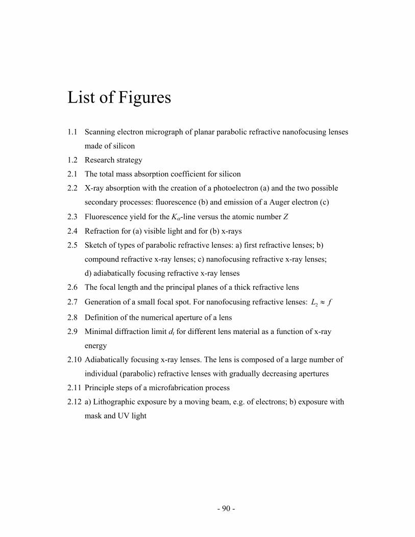
- 90 -
List of Figures 1.1 Scanning electron micrograph of planar parabolic refractive nanofocusing lenses
made of silicon
1.2 Research strategy
2.1 The total mass absorption coefficient for silicon
2.2 X-ray absorption with the creation of a photoelectron (a) and the two possible
secondary processes: fluorescence (b) and emission of a Auger electron (c)
2.3 Fluorescence yield for the Kα-line versus the atomic number Z
2.4 Refraction for (a) visible light and for (b) x-rays
2.5 Sketch of types of parabolic refractive lenses: a) first refractive lenses; b)
compound refractive x-ray lenses; c) nanofocusing refractive x-ray lenses;
d) adiabatically focusing refractive x-ray lenses
2.6 The focal length and the principal planes of a thick refractive lens
2.7 Generation of a small focal spot. For nanofocusing refractive lenses: fL ≈2
2.8 Definition of the numerical aperture of a lens
2.9 Minimal diffraction limit dt for different lens material as a function of x-ray
energy
2.10 Adiabatically focusing x-ray lenses. The lens is composed of a large number of
individual (parabolic) refractive lenses with gradually decreasing apertures
2.11 Principle steps of a microfabrication process
2.12 a) Lithographic exposure by a moving beam, e.g. of electrons; b) exposure with
mask and UV light
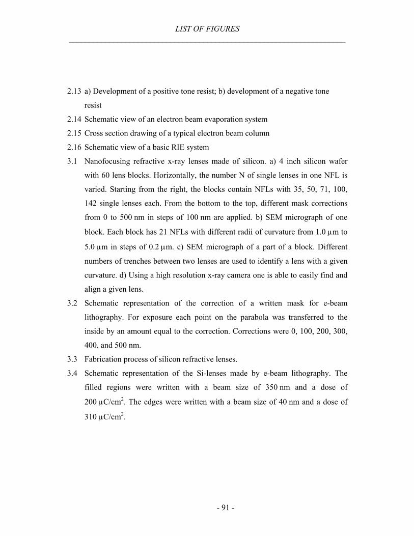
LIST OF FIGURES ____________________________________________________________________
- 91 -
2.13 a) Development of a positive tone resist; b) development of a negative tone
resist
2.14 Schematic view of an electron beam evaporation system
2.15 Cross section drawing of a typical electron beam column
2.16 Schematic view of a basic RIE system
3.1 Nanofocusing refractive x-ray lenses made of silicon. a) 4 inch silicon wafer
with 60 lens blocks. Horizontally, the number N of single lenses in one NFL is
varied. Starting from the right, the blocks contain NFLs with 35, 50, 71, 100,
142 single lenses each. From the bottom to the top, different mask corrections
from 0 to 500 nm in steps of 100 nm are applied. b) SEM micrograph of one
block. Each block has 21 NFLs with different radii of curvature from 1.0 µm to
5.0 µm in steps of 0.2 µm. c) SEM micrograph of a part of a block. Different
numbers of trenches between two lenses are used to identify a lens with a given
curvature. d) Using a high resolution x-ray camera one is able to easily find and
align a given lens.
3.2 Schematic representation of the correction of a written mask for e-beam
lithography. For exposure each point on the parabola was transferred to the
inside by an amount equal to the correction. Corrections were 0, 100, 200, 300,
400, and 500 nm.
3.3 Fabrication process of silicon refractive lenses.
3.4 Schematic representation of the Si-lenses made by e-beam lithography. The
filled regions were written with a beam size of 350 nm and a dose of
200 µC/cm2. The edges were written with a beam size of 40 nm and a dose of
310 µC/cm2.
LIST OF FIGURES ____________________________________________________________________
- 92 -
3.5 Determination of the lens depth. a) Due to the small area and large depth of the
lenses depth determination by electron micrograph is not possible without
breaking the lenses. b) However, the lens depth was successfully determined by
FRT and turned out to be 62 µm
3.6 a) First nanofocusing lenses made of silicon. Due to a small wafer size
(2 cm × 2 cm) and the resulting non-optimal contact between the wafer and the
plate in the reactive ion etching chamber, the depth was only 23 µm. The lens
surfaces are also slightly curved. b) Nanofocusing lenses made on a 4 inch
silicon wafer. Due to better contact between the sample and the plate in the
reactive ion etching chamber the depth was increased to 62 µm. In addition
vertical flats are obtained
3.7 a) SEM micrograph of half of a single lens (R=3.0 µm). b) The brightest point
on the curve corresponds to the edge of the lens
3.8 a) Fit of the lens shape to a parabolic function. b) The difference between the
lens shape and parabolic function shows minimal discrepancy
3.9 Schematic sketch of an experimental arrangement with nanofocusing lenses.
Two lenses perpendicular to each other must be aligned to focus in one plane
3.10 Experimental setup with silicon nanofocusing lenses as implemented at
ESRF/ID13. (1) Picomotor stage with entcoders for alignment of vertical lens,
(2) high resolution camera, (3) nanocube, (4) fluorescence detector, (5) sample
holder, (6) aperture, (7) horizontal lens, (8) vertical lens
3.11 (a) Horizontal and (b) vertical beam profile determined by fluorescence knife-
edge scans
LIST OF FIGURES ____________________________________________________________________
- 93 -
4.1 Scanning micrograph of an amorphous Ge2Sb2Te5 matrix with laser modified
areas. The thickness of the film is 80 nm. A 2000 Cu-mesh was used to identify
the given bit more easily
4.2 a) Scanning electron micrograph of laser induced polycrystalline microstructure
(Ge2Sb2Te5) in an amorphous film. b) Schematic sketch of a mesh –scan (9 x 9
points, step of 0.5 µm, exposure time per point of 90 s) through the laser
induced polycrystalline microstructure (Ge2Sb2Te5) in amorphous film
4.3 a) Diffraction from the polycrystalline AgInSbTe reference sample (exposure
time of 60s). b) Diffraction from a laser induced polycrystalline microstructure
(Ge2Sb2Te5) in amorphous film (exposure time of 90 s)
4.4 Schematic sketch of morphology of the crystallized area and diffraction patterns
for the laser induced crystallization samples (Ge2Sb2Te5, exposure time of 90s)
by varying of the spot position through the bit (points 1-7)
4.5 Diffracted intensity of the (200) reflection by the different spot position for the
laser induced crystallization samples (Ge2Sb2Te5, exposure time of 90 s)
4.6 a) White light interferometer image of the mirror array; b) a FIB (focused ion
beam image of an Al-blade at the hinge section
4.7 Scheme of the omega mode, where the scattering plane is inclined down near to
the surface and the shift of the diffraction peak is measured for different ξ-
values.
4.8 Diffraction from the Al-mirror (exposure time 10 s). Reflections in the centre
are due to higher harmonic in the beam and neglected by sample analysis.
Analysis of the residual stress was made by using 111-reflex with the
corresponding theoretical value of interplanar spacing of 2.338 Å
LIST OF FIGURES ____________________________________________________________________
- 94 -
4.9 a) Interplanar spacing of 111-reflex for the different rotation positions and shift
of interplanar spacing in the rocking mode of sin2(∆Ω)
5.1 Diffractogramm from the boron layers produced by CVD. The calculation
shows that it is β-rhombohedral phase.
5.2 The rhombohedral β-boron (R-105) structure.
5.3 a) Comparison of boron etch rates for different gas mixtures. The O2 gas flow
was varied. b) Etch rate of boron and self-bias for different gas flow in a pure
SF6 plasma (5 Pa, 200 W).
5.4 Etch rate of boron and etch selectivity of boron to Al-mask for different rf
power.
5.5 a) 1 µm thick aluminium mask structured with wet chemistry shows an isotropic
etch profile. b) Dry etching of 1 µm aluminium mask with BCl3 generates
vertical sidewalls.
5.6 Scanning electron micrograph of a) RIE grass by the etching of boron in the SF6
plasma; b) planar parabolic refractive nanofocusing lenses made of boron
5.7 Schematic sketches and images of lenses taken in transmission with the high
resolution x-ray camera for the different possibilities of the focusing. Due to a
curved boron surface only few lenses in one nanofocusing lens (NFL) could be
used for the focusing of x-rays. a) Some of the first and some of the last boron
lenses in one NFL take part in the focusing. b) Some fraction of the boron lenses
in an NFL creates a focus. c) Due to a flat surface from the beginning of the
microfabrication process, all silicon lenses in an NFL focus
5.8 Comparison of diamond etching rate for different processing gas mixtures and rf
power values.
LIST OF FIGURES ____________________________________________________________________
- 95 -
5.9 SEM image of an etched diamond sample. Etch parameters: 8 sccm of O2 and
7 sccm of Ar, total pressure of 0.33 Pa, rf power of 500 W. Etching time is 6
hours.
5.10 a)Comparison of pyrolitic graphite and titanium etch rates for different gas
mixture. O2 gas flow was varied. b) Scanning electron micrograph of an array of
parabolic refractive x-ray lenses made of pyrolitic graphite (N=60, R=2-4 µm,
l=8.6 mm)

- 96 -
List of Tables
3.1 Experimental details for the lenses test
4.1 Interplanar spacing for analysed samples.
- 97 -
Bibliography
[Amb] E. Amberger, K. Ploog, J. Less. Common. Met., 23, p.21, 1971.
[And] E. H. Anderson, D. L. Olynick, B. Harteneck, E. Veklerov, G.
Denbeaux, W. Chao, A. Lucero, L. Johnson, D. Attwood, J. Vac. Sci.
Technol. B, 18(6), 2970, 2000.
[Aris] V. Aristov, M. Grigoriev, S. Kuznecov, L. Shabelnikov, V. Zunkin, T.
Weitkamp, C. Rau, I. Snigireva, A. Snigirev, M. Hoffmann, E. Voges,
Appl. Phys. Lett., 77, 4058 (2000).
[Ayón] A. A. Ayón, R. L. Bayt, K. S. Breuer, Smart Mater. and Struct., 10,
1135, 2001.
[Ber] C. Bergemann, H. Keymeulen, and J. F. van der Veen, Phys. Rev. Lett.,
91 (20), 204801, 2003.
[Berg] M. Berger, J. Hubbell, S. Seltzer, J. S. Coursey, and D. S. Zucker,
XCOM: Photon Cross Section Database,
http://physics.nist.gov/PhysRefData/Xcom/html/xcom1.html.
[Boer] M. J. de Boer, et al, J. Microelectromech. Sys., 11, 385, 2002.
[Chem] “Chemical Bachgrounder”, http://www.nsc.org/library/chemical/.
[Chab] M. Chabloz, Y. Sakai, T. Matsuura, K. Tsutsumi, Microsys. Technol., 6,
86, 2000.
[Chan] C. Y. Chang, S. M. Sze, ULSI Technology. The McGRAW-Hill
Companies Inc, 1996.
BIBLIOGRAPHY ____________________________________________________________________
- 98 -
[Cloe] P. Cloetens, O. Hignette, S. Bohic, E. Pereiro, C. Ch. Morawe, W.
Ludwig, SRI 2003, San Francisco, 25-29 August, online presentation,
see http://www.sri2003.lbl.gov/html/presentations.thml.
[Clou] R. L. Clough, Nucl. Instr. and Meth. B, 185, 8, 2001.
[Dav] C. David, B. Kaulich, R. Medenwaldt, M. Hettwer, N. Fay, M. Diehl, J.
Thieme, G. Schmahl, J. Vac. Sci. and Technol. B, 13(6), 2762, 1995.
[Don] X. Dongzhu, Z. Dehang, P. Haochang, X. Hngjie, R. Zongxin, J. Appl.
Phys., 31, 1647, 1998.
[Duf] E.M. Dufrence, D. A. Arms, R. Clarke, N. R. Pereira, S. B. Dierker, D.
Foster, Appl. Phys. Lett., 79(25), 4085, 2001.
[Enl] J. Enlund, “ICP Etching of Single Crystal HTHP and CVD Diamond”,
February, 2003.
[Fed] J. B. Fedison, T. P. Chow, H. Lu, I. B. Bhat, J. Electrochem. Soc., 144,
221, 1997.
[FIT2D] http://www.esrf.fr/computing/scientific/FIT2D/.
[Fri1] I. Friedrich, V. Weidenhof, W. Njoroge, P. Franz, M. Wuttig, J. Appl.
Phys., 87, 4130, 2000.
[Fri2] I. Friedrich, V. Weidenhof, S. Lenk, M. Wuttig, Thin Solid Films, 389,
239, 2001.
[Gat] M. Gather, Bachelors thesis: „Boron nanofocusing refractive x-ray
lenses”, Aachen, 2004.
[Grig] I.S. Grigoriev, E. Z. Meilikhov, „Handbook of physical Quantities”,
CRC Press, Boca Raton, New York, London, Tokyo, 1997.
BIBLIOGRAPHY ____________________________________________________________________
- 99 -
[Hauk] V. Hauk, H. Behnken, W. Reimers, W. Pfeiffer, Ch. Genzel,
“Structural and Residual Stress Analysis by Nondestructive Methods”,
Elsevier Health Sciences, 1997.
[Hay] A. Hayes, J. F. Welden, E. Ostun, R. J. Gambino, Data Storage 43
(March/April), 1995.
[Haya] S. Hayakawa, N. Ikuta, M. Suzuki, M Wakatsuki, T. Hirokawa, J. Syn.
Rad., 8, 328, 2001.
[Hech] E. Hecht and A. Zajac, “Optics”, Addison-Wesley Publishing
Company, 2nd edition, 1987.
[Hign1] O Hignette, G. Rostaing, P. Cloetens, A. Rommeveaux, W. Ludwig, A.
Freund, in “X-ray Micro- and Nano- Focusing: Applications and
Techniques II” (ed. by McNulty), SPIE 4499, San Diego, 105, 2001.
[Hign2] O. Hignette, P. Cloetens, W. K. Lee, W. Ludwig, G. O. Rostaing,
Journal de Physique IV, 104, 231, 2003.
[Hop] J. Hopkins, et al, MRS Symposiom Proceedings, vol. 546, 63, Boston
1998.
[Ice] G. E. Ice, J. Chung, J. Z. Tischler, A. Lunt L. Assoufid, Rev. Scient.
Inst., 71(7), 2635, 2000.
[Ich] M. Ichinose, T.Ishida, Y. Takagai, M. Ito, S. Ohara, I. Satoh, Y.
Okazaki, R. Imanaka, Jpn J. Appl. Phys., 32, 5320, 1993.
[Jam] R. W. James, “The optical principles of the diffraction of x-rays,”
Cornell University Press, 1967.
[Kim] J. W. Kim, Y. C. Kim, W. J. Lee, J. Appl. Phys., 78, 2045, 1995.
[Kirk] P. Kirkpatrick, A.V. Baez, J. Opt. Soc. Am., 38, 766, 1948.
BIBLIOGRAPHY ____________________________________________________________________
- 100 -
[Köhl] M. Köhler, „Etching in Microsystem Technology“, WILEY-VCH
Verlag GmbH, 1999.
[Len1] B. Lengeler, C. G. Schroer, M. Richwin, J. Tümmler, M. Drakopoulos,
A. Snigirev, I. Snigireva, Appl. Phys. Lett., 74 (26), 3924, 1999.
[Len2] B. Lengeler, C. G. Schroer, B. Benner, A. Gerhardus, T. F. Günzler, M.
Kuhlmann, J. Meyer, C. Zimprich, J. Syn. Rad., 9, 119, 2002.
[Len3] B. Lengeler, J. Tümmler, A. Snigirev, I. Snigireva, C. Raven, J. Appl.
Phys, 84 (11), 5855, 1998.
[Len4] B. Lengeler, C. Schroer, M. Kuhlmann, B. Benner, T. Günzler, O.
Kurapova, F. Zontone, A. Snigirev, I. Snigireva, J. Phys. D: Appl.
Phys., 38, 1, 2005.
[Liu] H.-C. Liu, Y.-H. Lin, W. Hsu, Microsys. Technol., 10, 29, 2003.
[Mich] A. G. Michette, “Optical systems for soft x-rays”, Plenum Press, New
York, 1986.
[NFL] Calculating, using the software NFLCALC which was developed by C.
G. Schroer, www.xray-lens.de.
[Pie] H. O. Pierson, “Handbook of carbon, graphite, diamond and fullers”,
1993.
[Prot] V. V. Protopopov, K. A. Valiev, Opt. Commun., 151, 297, 1998.
[Rai] P. Rai-Choudhury, “Microlithography, Micromachining and
Microfabrication”, volume 1. SPIE Optical Engineering Press, 1997.
[Sam] www.samcointl.com/apps/mems.html.
[Sch] J. Schreiber, S. Braun, A Gatto, H. Schenk, Proceeding of SPIE, 5392,
18, 2004.
BIBLIOGRAPHY ____________________________________________________________________
- 101 -
[Schr1] C. G. Schroer, M. Kuhlmann, U. T. Hunger, T. F. Günzler, O.
Kurapova, S. Feste, F. Frehse, B. Lengeler, M. Drakopoulos, A.
Somogyi, A. S. Simionovici, A. Snigirev, I. Snigireva, C. Schug, W. H.
Schröder, Appl. Phys. Lett., 82 (9), 1485, 2003.
[Schr2] C. G. Schroer, B. Lengeler, Phys. Rev. Lett., 94, 054802, 2005.
[Schr3] C. G. Schroer, „Hard x-ray microscopy and microanalysis with
refractive x-ray lenses“, RWTH Aachen University, Department of
Physics, habilitation, 2004.
[Schr4] C. G. Schroer, M. Kuhlmann, O. Kurapova, T. Hunger, T. Günzler, S.
Feste, B. Lengeler, S. Ziegler, M. Drakopoulos, M. Burghammer, C.
Riekel, A. Snigirev, I. Snigireva, “Design and Microfabrication of
Novel X-ray Optics II”, Proceedings of SPIE, 5535, 10, 2004.
[Schr5] C. G. Schroer, T. Günzler, M Kuhlmann, O. Kurapova, S. Feste, M.
Schweizer, B. Lengeler, W. Schröder, M. Drakopoulos, A. Somogyi, A.
Simionovici, A. Snigirev, I. Snigireva, “Developments in X-ray
Tomography IV”, Proceeding of SPIE, 5535, 162, 2004.
[Schr6] C. G. Schroer, O. Kurapova, J. Patommel, P. Boye, J. Feldkamp, B.
Lengeler, L. Vincze, A. van der Hart, M. Küchler, Appl. Phys. Lett.,
2005.
[Schn] G. Schneider, T. Schliebe, H. Aschoff, J. Vac. Sci. Technol. B, 13(6),
2809, 1995.
[Shin] M. Shinotsuka, T. Shibaguchi, M. Abe, Y. Ide, Jpn. J. Appl. Phys., 36,
536, 1997.
[Slo] D. Slovetsky, “Mechanism of the materials etching in plasma”,
Lections.
BIBLIOGRAPHY ____________________________________________________________________
- 102 -
[SM1] Specialty Materials, Inc., 1449 Middlesex Street, Lowell, MA, USA,
http://www.specmaterials.com.
[SM2] Data provided by Specialty Materials Inc.
[Snig] A. Snigirev, V. Kohn, I. Snigireva, B. Lengeler, Nature, 384, 49, 1996.
[Spec] S. J. Spector, C. J. Jacobsen, D. M. Tennant, J. Vac. Sci. Technol. B,
15(6), 2872, 1997.
[Sung] Y. J. Sung, H. S. Kim, Y. H. Lee, J. W. Lee, S. H. Chae, Y. J. Park, G.
Y. Yeom, Mat. Sci. and Engin. B82, 50, 2001.
[Tam] N. Tamura, R. S. Celestre, A. A. MacDowell, H. A. Padmore, R.
Spolenak, B. C. Valek, N. Meier Chang, A. Manceau, J. P. Patel, Rev.
Sci. Instr., 73(3), 1369, 2002.
[Tüm] J. Tümmler, “Development of Compound Refractive Lenses for Hard X-
Rays”, Dissertation RWTH Aachen, Shaker Verlag, 17, 2000.
[Veig] W. J. Veigele, “Mass attenuation and absorption cross section for 94
elements; 0.1 keV to 1 MeV”, in “Handbook of Spectroscopy”, ed. by J.
W. Robinson, CRC Press, Inc., Bosa Raton, Florida 33431, USA, 28,
1980.
[Vol] B. Volland, et al, J. Vac. Sci. and Techn. B, 17, 2768, 1999.
[Yam] K. Yamauchi, K. Yamamura, H. Mimura, Y. Sano, A. Saito, A.
Suvorov, M. Yabashi, K. Tamasaku, T. Ishikava, Y. Mori, J. Syn. Rad.,
9, 313, 2002.
[Yama] N. Yamada, E. Ohno, N. Akahira, K. Nishiuchi, K. Nagata, M. Takao,
Jpn. J. Appl. Phys., 26, 61, 1987.

BIBLIOGRAPHY ____________________________________________________________________
- 103 -
[Yun] W. Yun, B. Lai, Z. Cai, J. Maser, D. Legnini, E. Gluskin, Z. Chen, A.
Krasnoperova, Y. Vladimirsky. R. Cerrina, E. Di Fabrizio, M. Gentili,
Rev. Sci. Instr., 70(5), 2238, 1999.
- 104 -
Acknowledgements
PhD project always comes to fruition only with the assistance of many people. Here I
would like to thank all who contributed directly (and indirectly) to the quality of this
work:
• Prof. Dr. B. Lengeler for the very interesting topic and efficient supervision on
all stages of my thesis,
• Prof. Dr. U. Klemradt for agreeing to act as co-referee in this work,
• Dr. Schroer who introduced the world of x-ray optics and of article writing to
me and whose enthusiasm and optimism always was helpful,
• Dr. T. Hunger who introduced the microfabrication techniques to me and
always helped with many tips and tricks of RIE and not only,
• all members of our group – B. Benner, P. Boye, J. Feldkamp, S. Feste, F.
Frehse, F. Günzler, M. Kuhlmann, J. Patommel, M. Schweitzer, C. Zimprich -
for the warm atmosphere and fruitful discussions, what ever a subject was and
letting me keep my experimental work in a good form. People, who were
always ready to give me a small lecture about right German and local dialect,
respectively.
• our secretaries - R. Weinkauf, A. Schüren and S. Vurgun – for help with the
office work and office techniques, for sweets and tee, for smiles and
countenance,
• to all people of mechanical workshop of the University, to P. Kordt and W.
Retetzki in particular, who were very patient to realized all technical ideas for
the lens setup,
- 105 -
• K. D. Schaefer from the electrical workshop for reanimating the low-voltage
voltmeter for galvanic and D. Schulte, especially, for his help with the cooling
system for the evaporation plant,
• ESRF people - I. Snigireva, A. Snigirev, M. Drakopoulos, M. Burghammer, C.
Riekel, F. Zontone, A. Somogyi, A. Simionovici - for the friendly and
communicative atmosphere, without their help our experiments would be not
so successful,
• FZ - Jülich people - A. Steffen for the careful evaporation of Si-wafer and for
possibility to use modern rein room in my aims, A. van der Hart for e-beam
lithography over a long period of time and for an unceasing interest to results
of the experiments, W. Schröder for interesting discussion about biological
objects,
• ZfM people, especially M. Küchler, for professional etching our Si lenses and
for care during my visit in Chemnitz,
• The very special thanks is addressed to my husband Denis for his support,
understanding, believe and everything else.
- 106 -
Curriculum Vitae
Personal details:
Name Olga Kurapova
Maiden name Prokopenko
Date of birth 03.04.1977
Place of birth Tashkent, USSR
Marital status married, no children
Nationality Russian
School education:
09/1984-06/1994 Secondary school with profound study of Physics
and Math, Tashkent, USSR
University education:
09/1994-06/1998 Bachelor’s degree in Physics of Condensed Matter,
Moscow State Steel and Alloys University,
Department of Physical Chemistry
09/1998-06/2000 Master’s degree in Physics of Condensed Matter,
Moscow State Steel and Alloys University,
Department of Theoretical Physics
04/2002-10/2005 Ph. D. student at the II. Physicalisches Institut B,
RWTH, Aachen University