Effiziente Modellbildung für Verbindungsstrukturen der … in der TET... · 2013-10-14 ·...
57
Effiziente Modellbildung für Verbindungsstrukturen der Elektrotechnik Vortrag am Lothar-Collatz-Zentrum für Wissenschaftliches Rechnen, Universität Hamburg 18. Juni 2013 Prof. Dr. sc. techn. Christian Schuster Theoretische Elektrotechnik Technische Universität Hamburg-Harburg
Transcript of Effiziente Modellbildung für Verbindungsstrukturen der … in der TET... · 2013-10-14 ·...
Effiziente Modellbildung für Verbindungsstrukturen
der Elektrotechnik
Vortrag am Lothar-Collatz-Zentrum für Wissenschaftliches Rechnen, Universität Hamburg
18. Juni 2013
Prof. Dr. sc. techn. Christian Schuster
Theoretische Elektrotechnik Technische Universität Hamburg-Harburg

2
Mitarbeiter
Xiaomin Duan, Sebastian Müller, Miroslav
Kotzev, Andreas Hardock, Heinz-Dietrich Brüns
Young Kwark, Xiaoxiong Gu, Renato Rimolo-
Donadio, Bruce Archambeault, Hubert Harrer,
Mark Ritter
Jim Drewniak, Jun Fan, Yaojiang Zhang
… und weitere!
3
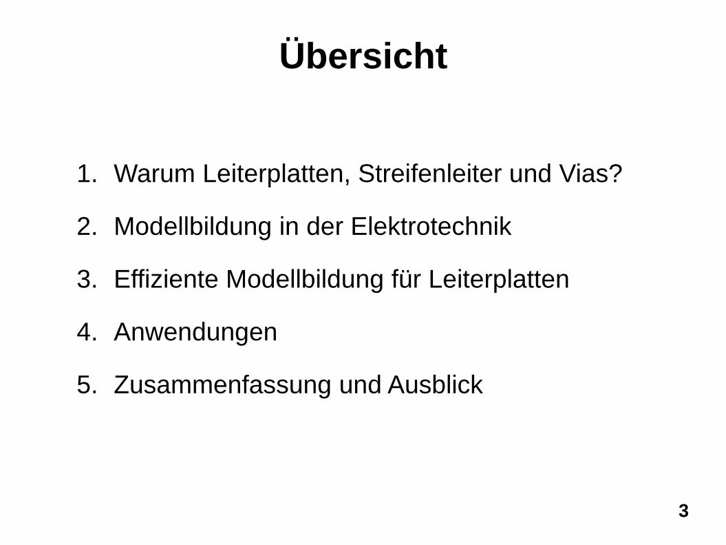
1. Warum Leiterplatten, Streifenleiter und Vias?
2. Modellbildung in der Elektrotechnik
3. Effiziente Modellbildung für Leiterplatten
4. Anwendungen
5. Zusammenfassung und Ausblick
Übersicht
4
1. Warum Leiterplatten, Streifenleiter und Vias?
2. Modellbildung in der Elektrotechnik
3. Effiziente Modellbildung für Leiterplatten
4. Anwendungen
5. Zusammenfassung und Ausblick
Übersicht
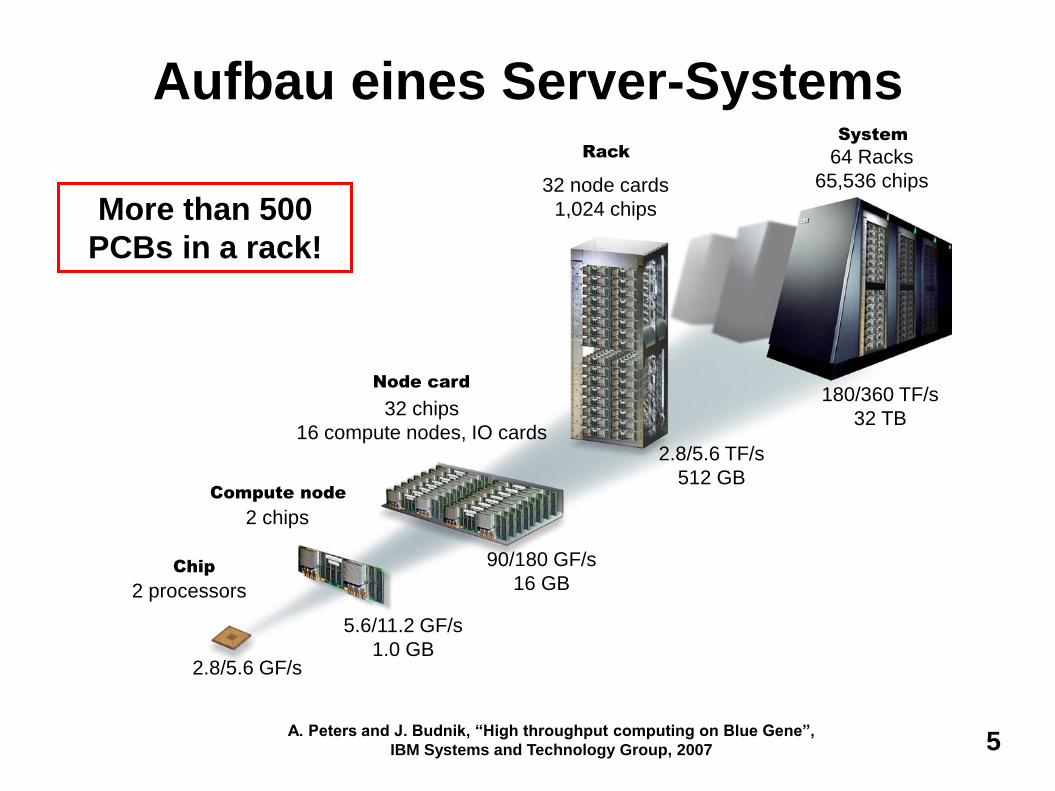
32 node cards
1,024 chips
2.8/5.6 TF/s
512 GB
Rack 64 Racks
65,536 chips
180/360 TF/s
32 TB
System
32 chips
16 compute nodes, IO cards
90/180 GF/s
16 GB
Node card
2 chips
5.6/11.2 GF/s
1.0 GB
Compute node
2.8/5.6 GF/s
2 processors
Chip
A. Peters and J. Budnik, “High throughput computing on Blue Gene”,
IBM Systems and Technology Group, 2007
More than 500
PCBs in a rack!
Aufbau eines Server-Systems
5
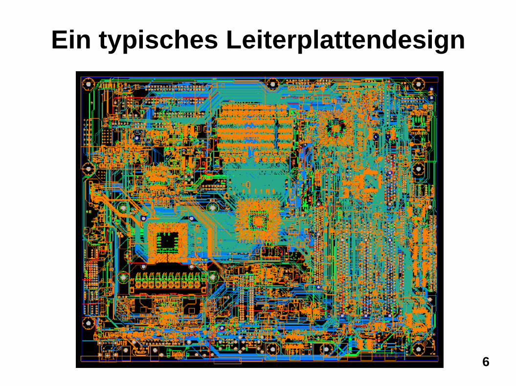
Ein typisches Leiterplattendesign
6
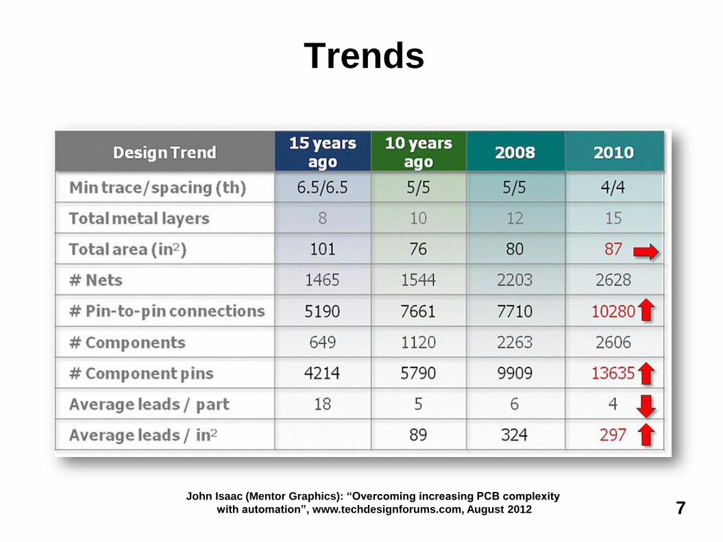
John Isaac (Mentor Graphics): “Overcoming increasing PCB complexity
with automation”, www.techdesignforums.com, August 2012
Trends
7
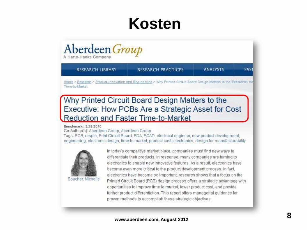
Kosten
www.aberdeen.com, August 2012 8
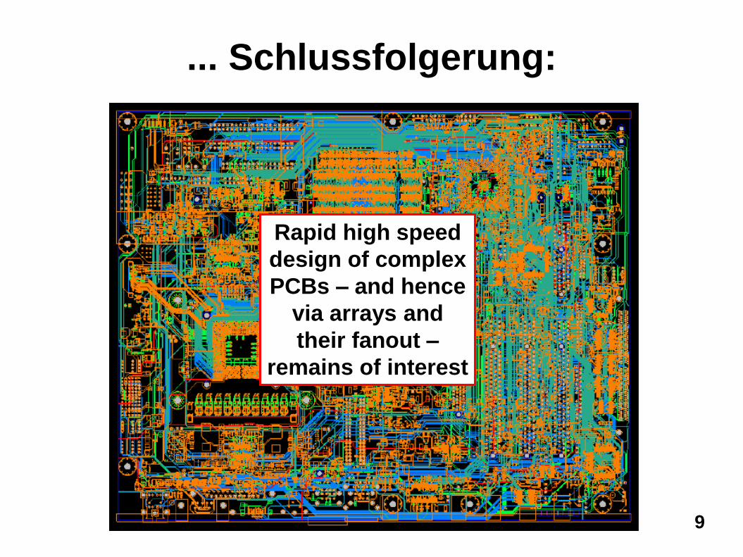
... Schlussfolgerung:
Rapid high speed
design of complex
PCBs – and hence
via arrays and
their fanout –
remains of interest
9
10
1. Warum Leiterplatten, Streifenleiter und Vias?
2. Modellbildung in der Elektrotechnik
3. Effiziente Modellbildung für Leiterplatten
4. Anwendungen
5. Zusammenfassung und Ausblick
Übersicht
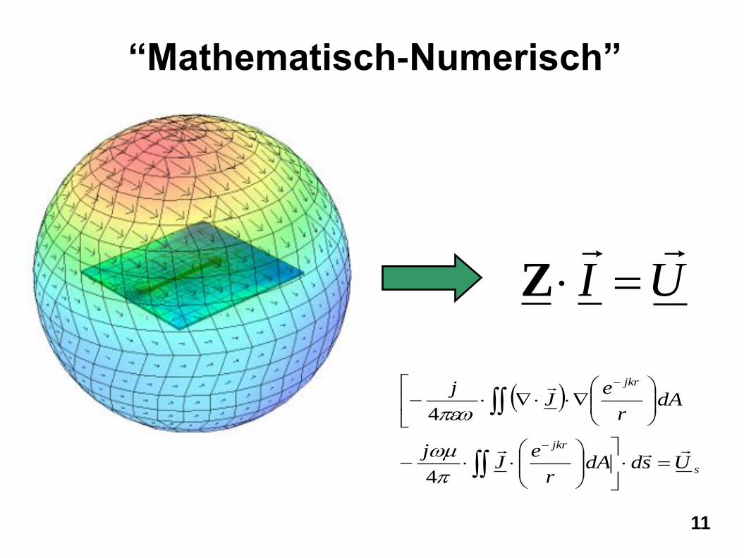
“Mathematisch-Numerisch”
UI
Z
s
jkr
jkr
UsddAr
eJ
j
dAr
eJ
j
4
4
11
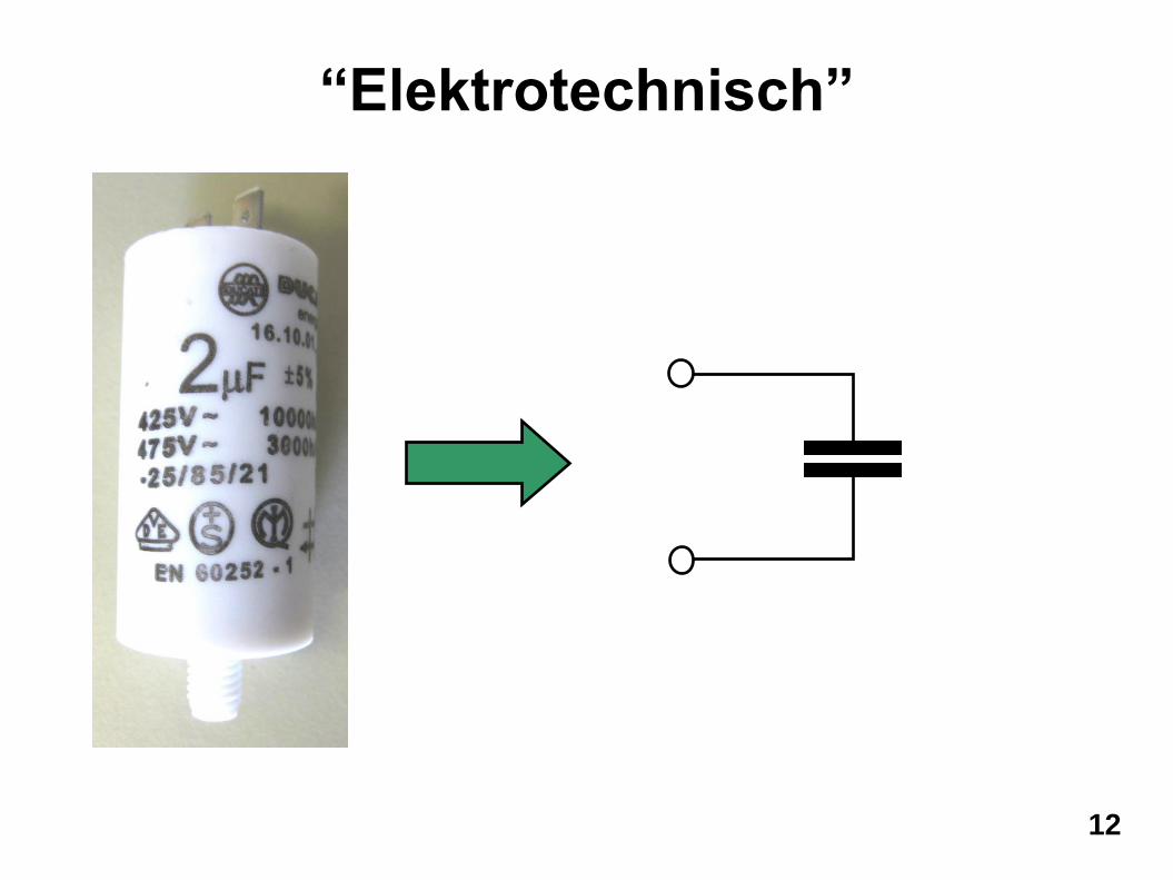
“Elektrotechnisch”
12
Frequency
Ma
gn
itu
de
of Im
pe
da
nce
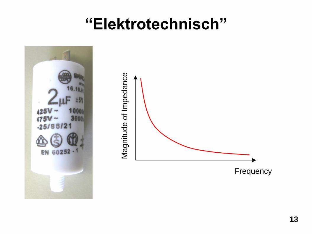
“Elektrotechnisch”
13
Frequency
Ma
gn
itu
de
of Im
pe
da
nce
“Elektrotechnisch”
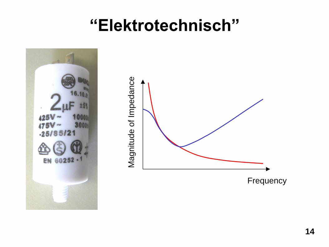
14
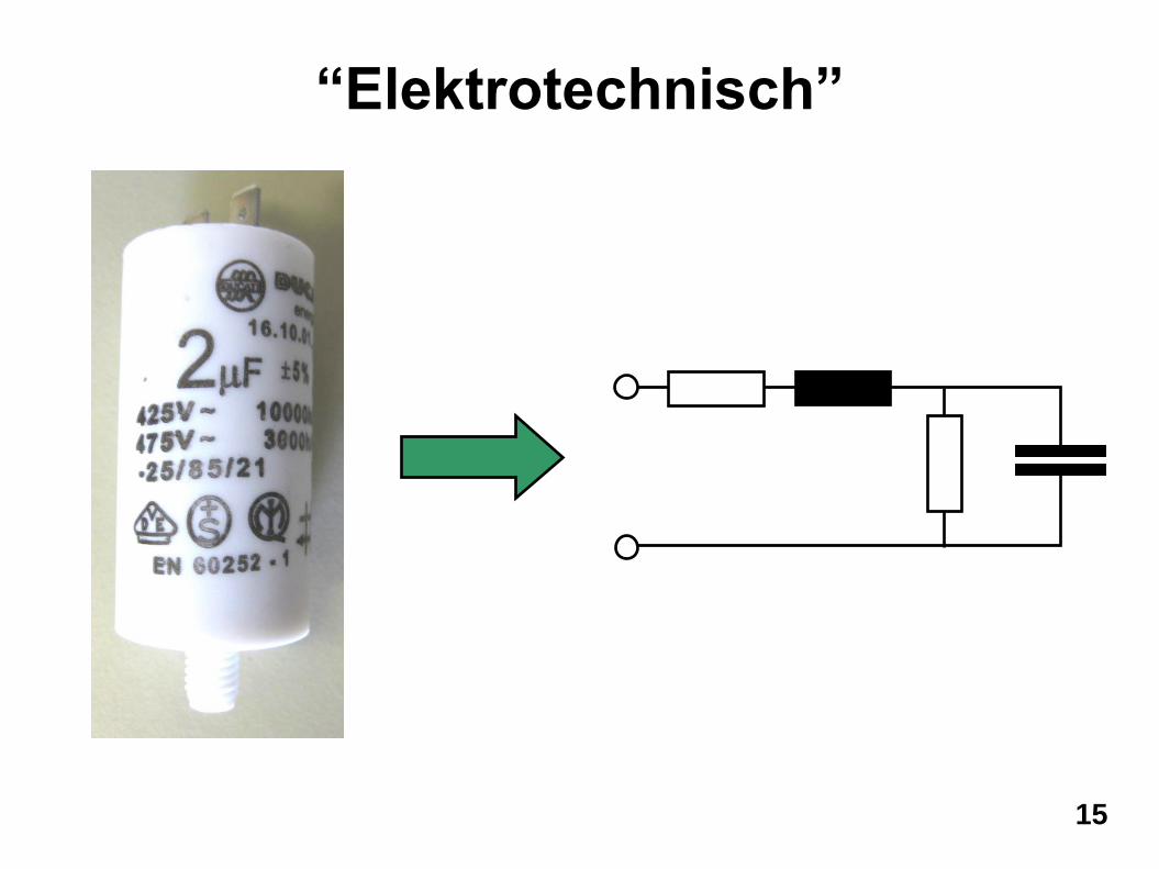
“Elektrotechnisch”
15
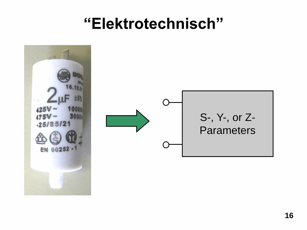
S-, Y-, or Z-
Parameters
“Elektrotechnisch”
16
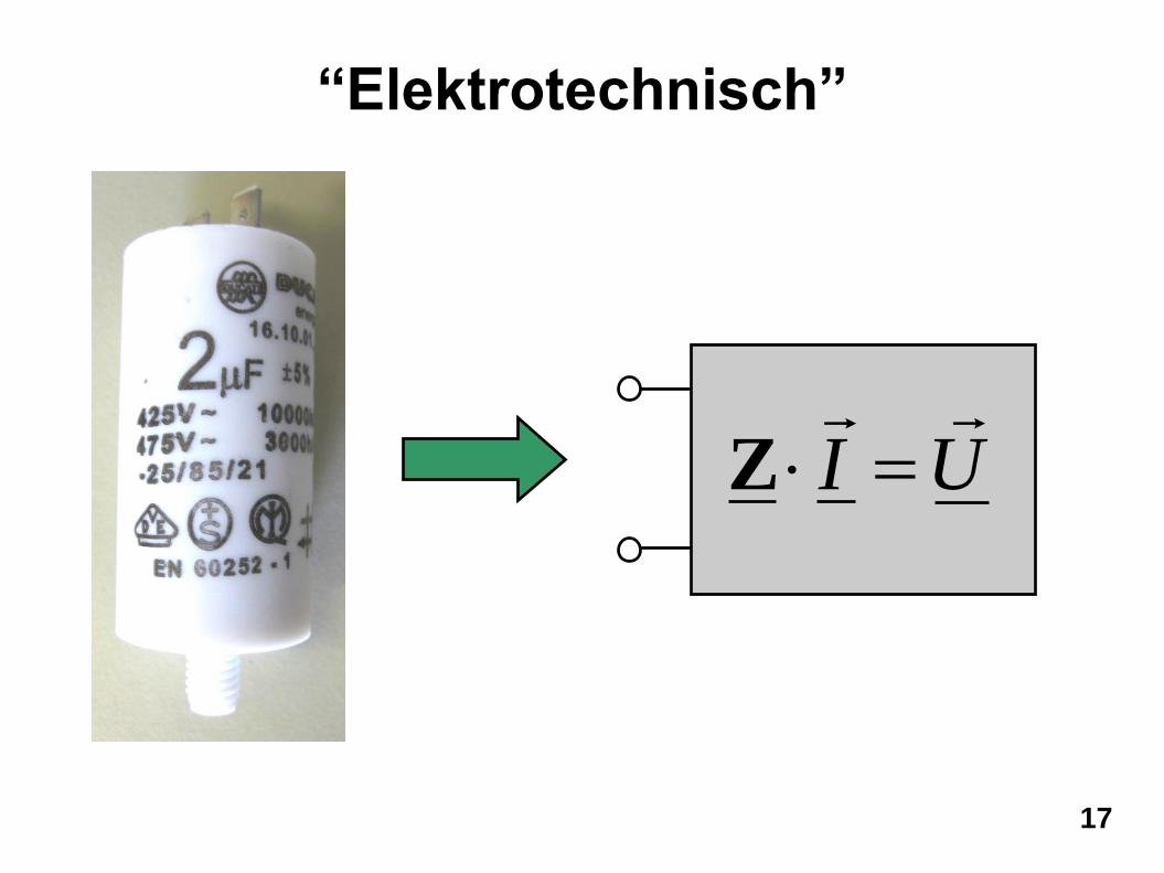
“Elektrotechnisch”
17
UI
Z
18
1. Warum Leiterplatten, Streifenleiter und Vias?
2. Modellbildung in der Elektrotechnik
3. Effiziente Modellbildung für Leiterplatten
4. Anwendungen
5. Zusammenfassung und Ausblick
Übersicht
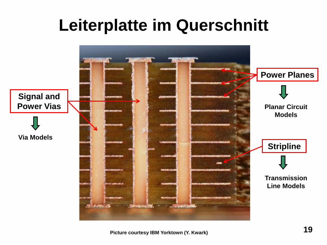
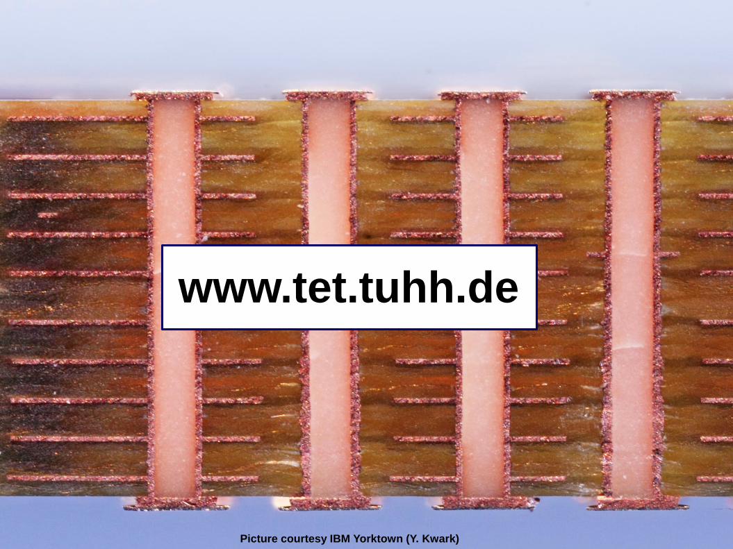
Picture courtesy IBM Yorktown (Y. Kwark)
Power Planes
Stripline
Signal and
Power Vias
Transmission
Line Models
Planar Circuit
Models
Via Models
19
Leiterplatte im Querschnitt
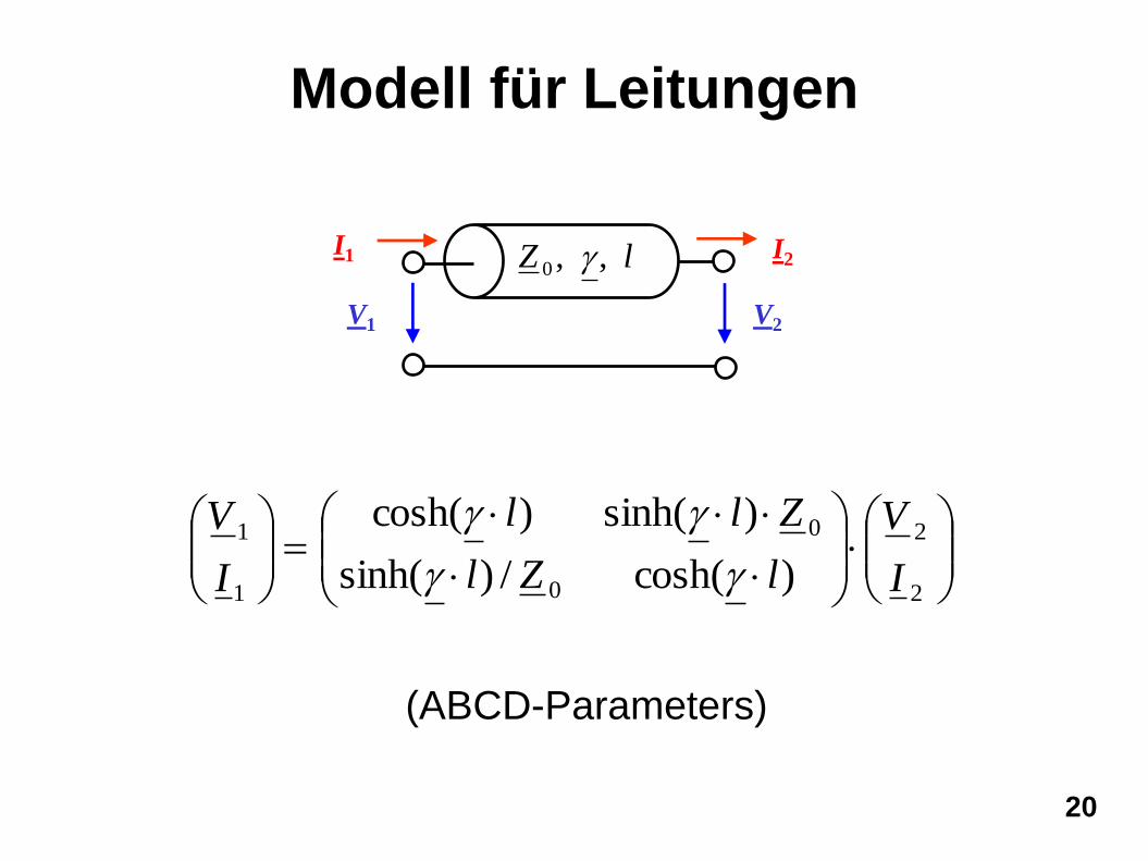
Modell für Leitungen
I1
V1
I2
V2
lZ ,,0
20
2
2
0
0
1
1
)cosh(/)sinh(
)sinh()cosh(
I
V
lZl
Zll
I
V
(ABCD-Parameters)
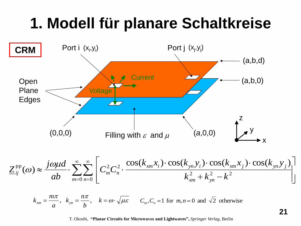
x
y
z
(0,0,0) (a,0,0)
(a,b,0)
(a,b,d)
Port i Port j (xi,yi)
Open
Plane
Edges
Voltage
Current
(xj,yj)
Filling with and
CRM
kb
nk
a
mk ynxm ,, otherwise 2 and 0,for 1 , nmCC nm
0 0222
22pp )cos()cos()cos()cos()(
m n ynxm
jynjxmiynixm
nmijkkk
ykxkykxkCC
ab
djZ
21
1. Modell für planare Schaltkreise
T. Okoshi, “Planar Circuits for Microwaves and Lightwaves”, Springer Verlag, Berlin
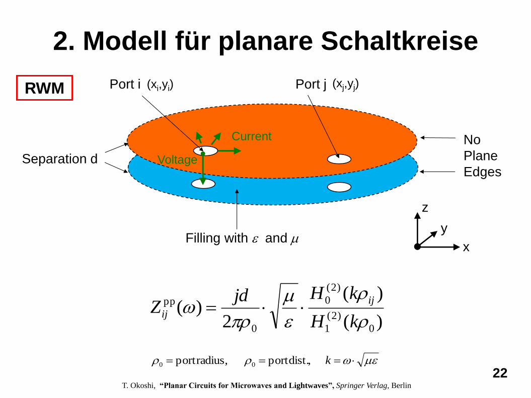
x
y
z
Separation d
Port i Port j (xi,yi)
No
Plane
Edges Voltage
Current
(xj,yj)
Filling with and
)(
)(
2)(
0
)2(
1
)2(
0
0
pp
kH
kHjdZ
ij
ij
k,dist.port,radiusport 00
RWM
22
2. Modell für planare Schaltkreise
T. Okoshi, “Planar Circuits for Microwaves and Lightwaves”, Springer Verlag, Berlin
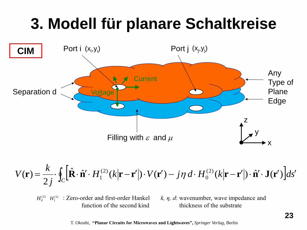
x
y
z
Separation d
Port i Port j (xi,yi)
Any
Type of
Plane
Edge Voltage
Current
(xj,yj)
Filling with and
CIM
3. Modell für planare Schaltkreise
23
sdkHdjVkHj
kV
C )(ˆ)()()(ˆˆ
2)( )2(
0
)2(
1 rJnrrrrrnRr
)2(
1H)2(
0H : Zero-order and first-order Hankel
function of the second kind
k, η, d: wavenumber, wave impedance and
thickness of the substrate
T. Okoshi, “Planar Circuits for Microwaves and Lightwaves”, Springer Verlag, Berlin
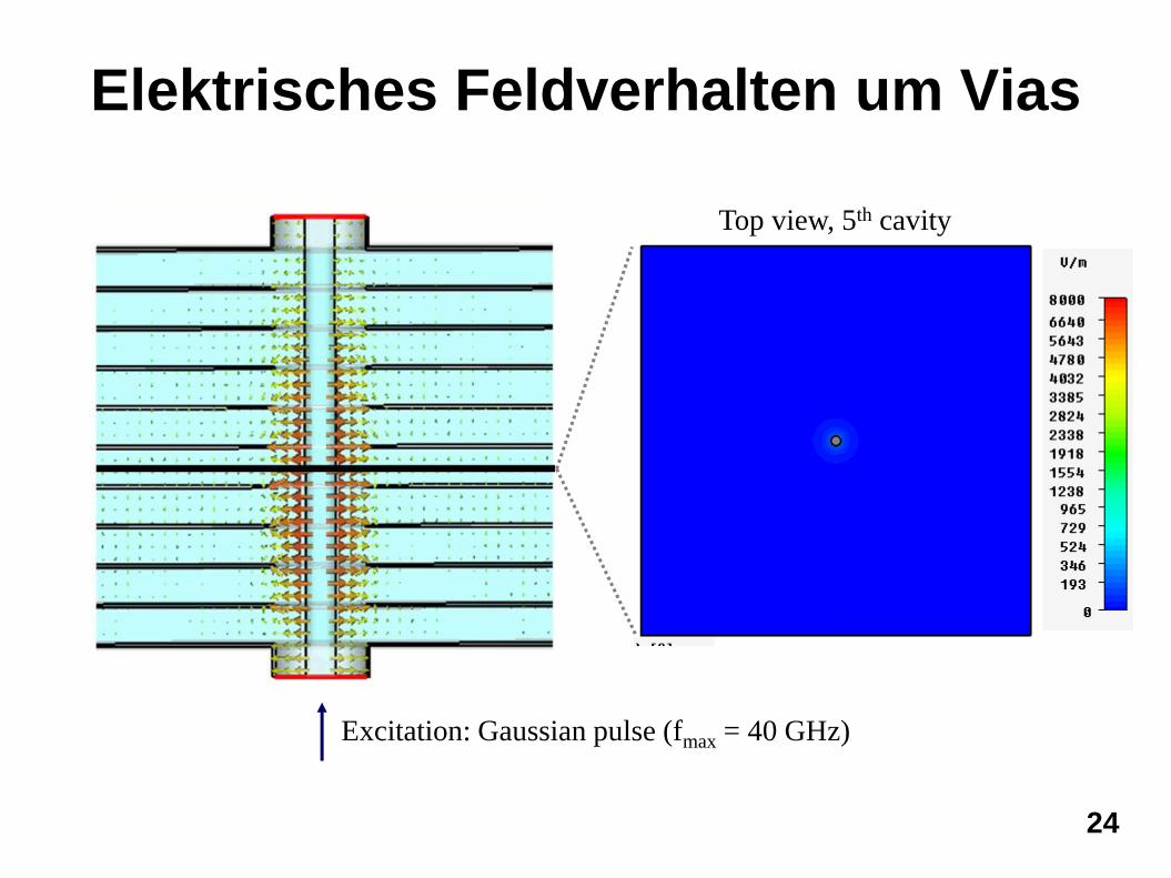
Top view, 5th cavity
Excitation: Gaussian pulse (fmax = 40 GHz)
24
Elektrisches Feldverhalten um Vias
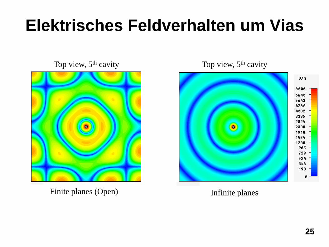
Top view, 5th cavity
Infinite planes Finite planes (Open)
Top view, 5th cavity
25
Elektrisches Feldverhalten um Vias
26
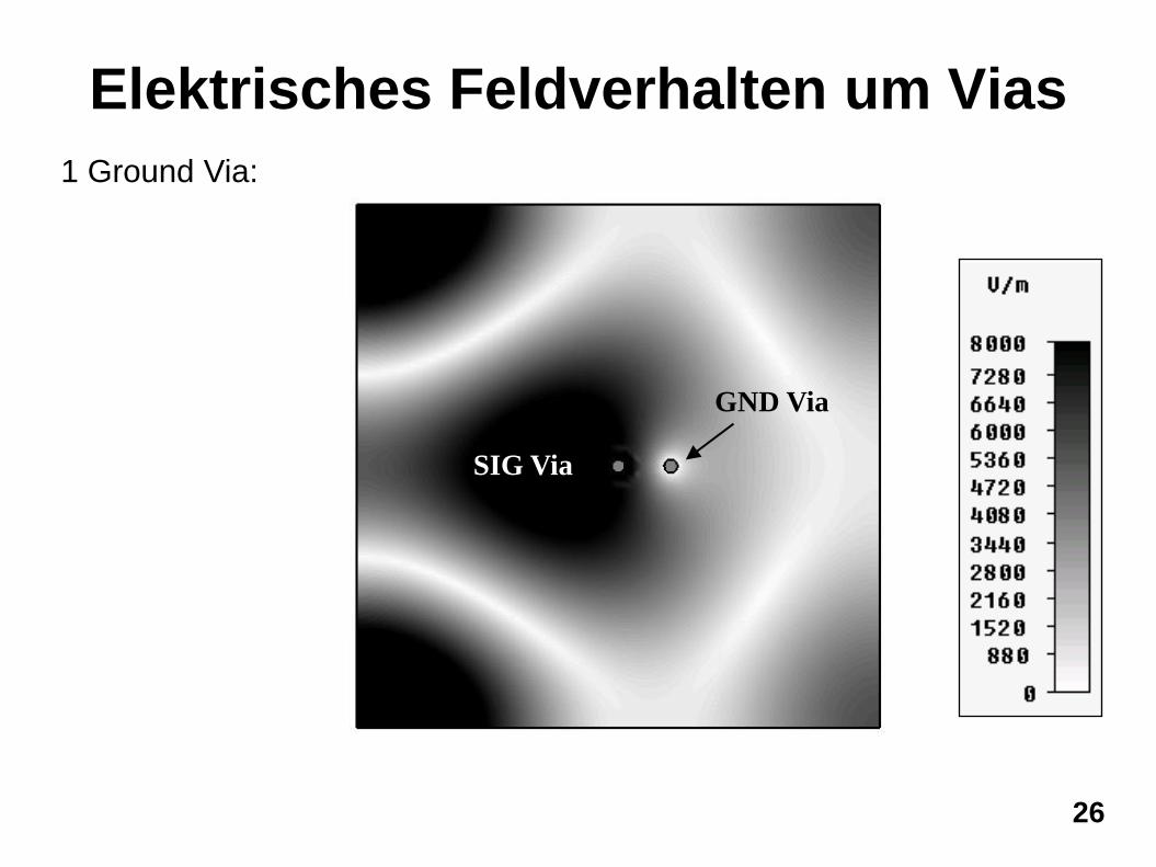
Elektrisches Feldverhalten um Vias
1 Ground Via:
1 GND via
GND Via
SIG Via
27
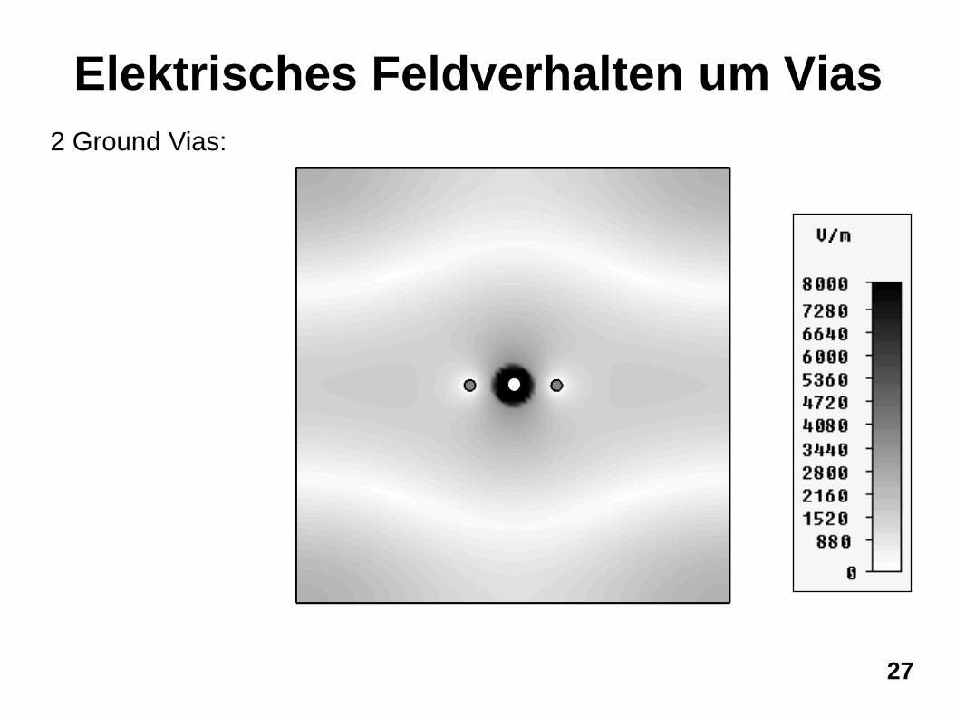
Elektrisches Feldverhalten um Vias
2 Ground Vias:

28
Elektrisches Feldverhalten um Vias
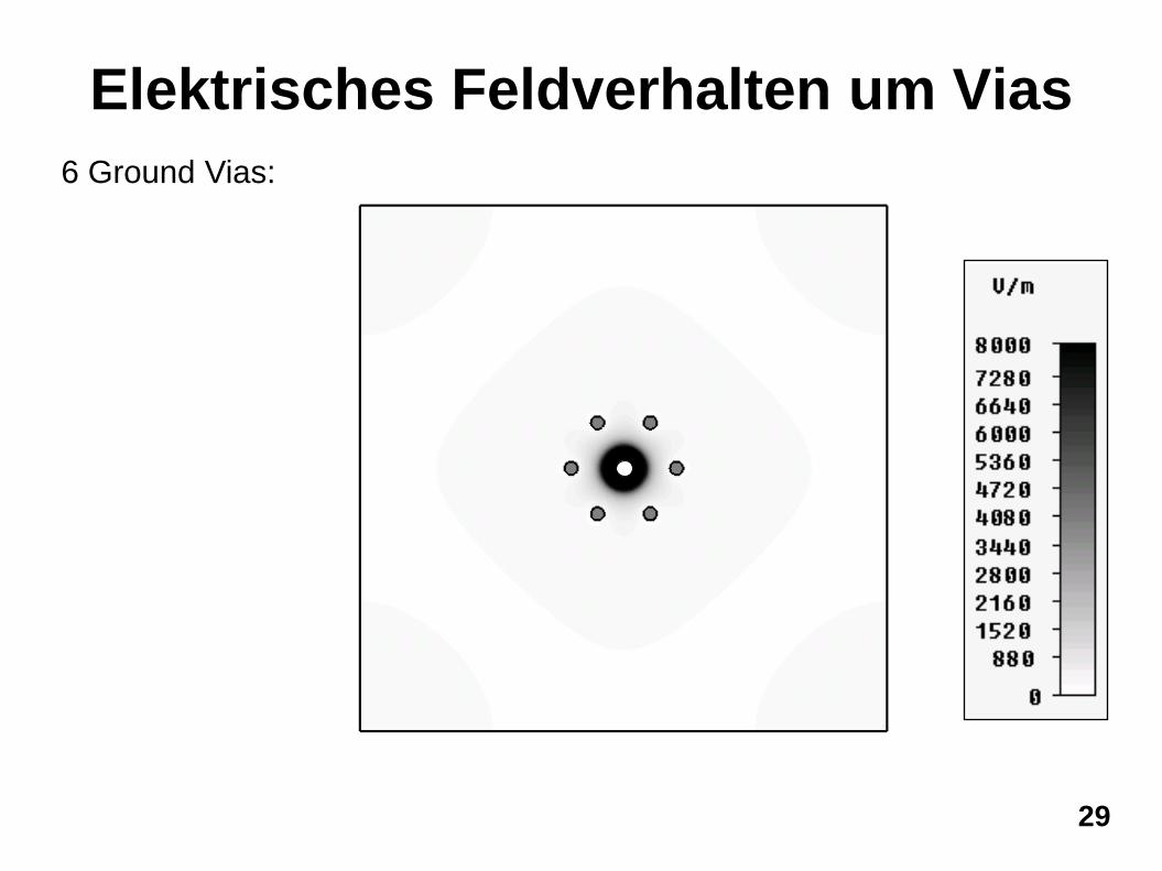
4 Ground Vias:
29
Elektrisches Feldverhalten um Vias
6 Ground Vias:
30
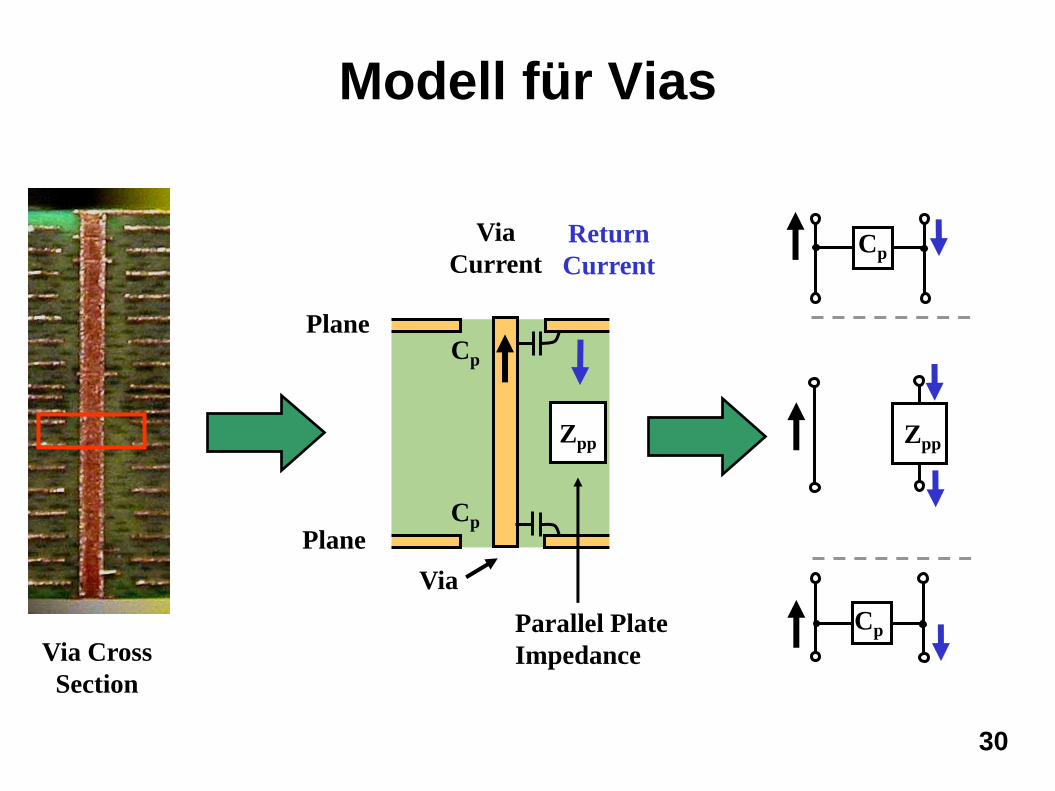
Via Cross
Section
Modell für Vias
Cp
Zpp
Cp
Via
Plane
Plane Cp
Cp
Zpp
Parallel Plate
Impedance
Return
Current
Via
Current
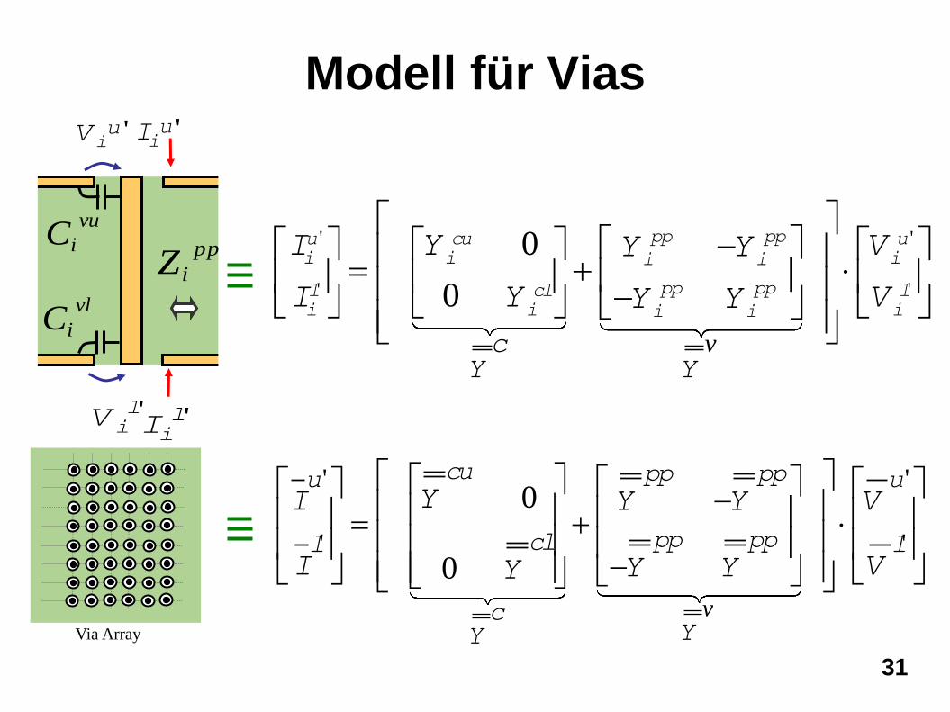
31
'uiV
'liV
'liI
'uiI
vu
iC
vl
iC
pp
iZ' '
' '
0
0
pp ppu cu ui i ii i
pp ppl cl li i ii i
Y Yc
I Y VY Y
I Y VY Y
v
Via Array
' '
' '
0
0
cu pp ppu u
pp ppcll l
YYc
YI VY Y
I VY YY
v
Modell für Vias
32
Modell für Vias
Y. Zhang, J. Fan, G. Selli, M. Cocchini, and D. P. Francesco
“Analytical evaluation of via-plate capacitance for multilayer printed circuit boards and packages”
IEEE Trans. on Microwave Theory and Techniques, vol. 56, no. 9, September 2008.
(2) (2)
(2)
2 1
.
0 0
01,3,5..2
8 1( ) ( )
ln( ) ( )
N
n
dn n
n n
H k H kd k H k
ap
i
apb vi i iv v
i i
C r rr / r r
22
0 )/( dnkk rn
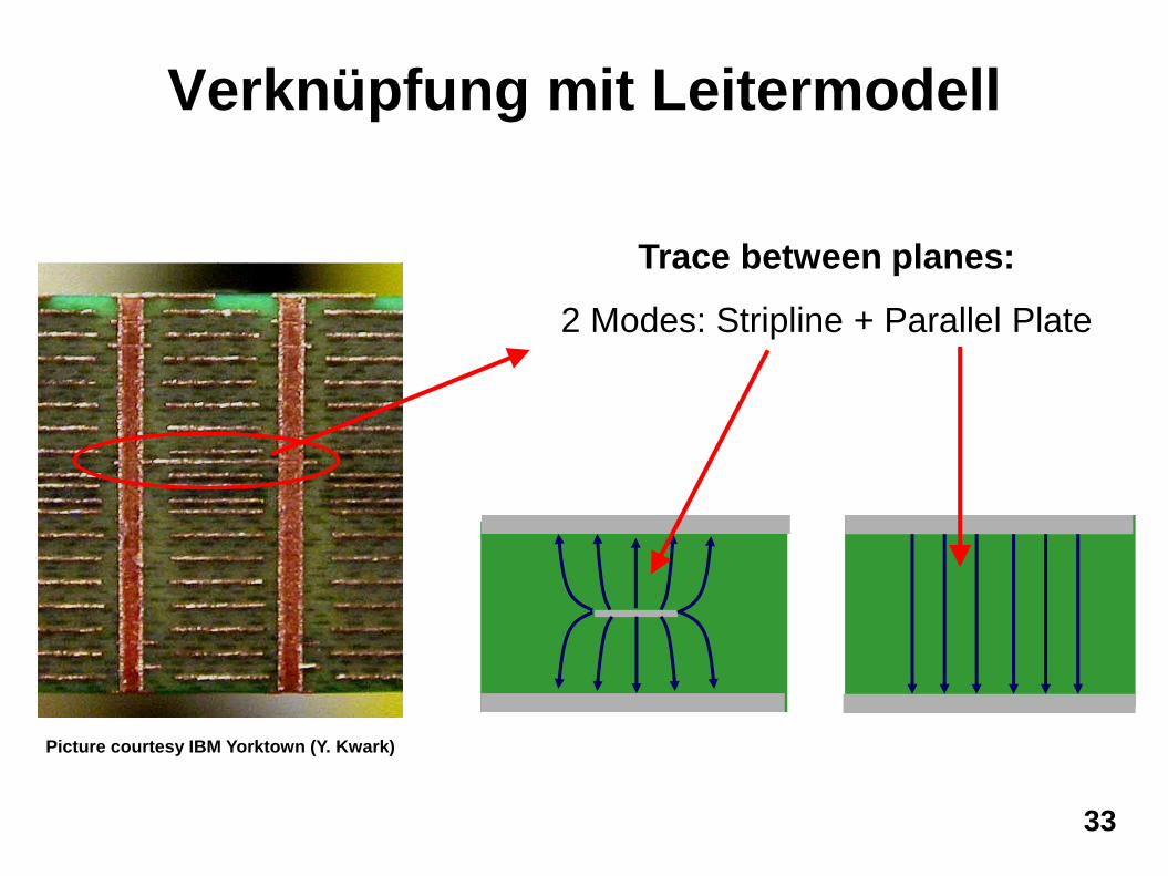
Verknüpfung mit Leitermodell
33
Trace between planes:
2 Modes: Stripline + Parallel Plate
Picture courtesy IBM Yorktown (Y. Kwark)
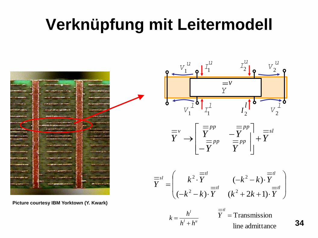
Verknüpfung mit Leitermodell
34
Yv
uI
1
uI
2u
V2
uV
1
lV
1
lI
1
lV
2
lI
2
tltl
tltlsl
YkkYkk
YkkYkY
)12()(
)(
22
22
sl
pppp
ppppv
YYY
YYY
ul
l
hh
hk
admittance line
on Transmissitl
Y
Picture courtesy IBM Yorktown (Y. Kwark)
tlYkk
tlYkk
tlYkk
tlYkk
tlYk0
0tl
Yk
)()(
)()(
)( 22
22
1
vl
vu
Y0
0Y
l
u
I
I
T T
1uv
1ui
2uv
2ui
3uv
3ui
1lv
1li 2l
v2l
i3l
v3l
i
u
uIV
l
lIV
pppp
pppp
YY
YY
Ztl Ztl
Zpp Zpp Zpp Zpp
l
u
V
V
vC
vC v
C
vC
vC v
C
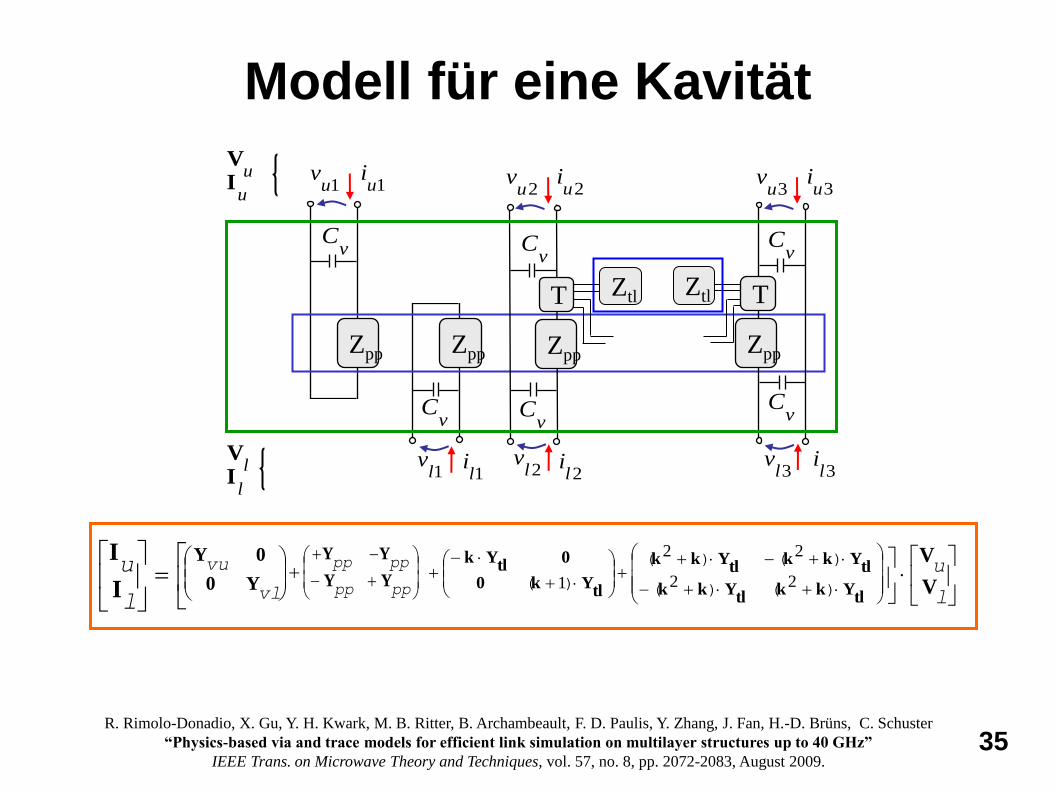
R. Rimolo-Donadio, X. Gu, Y. H. Kwark, M. B. Ritter, B. Archambeault, F. D. Paulis, Y. Zhang, J. Fan, H.-D. Brüns, C. Schuster
“Physics-based via and trace models for efficient link simulation on multilayer structures up to 40 GHz”
IEEE Trans. on Microwave Theory and Techniques, vol. 57, no. 8, pp. 2072-2083, August 2009.
Modell für eine Kavität
35
Zpp Ztl
Decap
Linterc.
Zpp Ztl
Decap
Linterc.
Decap
Linterc.
Decoupling capacitor model
Cavity
N
Port i Port j
Port k
36
Vollständiges Leiterplattenmodell
Cavity
1
Cavities merged using
segmentation techniques
S-, Y-, or Z-
Parameters
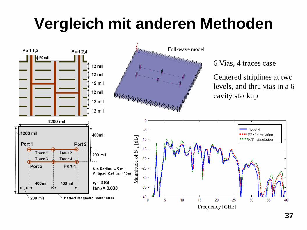
6 Vias, 4 traces case
Centered striplines at two
levels, and thru vias in a 6
cavity stackup
Full-wave model
Mag
nit
ude
of
S12 [
dB
]
Frequency [GHz]
Model
FEM simulation
FIT simulation Full-wave model M
agn
itu
de
of
S14 [
dB
]
Frequency [GHz]
Model
FEM simulation
FIT simulation
37
Vergleich mit anderen Methoden
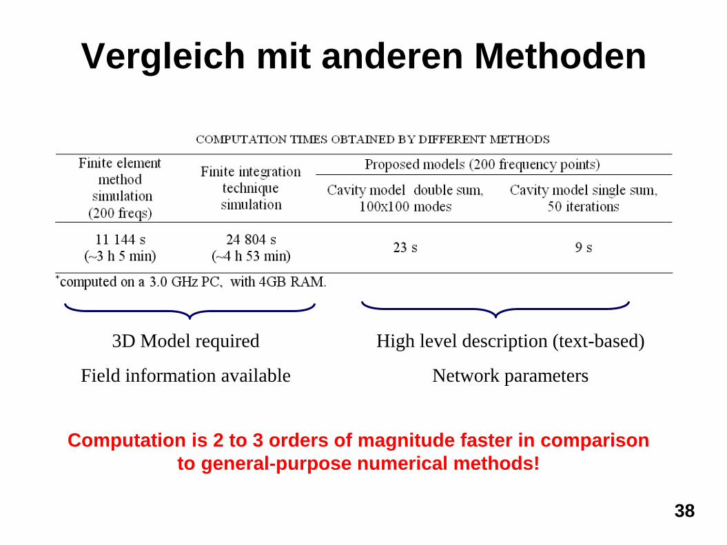
Computation is 2 to 3 orders of magnitude faster in comparison
to general-purpose numerical methods!
3D Model required
Field information available
High level description (text-based)
Network parameters
38
Vergleich mit anderen Methoden
• Identify & remove the bottlenecks
• Choose most efficient algorithms
• Use redundancies
• Parallelize the computation
39
Weitere Beschleunigung
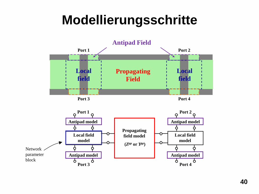
Propagating
Field
Local
field
Local
field
Antipad Field Port 1
Port 3
Port 2
Port 4
Antipad model
Antipad model
Antipad model
Antipad model
Local field
model
Propagating
field model
(Zpp or Ypp)
Local field
model
Port 1
Port 3
Port 2
Port 4
Network
parameter
block
40
Modellierungsschritte
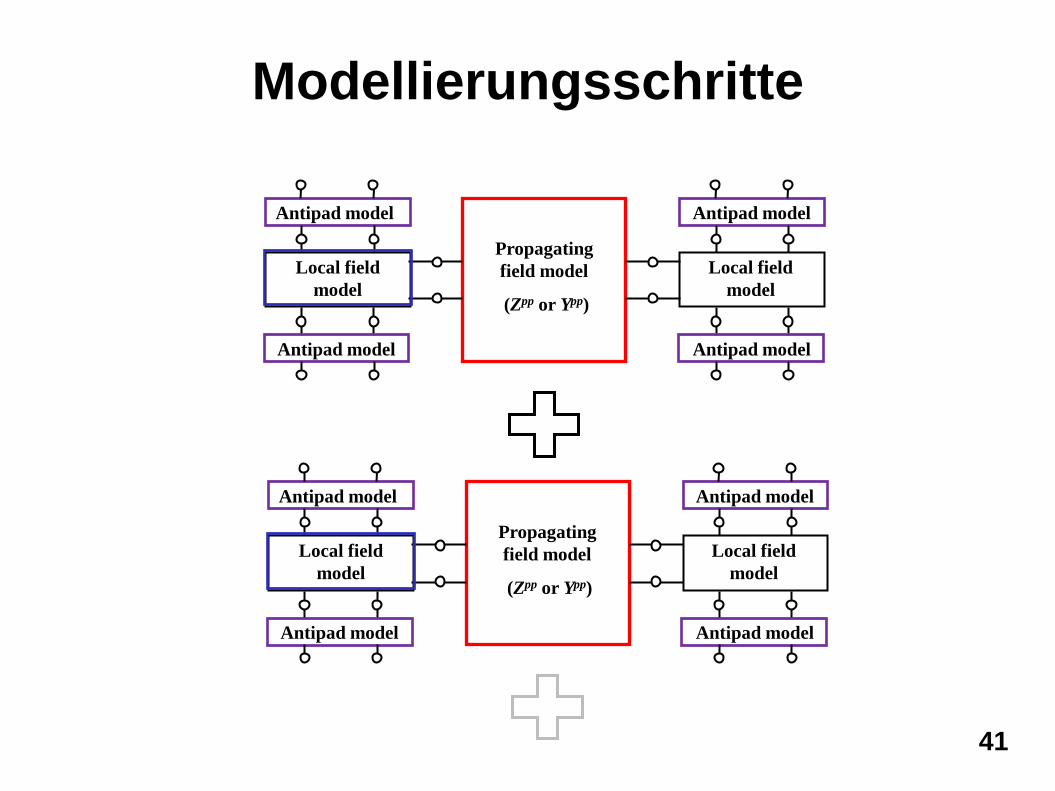
Antipad model
Antipad model
Antipad model
Antipad model
Local field
model
Propagating
field model
(Zpp or Ypp)
Local field
model
Antipad model
Antipad model
Antipad model
Antipad model
Local field
model
Propagating
field model
(Zpp or Ypp)
Local field
model
41
Modellierungsschritte
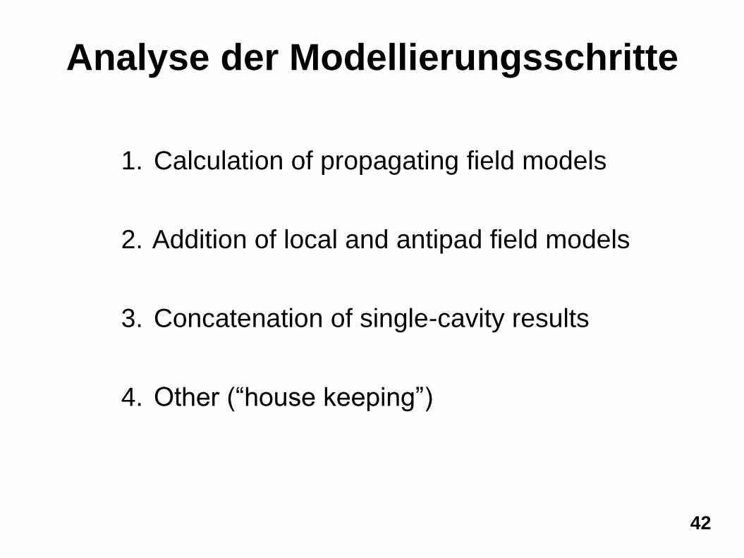
1. Calculation of propagating field models
2. Addition of local and antipad field models
3. Concatenation of single-cavity results
4. Other (“house keeping”)
42
Analyse der Modellierungsschritte
10
10
10
10
10
10
10
10
1
1
1
1
1
1
1
1
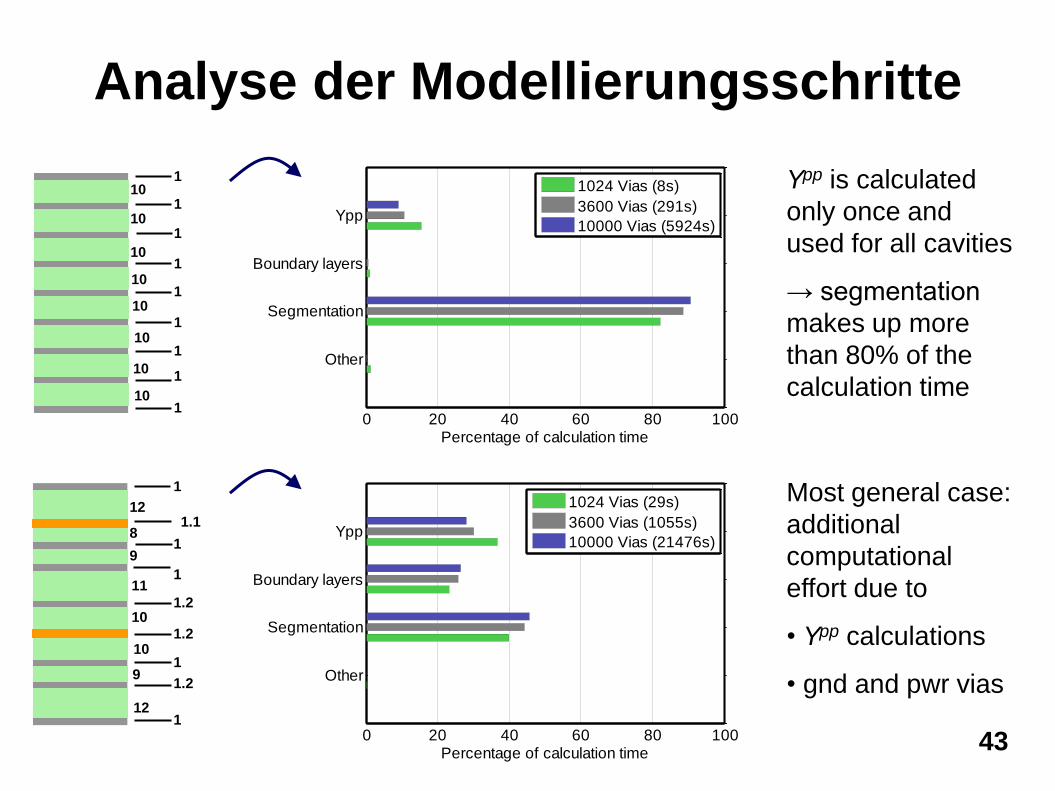
10 20 40 60 80 100
Other
Segmentation
Boundary layers
Ypp
Percentage of calculation time
1024 Vias (8s)
3600 Vias (291s)
10000 Vias (5924s)
Ypp is calculated
only once and
used for all cavities
→ segmentation
makes up more
than 80% of the
calculation time
0 20 40 60 80 100
Other
Segmentation
Boundary layers
Ypp
Percentage of calculation time
1024 Vias (29s)
3600 Vias (1055s)
10000 Vias (21476s)
12
8
9
11
10
10
9
12
1
1.1
1
1
1.2
1.2
1
1.2
1
Most general case:
additional
computational
effort due to
• Ypp calculations
• gnd and pwr vias
Analyse der Modellierungsschritte
43
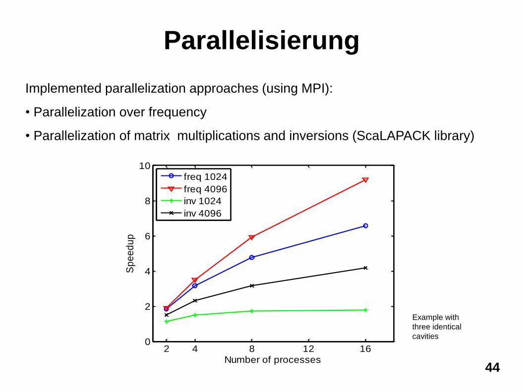
Implemented parallelization approaches (using MPI):
• Parallelization over frequency
• Parallelization of matrix multiplications and inversions (ScaLAPACK library)
2 4 8 12 160
2
4
6
8
10
Number of processes
Sp
ee
du
p
freq 1024
freq 4096
inv 1024
inv 4096
Example with
three identical
cavities
44
Parallelisierung
……
……
……
……
……
.
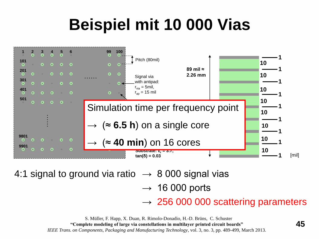
1 2 3 4 5 6 99 100
101
201
301
401
501
9801
9901 10000
Pitch (80mil)
Signal via
with antipad:
rvia = 5mil,
rap = 15 mil
Ground via:
rvia = 5mil
Conductor: copper
(σ = 5.8∙107 S/m)
Substrate: εr = 3.7,
tan(δ) = 0.03
Infinite
planes
4951 4952 4953 4954 4956 4961 4966
Vias for the crosstalk study (center area of the board)
4:1 signal to ground via ratio → 8 000 signal vias
→ 16 000 ports
→ 256 000 000 scattering parameters
10
10
10
10
10
10
10
10
1
1
1
1
1
1
1
1
1 [mil]
89 mil ≈
2.26 mm
Beispiel mit 10 000 Vias
Simulation time per frequency point
→ (≈ 6.5 h) on a single core
→ (≈ 40 min) on 16 cores
45 S. Müller, F. Happ, X. Duan, R. Rimolo-Donadio, H.-D. Brüns, C. Schuster
“Complete modeling of large via constellations in multilayer printed circuit boards”
IEEE Trans. on Components, Packaging and Manufacturing Technology, vol. 3, no. 3, pp. 489-499, March 2013.
46
1. Warum Leiterplatten, Streifenleiter und Vias?
2. Modellbildung in der Elektrotechnik
3. Effiziente Modellbildung für Leiterplatten
4. Anwendungen
5. Zusammenfassung und Ausblick
Übersicht
47
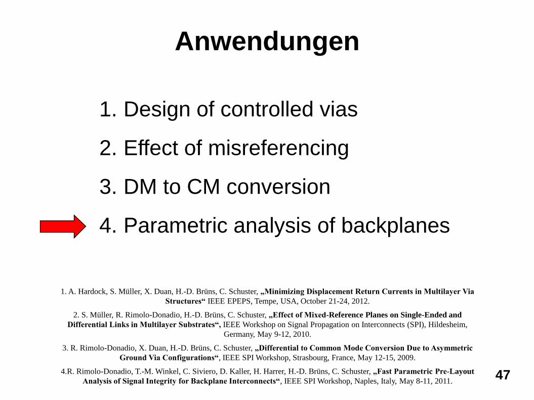
Anwendungen
1. Design of controlled vias
2. Effect of misreferencing
3. DM to CM conversion
4. Parametric analysis of backplanes
1. A. Hardock, S. Müller, X. Duan, H.-D. Brüns, C. Schuster, „Minimizing Displacement Return Currents in Multilayer Via
Structures“ IEEE EPEPS, Tempe, USA, October 21-24, 2012.
2. S. Müller, R. Rimolo-Donadio, H.-D. Brüns, C. Schuster, „Effect of Mixed-Reference Planes on Single-Ended and
Differential Links in Multilayer Substrates“, IEEE Workshop on Signal Propagation on Interconnects (SPI), Hildesheim,
Germany, May 9-12, 2010.
3. R. Rimolo-Donadio, X. Duan, H.-D. Brüns, C. Schuster, „Differential to Common Mode Conversion Due to Asymmetric
Ground Via Configurations“, IEEE SPI Workshop, Strasbourg, France, May 12-15, 2009.
4.R. Rimolo-Donadio, T.-M. Winkel, C. Siviero, D. Kaller, H. Harrer, H.-D. Brüns, C. Schuster, „Fast Parametric Pre-Layout
Analysis of Signal Integrity for Backplane Interconnects“, IEEE SPI Workshop, Naples, Italy, May 8-11, 2011.
48
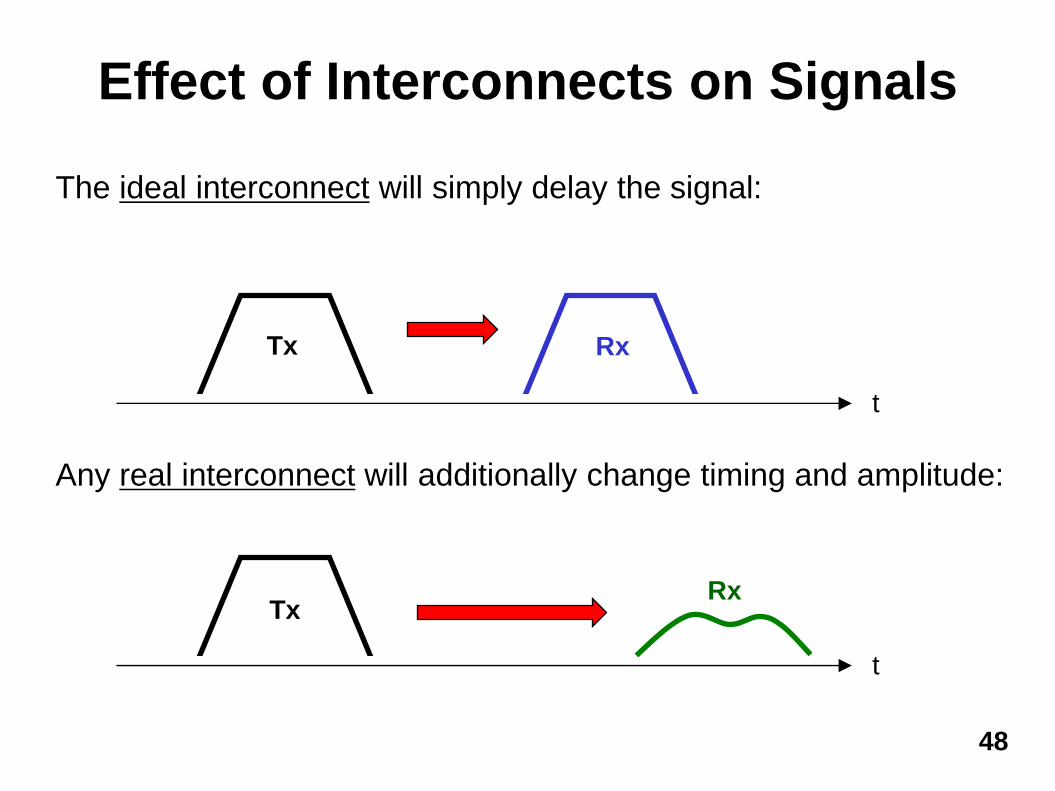
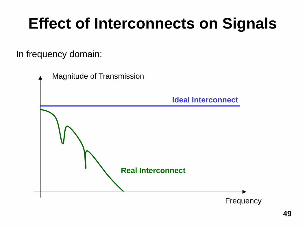
Effect of Interconnects on Signals
The ideal interconnect will simply delay the signal:
Any real interconnect will additionally change timing and amplitude:
t
Tx Rx
t
Tx Rx
49
Effect of Interconnects on Signals
In frequency domain:
Magnitude of Transmission
Frequency
Ideal Interconnect
Real Interconnect
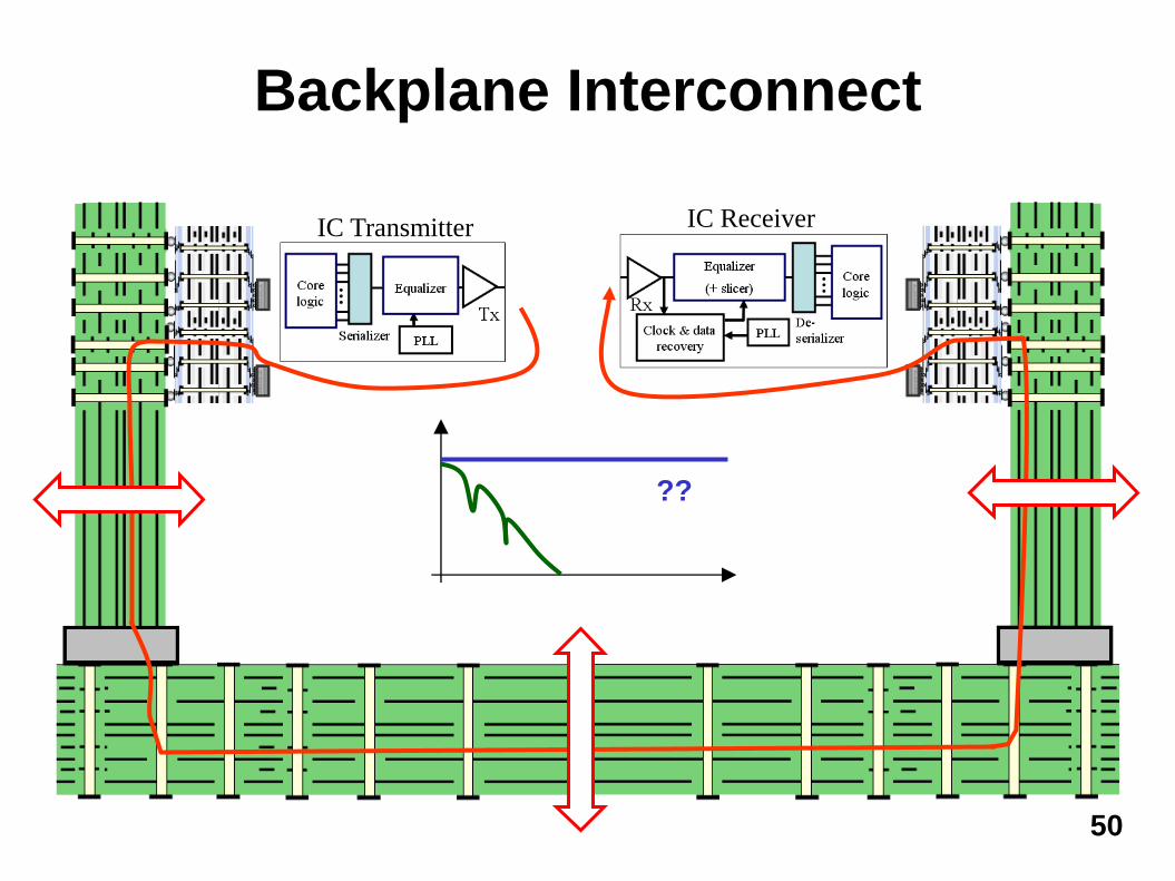
IC Transmitter IC Receiver
Backplane Interconnect
50
??
Total response (Network parameters)
Port 1a Port 2c
Port na Port nc Iterative loop
Substrate 1(Board)
Port 1a
Port na
Port 2a
Port na
Substrate 2 (Backplane)
Port 1b
Port nb
Port 2b
Port nb
Port 1c
Port nc
Port 2c
Port nc
Substrate 3 (Board)
Connector Connector
Automated concatenation (segmentation)
Selected design variables
Parametric Study – Set Up
51
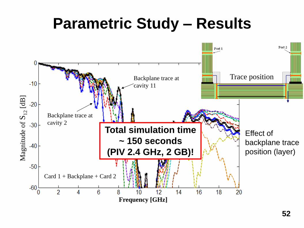
Frequency [GHz]
Mag
nit
ude
of
S1
2 [
dB
]
Card 1 + Backplane + Card 2
Backplane trace at
cavity 2
Backplane trace at
cavity 11
Total simulation time
~ 150 seconds
(PIV 2.4 GHz, 2 GB)!
Effect of
backplane trace
position (layer)
Trace position
Parametric Study – Results
52
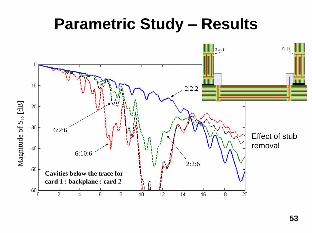
Effect of stub
removal
Mag
nit
ude
of
S1
2 [
dB
]
6:10:6
6:2:6
2:2:6
Cavities below the trace for
card 1 : backplane : card 2
2:2:2
Parametric Study – Results
53
54
1. Warum Leiterplatten, Streifenleiter und Vias?
2. Modellbildung in der Elektrotechnik
3. Effiziente Modellbildung für Leiterplatten
4. Anwendungen
5. Zusammenfassung und Ausblick
Übersicht
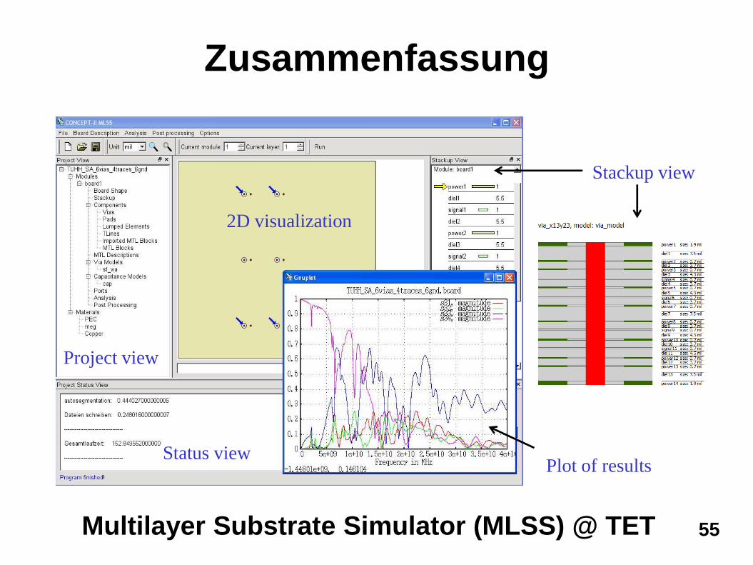
Zusammenfassung
55
2D visualization
Project view
Status view Plot of results
Stackup view
Multilayer Substrate Simulator (MLSS) @ TET
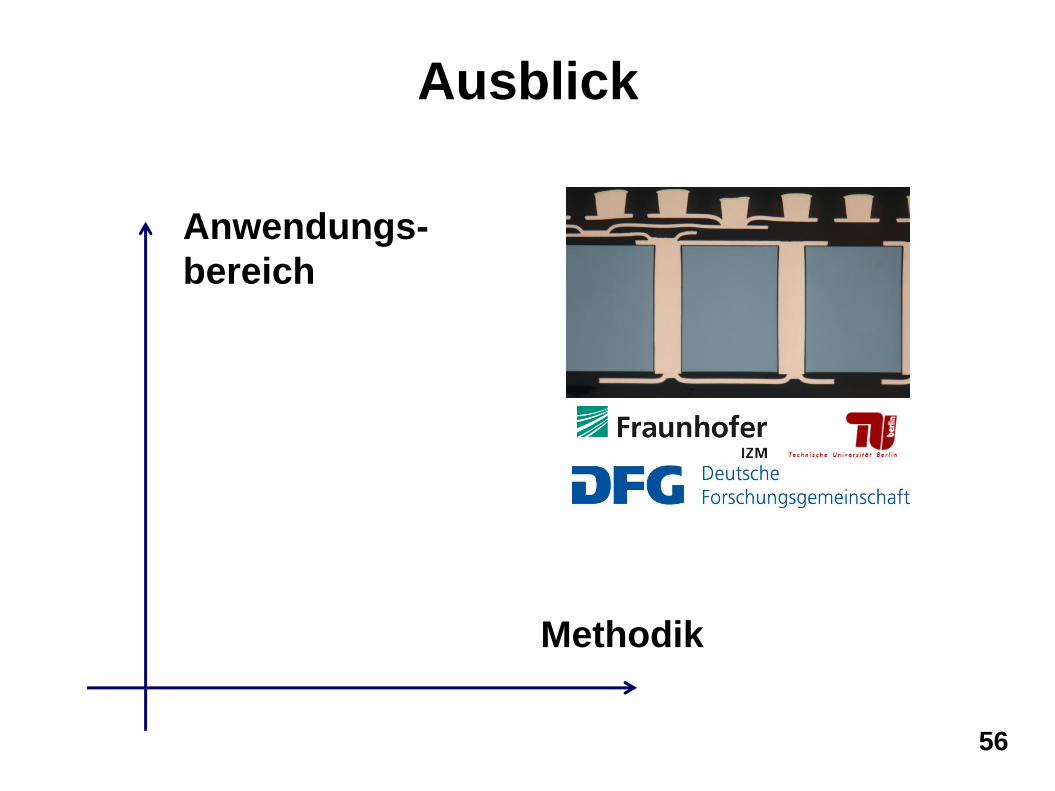
Ausblick
56
Anwendungs-
bereich
Methodik
www.tet.tuhh.de
Picture courtesy IBM Yorktown (Y. Kwark)