Fraunhofer CNT Annual Report 2011
34
1 1 2011 JAHRESBERICHT ------------------------------------------------ ANNUAL REPORT FRAUNHOFER CENTER NANOELECTRONIC TECHNOLOGIES
description
Research institute in Dresden, specialized on material and process development on 300 mm silicon wafer.
Transcript of Fraunhofer CNT Annual Report 2011

1 1
2011Jahresbericht- - - - - - - - - - - - - - - - - - - - - - - - - - - - - - - - - - - - - - - - - - - - - - - - aNNUaL rePOrt
F R A U N H O F E R c E N t E R N A N O E l E c t R O N i c t E c H N O l O g i E s

2 3
Preface 4
Fraunhofer center Nanoelectronic technologies Overview
Profile 8
Figures 12
Cooperation 16
competence Areas and Research Results 19
Analytics 20
FunctionalElectronicMaterials-FrontEndofLine 26
FunctionalElectronicMaterials-BackEndofLine 32
MasklessLithography 40
Devices&Integration 46
Events 54
Publications 59
contact 64
Editorial Notes 65
cONteNts

4 5
Für das FraunhoferCenterNanoelektronische Technolo-
gien(CNT)war2011einerfolgreichesJahr,indemeinige
Rahmenbedingungen für die zukünftige Entwicklung
geschaffenwurden.
Die langeZeitderUngewissheitseit2009bezüglichder
angemieteten Reinraum-, Labor- und Büroflächen nach
der Insolvenzdes IndustriepartnersQimonda,wurdemit
dem Erwerb des ehemaligen Qimonda-Geländes durch
InfineonimJuni2011beendet.InfineonhatdasInteres-
se bekundet, die Flächen auchweiterhin an Fraunhofer
zu vermieten und standortbezogene Dienstleistungen
anzubieten. Die Verhandlungen dazu sollen in 2012
abgeschlossenwerden.IneinemumfassendenStrategie-
prozesshabenwir langfristigdieKernkompetenzenund
Geschäftsfelderneudefiniert sowiedieZiele festgelegt.
DerJahresberichtgibtIhnendazueinengutenÜberblick.
BesonderserfreulichistdieZunahmevonAufträgen,ne-
bengroßenIC-Herstellern,geradevonmittelständischen
UnternehmenundStart-up Firmen,dieunabhängig von
FörderprojektendirektandieEinrichtungerteiltwurden
undindiesemJahr,denUmfangvonnahezueinerMillion
Euroerreichten.Dies isteinmalmehrderBeweisfürdie
Wertschätzung der vorhandenen Kompetenzen und die
Erkenntnis, dass die Ergebnisse aus der Nanoelektronik
zunehmendAnwendungenauchinSystemenderMikro-
elektronik findengemäßdemMotto„Nano forMicro“.
Mein besonderer Dank geht an die Auftraggeber, die
das Fraunhofer CNT auch in den turbulenten vergan-
genen Jahren als zuverlässigen Forschungsdienstleister
geschätzt haben,woraus sich auch einige längerfristige
Partnerschaftenentwickelten.
Als Beispiel sei hier ASM International genannt. Nach
mehrerenJahrenvertrauensvollerZusammenarbeitkonn-
temitdieseminternationalführendenAnlagenhersteller
eine längerfristige, bilaterale Kooperation im Bereich
Atomlagenabscheidung (ALD) und Epitaxie abgeschlos-
sen werden. Unsere Kompetenz im Bereich Prozesse,
PreFace
Materialien und Anlagen soll zukünftig durch weitere
Kooperationen ausgebaut werden. Als ein beständiger
PartnerfürEntwicklungsprojekteerwiessichunserIndus-
triepartner GLOBALFOUNDRIES. Durch dessen deutliche
VerbreiterungdesTechnologie-undProduktportfoliosals
Foundry ergaben sich zusätzliche Anknüpfungspunkte
für Industrieaufträge, die erfolgreich zum Abschluss
gebracht wurden. Zudem sind neue Forschungsinhalte
definiertworden.MehrereProjekteundVereinbarungen
konnten zudem mit anderen IC-Herstellern, IP-Firmen
undAnlagenherstellernsowohlimBereichAbscheidung,
Hoch-TemperaturBehandlungalsauchbeiTestsystemen
z.B.mitderFirmaTokyoElektron(TEL)getroffenwerden.
Seit Mitte 2011 konnte das Fraunhofer CNT auf eine
Grundfinanzierung zurückgreifen. Damit wurden unter
anderemdievorhandenenKompetenzenfürMIM(Metall-
Isolator-Metall) Kondensatorstrukturen, z.B. für Puffer-
speicher inAnalog/DigitalMixedSignalBausteinenoder
inmikroelektronischenSystemen,weiterentwickelt.
DurchdievomLandSachsengefördertenProjekteinden
Geschäftsfeldern „Enabling 300mm Production“ und
„Nanopatterning“ sowie „Innovative Materialien und
Prozesse für dieNano-undMikroelektronik“ konntedie
herausragendeQualitätunddasPotentialderetablierten
Technologien gerade in der breitenAnwendung für die
Mikrosystemtechnik und Nanoelektronik bei Strukturen
unter30nmdemonstriertwerden.DurchdieseProjekte
hatdieEinrichtungwesentlichdazubeitragen,Innovatio-
neninden„KeyEnablingTechnologies“voranzutreiben,
wie in einer EU Kommunikation im September 2009
„Preparing for our future: Developing a common strat-
egyforkeyenablingtechnologies intheEU"SEC(2009)
1257beschrieben.
Damit liefert das Fraunhofer CNT auchweiterhin einen
wesentlichen Beitrag für die herausragende Stellung
Dresdens als Mikroelektronik-Standort in Europa, als
Bindeglied zwischen „More Moore“ und „More than
Moore“ Technologien und Anwendungen. Besonders
A steady partner for development projects is our
industry partners GLOBALFOUNDRIES. Its significant
broadening of the technology and product portfolio
asafoundryresultedinadditionalindustryordersthat
have been completed successfully. In addition, new
researchcontenthasbeendefined.Severalprojectsand
agreementswerealsomadewithotherICmanufacturers,
IPcompaniesandequipmentmanufacturersinthefield
ofdeposition,high-temperaturetreatmentaswellasin
testsystemswiththecompanyTokyoElectron(TEL).
Since mid-2011, Fraunhofer CNT can rely on core
funding.Amongotherthings,thiswasusedtodevelop
the existing competencies for MIM (metal-insulator-
metal) capacitor structures, e.g. for buffermemory in
analog / digitalmixed signal ICs or inmicroelectronic
systemsevolved.
By thestateofSaxony-fundedprojects in thefieldsof
"enabling 300mmProduction" and "Nanopatterning"
and"Innovativematerials andprocesses fornano-and
microelectronics" the outstanding quality and the
potentialofestablishedtechnologiescurrently inwide
use for microsystems technology and nanoelectronics
weredemonstratedinstructuresbelow30nm.
Through these projects, the Fraunhofer CNTwas able
to significantly push innovations in the "Key Enabling
Technologies"forward,statedinanEUCommunication
inSeptember2009"Preparingforourfuture:Developing
acommonstrategyforkeyenablingtechnologiesinthe
EU"SEC(2009)1257.ForthisreasontheFraunhofer
CNTcontinuestocontributetotheprominentposition
ofDresdenasamicroelectronic location inEurope, as
alinkbetween"MoreMoore"and"MorethanMoore"
technologiesandapplications.
Particularly encouraging, the conclusion of two other
promotions at Fraunhofer CNT with the subjects:
2011 was a successful year for Fraunhofer Center
Nanoelectronic Technologies (CNT) in which the
frameworkforfuturedevelopmenthasbeencreated.
Thelongperiodofuncertaintysince2009regardingthe
rentedcleanroom,laboratoryandofficespacefollowed
bytheinsolvencyofindustrypartnerQimonda,hasbeen
completedwiththeacquisitionofQimonda’sproperties
by Infineon in June 2011. Infineon has expressed an
interest in further collaborations with Fraunhofer by
providing facilities and location-based services. The
negotiations shouldbecompleted in2012. Long-term
corecompetencies,businessareasandgoalshavebeen
established in a comprehensive strategy process. This
annualreportgivesyouagoodoverview.
Particularly pleasing is the increase of orders, from
major IC manufacturers and especially from medium-
sized companies and start-up companies which were
granted,regardlessoffundingprojects,directlytothe
institution.Thisyear,theamounthasreachednearlyone
millionEuros.Thisisanotherproofoftheappreciation
of the CNT competencies and the evidence that
results from nanoelectronic research increasingly find
applications inmicroelectronics systems in accordance
withtheslogan"NanoforMicro."
My special thanks goes to the authorities who have
valued theFraunhoferCNTas reliable researchservice
provider in the turbulent last years from which, also
some longer-term partnerships have developed. As
an example, ASM International is mentioned. After
several years of faithful cooperationwith this leading
international equipment manufacturer, a longer-term
bilateral cooperation in the field of atomic layer
deposition(ALD)andepitaxyiscompleted.Ourexpertise
inprocesses,materialsandequipmentisplannedtobe
expandedthroughfurthercooperation.
Director: Prof. Dr. Peter Kücher

6 7
PreFace
erfreulichwarauchderAbschlussvonzweiweiterenPro-
motionen imFraunhoferCNTmitdenThemen:Kinetik
der elektrochemischen Kupferabscheidung in Sub-100
nm-Strukturen und der Analyse von High-kMaterialien
mittels Atom Probe. Alle Doktoranden bestätigten die
EffektivitätmitderdieArbeiten,geradedurchdieenge
Zusammenarbeitmitder Industrieunddenbetreuenden
Professoren, durchgeführt werden konnten. Viele Mit-
arbeiter undMitarbeiterinnen haben sich im Laufe des
Jahres z.B. bei der„LangenNachtderWissenschaften“
oder beim Praktikum von Schülern, z.B. des Martin-
Andersen-NexöGymnasiumsengagiert.
Am 2. November fand der zweite „Fraunhofer CNT
Research Day“ statt. Dafür konnten wir mehrere Ex-
pertenmit Beiträgen von führendenUnternehmen wie
z.B. Infineon, STMicroelectronics, ASM und CEA-Leti,
Air Liquide begrüßen, die neben Wissenschaftlern aus
unserem Institut neueste Erkenntnisse und Strategien
auf verschiedenen Fachgebieten vorstellten. Die große
Beteiligungmitnahezu100Teilnehmernunddaspositive
FeedbackderGästesindMotivation,dieseVeranstaltung
auch im nächsten Jahr fortzuführen. Als Auszeichnung
fürdiewissenschaftlicheKompetenzamCNTdürfenwir
die Entscheidung werten, den 17thWorkshop on Diel-
ectrics inMicroelectronics(WoDiM)vom25.-27.6.2012
ausrichtenzudürfen.
Die Einrichtung wurde mit ihren Kompetenzbereichen
und der Ausrichtung auf neue Anwendungsfelder
optimiert aufgestellt. Für das Jahr 2012 und darüber
hinausermöglichtdieseinweiteresWachstumundlässt
uns positiv in die Zukunft schauen. Dies verdankt das
Fraunhofer CNT engagierten und kompetenten Mitar-
beitern und Mitarbeiterinnen sowie unseren Partnern
ausderIndustrie,anderenForschungseinrichtungenund
Instituten, denen ich andieser Stelle besonders für das
entgegengebrachteVertrauendankenmöchte.
Prof.Dr.PeterKücher
kinetics of electrochemical deposition of copper in
sub-100 nm structures and the analysis of high-k
materialswithAtomProbe.Allstudentsconfirmedthe
effectivenessoftheirworkthroughaclosecooperation
withtheindustryandthesupervisingprofessors.Many
staff members were engaged in activities such as the
"Night of Science" or the internship of students e.g.
fromthe“MartinAndersenNexo”-school.
OnNovember2ndthesecond"FraunhoferCNTResearch
Day" took place with several experts from leading
companies such as Infineon, STMicroelectronics, ASM
and CEA-Leti, Air Liquide and researchers from our
institutewhopresentedthelatestresultsandstrategies
in various fields. The large turnout with about 100
participantsandthepositivefeedbackfromguestsare
motivation to continue this event again in 2012. As
recognition of the scientific expertise at the CNT, we
evaluate the decision, to host the 17thWorkshop on
Dielectrics inMicroelectronics (WoDiM) June25 -27,
2012inDresden.
The facility has been optimized regarding its
competence areas and new fields of applications. For
the year2012andbeyond, this allows furthergrowth
and a positive perspective for the future. Iwould like
to use this opportunity to thank our highlymotivated
and competent employees as well as all our business
partnersandsupportersfortheirconfidence.

8 9
Forschung und entwicklung im Fraunhofer cNt
DasGeschäftsfeld des FraunhoferCNTumfasst die Ent-
wicklungvonProzessschrittenundMaterialiensowiedie
physikalischeundelektrischeCharakterisierungfürHigh-
Performance-Logik,Derivate(z.B.embeddedDRAM)und
Speichertechnologien für flüchtige und nicht-flüchtige
Bauelemente.
Zielsetzung der Einrichtung ist es, innovative Einzelpro-
zesslösungen für nanoelektronische Systeme vor allem
auf300mmWafernmit Industriepartnernundanderen
Forschungseinrichtungen so zu entwickeln, dass diese
schnell in ein industrielles Fertigungsumfeld übertragen
werdenkönnen.
Das Leistungsangebot des Fraunhofer CNT basiert auf
fünfKompetenzbereichen:
Analytik
FunktionaleElektronischeMaterialien-FrontEndofLine
FunktionaleElektronischeMaterialien-BackEndofLine
Devices&Integration
MaskenloseLithographie
Die Kompetenzbereiche forschen vor allem in den fol-
gendenGeschäftsfeldern:
LeadingEdgeTechnologiefürdieNano-Mikroelekt
ronik
Enabling300mmProduction Nanostructuring
PrOFiLe
research and Development at Fraunhofer cNt
ThebusinessareasofFraunhoferCNTincludethedeve-
lopmentofprocessesandmaterialsaswellasthephysi-
calandelectricalcharacterizationofhigh-performance-
logics, derivates (e. g. embedded DRAM) andmemory
technologiesforvolatileandnon-volatiledevices.
In close cooperation with industrial partners and
other R&Dorganizations, theobjectiveof our institute
is to develop innovative unit process solutions for
nanoelectronic systemson300mm siliconwafers. The
aim is to transfer research results fast into industrial
manufacturing.
TherangeofservicesofferedbyFraunhoferCNTisbased
onfivecompetenceareas:
Analytics FunctionalElectronicMaterials-FrontEndofLine
FunctionalElectronicMaterials-BackEndofLine
Devices&Integration MasklessLithography
The competence areas do research especially in the
followingfields:
Leadingedgetechnologyfornano-micro-electronic Enabling300mmproduction Nanostructuring
environment
At present, Fraunhofer CNT uses 800 m² clean room
area (class 1000) and an infrastructure which meets
industry standards. Inaddition to40clean roomtools,
scientistsatFraunhoferCNTuseconsiderableanalytical
andmetrological processes for R&D as well as for the
characterizationofnanoelectronicdevices.
The institute does not maintain a continuous process
line to cover all the necessary process steps in order
to realize high-integrated memory chips. However,
FraunhoferCNTpossessesnewprocesstoolswhichare
typical of production and enabling common research
anddevelopmentwithitspartners.
Pre-processedwafersareprovidedbyGLOBALFOUNDRIES
–innovativeprocessstepswillbeoperatedatFraunhofer
CNT. Thus, the results canbe transferred immediately
into manufacturing. This enables partners to reduce
their capital expenditures.Moreover, it allows a faster
schedule.
ausstattung
Für das Fraunhofer CNT stehen derzeit 800m² Reinraum-
fläche (Reinraumklasse 1000) sowie eine Infrastruktur zur
Verfügung,diedemIndustriestandardentspricht.Zusätzlich
zudenca.40Anlagen imReinraumkönnenumfangreiche
Analyse- und Metrologieverfahren für die Forschung und
Entwicklung sowie die Bausteincharakterisierung genutzt
werden.
Die Einrichtung unterhält keine durchgängige Prozesslinie
in der alle notwendigen Prozessschritte zur Realisierung
höchstintegrierterChips zurVerfügung stehen. Sie verfügt
aber über neue, fertigungstypische Prozessgeräte, an
denendie Partner zusammenmit denWissenschaftlern im
FraunhoferCNTforschenundentwickelnkönnen.
Teilprozessierte Wafer kommen von GLOBALFOUNDRIES -
die innovativen Prozessschrittewerden im Fraunhofer CNT
durchgeführt. Die gewonnenen Erkenntnisse können dann
sofort in die praktische Erprobung in der angrenzenden
Fertigung übertragenwerden. Dadurch lassen sich sowohl
Investitionen für die Partner minimieren, als auch ein
schnellererZeitablaufermöglichen.
10 11
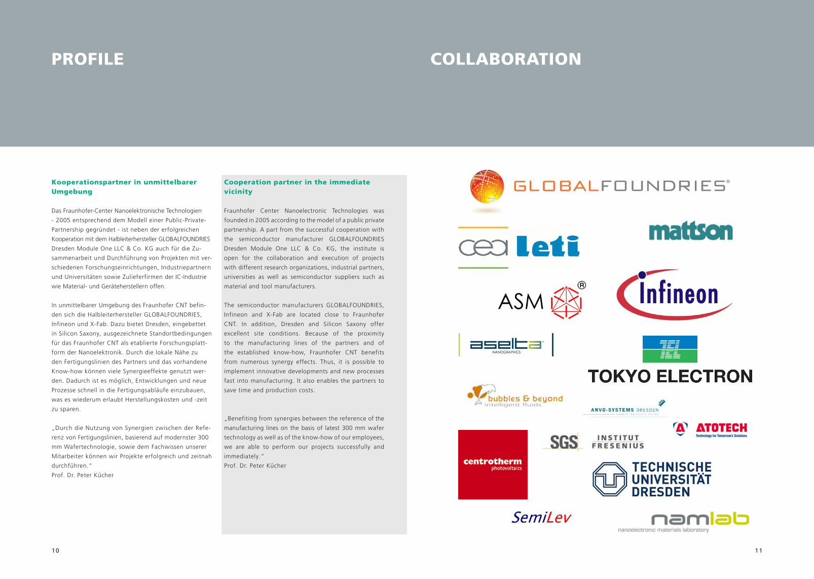
Kooperationspartner in unmittelbarer Umgebung
DasFraunhofer-CenterNanoelektronischeTechnologien
-2005entsprechenddemModelleinerPublic-Private-
Partnershipgegründet-istnebendererfolgreichen
KooperationmitdemHalbleiterherstellerGLOBALFOUNDRIES
DresdenModuleOneLLC&Co.KGauchfürdieZu-
sammenarbeitundDurchführungvonProjektenmitver-
schiedenenForschungseinrichtungen,Industriepartnern
undUniversitätensowieZulieferfirmenderIC-Industrie
wieMaterial-undGeräteherstellernoffen.
InunmittelbarerUmgebungdesFraunhoferCNTbefin-
densichdieHalbleiterherstellerGLOBALFOUNDRIES,
InfineonundX-Fab.DazubietetDresden,eingebettet
inSiliconSaxony,ausgezeichneteStandortbedingungen
fürdasFraunhoferCNTalsetablierteForschungsplatt-
formderNanoelektronik.DurchdielokaleNähezu
denFertigungsliniendesPartnersunddasvorhandene
Know-howkönnenvieleSynergieeffektegenutztwer-
den.Dadurchistesmöglich,Entwicklungenundneue
ProzesseschnellindieFertigungsabläufeeinzubauen,
waseswiederumerlaubtHerstellungskostenund-zeit
zusparen.
„DurchdieNutzungvonSynergienzwischenderRefe-
renzvonFertigungslinien,basierendaufmodernster300
mmWafertechnologie,sowiedemFachwissenunserer
MitarbeiterkönnenwirProjekteerfolgreichundzeitnah
durchführen.“
Prof.Dr.PeterKücher
PrOFiLe
cooperation partner in the immediate vicinity
Fraunhofer Center Nanoelectronic Technologies was
foundedin2005accordingtothemodelofapublicprivate
partnership.Apartfromthesuccessfulcooperationwith
the semiconductor manufacturer GLOBALFOUNDRIES
Dresden Module One LLC & Co. KG, the institute is
open for the collaboration and execution of projects
withdifferentresearchorganizations,industrialpartners,
universities as well as semiconductor suppliers such as
materialandtoolmanufacturers.
The semiconductor manufacturers GLOBALFOUNDRIES,
Infineon and X-Fab are located close to Fraunhofer
CNT. In addition, Dresden and Silicon Saxony offer
excellent site conditions. Because of the proximity
to the manufacturing lines of the partners and of
the established know-how, Fraunhofer CNT benefits
from numerous synergy effects. Thus, it is possible to
implementinnovativedevelopmentsandnewprocesses
fast intomanufacturing. Italsoenablesthepartnersto
savetimeandproductioncosts.
„Benefitingfromsynergiesbetweenthereferenceofthe
manufacturing lineson thebasisof latest300mmwafer
technologyaswellasoftheknow-howofouremployees,
we are able to perform our projects successfully and
immediately.“
Prof.Dr.PeterKücher
cOLLabOratiON

12 13
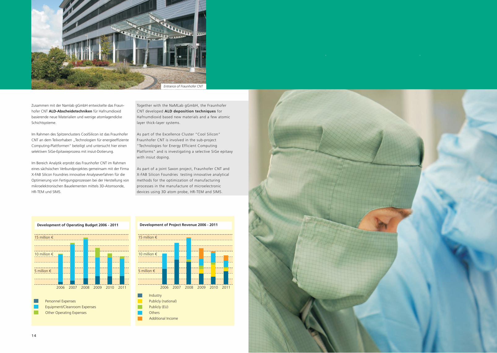
DasFraunhoferCNTerwirtschaftete2011einenErtragvon
ca. 8,8MioEuro.DerBetriebshaushaltsetztesichzuca.
51%ausWirtschaftserträgen,zuetwa7%ausErträgen
ausnationalenöffentlichenProjekten,zurund3%ausEU-
Erträgen,zurund22%aussonstigenErträgenundzu17%
ausSonderfinanzierungsmittelnzusammen.
ZurBearbeitungderForschungsaufträgestehenauf800
m²Reinraumflächeund200m²Laborflächemodernste
LaborausstattungenundGroßgerätezurVerfügung.Der
AnlagenparkumfasstAbscheide-undÄtzanlagenfürdieWär-
mebehandlungbeiHochtemperaturensowieInspektions-und
AnalysegerätezumBestimmenvonDefektenunddemMessen
vonSchichteigenschaften.
ZumJahresende2011beschäftigtedasFraunhoferCNT49
festangestellteMitarbeiter.DasPersonalsetztesichaus32
Wissenschaftlerneinschließlich7Doktoranden,6technischen
Mitarbeiternund11MitarbeiterninManagementundVer-
waltungzusammen.MitmodernstemAnlagenpark,intensiver
VorlaufforschungsowieeinerlangjährigenIndustrieerfahrung
stehendieMitarbeiterdesFraunhoferCNTihrennationalen
undinternationalenKundenundPartnernzurSeite,um
InnovationenfürdieZukunftnutzbarzumachen.
Expenditures and Revenues 2011
Annual Budget 2011 in k € in %
Revenues 8.771
Industry 4.508 51,0
Publicity(national) 632 7,0
Publicity(EU) 281 3,0
Others 1.918 22,0
AdditionalIncome 1.432 17,0
Head of Administration: Antje Spitzer
50
45
40
35
30
25
20
15
10
5
0
Personnel 2006 - 2011
200620072008200920102011
Scientificpersonnel Management/Administration/
Operation
In 2011 Fraunhofer CNT generated revenues of about 8.8
millionEuro.Theoperationbudgetwascomposedof51%of
industryreturns,3%earningsfromnationalpublicprojects,
7%ofEUearnings,22%ofother revenuesand17%of
specialfinancing.
InordertoprocessR&Dwafersprofessionally,Fraunhofer
CNT has an area of 800 m² clean room and 200 m²
laboratory availablewhich are equippedwith the latest
semiconductor R&D tools. The equipment ranges from
depositionandetchingtoolsusedfortheheattreatment
at high-temperatures as well as from inspection and
analytic toolswhichareusedforthecharacterizationof
defectsandlayers.
Intheendof2011,FraunhoferCNTemployed49permanent
staff.Thepersonnelwascomposedof32scientistsincluding
7 Ph.D. students, 6 technicians and 11 employees in
administrationandmanagement.Equippedwiththelatest
devices, intense initial researchanda long-lasting industry
know-how,employeesofFraunhoferCNTprovidesupport
totheirnationaland internationalcustomersandpartners
inordertorealizeinnovationsinthefuture.
DasFraunhoferCNThat2011ca.1MioEuroinvestiert,
umseintechnischesEquipmentzuerweitern.DieseInves-
titionenwurdenausdemEuropäischenFondfürRegionale
EntwicklungundvomFreistaatSachsengefördertsowieaus
Sondermittelnfinanziert.
DerstrategischeIndustriepartnerGlobalfoundriessetzteseine
ZusammenarbeitmitdemFraunhoferCNTkontinuierlichin
mehrerebereitsvor2011gestartetenForschungsvorhaben
fort.
FürGlobalfoundrieswurdesobeispielsweiseeineschädi-
gungsfreie,plasmagestützteStrukturierungvonUltra-low-k
DielektrikafürdieAnwendungineinersub30nm-Technologie
entwickelt.
EinweiteresProjektbeinhaltetdieEntwicklung zukünftiger
High-k gate-Dielektrik-transistoren einschließlicheiner
MachbarkeitsstudiefürferroelektrischeSpeicher.
DarüberhinausarbeitetendieWissenschaftlerdesCNTin
einemProjektanderEntwicklung einer Verdrahtungstech-
nologie für kleinste strukturenunterBerücksichtigungder
wachsendenAnforderungenandieelektrischeZuverlässigkeit,
sowieineinemProjektanderOptimierung von Metal-
gate-ProzessenfürdieReplacement-Gate-Technologieund
EntwicklungvonProzessenzurVerbesserungderZuverlässig-
keitvonHigh-k-Metal-Gate(HKMG)-Stapeln.
Dasin2010vonGlobalfoundriesbeauftragteProjekt„Verbes-
serungderMikroprozessoreneigenschaftenmittelsEinsatzvon
Kohlenstoff“wurdein2011erfolgreichabgeschlossen.
WeitereProjektewurdenmitverschiedenennamhaften
ForschungseinrichtungenundUnternehmenumgesetzt,
sobeispielsweiseeinProjektmitASELTANanographics
(Frankreich)zurE-BeamProximityEffektKorrekturfürdie
HerstellungvonoptischenMaskenundAnwendungenim
BereichdermaskenlosenLithografie.
TheFraunhoferCNThasinvestedabout€1million
toexpanditstechnicalequipmentin2011.These
investmentswerefinancedthroughtheEuropean
RegionalDevelopmentFund,theFreeStateofSaxony
andfromspecialfunds.
ThestrategicindustrypartnerGlobalfoundriessteadily
continuedhiscollaborationwiththeFraunhoferCNTin
severalresearchprojectsthatstartedbefore2011.
OnedevelopmentforGlobalfoundrieswasadamage-
free,plasma-basedpatterningofultra-low-kdielectrics
fortheuseinasub30nmtechnology.Anotherproject
involvesthedevelopment of future high-k gate
dielectric transistorsincludingafeasibilitystudyfor
ferroelectricmemory.
Furthermore,scientistsatCNTwereworkingona
projecttodevelop a wiring technology for smallest
structures,consideringthegrowingdemandsonthe
electricalreliability.Anotherprojectisworkingon
theoptimization of metal-gate processes for the
replacement-gate technologyanddevelopmentof
processestoimprovethereliabilityofhigh-kmetal
gate(HKMG)stacks.
Thein2010commissionedGlobalfoundriesproject
"Improvementofthemicroprocessorfeaturesthrough
theuseofcarbon"wassuccessfullycompletedin
2011.
Otherprojectshavebeenimplementedwithseveral
renownedresearchinstitutesandcompanies,suchas
theprojectwithASELTANanoGraphics(France)for
e-beamproximityeffectcorrectionforthemanufacture
ofopticalmasksandapplicationsinmaskless
lithography.
FraUNhOFer cNt iN FigUres
14 15
15million€
10million€
5million€
Development of Operating Budget 2006 - 2011
200620072008200920102011
OtherOperatingExpenses
Equipment/CleanroomExpenses
15million€
10million€
5million€
Development of Project Revenue 2006 - 2011
200620072008200920102011
Industry
Publicly(EU)
Publicly(national)
AdditionalIncome
Others
PersonnelExpenses
ZusammenmitderNamlabgGmbHentwickeltedasFraun-
hoferCNTAlD-Abscheidetechniken fürHafnumdioxid
basierendeneueMaterialienundwenigeatomlagendicke
Schichtsysteme.
ImRahmendesSpitzenclustersCoolSiliconistdasFraunhofer
CNTandemTeilvorhaben„Technologienfürenergieeffiziente
Computing-Plattformen“beteiligtunduntersuchthiereinen
selektivenSiGe-Epitaxieprozessmitinsiut-Dotierung.
ImBereichAnalytikerprobtdasFraunhoferCNTimRahmen
einessächsischenVerbundprojektesgemeinsammitderFirma
X-FABSiliconFoundriesinnovativeAnalyseverfahrenfürdie
OptimierungvonFertigungsprozessenbeiderHerstellungvon
mikroelektronischenBauelementenmittels3D-Atomsonde,
HR-TEMundSIMS.
Entrance of Fraunhofer CNT
TogetherwiththeNaMLabgGmbH,theFraunhofer
CNTdevelopedAlD deposition techniquesfor
Hafnumdioxidbasednewmaterialsandafewatomic
layerthick-layersystems.
AspartoftheExcellenceCluster“CoolSilicon”
FraunhoferCNTisinvolvedinthesub-project
"TechnologiesforEnergyEfficientComputing
Platforms"andisinvestigatingaselectiveSiGeepitaxy
withinsiutdoping.
AspartofajointSaxonproject,FraunhoferCNTand
X-FABSiliconFoundriestestinginnovativeanalytical
methodsfortheoptimizationofmanufacturing
processesinthemanufactureofmicroelectronic
devicesusing3Datomprobe,HR-TEMandSIMS.
16 17
Der Fraunhofer-Verbund Mikroelektronik (VµE) koordiniert
die Aktivitäten der auf den gebieten Mikroelektronik und
Mikrointegration tätigen Fraunhofer-institute.
Die Technologiekompetenz des Verbunds reicht von
der klassischen CMOS-Technologie bis zum Einsatz
innovativer Systemlösungen. Sie schließt neben Silizium
auch Verbindungshalbleiter und neue Materialien ein. Die
Kompetenz in der Entwicklung von CMOS- und anderen
Bauelementetechnologien für die Mikroelektronik stellt die
BasissowohlfürtechnologischeDienstleistungenalsauchfür
anwendungsbezogene Komponentenentwicklung dar. Das
FraunhoferCNT istAnsprechpartner fürdieBereiche„More
Moore“und„BeyondCMOS“imGeschäftsfeldTechnologie.
FraUNhOFer verbUND miKrOeLeKtrONiK
The Fraunhofer Group for Microelectronics (VμE)
coordinates the activities of Fraunhofer institutes working
in the fields of microelectronics and microintegration.
Thegroup’sexpertiserangesfromclassicCMOStechnology
to the use of innovative system solutions. Apart from
silicon, this also includes compound semiconductors and
new materials. Expertise in developing CMOS and other
device technologies for microelectronics forms the basis
for both, technological services and application-specific
component development. Fraunhofer CNT is the contact
for the business area Technology which consists of two
divisions:„MoreMoore“and„BeyondCMOS“.
ForschenfürdiePraxisistdiezentraleAufgabederFraunhofer-
Gesellschaft. Die 1949 gegründete Forschungsorganisation
betreibt anwendungsorientierte Forschung zum Nutzen der
WirtschaftundzumVorteilderGesellschaft.Vertragspartnerund
AuftraggebersindIndustrie-undDienstleistungsunternehmen
sowiedieöffentlicheHand.
Die Fraunhofer-Gesellschaft betreibt in Deutschland derzeit
mehrals80Forschungseinrichtungen,davon60Institute.Mehr
als17.000MitarbeiterinnenundMitarbeiter,überwiegendmit
natur-oderingenieurwissenschaftlicherAusbildung,bearbeiten
dasjährlicheForschungsvolumenvon1,7MrdEuro.Davonfallen
1,4MrdEuroaufdenLeistungsbereichVertragsforschung.Zwei
Drittel dieses Leistungsbereichs erwirtschaftet die Fraunhofer-
GesellschaftmitAufträgenausderIndustrieundmitöffentlich
finanzierten Forschungsprojekten. Nur etwas ein Drittel wird
von Bund und Ländern als Grundfinanzierung beigesteuert,
damit die Institute Problemlösungen erarbeiten können, die
erst in fünfoderzehnJahren fürWirtschaftundGesellschaft
aktuellwerden.
FraUNhOFer-geseLLschaFtResearchforpracticeisthemainissueofallactivitiespursuedby
theFraunhofer-Gesellschaft.Theresearchorganization,which
wasfoundedin1949,undertakesappliedresearchthatdrives
economicdevelopmentandservesthewiderbenefitofsociety.
Itsservicesaresolicitedbycustomersandcontractualpartners
inindustry,theservicesectorandpublicadministration.
Atpresent,theFraunhofer-Gesellschaftmaintainsmorethan
80researchunits inGermany, including60Fraunhofer insti-
tutes. Themajorityof themore than17.000employeesare
qualified scientists andengineerswhoworkwith an annual
researchbudgetof1.7billioneuro.Morethan1.4billioneuro
of this amount are generated through contract research.
TwothirdsoftheFraunhofer-Gesellschaft‘scontractresearch
revenues derive fromcontractswith industrialpartnersand
frompubliclyfinancedresearchprojects.Onlyonethirdiscon-
tributedby theGerman federal and Länder governments in
theformofbasefundingwhichenablestheinstitutestowork
aheadonsolutionstoproblemsthatwillbecomerelevantto
industryandsocietyinfiveortenyears.
FraUNhOFer-geseLLschaFt FraUNhOFer grOUP micrOeLectrONics
iNNOvatiON thrOUgh cOOPeratiON
Die Fraunhofer-Gesellschaft istmit sechs Instituten und
sechs weiteren Einrichtungen in Dresden vertreten. Die
zwölfFraunhofer-Einrichtungenbeschäftigenzusammen
mehrals1.100Mitarbeiterbeieinem jährlichenUmsatz
vonüber100MioEuro.FürdienächstenJahrewirdein
weiteresWachstumprognostiziert.
NebenderaußerordentlichhohenDichteanForschungs-
einrichtungenzeichnetsichderStandortDresdendurch
eineengeVerflechtungvonIndustrieundForschungaus.
DiedarausentstehendenSpitzenleistungenund innova-
tivenEntwicklungensetzenweltweiteImpulse.
FraUNhOFer iN DresDeN:gebaLLte FOrschUNg
The Fraunhofer-Gesellschaft is represented in Dres-
denbysixinstitutesandsixotherfacilities.Morethan
1.100employeesworkforthetwelveFraunhoferfaci-
lities.Theannualturnoveramountstomorethan100
millioneuroandfurthergrowthisexpectedwithinthe
nextyears.
Inadditiontotheextraordinarilyhighdensityofresearch
facil it ies, the region is characterized by the close
connectionbetweenresearchandindustry,resultingin
the creation of leading-edge services and innovative
developmentswhichhaveaglobalimpact.
FraUNhOFer iN DresDeN:cLUstereD research
123
56
9
78
1011
4
ab
12
c
13
abc
AngewandteFestkörperphysikIAF
ElektronischeNanosystemeENAS
HochfrequenzphysikundRadartechnikFHR
IntegrierteSchaltungenIIS
IntegrierteSystemeundBauelementetechnologieIISB
MikroelektronischeSchaltungenundSystemeIMS
ModulareFestkörper-TechnologienEMFT
Nachrichtentechnik,Heinrich-Hertz-InstitutHHI
NanoelektronischeTechnologienCNT
PhotonischeMikrosystemeIPMS
SiliziumtechnologieISIT
SystemederKommunikationstechnikESK
ZuverlässigkeitundMikrointegrationIZM
Gastinstitute/GuestInstitutes
DigitaleMedientechnologieIDMT
OffeneKommunikationssystemeFOKUS
ZerstörungsfreiePrüfverfahrenIZFP
18 19
aNaLytics
FUNctiONaL eLectrONic materiaLs
FrONt-eND OF LiNe
FUNctiONaL eLectrONic materiaLs
bacK-eND OF LiNe
masKLess LithOgraPhy
Devices & iNtegratiON
cOmPeteNce areas aND research resULts
Microelectronicsisthebasictechnologyforalotoftechnicalapplications.Theprogress
intheautomobileandthecomputerindustrycanbeownedbythistechnology.Micro-
electronicsystemshavetobecomesmallerandsmallerandmoreenergyefficient.They
alsohavetoprovidemuchmorepowerandcombinemoreandmorenewfeatures.The
keyactivitiesofFraunhoferCNTfocusonthedevelopmentofinnovativeprocessesfor
high-performancetransistorsaswellasthedevelopmentofnanoelectronicintegrated
circuitstofulfillthetasksmentionedabove.FraunhoferCNTdividesitsgroupsintofive
areasofcompetences.
Seit Oktober 2009 ist das Fraunhofer CNT Mitglied
im Dresdner Fraunhofer-Cluster Nanoanalytik. Zehn
Fraunhofer-InstituteunddreiFakultätenderTechnischen
UniversitätDresdensowiedasHelmholtz-ZentrumBerlin
bündeln ihre Kompetenzen und decken das gesamte
ThemenspektrumderNanoanalytikab.DieInstitutesind
flexibel vernetzt und werden auch sehr umfassenden
AnforderungenimBereichAnalytikgerecht.
cLUster NaNOaNaLytiK
ImOktober2010wurdedasALDLabDresdengegründet.
Mit demLabwerdenKompetenzenaufdemGebietder
ALD(Atomlagenabscheidung)amStandortDresden,dem
InstitutfürHalbleiter-undMikrosystemtechnik(IHM)der
Technischen Universität Dresden (Prof. Johann Bartha)
und der ALD-Gruppe des Fraunhofer CNT (Dr. Jonas
Sundqvist) zusammengeführt. Gemeinsam entwickeln
diePartnerneueALD-Precursorenund–Prozesse fürdie
Halbleiter-undPhotovoltaik-Industrie.
aLD Lab DresDeN
SeitApril2010istdasFraunhoferCNToffiziellesMitglied
derE-Beam-Initiative.
Die Initiative bietet ein Forum für bildungs- und
verkaufsförderndeAktivitäten,unterdemGesichtspunkt
eines neuen „design-to-manufacturing“-Ansatzes,
bekannt als „design for e-beam“ (DFEB). DFEB
reduziert Maskenkosten für Halbleiterbauelemente, in
VerbindungmitDesign,Design-Software,Herstel lung,
HerstellungsmaterialienundHersteller-Software-Expertise.
e-beam-iNitiative
cLUster NaNOaNaLytiK
aLD Lab DresDeN
e-beam iNitiative
Since October 2009, Fraunhofer CNT has been a
member of the Fraunhofer-Cluster Nanoanalytics in
Dresden. Ten Fraunhofer institutes, three faculties
of the Dresden University of Technology as well
as the Helmholtz-Zentrum Berlin consolidate their
competences and thus cover the entire field of
nanoanalytics.Theinstitutesareflexiblylinkedandcan
meetcomprehensiveanalyticsrequirements.
The ALD Lab Dresdenwas founded in October 2010.
It is a joint venture of the Institut fürHalbleiter- und
Mikrosystemtechnik(IHM)oftheDresdenUniversityof
Technology(Prof.JohannBartha)andtheALDgroupof
FraunhoferCNT(Dr. JonasSundqvist)whichcombines
their competences in the field of ALD (atomic layer
deposition). The workscope is to develop new ALD
precursors and processes for the semiconductor and
photovoltaicindustry.
SinceApril2010,FraunhoferCNTisanofficialmember
ofthee-beaminitiative.
The initiative provides a forum for educational and
promotional activities considering a new “design-
to-manufacturing” approach known as “design
for e-beam” (DFEB). DFEB reduces mask costs for
semiconductor components linked to designs, design
software,manufacturing,manufacturingmaterialsand
manufacturer’ssoftwareexpertise.
iNNOvatiON thrOUgh cOOPeratiON
20 21
cOmPeteNce areaaNaLytics
The competence area Analytics concentrates on the characterization of materials
neededforthefabricationofmodernsemiconductorchips.Itfocusesontopicssuchas
the distribution and activity of dopants, properties of surfaces and interfaces,
crystallization and phase formation, lateral resolved stress measurements and
quantificationofimpurities.Inordertomeetthechallengesofongoingminiaturization,
weengageintheimprovementofexistingmethodsandalsointheapplicationofnew
methods,e.g.atomprobetomography.
cOmPeteNces
GroupManager
Analytics
Dr.LutzWilde
Phone:+493512607-3020
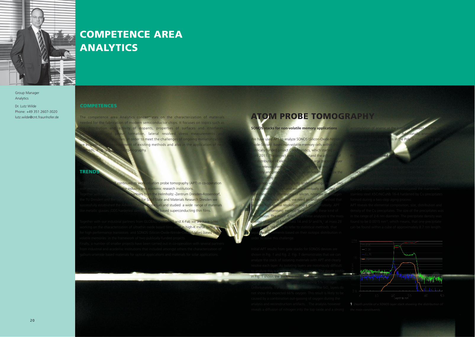
sONOs stacks for non-volatile memory applications
WehaveusedAPTtoanalyzeSONOS(Silicon-Oxide-Nitride-
Oxide-Silicon)basednon-volatilememorycellswithinthe
publicallyfundedprojectCoolAnalytics,whichstartedin
April2011.Theprojectaimstounderstandtheinfluenceof
thedistributionofelementswithinthechargetrappinglayer
ontherelevantelectricalpropertieslikechargeretention,
reliabilityandprogrammingvoltageinordertooptimizethe
manufacturingprocess.
Asthenon-volatilememorycellsunderinvestigationaretwo-
dimensionalstructuresandweareeventuallyinterestedto
determinetheconcentrationofsilicon,nitrogenandoxygen
intwodimensionsaswell,weneedananalysismethodthat
provideshighspatialresolutionandagoodsensitivity.APT
isthemostpromisingmethodforextractingthesekindof
information.Themajordifficultyintheseanalysesisthemass
overlapofSi2+andN+atmass14andSi+andN2+atmass28
respectively.Wehavetorefertostatisticalmethodsthat
separatetheelementsbasedontheirisotopicdistributionin
ordertosolvethischallenge.
InitialAPTresultsfromgatestacksforSONOSdevicesare
showninFig.1andFig.2.Fig.1demonstratesthatwecan
analyzethestackofisolatingmaterialswithAPTandclearly
resolveeachlayer.Asisolatinglayersarenotoriouslydifficult
toanalyzethisisamajorstepintheproject.Thedepthprofile
inFig.1showsthethicktopoxide,thethinbottomoxide
andtheintermediateoxy-nitridecontaining5%nitrogen.
Unfortunately,theoxygenquantificationintheSiO2layersdo
notshowtheexpected66%oxygen.Thisresultislikelytobe
causedbyacombinationout-gassingofoxygenduringthe
analysisandreconstructionartifacts..Theanalysishowever
revealsadiffusionofnitrogenintothetopoxideandastrong
accumulationofarsenicattheinterfacebetweenthePoly-Si
electrodeandthetopoxidelayer.Additionally,arsenicis
enrichedatgrainboundariesinthePoly-Sicoveringthegate
stack(Fig.2).
Precipitation hardened steels
Thehardeningofsteelbytheprecipitationofnano-scaled
particlesisacommonmethodinsteelmetallurgy.APTis
anidealmethodtostudytheseprecipitationphenomenain
detail.TogetherwithFraunhoferIWS(Dr.JörgKasparand
Dr.JörgBretschneider)wehaveinvestigatedthemartensitic
stainlesssteelX5CrNiCuNb16-4hardenedbyCuprecipitates
formedduringatwo-stepagingprocess.
APTrevealstheelementalcomposition,size,distributionand
densityoftheCuprecipitates.Thesizeoftheprecipitateswas
intherangeof2-6nmdiameter.Theprecipitatedensitywas
foundtobe0.0015nm-3,whichmeans,thatoneprecipitate
canbefoundwithinacubeofapproximately8.7nmlength.
atOm PrObe tOmOgraPhy
1 Depth profile of a SONOS layer stack showing the distribution of
the main constituents.
treNDs
In2011FraunhoferCNTcontinueditsworkonatomprobetomography(APT)inco-operation
withexternalpartnersfromtheindustryandacademicresearchinstitutions.
TogetherwithourlocalacademicpartnersfromtheHelmholtz-ZentrumDresden-Rossendorf,
theTUDresdenandtheLeibniz-InstituteforSolidStateandMaterialsResearchDresdenwe
successfullyestablishedtheAdvancedAtomProbeLabandstudiedawiderangeofmaterials
likemetallicglasses,ODShardenedsteelsorpnictidebasedsuperconductingthinfilms.
TogetherwithourindustrialpartnersfromGLOBALFOUNDRIESandX-Fabwearehavebeen
workingonthecharacterizationofultrathinoxidebasedfilmsusedinhigh-Kmetalgatestack
forhighperformancetransistorsandSONOS(Silicon-Oxide-Nitride-Oxide-Silicon)basednon-
volatilememoriesintheframeworkoftwopublicallyfundedprojects.
Finally,anumberofsmallerprojectshavebeencarriedoutinco-operationwithseveralpartners
fromindustrialandacademicinstitutionsthatincludedamongstothersthecharacterizationof
gallium-arsenidebasedmaterialsforopticalapplicationsandmaterialsforsolarapplications.

22 23
aNaLytics
Theresultsclearlyshow,thattheprecipitatesareenriched
inCuandNiwhereasFeandCraredepletedcomparedto
thematrixcomposition.Thevicinityoftheprecipitatesis
depletedinCu(Cudiffusionzone).Aconcentrationprofilefor
constituentelementsascalculatedfromaveragingover300
precipitatesisshowninFig3.The3Dspatialdistributionof
CuprecipitatesinthematrixisshowninFig.4.Furthermore,
thespatialdistributionmicrographobtainedusingatomprobe
tomographyreveals,thatcarbonisenrichedatanarch-like
grainboundary(Fig.5).
Superconducting thin films
In2008anewclassofhigh-temperaturesuperconductorshas
beendiscoveredinlayeredironarseniccompounds.Theyare
extremetypeIIsuperconductors(similartothecuprates)of
multibandnature(similartoMgB2).Sincetheirdiscoverythin
filmsoftheintermetalliccobalt-dopedBaFe2As2(Ba-122)pha-
seweresynthesizedbypulsedlaserdeposition.Theepitaxial
growthofthiscompoundonbccironoffersthepossibilityto
growFe/Ba(Fe1-xCox)2As2multilayersthatpossessmagnetically
influencedsuperconductingandtransportproperties.This
layerstackhasbeenanalysedbyAPTinco-operationwithDr.
SilviaHaindlandJanEngelmannfromIFWDresden.
Inordertofabricatesuchmultilayersforelectronicapplications
likeJosephsonjunctionsadetailedunderstandingofits
microstructureisneeded.Theinvestigatedmultilayerwas
grownbypulsedlaserdepositionunderultrahighvacuum
conditionsonMgAl2O4substrates.First,anironbufferlayer
wasdepositedatroomtemperatureandsubsequentlyheated
upto700°Ctoachieveaclosedironlayerwithsmoothinter-
faces.TheBa-122layerwasgrownatthesametemperature.
Aftercoolingdowntoroomtemperatureanapproximately
5nmthickironinterlayerwasdepositedandagainheated
up.Finally,asecondBa-122layerwasdepositedat700°C.
EpitaxialfilmgrowthwasconfirmedbyX-rayanalysis.TheFe/
Ba-122stackissuperconductinguptoatemperatureof22K.
APTresultsshowsmallscaleinhomogeneitiesofthebarium,
iron,arsenic,andcobaltdistributionintheBa-122film(Fig.6).
TheanalysedsamplesrevealedaCodopantgradientalongthe
filmthicknessaswellasBa-andFe-richregions.Theoxygen
contaminationwasfoundtobestrongestontheFelayers.
2 SEM image of a ready-to-run tip including the ROI (left) and 2d
projection of 3D atomic maps of the SONOS stack (middle and right)
showing enrichment of arsenic at the grain boundaries and at the
top oxide.
Matrix|Cudiffusionzone|Cuppt
3 Concentration profile calculated from a proximity histogram aver-
aged over 300 precipitates
z(195nm)
4 3D spatial distributions of the Cu precipitates in the steel matrix
x
y
5 Carbon enrichment at an arch-like grain boundary
6 Distribution of the iron concentration in the layer stack (left side) and iso-concentration surfaces of iron, arsenic, co-
balt, barium and oxygen showing inhomogeneities in the Ba-122 layer
53% Fe i sosurface
18% As i sosurface
11% Co i sosurface
35% Ba i sosurface
4% O i sosurface

24 25
aNaLytics
traNsmissiON eLectrON micrOscOPyAtFraunhoferCNT,theALDprocessdevelopmentandthe
evaluationofnewALDprecursorsforthedepositionof
dielectricsisoneofthecorecompetences.TEMinvestigations
ofthestepcoverageofanewprecursorforthedepositionof
Si3N4intoateststructurewithhigh-aspectratiotrencheshave
beencarriedouttosupporttheseactivities.Inordertoreduce
preparationartefactsduringFIBpreparation,thetrenches
werefilledbyaspecialresin,whichshowsthegrainystructure
inthehighresolutionimages(Fig.7&8).TheALDdeposited
Si3N4appearsinmiddlegray.Theanalysisofthelayerthickness
atthetopandatthebottomshowsexcellentstepcoverageof
betterthan80%(Fig.7).AEDXlinescanovertheSi3N4layer
reveals,thattheSi3N4layerisoxidizedatthesurface(Fig.8).
7 Analysis of the step coverage of an ALD grown Si3N4 layer by TEM
(left side: overview image; right side: top and bottom details)
8 EDX line scan over ALD grown Si3N4 layer (left side: red bar shows position of EDX scan; right side: EDX results)
X-ray DiFFractiONWecontinuedwithoursuccessfulco-operationonthecharacterizationoforganicthinfilmswithChristophSchünemannand
ChrisElschnerfromTUDresden,InstituteforAppliedPhotophysics(IAPP).Thesefilmshavepotentialapplicationsinthefield
oforganicelectronics.Especially,wefocusedontheinfluenceofthedepositiontemperatureandthemixingratioonthephase
separationandlayermorphologyinblendlayersofC60andZinc-phtalocyanide(ZnPc)whichmaybeusedasphotoactivelayer
inorganicsolarcells.Duetothelowlayerthicknessof150nmorless,themeasurementsneedtobecarriedoutingrazing
incidencegeometry.AcomparisontostandardBragg-BrentanogeometryisshowninFig.9.Whileinthegrazingincidence
modethereflectionsfromtheC60filmareclearlyvisible,inspecularBragg-Brentanogeometryonlythebroadhumpfromthe
glasssubstrateisvisible.Bothmoleculeshaveadifferentshape,asshownintheinsetofFig.9a,leadingtotheformationof
separatedC60andZnPcdomains.EnhancedphaseseparationwasobservedforhigherC60contentsandforhighergrowth
temperaturesresultinginimprovedchargecarrierpercolationpathsandthereforeimprovedsolarcellperformance.TheGIXRD
measurementclearlyindicatesthatevenforhighZnPccontentwithintheblend,ZnPcisnotabletocrystallize,evenforelevated
substratetemperaturesof140°C(Fig.9).
9 GIXRD scans of pristine C60 and
ZnPc films (left)
GIXRD scans of heated blend layers
with different ZnPc:C60 ratio (right)
tOF-simsThedepositionof5nmthinTaCNfilmsfromtetramethyldisilazane(TDMS)andTaF5precursorsonSisubstratebyanALD
processwasstudiedbyToF-SIMSmeasurements.Thesefilmsareusedasetchstoplayersinthereplacementgatetechnologyfor
thesub-28nmnode.TheToF-SIMSmeasurementsareperformedtodeterminetheinfluenceofthedepositiontemperatureand
thetemperatureofasubsequentpostdepositionanneal(PDA)onthecarbonandfluorineconcentrationwithinthefilm.From
themeasurementsitisobvious,thatthePDAtemperaturehasasignificantlyhigherinfluenceonthefluorinecontamination
withinthefilmthanthedepositiontemperature(Fig.10).ThedecreasingfluorineconcentrationuponhigherPDAtemperature
canbeattributedtooutgassingoffluorine.Otherwise,thecarboncontentisalmostindependentofthePDAtemperaturebut
showsasignificantdependenceonthedepositiontemperatureasshowninFig.11.TheN/Cratio(Nnotshownhere)increases
withincreasingtemperatureofdepositionduetothegrowthbehavioroftheALDprecursors.
10 Depth profile of the fluorine intensity in dependence of PDA
and deposition temperature
11 Depth profile of the carbon intensity in dependence of PDA
and deposition temperature
26 27
FUNctiONaL eLectrONic materiaLsFrONt-eND OF LiNe
Objectiveofthisresearchareaisthedevelopmentofinsulating,semi-insulatingandconductive
thinfilms.Thesematerialsaresuitableforvariousapplicationsinmicro-andnanoelectronics.
OneofthecorecompetenciesofthegroupistheAtomicLayerDeposition(ALD)ofdielectric
andconductivelayerson300mmsiliconwafers.ThebroadspectrumofALDresearchactivities
coversdifferenttechnicalareas:ALDprecursortesting,hardwareandequipmentevaluation
aswellasmaterialandprocessdevelopmentforhigh-volumemanufacturing.FraunhoferCNT
worksinclosecollaborationwithindustrialandacademicpartners.Hence,theDresdenALD
communityestablishedthe„ALDLabDresden“asacommonplatforminfall2010.
cOmPeteNces
ThefocusofourR&Dactivitiesarehigh-k/metalgate(HKMG)stacksforcominggenerations
offieldeffecttransistors(FET)andhigh-kdielectricsandelectrodesfornon-volatilememories
(NVM)andMIM-basedcapacitors.Inthefieldofferroelectricmemories(FeFET)Fraunhofer
CNTmadeasignificantcontributionthroughtheengineeringofferroelectrichafniumoxide
(HfO2)creatingthe“mostaggressivelyscaled”FeFETsusingferroelectricSi:HfO2ina28nm
HKMGstack(TiN/Si:HfO2/SiO2/Si).FullyfunctionalFeFETscouldbefabricatedfulfillingcurrent
Flashspecificationintermsofdataretentionandendurance,butwithmuchlowerpower
consumptionandDRAM-likewrite/erasespeed.MIMcapacitorsareusedinstand-aloneand
embeddedDRAMandasintegratedpassivedevicesforRFCMOS.In2011,weoptimizedthe
interfacesintheMIMstacktofurtherimprovethelinearityoftheTiN/ZrO2-basedcapacitors.
Inaddition,wedevelopedalowcosttantalumcarbonitride(TaCN)ALDprocessonalarge
batchfurnace.BesidetheusageintheReplacementGatetransistortechnologythisprocesscan
beusedalsoformemoryapplicationsinhigh-volumemanufacturing(e.g.MONOSFlash)and
heaterelectrodesforphasechangememory(PCRAM).
treNDs
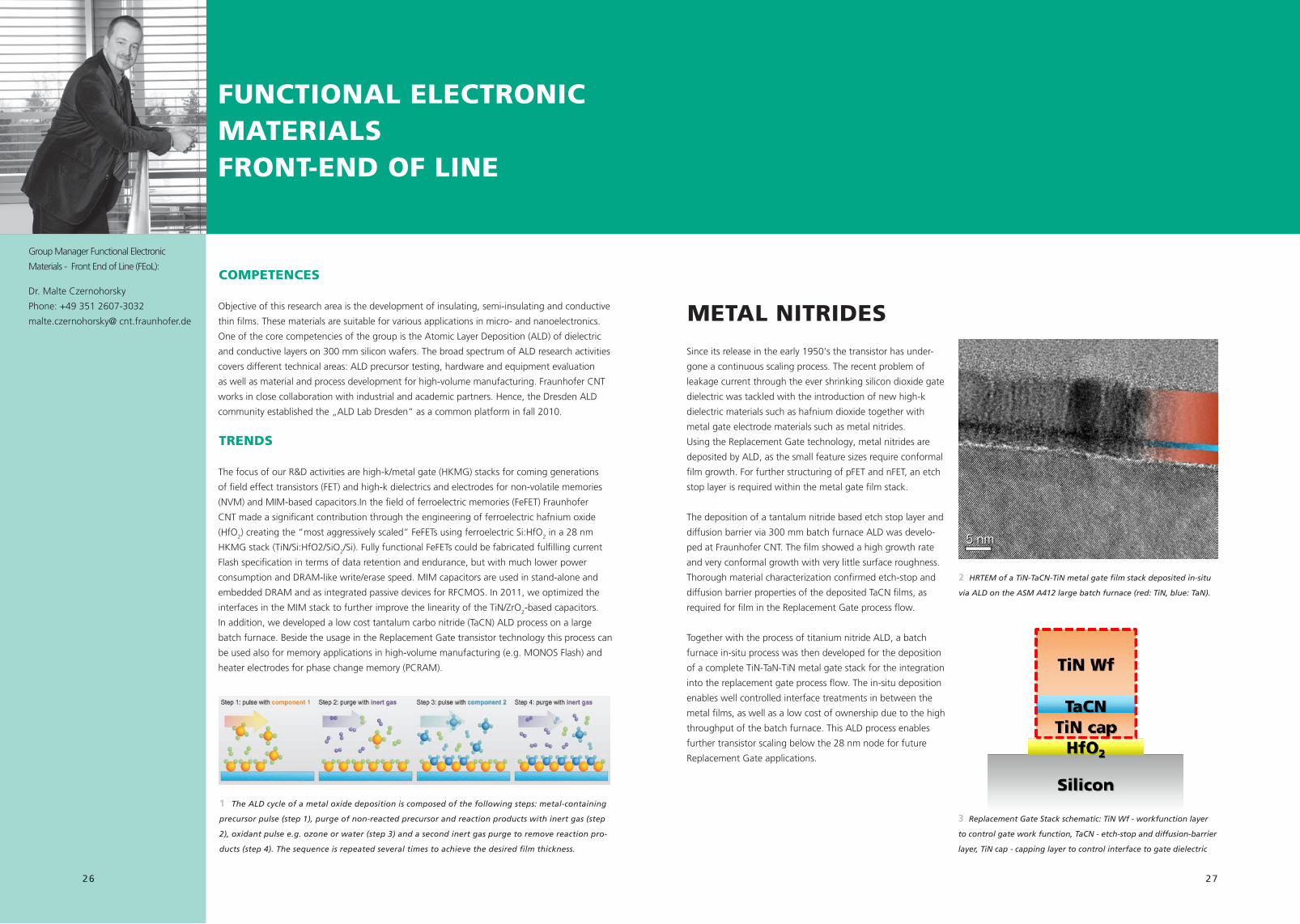
Sinceitsreleaseintheearly1950'sthetransistorhasunder-
goneacontinuousscalingprocess.Therecentproblemof
leakagecurrentthroughtheevershrinkingsilicondioxidegate
dielectricwastackledwiththeintroductionofnewhigh-k
dielectricmaterialssuchashafniumdioxidetogetherwith
metalgateelectrodematerialssuchasmetalnitrides.
UsingtheReplacementGatetechnology,metalnitridesare
depositedbyALD,asthesmallfeaturesizesrequireconformal
filmgrowth.ForfurtherstructuringofpFETandnFET,anetch
stoplayerisrequiredwithinthemetalgatefilmstack.
Thedepositionofatantalumnitridebasedetchstoplayerand
diffusionbarriervia300mmbatchfurnaceALDwasdevelo-
pedatFraunhoferCNT.Thefilmshowedahighgrowthrate
andveryconformalgrowthwithverylittlesurfaceroughness.
Thoroughmaterialcharacterizationconfirmedetch-stopand
diffusionbarrierpropertiesofthedepositedTaCNfilms,as
requiredforfilmintheReplacementGateprocessflow.
TogetherwiththeprocessoftitaniumnitrideALD,abatch
furnacein-situprocesswasthendevelopedforthedeposition
ofacompleteTiN-TaN-TiNmetalgatestackfortheintegration
intothereplacementgateprocessflow.Thein-situdeposition
enableswellcontrolledinterfacetreatmentsinbetweenthe
metalfilms,aswellasalowcostofownershipduetothehigh
throughputofthebatchfurnace.ThisALDprocessenables
furthertransistorscalingbelowthe28nmnodeforfuture
ReplacementGateapplications.
1 The ALD cycle of a metal oxide deposition is composed of the following steps: metal-containing
precursor pulse (step 1), purge of non-reacted precursor and reaction products with inert gas (step
2), oxidant pulse e.g. ozone or water (step 3) and a second inert gas purge to remove reaction pro-
ducts (step 4). The sequence is repeated several times to achieve the desired film thickness.
GroupManagerFunctionalElectronic
Materials-FrontEndofLine(FEoL):
Dr.MalteCzernohorsky
Phone:+493512607-3032
[email protected] metaL NitriDes
2 HRTEM of a TiN-TaCN-TiN metal gate film stack deposited in-situ
via ALD on the ASM A412 large batch furnace (red: TiN, blue: TaN).
3 Replacement Gate Stack schematic: TiN Wf - workfunction layer
to control gate work function, TaCN - etch-stop and diffusion-barrier
layer, TiN cap - capping layer to control interface to gate dielectric

28 29
FUNctiONaL eLectrONic materiaLs - FrONt-eND OF LiNe
Microelectronicsanddatastoragetechnologiesinparticular,
arestronglydependentontheever-progressingstrivetosmal-
lerfeaturesizes.Onlythenthecostsavingsinmassproduction
areachievednecessarytoremaincompetitiveinamarketof
rapidlyincreasingstoragedensity.Thus,inanalogytotheag-
gressivescalingoflogictransistors,thedevicedensityperunit
areaofthehigh-volumesegmentsSRAM,DRAMandFLASH
continuouslyincreaseswitheachnewtechnologyintroduced.
Nevertheless,despitetheirhighscalabilitythoseconventional
technologiesareinmanyaspectsinferiortonew,innovative
storeconcepts.Thediversificationofstorageapplications
(mobility,cloudcomputing,longtermstorage,etc.)makes
roomfornewstoragetechnologies,generallysummarizedas
“emergingmemories”.
Theindividualcombinationofmemorypropertieswithrespect
tononvolatility,speed,powerconsumption,enduranceand
scalabilitygivesconceptssuchasSTT-MRAM(magneticRAM),
RRAM(resistiveRAM),PCRAM(phasechangeRAM)andFRAM
(ferroelectricRAM)aclearedgeovertheaforementionedmass
memories.However,regardingpowerconsumptionduring
switchingoperationtheFRAM,eveninthefieldofemerging
memories,hastobeaccentuated.Especiallyinthecaseof1T
FRAM(ferroelectricfieldeffecttransistorFeFET)theswitching
processislimitedtoasimplefield-effectwhosepower
consumptioninrelationtothecurrent-drivenswitchinginthe
STT-MRAM,RRAMandPCRAMhasavanishinglylowenergy
consumption.
Thesuccessfulintegrationofsuchanenergy-efficient
storagedeviceintoindustrialproduction,however,hadbeen
considerablymoredifficultthanexpectedandwaslimited
FerrOeLectric FieLD eFFect traNsistOrs FOr FUtUre memOries
bytheavailableofintegratedferroelectricmaterials.Already
knownferroelectricssuchaslead-zirconat-titanate(PZT)or
strontium-bismut-tantalate(SBT)lackbackendofline(BEOL)
stability,fullCMOScompatibilityandsufferfromahigh
1 Conventionalized gate structure of a HfO2-based fer-
roelectric field effect transistor.
physical-layerthickness(lowcoercivefields,highdielectric
constant)thatonlywithconsiderableeffortcanbeintegrated
intoaconventionalprocessflow.However,withthesuccessful
stabilizationofferroelectricityinHfO2,amaterialsystem
alreadywell-knowntomicroelectronicengineering,anew
approachandtherewithanewperspectiveforhighlyscaled,
ferroelectricmemorieshasbeendemonstrated.Scientistof
theFraunhoferCNThaveidentifiedseveralstrategiestoform
ferroelectricHfO2andinthecourseoftheprojectsMERLINand
HEIKOdevelopedlargeexpertiseindepositing,structuringand
characterizingthosenovelferroelectricmaterials.
Currentlytheintegrationofanactualmemorydevicebasedon
anHfO2basedferroelectricfieldeffecttransistorhasreached
afinalstage.Incooperationwithourlongtermpartners
GLOBALFOUNDRIESandNamlabgGmbHfullyfunctional
ferroelectricfieldeffecttransistorsonastateoftheart28nm
groundrulehavebeendemonstrated.
Figure2depictsTEMcrosssectionsofthegatestackof
anearlierbutcomparableferroelectricdevice,aswellasa
ferroelectricMIMcapacitorusedforprocessqualificationand
ferroelectricparameterextraction.Basicdeviceoperationwas
statisticallyverifiedandisrepresentativelydepictedinFigure3a.
EndurancecomparabletocurrentFlashtechnologiesaswellas
dataretentionexceeding10yearswasfurtherdemonstrated.
Additionally,outstandingswitchingtimesbelow20nswere
achievedascanbeseeninthetimeandfielddependent
memorywindowmatrixinFigure3b.Insummarythispredicts
afast,highlyscaled,non-volatilememoryconceptbasedon
ahighlyengineered,ferroelectricHfO2.Incurrentandfuture
2 TEM cross section of a HfO2-based ferrolectric field effect transis-
tor and a metal-ferroelectric-metal capacitor.
3 Basic device operation of a ferroelectric field effect transistor (a).
Time and field dependence of ferroelectric switching and its impact
on memory window evolution.
projectsa100bitdemonstratorwillbefabricatedrepresenting
thefinalstepinputtingthenewlydiscoveredferroelectric
propertiesofHfO2toausefulapplicationinindustrialscale.

30 31
FUNctiONaL eLectrONic materiaLs - FrONt-eND OF LiNe
ZrO2isofveryhighinterestinsemiconductorindustrymainly
ashigh-kdielectricinDRAM,eDRAMorevenresistiveRAM.
Aboveall,noalternativematerialsareinsightforthenext
generationsofDRAM.Thus,furtherimprovingofdeposition
processes,ofmaterialpropertiesandofintegrationschemes
isessentialtomeetthestrictrequirementsoffuturedevices.
Onekeychallengeisreducingtheprocesstimeofthebottle
neckhigh-kALDdeposition.Themostcommonprocessused
forZrO2depositionisTEMAZ/O3withapublishedgrowthrate
of1Å/cycle.Thereby,theO3processcausesoxidationofthe
TiNbottomelectrodesresultinginMIMcapacitorasymmetries
andcapacitancelinearityissues.AttheFraunhoferCNT,we
improvedtheTEMAZ/O3ALDprocessandstudiedthegrowth
andcrystallizationbehaviorofthinZrO2films.Agrowth
rateof1.8Å/cycleupto2.7Å/cyclecouldbeachievedby
increasingtheTEMAZandtheO3pulsetimes(Figure1).Linear
growthandgooduniformityon300mmwaferscouldbe
provedforanALDwindowupto270°Cwhichiscomparable
topublishedTEMAZ/O3processes.Theincreaseofthegrowth
ratecorrelatestothecrystallizationoftheZrO2filmsduring
depositionstartingatacriticalfilmthickness.Besidesthefast
growthratethedepositedZrO2layersshowverygoodelectri-
calperformancewithaCETof0.7nmandaleakagecurrent
of2.6•10-9A/cm2at-1Vfora7nmthickcrystallinefilm.
Additionally,thenewZrO2ALDprocesswasusedtooptimize
theintegrationschemeofMIMcapacitorswithTiNelectrodes
addressingthebottominterfacebetweenZrO2andTiN.Ina
firststep,theTiNsurfacewasstudiedindetailafteranHF-Dip
byXPSandRsmeasurementstoimplementatimecoupling
betweenTiNandZrO2deposition.Interestingly,thenative
TiO2canbereducedbutneverremovedcompletely.Ina
secondstep,theinfluenceoftheO3oxidationwasminimized
byseveralprocessvariationsincludinglowerO3pulsetimes
orskippingtheO3pulseonlyforthefirstcyclesoftheALD
deposition.AR-XPSandToF-SIMSdepthprofilesshowa
significantdecreaseoftheTiO2betweenZrO2andTiNbyusing
anHF-Dip.ThisreductionisintensifiedbytheZrO2process
withoutO3whichisvisiblebythedecreaseoftheTiO-ionat
theinterfacebetweenZrO2andTiNinFigure2.
high-K materiaLs FOr mim caPacitOrs
1 Linear growth of ZrO2 from a new TEMAZ/O3 process at different
deposition temperatures.
2 ToF-SIMS depth profile of the interface between ZrO2 and TiN
after different interface treatements.
cleanroom at Fraunhofer CNT

32 33
FUNctiONaL eLectrONic materiaLs - bacK-eND OF LiNe
15yearsago,aremarkablestepwastakenbyimplementingcopperasmetallizationmaterial
inthefabricationofintegratedcircuits(ICs).Itwasnotonlythechangeofmaterialfrom
aluminumtocopperbutratherthewholeintegrationscheme,changingfromthesubtractive
structuringmethodtothedamasceneprocess,thatchallengedengineersandscientists.How-
ever,especiallytheintegrationofnewprocesseslikeCMP(chemical-mechanicalplanarization)
andthedevelopmentofnewmaterialcombinationsprovedthesuperiorityofcopperagainst
aluminummetallization.
Intheearlyyearsofchipmanufacturing,thetransistorsizedeterminedtheprocessorclock
rate.Adecreasedgatelengthallowedashorterswitchingtime,whichmadetheprocessors
fasterandfaster.However,asideeffectofshrinkinggatelengthsisthattheareaavailable
forelectricalcontactingisreducedaswell.Thewiresaswellasthespacesbetweenthemget
smallerandreachthedimensionofactualcoppergrainsizes,leadingtoanon-linearresistivity
increaseaswellasincreasedcapacitanceeffects.Thatmeans,nowadays,thesignalpropagation
ratethroughtheelectricalwireslimitstheprocessorclockrate,sinceitpassedthetransistor
switchingtimedelay(Figure1).Thus,themaintaskforresearchanddevelopmentintheback-
endoflineistominimizetheRCdelay.Thisisaddressedthroughalldifferentprocessesinthe
back-endoflinemoduleattheFraunhoferCNT.
cOmPeteNces
GroupManager
FunctionalElectronicMaterials-
BackEndofLine(BEoL):
Dr.RomyLiske
Phone:+493512607-3040
ThecapacitanceCcanbedecreasedbyusinglow-kmaterials
asdielectrics.Besideschangingthematerialtype,porosity
canbeintroducedtofurtherdecreasethek-value.However,a
porousmaterialincreasestheintegrationcomplexity,because
allconnectedprocessesneedtobetunedastominimize
thedamageoftheporousmaterialitselfandthek-value
degradation.Furthermorethemechanicalstrengthofporous
low-kmaterialcanbechallenging.
AttheFraunhoferCNTresearchfocushasbeenputonthesi-
dewalldamageofthelow-kduetotheRIEetch,theinfluence
ofwetcleanprocessesafterdryetchingandthepossibilitiesof
restoringk-valuesthroughrepairprocesses.Forthefutureitis
intendedtoinvestigatetheinfluenceofCMPprocessesonthe
k-value.
TheresistivityRdependsonthematerialsusedformetalli-
zationandtheirmicrostructure.State-of-the-artmaterialfor
leadingedgeinterconnecttechnologyremainscopper.Its
specificresistivityislow(1.7µΩcm)andelectro-andstress
migrationaresufficient.However,copperneedsanefficient
barriertopreventitfromdiffusionintotheinterlayerdielectric
andtopreventitfromoxidation.Itistheaimofinterconnect
integrationtouseasmuchcopperforthecircuitaspossible
forperformanceandaslittlebarrierasabsolutelyneededfor
reliability.Asthecross-sectionofconnectsforleadingedge
technologynodesisintheorderofcoppergrainsizesandthe
barrierusesasignificantareafraction,barriermaterialreduc-
tionandvoid-freecopperfillingwithoptimizedmicrostructure
isdemanded.
ThusattheFraunhoferCNTfocusisonthedevelopment
ofnewCVD-depositedbarriermaterials,thatallowathin
andconformaldepositionwithgoodsidewallcoverage.
Preferably,thesebarriershavevalueaddedpropertieslike
goodconductancetoomitaseedlayerforcopperdeposition,
which,togetherwithavoid-freecoppersuperfillingbyelectro-
chemicaldeposition,leadstoabettercoppermicrostructure
andthusfasterandmorereliablecircuits.Theroleofthebath
additivesinelectrochemicalplating,whichareresponsible
forsuperfilling,issubjectofresearchattheFraunhoferCNT.
Furthermoretheinfluenceoftheannealingregimeonthe
coppermicrostructurecanbestudied.
Inthenearfutureprocessdevelopmentinthefieldofchemi-
cal-mechanicalplanarizationininterconnecttechnologycan
becarriedout.Topicsofinterestwillcoverpolishingofnew
barriermaterialswithlowdamagestoponlow-kdielectrics.
Theback-endoflineprocessflowisshowninFigure2.
LeadingedgeresearchintheFraunhoferCNTcoversULKetch,
clean,barrierandseeddeposition,copperplatingandCMP.
1 RC delay influence of front-end of line transistor and back-end
of line interconnects. Effect of change to copper and low-k. From:
Bohr; „Interconnect Scaling – The Real Limiter to High Performance
ULSI“; Proceedings of the 1995, IEEE International Electron Devices
Meeting.
2 Dual damascene process
flow in the back-end of
line.
1: ULK and hardmask
deposition,
2: lithography, etch and
cleaning,
3: barrier and seed layer
deposition,
4: copper plating and
anneal,
5: copper and barrier CMP.
34 35
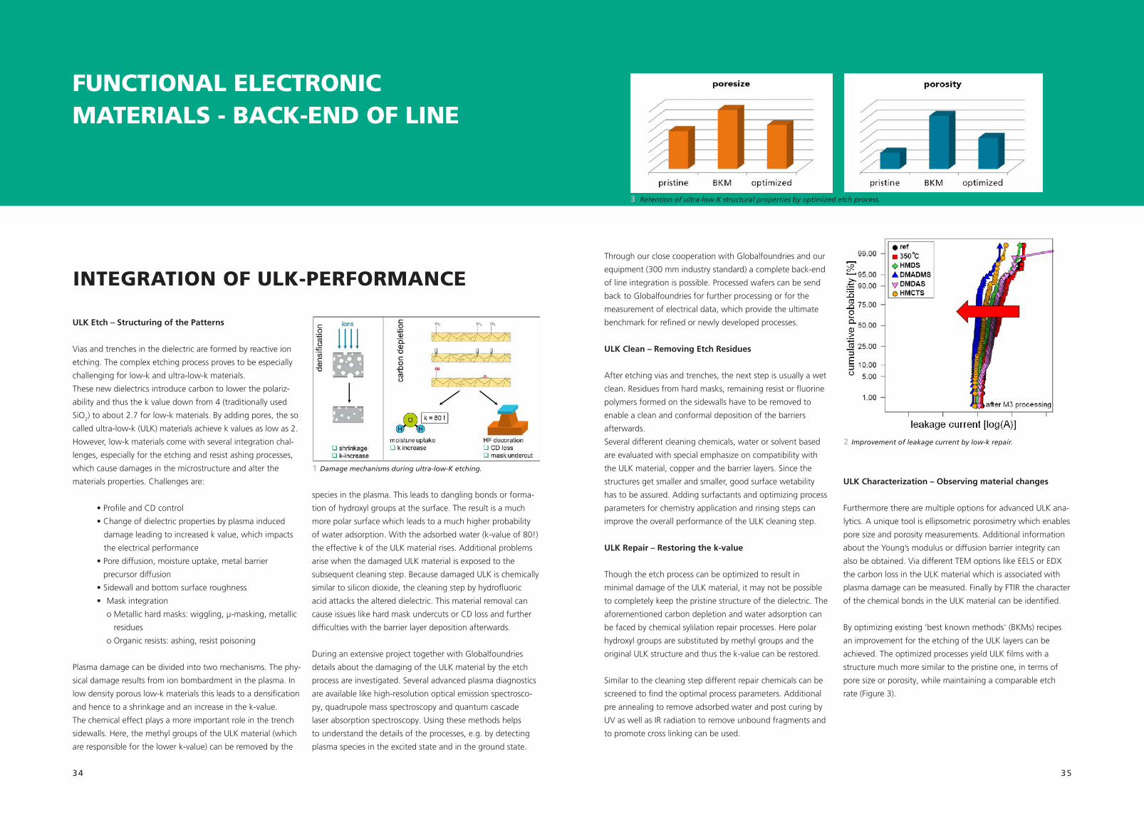
3 Retention of ultra-low-K structural properties by optimized etch process.
FUNctiONaL eLectrONic materiaLs - bacK-eND OF LiNe
ThroughourclosecooperationwithGlobalfoundriesandour
equipment(300mmindustrystandard)acompleteback-end
oflineintegrationispossible.Processedwaferscanbesend
backtoGlobalfoundriesforfurtherprocessingorforthe
measurementofelectricaldata,whichprovidetheultimate
benchmarkforrefinedornewlydevelopedprocesses.
UlK clean – Removing Etch Residues
Afteretchingviasandtrenches,thenextstepisusuallyawet
clean.Residuesfromhardmasks,remainingresistorfluorine
polymersformedonthesidewallshavetoberemovedto
enableacleanandconformaldepositionofthebarriers
afterwards.
Severaldifferentcleaningchemicals,waterorsolventbased
areevaluatedwithspecialemphasizeoncompatibilitywith
theULKmaterial,copperandthebarrierlayers.Sincethe
structuresgetsmallerandsmaller,goodsurfacewetability
hastobeassured.Addingsurfactantsandoptimizingprocess
parametersforchemistryapplicationandrinsingstepscan
improvetheoverallperformanceoftheULKcleaningstep.
UlK Repair – Restoring the k-value
Thoughtheetchprocesscanbeoptimizedtoresultin
minimaldamageoftheULKmaterial,itmaynotbepossible
tocompletelykeepthepristinestructureofthedielectric.The
aforementionedcarbondepletionandwateradsorptioncan
befacedbychemicalsylilationrepairprocesses.Herepolar
hydroxylgroupsaresubstitutedbymethylgroupsandthe
originalULKstructureandthusthek-valuecanberestored.
Similartothecleaningstepdifferentrepairchemicalscanbe
screenedtofindtheoptimalprocessparameters.Additional
preannealingtoremoveadsorbedwaterandpostcuringby
UVaswellasIRradiationtoremoveunboundfragmentsand
topromotecrosslinkingcanbeused.
2 Improvement of leakage current by low-k repair.
UlK characterization – Observing material changes
FurthermoretherearemultipleoptionsforadvancedULKana-
lytics.Auniquetoolisellipsometricporosimetrywhichenables
poresizeandporositymeasurements.Additionalinformation
abouttheYoung’smodulusordiffusionbarrierintegritycan
alsobeobtained.ViadifferentTEMoptionslikeEELSorEDX
thecarbonlossintheULKmaterialwhichisassociatedwith
plasmadamagecanbemeasured.FinallybyFTIRthecharacter
ofthechemicalbondsintheULKmaterialcanbeidentified.
Byoptimizingexisting'bestknownmethods'(BKMs)recipes
animprovementfortheetchingoftheULKlayerscanbe
achieved.TheoptimizedprocessesyieldULKfilmswitha
structuremuchmoresimilartothepristineone,intermsof
poresizeorporosity,whilemaintainingacomparableetch
rate(Figure3).
Viasandtrenchesinthedielectricareformedbyreactiveion
etching.Thecomplexetchingprocessprovestobeespecially
challengingforlow-kandultra-low-kmaterials.
Thesenewdielectricsintroducecarbontolowerthepolariz-
abilityandthusthekvaluedownfrom4(traditionallyused
SiO2)toabout2.7forlow-kmaterials.Byaddingpores,theso
calledultra-low-k(ULK)materialsachievekvaluesaslowas2.
However,low-kmaterialscomewithseveralintegrationchal-
lenges,especiallyfortheetchingandresistashingprocesses,
whichcausedamagesinthemicrostructureandalterthe
materialsproperties.Challengesare:
•ProfileandCDcontrol
•Changeofdielectricpropertiesbyplasmainduced
damageleadingtoincreasedkvalue,whichimpacts
theelectricalperformance
•Porediffusion,moistureuptake,metalbarrier
precursordiffusion
•Sidewallandbottomsurfaceroughness
• Maskintegration
oMetallichardmasks:wiggling,µ-masking,metallic
residues
oOrganicresists:ashing,resistpoisoning
Plasmadamagecanbedividedintotwomechanisms.Thephy-
sicaldamageresultsfromionbombardmentintheplasma.In
lowdensityporouslow-kmaterialsthisleadstoadensification
andhencetoashrinkageandanincreaseinthek-value.
Thechemicaleffectplaysamoreimportantroleinthetrench
sidewalls.Here,themethylgroupsoftheULKmaterial(which
areresponsibleforthelowerk-value)canberemovedbythe
speciesintheplasma.Thisleadstodanglingbondsorforma-
tionofhydroxylgroupsatthesurface.Theresultisamuch
morepolarsurfacewhichleadstoamuchhigherprobability
ofwateradsorption.Withtheadsorbedwater(k-valueof80!)
theeffectivekoftheULKmaterialrises.Additionalproblems
arisewhenthedamagedULKmaterialisexposedtothe
subsequentcleaningstep.BecausedamagedULKischemically
similartosilicondioxide,thecleaningstepbyhydrofluoric
acidattacksthealtereddielectric.Thismaterialremovalcan
causeissueslikehardmaskundercutsorCDlossandfurther
difficultieswiththebarrierlayerdepositionafterwards.
DuringanextensiveprojecttogetherwithGlobalfoundries
detailsaboutthedamagingoftheULKmaterialbytheetch
processareinvestigated.Severaladvancedplasmadiagnostics
areavailablelikehigh-resolutionopticalemissionspectrosco-
py,quadrupolemassspectroscopyandquantumcascade
laserabsorptionspectroscopy.Usingthesemethodshelps
tounderstandthedetailsoftheprocesses,e.g.bydetecting
plasmaspeciesintheexcitedstateandinthegroundstate.
UlK Etch – structuring of the Patterns
1 Damage mechanisms during ultra-low-K etching.
iNtegratiON OF ULK-PerFOrmaNce

36 37
FUNctiONaL eLectrONic materiaLs - bacK-eND OF LiNe
cOPPer DiFFUsiON barriers scaLiNgThetransitiontotheCu/ULKnodeinducedaneedforthe
developmentofnoveldiffusionbarrierspreventingthe
intermixingofcopperwiththeadjacentdielectriclayerand
otherregionsonthechip.Theyshouldbecompatiblewith
currentintegratedcircuitfabricationflows.Atthesametime
thematerialusedneedstobethermalandstructuralstable
andalsohighlythermallyandelectricallyconductive.
Thepresentstate-of-the-artbarrier/adhesionpromoterusedin
theback-endoflineisaTa/TaNfilmstack.However,despiteits
excellentbarrierproperties,thismaterialcombinationhasalso
somelimitations.Oneofthemisgivenbythefactthatboth,
theTaandTaNaredepositedbyphysicalvapordeposition
(PVD).Thisdepositiontechniquedoesnotcomplywiththe
stringentstepcoveragerequirementsforfeatureshaving
criticaldimensions.Furthermore,thecopperplatingcannot
beconducteddirectontheTalayer.Firstaseedlayerhasto
bedeposited.Bythiswaythetrenchfractionthatisfilled
withbulkcopperisreducedandtheresistivityofthewhole
interconnectstructureincreases.
ToovercometheselimitationsFraunhoferCNTandGLOBAL-
FOUNDRIEShavejointtheireffortstoenablechemicalvapor
deposited(CVD)cobaltasthediffusionbarrierofchoice
forsub28nmtechnologynodes,seeFigures1and2for
topographymeasurementsbyAFMandaTEMcrosssection,
respectively.ComparedtoTaithasamuchlowerelectrical
resistivityandhigherthermalconductivity,butthegreatest
benefitofintroducingCoasabarriermaterialisgivenbythe
fact,thatitcanbedepositedbyCVDandtheCuplatingcan
beconducteddirectlyonitssurface.
Inthiswaythestepcoverageofstructureswithcritical
dimensionscanbeimprovedandthetrenchfractionfilledwith
bulkcopper,thustheelectricalconductivityoftheconductor
pathcanbeincreased.
ForprocessdevelopmentandoptimizationFraunhoferCNT
usesastate-of-the-artAMATEndura2toolhavingDegas,PVD
Ta/TaN,PVDCuRFXandCVDCochambers.Oneadditional
advantageisgivenbytheinsituXPSmeasurementsystem
enablingchemicalanalysisofthedepositedthinfilmlayers
withoutbreakingtheprocessvacuum.Theimportanceofin
situXPSisshowninFigure3:exposuretoairduringexsitu
measurementsleadstoarapidoxidationoftheCosurface.
1A AFM measurement of a 7.5 nm thick cobalt layer.
3 In situ and ex situ XPS measurement of a cobalt layer.
siOx-cover
co
taN
tEOs
1B AFM measurement of a 7.5 nm thick cobalt layer
2 TEM of a Co layer deposited on TaN.

38 39
FUNctiONaL eLectrONic materiaLs - bacK-eND OF LiNe
FrOm POLishiNg tO high PerFOrmaNce PLaNarizatiONAsthesizeofmodernintegratedcircuitscontinuestoshrink,
theplanarityofstructuresafterCMPbecomesmoreandmore
important.Asaresult,abetterunderstandingoftherelevant
mechanismsaffectingplanarizationisneededinordertomeet
futureprocessspecifications.
Theplanarizationofapatternedwaferischaracterizedbythe
interactionofnumerousvariablessuchasappliedpressure,
relativevelocitybetweenpadandwafer,pad(roughness,
hardness,elasticmodulus,etc.)andslurrycharacteristics.In
respecttopadsurfaceroughness,aconditioningprocessis
performedinordertoremovedebrisfromthepadsurface,
restorepadsurfacequalityandthustoachievehighandstable
removalratesfromwafertowafer.
Thus,asmallamountofpadmaterialiscontinuouslyremoved
andthespecificpadsurfacepropertiesareestablished.Be-
causeonlythismodifiedupperpadlayer,definedas‘asperity
layer’,contactsthewaferduringpolishing,ithasalarge
impactonthequalityoftheCMPprocess.Tocharacterizethe
interrelationbetweenconditioningandpadsurfacetexture,a
novelroughnesscharacterizationmethodologyhasbeendeve-
loped.Itiscapableofextractingimportantcontactmechanical
parameterslikethemeanasperitiesradiusofcurvature,the
asperityheightandsizedistribution.Thesepadpropertiescan
belinkeddirectlytoprocesscharacteristicslikeremovalrate,
defectdensityandplanarizationperformanceinCMPandthus
beusedforconsumablestestingandoptimization(Fig.3).
AnothertopicinwhichtheFraunhoferCNThaslarge
experienceisthecharacterizationoftheCMPplanarization
performance.Forthis,theinfluenceofconsumableslikeslurry,
padorconditionerontheplanarizationofspecificallydevelo-
pedCMPtest-wafersissystematicallyexaminedandevaluated
usinginhousedevelopedanalysisroutines.
Stringentrequirementsofnewesttechnologynodesaswell
asthetransformationoftraditionalICmanufacturingtowards
foundrybusinesseswithawideandrapidlychangingproduct
portfolio,inextremecaseswithlittlequantities,theever
decreasingtimetomarketandshortenedproductlifetimeof
chipgenerations,allthesedemandawell-alignedCMPdesign
andprocess.ThusaCMP-awaredesignbecomesmoreand
morecrucialtobecapableofcompetingonthemarket.
NovelCMPmodelingapproachesareapowerfultoolfor
achievingthisgoalbyenhancedprocessunderstanding,
thereforeenablingnewintegrationpaths,precisedesignrules
withfillstrategiesandcosteffecientprocessdevelopment.
TheFraunhoferCNThasgreatknowledgeinthecharacteri-
zationofplanarizationprocesseswiththehelpofpatterned
CMPtestchips(Fig.1).Thedatacollectedisusedtobuild
upchipandfeaturescaleCMPmodels,whicharecapable
ofsimulatingthecharacterizedplanarizationprocess.Such
calibratedmodelscanbeusedonrealproductionlayoutsto
identifyhotspotsandsupportsmartfillstrategiesorsuggest
designchangesbeforetheproductionofthemasksets.
1 Structures used for
process characteri-
zation.
(a) density field 1,
(b) pitch field,
(c) density field 2.
white: up-regions,
black: down-regions.
2 CMP equipment at the Fraunhofer CNT: (left) Applied Materials
Reflexion LK; (right) Stangl mobile slurry systems.
3 Confocal measurements of a conditioner (top)
and a 1 mmx1 mm conditioned pad sample (down).
4 (left) Measured (symbols) and modeled planarization of test structures with 20 µm line width, 20 µm space width and 50 %
density. (right) Measured (symbols) and modeled planarization of test structures with 50 µm line width, 20 µm space width and
71.4 % density.

40 41
cOmPeteNce areamasKLess LithOgraPhy
Thecompetencearea"MasklessLithography"providesmanufacturingofresist
masksinspecialorganicphotoresistswithpatterningsizesdownto35nmandtheir
transferintotheunderlyinghardmask.Exposureiscarriedoutusingmasklesselectron
beamlithography.Thecompetenceareafocusesonthepreparationofcustomerand
application-specificdesignsandlayoutson200mmand300mmwafersviaamodern
andflexibledirectpatterningprocess.
cOmPeteNces
In2011,FraunhoferCNT‘spatterningcapabilitieshavebeenextendedtomeetcustomer
requirementsaccordingtohighresolution"More-Moore"applicationsbutalsofornovel
"More-than-Moore"challenges.Researchinthefieldofe-beampatterninghasbeenintensi-
fiedregardingresistresolution,dataprepandproximityeffectcorrection(PEC)aswellasmost
advancede-beamlithographyprocessesoncustomerspecificsubstratesandstacks.
treNDs
In2011,FraunhoferCenterNanoelectronicTechnologies
(CNT)startedactivitiesinthefieldofproductionofnano
imprintmastertemplatesinclosecollaborationwithvarious
customers.Themaintaskwastoimplementasuitableprocess
forshortreactiontimestolayoutchangesandfastproduction
oftheresistmasksforfurtherprocessing.Firstexperiments
withasimplehardmaskandresiststackasshowninFigure1
yieldedpromisingresultsforawiderangeoffeaturessuchas
linespacestructuresandlargelatticeorpillararrays.
ThisprocesstakesadvantageofexistingknowhowatFraun-
hoferCNT,especiallytheflexibilityoftheVistecSB3050DW
shapedelectronbeamlithographytoolwhichallowsalmost
anyfeaturetobewrittendirectlyintotheresistonthesame
wafer.Afterthelithographicpatterning,thestructuresare
transferredintothesiliconbyahardmasketchprocess.
Thisallowsprecisedepthtuningfortheimprinttemplatewith
verygooddepthuniformityandsteepsidewallangles.Thisin
turnensuresahighstructurequalityovertheentiretemplate
area.ExampleSEMsoffinishedtemplatestructuresareshown
inFigure2.Becauseofthesiliconstructuring,theproduced
templatesareverydurable.Afterfinishingthestructuringof
thetemplates,anadditionalorganiclayerisspunontopof
theproductinordertoprotectthesurfacefromdamageor
particles.Inthisstatetheycanalsobecleavedtotherequired
sizeinordertobereadyforusageatthecustomer’ssite,
wheretheprotectivecoatcanbeeasilyremovedwithstandard
solvents.Thispost-structuringhandlingprocessisdesignedto
ensureverylowdefectivityonthedeliveredtemplates.
Theproductionofmultilayerimprintmasterstakesthe
templateproductiononestepfurther.Amultilayertemplate
eliminatestheissueofoverlaywhileproducingwithtwo
separatetemplatesatthecostofamorecomplexproduction
cycleofthetemplate.Wesuccessfullyintegratedatwo-layer-
templatewithourpartnersFraunhoferInstituteforPhotonic
Microsystems(IPMS)andtheTechnicalUniversityDresden.
maNUFactUriNg OF NaNOimPriNt temPLates
Thefirststepstructuredawaveguideintothesilicon,shown
aspinkbarsinFigure3.Thesecondlayer(purple)structured
acouplingontopofthewaveguideinordertoallowsignals
ofacertainwavelengthtobecoupledintothesubstrate.
Waveguidesandcouplingswereprintedinawiderangeof
sizestoallowfinetuningofwavelengthsandtobeableto
characterizethewaveguidebehavior.Anexampleofthe
producedpatternsisshowninFigure3(left page).
Itshowsthelayoutofthecouplingontheleftandthe
producedimprinttemplateontheright.Thisfeaturecontains
acurvedshapewhichwaseasilypatternedviaagdslayout
providedbyourpartners,whohadfreehandindesigning
theirtemplate.Incaseoflayoutproblems,adjustmentsand
changescanbeimplementedonsitewithinminutestoensure
thatonlycorrectpatternsareprinted.
TheconstantlymonitoredprocessesatFraunhoferCNT
enableaquickandpreciseintegrationofbothlayersonthe
siliconsubstrate.DirectwritelithographyatFraunhoferCNT
iscurrentlypossibleon200mmand300mmwafersona
production-likeflow.Inaddition.wafersizesdownto100mm
canbehandledforrapidprototypingapplicationsenabling
cost-effectiveandflexibledirectwritingformanyR&D
scenarios.
GroupManager
Patterning
Dr.ChristophHohle
Phone:+493512607-3013
1 Schematic process flow of imprint production
2 Imprint template structures transferred into silicon
3 Optical coupling as designed
(left) and as final imprint temp-
late (down)

42 43
masKLess LithOgraPhy
Resistpatterningonwafersusinge-beamlithographyisan
alternativetoopticallithography.Especiallyforrapidprototy-
pingapplicationswithverysmallwafervolume,electronbeam
directwrite(EBDW)hascertainadvantages.Forexample,
designchangescanbeimplementedovernightandverified
beforemasktapeout,differentdesignversionscanbetested
ononewaferordesignbugscanbecorrected(especially
metalfix).EBDWprovideshighresolutionandthevariable
shapedbeamsystemshavehigherthroughputcomparedto
Gaussianbeamsystems.Furthermore,maskcostsaresaved
andmaskdeliverydelayisremoved.
Forthe22nmnode,theITRSroadmapincludesmaskless
lithography(ML2)usingmultibeamtechnologies.High
resolutione-beamresistsareneededforML2toreachthe
requirementsoftheITRS.Chemicallyamplifiedelectronbeam
evaLUatiON OF Direct PatterNabLe iN-OrgaNic sPiN-ON harD masK materiaLs UsiNg eLectrON beam LithOgraPhy
resistsarefulfillingsensitivityrequirementsfore-beamdirect
writingbutarelimitedinresolutionduetoaciddiffusion.
Stowersetalhaveshownelectronbeamexposureresults
usinginorganicnon-chemicallyamplifiedresistsbasedon
hafniumandzirconiumoxideswithhighresolutionandhigher
sensitivitycomparedtostateofartnon-chemicallyamplified
resistslikehydrogensilsesquioxane(HSQ).
FraunhoferCNTinvestigatedanewinorganicnon-chemically
amplifiedresistsprovidedbyInpriaCorp.andcomparedthem
withtwootherhighresolutionresists:HSQandanegative
tonechemicallyamplifiedresist(nCAR).Asametaloxide,
theresisthashighetchresistancecomparabletohardmask
materialsandisapromisingcandidatefore-beamlithography
aswellasforEUVlithography.Withthevariableshapedbeam
atFraunhoferCNT1:1densepatternwithadimensionof
100μmx100μmwereexposed.InFigure1exposureresults
ofthat1:1densepatternfor3differentfeatureCDsare
summarized.Thepatternsarealmostontarget.Aproximity
effectcorrectionfor1:1densepatternisnotneeded.XE15IB
isabletoresolveeasily30nmoftheselargedensepatterns.
VISTECsSB3050DWwasdesignedfortherequirementsofthe
50nmnodeandreachesitstoollimitationexposing30nm
patternandbelow.Aresolutionof30nmhpdenselineswas
neverachievedbeforewiththistoolatFraunhoferCNT.
Theslightstitchingvisibleinthepicturescomesfrom
theelectronbeamandcanbeminimized.ForcomparisonHSQ
isabletoresolve35nmonly(55nmfilmthicknessandconcen-
trateddevelopmentwith25%TMAH)havingnoresolutionto
obtain30nm.K.SteidelhasshowninherPh.D.thesisthatthe
nCARhasaminimumresolutionof40nmfor1:1denselines.
Alargerealapplicationpatternisalsodemonstrated.The
chosenpatternisarealSRAMmetal1layerforthe32nm
technologynode.Thislayerwasshrinkeddownto22nm
featuresize.
Thepatternwasproximityeffectcorrectedwithgeneralpro-
ximityeffectcorrection(PEC)parametersfornon-chemically
amplifiedresists.ThedesignandSEMimagesoftheSRAM
patternareshowninFigure2.WhilethefeatureCDison
target,itisclearlyvisiblethatsomelinesarenotcorrectly
resolvedorspacesaremerged.CorrectPECparameterscan
improvetheresolutionandwillbedeterminedfortheInpria
resistinthenextsteps.FraunhoferCNTevaluatedXE15IBina
nearproductionenvironment.Theresistisbasedonhafnium
oxideasadirectpatternablespinonhardmask.Toinvestigate
resolutionanddelaystabilitiessuchasvacuumdelayandshelf
life,Contrastpattern,1:1denselinesandaSRAMmetal1
layerwereexposed.
ThecontrastofXE15IBisabout50%betterthanHSQand
thedoseiscomparable.XE15IBshowsgoodresolutionfor
22nmSRAMpattern.ComparedtoHSQandthenCAR,XE15-
IBhasabetterresolutionforlarge1:1densepattern.30nm
halfpitchlinesareresolvable.Shelflifeandvacuumstability
ofXE15IBdoesnotyetmeettherequirementsforashelf
lifeofseveralmonthsandavacuumdelayuptooneday.By
improvingtheresistprocessorbysizingthedensestructures
thepatternqualityofthe30nmlinesisexpectedtobecome
improveddownto27nm.
AfurtherresolutionimprovementoftheSRAMfeatures
canbeobtainedbyapplyingthecorrectproximityeffect
parameter.Asignificantadvantageofahafniumoxidebased
resistcomparedtoothersistheetchselectivitysothatrelaxing
thefilmthicknessispreventedfrompatterncollapse.Infuture
researchactivitiesetchperformance(selectivitytoSilicon)
hastobeprovenandadditionallyLWRandLERhavetobe
investigatedatFraunhoferCNT.1 XE15IB SEM images of 1:1 dense pattern with feature CD 30nm (measured CD mentioned top left)
2 XE15IB SEM ima-
ges of 22nm SRAM
pattern (FOV 4µm (a)
and 2µm (b)), layout
courtesy of GLOBAL-
FOUNDRIES

44 45
masKLess LithOgraPhy
Thedatapreparationfore-beamlithographyisan
essentialtechnologicalcomponentandneedstobe
improvedsimilarlytoimprovementsofresistresolution
ortheresolutionoftheexposuretool.Tofulfillthe
requirementsanddemandsofupcomingsemiconductor
technologynodesandothercustomersofe-beamlitho-
graphy,FraunhoferCNTupgradeditsformer32-bitdata
preparationclusterenvironmentin2011.Thenewhigh
performancecluster,whichwassetupfornewdata
preparationsoftware,isequippedwithamasternode
andfourcomputingnodeswithGraphicsProcessing
Units(GPUs)basedona64bitLinuxoperatingsystem.
Theaccessiblememoryandcomputingpowerenables
theprocessingofhugeamountsofdatawhichare
commoninsemiconductorindustryandincreasewith
upcomingtechnologynode.Theinvestmentforthe
DataPrephardwarewasfundedbyBMBF/SMWKwithin
theBRIDGEproject.
Thedatapreparationsoftware,whichpreparestheexposure
datausingparticularalgorithmsofproximityeffectcorrection
andfracturing,impactstheresolution,theexposurequality
anditsprocesswindowine-beamlithography.Fraunhofer
CNTiscollaboratingwithASELTANanographics,Grenoble,
Franceforprovidingthecreativesolutionforfuturesub-30nm
maskwritingandML2applications[Ref.PressRelease].This
industrialcooperationnotonlyaimsatthedevelopmentof
proximityeffectcorrectionsbutalsotriestoimprovevarious
practicalfactorsine-beamlithography,suchastheshortening
ofwritingtime,speedingupthedatapreparationprocess,
customizationetc.
Throughtheco-workofFraunhoferCNTandASELTA
Nanographicsitwasalreadyproventhattheexposurequality
andcapabilityine-beamlithographycanbeenhancedbythe
newlydevelopeddataprepsoftwareINSCALE®.[Ref.Proc.
SPIEVol.8166,816621,2011.]Furthermoreiteithercan
amendtherealapplicationfactorsofe-beamlithography,like
calculationtime,theinfluenceforwritingtimeetc.Thecolla-
borationbetweenFraunhoferCNTandASELTANanographics
isongoingtorefinetheinnovativedataprepsolutionandto
makeitfitfornexttechnologicalnodesandML2applications.
AseltaNanographicsdevelopedthenewtypeofalgorithm
calledelectronResolutionImprovementFeatures(eRIF),which
basesonthedosemodulationandmultiplepassexposure.
UPgraDe OF the Data PreParatiON eNvirONmeNt FOr cNt’s e-beam LithOgraPhy
Figure2 presentsthetestpatternimages,exposedand
observedatFraunhoferCNTandcorrectedwitheRIF.With
theapplicationofeRIF,testpatternsareclearlyresolvednot
onlyonthedenselinesof40nmbutalsoonthatofdown
to36nm.Theartificialarraysof40nmtestpatternsarealso
resolvedwithgoodqualities.
ThetestartificialarraywiththedesignCDsof36nmare
observedasenhanceditsqualityofexposuresbutwithsome
glitches.Itisconsideredthatthesearenotjustduetothe
capabilitiesofdataprepbutalsothesusceptibilityofprocess
intheappliednCARisgettingtoreachitsboundary.Though
theobservationoftestexposurethatisobtainedinthe
artificialarrayof36nmdoesnotseemperfect,theeRIFisable
todemonstratethatthedataprepcanmaketheexposures
possibleforatechnologynodebeyondusingcurrentexposure
toolanditsprocesses.
1 Comparison of the simulations and test exposed images between
dose modulated correction and dose-geometry modulated correc-
tion
Oneofthepromisingcandidatesfortherealapplicationin
e-beamlithographyinnearfutureiscomplementaryexposure,
especiallyforthehighvolumemanufacturinginfuturetechno-
logicalnode.Becauseofthecharacteristicsofitsapplication,
thedesignconsistsnotsimplyofthelinerepetitionbutofthe
complicatedcombinationoflines,polygons,elongatedholes
andholes.Toachievetheusablecorrectionsforthose,the
variouscorrectionredundancies,whichmeansnotonlyofCDs
butalsoforcornerroundingandLES,arerequired.
Thismeansthecorrectionalgorithmitselfshouldbemore
weightedto2-dimensionsthanthe1-dimensionalway.Itis
thereasonwhyeRIFisconsideredasbeneficialtothisappli-
cation.Figure2exhibitstheimagesofexposedtestpatterns,
whicharecorrectedbyeRIF,alongwiththesimulatedresist
contoursafterthecorrection.Thosearefurtherenhanced
thantheimagesobtainedfromthepatternsthatarecorrected
usingdose-geometrymodulations,whicharenotshownin
here,whentheyarecross-examinedincomparison.
2 SEM images of test exposed patterns corrected and prepared with
eRIF and Inscale®.
dose modulation dose-geometry mod.50
nm
60
nm
dense line artificial array
36 n
m40
nm
Novel 64bit-high
performance cluster device
for e-beam data prep
3 Screenshot: graphical user interface (GUI) Inscale Software
36 n
m40
nm
46 47
cOmPeteNce areaDevices & iNtegratiON
Themainresearchtopicofthecompetencegroup“Device&Integration“isthe
developmentandintegrationofnanoelectronicprocessmodulesanddevices.There,
thefocusisontheelectricalcharacterizationofsemiconductordevicesonwaferlevel
suchasmemorydevices(singlememorytransistors,arraysanddemonstrators)aswell
asonthedevelopmentofconceptsfortheintegrationofnewmaterialsand
innovativeetchingprocessesinprocessflowsinordertofabricatenanoscaled
structures.Thedesignandfabricationofteststructuresandtestchipsenablesfast
learningcyclesforprocessdevelopment.
cOmPeteNces
Withtherecentdevelopmentsinintegratingnewthin-filmmaterialssuchashigh-k
gatedielectrics,manyprocessintegrationissueshavetobesolvedinordertomeet
thereliabilitytargetsandtobenefitfromalowpowerconsumptionandhigh-
operatingfrequencyofdevicesinthe2xnmscale.Forstructuringthenewmaterials,
advancedetchingprocessesneedstobedevelopedforachievinggooduniformityand
lowdamageofadjacentstructures.Theetchingplaysalsoabigroleinthefabrication
ofdeeptrencheswithsmalldiameterthatareusedfor3D-capacitorsbutalsoforthe
TSVpackagingtechnology.Here,researchisfocusingongaininghighaspectratios
whilemaintainingsmoothtrenchsurfaces.
Theelectricalcharacterizationisaddressingthechallengesofthenewmaterialsand
processes.Therefore,advancedreliabilitycharacterizationmethodsofhigh-k
materialsandthedevelopmentofnewteststructuresforprocessmonitoringareon
theroadmapaswellastheinvestigationofreliableprobingandtestingonsmall
contactpadsthatareimportanttoreducethechip-areaandtoenablenewpackaging
treNDs
GroupManager
Devices&Integration:
Dr.VolkhardBeyer
Phone:+493512607-3051
FLeXibLe waFermaP sOFtwareDuetothelackofsuitablefreeandcommercialsoftwaretools
toanalyzeandvisualizetestdataasawafermap,theCNTD&I
groupdesignedandprogrammedasoftwaretoolthatcan
collectandvisualizemeasuredphysicalorelectricalparameters
ondevicelevel.Theaimofsuchsoftwareistomapmeasured
dataofsemiconductorstructurestothephysicalpositionson
thewafer.Thiskindofvisualizationhelpstofindtrendsor
outliersofphysicalorelectricalparametersacrossthewafer
andhencetofindpossibleproblemsintheproductionprocess.
Theprimarygoalwastodesignatoolthatcanhandlemeasu-
reddataofdiscretesemiconductordevicesandteststructures
(regularlyspaceddatewithoutinterpolationinbetween),
e.g.CMOStransistors,memorydeviceslikeFeFET,standard
FlashandTANOSflashcellsaswellascapacitorstructureslike
“MIM”or“MIS”.
Tobeabletohandledifferentkindsofdatafromdifferent
typesoftestequipmentthetoolneedsaflexibleinterface
forthedataimport.Furthermoreitneedstobeflexibleand
extendableenoughtosupportfuturetestdataformats.
Otherrequirementsare:
•Easyuserinterfacethatsupportsafastand
straightforwardworkflow
• Automatizationcapability:Performrepeatingwafer
mappingoperationsautomaticallythatrequiresonlya
smallamountofeffortfromtheuser
• Differenttypesofoutputformats(reports)
TheCNTwafermapsoftwaresupportstwotypesofoperation
modes:Interactivemodeandscriptingmode.Intheinteractive
modetheusermanuallyadjustthedataimportandthevisual
appearanceoftheresultwithaGUIdesignedforthatpur-
pose.Thisisthefastestwaytoproducearesultinonlyafew
minutes.Theusercanadjustthecolormappingandafewof
themostimportantparametersforthevisualstyle.Thismode
islikeafastpreviewmodeduetoitslimitednumberofadjus-
tableparameters.Thesecond,muchmorepowerfulmodeis
thescriptingmode.TheCNTwafermaptoolcanbecontrolled
byaspeciallydesignedscriptinglanguage(batch-style).The
integratedscripteditorallowstoload,save,editandrunsuch
scripts.Withmorethan20keywordstheusercancontrolall
parametersfordataimport,exportandthevisualappearance
ofthewafermap.
Additionally,thescriptmodeispartlyinteractivebyallowing
theusertoclickoncertainkeywordswhichopensasuitable
windowtomakeadjustmentstothekeywordparameters(e.g.
clickingonacolorstatementwouldopenacolorpicker).The
outputgeneratedbythescriptcanbepreviewedbeforebeing
exportedtoanexternalreportfileandtheusercanbrowse
throughthegeneratedwafermapsheets.Thus,theuserhas
afastfeedbackoftheresultinacomfortableandeasytouse
developmentenvironment.
1 A typical wafermap generated by CNT Wafermap (up),
CNT Wafermap interactive mode (down)

48 49
Devices & iNtegratiON
Sinceconventionalmemorytechnologiessuchasfloatinggate
flasharefacingsevereproblemsbelowtechnologynodes
ofaround3xnmandbeyond,manufacturersofnonvolatile
memories(NVM)aredevelopingmemoryconceptswhich
allowforfurtherincreaseofcelldensity.Thesenewconcepts
areoftenreferredtoasemergingmemories.AlsoFhGCNTis
involvedinseveralprojectsinvestigatingandpreparingnext
generationNVM.
FeFEt
Onepromisingcandidateforfuturenonvolatilememoryis
theFerroelectricFieldEffectTransistor(FeFET)whichhas
beendevelopedandmanufacturedincooperationwithGLO-
BALFOUNDRIESandNAMLABgGmbH.AtFhGCNTcritical
processesforthedeviceperformancewerecarriedoutsuchas
depositionoftheferroelectricmaterialandetch.Usingvarious
teststructuresandsingletransistorsontheprocessedwafers
FhGCNTconductedapartoftheelectricalcharacterization
andoptimizationofperformanceparameters.
There,itwaspossibletoverifythebasicdeviceoperation
whichisrepresentativelydepictedinFigure1a.Endurance
comparabletocurrentFlashtechnologiesaswellasdata
retentionexceeding10yearswasfurtherdemonstrated.
Additionally,outstandingswitchingtimesbelow20nswere
achievedascanbeseeninthetimeandfielddependent
memorywindowmatrixinFigure1b.
Usingleadingedgewafertestequipmentallcharacterizations
werealsodoneonhighstatisticstoensureabalanced
overviewofelectricalparameters.
aDvaNceD memOry DeveLOPmeNt
1 (a) Basic device operation of a ferroelectric field effect transistor
(top). (b) Time and field dependence of ferroelectric switching and
its impact on memory window evolution.(down)
Insummarythispredictsafast,highlyscaled,non-volatile
memoryconceptbasedonahighlyengineered,ferroelectric
HfO2.Incurrentandfutureprojectsa100bitdemonstrator
willbefabricatedrepresentingthefinalstepinputtingthe
newlydiscoveredferroelectricpropertiesofHfO2toauseful
applicationinindustrialscale.
Enery efficient non-volatile SRAM
FhGCNTisinvolvedinthedevelopmentofnon-volatileSRAM
(nvSRAM)atANVO-SYSTEMSDRESDEN.Thebasicelectrical
characterizationaswellasreliabilitymeasurementssuchas
program-eraseenduranceanddataretentionwasconducted
usingautomaticwafertestersintheCNTlaboratory.
Forthispurposeasetofspecifictestprogramswasdesigned
implementingtheindividualneedsofthisnewmemory
technology..Thisnon-volatileSRAMcombinestwoproven
technologies(CMOS-SRAMandSONOSnon-volatilememory)
intoanewtechnologyforfast,reliableandenergyefficient
memories.
DuetounrestrictedinternalSRAMfunctionality,bothfast
readsandwritescanbeexecutedwiththesamehighspeed.
Thebuiltindataprotectionisrealizedinahighlyparallel
internalarchitecture.AnextremelyenergyefficientSTOREme-
chanismenablesthedevicetotransferthewholeSRAMdata
to/fromthenon-volatilearrayinjustonesinglestepoperation
(8msSTORE/10μsRECALL).
Theobtainedelectricaldatarevealsasuperiorreliabilityof
20+yearsdataretentionandpracticallyunlimitedwrite/erase
endurance.Combinedwithextremelylowpowerconsumption
atfastwritespeedsthisnvSRAMaddressesawiderangeof
applications.
Itisideallysuitedforself-poweredandlowpowermobile
systemsinmedicalandautomotivesolutionsbutalsoas
highspeednon-volatilestorageinindustrialorcomputing
applications.rangeofapplications.Itisideallysuitedforenergy
autarkicandlowpowermobilesystemsinmedicalandauto-
2 Schematic of an nvSRAM cell (6 SRAM transistors and 2 SONOS non-volatile transistors)
motivesolutionsbutalsoashighspeednon-volatilestoragein
industrialorcomputingapplications.
3D NAND Flash Memory
Anotheraspectofmanufacturingnonvolatilememoriesis
thescalabilityofthedevice.Duetotechnologicallimitsand
emergingcostsforplanarmemoryarraystherearevarious
approachestobuild3-dimensionalmemoryarchitectures.
Thesenewarchitecturesarebasedonaverticalmultigate
NAND-structuretoincreasethedevicedensityperchipby
stackingmemorycells.
Thechallengeinbuildingsuchmemorydevicesishere
shiftedfromlithographytotheetchingprocess,whichhasto
structureamultilayerstackconsistingofSiO2andamorphous
siliconinthecaseofaBiCS(Bit-costscalable)flashmemory.
WithintheGOSSAMERProjectFraunhoferCNThasfocused
in2011onselectedtopicsrelatedtotheintegrationof
3D-structuresintheBiCsflashmemoryconceptsuchasmulti
stacketch,dielectricdepositionandpoly-Siverticalchannel
formationinmemoryholes.Thetestvehicleisbasedona
SiO2/Simulti-layerstackthatmimicsthehorizontalcontrol
gateplatesofmemorycellsseparatedbySiO2insulatorlayers
(Figure3).

50 51
Devices & iNtegratiON
Themajorchallengein3DNANDfabricationusingtheBICS
approachisthehighaspectratiofordryetchingofmemory
holearraysintothea-Si/SiO2multigatestack.Basedon
previouslydevelopedSiO2andSisinglelayeretchprocesses,a
one-stepetchprocesshasbeenchosenasfrontupapproach
forthemulti-stackopenprocess.
Inthisapproachbothmaterialsa-SiandSiO2areetchedwithin
oneprocessstep.Advantagesofthissetupcomparedtomulti
stepormultichamberapproachesarelesscomplexity,higher
manufacturabilityandlowriskofdefectdensity.
Twomajortopicshavebeenidentifiedasmainchallenges
whichareisotropicetchintothea-Silayerandetchselectivity
SiO2
a-SiSiO2a-SiSiO2
4 Multi gate stack etch after optimization of the isotropic
a-Si etch attack and selectivity to the SiO2 hard mask.
3 Schematic of test vehicle for 3D NAND flash development
totophardmask.Inordertodecreasetheseeffectsseveral
gasadditiveshavebeentestedtosustainthepassivationon
theverticalsiliconsurfacesontheonehandanddecrease
thehardmasketchrateontheotherhand.Theoptimized
etchprocessshowspromisingresultswithsufficient
selectivityandnosiliconnotching(Figure4).
Additionally,processesforSiO2/SiN/SiO2chargetrapping
stackfabricationweredevelopedusingtheatomiclayer
depositiontechniquestocoverthesidewallsofthehighas-
pectratiodevicestringtemplates.ForSichannelformation
a-Sidepositiontechniqueswereinvestigatedincludingthe
selectiveepitaxyofSitogrowtheSichannelverticallyfrom
thechannelbottom.
a-SiSiO2
shOrt-LOOPs FOr eLectricaL materiaL characterizatiON
Highperformanceandreliabilityaswellaslowpower
consumptionaremainrequirementsontheevolutionroadmap
ofintegratedcircuitsaddingmorefunctionalityandprocessing
speedtonextchipgenerations.Inordertomeetthese
requirements,materialandinterfacepropertiesofinternal
devicesasinthegatestackoftransistorsorinintegrated
capacitorsusedinDRAMmemoriesorinanalogcircuits-need
tobeoptimizedineachtechnologygenerationinparallelto
downscalingoffeaturesizes..
AtFraunhoferCNTprocessesforthinlayerdepositionofnew
andalsoconventionalmaterialsareevaluatedandoptimized
for300mmwaferfabricationandbelowfordifferentchip
applications.Besidesuniformityorinterfaceroughness,the
electricalperformanceofconductanceandcapacitanceas
wellasinterfacetrapdensityorbreakdowncharacteristicsare
keyparametersstudyingthefeasibilityofnewmaterialsor
processingtechniques.Inordertoachievefastfeedbackloops
forcustomers'processandmaterialsoptimizationdifferent
short-loopconceptsareavailableatFraunhoferCNT:
IntegratedplanarMIS/MIMshort-loop•
MetaldotdepositiononMIS/MIMstacks•
MIS/MIMtrenchcapacitorshort-loop•
AllthreeconceptsaresuitableforMISandMIMstacksof
variousmaterialcompositionsandwillbedescribedinthenext
sections.
integrated planar Mis/MiM short-loop
ThisconceptisbasedonaflexibletestorderThisconceptis
basedonaflexibletestchip(Figure1)comprisingtwolitho-
graphylayersthatarewrittenmasklessbye-beamlithography
onmanyspotsoverthewafer,thusprovidinghighaccuracy
andstatisticsforelectricalcharacterizationanddeliveringalso
informationaboutuniformitycharacteristicsofthinfilmlayers
overthewafer.TheplanarMIS/MIMtestwaferarefabricated
using300mmwaferprocessingtools.
AsshowninFigure2theMIS/MIMareasaresurroundedby
SiO2inordertoachievesufficientisolationbetweenbottom
andtopelectrodeandtoallowsavecontactbyprobeneedles.
DuetoastandardcontactinterfacetheintegratedMIS/MIM
waferscanbemeasuredonafullyautomatedprobe-station
usingaprobecardwith25needles.Thisallowsstatisticalreli-
1 Testchip Layout

52 53
Devices & iNtegratiON
abilitytestingandmaterialcharacterizationinatemperature
rangefrom-55°Cupto200°C.Electricalmeasurement
resultsofaMISstructurewithhigh-kmaterialasdielectricare
showninFigure3.IntheCVcharacteristicperformancegain
ofhigh-kmaterialscanbederivedwhentransformingthe
measuredcapacitanceintoatheoreticalequivalentthickness
ofSiO2.Thatmeans,whilemaintainingsamegatecapacitance
thehigh-kmaterialcanbemuchthickercomparedtoSiO2thus
reducinggateleakage.currentandfinallypowerconsumption
ofthedevices.
Metal dot deposition on Mis/MiM stacks
Inearlydevelopmentphaseorforveryfastfeedbackloops
themetaldotdepositiononMIS/MIMstacksisthemethod
ofchoiceenablingfastelectricalassessmentofmaterials.
Althoughaquitesimpleapproach,itallowsalargevariety
ofdifferentmeasurementsincludingreliabilitytestingwith
moderatestatistics.
Beingbasedonlyonsmallwaferpiecesthedrawbackofthis
procedureislackinginformationaboutwaferuniformityunless
preparingmultiplesamplesfromdifferentwaferspots.Inan
ionbeamdepositiontoolashadowmaskontopofthesample
projectsdefinedmetalelectrodes(dots)ofdifferentsizeand
shapeontothesample.
Bymeansofspecificpreparationmethods,theseries
resistanceandcontacttothechuckisreducedforoptimum
3 Electrical results of a high-k based MIS stack with (l) current voltage-, (m) capacitance-voltage- and (r) conductance characterisic
measurementresults.Whenhavinganadditionalplanarmetal
electrodeontopofthedielectricfurtherspecialtreatmentsare
requiredafterdotdepositionallowingalsothecharacteriza-
tionofcompleteMIM/MISstackswithdefinedworkfunction.
Thelayoutofthedotarrangementallowsalsoautomatic
characterizationofmultipledotswithdifferentsize.Electrical
resultswitherrorbarsofcurrent-voltagemeasurementsin
Figure5showsagoodreproducibilityofthemeasurementson
differentdots.
Mis/MiM trench capacitors short-loop
ResearchersatFraunhoferCNTdevelopedapreparationand
characterizationmethodforMIS/MIMtrenchcapacitorsin
ordertounderstandtheelectricalperformanceofdielectrics
andelectrodesin3Dtrenchesinaveryearlytechnologydeve-
lopmentphase.Thisenablesalsoevaluationofnewmaterials
anddepositionprocessesatotherresearchsitesbasedon
wafersorwaferpieceswithtrencharraysofdifferentpitch
andcriticaldimension.Forelectricalmeasurement,thetrench
arraysareequippedwithsmallmetalelectrodesthatare
separatedfromotherelectrodesbyanadditionalprocessing
step(Figure6).Thecharacterizationiscarriedoutwithtiny
probe-needles.Withthismethod,variouselectricalproperties,
likecapacitancepertrenchorleakagecharacteristiccanbe
investigated.
-3 -2 -1 0 1 2 31E-91E-81E-71E-61E-51E-41E-30.010.1
110
J[A
/cm
²]
Bias [V]
Diel. A Diel. B Diel. C Diel. D Diel. E
4 (top): Shadow mask layout (top) and schematic measurement se-
tup (down) as example for dielectric characterization (MIS)
5 (top left): Current-voltage plots with error bars of different high-k
dielectric material thicknesses
6 (left): Photograph of trench arrays having different pitch and di-
mension with metal electrodes (black) and probe-needle on contact
2 Schematic cross
section (left) and TEM
cross-section (down)
showing the integrated
MIS material stack with
magnification

54 55
eveNts
Fraunhofer CNT at Semicon Europe 2011
Torben Kelwing in the TechArena at the Semicon Europe 2011 Dr. Malte Czernohorsky at Nanotech Japan 2011
traDe Fair activities
DasFraunhoferCNTpräsentiertesich2011aufinsgesamt
fünf Messen und Ausstellungen mit den neuesten
Entwicklungen.des Institutes.Besonders gefragt waren
die Analytikleistungen des Fraunhofer CNT, vor allem
die Atomsondentomographie sowie das energieautarke
Sensorsystem. Erstmals in diesem Jahr war das CNT
zweimalbeiMesseninJapanvertreten,umKontaktemit
Industrievertreterzuintensivieren.
In 2011, Fraunhofer CNT presented its latest research
resultsonfivetradeshowsandexhibitions.
Theanalyticservices,liketheatomprobetomographyas
wellastheself-poweredsensorsystem,wereespecially
popularamongthevisitors.
For the first time, theCNT attended two trade fairs in
Japantointensifycontactswiththelocalindustry.
Nano tech February 16-18, 2011 Tokyo / Japan
silicon saxony Day March 09, 2011 Dresden / Germany
semicon West July 12-14, 2011 San Francisco / USA
semicon Europa October, 11-13, 2011 Dresden / Germany
semicon Japan December, 07-09, 2011 Chiba / Japan

56 57
eveNts
FraUNhOFer cNt research Day 2011
Am 2. November 2011 fand der zweite Fraunhofer CNT
Research Day statt. Spannende Vorträge von externen
ExpertenundWissenschaftlerndesFraunhoferCNTstanden
imMittelpunktdiesesTages.Eskonntenwiederhochkarätige
Referenten von Infineon, Air Liquide, ASM und weiteren
bekannten Unternehmen der Mikroelektronik gewonnen
werden.NebendenexternenVorträgenwurdenErgebnisse
aktueller Forschungsarbeiten von Wissenschaftlern des
FraunhoferCNTvorgestellt.
Knapp 100 nationale und internationale Gäste aus Politik,
Wirtschaft und Wissenschaft namen an der Veranstaltung
teil..Aufgrund der wiederholt zahlreichen Teilnahme und
dempositivenFeedbackderGästehatsichderCNTResearch
DayfestinunseremVeranstaltungskalenderetabliert.
ThesecondCNTResearchDaytookplaceon2ndNovember
2011. Recognized experts of leading companies in the
microelectronics business, such as Infineon, Air Liquide
and ASM, as well as scientific staff representatives of
FraunhoferCNTgaveexcitingtalksontheirlatestresearch
resultsandinnovations.
About100nationalandinternationalguestsfrompolitics,
industry and science took part in the event. The large
number of participants and the positive feedback show
the successof theResearchDay.Thus, itwillbecomea
regulareventattheFraunhoferCNT.
lange Nacht der Wissenschaften
Am 1. Juli 2011 fand die 9. Dresdner Lange Nacht der
Wissenschaftenstatt.DasFraunhoferCNTpräsentiertesich
im Fraunhofer Institutszentrum auf der Winterbergstraße.
DieBesucherdesStandeskonntenaneinemModelldenWeg
vomSandzumSuperchipverfolgenoderaneinerAnimation
eine Reise in die Nanowelt antreten. Zusätzlich gab es die
Möglichkeit, einen Chip unter einemMikroskop unter die
Lupezunehmen,sichineinemReinraumanzugfotografieren
zulassensowieseinWissenineinemQuizzutesten.
The 9th Night of Sciences took place on 1st of July
2011. FraunhoferCNTparticipatedwithaboothat the
FraunhoferinstitutecenteratWinterbergstraße.Visitors
could follow the way „from sand to superchip“ on a
model. They could experience a jouney into the world
of nanoelectronics. They had the chance to examine
microchips with a microscope or to slip in clean room
clothes and to test their knowledge by participating in
aquiz.
Friday@Fraunhofer
Am24.Juni2011besuchtenSchüleranlässlichdesFriday@
FraunhoferdasFraunhoferCNT,umaneinemVortragsowie
einer Window- und Labortour teilzunehmen. Bei einem
BesuchdesReinraumskonntendieSchülereineMengeüber
die Forschung, z. B. im Bereich der Halbleiter, deren inte-
grierte Schaltkreise mit Strukturbreiten unter 100 nm, die
CharakterisierungvonMaterialienoder innovativeAnalyse-
undProzessmethodenlernen.
OnJune24,2011pupilsvisitedFraunhoferCNTonthe
tolistentoalectureandtotakepart inawindowand
laboratorytour.Duringavisitinthecleanroom,students
learnedalotaboutresearch,theygotinformationabout
semiconductors, integrated circuits with dimensions
below100nm,material characterization or innovative
analyticalandprocessmethods.
Promotionen am cNt
Im Jahr 2011 konnten wir zwei unserer Mitarbeiter zu
ihrerPromotionbeglückwünschen.
FrauDr.RomyLiskeverteidigteihreDissertationmitdem
Thema:"Die Kinetik der elektrochemischen Kupferab-
scheidung in Sub-100 nm-Strukturen". RomyLiskeist
seit2011GruppenleiterdesBereichesFunctionalElectronic
Materals:Back-EndofLineamFraunhoferCNT.
HerrDr.SergejMutasverteidigteseineDissertationmitdem
Titie„Analysis of high-k materials with Local Electrode
Atom Probe“.Dr.SegejMutasistnachseinererfolgreichen
VerteidigungzuGlobalfoundriesgewechselt.
In2011,twooftheFraunhoferCNTscientistswereableto
completetheirdissertations.
Mrs.RomyLiskedefendedherthesiswiththetopic:"The
kinetics of electrochemical deposition of copper in
sub-100 nm structures". She is now working as group
manager of the competence area Functional Electronic
Materials:Back-EndofLineatCNT.
Mr. Sergej Mutas completed his thesis on "Analysis of
high-k materials with Local Electrode Atom Probe“ andis
nowworkingforGlobalfoundries.
Night of sciences
Friday@Fraunhofer
Doctorates at cNt

58 59
eveNts
cOLLOqUia
17.01.2011
48thFraunhoferCNTKolloquium
Prof.Joo-HyungKim
"New electronic material: cellulose for electronics"
20.01.2011
49thFraunhoferCNTKolloquium
Dr.FrankSchwierz,TUIlmenau
"graphen - das Material für die Elektronik von
morgen?“
25.01.2011
50thFraunhoferCNTKolloquium
MayritaArrandale,AtotechUSAInc.
"Microbial Bioremediation of Heavy Metal
containing cMP Wastewater"
08.02.2011
51stFraunhoferCNTKolloquium
Prof.HorstHahn,KIT
"Nano-Forschung am Kit – Kooperationskonzept"
31.03.2011
52ndFraunhoferCNTKolloquium
JanSickmann,TUDresden
"Mapping nanofields in semiconductors by off-axis
electron holography"
13.09.2011
53rdFraunhoferCNTKolloquium
Dr. Torsten Feigl, Fraunhofer Institut für Angewandte
OptikundFeinmechanik,Jena
"EUV multilayer optics"
PUbLicatiONs
Hermann,P.;Fabian,H.;Naumann,D.;Hermelink,A.
Comparative study of far-field and near-field Raman spectra from silicon-based samples and biological
nanostructures
In:Journalofphysicalchemistry.C,Nanomaterialsandinterfaces115(2011),Nr.50,S.24512-24520
Angelova,F.I.
Analyse und Vergleich professioneller Software zur Festplattenverschlüsselung anhand von Verschlüsselungsmetho-
den und Handhabbarkeit zur Absicherung tragbarer Computer
TUDresden,DiplomaThesis
Kukli,K.;Kemell,M.;Lu,J.;Hultman,L.;Riedel,S.;Sundqvist,J.;Ritala,M.;Leskela,M.
Atomic layer deposition of ruthenium films on strontium titanate
In:Journalofnanoscienceandnanotechnology11(2011),Nr.9,S.8378-8382
Müller,J.;Schröder,U.;Böscke,T.S.;Müller,I.;Böttger,U.;Wilde,L.;Sundqvist,J.;Lemberger,M.;Kücher,P.;etal.
Ferroelectricity in yttrium-doped hafnium oxide
In:Journalofappliedphysics110(2011),Nr.11,Art.114113
Naumann,A.;Sundqvist,J.;Ogiewa,M.;Boitier,L.;Czernohorsky,M.;Sienz,S.;Probst,G.;Jongbloed,B.;Beulens,S.;etal.
SiGe epitaxy on a 300 mm batch furnace
In:Journalofnanoscienceandnanotechnology11(2011),Nr.9,S.8040-8043
Boschke,T.S.;Müller,J.;Bräuhaus,D.;Schröder,U.;Böttger,U.
Ferroelectricity in hafnium oxide: CMOS compatible ferroelectric field effect transistors
IEEEElectronDevicesSociety:IEEEInternationalElectronDevicesMeeting,IEDM2011:Washington,DC,USA,5-7
Choi,K.-H.;Gutsch,M.;Freitag,M.;Hohle,C.
Efficient large volume data preparation for electron beam lithography for sub-45nm node
In:Maurer,W.;SocietyofPhoto-OpticalInstrumentationEngineers-SPIE-,Bellingham/Wash.:PhotomaskTechnology2011:19
September2011,Monterey,California;Bellingham,WA:SPIE,2011(ProceedingsofSPIE8166)
Freitag,M.;Choi,K.-H.;Gutsch,M.;Hohle,C.;Galler,R.;Krüger,M.;Weidenmüller,U.
Fast characterization of line end shortening and application of novel correction algorithms in e-beam direct write
In:Journalofmicro/nanolithography,MEMSandMOEMS10(2011),Nr.4,Art.043012

60 61
PUbLicatiONs
Kukli,K.;Kemeli,M.;Puukilainen,E.;Aarik,J.;Aidla,A.;Sjavaara,T.;Laitinen,M.;Tallarida,M.;Sundqvist,J.etal.
Atomic layer deposition of ruthenium films from (Ethylcyclopentadienyl)(pyrrolyl)ruthenium and oxygen.
In:JournaloftheElectrochemicalSociety158(2011),Nr.3
Bott,S.;Rzehak,R.;Vasilev,B.;Kücher,P.;Bartha,J.W.:
A CMP model including global distribution of pressure.
In:IEEEtransactionsonsemiconductormanufacturing24(2011),Nr.2
Lanza,M.;Porti,M.;Nafria,M.;Aymerich,X.;Benstetter,G.;Lodermeier,E.;Ranzinger,H.;Jaschke,G.;Wilde,L.;etal.
ConductivityandchargetrappingafterelectricalstressinamorphousandpolycrystallineAl2O3-baseddevicesstudiedwith
AFM-relatedtechniques.
In:IEEETransactionsonNanotechnology10(2011),Nr.2,
Martin,L.;Manakli,S.;Bayle,S.;Choi,K.-H.;Gutsch,M.;Pradelles,J.;Bustos,J.:
Data preparation solution for e-beam multiple pass exposure: Reaching sub-22nm nodes with a tool dedicated to
45nm.
In:Herr,D.J.C.;SocietyofPhoto-OpticalInstrumentationEngineers-SPIE-,Bellingham/Wash.:
AlternativelithographictechnologiesIII:1-3March2011,SanJose,California,UnitedStates
Bellingham,WA:SPIE,2011,Paper797019(ProceedingsofSPIE7970)
Elschner,C.;Levin,A.A.;Wilde,L.;Grenzer,J.;Schroer,C.;Leo,K.;Riede,M.:
Determining the C60 molecular arrangement in thin films by means of X-ray diffraction.
In:JournalofAppliedCrystallography44(2011),Nr.5
Hermann,P.;Hecker,M.;Renn,F;Rlke,M.;Kolanek,K.;Rinderknecht,J.;Eng,L.M.:
Effects of patterning induced stress relaxation in strained SOI/SiGe layers and substrate.
In:Journalofappliedphysics109(2011),Nr.12
Wojcik,H.;Kaltofen,R.;Merkel,U.;Krien,C.;Strehle,S.;Gluch,J.;Knaut,M.;Wenzel,C.;Preusse,A.;Bartha,J.W.;Geidel,M.
;Adolphi,B.;Neumann,V.;Liske,R.;Munnik,F.:
Electrical evaluation of Ru-W(-N), Ru-Ta(-N) and Ru-Mn films as Cu diffusion barriers.
In:Microelectronicengineering(2011),OnlineFirst
Thomas,O.;Schaller,M.;Gerlich,L.;Fischer,D.;Leppack,S.;Bartsch,C.;Schulz,S.E.:
Electrical property improvements of ultra low-k ILD using a silylation process feasible for process integration.
In:InstituteofElectricalandElectronicsEngineers-IEEE-:
IEEE14thInternationalInterconnectTechnologyConference,IITC2011:HeldatMay8-12,2011,togetherwiththeEuropean
WorkshoponMaterialsforAdvancedMetallization,MAM2011attheInternationalCongressCenterDresden
NewYork,NY:IEEE,2011,Art.5940329,3S.
Freitag,M.;Choi,K.-H.;Gutsch,M.;Hohle,C.;Galler,R.;Krueger,M.;Weidenmueller,U.:
Fast characterization of line end shortening and application of novel correction algorithms in e-beam direct write.
In:Herr,D.J.C.;SocietyofPhoto-OpticalInstrumentationEngineers-SPIE-,Bellingham/Wash.:
AlternativelithographictechnologiesIII:1-3March2011,SanJose,California,UnitedStates
Bellingham,WA:SPIE,2011,Paper79701C(ProceedingsofSPIE7970)
Müller,J.;Böscke,T.S.;Bräuhaus,D.;Schröder,U.;Böttger,U.;Sundqvist,J.;Kcher,P.;Mikolajick,T.;Frey,L.:
Ferroelectric Zr0.5Hf0.5O2 thin films for nonvolatile memory applications.
In:AppliedPhysicsLetters99(2011),Nr.11,Art.112901
Böscke,T.S.;Müller,J.;Bräuhaus,D.;Schröder,U.;Böttger,U.:
Ferroelectricity in hafnium oxide thin films.
In:AppliedPhysicsLetters99(2011),Nr.10,Art.102903
Galler,R.;Choi,K.-H.;Gutsch,M.;Hohle,C.;Krueger,M.;Ramos,L.E.;Suelzle,M.;Weidenmueller,U.:
Geometrically induced dose correction: Method and performance results..
In:Behringer,U.F.W.;SocietyofPhoto-OpticalInstrumentationEngineers-SPIE-,Bellingham/Wash.;VDE/VDI-Gesellschaft
Mikroelektronik,Mikro-undFeinwerktechnik-GMM-:27thEuropeanMaskandLithographyConference2011:18-19January
2011,Dresden,GermanyBellingham,WA:SPIE,2011,Paper79850S(ProceedingsofSPIE7985)
Vasilev,B.;Rzehak,R.;Bott,S.;Kücher,P.;Bartha,J.W.:
Greenwood-Williamson model combining pattern-density and pattern-size effects in CMP.
In:IEEEtransactionsonsemiconductormanufacturing24(2011),Nr.2
Oszinda,T.;Schaller,M.;Dittmar,K.;Jiang,L.;Schulz,S.E.:
How to evaluate surface free energies of dense and ultra low-kappa dielectrics in pattern structures.
In:Travaly,Y.:InternationalWorkshopon"MaterialsforAdvancedMetallization",MAM2010:Mechelen(Malines),Belgium,
washeldfromMarch7thtoMarch10th,Amsterdam:Elsevier,2011(Microelectronicengineering88.2011,Nr.5)
Hermann,P.;Hecker,M.;Chumakov,D.;Weisheit,M.;Rinderknecht,J.;Shelaev,A.;Dorozhkin,P.;Eng,L.M.:
Imaging and strain analysis of nano-scale SiGe structures by tip-enhanced Raman spectroscopy.
In:Ultramicroscopy111(2011),Nr.11,S.1630-1635
Kelwing,T.;Naumann,A.;Trentzsch,M.;Graetsch,F.;Bayha,B.;Herrmann,L.;Trui,B.;Rudolph,D.;Lipp,D.;Krause,G.;
Carter,R.;Stephan,R.;Kücher,P.;Hansch,W.:
Impact of nitrogen post deposition annealing on hafnium zirconate dielectrics for 32 nm high-performance SOI
CMOS technologies.
In:Microelectronicengineering88(2011),2

62 63
PUbLicatiONs
Czernohorsky,M.;Melde,T.;Beyer,V.;Beug,M.F.;Paul,J.;Hoffmann,R.;Knöfler,R.;Tilke,A.T.:
Influence of metal gate and capping film stress on TANOS cell performance.
In:Microelectronicengineering88(2011),Nr.7,S.1178-1181
Mutas,S.;Klein,C.;Gerstl,S.S.A.:
Investigation of the analysis parameters and background subtraction for high-k materials with atom probe
tomography.
In:Suchorski,Y.:IFES2010,52ndInternationalFieldEmissionSymposium.Proceedings:HeldbetweenJuly5and8,2010,in
Sydney,AustraliaAmsterdam:Elsevier,2011
Wojcik,H.;Kaltofen,R.;Krien,C.;Merkel,U.;Wenzel,C.;Bartha,J.W.;Friedemann,M.;Adolphi,B.;Liske,R.;etal.
Investigations on Ru-Mn films as plateable Cu diffusion barriers.
In:InstituteofElectricalandElectronicsEngineers-IEEE-:IEEE14thInternationalInterconnectTechnologyConference,IITC2011
:HeldatMay8-12,2011,togetherwiththeEuropeanWorkshoponMaterialsforAdvancedMetallization,MAM2011atthe
InternationalCongressCenterDresden,NewYork,NY:IEEE,2011,Art.5940262
Liske,R.:
Die Kinetik der elektrochemischen Kupferabscheidung in Sub-100-nm-Strukturen.
Stuttgart:FraunhoferVerlag,2011,XIX
Martin,D;Grube,M;Weinreich,W.;Müller,J;Wilde,L.;Erben,E.;Weber,W.M.;Heitmann,J.;Schröder,U;etal.
Macroscopic and microscopic electrical characterizations of high-k ZrO 2 and ZrO2/Al2O3/ZrO2 metal-insulator-metal
structures
In:JournalofvacuumscienceandtechnologyB.Microelectronicsandnanometerstructures29(2011),No.1
Jegert,G.;Kersch,A.;Weinreich,W.;Lugli,P.:
Monte Carlo simulation of leakage currents in TiN/ZrO2/TiN capacitors.
In:IEEEtransactionsonelectrondevices58(2011),No.2
Vasilev,B.;Bott,S.;Rzehak,R.;Kücher,P.;Bartha,J.W.:
Pad roughness effects on the planarization and material removal rate in CMP processes
In:InstituteofElectricalandElectronicsEngineers-IEEE-:IEEE14thInternationalInterconnectTechnologyConference,IITC2011
HeldatMay8-12,2011,togetherwiththeEuropeanWorkshoponMaterialsforAdvancedMetallization,MAM2011atthe
InternationalCongressCenterDresden,NewYork,NY:IEEE,2011,Art.5940349
Mattern,N.;Vainio,U;Park,J.M.;Han,J.H.;Shariq,A.;Kim,D.H.;Eckert,J.:
Phase separation in Cu46Zr47-xAl7Gd x metallic glasses.
In:Journalofalloysandcompounds509(2011),No.SUPPL.1
Böscke,T.S;Teichert,S.;Bräuhaus,D.;Müller,J.;Schröder,U.;Böttger,U.;Mikolajick,T.:
Phase transitions in ferroelectric silicon doped hafnium oxide.
In:AppliedPhysicsLetters99(2011),No.11,Art.112904
Wedderhoff,K.;Kleint,C.A.;Shariq,A.;Teichert,S.:
A study of nanoscale TiB2 precipitation during titanium silicidation using atom probe tomography.
In:Thinsolidfilms519(2011),No.22
Shariq,A.;Mattern,N.:
A study of phase separated Ni66Nb17Y17 metallic glass using atom probe tomography.
In:Ultramicroscopy111(2011),No.8
Riedel,S.;Neidhardt,J.;Jansen,S.;Wilde,L.;Sundqvist,J.;Erben,E.;Teichert,S.;Michaelis,A.:
Synthesis of SrTiO3 by crystallization of SrO/TiO2 superlattices prepared by atomic layer deposition.
In:Journalofappliedphysics109(2011),No.9,Art.094101
Beug,M.F.;Melde,T.;Paul,J.;Knoefler,R.:
TaN and Al2O3 sidewall gate-etch damage influence on program, erase, and retention of sub-50-nm TANOS nand
flash memory cells.
In:IEEEtransactionsonelectrondevices58(2011),No.6
Jegert,G.;Kersch,A.;Weinreich,W.;Lugli,P.:
Ultimate scaling of TiN/ZrO2/TiN capacitors: Leakage currents and limitations due to electrode roughness.
In:Journalofappliedphysics109(2011),No.1
Gerlich,L.;Ohsiek,S.;Klein,C.;Geiß,M.;Friedemann,M.;Kücher,P.;Schmeißer,D.:
Ultrathin TaN/Ta barrier modifications to fullfill next technology node requirements.
In:InstituteofElectricalandElectronicsEngineers-IEEE-IEEE14thInternationalInterconnectTechnologyConference,IITC2011:
HeldatMay8-12,2011,togetherwiththeEuropeanWorkshoponMaterialsforAdvancedMetallization,MAM2011atthe
InternationalCongressCenterDresden,NewYork,NY:IEEE,2011,Art.5940322
Steidel,K.:
Untersuchung der Auflösungsgrenzen eines Variablen Formstrahlelektronenschreibers mit Hilfe chemisch verstärkter
und nicht verstärkter Negativlacke.
Stuttgart:FraunhoferVerlag,2011,III,
Jaschinsky,P.;Erben,E.,J.-W;Choi,K.-H.;Schulze,K;Gutsch,M;Freitag,M.;Schulz,S.E.;Steidel,K.;Hohle,C;Gessner,T.;
Kücher,P.:
Variable-shaped e-beam lithography enabling process development for future copper damascene technology.
In:Microelectronicengineering88(2011),No.8

64 65
FraunhoferCenterNanoelectronicTechnologiesCNT
KönigsbrückerStr.180
01099Dresden
Phone:+493512607-3001
Fax:+493512607-3005
Director
Prof.Dr.PeterKücher
+493512607-3000
Head of Administration
AntjeSpitzer
+493512607-3006
Forfurtherinformationenaboutour
competenciesandtechnologiesvisitusat:
www.cnt.fraunhofer.de
How to reach us
By plane:
Takethebusline77fromDresden-Airportandleaveatthe
stop"Infineon".Changetothetramline7towards"Penn-
rich".Getoffatthestop"InfineonSüd".Fromhereitisonly
a3-minute-walktobuilding48.
By car:
ExitfreewayA4atDresden-AirporttowardsDresden-
Airport.TurnrightatthecrosswayHerman-Reichelt-Straße/
Flughafen-Straße.FollowFlughafen-Straßewhichleadsinto
Karl-Marx-Straße.TurnrightatthecrosswayKarl-Marx-Straße/
KönigsbrückerLandstraße.Turnleftatthesecondstop-light
(accessInfineonSüd)andgotobuilding48.
By tram:
Takethetramline7or8fromthecentralstationtowards
“Hellerau”or“Weixdorf”.Getoffatthestop„InfineonSüd“.
Fromhereitisonlya3-minute-walktobuilding48.
cONtactcONtact
Published by
FraunhoferCenterNanoelectronicTechnologiesCNT
KönigsbrückerStr.180
01099Dresden
Phone:+493512607-3001
Fax:+493512607-3005
www.cnt.fraunhofer.de
coordination and layout
PeterFelten
Marketing & Public Relations
+493512607-3046
Photo acknowledgements
MaximilianDrescher
VistecElectronBeamGmbH
GLOBALFOUNDRIESDresdenModuleOneLLC&Co.KG
@FraunhoferCenterNanoelectronicTechnologiesCNT,
Dresden2012
Allrightsreserved.
ReproductionsonlywithpermissionfromFraunhoferCNT.
eDitOriaL NOtes

66 67