Impact of the interface on the paraelectric-to ... · Berichte des Forschungszentrums Jülich ;...
128
Impact of the interface on the paraelectric-to-ferroelectric phase transition in epitaxial BaSrTiO 3 thin film capacitors Von der Fakultät für Elektrotechnik und Informationstechnik der Rheinisch-Westfälischen Technischen Hochschule Aachen zur Erlangung des akademischen Grades eines Doktors der Ingenieurwissenschaften genehmigte Dissertation vorgelegt von Dipl.-Ing. Rafael Plonka aus Moers Berichter: Univ.-Prof. Dr.-Ing. Rainer Waser Univ.-Prof. Dr.-Ing. Bernhard Rembold Tag der mündlichen Prüfung: 14.11. 2007 Diese Dissertation ist auf den Internetseiten der Hochschulbibliothek online verfügbar.
Transcript of Impact of the interface on the paraelectric-to ... · Berichte des Forschungszentrums Jülich ;...
Impact of the interface on the paraelectric-to-ferroelectric phase transition in epitaxial BaSrTiO3 thin film capacitors
Von der Fakultät für Elektrotechnik und Informationstechnik der Rheinisch-Westfälischen Technischen Hochschule Aachen
zur Erlangung des akademischen Grades eines Doktors der Ingenieurwissenschaften genehmigte Dissertation
vorgelegt von
Dipl.-Ing. Rafael Plonka aus Moers
Berichter: Univ.-Prof. Dr.-Ing. Rainer Waser Univ.-Prof. Dr.-Ing. Bernhard Rembold Tag der mündlichen Prüfung: 14.11. 2007 Diese Dissertation ist auf den Internetseiten der Hochschulbibliothek online verfügbar.
Impact of the interface on the paraelectric-to-ferroelectric phase transition in epitaxial BaSrTiO3 thin film capacitors
Rafael Plonka
Berichte des Forschungszentrums Jülich ; 4266 ISSN 0944-2952
Institut für Festkörperforschung (IFF)
Elektronische Materialien (IFF-6) Jül-4266
D82 (Diss., RWTH Aachen, Univ., 2007)
The complete volume is freely available on the Internet on the Jülicher Open Access Server
(JUWEL) at http://www.fz-juelich.de/zb/juwel
Zu beziehen durch: Forschungszentrum Jülich GmbH · Zentralbibliothek, Verlag
D-52425 Jülich · Bundesrepublik Deutschland
Tel.: 02461 61-5220 · Telefax: 02461 61-6103 · email: [email protected]
III
Preface
This dissertation was written during my Ph.D. studies at the Institut für Werkstoffe der Elektro-
technik II (IWE II) of the Rheinisch Westfälische Technische Hochschule Aachen, Germany
(RWTH Aachen), with regular stays at the Institut für Festkörperforschung (IFF) at the Fors-
chungszentrum Jülich, Germany.
I would like to express my gratitude to Prof. R. Waser for allowing me to do research at the
Institut für Werkstoffe der Elektrotechnik and the Institut für Festkörperforschung in the excit-
ing field of the high-k dielectrics for DRAM Applications. I highly appreciate his advice and
support.
I am also indebted to Prof. B. Rembold who kindly agreed to be the co-examiner in the jury.
Many thanks also to the following people, who by their valuable support made this dissertation
possible:
Dr. R. Dittmann for giving me an excellent supervision during these five years of research
and her support in the numerous iterations of proof-reading of the manuscript.
Dr. habil N.A. Pertsev for generously offering me to use his theoretical results together with
my experimental findings, as well as for his helpful annotations to the manuscript.
Dr. U. Böttger for his support in the IWE group and the important advices in the final writ-
ing phase.
Dr. C. Kügeler for giving me lots of helpful advices in the process of writing the thesis and
preparing myself for the exam, his careful proof-reading, being a great office-mate & travel
companion and his hospitality whenever necessary.
Dr. S. Hoffmann-Eifert for the recommendation of a rather unusual approach that finally
helped to explain the last remaining questions.
Dr. C.L. Jia and J.Q. He for providing the excellent HRTEM images.
IV
Dr. T. Schneller and R. Thelen for guidance in the field of chemistry and the spontaneous
help getting dry-shod to the thesis delivery.
T. Pössinger and D. Leisten for supporting me in the most critical phases of desktop-pub-
lishing and the admission to spectacular football matches.
U. Evertz, M. Gerst, P. Roegels, H. Pütz and J. Heiss for assistance in the numerous hard-
ware- and software-related problems in the last years.
D. Erdoglia and G. Wasse for supplying Pt top-electrodes, assistance in SEM micrographs
and their helpful advices.
U. Kall, Dr. P. Gerber, Dr. S. Tappe, Dr. T. Hölbling, Dr. C. Kügeler, C. Dehoff, S. Menzel,
D. Bräuhaus and H. Kambara for being great office mates and providing a pleasant work
climate in the past years.
M. Heins and M. Garcia for their important support, especially at the final phase of submit-
ting the thesis.
I am very much obliged to all co-workers from IWE and IFF which in one or the other way
contributed to the successful completion of this work.
Special thanks go to my parents, who supported me in the last years whenever necessary. The
encouragements of my family have been very helpful to regain my motivation at certain times.

V

VI
Dedicated to my parents and Mirjam Blum
VII
Contents
1 Introduction ...........................................................................................................11.1 Motivation....................................................................................................11.2 State of the Art .............................................................................................21.3 Objectives ....................................................................................................4
2 Ferroelectric Materials and their Properties......................................................72.1 Crystallographic Considerations and Definition of a Ferroelectric .............72.2 General Features of Ferroelectric Crystals ..................................................82.3 Material Systems........................................................................................122.4 Mechanical Boundary Conditions..............................................................162.5 Thermodynamics of Ferroelectrics ............................................................18
3 Thickness Dependence of Dielectric Properties in Ferroelectrics...................273.1 Extrinsic Influences ...................................................................................303.2 Intrinsic Influences.....................................................................................32
4 Experimental Methods........................................................................................414.1 Sample Preparation ....................................................................................414.2 Electrical Characterization Methods..........................................................44
4.2.1 Small Signal Measurements ..........................................................444.2.2 Hysteresis Measurements ..............................................................46
5 Results ..................................................................................................................495.1 Physical Characterization: X-Ray Diffraction ...........................................495.2 Electrical Characterization: Small Signal Response..................................52
5.2.1 Voltage Dependence of the Small Signal Capacitance ..................535.2.2 Temperature dependence ...............................................................595.2.3 Loss tangent...................................................................................68
5.3 Electrical Characterization: Large Signal Hysteresis Measurements ........695.4 Summary of the Experimental Results ......................................................74
6 Discussion.............................................................................................................776.1 Influences from the Measurement Voltage Level ......................................776.2 Strain Effects..............................................................................................876.3 Depolarizing Fields and their Competition with Strain Effects.................936.4 Comparison with experimental Values ......................................................986.5 Validation of the Theoretic Findings..........................................................99
7 Conclusion..........................................................................................................1037.1 Summary..................................................................................................1037.2 Outlook ....................................................................................................105
References ..........................................................................................................107

VIII
IX
Used Symbols and AbbreviationsSymbolsa Lattice constantai, aij, aijk, ... Dielectric stiffness and higher order stiffnessesA Capacitor areab Lattice constantc Lattice constantc, cb, ceff, ci, ct capacitance density, bulk ~, effective ~, interface ~, total ~C, Ci, Crev, CS Capacitance, Interface ~, Reversible ~, Storage ~Ceff, Effective CapacitanceC Curie constantd molecular diameterD, Di, Db Dielectric displacement, ~ in the interface, ~ in the bulke Electron chargeE, Eb, Ec, Edep Electric field, ~ in the bulk, coercive field, Depolarizing fieldEAC Small signal excitation fieldEF, Epot Fermi energy, Potential energyf FrequencyF Free energyG, Gibbs Free Energy, Modified ~gi CoefficientskB Boltzmann constantKs, Ksc Sensitivity of the permittivity on strainl, lTF screening length, Thomas-Fermi ~L Debye Lengthn0 Free electron densityN gas concentrationp PressureP, Ps Electrical polarization, Spontaneous ~Pr, Pr+, Pr- Remanent polarization, Positive ~, Negative ~Pr,rel+, Pr,rel- Positive relaxed polarization, Negative relaxed polarizationQ HeatQ ChargeQln Electrostrictive constantsr0 Penetration lengthRi Internal resistorsln Elastic compliancesS EntropySm, Misfit strain, Critical ~t, tc Thickness, Critical ~teq, ti, tphys Equivalent dielectric ~, Interface ~, Physical ~T, TC, T0 Temperature, Phase transition ~, Curie-Weiss ~ΔTC Shift of the Curie TemperatureTg Film growth temperature
G
Sm*
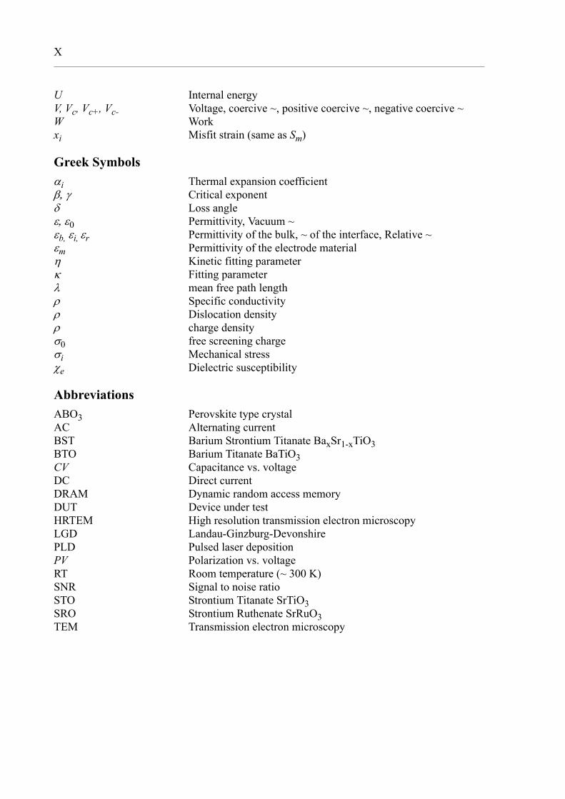
X
U Internal energyV, Vc, Vc+, Vc- Voltage, coercive ~, positive coercive ~, negative coercive ~W Workxi Misfit strain (same as Sm)
Greek Symbolsαi Thermal expansion coefficientβ, γ Critical exponentδ Loss angleε, ε0 Permittivity, Vacuum ~εb, εi, εr Permittivity of the bulk, ~ of the interface, Relative ~εm Permittivity of the electrode materialη Kinetic fitting parameterκ Fitting parameterλ mean free path lengthρ Specific conductivityρ Dislocation densityρ charge densityσ0 free screening chargeσi Mechanical stressχe Dielectric susceptibility
AbbreviationsABO3 Perovskite type crystalAC Alternating currentBST Barium Strontium Titanate BaxSr1-xTiO3BTO Barium Titanate BaTiO3CV Capacitance vs. voltageDC Direct currentDRAM Dynamic random access memoryDUT Device under testHRTEM High resolution transmission electron microscopyLGD Landau-Ginzburg-DevonshirePLD Pulsed laser depositionPV Polarization vs. voltageRT Room temperature (~ 300 K)SNR Signal to noise ratioSTO Strontium Titanate SrTiO3SRO Strontium Ruthenate SrRuO3TEM Transmission electron microscopy
1
1 Introduction1.1 Motivation
The use of ceramic thin films exhibiting ferroelectric, pyroelectric, piezoelectric, electro-opti-
cal and magneto-optical properties in combination with silicon technologies (e.g. CMOS)
allows for the development of a variety of novel functional devices in the fields of memory,
sensors, actuators and modulators [1-6]. Restricting on the memory sector, it is obvious that in
recent years the performance of mobile electronic devices such as digital cameras, PDAs, cell
phones, notebooks and even wearable electronics has been increased rapidly. As a conse-
quence, the need for low power-consuming non-volatile high-density memory technologies
compatible with the powerful processors of those devices has increased, too. On the other
hand, the efficiency of non-mobile electronic applications (e.g. desktop computers) has been
improved in a similar way: Here, the incorporated memory devices were mostly optimized to
achieve higher storage densities and faster data transfer rates, whereas the power consumption
plays only a secondary role. According to the above considerations, the application of electro-
ceramics in storage capacitors is promising in the following two cases:
• The development of novel, non-volatile ferroelectric semiconductor memories (FeRAM)
could be achieved by the implementation of ferroelectric ceramics such as lead zirconate-
titanate, Pb(Zr1-yTiy)O3 or strontium bismuth tantalate, SrBi2Ta2O9. This type of memory
exhibits high switching cycles (typically > 1014) as well as fast write access times (< 50 ns)
and therefore is a potential candidate for replacing EEPROMs as a widely used non-volatile
memory in mobile applications [7,8].
• As the current state of the art dielectrics in dynamic random access memory (DRAM),
Al2O3, Ta2O5 as well HfO2 were incorporated, which show maximum permittivity values εr
between 10 and 26. For a higher miniaturization level (higher memory density), the current
area of the storage capacitor has to be further reduced while at the same time the thickness
of the dielectric layer must be decreased substantially to maintain a sufficiently high capac-
itance level. This in term leads to unfavorable high tunneling currents through the dielectric,
which means a faster self-discharge of the capacitor and hence a possible dysfunction of the
memory device. As an alternative, the integration of thin film ceramic perovskites display-
2 1 Introduction
ing high permittivity values into DRAM storage capacitors offers storage densities 20 to 50
times higher than what can be achieved at present, while the dielectric thickness would not
be changed. These materials are thought to have the potential for replacing the currently
used dielectrics, according to the latest semiconductor roadmaps [9]. One of the most stud-
ied materials (thus the model material) in this context is BaxSr1-xTiO3 (BST), and here
especially its composition with x = 0.7, showing dielectric permittivities εr as high as
15,000 [10-12].
However, several obstacles have been detected during the general implementation of perovs-
kite ceramics into memory applications: Amongst others, these include the adjustment of the
necessary deposition temperatures to levels compatible with the silicon technology and general
compatibility issues of the used materials. In the case of FeRAM, failure mechanisms in ferro-
electrics such as fatigue, imprint and retention have to be considered, which partly could be
handled even though physical explanations have not always been found. In the DRAM case, a
reduction of the effective permittivity with decreasing thickness of the incorporated high per-
mittivity materials has been observed as the most restraining challenge.
Thus, the goal should be to minimize the difficulties that by now do not allow for a successful
implementation of ferroelectrics into memory devices considering a commercial point of view.
Therefore, it is indispensable to get a detailed knowledge of the variety of material properties
derived by exhaustive experimental characterizations as well as by theoretical predictions uti-
lizing the inherent physical mechanisms and theories. In this context, much of the work will be
spent on the electrode/dielectric interfaces as they are assumed to be accountable for the major-
ity of the hindering behavior.
1.2 State of the Art
A deterioration of ferroelectric properties can be observed when the dimensions of thin films
become more and more reduced, as it is mandatory for the ever-growing integration densities
in modern microelectronic applications [13]. At thicknesses in the region well below 50 nm,
the dielectrics approach length scales associated with characteristics of the ferroelectric mate-
rial and electrode interfaces themselves. It is also expected that reducing the lateral dimensions
of the structures could alter the response of the ferroelectric [14]. The influence of the size on
1.2 State of the Art 3
the properties of ferroelectrics is an important factor determining the way to implement these
materials in future generations of microelectronic structures. With respect to possible memory
applications, it has been found that by decreasing the thickness of capacitors with high permit-
tivity dielectrics such as BST, the measured permittivity εr does not remain constant but rather
decreases significantly [15]. Hence, εr no longer appears to be a material constant but rather
seems to be an effective value that depends on the capacitor thickness. Additional to the gen-
eral permittivity decrease, it has also been found that the former pronounced ferroelectric to
paraelectric phase transition in high permittivity materials becomes strongly suppressed or
even hardly noticeable when dealing with thin films of the same composition [13]. Various
approaches have been used that attribute the observed phenomena to a so called interface
capacitance, hence a thin layer with reduced permittivity that acts electrically in series to the
actual high permittivity capacitor and therefore leads to a reduction of the overall capacitance.
Experimentally, the idea of this series connection has been confirmed according to the mea-
sured thickness dependent permittivity by a number of authors [13-18], whereas a physical evi-
dence of such a low permittivity layer (or „dead layer“) has never been found by means of any
microstructural investigation. Several different mechanisms have been discussed to be respon-
sible for the observed phenomenon, which include changes in the phonon spectrum at the
interface due to broken lattice periodicity [19,20] or crystal defects related to the interface [21-
23], chemically different reaction layers [24-26], electronic surface- or interface-states [27-
29], electric field penetration into the electrode material and corresponding screening length
issues [30-32], whereas the hardening of the soft phonon throughout the whole ferroelectric
film is a result of all intrinsic effects [33], and is strongly related to the existence of depolariz-
ing fields [34]. In general, the use of oxide electrode materials such as SrRuO3 (SRO) instead
of Pt has an improving effect on the observed permittivity decrease with reduced thickness, as
reported from several authors [35-37].
Taking a look at the measured polarization in thin film ferroelectrics, it can be found that in
general the coercive field becomes increased, while the remanent polarization drops as the film
thickness is decreased [38,39]. This thickness dependence is generally attributed to a surface
layer and depends strongly on the properties of the ferroelectric/electrode interface. Such a sur-
face layer can appear as a consequence of non-stoichiometry near the film surface or damage
induced by the electroding process, but may also be caused by intrinsic factors. The different
4 1 Introduction
reported polarization behavior in general can be explained by the different preparation tech-
niques used, which may induce different properties in the ferroelectric close to the electrodes.
Investigations on BST as a ferroelectric model system easily allow the study of ferroelectric
properties such as the remanent polarization Pr, the coercive field Ec and the phase transition
temperature TC, which are all strongly influenced by the particular choice of the electrode/
dielectric interface.
In summary, it should be noted that there exists a variety of extrinsic as well as intrinsic influ-
ences that cause a suppression of the dielectric permittivity and a frustrated ferroelectric-to-
paraelectric phase transition. Among those, grain boundaries from polycrystalline films, ten-
sile strains from crystal lattice mismatch or deteriorated interfaces due to defects and interdif-
fusion as well as different screening properties of the electrodes have the most critical impact.
1.3 Objectives
From the previous paragraph it follows, that in order to investigate the pure intrinsic influences
it is especially mandatory to get rid of all extrinsic influences. This will be accomplished most
of all by choosing an epitaxial growth technique and a single crystalline substrate to prepare
high quality ferroelectric thin films free from grain boundaries and results in interfaces without
interdiffusion layers or defects. Thus, the extraction of intrinsic material properties can be
accomplished and a successful comparison between BST capacitors electroded with Pt and
SRO can be performed.
Besides a comprehensive introduction into the principles of ferroelectric materials and the
experimental methods for the fabrication and characterization of thin film capacitors, the fol-
lowing main tasks will be accomplished in this work:
• Epitaxially grown thin film capacitors with dielectric layers of various BST thicknesses will
be fabricated. These capacitors show a high crystalline quality and allow an extensive anal-
ysis of their electrical properties.
• Starting from capacitance and polarization measurements at room temperature, the electri-
cal analyzes will be carried out in a wide temperature range under systematic variations of
the applied voltage and frequency. This allows a thickness and temperature dependent anal-

1.3 Objectives 5
ysis of the key properties and will permit the evaluation of the phase transition temperature.
• The thus determined measurement results will be compared with those reported in the liter-
ature for comparable studies to evaluate the achieved quality of the experimental work. A
theoretical discussion in the light of a thermodynamic model based on the Landau-Gin-
zburg-Devonshire (LGD) theory of ferroelectric materials finally concludes the presented
studies.

6 1 Introduction
7
2 Ferroelectric Materials and their Properties
This chapter deals with the basic properties of ferroelectric materials that will be relevant in
this work. For a detailed description of the fundamentals of ferroelectric phenomena, the
reader is advised to the standard text books [5,40-49] or review articles [50-52].
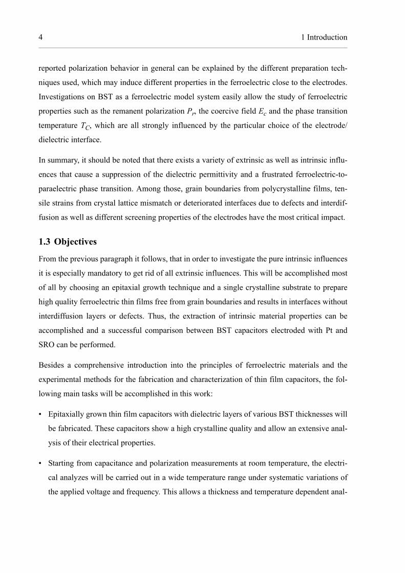
2.1 Crystallographic Considerations and Definition of a Ferroelectric
Among the classical 32 crystal classes (or point groups) describing all crystalline material, 11
classes have a center of symmetry and are therefore called centrosymmetric. Applying an elec-
tric field to such a centrosymmetric crystal will create a mechanical strain that does not change
its sign, regardless to the direction of field. The strain is proportional to the square of the ap-
plied field and this quadratic effect is called electrostriction. Electrostriction occurs in all sub-
stances, no matter if it is crystalline or amorphous, solid or fluid.
The remaining 21 classes do not have a center of symmetry, they are non-centric and show (ex-
cept for one) the piezoelectric effect: Piezoelectricity means that the crystal exhibits electric
polarity when exposed to strain. This effect is a linear one, i.e. reversing the sign of the stress
will cause a reversed polarity. By applying an electric field to the crystal, it will be stretched or
compressed, corresponding to the polarity of the field. This is the converse piezoelectric effect.
no reversible spontaneous polarisationnot ferroelectric
reversible spontaneous polarizationferroelectric
32 classesall crystalline material
electrostrictive
11 classes
centrosymmetric
21 classes
not centrosymmetric
1 class
not piezoelectric
20 classes
piezoelectric
10 classesno unique polar axis
not pyroelectric
10 classesunique polar axis
pyroelectric
FIGURE 2.1:Ferroelectric crystals and their position among the 32 general crystal classes.
8 2 Ferroelectric Materials and their Properties
From those 20 classes, ten have a unique polar axis, i.e. an axis which shows different proper-
ties on the one end than on the other end. These crystals are called polar and exhibit a sponta-
neous polarization which is dependent on temperature. These are the pyroelectric crystals.
If the direction of the spontaneous polarization in such a pyroelectric crystal can be switched
between two stable states by applying an electric field, the crystal is called ferroelectric. For
ferroelectrics it is therefore a necessary attribute to belong to one of the ten pyroelectric crystal
classes as well as to have a reversible spontaneous polarization.
2.2 General Features of Ferroelectric Crystals
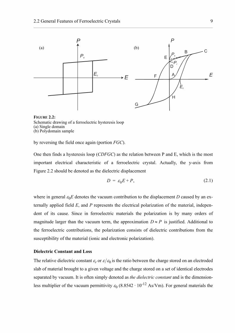
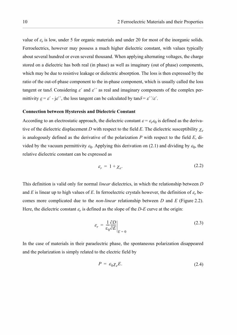
Ferroelectric Hysteresis
Measuring the relationship between the applied electric field and the electric polarization in a
ferroelectric material, a typical hysteresis curve results as displayed in Figure 2.2. The ideal
case of a single domain1 crystal is shown in Figure 2.2 (a): Here, a variation of the electric
field E leads to a linear increase of the polarization P, while for fields exceeding the coercive
field Ec, a jump of the polarization occurs. In the zero field case, the polarization remains ei-
ther at the positive or negative spontaneous polarization Ps. Figure 2.2 (b) shows the hysteresis
curve of a polydomain sample: Starting at the virgin state (the polarization is pointing in an
equal portion of volume to the positive and negative direction), a part of the negatively ori-
ented domains will be switched over into the positive direction by increasing the electric field
(path AB), and the polarization increases strongly until the saturation state is reached (path
BC). Here, the complete volume is aligned in the positive direction and the crystal consists
now of one single domain. Decreasing the field does not bring the net polarization in generally
back to zero but rather follows the path CD, which means that some of the domains will stay
positively oriented without applied field and the crystal exhibits a remanent polarization Pr.
Extrapolating the saturation path BC back to the polarization axis, the intercept represents the
spontaneous polarization Ps. To decrease the polarization then further to zero, it is necessary to
apply a negative electric field (portion DE). The electric field corresponding to this zero polar-
ization state is called the coercive field Ec. Additional decrease of the field will cause all di-
poles to align in the negative orientation (portion EF), after which the cycle can be completed
1. A domain describes a fraction of volume in which the polarization is oriented uniformly
2.2 General Features of Ferroelectric Crystals 9
by reversing the field once again (portion FGC).
One then finds a hysteresis loop (CDFGC) as the relation between P and E, which is the most
important electrical characteristic of a ferroelectric crystal. Actually, the y-axis from
Figure 2.2 should be denoted as the dielectric displacement
where in general ε0E denotes the vacuum contribution to the displacement D caused by an ex-
ternally applied field E, and P represents the electrical polarization of the material, indepen-
dent of its cause. Since in ferroelectric materials the polarization is by many orders of
magnitude larger than the vacuum term, the approximation is justified. Additional to
the ferroelectric contributions, the polarization consists of dielectric contributions from the
susceptibility of the material (ionic and electronic polarization).
Dielectric Constant and Loss
The relative dielectric constant εr or ε/ε0 is the ratio between the charge stored on an electroded
slab of material brought to a given voltage and the charge stored on a set of identical electrodes
separated by vacuum. It is often simply denoted as the dielectric constant and is the dimension-
less multiplier of the vacuum permittivity ε0 (8.8542 · 10-12 As/Vm). For general materials the
D ε0E P+ ,= (2.1)
D P≈
FIGURE 2.2:Schematic drawing of a ferroelectric hysteresis loop(a) Single domain(b) Polydomain sample
A
B CE
F
G
H
P
E
Ec
Pr
Ps
D
Ps
Ec E
P(a) (b)
10 2 Ferroelectric Materials and their Properties
value of εr is low, under 5 for organic materials and under 20 for most of the inorganic solids.
Ferroelectrics, however may possess a much higher dielectric constant, with values typically
about several hundred or even several thousand. When applying alternating voltages, the charge
stored on a dielectric has both real (in phase) as well as imaginary (out of phase) components,
which may be due to resistive leakage or dielectric absorption. The loss is then expressed by the
ratio of the out-of-phase component to the in-phase component, which is usually called the loss
tangent or tanδ. Considering ε´ and ε´´ as real and imaginary components of the complex per-
mittivity ε = ε´ - jε´´, the loss tangent can be calculated by tanδ = ε´´/ε´.
Connection between Hysteresis and Dielectric Constant
According to an electrostatic approach, the dielectric constant ε = εrε0 is defined as the deriva-
tive of the dielectric displacement D with respect to the field E. The dielectric susceptibility χe
is analogously defined as the derivative of the polarization P with respect to the field E, di-
vided by the vacuum permittivity ε0. Applying this derivation on (2.1) and dividing by ε0, the
relative dielectric constant can be expressed as
This definition is valid only for normal linear dielectrics, in which the relationship between D
and E is linear up to high values of E. In ferroelectric crystals however, the definition of εr be-
comes more complicated due to the non-linear relationship between D and E (Figure 2.2).
Here, the dielectric constant εr is defined as the slope of the D-E curve at the origin:
In the case of materials in their paraelectric phase, the spontaneous polarization disappeared
and the polarization is simply related to the electric field by
εr 1 χe.+= (2.2)
εr1ε0----- D∂
E∂-------
E 0=
= (2.3)
P ε0χeE.= (2.4)
2.2 General Features of Ferroelectric Crystals 11
Combining (2.1) together with (2.4), this leads to
giving the linear relation between electric displacement and electric field. It has to be men-
tioned that the dielectric permittivity does not have to be constant and in certain circumstances
also depends on the applied field.
Temperature Dependence
In general, ferroelectric materials perform a phase transition from the (low temperature) ferro-
electric phase to the (high temperature) paraelectric phase (strong analogy with ferromag-
netism). The temperature at which this transition occurs is called the Curie temperature TC,
above which no ferroelectricity is observable. The corresponding material condition is then
called the paraelectric phase. Also, the dielectric constant εr exhibits some kind of anomaly at
the transition temperature. In many ferroelectrics (including those that were investigated in this
work), the temperature dependence of the dielectric constant above the phase transition obeys
a quite simple law, the so-called Curie-Weiss law:
Here, C means the Curie-Weiss constant and T0 denotes the paraelectric Curie point (or extrap-
olated Curie point or Curie-Weiss temperature). It should be noted that TC and T0 generally do
not coincide, which is one of the most frequent errors in this subject. In a ferroelectric with a
second order phase transition (properties such as lattice constants, dielectric constant, polariza-
tion, etc., change rather continuously with temperature), these two temperatures may be effec-
tively the same. In the case of first order transitions, however (above mentioned properties
change rather discontinuously, i.e. exhibit “jumps”), the Curie temperature can be more than
10K lower than the Curie point.
D ε0 1 χe+( )E ε0εrE,= = (2.5)
εrC
T T0–---------------= (2.6)
12 2 Ferroelectric Materials and their Properties
2.3 Material Systems
Most investigations in this work were performed on Barium-Strontium Titanate BaxSr1-xTiO3
(BST) thin films. Since this material is derived from the prototypic materials Barium Titanate
BaTiO3 (BTO) and Strontium Titanate SrTiO3 (STO), first an introduction to BTO and STO
will be given.
Barium Titanate
The ferroelectric solid solution system BTO is one of the most extensively studied ferroelectric
materials. Its anomalous dielectric properties were discovered on ceramic samples indepen-
dently from each other around 1943 by Wainer and Salomon in the USA, Ogawa in Japan and
Wul and Goldman in Russia. Its ferroelectric properties were reported 1945-1946 by von Hip-
pel et al. [53] and independently by Wul and Goldman [54].
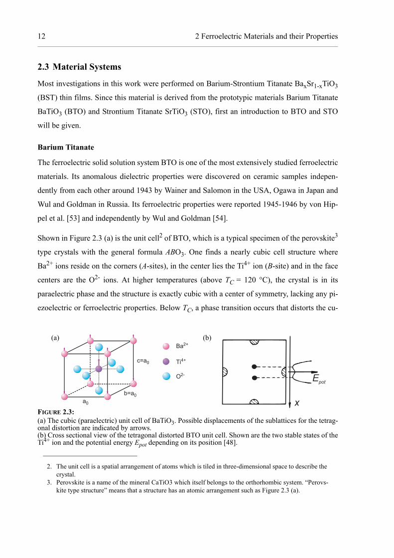
Shown in Figure 2.3 (a) is the unit cell2 of BTO, which is a typical specimen of the perovskite3
type crystals with the general formula ABO3. One finds a nearly cubic cell structure where
Ba2+ ions reside on the corners (A-sites), in the center lies the Ti4+ ion (B-site) and in the face
centers are the O2- ions. At higher temperatures (above TC = 120 °C), the crystal is in its
paraelectric phase and the structure is exactly cubic with a center of symmetry, lacking any pi-
ezoelectric or ferroelectric properties. Below TC, a phase transition occurs that distorts the cu-
2. The unit cell is a spatial arrangement of atoms which is tiled in three-dimensional space to describe the crystal.
3. Perovskite is a name of the mineral CaTiO3 which itself belongs to the orthorhombic system. “Perovs-kite type structure” means that a structure has an atomic arrangement such as Figure 2.3 (a).
a0
Ba2+
Ti4+
O2-
c=a0
b=a0
Epot
x
(a) (b)
FIGURE 2.3:(a) The cubic (paraelectric) unit cell of BaTiO3. Possible displacements of the sublattices for the tetrag-onal distortion are indicated by arrows.(b) Cross sectional view of the tetragonal distorted BTO unit cell. Shown are the two stable states of the Ti4+ ion and the potential energy Epot depending on its position [48].
2.3 Material Systems 13
bic cell into a tetragonal shaped cell. Whereas one axis of the crystal becomes elongated (the
so called c-axis), the other two crystal axes become compressed (a-axes). As can be seen in
Figure 2.3 (b), the potential energy Epot of the Ti4+ ion now has two minima that mark the two
stable states of polarization. Using an external electric field, it is possible to switch between
those states, hence to reverse the polarization, so BaTiO3 fulfills the essential requirement for
ferroelectric materials. Since the necessary energy to overcome the maximum in Epot and to
switch the Ti4+ ion from one to another state is very low, also the field from surrounding di-
poles could be strong enough to polarize the crystal, resulting in a spontaneous polarization Ps.
Besides the already mentioned cubic and tetragonal phases, further crystal configurations of
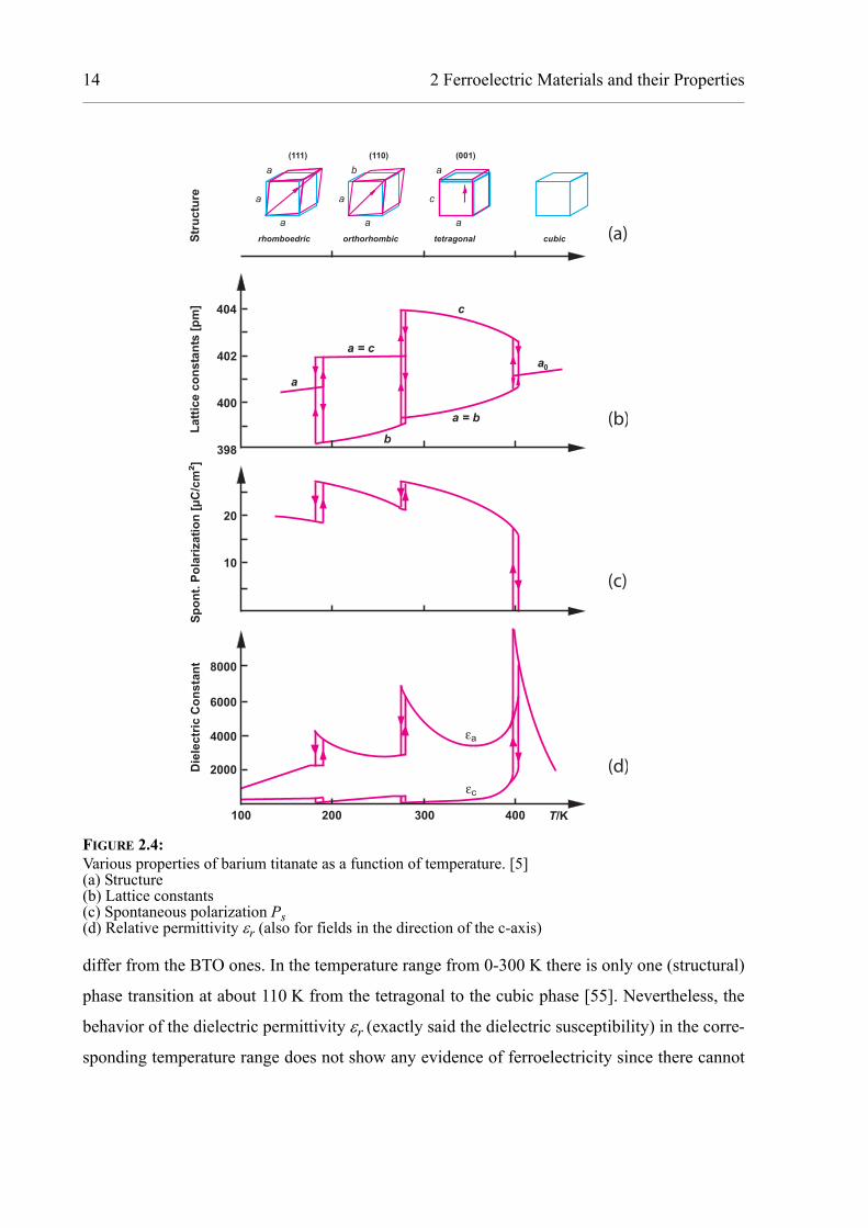
BTO are possible. As can be seen in Figure 2.4 (a), there exist three different phase transitions
for BTO in the temperature range 150-400 K, connecting the four possible crystal phases.
Figure 2.4 (b) shows the dependence of the lattice constants of the BTO unit cell depending on
the temperature, hence the resulting phases at those temperatures. Below 180 K the crystal is in
its rhombohedral phase with the polarization along the space diagonal. Up to 275 K, the
orthorhombic phase exists and the polarization is oriented in parallel to the face diagonal. Then
the crystal becomes tetragonal shaped with a polarization in the <001> direction, parallel to the
(longer) c-axis. The phase transition from tetragonal to cubic occurs at the Curie temperature
TC which is at about 390K. Above this critical temperature no ferroelectric polarization re-
mains, the crystal has a symmetry center which is the central Ti4+ ion. It can be seen that the
phase transitions occur with a certain temperature hysteresis, which means that depending on
the direction of the temperature change (cooling or heating) of the crystal the transition tem-
peratures may vary by about ten K. Since all but the cubic phase lack a center of symmetry,
there exists a switchable polarization in the crystal with different direction for each of these
phases (Figure 2.4 (c)). The temperature dependence for the dielectric constant is given in
Figure 2.4 (d): Again, there are three phase transitions, indicated by the respective dielectric
anomalies. The permittivity εr reaches its highest value of about 12,000 at the phase transition
form the tetragonal to the cubic phase (ferroelectric to paraelectric phase).
Strontium Titanate
Strontium Titanate SrTiO3 (STO) has a similar shaped unit cell compared to BTO except that
here the Ba2+ ions are replaced by Sr2+ ions. Its electrical and structural properties, however,
14 2 Ferroelectric Materials and their Properties
differ from the BTO ones. In the temperature range from 0-300 K there is only one (structural)
phase transition at about 110 K from the tetragonal to the cubic phase [55]. Nevertheless, the
behavior of the dielectric permittivity εr (exactly said the dielectric susceptibility) in the corre-
sponding temperature range does not show any evidence of ferroelectricity since there cannot
FIGURE 2.4:Various properties of barium titanate as a function of temperature. [5](a) Structure(b) Lattice constants(c) Spontaneous polarization Ps(d) Relative permittivity εr (also for fields in the direction of the c-axis)
2.3 Material Systems 15
be found any decrease of εr below the structural phase transition temperature, as it is the case
for BTO [56].
Barium-Strontium Titanate
BaxSr1-xTiO3 (BST) has become attractive due to its promising properties, i.e. high dielectric
constant, for using it in high density dynamic random access memory (DRAM) [14,57,58] as
well as tunable microwave devices like filters and phase shifters [59-61].
The material is a solid solution of BaTiO3 and SrTiO3, while the Ba/Sr-ratio of x/(1-x) strongly
affects its physical properties. Its unit cell, again, has the typical perovskite shape, while on the
A-sites an alternating occupation of Ba2+ and Sr2+ atoms according to x can be found. Mc-
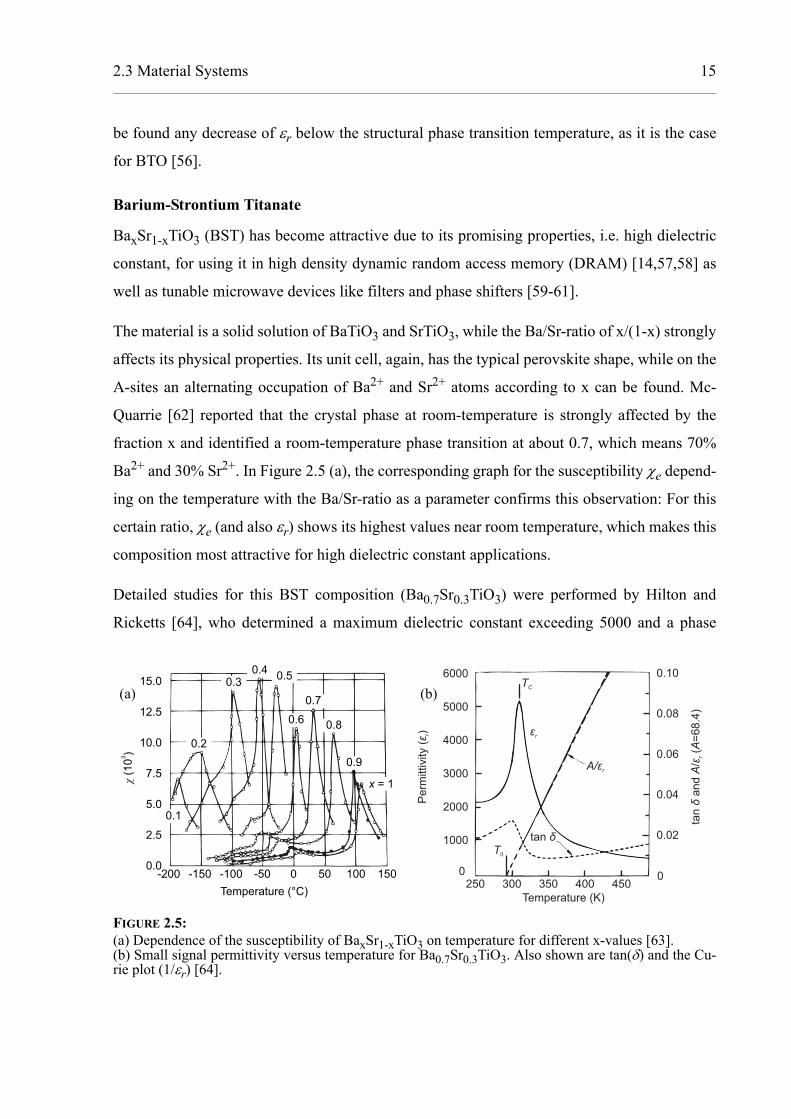
Quarrie [62] reported that the crystal phase at room-temperature is strongly affected by the
fraction x and identified a room-temperature phase transition at about 0.7, which means 70%
Ba2+ and 30% Sr2+. In Figure 2.5 (a), the corresponding graph for the susceptibility χe depend-
ing on the temperature with the Ba/Sr-ratio as a parameter confirms this observation: For this
certain ratio, χe (and also εr) shows its highest values near room temperature, which makes this
composition most attractive for high dielectric constant applications.
Detailed studies for this BST composition (Ba0.7Sr0.3TiO3) were performed by Hilton and
Ricketts [64], who determined a maximum dielectric constant exceeding 5000 and a phase
FIGURE 2.5:(a) Dependence of the susceptibility of BaxSr1-xTiO3 on temperature for different x-values [63].(b) Small signal permittivity versus temperature for Ba0.7Sr0.3TiO3. Also shown are tan(δ) and the Cu-rie plot (1/εr) [64].
TC
T0
Temperature (K)
Per
mitt
ivity
(εr)
1000
2000
3000
4000
5000
6000
0250 350300 450400
0
0.02
0.08
0.06
0.04
0.10
tan δ
A/εr
εr
tan
δ an
d A
/εr (
A=6
8.4)
Temperature (°C)-200 150100500-50-100-150
0.20.9
0.8
0.7
0.6
0.50.40.3
0.1
x = 1χ (1
03 )
0.0
15.0
12.5
10.0
7.5
5.0
2.5
(a) (b)
16 2 Ferroelectric Materials and their Properties
transition temperature TC = 310 K, as can be found in Figure 2.5 (b). Here, the difference be-
tween TC and T0 is about 20 K, indicating that bulk BST exhibits a first order phase transition.
Strontium Ruthenate as Electrode Material
For building a ferroelectric thin film capacitor, not only the used dielectrics BTO, STO and
BST, but also the choice of suitable electrode material must be considered. Besides the widely
used standard material Pt, here SrRuO3 (SRO) has been chosen as an alternative electrode ma-
terial. Similar to STO, SRO is an ABO3 or perovskite-type material where the Ru4+ ions lie on
the (central) B site. Its room temperature resistance (ρSRO = 340 µΩcm [65]) is rather high
compared to the standard material Pt (ρPt = 10.4 µΩcm [44]), nevertheless it is an excellent
electrode for the (epitaxial) growth of BTO or BST due to its (pseudo-cubic) lattice constant of
3.93 Å, which is similar to BTO, STO or BST and results in low lattice mismatch [66,67]. Its
work function is lower compared to the one for Pt (5.3 eV [68]) and can be determined to 4.6 -
5.0 eV, depending on the state of SRO oxidation [69].
Strontium Titanate as Substrate Material
From the above mentioned parameters such as the lattice constants of the used materials, an
adequate substrate material can be derived. (100) STO single crystals that result in small lattice
mismatch (with respect to BST or SRO) are commercially available in excellent quality and
will be used in this work as sample substrates.
2.4 Mechanical Boundary Conditions
Instead of freestanding, thick layers, the samples used in this work incorporate rather thin films
which are mostly grown epitaxially on much thicker substrates. The materials under investiga-
tion are thus subjected to mechanical boundary conditions, whose impact will be discussed in
the following:
By interaction with the underlying substrate significant mechanical stresses can be generated
inside the films. At the time of the film deposition, growth stresses may appear while the mate-
rial is in its paraelectric phase. The specific amount of stress strongly depends on the parame-
ters of the particular deposition process, i.e. the choice of the involved materials. It is known
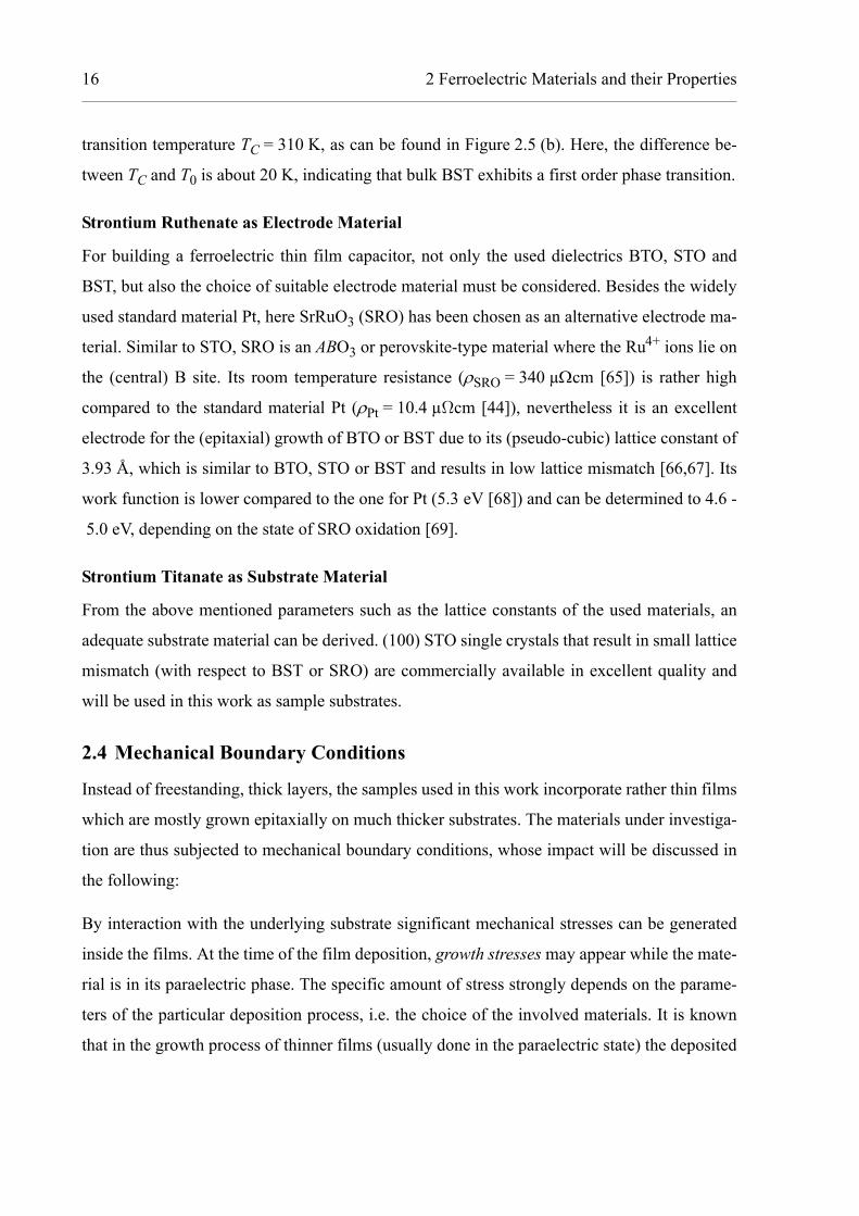
that in the growth process of thinner films (usually done in the paraelectric state) the deposited
2.4 Mechanical Boundary Conditions 17
material stays in its pseudomorphic cubic phase, which is accompanied by epitaxial strain, as
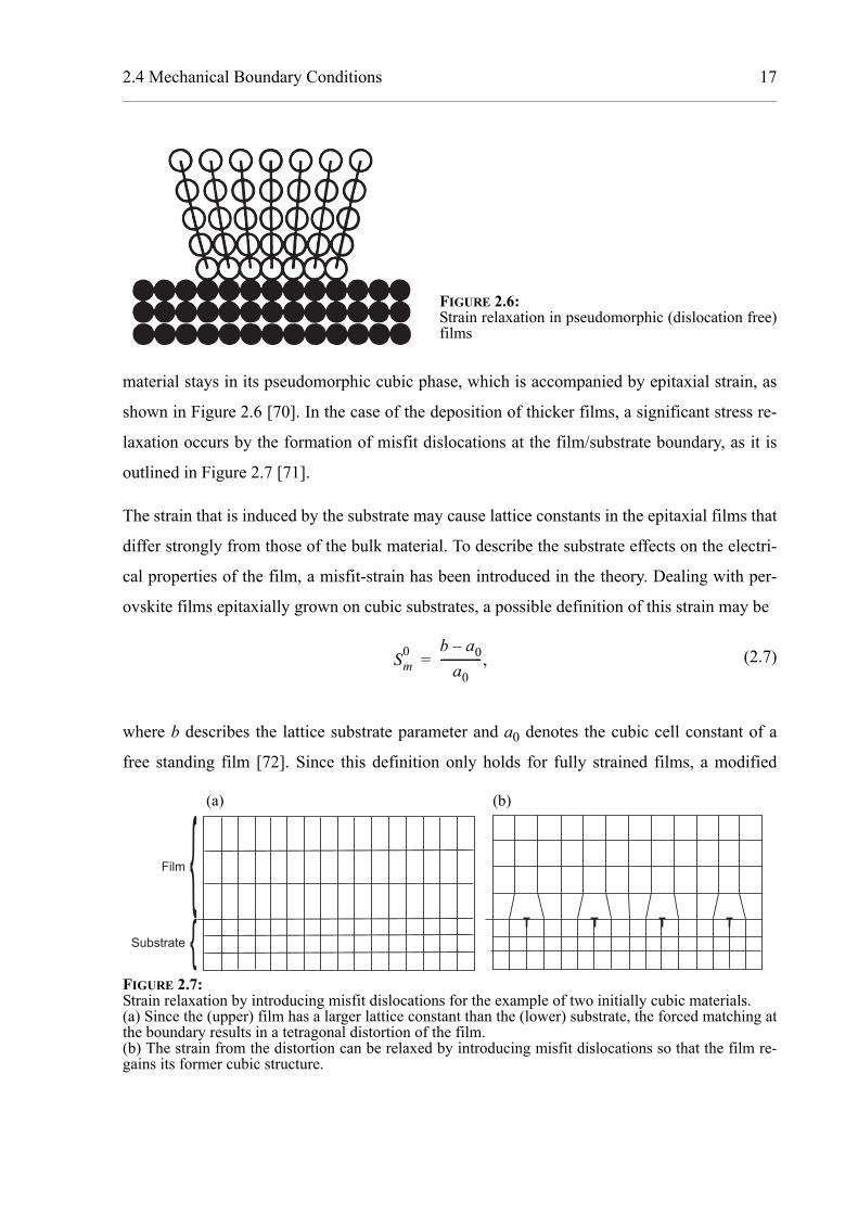
shown in Figure 2.6 [70]. In the case of the deposition of thicker films, a significant stress re-
laxation occurs by the formation of misfit dislocations at the film/substrate boundary, as it is
outlined in Figure 2.7 [71].
The strain that is induced by the substrate may cause lattice constants in the epitaxial films that
differ strongly from those of the bulk material. To describe the substrate effects on the electri-
cal properties of the film, a misfit-strain has been introduced in the theory. Dealing with per-
ovskite films epitaxially grown on cubic substrates, a possible definition of this strain may be
where b describes the lattice substrate parameter and a0 denotes the cubic cell constant of a
free standing film [72]. Since this definition only holds for fully strained films, a modified
FIGURE 2.6:Strain relaxation in pseudomorphic (dislocation free) films
Film
Substrate
(a) (b)
FIGURE 2.7:Strain relaxation by introducing misfit dislocations for the example of two initially cubic materials.(a) Since the (upper) film has a larger lattice constant than the (lower) substrate, the forced matching at the boundary results in a tetragonal distortion of the film.(b) The strain from the distortion can be relaxed by introducing misfit dislocations so that the film re-gains its former cubic structure.
Sm0 b a0–
a0--------------,= (2.7)
18 2 Ferroelectric Materials and their Properties
strain definition must be found. Due to the fact that above a critical thickness the incorporation
of misfit dislocations is energetically favorable, the lattice strain becomes dependent on the
film thickness [73]. When the density ρ of these dislocations is evaluated to , the actual
misfit strain can be expressed as
with as the effective lattice parameter of the substrate [71,74]. This reduced
substrate lattice constant can be explained in the following way: Once a misfit dislocation ar-
ray has developed at the film/substrate interface, the film no longer experiences the lattice pa-
rameter of the original substrate, but that of a substrate with an array of misfit dislocations.
Additional strains may arise from thermal stresses that develop inside the film due to different
expansion coefficients of substrate and film. Here, we can neglect these contributions due to
the fact that the used materials (BST, SRO and STO) all have similar thermal expansion coef-
ficients.
2.5 Thermodynamics of Ferroelectrics
The thermodynamics of ferroelectric phase transitions can be described using a mean field the-
ory: Here, the dipole as the thermodynamic entity is subject to the mean field of all other di-
poles. Landau [78] and Ginzburg [79] expanded the thermodynamic potential near the phase
transition temperature into a power series and introduced the polarization P as an order pa-
rameter, which for a second order phase transition diminishes continuously to zero at the
phase transition TC. This approach has been used by Devonshire to describe both ferroelectric
and non-ferroelectric phases so that he could characterize the phase transition of BaTiO3 (see
chapter 2.3) [80].
From the first law of thermodynamics it is known that a change of the internal energy U (per
unit volume) is given as
ρ 1«
Smb∗ a0–
a0-----------------= (2.8)
b∗ b 1 ρ–( )=
Ud Q W,d+d= (2.9)
2.5 Thermodynamics of Ferroelectrics 19
where dQ means an infinitesimal portion of heat received by a unit volume of dielectric and
dW is the work done on this volume (by electrical and mechanical forces) during the resulting
quasi-static transformation. On the other hand it is known that dW can be expressed by
defining the total work dependent on infinitesimal changes of strain xi (to prevent confusion
with the entropy density S, the strain Si as defined in chapter 2.4 will be named xi here) and
electric polarization Pi in the presence of uniform stress σi and electric field Ei [40,43]. The
second law of thermodynamics then gives
with the absolute temperature T and the entropy density S. Besides, the equality sign in
Eq. (2.11) is valid for a reversible process, while the inequality holds for an irreversible pro-
cess. Using Eq. (2.9) and (2.10), Eq. (2.11) can be written as
where the inequality sign in Eq. (2.12) again becomes an equality sign in the case of a revers-
ible process. One obtains from Eq. (2.12)
This means that when a system is described by independent variables S, xi and Pi, the other
variables can be found by first derivatives of the internal energy U. There are eight ways for
describing a system by independent variables, chosen from the pairs (T, S), (σ, x) and (E, P)
and therefore eight possible thermodynamic functions.
dW σi xi Ei Pi,d+d= (2.10)
T dS dQ,≥⋅ (2.11)
dU T dS σi xi Ei Pi,d+d+⋅≤ (2.12)
T U S∂⁄∂( )x P, , σi U xi∂⁄∂( )S P, , Ei U Pi∂⁄∂( )S x,= = = (2.13)
20 2 Ferroelectric Materials and their Properties
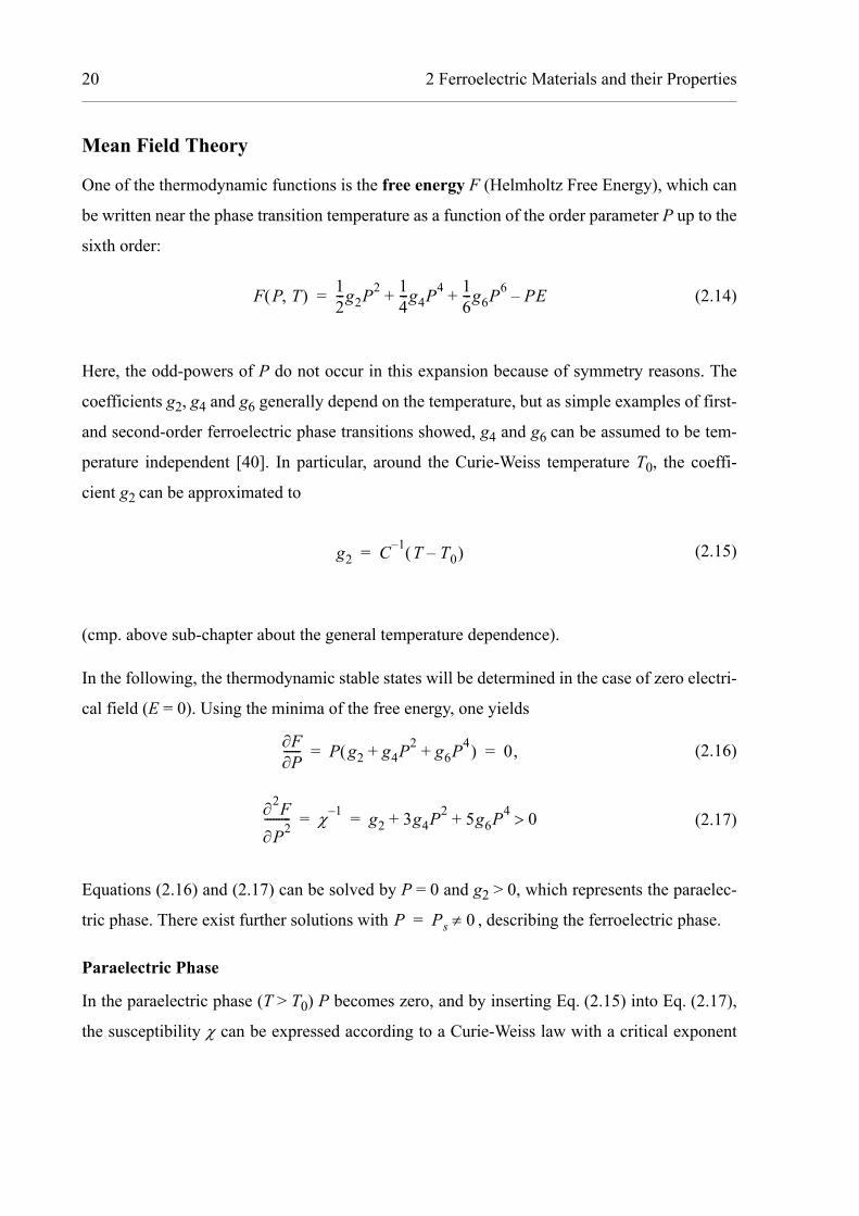
Mean Field Theory
One of the thermodynamic functions is the free energy F (Helmholtz Free Energy), which can
be written near the phase transition temperature as a function of the order parameter P up to the
sixth order:
Here, the odd-powers of P do not occur in this expansion because of symmetry reasons. The
coefficients g2, g4 and g6 generally depend on the temperature, but as simple examples of first-
and second-order ferroelectric phase transitions showed, g4 and g6 can be assumed to be tem-
perature independent [40]. In particular, around the Curie-Weiss temperature T0, the coeffi-
cient g2 can be approximated to
(cmp. above sub-chapter about the general temperature dependence).
In the following, the thermodynamic stable states will be determined in the case of zero electri-
cal field (E = 0). Using the minima of the free energy, one yields
Equations (2.16) and (2.17) can be solved by P = 0 and g2 > 0, which represents the paraelec-
tric phase. There exist further solutions with , describing the ferroelectric phase.
Paraelectric Phase
In the paraelectric phase (T > T0) P becomes zero, and by inserting Eq. (2.15) into Eq. (2.17),
the susceptibility χ can be expressed according to a Curie-Weiss law with a critical exponent
F P T,( ) 12---g2P2 1
4---g4P4 1
6---g6P6 PE–+ += (2.14)
g2 C 1– T T0–( )= (2.15)
F∂P∂
------ P g2 g4P2 g6P4+ +( ) 0,= = (2.16)
∂2F∂P2--------- χ 1– g2 3g4P2 5g6P4 0>+ += = (2.17)
P Ps 0≠=

2.5 Thermodynamics of Ferroelectrics 21
γ = 1:
Ferroelectric Phases: First Order Transition
Materials of this type of phase transition are characterized by the appearance of metastable
phases, since a new phase has to nucleate out of an old one. Further characteristics of first or-
der transitions are the sudden changes in the structure and volume of the material under inves-
tigation.
Considering the first derivative of the free energy (Eq. (2.16)) for g4 < 0 and g6 > 0, the ther-
modynamic stable states are given by P = 0 or
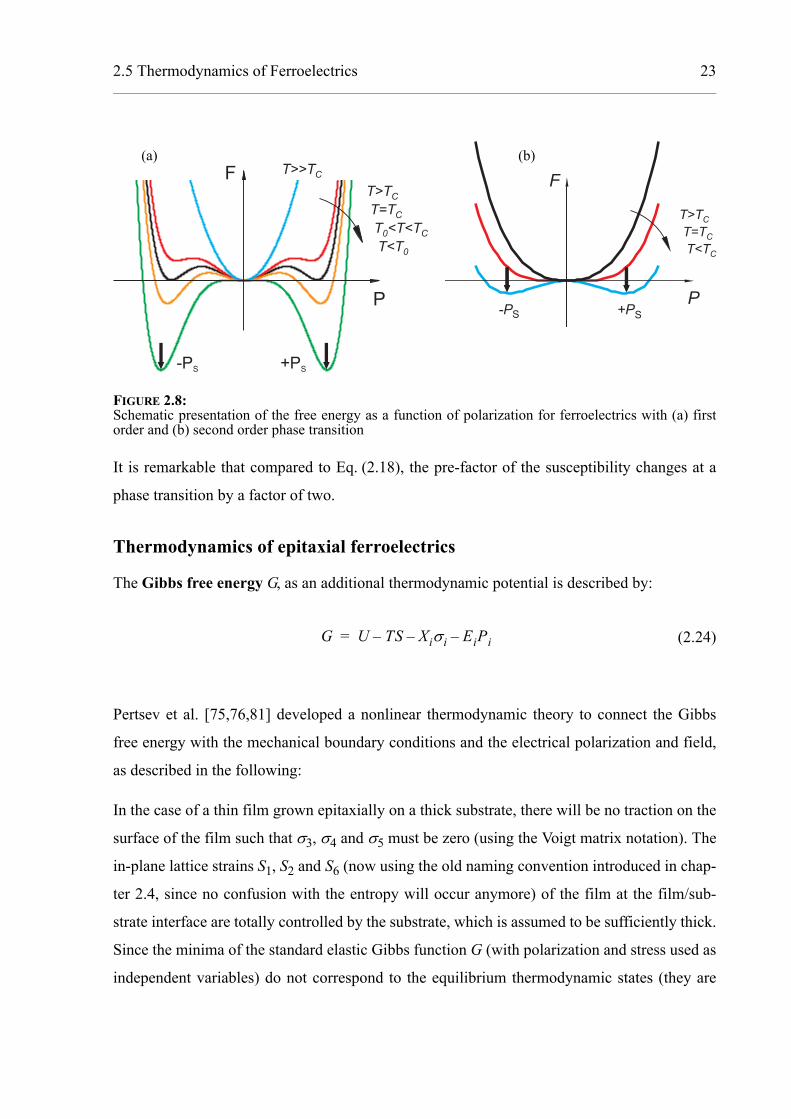
In Figure 2.8 (a) the free energy as a function of polarization is depicted for different tempera-
tures in case of a material with a first order phase transition. As it was already mentioned, the
Curie-Weiss temperature T0 is not equal to the phase transition temperature TC. The following
temperature regimes can be distinguished:
• : stable paraelectric phase (P = 0)
• T > TC: stable paraelectric phase, metastable ferroelectric phase
• T = TC: coexistence of paraelectric and ferroelectric phase
• T0 <T < TC: stable ferroelectric phase and metastable paraelectric phase
• T < T0: stable ferroelectric phase
Somewhere during cooling from the regime where the stable ferroelectric phase coexists with
the metastable paraelectric phase (T0 <T < TC), the first order phase transition will occur with a
corresponding jump of the spontaneous polarization from zero to a finite value. Additional dis-
continuous changes in susceptibility χ and entropy S will be achieved using the known thermo-
dynamic relations.
χ T( ) CT T0–( )
-------------------- T T0–( ) γ– ; γ∝ 1= = (2.18)
Ps2 g4 g4
2 4C 1– T T0–( )g6–+2g6
--------------------------------------------------------------------= (2.19)
T TC»
Ps± 0≠( )
22 2 Ferroelectric Materials and their Properties
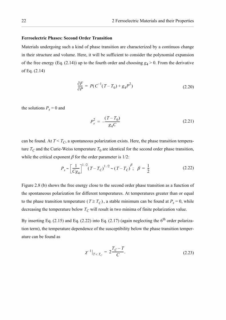
Ferroelectric Phases: Second Order Transition
Materials undergoing such a kind of phase transition are characterized by a continuos change
in their structure and volume. Here, it will be sufficient to consider the polynomial expansion
of the free energy (Eq. (2.14)) up to the fourth order and choosing g4 > 0. From the derivative
of Eq. (2.14)
the solutions Ps = 0 and
can be found. At T < TC, a spontaneous polarization exists. Here, the phase transition tempera-
ture TC and the Curie-Weiss temperature T0 are identical for the second order phase transition,
while the critical exponent β for the order parameter is 1/2:
Figure 2.8 (b) shows the free energy close to the second order phase transition as a function of
the spontaneous polarization for different temperatures. At temperatures greater than or equal
to the phase transition temperature , a stable minimum can be found at Ps = 0, while
decreasing the temperature below TC will result in two minima of finite polarization value.
By inserting Eq. (2.15) and Eq. (2.22) into Eq. (2.17) (again neglecting the 6th order polariza-
tion term), the temperature dependence of the susceptibility below the phase transition temper-
ature can be found as
F∂P∂
------ P C 1– T T0–( ) g4P2+( )= (2.20)
Ps2 T T0–( )
g4C--------------------–= (2.21)
Ps1
Cg4---------
1 2⁄T TC–( )1 2⁄ T TC–( )∼
β; β∼ 1
2---= (2.22)
T TC≥( )
χ 1–T TC< 2
TC T–C
---------------.= (2.23)
2.5 Thermodynamics of Ferroelectrics 23
It is remarkable that compared to Eq. (2.18), the pre-factor of the susceptibility changes at a
phase transition by a factor of two.
Thermodynamics of epitaxial ferroelectrics
The Gibbs free energy G, as an additional thermodynamic potential is described by:
Pertsev et al. [75,76,81] developed a nonlinear thermodynamic theory to connect the Gibbs
free energy with the mechanical boundary conditions and the electrical polarization and field,
as described in the following:
In the case of a thin film grown epitaxially on a thick substrate, there will be no traction on the
surface of the film such that σ3, σ4 and σ5 must be zero (using the Voigt matrix notation). The
in-plane lattice strains S1, S2 and S6 (now using the old naming convention introduced in chap-
ter 2.4, since no confusion with the entropy will occur anymore) of the film at the film/sub-
strate interface are totally controlled by the substrate, which is assumed to be sufficiently thick.
Since the minima of the standard elastic Gibbs function G (with polarization and stress used as
independent variables) do not correspond to the equilibrium thermodynamic states (they are
F
P
+PS-PS
T>TT=
<T<T<
CT
T TT
C
0 C
0
T>>TC F
P+PS-PS
T>TT=T<
CTTC
C
FIGURE 2.8:Schematic presentation of the free energy as a function of polarization for ferroelectrics with (a) first order and (b) second order phase transition
(a) (b)
G U TS– Xiσi– EiPi–= (2.24)
24 2 Ferroelectric Materials and their Properties
associated with the equilibrium thermodynamic states at fixed stresses), the necessary thermo-
dynamic potential is given by the following Legendre transformation of G:
While this is a general expression for the thermodynamic potential of a thin ferroelectric film
on a thick substrate, the here considered case of a (001) ferroelectric thin film epitaxially
grown in a cubic paraelectric phase on a cubic (001) substrate results in S1 = S2 = Sm (Sm ac-
cording to Eq. (2.8)) and S6 = 0.
Using the Landau-Ginsburg-Devonshire formalism from chapter 2.5, the modified Gibbs free
energy was expanded into a power series of the polarization, with simplifications according
to Ref. 82. Instead of a huge mathematical term expanding over several lines or more that in-
cludes all possible cases of polarization states and crystallographic orientations as it is shown
in Ref. 83, here the result simply is
In Eq. (2.26), simplifications have been included due to the fact that here only the particular
case of thin films grown on compressive substrates will be considered. In this case, the film
stabilizes below TC in the out-of-plane polarization state , while the
renormalized coefficients (as defined in this 2D-clamping case) are
The parameters a1, a11 and a111 are the dielectric stiffness and higher order stiffness coeffi-
cients at constant stress (a1 is also known as the reciprocal dielectric susceptibility of the unpo-
larized crystal), sln are the film elastic compliances at constant polarization and Qln are the
electrostrictive constants in polarization notation.
The phase transition temperature as a function of the lattice mismatch strain can be found by
G G S1σ1 S2σ2 S6σ6+ + += (2.25)
G
GSm
2
s11 s12+-------------------- a3
*P32 a33
* P34 a111P3
6 P3E3.–+ + += (2.26)
P1 P2 0 P3 0≠,= =( )
a3* a1 2SmQ12 s11 s12+( )⁄ and a33
* a11 Q122 s11 s12+( )⁄ .+=–= (2.27)
2.5 Thermodynamics of Ferroelectrics 25
setting and with
(see Ref. 75) as
The dependence of the dielectric susceptibility on the lattice strains has been extensively stud-
ied by Pertsev et al. [75-77]. They considered a thin film grown on a thicker substrate and
found the reciprocal dielectric susceptibility 1/χel (perpendicular to the film/substrate inter-
face) to be linearly dependent on the misfit strain:
Here, sln are the film elastic compliances at constant polarization, Qln are the electrostrictive
constants in polarization notation and a1 is the dielectric stiffness of a bulk crystal linearly de-
pendent on the temperature T. For describing the dielectric permittivity ε (which is almost the
susceptibility) depending on the misfit strain, Eq. (2.30) leads to
One realizes, that the dependence of the permittivity on the lattice strain in the film obeys a
Curie-Weiss type law. Eq. (2.31) describes the conditions of a tetragonal thin film grown on a
compressive substrate (Sm < 0) and is valid only at .
represents a material parameter equivalent to the Curie
constant C and describes the sensitivity of the permittivity on the strain (in analogy to the sen-
sitivity of the permittivity on the temperature from Eq. (2.18)).
displays a critical misfit strain at which the paraelectric
phase loses its stability against the appearance of the out of plane polarization P3 (in analogy to
a3* 0=
a1T T0–2Cε0---------------= (2.28)
T TC=( ) T0 SmC 2ε02Q12
s11 s12+--------------------.⋅+= (2.29)
1χel------- 2a1 T( )
4SmQ12s11 s12+--------------------–= (2.30)
εε0Ks
Sm Sm*–
-------------------.= (2.31)
Sm Sm*>
Ks s11 s12+( ) 4ε0Q12( ) 0>⁄–=
Sm* T( ) a1 T( ) s11 s12+( ) 2Q12( )⁄=
26 2 Ferroelectric Materials and their Properties
the critical temperature T0 from Eq. (2.18) above which the ferroelectricity disappears).
27
3 Thickness Dependence of Dielectric Properties in Ferroelectrics
Several authors reported a strong decrease of the dielectric constant with decreasing thickness
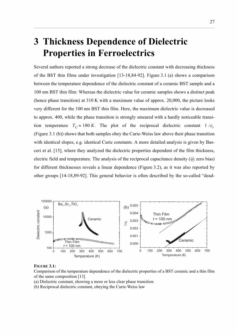
of the BST thin films under investigation [13-18,84-92]. Figure 3.1 (a) shows a comparison
between the temperature dependence of the dielectric constant of a ceramic BST sample and a
100 nm BST thin film: Whereas the dielectric value for ceramic samples shows a distinct peak
(hence phase transition) at 310 K with a maximum value of approx. 20,000, the picture looks
very different for the 100 nm BST thin film. Here, the maximum dielectric value is decreased
to approx. 400, while the phase transition is strongly smeared with a hardly noticeable transi-
tion temperature . The plot of the reciprocal dielectric constant
(Figure 3.1 (b)) shows that both samples obey the Curie-Weiss law above their phase transition
with identical slopes, e.g. identical Curie constants. A more detailed analysis is given by Bas-
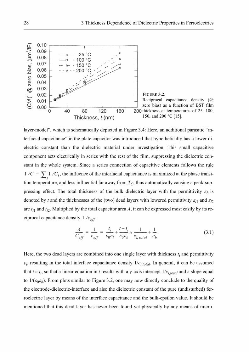
ceri et al. [15], where they analyzed the dielectric properties dependent of the film thickness,
electric field and temperature. The analysis of the reciprocal capacitance density (@ zero bias)
for different thicknesses reveals a linear dependence (Figure 3.2), as it was also reported by
other groups [14-18,89-92]. This general behavior is often described by the so-called “dead-
0 700600500400300200100Temperature (K)
100
1000
10000
100000
Die
lect
ric c
onst
ant
Ceramic
Ba0.7Sr0.3TiO3
Thin Filmt = 100 nm
0 100 200 300 400 500 600 700Temperature (K)
0.000
0.001
0.002
0.003
0.004
0.005
1/ε r
Ceramic
Thin Filmt = 100 nm
FIGURE 3.1:Comparison of the temperature dependence of the dielectric properties of a BST ceramic and a thin film of the same composition [13](a) Dielectric constant, showing a more or less clear phase transition(b) Reciprocal dielectric constant, obeying the Curie-Weiss law
(a) (b)
TC 180 K≈ 1 εr⁄
28 3 Thickness Dependence of Dielectric Properties in Ferroelectrics
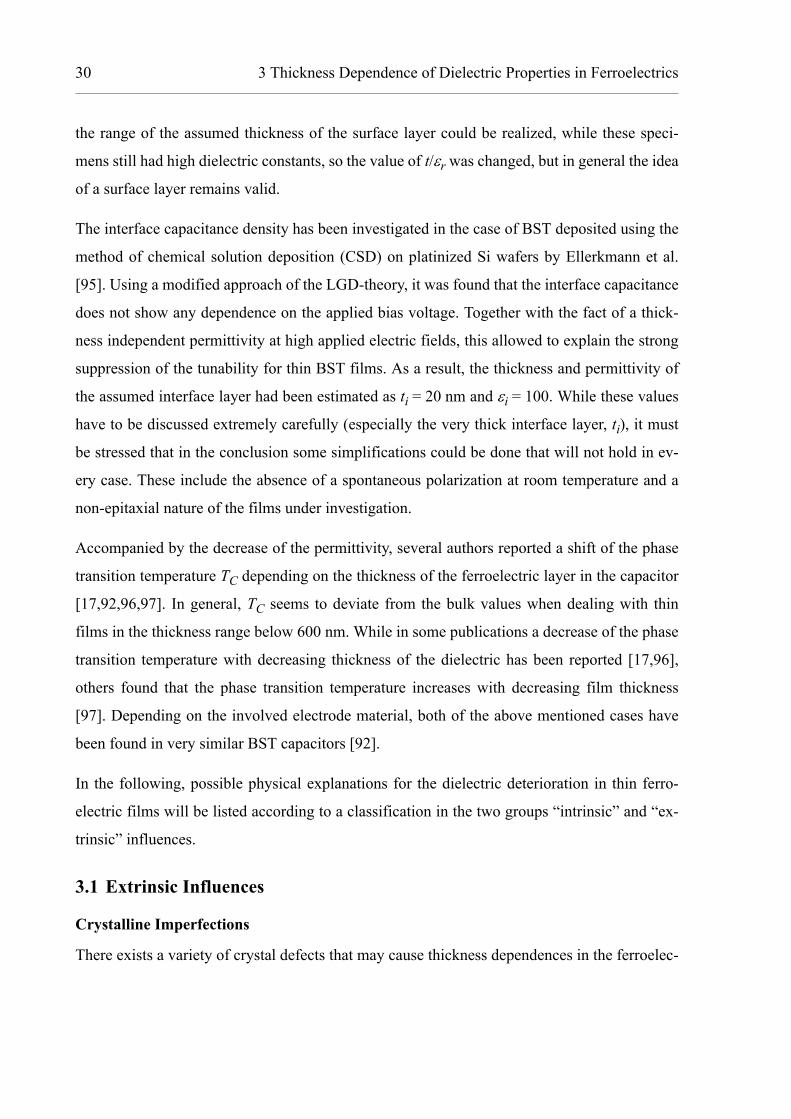
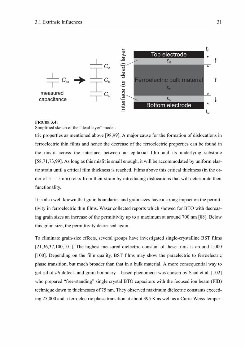
layer-model”, which is schematically depicted in Figure 3.4: Here, an additional parasitic “in-
terfacial capacitance” in the plate capacitor was introduced that hypothetically has a lower di-
electric constant than the dielectric material under investigation. This small capacitive
component acts electrically in series with the rest of the film, suppressing the dielectric con-
stant in the whole system. Since a series connection of capacitive elements follows the rule
, the influence of the interfacial capacitance is maximized at the phase transi-
tion temperature, and less influential far away from TC, thus automatically causing a peak-sup-
pressing effect. The total thickness of the bulk dielectric layer with the permittivity εb is
denoted by t and the thicknesses of the (two) dead layers with lowered permittivity εi1 and εi2
are ti1 and ti2. Multiplied by the total capacitor area A, it can be expressed most easily by its re-
ciprocal capacitance density :
Here, the two dead layers are combined into one single layer with thickness ti and permittivity
εi, resulting in the total interface capacitance density 1/ci,total. In general, it can be assumed
that t » ti, so that a linear equation in t results with a y-axis intercept 1/ci,total and a slope equal
to 1/(ε0εb). From plots similar to Figure 3.2, one may now directly conclude to the quality of
the electrode-dielectric-interface and also the dielectric constant of the pure (undisturbed) fer-
roelectric layer by means of the interface capacitance and the bulk-epsilon value. It should be
mentioned that this dead layer has never been found yet physically by any means of micro-
0 40 80 120 160 200Thickness, t (nm)
(C/A
)-1 @
zer
o bi
as, (
µm2 /fF
)
0.000.010.020.030.040.050.060.070.080.090.10
25 °C100 °C150 °C200 °C
FIGURE 3.2:Reciprocal capacitance density (@ zero bias) as a function of BST film thickness at temperatures of 25, 100, 150, and 200 °C [15].
1 C⁄ 1 Ci⁄i
∑=
1 ceff⁄
ACeff--------- 1
ceff-------
tiε0εi---------
t ti–ε0εb----------+ 1
ci total,--------------- 1
cb-----+≈= = (3.1)
29
scopic investigations or chemical analyses. Nevertheless, it is a fairly good model to describe
phenomenologically the permittivity decrease in ferroelectric thin film capacitors with de-
creasing thickness.
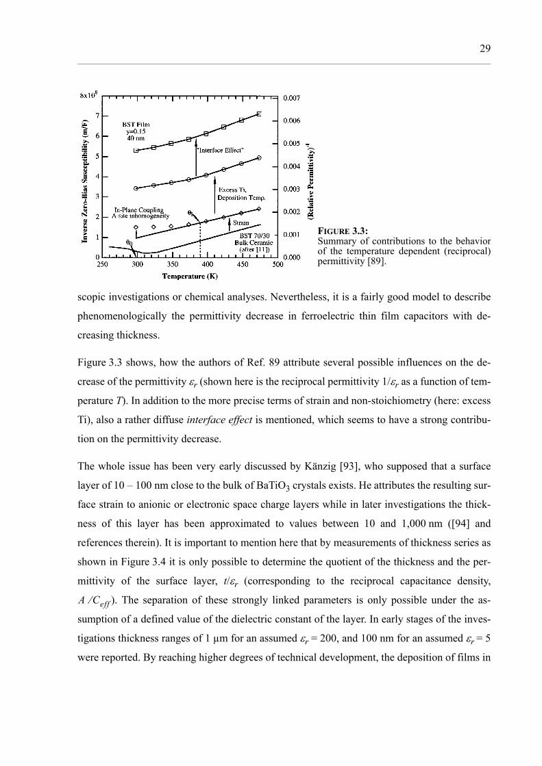
Figure 3.3 shows, how the authors of Ref. 89 attribute several possible influences on the de-
crease of the permittivity εr (shown here is the reciprocal permittivity 1/εr as a function of tem-
perature T). In addition to the more precise terms of strain and non-stoichiometry (here: excess
Ti), also a rather diffuse interface effect is mentioned, which seems to have a strong contribu-
tion on the permittivity decrease.
The whole issue has been very early discussed by Känzig [93], who supposed that a surface
layer of 10 – 100 nm close to the bulk of BaTiO3 crystals exists. He attributes the resulting sur-
face strain to anionic or electronic space charge layers while in later investigations the thick-
ness of this layer has been approximated to values between 10 and 1,000 nm ([94] and
references therein). It is important to mention here that by measurements of thickness series as
shown in Figure 3.4 it is only possible to determine the quotient of the thickness and the per-
mittivity of the surface layer, t/εr (corresponding to the reciprocal capacitance density,
). The separation of these strongly linked parameters is only possible under the as-
sumption of a defined value of the dielectric constant of the layer. In early stages of the inves-
tigations thickness ranges of 1 µm for an assumed εr = 200, and 100 nm for an assumed εr = 5
were reported. By reaching higher degrees of technical development, the deposition of films in
FIGURE 3.3:Summary of contributions to the behavior of the temperature dependent (reciprocal) permittivity [89].
A Ceff⁄
30 3 Thickness Dependence of Dielectric Properties in Ferroelectrics
the range of the assumed thickness of the surface layer could be realized, while these speci-
mens still had high dielectric constants, so the value of t/εr was changed, but in general the idea
of a surface layer remains valid.
The interface capacitance density has been investigated in the case of BST deposited using the
method of chemical solution deposition (CSD) on platinized Si wafers by Ellerkmann et al.
[95]. Using a modified approach of the LGD-theory, it was found that the interface capacitance
does not show any dependence on the applied bias voltage. Together with the fact of a thick-
ness independent permittivity at high applied electric fields, this allowed to explain the strong
suppression of the tunability for thin BST films. As a result, the thickness and permittivity of
the assumed interface layer had been estimated as ti = 20 nm and εi = 100. While these values
have to be discussed extremely carefully (especially the very thick interface layer, ti), it must
be stressed that in the conclusion some simplifications could be done that will not hold in ev-
ery case. These include the absence of a spontaneous polarization at room temperature and a
non-epitaxial nature of the films under investigation.
Accompanied by the decrease of the permittivity, several authors reported a shift of the phase
transition temperature TC depending on the thickness of the ferroelectric layer in the capacitor
[17,92,96,97]. In general, TC seems to deviate from the bulk values when dealing with thin
films in the thickness range below 600 nm. While in some publications a decrease of the phase
transition temperature with decreasing thickness of the dielectric has been reported [17,96],
others found that the phase transition temperature increases with decreasing film thickness
[97]. Depending on the involved electrode material, both of the above mentioned cases have
been found in very similar BST capacitors [92].
In the following, possible physical explanations for the dielectric deterioration in thin ferro-
electric films will be listed according to a classification in the two groups “intrinsic” and “ex-
trinsic” influences.
3.1 Extrinsic Influences
Crystalline Imperfections
There exists a variety of crystal defects that may cause thickness dependences in the ferroelec-
3.1 Extrinsic Influences 31
tric properties as mentioned above [98,99]. A major cause for the formation of dislocations in
ferroelectric thin films and hence the decrease of the ferroelectric properties can be found in
the misfit across the interface between an epitaxial film and its underlying substrate
[58,71,73,99]. As long as this misfit is small enough, it will be accommodated by uniform elas-
tic strain until a critical film thickness is reached. Films above this critical thickness (in the or-
der of 5 – 15 nm) relax from their strain by introducing dislocations that will deteriorate their
functionality.
It is also well known that grain boundaries and grain sizes have a strong impact on the permit-
tivity in ferroelectric thin films. Waser collected reports which showed for BTO with decreas-
ing grain sizes an increase of the permittivity up to a maximum at around 700 nm [88]. Below
this grain size, the permittivity decreased again.
To eliminate grain-size effects, several groups have investigated single-crystalline BST films
[21,36,37,100,101]. The highest measured dielectric constant of these films is around 1,000
[100]. Depending on the film quality, BST films may show the paraelectric to ferroelectric
phase transition, but much broader than that in a bulk material. A more consequential way to
get rid of all defect- and grain boundary – based phenomena was chosen by Saad et al. [102]
who prepared “free-standing” single crystal BTO capacitors with the focused ion beam (FIB)
technique down to thicknesses of 75 nm. They observed maximum dielectric constants exceed-
ing 25,000 and a ferroelectric phase transition at about 395 K as well as a Curie-Weiss-temper-
Ferroelectric bulk material εb
Bottom electrode
Top electrode
Inte
rface
(or d
ead)
laye
r
t
ti2
ti1
Cb
Ci2
Ci1
Ceff
εi1
εi2
measured capacitance
FIGURE 3.4:Simplified sketch of the “dead layer” model.
32 3 Thickness Dependence of Dielectric Properties in Ferroelectrics
ature of about 377 K that usually can be seen only in single crystal bulk ceramics. These
findings were regarded as a full recovery of bulk-like functional behavior for ferroelectrics in
the sub-100 nm thickness regime, as no one has seen before.
Local Diffusion of Electrode Material into the Ferroelectric Film
The dependence of ionic interdiffusion on the ferroelectric properties of thin BST films was in-
vestigated by several groups. Tsai et al. found that BST thin films on Ru bottom electrodes
showed a decreased dielectric constant from 548 down to 325 after annealing in O2 at 700 °C,
while the same films on Ru/RuO2 bottom electrodes had an increased dielectric constant from
322 to 433 after a similar annealing treatment [103]. They assume that the BST films on Ru/
RuO2 behave more stable while on Ru, a possible thin interfacial layer like (Ba, Sr)(Ru, Ti)O3
might have been formed by the interdiffusion of ions after annealing, caused by the similarity
of the ionic radii of Ru and Ti. The approach of Choi et al. was to use (Ba, Sr)RuO3 (BSR) as
the electrode material, where they found a strong dependence of the dielectric constant on the
(Ba, Sr)/Ru ratio in the BSR electrodes with the highest values at about 550 for a stoichiomet-
ric ratio of 1.0 and lower values at 470 and 350 for ratios of 1.3 and 0.7 respectively [23]. They
assume a diffusion of the shared elements Ba and Sr in either direction between stoichiometric
BST and Ru-rich or Ru-deficient BSR, leading to the formation of a low dielectric interface
layer. This diffusion may be suppressed in the case of stoichiometric BSR due to equal driving
forces.
3.2 Intrinsic Influences
Built-In Electric Fields
The temperature dependence of the permittivity in BST has been investigated by Vendik et al.
[104]. They consider perfect single crystals of BST (no defects) which are free of built-in elec-
tric fields and internal mechanical strains, where the position of the maximum permittivity co-
incides with the phase transition temperature. Since such a perfect crystal is not available when
dealing with thin film capacitors, one has always to account for built-in fields from work-func-
tion differences of the used electrode materials, which following their calculations cause a shift
of the maximum permittivity towards higher temperatures and a decrease of the permittivity in
general. Other sources for internal built-in fields are mentioned by Tagantsev et. al., who iden-
3.2 Intrinsic Influences 33
tified depletion layers at the electrodes to be the reason for a reduction of the effective dielec-
tric permittivity of the film [105].
Lattice Strains
The mechanical boundary conditions at the electrode/ferroelectric interface, as introduced in
chapter 2.4, not only have an extrinsic effect when they lead to the generation of misfit disloca-
tions (cmp. chapter 3.1), but also affect intrinsic size effects. In fact, the lattice strain can also
affect the stability of the ferroelectric phase and impact the equilibrium domain structures. In
Ref. 91, using a thermodynamic theory the decrease of the permittivity has been explained by
the thickness dependent strain relaxation in epitaxial ferroelectric thin films, which leads to a
thickness dependence of the reciprocal capacitance density in analogy to Eq. 3.1.
Finite Screening Abilities of the Electrode Material
The reduction of the applied field inside the ferroelectric film due to a finite screening length
of the electrodes was first mentioned 1961 by Mead [106]. He reported measurements of the
reciprocal capacitance density vs. film thickness for Ta-TaO2 capacitors that resulted in plots
similar to those in Figure 3.2 and attributed this thickness dependence to electric field penetra-
tion into the (metal) electrode, while he assumed the penetration depth to be approx. 1 Å. The-
oretical studies from Ku and Ullman showed a good agreement with Mead´s investigation
[30]. By using the Debye-length L, defined by
with specific parameters of the electrode material such as its Fermi energy EF, its dielectric
constant εm and its free electron density n0 they found a description of the reciprocal capaci-
tance density similar to that given by Eq. (3.1):
Again, the reciprocal capacitance density consists of one thickness dependent part from the
pure dielectric behavior plus one thickness independent part (intercept) governed by the char-
acteristic length L multiplied by 2.3. The characteristic penetration length L has been corrected
1 L2⁄ 2n0e2 εmε0EF⁄ ,= (3.2)
1c--- t
ε0εr---------- 2.3 L
ε0εm-----------+= (3.3)
34 3 Thickness Dependence of Dielectric Properties in Ferroelectrics
later by Simmons to r0,
who found an analytical expression rather than the numerical values from Ku and Ullman
[107].
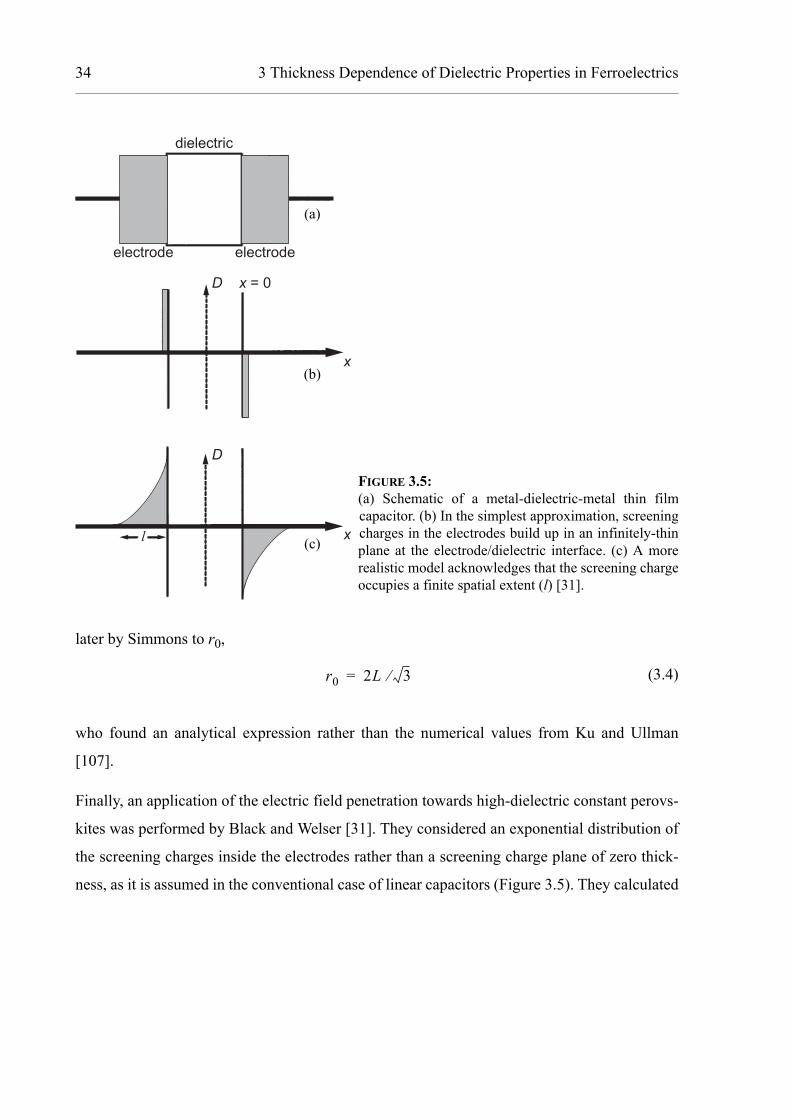
Finally, an application of the electric field penetration towards high-dielectric constant perovs-
kites was performed by Black and Welser [31]. They considered an exponential distribution of
the screening charges inside the electrodes rather than a screening charge plane of zero thick-
ness, as it is assumed in the conventional case of linear capacitors (Figure 3.5). They calculated
r0 2L 3⁄= (3.4)
dielectric
electrodeelectrode
x = 0D
D
x
l x
FIGURE 3.5:(a) Schematic of a metal-dielectric-metal thin film capacitor. (b) In the simplest approximation, screening charges in the electrodes build up in an infinitely-thin plane at the electrode/dielectric interface. (c) A more realistic model acknowledges that the screening charge occupies a finite spatial extent (l) [31].
(a)
(b)
(c)
3.2 Intrinsic Influences 35
the characteristic screening length l by means of the Thomas-Fermi method as follows:
Here, one finds again Fermi energy EF and dielectric constant εm of the electrode material,
while ρ0 denotes the induced charge density at position x = 0 and lTF is typically defined as the
Thomas-Fermi screening length. Now the resulting reciprocal capacitance density can be cal-
culated as
Again, this results in an equation describing 1/ceff linear dependent on t with a y-axis intercept
resulting from the interface capacitance. Hence, one can now calculate maximum values of the
interface capacitance when lTF and εm are known. It should be noted that these values, depend-
ing on the accuracy of the used electrode parameters, seem to display limits of the interface ca-
pacitance density regardless of the used dielectric material or thickness of the dielectric layer.
The value of the electrode permittivity εm in the case of SRO is under controversial discussion
in the literature: While Black and Welser suggest a speculative value of ~100, Kim et al. have
calculated the SRO permittivity by means of optical measurements to a more realistic value of
~8.45 [108]. In contrast, Dawber et al. neglect the SRO permittivity by simply setting this
value to 1 [32,109].
From publications of Batra et al. an influence of the so called depolarizing field Edep on the
phase transition temperature in ferroelectric thin films can be observed [110-112]. This field
may occur when the polarization charges are not perfectly compensated by free
charges. Such compensation charges can reside either internally (in the ferroelectric) or exter-
nally (in the electrodes). Since the conductivity of the ferroelectric is generally rather low (sev-
eral orders of magnitude smaller) compared to the electrode material, one assumes that for
most cases of interest the polarization will be compensated externally. In thin films however,
such a charge compensation cannot be done completely, resulting in a residual field that may
modify the phase stability of ferroelectric films with sufficiently low thickness. With these ob-
l2 εm23---
ε0EFρ0e
------------ εmlTF2= = (3.5)
1ceff------- 1
ε0----- t
εr----
2lTF
εm
----------+ 1cdielectric---------------------- 1
cinterface---------------------+= = (3.6)
ρ div– P=
36 3 Thickness Dependence of Dielectric Properties in Ferroelectrics
servations, a decreasing phase transition temperature with decreasing film thickness could be
found.
To determine the magnitude of the depolarizing field, the considerations of Mehta et al. can be
used [113]. They found a strong dependence of the retention behavior in
Pb0.92Bi0.07La0.01(Fe0.405Nb0.325Zr0.27)O3 on the film thickness and attribute this to depolar-
izing fields existing inside the ferroelectric. Assuming a charge distribution similar to what has
been found by Black and Welser [31], and by solving Poisson’s equation, the depolarizing
field Edep was calculated to
where they use the dielectric constant of the electrode εm again, while ls means the screening
length in the electrodes and P, l and εr denote the polarization, thickness and dielectric con-
stant of the ferroelectric layer. By applying voltage pulses on the capacitor, they measured the
time dependence on the retention loss and found that different polarities of the applied pulses
result in different polarization retention decay. They attributed this to contact potential differ-
ences and could improve the retention behavior by applying additional external voltages com-
pensating these differences.
Großmann has shown a way to connect the interface capacitance with the polarization and the
depolarizing field by using the model of a short-circuited capacitor with the two possible dead
layers combined into one single interface layer, as shown in Figure 3.6 [114]. With Maxwells
equation
and the continuity condition at the ferroelectric/electrode interface as well as the ex-
plicit expression of the screening in the ferroelectric
EdepP
ε0εr----------
2εr l⁄2εr l⁄ εm ls⁄+--------------------------------- ,–= (3.7)
(3.8) Ed s =∫ 0
Di Db=
Eb Edep–=( )
Db P ε0εbEb+= (3.9)
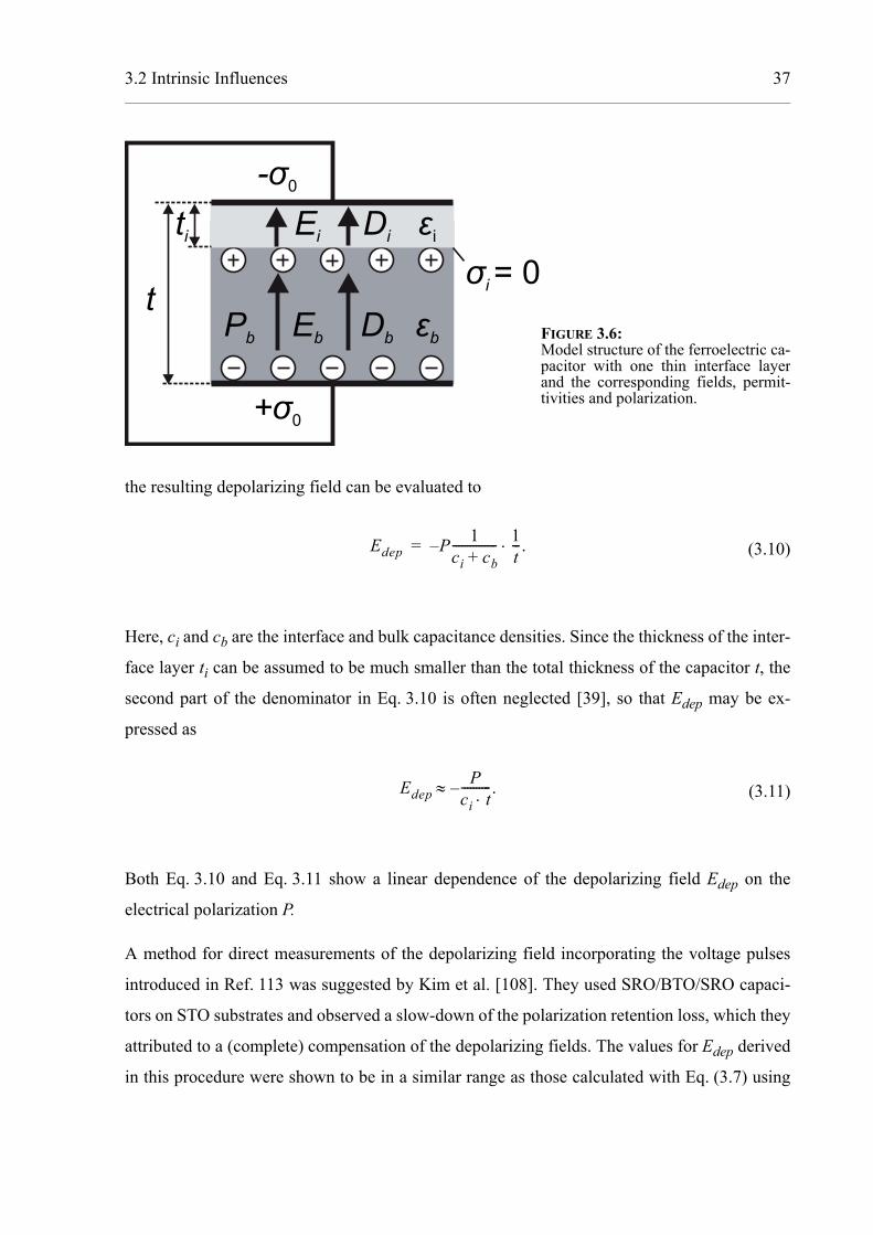
3.2 Intrinsic Influences 37
the resulting depolarizing field can be evaluated to
Here, ci and cb are the interface and bulk capacitance densities. Since the thickness of the inter-
face layer ti can be assumed to be much smaller than the total thickness of the capacitor t, the
second part of the denominator in Eq. 3.10 is often neglected [39], so that Edep may be ex-
pressed as
Both Eq. 3.10 and Eq. 3.11 show a linear dependence of the depolarizing field Edep on the
electrical polarization P.
A method for direct measurements of the depolarizing field incorporating the voltage pulses
introduced in Ref. 113 was suggested by Kim et al. [108]. They used SRO/BTO/SRO capaci-
tors on STO substrates and observed a slow-down of the polarization retention loss, which they
attributed to a (complete) compensation of the depolarizing fields. The values for Edep derived
in this procedure were shown to be in a similar range as those calculated with Eq. (3.7) using
Edep P 1ci cb+--------------- 1
t---.⋅–= (3.10)
EdepP
ci t⋅----------.–≈ (3.11)
t
ti Ei Di εi
εbDbEbPb
+σ0
-σ0
σi = 0FIGURE 3.6:Model structure of the ferroelectric ca-pacitor with one thin interface layer and the corresponding fields, permit-tivities and polarization.
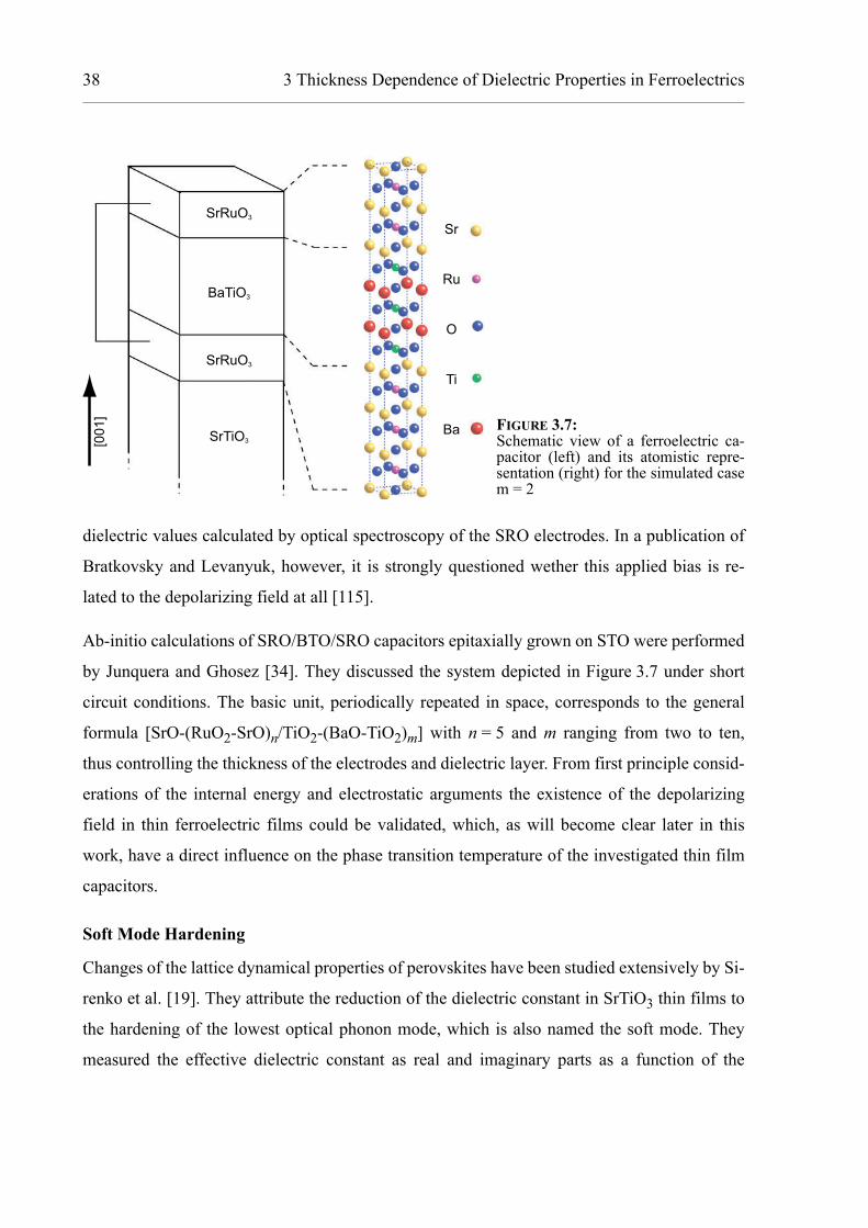
38 3 Thickness Dependence of Dielectric Properties in Ferroelectrics
dielectric values calculated by optical spectroscopy of the SRO electrodes. In a publication of
Bratkovsky and Levanyuk, however, it is strongly questioned wether this applied bias is re-
lated to the depolarizing field at all [115].
Ab-initio calculations of SRO/BTO/SRO capacitors epitaxially grown on STO were performed
by Junquera and Ghosez [34]. They discussed the system depicted in Figure 3.7 under short
circuit conditions. The basic unit, periodically repeated in space, corresponds to the general
formula [SrO-(RuO2-SrO)n/TiO2-(BaO-TiO2)m] with n = 5 and m ranging from two to ten,
thus controlling the thickness of the electrodes and dielectric layer. From first principle consid-
erations of the internal energy and electrostatic arguments the existence of the depolarizing
field in thin ferroelectric films could be validated, which, as will become clear later in this
work, have a direct influence on the phase transition temperature of the investigated thin film
capacitors.
Soft Mode Hardening
Changes of the lattice dynamical properties of perovskites have been studied extensively by Si-
renko et al. [19]. They attribute the reduction of the dielectric constant in SrTiO3 thin films to
the hardening of the lowest optical phonon mode, which is also named the soft mode. They
measured the effective dielectric constant as real and imaginary parts as a function of the
SrTiO3
SrRuO3
BaTiO3
SrRuO3
[001
]
Ba
Ti
O
Ru
Sr
FIGURE 3.7:Schematic view of a ferroelectric ca-pacitor (left) and its atomistic repre-sentation (right) for the simulated case m = 2
3.2 Intrinsic Influences 39
wavenumber (cm-1) at various temperatures. From these measurements, the eigenfrequencies
of the soft mode optical phonons were evaluated. As it is known from Ref. 116, this eigenfre-
quency, measured at bulk ceramics, should decrease with decreasing temperatures until it
reaches approx. zero at a critical temperature. The experiments in Ref. 19 however showed a
reduced softening of the soft mode depending on the temperature, e.g. the frequency of the soft
mode phonon does not reach zero but saturates at finite frequency values. In contrast, the
eigenfrequencies of all other longitudinal and transversal optical phonon modes will be only
slightly affected by variations of the temperature and do not differ from those of the bulk STO.
The comparison of the inverse of the static dielectric constant and the soft mode as a function
of temperature showed a good agreement, as it was previously predicted by theoretical values
of the Lyddane-Sachs-Teller (LST) relation.
In a Ref. 33, a correlation between the dead layer and the hardening of the SrTiO3 soft mode
could be established. With first principles calculations for SRO/STO/SRO heterostructures a
macroscopically averaged local permittivity profile has been achieved. From the correspond-
ing electrostatic potential, a direct conclusion on the depolarizing field Edep was made, which
the authors think is the main cause of both the interfacial dead layer and the soft-mode harden-
ing. They found from their analysis that excellent screening properties at the interface are im-
portant, since even one or two sub-polarized atomic monolayers would seriously affect the
properties of micrometer-thick devices (and of course thinner film thickness).
To summarize this chapter, the following should be noted: The simplest model assuming low
permittivity layers at the electrodes/ferroelectric interfaces reveals a widely accepted equation
for the calculation of the reciprocal capacitance density linearly dependent on the film thick-
ness (Eq. 3.1). As will be shown later, some of the intrinsic and extrinsic effects lead to similar
representations of the capacitance density with a variation of the basic equation due to the par-
ticular physical effect, so that additional terms are added that include the dependence of me-
chanical strains or depolarizing field.

40 3 Thickness Dependence of Dielectric Properties in Ferroelectrics
41
4 Experimental MethodsThe first part of this chapter gives the details about the preparation of the ferroelectric capaci-
tors used in the investigations of this work. In the second part, the different methods and tech-
niques of electrical characterization are described.
4.1 Sample Preparation
Numerous methods for the deposition of ceramic thin films have been developed in the last de-
cades. Choosing the right method is not easy and always depends on the specific material to be
grown on a certain substrate to fulfill a certain purpose. The deposition techniques can be clas-
sified into either physical or chemical deposition methods [5,117,118]. The physical methods
are characterized by a well defined particle source (target) and generally a free flight (in vac-
uum) to the substrate. In chemical methods, so-called precursor solutions containing the de-
sired materials dissociate at the hot substrate surface and release the atoms of interest.
Since in this work solely physical deposition methods were used, a detailed description of the
chemical methods will be omitted.
In the following, a description of the deposition techniques used in this work will be given.
The BST and SRO thin films were deposited by pulsed laser deposition while the Pt electrodes
were fabricated by sputtering.
Pulsed Laser Deposition of perovskite thin films
A comprehensive description of all details of the pulsed laser deposition (PLD) technique can
be found in Ref. 120, therefore this introduction will be rather brief to explain only the essen-
tial parts of this method. The working principle of the PLD technique is displayed in
Figure 4.1 (a). A short pulsed laser beam from an excimer laser4 is focused on a rotating target
containing the materials to be deposited in a stoichiometric composition. In the deposition
chamber an ambient gas pressure (usually O2) of 0.3 to 1 mbar is maintained, so that these
pulses with an energy of typically 2 – 5 J/pulse lead to the immediate formation of a plasma at
the target surface, containing energetic neutral atoms, ions and molecules. This so-called
4. Here, a KrF excimer laser with a wavelength of 248 nm and a repetition rate between 5 and 10 Hz was used
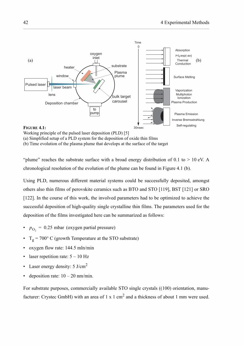
42 4 Experimental Methods
“plume” reaches the substrate surface with a broad energy distribution of 0.1 to > 10 eV. A
chronological resolution of the evolution of the plume can be found in Figure 4.1 (b).
Using PLD, numerous different material systems could be successfully deposited, amongst
others also thin films of perovskite ceramics such as BTO and STO [119], BST [121] or SRO
[122]. In the course of this work, the involved parameters had to be optimized to achieve the
successful deposition of high-quality single crystalline thin films. The parameters used for the
deposition of the films investigated here can be summarized as follows:
• (oxygen partial pressure)
• Tg = 700° C (growth Temperature at the STO substrate)
• oxygen flow rate: 144.5 mln/min
• laser repetition rate: 5 – 10 Hz
• Laser energy density: 5 J/cm2
• deposition rate: 10 – 20 nm/min.
For substrate purposes, commercially available STO single crystals ((100) orientation, manu-
facturer: Crystec GmbH) with an area of 1 x 1 cm2 and a thickness of about 1 mm were used.
0
30nsec
Absorption
I=I exp(-ax)0
Thermal Conduction
Surface Melting
VaporizationMultiphoton Ionization
Plasma Production
Self-regulating
Plasma Emission
Time
Inverse Bremsstrahlung
bulk target carousel
FIGURE 4.1:Working principle of the pulsed laser deposition (PLD) [5](a) Simplified setup of a PLD system for the deposition of oxide thin films(b) Time evolution of the plasma plume that develops at the surface of the target
(a) (b)
pO20.25 mbar=
4.1 Sample Preparation 43
In an in-situ5 process, first the bottom electrodes were deposited, resulting in SRO layers of
about 100 nm thickness. Prior to this deposition, the substrate was heated up to the desired pro-
cess temperature, after which the ambient O2 pressure has been adjusted to a constant pressure.
To get a “clean” atmosphere in the process chamber, the pump exhausted the “used” oxygen,
while fresh oxygen has been let in, thus resulting in stable flow-rates and oxygen pressures.
After setting up the chamber parameters according to the desired values, the laser has been
switched on with a suitable repetition frequency. For the next layer to be deposited, the SRO
target has been replaced by turning the target carousel and positioning the BST target into the
laser beam without breaking the low vacuum, thus allowing an in-situ deposition of the thin
films of interest. The film thicknesses deposited in this second step range from about 10 nm up
to about 300 nm. Depending on the certain concept, a third deposition step has been per-
formed. Here, top electrodes with thickness of about 30 nm were deposited in a subsequent in-
situ deposition step after changing the target back to SRO at the same temperature and pressure
as the BST films before.
Top Electrode Structuring
Besides the aforementioned deposition of the perovskite materials via PLD, additional samples
were prepared with top electrodes of Pt deposited ex-situ in a dc-sputtering system. The Pt as
well as the SRO top electrodes had to be structured to finally form a plate capacitor configura-
tion with a suitable geometry ratio. In principle, this structuring could be done using a lift-off
process [5] or by means of a dry etching step. For the Pt case, it has been experimentally ob-
served that a treatment of the BST surface with chemicals such as the developer and photore-
sist in the lift-off process prior to the deposition of Pt leads to a significant deterioration of the
dielectric properties of the thin film capacitors. In case of SRO top electrodes, the photoresist
would not withstand the high temperatures necessary for the PLD process. Therefore, a dry
etching process had been used for defining both the Pt and SRO top contacts, which by the way
makes it easier to compare the two different material systems.
Here, photoresist (AZ5214) has been spun on the top electrode layer and has been prebaked,
thus establishing a so called positive tone process. The thus prepared photoresist was then ex-
5. Different processing steps are performed in series without changing the reaction chamber (here: PLD chamber) and without breaking the process atmosphere (vacuum)
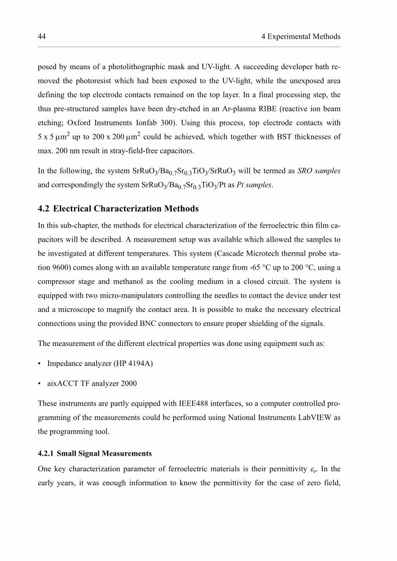
44 4 Experimental Methods
posed by means of a photolithographic mask and UV-light. A succeeding developer bath re-
moved the photoresist which had been exposed to the UV-light, while the unexposed area
defining the top electrode contacts remained on the top layer. In a final processing step, the
thus pre-structured samples have been dry-etched in an Ar-plasma RIBE (reactive ion beam
etching; Oxford Instruments Ionfab 300). Using this process, top electrode contacts with
5 x 5 μm2 up to 200 x 200 μm2 could be achieved, which together with BST thicknesses of
max. 200 nm result in stray-field-free capacitors.
In the following, the system SrRuO3/Ba0.7Sr0.3TiO3/SrRuO3 will be termed as SRO samples
and correspondingly the system SrRuO3/Ba0.7Sr0.3TiO3/Pt as Pt samples.
4.2 Electrical Characterization Methods
In this sub-chapter, the methods for electrical characterization of the ferroelectric thin film ca-
pacitors will be described. A measurement setup was available which allowed the samples to
be investigated at different temperatures. This system (Cascade Microtech thermal probe sta-
tion 9600) comes along with an available temperature range from -65 °C up to 200 °C, using a
compressor stage and methanol as the cooling medium in a closed circuit. The system is
equipped with two micro-manipulators controlling the needles to contact the device under test
and a microscope to magnify the contact area. It is possible to make the necessary electrical
connections using the provided BNC connectors to ensure proper shielding of the signals.
The measurement of the different electrical properties was done using equipment such as:
• Impedance analyzer (HP 4194A)
• aixACCT TF analyzer 2000
These instruments are partly equipped with IEEE488 interfaces, so a computer controlled pro-
gramming of the measurements could be performed using National Instruments LabVIEW as
the programming tool.
4.2.1 Small Signal Measurements
One key characterization parameter of ferroelectric materials is their permittivity εr. In the
early years, it was enough information to know the permittivity for the case of zero field,
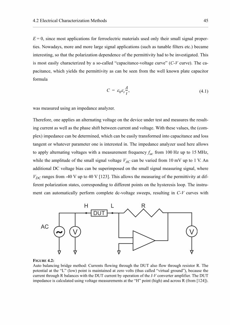
4.2 Electrical Characterization Methods 45
E = 0, since most applications for ferroelectric materials used only their small signal proper-
ties. Nowadays, more and more large signal applications (such as tunable filters etc.) became
interesting, so that the polarization dependence of the permittivity had to be investigated. This
is most easily characterized by a so-called “capacitance-voltage curve” (C-V curve). The ca-
pacitance, which yields the permittivity as can be seen from the well known plate capacitor
formula
was measured using an impedance analyzer.
Therefore, one applies an alternating voltage on the device under test and measures the result-
ing current as well as the phase shift between current and voltage. With these values, the (com-
plex) impedance can be determined, which can be easily transformed into capacitance and loss
tangent or whatever parameter one is interested in. The impedance analyzer used here allows
to apply alternating voltages with a measurement frequency fac from 100 Hz up to 15 MHz,
while the amplitude of the small signal voltage VAC can be varied from 10 mV up to 1 V. An
additional DC voltage bias can be superimposed on the small signal measuring signal, where
VDC ranges from -40 V up to 40 V [123]. This allows the measuring of the permittivity at dif-
ferent polarization states, corresponding to different points on the hysteresis loop. The instru-
ment can automatically perform complete dc-voltage sweeps, resulting in C-V curves with
C ε0εrAt---,= (4.1)
VV˜AC
H LDUT
R
FIGURE 4.2:Auto balancing bridge method: Currents flowing through the DUT also flow through resistor R. The potential at the “L” (low) point is maintained at zero volts (thus called “virtual ground”), because the current through R balances with the DUT current by operation of the I-V converter amplifier. The DUT impedance is calculated using voltage measurements at the “H” point (high) and across R (from [124]).
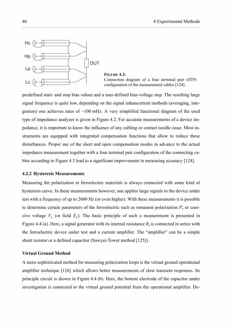
46 4 Experimental Methods
predefined start- and stop bias values and a user-defined bias-voltage step. The resulting large
signal frequency is quite low, depending on the signal enhancement methods (averaging, inte-
gration) one achieves rates of ~100 mHz. A very simplified functional diagram of the used
type of impedance analyzer is given in Figure 4.2. For accurate measurements of a device im-
pedance, it is important to know the influence of any cabling or contact needle issue. Most in-
struments are equipped with integrated compensation functions that allow to reduce these
disturbances. Proper use of the short and open compensation modes in advance to the actual
impedance measurement together with a four terminal pair configuration of the connecting ca-
bles according to Figure 4.3 lead to a significant improvement in measuring accuracy [124].
4.2.2 Hysteresis Measurements
Measuring the polarization in ferroelectric materials is always connected with some kind of
hysteresis curve. In these measurements however, one applies large signals to the device under
test with a frequency of up to 2000 Hz (or even higher). With these measurements it is possible
to determine certain parameters of the ferroelectric such as remanent polarization Pr or coer-
cive voltage Vc (or field Ec). The basic principle of such a measurement is presented in
Figure 4.4 (a). Here, a signal generator with its internal resistance Ri is connected in series with
the ferroelectric device under test and a current amplifier. The “amplifier” can be a simple
shunt resistor or a defined capacitor (Sawyer-Tower method [125]).
Virtual Ground Method
A more sophisticated method for measuring polarization loops is the virtual ground operational
amplifier technique [126] which allows better measurements of slow transient responses. Its
principle circuit is shown in Figure 4.4 (b). Here, the bottom electrode of the capacitor under
investigation is connected to the virtual ground potential from the operational amplifier. De-
Lc
Lp
Hp
Hc
DUT
FIGURE 4.3:Connection diagram of a four terminal pair (4TP) configuration of the measurement cables [124].
4.2 Electrical Characterization Methods 47
pending on the choice of the circuit element in the feedback loop, the amplifier acts as a cur-
rent amplifier (Resistor Rs) or a current integrator (Capacitor CS) and provides a signal
proportional to the current or proportional to the charge (which is the integrated current). The
hysteresis curves presented in this work were recorded with an aixACCT TF analyzer 2000
[127].
Ri
FIGURE 4.4:(a) Schematic hysteresis measurement setup: Waveform generator, device under test and amplifier.(b) Virtual ground operational amplifier circuit.
(b)(a)

48 4 Experimental Methods
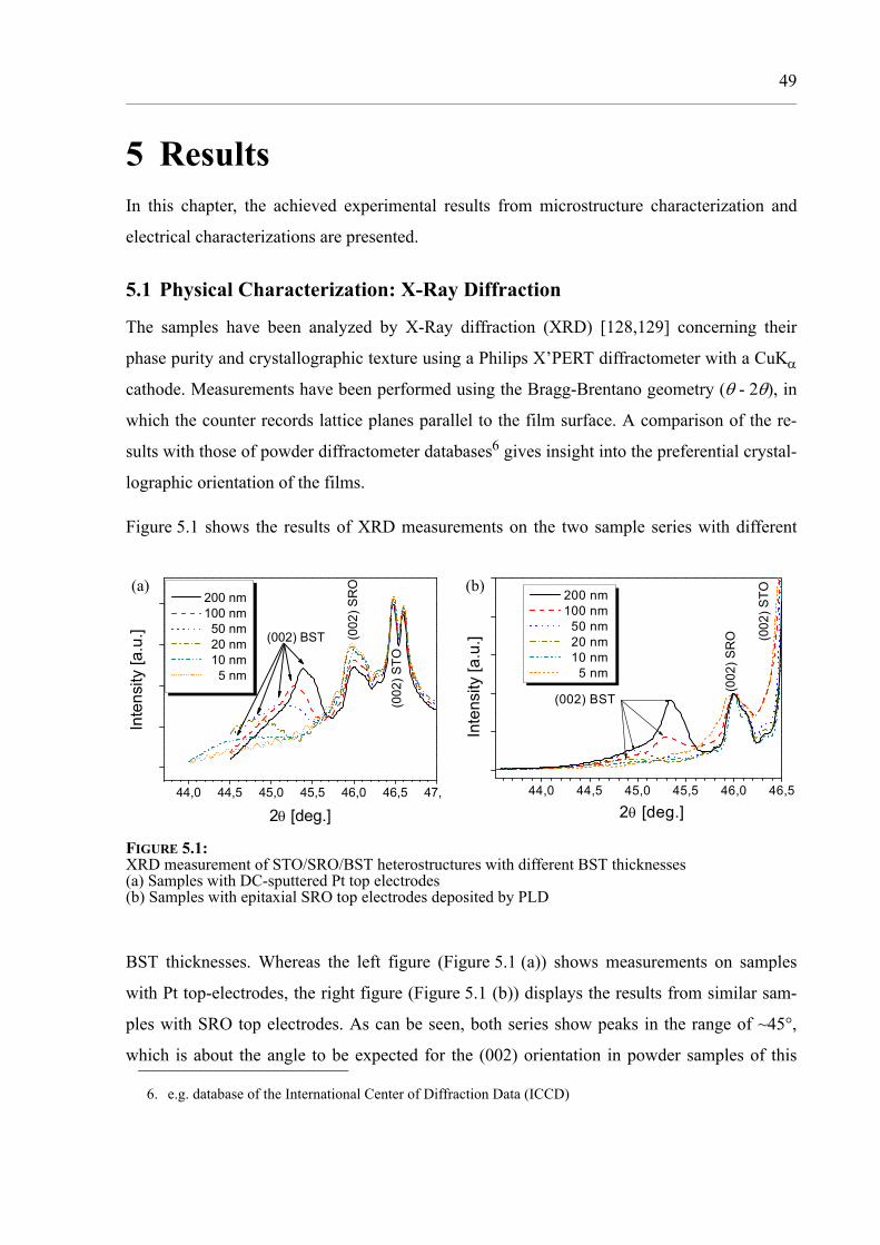
49
5 ResultsIn this chapter, the achieved experimental results from microstructure characterization and
electrical characterizations are presented.
5.1 Physical Characterization: X-Ray Diffraction
The samples have been analyzed by X-Ray diffraction (XRD) [128,129] concerning their
phase purity and crystallographic texture using a Philips X’PERT diffractometer with a CuKα
cathode. Measurements have been performed using the Bragg-Brentano geometry (θ - 2θ), in
which the counter records lattice planes parallel to the film surface. A comparison of the re-
sults with those of powder diffractometer databases6 gives insight into the preferential crystal-
lographic orientation of the films.
Figure 5.1 shows the results of XRD measurements on the two sample series with different
BST thicknesses. Whereas the left figure (Figure 5.1 (a)) shows measurements on samples
with Pt top-electrodes, the right figure (Figure 5.1 (b)) displays the results from similar sam-
ples with SRO top electrodes. As can be seen, both series show peaks in the range of ~45°,
which is about the angle to be expected for the (002) orientation in powder samples of this
6. e.g. database of the International Center of Diffraction Data (ICCD)
44,0 44,5 45,0 45,5 46,0 46,5 47,0
200 nm 100 nm 50 nm 20 nm 10 nm 5 nm
(002
) SR
O
(002) BST
(002
) STO
Inte
nsity
[a.u
.]
2θ [deg.]44,0 44,5 45,0 45,5 46,0 46,5
200 nm 100 nm 50 nm 20 nm 10 nm 5 nm
Inte
nsity
[a.u
.]
(002) BST
(002
) STO
(002
) SR
O
2θ [deg.]
FIGURE 5.1:XRD measurement of STO/SRO/BST heterostructures with different BST thicknesses(a) Samples with DC-sputtered Pt top electrodes(b) Samples with epitaxial SRO top electrodes deposited by PLD
(a) (b)
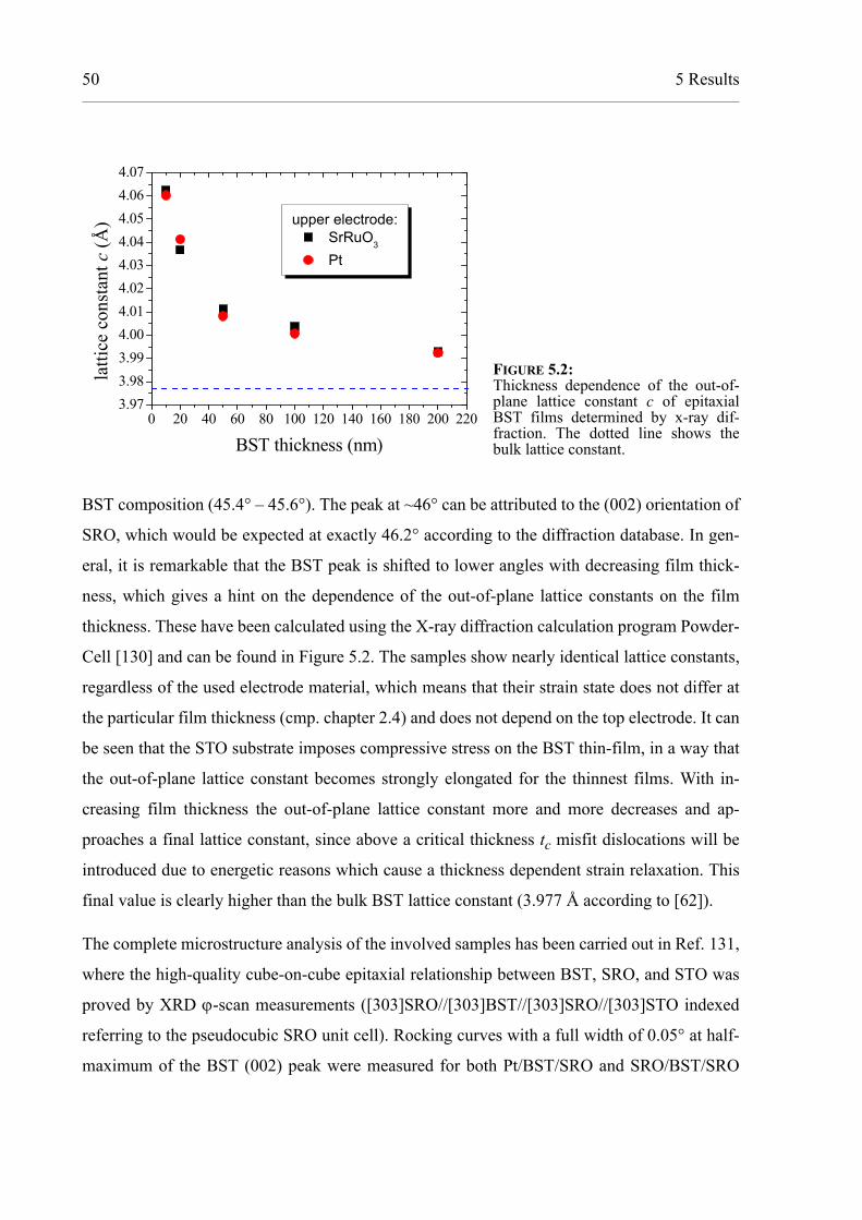
50 5 Results
BST composition (45.4° – 45.6°). The peak at ~46° can be attributed to the (002) orientation of
SRO, which would be expected at exactly 46.2° according to the diffraction database. In gen-
eral, it is remarkable that the BST peak is shifted to lower angles with decreasing film thick-
ness, which gives a hint on the dependence of the out-of-plane lattice constants on the film
thickness. These have been calculated using the X-ray diffraction calculation program Powder-
Cell [130] and can be found in Figure 5.2. The samples show nearly identical lattice constants,
regardless of the used electrode material, which means that their strain state does not differ at
the particular film thickness (cmp. chapter 2.4) and does not depend on the top electrode. It can
be seen that the STO substrate imposes compressive stress on the BST thin-film, in a way that
the out-of-plane lattice constant becomes strongly elongated for the thinnest films. With in-
creasing film thickness the out-of-plane lattice constant more and more decreases and ap-
proaches a final lattice constant, since above a critical thickness tc misfit dislocations will be
introduced due to energetic reasons which cause a thickness dependent strain relaxation. This
final value is clearly higher than the bulk BST lattice constant (3.977 Å according to [62]).
The complete microstructure analysis of the involved samples has been carried out in Ref. 131,
where the high-quality cube-on-cube epitaxial relationship between BST, SRO, and STO was
proved by XRD ϕ-scan measurements ([303]SRO//[303]BST//[303]SRO//[303]STO indexed
referring to the pseudocubic SRO unit cell). Rocking curves with a full width of 0.05° at half-
maximum of the BST (002) peak were measured for both Pt/BST/SRO and SRO/BST/SRO
0 20 40 60 80 100 120 140 160 180 200 2203.973.983.994.004.014.024.034.044.054.064.07
upper electrode: SrRuO3
Pt
latti
ce c
onst
ant c
(Å)
BST thickness (nm)
FIGURE 5.2:Thickness dependence of the out-of-plane lattice constant c of epitaxial BST films determined by x-ray dif-fraction. The dotted line shows the bulk lattice constant.
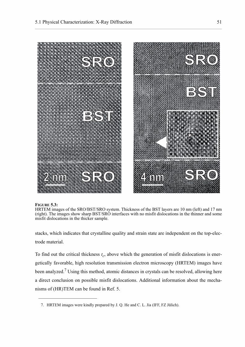
5.1 Physical Characterization: X-Ray Diffraction 51
stacks, which indicates that crystalline quality and strain state are independent on the top-elec-
trode material.
To find out the critical thickness tc, above which the generation of misfit dislocations is ener-
getically favorable, high resolution transmission electron microscopy (HRTEM) images have
been analyzed.7 Using this method, atomic distances in crystals can be resolved, allowing here
a direct conclusion on possible misfit dislocations. Additional information about the mecha-
nisms of (HR)TEM can be found in Ref. 5.
7. HRTEM images were kindly prepared by J. Q. He and C. L. Jia (IFF, FZ Jülich).
4 nm4 nm SROSRO
SROSRO
BSTBST
2 nm2 nm
SROSRO
SROSRO
BSTBST
FIGURE 5.3:HRTEM images of the SRO/BST/SRO system. Thickness of the BST layers are 10 nm (left) and 17 nm (right). The images show sharp BST/SRO interfaces with no misfit dislocations in the thinner and some misfit dislocations in the thicker sample.
52 5 Results
Examples of such images are shown in Figure 5.3: On the left, a sample with SRO top and bot-
tom electrode is presented, while the thickness of the BST layer could be determined to 10 nm.
The right image shows a similar sample with a BST thickness of 17 nm. The BST/SRO inter-
faces in both cases are very sharp and do not display secondary (mixed) phases. Remarkably,
there is no evidence of misfit dislocations in the thinner sample, while some misfit dislocations
can be found in the thicker sample (marked by arrows, see magnification included in the right
image). From these observations, the critical thickness can be approximated to
5.2 Electrical Characterization: Small Signal Response
Measurements of the small signal capacitance yield informations about the dielectric constant
of the ferroelectric material at various conditions. In principle, one finds the contributions of
the reversible polarization of the material under investigation, as has been investigated by Bol-
ten [132]. In order to measure the pure capacitance (that gives the permittivity), one has to
make sure that no polarization switching occurs which would falsify the measurements due to
switching currents. Thus, the amplitude of the excitation voltage has to be kept below the value
that allows for the polarization to be switched, or in other words: Small amplitudes of the exci-
tation field will only result in small reversible displacements of the domain walls inside the
material and reducing the amplitude of the excitation field results in a suppression of the irre-
versible displacements. The reversible capacitance according to Bolten is then defined as
where EAC denotes the amplitude of the oscillating small signal excitation that is used to deter-
mine the capacitance, and E depicts the applied bias field. Indeed, this is the best (theoretical)
method to determine the capacitance value of a device under test, but practically cannot be ap-
plied in real experiments: Since the measuring equipment as introduced in chapter 4.2.1 uses a
non-vanishing amplitude of the excitation voltage, the task will be to determine the small sig-
nal capacitance with sufficient precision even in the case of non-zero excitation levels.
tc 10 nm.≈ (5.1)
Crev E( ) C E EAC,( )EAC 0→
lim ,= (5.2)
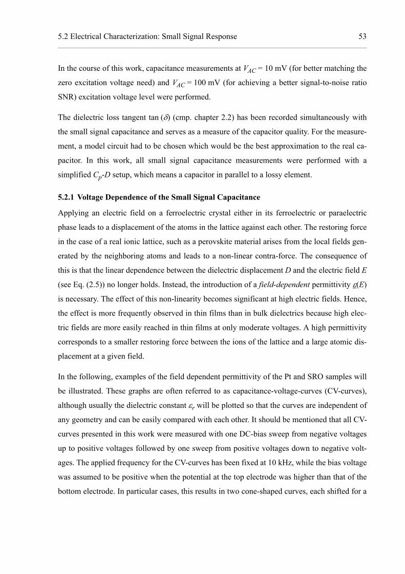
5.2 Electrical Characterization: Small Signal Response 53
In the course of this work, capacitance measurements at VAC = 10 mV (for better matching the
zero excitation voltage need) and VAC = 100 mV (for achieving a better signal-to-noise ratio
SNR) excitation voltage level were performed.
The dielectric loss tangent tan (δ) (cmp. chapter 2.2) has been recorded simultaneously with
the small signal capacitance and serves as a measure of the capacitor quality. For the measure-
ment, a model circuit had to be chosen which would be the best approximation to the real ca-
pacitor. In this work, all small signal capacitance measurements were performed with a
simplified Cp-D setup, which means a capacitor in parallel to a lossy element.
5.2.1 Voltage Dependence of the Small Signal Capacitance
Applying an electric field on a ferroelectric crystal either in its ferroelectric or paraelectric
phase leads to a displacement of the atoms in the lattice against each other. The restoring force
in the case of a real ionic lattice, such as a perovskite material arises from the local fields gen-
erated by the neighboring atoms and leads to a non-linear contra-force. The consequence of
this is that the linear dependence between the dielectric displacement D and the electric field E
(see Eq. (2.5)) no longer holds. Instead, the introduction of a field-dependent permittivity ε(E)
is necessary. The effect of this non-linearity becomes significant at high electric fields. Hence,
the effect is more frequently observed in thin films than in bulk dielectrics because high elec-
tric fields are more easily reached in thin films at only moderate voltages. A high permittivity
corresponds to a smaller restoring force between the ions of the lattice and a large atomic dis-
placement at a given field.
In the following, examples of the field dependent permittivity of the Pt and SRO samples will
be illustrated. These graphs are often referred to as capacitance-voltage-curves (CV-curves),
although usually the dielectric constant εr will be plotted so that the curves are independent of
any geometry and can be easily compared with each other. It should be mentioned that all CV-
curves presented in this work were measured with one DC-bias sweep from negative voltages
up to positive voltages followed by one sweep from positive voltages down to negative volt-
ages. The applied frequency for the CV-curves has been fixed at 10 kHz, while the bias voltage
was assumed to be positive when the potential at the top electrode was higher than that of the
bottom electrode. In particular cases, this results in two cone-shaped curves, each shifted for a
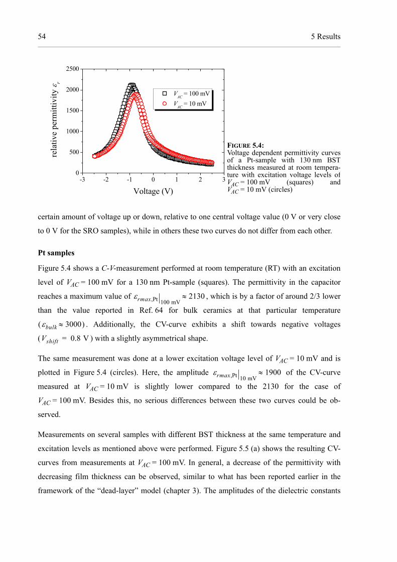
54 5 Results
certain amount of voltage up or down, relative to one central voltage value (0 V or very close
to 0 V for the SRO samples), while in others these two curves do not differ from each other.
Pt samples
Figure 5.4 shows a C-V-measurement performed at room temperature (RT) with an excitation
level of VAC = 100 mV for a 130 nm Pt-sample (squares). The permittivity in the capacitor
reaches a maximum value of , which is by a factor of around 2/3 lower
than the value reported in Ref. 64 for bulk ceramics at that particular temperature
. Additionally, the CV-curve exhibits a shift towards negative voltages
( ) with a slightly asymmetrical shape.
The same measurement was done at a lower excitation voltage level of VAC = 10 mV and is
plotted in Figure 5.4 (circles). Here, the amplitude of the CV-curve
measured at VAC = 10 mV is slightly lower compared to the 2130 for the case of
VAC = 100 mV. Besides this, no serious differences between these two curves could be ob-
served.
Measurements on several samples with different BST thickness at the same temperature and
excitation levels as mentioned above were performed. Figure 5.5 (a) shows the resulting CV-
curves from measurements at VAC = 100 mV. In general, a decrease of the permittivity with
decreasing film thickness can be observed, similar to what has been reported earlier in the
framework of the “dead-layer” model (chapter 3). The amplitudes of the dielectric constants
-3 -2 -1 0 1 2 30
500
1000
1500
2000
2500
rela
tive
perm
ittiv
ity ε r
Voltage (V)
VAC = 100 mV VAC = 10 mV
FIGURE 5.4:Voltage dependent permittivity curves of a Pt-sample with 130 nm BST thickness measured at room tempera-ture with excitation voltage levels of VAC = 100 mV (squares) and VAC = 10 mV (circles)
εrmax,Pt 100 mV2130≈
εbulk 3000≈( )
Vshift 0.8 V=
εrmax,Pt 10 mV1900≈
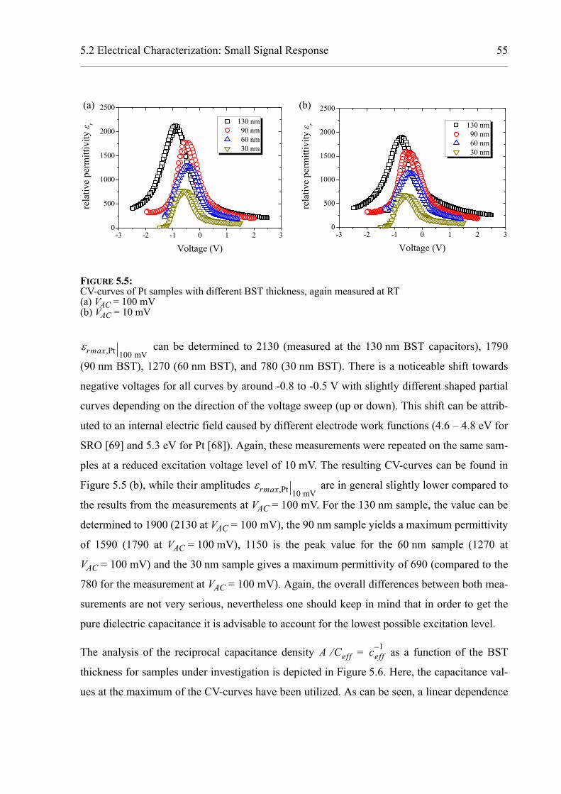
5.2 Electrical Characterization: Small Signal Response 55
can be determined to 2130 (measured at the 130 nm BST capacitors), 1790
(90 nm BST), 1270 (60 nm BST), and 780 (30 nm BST). There is a noticeable shift towards
negative voltages for all curves by around -0.8 to -0.5 V with slightly different shaped partial
curves depending on the direction of the voltage sweep (up or down). This shift can be attrib-
uted to an internal electric field caused by different electrode work functions (4.6 – 4.8 eV for
SRO [69] and 5.3 eV for Pt [68]). Again, these measurements were repeated on the same sam-
ples at a reduced excitation voltage level of 10 mV. The resulting CV-curves can be found in
Figure 5.5 (b), while their amplitudes are in general slightly lower compared to
the results from the measurements at VAC = 100 mV. For the 130 nm sample, the value can be
determined to 1900 (2130 at VAC = 100 mV), the 90 nm sample yields a maximum permittivity
of 1590 (1790 at VAC = 100 mV), 1150 is the peak value for the 60 nm sample (1270 at
VAC = 100 mV) and the 30 nm sample gives a maximum permittivity of 690 (compared to the
780 for the measurement at VAC = 100 mV). Again, the overall differences between both mea-
surements are not very serious, nevertheless one should keep in mind that in order to get the
pure dielectric capacitance it is advisable to account for the lowest possible excitation level.
The analysis of the reciprocal capacitance density as a function of the BST
thickness for samples under investigation is depicted in Figure 5.6. Here, the capacitance val-
ues at the maximum of the CV-curves have been utilized. As can be seen, a linear dependence
εrmax,Pt 100 mV
-3 -2 -1 0 1 2 30
500
1000
1500
2000
2500
rela
tive
perm
ittiv
ity ε r
Voltage (V)
130 nm 90 nm 60 nm 30 nm
FIGURE 5.5:CV-curves of Pt samples with different BST thickness, again measured at RT (a) VAC = 100 mV(b) VAC = 10 mV
-3 -2 -1 0 1 2 30
500
1000
1500
2000
2500
rela
tive
perm
ittiv
ity ε r
Voltage (V)
130 nm 90 nm 60 nm 30 nm
(a) (b)
εrmax,Pt 10 mV
A Ceff⁄ ceff1–=
56 5 Results
of (squared and round data markers in the graph) on the BST thickness t is valid for the Pt
samples, regardless of the used excitation voltage level. From a linear fit on these data points
one can find the core parameters εb and ci,total according to Eq. (3.1). While εb describes the
permittivity of a Pt sample with an infinitely thick BST layer (denoted here as the bulk permit-
tivity), ci,total can be regarded as the total capacitance density of the low permittivity interface
layer that has the same value in each sample irrespective of its actual BST thickness. Here, the
determined values for the permittivity are quite identical with and
, both exceeding the value found in Ref. 64 which was measured
on bulk ceramic samples. It is important to mention that due to a possible shift of the phase
transition (cmp. next sub-chapters), a comparison of permittivity values at constant tempera-
tures may result in a comparison of materials with different state, e.g. the material may be in its
FE state in one sample, whereas it may be in its PE state for another sample at the same tem-
perature. For the interface capacitance density, values of and
could be determined.
SRO Samples
Similar as for the Pt samples, measurements of CV-curves were also performed at the SRO
samples. An example of such a measurement is given in Figure 5.7. Here, the CV-curve from a
125 nm BST capacitor with epitaxial SRO top electrodes is shown, whereas the whole mea-
surement was performed at room temperature using an oscillation voltage level of
VAC = 100 mV (squares). The maximum value of the measured permittivity curve can be
0 20 40 60 80 100 120 1403.0
3.5
4.0
4.5
5.0
5.5
6.0
6.5
7.0
7.5
8.0
εb, Pt|10 mV = 4560
ci,total, Pt|10 mV = 0.23 F/m2
VAC = 100 mV VAC = 10 mV
c-1 eff (m
2 /F)
BST thickness (nm)
εb, Pt|100 mV = 4690
ci,total, Pt|100 mV = 0.27 F/m2
FIGURE 5.6:Thickness dependence of the recipro-cal capacitance density for the Pt sam-ples.
ceff1–
εb, Pt 100 mV4690≈
εb, Pt 10 mV4560≈ εb 3000≈
ci total, Pt, 100 mV0.27 F/m2=
ci total, Pt, 10 mV0.23 F/m2=
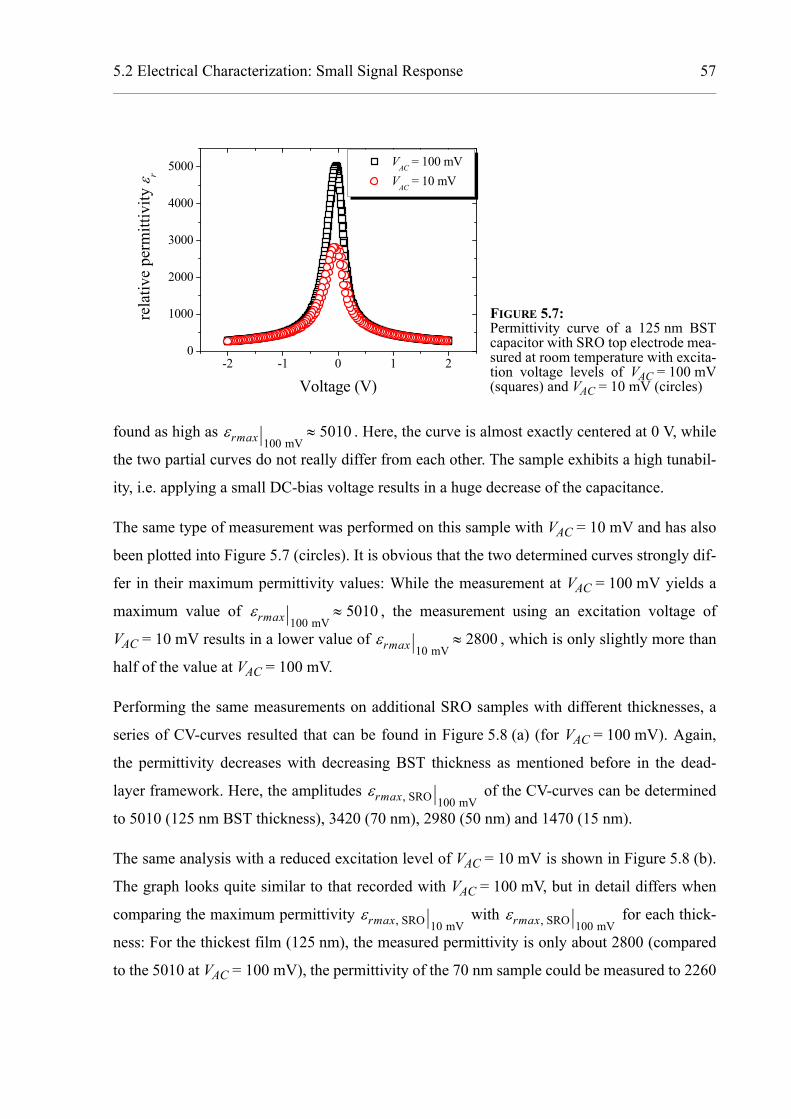
5.2 Electrical Characterization: Small Signal Response 57
found as high as . Here, the curve is almost exactly centered at 0 V, while
the two partial curves do not really differ from each other. The sample exhibits a high tunabil-
ity, i.e. applying a small DC-bias voltage results in a huge decrease of the capacitance.
The same type of measurement was performed on this sample with VAC = 10 mV and has also
been plotted into Figure 5.7 (circles). It is obvious that the two determined curves strongly dif-
fer in their maximum permittivity values: While the measurement at VAC = 100 mV yields a
maximum value of , the measurement using an excitation voltage of
VAC = 10 mV results in a lower value of , which is only slightly more than
half of the value at VAC = 100 mV.
Performing the same measurements on additional SRO samples with different thicknesses, a
series of CV-curves resulted that can be found in Figure 5.8 (a) (for VAC = 100 mV). Again,
the permittivity decreases with decreasing BST thickness as mentioned before in the dead-
layer framework. Here, the amplitudes of the CV-curves can be determined
to 5010 (125 nm BST thickness), 3420 (70 nm), 2980 (50 nm) and 1470 (15 nm).
The same analysis with a reduced excitation level of VAC = 10 mV is shown in Figure 5.8 (b).
The graph looks quite similar to that recorded with VAC = 100 mV, but in detail differs when
comparing the maximum permittivity with for each thick-
ness: For the thickest film (125 nm), the measured permittivity is only about 2800 (compared
to the 5010 at VAC = 100 mV), the permittivity of the 70 nm sample could be measured to 2260
εrmax 100 mV5010≈
εrmax 100 mV5010≈
εrmax 10 mV2800≈
-2 -1 0 1 20
1000
2000
3000
4000
5000 VAC = 100 mV VAC = 10 mV
rela
tive
perm
ittiv
ity ε r
Voltage (V)
FIGURE 5.7:Permittivity curve of a 125 nm BST capacitor with SRO top electrode mea-sured at room temperature with excita-tion voltage levels of VAC = 100 mV (squares) and VAC = 10 mV (circles)
εrmax, SRO 100 mV
εrmax, SRO 10 mVεrmax, SRO 100 mV
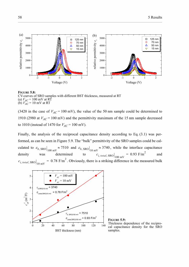
58 5 Results
(3420 in the case of VAC = 100 mV), the value of the 50 nm sample could be determined to
1910 (2980 at VAC = 100 mV) and the permittivity maximum of the 15 nm sample decreased
to 1010 (instead of 1470 for VAC = 100 mV).
Finally, the analysis of the reciprocal capacitance density according to Eq. (3.1) was per-
formed, as can be seen in Figure 5.9. The “bulk” permittivity of the SRO samples could be cal-
culated to and , while the interface capacitance
density was determined to and
. Obviously, there is a striking difference in the measured bulk
-2 -1 0 1 20
1000
2000
3000
4000
5000 125 nm 70 nm 50 nm 15 nm
rela
tive
perm
ittiv
ity ε r
Voltage (V)-2 -1 0 1 2
0
1000
2000
3000
4000
5000 125 nm 70 nm 50 nm 15 nm
rela
tive
perm
ittiv
ity ε r
Voltage (V)
FIGURE 5.8:CV-curves of SRO samples with different BST thickness, measured at RT(a) VAC = 100 mV at RT(b) VAC = 10 mV at RT
(a) (b)
0 20 40 60 80 100 120 1401
2
3
4
5 VAC = 100 mV VAC = 10 mV
εb,SRO|10 mV = 3740
ci,total,SRO|10 mV = 0.78 F/m2
εb, SRO|100 mV = 7510
ci,total,SRO|100 mV = 0.93 F/m2
c-1 eff (m
2 /F)
BST thickness (nm)
FIGURE 5.9:Thickness dependence of the recipro-cal capacitance density for the SRO samples.
εb, SRO 100 mV7510≈ εb, SRO 10 mV
3740≈
ci total, SRO, 100 mV0.93 F/m2=
ci total, SRO, 10 mV0.78 F/m2=
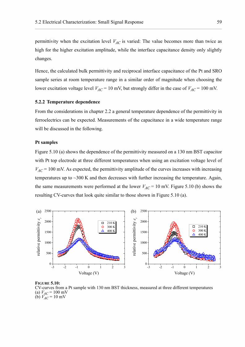
5.2 Electrical Characterization: Small Signal Response 59
permittivity when the excitation level VAC is varied: The value becomes more than twice as
high for the higher excitation amplitude, while the interface capacitance density only slightly
changes.
Hence, the calculated bulk permittivity and reciprocal interface capacitance of the Pt and SRO
sample series at room temperature range in a similar order of magnitude when choosing the
lower excitation voltage level VAC = 10 mV, but strongly differ in the case of VAC = 100 mV.
5.2.2 Temperature dependence
From the considerations in chapter 2.2 a general temperature dependence of the permittivity in
ferroelectrics can be expected. Measurements of the capacitance in a wide temperature range
will be discussed in the following.
Pt samples
Figure 5.10 (a) shows the dependence of the permittivity measured on a 130 nm BST capacitor
with Pt top electrode at three different temperatures when using an excitation voltage level of
VAC = 100 mV. As expected, the permittivity amplitude of the curves increases with increasing
temperatures up to ~300 K and then decreases with further increasing the temperature. Again,
the same measurements were performed at the lower VAC = 10 mV. Figure 5.10 (b) shows the
resulting CV-curves that look quite similar to those shown in Figure 5.10 (a).
-3 -2 -1 0 1 2 30
500
1000
1500
2000
2500
rela
tive
perm
ittiv
ity ε r
Voltage (V)
210 K 300 K 400 K
-3 -2 -1 0 1 2 30
500
1000
1500
2000
2500
rela
tive
perm
ittiv
ity ε r
Voltage (V)
210 K 300 K 400 K
FIGURE 5.10:CV-curves from a Pt sample with 130 nm BST thickness, measured at three different temperatures(a) VAC = 100 mV(b) VAC = 10 mV
(a) (b)
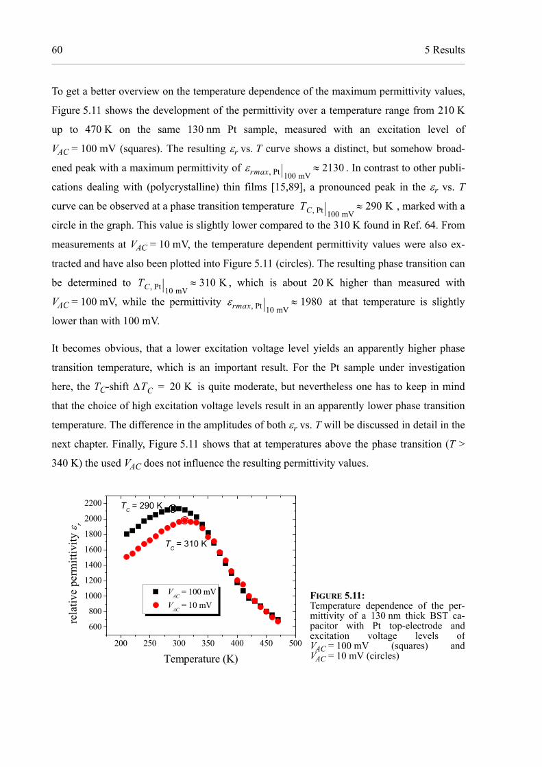
60 5 Results
To get a better overview on the temperature dependence of the maximum permittivity values,
Figure 5.11 shows the development of the permittivity over a temperature range from 210 K
up to 470 K on the same 130 nm Pt sample, measured with an excitation level of
VAC = 100 mV (squares). The resulting εr vs. T curve shows a distinct, but somehow broad-
ened peak with a maximum permittivity of . In contrast to other publi-
cations dealing with (polycrystalline) thin films [15,89], a pronounced peak in the εr vs. T
curve can be observed at a phase transition temperature , marked with a
circle in the graph. This value is slightly lower compared to the 310 K found in Ref. 64. From
measurements at VAC = 10 mV, the temperature dependent permittivity values were also ex-
tracted and have also been plotted into Figure 5.11 (circles). The resulting phase transition can
be determined to , which is about 20 K higher than measured with
VAC = 100 mV, while the permittivity at that temperature is slightly
lower than with 100 mV.
It becomes obvious, that a lower excitation voltage level yields an apparently higher phase
transition temperature, which is an important result. For the Pt sample under investigation
here, the TC-shift is quite moderate, but nevertheless one has to keep in mind
that the choice of high excitation voltage levels result in an apparently lower phase transition
temperature. The difference in the amplitudes of both εr vs. T will be discussed in detail in the
next chapter. Finally, Figure 5.11 shows that at temperatures above the phase transition (T >
340 K) the used VAC does not influence the resulting permittivity values.
εrmax, Pt 100 mV2130≈
TC, Pt 100 mV290 K≈
200 250 300 350 400 450 500
600
800
1000
1200
1400
1600
1800
2000
2200
TC = 310 K
TC = 290 K
VAC = 100 mV VAC = 10 mV
rela
tive
perm
ittiv
ity ε r
Temperature (K)
FIGURE 5.11:Temperature dependence of the per-mittivity of a 130 nm thick BST ca-pacitor with Pt top-electrode and excitation voltage levels of VAC = 100 mV (squares) and VAC = 10 mV (circles)
TC, Pt 10 mV310 K≈
εrmax, Pt 10 mV1980≈
ΔTC 20 K=
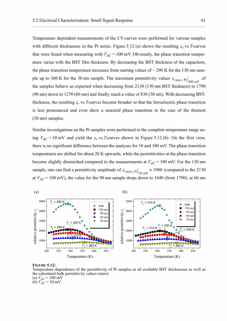
5.2 Electrical Characterization: Small Signal Response 61
Temperature dependent measurements of the CV-curves were performed for various samples
with different thicknesses in the Pt series. Figure 5.12 (a) shows the resulting εr vs T-curves
that were found when measuring with VAC = 100 mV. Obviously, the phase transition temper-
ature varies with the BST film thickness: By decreasing the BST thickness of the capacitors,
the phase transition temperature increases from starting values of ~ 290 K for the 130 nm sam-
ple up to 360 K for the 30 nm sample. The maximum permittivity values of
the samples behave as expected when decreasing from 2130 (130 nm BST thickness) to 1790
(90 nm) down to 1270 (60 nm) and finally reach a value of 830 (30 nm). With decreasing BST-
thickness, the resulting εr vs T-curves become broader so that the ferroelectric phase transition
is less pronounced and even show a smeared phase transition in the case of the thinnest
(30 nm) samples.
Similar investigations on the Pt samples were performed in the complete temperature range us-
ing VAC = 10 mV and yield the εr vs T-curves shown in Figure 5.12 (b). On the first view,
there is no significant difference between the analyses for 10 and 100 mV. The phase transition
temperatures are shifted for about 20 K upwards, while the permittivities at the phase transition
become slightly diminished compared to the measurements at VAC = 100 mV: For the 130 nm
sample, one can find a permittivity amplitude of (compared to the 2130
at VAC = 100 mV), the value for the 90 nm sample drops down to 1640 (from 1790), at 60 nm
FIGURE 5.12:Temperature dependence of the permittivity of Pt samples at all available BST thicknesses as well as the calculated bulk permittivity values (stars).(a) VAC = 100 mV(b) VAC = 10 mV
(a) (b)
200 250 300 350 400 450
1000
2000
3000
4000
5000 TC = 290 K
TC = 300 K
TC = 310 K
TC = 360 K
TC = 290 K
bulk 130 nm 90 nm 60 nm 30 nm
rela
tive
perm
ittiv
ity ε r
Temperature (K)200 250 300 350 400 450
1000
2000
3000
4000
5000
TC = 310 KTC = 330 K
TC = 340 K
TC = 380 K
TC = 310 K bulk 130 nm 90 nm 60 nm 30 nm
rela
tive
perm
ittiv
ity ε r
Temperature (K)
εrmax, Pt 100 mV
εrmax, Pt 10 mV1980≈
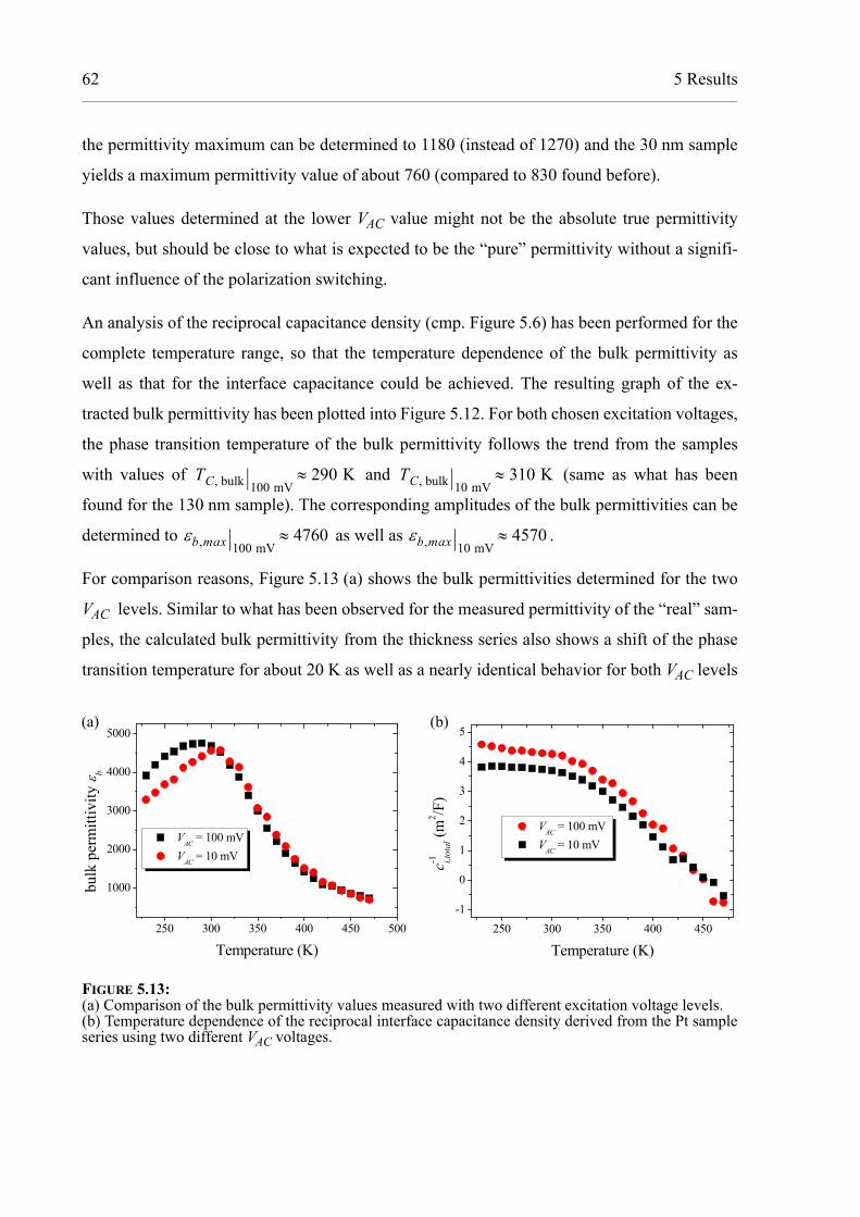
62 5 Results
the permittivity maximum can be determined to 1180 (instead of 1270) and the 30 nm sample
yields a maximum permittivity value of about 760 (compared to 830 found before).
Those values determined at the lower VAC value might not be the absolute true permittivity
values, but should be close to what is expected to be the “pure” permittivity without a signifi-
cant influence of the polarization switching.
An analysis of the reciprocal capacitance density (cmp. Figure 5.6) has been performed for the
complete temperature range, so that the temperature dependence of the bulk permittivity as
well as that for the interface capacitance could be achieved. The resulting graph of the ex-
tracted bulk permittivity has been plotted into Figure 5.12. For both chosen excitation voltages,
the phase transition temperature of the bulk permittivity follows the trend from the samples
with values of and (same as what has been
found for the 130 nm sample). The corresponding amplitudes of the bulk permittivities can be
determined to as well as .
For comparison reasons, Figure 5.13 (a) shows the bulk permittivities determined for the two
VAC levels. Similar to what has been observed for the measured permittivity of the “real” sam-
ples, the calculated bulk permittivity from the thickness series also shows a shift of the phase
transition temperature for about 20 K as well as a nearly identical behavior for both VAC levels
TC, bulk 100 mV290 K≈ TC, bulk 10 mV
310 K≈
εb,max 100 mV4760≈ εb,max 10 mV
4570≈
250 300 350 400 450 500
1000
2000
3000
4000
5000
VAC = 100 mV VAC = 10 mV
bulk
per
mitt
ivity
ε b
Temperature (K)
FIGURE 5.13:(a) Comparison of the bulk permittivity values measured with two different excitation voltage levels.(b) Temperature dependence of the reciprocal interface capacitance density derived from the Pt sample series using two different VAC voltages.
250 300 350 400 450-1
0
1
2
3
4
5
VAC = 100 mV VAC = 10 mV
c-1 i,tot
al (m
2 /F)
Temperature (K)
(a) (b)
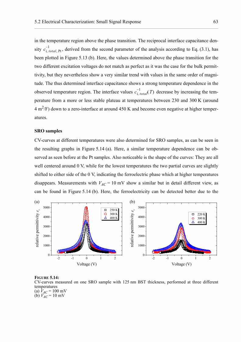
5.2 Electrical Characterization: Small Signal Response 63
in the temperature region above the phase transition. The reciprocal interface capacitance den-
sity , derived from the second parameter of the analysis according to Eq. (3.1), has
been plotted in Figure 5.13 (b). Here, the values determined above the phase transition for the
two different excitation voltages do not match as perfect as it was the case for the bulk permit-
tivity, but they nevertheless show a very similar trend with values in the same order of magni-
tude. The thus determined interface capacitance shows a strong temperature dependence in the
observed temperature region. The interface values decrease by increasing the tem-
perature from a more or less stable plateau at temperatures between 230 and 300 K (around
4 m2/F) down to a zero-interface at around 450 K and become even negative at higher temper-
atures.
SRO samples
CV-curves at different temperatures were also determined for SRO samples, as can be seen in
the resulting graphs in Figure 5.14 (a). Here, a similar temperature dependence can be ob-
served as seen before at the Pt samples. Also noticeable is the shape of the curves: They are all
well centered around 0 V, while for the lowest temperatures the two partial curves are slightly
shifted to either side of the 0 V, indicating the ferroelectric phase which at higher temperatures
disappears. Measurements with VAC = 10 mV show a similar but in detail different view, as
can be found in Figure 5.14 (b). Here, the ferroelectricity can be detected better due to the
ci total, Pt,1–
ci total,1– T( )
-2 -1 0 1 20
1000
2000
3000
4000
5000
rela
tive
perm
ittiv
ity ε r
Voltage (V)
250 K 300 K 400 K
-2 -1 0 1 20
1000
2000
3000
4000
5000
rela
tive
perm
ittiv
ity ε r
Voltage (V)
220 K 300 K 400 K
FIGURE 5.14:CV-curves measured on one SRO sample with 125 nm BST thickness, performed at three different temperatures (a) VAC = 100 mV(b) VAC = 10 mV
(a) (b)
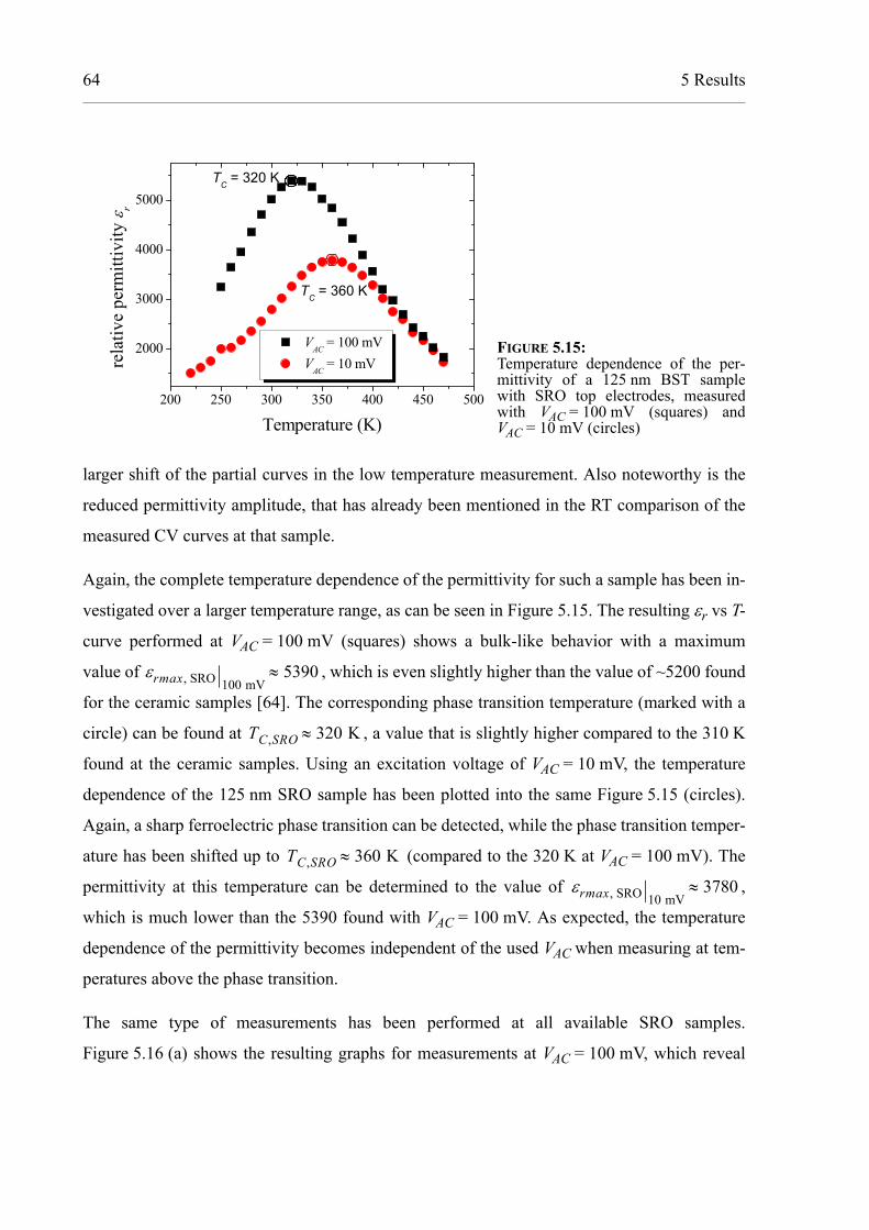
64 5 Results
larger shift of the partial curves in the low temperature measurement. Also noteworthy is the
reduced permittivity amplitude, that has already been mentioned in the RT comparison of the
measured CV curves at that sample.
Again, the complete temperature dependence of the permittivity for such a sample has been in-
vestigated over a larger temperature range, as can be seen in Figure 5.15. The resulting εr vs T-
curve performed at VAC = 100 mV (squares) shows a bulk-like behavior with a maximum
value of , which is even slightly higher than the value of ~5200 found
for the ceramic samples [64]. The corresponding phase transition temperature (marked with a
circle) can be found at , a value that is slightly higher compared to the 310 K
found at the ceramic samples. Using an excitation voltage of VAC = 10 mV, the temperature
dependence of the 125 nm SRO sample has been plotted into the same Figure 5.15 (circles).
Again, a sharp ferroelectric phase transition can be detected, while the phase transition temper-
ature has been shifted up to (compared to the 320 K at VAC = 100 mV). The
permittivity at this temperature can be determined to the value of ,
which is much lower than the 5390 found with VAC = 100 mV. As expected, the temperature
dependence of the permittivity becomes independent of the used VAC when measuring at tem-
peratures above the phase transition.
The same type of measurements has been performed at all available SRO samples.
Figure 5.16 (a) shows the resulting graphs for measurements at VAC = 100 mV, which reveal
εrmax, SRO 100 mV5390≈
TC,SRO 320 K≈
200 250 300 350 400 450 500
2000
3000
4000
5000
TC = 360 K
TC = 320 K
VAC = 100 mV VAC = 10 mVre
lativ
e pe
rmitt
ivity
ε r
Temperature (K)
FIGURE 5.15:Temperature dependence of the per-mittivity of a 125 nm BST sample with SRO top electrodes, measured with VAC = 100 mV (squares) and VAC = 10 mV (circles)
TC,SRO 360 K≈
εrmax, SRO 10 mV3780≈
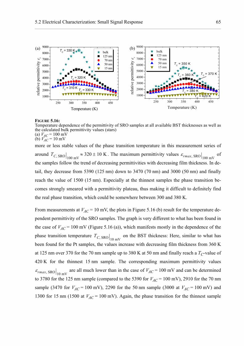
5.2 Electrical Characterization: Small Signal Response 65
more or less stable values of the phase transition temperature in this measurement series of
around . The maximum permittivity values of
the samples follow the trend of decreasing permittivities with decreasing film thickness. In de-
tail, they decrease from 5390 (125 nm) down to 3470 (70 nm) and 3000 (50 nm) and finally
reach the value of 1500 (15 nm). Especially at the thinnest samples the phase transition be-
comes strongly smeared with a permittivity plateau, thus making it difficult to definitely find
the real phase transition, which could be somewhere between 300 and 380 K.
From measurements at VAC = 10 mV, the plots in Figure 5.16 (b) result for the temperature de-
pendent permittivity of the SRO samples. The graph is very different to what has been found in
the case of VAC = 100 mV (Figure 5.16 (a)), which manifests mostly in the dependence of the
phase transition temperature on the BST thickness: Here, similar to what has
been found for the Pt samples, the values increase with decreasing film thickness from 360 K
at 125 nm over 370 for the 70 nm sample up to 380 K at 50 nm and finally reach a TC-value of
420 K for the thinnest 15 nm sample. The corresponding maximum permittivity values
are all much lower than in the case of VAC = 100 mV and can be determined
to 3780 for the 125 nm sample (compared to the 5390 for VAC = 100 mV), 2910 for the 70 nm
sample (3470 for VAC = 100 mV), 2290 for the 50 nm sample (3000 at VAC = 100 mV) and
1300 for 15 nm (1500 at VAC = 100 mV). Again, the phase transition for the thinnest sample
250 300 350 400 450
1000
2000
3000
4000
5000
6000
7000
8000
9000
TC = 350 K
TC = 420 K
TC = 370 KTC = 360 K
TC = 380 K
bulk 125 nm 70 nm 50 nm 15 nm
rela
tive
perm
ittiv
ity ε r
Temperature (K)250 300 350 400 450
1000
2000
3000
4000
5000
6000
7000
8000
9000
TC = 330 K
TC = 330 KTC = 310 K
TC = 320 K
bulk 125 nm 70 nm 50 nm 15 nm
rela
tive
perm
ittiv
ity ε r
Temperature (K)
FIGURE 5.16:Temperature dependence of the permittivity of SRO samples at all available BST thicknesses as well as the calculated bulk permittivity values (stars)(a) VAC = 100 mV(b) VAC = 10 mV
(a) (b)
TC, SRO 100 mV320 10 K±≈ εrmax, SRO 100 mV
TC, SRO 10 mV
εrmax, SRO 10 mV
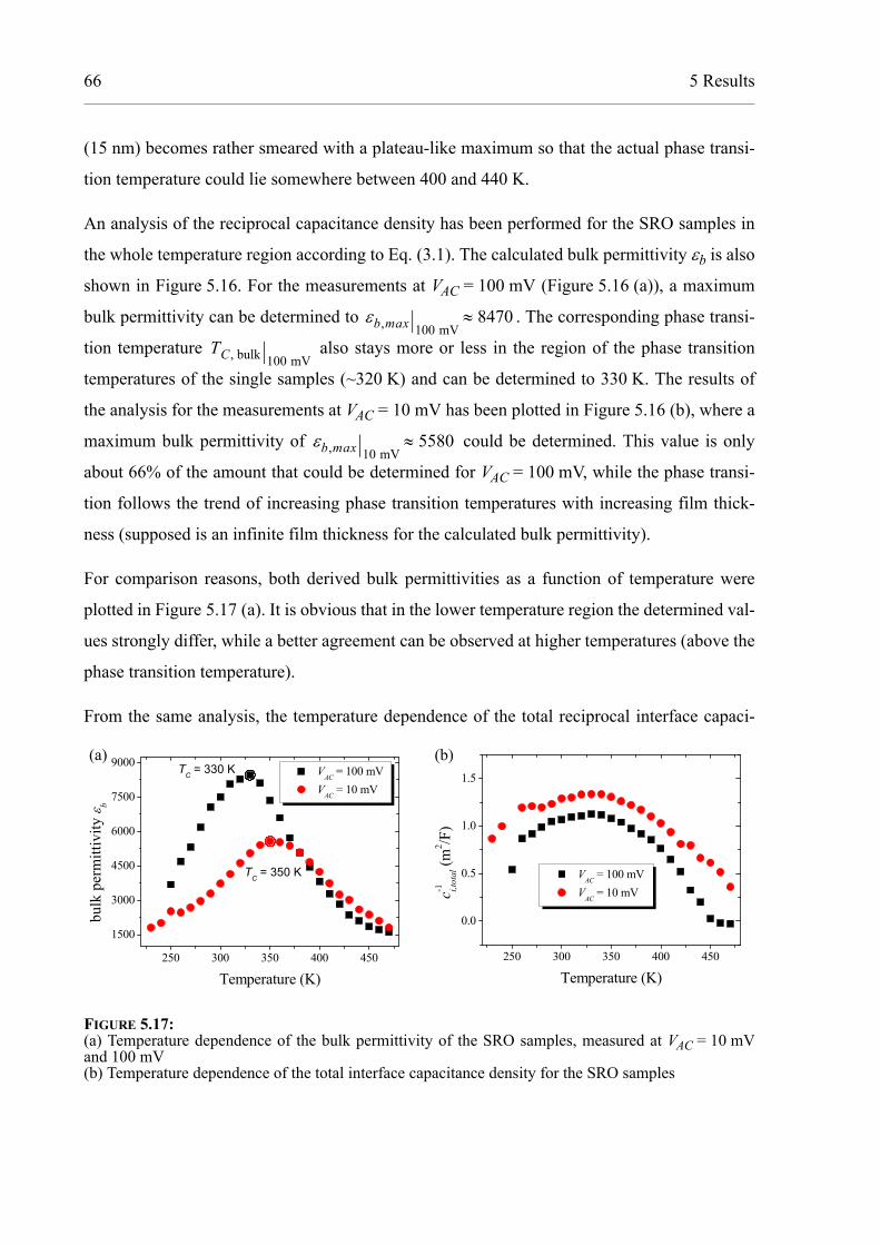
66 5 Results
(15 nm) becomes rather smeared with a plateau-like maximum so that the actual phase transi-
tion temperature could lie somewhere between 400 and 440 K.
An analysis of the reciprocal capacitance density has been performed for the SRO samples in
the whole temperature region according to Eq. (3.1). The calculated bulk permittivity εb is also
shown in Figure 5.16. For the measurements at VAC = 100 mV (Figure 5.16 (a)), a maximum
bulk permittivity can be determined to . The corresponding phase transi-
tion temperature also stays more or less in the region of the phase transition
temperatures of the single samples (~320 K) and can be determined to 330 K. The results of
the analysis for the measurements at VAC = 10 mV has been plotted in Figure 5.16 (b), where a
maximum bulk permittivity of could be determined. This value is only
about 66% of the amount that could be determined for VAC = 100 mV, while the phase transi-
tion follows the trend of increasing phase transition temperatures with increasing film thick-
ness (supposed is an infinite film thickness for the calculated bulk permittivity).
For comparison reasons, both derived bulk permittivities as a function of temperature were
plotted in Figure 5.17 (a). It is obvious that in the lower temperature region the determined val-
ues strongly differ, while a better agreement can be observed at higher temperatures (above the
phase transition temperature).
From the same analysis, the temperature dependence of the total reciprocal interface capaci-
εb,max 100 mV8470≈
TC, bulk 100 mV
εb,max 10 mV5580≈
250 300 350 400 450
1500
3000
4500
6000
7500
9000 TC = 330 K
TC = 350 K
VAC = 100 mV VAC = 10 mV
bulk
per
mitt
ivity
ε b
Temperature (K)
FIGURE 5.17:(a) Temperature dependence of the bulk permittivity of the SRO samples, measured at VAC = 10 mV and 100 mV(b) Temperature dependence of the total interface capacitance density for the SRO samples
250 300 350 400 450
0.0
0.5
1.0
1.5
VAC = 100 mV VAC = 10 mVc-1 i,t
otal (m
2 /F)
Temperature (K)
(a) (b)
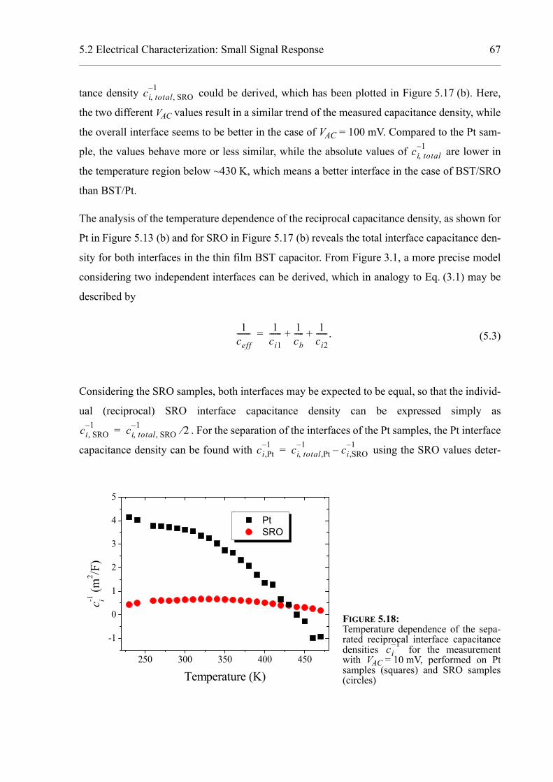
5.2 Electrical Characterization: Small Signal Response 67
tance density could be derived, which has been plotted in Figure 5.17 (b). Here,
the two different VAC values result in a similar trend of the measured capacitance density, while
the overall interface seems to be better in the case of VAC = 100 mV. Compared to the Pt sam-
ple, the values behave more or less similar, while the absolute values of are lower in
the temperature region below ~430 K, which means a better interface in the case of BST/SRO
than BST/Pt.
The analysis of the temperature dependence of the reciprocal capacitance density, as shown for
Pt in Figure 5.13 (b) and for SRO in Figure 5.17 (b) reveals the total interface capacitance den-
sity for both interfaces in the thin film BST capacitor. From Figure 3.1, a more precise model
considering two independent interfaces can be derived, which in analogy to Eq. (3.1) may be
described by
Considering the SRO samples, both interfaces may be expected to be equal, so that the individ-
ual (reciprocal) SRO interface capacitance density can be expressed simply as
. For the separation of the interfaces of the Pt samples, the Pt interface
capacitance density can be found with using the SRO values deter-
ci total, SRO,1–
ci total,1–
250 300 350 400 450
-1
0
1
2
3
4
5
Pt SRO
c-1 i (m
2 /F)
Temperature (K)
FIGURE 5.18:Temperature dependence of the sepa-rated reciprocal interface capacitance densities for the measurement with VAC = 10 mV, performed on Pt samples (squares) and SRO samples (circles)
ci1–
1ceff------- 1
ci1------ 1
cb----- 1
ci2------.+ += (5.3)
ci, SRO1– ci total, SRO,
1– 2⁄=
ci,Pt1– ci total,Pt,
1– ci,SRO1––=
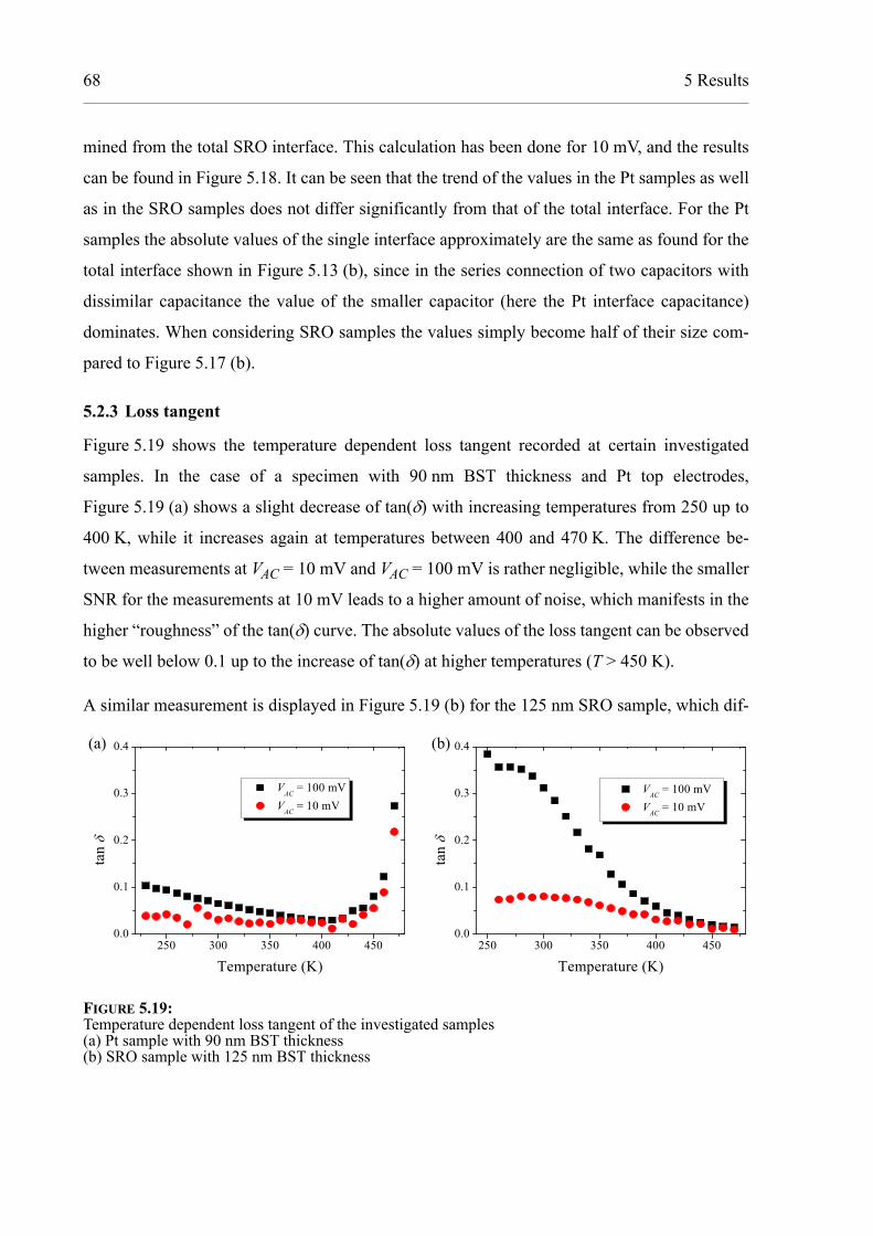
68 5 Results
mined from the total SRO interface. This calculation has been done for 10 mV, and the results
can be found in Figure 5.18. It can be seen that the trend of the values in the Pt samples as well
as in the SRO samples does not differ significantly from that of the total interface. For the Pt
samples the absolute values of the single interface approximately are the same as found for the
total interface shown in Figure 5.13 (b), since in the series connection of two capacitors with
dissimilar capacitance the value of the smaller capacitor (here the Pt interface capacitance)
dominates. When considering SRO samples the values simply become half of their size com-
pared to Figure 5.17 (b).
5.2.3 Loss tangent
Figure 5.19 shows the temperature dependent loss tangent recorded at certain investigated
samples. In the case of a specimen with 90 nm BST thickness and Pt top electrodes,
Figure 5.19 (a) shows a slight decrease of tan(δ) with increasing temperatures from 250 up to
400 K, while it increases again at temperatures between 400 and 470 K. The difference be-
tween measurements at VAC = 10 mV and VAC = 100 mV is rather negligible, while the smaller
SNR for the measurements at 10 mV leads to a higher amount of noise, which manifests in the
higher “roughness” of the tan(δ) curve. The absolute values of the loss tangent can be observed
to be well below 0.1 up to the increase of tan(δ) at higher temperatures (T > 450 K).
A similar measurement is displayed in Figure 5.19 (b) for the 125 nm SRO sample, which dif-
250 300 350 400 4500.0
0.1
0.2
0.3
0.4
VAC = 100 mV VAC = 10 mV
tan
δ
Temperature (K)250 300 350 400 450
0.0
0.1
0.2
0.3
0.4
VAC = 100 mV VAC = 10 mV
tan
δ
Temperature (K)
FIGURE 5.19:Temperature dependent loss tangent of the investigated samples(a) Pt sample with 90 nm BST thickness(b) SRO sample with 125 nm BST thickness
(a) (b)
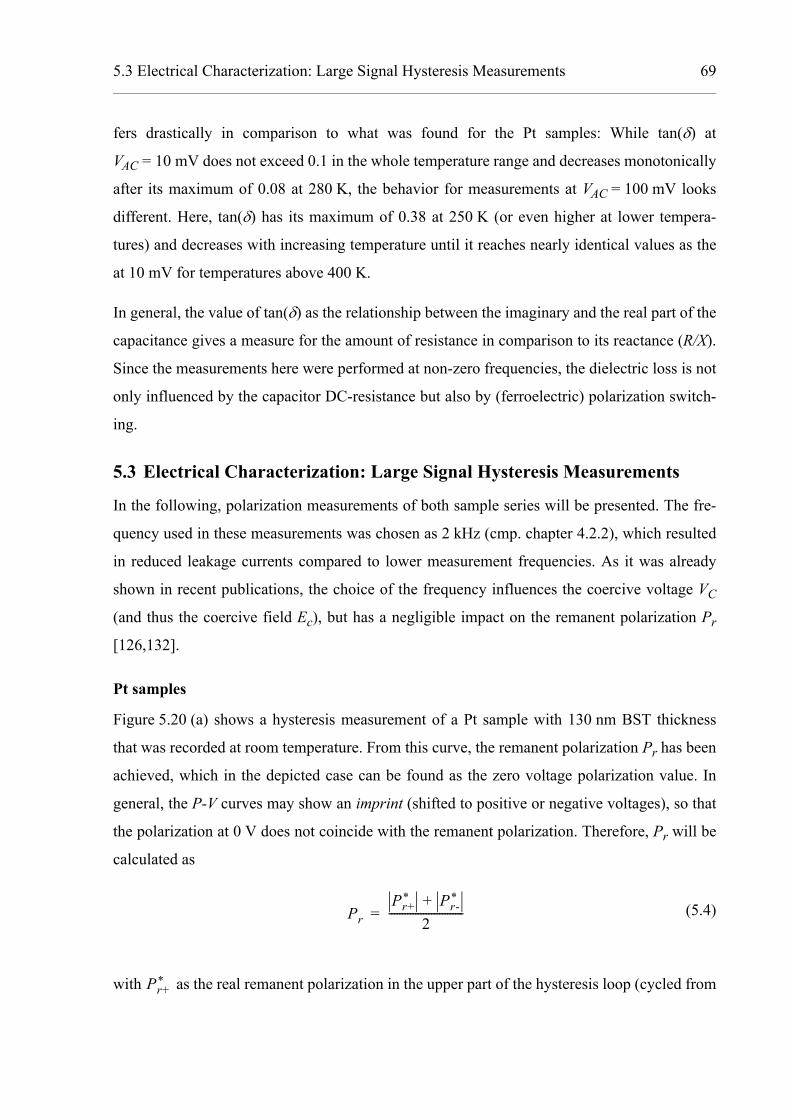
5.3 Electrical Characterization: Large Signal Hysteresis Measurements 69
fers drastically in comparison to what was found for the Pt samples: While tan(δ) at
VAC = 10 mV does not exceed 0.1 in the whole temperature range and decreases monotonically
after its maximum of 0.08 at 280 K, the behavior for measurements at VAC = 100 mV looks
different. Here, tan(δ) has its maximum of 0.38 at 250 K (or even higher at lower tempera-
tures) and decreases with increasing temperature until it reaches nearly identical values as the
at 10 mV for temperatures above 400 K.
In general, the value of tan(δ) as the relationship between the imaginary and the real part of the
capacitance gives a measure for the amount of resistance in comparison to its reactance (R/X).
Since the measurements here were performed at non-zero frequencies, the dielectric loss is not
only influenced by the capacitor DC-resistance but also by (ferroelectric) polarization switch-
ing.
5.3 Electrical Characterization: Large Signal Hysteresis Measurements
In the following, polarization measurements of both sample series will be presented. The fre-
quency used in these measurements was chosen as 2 kHz (cmp. chapter 4.2.2), which resulted
in reduced leakage currents compared to lower measurement frequencies. As it was already
shown in recent publications, the choice of the frequency influences the coercive voltage VC
(and thus the coercive field Ec), but has a negligible impact on the remanent polarization Pr
[126,132].
Pt samples
Figure 5.20 (a) shows a hysteresis measurement of a Pt sample with 130 nm BST thickness
that was recorded at room temperature. From this curve, the remanent polarization Pr has been
achieved, which in the depicted case can be found as the zero voltage polarization value. In
general, the P-V curves may show an imprint (shifted to positive or negative voltages), so that
the polarization at 0 V does not coincide with the remanent polarization. Therefore, Pr will be
calculated as
with as the real remanent polarization in the upper part of the hysteresis loop (cycled from
PrPr+
* Pr-*+
2----------------------------= (5.4)
Pr+*
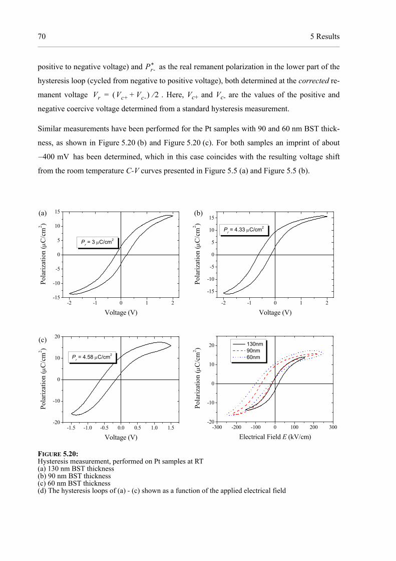
70 5 Results
positive to negative voltage) and as the real remanent polarization in the lower part of the
hysteresis loop (cycled from negative to positive voltage), both determined at the corrected re-
manent voltage . Here, Vc+ and Vc- are the values of the positive and
negative coercive voltage determined from a standard hysteresis measurement.
Similar measurements have been performed for the Pt samples with 90 and 60 nm BST thick-
ness, as shown in Figure 5.20 (b) and Figure 5.20 (c). For both samples an imprint of about
has been determined, which in this case coincides with the resulting voltage shift
from the room temperature C-V curves presented in Figure 5.5 (a) and Figure 5.5 (b).
-1.5 -1.0 -0.5 0.0 0.5 1.0 1.5-20
-10
0
10
20
Pola
rizat
ion
(μC
/cm
2 )
Voltage (V)
Pr = 4.58 μC/cm2
-2 -1 0 1 2-15
-10
-5
0
5
10
15
Pola
rizat
ion
(μC
/cm
2 )
Voltage (V)
Pr = 3 μC/cm2
FIGURE 5.20:Hysteresis measurement, performed on Pt samples at RT(a) 130 nm BST thickness(b) 90 nm BST thickness(c) 60 nm BST thickness(d) The hysteresis loops of (a) - (c) shown as a function of the applied electrical field
-2 -1 0 1 2
-15
-10
-5
0
5
10
15
Po
lariz
atio
n (μ
C/c
m2 )
Voltage (V)
Pr = 4.33 μC/cm2
(a) (b)
(c) (d)
-300 -200 -100 0 100 200 300-20
-10
0
10
20 130nm 90nm 60nm
Pola
rizat
ion
(μC
/cm
2 )
Electrical Field E (kV/cm)
Pr-*
Vr Vc+ Vc-+( ) 2⁄=
400 mV–
5.3 Electrical Characterization: Large Signal Hysteresis Measurements 71
The presented hysteresis curves in Figure 5.20 (b) and Figure 5.20 (c) result in an apparent re-
manent polarization value of . However, from the P-V loop of the
60 nm sample in Figure 5.20 (c) it can be assumed that this value is falsified strongly by leak-
age currents, since the curves at the maximum (and minimum) bias voltage are not as tapered
as expected. In contrast, the loop in Figure 5.20 (b), determined from the 90 nm sample still
looks rather free from strong leakage currents, which makes this Pr value more reliable.
Figure 5.20 (d) shows all three aforementioned hysteresis loops in one diagram as a function of
the applied electrical field. Notably, the coercive field increases with decreasing thickness of
the BST film, which has been already reported in previous publications [133].
The thinnest sample (30 nm) did not allow the measurement of meaningful hysteresis loops
due to its strong leakage currents which made it impossible to conclude on the ferroelectricity
of this sample.
Pr 4.3 .. 4.6 μC/cm2≈
-2 -1 0 1 2
-15
-10
-5
0
5
10
15 270 K 360 K 300 K 400 K 330 K 470 K
increasing T
Pola
rizat
ion
(μC
/cm
2 )
Voltage (V)
increasing T
-1.5 -1.0 -0.5 0.0 0.5 1.0 1.5-20
-10
0
10
20
270 K 360 K 300 K 400 K 330 K 470 K
increasing T
increasing T
Pola
rizat
ion
(μC
/cm
2 )
Voltage (V)
-2 -1 0 1 2-20
-10
0
10
20
270 K 360 K 300 K 400 K 330 K 470 K
increasing T
increasing T
Pola
rizat
ion
(μC
/cm
2 )
Voltage (V)
FIGURE 5.21:Hysteresis loops, recorded at various temperatures: (a) 130 nm Pt sample(b) 90 nm Pt sample(c) 60 nm Pt sample
(a) (b)
(c)
72 5 Results
For the three thicker Pt samples (130, 90 & 60 nm BST thickness), hysteresis loops have been
recorded also at various temperatures. Figure 5.21 shows the achieved P-V curves, which yield
some remarkable results. For all samples under investigation, the maximum polarization value
decreases with increasing temperature, as marked by the arrows. For the 130 nm sample
(Figure 5.21 (a)), it can be seen that the coercive voltage did not change significantly with tem-
perature, while the remanent polarization at that sample gradually decreases. The curves be-
come more and more slanted by increasing the temperature and show broader ends, which
indicates an increase of the leakage currents in the sample.
The temperature dependence of the hysteresis curves of the 90 and 60 nm samples is slightly
different to what has been found for the 130 nm sample (Figure 5.21 (b) and (c)). Here, the
curves show a shift of their coercive voltage by increasing the temperature due to their larger
imprint, while the remanent polarization decreases as seen from the 130 nm sample. These
curves also become slanted, while the leakage current seems to increase stronger than in the
case of the 130 nm sample.
In general, it seems that the samples (partly) keep their ferroelectric state even at temperatures
above their phase transition, determined from the temperature dependent small signal capaci-
tance measurements of chapter 5.2.2.
SRO samples
Measurements of the ferroelectric hysteresis were also performed for the SRO samples and are
presented in Figure 5.22. The remanent polarization values Pr decrease with decreasing BST
thickness from 9.9 μC/cm2 for the 125 nm sample over 9.24 μC/cm2 for the 70 nm sample
down to 7.76 μC/cm2 measured at the 50 nm sample. This trend is opposite to what has been
found for the Pt samples. The quality of the hysteresis loops seems to be satisfying, but one has
to keep in mind that there was no chance to apply higher voltages on the thinner samples (70 &
50 nm) without generating large leakage currents. Thus, the curves appear to be slightly
opened in the negative voltage region. Figure 5.22 (d) shows the hysteresis loops of the three
samples all plotted in one diagram as a function of the applied electrical field. As it could be
seen for Pt (Figure 5.20 (d)), again an increase of the coercive field with decreasing BST thick-
ness is observable.
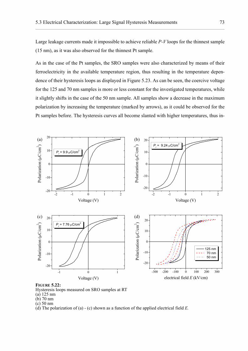
5.3 Electrical Characterization: Large Signal Hysteresis Measurements 73
Large leakage currents made it impossible to achieve reliable P-V loops for the thinnest sample
(15 nm), as it was also observed for the thinnest Pt sample.
As in the case of the Pt samples, the SRO samples were also characterized by means of their
ferroelectricity in the available temperature region, thus resulting in the temperature depen-
dence of their hysteresis loops as displayed in Figure 5.23. As can be seen, the coercive voltage
for the 125 and 70 nm samples is more or less constant for the investigated temperatures, while
it slightly shifts in the case of the 50 nm sample. All samples show a decrease in the maximum
polarization by increasing the temperature (marked by arrows), as it could be observed for the
Pt samples before. The hysteresis curves all become slanted with higher temperatures, thus in-
-2 -1 0 1 2-20
-10
0
10
20
Pola
rizat
ion
(μC
/cm
2 )
Voltage (V)
Pr = 9.9 μC/cm2
-1 0 1
-20
-10
0
10
20
Pola
rizat
ion
(μC
/cm
2 )
Voltage (V)
Pr = 7.76 μC/cm2
-2 -1 0 1 2
-20
-10
0
10
20
Po
lariz
atio
n (μ
C/c
m2 )
Voltage (V)
Pr = 9.24 μC/cm2
FIGURE 5.22:Hysteresis loops measured on SRO samples at RT(a) 125 nm(b) 70 nm(c) 50 nm(d) The polarization of (a) - (c) shown as a function of the applied electrical field E.
(a) (b)
(c)
-300 -200 -100 0 100 200 300
-20
-10
0
10
20
125 nm 70 nm 50 nm
Pola
rizat
ion
(μC
/cm
2 )
electrical field E (kV/cm)
(d)
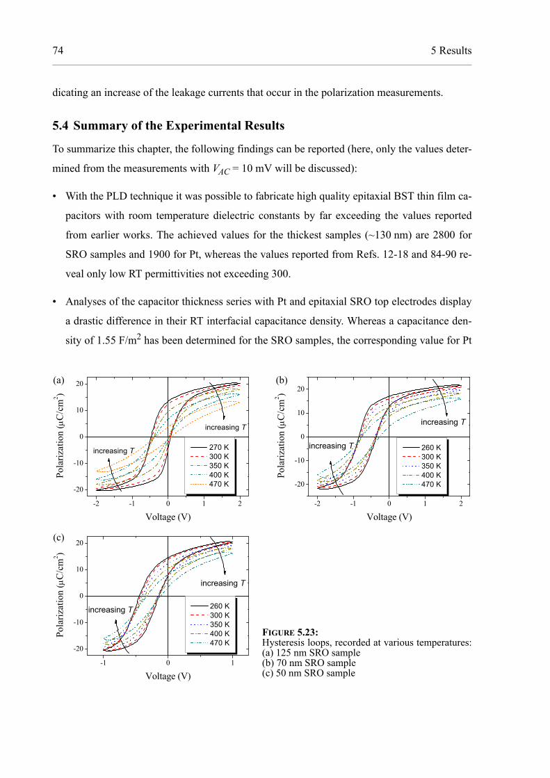
74 5 Results
dicating an increase of the leakage currents that occur in the polarization measurements.
5.4 Summary of the Experimental Results
To summarize this chapter, the following findings can be reported (here, only the values deter-
mined from the measurements with VAC = 10 mV will be discussed):
• With the PLD technique it was possible to fabricate high quality epitaxial BST thin film ca-
pacitors with room temperature dielectric constants by far exceeding the values reported
from earlier works. The achieved values for the thickest samples (~130 nm) are 2800 for
SRO samples and 1900 for Pt, whereas the values reported from Refs. 12-18 and 84-90 re-
veal only low RT permittivities not exceeding 300.
• Analyses of the capacitor thickness series with Pt and epitaxial SRO top electrodes display
a drastic difference in their RT interfacial capacitance density. Whereas a capacitance den-
sity of 1.55 F/m2 has been determined for the SRO samples, the corresponding value for Pt
-2 -1 0 1 2
-20
-10
0
10
20
increasing T 260 K 300 K 350 K 400 K 470 K
Pola
rizat
ion
(μC
/cm
2 )
Voltage (V)
increasing T
-1 0 1
-20
-10
0
10
20
260 K 300 K 350 K 400 K 470 K
increasing T
Pola
rizat
ion
(μC
/cm
2 )
Voltage (V)
increasing T
-2 -1 0 1 2
-20
-10
0
10
20
270 K 300 K 350 K 400 K 470 K
increasing T
Pola
rizat
ion
(μC
/cm
2 )
Voltage (V)
increasing T
(a) (b)
(c)
FIGURE 5.23:Hysteresis loops, recorded at various temperatures: (a) 125 nm SRO sample(b) 70 nm SRO sample(c) 50 nm SRO sample
5.4 Summary of the Experimental Results 75
ranges at only 0.28 F/m2 (see Figure 5.18). From the literature (Refs. 12-18 and 84-90), the
highest values reported at similar conditions are 0.2 F/m2.
• The RT bulk permittivity from the thickness series (cmp. Figure 5.6 and Figure 5.9) can be
evaluated as 3740 for SRO and 4560 for the Pt samples. This seems surprising, since a
higher permittivity would have been expected for SRO than for Pt, but can be explained by
the difference in the phase transition temperature of the Pt and SRO samples. The corre-
sponding values from the literature (Refs. 12-18 and 84-90) do not exceed a RT bulk per-
mittivity of 1000.
• The phase transition temperature becomes thickness dependent in both sample series with
an increase of TC for decreasing film thickness. For Pt, the bulk permittivity and also that of
the thickest sample (130 nm) can be determined to 310 K, which is the same as determined
in Ref. 64 for bulk crystals. For the SRO sample, a slightly higher phase transition tempera-
ture (compared to the bulk crystals) of TC = 350 K can be found. In general, the temperature
dependence of the permittivity reveals distinctive ferroelectric-to-paraelectric phase transi-
tions for the thickest samples in both series.
• The loss tangent for both sample series can be observed in a wide temperature range to be
well below 0.1, while for the Pt samples the value finally increases with increasing temper-
atures, similar as it was displayed in Ref. 17.
• From polarization-voltage loops a clear evidence of ferroelectricity at RT and temperatures
above can be found for the thicker samples in both series, which so far has not been reported
before. The RT values of the remanent polarization can be determined as 10 μC/cm2
(125 nm BST) for the SRO samples and 3 μC/cm2 (130 nm BST) for the Pt samples. The
polarization values of the SRO show the trend to increase with increasing thickness,
whereas the Pt samples display an inverted thickness dependence. Both series show a sec-
ond order phase transition, e.g. no exact transition temperature can be determined from the
temperature dependence of the remanent polarization.
• In general, the system SRO/BST/SRO on STO results in higher overall permittivity values
compared to SRO/BST/Pt (~ 2 times higher) at comparable thicknesses, while the dielectric
loss can be determined to approximately the same low (< 0.1) values. Also, the paraelectric
76 5 Results
to ferroelectric phase transition in the SRO samples is shifted to higher temperatures com-
pared to the Pt samples. The interface capacitance values around RT found for the SRO
samples are by a factor of ~4-6 higher in comparison to Pt. Finally, the ferroelectric hyster-
esis loops show that the SRO samples show higher polarization values and a smaller
amount of leakage current compared to Pt samples at the same temperature.
From the validation of the experimental results it follows, that although both sample series
show dielectric properties mostly exceeding what has been reported for comparable systems up
to now, the samples with SRO top electrode still show a superior behavior compared to the
(likewise excellent) samples with Pt top electrodes.
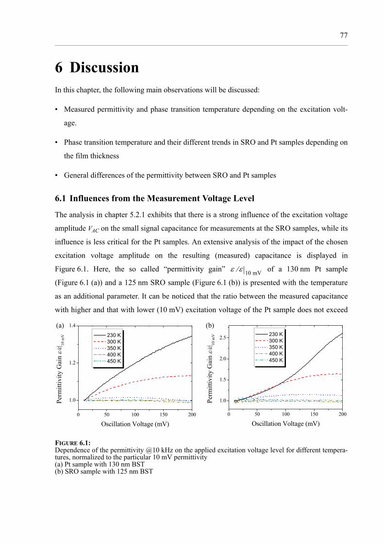
77
6 DiscussionIn this chapter, the following main observations will be discussed:
• Measured permittivity and phase transition temperature depending on the excitation volt-
age.
• Phase transition temperature and their different trends in SRO and Pt samples depending on
the film thickness
• General differences of the permittivity between SRO and Pt samples
6.1 Influences from the Measurement Voltage Level
The analysis in chapter 5.2.1 exhibits that there is a strong influence of the excitation voltage
amplitude VAC on the small signal capacitance for measurements at the SRO samples, while its
influence is less critical for the Pt samples. An extensive analysis of the impact of the chosen
excitation voltage amplitude on the resulting (measured) capacitance is displayed in
Figure 6.1. Here, the so called “permittivity gain” of a 130 nm Pt sample
(Figure 6.1 (a)) and a 125 nm SRO sample (Figure 6.1 (b)) is presented with the temperature
as an additional parameter. It can be noticed that the ratio between the measured capacitance
with higher and that with lower (10 mV) excitation voltage of the Pt sample does not exceed
0 50 100 150 200
1.0
1.5
2.0
2.5 230 K 300 K 350 K 400 K 450 K
Perm
ittiv
ity G
ain
ε/ε| 10
mV
Oscillation Voltage (mV)0 50 100 150 200
1.0
1.2
1.4
230 K 300 K 350 K 400 K 450 K
Perm
ittiv
ity G
ain
ε/ε| 10
mV
Oscillation Voltage (mV)
FIGURE 6.1:Dependence of the permittivity @10 kHz on the applied excitation voltage level for different tempera-tures, normalized to the particular 10 mV permittivity(a) Pt sample with 130 nm BST(b) SRO sample with 125 nm BST
(a) (b)
ε ε 10 mV⁄
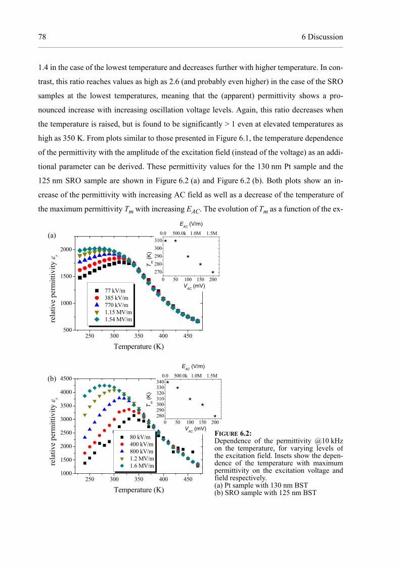
78 6 Discussion
1.4 in the case of the lowest temperature and decreases further with higher temperature. In con-
trast, this ratio reaches values as high as 2.6 (and probably even higher) in the case of the SRO
samples at the lowest temperatures, meaning that the (apparent) permittivity shows a pro-
nounced increase with increasing oscillation voltage levels. Again, this ratio decreases when
the temperature is raised, but is found to be significantly > 1 even at elevated temperatures as
high as 350 K. From plots similar to those presented in Figure 6.1, the temperature dependence
of the permittivity with the amplitude of the excitation field (instead of the voltage) as an addi-
tional parameter can be derived. These permittivity values for the 130 nm Pt sample and the
125 nm SRO sample are shown in Figure 6.2 (a) and Figure 6.2 (b). Both plots show an in-
crease of the permittivity with increasing AC field as well as a decrease of the temperature of
the maximum permittivity Tm with increasing EAC. The evolution of Tm as a function of the ex-
250 300 350 400 450500
1000
1500
2000
0 50 100 150 200270280290300310
0.0 500.0k 1.0M 1.5M
77 kV/m 385 kV/m 770 kV/m 1.15 MV/m 1.54 MV/mre
lativ
e pe
rmitt
ivity
ε r
Temperature (K)
Tm (K
)
VAC (mV)
EAC (V/m)
250 300 350 400 4501000
1500
2000
2500
3000
3500
4000
4500
0 50 100 150 200280290300310320330340
0.0 500.0k 1.0M 1.5M
80 kV/m 400 kV/m 800 kV/m 1.2 MV/m 1.6 MV/mre
lativ
e pe
rmitt
ivity
ε r
Temperature (K)
T m (K
)
VAC (mV)
EAC (V/m)
FIGURE 6.2:Dependence of the permittivity @10 kHz on the temperature, for varying levels of the excitation field. Insets show the depen-dence of the temperature with maximum permittivity on the excitation voltage and field respectively.(a) Pt sample with 130 nm BST(b) SRO sample with 125 nm BST
(a)
(b)
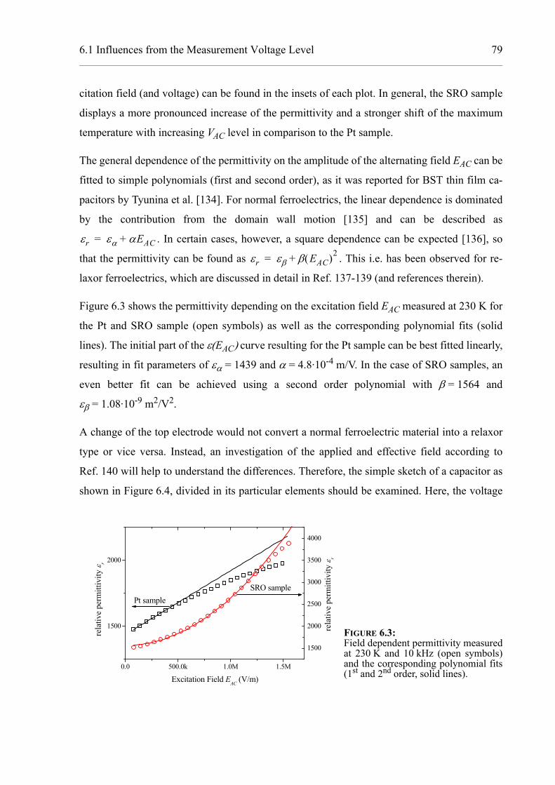
6.1 Influences from the Measurement Voltage Level 79
citation field (and voltage) can be found in the insets of each plot. In general, the SRO sample
displays a more pronounced increase of the permittivity and a stronger shift of the maximum
temperature with increasing VAC level in comparison to the Pt sample.
The general dependence of the permittivity on the amplitude of the alternating field EAC can be
fitted to simple polynomials (first and second order), as it was reported for BST thin film ca-
pacitors by Tyunina et al. [134]. For normal ferroelectrics, the linear dependence is dominated
by the contribution from the domain wall motion [135] and can be described as
. In certain cases, however, a square dependence can be expected [136], so
that the permittivity can be found as . This i.e. has been observed for re-
laxor ferroelectrics, which are discussed in detail in Ref. 137-139 (and references therein).
Figure 6.3 shows the permittivity depending on the excitation field EAC measured at 230 K for
the Pt and SRO sample (open symbols) as well as the corresponding polynomial fits (solid
lines). The initial part of the ε(EAC) curve resulting for the Pt sample can be best fitted linearly,
resulting in fit parameters of εα = 1439 and α = 4.8·10-4 m/V. In the case of SRO samples, an
even better fit can be achieved using a second order polynomial with β = 1564 and
εβ = 1.08·10-9 m2/V2.
A change of the top electrode would not convert a normal ferroelectric material into a relaxor
type or vice versa. Instead, an investigation of the applied and effective field according to
Ref. 140 will help to understand the differences. Therefore, the simple sketch of a capacitor as
shown in Figure 6.4, divided in its particular elements should be examined. Here, the voltage
0.0 500.0k 1.0M 1.5M
1500
2000
1500
2000
2500
3000
3500
4000
rela
tive
perm
ittiv
ity ε r
Pt sample
rela
tive
perm
ittiv
ity ε r
Excitation Field EAC (V/m)
SRO sample
FIGURE 6.3:Field dependent permittivity measured at 230 K and 10 kHz (open symbols) and the corresponding polynomial fits (1st and 2nd order, solid lines).
εr εα αEAC+=
εr εβ β EAC( )2+=
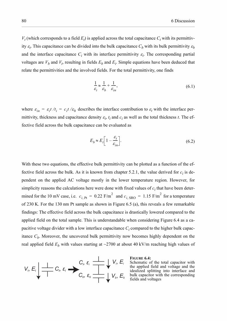
80 6 Discussion
Vt (which corresponds to a field Et) is applied across the total capacitance Ct with its permittiv-
ity εt. This capacitance can be divided into the bulk capacitance Cb with its bulk permittivity εb
and the interface capacitance Ci with its interface permittivity εi. The corresponding partial
voltages are Vb and Vi, resulting in fields Eb and Ei. Simple equations have been deduced that
relate the permittivities and the involved fields. For the total permittivity, one finds
where describes the interface contribution to εt with the interface per-
mittivity, thickness and capacitance density εi, ti and ci as well as the total thickness t. The ef-
fective field across the bulk capacitance can be evaluated as
With these two equations, the effective bulk permittivity can be plotted as a function of the ef-
fective field across the bulk. As it is known from chapter 5.2.1, the value derived for ci is de-
pendent on the applied AC voltage mostly in the lower temperature region. However, for
simplicity reasons the calculations here were done with fixed values of ci that have been deter-
mined for the 10 mV case, i.e. and for a temperature
of 230 K. For the 130 nm Pt sample as shown in Figure 6.5 (a), this reveals a few remarkable
findings: The effective field across the bulk capacitance is drastically lowered compared to the
applied field on the total sample. This is understandable when considering Figure 6.4 as a ca-
pacitive voltage divider with a low interface capacitance Ci compared to the higher bulk capac-
itance Cb. Moreover, the uncovered bulk permittivity now becomes highly dependent on the
real applied field Eb with values starting at ~2700 at about 40 kV/m reaching high values of
Ct, εt
Cb, εb
Ci, εi
Vt, Et
Vi, Ei
Vb, Eb
FIGURE 6.4:Schematic of the total capacitor with the applied field and voltage and the idealized splitting into interface and bulk capacitor with the corresponding fields and voltages
1εt---- 1
εb----- 1
εin------,+≈ (6.1)
εin εit ti⁄ cit ε0⁄= =
Eb Et 1εtεin------– .≈ (6.2)
ci, Pt 0.22 F/m2= ci, SRO 1.15 F/m2=
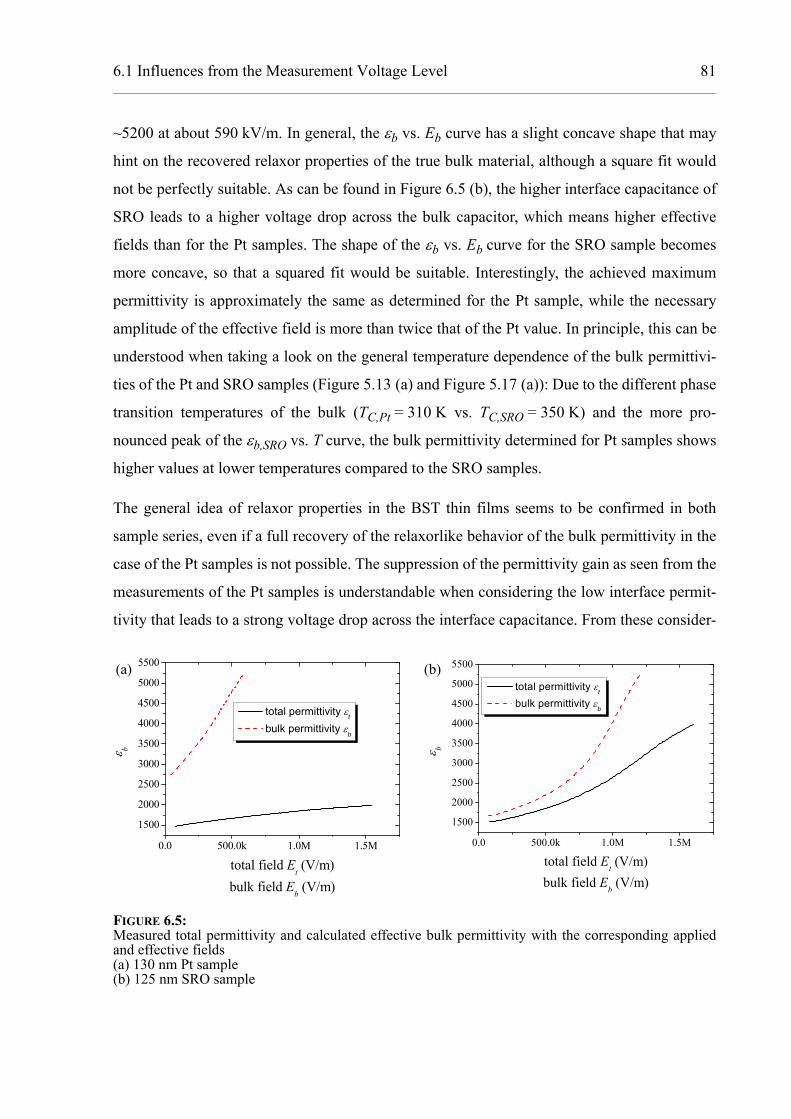
6.1 Influences from the Measurement Voltage Level 81
~5200 at about 590 kV/m. In general, the εb vs. Eb curve has a slight concave shape that may
hint on the recovered relaxor properties of the true bulk material, although a square fit would
not be perfectly suitable. As can be found in Figure 6.5 (b), the higher interface capacitance of
SRO leads to a higher voltage drop across the bulk capacitor, which means higher effective
fields than for the Pt samples. The shape of the εb vs. Eb curve for the SRO sample becomes
more concave, so that a squared fit would be suitable. Interestingly, the achieved maximum
permittivity is approximately the same as determined for the Pt sample, while the necessary
amplitude of the effective field is more than twice that of the Pt value. In principle, this can be
understood when taking a look on the general temperature dependence of the bulk permittivi-
ties of the Pt and SRO samples (Figure 5.13 (a) and Figure 5.17 (a)): Due to the different phase
transition temperatures of the bulk (TC,Pt = 310 K vs. TC,SRO = 350 K) and the more pro-
nounced peak of the εb,SRO vs. T curve, the bulk permittivity determined for Pt samples shows
higher values at lower temperatures compared to the SRO samples.
The general idea of relaxor properties in the BST thin films seems to be confirmed in both
sample series, even if a full recovery of the relaxorlike behavior of the bulk permittivity in the
case of the Pt samples is not possible. The suppression of the permittivity gain as seen from the
measurements of the Pt samples is understandable when considering the low interface permit-
tivity that leads to a strong voltage drop across the interface capacitance. From these consider-
0.0 500.0k 1.0M 1.5M
1500
2000
2500
3000
3500
4000
4500
5000
5500
total permittivity εt
bulk permittivity εb
ε b
total field Et (V/m)bulk field Eb (V/m)
0.0 500.0k 1.0M 1.5M
1500
2000
2500
3000
3500
4000
4500
5000
5500
total permittivity εt
bulk permittivity εb
ε b
total field Et (V/m)bulk field Eb (V/m)
FIGURE 6.5:Measured total permittivity and calculated effective bulk permittivity with the corresponding applied and effective fields(a) 130 nm Pt sample(b) 125 nm SRO sample
(a) (b)
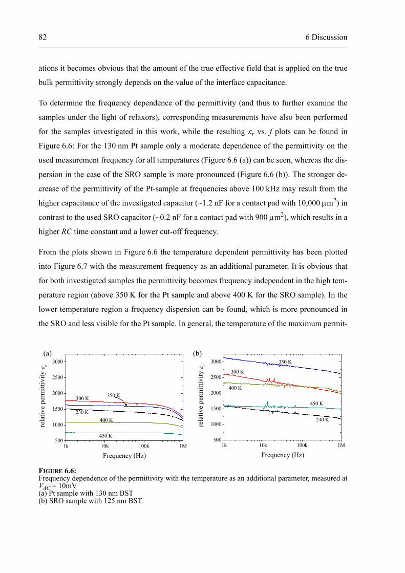
82 6 Discussion
ations it becomes obvious that the amount of the true effective field that is applied on the true
bulk permittivity strongly depends on the value of the interface capacitance.
To determine the frequency dependence of the permittivity (and thus to further examine the
samples under the light of relaxors), corresponding measurements have also been performed
for the samples investigated in this work, while the resulting εr vs. f plots can be found in
Figure 6.6: For the 130 nm Pt sample only a moderate dependence of the permittivity on the
used measurement frequency for all temperatures (Figure 6.6 (a)) can be seen, whereas the dis-
persion in the case of the SRO sample is more pronounced (Figure 6.6 (b)). The stronger de-
crease of the permittivity of the Pt-sample at frequencies above 100 kHz may result from the
higher capacitance of the investigated capacitor (~1.2 nF for a contact pad with 10,000 μm2) in
contrast to the used SRO capacitor (~0.2 nF for a contact pad with 900 μm2), which results in a
higher RC time constant and a lower cut-off frequency.
From the plots shown in Figure 6.6 the temperature dependent permittivity has been plotted
into Figure 6.7 with the measurement frequency as an additional parameter. It is obvious that
for both investigated samples the permittivity becomes frequency independent in the high tem-
perature region (above 350 K for the Pt sample and above 400 K for the SRO sample). In the
lower temperature region a frequency dispersion can be found, which is more pronounced in
the SRO and less visible for the Pt sample. In general, the temperature of the maximum permit-
1k 10k 100k 1M500
1000
1500
2000
2500
3000
450 K
400 K
300 K 350 K
rela
tive
perm
ittiv
ity ε r
Frequency (Hz)
230 K
1k 10k 100k 1M500
1000
1500
2000
2500
3000
450 K
400 K
350 K
300 K
rela
tive
perm
ittiv
ity ε r
Frequency (Hz)
240 K
FIGURE 6.6:Frequency dependence of the permittivity with the temperature as an additional parameter, measured at VAC = 10mV(a) Pt sample with 130 nm BST(b) SRO sample with 125 nm BST
(a) (b)
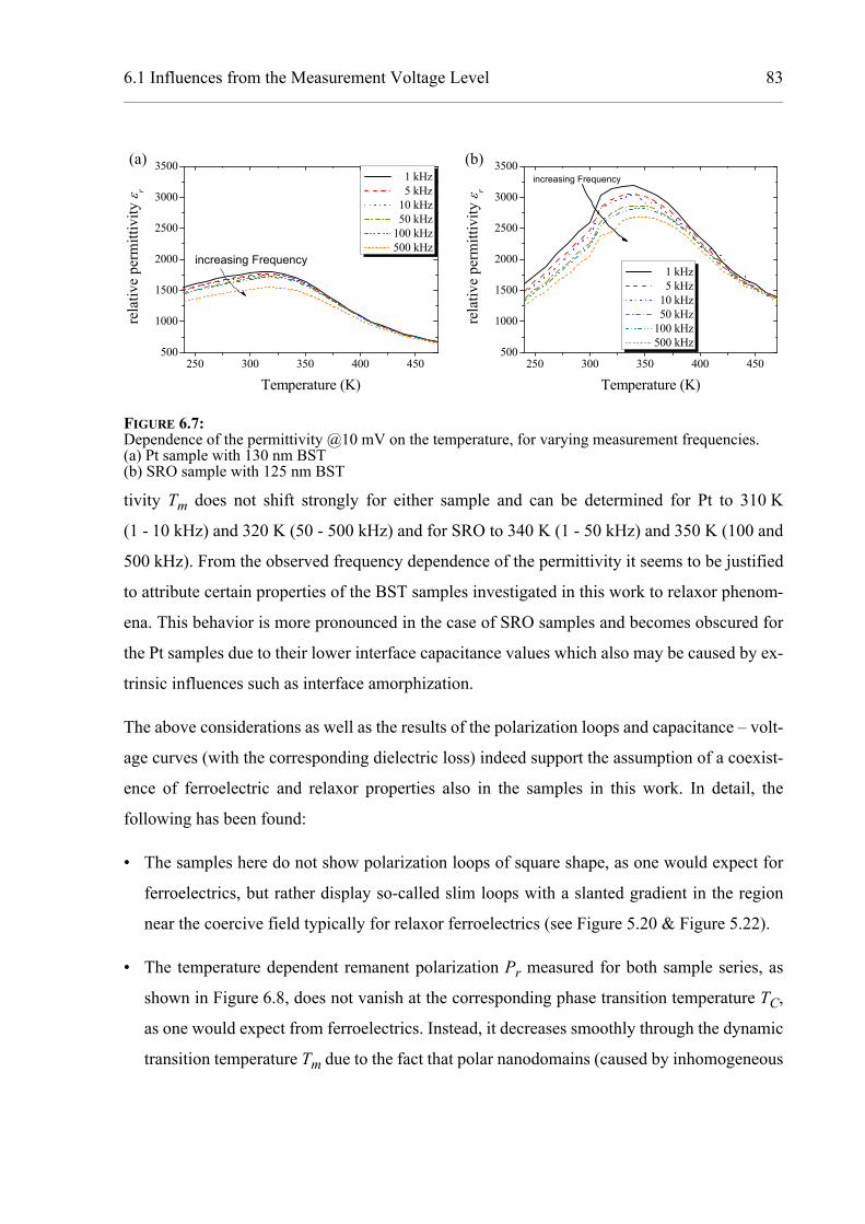
6.1 Influences from the Measurement Voltage Level 83
tivity Tm does not shift strongly for either sample and can be determined for Pt to 310 K
(1 - 10 kHz) and 320 K (50 - 500 kHz) and for SRO to 340 K (1 - 50 kHz) and 350 K (100 and
500 kHz). From the observed frequency dependence of the permittivity it seems to be justified
to attribute certain properties of the BST samples investigated in this work to relaxor phenom-
ena. This behavior is more pronounced in the case of SRO samples and becomes obscured for
the Pt samples due to their lower interface capacitance values which also may be caused by ex-
trinsic influences such as interface amorphization.
The above considerations as well as the results of the polarization loops and capacitance – volt-
age curves (with the corresponding dielectric loss) indeed support the assumption of a coexist-
ence of ferroelectric and relaxor properties also in the samples in this work. In detail, the
following has been found:
• The samples here do not show polarization loops of square shape, as one would expect for
ferroelectrics, but rather display so-called slim loops with a slanted gradient in the region
near the coercive field typically for relaxor ferroelectrics (see Figure 5.20 & Figure 5.22).
• The temperature dependent remanent polarization Pr measured for both sample series, as
shown in Figure 6.8, does not vanish at the corresponding phase transition temperature TC,
as one would expect from ferroelectrics. Instead, it decreases smoothly through the dynamic
transition temperature Tm due to the fact that polar nanodomains (caused by inhomogeneous
250 300 350 400 450500
1000
1500
2000
2500
3000
3500
rela
tive
perm
ittiv
ity ε r
Temperature (K)
1 kHz 5 kHz 10 kHz 50 kHz 100 kHz 500 kHz
increasing Frequency
250 300 350 400 450500
1000
1500
2000
2500
3000
3500
rela
tive
perm
ittiv
ity ε r
Temperature (K)
1 kHz 5 kHz 10 kHz 50 kHz 100 kHz 500 kHz
increasing Frequency
FIGURE 6.7:Dependence of the permittivity @10 mV on the temperature, for varying measurement frequencies.(a) Pt sample with 130 nm BST(b) SRO sample with 125 nm BST
(a) (b)
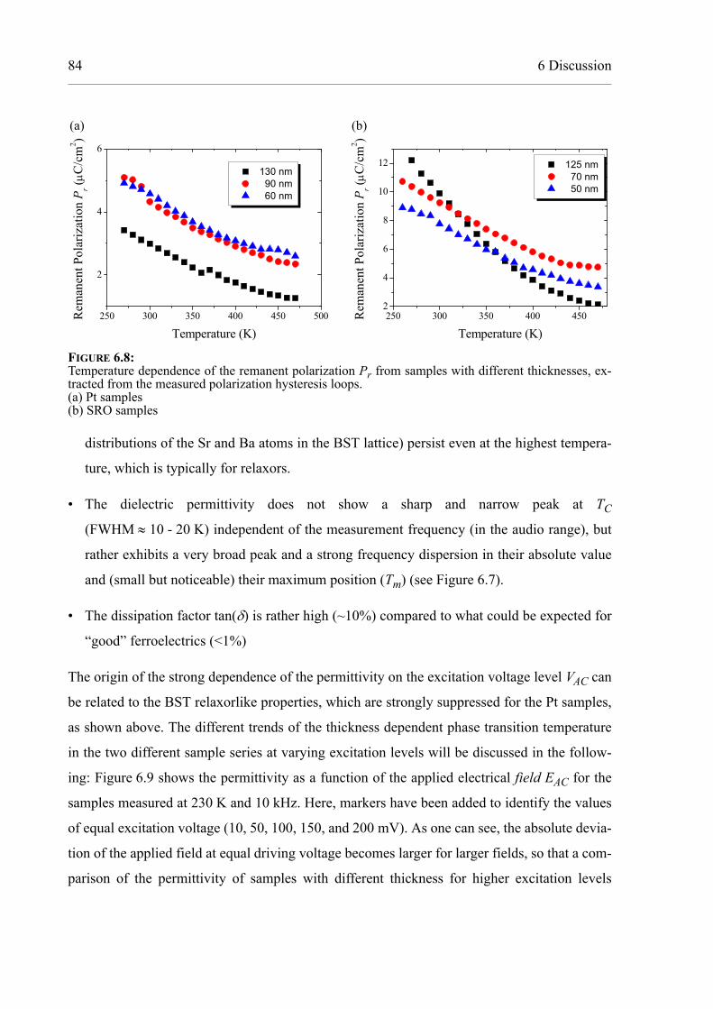
84 6 Discussion
distributions of the Sr and Ba atoms in the BST lattice) persist even at the highest tempera-
ture, which is typically for relaxors.
• The dielectric permittivity does not show a sharp and narrow peak at TC
(FWHM ≈ 10 - 20 K) independent of the measurement frequency (in the audio range), but
rather exhibits a very broad peak and a strong frequency dispersion in their absolute value
and (small but noticeable) their maximum position (Tm) (see Figure 6.7).
• The dissipation factor tan(δ) is rather high (~10%) compared to what could be expected for
“good” ferroelectrics (<1%)
The origin of the strong dependence of the permittivity on the excitation voltage level VAC can
be related to the BST relaxorlike properties, which are strongly suppressed for the Pt samples,
as shown above. The different trends of the thickness dependent phase transition temperature
in the two different sample series at varying excitation levels will be discussed in the follow-
ing: Figure 6.9 shows the permittivity as a function of the applied electrical field EAC for the
samples measured at 230 K and 10 kHz. Here, markers have been added to identify the values
of equal excitation voltage (10, 50, 100, 150, and 200 mV). As one can see, the absolute devia-
tion of the applied field at equal driving voltage becomes larger for larger fields, so that a com-
parison of the permittivity of samples with different thickness for higher excitation levels
250 300 350 400 450 500
2
4
6
130 nm 90 nm 60 nm
Rem
anen
t Pol
ariz
atio
n P r (μ
C/c
m2 )
Temperature (K)250 300 350 400 450
2
4
6
8
10
12 125 nm 70 nm 50 nm
Rem
anen
t Pol
ariz
atio
n P r (μ
C/c
m2 )
Temperature (K)
FIGURE 6.8:Temperature dependence of the remanent polarization Pr from samples with different thicknesses, ex-tracted from the measured polarization hysteresis loops.(a) Pt samples(b) SRO samples
(a) (b)
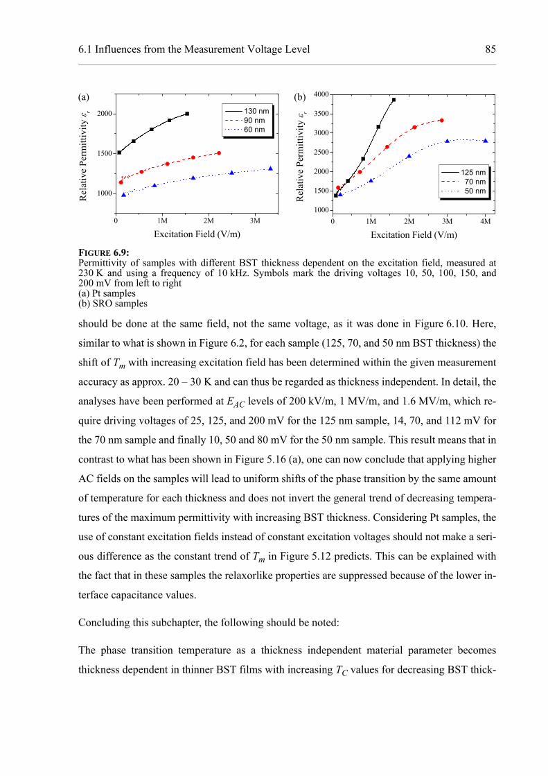
6.1 Influences from the Measurement Voltage Level 85
should be done at the same field, not the same voltage, as it was done in Figure 6.10. Here,
similar to what is shown in Figure 6.2, for each sample (125, 70, and 50 nm BST thickness) the
shift of Tm with increasing excitation field has been determined within the given measurement
accuracy as approx. 20 – 30 K and can thus be regarded as thickness independent. In detail, the
analyses have been performed at EAC levels of 200 kV/m, 1 MV/m, and 1.6 MV/m, which re-
quire driving voltages of 25, 125, and 200 mV for the 125 nm sample, 14, 70, and 112 mV for
the 70 nm sample and finally 10, 50 and 80 mV for the 50 nm sample. This result means that in
contrast to what has been shown in Figure 5.16 (a), one can now conclude that applying higher
AC fields on the samples will lead to uniform shifts of the phase transition by the same amount
of temperature for each thickness and does not invert the general trend of decreasing tempera-
tures of the maximum permittivity with increasing BST thickness. Considering Pt samples, the
use of constant excitation fields instead of constant excitation voltages should not make a seri-
ous difference as the constant trend of Tm in Figure 5.12 predicts. This can be explained with
the fact that in these samples the relaxorlike properties are suppressed because of the lower in-
terface capacitance values.
Concluding this subchapter, the following should be noted:
The phase transition temperature as a thickness independent material parameter becomes
thickness dependent in thinner BST films with increasing TC values for decreasing BST thick-
0 1M 2M 3M
1000
1500
2000 130 nm 90 nm 60 nm
Rel
ativ
e Pe
rmitt
ivity
ε r
Excitation Field (V/m)0 1M 2M 3M 4M
1000
1500
2000
2500
3000
3500
4000
125 nm 70 nm 50 nm
Rel
ativ
e Pe
rmitt
ivity
ε r
Excitation Field (V/m)
FIGURE 6.9:Permittivity of samples with different BST thickness dependent on the excitation field, measured at 230 K and using a frequency of 10 kHz. Symbols mark the driving voltages 10, 50, 100, 150, and 200 mV from left to right(a) Pt samples(b) SRO samples
(a) (b)
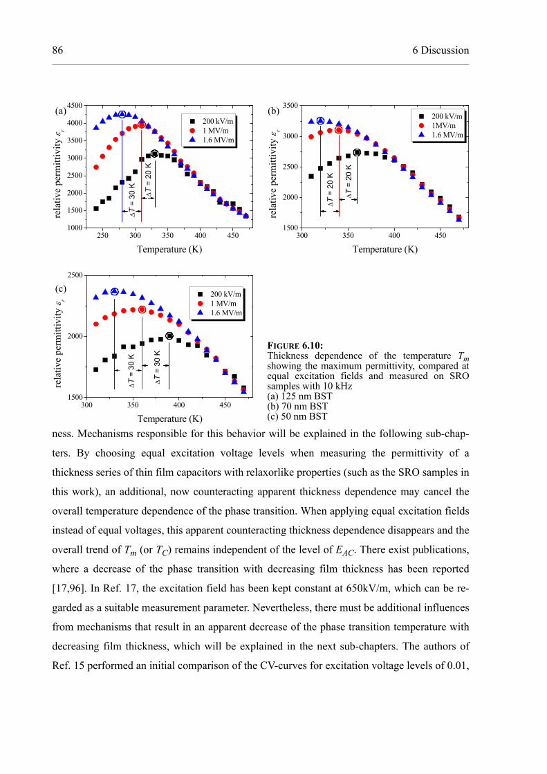
86 6 Discussion
ness. Mechanisms responsible for this behavior will be explained in the following sub-chap-
ters. By choosing equal excitation voltage levels when measuring the permittivity of a
thickness series of thin film capacitors with relaxorlike properties (such as the SRO samples in
this work), an additional, now counteracting apparent thickness dependence may cancel the
overall temperature dependence of the phase transition. When applying equal excitation fields
instead of equal voltages, this apparent counteracting thickness dependence disappears and the
overall trend of Tm (or TC) remains independent of the level of EAC. There exist publications,
where a decrease of the phase transition with decreasing film thickness has been reported
[17,96]. In Ref. 17, the excitation field has been kept constant at 650kV/m, which can be re-
garded as a suitable measurement parameter. Nevertheless, there must be additional influences
from mechanisms that result in an apparent decrease of the phase transition temperature with
decreasing film thickness, which will be explained in the next sub-chapters. The authors of
Ref. 15 performed an initial comparison of the CV-curves for excitation voltage levels of 0.01,
300 350 400 4501500
2000
2500
3000
3500 200 kV/m 1MV/m 1.6 MV/m
rela
tive
perm
ittiv
ity ε r
Temperature (K)
ΔT
= 20
K
ΔT =
20
K
300 350 400 4501500
2000
2500
200 kV/m 1 MV/m 1.6 MV/m
rela
tive
perm
ittiv
ity ε r
Temperature (K)
ΔT
= 30
K
ΔT
= 30
K
250 300 350 400 4501000
1500
2000
2500
3000
3500
4000
4500
200 kV/m 1 MV/m 1.6 MV/m
rela
tive
perm
ittiv
ity ε r
Temperature (K)
ΔT =
20
K
ΔT
= 30
K
FIGURE 6.10:Thickness dependence of the temperature Tmshowing the maximum permittivity, compared at equal excitation fields and measured on SRO samples with 10 kHz(a) 125 nm BST(b) 70 nm BST(c) 50 nm BST
(a)
(c)
(b)
6.2 Strain Effects 87
0.05, and 0.1 V, where they did not find any difference in the temperature range from RT up to
473 K. This is understandable, since their samples are paraelectric in that temperature region
and a possible relaxorlike behavior will not show up. In Ref. 96, no information about the used
measurement parameters is given, so it is only speculative whether constant AC voltages could
be responsible for the observed trend of the phase transition.
Finally, for any further interpretation only the achieved values and parameters of the measure-
ments at low excitation voltage levels will be considered.
6.2 Strain Effects
From the considerations in chapter 2.4 it is obvious that the misfit strain inside heteroepitaxial
films can be controlled by the choice of the underlying substrate material. Additionally, by
variations of the film thickness the internal strain state can be altered by the introduction of
misfit dislocations at the growth temperature Tg. It is widely accepted that the generation of
misfit dislocations in perovskite films occurs only at Tg, because the dislocation glide must be
suppressed at due to relatively high Peierls8 barriers. From Ref. 73, the thick-
ness dependent dislocation density ρ can be calculated as
with tc as the critical thickness below which no misfit dislocations will be generated and η as a
factor which makes it possible that the equilibrium dislocation density is not reached due to ki-
netic reasons . Eq. (2.8) together with Eq. (6.3) leads to
8. To maintain the motion of a dislocation through a periodical potential (such as a crystal lattice), a force called the Peierls force is required [141].
T Tg 700° C∼«
ρ t( ) ηSm0 Tg( ) 1 tc t⁄–( ),= (6.3)
η 1≤( )
Sm T t,( )b 1 ρ–( ) a0–
a0-------------------------------- b
a0----- 1– b
a0-----ηSm
0 Tg( ) 1 tc t⁄–( ),+= = (6.4)
88 6 Discussion
which can be easily converted to
describing the temperature and thickness dependent strain in the films. Here,
represents the in-plane strains S1 and S2 in a very thick film
, which would be fully relaxed at Tg under equilibrium conditions (η = 1). The temper-
ature dependence of may be described in a first approximation by a linear relation
where αb and α0 are the thermal expansion coefficients of the substrate and the paraelectric
film, respectively.
Eq. (2.24) allows the evaluation of the out-of-plane lattice strain according to Ref. 81 as
with the material parameters as explained in chapter 2.4. With Eq. (6.7), the calculation of the
strain-dependent out-of-plane lattice constant can be done, using the follow-
ing values and definitions:
• , (strains were calculated using
the data of lattice constants and thermal expansion coefficients of BaTiO3, SrTiO3, and
SRO, cmp. Ref. 142)
• η = 0.7, determined using the experimental value of Sm = (a – a0)/a0 ≈ –2 · 10-3, which was
evaluated from the measured in-plane lattice constant a ≈ 0.397 nm of a 200-nm BST film
and the estimated prototypic-cell size a0(T = 300 K) ≈ 0.3977 nm
• results from (using the P4 approximation in Eq. (2.26))
Sm T t,( ) Sm∞ T( ) ηSm
0 Tg( )tct---,+= (6.5)
Sm∞ T( ) Sm
0 T( ) ηSm Tg( )–=
t tc»( )
Sm∞ T( )
Sm∞ T( ) 1 η–( )Sm
0 Tg( ) αb α0–( ) T Tg–( ),+≈ (6.6)
S3c a0–
a0-------------- G∂
σ3∂---------–
2s12Sms11 s12+-------------------- Q11
2s12Q12s11 s12+--------------------– P3
2,+= = = (6.7)
c a0 S3 1+( )=
Sm0 Tg = 973 K( ) 15 10 3–⋅–≈ Sm
0 T = 300 K( ) 12 10 3–⋅–≈
P32 a3
* 2a33*( )⁄–= G P3∂⁄∂ 0=
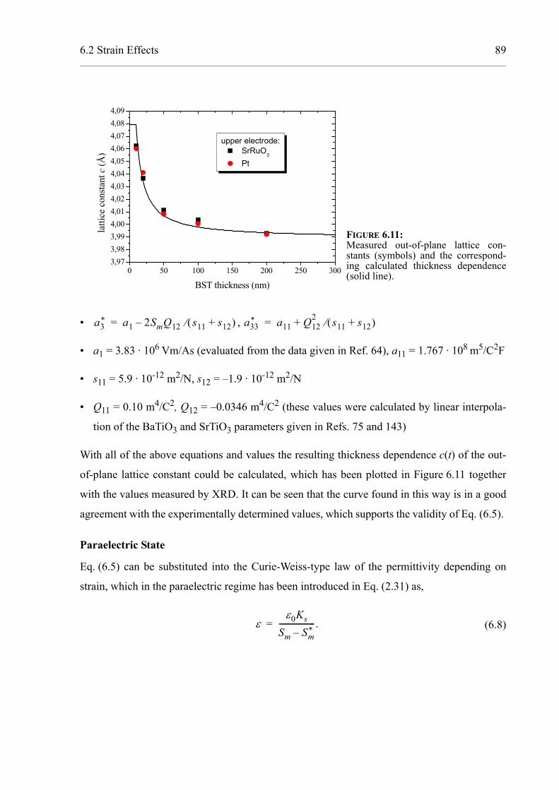
6.2 Strain Effects 89
• ,
• a1 = 3.83 · 106 Vm/As (evaluated from the data given in Ref. 64), a11 = 1.767 · 108 m5/C2F
• s11 = 5.9 · 10-12 m2/N, s12 = –1.9 · 10-12 m2/N
• Q11 = 0.10 m4/C2, Q12 = –0.0346 m4/C2 (these values were calculated by linear interpola-
tion of the BaTiO3 and SrTiO3 parameters given in Refs. 75 and 143)
With all of the above equations and values the resulting thickness dependence c(t) of the out-
of-plane lattice constant could be calculated, which has been plotted in Figure 6.11 together
with the values measured by XRD. It can be seen that the curve found in this way is in a good
agreement with the experimentally determined values, which supports the validity of Eq. (6.5).
Paraelectric State
Eq. (6.5) can be substituted into the Curie-Weiss-type law of the permittivity depending on
strain, which in the paraelectric regime has been introduced in Eq. (2.31) as,
a3* a1 2SmQ12 s11 s12+( )⁄–= a33
* a11 Q122 s11 s12+( )⁄+=
0 50 100 150 200 250 3003,973,983,994,004,014,024,034,044,054,064,074,084,09
upper electrode: SrRuO3
Pt
latti
ce c
onst
ant c
(Å)
BST thickness (nm)
FIGURE 6.11:Measured out-of-plane lattice con-stants (symbols) and the correspond-ing calculated thickness dependence (solid line).
εε0Ks
Sm Sm*–
-------------------.= (6.8)
90 6 Discussion
This leads to the following relation for the reciprocal permittivity of a paraelectric film:
Here, describes the permittivity of a very thick strained BST
film , while Eq. (6.9) itself shows that the intrinsic reciprocal permittivity is linear de-
pendent on the reciprocal film thickness t-1. It can be seen that depending on the sign of
, the permittivity of the paraelectric film either increases or decreases with increasing
thickness. From Eq. (6.9) the reciprocal capacitance density (at t > tc) can be evaluated as
From the extrapolation of to zero thickness, a nonzero intercept results which is caused by
the strain relaxation. This intercept can be negative (for compressive in-plane film strains,
) or positive (for tensile in-plane film strains, ), which should be kept in
mind as a noteworthy result.
Ferroelectric Regime
Considering epitaxial films in their ferroelectric state, a tetragonal c-phase with the out-of-
plane spontaneous polarization (P1 = P2 = 0, ) can be found. The dependence of the
permittivity ε on the misfit strain in the ferroelectric case can be described again using a Curie-
Weiss type law as
since near the second-order phase transition the P4 approximation is valid [91]. In contrast to
the paraelectric case (Eq. (6.8)), here the lattice strains must be and the parameter de-
scribing the sensitivity of the permittivity on the strain can be found as Ksc = Ks/2, which
shows analogy to what has been found in Eq. (2.18) and Eq. (2.23) for the pre-factor above and
1ε T t,( )--------------- 1
ε∞ T( )-------------- η
Sm0 Tg( )ε0Ks
-----------------tct---.+= (6.9)
ε∞ T( ) ε0Ks Sm∞ T( ) Sm
* T( )–( )⁄=
t tc»( )
Sm0 Tg( )
1ceff------- t
ε-- η
Sm0 Tg( )tcε0Ks
---------------------.+= (6.10)
ceff1–
Sm0 Tg( ) 0< Sm
0 Tg( ) 0>
P3 0≠
εε0Ksc
Sm* Sm–
-------------------,= (6.11)
Sm Sm*<
6.2 Strain Effects 91
below the phase transition temperature.
Eq. (6.5), which has been validated according to Figure 6.11, can now be substituted into
Eq. (2.31), leading to an equation describing the intrinsic reciprocal permittivity dependent on
thickness and temperature (in analogy to the above discussed paraelectric case):
Accordingly, describes the permittivity of a very thick
strained BST film , while the thickness dependent term in Eq. (6.12) differs from that in
Eq. (6.9) by the negative sign and the two times larger amplitude. In analogy to the paraelectric
case in the previous sub-chapter, the thickness dependent reciprocal capacitance can be de-
rived from Eq. (6.12) as
In analogy to Eq. (6.10), Eq. (6.13) again appears as a linear equation in t, with the difference
in the negative sign and a two times smaller pre-factor Ksc (compared to Ks)
Summary of the Strain Effects
Eq. (6.10) and Eq. (6.13) as the key results reveal the following aspects which are valid in both
states (PE or FE):
• The slope of the dependence reflects the permittivity of a thick strained film, which
does not correspond with the permittivity of the bulk material, εb.
• The extrapolation of the measured thickness dependence of the inverse capacitance to t = 0
may give a considerable nonzero intercept even when the interface effect is negligible
.
Substitution of the numerical values for the involved parameters as given above into Eq. (6.10)
and Eq. (6.13) results in apparent reciprocal interface capacitances of in
1ε T t,( )--------------- 1
ε∞ T( )-------------- η
Sm0 Tg( )ε0Ksc
-----------------tct---.–= (6.12)
ε∞ T( ) ε0Ksc Sm* T( ) Sm
∞ T( )–( )⁄=
t tc»( )
1ceff------- t
ε∞ T( )-------------- η
Sm0 Tg( )tcε0Ksc
----------------------.–= (6.13)
ceff1– ε∞
ci1– 0→( )
ci1– 0.9688 m2 F⁄=
92 6 Discussion
the ferroelectric case and in the paraelectric case. These values can be
regarded as the theoretical limits of the intercept, solely defined by effects of the strain relax-
ation when no extrinsic influences have to be considered. It can be seen that the room tempera-
ture interface capacitance density determined in chapter 5.2.1 for SRO samples
is very close to that theoretical minimum for the ferroelectric case,
while the value for Pt is clearly higher. As shown above, depending on
the state of the material (ferro- or paraelectric) the strain contribution of the interface capaci-
tance may have a negative sign. This in combination with additional contributions to the inter-
face capacitance can lead to a reduction of the total interface capacitance density, as will be
shown in the following chapters.
To conclude this sub-chapter, it must be stressed that the increase of TC (compared to the bulk
ceramics) measured with the “correct” excitation voltage of VAC = 10 mV, can be explained by
the strain effect as well. Indeed, the thermodynamic considerations from chapter 2.5 predict
with T0 and C as the Curie-Weiss temperature and constant of the bulk material, respectively.
Taking T0 = 290 K, C = 1.18 · 105 K (Ref. 64), Q12, s11 and s12 as mentioned above and by
calculating Sm = (a - a0)/a0 via the thickness dependence of the in-plane lattice constant
, a thickness dependent phase transition temperature results as shown in
Figure 6.12 (solid line)9. The squared and round symbols in Figure 6.12 display the experi-
mentally determined phase transition temperatures for the Pt and SRO samples (cmp. chapter
5.2.2) and show in principle a good agreement to the trend of the calculated phase transition
temperature. It will be shown in the next chapter what might be responsible for the difference
between the measured phase transition and that calculated using Eq. (6.14).
9. assuming a constant volume of the BST cell, with a0 = 0.3977 Å as the estimated prototypic cell size
ci1– 0.4844– m2 F⁄=
ci SRO,1– 1.282 m2 F⁄=( )
ci Pt,1– 4.348 m2 F⁄=( )
TC T0 Sm4ε0CQ12
s11 s12+( )-------------------------,+= (6.14)
a a03 c⁄=
a03
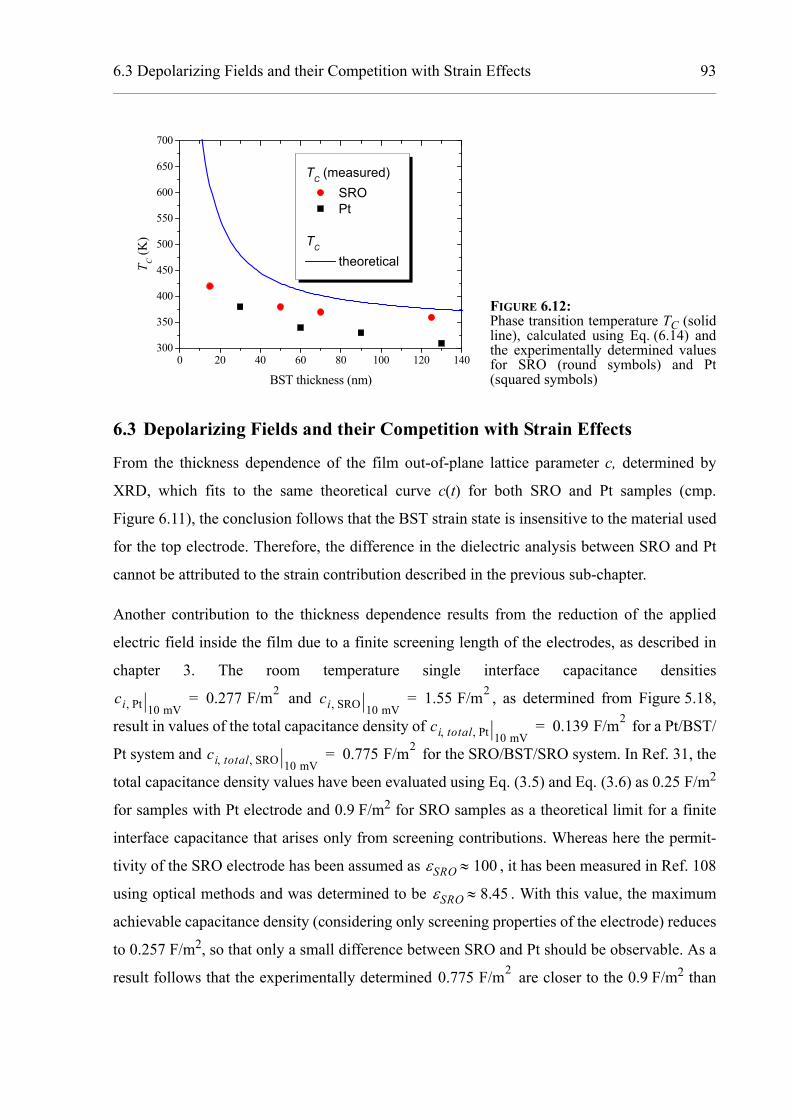
6.3 Depolarizing Fields and their Competition with Strain Effects 93
6.3 Depolarizing Fields and their Competition with Strain Effects
From the thickness dependence of the film out-of-plane lattice parameter c, determined by
XRD, which fits to the same theoretical curve c(t) for both SRO and Pt samples (cmp.
Figure 6.11), the conclusion follows that the BST strain state is insensitive to the material used
for the top electrode. Therefore, the difference in the dielectric analysis between SRO and Pt
cannot be attributed to the strain contribution described in the previous sub-chapter.
Another contribution to the thickness dependence results from the reduction of the applied
electric field inside the film due to a finite screening length of the electrodes, as described in
chapter 3. The room temperature single interface capacitance densities
and , as determined from Figure 5.18,
result in values of the total capacitance density of for a Pt/BST/
Pt system and for the SRO/BST/SRO system. In Ref. 31, the
total capacitance density values have been evaluated using Eq. (3.5) and Eq. (3.6) as 0.25 F/m2
for samples with Pt electrode and 0.9 F/m2 for SRO samples as a theoretical limit for a finite
interface capacitance that arises only from screening contributions. Whereas here the permit-
tivity of the SRO electrode has been assumed as , it has been measured in Ref. 108
using optical methods and was determined to be . With this value, the maximum
achievable capacitance density (considering only screening properties of the electrode) reduces
to 0.257 F/m2, so that only a small difference between SRO and Pt should be observable. As a
result follows that the experimentally determined are closer to the 0.9 F/m2 than
0 20 40 60 80 100 120 140300
350
400
450
500
550
600
650
700
TC (measured) SRO Pt
TC
theoreticalT C (K
)
BST thickness (nm)
FIGURE 6.12:Phase transition temperature TC (solid line), calculated using Eq. (6.14) and the experimentally determined values for SRO (round symbols) and Pt (squared symbols)
ci, Pt 10 mV0.277 F/m2= ci, SRO 10 mV
1.55 F/m2=
ci total, Pt, 10 mV0.139 F/m2=
ci total, SRO, 10 mV0.775 F/m2=
εSRO 100≈
εSRO 8.45≈
0.775 F/m2
94 6 Discussion
the 0.257 F/m2, which either means that the parameters for calculating the screening length of
the SRO electrodes (permittivity, electron density, etc.) are chosen incorrectly (cmp. 3.2), or
that a negative extrinsic contribution leads to a modified interface capacitance (as will be dis-
cussed later). From Ref. 33 however, the interface capacitance of the “intrinsic dead layer” has
been determined to which now fits considerably better with respect to the
experimental 0.775 F/m2.
Using a simple phenomenological model, the properties of strained ferroelectric capacitors
have been analyzed. In contrast to the previous calculations [31], here it was taken into account
that the electrode screening ability also affects the temperature TC of the ferroelectric phase
transition, which modifies the thickness dependence of the dielectric response additionally.
The thermodynamic considerations now allow a better understanding of the differences found
between Pt and SRO samples.
The interface between the ferroelectric film and the electrode can be characterized by assum-
ing thin low permittivity layers (of intrinsic or extrinsic origins) with characteristics indepen-
dent of the thickness of the film t. In chapter 3.2 it was shown how the electric fields of the
ferroelectric film and these interfacial layers can be evaluated, resulting in a depolarizing field
that exists inside the ferroelectric (see Eq. (3.11)). Here, P is the out-of-
plane polarization of the film, whereas all interface contributions (intrinsic as well as extrinsic
influences) are summarized as: . If variations of the ferroelectric polar-
ization near the film surfaces are negligible, is the thickness of the interface
layer with a low permittivity εd = εm, where lTF and εm are the Thomas-Fermi screening length
and the lattice dielectric constant of the electrode material, respectively [31].
In a recent publication of Pertsev et al., the influence of the depolarizing field has been dis-
cussed using a P8 approximation [144]. The differentiation of the (then 8th order) film thermo-
dynamic potential (cmp. Eq. (2.26)) leads to
With the continuity condition for the electric displacement and the electrostatic
ci 0 615 F/m2,=
Edep P– cintt( )⁄≈
cint 1 2⁄( )ε0εd d⁄=
d εm lTF t«⋅=
2a3*P 4a33
* P3 6a111P5 8a1111P7 …+ + + + E.= (6.15)
D ε0E P+=
6.3 Depolarizing Fields and their Competition with Strain Effects 95
potential at the interfaces, Eq. (6.15) can be rewritten as
Here, V is the voltage applied to the electrodes whereas E represents the total field inside the
ferroelectric film, which is the algebraic sum of the applied field and the depolarizing field
Edep. Now, the total capacitance density can be evaluated as
where the inverse susceptibility of the ferroelectric film is represented by
From the P4 approximation the spontaneous polarization can be found as
and the reciprocal susceptibility may be evaluated as
. Now, the inverse of the total capacitance density can be written as
where is the permittivity of a thick strained film, as mentioned in the above sections. As a
remarkable result, Eq. (6.18) shows that the extrapolation of the inverse total capacitance 1/ct
to zero film thickness has a negative intercept. This is only valid for films in the ferroelectric
state, while for paraelectric materials the standard result follows.
In the P6 and higher order approximations, the reciprocal total capacitance becomes non-
linear, but it can be seen that the nonlinearity is usually negligible when plotting in the
2 a3* 1
2 ε0 cintt+( )-----------------------------+ P 4a33
* P3 6a111P5 8a1111P7 …+ + + +cint
ε0 cintt+( )--------------------------V.–= (6.16)
ct D V( ) V∂⁄∂=
ctcint
ε0 cint t⋅+( )------------------------------
ε0t
-----cint
1 ε0 cint t⋅+( )χ 1–+------------------------------------------------+ ,= (6.17)
χ 1– E P∂⁄∂ 2a3* 12a33
* P2 30a111P4 56a1111P6 …+ + + += =
Ps2 a3
* 1 2cit( )⁄+[ ] 2a33*( )⁄–≈
χ 1– 4a3*– 3 cit( )⁄–≈
1ct---- χ 1– t 1
cint--------+≈ t
ε∞------ 2
cint--------,–= (6.18)
ε∞
ct1– t 0→( ) 1 cint⁄=
ct1–
ct1– t( )
96 6 Discussion
limited thickness range . This makes it possible to approximate the reciprocal
capacitance density as
in analogy to Eq. (6.18) but with two fitting parameters εeff and κ. Remarkably, the extrapola-
tion to zero thickness gives a negative intercept , which may significantly vary with
temperature.
The influence of both strain and depolarizing field effects on the phase transition temperature
has been calculated in Ref. [144] as
where the thickness dependence of the misfit strain, given by Eq. (6.5), has been taken into ac-
count, while its weak temperature dependence described by Eq. (6.6) has been neglected. The
thickness dependence of TC can be thus determined by the difference between the two terms in
square brackets in Eq. (6.20). While the first term is positive, the second one must be negative
( and Q12 < 0), so that the variation of TC is governed by the competition of the strain
relaxation and the depolarizing-field effect, as already mentioned in chapter 6.3. When the lat-
ter prevails, the critical temperature is expected to decrease in thinner films. On the other hand,
TC will increase with decreasing thickness, if the dominant term in Eq. (6.20) is associated
with the relaxation of compressive misfit strain. In addition to the thickness dependence of TC
solely from strain as shown in Figure 6.12, Figure 6.13 now shows the calculated thickness de-
pendence of TC when also the depolarizing field has been considered. It can be seen that these
calculated values now much better fit the experimentally determined phase transition tempera-
ture both for the SRO as well as the Pt samples. For the calculation, cint in Eq. (6.20) has been
chosen to 0.7 F/m2 for SRO and 0.45 F/m2 for the Pt samples. These values are comparable to
the theoretical value of given in Ref. 33, hence this fitting parameter is con-
firmed by theory.
tmin t tmax≤ ≤
1ct---- t
εeff------- κ
cint--------,–≈ (6.19)
κ cint⁄–
TC T0 4ε0CQ12s11 s12+--------------------Sm
∞ Tg( ) ε0C 32cint----------- 4
Q12tcηs11 s12+--------------------Sm
0 Tg( )– 1t---,–+= (6.20)
Sm0 0<
ci 0.615 F/m2=
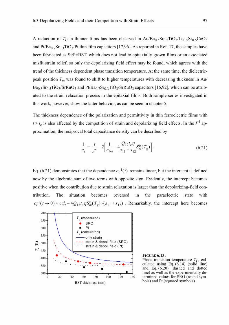
6.3 Depolarizing Fields and their Competition with Strain Effects 97
A reduction of TC in thinner films has been observed in Au/Ba0.5Sr0.5TiO3/La0.5Sr0.5CoO3
and Pt/Ba0.7Sr0.3TiO3/Pt thin-film capacitors [17,96]. As reported in Ref. 17, the samples have
been fabricated as Si/Pt/BST, which does not lead to epitaxially grown films or an associated
misfit strain relief, so only the depolarizing field effect may be found, which agrees with the
trend of the thickness dependent phase transition temperature. At the same time, the dielectric-
peak position Tm was found to shift to higher temperatures with decreasing thickness in Au/
Ba0.5Sr0.5TiO3/SrRuO3 and Pt/Ba0.7Sr0.3TiO3/SrRuO3 capacitors [16,92], which can be attrib-
uted to the strain relaxation process in the epitaxial films. Both sample series investigated in
this work, however, show the latter behavior, as can be seen in chapter 5.
The thickness dependence of the polarization and permittivity in thin ferroelectric films with
t > tc is also affected by the competition of strain and depolarizing field effects. In the P4 ap-
proximation, the reciprocal total capacitance density can be described by
Eq. (6.21) demonstrates that the dependence remains linear, but the intercept is defined
now by the algebraic sum of two terms with opposite sign. Evidently, the intercept becomes
positive when the contribution due to strain relaxation is larger than the depolarizing-field con-
tribution. The situation becomes reversed in the paraelectric state with
. Remarkably, the intercept here becomes
0 20 40 60 80 100 120 140300
350
400
450
500
550
600
650
700TC (measured)
SRO Pt
TC (calculated) only strain strain & depol. field (SRO) strain & depol. field (Pt)
T C (K
)
BST thickness (nm)
FIGURE 6.13:Phase transition temperature TC, cal-culated using Eq. (6.14) (solid line) and Eq. (6.20) (dashed and dotted line) as well as the experimentally de-termined values for SRO (round sym-bols) and Pt (squared symbols)
1ct---- t
ε∞------ 2 1
cint-------- 4
Q12tcηs11 s12+--------------------Sm
0 Tg( )– .–= (6.21)
ct1– t( )
ct1– t 0→( ) cint
1– 4Q12tcηSm0 Tg( ) s11 s12+( )⁄–≈
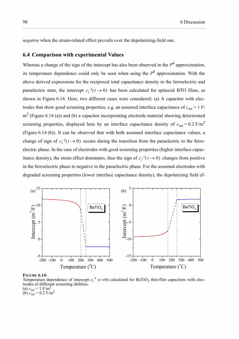
98 6 Discussion
negative when the strain-related effect prevails over the depolarizing-field one.
6.4 Comparison with experimental Values
Whereas a change of the sign of the intercept has also been observed in the P4 approximation,
its temperature dependence could only be seen when using the P8 approximation. With the
above derived expressions for the reciprocal total capacitance density in the ferroelectric and
paraelectric state, the intercept has been calculated for epitaxial BTO films, as
shown in Figure 6.14. Here, two different cases were considered: (a) A capacitor with elec-
trodes that show good screening properties, e.g. an assumed interface capacitance of cint = 1 F/
m2 (Figure 6.14 (a)) and (b) a capacitor incorporating electrode material showing deteriorated
screening properties, displayed here by an interface capacitance density of cint = 0.2 F/m2
(Figure 6.14 (b)). It can be observed that with both assumed interface capacitance values, a
change of sign of occurs during the transition from the paraelectric to the ferro-
electric phase. In the case of electrodes with good screening properties (higher interface capac-
itance density), the strain effect dominates, thus the sign of changes from positive
in the ferroelectric phase to negative in the paraelectric phase. For the assumed electrodes with
degraded screening properties (lower interface capacitance density), the depolarizing field ef-
-200 -100 0 100 200 300 400 500-15
-10
-5
0
5
In
terc
ept (
m2 /F
)
Temperature (oC)
BaTiO3
-200 -100 0 100 200 300 400 500-5
0
5
10
15
BaTiO3
Inte
rcep
t (m
2 /F)
Temperature (oC)FIGURE 6.14:Temperature dependence of intercept ct
-1 (t→0) calculated for BaTiO3 thin-film capacitors with elec-trodes of different screening abilities.(a) cint = 1 F/m2
(b) cint = 0.2 F/m2
(a) (b)
ct1– t 0→( )
ct1– t 0→( )
ct1– t 0→( )
6.5 Validation of the Theoretic Findings 99
fect overrides the influences of strain relaxation, resulting in a change of the sign of
from negative in the ferroelectric phase to positive in the paraelectric phase.
When the temperature dependence of the intercept, as shown in Figure 6.14 is compared to the
temperature dependent values resulting from measurements of the SRO and Pt samples in
chapter 5 (cmp. Figure 5.13 & Figure 5.17), the following becomes obvious:
• In principle, the temperature dependence of the Pt samples (Figure 5.13) shows a very good
agreement to the behavior of a capacitor with electrodes having good screening abilities
(Figure 6.14 (a)), thus the strain relaxation effects dominate the intercept .
• For the SRO samples, this temperature dependence (Figure 5.17) does not show the same
good agreement as in the Pt case, but nevertheless can be regarded as qualitatively compara-
ble. Hence, also here the strain relaxation effects dominate the capacitance density.
It follows from this comparison that only the theoretical approach incorporating electrodes
with good screening properties can be confirmed by the experimental values. This is reason-
able, since both sample series show the same strain state, as discussed in chapter 6.2 and do not
differ much in the theoretical estimates of their interface capacitance density associated with
the screening space charge in the electrodes which can be calculated using the results of
Refs. 31 and 108.
6.5 Validation of the Theoretic Findings
To conclude this chapter, the results of the theoretical discussion about the experimentally
achieved values will be summarized:
• It has been shown that the different trends of the thickness dependence of the phase transi-
tion temperature evaluated for the SRO and Pt samples can be solely explained by the influ-
ence of the excitation voltage levels. Using equal excitation fields rather then equal
excitation voltages, no serious difference in the trend of the phase transition temperature for
each thickness can be observed.
• In general, the BST layers investigated here show a relaxorlike dependence of the permittiv-
ity on the excitation amplitude, which in case of the Pt samples is obscured by the low inter-
ct1– t 0→( )
ct1– t 0→( )
100 6 Discussion
face capacitance and the subsequently lower voltage drop across the bulk capacitor. From
recalculations of the real applied field assuming a capacitive voltage divider, the relaxor
properties in principle can be recovered. A microscopic interpretation concerning the re-
laxor properties in perovskites is given in Ref. 137 and Ref. 138. In the present case, an in-
homogeneous distribution of STO and BTO in the BST-matrix can be assumed, that leads to
nanodomains with long-range interaction.
• From the analysis of the out-of-plane lattice constant it can be found that both SRO and Pt
samples are in the same thickness dependent strain state. The experimentally determined
thickness dependence of the lattice constant can be evaluated theoretically by means of the
thermodynamic theory.
• A thickness and strain dependent apparent interface capacitance could be evaluated by
means of a Curie-Weiss type dependence of the permittivity on the lattice mismatch strain.
The experimentally determined values in general show a good agreement with the thus cal-
culated values. The shift of the phase transition temperature depending on the strain in the
BST layer has been evaluated and reveals a fair agreement to what has been found experi-
mentally.
• Additional effects from depolarizing fields compete with the strain effects, while their con-
tributions to the apparent interface capacitance and the phase transition temperature have
opposite signs. The measured values of the phase transition temperature agree much better
with the calculated values when both strain and depolarizing fields are considered. Depend-
ing on the dominating effect the resulting apparent interface capacitance may be higher or
lower and even can become negative. A comparison of the experimentally determined tem-
perature dependence of the interface capacitance with the theoretically determined one re-
vealed a good agreement with the case of electrodes with good screening abilities in both
the SRO and Pt samples. In general, the depolarizing field is thought to be strongly depen-
dent on the screening abilities of the used electrode, which seem to be better in the SRO
case compared to the Pt case.
• Since theoretically both the strain effects and the depolarizing field result in apparent inter-
face capacitance values of the same order of magnitude as observed experimentally, it
6.5 Validation of the Theoretic Findings 101
seems to be difficult to distinguish between both influences. The strain state in the two com-
pared sample series was found to be identical, so that from the difference in the screening
abilities of the electrode material a separation may be accomplished.

102 6 Discussion
103
7 Conclusion7.1 Summary
In the course of this work, high quality epitaxial Ba0.7Sr0.3TiO3 (BST) thin films with SrRuO3
(SRO) bottom electrodes have been fabricated on SrTiO3 (STO) single crystalline substrates
using the pulsed laser deposition (PLD) technology. SRO (epitaxial via PLD) as well as Pt (by
sputter deposition) have been deposited on these bilayers to finally form BST thin film capaci-
tors. These samples have been termed accordingly SRO samples and Pt samples.
Physical analyses approved the BST films to be single crystalline with smooth, defect-free in-
terfaces to the electrode layers. From electrical analyses, small signal capacitance values as
well as ferroelectric polarization loops of the samples have been determined at a variety of
temperatures, voltages and frequencies. The interpretation of these measurements revealed val-
ues of the room temperature interface capacitance density as high as 1.55 F/m2 in the SRO
samples, which is at the order of magnitude as expected when having solely intrinsic influ-
ences and clearly outnumbers the values from previously reported studies. The polarization-
voltage loops show that ferroelectricity can be found even at temperatures high above RT,
which otherwise has not been reported yet. RT remanent polarization values of ~10 μC/cm2 for
the SRO sample and ~3 μC/cm2 for the Pt sample (both ~130 nm) have been found, while in
general the polarization loops are rather strongly slanted slim-loops.
• The analysis of the out-of-plane lattice constant revealed that both sample series are in the
same thickness dependent strain state. The experimentally determined thickness depen-
dence of the lattice constant agrees very well to a theoretically calculated one using a ther-
modynamic theory. From a Curie-Weiss type dependence of the permittivity on the lattice
mismatch strain a thickness and strain dependent apparent interface capacitance has been
evaluated as well as an estimate of the strain dependent shift of the phase transition temper-
ature. The experimentally values for ci and TC agree fairly well with these theoretical esti-
mates.
• Additional contributions from a depolarizing field to the apparent interface capacitance and
the shift of the phase transition temperature have been discussed. Theoretical calculations
104 7 Conclusion
reveal that these contributions in the case of the intercept have a different sign compared to
the strain influence, but can be roughly estimated to be in the same order of magnitude.
Since the strain contribution has been shown to be the same in both series, a separation of
the apparent interface capacitance into its components due to the assumed different depolar-
izing field contributions for Pt and SRO might be possible. Considering the influence of the
depolarizing field on the phase transition temperature explains and corrects the inaccuracy
that remains when comparing the observed thickness dependent phase transition tempera-
tures with the calculated ones that were derived allowing solely strain contributions.
Those theoretical considerations have shown that the term „interface capacitance“ has to be
used carefully. This parameter in general involves apparent contributions caused by the thick-
ness dependence of the intrinsic film permittivity, and may also become negative in special
cases. In the present case, the influences from the depolarizing fields as well those from the lat-
tice mismatch strain are in the same order of magnitude and therefore may counteract each
other. In general, the consideration of both mechanisms allows for a better understanding of
the observed differences in the behavior of the two sample series.
The maximum permittivity values for the thickest BST films (~130 nm) have been determined
as 3800 (SRO) and 2100 (Pt) and correspond to phase transition temperatures TC of 360 K
(SRO) and 310 K (Pt). In general, the BST thin film capacitors investigated here show a relax-
orlike dependence of the permittivity on the applied excitation voltage amplitude, which can
lead to an overestimation of the determined permittivity at higher excitation levels. In the case
of the Pt samples this behavior is strongly obscured by the low interface capacitance and the
correspondingly lower effective field at the bulk capacitor. By correcting the real effective
field and the real bulk permittivity, a partial recovery of the relaxorlike properties of the Pt
samples has been shown. Thus, relaxor properties in BST thin films are more pronounced
when dealing with better (thus defect free) interfaces but in most cases have not been reported
due to deteriorated electrode/film interfaces. In general, an inhomogeneous distribution of
STO and BTO in the BST-matrix that leads to the formation of polar nanodomains may be re-
sponsible for the observed relaxor phenomenon.
In summary, the experimental findings result in dielectric properties by far exceeding what has
been reported for comparable systems up to now. After all, the samples with oxide electrodes
7.2 Outlook 105
(SRO) show a superior behavior compared to the Pt samples. Using the effects of misfit strain
relaxation and depolarizing fields together with the nonlinear thermodynamic theory of ferro-
electrics the experimentally observed thickness dependent shift of the phase transition temper-
ature and the occurrence of a non-zero intercept in the linear fit of the reciprocal capacitance
density can be understood. The partial suppression of the relaxor properties of BST thin films
with Pt electrodes can be qualitatively explained by the less perfect film/electrode interface in
these samples compared to the SRO samples.
7.2 Outlook
Further evaluation of Pt and SRO with respect to their suitability as electrode material in thin
film BST capacitors should be considered. While the SRO layers can be regarded as high-qual-
ity single crystalline films, the Pt electrodes suffer from a poor interface to the BST: In addi-
tion to their non-epitaxial growth, contamination and amorphization of the interface is likely
due to the incorporated ex-situ deposition process. Additional studies with epitaxial Pt elec-
trodes and better interface characteristics are necessary to finally judge about any of the two´s
applicability in an actual memory device.
With the awareness of the relaxor properties in the BST samples, some more investigations
would be necessary to further understand its origins. One of the major questions in this context
must be to asses the inhomogeneities on the nano-scale, comparable to the correlation length rc
of the dipole nanoclusters as mentioned in [137]. A variation of the material composition in a
way that both epitaxial STO as well as BaTiO3 (BTO) samples could be investigated would
give a further insight into this issue: Since here no inhomogeneous distribution of any clusters
is expected, also no relaxor behavior should occur.
As a major goal for future work, the elimination of the inhomogeneities in thin BST films (and
thus the source of the relaxor-like properties) must be regarded. Having accomplished this
task, it would seem possible to regain the real bulk properties of BST even in thin films of a
few nm thickness. A similar recovery of bulk properties has been successfully achieved by
Saad et al. in the case of BTO lamellae [102], where they eliminated the deleterious influence
from defects in the thin films.

106 7 Conclusion
107
References[1] O. Auciello, R. Waser (Eds.), Science and Technology of Electroceramic Thin Films,
NATO ASI-Series E: Applied Sciences 284, Kluwer Academic Publishers (1995)
[2] O. Auciello, R. Ramesh, Guest Editors, Electroceramic Thin Films, Part I: Processing, Mat. Res. Bulletin 21, No. 6 (1996)
[3] O. Auciello, R. Ramesh, Guest Editors, Electroceramic Thin Films, Part II: Device Applications, Mat. Res. Bulletin 21, No. 7 (1996)
[4] H. Schaumburg, Keramik, Bd. 5 der Reihe Werkstoffe und Bauelemente der Elektrotech-nik, Teubner Verlag, Stuttgart (1994)
[5] R. Waser, Nanoelectronics and Information Technology, Wiley - VCH (2003)
[6] N. Setter, D. Damjanovic, L. Eng, G. Fox, S. Gevorgian, S. Hong, A. Kingon, H. Kohlst-edt, N. Y Park, G. B. Stephenson, I. Stolichnov, A. K. Tagantsev, D. V. Taylor, T. Yamada, and S. Streiffer, Ferroelectric thin films: Review of materials, properties, and applications, J. Appl. Phys. 100, 051606-1-46 (2006)
[7] J. F. Scott, Ferroelectric memories, Physics World 8, 46-50 (1995)
[8] J. F. Scott and C. A. Paz de Araujo, Ferroelectric Memories, Science 246, 1400-5 (1989)
[9] http://www.itrs.net/Links/2006Update/2006UpdateFinal.htm, International Technology Roadmap for Semiconductors, 2006 Edition: Front End Processes (2006)
[10] E. Fujii, Y. Uemoto, S. Hayashi, T. Nasu, Y. Shimada, A. Matsuda, M. Kibe, M. Azuma, T. Otsuki, G. Kano, M. Scott, L. D. McMillan, and C. A. Paz de Araujo, ULSI DRAM technology with Ba0.7Sr0.3TiO3 film of 1.3 nm equivalent SiO2 thickness and 10-9 A/cm2 leakage current, Proceedings of IEEE International Electron Devices Meeting, San Francisco, 267-70 (1992)
[11] B. E. Gnade, S. R. Summerfelt, D. Crenshaw, Processing and device issues of high per-mittivity materials for DRAMs, Nato ASI Series E: Applied Sciences, 284, 373-82, O. Auciello and R. Waser (Editors), Kluwer Academic Publishers, Dordrecht (1995)
[12] D. E. Kotecki, A review of high dielectric materials for DRAM capacitors, Integr. Ferro-electrics, 16, 1-20 (1997)
[13] T. M. Shaw, S. Trolier-McKinstry, and P. C. McIntyre, The Properties of Ferroelectric Films at small Dimensions, Annu. Rev. Mater. Sci. 30, 263-298 (2000)
[14] D. E. Kotecki, J. D. Baniecki, H. Shen, R. B. Laibowitz, K. L. Saenger, J. J. Lian, T. M. Shaw, S. D. Athavale, Cabral-C-Jr, P. R. Duncombe, M. Gutsche, G. Kunkel, Y. J. Park, Y. Y. Wang, and R. Wise, (Ba,Sr)TiO3 dielectrics for future stacked capacitor DRAM, IBM J. Res. Develop. 43, 367-82 (1999)
[15] C. Basceri, S. K. Streiffer, A. I. Kingon, and R. Waser, The dielectric response as a func-tion of temperature and film thickness of fiber-textured (Ba,Sr)TiO3 thin films grown by chemical vapor deposition, J. Appl. Phys. 82, 2497-504 (1997)
108 References
[16] L. J. Sinnamon, R. M. Bowman, and J. M. Gregg, Investigation of dead-layer thickness in SrRuO3/Ba0.5Sr0.5TiO3/Au thin-film capacitors, Appl. Phys. Lett. 78, 1724-6 (2001)
[17] C. B. Parker, J. P. Maria, and A. I. Kingon, Temperature and thickness dependent per-mittivity of (Ba,Sr)TiO3 thin films, Appl. Phys. Lett. 81, 340-2 (2002)
[18] J. McAneney, L. J. Sinnamon, R. M. Bowman, and J. M. Gregg, Temperature and fre-quency characteristics of the interfacial capacitance in thin-film barium-strontium-titan-ate capacitors, J. Appl. Phys. 94, 4566-70 (2003)
[19] A. A. Sirenko, C. Bernhard, A. Golnik, A. M. Clark, J. Hao, W. Si, and X. X. Xi, Soft-mode hardening in SrTiO3 thin films, Nature 404, 373-6 (2000)
[20] C. Zhou and D. M. Newns, Intrinsic dead layer effect and the performance of ferroelec-tric thin film capacitors, J. Appl. Phys. 82, 3081-3088 (1997)
[21] M. Izuha, K. Abe, and N. Fukushima, Electrical properties of all-perovskite oxide (SrRuO3/BaxSr1-xTiO3/SrRuO3) capacitors, Jpn. J. Appl. Phys. 36, 5866-9 (1997)
[22] I. Stolichnov, A. Tagantsev, N. Setter, J. S. Cross, and M. Tsukada, Control of leakage conduction of high-fatigue-endurance (Pb,La)(Zr,Ti)O3 film ferroelectric capacitors with Pt/SrRuO3 electrodes, Appl. Phys. Lett. 75, 1790-2 (1999)
[23] D.-K. Choi, B.-S. Kim, S.-Y. Son, S.-H. Oh, and K.-W. Park, Evaluation of tailored elec-trode (Ba,Sr)RuO3 for (Ba,Sr)TiO3, J. Appl. Phys. 86, 3347-51 (1999)
[24] V. Craciun and R. K. Singh, Characteristics of the surface layer of barium strontium titanate thin films deposited by laser ablation, Appl. Phys. Lett. 76, 1932-4 (2000)
[25] S. Stemmer, G. R. Bai, N. D. Browning, and S. K Streiffer, Microstructure of epitaxial Pb(Mg1/3Nb2/3)O3–PbTiO3 thin films grown by metalorganic chemical vapor deposi-tion, J. Appl. Phys. 87, 3526-31 (2000)
[26] C. L. Jia, K. Urban, S. Hoffmann, and R. Waser, Microstructure of columnar-grained SrTiO3 and BaTiO3 thin films prepared by chemical solution deposition, J. Mater. Res. 13, 2206-9
[27] E. H. Rhoderick and R. H. Williams, Metal-Semiconductor Contacts, Clarendon Press, Oxford (1988)
[28] A. M. Cowley and S. M. Sze, Surface States and Barrier Height of Metal-Semiconductor Systems, J. Appl. Phys. 36, 3212-20 (1965)
[29] W. Mönch, Role of virtual gap states and defects in metal-semiconductor contacts, Phys. Rev. Lett. 58, 1260-3 (1987)
[30] H. Y. Ku and F. G. Ullman, Capacitance of thin dielectric structures, J. Appl. Phys. 35, 265-267 (1964)
[31] C. T. Black and J. J. Welser, Electric-field penetration into metals: consequences for high-dielectric-constant capacitors, IEEE Transactions on Electron Devices 46, 776-80 (1999)
References 109
[32] M. Dawber, L. J. Sinnamon, J. F. Scott, and J. M. Gregg, Electrode field penetration: A new interpretation of tunnelling currents in barium strontium titanate (BST) thin films, Ferroelectrics 268, 35-40 (2002)
[33] M. Stengel and N. A. Spaldin, Origin of the dielectric dead layer in nanoscale capacitors, Nature 443, 679-82 (2006)
[34] J. Junquera and P. Ghosez, Critical thickness for ferroelectricity in perovskite ultrathin films, Nature 422, 506-9 (2003)
[35] C. S. Hwang, B. T. Lee, C. S. Kang, K. H. Lee, H.-J. Cho, H. Hideki, W. D. Kim, S. I. Lee, and M. Y. Lee, Depletion layer thickness and Schottky type carrier injection at the interface between Pt electrodes and (Ba, Sr)TiO3 thin films, J. Appl. Phys. 85, 287-95, (1998)
[36] Q. X. Jia, X. D. Wu, S. R. Foltyn, and P. Tiwari, Structural and electrical properties of Ba0.5Sr0.5TiO3 thin films with conductive SrRuO3 bottom electrodes, Appl. Phys. Lett.66, 2197-9 (1995)
[37] K. Abe, N. Yanase, S. Komatsu, K. Sano, N. Fukushima, and T. Kawakubo, Dielectric and ferroelectric properties of heteroepitaxial BaxSr1-xTiO3 films grown on SrRuO3/SrTiO3 substrates, IEICE Transactions on Electronics, E81-C, 505-12 (1998)
[38] P. K. Larsen, G. J. M. Dormans, D. J. Taylor, and P. J. van-Veldhoven, Ferroelectric properties and fatigue of PbZr0.51Ti0.49O3 thin films of varying thickness: blocking layer model, J. Appl. Phys. 76, 2405-13 (1994)
[39] A. K. Tagantsev and I. A. Stolichnov, Injection-controlled size effect on switching of ferroelectric thin films, Appl. Phys. Lett. 74, 1326-8 (1999)
[40] M. E. Lines and A. M. Glass, Principles and applications of ferroelectrics and related materials, Clarendon Press, Oxford (1977)
[41] B. Jaffe, W. R. Cook, and H. Jaffe, Piezoelectric ceramics, Academic Press, London (1971)
[42] F. Jona and G. Shirane, Ferroelectric Crystals, Pergamon Press, Oxford, London, New York, Paris (1962)
[43] T. Mitsui, I. Tatsuzaki, and E. Nakamura, Introduction to the physics of ferroelectrics, Gordon & Breach, London (1976)
[44] C. Kittel, Einführung in die Festkörperphysik, 12. tot. new rev. ed. (Introduction to solid state physics), Oldenbourg, München (1999)
[45] R. E. Newnham, Structure-property relations, Springer-Verlag, Berlin (1975)
[46] B. A. Strukov and A. P. Levanyuk, Ferroelectric phenomena in crystals. Physical found-ations, Springer-Verlag, Berlin (1998)
[47] A. S. Sonin and B. A. Strukow, Einführung in die Ferroelektrizität, Vieweg, Braunsch-weig (1974)
[48] G. Fasching, Werkstoffe für die Elektrotechnik, Springer Verlag Wien New York (1984)
110 References
[49] H. - J. Martin, Die Ferroelektrika, Akademische Verlagsgesellschaft, Leipzig (1964)
[50] G. H. Haertling, Ferroelectric ceramics: history and technology, J. Am. Ceram. Soc. 82, 797-818 (1999)
[51] N. Setter and R. Waser, Electroceramic materials, Acta Mater. 48, 151-78 (2000)
[52] D. Damjanovic, Ferroelectric, dielectric and piezoelectric properties of ferroelectric thin films and ceramics, Rep. Prog. Phys. 61, 1267-324 (1998)
[53] A. Hippel, R. G. Breckenridge, F. G. Chesley, and L. Tisza, High dielectric constant ceramics, Ind. Eng. Chem. 38, 1097-109 (1946)
[54] B. M. Wul and I. M. Goldman, Dielectric constants of titanates of metals of the second group, Compt. Rend. Acad. Sci. URSS 49, 139-42 (1945)
[55] A. Okazaki and M. Kawaminami, Lattice constant of strontium titanate at low tempera-tures, Mater. Res. Bull. 8, 545-50 (1973)
[56] T. Mitsui and W. B. Westphal, Dielectric and X-ray studies of CaxBa1-xTiO3 and CaxSr1-xTiO3, Phys. Rev. 124, 1354-1359 (1961)
[57] J. F. Scott, High-Dielectric Constant Thin Films for dynamic random access memories (DRAM). Annu. Rev. Mater. Sci. 28, 79-100 (1999)
[58] A. I. Kingon, S. K. Streiffer, C. Basceri, and S. R. Summerfelt, High-permittivity perovs-kite thin films for dynamic random-access memories, MRS Bull. 21, 46-52 (1996)
[59] I. Vendik, O. Vendik, V. Pleskachev, A. Svishchev, and R. Wordenweber, Design of tunable ferroelectric filters with a constant fractional band width, IEEE MTT-S Int. Microwave Symp. Dig. 3, 1461-4 (2001)
[60] B. Acikel, Y. Liu, A. S. Nagra, T. R. Taylor, P. J. Hansen, J. S. Speck, and R. A. York, Phase shifters using (Ba,Sr)TiO3 thin films on sapphire and glass substrates, IEEE MTT-S Int. Microwave Symp. Dig. 2, 1191-4 (2001)
[61] S. Tappe, U. Böttger, and R. Waser, Investigation of the high frequency properties of BST thin films-a comparison of three different commonly used methods, Int. Ferroelec-trics 53, 455-64 (2003)
[62] M. McQuarrie, Structural Behavior in the System (Ba, Ca, Sr) TiO3 and its relation to certain dielectric characteristics, J. Am. Cer. Soc. 38, 444 (1955)
[63] G. A. Smolenskii and K. I. Rozgachev, Ferroelectric properties in the barium titanate and strontium titanate solid solution system, Zh. Tekh. Fiz. 24, 1751-60 (1954)
[64] A. D. Hilton and B. W. Ricketts, Dielectric properties of Ba1-xSrxTiO3 ceramics, J. Phys. 29, 1321-5 (1996)
[65] C. B. Eom, R. B. Van-Dover, J. M. Phillips, D. J. Werder, J. H. Marshall, C. H. Chen, R. J. Cava, R. M. Fleming, and D. K. Fork, Fabrication and properties of epitaxial ferroelec-tric heterostructures with (SrRuO3) isotropic metallic oxide electrodes, Appl. Phys. Lett.63, 2570-2 (1993)
References 111
[66] P. R. van Loan, Conductive ternary oxides of ruthenium, and their use in thick film resis-tor glazes, Ceram. Bull. 51, 231-3 (1972)
[67] R. J. Bouchard and J. L. Gillson, Electrical properties of CaRuO3 and SrRuO3 single crystals, Mater. Res. Bull. 7, 873-8 (1972)
[68] J. F. Scott, Ferroelectric Memories, Springer Verlag, Berlin Heidelberg (2000)
[69] A. J. Hartmann, M. Neilson, R. N. Lamb, K. Watanabe, and J. F. Scott, Ruthenium oxide and strontium ruthenate electrodes for ferroelectric thin-films capacitors, Appl. Phys. A A70, 239-42 (2000)
[70] B. S. Kwak, A. Erbil, B. J. Wilkens, J. D. Budai, M. F. Chisholm, and L. A. Boatner, Strain relaxation by domain formation in epitaxial ferroelectric thin films, Phys. Rev. Lett. 68, 3733-6 (1992)
[71] J. S. Speck and W. Pompe, Domain configurations due to multiple misfit relaxation mechanisms in epitaxial ferroelectric thin films. I. Theory, J. Appl. Phys. 76, 466-76 (1994)
[72] H. Kohlstedt, N. A. Pertsev, and R. Waser, Size effects on polarization in epitaxial ferro-electric films and the concept of ferroelectric tunnel junctions including first results, Mater. Res. Soc. Symp. Proc., 161-72 (2002)
[73] J. W. Matthews and A. E. Blakeslee, Defects in epitaxial multilayers. I. Misfit disloca-tions, J. Cryst. Growth 27, 118-25 (1974)
[74] Z. G. Ban and S. P. Alpay, Optimization of the tunability of barium strontium titanate films via epitaxial stresses, J. Appl. Phys. 93, 504-11 (2003)
[75] N. A. Pertsev, A. G. Zembilgotov, and A. K. Tagantsev, Equilibrium states and phase transitions in epitaxial ferroelectric thin films, Ferroelectrics 223, 79-90 (1999)
[76] N. A. Pertsev, A. G. Zembilgotov, and A. K. Tagantsev, Effect of mechanical boundary conditions on phase diagrams of epitaxial ferroelectric thin films, Phys. Rev. Lett. 80, 1988-91 (1998)
[77] N. A. Pertsev, V. G. Koukhar, R. Waser, and S. Hoffmann, Curie-Weiss-type law for the strain and stress effects on the dielectric response of ferroelectric thin films, Appl. Phys. Lett. 77, 2596-8 (2000)
[78] L. Landau, On the theory of phase transformations. I, Phys. Z. Sowjet. 11, 26-47 (1937); L. Landau, On the theory of phase transformations. II, Phys. Z. Sowjet. 11, 545-555 (1937)
[79] V. Ginzburg, On the dielectric properties of ferroelectric (Seignette-electric) crystals and barium titanate, J. Phys., USSR 10, 107-115 (1946)
[80] A. F. Devonshire, Theory of barium titanate. I, Philosophical Magazine, UK 40, 1040-1063 (1949); A. F. Devonshire, Theory of barium titanate. II, Philosophical Magazine, UK 42, 1065-1079 (1951)
112 References
[81] N. A. Pertsev, V. G. Kukhar, H. Kohlstedt, and R. Waser, Phase diagrams and physical properties of single-domain epitaxial Pb(Zr1-xTix)O3 thin films, Phys. Rev. B: Condens. Matter, 67, 54107-1-10 (2003)
[82] N. A. Pertsev, J. R. Contreras, V. G. Kukhar, B. Hermanns, H. Kohlstedt, and R. Waser, Coercive field of ultrathin Pb(Zr0.52Ti0.48)O3 epitaxial films, Appl. Phys. Lett. 83, 3356-8 (2003)
[83] M. J. Haun, E. Furman, S. J. Jang, and L. E. Cross, Thermodynamic theory of the lead zirconate-titanate solid solution system. I. Phenomenology, Ferroelectrics 99, 13-25 (1989)
[84] P. C. Van Buskirk, J. F. Roeder, and S. Bilodeau, Manufacturing of perovskite thin films using liquid delivery MOCVD, Int. Ferroelectrics 10, 9-22 (1995)
[85] T. Horikawa, N. Mikami, H. Ito, Y. Ohno, T. Makita, and K. Sato (Ba0.75Sr0.25) TiO3films for 256 Mbit DRAM, IEICE Transactions on Electronics, E77-C, 385-91 (1994)
[86] W.-J. Lee and H.-G. Kim, Electrical properties of barium strontium titanate (BST) thin films deposited on various Pt-base electrodes, Int. Ferroelectrics 11, 111-9 (1995)
[87] C. S. Hwang, S. O. Park, H.-J. Cho, C. S. Kang, H.-K. Kang, S. I. Lee, and M. Y. Lee, Deposition of extremely thin (Ba,Sr)TiO3 thin films for ultra-large-scale integrated dynamic random access memory application, Appl. Phys. Lett. 67, 2819-21 (1995)
[88] R. Waser, Dielectric analysis of integrated ceramic thin film capacitors, Int. Ferroelec-trics 15, 39-51 (1997)
[89] S. K. Streiffer, C. Basceri, C. B. Parker, S. E. Lash, and A. I. Kingon, Ferroelectricity in thin films: The dielectric response of fiber-textured (BaxSr1-x)Ti1+yO3+z thin films grown by chemical vapor deposition, J. Appl. Phys. 86, 4565-75 (1999)
[90] W. Y. Park, K. H. Ahn, and C. S. Hwang, Effects of in-plane compressive stress on elec-trical properties of (Ba,Sr)TiO3 thin film capacitors prepared by on- and off-axis rf mag-netron sputtering, Appl. Phys. Lett. 83, 4387-9 (2003)
[91] R. Dittmann, R. Plonka, E. Vasco, N. A. Pertsev, J. Q. He, C. L. Jia, S. Hoffmann-Eifert, and R. Waser, Sharp ferroelectric phase transition in strained single-crystalline SrRuO3/Ba0.7Sr0.3TiO3/SrRuO3 capacitors, Appl. Phys. Lett. 83, 5011-13 (2003)
[92] R. Plonka, R. Dittmann, N. A. Pertsev, E. Vasco, and R. Waser, Impact of the top-elec-trode material on the permittivity of single-crystalline Ba0.7Sr0.3TiO3 thin films, Appl. Phys. Lett. 86, 202908-1-3 (2005)
[93] W. Känzig, Space Charge Layer Near the Surface of a Ferroelectric, Phys. Rev. 98, 549-50 (1955)
[94] V. G. Bhide, R. T. Gondhalekar, and S. N. Shringi, Surface layers on ferroelectric BaTiO3 crystals, J. Appl. Phys. 36, 3825-33 (1965)
[95] U. Ellerkmann, R. Liedtke, U. Böttger, and R. Waser, Interface related thickness depen-dence of the tunability in BaSrTiO3 thin films, Appl. Phys. Lett. 85, 4708-10 (2004); U. Ellerkmann, Impact of the interface capacity on failure mechanisms and size effects in ferroelectric thin films, PhD Thesis RWTH Aachen (2006)
References 113
[96] A. Lookman, R. M. Bowman, J. M. Gregg, J. Kut, S. Rios, M. Dawber, A. Ruediger, and J. F. Scott, Thickness independence of true phase transition temperatures in barium strontium titanate films, J. Appl. Phys. 96, 555-62 (2004)
[97] L. J. Sinnamon, R. M. Bowman, and J. M. Gregg, Thickness-induced stabilization of fer-roelectricity in SrRuO3/Ba0.5Sr0.5TiO3/Au thin film capacitors, Appl. Phys. Lett. 81, 889-91 (2002)
[98] S. Hoffmann, Modifizierte Erdalkalititanat-Dünnschichten für integrierte Bauelemente: Morphologie, dielektrische Eigenschaften und Ladungstransportmechanismen, PhD Thesis RWTH Aachen (1994)
[99] R. Liedtke, Herstellung, Charakterisierung und Bauelementsimulation von integrierten, elektrokeramischen Dünnschichtkondensatoren, PhD Thesis RWTH Aachen (2003)
[100] K. Abe and S. Komatsu, Dielectric constant and leakage current of epitaxially grown and polycrystalline SrTiO3 thin films, Jpn. J. Appl. Phys. 32, 4186-9 (1993)
[101] C. M. Chu and P. Lin, Electrical properties and crystal structures of (Ba,Sr)TiO3 films and BaRuO3 bottom electrodes prepared by sputtering, Appl. Phys. Lett. 72, 1241-3 (1998)
[102] M. M. Saad, P. Baxter, R. M. Bowman, J. M. Gregg, F. D. Morrison, and J. F. Scott, Intrinsic dielectric response in ferroelectric nano-capacitors, J. Phys.: Condens. Matter16, L451-6 (2004)
[103] M.-S. Tsai, S. C. Sun, and T.-Y. Tseng, Effect of bottom electrode materials on the elec-trical and reliability characteristics of (Ba, Sr)TiO3 capacitors, IEEE Transactions on Electron Devices 46, 1829-38 (1999)
[104] O. G. Vendik and S. P. Zubko, Ferroelectric phase transition and maximum dielectric permittivity of displacement type ferroelectrics (BaxSr1-xTiO3), J. Appl. Phys. 88, 5343-50 (2000)
[105] A. K. Tagantsev, V. O. Sherman, K. F. Astafiev, J. Venkatesh, and N. Setter, Ferroelec-tric Materials for Microwave Tunable Applications, J. Electroceram. 11, 5-66 (2003)
[106] C. A. Mead, Anomalous capacitance of thin dielectric structure, Phys. Rev. Lett. 6, 545-546 (1961)
[107] J. G. Simmons, An analytic form of Ku and ullmans equations, Appl. Phys. Lett. 6, 54-55 (1965)
[108] D. J. Kim, J. Y. Jo, Y. S. Kim, Y. J. Chang, J. S. Lee, Yoon, T. K. Song, and T. W. Noh, Polarization relaxation induced by a depolarization field in ultrathin ferroelectric BaTiO3capacitors, Phys. Rev. Lett. 95, 237602/1-4 (2005)
[109] M. Dawber and J. F. Scott, Models of electrode-dielectric interfaces in ferroelectric thin-film devices, Jpn. J. Appl. Phys. 41, 6848-51 (2002)
[110] I. P. Batra, P. Wurfel, and B. D. Silverman, Phase transition, stability and depolarization field in ferroelectric thin films, Phys. Rev. B (Solid State), USA 8, 3257-65 (1973)
114 References
[111] I. P. Batra, P. Wurfel, and B. D. Silverman, Depolarization field and stability consider-ations in thin ferroelectric films, J. Vac. Sci. Technol., USA 10, 687-92 (1973)
[112] I. P. Batra, P. Wurfel, and B. D. Silverman, New type of first-order phase transition in ferroelectric thin films, Phys. Rev. Lett. 30, 384-7 (1973)
[113] R. R. Mehta, B. D. Silverman, and J. T. Jacobs, Depolarization fields in thin ferroelectric films, J. Appl. Phys. 44, 3379-85 (1973)
[114] M. Großmann, Imprint: An Important Failure Mechanism of Ferroelectric Thin Films in View of Memory Applications, PhD Thesis RWTH Aachen (2001)
[115] A. M. Bratkovsky and A. P. Levanyuk, Depolarizing field and "real" hysteresis loops in nanometer-scale ferroelectric films, arXiv:cond-mat/0608283 (2006)
[116] W. Cochran, Crystal stability and the theory of ferroelectricity, Adv. Phys. 9, 387-423 (1960)
[117] U. Poppe, Herstellung von Oxidschichten mit physikalischen Methoden: Sputtern, reak-tives Aufdampfen, Laserablation, in R. Hölzle (Ed.), Elektrokeramische Materialien, volume 26 of Vorlesungsmanuskripte des IFF-Ferienkurses, chapter B4, ppB4.1-38, Forschungszentrum Jülich GmbH, Jülich (1995)
[118] M. Klee, Schichtherstellung mit chemischen Methoden: Sol-Gel, MOD, in R. Hölzle (Ed.), Elektrokeramische Materialien, volume 26 of Vorlesungsmanuskripte des IFF-Ferienkurses, chapter B5, ppB5.1-16, Forschungszentrum Jülich GmbH, Jülich (1995)
[119] H. Schwarz and H. A. Tourtellotte, Vacuum deposition high-energy laser with emphasis on barium titanate films, J. Vac. Sci. Technol. 6, 373-8 (1969)
[120] D. B. Chrisey and G. K. Hubler, Pulsed Laser Deposition of Thin Films, John Wiley & Sons, Inc. (1994)
[121] R. F. Pinizzotto, E. G. Jacobs, H. Yang, S. R. Summerfelt, and B. E. Gnade, Cross-sec-tional TEM studies of barium strontium titanate deposited on silicon by pulsed laser ablation, Mater. Res. Soc. 463-8 (1992)
[122] C. L. Chen, Y. Cao, Z. J. Huang, Q. D. Jiang, Z. Zhang, Y. Y. Sun, W. N. Kang, L. M. Dezaneti, W. K. Chu, and C. W. Chu, Epitaxial SrRuO3 thin films on (001) SrTiO3, Appl. Phys. Lett. 71, 1047-9 (1997)
[123] Hewlett Packard, HP 4194A Impedance/Gain-Phase Analyzer Operation Manual (1996)
[124] Agilent Technologies, Impedance Measurement Handbook (2006)
[125] C. B. Sawyer and C. H. Tower, Rochelle Salt as a Dielectric, Phys. Rev. 35, 269-73 (1930)
[126] O. Lohse, Verlustmechanismen in ferroelektrischen keramischen Dünnschichtkondensa-toren für hochintegrierte nicht-flüchtige Halbleiterspeicher, PhD Thesis RWTH Aachen(2001)
[127] aixACCT Systems GmbH, Aachen, Germany, manual of the TF Analyzer 2000 FE-Mod-ule
References 115
[128] H. Krischner, Einführung in die Röntgenfeinstrukturanalyse, Vieweg, Braunschweig (1990)
[129] B.D. Cullity and S.R. Stock, Elements of X-Ray Diffraction (3rd Edition), Prentice Hall (2001)
[130] W. Kraus and G. Nolze, PowderCell, Version 2.3, Federal Institute for Materials Research and Testing, Berlin, Germany
[131] J. Q. He, E. Vasco, C. L. Jia, R. Dittmann, and R. H. Wang, Microstructure of epitaxial Ba0.7Sr0.3TiO3/SrRuO3 bilayer films on SrTiO3 substrates, J. Appl. Phys. 97, 104907-1-5 (2005)
[132] D. Bolten, Reversible and Irreversible Polarization Processes in Ferroelectric Ceramics and Thin Films, PhD Thesis RWTH Aachen (2002)
[133] J. Rodriguez Contreras, Ferroelectric Tunnel Junctions, PhD Thesis Universität zu Köln(2003)
[134] M. Tyunina and J. Levoska, Coexistence of ferroelectric and relaxor properties in epitax-ial films of Ba1-xSrxTiO3, Physical Review B (Condensed Matter and Materials Phys-ics), USA 70, 132105-1-4 (2004)
[135] D. V. Taylor and D. Damjanovic, Domain wall pinning contribution to the nonlinear dielectric permittivity in Pb(Zr, Ti)O3 thin films, Appl. Phys. Lett. 73, 2045-7 (1998)
[136] E. V. Colla, S. M. Gupta, and D. Viehland, Alternating current field effect on the freez-ing temperature of relaxor ferroelectrics, J. Appl. Phys. 85, 362-7 (1999)
[137] G. A. Samara, The relaxational properties of compositionally disordered ABO3 perovs-kites, J. Phys. Condens. Mat. 15, R367-411 (2003)
[138] L. Zhou, P. M. Vilarinho, and J. L. Baptista, Dependence of the structural and dielectric properties of Ba1-xSrxTiO3 ceramic solid solutions on raw material processing, J. Eur. Ceram. Soc. 19, 2015-20 (1999)
[139] R. Waser, U. Böttger, and S. Tiedke, Polar Oxides: Properties, Characterization, and Imaging, chapter 15, Wiley-VCH (2005)
[140] M. Tyunina, J. Levoska, S. Leppävuori, and A. Sternberg, Dielectric nonlinearities in ferroelectric thin-film heterostructures, Appl. Phys. Lett. 78, 527-9 (2001)
[141] R. E. Peierls, The size of a dislocation, Proc. Phys. Soc. Lond. 52, 34-7 (1940)
[142] Landolt-Börnstein, Numerical Data and Functional Relationships in Science and Tech-nology, New Series, Vol. III/29a, Springer, Berlin, 1992; Y. S. Touloukian, R. K. Kirby, R. E. Taylor, and T. Y. R. Lee, Thermal Expansion: Nonmetallic Solids (Thermophysical Properties of Matter), Vol. 13, Plenum, New York, 1977
[143] N. A. Pertsev, A. K. Tagantsev, and N. Setter, Phase transitions and strain-induced ferro-electricity in SrTiO3 epitaxial thin films, Phys. Rev. B: Condens. Matter, 61, R825-9 (2000)
116 References
[144] N. A. Pertsev, R. Dittmann, R. Plonka, and R. Waser, Thickness dependence of intrinsic dielectric response and apparent interfacial capacitance in ferroelectric thin films, J. Appl. Phys. 101, 074102-1-9 (2007)
Lebenslauf
Persönliche Daten
Name, Vorname Plonka, Rafael Anschrift Holunderstr. 116 28207 Bremen Geburtsdatum 17.04.1975 Geburtsort Moers Familienstand ledig, keine Kinder Staatsangehörigkeit deutsch
Schulbildung
1981 – 1985 St. Viktor Grundschule Xanten 1985 – 1992 Städt. Stiftsgymnasium Xanten 1992 – 1994 Gymnasium Adolfinum Moers Abschluss am 08.06.1994 mit Abitur 07/94 – 09/95 Zivildienst in der Malteser Betreuungseinrichtung Xanten WS 95 – WS 01 Studium der Elektrotechnik an der RWTH-Aachen Abschluss am 29.11.2001 als Diplom-Ingenieur
Berufliche Tätigkeit
01.03.2002 – 31.03.2007 wissenschaftlicher Angestellter am Institut für Werkstoffe der Elektrotechnik der RWTH-Aachen (Prof. Dr.-Ing. R. Waser)
Seit 01.05.2007 Entwicklungsingenieur bei der ZARM Technik AG, Bremen