Nanophysics and Nanotechnology - ReadingSample
17
Nanophysics and Nanotechnology An Introduction to Modern Concepts in Nanoscience Bearbeitet von Edward L. Wolf 3. Auflage 2015. Buch. XX, 336 S. Kartoniert ISBN 978 3 527 41324 9 Format (B x L): 17 x 24,4 cm Gewicht: 722 g Weitere Fachgebiete > Technik > Technik Allgemein > Nanotechnologie Zu Inhaltsverzeichnis schnell und portofrei erhältlich bei Die Online-Fachbuchhandlung beck-shop.de ist spezialisiert auf Fachbücher, insbesondere Recht, Steuern und Wirtschaft. Im Sortiment finden Sie alle Medien (Bücher, Zeitschriften, CDs, eBooks, etc.) aller Verlage. Ergänzt wird das Programm durch Services wie Neuerscheinungsdienst oder Zusammenstellungen von Büchern zu Sonderpreisen. Der Shop führt mehr als 8 Millionen Produkte.
Transcript of Nanophysics and Nanotechnology - ReadingSample
Nanophysics and Nanotechnology
An Introduction to Modern Concepts in Nanoscience
Bearbeitet vonEdward L. Wolf
3. Auflage 2015. Buch. XX, 336 S. KartoniertISBN 978 3 527 41324 9
Format (B x L): 17 x 24,4 cmGewicht: 722 g
Weitere Fachgebiete > Technik > Technik Allgemein > Nanotechnologie
Zu Inhaltsverzeichnis
schnell und portofrei erhältlich bei
Die Online-Fachbuchhandlung beck-shop.de ist spezialisiert auf Fachbücher, insbesondere Recht, Steuern und Wirtschaft.Im Sortiment finden Sie alle Medien (Bücher, Zeitschriften, CDs, eBooks, etc.) aller Verlage. Ergänzt wird das Programmdurch Services wie Neuerscheinungsdienst oder Zusammenstellungen von Büchern zu Sonderpreisen. Der Shop führt mehr
als 8 Millionen Produkte.
1
1Introduction
Technology has to do with the application of scientific knowledge to the economic(profitable) production of goods and services.This textbook is concerned with thesize or scale of working machines and devices in different forms of technology. Itis particularly concerned with the smallest devices that are possible, and equallywith the appropriate laws of nanometer-scale physics: “nanophysics,” which areavailable to accurately predict behavior of matter on this invisible scale. Physicalbehavior at the nanometer scale is predicted accurately by quantum mechanics,represented by Schrodinger’s equation. Schrodinger’s equation provides a quan-titative understanding of the structure and properties of atoms. Chemical mat-ter, molecules, and even the cells of biology, being made of atoms, are therefore,in principle, accurately described (given enough computing power) by this well-tested formulation of nanophysics.There are often advantages in making devices smaller, as in modern semi-
conductor electronics. What are the limits to miniaturization and how smalla device can be made? Any device must be composed of atoms, whose sizesare of the order of 0.1 nm. Here, the term “nanotechnology” will be associatedwith human-designed working devices in which some essential element(s),produced in a controlled fashion, have sizes of 0.1 nm to thousands of nanome-ters, or, 1Å to 1 μm. There is thus an overlap with “microtechnology” at themicrometer-size scale. Microelectronics is the most advanced present technol-ogy, apart from biology, whose complex operating units are on a scale as small asmicrometers.Even though the literature of nanotechnology may refer to nanoscale machines,
even “self-replicating machines built at the atomic level” [1], it is admitted that an“assembler breakthrough” [2] will be required for this to happen, and no nanoscalemachines presently exist. In fact, scarcely any micrometer-scale machines existeither, and it seems that the smallest mechanical machines readily available in awide variety of forms are really on the millimeter scale, as in conventional wrist-watches. (To avoid confusion, note that the prefix “micro” is sometimes applied,but never in this textbook, to larger scale techniques guided by opticalmicroscopy,such as “microsurgery.”)The reader may correctly infer that nanotechnology is presently more concept
than fact, although it is certainly a media and funding reality. The fact that the
Nanophysics and Nanotechnology: An Introduction to Modern Concepts in Nanoscience, Third Edition.Edward L Wolf.© 2015 Wiley-VCH Verlag GmbH & Co. KGaA. Published 2015 by Wiley-VCH Verlag GmbH & Co. KGaA.
2 1 Introduction
concept has great potential for technology is themessage to read from the fundingand media attention to this topic.The idea of the limiting size scale of a miniaturized technology is fundamentally
interesting for several reasons. As sizes approach the atomic scale, the relevantphysical laws change from classical to quantum-mechanical laws of nanophysics.The changes in behavior from classical, to “mesoscopic,” to atomic scale, arebroadly understood in contemporary physics, but the details in specific cases arecomplex and need to be worked out. While the changes from classical physicsto nanophysics may mean that some existing devices will fail, the same changesopen up possibilities for the invention of new devices.A primary interest in the concept of nanotechnology comes from its connec-
tions with biology. The smallest forms of life, bacteria, cells, and the active com-ponents of living cells of biology, have sizes in the nanometer range. In fact, itmay turn out that the only possibility for a viable complex nanotechnology is thatrepresented by biology. Certainly, the present understanding of molecular biol-ogy has been seen as an existence proof for “nanotechnology” by its pioneers andenthusiasts. Inmolecular biology, the “self-replicatingmachines at the atomic lev-el” are guided by DNA, replicated by RNA, specific molecules are “assembled” byenzymes, and cells are replete with molecular-scale motors, of which kinesin isone example. Ion channels, which allow (or block) specific ions (e.g., potassiumor calcium) to enter a cell through its lipid wall, seem to be exquisitely engineeredmolecular-scale devices where distinct conformations of proteinmolecules definean open channel versus a closed channel.Biological sensors, such as the rods and cones of the retina and the nanoscale
magnets found in magnetotactic bacteria, appear to operate at the quantumlimit of sensitivity. Understanding the operation of these sensors doubtlesslyrequires application of nanophysics. One might say that Darwinian evolution, amatter of odds of survival, has mastered the laws of quantum nanophysics, whichare famously probabilistic in their nature. Understanding the role of quantumnanophysics entailed in the molecular building blocks of nature may informthe design of artificial sensors, motors, and perhaps much more, with expectedadvances in experimental and engineering techniques for nanotechnology.In the improbable event that engineering, in the traditional sense, of molecular-
scale machines becomes possible, the most optimistic observers note that theseinvisible machines could be engineered tomatch the size or scale of the moleculesof biology.Medical nanomachinesmight then be possible, which could be directedto correct defects in cells, to kill dangerous cells, such as cancer cells, or even,mostfancifully, to repair cell damage present after thawing of biological tissue, frozenas a means of preservation [3].This textbook is intended to provide a guide to the ideas and physical concepts
that allow an understanding of the changes that occur as the size scale shrinkstoward the atomic scale. Our point of view is that a general introduction to theconcepts of nanophysicswill add greatly to the ability of students and professionalswhose undergraduate training has been in engineering or applied science, to con-tribute in the various areas of nanotechnology. The broadly applicable concepts
1.1 Nanometers, Micrometers, and Millimeters 3
of nanophysics are worth study, as they do not become obsolete with inevitablechanges in the forefront of technology.
1.1Nanometers, Micrometers, and Millimeters
A nanometer, 10−9 m, is about 10 times the size of the smallest atoms, such ashydrogen and carbon, while a micron is barely larger than the wavelength of vis-ible light, thus invisible to the human eye. A millimeter, the size of a pinhead, isroughly the smallest size available in present-day machines. The range of scalesfrom millimeters to nanometers is one million, which is also about the range ofscales in present-day mechanical technology, from the largest skyscrapers to thesmallest conventional mechanical machine parts. The vast opportunity for mak-ing new machines, spanning almost six orders of magnitude from 1mm to 1 nm,is one take on Richard Feynman’s famous statement [4]: “there is plenty of room atthe bottom.” If L is taken as the typical length, 0.1 nm for an atom, perhaps 2m fora human, this scale range in L would be 2 × 10¹⁰. If the same scale range were toapply to an area, 0.1 nm by 0.1 nm versus 2 m × 2 m, the scale range for area L2 is4 × 1020. Since the volume L3 is enclosed by sides L, we can see that the number ofatoms of size 0.1 nm in a (2m)3 volume is about 8 × 1030. Recalling that Avogadro’snumber NA = 6.022 × 10²³ is the number of atoms in a grammole, supposing thatthe atoms were 12C, molar mass 12 g; then the mass enclosed in the (2m)3 volumewould be 15.9 × 10⁴ kg, corresponding to a density 1.99 × 10⁴ kgm−3 (19.9 g cc−1).(This is about 20 times the density of water, and higher than the densities of ele-mental carbon in its diamond and graphitic forms (which are 3.51 and 2.25 g cc−1,respectively), because the equivalent size L of a carbon atom in these elementalforms slightly exceeds 0.1 nm.)A primary working tool of the nanotechnologist is facility in scaling the magni-
tudes of various properties of interest, as the length scale L shrinks, for example,from 1mm to 1 nm.Clearly, the number of atoms in a device scales as L3. If a transistor on a micron
scale contains 1012 atoms, then on a nanometer scale, L′∕L = 10−3 it will contain1000 atoms, likely too few to preserve its function!Normally, we think of scaling as an isotropic scale reduction in three dimen-
sions. However, scaling can be thought of usefully when applied only to one ortwo dimensions, scaling a cube to a two-dimensional (2D) sheet of thickness a orto a one-dimensional (1D) tube or “nanowire” of cross-sectional area a2.The term“zero-dimensional” is used to describe an object small in all three dimensions, hav-ing volume a3. In electronics, a zero-dimensional object (a nanometer sized cubea3 of semiconductor) is called a “quantum dot” (QD) or “artificial atom” becauseits electronic states are few, sharply separated in energy, and thus resemble thoseof an atom.As we see, a QD also typically has so small a radius a, with correspondingly
small electrical capacitance C = 4𝜋𝜀𝜀oa (where 𝜀𝜀o is the dielectric constant of
4 1 Introduction
the medium in which the QD is immersed), that the electrical charging energyU = Q2∕2C is “large.” (In many situations, a “large” energy is one that exceedsthe thermal excitation energy, kBT , for T = 300K, basically room temperature.Here, T is the absolute Kelvin temperature and kB is the Boltzmann’s constant,1.38 × 10−23 JK−1.) In this situation, a change in the charge Q on the QD by evenone electron charge e may effectively, by the “large” change in U, switch off thepossibility of the QD being part of the path of flow for an external current.This is the basic idea of the “single electron transistor.”The role of theQD in this
application resembles the role of the grid in the vacuum triode, but only one extraelectron change of charge on the “grid” turns the device off. To make a deviceof this sort work at room temperature requires that the QD be tiny, only a fewnanometers in size.
1.1.1Plenty of Room at the Bottom
Think of reducing the scale of working devices and machines from 1mm to 1 nm,six orders of magnitude! Over most of this scaling range, perhaps the first fiveorders of magnitude, down to 10 nm (100Å), the laws of classical Newtonianphysics may well suffice to describe changes in behavior. This classical rangeof scaling is so large, and the changes in magnitudes of important physicalproperties, such as resonant frequencies, are so great, that completely differentapplications may appear.
1.1.2Scaling the Xylophone
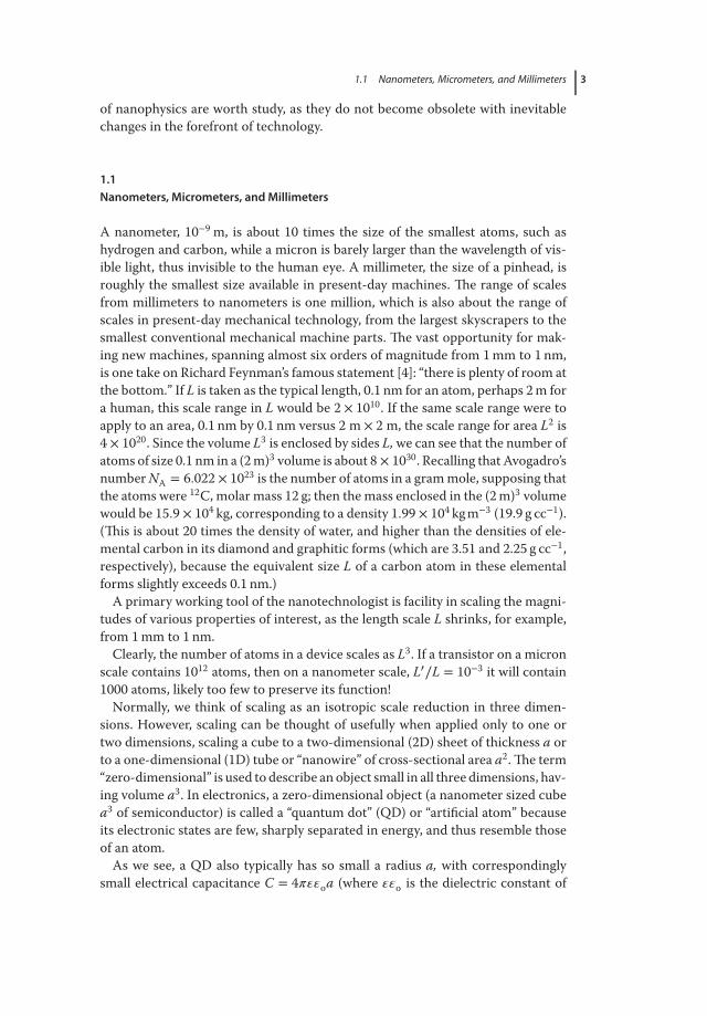
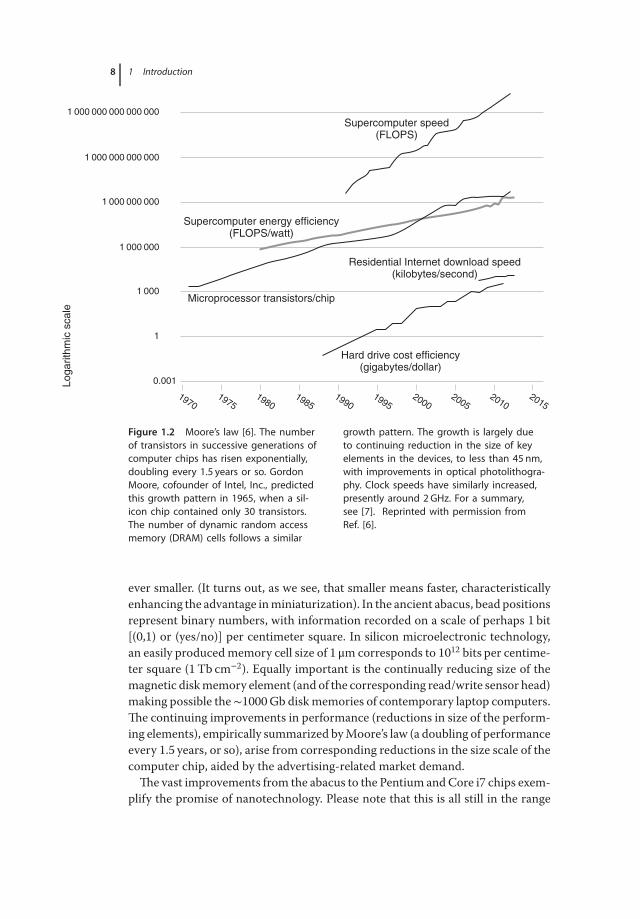
The familiar xylophone produces musical sounds when its keys (a linear array ofrectangular bars of dimensions a × b × c, with progressively longer key lengths cproducing lower audio frequencies) are struck by a mallet and go into transversevibration perpendicular to the smallest, a, dimension. The traditional “middle C”in music corresponds to 256Hz. If the size scale of the xylophone key is reducedto the micrometer scale, as has recently been achieved, using the semiconduc-tor technology, and the mallet is replaced by electromagnetic excitation, the sametransverse mechanical oscillations occur, and are measured to approach the giga-hertz (109 Hz) range [5]!The measured frequencies of the micrometer-scale xylophone keys are still
accurately described by the laws of classical physics. (In fact, the oscillators thathave been successfully miniaturized, see Figure 1.1, differ slightly from xylophonekeys, in that they are clamped at both ends, rather than being loosely suspended.Very similar equations are known to apply in this case.) Oscillators whosefrequencies approach the gigahertz range have completely different applicationsthan those in the musical audio range!Could such elements be used in new devices to replace Klystrons and Gunn
oscillators, conventional sources of gigahertz radiation? If means could be found
1.1 Nanometers, Micrometers, and Millimeters 5
×20 000 2 μm 5 kv 5 mm
Figure 1.1 Silicon nanowires in a harp-likearray. Due to the clamping of the single-crystal silicon bars at each end and the lackof applied tension, the situation is more likean array of xylophone keys. The resonant
frequency of the wire of 2 μm length isabout 400MHz. After reprinted with permis-sion from Ref. [5], Copyright 1999. AmericanInstitute of Physics.
to fabricate “xylophone keys” scaling down from the micrometer scale to thenanometer scale, classical physics would presumably apply almost down to themolecular scale. The limiting vibration frequencies would be those of diatomicmolecules, which lie in the range 1013–1014 Hz. For comparison, the frequencyof light used in fiber-optic communication is about 2 × 10¹⁴ Hz.
1.1.3Reliability of Concepts and Approximate Parameter Values Down to AboutL= 10 nm (100 Atoms)
The large extent of the “classical” range of scaling, from 1mm down to perhaps10 nm, is related to the stability (constancy) of the basic microscopic properties ofcondensedmatter (conventional building and engineeringmaterials) almost downto the scale L of 10 nm or 100 atoms in line, or a million atoms per cube.Typical microscopic properties of condensed matter are interatomic spacing,
mass density, bulk speed of sound 𝜐s, Young’s modulus Y , bulk modulus B, cohe-sive energy Uo, electrical resistivity 𝜌, thermal conductivity K , relative magneticand dielectric susceptibilities 𝜅 and 𝜀, Fermi energy EF and work function 𝜑 ofa metal, and bandgap of a semiconductor or insulator, Eg. A timely example inwhich bulk properties are retained down to nanometer sample sizes is afforded bythe CdSe “QD” fluorescent markers, which are described below.
6 1 Introduction
1.1.4Nanophysics Built into the Properties of Bulk Matter
Even if we can describe the size scale of 1mm to 10 nm as one of “classical scal-ing,” before distinctly size-related anomalies are strongly apparent, a nanotech-nologist must appreciate that many properties of bulk condensed matter alreadyrequire concepts of nanophysics for their understanding. This might seem obvi-ous, in that atoms themselves are completely nanophysical in their structure andbehavior!Beyond this, however, the basic modern understanding of semiconductors,
involving energy bands, forbidden gaps, and effective masses m* for free electronsand free holes, is based on nanophysics in the form of Schrodinger’s equation asapplied to a periodic structure.Periodicity, a repeated unit cell of dimensions a×b×c (in three dimensions), pro-
foundly alters the way an electron (or a “hole,” which is the inherently positivelycharged in the absence of an electron) moves in a solid. As we discuss more com-pletely in the following, ranges (bands) of energy of the free carrier exist for whichthe carrier will pass through the periodic solid with no scattering at all, muchin the same way that an electromagnetic wave will propagate without attenua-tion in the passband of a transmission line. In energy ranges between the allowedbands, gaps appear, where no moving carriers are possible, in analogy to the lackof signal transmission in the stopband frequency range of a transmission line.Therefore, the “classical” range of scaling as mentioned earlier is one in which
the consequences of periodicity for the motions of electrons and holes (wildly“nonclassical,” if referred to Newton’s laws, for example) are unchanged. In prac-tice, the properties of a regular array of 100 atoms on a side, a nanocrystal con-taining only a million atoms, is still large enough to be accurately described bythe methods of solid-state physics. If the material is crystalline, the properties ofa sample of 106 atoms are likely to be an approximate guide to the properties of abulk sample. To extrapolate the bulk properties from a 100-atom-per-side simu-lation may not be too far off.It is probably clear that a basic understanding of the ideas, and also the
fabrication methods, of semiconductor physics is likely to be a useful tool forthe scientist or engineer who works in nanotechnology. Almost all devices inthe Micro-Electro-Mechanical Systems category, including accelerometers,related angular rotation sensors, and more, are presently fabricated using thesemiconductor microtechnology.The second, and more challenging, question for the nanotechnologist is to
understand and hopefully to exploit those changes in physical behavior thatoccur at the end of the classical scaling range. The “end of the scaling” is thesize scale of atoms and molecules, where nanophysics is the proven conceptualreplacement of the laws of classical physics. Modern physics, which includesquantum mechanics as a description of matter on a nanometer scale, is a fullydeveloped and proven subject whose application to real situations is limited onlyby modeling and computational competence.
1.2 Moore’s Law 7
In themodern era, simulations and approximate solutions increasingly facilitatethe application of nanophysics to almost any problem of interest. Many centralproblems are already (adequately, or more than adequately) solved in the exten-sive literature of theoretical chemistry, biophysics, condensedmatter physics, andsemiconductor device physics. The practical problem is to find the relevant work,and, frequently, to convert the notation and units systems to apply the results tothe problem at hand.It is worth saying that information has no inherent (i.e., zero) size.The density of
information that can be stored is limited only by the coding element, be it a beadon an abacus, a magnetized region on a hard disk, a charge on a complementarymetal oxide semiconductor capacitor, a nanoscale indentation on a plastic record-ing surface, the presence or absence of a particular atom at a specified location, orthe presence of an “up” or “down” electronic or nuclear spin (magnetic moment)on a density of atoms in condensed matter, (0.1nm)−3 = 1030m−3 = 1024 cm−3. Ifthese coding elements are on a surface, then the limiting density is (0.1nm)−2 =1020m−2, or 6.45 × 10¹⁶ per inch2.The principal limitation may be the physical size of the reading element, which
historically would be a coil of wire (solenoid) in the case of the magnetic bit. Thelimiting density of information in the presently advancing technology of mag-netic computer hard disk drives is about 100Gb per inch2 or 1011 per inch2. Itappears that nonmagnetic technologies, perhaps based on arrays of atomic forcemicroscope tips writing onto a plastic film such as polymethylmethacrylate, mayeventually overtake the magnetic technology.
1.2Moore’s Law
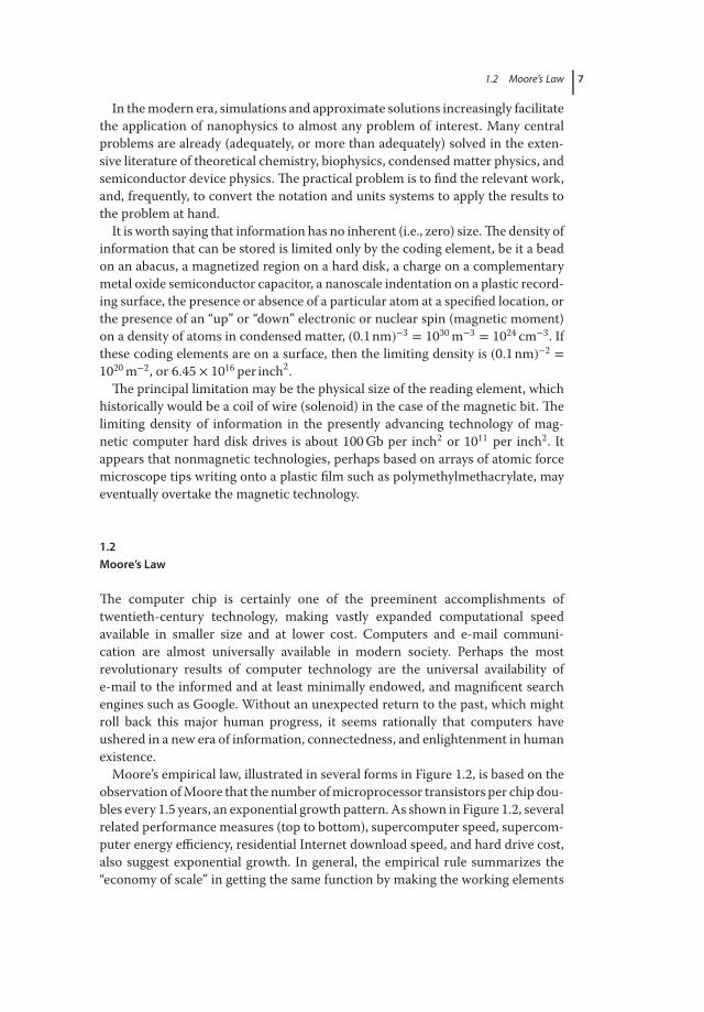
The computer chip is certainly one of the preeminent accomplishments oftwentieth-century technology, making vastly expanded computational speedavailable in smaller size and at lower cost. Computers and e-mail communi-cation are almost universally available in modern society. Perhaps the mostrevolutionary results of computer technology are the universal availability ofe-mail to the informed and at least minimally endowed, and magnificent searchengines such as Google. Without an unexpected return to the past, which mightroll back this major human progress, it seems rationally that computers haveushered in a new era of information, connectedness, and enlightenment in humanexistence.Moore’s empirical law, illustrated in several forms in Figure 1.2, is based on the
observation ofMoore that the number ofmicroprocessor transistors per chip dou-bles every 1.5 years, an exponential growth pattern. As shown in Figure 1.2, severalrelated performance measures (top to bottom), supercomputer speed, supercom-puter energy efficiency, residential Internet download speed, and hard drive cost,also suggest exponential growth. In general, the empirical rule summarizes the“economy of scale” in getting the same function by making the working elements
8 1 Introduction
1 000 000 000 000 000Supercomputer speed
(FLOPS)
Supercomputer energy efficiency(FLOPS/watt)
Microprocessor transistors/chip
Residential Internet download speed(kilobytes/second)
Hard drive cost efficiency(gigabytes/dollar)
1 000 000 000 000
1 000 000 000
1 000 000
1 000
Loga
rithm
ic s
cale
1
0.001
19701975
19801985
19901995
20002005
20102015
Figure 1.2 Moore’s law [6]. The numberof transistors in successive generations ofcomputer chips has risen exponentially,doubling every 1.5 years or so. GordonMoore, cofounder of Intel, Inc., predictedthis growth pattern in 1965, when a sil-icon chip contained only 30 transistors.The number of dynamic random accessmemory (DRAM) cells follows a similar
growth pattern. The growth is largely dueto continuing reduction in the size of keyelements in the devices, to less than 45 nm,with improvements in optical photolithogra-phy. Clock speeds have similarly increased,presently around 2GHz. For a summary,see [7]. Reprinted with permission fromRef. [6].
ever smaller. (It turns out, as we see, that smaller means faster, characteristicallyenhancing the advantage inminiaturization). In the ancient abacus, bead positionsrepresent binary numbers, with information recorded on a scale of perhaps 1 bit[(0,1) or (yes/no)] per centimeter square. In silicon microelectronic technology,an easily producedmemory cell size of 1 μm corresponds to 1012 bits per centime-ter square (1Tb cm−2). Equally important is the continually reducing size of themagnetic diskmemory element (and of the corresponding read/write sensor head)making possible the∼1000Gb diskmemories of contemporary laptop computers.The continuing improvements in performance (reductions in size of the perform-ing elements), empirically summarized byMoore’s law (a doubling of performanceevery 1.5 years, or so), arise from corresponding reductions in the size scale of thecomputer chip, aided by the advertising-related market demand.The vast improvements from the abacus to the Pentium andCore i7 chips exem-
plify the promise of nanotechnology. Please note that this is all still in the range
1.3 Esaki’s Quantum Tunneling Diode 9
of “classical scaling”! The computer experts are absolutely sure that nanophysicaleffects are so far negligible.The semiconductor industry, having produced a blockbuster performance over
decades, transforming advanced society and suitably enriching its players andstockholders, is concerned about its next act!The next act in the semiconductor industry, if a second act indeed shows up,
must deal with the nanophysical rules. Any new technology, if such is feasible,will have to compete with a base of universally available applied computation, atunimaginably low costs. If terahertz-speed computers with 8Gb randomly acces-sible memories and 1000Gb hard drives, indeed become a commodity, what cancompete with that? Silicon technology is a hard act to follow.Nanotechnology, taken literally, also represents the physically possible limit of
such improvements.The limit of technology is also evident, since the smallest pos-sible interconnecting wire on the chip must be at least 100 atoms across! Moore’slaw empirically has characterized the semiconductor industry’s success in pro-viding faster computers of increasing sophistication and continually falling price.Success has been obtained with a larger number of transistors per chip made pos-sible by finer scales of thewiring and active components on the silicon chips.Thereis a challenge to the continuation of this trend (Moore’s law) from the economicreality of steeply increasing plant cost (to realize reduced linewidths and smallertransistors).The fundamental challenge to the continuation of this trend (Moore’s law) from
the change of physical behavior as the atomic size limit is approached is a centraltopic in this textbook.
1.3Esaki’s Quantum Tunneling Diode
The tunneling effect is basic in quantum mechanics, a fundamental consequenceof the probabilistic wave function as a measure of the location of a particle.Unlike a tennis ball, a tiny electron may penetrate a barrier. This effect was firstexploited in semiconductor technology by Leo Esaki, who discovered that thecurrent–voltage (I/V ) curves of semiconductor p–n junction rectifier diodes(when the barrier was made very thin, by increasing the dopant concentrations)became anomalous, and in fact double-valued. The forward bias I versus V plot,normally a rising exponential exp(eV /kT), was preceded by a distinct “currenthump” starting at zero bias and extending to V = 50mV or so. Between theregion of the “hump” and the onset of the conventional exponential current rise,there was a region of negative slope, dI∕dV < 0!The planar junction between an N-type region and a P-type region in a semi-
conductor such as Si contains a “depletion region” separating conductive regionsfilled with free electrons on the N-side and free holes on the P-side. It is a use-ful nontrivial exercise in semiconductor physics to show that the width W of thedepletion region is
10 1 Introduction
W =
[2𝜀𝜀oVB
(ND + NA
)e(NDNA)
]1∕2
, (1.1)
where 𝜀𝜀o is the dielectric constant, e the electron charge,V B in Volts is the shift inthe bands across the junction, andND andNA, respectively, are the concentrationsof donor and acceptor impurities.The change in electrical behavior (the negative resistance range) resulting from
the electron tunneling (in the thin depletion region limit)made possible an entirelynew effect, an oscillation, at an extremely high frequency! (As often happens withthe continuing advance of technology, this pioneering device has been largely sup-planted as an oscillator by the Gunn diode, which is easier to manufacture.)The Esaki tunnel diode is perhaps the first example in which the appearance of
quantum physics at the limit of a small size led to a new device. In our terminol-ogy, the depletion layer tunneling barrier is 2D, with only one small dimension,the depletion layer thickness W. The Esaki diode falls into our classification asan element of nanotechnology, since the controlled small barrier W is only a fewnanometers in thickness.
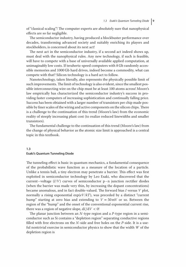
1.4QDs of Many Colors
QDs of CdSe and similar semiconductors are grown in carefully controlled solu-tion precipitation with controlled sizes in the range L = 4 or 5nm. It is foundthat the wavelength (color) of strong fluorescent light emitted by these QDs underultraviolet (UV) light illumination depends sensitively on the size L, see Figure 1.3.There are enough atoms in this particle to effectively validate the concepts of
solid-state physics, which include electron bands, forbidden energy bandgaps,electron and hole effective masses, and more.Still, the particle is small enough to be called an “artificial atom,” characterized
by discrete sharp electron energy states, and discrete sharp absorption, and emis-sion wavelengths for photons.Transmission electron microscope (TEM) images of such nanocrystals, which
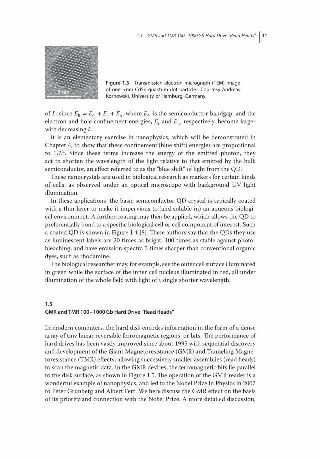
may contain only 50 000 atoms, reveal perfectly ordered crystals having the bulkcrystal structure and nearly the bulk lattice constant. Quantitative analysis of thelight emission process in QDs suggests that the bandgap, effective masses of elec-trons and holes, and other microscopic material properties are very close to theirvalues in large crystals of the same material. The light emission in all cases comesfrom radiative recombination of an electron and a hole, created initially by theshorter wavelength illumination (Figure 1.3).The energy ER released in the recombination is given entirely to a photon (the
quantum unit of light), according to the relation ER = hν = hc∕𝜆. Here, 𝜈 and𝜆 are, respectively, the frequency and wavelength of the emitted light, c is thespeed of light 3 × 10⁸ms−1, and h is Planck’s constant h = 6.63 × 10⁻³⁴ Js =4.136 × 10⁻¹⁵ eVs. The color of the emitted light is controlled by the choice
1.5 GMR and TMR 100–1000 Gb Hard Drive “Read Heads” 11
5 nm
Figure 1.3 Transmission electron micrograph (TEM) imageof one 5 nm CdSe quantum dot particle. Courtesy AndreasKornowski, University of Hamburg, Germany.
of L, since ER = EG + Ee + Eh, where EG is the semiconductor bandgap, and theelectron and hole confinement energies, Ee and Eh, respectively, become largerwith decreasing L.It is an elementary exercise in nanophysics, which will be demonstrated in
Chapter 4, to show that these confinement (blue shift) energies are proportionalto 1/L2. Since these terms increase the energy of the emitted photon, theyact to shorten the wavelength of the light relative to that emitted by the bulksemiconductor, an effect referred to as the “blue shift” of light from the QD.These nanocrystals are used in biological research as markers for certain kinds
of cells, as observed under an optical microscope with background UV lightillumination.In these applications, the basic semiconductor QD crystal is typically coated
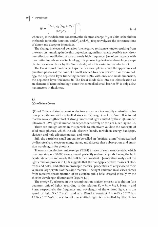
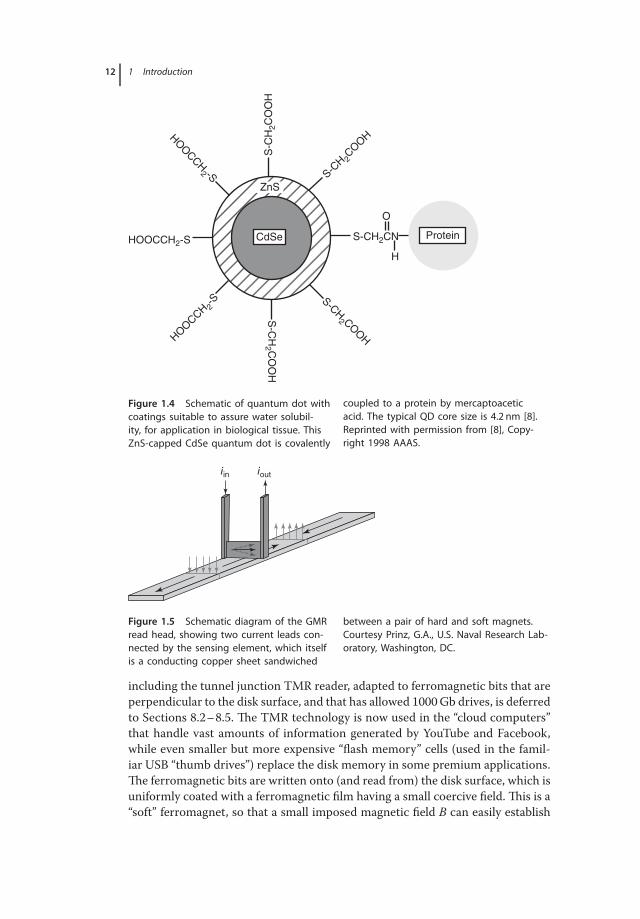
with a thin layer to make it impervious to (and soluble in) an aqueous biologi-cal environment. A further coating may then be applied, which allows the QD topreferentially bond to a specific biological cell or cell component of interest. Sucha coated QD is shown in Figure 1.4 [8]. These authors say that the QDs they useas luminescent labels are 20 times as bright, 100 times as stable against photo-bleaching, and have emission spectra 3 times sharper than conventional organicdyes, such as rhodamine.Thebiological researchermay, for example, see the outer cell surface illuminated
in green while the surface of the inner cell nucleus illuminated in red, all underillumination of the whole field with light of a single shorter wavelength.
1.5GMR and TMR 100–1000Gb Hard Drive “Read Heads”
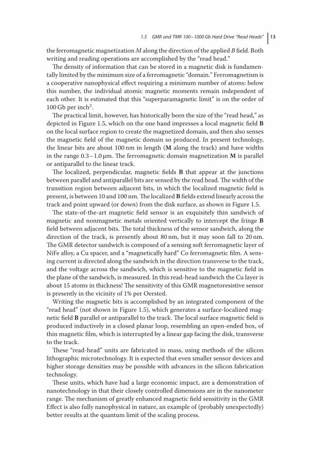
In modern computers, the hard disk encodes information in the form of a densearray of tiny linear reversible ferromagnetic regions, or bits. The performance ofhard drives has been vastly improved since about 1995 with sequential discoveryand development of the Giant Magnetoresistance (GMR) and Tunneling Magne-toresistance (TMR) effects, allowing successively smaller assemblies (read heads)to scan the magnetic data. In the GMR devices, the ferromagnetic bits lie parallelto the disk surface, as shown in Figure 1.5. The operation of the GMR reader is awonderful example of nanophysics, and led to the Nobel Prize in Physics in 2007to Peter Grunberg and Albert Fert. We here discuss the GMR effect on the basisof its priority and connection with the Nobel Prize. A more detailed discussion,
12 1 Introduction
S-C
H2C
OO
H
S-C
H2 C
OO
H
HOOCCH2-S
HOOCCH2 -S
HOOCCH 2-S
S-CH2CN
H
O
S-CH 2
COOH
S-CH2 COOH
ZnS
CdSe Protein
Figure 1.4 Schematic of quantum dot withcoatings suitable to assure water solubil-ity, for application in biological tissue. ThisZnS-capped CdSe quantum dot is covalently
coupled to a protein by mercaptoaceticacid. The typical QD core size is 4.2 nm [8].Reprinted with permission from [8], Copy-right 1998 AAAS.
iin iout
Figure 1.5 Schematic diagram of the GMRread head, showing two current leads con-nected by the sensing element, which itselfis a conducting copper sheet sandwiched
between a pair of hard and soft magnets.Courtesy Prinz, G.A., U.S. Naval Research Lab-oratory, Washington, DC.
including the tunnel junction TMR reader, adapted to ferromagnetic bits that areperpendicular to the disk surface, and that has allowed 1000Gb drives, is deferredto Sections 8.2–8.5. The TMR technology is now used in the “cloud computers”that handle vast amounts of information generated by YouTube and Facebook,while even smaller but more expensive “flash memory” cells (used in the famil-iar USB “thumb drives”) replace the disk memory in some premium applications.The ferromagnetic bits are written onto (and read from) the disk surface, which isuniformly coated with a ferromagnetic film having a small coercive field. This is a“soft” ferromagnet, so that a small imposed magnetic field B can easily establish
1.5 GMR and TMR 100–1000 Gb Hard Drive “Read Heads” 13
the ferromagneticmagnetizationM along the direction of the appliedB field. Bothwriting and reading operations are accomplished by the “read head.”The density of information that can be stored in a magnetic disk is fundamen-
tally limited by theminimum size of a ferromagnetic “domain.” Ferromagnetism isa cooperative nanophysical effect requiring a minimum number of atoms: belowthis number, the individual atomic magnetic moments remain independent ofeach other. It is estimated that this “superparamagnetic limit” is on the order of100Gb per inch2.The practical limit, however, has historically been the size of the “read head,” as
depicted in Figure 1.5, which on the one hand impresses a local magnetic field Bon the local surface region to create the magnetized domain, and then also sensesthe magnetic field of the magnetic domain so produced. In present technology,the linear bits are about 100 nm in length (M along the track) and have widthsin the range 0.3–1.0 μm. The ferromagnetic domain magnetization M is parallelor antiparallel to the linear track.The localized, perpendicular, magnetic fields B that appear at the junctions
between parallel and antiparallel bits are sensed by the read head.Thewidth of thetransition region between adjacent bits, in which the localized magnetic field ispresent, is between 10 and 100 nm.The localizedB fields extend linearly across thetrack and point upward (or down) from the disk surface, as shown in Figure 1.5.The state-of-the-art magnetic field sensor is an exquisitely thin sandwich of
magnetic and nonmagnetic metals oriented vertically to intercept the fringe Bfield between adjacent bits. The total thickness of the sensor sandwich, along thedirection of the track, is presently about 80 nm, but it may soon fall to 20 nm.The GMR detector sandwich is composed of a sensing soft ferromagnetic layer ofNiFe alloy, a Cu spacer, and a “magnetically hard” Co ferromagnetic film. A sens-ing current is directed along the sandwich in the direction transverse to the track,and the voltage across the sandwich, which is sensitive to the magnetic field inthe plane of the sandwich, is measured. In this read-head sandwich the Cu layer isabout 15 atoms in thickness! The sensitivity of this GMRmagnetoresistive sensoris presently in the vicinity of 1% per Oersted.Writing the magnetic bits is accomplished by an integrated component of the
“read head” (not shown in Figure 1.5), which generates a surface-localized mag-netic field B parallel or antiparallel to the track.The local surface magnetic field isproduced inductively in a closed planar loop, resembling an open-ended box, ofthin magnetic film, which is interrupted by a linear gap facing the disk, transverseto the track.These “read-head” units are fabricated in mass, using methods of the silicon
lithographic microtechnology. It is expected that even smaller sensor devices andhigher storage densities may be possible with advances in the silicon fabricationtechnology.These units, which have had a large economic impact, are a demonstration of
nanotechnology in that their closely controlled dimensions are in the nanometerrange. The mechanism of greatly enhanced magnetic field sensitivity in the GMREffect is also fully nanophysical in nature, an example of (probably unexpectedly)better results at the quantum limit of the scaling process.
14 1 Introduction
1.6Accelerometers in Your Car
Modern cars have airbags that inflate in crashes to protect drivers and passen-gers from accidents. Micro-electro-mechanical semiconductor acceleration sen-sors (accelerometers) are located in bumpers, which quickly inflate the airbags.The basic accelerometer is a mass m attached by a spring of constant k to theframe of the sensor device, itself secured to the automobile frame. If the car frame(and thus the frame of the sensor device) undergoes a strong acceleration, thespring connecting the mass to the sensor frame will extend or contract, leading toa motion of the mass m relative to the frame of the sensor device. This deflectionis measured, for example, by change in a capacitance, which then triggers expan-sion of the airbag. This micro-electro-mechanical device is mass produced in anintegrated package, including relevant electronics, using the methods of siliconmicroelectronics.
Newton’s laws of motion
Newton’s laws of motion describe the position x, the velocity v = dx∕dt, and theacceleration a = d2x∕dt2 of amassmwhichmaybe acted uponby a force F, accord-ing to
md2x∕dt2 = F. (1.2)
Kinematics describes the relationships among x, v, a, and t. As an example, thetime-dependent position x under uniform acceleration a is
x = xo + vot + at2, (1.3)
where xo and vo, respectively, are the position and velocity at t = 0. Also, if a time-varying acceleration a(t) is known, and xo = 0 and vo = 0, then
x(t) = ∫ ∫ a(t)dt2. (1.4)
Newton’s first law states that in the absence of a force, themassm remains at restif initially so, and if initially in motion continues unchanged in that motion. (Theselaws are valid only if the coordinate system in which the observations are madeis one of uniform motion, and certainly do not apply in an accelerated frame ofreference, such as a carrousel or a merry-go-round. For most purposes, the earth’ssurface, although accelerated toward its rotation axis, can be regarded as an “iner-tial frame of reference,” that is, Newton’s laws are useful.)Newton’s second law is F = ma, Eq. (1.2).The Third Law states that for twomasses in contact, the force exerted by the first
on the second is equal and opposite to the force exerted by the second on the first.
1.8 Nanoscale Elements in Traditional Technologies 15
A more sophisticated version of such an accelerometer, arranged to recordaccelerations in x, y, z directions, and equipped with integrating electronics, canbe used to record the three-dimensional displacement over time.These devices are not presently built on a nanometer scale, of course, but are
one example of a wide class of microelectronic sensors that could be made onsmaller scales as semiconductor technology advances, and if smaller devices areuseful.
1.7Nanopore Filters
The original nanopore (Nuclepore) filters1) [9] are sheets of polycarbonate of6–11 μm thickness with closely spaced arrays of parallel holes running throughthe sheet. The filters are available with pore sizes rated from 0.015 to 12.0 μm(15–12 000 nm). The holes are made by exposing the polycarbonate sheetsto perpendicular flux of ionizing 𝛼 particles, which produce linear paths ofatomic-scale damage in the polycarbonate. Controlled chemical etching is thenemployed to establish and enlarge the parallel holes to the desired diameter. Thisscheme is an example of nanotechnology.The filters are robust and can have a very substantial throughput, with up to
12% of the area being open. The smallest filters will block passage of bacteria andperhaps even some viruses, and are used in many applications including waterfilters for hikers.A second class of filters (Anapore) was later established, formed of alumina
grown by anodic oxidation of aluminum metal. These filters are more porous, upto 40%, and are stronger and more temperature resistant than the polycarbonatefilters. They have been used, for example, to produce dense arrays of nanowires.Nanowires are obtained using a hot press to force a ductile metal into the pores ofthe nanopore alumina filter.
1.8Nanoscale Elements in Traditional Technologies
From the present knowledge of materials, it is understood that the beautiful col-ors of stained glass windows originate in nanometer-scale metal particles presentin the glass. These metal particles have scattering resonances for light of specificwavelengths, depending on the particle size L. The particle size distribution, inturn, will depend upon the choice of metal impurity, its concentration, and theheat treatment of the glass. When the metallic particles in the glass are illumi-nated, they preferentially scatter light of particular colors. Neutral density filters
1) These filters are manufactured by Nuclepore Corporation, 7035 Commerce Circle, Pleasanton, CA94566.
16 1 Introduction
marketed for photographic application also have distributions of small particlesembedded in glass.Carbon black, commonly known as soot, which contains nanometer-sized par-
ticles of carbon, was used very early as an additive to the rubber in automobiletires. (As we now know, carbon black contains small amounts of 60C (Buckmin-sterfullerene), other fullerenes, and graphitic nanotubes of various types.)The AgBr and AgI crystals of conventional photography are nanometer-sized
single crystals embedded in a thin gelatin matrix. It appears that the fundamentallight absorption in these crystals is close to the quantum sensitivity limit. It fur-ther appears that the nanoscopic changes in these tiny crystals, which occur uponabsorption of one or more light photons, enable them to be turned into largermetallic silver particles in the conventional photographic development process.The conventional photographic negative image is an array of solid silver grainsembedded in a gelatin matrix. As such, it is remarkably stable as a record, overdecades or more.Thedrugs that are very important in everyday life (and are also of huge economic
importance), including caffeine, aspirin, andmanymore, are specific molecules ofnanometer size, typically containing fewer than 100 atoms.Controlled precipitation chemistry, for example, is employed to produce uni-
form nanometer-sized spheres of polystyrene, which have long been marketed ascalibration markers for transmission electron microscopy.
References
1. Kurzweil, R. (1999) The Age of SpiritualMachines, Penguin Books, New York,p. 140.
2. Drexler, K.E. (1986) Engines of Creation,Anchor Books, New York, p. 49.
3. Drexler, K.E. (1986) Engines of Creation,Anchor Books, New York, p. 268; See alsoDrexler, K.E. (2013) Radical Abundance:How a Revolution in Nanotechnology willChange Civilization, PublicAffairs/Perseus,New York.
4. Feynman, R. (1961) There’s plenty ofroom at the bottom, in Miniaturization(ed. H.D. Gilbert), Reinhold, New York.
5. Carr, D.W. et al. (1999) Appl. Phys. Lett.,75, 920.
6. Brynjolfsson, E. and McAfee, A. (2014)The Second Machine Age: Work, Progress,and Prosperity in a Time of Technologies,Norton Publishers.
7. Lundstrom, M. (2003) Science, 299, 210.8. Warren, C.W. and Shumig, N. (1998)
Science, 281, 2016–2018.9. Crawford, G.P., Steele, L.M.,
Ondris-Crawford, R., Iannocchione, G.S.,Yeager, C.J., Doane, J.W., and Finotello, D.(1992) J. Chem. Phys., 96, 7788.