PHYSICAL REVIEW X 11, 031026 (2021)
8
Three-Dimensional Charge Density Wave and Surface-Dependent Vortex-Core States in a Kagome Superconductor CsV 3 Sb 5 Zuowei Liang, 1,§ Xingyuan Hou , 2,§ Fan Zhang, 3,2,§ Wanru Ma, 1 Ping Wu, 1 Zongyuan Zhang, 2 Fanghang Yu, 1 J.-J. Ying, 1 Kun Jiang, 3 Lei Shan , 2,4,* Zhenyu Wang , 1,† and X.-H. Chen 1,5,6,‡ 1 Department of Physics and Chinese Academy of Sciences Key laboratory of Strongly-coupled Quantum Matter Physics, University of Science and Technology of China, Hefei, Anhui 230026, China 2 Information Materials and Intelligent Sensing Laboratory of Anhui Province, Institutes of Physical Science and Information Technology, Anhui University, Hefei 230601, China 3 Beijing National Laboratory for Condensed Matter Physics, and Institute of Physics, Chinese Academy of Sciences, Beijing 100190, China 4 Key Laboratory of Structure and Functional Regulation of Hybrid Materials of Ministry of Education, Anhui University, Hefei 230601, China 5 CAS Center for Excellence in Quantum Information and Quantum Physics, Hefei, Anhui 230026, China 6 Collaborative Innovation Center of Advanced Microstructures, Nanjing 210093, China (Received 8 March 2021; revised 12 May 2021; accepted 7 June 2021; published 2 August 2021) The transition-metal-based kagome metals provide a versatile platform for correlated topological phases hosting various electronic instabilities. While superconductivity is rare in layered kagome compounds, its interplay with nontrivial topology could offer an engaging space to realize exotic excitations of quasiparticles. Here, we use scanning tunneling microscopy to study a newly discovered Z 2 topological kagome metal CsV 3 Sb 5 with a superconducting ground state. We observe charge modulation associated with the opening of an energy gap near the Fermi level. When across single-unit-cell surface step edges, the intensity of this charge modulation exhibits a π-phase shift, suggesting a three-dimensional 2 × 2 × 2 charge density wave ordering. Interestingly, while conventional Caroli–de Gennes–Matricon bound states are observed inside the superconducting vortex on the Sb surfaces, a robust zero-bias conductance peak emerges that does not split in a large distance when moving away from the vortex center on the Cs 2 × 2 surfaces, resembling the Majorana bound states arising from the superconducting Dirac surface states in Bi 2 Te 3 =NbSe 2 heterostructures. Our findings establish CsV 3 Sb 5 as a promising candidate for realizing exotic excitations at the confluence of nontrivial lattice geometry, topology and multiple electronic orders. DOI: 10.1103/PhysRevX.11.031026 Subject Areas: Condensed Matter Physics The kagome nets consisting of 3d transition metal ions are emerging as a new frontier for exploring novel cor- related and topological electronic states [1–10]. Thanks to its special lattice geometry, a kagome lattice naturally possesses Dirac cones and flat band with quenched kinetic energy [11,12], leading to interaction-driven topological many-body phenomena. Experimentally, 3D magnetic Weyl semimetal [4,13–15] and 2D Chern insulator [9] phases have been realized in kagome lattices compounded with a net magnetization. On the other hand, depending on the electron filling level, various electronic states ranging from density waves to superconductivity have also been theoretically predicted [11,16–19]. However, the search for a layered kagome compound with a superconducting ground state remains a great challenge, leaving much of the related field unexplored. Recently, a new family of layered kagome metals AV 3 Sb 5 (A ¼ K, Rb, Cs) has been discovered with a superconducting ground state [20–23]. The normal state of these compounds has been theoretically identified to host a Z 2 topological invariant, with topological Dirac surface states near the Fermi energy (Dirac energy E D ∼ 40 meV) and the calculated band structure is supported by angle- resolved photoemission measurements [21]. In addition, these materials all exhibit a clear transport and magnetic anomaly at T ∼ 78–104 K due to the formation of a charge order [20–22], suggesting that the electronic interactions * Corresponding author. [email protected] † Corresponding author. [email protected] ‡ Corresponding author. [email protected] § These authors contributed equally to this work Published by the American Physical Society under the terms of the Creative Commons Attribution 4.0 International license. Further distribution of this work must maintain attribution to the author(s) and the published article’s title, journal citation, and DOI. PHYSICAL REVIEW X 11, 031026 (2021) 2160-3308=21=11(3)=031026(8) 031026-1 Published by the American Physical Society
Transcript of PHYSICAL REVIEW X 11, 031026 (2021)
Three-Dimensional Charge Density Wave and Surface-Dependent Vortex-CoreStates in a Kagome Superconductor CsV3Sb5
Zuowei Liang,1,§ Xingyuan Hou ,2,§ Fan Zhang,3,2,§ Wanru Ma,1 Ping Wu,1 Zongyuan Zhang,2 Fanghang Yu,1
J.-J. Ying,1 Kun Jiang,3 Lei Shan ,2,4,* Zhenyu Wang ,1,† and X.-H. Chen1,5,6,‡1Department of Physics and Chinese Academy of Sciences Key laboratory of Strongly-coupled Quantum
Matter Physics, University of Science and Technology of China, Hefei, Anhui 230026, China2Information Materials and Intelligent Sensing Laboratory of Anhui Province,
Institutes of Physical Science and Information Technology, Anhui University, Hefei 230601, China3Beijing National Laboratory for Condensed Matter Physics, and Institute of Physics,
Chinese Academy of Sciences, Beijing 100190, China4Key Laboratory of Structure and Functional Regulation of Hybrid Materials of Ministry of Education,
Anhui University, Hefei 230601, China5CAS Center for Excellence in Quantum Information and Quantum Physics, Hefei, Anhui 230026, China
6Collaborative Innovation Center of Advanced Microstructures, Nanjing 210093, China
(Received 8 March 2021; revised 12 May 2021; accepted 7 June 2021; published 2 August 2021)
The transition-metal-based kagome metals provide a versatile platform for correlated topological phaseshosting various electronic instabilities. While superconductivity is rare in layered kagome compounds, itsinterplay with nontrivial topology could offer an engaging space to realize exotic excitations ofquasiparticles. Here, we use scanning tunneling microscopy to study a newly discovered Z2 topologicalkagome metal CsV3Sb5 with a superconducting ground state. We observe charge modulation associatedwith the opening of an energy gap near the Fermi level. When across single-unit-cell surface step edges, theintensity of this charge modulation exhibits a π-phase shift, suggesting a three-dimensional 2 × 2 × 2
charge density wave ordering. Interestingly, while conventional Caroli–de Gennes–Matricon bound statesare observed inside the superconducting vortex on the Sb surfaces, a robust zero-bias conductance peakemerges that does not split in a large distance when moving away from the vortex center on the Cs 2 × 2
surfaces, resembling the Majorana bound states arising from the superconducting Dirac surface states inBi2Te3=NbSe2 heterostructures. Our findings establish CsV3Sb5 as a promising candidate for realizingexotic excitations at the confluence of nontrivial lattice geometry, topology and multiple electronic orders.
DOI: 10.1103/PhysRevX.11.031026 Subject Areas: Condensed Matter Physics
The kagome nets consisting of 3d transition metal ionsare emerging as a new frontier for exploring novel cor-related and topological electronic states [1–10]. Thanks toits special lattice geometry, a kagome lattice naturallypossesses Dirac cones and flat band with quenched kineticenergy [11,12], leading to interaction-driven topologicalmany-body phenomena. Experimentally, 3D magnetic
Weyl semimetal [4,13–15] and 2D Chern insulator [9]phases have been realized in kagome lattices compoundedwith a net magnetization. On the other hand, depending onthe electron filling level, various electronic states rangingfrom density waves to superconductivity have also beentheoretically predicted [11,16–19]. However, the search fora layered kagome compound with a superconductingground state remains a great challenge, leaving much ofthe related field unexplored.Recently, a new family of layered kagome metals
AV3Sb5 (A ¼ K, Rb, Cs) has been discovered with asuperconducting ground state [20–23]. The normal stateof these compounds has been theoretically identified to hosta Z2 topological invariant, with topological Dirac surfacestates near the Fermi energy (Dirac energy ED ∼ 40 meV)and the calculated band structure is supported by angle-resolved photoemission measurements [21]. In addition,these materials all exhibit a clear transport and magneticanomaly at T� ∼ 78–104 K due to the formation of a chargeorder [20–22], suggesting that the electronic interactions
*Corresponding [email protected]
†Corresponding [email protected]
‡Corresponding [email protected]
§These authors contributed equally to this work
Published by the American Physical Society under the terms ofthe Creative Commons Attribution 4.0 International license.Further distribution of this work must maintain attribution tothe author(s) and the published article’s title, journal citation,and DOI.
PHYSICAL REVIEW X 11, 031026 (2021)
2160-3308=21=11(3)=031026(8) 031026-1 Published by the American Physical Society
could be at play in these compounds. This charge order hasbeen revealed to be unconventional with a chiral anisotropy[24], giving rise to the observed anomalous Hall effect inthe absence of long-range magnetic order [25,26]. Whenthese Z2 topological metals fall into a superconductingstate, the natively proximitized superconducting topologi-cal surface states may provide a promising route to realizezero energy modes related to Majorana bound states(MBSs) [21,27], which are the key ingredients for topo-logical quantum computation [28]. Furthermore, signa-tures of spin-triplet pairing and an edge supercurrent inNb=K1−XV3Sb5 devices have been reported [29], sug-gesting a potential exotic superconducting state in thesedevices. Therefore, a spectroscopic probe of the electronicorders in AV3Sb5, particularly for the superconductingstate, is highly desired.Scanning tunneling microscopy (STM), owing to its high
spatial topographic resolution and high energy spectro-scopic resolution, is an ideal probe to investigate the realspace charge ordering and novel quasiparticle excitationsin the superconducting state. In this work, we use low-temperature STM to study a kagome superconductorCsV3Sb5 with the highest TC ∼ 3 K in the AV3Sb5 family.We pinpoint a three-dimensional 2 × 2 × 2 charge densitywave (CDW) order in CsV3Sb5 with the opening of anenergy gap of ∼� 20 meV at the Fermi level. Insidesuperconducting vortices on the ordered Cs surfaces, weobserve a robust, nonsplit zero-bias conductance peak
(ZBCP) within a large distance away from the core center,whose full width at half maximum (FWHM) almost doesnot change. This ZBCP bears a remarkable resemblance tothe MBSs that have been observed in the Bi2Te3=NbSe2heterostructures [30].Single crystals of CsV3Sb5 were grown via a self-
flux growth method as described in earlier studies [20,21].The crystals are first characterized by the x-ray diffraction[Supplemental Material note I (SM 1) [31] ] and resis-tivity measurements. As shown in Fig. 1(b), a resistivityanomaly appears at 94 K, similar to the previous report[21]. The onset of the superconductivity in our samplesoccurs around 3.5 K, and zero resistivity can be achievedaround 2.7 K. The crystals were cold cleaved in situ at30 or 80 K, and then immediately transferred into theSTM head. Chemically etched tungsten tips were usedin all the measurements, after being checked on a cleanAu (111) surface. STM measurements for the normalstate and superconducting state are carried out at 5 and0.4 K, respectively. Spectroscopic data were acquiredby the standard lock-in technique at a frequency of987.5 Hz.CsV3Sb5 has a layered structure with the space group of
P6=mmm and hexagonal lattice constant a ¼ 5.5 Å andc ¼ 9.3 Å. It consists of a kagome vanadium net interpen-etrated by a hexagonal net of Sb1 in between twohoneycomb-structured Sb2 layers, and all sandwiched inbetween two hexagonal Cs layers [Fig. 1(a)]. Considering
Low High Low High Low High
0-20 20Energy (meV)
-40 40
1
2
3
dI/d
V (
nS)
dI/d
V (
nS)
dI/d
V (
nS)
dI/d
V (
nS)
0-20 20Energy (meV)
-40 40
5
10
15
1
2
3
0-20 20Energy (meV)
-40 40
3 nm3 nm 3 nm
Cs surface Half Cs
CsSb1Sb2V
100 200Temperature (K)
0030
0 5 100
1
0
50
100
ρ( μ
Ωcm
)
CDW
SC
Suppression of DOS
0-20 20Energy (meV)
-40 40
Low High
Sb: 1Q-CDW
3 nm
2
4
Sb: 3Q-CDW(a)
(c) (d) (e) (f)
(b)(g) (h) (i) (j)
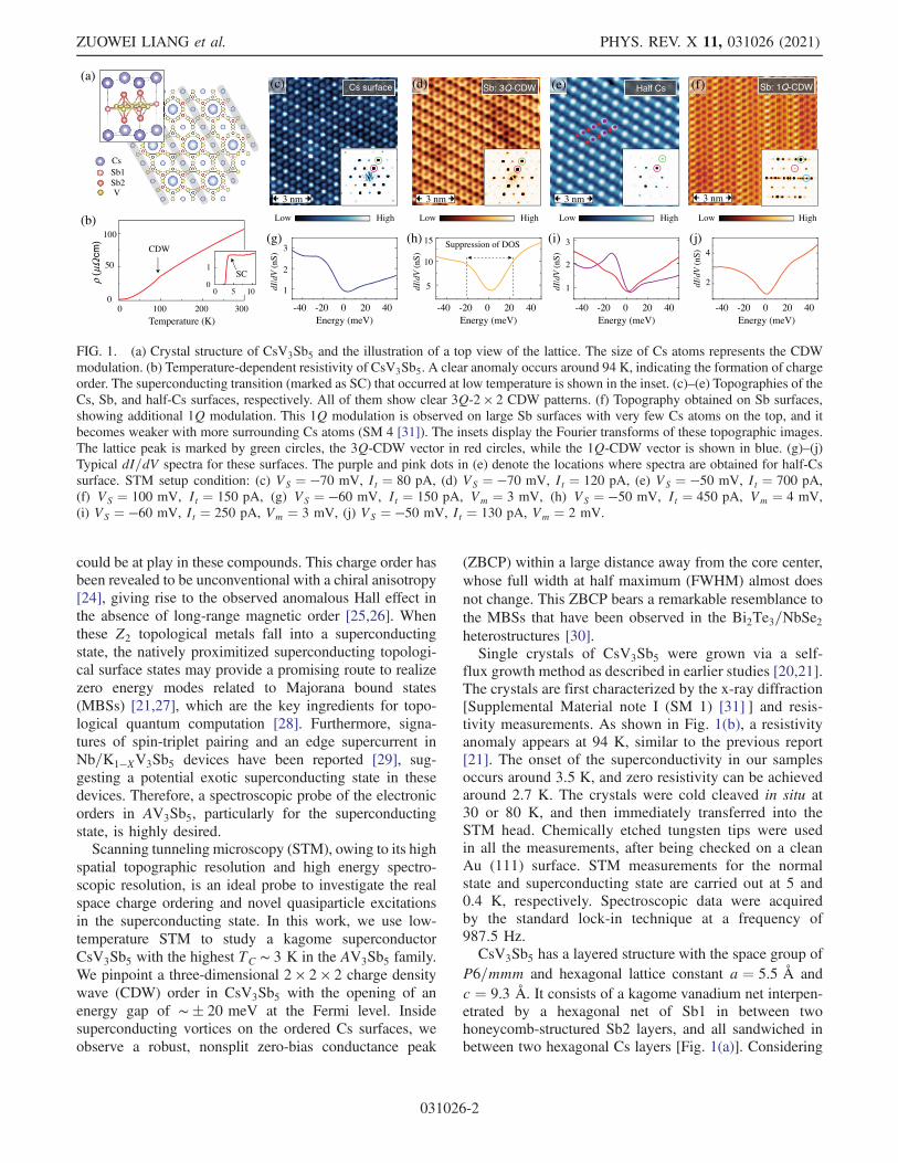
FIG. 1. (a) Crystal structure of CsV3Sb5 and the illustration of a top view of the lattice. The size of Cs atoms represents the CDWmodulation. (b) Temperature-dependent resistivity of CsV3Sb5. A clear anomaly occurs around 94 K, indicating the formation of chargeorder. The superconducting transition (marked as SC) that occurred at low temperature is shown in the inset. (c)–(e) Topographies of theCs, Sb, and half-Cs surfaces, respectively. All of them show clear 3Q-2 × 2 CDW patterns. (f) Topography obtained on Sb surfaces,showing additional 1Q modulation. This 1Q modulation is observed on large Sb surfaces with very few Cs atoms on the top, and itbecomes weaker with more surrounding Cs atoms (SM 4 [31]). The insets display the Fourier transforms of these topographic images.The lattice peak is marked by green circles, the 3Q-CDW vector in red circles, while the 1Q-CDW vector is shown in blue. (g)–(j)Typical dI=dV spectra for these surfaces. The purple and pink dots in (e) denote the locations where spectra are obtained for half-Cssurface. STM setup condition: (c) VS ¼ −70 mV, It ¼ 80 pA, (d) VS ¼ −70 mV, It ¼ 120 pA, (e) VS ¼ −50 mV, It ¼ 700 pA,(f) VS ¼ 100 mV, It ¼ 150 pA, (g) VS ¼ −60 mV, It ¼ 150 pA, Vm ¼ 3 mV, (h) VS ¼ −50 mV, It ¼ 450 pA, Vm ¼ 4 mV,(i) VS ¼ −60 mV, It ¼ 250 pA, Vm ¼ 3 mV, (j) VS ¼ −50 mV, It ¼ 130 pA, Vm ¼ 2 mV.
ZUOWEI LIANG et al. PHYS. REV. X 11, 031026 (2021)
031026-2
the chemical bonding between V, Sb2, and Cs, the maincleavage plane is in between the Cs and Sb2 layers, gen-erating either Cs or Sb terminated surfaces. Atomicallyresolved STM topographies are shown in Figs. 1(c)and 1(d), with hexagonal and honeycomb lattice, respec-tively. In SM 2 [31], we show a joint area between thesetwo types of lattices, with an atomic step edge where theupper regime shows hexagonal lattice while the lowershows honeycomb lattice. On the basis of the crystallinestructure, we can identify them as Cs [Fig. 1(c)] and Sb[Fig. 1(d)] surfaces, respectively. One can see tridirec-tional (3Q) 2 × 2 superstructure in the real space topog-raphies for both types of surfaces, with additional peaks athalf of the Bragg reciprocal lattice vectors in the Fouriertransforms (FTs), similar to the case of KV3Sb5 (seeRef. [24]). The observed modulation on both Cs and Sbsurfaces suggests a 2 × 2 superlattice pattern in theunderlying kagome V plane, as illustrated in Fig. 1(a),since the 3d orbitals of V have a large contribution to thetotal electronic density of states (DOS) at low energies[21,24]. The 2 × 2 superlattice of V kagome lattice isplotted following an inverse Star of David structure asproposed by a recent density functional theory calculation[32]. The cleavage can also break the Cs atomic layer andresult in a third type of surface with half the amount of theCs atoms. In fact, this is the most commonly observedsurface in our experiments. Figure 1(e) shows one of suchsurfaces, where half of the Cs chains are alternatelymissing, as illustrated by the gray lines in Fig. 1(a).Interestingly, we can still see clear charge modulation onall the remnant Cs chains [Fig. 1(e)] (more bias-dependenttopographic images of half-Cs surface can be found in SM3 [31]). We note that a unidirectional modulation with 4a0or 5a0 lattice constant (1Q charge order; Ref. [33]), inaddition to the 3Q-2 × 2 order, can be observed on largelyexposed Sb surfaces with only a few Cs atoms on the top[Fig. 1(f)], and becomes weak with more surrounding Csatoms (SM 4 [31]). Thus, these two types of 3Q and 1Qcharge orders may save similar total energy and can beinfluenced by strain [34,35] or doping, especially near thesurface.Typically, in an electronic ordering phase, such as
the classic Peierls-CDW state, one could observe a sup-pression of DOS near the Fermi level. We characterize theDOS by measuring the differential conductance (dI=dV)and show the typical spectra far away from defects inFigs. 1(g)–1(j). There are several intriguing features inthese spectra. Firstly, although a suppression of DOSnear the EF can be observed for all these surfaces, thisgaplike feature is clearer on the Sb surface, and we candeduce an energy scale of ∼� 20 meV from the change ofslope in the spectral line shape. On the half-Cs surfaces,additional states appear at low energy (around −12 meV),which exhibit spatial variations with the superlattice (SM 5[31]) and change the apparent spectral line shape. Secondly,
the suppression of DOS disappears above 94 K, as shownin SM 6 [31], suggesting its close relationship withthe formation of the superlattice. Thirdly, the additionalmodulation of the superlattice also leads to pronouncedsignatures in the spectroscopic images that reverses itsintensity across the Fermi energy (SM 5 [31]), consistentwith the CDW contribution to STM images observedin many CDW materials [36–38]. Thus, the observedsuperlattice modulation, the suppression of DOS near EF,and the contrast inversion collectively support a CDWstate in CsV3Sb5. In addition, we find that the minimum ofthe DOS is located slightly above EF, similar to thatobserved in NbSe2 (see Ref. [34]). Although the drivingmechanism of the CDW order remains unclear inCsV3Sb5, the particle-hole asymmetric gap indicates thatit could not be prefect weak-coupled Fermi surfacenesting, but may involve saddle points or strong elec-tron-phonon coupling.With the formation of 2 × 2 superlattice in the Cs layer,
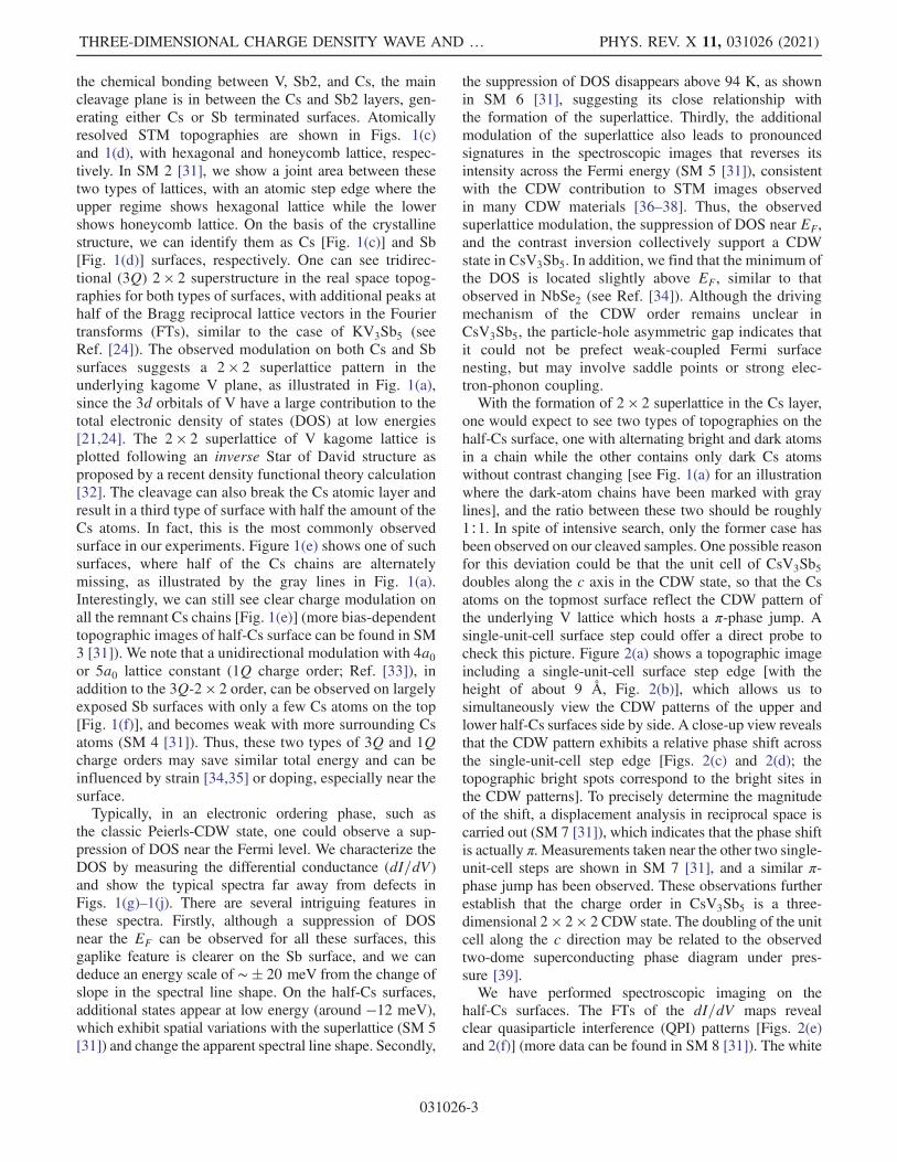
one would expect to see two types of topographies on thehalf-Cs surface, one with alternating bright and dark atomsin a chain while the other contains only dark Cs atomswithout contrast changing [see Fig. 1(a) for an illustrationwhere the dark-atom chains have been marked with graylines], and the ratio between these two should be roughly1∶1. In spite of intensive search, only the former case hasbeen observed on our cleaved samples. One possible reasonfor this deviation could be that the unit cell of CsV3Sb5doubles along the c axis in the CDW state, so that the Csatoms on the topmost surface reflect the CDW pattern ofthe underlying V lattice which hosts a π-phase jump. Asingle-unit-cell surface step could offer a direct probe tocheck this picture. Figure 2(a) shows a topographic imageincluding a single-unit-cell surface step edge [with theheight of about 9 Å, Fig. 2(b)], which allows us tosimultaneously view the CDW patterns of the upper andlower half-Cs surfaces side by side. A close-up view revealsthat the CDW pattern exhibits a relative phase shift acrossthe single-unit-cell step edge [Figs. 2(c) and 2(d); thetopographic bright spots correspond to the bright sites inthe CDW patterns]. To precisely determine the magnitudeof the shift, a displacement analysis in reciprocal space iscarried out (SM 7 [31]), which indicates that the phase shiftis actually π. Measurements taken near the other two single-unit-cell steps are shown in SM 7 [31], and a similar π-phase jump has been observed. These observations furtherestablish that the charge order in CsV3Sb5 is a three-dimensional 2 × 2 × 2 CDW state. The doubling of the unitcell along the c direction may be related to the observedtwo-dome superconducting phase diagram under pres-sure [39].We have performed spectroscopic imaging on the
half-Cs surfaces. The FTs of the dI=dV maps revealclear quasiparticle interference (QPI) patterns [Figs. 2(e)and 2(f)] (more data can be found in SM 8 [31]). The white
THREE-DIMENSIONAL CHARGE DENSITY WAVE AND … PHYS. REV. X 11, 031026 (2021)
031026-3
circle in the FTs denotes the 3Q-CDW wave vector.The QPI data show two ringlike signals centered at theΓ point. We find that the outer ring (q0) is almostnondispersing, which may potentially originate fromFriedel oscillations (2kF) or STM setpoint effect [40].The inner one (q1) arises from the intrapocket scattering of
the electron band at Γ, which has been assigned to the pzorbital of Sb. The extracted dispersion of q1, together with aparabolic fit, is displayed in Fig. 2(g). The band bottom isestimated to be −0.6 eV from the fitting, consistent withthe reported angle-resolved photoemission spectroscopydata [21].
0.40
0.60
0.80
1.45
1.57
1.82
2.06
2.31
2.50
2.803.00
3.22
3.47
Temp. (K)
-2.0 0 2.0
Energy (meV)
1
2
3
dI/d
V (
arb.
uni
ts)
dI/d
V (
arb.
uni
ts)
(a) (b)
-1.0 0 1.0
Energy (meV)
1
0.8
0.6
0.4
Cs 2×2
Half-Cs
Sb: 1Q
Sb: 3Q
0.2 0.4 0.6 0.8
0 0.2-0.2
Energy (meV)
Cs- 2×2
FIG. 3. (a) Temperature evolution of the superconducting gap. (b) Superconducting spectra obtained on different types of surfaces.The spectra of half-Cs, Sb 3Q − 2 × 2, and Sb 1Q regions are obtained in one field of view with the same tip. STM setup condition: (a),(b) VS ¼ −2 mV, It ¼ 200 pA, Vm ¼ 0.1 mV.
10 nm
0100 20 30
r (nm)
1 z (nm)
0.9 nm(a)
(b)
(c) (g)
(d)
0 0.4-0.4
q=2k (1/A)
0
-0.2
-0.4
-0.6
-0.8
0.2
Ene
rgy
(eV
)
q0
q1
q1
3Q-CDW
q1
q0
H
L
H
L
H
L
11 nm
(e)
(f)
FIG. 2. (a) Topographic image of the half-Cs surface showing a single-unit-cell step. (b) Height profile obtained along the pink lineshown in (a). (c) Close-up of the step edge. The dashed pink lines track the chains with CDW modulation on the upper side. A π-phasejump can be observed between the upper and lower sides. (d) Illustration of the CDW patterns near a single-unit-cell step. (e),(f)Normalized dI=dV maps (dI=dVðr; eVÞ=½Iðr; eVÞ=V�) and their FTs at −80 and −300 mV, respectively. The white circle denotes oneof the 3Q-CDW wave vectors. The clearly dispersing vector is marked as q1. (g) The energy dispersion of q1 extracted from line cuts ofthe FTs and a parabolic fit, E ¼ 9.77k2 − 0.6. STM setup condition: (a) VS ¼ −100 mV, It ¼ 80 pA, (e) VS ¼ −80 mV, (f)VS ¼ −300 mV, It ¼ 450 pA, Vm ¼ 4 mV.
ZUOWEI LIANG et al. PHYS. REV. X 11, 031026 (2021)
031026-4
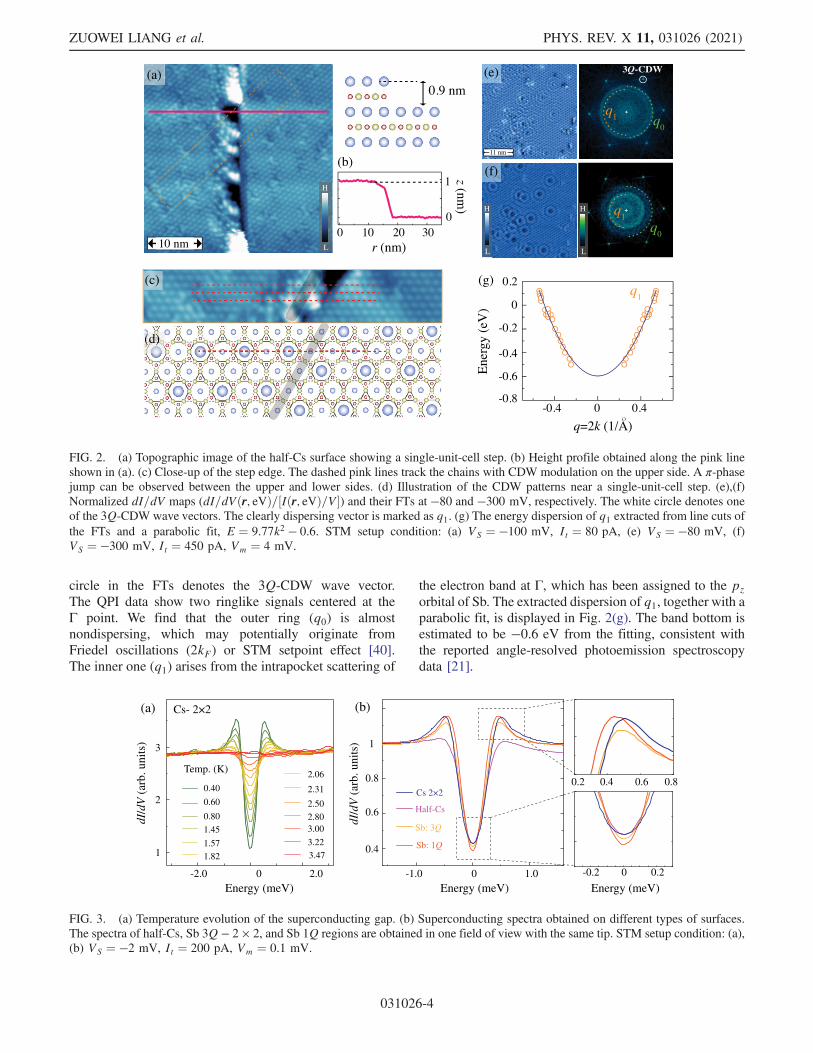
We now investigate the superconducting state ofCsV3Sb5. At 0.4 K, we observe a suppression of DOSat EF with symmetric coherence peaks forming at�0.55 meV in the tunneling spectra [Fig. 3(a)], whichwe identify to be the superconducting gap. This gap isgradually suppressed at elevated temperatures and even-tually disappears at the bulk Tc ∼ 3 K. Interestingly, wefind that the superconducting spectra obtained on differenttypes of surfaces are slightly different. As summarized inFig. 3(b), while the spectra acquired on the Cs 2 × 2 and Sbsurfaces have more similar line shapes, the superconduct-ing spectrum of the half-Cs surface shows clearly sup-pressed superconducting coherence peaks, indicating alarger scattering effect [41]. The overall evolution of thesuperconducting spectra has been checked on two samples.To gain a quantitative understanding on the superconduct-ing order parameter, we fit the tunneling spectrum obtained
on the Cs surface with the Dynes model [41], usingisotropic s-wave gap, anisotropic s-wave, and two isotropics-wave gap functions, respectively. The results can befound in SM 9 [31].Next, we check the possible excitations inside a super-
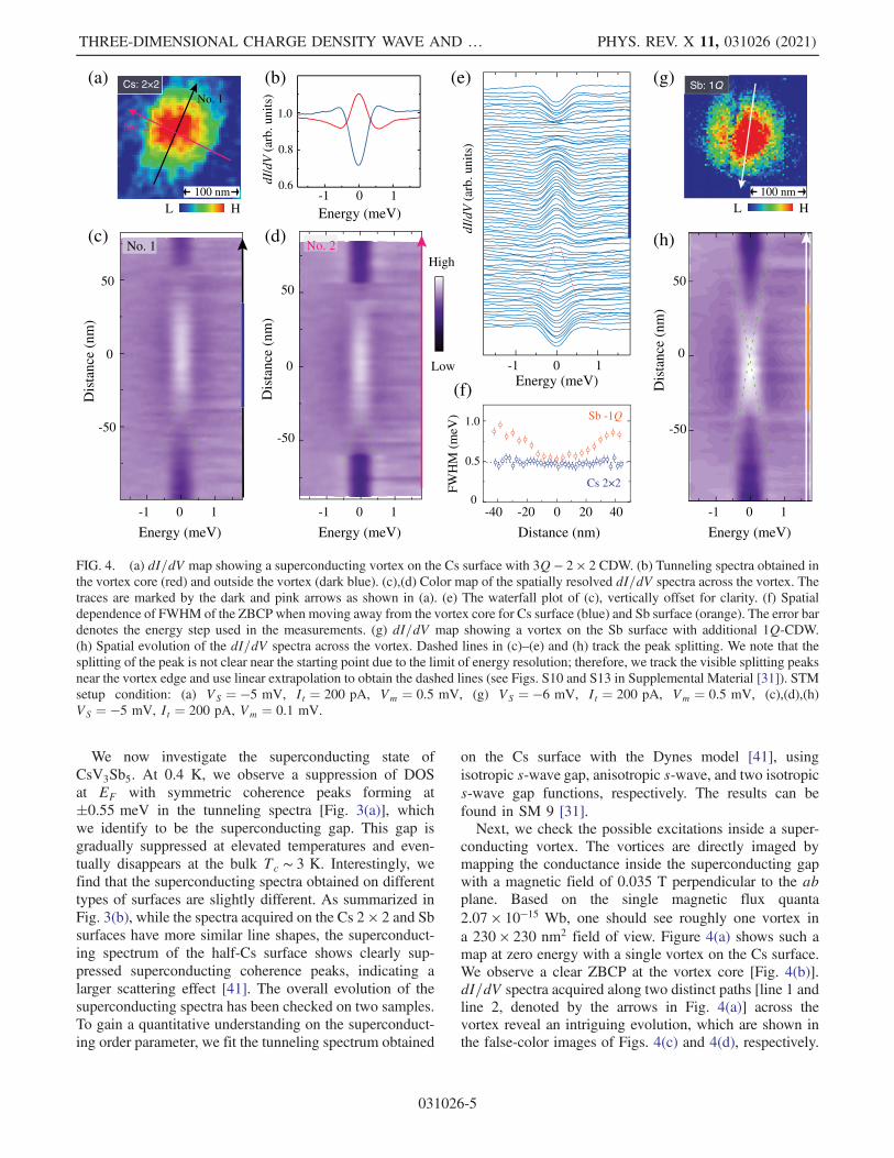
conducting vortex. The vortices are directly imaged bymapping the conductance inside the superconducting gapwith a magnetic field of 0.035 T perpendicular to the abplane. Based on the single magnetic flux quanta2.07 × 10−15 Wb, one should see roughly one vortex ina 230 × 230 nm2 field of view. Figure 4(a) shows such amap at zero energy with a single vortex on the Cs surface.We observe a clear ZBCP at the vortex core [Fig. 4(b)].dI=dV spectra acquired along two distinct paths [line 1 andline 2, denoted by the arrows in Fig. 4(a)] across thevortex reveal an intriguing evolution, which are shown inthe false-color images of Figs. 4(c) and 4(d), respectively.
100 nm
dI/d
V (
arb.
uni
ts)
Low
High
0
50
-50
Dis
tanc
e (n
m)
0
-50
50
0 011- -1 1
Energy (meV) Energy (meV)
L H0-1 1
Energy (meV)
dI/d
V (
arb.
uni
ts)
1.0
0.6
0.8
0-1 1Energy (meV)
0-40 40-20 20
Distance (nm)
0
0.5
1.0
FWH
M (
meV
)
Dis
tanc
e (n
m)
(a) (b)
(c) (d)
(e)
(f)
(g)
(h)
No. 1
No. 2
0-1 1
Energy (meV)
0
-50
50
Dis
tanc
e (n
m)
Sb: 1Q
100 nm
Cs: 2×2
L H
Cs 2×2
Sb -1Q
No. 2No. 1
FIG. 4. (a) dI=dV map showing a superconducting vortex on the Cs surface with 3Q − 2 × 2 CDW. (b) Tunneling spectra obtained inthe vortex core (red) and outside the vortex (dark blue). (c),(d) Color map of the spatially resolved dI=dV spectra across the vortex. Thetraces are marked by the dark and pink arrows as shown in (a). (e) The waterfall plot of (c), vertically offset for clarity. (f) Spatialdependence of FWHM of the ZBCP when moving away from the vortex core for Cs surface (blue) and Sb surface (orange). The error bardenotes the energy step used in the measurements. (g) dI=dV map showing a vortex on the Sb surface with additional 1Q-CDW.(h) Spatial evolution of the dI=dV spectra across the vortex. Dashed lines in (c)–(e) and (h) track the peak splitting. We note that thesplitting of the peak is not clear near the starting point due to the limit of energy resolution; therefore, we track the visible splitting peaksnear the vortex edge and use linear extrapolation to obtain the dashed lines (see Figs. S10 and S13 in Supplemental Material [31]). STMsetup condition: (a) VS ¼ −5 mV, It ¼ 200 pA, Vm ¼ 0.5 mV, (g) VS ¼ −6 mV, It ¼ 200 pA, Vm ¼ 0.5 mV, (c),(d),(h)VS ¼ −5 mV, It ¼ 200 pA, Vm ¼ 0.1 mV.
THREE-DIMENSIONAL CHARGE DENSITY WAVE AND … PHYS. REV. X 11, 031026 (2021)
031026-5
When tracking the splitting peaks near the vortex core edge,we find that the start point of the splitting is located∼35 nm away from the vortex core center (close-up ofthe splitting spectra is shown in SM 10 [31]), and theFWHM of the ZBCP bears little change in this range withinour STM resolution ∼0.23 meV (SM 11 [31]). Thisobservation is in sharp contrast to the vortex core statesin conventional s-wave superconductors, such as NbSe2(see Ref. [42]), where an “X”-type splitting has been widelyobserved, but is similar to the “Y”-type splitting observed in4–6 quintuple layer Bi2Te3=NbSe2 heterostructures [30](a direct comparison has been shown in SM 10 [31]).We would like to emphasize that the ZBCP inside thevortex core is not induced by disorder for two reasons.First, at zero field, homogeneous superconducting spectracan be observed along the same trace of line 1 (SM 12[31]), suggesting that the ZBCP indeed represents quasi-particle excitations inside a vortex. In fact, we never see anin-gap state that extends tens of nanometers at 0 T in oursamples. Second, this Y-type splitting of ZBCP is repeat-able once the vortex is located on the Cs surfaces(SM 13 [31]).As we mentioned above, the largely exposed Sb surfaces
exhibit additional 1Q modulation, which is in contrast tothe Cs surfaces that show only 3Q − 2 × 2 CDW.Interestingly, a distinct evolution of the vortex-core statesis observed on the Sb surfaces. As shown in Figs. 4(g) and4(h), the ZBCP inside the vortex core obtained on the Sbsurface splits faster when moving away from the corecenter, exhibiting a clear X-type evolution that is moresimilar to the conventional case. As a result, the apparentwidth of the vortex-core states also shows remarkablespatial dependence, in contrast to that observed on theCs surface [Fig. 4(f)]. For a better comparison, the spatialevolutions of vortex-core states observed on the Cs surface,half-Cs surface (with extra Cs atoms), and Sb surface,together with the atomic-resolution topographies, are pre-sented in SM 14 [31].The observation of distinct vortex-core states on different
surfaces of CsV3Sb5 is not trivial. One possible explanationfor the robust, finite-distance splitting ZBCP on the3Q − 2 × 2 Cs surfaces is the presence of MBSs insidethe vortex core. In the vortex of a conventional super-conductor, discrete energy levels of Caroli–de Gennes–Matricon bound states (CBSs) appear at Eμ ¼ μΔ2=EF,with μ the half-integer angular momentum number(μ ¼ �1=2;�3=2;�5=2;…) [43]. The spatial distributionof specific CBS scales with its angular momentum numberμ, leading to a wave function that peaks at rμ ∼ jμj=kF awayfrom the vortex center. In most superconductors, the energyspacing of μΔ2=EF is too small to be discernible; thus aparticle-hole symmetric ZBCP is experimentally observedat the core and it splits when moving right away from thevortex center, resulting in an X-type cross [30,42,44,45].This is different from what we have found here. On the
other hand, if Dirac surface states become superconducting,inside a vortex, quasiparticles gain an additional half-odd-integer contribution to the total angular momentumnumber owing to the intrinsic spin texture of Diracfermions. Therefore, quasiparticles are integer quantized(μ ¼ 0;�1;�2…) and MBSs can be regarded as a specialzero-energy CBS whose spin degree of freedom is elim-inated. Theoretically, the MBS extends in real space with alength scale ∼vF=Δ (similar to the superconducting coher-ence length) [46]. The presence of MBS could change theevolution of the quasiparticle spectra across the vortex, asseen in the cases of Bi2Te3=NbSe2 heterostructures [30]and 2M-WS2 (see Ref. [47]). In CsV3Sb5, the super-conducting gap could open on the bulk bands and topo-logical surface states with tiny electron doping on the Cssurfaces, and they all contribute to the observed CBSsinside the vortex. The presence of MBSs is expected toenhance the conductance near zero energy within a lengthscale ∼vF=Δ from the vortex center, resulting in the finite-distance (Y-type) splitting of the ZBCP. By taking the slopeof the calculated surface states of CsV3Sb5 (∼0.18 eVÅ[21]) and experimentally extracted superconducting gap(∼0.4 meV, SM 9 [31]), if they exist, the MBSs wouldextend about 45 nm in real space, a value in goodagreement with our experimental observation. Comparedwith iron-based superconductors Fe(Se,Te) [48,49] and (Li,Fe)OHFeSe [50], the relatively large Fermi energies forboth bulk bands and Dirac surface band in CsV3Sb5 impedethe observation of discrete CBSs, making the case moresimilar to that of Bi2Te3=NbSe2 heterostructure.Furthermore, the reported edge supercurrent in the
Nb=K1−XV3Sb5 devices [29] and chiral anisotropy in theCDW states [24] indicate that the superconducting state inthis family of compounds may also simultaneously breakthe time-reversal symmetry, making the situation morecomplex. A spin-triplet superconducting state with break-ing time-reversal symmetry could also host MBSs insidethe vortex core. To further reveal the superconductivity,possible future plans would include Bogoliubov QPImeasurements to probe the superconducting gap functionsΔiðkÞ, and searching for possible edge states in the dI=dVmaps. Finally, we would like to emphasize that, althoughour STM data are consistent with the presence of MBSsinside the vortex core of CsV3Sb5, further investigations atlower temperature and on doped samples are necessary andmore evidence is needed. Moreover, the distinct vortex-core states on the Cs and Sb surfaces, which may depend onlocal carrier doping [51] or different CDW modulations,would be an interesting topic for future theoretical study.In summary, we have demonstrated a three-dimensional
2 × 2 × 2 CDW state with an energy gap opening near theFermi level in kagome superconductor CsV3Sb5. In thesuperconducting state, we find a ZBCP inside the vortexcore that splits off at a large distance away from the vortexcenter on the Cs surfaces. This unusual splitting behavior,
ZUOWEI LIANG et al. PHYS. REV. X 11, 031026 (2021)
031026-6
reminiscent of that observed in Bi2Te3=NbSe2, couldpossibly be due to the MBSs inside the vortex core. Ourfindings may have provided the first glimpse into possibleMajorana modes in a kagome superconductor.
This work is supported by the National Key Researchand Development Program of the Ministry of Scienceand Technology of China (No. 2017YFA0303001,No. 2017YFA0302904, and No. 2018YFA0305602), theNational Natural Science Foundation of China (GrantsNo. 11888101, No. 12074002, and No. 11804379),the Strategic Priority Research Program of ChineseAcademy of Sciences (Grant No. XDB25000000),Anhui Initiative in Quantum Information Technologies(Grant No. AHY160000), the Key Research Program ofFrontier Sciences, CAS, China (QYZDYSSW-SLH021).Z.W. is supported by National Natural Science Foundationof China (No. 12074364), the Fundamental ResearchFunds for the Central Universities (WK3510000012),and USTC start-up fund. L. S. is supported by theRecruitment Program for Leading Talent Team of AnhuiProvince (2019-16).
[1] S. Nakatsuji, N. Kiyohara, and T. Higo, Large AnomalousHall Effect in a Non-Collinear Antiferromagnet at RoomTemperature, Nature (London) 527, 212 (2015).
[2] K. Kuroda et al., Evidence for Magnetic Weyl Fermions in aCorrelated Metal, Nat. Mater. 16, 1090 (2017).
[3] L. Ye, M. Kang, J. Liu, F. von Cube, C. R. Wicker,T. Suzuki, C. Jozwiak, A. Bostwick, E. Rotenberg, D. C.Bell, L. Fu, R. Comin, and J. G. Checkelsky,Massive DiracFermions in a Ferromagnetic Kagome Metal, Nature(London) 555, 638 (2018).
[4] E. Liu et al.,Giant AnomalousHall Effect in a FerromagneticKagome-Lattice Semimetal, Nat. Phys. 14, 1125 (2018).
[5] J.-X. Yin et al., Giant and Anisotropic Many-Body Spin–Orbit Tunability in a Strongly Correlated Kagome Magnet,Nature (London) 562, 91 (2018).
[6] Q. Wang, Y. Xu, R. Lou, Z. Liu, M. Li, Y. Huang, D. Shen,H. Weng, S. Wang, and H. Lei, Large Intrinsic AnomalousHall Effect in Half-Metallic Ferromagnet Co3Sn2S2 withMagnetic Weyl Fermions, Nat. Commun. 9, 3681 (2018).
[7] Z. Lin, J.-H. Choi, Q. Zhang, W. Qin, S. Yi, P. Wang, L. Li,Y. Wang, H. Zhang, Z. Sun, L. Wei, S. Zhang, T. Guo, Q.Lu, J.-H. Cho, C. Zeng, and Z. Zhang, Flatbands andEmergent Ferromagnetic Ordering in Fe3Sn2 KagomeLattices, Phys. Rev. Lett. 121, 096401 (2018).
[8] M. Kang et al., Dirac Fermions and Flat Bands in the IdealKagome Metal FeSn, Nat. Mater. 19, 163 (2020).
[9] J.-X. Yin et al., Quantum-Limit Chern Topological Magnet-ism in TbMn6Sn6, Nature (London) 583, 533 (2020).
[10] Y. Xing et al., Localized Spin-Orbit Polaron in MagneticWeyl Semimetal Co3Sn2S2, Nat. Commun. 11, 5613 (2020).
[11] H. M. Guo and M. Franz, Topological Insulator on theKagome Lattice, Phys. Rev. B 80, 113102 (2009).
[12] I. I. Mazin, H. O. Jeschke, F. Lechermann, H. Lee, M. Fink,R. Thomale, and R. Valentí, Theoretical Prediction of a
Strongly Correlated Dirac Metal, Nat. Commun. 5, 4261(2014).
[13] D. F. Liu, A. J. Liang, E. K. Liu, Q. N. Xu, Y.W. Li, C.Chen, D. Pei, W. J. Shi, S. K. Mo, P. Dudin, T. Kim, C.Cacho, G. Li, Y. Sun, L. X. Yang, Z. K. Liu, S. S. P. Parkin,C. Felser, and Y. L. Chen, Magnetic Weyl Semimetal Phasein a Kagome Crystal, Science 365, 1282 (2019).
[14] I. Belopolski et al., Discovery of Topological Weyl FermionLines and Drumhead Surface States in a Room TemperatureMagnet, Science 365, 1278 (2019).
[15] N. Morali, R. Batabyal, P. K. Nag, E. Liu, Q. Xu, Y. Sun, B.Yan, C. Felser, N. Avraham, and H. Beidenkopf, Fermi-ArcDiversity on Surface Terminations of the Magnetic WeylSemimetal Co3Sn2S2, Science 365, 1286 (2019).
[16] J. Wen, A. Rüegg, C. C. J. Wang, and G. A. Fiete,Interaction-Driven Topological Insulators on the Kagomeand the Decorated Honeycomb Lattices, Phys. Rev. B 82,075125 (2010).
[17] W.-H. Ko, P. A. Lee, and X.-G. Wen, Doped KagomeSystem as Exotic Superconductor, Phys. Rev. B 79,214502 (2009).
[18] M. L. Kiesel, C. Platt, and R. Thomale, UnconventionalFermi Surface Instabilities in the Kagome Hubbard Model,Phys. Rev. Lett. 110, 126405 (2013).
[19] S.-L. Yu and J.-X. Li, Chiral Superconducting Phase andChiral Spin-Density-Wave Phase in a Hubbard Model onthe Kagome Lattice, Phys. Rev. B 85, 144402 (2012).
[20] B. R. Ortiz, L. C. Gomes, J. R. Morey, M. Winiarski,M. Bordelon, J. S. Mangum, I. W. H. Oswald, J. A.Rodriguez-Rivera, J. R. Neilson, S. D. Wilson, E. Ertekin,T. M. McQueen, and E. S. Toberer, New Kagome PrototypeMaterials: Discovery of KV3Sb5, RbV3Sb5, and CsV3Sb5,Phys. Rev. Mater. 3, 094407 (2019).
[21] B. R. Ortiz, S. M. L. Teicher, Y. Hu, J. L. Zuo, P. M. Sarte,E. C. Schueller, A. M.M. Abeykoon, M. J. Krogstad, S.Rosenkranz, R. Osborn, R. Seshadri, L. Balents, J. He, andS. D. Wilson, CsV3Sb5: A Z2 Topological Kagome Metalwith a Superconducting Ground State, Phys. Rev. Lett. 125,247002 (2020).
[22] B. R. Ortiz, P. M. Sarte, E. M. Kenney, M. J. Graf, S. M. L.Teicher, R. Seshadri, and S. D. Wilson, Superconductivity inthe Z2 Kagome Metal KV3Sb5, Phys. Rev. Mater. 5, 034801(2021).
[23] Q. Yin, Z. Tu, C. Gong, Y. Fu, S. Yan, and H. Lei,Superconductivity and Normal-State Properties of KagomeMetal RbV3Sb5 Single Crystals, Chin. Phys. Lett. 38,037403 (2021).
[24] Y.-X. Jiang et al., Unconventional Chiral Charge Order inKagome Superconductor KV3Sb5, Nat. Mater. (2021),https://doi.org/10.1038/s41563-021-01034-y.
[25] S.-Y. Yang, Y. Wang, B. R. Ortiz, D. Liu, J. Gayles, E.Derunova, R. Gonzalez-Hernandez, L. Šmejkal, Y. Chen,S. S. P. Parkin, S. D. Wilson, E. S. Toberer, T. McQueen, andM. N. Ali, Giant, Unconventional Anomalous Hall Effectin the Metallic Frustrated Magnet Candidate, KV3Sb5,Sci. Adv. 6, eabb6003 (2020).
[26] F. H. Yu, T. Wu, Z. Y. Wang, B. Lei, W. Z. Zhuo, J. J. Ying,and X. H. Chen, Concurrence of Anomalous Hall Effect andCharge Density Wave in a Superconducting TopologicalKagome Metal, arXiv:2102.10987.
THREE-DIMENSIONAL CHARGE DENSITY WAVE AND … PHYS. REV. X 11, 031026 (2021)
031026-7
[27] L. Fu and C. L. Kane, Superconducting Proximity Effect andMajorana Fermions at the Surface of a TopologicalInsulator, Phys. Rev. Lett. 100, 096407 (2008).
[28] A. Kitaev, Fault-Tolerant Quantum Computation by Any-ons, Ann. Phys. (Amsterdam) 303, 2 (2003).
[29] Y. Wang, S. Yang, P. K. Sivakumar, B. R. Ortiz, S. M. L.Teicher, H. Wu, A. K. Srivastava, C. Garg, D. Liu, S. S. P.Parkin, E. S. Toberer, T. McQueen, S. D. Wilson, and M. N.Ali, Proximity-Induced Spin-Triplet Superconductivity andEdge Supercurrent in the Topological Kagome Metal,K1−xV3Sb5, arXiv:2012.05898.
[30] J.-P. Xu, M.-X. Wang, Z. L. Liu, J.-F. Ge, X. Yang, C. Liu,Z. A. Xu, D. Guan, C. L. Gao, D. Qian, Y. Liu, Q.-H. Wang,F.-C. Zhang, Q.-K. Xue, and J.-F. Jia, Experimental De-tection of a Majorana Mode in the Core of a MagneticVortex Inside a Topological Insulator-SuperconductorBi2Te3=NbSe2 Heterostructure, Phys. Rev. Lett. 114,017001 (2015).
[31] See Supplemental Material athttp://link.aps.org/supplemental/10.1103/PhysRevX.11.031026 for moretopographies and tunneling spectra of the CDW state,displacement analysis near a single-unit-cell step, fittingof the superconducting spectra and more vortex data ondifferent surfaces.
[32] H. Tan, Y. Liu, Z. Wang, and B. Yan, Charge Density Wavesand Electronic Properties of Superconducting KagomeMetals, arXiv:2103.06325.
[33] H. Zhao, H. Li, B. R. Ortiz, S. M. L. Teicher, T. Park, M. Ye,Z. Wang, L. Balents, S. D. Wilson, and I. Zeljkovic,Cascade of Correlated Electron States in a Kagome Super-conductor CsV3Sb5, arXiv:2103.03118.
[34] A. Soumyanarayanan, M.M. Yee, Y. He, J. van Wezel, D. J.Rahn, K. Rossnagel, E. W. Hudson, M. R. Norman, and J. E.Hoffman, Quantum Phase Transition from Triangular toStripe Charge Order in NbSe2, Proc. Natl. Acad. Sci.U.S.A. 110, 1623 (2013).
[35] S. Gao, F. Flicker, R. Sankar, H. Zhao, Z. Ren, B.Rachmilowitz, S. Balachandar, F. Chou, K. S. Burch, Z.Wang, J. van Wezel, and I. Zeljkovic, Atomic-Scale StrainManipulation of a Charge Density Wave, Proc. Natl. Acad.Sci. U.S.A. 115, 6986 (2018).
[36] P. Mallet, K. M. Zimmermann, P. Chevalier, J. Marcus, J. Y.Veuillen, and J. M. G. Rodriguez, Contrast Reversal of theCharge Density Wave STM Image in Purple PotassiumMolybdenum Bronze K0.9Mo6O17, Phys. Rev. B 60, 2122(1999).
[37] D. Stoltz, M. Bielmann, M. Bovet, L. Schlapbach,and H. Berger, Tunneling Evidence for Spatial Locationof the Charge-Density-Wave Induced Band Splitting in1T − TaSe2, Phys. Rev. B 76, 073410 (2007).
[38] M. Spera, A. Scarfato, Á. Pásztor, E. Giannini, D. R.Bowler, and C. Renner, Insight into the Charge DensityWave Gap from Contrast Inversion in Topographic STMImages, Phys. Rev. Lett. 125, 267603 (2020).
[39] K. Y. Chen, N. N. Wang, Q. W. Yin, Z. J. Tu, C. S. Gong,J. P. Sun, H. C. Lei, Y. Uwatoko, and J.-G. Cheng, DoubleSuperconducting Dome and Triple Enhancement of Tc inthe Kagome Superconductor CsV3Sb5 under High Pres-sure, arXiv:2102.09328 [Phys. Rev. Lett. (to be published)].
[40] A. Macdonald, Y.-S. Tremblay-Johnston, S. Grothe, S. Chi,P. Dosanjh, S. Johnston, and S. A. Burke, DispersingArtifacts in FT-STS: A Comparison of Set Point Effectsacross Acquisition Modes, Nanotechnology 27, 414004(2016).
[41] R. C. Dynes, J. P. Garno, G. B. Hertel, and T. P. Orlando,Tunneling Study of Superconductivity Near the Metal-Insulator Transition, Phys. Rev. Lett. 53, 2437 (1984).
[42] H. F. Hess, R. B. Robinson, and J. V. Waszczak, Vortex-Core Structure Observed with a Scanning Tunneling Micro-scope, Phys. Rev. Lett. 64, 2711 (1990).
[43] L. Kramer and W. Pesch, Core Structure and Low-EnergySpectrum of Isolated Vortex Lines in Clean Superconduc-tors at T ≪ Tc, Z. Phys. 269, 59 (1974).
[44] F. Gygi and M. Schlüter, Self-Consistent ElectronicStructure of a Vortex Line in a Type-II superconductor,Phys. Rev. B 43, 7609 (1991).
[45] H. F. Hess, R. B. Robinson, R. C. Dynes, J. M. Valles,and J. V. Waszczak, Scanning-Tunneling-Microscope Ob-servation of the Abrikosov Flux Lattice and the Density ofStates near and inside a Fluxoid, Phys. Rev. Lett. 62, 214(1989).
[46] C.-K. Chiu, M. J. Gilbert, and T. L. Hughes, Vortex Lines inTopological Insulator-Superconductor Heterostructures,Phys. Rev. B 84, 144507 (2011).
[47] Y. Yuan, J. Pan, X. Wang, Y. Fang, C. Song, L. Wang, K.He, X. Ma, H. Zhang, F. Huang, W. Li, and Q.-K. Xue,Evidence of Anisotropic Majorana Bound States in2M −WS2, Nat. Phys. 15, 1046 (2019).
[48] D. Wang, L. Kong, P. Fan, H. Chen, S. Zhu, W. Liu, L. Cao,Y. Sun, S. Du, J. Schneeloch, R. Zhong, G. Gu, L. Fu,H. Ding, and H.-J. Gao, Evidence for Majorana BoundStates in an Iron-Based Superconductor, Science 362, 333(2018).
[49] L. Kong, S. Zhu, M. Papaj, H. Chen, L. Cao, H. Isobe, Y.Xing, W. Liu, D. Wang, P. Fan, Y. Sun, S. Du, J.Schneeloch, R. Zhong, G. Gu, L. Fu, H.-J. Gao, and H.Ding, Half-Integer Level Shift of Vortex Bound States in anIron-Based Superconductor, Nat. Phys. 15, 1181 (2019).
[50] Q. Liu, C. Chen, T. Zhang, R. Peng, Y.-J. Yan, C.-H.-P.Wen, X. Lou, Y.-L. Huang, J.-P. Tian, X.-L. Dong, G.-W.Wang, W.-C. Bao, Q.-H. Wang, Z.-P. Yin, Z.-X. Zhao, andD.-L. Feng, Robust and Clean Majorana Zero Mode in theVortex Core of High-Temperature Superconductor(Li0.84Fe0.16)OHFeSe, Phys. Rev. X 8, 041056 (2018).
[51] P. Hosur, P. Ghaemi, R. S. K. Mong, and A. Vishwanath,Majorana Modes at the Ends of Superconductor Vortices inDoped Topological Insulators, Phys. Rev. Lett. 107, 097001(2011).
ZUOWEI LIANG et al. PHYS. REV. X 11, 031026 (2021)
031026-8