Zinc Oxide Thin Film Transistors by Radio Frequency ... · Zinc Oxide Thin Film Transistors by...
146
Zinc Oxide Thin Film Transistors by Radio Frequency Magnetron Sputtering (Zinkoxid-Dünnschichttransistoren mittels Hochfrequenz-Magnetron- Kathodenzerstäubung) Der Technischen Fakultät der Friedrich-Alexander-Universität Erlangen-Nürnberg zur Erlangung des Grades DOKTOR – INGENIEUR vorgelegt von Jiaye HUANG aus Shanghai
Transcript of Zinc Oxide Thin Film Transistors by Radio Frequency ... · Zinc Oxide Thin Film Transistors by...
Zinc Oxide Thin Film Transistors by
Radio Frequency Magnetron Sputtering
(Zinkoxid-Dünnschichttransistoren
mittels Hochfrequenz-Magnetron-
Kathodenzerstäubung)
Der Technischen Fakultät
der Friedrich-Alexander-Universität Erlangen-Nürnberg
zur Erlangung des Grades
DOKTOR – INGENIEUR
vorgelegt von
Jiaye HUANG
aus Shanghai
Als Dissertation genehmigt von
der Technischen Fakultät der
Friedrich-Alexander-Universität Erlangen-Nürnberg
Tag der mündlichen Prüfung:
Vorsitzende des Promotionsorgans:
Gutachter:
20.10.2014
Prof. Dr.-Ing. Marion Merklein
Prof. Dr. rer. nat. Lothar Frey
Prof. Dr.-Ing. Peter Wellmann


v
Abstract
The major goal of this work is to investigate the electrical and morphological characteristics of single ZnO thin film transistors (TFTs) and construct basic logic circuits based on ZnO TFTs. In this work, zinc oxide (ZnO) thin films are fabricated by RF magnetron sputtering method. The working principle of ZnO TFTs with respect to traditional silicon MOSFETs is discussed and a model combining MOSFET with accumulation channel and JFET with insu-lated gate is included to understand the electrical behavior of ZnO TFTs. During sputtering processes, the influence of sputtering parameters on the sputtering rate is investigated. Sput-tering parameters include oxygen flow rate, total pressure, sputtering power, and substrate-to-target distance. Effects of these sputtering parameters on the ZnO electrical characteris-tics such as bulk resistivity are also analyzed. Morphological and electrical characteristics of ZnO TFTs after post deposition annealing in both oxygen and forming gas atmosphere in the temperature range of 400°C to 500°C are investigated. The ZnO layer after annealing shows polycrystalline morphology and the grain size tends to increase with increasing temperature in both oxygen and forming gas atmosphere. The threshold voltage decreases and the satu-ration mobility increases with increasing temperature in both cases. The correlations be-tween ZnO layer properties and electrical characteristics after annealing are investigated. With the decrease in the interface trap density and grain boundary trap density, the threshold voltage and turn-on voltage of the ZnO TFTs decrease while the saturation mobility increas-es after both oxygen and forming gas annealing. Besides the reduction of trap density, incor-porated hydrogen during forming gas annealing acts as shallow donors and thus ZnO TFTs in forming gas annealing show an even higher mobility and lower threshold voltage than the TFTs annealed at same temperature in oxygen. ZnO TFTs are also demonstrated in this work to construct NMOS enhancement load inverters. The inverter gain increases with sup-ply voltage and is limited by the off currents in single ZnO TFTs. An additional modification mask with the possibility to modify the ZnO active channel layer through different annealing steps or ion implantation is included in this work and a boost in inverter gain is realistic with the integration of the modification mask to realize NMOS depletion load inverters.

vii
Zusammenfassung
Das wichtigste Ziel dieser Arbeit war es, die elektrischen und morphologischen Merkmale von ZnO-Dünnschichttransistoren (TFTs) zu untersuchen und grundlegende Logik-Schaltungen auf Basis von ZnO-TFTs zu konstruieren. In dieser Arbeit wurden Zinkoxid (ZnO)-Dünnschichten mittels RF-Magnetron-Kathodenzerstäubungs-Verfahren hergestellt. Das Funktionsprinzip von ZnO-TFTs wird im Vergleich zu herkömmlichen Silizium-MOSFETs diskutiert und ein Modell zur Kombination eines MOSFETs mit Akkumulationskanal und eines JFETs mit isoliertem Gate wird beschrieben, um das Stromverhalten in ZnO-TFTs zu verstehen. Bezüglich der Sputterverfahren wird der Einfluss der Prozessparameter auf die Sputterrate untersucht. Sputterparameter beinhalten Sauerstoffdurchfluss, Gesamtdruck, Sputterleistung und Abstand zwischen Substrat und Target. Die Auswirkungen dieser Sputterparameter auf die elektrischen Eigenschaften des ZnO, wie spezifischer Widerstand, werden ebenfalls analysiert. Morphologische und elektrische Eigenschaften von ZnO-TFTs nach der Temperung in Sauerstoff- und Formiergasatmosphäre im Temperaturbereich von 400 °C bis 500 °C werden untersucht. Die ZnO-Schicht weist nach der Temperung polykristalline Morphologie auf und die Korngröße nimmt sowohl unter Sauerstoffatmosphäre als auch unter Formiergasumgebung mit steigender Ausheiltemperatur zu. Die Einsatzspannung verringert sich und die Sättigungsbeweglichkeit erhöht sich mit zunehmender Temperatur in beiden Fällen. Der Zusammenhang zwischen ZnO-Schichteneigenschaften und elektrischen Eigenschaften nach der Temperung wird beschrieben. Mit der Abnahme der Haftstellendichte verringern sich die Einsatzspannung und die Einschaltspannung der ZnO-TFTs, während die Sättigungsbeweglichkeit nach der Sauerstoff- und Formiergastemperung steigt. Neben der Reduzierung der Haftstellendichte wird während der Formiergastemperung Wasserstoff in das ZnO eingebaut, der als flacher Donator wirkt. Somit zeigen in Formiergas getemperte ZnO-TFTs eine höhere Beweglichkeit und niedrigere Einsatzspannung als bei gleicher Temperatur in Sauerstoff getemperte Proben. Des Weiteren wird in dieser Arbeit die Konstruktion von NMOS-Invertern mit Anreicherungs-Lasttransistoren demonstriert. Das Inverteramplitudenverhältnis erhöht sich mit der Versorgungsspannung und wird durch die Off-Ströme in einzelnen ZnO-TFTs beschränkt. Eine weitere Maskenebene mit der Möglichkeit, den aktiven ZnO-Kanal des Last- oder Schalttransistors durch zusätzliche Temperschritte oder Ionenimplantation zu ändern, wird in dieser Arbeit beschrieben. Mit der Integration der Modifikationsmaske erscheint die Realisierung eines NMOS Verarmungs-Last Inverters und eine Erhöhung des Inverteramplitudenverhältnisses realistisch.


ix
Acknowledgments
I would like to express my gratitude to my supervisor at the Friedrich-Alexander-University Erlangen-Nuremberg, Prof. Dr. Lothar Frey, for granting me the opportunity to carry out the research presented in this work, as well as for his guidance during my research and writing of this thesis. I would also like to thank Prof. Dr. Peter Wellmann for his careful co-examination on this thesis.
I would also like to thank the head of the technology department at the Fraunhofer IISB, Dr. Anton Bauer, for his support during my research project.
Special thanks go to the printed electronics group at the Fraunhofer IISB and the chair of electron devices at the Friedrich-Alexander-University Erlangen-Nuremberg. Without support and guidance from all the members in this group I would not be able to conduct this research and successfully complete my thesis. Big thanks go to Dr. Michael Jank for his care and support for my research work. I am very grateful to him for his discussion about experimental results and his corrections for the thesis. I would also express my sincere gratitude to all my colleagues in the group including Dr. Martin Lemberger, Dr. Susanne Oertel, Anke Haas, Erik Teuber, Dr. Simon Lukas, Dr. Sabine Walther, Sebastian Polster, Sebastian Weis, and Bern-hard Meyer.
Besides, I would like to thank all the colleagues with whom I had the pleasure to work with. In particular, I would like to thank Christian Strenger, Dr. Johannes Laven, Dr. Azinwi Fet, Dr. Vincent Lorentz, Sieglinde Elsesser, Angela Meixner, Dr. Elke Meißner, Dr. Volker Häublein, Christian Heilmann, Martin Heilmann, Stefan Knopf, Erich Pauer, Herbert Hofmann, Anette Daurer, Dr. Joachim vom Dorp, Dr. Holger Schwarzmann, Dr. Tobias Erlbacher.
Big love and many thanks go to my father Guoliang Huang, my mother Lexin Zhang for their support, patience and love during my thesis. Without them I would never be able to success-fully complete my thesis.


My Family

xiii
Contents
1 Introduction ........................................................................................................................ 1
2 Theory ................................................................................................................................. 7
2.1 Material properties of ZnO ............................................................................................ 7
2.1.1 General properties of ZnO as a semiconductor .................................................. 8
2.1.2 Defects and impurities in ZnO ............................................................................ 9
2.1.3 P-doping in ZnO ............................................................................................... 13
2.2 Thin film transistors .................................................................................................... 15
2.2.1 Comparison of Si MIS capacitors and ZnO MIS capacitors ............................. 15
2.2.2 Comparison of Si MOSFETs and ZnO thin film transistors .............................. 23
2.2.2.1 MOSFETs theory ................................................................................. 23
2.2.2.2 Junction FET theory ............................................................................ 27
2.2.2.3 ZnO thin film transistors ....................................................................... 30
2.3 Sputtering as a thin film deposition method ............................................................... 33
2.3.1 Basic sputtering mechanisms ........................................................................... 33
2.3.1.1 Direct current (DC) sputtering .............................................................. 35
2.3.1.2 Radio frequency (RF) sputtering ......................................................... 36
2.3.1.3 Magnetron sputtering ........................................................................... 37
2.3.1.4 Reactive sputtering .............................................................................. 37
2.3.2 Effects of processing parameters on the properties of sputtered ZnO layers .. 38
2.4 Logic circuits ............................................................................................................... 40
3 Experimental methods ..................................................................................................... 49
3.1 Sputtering equipment ................................................................................................. 49
3.2 Test structures ............................................................................................................ 51
3.3 Physical characterization methods ............................................................................. 54
3.3.1 Ellipsometry ..................................................................................................... 54
3.3.2 Atomic force microscopy ................................................................................. 56
3.3.3 Scanning electron microscopy ......................................................................... 56
3.3.4 Transmission electron microscopy .................................................................. 57
3.3.5 X-ray diffraction ............................................................................................... 58

xiv CONTENTS
3.4 Electrical characterization methods ............................................................................ 58
3.4.1 Electrical characterization ................................................................................ 58
3.4.2 Evaluation of electrical characterization results ............................................... 60
3.4.3 Extraction of electrical parameters .................................................................. 62
4 Results and discussions ................................................................................................. 63
4.1 Influence of sputtering parameters on properties of ZnO films ................................... 63
4.1.1 Influence of sputtering parameters on the deposition rate of ZnO films .......... 63
4.1.2 Influence of sputtering parameters on electrical characteristics of ZnO TFTs 66
4.2 Effects of annealing on morphological changes of ZnO layers .................................. 71
4.3 Effects of annealing on electrical characteristics of ZnO TFTs .................................. 79
4.3.1 Shadow mask design ...................................................................................... 79
4.3.2 Effects of forming gas annealing ..................................................................... 80
4.3.3 Effects of oxygen annealing ............................................................................ 82
4.3.4 Comparison of oxygen and forming gas annealing ......................................... 84
4.4 Inverter characterization ............................................................................................. 89
4.4.1 Characterization of the inverter ....................................................................... 89
4.4.2 Perspective of realization of depletion-load NMOS inverters .......................... 93
5 Conclusion and outlook .................................................................................................. 97
Bibliography ....................................................................................................................... 101
List of symbols ................................................................................................................... 117
List of abbreviations .......................................................................................................... 123
Index .................................................................................................................................... 125
List of own publications .................................................................................................... 127
Curriculum vitae ................................................................................................................. 129


1
Chapter 1
Introduction
Since the realization of the first metal-oxide-semiconductor field-effect transistor (MOSFET) by D. Khang and M. Atalla from Bell Labs in 1959 [Kha63], there have been tremendous in-novations and inventions for semiconductor devices. Shortly after the invention of MOSFET, C. Sah and F. Wanlass from Fairchild Laboratory developed the first logic circuit combining p-channel and n-channel MOS transistors in a complementary symmetry circuit configuration in 1963, which is known as the first CMOS device [Wan63]. The idea of integrated circuit (IC) was first presented by J. Kilby in 1958 [Kil76]. With the invention of CMOS technologies and the concept of IC, it is possible to integrate thousands of MOSFETs on chips with the size of a thumbnail. The development of the IC is described by Moore’s law which states that the number of transistors which can be placed on one single integrated circuit doubles approxi-mately every two years [Moo65]. Moore’s law holds true with the continuous improvement in semiconductor fabrication technology and consistent reduction in the dimensions of the sem-iconductor devices. The two important factors in semiconductor industry are the performance of the device such as the switching speed in the IC and the cost of the production. In order to achieve increasing device performance with decreasing fabrication cost, the focus of silicon technology lies strongly on application fields with high integration density and high power density such as dynamic random-access memory (DRAM) and processors. The technology node and minimum dimensions for high performance logic and memory is defined by experts within the framework of the International Technology Roadmap for Semiconductors [Itr11]. State-of-the-art semiconductor technology features a 40 nm half-pitch for DRAM and logic devices and a 22 nm gate length, which is defined as 22 nm technology node [Itr11].
In silicon technology, important process steps with high temperatures are used to achieve different goals. High quality field oxide is grown at up to 1000°C and annealing after ion im-plantation to reduce the implantation damage involves a process temperature as high as about 1100°C. These high temperature processes hinder the application of a large amount of substrates which can only endure a much lower process temperature, such as glass sub-strates, papers, and plastic foils. With the versatility of the applications involved in semicon-ductor technology, substrates compatible with low process temperatures play a more and more important role in the semiconductor fabrication technology, such as in printed electron-ics and transparent electronics. In order to meet the increasing demands in these applica-
2 CHAPTER 1: INTRODUCTION tions, thin film transistors (TFTs) which can be deposited on both silicon substrates and other substrates mentioned above are developed and fabricated. The first actual realization of a TFT was reported by P. Weimer in 1961 and fabricated by depositing cadmium sulphide (CdS) as a channel layer via vacuum evaporation [Wei62]. In
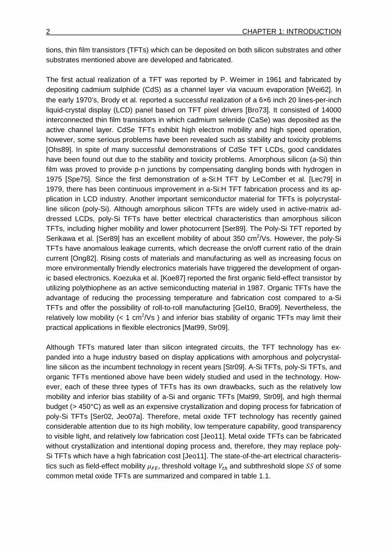
the early 1970’s, Brody et al. reported a successful realization of a 6×6 inch 20 lines-per-inch liquid-crystal display (LCD) panel based on TFT pixel drivers [Bro73]. It consisted of 14000 interconnected thin film transistors in which cadmium selenide (CaSe) was deposited as the active channel layer. CdSe TFTs exhibit high electron mobility and high speed operation, however, some serious problems have been revealed such as stability and toxicity problems [Ohs89]. In spite of many successful demonstrations of CdSe TFT LCDs, good candidates have been found out due to the stability and toxicity problems. Amorphous silicon (a-Si) thin film was proved to provide p-n junctions by compensating dangling bonds with hydrogen in 1975 [Spe75]. Since the first demonstration of a-Si:H TFT by LeComber et al. [Lec79] in 1979, there has been continuous improvement in a-Si:H TFT fabrication process and its ap-plication in LCD industry. Another important semiconductor material for TFTs is polycrystal-line silicon (poly-Si). Although amorphous silicon TFTs are widely used in active-matrix ad-dressed LCDs, poly-Si TFTs have better electrical characteristics than amorphous silicon TFTs, including higher mobility and lower photocurrent [Ser89]. The Poly-Si TFT reported by Serikawa et al. [Ser89] has an excellent mobility of about 350 cm2/Vs. However, the poly-Si TFTs have anomalous leakage currents, which decrease the on/off current ratio of the drain current [Ong82]. Rising costs of materials and manufacturing as well as increasing focus on more environmentally friendly electronics materials have triggered the development of organ-ic based electronics. Koezuka et al. [Koe87] reported the first organic field-effect transistor by utilizing polythiophene as an active semiconducting material in 1987. Organic TFTs have the advantage of reducing the processing temperature and fabrication cost compared to a-Si TFTs and offer the possibility of roll-to-roll manufacturing [Gel10, Bra09]. Nevertheless, the relatively low mobility (< 1 cm2/Vs ) and inferior bias stability of organic TFTs may limit their practical applications in flexible electronics [Mat99, Str09]. Although TFTs matured later than silicon integrated circuits, the TFT technology has ex-panded into a huge industry based on display applications with amorphous and polycrystal-line silicon as the incumbent technology in recent years [Str09]. A-Si TFTs, poly-Si TFTs, and organic TFTs mentioned above have been widely studied and used in the technology. How-ever, each of these three types of TFTs has its own drawbacks, such as the relatively low mobility and inferior bias stability of a-Si and organic TFTs [Mat99, Str09], and high thermal budget (> 450°C) as well as an expensive crystallization and doping process for fabrication of poly-Si TFTs [Ser02, Jeo07a]. Therefore, metal oxide TFT technology has recently gained considerable attention due to its high mobility, low temperature capability, good transparency to visible light, and relatively low fabrication cost [Jeo11]. Metal oxide TFTs can be fabricated without crystallization and intentional doping process and, therefore, they may replace poly-Si TFTs which have a high fabrication cost [Jeo11]. The state-of-the-art electrical characteris-tics such as field-effect mobility , threshold voltage and subthreshold slope of some common metal oxide TFTs are summarized and compared in table 1.1.
3
Table 1.1 A comparison of important electrical characteristics for various metal oxide TFTs including zinc oxide (ZnO), gallium indium zinc oxide (GIZO), hafnium indium zinc oxide (HIZO), and aluminum tin zinc indium oxide (AT-ZIO) TFTs [Joe11].
Oxide semi-conductor
Field-effect mobility (cm2/Vs)
Threshold voltage (V)
Subthreshold slope (V/dec)
On/off cur-rent ratio
Reference
ZnO 27 19 1.39 3 × 10⁵ [For04]
IGZO 12 1.4 0.20 1 × 10⁸ [Yab06]
IGZO 19.3 0.59 0.35 1.5 × 10⁷ [Jeo07b]
HIZO 10 -4.7 0.23 108 [Kim09] AT-ZIO 31.9 -0.2 0.07 2 × 10⁹ [Yan10]
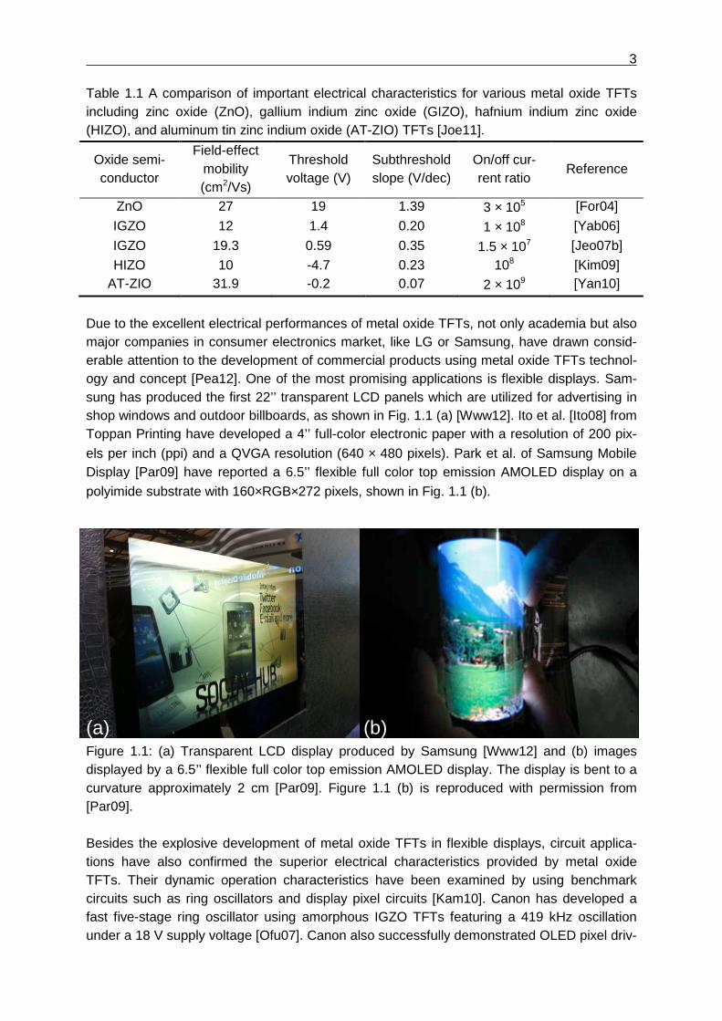
Due to the excellent electrical performances of metal oxide TFTs, not only academia but also major companies in consumer electronics market, like LG or Samsung, have drawn consid-erable attention to the development of commercial products using metal oxide TFTs technol-ogy and concept [Pea12]. One of the most promising applications is flexible displays. Sam-sung has produced the first 22’’ transparent LCD panels which are utilized for advertising in shop windows and outdoor billboards, as shown in Fig. 1.1 (a) [Www12]. Ito et al. [Ito08] from Toppan Printing have developed a 4’’ full-color electronic paper with a resolution of 200 pix-
els per inch (ppi) and a QVGA resolution (640 × 480 pixels). Park et al. of Samsung Mobile Display [Par09] have reported a 6.5’’ flexible full color top emission AMOLED display on a
polyimide substrate with 160×RGB×272 pixels, shown in Fig. 1.1 (b).
(a) (b) Figure 1.1: (a) Transparent LCD display produced by Samsung [Www12] and (b) images displayed by a 6.5’’ flexible full color top emission AMOLED display. The display is bent to a curvature approximately 2 cm [Par09]. Figure 1.1 (b) is reproduced with permission from [Par09]. Besides the explosive development of metal oxide TFTs in flexible displays, circuit applica-tions have also confirmed the superior electrical characteristics provided by metal oxide TFTs. Their dynamic operation characteristics have been examined by using benchmark circuits such as ring oscillators and display pixel circuits [Kam10]. Canon has developed a fast five-stage ring oscillator using amorphous IGZO TFTs featuring a 419 kHz oscillation under a 18 V supply voltage [Ofu07]. Canon also successfully demonstrated OLED pixel driv-
4 CHAPTER 1: INTRODUCTION ing at a frame rate of 120 Hz [Hay07]. Görrn et al. demonstrated operation of transparent OLED pixels using amorphous zinc tin oxide (a-ZTO) TFTs [Gör06]. Both flexible displays and circuit applications require high-density integrated metal oxide TFTs. When scaling down the size of individual TFTs, short channel effects [Tau98] which mostly relate to the decrease of the threshold voltage with decreasing channel length are examined for metal oxide TFTs. Song et al. [Son08] from Samsung Advanced Institute of Technology have successfully demonstrated amorphous IGZO TFTs with short channel lengths of 50 nm without suffering from short-channel effects. An indium zinc oxide (IZO) TFT with a short channel length of 1 µm and drain-to-source distance of 2.5 µm has been fabricated by RF magnetron sputtering at room temperature [Wan08]. The device has a high-frequency operation of up to 180 MHz [Wan08]. This property of down scalability to a chan-nel length of 1 µm or even shorter without suffering from short channel effects makes metal oxide TFTs very promising for applications in integrated high-density memory devices [Kam10].
Among the metal oxide semiconductor materials investigated up to now, ZnO has been wide-ly investigated due to its wide band gap, large and easy availability, and its compatibility with semiconductor fabrication technology. The first ZnO field-effect transistor was announced by Boesen et al. in 1968 utilizing lithium doped single crystal of ZnO [Boe68]. ZnO thin films can be fabricated by different techniques such as chemical vapor deposition (CVD) [Tik80, Kas81] or molecular-beam epitaxy [Hei07, Dad04]. The most common method for depositing ZnO thin films is magnetron sputtering [Hac94, Gar98]. Compared to other methods, magne-tron sputtering has the advantage of depositing homogeneous ZnO thin films at room tem-perature and better control of film stoichiometry and resistivity by optimizing sputtering pa-rameters. By using magnetron sputtering at room temperature, Fortunato et al. [For05] have demonstrated a fully transparent ZnO thin film transistor which exhibits a high saturation mo-
bility of about 20 cm2/Vs and a high on/off drain current ratio of 2 × 10⁵. This work focuses on thin film transistors and their applications based on radio frequency (RF) magnetron sputtered ZnO thin films. ZnO thin films are sputtered at room temperature from a ZnO target. Oxygen is used as a reactive gas during magnetron sputtering and ZnO TFTs are fabricated by using defined test structures. Chapter 2 first discusses the general properties of ZnO including intrinsic defects and impurities in ZnO and their roles for n- and p-type doping. Later on in chapter 2, comparison and common models for classical MOSFETs and ZnO TFTs are followed by the discussion of sputtering mechanisms and the working principle of basic logic circuits. In chapter 3, the sputtering equipment used in this work is introduced. Basic test structures as well as physical and electrical characterization methods for ZnO thin films and TFTs are also included in chapter 3. Chapter 4 first investi-gates the dependence of sputtering rate and the electrical properties of fabricated ZnO TFTs on the sputtering parameters such as oxygen flow rate, RF sputtering power, total pressure, and substrate-to-target distance. A thorough discussion about post deposition annealing ef-fects on ZnO thin films and TFTs is conducted. The structural changes in ZnO films after an-nealing in oxygen or forming gas including crystallinity, residual stress, and grain size are investigated by X-Ray Diffraction (XRD), scanning electron microscopy (SEM), transmission electron microscopy (TEM), and atomic force microscopy (AFM). Furthermore, the effects of post deposition annealing in both oxygen and forming gas atmosphere on electrical charac-

5
teristics of ZnO TFTs are demonstrated. This helps understanding the different roles of oxy-gen and hydrogen in ZnO thin films. Last but not least, an enhancement NMOS inverter which consists of two ZnO TFTs as load and driver transistors is realized. Although optimiza-tion for better inverter performance is necessary in future work, this shows the potential of ZnO TFTs in circuit applications. Chapter 5 makes the conclusion for the work and future perspectives and possible optimization are also given in order to further expand the material properties of ZnO and its applications such as in transparent electronics and flexible dis-plays.

7
Chapter 2
Theory
2.1 Material properties of ZnO Being initially considered as a substrate for GaN and related alloys, the availability of high-quality large bulk single crystals, the strong luminescence demonstrated in optically pumped lasers, and the prospects of gaining control over its electrical conductivity have led a large number of research groups to turn their interest on ZnO as an optoelectronic or electronic material in its own right [Jan09a]. The high electron mobility, high optical transmittivity and high conductivity, high electromechanical coupling coefficients, wide and direct band gap, and large exciton binding energy make ZnO attractive for a wide range of devices, including light-emitting diodes, optically pumped lasers, transparent conducting oxides and TFTs, and piezoelectric devices [Özg10]. In many respects, ZnO is considered to be a good alternate to GaN for device applications due to its relatively low production cost and superior optical properties [Özg10]. Comparing to GaN, ZnO has a huge advantage of availability of large single crystals [Jan09a]. GaN is usually grown on sapphire with a large lattice mismatch of ~16%, which leads to an extremely high concentration of extended defects (106-109 cm-2) [Nak00]. The epitaxy of ZnO films on native substrates can lead to ZnO layers with reduced concentration of extended defects and, consequently, better performance in electronic and photonic devices [Loo01, Özg05, Oga05, Nic05, Jag06]. Another big advantage of ZnO over GaN is the amenability to wet chemical etching, which is particularly favourable in the device design and fabrication process [Loo01, Jan09a]. Due to these advantages, ZnO gradually becomes superior to GaN and replaces it in the device applications. However, problems con-cerning the reproducibility and the stability of p-type doping remain to be the most difficult obstacle to realizing bipolar ZnO-based devices [Özg10]. In the following section, the general properties of ZnO involving several characteristics which make ZnO a very attractive candidate for semiconductor device applications are first intro-duced. Then the source of unintentional n-type doping in ZnO and possible methods as well as remaining challenges in achieving p-type doping are discussed.
8 CHAPTER 2: THEORY
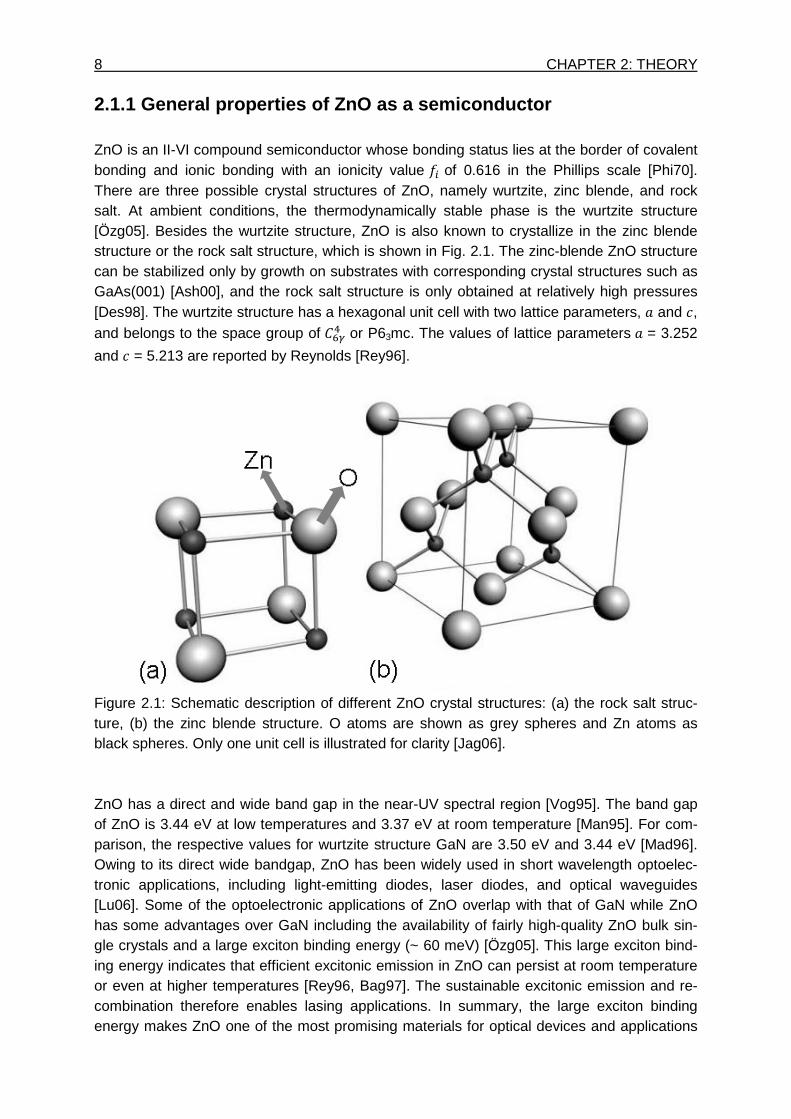
2.1.1 General properties of ZnO as a semiconductor ZnO is an II-VI compound semiconductor whose bonding status lies at the border of covalent bonding and ionic bonding with an ionicity value of 0.616 in the Phillips scale [Phi70]. There are three possible crystal structures of ZnO, namely wurtzite, zinc blende, and rock salt. At ambient conditions, the thermodynamically stable phase is the wurtzite structure [Özg05]. Besides the wurtzite structure, ZnO is also known to crystallize in the zinc blende structure or the rock salt structure, which is shown in Fig. 2.1. The zinc-blende ZnO structure can be stabilized only by growth on substrates with corresponding crystal structures such as GaAs(001) [Ash00], and the rock salt structure is only obtained at relatively high pressures [Des98]. The wurtzite structure has a hexagonal unit cell with two lattice parameters, and , and belongs to the space group of or P63mc. The values of lattice parameters = 3.252
and = 5.213 are reported by Reynolds [Rey96].
Figure 2.1: Schematic description of different ZnO crystal structures: (a) the rock salt struc-ture, (b) the zinc blende structure. O atoms are shown as grey spheres and Zn atoms as black spheres. Only one unit cell is illustrated for clarity [Jag06]. ZnO has a direct and wide band gap in the near-UV spectral region [Vog95]. The band gap of ZnO is 3.44 eV at low temperatures and 3.37 eV at room temperature [Man95]. For com-parison, the respective values for wurtzite structure GaN are 3.50 eV and 3.44 eV [Mad96]. Owing to its direct wide bandgap, ZnO has been widely used in short wavelength optoelec-tronic applications, including light-emitting diodes, laser diodes, and optical waveguides [Lu06]. Some of the optoelectronic applications of ZnO overlap with that of GaN while ZnO has some advantages over GaN including the availability of fairly high-quality ZnO bulk sin-gle crystals and a large exciton binding energy (~ 60 meV) [Özg05]. This large exciton bind-ing energy indicates that efficient excitonic emission in ZnO can persist at room temperature or even at higher temperatures [Rey96, Bag97]. The sustainable excitonic emission and re-combination therefore enables lasing applications. In summary, the large exciton binding energy makes ZnO one of the most promising materials for optical devices and applications
2.1 MATERIAL PROPERTIES OF ZNO 9
that are based on excitonic effects [Jan09a]. However, ZnO still faces strong competition when faced with GaN. One of the disadvantages of ZnO over GaN is the less maturity in terms of devices. GaN device technology is much more mature as GaN-based very high-performance electronic and optical devices have already been commercialized [Özg10]. ZnO can be fabricated both as large single crystals and polycrystalline thin films depending on its detailed applications and relevant characteristics. Single crystals can be grown by dif-ferent methods including hydrothermal growth [Sek00], vapour-phase transport [Loo97], and pressurized melt growth [Rey04, Nau05]. Deposition of ZnO thin films can be realized by using chemical vapour deposition (CVD) [Tik80, Kas81] or molecular-beam epitaxy [Hei07, Dad04]. The most common method for depositing ZnO thin films is magnetron sputtering [Hac94, Gar98]. Comparing with the methods used for fabrication of single ZnO crystal bulks, magnetron sputtering has an advantage of fabricating ZnO thin films at low temperatures or even at room temperature [For05]. Besides the low temperature processing conditions pro-vided by magnetron sputtering, thin film transistors (TFTs) with sputtered ZnO thin films are often reported to have high mobility values and high / ratios. Fortunato et al. [For05]
have reported a high saturation mobility of about 20 cm2/Vs for the ZnO TFTs fabricated by radio frequency (RF) magnetron sputtering. Carcia et al. [Car03] have demonstrated a trans-parent ZnO TFT fabricated by magnetron sputtering near room temperature with the device on/off ratio > 106. The same research group has later reported the realization of ZnO TFTs on a flexible Kapton substrate with a saturation mobility of about 50 cm2/Vs [Car05]. Regard-ing to the fabrication of ZnO thin films, the amenability to wet chemical etching provides the possibility to structure the ZnO layer with ease. Acidic, alkaline as well as mixture solutions can be used to etch ZnO thin films [Jan09a]. In summary, ZnO has provided new insights from both material aspects and application as-pects. Although GaN films are earlier commercialized, ZnO has the advantage of a larger exciton binding energy of about 60 meV which makes it attractive for optical applications. Silicon technology and fabrication of amorphous silicon (Si) TFTs and polycrystalline Si TFTs are mature technologies. However low-temperature magnetron sputtered ZnO TFTs have advantage due to the fact that the maximal reported mobility value for amorphous silicon TFTs are about 1 cm2/Vs and the polycrystalline Si is normally fabricated under very high temperatures. Besides the applications mentioned above of ZnO thin films for transparent TFTs, more complicated electronic applications such as inverters and ring oscillators based on ZnO TFTs with high inverter gains and low propagation delays are also reported recently [Oh10, Sun08].
2.1.2 Defects and impurities in ZnO ZnO shows n-type conductivity regardless of deposition methods and its morphology. The cause of this intrinsic n-type doping is widely investigated and many researchers attribute n-type doping to the intrinsic defects inside ZnO including oxygen vacancies and zinc intersti-tials [Har54, Hut57, Tho57, Moh61, Hag76]. However, recent studies by density-functional calculations have demonstrated that the cause of n-type doping may not be due to oxygen vacancies and zinc interstitials [Koh00, Wal01, Jan05, Jan06, Jan07a, Vla05a, Vla05b]. In-stead of intrinsic defects, impurities such as hydrogen may be the cause of the unintentional
10 CHAPTER 2: THEORY n-type conductivity [Wal00, Jan07b]. The research of determining the cause of n-type doping is still under discussion. The two main sources which can influence the electrical conductivity are intrinsic defects and impurities. A discussion of intrinsic defects will be followed by inves-tigation of possible impurities which can contribute to n-type conductivity. Intrinsic defects are defined as imperfections in the crystal lattice that involve only the con-stituent elements [Lan81, Lan83]. Intrinsic defects can be mainly divided into three different types: vacancies (missing atoms at regular lattice positions), interstitials (extra atoms at in-terstices in the lattice), and antisites (a Zn atom occupying an O lattice site or vice versa in the ZnO structure) [Jan09a]. Assuming thermodynamic equilibrium and neglecting defect-
defect interaction, the concentration of an intrinsic defect in a solid, ,can be expressed by
its formation energy through the following equation [Kit05]:
′ = exp −
,(2.1)
where is the number of sites per unit volume the defect can be incorporated on, is the Boltzmann constant and the temperature. Equation (2.1) indicates that the concentra-tion of defects is lower with higher formation energies. The formation energy of a typical point defect depends on the growth environment or annealing conditions [Wal04]. The formation energy of an oxygen vacancy in ZnO is given by [Jan09a]:
= − ! +# + $% +&!,(2.2)
where is the total energy of a supercell containing the oxygen vacancy in the charge
state $, ! is the total energy of a ZnO perfect crystal in the same supercell, # is the oxygen chemical potential, % is the Fermi level and & is the valence-band maximum. Ex-pressions similar to equation (2.2) can be applied to all intrinsic point defects [Jan09a]. Defects are often electrically active and can create different levels in the semiconductor band gap, resulting in transitions between different charge states of the same defect [Lan81, Lan83]. The transition level '$ $⁄ ! is defined as the Fermi-level position for which the for-mation energies of charge states $ and $′ are equal [Jan07a]. The transition level indicates that for Fermi-level positions below '$ $⁄ ! charge state $ is stable, while for Fermi-level positions above '$ $⁄ ! charge state $′ is stable. The difference of a deep defect level and a shallow defect level lies in where the corresponding defect transition level is located. If a de-fect transition level is such positioned that it can be thermally ionized at room temperature or under device operation conditions, it is a shallow level. Otherwise it is a deep defect level. Considering the relative positioning of the transition levels to the band gaps in the semicon-ductor, the shallow levels can be defined in the following two scenarios: Firstly, the transition levels are close to the edge of the band gap (either to valence-band maximum (VBM) for an acceptor or to conduction-band minimum (CBM) for a donor); second, the transition levels function as resonance centers in either the conduction or valence band. In ZnO, the oxygen vacancy is the most discussed defect and since a long time, has been considered as the main cause of the unintentional n-type conductivity, but recent densi-
2.1 MATERIAL PROPERTIES OF ZNO 11
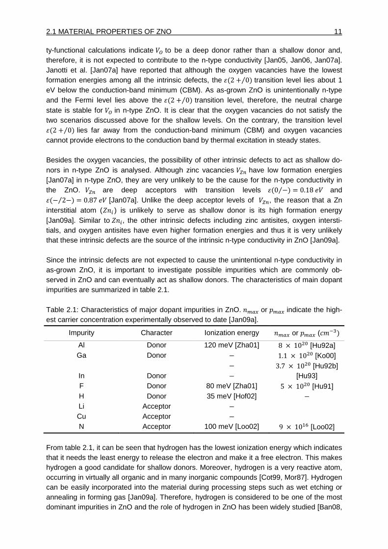
ty-functional calculations indicate ( to be a deep donor rather than a shallow donor and, therefore, it is not expected to contribute to the n-type conductivity [Jan05, Jan06, Jan07a]. Janotti et al. [Jan07a] have reported that although the oxygen vacancies have the lowest formation energies among all the intrinsic defects, the 3+2 + 0/⁄ transition level lies about 1 eV below the conduction-band minimum (CBM). As as-grown ZnO is unintentionally n-type and the Fermi level lies above the 3+2 + 0/⁄ transition level, therefore, the neutral charge state is stable for ( in n-type ZnO. It is clear that the oxygen vacancies do not satisfy the two scenarios discussed above for the shallow levels. On the contrary, the transition level 3+2 + 0/⁄ lies far away from the conduction-band minimum (CBM) and oxygen vacancies cannot provide electrons to the conduction band by thermal excitation in steady states. Besides the oxygen vacancies, the possibility of other intrinsic defects to act as shallow do-nors in n-type ZnO is analysed. Although zinc vacancies 7 have low formation energies [Jan07a] in n-type ZnO, they are very unlikely to be the cause for the n-type conductivity in the ZnO. 7 are deep acceptors with transition levels 3+0 −/ = 0.18;⁄ and 3+− 2−/ = 0.87;⁄ [Jan07a]. Unlike the deep acceptor levels of 7, the reason that a Zn interstitial atom (,- ) is unlikely to serve as shallow donor is its high formation energy [Jan09a]. Similar to ,-, the other intrinsic defects including zinc antisites, oxygen intersti-tials, and oxygen antisites have even higher formation energies and thus it is very unlikely that these intrinsic defects are the source of the intrinsic n-type conductivity in ZnO [Jan09a]. Since the intrinsic defects are not expected to cause the unintentional n-type conductivity in as-grown ZnO, it is important to investigate possible impurities which are commonly ob-served in ZnO and can eventually act as shallow donors. The characteristics of main dopant impurities are summarized in table 2.1. Table 2.1: Characteristics of major dopant impurities in ZnO. -=>? or @=>? indicate the high-est carrier concentration experimentally observed to date [Jan09a].
Impurity Character Ionization energy -=>? or @=>? ( ABC/ Al Donor 120 meV [Zha01] 8 ×10EF [Hu92a] Ga Donor − 1.1 × 10EF [Ko00]
− 3.7 × 10EF [Hu92b] In Donor − [Hu93] F Donor 80 meV [Zha01] 5 ×10EF [Hu91] H Donor 35 meV [Hof02] − Li Acceptor − Cu Acceptor − N Acceptor 100 meV [Loo02] 9 ×10J [Loo02]
From table 2.1, it can be seen that hydrogen has the lowest ionization energy which indicates that it needs the least energy to release the electron and make it a free electron. This makes hydrogen a good candidate for shallow donors. Moreover, hydrogen is a very reactive atom, occurring in virtually all organic and in many inorganic compounds [Cot99, Mor87]. Hydrogen can be easily incorporated into the material during processing steps such as wet etching or annealing in forming gas [Jan09a]. Therefore, hydrogen is considered to be one of the most dominant impurities in ZnO and the role of hydrogen in ZnO has been widely studied [Ban08,
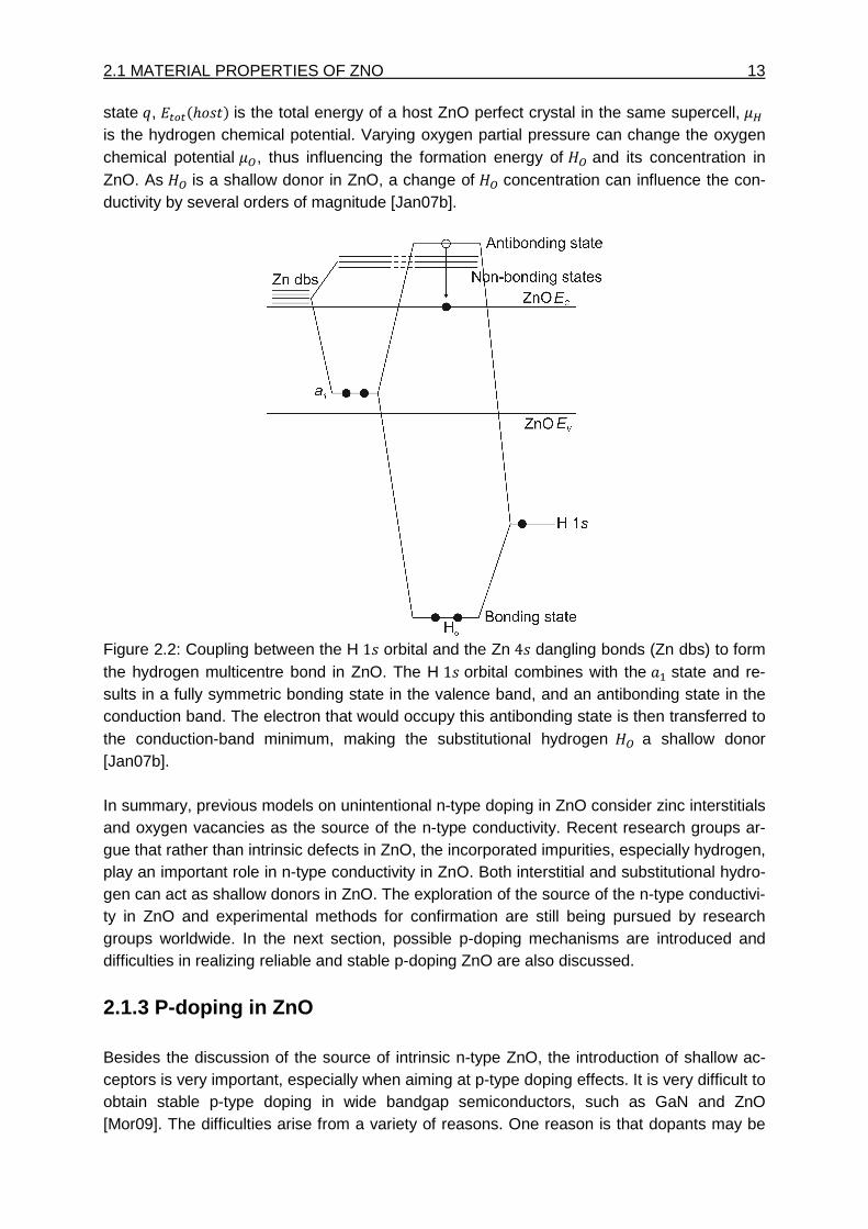
12 CHAPTER 2: THEORY Wal00, Jan07b, Jan09a]. When incorporated in ZnO, hydrogen can either locate at intersti-tial sites Kor replace oxygen in ZnO which is defined as a substitutional hydrogen K(. What makes hydrogen unique in ZnO is that hydrogen does not show its amphoteric property which can be observed when hydrogen is present in almost all other semiconductors [Pan91, Wal98, Wal06]. Amphoteric property means that hydrogen counteracts the prevailing con-ductivity of the material. In p-type materials, hydrogen exists with the form of KL, and in n-type materials it incorporates as KB. Therefore, hydrogen is not expected to be the source of conductivity in almost all semiconductors due to its amphoteric property. In ZnO, however, K is only present in the positive charge state (KL ) because only the positive charge state is thermodynamically stable. Thus hydrogen can act as a donor [Jan09a]. Although interstitial hydrogen is expected to act as a donor in ZnO, Janotti and Van de Walle have found that during sputtering of ZnO, the observed dependence of conductivity on the oxygen partial pressure cannot be explained only by interstitial hydrogen [Jan07b]. In addi-tion to the interstitial positions, it has been recently found that hydrogen can also replace oxygen in ZnO (K(/ [Jan07b], which may explain the dependence of conductivity on oxygen partial pressure. When substitutional hydrogen (K() replaces oxygen, it is sensitive to the oxygen partial pressure in the growth or annealing environments. Increasing the oxygen par-tial pressure can decrease the K( concentration and hence lower the conductivity by several orders of magnitude. The substitutional hydrogen (K() forms a multicentre bond in which H is equally bonded to the four Zn nearest neighbors [Jan09a]. The concept of this multicentre bond can be easily explained by the classical three-center bonds in diborane MEK, where three atoms share two electrons [Lip63, Bar65]. Similar to the three-center bonds principle, hydrogen bonds equally to the four Zn nearest neighbors when substituting oxygen in ZnO. Figure 2.2 depicts the formation of hydrogen multicentre bond in ZnO. The four dangling bonds on the surrounding Zn atoms form a symmetric (J/ combination, which leads to a doubly occupied electronic state located in the bandgap of ZnO [Jan05]. If hydrogen is located at the center of the oxy-gen vacancy, the H 1N orbital strongly interacts with this symmetric combination to form a fully symmetric state in the valence band and an antibonding state in the conduction band [Jan07b]. There are three electrons available from the combination of substitutional hydrogen with the four Zn dangling bonds, within which one is from hydrogen and the other two are from the four Zn dangling bonds. Two of these three electrons occupy the low-energy fully symmetric orbital deep inside the valence band and stabilize the center; the third electron, which would occupy the next available orbital resonant in the conduction band, is weakly bonded and can be easily transferred to the conduction-band minimum and can contribute to the n-type conductivity in ZnO. Therefore, substitutional K( replacing at oxygen vacancies can act as a shallow donor in ZnO. The formation energy of K( can be calculated by [Jan07b]:
'K()* = 'K()* −+ℎPNQ/ −R + ( + 1 ,(2.3)
where 'K()* is the formation energy of substitutional hydrogen in the charge state 1 , 'K()* is the total energy of a supercell containing the substitutional hydrogen in the charge
2.1 MATERIAL PROPERTIES OF ZNO 13
state 1, +ℎPNQ/ is the total energy of a host ZnO perfect crystal in the same supercell, R is the hydrogen chemical potential. Varying oxygen partial pressure can change the oxygen chemical potential (, thus influencing the formation energy of K( and its concentration in ZnO. As K( is a shallow donor in ZnO, a change of K( concentration can influence the con-ductivity by several orders of magnitude [Jan07b].
Figure 2.2: Coupling between the H 1N orbital and the Zn 4N dangling bonds (Zn dbs) to form the hydrogen multicentre bond in ZnO. The H 1N orbital combines with the J state and re-sults in a fully symmetric bonding state in the valence band, and an antibonding state in the conduction band. The electron that would occupy this antibonding state is then transferred to the conduction-band minimum, making the substitutional hydrogen K( a shallow donor [Jan07b]. In summary, previous models on unintentional n-type doping in ZnO consider zinc interstitials and oxygen vacancies as the source of the n-type conductivity. Recent research groups ar-gue that rather than intrinsic defects in ZnO, the incorporated impurities, especially hydrogen, play an important role in n-type conductivity in ZnO. Both interstitial and substitutional hydro-gen can act as shallow donors in ZnO. The exploration of the source of the n-type conductivi-ty in ZnO and experimental methods for confirmation are still being pursued by research groups worldwide. In the next section, possible p-doping mechanisms are introduced and difficulties in realizing reliable and stable p-doping ZnO are also discussed.
2.1.3 P-doping in ZnO Besides the discussion of the source of intrinsic n-type ZnO, the introduction of shallow ac-ceptors is very important, especially when aiming at p-type doping effects. It is very difficult to obtain stable p-type doping in wide bandgap semiconductors, such as GaN and ZnO [Mor09]. The difficulties arise from a variety of reasons. One reason is that dopants may be
14 CHAPTER 2: THEORY compensated by intrinsic defects with low formation energies, such as Zn interstitials (,-) or oxygen vacancies () [Wal94], or incorporated hydrogen. Another problem in p-type doping is the low solubility of the dopant in the host material [Wal93]. Deep impurity levels can also be a source of the doping problem, making the formation of shallow acceptor levels more difficult [Özg05]. Group-IA elements such as Lithium (Li), Sodium (Na), Potassium (K) can act as possible acceptors by substituting Zn sites with very low ionization energies between 90 meV and 320 meV [Par02]. Look et al. [Loo04] have reported the compensation of p-type doping when these elements are located at interstitial positions. The p-doping by Li and Na has been re-ported experimentally by different groups. Zeng et al. [Zen06] have reported a hole concen-
tration of 1.44×1017 cm-3 and a hole mobility of about 2.65 cm2/Vs through doping of Li in
ZnO. A hole concentration of 4.7×1018 cm-3 and a hole mobility of 1.42 cm2/Vs by doping of Na in ZnO has been achieved by Lin et al. [Lin08]. Group-IB elements copper (Cu), silver (Ag), and gold (Au) can also replace Zn sites and act as acceptors. Although the ionization energies for group-IB elements are in the range of 400 meV and 700 meV, which is much higher than for the group-IA elements, the compensation effects are not expected for group-
IB elements [Yan06]. Kang et al. [Kan06] have reported a hole concentration of 6×1017 cm-3 and a hole mobility of about 2.4 cm2/Vs by doping of Ag. Group-V elements such as nitrogen (N), phosphorus (P), arsenic (As), antimony (Sb) can also act as acceptors when substituting on the oxygen lattice sites. Among the group-V ele-ments, nitrogen is considered to be the most suitable p-type dopant for several reasons [Jan09a]. Firstly, the nitrogen atom has the closest atomic size to oxygen, resulting in mini-mum strain in ZnO. Secondly, the energy of the valence 2p states and the electronegativity of nitrogen are also the closest to those of the oxygen atom. Lin et al. [Lin04] have reported a
hole concentration of 5×1017 cm-3 and a hole mobility of 2 cm2/Vs by incorporation of N into ZnO. However, the p-type conductivity in N-doped ZnO still remains controversial. For in-stance, Lyons et al. [Lyo09] have reported that nitrogen in ZnO has a high ionization energy of 1.3 eV, and therefore, it is actually a deep acceptor and unlikely to contribute to p-type conductivity in ZnO. Besides group-I and group-V elements, fluorine (F) can also act as a shallow acceptor when incorporated at interstitial sites. It is important to differentiate the roles of F as interstitial fluo-rine (T) and substitutional fluorine (T(/. Fluorine has one more electron than oxygen and, therefore, it is a shallow donor in ZnO when replacing at oxygen lattice sites. Different than T(, T strongly bonds to the ZnO atom and one electron from the VBM is transferred to its low-lying p states to complete its octet. The resulting hole can be thermally excited into the valence band when it is free to move under the influence of an electric field [Jan09b]. In sec-tion 4.4.2, the electrical characteristics of fluorine-implanted ZnO TFTs are discussed. Alt-hough p-type conductivity has not been realized by the applied doses and implantation ener-gies used in this work, it has the effect to modify the bulk charge concentration in ZnO and is useful to tune the threshold voltages of the ZnO TFTs.
2.2 THIN FILM TRANSISTORS 15
Another critical problem of realizing stable and reproducible p-type results is that the experi-mental methods for confirming the p-type conductivity in ZnO are still questionable. Hall-effect measurements are one of the most frequently used methods to detect charge carrier types, however, Hall-effect measurements for ZnO often tend to result in wrong interpreta-tions, sometimes even yielding the wrong carrier type [Ohg08, Bie08]. Ohgaki et al. [Ohg08] have reported that in Hall measurement, non-uniform electrical properties of the sample can lead to an incorrect determination of the carrier type. Additionally, it has been reported by Bierwagen et al. [Bie08] that inhomogeneities in carrier mobility do not affect the determina-tion of carrier type and concentration, as long as the carrier concentration remains homoge-neous. However, inhomogeneities in carrier concentrations can result in an incorrect deter-mination of the carrier type. In summary, there are many possibly suitable elements to serve as p-type dopants in ZnO. These possible candidates include interstitial fluorine, group-IA, group-IB, and group-V ele-ments. However, one critical problem regarding to p-doping in ZnO is the stability and relia-bility of the p-doping results. Hall-effect measurements often cannot make correct determina-tion of the charge carrier type and concentration mainly due to the nonuniformity and inho-mogeneities in the ZnO layer. The investigation of reliable p-doping experiments and detec-tion methods is of great importance. If reproducible and reliable p-type doping in ZnO can be achieved, which currently remains to be the main obstacle for realization of bipolar devices, it would dramatically extend the applications of ZnO for optoelectronic applications such as LEDs and lasers.
2.2 Thin film transistors ZnO-based devices can be classified into three main categories: passive linear devices such as resistors, capacitors, and inductors; two-terminal semiconductor devices such as p-n junc-tions, schottky barriers, heterojunctions, and MIS capacitors; three terminal devices such as TFTs [Wag08]. Passive two terminal devices are described by conventional Ohms law, charge-voltage (C-V) and current-voltage (I-V) relations. Among two terminal semiconductor devices, MIS capacitor is one important structure and understanding the working principle of MIS capacitor is the prerequisite of understanding the operations of TFTs. Below the different operation modes of classical silicon MIS capacitors are first introduced. For understanding of switch-on behavior in ZnO TFTs, it is important to compare a p-type silicon MIS capacitor under strong inversion and an n-type ZnO-based MIS capacitor under accumulation because under both conditions there is an electron channel in existance.
2.2.1 Comparison of Si MIS capacitors and ZnO MIS c apacitors In quantum mechanics, the allowed energy levels of electrons in a solid are grouped into bands separated by energy gaps [Sze07]. Energy gaps are defined as regions of energy the electron cannot occupy. In semiconductors, the valence band is the highest range of electron energies in which electrons are normally present at absolute zero temperature. The conduc-tion band is the next higher band which is separated from the valence band by a forbidden gap (the bandgap U). The bottom of the conduction band is labeled as V and the top of the
valence band as 2, which can be seen in Fig. 2.3. The energy distribution of electrons in a
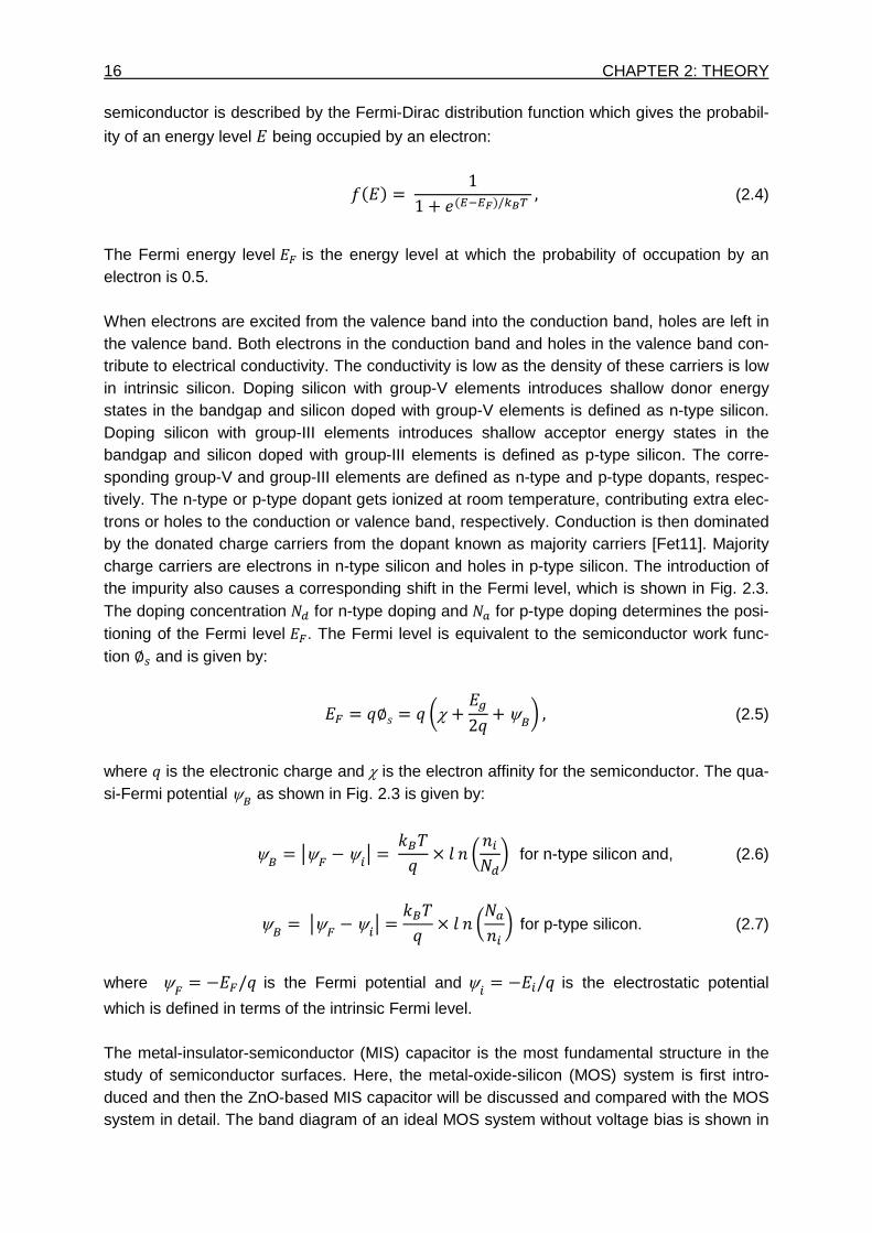
16 CHAPTER 2: THEORY semiconductor is described by the Fermi-Dirac distribution function which gives the probabil-
ity of an energy level being occupied by an electron:
+/ = 11 + ;+BW//XYZ ,(2.4)
The Fermi energy level is the energy level at which the probability of occupation by an electron is 0.5. When electrons are excited from the valence band into the conduction band, holes are left in the valence band. Both electrons in the conduction band and holes in the valence band con-tribute to electrical conductivity. The conductivity is low as the density of these carriers is low in intrinsic silicon. Doping silicon with group-V elements introduces shallow donor energy states in the bandgap and silicon doped with group-V elements is defined as n-type silicon. Doping silicon with group-III elements introduces shallow acceptor energy states in the bandgap and silicon doped with group-III elements is defined as p-type silicon. The corre-sponding group-V and group-III elements are defined as n-type and p-type dopants, respec-tively. The n-type or p-type dopant gets ionized at room temperature, contributing extra elec-trons or holes to the conduction or valence band, respectively. Conduction is then dominated by the donated charge carriers from the dopant known as majority carriers [Fet11]. Majority charge carriers are electrons in n-type silicon and holes in p-type silicon. The introduction of the impurity also causes a corresponding shift in the Fermi level, which is shown in Fig. 2.3. The doping concentration [ for n-type doping and > for p-type doping determines the posi-tioning of the Fermi level . The Fermi level is equivalent to the semiconductor work func-tion ∅ and is given by:
= 1∅N = 1 ]χ + U21 + ψ$^ ,(2.5)
where 1 is the electronic charge and χ is the electron affinity for the semiconductor. The qua-si-Fermi potential ψ$ as shown in Fig. 2.3 is given by:
ψ$ = _ψ − ψ_ = #$%1 × ` - ]-[^ for n-type silicon and, (2.6)
ψ$ = _ψ − ψ_ = #$%1 × ` - ]>- ^ for p-type silicon. (2.7)
where ψ = −/1 is the Fermi potential and ψ = −/1 is the electrostatic potential
which is defined in terms of the intrinsic Fermi level. The metal-insulator-semiconductor (MIS) capacitor is the most fundamental structure in the study of semiconductor surfaces. Here, the metal-oxide-silicon (MOS) system is first intro-duced and then the ZnO-based MIS capacitor will be discussed and compared with the MOS system in detail. The band diagram of an ideal MOS system without voltage bias is shown in
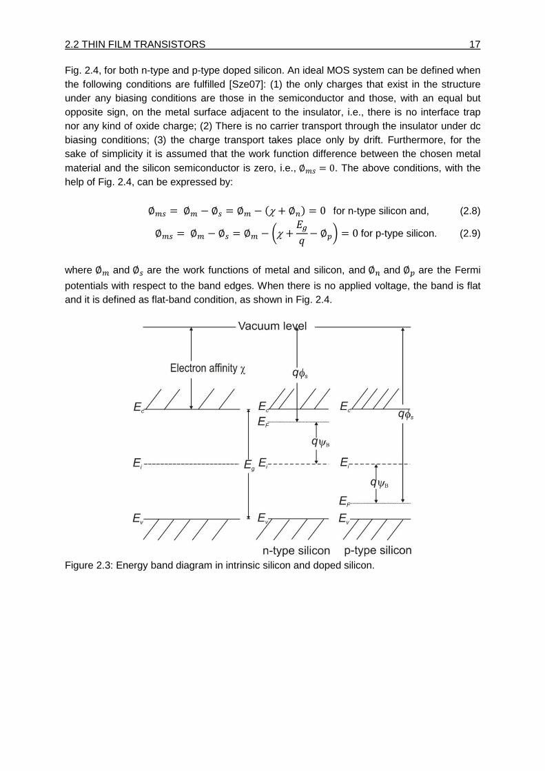
2.2 THIN FILM TRANSISTORS 17
Fig. 2.4, for both n-type and p-type doped silicon. An ideal MOS system can be defined when the following conditions are fulfilled [Sze07]: (1) the only charges that exist in the structure under any biasing conditions are those in the semiconductor and those, with an equal but opposite sign, on the metal surface adjacent to the insulator, i.e., there is no interface trap nor any kind of oxide charge; (2) There is no carrier transport through the insulator under dc biasing conditions; (3) the charge transport takes place only by drift. Furthermore, for the sake of simplicity it is assumed that the work function difference between the chosen metal material and the silicon semiconductor is zero, i.e., ∅= = 0. The above conditions, with the help of Fig. 2.4, can be expressed by: ∅= =∅= − ∅ = ∅= − +χ+ ∅/ = 0for n-type silicon and, (2.8)
∅= =∅= − ∅ = ∅= − ]χ + U1 −∅a^ = 0for p-type silicon. (2.9)
where ∅= and ∅ are the work functions of metal and silicon, and ∅ and ∅a are the Fermi
potentials with respect to the band edges. When there is no applied voltage, the band is flat and it is defined as flat-band condition, as shown in Fig. 2.4.
Figure 2.3: Energy band diagram in intrinsic silicon and doped silicon.
18 CHAPTER 2: THEORY
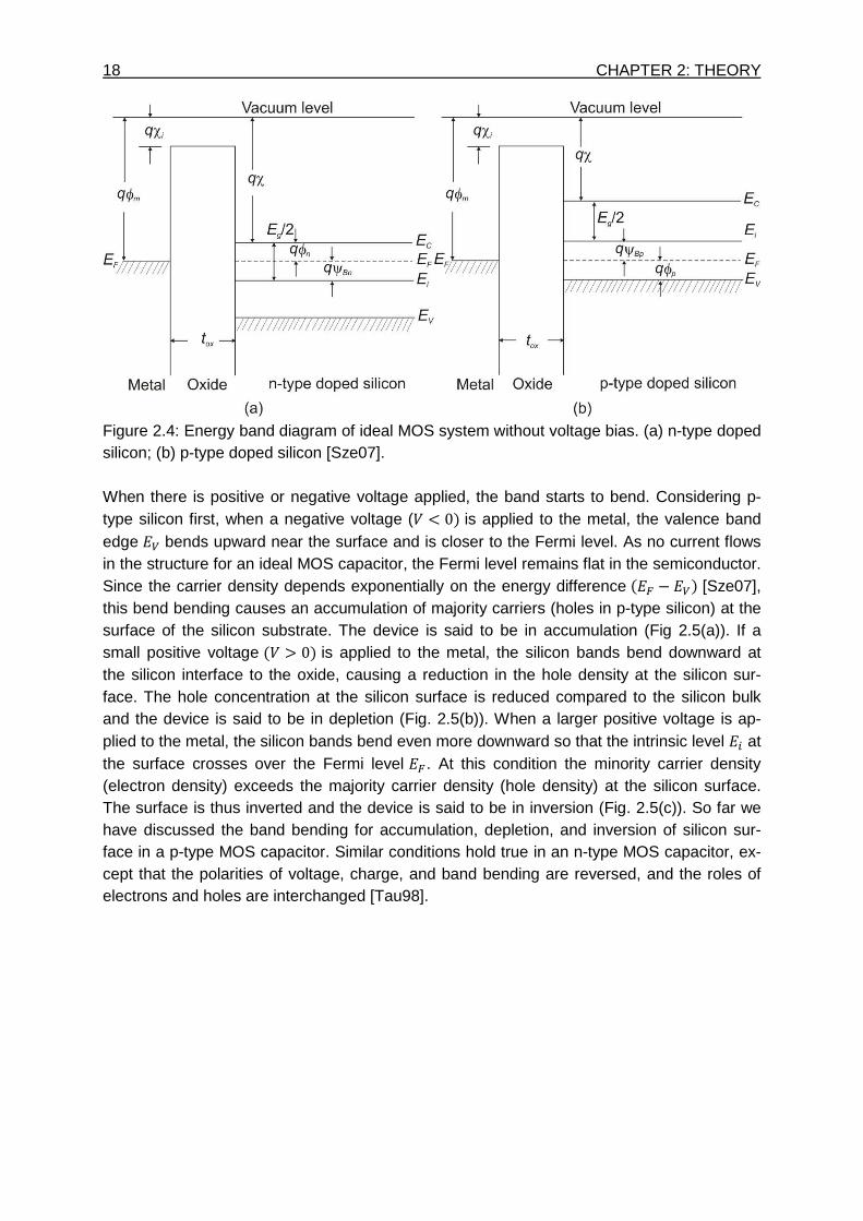
Figure 2.4: Energy band diagram of ideal MOS system without voltage bias. (a) n-type doped silicon; (b) p-type doped silicon [Sze07]. When there is positive or negative voltage applied, the band starts to bend. Considering p-type silicon first, when a negative voltage ( < 0/ is applied to the metal, the valence band edge 2 bends upward near the surface and is closer to the Fermi level. As no current flows in the structure for an ideal MOS capacitor, the Fermi level remains flat in the semiconductor. Since the carrier density depends exponentially on the energy difference + − 2/ [Sze07], this bend bending causes an accumulation of majority carriers (holes in p-type silicon) at the surface of the silicon substrate. The device is said to be in accumulation (Fig 2.5(a)). If a small positive voltage + > 0/ is applied to the metal, the silicon bands bend downward at the silicon interface to the oxide, causing a reduction in the hole density at the silicon sur-face. The hole concentration at the silicon surface is reduced compared to the silicon bulk and the device is said to be in depletion (Fig. 2.5(b)). When a larger positive voltage is ap-plied to the metal, the silicon bands bend even more downward so that the intrinsic level at the surface crosses over the Fermi level . At this condition the minority carrier density (electron density) exceeds the majority carrier density (hole density) at the silicon surface. The surface is thus inverted and the device is said to be in inversion (Fig. 2.5(c)). So far we have discussed the band bending for accumulation, depletion, and inversion of silicon sur-face in a p-type MOS capacitor. Similar conditions hold true in an n-type MOS capacitor, ex-cept that the polarities of voltage, charge, and band bending are reversed, and the roles of electrons and holes are interchanged [Tau98].
2.2 THIN FILM TRANSISTORS 19
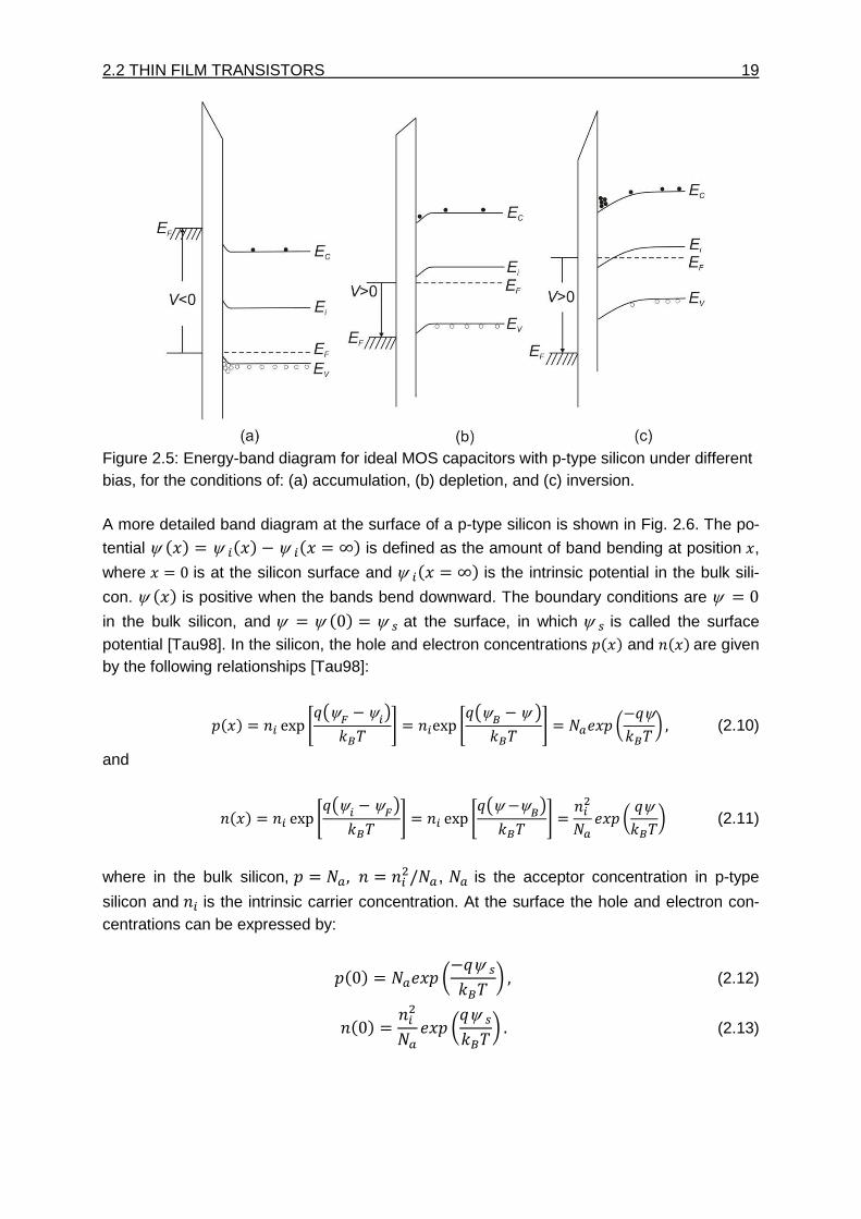
Figure 2.5: Energy-band diagram for ideal MOS capacitors with p-type silicon under different bias, for the conditions of: (a) accumulation, (b) depletion, and (c) inversion. A more detailed band diagram at the surface of a p-type silicon is shown in Fig. 2.6. The po-
tential ψ+d/ = ψ+d/ − ψ+d = ∞/ is defined as the amount of band bending at position d,
where d = 0 is at the silicon surface and ψ+d = ∞/ is the intrinsic potential in the bulk sili-
con. ψ+d/ is positive when the bands bend downward. The boundary conditions are ψ = 0 in the bulk silicon, and ψ = ψ+0/ = ψ at the surface, in which ψ is called the surface potential [Tau98]. In the silicon, the hole and electron concentrations @+d/ and -+d/are given by the following relationships [Tau98]:
@+d/ = - exp f1'ψ − ψ*#$% g = -exp f1'ψ$ − ψ*#$% g = >;d@ ]−1ψ#$%^ ,(2.10)
and
-+d/ = - exp f1'ψ − ψ*#$% g = - exp f1'ψ−ψ$*#$% g = -E> ;d@ ] 1ψ#$%^ (2.11)
where in the bulk silicon, @ = >, - = -E/>, > is the acceptor concentration in p-type
silicon and - is the intrinsic carrier concentration. At the surface the hole and electron con-centrations can be expressed by: @+0/ = >;d@ ]−1ψ#$% ^ ,(2.12)
-+0/ = -E> ;d@ ]1ψ#$%^ .(2.13)
20 CHAPTER 2: THEORY
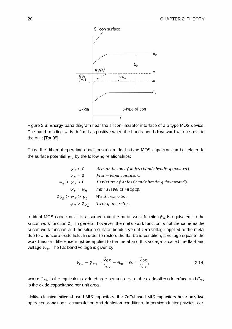
Figure 2.6: Energy-band diagram near the silicon-insulator interface of a p-type MOS device.
The band bending ψ is defined as positive when the bands bend downward with respect to the bulk [Tau98]. Thus, the different operating conditions in an ideal p-type MOS capacitor can be related to
the surface potential ψ by the following relationships: ψ < 0h iAi`QjP-PℎP`;N+k-lNk;-lj-mi@nol/. ψ = 0T`Q − k-l P-ljQjP-. ψM > ψ > 0p;@`;QjP-PℎP`;N+k-lNk;-lj-mlPn-nol/. ψ = ψMT;oAj`;q;`QAjlm@. 2ψM > ψ > ψMr;#j-q;oNjP-. ψ > 2ψMQoP-mj-q;oNjP-.
In ideal MOS capacitors it is assumed that the metal work function ∅=is equivalent to the
silicon work function ∅. In general, however, the metal work function is not the same as the silicon work function and the silicon surface bends even at zero voltage applied to the metal due to a nonzero oxide field. In order to restore the flat-band condition, a voltage equal to the work function difference must be applied to the metal and this voltage is called the flat-band voltage $. The flat-band voltage is given by:
$ = ∅= − s(t(t = ∅= − ∅ − s(t(t ,(2.14)
where s(t is the equivalent oxide charge per unit area at the oxide-silicon interface and (t is the oxide capacitance per unit area. Unlike classical silicon-based MIS capacitors, the ZnO-based MIS capacitors have only two operation conditions: accumulation and depletion conditions. In semiconductor physics, car-
2.2 THIN FILM TRANSISTORS 21
rier lifetimes are important parameters and fall into two primary categories: recombination
lifetimes and generation lifetimes [Sch82]. The concept of recombination lifetime uv applies when excess carriers decay as a result of recombination. The three well known recombina-tion mechanisms are Shockley-Read-Hall or multiphonon recombination, radiative recombi-
nation and Auger recombination [Sch82]. The generation lifetime uU is the time that it takes
on average to generate an electron-hole pair. When generation events occur in the bulk, they
are characterized by uU and when they occur at the surface, they are characterized by the
surface generation velocity NU. The rate of minority carrier generation for bulk and surface
generation is given by [Sch06]: wx = -uU for bulk generation and, (2.15)
w = -NUfor surface generation. (2.16)
From the above relationships, it can be seen that the minority carrier generation rate de-pends on the intrinsic carrier concentration - in the layer. In silicon, the intrinsic carrier con-centration - at room temperature is 1.4 × 10JFcmBC [Tau98]. Similar to other semiconduc-tors, the intrinsic carrier concentration in ZnO is given by:
- = | exp ] −U2#$%^ , (2.17)
where | and are the effective densities of states in the conduction band and valence band, respectively. At room temperature, the band gap of ZnO has a value of 3.37 eV
[Man95] and the | and values are reported to be 3.0×1018cm-3 and 1.8 × 10JcmBC , respectively [Wag08]. Inserting these values into Eq. (2.17), the calculated intrinsic carrier
concentration in ZnO - is about 10BJF ABC . Comparing to silicon, the minority carrier (holes) generation rate in ZnO is expected to be about 20 orders of magnitude less than that in silicon. This is the main reason why the inversion condition in classical silicon MIS capaci-tors is not relevant in ZnO-based MIS capacitors. Moreover, as a wide band gap semicon-ductor, ZnO requires about 2.5-3 V of surface potential modulation from flat-band condition to inversion condition compared to about 0.7-1 V for silicon [Wag08]. Additionally, surface po-tential modulation in ZnO requires the depletion of filled deep level traps and band tail states prior to reaching the inversion condition. For all these reasons, inversion does not occur in ZnO-based MIS capacitors.
22 CHAPTER 2: THEORY
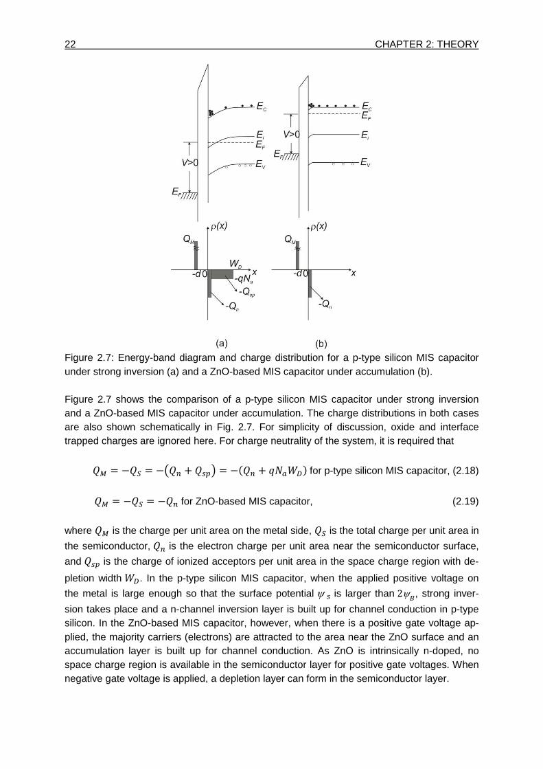
Figure 2.7: Energy-band diagram and charge distribution for a p-type silicon MIS capacitor under strong inversion (a) and a ZnO-based MIS capacitor under accumulation (b). Figure 2.7 shows the comparison of a p-type silicon MIS capacitor under strong inversion and a ZnO-based MIS capacitor under accumulation. The charge distributions in both cases are also shown schematically in Fig. 2.7. For simplicity of discussion, oxide and interface trapped charges are ignored here. For charge neutrality of the system, it is required that s = −s = −'s + sa* = −+s + 1>r/for p-type silicon MIS capacitor, (2.18)
s = −s = −sfor ZnO-based MIS capacitor, (2.19)
where s is the charge per unit area on the metal side, s is the total charge per unit area in
the semiconductor, s is the electron charge per unit area near the semiconductor surface,
and sa is the charge of ionized acceptors per unit area in the space charge region with de-
pletion width r. In the p-type silicon MIS capacitor, when the applied positive voltage on
the metal is large enough so that the surface potential ψ is larger than 2ψ$, strong inver-
sion takes place and a n-channel inversion layer is built up for channel conduction in p-type silicon. In the ZnO-based MIS capacitor, however, when there is a positive gate voltage ap-plied, the majority carriers (electrons) are attracted to the area near the ZnO surface and an accumulation layer is built up for channel conduction. As ZnO is intrinsically n-doped, no space charge region is available in the semiconductor layer for positive gate voltages. When negative gate voltage is applied, a depletion layer can form in the semiconductor layer.
2.2 THIN FILM TRANSISTORS 23
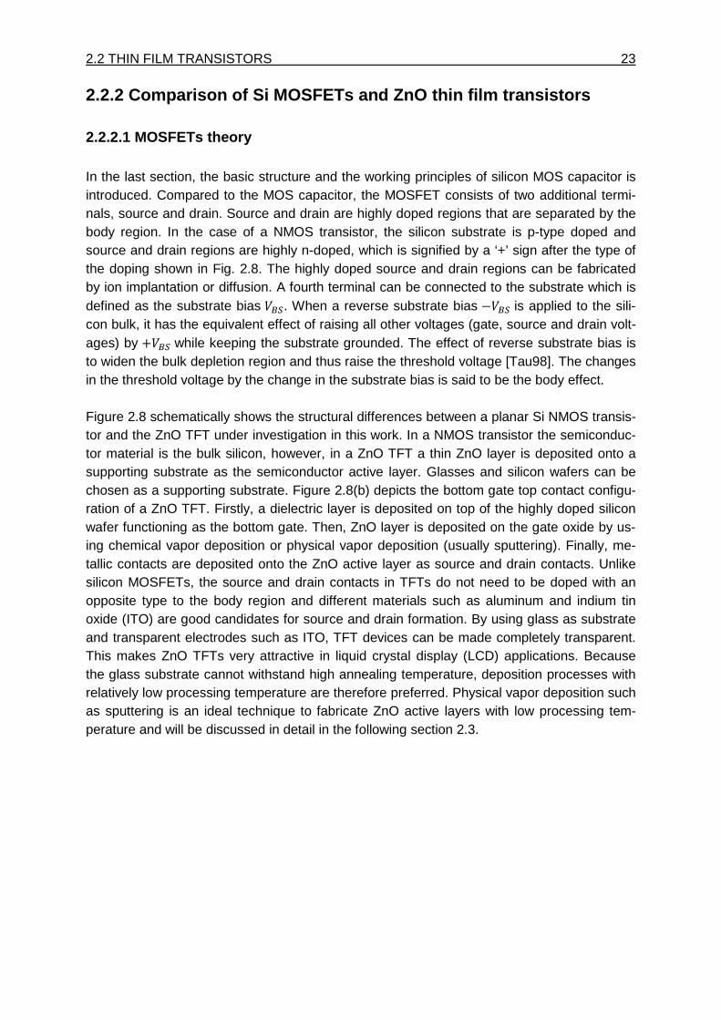
2.2.2 Comparison of Si MOSFETs and ZnO thin film tr ansistors 2.2.2.1 MOSFETs theory In the last section, the basic structure and the working principles of silicon MOS capacitor is introduced. Compared to the MOS capacitor, the MOSFET consists of two additional termi-nals, source and drain. Source and drain are highly doped regions that are separated by the body region. In the case of a NMOS transistor, the silicon substrate is p-type doped and source and drain regions are highly n-doped, which is signified by a ‘+’ sign after the type of the doping shown in Fig. 2.8. The highly doped source and drain regions can be fabricated by ion implantation or diffusion. A fourth terminal can be connected to the substrate which is defined as the substrate bias $. When a reverse substrate bias −$ is applied to the sili-con bulk, it has the equivalent effect of raising all other voltages (gate, source and drain volt-ages) by +$ while keeping the substrate grounded. The effect of reverse substrate bias is to widen the bulk depletion region and thus raise the threshold voltage [Tau98]. The changes in the threshold voltage by the change in the substrate bias is said to be the body effect. Figure 2.8 schematically shows the structural differences between a planar Si NMOS transis-tor and the ZnO TFT under investigation in this work. In a NMOS transistor the semiconduc-tor material is the bulk silicon, however, in a ZnO TFT a thin ZnO layer is deposited onto a supporting substrate as the semiconductor active layer. Glasses and silicon wafers can be chosen as a supporting substrate. Figure 2.8(b) depicts the bottom gate top contact configu-ration of a ZnO TFT. Firstly, a dielectric layer is deposited on top of the highly doped silicon wafer functioning as the bottom gate. Then, ZnO layer is deposited on the gate oxide by us-ing chemical vapor deposition or physical vapor deposition (usually sputtering). Finally, me-tallic contacts are deposited onto the ZnO active layer as source and drain contacts. Unlike silicon MOSFETs, the source and drain contacts in TFTs do not need to be doped with an opposite type to the body region and different materials such as aluminum and indium tin oxide (ITO) are good candidates for source and drain formation. By using glass as substrate and transparent electrodes such as ITO, TFT devices can be made completely transparent. This makes ZnO TFTs very attractive in liquid crystal display (LCD) applications. Because the glass substrate cannot withstand high annealing temperature, deposition processes with relatively low processing temperature are therefore preferred. Physical vapor deposition such as sputtering is an ideal technique to fabricate ZnO active layers with low processing tem-perature and will be discussed in detail in the following section 2.3.
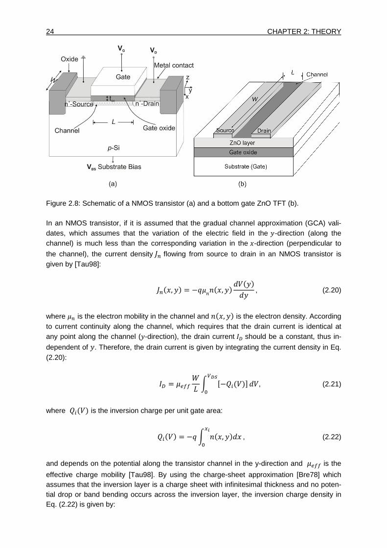
24 CHAPTER 2: THEORY
Figure 2.8: Schematic of a NMOS transistor (a) and a bottom gate ZnO TFT (b). In an NMOS transistor, if it is assumed that the gradual channel approximation (GCA) vali-dates, which assumes that the variation of the electric field in the -direction (along the channel) is much less than the corresponding variation in the d-direction (perpendicular to
the channel), the current density flowing from source to drain in an NMOS transistor is given by [Tau98]:
+d, / = −1--+d, / l+/l , (2.20)
where is the electron mobility in the channel and -+d, / is the electron density. According to current continuity along the channel, which requires that the drain current is identical at any point along the channel (-direction), the drain current should be a constant, thus in-
dependent of . Therefore, the drain current is given by integrating the current density in Eq. (2.20):
= r −s+/2F l, (2.21)
where s+/ is the inversion charge per unit gate area:
s+/ = −1 -+d, /ld?F , (2.22)
and depends on the potential along the transistor channel in the y-direction and is the
effective charge mobility [Tau98]. By using the charge-sheet approximation [Bre78] which assumes that the inversion layer is a charge sheet with infinitesimal thickness and no poten-tial drop or band bending occurs across the inversion layer, the inversion charge density in Eq. (2.22) is given by:
2.2 THIN FILM TRANSISTORS 25
s = s − s[ = −(t' − $ − 2ψM − * +23Nj1'2ψM + *.(2.23)
where s and s[ are surface charge density and depletion charge density, and 3 is the silicon permittivity. Substituting Eq. (2.23) into Eq. (2.21) and carrying out the integration, the drain current is given by [Tau98]:
= (tr ] − $ − 2ψ$ − 2 ^ − 223Nj1>3(t '2ψ$ + *C/E − '2ψ$*C/E . (2.24)
Equation (2.24) indicates that the drain current depends on the gate voltage and the
drain voltage . Under a fixed gate voltage , the drain current first increases linearly
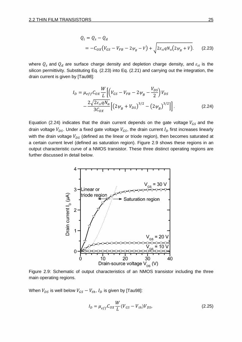
with the drain voltage (defined as the linear or triode region), then becomes saturated at a certain current level (defined as saturation region). Figure 2.9 shows these regions in an output characteristic curve of a NMOS transistor. These three distinct operating regions are further discussed in detail below.
Figure 2.9: Schematic of output characteristics of an NMOS transistor including the three main operating regions.
When is well below − , is given by [Tau98]:
= ;.r +w − Qℎ/p,(2.25)
26 CHAPTER 2: THEORY where is the threshold voltage given by = $ + ψ + (t
= TM + 2ψ$ +431>ψ$. . (2.26)
The threshold voltage consists of three parts: the flat-band voltage $, the voltage drop in the substrate equating the surface potential ψ and the potential drop on the oxide (t.
Recalling that when ψ > 2ψM, strong inversion happens, is the gate voltage when the
surface potential or band bending reaches 2ψ$ and an inversion layer forms at the interface
between the gate oxide and the silicon substrate of the transistor. When < , there is very little current flow and the transistor operates in the subthreshold region. When > ,
the transistor is turned on. If is much smaller than the difference between the gate volt-age and the threshold voltage, a homogenous channel forms at the interface between the semiconductor and the gate oxide. The transistor acts like a resistor with a sheet resistivity , which is given by:
= 1;.+w −Qℎ/ ,(2.27)
and is modulated by the gate voltage. The drain current is described by Eq. (2.25) and the device is said to be in the linear region. For larger values of , the channel resistance be-gins to increase and the relationship between drain current and drain voltage is not linear any more. When the potential difference between gate and drain becomes smaller due to in-creasing , the number of electrons at the drain end becomes smaller. In this region, the drain current follows a parabolic curve until the saturation level is reached. The transistor is
said to be in the triode region. The drain current in the triode region is given by:
= ;.r !w −Qℎ −p2 &p.(2.28)
When the drain voltage increases to a value that exceeds the difference between the gate voltage and the threshold voltage, there are only few electrons at the drain end and a space charge region extends from drain towards source at the interface between semicon-ductor and insulator. This condition is defined as pinch-off. If increases further, the pinch-off point of the channel begins to move away from the drain towards the source. The poten-tial at the pinch-off point remains unchanged and the number of electrons from the source to the pinch-off point remains unchanged. The transistor is now said to be in the saturation re-
gion. The drain current in the saturation region is given by:
= 12(tr + − /E.(2.29)
2.2 THIN FILM TRANSISTORS 27
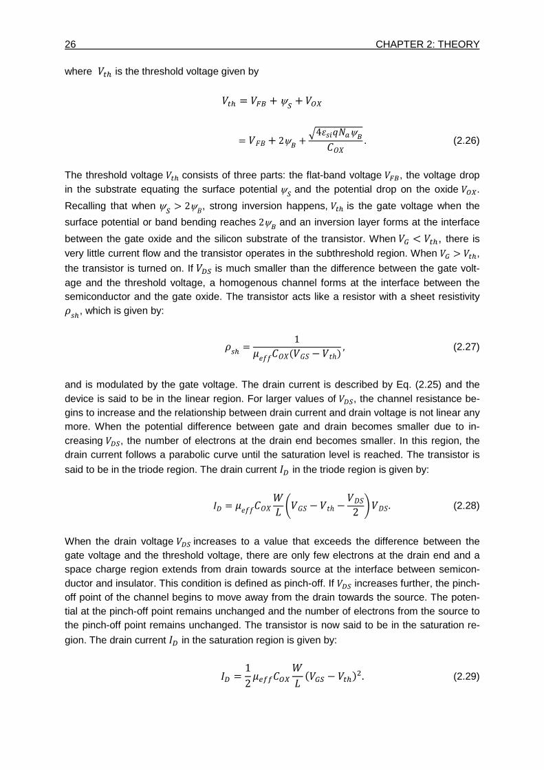
From Eq. (2.29), the drain current in the saturation region under a fixed gate voltage stays constant, independent of the drain voltage . The channel formation under different operat-ing regions is shown in Fig. 2.10.
Figure 2.10: Channel formation in an NMOS transistor under different operating conditions (a) turn-off region, (b) linear region, (c) triode region and (d) saturation region.
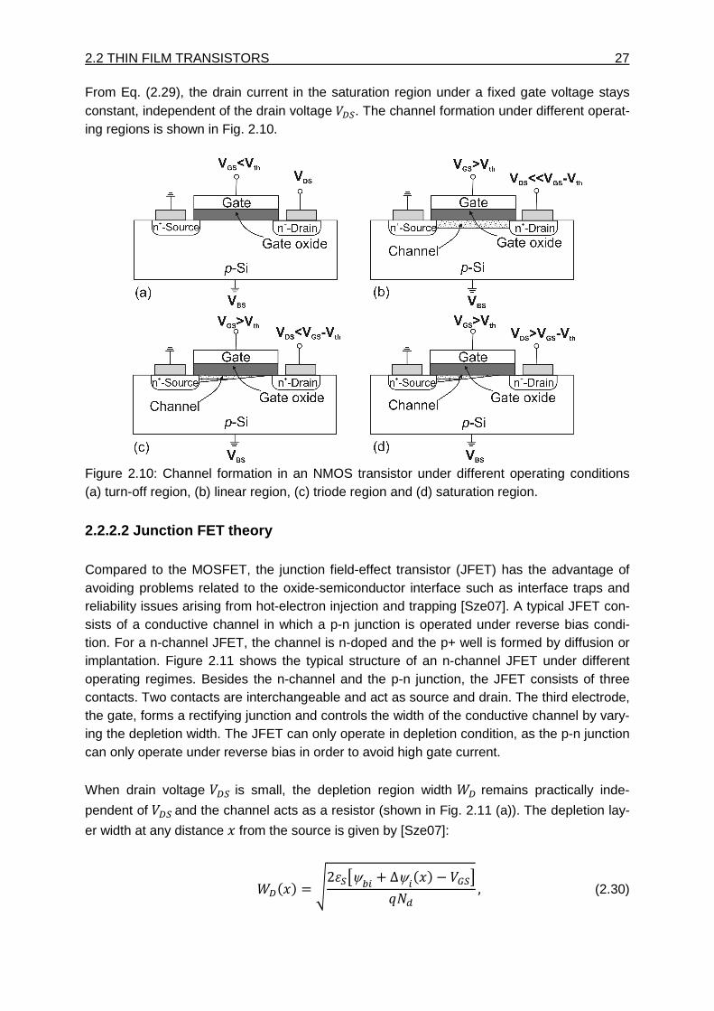
2.2.2.2 Junction FET theory Compared to the MOSFET, the junction field-effect transistor (JFET) has the advantage of avoiding problems related to the oxide-semiconductor interface such as interface traps and reliability issues arising from hot-electron injection and trapping [Sze07]. A typical JFET con-sists of a conductive channel in which a p-n junction is operated under reverse bias condi-tion. For a n-channel JFET, the channel is n-doped and the p+ well is formed by diffusion or implantation. Figure 2.11 shows the typical structure of an n-channel JFET under different operating regimes. Besides the n-channel and the p-n junction, the JFET consists of three contacts. Two contacts are interchangeable and act as source and drain. The third electrode, the gate, forms a rectifying junction and controls the width of the conductive channel by vary-ing the depletion width. The JFET can only operate in depletion condition, as the p-n junction can only operate under reverse bias in order to avoid high gate current.
When drain voltage is small, the depletion region width r remains practically inde-
pendent of and the channel acts as a resistor (shown in Fig. 2.11 (a)). The depletion lay-
er width at any distance d from the source is given by [Sze07]:
r+d/ = 23ψx + ∆ψ+d/ − 1[ , (2.30)
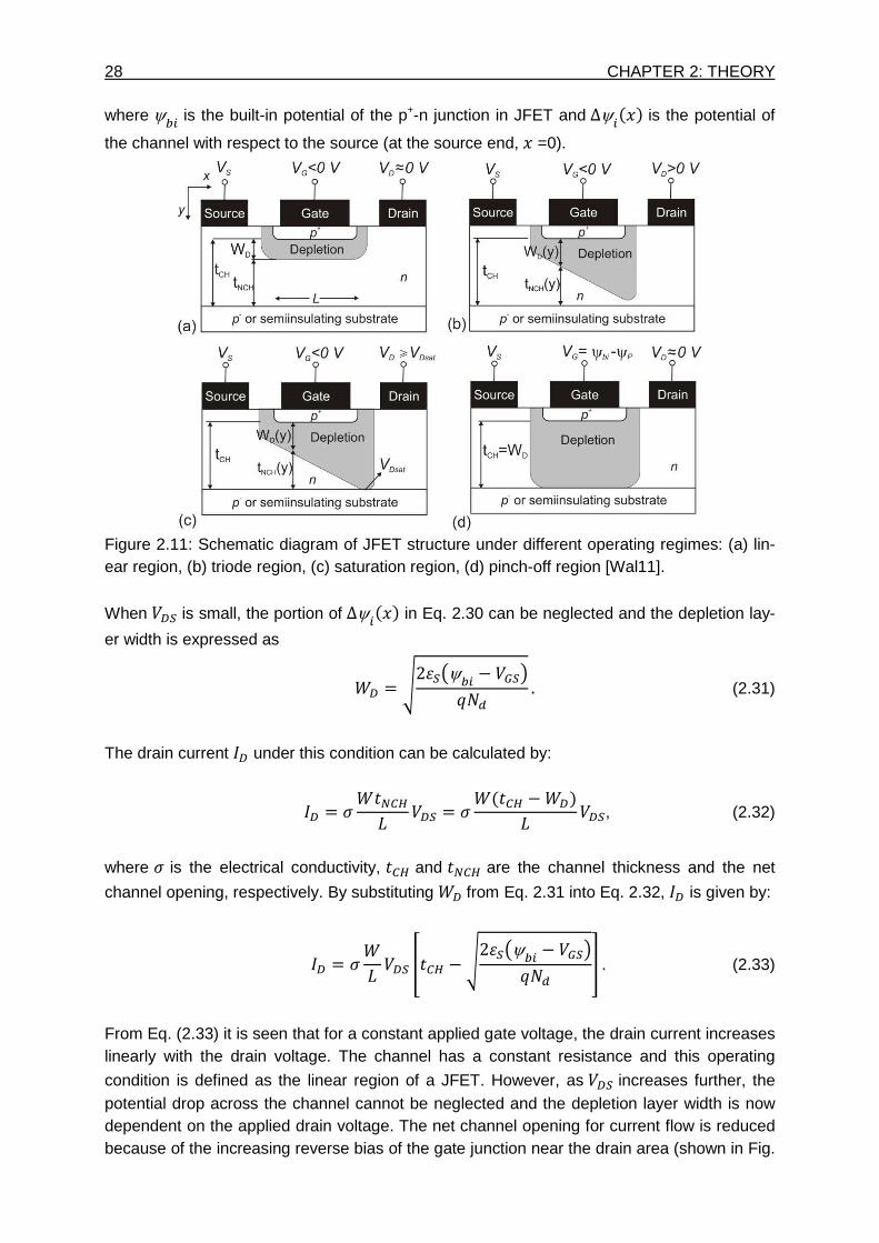
28 CHAPTER 2: THEORY where ψx is the built-in potential of the p+-n junction in JFET and ∆ψ+d/ is the potential of
the channel with respect to the source (at the source end, d =0).
Figure 2.11: Schematic diagram of JFET structure under different operating regimes: (a) lin-ear region, (b) triode region, (c) saturation region, (d) pinch-off region [Wal11].
When is small, the portion of ∆ψ+d/ in Eq. 2.30 can be neglected and the depletion lay-
er width is expressed as
r = 23'ψx − *1[ . (2.31)
The drain current under this condition can be calculated by:
= rQVR = r+QVR −r/ , (2.32)
where is the electrical conductivity, QVR and QVR are the channel thickness and the net
channel opening, respectively. By substituting rfrom Eq. 2.31 into Eq. 2.32, is given by:
= r QVR −23'ψx − *1[ . (2.33)
From Eq. (2.33) it is seen that for a constant applied gate voltage, the drain current increases linearly with the drain voltage. The channel has a constant resistance and this operating
condition is defined as the linear region of a JFET. However, as increases further, the potential drop across the channel cannot be neglected and the depletion layer width is now dependent on the applied drain voltage. The net channel opening for current flow is reduced because of the increasing reverse bias of the gate junction near the drain area (shown in Fig.
2.2 THIN FILM TRANSISTORS 29
2.11 (b)). Thus, the channel resistance will also increase and the current-voltage characteris-tics will enter the triode region. In the triode region, the drain current is calculated by:
= r QVR −23'ψx + ∆ψ+d/ − *1[ 2F
l∆ψ.(2.34)
By integrating the potential difference from source end to drain end, is given by:
= rQVR − 23ψ 'ψx + − *C/E − 'ψx − *C/E , (2.35)
where ψ is defined as the pinch-off voltage [Sze07]. When the gate voltage satisfies the
following conditions: = ψx − ψ, (2.36)
the channel is fully depleted and the drain current is equal to zero (shown in Fig. 2.11 (d)).
The value of ψ is given by [Sze07]:
ψ = 1[QVRE23 . (2.37)
In the triode region, the current-voltage characteristic is non-linear and the drain current is
proportional to C/E. When the drain voltage continues to increase, the depletion width near
the drain end will reach the channel thickness QVR and the pinch-off effect happens. The at the onset of this condition can be shown to occur at [Sze07]: ,> = ψ − ψx + . (2.38)
The current in the saturation region can be calculated by substituting ,> into Eq. (2.35):
> = rQVR ψ3 − 'ψx − *1 − 23ψx − ψ . (2.39)
As the drain voltage further increases beyond ,>, the pinch-off point starts to migrate
towards the source. However, the voltage drop from the source to the pinch-off point will re-
main to be ,>. Accordingly, the drain current will also remain at its value >. The max-
imum saturation current can be found by substituting = 0 into Eq. 2.39:
30 CHAPTER 2: THEORY
>=>? = rQVR ψ3 − ψx 1 − 23ψxψ . (2.40)
In sum, when < ψx − ψ, JFET is turned off. When > ψx − ψ, JFET is turned on.
When is small and the JFET is turned on, the channel acts as a resistor and the JFET is
operating in the linear region. When becomes larger, the JFET enters the triode region
and the drain current is proportional to C/E. When ≥ ,>, the JFET operates in the
saturation region and the drain current remains at >. 2.2.2.3 ZnO thin film transistors The modelling of ZnO TFTs is based on the understanding of classical Si MOSFET theory and the JFET theory. In the case of the Si NMOS transistor, the threshold voltage is the gate voltage that makes the surface potential reach 2ψ$. Under this condition, an inversion chan-
nel forms at the interface between the gate oxide and the substrate of the transistor. As al-ready discussed in the section 2.2.1, inversion cannot account for the conduction mechanism in ZnO TFTs. When a positive gate voltage is applied to the metal contact, the electrons are attracted to the interface between ZnO and the gate oxide, leading to the formation of an accumulation channel. Without consideration of trap states, the threshold voltage for forming the accumulation channel in ZnO TFTs is the flat band voltage. It is the work function differ-ence between the metal and the semiconductor layer. It can be expressed by: = $ = ∅=. (2.41) In real ZnO TFTs, there are trap states which can donate or accept electrons at the insulator-semiconductor interfaces [Wag08]. They are named as donor-like traps and acceptor-like interface traps. Donor-like traps are neutral when they are filled with electrons, otherwise positively charged. For switching on ZnO TFTs, these donor-like traps have to be first filled with electrons before electrons can contribute to conductivity. On the contrary, acceptor-like traps are negatively charged when filled with electrons, otherwise neutral. As ZnO-TFT is n-type, donor-like traps which lie near the conduction band have substantial effect of shifting the threshold voltages. Acceptor-like traps lie closer to the valence band and are more rele-vant to p-type TFTs, thus having little influence on the threshold voltage of ZnO TFTs. For the simplicity of calculation, the influence of acceptor-like traps is neglected here. Besides interface traps, oxide charges at the insulator-semiconductor interface should be taken into consideration for real ZnO TFTs [Wag08]. Thus, the threshold voltage can be calculated by:
= ∅= − s(t(t + 1@(t , (2.42)
where @ is the donor-like interface trap density. Due to oxide charges and interface traps, the threshold voltage for real ZnO TFTs can have both positive and negative values.
2.2 THIN FILM TRANSISTORS 31
Next, ZnO TFTs in different operating regions will be discussed and for simplicity of our dis-
cussion, the threshold voltage for the accumulation channel is considered to be the flat
band voltage . For the total drain current , it is given by:
= + , (2.43)
where is the current flowing in the accumulation channel of the MOSFET and is the current flowing in the bulk that can be modelled by a JFET with an insulated gate. The work-ing principle of a JFET with an insulated gate is similar to that of a normal JFET with a p-n junction or a Schottky-barrier junction. In both cases, the net channel opening will be con-trolled by the depletion width. The difference in a JFET with insulated gate is that when the channel is fully depleted, there is also a voltage drop across the insulator. So the pinch-off voltage for a JFET with insulated gate is given by [Hon07]:
= −ψ −
,(2.44)
where the second term is the voltage drop across the insulator when the channel is fully de-pleted. In this equation instead of the donor concentration , the equilibrium charge carrier concentration is used in order to imply that the ZnO layer is intrinsically n-doped material.
The threshold voltage and the pinch-off voltage are two characteristic voltages which separate the different operating regions in ZnO TFTs. Figure 2.12 shows the cross section of the channel under different gate and drain biases. The voltage constraints for different re-gimes of operation and the corresponding operation regions for the MOSFET with accumula-tion channel and the JFET with insulated gate are listed in table 2.2. As listed in table 2.2, there are totally six different regimes of operation for ZnO TFTs. Corre-sponding to gate and drain bias constraints, ZnO TFTs can operate in turn-off (OFF) mode, depletion (DEPL) mode, depletion-saturation (DEPL-SAT) mode, accumulation (ACC) mode, accumulation-depletion (ACC-DEPL) mode and accumulation-saturation (ACC-SAT) mode. The channel behaviour can always be modelled by considering the MOSFET with accumula-tion channel and JFET with insulated gate in parallel. Here, we will discuss how the gate and drain bias can influence the regimes of operation for ZnO TFTs. When gate voltage < , the TFT is in the OFF mode and the total drain current is zero. When < < , the drain current only consists of as there is no accumulation channel formed. Under this gate bias condition, the JEFT operates in linear or triode region when < − and in saturation region when > − . The ZnO TFT operates in DEPL and DEPL-SAT mode, respectively. When gate voltages increases further and it satis-fies the condition < , an accumulation channel forms and depending on the drain volt-
age , the portion of should be added to to get the total drain current . Under the
condition of < , three different regimes of operations should be separately considered. When < − , the MOSFET operates in linear or triode region and the JFET operates in the linear region. When − < < − ,the MOSFETs enters the saturation re-gion and the JFET operates in the linear or triode region. When − < , both MOSFET
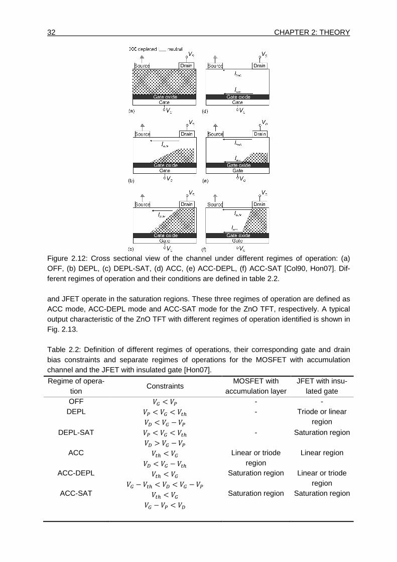
32 CHAPTER 2: THEORY
Figure 2.12: Cross sectional view of the channel under different regimes of operation: (a) OFF, (b) DEPL, (c) DEPL-SAT, (d) ACC, (e) ACC-DEPL, (f) ACC-SAT [Col90, Hon07]. Dif-ferent regimes of operation and their conditions are defined in table 2.2. and JFET operate in the saturation regions. These three regimes of operation are defined as ACC mode, ACC-DEPL mode and ACC-SAT mode for the ZnO TFT, respectively. A typical output characteristic of the ZnO TFT with different regimes of operation identified is shown in Fig. 2.13. Table 2.2: Definition of different regimes of operations, their corresponding gate and drain bias constraints and separate regimes of operations for the MOSFET with accumulation channel and the JFET with insulated gate [Hon07].
Regime of opera-tion
Constraints MOSFET with
accumulation layer JFET with insu-
lated gate OFF
DEPL < < < < −
- -
- Triode or linear
region
DEPL-SAT
ACC
ACC-DEPL
ACC-SAT
< < > − < < − < − < < − < − <
-
Linear or triode region
Saturation region
Saturation region
Saturation region
Linear region
Linear or triode region
Saturation region
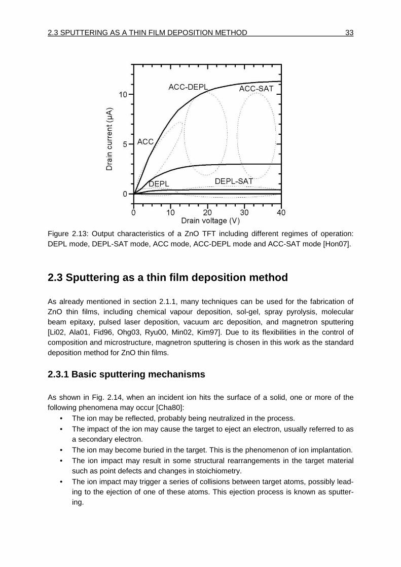
2.3 SPUTTERING AS A THIN FILM DEPOSITION METHOD 33
Figure 2.13: Output characteristics of a ZnO TFT including different regimes of operation: DEPL mode, DEPL-SAT mode, ACC mode, ACC-DEPL mode and ACC-SAT mode [Hon07].
2.3 Sputtering as a thin film deposition method As already mentioned in section 2.1.1, many techniques can be used for the fabrication of ZnO thin films, including chemical vapour deposition, sol-gel, spray pyrolysis, molecular beam epitaxy, pulsed laser deposition, vacuum arc deposition, and magnetron sputtering [Li02, Ala01, Fid96, Ohg03, Ryu00, Min02, Kim97]. Due to its flexibilities in the control of composition and microstructure, magnetron sputtering is chosen in this work as the standard deposition method for ZnO thin films.
2.3.1 Basic sputtering mechanisms As shown in Fig. 2.14, when an incident ion hits the surface of a solid, one or more of the following phenomena may occur [Cha80]:
• The ion may be reflected, probably being neutralized in the process.
• The impact of the ion may cause the target to eject an electron, usually referred to as a secondary electron.
• The ion may become buried in the target. This is the phenomenon of ion implantation. • The ion impact may result in some structural rearrangements in the target material
such as point defects and changes in stoichiometry.
• The ion impact may trigger a series of collisions between target atoms, possibly lead-ing to the ejection of one of these atoms. This ejection process is known as sputter-ing.
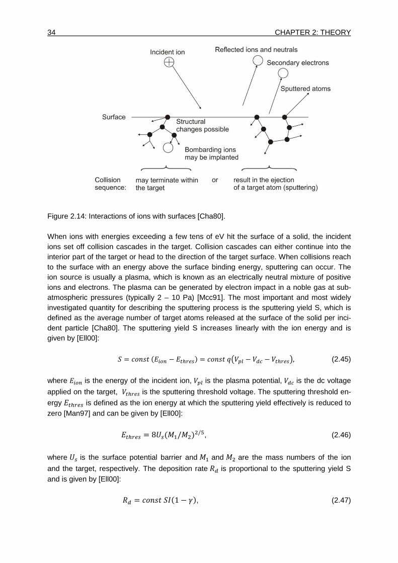
34 CHAPTER 2: THEORY
Figure 2.14: Interactions of ions with surfaces [Cha80]. When ions with energies exceeding a few tens of eV hit the surface of a solid, the incident ions set off collision cascades in the target. Collision cascades can either continue into the interior part of the target or head to the direction of the target surface. When collisions reach to the surface with an energy above the surface binding energy, sputtering can occur. The ion source is usually a plasma, which is known as an electrically neutral mixture of positive ions and electrons. The plasma can be generated by electron impact in a noble gas at sub-atmospheric pressures (typically 2 – 10 Pa) [Mcc91]. The most important and most widely investigated quantity for describing the sputtering process is the sputtering yield S, which is defined as the average number of target atoms released at the surface of the solid per inci-dent particle [Cha80]. The sputtering yield S increases linearly with the ion energy and is given by [Ell00]: = P-NQ+ − v/ = P-NQ1'a£ − [| − v*,(2.45)
where is the energy of the incident ion, a£ is the plasma potential, [| is the dc voltage
applied on the target, v is the sputtering threshold voltage. The sputtering threshold en-
ergy v is defined as the ion energy at which the sputtering yield effectively is reduced to zero [Man97] and can be given by [Ell00]: v = 8¤+¥J/¥E/E/¦, (2.46)
where ¤ is the surface potential barrier and ¥J and ¥E are the mass numbers of the ion
and the target, respectively. The deposition rate §[ is proportional to the sputtering yield S and is given by [Ell00]: §[ = P-NQ+1 − ¨/, (2.47)
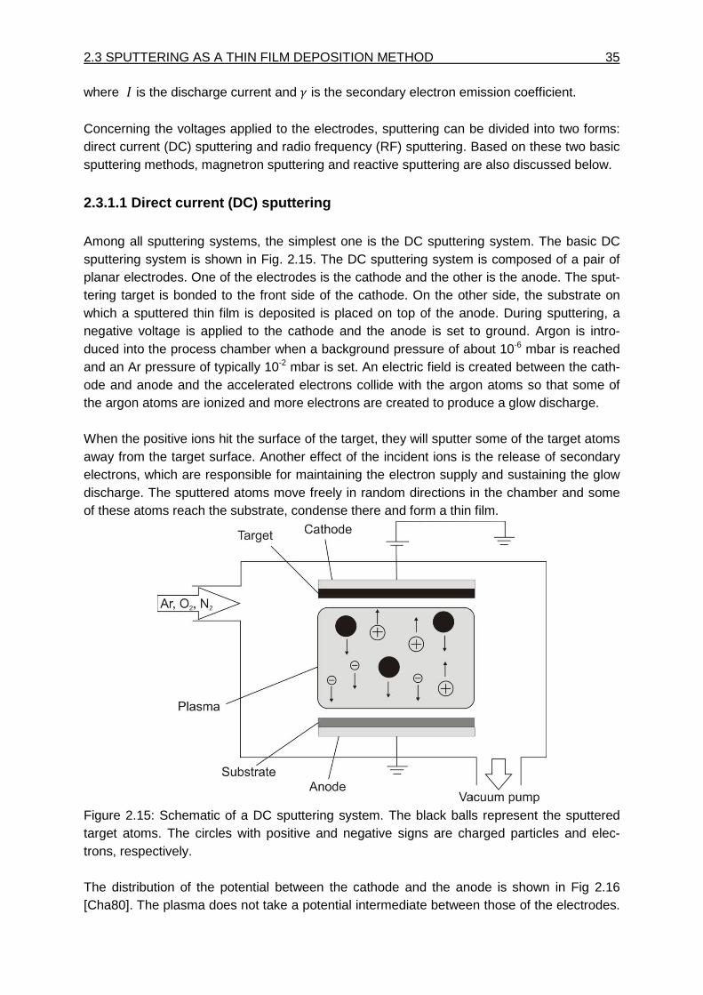
2.3 SPUTTERING AS A THIN FILM DEPOSITION METHOD 35
where is the discharge current and is the secondary electron emission coefficient. Concerning the voltages applied to the electrodes, sputtering can be divided into two forms: direct current (DC) sputtering and radio frequency (RF) sputtering. Based on these two basic sputtering methods, magnetron sputtering and reactive sputtering are also discussed below.
2.3.1.1 Direct current (DC) sputtering Among all sputtering systems, the simplest one is the DC sputtering system. The basic DC sputtering system is shown in Fig. 2.15. The DC sputtering system is composed of a pair of planar electrodes. One of the electrodes is the cathode and the other is the anode. The sput-tering target is bonded to the front side of the cathode. On the other side, the substrate on which a sputtered thin film is deposited is placed on top of the anode. During sputtering, a negative voltage is applied to the cathode and the anode is set to ground. Argon is intro-duced into the process chamber when a background pressure of about 10-6 mbar is reached and an Ar pressure of typically 10-2 mbar is set. An electric field is created between the cath-ode and anode and the accelerated electrons collide with the argon atoms so that some of the argon atoms are ionized and more electrons are created to produce a glow discharge. When the positive ions hit the surface of the target, they will sputter some of the target atoms away from the target surface. Another effect of the incident ions is the release of secondary electrons, which are responsible for maintaining the electron supply and sustaining the glow discharge. The sputtered atoms move freely in random directions in the chamber and some of these atoms reach the substrate, condense there and form a thin film.
Figure 2.15: Schematic of a DC sputtering system. The black balls represent the sputtered target atoms. The circles with positive and negative signs are charged particles and elec-trons, respectively. The distribution of the potential between the cathode and the anode is shown in Fig 2.16 [Cha80]. The plasma does not take a potential intermediate between those of the electrodes.
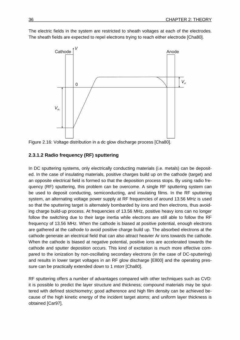
36 CHAPTER 2: THEORY The electric fields in the system are restricted to sheath voltages at each of the electrodes. The sheath fields are expected to repel electrons trying to reach either electrode [Cha80].
Figure 2.16: Voltage distribution in a dc glow discharge process [Cha80]. 2.3.1.2 Radio frequency (RF) sputtering In DC sputtering systems, only electrically conducting materials (i.e. metals) can be deposit-ed. In the case of insulating materials, positive charges build up on the cathode (target) and an opposite electrical field is formed so that the deposition process stops. By using radio fre-quency (RF) sputtering, this problem can be overcome. A single RF sputtering system can be used to deposit conducting, semiconducting, and insulating films. In the RF sputtering system, an alternating voltage power supply at RF frequencies of around 13.56 MHz is used so that the sputtering target is alternately bombarded by ions and then electrons, thus avoid-ing charge build-up process. At frequencies of 13.56 MHz, positive heavy ions can no longer follow the switching due to their large inertia while electrons are still able to follow the RF frequency of 13.56 MHz. When the cathode is biased at positive potential, enough electrons are gathered at the cathode to avoid positive charge build up. The absorbed electrons at the cathode generate an electrical field that can also attract heavier Ar ions towards the cathode. When the cathode is biased at negative potential, positive ions are accelerated towards the cathode and sputter deposition occurs. This kind of excitation is much more effective com-pared to the ionization by non-oscillating secondary electrons (in the case of DC-sputtering) and results in lower target voltages in an RF glow discharge [Ell00] and the operating pres-sure can be practically extended down to 1 mtorr [Cha80]. RF sputtering offers a number of advantages compared with other techniques such as CVD: it is possible to predict the layer structure and thickness; compound materials may be sput-tered with defined stoichiometry; good adherence and high film density can be achieved be-cause of the high kinetic energy of the incident target atoms; and uniform layer thickness is obtained [Car97].

2.3 SPUTTERING AS A THIN FILM DEPOSITION METHOD 37
In DC sputtering systems, arcing is sometimes a problem, leading to the necessity of condi-tioning a sputtering target before general usage. These arcs are less likely to form in RF dis-charges because the field is maintained in one direction for less than one cycle, and reduces to zero twice in each cycle, making it more difficult for the arc to be sustained [Cha80].
2.3.1.3 Magnetron sputtering It took nearly 40 years from the first report of the magnetron sputtering principle by Penning in 1936 [Pen36] until the invention of the planar magnetron, which is the fundamental config-uration in magnetron sputtering deposition today. Figure 2.17 shows a penning cathode in its simplest form. Permanent magnets are fixed at the back side of the target material and they provide a toroidal confinement field with the field lines forming a closed tunnel on the target surface. The energetic secondary electrons are confined at the area near the cathode and heavier ions can move more freely under the elec-tric field due to their much higher mass. When no magnets are placed at the back side of the cathode, secondary electrons emitted from the target during the sputtering process are accelerated across the cathode dark space towards the highly charged plasma sheath. Utilizing the magnets, the electron path is modi-fied under the influence of the E × B Lorentz force and the electrons follow helical paths around the magnetic field. This results in an extended electron path length and leads to an increase in the number of collisions of the electrons with gas atoms. These collisions result in increased ionization and a much denser plasma. The increased ionization of Ar near the cathode results in higher sputtering rates at lower Ar pressure [Qia03, Beh91, Vos91].
Figure 2.17: A penning cathode in its simplest form.
2.3.1.4 Reactive sputtering The term reactive sputtering is defined as the sputtering process in which neutral, excited, or ionized gaseous species react with the target, sputtered particles, or the substrate [Beh91]. Besides RF sputtering, nonconducting compound thin films, such as oxides, nitrides, and sulfides can also be deposited by reactive sputtering through the introduction of reactive gases (O2, N2, or H2S) mixed with inert gas into the process chamber [Qia03]. The stoichi-ometry of the deposited films can be controlled by varying the partial pressures of the inert and reactive gases. In the reactive sputtering, compound targets corresponding to the de-
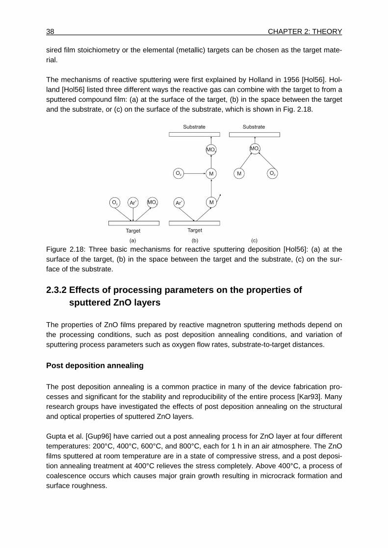
38 CHAPTER 2: THEORY sired film stoichiometry or the elemental (metallic) targets can be chosen as the target mate-rial. The mechanisms of reactive sputtering were first explained by Holland in 1956 [Hol56]. Hol-land [Hol56] listed three different ways the reactive gas can combine with the target to from a sputtered compound film: (a) at the surface of the target, (b) in the space between the target and the substrate, or (c) on the surface of the substrate, which is shown in Fig. 2.18.
Figure 2.18: Three basic mechanisms for reactive sputtering deposition [Hol56]: (a) at the surface of the target, (b) in the space between the target and the substrate, (c) on the sur-face of the substrate.
2.3.2 Effects of processing parameters on the prope rties of sputtered ZnO layers
The properties of ZnO films prepared by reactive magnetron sputtering methods depend on the processing conditions, such as post deposition annealing conditions, and variation of sputtering process parameters such as oxygen flow rates, substrate-to-target distances.
Post deposition annealing The post deposition annealing is a common practice in many of the device fabrication pro-cesses and significant for the stability and reproducibility of the entire process [Kar93]. Many research groups have investigated the effects of post deposition annealing on the structural and optical properties of sputtered ZnO layers. Gupta et al. [Gup96] have carried out a post annealing process for ZnO layer at four different temperatures: 200°C, 400°C, 600°C, and 800°C, each for 1 h in an air atmosphere. The ZnO films sputtered at room temperature are in a state of compressive stress, and a post deposi-tion annealing treatment at 400°C relieves the stress completely. Above 400°C, a process of coalescence occurs which causes major grain growth resulting in microcrack formation and surface roughness.
2.3 SPUTTERING AS A THIN FILM DEPOSITION METHOD 39
The effect of relieving the stress in the as-grown ZnO films is also reported by Hong et al [Hon05a]. They have conducted a post annealing at 700°C for 8 h and the XRD spectra indi-cate that the crystal quality of ZnO films has been improved. Compared with the as-grown sample, annealed samples exhibit a blue shift in the UV emission peaks, and a strong green emission is found in the annealed ZnO film. Similar effects are also observed by Chu et al. [Chu03]. Post annealing is carried out at 400°C and 600°C in vacuum (10-5 torr) for 1 h. Post deposition annealing at 400°C makes ZnO films more suitable for piezoelectric applications. It yields improved ZnO films with high-er resistivity, stronger c-axis (002) orientation, denser structure, smoother surface and re-lieved stress. However, annealing at too high temperature at 600°C increases loss factor and stress. Although many research groups have reported the effects of post deposition annealing on the structural and optical properties of the sputtered ZnO layers, very few groups have relat-ed these to the effects of post annealing on the electrical properties of the sputtered ZnO layer. In this work, the bottom-gate top-contact thin film transistor structure is used as the reference structure for the investigation of electrical characteristics changes of the devices that are annealed at different temperatures in different atmospheres. It is shown that anneal-ing in forming gas and oxygen atmospheres in the temperature range of 400°C to 500°C will obviously influence the threshold voltage and saturation mobility >. The results of post annealing effects will be discussed in details in chapter 4.
Oxygen flow rates Oxygen partial pressure or flow rate has not only important influence on the deposition rate of ZnO but also on the electrical characteristics of ZnO TFTs [Ell00, Car03]. It is necessary and important to add oxygen during RF sputtering process for obtaining a semiconducting ZnO film. No oxygen or too much oxygen can make the ZnO film either metallic or insulating. Carcia et al. [Car03] have investigated the dependence of electrical resistivity for sputtered ZnO thin films on oxygen partial pressure. The resistivity underwent a transition from semi-conducting at low oxygen partial pressure to semi-insulating at higher partial pressure. For ZnO TFTs fabricated at three different oxygen partial pressures, field-effect mobility decreas-es with an increasing oxygen partial pressure. The structural and optical properties of sputtered ZnO thin films can also be strongly influ-enced by changing oxygen partial pressure [Hon05b, Zha07]. In this work, instead of oxygen partial pressure, the oxygen flow rates are varied directly and their influence on electrical properties of ZnO thin films is discussed in chapter 4.
Substrate-to-target distances During sputtering process, gas phase scattering of atoms and the angular emission from the target have a direct effect on the deposition rate. The mean free path of the sputtered parti-cles can be calculated by the equation [Nog80]:
40 CHAPTER 2: THEORY
` = ℎ21 ]3-© ^J/C μ,(2.48)
where ℎ is Planck’s constant, 1 is the electron charge, - is the carrier concentration and μ is the mobility. When the mean free path of the atoms are much less than substrate-to-target distances, the gas phase scattering will have an important effect on the decrease of the dep-osition rate with the increasing substrate-to-target distance. When the Zn and O atoms are scattered by the background argon and oxygen gas, they are redirected away from the sub-strate. This scattering results in a decay in the number of atoms that actually reach the sub-strate. In addition, the angular emission results in a cosine-like angular distribution from the target. Therefore, when the substrate moves further away from the target, some of the atoms hit the chamber walls before they can reach the substrate, also leading to a decrease of the deposition rate [Men00].
2.4 Logic circuits One of the goals of this work is the realization of an NMOS inverter based on sputtered ZnO TFTs. In this section, the current status and motivation of fabricating simple logic circuits by using metal-oxide-semiconductor materials are introduced firstly. Then, the fundamentals of digital circuits especially inverters are described. A majority of the recent work on ZnO has concentrated on the TFT active channel layer in-cluding optical applications due to the wide band gap of the material and electrical properties of ZnO functioning as the active layer in the thin film transistors. In contrast, circuit integration has been pursued by employing silicon technology or organic TFTs [Cle04, Lin99, Kno04, Gel00]. Due to the sensitivity of organic materials to moisture and ultraviolet light, many re-search groups have recently begun to explore the potential of using metal-oxide-semiconductor materials to construct simple logic devices such as inverters and ring oscilla-tors [Oh10, Pre06, Cha08, Hei09, Ofu07, Sun08]. Although the exploration is still at the initial stage, many groups do obtain impressive results in the characterization of inverters and ring oscillators based on metal-oxide materials. Oh et al. [Oh10] have demonstrated a ZnO-based inverter with an excellent inverter gain of about 41 at a low supply voltage of 5 V by coupling top- and bottom-gate structures with the same channel width-to-length ratio. Presley et al. [Pre06] have managed to fabricate an inverter with a gain of about 1.5 at a supply voltage of 30 V by using sputtered indium gallium oxide as the semiconductor material. Cha et al. [Cha08] have reported a ZnO-based inverter with a gain of about 22 at a low supply voltage of 2 V by using two n-channel TFTs. Heineck et al. [Hei09] have reported a depletion-load NMOS inverter design which has achieved an inverter gain of about 10 at a supply voltage of 10 V. The material in his study is zinc tin oxide. With the maturity of TFT technology, it is important and necessary to demonstrate the feasi-bility of using TFT technology in the circuit integration. As far as the author’s knowledge there are very few groups in Europe which have reported on the realization of simple logics such as inverters based on RF magnetron sputtered ZnO thin films. In this work, the design and characterization of inverters with two n-channel ZnO TFTs is reported.
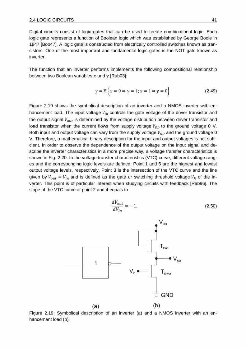
2.4 LOGIC CIRCUITS 41
Digital circuits consist of logic gates that can be used to create combinational logic. Each logic gate represents a function of Boolean logic which was established by George Boole in 1847 [Boo47]. A logic gate is constructed from electrically controlled switches known as tran-sistors. One of the most important and fundamental logic gates is the NOT gate known as inverter. The function that an inverter performs implements the following compositional relationship between two Boolean variables d and [Rab03]:
= d: ¬d = 0 ⇒ = 1; d = 1⇒ = 0¯ (2.49)
Figure 2.19 shows the symbolical description of an inverter and a NMOS inverter with en-
hancement load. The input voltage controls the gate voltage of the driver transistor and
the output signal ¢ is determined by the voltage distribution between driver transistor and load transistor when the current flows from supply voltage to the ground voltage 0 V. Both input and output voltage can vary from the supply voltage and the ground voltage 0 V. Therefore, a mathematical binary description for the input and output voltages is not suffi-cient. In order to observe the dependence of the output voltage on the input signal and de-scribe the inverter characteristics in a more precise way, a voltage transfer characteristics is shown in Fig. 2.20. In the voltage transfer characteristics (VTC) curve, different voltage rang-es and the corresponding logic levels are defined. Point 1 and 5 are the highest and lowest output voltage levels, respectively. Point 3 is the intersection of the VTC curve and the line
given by ¢ = and is defined as the gate or switching threshold voltage of the in-verter. This point is of particular interest when studying circuits with feedback [Rab96]. The slope of the VTC curve at point 2 and 4 equals to l¢l = −1.(2.50)
Figure 2.19: Symbolical description of an inverter (a) and a NMOS inverter with an en-hancement load (b).
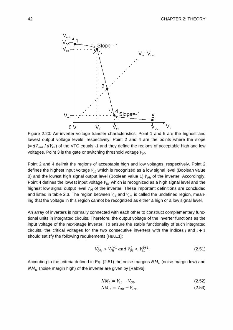
42 CHAPTER 2: THEORY
Figure 2.20: An inverter voltage transfer characteristics. Point 1 and 5 are the highest and lowest output voltage levels, respectively. Point 2 and 4 are the points where the slope
(=lPiQ/l) of the VTC equals -1 and they define the regions of acceptable high and low
voltages. Point 3 is the gate or switching threshold voltage . Point 2 and 4 delimit the regions of acceptable high and low voltages, respectively. Point 2 defines the highest input voltage °± which is recognized as a low signal level (Boolean value 0) and the lowest high signal output level (Boolean value 1) ( of the inverter. Accordingly, Point 4 defines the lowest input voltage °R which is recognized as a high signal level and the highest low signal output level (£ of the inverter. These important definitions are concluded and listed in table 2.3. The region between °± and °Ris called the undefined region, mean-ing that the voltage in this region cannot be recognized as either a high or a low signal level. An array of inverters is normally connected with each other to construct complementary func-tional units in integrated circuits. Therefore, the output voltage of the inverter functions as the input voltage of the next-stage inverter. To ensure the stable functionality of such integrated circuits, the critical voltages for the two consecutive inverters with the indices j and j + 1 should satisfy the following requirements [Huu11]: ( > °RLJ-l(£ < °±LJ.(2.51)
According to the criteria defined in Eq. (2.51) the noise margins ¥± (noise margin low) and ¥R (noise margin high) of the inverter are given by [Rab96]: ¥± = °± − (£,(2.52) ¥R = ( − °R.(2.53)
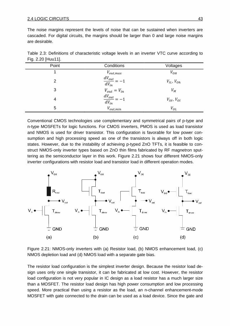
2.4 LOGIC CIRCUITS 43 The noise margins represent the levels of noise that can be sustained when inverters are cascaded. For digital circuits, the margins should be larger than 0 and large noise margins are desirable. Table 2.3: Definitions of characteristic voltage levels in an inverter VTC curve according to Fig. 2.20 [Huu11].
Point Conditions Voltages
1 ¢,=>? (R
2 l¢l = −1 °±, (
3 ¢ =
4 l¢l = −1 °R, (£
5 ¢,= (± Conventional CMOS technologies use complementary and symmetrical pairs of p-type and n-type MOSFETs for logic functions. For CMOS inverters, PMOS is used as load transistor and NMOS is used for driver transistor. This configuration is favorable for low power con-sumption and high processing speed as one of the transistors is always off in both logic states. However, due to the instability of achieving p-typed ZnO TFTs, it is feasible to con-struct NMOS-only inverter types based on ZnO thin films fabricated by RF magnetron sput-tering as the semiconductor layer in this work. Figure 2.21 shows four different NMOS-only inverter configurations with resistor load and transistor load in different operation modes.
Figure 2.21: NMOS-only inverters with (a) Resistor load, (b) NMOS enhancement load, (c) NMOS depletion load and (d) NMOS load with a separate gate bias. The resistor load configuration is the simplest inverter design. Because the resistor load de-sign uses only one single transistor, it can be fabricated at low cost. However, the resistor load configuration is not very popular in IC design as a load resistor has a much larger size than a MOSFET. The resistor load design has high power consumption and low processing speed. More practical than using a resistor as the load, an n-channel enhancement-mode MOSFET with gate connected to the drain can be used as a load device. Since the gate and
44 CHAPTER 2: THEORY
the drain of the load transistor are connected, the gate-to-source voltage equals to drain-to-source voltage ,± = ,± ,(2.54)
where the symbol refers to the load transistor. When ,± = ,± > Qℎ,, a non-zero drain
current flows through the transistor and thus the transistor operates in the saturation region only because the following condition is always satisfied: ,± > ,± − ,± .(2.55) In the saturation region, the drain current is
± = ²±2 +,± − ,±/E = ²±2 +,± − ,±/E,(2.56)
where ²± = ±(t ³´±´ , in which ± is the saturation mobility of the load transistor. When the
input voltage < ,, in which the symbol p refers to the driver transistor, the driver tran-
sistor is in cut-off region and thus the drain current is zero:
± = 0 = ²±2 +,± − ,±/E.(2.57)
From Eq. (2.57), it can be derived that − ¢ − ,± = 0.(2.58)
Thus, the maximum output voltage can be expressed as: ¢,=>? = (R = − ,± .(2.59)
For the enhancement-load NMOS inverter, the maximum output voltage, which corresponds to the logic level 1, does not reach the full value of supply voltage . When the input volt-age increases and exceeds ,, the driver transistor turns on and is biased in the saturation
region. The drain currents of driver transistor and load transistor are equal and can be ex-pressed by: ²±2 +,± − ,±/E = ²2 +, − ,/E.(2.60)
Considering ,± = − ¢ and , = j-, the above equation can be rewritten as:
²±2 + − ¢ − ,±/E = ²2 + − ,/E.(2.61)
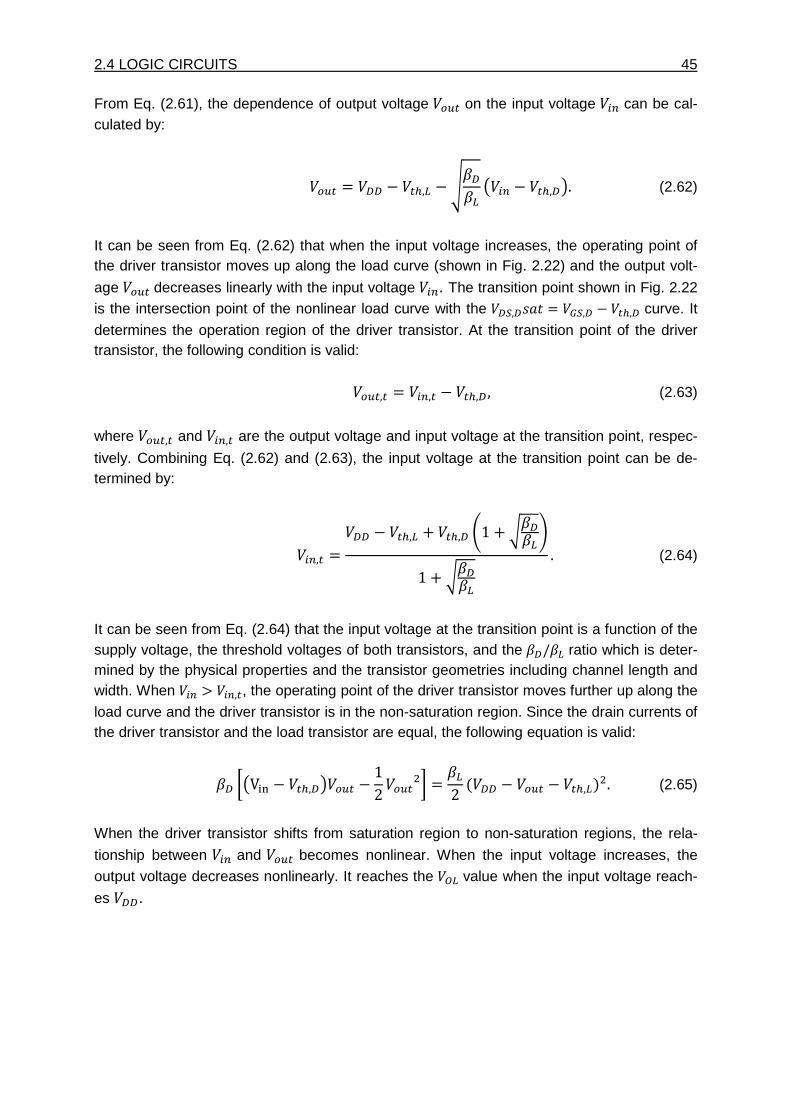
2.4 LOGIC CIRCUITS 45 From Eq. (2.61), the dependence of output voltage ¢ on the input voltage can be cal-culated by:
¢ = − ,± −²²± ' − ,*.(2.62)
It can be seen from Eq. (2.62) that when the input voltage increases, the operating point of the driver transistor moves up along the load curve (shown in Fig. 2.22) and the output volt-
age ¢decreases linearly with the input voltage . The transition point shown in Fig. 2.22 is the intersection point of the nonlinear load curve with the ,NQ = , − , curve. It
determines the operation region of the driver transistor. At the transition point of the driver transistor, the following condition is valid: ¢, = , − , ,(2.63)
where ¢, and , are the output voltage and input voltage at the transition point, respec-
tively. Combining Eq. (2.62) and (2.63), the input voltage at the transition point can be de-termined by:
, = − ,± + , !1 + ²²±&1 + ²²±
.(2.64)
It can be seen from Eq. (2.64) that the input voltage at the transition point is a function of the supply voltage, the threshold voltages of both transistors, and the ²/²± ratio which is deter-mined by the physical properties and the transistor geometries including channel length and width. When > ,, the operating point of the driver transistor moves further up along the
load curve and the driver transistor is in the non-saturation region. Since the drain currents of the driver transistor and the load transistor are equal, the following equation is valid:
² 'V¶· − ,*¢ − 12¢E = ²±2 + − ¢ − ,±/E.(2.65)
When the driver transistor shifts from saturation region to non-saturation regions, the rela-
tionship between and ¢ becomes nonlinear. When the input voltage increases, the
output voltage decreases nonlinearly. It reaches the (± value when the input voltage reach-
es .
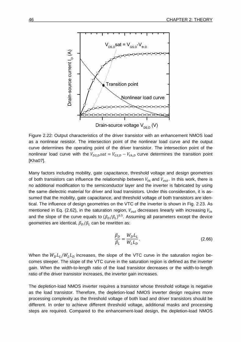
46 CHAPTER 2: THEORY
Figure 2.22: Output characteristics of the driver transistor with an enhancement NMOS load as a nonlinear resistor. The intersection point of the nonlinear load curve and the output curve determines the operating point of the driver transistor. The intersection point of the nonlinear load curve with the ,NQ = , − , curve determines the transition point
[Kha07]. Many factors including mobility, gate capacitance, threshold voltage and design geometries of both transistors can influence the relationship between and ¢. In this work, there is no additional modification to the semiconductor layer and the inverter is fabricated by using the same dielectric material for driver and load transistors. Under this consideration, it is as-sumed that the mobility, gate capacitance, and threshold voltage of both transistors are iden-tical. The influence of design geometries on the VTC of the inverter is shown in Fig. 2.23. As mentioned in Eq. (2.62), in the saturation region, ¢ decreases linearly with increasing
and the slope of the curve equals to +²/²±/F.¦. Assuming all parameters except the device geometries are identical, ²/²± can be rewritten as: ²²± = r±r± .(2.66)
When the r±/r± increases, the slope of the VTC curve in the saturation region be-comes steeper. The slope of the VTC curve in the saturation region is defined as the inverter gain. When the width-to-length ratio of the load transistor decreases or the width-to-length ratio of the driver transistor increases, the inverter gain increases. The depletion-load NMOS inverter requires a transistor whose threshold voltage is negative as the load transistor. Therefore, the depletion-load NMOS inverter design requires more processing complexity as the threshold voltage of both load and driver transistors should be different. In order to achieve different threshold voltage, additional masks and processing steps are required. Compared to the enhancement-load design, the depletion-load NMOS
2.4 LOGIC CIRCUITS 47
inverter has the advantage of reaching (R = . In this work, the inverter design takes the choice of having an enhancement-load NMOS inverter with a separate gate supply for the load transistor as shown in Fig. 2.21 (d). This configuration has the advantage of choosing the gate voltage applied to the load transistor within a dynamic range including and val-ues different than .
Figure 2.23: Influence of ² ratio on the VTC of the inverter. Assuming all other parameters except transistor geometries are identical for both transistors, the slope of the inverter in the
saturation region becomes steeper when the r±/r± ratio becomes bigger [Kha07].
The line ¢, = , − , separates the nonsaturation and saturation region of the driver
transistor.

49
Chapter 3
Experimental methods
3.1 Sputtering equipment The most important processing step in this work is the RF magnetron sputtering of ZnO thin film on silicon substrate with silicon dioxide on top of it. Except the experimental results pre-sented in section 4.1, all the other sputtering experiments for ZnO thin films are conducted in the sputtering equipment L400 SP from Leybold. The equipment provides two sputtering modes: DC and RF sputtering. Switching between DC and RF sputtering modes is allowed by controlling the cathode switch-over unit. In this work, ZnO is sputtered by RF sputtering. The electrical system of RF sputtering for ZnO deposition involves a RF generator operated at 13.56 MHz and a match box. Inside the sputtering chamber, there are three possible cath-ode positions, on which the sputtering targets can be mounted. When sputtering ZnO thin films, a ZnO target with a diameter of 152.4 mm from SenVac Thin Film Technologies GmbH is used and fixed on one of the three cathode positions in the process chamber. The thick-ness of the ZnO target is 6 mm and the concentration of the target is 99.95%. When the pressure in the chamber is reduced to as low as 10-6 mbar, the sputtering process can be started. If more than one wafers are sputtered at one time, the substrate holder should be set to the rotational mode during the whole sputtering process. Otherwise either stationary or rotational mode is chosen to sputter one single wafer. The sputtering rates for both rotational mode and stationary mode under certain sputtering conditions should be determined before ZnO thin films are deposited. When starting the sputtering process, the cooling water should be turned on by the water flow switchers in order to avoid the overheating problem during the sputtering process. There is a heater and thermo couple available for the system. Therefore, substrate temperature can be adjusted at room temperature or a higher temperature. The opening of the shutter is adjusted to the position directly below the ZnO target before sputter-ing begins. In order to obtain a semiconducting ZnO layer, the oxygen is introduced to the process chamber. The oxygen and argon partial pressure is set to 1:1 at a level of 2.4 µbar for each gas by adjusting the mass flow controller. A sputtering power of about 100 W is used to ignite the plasma. As soon as the plasma has been ignited, the sputtering power is adjusted to 500 W for the whole sputtering procedure and the timer is started to control the sputtering time according to the predetermined sputtering rate.
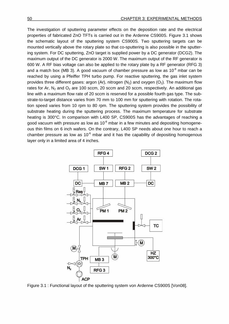
50 CHAPTER 3: EXPERIMENTAL METHODS The investigation of sputtering parameter effects on the deposition rate and the electrical properties of fabricated ZnO TFTs is carried out in the Ardenne CS900S. Figure 3.1 shows the schematic layout of the sputtering system CS900S. Two sputtering targets can be mounted vertically above the rotary plate so that co-sputtering is also possible in the sputter-ing system. For DC sputtering, ZnO target is supplied power by a DC generator (DCG2). The maximum output of the DC generator is 2000 W. The maximum output of the RF generator is 600 W. A RF bias voltage can also be applied to the rotary plate by a RF generator (RFG 3) and a match box (MB 3). A good vacuum of chamber pressure as low as 10-8 mbar can be reached by using a Pfeiffer TPH turbo pump. For reactive sputtering, the gas inlet system provides three different gases: argon (Ar), nitrogen (N2) and oxygen (O2). The maximum flow rates for Ar, N2 and O2 are 100 sccm, 20 sccm and 20 sccm, respectively. An additional gas line with a maximum flow rate of 20 sccm is reserved for a possible fourth gas type. The sub-strate-to-target distance varies from 70 mm to 100 mm for sputtering with rotation. The rota-tion speed varies from 10 rpm to 80 rpm. The sputtering system provides the possibility of substrate heating during the sputtering process. The maximum temperature for substrate heating is 300°C. In comparison with L400 SP, CS900S has the advantages of reaching a good vacuum with pressure as low as 10-8 mbar in a few minutes and depositing homogene-ous thin films on 6 inch wafers. On the contrary, L400 SP needs about one hour to reach a chamber pressure as low as 10-6 mbar and it has the capability of depositing homogenous layer only in a limited area of 4 inches.
Figure 3.1 : Functional layout of the sputtering system von Ardenne CS900S [Von08].
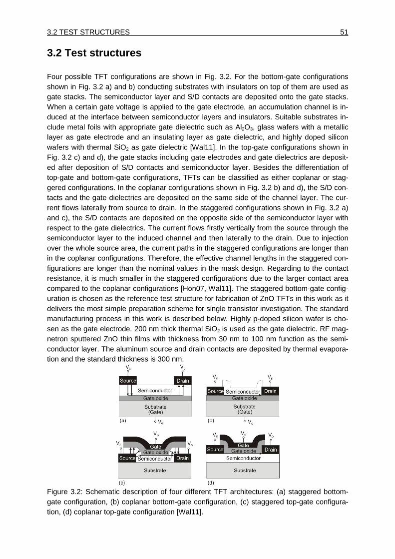
3.2 TEST STRUCTURES 51
3.2 Test structures Four possible TFT configurations are shown in Fig. 3.2. For the bottom-gate configurations shown in Fig. 3.2 a) and b) conducting substrates with insulators on top of them are used as gate stacks. The semiconductor layer and S/D contacts are deposited onto the gate stacks. When a certain gate voltage is applied to the gate electrode, an accumulation channel is in-duced at the interface between semiconductor layers and insulators. Suitable substrates in-clude metal foils with appropriate gate dielectric such as Al2O3, glass wafers with a metallic layer as gate electrode and an insulating layer as gate dielectric, and highly doped silicon wafers with thermal SiO2 as gate dielectric [Wal11]. In the top-gate configurations shown in Fig. 3.2 c) and d), the gate stacks including gate electrodes and gate dielectrics are deposit-ed after deposition of S/D contacts and semiconductor layer. Besides the differentiation of top-gate and bottom-gate configurations, TFTs can be classified as either coplanar or stag-gered configurations. In the coplanar configurations shown in Fig. 3.2 b) and d), the S/D con-tacts and the gate dielectrics are deposited on the same side of the channel layer. The cur-rent flows laterally from source to drain. In the staggered configurations shown in Fig. 3.2 a) and c), the S/D contacts are deposited on the opposite side of the semiconductor layer with respect to the gate dielectrics. The current flows firstly vertically from the source through the semiconductor layer to the induced channel and then laterally to the drain. Due to injection over the whole source area, the current paths in the staggered configurations are longer than in the coplanar configurations. Therefore, the effective channel lengths in the staggered con-figurations are longer than the nominal values in the mask design. Regarding to the contact resistance, it is much smaller in the staggered configurations due to the larger contact area compared to the coplanar configurations [Hon07, Wal11]. The staggered bottom-gate config-uration is chosen as the reference test structure for fabrication of ZnO TFTs in this work as it delivers the most simple preparation scheme for single transistor investigation. The standard manufacturing process in this work is described below. Highly p-doped silicon wafer is cho-sen as the gate electrode. 200 nm thick thermal SiO2 is used as the gate dielectric. RF mag-netron sputtered ZnO thin films with thickness from 30 nm to 100 nm function as the semi-conductor layer. The aluminum source and drain contacts are deposited by thermal evapora-tion and the standard thickness is 300 nm.
Figure 3.2: Schematic description of four different TFT architectures: (a) staggered bottom-gate configuration, (b) coplanar bottom-gate configuration, (c) staggered top-gate configura-tion, (d) coplanar top-gate configuration [Wal11].
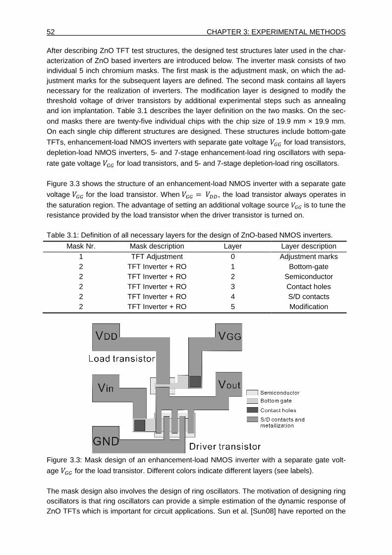
52 CHAPTER 3: EXPERIMENTAL METHODS After describing ZnO TFT test structures, the designed test structures later used in the char-acterization of ZnO based inverters are introduced below. The inverter mask consists of two individual 5 inch chromium masks. The first mask is the adjustment mask, on which the ad-justment marks for the subsequent layers are defined. The second mask contains all layers necessary for the realization of inverters. The modification layer is designed to modify the threshold voltage of driver transistors by additional experimental steps such as annealing and ion implantation. Table 3.1 describes the layer definition on the two masks. On the sec-
ond masks there are twenty-five individual chips with the chip size of 19.9 mm × 19.9 mm. On each single chip different structures are designed. These structures include bottom-gate
TFTs, enhancement-load NMOS inverters with separate gate voltage for load transistors, depletion-load NMOS inverters, 5- and 7-stage enhancement-load ring oscillators with sepa-
rate gate voltage for load transistors, and 5- and 7-stage depletion-load ring oscillators. Figure 3.3 shows the structure of an enhancement-load NMOS inverter with a separate gate
voltage for the load transistor. When =, the load transistor always operates in
the saturation region. The advantage of setting an additional voltage source is to tune the resistance provided by the load transistor when the driver transistor is turned on. Table 3.1: Definition of all necessary layers for the design of ZnO-based NMOS inverters.
Mask Nr. Mask description Layer Layer description 1 TFT Adjustment 0 Adjustment marks 2 TFT Inverter + RO 1 Bottom-gate 2 TFT Inverter + RO 2 Semiconductor 2 TFT Inverter + RO 3 Contact holes 2 TFT Inverter + RO 4 S/D contacts 2 TFT Inverter + RO 5 Modification
Figure 3.3: Mask design of an enhancement-load NMOS inverter with a separate gate volt-
age for the load transistor. Different colors indicate different layers (see labels). The mask design also involves the design of ring oscillators. The motivation of designing ring oscillators is that ring oscillators can provide a simple estimation of the dynamic response of ZnO TFTs which is important for circuit applications. Sun et al. [Sun08] have reported on the
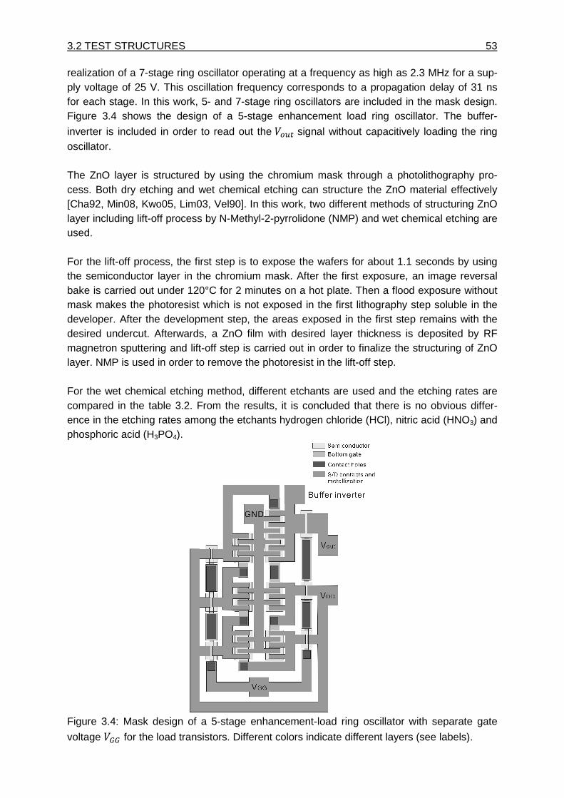
3.2 TEST STRUCTURES 53
realization of a 7-stage ring oscillator operating at a frequency as high as 2.3 MHz for a sup-ply voltage of 25 V. This oscillation frequency corresponds to a propagation delay of 31 ns for each stage. In this work, 5- and 7-stage ring oscillators are included in the mask design. Figure 3.4 shows the design of a 5-stage enhancement load ring oscillator. The buffer-
inverter is included in order to read out the ¢ signal without capacitively loading the ring oscillator. The ZnO layer is structured by using the chromium mask through a photolithography pro-cess. Both dry etching and wet chemical etching can structure the ZnO material effectively [Cha92, Min08, Kwo05, Lim03, Vel90]. In this work, two different methods of structuring ZnO layer including lift-off process by N-Methyl-2-pyrrolidone (NMP) and wet chemical etching are used. For the lift-off process, the first step is to expose the wafers for about 1.1 seconds by using the semiconductor layer in the chromium mask. After the first exposure, an image reversal bake is carried out under 120°C for 2 minutes on a hot plate. Then a flood exposure without mask makes the photoresist which is not exposed in the first lithography step soluble in the developer. After the development step, the areas exposed in the first step remains with the desired undercut. Afterwards, a ZnO film with desired layer thickness is deposited by RF magnetron sputtering and lift-off step is carried out in order to finalize the structuring of ZnO layer. NMP is used in order to remove the photoresist in the lift-off step. For the wet chemical etching method, different etchants are used and the etching rates are compared in the table 3.2. From the results, it is concluded that there is no obvious differ-ence in the etching rates among the etchants hydrogen chloride (HCl), nitric acid (HNO3) and phosphoric acid (H3PO4).
Figure 3.4: Mask design of a 5-stage enhancement-load ring oscillator with separate gate
voltage for the load transistors. Different colors indicate different layers (see labels).
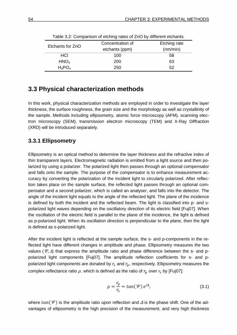
54 CHAPTER 3: EXPERIMENTAL METHODS
Table 3.2: Comparison of etching rates of ZnO by different etchants.
Etchants for ZnO Concentration of etchants (ppm)
Etching rate (nm/min)
HCl HNO3
H3PO4
100 200 250
58 63 52
3.3 Physical characterization methods In this work, physical characterization methods are employed in order to investigate the layer thickness, the surface roughness, the grain size and the morphology as well as crystallinity of the sample. Methods including ellipsometry, atomic force microscopy (AFM), scanning elec-tron microscopy (SEM), transmission electron microscopy (TEM) and X-Ray Diffraction (XRD) will be introduced separately.
3.3.1 Ellipsometry Ellipsometry is an optical method to determine the layer thickness and the refractive index of thin transparent layers. Electromagnetic radiation is emitted from a light source and then po-larized by using a polarizer. The polarized light then passes through an optional compensator and falls onto the sample. The purpose of the compensator is to enhance measurement ac-curacy by converting the polarization of the incident light to circularly polarized. After reflec-tion takes place on the sample surface, the reflected light passes through an optional com-pensator and a second polarizer, which is called an analyser, and falls into the detector. The angle of the incident light equals to the angle of the reflected light. The plane of the incidence is defined by both the incident and the reflected beam. The light is classified into p- and s-polarized light waves depending on the oscillatory direction of its electric field [Fuj07]. When the oscillation of the electric field is parallel to the plane of the incidence, the light is defined as p-polarized light. When its oscillation direction is perpendicular to the plane, then the light is defined as s-polarized light. After the incident light is reflected at the sample surface, the s- and p-components in the re-flected light have different changes in amplitude and phase. Ellipsometry measures the two values +Ψ,∆) that express the amplitude ratio and phase difference between the s- and p-polarized light components [Fuj07]. The amplitude reflection coefficients for s- and p-
polarized light components are donated by o and oa, respectively. Ellipsometry measures the
complex reflectance ratio , which is defined as the ratio of oa over o by [Fuj07]:
= oao = Q-+Ψ/ ;∆,(3.1)
where Q-+Ψ/ is the amplitude ratio upon reflection and ∆ is the phase shift. One of the ad-vantages of ellipsometry is the high precision of the measurement, and very high thickness
3.3 PHYSICAL CHARACTERIZATION METHODS 55
sensitivity (~0.1 Å) can be obtained even for conventional instruments [Fuj07]. However, el-
lipsometry is an indirect method and the measured Ψ and ∆ values cannot be directly con-verted to the optical parameters of the sample. An optical model should be created in order to derive the optical parameters of the sample. The next step after the construction of the optical model is to select the layer parameters including the refractive index of the sample, the correct layer sequence, and the thickness parameters of all individual layers of the sam-ple. Linear regression analysis is then used to fit the measured (Ψ,∆) spectra. By minimizing fitting errors, the optical constants and film structures of the sample are determined. The data analysis procedure in spectroscopic ellipsometry is described in the flow chart shown in Fig. 3.5. The ellipsometer which is used in this work uses a helium-neon laser with a wavelength of 632.8 nm as the light source. The incident light radiates on the sample with an angle of 70°. The measurement spot has a diameter of about 25 µm. The polarization state of the reflected light is determined by a rotating analyser [Lem10].
Figure 3.5: Flowchart of data analysis process in spectroscopic ellipsometry [Fuj07].
56 CHAPTER 3: EXPERIMENTAL METHODS
3.3.2 Atomic force microscopy Atomic force microscopy (AFM) is a very sensitive method to characterize the surface topog-raphy of samples with atomic resolution. By using AFM, layer parameters such as surface roughness and sample grain size can be determined. The AFM is constructed with a cantilever with a sharp tip at its end that is used to scan the specimen surface. A deflection of the cantilever occurs due to the forces between the tip and the sample according to Hooke’s law when the tip is brought into proximity of a sample sur-face. The atomic interaction between the tip and the sample surface includes van der Waals forces and electrostatic forces [Lem10]. A laser radiation is used to measure the deflection of the cantilever. When atomic interaction occurs, the deflection can be measured by the changes in the reflected lasers which are detected by an array of photodiodes. A feedback mechanism plays an important role in AFM to keep the tip-to-sample distance constant, thus avoiding collisions between the tip and the sample surface. In order to obtain the surface topography of the sample, the sample is scanned in d and directions. Two different param-eters, the root mean square (RMS) roughness and the average roughness, are used in this work to evaluate the sample roughness. The root mean square (RMS) and the average roughness are the standard deviation and the mean value of the ¸-direction deflection, re-spectively. There are different measurement modes for AFM. In the contact mode, the tip makes soft physical contact with the surface of the sample with a constant force and the deflection in ¸-direction is measured [Cle08]. This method has the advantage of high scan speed while di-rect contact with the surface can cause damage to soft samples. In this work, an atomic force microscope Dimension 5000 from Digital Instruments is used and the so-called tapping mode is employed. In tapping mode, the cantilever is oscillated at a frequency close to its resonant frequency. When the cantilever is brought near to the sample surface, the van der Waals forces between the tip and the sample surface decrease the resonant frequency of the canti-lever. An electronic feedback loop system maintains the oscillation amplitude constant by adjusting the tip-to-sample distance. The advantage of the tapping mode is less damage to soft samples by avoiding the lateral forces between the tip and the sample. However, it has a slower scanning speed compared to the contact mode.
3.3.3 Scanning electron microscopy Due to the magnification limit of the light microscopes and capability of producing very high-resolution images of a sample surface, scanning electron microscopy (SEM) is employed in this work to characterize the surface topography and layer homogeneity of the sputtered ZnO layer. Scanning electron microscope images a sample by scanning it with a high-energy beam of electrons in a raster scan pattern. The electrons interact with the atoms in the sample and imaging through emission of secondary electrons is the basic mode of common SEM tech-niques [Ebe91]. It provides signals that contain information about the topography of the sam-ple surface, chemical composition, and other properties. An electron beam is thermionically
3.3 PHYSICAL CHARACTERIZATION METHODS 57
emitted from an electron gun and is accelerated at voltages in the range of 20 kV to 40 kV [Ebe91]. After being accelerated in the electric field, the electron beam is focused by con-denser lenses and interacts with the sample atoms. The incident electrons with high kinetic energy are decelerated in the sample material by repeated random scattering and absorp-tion. A variety of signals are produced by the interaction between the electrons and the sam-ple. These signals include secondary electrons, backscattered electrons, diffracted backscat-tered electrons, characteristic X-rays, visible light, and heat. Each type of signals can be de-tected by specialized detectors. For the purpose of characterization of surface morphology, emission of secondary electrons by inelastic scattering is detected and the resulting image is a distribution map of the intensity of the signal being emitted from the scanned area of the sample. A current SEM, operating in the basic secondary electron emission mode, can pro-duce very high resolution images in the order of 30 to 100 Å and have an extended magnifi-cation range from some 10X to 100000X [Ebe91]. The characterization of surface morphology in this work is conducted by using JEOL JSM-7500F. It is equipped with a cold field emission source so that the narrow energy spread of the emitting electrons provides superb focusing capability for the electron beam and thus allows for excellent resolution. The acceleration voltage extends from 0.1 kV to 30kV and a high resolution in secondary electron imaging reaches 1.4 nm at 1 kV and 1.0 nm at 15 kV [Jeo12].
3.3.4 Transmission electron microscopy Transmission electron microscopy (TEM) is a very important method to characterize poly-crystalline and amorphous samples in nanometer range [Hei70]. Based on de Broglie’s ideas of the wave-particle duality of electrons, the wave property of electrons is used to obtain high-resolution images in the atomic range in the TEM. In the TEM, the electrons are emitted either by thermionic or field electron emission into the vacuum. Before the electron beam is focused on a thin specimen, the electrons are accelerated and based on de Broglie’s con-
cept, the wavelength of the electron λ can be derived by a given acceleration voltage as [Cha01]:
λ = ℎ =
ℎ2(1 +
2 ),(3.2)
where ℎ is Planck’s constant, is the electron momentum, is the electron mass and is the speed of light. The electrons will interact with a very thin specimen after acceleration and electron waves such as secondary electrons and backscattered electrons reflected from the specimen obtain important specimen information. The information is magnified and focused onto an imaging device or detected by a CCD camera. The cross section images are detected in the TEM for the characterization of the ZnO sam-ple. In order to achieve high-resolution TEM images, the area to be observed should reach an optimal thickness of several nm as a thin specimen permits electrons to be scattered in both forward and backward directions while a bulk specimen only backscatters the incident
58 CHAPTER 3: EXPERIMENTAL METHODS beam electrons [Wil09]. In order to reach this optimal thickness, the samples are first sawn and then polished to a thickness of about 20 nm. Finally the samples are thinned to several nm by ion milling process. In this work, the TEM images are taken by the Philips CM300 Ul-traTwin in the electron microscopy group at the chair of biomaterials of Friedrich-Alexander-University Erlangen-Nuremberg. CM300 operates at an acceleration voltage of 300 kV and it features a double tilt holder. A point-to-point resolution of 0.17 nm can be achieved.
3.3.5 X-ray diffraction X-ray diffraction (XRD) is a very important experimental method in revealing the crystal struc-ture of bulk solid microstructure of thin films. Important information related to the crystal structure of the films, including lattice parameters, grain size, preferred crystal orientation, stress and defects can be determined from the XRD measurement.
X-rays are electromagnetic waves whose wavelengths λ are in the same order of magnitude
(1-100 angstroms) as the spacing l between diffraction planes in the crystal structure. In XRD, X-rays primarily interact with electrons in atoms. The phenomenon of the X-ray diffrac-tion in crystals results from elastic scattering processes in which the scattered X-rays have the same wavelength as the incident beam and only momentum is transferred in the scatter-ing process. These scattered X-rays carry information about the electron distribution in mate-rials and are produced by elastic scattering only when certain geometrical conditions are sat-isfied, which can be expressed by Bragg’s law: 2lNj-¹ = -λ,(3.3)
where ¹ is the incident angle, - is any integer, and λ is the wavelength of the beam. Analysis of the sharp interference maxima (peaks) and peak positions in an X-ray diffraction pattern leads to the understanding of the size, shape and orientation of the unit cell in a crystal. The XRD measurement in this work is conducted by a Panalytical X’pert MRD XL with CuKα radiation with wavelength 0.15406 nm. The XRD spectra are collected in the 20 – 80° of 2¹ range with a measurement step of 0.005°.
3.4 Electrical characterization methods
3.4.1 Electrical characterization In this work, the most important electrical measurements are the current-voltage measure-ments, in short I-V measurements. The I-V measurements of the fabricated ZnO TFTs are conducted mostly at two different measurement stations: a manual measurement station with a HP 4156A parameter analyzer and a Karl Suss PA-300 prober with a Keithley SCS 4200 parameter analyzer. Figure 3.6 shows the schematic block diagram of the manual measurement station with the HP 4156A parameter analyzer. During I-V measurements, a gate voltage is applied through
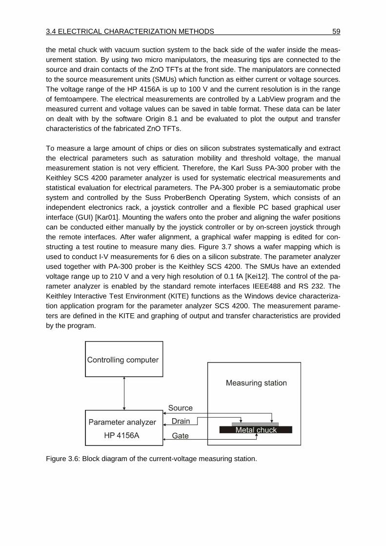
3.4 ELECTRICAL CHARACTERIZATION METHODS 59
the metal chuck with vacuum suction system to the back side of the wafer inside the meas-urement station. By using two micro manipulators, the measuring tips are connected to the source and drain contacts of the ZnO TFTs at the front side. The manipulators are connected to the source measurement units (SMUs) which function as either current or voltage sources. The voltage range of the HP 4156A is up to 100 V and the current resolution is in the range of femtoampere. The electrical measurements are controlled by a LabView program and the measured current and voltage values can be saved in table format. These data can be later on dealt with by the software Origin 8.1 and be evaluated to plot the output and transfer characteristics of the fabricated ZnO TFTs. To measure a large amount of chips or dies on silicon substrates systematically and extract the electrical parameters such as saturation mobility and threshold voltage, the manual measurement station is not very efficient. Therefore, the Karl Suss PA-300 prober with the Keithley SCS 4200 parameter analyzer is used for systematic electrical measurements and statistical evaluation for electrical parameters. The PA-300 prober is a semiautomatic probe system and controlled by the Suss ProberBench Operating System, which consists of an independent electronics rack, a joystick controller and a flexible PC based graphical user interface (GUI) [Kar01]. Mounting the wafers onto the prober and aligning the wafer positions can be conducted either manually by the joystick controller or by on-screen joystick through the remote interfaces. After wafer alignment, a graphical wafer mapping is edited for con-structing a test routine to measure many dies. Figure 3.7 shows a wafer mapping which is used to conduct I-V measurements for 6 dies on a silicon substrate. The parameter analyzer used together with PA-300 prober is the Keithley SCS 4200. The SMUs have an extended voltage range up to 210 V and a very high resolution of 0.1 fA [Kei12]. The control of the pa-rameter analyzer is enabled by the standard remote interfaces IEEE488 and RS 232. The Keithley Interactive Test Environment (KITE) functions as the Windows device characteriza-tion application program for the parameter analyzer SCS 4200. The measurement parame-ters are defined in the KITE and graphing of output and transfer characteristics are provided by the program.
Figure 3.6: Block diagram of the current-voltage measuring station.
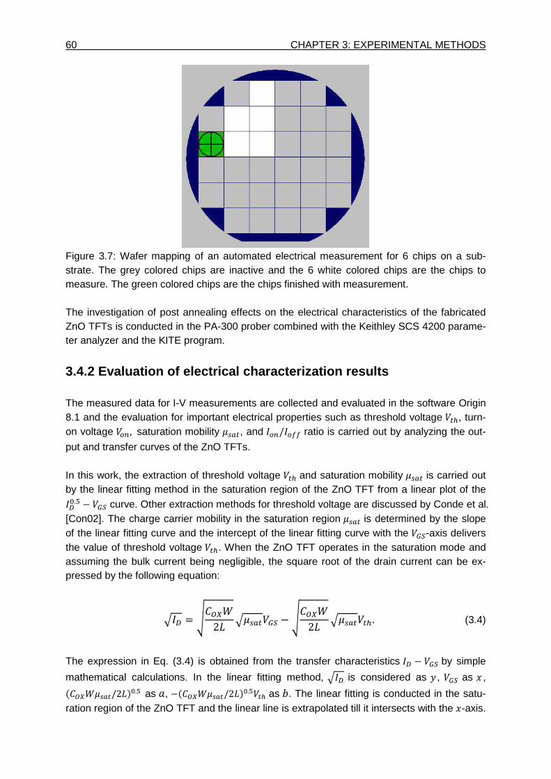
60 CHAPTER 3: EXPERIMENTAL METHODS
Figure 3.7: Wafer mapping of an automated electrical measurement for 6 chips on a sub-strate. The grey colored chips are inactive and the 6 white colored chips are the chips to measure. The green colored chips are the chips finished with measurement. The investigation of post annealing effects on the electrical characteristics of the fabricated ZnO TFTs is conducted in the PA-300 prober combined with the Keithley SCS 4200 parame-ter analyzer and the KITE program.
3.4.2 Evaluation of electrical characterization res ults The measured data for I-V measurements are collected and evaluated in the software Origin 8.1 and the evaluation for important electrical properties such as threshold voltage , turn-on voltage , saturation mobility >, and / ratio is carried out by analyzing the out-
put and transfer curves of the ZnO TFTs. In this work, the extraction of threshold voltage and saturation mobility > is carried out by the linear fitting method in the saturation region of the ZnO TFT from a linear plot of the F.¦ − curve. Other extraction methods for threshold voltage are discussed by Conde et al. [Con02]. The charge carrier mobility in the saturation region > is determined by the slope of the linear fitting curve and the intercept of the linear fitting curve with the -axis delivers the value of threshold voltage . When the ZnO TFT operates in the saturation mode and assuming the bulk current being negligible, the square root of the drain current can be ex-pressed by the following equation:
= (tr2 > −(tr2 >.(3.4)
The expression in Eq. (3.4) is obtained from the transfer characteristics − by simple
mathematical calculations. In the linear fitting method, is considered as , as d , +(tr>/2/F.¦as , −+(tr>/2/F.¦ as k. The linear fitting is conducted in the satu-ration region of the ZnO TFT and the linear line is extrapolated till it intersects with the d-axis.
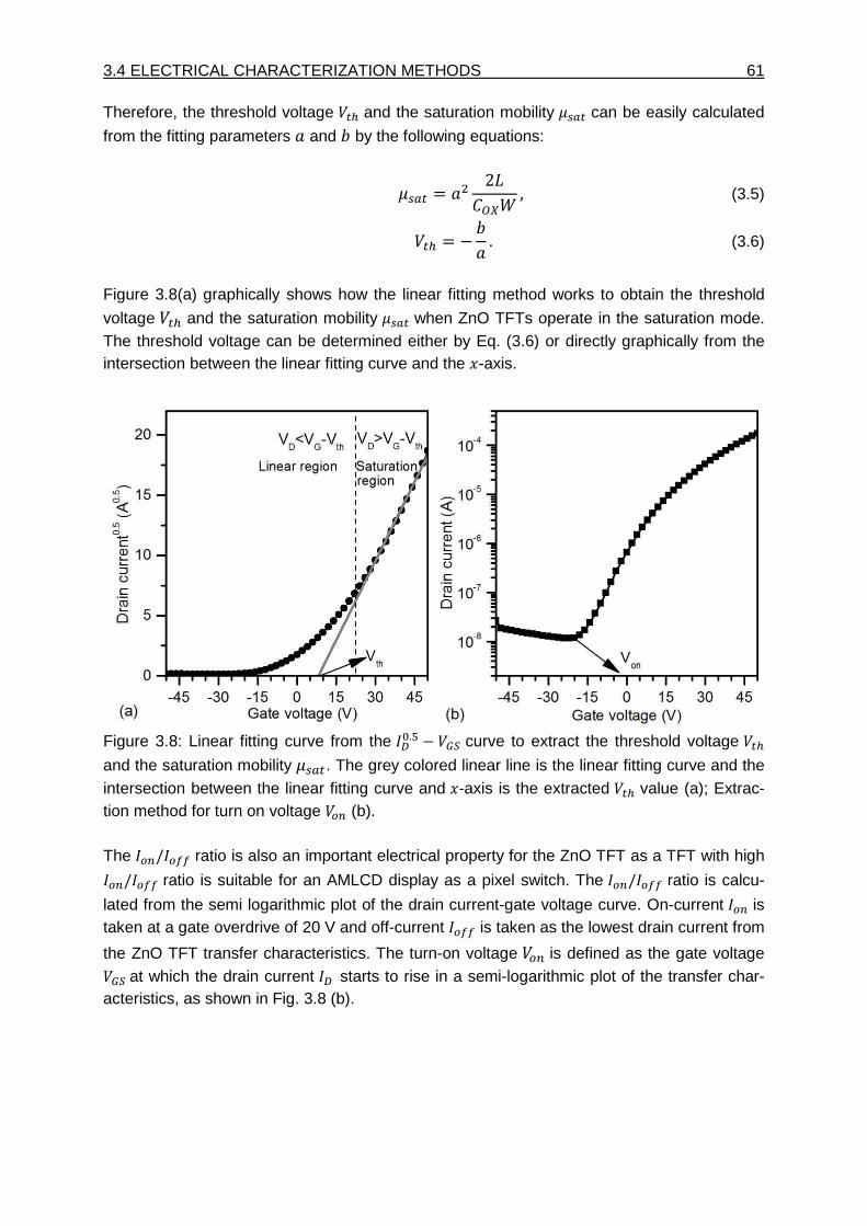
3.4 ELECTRICAL CHARACTERIZATION METHODS 61
Therefore, the threshold voltage and the saturation mobility > can be easily calculated
from the fitting parameters and k by the following equations:
> = E 2(tr ,(3.5)
= −k .(3.6)
Figure 3.8(a) graphically shows how the linear fitting method works to obtain the threshold
voltage and the saturation mobility > when ZnO TFTs operate in the saturation mode. The threshold voltage can be determined either by Eq. (3.6) or directly graphically from the intersection between the linear fitting curve and the d-axis.
Figure 3.8: Linear fitting curve from the F.¦ − curve to extract the threshold voltage and the saturation mobility >. The grey colored linear line is the linear fitting curve and the intersection between the linear fitting curve and d-axis is the extracted value (a); Extrac-tion method for turn on voltage (b). The / ratio is also an important electrical property for the ZnO TFT as a TFT with high / ratio is suitable for an AMLCD display as a pixel switch. The / ratio is calcu-
lated from the semi logarithmic plot of the drain current-gate voltage curve. On-current is taken at a gate overdrive of 20 V and off-current is taken as the lowest drain current from
the ZnO TFT transfer characteristics. The turn-on voltage is defined as the gate voltage at which the drain current starts to rise in a semi-logarithmic plot of the transfer char-acteristics, as shown in Fig. 3.8 (b).
62 CHAPTER 3: EXPERIMENTAL METHODS
3.4.3 Extraction of electrical parameters
After evaluating the turn-on voltage and threshold voltage from the transfer charac-teristics of ZnO TFTs, more electrical parameters of the ZnO layer can be extracted. In the
following, extraction routines for the bulk charge carrier concentration in ZnO layer -, the
interface trap density @ and the ZnO volume mobility £ are derived. The turn-on voltage can be calculated according to Wager [Wag08]:
= −1Q7((t - + 1@(t + $.(3.7)
The relationship between the threshold voltage and the interface trap density @ is al-ready illustrated in section 2.2.2.3 and is written as:
= ∅= − s(t(t + 1@(t .(3.8)
By combining Eq. (3.7) and (3.8), the bulk charge carrier concentration in the ZnO layer can be extracted by:
- = + − /(t1Q7( ,(3.9)
where Q7( is the ZnO layer thickness. By assuming the work function difference ∅= be-tween Al and ZnO is about -0.4 V and the fixed oxide charge density is about 5x1011 cm-2
[Nan03], the interface trap density @ can be extracted by rewritting Eq. (3.8):
@ = + + 5/(t1 .(3.10)
Besides the bulk charge carrier concentration and the interface trap density, another im-
portant electrical parameter which can be extracted is the ZnO volume mobility £. The volume mobility is independent of the ZnO layer thickness and can be extracted from the off-current level of the ZnO TFTs by [Chu08]:
£ = 1-rQ7( .(3.11)
By rewriting Eq. (3.11), the bulk resistivity can be calculated by:
= 1 = 1qP`1- =rQ,-.pP .(3.12)
63
Chapter 4
Results and discussions In this chapter, the effects of sputtering parameters on the deposition rate of ZnO thin films and electrical properties of ZnO TFTs are discussed. Then a thorough investigation of post deposition annealing at different temperatures in different atmospheres is carried out. Both morphological and electrical properties of the ZnO thin films after post deposition annealing are analyzed. Finally, NMOS inverters based on ZnO TFTs are fabricated and their electrical performances are evaluated.
4.1 Influence of sputtering parameters on properties of ZnO films
As already discussed in chapter 2, the deposition conditions during the RF magnetron sput-tering process play a crucial role for the properties of ZnO films prepared by RF magnetron sputtering. Among these deposition parameters are sputtering power, total gas pressure, oxygen flow rate, and substrate-to-target distance. The influence of these parameters on the properties of ZnO is analyzed in two steps. Firstly, the influence of the sputtering parameters on the deposition rate is evaluated and later the electrical properties of ZnO TFTs fabricated under different sputtering conditions are compared.
4.1.1 Influence of sputtering parameters on the deposition rate of ZnO films As discussed in section 3.3.1, the thickness of the sputtered ZnO layer is measured by an ellipsometer. Figure 4.1 depicts a typical 2D thickness distribution of a RF magnetron sput-tered ZnO layer obtained by raster measurement in the ellipsometer. Statistical deviation of the layer thickness can be derived from the raster measurement on the whole wafer. The
average layer thickness and its standard deviation are given in Fig. 4.1.
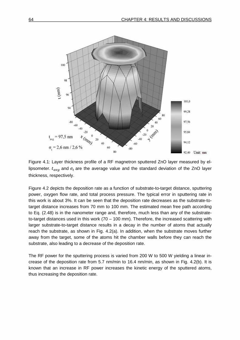
64 CHAPTER 4: RESULTS AND DISCUSSIONS
Figure 4.1: Layer thickness profile of a RF magnetron sputtered ZnO layer measured by el-
lipsometer. Q>U and are the average value and the standard deviation of the ZnO layer
thickness, respectively.
Figure 4.2 depicts the deposition rate as a function of substrate-to-target distance, sputtering power, oxygen flow rate, and total process pressure. The typical error in sputtering rate in this work is about 3%. It can be seen that the deposition rate decreases as the substrate-to-target distance increases from 70 mm to 100 mm. The estimated mean free path according to Eq. (2.48) is in the nanometer range and, therefore, much less than any of the substrate-to-target distances used in this work (70 – 100 mm). Therefore, the increased scattering with larger substrate-to-target distance results in a decay in the number of atoms that actually reach the substrate, as shown in Fig. 4.2(a). In addition, when the substrate moves further away from the target, some of the atoms hit the chamber walls before they can reach the substrate, also leading to a decrease of the deposition rate. The RF power for the sputtering process is varied from 200 W to 500 W yielding a linear in-crease of the deposition rate from 5.7 nm/min to 16.4 nm/min, as shown in Fig. 4.2(b). It is known that an increase in RF power increases the kinetic energy of the sputtered atoms, thus increasing the deposition rate.
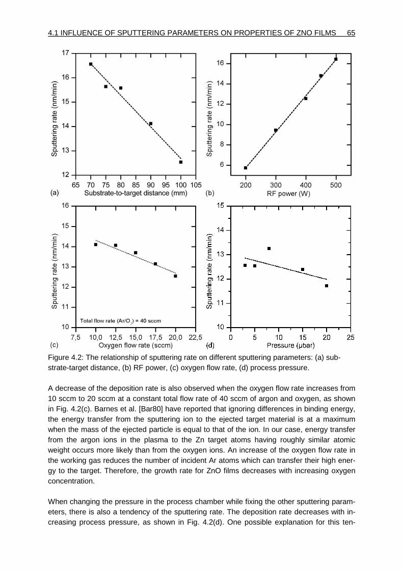
4.1 INFLUENCE OF SPUTTERING PARAMETERS ON PROPERTIES OF ZNO FILMS 65
Figure 4.2: The relationship of sputtering rate on different sputtering parameters: (a) sub-strate-target distance, (b) RF power, (c) oxygen flow rate, (d) process pressure. A decrease of the deposition rate is also observed when the oxygen flow rate increases from 10 sccm to 20 sccm at a constant total flow rate of 40 sccm of argon and oxygen, as shown in Fig. 4.2(c). Barnes et al. [Bar80] have reported that ignoring differences in binding energy, the energy transfer from the sputtering ion to the ejected target material is at a maximum when the mass of the ejected particle is equal to that of the ion. In our case, energy transfer from the argon ions in the plasma to the Zn target atoms having roughly similar atomic weight occurs more likely than from the oxygen ions. An increase of the oxygen flow rate in the working gas reduces the number of incident Ar atoms which can transfer their high ener-gy to the target. Therefore, the growth rate for ZnO films decreases with increasing oxygen concentration. When changing the pressure in the process chamber while fixing the other sputtering param-eters, there is also a tendency of the sputtering rate. The deposition rate decreases with in-creasing process pressure, as shown in Fig. 4.2(d). One possible explanation for this ten-
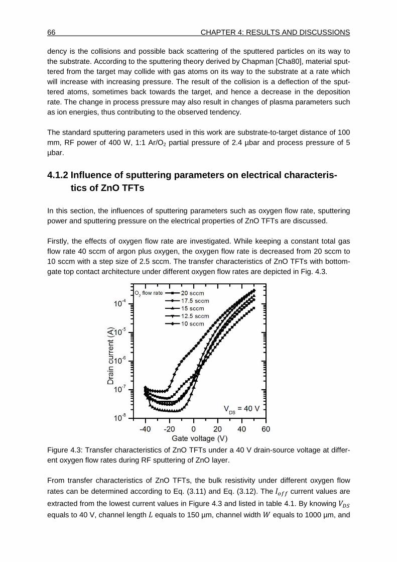
66 CHAPTER 4: RESULTS AND DISCUSSIONS dency is the collisions and possible back scattering of the sputtered particles on its way to the substrate. According to the sputtering theory derived by Chapman [Cha80], material sput-tered from the target may collide with gas atoms on its way to the substrate at a rate which will increase with increasing pressure. The result of the collision is a deflection of the sput-tered atoms, sometimes back towards the target, and hence a decrease in the deposition rate. The change in process pressure may also result in changes of plasma parameters such as ion energies, thus contributing to the observed tendency. The standard sputtering parameters used in this work are substrate-to-target distance of 100 mm, RF power of 400 W, 1:1 Ar/O2 partial pressure of 2.4 µbar and process pressure of 5 µbar.
4.1.2 Influence of sputtering parameters on electri cal characteris- tics of ZnO TFTs In this section, the influences of sputtering parameters such as oxygen flow rate, sputtering power and sputtering pressure on the electrical properties of ZnO TFTs are discussed. Firstly, the effects of oxygen flow rate are investigated. While keeping a constant total gas flow rate 40 sccm of argon plus oxygen, the oxygen flow rate is decreased from 20 sccm to 10 sccm with a step size of 2.5 sccm. The transfer characteristics of ZnO TFTs with bottom-gate top contact architecture under different oxygen flow rates are depicted in Fig. 4.3.
Figure 4.3: Transfer characteristics of ZnO TFTs under a 40 V drain-source voltage at differ-ent oxygen flow rates during RF sputtering of ZnO layer. From transfer characteristics of ZnO TFTs, the bulk resistivity under different oxygen flow
rates can be determined according to Eq. (3.11) and Eq. (3.12). The current values are
extracted from the lowest current values in Figure 4.3 and listed in table 4.1. By knowing
equals to 40 V, channel length equals to 150 µm, channel width r equals to 1000 µm, and
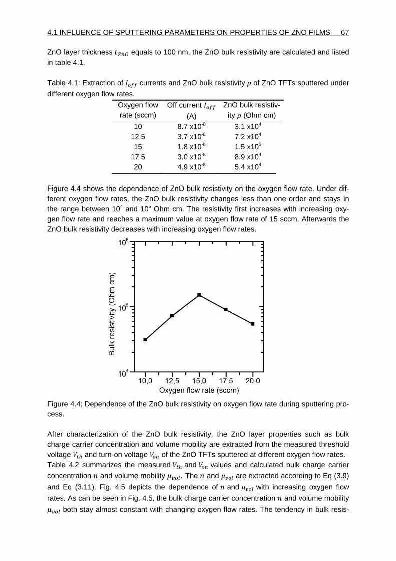
4.1 INFLUENCE OF SPUTTERING PARAMETERS ON PROPERTIES OF ZNO FILMS 67
ZnO layer thickness Q7( equals to 100 nm, the ZnO bulk resistivity are calculated and listed in table 4.1. Table 4.1: Extraction of currents and ZnO bulk resistivity of ZnO TFTs sputtered under
different oxygen flow rates.
Oxygen flow rate (sccm)
Off current
(A)
ZnO bulk resistiv-ity (Ohm cm)
10 8.7 x10⁻⁸ 3.1 x10⁴ 12.5 3.7 x10⁻⁸ 7.2 x10⁴ 15 1.8 x10⁻⁸ 1.5 x10⁵
17.5 3.0 x10⁻⁸ 8.9 x10⁴ 20 4.9 x10⁻⁸ 5.4 x10⁴
Figure 4.4 shows the dependence of ZnO bulk resistivity on the oxygen flow rate. Under dif-ferent oxygen flow rates, the ZnO bulk resistivity changes less than one order and stays in the range between 104 and 105 Ohm cm. The resistivity first increases with increasing oxy-gen flow rate and reaches a maximum value at oxygen flow rate of 15 sccm. Afterwards the ZnO bulk resistivity decreases with increasing oxygen flow rates.
Figure 4.4: Dependence of the ZnO bulk resistivity on oxygen flow rate during sputtering pro-cess. After characterization of the ZnO bulk resistivity, the ZnO layer properties such as bulk charge carrier concentration and volume mobility are extracted from the measured threshold voltage and turn-on voltage of the ZnO TFTs sputtered at different oxygen flow rates. Table 4.2 summarizes the measured and values and calculated bulk charge carrier
concentration - and volume mobility £. The - and £ are extracted according to Eq (3.9)
and Eq (3.11). Fig. 4.5 depicts the dependence of - and £ with increasing oxygen flow
rates. As can be seen in Fig. 4.5, the bulk charge carrier concentration - and volume mobility £ both stay almost constant with changing oxygen flow rates. The tendency in bulk resis-
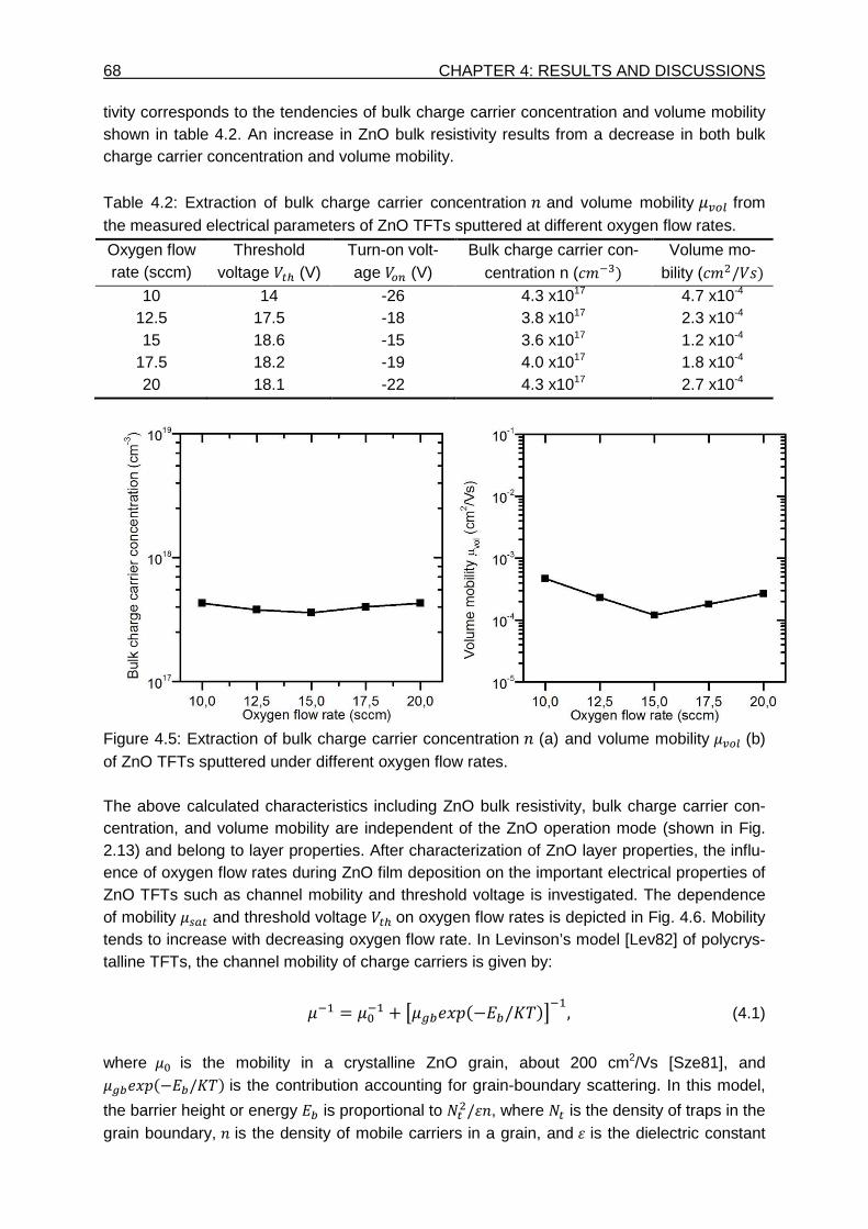
68 CHAPTER 4: RESULTS AND DISCUSSIONS tivity corresponds to the tendencies of bulk charge carrier concentration and volume mobility shown in table 4.2. An increase in ZnO bulk resistivity results from a decrease in both bulk charge carrier concentration and volume mobility.
Table 4.2: Extraction of bulk charge carrier concentration - and volume mobility £ from the measured electrical parameters of ZnO TFTs sputtered at different oxygen flow rates.
Oxygen flow rate (sccm)
Threshold voltage (V)
Turn-on volt-age (V)
Bulk charge carrier con-centration n ( ABC/ Volume mo-
bility ( AE/N/ 10 14 -26 4.3 x10¹⁷ 4.7 x10⁻⁴
12.5 17.5 -18 3.8 x10¹⁷ 2.3 x10⁻⁴ 15 18.6 -15 3.6 x10¹⁷ 1.2 x10⁻⁴
17.5 18.2 -19 4.0 x10¹⁷ 1.8 x10⁻⁴ 20 18.1 -22 4.3 x10¹⁷ 2.7 x10⁻⁴
Figure 4.5: Extraction of bulk charge carrier concentration - (a) and volume mobility £ (b) of ZnO TFTs sputtered under different oxygen flow rates. The above calculated characteristics including ZnO bulk resistivity, bulk charge carrier con-centration, and volume mobility are independent of the ZnO operation mode (shown in Fig. 2.13) and belong to layer properties. After characterization of ZnO layer properties, the influ-ence of oxygen flow rates during ZnO film deposition on the important electrical properties of ZnO TFTs such as channel mobility and threshold voltage is investigated. The dependence of mobility > and threshold voltage on oxygen flow rates is depicted in Fig. 4.6. Mobility tends to increase with decreasing oxygen flow rate. In Levinson’s model [Lev82] of polycrys-talline TFTs, the channel mobility of charge carriers is given by: BJ = FBJ + Ux;d@+−x/º%/BJ,(4.1)
where F is the mobility in a crystalline ZnO grain, about 200 cm2/Vs [Sze81], and Ux;d@+−x/º%/ is the contribution accounting for grain-boundary scattering. In this model,
the barrier height or energy x is proportional to E/3-, where is the density of traps in the grain boundary, - is the density of mobile carriers in a grain, and 3 is the dielectric constant
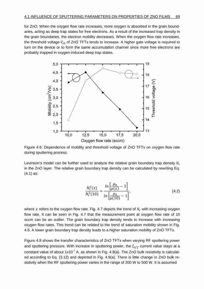
4.1 INFLUENCE OF SPUTTERING PARAMETERS ON PROPERTIES OF ZNO FILMS 69
for ZnO. When the oxygen flow rate increases, more oxygen is absorbed in the grain bound-aries, acting as deep trap states for free electrons. As a result of the increased trap density in the grain boundaries, the electron mobility decreases. When the oxygen flow rate increases, the threshold voltage of ZnO TFTs tends to increase. A higher gate voltage is required to turn on the device or to form the same accumulation channel since more free electrons are probably trapped in oxygen-induced deep trap states.
Figure 4.6: Dependence of mobility and threshold voltage of ZnO TFTs on oxygen flow rate during sputtering process. Levinson’s model can be further used to analyze the relative grain boundary trap density in the ZnO layer. The relative grain boundary trap density can be calculated by rewriting Eq. (4.1) as:
()(10) =
() − 1 (10) − 1
,(4.2)
where refers to the oxygen flow rate. Fig. 4.7 depicts the trend of with increasing oxygen flow rate. It can be seen in Fig. 4.7 that the measurement point at oxygen flow rate of 10 sccm can be an outlier. The grain boundary trap density tends to increase with increasing oxygen flow rates. This trend can be related to the trend of saturation mobility shown in Fig. 4.6. A lower grain boundary trap density leads to a higher saturation mobility of ZnO TFTs. Figure 4.8 shows the transfer characteristics of ZnO TFTs when varying RF sputtering power
and sputtering pressure. With increase in sputtering power, the current value stays at a
constant value of about 1x10⁻⁷ A, as shown in Fig. 4.8(a). The ZnO bulk resistivity is calculat-ed according to Eq. (3.12) and depicted in Fig. 4.9(a). There is little change in ZnO bulk re-sistivity when the RF sputtering power varies in the range of 200 W to 500 W. It is assumed
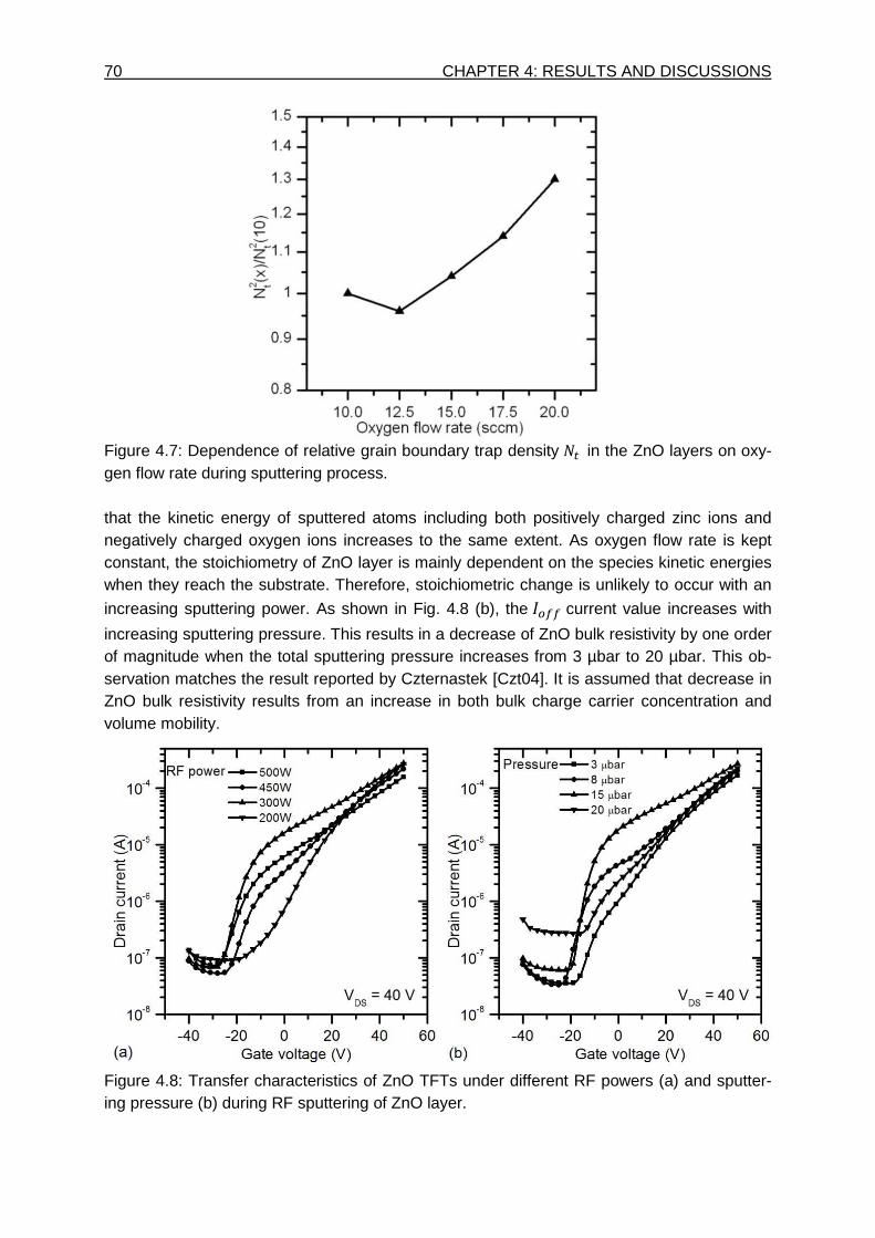
70 CHAPTER 4: RESULTS AND DISCUSSIONS
Figure 4.7: Dependence of relative grain boundary trap density in the ZnO layers on oxy-gen flow rate during sputtering process. that the kinetic energy of sputtered atoms including both positively charged zinc ions and negatively charged oxygen ions increases to the same extent. As oxygen flow rate is kept constant, the stoichiometry of ZnO layer is mainly dependent on the species kinetic energies when they reach the substrate. Therefore, stoichiometric change is unlikely to occur with an
increasing sputtering power. As shown in Fig. 4.8 (b), the current value increases with
increasing sputtering pressure. This results in a decrease of ZnO bulk resistivity by one order of magnitude when the total sputtering pressure increases from 3 µbar to 20 µbar. This ob-servation matches the result reported by Czternastek [Czt04]. It is assumed that decrease in ZnO bulk resistivity results from an increase in both bulk charge carrier concentration and volume mobility.
Figure 4.8: Transfer characteristics of ZnO TFTs under different RF powers (a) and sputter-ing pressure (b) during RF sputtering of ZnO layer.
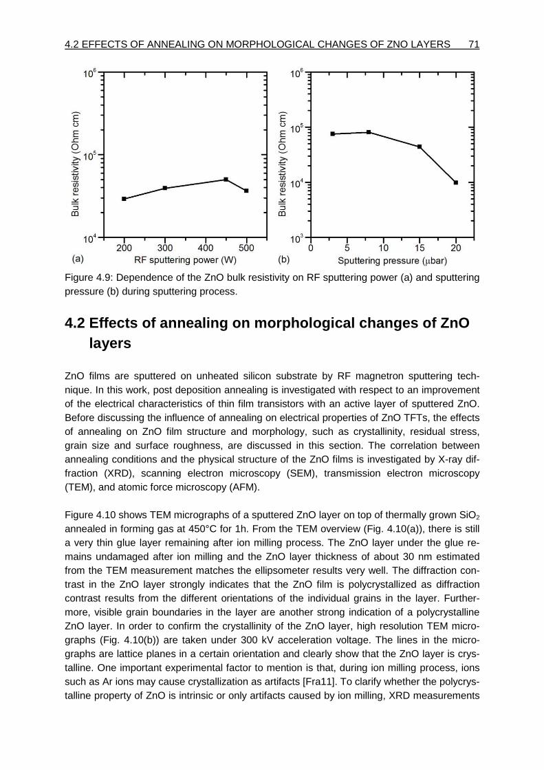
4.2 EFFECTS OF ANNEALING ON MORPHOLOGICAL CHANGES OF ZNO LAYERS 71
Figure 4.9: Dependence of the ZnO bulk resistivity on RF sputtering power (a) and sputtering pressure (b) during sputtering process.
4.2 Effects of annealing on morphological changes o f ZnO layers ZnO films are sputtered on unheated silicon substrate by RF magnetron sputtering tech-nique. In this work, post deposition annealing is investigated with respect to an improvement of the electrical characteristics of thin film transistors with an active layer of sputtered ZnO. Before discussing the influence of annealing on electrical properties of ZnO TFTs, the effects of annealing on ZnO film structure and morphology, such as crystallinity, residual stress, grain size and surface roughness, are discussed in this section. The correlation between annealing conditions and the physical structure of the ZnO films is investigated by X-ray dif-fraction (XRD), scanning electron microscopy (SEM), transmission electron microscopy (TEM), and atomic force microscopy (AFM). Figure 4.10 shows TEM micrographs of a sputtered ZnO layer on top of thermally grown SiO2
annealed in forming gas at 450°C for 1h. From the TEM overview (Fig. 4.10(a)), there is still a very thin glue layer remaining after ion milling process. The ZnO layer under the glue re-mains undamaged after ion milling and the ZnO layer thickness of about 30 nm estimated from the TEM measurement matches the ellipsometer results very well. The diffraction con-trast in the ZnO layer strongly indicates that the ZnO film is polycrystallized as diffraction contrast results from the different orientations of the individual grains in the layer. Further-more, visible grain boundaries in the layer are another strong indication of a polycrystalline ZnO layer. In order to confirm the crystallinity of the ZnO layer, high resolution TEM micro-graphs (Fig. 4.10(b)) are taken under 300 kV acceleration voltage. The lines in the micro-graphs are lattice planes in a certain orientation and clearly show that the ZnO layer is crys-talline. One important experimental factor to mention is that, during ion milling process, ions such as Ar ions may cause crystallization as artifacts [Fra11]. To clarify whether the polycrys-talline property of ZnO is intrinsic or only artifacts caused by ion milling, XRD measurements
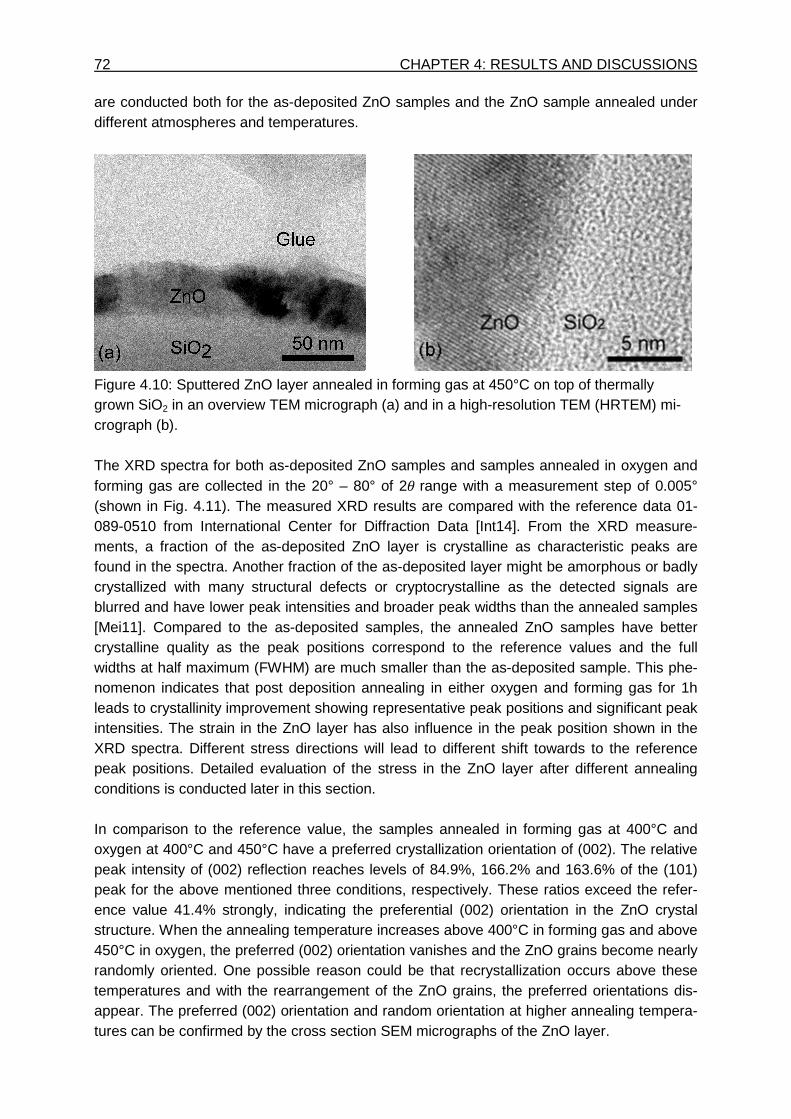
72 CHAPTER 4: RESULTS AND DISCUSSIONS are conducted both for the as-deposited ZnO samples and the ZnO sample annealed under different atmospheres and temperatures.
Figure 4.10: Sputtered ZnO layer annealed in forming gas at 450°C on top of thermally grown SiO2 in an overview TEM micrograph (a) and in a high-resolution TEM (HRTEM) mi-crograph (b). The XRD spectra for both as-deposited ZnO samples and samples annealed in oxygen and forming gas are collected in the 20° – 80° of 2¹ range with a measurement step of 0.005° (shown in Fig. 4.11). The measured XRD results are compared with the reference data 01-089-0510 from International Center for Diffraction Data [Int14]. From the XRD measure-ments, a fraction of the as-deposited ZnO layer is crystalline as characteristic peaks are found in the spectra. Another fraction of the as-deposited layer might be amorphous or badly crystallized with many structural defects or cryptocrystalline as the detected signals are blurred and have lower peak intensities and broader peak widths than the annealed samples [Mei11]. Compared to the as-deposited samples, the annealed ZnO samples have better crystalline quality as the peak positions correspond to the reference values and the full widths at half maximum (FWHM) are much smaller than the as-deposited sample. This phe-nomenon indicates that post deposition annealing in either oxygen and forming gas for 1h leads to crystallinity improvement showing representative peak positions and significant peak intensities. The strain in the ZnO layer has also influence in the peak position shown in the XRD spectra. Different stress directions will lead to different shift towards to the reference peak positions. Detailed evaluation of the stress in the ZnO layer after different annealing conditions is conducted later in this section. In comparison to the reference value, the samples annealed in forming gas at 400°C and oxygen at 400°C and 450°C have a preferred crystallization orientation of (002). The relative peak intensity of (002) reflection reaches levels of 84.9%, 166.2% and 163.6% of the (101) peak for the above mentioned three conditions, respectively. These ratios exceed the refer-ence value 41.4% strongly, indicating the preferential (002) orientation in the ZnO crystal structure. When the annealing temperature increases above 400°C in forming gas and above 450°C in oxygen, the preferred (002) orientation vanishes and the ZnO grains become nearly randomly oriented. One possible reason could be that recrystallization occurs above these temperatures and with the rearrangement of the ZnO grains, the preferred orientations dis-appear. The preferred (002) orientation and random orientation at higher annealing tempera-tures can be confirmed by the cross section SEM micrographs of the ZnO layer.
4.2 EFFECTS OF ANNEALING ON MORPHOLOGICAL CHANGES OF ZNO LAYERS 73
Figure 4.11: XRD spectra for as-deposited ZnO and ZnO layers annealed in forming gas and oxygen at temperatures of 400°C, 450°C, and 500°C for 1h [Int14]. Figure 4.12 shows that the grain growth in the ZnO layer with an annealing temperature of 400°C in forming gas elongates along the c-axis and forms columnar shape, corresponding to the preferred (002) orientation. At a higher temperature of 500°C, a recrystallization pro-cess is assumed to appear and the columnar shape tends to disappear. It is important to mention that during the XRD measurement, the samples are not rotated so that there is no equal statistical opportunity for each single grain to construct diffraction patterns [Mei11]. For this reason, only comparison of the relative intensity among different peaks is conducted and a full quantification of peak intensities is not conducted in this work.
Figure 4.12: Cross sectional SEM micrographs for sputtered ZnO layer annealed in FGA 400°C for 1h (a) and FGA 500°C for 1h (b). All the diffraction peaks shown in Fig. 4.11 tend to have a shift either to lower 2 angles for the case of as-deposited ZnO or to higher 2 angles for the cases of the annealed ZnO lay-ers. One possible reason for shifting at the peak positions can be due to imperfect stoichio-metric ratio between Zn and O and the sputtered layer composition could be Zn1-xOx
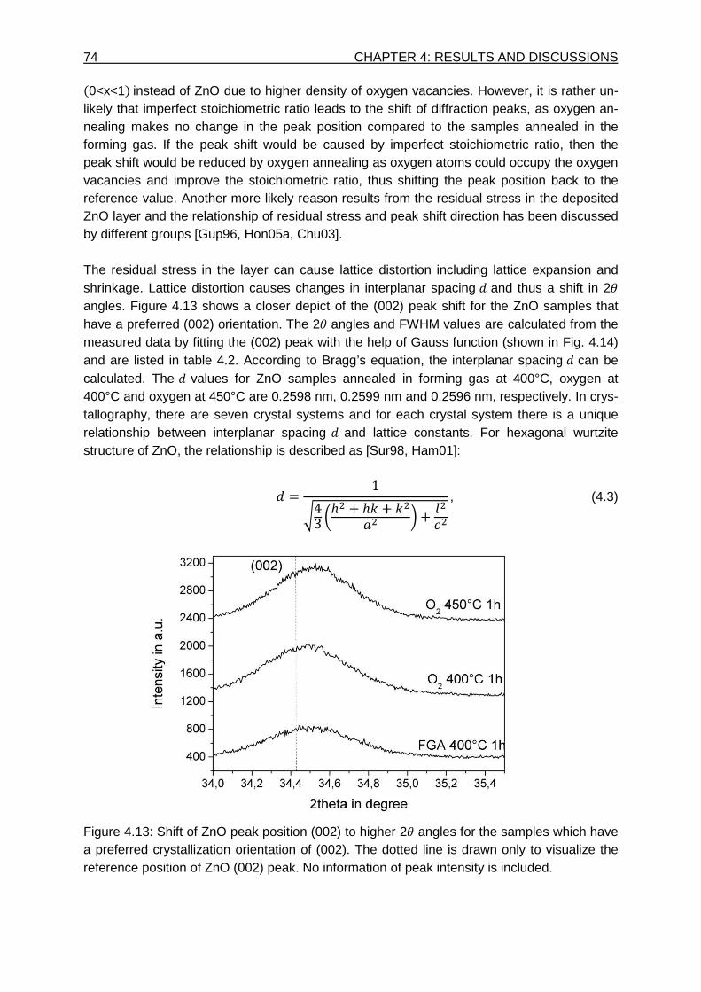
74 CHAPTER 4: RESULTS AND DISCUSSIONS +0<x<1/instead of ZnO due to higher density of oxygen vacancies. However, it is rather un-likely that imperfect stoichiometric ratio leads to the shift of diffraction peaks, as oxygen an-nealing makes no change in the peak position compared to the samples annealed in the forming gas. If the peak shift would be caused by imperfect stoichiometric ratio, then the peak shift would be reduced by oxygen annealing as oxygen atoms could occupy the oxygen vacancies and improve the stoichiometric ratio, thus shifting the peak position back to the reference value. Another more likely reason results from the residual stress in the deposited ZnO layer and the relationship of residual stress and peak shift direction has been discussed by different groups [Gup96, Hon05a, Chu03]. The residual stress in the layer can cause lattice distortion including lattice expansion and shrinkage. Lattice distortion causes changes in interplanar spacing l and thus a shift in 2¹ angles. Figure 4.13 shows a closer depict of the (002) peak shift for the ZnO samples that have a preferred (002) orientation. The 2¹ angles and FWHM values are calculated from the measured data by fitting the (002) peak with the help of Gauss function (shown in Fig. 4.14) and are listed in table 4.2. According to Bragg’s equation, the interplanar spacing l can be calculated. The l values for ZnO samples annealed in forming gas at 400°C, oxygen at 400°C and oxygen at 450°C are 0.2598 nm, 0.2599 nm and 0.2596 nm, respectively. In crys-tallography, there are seven crystal systems and for each crystal system there is a unique relationship between interplanar spacing l and lattice constants. For hexagonal wurtzite structure of ZnO, the relationship is described as [Sur98, Ham01]:
l = 143 ]ℎE + ℎ# + #EE ^ + `E E
, (4.3)
Figure 4.13: Shift of ZnO peak position (002) to higher 2¹ angles for the samples which have a preferred crystallization orientation of (002). The dotted line is drawn only to visualize the reference position of ZnO (002) peak. No information of peak intensity is included.
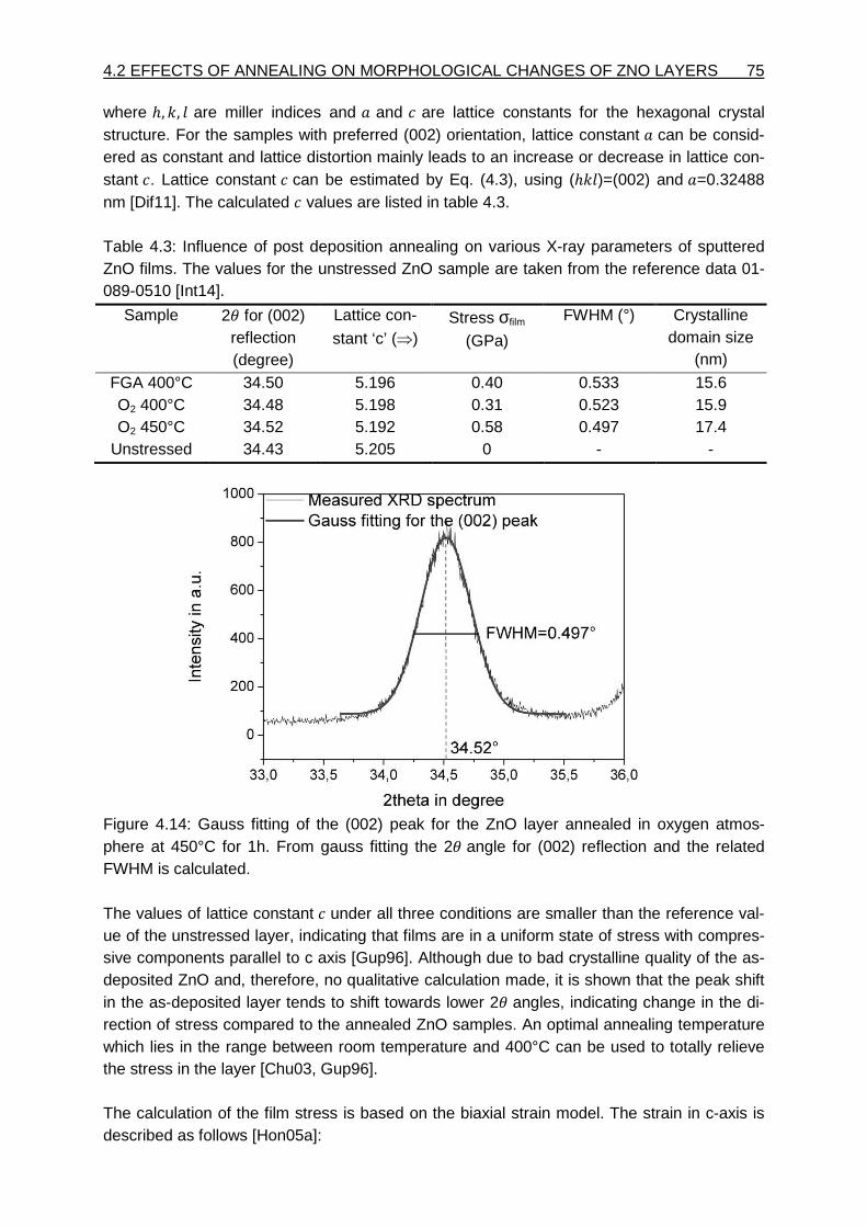
4.2 EFFECTS OF ANNEALING ON MORPHOLOGICAL CHANGES OF ZNO LAYERS 75
where ℎ, , are miller indices and and are lattice constants for the hexagonal crystal structure. For the samples with preferred (002) orientation, lattice constant can be consid-ered as constant and lattice distortion mainly leads to an increase or decrease in lattice con-stant . Lattice constant can be estimated by Eq. (4.3), using (ℎ)=(002) and =0.32488 nm [Dif11]. The calculated values are listed in table 4.3. Table 4.3: Influence of post deposition annealing on various X-ray parameters of sputtered ZnO films. The values for the unstressed ZnO sample are taken from the reference data 01-089-0510 [Int14].
Sample 2 for (002) reflection (degree)
Lattice con-
stant ‘c’ (⇒) Stress σfilm
(GPa)
FWHM (°) Crystalline domain size
(nm)
FGA 400°C 34.50 5.196 0.40 0.533 15.6 O2 400°C 34.48 5.198 0.31 0.523 15.9 O2 450°C 34.52 5.192 0.58 0.497 17.4
Unstressed 34.43 5.205 0 - -
Figure 4.14: Gauss fitting of the (002) peak for the ZnO layer annealed in oxygen atmos-phere at 450°C for 1h. From gauss fitting the 2 angle for (002) reflection and the related FWHM is calculated. The values of lattice constant under all three conditions are smaller than the reference val-ue of the unstressed layer, indicating that films are in a uniform state of stress with compres-sive components parallel to c axis [Gup96]. Although due to bad crystalline quality of the as-deposited ZnO and, therefore, no qualitative calculation made, it is shown that the peak shift in the as-deposited layer tends to shift towards lower 2 angles, indicating change in the di-rection of stress compared to the annealed ZnO samples. An optimal annealing temperature which lies in the range between room temperature and 400°C can be used to totally relieve the stress in the layer [Chu03, Gup96]. The calculation of the film stress is based on the biaxial strain model. The strain in c-axis is described as follows [Hon05a]:
76 CHAPTER 4: RESULTS AND DISCUSSIONS 3 = £= − x¢£X x¢£X ,(4.4)
where £= and x¢£X are the lattice constants of ZnO film and bulk (or powder), respective-
ly. To derive the film stress £= parallel to the film surface, the following formula is used,
which is valid for a hexagonal lattice [Hon05a]:
£= = 2 JCE − CC+ JJ + JE/2 JC × £= − x¢£X x¢£X ,(4.5)
where » are elastic stiffness constants. For the elastic constants », the following values for
sputtered ZnO are used: JJ equals to 208.8 GPa, CC equals to 213.8 GPa, JE equals to 119.7 GPa, JC equals to 104.2 GPa [Cul78]. This yields the following numerical relation for the stress derived from XRD: £== -233 × ε (GPa). (4.6)
Combined with Eq. (4.4), the compressive stresses in the layer are calculated and shown in table 4.3. From table 4.3, the residual stresses in the film exhibit compressive nature and are comparable to the residual stress in the sputtered ZnO layer after annealing reported by Hong et al. [Hon05a]. It is important to mention that when comparing residual stresses in sputtered ZnO layers, variation of sputtering parameters plays an important role and different values of elastic constants of ZnO crystals [Tu06] may cause discrepancies in the reported values. A direct quantitative comparison of residual stresses between annealed and as-deposited ZnO layer is difficult as the bad crystalline quality makes the estimation of stress in the as-deposited layer problematic. However, larger peak shift in the as-deposited layer indi-cates larger lattice distortion and thus higher possibility of larger tensile stress. The crystalline domain size of the sputtered ZnO layer can be estimated by Scherrer formula, using FWHM value of the XRD diffraction peaks as follows [Klu74]:
p = 0.9λM PN¹ ,(4.7) where p, λ, ¹, and M are the average crystalline domain size, the X-ray wavelength of 0.1541 nm, the Bragg diffraction angle, and the FWHM of the diffraction peak of the (002) direction at around 34° (2¹) for ZnO films, respectively. The crystalline domain size lies in the range between 15.6 nm and 17.4 nm and the samples annealed under forming gas and oxygen at 400°C have almost the same domain size. When annealing under oxygen at 450°C, the do-main size increases slightly to 17.4 nm. The trend of domain size under these three condi-tions can be confirmed by the corresponding SEM micrographs shown in Fig. 4.15. When discussing the domain size estimated from Scherrer formula, the absolute values of domain size can probably be different from those determined by SEM and AFM methods. The first reason is that the Scherrer formula to calculate the domain size has systematic error due to the assumption that all the crystalline domains have spherical shape and the domain size is
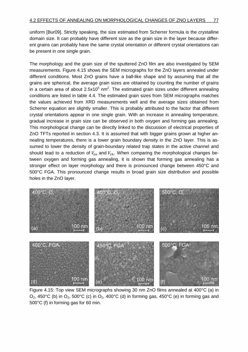
4.2 EFFECTS OF ANNEALING ON MORPHOLOGICAL CHANGES OF ZNO LAYERS 77
uniform [Bur09]. Strictly speaking, the size estimated from Scherrer formula is the crystalline domain size. It can probably have different size as the grain size in the layer because differ-ent grains can probably have the same crystal orientation or different crystal orientations can be present in one single grain. The morphology and the grain size of the sputtered ZnO film are also investigated by SEM measurements. Figure 4.15 shows the SEM micrographs for the ZnO layers annealed under different conditions. Most ZnO grains have a ball-like shape and by assuming that all the grains are spherical, the average grain sizes are obtained by counting the number of grains in a certain area of about 2.5x10⁵ nm2. The estimated grain sizes under different annealing conditions are listed in table 4.4. The estimated grain sizes from SEM micrographs matches the values achieved from XRD measurements well and the average sizes obtained from Scherrer equation are slightly smaller. This is probably attributed to the factor that different crystal orientations appear in one single grain. With an increase in annealing temperature, gradual increase in grain size can be observed in both oxygen and forming gas annealing. This morphological change can be directly linked to the discussion of electrical properties of ZnO TFTs reported in section 4.3. It is assumed that with bigger grains grown at higher an-nealing temperatures, there is a lower grain boundary density in the ZnO layer. This is as-sumed to lower the density of grain-boundary related trap states in the active channel and should lead to a reduction of and . When comparing the morphological changes be-tween oxygen and forming gas annealing, it is shown that forming gas annealing has a stronger effect on layer morphology and there is pronounced change between 450°C and 500°C FGA. This pronounced change results in broad grain size distribution and possible holes in the ZnO layer.
Figure 4.15: Top view SEM micrographs showing 30 nm ZnO films annealed at 400°C (a) in O2, 450°C (b) in O2, 500°C (c) in O2, 400°C (d) in forming gas, 450°C (e) in forming gas and 500°C (f) in forming gas for 60 min.
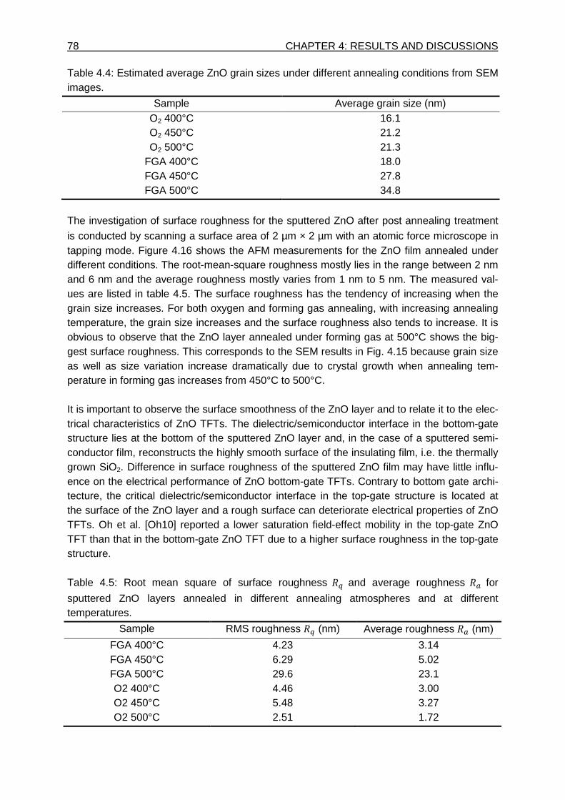
78 CHAPTER 4: RESULTS AND DISCUSSIONS Table 4.4: Estimated average ZnO grain sizes under different annealing conditions from SEM images.
Sample Average grain size (nm) O2 400°C 16.1 O2 450°C 21.2 O2 500°C 21.3
FGA 400°C 18.0 FGA 450°C 27.8 FGA 500°C 34.8
The investigation of surface roughness for the sputtered ZnO after post annealing treatment
is conducted by scanning a surface area of 2 µm × 2 µm with an atomic force microscope in tapping mode. Figure 4.16 shows the AFM measurements for the ZnO film annealed under different conditions. The root-mean-square roughness mostly lies in the range between 2 nm and 6 nm and the average roughness mostly varies from 1 nm to 5 nm. The measured val-ues are listed in table 4.5. The surface roughness has the tendency of increasing when the grain size increases. For both oxygen and forming gas annealing, with increasing annealing temperature, the grain size increases and the surface roughness also tends to increase. It is obvious to observe that the ZnO layer annealed under forming gas at 500°C shows the big-gest surface roughness. This corresponds to the SEM results in Fig. 4.15 because grain size as well as size variation increase dramatically due to crystal growth when annealing tem-perature in forming gas increases from 450°C to 500°C. It is important to observe the surface smoothness of the ZnO layer and to relate it to the elec-trical characteristics of ZnO TFTs. The dielectric/semiconductor interface in the bottom-gate structure lies at the bottom of the sputtered ZnO layer and, in the case of a sputtered semi-conductor film, reconstructs the highly smooth surface of the insulating film, i.e. the thermally grown SiO2. Difference in surface roughness of the sputtered ZnO film may have little influ-ence on the electrical performance of ZnO bottom-gate TFTs. Contrary to bottom gate archi-tecture, the critical dielectric/semiconductor interface in the top-gate structure is located at the surface of the ZnO layer and a rough surface can deteriorate electrical properties of ZnO TFTs. Oh et al. [Oh10] reported a lower saturation field-effect mobility in the top-gate ZnO TFT than that in the bottom-gate ZnO TFT due to a higher surface roughness in the top-gate structure. Table 4.5: Root mean square of surface roughness §) and average roughness §> for
sputtered ZnO layers annealed in different annealing atmospheres and at different temperatures.
Sample RMS roughness §) (nm) Average roughness §> (nm)
FGA 400°C 4.23 3.14 FGA 450°C 6.29 5.02 FGA 500°C 29.6 23.1 O2 400°C 4.46 3.00 O2 450°C 5.48 3.27 O2 500°C 2.51 1.72
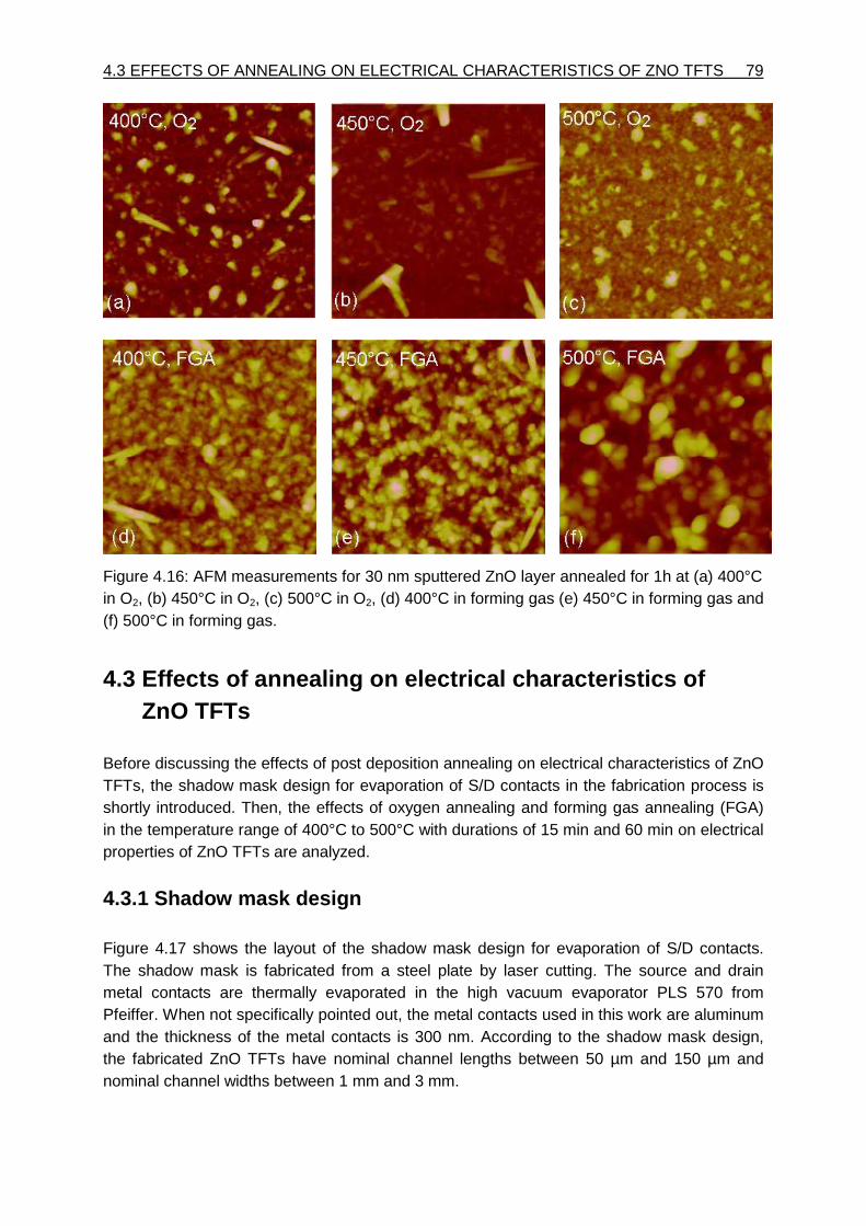
4.3 EFFECTS OF ANNEALING ON ELECTRICAL CHARACTERISTICS OF ZNO TFTS 79
Figure 4.16: AFM measurements for 30 nm sputtered ZnO layer annealed for 1h at (a) 400°C in O2, (b) 450°C in O2, (c) 500°C in O2, (d) 400°C in forming gas (e) 450°C in forming gas and (f) 500°C in forming gas.
4.3 Effects of annealing on electrical characterist ics of ZnO TFTs Before discussing the effects of post deposition annealing on electrical characteristics of ZnO TFTs, the shadow mask design for evaporation of S/D contacts in the fabrication process is shortly introduced. Then, the effects of oxygen annealing and forming gas annealing (FGA) in the temperature range of 400°C to 500°C with durations of 15 min and 60 min on electrical properties of ZnO TFTs are analyzed.
4.3.1 Shadow mask design Figure 4.17 shows the layout of the shadow mask design for evaporation of S/D contacts. The shadow mask is fabricated from a steel plate by laser cutting. The source and drain metal contacts are thermally evaporated in the high vacuum evaporator PLS 570 from Pfeiffer. When not specifically pointed out, the metal contacts used in this work are aluminum and the thickness of the metal contacts is 300 nm. According to the shadow mask design, the fabricated ZnO TFTs have nominal channel lengths between 50 µm and 150 µm and nominal channel widths between 1 mm and 3 mm.
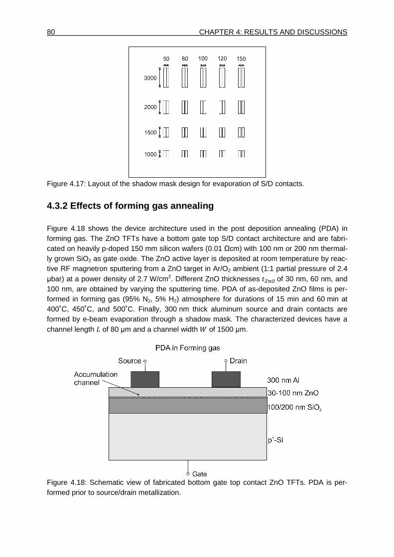
80 CHAPTER 4: RESULTS AND DISCUSSIONS
Figure 4.17: Layout of the shadow mask design for evaporation of S/D contacts.
4.3.2 Effects of forming gas annealing Figure 4.18 shows the device architecture used in the post deposition annealing (PDA) in forming gas. The ZnO TFTs have a bottom gate top S/D contact architecture and are fabri-cated on heavily p-doped 150 mm silicon wafers (0.01 Ωcm) with 100 nm or 200 nm thermal-ly grown SiO2 as gate oxide. The ZnO active layer is deposited at room temperature by reac-tive RF magnetron sputtering from a ZnO target in Ar/O2 ambient (1:1 partial pressure of 2.4 µbar) at a power density of 2.7 W/cm2. Different ZnO thicknesses Q7(of 30 nm, 60 nm, and 100 nm, are obtained by varying the sputtering time. PDA of as-deposited ZnO films is per-formed in forming gas (95% N2, 5% H2) atmosphere for durations of 15 min and 60 min at 400˚C, 450˚C, and 500˚C. Finally, 300 nm thick aluminum source and drain contacts are formed by e-beam evaporation through a shadow mask. The characterized devices have a channel length of 80 µm and a channel width r of 1500 µm.
Figure 4.18: Schematic view of fabricated bottom gate top contact ZnO TFTs. PDA is per-formed prior to source/drain metallization.
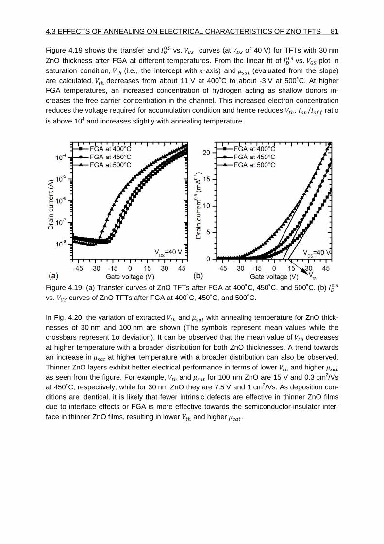
4.3 EFFECTS OF ANNEALING ON ELECTRICAL CHARACTERISTICS OF ZNO TFTS 81
Figure 4.19 shows the transfer and F.¦ vs. curves (at of 40 V) for TFTs with 30 nm
ZnO thickness after FGA at different temperatures. From the linear fit of F.¦ vs. plot in saturation condition, (i.e., the intercept with d-axis) and > (evaluated from the slope) are calculated. decreases from about 11 V at 400˚C to about -3 V at 500˚C. At higher FGA temperatures, an increased concentration of hydrogen acting as shallow donors in-creases the free carrier concentration in the channel. This increased electron concentration reduces the voltage required for accumulation condition and hence reduces . / ratio
is above 104 and increases slightly with annealing temperature.
Figure 4.19: (a) Transfer curves of ZnO TFTs after FGA at 400˚C, 450˚C, and 500˚C. (b) F.¦ vs. curves of ZnO TFTs after FGA at 400˚C, 450˚C, and 500˚C. In Fig. 4.20, the variation of extracted and > with annealing temperature for ZnO thick-nesses of 30 nm and 100 nm are shown (The symbols represent mean values while the crossbars represent 1σ deviation). It can be observed that the mean value of decreases at higher temperature with a broader distribution for both ZnO thicknesses. A trend towards an increase in > at higher temperature with a broader distribution can also be observed. Thinner ZnO layers exhibit better electrical performance in terms of lower and higher > as seen from the figure. For example, and > for 100 nm ZnO are 15 V and 0.3 cm2/Vs at 450˚C, respectively, while for 30 nm ZnO they are 7.5 V and 1 cm2/Vs. As deposition con-ditions are identical, it is likely that fewer intrinsic defects are effective in thinner ZnO films due to interface effects or FGA is more effective towards the semiconductor-insulator inter-face in thinner ZnO films, resulting in lower and higher >.
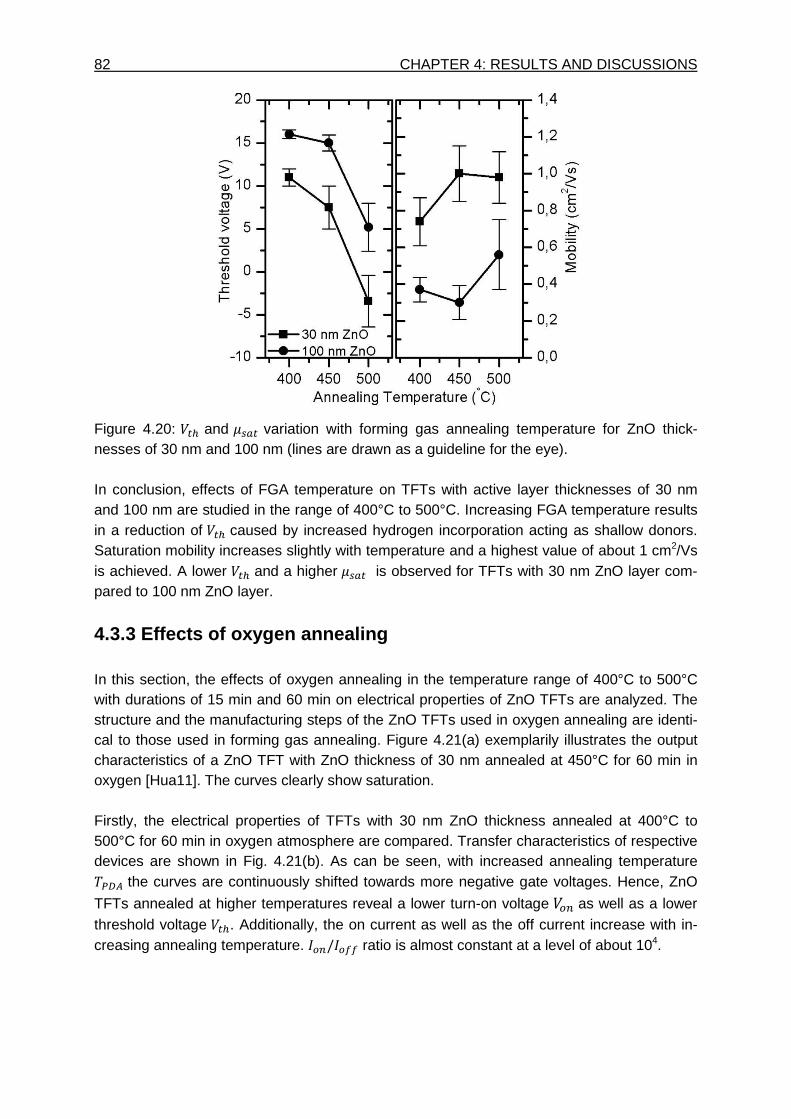
82 CHAPTER 4: RESULTS AND DISCUSSIONS
Figure 4.20: and variation with forming gas annealing temperature for ZnO thick-nesses of 30 nm and 100 nm (lines are drawn as a guideline for the eye). In conclusion, effects of FGA temperature on TFTs with active layer thicknesses of 30 nm and 100 nm are studied in the range of 400°C to 500°C. Increasing FGA temperature results in a reduction of caused by increased hydrogen incorporation acting as shallow donors. Saturation mobility increases slightly with temperature and a highest value of about 1 cm2/Vs is achieved. A lower and a higher is observed for TFTs with 30 nm ZnO layer com-pared to 100 nm ZnO layer.
4.3.3 Effects of oxygen annealing In this section, the effects of oxygen annealing in the temperature range of 400°C to 500°C with durations of 15 min and 60 min on electrical properties of ZnO TFTs are analyzed. The structure and the manufacturing steps of the ZnO TFTs used in oxygen annealing are identi-cal to those used in forming gas annealing. Figure 4.21(a) exemplarily illustrates the output characteristics of a ZnO TFT with ZnO thickness of 30 nm annealed at 450°C for 60 min in oxygen [Hua11]. The curves clearly show saturation. Firstly, the electrical properties of TFTs with 30 nm ZnO thickness annealed at 400°C to 500°C for 60 min in oxygen atmosphere are compared. Transfer characteristics of respective devices are shown in Fig. 4.21(b). As can be seen, with increased annealing temperature the curves are continuously shifted towards more negative gate voltages. Hence, ZnO
TFTs annealed at higher temperatures reveal a lower turn-on voltage as well as a lower threshold voltage . Additionally, the on current as well as the off current increase with in-creasing annealing temperature. / ratio is almost constant at a level of about 104.
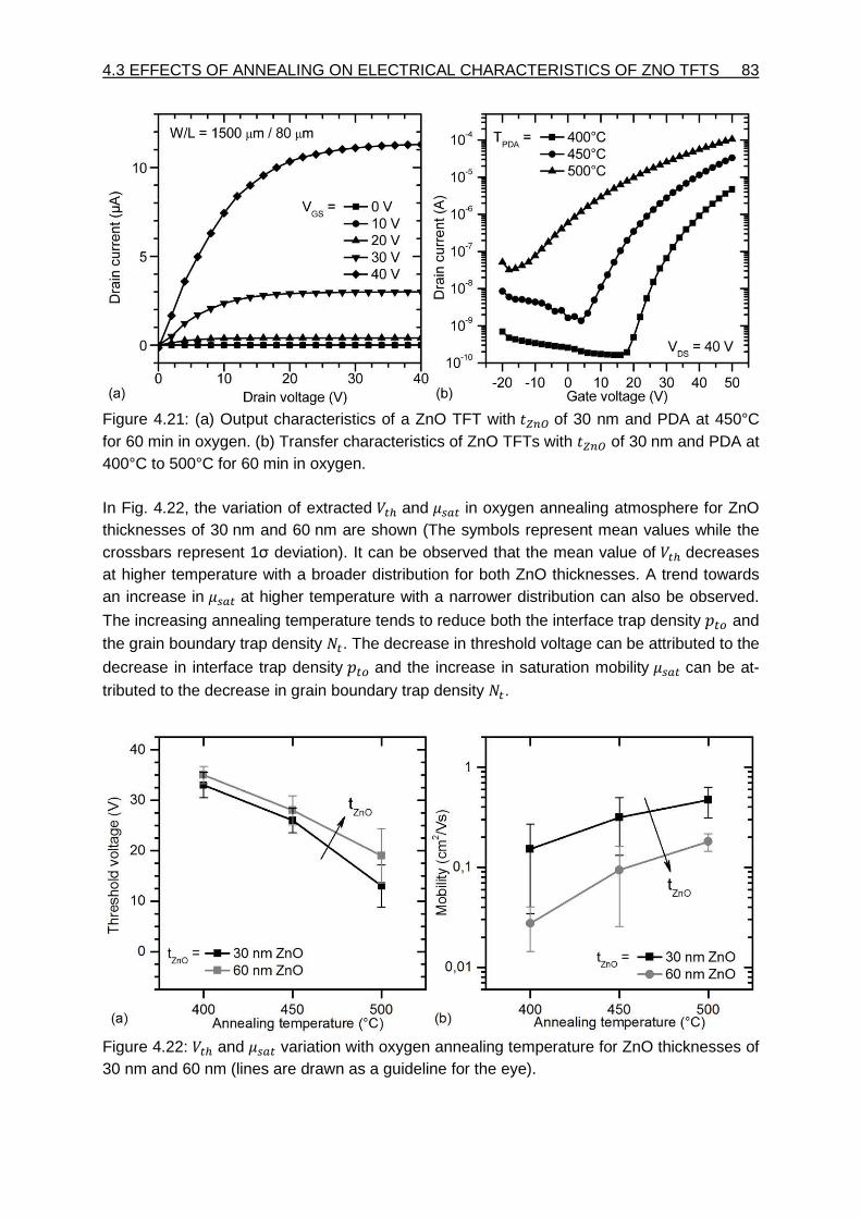
4.3 EFFECTS OF ANNEALING ON ELECTRICAL CHARACTERISTICS OF ZNO TFTS 83
Figure 4.21: (a) Output characteristics of a ZnO TFT with Q7( of 30 nm and PDA at 450°C for 60 min in oxygen. (b) Transfer characteristics of ZnO TFTs with Q7( of 30 nm and PDA at 400°C to 500°C for 60 min in oxygen. In Fig. 4.22, the variation of extracted and > in oxygen annealing atmosphere for ZnO thicknesses of 30 nm and 60 nm are shown (The symbols represent mean values while the crossbars represent 1σ deviation). It can be observed that the mean value of decreases at higher temperature with a broader distribution for both ZnO thicknesses. A trend towards an increase in > at higher temperature with a narrower distribution can also be observed.
The increasing annealing temperature tends to reduce both the interface trap density @ and
the grain boundary trap density . The decrease in threshold voltage can be attributed to the
decrease in interface trap density @ and the increase in saturation mobility > can be at-
tributed to the decrease in grain boundary trap density .
Figure 4.22: and > variation with oxygen annealing temperature for ZnO thicknesses of 30 nm and 60 nm (lines are drawn as a guideline for the eye).
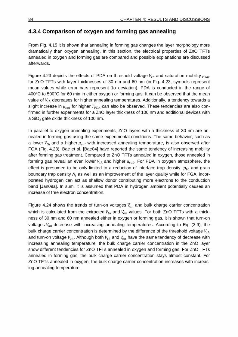
84 CHAPTER 4: RESULTS AND DISCUSSIONS
4.3.4 Comparison of oxygen and forming gas annealin g From Fig. 4.15 it is shown that annealing in forming gas changes the layer morphology more dramatically than oxygen annealing. In this section, the electrical properties of ZnO TFTs annealed in oxygen and forming gas are compared and possible explanations are discussed afterwards. Figure 4.23 depicts the effects of PDA on threshold voltage and saturation mobility > for ZnO TFTs with layer thicknesses of 30 nm and 60 nm (in Fig. 4.23, symbols represent mean values while error bars represent 1σ deviation). PDA is conducted in the range of 400°C to 500°C for 60 min in either oxygen or forming gas. It can be observed that the mean value of decreases for higher annealing temperatures. Additionally, a tendency towards a slight increase in > for higher %½ can also be observed. These tendencies are also con-firmed in further experiments for a ZnO layer thickness of 100 nm and additional devices with a SiO2 gate oxide thickness of 100 nm. In parallel to oxygen annealing experiments, ZnO layers with a thickness of 30 nm are an-nealed in forming gas using the same experimental conditions. The same behavior, such as a lower and a higher > with increased annealing temperature, is also observed after FGA (Fig. 4.23). Bae et al. [Bae04] have reported the same tendency of increasing mobility after forming gas treatment. Compared to ZnO TFTs annealed in oxygen, those annealed in forming gas reveal an even lower and higher >. For PDA in oxygen atmosphere, the
effect is presumed to be only limited to a reduction of interface trap density @ and grain boundary trap density as well as an improvement of the layer quality while for FGA, incor-porated hydrogen can act as shallow donor contributing more electrons to the conduction band [Jan09a]. In sum, it is assumed that PDA in hydrogen ambient potentially causes an increase of free electron concentration.
Figure 4.24 shows the trends of turn-on voltages and bulk charge carrier concentration
which is calculated from the extracted and values. For both ZnO TFTs with a thick-ness of 30 nm and 60 nm annealed either in oxygen or forming gas, it is shown that turn-on
voltages decrease with increasing annealing temperatures. According to Eq. (3.9), the
bulk charge carrier concentration is determined by the difference of the threshold voltage and turn-on voltage . Although both and have the same tendency of decrease with increasing annealing temperature, the bulk charge carrier concentration in the ZnO layer show different tendencies for ZnO TFTs annealed in oxygen and forming gas. For ZnO TFTs annealed in forming gas, the bulk charge carrier concentration stays almost constant. For ZnO TFTs annealed in oxygen, the bulk charge carrier concentration increases with increas-ing annealing temperature.
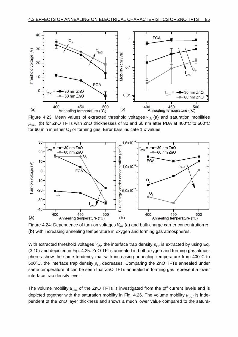
4.3 EFFECTS OF ANNEALING ON ELECTRICAL CHARACTERISTICS OF ZNO TFTS 85
Figure 4.23: Mean values of extracted threshold voltages (a) and saturation mobilities > (b) for ZnO TFTs with ZnO thicknesses of 30 and 60 nm after PDA at 400°C to 500°C for 60 min in either O2 or forming gas. Error bars indicate 1 σ values.
Figure 4.24: Dependence of turn-on voltages (a) and bulk charge carrier concentration - (b) with increasing annealing temperature in oxygen and forming gas atmospheres.
With extracted threshold voltages , the interface trap density @ is extracted by using Eq. (3.10) and depicted in Fig. 4.25. ZnO TFTs annealed in both oxygen and forming gas atmos-pheres show the same tendency that with increasing annealing temperature from 400°C to
500°C, the interface trap density @ decreases. Comparing the ZnO TFTs annealed under same temperature, it can be seen that ZnO TFTs annealed in forming gas represent a lower interface trap density level.
The volume mobility £ of the ZnO TFTs is investigated from the off current levels and is
depicted together with the saturation mobility in Fig. 4.26. The volume mobility £ is inde-pendent of the ZnO layer thickness and shows a much lower value compared to the satura-
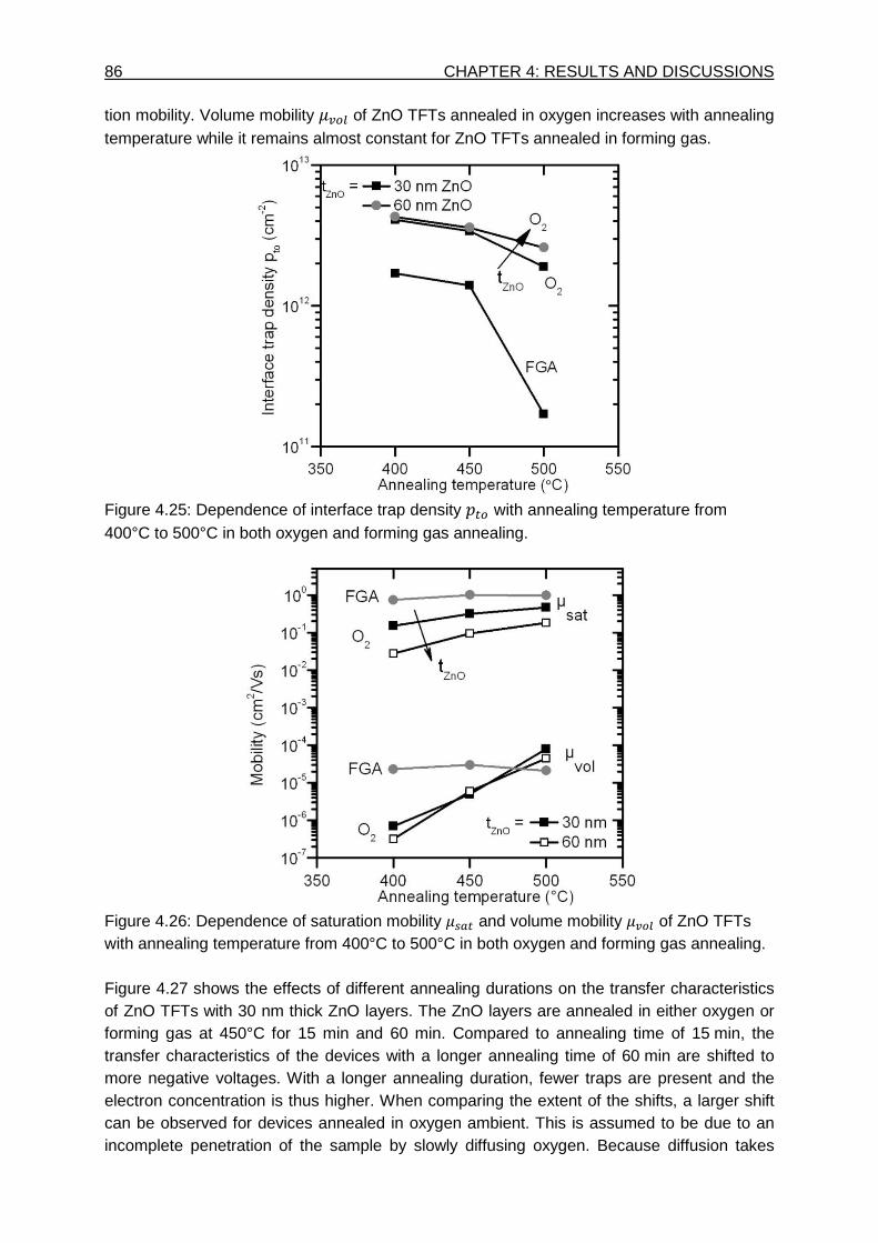
86 CHAPTER 4: RESULTS AND DISCUSSIONS tion mobility. Volume mobility £ of ZnO TFTs annealed in oxygen increases with annealing temperature while it remains almost constant for ZnO TFTs annealed in forming gas.
Figure 4.25: Dependence of interface trap density @ with annealing temperature from 400°C to 500°C in both oxygen and forming gas annealing.
Figure 4.26: Dependence of saturation mobility > and volume mobility £ of ZnO TFTs with annealing temperature from 400°C to 500°C in both oxygen and forming gas annealing. Figure 4.27 shows the effects of different annealing durations on the transfer characteristics of ZnO TFTs with 30 nm thick ZnO layers. The ZnO layers are annealed in either oxygen or forming gas at 450°C for 15 min and 60 min. Compared to annealing time of 15 min, the transfer characteristics of the devices with a longer annealing time of 60 min are shifted to more negative voltages. With a longer annealing duration, fewer traps are present and the electron concentration is thus higher. When comparing the extent of the shifts, a larger shift can be observed for devices annealed in oxygen ambient. This is assumed to be due to an incomplete penetration of the sample by slowly diffusing oxygen. Because diffusion takes
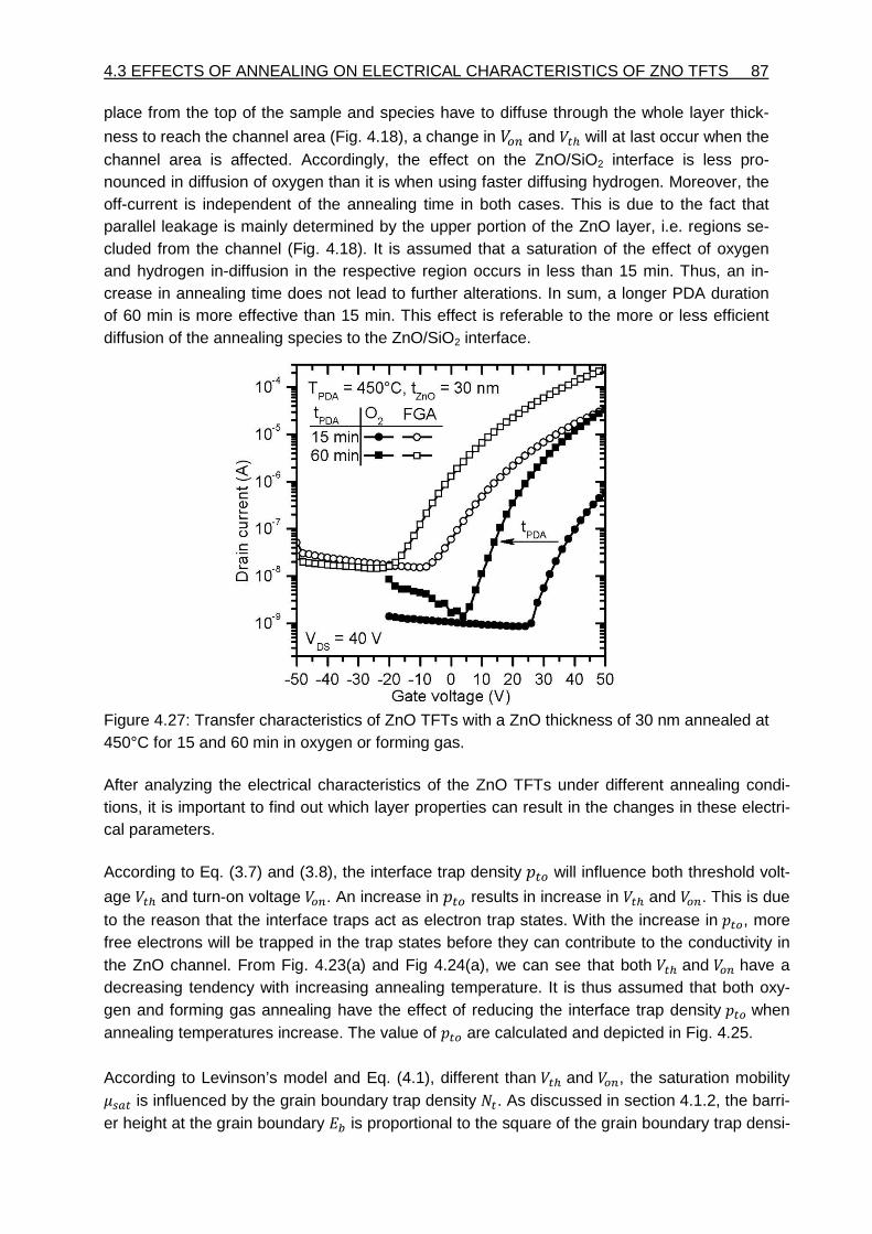
4.3 EFFECTS OF ANNEALING ON ELECTRICAL CHARACTERISTICS OF ZNO TFTS 87
place from the top of the sample and species have to diffuse through the whole layer thick-
ness to reach the channel area (Fig. 4.18), a change in and will at last occur when the channel area is affected. Accordingly, the effect on the ZnO/SiO2 interface is less pro-nounced in diffusion of oxygen than it is when using faster diffusing hydrogen. Moreover, the off-current is independent of the annealing time in both cases. This is due to the fact that parallel leakage is mainly determined by the upper portion of the ZnO layer, i.e. regions se-cluded from the channel (Fig. 4.18). It is assumed that a saturation of the effect of oxygen and hydrogen in-diffusion in the respective region occurs in less than 15 min. Thus, an in-crease in annealing time does not lead to further alterations. In sum, a longer PDA duration of 60 min is more effective than 15 min. This effect is referable to the more or less efficient diffusion of the annealing species to the ZnO/SiO2 interface.
Figure 4.27: Transfer characteristics of ZnO TFTs with a ZnO thickness of 30 nm annealed at 450°C for 15 and 60 min in oxygen or forming gas.
After analyzing the electrical characteristics of the ZnO TFTs under different annealing condi-tions, it is important to find out which layer properties can result in the changes in these electri-cal parameters. According to Eq. (3.7) and (3.8), the interface trap density will influence both threshold volt-
age and turn-on voltage . An increase in results in increase in and . This is due to the reason that the interface traps act as electron trap states. With the increase in , more free electrons will be trapped in the trap states before they can contribute to the conductivity in the ZnO channel. From Fig. 4.23(a) and Fig 4.24(a), we can see that both and have a decreasing tendency with increasing annealing temperature. It is thus assumed that both oxy-gen and forming gas annealing have the effect of reducing the interface trap density when annealing temperatures increase. The value of are calculated and depicted in Fig. 4.25. According to Levinson’s model and Eq. (4.1), different than and , the saturation mobility is influenced by the grain boundary trap density . As discussed in section 4.1.2, the barri-er height at the grain boundary is proportional to the square of the grain boundary trap densi-
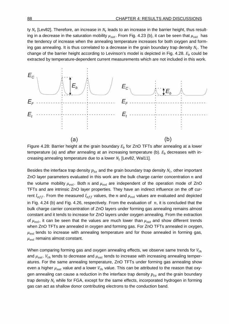
88 CHAPTER 4: RESULTS AND DISCUSSIONS ty [Lev82]. Therefore, an increase in leads to an increase in the barrier height, thus result-ing in a decrease in the saturation mobility >. From Fig. 4.23 (b), it can be seen that > has the tendency of increase when the annealing temperature increases for both oxygen and form-ing gas annealing. It is thus correlated to a decrease in the grain boundary trap density . The change of the barrier height according to Levinson’s model is depicted in Fig. 4.28. x could be extracted by temperature-dependent current measurements which are not included in this work.
Figure 4.28: Barrier height at the grain boundary x for ZnO TFTs after annealing at a lower temperature (a) and after annealing at an increasing temperature (b). x decreases with in-creasing annealing temperature due to a lower [Lev82, Wal11].
Besides the interface trap density @ and the grain boundary trap density , other important
ZnO layer parameters evaluated in this work are the bulk charge carrier concentration - and
the volume mobility £ . Both - and £ are independent of the operation mode of ZnO TFTs and are intrinsic ZnO layer properties. They have an indirect influence on the off cur-
rent . From the measured values, the- and £ values are evaluated and depicted
in Fig. 4.24 (b) and Fig. 4.26, respectively. From the evaluation of -, it is concluded that the bulk charge carrier concentration of ZnO layers under forming gas annealing remains almost constant and it tends to increase for ZnO layers under oxygen annealing. From the extraction of £, it can be seen that the values are much lower than > and show different trends when ZnO TFTs are annealed in oxygen and forming gas. For ZnO TFTs annealed in oxygen, £ tends to increase with annealing temperature and for those annealed in forming gas, £ remains almost constant. When comparing forming gas and oxygen annealing effects, we observe same trends for and >. tends to decrease and > tends to increase with increasing annealing temper-atures. For the same annealing temperature, ZnO TFTs under forming gas annealing show even a higher > value and a lower value. This can be attributed to the reason that oxy-
gen annealing can cause a reduction in the interface trap density @ and the grain boundary
trap density while for FGA, except for the same effects, incorporated hydrogen in forming gas can act as shallow donor contributing electrons to the conduction band.
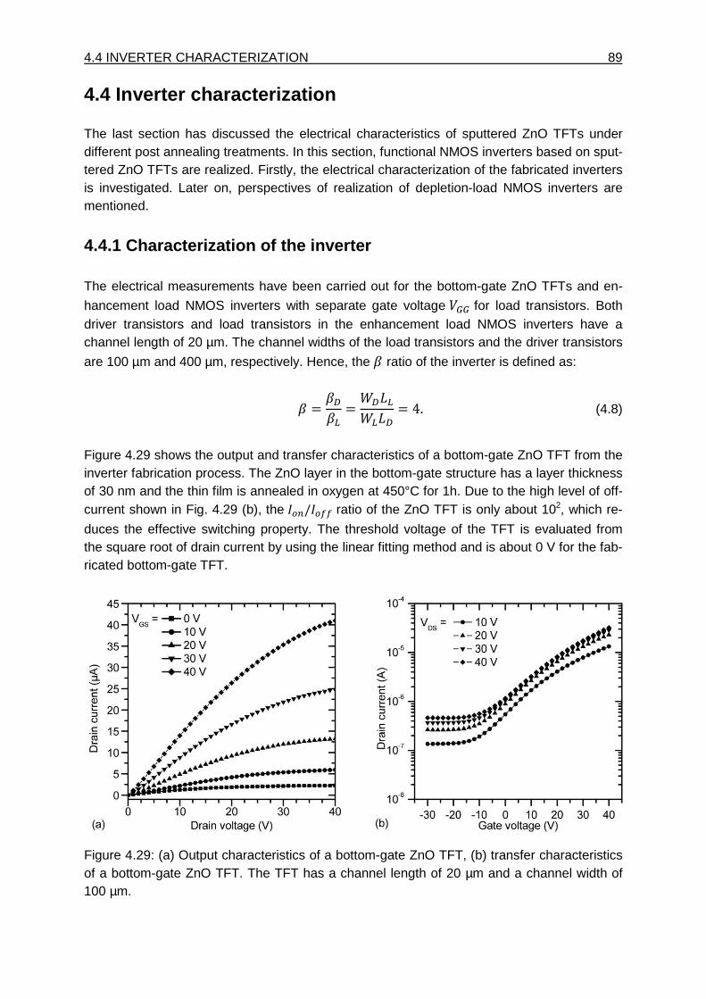
4.4 INVERTER CHARACTERIZATION 89
4.4 Inverter characterization The last section has discussed the electrical characteristics of sputtered ZnO TFTs under different post annealing treatments. In this section, functional NMOS inverters based on sput-tered ZnO TFTs are realized. Firstly, the electrical characterization of the fabricated inverters is investigated. Later on, perspectives of realization of depletion-load NMOS inverters are mentioned.
4.4.1 Characterization of the inverter The electrical measurements have been carried out for the bottom-gate ZnO TFTs and en-
hancement load NMOS inverters with separate gate voltage for load transistors. Both driver transistors and load transistors in the enhancement load NMOS inverters have a channel length of 20 µm. The channel widths of the load transistors and the driver transistors
are 100 µm and 400 µm, respectively. Hence, the ratio of the inverter is defined as:
=
=
= 4.(4.8)
Figure 4.29 shows the output and transfer characteristics of a bottom-gate ZnO TFT from the inverter fabrication process. The ZnO layer in the bottom-gate structure has a layer thickness of 30 nm and the thin film is annealed in oxygen at 450°C for 1h. Due to the high level of off-current shown in Fig. 4.29 (b), the / ratio of the ZnO TFT is only about 102, which re-
duces the effective switching property. The threshold voltage of the TFT is evaluated from the square root of drain current by using the linear fitting method and is about 0 V for the fab-ricated bottom-gate TFT.
Figure 4.29: (a) Output characteristics of a bottom-gate ZnO TFT, (b) transfer characteristics of a bottom-gate ZnO TFT. The TFT has a channel length of 20 µm and a channel width of 100 µm.
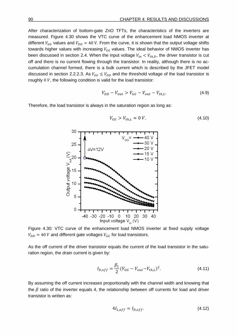
90 CHAPTER 4: RESULTS AND DISCUSSIONS After characterization of bottom-gate ZnO TFTs, the characteristics of the inverters are measured. Figure 4.30 shows the VTC curve of the enhancement load NMOS inverter at different values and = 40V. From the curve, it is shown that the output voltage shifts towards higher values with increasing values. The ideal behavior of NMOS inverter has been discussed in section 2.4. When the input voltage < ,, the driver transistor is cut
off and there is no current flowing through the transistor. In reality, although there is no ac-cumulation channel formed, there is a bulk current which is described by the JFET model discussed in section 2.2.2.3. As ≤ and the threshold voltage of the load transistor is roughly 0, the following condition is valid for the load transistor: − ¢ > − ¢ − ,± .(4.9)
Therefore, the load transistor is always in the saturation region as long as: > ,± ≈ 0.(4.10)
Figure 4.30: VTC curve of the enhancement load NMOS inverter at fixed supply voltage = 40 and different gate voltages for load transistors. As the off current of the driver transistor equals the current of the load transistor in the satu-ration region, the drain current is given by:
, = ²±2 + − ¢−,±/E.(4.11)
By assuming the off current increases proportionally with the channel width and knowing that
the ² ratio of the inverter equals 4, the relationship between off currents for load and driver transistor is written as: 4±, = , .(4.12)
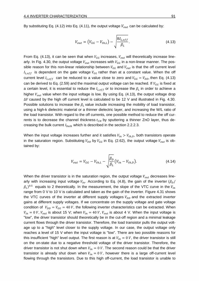
4.4 INVERTER CHARACTERIZATION 91
By substituting Eq. (4.12) into Eq. (4.11), the output voltage ¢ can be calculated by:
¢ = ' − ,±* − 8±,²± .(4.13)
From Eq. (4.13), it can be seen that when increases, ¢ will theoretically increase line-arly. In Fig. 4.30, the output voltage ¢ increases with in a non-linear manner. The pos-sible reason for this non-linear relationship between and ¢ is that the off current level ±,is dependent on the gate voltage rather than at a constant value. When the off
current level ±, can be reduced to a value close to zero and = , then Eq. (4.13)
can be derived to Eq. (2.59) and the maximal output voltage can be reached. If is fixed at a certain level, it is essential to reduce the ±, or to increase the ²± in order to achieve a
higher ¢ value when the input voltage is low. By using Eq. (4.13), the output voltage drop ∆caused by the high off current level is calculated to be 12 V and illustrated in Fig. 4.30. Possible solutions to increase the ²± value include increasing the mobility of load transistor, using a high-k dielectric material or a thinner dielectric layer, and increasing the W/L ratio of the load transistor. With regard to the off currents, one possible method to reduce the off cur-rents is to decrease the channel thickness QVR by sputtering a thinner ZnO layer, thus de-creasing the bulk current x¢£X which is described in the section 2.2.2.3. When the input voltage increases further and it satisfies > ,, both transistors operate
in the saturation region. Substituting by in Eq. (2.62), the output voltage ¢ is ob-tained by:
¢ = − ,± −²²± ' − ,*.(4.14)
When the driver transistor is in the saturation region, the output voltage ¢ decreases line-arly with increasing input voltage . According to Eq. (4.8), the gain of the inverter +²/²±/F.¦ equals to 2 theoretically. In the measurement, the slope of the VTC curve in the range from 0 V to 10 V is calculated and taken as the gain of the inverter. Figure 4.31 shows the VTC curves of the inverter at different supply voltages and the extracted inverter gains at different supply voltages. If we concentrate on the supply voltage and gate voltage condition of = = 40, the following inverter characteristics can be extracted. When = 0, ¢ is about 15 V; when = 40, ¢ is about 4 V. When the input voltage is "low", the driver transistor should theoretically be in the cut-off region and a minimal leakage current flows through the driver transistor. Therefore, the load transistor pulls the output volt-age up to a "high" level closer to the supply voltage. In our case, the output voltage only reaches a level of 15 V when the input voltage is "low". There are two possible reasons for this insufficient "high" level output. The first reason is at = 0, the driver transistor is still on the on-state due to a negative threshold voltage of the driver transistor. Therefore, the driver transistor is not shut down when = 0. The second reason could be that the driver transistor is already shut down when = 0, however there is a large off-current level flowing through the transistors. Due to this high off-current, the load transistor is unable to
92 CHAPTER 4: RESULTS AND DISCUSSIONS pull the output level up to a value closer to the supply voltage. In the process, both driver transistor and load transistor are fabricated in an exactly same manner and it turns out that the off current for the load transistor has a level as high as about 0.1 µA. Considering the scaling effects on the off current level and using Eq. (4.12), it is expected that the driver tran-sistor has a high off-current level at about 0.4 µA. The gain of the inverter is affected by many factors including the channel mobility, the gate capacitances, the device geometry, and the biasing conditions. Figure 4.31 (b) shows that the inverter gain is a function of the supply voltage . When increases from 10 V to 50 V, the inverter gain increases with increasing and reaches a maximum value of about 0.4 at a value of 50 V. Similar tendency has also been reported by Presley et al [Pre06]. Be-cause an inverter gain great than one is required to switch the next inverter in a ring oscilla-tor, the maximum gain of 0.4 measured here is not sufficient enough to fabricate a ring oscil-lator consisting of odd numbers of NMOS inverters.
Figure 4.31: VTC curves of the enhancement load NMOS inverter at enhancement mode ( = ) (a) and extracted inverter gain as a function of the supply voltage (b). As the concept of building inverters constituting only n-channel transistors based on RF magnetron sputtered ZnO thin films as the semiconductor material is very new and the measured inverters have shown functionality, there are a lot of potentials to improve the in-verter characteristics for more complex logic circuits such as ring oscillators. As discussed above, a thinner ZnO layer can be deposited in order to suppress the off-currents of both driver and load transistors. When assuming mobility and gate capacitance identical for driver and load transistor, a greaterrp/r ratio will result in higher inverter gain. Therefore, ap-
propriate geometrical design with a suitable r/r± ratio is important to obtain a higher in-verter gain.
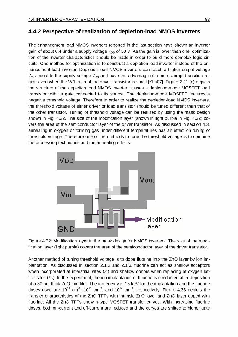
4.4 INVERTER CHARACTERIZATION 93
4.4.2 Perspective of realization of depletion-load NMOS inverters The enhancement load NMOS inverters reported in the last section have shown an inverter gain of about 0.4 under a supply voltage of 50 V. As the gain is lower than one, optimiza-tion of the inverter characteristics should be made in order to build more complex logic cir-cuits. One method for optimization is to construct a depletion load inverter instead of the en-hancement load inverter. Depletion load NMOS inverters can reach a higher output voltage ¢ equal to the supply voltage and have the advantage of a more abrupt transition re-gion even when the W/L ratio of the driver transistor is small [Kha07]. Figure 2.21 (c) depicts the structure of the depletion load NMOS inverter. It uses a depletion-mode MOSFET load transistor with its gate connected to its source. The depletion-mode MOSFET features a negative threshold voltage. Therefore in order to realize the depletion-load NMOS inverters, the threshold voltage of either driver or load transistor should be tuned different than that of the other transistor. Tuning of threshold voltage can be realized by using the mask design shown in Fig. 4.32. The size of the modification layer (shown in light purple in Fig. 4.32) co-vers the area of the semiconductor layer of the driver transistor. As discussed in section 4.3, annealing in oxygen or forming gas under different temperatures has an effect on tuning of threshold voltage. Therefore one of the methods to tune the threshold voltage is to combine the processing techniques and the annealing effects.
Figure 4.32: Modification layer in the mask design for NMOS inverters. The size of the modi-fication layer (light purple) covers the area of the semiconductor layer of the driver transistor. Another method of tuning threshold voltage is to dope fluorine into the ZnO layer by ion im-plantation. As discussed in section 2.1.2 and 2.1.3, fluorine can act as shallow acceptors when incorporated at interstitial sites (T) and shallow donors when replacing at oxygen lat-tice sites (T(). In the experiment, the ion implantation of fluorine is conducted after deposition of a 30 nm thick ZnO thin film. The ion energy is 15 keV for the implantation and the fluorine doses used are 1012 cm-2, 1013 cm-2, and 1014 cm-2, respectively. Figure 4.33 depicts the transfer characteristics of the ZnO TFTs with intrinsic ZnO layer and ZnO layer doped with fluorine. All the ZnO TFTs show n-type MOSFET transfer curves. With increasing fluorine doses, both on-current and off-current are reduced and the curves are shifted to higher gate
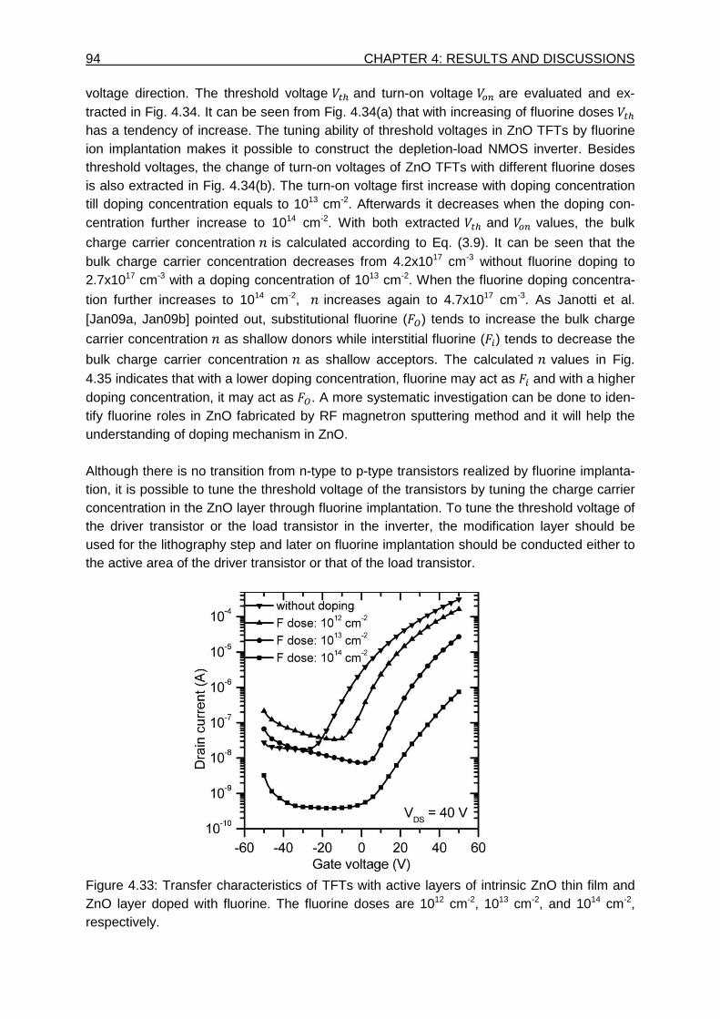
94 CHAPTER 4: RESULTS AND DISCUSSIONS voltage direction. The threshold voltage and turn-on voltage are evaluated and ex-tracted in Fig. 4.34. It can be seen from Fig. 4.34(a) that with increasing of fluorine doses has a tendency of increase. The tuning ability of threshold voltages in ZnO TFTs by fluorine ion implantation makes it possible to construct the depletion-load NMOS inverter. Besides threshold voltages, the change of turn-on voltages of ZnO TFTs with different fluorine doses is also extracted in Fig. 4.34(b). The turn-on voltage first increase with doping concentration till doping concentration equals to 1013 cm-2. Afterwards it decreases when the doping con-centration further increase to 1014 cm-2. With both extracted and values, the bulk
charge carrier concentration - is calculated according to Eq. (3.9). It can be seen that the bulk charge carrier concentration decreases from 4.2x1017 cm-3 without fluorine doping to 2.7x1017 cm-3 with a doping concentration of 1013 cm-2. When the fluorine doping concentra-
tion further increases to 1014 cm-2, - increases again to 4.7x1017 cm-3. As Janotti et al.
[Jan09a, Jan09b] pointed out, substitutional fluorine (T() tends to increase the bulk charge
carrier concentration - as shallow donors while interstitial fluorine (T) tends to decrease the
bulk charge carrier concentration - as shallow acceptors. The calculated - values in Fig. 4.35 indicates that with a lower doping concentration, fluorine may act as T and with a higher doping concentration, it may act as T(. A more systematic investigation can be done to iden-tify fluorine roles in ZnO fabricated by RF magnetron sputtering method and it will help the understanding of doping mechanism in ZnO. Although there is no transition from n-type to p-type transistors realized by fluorine implanta-tion, it is possible to tune the threshold voltage of the transistors by tuning the charge carrier concentration in the ZnO layer through fluorine implantation. To tune the threshold voltage of the driver transistor or the load transistor in the inverter, the modification layer should be used for the lithography step and later on fluorine implantation should be conducted either to the active area of the driver transistor or that of the load transistor.
Figure 4.33: Transfer characteristics of TFTs with active layers of intrinsic ZnO thin film and ZnO layer doped with fluorine. The fluorine doses are 1012 cm-2, 1013 cm-2, and 1014 cm-2, respectively.
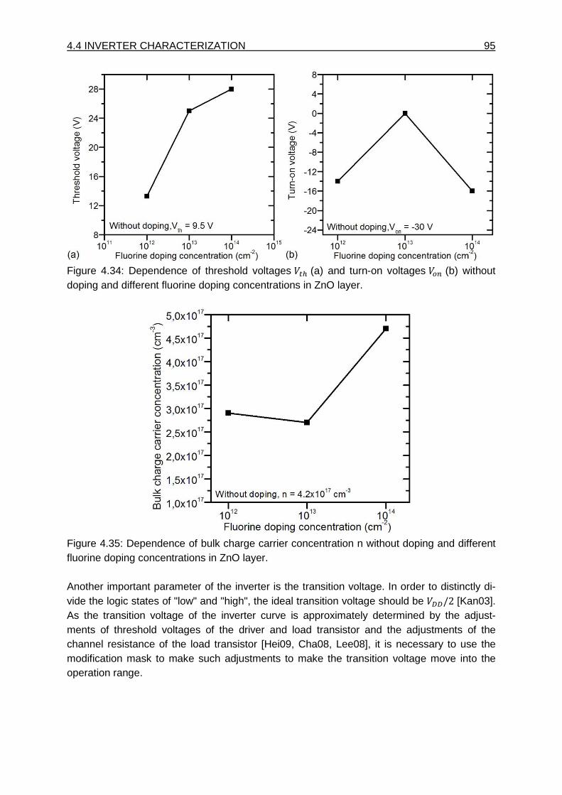
4.4 INVERTER CHARACTERIZATION 95
Figure 4.34: Dependence of threshold voltages (a) and turn-on voltages (b) without doping and different fluorine doping concentrations in ZnO layer.
Figure 4.35: Dependence of bulk charge carrier concentration n without doping and different fluorine doping concentrations in ZnO layer. Another important parameter of the inverter is the transition voltage. In order to distinctly di-vide the logic states of "low" and "high", the ideal transition voltage should be /2 [Kan03]. As the transition voltage of the inverter curve is approximately determined by the adjust-ments of threshold voltages of the driver and load transistor and the adjustments of the channel resistance of the load transistor [Hei09, Cha08, Lee08], it is necessary to use the modification mask to make such adjustments to make the transition voltage move into the operation range.

97
Chapter 5
Conclusion and outlook In this work, semiconducting ZnO thin films are successfully fabricated by RF magnetron sputtering method. Due to its material properties such as wide band gap, large exciton bind-ing energy, large mobility, and high Ion/Ioff ratio, it is considered as one of the promising ma-terials that can provide potentials in optoelectronic and electronic applications. One of the most appealing applications of ZnO has been recently explored in the logic circuit which is essential in almost all electronic applications. NMOS inverters based on two ZnO TFTs fabri-cated by magnetron sputtering are realized in this work. As far as the author’s knowledge, this achievement is one of the cutting edge research results regarding to the involvement of ZnO TFTs in inverter design in Europe. As the important component of NMOS inverters, ZnO TFTs have been fabricated by deposit-ing a ZnO thin film as the active layer in bottom-gate structures. Magnetron sputtered ZnO thin films have many advantages over ZnO nanoparticle films. From the aspect of fabrication complexity, magnetron sputtering of ZnO thin films is more reproducible and stable than gas phase fabrication of ZnO nanoparticles. A homogeneous ZnO layer with little surface rough-ness can be sputtered at room temperature while the ZnO nanoparticle layer is often very porous and has a large surface roughness. Regarding to the electrical properties such as saturation mobility, the maximum saturation mobility of the ZnO TFTs fabricated by magne-tron sputtering in this work has a value of about 1 cm2/Vs. The staggered bottom-gate configuration is chosen as the ZnO TFT architecture investigated in this work. In comparison with the coplanar configuration, the staggered bottom-gate con-figuration has a larger effective channel length due to the different drain current paths in the channel. In the bottom-gate configuration, sputtered ZnO thin films are deposited on thermal-ly oxidized SiO2. As perspective for future work, the effects of using different TFT architec-tures including top- and bottom-gate configurations and staggered and coplanar structures on the electrical characteristics of ZnO TFTs can be investigated. One important aspect worthwhile to mention here is that the induced channel in the bottom-gate configuration lies at the bottom of the sputtered ZnO layer while it is located at the top surface of the sputtered ZnO layer in the top-gate configuration. The top surface of the as-grown ZnO thin film has a rougher surface than the bottom surface and the difference in the surface roughness in the active ZnO channel can also result in changes in electrical characteristics of ZnO TFTs. For
98 CHAPTER 5: CONCLUSION AND OUTLOOK
fabrication of top-gate ZnO TFTs, suitable candidates for gate oxide include plasma-enhanced chemical vapor deposition (PECVD) oxide and atomic layer deposition (ALD) Al2O3. Besides the coplanar and staggered configurations, there is a novel device structure which has been developed by the printed electronics group in Fraunhofer IISB. This novel device structure consists of a coplanar drain and a staggered source electrode. The device shows non-symmetric output characteristics and this non-symmetric property of the ZnO TFT opens up a class of novel devices for simple integration in conventional thin film electronics [Jan12]. In the sputtering process, many sputtering parameters such as substrate-to-target distance, RF power, oxygen flow rate, and sputtering pressure have an influence on the deposition rate of the ZnO thin film. With the increase in substrate-to-target distance, more gas phase scattering between the Zn and O atoms and the background argon and oxygen gas occurs, leading to a reduction in the sputtering rate. An increase in the RF power increases the kinet-ic energy of the sputtered atoms and the deposition rate increases almost linearly with the RF power. Although oxygen vacancies have been recently considered as deep donors by density-functional calculations, the change in the oxygen flow rate in the reactive sputtering process results in variations in the ZnO deposition rate. An increase in oxygen flow rate re-duces the amount of incident Ar atoms which can transfer high energy to the target atoms and thus leads to a reduction in the sputtering rate. Sputtering pressure affects the rate at which the sputtered atoms collide with the gas atoms on their way to the substrate. With an increase in pressure, more collisions and back scattering of the sputtered particles occur, leading to a decrease in the deposition rate. Besides the dependence of the deposition rate on the sputtering parameters, the bulk resistivity of the layer is compared under different sputtering conditions. The bulk resistivity remains almost at a constant level with changing RF powers and oxygen flow rates while the increase in total pressure causes a ZnO layer with lower bulk resistivity. When changing oxygen flow rate in the sputtering process and keeping all other fabrication parameters identical, the saturation mobility of fabricated ZnO TFT increases and the threshold voltage decreases with decreasing oxygen flow rate. Post deposition annealing is effective to improve the crystallinity of the sputtered ZnO layer and its effects on both structural and electrical characteristics of ZnO layers are investigated. The post deposition annealing is conducted either in forming gas or oxygen atmosphere in the temperature range between 400°C and 500°C for 1h. Compared to the as-deposited ZnO layer which is badly crystallized, the ZnO layer after annealing is polycrystalline with strong peak intensities and smaller FWHM values. The ZnO films annealed under forming gas at 400°C, oxygen at 400°C, and oxygen at 450°C tend to show a preferred (002) crystal orienta-tion while the ZnO films annealed under higher temperatures show random orientation. The reduction of the (002) peak intensities under higher temperatures may be due to the recrys-tallization process in which the rearrangement of the ZnO grains takes place. For the ZnO films with a (002) orientation, residual stress, and crystalline domain sizes are determined from the XRD measurement results. The residual stress in the ZnO layer is compressive and it shifts the corresponding peaks in the XRD spectra to larger 2θ angles. The shift of the peaks to smaller 2θ angles in the XRD spectra for the as-deposited ZnO sample indicates a large tensile stress in the layer. In order to completely remove the residual stress in the ZnO layer, a post deposition annealing with the temperature between room temperature and 400°C is expected. The crystalline domain sizes determined from the XRD results corre-
99
spond to the estimated grain sizes achieved from SEM measurements very well. With in-creasing annealing temperature from 400°C to 500°C in forming gas, the threshold voltage of the ZnO TFTs have a decreasing tendency and the saturation mobility increases to a maxi-mum value of about 1 cm2/Vs. The same effect is observed in the oxygen annealing within the temperature range between 400°C and 500°C. Comparing the devices annealed under same temperature in forming gas and oxygen, the devices annealed in forming gas show a lower threshold voltage and a higher saturation mobility. The reason for that can be attributed to different roles of incorporated hydrogen and oxygen in the ZnO layer. In oxygen annealing, the effect is presumed to be only limited to a reduction of trap density and an improvement of the layer quality. In forming gas annealing, hydrogen can act as shallow donors and contrib-ute more electrons to the conduction band, thus leading to an even lower threshold voltage and a higher saturation mobility. The annealing temperatures used in this work are in the range of 400°C to 500°C, which is still too high for substrates like plastic foils and glasses. A good continuation of this work should focus on the reduction of annealing temperatures so that sputtering of ZnO thin films is compatible with the use of low-temperature substrates. One possibility of realizing low post deposition annealing temperature is to set the substrate temperature to a certain temperature level during RF magnetron sputtering of ZnO thin films. Due to its wide band gap, fully trans-parent electronics are future achievable goals with glass substrates and transparent elec-trodes such as ITO. Another important experimental result in this work is the realization of NMOS inverters which consist of two ZnO TFTs. Both driver and load transistors have the same channel lengths and the β ratio of the inverter equals to 4. The inverter gain increases with the supply voltage V and a maximum inverter gain of about 0.4 is achieved with a supply voltage of 50 V. The inverter gain is less than the unity gain which is the minimum requirement to build ring oscil-lators. The main reason for the low gain is due to the high off-current levels from single ZnO TFTs. Suppression of off currents and increase in the β ratio by appropriate geometrical im-provement in the mask help boost the inverter gain. The NMOS inverters realized in this work have a separate gate for the load transistor and the inverter gain is measured under the en-hancement mode in which the gate of the load transistor is applied a same voltage as the supply voltage. Depletion mode NMOS inverters in which the gate of the load transistor is connected directly to the output voltage have the advantage of reaching the maximum high output level to the supply voltage and featuring a more abrupt transition region even though the W/L ratio of the driver transistor is small. The design for depletion mode NMOS inverters is included in the work and further utilization of the modification mask should help tune the threshold voltage for either the driver or the load transistor. Possible methods to tune the threshold voltage include using different annealing steps to the driver and load transistors and doping the channel area by fluorine implantation. In order to expand future potentials of ZnO and fully utilize ZnO characteristics in optical, optoelectronic, and electronic applications, the cause of the intrinsic n-type doping in ZnO should be further investigated. Although quite a few research groups have reported the reali-zation of p-type doped ZnO, more robust and reliable confirmation measurement methods than the Hall-effect measurements should be developed. In the work of A. Hutzler [Hut11], it is reported that ZnO suffers from the degradation of electrical characteristics such as a much

100 CHAPTER 5: CONCLUSION AND OUTLOOK
higher off-current after a long storage time. Possible solution to avoid deterioration in electri-cal performance is to deposit a passivation layer to shield the ZnO device such as the depo-sition of SU-8 photoresist as an encapsulation layer.
101
Bibliography [Ala01] M. J. Alama, D. C. Cameron, Preparation and properties of transparent conductive
aluminum-doped zinc oxide thin films by sol-gel process, Journal of Vacuum Sci-ence and Technology A, 19, 1642 (2001).
[Ash00] A. B. M. A. Ashrafi, A. Ueta, A. Avramescu, H. Kumano, I. Suemune, Y.-W. Ok, T.-
Y. Seong, Growth and characterization of hypothetical zinc-blende ZnO films on GaAs(001) substrates with ZnS buffer layers, Applied Physics Letters, 76, 550 (2000).
[Bae04] H. S. Bae, J. H. Kim, S. Im, Mobility Enhancement in ZnO-based TFTs by H
Treatment, Electrochemical and Solid-State Letters, 7, G279 (2004). [Ban08] J. Bang, K. J. Chang, Diffusion and thermal stability of hydrogen in ZnO, Applied
Physics Letters, 92, 132109 (2008). [Bag97] D. M. Bagnall, Y. F. Chen, Z. Zhu, T. Yao, S. Koyama, M. Y. Shen, T. Goto, Opti-
cally pumped lasing of ZnO at room temperature, Applied Physics Letters, 70, 2230 (1997).
[Bar65] L. S. Bartell, B. L. Carroll, Electron-Diffraction Study of Diborane and Deuterodibo-
rane, The Journal of Chemical Physics, 42, 1135 (1965). [Bar80] J. O. Barnes, D. J. Leary, A. G. Jordan, Relationship Between Deposition Condi-
tions and Physical Properties of sputtered ZnO, Journal of The Electrochemical Society, 127, 1636 (1980).
[Beh91] R. Behrisch, K. Wittmaack, Sputtering by Particle Bombardment III: Characteristics
of Sputtered Particles, Technical Applications, Topics in Applied Physics, 64, Springer-Verlag, Berlin-Heidelberg (1991).
[Bie08] O. Bierwagen, T. Ive, C. G. Van de Walle, J. S. Speck, Causes of incorrect carrier-
type identification in van der Pauw-Hall measurements, Applied Physics Letters, 93, 242108 (2008).
102 BIBLIOGRAPHY
[Boe68] G. F. Boesen, J. E. Jacobs, ZnO field-effect transistor, Proceedings of the IEEE, 56, 2094 (1968).
[Boo47] G. Boole, The Mathematical Analysis of Logic, Macmillan, Barclay, & Macmillan,
London (1847). [Bra09] D. Braga, G. Horowitz, High-Performance Organic Field-Effect Transistors, Ad-
vanced Materials, 21, 1473 (2009). [Bre78] J. R. Brews, A Charge-sheet Model of the MOSFET, Solid-State Electronics, 21,
345 (1978).
[Bro73] T. P. Brody, J. A. Asars, G. D. Dixon, A 6×6 Inch 20 Lines-per-Inch Liquid-Crystal Display Panel, IEEE Transactions on Electron Devices, ED-20, 995 (1973).
[Bur09] A. W. Burton, K. Ong, T. Rea, I. Y, Chan, On the estimation of average crystallite
size of zeolites from the Scherrer equation: A critical evaluation of its application to zeolites with one-dimensional pore systems, Microporous and Mesoporous Mate-rials, 117, 75 (2009).
[Car97] K. Carl, H. Schmitt, I. Friedrich, Optimization of sputtered ITO films with respect to
the oxygen partial pressure and substrate temperature, Thin Solid Films, 295, 151 (1997).
[Car03] P. F. Carcia, R. S. McLean, M. H. Reilly, G. Nunes, Jr., Transparent ZnO thin-film
transistor fabricated by rf magnetron sputtering, Applied Physics Letters, 82, 1117 (2003).
[Car05] P. F. Carcia, R. S. McLean, M. H. Reilly, Oxide engineering of ZnO thin-film tran-
sistors for flexible electronics, Journal of the Society for Information Display, 13, 547 (2005).
[Cha80] B. Chapman, Glow Discharge Processes, John Wiley & Sons, New York (1980). [Cha92] S.-C. Chang, D. B. Hicks, R. C. O. Laugal, Patterning of Zinc Oxide Thin Films,
Solid-State Sensor and Actuator Workshop, 22-25, 41 (1992). [Cha01] P. E. Champness, Electron Diffraction in the Transmission Electron Microscope,
Garland Science, Great Britain (2001). [Cha08] S. H. Cha, M. S. Oh, K. H. Lee, J.-M. Choi, B. H. Lee, M. M. Sung, S. Im, ZnO-
Based Low-Voltage Inverter with Quantum-Well-Structured Nanohybrid Dielectric, IEEE Eelctron Device Letters, 29, 1145 (2008).
[Chu03] S.-Y. Chu, W. Water, J.-T. Liaw, Influence of postdeposition annealing on the
properties of ZnO films prepared by RF magnetron sputtering, Journal of the Eu-ropean Ceramic Society, 23, 1593 (2003).
BIBLIOGRAPHY 103
[Chu08] J. H. Chung, J. Y. Lee, H. S. Kim, N. W. Jang, J. H. Kim, Effect of thickness of ZnO active layer on ZnO-TFT’s characteristics, Thin Solid Films, 516, 5597 (2008).
[Cle04] W. Clemens, W. Fix, J. Ficker, A. Knobloch, A. Ullmann, From polymer transistors
toward printed electronics, Journal of Materials Research, 19, 1963 (2004). [Cle08] A. V. Clemente, K. Gloystein, Principles of Atomic Force Microscopy, Physics of
Advanced Materials Winter School, Greece (2008). [Col90] J.-P. Colinge, Conduction mechanisms in thin-film accumulation-mode SOI p-
channel MOSFET’s, IEEE Transactions on Electron Devices, 37, 718 (1990). [Con02] A. O.-Conde, F. J. García Sánchez, J. J. Liou, A. Cerdeira, M. Estrada, Y. Yue, A
review of recent MOSFET threshold voltage extraction methods, Microelectronics Reliability, 42, 583 (2002).
[Cot99] F. A. Cotton, G. Wilkinson, C. A. Murillo, M. Bochmann, Advanced Inorganic
Chemistry, Wiley, New York (1999). [Cul78] B. D. Cullity, Elements of X-Ray Diffractions, Addition-Wesley, USA (1978). [Czt04] H. Czternastek, ZnO thin films prepared by high pressure magnetron sputtering,
Opto-Electronics Review 12(1), 49 (2004). [Dad04] A. Dadgar, N. Oleynik, J. Bläsing, S. Deiter, D. Forster, F. Bertram, A. Diez, M.
Seip, A. Greiling, J. Christen, A. Krost, Heteroepitaxy and nitrogen doping of high-quality ZnO, Journal of Crystal Growth, 272, 800, (2004).
[Des98] S. Desgreniers, High-density phases of ZnO: Structural and compressive parame-
ters, Physical Review B, 58, 14102 (1998). [Dif11] Diffraction reference value for ZnO from PDF-number 01-089-0510, International
Center for Diffraction Data (2011). [Ebe91] J. P. Eberhart, Structural and Chemical Analysis of Materials, Wiley, Chichester
(1991). [Ell00] K. Ellmer, Magnetron sputtering of transparent conductive zinc oxide: relation be-
tween the sputtering parameters and the electronic properties, Journal of Physics D: Applied Physics, 33, R17 (2000).
[Fet11] A. Fet, Work Function Engineering for Metal/High-K Dielectric Gate Stacks, Doc-
toral thesis, Friedrich-Alexander-University, Erlangen-Nuremberg (2011). [Fid96] A. J. C. Fiddes, K. Durose, A. W. Brinkman, J. Woods, P. D. Coates, A. J. Banis-
ter, Preparation of ZnO films by spray pyrolysis, Journal of Crystal Growth, 159, 210 (1996).
104 BIBLIOGRAPHY
[For04] E. M. C. Fortunato, P. M. C. Barquinha, A. C. M. B. G. Pimentel, A. M. F. Gon-çalves, A. J. S. Marques, R. F. P. Martins, L. M. N. Pereira, Wide-bandgap high-mobility ZnO thin-film transistors produced at room temperature, Applied Physics Letters, 85, 2541 (2004).
[For05] E. M. C. Fortunato, P. M. C. Barquinha, A. C. M. B. G. Pimentel, A. M. F. Gon-
çalves, A. J. S. Marques, L. M. N. Pereira, R. F. P. Martins, Fully Transparent ZnO Thin-Film Transistor Produced at Room Temperature, Advanced Materials, 17, 590 (2005).
[Fra11] G. Frank, Personal discussion with G. Frank (2011). [Fuj07] H. Fujiwara, Spectroscopic Ellipsometry, Wiley (2007). [Gar98] J. G. E. Gardeniers, Z. M. Rittersma, G. J. Burger, Preferred orientation and pie-
zoelectricity in sputtered ZnO films, Journal of Applied Physics, 83, 7844 (1998). [Gel00] G. H. Gelinck, T. C. T. Geuns, D. M. de Leeuw, High-performance all-polymer in-
tegrated circuits, Applied Physics Letters, 77, 1487 (2000). [Gel10] G. Gelinck, P. Heremans, K. Nomoto, T. D. Anthopoulos, Organic Transistors in
Optical Displays and Microelectronic Applications, Advanced Materials, 22, 3778 (2010).
[Gör06] P. Görrn, M. Sander, J. Meyer, M. Kröger, E. Becker, H.-H. Johannes, W. Kow-
alsky,T. Riedl, Towards See-Through Displays: Fully Transparent Thin-Film Tran-sistors Driving Transparent Organic Light-Emitting Diodes, Advanced Materials, 18, 738 (2006).
[Gup96] V. Gupta, A. Mansingh, Influence of postdeposition annealing on the structural and
optical properties of sputtered zinc oxide film, Journal of Applied Physics, 80, 1063 (1996).
[Hac94] A. Hachigo, H. Nakahata, K. Higaki, S. Fujii, S. Shikata, Heteroepitaxial growth of
ZnO films on diamond (111) plane by magnetron sputtering, Applied Physics Let-ters, 65, 2556 (1994).
[Hag76] K. I. Hagemark, Defect Structure of Zn-Doped ZnO, Journal of Solid State Chemis-
try, 16, 293 (1976). [Ham01] C. Hammond, The Basics of Crystallography and Diffraction, Oxford University
Press (2001). [Har54] S. E. Harrison, Conductivity and Hall Effect of Zno at Low Temperatures, Physical
Review, 93, 52 (1954).
BIBLIOGRAPHY 105
[Hay07] R. Hayashi, M. Ofuji, N. Kaji, K, Takahashi, K. Abe, H. Yabuta, M. Sano, H. Kumomi, K. Nomura, T. Kamiya, M. Hirano, H. Hosono, Circuits using uniform TFTs based on amorphous In-Ga-Zn-O, Journal of the Society for Information Dis-play, 15, 915 (2007).
[Hei70] M. von Heimendahl, Einführung in die Elektronenmikroskopie, Vieweg Friedrich +
Sohn Verlag, Braunschweig (1970). [Hei07] S. Heinze, A. Krtschil, J. Bläsing, T. Hempel, P. Veit, A. Dadgar, J. Christen, A.
Krost, Homoepitaxial growth of ZnO by metalorganic vapor phase epitaxy in two-dimensional growth mode, Journal of Crystal Growth, 308, 170 (2007).
[Hei09] D. P. Heineck, B. R. McFarlane, J. F. Wager, Zinc Tin Oxide Thin-Film-Transistor
Enhancement/Depletion Inverter, IEEE Electron Device Letters, 30, 514 (2009). [Hof02] D. M. Hofmann, A. Hofstaetter, F. Leiter, H. Zhou, F. Henecker, B. K. Meyer, S. B.
Orlinskii, J. Schmidt, P. G. Baranov, Hydrogen: A Relevant Shallow Donor in Zinc Oxide, Physical Review Letters, 88, 045504 (2002).
[Hof04] R. L. Hoffman, ZnO-channel thin-film transistors: Channel mobility, Journal of Ap-
plied Physics, 95, 5813 (2004). [Hof07] D. M. Hofmann, D. Pfisterer, J. Sann, B. K. Meyer, R. Tena-Zaera, V. Munoz-
Sanjose, T. Frank, G. Pensl, Properties of the oxygen vacancy in ZnO, Applied Physics A: Materials Science & Processing, 88, 147 (2007).
[Hol56] L. Holland, The Vaccum Deposition of Thin Films, Wiley, New York (1956). [Hon05a] R. Hong, J. Huang, H. He, Z. Fan, J. Shao, Influence of different post-treatments
on the structure and optical properties of zinc oxide thin films, Applied Surface Science, 242, 346 (2005).
[Hon05b] R. Hong, H. Qi, J. Huang, H. He, Z. Fan, J. Shao, Influence of oxygen partial pres-
sure on the structure and photoluminescence of direct current reactive magnetron sputtering ZnO thin films, Thin Solid Films, 473, 58 (2005).
[Hon07] D. Hong, G. Yerubandi, H. Chiang, M. Spiegelberg, J. F. Wafer, Electrical Model-
ing of Thin-Film Transistors, Critical Reviews in Solid State and Materials Scienc-es, 33, 101 (2007).
[Hu91] J. Hu, R. G. Gordon, Textured fluorine-doped ZnO films by atmospheric pressure
chemical vapor deposition and their use in amorphous silicon solar cells, Solar Cells, 30, 437 (1991).
[Hu92b] J. Hu, R. G. Gordon, Textured aluminum-doped zinc oxide thin films from atmos-
pheric pressure chemical-vapor deposition, Journal of Applied Physics, 71, 880 (1992).
106 BIBLIOGRAPHY
[Hu92b] J. Hu, R. G. Gordon, Atmospheric pressure chemical vapor deposition of gallium doped zinc oxide thin films from diethyl zinc, water, and triethyl gallium, Journal of Applied Physics, 72, 5381 (1992).
[Hu93] J. Hu, R. G. Gordon, Electrical and optical properties of indium doped zinc oxide
films prepared by atmospheric pressure chemical vapor deposition, Materials Re-search Society Symposium Proceedings, 283, 891 (1993).
[Hua10] J. Huang, U. R. Krishna, M. Lemberger, M. P. M. Jank, H. Ryssel, L. Frey, Impact
of forming gas annealing on ZnO-TFTs, 10th IEEE International Conference on Solid-State and Integrated Circuit Technology, 3, 1548 (2010).
[Hua11] J. Huang, U. Radhakrishna, M. Lemberger, M. P. M. Jank, S. Polster, H. Ryssel, L.
Frey, Effects of Oxygen and Forming Gas Annealing on ZnO TFTs, Materials Re-search Society Symposium Proceedings, 1287, mrsf10-1287-f08-05 (2011).
[Hut57] A. R. Hutson, Hall Effect Studies of Doped Zinc Oxide Single Crystals, Physical
Review, 108, 222 (1957). [Hut11] A. Hutzler, Kathodenzerstäubung von Gallium-Indium-Zinkoxid variabler Stöchio-
metrie für den Einsatz in Dünnfilmtransistoren, Bachelor thesis, Friedrich-Alexander-University, Erlangen-Nuremberg (2011).
[Huu11] M. Le-Huu, Entwicklung und Charakterisierung von integrierten Schaltungen auf
Siliciumcarbid für den Betrieb bei hohen Temperaturen, Doctoral thesis, Friedrich-Alexander-University, Erlangen-Nuremberg (2011).
[Int14] International Center for Diffraction Data, www.icdd.com (2014). [Ito08] M. Ito, C. Miyazaki, M. Ishizaki, M. Kon, N. Ikeda, T. Okubo, R. Matsubara, K. Hat-
ta, Y. Ugajin, N. Sekine, Application of amorphous oxide TFT to electrophoretic display, Journal of Non-Crystalline Solids, 354, 2777 (2008).
[Itr11] International Technology Roadmap for Semiconductors, www.itrs.net (2011). [Jag06] C. Jagadish, S. J. Pearton, Zinc Oxide Bulk, Thin Films, and Nanostructures,
Elsevier, New York (2006). [Jan05] A. Janotti, C. G. Van de Walle, Oxygen vacancies in ZnO, Applied Physics Letters,
87, 122102 (2005). [Jan06] A. Janotti, C. G. Van de Walle, New insights into the role of native point defects in
ZnO, Journal of Crystal Growth, 287, 58 (2006). [Jan07a] A. Janotti, C. G. Van de Walle, Native point defects in ZnO, Physical Review B,
76, 165202 (2007).
BIBLIOGRAPHY 107
[Jan07b] A. Janotti, C. G. Van de Walle, Hydrogen multicentre bonds, Nature Materials, 6, 44 (2007).
[Jan09a] A. Janotti, C. G. Van de Walle, Fundamentals of zinc oxide as a semiconductor,
Reports on Progress in Physics, 72, 126501 (2009). [Jan09b] A. Janotti, E. Snow, C. G. Van de Walle, A pathway to p-type wide-band-gap
semiconductors, Applied Physics Letters, 95, 172109 (2009). [Jan12] M. P. M. Jank, E. Teuber, M. Lemberger, J. Huang, L. Frey, A Multi-functional
Thin-Film Device by Combination of Coplanar and Staggered Source/Drain Elec-trodes, 8th International Thin-Film Transistor Conference, Lisbon, Portugal (2012).
[Jeo07a] J. K. Jeong, D. U. Jin, H. S. Shin, H. J. Lee, M. Kim, T. K. Ahn, J. Lee, Y. G. Mo,
H. K. Chung, Flexible Full-Color AMOLED on Ultrathin Metal Foil, IEEE Electron Device Letters, 28, 389 (2007).
[Jeo07b] J. K. Jeong, J. H. Jeong, H. W. Yang, J.-S. Park, Y.-G. Mo, H. D. Kim, High per-
formance thin film transistors with cosputtered amorphous indium gallium zinc ox-ide channel, Applied Physics Letters, 91, 113505 (2007).
[Jeo11] J. K. Jeong, The status and perspectives of metal oxide thin-film transistors for
active matrix flexible displays, Semiconductor Science and Technology, 26, 034008 (2011).
[Jeo12] Jeol homepage, JSM-7500F Scanning Electron Microscope, available under
www.jeol.com (2012). [Kam10] T. Kamiya, H. Hosono, Material characteristics and applications of transparent
amorphous oxide semiconductors, NPG Asia Materials, 2(1), 15 (2010). [Kan03] S.-M. Kang, Y. Leblebici, CMOS Digital Integrated Circuits, McGraw-Hill, New
York (2003). [Kan06] H. S. Kang, B. D. Ahn, J. H. Kim, G. H. Kim, S. H. Lim, H. W. Chang, S. Y. Lee,
Structural, electrical, and optical properties of p-type ZnO thin films with Ag do-pant, Applied Physics Letters, 88, 202108 (2006).
[Kar93] T. Karasawa, Y. Miyata, Electrical and optical properties of indium tin oxide thin
films deposited on unheated substrates by d.c. reactive sputtering, Thin Solid Films, 223, 135 (1993).
[Kar01] Karl Suss Company, Karl Suss Semiautomatic Probe System (2001). [Kas81] M. Kasuga and M. Mochizuki, Orientation relationships of zinc oxide on sapphire in
heteroepitaxial chemical vapor deposition, Journal of Crystal Growth, 54, 185 (1981).
108 BIBLIOGRAPHY
[Kei12] Keithley Company, Model 4200-SCS Semiconductor Characterization System (2012).
[Kha63] D. Khang, M. Atalla, Electric Field Controlled Semiconductor Device, United States
Patent Nr. 3102230 (1963). [Kha07] A. Khan, Notes of MOSFET Digital Circuits, Chapter 16, available under
http://www.southalabama.edu/engineering/ece/faculty/akhan/ (2007). [Kil76] J. S. Kilby, Invention of the integrated circuits, IEEE Transactions on Electron De-
vices, 23, 648 (1976). [Kim97] K. H. Kim, K. C. Park, D. Y. Ma, Structural, electrical and optical properties alumi-
num doped zinc oxide films prepared by radio frequency magnetron sputtering, Journal of Applied Physics, 81, 7764 (1997).
[Kim09] C.-J. Kim, S. Kim, J.-H. Lee, J.-S. Park, S. Kim, J. Park, E. Lee, J. Lee, Y. Park, J.
H. Kim, S. T. Shin, U-I. Chung, Amorphous hafnium-indium-zinc oxide semicon-ductor thin film transistors, Applied Physics Letters, 95, 252103 (2009).
[Kit05] C. Kittel, Introduction to Solid State Physics, Wiley, New York (2005). [Klu74] H. P. Klug, L. E. Alexander, X-Ray Diffraction Procudures: For Polycrystalline and
Amorphous Materials, Wiley, New York (1974). [Kno04] A. Knobloch, A. Manuelli, A. Bernds, W. Clemens, Fully printed integrated circuits
from solution processable polymers, Journal of Applied Physics, 96, 2286 (2004). [Ko00] H. J. Ko, Y. F. Chen, S. K. Hong, H. Wenisch, T. Yao, D. C. Look, Ga-doped ZnO
films grown on GaN templates by plasma-assisted molecular-beam epitaxy, Ap-plied Physics Letters, 77, 3761 (2000).
[Koe87] H. Koezuka, A. Tsumura, T. Ando, Field-effect transistor with polythiophene thin
film, Synthetic Metals, 18, 699 (1987). [Koh00] A. F. Kohan, G. Ceder, D. Morgan, C. G. Van de Walle, First-principles study of
native point defects in ZnO, Physical Review B, 61, 15019 (2000). [Kwo05] J. W. Kwon, E. S. Kim, Fine ZnO Patterning With Controlled Sidewall-Etch Front
Slope, Journal of Microelectromechanical Systems, 14, 603 (2005). [Lan81] M. Lannoo, J. Bourgoin, Point Defects in Semiconductors I: Theoretical Aspects,
Springer, Berlin (1981). [Lan83] M. Lannoo, J. Bourgoin, Point Defects in Semiconductors II: Experimental As-
pects, Springer, Berlin (1983).
BIBLIOGRAPHY 109
[Lec79] P. G. LeComber, W. E. Spear, A. Ghaith, Amorphous-silicon Field-Effect Devices and Possible Applications, Electronics Letters, 15, 179 (1979).
[Lee08] K. Lee, K. Kim, K. H. Lee, G. Lee, M. S. Oh, J. M. Choi, S. Im, S. Jang, E. Kim,
ZnO-based low voltage inverter with low-k/high-k double polymer dielectric layer, Applied Physics Letters, 93, 193514 (2008).
[Lem10] M. Lemberger, Chemische Gasphasenabscheidung von Metallsilicatschichten aus
Einquellen-Ausgangsstoffen für Anwendungen in der Mikroelektronik, Doctoral thesis, Friedrich-Alexander-University, Erlangen-Nuremberg (2010).
[Lev82] J. Levinson, F. R. Shepherd, P. J. Scanlon, W. D. Westwood, G. Este, M. Rider,
Conductivity behavior in polycrystalline semiconductor thin film transistors, Journal of Applied Physics, 53, 1193 (1982).
[Ley95] Leybold Company, Instruction Guide for L400 SP (1995). [Li02] B. S. Li, Y. C. Liu, Z. S. Chu, D. Z. Shen, Y. M. Lu, J. Y. Zhang, X. W. Fan, High
quality ZnO thin films grown by plasma enhanced chemical vapor deposition, Journal of Applied Physics, 91, 501 (2002).
[Lim03] W. T. Lim, I. K. Baek, J. W. Lee, E. S. Lee, M. H. Jeon, G. S. Cho, Y. W. Heo, D.
P. Norton, S. J. Pearton, Temperature-dependent Cl2/Ar plasma etching of bulk single-crystal ZnO, Applied Physics Letters, 83, 3105 (2003).
[Lin99] Y.-Y. Lin, A. Dodabalapur, R. Sarpeshkar, Z. Bao, W. Li, K. Baldwin, V. R. Raju, H.
E. Katz, Organic complementary ring oscillators, Applied Physics Letters, 74, 2714 (1999).
[Lin04] C.-C. Lin, S.-Y. Chen, S.-Y. Cheng, H.-Y. Lee, Properties of nitrogen-implanted p-
type ZnO films grown on Si3N4/Si by radio-frequency magnetron sputtering, Ap-plied Physics Letters, 84, 5040 (2004).
[Lin08] S. S. Lin, Z. Z. Ye, J. G. Lu, H. P. He, L. X. Chen, X. Q. Gu, J. Y. Huang, L. P.
Zhu, B. H. Zhao, Na doping concentration tuned conductivity of ZnO films via pulsed laser deposition and electroluminescence from ZnO homojunction on sili-con substrate, Journal of Physics D: Applied Physics, 41, 155114 (2008).
[Lip63] W. N. Lipscomb, Boron Hydrides, Benjamin, New York (1963). [Loo97] D. C. Look, D. C. Reynolds, J. R. Sizelove, R. L. Jones, C. W. Litton, G. Cantwell,
W. C. Harsch, Electrical properties of bulk ZnO, Solid State Communications, 105, 399 (1997).
[Loo01] D. C. Look, Recent advances in ZnO materials and devices, Materials Science
and Engineering, B 80, 383 (2001).
110 BIBLIOGRAPHY
[Loo02] D. C. Look, D. C. Reynolds, C. W. Litton, R. L. Jones, D. B. Eason, G. Cantwell, Characterization of homoepitaxial p-type ZnO grown by molecular beam epitaxy, Applied Physics Letters, 81, 1830 (2002).
[Loo04] D. C. Look, B. Claflin, P-type doping and devices based on ZnO, Physica Status
Solidi (b), 241, 624 (2004). [Lu06] J. G. Lu, P. Chang, Z. Fan, Quasi-one-dimensional metal oxide materials – Syn-
thesis, properties and applications, Materials Science and Engineering R, 52 (2006).
[Lyo09] J. L. Lyons, A. Janotti, C. G. Van de Walle, Why nitrogen cannot lead to p-type
conductivity in ZnO, Applied Physics Letters, 95, 252105 (2009). [Mad96] O. Madelung, Semiconductors – Basic Data, Springer, Berlin (1996). [Man95] A. Mang, K. Reimann, St. Rübenacke, Band Gaps, Crystal-field Splitting, Spin-
orbit Coupling, and Exciton binding energies in ZnO under hydrostatic pressure, Solid State Communications, 94, 251 (1995).
[Man97] M. A. Mantenieks, Sputtering threshold energies of heavy ions, International Elec-
tric Propulsion Conference, 187, 1145 (1997). [Mat99] M. Matters, D. M. de Leeuw, P. T. Herwig, A. R. Brown, Bias-stress induced insta-
bility of organic thin film transistors, Synthetic Metals, 102, 998 (1999). [Mcc91] E. D. McClanahan, N. Laegreid, Production of Thin Films by Controlled Deposition
of Sputtered Material, Topics in Applied Physics, 64, 339 (1991). [Mei11] E. Meißner, Personal discussion with E. Meißner (2011). [Men00] L.-J. Meng, M. P. dos Santos, Influence of the target-substrate distance on the
properties of indium tin oxide films prepared by radio frequency reactive magne-tron sputtering, Journal of Vacuum Science & Technology A, 18(4), 1668 (2000).
[Min02] T. Minami, S. Ida, T. Miyata, High rate deposition of transparent conducting oxide
thin films by vacuum arc plasma evaporation, Thin Solid Films, 416, 92 (2002). [Min08] S. R. Min, H. N. Cho, Y. L. Li, C. W. Chung, Inductively coupled plasma reactive
ion etching of ZnO films in HBr/Ar plasma, Thin Solid Films, 516, 3521 (2008). [Min10] C.-H. Min, S. Cho, S.-H. Lee, D.-Y. Cho, W. G. Park, J. G. Chung, E. Lee, J. C.
Lee, B. Anass, J. H. Lee, C. S. Hwang, S.-J. Oh, Effect of oxygen partial pressure on the Fermi level of ZnO1-x films fabricated by pulsed laser deposition, Applied Physics Letters, 96, 201907 (2010).
BIBLIOGRAPHY 111
[Moh61] G. P. Mohanty, L. V. Azároff, Electron Density Distributions in ZnO Crystals, The Journal of Chemical Physics, 35, 1268, (1961).
[Moo65] G. Moore, Cramming more components onto integrated circuits, Electronics, 38,
114 (1965). [Mor87] R. T. Morrison, R. N. Boyd, Organic Chemistry, Allyn and Bacon, Boston (1987). [Mor09] H. Morkoç, Ü. Özgür, Zinc Oxide: Fundamentals, Materials and Device Technolo-
gy, Wiley-VCH, Weinheim (2009). [Nak00] S. Nakamura, S. F. Chichibu, Introduction to nitride semiconductor blue lasers and
light emitting diodes, Taylor and Francis (2000). [Nan03] S. K. Nandi, S. Chatterjee, S. K. Samanta, P. K. Bose, C. K. Maiti, Electrical char-
acterization of low temperature deposited oxide films on ZnO/n-Si substrate, Bulle-tin of Material Science, 26, 7 (2003).
[Nau05] J. Nause, B. Nemeth, Pressurized melt growth of ZnO boules, Semiconductor Sci-
ence and Technology, 20, 45 (2005). [Nic05] N. H. Nickel, E. Terukov, Zinc Oxide – A Material for Micro- and Optoelectronic
Applications, Springer, Netherlands (2005). [Nog80] S. Noguchi, H. Sakata, Electrical properties of undoped In2O3 films prepared by
reactive evaporation, Journal of Physics D: Applied Physics, 13, 1129 (1980). [Ofu07] M. Ofuji, K. Abe, H. Shimizu, N. Kaji, R. Hayashi, M. Sano, H. Kumomi, K. Nomu-
ra, T. Kamiya, H. Hosono, Fast Thin-Film Transistor Circuits Based on Amorphous Oxide Semiconductor, IEEE Electron Device Letters, 28, 273 (2007).
[Oga05] S. B. Ogale, Thin Films and Heterostructures for Oxide Electronics, Springer, New
York (2005). [Oh10] M. S. Oh, J. I. Han, K. Lee, B. H. Lee, M. M. Sung, S. Im, Coupling Top- and Bot-
tom-Gate ZnO Thin Film Transistors for Low Voltage, High Gain Inverter, Electro-chemical and Solid-State Letters, 13, 194 (2010).
[Ohg03] T. Ohgaki, N. Ohashi, H. Kakemeoto, S. Wada, Y. Adachi, H. Haneda, T. Tsurumi,
Growth condition dependence of morphology and electric properties of ZnO films on sapphire substrates prepared by molecular beam epitaxy, Journal of Applied Physics, 93, 1961 (2003).
[Ohg08] T. Ohgaki, N. Ohashi, S. Sugimura, H. Ryoken, I. Sakaguchi, Y. Adachi, H.
Haneda, Positive Hall coefficients obtained from contact misplacement on evident n-type ZnO films and crystals, Journal of Materials Research, 23, 2293 (2008).
112 BIBLIOGRAPHY
[Ohs89] H. Ohshima, S. Morozumi, Future Trends for TFT Integrated Circuits on Glass Substrates, IEEE International Electron Devices Meeting, Technical Digest, 157 (1989).
[Ong82] S. Onga, Y. Mizutani, K. Taniguchi, M. Kashiwagi, K. Shibata, S. Kohyama, Char-
acterization of polycrystalline silicon MOS transistors and its film properties, Japa-nese Journal of Applied Physics, 21, 1472 (1982).
[Özg05] Ü. Özgür, Ya. I. Alivov, C. Liu, A. Teke, M. A. Reshchikov, S. Doğan, V. Avrutin,
S.-J. Cho, H. Morkoç, A comprehensive review of ZnO materials and devices, Journal of Applied Physics 98, 041301 (2005).
[Özg10] Ü. Özgür, D. Hofstetter, H. Morkoç, ZnO Devices and Applications: A Review of
Current Status and Future Prospects, Proceedings of the IEEE 98, 1255 (2010). [Pan91] J. I. Pankove, N. M. Johnson, Hydrogen in Semiconductors: Semiconductors and
Semimetals, volume 34, Academic Press, Boston (1991). [Par02] C. H. Park, S. B. Zhang, S.-H. Wie, Origin of p-type doping difficulty in ZnO: The
impurity perspective, Physical Review B, 66, 73202 (2002). [Par09] J.-S. Park, T.-W. Kim, D. Stryakhilev, J.-S. Lee, S.-G. An, Y.-S. Pyo, D.-B. Lee, Y.
G. Mo, D.-U. Jin, H. K. Chung, Flexible full color organic light-emitting diode dis-play on polyimide plastic substrate driven by amorphous indium gallium zinc oxide thin-film transistors, Applied Physics Letters, 95, 013503 (2009).
[Pea12] S. Pearton, GaN and ZnO-based Materials and Devices, Springer Series in Mate-
rials Science, 156 (2012). [Pen36] F. M. Penning, Die Glimmentladung bei niedrigem Druck zwischen koaxialen Zy-
lindern in einem axialen Magnetfeld, Physica, 3, 873 (1936). [Phi70] J. C. Phillips, Ionicity of the Chemical Bond in Crystals, Reviews of Modern Phys-
ics, 42, 317 (1970). [Pre06] R. E. Presley, D. Hong, H. Q. Chiang, C. M. Hung, R. L. Hoffman, J. F. Wager,
Transparent ring oscillator based on indium gallium oxide thin-film transistors, Sol-id-State Electronics, 50, 500 (2006).
[Qia03] Z. Qia, Fabrication and study of ITO thin films prepared by magnetron sputtering,
Doctoral thesis, Duisburg-Essen University, Duisburg-Essen (2003). [Rab96] J. M. Rabaey, Digital Integrated Circuits, Prentice Hall, New Jersey (1996). [Rab03] J. M. Rabaey, A. Chandrakasan, B. Nikolić, Digital Integrated Circuits, Pearson
Education International, New Jersey (2003).
BIBLIOGRAPHY 113
[Rey96] D. C. Reynolds, D. C. Look, B. Jogai, Optically Pumped Ultraviolet Lasing from ZnO, Solid State Communications, 99, 873 (1996).
[Rey04] D. C. Reynolds, C. W. Litton, D. C. Look, J. E. Hoelscher, B. Claflin, T. C. Collins,
J. Nause, B. Nemeth, High-quality, melt-grown ZnO single crystals, Journal of Ap-plied Physics, 95, 4802 (2004).
[Ryu00] Y. R. Ryu, S. Zhu, J. D. Budai, H. R. Chandrasekhar, P. F. Miceli, H. W. White,
Optical and structural properties of ZnO films deposited on GaAs by pulsed laser deposition, Journal of Applied Physics, 88, 201 (2000).
[Sch82] D. K. Schroder, The Concept of Generation and Recombination Lifttimes in Semi-
conductors, IEEE Transactions on Electron Devices, ED-29, 1336 (1982). [Sch06] D. K. Schroder, Semiconductor Material and Device Characterization, Wiley-
Interscience (2006). [Sek00] T. Sekiguchi, S. Miyashita, K. Obara, T. Shishido, N. Sakagami, Hydrothermal
growth of ZnO single crystals and their optical characterization, Journal of Crystal Growth, 214-215, 72 (2000).
[Set75] J. Y. W. Seto, The electrical properties of polycrystalline silicon films, Journal of
Applied Physics, 46, 5247 (1975). [Ser89] T. Serikawa, S. Shirai, A. Okamoto, S. Suyama, Low-Temperature Fabrication of
High-Mobility Poly-Si TFT’s for Large-Area LCD’s, IEEE Transactions on Electron Devices, 36, 1929 (1989).
[Ser02] T. Serikawa, F. Omata, High-Quality Polycrystalline Si TFTs Fabricated on Stain-
less-Steel Foils by Using Sputtered Si Films, IEEE Transactions on Electron De-vices, 49, 820 (2002).
[Son08] I. Song, S. Kim, H. Yin, C. J. Kim, J. Park, S. Kim, H. S. Choi, E. Lee, Y. Park,
Short Channel Characteristics of Gallium-Indium-Zinc-Oxide Thin Film Transistors for Three-Dimensional Stacking Memory, IEEE Electron Device Letters, 29, 549 (2008).
[Spe75] W. E. Spear, P. G. LeComber, Substitutional Doping of Amorphous Silicon, Solid
State Communications, 17, 1193 (1975). [Str09] R. A. Street, Thin-Film Transistors, Advanced Materials, 21, 2007 (2009). [Sun08] J. Sun, D. A. Mourey, D. Zhao, S. K. Park, S. F. Nelson, D. H. Levy, D. Freeman,
P. C. Corvan, L. Tutt, T. N. Jackson, ZnO Thin-Film Transistor Ring Oscillators with 31-ns Propagation Delay, IEEE Electron Device Letters, 29, 721 (2008).
114 BIBLIOGRAPHY
[Sur98] C. Suryanarayana, M. G. Norton, X-Ray Diffraction: A Practical Approach, Plenum Press, New York (1998).
[Sze81] S. Sze, Physics of Semiconductor Devices, John Wiley and Sons (1981). [Sze07] S. Sze, Physics of Semiconductor Devices, John Wiley and Sons (2007). [Tau98] Y. Taur, T. H. Ning, Fundamentals of Modern VLSI Devices, Cambridge University
Press (1998). [Tho57] D. G. Thomas, Interstitial Zinc in Zinc Oxide, Journal of Physics and Chemistry of
Solids, 3, 229 (1957). [Tik80] S. K. Tiku, C. K. Lau, and K. M. Lakin, Chemical vapor deposition of ZnO epitaxial
films on sapphire, Applied Physics Letters, 36, 318 (1980). [Tu06] Z. C. Tu, X. Hu, Elasticity and piezoelectricity of zinc oxide crystals, single layers,
and possible single-walled nanotubes, Physical Review B, 74, 035434 (2006). [Vel90] M. J. Vellekoop, C. C. G. Visser, P. M. Sarro, A. Venema, Compatibility of Zinc
Oxide with Silicon IC Processing, Sensors and Actuators, A21-A23 , 1027 (1990). [Vla05a] L. S. Vlasenko, G. D. Watkins, Optical detection of electron paramagnetic reso-
nance for intrinsic defects produced in ZnO by 2.5-MeV electron irradiation in situ at 4.2 K, Physical Review B, 72, 035203 (2005).
[Vla05b] L. S. Vlasenko, G. D. Watkins, Optical detection of electron paramagnetic reso-
nance in room-temperature electron-irradiated ZnO, Physical Review B, 71, 125210 (2005).
[Vog95] D. Vogel, P. Krüger, J. Pollmann, Ab initio electronic-structure calculations for II-VI
semiconductors using self-interaction-corrected pseudopotentials, Physical Re-view B, 52, R14316 (1995).
[Von08] Von Ardenne Company, Instruction Guide for CS900S (2008). [Vos91] J. L. Vossen, W. Kern, Thin Film Processes II, Academic Press, San Diego (1991). [Wag08] J. F. Wager, D. A. Keszler, R. E. Presley, Transparent Electronics, Springer Sci-
ence+Business Media (2008). [Wal93] C. G. Van de Walle, D. B. Laks, G. F. Neumark, S. T. Pantelides, First-principles
calculations of solubilities and doping limits: Li, Na, and N in ZnSe, Physical Re-view B, 47, 9425 (1993).
[Wal94] W. Walukiewicz, Defect formation and diffusion in heavily doped semiconductors,
Physical Review B, 50, 5221 (1994).
BIBLIOGRAPHY 115
[Wal98] C. G. Van de Walle, N. M. Johnson, Gallium Nitride (GaN) II, Semiconductors and Semimetals, volume 57, Academic Press, Boston (1998).
[Wal00] C. G. Van de Walle, Hydrogen as a Cause of Doping in Zinc Oxide, Physical Re-
view Letters, 85, 1012 (2000). [Wal01] C. G. Van de Walle, Defect analysis and engineering in ZnO, Physica B, 308-310,
899 (2001). [Wal04] C. G. Van de Walle, J. Neugebauer, First-principles calculations for defects and
impurities:Applications to III-nitrides, Journal of Applied Physics, 95, 3851 (2004). [Wal06] C. G. Van de Walle, J. Neugebauer, Hydrogen in Semiconductors, Annual Review
of Materials Research, 36, 179 (2006). [Wal11] S. Walther, ZnO Dünnfilmtransistoren für druckbare Elektronik, Doctoral thesis,
Friedrich-Alexander-University, Erlangen-Nuremberg (2011). [Wan63] F. M. Wanlass, C. T. Sah, Nanowatt logic using field-effect metal-oxide semicon-
ductor triodes, Solid-State Circuits Conference, Digest of Technical Papers, IEEE, 32 (1963).
[Wan08] Y.-L. Wang, L. N. Covert, T. J. Anderson, W. Lim, J. Lin, S. J. Pearton, D. P. Nor-
ton, J. M. Zavada, F. Ren, RF Characteristics of Room-Temperature-Deposited, Small Gate Dimension Indium Zinc Oxide TFTs, Electrochemical and Solid-State Letters, 11, H60 (2008).
[Wei62] P. K. Weimer, The TFT: A New Thin-Film Transistor, Proceedings of the IRE, 50,
1462 (1962). [Wil09] D. B. Williams, C. B. Carter, Transmission Electron Microscopy, Springer Science
+ Business Media, New York (2009). [Www12] www.gizmag.com/samsungs-transparent-lcd-display/18283/picture/132495/ (2012)
[Yab06] H. Yabuta, M. Sano, K. Abe, T. Aiba, T. Den, H. Kumomi, High-mobility thin-film
transistor with amorphous InGaZnO4 channel fabricated by room temperature rf-magnetron sputtering, Applied Physics Letters, 89, 112123 (2006).
[Yan06] Y. Yan, M. M. Al-Jassim, S.-H. Wei, Doping of ZnO by group-IB elements, Applied
Physics Letters, 89, 181912 (2006). [Yan10] S. Yang, D.-H. Cho, M. K. Ryu, S.-H. K. Park, C.-S. Hwang, J. Jang, J. K. Jeong,
High-Performance Al-Sn-Zn-In-O Thin-Film Transistors: Impact of Passivation Layer on Device Stability, IEEE Electron Device Letters, 31, 144 (2010).

116 BIBLIOGRAPHY
[Zen06] Y. J. Zeng, Z. Z. Ye, W. Z. Xu, D. Y. Li, J. G. Lu, L. P. Zhu, B. H. Zhao, Dopant source choice for formation of p-type ZnO: Li acceptor, Applied Physics Letters, 88, 062107 (2006).
[Zha01] S. B. Zhang, S.-H. Wei, A. Zunger, Intrinsic n-type versus p-type doping asym-
metry and the defect physics of ZnO, Physical Review B, 63, 075205 (2001). [Zha07] J. P. Zhang, G. He, L. Q. Zhu, M. Liu, S. S. Pan, L. D. Zhang, Effect of oxygen
partial pressure on the structural and optical properties of ZnO film deposited by reactive sputtering, Applied Surface Science, 253, 9414 (2007).
117
List of symbols Symbol Description Unit ² Geometrical ratio of the inverter - ² Transconductance coefficient of driver transistor A/V2
in an inverter ²± Transconductance coefficient of load transistor A/V2
in an inverter ¨ Secondary electron emission coefficient -
∆ Defined angle in ellipsometry - 3 Dielectric constant for ZnO F/cm 3 Strain - 3 Silicon permittivity F/cm ¹ Incident angle in X-Ray diffraction - λ Wavelength of an electron cm Carrier mobility cm2/Vs >U Average mobility cm2/Vs Effective mobility cm2/Vs Field-effect mobility cm2/Vs R Hydrogen chemical potential eV | Incremental mobility cm2/Vs Electron mobility cm2/Vs ( Oxygen chemical potential eV F Mobility in a crystalline ZnO grain cm2/Vs > Saturation mobility cm2/Vs Resistivity Ω·cm Complex reflectance ratio in ellipsometry - Sheet resistivity Ω/ Electrical conductivity S·cm-1
£= Film stress Pa
Standard deviation of layer thickness cm
uU Generation lifetime s uv Recombination lifetime s ∅= Metal work function V ∅ Fermi potential with respect to V conduction-band edge
118 LIST OF SYMBOLS
∅a Fermi potential with respect to V
valence-band edge ∅= Work-function difference between metal V and semiconductor ∅ Semiconductor work function V χ Electron affinity V Ψ Defined angle in ellipsometry - ψ$ Quasi-Fermi potential V
ψx Built-in potential at equilibrium V
ψ$ Quasi-Fermi potential in n-type material V
ψ$a Quasi-Fermi potential in p-type material V
ψ Fermi potential V
ψ Electrostatic potential V
ψ Pinch-off voltage in JFET V
ψ Surface potential V h Cross section area cm2 Lattice constant in d dimension ⇒ M Full width at half maximum in XRD spectrum - Lattice constant in ¸ dimension ⇒ Speed of light cm/s ′ Concentration of an intrinsic defect in a solid cm-3 x¢£X Lattice constant of ZnO bulk ⇒ £= Lattice constant of ZnO film ⇒ Gate capacitance per unit area F/cm2
» Elastic stiffness constant Pa (t Oxide capacitance per unit area F/cm2
p Average crystalline domain size cm
l Interplanar spacing in a lattice cm
x Barrier height eV
V Conduction-band minimum eV Fermi level eV Formation energy of a defect eV 'K()* Formation energy of substitutional eV
hydrogen in charge state 1 '()* Formation energy of an oxygen eV
vacancy in charge state 1 U Electronic bandgap eV Intrinsic Fermi level eV Incident ion energy eV v Sputtering threshold energy eV 'K()* Total energy of a supercell containing eV
substitutional hydrogen in charge state 1 '()* Total energy of a supercell containing eV
the oxygen vacancy in charge state 1
LIST OF SYMBOLS 119
+,-./ Total energy of a ZnO perfect crystal eV 2 Valence-band maximum eV Phillips iconicity - w Channel conductance S wx Bulk generation rate cm-3·s-1
w Surface generation rate cm-2·s-1
ℎ Planck’s constant J·s ℎ Miller index -
Discharge current A
>|| Drain current in the accumulation channel A of the MOSFET x¢£X Bulk current A
Drain current A > Drain saturation current A >=>? Maximal drain saturation current A Current in turn-off mode A Current in turn-on mode A Current density in an NMOS transistor A/cm2
# Miller index - #$ Boltzmann constant J K-1
Transistor channel length cm ` Mean free path cm ` Miller index - AF Electron mass kg ¥J Mass number of the ion - ¥E Mass number of the target - - Concentration of free electron cm-3
- Density of mobile carriers in a grain cm-3 > Acceptor impurity density cm-3
| Effective density of states in conduction band cm-3 [ Donor impurity density cm-3
[ Surface density of empty donor-like traps cm-2
- Intrinsic carrier concentration cm-3 -=>? Highest carrier concentration in cm-3 n-type dopant impurity -F Equilibrium charge carrier concentration cm-3 The number of sites per unit volume cm-3 the defect can be incorporated on Density of traps in the grain boundary cm-3 Effective density of states in valence band cm-3
¥R Noise margin high V
¥± Noise margin low V @ Concentration of free hole cm-3
@ Electron momentum J·s/cm@=>? Highest carrier concentration in cm-3 p-type dopant impurity
120 LIST OF SYMBOLS
@ Interface trap density cm-2 1 Electronic charge C s[ Depletion charge per unit area C/cm2 s Inversion charge per unit area C/cm2 s Charges per unit area on the metal side C/cm2
s Charges per unit area near the semiconductor C/cm2 surface s(t Equivalent oxide charge density per unit area C/cm2
s Total charges per unit area in the semiconductor C/cm2 sa Ionized acceptors per unit area in the space C/cm2 charge region § Resistance Ω §> Average roughness cm §[ Deposition rate cm/min oa Reflection coefficient for p-polarized light - §) Root mean square of surface roughness cm o Reflection coefficient for s-polarized light -
Sputtering yield Atom/IonNU Surface generation velocity cm/s
Subthreshold slope V/dec % Temperature °C Q>U Average value of layer thickness cm QVR Channel depth cm QVR Net channel opening cm Q? Oxide thickness cm %½ Temperature of post deposition annealing °C Q½ Duration of post deposition annealing s Q7( Layer thickness of ZnO cm ¤ Surface potential barrier eV $ Substrate bias voltage V Drain voltage V [| DC voltage V Supply voltage V Drain-to-source voltage V ,> Drain saturation voltage V $ Flat-band voltage V Gate voltage V Gate voltage for load transistor in the inverter V Gate-to-source voltage V °R Lowest high input voltage in an inverter V °± Highest low input voltage in an inverter V Input voltage in an inverter V Switching threshold voltage in an inverter V (R Maximal high output voltage in an inverter V ( Lowest high output voltage in an inverter V

LIST OF SYMBOLS 121
(± Minimal low output voltage in an inverter V (£ Highest low output voltage in an inverter V Turn-on voltage of a thin film transistor V ¢ Output voltage in an inverter V (t Potential drop across oxide V Pinch-off voltage for a JFET with insulated gate V a£ Plasma potential V Source voltage V Threshold voltage V v Sputtering threshold voltage V r Transistor channel width cm r Depletion-layer width cm

123
List of abbreviations Abbreviation Description AFM Atomic force microscopy ALD Atomic layer deposition AMLCD Active-matrix liquid crystal display AMOLED Active-matrix organic light-emitting diode CBM Conduction-band minimum CCD Charge-coupled device CMOS Complementary metal oxide semiconductor C-V Charge-voltage CVD Chemical vapor deposition DC Direct current DRAM Dynamic random-access memory FGA Forming gas annealing FWHM Full widths at half maximum GCA Gradual channel approximation GUI Graphical user interface HRTEM High resolution transmission electron microscopy IC Integrated circuit I-V Current-voltage JFET Junction field-effect transistor LCD Liquid crystal display MIS Metal-insulator-semiconductor MOSFET Metal-oxide-semiconductor field-effect transistor NM Noise margin NMOS N-type metal-oxide semiconductor OLED Organic light-emitting diode PDA Post deposition annealing PECVD Plasma-enhanced chemical vapor deposition PMOS P-type metal-oxide semiconductor PVD Physical vapor deposition RF Radio frequency RMS Root mean square S/D Source/drain SEM Scanning electron microscopy SMU Source measurement unit

124 LIST OF ABBREVIATIONS
TEM Transmission electron microscopy TFT Thin film transistor VBM Valence-band maximum VTC Voltage transfer characteristic W/L Width/length XRD X-ray diffraction
125
Index
A
Accumulation ....................... 15, 18, 22, 32 AFM ............................................ 4, 54, 71
B
Band bending ...................... 18, 20, 24, 26 Band gap ........................................... 7, 10 Bottom-gate configuration ............... 51, 95
C
Channel length ...................... 4, 44, 80, 89 Channel resistance .................... 26, 29, 94 Channel width ........................... 79, 80, 89 Charge carrier concentration ........... 31, 93 CMOS ............................................... 1, 43 Compressive stress ......................... 36, 76 Conduction band ....................... 11, 15, 21 Contact resistance ................................. 51 Crystallinity ................................ 71, 72, 96 CVD .............................................. 4, 9, 36
D
Depletion width ................................ 22, 29 Diffraction contrast ................................ 71 Donors
Deep .................................................. 96 Shallow .............................................. 11
Doping N-type ............................................ 9, 13 P-type .......................................... 13, 14
E
Electronegativity .................................... 14
F
Fermi level ........................... 10, 11, 16, 18 Flat band voltage ............................. 30, 31 Fluorine ........................................... 14, 93 Forming gas annealing .............. 77, 79, 84
G
Grain boundary ................................ 68, 77 Grain size ...................... 56, 58, 71, 76, 77
H
HRTEM ..................................................72 Hydrogen ............................... 9, 11, 12, 81
I
Impurity ...................................... 11, 14, 16 Inverter
Depletion load .............................. 43, 93 Enhancement load ................. 41, 89, 92 Gain ................................. 45, 91, 92, 97
Inverters NMOS .................................... 52, 89, 92
Ion implantation ........................... 1, 33, 93
J
JFET .................................... 27, 28, 30, 31
L
Lattice constant ................................ 74, 75 Linear region ........................ 26, 27, 28, 31
M
Mobility Saturation .............................. 37, 60, 84
MOSFET ................................ 1, 23, 31, 32
N
NMOS .................................. 24, 25, 36, 89
O
Off current ........................................ 90, 91 Oxygen flow rates ...................... 37, 66, 68 Oxygen partial pressure ............. 12, 13, 37 Oxygen vacancies .............................. 9, 11
126 INDEX
P
Pinch-off .......................................... 26, 29 PMOS ................................................... 43 Point defects ................................... 10, 33 Post deposition annealing ... 36, 71, 80, 96
R
Residual stress .................... 71, 73, 76, 96 Ring oscillators ...................... 3, 36, 52, 53
5-stage .............................................. 53 7-stage ........................................ 52, 53
S
Saturation region ...... 25, 26, 28, 31, 44, 60 Scherrer ................................................ 76 SEM .................................................. 4, 56 Sputtering .................................. 33, 49, 63
Direct current (DC) ............................ 35 Magnetron ..................................... 4, 37 Radio frequency (RF) ........................ 36 Reactive sputtering ............................ 37
Sputtering power ................... 4, 63, 66, 70 Sputtering rate ....................... 4, 49, 65, 96 Strong inversion .............................. 22, 26
Substrate-target distance ............. 4, 36, 63 Surface roughness ............... 54, 56, 71, 78
T
TEM ............................................. 4, 54, 57 Tensile stress ................................... 76, 96 Threshold voltage ...... 2, 23, 26, 30, 60, 68 Top-gate configuration ..................... 51, 95 Total pressure ......................................... 4 Triode region ............ 25, 26, 27, 28, 31, 32
V
Valence band ....................... 10, 12, 15, 21
W
Work function ....................... 16, 17, 20, 30 Wurtzite structure ............................... 8, 74
X
XRD ....................................... 4, 54, 58, 71
Z
Zinc interstitials .................................. 9, 13
127
List of own publications
1. O. Hayden, J. Huang, Flow Sensor and Uses Thereof, Patent Nr. WO 2010/034584 (2010).
2. J. Huang, U. R. Krishna, M. Lemberger, M. P. M. Jank, H. Ryssel, L. Frey, Impact of forming gas annealing on ZnO-TFTs, 10th IEEE International Conference on Solid-State and Integrated Circuit Technology, 3, 1548 (2010).
3. J. Huang, U. Radhakrishna, M. Lemberger, M. P. M. Jank, S. Polster, H. Ryssel, L. Frey, Effects of Oxygen and Forming Gas Annealing on ZnO TFTs, Materials Re-search Society Symposium Proceedings, 1287, mrsf10-1287-f08-05 (2011).
4. R. Kubrin, J. Huang, F. Moglia, K. Petermann, W. Bauhofer, Photoluminescence of (YGd)2O3:Eu phosphors produced by nanoparticle-seeded flame-assisted spray py-rolysis, Materials Science and Engineering, 18, 102018 (2011).
5. M. Jank, E. Teuber, M. Lemberger, J. Huang, Thin Film Transistor, Patent Nr. WO 2013/060737 (2013).

129
Curriculum vitae Personal Data: Name: Jiaye Huang Birthday: 19.05.1983 Birthplace: Shanghai, China Nationality: Chinese
Work Experience:
2008-2012 Wissenschaftlicher Mitarbeiter at Fraunhofer
Institute for Integrated Systems and Device Technology
Education:
2005-2008 M.Sc. in Microelectronics and Microsystems at
Technical University Hamburg-Harburg (TUHH), Germany. Thesis: Integration of Organic Photo-detectors into Microfluidic Systems
2005-2008 MBA at Northern Institute of Technology (NIT),
Germany 2001-2005 B.Sc in Electronic Engineering at Shanghai Jiao
Tong University, China. Thesis: Research on Er3+:Yb3+ Co-Doped Fiber Amplifier


![Mikrowelle Magnetron Micro-ondes Forno a microondemedia3.bsh-group.com/Documents/9000967460_J.pdf · Ursachen für Schäden de 7]Ursachen für Schäden chäden enfürS UrsachAchtung!](https://static.fdokument.com/doc/165x107/5e1621e497738f10f354fc7f/mikrowelle-magnetron-micro-ondes-forno-a-ursachen-fr-schden-de-7ursachen-fr.jpg)


![Micro-ondes Forno a microonde MagnetronMicro-ondes Forno a microonde Magnetron HF15M241 HF15M541 2 Ø Inhaltsverzeichnis [de]Gbrauc hsnleitug Wichtige Sicherheitshinweise ..... 2 Ursachen](https://static.fdokument.com/doc/165x107/6128d866f9eb294f5753c21b/micro-ondes-forno-a-microonde-magnetron-micro-ondes-forno-a-microonde-magnetron.jpg)
![Preparation and Structure of Zinc(II) Complexes of Purine and ...zfn.mpdl.mpg.de/data/Reihe_B/37/ZNB-1982-37b-0653.pdfbase and zinc(II) chloride. In the latter case the salt di-[7-azaindolium]zinc(II)](https://static.fdokument.com/doc/165x107/608e1539c6d08c0a455ce938/preparation-and-structure-of-zincii-complexes-of-purine-and-zfnmpdlmpgdedatareiheb37znb-1982-37b-0653pdf.jpg)