
A Si Schottky Diode Demultiplexer Circuit for High … · A Si Schottky Diode Demultiplexer Circuit...
124
Lehrstuhl für Hochfrequenztechnik der Technischen Universität München Univ.-Prof. Dr. techn. Peter Russer A Si Schottky Diode Demultiplexer Circuit for High Bit Rate Fiber Optical Receivers Jung Han Choi Vollständiger Abdruck der von der Fakultät für Elektrotechnik und Informationstechnik der Technischen Universtät München zur Erlangung des akademischen Grades eines Doktor-Ingenieurs genehmigten Dissertation. Vorsitzender: Univ.-Prof. Dr.-Ing. Fernando Puente León Prüfer der Dissertation: 1. Univ.-Prof. Dr. techn. Peter Russer 2. Univ.-Prof. Dr.-Ing. Norbert Hanik Die Dissertation wurde am 15.06.2004 bei der Technischen Universität München eingereicht und durch die Fakultät für Elektrotechnik und Informationstechnik am 31.08.2004 angenommen.
Transcript of A Si Schottky Diode Demultiplexer Circuit for High … · A Si Schottky Diode Demultiplexer Circuit...

Lehrstuhl für Hochfrequenztechnik der Technischen Universität München
Univ.-Prof. Dr. techn. Peter Russer
A Si Schottky Diode Demultiplexer Circuit
for High Bit Rate Fiber Optical Receivers
Jung Han Choi
Vollständiger Abdruck der von der Fakultät für Elektrotechnik und Informationstechnik der
Technischen Universtät München zur Erlangung des akademischen Grades eines
Doktor-Ingenieurs
genehmigten Dissertation.
Vorsitzender: Univ.-Prof. Dr.-Ing. Fernando Puente León
Prüfer der Dissertation: 1. Univ.-Prof. Dr. techn. Peter Russer
2. Univ.-Prof. Dr.-Ing. Norbert Hanik
Die Dissertation wurde am 15.06.2004 bei der Technischen Universität München eingereicht
und durch die Fakultät für Elektrotechnik und Informationstechnik am 31.08.2004
angenommen.

i
Abstract
A novel demultiplexer circuit for high bit rate fiber optic receiver applications using Si
Schottky diodes has been developed and investigated experimentally. A sampling circuit
based demultiplexer circuit theory is presented and simulated for a direct detection optical
receiver with optical preamplification. For the experimental demonstration of the
demultiplexer, very high-speed Si Schottky diodes are modeled applying the Root-diode
model. The diode parameters were obtained using a parameter extraction software, and
compared with the measurement data for various bias conditions until 40 GHz. The flip-chip
bonding connections were simulated with a three dimensional electro-magnetic simulator, and
an equivalent circuit model was established and used for the simulation of the complete
demultiplexer circuit. The Root-diode model including the flip-chip equivalent circuits
showed a good agreement with the measurement data up to 50 GHz. The hybrid technology
using alumina substrates ( Al2O3 ) of 250 µm thickness was used for the implementation.
Conductor-backed coplanar waveguides were designed, fabricated and characterized by
measurements. A 3 dB cutoff frequency of 72 GHz, and a reflection coefficient ( S11 ) of
–20 dB until 70 GHz were obtained.
Using the extracted diode model and the developed flip-chip bonding equivalent circuit, the
diode sampling circuit was designed and simulated. For the purpose of reducing deterministic
intersymbol interferences, an equalizer circuit with zero-forcing algorithm was designed and
simulated. The simulation results showed an enhanced eye diagram. The designed sampling
circuit was fabricated, and measured using a 43 Gbit/s pseudo random binary sequence
( PRBS ) input signal. The measurement results displayed the demultiplexed signal output, as
expected in the simulation.
The advantage of the demultiplexer concept described in this work is that it does not
require high-speed active three-terminal devices ( e.g. HBTs, HEMTs ). The complete
demultiplexer circuit is based on Schottky diodes only. The only active circuit required in this
concept is the clock oscillator which needs to provide a clock signal at half the bit rate. If the
clock oscillator is realized as a push-push oscillator [13], the transistors need to generate
oscillation at a frequency corresponding to only a quarter of the bit rate. Therefore this
concept opens the door for future Si-based monolithically integrated demultiplexer for bit
rates up to 160 Gbit/s. Using the matured Si technology, the high-speed digital circuit can be
constructed by an analog circuit using two-terminal devices, namely Si Schottky diodes. This

ii
method is expected to reduce the bottleneck in the electronic part of optical communication
links. Many issues during circuit design and test, such as power consumption, yield, and
reliability, can be solved and never-reached high-speed circuits might be implemented in this
way.

iii
Table of Contents
Chapter 1 Introduction ................................................1
1.1. Introduction.................................................................................................................. 1
1.2. Motivations .................................................................................................................. 2
1.3. Structure of the work ................................................................................................... 3
Chapter 2 The Principle of the Si Schottky Diode
Demultiplexer................................................................5
2.1. The Optical Receiver with Optical Preamplifier ......................................................... 5
2.1.1. Background........................................................................................................... 5
2.1.2. Fiber Losses and Dispersions ............................................................................... 6
2.1.3. Optical Amplifiers ( OAs ) ................................................................................. 13
2.1.4. High-speed and high-power photodetectors ....................................................... 14
2.2. System model for an optically preamplified direct detection receiver system.......... 22
2.2.1. Introduction......................................................................................................... 22
2.3. Theory for the sampling circuit based demultiplexer circuit..................................... 32
2.3.1. Introduction......................................................................................................... 32
2.3.2. Theory description .............................................................................................. 33
2.4. Electrical equalizer circuit ......................................................................................... 39
2.4.1. Introduction......................................................................................................... 39
2.4.2. Model description ............................................................................................... 41
Chapter 3 Circuit Design and Simulation................48
3.1. Si Schottky diode modeling....................................................................................... 48
3.1.1. The Root-diode model generation ...................................................................... 50
3.2. Flip-chip equivalent circuit modeling........................................................................ 57
3.2.1. Simulation of the flip-chip bonding connection ................................................. 58
3.3. The Root-diode model and the flip-chip simulation verification .............................. 63
3.4. Design of the 43 Gbit/s demultiplexer circuit............................................................ 65
3.4.1. A sampling circuit for the 43 Gbit/s MMIC demultiplexer circuit..................... 65
3.4.2. The transversal tapped delay line filter............................................................... 73

iv
3.4.3. 43 Gbit/s hybrid demultiplexer circuit................................................................ 77
3.5. 86 Gbit/s MMIC 1:2 demultiplexer circuit ................................................................ 80
3.5.1. 86 Gbit/s MMIC 1:2 demultiplexer .................................................................... 80
Chapter 4 Fabrication and Measurements ..............83
4.1. Coplanar waveguide measurement and analysis ....................................................... 83
4.1.1. Conductor-backed CPW with via holes.............................................................. 85
4.1.2. Signal propagation characteristics in the conductor-backed CPW with via holes .
.............................................................................................................. 87
4.2. Resistive power divider circuit design and measurement.......................................... 92
4.3. Sampling circuit measurement .................................................................................. 97
Chapter 5 Conclusion and outlook .........................102
Appendix A................................................................104
Appendix B................................................................107
References
1
1.1. Introduction
A rapid success and development in internet communications increasingly require higher
speed signal transmissions and processings. In optical communications, to catch up with those
necessities, research activities are evolved into two ways: One is to increase data bit rates in
time domain, e.g. by ETDM ( electrical time-division multiplexing ) or OTDM ( optical time-
division multiplexing ). The other way is to increase the data rate by WDM ( wavelength
domain multiplexing ). An overalll data rate of 3 Tbit/s has been demonstrated in a recent
experiment by combining of TDM and WDM [1]. An ultimate limitation behind this arises
from the speed of electronic circuitry. It becomes a bottleneck in optical communication links.
Up to now, it is the advent of the higher speed devices that determines and overcomes the
electronics speed limit. Therefore, many research activities are actually focused on the
development of faster three-terminal devices. Reported records for multiplexer and
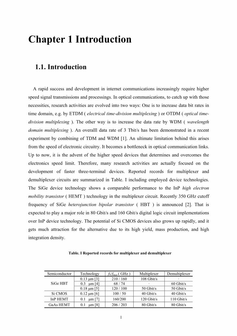
demultiplexer circuits are summarized in Table. I including employed device technologies.
The SiGe device technology shows a comparable performance to the InP high electron
mobility transistor ( HEMT ) technology in the multiplexer circuit. Recently 350 GHz cutoff
frequency of SiGe heterojunction bipolar transistor ( HBT ) is announced [2]. That is
expected to play a major role in 80 Gbit/s and 160 Gbit/s digital logic circuit implementations
over InP device technology. The potential of Si CMOS devices also grows up rapidly, and it
gets much attraction for the alternative due to its high yield, mass production, and high
integration density.
Chapter 1 Introduction
Table. I Reported records for multiplexer and demultiplexer
Semiconductor Technology fT/fmax ( GHz ) Multiplexer Demultiplexer 0.13 µm [3] 210 / 160 108 Gbit/s ·
0.3 µm [4] 68 / 74 · 60 Gbit/s SiGe HBT 0.18 µm [5] 120 / 100 50 Gbit/s 50 Gbit/s
Si CMOS 0.12 µm [6] 100 / 50 40 Gbit/s 40 Gbit/s InP HEMT 0.1 µm [7] 160/200 120 Gbit/s 110 Gbit/s
GaAs HEMT 0.1 µm [8] 206 / 203 80 Gbit/s 80 Gbit/s
2
Most of multiplexer and demultiplexer circuits listed in Table. I are built using transistor logic
cells, such as a master-slave flip-flop ( MS-FF ) or an emitter-coupled logic ( ECL ). For the
future development of 160 Gbit/s circuits faster electronic switching devices or concepts are
necessarily required in broadband fiber optic transmission links. Improving device speed
performance needs smaller gate length in HEMT devices, smaller transit time in HBTs, and
much lower parasitic components. Even the modern E-beam technology and photolithography
methods suffer from achieving both the gate length reduction and high reproducibility,
simultaneously. A scaling of the device dimension does not directly lead to the switching
speed improvement any more. Therefore, in order to overcome those deficiencies new design
concept is mandated in high-speed digital logic circuit implementation.
Si Schottky diodes already reach THz cutoff frequency band [9][10]. They are also
commercially available. Constructing digital circuits using Si Schottky diodes in an analog
way is a very challenging and promising issue due to the above viewpoint. One of possible
ways to consider is to design a digital circuit using Si Schottky diodes as switching elements,
namely using a sampling technique.
1.2. Motivations
One principle motivation is to demonstrate a demultiplexing functionality using Si
Schottky diodes in an analog way. Because Si Schottky diodes have cutoff frequencies greater
than 1 THz, it is certain that a proper analog signal processing method and circuit topology
will perform the high-speed demultiplexing function. A sampling circuit built with Si
Schottky diodes is a good candidate for the realization of the demultiplexing function. A
sampling technology is generally employed in high-speed measurement instruments as high
as 60 GHz [12]. In order to overcome a frequency limitation of electronics, the sampling
circuit controlled by short time pulses was developed. The sampling circuits’ application area
will be broadened in future [10][11], and the its application to the demultiplexer circuit is a
good example to consider.
Si technology is emerging for microwave and millimeter-wave integrated circuits. Silicon
monolithic millimeter-wave integrated circuits ( SIMMWICs ) have been found in many
applications such as sensorics and communications [9]. From active devices to passive
circuits they have been integrated on a semi-insulating Si substrates. A Si Schottky diode
based sampling circuit also can be integrated with other receiver circuit parts. A push-push
oscillator circuit is a good example to consider [13]. It generates two oscillating signals
3
simultaneously, and one output frequency is one half of another output. If the sampling circuit
based demultiplexer circuit is combined with the push-push oscillator circuit, a
demultiplexing function can be extended from 1:2 to 1:4. In this way, over 43 Gbit/s ETDM
optical receiver circuit will be constructed and integrated using the Si technology. This is a
significant aspect of the SIMMWIC for optical communication link applications. This concept
would be strongly anticipated to work soon.
In this work, we focus on a function of 43 Gbit/s demultiplexing using a flip-chip bonding
technology. However, in principle this sampling circuit concept is feasible in 80 Gbit/s and
160 Gbit/s demultiplexer circuit applications. We therefore present simulation results for an
80 Gbit/s demultiplexer circuit in Chapter 3 to show that the sampling circuit shall work for
the higher bit rates. However, the circuit for higher bit rates above 80 Gbit/s should be
fabricated in MMIC to minimize the parasitics.
Besides this, we should mention the advantage of the analog approach. It provides merits
over digital methods. In fact, the logic circuit consists of cascaded logic blocks. However, if
we use diodes instead of transistors as the switching device, we can considerably reduce the
used number of devices. In consequence, in realizing the demultiplexer the sampling circuit
concept shall reduce the complexity of the circuit. It is noted that in the analog approach the
post signal processor will be combined with the sampling unit. So the overall system will be
complicated. However, it has still advantages over the conventional digital circuits in
complexity.
1.3. Structure of the work
In Chapter 2, we describe a theory for the sampling circuit based demultiplexer, first of all.
We introduce an optically preamplified direct detection system for the theory description.
Essential elements for this system are discussed and introduced. We introduce receiver part
components, such as an erbium-doped fiber amplifier ( EDFA ), an optical band pass filter,
and a high-speed and high-power photodiode ( PD ). Analytical expressions for the sampling
circuit based demultiplexer are derived and calculated. Simulation results are presented and
algorithm routines are provided in Appendix B We also discuss a linear signal equalizer
following the sampling circuit. Two algorithms are explained to calculate equalizer
coefficients.
In Chapter 3, the Si Schottky diode modeling process is discussed. A theoretical
background for the Root-diode model is provided in detail. Modeling procedures are

4
described for IC-CAP program. The diode DC and AC measurement data are illustrated and
summarized. Diode modeling results were compared with the measurement data up to 50 GHz.
Then, the flip-chip bonding model simulation was carried out. In order to establish an
equivalent circuit model, we find out the discrete component values by interpolating the
simulation results. Fabrication processes and simulation environments are explained. A flip-
chip bonded Si Schottky diode module was measured and its result was compared with the
modeling result. The sampling circuit design and the simulations were performed under both
hybrid and MMIC fabrication conditions. The circuit design using the developed Root-diode
model is presented. Simulation results are given in each step. A linear equalizer circuit is
designed using the algorithm presented in Chapter 2. It is combined with the sampling circuit
and the eye waveform is obtained and evaluated. We also propose a 80 Gbit/s return-to-zero
( RZ ) demultiplexer circuit and simulations are provided.
In the following Chapter 4, the measurement results are discussed. The fabricated
conductor-backed coplanar waveguide ( CPW ) with via holes on an alumina substrate were
measured, analyzed and compared with analytical results. Then, a resistive power divider
circuit was discussed. This is an essential part in designing the hybrid 1:2 demultiplexer
circuit. The S-parameter measurement result is presented. We test the power divider circuit
using 43 Gbit/s nonreturn-to-zero ( NRZ ) and 86 Gbit/s RZ signals and the measured output
waveforms are provided. The sampling circuit was fabricated and measured. The
measurement set-up is described in detail. We discussed the measured transient output results.
Finally, in Chapter 5, the summary of the design and the experimental results are presented
and the conclusion will be made. The outlook for the analog approach to the higher bit rate
digital circuit will be discussed.
5
2.1. The Optical Receiver with Optical Preamplifier
2.1.1. Background
The transmission distance in a fiber optic transmission link is basically limited by fiber
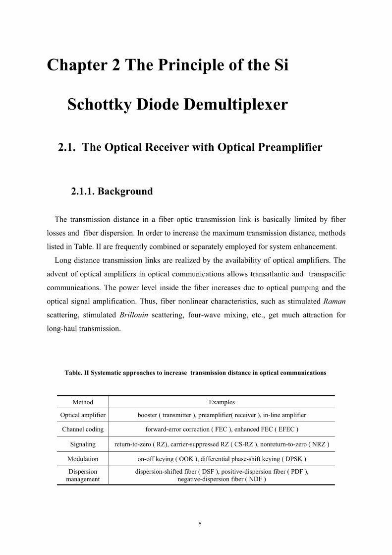
losses and fiber dispersion. In order to increase the maximum transmission distance, methods
listed in Table. II are frequently combined or separately employed for system enhancement.
Long distance transmission links are realized by the availability of optical amplifiers. The
advent of optical amplifiers in optical communications allows transatlantic and transpacific
communications. The power level inside the fiber increases due to optical pumping and the
optical signal amplification. Thus, fiber nonlinear characteristics, such as stimulated Raman
scattering, stimulated Brillouin scattering, four-wave mixing, etc., get much attraction for
long-haul transmission.
Chapter 2 The Principle of the Si
Schottky Diode Demultiplexer
Method Examples
Optical amplifier booster ( transmitter ), preamplifier( receiver ), in-line amplifier
Channel coding forward-error correction ( FEC ), enhanced FEC ( EFEC )
Signaling return-to-zero ( RZ), carrier-suppressed RZ ( CS-RZ ), nonreturn-to-zero ( NRZ )
Modulation on-off keying ( OOK ), differential phase-shift keying ( DPSK )
Dispersion management
dispersion-shifted fiber ( DSF ), positive-dispersion fiber ( PDF ), negative-dispersion fiber ( NDF )
Table. II Systematic approaches to increase transmission distance in optical communications
6
In this section, we will introduce the optically preamplified direct detection system
( OPDD ). Although many linear and nonlinear problems are necessarily explained to describe
the OPDD system, we will focus on essential elements to deal with this system.
At first, the fundamental fiber losses will be described. Those losses are intrinsic causes
reducing the transmission distance. It is significant to understand inherent reasons of the fiber
loss. Secondly, as the transmission speed and distance are increased, the second-order
properties, such as chromatic dispersion ( CMD ) and polarization mode dispersions ( PMD )
play important roles in determining system performance. Detailed explanation of each
phenomenon will be given. Discussions will be made in the system performance viewpoint.
The usage of the optical amplifier ( OA ) will be described. Even if the detailed operation
principle of the OA is avoided, their system usages and the encountered problems in the
system operation are discussed. Finally, high-speed and high-power photodetectors ( PDs )
are dealt in the following section. They are classified with their illumination geometries and
transporting carrier types. Operation principles are explained and compared with each other.
They are discussed with regard to the relation between bandwidth and maximum saturation
current.
2.1.2. Fiber Losses and Dispersions
2.1.2.1. Fiber losses
In the fiber, losses occur due to the following reasons : Rayleigh scattering, ultraviolet
absorption, infrared absorption, and waveguide imperfections [14].
Rayleigh scattering is an intrinsic and fundamental loss in the fiber due to the density
fluctuations in silica fibers. These density fluctuations induce refractive index fluctuations in
the fiber. Lightwave scattering due to this phenomenon is called Rayleigh scattering, and
described by the attenuation coefficients,
4λα C
Rayleigh = .
( 2.1 )
7
where the constant C is in the range of 0.7-0.9 dB/(km·)4. The Rayleighα value near
λ =1.55 is 0.12-0.15 dB/km, which is main contribution to the loss at this wavelength [15].
Silica molecules have electronic resonance in ultraviolet region below 0.4 and vibration
resonance above 7 wavelength ( infrared region ). These resonances yield absorption
depending on wavelength. The absorption extends to our spectral interest region from 1.3 to
1.55 . The loss due to the ultraviolet resonance and the infrared loss ( intrinsic loss ) in pure
silica is smaller than that due to Rayleigh scattering. However, the vibration spectral peak
caused by OH ion, forms a detrimental extrinsic loss in the fiber, which has harmonic
components at 1.39, 1.24, and 0.95 [14]. Reducing the loss due to OH ions is very
significantly associated with a low loss fiber.
Waveguide imperfections include core radius fluctuations in cable, macro bending loss, and
micro bending loss. In practice, core-cladding layer imperfections in the fiber cable can
generate net optical loss. During the fiber fabrication attention should be paid to control
uniform core radius. Macro bending loss represents a radiation loss due to a bend. The part of
the mode is scattered into the cladding layer. This scattered energy loses its power. The
radiation loss coefficient is given by [16]
)exp( 21 RccBEND −⋅=α
where, c1 and c2 are constants which are not dependent on R, and R is bending radius.
Whereas the macro bending satisfies R≫a ( fiber core radius ) condition, micro bending
loss occurs when R ~ a. That is attributed to the localized defects in the fiber. In a single mode
fiber, the micro bending loss can be minimized by confining the energy to the core. It means
that a parameter, so-called normalized frequency parameter ( v ) in fiber design, has the
value between 2 and 2.405 [14].
212
22
10 )(v nnak −=
where, a is core radius, n1 and n2 are a refractive index in the core and cladding layer,
respectively.
Power attenuation caused by above reasons in the fiber is governed by
( 2.2 )
( 2.3 )

8
PdzdP ⋅−= α
where α is the attenuation coefficient and P is the optical power inside the fiber. When the
launched power to the input of the fiber of the length L, then the output power of the fiber is
)Lexp( ⋅−⋅= αinout PP .
Expressing the α in units of dB/km, the following relation is obtained [14].
αα 343.4)/(10log10)/( =⋅−= inout PPLkmdB
In the spectral window of modern optical communications, λ=1.31 and 1.55 , the
attenuation coefficients show 0.35 dB/km and 0.2 dB/km, respectively. Recently, efforts to
reduce optical attenuation coefficient are exerted using a novel photonic crystal fiber ( PCF ).
The best performances ever reported using the PCF are 0.71 dB/km and 0.37 dB/km for
1.31 and 1.55 , respectively [17]. They reduced the optical attenuation coefficient by
avoiding the inclusion of OH ion during fabrication processes. The absorption loss by OH ion
was measured and found to contribute the loss of 0.12 dB/km at 1.55 . They also indicated
that by eliminating the loss by OH ions and reducing the surface roughness in PCF, the
optical loss of the PCF can be less than that of a conventional fiber. Even if the PCF
nowadays does not show better performance than the normal fiber, it is expected that it will
replace the current fiber in future.
2.1.2.2. Chromatic dispersion ( CMD )
Chromatic dispersion is also called group velocity dispersion ( GVD ). This dispersion
phenomenon is attributed to the interaction of the two underlying effects, namely the material
dispersion and the waveguide dispersion. The chromatic dispersion parameter, D, is written as
a linear sum of each dispersion parameter as
WM DDD +=
( 2.4 )
( 2.5 )
( 2.6 )
( 2.7 )
9
where, DM is a dispersion parameter of the material in the fiber ( silica ), and DW is from the
waveguide effect of the fiber.
As the dielectric medium has its own resonance frequencies, the refractive index, n, is
dependent on the optical angular frequency, ω . This dependency is well suited with the
Sellmeier equation [15],
∑= −
+=M
j j
jjBn
122
22 1)(
ωω
ωω
where jω is the resonance frequency and Bj is the oscillation strength.
This equation describes that spectral components travel different velocities, c/n(ω). Mode
propagation constant, β , accounts for the effects of CMD. Expanding β using a Talyor
series about the center frequency, oω , the following equation is obtained as,
L+−+−+== 202010 )(
21)()()( ωωβωωββωωωβ
cn
where, ),2,1,0(0
K=
=
=
mdd
m
m
mωω
ωββ .
The parameter 1β and 2β are found with the relation of the refractive index and its
derivatives with regard to the optical frequency are shown here.
+===
ωω
υβ
ddnn
ccn g
g
11
11
11
+= 2
12
12 21
ωω
ωβ
dnd
ddn
c
where, gn1 is the group refractive index of the core, and gυ is the group velocity. The 1β is
responsible for the group velocity whereas the 2β represents the group velocity dispersion.
( 2.8 )
( 2.9 )
( 2.10 )
( 2.11 )
10
The material dispersion parameter is expressed as width
λddn
cD g
M21
=
where n2g represents the group index of the cladding material [14].
When the dispersion parameter, DM, is zero, the corresponding wavelength is called a zero-
dispersion wavelength, λZD. This wavelength can be varied changing the doping materials in
the core and cladding layer. Its range is about 1.27 – 1.29 for pure silica [14]. It should be
noted that the dispersion behavior at λZD should include the third-order distortion ( TOD )
parameter, 3β . Its inclusion is necessary only when the operating wavelength is a few
nanometers different from the λZD , for instance.
The contribution of the waveguide effect to the dispersion parameter D is given
+⋅
∆−=
dVVbd
ddn
dVVbVd
nnD gg
W)()(2 2
2
2
2
22
2 ωωλπ
where, 21
20
nnnk
b−−
=β
, k0 is the free space propagation constant, and 1
21
nnn −
=∆ [14]. The
DW shows negative value in the wavelength region of our interest ( 1.1 – 1.7 ). Therefore,
the zero dispersion wavelength λZD due to material dispersion is shifted into higher
wavelength value. Incorporating the waveguide dispersion with the material dispersion
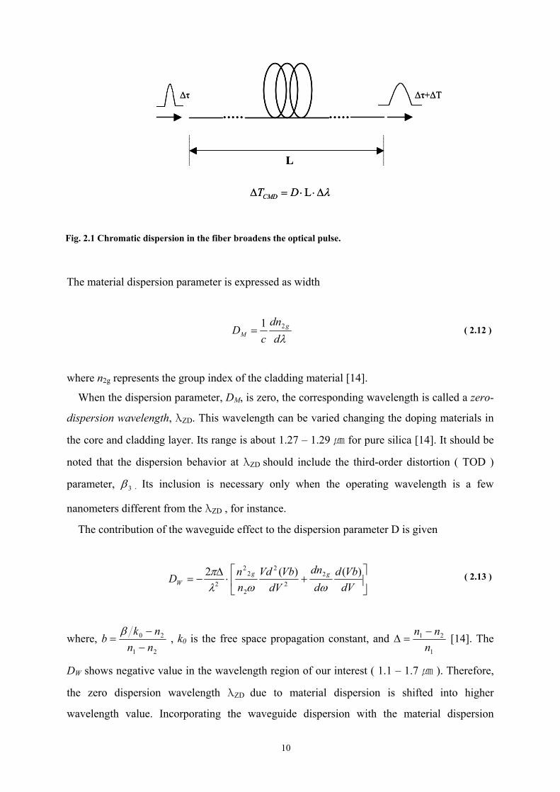
Fig. 2.1 Chromatic dispersion in the fiber broadens the optical pulse.
( 2.12 )
( 2.13 )
L
∆τ ∆τ+∆T
λ∆⋅⋅=∆ LDTCMD
L
∆τ ∆τ+∆T
λ∆⋅⋅=∆ LDTCMD

11
parameter, the λZD can be shifted into 1.55 , at which most of modern optical
communications are implemented. For example, using double-clad or quadruple-clad layer
dispersion parameter, D, can have very small dispersion value in wide range of wavelength
from 1.3 to 1.55 . This is so-called dispersion-flattened fiber. This fiber is advantageous
in ( dense ) wavelength-division multiplexing ( (D)WDM ) applications because wide rages of
wavelengths are employed in the system.
The total dispersion parameter D is given by
221 2 β
λπ
λβ c
dd
DDD WM −==+= .
By its convention the total dispersion parameter is expressed using D although its sign is
reversed compared with 2β . Its dimension is given ps/(km)(nm). In fact, the dispersion has a
positive value above λZD. In this range the longer wavelength signal travels slower than the
shorter wavelength. This anomalous behavior is of great interest in soliton communications,
which cancel the pulse broadening effect combining with a signal chirping. The chirping is
related with the fiber nonlinearities: the refractive index is also dependent on the optical
power as well as the optical frequency. This is attributed to the third-order polarization
dependence on the optical intensity [14]. Further discussion, however, is beyond of our
consideration in this chapter, thus is omitted here.
2.1.2.3. Polarization mode dispersion ( PMD )
Fundamental limitations of real fiber characteristics, such as core shape, ideal symmetry
along the fiber, and uniform refractive index distribution, etc., cause polarization-dependent
nondegeneracy. Even if the two orthogonally polarized fundamental modes are injected into
the single mode fiber, each field mode experiences different mode index, and couples each
other randomly. At the output of the fiber, each polarized mode arrives at a different time
yielding the pulse broadening. This phenomenon is called polarization mode dispersion
( PMD ). Analytically, PMD related system performance restriction can be explained with
regard to fiber modal birefringence. This property explains that orthogonal modes in x and y
direction have a different propagation constant. It is defined as
( 2.14 )

12
yxyx
m nnk
B −=−
=0
ββ
If we assume that Bm is constant along the fiber, the pulse broadening is shown
ωββ
ddB
kLLvL
vLT m
yxgygx
011 ⋅=−⋅=−=∆ .
Since Bm is random along the fiber, it is desirable to express using its variance given by
LD
hL
hL
hLhT
p
PMD
=
>⋅∆≈
−+−⋅∆=∆=
)km 0.1L (
2exp1221)(
1
221
22
β
βσ
where, h is the decorrelation length and Dp is the PMD parameter [14]. It is noted that the
variance of the PMD has a dependence of L1/2 and is a limiting factor in long-haul
transmission system operated in near λZD.
Fig. 2.2 Each polarization mode has a different group velocity. Thus, after fiber length L each polarized mode arrives at different time.
( 2.15 )
( 2.16 )
( 2.17 )
L
∆T
( ) L22PPMD DT =∆=σ
x
y
z
y
z
x
L
∆T
( ) L22PPMD DT =∆=σ
x
y
z
y
z
x

13
In the optical receiver design viewpoint, this PMD is of significance because this is actually
a random phenomenon in the installed fiber. Ultimately, uncontrolled PMD in the system
degrades bit error rate ( BER ) in the receiver. An adaptive signal processing in the receiver
side is an effective technique to mitigate the influence of the PMD. So far this technique is
implemented in the two domain: one is optical signal domain, and the other is electrical
domain. Further discussion will be done in later chapter.
2.1.3. Optical Amplifiers ( OAs )
In early stage of long-haul transmission system development, an electronic regeneration has
been used to overcome losses and dispersions. The regenerator converts the optical signal into
the electrical signal ( OE ), then amplifies and regenerates the signal electronically, and
finally converts the signal into an optical signal again ( EO ). These signal conversions
( OEO ), however, become problematic in multi channel lightwave systems, as the regenerator
modules become quite complex and expensive. An emerged candidate instead of the
electronic regenerators allowing long-haul transmission is an optical amplifier.
(a)
(b)
(c)
Fig. 2.3 Optical amplifier usages. (a) booster (b) in-line amplifier (c) preamplifier
Transmitter( TX )
Receiver( RX )
Transmitter( TX )
Receiver( RX )
Transmitter( TX )
Receiver( RX )
Transmitter( TX )
Receiver( RX )
Transmitter( TX )
Receiver( RX )
Transmitter( TX )
Receiver( RX )
14
Until mid-1990s, the development of erbium-doped fiber amplifier ( EDFAs ) looks more
attractive over Raman amplification, because EDFA needs less pump power than the Raman
optical amplifier does. After the success of high pump power development for the Raman
amplification, the Raman amplifier employment in real transmission experiment has been
increased considerably [18].
The usage for the optical amplifier is found as three ways. One is the optical booster in the
transmitter part, that enables the system have longer transmission span. But, due to high
optical power nonlinear problems occur : such as stimulated Raman scattering ( SRS ),
stimulated Brillouin scattering ( SBS ), four-wave mixing ( FWM ), self-phase modulation
( SPM ), and cross-phase modulation ( XPM ). In a consequence, reducing the optical power
in the transmission fiber and simultaneously satisfying the required optical signal to noise
power ratio ( OSNR ) at the system output is of our concern. That will be accomplished by
reducing the loss per span length, and(or) using in-line amplifications ( e.g. the Raman
amplification ).
We find the second usage of the optical amplifier as in-line amplifier in [19]. They jointly
used the EDFA and the Raman amplifier for the in-line amplification. After the Raman
amplification along the transmission fiber, the C-band ( 1528 – 1561 nm ) and the L-band
( 1561 – 1620 nm ) amplifications are successively done respectively using EDFAs. Optical
splitters are inserted for the separate band amplification. They have demonstrated 3.2 Tbit/s
capacity transmission using standard single-mode fiber ( SSMF ) employing those optical
amplifiers.
The third usage for the optical amplifier is the preamplification of the optical signal prior to
the electronic receiver. By amplifying the optical signal, receiver sensitivity is enhanced and
may approach to the limit of the optical heterodyne detection systems [20]. Furthermore, the
resultant electrical signal after the optical amplifier is large enough to drive the following
demultiplexer circuit and decision circuit without electrical preamplifier and limiting
amplifier. Therefore, the receiver system becomes more simple in reality.
2.1.4. High-speed and high-power photodetectors
High-speed and high-power photodetector ( PD ) is an essential element to realize the
OPDD receiver system. The optical amplifier ( EDFA ) in front the PD increases the optical

15
power falling upon the PD, and then increases the signal to noise ratio ( SNR ). The
transmission distance is also increased in this way. High-power PDs can considerably reduce
RF insertion loss, and increase the spurious-free dynamic range [21]. In the context, high-
power photodiodes mean an output voltage of 200 mVpp at 50 Ω.
As optical power incident upon the photodetector increases, the number of generated
electron-hole pairs ( EHPs ) is increased. Those carriers in turn decrease the electrical field
inside the transit region. The field is formed by reverse bias and accelerates the carriers
generated by the incident optical light. The decreased electrical field accounts for the
increased transit time through the intrinsic layer for p-i-n type PD ( electric field screening
effect ). Therefore, the increased optical power in the OPDD system decreases the intrinsic
electrical bandwidth of the PD, thus limits the high saturation current in the high-speed PD.
The other factors to limit the maximum available saturation current are thermal effects in the
PD, and the breakdown as the current density increases [22].
In fact, the PD bandwidth for p-i-n type PD is composed of two components, RCτ and trτ ,
thus
)(21
RCtrpinf
ττπ +=
where, dtr W υτ /= , W is a transit layer width, dυ is a drift velocity corresponding to the
( 2.18 )
Table. III Photodetectors are classified with respect to the illumination geometry and transporting carriers
Illumination Geometry
Carrier multiplication Avalanche PDs ( InP, Si, super-lattice )
Surface-illumination Carrier nonmultiplication
p-i-n PD , MSM PD
( metal-semiconductor-metal )
Edge-illumination Traveling-wave PD ( TWPD )
Waveguide PD ( WGPD ) Velocity-matched distributed PD ( VMDP )
Single carrier Uni-traveling carrier PD ( UTC-PD )
Two carriers ( electron and hole ) p-i-n PD, MSM PD, edge-illuminated PDs
Transporting Carriers
Multiplied carriers Avalanche PDs
16
electrical field, and psLRC CRR ⋅+= )(τ is the time constant by the parasitic capacitance
( Cp ) and the series connection of the series resistance ( Rs ) and the load resistance ( RL ).
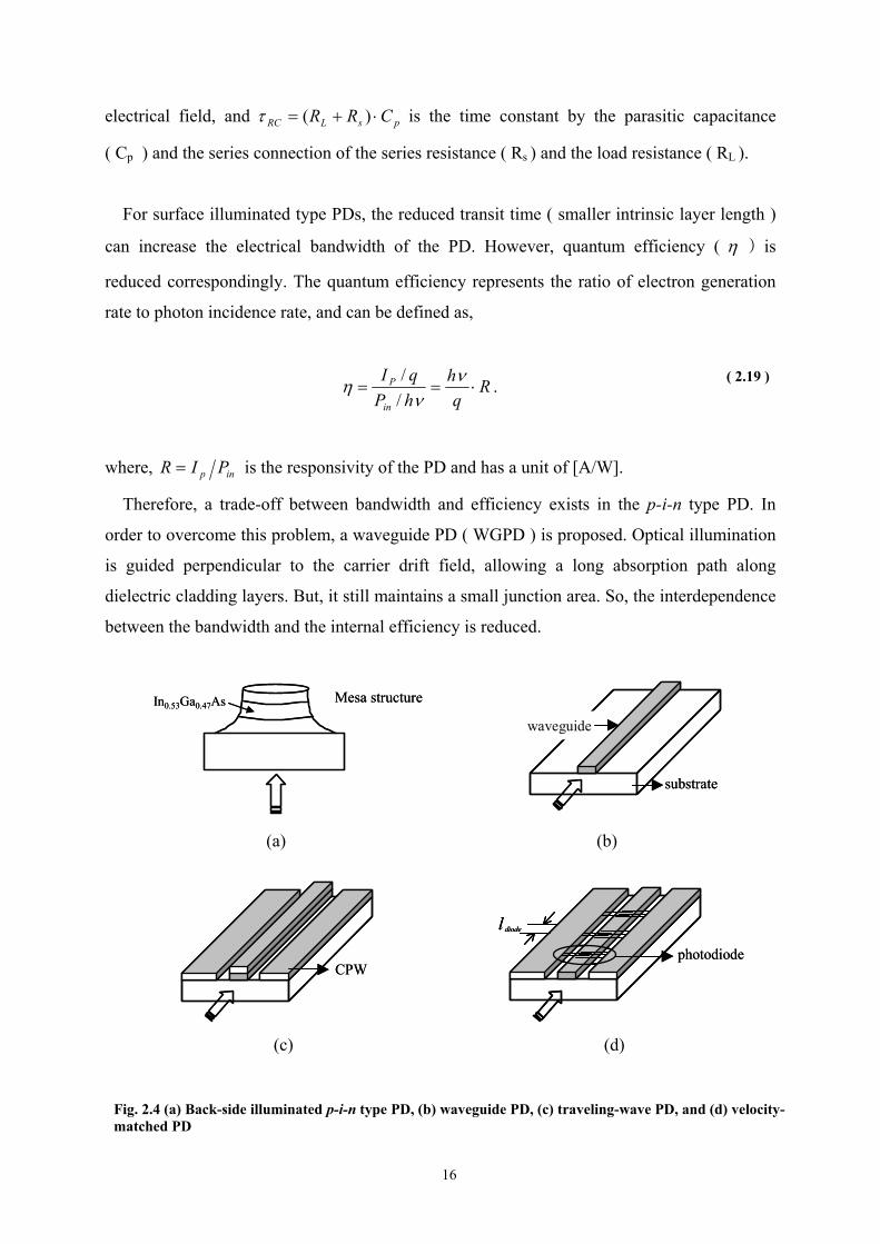
For surface illuminated type PDs, the reduced transit time ( smaller intrinsic layer length )
can increase the electrical bandwidth of the PD. However, quantum efficiency ( η ) is
reduced correspondingly. The quantum efficiency represents the ratio of electron generation
rate to photon incidence rate, and can be defined as,
Rq
hhPqI
in
P ⋅==ν
νη
// .
where, inp PIR = is the responsivity of the PD and has a unit of [A/W].
Therefore, a trade-off between bandwidth and efficiency exists in the p-i-n type PD. In
order to overcome this problem, a waveguide PD ( WGPD ) is proposed. Optical illumination
is guided perpendicular to the carrier drift field, allowing a long absorption path along
dielectric cladding layers. But, it still maintains a small junction area. So, the interdependence
between the bandwidth and the internal efficiency is reduced.
(a) (b)
(c) (d)
( 2.19 )
Fig. 2.4 (a) Back-side illuminated p-i-n type PD, (b) waveguide PD, (c) traveling-wave PD, and (d) velocity-matched PD
CPWCPWphotodiode
diodel
photodiode
diodel diodel
substrate
waveguide
substrate
waveguide
Mesa structureIn0.53Ga0.47As Mesa structureIn0.53Ga0.47As
17
The quantum efficiency of the WGPD is written as
L
WGPD e Γ−−= αη 1
where, α is an absorption constant, Γ is a confinement factor of the light, and L is the whole
optical dielectric waveguide. In general, the optical light confinement factor is given using the
optical field distribution at the PD.
∫
∫∞
∞−
=Γdyy
dyy
yj
layerabsorption
yj
2
2
)(
)(
φ
φ
where, )(yyjφ is the optical field in the waveguide, and y is the direction perpendicular to the
diode junction layer. Physically, the confinement factor describes how much the incident
optical power effectively couples to the absorption layer. In practice, the optical field at the
WGPD is much narrower than the transverse extension of the optical field from the fiber. In
[23], a multimode WGPD is proposed enlarging the optical field at the PD without sacrificing
the bandwidth. High-doped quaternary InGaAsP forms double core around InGaAs
absorption layer and confines the optical field in transverse direction. Thus, the increased
coupling efficiency was obtained successively.
There is an inherent defect in the WGPD that the electrical signal is reflected if the
electrical waveguide is not terminated correctly. This causes pulse broadening. Matching the
characteristic impedance of the PD and supporting coplanar waveguide along the dielectric
waveguide, a traveling-wave photodetector ( TWPD ) is designed and implemented [24]. The
dBf3 in the TWPD can be expressed below
23
1
+
=
VM
t
tdB
ff
ff
( 2.20 )
( 2.21 )
( 2.22 )

18
where, tf is an electrical bandwidth limited by the carrier transit time, and VMf is defined for
matched termination at the output using electrical wave velocity ( eυ ) and optical wave
velocity ( oυ ) in the semiconductor [22] as below,
−
Γ=
o
e
eVMf
υυ
π
αυ
12
Velocity mismatch occurs because the electrical signal along the coplanar waveguide
( CPW ) travels in different velocity with the guided optical signal along the waveguide. As
eυ is given,
00
1wZ
dCL rtrtr
e εευ =
⋅=
where, d is the transit layer thickness, w is the width of the WGPD, and Z0 is characteristic
impedance of the CPW ( trtr CL= ), the electrical velocity can be as close as to the optical
light velocity in the waveguide choosing the proper CPW geometry parameters. The quantum
efficiency of the TWPD ( input matching case ) is expressed by
21 L
TWPDe Γ−−
=α
η .
Considering the high power capability of the PD, we should consider saturation current in
each type PD. For the TWPD [21],
∫=
Γ−
Γ=Γ⋅
Γ⋅=
L
xTWPDs
xTWPDSAT IWdxePdWqI
00, 2
1 ηα
α α
where, sI is the saturation photocurrent density per unit area, and oP is the incident photon
flux per unit area at the saturation condition ( sec//1 2mµ ). In the same way, for the WGPD
[21],
( 2.23 )
( 2.24 )
( 2.25 )
( 2.26 )

19
WGPDsWGPDSAT IWI ηα Γ
=,
As Γα decreases, TWPDSATI , value increases, which provides improved power handing
capability. In contrast to the increased TWPDSATI , , the 3dB bandwidth decreases as the VMf is
proportional to Γα . Therefore, there exists a trade-off between the bandwidth and the power
capability in the TWPD.
The velocity mismatch can be eliminated by periodic capacitance loading effect. In fact, the
electrical signal velocity in the CPW structure is around 35 % faster than the optical guided
wave [21]. Therefore, distributing the PD in a periodic way, the electrical signal velocity can
be slowed, and matches with the optical wave in the semiconductor. The electrical wave
velocity is given in the periodic structure as,
( )dtrtre lCCL 0
1+⋅
=υ
where, 0C is the capacitance by each PD and dl is the distance between PDs. These PDs are
called velocity-matched distributed PDs ( VMDPs ). The detected electrical signal in each PD
is collected in-phase, and high output current can be expected. Distinctive advantages in the
VMDP are not only equivalent bandwidth to the transit time limited bandwidth ( tf ) of a
single PD, but also the separate design optimizations for the PD, the optical waveguide, and
the electrical transmission line. The PD can be designed to have maximum allowable
bandwidth, and the optical waveguide lines are independently optimized with respect to the
single mode operation and the improved coupling efficiency. For the electrical transmission
line, the micro strip line shall be used for the electrical signal summation, and be accounted
for the characteristic impedance and the velocity matching. The saturation current for the
VMDP is calculated as the summation of the each PD given by [21],
∑∫=
−Γ−−
=
Γ− ⋅⋅ΓΓ
=N
m
mlml
x
xVMDPSAT
diodediode
edxePdWqI1
)1()1(2
00,
αα κα
( 2.27 )
( 2.28 )
( 2.29 )
20
where, κ is the coupling efficiency between the optical waveguide line and the individual PD,
N is the number of employed diodes, diodel is the length of each PD, and the quantum
efficiency of the VMDP is,
20
20
)1(1))1((1
21
κηκηη
α
−−−−−
=Γ− Nl
VMDP
diodee .
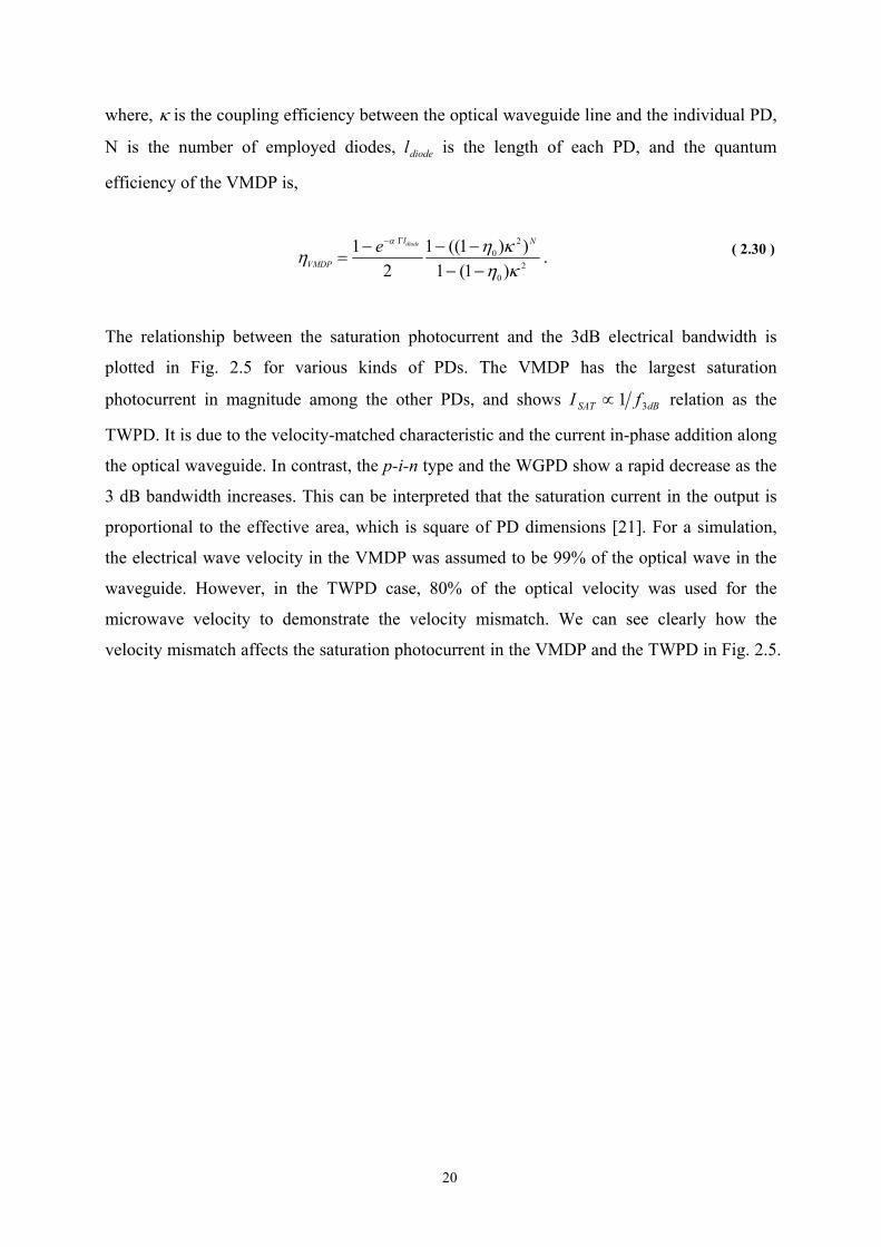
The relationship between the saturation photocurrent and the 3dB electrical bandwidth is
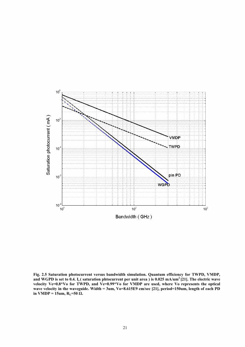
plotted in Fig. 2.5 for various kinds of PDs. The VMDP has the largest saturation
photocurrent in magnitude among the other PDs, and shows dBSAT fI 31∝ relation as the
TWPD. It is due to the velocity-matched characteristic and the current in-phase addition along
the optical waveguide. In contrast, the p-i-n type and the WGPD show a rapid decrease as the
3 dB bandwidth increases. This can be interpreted that the saturation current in the output is
proportional to the effective area, which is square of PD dimensions [21]. For a simulation,
the electrical wave velocity in the VMDP was assumed to be 99% of the optical wave in the
waveguide. However, in the TWPD case, 80% of the optical velocity was used for the
microwave velocity to demonstrate the velocity mismatch. We can see clearly how the
velocity mismatch affects the saturation photocurrent in the VMDP and the TWPD in Fig. 2.5.
( 2.30 )
21
Fig. 2.5 Saturation photocurrent versus bandwidth simulation. Quantum efficiency for TWPD, VMDP, and WGPD is set to 0.4. Is ( saturation phtocurrent per unit area ) is 0.025 mA/um2 [21]. The electric wave velocity Ve=0.8*Vo for TWPD, and Ve=0.99*Vo for VMDP are used, where Vo represents the optical wave velocity in the waveguide. Width = 3um, Vo=8.615E9 cm/sec [21], period=150um, length of each PD in VMDP = 15um, RL=50 Ω.

22
2.2. System model for an optically preamplified direct detection receiver system
2.2.1. Introduction
The system block diagram for an optically preamplified direct detection ( OPDD ) receiver
is presented in Fig. 2.6. The light intensity is modulated in laser to transmit data stream. In
long-haul transmission system, optical amplifiers such as the Raman and(or) the EDFA
amplifier are utilized to increase optical signal power. In the OPDD system, the signal is
amplified by the EDFA ( C-band, L-band ) before the optical signal arrives the PD. In most
wavelength-division multiplexing ( WDM ) system, the optical band pass filter is located
between the EDFA and the PD. It reduces the amplified spontaneous emission ( ASE ) noise
generated in the EDFA. Regarding the ASE noise, it will be discussed in the following section.
Then, the PD directly detects the optical signal and converts into an electrical signal. The
detected electrical signal is large enough to drive the following demultiplexer circuit. Thus,
the sampling circuit based demultiplexer circuit can be directly connected to the photodetector
without further electrical amplification. In the conventional 2.5 Gbit/s and 10 Gbit/s optical
receivers without optical amplifier, the electrical current after the PD is too low for direct
digital processing in the demultiplexer and the decision circuit. Thus, so far a low noise
preamplifier and a limiting amplifier circuit have been used. Furthermore, they increase the
Fig. 2.6 System block diagram for an optically preamplified direct detection receiver with sampling circuit concept.
R
t = (k+1)Ts
fc@3dB
fc@3dBPush-push
VCO
180°
Resistive power divider
Erbium-dopedfiber amplifier
nASE
Bandpass filter
High-power photodiode
t = kTs
R
R
Equalizer
Equalizer
Phase detector Filter
R
t = (k+1)Ts
fc@3dB
fc@3dBPush-push
VCO
180°
Resistive power divider
Erbium-dopedfiber amplifier
nASE
Bandpass filter
High-power photodiode
t = kTs
R
R
Equalizer
Equalizer
Phase detector Filter
23
complexity of the optical receiver system and degrade the system performances ( power
consumption, bit error rate, etc. ). However, in the OPDD receiver system, thanks to the
optical preamplifier and the high-power PD, we expect high amplitude voltage ( current ) at
the output of the PD. The signal shall be directly processed in the following demultiplexer
circuit. We utilize this concept to construct the sampling circuit based optical receiver circuit
and illustrate this configuration in Fig. 2.6.
From the EDFA to the photodetector, it is equivalent to the conventional OPDD receiver
system. We describe here only the receiver side including the optical amplifier ( EDFA ) and
the band pass filter. It is an effective way to analyze the receiver performance excluding the
transmitter part. In this section, we describe the system model analytically for the OPDD
receiver components ( the EDFA, the optical band pass filter, and the PD ). We provide the
system characteristic functions and noise statistics when necessary. Using those analytic
descriptions above, we further present the sampling circuit based demultiplexer circuit and the
equalizer, in later sections.
2.2.1.1. System model of the EDFA
While the EDFA amplifies the optical signal, it also generates a noise component, the so-
called an amplified spontaneous emission ( ASE ) noise. It is a significant noise quantity to be
considered in a high sensitivity receiver. The EDFA can be represented equivalently with a
frequency-dependent gain ( )(υG ), and the noise figure, F . The ASE noise after signal
amplification in the EDFA is modeled as a circularly symmetric additive white Gaussian
noise process [31]. The single-sided ASE noise power spectral density is written
νννν hGnS effspASE ⋅−= )1)()(()(
where, )(νeffspn is spontaneous emission factor, )(υG is effective gain of the EDFA, h is the
Planck constant ( 6.626·10-34 J·sec ), and ν is the optical frequency. When the influence of
the incoherent background light is included in the noise power, the amplifiers’ equivalent
noise figure, equiF , is expressed as [31]
( 2.31 )

24
equibASE FGhSGS ⋅⋅⋅=⋅+ )(21)( ννν
bsp
eff
bequi ShcG
GnShFF ⋅
⋅+
−=⋅+= − λ
νννν 2
)()1)()((2)(2 1
where, F is the noise figure of the EDFA, and bS is the power spectral density ( PSD ) of the
incoherent background light.
It should be noted that relying on the signal level to be amplified in the EDFA, the
dominant noise sources are different. For a logical zero level ( ‘0’ ), a spontaneous-
spontaneous beat noise dominates, whereas a signal-spontaneous beat noise is significant for a
logical one level ( ‘1’ ). Furthermore, the probability density function ( PDF ) for each
dominating noise source has been verified theoretically as a non-Gaussian. However, the
Gaussian approximation for those noise components shows very little difference, 0.3 dB [32].
Therefore, we will use the Gaussian pdf of the ASE noise without loss of generality.
2.2.1.2. Optical band pass filters
After the broadband amplification, an optical band pass filter follows the EDFA. In the
WDM system, optical spectral filters can be classified relying on the physical phenomenon;
interference and diffraction. A typical band pass filter which takes an advantage of the
interference is the Fabry-Perot filter ( FPF ). It consists of two high-reflectance multi layers
separated by 2λ . So, spectral characteristic peaks sharply at wavelength of multiples of
2λ . Its transfer function is written below under the assumption of Lorentzian distribution,
FWHM/211
2)(
νπνααν
jjH FPF +
=+
=
where the FWHM ( πα= ) stands for full width at half maximum or at the 3dB frequency
[31][33].
The other band pass filter used in WDM system is fiber Bragg grating ( FBG ) band pass
filter. A Bragg grating is an one dimensional periodic array which has multiple semi-
( 2.32 )
( 2.33 )
( 2.34 )
25
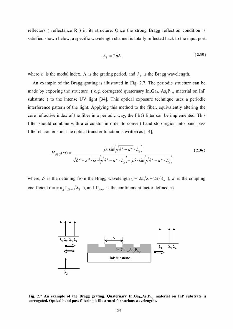
reflectors ( reflectance R ) in its structure. Once the strong Bragg reflection condition is
satisfied shown below, a specific wavelength channel is totally reflected back to the input port.
Λ= nB 2λ
where n is the modal index, Λ is the grating period, and Bλ is the Bragg wavelength.
An example of the Bragg grating is illustrated in Fig. 2.7. The periodic structure can be
made by exposing the structure ( e.g. corrugated quaternary InxGa1-xAsyP1-y material on InP
substrate ) to the intense UV light [34]. This optical exposure technique uses a periodic
interference pattern of the light. Applying this method to the fiber, equivalently altering the
core refractive index of the fiber in a periodic way, the FBG filter can be implemented. This
filter should combine with a circulator in order to convert band stop region into band pass
filter characteristic. The optical transfer function is written as [14],
( )( ) ( )gg
gFBG
LjL
LjH
⋅−⋅−⋅−⋅−
⋅−=
222222
22
sincos
sin)(
κδδκδκδ
κδκω
where, δ is the detuning from the Bragg wavelength ( = Bλπλπ 22 − ), κ is the coupling
coefficient ( Bfibergn λπ Γ= ), and fiberΓ is the confinement factor defined as
( 2.35 )
( 2.36 )
Fig. 2.7 An example of the Bragg grating. Quaternary InxGa1-xAsyP1-y material on InP substrate is corrugated. Optical band pass filtering is illustrated for various wavelengths.
λ1 λ2 λ3 λ4
λ1 λ3 λ4
λ2
InP substrate
Λ
InxGa1-xAsyP1-y
λ1 λ2 λ3 λ4λ1 λ2 λ3 λ4
λ1 λ3 λ4λ1 λ3 λ4
λ2λ2
InP substrate
Λ
InxGa1-xAsyP1-y
InP substrate
Λ
InxGa1-xAsyP1-y
26
∫
∫∞
⋅
⋅==Γ
0
2
0
2
ρρ
ρρ
dE
dE
PP
x
a
x
total
corefiber
It is desirable to note that the bandwidth of the optical band pass filter impacts on the signal
and the noise power related with the coding scheme; non return-to-zero ( NRZ ) and return-to-
zero ( RZ ). It has been shown that ( see e.g. [35] ) for RZ signal the narrow bandwidth of the
optical filter decrease the signal energy whereas it increases the intersymbol interference
( ISI ) for NRZ. There should be a tradeoff for the NRZ coding between the ISI and the ASE-
ASE beat noise in choosing an optimum optical bandwidth of the filter. In contrast, for RZ,
the ISI does not play a significant role in determining the optimum optical bandwidth, thus the
ASE-ASE beat noise component should be considered to be minimum.
2.2.1.3. Photocurrent and noise
For the coherent electromagnetic field, the detection probability of photons is modeled by a
Poisson probability distribution. In [37], the photocurrent is considered as a stochastic process
when the photon falling at the PD is also a stochastic process. It has been shown that the
photoelectrons also have the Poisson distribution. The photoelectron generation rate is
expressed with the product of the photon arrival rate ( )(tphλ ) and the quantum efficiency of
the photon detector (η ). In this way, we can relate the photon statistics with the generated
photoelectron,
)()( tt phληλ ⋅=
where )(tphλ has the dimension of [number of photons/sec] and is defined as νhPopt . Here
optP stands for the optical power. During incremental time interval t∆ , the probability P to
find out photoelectrons is [41]
ttP ∆⋅= )(λ .
( 2.37 )
( 2.38 )
( 2.39 )

27
When photoelectrons are produced by the arrival of photons with the ratio given in ( 2.38 ),
we can assume that the electric pulse )(th with the area of q ( unit charge ) is stimulated. If
this event occurs at tkt ∆= , the pulse is delayed by tk∆ , )( tkth ∆− . Thus, electric current
)(tiPD is given by a linear superposition of the electric pulse )(th with time interval t∆ [38].
[ ]
)()(
)2()2()()()()0()()()(
tkthtkX
tthtXtthtXthXtthtXti
k
PD
∆−⋅∆=
+∆−⋅∆+∆−⋅∆+⋅+∆+⋅∆−+=
∑∞
−∞=
LL
where 1,0)( ∈⋅X is a random variable which takes ‘1’ with probability P and ‘0’ with ( 1-P ).
Ensemble average and variance of the photocurrent, which determine the statistical
characteristic of the detected photocurrent, are calculated in the following. Throughout the
derivation processes, the ⋅ symbol denotes an ensemble average.
First of all, the ensemble average of the photocurrent is expressed using the above equation
as,
( )∑∑∞
−∞=
∞
−∞=
∆−⋅∆=∆−⋅∆=kk
PD tkthtkPtkthtkXti )()()()(
Here we should note that equation ( 2.39 ) considers only one realization of the random
process. However, when we treat with the ensemble average, the probability ( )tkP ∆ is
expressed using the total probability theorem [36],
( ) ( ) ( )∫∞
∞−
== dλpkPkP λλλ
where ( )λp stands for the probability density function ( pdf ) of the random process )(tλ . By
physical interpretation, ( )λ=λkP equals to λ because the number of generated
photoelectron during time interval t∆ given the condition of photoelectron generation rate
( )tλ is ( )tλ t∆ . Therefore, the probability equals to
( 2.40 )
( 2.41 )
( 2.42 )
28
( ) λλλ =∆∆⋅
==t
tkP λ .
Inserting ( 2.43 ) into ( 2.42 ), we express the probability ( )kP as,
( ) ( ) ( ) ( ) λλλλλ =⋅=== ∫∫∞
∞−
∞
∞−
dλpdλpkPkP λ .
Inserting ( 2.44 ) into ( 2.41 ) and taking a limit as 0→∆t , we obtain the following relation,
)(*)(
)()(
)()(lim)(0
tht
dth
tkthtktiktPD
λ
τττλ
λ
=
−⋅=
∆−⋅∆=
∫
∑
∞
∞−
∞
−∞=→∆
.
The * symbol represents a convolution defined below
∫∞
∞−
−⋅= τττ dtgftgf )()())(*(
Using the following definition of the sensitivity of the photodetector,
Rq
h⋅=
νη
where R is the responsivity of the photodetector and has the unit of [ A/W ], the photoelectron
generation rate is written by,
optop
ph
PqR
hP
Rq
h
tt
⋅=
⋅
⋅=
⋅=
νν
ληλ )()(
.
( 2.43 )
( 2.44 )
( 2.45 )
( 2.46 )
( 2.47 )
( 2.48 )

29
The optical field intensity after the optical band pass filter in the optically preamplified
direct detection ( OPDD ) system is modeled as a normalized complex optical field as [47],
)()()( ttOt SIG NRX OO +=
where )(tOSIG means the complex envelope of the deterministic signal, and )(tNO stands for
the ASE noise of which characteristic is the stationary, circularly symmetric, complex
Gaussian process. It is noted that we use the bold notation in order to indicate the random
noise process. So, the optical power optP is given by
)()(2)()()( *222 ttOttOtP SIGSIGopt NNRX OOO ⋅ℜ⋅++==
where ( )ℜ denotes the real part of a complex number and ( )*⋅ symbol represents a complex
conjugate. Substituting equation ( 2.45 ) with ( 2.48 ) and ( 2.50 ),
( )
)(*)()(2)()(
)(*)()(
*22
2
thttOttOR
thtqRti
PDSIGSIG
PD
NN
RX
OO
O
⋅ℜ⋅++=
=
where we replace qth )( with )(thPD , thus the )(thPD area is normalized as
1)()(1∫∫∞
∞−
∞
∞−
== dtthdtthq PD .
Using the fact that the stationary zero mean process of the noise )(tNO , 2)(tPN NO= , and
22 )()()( tOtOtp SIGSIGSIG == we can simplify equation ( 2.51 ) as
NPDSIG
PDNPDSIGPD
PRthtpR
thPRthtpRti
⋅+⋅=
⋅+⋅=
)(*)(
)(*)(*)()(
( 2.49 )
( 2.50 )
( 2.51 )
( 2.52 )
( 2.53 )
30
Next, the autocovariance of )(tiPD is induced, and the detailed derivation process is
presented in Appendix A and [39][40].
( ) ∫ ∫∞
∞−
∞
∞−
∆
−−+⋅=
−=∆⋅∆=
')'()()',()(*)(
)'()()'()()'()()',(
222 ττττττ ddththCRthtqR
titititititittC
PDPDPD
i
RXORXO
where )()()( tititi −=∆ and )',( ττC is autocovariance of 2)(tRXO written as,
2222 )'()()'()()',( ττττττ RXRXRXRXO OOOO
RX−⋅=C .
By equating 'tt = in ( 2.54 ) we can acquire four noise components. After mathematical
manipulations using the equations ( 2.53 ) and ( 2.55 ), noise components can be found as [47],
44444 344444 2144444 344444 21 termsstationary
)()(
dependent time
)()()( 2,
2,
2,
2,
2 ttttt ASEASEishotASEiASEsignalishotsignalii −− ++++= σσσσσ
where )(2, tshotsignaliσ is the signal shot noise, )(2
, tshotASEiσ is the ASE shot noise,
)(2, tASEsignali −σ is the signal-ASE beat noise, and )(2
, tASEASEi −σ is the ASE-ASE beat noise.
Each expression is revisited from Appendix A.
))(*)(()( 22, thtpqRt PDSIGshotsignali ⋅=σ
( )NPDNshotASEi PRqBthPqRt ⋅=⋅= 2))(*()( 22,σ
))(*)((2
')'()()'()()'()(2)(
22
**22,
thtpPR
ddththOORt
PDSIGN
PDPDSIGSIGASEsignali
⋅=
⋅−−ℜ⋅= ∫ ∫∞
∞−
∞
∞−− ττττττττσ NN OO
( 2.54 )
( 2.55 )
( 2.56 )
( 2.57 )
( 2.58 )
( 2.59 )

31
∫ ∫∞
∞−
∞
∞−− ⋅−−⋅= ')'()()'()()(
2*22, ττττττσ ddththRt PDPDASEASEi NN OO
In ( 2.58 ), the following definition for the bandwidth is used as [37][41],
dtthB PD∫∞
∞−
= )(21 2 .
The noise autocorrelation function )'()(* ττ NN OO can be approximated using the Dirac
δ-function as )'( ττδ −NP . So, we can express )(2, tASEsignali −σ using the instantaneous signal
power )(tpSIG and the ASE noise power NP as shown in ( 2.59 ). Including the noise by the
receiver electronic circuits, the whole receiver noise is completed as,
)()()()()()( 22,
2,
2,
2,
2 tttttt elecASEASEiASEsignalishotASEishotsignalii σσσσσσ ++++= −−
where helec BNEPRt ⋅⋅= 22 )(σ and the hB is a receiver system bandwidth. The NEP means
noise-equivalent power having a dimension of [W/Hz1/2], and it is defined below.
2
4RR
FTkNEP
L
nB
⋅⋅
=
where Bk is the Boltzmann constant ( J/K 1038066.1 23−× ), LR is the load resistance, and
nF is an equivalent amplifier noise figure. We derive the photocurrent and the noise statistics.
In the OPDD system, the noise components come from the signal amplitude dependent terms
and the stationary terms. The source signal dependent noises are composed of the signal shot
noise and the signal-ASE beat noise whereas the stationary noises are due to the ASE-ASE
beat noise and the ASE shot noise. Finally we include the electronics noise to fulfil the all
noise components. This result is summarized in ( 2.62 ).
( 2.60 )
( 2.61 )
( 2.62 )
( 2.63 )
32
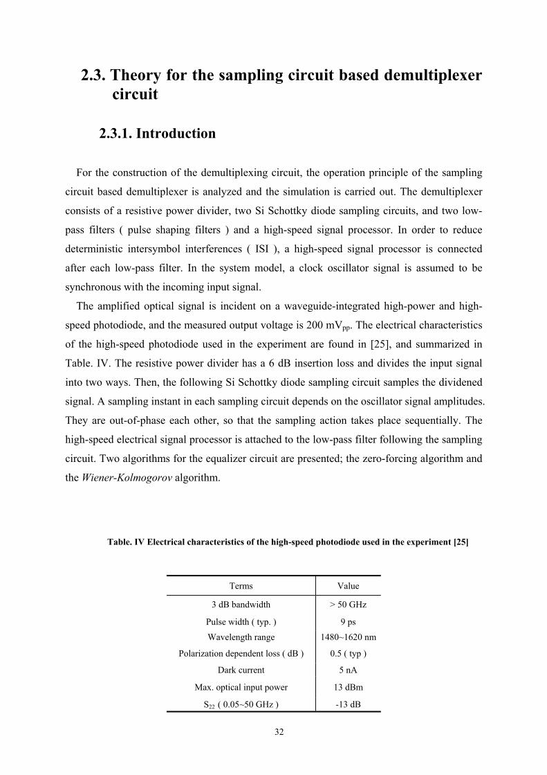
2.3. Theory for the sampling circuit based demultiplexer circuit
2.3.1. Introduction
For the construction of the demultiplexing circuit, the operation principle of the sampling
circuit based demultiplexer is analyzed and the simulation is carried out. The demultiplexer
consists of a resistive power divider, two Si Schottky diode sampling circuits, and two low-
pass filters ( pulse shaping filters ) and a high-speed signal processor. In order to reduce
deterministic intersymbol interferences ( ISI ), a high-speed signal processor is connected
after each low-pass filter. In the system model, a clock oscillator signal is assumed to be
synchronous with the incoming input signal.
The amplified optical signal is incident on a waveguide-integrated high-power and high-
speed photodiode, and the measured output voltage is 200 mVpp. The electrical characteristics
of the high-speed photodiode used in the experiment are found in [25], and summarized in
Table. IV. The resistive power divider has a 6 dB insertion loss and divides the input signal
into two ways. Then, the following Si Schottky diode sampling circuit samples the dividened
signal. A sampling instant in each sampling circuit depends on the oscillator signal amplitudes.
They are out-of-phase each other, so that the sampling action takes place sequentially. The
high-speed electrical signal processor is attached to the low-pass filter following the sampling
circuit. Two algorithms for the equalizer circuit are presented; the zero-forcing algorithm and
the Wiener-Kolmogorov algorithm.
Table. IV Electrical characteristics of the high-speed photodiode used in the experiment [25]
Terms Value
3 dB bandwidth > 50 GHz
Pulse width ( typ. ) 9 ps
Wavelength range 1480~1620 nm
Polarization dependent loss ( dB ) 0.5 ( typ )
Dark current 5 nA
Max. optical input power 13 dBm
S22 ( 0.05~50 GHz ) -13 dB
33
2.3.2. Theory description
For the purpose of the description about the sampling circuit based demultiplexer circuit,
we will use a time-limited signal, )(tORX and generalize the analytic pulse expression for
both the NRZ and the RZ signal. We temporarily consider only optical signal field excluding
the random noise component for circuit’s functional explanation. Thus, we would use scalar
notation for the signal after the optical band pass filter, i.e. )(tO(t)O SIGRX = . Let the optical
field be defined within the time interval [0, (1+α)Tp],
+≤≤⋅≤≤
−+−
⋅−⋅
⋅
≤≤⋅
=
otherwise0
)1(or0for22
)1(sin12
for
)( 1
1
ppppp
pp
ppp
RX TtTTtTT
tTT
E
TtTTE
tO ααααπ
α
where, E1 denotes the optical energy for a ‘1’ bit, and Tp is the effective pulse duration shown
below [31].
( ) ( ))(max)(max
)(1
tOE
tO
dttOT
RXtRXt
RX
p ==∫∞
∞−
Varying the pulse width with α and Tp, the NRZ and RZ pulse shape can be acquired. For
example,
⋅=
signalRZforTdsignalNRZforT
Tbit
bitp
where, bitT is a bit duration, and d is the duty cycle, 33% [31]. Using the above equation, the
optical pulse of 86 Gbit/s RZ optical signal is depicted in Fig. 2.8(a). Representing the
frequency response of the photodiode and the electrical connector as a 5th order Bessel filter,
its transfer function can be written as,
( 2.64 )
( 2.65 )
( 2.66 )

34
94594542010515945
)()(
23455
0
+++++=
⋅=
ssssssBbK
sHthn
where, K is the gain, and 011
1)( bsbsbssB nn
nn ++++= −
− L . For ,,,2,1,0 nk K=
knc
k knkknb
−
−−
=2)!(!
)!2( ω[49].
Using the ideal photodiode responsivity and normalizing the Bessel transfer function with
respect to the load impedance, the electrical signal waveform can be obtained in Fig. 2.8(b).
The simulated eye diagram shows a NRZ-like waveform due to the frequency response.
Compared with the actual measured signal for the 86 Gbit/s RZ signal in Fig. 2.9, it emulates
the real signal with a good agreement.
The sampling process can be regarded as the multiplication of the input signal waveform
with the train of the impulse response of the sampling circuit in time domain. Let the
sampling circuit impulse response be an ideal rectangular pulse with a pulse width τ,
)( τtrect .
(a) (b)
( 2.67 )
Fig. 2.8 (a) 86 Gbit/s optical signal incident on photodiode, which has a bandwidth of 55 GHz. (b) 86 Gbit/s electrical signal waveform after the photodiode. Due to the bandwidth constraint of the photodiode( 55 GHz ) for 86 Gbit/s application, the resultant output shows NRZ-like signal having less signal harmonic components at the high frequency area.
-1 -0.8 -0.6 -0.4 -0.2 0 0.2 0.4 0.6 0.8 10
0.1
0.2
0.3
0.4
0.5
0.6
0.7
0.8
0.9
1
Time ( Normalized with T )
Nor
mal
ized
am
plitu
de
ideal 86 Gbit/s RZ signal eye waveform ( alpha=0.4 )
-1 -0.8 -0.6 -0.4 -0.2 0 0.2 0.4 0.6 0.8 1-0.1
0
0.1
0.2
0.3
0.4
0.5
0.686 Gbit/s RZ signal eye waveform after photodiode
Time ( normalized with T )
Nor
mal
ized
am
plitu
de

35
The input signal to the demultiplexer can be expressed as
∑∞
=
−⋅=⋅0
)()(),(n
bitn nTtgrtd
where, )(⋅nr represents all possible ensembles of a random variable 1,exγ with a extinction
ratio exγ . The extinction ratio is defined as
101
0 ≤=≤PP
exγ
where 0P is the power emitted during logical level ‘0’, and 1P is for the level ‘1’. Here, we
use the normalized 1P value. And, )(tg can be expressed as a convolution of )(tORX and
)(th of the inverse Laplace transform of the 5th order Bessel filter.
Thus,
∫∞
−∞=−⋅⋅⋅=⋅⋅=
ττττ dthORZthtORZtg RXLRXL )()()(*)()( 22
Fig. 2.9 Measured 86 Gbit/s RZ signal. It looks like a NRZ-like waveform.
( 2.68 )
( 2.69 )
( 2.70 )
~ 240 mVpp
~12.5 psec
36
where )()( 1 sHLth −= , R , and LZ are the responsivity and a load impedance of the PD.
Using a pulse shaping function, )(tg , a code length of 128 − PRBS data waveform is
generated shown in Fig. 2.10(a) and depicts a logical value, ‘1’, or ‘0’ on each signal.
The sampling circuit output signals, channel 1 and channel 2, can be expresses as,
+−
⋅−⋅⋅⋅=⋅⋅+−⋅=
−
⋅−⋅⋅⋅=⋅⋅−⋅=
∑
∑
∞
=
∞
=
TTntrectnTtgrtdTnthtS
TnTtrectnTtgrtdnTthtS
nntrainChsampler
nntrainChsampler
)12()()(21),())12((2
1)(
2)()(21),()2(2
1)(
02.
01.
where, ∑ ∑∞
=
∞
=
−
=−=0 0
)()(n n
train TnTtrectnTthth is the impulse train of the sampling
circuit, illustrated in Fig. 2.10(b). Fig. 2.10(c) depicts its sampled signal waveform, and they
are ideally similar to the rectangular pulses. Comparing with the input signal waveform in Fig.
2.10(a), the output waveform clearly explains that every second bits in the input data stream
are detected. The sampled signal should be processed with the low-pass filter to make a
demultiplexed waveform. It is simulated using the 5th order Bessel filter, which has a
bandwidth of 20 GHz. Therefore, the demultiplexed output signal is written as a convolution
of the )(tSsampler with a low-pass filter .
τττ dthSthtStS LPFChsamplerLPFChsamplerChDEM )()()(*)()(2,1.2,1.2,1.
−⋅== ∫
where )(thLPF is the low-pass filter transfer function with 20 GHz bandwidth. Simulation
result is presented in Fig. 2.11. It illustrates a demultiplexed pulse width ( ~20psec, 40
Gbit/s ) and NRZ-like waveform. A MATLAB program is presented in Appendix B.
So far, we explain the sampling circuit based receiver circuit theory in detail using the ideal
sampling circuit impulse response ( rectangular function in time domain ). We successfully
acquire the demultiplexed digital eye waveform. It should be noted that the sampling in the
sampling circuit does mean literally detecting the electrical signal periodically for
demultiplexing purpose. It differs from the sampling in Nyquist theorem which defines the
minimum sampling frequency to reconstruct the original signal without aliasing effect.
( 2.71 )
( 2.72 )

37
Fig. 2.10 (a) A code length of 28-1 data is presented in time domain. (b), (c) Impulse train of the sampling circuit for channel 1 and 2, respectively, which is synchronized with the input signal. The sampling process is regarded as the product of the input signal with the impulse train. (d), (e) The resultant output signals are shown indicating the corresponding data value, “1”, and “0” for channel 1 and 2, respectively.
0 1 2 3 4 5 6 7 8 9 10 11 12 13 14 15 16 17 18 19 20 21 22 23 24 25 26 27 28 29 30-0.2
0
0.2
0.4
0.6
time
Am
plitu
de
0 1 2 3 4 5 6 7 8 9 10 11 12 13 14 15 16 17 18 19 20 21 22 23 24 25 26 27 28 29 300
0.5
1
1.5
time
Am
plitu
de
0 1 2 3 4 5 6 7 8 9 10 11 12 13 14 15 16 17 18 19 20 21 22 23 24 25 26 27 28 29 300
0.5
1
1.5
time
Am
plitu
de
0 1 2 3 4 5 6 7 8 9 10 11 12 13 14 15 16 17 18 19 20 21 22 23 24 25 26 27 28 29 30-0.2
0
0.2
0.4
0.6
time
Am
plitu
de
0 1 2 3 4 5 6 7 8 9 10 11 12 13 14 15 16 17 18 19 20 21 22 23 24 25 26 27 28 29 30-0.2
0
0.2
0.4
0.6
time ( normalized with T )
Am
plitu
de
1 1 1 1 1 1 1 1 1 1 1 1 1 1 1 1 1 0 0 0 0 0 0 0 00 0 0 0
1 1 1 1 1 1 1 1 1 0 0 0 0 0
0 0 0 0 0 0 0 1 1 1 1 1 1 1 1
(a)
(b)
(c)
(d)
(e)

38
Fig. 2.11 A sampled waveform after the sampling circuit is passed through the low-pass filter. A demultiplexed eye diagram is simulated successfully.
-2 -1.5 -1 -0.5 0 0.5 1 1.5 2-0.02
0
0.02
0.04
0.06
0.08
0.1
0.12
Demultiplexed Waveform
time ( normalized with T )
Ampl
itude
39
2.4. Electrical equalizer circuit
2.4.1. Introduction
In the optical fiber transmission the optical signal experiences dispersions ( CMD and
PMD ) and many impairments. As a result, the optical signal suffers from the ISI phenomena
and corrupted by noise. As the bit rate-transmission distance product increases in the long-
haul system transmission, the ISI mitigation is mandatory to enhance the bit-error-rate
( BER ). Transmission impairments can be largely classified into five ways, and summarized
in Table. V [50]. So far, compensation techniques have been implemented in two ways: in the
optical signal domain and in the electrical domain.
Optical signal compensation has an advantage over the electrical processing method in that
it is independent of the signal bit rate because the bandwidth of the optical signal is much
wider than that of the electrical signal. Furthermore, in case of the CMD, it is better than the
electrical way because the CMD is linear phenomenon before electrical conversion. It is
generally accepted that the optical mitigation outperforms the counterpart, i.e., the electrical
way when the signal distortions are from the CMD, the PMD, fiber nonlinearities, and laser
nonlinearities.
Many electrical signal processing methods are also developed and implemented in the
transmission experiments. Electrical methods to reduce signal distortions include a linear
equalization, nonlinear cancellation ( decision-feedback equalization ), maximum likelihood
sequence detection ( MLSD ), coding and multi-level signaling. The ultimate performance of
the electrical equalization can be acquired using the MLSD. It performs the Viterbi algorithm
to detect the most probable information sequences after receiving distorted signal sequences.
This method provides a criterion to evaluate other electrical methods. On the other hand, it
increases the complexity of the receiver circuit. Therefore, the suboptimal equalization
methods are nowadays employed: linear transversal filter or decision-feedback equalizer.
In general, the distortions are pattern-dependent, i.e. the distortion behavior is deterministic.
Therefore, observing the signal distortion we can calculate the ISI directly. If optical
transmission channels are time-varying, the adaptation algorithm could be utilized. For
example, the PMD is a time-varying random phenomenon, so its characteristic is expressed
using the root-mean-square ( RMS ) value. In this case, we effectively employ the adaptive
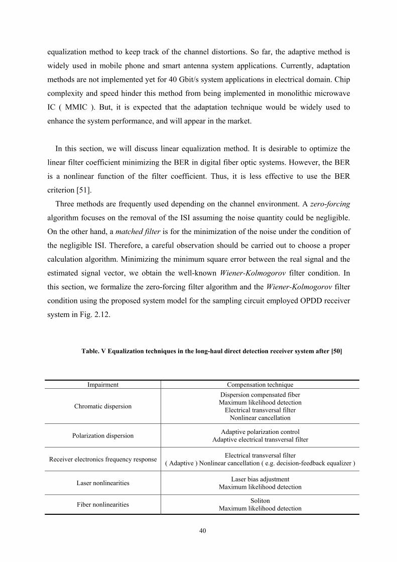
40
equalization method to keep track of the channel distortions. So far, the adaptive method is
widely used in mobile phone and smart antenna system applications. Currently, adaptation
methods are not implemented yet for 40 Gbit/s system applications in electrical domain. Chip
complexity and speed hinder this method from being implemented in monolithic microwave
IC ( MMIC ). But, it is expected that the adaptation technique would be widely used to
enhance the system performance, and will appear in the market.
In this section, we will discuss linear equalization method. It is desirable to optimize the
linear filter coefficient minimizing the BER in digital fiber optic systems. However, the BER
is a nonlinear function of the filter coefficient. Thus, it is less effective to use the BER
criterion [51].
Three methods are frequently used depending on the channel environment. A zero-forcing
algorithm focuses on the removal of the ISI assuming the noise quantity could be negligible.
On the other hand, a matched filter is for the minimization of the noise under the condition of
the negligible ISI. Therefore, a careful observation should be carried out to choose a proper
calculation algorithm. Minimizing the minimum square error between the real signal and the
estimated signal vector, we obtain the well-known Wiener-Kolmogorov filter condition. In
this section, we formalize the zero-forcing filter algorithm and the Wiener-Kolmogorov filter
condition using the proposed system model for the sampling circuit employed OPDD receiver
system in Fig. 2.12.
Table. V Equalization techniques in the long-haul direct detection receiver system after [50]
Impairment Compensation technique
Chromatic dispersion
Dispersion compensated fiber Maximum likelihood detection
Electrical transversal filter Nonlinear cancellation
Polarization dispersion Adaptive polarization control Adaptive electrical transversal filter
Receiver electronics frequency response Electrical transversal filter ( Adaptive ) Nonlinear cancellation ( e.g. decision-feedback equalizer )
Laser nonlinearities Laser bias adjustment Maximum likelihood detection
Fiber nonlinearities Soliton Maximum likelihood detection
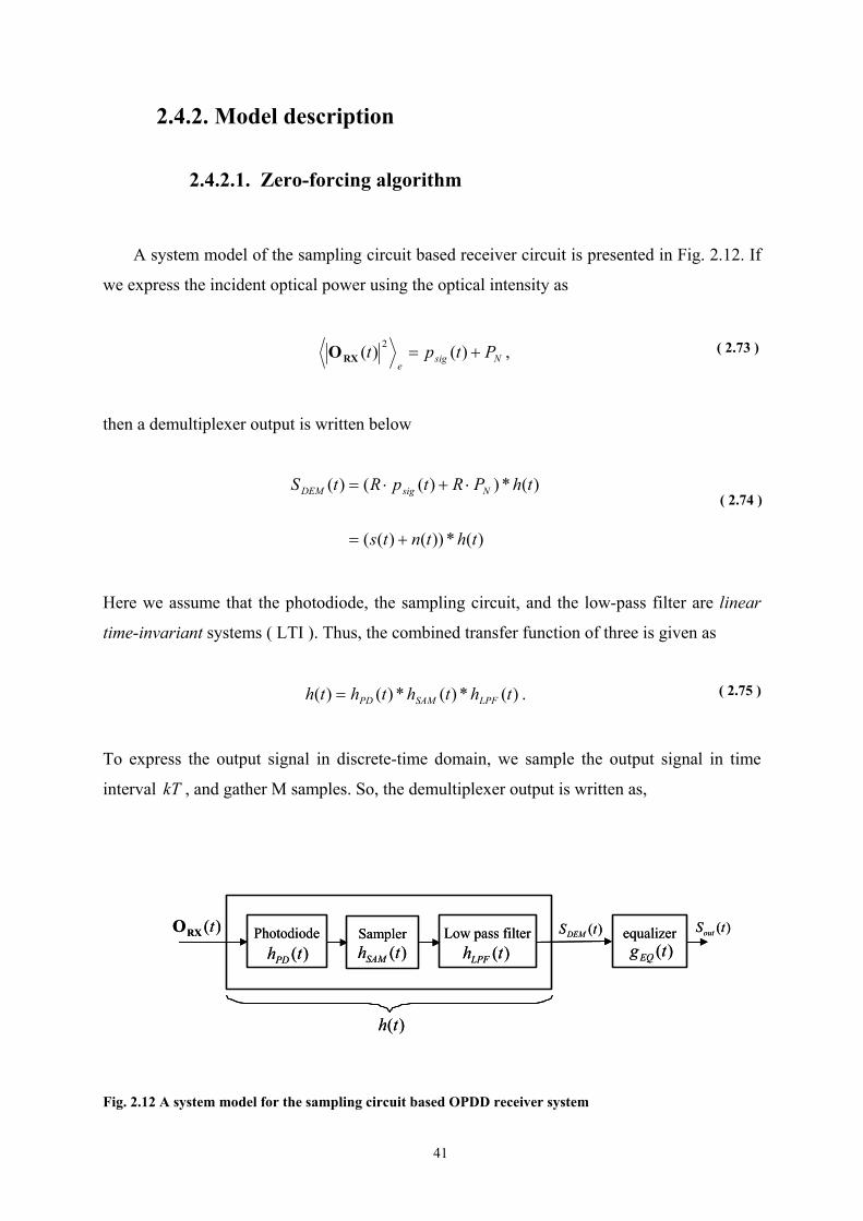
41
2.4.2. Model description
2.4.2.1. Zero-forcing algorithm
A system model of the sampling circuit based receiver circuit is presented in Fig. 2.12. If
we express the incident optical power using the optical intensity as
Nsige
Ptpt += )()( 2RXO ,
then a demultiplexer output is written below
)(*))()((
)(*))(()(
thtnts
thPRtpRtS NsigDEM
+=
⋅+⋅=
Here we assume that the photodiode, the sampling circuit, and the low-pass filter are linear
time-invariant systems ( LTI ). Thus, the combined transfer function of three is given as
)(*)(*)()( thththth LPFSAMPD= .
To express the output signal in discrete-time domain, we sample the output signal in time
interval kT , and gather M samples. So, the demultiplexer output is written as,
( 2.73 )
( 2.74 )
( 2.75 )
Fig. 2.12 A system model for the sampling circuit based OPDD receiver system
Photodiode Sampler)(thPD )(thSAM
Low pass filter)(thLPF
equalizer)(tgEQ
)(th
)(tRXO )(tSDEM )(tSoutPhotodiode Sampler)(thPD )(thSAM
Low pass filter)(thLPF
equalizer)(tgEQ
)(th
)(tRXO )(tSDEM )(tSout
42
[ ]
[ ]T1,1,0,
T
,,,
)1(,),1(),0(
−=
−=
MDEMDEMDEM
DEMDEMDEM
SSS
MSSS
K
KDEMs
And, we can also write the above equation using the transfer function ( )(th ) in matrix form,
ηsH
nHsHsDEM
+⋅=
⋅+⋅=
where, 1×∈ MCsDEM , T21 ][ Nk ssss LL=s , 1×∈ NCn , NM ×∈CH , and we assume 0n =E
After the equalizer, the output signal is given as
ηGsHG
ηsHGs
HH
Hout
⋅+⋅⋅=
+⋅⋅= )(
,
where G is the transfer function of the equalizer circuit, and NM×∈CG . The symbol H)(⋅
means the Hermitian matrix, a combined operation of transpose and complex conjugation.
The kth element of outs is given by
32144 344 21
43421noise
ISIsignaldesired
ˆ1
, ηGhGhG Hki
Hkk
Hk ⋅+⋅⋅+⋅⋅= ∑
≠=
N
kii
ikkout sss
where Nk21 GGGGG KK ,,,,= , [ ]T,,1, ,,, kLkLkL ggg K+−−=kG , Nk21 hhhhH ,,,,, KK= ,
[ ]T,1,1,0 ,,, kMkk hhh −= Kkh , and 12 += LM .
The zero-forcing filter is defined as an equalizer to eliminate the ISI component. It is also
called as the peak distortion criterion, because it minimize the peak distortion defined by the
ISI. Assuming the infinite number of filter coefficients, the kth output signal is acquired as
( 2.76 )
( 2.77 )
( 2.78 )
( 2.79 )

43
ηG Hk ⋅+= kkout ss ,ˆ
Therefore, if the following condition is satisfied
NH IHG =⋅
where,
=
1
11
N
0
0
IO
,
we can obtain the ISI-free signal after the equalizer. Fig. 2.13 illustrates a filter based on the
zero-forcing algorithm with order of ( 2N+1 ). It consists of periodic delay lines and
coefficient multipliers. At this moment filter coefficients are fixed to a certain value, however
if we apply the adaptive signal processing technique to the filter, coefficients are adaptively
changed.
The zero-forcing filter coefficients are decided by the following argument.
NHH subject to )( min arg IHGGRG ηG
=⋅⋅⋅tr
where, HHHE HRHHnnHR nη ⋅⋅=⋅⋅= , and H E nnRn = is a noise correlation vector.
The )(⋅tr symbol represents a trace of a matrix.
Fig. 2.13 Linear equalizer. Coefficients are calculated using the Zero-forcing algorithm.
( 2.80 )
( 2.81 )
( 2.82 )
Z-1
Σ
Z-1Input Z-1 Z-1
gLgL-1g-L+1g-L g-L+2
Output
Z-1
Σ
Z-1Input Z-1 Z-1
gLgL-1g-L+1g-L g-L+2
Output

44
Minimizing the noise power, )( H GRG η ⋅⋅tr at the output of the equalizer circuit, we
calculate filter coefficients. This is a constrained minimization problem, which can be solved
using the Lagrange multipliers method. The Lagrangian equation is
λIHGIGHλGRGλG η ⋅−⋅+−⋅⋅+⋅⋅= )()()(),(N
HN
HHHtrL ,
where λ is a Lagrange multiplier in vector form.
Finding out the conditions for 0),(
* =G
λG
d
dL and 0
),(* =
λ
λG
d
dL, the following result can be
derived,
11H1
ZF)( −−− ⋅⋅= HRHHRG ηη .
If N
2 IR η nσ= , the zero-forcing filter coefficient vector is found as += )( H
ZFHG . Here, the
(·)+ symbol represents the pseudo-inverse matrix.
Using the above result, we can calculate the SNR at the output of the filter. We will derive
the expressions for the signal power and the noise power, respectively. First of all, the signal
power after the equalization
Ntr === H22EQs, EEP sss .
Here we normalize the signal power and assume the infinite number of filter coefficients.
And, the noise power is given
( ) ( )
( ) 1H
1HH1HHEQN,P
−
−−
⋅=
⋅⋅⋅⋅=
⋅⋅=
HH
HHHHHHGRG η
tr
trtr
Let us decompose ( ) 1H −⋅HH using the singular value decomposition ( SVD ). It is shown that
if HUΛUHH ⋅⋅=⋅H where Λ is given by,
( 2.83 )
( 2.84 )
( 2.85 )
( 2.86 )
45
=
Nλ
λλ
0
0
ΛO
2
1
with eigenvalues of the matrix ),,,( 21 Nλλλ K , then
( ) HUΛUHH ⋅⋅=⋅ −− 11H .
Thus, the noise power is calculated as
∑=
=N
k k1EQN,
1Pλ
.
We therefore obtain the SNR as
∑=
== N
k k
EQN
EQs NPP
1
,
,
1SNR
λ
.
If CN λλλλ ==== L21 , then the SNR simply equals to cλ .
2.4.2.2. Wiener-Kolmogorov filter
A Wiener-Kolmogorov filter is called as a minimum mean square error ( MMSE ) filter. It
measures the distance between the real signal vector and the estimated signal vector, and then
minimizes the distance with regard to the filter coefficients. Here, we describe the MMSE
filter argument as
2
2WFEmin arg ssG outG
−= .
( 2.87 )
( 2.88 )
( 2.89 )
( 2.90 )
( 2.91 )

46
The solution for the above argument can be obtained when the first differentiation
0Gssout =− *2
2E dd .
A function for the vector norm is given by
( ) ( )
HHHH
H
E EEE
E)K(
ssssssss
ssssG
outoutoutout
outout
⋅−⋅−⋅−⋅=
−⋅−=
trtrtrtr
tr
If we assume that the signal and the noise is uncorrelated each other, and using facts below,
Ntrtr ==
⋅+⋅⋅=
NH
HH
E Iss
ηGsHGsout
we express the vector norm function as
( ) ( ) Ntrtrtr +⋅−⋅−
+= GHHGGRHHGG η
HHHH)K(
Solving 0GG =*)(K dd , the MMSE filter condition is calculated as shown below,
( )
+⋅=
−
ηRHHHG1H
WF.
To compare this solution with the zero-forcing algorithm solution, let us use the matrix
identity below.
( ) ( ) 111H11H −−−−−+≡+ BACAACBACABA
Setting HA = , N
IB = , and ηRC = , and inserting to the above equation, the final result is
( 2.92 )
( 2.93 )
( 2.94 )
( 2.95 )
( 2.96 )
( 2.97 )

47
straightforward.
1
N1H1
WF
−−−
+= IHRHHRG ηη
In general, when the transmit power increases, the MMSE filter solution approaches to the
zero-forcing solution while the decreased signal power causes the MMSE filter coefficients
converging to the matched filter coefficients.
For the sampling circuit based demultiplexer circuit, two algorithm for the equalizer circuit
are presented. Using a finite number of taps the equalizer circuit for the demultiplexer circuit
will be proposed and simulated. That is discussed in section 3.4.2.
( 2.98 )

48
3.1. Si Schottky diode modeling
Schottky diodes are majority carrier devices, and as a consequence a storage time due to
minority carriers is quite small, i.e., resulting in little diffusion capacitance. A junction
capacitance dominates in forward bias condition. Hence, the diode shows ultra-fast switching
speed compared to other junction diodes. This is an attractive advantage for millimeter-wave
circuit design. Very high-speed Schottky diodes having cutoff frequencies in THz regime are
reported in [9] and [10] using Si and III-V compound semiconductor materials.
Concerning the Schottky diode model, a large-signal nonquasi-static model should be
considered in high frequency regime. Nonquasi-static device modeling is desirable when the
operating frequency approaches the upper limit of validity for quasi-static models.
Chapter 3 Circuit Design and
Simulation
Fig. 3.1 Equivalent circuit of a diode. It is composed of extrinsic components ( L, R ) and the intrinsic components )( diodeC υ , )( diodeR υ , and )( diodeG υ , which are bias-dependent and specified independently.
L R
)( diodeC υ )( diodeR υ
)( diodeG υ
+ −diodeυ
Anode Cathode
49
Fig. 3.1 depicts the equivalent circuit model for a Si Schottky diode. Each parameter value
is linearized depending on the bias voltage, and independent of each other. The model is
composed of two series parasitic components ( inductance and resistance) and the intrinsic
three parts; intrinsic capacitance ( )( diodeC υ ), bias-dependent resistance ( )( diodeR υ ), and
bias-dependent current source ( )( diodeG υ ). In order to construct a large-signal diode model in
this work, three constitutive relations shown below are employed so as to express the
instantaneous current at each node under large-signal conditions. They are bias-dependent and
have a charge-conservative relation.
∫= υυυ dCQ )()(
υυυ ⋅= )()( DCDC GI
)()()( υυυτ RC ⋅=
Strictly speaking, as discussed below, a charge-relaxation-time equation is associated for
the purpose of describing instantaneous node currents using the above equations. In this work,
for the Si Schottky diode modeling, the Root-diode model is chosen. This diode model is
fundamentally a nonquasi-static and a charge-conservative model [26], and widely used for
three-terminal devices ( HEMT, FET ) modeling. The Root-diode model was originally
proposed by David Root in [28]. Due to its superior characteristics, i.e., fabrication-
independent modeling, less time consumption compared to other device models, and very
precise device description regardless of its operating frequency, this model is frequently
preferred in very high-speed device modeling.
When a terminal voltage changes slowly, terminal charges can catch up with its steady-
state charge value, ))(( tvQ diodesss . But, for higher operating frequency regime, the terminal
charge shows a delay, not responding to the voltage change simultaneously. This nonquasi-
static phenomenon can be described using a first-order differential equation, or a charge-
relaxation-time approach method. In general, the total current at each node is the summation
of conduction current and displacement current [27] written by
( 3.1 )
( 3.2 )
( 3.3 )

50
)()()( tItItI dispcondtotal +=
where ))(()( tvItI diodeocond = , dttdQtI disp )()( = , and )(tQ is the node charge.
Using a charge-relaxation-time approach, )(tI disp can be expressed using the following
equation.
)))((),((())(()()()(tvRtvC
tvQtQdt
tdQtIdiodediode
diodesss
disp τ−
−==
Note that the applied bias to the diode neglects voltage drops at the parasitic resistance for
simplicity. Equation ( 3.5 ) describes the large-signal behavior of the displacement current,
and also enables to determine the nonquasi-static characteristic of the diode. This Root-diode
model can be used for transient analysis in time domain, harmonic balance simulation in
frequency domain, and small-signal analysis in frequency domain [28].
3.1.1. The Root-diode model generation
Using Agilent’s parameter extraction software, IC-CAP, the intrinsic Si Schottky diode
elements are modeled, excluding parasitic resistances and de-embedding open and short
patterns. The parasitic resistance comes from the RF probes and cable losses. Fig. 3.2 displays
the procedure how to generate the Root-diode model using the IC-CAP program.
First of all, it measures RF port series resistances using short pattern on an impedance
standard substrate ( ISS ). For a two-port configuration, it will measure series resistances at
each port varying the current. Extracted resistance values are removed from the measurement
data. Also, the procedure includes the extraction of the parasitic series resistance and
inductance, which are shown in Fig. 3.1. In addition, open pad parasitics are de-embedded
from the measurement data, hence the intrinsic Root-diode model can be acquired. After
iterating the comparison with the measurement data until discrepancy satisfies the user-
defined criterion, the program produces the Root-diode model.
( 3.4 )
( 3.5 )

51
Setting the currents limits for instrument protection
Extracting the port series resistances
Pre-verifying the device DC data
Calibration of the Network analyzer
Pre-verifying the device S-parameter data
Measuring and extracting the ideality factor
Measuring and extracting parasitic R and L values
Measuring and extracting open pad parasitics
Performing data acquisition measurement
Generating the model
Comparing the model with the measurement data
END
NO
YES
Fig. 3.2 Procedures to generate the Root-diode model using Agilent IC-CAP program

52
When measuring the diode ideality factor, the following equation is used for its calculation,
and measured for various bias condition.
12
12
logloglog
iiVen
T −−
⋅=υυ
where, TV is the thermal voltage, qkT ( 25.8 mV ), 12 ,υυ are closely adjacent measurement
voltages, and 12 , ii are corresponding currents, respectively.
The measurement result is depicted in Fig. 3.3. The ideality factor calculation using the
above equation is only valid in the range of diodeυ > 0 and its relevant current region is where
recombination current is not dominant ( typically > 0.2 V ) [60]. As shown in Fig. 3.3, the
ideality factor starts to increase from diodeυ = 0 V to diodeυ = 0.35 V, and then it decreases until
diodeυ = 0.46 V. Above this voltage high-current effects, such as high level injection and ohmic
effects occur. Averaging the calculated ideality factor for diodeυ < 0.4 V, we obtain the diode
ideality factor of 1.51.
( 3.6 )
Fig. 3.3 Measured diode ideality factor
0.1 0.2 0.3 0.4 0.5 0.6 0.7 0.81
2
3
4
5
6
7
8
9
Forward bias voltage ( V )
Idea
lity
fact
or (
n )
0.1 0.2 0.3 0.4 0.51
1.2
1.4
1.6
1.8
2
Forward bias voltage ( V )
Idea
lity
fact
or (
n )
53
Fig. 3.4(a) shows the I-V curve comparing measurement results with the modeling data.
They show excellent agreement in the whole measurement range. And, the C-V characteristic
curve is shown in Fig. 3.4(b). We compare the Root-diode model, the measurement data, and
an analytic modeling equation. In order to determine parameters in the analytical expression,
we fit the equation ( 3.7 ) to the measurement data,
γ
Φ−=
bi
V
CVC1
)0()(
where the zero voltage capacitance )0(C is 47 fF, the built-in potential biΦ is 0.63 V, and the
junction grading coefficient γ is 0.5 [61].
The comparison between the Root-diode model, the measurement data, and the analytical
modeling data looks quite good below the forward bias of 0.2 V. In general as the forward
bias increases, the diffusion capacitance increases while the junction capacitance dominates in
the reverse bias condition. The slight deviation from the Root-diode model is attributed to the
parasitic voltage drop due to the parasitic resistance in probes and the extrinsic device series
resistance. Thus, the diffusion capacitance is lower than the Root-diode model data.
Effective barrier height calculation is straightforward using a Schottky barrier diode I-V
relation,
−
⋅
∆Φ−−⋅⋅= 1expexp2**
nkTqV
nkTTAJ B
sφ
where Bφ is the barrier height of a Schottky junction, ∆Φ is an effective barrier lowering due
to the image force effect, and **A is an effective Richardson constant, which is assumed to be
unaffected by the tunneling process ( 112 22/ TcmA ⋅ ). We obtain the effective barrier height
( ∆Φ−Bφ ) of 0.53 eV using the measured DC I-V relation.
The parasitic intrinsic series resistance and inductances are also measured varying the
frequency up to 50 GHz. When performing data acquisition measurement in the Root-diode
model generation, as described in Fig. 3.5, the average values are used to accommodate error
tolerances in the actual model.
( 3.7 )
( 3.8 )
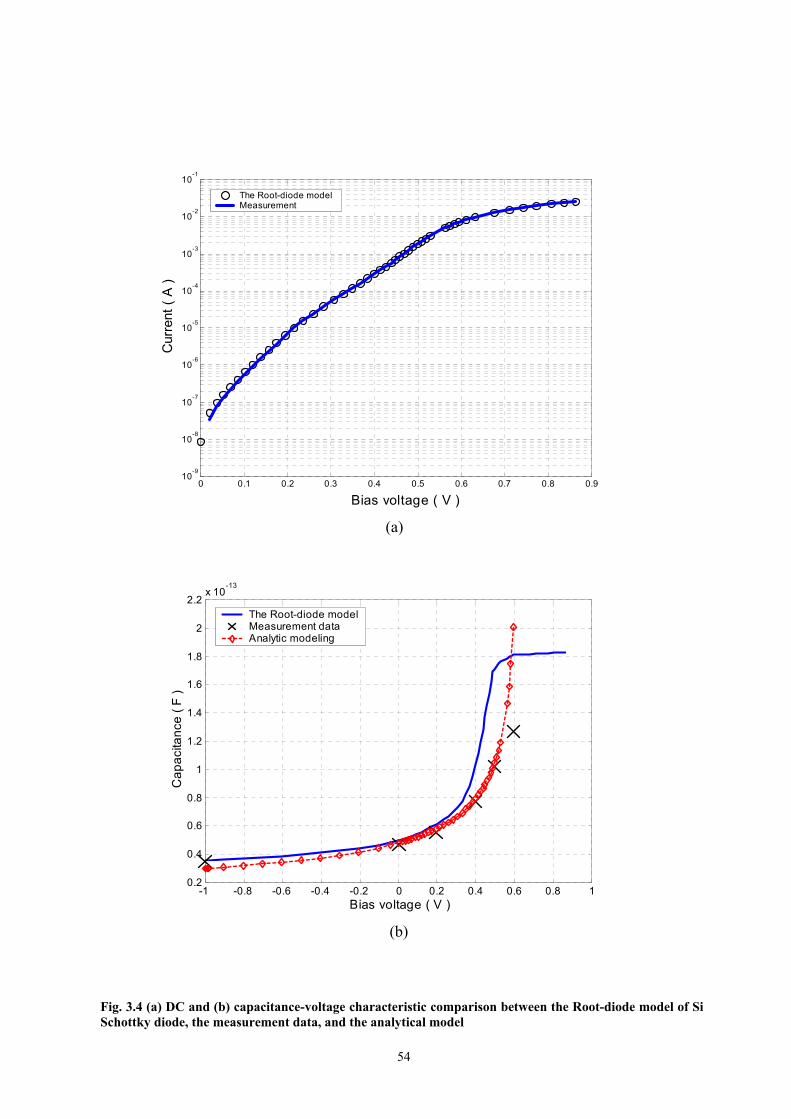
54
(a)
(b)
Fig. 3.4 (a) DC and (b) capacitance-voltage characteristic comparison between the Root-diode model of Si Schottky diode, the measurement data, and the analytical model
0 0.1 0.2 0.3 0.4 0.5 0.6 0.7 0.8 0.910
-9
10-8
10-7
10-6
10-5
10-4
10-3
10-2
10-1
Bias voltage ( V )
Cur
rent
( A
)
The Root-diode model Measurement
-1 -0.8 -0.6 -0.4 -0.2 0 0.2 0.4 0.6 0.8 10.2
0.4
0.6
0.8
1
1.2
1.4
1.6
1.8
2
2.2x 10
-13
Bias voltage ( V )
Cap
acita
nce
( F )
The Root-diode modelMeasurement data Analytic modeling

55
The average value of the series resistance is 12.71 Ω. However, in the data acquisition step
this value is reduced to 10.5 Ω in order to satisfy model tolerance in the whole measurement
range. And, the series inductance shown in Fig. 3.1, the average value of 58.56 pH is
calculated from the measurement data and this value is employed in the generation step. The
measured and calculated diode parameters are summarized in Table. VI.
(a)
(b)
Fig. 3.5 (a) Measured intrinsic parasitic resistance, and (b) inductance.
0 1 2 3 4 5
x 1010
11.8
12.3
12.8
13.3
13.8
Frequency ( Hz )
Res
ista
nce
( Ohm
)
0 1 2 3 4 5
x 1010
0
1
2
3
4
5
6x 10
-10
Frequency ( Hz )
Indu
ctan
ce (
H )

56
Terms Value
Ideality factor 1.51
Effective barrier height 0.63 eV Contact metal Ni silicide
Capacitance at zero bias 48 fF
Grading coefficient 0.5
Reverse saturation current, Is 2.7 nA
Series resistance 10.5 Ω
Series inductance 58.6 pH
Cutoff frequency 320 GHz
Table. VI. Measured diode model parameters ( diode area : 4.5 µm x 4.5 µm )
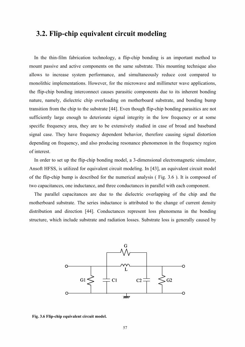
57
3.2. Flip-chip equivalent circuit modeling
In the thin-film fabrication technology, a flip-chip bonding is an important method to
mount passive and active components on the same substrate. This mounting technique also
allows to increase system performance, and simultaneously reduce cost compared to
monolithic implementations. However, for the microwave and millimeter wave applications,
the flip-chip bonding interconnect causes parasitic components due to its inherent bonding
nature, namely, dielectric chip overloading on motherboard substrate, and bonding bump
transition from the chip to the substrate [44]. Even though flip-chip bonding parasitics are not
sufficiently large enough to deteriorate signal integrity in the low frequency or at some
specific frequency area, they are to be extensively studied in case of broad and baseband
signal case. They have frequency dependent behavior, therefore causing signal distortion
depending on frequency, and also producing resonance phenomenon in the frequency region
of interest.
In order to set up the flip-chip bonding model, a 3-dimensional electromagnetic simulator,
Ansoft HFSS, is utilized for equivalent circuit modeling. In [43], an equivalent circuit model
of the flip-chip bump is described for the numerical analysis ( Fig. 3.6 ). It is composed of
two capacitances, one inductance, and three conductances in parallel with each component.
The parallel capacitances are due to the dielectric overlapping of the chip and the
motherboard substrate. The series inductance is attributed to the change of current density
distribution and direction [44]. Conductances represent loss phenomena in the bonding
structure, which include substrate and radiation losses. Substrate loss is generally caused by
Fig. 3.6 Flip-chip equivalent circuit model.
G
G2G1 C1 C2
L
G
G2G1 C1 C2
L

58
the excitation of surface waves in the substrate. Radiation loss stems from the energy loss of
radiated electromagnetic waves from the bump [43]. In this work, those losses are neglected,
hence only two capacitances and one inductance are considered in the equivalent circuit
modeling of the flip-chip bonding connection.
Since there are one inductance and two capacitances in the circuit model, two resonance
frequencies are analytically found. If one port is terminated with 0Z , the first resonance
frequency is Hz0=resf and the second is
+−
++
−=
)(41
2221
12
221
21
12
21
12
CCLZCC
ZCCCC
ZCCCCf o
oores π
.
In the transverse direction of the bump transition, 0Z approaches ∞ [30]. In this case a
transverse resonance frequency is located at
( )2121
21, ||
121
21
CCLLCCCCf transverseres ππ
=+
= .
Various methods to reduce return loss due to the flip-chip bump transition have been
developed. For example, a staggered bump method and an insertion of a hi-impedance line in
order to compensate capacitive behavior of the flip-chip [46]. Those geometrical approaches
are fundamentally intended to change the resonance frequency or to add ( or reduce ) the
discrete component. It is reported that the return loss can remain below –20 dB until 82 GHz
using the compensation method [46].
3.2.1. Simulation of the flip-chip bonding connection
A three-dimensional simulation structure is shown in Fig. 3.7(a). We illustrate a cross
sectional view of the actual flip-chip bonded structure in Fig. 3.7(b) in order to show the
origin of equivalent circuit components. It is noted that this diagram does not account for an
unwanted substrate mode, i.e., parallel plate mode. An equivalent circuit model fully
characterizing the
( 3.9 )
( 3.10 )

59
(a)
(b)
flip-chip bonding including higher order modes is under research. However, the flip-chip
employed circuit generally operates within a certain frequency range where higher order
electromagnetic modes start to occur. Thus, it is still useful to use discrete equivalent circuit
model for circuit design purposes.
The Si Schottky diode was flip-chip bonded at 300˚C to the backside grounded alumina
substrate, which has a thickness of 250 µm. Bump height after bonding was measured about
5 µm on average. Mechanical bonding force 3.5 N is applied for 5~6 seconds. The used chip
has two Schottky diodes connected in series, and has six pads with one bump each as shown
in Fig. 3.8(a). The chip size is 500 µm x 230 µm, and each bump is made up of AuSn, and
has a height of about 35 µm, as plotted in Fig. 3.8(b). Coplanar waveguides ( CPWs ) with
tapering structures were patterned on the substrate intentionally in order to evaluate the diode
and the flip-chip connection.
Fig. 3.7 (a) A three-dimensional simulation structure in Ansoft HFSS. Si Schottky diode is up-side down, emulating flip-chip bonding structure. (b) Cross sectional view of the flip-chip bonding.
Si Schottky diode
Al2O3 substrate
Alumina substrate ( Al2O3 )
Si Schottky diode
bumpmetallization
C1
C2
Alumina substrate ( Al2O3 )
Si Schottky diode
bumpmetallization
Alumina substrate ( Al2O3 )
Si Schottky diode
bumpmetallization
C1
C2

60
(a) (b)
We carry out a S-parameter simulation of the structure in Fig. 3.7(a), and de-embedding the
CPW line length. This CPW line is intended for the measurement purpose. Then, we obtain
the de-embedded S-parameter and convert it into a Y-parameter. The Y-parameter matrix is
established using the equivalent circuit model shown in Fig. 3.9.
+−
−+
=
=
LjCj
Lj
LjLjCj
yyyy
ωω
ω
ωωω
11
11
2
1
2221
1211Y
Therefore,
ω)Im( 1211
1yyC +
= ,
ω)Im( 1222
2yyC +
= ,
and,
)Im(1
121 y
L⋅
=ω
.
Fig. 3.8 (a) A Si Schottky diode SEM photograph (b) bump height ( 35 µm ) is measured using DekTak ( submicron measurement unit ).
( 3.11 )
( 3.12 )
( 3.13 )
( 3.14 )
80u
35um

61
In Fig. 3.10, simulation results are given varying the simulation frequency from 5 GHz to
40 GHz. As the frequency increases, C2 value gets larger. This phenomenon can be explained
as the overlapping between the dielectric chip and motherboard substrate. However, C1
decreases because this value includes the effect of the bonding pad on the substrate which is
dominant at low frequencies compared to the overlapping effect. Moreover, the summation of
C1 and C2 is almost constant, approximately 90 fF. This means that in the low frequency
region ( e.g. up to 10 GHz ) the overlapping effect ( C2 ) can be neglected compared to C1. As
the frequency increases, these effects are evenly divided showing the similar capacitance
value at 40 GHz.
For a circuit design purpose, the flip-chip bonding simulation results are averaged up to
40 GHz. Those values are summarized in Table. VII.
Fig. 3.9 Y-parameter matrix of the flip-chip equivalent circuit model
Table. VII. Simulation result for the flip-chip bonding equivalent circuit model
Terms Values
C1
C2
L
49 fF
42 fF
103 pH
Y1 Y3
Y2
+−
−+=
322
221
YYYYYY
Y
Y1 Y3
Y2
Y1 Y3
Y2
+−
−+=
322
221
YYYYYY
Y

62
(a)
(b)
Fig. 3.10 Flip-chip simulation results for (a) capacitance and (b) inductance varying the frequency until 40 GHz for a bump height of 5 µm.
0 5 10 15 20 25 30 35 40 450
20
40
60
80
100
120
Frequency ( GHz )
Indu
ctan
ce (
pH )
0 5 10 15 20 25 30 35 40 450
10
20
30
40
50
60
70
80
Frequency ( GHz )
Cap
acita
nce
( fF
)capacitance 1capacitance 2
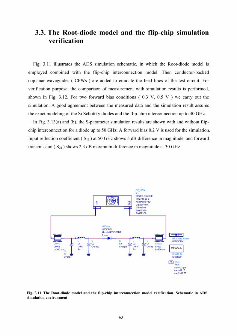
63
3.3. The Root-diode model and the flip-chip simulation verification
Fig. 3.11 illustrates the ADS simulation schematic, in which the Root-diode model is
employed combined with the flip-chip interconnection model. Then conductor-backed
coplanar waveguides ( CPWs ) are added to emulate the feed lines of the test circuit. For
verification purpose, the comparison of measurement with simulation results is performed,
shown in Fig. 3.12. For two forward bias conditions ( 0.3 V, 0.5 V ) we carry out the
simulation. A good agreement between the measured data and the simulation result assures
the exact modeling of the Si Schottky diodes and the flip-chip interconnection up to 40 GHz.
In Fig. 3.13(a) and (b), the S-parameter simulation results are shown with and without flip-
chip interconnection for a diode up to 50 GHz. A forward bias 0.2 V is used for the simulation.
Input reflection coefficient ( S11 ) at 50 GHz shows 5 dB difference in magnitude, and forward
transmission ( S21 ) shows 2.3 dB maximum difference in magnitude at 30 GHz.
Fig. 3.11 The Root-diode model and the flip-chip interconnection model verification. Schematic in ADS simulation environment
CPWGCPW3L=300 um
CPWGCPW2L=300 um
SP_NWAX1
Port2Z=50Port1Z=50VBias2=0VBias1=0.0NumPoints=101Stop=40 GHzStart=0.045 GHz
+ +
21
VARVAR1
cap2=42 fFcap=49 fFind=103 pH
EqnVar
CPWSUBCPWSub1
CPWSub
LL2
R=L=ind
CC3C=cap2
CC4C=cap
CC2C=cap2
LL1
R=L=ind
CC1C=cap
HP_Diode_ModelHPDIODEM1
HPDiodeHPDIODE1
Area=Model=HPDIODEM1
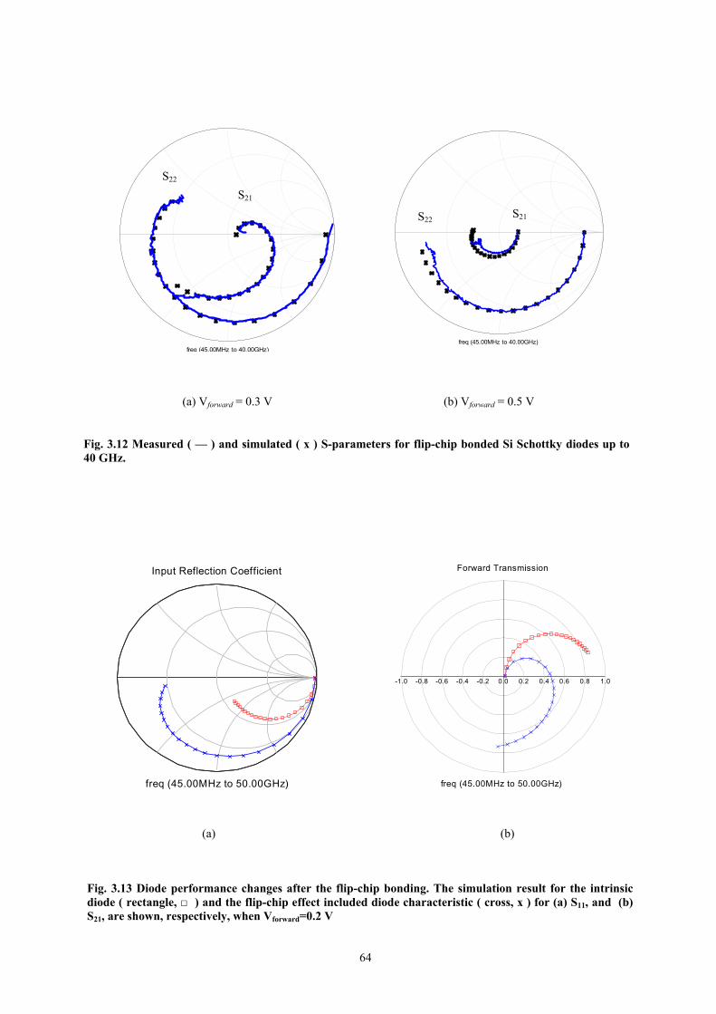
64
S21 S22
freq (45.00MHz to 40.00GHz)
S22 S21
freq (45.00MHz to 40.00GHz)
(a) Vforward = 0.3 V (b) Vforward = 0.5 V
(a) (b)
Fig. 3.12 Measured ( — ) and simulated ( x ) S-parameters for flip-chip bonded Si Schottky diodes up to 40 GHz.
Fig. 3.13 Diode performance changes after the flip-chip bonding. The simulation result for the intrinsic diode ( rectangle, ) and the flip-chip effect included diode characteristic ( cross, x ) for (a) S11, and (b) S21, are shown, respectively, when Vforward=0.2 V
freq (45.00MHz to 50.00GHz)
Input Reflection Coefficient
-0.8 -0.6 -0.4 -0.2 0.0 0.2 0.4 0.6 0.8-1.0 1.0
freq (45.00MHz to 50.00GHz)
Forward Transmission

65
3.4. Design of the 43 Gbit/s demultiplexer circuit
As discussed in section 2.3, we pursue constructing a high-speed demultiplexer circuit
using the Si Schottky diode instead of transistors. To do that, we need a diode sampling
circuit. The 43 Gbit/s 1:2 demultiplexer circuits are designed and simulated considering both
hybrid and monolithic implementations. First of all, we present sampling circuit design and
simulation results. Then, a tapped delay line filter is examined and designed in the following
section. When the circuit is designed under the hybrid fabrication condition, the flip-chip
equivalent circuit model is attached to each diode pair. Thus, we can acknowledge how the
flip-chip bonding parasitic affects circuit performances compared with the monolithic IC case.
3.4.1. A sampling circuit for the 43 Gbit/s MMIC demultiplexer circuit
3.4.1.1. A sampling circuit schematic and simulation
Fig. 3.14 shows a sampling circuit under the condition of monolithic implementation.
Neglecting the flip-chip bonding connection effect, the intrinsic Root-diode model is
incorporated with the circuit simulator. Three 50 Ω resistances are used in the design: one is
at the input port for matching when the diode pairs are turned off ( non-sampling
instant ). With this resistance, the input signal is completely absorbed, not being reflected
back.
Fig. 3.14 A Si Schottky diode MMIC sampling circuit.
50 Ω
50 Ω
50 Ω CHOLD
Clock
Clock
50 Ω
50 Ω
50 Ω CHOLD
Clock
Clock Clock

66
The other two resistances are for the oscillator signal matching. One capacitor at the output
port of the sampling circuit is to hold the transferred charge from the input port. Series
connected Si Schottky diodes are used in the sampling bridge circuit design. An illustrative
figure of the operation mode is depicted in Fig. 3.15. Four pairs of diodes ( D1, D2, D3, and
D4 ) are aligned in the same direction, forming a signal conducting path from input to output
when the sampling event occurs. One pair of diodes ( D5 and D6 ) counteracts with the others
when the oscillator signals are out of phase compared to the previous state. The oscillation
signals are not reflected back due to this diode pair. A virtual ground is formed in the mid of
D5 and D6 when these two diodes conduct. Thus, to match the oscillator signals, 50 Ω
resistors are connected in series along the oscillator paths.
The diode switching operation is mainly dependent on the external oscillator large-signal.
Once the diodes are turned on, the input signal ( small-signal ) can go through the circuit
toward the output port. Therefore, diode small-signal current can be described by two
components: One is the product of the diode junction voltage with the diode conductance, and
the other is small-signal charge stored in the diode’s junction capacitance [44].
)()()()(DIODE tQdtdttgti j +⋅= υ
( 3.15 )
Fig. 3.15 The simplified operation modes of the bridge circuit. In the left picture, D1, D2, D3, and D4 are conducting (solid line), whereas D5 and D6 are turned off ( dotted line ). In the right picture, vice versa.
D1 D2
D3D4
LOW
HIGH
D5
D6
LOW
HIGH
D1 D2
D3D4
LOW
HIGH
D1 D2
D3D4
LOW
HIGH
D5
D6
LOW
HIGH
D5
D6
LOW
HIGH

67
where, )(tjυ is diode junction voltage, )()()( DIODE tdtidtg jυ= is the diode small-signal
conductance, and )()()( tCttQ j ⋅=υ .
Because the diode capacitance is strongly dependent on the external clock signal rather than
the input signal, it relies on the large-signal, time-varying voltage across the diode’s junction,
and is given by
γ
Φ
−
=
0
0
)(1
)(tV
CtC j
where, 0jC is the zero-voltage junction capacitance, 0Φ is the junction built-in voltage, γ is
the grading coefficient , and )(tV is the time-varying large-signal voltage while )(tjυ in the
equation ( 3.15 ) is small-signal voltage across the p-n junction. Therefore, the small-signal
diode current when the diodes are conducting can be expressed as follows.
)()()()()()()(DIODE tCdtdtt
dtdtCttgti jjj ⋅+⋅+⋅= υυυ
This formula can be interpreted that the diode current comes from three factors: the
contribution of the large-signal excitation of a clock signal, the time-varying small-signal
input, and its time derivative quantity. The transferred charge to the output hold capacitance is
calculated using the following equation,
∫+
⋅=Tk
kT
dttitq)1(
DIODEHOLD )()( .
The instantaneous current and the charge in time domain are simulated using Agilent ADS.
The results are depicted in Fig. 3.16. The output current is calculated using the Kirchhoff
current law at the output port. In Fig. 3.16(a), the negative peaking is obviously shown due to
the two derivative terms in equation ( 3.17 ). When either small-signal voltage across the
diode junction is steeply decreased or the oscillator amplitude decreases, )(tiDIODE shall be
below zero. We also calculated the transferred charge using the current simulation result. The
time period for the calculation was 46.5 psec.
( 3.16 )
( 3.17 )
( 3.18 )

68
(a) (b)
In fact, the small-signal diode current calculation needs both a large-signal and small-signal
analysis in the sampling circuit, because the diode current is also dependent on the time
drivative of the capacitance, which is changed by the large-signal of the oscillator. Analytic
analysis thus needs complicated numerical analysis for our circuit simulation.
In high-speed digital applications, a linear phase characteristic is of great significance. The
input signal has an ultra broadband frequency spectrum, for example 21.5 GHz fundamental
frequency for 43 Gbit/s NRZ signal. A nonlinear phase response of the system will distort a
signal eye waveform degrading system performance. Thus, we investigate S21 parameter
phase characteristic and also its magnitude response. For simulations, we consider a sampling
instant at which the external oscillator signal is the highest amplitude, and the diode pairs are
fully conducting. The oscillator signal amplitude is set to a constant DC value, 800 mV. The
hold capacitance is 0.2 pF. Even if the fixed oscillator signal amplitude does not emulate the
time-varying sampling actions perfectly, it is still worth while to making use of a simple
situation in order to predict circuit performance at a specific time instant. The same conditions
are used for impulse response simulation in Fig. 3.18. We obtain a very broadband S21
characteristic over 50 GHz. Insertion loss shows 10.2 dB on average until 50 GHz. This is due
to series connected parasitic component of the diode in the current conducting path and
voltage dividing by 50 Ω. In Fig. 3.17(b), a S21 phase simulation result is illustrated with an
interpolated linear phase line. The sampling circuit shows a good linear phase characteristic.
The maximum discrepancy with its linear line is 4.6 ˚ at 500 MHz.
Fig. 3.16 (a) Output current simulation result in the sampling circuit. (b) The transferred charge at the output port is calculated integrating the output current pulses. The charge is normalized and calculated for unity capacitor.
0 0.2 0.4 0.6 0.8 1 1.2 1.4 1.6 1.8 2
x 10-10
-0.4
-0.2
0
0.2
0.4
0.6
0.8
1
1.2
Time ( sec )
Nor
mal
ized
cha
rge
( C )
0 0.2 0.4 0.6 0.8 1 1.2 1.4 1.6 1.8 2
x 10-10
-3
-1
1
3
5
7
x 10-4
Time ( sec )
Cur
rent
( A
)
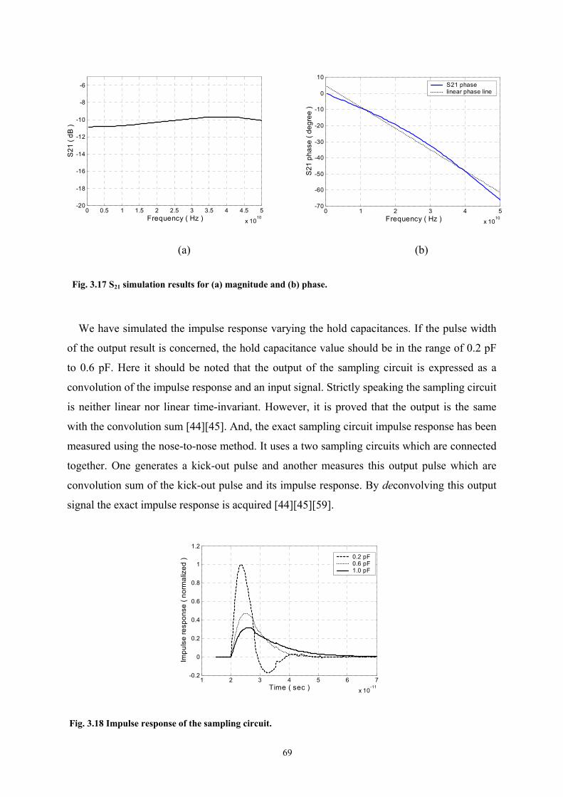
69
(a) (b)
We have simulated the impulse response varying the hold capacitances. If the pulse width
of the output result is concerned, the hold capacitance value should be in the range of 0.2 pF
to 0.6 pF. Here it should be noted that the output of the sampling circuit is expressed as a
convolution of the impulse response and an input signal. Strictly speaking the sampling circuit
is neither linear nor linear time-invariant. However, it is proved that the output is the same
with the convolution sum [44][45]. And, the exact sampling circuit impulse response has been
measured using the nose-to-nose method. It uses a two sampling circuits which are connected
together. One generates a kick-out pulse and another measures this output pulse which are
convolution sum of the kick-out pulse and its impulse response. By deconvolving this output
signal the exact impulse response is acquired [44][45][59].
Fig. 3.17 S21 simulation results for (a) magnitude and (b) phase.
Fig. 3.18 Impulse response of the sampling circuit.
0 0.5 1 1.5 2 2.5 3 3.5 4 4.5 5
x 1010
-20
-18
-16
-14
-12
-10
-8
-6
Frequency ( Hz )
S21
( dB
)
0 1 2 3 4 5
x 1010
-70
-60
-50
-40
-30
-20
-10
0
10
Frequency ( Hz )
S21
pha
se (
degr
ee )
S21 phase linear phase line
1 2 3 4 5 6 7
x 10-11
-0.2
0
0.2
0.4
0.6
0.8
1
1.2
Time ( sec )
Impu
lse
resp
onse
( no
rmal
ized
) 0.2 pF0.6 pF1.0 pF

70
(a)
(b)
A simulation block diagram for the 43 Gbit/s 1:2 demultiplexer simulation is shown in Fig.
3.19. The ideal 43 Gbit/s pseudo random binary sequence ( PRBS ) of a code length of 27-1 is
generated. Then it is filtered out using a Butterworth low-pass filter, which has a 3 dB
bandwidth of 50 GHz, and the order of 3. The signal is divided into two signals by the
resistive power divider. Due to the 6 dB insertion loss characteristic, each signal amplitude
( 100 mVpp ) is one half of the original signal ( 200 mVpp ). These signals are shown in Fig.
3.20(a) and (b) with their FFT transforms, respectively. The ideal 43 Gbit/s NRZ signal
clearly shows spectral distribution with multiple dips at integer times of 43 GHz. After
filtering, amount of signal power below 43 GHz is still remained, thus the simulated eye
waveform does not show a critical distortion. In general, the power spectral density of the
NRZ signal shows a sinc2 distribution. This fact is obvious from Fig. 3.20(a).
The divided signals are incident on the sampling circuit. The oscillator power for each
sampling circuit is 2 dBm ( ~800 mVpp ). The required oscillator power shall be determined as
the following. The minimum power at least should turn on the diodes while the maximum
power in the diodes should be lower than the thermal breakdown and the reverse breakdown
( 22.5 dBm ).
Fig. 3.19 (a) The 43 Gbit/s PRBS signal ( 200 mVpp) is filtered out using a Butterworth low-pass filter, and divided by the resistive power divider. (b) a 1:2 demultiplexer circuit block diagram using the sampling circuit. After the sampling circuit, the pulse shape filter ( low-pass filter ) is attached.
R
RR
R
RR
fc@ 3dBLow pass filter
PRBS generator
R
RR
R
RR
R
RR
R
RR
R
RR
fc@ 3dBLow pass filter
PRBS generator
R
RR
R
RR
fc@ 3dBLow pass filter
PRBS generator
R
RR
R
RR
R
RR
R
RR
R
RR
fc@ 3dBLow pass filter
PRBS generator
t = kTS
Diode sampler
t = kTS
Diode sampler
t = (k+1)TSDiode samplert = (k+1)TS
Diode sampler
R
RR
R
RR
R
RR
R
RR
R
RR
fc@ 3dBLow pass filter
PRBS generator
R
RR
R
RR
R
RR
R
RR
R
RR
R
RR
fc@ 3dBLow pass filter
PRBS generator
t = kTS
Diode sampler
t = kTS
Diode sampler
t = (k+1)TSDiode samplert = (k+1)TS
Diode sampler
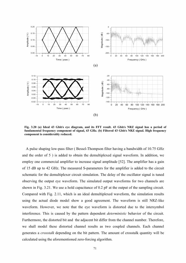
71
(a)
(b)
A pulse shaping low-pass filter ( Bessel-Thompson filter having a bandwidth of 10.75 GHz
and the order of 5 ) is added to obtain the demultiplexed signal waveform. In addition, we
employ one commercial amplifier to increase signal amplitude [52]. The amplifier has a gain
of 15 dB up to 42 GHz. The measured S-parameters for the amplifier is added to the circuit
schematic for the demultiplexer circuit simulation. The delay of the oscillator signal is tuned
observing the output eye waveform. The simulated output waveforms for two channels are
shown in Fig. 3.21. We use a hold capacitance of 0.2 pF at the output of the sampling circuit.
Compared with Fig. 2.11, which is an ideal demultiplexed waveform, the simulation results
using the actual diode model show a good agreement. The waveform is still NRZ-like
waveform. However, we note that the eye waveform is distorted due to the intersymbol
interference. This is caused by the pattern dependent deterministic behavior of the circuit.
Furthermore, the distorted bit and the adjacent bit differ from the channel number. Therefore,
we shall model these distorted channel results as two coupled channels. Each channel
generates a crosstalk depending on the bit pattern. The amount of crosstalk quantity will be
calculated using the aforementioned zero-forcing algorithm.
Fig. 3.20 (a) Ideal 43 Gbit/s eye diagram, and its FFT result. 43 Gbit/s NRZ signal has a period of fundamental frequency component of signal, 43 GHz. (b) Filtered 43 Gbit/s NRZ signal. High frequency component is considerably reduced.
0 10 20 30 40 50 60 70-10 80
0.05
0.10
0.15
0.00
0.20
Time ( psec )
Am
plitu
de (
V )
20 40 60 80 100 120 140 160 1800 200
-150
-100
-50
-200
0
Frequency ( GHz )
Mag
nitu
de (
dB
)0 10 20 30 40 50 60 70-10 80
-0.00
0.02
0.04
0.06
0.08
0.10
-0.02
0.12
Time ( psec )
Am
plitu
de (
V )
20 40 60 80 100 120 140 160 1800 200
-120
-100
-80
-60
-40
-140
-20
Frequency ( GHz )
Mag
nitu
de (
dB
)
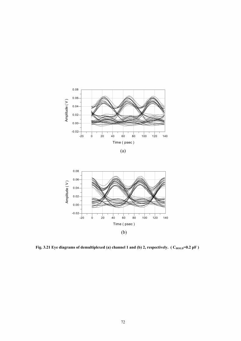
72
(a)
(b)
Fig. 3.21 Eye diagrams of demultiplexed (a) channel 1 and (b) 2, respectively. ( CHOLD=0.2 pF )
0 20 40 60 80 100 120-20 140
0.00
0.02
0.04
0.06
-0.02
0.08
Time ( psec )
Am
plitu
de (
V )
0 20 40 60 80 100 120-20 140
0.00
0.02
0.04
0.06
-0.02
0.08
Time ( psec )
Am
plitu
de (
V )

73
3.4.2. The transversal tapped delay line filter
A tapped delay line filter is designed for the purpose of reducing the ISI phenomenon. We
consider that the finite number of symbols, 2M+1, will affect the ISI. Thus, the kth output
symbol, kouts ,ˆ , is a function of 2M+1 elements given by
∑
∑
≠−=
+
−=+
+−+++−−
+=
=
=
M
jMj
jkjk
M
Mjjkj
MkMkkkMkMkkout
spsp
sp
ssssssfs
0
0
1,11, ),,,,,,(ˆ KK
where, using equation ( 2.76 ) kp is expressed as,
∑−=
−=⋅=L
Liikkik hgp ,k
Hk hG .
The condition to satisfy the zero-forcing algorithm can be alternatively described using
parameter kp given by,
=
=otherwise0
0if1 kpk .
Here we use the normalized parameter kp . In order to apply this algorithm to the transversal
equalizer circuit design, we consider the simple case for M=1. It means that the output is
assumed to be affected by one past and one future bit.
11,ˆ +− ⋅++⋅= kkkkout ssss βα
Expressing the above equation in z-domain, the transfer function is given by
( 3.19 )
( 3.20 )
( 3.21 )
( 3.22 )

74
zzzH ⋅++⋅= − βα 1)( 1
Applying ( 3.23 ) into ( 3.20 ), we obtain the transversal tapped delay line filter coefficients as,
.21
and,211,
21 101 αβα
αβαββ
−−
=−
=−−
=− ggg
Therefore, we can conclude that the equalizer transfer function is written by,
( )11211)( −⋅−+⋅−
−= zzzHEQ αβ
αβ
Comparing the equalizer transfer function with Fig. 3.22, and assuming the symmetry
between two channels, the coefficients can be chosen as,
ααβαβ
αββ
−≈−−
==−≈−−
==21
and,21 1100 DCDC .
( 3.23 )
( 3.24 )
( 3.25 )
( 3.26 )
Fig. 3.22 Proposed transversal filter to equalize ISI phenomena.
Z-2
C0 C1
Σ
Z-2
D0D1
Σ
Z-1 Z-1
Ch.1 Ch.2
Ch.1 Ch.2
Z-2
C0 C1
Σ
Z-2
D0D1
Σ
Z-1 Z-1Z-1
Ch.1 Ch.2
Ch.1 Ch.2
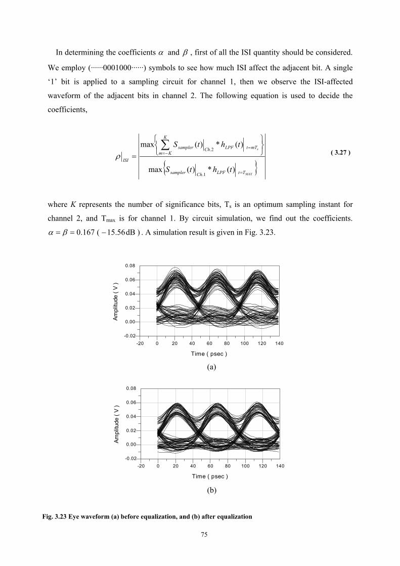
75
In determining the coefficients α and β , first of all the ISI quantity should be considered.
We employ (······0001000······) symbols to see how much ISI affect the adjacent bit. A single
‘1’ bit is applied to a sampling circuit for channel 1, then we observe the ISI-affected
waveform of the adjacent bits in channel 2. The following equation is used to decide the
coefficients,
MAX
s
TtLPFChsampler
K
KmmTtLPFChsampler
ISI
thtS
thtS
=
−==
=∑
)(*)(max
)(*)(max
1.
2.ρ
where K represents the number of significance bits, Ts is an optimum sampling instant for
channel 2, and Tmax is for channel 1. By circuit simulation, we find out the coefficients.
)dB56.15(167.0 −== βα . A simulation result is given in Fig. 3.23.
(a)
(b)
( 3.27 )
Fig. 3.23 Eye waveform (a) before equalization, and (b) after equalization
0 20 40 60 80 100 120-20 140
0.00
0.02
0.04
0.06
-0.02
0.08
Time ( psec )
Am
plitu
de (
V )
0 20 40 60 80 100 120-20 140
0.00
0.02
0.04
0.06
-0.02
0.08
Time ( psec )
Am
plitu
de (
V )
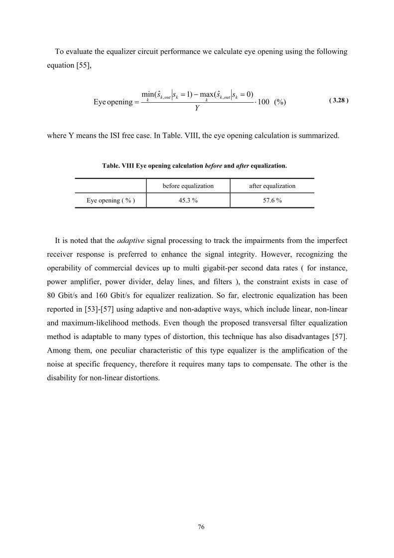
76
To evaluate the equalizer circuit performance we calculate eye opening using the following
equation [55],
(%)100)0ˆ(max)1ˆ(min
opening Eye,,
⋅=−=
=Y
ssss koutkkkoutkk
where Y means the ISI free case. In Table. VIII, the eye opening calculation is summarized.
before equalization after equalization
Eye opening ( % ) 45.3 % 57.6 %
It is noted that the adaptive signal processing to track the impairments from the imperfect
receiver response is preferred to enhance the signal integrity. However, recognizing the
operability of commercial devices up to multi gigabit-per second data rates ( for instance,
power amplifier, power divider, delay lines, and filters ), the constraint exists in case of
80 Gbit/s and 160 Gbit/s for equalizer realization. So far, electronic equalization has been
reported in [53]-[57] using adaptive and non-adaptive ways, which include linear, non-linear
and maximum-likelihood methods. Even though the proposed transversal filter equalization
method is adaptable to many types of distortion, this technique has also disadvantages [57].
Among them, one peculiar characteristic of this type equalizer is the amplification of the
noise at specific frequency, therefore it requires many taps to compensate. The other is the
disability for non-linear distortions.
( 3.28 )
Table. VIII Eye opening calculation before and after equalization.

77
3.4.3. 43 Gbit/s hybrid demultiplexer circuit
A hybrid sampling circuit is designed considering the flip-chip bonding technology. The
flip-chip equivalent circuit in Fig. 3.6 is applied to the circuit design. An alumina substrate
and the conductor-backed coplanar waveguide ( CPW ) with via holes are also employed. The
circuit schematic is fundamentally the same as in Fig. 3.14. We investigate the circuit
performance comparing with the MMIC circuit simulation results. Also, the tapped delay line
filter simulation is carried out. First of all, Fig. 3.24 shows impulse responses of the hybrid
sampling circuit for various hold capacitors.
The simulation condition is the same with that of the MMIC sampling circuit. It is obvious from Fig. 3.24 that
flip-chip parasitics change its intrinsic impulse response considerably. Rise and fall time increase in the hybrid
circuit, and a trailing edge is more irregularly oscillating and seldomly die out completely as simulation
sweeping time increases. The full width at half maximum ( FWHM ) value is measured. It increases from 6 psec
to 18 psec in the hybrid circuit when the hold capacitance is 0.2 pF. The S21 parameter simulation results are
shown in Fig. 3.25. They are compared with MMIC circuit simulation results. The simulated 3 dB cutoff
frequency is 26 GHz while in the MMIC circuit above 50 GHz cutoff freqeucny is estimated. The phase changes
more rapidly in the hybrid circuit. Above 43 GHz the nonlinear phase characteristic starts to show up. We
investigate the group delay characteristic. Until 37 GHz, it deviates ±13 psec from the average value, 31.5 psec.
Around 50 GHz spectral components begin to be lagged down.
Fig. 3.24 Impulse response simulation results including flip-chip parasitics for various hold capacitances.
0 0.1 0.2 0.3 0.4 0.5 0.6 0.7 0.8 0.9 1 1.1
x 10-10
-0.4
-0.2
0
0.2
0.4
0.6
0.8
1
1.2
Time ( sec )
Impu
lse
resp
onse
( no
rmal
ized
) 0.2 pF0.6 pF1.0 pF

78
(a) (b)
The hybrid sampling circuit simulations for the demultiplexer are done with the equalizer.
Their results are given in Fig. 3.27. Simulation conditions are all the same with the MMIC
case. The hold capacitance value is 0.2 pF, and the equalizer coefficients are 15 dB. In
contrast to the MMIC circuit simulation results, the equalizer enhances the eye opening by
5 %.
Fig. 3.25 S21 of the hybrid circuit is compared with those of the MMIC sampling circuit for (a) magnitude and (b) phase.
Fig. 3.26 Group delay of the hybrid sampling circuit.
0 1 2 3 4 5
x 1010
-50
-45
-40
-35
-30
-25
-20
-15
-10
-5
Frequency ( Hz )
S21
( dB
)
MMIC samplerHybrid sampler
0 1 2 3 4 5
x 1010
-200
-150
-100
-50
0
50
100
150
200
Frequency ( Hz )
S21
pha
se( d
egre
e )
MMIC samplerHybrid sampler
0 1 2 3 4 5
x 1010
-6
-4
-2
0
2
4
6
8x 10
-11
Frequency ( Hz )
Gro
up d
elay
( se
c )

79
(a)
(b)
This small enhancement can be explained with regard to the irregular trailing edge in the
impulse response. The edge affects several adjacent bits, thus the equalizer circuit needs more
than three taps. And, it is sophisticated to determine the filter coefficients because the ISI
depends on both bit patterns and the irregular trailing edges by each pattern. So, we use the
averaged coefficient value for the equalizer circuit simulation. Those constant should be
verified with the experimental result. It is noted that the output amplitude is reduced by half
compared with the MMIC simulation result. The main loss comes from the flip-chip parasitics.
For the equalizer in the hybrid sampling circuit, the adaptive algorithm is another choice to
consider. Keeping track of the eye waveform variation, the filter coefficients can be
adaptively changed and the clean eye waveform is obtained. However, the complexity of the
receiver structure and the high-speed adaptive signal processor implementations are also
considered.
Fig. 3.27 The hybrid circuit simulation result (a) before and (b) after equalization
0 20 40 60 80 100 120 140-20 160
0.00
0.01
0.02
0.03
-0.01
0.04
Time ( psec )
Am
plitu
de (
V )
0 20 40 60 80 100 120 140-20 160
0.00
0.01
0.02
0.03
-0.01
0.04
Time ( psec )
Am
plitu
de (
V )

80
3.5. 86 Gbit/s MMIC 1:2 demultiplexer circuit
3.5.1. 86 Gbit/s MMIC 1:2 demultiplexer
In this section we show that the sampling concept using Si Schottky diodes for the
demultiplexer circuit is feasible for an 86 Gbit/s 1:2 demultiplexer or higher speed circuit
implementation. We propose a circuit schematic and present simulation results for
an 86 Gbit/s demultiplexer. It is of significance to show that the Si Schottky diode sampling
circuit would be expanded into a higher bit rate communication circuit. Circuit simulation
results are provided supporting this fact. A linear equalizer circuit is also utilized to obtain a
demultiplexed signal waveform. As discussed in chapter 1, this work is motivated by the fact
that high-speed digital circuits can be implemented by analog ways using Si Schottky diodes.
Challenging to the 86 Gbit/s demultiplexer circuit, we present the Si Schottky diode sampling
circuit based demultiplexer circuit and simulation results.
3.5.1.1. Operation principle and simulation results
The circuit topology is different from the 43 Gbit/s 1:2 demultiplexer circuit. In order to
achieve higher bit rate using Si Schottky diodes, the structure itself is minimized. The same
diode model in the previous section is used for 86 Gbit/s MMIC 1:2 demultiplexer circuit
simulation.
Eliminating the requirement of the broadband resistive power divider, an integrated 1:2
demultiplexer is developed ( see Fig. 3.28 ). It is composed of two sampling circuits. Both of
them are equivalent and connected in parallel sharing the same oscillator signal. The distinct
difference is the direction of the diode pair. The diodes are anti-parallel, but each sampling
circuit is fundamentally identical. Compared with the sampling circuit for the 43 Gbit/s 1:2
demultiplexer, a 50 Ω matching resistance is removed and the number of used diodes is
smaller than that of the 43 Gbit/s sampling circuit. It is also beneficial to use the decreased
number of oscillator signal, because we do not need to supply high power oscillating signal
for the switching operation. The illustrative figure is illustrated in Fig. 3.28. Depending on the
clock signal amplitude, diode pairs are either conducting or not. Because diode pairs are anti-
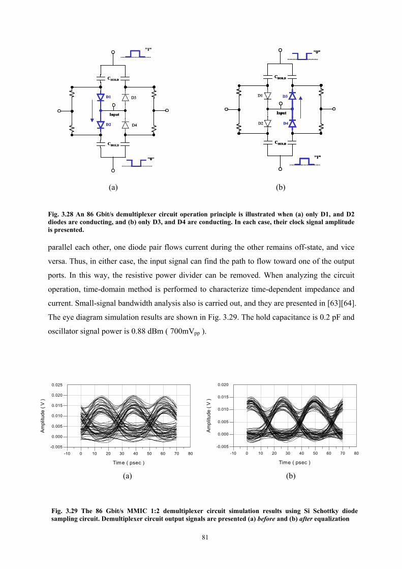
81
CHOLD
CHOLD
Input
''1''
''0''
D1
D2
D3
D4
CHOLD
CHOLD
Input
''1''
''0''
D1
D2
D3
D4
CHOLD
CHOLD
Input
''1''
''0''
D1
D2
D3
D4
CHOLD
CHOLD
Input
''1''
''0''
CHOLD
CHOLD
Input
''1''''1''
''0''''0''
D1
D2
D3
D4
(a) (b)
parallel each other, one diode pair flows current during the other remains off-state, and vice
versa. Thus, in either case, the input signal can find the path to flow toward one of the output
ports. In this way, the resistive power divider can be removed. When analyzing the circuit
operation, time-domain method is performed to characterize time-dependent impedance and
current. Small-signal bandwidth analysis also is carried out, and they are presented in [63][64].
The eye diagram simulation results are shown in Fig. 3.29. The hold capacitance is 0.2 pF and
oscillator signal power is 0.88 dBm ( 700mVpp ).
(a) (b)
Fig. 3.28 An 86 Gbit/s demultiplexer circuit operation principle is illustrated when (a) only D1, and D2 diodes are conducting, and (b) only D3, and D4 are conducting. In each case, their clock signal amplitude is presented.
Fig. 3.29 The 86 Gbit/s MMIC 1:2 demultiplexer circuit simulation results using Si Schottky diode sampling circuit. Demultiplexer circuit output signals are presented (a) before and (b) after equalization
0 10 20 30 40 50 60 70-10 80
0.000
0.005
0.010
0.015
0.020
-0.005
0.025
Time ( psec )
Am
plit
ude
( V
)
0 10 20 30 40 50 60 70-10 80
0.000
0.005
0.010
0.015
-0.005
0.020
Time ( psec )
Am
plit
ud
e (
V )
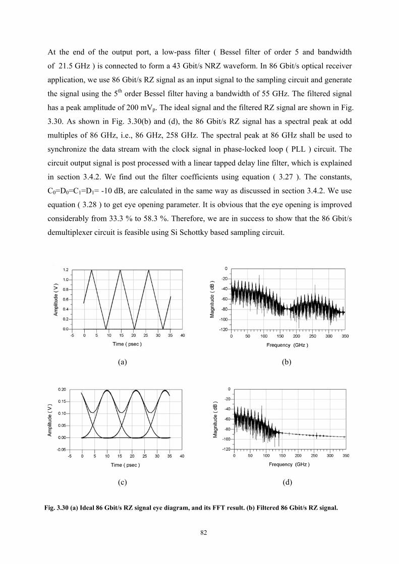
82
At the end of the output port, a low-pass filter ( Bessel filter of order 5 and bandwidth
of 21.5 GHz ) is connected to form a 43 Gbit/s NRZ waveform. In 86 Gbit/s optical receiver
application, we use 86 Gbit/s RZ signal as an input signal to the sampling circuit and generate
the signal using the 5th order Bessel filter having a bandwidth of 55 GHz. The filtered signal
has a peak amplitude of 200 mVp. The ideal signal and the filtered RZ signal are shown in Fig.
3.30. As shown in Fig. 3.30(b) and (d), the 86 Gbit/s RZ signal has a spectral peak at odd
multiples of 86 GHz, i.e., 86 GHz, 258 GHz. The spectral peak at 86 GHz shall be used to
synchronize the data stream with the clock signal in phase-locked loop ( PLL ) circuit. The
circuit output signal is post processed with a linear tapped delay line filter, which is explained
in section 3.4.2. We find out the filter coefficients using equation ( 3.27 ). The constants,
C0=D0=C1=D1= -10 dB, are calculated in the same way as discussed in section 3.4.2. We use
equation ( 3.28 ) to get eye opening parameter. It is obvious that the eye opening is improved
considerably from 33.3 % to 58.3 %. Therefore, we are in success to show that the 86 Gbit/s
demultiplexer circuit is feasible using Si Schottky based sampling circuit.
(a) (b)
(c) (d)
Fig. 3.30 (a) Ideal 86 Gbit/s RZ signal eye diagram, and its FFT result. (b) Filtered 86 Gbit/s RZ signal.
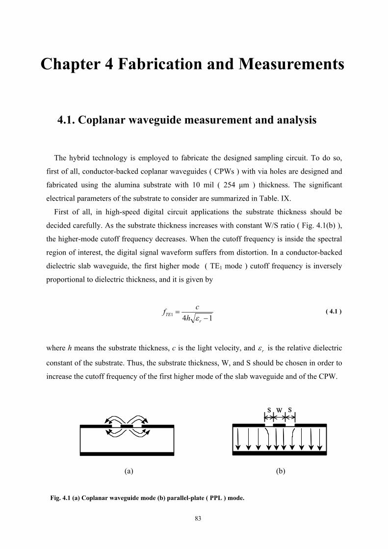
83
4.1. Coplanar waveguide measurement and analysis
The hybrid technology is employed to fabricate the designed sampling circuit. To do so,
first of all, conductor-backed coplanar waveguides ( CPWs ) with via holes are designed and
fabricated using the alumina substrate with 10 mil ( 254 µm ) thickness. The significant
electrical parameters of the substrate to consider are summarized in Table. IX.
First of all, in high-speed digital circuit applications the substrate thickness should be
decided carefully. As the substrate thickness increases with constant W/S ratio ( Fig. 4.1(b) ),
the higher-mode cutoff frequency decreases. When the cutoff frequency is inside the spectral
region of interest, the digital signal waveform suffers from distortion. In a conductor-backed
dielectric slab waveguide, the first higher mode ( TE1 mode ) cutoff frequency is inversely
proportional to dielectric thickness, and it is given by
141 −=
rTE h
cfε
where h means the substrate thickness, c is the light velocity, and rε is the relative dielectric
constant of the substrate. Thus, the substrate thickness, W, and S should be chosen in order to
increase the cutoff frequency of the first higher mode of the slab waveguide and of the CPW.
(a) (b)
Chapter 4 Fabrication and Measurements
( 4.1 )
Fig. 4.1 (a) Coplanar waveguide mode (b) parallel-plate ( PPL ) mode.
W SS W SS

84
However, as the dielectric height is reduced in the conductor-backed CPW close enough to
affect the coplanar waveguide field distribution, the CPW mode field pattern starts to be
altered allowing so-called the parallel-plate line ( PPL ) mode. This mode changes the field
profile of the dominant mode in the CPW. Thus, it changes the propagation properties of the
CPW and also couples the power to the other parts of the circuit. For example, in the
amplifier MMIC circuit, the feedback path due to the resonance phenomena of the PPL mode
in the conductor-backed CPW causes the power coupling. It results in the instability and cross
talk between the signal lines [68]. Therefore, the substrate thickness in high-speed digital
circuit shall be determined considering the higher-order mode cutoff frequency and the CPW
mode field profiles of the given CPW structure.
Secondly, the dielectric constant is to be considered. In addition to the effect on the cutoff
frequency in equation ( 4.1 ), if the dielectric constant is high, the field profile is concentrated
into a smaller area. Thus, we realize the high density of components in a motherboard. But,
with a lower dielectric constant the field energy is distributed in broader region. It causes the
crosstalk between the digital signal lines and higher radiation losses [66]. Thus, the dielectric
constant should be chosen after examining the effects on the circuit layout and frequency
range of interest.
And, finally metal thickness and its conductivity should be cared. The metal thickness
should be larger than the skin depth given by
condff
σπµδ 1)( =
where rµµµ 0= is the permeability of the conductor, and condσ is the conductivity of the metal.
Terms Value
Substrate thickness 10 mil
Metal thickness 5 µm ( Au )
Dielectric constant 9.9
( 4.2 )
Table. IX Alumina substrate parameters for simulation
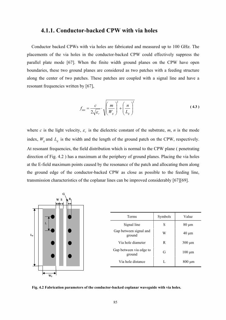
85
4.1.1. Conductor-backed CPW with via holes
Conductor backed CPWs with via holes are fabricated and measured up to 100 GHz. The
placements of the via holes in the conductor-backed CPW could effectively suppress the
parallel plate mode [67]. When the finite width ground planes on the CPW have open
boundaries, these two ground planes are considered as two patches with a feeding structure
along the center of two patches. These patches are coupled with a signal line and have a
resonant frequencies written by [67],
22
2
+
⋅=
ggrmn L
nWmcf
ε
where c is the light velocity, rε is the dielectric constant of the substrate, m, n is the mode
index, gW and gL is the width and the length of the ground patch on the CPW, respectively.
At resonant frequencies, the field distribution which is normal to the CPW plane ( penetrating
direction of Fig. 4.2 ) has a maximum at the periphery of ground planes. Placing the via holes
at the E-field maximum points caused by the resonance of the patch and allocating them along
the ground edge of the conductor-backed CPW as close as possible to the feeding line,
transmission characteristics of the coplanar lines can be improved considerably [67][69].
( 4.3 )
Terms Symbols Value
Signal line S 80 µm
Gap between signal and ground W 40 µm
Via hole diameter R 300 µm
Gap between via edge to ground G 100 µm
Via hole distance L 800 µm
Fig. 4.2 Fabrication parameters of the conductor-backed coplanar waveguide with via holes.
SW R
G
L
Lg
Wg
SW R
G
L
Lg
Wg
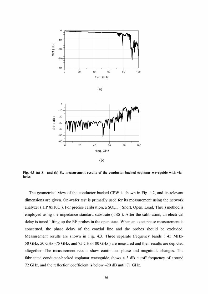
86
(a)
(b)
The geometrical view of the conductor-backed CPW is shown in Fig. 4.2, and its relevant
dimensions are given. On-wafer test is primarily used for its measurement using the network
analyzer ( HP 8510C ). For precise calibration, a SOLT ( Short, Open, Load, Thru ) method is
employed using the impedance standard substrate ( ISS ). After the calibration, an electrical
delay is tuned lifting up the RF probes in the open state. When an exact phase measurement is
concerned, the phase delay of the coaxial line and the probes should be excluded.
Measurement results are shown in Fig. 4.3. Three separate frequency bands ( 45 MHz-
50 GHz, 50 GHz -75 GHz, and 75 GHz-100 GHz ) are measured and their results are depicted
altogether. The measurement results show continuous phase and magnitude changes. The
fabricated conductor-backed coplanar waveguide shows a 3 dB cutoff frequency of around
72 GHz, and the reflection coefficient is below –20 dB until 71 GHz.
Fig. 4.3 (a) S21 and (b) S11 measurement results of the conductor-backed coplanar waveguide with via holes.
20 40 60 800 100
-30
-20
-10
-40
0
freq, GHz
S21
( d
B )
20 40 60 800 100
-50
-40
-30
-20
-10
-60
0
freq, GHz
S11
( d
B )
87
4.1.2. Signal propagation characteristics in the conductor-backed CPW with via holes
In high-speed digital circuit applications, the signal waveform prediction is of significance
as the electrical signal propagates a conductor path. As the pulse width of the digital signal
reaches the picosecond ( or subpicosecond ) range, the transmission line characteristics such
as dispersion and attenuation should be measured with a high precision. In general, they are
measured in frequency domain. Therefore, to estimate the signal waveform in time domain
we should make a Fourier transformation written as,
( )( ) zfffVzfVzt ⋅+−⋅== −− )(j)(exp)0,(),(),( 11 βαυ FF
where ),( zfV is the Fourier transform of ),( ztυ , )( fα is the frequency dependent
attenuation coefficient, and )( fβ is the frequency dependent phase. ( )⋅−1F denotes an
inverse Fourier transformation.
The CPW loss is composed of dielectric loss, conductor loss, and radiation loss. Usually,
the dielectric loss is much smaller than the conductor loss and negligible [72]. If no leaky
wave mode is excited, the conductor loss is dominant source for the attenuation. However,
above 200 GHz the radiation loss starts to be dominant [70]. The radiation leakage occurs
because of surface waves in the conductor-backed slab waveguide. Therefore, the attenuation
coefficients can expressed as the summation of conductor loss and radiation loss by
radcond ααα += .
The dispersion problem arises from the frequency-dependent characteristics of the
propagation constant associated with physical geometries of the structures, i.e., coplanar
waveguides or microstrip lines. The frequency-dependent nature of the signal propagation
constants causes signal distortion, in other words, the propagated signal shows the pulse
broadening effect. The dispersion characteristic is modeled using the following equation.
effcff επβ 2)( =
where effε is the effective dielectric constant and analytic equation is shown below.
( 4.4 )
( 4.5 )
( 4.6 )

88
⋅+
−+=
− 8.1
1
1
1
)(
TE
qrq
neff
ffa
fεε
εε
where, 2
1+= r
qεε , rε is the relative dielectric constant of the substrate, n is 2, fTE1 is given
in ( 4.1 ), and a is found using [70],
( )
2
2
log540.0log86.043.0
log015.0log69.054.0
loglog
⋅+
⋅−=
⋅+
⋅−=
+
⋅=
hW
hW
hW
hWu
SWua
υ
υ
where h is the thickness of the substrate. The calculation for the attenuation and the effective
dielectric constant are carried out using the measured S-parameter. The S-parameter response
of the lossy unmatched transmission line is expressed as [73][74],
−−
=
lZZZZ
ZZlZZDSS
SS
oo
oo
s γγ
sinh)(22sinh)(1
22
22
2221
1211
where, lZZlZZD oos γγ cosh2sinh)( 22 ++= . Using the equation ( 4.9 ), the following
equation can be derived directly,
( )( )2
21
221
2221
211
21
221
211
241
21
SSSS
SSSe l −−−
±+−
=−γ
where ( ) ( ) )()()( fjfCjGLjRf βαωωγ +=+⋅+= , and we use the symmetry condition
for port 1 and port 2, namely, 2211 SS = , and 2112 SS = . The positive sign is used to find the
negative direction propagation constant, and the negative sign is for the positive direction.
( 4.7 )
( 4.8 )
( 4.9 )
( 4.10 )
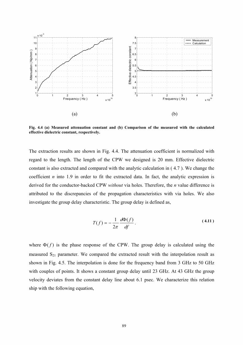
89
(a) (b)
The extraction results are shown in Fig. 4.4. The attenuation coefficient is normalized with
regard to the length. The length of the CPW we designed is 20 mm. Effective dielectric
constant is also extracted and compared with the analytic calculation in ( 4.7 ). We change the
coefficient n into 1.9 in order to fit the extracted data. In fact, the analytic expression is
derived for the conductor-backed CPW without via holes. Therefore, the n value difference is
attributed to the discrepancies of the propagation characteristics with via holes. We also
investigate the group delay characteristic. The group delay is defined as,
dffd
fT)(
21
)(Φ
−=π
.
where )( fΦ is the phase response of the CPW. The group delay is calculated using the
measured S21 parameter. We compared the extracted result with the interpolation result as
shown in Fig. 4.5. The interpolation is done for the frequency band from 3 GHz to 50 GHz
with couples of points. It shows a constant group delay until 23 GHz. At 43 GHz the group
velocity deviates from the constant delay line about 6.1 psec. We characterize this relation
ship with the following equation,
Fig. 4.4 (a) Measured attenuation constant and (b) Comparison of the measured with the calculated effective dielectric constant, respectively.
( 4.11 )
0 1 2 3 4 5
x 1010
1
2
3
4
5
6
7
8
9
10
11x 10
-3
Frequency ( Hz )
Atte
nuat
ion
( Np/
mm
)
0 1 2 3 4 5
x 1010
3
3.5
4
4.5
5
5.5
6
6.5
7
7.5
8
Frequency ( Hz )
Effe
ctiv
e di
elec
tric
cons
tant
MeasurementCalculation
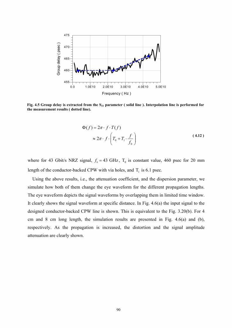
90
⋅+⋅⋅≈
⋅⋅=Φ
0102
)(2)(
ffTTf
fTff
π
π
where for 43 Gbit/s NRZ signal, GHz430 =f , 0T is constant value, 460 psec for 20 mm
length of the conductor-backed CPW with via holes, and 1T is 6.1 psec.
Using the above results, i.e., the attenuation coefficient, and the dispersion parameter, we
simulate how both of them change the eye waveform for the different propagation lengths.
The eye waveform depicts the signal waveforms by overlapping them in limited time window.
It clearly shows the signal waveform at specific distance. In Fig. 4.6(a) the input signal to the
designed conductor-backed CPW line is shown. This is equivalent to the Fig. 3.20(b). For 4
cm and 8 cm long length, the simulation results are presented in Fig. 4.6(a) and (b),
respectively. As the propagation is increased, the distortion and the signal amplitude
attenuation are clearly shown.
Fig. 4.5 Group delay is extracted from the S21 parameter ( solid line ). Interpolation line is performed for the measurement results ( dotted line).
( 4.12 )
1.0E10 2.0E10 3.0E10 4.0E100.0 5.0E10
460
465
470
455
475
Frequency ( Hz )
Gro
up d
elay
( p
sec
)
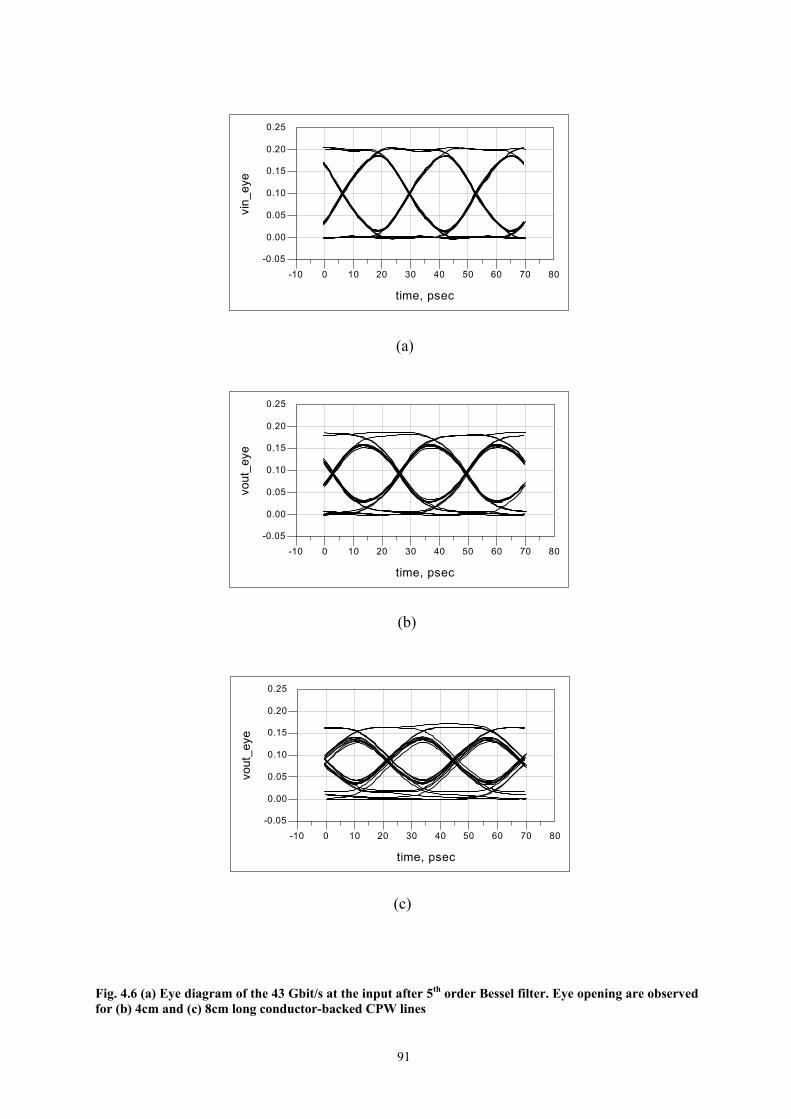
91
(a)
(b)
(c)
Fig. 4.6 (a) Eye diagram of the 43 Gbit/s at the input after 5th order Bessel filter. Eye opening are observed for (b) 4cm and (c) 8cm long conductor-backed CPW lines
0 10 20 30 40 50 60 70-10 80
0.00
0.05
0.10
0.15
0.20
-0.05
0.25
time, psec
vin_
eye
0 10 20 30 40 50 60 70-10 80
0.00
0.05
0.10
0.15
0.20
-0.05
0.25
time, psec
vout
_eye
0 10 20 30 40 50 60 70-10 80
0.00
0.05
0.10
0.15
0.20
-0.05
0.25
time, psec
vout
_eye
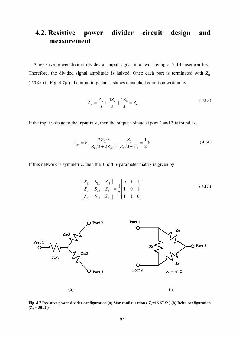
92
4.2. Resistive power divider circuit design and measurement
A resistive power divider divides an input signal into two having a 6 dB insertion loss.
Therefore, the divided signal amplitude is halved. Once each port is terminated with 0Z
( 50 Ω ) in Fig. 4.7(a), the input impedance shows a matched condition written by,
0000
34||
34
3ZZZZZin =+=
If the input voltage to the input is V, then the output voltage at port 2 and 3 is found as,
VZZ
ZZZ
ZVVout 21
332332
00
0
00
0 =+
⋅+
⋅= .
If this network is symmetric, then the 3 port S-parameter matrix is given by
=
011101110
21
333231
232221
131211
SSSSSSSSS
.
(a) (b)
( 4.13 )
( 4.14 )
( 4.15 )
Fig. 4.7 Resistive power divider configuration (a) Star configuration ( Zo=16.67 Ω ) (b) Delta configuration (Zo = 50 Ω )
Zo/3
Zo/3Zo/3
Port 1
Port 2
Port 3
Zo/3
Zo/3Zo/3
Port 1
Port 2
Port 3
Zo
Zo
Zo
Zo = 50 Ω
Port 1
Port 2
Port 3Zo
Zo
Zo
Zo = 50 Ω
Zo
Zo
Zo
Zo
Zo
Zo
Zo = 50 Ω
Port 1
Port 2
Port 3

93
The resistive power divider can be implemented using the two configurations. One is a star
configuration, named after its position of the resistance 16.67 Ω ( Fig. 4.7(a) ), and the other is
a delta configuration ( Fig. 4.7(b) ). In fact, the larger resistance value is employed, the better
performance shall be acquired because of the fabrication tolerance. Using the Y-∆
transformation equations according to Fig. 4.8, the star configuration is converted into the
delta configuration. The delta configuration is preferred in the hybrid implementation due to
the magnitude of the resistance value.
In Fig. 4.9(a), the actual layout is illustrated. Both the star and the delta configurations are
utilized for the implementation. Fig. 4.9(a) illustrates the delta configuration layout. The
designed conductor-backed CPWs are used for the resistive power divider implementation.
The sheet resistance is 100 Ω/ٱ. Anritsu integrated V connector ( model V115FCPW ) is
employed for the transition. This connector includes the solder-in CPW line with a ground-
lip in the structure. The frequency range is from DC to 65 GHz [76].
(a) (b)
Fig. 4.8 Y-∆ transformation diagram [75].
Fig. 4.9 (a) Resistive power divider circuit layout, and (b) fabrication module.
a
bc
ab
bc
caa
bc
ab
bc
cacabcab
caaba ZZZ
ZZZ++
⋅=
c
babaab Z
ZZZZZ ⋅++=
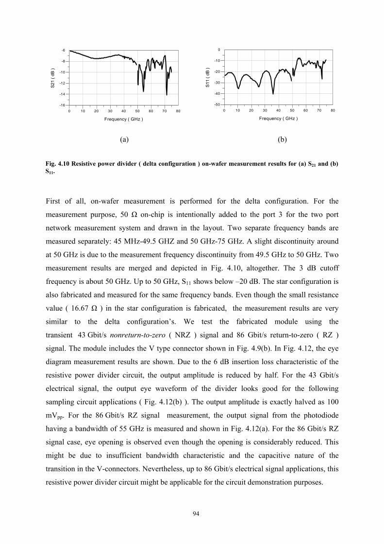
94
(a) (b)
First of all, on-wafer measurement is performed for the delta configuration. For the
measurement purpose, 50 Ω on-chip is intentionally added to the port 3 for the two port
network measurement system and drawn in the layout. Two separate frequency bands are
measured separately: 45 MHz-49.5 GHZ and 50 GHz-75 GHz. A slight discontinuity around
at 50 GHz is due to the measurement frequency discontinuity from 49.5 GHz to 50 GHz. Two
measurement results are merged and depicted in Fig. 4.10, altogether. The 3 dB cutoff
frequency is about 50 GHz. Up to 50 GHz, S11 shows below –20 dB. The star configuration is
also fabricated and measured for the same frequency bands. Even though the small resistance
value ( 16.67 Ω ) in the star configuration is fabricated, the measurement results are very
similar to the delta configuration’s. We test the fabricated module using the
transient 43 Gbit/s nonreturn-to-zero ( NRZ ) signal and 86 Gbit/s return-to-zero ( RZ )
signal. The module includes the V type connector shown in Fig. 4.9(b). In Fig. 4.12, the eye
diagram measurement results are shown. Due to the 6 dB insertion loss characteristic of the
resistive power divider circuit, the output amplitude is reduced by half. For the 43 Gbit/s
electrical signal, the output eye waveform of the divider looks good for the following
sampling circuit applications ( Fig. 4.12(b) ). The output amplitude is exactly halved as 100
mVpp. For the 86 Gbit/s RZ signal measurement, the output signal from the photodiode
having a bandwidth of 55 GHz is measured and shown in Fig. 4.12(a). For the 86 Gbit/s RZ
signal case, eye opening is observed even though the opening is considerably reduced. This
might be due to insufficient bandwidth characteristic and the capacitive nature of the
transition in the V-connectors. Nevertheless, up to 86 Gbit/s electrical signal applications, this
resistive power divider circuit might be applicable for the circuit demonstration purposes.
Fig. 4.10 Resistive power divider ( delta configuration ) on-wafer measurement results for (a) S21 and (b) S11.
10 20 30 40 50 60 700 80
-14
-12
-10
-8
-16
-6
Frequency ( GHz )
S21
( d
B )
10 20 30 40 50 60 700 80
-40
-30
-20
-10
-50
0
Frequency ( GHz )
S11
( d
B )

95
(a)
(b)
Fig. 4.11 Eye diagrams for (a) 43 Gbit/s NRZ input signal and (b) the resistive power divider output.
~ 200 mVpp
~ 100 mVpp 100 mVpp
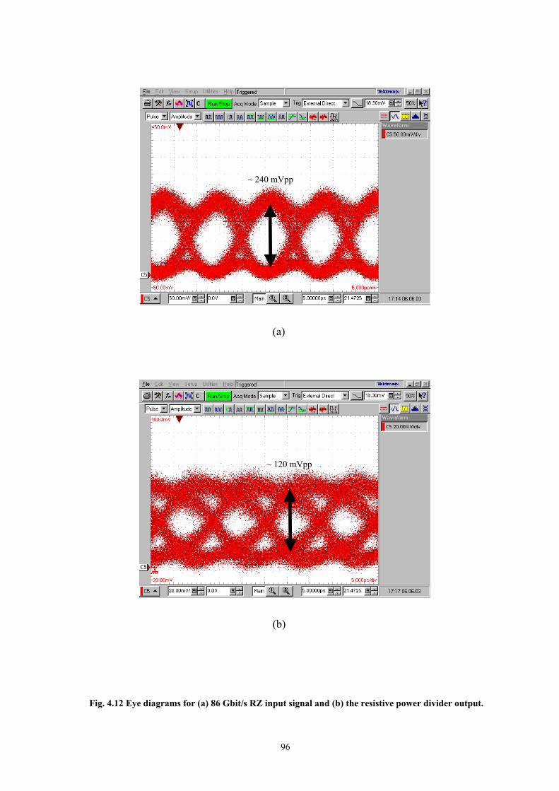
96
(a)
(b)
Fig. 4.12 Eye diagrams for (a) 86 Gbit/s RZ input signal and (b) the resistive power divider output.
~ 120 mVpp
~ 240 mVpp
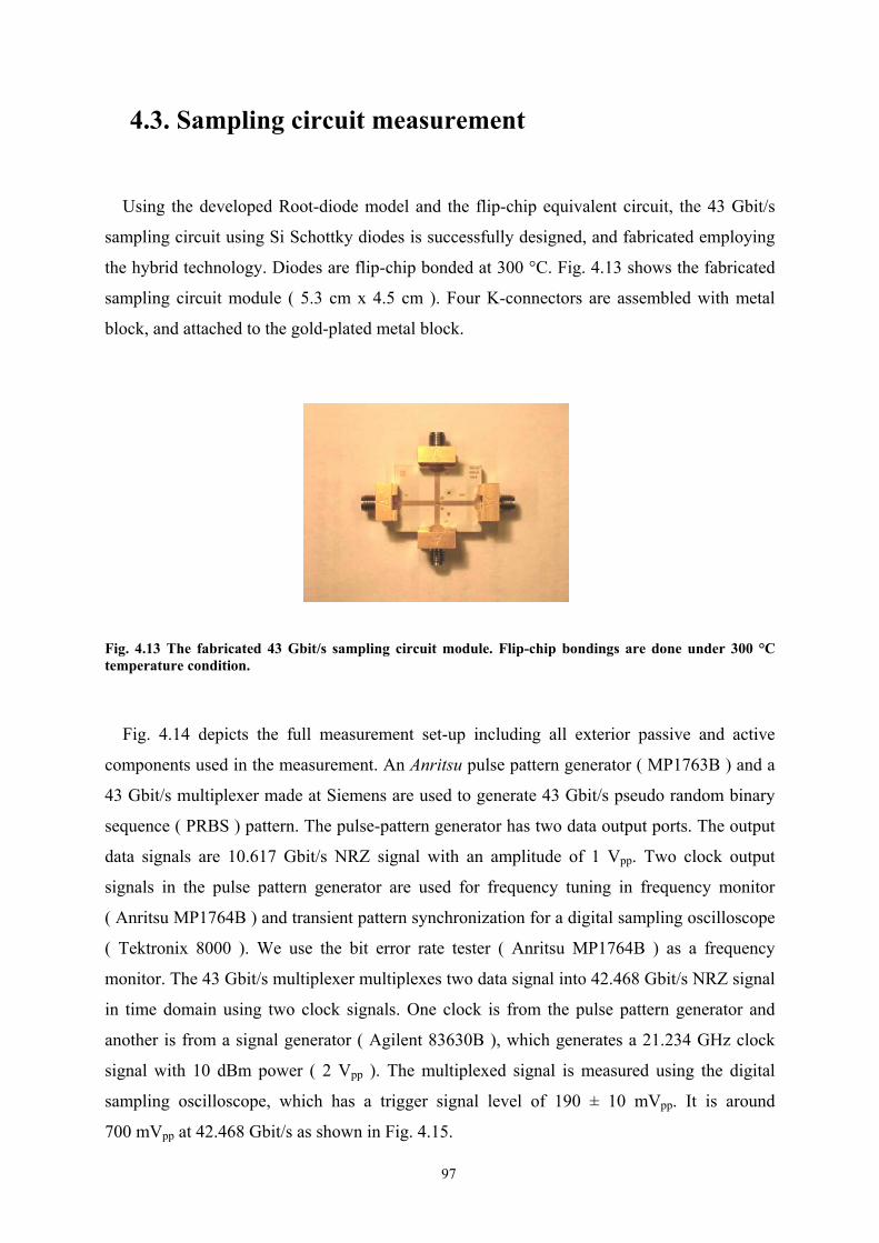
97
4.3. Sampling circuit measurement
Using the developed Root-diode model and the flip-chip equivalent circuit, the 43 Gbit/s
sampling circuit using Si Schottky diodes is successfully designed, and fabricated employing
the hybrid technology. Diodes are flip-chip bonded at 300 °C. Fig. 4.13 shows the fabricated
sampling circuit module ( 5.3 cm x 4.5 cm ). Four K-connectors are assembled with metal
block, and attached to the gold-plated metal block.
Fig. 4.14 depicts the full measurement set-up including all exterior passive and active
components used in the measurement. An Anritsu pulse pattern generator ( MP1763B ) and a
43 Gbit/s multiplexer made at Siemens are used to generate 43 Gbit/s pseudo random binary
sequence ( PRBS ) pattern. The pulse-pattern generator has two data output ports. The output
data signals are 10.617 Gbit/s NRZ signal with an amplitude of 1 Vpp. Two clock output
signals in the pulse pattern generator are used for frequency tuning in frequency monitor
( Anritsu MP1764B ) and transient pattern synchronization for a digital sampling oscilloscope
( Tektronix 8000 ). We use the bit error rate tester ( Anritsu MP1764B ) as a frequency
monitor. The 43 Gbit/s multiplexer multiplexes two data signal into 42.468 Gbit/s NRZ signal
in time domain using two clock signals. One clock is from the pulse pattern generator and
another is from a signal generator ( Agilent 83630B ), which generates a 21.234 GHz clock
signal with 10 dBm power ( 2 Vpp ). The multiplexed signal is measured using the digital
sampling oscilloscope, which has a trigger signal level of 190 ± 10 mVpp. It is around
700 mVpp at 42.468 Gbit/s as shown in Fig. 4.15.
Fig. 4.13 The fabricated 43 Gbit/s sampling circuit module. Flip-chip bondings are done under 300 °C temperature condition.
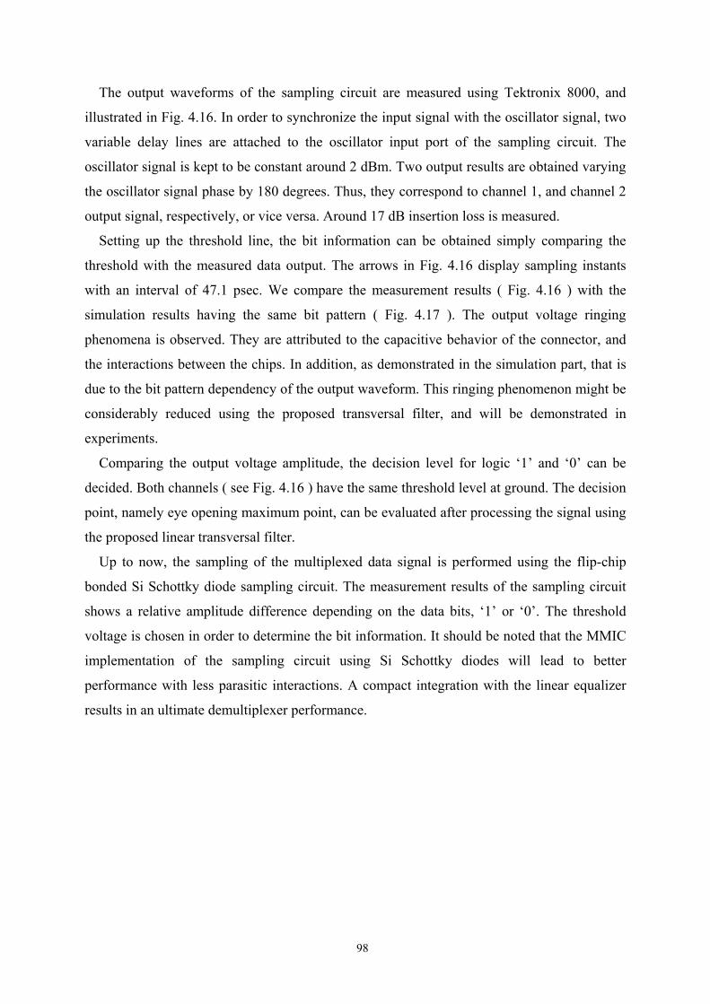
98
The output waveforms of the sampling circuit are measured using Tektronix 8000, and
illustrated in Fig. 4.16. In order to synchronize the input signal with the oscillator signal, two
variable delay lines are attached to the oscillator input port of the sampling circuit. The
oscillator signal is kept to be constant around 2 dBm. Two output results are obtained varying
the oscillator signal phase by 180 degrees. Thus, they correspond to channel 1, and channel 2
output signal, respectively, or vice versa. Around 17 dB insertion loss is measured.
Setting up the threshold line, the bit information can be obtained simply comparing the
threshold with the measured data output. The arrows in Fig. 4.16 display sampling instants
with an interval of 47.1 psec. We compare the measurement results ( Fig. 4.16 ) with the
simulation results having the same bit pattern ( Fig. 4.17 ). The output voltage ringing
phenomena is observed. They are attributed to the capacitive behavior of the connector, and
the interactions between the chips. In addition, as demonstrated in the simulation part, that is
due to the bit pattern dependency of the output waveform. This ringing phenomenon might be
considerably reduced using the proposed transversal filter, and will be demonstrated in
experiments.
Comparing the output voltage amplitude, the decision level for logic ‘1’ and ‘0’ can be
decided. Both channels ( see Fig. 4.16 ) have the same threshold level at ground. The decision
point, namely eye opening maximum point, can be evaluated after processing the signal using
the proposed linear transversal filter.
Up to now, the sampling of the multiplexed data signal is performed using the flip-chip
bonded Si Schottky diode sampling circuit. The measurement results of the sampling circuit
shows a relative amplitude difference depending on the data bits, ‘1’ or ‘0’. The threshold
voltage is chosen in order to determine the bit information. It should be noted that the MMIC
implementation of the sampling circuit using Si Schottky diodes will lead to better
performance with less parasitic interactions. A compact integration with the linear equalizer
results in an ultimate demultiplexer performance.

99
Fig. 4.14 Sampling circuit measurement set-up.
Signal Generator( Agilent 83630B )
Power Divider(Ring Hybrid)
Power Divider
Pulse Pattern Generator( Anritsu MP1763B)
Pattern. Sync. Data Data CLK1
Frequency monitor( Anritsu MP1764B )
CLK
Freq. Divider( Siemens )
÷ 2 ÷ 8
40 Gbit/s Multiplexer( Siemens )
Data Data CLKCLK1
Out Out
Digital Sampling Ocsilloscope( Tektronix 8000 )
DUT
LO LO
InOut
Amp
Variable delay
Power Divider
Power Divider Variable delay
trigger
21.234 GHz
10.617 GHz
10.617 GHz
10.617 GHz(transient sync.)
Modular switch21.234 GHz
42.468 Gbit/s
Zo
2.6543 GHz(eye waveform sync.)
Signal Generator( Agilent 83630B )
Power Divider(Ring Hybrid)
Power Divider
Pulse Pattern Generator( Anritsu MP1763B)
Pattern. Sync. Data Data CLK1
Pulse Pattern Generator( Anritsu MP1763B)
Pattern. Sync. Data DataData CLK1
Frequency monitor( Anritsu MP1764B )
CLK
Frequency monitor( Anritsu MP1764B )
CLK
Freq. Divider( Siemens )
÷ 2 ÷ 8
Freq. Divider( Siemens )
÷ 2 ÷ 8
40 Gbit/s Multiplexer( Siemens )
Data Data CLKCLK1
Out Out
40 Gbit/s Multiplexer( Siemens )
Data DataData CLKCLK1
Out OutOut
Digital Sampling Ocsilloscope( Tektronix 8000 )
DUT
LO LO
InOut
DUT
LO LOLO
InOut
AmpAmp
Variable delayVariable delay
Power Divider
Power Divider Variable delayVariable delayVariable delay
trigger
21.234 GHz
10.617 GHz
10.617 GHz
10.617 GHz(transient sync.)
Modular switch21.234 GHz
42.468 Gbit/s
Zo
2.6543 GHz(eye waveform sync.)
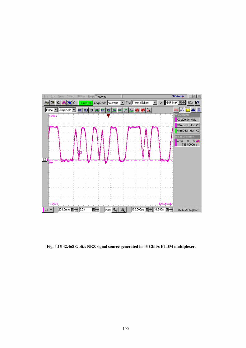
100
Fig. 4.15 42.468 Gbit/s NRZ signal source generated in 43 Gbit/s ETDM multiplexer.
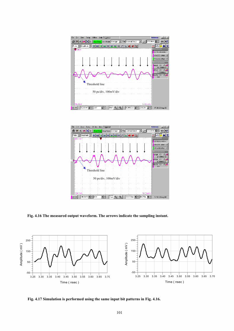
101
Fig. 4.16 The measured output waveform. The arrows indicate the sampling instant.
Fig. 4.17 Simulation is performed using the same input bit patterns in Fig. 4.16.
Threshold line
50 ps/div, 100mV/div
50 ps/div, 100mV/div
Threshold line
3.30 3.35 3.40 3.45 3.50 3.55 3.60 3.653.25 3.70
50
150
-50
250
Time ( nsec )
Am
plitu
de (
mV
)
3.30 3.35 3.40 3.45 3.50 3.55 3.60 3.653.25 3.70
50
150
-50
250
Time ( nsec )
Am
plitu
de (
mV
)

102
For a high-speed demultiplexer circuit implementation, we proposed and demonstrated a
sampling circuit combining with a linear equalizer. For the circuit demonstration, we carried
out the Root-diode modeling. This diode model is suitable for the accurate performance
prediction of Si Schottky diodes in high frequency operation. It is a nonquasi-static and a
charge-conservative model. The developed Root-diode model showed a good agreement with
the measurement data for both DC and CV. This characteristic is well suited for the sampling
circuit simulation since the large and the small-signal analysis are needed in the simulation.
For hybrid implementations, we have carried out the simulation of the flip-chip
interconnection using a full wave electromagnetic simulator. We established an equivalent
circuit model and obtained discrete model components value by interpolating simulation
results. In order to verify the equivalent circuit model, we simulated, fabricated, and measured
the flip-chip bonded Si Schottky diode on the alumina substrate employing the developed
Root-diode model and the flip-chip bonding equivalent circuit. A good agreement has been
found between the simulation result and the measurement up to 50 GHz.
Then, the sampling circuit was designed, and simulated for the realization of the
demultiplexer circuit. We used the Root-diode model and the flip-chip equivalent circuit.
Both hybrid and monolithic microwave IC ( MMIC ) implementations were considered in the
circuit simulation for the 43 Gbit/s demultiplexer circuit. We compared the impulse responses
and investigated the eye diagrams for two cases. We successfully designed the sampling
circuit based on the Si Schottky diodes for the 43 Gbit/s 1:2 demultiplexer circuit operation.
In order to eliminate the deterministic intersymbol interference ( ISI ), we proposed a linear
equalizer circuit. Using a zero-forcing algorithm, we calculated the tap coefficient analytically
and simulated the eye waveform combining with the equalizer circuit. We have identified the
eye opening enhancement in the simulation.
For the circuit fabrication, first of all, we designed a conductor-backed CPW with via holes.
The cutoff frequency of 72 GHz was obtained. It was analyzed in terms of the losses and the
dispersion analytically. We simulated how these two affect signal waveform as the
propagation length increases. The resistive power divider was also designed employing the
designed CPW with via holes. It was measured under on-wafer condition, and about 50 GHz
Chapter 5 Conclusion and outlook

103
bandwidth was acquired. We tested the resistive power divider module employing the
43 Gbit/s NRZ and 86 Gbit/s RZ electrical signal. The 6 dB insertion loss was observed and a
good eye opening was maintained for both signal schemes.
We measured the fabricated sampling module. The experimental set-up was illustrated in
detail. A 42.468 Gbit/s NRZ signal is synchronized with the oscillator signal. The measured
output signal was obtained in time domain and showed a ringing phenomenon. It was
attributed to the connector parasitics and the chip interactions. After choosing a threshold
level, we could decide the bit information ( ‘1’ or ‘0’ ). Improvements should be made to
achieve a good eye waveform. When the circuit would be made in a MMIC chip, it is
expected that the chip shows a better performance. Furthermore, the linear equalizer also
should be tested. Tap coefficients might be decided experimentally and compared with the
theoretical value. Those works are remained as future works.
The proposed sampling circuit based demultiplexer circuit with a linear equalizer circuit is
a significant step toward 160 Gbit/s Si based optical receiver circuit implementation. In this
work, we successfully designed the demultiplexer circuit using only Si Schottky diodes. This
approach contrasts to the conventional one in that we pursue Si Schottky diodes for the
demultiplexer circuit implementation. Our primary intention behind this work is to integrate
this demultiplexer circuit with the push-push oscillator circuit, and complete the optical
receiver circuit using Si technologies. A push-push oscillator is also built up with Si
heterojunction biploar transistors ( HBTs ), which is the only three terminal devices in the
whole receiver circuit and has been reported in [13]. Considering the fact that the Si Schottky
diodes have achieved over 1 THz cutoff frequency and the the reported push-push oscillator is
feasible to be integrated with the sampling circuit for the demultiplexer circuit, we can
conclude that the high-speed optical receiver circuit up to 160 Gbit/s will be constructed in
silicon monolithic millimeter-wave integrated circuits ( SIMMWICs ).

104
Appendix A
Photocurrent and noise statistics
In [39] and [47], it is shown that the photocurrent variance is calculated using the
semiclassical theory of the photoelectric detection of light. This approach enables the
photodetector’s impulse response to be associated with the theory of the detection of the light.
Here we will explain the detailed derivation processes of the photocurrent autocovariance
using the Gaussian nature of the noise.
First of all, we pursue for the autocorrelation function of the photocurrent. From the
equation ( 2.40 ),
∑ ∑∑
∑ ∑
∞
−∞=
∞
≠−∞=
∞
−∞=
∞
−∞=
∞
−∞=
∆−∆−∆∆+∆−∆−∆∆=
∆−∆⋅∆−∆=⋅
klk
lk
k lPDPD
tlthtkthtlXtkXtkthtkthtkXtkX
tlthtlXtkthtkXtiti
)()()()()()()()(
)()()()()'()(
We identify that XX =2 since 0,1∈X . Taking a limit as 0→∆t and using ( 2.39 ),
( 2.41 ) and ( 2.44 ), we can simplify the equation [ A.1 ] as,
∫ ∫∫
∑ ∑∑
∞
∞−
∞
∞−
∞
∞−
∞
−∞=
∞
≠−∞=
→∆
∞
−∞=→∆
−−⋅+−=
∆−∆−∆∆+∆−∆=⋅
')'()()'()()()(
)()()()(lim)()(lim)'()(
2
0
2
0
τττττλτλτττλ ddththdth
tlthtkthtlXtkXtkthtkXtitik
lkltktPDPD
.
[ A.1 ]
[ A.2 ]

105
Next, performing the product of the two ensemble averages we also get the equation given
by,
( ) ( )
∫ ∫∞
∞−
∞
∞−
−−=
⋅=
')'()()'()(
)'(*)'()(*)()'()(
τττττλτλ
λλ
ddthth
thtthttiti PDPD
Therefore, we conclude that the autocovariance of the photocurrent is written as,
( ) ( )∫ ∫∞
∞−
∞
∞−∆ −−⋅−+= ')'()()'()()'()()(*)(', 2 τττττλτλτλτλλ ddthththtttC i
From now on, we associate the photoelectron generation rate with the complex optical field
intensity. Then, we will calculate the variance component with respect to the optical field.
From ( 2.51 ), ( 2.52 ) and ( 2.53 ),
( )
( )( )
( ) )(*)(
)(*)(2)(
)(*)(*)(
2
2*22
222
thPtpqR
thtOtOqR
thqRtht
PDNSIG
PDSIGSIG
PD
+⋅=
ℜ++⋅=
⋅=
(t)O(t)O
(t)O
NN
RXλ
where we assume that the signal field and the noise are uncorrelated, the zero-mean Gaussian
noise characteristic, and Oeff
spOASEN BhGnBSP ⋅⋅−=⋅= νννν )1)()(()( is the average ASE
noise power with the optical filter bandwidth, OB . Here it is noted that using the semiclassical
theory of the photoelectron detection of the light we express the ensemble average of the
photocurrent incorporating with the PD’s impulse response.
The autocovariance of the photoelectron generation rate is expressed using the complex
optical field written by,
22222
'')'()()'()( )(τO)(τO)(τO)(τO RXRXRXRX −
=−
qRτλτλτλτλ
[ A.3 ]
[ A.4 ]
[ A.5 ]
[ A.6 ]
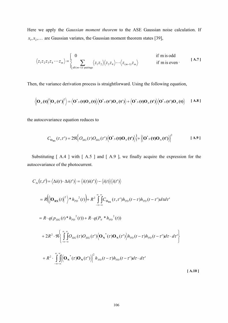
106
Here we apply the Gaussian moment theorem to the ASE Gaussian noise calculation. If
K,, 21 xx are Gaussian variates, the Gaussian moment theorem states [39],
= ∑−
− even is m if odd is m if 0
pairings )!1( all)1(43214321
mmmm zzzzzzzzzzz LL .
Then, the variance derivation process is straightforward. Using the following equation,
)(τ)O(τO)(τ)O(τO)(τ)O(τO)(τ)O(τO)(τO)(τO NNNNNNNNNN ''''' ****22 +=
the autocovariance equation reduces to
2** '')'()(2)',( )(τ)O(τO)(τ)O(τORXO NNNNSIGSIG OOC +ℜ= ττττ
Substituting [ A.4 ] with [ A.5 ] and [ A.9 ], we finally acquire the expression for the
autocovariance of the photocurrent.
( )
( )
∫ ∫
∫ ∫
∫ ∫
∞
∞−
∞
∞−
∞
∞−
∞
∞−
∞
∞−
∞
∞−
∆
⋅−−⋅+
⋅−−ℜ⋅+
⋅+⋅=
−−+=
−=∆⋅∆=
')'()()'()(
')'()()'()()'()(2
))(*())(*)((
')'()()',()(*)(
)'()()'()()'()(',
2*2
*2
22
222
ττττττ
ττττττττ
ττττττ
ddththR
ddththOOR
thPqRthtpqR
ddththCRthtR
titititititittC
PDPD
PDPDSIGSIG
PDNPDSIG
PDPDPD
i
NN
NN
ORX
OO
OO
ORX
[ A.7 ]
[ A.8 ]
[ A.9 ]
[ A.10 ]

107
Appendix B
Si Schottky diode demultiplexer circuit MATLAB program
%--------------------------------------------------------------------% % Author : Jung Han Choi % Parameter definitions %--------------------------------------------------------------------% % Nyquist wavefrom Roll-off factor. Ref : IEEE Journal of Light. Tech. Vol.19, No. 9, pp. 1263-1273, Sep. 2001. alpha=0.4; % td : pulse width % 40 Gbps NRZ : td=25.00e-12 sec, 80 Gbps RZ : td= 6.25e-12 sec td=6.25e-12; % Number of periods in the Nyquist waveform num_period=1; % Number of points in one period of waveform pts=100 ; %--------------------------------------------------------------------% % Simulation range definition in time domain. % start and stop points should be integer times of period % e.g.) start_time=0,stop_time=100 means that simulation time is % from 0(sec) to 100*td ( sec ) ( 0 ~ 100T ) for NRZ signal % from 0(sec) to 100*td*2 ( sec ) ( 0 ~ 100T ) for RZ signal %--------------------------------------------------------------------% start_time=0; stop_time=30; %--------------------------------------------------------------------% % Random input signal generation combining with Nyquist waveform and pseudo-random binary sequence ( PRBS ) %--------------------------------------------------------------------% e=[]; e=input_signal(td, alpha, pts, num_period, start_time, stop_time); %--------------------------------------------------------------------% % 5th order Bessel-Thompson filter . Input_signal passes through the filter. We depict eye diagram after the filter. %--------------------------------------------------------------------% num=[0 0 0 0 0 945]; den=[1 15 105 420 945 945]; [A B C D]=tf2ss(num,den); % Converts into the state-sapce domain [G H]=c2d(A, B, 0.01375); % 55GHz / 8000GHz ( 80G NRZ ) *2 % 8000GHz : sampling frequency. One period of 80 Gbit/s RZ signal ( 2*6.25psec ) is subdivided by 'pts'. % Thus,sampling time difference is 2*6.25psec / 100 pts, which corresponds to 8000 GHz. [numz denz]=ss2tf(G,H,C,D); y=filter(numz, denz, e); eye_waveform(y, td, pts, 0); % Draw eye diagram

108
%--------------------------------------------------------------------% % Sampling process ( demultiplexing ) %--------------------------------------------------------------------% figure;x=start_time:1/pts:stop_time; subplot(5,1,1); plot(x,y); % Plot PRBS Nyquist waveform after Bessel filter subplot(5,1,2); % Generate impulse train for channel 1 and draw it imp_sampler_ch1=transfer_sampler(2*td, 2*pts, start_time, stop_time, 6.25e-12); % Perform sampling ( demultiplexing ) for channel 1 output_sampling_ch1=sampling(y, imp_sampler_ch1); subplot(5,1,3); % Generate impulse train for channel 2 and draw it imp_sampler_ch2=transfer_sampler(2*td, 2*pts, start_time, stop_time, 12.5e-12); % Perform sampling ( demultiplexing ) for channel 1 output_sampling_ch2=sampling(y, imp_sampler_ch2); % Depict the sampled waveform in time domain for channel 1 and 2 subplot(5,1,4); plot(x,output_sampling_ch1); subplot(5,1,5); plot(x,output_sampling_ch2); %--------------------------------------------------------------------% % The sampled signal passes through a low-pass filter ( LPF ) to make its demultiplexed waveform. %--------------------------------------------------------------------% [G H]=c2d(A, B, 0.005); % 20 GHz /8000GHz ( 40G NRZ ) *2 [numz denz]=ss2tf(G,H,C,D); % Sampled signal ( channel 1 ) is filter out by the 5th order Bessel filter % which has a bandwidth of 20GHz. yy=filter(numz, denz, output_sampling_ch1'); % Draw eye diagram eye_waveform(yy, td, pts, 0); ------------------------------------------------------SUBROUTINE 1------------------------------------------------------ %--------------------------------------------------------------------% % Signal modeling % Function usage : input_signal(td, alpha, pts, num_period, start_time, stop_time) % % This function generates PRBS waveform in time domain. % The pulse used here is Nyquist waveform with roll-off factor, 0<alpha<1. % % 1. Pulse width : td % 2. Nyquist coefficient : alpha % 3. # of points in one pulse duration : pts % 4. # of periods in Nyquist waveform : num_period % 5. start time point : start_time % 6. stop time : stop_time %--------------------------------------------------------------------% function e=input_signal(td, alpha, pts, num_period, start_time, stop_time) % Nyquist waveform generation with Roll-off factor and pts. pulse=Nyquist_pulse(alpha,pts,num_period); % PRBS sequence 2^8-1 generation (Subroutine PRBS_seq) PRBS_sequence=PRBS_seq(8); % input signal matrix initialization e([1:(stop_time)*pts+1],:)=0;

109
% 80 Gbps RZ case for i=start_time:stop_time+num_period-1, if(-i<-num_period) p_start=-num_period; else p_start=-i; end; if(i+num_period)>stop_time p_stop=stop_time-i; else p_stop=num_period;end; temp_pulse=pulse([(p_start+num_period)*pts+1:(p_stop+num_period)*pts+1],:); if(i<=num_period) index=0; else index=i-num_period;end; temp_index=0; for k=index*pts+1:index*pts+size(temp_pulse,1), temp_index=temp_index+1; e(k,:)=e(k,:)+temp_pulse(temp_index)*PRBS_sequence(i+1); end end ------------------------------------------------------SUBROUTINE 2------------------------------------------------------ %--------------------------------------------------------------------% % PRBS (Pseudo-random Binary Sequence) generator Program % PRBS(num_stage) % PRBS() generate PN sequences with user-defined recurrence relation. % num_register ; # of shift register in Linear Feedback Shift Register(LFSR) % Note that Student version of MATLAB supports not more than 14 shift registers. %--------------------------------------------------------------------% function p=PRBS_seq(num_register) if (num_register<2|num_register>33) error('Num_register represents the number of shift register in Linear Feedback Shift Register'); error('num_register should be larger than 2, or smaller than 33 in this version'); end % Tap reference ref_tap=[2 1 0 0;3 1 0 0;4 1 0 0;5 2 0 0;6 1 0 0;7 1 0 0;8 4 3 2;9 4 0 0;10 3 0 0;11 1 0 0;12 6 4 1; 13 4 3 1;14 12 2 1;15 13 10 9;16 12 3 1;17 3 0 0;18 7 0 0;19 5 2 1;20 3 0 0;21 2 0 0;22 1 0 0; 23 5 0 0;24 7 2 0;25 3 0 0;26 6 2 1;27 5 2 1;28 3 0 0;29 2 0 0;30 23 2 1;31 29 21 17;32 22 2 1; 33 13 0 0]; tap=ref_tap(num_register-1,:); temp=0; for i=1:size(tap,2), if tap(i)>0, temp=temp+1; end; end; size_tap=temp; num_stage=max(tap); % Seed is assumed to be '1'. state(1:num_stage)=1; p=[];p_final=[]; for index=1:2^num_stage-1, tot=0; for sub=1:size_tap,tot=XOR(tot,state(tap(sub))); end; state(1:num_stage)=[tot,state(1:num_stage-1)]; p=[p;state(num_stage)]; end return ------------------------------------------------------SUBROUTINE 3------------------------------------------------------ %--------------------------------------------------------------------% % Nyquist pulse generation and plotting % function usage ; Nyquist_pulse(alpha,pts, num_period); % Nyquist Roll-off factor : alpha % Number of points in one period : pts % # of periods to calculate : -num_period*T ~ num_period*T

110
%--------------------------------------------------------------------% function pulse=Nyquist_pulse(alpha, pts, num_period) x=[];pulse=[];temp=[]; % Ref. IEEE journal of Light. Tech. Vol. 19, No. 9, pp.1263-1273, Sept. 2001. % d_cycle means duty cycle of Return-to-Zero signal. % If d_cycle is equal to '1', then the waveform becomes Nonreturn-to-Zero. d_cycle=0.33; for x=-num_period:1/pts:num_period, if alpha*d_cycle<x & x< d_cycle pulse=[pulse,1]; elseif (0<=x&x<=alpha*d_cycle)|(d_cycle<=x&x<(1+alpha)*d_cycle) pulse=[pulse,(1-sin(pi/(alpha*d_cycle)*(abs(x-(1+alpha)/2*d_cycle)-1/2*d_cycle)))/2]; else pulse=[pulse,0]; end end % The Nyquist pulse drawing pulse=pulse'; x=[-num_period:1/pts:num_period]'; figure;plot(x, pulse); return ------------------------------------------------------SUBROUTINE 4------------------------------------------------------ %--------------------------------------------------------------------% % Eye waveform Drawing % Function Usage ; eye_waveform(signal_sequence, period, pts, offset) % signal_sequence : signal column vector which stores signal waveform % period : one cycle duration ( sec ) % pts : # of points in one period % offset : offset time at which integer multiples of period start ( sec ) %--------------------------------------------------------------------% function eye_waveform(signal, period, pts, offset) offset_pos=round(offset/(period/pts)); figure;hold on; % 80 Gbps RZ x=-2:1/pts:2; for i=2:2:((size(signal,1)-1)/pts)-1, plot(x,signal([(i-2)*pts+1+offset_pos:(i+2)*pts+1+offset_pos],:)); end hold off; ------------------------------------------------------SUBROUTINE 5------------------------------------------------------ %--------------------------------------------------------------------% % Sampling Process % Function usage ; sampled_signal=sampling(signal, pulse_train) % signal : input signal to sample % pulse_train : impulse train %--------------------------------------------------------------------% function sampled_signal=sampling(signal, pulse_train); if ( size(signal,1)~=size(pulse_train,1)) error(' Two signal dimensions are different!!'); end for i=1:size(signal,1), sampled_signal(i)=signal(i)*pulse_train(i); end return

111
------------------------------------------------------SUBROUTINE 6------------------------------------------------------ %--------------------------------------------------------------------% % Impulse response of the sampler % transfer_sampler(t_sampling, pts,start_time, stop_time, offset) % t_sampling ; sampling period ( sec ) % pts ; number of points in one sampling period % start_time ; start time % stop_time ; stop time % offset ; # of time to make offset, nonnegative value.(sec) %--------------------------------------------------------------------% function sample=transfer_sampler(t_sampling, pts, start_time, stop_time, offset); % As a first example, let's assume that the transfer function of the sampler is rectangular function. F(t)=rect(t/T) % Practically, that should be replaced with the impulse response of the real diode sampler. % impulse response initialization impulse_response([1:pts],:)=0; % pulse width of rectangular function ( # of samples ): pulse_width_time =(t_sampling/pts)*(pulse_width-1) pulse_width=51; for i=(pts/2)+1-(pulse_width-1)/2:(pts/2)+1+(pulse_width-1)/2, impulse_response(i,:)=1; end %....................................................% offset_pos=offset/(t_sampling/pts)+1; sample=[]; for i=1:(stop_time)*pts/2/(size(impulse_response,1)), sample=[sample;impulse_response]; end sample=[sample;0]; temp_sample([1:size(sample,1)],:)=0; for i=1:size(sample), if(i+offset_pos>size(sample,1)) temp_pos=i+offset_pos-size(sample,1); else temp_pos=i+offset_pos; end temp_sample(temp_pos)=sample(i); end sample=temp_sample; x=start_time:2/pts:stop_time; plot(x,sample); return
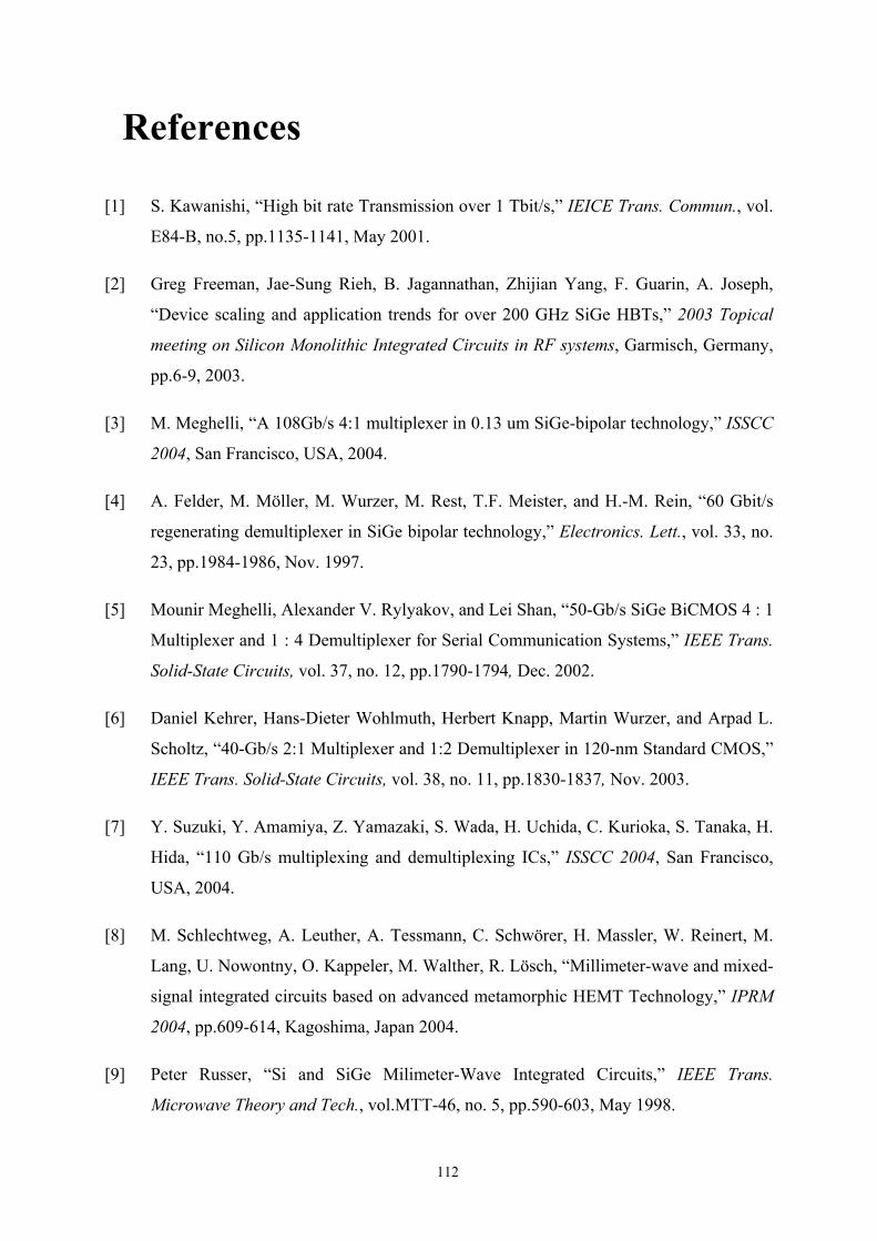
112
References
[1] S. Kawanishi, “High bit rate Transmission over 1 Tbit/s,” IEICE Trans. Commun., vol.
E84-B, no.5, pp.1135-1141, May 2001. [2] Greg Freeman, Jae-Sung Rieh, B. Jagannathan, Zhijian Yang, F. Guarin, A. Joseph,
“Device scaling and application trends for over 200 GHz SiGe HBTs,” 2003 Topical
meeting on Silicon Monolithic Integrated Circuits in RF systems, Garmisch, Germany,
pp.6-9, 2003. [3] M. Meghelli, “A 108Gb/s 4:1 multiplexer in 0.13 um SiGe-bipolar technology,” ISSCC
2004, San Francisco, USA, 2004. [4] A. Felder, M. Möller, M. Wurzer, M. Rest, T.F. Meister, and H.-M. Rein, “60 Gbit/s
regenerating demultiplexer in SiGe bipolar technology,” Electronics. Lett., vol. 33, no.
23, pp.1984-1986, Nov. 1997. [5] Mounir Meghelli, Alexander V. Rylyakov, and Lei Shan, “50-Gb/s SiGe BiCMOS 4 : 1
Multiplexer and 1 : 4 Demultiplexer for Serial Communication Systems,” IEEE Trans.
Solid-State Circuits, vol. 37, no. 12, pp.1790-1794, Dec. 2002. [6] Daniel Kehrer, Hans-Dieter Wohlmuth, Herbert Knapp, Martin Wurzer, and Arpad L.
Scholtz, “40-Gb/s 2:1 Multiplexer and 1:2 Demultiplexer in 120-nm Standard CMOS,”
IEEE Trans. Solid-State Circuits, vol. 38, no. 11, pp.1830-1837, Nov. 2003. [7] Y. Suzuki, Y. Amamiya, Z. Yamazaki, S. Wada, H. Uchida, C. Kurioka, S. Tanaka, H.
Hida, “110 Gb/s multiplexing and demultiplexing ICs,” ISSCC 2004, San Francisco,
USA, 2004. [8] M. Schlechtweg, A. Leuther, A. Tessmann, C. Schwörer, H. Massler, W. Reinert, M.
Lang, U. Nowontny, O. Kappeler, M. Walther, R. Lösch, “Millimeter-wave and mixed-
signal integrated circuits based on advanced metamorphic HEMT Technology,” IPRM
2004, pp.609-614, Kagoshima, Japan 2004. [9] Peter Russer, “Si and SiGe Milimeter-Wave Integrated Circuits,” IEEE Trans.
Microwave Theory and Tech., vol.MTT-46, no. 5, pp.590-603, May 1998.
113
[10] R. Pullela, U. Bhattacharya, S.T. Allen, M.J.W. Rodwell, “Multiplexer/demultiplexer
IC technology for 100 Gb/s fiber-optic transmission,” IEEE Trans. Solid-State Circuits,
vol. 31, no. 5, pp.740-743, May 1996.
[11] T. H. Hu and P. R. Gray, “A monolithic 480 Mb/s parallel AGC/decision clock-
recovery circuit in 1.2 µm CMOS,” IEEE Trans. Solid-State Circuits, vol. 28, no. 12,
pp.1314-1320, Dec. 1993. [12] Mark Kahrs, “50 years of RF and microwave sampling,” IEEE Trans. Microwave
Theory and Tech., vol.MTT-41, no. 6, pp.1787-1805, June 2003. [13] F. X. Sinnesbichler, B. Hautz, G. R. Olbrich, “Low phase noise 58 GHz SiGe HBT
push-push oscillator with simultaneous 29 GHz output,” IEEE MTT-S International
Microwave Symposium Digest, Boston, USA, pp. 35-38, 2000. [14] Govind P. Agrawal, Fiber Optic Communication Systems, A Wiley-Interscience
publication, NY, 1997. [15] Govind P. Agrawal, Nonlinear Fiber Optics, Academic Press, USA, 2001. [16] C.P. Sandbank, Optical Fiber Communication Systems, A Wiley-Interscience
publication, 1980. [17] Katsusuke Takima, Jian Zhou, Kazuhide Nakajima, Kiminori Sato, “Ultralow loss and
long length photonic crystal fiber,” Journal of Lightwave Tech., vol. 22, no. 1, pp.7-10,
Jan. 2004. [18] Jake Bromage, “Raman amplification for fiber communications systems,” Journal of
Lightwave Tech., vol. 22, no. 1, pp.79-93, Jan. 2004. [19] Peter M. Krummrich, Erich Gottwald, Nancy E. Hecker, Cluas-Jörg Weiske, Andreas
Schöpflin, Andreas Färbert, and Klaus Kotten, “40 Gbit/s ETDM for multi terabit/s
long haul WDM transmission,” IEICE Trans. Commun., vol. E85-B, no. 2, Feb. 2002. [20] Jae-Seung Lee, Chang-Sup Shim, “Bit-Error-Rate analysis of optically preamplified
receivers using an eigenfunction expansion method in optical frequency domain,”
Journal of Lightwave Tech., vol. 12, no. 7, pp.1224-1229, July 1994. [21] L. Y. Lin, M. C. Wu, T. Itoh, T. A. Vang, R. E. Muller, D. L. Sivco, A. Y. Cho, “High-
power high-speed photodetectors – design, analysis, and experimental demondtration,”

114
IEEE Trans. Microwave Theory and Tech., vol.MTT-45, no.8, pp.1320-1331, Aug.
1997.
[22] Kazutoshi Kato, “Ultrawide-band/high-frequency phtodetectors,” IEEE Trans.
Microwave Theory and Tech., vol.MTT-47, no.7, pp.1265-1281, July 1999. [23] Kazutoshi Kato, Susumu Hata, Kenji Kawano, Junichi Yoshida, and Atsuo Kozen, “A
high-efficiency 50 GHz InGaAs multimode waveguide photodetector,” IEEE J.
Quantum Electron., vol.28, no.12, pp.2728-2735, Dec. 1992. [24] K. S. Giboney, R. L. Nagarajan, T. E. Reynolds, S. T. Allen, R. P. Mirin, M. J. W.
Rodwell, and J. E. Bowers, “Travelling wave photodetectors with 172 GHz bandwidth
and 76 GHz bandwidth-efficiency product,” IEEE Photonics Tech. Lett., vol.7, no.4,
pp.412-414, April 1995. [25] Datasheet of photodetector ( model : XPDV ) in u2t photonics AG. [26] Mark C. Foisy, P.E. Jeroma, G.H. Martin, “Large-Signal Relaxation-Time Model for
HEMTs and MESFETs,” IEEE International Microwave Symposium MTT-S Digest,
Albuquerque, New Mexico, pp.251-254, 1992. [27] Robert R. Daniels, A.T. Yang, J.P. Harrang, “A universal large/small signal 3-terminal
FET model using a nonquasi-static charge-based approach,” IEEE. Trans. Electron
Devices, vol.40, no.10, pp.1723-1729, Oct. 1993. [28] David E. Root, “Measurement-based large signal diode modelling system for circuit
and device design,” IEEE Trans. Microwave Theory and Tech., vol.MTT-41, no.12,
pp.2211-2217, Dec. 1993. [29] Y. Arai, M. Sato, H.T. Yamada, T. Hamada, K. Nagai, H. Fujishiro, “60 GHz Flip-Chip
Assembled MIC Design Considering Chip-Substrate Effect,” IEEE Trans. Microwave
Theory and Tech., vol.MTT-45, no.12, pp.2261-2266, Dec. 1997. [30] Chun-Long Wang and Ruey-Beei Wu, “A locally matching technique for broadband
flip-chip transition design,” IEEE International Microwave Symposium MTT-S Digest,
Seattle, Washington, pp.1397-1400, 2002.
115
[31] Peter J. Winzer, M. Pfennigbauer, M.M. Strasser, W.R. Leeb, “Optimum filter
bandwidths for optically preamplified NRZ receivers,” Journal of Lightwave Tech., vol.
19, no. 9, pp.1263-1273, Sep. 2001. [32] Benjamin Chan and Jan Conradi, “On the non-Gaussian noise in Erbium-doped fiber
amplifiers,” Journal of Lightwave Tech., vol. 15, no. 4, pp.680-687, April 1997. [33] Chris Lawets and John C. Cartledge, “Performance of optically preamplified receivers
with Fabry-Perot optical filters,” Journal of Lightwave Tech., vol. 14, no.11, pp.2467-
2474, Nov. 1996. [34] Stamatios V. Kartalopoulos, Introduction to DWDM technology, IEEE press, 2000. [35] Martin Pfennigbauer, Martin Pauer, Peter J. Winzer and Martin M. Strasser,
“Performance optimization of optically preamplified revievers for return-to-zero and
non return-to-zero coding,” AEÜ Int. J. Electron. Commun., 56, no.4, pp.261-267, 2002. [36] Athanasios Papoulis, S. Unnikrishna Pillai, Probability, Random variables and
stochastic processes, 4Th Ed., McGraw-Hill, 2002. [37] Peter J. Winzer, “Shot-noise formula for time-varying photon rates: a general
derivation,” J. Opt. Soc. Am. B, vol.14, no.10, pp.2424-2429, Oct. 1997. [38] Peter J. Winzer, “Linking equations between photon statistics and photocurrent
statistics for time-varying stochastic photon rates,” Quantum Semiclass. Opt., no.10, pp.
643-655, 1998. [39] Mandel and Wolf, Optical coherence and quantum optics, Cambridge University Press,
1995. [40] Athanasios Papoulis, S. Unnikrishna Pillai, Probability, random variables, and
stochastic processes, 4th Ed., McGraw-Hill, Inc., 2002. [41] Bahaa E.A. Saleh, Malvin Carl Teich, Fundamental of photonics, John Wiley & Sons,
Inc., 1991. [42] L. Möller et al., “ISI mitigation using decision feedback loop demonstrated with PMD
distorted 10Gbit/s signals,” Electronics. Lett. , vol. 35, no. 24, pp. 2092-2093, Nov.
1999.
116
[43] Hussein H. M. Ghouz, EL-Badawy EL-Sharawy, “An accurate equivalent circuit model
of flip chip and via interconnects,” IEEE Trans. Microwave Theory and Tech., vol.
MTT-44, no. 12, pp.2543-2554, Dec. 1996. [44] Dylan F. Williams, Kate A. Remley, “Analytic sampling-circuit model,” IEEE Trans.
Microwave Theory and Tech., vol. MTT-49, no. 6, pp.1013-1019, June 2001. [45] Dylan F. Williams, Kate A. Remley, and Donald DeGrrot, “Nose-to-nose response of a
20-GHz sampling circuit,” 54th ARFTG Conf. Dig., Dec. 1999. [46] Andrea Jentzsch and Wolfgang Heinrich, “Theory and measurements of flip-chip
interconnects for frequencies up to 100 GHz,” IEEE Trans. Microwave Theory and
Tech., vol. MTT-49, no. 5, pp.871-877, May 2001. [47] Peter J. Winzer and András Klamár, “Sensitivity enhancement of optical receivers by
impulsive coding,” Jounrnal of Lightwave Tech., vol. 17, no. 2, pp.171-177, Feb. 1999. [48] Q. Lee, S.C. Martin, D. Mensa, R.P. Smith, J. Guthrie, S. Jaganathan, Y. Betser, T.
Mathew, S. Krishnan, L. Samoska, and M.J.W. Rodwell, “Submicron-Transferred-
Substrate Heterojunction Bipolar Transistors with Greater than 1 THz fmax,” 57th
Device Research Conference, University of California, Santa Barbara, CA, pp. 28-30,
June 1999. [49] D. E. Johnson, J. R. Johnson, and H. P. Moore, A Handbook of Active Filters,
Englewood Cliffs, NJ, Prentice Hall, 1980. [50] Jack H. Winters, Richard D. Gitlin, and Sanjay Kasturia, “Reducing the effects of
transmission impairments in digital fiber optic systems,” IEEE Comm. Magazine,
pp.68-76, June 1993. [51] John G. Proakis, Digital communications, 3rd Ed., McGraw-Hill, 1995. [52] Datasheets of 104P linear power amplifier, SHF communication Technologies AG. [53] Dieter Schlump, Berthold Wedding, Henning Bülow, “Electronic equalisation of PMD
and chromatic dispersion induced distortion after 100 km standard fibre at 10 Gbit/s,”
ECOC 98, pp.20-24, Madrid, Spain, Sept. 1998.
117
[54] Jack H. Winters, and Mario A. Santoro, “Experimental equalization of polarization
dispersion,” IEEE Photonics Tech. Lett., vol. 2, no. 8, pp.591-593, Aug. 1990. [55] Jack H. Winters, and Richard D. Giltin, “Electrical signal processing technique in lonh-
haul fiber-optic systems,” IEEE Trans. Comm., vol 38, no. 9, pp.1439-1453, Sept. 1990.
[56] Jack H. Winters, and Sanjay Kasturia, “Adaptive nonlinear cancellation for high-speed
fiber-optic systems,” Jounrnal of Lightwave Tech., vol. 10, no. , pp. 971-977, July 1992. [57] Jack H. Winters, Richard D. Gitlin, and Sanjay Kasturia, “Reducing the effects of
transmission impairments in digital fiber optic systems,” IEEE Comm. Magazine,
pp.68-76, June 1993. [58] Data sheets of BAT14-077D and BAT14-077S, Infineon technologies. [59] Kate A. Remley, Dylan F. Williams, Donald C. DeGroot, Jan Verspecht, and John
Kerley, “Effects of nonlinear diode junction capacitance on the nose-to-nose
calibration,” IEEE Micro. Wireless Comp. Lett., vol. 11, Issue 5, pp.196-198, May
2001. [60] IC-CAP Characterization & Modeling Handbook, Modeling a Diode, Chapter 6.,
Agilent Technologies. [61] Internal Report, Messungen zum Mischerverhalten von Silizium-Schottky-Dioden
BAT14-077D, Infineon, 1998. [62] A. N. Gerkis, “Broadband impedance matching using the real frequency network
systhesis technique,” Applied Microwave & Wireless, vol. 10, no. 6, pp.26-32, July
1998. [63] Jung Han Choi, Gerhard R. Olbrich, Peter Russer, 80 Gbit/s ETDM optical receiver,
Final report, Bundesministerium für Bildung und Forschung ( BMBF ) project, contract
number 01 BP 156. [64] Septiaji Eko Nugroho, Design, analysis and simulation of a Si Schottky diode based
sampling circuit for 40 Gbps ETDM demultiplexer circuit, master thesis, Institute for
High-frequency Engineering, Munich University of Technology, Oct. 2003.

118
[65] T. Krems, A. Tessmann, and W.H. Haydl, “Avoiding cross talk and feedback effects in
packaging coplanar mm-wave circuits,” IEEE MTT-S Int. Microwave Symp. Dig.,
pp.1091-1094, June 1998. [66] Reinhold Ludwig, Pavel Bretchko, RF circuit design: Theory and applications,
Prentice-Hall, New Jersey, 2000. [67] W.H. Haydl, “On the used of vias in conductor-backed coplanar circuits,” IEEE Trans.
Microwave Theory Tech., vol. MTT-50, no. 6, pp.1571-1577, June 2002. [68] K. Beilenhoff and W. Heinrich, “Excitation of the parasitic parallel-plate line mode at
coplanar discontinuities,” IEEE MTT-S Int. Microwave Symp. Dig., pp.1789-1792, June
1997. [69] M. Yu, R. Vahldieck, and J. Huang, “Comparing coax launcher and wafer probe
excitation for 10 mil conductor-backed CPW with via holes and air bridges,” IEEE
MTT-S Int. Microwave Symp. Dig., pp.705-708, June 1993. [70] Michael Y. Frankel, Shantanu Gupta, Janis A. Valdmanis, and Gerard A. Mourou,
“Terahertz attenuation and dispersion characteristics of coplanar transmission lines,”
IEEE Trans. Microwave Theory Tech., vol.MTT-39, no. 6, pp.910-916, June 1991. [71] Martin C. Nuss ans Keith W. Goossen, “Investigtion of high-temperature
superconductors with terahertz bandwidth electrical pulses,” IEEE J. Quantum
Electron., vol.25, no.12, pp.2596-2607, Dec. 1989. [72] D. S. Phatak, and A.P.Defonzo, “Dispersion characteristics of optically exicted
coplanar striplines: pulse propagation,” IEEE Trans. Microwave Theory Tech., vol.
MTT-38, no. 5, pp. 654-661, May 1990. [73] William R. Eisenstadt, and Yungseon Eo, “S-parameter-based IC Interconnect
transmission line characterization,” IEEE Trans. Components, hybrids, and
manufacturing Tech., vol.15, no. 4, pp.483-490, Aug. 1992. [74] K.C. Gupta, Ramesh Garg, and Rakesh chadha, Computer-aided design of microwave
circuits, Artech-House, 1981. [75] Hugh Hildreth Skilling, Electrical engineering circuits, John Wiley & Sons, Inc., 1959.

119
[76] DC-65 GHz Integrated V connectors. Anritsu Preliminary Technical Data Sheet. [77] Picosecond Pulse Labs, Application Note AN-4, 1989.