
Claude Leiner Multiskalen-Simulation und Modellierung von...
147
Transcript of Claude Leiner Multiskalen-Simulation und Modellierung von...

Claude Leiner
Multiskalen-Simulation und Modellierung von optischen Systemen
Dissertation
Karl-Franzens-Universität Graz
Institut für Physik
Betreuer: Ao. Univ. Prof. Dr. Ulrich Hohenester
Graz, Januar 2015

meinen Eltern,
für ihre Liebe und Unterstützung

DANKSAGUNG
An dieser Stelle möchte ich mich bei vielen Personen bedanken, die mich während meiner Dissertationszeit begleitet haben und die mich mit Rat und Tat sehr unterstützt
haben.
Als erstes möchte ich mich bei Christian Sommer bedanken, Leiter des Projekts SiMOS und hochgeschätzter Mentor, der mir immer bei inhaltlichen und
methodischen Fragen zur Seite gestanden ist, mich motiviert und mir in schweren Zeiten Mut gemacht hat. Vielen Dank!
Ich möchte mich auch bei meinem Doktorvater Ulrich Hohenester dafür bedanken, dass er meine Betreuung übernommen hat und mich sicher durch die Dissertationszeit
geführt hat.
Eine wissenschaftliche Arbeit, die über Jahre aufgebaut wird, ist selten die Arbeit eines einzelnen. Aus diesem Grund möchte ich mich bei allen Kollegen und
Kolleginnen bedanken, für das freundschaftliche und zugleich professionelle Umfeld, welches ich bei Joanneum Research während meiner Dissertation genießen durfte.
Besonderen Dank verdienen auch meine Kollegen/-innen Franz Peter Wenzl, Gerhard Peharz, Susanne Schweitzer und Wolfgang Nemitz. Euch möchte ich besonders
danken für viele anregende Diskussionen und Hilfestellungen bei der Durchführung meiner Arbeit.
Als Letztes möchte ich mich auch beim BMViT bedanken, ohne dessen finanzielle Unterstützung die Durchführung des Projekts SiMOS nicht möglich gewesen wäre.
ZUSAMMENFASSUNG DEUTSCH
Die Entwicklung von optischen Systemen mit maßgeschneiderten optischen
Eigenschaften erfordert das genaue Verständnis und die Simulation der Propagation
des Lichts durch die Strukturen der einzelnen Komponenten. Die Strukturgrößen
dieser Komponenten können dabei in Größenordnungen liegen, die vom (Sub-)
Wellenlängenbereich des verwendeten Lichts bis hin zu makroskopischen Größen
reichen. Für die Modellierung von solchen optischen Systemen sind Multiskalen-
Simulationen erforderlich. Dabei handelt es sich um Simulationen, die sich aus
verschiedenen Simulationsmethoden zusammensetzen, um die Effekte des Lichts, wie
z.B. Polarisation, Beugung und Brechung in den verschiedenen Größenordnungen
physikalisch richtig berücksichtigen zu können. In Größenordnungen, die viel größer
als das der Wellenlänge des verwendeten Lichts sind, werden Simulationsmethoden
eingesetzt, die auf dem Prinzip der geometrischen Optik basieren. Für Simulationen
von Strukturen, deren Strukturgröße im Wellenlängenbereich des Lichts liegt, werden
hingegen Simulationsmethoden benötigt, welche auf dem Prinzip der Wellenoptik
basieren. Die Durchführung einer Multiskalensimulation wird demnach nur durch ein
geeignetes Interface zwischen Simulationsmethoden der geometrischen Optik und der
Wellenoptik ermöglicht. Ein solches Interface benötigt jedoch klar definierte Kriterien
und Parameter, die es erlauben, von einer Simulationsmethode zur anderen zu
wechseln. Die Definition dieser Kriterien und Parameter erfordert allerdings
grundlegende physikalische und mathematische Überlegungen, um eine
Aufsummierung von Fehlern im Simulationsprozess zu vermeiden.
In dieser Dissertation werden zwei verschiedene Ansätze für Multiskalen-Techniken
zur Simulation von optischen Bauelementen, welche sowohl diffraktive als auch
refraktive optische Komponenten enthalten, vorgestellt und auf ihre Anwendbarkeit
untersucht. Der erste Ansatz basiert auf der Erweiterung einer bereits implementierten
Schnittstelle zwischen zwei kommerziell erhältlichen Simulationsprogrammen, um das
Anwendungsgebiet dieser Schnittstelle zu erweitern. Der zweite Ansatz nutzt das
Prinzip des Poynting-Vektors, um eine Schnittstelle zwischen klassischem Ray-
Tracing, einer Simulationsmethode der geometrischen Optik, und der Finite-
Difference-Time-Domain (FDTD) Methode, einer Simulationsmethode aus der
Wellenoptik, zu realisieren.
IV
ABSTRACT ENGLISH
The development of photonic devices with tailor-made optical properties requires the
control and the manipulation of light propagation within structures of different length
scales, ranging from sub-wavelength to macroscopic dimensions. However, optical
simulation at different length scales necessitates the combination of different
simulation methods, which have to account properly for various effects such as polar-
ization, interference, or diffraction: At dimensions much larger than the wavelength of
light simulation approaches based on the principle of geometrical optics are usually
employed, while in the sub-wavelength regime more sophisticated approaches based
on the principles of wave optics are needed. Describing light propagation both in the
sub-wavelength regime as well as at macroscopic length scales can only be achieved
by bridging between these two approaches. Unfortunately, there are no well-defined
criteria for a switching from one method to the other, and the development of
appropriate selection criteria is a major issue to avoid a summation of errors.
Moreover, since the output parameters of one simulation method provide the input
parameters for the other one, they have to be chosen carefully to ensure mathematical
and physical consistency.
In this work two different techniques for a combination of simulation approaches for
geometrical optics and wave optics will be discussed and presented. This allows an
integrated simulation of optical devices including both refractive and diffractive
optical elements at different length scales. One approach is based on a “native”
interface between two commercial simulation programs in order to enable the handling
of a larger number of applications. The other approach uses the Poynting vector to
interface between the classical Ray-tracing (RT) and the Finite-Difference-Time-
Domain (FDTD) method for a step by step simulation of suchlike optical devices.
V
Inhaltsverzeichnis
1. EINLEITUNG ........................................................................................................... 1
1.1 Aufbau der Dissertation ......................................................................................... 2
1.2 Motivation ............................................................................................................. 3
1.3 Ziele der Disseration .............................................................................................. 6
2. THEORIE .................................................................................................................. 8
2.1 Grundlagen ............................................................................................................ 8
2.1.1 Maxwell Gleichungen ..................................................................................... 8
2.1.2 Poynting-Vektor ............................................................................................ 12
2.2 Ray-tracing .......................................................................................................... 13
2.2.1 Geometrische Optik ....................................................................................... 13
2.2.2 Ray-Traying Grundlagen .............................................................................. 15
2.2.3 Ray-Tracing Quellen in ASAP ...................................................................... 18
2.2.4 Grenzflächen und Detektoren in ASAP ......................................................... 19
2.3 Finite Difference Time Domain .......................................................................... 23
2.3.1 FDTD Algorithmus ....................................................................................... 23
2.3.2 Yee Algorithmus ............................................................................................ 17
2.3.3 SimulationsKomponenten .............................................................................. 29
2.4 Kohärenz und Interferenz .................................................................................... 29
2.4.1 Interferenz ..................................................................................................... 32
2.4.2 Zeitliche Kohärenz ........................................................................................ 35
2.4.3 Räumliche Kohärenz ..................................................................................... 37
2.4.4 Teilkohärenz .................................................................................................. 39
2.4.5 Beugungsgitter .............................................................................................. 44
3. WISSENSCHAFTLICHE ARBEIT ..................................................................... 48
3.1 Veröffentlichte Publikationen ............................................................................. 48
3.1.1 A Simulation Procedure for Light-Matter Interaction at Different Length Scales ...................................................................................................................... 48
3.1.2 A Simulation Procedure Interfacing Ray-Tracing and Finite-Difference-Time-Domain Methods for a Combined Simulation of Diffractive and Refractive Optical Elements .................................................................................................... 57
VI
3.1.3 Multi-Scale Simulation of an Optical Device Using a Novel Approach for Combining Ray-Tracing and FDTD ...................................................................... 67
3.1.4 Multiple Interfacing Between Classical Ray-Tracing and Wave-Optical Simulation Approaches: A Study on Applicability and Accuracy .......................... 73
3.1.5 Reducing shadowing losses with femtosecond-laser-written deflective optical elements in the bulk of EVA encapsulation ............................................................ 87
3.2 Erläuterungen zu den Publikationen .................................................................... 99
3.2.1 A Simulation Procedure for Light-Matter Interaction at Different Length Scales ...................................................................................................................... 99
3.2.2 A Simulation Procedure Interfacing Ray-Tracing and Finite-Difference-Time-Domain Methods for a Combined Simulation of Diffractive and Refractive Optical Elements .................................................................................................. 104
3.2.3 Multi-Scale Simulation of an Optical Device Using a Novel Approach for Combining Ray-Tracing and FDTD .................................................................... 116
3.2.4 Multiple Interfacing Between Classical Ray-Tracing and Wave-Optical Simulation Approaches: A Study on Applicability and Accuracy ........................ 117
3.2.5 Reducing shadowing losses with femtosecond-laser-written deflective optical elements in the bulk of EVA encapsulation .......................................................... 123
4. ZUSAMMENFASSUNG UND AUSBLICK ...................................................... 128
Quellen ........................................................................................................................ 133
Bibliografie ................................................................................................................. 138
VII
1. EINLEITUNG
Die vorliegende Dissertation „Multiskalen-Simulation und Modellierung von optischen Systemen“ behandelt die Modellierung und Simulationen von optischen Systemen, welche optische Elemente mit unterschiedlichen Strukturgrößen beinhalten. Die Strukturgrößen dieser optischen Elemente decken hierbei Größenordnungen ab, die vom Bereich der Wellenlänge des verwendeten Lichtes (einige 100 nm) bis zu mehreren Metern betragen können. Dies bedeutet, dass für eine gesamtheitliche theoretische Betrachtung von optischen Systemen, die aus derartigen optischen Elementen bestehen, ein Multiskalensimulationsansatz erforderlich ist.
Im folgenden 1. Kapitel werden die Motivation und die Zielsetzung der Dissertation näher erläutert. Ausgehend von gängigen optischen Simulationsmethoden wird dabei eine Einführung in die zugrundeliegende Problematik einer solchen Multiskalensimulation und die sich in diesem Zusammenhang ergebenden Fragestellungen gegeben. Es wird erläutert, warum es notwendig ist, eine Schnittstelle zwischen zwei oder mehreren unterschiedlichen Simulationsmethoden zu entwickeln, um solch eine Multiskalensimulation durchführen zu können. Zur Beschreibung des gegenwärtigen wissenschaftlichen State of the Art werden auch exemplarische Arbeiten anderer Autoren vorgestellt, die sich bereits mit dieser Problemstellung auseinandergesetzt haben.
1
1.1 AUFBAU DER DISSERTATION Da im Laufe der Dissertation einige Veröffentlichungen verfasst wurden, soll ein „publikationsorientierter“ Aufbau der Dissertationsarbeit zur Anwendung kommen, in dessen Rahmen die Publikationen einen zentralen Teil darstellen.
In den Unterkapiteln 1.2 und 1.3 wird anhand von Literaturverweisen die Notwendigkeit einer Schnittstellenmethodik erläutert. Zusätzlich werden Beispiele verschiedener optischer Simulationsmethoden angeführt, sowie anhand von Literaturverweisen in der wissenschaftlichen Literatur bereits beschriebene „Hybridsimulationsmethoden“ diskutiert. Daraus abgeleitet werden anschließend die konkrete Aufgabenstellung und die Ziele dieser Dissertationsarbeit vorgestellt.
Das 2. Kapitel der Dissertation gibt einen Überblick über die theoretischen Grundlagen, auf denen die einzelnen Publikationen beruhen. Es umfasst die Grundlagen der Maxwell Gleichungen (2.1.1), des Prinzips des Poynting-Vektors (2.1.2) und der Kohärenztheorie (2.4). Zusätzlich werden die Algorithmen inklusive der physikalischen Formalismen, auf denen diese beruhen der Ray-Tracing- (2.2) und der FDTD Methode (2.3) erläutert.
Das 3. Kapitel enthält die im Rahmen dieser Dissertation erarbeiteten Publikationen in der Form, in der sie in den jeweiligen Journalen veröffentlich worden sind.
• 3.1.1: “A Simulation Procedure for Light-Matter Interaction at Different Length Scales” Proc. SPIE, vol. 8429, p. 84290L, 2012.
• 3.1.2: “A Simulation Procedure Interfacing Ray-Tracing and Finite-Difference-Time-Domain Methods for a Combined Simulation of Diffractive and Refractive Optical Elements”, Journal of Lightwave Technology, vol. 32, no. 6, pp. 1954-1062 2014.
• 3.1.3: “Multi-Scale Simulation of an Optical Device Using a Novel Approach for Combining Ray-Tracing and FDTD”, Proc. SPIE, vol. 8781, pp. 87810Z, 2013.
• 3.1.4: ” Multiple Interfacing Between Classical Ray-Tracing and Wave-Optical Simulation Approaches: A Study on Applicability and Accuracy”, Optics Express, vol. 22, no. 13, pp. 16048–16060, 2014.
• 3.1.5: “Reducing shadowing losses with femtosecond-laser-written deflective optical elements in the bulk of EVA encapsulation”, Progress in Photovoltaics, 2014.
Im Unterkapitel 3.2 werden diese Publikationen in einen chronologischen sowie einen themenbezogenen Kontext gebracht, in dem die Erkenntnisse der einzelnen Publikationen analysiert und diskutiert werden.
2
Im 4. Kapitel werden die Ergebnisse und gewonnen Erkenntnisse aufbereitet und
zusammengefasst, so dass sie ein einheitliches Bild ergeben.
1.2 MOTIVATION Die numerische Mathematik, oder kurz Numerik, stellt bereits seit der Antike ein wichtiges Werkzeug dar, um analytische Formeln algorithmisch oder approximativ berechnen zu können. In der Physik gibt es eine Vielzahl von Problemstellungen, die ohne die Numerik nicht explizit gelöst werden könnten, da entweder keine expliziten Lösungen existieren oder diese sehr aufwändig zu berechnen sind.
In der Mitte des letzten Jahrhunderts setzte die rasante Entwicklung von Computern ein, die es ermöglichte, physikalische Problemstellungen zu „simulieren“. Die bemerkenswerte Erhöhung der Leistungsfähigkeit und die immer weiter steigenden Speicherkapazitäten der Computer erlauben es heutzutage selbst extrem herausfordernde numerische Verfahren in nur kurzer Zeit durchzuführen. Aus diesem Grund wurden Computersimulationen in vielen Bereichen der Physik, so auch im Bereich der Optik, zu einem Werkzeug, auf welches heutzutage nicht mehr verzichtet werden kann. Die mathematischen Grundlagen für eine Vielzahl dieser numerischen Simulationsalgorithmen wurden bereits im letzten Jahrhundert entwickelt [1], [2], jedoch konnten diese erst durch die rapide Weiterentwicklung der Computer sinnvoll in heutigen Simulationsprogrammen wie z.B. ASAP (Breault Organisation) [3] oder in FDTD SOLUTIONS (Lumerical) [4] eingesetzt werden.
Im Allgemeinen können die unterschiedlichen Simulationsmethoden in der Optik in verschiedene Klassen unterteilt werden, die sich durch ihr Anwendungsgebiet unterscheiden [5]. Einige der Simulationsmethoden basieren auf den Gleichungen der Wellenoptik (siehe Kapitel 2.3) und eignen sich in erster Linie für die Berechnung des optischen Verhaltens von diffraktiven optischen Elementen (DOEs) mit sehr kleinen Strukturgrößen (< 10 µm), wie z.B. optische Beugungsgitter. Beispiele hierfür sind z.B. die Finite-Difference-Time-Domain (FDTD) Methode, die Finite-Element (FEM) Methode oder die Rigorous Coupled-Wave Analysis (RCWA) Methode.
Andere Methoden basieren auf der Näherung der Strahlenoptik, auch geometrische Optik genannt (siehe Kapitel 2.2.1), welche die Wellennatur des Lichtes vernachlässigt. Diese Simulationsmethoden eigenen sich daher nur für die Simulation von refraktiven optischen Elementen (ROEs) mit großen Strukturgrößen (< 100 µm) wie z.B. Linsen und Spiegel. Vertreter dieser Klasse sind z.B. das klassische Ray-Tracing (RT), das Gauß-Beam-Tracing (GBT) oder die Beam-Propagation Methode (BPM).
3
Trotz der großen Anzahl an verschiedenen Techniken zur Simulation von optischen Elementen in den jeweiligen Strukturgrößenbereichen gibt es keine allumfassende- Simulationsmethode, die in der Lage ist, das ganze Spektrum an Strukturgrößenbereichen zu behandeln.
Eine derartige umfassende Simulationsmethode wäre aber sehr erstrebenswert. DOEs bieten eine Vielzahl an speziellen Eigenschaften zur Manipulation von Licht, welche abhängig von ihrer Bauart speziell eingestellt werden können. Zusätzlich besitzen sie eine sehr geringe Bautiefe im Vergleich zu klassischen ROEs. Aus diesem Grund werden heutzutage immer mehr optische Bauelemente aus einer Kombination von DOEs und ROEs gefertigt.
Ein gutes Beispiel ist hier die Entwicklung von LED-Chips, wo z.B. die Extraktion des Lichts aus dem Chip oder die Abstrahlcharakteristik der LED durch DOEs gezielt verändert werden kann [6]–[8]. Bei Solarzellen werden DOEs eingesetzt um z.B. Licht in Wellenleiterstrukturen einzukoppeln und damit auf die aktiven Flächen der Solarzellen zu konzentrieren [9], [10]. Eine andere Anwendung von DOEs bei Solarzellen besteht darin, die Reflexion von einfallendem Licht zu reduzieren [11].
Optische Simulationen solcher Bauelemente können jedoch mit keiner der oben genannten Simulationsmethoden exklusiv behandelt werden und sind daher auf die Simulation der einzelnen Teilkomponenten beschränkt.
Diese Aufgabenstellung wurde bereits von einigen Wissenschaftlern behandelt. Dazu untersuchten sie verschiedene Ansätze, um die erwähnten Simulationsmethoden miteinander zu verbinden.
Ying Wang et al. präsentierten bereits im Jahre 2000 eine hybride Simulationstechnik, welche eine Kombination aus klassischem Ray-Tracing und der FDTD-Methode nutzt, um die Propagation von Radiowellen in Innenräumen von Gebäuden zu berechnen [12], [13]. Ähnlich wie bei den oben angeführten Beispielen aus der Optik und der Optoelektronik gibt es auch bei dieser Aufgabenstellung Bereiche, in denen die alleinige Verwendung von klassischem Ray-Tracing nicht geeignet ist, um das Verhalten der Schallwellen mit ausreichender Genauigkeit zu beschreiben. Aus diesem Grund wurde das Simulationsgebiet unterteilt und diese speziellen Bereiche mit FDTD berechnet. Strahlen, die in der Ray-Tracing Simulation auf die Grenzen dieser Bereiche getroffen sind, wurden gestoppt und in der nachfolgenden FDTD Simulation als Quelle benutzt.
Wyrowski und Kuhn stellten im Jahr 2010 [14] ihr Konzept mit dem Namen „Field-Tracing“ vor: Anstelle von Strahlen wie im klassischem Ray-Tracing (siehe Kapitel 2.2) werden bei dieser Methode harmonische Felder durch das optische System propagiert. Zusätzlich wird das Simulationsgebiet in Abhängigkeit von den Strukturgrößen der enthaltenen optischen Komponenten in verschiedene Bereiche
4
unterteilt. Field-Tracing wird hierbei für Bereiche mit ROEs verwendet und WO Methoden, wie z.B. RCWA, für die Bereiche mit diffraktiven Strukturen. Da bei Field-Tracing die Wellennatur des Lichts nicht vernachlässigt wird, erleichtert dies den Übergang von geometrischer Optik zur Wellenoptik und umgekehrt. Dieses Konzept wurde bereits in einem kommerziellen Programm namens „VirtualLab“ umgesetzt und wird von LightTrans vertrieben [15].
Rohani et al. entwickelten einen Simulationsalgorithmus basierend auf den Simulationstechniken GBT, „Gabor Expansion“ und der FDTD Methode [16]. Durch diese Technik können Bauelemente simuliert werden, die sowohl ROE als auch ausgedehnte periodische diffraktive Strukturen (optische Gitter) enthalten.
Die steigende Nachfrage an Simulationstechniken, die es erlauben refraktive optische Bauelemente, die zusätzlich DOEs enthalten, behandeln zu können, zeigt sich ebenfalls dadurch, dass selbst Entwickler von bekannten kommerziellen Simulationsprogrammen diese Problematik aufgreifen. Breault Research (Hersteller des RT-Programms ASAP) hat hierfür in einem Kooperationsprojekt mit Lumerical (Hersteller des FDTD Programms FDTD SOLUTIONS) eine Schnittstelle entwickelt, um den bidirektionalen Transfer von optischen Feldern zwischen dem GB-Modus von ASAP und FDTD SOLUTIONS zu ermöglichen. Die räumliche Ausdehnung dieser Felder ist hierbei jedoch durch die Größe des FDTD Simulationsgebietes beschränkt und limitiert die Anwendung der Schnittstelle auf Aufgabenstellungen, in denen Licht in der RT-Simulation auf das DOE fokussiert wird. Ungeachtet dessen ermöglicht diese Schnittstelle jedoch die Simulation eines breiten Gebietes von Anwendungen, wie z.B. die Simulation einer LCD Kamera oder die Reflexionen einer mit Mikrostrukturen beschichteten DVD.
5
1.3 ZIELE DER DISSERATION Kommerzielle Ray-Tracing Programme, wie z.B. ASAP, haben sich bereits seit einem langen Zeitraum bei der Entwicklung von optischen Bauelementen bewährt [17]–[20]. Die zugrundeliegenden numerischen Algorithmen werden bereits seit über 20 Jahren weiterentwickelt und optimiert, was die Geschwindigkeit der durchgeführten Simulationen gegenüber selbstentwickelten Simulationsprogrammen steigert. Zusätzlich wurde ASAP mit verschiedenen physikalischen Modellen zur Beschreibung von z.B. Streulicht [21] oder Polarisation [22] des Lichts erweitert. Dadurch kann ein breites Spektrum von unterschiedlichen Simulations-Aufgabenstellungen bewältigt werden, im Gegensatz zu selbstentwickelten Simulationsumgebungen, die in vielen Fällen auf wenige Anwendungsfälle beschränkt sind.
Das Ziel dieser Dissertation besteht darin, eine möglichst allgemeine Schnittstelle zwischen den zwei Simulationsprogrammen ASAP und FDTD SOLUTIONS zu realisieren. Dadurch können die bereits genannten Vorteile, die kommerzielle Simulationsprogramme im Hinblick auf Simulationsgeschwindigkeit und breite Anwendbarkeit aufweisen, zusätzlich genutzt werden. Da es jedoch nicht möglich ist, in die Algorithmen der kommerziellen Programme direkt einzugreifen, muss diese Schnittstelle über die Manipulation der exportierten Daten der beiden Simulationsprogramme realisiert werden. Hierfür wird in dieser Dissertation das Programm MATLAB von MATHWORKS [23] verwendet.
In dieser Dissertation werden optische Bauelemente untersucht, die aus ROEs aufgebaut sind und ein oder mehrere optische Beugungsgitter als DOEs enthalten. Da jedoch Beugungsgitter in der Regel eine räumliche Ausdehnung von mehreren hunderten µm² und darüber besitzen, kann die im Abschnitt 1.2 erwähnte, bereits vorhandene Schnittstelle zwischen dem GB-Modus von ASAP und FDTD-Solutions nicht verwendet werden.
Ein Ziel dieser Dissertation besteht deshalb darin, Methoden zu untersuchen, um diese bereits von den Herstellern realisierte Schnittstelle so zu erweitern, dass eine Simulation der zu untersuchenden optischen Bauelemente ermöglicht wird.
Ein weiteres Ziel ist auch die Realisierung einer selbstentwickelten Schnittstelle zwischen dem klassischem Ray-Tracing Modus von ASAP und dem FDTD Programm. Das klassische RT unterliegt im Vergleich zu anderen Simulationsmethoden der geometrischen Optik, wie z.B. der GBT oder der BPM Methode, den geringsten Einschränkungen bezüglich Modellierung der Quelle und den einzelnen ROEs. Aus diesem Grund würde es eine solche Schnittstelle ermöglichen, ein breites Spektrum an unterschiedlichen Simulationsaufgabenstellungen bewältigen zu können.
6
Wie im Abschnitt Motivation erwähnt, wurde solch eine Schnittstelle zwischen RT und FDTD bereits von Ying Wang et al. in [12], [13] eingeführt, allerdings nur in Richtung RTFDTD verwendet. Dies stellt den einfachsten Fall dar, da die Phasenbeziehungen zwischen den einzelnen Strahlen, abhängig von der Lichtquelle, als zufällig angenommen werden können. Wendet man solch eine Schnittstelle jedoch in Richtung FDTDRT an, müssen die Phasenbeziehungen zwischen den einzelnen Wellenfronten vernachlässigt werden, da diese im Algorithmus der klassischen RT-Methode nicht berücksichtigt werden. Um jedoch ein optisches Bauelement simulieren zu können, welches mehrere DOEs enthält, ist eine bidirektionale Schnittstelle notwendig, die eine beliebige Anzahl an RTFDTD Schritte ermöglicht. Aus diesem Grund werden die Auswirkungen einer Vernachlässigung dieser Phasenbeziehungen in dieser Dissertation gezielt untersucht, um Bedingungen zu definieren, in denen der Einsatz solch einer Schnittstelle zulässig ist.
Um die Genauigkeit und die Anwendbarkeit der entwickelten Schnittstellenmethode zu untersuchen, werden die Simulationsergebnisse der Schnittstellen-Methode mit experimentellen Messergebnissen verglichen.
7
2. THEORIE
In diesem Kapitel werden allgemeine Grundlagen behandelt, die das Verständnis der
im Rahmen dieser Dissertation verfassten Publikationen erleichtern sollen. Es umfasst
unter anderem die Grundlagen der Elektrodynamik, welche verwendet werden, um das
Verhalten von Licht in verschiedenen Medien zu beschreiben, sowie numerische
Methoden zur Lösung der Gleichungen der Elektrodynamik, um das Verhalten von
Licht in verschiedenen Medien und verschiedenen Größenordnungen von optischen
Strukturen zu simulieren.
2.1 GRUNDLAGEN
2.1.1 MAXWELL GLEICHUNGEN
Bereits im neunzehnten Jahrhundert wurde von. J. C. Maxwell gefolgert, dass es sich
bei Licht um einen elektromagnetischen Effekt handelt [24]. Maxwell vereinte die
grundlegenden physikalischen Gesetze zur Beschreibung von elektromagnetischen
Effekten, die von M. Faraday, A. M. Ampère und C. F. Gauß aufgestellt worden
waren:
• Das Faraday‘sche Induktionsgesetz (2.1), welches zeigt, dass ein zeitlich
veränderlicher magnetischer Fluss durch eine von einer Leiterschleife L
umschlossene Fläche A einen elektrischen Strom in dieser Leiterschleife
erzeugt. Durch dieses Gesetz wird es ermöglicht, das elektrische Feld E mit
einem zeitlich veränderten Magnetfeld H in Verbindung zu setzen.
• Das Gegenstück zum Faraday’sche Induktionsgesetz bildete das Ampère‘sche
Durchflutungsgesetz, welches von Maxwell zu (2.2) erweitert wurde, um den
Zusammenhang zwischen H und einem zeitlich veränderlichem E zu
beschreiben.
• Weiteres erlauben es die Gauß‘sche Sätze für H (2.3) und für E (2.4), den
elektrischen und magnetischen Fluss durch eine räumlich geschlossene Fläche
mit den durch diese Fläche eingeschlossenen Ladungen in Beziehung zu
bringen.
Maxwell fasste diese Grundgesetze zu einem heute als Maxwellgleichungen bekannten
Satz aus Integralgleichungen zusammen. Unter der Annahme von linearen, isotropen,
8
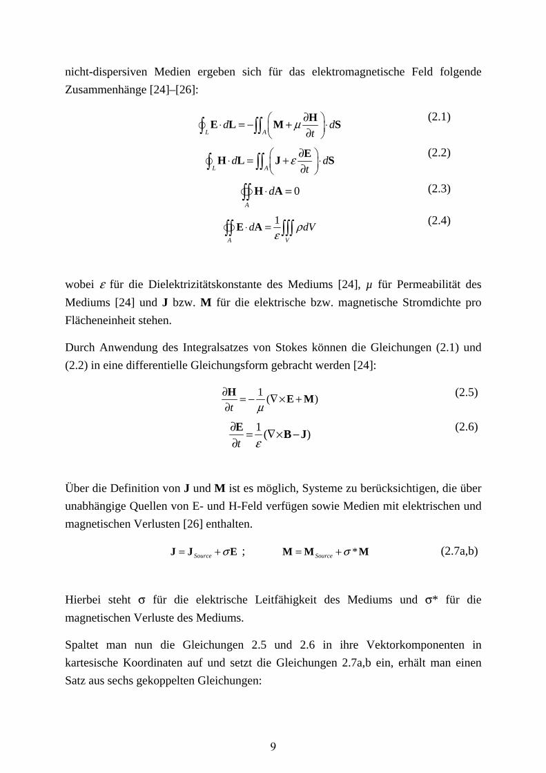
nicht-dispersiven Medien ergeben sich für das elektromagnetische Feld folgende
Zusammenhänge [24]–[26]:
L A
d dt
μ ∂ ⋅ = − + ⋅ ∂ H
E L M S (2.1)
L A
d dt
ε ∂ ⋅ = + ⋅ ∂ E
H L J S (2.2)
0A
d⋅ = H A (2.3)
1
A V
d dVρε
⋅ = E A (2.4)
wobei ε für die Dielektrizitätskonstante des Mediums [24], µ für Permeabilität des
Mediums [24] und J bzw. M für die elektrische bzw. magnetische Stromdichte pro
Flächeneinheit stehen.
Durch Anwendung des Integralsatzes von Stokes können die Gleichungen (2.1) und
(2.2) in eine differentielle Gleichungsform gebracht werden [24]:
1( )
t μ∂ = − ∇× +∂H
E M (2.5)
1( )
t ε∂ = ∇× −∂E
B J (2.6)
Über die Definition von J und M ist es möglich, Systeme zu berücksichtigen, die über
unabhängige Quellen von E- und H-Feld verfügen sowie Medien mit elektrischen und
magnetischen Verlusten [26] enthalten.
Source σ= +J J E ; *Source σ= +M M M (2.7a,b)
Hierbei steht σ für die elektrische Leitfähigkeit des Mediums und σ* für die
magnetischen Verluste des Mediums.
Spaltet man nun die Gleichungen 2.5 und 2.6 in ihre Vektorkomponenten in
kartesische Koordinaten auf und setzt die Gleichungen 2.7a,b ein, erhält man einen
Satz aus sechs gekoppelten Gleichungen:
9
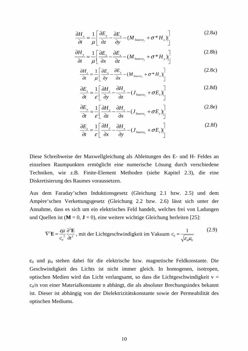
1( * )
x
yx zSource x
EH EM H
t z yσ
μ∂ ∂ ∂= − − + ∂ ∂ ∂
(2.8a)
1( * )
y
y xzSource y
H EEM H
t x zσ
μ∂ ∂∂ = − − + ∂ ∂ ∂
(2.8b)
1( * )
z
yxzSource z
EEHM H
t y xσ
μ∂ ∂∂ = − − + ∂ ∂ ∂
(2.8c)
1( )
x
yx zSource x
HE HJ E
t y zσ
ε∂ ∂ ∂= − − + ∂ ∂ ∂
(2.8d)
1( )
y
y x zSource y
E H HJ E
t z xσ
ε∂ ∂ ∂ = − − + ∂ ∂ ∂
(2.8e)
1( )
z
y xzSource z
H HEJ E
t x yσ
ε∂ ∂∂ = − − + ∂ ∂ ∂
(2.8f)
Diese Schreibweise der Maxwellgleichung als Ableitungen des E- und H- Feldes an
einzelnen Raumpunkten ermöglicht eine numerische Lösung durch verschiedene
Techniken, wie z.B. Finite-Element Methoden (siehe Kapitel 2.3), die eine
Diskretisierung des Raumes voraussetzen.
Aus dem Faraday’schen Induktionsgesetz (Gleichung 2.1 bzw. 2.5) und dem
Ampère‘schen Verkettungsgesetz (Gleichung 2.2 bzw. 2.6) lässt sich unter der
Annahme, dass es sich um ein elektrisches Feld handelt, welches frei von Ladungen
und Quellen ist (M = 0, J = 0), eine weitere wichtige Gleichung herleiten [25]:
22
2 20c t
εμ ∂∇ =∂
EE , mit der Lichtgeschwindigkeit im Vakuum 0
0 0
1c
ε μ=
(2.9)
ε0 und μ0 stehen dabei für die elektrische bzw. magnetische Feldkonstante. Die
Geschwindigkeit des Lichts ist nicht immer gleich. In homogenen, isotropen,
optischen Medien wird das Licht verlangsamt, so dass die Lichtgeschwindigkeit v =
c0/n von einer Materialkonstante n abhängt, die als absoluter Brechungsindex bekannt
ist. Dieser ist abhängig von der Dielektrizitätskonstante sowie der Permeabilität des
optischen Mediums.
10
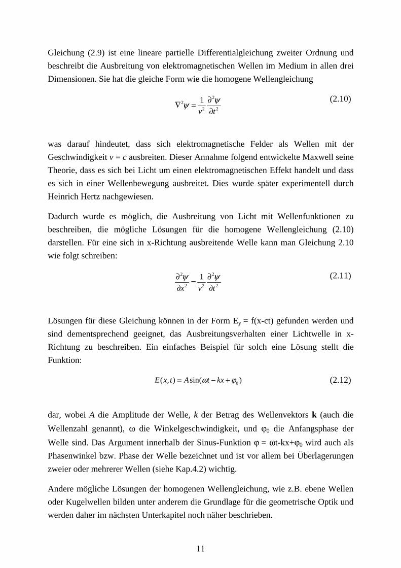
Gleichung (2.9) ist eine lineare partielle Differentialgleichung zweiter Ordnung und
beschreibt die Ausbreitung von elektromagnetischen Wellen im Medium in allen drei
Dimensionen. Sie hat die gleiche Form wie die homogene Wellengleichung
22
2 2
1
v t
ψψ ∂∇ =∂
(2.10)
was darauf hindeutet, dass sich elektromagnetische Felder als Wellen mit der
Geschwindigkeit v = c ausbreiten. Dieser Annahme folgend entwickelte Maxwell seine
Theorie, dass es sich bei Licht um einen elektromagnetischen Effekt handelt und dass
es sich in einer Wellenbewegung ausbreitet. Dies wurde später experimentell durch
Heinrich Hertz nachgewiesen.
Dadurch wurde es möglich, die Ausbreitung von Licht mit Wellenfunktionen zu
beschreiben, die mögliche Lösungen für die homogene Wellengleichung (2.10)
darstellen. Für eine sich in x-Richtung ausbreitende Welle kann man Gleichung 2.10
wie folgt schreiben:
2 2
2 2 2
1
x v t
ψ ψ∂ ∂=∂ ∂
(2.11)
Lösungen für diese Gleichung können in der Form Ey = f(x-ct) gefunden werden und
sind dementsprechend geeignet, das Ausbreitungsverhalten einer Lichtwelle in x-
Richtung zu beschreiben. Ein einfaches Beispiel für solch eine Lösung stellt die
Funktion:
0( , ) sin( )E x t A t kxω ϕ= − + (2.12)
dar, wobei A die Amplitude der Welle, k der Betrag des Wellenvektors k (auch die
Wellenzahl genannt), ω die Winkelgeschwindigkeit, und ϕ0 die Anfangsphase der
Welle sind. Das Argument innerhalb der Sinus-Funktion ϕ = ωt-kx+ϕ0 wird auch als
Phasenwinkel bzw. Phase der Welle bezeichnet und ist vor allem bei Überlagerungen
zweier oder mehrerer Wellen (siehe Kap.4.2) wichtig.
Andere mögliche Lösungen der homogenen Wellengleichung, wie z.B. ebene Wellen
oder Kugelwellen bilden unter anderem die Grundlage für die geometrische Optik und
werden daher im nächsten Unterkapitel noch näher beschrieben.
11
2.1.2 POYNTING-VEKTOR
Eine weitere wichtige Größe in der Elektrodynamik ist der sogenannte Poynting-
Vektor S. Seine Orientierung ist parallel zur Ausbreitungsrichtung der Welle und
somit normal zur Richtung des elektrischen Feldes E und des magnetischen Feldes H.
Er ergibt sich aus dem Kreuzprodukt der beiden Felder [24], [25]:
= ×S E H (2.13)
Der Betrag von |S| repräsentiert die Menge an Energie oder die Strahlungsleistung, die
durch eine Fläche fließt, deren Normalvektor parallel zu S ist [24], [27]. Da jedoch E
und H schnell oszillieren und |S| den momentanen Energiefluss angibt, ist es sinnvoll,
das zeitliche Mittel von S zu bilden [24].
( )2
0 0 00 02
c ε μ= ×S E H (2.14)
Dabei sind E0 und H0 die Amplitudenvektoren des elektrischen bzw. magnetischen
Feldes. Die durchschnittliche Energie pro Flächen- und Zeiteinheit wird auch
Bestrahlungsstärke oder Intensität I genannt, sie ist definiert durch den Betrag des
zeitlich gemittelten Poynting-Vektors [24]:
20 0 0
0 02
cI
ε μ≡ = ×S E H (2.15)
12
2.2 RAY-TRACING
2.2.1 GEOMETRISCHE OPTIK
Durch die im Kapitel 2.1.1 beschriebenen Maxwellgleichungen lässt sich das
Verhalten von elektromagnetischen Wellen, wie z.B. Licht, in unterschiedlichen
Medien genau beschreiben. Jedoch sind sie in ihrer integralen Form (2.1-2.4) schwer
auf analytische Probleme anzuwenden und in ihrer diskretisiert-differentiellen Form
selbst für heutige Rechner für viele Aufgabenstellungen numerisch nicht lösbar (siehe
Kap. 2.3). Aus diesem Grund werden zur analytischen Lösung mathematische Modelle
wie z.B. Kugelwellen (3D) oder ebene Wellen (1D) verwendet, welche die homogene
Wellengleichung (Gleichung 2.10) erfüllen.
Sind an den Übergängen zwischen homogenen Medien unterschiedlicher Brechzahl
Strukturen vorhanden, so wird die Wellenfront z.B. einer elektromagnetischen
Kugelwelle verändert, da nur ein Segment der Kugelwelle eingefangen werden kann
[28]. Diese Veränderungen der elektromagnetischen Wellenfront wird Beugung
genannt, wobei die Stärke dieser Beugungseffekte vom Verhältnis zwischen
Wellenlänge der elektromagnetischen Strahlung zur geometrischen Größe der
Strukturen an den Übergängen abhängt [28]. Im Grenzfall, wenn das Verhältnis λ zu
Strukturgröße 0 wird, verschwinden jedoch diese Beugungseffekte und man kann
von einer geradlinigen Ausbreitung der Wellenfronten ausgehen.
Um optische Probleme jedoch analytisch lösen zu können, wurde Ende des 19. bzw.
Anfang des 20. Jahrhunderts die sogenannte geometrische Optik oder Strahlenoptik
eingeführt [27]. Sie vernachlässigt die Wellenlänge des Lichtes und ersetzt die
elektromagnetischen Wellen durch geometrische Strahlen parallel zur
Ausbreitungsrichtung der Wellenfronten, wobei der Energietransport der
elektromagnetischen Strahlung nun entlang der Richtung dieser Strahlen erfolgt [27].
Eine genaue mathematische Herleitung der geometrischen Optik aus den
Maxwellgleichungen für den Fall 0λ → kann in [27] nachgelesen werden.
Eine weitere Möglichkeit, um die Strahlen in der geometrischen Optik zu definieren,
bietet der zeitlich gemittelte Poynting-Vektor <S> [27]. Da die Richtung des Poynting-
Vektors ebenfalls normal zu den geometrischen Wellenfronten ist, kann man die
Strahlen der geometrischen Optik parallel zur Ausbreitungsrichtung des Poynting-
13
Vektors definieren, wobei die Summe ihres Energieflusses dem Betrag des Poynting-
Vektors entspricht.
In makroskopisch-optischen Systemen, für die die Näherungen der geometrischen
Optik zulässig sind, ist es nun möglich, die komplexen Geometrien von vorhandenen
optischen Elementen wie z.B. Linsen, Spiegel, etc. auf ihre optischen Grenzflächen zu
reduzieren. Aufgrund der Tatsache, dass die Wellenfronten der elektromagnetischen
Strahlung in der geometrischen Optik durch Strahlen ersetzt werden, vereinfacht sich
die mathematische Beschreibung des optischen Systems auf die Interaktionen dieser
Strahlen mit den vorhandenen optischen Grenzflächen. Diese Interaktionen
verursachen im Allgemeinen eine Änderung der Ausbreitungsrichtung und
Polarisation der Strahlen und führen zu einer Aufteilung der Energie des einfallenden
Strahls auf einen transmittierten und einen reflektierten Strahl.
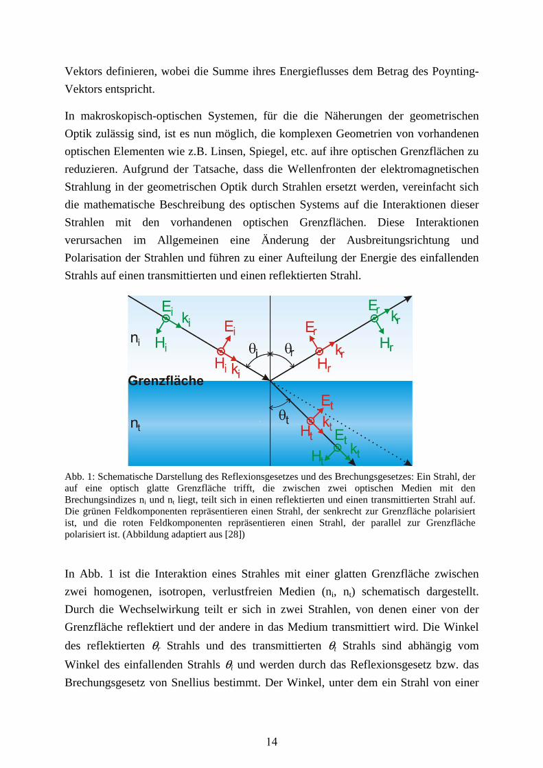
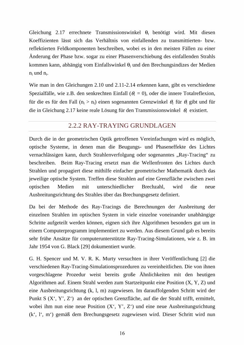
Abb. 1: Schematische Darstellung des Reflexionsgesetzes und des Brechungsgesetzes: Ein Strahl, der auf eine optisch glatte Grenzfläche trifft, die zwischen zwei optischen Medien mit den Brechungsindizes ni und nt liegt, teilt sich in einen reflektierten und einen transmittierten Strahl auf. Die grünen Feldkomponenten repräsentieren einen Strahl, der senkrecht zur Grenzfläche polarisiert ist, und die roten Feldkomponenten repräsentieren einen Strahl, der parallel zur Grenzfläche polarisiert ist. (Abbildung adaptiert aus [28])
In Abb. 1 ist die Interaktion eines Strahles mit einer glatten Grenzfläche zwischen
zwei homogenen, isotropen, verlustfreien Medien (ni, nt) schematisch dargestellt.
Durch die Wechselwirkung teilt er sich in zwei Strahlen, von denen einer von der
Grenzfläche reflektiert und der andere in das Medium transmittiert wird. Die Winkel
des reflektierten θr Strahls und des transmittierten θt Strahls sind abhängig vom
Winkel des einfallenden Strahls θi und werden durch das Reflexionsgesetz bzw. das
Brechungsgesetz von Snellius bestimmt. Der Winkel, unter dem ein Strahl von einer
14
optisch glatten Oberfläche reflektiert wird, ist gleich dem Einfallswinkel des
einfallenden Strahls [28]:
i rθ θ= (2.16)
Der Winkel des transmittierten Strahls θt ergibt sich aus dem Brechungsgesetz von
Snellius [28],
sin sini i t tn nθ θ= (2.17)
wobei dieser ebenfalls vom Einfallswinkel θi, jedoch zusätzlich auch von den
Brechzahlen der beiden Medien (ni, nt), abhängt. Dies bedeutet, dass der transmittierte
Strahl, bei nicht senkrechtem Einfall, eine andere Ausbreitungsrichtung als der
einfallende Strahl aufweist. Weist das Transmissionsmedium eine höhere Brechzahl
als das Einfallsmedium auf, wird der transmittierte Strahl zum Lot gebrochen. Im
gegensätzlichen Fall, wenn ein Strahl aus einem optisch dichten auf ein optisch dünnes
Medium trifft, wird der transmittierte Strahl vom Lot gebrochen [28], unabhängig von
der Polarisation des einfallenden Strahls.
Um die Aufteilung der Energie des einfallenden Strahls auf den transmittierten und
den reflektierten Strahl zu berechnen, ist die Polarisation des Strahls jedoch
entscheidend. Aus Stetigkeitsüberlegungen der einzelnen E und H -Feldkomponenten
an der Grenzfläche ergeben sich die Gleichungen [28]
sin( )
sin( )i t
i t
rθ θθ θ⊥
−= −+
(2.18)
tan( )
tan( )i t
i t
rθ θθ θ
−= ++
(2.19)
2sin cos
sin( )t i
i t
tθ θθ θ⊥ = +
+
(2.20)
2sin cos
sin( )cos( )t i
i t i t
tθ θ
θ θ θ θ= +
+ − (2.21)
die unter dem Namen Fresnelgleichungen bekannt sind. Mit ihnen lassen sich die
Amplituden der Reflexionskoeffizienten r⊥ , r und die Amplituden der
Transmissionskoeffizienten t⊥ t berechnen, wofür der Einfallswinkel θi sowie der aus
15
Gleichung 2.17 errechnete Transmissionswinkel θt benötigt wird. Mit diesen
Koeffizienten lässt sich das Verhältnis von einfallenden zu transmittierten- bzw.
reflektierten Feldkomponenten beschreiben, wobei es in den meisten Fällen zu einer
Änderung der Phase bzw. sogar zu einer Phasenverschiebung des einfallenden Strahls
kommen kann, abhängig vom Einfallswinkel θi und den Brechungsindizes der Medien
ni und nt.
Wie man in den Gleichungen 2.10 und 2.11-2.14 erkennen kann, gibt es verschiedene
Spezialfälle, wie z.B. den senkrechten Einfall (θi = 0), oder die innere Totalreflexion,
für die es für den Fall (ni > nt) einen sogenannten Grenzwinkel θc für θi gibt und für
die in Gleichung 2.17 keine reale Lösung für den Transmissionswinkel θt existiert.
2.2.2 RAY-TRAYING GRUNDLAGEN
Durch die in der geometrischen Optik getroffenen Vereinfachungen wird es möglich,
optische Systeme, in denen man die Beugungs- und Phaseneffekte des Lichtes
vernachlässigen kann, durch Strahlenverfolgung oder sogenanntes „Ray-Tracing“ zu
beschreiben. Beim Ray-Tracing ersetzt man die Wellenfronten des Lichtes durch
Strahlen und propagiert diese mithilfe einfacher geometrischer Mathematik durch das
jeweilige optische System. Treffen diese Strahlen auf eine Grenzfläche zwischen zwei
optischen Medien mit unterschiedlicher Brechzahl, wird die neue
Ausbreitungsrichtung des Strahles über das Brechungsgesetz definiert.
Da bei der Methode des Ray-Tracings die Berechnungen der Ausbreitung der
einzelnen Strahlen im optischen System in viele einzelne voneinander unabhängige
Schritte aufgeteilt werden können, eignen sich ihre Algorithmen besonders gut um in
einem Computerprogramm implementiert zu werden. Aus diesem Grund gab es bereits
sehr frühe Ansätze für computerunterstützte Ray-Tracing-Simulationen, wie z. B. im
Jahr 1954 von G. Black [29] dokumentiert wurde.
G. H. Spencer und M. V. R. K. Murty versuchten in ihrer Veröffentlichung [2] die
verschiedenen Ray-Tracing-Simulationsprozeduren zu vereinheitlichen. Die von ihnen
vorgeschlagene Prozedur weist bereits große Ähnlichkeiten mit den heutigen
Algorithmen auf. Einem Strahl werden zum Startzeitpunkt eine Position (X, Y, Z) und
eine Ausbreitungsrichtung (k, l, m) zugewiesen. Im darauffolgenden Schritt wird der
Punkt S (X‘, Y’, Z‘) an der optischen Grenzfläche, auf die der Strahl trifft, ermittelt,
wobei ihm nun eine neue Position (X‘, Y’, Z‘) und eine neue Ausbreitungsrichtung
(k‘, l‘, m‘) gemäß dem Brechungsgesetz zugewiesen wird. Dieser Schritt wird nun
16
wiederholt bis der Strahl entweder auf eine Oberfläche trifft, die als absorbierend
definiert wurde, oder das optische System verlässt.
Bei einer Vielzahl heutiger Ray-Tracing Simulationsprogramme, wie z.B. dem im
Rahmen dieser Dissertation verwendeten Programm ASAP (Breault Research
Organisation) werden jedoch noch zusätzliche Parameter berücksichtigt [3]. Neben der
Position und Richtung werden jedem Strahl auch eine Energie und eine
Polarisationsrichtung zugeordnet. Da die Simulationsalgorithmen weiterhin in den
meisten Fällen auf Strahlen-Berechnungen an Grenzflächen basieren, werden Strahlen
im Simulationssystem entlang ihrer Ausbreitungsrichtung propagiert, bis sie auf solch
eine Grenzfläche auftreffen. Durch die Einführung der zusätzlichen Parameter ist es
jedoch nun möglich, an diesen Grenzflächen die Fresnelgleichungen (siehe
Gleichungen 2.18-2.21) zu berücksichtigen. Dies ermöglicht eine Aufteilung des
einfallenden Strahls in einen reflektierten und einen transmittierten Strahl, deren
Ausbreitungsrichtungen mit dem Reflexionsgesetz bzw. dem Gesetz von Snellius
berechnet und deren Energien und Polarisationsrichtungen durch die
Fresnelgleichungen bestimmt werden können. Durch diese Erweiterung des Ray-
Tracing Prinzips können Mehrfachreflexionen zwischen verschiedenen Grenzflächen
sehr viel genauer beschrieben werden. Dieser Ansatz ist im Allgemeinen als Nicht-
sequentielles Ray-Tracing bekannt und wird von vielen Ray-Tracing
Simulationsprogrammen unterstützt. Im Falle von absorbierenden Medien wird der
absorbierte Anteil über die optische Weglänge mittels des Lambert-Beer‘schen-
Gesetzes [28] berechnet. Für die numerische Umsetzung wird ein Grenzwert für die
Energie des Strahls festgelegt, wobei ein Strahl, dessen Energie diesen Grenzwert
unterschreitet, als absorbiert gilt.
In Abhängigkeit von der Anzahl der Grenzflächen, aus denen ein optisches System
besteht, kann dieser Algorithmus der „Strahlaufteilung“ jedoch zu Problemen führen,
da es während der Modellierung des Systems nicht vorhersehbar ist, wie viele Strahlen
während der Simulation erzeugt werden. Begrenzt man hingegen die Anzahl der
möglichen Aufspaltungen eines Strahls mit einem Grenzwert, kann es zu einer
ungenauen Simulation kommen. Eine Alternative zur Methode der Strahlaufteilung an
Grenzflächen ist die Verwendung von Transmissions- und Reflexionskoeffizienten als
Transmissions- bzw. Reflexionswahrscheinlichkeiten. Ein Monte-Carlo-Algorithmus
„würfelt“ hierbei basierend auf berechneten Wahrscheinlichkeiten, ob der einfallende
Strahl transmittiert oder reflektiert wird, wobei die Energie des Strahles gleich bleibt.
Der Nachteil dieser Methode besteht darin, dass man für eine physikalisch korrekte
17
Simula
Wahrsc
schon b
Simula
abgesch
Mit A
Flächen
Quellen
Glühbir
gemess
Lichtqu
genaue
einen e
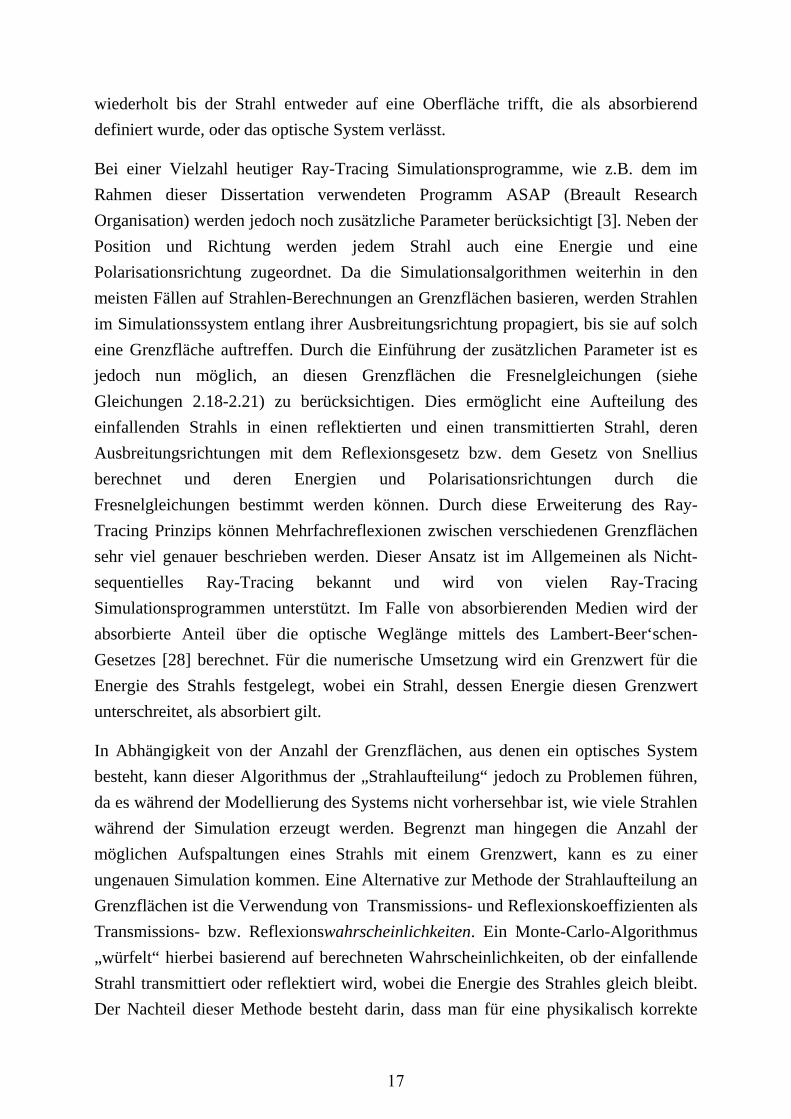
(aAbb. 2a)Tracing Chip 2c)
In Abb
ausgehe
Glühfad
Strahle
(Braune
Ausbre
ation eines
cheinlichke
bei der M
ation festge
hätzt werd
2
SAP ist e
nquelle zu
n gezielt
rnen, LED
sene Intens
uelle die
re Modelli
entscheiden
a) ) DreidimensStrahlen em
) ASAP Mod
b. 2a ist d
enden Str
den emitti
n (Schwar
e Helix
eitungsricht
optischen
eitsverteilu
Modellierun
elegt und
en kann.
.2.3 RAY
es möglic
verwenden
zu model
Ds, Haloge
sitätsverteil
gleiche A
ierung des
nden Einflu
sionale Darsmittiert werdedell dieses LE
das Model
rahlen darg
ierten Lic
rze Pfeile
in Ab
tung. In A
n Systems
ungen zu v
g des Sys
dadurch d
Y-TRAC
ch, nicht n
n, sondern
llieren. D
enlampen,
lungen zu
Abstrahlcha
optischen
uss auf das
(b) stellung einesen [Quelle [3ED Chips.
ll einer G
gestellt: D
chtes in a
in Abb. 2
b. 2a)
bb. 2c ist d
viele Strah
vermeiden.
tems die m
die Dauer
CING QU
nur einzel
n eine Vielz
amit lasse
etc. darste
adaptieren
arakteristik
n Systems
Ergebnis h
s Models ein30]] 2b) Gem
Glühwendel
Da man v
alle Raumr
2a) zufällig
angeordn
die Lichtem
hlen brauc
. Der Vort
maximale
und Durch
UELLEN
lne Strahl
zahl von u
en sich k
ellen [30].
n, so dass d
k aufweise
möglich, d
haben kann
ner Glühwenmessene Inte
l einer Gl
von einer
richtungen
g auf der O
et und
mission vo
cht, um Ar
teil liegt je
Anzahl de
hführbarke
IN ASA
len aus ei
unterschied
komplexe
Zusätzlic
die modelli
n. Hierdu
da die Form
n.
(c)ndel, von desensitätsvertei
lühbirne so
Gleichver
n ausgehen
Oberfläche
besitzen
on der Obe
rtefakte du
edoch dari
er Strahlen
eit der Sim
AP
iner Punk
dlich ausge
Lichtquell
ch ist es m
erte und d
urch ist ei
m der Lich
) ssen Oberfläilung auf ein
owie die
rteilung de
n kann, s
e der Glüh
eine z
erseite eine
urch die
in, dass
n in der
mulation
kt- oder
dehnten
len wie
möglich,
die reale
ine viel
htquelle
äche Ray-nem LED
von ihr
es vom
ind die
hwendel
zufällige
es LED-
18
Chips dargestellt. In diesem Beispiel werden die Strahlen zwar von einer ebenen
Fläche aus emittiert, jedoch sind diese Strahlen nicht gleichmäßig über die Oberfläche
verteilt, da Leiterbahnen Teile der Oberfläche abdecken. Um die Verteilung der
Strahlen auf der Oberfläche zu bestimmen, wurde die LED zuerst experimentell
vermessen und in ASAP als Quelle importiert (Abb. 2b,c).
Eine weitere Möglichkeit zur Modellierung einer Lichtquelle besteht darin, jeden
Strahl einzeln zu definieren (Position, Raumrichtung, Energie) und die Gesamtheit der
Strahlen in ASAP zu importieren. Durch dieses Prinzip wird ein gezielter
Datenaustausch zwischen verschiedenen Programmen vereinfacht und stellt in weiterer
Folge die Basis für die in dieser Dissertation entwickelte Schnittstelle dar. Dabei
werden die Strahlendaten an geeigneten Positionen im geometrischen Modell
gespeichert, entsprechend anderer Simulationsergebnisse manipuliert und
anschließend re-importiert. (siehe Kapitel 3.1.2).
2.2.4 GRENZFLÄCHEN UND DETEKTOREN IN ASAP
In diesem Abschnitt soll ein Überblick vermittelt werden, wie mittels der
Simulationssoftware ASAP optische Modelle entworfen werden können.
Wie schon in Kapitel 2.2.2 erwähnt, basiert der Algorithmus des Ray-Tracings auf
Strahlen-Berechnungen an Grenzflächen. Dementsprechend werden für die Erstellung
von Modellen in ASAP keine Volumen, sondern Flächen verwendet. Diesen Flächen
werden verschiedene optische Eigenschaften zugeordnet, welche die Wechselwirkung
mit auftreffenden Strahlen bestimmen. Eine Möglichkeit besteht darin, den
Grenzflächenübergang zweier optischer Medien über die unterschiedlichen
Brechzahlen festzulegen, so dass es zur Lichtbrechung gemäß dem Brechungsgesetz
an der Fläche kommt. Man kann allerdings auch beliebige Transmissions- und
Reflexionswerte direkt zuordnen, für den Fall, dass diese aus experimentellen
Messungen der Materialien stammen. Des Weiteren ist es sogar möglich, den Flächen
verschiedene Streueigenschaften zuzuordnen, um damit raue Oberflächen beschreiben
zu können.
19
(a) (b) (c)
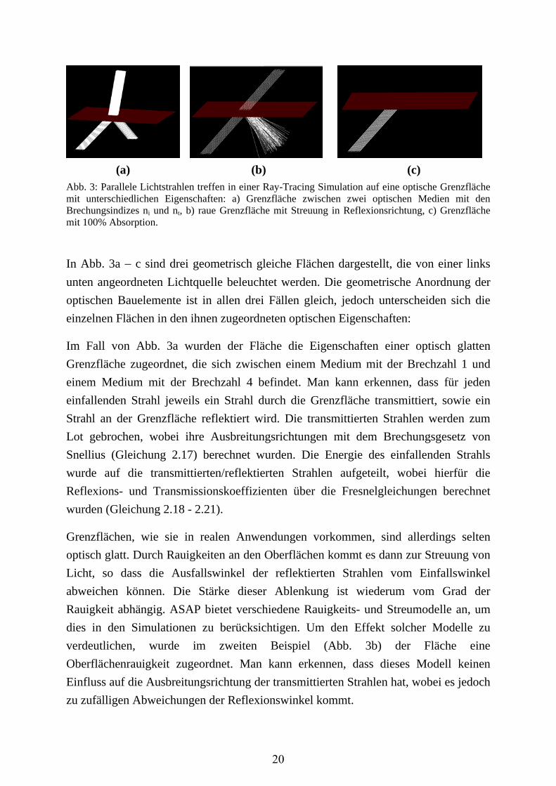
Abb. 3: Parallele Lichtstrahlen treffen in einer Ray-Tracing Simulation auf eine optische Grenzfläche mit unterschiedlichen Eigenschaften: a) Grenzfläche zwischen zwei optischen Medien mit den Brechungsindizes ni und nt, b) raue Grenzfläche mit Streuung in Reflexionsrichtung, c) Grenzfläche mit 100% Absorption.
In Abb. 3a − c sind drei geometrisch gleiche Flächen dargestellt, die von einer links
unten angeordneten Lichtquelle beleuchtet werden. Die geometrische Anordnung der
optischen Bauelemente ist in allen drei Fällen gleich, jedoch unterscheiden sich die
einzelnen Flächen in den ihnen zugeordneten optischen Eigenschaften:
Im Fall von Abb. 3a wurden der Fläche die Eigenschaften einer optisch glatten
Grenzfläche zugeordnet, die sich zwischen einem Medium mit der Brechzahl 1 und
einem Medium mit der Brechzahl 4 befindet. Man kann erkennen, dass für jeden
einfallenden Strahl jeweils ein Strahl durch die Grenzfläche transmittiert, sowie ein
Strahl an der Grenzfläche reflektiert wird. Die transmittierten Strahlen werden zum
Lot gebrochen, wobei ihre Ausbreitungsrichtungen mit dem Brechungsgesetz von
Snellius (Gleichung 2.17) berechnet wurden. Die Energie des einfallenden Strahls
wurde auf die transmittierten/reflektierten Strahlen aufgeteilt, wobei hierfür die
Reflexions- und Transmissionskoeffizienten über die Fresnelgleichungen berechnet
wurden (Gleichung 2.18 - 2.21).
Grenzflächen, wie sie in realen Anwendungen vorkommen, sind allerdings selten
optisch glatt. Durch Rauigkeiten an den Oberflächen kommt es dann zur Streuung von
Licht, so dass die Ausfallswinkel der reflektierten Strahlen vom Einfallswinkel
abweichen können. Die Stärke dieser Ablenkung ist wiederum vom Grad der
Rauigkeit abhängig. ASAP bietet verschiedene Rauigkeits- und Streumodelle an, um
dies in den Simulationen zu berücksichtigen. Um den Effekt solcher Modelle zu
verdeutlichen, wurde im zweiten Beispiel (Abb. 3b) der Fläche eine
Oberflächenrauigkeit zugeordnet. Man kann erkennen, dass dieses Modell keinen
Einfluss auf die Ausbreitungsrichtung der transmittierten Strahlen hat, wobei es jedoch
zu zufälligen Abweichungen der Reflexionswinkel kommt.
20
Im letzten Beispiel (Abb. 3c) wurde der Transmissions- und Reflexionswert der Fläche
manuell auf 0 gesetzt, wodurch einfallende Strahlen weder transmittiert noch
reflektiert werden und die Fläche alle einfallende Strahlen absorbiert. Dadurch, dass
ASAP ein oberflächenbasiertes Ray-Tracing Programm ist, werden die Positionen aller
Strahlen der letzten Grenzfläche zugeordnet, mit der es zu einer Interaktion gekommen
ist. Alle Strahlen, die auf diese Fläche treffen, werden gestoppt, wobei ihre Position
auf der Fläche sowie ihre Ausbreitungsrichtung gespeichert werden. Des Weiteren ist
es möglich, nach Abschluss der Simulation einzelne Flächen gezielt auszuwerten, so
dass nur Strahlen, die an den ausgewählten Flächen verblieben sind, berücksichtigt
werden. Hierfür stellt das Programm ASAP verschiedene Analysefunktionen zur
Verfügung, die eine gezielte Auswertung der Strahlenposition oder Strahlenrichtung
an den Flächen der einzelnen Detektoren ermöglichen. Zusätzlich besteht allerdings
die Möglichkeit, die Strahlendaten (Position, Richtung, Energie) eines jeden Strahls
einzeln zu exportieren.
(a) (b) (c)
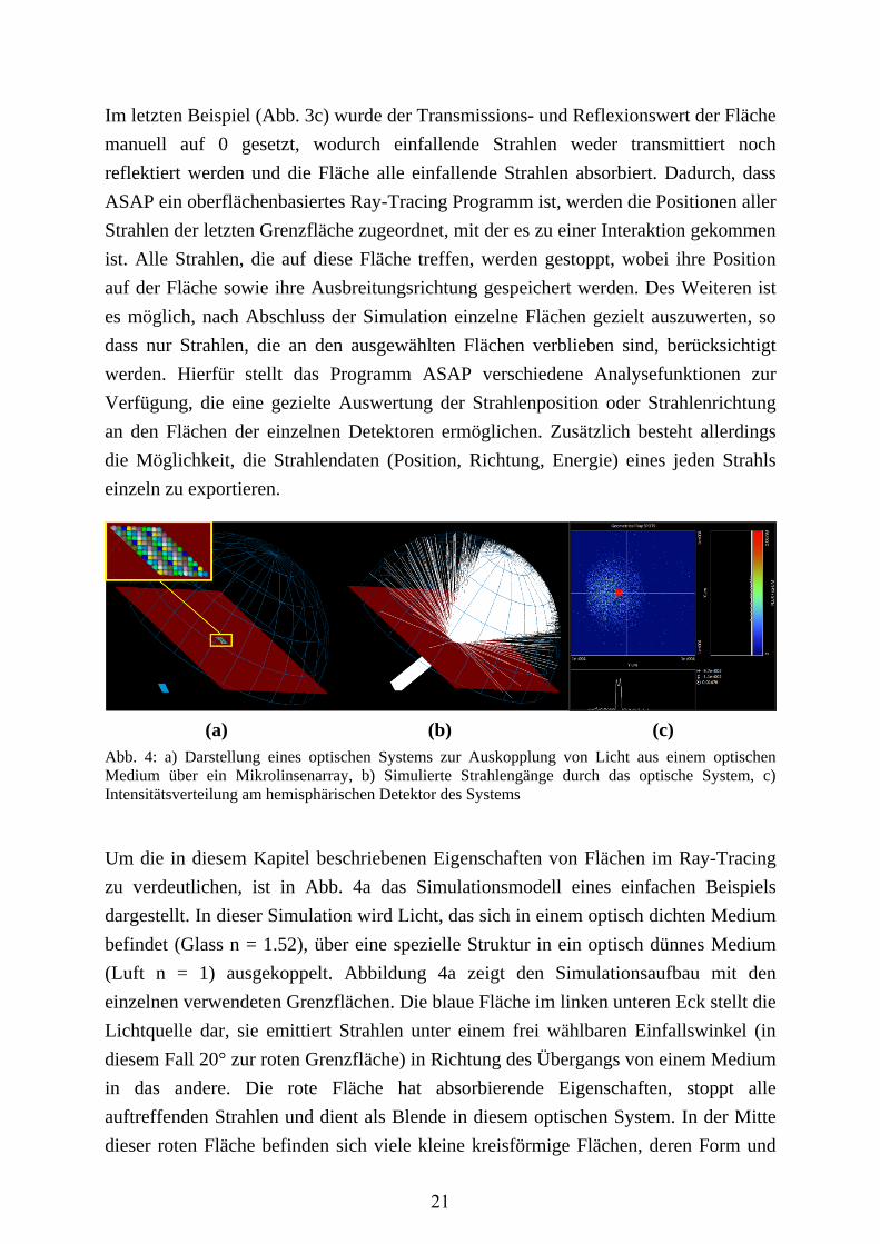
Abb. 4: a) Darstellung eines optischen Systems zur Auskopplung von Licht aus einem optischen Medium über ein Mikrolinsenarray, b) Simulierte Strahlengänge durch das optische System, c) Intensitätsverteilung am hemisphärischen Detektor des Systems
Um die in diesem Kapitel beschriebenen Eigenschaften von Flächen im Ray-Tracing
zu verdeutlichen, ist in Abb. 4a das Simulationsmodell eines einfachen Beispiels
dargestellt. In dieser Simulation wird Licht, das sich in einem optisch dichten Medium
befindet (Glass n = 1.52), über eine spezielle Struktur in ein optisch dünnes Medium
(Luft n = 1) ausgekoppelt. Abbildung 4a zeigt den Simulationsaufbau mit den
einzelnen verwendeten Grenzflächen. Die blaue Fläche im linken unteren Eck stellt die
Lichtquelle dar, sie emittiert Strahlen unter einem frei wählbaren Einfallswinkel (in
diesem Fall 20° zur roten Grenzfläche) in Richtung des Übergangs von einem Medium
in das andere. Die rote Fläche hat absorbierende Eigenschaften, stoppt alle
auftreffenden Strahlen und dient als Blende in diesem optischen System. In der Mitte
dieser roten Fläche befinden sich viele kleine kreisförmige Flächen, deren Form und
21
Anordnung man in der Vergrößerung im linken oberen Eck von Abb. 3a erkennen
kann. Diesen Flächen ist die Eigenschaft einer optischen Grenzfläche von (n = 1.52 zu
n = 1) zugeordnet. Die blaue kreisrunde Fläche, die durch ihre Umrisse dargestellt ist,
dient als Detektor. Dementsprechend sind auch die Transmissions- und
Reflexionswerte auf 0 gesetzt, so dass auftreffende Strahlen gestoppt werden.
Abb. 4b zeigt den Strahlenverlauf in der Simulation. In Weiß sind die Wege der
einzelnen Strahlen eingezeichnet, die von der Quelle emittiert wurden und die auf den
hemisphärischen Detektor getroffen sind. Strahlen, die das Simulationssystem
verlassen haben, wie z.B. Strahlen, die von der Auskoppelstruktur reflektiert wurden
oder Strahlen, die auf die rote Blende getroffen sind, wurden vernachlässigt. Man kann
erkennen, dass es durch die gekrümmte Oberfläche der einzelnen Auskoppelstrukturen
zu einer Abstrahlung in viele Raumrichtungen gekommen ist und nicht nur in eine
spezielle Raumrichtung, wie man es z.B. von einer flachen Auskoppelfläche erwarten
würde. Um die Abstrahlcharakteristik dieser Auskoppelstruktur näher zu untersuchen,
wurden die Strahlendaten auf der Detektorfläche mittels ASAP ausgewertet. In Abb.
4c kann man eine Projektion der Strahlenpositionen auf der hemisphärischen
Detektoroberfläche auf eine Ebene sehen. Anders als man aus Abb. 4b erwarten
würde, gibt es weiterhin eine Vorzugsrichtung, in die der Großteil der Strahlen
abgelenkt wird (Abb. 4c roter Punkt). Nur ein kleiner Teil wird in andere
Raumrichtungen abgelenkt. Dieses Beispiel verdeutlicht, wie wichtig eine genaue
Analyse der Simulationsdaten ist, um physikalisch richtige Erkenntnisse aus einer
Simulation zu gewinnen.
22
2.3 FINITE DIFFERENCE TIME DOMAIN
Für sehr kleine Strukturgrößen, deren Abmessungen im Bereich der Wellenlänge des
Lichts liegen, versagen die Ansätze der geometrischen Optik, die die Wechselwirkung
von Licht mit Materie durch einfache Strahlen beschreibt. Dieser spezielle Bereich der
Optik, in dem die Wellennatur des Lichts nicht vernachlässigt werden sollte und
Effekte wie Beugung und Interferenz eine entscheidende Rolle spielen, wird
Wellenoptik genannt. In diesem Bereich stoßen analytische Methoden schnell an ihre
Grenzen, da die Maxwellgleichungen nur für wenige Spezialfälle lösbar sind. Durch
die sich ständig verbessernde Rechen- und Speicherkapazitäten moderner Computer
gewinnen für die Simulation derartiger Strukturen vor allem numerische Methoden
immer mehr an Bedeutung.
Die “Finite Difference Time Domain” (FDTD) Methode stellt ein gutes Beispiel für
eine numerische wellenoptische Simulationsmethode dar. Sie gehört zur Gruppe der
Finiten-Differenzen-Methoden, welche auf das Lösen von partiellen
Differentialgleichungen spezialisiert sind. FDTD unterteilt den Simulationsbereich in
Elementarzellen, in die sogenannten „YEE-Zellen“ [1], wodurch eine Diskretisierung
der Maxwellgleichungen ermöglicht wird. Diese können anschließend numerisch
gelöst werden. FDTD arbeitet in der Zeitdomäne. Das bedeutet, dass ein zeitlich
begrenzter Puls als Quelle verwendet wird, welcher nach einer Fourier Transformation
in den Frequenzraum einer gewissen Bandbreite von Frequenzen entspricht. Aus
diesem Grund wird mit dieser Methode auch das zeitabhängige elektromagnetische
Feld nach Interaktion mit dem des optischen Systems berechnet. Um Aussagen über
die Wechselwirkung von Licht verschiedener Wellenlängen mit dem optischen System
treffen zu können, wird das zeitabhängige elektromagnetische Feld anschließend durch
eine Fast-Fourier-Transformation (FFT) in den Frequenzraum transformiert. Dadurch
wird es sogar möglich, durch geeignete Modellierung des zeitlichen Anregungspulses
mit nur einer durchgeführten Simulation bereits eine breitbandige Frequenzantwort des
Systems zu erhalten [31].
2.3.1 FDTD ALGORITHMUS
Alle in diesem Abschnitt verwendeten Herleitungen stammen aus Kapitel 2 des Buchs
„Computational Electrodynamics“ [31] und können dort in einer ausführlicheren Form
nachvollzogen werden.
23
Um das Prinzip des FDTD Algorithmus besser verstehen zu können, wird dieses
zunächst mittels der homogenen Wellengleichung in einer Dimension aus Kap. 2.1.1
skizziert:
2 22
02 2
( , ) ( , )u x t u x tc
t x
∂ ∂=∂ ∂
(2.22)
Dabei ist u(x, t) eine Funktion von Ort x und Zeit t und c0 die Geschwindigkeit des
Lichts im Vakuum. Eine mögliche Lösung von Gleichung (2.22) ist die Funktion
( )( , ) ,i t kxu x t e ω −= (2.23)
die eine kontinuierliche Welle darstellt, die sich in x-Richtung ausbreitet (mit i als
imaginärer Einheit, der Kreisfrequenz ω = 2πf und dem Kreiswellenzahl k = 2π/λ). Setzt man diese Welle in Gleichung 2.22 ein, erhält man nach Herausheben des
Exponentialterms und Umformen der Gleichung die Dispersionsrelation:
0
kc
ω= ± bzw. 0
( ) ( )p
cv
kn n
ωω ω
= ± = (2.24 a,b)
Gleichung 2.24a beschreibt die lineare Beziehung zwischen Kreisfrequenz ω und
Kreiswellenzahl k von Licht im Vakuum. Befindet sich das Licht jedoch in einem
Medium mit frequenzabhängiger Brechzahl n(ω), ändert sich auch die
Geschwindigkeit des Lichts pv zu c = c0/n(ω), was dazu führt, dass die Beziehung
zwischen Kreisfrequenz und Kreiswellenzahl ebenfalls frequenzabhängig wird, wie
man in Gleichung 2.24b erkennen kann.
Da FDTD eine Finite-Differenzen-Methode ist, müssen die Orts- und Zeit-
Dimensionen in einzelne Ortspunkte xi mit Abstand Δx, bzw. Zeitpunkte tn mit
Abstand Δt, diskretisiert werden. Zur Vereinfachung der Syntax werden in allen
kommenden Gleichungen die Ortsposition durch den tiefgestellten Index i und die
Zeitposition durch den hochgestellten Index n wiedergegeben. Die Funktion niu
repräsentiert die Feldstärke am Ort x = iΔx und der Zeit t = nΔt. FDTD nutzt das
zentrale Differenzverfahren [32] zur Bestimmung der Näherung der zweiten partiellen
Ableitungen von u(x, t) nach dem Ort oder der Zeit, die für Gleichung 2.22 benötigt
werden. Durch Addition und Umformung der Taylorentwicklungen von u(xi, t) am
24
Punkt xi zu den nächsten Nachbar-Punkten xi+Δx und xi-Δx bei festgehaltener Zeit tn
lässt sich die partielle Ableitung nach dem Ort darstellen:
221 1
,2 2
2[( ) ]
( )i n
n n ni i i
x t
u u uuO x
x x+ − − +∂ = + Δ ∂ Δ
. (2.25a)
Nach dem gleichen Verfahren lässt sich auch die partielle Ableitung nach der Zeit
berechnen:
1 122
,2 2
2[( ) ]
( )i n
n n ni i i
x t
u u uuO t
t t
+ − − +∂ = + Δ ∂ Δ .
(2.25b)
Der Vorteil des zentralen Differenzverfahrens gegenüber dem vor- oder rückwärtigen
Differenzverfahren liegt in der erhöhten Genauigkeit, da nur die Terme O[(Δx)²]
vernachlässigt werden. Setzt man nun die Gleichungen 2.25a und 2.25b in die
homogene Wellengleichung (2.22) ein, kann man den Ausdruck zu
1 2 11 1( ) 2
( )²
n n nn n ni i ii i i
u u uu c t u u
x+ −+ + − +≅ Δ + − Δ
(2.26)
umformen. Hier steht nun die Feldstärke am Ort xi zum Zeitpunkt tn+1 in Abhängigkeit
von den Feldstärken der nächsten Nachbarn, sowie des Ortes selbst, zu den vorherigen
Zeitpunkten tn und tn-1. Diese Werte sollten allerdings durch die vorherigen
Simulationsschritte bereits bekannt sein und ermöglichen so eine zeitlich iterative
Berechnung der Wellenausbreitung über alle Ortspunkte des Simulationsgebietes mit
dem FDTD Algorithmus.
Gleichung (2.26) stellt jedoch aufgrund der Vernachlässigung der Terme O[(Δx)²+
(Δt)²] nur eine Näherung dar. Um den Fehler der durchgeführten Näherungen
abschätzen zu können, wird der Begriff der numerischen Dispersion eingeführt, also
die Abweichung der Ausbreitungsgeschwindigkeiten der numerischen Wellen in der
Simulation zur Ausbreitungsgeschwindigkeit der realen Welle in Abhängigkeit von
der verwendeten Frequenz. Um diese zu berechnen, ersetzt man die Kreiswellenzahl k
durch eine „numerische“ Kreiswellenzahl k :
Re( ) Im( )k k i k= + (2.27)
25
In Gleichung 2.23 eingesetzt ergibt sich die Feldstärke am Ort xi zum Zeitpunkt tn zu
( ) Im( ) ( Re( ) )n j n t ki x k i x j n t k i xiu e e eω ωΔ − Δ Δ Δ − Δ= =
(2.28)
Setzt man nun Gleichung 2.28 für die numerische Kreiswellenzahl k in Gleichung
2.26 ein, erhält man die Beziehung zwischen Kreisfrequenz ω und numerischer
Kreiswellenzahl k
( )
21
cos 1 cos 1x
k arc tx c t
ω Δ = + Δ − Δ Δ
(2.29)
Anhand dieser numerischen Dispersionsfunktion ist es nun möglich, Aussagen über
die Genauigkeit des FDTD Algorithmus zu treffen. Bei Verwendung einer sehr groben
Diskretisierung wie z.B. cΔt = Δx/2 und Δx = λ0/10, wobei λ0 für die Vakuum-
Wellenlänge der verwendeten Sinuswelle steht, erhält man aus Gleichung 2.29
0.63642k
x=
Δ bzw. 00.9873pv c= .
(2.30)
In diesem Fall unterscheiden sich numerische und reale Kreiswellenzahl, was ähnlich
wie für die Brechzahl in Gleichung 2.24b zu einer Veränderung der numerischen
Ausbreitungsgeschwindigkeit der Welle pv führt. Diese Abweichung von 1.27% der
realen Ausbreitungsgeschwindigkeit der Welle 0pv c= führt dazu, dass es bereits nach
einer Distanz von 100 Δx Schritten zu einer Phasenverschiebung von 45.72° zwischen
simulierter und realer Wellenfront kommt und die Simulation nicht mehr das
Verhalten des realen Systems beschreibt.
Wird jedoch eine sehr feine Diskretisierung Δt und Δx angenommen, lässt sich
Gleichung 2.29 zu
1( )k k x k
x= Δ =
Δ
(2.31)
vereinfachen. Für diesen Fall wäre k nicht abhängig von der verwendeten
Wellenlänge, dispersionslos und die numerische Lösung exakt.
26
Das in dieser Dissertation verwendete Simulationsprogramm FDTD Solution benutzt
zusätzlich eine nicht einheitliche Diskretisierung des Simulationsgebietes, so dass die
Diskretisierung an Übergängen zwischen Medien zusätzlich erhöht wird. Bei einer
Simulation mit hoher Genauigkeit wird eine durchschnittliche Diskretisierung von
cΔt ~ Δx/5 und Δx ~ λ0/34 verwendet.
2.3.2 YEE ALGORITHMUS
In Kapitel 2.3.1 wurde die FDTD Methode einer Wellenbewegung in einer Dimension
demonstriert. In diesem Kapitel wird dieses Prinzip nun auf die Maxwellgleichungen
in drei Dimensionen erweitert. Alle in diesem Abschnitt verwendeten Herleitungen
lehnen sich an Kapitel 3 des Buchs „Computational Electrodynamics“ [26] an und
können dort in einer ausführlicheren Form nachvollzogen werden.
1966 veröffentlichte Kane S.YEE seine wissenschaftliche Arbeit, in der er erstmalig
die Finite-Differenzen-Methode nutzte, um die Maxwellgleichungen numerisch lösen
zu können [1]. Er unterteilte den Raum in so genannte Yee-Zellen, auf denen die
einzelnen Komponenten des E- und H-Feldes verteilt sind, so dass jede E-Komponente
von jeweils vier H-Komponenten umgeben ist bzw. umgekehrt, jede H-Komponente
von vier E-Komponenten (siehe Abb. 5a). Dadurch führte Yee zwei unterschiedliche
Diskretisierungen ein: Der Abstand zwischen zwei benachbarten E-Komponenten
beträgt eine volle Einheitszelle (Δx, Δy oder Δz), der Abstand zwischen E- und H-
Komponenten hingegen jedoch nur eine halbe Einheitszelle (Δx/2, Δy/2 oder Δz/2).
Dieselbe Diskretisierung wird auch für die Zeit eingeführt: Ein Zeitschritt von E- zu
zeitlich versetzen E-Feldkomponenten wird in einer vollen Zeiteinheit (Δt)
durchgeführt, ein Zeitschritt von E- zu H-Feldkomponenten wird in einer halben
Zeiteinheit (Δt/2) durchgeführt. Dadurch ist es möglich, durch ständigen Wechsel
zwischen elektrischem und magnetischem Feld, beide Felder automatisch in
Abhängigkeit voneinander zu berechnen [1]. Um die Schreibweise auch für den
dreidimensionalen Fall zu vereinfachen, wird die in Kapitel 2.3.1 eingeführte Notation
erweitert zu:
, ,( , , , ) n
i j ku i x j y k z n t uΔ Δ Δ Δ = (2.32)
Die Näherungen der ersten Ableitung nach Zeit und Raum durch die zentralen
Differenzen ergeben sich dementsprechend zu:
27
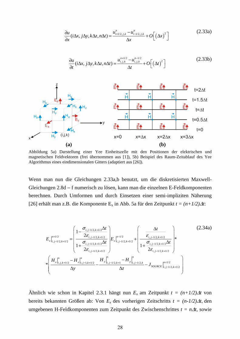
( )21/2, , 1/2, ,( , , , )
n ni j k i j ku uu
i x j y k z n t O xx x
+ −−∂ Δ Δ Δ Δ = + Δ ∂ Δ
(2.33a)
( )
1/2 1/22, , , ,( , , , )
n ni j k i j ku uu
i x j y k z n t O tt t
+ −−∂ Δ Δ Δ Δ = + Δ ∂ Δ
(2.33b)
(a) (b) Abbildung 5a) Darstellung einer Yee Einheitszelle mit den Positionen der elektrischen und magnetischen Feldvektoren (frei übernommen aus [1]), 5b) Beispiel des Raum-Zeitablauf des Yee Algorithmus eines eindimensionalen Gitters (adaptiert aus [26]).
Wenn man nun die Gleichungen 2.33a,b benutzt, um die diskretisierten Maxwell-
Gleichungen 2.8d − f numerisch zu lösen, kann man die einzelnen E-Feldkomponenten
berechnen. Durch Umformen und durch Einsetzen einer semi-impliziten Näherung
[26] erhält man z.B. die Komponente Ex in Abb. 5a für den Zeitpunkt t = (n+1/2)Δt:
, 1/2, 1/2
1/2 1/2, 1/2, 1/2 , 1/2, 1/2
, 1/2, 1/2 , 1/2, 1/2, 1/2, 1/2 , 1/2, 1/2
, 1/2, 1/2 , 1/2, 1/2
, , 1/2 ,
12
*
1 12 2
*
i j k
n ni j k i j kx xi j k i j k
i j k i j k
i j k i j k
n
z zi j k i
t t
E Et t
H H
σε ε
σ σε ε
− +
+ −− + − +− + − +
− + − +
− + − +
+
Δ Δ− = +Δ Δ
+ +
− 1/21, 1/2 , 1/2, 1 , 1/2,
, 1/2, 1/2
n nny y nj k i j k i j k
SOURCE i j k
H HJ
y z+− + − + −
− +
− − − Δ Δ
(2.34a)
Ähnlich wie schon in Kapitel 2.3.1 hängt nun Ex am Zeitpunkt t = (n+1/2)Δt von
bereits bekannten Größen ab: Von Ex des vorherigen Zeitschritts t = (n-1/2)Δt, den
umgebenen H-Feldkomponenten zum Zeitpunkt des Zwischenschrittes t = nΔt, sowie
28
der Quelle J und den Materialkonstanten ε und σ am Gitterpunkt von Ex. Analog kann
man mit den Gleichungen 2.33a,b die diskretisierten Maxwell-Gleichungen 2.8a-c
lösen, um z.B. die benachbarte Hz Komponente für den nächsten halben Zeitschritt zu
bestimmen:
*, , 1/2
1 , , 1/2 , , 1/2
* *, , 1/2 , , 1/2, , 1/2 , , 1/2
, , 1/2 , , 1/2
1/2 1/2
, 1/2, 1/2 , 1/2, 1/2 1/2,
12
*
1 12 2
*
i j k
n ni j k i j kz zi j k i j k
i j k i j k
i j k i j k
n nyx xi j k i j k i
t t
H Ht t
EE E
x
σμ μ
σ σμ μ
+
+ + ++ +
+ +
+ +
+ +
+ + − + +
Δ Δ− = + Δ Δ + +
−−
Δ
1/2 1/2
1/2, 1/2 1/2, , 1/2
, , 1/2
n n
y nj k i j kSOURCE i j k
EM
y
+ +
++ − ++
− − Δ
(2.35b)
Um die Funktionsweise und den zeitlichen Ablauf des Yee-Algorithmus vereinfacht zu
verdeutlichen, wird in Abb. 5b die Anwendung des Verfahrens auf ein
eindimensionales Gitter dargestellt. Durch numerisches Lösen der
Maxwellgleichungen werden alle E-Komponenten des Zeitpunkts t=Δt aus den H-
Komponenten des Zeitpunkts t = 0.5Δt, sowie den E-Komponenten des Zeitpunkts
t = 0, berechnet. Anschließend werden wiederum die H-Komponenten des Zeitpunkts
t = 1.5Δt aus den vorher berechneten E- und H-Komponenten ermittelt. Durch
mehrfache Iterationen dieses Prozesses lässt sich der zeitliche Verlauf des E- und H-
Feldes für das gegebene Problem numerisch berechnen.
2.3.3 SIMULATIONSKOMPONENTEN
In diesem Kapitel werden die einzelnen Komponenten einer FDTD Simulation
diskutiert, die notwendig sind, um den in Kapitel 2.3.2 besprochenen Algorithmus auf
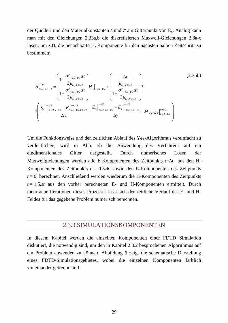
ein Problem anwenden zu können. Abbildung 6 zeigt die schematische Darstellung
eines FDTD-Simulationsgebietes, wobei die einzelnen Komponenten farblich
voneinander getrennt sind.
29
Abb. 6) Schematische Darstellung eines FDTD-Simulationsgebiets mit den einzelnen Komponenten: Lichtquellenmodell einer ebenen Welle in Grün; Hintergrund mit Brechungsindex n1 in Grau; Struktur mit Brechungsindex n2 in Blau; Standard Fourier Transformationsmonitor (SFT) als Detektor in Gelb; Randbedingungen des Simulationsgebietes in Orange.
Als Quelle für die in dieser Dissertation verwendeten FDTD Simulationen dient immer
das idealisierte Modell einer unendlich ausgedehnten ebenen Welle, deren Wellenfront
senkrecht auf deren Ausbreitungsrichtung steht. Die Polarisationsrichtung dieser
ebenen Welle ist immer so gewählt, dass diese eine Mittelung aus s und p Polarisation
darstellt (45°-polarisiert).
Die Anwendung des FDTD-Algorithmus verlangt eine Diskretisierung des
Simulationsgebiets in einzelne Yee-Zellen, wobei aus Gründen der numerischen
Stabilität die Größe der einzelnen Yee-Zellen zusätzlich möglichst klein sein sollte.
Da jedoch die Anzahl der Yee-Zellen die für die Simulation benötigte Rechenleistung
und Kapazität bestimmen, steigt der Simulationsaufwand quadratisch mit der Größe
dieses Simulationsgebiets für 2-dimensionale Simulationsgebiete. Aus diesem Grund
wird das Simulationsgebiet durch spezielle Randbedingungen (vergleiche Abb. 6,
orange Linien) begrenzt, um dessen Größe zu minimieren.
Um das Simulationsgebiet aus Abb. 6 in y-Richtung zu begrenzen, wurden
absorbierende Randbedingungen verwendet, deren Hauptaufgabe darin besteht, der
Erweiterung des Simulationsgebietes in den freien Raum zu entsprechen. Durch diese
Randbedingungen wird es ermöglicht, das Simulationsgebiet bereits sehr nahe an der
Struktur abzuschließen und dadurch Simulationskapazitäten zu sparen. Das im
Rahmen dieser Dissertation verwendete Simulationsprogramm „FDTD Solutions“
benutzt hierfür sogenannte „Perfectly Matched Layer“ (PML). Diese wurden erstmals
von Berenger [33], [34] eingeführt und stellen heute die meistbenutzte Randbedingung
der FDTD Methode dar, um einfallende elektromagnetische Felder zu absorbieren. Bei
dieser Technik werden zusätzliche Ebenen von Yee-Zellen, die die optischen
Eigenschaften eines absorbierenden Mediums besitzen, eingeführt. Das Hauptproblem
besteht darin, einfallende Wellen unabhängig von ihrem Einfallswinkel ohne
30
Rückreflexion möglichst vollständig zu absorbieren [35], wobei die Stärke der
Reflexionen mit einer höheren Anzahl an PML Ebenen deutlich reduziert werden
kann.
Viele diffraktive optische Elemente (DOEs), wie z.B. Phasen-Transmissions-Gitter
(siehe Kapitel 2.4.5), deren räumliche Ausdehnung eine FDTD Simulation eines
kompletten DOEs unmöglich macht, setzen sich aus periodischen Strukturen in eine
oder mehrere Raumrichtungen zusammen. Mit Hilfe von periodischen
Randbedingungen in diesen Raumrichtungen ist es möglich, das Simulationsgebiet auf
nur ein Element zu reduzieren, wie es z.B. in Abb. 5 für eine Dimension in x-Richtung
gezeigt ist. Verlassen nun Wellen das Simulationsgebiet an den Rändern der
periodischen Randbedingungen, werden diese an der jeweils komplementären Seite re-
emittiert, um den Einfluss von benachbarten Perioden zu berücksichtigen. Bei diesen
Randbedingungen muss berücksichtigt werden, dass keine Streuartefakte an den
Rändern auftreten. Um diese zu vermeiden, werden sogenannte „Bloch“
Randbedingungen [36] verwendet, die zusätzlich die Phasenänderungen zwischen den
einzelnen Perioden berücksichtigen.
FDTD ist ein Algorithmus, der in der Zeitdomäne arbeitet. Aus diesem Grund muss
man einen Standard-Fourier-Transformation Monitor (SFT Monitor) als Detektor
(Gelbe Linie Abb. 5) verwenden, um das elektrische bzw. magnetische Feld an einer
gewünschten Position innerhalb des Simulationsgebietes für verschiedene
Wellenlängen zu bestimmen. Der SFT Monitor speichert den zeitlichen Verlauf der E-
und H-Feldkomponenten während der Simulation und transformiert die gespeicherten
Daten anschließend mittels FFT in den Frequenzraum. Durch eine sogenannte „Nah-
zu-Fernfeldtransformation“, die durch Anwendung des Green‘schen Theorems [37],
[38] realisiert werden kann, ist es anschließend möglich, die Nahfelder in
winkelabhängige Intensitätsverteilungen im Fernfeld zu transformieren. Wurden
periodische Randbedingungen, wie z.B. die Bloch Randbedingungen, für das
Simulationsgebiet verwendet, ist es im Prozess der Nah-zu-Fernfeldtransformation
zusätzlich möglich, eine beliebige Anzahl an Perioden in diese Richtung zu definieren.
Dies hat einen starken Einfluss auf die resultierende Fernfeldverteilung (siehe
Abschnitt 2.4.5).
31
2.4 KOHÄRENZ UND INTERFERENZ
Wie schon in Kapitel 2.1.1 erwähnt, kann die Ausbreitung von Licht durch
Wellenfunktionen beschrieben werden, die eine Lösung der homogenen
Wellengleichung darstellen. Treffen zwei oder mehrere Wellen in einem Raumpunkt
zusammen, kommt es zu einer Überlagerung ihrer Feldkomponenten. Dies kann,
abhängig von den Phasenbeziehungen der einzelnen Wellenfunktionen, zu einer
gegenseitigen Auslöschung oder einer Verstärkung der Amplituden führen. Dieser
Effekt ist allgemein unter dem Namen Interferenz bekannt, wobei man im Falle von
Verstärkung von konstruktiver Interferenz und im Falle von Auslöschung von
destruktiver Interferenz spricht. Dieses Phänomen der Interferenz ist für eine Vielzahl
verschiedener optischer Effekte verantwortlich, wie z.B. die Aufspaltung von Licht in
verschiedene Intensitätsordnungen durch ein optisches Gitter [39], [40] oder die
Unterdrückung von Transmission oder Reflexion bei einem optischen
Dünnschichtsystem [41].
Die Stärke dieser Interferenzeffekte wird durch die sogenannte Kohärenz bzw. den
Grad der Kohärenz der Wellen bestimmt. Sie definiert die Gesamtheit der
Korrelationseigenschaften zwischen den einzelnen Wellengrößen und ist abhängig von
der Bandbreite der Frequenzen der interferierenden Wellen, sowie ihrer räumlichen
Beschränktheit [39]. Oft ist es für eine einfachere Betrachtungsweise zweckmäßig, das
Prinzip der Kohärenz in eine zeitliche Kohärenz und eine räumliche Kohärenz zu
unterteilen.
In diesem Kapitel wird das physikalische Konzept der Interferenz und der Kohärenz
diskutiert und die notwendigen Grundlagen, die zum Verständnis der Publikationen in
dieser Dissertation notwendig sind, zusammengefasst.
2.4.1 INTERFERENZ
Für die Überlagerung einzelner Wellen gilt das sogenannte Superpositionsprinzip im
Bereich der linearen Optik [39]. Wenn die Feldkomponenten der sich überlagernden
Wellen die homogene Wellengleichung (Gleichung 2.10) erfüllen, so erfüllt auch jede
Linearkombination der Komponenten dieser Wellen die homogene Wellengleichung.
Dadurch entsprechen die Feldkomponenten der resultierenden Welle in jedem Punkt
im Raum der algebraischen Summe der einzelnen Feldkomponenten der sich
überlagernden Wellen.
32
Überlagern sich zwei Wellen gleicher Frequenz E1 und E2, was zwei
monochromatischen Lichtwellen entspricht, kann die resultierende Welle als lineare
Überlagerung der beiden Wellen dargestellt werden [39]:
1 2 01 1 02 2 0sin( ) sin( ) sin( )E E E A t A t A tω α ω α ω α= + = + + + = + . (2.36)
mit
1,2 1,2 1,2( , ) ( )x kxα ε ε= − + (2.37)
In den Termen α1,2 sind die optischen Weglängen x1,2 und die Anfangsphasen ε1,2 der
beiden interferierenden Wellen enthalten. Das Quadrat der Amplitude der
resultierenden Welle E kann durch die Gleichung [39]
2 2 20 01 02 01 02 2 12 cos( )A A A A A α α= + + − (2.38)
beschrieben werden. Man kann erkennen, dass auf der rechten Seite der Gleichung
zusätzlich zu den Quadraten der Amplituden der erzeugenden Wellen ein sogenannter
Interferenzterm δ vorhanden ist, der vom Phasenunterschied der beiden
interferierenden Wellen abhängig ist:
2 1 1 2 1 2
2( ) ( ) ( )x x
πδ α α ε ελ
≡ − = − + − (2.39)
Aus diesem Grund ist auch die mittlere Intensität der entstehenden Welle, die
proportional vom zeitlichen Mittel des Quadrats der Amplituden abhängt [39], nicht
gleich der Summe der Intensitäten der erzeugenden Wellen, sondern auch vom
Phasenunterschied der beiden erzeugenden Wellen abhängig. Aus Gleichung 2.39
kann man erkennen, dass ein Phasenunterschied entweder durch eine unterschiedliche
optische Weglänge oder über eine unterschiedliche Anfangsphase erzeugt werden
kann.
33
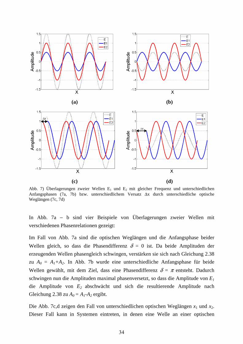
(a) (b)
(c) (d) Abb. 7) Überlagerungen zweier Wellen E1 und E2 mit gleicher Frequenz und unterschiedlichen Anfangsphasen (7a, 7b) bzw. unterschiedlichem Versatz Δx durch unterschiedliche optische Weglängen (7c, 7d)
In Abb. 7a − b sind vier Beispiele von Überlagerungen zweier Wellen mit
verschiedenen Phasenrelationen gezeigt:
Im Fall von Abb. 7a sind die optischen Weglängen und die Anfangsphase beider
Wellen gleich, so dass die Phasendifferenz δ = 0 ist. Da beide Amplituden der
erzeugenden Wellen phasengleich schwingen, verstärken sie sich nach Gleichung 2.38
zu A0 = A1+A2. In Abb. 7b wurde eine unterschiedliche Anfangsphase für beide
Wellen gewählt, mit dem Ziel, dass eine Phasendifferenz δ = π entsteht. Dadurch
schwingen nun die Amplituden maximal phasenversetzt, so dass die Amplitude von E1
die Amplitude von E2 abschwächt und sich die resultierende Amplitude nach
Gleichung 2.38 zu A0 = A1-A2 ergibt.
Die Abb. 7c,d zeigen den Fall von unterschiedlichen optischen Weglängen x1 und x2.
Dieser Fall kann in Systemen eintreten, in denen eine Welle an einer optischen
34
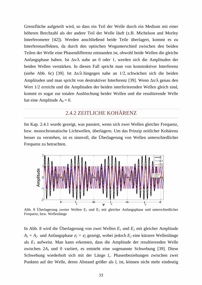
Grenzfläche aufgeteilt wird, so dass ein Teil der Welle durch ein Medium mit einer
höheren Brechzahl als der andere Teil der Welle läuft (z.B. Michelson and Morley
Interferometer [42]). Werden anschließend beide Teile überlagert, kommt es zu
Interferenzeffekten, da durch den optischen Wegunterschied zwischen den beiden
Teilen der Welle eine Phasendifferenz entstanden ist, obwohl beide Wellen die gleiche
Anfangsphase haben. Ist Δx/λ nahe an 0 oder 1, werden sich die Amplituden der
beiden Wellen verstärken. In diesen Fall spricht man von konstruktiver Interferenz
(siehe Abb. 6c) [39]. Ist Δx/λ hingegen nahe an 1/2, schwächen sich die beiden
Amplituden und man spricht von destruktiver Interferenz [39]. Wenn Δx/λ genau den
Wert 1/2 erreicht und die Amplituden der beiden interferierenden Wellen gleich sind,
kommt es sogar zur totalen Auslöschung beider Wellen und die resultierende Welle
hat eine Amplitude A0 = 0.
2.4.2 ZEITLICHE KOHÄRENZ
Im Kap. 2.4.1 wurde gezeigt, was passiert, wenn sich zwei Wellen gleicher Frequenz,
bzw. monochromatische Lichtwellen, überlagern. Um das Prinzip zeitlicher Kohärenz
besser zu verstehen, ist es sinnvoll, die Überlagerung von Wellen unterschiedlicher
Frequenz zu betrachten.
Abb. 8 Überlagerung zweier Wellen E1 und E2 mit gleicher Anfangsphase und unterschiedlicher Frequenz, bzw. Wellenlänge
In Abb. 8 wird die Überlagerung von zwei Wellen E1 und E2 mit gleicher Amplitude
A1 = A2 und Anfangsphase ε1 = ε2 gezeigt, wobei jedoch E2 eine kürzere Wellenlänge
als E1 aufweist. Man kann erkennen, dass die Amplitude der resultierenden Welle
zwischen 2A1 und 0 variiert, es entsteht eine sogenannte Schwebung [39]. Diese
Schwebung wiederholt sich mit der Länge lc. Phasenbeziehungen zwischen zwei
Punkten auf der Welle, deren Abstand größer als lc ist, können nicht mehr eindeutig
35
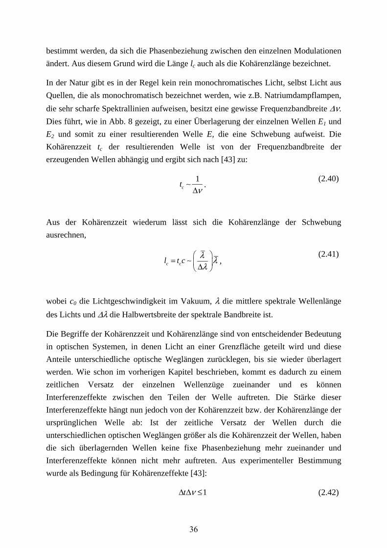
bestimmt werden, da sich die Phasenbeziehung zwischen den einzelnen Modulationen
ändert. Aus diesem Grund wird die Länge lc auch als die Kohärenzlänge bezeichnet.
In der Natur gibt es in der Regel kein rein monochromatisches Licht, selbst Licht aus
Quellen, die als monochromatisch bezeichnet werden, wie z.B. Natriumdampflampen,
die sehr scharfe Spektrallinien aufweisen, besitzt eine gewisse Frequenzbandbreite Δν.
Dies führt, wie in Abb. 8 gezeigt, zu einer Überlagerung der einzelnen Wellen E1 und
E2 und somit zu einer resultierenden Welle E, die eine Schwebung aufweist. Die
Kohärenzzeit tc der resultierenden Welle ist von der Frequenzbandbreite der
erzeugenden Wellen abhängig und ergibt sich nach [43] zu:
1ct νΔ .
(2.40)
Aus der Kohärenzzeit wiederum lässt sich die Kohärenzlänge der Schwebung
ausrechnen,
c cl t c
λ λλ
= Δ
, (2.41)
wobei c0 die Lichtgeschwindigkeit im Vakuum, λ die mittlere spektrale Wellenlänge
des Lichts und Δλ die Halbwertsbreite der spektrale Bandbreite ist.
Die Begriffe der Kohärenzzeit und Kohärenzlänge sind von entscheidender Bedeutung
in optischen Systemen, in denen Licht an einer Grenzfläche geteilt wird und diese
Anteile unterschiedliche optische Weglängen zurücklegen, bis sie wieder überlagert
werden. Wie schon im vorherigen Kapitel beschrieben, kommt es dadurch zu einem
zeitlichen Versatz der einzelnen Wellenzüge zueinander und es können
Interferenzeffekte zwischen den Teilen der Welle auftreten. Die Stärke dieser
Interferenzeffekte hängt nun jedoch von der Kohärenzzeit bzw. der Kohärenzlänge der
ursprünglichen Welle ab: Ist der zeitliche Versatz der Wellen durch die
unterschiedlichen optischen Weglängen größer als die Kohärenzzeit der Wellen, haben
die sich überlagernden Wellen keine fixe Phasenbeziehung mehr zueinander und
Interferenzeffekte können nicht mehr auftreten. Aus experimenteller Bestimmung
wurde als Bedingung für Kohärenzeffekte [43]:
1t νΔ Δ ≤ (2.42)
36
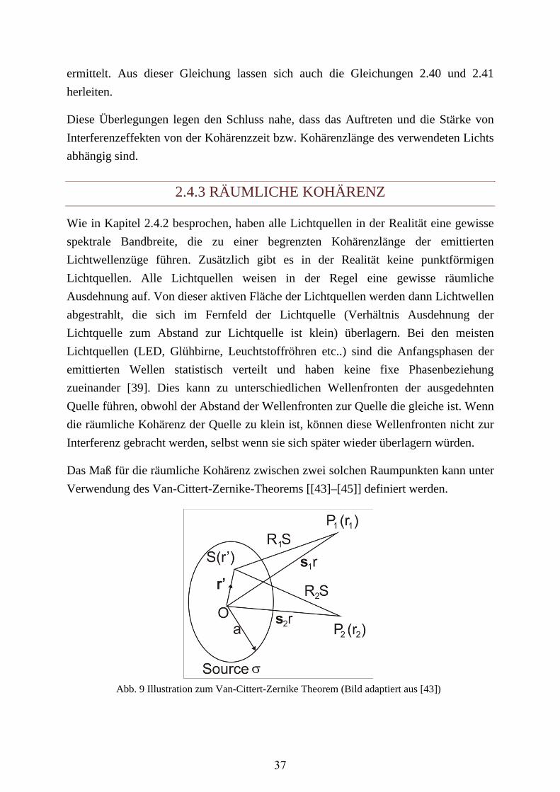
ermittelt. Aus dieser Gleichung lassen sich auch die Gleichungen 2.40 und 2.41
herleiten.
Diese Überlegungen legen den Schluss nahe, dass das Auftreten und die Stärke von
Interferenzeffekten von der Kohärenzzeit bzw. Kohärenzlänge des verwendeten Lichts
abhängig sind.
2.4.3 RÄUMLICHE KOHÄRENZ
Wie in Kapitel 2.4.2 besprochen, haben alle Lichtquellen in der Realität eine gewisse
spektrale Bandbreite, die zu einer begrenzten Kohärenzlänge der emittierten
Lichtwellenzüge führen. Zusätzlich gibt es in der Realität keine punktförmigen
Lichtquellen. Alle Lichtquellen weisen in der Regel eine gewisse räumliche
Ausdehnung auf. Von dieser aktiven Fläche der Lichtquellen werden dann Lichtwellen
abgestrahlt, die sich im Fernfeld der Lichtquelle (Verhältnis Ausdehnung der
Lichtquelle zum Abstand zur Lichtquelle ist klein) überlagern. Bei den meisten
Lichtquellen (LED, Glühbirne, Leuchtstoffröhren etc..) sind die Anfangsphasen der
emittierten Wellen statistisch verteilt und haben keine fixe Phasenbeziehung
zueinander [39]. Dies kann zu unterschiedlichen Wellenfronten der ausgedehnten
Quelle führen, obwohl der Abstand der Wellenfronten zur Quelle die gleiche ist. Wenn
die räumliche Kohärenz der Quelle zu klein ist, können diese Wellenfronten nicht zur
Interferenz gebracht werden, selbst wenn sie sich später wieder überlagern würden.
Das Maß für die räumliche Kohärenz zwischen zwei solchen Raumpunkten kann unter
Verwendung des Van-Cittert-Zernike-Theorems [[43]–[45]] definiert werden.
Abb. 9 Illustration zum Van-Cittert-Zernike Theorem (Bild adaptiert aus [43])
37
Es beschreibt die Korrelationen zwischen zwei Punkten P1 und P2 im Raum, die sich
in einem elektromagnetischen Feld einer monochromatischen, räumlich ausgedehnten
planen Quelle σ mit Radius a befindet. Monochromatisches Licht hat eine
Frequenzbandbreite Δν = 0 und bedeutet eigentlich unendliche zeitliche
Kohärenzlänge der Lichtwellenzüge. Aus diesem Grund kommt es zu keiner
Abschwächung der Interferenz durch zeitliche Kohärenzeffekte. Es wird zusätzlich
angenommen, dass die Phasen der Lichtwellen, die von der Fläche der Quelle emittiert
werden, nicht miteinander korrelieren − sondern statistisch verteilt sind. Durch die
Überlagerung der emittierten Lichtwellen bildet sich nun ein zeitlich verändertes
elektromagnetisches Feld, das von der Quelle ausgestrahlt wird. Das Van-Cittert-
Zernike-Theorem beschreibt nun den Grad der räumlichen Kohärenz j(r1, r2) zwischen
den zwei Punkten P1(r1) und P2(r2) [43]:
[ ] [ ]2 1( )
1 2 1/2 1/21 21 2
1( , ) ( ') ² '
2( ) ( )
ik R S R Sk ej I d r
R SR SI I σπ
− = r r r
r r
(2.43)
Dabei sind I(r1), I(r2) die Intensitäten an den Punkten r1 bzw. r2, I(r‘) die Intensität
entlang der Quelle σ, k die Wellenzahl und R1S bzw. R2S die Entfernung der Punkte
zur Quelle.
In den meisten Fällen sind die beiden Punkte P1 und P2 weit von der Quelle entfernt,
so dass sie sich im Fernfeld der Quelle befinden. Durch diese Näherung kann die
Gleichung 2.43 vereinfacht werden zu der Fernfeldform des Van-Cittert-Zernike-
Theorems, welches in der Publikation „Multiple Interfacing Between Classical Ray-
Tracing and Wave-Optical Simulation Approaches: A Study on Applicability and
Accuracy” verwendet wurde, um eine Kohärenz-Korrelation zwischen zwei Gittern zu
berechnen [43]:
2 1
2 1
( ) '
( )1 2
( ') ² '( , )
( ') ² '
ik
ik r rI e d r
j eI d r
σ
σ
− − ⋅−=
s s rrr r
r
(2.44)
Dabei sind r1 und r2 die Abstände der Punkte P1(r1) und P2(r2) zum Ursprung O sind
und s1 und s2 die Einheitsvektoren in Richtung der beiden Punkte. Weiters geht man
davon aus, dass sich der Ursprung O in der Mitte der Quelle σ befindet, dass die
Intensitätsverteilung der von der Quelle emittierten Wellen über die gesamte Fläche
der Quelle konstant ist (I(r‘) = konst.) und dass sich die beiden Punkte im gleichen
38
Abstand zur Mitte der Quelle befinden. Unter diesen Annahmen kann man Gleichung
2.44 weiter vereinfachen zu [43]:
2 1( ) '
'1 2
'
² '( , )
² '
ik
r a
r a
e d rj
d r
− − ⋅
≤
≤
=
s s r
r r . (2.45)
Das Integral aus Gleichung 2.45 kann mit Hilfe der Fraunhofer’schen Beugungstheorie
an einer kreisförmigen Apertur gelöst werden und führt zu:
11 2
2 ( )( , )
Jj
υυ
=r r , mit 12
ak d
rυ =
,
(2.46)
wobei J1(x) die Besselfunktion erster Art und erster Ordnung und d12 die Entfernung
zwischen den beiden Punkten P1(r1) und P2(r2) sind: Durch Gleichung 2.46 ist es nun
möglich, den Grad der räumlichen Kohärenz zwischen zwei Punkten im Raum zu
bestimmen. Ein Wert von υ = 0 ergibt j(r1, r2) = 1, was eine vollständige Kohärenz
und somit auch maximale Stärke der Interferenz zwischen den beiden Punkten P1 und
P2 bedeutet. Ein kleiner Wert für υ und somit eine hohe räumliche Kohärenz zwischen
den beiden Punkten kann erzeugt werden, indem entweder die Distanz d12 zwischen
den Punkten verringert wird oder das Verhältnis zwischen Ausdehnung der Quelle a
und dem Abstand der Punkte zur Quelle r verkleinert wird. Wenn d12 gegen 0 geht,
wird P1 zu P2 und die räumliche Kohärenzbeziehung wird maximal. Verkleinert man
die Ausdehnung der Quelle a mittels einer Blende, steigt die räumliche Kohärenz
ebenfalls. Aus diesem Grund hat eine Punktlichtquelle ohne Ausdehnung (a = 0) eine
maximale räumliche Kohärenz.
2.4.4 TEILKOHÄRENZ
Wie in den Kapiteln 2.4.3 und 2.4.4 ausgeführt, ist es möglich, das Ausmaß einer
möglichen Interferenz zwischen zwei Wellen bzw. den Feldern zwischen zwei
Punkten durch den Grad der Kohärenz zu bestimmen. Der Grad der zeitlichen
Kohärenz ist abhängig von der spektralen Bandbreite des Lichtes, der Grad der
räumlichen Kohärenz ist abhängig von der Ausdehnung der Quelle, dem Abstand zur
Quelle und dem Abstand der beiden Punkte, deren ausgehende Wellen zur Interferenz
gebracht werden. Reale Lichtquellen wie z.B. LEDs oder Glühbirnen haben sowohl
eine spektrale Bandbreite sowie eine räumliche Ausdehnung und sind dadurch
39
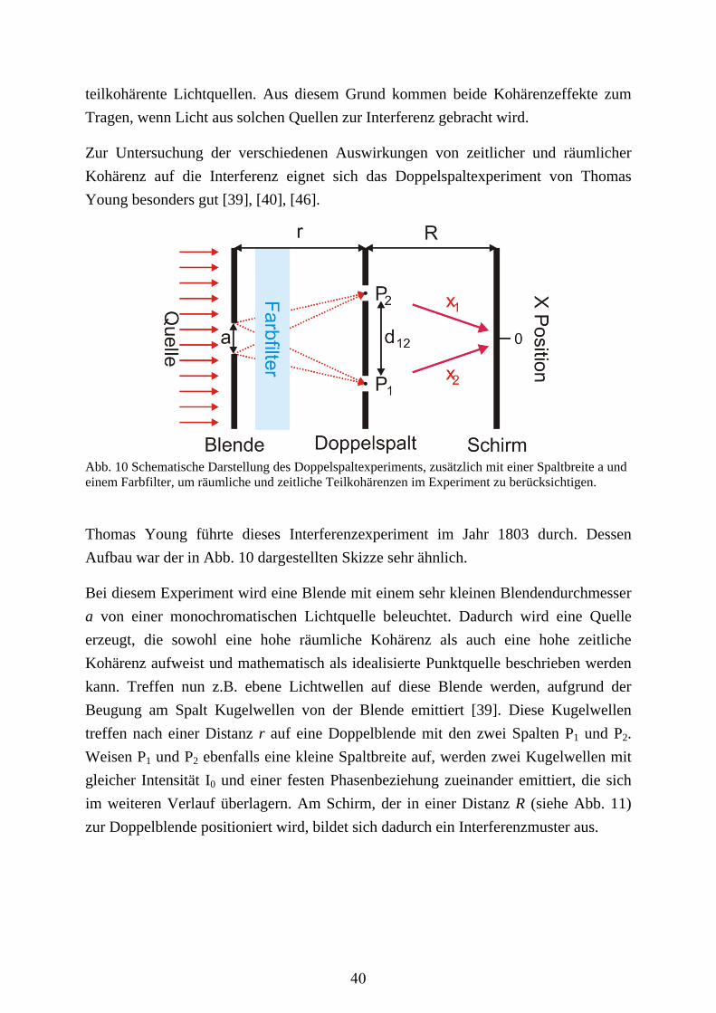
teilkohärente Lichtquellen. Aus diesem Grund kommen beide Kohärenzeffekte zum
Tragen, wenn Licht aus solchen Quellen zur Interferenz gebracht wird.
Zur Untersuchung der verschiedenen Auswirkungen von zeitlicher und räumlicher
Kohärenz auf die Interferenz eignet sich das Doppelspaltexperiment von Thomas
Young besonders gut [39], [40], [46].
Abb. 10 Schematische Darstellung des Doppelspaltexperiments, zusätzlich mit einer Spaltbreite a und einem Farbfilter, um räumliche und zeitliche Teilkohärenzen im Experiment zu berücksichtigen.
Thomas Young führte dieses Interferenzexperiment im Jahr 1803 durch. Dessen
Aufbau war der in Abb. 10 dargestellten Skizze sehr ähnlich.
Bei diesem Experiment wird eine Blende mit einem sehr kleinen Blendendurchmesser
a von einer monochromatischen Lichtquelle beleuchtet. Dadurch wird eine Quelle
erzeugt, die sowohl eine hohe räumliche Kohärenz als auch eine hohe zeitliche
Kohärenz aufweist und mathematisch als idealisierte Punktquelle beschrieben werden
kann. Treffen nun z.B. ebene Lichtwellen auf diese Blende werden, aufgrund der
Beugung am Spalt Kugelwellen von der Blende emittiert [39]. Diese Kugelwellen
treffen nach einer Distanz r auf eine Doppelblende mit den zwei Spalten P1 und P2.
Weisen P1 und P2 ebenfalls eine kleine Spaltbreite auf, werden zwei Kugelwellen mit
gleicher Intensität I0 und einer festen Phasenbeziehung zueinander emittiert, die sich
im weiteren Verlauf überlagern. Am Schirm, der in einer Distanz R (siehe Abb. 11)
zur Doppelblende positioniert wird, bildet sich dadurch ein Interferenzmuster aus.
40
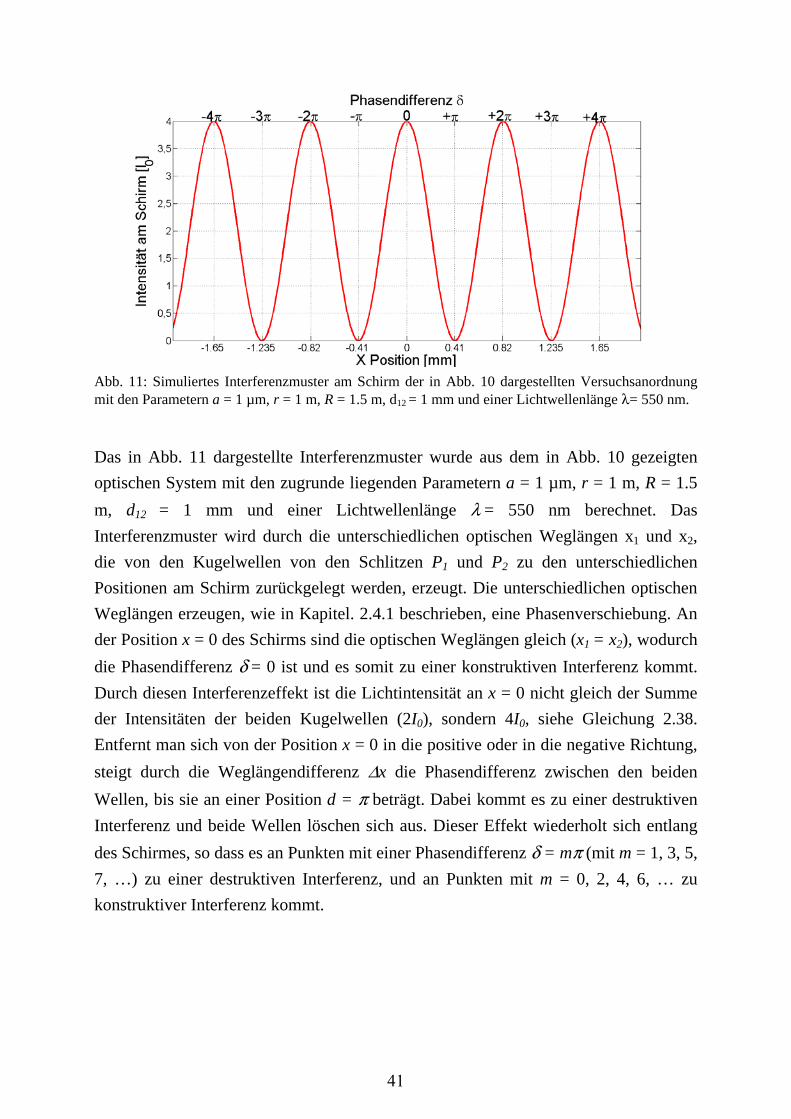
Abb. 11: Simuliertes Interferenzmuster am Schirm der in Abb. 10 dargestellten Versuchsanordnung mit den Parametern a = 1 µm, r = 1 m, R = 1.5 m, d12 = 1 mm und einer Lichtwellenlänge λ= 550 nm.
Das in Abb. 11 dargestellte Interferenzmuster wurde aus dem in Abb. 10 gezeigten
optischen System mit den zugrunde liegenden Parametern a = 1 µm, r = 1 m, R = 1.5
m, d12 = 1 mm und einer Lichtwellenlänge λ = 550 nm berechnet. Das
Interferenzmuster wird durch die unterschiedlichen optischen Weglängen x1 und x2,
die von den Kugelwellen von den Schlitzen P1 und P2 zu den unterschiedlichen
Positionen am Schirm zurückgelegt werden, erzeugt. Die unterschiedlichen optischen
Weglängen erzeugen, wie in Kapitel. 2.4.1 beschrieben, eine Phasenverschiebung. An
der Position x = 0 des Schirms sind die optischen Weglängen gleich (x1 = x2), wodurch
die Phasendifferenz δ = 0 ist und es somit zu einer konstruktiven Interferenz kommt.
Durch diesen Interferenzeffekt ist die Lichtintensität an x = 0 nicht gleich der Summe
der Intensitäten der beiden Kugelwellen (2I0), sondern 4I0, siehe Gleichung 2.38.
Entfernt man sich von der Position x = 0 in die positive oder in die negative Richtung,
steigt durch die Weglängendifferenz Δx die Phasendifferenz zwischen den beiden
Wellen, bis sie an einer Position d = π beträgt. Dabei kommt es zu einer destruktiven
Interferenz und beide Wellen löschen sich aus. Dieser Effekt wiederholt sich entlang
des Schirmes, so dass es an Punkten mit einer Phasendifferenz δ = mπ (mit m = 1, 3, 5,
7, …) zu einer destruktiven Interferenz, und an Punkten mit m = 0, 2, 4, 6, … zu
konstruktiver Interferenz kommt.
41
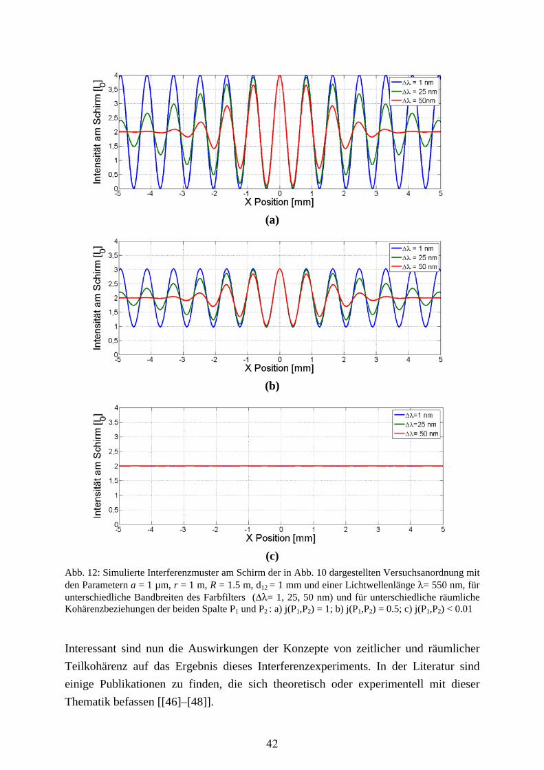
(a)
(b)
(c) Abb. 12: Simulierte Interferenzmuster am Schirm der in Abb. 10 dargestellten Versuchsanordnung mit den Parametern a = 1 µm, r = 1 m, R = 1.5 m, d12 = 1 mm und einer Lichtwellenlänge λ= 550 nm, für unterschiedliche Bandbreiten des Farbfilters (Δλ= 1, 25, 50 nm) und für unterschiedliche räumliche Kohärenzbeziehungen der beiden Spalte P1 und P2 : a) j(P1,P2) = 1; b) j(P1,P2) = 0.5; c) j(P1,P2) < 0.01
Interessant sind nun die Auswirkungen der Konzepte von zeitlicher und räumlicher
Teilkohärenz auf das Ergebnis dieses Interferenzexperiments. In der Literatur sind
einige Publikationen zu finden, die sich theoretisch oder experimentell mit dieser
Thematik befassen [[46]–[48]].
42
Um die verschiedenen Effekte zu veranschaulichen, wurden mittels Matlab-Skripts
numerische Simulationen des Experiments durchgeführt. Bei den numerischen
Simulationen wurde die Spaltbreite a der ersten Blende variiert, um unterschiedliche
räumliche Teilkohärenzen der Lichtquelle zu erzeugen. Zusätzlich wurde ein Farbfilter
mit einer mittleren Wellenlänge 550λ = nm und verschiedenen Bandbreiten (Δλ= 1,
25, 50 nm) verwendet, was zu unterschiedlichen zeitlichen Teilkohärenzen des Lichts
führt.
Im ersten Fall wurde das Verhältnis zwischen der Spaltbreite a und der Distanz der
Blende zum Doppelgitter r so gewählt, dass man von einer räumlich kohärenten
Quelle ausgehen kann. Die Simulation des Doppelgittersystems wurde für drei
unterschiedliche Bandbreiten des Farbfilters durchgeführt: Δλ = 1 nm, Δλ = 25 nm,
Δλ = 50 nm, wobei die resultierenden Simulationsergebnisse in Abb. 12a dargestellt
wurden. Eine Bandbreite Δλ = 1 nm hat eine hohe zeitliche Kohärenz, aus diesem
Grund weist das Ergebnis eine große Ähnlichkeit mit dem aus Abb. 11 auf. Bei den
Bandbreiten Δλ = 25 nm und Δλ = 50 nm ist nur mehr eine zeitliche
Teilkohärenzlänge vorhanden. Dies führt offensichtlich zu dem Resultat, dass das
Ausmaß der Interferenzeffekte mit steigender Phasendifferenz δ = mπ für hohe m
abnimmt. Mit steigendem Abstand zur x = 0 Position ergibt sich eine Intensität von
2I0, was einer inkohärenten Überlagerung der Intensitäten I0 der beiden Kugelwellen
entspricht. Am Punkt x = 0 jedoch, wo die Phasendifferenz δ = 0 beträgt, überlagern
sich alle Wellen perfekt, so dass die unterschiedlichen Kohärenzlängen der einzelnen
Lichtquellen keinen Einfluss auf die Stärke der Interferenz ausüben. Berechnet man
sich die Kohärenzlänge lc für die Quelle mit der Bandbreite Δλ = 50 nm aus
Gleichung 2.41, kann man feststellen, dass diese nur 6.05 µm bzw. 11 Wellenzüge
beträgt. Dies entspricht dementsprechend auch genau der Ausdehnung des
Interferenzmusters aus Abb. 12a für den Fall Δλ = 50 nm.
Für die Ergebnisse, die in Abb. 12b und Abb. 12c dargestellt sind, wurde das
Verhältnis zwischen der Spaltbreite a und der Distanz der Blende zum Doppelgitter r
so gewählt, dass die räumliche Kohärenzbeziehung j(r1, r2) zwischen den beiden
Spalten P1 und P2 0.5 für Abb. 12b bzw. < 0.01 für Abb. 12c ergibt. Betrachtet man
wieder die Intensität am Punkt x = 0 in Abb. 12b, wo die zeitliche Teilkohärenz der
einzelnen Quellen keinen Einfluss auf die Stärke der Interferenz hat, da die Weglängen
von P1 und P2 exakt gleich lang sind, kann man erkennen, dass die Intensität nun den
Wert I = 3I0 aufweist. Dieser Effekt ist auf die räumliche Teilkohärenz der Lichtquelle
zurückzuführen, die die maximale Stärke der Interferenz am Schirm festlegt. Aufgrund
43
der Tatsache, dass j(r1, r2) in diesem Fall den Wert 0.5 hat, kann auch die maximale
Verstärkung bzw. Abschwächung der Intensität durch Interferenzeffekte nur 50%
betragen (vergleiche Abb. 12a mit j(r1, r2) = 1).
Dies wird in Abb. 12c noch stärker verdeutlicht, wo j(r1, r2) < 0.01 ist. Hier ist es
unabhängig von der zeitlichen Teilkohärenz der Lichtquelle, sogar möglich, die
Interferenzeffekte zu vernachlässigen, so dass die Intensität in jedem Punkt am Schirm
eine Addition der beiden Intensitäten der Kugelwellen ist. Daraus kann man schließen,
dass Wellen emittiert von Lichtquellen mit niedriger zeitlicher Kohärenz an
bestimmten Punkten, an denen die Phasendifferenz zwischen den Wellen δ = 0 ist,
noch interferieren können. Für Lichtquellen mit niedriger räumlicher Kohärenz können
aber keine Interferenzeffekte mehr auftreten.
2.4.5 BEUGUNGSGITTER
In allen optischen Systemen der im Rahmen dieser Dissertation verfassten
Publikationen spielen Beugungsgitter eine zentrale Rolle. Aus diesem Grund wird in
diesem Kapitel auf die Funktionsweise dieses optischen Bauelements etwas näher
eingegangen. Durch die vielseitige Einsetzbarkeit von Beugungsgittern in optischen
Systemen gibt es umfangreiche Fachliteratur, die sich ausschließlich mit den Effekten
und den Herstellungsmethoden dieser Beugungsgitter beschäftigt [49].
Ein Beugungsgitter ist ein wichtiges optisches Bauteil, das aus einer regelmäßigen
Anordnung von optischen Strukturen besteht, die eine periodische Änderung der
Amplitude oder der Phase einer eintreffenden ebenen Welle verursachen, wobei die
geometrische Größe der Strukturen eine wichtige Rolle spielt. [39].
Dies kann durch eine periodische Anordnung von Spalten in einer Blende erfolgen,
wodurch Teile der ebenen Welle, die auf die Blende treffen, absorbiert werden. Die
ebene Welle erfährt hierdurch eine periodische Modulation ihrer Amplituden, was zu
Interferenzeffekten hinter der Blende führt. Solche Gitter, die auf Absorption von
Teilen der einfallenden Welle beruhen, nennt man Transmissions-Amplituden-Gitter
[39].
Eine andere Möglichkeit, ein Beugungsgitter zu realisieren, stellt das Phasen-
Transmissions- Gitter dar. Bei dieser Art von Beugungsgitter wird eine periodische
Struktur auf eine Oberfläche aufgebracht, wodurch eine periodische Änderung des
Brechungsindex erzeugt wird (Material zu Umgebungsmedium). Dadurch wird eine
unterschiedliche optische Weglänge zwischen Wellen, die durch die Struktur laufen,
44
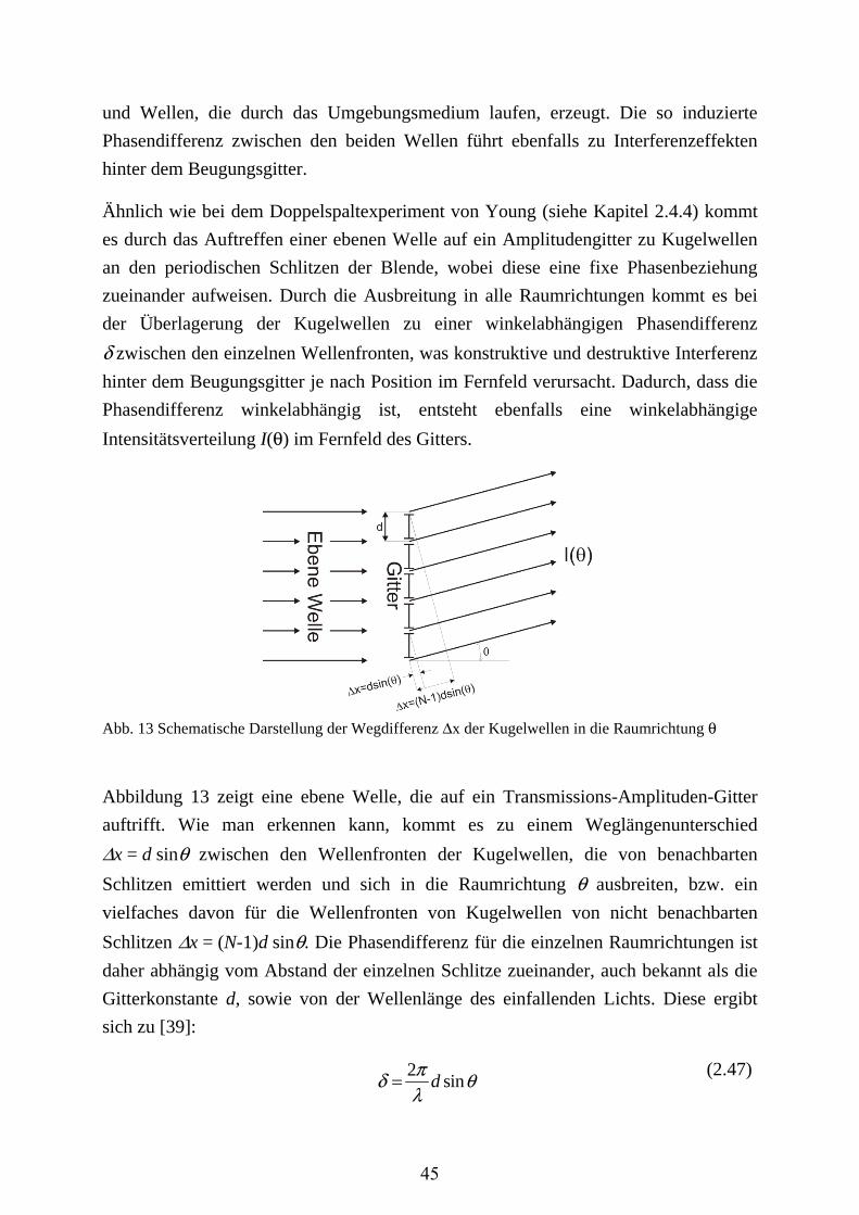
und Wellen, die durch das Umgebungsmedium laufen, erzeugt. Die so induzierte
Phasendifferenz zwischen den beiden Wellen führt ebenfalls zu Interferenzeffekten
hinter dem Beugungsgitter.
Ähnlich wie bei dem Doppelspaltexperiment von Young (siehe Kapitel 2.4.4) kommt
es durch das Auftreffen einer ebenen Welle auf ein Amplitudengitter zu Kugelwellen
an den periodischen Schlitzen der Blende, wobei diese eine fixe Phasenbeziehung
zueinander aufweisen. Durch die Ausbreitung in alle Raumrichtungen kommt es bei
der Überlagerung der Kugelwellen zu einer winkelabhängigen Phasendifferenz
δ zwischen den einzelnen Wellenfronten, was konstruktive und destruktive Interferenz
hinter dem Beugungsgitter je nach Position im Fernfeld verursacht. Dadurch, dass die
Phasendifferenz winkelabhängig ist, entsteht ebenfalls eine winkelabhängige
Intensitätsverteilung I(θ) im Fernfeld des Gitters.
Abb. 13 Schematische Darstellung der Wegdifferenz Δx der Kugelwellen in die Raumrichtung θ
Abbildung 13 zeigt eine ebene Welle, die auf ein Transmissions-Amplituden-Gitter
auftrifft. Wie man erkennen kann, kommt es zu einem Weglängenunterschied
Δx = d sinθ zwischen den Wellenfronten der Kugelwellen, die von benachbarten
Schlitzen emittiert werden und sich in die Raumrichtung θ ausbreiten, bzw. ein
vielfaches davon für die Wellenfronten von Kugelwellen von nicht benachbarten
Schlitzen Δx = (N-1)d sinθ. Die Phasendifferenz für die einzelnen Raumrichtungen ist
daher abhängig vom Abstand der einzelnen Schlitze zueinander, auch bekannt als die
Gitterkonstante d, sowie von der Wellenlänge des einfallenden Lichts. Diese ergibt
sich zu [39]:
2sind
πδ θλ
= (2.47)
45
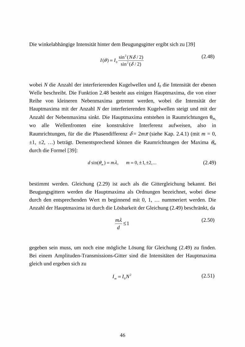
Die winkelabhängige Intensität hinter dem Beugungsgitter ergibt sich zu [39]
2
0 2
sin ( / 2)( )
sin ( / 2)
NI I
δθδ
= (2.48)
wobei N die Anzahl der interferierenden Kugelwellen und I0 die Intensität der ebenen
Welle beschreibt. Die Funktion 2.48 besteht aus einigen Hauptmaxima, die von einer
Reihe von kleineren Nebenmaxima getrennt werden, wobei die Intensität der
Hauptmaxima mit der Anzahl N der interferierenden Kugelwellen steigt und mit der
Anzahl der Nebenmaxima sinkt. Die Hauptmaxima entstehen in Raumrichtungen θm,
wo alle Wellenfronten eine konstruktive Interferenz aufweisen, also in
Raumrichtungen, für die die Phasendifferenz δ = 2mπ (siehe Kap. 2.4.1) (mit m = 0,
±1, ±2, …) beträgt. Dementsprechend können die Raumrichtungen der Maxima θm
durch die Formel [39]:
sin( ) , 0, 1, 2,...md m mθ λ= = ± ± (2.49)
bestimmt werden. Gleichung (2.29) ist auch als die Gittergleichung bekannt. Bei
Beugungsgittern werden die Hauptmaxima als Ordnungen bezeichnet, wobei diese
durch den entsprechenden Wert m beginnend mit 0, 1, … nummeriert werden. Die
Anzahl der Hauptmaxima ist durch die Lösbarkeit der Gleichung (2.49) beschränkt, da
1
m
d
λ ≤ (2.50)
gegeben sein muss, um noch eine mögliche Lösung für Gleichung (2.49) zu finden.
Bei einem Amplituden-Transmissions-Gitter sind die Intensitäten der Hauptmaxima
gleich und ergeben sich zu
20mI I N= (2.51)
46
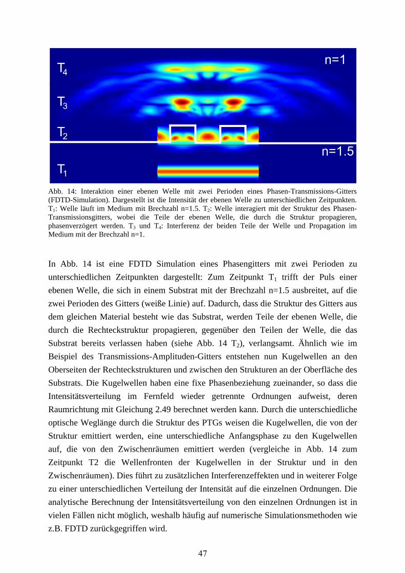
Abb. 14: Interaktion einer ebenen Welle mit zwei Perioden eines Phasen-Transmissions-Gitters (FDTD-Simulation). Dargestellt ist die Intensität der ebenen Welle zu unterschiedlichen Zeitpunkten. T1: Welle läuft im Medium mit Brechzahl n=1.5. T2: Welle interagiert mit der Struktur des Phasen-Transmissionsgitters, wobei die Teile der ebenen Welle, die durch die Struktur propagieren, phasenverzögert werden. T3 und T4: Interferenz der beiden Teile der Welle und Propagation im Medium mit der Brechzahl n=1.
In Abb. 14 ist eine FDTD Simulation eines Phasengitters mit zwei Perioden zu
unterschiedlichen Zeitpunkten dargestellt: Zum Zeitpunkt T1 trifft der Puls einer
ebenen Welle, die sich in einem Substrat mit der Brechzahl n=1.5 ausbreitet, auf die
zwei Perioden des Gitters (weiße Linie) auf. Dadurch, dass die Struktur des Gitters aus
dem gleichen Material besteht wie das Substrat, werden Teile der ebenen Welle, die
durch die Rechteckstruktur propagieren, gegenüber den Teilen der Welle, die das
Substrat bereits verlassen haben (siehe Abb. 14 T2), verlangsamt. Ähnlich wie im
Beispiel des Transmissions-Amplituden-Gitters entstehen nun Kugelwellen an den
Oberseiten der Rechteckstrukturen und zwischen den Strukturen an der Oberfläche des
Substrats. Die Kugelwellen haben eine fixe Phasenbeziehung zueinander, so dass die
Intensitätsverteilung im Fernfeld wieder getrennte Ordnungen aufweist, deren
Raumrichtung mit Gleichung 2.49 berechnet werden kann. Durch die unterschiedliche
optische Weglänge durch die Struktur des PTGs weisen die Kugelwellen, die von der
Struktur emittiert werden, eine unterschiedliche Anfangsphase zu den Kugelwellen
auf, die von den Zwischenräumen emittiert werden (vergleiche in Abb. 14 zum
Zeitpunkt T2 die Wellenfronten der Kugelwellen in der Struktur und in den
Zwischenräumen). Dies führt zu zusätzlichen Interferenzeffekten und in weiterer Folge
zu einer unterschiedlichen Verteilung der Intensität auf die einzelnen Ordnungen. Die
analytische Berechnung der Intensitätsverteilung von den einzelnen Ordnungen ist in
vielen Fällen nicht möglich, weshalb häufig auf numerische Simulationsmethoden wie
z.B. FDTD zurückgegriffen wird.
47
3. WISSENSCHAFTLICHE ARBEIT
3.1 VERÖFFENTLICHTE PUBLIKATIONEN
3.1.1 A SIMULATION PROCEDURE FOR LIGHT-MATTER
INTERACTION AT DIFFERENT LENGTH SCALES
”A Simulation Procedure for Light-Matter Interaction at Different Length Scales”
wurde im Rahmen der Konferenz SPIE Photonics Europe 2012 verfasst und als
Proceeding-Artikel in Proc. SPIE 8429, Optical Modelling and Design II, 84290L
(June 1, 2012) veröffentlicht. Zusätzlich wurde ein Vortrag im Konferenzzeitraum 16.-
19. April 2012 in Brüssel gehalten. Der eigene Anteil bei dieser Veröffentlichung
beträgt 70%.
In dieser Veröffentlichung wird das Transmissionsverhalten von Auskoppelstrukturen
mit verschiedenen Strukturgrößen Λ mit den beiden unterschiedlichen
Simulationsprogrammen ASAP (Ray-Tracing Programm von Breault Research) und
FDTD Solutions (Finite Difference Time Domain Programm von Lumerical)
untersucht, um Unterschiede zwischen den beiden Simulationstechniken aufzuzeigen.
Für diese Simulation wurden Lichtstrahlen im RT-Programm, bzw. Lichtwellen im
FDTD-Programm, in einem optischen Medium der Brechzahl n = 1.5 erzeugt und
unter verschiedenen Einfallswinkeln in Richtung der unterschiedlichen
Auskoppelstrukturen emittiert. Die Intensität des transmittierten (aus der
Auskopplungsstruktur ausgetretenen) Lichtflusses wurde durch Detektoren mit den
jeweiligen Simulationsprogrammen ermittelt und miteinander verglichen. Anhand
dieser Untersuchungen kann gezeigt werden, wie sich das Transmissionsverhalten von
Auskoppelstrukturen in Abhängigkeit ihrer Strukturgrößen durch wellenoptische
Effekte ändert.
Zusätzlich wird in dieser Veröffentlichung ein Ansatz untersucht, die bereits zwischen
ASAP und FDTD implementierte Schnittstelle zu erweitern, um auch großflächige
Phasen-Transmissions-Gitter simulieren zu können.
48
A SIMULATION PROCEDURE FOR LIGHT-MATTER INTERACTION AT DIFFERENT LENGTH SCALES
Claude Leiner1, Wolfgang Nemitz1, Franz P. Wenzl1, Paul Hartmann1, Ulrich Hohenester2,
Christian Sommer1
1 Institute of Surface Technologies and Photonics, Joanneum Research Forschungsges.m.b.H, Franz-Pichler Straße 30, A-8160 Weiz, Austria
2 Institute of Physics, Karl-Franzens-University Graz, Universitätsplatz 5, A-8010 Graz, Austria
ABSTRACT
The development of photonic devices with tailor-made optical properties requires the control and the manipulation of light propagation within structures of different length scales, ranging from sub-wavelength to macroscopic dimensions. However, optical simulation at different length scales necessitates the combination of different simulation methods, which have to account properly for various effects such as polarization, interference, or diffraction: At dimensions much larger than the wavelength of light common ray-tracing (RT) techniques are conveniently employed, while in the sub-wavelength regime more sophisticated approaches, like the so-called finite-difference time-domain (FDTD) technique, are needed. Describing light propagation both in the sub-wavelength regime as well as at macroscopic length scales can only be achieved by bridging between these two approaches. In this contribution we present on the one hand a study aiming at the determination of the intermediate size range for which both simulation methods are applicable and on the other hand an approach for combining classical ray-tracing with FDTD simulation in order to handle optical elements of large sizes. Generally, the interface between RT and FDTD is restricted to very small sample areas. Nevertheless, many real world optical devices use e.g. diffractive optical elements (DOEs) having comparably large areas in the order of 1-2 mm² (or larger). Therefore, one has to develop strategies in order to handle the data transfer between FDTD and RT also for structures of such larger size scales. Our approach in this regard is based on the symmetries of the structures. In this way support programs like e.g. MATLAB can be used to replicate the near-field of a single structure and to merge it to the near-field of a larger area. Comparisons of RT and FDTD simulations in the far-field can be used to validate the physical correctness of this approach. With such procedure it is possible to optimize light propagation effects at both the macro- and microscale and to exploit their whole potential for the manipulation and optimization of optical and photonic devices. Keywords: Optical Simulation, Ray-Tracing, FDTD,DOE
1. INTRODUCTION Diffractive optical elements (DOEs) with customized optical properties become more and more important as an integrated part for a lot of micro optical and photonic devices [1] operating in the visible range of electromagnetic waves. The design and optimization of such structures requires a combination of optical ray-tracing (RT) methods and finite-difference-time-domain (FDTD) techniques in order to consider all optical aspects (coherent and incoherent). In the context of optical simulation of indoor radio wave propagation for, e.g., wireless LAN, the combination of RT and FDTD simulation algorithms has been successfully shown for radio waves in [2-3]. Similar to radio wave applications, optical RT methods are insufficient for an appropriate simulation of optical and photonic devices that contain diffractive structures for the visible range of the electromagnetic spectrum. For a proper description of such structures FDTD techniques taking wave optical phenomena into account are necessary in addition. In this case the Maxwell equations are solved at the mesh points of the discretized simulation area. For the design and optimization of optical devices it is therefore essential to provide a simulation technique that allows for a comprehensive simulation of all the individual components the device is built of. In this context, e.g. studies on the ranges of applicability for the different simulation techniques and the respective interface for data transfer from one
49
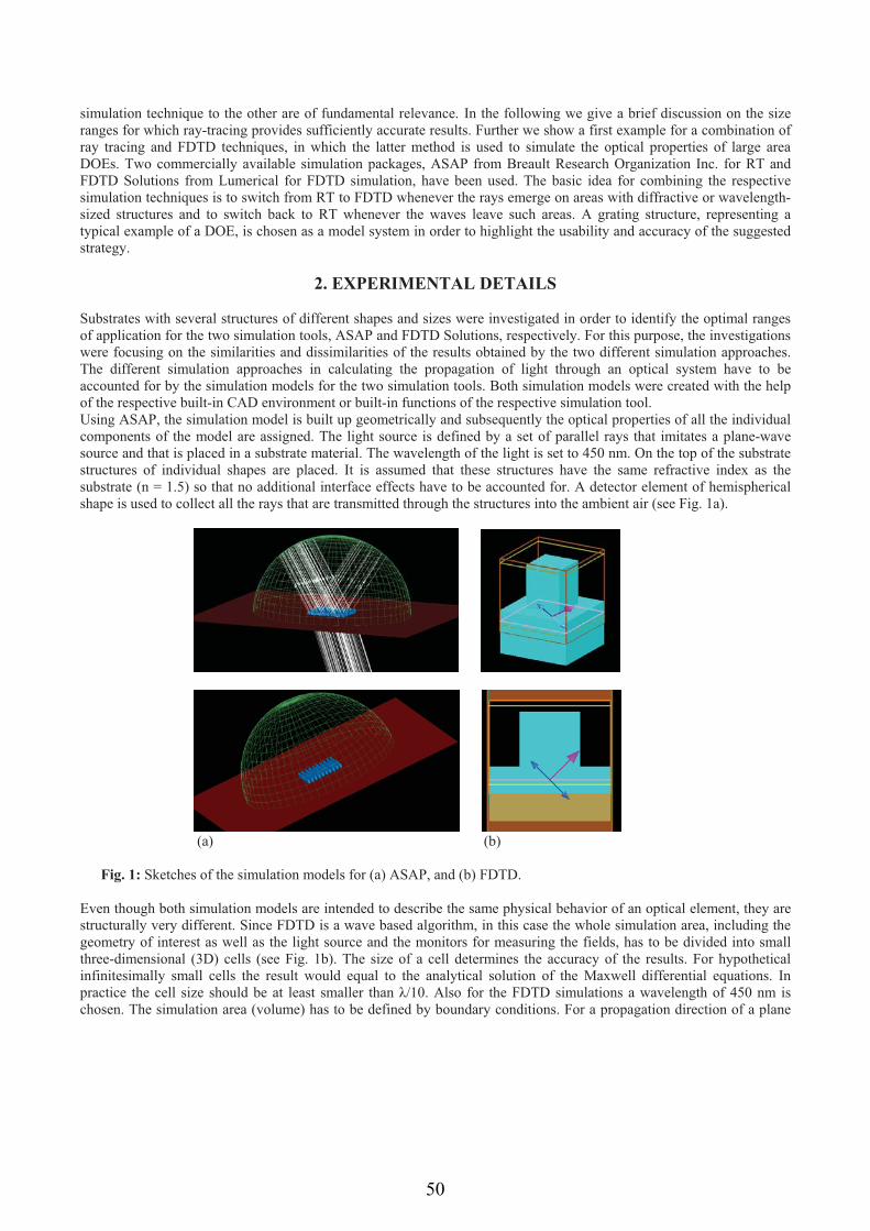
simulation technique to the other are of fundamental relevance. In the following we give a brief discussion on the size ranges for which ray-tracing provides sufficiently accurate results. Further we show a first example for a combination of ray tracing and FDTD techniques, in which the latter method is used to simulate the optical properties of large area DOEs. Two commercially available simulation packages, ASAP from Breault Research Organization Inc. for RT and FDTD Solutions from Lumerical for FDTD simulation, have been used. The basic idea for combining the respective simulation techniques is to switch from RT to FDTD whenever the rays emerge on areas with diffractive or wavelength-sized structures and to switch back to RT whenever the waves leave such areas. A grating structure, representing a typical example of a DOE, is chosen as a model system in order to highlight the usability and accuracy of the suggested strategy.
2. EXPERIMENTAL DETAILS Substrates with several structures of different shapes and sizes were investigated in order to identify the optimal ranges of application for the two simulation tools, ASAP and FDTD Solutions, respectively. For this purpose, the investigations were focusing on the similarities and dissimilarities of the results obtained by the two different simulation approaches. The different simulation approaches in calculating the propagation of light through an optical system have to be accounted for by the simulation models for the two simulation tools. Both simulation models were created with the help of the respective built-in CAD environment or built-in functions of the respective simulation tool. Using ASAP, the simulation model is built up geometrically and subsequently the optical properties of all the individual components of the model are assigned. The light source is defined by a set of parallel rays that imitates a plane-wave source and that is placed in a substrate material. The wavelength of the light is set to 450 nm. On the top of the substrate structures of individual shapes are placed. It is assumed that these structures have the same refractive index as the substrate (n = 1.5) so that no additional interface effects have to be accounted for. A detector element of hemispherical shape is used to collect all the rays that are transmitted through the structures into the ambient air (see Fig. 1a).
(a) (b)
Fig. 1: Sketches of the simulation models for (a) ASAP, and (b) FDTD.
Even though both simulation models are intended to describe the same physical behavior of an optical element, they are structurally very different. Since FDTD is a wave based algorithm, in this case the whole simulation area, including the geometry of interest as well as the light source and the monitors for measuring the fields, has to be divided into small three-dimensional (3D) cells (see Fig. 1b). The size of a cell determines the accuracy of the results. For hypothetical infinitesimally small cells the result would equal to the analytical solution of the Maxwell differential equations. In practice the cell size should be at least smaller than �/10. Also for the FDTD simulations a wavelength of 450 nm is chosen. The simulation area (volume) has to be defined by boundary conditions. For a propagation direction of a plane
50
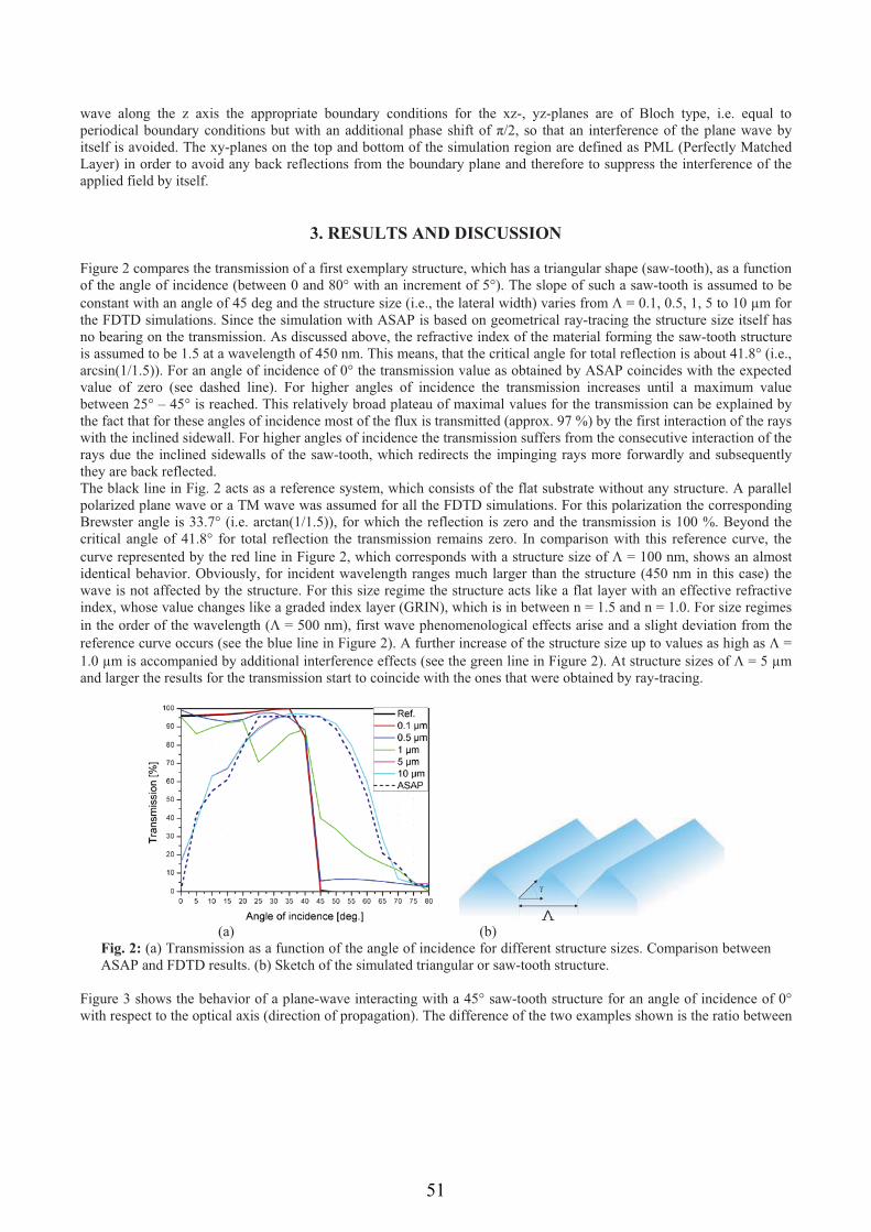
wave along the z axis the appropriate boundary conditions for the xz-, yz-planes are of Bloch type, i.e. equal to periodical boundary conditions but with an additional phase shift of �/2, so that an interference of the plane wave by itself is avoided. The xy-planes on the top and bottom of the simulation region are defined as PML (Perfectly Matched Layer) in order to avoid any back reflections from the boundary plane and therefore to suppress the interference of the applied field by itself.
3. RESULTS AND DISCUSSION Figure 2 compares the transmission of a first exemplary structure, which has a triangular shape (saw-tooth), as a function of the angle of incidence (between 0 and 80° with an increment of 5°). The slope of such a saw-tooth is assumed to be constant with an angle of 45 deg and the structure size (i.e., the lateral width) varies from � = 0.1, 0.5, 1, 5 to 10 μm for the FDTD simulations. Since the simulation with ASAP is based on geometrical ray-tracing the structure size itself has no bearing on the transmission. As discussed above, the refractive index of the material forming the saw-tooth structure is assumed to be 1.5 at a wavelength of 450 nm. This means, that the critical angle for total reflection is about 41.8° (i.e., arcsin(1/1.5)). For an angle of incidence of 0° the transmission value as obtained by ASAP coincides with the expected value of zero (see dashed line). For higher angles of incidence the transmission increases until a maximum value between 25° – 45° is reached. This relatively broad plateau of maximal values for the transmission can be explained by the fact that for these angles of incidence most of the flux is transmitted (approx. 97 %) by the first interaction of the rays with the inclined sidewall. For higher angles of incidence the transmission suffers from the consecutive interaction of the rays due the inclined sidewalls of the saw-tooth, which redirects the impinging rays more forwardly and subsequently they are back reflected. The black line in Fig. 2 acts as a reference system, which consists of the flat substrate without any structure. A parallel polarized plane wave or a TM wave was assumed for all the FDTD simulations. For this polarization the corresponding Brewster angle is 33.7° (i.e. arctan(1/1.5)), for which the reflection is zero and the transmission is 100 %. Beyond the critical angle of 41.8° for total reflection the transmission remains zero. In comparison with this reference curve, the curve represented by the red line in Figure 2, which corresponds with a structure size of � = 100 nm, shows an almost identical behavior. Obviously, for incident wavelength ranges much larger than the structure (450 nm in this case) the wave is not affected by the structure. For this size regime the structure acts like a flat layer with an effective refractive index, whose value changes like a graded index layer (GRIN), which is in between n = 1.5 and n = 1.0. For size regimes in the order of the wavelength (� = 500 nm), first wave phenomenological effects arise and a slight deviation from the reference curve occurs (see the blue line in Figure 2). A further increase of the structure size up to values as high as � = 1.0 μm is accompanied by additional interference effects (see the green line in Figure 2). At structure sizes of � = 5 μm and larger the results for the transmission start to coincide with the ones that were obtained by ray-tracing.
(a) (b) Fig. 2: (a) Transmission as a function of the angle of incidence for different structure sizes. Comparison between ASAP and FDTD results. (b) Sketch of the simulated triangular or saw-tooth structure.
Figure 3 shows the behavior of a plane-wave interacting with a 45° saw-tooth structure for an angle of incidence of 0° with respect to the optical axis (direction of propagation). The difference of the two examples shown is the ratio between
51
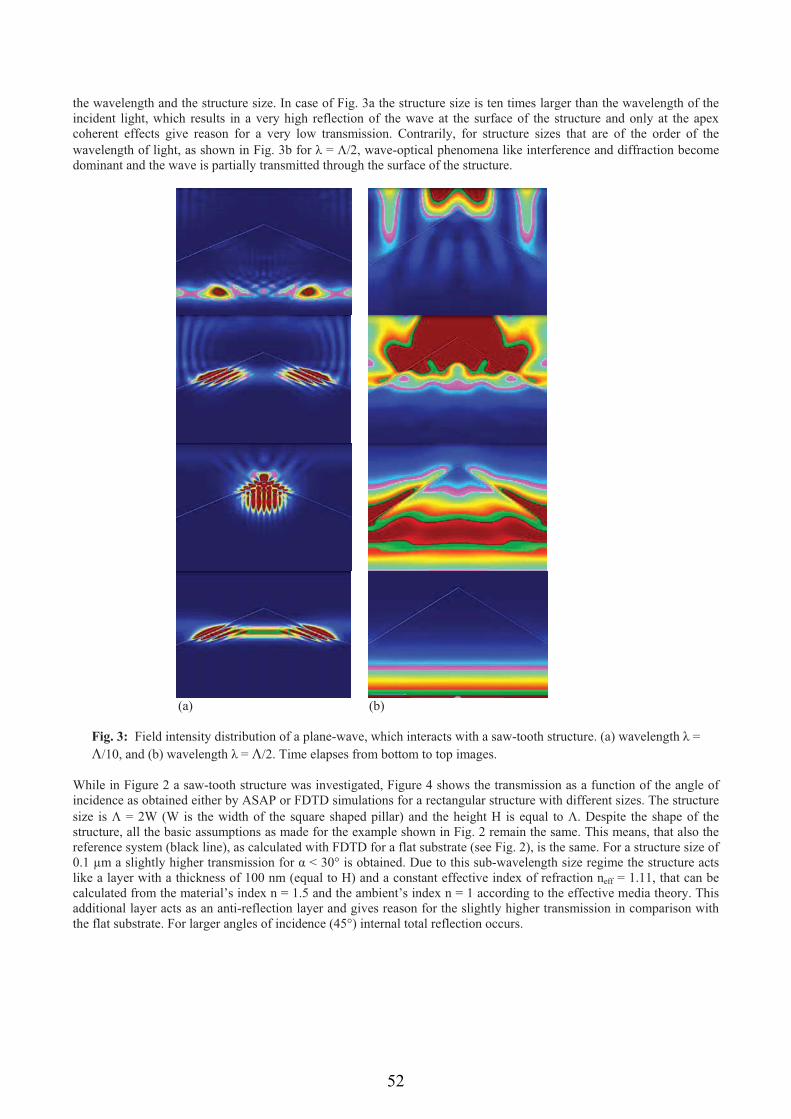
the wavelength and the structure size. In case of Fig. 3a the structure size is ten times larger than the wavelength of the incident light, which results in a very high reflection of the wave at the surface of the structure and only at the apex coherent effects give reason for a very low transmission. Contrarily, for structure sizes that are of the order of the wavelength of light, as shown in Fig. 3b for � = �/2, wave-optical phenomena like interference and diffraction become dominant and the wave is partially transmitted through the surface of the structure.
(a) (b)
Fig. 3: Field intensity distribution of a plane-wave, which interacts with a saw-tooth structure. (a) wavelength � = �/10, and (b) wavelength � = �/2. Time elapses from bottom to top images.
While in Figure 2 a saw-tooth structure was investigated, Figure 4 shows the transmission as a function of the angle of incidence as obtained either by ASAP or FDTD simulations for a rectangular structure with different sizes. The structure size is � = 2W (W is the width of the square shaped pillar) and the height H is equal to �. Despite the shape of the structure, all the basic assumptions as made for the example shown in Fig. 2 remain the same. This means, that also the reference system (black line), as calculated with FDTD for a flat substrate (see Fig. 2), is the same. For a structure size of 0.1 μm a slightly higher transmission for � < 30° is obtained. Due to this sub-wavelength size regime the structure acts like a layer with a thickness of 100 nm (equal to H) and a constant effective index of refraction neff = 1.11, that can be calculated from the material’s index n = 1.5 and the ambient’s index n = 1 according to the effective media theory. This additional layer acts as an anti-reflection layer and gives reason for the slightly higher transmission in comparison with the flat substrate. For larger angles of incidence (45°) internal total reflection occurs.
52
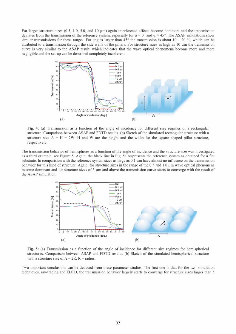
For larger structure sizes (0.5, 1.0, 5.0, and 10 μm) again interference effects become dominant and the transmission deviates from the transmission of the reference system, especially for � = 0° and � > 45°. The ASAP simulations show similar transmissions for these ranges. For angles larger than 45° the transmission is about 10 – 20 %, which can be attributed to a transmission through the side walls of the pillars. For structure sizes as high as 10 μm the transmission curve is very similar to the ASAP result, which indicates that the wave optical phenomena become more and more negligible and the set-up can be described completely incoherent.
(a) (b)
Fig. 4: (a) Transmission as a function of the angle of incidence for different size regimes of a rectangular structure. Comparison between ASAP and FDTD results. (b) Sketch of the simulated rectangular structure with a structure size � = H = 2W. H and W are the height and the width for the square shaped pillar structure, respectively.
The transmission behavior of hemispheres as a function of the angle of incidence and the structure size was investigated as a third example, see Figure 5. Again, the black line in Fig. 5a respresents the reference system as obtained for a flat substrate. In comparision with the reference system sizes as large as 0.1 μm have almost no influence on the transmission behavior for this kind of structure. Again, for structure sizes in the range of the 0.5 and 1.0 μm wave optical phenomena become dominant and for structure sizes of 5 μm and above the transmission curve starts to converge with the result of the ASAP simulation.
(a) (b)
Fig. 5: (a) Transmission as a function of the angle of incidence for different size regimes for hemispherical structures. Comparison between ASAP and FDTD results. (b) Sketch of the simulated hemispherical structure with a structure size of � = 2R, R = radius.
Two important conclusions can be deduced from these parameter studies. The first one is that for the two simulation techniques, ray-tracing and FDTD, the transmission behavior largely starts to converge for structure sizes larger than 5
53
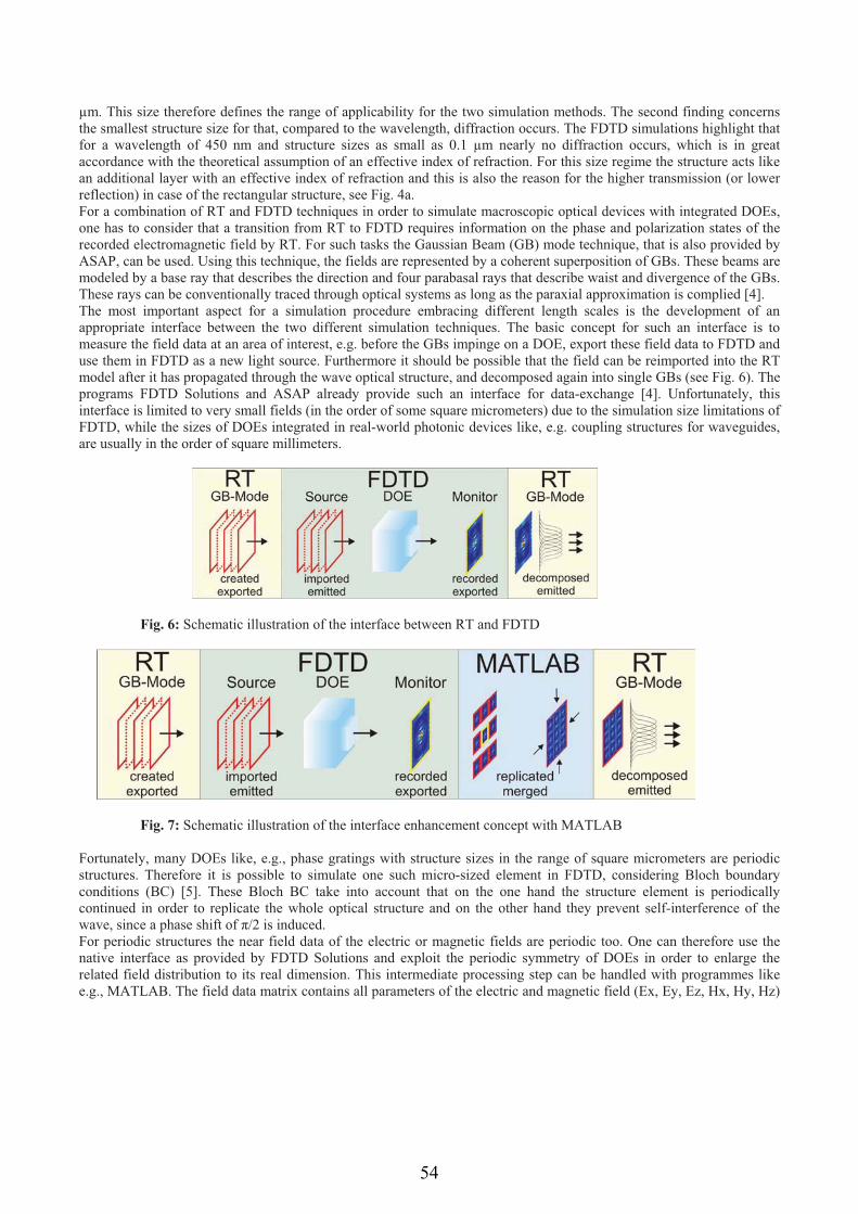
μm. This size therefore defines the range of applicability for the two simulation methods. The second finding concerns the smallest structure size for that, compared to the wavelength, diffraction occurs. The FDTD simulations highlight that for a wavelength of 450 nm and structure sizes as small as 0.1 μm nearly no diffraction occurs, which is in great accordance with the theoretical assumption of an effective index of refraction. For this size regime the structure acts like an additional layer with an effective index of refraction and this is also the reason for the higher transmission (or lower reflection) in case of the rectangular structure, see Fig. 4a. For a combination of RT and FDTD techniques in order to simulate macroscopic optical devices with integrated DOEs, one has to consider that a transition from RT to FDTD requires information on the phase and polarization states of the recorded electromagnetic field by RT. For such tasks the Gaussian Beam (GB) mode technique, that is also provided by ASAP, can be used. Using this technique, the fields are represented by a coherent superposition of GBs. These beams are modeled by a base ray that describes the direction and four parabasal rays that describe waist and divergence of the GBs. These rays can be conventionally traced through optical systems as long as the paraxial approximation is complied [4]. The most important aspect for a simulation procedure embracing different length scales is the development of an appropriate interface between the two different simulation techniques. The basic concept for such an interface is to measure the field data at an area of interest, e.g. before the GBs impinge on a DOE, export these field data to FDTD and use them in FDTD as a new light source. Furthermore it should be possible that the field can be reimported into the RT model after it has propagated through the wave optical structure, and decomposed again into single GBs (see Fig. 6). The programs FDTD Solutions and ASAP already provide such an interface for data-exchange [4]. Unfortunately, this interface is limited to very small fields (in the order of some square micrometers) due to the simulation size limitations of FDTD, while the sizes of DOEs integrated in real-world photonic devices like, e.g. coupling structures for waveguides, are usually in the order of square millimeters.
Fig. 6: Schematic illustration of the interface between RT and FDTD
Fig. 7: Schematic illustration of the interface enhancement concept with MATLAB Fortunately, many DOEs like, e.g., phase gratings with structure sizes in the range of square micrometers are periodic structures. Therefore it is possible to simulate one such micro-sized element in FDTD, considering Bloch boundary conditions (BC) [5]. These Bloch BC take into account that on the one hand the structure element is periodically continued in order to replicate the whole optical structure and on the other hand they prevent self-interference of the wave, since a phase shift of �/2 is induced. For periodic structures the near field data of the electric or magnetic fields are periodic too. One can therefore use the native interface as provided by FDTD Solutions and exploit the periodic symmetry of DOEs in order to enlarge the related field distribution to its real dimension. This intermediate processing step can be handled with programmes like e.g., MATLAB. The field data matrix contains all parameters of the electric and magnetic field (Ex, Ey, Ez, Hx, Hy, Hz)
54
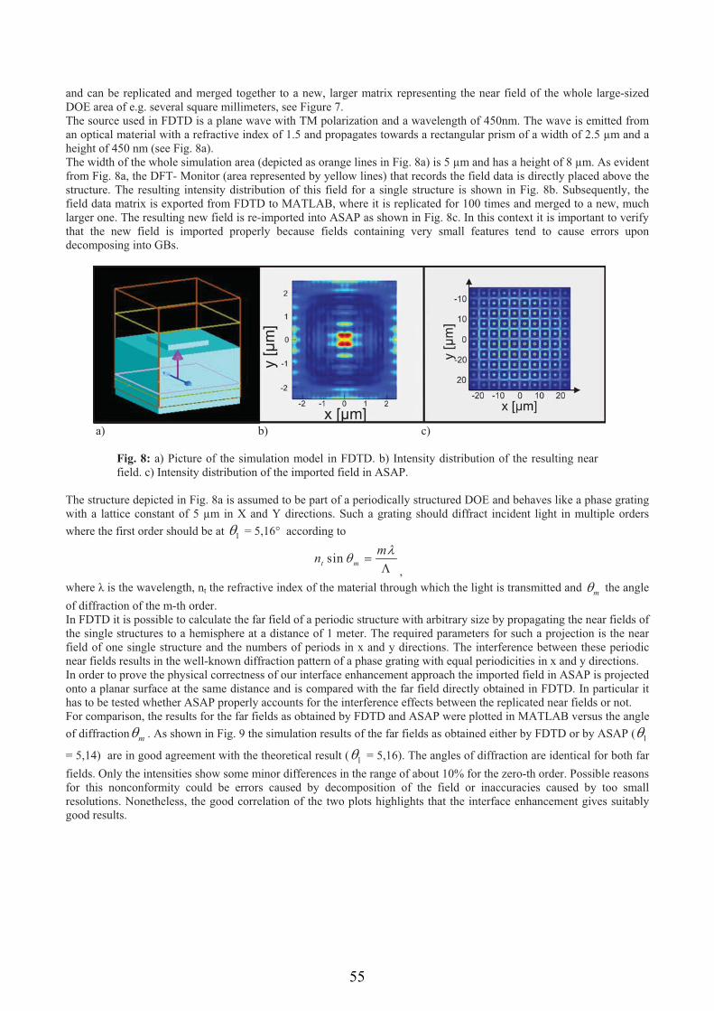
and can be replicated and merged together to a new, larger matrix representing the near field of the whole large-sized DOE area of e.g. several square millimeters, see Figure 7. The source used in FDTD is a plane wave with TM polarization and a wavelength of 450nm. The wave is emitted from an optical material with a refractive index of 1.5 and propagates towards a rectangular prism of a width of 2.5 μm and a height of 450 nm (see Fig. 8a). The width of the whole simulation area (depicted as orange lines in Fig. 8a) is 5 μm and has a height of 8 μm. As evident from Fig. 8a, the DFT- Monitor (area represented by yellow lines) that records the field data is directly placed above the structure. The resulting intensity distribution of this field for a single structure is shown in Fig. 8b. Subsequently, the field data matrix is exported from FDTD to MATLAB, where it is replicated for 100 times and merged to a new, much larger one. The resulting new field is re-imported into ASAP as shown in Fig. 8c. In this context it is important to verify that the new field is imported properly because fields containing very small features tend to cause errors upon decomposing into GBs.
a) b) c)
Fig. 8: a) Picture of the simulation model in FDTD. b) Intensity distribution of the resulting near field. c) Intensity distribution of the imported field in ASAP.
The structure depicted in Fig. 8a is assumed to be part of a periodically structured DOE and behaves like a phase grating with a lattice constant of 5 μm in X and Y directions. Such a grating should diffract incident light in multiple orders where the first order should be at 1� = 5,16° according to
sint mmn �� �� ,
where � is the wavelength, nt the refractive index of the material through which the light is transmitted and m� the angle of diffraction of the m-th order. In FDTD it is possible to calculate the far field of a periodic structure with arbitrary size by propagating the near fields of the single structures to a hemisphere at a distance of 1 meter. The required parameters for such a projection is the near field of one single structure and the numbers of periods in x and y directions. The interference between these periodic near fields results in the well-known diffraction pattern of a phase grating with equal periodicities in x and y directions. In order to prove the physical correctness of our interface enhancement approach the imported field in ASAP is projected onto a planar surface at the same distance and is compared with the far field directly obtained in FDTD. In particular it has to be tested whether ASAP properly accounts for the interference effects between the replicated near fields or not. For comparison, the results for the far fields as obtained by FDTD and ASAP were plotted in MATLAB versus the angle of diffraction m� . As shown in Fig. 9 the simulation results of the far fields as obtained either by FDTD or by ASAP ( 1�
= 5,14) are in good agreement with the theoretical result ( 1� = 5,16). The angles of diffraction are identical for both far fields. Only the intensities show some minor differences in the range of about 10% for the zero-th order. Possible reasons for this nonconformity could be errors caused by decomposition of the field or inaccuracies caused by too small resolutions. Nonetheless, the good correlation of the two plots highlights that the interface enhancement gives suitably good results.
55
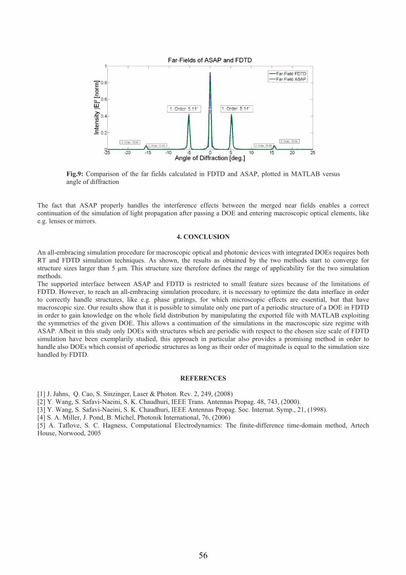
Fig.9: Comparison of the far fields calculated in FDTD and ASAP, plotted in MATLAB versus angle of diffraction
The fact that ASAP properly handles the interference effects between the merged near fields enables a correct continuation of the simulation of light propagation after passing a DOE and entering macroscopic optical elements, like e.g. lenses or mirrors.
4. CONCLUSION An all-embracing simulation procedure for macroscopic optical and photonic devices with integrated DOEs requires both RT and FDTD simulation techniques. As shown, the results as obtained by the two methods start to converge for structure sizes larger than 5 μm. This structure size therefore defines the range of applicability for the two simulation methods. The supported interface between ASAP and FDTD is restricted to small feature sizes because of the limitations of FDTD. However, to reach an all-embracing simulation procedure, it is necessary to optimize the data interface in order to correctly handle structures, like e.g. phase gratings, for which microscopic effects are essential, but that have macroscopic size. Our results show that it is possible to simulate only one part of a periodic structure of a DOE in FDTD in order to gain knowledge on the whole field distribution by manipulating the exported file with MATLAB exploiting the symmetries of the given DOE. This allows a continuation of the simulations in the macroscopic size regime with ASAP. Albeit in this study only DOEs with structures which are periodic with respect to the chosen size scale of FDTD simulation have been exemplarily studied, this approach in particular also provides a promising method in order to handle also DOEs which consist of aperiodic structures as long as their order of magnitude is equal to the simulation size handled by FDTD.
REFERENCES
[1] J. Jahns, Q. Cao, S. Sinzinger, Laser & Photon. Rev. 2, 249, (2008) [2] Y. Wang, S. Safavi-Naeini, S. K. Chaudhuri, IEEE Trans. Antennas Propag. 48, 743, (2000). [3] Y. Wang, S. Safavi-Naeini, S. K. Chaudhuri, IEEE Antennas Propag. Soc. Internat. Symp., 21, (1998). [4] S. A. Miller, J. Pond, B. Michel, Photonik International, 76, (2006) [5] A. Taflove, S. C. Hagness, Computational Electrodynamics: The finite-difference time-domain method, Artech House, Norwood, 2005
56
3.1.2 A SIMULATION PROCEDURE INTERFACING RAY-
TRACING AND FINITE-DIFFERENCE-TIME-DOMAIN
METHODS FOR A COMBINED SIMULATION OF DIFFRACTIVE
AND REFRACTIVE OPTICAL ELEMENTS
”A Simulation Procedure Interfacing Ray-Tracing and Finite-Difference-Time-
Domain Methods for a Combined Simulation of Diffractive and Refractive Optical
Elements” wurde 2013 als Full Paper beim IEEE/OSA Journal of Lightwave
Technology eingereicht und im März 2014 (Volume 32, Issue 6, pp. 1054-1062) in
dieser Zeitschrift veröffentlicht. Der eigene Anteil bei dieser Veröffentlichung beträgt
60%.
In dieser Publikation wird erstmalig die im Rahmen dieser Dissertation entwickelte
Schnittstellenmethode zwischen der klassischen Ray-Tracing Simulationsmethode und
der Finite-Difference-Time-Domain Simulationsmethode über das Prinzip des
Poynting-Vektors vorgestellt. Durch diese Methode wird die schrittweise Simulation
eines optischen Systems, bestehend aus refraktiven und diffraktiven optischen
Bauteilen, ermöglicht. Um das Konzept der Schnittstelle zu verifizieren und deren
Genauigkeit zu analysieren, werden in dieser Publikation die gewonnenen
Simulationsergebnisse mit realen Messungen verglichen.
Das verwendete optische Gitter wurde von M. Belegratis, V. Schmidt und B.
Lamprecht hergestellt. Die Messungen wurden von C. Sommer durchgeführt.
.
57
1054 JOURNAL OF LIGHTWAVE TECHNOLOGY, VOL. 32, NO. 6, MARCH 15, 2014
A Simulation Procedure Interfacing Ray-Tracingand Finite-Difference Time-Domain Methodsfor a Combined Simulation of Diffractive and
Refractive Optical ElementsClaude Leiner, Susanne Schweitzer, Franz-Peter Wenzl, Paul Hartmann, Ulrich Hohenester, and Christian Sommer
Abstract—A simulation procedure which enables integrated sim-ulation of optical devices including both refractive and diffrac-tive optical elements at different length scales is presented. Theapproach uses the Poynting vector to interface between a Ray-tracing and a finite-difference-time-domain tool for a step by stepsimulation of both the light propagation through a laser-writtendiffractive grating structure and its measurement by an appro-priate setup. These simulated results are in great accordance withexperimentally determined ones. Furthermore, the impact of pa-rameter variations is analyzed and discussed in detail.
Index Terms—Computational modeling, finite-difference-time-domain (FDTD), gratings, microstructure, ray tracing.
I. INTRODUCTION
IN the last years, diffractive optical elements (DOEs) withcustomized properties became more and more common in
optical devices. As the state of the art, DOEs are used in com-bination with light emitting diodes (LEDs) to enhance e.g. lightextraction or to tailor the emission patterns [1]–[3], with solarcells as light trapping structures [4]–[6], or as coupling struc-tures for fiber-waveguides or planar waveguides [7]–[9] in thefield of optical sensing or integrated optics [10], [11]. For allthese applications optical simulations are useful to design, sim-ulate, optimize, and analyze these devices as they enable com-paratively easy parameter variations of different components ofthe setups in order to identify their ideal properties [12]–[19].However, the complete simulation comprising both refractive aswell as diffractive optical components of more complex devicesis often not possible and is limited to the simulation of only oneaspect of the device.
Manuscript received June 10, 2013; revised December 2, 2013; accepted De-cember 23, 2013. Date of publication January 1, 2014; date of current versionJanuary 23, 2014. This work was supported by the BMVIT within the FIT-IT Program—ModSim Computational Mathematics—of the Austrian ResearchPromotion Agency (FFG) under Project number 828706.C. Leiner, S. Schweitzer, F. P. Wenzl, P. Hartmann, and C. Sommer
are with the Institute of Surface Technologies and Photonics, JoanneumResearch Forschungsges.mbH, A-8160 Weiz, Austria (e-mail: [email protected]; [email protected]; [email protected], [email protected]; [email protected]).U. Hohenester is with the Institute of Physics, University of Graz, A-8010
Graz, Austria (e-mail [email protected]).Color versions of one or more of the figures in this paper are available online
at http://ieeexplore.ieee.org.Digital Object Identifier 10.1109/JLT.2013.2297411
In general, there is a broad variety of different methods for thenumerical simulation of light propagation in optical devices andtheir suitability depends on the ratios of the size ranges of theoptical elements constituting the device and the wavelengths inuse. In the so-called “macro” regime, which is applicable whenthe structure sizes are more than 100 times larger than the wave-length, classical ray tracing (RT), Gaussian beam tracing (GBT)or beam propagation methods (BPM) are commonly used to de-scribe refractive optical elements (ROE) [20]. On the contrary,in the “nano” regime, which is applicable when the structuresize is smaller or up to ten times larger than the wavelength,wave optical (WO) approaches like the finite-difference-time-domain (FDTD) method, the finite element method (FEM) orthe rigorous coupled-wave analysis (RCWA) have to be appliedas diffractive optical effects become important [20]. While themacro regime methods cannot be used to describe optical struc-tures in the nano regime, the simulation area which can behandled with WO methods is restricted by today’s computerperformance, which impedes a complete simulation of suchlikeoptical systems when they become too large.This problem has been addressed by many authors investigat-
ing different approaches to combine either self-made or com-mercial tools for RT, GBT, BPM, FDTD, FEM, and RCWA fora simulation of systems comprising optical components bothin the macro and nano regimes. For example, Wyrowski andKuhn introduced a generalized concept called “field tracing,”where harmonic fields instead of classical rays are propagatedvia operators through the optical system [21], allowing an easytransition between the different optical methods. This approachis implemented in a commercial tool called VirtualLab fromLightTrans [22]. Furthermore, Rohani et al. developed a hybridmethod composed of GBT, Gabor expansion and FDTD for thesimulation of passive unbounded wave structures [23]; however,the GBT has limitations in terms of general surfaces or fields inthe macro regime.The classical RT method does not have these limitations con-
sidering general boundaries, but phase relations between differ-ent rays cannot be considered with this method, making a directtransition from RT to nano regime methods difficult. However,for many light or field sources it is possible to neglect suchphase relations in case that they are random, This condition,e.g., is fulfilled by broadband light sources like incandescencebulbs, halogen lamps, and light emitting diodes. An example fora combination of the classical RT and the FDTD method was
0733-8724 © 2014 IEEE. Personal use is permitted, but republication/redistribution requires IEEE permission.See http://www.ieee.org/publications standards/publications/rights/index.html for more information.
58
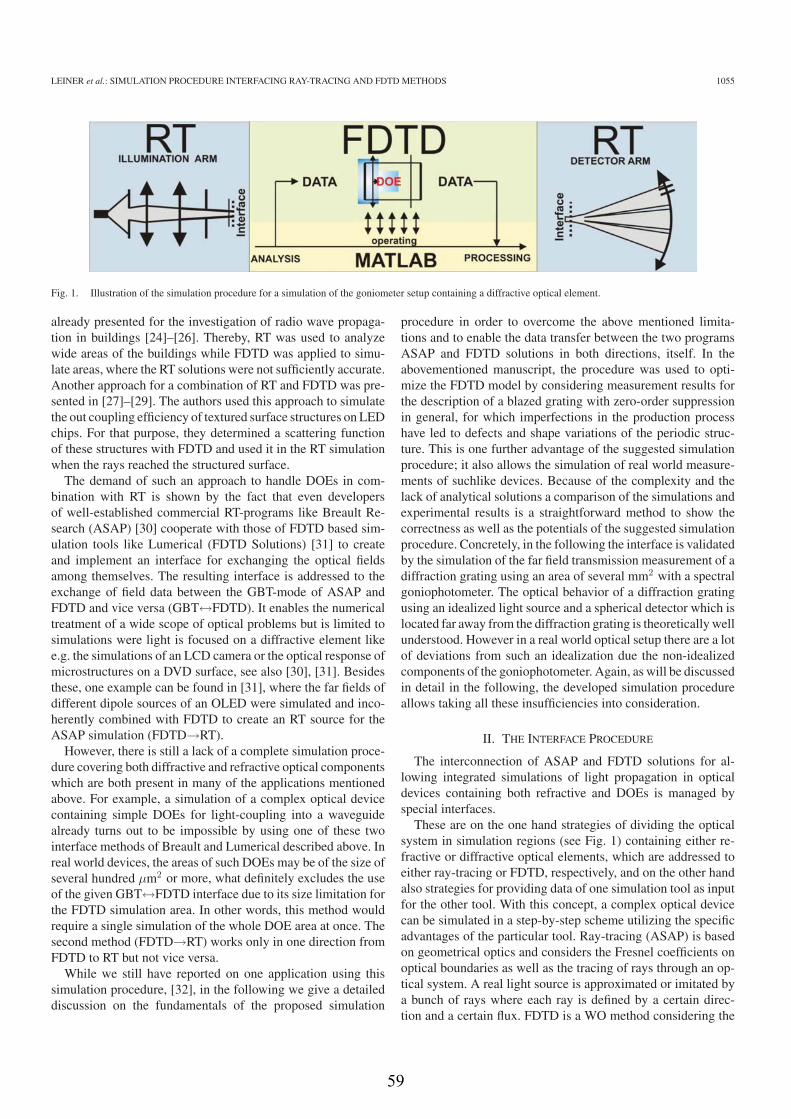
LEINER et al.: SIMULATION PROCEDURE INTERFACING RAY-TRACING AND FDTD METHODS 1055
Fig. 1. Illustration of the simulation procedure for a simulation of the goniometer setup containing a diffractive optical element.
already presented for the investigation of radio wave propaga-tion in buildings [24]–[26]. Thereby, RT was used to analyzewide areas of the buildings while FDTD was applied to simu-late areas, where the RT solutions were not sufficiently accurate.Another approach for a combination of RT and FDTD was pre-sented in [27]–[29]. The authors used this approach to simulatethe out coupling efficiency of textured surface structures on LEDchips. For that purpose, they determined a scattering functionof these structures with FDTD and used it in the RT simulationwhen the rays reached the structured surface.The demand of such an approach to handle DOEs in com-
bination with RT is shown by the fact that even developersof well-established commercial RT-programs like Breault Re-search (ASAP) [30] cooperate with those of FDTD based sim-ulation tools like Lumerical (FDTD Solutions) [31] to createand implement an interface for exchanging the optical fieldsamong themselves. The resulting interface is addressed to theexchange of field data between the GBT-mode of ASAP andFDTD and vice versa (GBT↔FDTD). It enables the numericaltreatment of a wide scope of optical problems but is limited tosimulations were light is focused on a diffractive element likee.g. the simulations of an LCD camera or the optical response ofmicrostructures on a DVD surface, see also [30], [31]. Besidesthese, one example can be found in [31], where the far fields ofdifferent dipole sources of an OLED were simulated and inco-herently combined with FDTD to create an RT source for theASAP simulation (FDTD→RT).However, there is still a lack of a complete simulation proce-
dure covering both diffractive and refractive optical componentswhich are both present in many of the applications mentionedabove. For example, a simulation of a complex optical devicecontaining simple DOEs for light-coupling into a waveguidealready turns out to be impossible by using one of these twointerface methods of Breault and Lumerical described above. Inreal world devices, the areas of such DOEs may be of the size ofseveral hundred μm2 or more, what definitely excludes the useof the given GBT↔FDTD interface due to its size limitation forthe FDTD simulation area. In other words, this method wouldrequire a single simulation of the whole DOE area at once. Thesecond method (FDTD→RT) works only in one direction fromFDTD to RT but not vice versa.While we still have reported on one application using this
simulation procedure, [32], in the following we give a detaileddiscussion on the fundamentals of the proposed simulation
procedure in order to overcome the above mentioned limita-tions and to enable the data transfer between the two programsASAP and FDTD solutions in both directions, itself. In theabovementioned manuscript, the procedure was used to opti-mize the FDTD model by considering measurement results forthe description of a blazed grating with zero-order suppressionin general, for which imperfections in the production processhave led to defects and shape variations of the periodic struc-ture. This is one further advantage of the suggested simulationprocedure; it also allows the simulation of real world measure-ments of suchlike devices. Because of the complexity and thelack of analytical solutions a comparison of the simulations andexperimental results is a straightforward method to show thecorrectness as well as the potentials of the suggested simulationprocedure. Concretely, in the following the interface is validatedby the simulation of the far field transmission measurement of adiffraction grating using an area of several mm2 with a spectralgoniophotometer. The optical behavior of a diffraction gratingusing an idealized light source and a spherical detector which islocated far away from the diffraction grating is theoretically wellunderstood. However in a real world optical setup there are a lotof deviations from such an idealization due the non-idealizedcomponents of the goniophotometer. Again, as will be discussedin detail in the following, the developed simulation procedureallows taking all these insufficiencies into consideration.
II. THE INTERFACE PROCEDURE
The interconnection of ASAP and FDTD solutions for al-lowing integrated simulations of light propagation in opticaldevices containing both refractive and DOEs is managed byspecial interfaces.These are on the one hand strategies of dividing the optical
system in simulation regions (see Fig. 1) containing either re-fractive or diffractive optical elements, which are addressed toeither ray-tracing or FDTD, respectively, and on the other handalso strategies for providing data of one simulation tool as inputfor the other tool. With this concept, a complex optical devicecan be simulated in a step-by-step scheme utilizing the specificadvantages of the particular tool. Ray-tracing (ASAP) is basedon geometrical optics and considers the Fresnel coefficients onoptical boundaries as well as the tracing of rays through an op-tical system. A real light source is approximated or imitated bya bunch of rays where each ray is defined by a certain direc-tion and a certain flux. FDTD is a WO method considering the
59
1056 JOURNAL OF LIGHTWAVE TECHNOLOGY, VOL. 32, NO. 6, MARCH 15, 2014
electromagnetic fields by discretizing the space (so called Yeecells) and solving the Maxwell-equations at the vertices of themin a leapfrog manner [33].Common light sources, like incandescent bulbs or LEDs, emit
light waves with more or less spherical wave fronts. However,in the far field region where k2
x+k2y � k2
z is valid, which meansthat the distance in z direction from the light source is muchlarger than the wavelength and the interacting structure, everyspherical wave can be approximated by a plane wave in the WOmodel or a bunch of parallel rays in the RT model [34].Our approach to realize the interface between RT and FDTD
is to connect them via the Poynting vector. In RT, the raysare typically defined over the time averaged Poynting vector〈S〉 [35]. Thereby, the ray directions are parallel to 〈S〉, whichis orthogonal to the geometrical wave-fronts, and the flux ofthe rays is proportional to the magnitude of 〈|S|〉. In FDTD, thewave vector k, which represents the propagation direction of aplane wave, is parallel to 〈S〉 assuming the wave travels in an(isotropic) dielectric medium. The flux of the waves is obtainedby integration (summation) of 〈S〉 over a surface or a solid angle,respectively.Using these relations, the directions and fluxes of the prop-
agating light in RT and FDTD can be connected. But it has tobe noticed that when switching from FDTD to RT, the infor-mation of the phase relations between different rays is lost. Incase of our example the simulation starts in the RT model. Atthe interface, the phase relations between the different rays areassumed as random because an incoherent light source is used.After the DOE, the phase relations between the different ordersare not random anymore but can still be neglected because thereis no further diffractive optical element in our setting wherethe different orders could interfere. However, these phase rela-tions would be essential when the rays hit another DOE locatedclose to the first DOE. In such cases, supplementary informationwould be needed to maintain the validity of the approach, e.g.,the coherence length of the light emitted by the source. Never-theless, due to the small coherence length (up to several hundredmicrons) of conventional white light sources, the simulation ap-proach would still be valid for simulation settings where thedistance between two consecutive DOEs is larger than severalmillimeters, because the phase relations between the differentorders could be assumed as random again for such conditions.The whole simulation procedure is operated through MAT-
LAB scripts which are executed via the program interface ofFDTD Solutions. The scripts control the different parts of thesimulation and the data transfer between RT and FDTD (seeFig. 1). In particular, in the first simulation part light rays aretraced in ASAP through refractive optical elements up to anappropriate interface plane. This plane is located at the positiondirectly before the DOE and also provides the connection to thesecond simulation part. At this plane, the rays are stopped andtheir positions, directions and fluxes are recorded. By analyz-ing the ray-data MATLAB creates a set of plane wave sourceswith different k vectors in FDTD; these vectors are sampled toimitate the angular and spatial intensity distribution previouslyobtained from the RT Part (see Fig. 1). In the case that a spec-tral broadband light source is used, the phase relations between
the different plane waves can be assumed as random and there-fore independent FDTD simulations can be started for everysingle plane wave. Practically, the propagation directions of therays are binned into representative (i.e., small enough) angularintervals. As a result, after the interaction with the DOE theobtained fields in terms of the Poynting vectors are assigned toangular intervals (bins) according to the respective k directions.Further processing of the Poynting vectors yields all relevant in-formation for the data exchange through the interface to createa source for the subsequent RT step (see Fig. 1); in particularthese are the angular intensity distributions in the far field aswellas the reflection and transmission coefficients. Hence, steppingforward to ASAP, the propagation direction of each initial raydetermined on the first interface plane (RT→FDTD) is randomlysampled according to the probability density distribution, whichis equivalent to the calculated far field distribution obtained bythe FDTD simulations. Additionally, the flux of each ray is al-tered by applying the obtained transmission coefficients. Thisis the final step of the sketched simulation scheme starting withRT, continuing with FDTD and ending with RT (RT – FDTD –RT).The numerical effort and the simulation time needed for the
presented simulation procedure depend mainly on four differentparameters: The number of different wavelengths required, thenumber of rays used in the RT simulation, the number of theangular intervals (bins) and the time required for a single FDTDsimulation of a plane wave interacting with the grating or DOE.Classical RT does not support optical broadband simulations;therefore an independent interface simulation for every requiredwavelength has to be performed. Furthermore the number of raysaffects both the simulation time of the RT and theMATLAB partof the simulation. For the FDTD part each angular interval ofthe relevant angle range corresponds with a plane wave so thatthe number of angular bins and the number of wavelengths aredetermining the number of independent FDTD simulation runs,which are needed for describing the interaction of the differentplane waves with the DOE properly.In the present case, a self-made diffraction grating is mea-
sured and simulated using the above mentioned scheme. Thewell-known far field intensity distribution makes it easier forthe process of comparison, because fabrication errors or mea-surement tolerances can be identified more easily.
III. EXPERIMENTAL AND SIMULATION SETUP
For the validation of the proposed interface approach an ap-propriate model for both the DOE and the measurement set-upwas developed. The experiment comprised transmission mea-surements of the diffraction grating in a goniometer setup (GON360) with independently rotatable arms, one for illuminating thesample and one for detecting the scattered light after the inter-action with the sample.The particular diffraction grating was directly written in a
spin coated photosensitive resist on a glass substrate (with anassumed refractive index n = 1.52) by use of the two photonabsorption 3D laser lithography method [36]. In order to getthe right dimension of the diffraction grating structure and for
60
LEINER et al.: SIMULATION PROCEDURE INTERFACING RAY-TRACING AND FDTD METHODS 1057
Fig. 2. (a) and (b) Scanning electron microscope images of the negative struc-ture of the diffraction grating.
stability reasons, the auto-focusing laser was writing back andforward for one feature of the grating in a positive photosensitiveresist (AZ6615 fromMicrochemicals,n = n(λ)) with a speed of2000 μm/s and a power of 10 mW. The grating was written in arepeated process where an area consisting of 10× 10 sub-areaseach with 300 μm× 300 μmwas stitched together. A small gapof about 10 μm in between these single sub-areas (see Fig. 2(a)and (b)) was induced for technical reason and has a negligibleinfluence on the expected far field transmission distribution. Theso obtained grating structure has an area of about 3 mm× 3mm.In order to preserve the directly written grating structure for
goniometer measurements, a mold was fabricated for furthercharacterizations of the diffraction grating’s geometry. Fig. 2(a), (b) show scanning electronmicroscope (SEM) images of themold, i.e., the negative form of the directly written structure; forthe simulation the dimension of the grooves and the walls hasto be swapped. The grating is composed of rectangular groovesand walls with a grating constant of 3000 nm ± 10 nm, a widthof 1200 nm ± 10 nm and a depth of 1775 nm ± 45 nm. Thesevalues were obtained from SEM images by use of an imageanalyzing software with an additional statistical analysis for themeasurement errors. The mean values were used as the baseparameters for setting up the FDTD simulation model.For determining the transmitted intensity distribution in the
far field, the GON 360 measurement setup was used. It consistsof two independent rotatable arms, one for illumination and onefor detection. For correct measurements, the sample has to beplaced with a height adjustable stage in the rotation center ofthe two arms. The illumination arm is connected via an opticalfiber to a halogen lamp (8.3 A, 12 V, non-polarized broadbandsource) and produces a circular illumination spot of about 3 mmin diameter. The detection arm is connected via an optical fiberto an array spectrometer (CAS140CT, Instrument Systems) anddetermines the spectral intensity of the scattered/diffracted light.The GON 360 measurement of the diffraction grating has beenapplied between −90◦ and +90◦ for step size of 0.5◦.In order to test the proposed simulation approach, as will
be shown in section IV, a correct modeling of the illumina-tion arm, which is the refractive or incoherent part of the sim-ulation model, is essential for getting correct simulation re-sults. The beam path through the GON 360 is rather complexand can be sketched as follows: Light coming from a halogenlamp couples out of the optical fiber into the illumination armwith a divergence angle of approximately 23◦, hits a 45◦ tilted
mirror (neglected in the sketch of Fig. 3(a)) and passes througha 6 mm aperture which cuts the divergence of the beam to ap-proximately 5.5◦. The remaining beam passes through a doublelens system for which the positions and the focal lengths areconfigured so that at the rotational center (or at the sample posi-tion) the beam of the GON 360 is convergent with a diameter of3 mm. The smallest waist (focus) of the beam is about 16 mmbeyond that position; see also Fig. 3(a). The distance measuredfrom the rotation center to the aperture of the detector arm isabout 113.5 mm. At this position, the beam enters the detec-tor arm through a circular aperture with a diameter of 10 mmand reaches the spectrometer via an optical fiber. In order toincrease the angular resolution of the measurement, the aper-ture was shortened by a 1 mm aperture slit perpendicular to thedirection of rotation.As shown in Fig. 4(a) and (b), the angular distribution of
the rays is not homogenous within the illumination spot at thesample’s position. As a consequence it is inevitable to take theillumination arm of the GON 360 for the RT simulations intoaccount, since wrong angular ray distributions would be crucialfor the input of the subsequent FDTD simulation step and wouldlead to incorrect results. This will be discussed in more detaillater in this paper. The sample with diffraction grating is placedface up in the GON 360; as a result of this the rays enter theglass substrate from the back before reaching the diffractiongrating. As a consequence the interface plane as well as thesource in FDTD is immersed within the glass substrate. In orderto take this into account, a plane (black line in Fig. 3(a) atsample position) with a boundary surface between air (n = 1)and glass (n = 1.52) was placed in ASAP 1 mm, representingthe substrate thickness, in front of the interface plane (dottedblack line in Fig. 3(a) at sample position). For obtaining thecorrect angular distribution for the FDTD simulation the raysgot stopped inside the medium while their flux positions anddirectional data were recorded for further processing.For the following FDTD part of the simulation procedure, the
dimensions of the diffraction grating obtained from the SEMimages were put into the FDTD model (see Fig. 3(b)). The raysfrom ASAP at the interface plane were converted according totheir angular distribution into independent plane wave sourceswith different k vectors. As already mentioned above, theseplane waves were immersed in media, in particular in the glasssubstrate of the grating structure. The polarization of the sourceswas set to 45◦ which corresponds to non-polarized light.The FDTD simulation area was assumed to be two dimen-
sional in the x-y coordinate plane, which was possible in thisexample as the diffraction grating is symmetrical in the z direc-tion. In the x direction, the simulation area was limited throughBloch boundary conditions (BCs), in the y direction it waslimited by perfectly matched layer (PML) BCs, as depictedin Fig. 3(b). Bloch BCs are periodic boundary conditions wherefields which leave the simulation area reenter while consideringthe phase shift between the periods. Such a BC allows restrictingthe simulation area to one period of the (periodically symmet-ric) diffraction grating. Thereby, accounting for the phase shiftit is essential to prevent self-interference when the source hasnon-zero field components of the wave vector in x direction
61
1058 JOURNAL OF LIGHTWAVE TECHNOLOGY, VOL. 32, NO. 6, MARCH 15, 2014
Fig. 3. (a) Sketch of the ASAP simulation setup for the GON 360 illumination arm and the detector and (b) sketch of the FDTD simulation setup of the diffractiongrating.
Fig. 4. Distribution of the maximum (b) and the minimum (a) ray directionangles per pixel within the recorded spot area at sample position in the glasspart of the interface plane. Sketch (e) to illustrate the difference between theconvergent and the divergent beam model used in ASAP.
(kx). The top and bottom PML BCs are absorbing boundaryconditions which should suppress back-reflections completely.In this way, the FDTD simulation area covered 3 μm in x
direction, including exactly one grating period. The extent ofthe simulation area in the y direction was chosen to be suf-ficiently large to be able to represent the height of a gratingfeature (1.775 μm) and to allow the placement of the monitorand sources in appropriate distances to the grating structure forcalculating the correct transmitted far field. For the simulationarea a non-conformal mesh refinement with variable step sizesin x and y direction (dx, dy) was applied. The step sizes werecalculated automatically depending on their position with re-spect to the grating structure and the wavelength of the source,with a smaller step size over structure elements.Since FDTD is a time domain method, the time independent
electromagnetic fields for the different wavelengths were ob-tained by using a standard Fourier transform monitor. The timedependent transmitted electromagnetic-fieldswere recorded andconverted into frequency dependent electromagnetic-fields witha Fourier transformation. From these, a near-to far-field transfor-mation resulted in the respective angular far field distributions.For the simulation results, presented in this paper, the an-
gular intervals of the plane waves were set to 0.1 degree. Thesimulation considered 41 different wavelengths between 400and 800 nm with 500 k rays for each run to reach a significant
ray-distribution on the RT-detectors. A single FDTD simulationof a plane wave interacting with the grating, required approxi-mately 8 to 10 s, leading to a total simulation time of approx.3 h for the FDTD part and 7 h for the RT and MATLAB parts,considering a common workstation.
IV. RESULTS AND DISCUSSION
This section is dedicated to highlight the accuracy of thesimulation procedure, which starts in particular with an RT sim-ulation of the incoherent illumination part of the GON 360,proceeds with FDTD simulations of the diffraction grating andends with a second RT simulation for obtaining the far field atthe aperture of the detector arm. This procedure needs appro-priate interfaces for providing the data-exchange between thetwo simulation approaches. All this is automated, controlled andprocessedwithMATLAB scripts. In order to verify the proposedscheme, a comparison of simulation results and measurementresults of the diffractive grating structure under investigation ismade. In addition, we demonstrate the importance of an exactmodel for a correct simulation of the optical system, as well asthe possibility to consider the influences of the non-idealizedcomponents on the measuring results using our interface proce-dure with these exact models.An idealized diffraction grating always deflects light into a
very sharp intensity pattern in the far field considering a singlewavelength, presupposed that many periods of the grating areilluminated. This can be imitated in the simulation model by us-ing an idealized source model, e.g. a disc source emitting lightparallel to the optical axis, and by using an idealized sphericaldetector, which is in an adequate distance to the sample, wherethe lateral dimensions of the source does not influence the angu-lar resolution of the intensity distribution (see Fig. 5(a) and (b)gray line). However, the intensity distributions measured withthe GON 360 show a zeroth order with a full width at half max-imum (FWHM) of about 4◦, shown in Fig. 5(a) for λ = 520 nm.For higher orders, the FWHM is further increasing up to about8◦ for the fifth order (see Fig. 5(b)). There are several reasonsfor this broadening of the orders. First, the ratio of the spot di-ameter to the detector distance cannot be neglected which leadsto a projection of the spot diameter onto the angle dependent
62
LEINER et al.: SIMULATION PROCEDURE INTERFACING RAY-TRACING AND FDTD METHODS 1059
Fig. 5. (a) Lower and (b) higher orders of the measured intensity distribution for a wavelength of 520 nm compared with the results from different ASAP beamsetups in the simulation. In order to make all distributions comparable, the curves were normalized by the areas they cover, except the curve of the idealizeddetector model which was normalized to the 0th order of the GON 360 measurement.
Fig. 6. Sketch to illustrate the difference between the convergent and thedivergent beam model used in ASAP.
far field. Second, the diameter of the detector aperture leads toa smoothing of adjacent measuring points and also of the inten-sity orders. Third, also the angular distribution of the rays withinthe spot leads to different angles of incidence on the diffractiongrating and hence to an overlap of the corresponding far fielddistributions.In order to investigate the influence of the correlation of spot
diameter and detector setting on the far field intensity distri-bution separately, we use two circular disc sources in ASAPwith different diameters, but both with a propagation directionof 0◦. These collimated rays are parallel to the optical axis ofthe system, which is perpendicular to the surface of the sample.For the first disc source, a diameter of 3 mm is chosen, whichrepresents the spot diameter at the sample position. The diam-eter of the second disc source is chosen as large as 9.1 mm,which is equivalent to the spot diameter at the aperture of thedetector position. While the 3 mm source leads to completelyincorrect results, the far field distributions of the 9.1 mm sourcefit pretty well for lower orders (see Fig. 5(a)). This is not sur-prising because the larger disc source fits the projection of thespot diameter on the detector’s aperture, while the 3 mm sourcecontains the same flux but is projected to a smaller angle range.However, for higher orders the FWHM decreases comparablyto the measured peaks for this kind of sources. This implies thatthe angular distribution of the rays within the spot has to beconsidered too.For this attempt, a beam with non-parallel rays and a spot di-
ameter of 3 mm at the sample position is used. Designing a spot
Fig. 7. (a) Simulation results of the convergent beam model for the wholewavelength range with 10 nm step size and (b) GON 360 measurement resultsfor the hole wavelength range with 10 nm step size.
of a convergent beam, in accordance with the GON 360 beamat the sample position, is rather difficult because the angulardistribution of the rays within such a spot is not uniform and re-quires an exact ASAP simulation of the GON 360 illuminationpart. As a further approximation of the real beam properties, adivergent beam (called “divergent beam model” below) with auniform angular distribution of the rays is assumed. The maxi-mum divergence angle α = 1.4◦ (which is approximately 1◦ fora transition of the light beam from air into glass with n = 1.52)
63
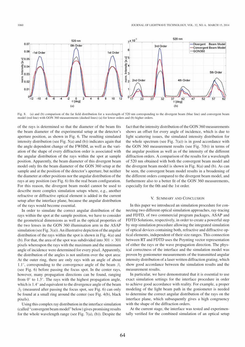
1060 JOURNAL OF LIGHTWAVE TECHNOLOGY, VOL. 32, NO. 6, MARCH 15, 2014
Fig. 8. (a) and (b) comparison of the far field distribution for a wavelength of 520 nm corresponding to the divergent beam (blue line) and convergent beammodel (red line) with GON 360 measurements (dashed lines) (a) for lower orders and (b) higher orders.
of the rays is determined so that the diameter of the beam fitsthe beam diameter of the experimental setup at the detector’saperture position, as shown in Fig. 6. The resulting simulatedintensity distribution (see Fig. 5(a) and (b)) indicates again thatthe angle dependent change of the FWHM, as well as the vari-ation of the shape of every diffraction order is associated withthe angular distribution of the rays within the spot at sampleposition. Apparently, the beam diameter of this divergent beammodel only fits the beam diameter of the GON 360 setup at thesample and at the position of the detector’s aperture, but neitherthe diameter at other positions nor the angular distribution of therays at any position (see Fig. 6) fits the real beam configuration.For this reason, the divergent beam model cannot be used todescribe more complex simulation setups where, e.g., anotherrefractive or diffractive optical element is added in the currentsetup after the interface plane, because the angular distributionof the rays would become essential.In order to simulate the correct angular distribution of the
rays within the spot at the sample position, we have to considerthe geometrical dimensions as well as the optical properties ofthe two lenses in the GON 360 illumination arm in the ASAPsimulation (see Fig. 3(a)).An illustrative depiction of the angulardistribution of the rays within the spot is shown in Fig. 4(a) and(b). For that, the area of the spot was subdivided into 301× 301pixels whereupon the rays with the maximum and the minimumangle of incidence were determined for every pixel. Apparently,the distribution of the angles is not uniform over the spot area:At the outer ring, there are only rays with an angle of about1.1◦, corresponding to the convergence angle of the beam β1(see Fig. 6) before passing the focus spot. In the center rays,however, many propagation directions can be found, rangingfrom 0◦ to 1.3◦. The rays with the highest propagation angle,which is 1.4◦ and equivalent to the divergence angle of the beamβ2 (measured after passing the focus spot, see Fig. 6) can onlybe found at a small ring around the center (see Fig. 4(b), blackpixels).Using this complex ray distribution in the interface simulation
(called “convergent beammodel” below) gives promising resultsfor the whole wavelength range (see Fig. 7(a), (b)). Despite the
fact that the intensity distribution of theGON360measurementsshows an offset for every angle of incidence, which is due tolight scattering issues, the simulated intensity distribution forthe whole spectrum (see Fig. 7(a)) is in good accordance withthe GON 360 measurement results (see Fig. 7(b)) in terms ofthe angular position as well as of the intensity of the differentdiffraction orders. A comparison of the results for a wavelengthof 520 nm obtained with both the convergent beam model andthe divergent beam model is shown in Fig. 8(a) and (b). As canbe seen, the convergent beam model results in a broadening ofthe different orders compared to the divergent beam model, andfurthermore also to a better fit of the GON 360 measurements,especially for the 0th and the 1st order.
V. SUMMARY AND CONCLUSION
In this paper we introduced an simulation procedure for con-necting two different optical simulation approaches, ray-tracingand FDTD, of two commercial program packages, ASAP andFDTD Solutions, respectively, in order to create a powerful stepby step simulation procedure allowing the integrated simulationof optical devices containing both, refractive and diffractive op-tical elements, independent of their size ranges. This connectionbetween RT and FDTD uses the Poynting vector representationof either the rays or the wave propagation direction. The phys-ical correctness of the interface and the simulation model wasproven by goniometer measurements of the transmitted angularintensity distribution of a laser written diffraction grating, whichshow good accordance between the simulation results and themeasurement results.In particular, we have demonstrated that it is essential to use
exact simulation settings for the interface procedure in orderto achieve good accordance with reality. For example, a propermodeling of the light beam path in the goniometer is neededto determine the correct angular distribution of the rays on theinterface plane, which subsequently gives a high congruencywith the shape of the diffraction orders.At the current stage, the interface was tested and experimen-
tally verified for the combined simulation of an optical setup
64
LEINER et al.: SIMULATION PROCEDURE INTERFACING RAY-TRACING AND FDTD METHODS 1061
containing several refractive optical elements and one diffrac-tive optical element. This was realized by using the interface forstepping once from the RT to the FDTD and back again to theRT mode.Future work will focus on even more complex optical sys-
tems like waveguide settings with DOEs for perpendicular in-and out-coupling of light. This will require a multiple bidirec-tional stepping between RT and FDTD, and therefore calls for ageneralization of this simulation procedure in order to consideradditional interference effects.
ACKNOWLEDGMENT
The authors would like to thank M. Belegratis, V. Schmidt,and B. Lamprecht for fabricating and analyzing the diffractiongrating used in the experimental part of this study.
REFERENCES
[1] T. Bocksrocker, J. B. Preinfalk, J. Asche-Tauscher, A. Pargner,C. Eschenbaum, F. Maier-Flaig, and U. Lemme, “White organic lightemitting diodes with enhanced internal and external outcoupling for ultra-efficient light extraction and lambertian emission,” Opt. Exp., vol. 20,pp. A932–A940, 2012.
[2] J. Hauss, T. Bocksrocker, B. Riedel, U. Geyer, U. Lemmer, andM.Gerken,“Metallic Bragg-gratings for light management in organic light-emittingdevices,” Appl. Phys. Lett., vol. 99, pp. 103303–103303, 2011.
[3] C. H. Lin, C. Y. Chen, D. M. Yeh, and C. C. Yang, “Light extraction en-hancement of a GaN-based light-emitting diode through grating-patternedphotoelectrochemical surface etching with phase mask interferometry,”IEEE Photon. Technol. Lett., vol. 22, no. 2, pp. 640–642, May 2010.
[4] D. N. Weiss, H.-C. Yuan, B. G. Lee, H. M. Branz, S. T. Meyers,A. G. Douglas, and A. Keszler, “Nanoimprinting for diffractive light trap-ping in solar cells,” J. Vac. Sci. Technol. B, vol. 28, pp. C6M98–C6M103,2010.
[5] R. Dewan and D. Knipp, “Light trapping in thin-film silicon solar cellswith integrated diffraction grating,” J. Appl. Phys., vol. 106, p. 074901,2009.
[6] Y. M. Song, J. S.Yu, andY. T. Lee, “Antireflective submicrometer gratingson thin-film silicon solar cells for light-absorption enhancement,” Opt.Lett., vol. 35, pp. 276–278, 2010.
[7] S. Feng, X. Zhang, H.Wang,M. Xin, and Z. Lu, “Fiber coupledwaveguidegrating structures,” Appl. Phys. Lett., vol. 96, p. 133101, 2010.
[8] G. Roelkens, D. Van Thourhout, and R. Baets, “High efficiency gratingcoupler between silicon-on-insulator waveguides and perfectly verticaloptical fibers,” Opt. Lett., vol. 32, pp. 1495–1497, 2007.
[9] T. Pustelny, I. Zielonka, P. Karasinski, and J. Jurusik, “Bragg’s gratingcoupler in planar optical sol-gel waveguides,”Opt. Appl., vol. 34, pp. 477–487, 2004.
[10] K. Schmitt andC.Hoffmann, “High-refractive-indexwaveguide platformsfor chemical and biosensing,” in Optical Guided-wave Chemical andBiosensors I, Springer Series on Chemical Sensors and Biosensors 7,M. Zourob and A Lakhtakia, Eds. Heidelberg, Germany: Springer-Verlag, 2010.
[11] S. Grego, S. Naskar, A. M. Patel, A. Huffmann, C. A. Bower, andB. R. Stoner, “Novel optical-waveguide sensing platform based on in-put grating coupler,” Proc. SPIE, vol. 6123, pp. 61230D-1–61230D-11,2006.
[12] M. Prasciolua,D.Cojoc, S. Cabrini, L.Businaro, P. Candeloro,M.Tormen,R. Kumar, C. Liberale, V. Degiorgio, A. Gerardino, G. Gigli, D. Pisignano,E. Di Fabrizio, and R. Cingolani, “Design and fabrication of on-fiberdiffractive elements for fiber-waveguide coupling by means of e-beamlitho,” Microelectron. Eng., vol. 67–68, pp. 169–174, 2003.
[13] P. Struk and T. Pustelny, “Design and numerical analyses of the planargrating coupler,” Pol. Acad. Sci.-Tech. Sci. B., vol. 58, pp. 509–512, 2010.
[14] D. Taillaert, F. Van Laere, M. Ayre, W. Bogaerts, D. Van Thourhout,P. Bienstman, and R. Baets, “Grating couplers for coupling between op-tical fibers and nanophotonic waveguides,” Jpn. J. Appl. Phys., vol. 45,pp. 6071–6077, 2006.
[15] G. Roelkens, D. Van Thourhout, and R. Baets, “High efficiency silicon-on-insulator grating coupler based on a ploly-silicon overlay,” Opt. Exp.,vol. 14, p. 11622, 2006.
[16] S. S. Trieu and X. Jin, “Study of top and bottom photonic gratings on GaNLED with error grating models,” IEEE J. Quantum Electron., vol. 46,pp. 1456–1463, 2010.
[17] I. J. Buss, G. R. Nash, J. G. Rarity, and M. J. Cryan, “Finite-differencetime-domain modeling of periodic and disordered surface gratings inAlInSb light emitting diodes with metallic back-reflectors,” J. Lightw.Technol., vol. 28, pp. 1190–1200, 2010.
[18] Y. Jin, F.Yang,Q. Li, Z. Zhu, J. Zhu, and S. Fan, “Enhanced light extractionfrom a GaN-based green light-emitting diode with hemicylindrical lineargrating structure,” Opt. Exp., vol. 20, pp. 15818–15825, 2012.
[19] S. Trieu, X. Jin, B. Zhang, T. Dai, K. Bao, X. Kang, and G. Zhang,“Light extraction improvement of GaN-based light-emitting diodes usingpatterned undopedGaNbottom reflection gratings,”Proc. SPIE, vol. 7216,pp. 72162Q-1–72162Q-8, 2009.
[20] M. Lang and T. D. Milster, “Investigation of optics in the 10–200 μm sizeregime,” Opt. Rev., vol. 14, pp. 189–193, 2007.
[21] F. Wyrowski and M. Kuhn, “Introduction to field tracing,” J. Mod. Opt.,vol. 58, pp. 449–466, 2011.
[22] LightTrans. (2013). [Online]. Availble: http://www.lighttrans.com/[23] A. Rohani, S. K. Chaudhuri, and S. Safavi-Naeini, “Gaussian beam-based
hybrid method for quasi-optical systems,” IEEE Trans. Antennas Propag.,vol. 59, no. 12, pp. 4679–4690, Dec. 2011.
[24] Y. Wang, S. Safavi-Naeini, and S. K. Chaudhuri, “A hybrid techniquebased on combining ray tracing and FDTDmethods for site-specific mod-eling of indoor radio wave propagation,” IEEE Trans. Antennas Propag.,vol. 48, no. 5, pp. 743–754, May 2000.
[25] Y. Wang, S. K. Chaudhuri, and S. Safavi-Naeini, “An FDTD/Ray-tracinganalysis method for wave penetration through inhomogeneous walls,”IEEE Trans. Antennas Propag., vol. 50, no. 11, pp. 1598–1604, Nov.2002.
[26] L.Nagy, “Comparison and application of FDTDand ray opticalmethod forindoor wave propagation modeling,” in Proc. Fourth Eur. Conf. AntennasPropag. (EuCAP), 2010, pp. 1–3.
[27] Y. Kawaguchi, K. Nishizono, J. S. Lee, and H. Katsuda, “Light extractionsimulation of surface-textured light-emitting diodes by finite-differencetime-domain method and ray-tracing method,” Jpn. J. Appl. Phys., vol. 46,p. 31, 2007.
[28] L. W. Cheng, Y. Sheng, C. S. Xia, W. Lu, M. Lestrade, and Z. M. Li,“Simulation for light power distribution of 3D InGaN/GaN MQW LEDwith textured surface,” Opt. Quantum Electron., vol. 42, pp. 739–745,2011.
[29] Y. Sheng, C. S. Xia, Z. M. S. Li, and L. W. Cheng, “Simulation of In-GaN/GaN light-emitting diodes with patterned sapphire substrate,” inProc. 12th Int. Conf. Numerical Simul. Optoelectronic Devices (NUSOD),2012.
[30] Breault Research Organization, ASAP - Getting started guide,Tucson, AZ, USA. (2010). [Online]. Available http://www.breault.com/resources/kbasePDF/broman0108_getstart.pdf
[31] Lumerical Solutions, FDTD Solutions Knowledge Base, Vancou-ver, BC, Canada. (2012). [Online]. Available. http://docs.lumerical.com/en/fdtd/knowledge_base.html
[32] C. Leiner, S. Schweitzer, V. Schmidt, M. Belegratis, F. P. Wenzl,P. Hartmann, U. Hohenester, and C. Sommer, “Multi-scale simulationof an optical device using a novel approach for combining ray-tracing andFDTD,” Proc. SPIE, vol. 8781, pp. 87810Z-1–87810Z-9, 2013.
[33] A. Taflove and S. C. Hagness, Computational Electrodynamics: TheFinite-Difference Time-Domain Method, 3rd ed. Norwood, MA, USA:Artech House, 2005.
[34] N. Lukas and B. Hecht, Principles of nano-optics. Cambridge, U.K.:Cambridge univ. press, 2006.
[35] M. Born and E. Wolf, Principles of Optics: Electromagnetic Theory ofPropagation, Interference and Diffraction of Light, 7th ed. Cambridge,U.K.: Cambridge Univ. Press, 1999.
[36] K. S. Lee, R. H. Kim, D. Y. Yang, and S. H. Park, “Advances in 3Dnano/microfabrication using two-photon initiated polymerization,” Prog.Polym. Sci., vol. 33, pp. 631–681, 2008.
65
1062 JOURNAL OF LIGHTWAVE TECHNOLOGY, VOL. 32, NO. 6, MARCH 15, 2014
Claude Leiner studied physics at the Karl-Franzens-University Graz, and re-ceived the Diploma degree in 2011 for his investigations of annealing effectson particle plasmon resonances. He is currently working toward the Ph.D. de-gree by investigating “Light-matter interaction at different length scales” in theframework of the ModSim Project.
Susanne Schweitzer received the Ph.D. degree in physics from the WegenerCenter for Climate and Global Change, Institute of Physics, Karl-Franzens-University Graz, Graz, Austria, in 2010. After a Postdoctorate position with theDepartment of Chemistry, University of York, York, U.K., in 2010, she joinedthe Institute of Surface Technologies and Photonics of the Joanneum ResearchForschungsges mbH, Weiz, Austria, in 2012. Her current research activitiesinclude optical simulations in the field of solid-state lighting and white lightconversion.
Franz-Peter Wenzl studied physics at the Graz University of Technology, Aus-tria, where he received the Ph.D. degree for his work on organic light-emittingdiodes and light-emitting electrochemical cells at the Institute of Solid StatePhysics in 2004. In the following, he joined the Institute of NanostructuredMaterials and Photonics (since July, 1st 2010, Institute of Surface Technologiesand Photonics) of the Joanneum Research Forschungsges mbH in Weiz, Aus-tria, where he is now working on inorganic LED technology and white lightconversion.
Paul Hartmann born in 1966 in Austria, studied Physics at the Graz Uni-versity of Technology, Austria. He received the Ph.D. degree in experimentalphysics from the Karl-Franzens-University Graz. After 10 years of research onoptical chemical sensors at AVL Medical Instruments in Graz he served as aProject Manager in the product development of Roche Diagnostics GmbH inGraz, working on new concepts for critical care analysers. In 2005, he joinedTridonicAtco Optoelectronics GmbH (now Tridonic Jennersdorf GmbH) in Jen-nersdorf, Austria, as the Head of R&D. Since July, 1st 2010, he is the Director ofthe Institute of Surface Technologies and Photonics of the Joanneum ResearchForschungsges mbH in Weiz, Austria.
Ulrich Hohenester received the Ph.D. degree in theoretical physics from theKarl-Franzens-University Graz, Austria, in 1997. Then, he moved as a Postdoc-toral Researcher to the Nanoscience Group Modena, where he spent years from1997 to 2000 working on semiconductor quantum dots. In 2001, he joined theSolid State Theory Group, Karl-Franzens-University Graz. In the same year,he obtained his Habilitation in Theoretical Physics. He is currently an Asso-ciate Professor at the Institute of Physics, Karl-Franzens-University Graz. Since2006, he is an Associated Editor of the European Physical Journal B.
Christian Sommer received the Diploma and Ph.D. degrees both in the fieldof optics from the Institute of Theoretical Physics, Graz University of Tech-nology, Austria, in 2002 and 2004, respectively. In the following, he joinedthe Institute of Nanostructured Materials and Photonics (since July, 1st 2010,Institute of Surface Technologies and Photonics) of the Joanneum ResearchForschungsgesmbH, Weiz, Austria. His research interest includes optical simu-lations, especially in the fields of solid-state lighting and white light conversion.
66
3.1.3 MULTI-SCALE SIMULATION OF AN OPTICAL DEVICE
USING A NOVEL APPROACH FOR COMBINING RAY-
TRACING AND FDTD
”Multi-Scale Simulation of an Optical Device Using a Novel Approach for Combining
Ray-Tracing and FDTD” wurde im Rahmen der Konferenz SPIE Optics +
Optoelectronics 2013 verfasst und als Proceeding-Artikel in Proc. SPIE 8781,
Integrated Optics: Physics and Simulations, 87810Z (May 7, 2013) veröffentlicht.
Zusätzlich wurde ein Vortrag im Konferenzzeitraum 15.-18. April 2013 in Brüssel
gehalten. Der eigene Anteil bei dieser Veröffentlichung beträgt 60%.
In dieser Veröffentlichung wird die Schnittstellenmethode zwischen Ray-Tracing und
FDTD verwendet, um ein FDTD Simulationsmodell für ein Phasen-Transmissions-
Gitter zu finden, welches nach dem Herstellungsprozess viele Defekte aufweist und
daher eine unregelmäßige Struktur besitzt.
Das verwendete optische Gitter wurde von M. Belegratis und V. Schmidt hergestellt.
Die Messungen wurden von C. Sommer durchgeführt.
67
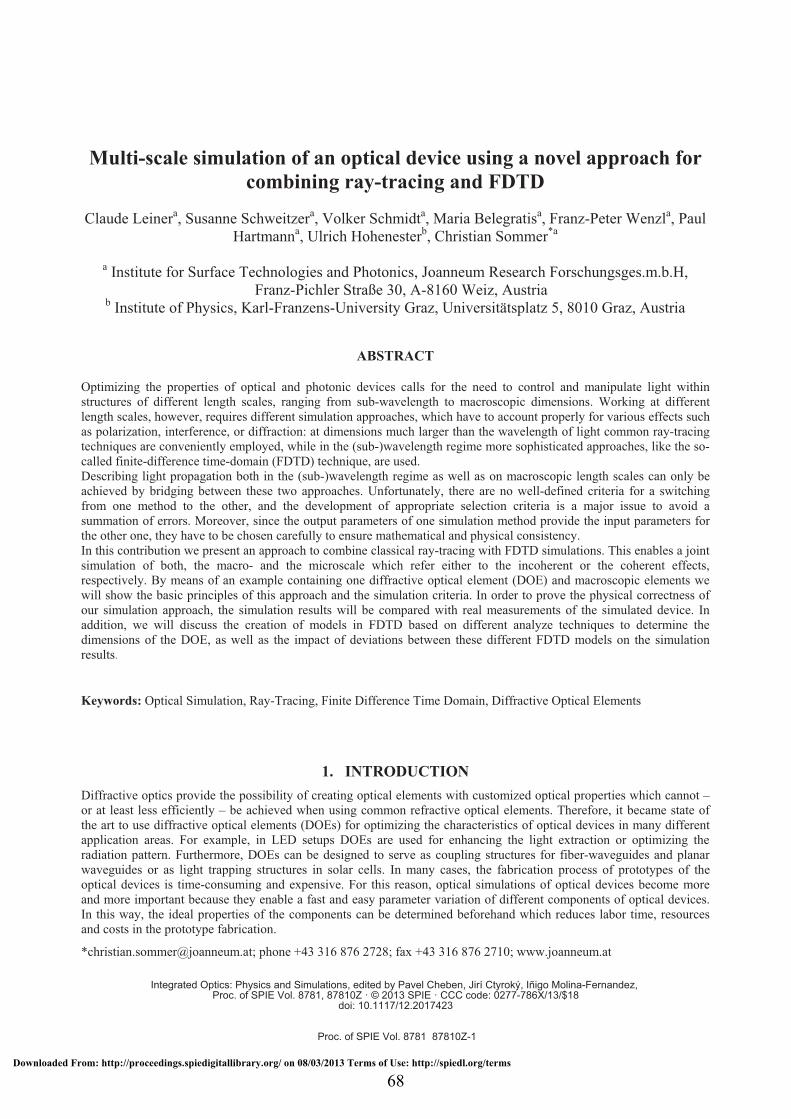
Multi-scale simulation of an optical device using a novel approach for combining ray-tracing and FDTD
Claude Leinera, Susanne Schweitzera, Volker Schmidta, Maria Belegratisa, Franz-Peter Wenzla, Paul
Hartmanna, Ulrich Hohenesterb, Christian Sommer*a
a Institute for Surface Technologies and Photonics, Joanneum Research Forschungsges.m.b.H, Franz-Pichler Straße 30, A-8160 Weiz, Austria
b Institute of Physics, Karl-Franzens-University Graz, Universitätsplatz 5, 8010 Graz, Austria
ABSTRACT
Optimizing the properties of optical and photonic devices calls for the need to control and manipulate light within structures of different length scales, ranging from sub-wavelength to macroscopic dimensions. Working at different length scales, however, requires different simulation approaches, which have to account properly for various effects such as polarization, interference, or diffraction: at dimensions much larger than the wavelength of light common ray-tracing techniques are conveniently employed, while in the (sub-)wavelength regime more sophisticated approaches, like the so-called finite-difference time-domain (FDTD) technique, are used. Describing light propagation both in the (sub-)wavelength regime as well as on macroscopic length scales can only be achieved by bridging between these two approaches. Unfortunately, there are no well-defined criteria for a switching from one method to the other, and the development of appropriate selection criteria is a major issue to avoid a summation of errors. Moreover, since the output parameters of one simulation method provide the input parameters for the other one, they have to be chosen carefully to ensure mathematical and physical consistency. In this contribution we present an approach to combine classical ray-tracing with FDTD simulations. This enables a joint simulation of both, the macro- and the microscale which refer either to the incoherent or the coherent effects, respectively. By means of an example containing one diffractive optical element (DOE) and macroscopic elements we will show the basic principles of this approach and the simulation criteria. In order to prove the physical correctness of our simulation approach, the simulation results will be compared with real measurements of the simulated device. In addition, we will discuss the creation of models in FDTD based on different analyze techniques to determine the dimensions of the DOE, as well as the impact of deviations between these different FDTD models on the simulation results. Keywords: Optical Simulation, Ray-Tracing, Finite Difference Time Domain, Diffractive Optical Elements
1. INTRODUCTION Diffractive optics provide the possibility of creating optical elements with customized optical properties which cannot – or at least less efficiently – be achieved when using common refractive optical elements. Therefore, it became state of the art to use diffractive optical elements (DOEs) for optimizing the characteristics of optical devices in many different application areas. For example, in LED setups DOEs are used for enhancing the light extraction or optimizing the radiation pattern. Furthermore, DOEs can be designed to serve as coupling structures for fiber-waveguides and planar waveguides or as light trapping structures in solar cells. In many cases, the fabrication process of prototypes of the optical devices is time-consuming and expensive. For this reason, optical simulations of optical devices become more and more important because they enable a fast and easy parameter variation of different components of optical devices. In this way, the ideal properties of the components can be determined beforehand which reduces labor time, resources and costs in the prototype fabrication.
*[email protected]; phone +43 316 876 2728; fax +43 316 876 2710; www.joanneum.at
Integrated Optics: Physics and Simulations, edited by Pavel Cheben, Jirí Ctyroký, Iñigo Molina-Fernandez, Proc. of SPIE Vol. 8781, 87810Z · © 2013 SPIE · CCC code: 0277-786X/13/$18
doi: 10.1117/12.2017423
Proc. of SPIE Vol. 8781 87810Z-1
Downloaded From: http://proceedings.spiedigitallibrary.org/ on 08/03/2013 Terms of Use: http://spiedl.org/terms
68
There are many numerical and analytical simulation methods founded on different approximations to simulate the behavior of light interacting with diffractive and/or refractive components of optical devices. A good overview of these methods is given in [1] which classifies the methods according to the different size regimes where they can be used efficiently. In the so-called “macro” regime, which can be described with geometrical optics because the structure sizes are more than 1000 times bigger than the wavelength used, classical ray tracing (RT) is commonly applied as numerical method. When the structure size becomes smaller, diffractive optical effects become more and more important. In this regime, Gaussian beam tracing (GBT) or the beam propagation method (BPM) are representative simulation methods. For structure sizes which are up to ten times bigger than the wavelength used, i.e. in the so-called “nano” regime, only wave optical (WO) models provide correct simulation results. One option is to solve the Maxwell’s curl equations with numerical methods like the Finite Difference Time Domain (FDTD) method or the Finite Element Method (FEM) [1].
Every numerical simulation model mentioned above is restricted to its own size regime: While e.g. RT neglects diffractive effects and is therefore not capable of simulating small structures, the size of FDTD simulations is limited by the required computational memory which increases with the third power of the structure size. Common workstations can handle simulation areas of several cubic micrometers only. Due to these size restrictions of the different simulation methods, simulation of whole devices containing refractive as well as diffractive optical elements is often not possible when using one model only.
For this reason, many authors are investigating opportunities for combining these methods with either self-made or commercial tools. For example, VirtualLab from LightTrans [2] applies a concept called “field tracing” which was published by Wyrowski and Kuhn. This method uses operators to propagate harmonic fields through the optical system instead of classical rays [3]. Furthermore, Rohani et al. combined GBT, Gabor expansion and FDTD to create an RT-FDTD hybrid method for the simulation of passive unbounded wave structures [4]. On the contrary, Ying Wang et al. presented a simulation method using a combination of the classical RT and the FDTD method for the investigation of radio wave propagation in buildings [5]. Another combination of classical RT and FDTD was used in [6-8] where the authors simulated the coupling-out efficiency of textured surface structures on LED chips.
In [9] we have introduced a simulation procedure which enables a combination of classical RT and FDTD by interfacing between the commercial tools ASAP from Breault Research [10] and FDTD Solutions from Lumerical [11], respectively. We have shown the physical correctness of the interface by simulating the goniophotometer measurement of light transmission through a diffraction grating. A comparison of the simulation results with real measurements has indicated a good accordance with the reality. Additionally, we also have investigated the impact of variations in the model settings (like e.g. changes of the height of the grating) on the corresponding simulated far field intensity distribution. In this proceeding, we make further investigations of the impact of the model settings on the simulation results. In particular, we use three different model settings to describe a diffraction grating with unsteady shapes of the periodic structures. The shapes of the modeled structures were designed on the basis of the results from different analysis methods to characterize the shape of the real diffraction grating.
2. METHOD The classical RT is based on geometrical optics, and the behavior of rays on optical boundaries (reflection, transmission, and absorption coefficients) which are traced through a surface based optical model is determined by the Fresnel coefficients. Thus, phase relations between the different rays are neglected in classical RT which is why diffractive optical elements cannot be described with this approach. The FDTD method is a wave optical approach for which the simulation area is discretized with a fine mesh and the Maxwell’s equations are solved numerically for each resulting cell by using a leapfrog algorithm. Thereby, the numerical error decreases with a higher number of cells or for smaller mesh cells. Hence, FDTD is considering diffraction effects but is restricted to smaller simulation areas because of computational memory and simulation-time issues. In fact, neither of the two approaches alone is capable of simulating a whole device which contains diffractive as well as refractive optical elements. The proposed procedure is addressed to overcome this limitation by connecting these two approaches using appropriate interface for exchanging data between them. In particular, the interface interconnects the RT tool (ASAP) and the WO tool (FDTD solutions). With this approach optical devices with refractive and diffractive optical elements can be simulated in a continuous step-by-step simulation procedure. Thereby, refractive optical parts of the device are simulated with ASAP and diffractive optical
Proc. of SPIE Vol. 8781 87810Z-2
Downloaded From: http://proceedings.spiedigitallibrary.org/ on 08/03/2013 Terms of Use: http://spiedl.org/terms
69
parts with FDTD. The interface is responsible for controlling the data transfer between the tools, which is realized at so-called interface planes and is schematically depicted in Figure 1.
The key of this interface is that in the geometrical optics it is possible to define the rays through the time averaged Poynting vector <S>: The propagation directions rays are parallel to the direction of corresponding <S> and the flux of each ray is proportional to the magnitude of <S>. On the other hand, in the wave optics it is possible to decompose <S> into a set of plane waves with different k vectors. Inversely, <S> can easily be re-obtained from calculated far fields by the vector product of the electrical field (E) and the magnetic field (H). These relationships are used for realizing the interface for the data transfer between ASAP and the FDTD simulation tool. It is used throughout this work and is explained in more detail below and in [9].
Figure 1: Sketch to illustrate the method of operation using interfaces between the different simulation regions (RT or FDTD) for the considered optical system.
In Figure 1 a schematic sketch of the considered optical devices comprising refractive and diffractive optical elements is shown. The simulation procedure needs to split the optical device in different areas, for which either the RT or FDTD simulation tool meets the requirement of the physical properties (either macro or nano regime). In particular, the first area is simulated with RT and is related to the illumination arm of the goniophotometer. For the considered diffraction grating in the intermediate area FDTD simulation are needed. The simulation process is finished with an RT simulation of a detector unit. This simulation sequence is controlled via Matlab scripts which also manage the data transfer through the interface from one simulation tool to the other. This data transfer is required because essential informations from the results of one simulation step are used as starting conditions for a subsequent simulation step. The data transfer is realized at so-called interface planes, which are positioned in the close vicinity of the DOE in the optical device (Figure 1). When switching from RT to FDTD, the positions, directions and fluxes of the rays at the interface plane, which result from the RT simulations, are recorded and converted into a set of plane waves. These plane waves are propagated independently through the DOE in a series of FDTD simulations. The results of these FDTD simulations are different far fields and transmission coefficients. The intensity distributions of these far fields are then converted into probability density distributions which are used to weight the sampling of the angular distribution of the rays according to ray data recorded at the interface plane previously. Furthermore, the flux of each ray is matched with the transmission coefficients obtained from the FDTD simulations. The so obtained new ray set is used for continuing the simulation within the subsequent RT simulation. With this, the step by step simulation of the above described optical device is completed.
3. EXPERIMENTAL AND SIMULATION SETUP In this section, a goniophotometer measurement of a (non-perfect) regular blazed diffraction grating is simulated using interfaces for combining RT and FDTD simulation tools. Particularly, it is the comparison of the measurement with the results of the simulation of the transmitted angular intensity distribution in the far field through a blazed grating. In addition, we show the importance of correct model settings for receiving good simulation results.
The diffraction grating is placed onto the measurement surface of a goniophotometer (GON 360; Fig. 2a and b) in order to determine the transmitted far field of the blazed grating. The goniometer comprises two independently rotatable arms which are driven by stepping motors and are controlled by a PC. One arm is connected via an optical fiber with a halogen lamp, this is the illumination unit (8.3 A, 12 V), and the other arm (detector arm) is coupled to an array
Proc. of SPIE Vol. 8781 87810Z-3
Downloaded From: http://proceedings.spiedigitallibrary.org/ on 08/03/2013 Terms of Use: http://spiedl.org/terms
70
spectrometer which is capable of measuring the spectral distribution of the light between approx. 380 nm to 1100 nm in a single measurement. For the measurement series, the detector arm was rotated in 0.5° steps in order to record the transmitted angular far field distribution. The detector aperture was limited by a slit aperture (1 mm) in order to increase the angular resolution in the direction of rotation.
Figure 2: a) and b) Sketches to illustrate the GON 360 system including all relevant size data to build the RT model. c) More detailed sketch of the illumination arm showing the double lens system, which focuses the beam towards the sample.
The sample is placed in the rotation center of the goniophotometer which is 16 mm in front of the focus position of the convergent illumination beam (Fig. 2b). Hence, the propagation directions of the rays hitting the sample are not homogenously distributed within the illumination spot at the sample’s position. A detailed RT simulation of the illumination arm (Fig. 2c) is inevitable. As a result a correct map of the ray distribution at the sample position is obtained.
Proc. of SPIE Vol. 8781 87810Z-4
Downloaded From: http://proceedings.spiedigitallibrary.org/ on 08/03/2013 Terms of Use: http://spiedl.org/terms
71
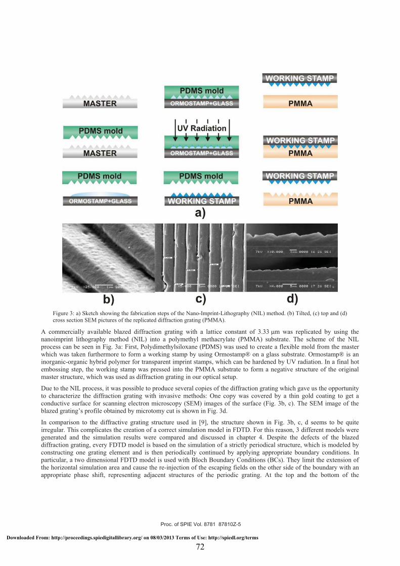
Figure 3: a) Sketch showing the fabrication steps of the Nano-Imprint-Lithography (NIL) method. (b) Tilted, (c) top and (d) cross section SEM pictures of the replicated diffraction grating (PMMA).
A commercially available blazed diffraction grating with a lattice constant of 3.33 �m was replicated by using the nanoimprint lithography method (NIL) into a polymethyl methacrylate (PMMA) substrate. The scheme of the NIL process can be seen in Fig. 3a: First, Polydimethylsiloxane (PDMS) was used to create a flexible mold from the master which was taken furthermore to form a working stamp by using Ormostamp® on a glass substrate. Ormostamp® is an inorganic-organic hybrid polymer for transparent imprint stamps, which can be hardened by UV radiation. In a final hot embossing step, the working stamp was pressed into the PMMA substrate to form a negative structure of the original master structure, which was used as diffraction grating in our optical setup.
Due to the NIL process, it was possible to produce several copies of the diffraction grating which gave us the opportunity to characterize the diffraction grating with invasive methods: One copy was covered by a thin gold coating to get a conductive surface for scanning electron microscopy (SEM) images of the surface (Fig. 3b, c). The SEM image of the blazed grating’s profile obtained by microtomy cut is shown in Fig. 3d.
In comparison to the diffractive grating structure used in [9], the structure shown in Fig. 3b, c, d seems to be quite irregular. This complicates the creation of a correct simulation model in FDTD. For this reason, 3 different models were generated and the simulation results were compared and discussed in chapter 4. Despite the defects of the blazed diffraction grating, every FDTD model is based on the simulation of a strictly periodical structure, which is modeled by constructing one grating element and is then periodically continued by applying appropriate boundary conditions. In particular, a two dimensional FDTD model is used with Bloch Boundary Conditions (BCs). They limit the extension of the horizontal simulation area and cause the re-injection of the escaping fields on the other side of the boundary with an appropriate phase shift, representing adjacent structures of the periodic grating. At the top and the bottom of the
Proc. of SPIE Vol. 8781 87810Z-5
Downloaded From: http://proceedings.spiedigitallibrary.org/ on 08/03/2013 Terms of Use: http://spiedl.org/terms
72
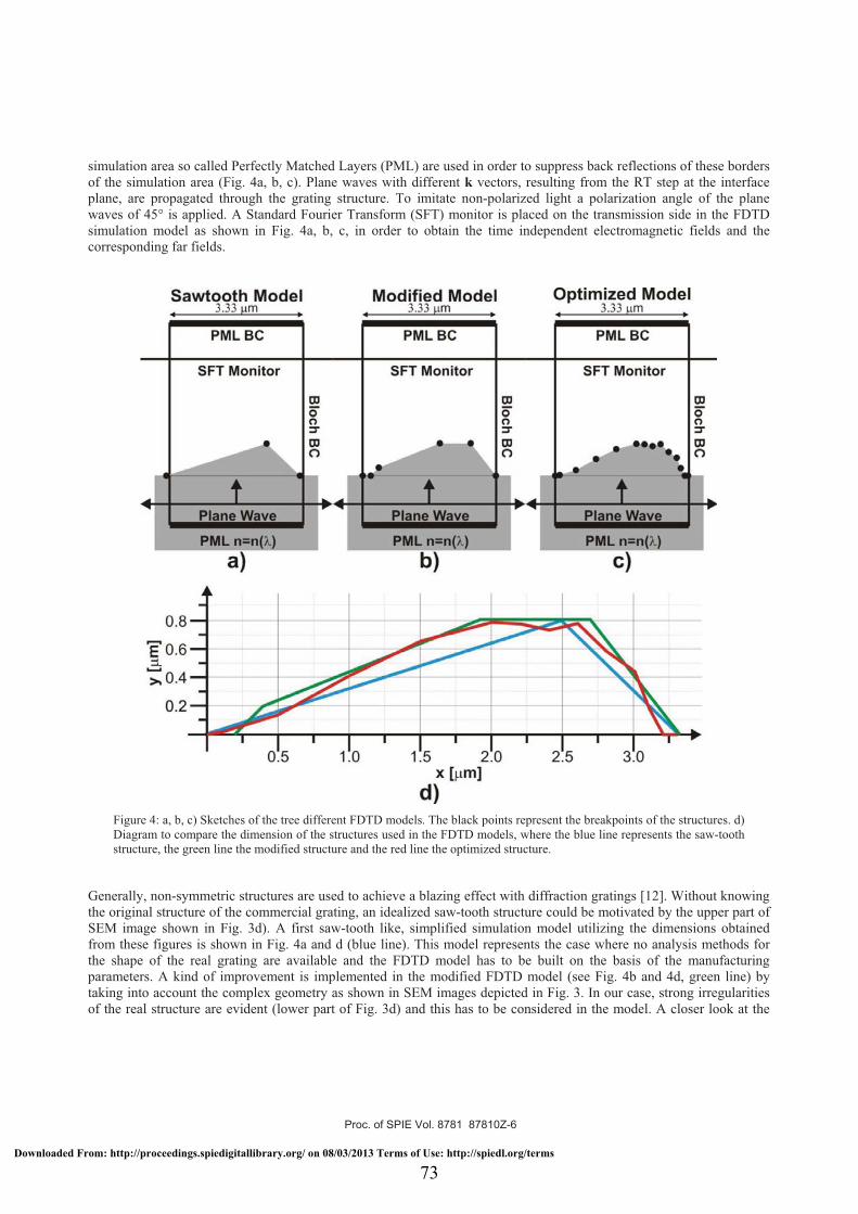
simulation area so called Perfectly Matched Layers (PML) are used in order to suppress back reflections of these borders of the simulation area (Fig. 4a, b, c). Plane waves with different k vectors, resulting from the RT step at the interface plane, are propagated through the grating structure. To imitate non-polarized light a polarization angle of the plane waves of 45° is applied. A Standard Fourier Transform (SFT) monitor is placed on the transmission side in the FDTD simulation model as shown in Fig. 4a, b, c, in order to obtain the time independent electromagnetic fields and the corresponding far fields.
Figure 4: a, b, c) Sketches of the tree different FDTD models. The black points represent the breakpoints of the structures. d) Diagram to compare the dimension of the structures used in the FDTD models, where the blue line represents the saw-tooth structure, the green line the modified structure and the red line the optimized structure.
Generally, non-symmetric structures are used to achieve a blazing effect with diffraction gratings [12]. Without knowing the original structure of the commercial grating, an idealized saw-tooth structure could be motivated by the upper part of SEM image shown in Fig. 3d). A first saw-tooth like, simplified simulation model utilizing the dimensions obtained from these figures is shown in Fig. 4a and d (blue line). This model represents the case where no analysis methods for the shape of the real grating are available and the FDTD model has to be built on the basis of the manufacturing parameters. A kind of improvement is implemented in the modified FDTD model (see Fig. 4b and 4d, green line) by taking into account the complex geometry as shown in SEM images depicted in Fig. 3. In our case, strong irregularities of the real structure are evident (lower part of Fig. 3d) and this has to be considered in the model. A closer look at the
Proc. of SPIE Vol. 8781 87810Z-6
Downloaded From: http://proceedings.spiedigitallibrary.org/ on 08/03/2013 Terms of Use: http://spiedl.org/terms
73
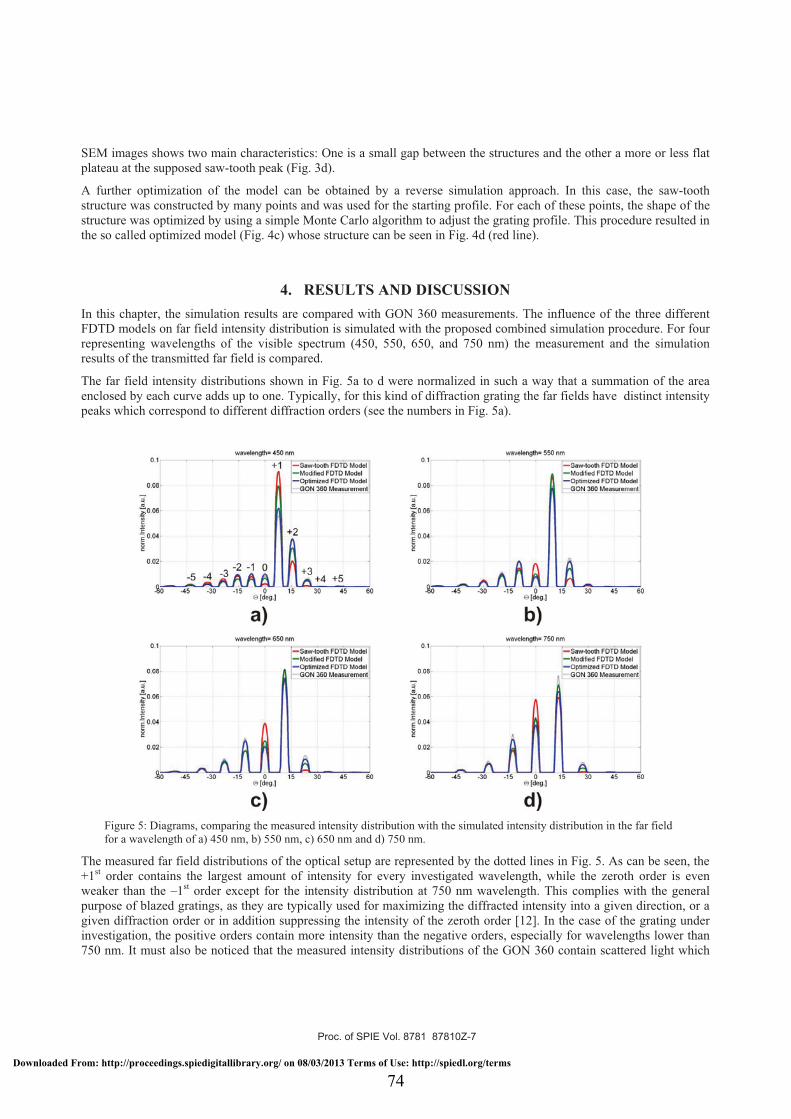
SEM images shows two main characteristics: One is a small gap between the structures and the other a more or less flat plateau at the supposed saw-tooth peak (Fig. 3d).
A further optimization of the model can be obtained by a reverse simulation approach. In this case, the saw-tooth structure was constructed by many points and was used for the starting profile. For each of these points, the shape of the structure was optimized by using a simple Monte Carlo algorithm to adjust the grating profile. This procedure resulted in the so called optimized model (Fig. 4c) whose structure can be seen in Fig. 4d (red line).
4. RESULTS AND DISCUSSION In this chapter, the simulation results are compared with GON 360 measurements. The influence of the three different FDTD models on far field intensity distribution is simulated with the proposed combined simulation procedure. For four representing wavelengths of the visible spectrum (450, 550, 650, and 750 nm) the measurement and the simulation results of the transmitted far field is compared.
The far field intensity distributions shown in Fig. 5a to d were normalized in such a way that a summation of the area enclosed by each curve adds up to one. Typically, for this kind of diffraction grating the far fields have distinct intensity peaks which correspond to different diffraction orders (see the numbers in Fig. 5a).
Figure 5: Diagrams, comparing the measured intensity distribution with the simulated intensity distribution in the far field for a wavelength of a) 450 nm, b) 550 nm, c) 650 nm and d) 750 nm.
The measured far field distributions of the optical setup are represented by the dotted lines in Fig. 5. As can be seen, the +1st order contains the largest amount of intensity for every investigated wavelength, while the zeroth order is even weaker than the –1st order except for the intensity distribution at 750 nm wavelength. This complies with the general purpose of blazed gratings, as they are typically used for maximizing the diffracted intensity into a given direction, or a given diffraction order or in addition suppressing the intensity of the zeroth order [12]. In the case of the grating under investigation, the positive orders contain more intensity than the negative orders, especially for wavelengths lower than 750 nm. It must also be noticed that the measured intensity distributions of the GON 360 contain scattered light which
Proc. of SPIE Vol. 8781 87810Z-7
Downloaded From: http://proceedings.spiedigitallibrary.org/ on 08/03/2013 Terms of Use: http://spiedl.org/terms
74
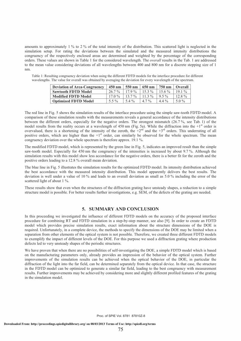
amounts to approximately 1 % to 2 % of the total intensity of the distribution. This scattered light is neglected in the simulation setup. For rating the deviations between the simulated and the measured intensity distributions the congruency of the respectively enclosed areas are determined and weighted by the percentage of the corresponding orders. These values are shown in Table 1 for the considered wavelength. The overall results in the Tab. 1 are addressed to the mean value considering deviations of all wavelengths between 400 and 800 nm for a discrete stepping size of 1 nm.
Table 1: Resulting congruency deviation when using the different FDTD models for the interface procedure for different wavelengths. The value for overall was obtained by averaging the deviation for every wavelength of the spectrum.
Deviation of Area-Congruency 450 nm 550 nm 650 nm 750 nm Overall Sawtooth FDTD Model 26.7 % 17.9 % 15.3 % 15.6 % 19.1 % Modified FDTD Model 17.0 % 13.7 % 11.3 % 9.5 % 12.8 % Optimized FDTD Model 5.5 % 5.4 % 4.7 % 4.4 % 5.0 %
The red line in Fig. 5 shows the simulation results of the interface procedure using the simple saw-tooth FDTD model. A comparison of these simulation results with the measurements reveals a general accordance of the intensity distributions between the different orders, especially for the negative orders. The strongest mismatch (26.7 %, see Tab. 1) of the model results from the reality occurs at a wavelength of 450 nm (Fig. 5a). While the diffraction into the +1st order is overvalued, there is a shortening of the intensity of the zeroth, the +2nd and the +3rd orders. This underrating of all positive orders, which are higher than the +1st order, can similarly be observed for the whole spectrum. The mean congruency deviation over the whole spectrum is therefore approx. 19.1 %.
The modified FDTD model, which is represented by the green line in Fig. 5, indicates an improved result than the simple saw-tooth model. Especially for 450 nm the congruency of the intensities is increased by about 9.7 %. Although the simulation results with this model show less accordance for the negative orders, there is a better fit for the zeroth and the positive orders leading to a 12.8 % overall mean deviation.
The blue line in Fig. 5 illustrates the simulation results for the optimized FDTD model. Its intensity distribution achieved the best accordance with the measured intensity distribution. This model apparently delivers the best results. The deviation is well under a value of 10 % and leads to an overall deviation as small as 5.0 % including the error of the scattered light of about 1 %.
These results show that even when the structures of the diffraction grating have unsteady shapes, a reduction to a simple structure model is possible. For better results further investigations, e.g. SEM, of the defects of the grating are needed.
5. SUMMARY AND CONCLUSION In this proceeding we investigated the influence of different FDTD models on the accuracy of the proposed interface procedure for combining RT and FDTD simulation in a step-by-step manner, see also [9]. In order to create an FDTD model which provides precise simulation results, exact information about the structure dimensions of the DOE is required. Unfortunately, in a complete device, the methods to specify the dimensions of the DOE may be limited when a separation from other elements of the optical system is not possible. Therefore, we created three different FDTD models to exemplify the impact of different levels of the DOE. For this purpose we used a diffraction grating where production defects led to very unsteady shapes of the periodic structures.
We have proven that when there are no possibilities of self-investigating the DOE, a simple FDTD model which is based on the manufacturing parameters only, already provides an impression of the behavior of the optical system. Further improvements of the simulation results can be achieved when the optical behavior of the DOE, in particular the diffraction of the light into the far field, can be determined separately from the optical device. In that case, the structure in the FDTD model can be optimized to generate a similar far field, leading to the best congruency with measurement results. Further improvements may be achieved by considering more and slightly different profiled features of the grating in the simulation model.
Proc. of SPIE Vol. 8781 87810Z-8
Downloaded From: http://proceedings.spiedigitallibrary.org/ on 08/03/2013 Terms of Use: http://spiedl.org/terms
75

Acknowledgments
The authors also gratefully acknowledge financial support from the BMVIT within the FIT-IT program – ModSim Computational Mathematics – of the Austrian Research Promotion Agency (FFG), project number 828706.
REFERENCES
[1] Lang, M., and Milster, T. D., “Investigation of Optics in the 10–200�m Size Regime,” Opt. Rev. 14, 189-193 (2007).
[2] LightTrans, http://www.lighttrans.com/. [3] Wyrowski, F., and Kuhn, M., "Introduction to field tracing," J. Mod. Opt. 58, 449-466 (2011). [4] Rohani, A., Chaudhuri, S. K., and Safavi-Naeini, S., “Gaussian Beam-Based Hybrid Method for Quasi-Optical
Systems,” IEEE Trans. Antennas Propag, 59, 4679-4690 (2011). [5] Wang, Y., Safavi-Naeini, S., and. Chaudhuri, S. K., “A hybrid technique based on combining ray tracing and
FDTD methods for site-specific modeling of indoor radio wave propagation,” IEEE Trans. Antennas Propag., 48, 743-754 (2000).
[6] Kawaguchi, Y., Nishizono, K., Lee, J. S. and Katsuda, H. “Light extraction simulation of surface-textured light-emitting diodes by finite-difference time-domain method and ray-tracing method,” Jpn. J. Appl. Phys, 46, 31 (2007).
[7] Cheng, L.W., Sheng, Y., Xia, C. S., Lu, W., Lestrade, M., and Z.M. Li, “Simulation for light power distribution of 3D InGaN/GaN MQW LED with textured surface,” Opt. Quantum Electron., 42, 739-745 (2011).
[8] Sheng, Y., Xia, C.S., Li, Z. M. S., and Cheng, L.W., “Simulation of InGaN/GaN light-emitting diodes with patterned sapphire substrate,” 12th International Conference on Numerical Simulation of Optoelectronic Devices (NUSOD 2012), 10.1109/NUSOD.2012.6316488 (2012).
[9] Leiner, C., Schweitzer, S., Wenzl, F. P., Hartmann, P., Hohenester, U., Sommer, C., “A simulation procedure interfacing ray-tracing and finite-difference time-domain methods for a combined simulation of diffractive and refractive optical elements,” submitted (2013).
[10] Breault Research Organization, “ASAP - Getting started guide,” Tucson AZ (2010). http://www.breault.com/resources/kbasePDF/broman0108_getstart.pdf
[11] Lumerical Solutions, “FDTD Solutions Knowledge Base,” Vancouver (2012). http://docs.lumerical.com/en/fdtd/knowledge_base.html
[12] Palmer, C., [Diffraction Grating Handbook], sixth edition, Newport Corporation, New York (2005).
Proc. of SPIE Vol. 8781 87810Z-9
Downloaded From: http://proceedings.spiedigitallibrary.org/ on 08/03/2013 Terms of Use: http://spiedl.org/terms
76
3.1.4 MULTIPLE INTERFACING BETWEEN CLASSICAL RAY-
TRACING AND WAVE-OPTICAL SIMULATION APPROACHES:
A STUDY ON APPLICABILITY AND ACCURACY
”Multiple Interfacing Between Classical Ray-Tracing and Wave-Optical Simulation
Approaches: A Study on Applicability and Accuracy” wurde im März 2014 als Full
Paper in Optics Express eingereicht und im Juni 2014 als open access Publikation in
Volume 22, Issue 13, pp. 16048-16060 des Journals veröffentlicht. Der eigene Anteil
bei dieser Veröffentlichung beträgt 70%.
In dieser Publikation wird der Einfluss der durch die Schnittstellenmethode
vernachlässigten Phasenbeziehungen auf das Simulationsergebnis untersucht. Aus
theoretischen Überlegungen über die räumliche Teilkohärenz wird eine
Grenzwertfunktion abgeleitet. Sie beschreibt den maximalen Grad an kohärenter
Kopplung zwischen zwei DOEs, abhängig vom Öffnungswinkel der Lichtquelle, der
Intensitätsverteilung nach den DOEs und dem Abstand zwischen den DOEs. Durch
diese Grenzwertfunktion wird ermöglicht, Aussagen über die Anwendbarkeit und die
Genauigkeit der Schnittstellenmethode bei einer gegebenen
Simulationsaufgabenstellung mit mehreren DOEs zu treffen. Zur Verifikation der
durch diese Grenzwertfunktion getroffenen Aussagen werden die Ergebnisse einer
RTFDTDRTFDTDRT Schnittstellensimulation mit den Ergebnissen einer
reinen FDTD Simulation verglichen, bei der die Phasenbeziehungen nicht
vernachlässigt wurden.
77
Multiple interfacing between classical ray-tracing and wave-optical simulation approaches:
a study on applicability and accuracy Claude Leiner,1 Wolfgang Nemitz,1 Susanne Schweitzer,1 Franz P. Wenzl,1 Paul
Hartmann,1 Ulrich Hohenester2 and Christian Sommer1* 1Institute of Surface Technologies and Photonics, Joanneum Research Forschungsgesellschaft mbH, Franz-Pichler
Straße 30, A-8160 Weiz, Austria 2Institute of Physics, University of Graz, Universitätsplatz 5, A-8010 Graz, Austria
Abstract: In this study the applicability of an interface procedure for combined ray-tracing and finite difference time domain (FDTD) simulations of optical systems which contain two diffractive gratings is discussed. The simulation of suchlike systems requires multiple FDTD↔RT steps. In order to minimize the error due to the loss of the phase information in an FDTD→RT step, we derive an equation for a maximal coherence correlation function (MCCF) which describes the maximum degree of impact of phase effects between these two different diffraction gratings and which depends on: the spatial distance between the gratings, the degree of spatial coherence of the light source and the diffraction angle of the first grating for the wavelength of light used. This MCCF builds an envelope of the oscillations caused by the distance dependent coupling effects between the two diffractive optical elements. Furthermore, by comparing the far field projections of pure FDTD simulations with the results of an RT→FDTD→RT→FDTD→RT interface procedure simulation we show that this function strongly correlates with the error caused by the interface procedure. ©2014 Optical Society of America OCIS codes: (050.1755) Computational electromagnetic methods; (050.1950) Diffraction gratings; (080.1753) Computation methods; (230.0230) Optical devices; (350.4600) Optical engineering;
References and links 1. M. Lang and T. D. Milster, “Investigation of optics in the 10 – 200 μm size regime,” Opt. Rev. 14(4), 189–193
(2007). 2. T. Bocksrocker, J. B. Preinfalk, J. Asche-Tauscher, A. Pargner, C. Eschenbaum, F. Maier-Flaig, and U. Lemmer,
“White organic light emitting diodes with enhanced internal and external outcoupling for ultra-efficient light extraction and Lambertian emission,” Opt. Express 20(S6), A932–A940 (2012).
3. J. Hauss, T. Bocksrocker, B. Riedel, U. Geyer, U. Lemmer, and M. Gerken, “Metallic Bragg-gratings for light management in organic light-emitting devices,” Appl. Phys. Lett. 99(10), 103303 (2011).
4. C.-H. Lin, C.-Y. Chen, D.-M. Yeh, and C.-C. Yang, “Light extraction enhancement of a GaN-based light-emitting diode through grating-patterned photoelectrochemical surface etching with phase mask interferometry,” IEEE Photon. Technol. Lett. 22(9), 640–642 (2010).
5. D. N. Weiss, H.-C. Yuan, B. G. Lee, H. M. Branz, S. T. Meyers, A. Grenville, and D. A. Keszler, “Nanoimprinting for diffractive light trapping in solar cells,” J. Vac. Sci. Technol. B-Microelectron. and Nanom. Struct. 28, C6M98 (2010).
6. R. Dewan and D. Knipp, “Light trapping in thin-film silicon solar cells with integrated diffraction grating,” J. Appl. Phys. 106(7), 074901 (2009).
7. Y. M. Song, J. S. Yu, and Y. T. Lee, “Antireflective submicrometer gratings on thin-film silicon solar cells for light-absorption enhancement,” Opt. Lett. 35(3), 276–278 (2010).
8. S. Feng, X. Zhang, H. Wang, M. Xin, and Z. Lu, “Fiber coupled waveguide grating structures,” Appl. Phys. Lett. 96(13), 133101 (2010).
#209272 - $15.00 USD Received 31 Mar 2014; revised 13 Jun 2014; accepted 17 Jun 2014; published 23 Jun 2014(C) 2014 OSA 30 June 2014 | Vol. 22, No. 13 | DOI:10.1364/OE.22.016048 | OPTICS EXPRESS 16048
78
9. G. Roelkens, D. Van Thourhout, and R. Baets, “High efficiency grating coupler between silicon-on-insulator waveguides and perfectly vertical optical fibers,” Opt. Lett. 32(11), 1495–1497 (2007).
10. T. Pustelny, I. Zielonka, P. Karasinski, and J. Jurusik, “Bragg ’ s grating coupler in planar optical sol-gel waveguides,” Opt. Appl. XXXIV, Vol. 4 (2004).
11. K. Schmitt and C. Hoffmann, High-Refractive-Index Waveguide Platforms for Chemical and Biosensing, Optical Gu, Springer Series on Chemical Sensors and Biosensors (Springer Berlin Heidelberg, 2009), Vol. 7, pp. 21–55.
12. S. Grego, S. Naskar, A. M. Patel, A. Huffman, C. A. Bower, and B. R. Stoner, “Novel optical-waveguide sensing platform based on input grating coupler,” Proc. SPIE 6123, 61230D (2006).
13. M. Prasciolu, D. Cojoc, S. Cabrini, L. Businaro, P. Candeloro, M. Tormen, R. Kumar, C. Liberale, V. Degiorgio, A. Gerardino, G. Gigli, D. Pisignano, E. Di Fabrizio, and R. Cingolani, “Design and fabrication of on-fiber diffractive elements for fiber-waveguide coupling by means of e-beam lithography,” Microelectron. Eng. 68, 169–174 (2003).
14. P. Struk and T. Pustelny, “Design and numerical analyses of the planar grating coupler,” Bull. Polish Acad. Sci. Tech. Sci. 58, 509–512 (2010).
15. D. Taillaert, F. Van Laere, M. Ayre, W. Bogaerts, D. Van Thourhout, P. Bienstman, and R. Baets, “Grating couplers for coupling between optical fibers and nanophotonic waveguides,” Jpn. J. Appl. Phys. 45(8A), 6071–6077 (2006).
16. G. Roelkens, D. Van Thourhout, and R. Baets, “High efficiency Silicon-on-Insulator grating coupler based on a poly-Silicon overlay,” Opt. Express 14(24), 11622–11630 (2006).
17. S. S. Trieu and X. Jin, “Study of top and bottom photonic gratings on GaN LED with error grating models,” IEEE J. Quantum Electron. 46(10), 1456–1463 (2010).
18. I. J. Buss, G. R. Nash, J. G. Rarity, and M. J. Cryan, “Finite-difference time-domain modeling of periodic and disordered surface gratings in AlInSb light emitting diodes with metallic back-reflectors,” J. Lightwave Technol. 28(8), 1190–1200 (2010).
19. Y. Jin, F. Yang, Q. Li, Z. Zhu, J. Zhu, and S. Fan, “Enhanced light extraction from a GaN-based green light-emitting diode with hemicylindrical linear grating structure,” Opt. Express 20(14), 15818–15825 (2012).
20. S. S. Trieu, X. Jin, B. Zhang, T. Dai, K. Bao, X.-N. Kang, and G.-Y. Zhang, “Light Extraction Improvement of GaN-based Light Emitting Diodes using Patterned Undoped GaN Bottom Reflection Gratings,” Proc. SPIE 7216, 72162Q (2009).
21. F. Wyrowski and M. Kuhn, “Introduction to field tracing,” J. Mod. Opt. 58(5-6), 449–466 (2011). 22. LightTrans,” http://www.lighttrans.com/. 23. A. Rohani, S. K. Chaudhuri, and S. Safavi-Naeini, “Gaussian Beam-Based Hybrid Method for Quasi-Optical
Systems,” IEEE Trans. Antenn. Propag. 59(12), 4679–4690 (2011). 24. Breault Research Organization, ASAP - Getting started guide,”
http://www.breault.com/resources/kbasePDF/broman0108_getstart.pdf. 25. Lumerical Solutions, FDTD Solutions Knowledge Base,”
http://docs.lumerical.com/en/fdtd/knowledge_base.html. 26. A. W. Greynolds, “Vector Formulation Of The Ray-Equivalent Method For General Gaussian Beam
Propagation,” Proc. of SPIE 0679 (1986). 27. Breault Research Organization, Wave Optics in ASAP,”
http://www.breault.com/resources/kbasePDF/brotg0919_wave.pdf. 28. Breault Research Organization, Modeling Incoherent, Extended Sources,”
http://www.breault.com/resources/kbasePDF/bropn1153_sources.pdf. 29. Y. Wang, S. Safavi-Naeini, and S. K. Chaudhuri, “A hybrid technique based on combining ray tracing and
FDTD methods for site-specific modeling of indoor radio wave propagation,” IEEE Trans. Antenn. Propag. 48(5), 743–754 (2000).
30. Y. Wang, S. K. Chaudhuri, and S. Safavi-Naeini, “An FDTD/ray-tracing analysis method for wave penetration through inhomogeneous walls,” IEEE Trans. Antenn. Propag. 50(11), 1598–1604 (2002).
31. Y. Kawaguchi, K. Nishizono, J.-S. Lee, and H. Katsuda, “Light extraction simulation of surface-textured light-emitting diodes by finite-difference time-domain method and ray-tracing method,” Jpn. J. Appl. Phys. 46(1), 31–34 (2007).
32. L.-W. Cheng, Y. Sheng, C.-S. Xia, W. Lu, M. Lestrade, and Z.-M. Li, “Simulation for light power distribution of 3D InGaN/GaN MQW LED with textured surface,” Numer Simul Optoelectron Devices 1-2 (2010).
33. Y. Sheng, C. S. Xia, Z. M. Simon Li, and L. W. Cheng, “Simulation of InGaN/GaN light-emitting diodes with patterned sapphire substrate,” 2012 12th Int. Conf. Numer. Simul. Optoelectron. Devices 23–24 (2012).
34. C. Leiner, S. Schweitzer, F. P. Wenzl, P. Hartmann, U. Hohenester, and C. Sommer, “A simulation procedure interfacing ray-tracing and finite-difference time-domain methods for a combined simulation of diffractive and refractive optical elements,” J. Lightwave Technol. 32(6), 1054–1062 (2014).
35. C. Leiner, S. Schweitzer, V. Schmidt, M. Belegratis, F. P. Wenzel, P. Hartmann, U. Hohenester, and C. Sommer, “Multi-scale simulation of an optical device using a novel approach for combining ray-tracing and FDTD,” Proc. SPIE 8781, 87810Z (2013).
36. L. Mandel and E. Wolf, Optical Coherence and Quantum Optics (Cambridge University Press, 1995). 37. M. Born and E. Wolf, Principles of Optics (1999), Vol. 1. 38. A. Taflove and S. C. Hagness, “Computational Electrodynamics,” The Finite-Difference Time-Domain Method
2010, 1006 (2005).
#209272 - $15.00 USD Received 31 Mar 2014; revised 13 Jun 2014; accepted 17 Jun 2014; published 23 Jun 2014(C) 2014 OSA 30 June 2014 | Vol. 22, No. 13 | DOI:10.1364/OE.22.016048 | OPTICS EXPRESS 16049
79

39. K. S. Yee, “Numerical solution of initial boundary value problems involving maxwell’s equations in isotropic media,” IEEE Trans. Antenn. Propag. 14(3), 302–307 (1966).
1. Introduction
The last few decades have witnessed remarkable progress of processing speed and storage capacity of computers. This facilitates the use of numerical simulations to address more and more problems in a lot of academic and industrial research and development areas. By this, in comparison with conventional trial and error experimental techniques, the research and innovation speed can be enhanced and costs can be saved.
A remarkable example in this regard is the design and optimization of optical devices that comprise different optical elements. Currently, there is a broad range of optical simulation techniques available to treat suchlike problems. The application ranges of the respective simulation tools mainly depend on the size ranges of the optical elements in the devices in relation to the wavelength of light used. In the “macro” regime, where structure sizes are more than 100 times larger than the wavelengths, the simulation methods are based on the theory of refractive optics (RO), such as classical ray-tracing (RT), Gaussian beam tracing (GBT) or the beam propagation method (BPM) [1]. Contrarily, in the so called “nano” regime, for which the ratio between structure size and wavelength becomes smaller than a factor of ten, simulation methods based on ray optics lose their accuracy. Therefore, for an appropriate simulation of devices containing diffractive optical elements (DOEs), numerical methods that are capable of solving problems in the context of wave optics (WO), in particular the Maxwell’s equations, are required. Well known examples in this regard are methods like the finite difference time domain method (FDTD), the finite element method (FEM) for more general applications, as well as semi analytic methods like the rigorous coupled-wave analysis method (RCWA), which is restricted to more specific problems [1]. However, numerical WO methods require computers with a high memory capacity and often prevent complete simulations of macroscopically optical devices even with the capacity of today’s workstation technology. Therefore, an all-embracing simulation of optical devices consisting of both DOEs and refractive optical elements constitute a problem for the abovementioned simulation methods.
On the other hand, as state of the art, DOEs are used in more and more macroscopic devices such as light emitting diodes (LEDs) to enhance, e.g., light extraction or to tailor the emission patterns [2–4], in solar cells for light trapping [5–7], in fiber-waveguides or planar waveguides as coupling structures [8–10], as well as in the field of optical sensing or integrated optics [11,12]. As a result of the size restrictions of the different simulation approaches mentioned above and the limited memory capacity of the computers, optical simulations of these devices are limited in many cases to the simulation of individual diffractive or refractive components [13–20]. In particular for devices that consist of several diffractive and refractive components these limitations restrict a combined simulation and optimization as well as the consideration of interaction phenomena. Therefore, simulation techniques which are capable of overcoming the abovementioned drawbacks and that allow to handle suchlike complex devices as a whole are highly recommended.
In this regard, several authors already suggested different approaches to interface between RO and WO based simulation tools, using either self-written or commercial RT, GBT, BPM, FDTD or FEM based simulation tools. Such interface approaches allow to address and to consider the individual ROEs and DOEs of a device by an appropriate data transfer from one simulation tool to the other. Still, the biggest challenge in this regard is the set-up of the interface and an appropriate and correct data transfer between WO and RO based simulation tools.
One possibility in this regard is the use of RO-based approaches which allow the consideration of both field and phase data, as shown, e.g., by Wyrowski and Kuhn [21], [22] or Rohani et al. [23]. In addition, also suppliers of well-known commercial simulation
#209272 - $15.00 USD Received 31 Mar 2014; revised 13 Jun 2014; accepted 17 Jun 2014; published 23 Jun 2014(C) 2014 OSA 30 June 2014 | Vol. 22, No. 13 | DOI:10.1364/OE.22.016048 | OPTICS EXPRESS 16050
80
programs provide tools addressing this problem. For example, Breault Research [24] (RT/GBT/BPM-Program: ASAP) and Lumerical [25] (FDTD Solutions) set up an interface for the exchange of field data between the GBT-mode of ASAP [26,27] and FDTD and vice versa (GBT↔FDTD). This interface allows to handle a wide scope of optical problems, for example, the simulation of an LCD camera or the optical response of microstructures on a DVD surface [24,25]. However, this interface is limited to simulation tasks for which in the GBT simulation part the light is focused on the DOE.
Another option to realize an interface between WO and RO based simulation approaches is to combine classical RT with WO approaches, which is a very simple method to address this problem without further restrictions for the RO part of the simulation. Anyway, it has to be considered that in classical RT phase relations between different rays are neglected. This restricts transitions from RT to FDTD to applications for which these relations can be assumed to be random. Nonetheless, this condition is fulfilled for broadband and spatially incoherent light sources like incandescence bulbs, halogen lamps, and light emitting diodes. Another advantage of this approach is that commercial RO simulation programs like ASAP offer a wide range of possibilities to design the emission patterns of such light sources [28].
An example for such a kind of interface was presented already in the year 2000 by Wang et al. who used a combination of classical RT and FDTD for the investigation of radio wave propagation in buildings [29,30]. The authors used RT for the simulation of large areas of the building and switched to FDTD for the simulation of areas for which RT was not sufficiently accurate. Further approaches for a combination of RT and FDTD were discussed in [31–33]. The authors used a combination of FDTD and classical RT for the simulation of the output coupling efficiency of textured surface structures on LED chips. Thereby, FDTD was applied for determining a “scattering” function of these structures mimicking the physical behavior of a DOE in the RT simulation. A further example can be found in the knowledge database of FDTD Solutions [25] where the far fields of different dipole sources of an organic LED were simulated and incoherently combined with FDTD to create an RT source for the ASAP simulation (FDTD→RT).
In addition to these approaches, we recently introduced a step by step simulation procedure for interfacing between the two commercial programs ASAP and FDTD by using the Poynting vector representation of either rays or wave propagation directions to connect the RO and WO approaches [34]. Additionally, we demonstrated the accuracy and physical correctness of this interface procedure by comparing the simulation results of an RT→FDTD→RT simulation with real world measurements of a DOE with a goniometer setup [34]. In another study [35], we used this RT→FDTD→RT simulation approach for the optimization of an FDTD model setup describing a diffraction grating with zero-order suppression. These studies proved that such an approach allows to get physically accurate results for simulation settings comprising a single interface steps from RT to FDTD and backwards.
In the RT parts of this simulation procedure, DOEs are represented by arbitrary planes. At these planes, the rays are stopped and their positions, directions and fluxes are recorded. Subsequently, FDTD is used to simulate the optical behavior of the DOEs. However, since phase effects are not considered in classical RT, any phase information of the electromagnetic fields is lost during the subsequent FDTD→RT step. For this reason, in our earlier studies the interface procedure was restricted to one FDTD→RT step in order to avoid inaccuracies due to disregarding phase effects between different DOEs.
Nevertheless, in order to be able to apply the simulation procedure for more complex simulation settings – in which e.g. the rays pass the first DOE and hit another DOE or the same DOE again – arbitrary bidirectional stepping between ASAP and FDTD (RT↔FDTD) is indispensable. For such simulation settings the coherence correlation between different DOEs gives reason for additional interference effects which, due to the loss of the phase
#209272 - $15.00 USD Received 31 Mar 2014; revised 13 Jun 2014; accepted 17 Jun 2014; published 23 Jun 2014(C) 2014 OSA 30 June 2014 | Vol. 22, No. 13 | DOI:10.1364/OE.22.016048 | OPTICS EXPRESS 16051
81
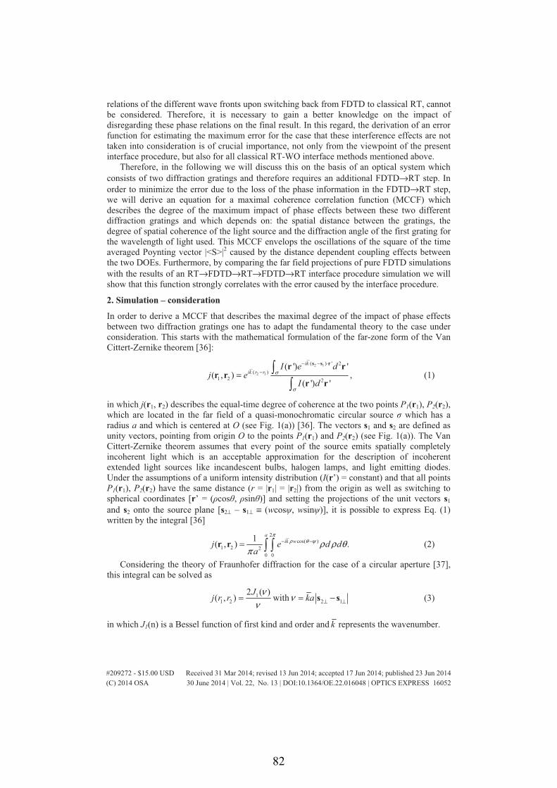
relations of the different wave fronts upon switching back from FDTD to classical RT, cannot be considered. Therefore, it is necessary to gain a better knowledge on the impact of disregarding these phase relations on the final result. In this regard, the derivation of an error function for estimating the maximum error for the case that these interference effects are not taken into consideration is of crucial importance, not only from the viewpoint of the present interface procedure, but also for all classical RT-WO interface methods mentioned above.
Therefore, in the following we will discuss this on the basis of an optical system which consists of two diffraction gratings and therefore requires an additional FDTD→RT step. In order to minimize the error due to the loss of the phase information in the FDTD→RT step, we will derive an equation for a maximal coherence correlation function (MCCF) which describes the degree of the maximum impact of phase effects between these two different diffraction gratings and which depends on: the spatial distance between the gratings, the degree of spatial coherence of the light source and the diffraction angle of the first grating for the wavelength of light used. This MCCF envelops the oscillations of the square of the time averaged Poynting vector |<S>|2 caused by the distance dependent coupling effects between the two DOEs. Furthermore, by comparing the far field projections of pure FDTD simulations with the results of an RT→FDTD→RT→FDTD→RT interface procedure simulation we will show that this function strongly correlates with the error caused by the interface procedure.
2. Simulation – consideration
In order to derive a MCCF that describes the maximal degree of the impact of phase effects between two diffraction gratings one has to adapt the fundamental theory to the case under consideration. This starts with the mathematical formulation of the far-zone form of the Van Cittert-Zernike theorem [36]:
2 1
2 1
( ) ' 2( )
1 2 2
( ') '( , ) ,
( ') '
ikik r r
I e dj e
I dσ
σ
− − ⋅
−= ��
s s rr rr r
r r (1)
in which j(r1, r2) describes the equal-time degree of coherence at the two points P1(r1), P2(r2), which are located in the far field of a quasi-monochromatic circular source � which has a radius a and which is centered at O (see Fig. 1(a)) [36]. The vectors s1 and s2 are defined as unity vectors, pointing from origin O to the points P1(r1) and P2(r2) (see Fig. 1(a)). The Van Cittert-Zernike theorem assumes that every point of the source emits spatially completely incoherent light which is an acceptable approximation for the description of incoherent extended light sources like incandescent bulbs, halogen lamps, and light emitting diodes. Under the assumptions of a uniform intensity distribution (I(r’) = constant) and that all points P1(r1), P2(r2) have the same distance (r = |r1| = |r2|) from the origin as well as switching to spherical coordinates [r’ = (�cos�, �sin�)] and setting the projections of the unit vectors s1 and s2 onto the source plane [s2⊥ – s1⊥ ≡ (wcos�, wsin�)], it is possible to express Eq. (1) written by the integral [36]
2
cos( )1 2 2
0 0
1( , ) .a
ik wj e d da
πρ θ ψ ρ ρ θ
π− −= � �r r (2)
Considering the theory of Fraunhofer diffraction for the case of a circular aperture [37], this integral can be solved as
11 2 2 1
2 ( )( , ) with
Jj r r kaν νν ⊥ ⊥= = −s s (3)
in which J1(n) is a Bessel function of first kind and order and k represents the wavenumber.
#209272 - $15.00 USD Received 31 Mar 2014; revised 13 Jun 2014; accepted 17 Jun 2014; published 23 Jun 2014(C) 2014 OSA 30 June 2014 | Vol. 22, No. 13 | DOI:10.1364/OE.22.016048 | OPTICS EXPRESS 16052
82
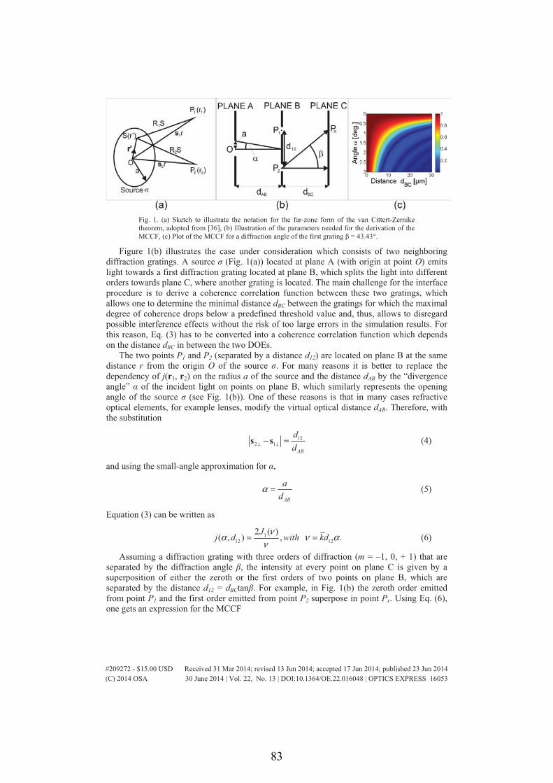
Fig. 1. (a) Sketch to illustrate the notation for the far-zone form of the van Cittert-Zernike theorem, adopted from [36], (b) Illustration of the parameters needed for the derivation of the MCCF, (c) Plot of the MCCF for a diffraction angle of the first grating � = 43.43°.
Figure 1(b) illustrates the case under consideration which consists of two neighboring diffraction gratings. A source � (Fig. 1(a)) located at plane A (with origin at point O) emits light towards a first diffraction grating located at plane B, which splits the light into different orders towards plane C, where another grating is located. The main challenge for the interface procedure is to derive a coherence correlation function between these two gratings, which allows one to determine the minimal distance dBC between the gratings for which the maximal degree of coherence drops below a predefined threshold value and, thus, allows to disregard possible interference effects without the risk of too large errors in the simulation results. For this reason, Eq. (3) has to be converted into a coherence correlation function which depends on the distance dBC in between the two DOEs.
The two points P1 and P2 (separated by a distance d12) are located on plane B at the same distance r from the origin O of the source �. For many reasons it is better to replace the dependency of j(r1, r2) on the radius a of the source and the distance dAB by the “divergence angle” � of the incident light on points on plane B, which similarly represents the opening angle of the source � (see Fig. 1(b)). One of these reasons is that in many cases refractive optical elements, for example lenses, modify the virtual optical distance dAB. Therefore, with the substitution
122 1
AB
dd⊥ ⊥− =s s (4)
and using the small-angle approximation for �,
AB
ad
α = (5)
Equation (3) can be written as
112 12
2 ( )( , ) , .
Jj d with kdνα ν αν
= = (6)
Assuming a diffraction grating with three orders of diffraction (m = –1, 0, + 1) that are separated by the diffraction angle �, the intensity at every point on plane C is given by a superposition of either the zeroth or the first orders of two points on plane B, which are separated by the distance d12 = dBCtan�. For example, in Fig. 1(b) the zeroth order emitted from point P1 and the first order emitted from point P2 superpose in point Px. Using Eq. (6), one gets an expression for the MCCF
#209272 - $15.00 USD Received 31 Mar 2014; revised 13 Jun 2014; accepted 17 Jun 2014; published 23 Jun 2014(C) 2014 OSA 30 June 2014 | Vol. 22, No. 13 | DOI:10.1364/OE.22.016048 | OPTICS EXPRESS 16053
83
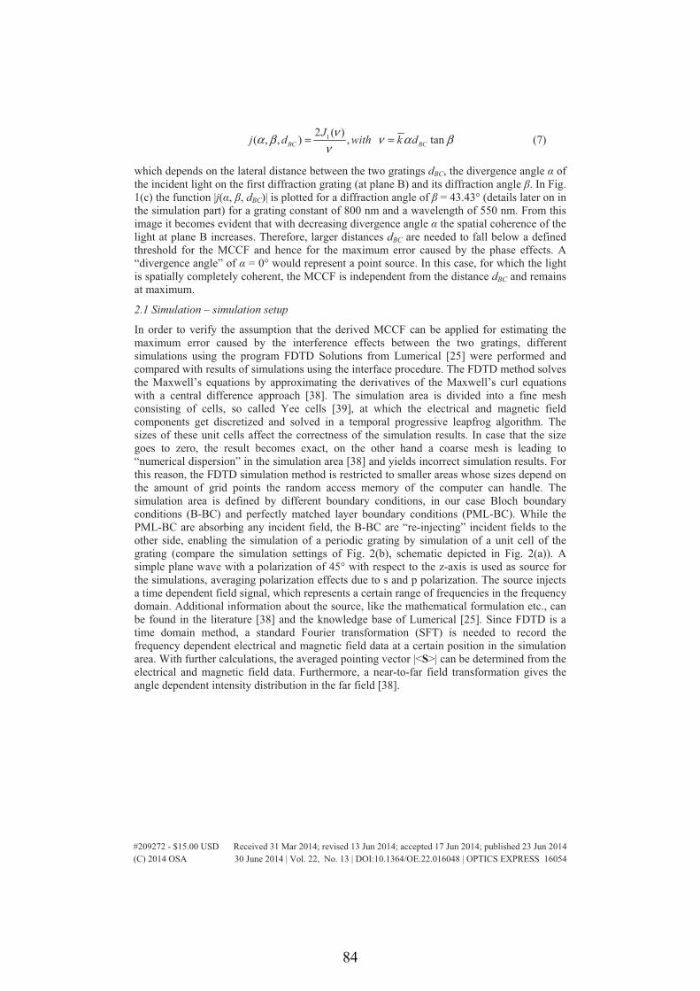
12 ( )( , , ) , tanBC BC
Jj d with k dνα β ν α βν
= = (7)
which depends on the lateral distance between the two gratings dBC, the divergence angle � of the incident light on the first diffraction grating (at plane B) and its diffraction angle �. In Fig. 1(c) the function |j(�, �, dBC)| is plotted for a diffraction angle of � = 43.43° (details later on in the simulation part) for a grating constant of 800 nm and a wavelength of 550 nm. From this image it becomes evident that with decreasing divergence angle � the spatial coherence of the light at plane B increases. Therefore, larger distances dBC are needed to fall below a defined threshold for the MCCF and hence for the maximum error caused by the phase effects. A “divergence angle” of � = 0° would represent a point source. In this case, for which the light is spatially completely coherent, the MCCF is independent from the distance dBC and remains at maximum.
2.1 Simulation – simulation setup
In order to verify the assumption that the derived MCCF can be applied for estimating the maximum error caused by the interference effects between the two gratings, different simulations using the program FDTD Solutions from Lumerical [25] were performed and compared with results of simulations using the interface procedure. The FDTD method solves the Maxwell’s equations by approximating the derivatives of the Maxwell’s curl equations with a central difference approach [38]. The simulation area is divided into a fine mesh consisting of cells, so called Yee cells [39], at which the electrical and magnetic field components get discretized and solved in a temporal progressive leapfrog algorithm. The sizes of these unit cells affect the correctness of the simulation results. In case that the size goes to zero, the result becomes exact, on the other hand a coarse mesh is leading to “numerical dispersion” in the simulation area [38] and yields incorrect simulation results. For this reason, the FDTD simulation method is restricted to smaller areas whose sizes depend on the amount of grid points the random access memory of the computer can handle. The simulation area is defined by different boundary conditions, in our case Bloch boundary conditions (B-BC) and perfectly matched layer boundary conditions (PML-BC). While the PML-BC are absorbing any incident field, the B-BC are “re-injecting” incident fields to the other side, enabling the simulation of a periodic grating by simulation of a unit cell of the grating (compare the simulation settings of Fig. 2(b), schematic depicted in Fig. 2(a)). A simple plane wave with a polarization of 45° with respect to the z-axis is used as source for the simulations, averaging polarization effects due to s and p polarization. The source injects a time dependent field signal, which represents a certain range of frequencies in the frequency domain. Additional information about the source, like the mathematical formulation etc., can be found in the literature [38] and the knowledge base of Lumerical [25]. Since FDTD is a time domain method, a standard Fourier transformation (SFT) is needed to record the frequency dependent electrical and magnetic field data at a certain position in the simulation area. With further calculations, the averaged pointing vector |<S>| can be determined from the electrical and magnetic field data. Furthermore, a near-to-far field transformation gives the angle dependent intensity distribution in the far field [38].
#209272 - $15.00 USD Received 31 Mar 2014; revised 13 Jun 2014; accepted 17 Jun 2014; published 23 Jun 2014(C) 2014 OSA 30 June 2014 | Vol. 22, No. 13 | DOI:10.1364/OE.22.016048 | OPTICS EXPRESS 16054
84
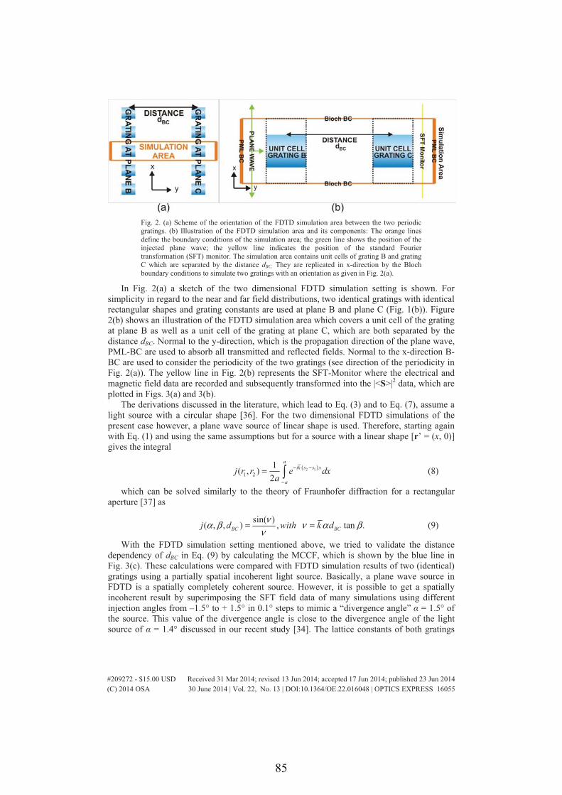
Fig. 2. (a) Scheme of the orientation of the FDTD simulation area between the two periodic gratings. (b) Illustration of the FDTD simulation area and its components: The orange lines define the boundary conditions of the simulation area; the green line shows the position of the injected plane wave; the yellow line indicates the position of the standard Fourier transformation (SFT) monitor. The simulation area contains unit cells of grating B and grating C which are separated by the distance dBC. They are replicated in x-direction by the Bloch boundary conditions to simulate two gratings with an orientation as given in Fig. 2(a).
In Fig. 2(a) a sketch of the two dimensional FDTD simulation setting is shown. For simplicity in regard to the near and far field distributions, two identical gratings with identical rectangular shapes and grating constants are used at plane B and plane C (Fig. 1(b)). Figure 2(b) shows an illustration of the FDTD simulation area which covers a unit cell of the grating at plane B as well as a unit cell of the grating at plane C, which are both separated by the distance dBC. Normal to the y-direction, which is the propagation direction of the plane wave, PML-BC are used to absorb all transmitted and reflected fields. Normal to the x-direction B-BC are used to consider the periodicity of the two gratings (see direction of the periodicity in Fig. 2(a)). The yellow line in Fig. 2(b) represents the SFT-Monitor where the electrical and magnetic field data are recorded and subsequently transformed into the |<S>|2 data, which are plotted in Figs. 3(a) and 3(b).
The derivations discussed in the literature, which lead to Eq. (3) and to Eq. (7), assume a light source with a circular shape [36]. For the two dimensional FDTD simulations of the present case however, a plane wave source of linear shape is used. Therefore, starting again with Eq. (1) and using the same assumptions but for a source with a linear shape [r’ = (x, 0)] gives the integral
( )2 11 2
1( , )2
aik s s x
a
j r r e dxa
− −
−
= � (8)
which can be solved similarly to the theory of Fraunhofer diffraction for a rectangular aperture [37] as
sin( )( , , ) , tan .BC BCj d with k dνα β ν α βν
= = (9)
With the FDTD simulation setting mentioned above, we tried to validate the distance dependency of dBC in Eq. (9) by calculating the MCCF, which is shown by the blue line in Fig. 3(c). These calculations were compared with FDTD simulation results of two (identical) gratings using a partially spatial incoherent light source. Basically, a plane wave source in FDTD is a spatially completely coherent source. However, it is possible to get a spatially incoherent result by superimposing the SFT field data of many simulations using different injection angles from –1.5° to + 1.5° in 0.1° steps to mimic a “divergence angle” � = 1.5° of the source. This value of the divergence angle is close to the divergence angle of the light source of � = 1.4° discussed in our recent study [34]. The lattice constants of both gratings
#209272 - $15.00 USD Received 31 Mar 2014; revised 13 Jun 2014; accepted 17 Jun 2014; published 23 Jun 2014(C) 2014 OSA 30 June 2014 | Vol. 22, No. 13 | DOI:10.1364/OE.22.016048 | OPTICS EXPRESS 16055
85
were chosen to be 800 nm, which gives reason for an angle of diffraction of � = 43.43° for a wavelength of 550 nm (see Fig. 1(c)).
3. Results
Fig. 3. (a), (b) Simulation results for the simulation model of Fig. 2, recorded with the SFT-monitor for different distances dBC using two identical diffraction gratings with � = 43.43° and (a) for an angle of incident 0°, (b) for a superposition of different angles of incidence from −1.5° up to + 1.5° in 0.1° steps. (c) Modulation of |<S>|2 extracted from the data of (b) compared with the MCCF j(� = 1.5°, � = 43.43°, dBC).
Figure 3(a) and 3(b) show the square of the time average pointing vector |<S>|2 for the different pixels of the SFT-Monitor plotted versus different distances dBC. In Fig. 3(a) the simulation results of a plane wave with an injection angle of 0° is shown. According to the applied model (Fig. 1(b)), this simulation setup is equivalent to a point source with a radius of zero and therefore represents a spatially completely coherent source. In this case, a distance dependent modulation of the values of |<S>|2 is caused by destructive and constructive coherence effects between the two gratings. However, the strength of the modulation is independent of the distance dBC, in accordance with Eq. (7) and Eq. (9) for the case � = 0°, which is why the MCCF remains at maximum for every distance dBC.
Figure 3(b) shows the superposition of many simulation results with different angles of incidence (–1.5° up to + 1.5° in 0.1° steps) representing the case of a partially spatial coherent light source with a divergence angle of � = 1.5°. Contrary to Fig. 3(a), the coherence correlation between the gratings is now decreasing with increasing distance, leading to a damping of this modulation. For large distances, the SFT-Monitor data for the square of the time average Poynting vector |<S>|2 is approaching a distribution which is independent of dBC representing the result of incoherent coupling of the two gratings. For comparison of this modulation of the incoherent result with the MCCF, the modulation was extracted by subtracting the incoherent part (output for dBC → ∞) of the results as determined by the SFT monitor for every pixel. These absolute values were averaged over the respective pixels. The resulting graph is plotted in Fig. 3(c) (green line), representing the averaged deviation from the incoherent part of the SFT monitor results. As evident, the damping behavior of the modulation fits pretty well the calculated values j(� = 1.5°, � = 43.43°, dBC) of Eq. (9). In this regard, it can be concluded that the calculated MCCF is suitable to estimate the maximal deviation from the incoherent result and furthermore to use the calculated values of j(�, �, dBC) as a threshold condition for the RT↔FDTD interface.
To highlight this as well as another point of interest which is the impact of the interference effects on the far fields of the gratings, near to far field projections of the data in Fig. 3(b) were performed and compared with an interface simulation of the grating using a RT→FDTD→RT→FDTD→RT interface simulation (Fig. 4(a), (c), (e)).
#209272 - $15.00 USD Received 31 Mar 2014; revised 13 Jun 2014; accepted 17 Jun 2014; published 23 Jun 2014(C) 2014 OSA 30 June 2014 | Vol. 22, No. 13 | DOI:10.1364/OE.22.016048 | OPTICS EXPRESS 16056
86
Fig. 4. (a),(c),(e) Far field transformations of the SFT-monitor data of Fig. 3(b) (colored lines) compared with the simulation results using the interface procedure (thick black line). (a) SFT data for 0 μm < dBC < 5 μm, (c) SFT data for 5 μm < dBC < 10 μm, (e) SFT data for 20 μm < dBC < 25 μm, (b) (d) (f) show zooms of the zeroth order of the far field distributions and the deviations of the FDTD far field results from the interface result.
The interface simulation represents the case of a completely incoherent coupling of the two gratings since any phase information is lost due to the RT step in between the respective FDTD calculations of the two gratings. In Fig. 4(a) the thick black line represent the result from the simulations using the interface procedure, while the colored lines represent the calculated far fields obtained from sole FDTD simulations for 50 different distances dBC, ranging from 0 μm to 5 μm in 0.1 μm steps. The FDTD results show a pronounced distance dependency and notable deviations from the results using the interface simulation procedure because of the strong coherence correlation of the two gratings. Figure 4(b) shows a zoom of the zeroth order of the far field. The far field result of the interface simulation procedure is apparently an average of the FDTD far field results, with a deviation of up to �I = 18.5% for the maximum of the zeroth order. The use of the variation of the maximum fulfills the requirements of the present study which aims at highlighting the general coherences, or to be more exactly, the area enclosed by the far field intensity distribution should be used as a measure.
#209272 - $15.00 USD Received 31 Mar 2014; revised 13 Jun 2014; accepted 17 Jun 2014; published 23 Jun 2014(C) 2014 OSA 30 June 2014 | Vol. 22, No. 13 | DOI:10.1364/OE.22.016048 | OPTICS EXPRESS 16057
87
In Fig. 4(c), the same RT→FDTD→RT→FDTD→RT far field results are compared with the far field projections of 50 FDTD simulations with the distances dBC ranging from 5 μm to 10 μm in 0.1 μm steps. Similar to Fig. 4(b) the zeroth order as obtained by the interface procedure is in accordance with the average of the FDTD far fields. However, the deviation (�I = 8.8%) is much smaller. This is in good accordance with our assumption that the differences between a pure FDTD simulations and the interface simulation are depending on the phase effects between the different orders and furthermore with Eq. (9) (the MCCF value becomes smaller with increasing distances dBC).
In the case of Fig. 4(e), the results of the interface procedure are compared with 50 FDTD far field simulations for large distances dBC, ranging from 20 μm to 25 μm in 0.1 μm steps. In this case the deviations for the zeroth order between FDTD and the interface procedure even drop below 5% (3.7%, see Fig. 4(f)), which could be a reasonable threshold value for a given simulation task. Since this value is comparably small, the impact of disregarded coherence effects on the error of the simulation results will be quite low. Therefore, in this exemplary simulation setting, distances in the range > 25 μm should be suitable for the use of the interface procedure without the risk of a distinct error by disregarding interference effects. Anyhow, the exact value for this distance will also depend on the required accuracy of the given problem, for which the threshold can be set accordingly.
The procedure is not limited to two diffraction gratings, each of them having structures with a rectangular shape. In an additional simulation setting a triangular sawtooth structure was used for the diffraction grating at plane B. In this case the obtained results are quite similar to the ones shown in Fig. 3(a). This can be explained by the fact that in this case only the shape of the structures was changed; however, the angle of diffraction remained the same. On the other hand, changing the grating constant of the diffraction gratings has a much stronger impact on the correlation between the two diffraction gratings; in particular, since the number of orders is increased the respective coherence correlations between these additional orders become important.
Therefore, in another simulation setting (two diffraction gratings with structures having a rectangular shape) we have increased the grating constant from 800 nm to 1400 nm. This gives reason for a far field distribution with 5 different diffraction orders located at −51.78°, −23.13°, 0°, + 23.13° and + 51.78° for an angle of incidence of 0°. In this case, it is necessary to consider all possible combinations of respective coherence correlations between the different orders which can occur in this example (e.g. the −2nd with the 0th or the −2nd with the −1st etc.), to obtain more precise information about the correlation between these two diffraction gratings. As evident from Eq. (9) reducing � from 43.43° to 23.12° will lead to a MCCF which is decreasing slower than in the previous example and FDTD simulations up to a distance dBC < 50 μm would be necessary for getting meaningful results. For this reason a divergence angle of � = 3° was used to counteract larger FDTD simulation areas, since this manuscript basically focuses on the verification of the accuracy and applicability of the interface simulation method in general.
For the image shown in Fig. 5(a) the modulation of |<S>|2 is extracted and compared with the calculated MCCF j(� = 3°, � = 23.13°, dBC), which represents the coherence correlation between the 0th and the ± 1st diffraction orders. As one can see in this case the modulation of |<S>|2 is decreasing faster than predicted by the MCCF. This faster decrease of the modulation of |<S>|2 can be explained by the fact that coherence correlations between the other orders have a significant additional impact. These coherence correlations have to be calculated separately in a way similarly to the calculation of the MCCF and subsequently averaged with different weighting factors to gain an averaged coherence correlation (ACCF) between the two diffraction gratings. We assume that the weighting factors will depend on the intensity of the different orders, because orders with insignificant intensity should not have a large impact on the final distribution even in case that the associated coherence correlation is high. The ACCF plotted in Fig. 5(a) is calculated with equal weighting factors of 1
#209272 - $15.00 USD Received 31 Mar 2014; revised 13 Jun 2014; accepted 17 Jun 2014; published 23 Jun 2014(C) 2014 OSA 30 June 2014 | Vol. 22, No. 13 | DOI:10.1364/OE.22.016048 | OPTICS EXPRESS 16058
88
(arithmetic mean of all coherence correlations) and shows a somewhat better envelopment of the modulation of |<S>|2 than the MCCF does. However, the values of the ACCF never exceed the values of the MCCF because the diffraction angle between the 1st and the 0th orders is smaller than for every other possible combination of orders, of which the ACCF is composed of. Since it is much more complex and time-consuming to calculate the ACCF than the MCCF (especially in cases with increasing numbers of diffraction orders and therefore of possible combinations between these), the MCCF is still more suitable and ascertainable as a threshold condition.
Fig. 5. (a) Modulation of |<(S)>|2 compared with the MCCF and an average of the different possible combinations of coherence correlations between the orders (b),(c) Far field transformations of the SFT-monitor data for two rectangular gratings with a grating constant of 1400 nm (colored lines) compared with the simulation results using the interface procedure (thick black line). (b) SFT data for 0 μm < dBC < 15 μm, (c) SFT data for 20 μm < dBC < 25 μm.
Furthermore, in order to show the applicability and accuracy of the interface procedure for more complex structures, the far field distributions are calculated and depicted in Fig. 5(b), (c). The corresponding far fields are obtained either by pure FDTD calculations or by using the interface procedure for the two diffraction gratings as a function of different distances dBC and a divergence angle of � = 3°. Similar to the results in Fig. 4(a), smaller distances dBC are leading to higher deviations between FDTD and interface simulation results in Fig. 5(b), whereas in Fig. 5(c) the deviations are much smaller due to higher distances dBC which cause smaller coherence correlations between the two diffraction gratings. These results again demonstrate the possibility of using the interface procedure without the risk of a distinct error by neglecting interference effects for distances of dBC > 25 μm for this combination of diffraction gratings and divergence angle of � = 3° of the light source. However, for such more complex examples und when using a light source with a smaller divergence angle like in the previous example (� = 1.5°), the minimal distance dBC would slightly increase according to the Eq. (9).
4. Summary and conclusions
As shown in our recent work [34, 35], the Poynting vector representation of either rays or wave propagation directions can be applied as an interface between two different simulation approaches, ray-tracing and the FDTD method. However, interfacing from FDTD to RT results in a loss of information, namely the phase relations between waves with different propagation directions. Generally, this information loss and the unknown impact of phase effects between different diffractive optical elements prohibit a multiple use of such an interface because of its unknown impact on the accuracy of the simulations and the risk of a massive error summation.
In order to quantify the impact of such interference effects between diffractive optical elements, such as, diffraction gratings, we derived a maximum coherence correlation function j(�, �, dBC) from the van Cittert-Zernike theorem, which allows to express the coherence
#209272 - $15.00 USD Received 31 Mar 2014; revised 13 Jun 2014; accepted 17 Jun 2014; published 23 Jun 2014(C) 2014 OSA 30 June 2014 | Vol. 22, No. 13 | DOI:10.1364/OE.22.016048 | OPTICS EXPRESS 16059
89
correlation between two diffraction gratings in dependence of their distance and the degree of spatial coherence of the light source. For spatially coherent sources, like e.g. point sources or laser sources, the coherence correlation is independent from the distance between the diffractive elements, which restricts the multiple use of such an interface for such light sources. Nevertheless, for more extended light sources, like e.g. blackbody radiators or LEDs, which are only partially spatial coherent the coherence correlation becomes damped for higher distances between the diffractive optical elements. Once the divergence angle of the light source and e.g., the grating constant of the diffraction gratings are known one can calculate the minimum distance between the DOEs for which the impact of interference effects drops below a defined value. In particular, as demonstrated for two diffraction gratings with � = 43.43° separated by a distance dBC > 25 μm and a source with � = 1.5°, results comparable to a sole FDTD simulation of the same setting can be obtained. In another example we verified the extensibility of the basic concept to diffraction gratings having a higher number of diffraction orders, where the correlation is much more complex because of the increasing importance of coherence correlations different from those that are considered by the MCCF. The example shows that the influence of these orders results in an even faster decrease of the oscillations of |<S>|2 than predicted by the MCCF and which can be described by an ACCF more exactly. However due to the easier calculability of the MCCF especially for more complicated simulation setups, the MCCF is more suitable to serve as threshold condition for the appliance of the interface procedure.
The far field results, plotted in Fig. 4(b),(c) and in Fig. 5(b),(c), indicate that the interface procedure is suitable for a simulation of a wide range of optical devices which contain partially spatial coherent sources where the distance between the diffractive optical elements is large enough so that j(�, �, dBC) falls below a pre-defined threshold value, which can be set in accordance with the desired accuracy of the simulation task. For simulation tasks for which the distances are smaller it might be possible to combine the two diffractive elements into a single simulation setting in FDTD and use this setting for the interface as a whole. Still, such a combined consideration of the DOEs again will need a compromise between the increasing need of random access memory capacity of the workstation with increasing distance of the DOEs and the decreasing impact of an error, which can be qualified with the help of the derived MCCF.
Acknowledgments
The authors gratefully acknowledge financial support from the BMVIT within the FIT-IT program – ModSim Computational Mathematics – of the Austrian Research Promotion Agency (FFG), project number 828706.
#209272 - $15.00 USD Received 31 Mar 2014; revised 13 Jun 2014; accepted 17 Jun 2014; published 23 Jun 2014(C) 2014 OSA 30 June 2014 | Vol. 22, No. 13 | DOI:10.1364/OE.22.016048 | OPTICS EXPRESS 16060
90
3.1.5 REDUCING SHADOWING LOSSES WITH
FEMTOSECOND-LASER-WRITTEN DEFLECTIVE OPTICAL
ELEMENTS IN THE BULK OF EVA ENCAPSULATION
”Reducing shadowing losses with femtosecond-laser-written deflective optical
elements in the bulk of EVA encapsulation” wurde im Juli 2014 als Full Paper in
Progress in Photovoltaics als Early View - Artikel veröffentlicht. Die Zuordnung
dieses Artikels zu einer Printausgabe ist derzeit noch ausständig. Der eigene Anteil bei
dieser Veröffentlichung beträgt 20%.
Der Anteil der Arbeit bei dieser Publikation beschränkt sich auf die Simulationen der
in der Publikation untersuchten Reduzierungen der Abschattungseffekte innerhalb
einer Photovoltaikzelle. Anhand dieser Aufgabenstellung konnte die im Rahmen dieser
Dissertation entwickelte Schnittstelle zwischen der klassischen Ray-Trace
Simulationsmethode und der FDTD-Simulationsmethode zur Verifikation einer realen
Anwendung verwendet werden.
91
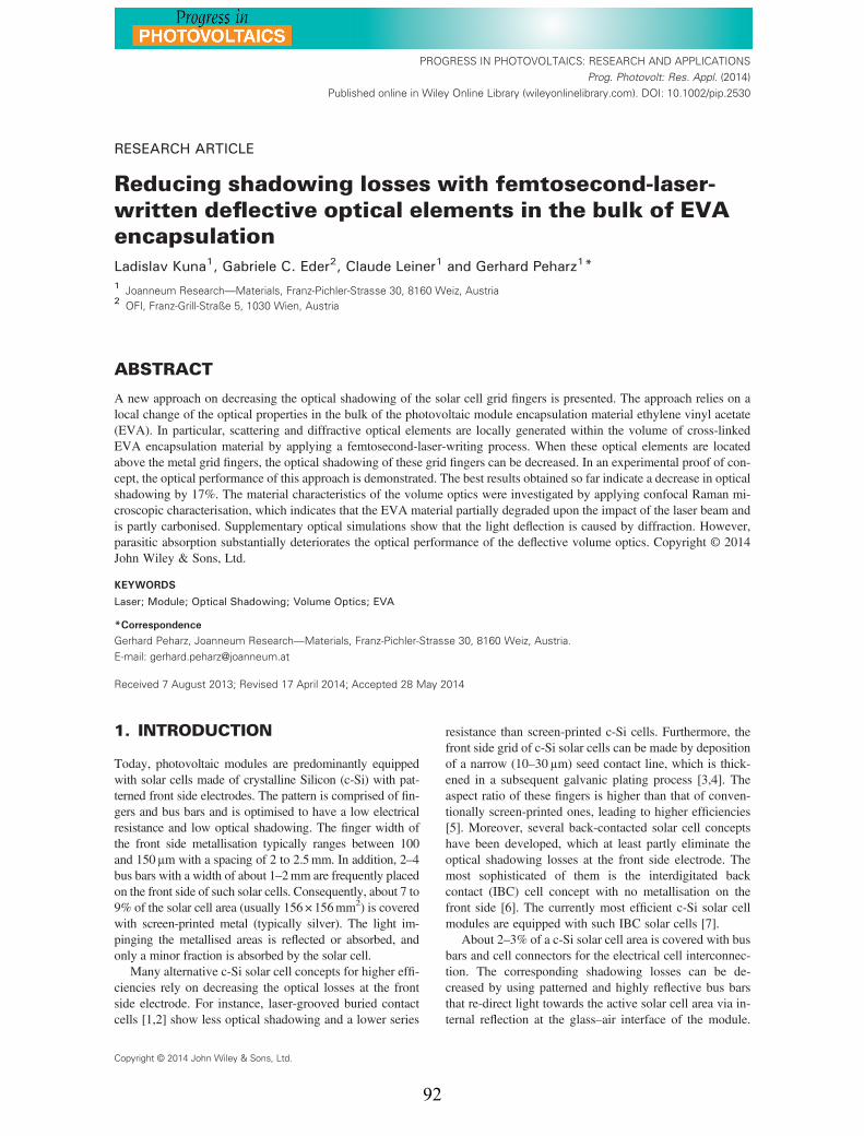
RESEARCH ARTICLE
Reducing shadowing losses with femtosecond-laser-written deflective optical elements in the bulk of EVAencapsulationLadislav Kuna1, Gabriele C. Eder2, Claude Leiner1 and Gerhard Peharz1*1 Joanneum Research—Materials, Franz-Pichler-Strasse 30, 8160 Weiz, Austria2 OFI, Franz-Grill-Straße 5, 1030 Wien, Austria
ABSTRACT
A new approach on decreasing the optical shadowing of the solar cell grid fingers is presented. The approach relies on alocal change of the optical properties in the bulk of the photovoltaic module encapsulation material ethylene vinyl acetate(EVA). In particular, scattering and diffractive optical elements are locally generated within the volume of cross-linkedEVA encapsulation material by applying a femtosecond-laser-writing process. When these optical elements are locatedabove the metal grid fingers, the optical shadowing of these grid fingers can be decreased. In an experimental proof of con-cept, the optical performance of this approach is demonstrated. The best results obtained so far indicate a decrease in opticalshadowing by 17%. The material characteristics of the volume optics were investigated by applying confocal Raman mi-croscopic characterisation, which indicates that the EVA material partially degraded upon the impact of the laser beam andis partly carbonised. Supplementary optical simulations show that the light deflection is caused by diffraction. However,parasitic absorption substantially deteriorates the optical performance of the deflective volume optics. Copyright © 2014John Wiley & Sons, Ltd.
KEYWORDS
Laser; Module; Optical Shadowing; Volume Optics; EVA
*Correspondence
Gerhard Peharz, Joanneum Research—Materials, Franz-Pichler-Strasse 30, 8160 Weiz, Austria.E-mail: [email protected]
Received 7 August 2013; Revised 17 April 2014; Accepted 28 May 2014
1. INTRODUCTION
Today, photovoltaic modules are predominantly equippedwith solar cells made of crystalline Silicon (c-Si) with pat-terned front side electrodes. The pattern is comprised of fin-gers and bus bars and is optimised to have a low electricalresistance and low optical shadowing. The finger width ofthe front side metallisation typically ranges between 100and 150μm with a spacing of 2 to 2.5mm. In addition, 2–4bus bars with a width of about 1–2mm are frequently placedon the front side of such solar cells. Consequently, about 7 to9% of the solar cell area (usually 156× 156mm2) is coveredwith screen-printed metal (typically silver). The light im-pinging the metallised areas is reflected or absorbed, andonly a minor fraction is absorbed by the solar cell.
Many alternative c-Si solar cell concepts for higher effi-ciencies rely on decreasing the optical losses at the frontside electrode. For instance, laser-grooved buried contactcells [1,2] show less optical shadowing and a lower series
resistance than screen-printed c-Si cells. Furthermore, thefront side grid of c-Si solar cells can be made by depositionof a narrow (10–30μm) seed contact line, which is thick-ened in a subsequent galvanic plating process [3,4]. Theaspect ratio of these fingers is higher than that of conven-tionally screen-printed ones, leading to higher efficiencies[5]. Moreover, several back-contacted solar cell conceptshave been developed, which at least partly eliminate theoptical shadowing losses at the front side electrode. Themost sophisticated of them is the interdigitated backcontact (IBC) cell concept with no metallisation on thefront side [6]. The currently most efficient c-Si solar cellmodules are equipped with such IBC solar cells [7].
About 2–3% of a c-Si solar cell area is covered with busbars and cell connectors for the electrical cell interconnec-tion. The corresponding shadowing losses can be de-creased by using patterned and highly reflective bus barsthat re-direct light towards the active solar cell area via in-ternal reflection at the glass–air interface of the module.
PROGRESS IN PHOTOVOLTAICS: RESEARCH AND APPLICATIONSProg. Photovolt: Res. Appl. (2014)
Published online in Wiley Online Library (wileyonlinelibrary.com). DOI: 10.1002/pip.2530
Copyright © 2014 John Wiley & Sons, Ltd.
92
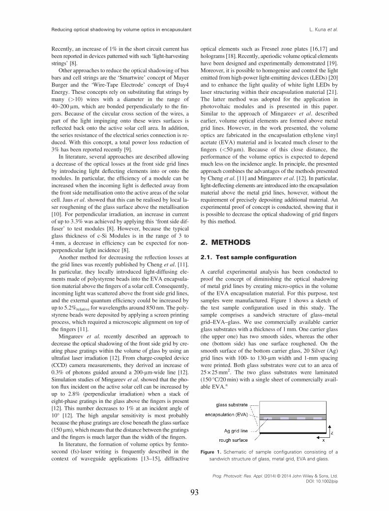
Recently, an increase of 1% in the short circuit current hasbeen reported in devices patterned with such ‘light-harvestingstrings’ [8].
Other approaches to reduce the optical shadowing of busbars and cell strings are the ‘Smartwire’ concept of MayerBurger and the ‘Wire-Tape Electrode’ concept of Day4Energy. These concepts rely on substituting flat strings bymany (>10) wires with a diameter in the range of40–200μm, which are bonded perpendicularly to the fin-gers. Because of the circular cross section of the wires, apart of the light impinging onto these wires surfaces isreflected back onto the active solar cell area. In addition,the series resistance of the electrical series connection is re-duced. With this concept, a total power loss reduction of3% has been reported recently [9].
In literature, several approaches are described allowinga decrease of the optical losses at the front side grid linesby introducing light deflecting elements into or onto themodules. In particular, the efficiency of a module can beincreased when the incoming light is deflected away fromthe front side metallisation onto the active areas of the solarcell. Jaus et al. showed that this can be realised by local la-ser roughening of the glass surface above the metallisation[10]. For perpendicular irradiation, an increase in currentof up to 3.3% was achieved by applying this ‘front side dif-fuser’ to test modules [8]. However, because the typicalglass thickness of c-Si Modules is in the range of 3 to4mm, a decrease in efficiency can be expected for non-perpendicular light incidence [8].
Another method for decreasing the reflection losses atthe grid lines was recently published by Cheng et al. [11].In particular, they locally introduced light-diffusing ele-ments made of polystyrene beads into the EVA encapsula-tion material above the fingers of a solar cell. Consequently,incoming light was scattered above the front side grid lines,and the external quantum efficiency could be increased byup to 5.2%relative for wavelengths around 850 nm. The poly-styrene beads were deposited by applying a screen printingprocess, which required a microscopic alignment on top ofthe fingers [11].
Mingareev et al. recently described an approach todecrease the optical shadowing of the front side grid by cre-ating phase gratings within the volume of glass by using anultrafast laser irradiation [12]. From charge-coupled device(CCD) camera measurements, they derived an increase of0.3% of photons guided around a 200-μm-wide line [12].Simulation studies of Mingareev et al. showed that the pho-ton flux incident on the active solar cell can be increased byup to 2.8% (perpendicular irradiation) when a stack ofeight-phase gratings in the glass above the fingers is present[12]. This number decreases to 1% at an incident angle of10° [12]. The high angular sensitivity is most probablybecause the phase gratings are close beneath the glass surface(150μm), whichmeans that the distance between the gratingsand the fingers is much larger than the width of the fingers.
In literature, the formation of volume optics by femto-second (fs)-laser writing is frequently described in thecontext of waveguide applications [13–15], diffractive
optical elements such as Fresnel zone plates [16,17] andholograms [18]. Recently, aperiodic volume optical elementshave been designed and experimentally demonstrated [19].Moreover, it is possible to homogenise and control the lightemitted from high-power light-emitting devices (LEDs) [20]and to enhance the light quality of white light LEDs bylaser structuring within their encapsulation material [21].The latter method was adopted for the application inphotovoltaic modules and is presented in this paper.Similar to the approach of Mingareev et al. describedearlier, volume optical elements are formed above metalgrid lines. However, in the work presented, the volumeoptics are fabricated in the encapsulation ethylene vinylacetate (EVA) material and is located much closer to thefingers (<50 μm). Because of this close distance, theperformance of the volume optics is expected to dependmuch less on the incidence angle. In principle, the presentedapproach combines the advantages of the methods presentedby Cheng et al. [11] and Mingareev et al. [12]. In particular,light-deflecting elements are introduced into the encapsulationmaterial above the metal grid lines, however, without therequirement of precisely depositing additional material. Anexperimental proof of concept is conducted, showing that itis possible to decrease the optical shadowing of grid fingersby this method.
2. METHODS
2.1. Test sample configuration
A careful experimental analysis has been conducted toproof the concept of diminishing the optical shadowingof metal grid lines by creating micro-optics in the volumeof the EVA encapsulation material. For this purpose, testsamples were manufactured. Figure 1 shows a sketch ofthe test sample configuration used in this study. Thesample comprises a sandwich structure of glass–metalgrid–EVA–glass. We use commercially available carrierglass substrates with a thickness of 1mm. One carrier glass(the upper one) has two smooth sides, whereas the otherone (bottom side) has one surface roughened. On thesmooth surface of the bottom carrier glass, 20 Silver (Ag)grid lines with 100- to 130-μm width and 1-mm spacingwere printed. Both glass substrates were cut to an area of25 × 25mm2. The two glass substrates were laminated(150 °C/20min) with a single sheet of commercially avail-able EVA.a
Figure 1. Schematic of sample configuration consisting of asandwich structure of glass, metal grid, EVA and glass.
Reducing optical shadowing by volume optics in encapusulant L. Kuna et al.
Prog. Photovolt: Res. Appl. (2014) © 2014 John Wiley & Sons, Ltd.DOI: 10.1002/pip
93
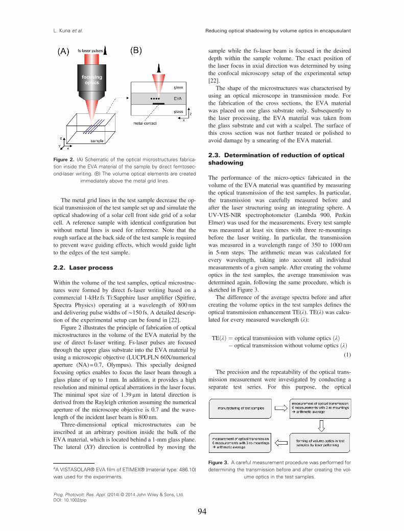
The metal grid lines in the test sample decrease the op-tical transmission of the test sample set up and simulate theoptical shadowing of a solar cell front side grid of a solarcell. A reference sample with identical configuration butwithout metal lines is used for reference. Note that therough surface at the back side of the test sample is requiredto prevent wave guiding effects, which would guide lightto the edges of the test sample.
2.2. Laser process
Within the volume of the test samples, optical microstruc-tures were formed by direct fs-laser writing based on acommercial 1-kHz fs Ti:Sapphire laser amplifier (Spitfire,Spectra Physics) operating at a wavelength of 800 nmand delivering pulse widths of ∼150 fs. A detailed descrip-tion of the experimental setup can be found in [22].
Figure 2 illustrates the principle of fabrication of opticalmicrostructures in the volume of the EVA material by theuse of direct fs-laser writing. Fs-laser pulses are focusedthrough the upper glass substrate into the EVA material byusing a microscopic objective (LUCPLFLN 60X/numericalaperture (NA)= 0.7, Olympus). This specially designedfocusing optics enables to focus the laser beam through aglass plane of up to 1mm. In addition, it provides a highresolution and minimal optical aberrations in the laser focus.The minimal spot size of 1.39μm in lateral direction isderived from the Rayleigh criterion assuming the numericalaperture of the microscope objective is 0.7 and the wave-length of the incident laser beam is 800 nm.
Three-dimensional optical microstructures can beinscribed at an arbitrary position inside the bulk of theEVA material, which is located behind a 1-mm glass plane.The lateral (XY) direction is controlled by moving the
sample while the fs-laser beam is focused in the desireddepth within the sample volume. The exact position ofthe laser focus in axial direction was determined by usingthe confocal microscopy setup of the experimental setup[22].
The shape of the microstructures was characterised byusing an optical microscope in transmission mode. Forthe fabrication of the cross sections, the EVA materialwas placed on one glass substrate only. Subsequently tothe laser processing, the EVA material was taken fromthe glass substrate and cut with a scalpel. The surface ofthis cross section was not further treated or polished toavoid damage by a smearing of the EVA material.
2.3. Determination of reduction of opticalshadowing
The performance of the micro-optics fabricated in thevolume of the EVA material was quantified by measuringthe optical transmission of the test samples. In particular,the transmission was carefully measured before andafter the laser structuring using an integrating sphere. AUV-VIS-NIR spectrophotometer (Lambda 900, PerkinElmer) was used for the measurements. Every test samplewas measured at least six times with three re-mountingsbefore the laser writing. In particular, the transmissionwas measured in a wavelength range of 350 to 1000 nmin 5-nm steps. The arithmetic mean was calculated forevery wavelength, taking into account all individualmeasurements of a given sample. After creating the volumeoptics in the test samples, the average transmission wasdetermined again, following the same procedure, which issketched in Figure 3.
The difference of the average spectra before and aftercreating the volume optics in the test samples defines theoptical transmission enhancement TE(λ). TE(λ) was calcu-lated for every measured wavelength (λ):
TE λð Þ ¼ optical transmission with volume optics λð Þ� optical transmission without volume optics λð Þ
(1)
The precision and the repeatability of the optical trans-mission measurement were investigated by conducting aseparate test series. For this purpose, the optical
aA VISTASOLAR® EVA film of ETIMEX® (material type: 486.10)was used for the experiments.
Figure 2. (A) Schematic of the optical microstructures fabrica-tion inside the EVA material of the sample by direct femtosec-ond-laser writing. (B) The volume optical elements are created
immediately above the metal grid lines.
Figure 3. A careful measurement procedure was performed fordetermining the transmission before and after creating the vol-
ume optics in the test samples.
Reducing optical shadowing by volume optics in encapusulantL. Kuna et al.
Prog. Photovolt: Res. Appl. (2014) © 2014 John Wiley & Sons, Ltd.DOI: 10.1002/pip
94
transmissions of two individual test samples were mea-sured 30 times each, with 15 re-mountings and at three dif-ferent days. It was found that the spectral average varied inthe range of 0.2% (difference of maximum and minimum).The standard deviation was less than 0.06%. Moreover, there-mounting was identified to have the highest impact onthe measurement precision. This can be related to the factthat the spatial distribution of the optical transmissionthrough the test samples is not homogeneous and sensitivelydepends on the particular lateral position of the light beam.Taking into account the results of the study on the precisionand repeatability, an increase in the spectral average of TE(λ)> 0.2% can be considered to be clearly significant.
Because only the direct light (not the diffuse light) is ef-fectively deflected onto the active solar cell area, theASTM G173 Edition 03AM 1.5 direct spectrum AM1.5d(λ)b was used for computing the short circuit current den-sity of a virtual solar cell with a (perfect) external quantumefficiency of 1. The corresponding virtual spectral responseSR(λ) is calculated as follows:
SR λð Þ ¼ q�λh�c �1 (2)
The relative increase in short circuit current density(JSC,rel,gain) expected for such a virtual solar cell with aperfect quantum efficiency is derived from the relative in-crease of the optical transmissions measured in the testsamples (TErel(λ)):
TErel λð Þ ¼ optical transmission with volume optics λð Þoptical transmission without volume optics λð Þ
(3)
JSC;rel;gain ¼ ∫1100
350 AM1:5d λð Þ�SR λð Þ�TErel λð Þ�dλ∫1100
350 AM1:5d λð Þ�SR λð Þ�dλ(4)
Note that for calculating the integral, the measurementdata was interpolated and extrapolated.
The relative optical shadowing (OSrel(λ)) of a test sam-ple was defined with respect to the optical transmission ofthe reference sample without the metal grid lines. Themaximally achievable gain in the short circuit current den-sity (JSC,rel,gain,max) is calculated as follows:
OSrel λð Þ ¼ optical transmission without volume optics λð Þoptical transmission reference sample without grid lines λð Þ
(5)
JSC;rel;gain;max ¼∫1100
350 AM1:5d λð Þ�SR λð Þ� 1OSrel λð Þ �dλ
∫1100
350 AM1:5d λð Þ�SR λð Þ�dλ(6)
The reduction of optical shadowing is defined by the ra-tio of JSC,rel,gain and JSC,rel,gain,max.
reduction of optical shadowing ¼ JSC;rel;gainJSC;rel;gain;max
�100%(7)
If the reduction of optical shadowing is 100%, all lightthat is lost (in transmission) due to the metal grid lineswould be perfectly deflected by the volume optics andthe TErel(λ) would be equal to OSrel(λ).
2.4. Measurement of the angular dependingtransmission
For measuring the angular dependence of the test sampletransmission, the light of a Xenon lamp was coupled intoa waveguide. At the exit of the waveguide, a collimatingoptics forms a beam with a divergence angle of about 2°.The exit of the waveguide was mounted onto a mechanicalarm that allows illuminating the entrance of an integratingsphere from different incidence angles. For every inci-dence angle, a 100% optical transmission measurementwas conducted (no test sample mounted). In addition, thelight intensity transmitted through a test sample mountedin front of an integrating sphere was measured for everyincidence angle. By comparison of the transmitted light in-tensity through a test sample and the 100% transmission,the relative transmissions of test samples were derived forvarying incidence angles.
2.5. Confocal Raman microscopy
Changes in the material characteristics induced by thefs-laser pulse interaction with the EVA material were in-vestigated by applying confocal Raman microscopy. TheRaman spectra of the laminated EVA were recorded usinga confocal LabRam Aramis (Horiba Jobin Yvon) equippedwith a computer-controlled motorised XYZ stage. Themeasurements were performed by using 532-nm laserexcitation. The detection system used was a Peltier-cooled1-in. CCD camera with 1024 × 256 pixels. A Leica objec-tive PL Fluotar with 100-fold magnification and NA 0.75was used. For the confocal collection of the spectra ofthe structures within the EVA films, the pinhole was setto 200μm, and the spectral slit was set to 100μm. Thespectra were recorded in the spectral region from 100 to4000 cm�1. The measuring positions within the samplewere chosen from the optical image of the sample in thefocus layer of the voxels (Volume Pixel [23,24]).
2.6. Optical modelling
Optical modelling was conducted to create a better under-standing of the optical effect of the volume optics and toidentify limits of their optical performance. Because thegeometric dimensions of the volume optical elementsbData from http://rredc.nrel.gov/solar/spectra/am1.5/
Reducing optical shadowing by volume optics in encapusulant L. Kuna et al.
Prog. Photovolt: Res. Appl. (2014) © 2014 John Wiley & Sons, Ltd.DOI: 10.1002/pip
95
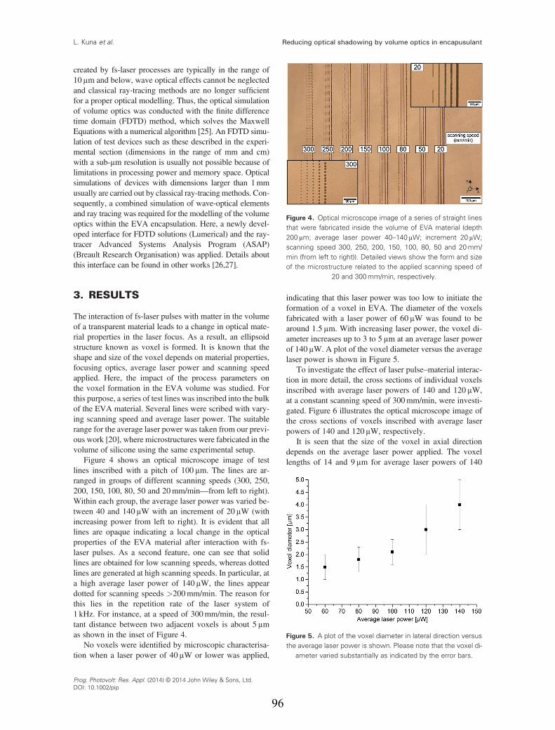
created by fs-laser processes are typically in the range of10μm and below, wave optical effects cannot be neglectedand classical ray-tracing methods are no longer sufficientfor a proper optical modelling. Thus, the optical simulationof volume optics was conducted with the finite differencetime domain (FDTD) method, which solves the MaxwellEquations with a numerical algorithm [25]. An FDTD simu-lation of test devices such as these described in the experi-mental section (dimensions in the range of mm and cm)with a sub-μm resolution is usually not possible because oflimitations in processing power and memory space. Opticalsimulations of devices with dimensions larger than 1mmusually are carried out by classical ray-tracingmethods. Con-sequently, a combined simulation of wave-optical elementsand ray tracing was required for the modelling of the volumeoptics within the EVA encapsulation. Here, a newly devel-oped interface for FDTD solutions (Lumerical) and the ray-tracer Advanced Systems Analysis Program (ASAP)(Breault Research Organisation) was applied. Details aboutthis interface can be found in other works [26,27].
3. RESULTS
The interaction of fs-laser pulses with matter in the volumeof a transparent material leads to a change in optical mate-rial properties in the laser focus. As a result, an ellipsoidstructure known as voxel is formed. It is known that theshape and size of the voxel depends on material properties,focusing optics, average laser power and scanning speedapplied. Here, the impact of the process parameters onthe voxel formation in the EVA volume was studied. Forthis purpose, a series of test lines was inscribed into the bulkof the EVA material. Several lines were scribed with vary-ing scanning speed and average laser power. The suitablerange for the average laser power was taken from our previ-ous work [20], where microstructures were fabricated in thevolume of silicone using the same experimental setup.
Figure 4 shows an optical microscope image of testlines inscribed with a pitch of 100μm. The lines are ar-ranged in groups of different scanning speeds (300, 250,200, 150, 100, 80, 50 and 20mm/min—from left to right).Within each group, the average laser power was varied be-tween 40 and 140μW with an increment of 20μW (withincreasing power from left to right). It is evident that alllines are opaque indicating a local change in the opticalproperties of the EVA material after interaction with fs-laser pulses. As a second feature, one can see that solidlines are obtained for low scanning speeds, whereas dottedlines are generated at high scanning speeds. In particular, ata high average laser power of 140μW, the lines appeardotted for scanning speeds >200mm/min. The reason forthis lies in the repetition rate of the laser system of1 kHz. For instance, at a speed of 300mm/min, the resul-tant distance between two adjacent voxels is about 5μmas shown in the inset of Figure 4.
No voxels were identified by microscopic characterisa-tion when a laser power of 40μW or lower was applied,
indicating that this laser power was too low to initiate theformation of a voxel in EVA. The diameter of the voxelsfabricated with a laser power of 60μW was found to bearound 1.5μm. With increasing laser power, the voxel di-ameter increases up to 3 to 5μm at an average laser powerof 140μW. A plot of the voxel diameter versus the averagelaser power is shown in Figure 5.
To investigate the effect of laser pulse–material interac-tion in more detail, the cross sections of individual voxelsinscribed with average laser powers of 140 and 120μW,at a constant scanning speed of 300mm/min, were investi-gated. Figure 6 illustrates the optical microscope image ofthe cross sections of voxels inscribed with average laserpowers of 140 and 120μW, respectively.
It is seen that the size of the voxel in axial directiondepends on the average laser power applied. The voxellengths of 14 and 9μm for average laser powers of 140
Figure 4. Optical microscope image of a series of straight linesthat were fabricated inside the volume of EVA material (depth200μm; average laser power 40–140μW; increment 20 μW;scanning speed 300, 250, 200, 150, 100, 80, 50 and 20mm/min (from left to right)). Detailed views show the form and sizeof the microstructure related to the applied scanning speed of
20 and 300mm/min, respectively.
Figure 5. A plot of the voxel diameter in lateral direction versusthe average laser power is shown. Please note that the voxel di-
ameter varied substantially as indicated by the error bars.
Reducing optical shadowing by volume optics in encapusulantL. Kuna et al.
Prog. Photovolt: Res. Appl. (2014) © 2014 John Wiley & Sons, Ltd.DOI: 10.1002/pip
96
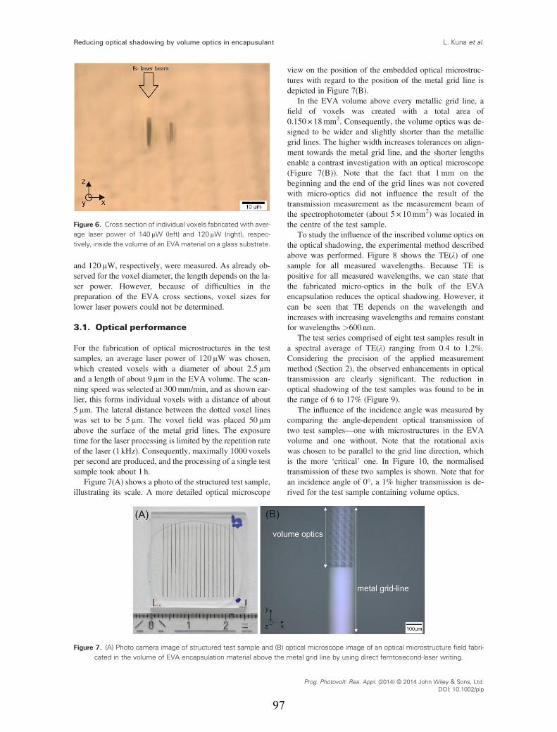
and 120μW, respectively, were measured. As already ob-served for the voxel diameter, the length depends on the la-ser power. However, because of difficulties in thepreparation of the EVA cross sections, voxel sizes forlower laser powers could not be determined.
3.1. Optical performance
For the fabrication of optical microstructures in the testsamples, an average laser power of 120μW was chosen,which created voxels with a diameter of about 2.5μmand a length of about 9μm in the EVA volume. The scan-ning speed was selected at 300mm/min, and as shown ear-lier, this forms individual voxels with a distance of about5μm. The lateral distance between the dotted voxel lineswas set to be 5μm. The voxel field was placed 50μmabove the surface of the metal grid lines. The exposuretime for the laser processing is limited by the repetition rateof the laser (1 kHz). Consequently, maximally 1000 voxelsper second are produced, and the processing of a single testsample took about 1 h.
Figure 7(A) shows a photo of the structured test sample,illustrating its scale. A more detailed optical microscope
view on the position of the embedded optical microstruc-tures with regard to the position of the metal grid line isdepicted in Figure 7(B).
In the EVA volume above every metallic grid line, afield of voxels was created with a total area of0.150 × 18mm2. Consequently, the volume optics was de-signed to be wider and slightly shorter than the metallicgrid lines. The higher width increases tolerances on align-ment towards the metal grid line, and the shorter lengthsenable a contrast investigation with an optical microscope(Figure 7(B)). Note that the fact that 1 mm on thebeginning and the end of the grid lines was not coveredwith micro-optics did not influence the result of thetransmission measurement as the measurement beam ofthe spectrophotometer (about 5 × 10mm2) was located inthe centre of the test sample.
To study the influence of the inscribed volume optics onthe optical shadowing, the experimental method describedabove was performed. Figure 8 shows the TE(λ) of onesample for all measured wavelengths. Because TE ispositive for all measured wavelengths, we can state thatthe fabricated micro-optics in the bulk of the EVAencapsulation reduces the optical shadowing. However, itcan be seen that TE depends on the wavelength andincreases with increasing wavelengths and remains constantfor wavelengths >600 nm.
The test series comprised of eight test samples result ina spectral average of TE(λ) ranging from 0.4 to 1.2%.Considering the precision of the applied measurementmethod (Section 2), the observed enhancements in opticaltransmission are clearly significant. The reduction inoptical shadowing of the test samples was found to be inthe range of 6 to 17% (Figure 9).
The influence of the incidence angle was measured bycomparing the angle-dependent optical transmission oftwo test samples—one with microstructures in the EVAvolume and one without. Note that the rotational axiswas chosen to be parallel to the grid line direction, whichis the more ‘critical’ one. In Figure 10, the normalisedtransmission of these two samples is shown. Note that foran incidence angle of 0°, a 1% higher transmission is de-rived for the test sample containing volume optics.
Figure 6. Cross section of individual voxels fabricated with aver-age laser power of 140μW (left) and 120μW (right), respec-tively, inside the volume of an EVA material on a glass substrate.
Figure 7. (A) Photo camera image of structured test sample and (B) optical microscope image of an optical microstructure field fabri-cated in the volume of EVA encapsulation material above the metal grid line by using direct femtosecond-laser writing.
Reducing optical shadowing by volume optics in encapusulant L. Kuna et al.
Prog. Photovolt: Res. Appl. (2014) © 2014 John Wiley & Sons, Ltd.DOI: 10.1002/pip
97
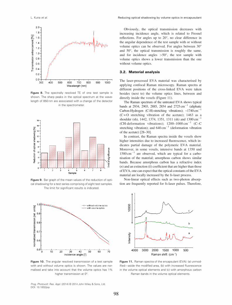
Obviously, the optical transmission decreases withincreasing incidence angle, which is related to Fresnelreflections. For angles up to 20°, no clear difference inthe angular dependence of the test sample with or withoutvolume optics can be observed. For angles between 30°and 50°, the optical transmission is roughly the same,and for incidence angles >50°, the test sample withvolume optics shows a lower transmission than the onewithout volume optics.
3.2. Material analysis
The laser-processed EVA material was characterised byapplying confocal Raman microscopy. Raman spectra atdifferent positions of the cross-linked EVA were takenbesides (next to) the volume optics lines, between anddirectly inside the voxels (Figure 11).
The Raman spectrum of the untreated EVA shows typicalbands at 2934, 2903, 2885, 2854 and 2725cm�1 (aliphaticCarbon-Hydrogen (C-H)-stretching vibrations); ~1740cm�1
(C =O stretching vibration of the acetate); 1463 as ashoulder (sh), 1442, 1374, 1351, 1311 (sh) and 1300 cm�1
(CH-deformation vibrations); 1200–1000 cm�1 (C–Cstretching vibration); and 640 cm�1 (deformation vibrationof the acetate) [28–30].
In contrast, the Raman spectra inside the voxels showhigher intensities due to increased fluorescence, which in-dicates partial damage of the polymeric EVA material.Moreover, in some voxels, intensive bands at 1350 und1580 cm�1 are observed, which are typical for a carbo-nisation of the material; amorphous carbon shows similarbands. Because amorphous carbon has a refractive index(n) and an extinction (k) coefficient that are higher than thoseof EVA, one can expect that the optical constants of the EVAmaterial are locally increased by the fs-laser process.
Non-linear optical effects such as two-photon absorp-tion are frequently reported for fs-laser pulses. Therefore,
Figure 8. The spectrally resolved TE of one test sample isshown. The sharp peaks in the optical spectrum at the wave-length of 850 nm are associated with a change of the detector
in the spectrometer.
Figure 9. Bar graph of the mean values of the reduction of opti-cal shadowing for a test series comprising of eight test samples.
The limit for significant results is indicated.
Figure 10. The angular resolved transmission of a test samplewith and without volume optics is shown. The values are nor-malised and take into account that the volume optics has 1%
higher transmission at 0°.
Figure 11. Raman spectra of the encapsulant (EVA): (a) unmod-ified—aside the modified area, (b) with increased fluorescencein the volume optical elements and (c) with amorphous carbon
Raman bands in the volume optical elements.
Reducing optical shadowing by volume optics in encapusulantL. Kuna et al.
Prog. Photovolt: Res. Appl. (2014) © 2014 John Wiley & Sons, Ltd.DOI: 10.1002/pip
98
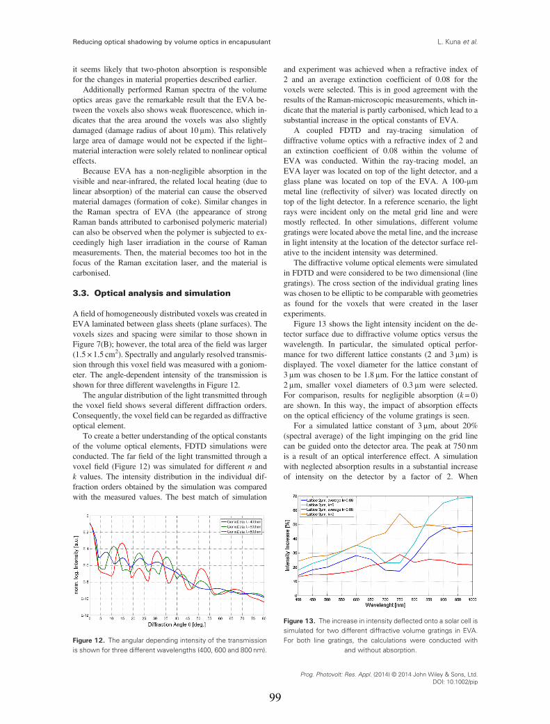
it seems likely that two-photon absorption is responsiblefor the changes in material properties described earlier.
Additionally performed Raman spectra of the volumeoptics areas gave the remarkable result that the EVA be-tween the voxels also shows weak fluorescence, which in-dicates that the area around the voxels was also slightlydamaged (damage radius of about 10μm). This relativelylarge area of damage would not be expected if the light–material interaction were solely related to nonlinear opticaleffects.
Because EVA has a non-negligible absorption in thevisible and near-infrared, the related local heating (due tolinear absorption) of the material can cause the observedmaterial damages (formation of coke). Similar changes inthe Raman spectra of EVA (the appearance of strongRaman bands attributed to carbonised polymeric material)can also be observed when the polymer is subjected to ex-ceedingly high laser irradiation in the course of Ramanmeasurements. Then, the material becomes too hot in thefocus of the Raman excitation laser, and the material iscarbonised.
3.3. Optical analysis and simulation
A field of homogeneously distributed voxels was created inEVA laminated between glass sheets (plane surfaces). Thevoxels sizes and spacing were similar to those shown inFigure 7(B); however, the total area of the field was larger(1.5 × 1.5 cm2). Spectrally and angularly resolved transmis-sion through this voxel field was measured with a goniom-eter. The angle-dependent intensity of the transmission isshown for three different wavelengths in Figure 12.
The angular distribution of the light transmitted throughthe voxel field shows several different diffraction orders.Consequently, the voxel field can be regarded as diffractiveoptical element.
To create a better understanding of the optical constantsof the volume optical elements, FDTD simulations wereconducted. The far field of the light transmitted through avoxel field (Figure 12) was simulated for different n andk values. The intensity distribution in the individual dif-fraction orders obtained by the simulation was comparedwith the measured values. The best match of simulation
and experiment was achieved when a refractive index of2 and an average extinction coefficient of 0.08 for thevoxels were selected. This is in good agreement with theresults of the Raman-microscopic measurements, which in-dicate that the material is partly carbonised, which lead to asubstantial increase in the optical constants of EVA.
A coupled FDTD and ray-tracing simulation ofdiffractive volume optics with a refractive index of 2 andan extinction coefficient of 0.08 within the volume ofEVA was conducted. Within the ray-tracing model, anEVA layer was located on top of the light detector, and aglass plane was located on top of the EVA. A 100-μmmetal line (reflectivity of silver) was located directly ontop of the light detector. In a reference scenario, the lightrays were incident only on the metal grid line and weremostly reflected. In other simulations, different volumegratings were located above the metal line, and the increasein light intensity at the location of the detector surface rel-ative to the incident intensity was determined.
The diffractive volume optical elements were simulatedin FDTD and were considered to be two dimensional (linegratings). The cross section of the individual grating lineswas chosen to be elliptic to be comparable with geometriesas found for the voxels that were created in the laserexperiments.
Figure 13 shows the light intensity incident on the de-tector surface due to diffractive volume optics versus thewavelength. In particular, the simulated optical perfor-mance for two different lattice constants (2 and 3μm) isdisplayed. The voxel diameter for the lattice constant of3μm was chosen to be 1.8μm. For the lattice constant of2μm, smaller voxel diameters of 0.3μm were selected.For comparison, results for negligible absorption (k= 0)are shown. In this way, the impact of absorption effectson the optical efficiency of the volume gratings is seen.
For a simulated lattice constant of 3μm, about 20%(spectral average) of the light impinging on the grid linecan be guided onto the detector area. The peak at 750 nmis a result of an optical interference effect. A simulationwith neglected absorption results in a substantial increaseof intensity on the detector by a factor of 2. When
Figure 12. The angular depending intensity of the transmissionis shown for three different wavelengths (400, 600 and 800 nm).
Figure 13. The increase in intensity deflected onto a solar cell issimulated for two different diffractive volume gratings in EVA.For both line gratings, the calculations were conducted with
and without absorption.
Reducing optical shadowing by volume optics in encapusulant L. Kuna et al.
Prog. Photovolt: Res. Appl. (2014) © 2014 John Wiley & Sons, Ltd.DOI: 10.1002/pip
99
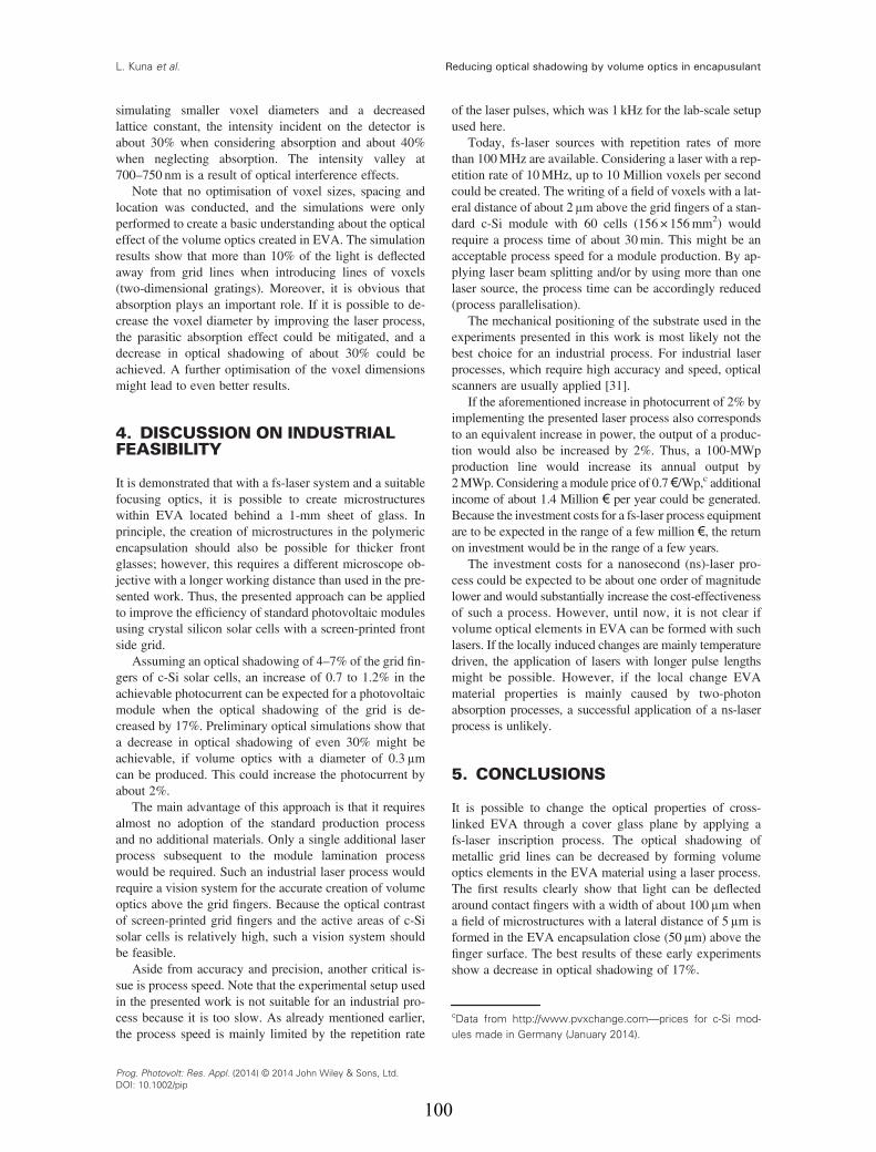
simulating smaller voxel diameters and a decreasedlattice constant, the intensity incident on the detector isabout 30% when considering absorption and about 40%when neglecting absorption. The intensity valley at700–750 nm is a result of optical interference effects.
Note that no optimisation of voxel sizes, spacing andlocation was conducted, and the simulations were onlyperformed to create a basic understanding about the opticaleffect of the volume optics created in EVA. The simulationresults show that more than 10% of the light is deflectedaway from grid lines when introducing lines of voxels(two-dimensional gratings). Moreover, it is obvious thatabsorption plays an important role. If it is possible to de-crease the voxel diameter by improving the laser process,the parasitic absorption effect could be mitigated, and adecrease in optical shadowing of about 30% could beachieved. A further optimisation of the voxel dimensionsmight lead to even better results.
4. DISCUSSION ON INDUSTRIALFEASIBILITY
It is demonstrated that with a fs-laser system and a suitablefocusing optics, it is possible to create microstructureswithin EVA located behind a 1-mm sheet of glass. Inprinciple, the creation of microstructures in the polymericencapsulation should also be possible for thicker frontglasses; however, this requires a different microscope ob-jective with a longer working distance than used in the pre-sented work. Thus, the presented approach can be appliedto improve the efficiency of standard photovoltaic modulesusing crystal silicon solar cells with a screen-printed frontside grid.
Assuming an optical shadowing of 4–7% of the grid fin-gers of c-Si solar cells, an increase of 0.7 to 1.2% in theachievable photocurrent can be expected for a photovoltaicmodule when the optical shadowing of the grid is de-creased by 17%. Preliminary optical simulations show thata decrease in optical shadowing of even 30% might beachievable, if volume optics with a diameter of 0.3μmcan be produced. This could increase the photocurrent byabout 2%.
The main advantage of this approach is that it requiresalmost no adoption of the standard production processand no additional materials. Only a single additional laserprocess subsequent to the module lamination processwould be required. Such an industrial laser process wouldrequire a vision system for the accurate creation of volumeoptics above the grid fingers. Because the optical contrastof screen-printed grid fingers and the active areas of c-Sisolar cells is relatively high, such a vision system shouldbe feasible.
Aside from accuracy and precision, another critical is-sue is process speed. Note that the experimental setup usedin the presented work is not suitable for an industrial pro-cess because it is too slow. As already mentioned earlier,the process speed is mainly limited by the repetition rate
of the laser pulses, which was 1 kHz for the lab-scale setupused here.
Today, fs-laser sources with repetition rates of morethan 100MHz are available. Considering a laser with a rep-etition rate of 10MHz, up to 10 Million voxels per secondcould be created. The writing of a field of voxels with a lat-eral distance of about 2μm above the grid fingers of a stan-dard c-Si module with 60 cells (156 × 156mm2) wouldrequire a process time of about 30min. This might be anacceptable process speed for a module production. By ap-plying laser beam splitting and/or by using more than onelaser source, the process time can be accordingly reduced(process parallelisation).
The mechanical positioning of the substrate used in theexperiments presented in this work is most likely not thebest choice for an industrial process. For industrial laserprocesses, which require high accuracy and speed, opticalscanners are usually applied [31].
If the aforementioned increase in photocurrent of 2% byimplementing the presented laser process also correspondsto an equivalent increase in power, the output of a produc-tion would also be increased by 2%. Thus, a 100-MWpproduction line would increase its annual output by2MWp. Considering a module price of 0.7 €/Wp,c additionalincome of about 1.4 Million € per year could be generated.Because the investment costs for a fs-laser process equipmentare to be expected in the range of a few million €, the returnon investment would be in the range of a few years.
The investment costs for a nanosecond (ns)-laser pro-cess could be expected to be about one order of magnitudelower and would substantially increase the cost-effectivenessof such a process. However, until now, it is not clear ifvolume optical elements in EVA can be formed with suchlasers. If the locally induced changes are mainly temperaturedriven, the application of lasers with longer pulse lengthsmight be possible. However, if the local change EVAmaterial properties is mainly caused by two-photonabsorption processes, a successful application of a ns-laserprocess is unlikely.
5. CONCLUSIONS
It is possible to change the optical properties of cross-linked EVA through a cover glass plane by applying afs-laser inscription process. The optical shadowing ofmetallic grid lines can be decreased by forming volumeoptics elements in the EVA material using a laser process.The first results clearly show that light can be deflectedaround contact fingers with a width of about 100μm whena field of microstructures with a lateral distance of 5μm isformed in the EVA encapsulation close (50μm) above thefinger surface. The best results of these early experimentsshow a decrease in optical shadowing of 17%.
cData from http://www.pvxchange.com—prices for c-Si mod-ules made in Germany (January 2014).
Reducing optical shadowing by volume optics in encapusulantL. Kuna et al.
Prog. Photovolt: Res. Appl. (2014) © 2014 John Wiley & Sons, Ltd.DOI: 10.1002/pip
100
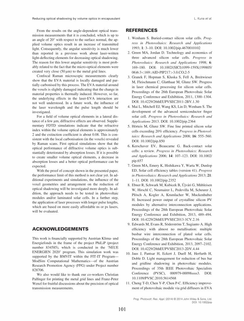
From the results on the angle-dependent optical trans-mission measurements that it is concluded, which is up toan angle of 20° with respect to the surface normal, the ap-plied volume optics result in an increase of transmittedlight. Consequently, the angular sensitivity is much lowerthan reported in a previous work about laser-writtenlight-deflecting elements for decreasing optical shadowing.The reason for this lower angular sensitivity is most prob-ably related to the fact that the micro-optical elements werecreated very close (50 μm) to the metal grid lines.
Confocal Raman microscopic measurements clearlyshow that the EVA material is locally damaged and par-tially carbonised by this process. The EVA material aroundthe voxels is slightly damaged indicating that the change inmaterial properties is thermally induced. However, so far,the underlying effects in the laser-EVA interaction arenot well understood. In a future work, the influence ofthe laser wavelength and the pulse length should beinvestigated.
For a field of volume optical elements in a lateral dis-tance of a few μm, diffractive effects are observed. Supple-mentary FDTD simulations indicate that the refractiveindex within the volume optical elements is approximately2 and the extinction coefficient is about 0.08. This is con-sistent with the local carbonisation (in the voxels) revealedby Raman scans. First optical simulations show that theoptical performance of diffractive volume optics is sub-stantially deteriorated by absorption losses. If it is possibleto create smaller volume optical elements, a decrease inabsorption losses and a better optical performance can beexpected.
With the proof of concept shown in the presented paper,the performance limit of this method is not clear yet. In ad-ditional experiments and simulations, the influence of thevoxel geometries and arrangement on the reduction ofoptical shadowing will be investigated more deeply. In ad-dition, the approach needs to be tested in photovoltaicmodules and/or laminated solar cells. In a further step,the application of laser processes with longer pulse lengths,which are based on more easily affordable ns or ps lasers,will be evaluated.
ACKNOWLEDGEMENTS
This work is financially supported by Austrian Klima- undEnergiefonds in the frame of the project PhiLiP (projectnumber 834585), which is conducted in the ‘NEUEENERGIEN 2020’ program. This simulation work wassupported by the BMVIT within the FIT-IT Program—ModSim Computational Mathematics—of the AustrianResearch Promotion Agency (FFG) under Project number828706.
We also would like to thank our co-workers ChristianPalfinger for printing the metal grid lines and Franz-PeterWenzl for fruitful discussions about the precision of opticaltransmission measurements.
REFERENCES
1. Wenham S. Buried-contact silicon solar cells. Prog-ress in Photovoltaics: Research and Applications1993; 1: 3–10. DOI: 10.1002/pip.4670010102
2. Green MA, Jordan D. Technology and economics ofthree advanced silicon solar cells. Progress inPhotovoltaics: Research and Applications 1998; 6:169–180. DOI: 10.1002/(SICI)1099-159X(199805/06)6:3<169::AID-PIP217>3.0.CO;2-5
3. Granek F, Hopman S, Kluska S, Fell A, BreitwieserM, Fleischmann C, Glatthaar M, Glunz SW. Progressin laser chemical processing for silicon solar cells.Proceedings of the 26th European Photovoltaic SolarEnergy Conference and Exhibition, 2011, 1300–1304.DOI: 10.4229/26thEUPVSEC2011-2BV.1.30
4. Mai L, Mitchell EJ, Wang KS, Lin D, Wenham S. Thedevelopment of the advanced semiconductor fingersolar cell. Progress in Photovoltaics: Research andApplications 2013. DOI: 10.1002/pip.2364
5. Hörteis M, Glunz SW. Fine line printed silicon solarcells exceeding 20% efficiency. Progress in Photovol-taics: Research and Applications 2008; 16: 555–560.DOI: 10.1002/pip.850
6. Kerschaver EV, Beaucarne G. Back-contact solarcells: a review. Progress in Photovoltaics: Researchand Applications 2006; 14: 107–123. DOI: 10.1002/pip.657
7. Green MA, Emery K, Hishikawa Y, Warta W, DunlopED, Solar cell efficiency tables (version 41). Progressin Photovoltaics: Research and Applications 2013; 21:1–11. DOI: 10.1002/pip.2352
8. Ebner R, Schwark M, Kubicek B, Újvári G, MühleisenW, Hirschl C, Neumairer L, Pedevilla M, Scheurer J,Plösch A, Kogler A, Krumlacher W, MuckenhuberH. Increased power output of crystalline silicon PVmodules by alternative interconnection applications.Proceedings of the 28th European Photovoltaic SolarEnergy Conference and Exhibition, 2013, 489–494.DOI: 10.4229/28thEUPVSEC2013-1CV.2.16
9. Edwards M, Evans R, Söderström T, Sugianto A. Highefficiency with almost no metallisation: multiplebusbar wire interconnection of plated solar cells.Proceedings of the 28th European Photovoltaic SolarEnergy Conference and Exhibition, 2013, 2097–2102.DOI: 10.4229/28thEUPVSEC2013-2DV.4.44
10. Jaus J, Pantsar H, Eckert J, Duell M, Herfurth H,Doble D. Light management for reduction of bus barand gridline shadowing in photovoltaic modules.Proceedings of 35th IEEE Photovoltaic SpecialistsConference (PVSC), 000979-00098ssss3. DOI:10.1109/PVSC.2010.5614568
11. Cheng T-D, Chen Y-P, Chen P-C. Efficiency improve-ment of photovoltaic module via grid diffusers in EVA
Reducing optical shadowing by volume optics in encapusulant L. Kuna et al.
Prog. Photovolt: Res. Appl. (2014) © 2014 John Wiley & Sons, Ltd.DOI: 10.1002/pip
101
encapsulation layer. Proceedings of the 27th EuropeanPhotovoltaic Solar Energy Conference and Exhibition,2012, 333–334. DOI: 10.4229/27thEUPVSEC2012-1BV.7.32
12. Mingareev I, Berlich R, Eichelkraut TJ, Herfurth H,Heinemann SM, Richardson C. Diffractive optical ele-ments utilized for efficiency enhancement of photovol-taic modules. Optics Express 19: 11397–11404. DOI:10.1364/OE.19.011397
13. Cerullo G, Osellame R, Taccheo S, Marangoni M,Polli D, Ramponi R, Laporta P, De Silvestri S. Femto-second micromachining of symmetric waveguides at1.5μm by astigmatic beam focusing. Optics Letters2002; 27: 1938–1940. DOI: 10.1364/OL.27.001938
14. Ams M, Marshall G, Spence D, Withford M. Slit beamshaping method for femtosecond laser direct-writefabrication of symmetric waveguides in bulk glasses.Optics Express 2005; 13: 5676–5681. DOI: 10.1364/OPEX.13.005676
15. Nolte S, Will M, Burghoff J, Tuennermann A, Femto-second wavequide writing: a new avenue to three-dimensional integrated optics. Applied Physics A2003; 77: 109–111. DOI: 10.1007/s00339-003-2088-6
16. Watanabe W, Kuroda D, Itoh K, Nishii J. Fabricationof Fresnel zone plate embedded in silica glass byfemtosecond laser pulses. Optics Express 2002; 10:978–983. DOI: 10.1364/OE.10.000978
17. Srisungsitthisunti P, Ersoy OK, Xu X. Volume Fresnelzone plates fabricated by femtosecond laser directwriting. Applied Physics Letters 2007; 90: 011104.DOI: 10.1063/1.2425026
18. Cai W, Reber TJ, Piestun R. Computer-generated vol-ume holograms fabricated by femtosecond lasermicromachining, Optics Letters 31, 1836–1838(2006). doi: 10.1364/OL.31.001836
19. Gerke TD, Piestun R. Nature Photonics 2010; 4:188–193. DOI: 10.1038/nphoton.2009.290
20. Kuna L, Sommer C, Zinterl E, Krenn JR, Pachler P,Hartmann P, Tasch S, Leising G, Wenzl FP. Volumestructuring of high power LED encapsulates byfemtosecond laser direct writing. Applied Physics A:Materials Science & Processing 2008; 93: 421–427.DOI: 10.1007/s00339-008-4779-5
21. Wenzl FP, Kuna L, Sommer C, Reil F, Krenn JR,Pachler P, Hartmann P. On the adjustment of the colortemperature of white light-emitting diodes by femto-second laser patterning. IEEE Photonics TechnologyLetters 2011; 23. DOI: 10.1109/LPT.2010.2092760
22. Kuna L, Sommer C, Reil F, Krenn JR, Hartmann P,Pachler P, Hoschopf H, Wenzl FP. Femtosecond laser
processing as a versatile tool for advanced solid statelighting sources: from efficacy enhancement to colourtemperature control. Applied Surface Science 2012;258: 9213–9217. DOI: 10.1016/j.apsusc.2012.01.086
23. Glezer EN, Mazur E. Ultrafast-laser driven micro-explosions in transparent materials. Applied PhysicsLetters 1997; 71: 882–884. DOI: 10.1063/1.119677
24. Korte F, Koch J, Serbin J, Ovsianikov A, ChichkovBN. Three-dimensional nanostructuring with femto-second laser pulses, IEEE Transactions on Nano-technology, 3, 468–472 (2004). doi: 10.1109/TNANO.2004.834189
25. Allen T, Hagness SC. Computational Electro-dynamics: the Finite-Difference Time-DomainMethod, 3rd ed. Artech House Publishers, 2005; ISBN1-58053-832-0.
26. Leiner C, Schweitzer S, Schmidt V, Belegratis M,Wenzl F-P, Hartmann P, Hohenester U, Sommer C.Multi-scale simulation of an optical device using anovel approach for combining ray-tracing and FDTD.Proc. SPIE 8781. Integrated Optics: Physics and Sim-ulations 2013; 87810Z. DOI:10.1117/12.2017423
27. Leiner C, Schweitzer S, Wenzl F-P, Hartmann P,Hohenester U, Sommer C. A simulation procedure in-terfacing ray-tracing and finite-difference time-domainmethods for a combined simulation of diffractive andrefractive optical elements. Journal of LightwaveTechnology 2014; 32: 1054–1062. http://www.opticsinfobase.org/jlt/abstract.cfm?URI=jlt-32-6-1054
28. Shimoyama M, Maeda H, Matsukawa K, Inoue H,Ninomiya T, Ozaki Y. Discrimination of ethylene/vi-nyl acetate copolymers with different compositionand prediction of the vinyl acetate content in the copol-ymers using Fourier-transform Raman spectroscopyand multivariate data analysis. Vibrational Spectros-copy 1997; 14: 253–259. DOI: 10.1016/S0924-2031(97)00010-6
29. Peike C, Kaltenbach T, Weiß K-A, Koehl M. Non-destructive degradation analysis of encapsulants inPV modules by Raman spectroscopy. Solar EnergyMaterials and Solar Cells 2011; 95: 1686–1693.DOI: 10.1016/j.solmat.2011.01.030
30. Chernev Boril S, Hirschl C, Eder GC. Non-destructivedetermination of ethylene vinyl acetate crosslinking inPV modules by Raman spectroscopy, AppliedSpectroscopy 2013; 67: 1296–1301. DOI: 10.1366/13-07085
31. Niyibizi A. Laser material processing in crystalline sil-icon photovoltaics. Sustaining Research InnovationProcessing 2012; 4: 69–74.
Reducing optical shadowing by volume optics in encapusulantL. Kuna et al.
Prog. Photovolt: Res. Appl. (2014) © 2014 John Wiley & Sons, Ltd.DOI: 10.1002/pip
102
3.2 ERLÄUTERUNGEN ZU DEN PUBLIKATIONEN
In diesem Kapitel werden die in der Dissertation veröffentlichten Publikationen in
einen chronologischen sowie einen themenbezogenen Kontext gebracht. Dafür werden
die Erkenntnisse der einzelnen Publikationen analysiert, diskutiert und zu einem Bild
zusammengefügt. Zusätzlich werden einzelne Aspekte ausführlicher diskutiert, um das
Verständnis der einzelnen Publikationen zu erleichtern.
3.2.1 A SIMULATION PROCEDURE FOR LIGHT-MATTER
INTERACTION AT DIFFERENT LENGTH SCALES
In „A Simulation Procedure for Light-Matter Interaction at Different Length Scales”
[50] wird das Transmissionsverhalten von Auskoppelstrukturen unterschiedlicher
Strukturgrößen Λ mit den beiden Simulationsprogrammen ASAP (Ray-Tracing
Programm von Breault Research) und FDTD Solutions (Finite Difference Time
Domain Programm von Lumerical) untersucht. Für diese Simulation wurden
Lichtstrahlen im RT-Programm, bzw. Lichtwellen im FDTD-Programm, in einem
optischen Medium der Brechzahl n = 1.5 erzeugt und unter verschiedenen
Einfallswinkeln in Richtung der Auskoppelstruktur emittiert. Die Intensität des
transmittierten Lichtflusses wurde durch Detektoren in den jeweiligen
Simulationsprogrammen bestimmt und verglichen.
Das Ray-Tracing Programm nutzt für die Simulation optischer Modelle ausschließlich
die Näherung der geometrischen Optik (siehe Kapitel 2.13 und 2.22), bei der die
Wellenlänge des Lichtes als verschwindend klein angenommen wird (λ 0) und das
Simulationsergebnis unabhängig von der Strukturgröße der Auskoppelstrukturen ist.
Die Simulation mit FDTD zeigte, dass für Strukturgrößen Λ = 10λ die Ergebnisse
übereinstimmen, diese für kleinere Strukturgrößen Λ < 2λ jedoch stark abweichen.
Fällt die Strukturgröße unter die Wellenlänge des verwendeten Lichtes, nähert sich das
Transmissionsverhalten der strukturierten Fläche dem einer ebenen Grenzfläche ohne
Strukturierung.
Diese Untersuchungen verdeutlichen, dass RT-Simulationen nicht geeignet sind,
Strukturen im Größenbereich der Wellenlänge zu simulieren. Andererseits wurden
103
auch die Grenzen der FDTD Methodik aufgezeigt: Für die Simulationen eines 10 µm x
10 µm x 10 µm großen Simulationsgebiets steigt der Speicherbedarf selbst bei grober
Diskretisierung des Simulationsgebietes auf 10GB RAM und die Simulationszeit auf
über eine Stunde (siehe Kapitel 2.3.1 und 2.3.2). Die Größe und Genauigkeit der
FDTD Simulationen wird daher durch die Kapazität der Workstation limitiert.
Dadurch wird eine vollständige Simulation von Systemen, die sowohl diffraktive als
auch refraktive optische Elemente beinhalten, ausgeschlossen und diese können selbst
mit den gegenwärtig leistungsfähigsten Computern nicht in adäquater Simulationszeit
durchgeführt werden. Aus diesem Grund wurde die Möglichkeit untersucht, die in
beiden Simulationsprogrammen implementierten Schnittstellen [51] zur Simulation
eines solchen optischen System zu nutzen, wie im Folgenden ausgeführt.
Hierfür wird das RT-Programm ASAP in einem speziellen Modus, dem sogenannten
Gauß-Beam (GB) Modus [52], ausgeführt, in dem GB [53] durch einzelne
geometrische Strahlen repräsentiert werden. GB, auch Gauß-Strahlen genannt, stellen
ähnlich wie ebene Wellen oder Kugelwellen eine Lösung der Gleichung 2.9 dar, unter
der Annahme, dass die GB eine geringe Divergenz in Richtung ihrer Ausbreitung
besitzen [53]. Dieser Modus ermöglicht das Zerlegen von elektromagnetischen
Feldern in einzelne GB, welche mit klassischem Ray-Tracing durch das optische
System propagiert werden können. Die Überlagerung der einzelnen GB an der
Detektorfläche ergibt anschließend das elektromagnetische Feld. Dieses Feld kann
exportiert und anschließend in das Programm FDTD-Solutions importiert werden, so
dass es in der FDTD Simulation als Quelle dient. Das Feld, welches am SFT-Monitor
(siehe Kapitel 2.3.3) in der FDTD Simulation aufgezeichnet wurde, kann anschließend
in ASAP re-importiert und in einzelne GB zerlegt werden.
Diese implementierte Schnittstelle unterliegt jedoch mehreren Beschränkungen:
• Dadurch, dass ASAP im GB-Modus betrieben wird, können die Oberflächen
der in der RT-Simulation verwendeten Quellen, Strukturen und Detektoren
nicht frei gewählt werden [52].
• Die räumliche Ausdehnung des aus ASAP exportierten Feldes darf die
räumliche Ausdehnung der FDTD Simulation nicht übersteigen. Diese Tatsache
beschränkt die Schnittstelle für RTFDTD Anwendungen auf Fälle, in denen
die Strahlen in der RT-Simulation auf eine kleine Fläche fokussiert werden.
• Die Größe des Simulationsgebiets bzw. des SFT-Monitors im
Simulationsgebiet bestimmt die Größe des Feldes, welches in ASAP re-
importiert wird.
104
Um jedoch das optische Verhalten eines Phasen-Transmissions-Gitters (PTG) (siehe
Kapitel 2.4.5), welches eine Fläche von mehreren mm² hat, simulieren zu können,
wurde die implementierte Schnittstelle erweitert, so dass die letztgenannte
Beschränkung umgangen werden konnte [54]. In FDTD wurde nur eine einzelne
Periode der Struktur des PTG simuliert, um die Größe des Simulationsgebietes zu
reduzieren. Die Verwendung von periodischen Randbedingungen (Bloch-BC) in x-
und y-Richtung bei der Simulation ermöglichte hierbei die Berücksichtigung der
Einflüsse von benachbarten Strukturen auf die Feldverteilung hinter der Struktur im
Simulationsgebiet. Anschließend wurde die durch die FDTD Simulation erhaltene
Feldverteilung einer einzelnen Struktur genutzt, um mittels MATLAB das gesamte
Feld hinter dem PTG zu rekonstruieren:
Ausgehend von der Annahme, dass die Feldverteilung hinter einer periodischen
Struktur ebenfalls periodisch ist, wurde die simulierte Feldverteilung repliziert und zu
einem Feld zusammengesetzt, dessen Fläche der des PTGs entspricht. Wie aus [50]
ersichtlich, war es durch diese Methode nach Import des zusammengesetzten Feldes in
ASAP möglich, die Fernfeldverteilung des PTGs im RT-Programm zu erzeugen.
Obwohl diese Methode eine Möglichkeit darstellt, die implementierte Schnittstelle zu
erweitern, so dass eine Simulation von großflächigen PTGs ermöglicht wird, können
zusätzliche Probleme auftreten, die diese Methode auf einige Spezialfälle beschränkt:
Die Divergenz der GB ist abhängig vom geometrischen Durchmesser der GB, wobei
ein kleiner Durchmesser eine hohe Divergenz bedeutet. Ein mögliches Problem stellt
daher die Zerlegung von sehr kleinen Feldverteilungen in einzelne GB dar, da der
Durchmesser der einzelnen GB die Wellenlänge des verwendeten Lichts λ nicht
beliebig unterschreiten darf. Um das mögliche Ausmaß an Fehlern durch diese
Zerlegung abschätzen zu können, wurden zwei GB mit unterschiedlichem
Durchmesser mit einer optischen Wellenlänge von 500 nm wiederholt zerlegt und
durch Überlagerung von Gauß-Strahlen wieder zusammengesetzt.
105
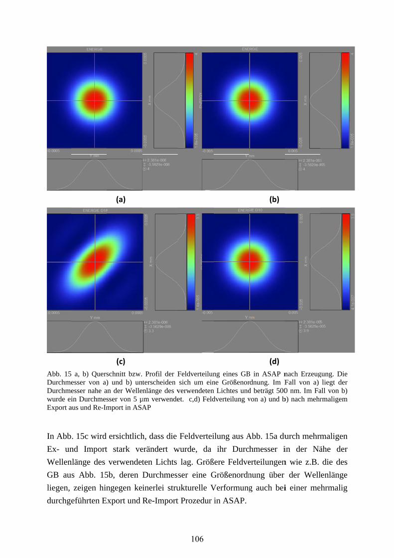
Abb. 15DurchmeDurchmewurde eiExport a
In Abb
Ex- un
Wellen
GB au
liegen,
durchge
a, b) Quersesser von a)esser nahe ain Durchmes
aus und Re-Im
. 15c wird
nd Import
nlänge des
us Abb. 15
zeigen hin
eführten E
(a)
(c) schnitt bzw.) und b) un
an der Wellesser von 5 µmport in ASA
ersichtlich
t stark ve
verwendet
5b, deren
ngegen ke
xport und
Profil der Fterscheiden nlänge des v
µm verwendeAP
h, dass die
erändert w
ten Lichts
Durchmess
inerlei stru
Re-Import
Feldverteilunsich um ein
verwendetenet. c,d) Feld
Feldvertei
wurde, da
lag. Größ
ser eine G
ukturelle V
t Prozedur
ng eines GBne Größenorn Lichtes unddverteilung v
ilung aus A
ihr Durc
ßere Feldve
Größenordn
Verformung
in ASAP.
(b)
(d) B in ASAP nrdnung. Im Fd beträgt 500von a) und b
Abb. 15a du
hmesser i
erteilungen
nung über
g auch bei
nach ErzeugFall von a) 0 nm. Im Fab) nach mehr
urch mehrm
in der Nä
n wie z.B.
der Well
i einer me
gung. Die liegt der
all von b) rmaligem
maligen
ähe der
die des
enlänge
hrmalig
106
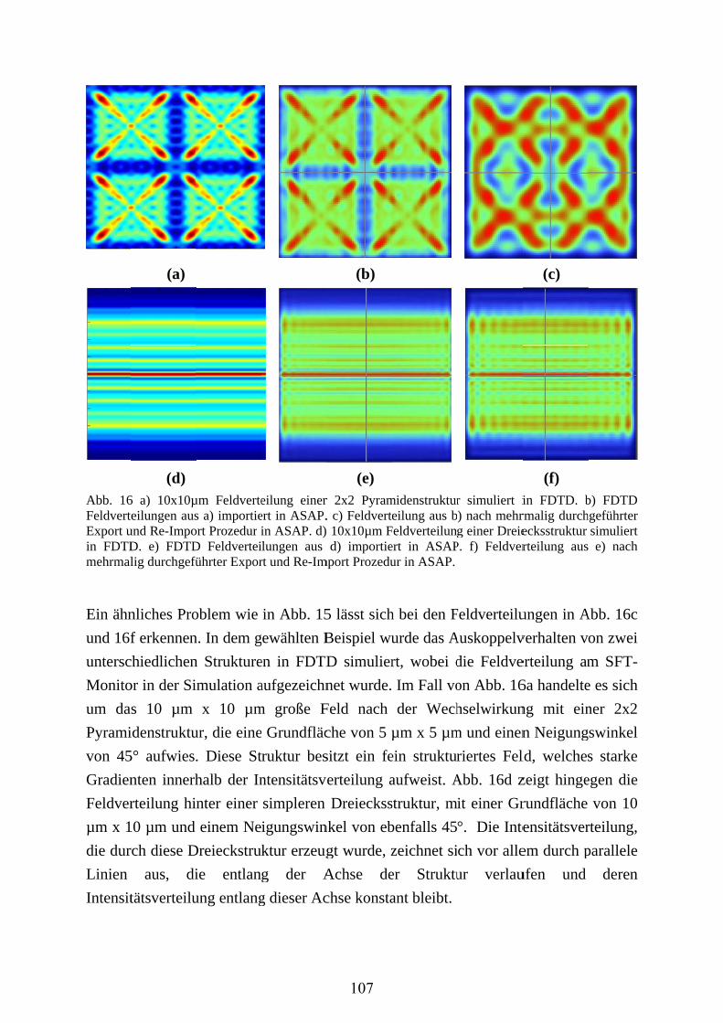
Abb. 16FeldvertExport uin FDTDmehrmal
Ein ähn
und 16f
untersc
Monito
um da
Pyrami
von 45
Gradien
Feldver
µm x 1
die dur
Linien
Intensit
(a)
(d) 6 a) 10x10µteilungen ausund Re-ImpoD. e) FDTDlig durchgefü
nliches Pro
f erkennen
chiedlichen
or in der Si
s 10 µm
idenstruktu
5° aufwies.
nten innerh
rteilung hi
10 µm und
rch diese D
aus, di
tätsverteilu
µm Feldvertes a) importieort Prozedur iD Feldverteiführter Expor
oblem wie
n. In dem g
n Strukture
mulation a
x 10 µm
ur, die eine
. Diese St
halb der In
nter einer
einem Ne
Dreieckstru
ie entlan
ung entlang
eilung einerert in ASAP.in ASAP. d) lungen aus rt und Re-Im
in Abb. 15
gewählten B
en in FDTD
aufgezeichn
m große F
e Grundfläc
truktur bes
ntensitätsv
simpleren
igungswin
ktur erzeug
g der A
g dieser Ac
(b)
(e) r 2x2 Pyram. c) Feldverte 10x10µm Fd) importie
mport Prozedu
5 lässt sich
Beispiel wu
D simulier
net wurde.
Feld nach
che von 5 µ
sitzt ein fe
erteilung a
Dreieckss
nkel von eb
gt wurde, z
Achse de
chse konsta
midenstruktureilung aus b
Feldverteilungert in ASAPur in ASAP.
h bei den F
urde das A
rt, wobei d
Im Fall vo
der Wech
µm x 5 µm
ein struktur
aufweist. A
struktur, m
benfalls 45
zeichnet si
er Struktu
ant bleibt.
r simuliert i) nach mehrg einer Dreie
P. f) Feldver
Feldverteilu
Auskoppelv
die Feldve
on Abb. 16
hselwirkun
m und einen
riertes Fel
Abb. 16d z
it einer Gr
°. Die Inte
ch vor alle
ur verlau
(c)
(f) in FDTD. brmalig durchecksstruktur rteilung aus
ungen in A
verhalten v
erteilung am
6a handelte
ng mit ein
n Neigung
ld, welches
zeigt hinge
rundfläche
ensitätsver
em durch p
ufen und
b) FDTD hgeführter
simuliert e) nach
Abb. 16c
on zwei
m SFT-
e es sich
ner 2x2
gswinkel
s starke
egen die
von 10
rteilung,
parallele
deren
107
In Abb. 16b und 16e wurden die in FDTD aufgezeichneten Feldverteilungen in ASAP
importiert, in einzelne GB zerlegt und anschließend wieder überlagert, um die
Intensitätsverteilung des Feldes zu erhalten. Durch den Import der Intensitätsverteilung
der Dreieckstruktur (Abb. 16e) ist es an den Rändern durch die scharf absteigende
Flanke der Intensitätsverteilung offenbar zu Fehlern gekommen. Zusätzlich werden
die scharfen Linien der Intensitätsverteilung durch den Import „verschmiert“, so dass
es zu Schwankungen entlang dieser Linien gekommen ist. Diese Schwankungen der
Intensitätsverteilung (Abb. 16b) treten bei der Pyramidenstruktur nicht so deutlich auf.
In Abb. 16c und 16f wurden die Intensitätsverteilungen aus Abb. 16b und 16e
mehrmalig exportiert und re-importiert, um das mögliche Ausmaß an Fehlern durch
die Import- und Export-Prozedur abschätzen zu können. Abb. 16c zeigt, dass es vor
allem bei der Intensitätsverteilung der Pyramidenstruktur zu sehr starken Verzerrungen
kommt. Daraus lässt sich vermuten, dass sich hierbei um eine Aufsummierung von
Fehlern durch die Import- und Export-Prozedur handelt und diese selbst bei einmaliger
Anwendung des Imports auftreten.
Anhand von Abb. 15 und Abb. 16 lässt sich des Weiteren schlussfolgern, dass ein
fehlerfreier Import einer beliebigen Feldverteilung nach ASAP nicht immer möglich
ist. Die in Abb. 16 verwendeten Strukturen weisen für PTGs große Strukturgrößen und
dadurch große Gitterkonstanten auf. Für manche PTGs werden Gitterkonstanten in der
Größe der verwendeten Wellenlänge benötigt. In solchen Fällen können die
korrespondierenden Feldverteilungen solcher Strukturen nicht in einzelne GB zerlegt
und daher nicht mit dieser Methode behandelt werden.
3.2.2 A SIMULATION PROCEDURE INTERFACING RAY-
TRACING AND FINITE-DIFFERENCE-TIME-DOMAIN
METHODS FOR A COMBINED SIMULATION OF DIFFRACTIVE
AND REFRACTIVE OPTICAL ELEMENTS
Aus diesem Grund wurde eine alternative Methode entwickelt, um eine Schnittstelle
zwischen ASAP und FDTD Solutions zu realisieren, die besser geeignet ist, die in der
Einleitung genannten Problemstellungen zu lösen. In „A Simulation Procedure
Interfacing Ray-Tracing and Finite-Difference-Time-Domain Methods for a Combined
Simulation of Diffractive and Refractive Optical Elements“ [55] wird diese Methode
vorgestellt.
108
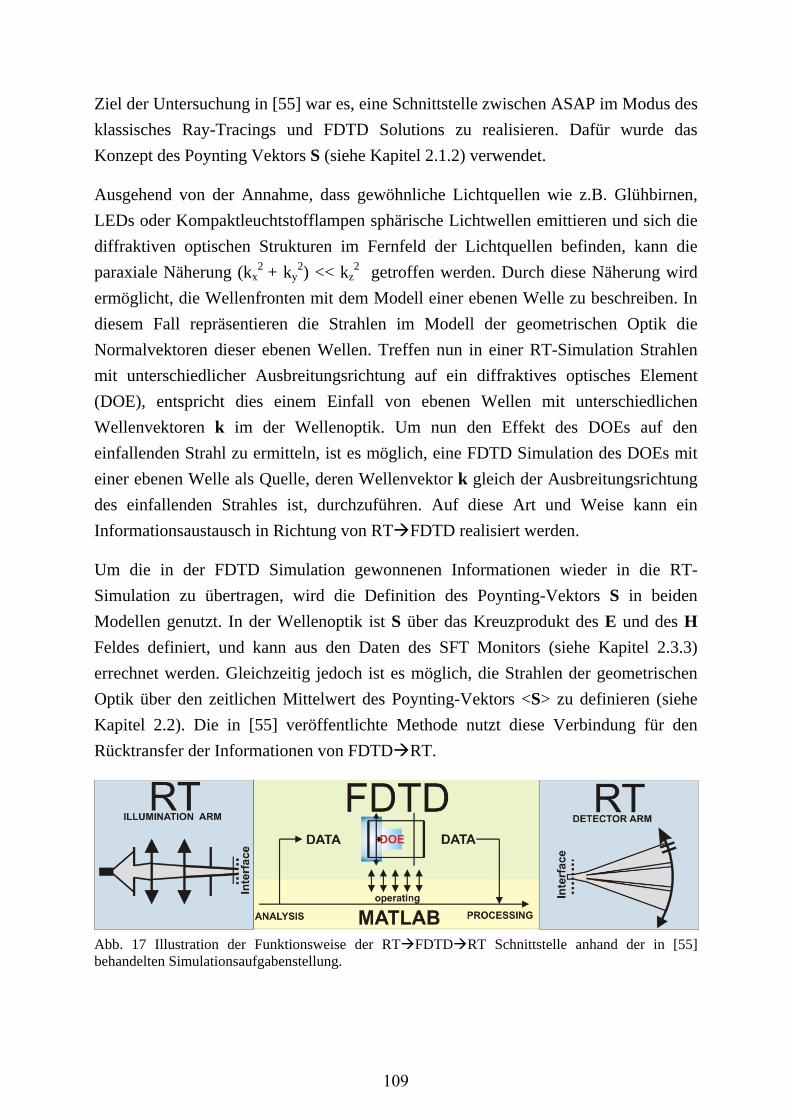
Ziel der Untersuchung in [55] war es, eine Schnittstelle zwischen ASAP im Modus des
klassisches Ray-Tracings und FDTD Solutions zu realisieren. Dafür wurde das
Konzept des Poynting Vektors S (siehe Kapitel 2.1.2) verwendet.
Ausgehend von der Annahme, dass gewöhnliche Lichtquellen wie z.B. Glühbirnen,
LEDs oder Kompaktleuchtstofflampen sphärische Lichtwellen emittieren und sich die
diffraktiven optischen Strukturen im Fernfeld der Lichtquellen befinden, kann die
paraxiale Näherung (kx2 + ky
2) << kz2 getroffen werden. Durch diese Näherung wird
ermöglicht, die Wellenfronten mit dem Modell einer ebenen Welle zu beschreiben. In
diesem Fall repräsentieren die Strahlen im Modell der geometrischen Optik die
Normalvektoren dieser ebenen Wellen. Treffen nun in einer RT-Simulation Strahlen
mit unterschiedlicher Ausbreitungsrichtung auf ein diffraktives optisches Element
(DOE), entspricht dies einem Einfall von ebenen Wellen mit unterschiedlichen
Wellenvektoren k im der Wellenoptik. Um nun den Effekt des DOEs auf den
einfallenden Strahl zu ermitteln, ist es möglich, eine FDTD Simulation des DOEs mit
einer ebenen Welle als Quelle, deren Wellenvektor k gleich der Ausbreitungsrichtung
des einfallenden Strahles ist, durchzuführen. Auf diese Art und Weise kann ein
Informationsaustausch in Richtung von RTFDTD realisiert werden.
Um die in der FDTD Simulation gewonnenen Informationen wieder in die RT-
Simulation zu übertragen, wird die Definition des Poynting-Vektors S in beiden
Modellen genutzt. In der Wellenoptik ist S über das Kreuzprodukt des E und des H
Feldes definiert, und kann aus den Daten des SFT Monitors (siehe Kapitel 2.3.3)
errechnet werden. Gleichzeitig jedoch ist es möglich, die Strahlen der geometrischen
Optik über den zeitlichen Mittelwert des Poynting-Vektors <S> zu definieren (siehe
Kapitel 2.2). Die in [55] veröffentlichte Methode nutzt diese Verbindung für den
Rücktransfer der Informationen von FDTDRT.
Abb. 17 Illustration der Funktionsweise der RTFDTDRT Schnittstelle anhand der in [55] behandelten Simulationsaufgabenstellung.
109
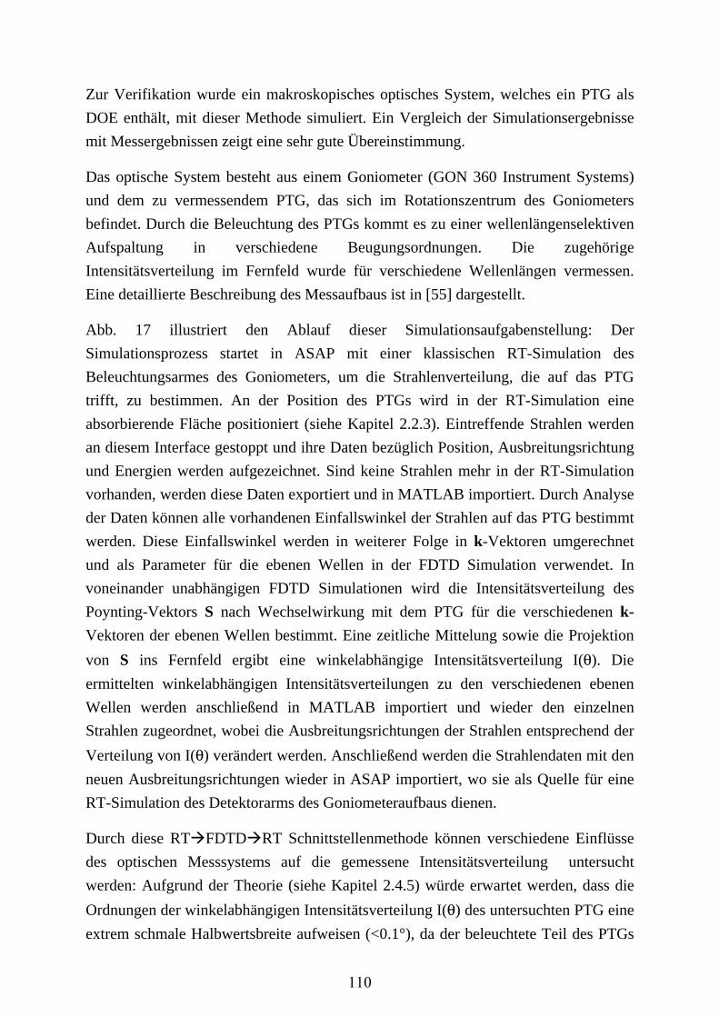
Zur Verifikation wurde ein makroskopisches optisches System, welches ein PTG als
DOE enthält, mit dieser Methode simuliert. Ein Vergleich der Simulationsergebnisse
mit Messergebnissen zeigt eine sehr gute Übereinstimmung.
Das optische System besteht aus einem Goniometer (GON 360 Instrument Systems)
und dem zu vermessendem PTG, das sich im Rotationszentrum des Goniometers
befindet. Durch die Beleuchtung des PTGs kommt es zu einer wellenlängenselektiven
Aufspaltung in verschiedene Beugungsordnungen. Die zugehörige
Intensitätsverteilung im Fernfeld wurde für verschiedene Wellenlängen vermessen.
Eine detaillierte Beschreibung des Messaufbaus ist in [55] dargestellt.
Abb. 17 illustriert den Ablauf dieser Simulationsaufgabenstellung: Der
Simulationsprozess startet in ASAP mit einer klassischen RT-Simulation des
Beleuchtungsarmes des Goniometers, um die Strahlenverteilung, die auf das PTG
trifft, zu bestimmen. An der Position des PTGs wird in der RT-Simulation eine
absorbierende Fläche positioniert (siehe Kapitel 2.2.3). Eintreffende Strahlen werden
an diesem Interface gestoppt und ihre Daten bezüglich Position, Ausbreitungsrichtung
und Energien werden aufgezeichnet. Sind keine Strahlen mehr in der RT-Simulation
vorhanden, werden diese Daten exportiert und in MATLAB importiert. Durch Analyse
der Daten können alle vorhandenen Einfallswinkel der Strahlen auf das PTG bestimmt
werden. Diese Einfallswinkel werden in weiterer Folge in k-Vektoren umgerechnet
und als Parameter für die ebenen Wellen in der FDTD Simulation verwendet. In
voneinander unabhängigen FDTD Simulationen wird die Intensitätsverteilung des
Poynting-Vektors S nach Wechselwirkung mit dem PTG für die verschiedenen k-
Vektoren der ebenen Wellen bestimmt. Eine zeitliche Mittelung sowie die Projektion
von S ins Fernfeld ergibt eine winkelabhängige Intensitätsverteilung I(θ). Die
ermittelten winkelabhängigen Intensitätsverteilungen zu den verschiedenen ebenen
Wellen werden anschließend in MATLAB importiert und wieder den einzelnen
Strahlen zugeordnet, wobei die Ausbreitungsrichtungen der Strahlen entsprechend der
Verteilung von I(θ) verändert werden. Anschließend werden die Strahlendaten mit den
neuen Ausbreitungsrichtungen wieder in ASAP importiert, wo sie als Quelle für eine
RT-Simulation des Detektorarms des Goniometeraufbaus dienen.
Durch diese RTFDTDRT Schnittstellenmethode können verschiedene Einflüsse
des optischen Messsystems auf die gemessene Intensitätsverteilung untersucht
werden: Aufgrund der Theorie (siehe Kapitel 2.4.5) würde erwartet werden, dass die
Ordnungen der winkelabhängigen Intensitätsverteilung I(θ) des untersuchten PTG eine
extrem schmale Halbwertsbreite aufweisen (<0.1°), da der beleuchtete Teil des PTGs
110
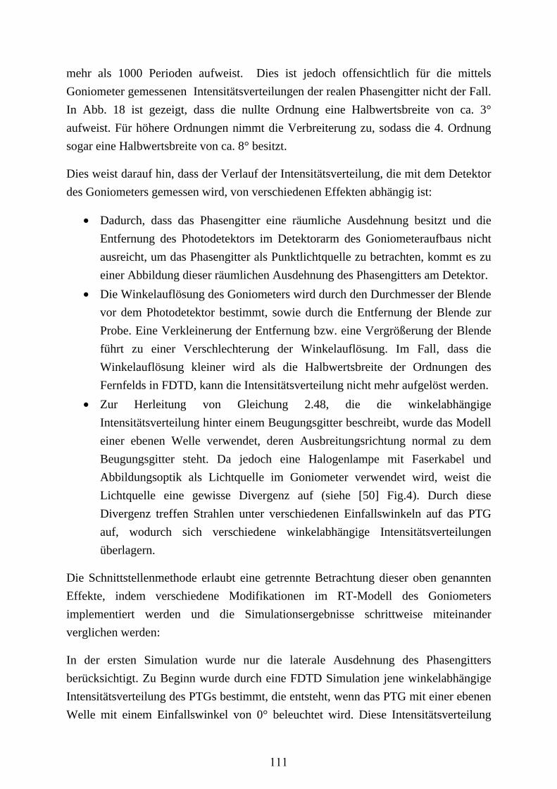
mehr als 1000 Perioden aufweist. Dies ist jedoch offensichtlich für die mittels
Goniometer gemessenen Intensitätsverteilungen der realen Phasengitter nicht der Fall.
In Abb. 18 ist gezeigt, dass die nullte Ordnung eine Halbwertsbreite von ca. 3°
aufweist. Für höhere Ordnungen nimmt die Verbreiterung zu, sodass die 4. Ordnung
sogar eine Halbwertsbreite von ca. 8° besitzt.
Dies weist darauf hin, dass der Verlauf der Intensitätsverteilung, die mit dem Detektor
des Goniometers gemessen wird, von verschiedenen Effekten abhängig ist:
• Dadurch, dass das Phasengitter eine räumliche Ausdehnung besitzt und die
Entfernung des Photodetektors im Detektorarm des Goniometeraufbaus nicht
ausreicht, um das Phasengitter als Punktlichtquelle zu betrachten, kommt es zu
einer Abbildung dieser räumlichen Ausdehnung des Phasengitters am Detektor.
• Die Winkelauflösung des Goniometers wird durch den Durchmesser der Blende
vor dem Photodetektor bestimmt, sowie durch die Entfernung der Blende zur
Probe. Eine Verkleinerung der Entfernung bzw. eine Vergrößerung der Blende
führt zu einer Verschlechterung der Winkelauflösung. Im Fall, dass die
Winkelauflösung kleiner wird als die Halbwertsbreite der Ordnungen des
Fernfelds in FDTD, kann die Intensitätsverteilung nicht mehr aufgelöst werden.
• Zur Herleitung von Gleichung 2.48, die die winkelabhängige
Intensitätsverteilung hinter einem Beugungsgitter beschreibt, wurde das Modell
einer ebenen Welle verwendet, deren Ausbreitungsrichtung normal zu dem
Beugungsgitter steht. Da jedoch eine Halogenlampe mit Faserkabel und
Abbildungsoptik als Lichtquelle im Goniometer verwendet wird, weist die
Lichtquelle eine gewisse Divergenz auf (siehe [50] Fig.4). Durch diese
Divergenz treffen Strahlen unter verschiedenen Einfallswinkeln auf das PTG
auf, wodurch sich verschiedene winkelabhängige Intensitätsverteilungen
überlagern.
Die Schnittstellenmethode erlaubt eine getrennte Betrachtung dieser oben genannten
Effekte, indem verschiedene Modifikationen im RT-Modell des Goniometers
implementiert werden und die Simulationsergebnisse schrittweise miteinander
verglichen werden:
In der ersten Simulation wurde nur die laterale Ausdehnung des Phasengitters
berücksichtigt. Zu Beginn wurde durch eine FDTD Simulation jene winkelabhängige
Intensitätsverteilung des PTGs bestimmt, die entsteht, wenn das PTG mit einer ebenen
Welle mit einem Einfallswinkel von 0° beleuchtet wird. Diese Intensitätsverteilung
111
wurde genutzt, um mittels der FTDT-RT Schnittstelle zwei unterschiedliche ASAP-
Lichtquellen zu erstellen. Die erste Lichtquelle repräsentiert eine Punktlichtquelle,
deren Abstrahlcharakteristik genau der simulierten, winkelabhängigen
Intensitätsverteilung des PTGs entspricht. Bei der zweiten Lichtquelle wurde die
räumliche Ausdehnung des PTGs berücksichtigt. Ausgehend von der Annahme, dass
das Phasengitter an jedem Punkt die gleiche winkelabhängige Intensitätsverteilung
aufweist, wurde der Ursprung jedes Strahls der Punktlichtquelle zufällig über eine
kreisrunde Fläche verteilt, deren Durchmesser der des Lichtkegels des Goniometers in
der Probenebene entspricht.
Um den Einfluss der Ausdehnung des Phasengitters beurteilen zu können, wurden
beide ASAP-Quellen auf einen Halbkugeldetektor projiziert, dessen Entfernung zur
ASAP-Quelle der Distanz zwischen Detektorarm und Phasengitter im Goniometer
entspricht.
Abb. 18 Vergleich der gemessenen Intensitätsverteilung des realen Phasengitters mit den Simulationsergebnissen der Punktlichtquelle und der ausgedehnten Quelle in ASAP. Um vergleichbare Kurven zu erhalten, wurden die Intensitätsverteilungen auf ihr Maximum normiert.
Abb. 18 zeigt das Ergebnis der Untersuchung: Die Intensitätsverteilung der ASAP-
Punktlichtquelle (grüne Kurve) am Detektor entspricht genau der winkelabhängigen
Intensitätsverteilung des PTGs in FDTD und besitzt aus diesem Grund nahezu keine
Winkelausdehnung. Die Ordnungen der ausgedehnten ASAP-Quelle (blaue Kurve)
weisen ein quadratisches Profil auf, wobei der Durchmesser der Quadrate vom
Verhältnis zwischen Ausdehnung der ASAP-Quelle und dem Abstand des Detektors
zur ASAP-Quelle abhängig ist. Dies ist dadurch zu erklären, dass sich bei kleinem
Abstand zum PTG die räumliche Ausdehnung des PTGs direkt auf den Detektor
112
abbildet. Aus diesem Grund entspricht die Intensitätsverteilung am Detektor auch
nicht mehr der winkelabhängigen Intensitätsverteilung des PTGs, sondern einer
Überlagerung der winkelabhängigen Intensitätsverteilung mit der räumlichen
Ausdehnung des PTGs. Da allerdings die ASAP-Punktlichtquelle und die ausgedehnte
ASAP-Quelle die gleiche Intensitätsverteilung besitzen, wird ihre jeweilige
Intensitätsverteilung am Detektor wieder identisch, sobald die räumliche Ausdehnung
der ASAP-Quelle im Vergleich zum Abstand des Detektors vernachlässigbar ist. Dies
wäre beim Goniometer genau dann der Fall, wenn der Abstand zwischen PTG und
Detektor so groß wird, dass die Abbildung des PTGs am Detektor kleiner wird als die
Winkelauflösung des Detektors.
Bei einem Blendendurchmesser von 1 mm hat ein Detektor in 113 mm Entfernung
eine maximale Winkelauflösung von 1°. Da allerdings in 0.5° Schritten gemessen
wurde, kommt es innerhalb eines Messpunkts zu einer Überlappung der Intensität des
gemessenen Raumwinkels mit den Intensitäten der benachbarten Messpunkte.
Bei der zweiten Simulation wurde dies berücksichtigt, indem die ASAP-Quellen nicht
auf einen Halbkugeldetektor projiziert wurden, sondern auf ein RT-Modell eines
beweglichen Detektors, entsprechend des Detektorarms des Goniometers. Mit diesem
Detektor wurden die Intensitäten der ASAP-Quellen einzeln, in einer Entfernung von
113 mm, in 0.5° Schritten gemessen. Vor dem Detektor wurde zusätzlich eine Blende
angebracht, deren Durchmesser dem Durchmesser der Blende des Goniometers
entspricht.
(a) (b)
Abb. 19: Vergleich der Intensitätsverteilung des realen Phasengitters mit den ASAP Simulationen des Goniometeraufbaus mit unterschiedlichem Quelldurchmesser. a) zeigt die niedrigen Ordnungen im Winkelbereich -25° bis +25°, b) zeigt die höheren Ordnungen im Winkelbereich -90° bis -25°. Um vergleichbare Kurven zu erhalten, wurden die Intensitätsverteilungen auf ihr Maximum normiert.
Anhand der Graphen aus Abb.19 wird ersichtlich, dass die Blende vor dem Detektor
einen starken Einfluss auf die Form der Ordnungen der Intensitätsverteilung hat. Die
113
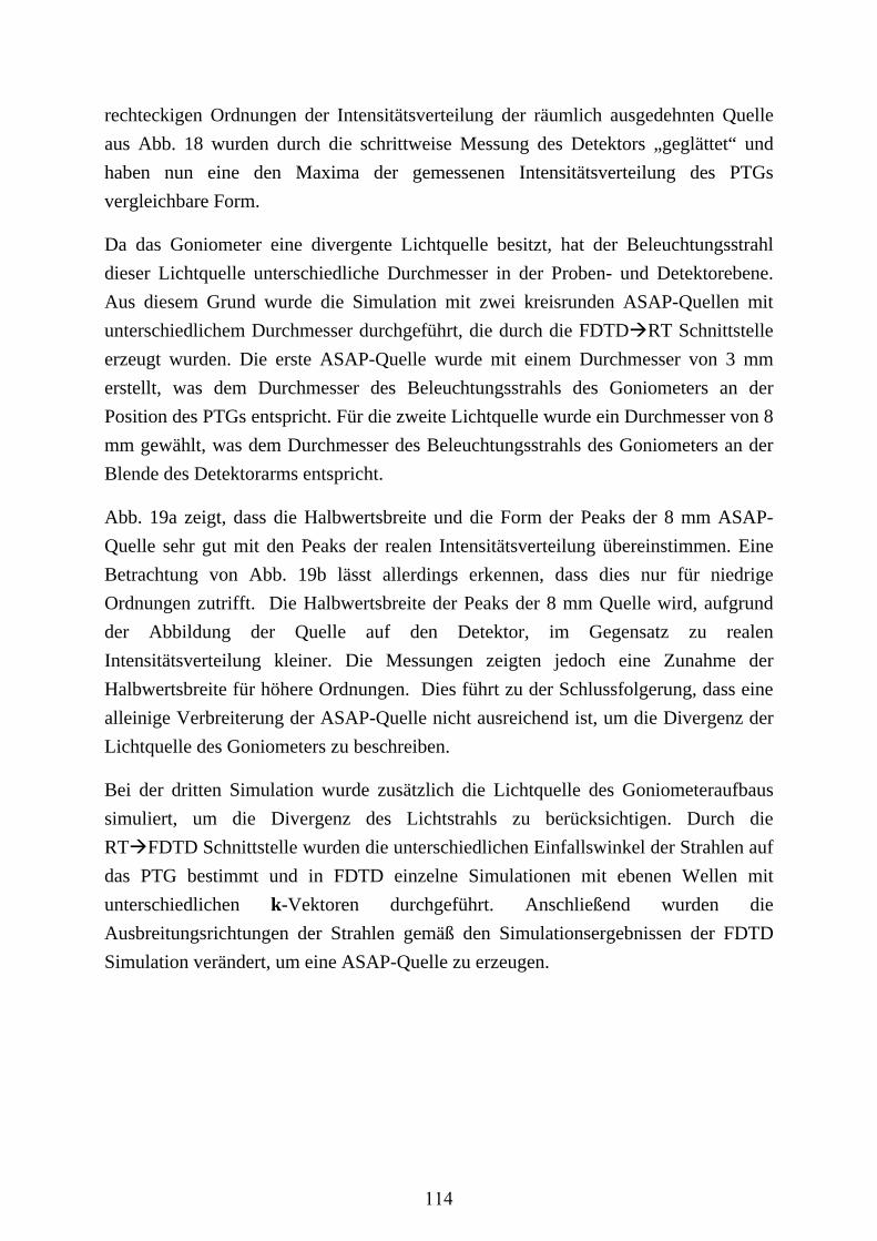
rechteckigen Ordnungen der Intensitätsverteilung der räumlich ausgedehnten Quelle
aus Abb. 18 wurden durch die schrittweise Messung des Detektors „geglättet“ und
haben nun eine den Maxima der gemessenen Intensitätsverteilung des PTGs
vergleichbare Form.
Da das Goniometer eine divergente Lichtquelle besitzt, hat der Beleuchtungsstrahl
dieser Lichtquelle unterschiedliche Durchmesser in der Proben- und Detektorebene.
Aus diesem Grund wurde die Simulation mit zwei kreisrunden ASAP-Quellen mit
unterschiedlichem Durchmesser durchgeführt, die durch die FDTDRT Schnittstelle
erzeugt wurden. Die erste ASAP-Quelle wurde mit einem Durchmesser von 3 mm
erstellt, was dem Durchmesser des Beleuchtungsstrahls des Goniometers an der
Position des PTGs entspricht. Für die zweite Lichtquelle wurde ein Durchmesser von 8
mm gewählt, was dem Durchmesser des Beleuchtungsstrahls des Goniometers an der
Blende des Detektorarms entspricht.
Abb. 19a zeigt, dass die Halbwertsbreite und die Form der Peaks der 8 mm ASAP-
Quelle sehr gut mit den Peaks der realen Intensitätsverteilung übereinstimmen. Eine
Betrachtung von Abb. 19b lässt allerdings erkennen, dass dies nur für niedrige
Ordnungen zutrifft. Die Halbwertsbreite der Peaks der 8 mm Quelle wird, aufgrund
der Abbildung der Quelle auf den Detektor, im Gegensatz zu realen
Intensitätsverteilung kleiner. Die Messungen zeigten jedoch eine Zunahme der
Halbwertsbreite für höhere Ordnungen. Dies führt zu der Schlussfolgerung, dass eine
alleinige Verbreiterung der ASAP-Quelle nicht ausreichend ist, um die Divergenz der
Lichtquelle des Goniometers zu beschreiben.
Bei der dritten Simulation wurde zusätzlich die Lichtquelle des Goniometeraufbaus
simuliert, um die Divergenz des Lichtstrahls zu berücksichtigen. Durch die
RTFDTD Schnittstelle wurden die unterschiedlichen Einfallswinkel der Strahlen auf
das PTG bestimmt und in FDTD einzelne Simulationen mit ebenen Wellen mit
unterschiedlichen k-Vektoren durchgeführt. Anschließend wurden die
Ausbreitungsrichtungen der Strahlen gemäß den Simulationsergebnissen der FDTD
Simulation verändert, um eine ASAP-Quelle zu erzeugen.
114
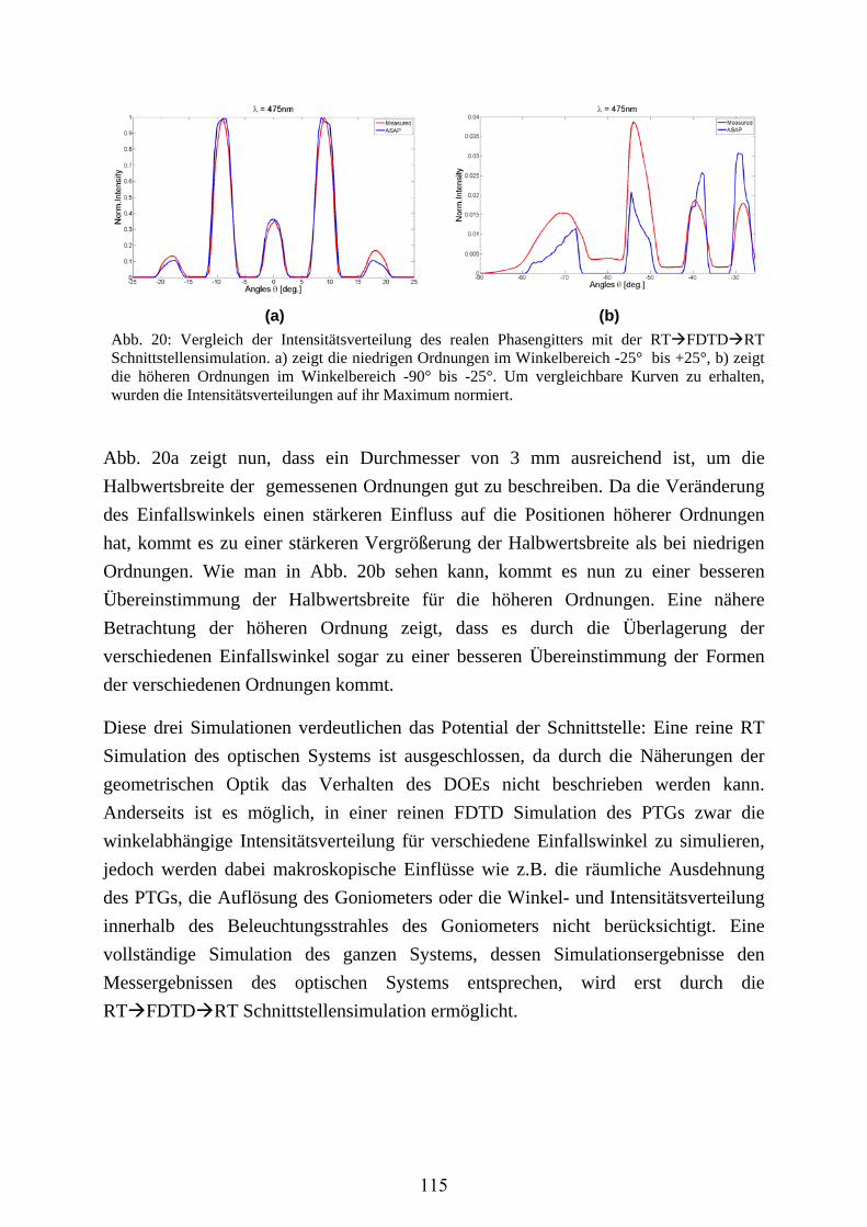
(a) (b)
Abb. 20: Vergleich der Intensitätsverteilung des realen Phasengitters mit der RTFDTDRT Schnittstellensimulation. a) zeigt die niedrigen Ordnungen im Winkelbereich -25° bis +25°, b) zeigt die höheren Ordnungen im Winkelbereich -90° bis -25°. Um vergleichbare Kurven zu erhalten, wurden die Intensitätsverteilungen auf ihr Maximum normiert.
Abb. 20a zeigt nun, dass ein Durchmesser von 3 mm ausreichend ist, um die
Halbwertsbreite der gemessenen Ordnungen gut zu beschreiben. Da die Veränderung
des Einfallswinkels einen stärkeren Einfluss auf die Positionen höherer Ordnungen
hat, kommt es zu einer stärkeren Vergrößerung der Halbwertsbreite als bei niedrigen
Ordnungen. Wie man in Abb. 20b sehen kann, kommt es nun zu einer besseren
Übereinstimmung der Halbwertsbreite für die höheren Ordnungen. Eine nähere
Betrachtung der höheren Ordnung zeigt, dass es durch die Überlagerung der
verschiedenen Einfallswinkel sogar zu einer besseren Übereinstimmung der Formen
der verschiedenen Ordnungen kommt.
Diese drei Simulationen verdeutlichen das Potential der Schnittstelle: Eine reine RT
Simulation des optischen Systems ist ausgeschlossen, da durch die Näherungen der
geometrischen Optik das Verhalten des DOEs nicht beschrieben werden kann.
Anderseits ist es möglich, in einer reinen FDTD Simulation des PTGs zwar die
winkelabhängige Intensitätsverteilung für verschiedene Einfallswinkel zu simulieren,
jedoch werden dabei makroskopische Einflüsse wie z.B. die räumliche Ausdehnung
des PTGs, die Auflösung des Goniometers oder die Winkel- und Intensitätsverteilung
innerhalb des Beleuchtungsstrahles des Goniometers nicht berücksichtigt. Eine
vollständige Simulation des ganzen Systems, dessen Simulationsergebnisse den
Messergebnissen des optischen Systems entsprechen, wird erst durch die
RTFDTDRT Schnittstellensimulation ermöglicht.
115
3.2.3 MULTI-SCALE SIMULATION OF AN OPTICAL DEVICE
USING A NOVEL APPROACH FOR COMBINING RAY-
TRACING AND FDTD
In der Veröffentlichung „Multi-Scale Simulation of an Optical Device Using a Novel
Approach for Combining Ray-Tracing and FDTD“ [54] wird eine alternative
Anwendung der Schnittstellensimulation erörtert:
In vielen Fällen ist es nicht möglich, die exakte Struktur der Perioden eines PTGs nach
der Herstellung zu bestimmen, beispielweise wenn es durch Produktionsprozesse zu
Defekten oder Abweichungen der originalen Struktur kommt. In solchen Fällen ist es
schwierig, ein geeignetes Modell der periodischen Struktur in FDTD zu erstellen.
Dadurch, dass die Schnittstellensimulation auch andere Einflüsse des optischen
Systems wie z.B. die des Messaufbaus auf das Simulationsergebnis berücksichtigen
kann, ermöglicht sie eine Optimierung des FDTD-Simulationsmodels anhand von
Messdaten der winkelabhängigen Intensitätsverteilung des PTGs.
Mittels „Nano Imprint Lithographie“ (NIL) wurde ein kommerziell erhältliches Gitter
abgeformt und reproduziert, wobei das resultierende PTG viele Defekte aufwies (siehe
[54] Fig.3). Die winkelabhängige Intensitätsverteilung des hergestellten PTGs wurde
anschließend im GON 360 vermessen.
Durch eine RTFDTDRT Schnittstellensimulation konnten verschiedene FDTD
Modelle der periodischen Struktur erstellt und optimiert werden und die simulierte
winkelabhängige Intensitätsverteilung mit der gemessenen winkelabhängigen
Intensitätsverteilung verglichen werden.
In beiden Publikationen [54], [55] wurden Systeme mit einer Schnittstellenmethode
untersucht, die klassisches RT mit FDTD verbindet. Hierfür war durch einen speziell
gewählten Aufbau des optischen Systems nur ein einzelner RTFDTDRT Schritt
notwendig. Um kompliziertere Aufgabenstellungen simulieren zu können, wie z.B.
optische Systeme mit mehreren DOEs oder optische Systeme, in denen Strahlen, die
mit dem DOE interagiert haben, wieder auf dasselbe DOE treffen, sind jedoch
mehrfache RTFDTD Schritte notwendig. Die Schnittstelle von FDTDRT wird
über den zeitlichen Mittelwert des Poynting-Vektors <S> realisiert, jedoch gehen
durch die zeitliche Mittelung alle Informationen über die Phasenbeziehungen zwischen
116
den einzelnen Wellenfronten verloren. Generell bietet klassisches Ray-Tracing
aufgrund der Definition über den zeitlichen Mittelwert des Poynting-Vektors keine
Möglichkeit der Implementierung von Phasenbeziehungen zwischen den einzelnen
Strahlen. Deswegen müssen die Phasenbeziehungen der Wellenfronten, die durch die
Interaktion der ebenen Welle mit dem DOE in der FDTD Simulation entstanden sind,
im Schritt FDTDRT vernachlässigt werden. Diese Phasenbeziehungen können
jedoch zu Interferenzeffekten zwischen den einzelnen Wellenfronten führen, wenn
diese sich wieder überlagern (siehe Kap. 2.4). Solche Interferenzeffekte können daher
auch in der Schnittstellensimulation nicht berücksichtigt werden, was, abhängig vom
optischen System, zu unbekannten Abweichungen zwischen Simulations- und
Messergebnis führen kann.
3.2.4 MULTIPLE INTERFACING BETWEEN CLASSICAL RAY-
TRACING AND WAVE-OPTICAL SIMULATION APPROACHES:
A STUDY ON APPLICABILITY AND ACCURACY
Die Publikation „Multiple Interfacing Between Classical Ray-Tracing and Wave-
Optical Simulation Approaches: A Study on Applicability and Accuracy” [56]
untersucht dieses Problem und analysiert den Einfluss der vernachlässigten
Phasenbeziehungen. Zu diesem Zweck werden die Ergebnisse einer
RTFDTDRTFDTDRT Schnittstellensimulation mit den Ergebnissen einer
reinen FDTD Simulation verglichen, bei der die Phasenbeziehungen berücksichtigt
wurden.
Wie schon in Kapitel 2.4.4 beschrieben, ist die Stärke von Interferenzeffekten
zwischen Wellen abhängig vom Grad der räumlichen und zeitlichen Kohärenz.
Typische Lichtquellen, die in makroskopischen optischen Systemen Anwendung
finden und für die sich die RT-Simulationsmethode besonders eignet, sind z.B.
Glühbirnen, LEDs, Kompaktleuchtstoffröhren, Sonnenlicht, etc. Solche Lichtquellen
besitzen aufgrund ihrer räumlichen Ausdehnung sowie ihres breitbandigen Spektrums,
nur eine Teilkohärenz (siehe Kapitel 2.4.4), wobei der Grad ihrer Kohärenz abhängig
ist vom Verhältnis ihrer Ausdehnung zu ihrem Abstand zum optischen System und
ihrer Bandbreite.
In der Publikation wird ausschließlich der Einfluss der räumlichen Teilkohärenz
untersucht. Wie auch in Kapitel 2.4.4 gezeigt, können im Falle von sehr geringer
117
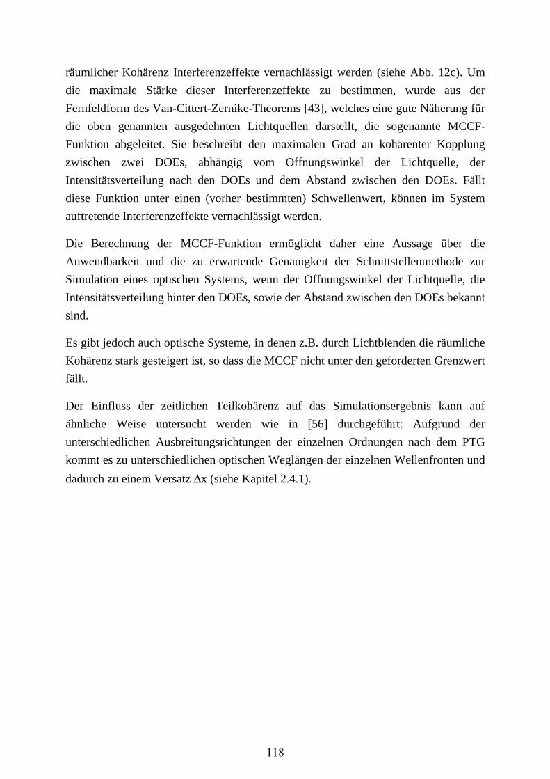
räumlicher Kohärenz Interferenzeffekte vernachlässigt werden (siehe Abb. 12c). Um
die maximale Stärke dieser Interferenzeffekte zu bestimmen, wurde aus der
Fernfeldform des Van-Cittert-Zernike-Theorems [43], welches eine gute Näherung für
die oben genannten ausgedehnten Lichtquellen darstellt, die sogenannte MCCF-
Funktion abgeleitet. Sie beschreibt den maximalen Grad an kohärenter Kopplung
zwischen zwei DOEs, abhängig vom Öffnungswinkel der Lichtquelle, der
Intensitätsverteilung nach den DOEs und dem Abstand zwischen den DOEs. Fällt
diese Funktion unter einen (vorher bestimmten) Schwellenwert, können im System
auftretende Interferenzeffekte vernachlässigt werden.
Die Berechnung der MCCF-Funktion ermöglicht daher eine Aussage über die
Anwendbarkeit und die zu erwartende Genauigkeit der Schnittstellenmethode zur
Simulation eines optischen Systems, wenn der Öffnungswinkel der Lichtquelle, die
Intensitätsverteilung hinter den DOEs, sowie der Abstand zwischen den DOEs bekannt
sind.
Es gibt jedoch auch optische Systeme, in denen z.B. durch Lichtblenden die räumliche
Kohärenz stark gesteigert ist, so dass die MCCF nicht unter den geforderten Grenzwert
fällt.
Der Einfluss der zeitlichen Teilkohärenz auf das Simulationsergebnis kann auf
ähnliche Weise untersucht werden wie in [56] durchgeführt: Aufgrund der
unterschiedlichen Ausbreitungsrichtungen der einzelnen Ordnungen nach dem PTG
kommt es zu unterschiedlichen optischen Weglängen der einzelnen Wellenfronten und
dadurch zu einem Versatz Δx (siehe Kapitel 2.4.1).
118
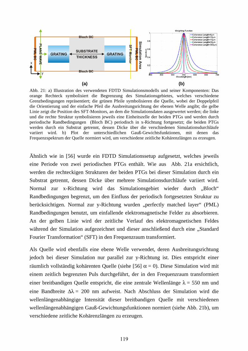
(a) (b) Abb. 21: a) Illustration des verwendeten FDTD Simulationsmodells und seiner Komponenten: Das orange Rechteck symbolisiert die Begrenzung des Simulationsgebietes, welches verschiedene Grenzbedingungen repräsentiert; die grünen Pfeile symbolisieren die Quelle, wobei der Doppelpfeil die Orientierung und der einfache Pfeil die Ausbreitungsrichtung der ebenen Welle angibt; die gelbe Linie zeigt die Position des SFT-Monitors, an dem die Simulationsdaten ausgewertet werden; die linke und die rechte Struktur symbolisieren jeweils eine Einheitszelle der beiden PTGs und werden durch periodische Randbedingungen (Bloch BC) periodisch in x-Richtung fortgesetzt; die beiden PTGs werden durch ein Substrat getrennt, dessen Dicke über die verschiedenen Simulationsdurchläufe variiert wird. b) Plot der unterschiedlichen Gauß-Gewichtsfunktionen, mit denen das Frequenzspektrum der Quelle normiert wird, um verschiedene zeitliche Kohärenzlängen zu erzeugen.
Ähnlich wie in [56] wurde ein FDTD Simulationssetup aufgesetzt, welches jeweils
eine Periode von zwei periodischen PTGs enthält. Wie aus Abb. 21a ersichtlich,
werden die rechteckigen Strukturen der beiden PTGs bei dieser Simulation durch ein
Substrat getrennt, dessen Dicke über mehrere Simulationsdurchläufe variiert wird.
Normal zur x-Richtung wird das Simulationsgebiet wieder durch „Bloch“
Randbedingungen begrenzt, um den Einfluss der periodisch fortgesetzten Struktur zu
berücksichtigen. Normal zur y-Richtung wurden „perfectly matched layer“ (PML)
Randbedingungen benutzt, um einfallende elektromagnetische Felder zu absorbieren.
An der gelben Linie wird der zeitliche Verlauf des elektromagnetischen Feldes
während der Simulation aufgezeichnet und dieser anschließend durch eine „Standard
Fourier Transformation“ (SFT) in den Frequenzraum transformiert.
Als Quelle wird ebenfalls eine ebene Welle verwendet, deren Ausbreitungsrichtung
jedoch bei dieser Simulation nur parallel zur y-Richtung ist. Dies entspricht einer
räumlich vollständig kohärenten Quelle (siehe [56] α = 0). Diese Simulation wird mit
einem zeitlich begrenzten Puls durchgeführt, der in den Frequenzraum transformiert
einer breitbandigen Quelle entspricht, die eine zentrale Wellenlänge λ = 550 nm und
eine Bandbreite Δλ = 200 nm aufweist. Nach Abschluss der Simulation wird die
wellenlängenabhängige Intensität dieser breitbandigen Quelle mit verschiedenen
wellenlängenabhängigen Gauß-Gewichtungsfunktionen normiert (siehe Abb. 21b), um
verschiedene zeitliche Kohärenzlängen zu erzeugen.
119
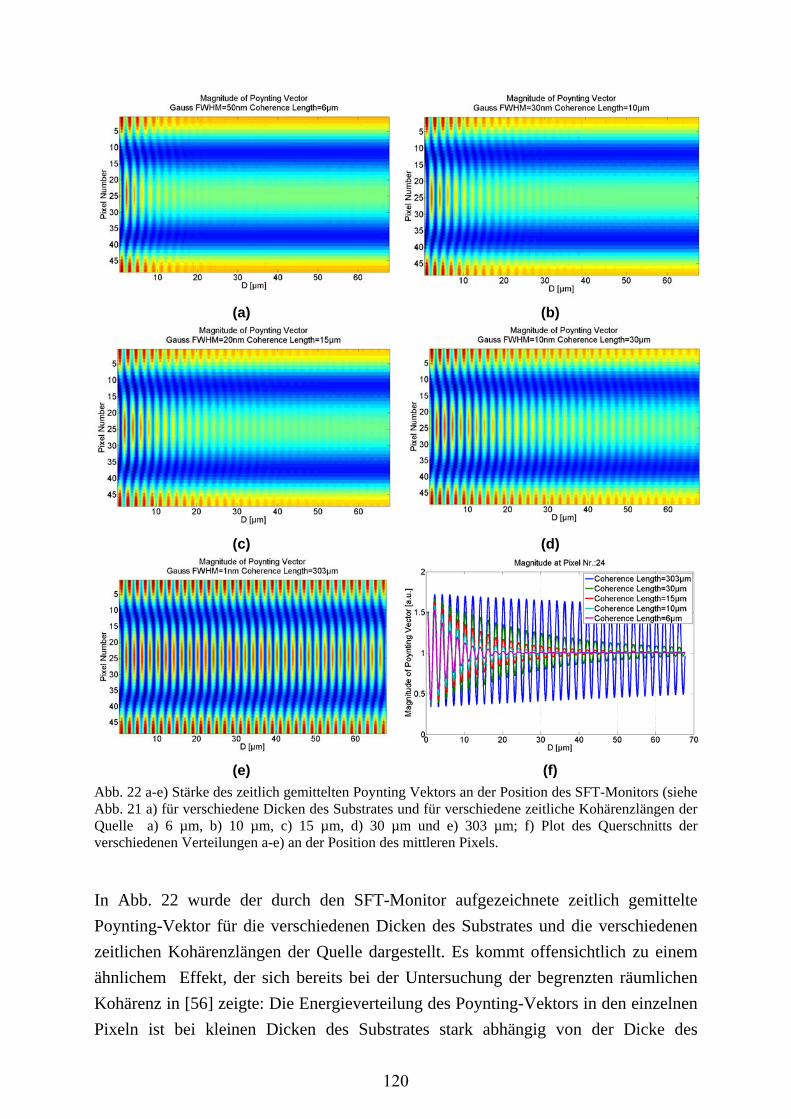
(a) (b)
(c) (d)
(e) (f) Abb. 22 a-e) Stärke des zeitlich gemittelten Poynting Vektors an der Position des SFT-Monitors (siehe Abb. 21 a) für verschiedene Dicken des Substrates und für verschiedene zeitliche Kohärenzlängen der Quelle a) 6 µm, b) 10 µm, c) 15 µm, d) 30 µm und e) 303 µm; f) Plot des Querschnitts der verschiedenen Verteilungen a-e) an der Position des mittleren Pixels.
In Abb. 22 wurde der durch den SFT-Monitor aufgezeichnete zeitlich gemittelte
Poynting-Vektor für die verschiedenen Dicken des Substrates und die verschiedenen
zeitlichen Kohärenzlängen der Quelle dargestellt. Es kommt offensichtlich zu einem
ähnlichem Effekt, der sich bereits bei der Untersuchung der begrenzten räumlichen
Kohärenz in [56] zeigte: Die Energieverteilung des Poynting-Vektors in den einzelnen
Pixeln ist bei kleinen Dicken des Substrates stark abhängig von der Dicke des
120
Substrates. Diese Abhängigkeit nimmt jedoch abhängig von der Kohärenzlänge der
Quelle für eine größere Dicke des Substrates ab. Dadurch kommt es ab einem
gewissen Abstand und bei größeren Abständen zu keinen Interferenzeffekten mehr
zwischen den zwei PTGs. Um dies zu verdeutlichen, wurde in Abb. 22f die Größe des
aufgezeichneten Poynting-Vektors im zentralen Pixel (Pixel Nr. 24) für die
unterschiedlichen Kohärenzlängen der Quellen graphisch überlagert. Es zeigt sich,
dass die Amplitude des Poynting-Vektors einer Dämpfung der Schwingungen für die
verschiedenen Kohärenzlängen unterworfen wird.
In [56] wurde beobachtet, dass in Bereichen, in denen sich der Poynting-Vektor nicht
mehr verändert, das Ergebnis der Schnittstellensimulation gleich dem Ergebnis der
reinen FDTD Simulation ist, obwohl Phaseneffekte vernachlässigt wurden.
Die Tatsache, dass eine partielle zeitliche Kohärenz einen ähnlichen Effekt auf die
maximalen Interferenzeffekte bewerkstelligt wie eine partielle räumliche Kohärenz,
kann dazu genutzt werden, die Anwendbarkeit der Schnittstellenmethode zu erweitern.
Abb. 23: Simple Klassifizierung verschiedener Lichtquellen hinsichtlich der Anwendbarkeit der Schnittstellenmethode: Systeme mit Lichtquellen, die im grünen Bereich enthalten sind, bieten bereits unter geringen Voraussetzungen die Möglichkeit, die Schnittstelle anzuwenden; für Systeme in den blassgrünen Bereichen müssen gewisse Bedingungen erfüllt sein; für Lichtquellen in den roten Bereichen ist die Schnittstelle nur unter Ausnahmefällen einsetzbar.
Abb. 23 zeigt eine schematische Übersicht über die möglichen Anwendungsgebiete
der Schnittstellenmethode. Der in grün dargestellte Bereich enthält räumlich
121
ausgedehnte, breitbandige Lichtquellen, die sowohl eine niedrige räumliche als auch
eine niedrige zeitliche Kohärenz aufweisen. Für Systeme mit solchen Lichtquellen
wird die Schnittstelle nur schwach begrenzt, da mögliche Interferenzeffekte durch
beide Kohärenzeffekte abgeschwächt werden, so dass die Schnittstellenmethode in den
meisten Fällen eingesetzt werden kann.
Die blassgrün dargestellten Bereiche enthalten Lichtquellen, die entweder eine hohe
zeitliche oder eine hohe räumliche Kohärenz aufweisen. Als Beispiel für Lichtquellen
mit hoher zeitlicher Kohärenz sind Natriumdampflampen aufgeführt, die ein extrem
schmales Emissionsspektrum aufweisen und normale Lichtquellen, deren spektrale
Bandbreite z.B. durch Bandpassfilter begrenzt wird. Zur Kategorie der Lichtquellen
mit hoher räumlicher Kohärenz gehört z.B. Sternenlicht, das zwar ein ähnliches
Spektrum aufweisen kann wie die Sonne, bei dem jedoch das Verhältnis der
räumlichen Ausdehnung zur Entfernung so klein wird, dass die räumliche Kohärenz
groß wird. Ein anderes Beispiel dieser Kategorie sind normale Lichtquellen, deren
räumliche Ausdehnung durch schmale Blenden begrenzt wird, so dass die räumliche
Kohärenz ebenfalls hoch wird. In diesen Fällen ist die Schnittstelle zwar einsetzbar,
jedoch müssen mögliche Interferenzeffekte berücksichtigt werden. In diesem Fall ist
es möglich, durch die Berechnung der MCCF den maximalen Fehler durch diese
Interferenzeffekte abzuschätzen.
Im roten Bereich sind Lichtquellen enthalten, die sowohl hohe zeitliche als auch eine
hohe räumliche Kohärenz aufweisen. Zu dieser Kategorie gehören Laser, deren Licht
in der Regel eine sehr geringe Divergenz sowie eine extrem schmale Bandbreite
aufweist. In diesen Fällen ist die RTFDTD Schnittstelle nicht bzw. nur in großen
Distanzen zwischen den einzelnen DOEs einsetzbar. Bei diesen Distanzen kann es sich
um einige Zentimeter bis hin zu mehreren Metern handeln.
122
3.2.5 REDUCING SHADOWING LOSSES WITH
FEMTOSECOND-LASER-WRITTEN DEFLECTIVE OPTICAL
ELEMENTS IN THE BULK OF EVA ENCAPSULATION
Abschließend wird eine reale Anwendung behandelt: In der Publikation „Reducing
shadowing losses with femtosecond-laser-written deflective optical elements in the
bulk of EVA encapsulation“ [57] wurde die Schnittstelle zur Verifikation eines
optischen Systems eingesetzt.
Heutige Solarzellen bestehen häufig aus kristallinen Siliziumplatten, eingebettet in
Ethylenvinylacetat (EVA), einem Polymer, das die Siliziumplatten vor äußeren
Einflüssen schützt. Um Ladungsträger aus den Siliziumplatten abzuleiten, müssen
diese an der Vorderseite durch ein feines metallisches Gitter kontaktiert werden,
welches aus größeren „Busbars“ und kleineren verzweigten „Fingern“ besteht. Als
Material für diese Gitter wird in vielen Fällen Silber verwendet. Dadurch, dass diese
Gitter eine hohe elektrische Leitfähigkeit besitzen müssen, weisen sie keine optische
Transparenz auf. Dadurch kommt es jedoch zu einer Abschattung der Siliziumplatten.
Typischerweise wird 7 - 9 % der Frontseite der Siliziumplatten durch dieses Gitter
bedeckt.
In [57] wird ein Ansatz untersucht, der es ermöglicht, diese Abschattung zu
reduzieren. Nach Herstellung der Solarmodule wird das EVA Material oberhalb der
Silberkontakte fokussierten fs-Laser-Pulsen ausgesetzt, wodurch die dielektrische
Funktion des EVAs im Fokus verändert wird. Dadurch ist es möglich, z.B. diffraktive
Gitter oberhalb der Metallkontakte zu erzeugen. Licht, welches auf die Kontakte
treffen würde, wird nun durch die diffraktiven Gitterstrukturen auf die Siliziumzellen
abgelenkt.
Um die Methode zu verifizieren, wurden zwei Prüfmuster erstellt (siehe Abb. 24a). Sie
bestehen aus zwei 1 mm dicken Glassubstraten, die eine 0.6 mm dicke Schicht aus
EVA einschließen. Innerhalb der EVA Schicht befinden sich mehrere 250 µm breite
und 50 µm hohe Metallkontakte aus Silber, die parallel mit einem Abstand von 1 mm
angeordnet sind. In eines dieser zwei Prüfmuster wurde mittels des fs-Puls-Lasers ein
diffraktives Gitter in die EVA Schicht in einem Abstand von 0.5 mm zur Oberseite
dieser Metallkontakte eingeschrieben. Anschließend wurden Transmissionsmessungen
an beiden Prüfmustern im Wellenlängenbereich von 350 – 1000 nm in 5 nm Schritten
123
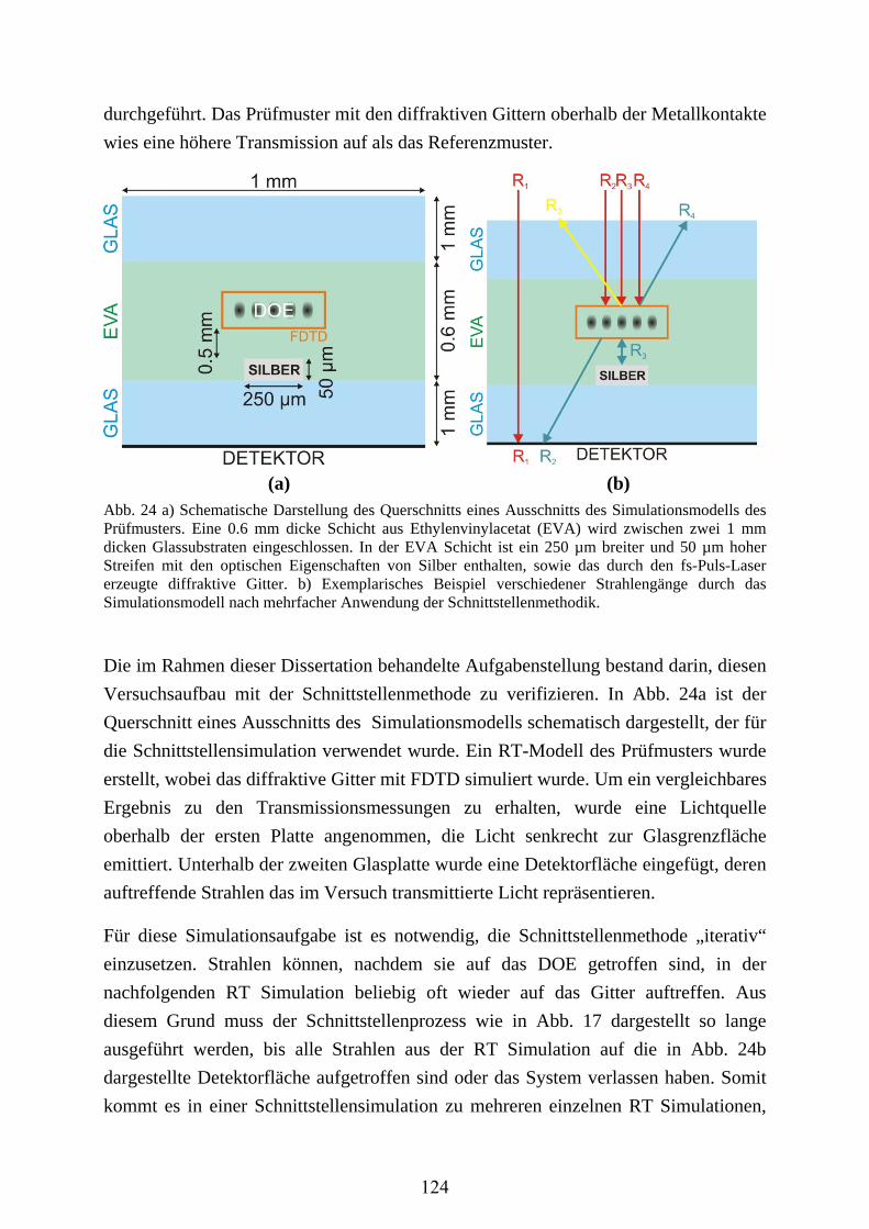
durchgeführt. Das Prüfmuster mit den diffraktiven Gittern oberhalb der Metallkontakte
wies eine höhere Transmission auf als das Referenzmuster.
(a) (b)
Abb. 24 a) Schematische Darstellung des Querschnitts eines Ausschnitts des Simulationsmodells des Prüfmusters. Eine 0.6 mm dicke Schicht aus Ethylenvinylacetat (EVA) wird zwischen zwei 1 mm dicken Glassubstraten eingeschlossen. In der EVA Schicht ist ein 250 µm breiter und 50 µm hoher Streifen mit den optischen Eigenschaften von Silber enthalten, sowie das durch den fs-Puls-Laser erzeugte diffraktive Gitter. b) Exemplarisches Beispiel verschiedener Strahlengänge durch das Simulationsmodell nach mehrfacher Anwendung der Schnittstellenmethodik.
Die im Rahmen dieser Dissertation behandelte Aufgabenstellung bestand darin, diesen
Versuchsaufbau mit der Schnittstellenmethode zu verifizieren. In Abb. 24a ist der
Querschnitt eines Ausschnitts des Simulationsmodells schematisch dargestellt, der für
die Schnittstellensimulation verwendet wurde. Ein RT-Modell des Prüfmusters wurde
erstellt, wobei das diffraktive Gitter mit FDTD simuliert wurde. Um ein vergleichbares
Ergebnis zu den Transmissionsmessungen zu erhalten, wurde eine Lichtquelle
oberhalb der ersten Platte angenommen, die Licht senkrecht zur Glasgrenzfläche
emittiert. Unterhalb der zweiten Glasplatte wurde eine Detektorfläche eingefügt, deren
auftreffende Strahlen das im Versuch transmittierte Licht repräsentieren.
Für diese Simulationsaufgabe ist es notwendig, die Schnittstellenmethode „iterativ“
einzusetzen. Strahlen können, nachdem sie auf das DOE getroffen sind, in der
nachfolgenden RT Simulation beliebig oft wieder auf das Gitter auftreffen. Aus
diesem Grund muss der Schnittstellenprozess wie in Abb. 17 dargestellt so lange
ausgeführt werden, bis alle Strahlen aus der RT Simulation auf die in Abb. 24b
dargestellte Detektorfläche aufgetroffen sind oder das System verlassen haben. Somit
kommt es in einer Schnittstellensimulation zu mehreren einzelnen RT Simulationen,
124
die im nachfolgenden Text als Iterationsschritte bezeichnet werden (z.B. 1. Iteration
RTFDTD 2. Iteration RTFDTD 3. Iteration RTFDTD).
In Abb. 24b ist der iterative Simulationsprozess für diese Aufgabe anhand von vier
exemplarischen Strahlen R1, R2, R3 und R4 skizziert. Strahlen in der ersten RT
Simulation, bzw. in der ersten Iteration, sind rot dargestellt. Sie werden von der
Lichtquelle oberhalb der ersten Glasplatte emittiert und besitzen eine
Ausbreitungsrichtung senkrecht zur Glasoberfläche. Im Fall von R1 wird der Strahl
direkt durch die drei Grenzflächen transmittiert und trifft bereits im ersten
Iterationsschritt auf den Detektor auf. Die Strahlen R2-R4 hingegen werden durch die
ersten beiden Grenzflächen transmittiert und treffen auf den Schnittstellen-Detektor
auf, der die Position des diffraktiven Gitters in der RT Simulation repräsentiert. Im
nachfolgen FDTD Schritt werden die Intensitäten (im Fall, dass das Material des
DOEs eine dielektrische Funktion mit komplexem Anteil besitzt) sowie die
Ausbreitungsrichtungen der Strahlen entsprechend den FDTD Simulationsergebnissen
angepasst. Aus diesen Strahlen wird anschließend eine neue Quelle für eine RT
Simulation erstellt, welche in der zweiten RT Simulation bzw. in der zweiten Iteration,
als Lichtquelle verwendet wird. Die Strahlen der zweiten Iteration sind in Abb. 24b in
Grün dargestellt. Wie zu erkennen ist, wurde der Strahl R2 durch das DOE
transmittiert, wobei sich seine Ausbreitungsrichtung verändert hat. Der Strahl wird
statt auf die Oberfläche des Metallkontakts nun durch die Grenzfläche zwischen EVA
und Glas transmittiert und trifft auf den Detektor auf. Der Strahl R4 wurde vom DOE
reflektiert und verlässt das System über die obere Glasplatte. Interessant ist hingegen
der Fall des Strahls R3. Er wurde durch das DOE transmittiert, jedoch wurde seine
Ausbreitungsrichtung nicht verändert, so dass er auf die Oberfläche des Metallkontakts
trifft. Dort wird er reflektiert und trifft wieder auf die Schnittstellen-Detektorfläche
auf. Dadurch wird ein weiterer RTFDTD Schritt notwendig, sowie eine weitere
Iteration der RT Simulation (Strahlen in Gelb dargestellt).
Dadurch, dass alle in Abb. 24b exemplarisch dargestellten Strahlenverhalten, bzw.
auch weitere, in der Simulation auftreten können, muss dieser iterative
Simulationsprozess solange durchgeführt werden, bis keine Strahlen mehr auf die
Schnittstellen-Detektorfläche die die Position des diffraktiven Gitters in der RT
Simulation repräsentiert, auftreffen.
Um mögliche Phaseneffekte auszuschließen bzw. vernachlässigen zu können, die
durch die Wechselwirkung des DOEs mit sich selbst entstehen können, muss die in
[56] behandelte MCCF Funktion berechnet werden. Die Lichtquelle ist im
125
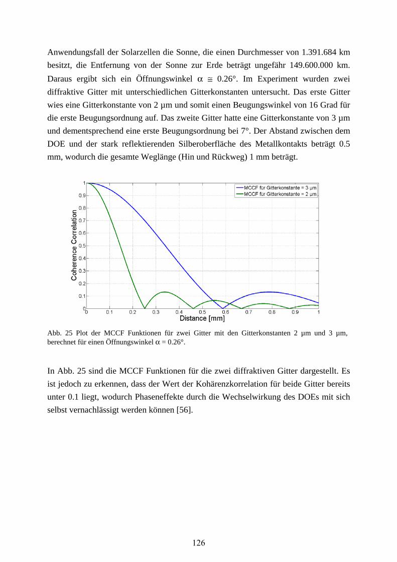
Anwendungsfall der Solarzellen die Sonne, die einen Durchmesser von 1.391.684 km
besitzt, die Entfernung von der Sonne zur Erde beträgt ungefähr 149.600.000 km.
Daraus ergibt sich ein Öffnungswinkel α ≅ 0.26°. Im Experiment wurden zwei
diffraktive Gitter mit unterschiedlichen Gitterkonstanten untersucht. Das erste Gitter
wies eine Gitterkonstante von 2 µm und somit einen Beugungswinkel von 16 Grad für
die erste Beugungsordnung auf. Das zweite Gitter hatte eine Gitterkonstante von 3 µm
und dementsprechend eine erste Beugungsordnung bei 7°. Der Abstand zwischen dem
DOE und der stark reflektierenden Silberoberfläche des Metallkontakts beträgt 0.5
mm, wodurch die gesamte Weglänge (Hin und Rückweg) 1 mm beträgt.
Abb. 25 Plot der MCCF Funktionen für zwei Gitter mit den Gitterkonstanten 2 µm und 3 µm, berechnet für einen Öffnungswinkel α = 0.26°.
In Abb. 25 sind die MCCF Funktionen für die zwei diffraktiven Gitter dargestellt. Es
ist jedoch zu erkennen, dass der Wert der Kohärenzkorrelation für beide Gitter bereits
unter 0.1 liegt, wodurch Phaseneffekte durch die Wechselwirkung des DOEs mit sich
selbst vernachlässigt werden können [56].
126
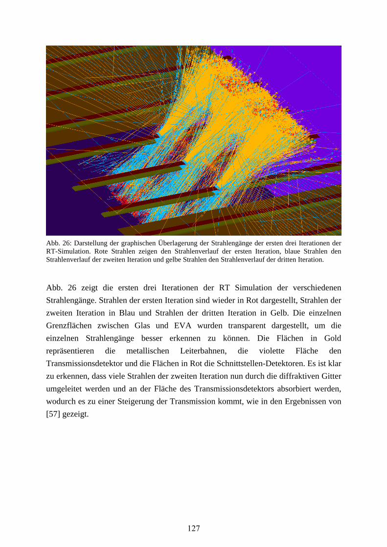
Abb. 26: Darstellung der graphischen Überlagerung der Strahlengänge der ersten drei Iterationen der RT-Simulation. Rote Strahlen zeigen den Strahlenverlauf der ersten Iteration, blaue Strahlen den Strahlenverlauf der zweiten Iteration und gelbe Strahlen den Strahlenverlauf der dritten Iteration.
Abb. 26 zeigt die ersten drei Iterationen der RT Simulation der verschiedenen
Strahlengänge. Strahlen der ersten Iteration sind wieder in Rot dargestellt, Strahlen der
zweiten Iteration in Blau und Strahlen der dritten Iteration in Gelb. Die einzelnen
Grenzflächen zwischen Glas und EVA wurden transparent dargestellt, um die
einzelnen Strahlengänge besser erkennen zu können. Die Flächen in Gold
repräsentieren die metallischen Leiterbahnen, die violette Fläche den
Transmissionsdetektor und die Flächen in Rot die Schnittstellen-Detektoren. Es ist klar
zu erkennen, dass viele Strahlen der zweiten Iteration nun durch die diffraktiven Gitter
umgeleitet werden und an der Fläche des Transmissionsdetektors absorbiert werden,
wodurch es zu einer Steigerung der Transmission kommt, wie in den Ergebnissen von
[57] gezeigt.
127
4. ZUSAMMENFASSUNG UND AUSBLICK
Ziel der vorliegenden Dissertation „Multiskalen-Simulation und Modellierung von
optischen Systemen“ war es, Simulationen von optischen Systemen, die sowohl
optische Elemente mit Strukturgrößen im Bereich der Wellenlänge des Lichts als auch
Elemente mit makroskopischen Strukturgrößen enthalten, zu ermöglichen. Im 1.
Kapitel dieser Arbeit wurde gezeigt, dass solche Simulationen nicht exklusiv mit einer
einzigen Simulationsmethode durchgeführt werden können, da sich die einzelnen
Methoden, abhängig von der Strukturgröße der optischen Elemente, in der
zugrundeliegenden physikalischen Theorie wesentlich unterscheiden.
Simulationsmethoden, denen die physikalischen Formalismen der geometrischen
Optik zugrunde liegen, können zwar zur Simulation von optischen Elementen mit
makroskopischen Strukturgrößen eingesetzt werden, jedoch nicht für optische
Elemente mit Strukturgrößen im Bereich der Wellenlänge des Lichts. Umgekehrt
können mit Simulationsmethoden, die auf den Formalismen der Wellenoptik basieren,
optische Elemente mit Strukturgrößen im Bereich der Wellenlänge des Lichts
behandelt werden, jedoch keine Simulationen von optische Elementen mit
makroskopischen Strukturgrößen in adäquater Simulationszeit durchführt werden,
selbst nicht unter Verwendung der gegenwärtig leistungsfähigsten Computer.
Aus diesem Grund wurde der Fokus dieser Arbeit auf das Auffinden von Strategien
und Konzepten für einen effizienten Datenaustausch zwischen Simulationsmethoden
der geometrischen Optik und den Simulationsmethoden der Wellenoptik gerichtet.
Solch ein Datenaustausch würde es ermöglichen, ein optisches Bauelement in
verschiedene Bereiche zu unterteilen, welche mit den jeweilig geeigneten
Simulationsmethoden behandelt werden könnten und auf diese Weise das Bauelement
gesamtheitlich zu simulieren. Zu diesem Zweck wurden zwei verschiedene Ansätze
für die Erstellung möglicher Schnittstellen untersucht, mit deren Hilfe zwei
kommerzielle Simulationsprogramme, ASAP (Breault Research) als ein Beispiel für
ein Simulationsprogramm auf der Basis geometrischer Optik und FDTD SOLUTIONS
(Lumerical) als ein Beispiel für ein Simulationsprogramm auf der Basis der
Wellenoptik, verbunden werden können.
Ein erster Ansatz zielte darauf ab, die bereits von den Firmen Breault Research und
Lumerical entwickelte Schnittstelle zwischen dem Gauß-Beam-Tracing Modus von
ASAP und FDTD SOLUTIONS zu erweitern, um eine Simulation von großflächigen
diffraktiven Gittern, die in makroskopischen optischen Bauelementen enthalten sind,
128
zu ermöglichen. Im der im Rahmen der SPIE-Proceedings veröffentlichten Publikation
„A Simulation Procedure For Light-Matter Interaction At different Length Scales”
[50] (siehe Kapitel 3.1.1) wurde untersucht, inwieweit die Limitierung dieser
Schnittstelle auf die Größe des FDTD-Simulationsgebietes dadurch umgangen werden
kann, indem man die Periodizität des diffraktiven Gitters nutzt. Dabei hat sich
herausgestellt, dass sich die Feldverteilung, die nach Interaktion der diffraktiven
Struktur des Gitters mit der einfallenden ebenen Welle entsteht, aus der FDTD
Simulation einer einzelnen Periode des Gitters rekonstruieren lässt. Dies ermöglichte
die in dieser Publikation veröffentlichte Schnittstellen-Simulation eines diffraktiven
Gitters mit einer Fläche von 50 µm x 50 µm. Ausgehend von der Feldverteilung, die
durch eine FDTD Simulation einer 5 µm x 5 µm großen Periode des Gitters bestimmt
wurde, wurde die Feldverteilung hinter dem Gitter in Matlab rekonstruiert und in
ASAP über die implementierte Schnittstelle importiert. Es konnte gezeigt werden, dass
die mit der erweiterten Schnittstellenmethode berechnete Intensitätsverteilung im
Fernfeld mit der Fernfeldverteilung übereinstimmte, die sich durch eine reine FDTD
Simulation ergab. Diese Übereinstimmung zeigt den prinzipiell fehlerfreien Import des
mittels FDTD berechneten Feldes nach Interaktion mit dem Gitter in ASAP, welches
in weiterer Folge zur Simulation eines Systems mit reaktiven optischen Elementen
genutzt werden kann.
Weiterführende Untersuchungen, deren Ergebnisse in Kapitel 3.2 präsentiert wurden,
zeigten jedoch, dass ein fehlerfreier Import einer beliebigen Feldverteilung nicht
immer möglich ist. Dies ist vor allem bei diffraktiven Strukturen der Fall. deren
Strukturgröße sehr klein ist, also in der Größenordnung der Wellenlänge des Lichts
liegt. In solchen Fällen entstehen zumeist sehr feine Feldverteilungen mit starken
Gradienten innerhalb der Intensitätsverteilung, deren Zerlegung in Gauß Strahlen zu
starken Verzerrungen und somit zu schweren Fehlern in den Simulationsergebnissen
führen kann.
Ein zweiter Ansatz zielte darauf ab, eine eigenständige Schnittstelle zwischen dem
Ray-Tracing Modus von ASAP und FDTD SOLUTIONS zu kreieren. Die in diesem
Zusammenhang entwickelte Vorgehensweise wurde im Rahmen der Publikation “A
Simulation Procedure Interfacing Ray-Tracing and Finite-Difference-Time-Domain
Methods for a Combined Simulation of Diffractive and Refractive Optical Elements”
[55] (siehe Kapitel 3.1.2) veröffentlicht. Diese Schnittstelle basiert auf einer
Verbindung der geometrischen Optik mit der Wellenoptik über das Konzept des
Poynting-Vektors S. Der RTFDTD Teil der Schnittstelle wurde realisiert, indem in
129
der RT- Simulation die Einfallsrichtungen der auf das DOE einfallenden Strahlen
verwendet wurden, um Quellen in der FDTD-Simulation zu definieren. Der Einfluss
des DOE auf die einfallenden Strahlen wurde anschließend durch FDTD Simulationen
bestimmt, indem der zeitliche Mittelwert des Vektorfeldes des Poynting Vektors <S>
nach Interaktion der verschiedenen Quellen mit dem DOE in den Simulationen
ermittelt wurde. Im FDTDRT Teil der Schnittstelle wurden die Daten von <S>
genutzt, um die Ausbreitungsrichtung und die Energiedichte der einzelnen Strahlen
gemäß den FDTD-Simulationsergebnissen anzupassen.
Dieses Konzept einer RTFDTDRT Schnittstelle wurde in [55] genutzt, um ein
optisches System, bestehend aus einem Goniometer und dem zu vermessenden
diffraktiven Phasengitter, welches sich im Rotationszentrum des Goniometers befand,
zu simulieren. Ein zusätzliches Experiment erlaubt einen Vergleich mit den
Simulationsergebnissen.
Es stellte sich heraus, dass es bei der Modellierung des RT-Simulationsmodels viele
Einflussfaktoren auf das Simulationsergebnis gibt, wie z.B. die räumliche Ausdehnung
des Phasengitters in der RT-Simulation, die Entfernung des Photodetektors zum
Phasengitter, sowie winkel- und ortsabhängige Intensitätsverteilungen der auf das
Phasengitter eintreffenden Strahlen. All diese Faktoren konnten nur durch eine
vollständige RTFDTDRT Simulation ausreichend berücksichtigt werden, die zu
dem in [55] veröffentlichten Endergebnis führten.
Die Schnittstellenmethode, die in den Publikationen [55] und „Multi-Scale Simulation
of an Optical Device Using a Novel Approach for Combining Ray-Tracing and
FDTD“ [54] (siehe Kapitel 3.1.3) zur Anwendung kam, verwendet jedoch nur einen
einzigen RTFDTDRT Schritt. Viele Simulationsaufgabenstellungen setzen jedoch
voraus, dass eine beliebige Anzahl an RTFDTD Schritten durchgeführt werden
kann. Da in der Methode des klassischen RT keine Phaseneffekte des Lichts
berücksichtigt werden, gehen im FDTDRT Teil alle in der FDTD Simulation
erhaltenen Phaseninformationen verloren. Dies würde bei einer beliebigen Anzahl an
RTFDTD Schritten zu einer unkontrollierten Summation von Fehler durch
Phaseneffekte führen und schließt aus diesem Grund eine allgemeine Verwendung
dieser Simulationsmethode aus.
Phaseneffekte sind allerdings abhängig vom Grad der jeweiligen Kohärenz (siehe
Kapitel 2.4.4) und in den vielen optischen Anordnungen, die aus ROEs und DOEs
aufgebaut sind, werden räumlich und zeitlich teilkohärente Lichtquellen verwendet. In
130
der Publikation „Multiple Interfacing Between Classical Ray-Tracing and Wave-
Optical Simulation Approaches: A Study on Applicability and Accuracy” [56] (siehe
Kapitel 3.1.4) wurde daher die mehrmalige Verwendung der Schnittstelle in einem
optischen System mit räumlich teilkohärenter Lichtquelle untersucht. Es stellte sich
heraus, dass der durch eine beliebige Anzahl an RTFDTD Schritten entstehende
Fehler unter anderem abhängig ist vom Grad der räumlichen Teilkohärenz der
Lichtquelle und dem Abstand der einzelnen DOEs. Es konnte eine Grenzwertfunktion
bestimmt werden, die zur Abschätzung des Fehlers dient und somit eine Aussage über
die Anwendbarkeit und die zu erwartende Genauigkeit der Schnittstellenmethode für
das jeweilige optische System ermöglicht. Zusätzlich wurde eine ähnliche
Untersuchung auch für eine zeitliche teilkohärente Lichtquelle (siehe Kapitel 3.2)
durchgeführt. Es stellte sich heraus, dass der Grad der zeitlichen Teilkohärenz einen
ähnlichen Einfluss auf den durch die Schnittstellenmethode erzeugten Fehler hat wie
der Grad der räumlichen Teilkohärenz. Bei steigendem Abstand zwischen den DOEs
verringert sich der Fehler durch die Vernachlässigung der Phasenbeziehungen,
wodurch eine mehrmalige Anwendung der Schnittstelle ermöglicht wird.
Letztlich fand das Schnittstellenverfahren in einem komplexen optischen Bauelement
Anwendung. In der Publikation “Reducing shadowing losses with femtosecond-laser-
written deflective optical elements in the bulk of EVA encapsulation” [57] (siehe
Kapitel 3.1.5) wurde die Schnittstellenmethode für die Simulation eines optisches
Systems eingesetzt, welches eine beliebige Anzahl an RTFDTD Schritten
benötigt, wobei der Fehler durch die in [56] bestimmte Grenzwertfunktion abgeschätzt
wurde. Das optische System bestand dabei aus einem Photovoltaikmodul, in dessen
Verkapselungsschicht mittels eines fs-Lasers Gitterstrukturen eingeschrieben wurden,
die die Aufgabe haben, das einfallende Licht so umzulenken, dass es bevorzugt auf die
aktive Halbleiteroberfläche und nicht auf die Elektrodenoberfläche trifft. Die auf der
Basis der Schnittstellenmethode erzielten Simulationsergebnisse stimmten einerseits
sehr gut mit den Messergebnissen überein und konnten andererseits auch dazu
verwendet werden, um eine optimale Anordnung der Gitterstrukturen zu ermitteln.
Die im Rahmen dieser Dissertation erarbeitete Schnittstelle weist bereits ein breites
Spektrum an Anwendungsmöglichkeiten auf, es besteht aber auch noch Potential für
mögliche Verbesserungen. Bisher ist der Prozess der Schnittstelle auf die zwei
kommerziellen Programme ASAP und FDTD Solutions beschränkt. Da der
Schnittstellenprozess an sich aber unabhängig von den verwendeten kommerziellen
Programmen für RT und FDTD Simulationen in MATLAB durchgeführt wird, ist es
131
denkbar, das Konzept der Schnittstelle auch auf andere kommerzielle Programme oder
sogar teilanalytische Methoden zu erweitern.
In den meisten Fällen einer Schnittstellensimulation verursacht der FDTD-
Simulationsteil den Großteil der Simulationszeit, da einzelne FDTD Simulationen für
jede Wellenlänge und jeden Einfallswinkel getrennt durchgeführt werden. Aus diesem
Grund wurde bisher die Schnittstelle nur auf eindimensionale
Phasentransmissionsgitter (PTGs) angewendet, also auf optische Gitter, die nur in eine
Raumrichtung eine periodische Struktur aufweisen. Durch Benützung der Symmetrie
des Problems ist es in diesen Fällen möglich, die FDTD Simulation des PTG mit
einem zweidimensionalen Simulationsmodell durchzuführen und dadurch die
Gesamtsimulationszeit der Schnittstellensimulation zu reduzieren. Da die FDTD
Methode jedoch im Zeitraum operiert (siehe Kapitel 2.3), ist es prinzipiell möglich, die
Simulationsergebnisse für alle unterschiedlichen Wellenlängen mit nur einer einzelnen
Simulation eines Einfallswinkels zu erhalten. Eine diesbezügliche Weiterentwicklung
des FDTD-Simulationsteils der Schnittstelle würde daher eine starke Reduktion der
Simulationszeit versprechen und es zudem ermöglichen, Simulationen von
zweidimensionalen Phasentransmissionsgittern oder anderen dreidimensionalen
diffraktiven optischen Elementen, wie z.B. Volumenhologrammen, in adäquater
Simulationszeit durchzuführen.
Die Entwicklung der Schnittstelle ist mit Ende dieser Dissertation nicht abgeschlossen
und wird in anderen Projekten weitergeführt. Zusätzlich ist eine weitere Publikation in
Arbeit, in der eine Schnittstellensimulation eines Wellenleitersystems durchgeführt
wird, welches zwei PTGs mit unsymmetrischer periodischer Struktur zur Ein- und
Auskopplung des Lichtes in bzw. aus dem Wellenleiter beinhaltet. Zusätzlich zu
Aussagen über die Energieflüsse im System wie in [57] wird durch die Simulationen
versucht, die entstehende Intensitätsverteilung des ausgekoppelten Lichts aus dem
Wellenleiter zu bestimmen und durch experimentelle Vermessung zu überprüfen.
132
QUELLEN
[1] K. S. Yee, “Numerical solution of initial boundary value problems involving maxwell’s equations in isotropic media,” IEEE Trans. Antennas Propag., vol. 14, no. 3, pp. 302–307, 1966.
[2] G. H. Spencer and M. V. R. K. Murty, “General Ray-Tracing Procedure,” J. Opt. Soc. Am., vol. 52, no. 6, pp. 672–676, 1962.
[3] “Onlinedokumentation des Programms ASAP.” [Online]. Available: http://www.breault.com/k-base.php. [Accessed: 11-Jan-2015].
[4] “Lumerical Solutions, FDTD Solutions Knowledge Base.” [Online]. Available: http://docs.lumerical.com/en/fdtd/knowledge_base.html. [Accessed: 11-Jan-2015].
[5] M. Lang and T. D. Milster, “Investigation of Optics in the 10 – 200 m Size Regime,” Opt. Rev., vol. 14, no. 4, pp. 189–193, 2007.
[6] T. Bocksrocker, J. B. Preinfalk, J. Asche-Tauscher, A. Pargner, C. Eschenbaum, F. Maier-Flaig, and U. Lemmer, “White organic light emitting diodes with enhanced internal and external outcoupling for ultra-efficient light extraction and Lambertian emission.,” Opt. Express, vol. 20, no. 23, pp. A932–A940, Nov. 2012.
[7] J. Hauss, T. Bocksrocker, B. Riedel, U. Geyer, U. Lemmer, and M. Gerken, “Metallic Bragg-gratings for light management in organic light-emitting devices,” Appl. Phys. Lett., vol. 99, no. 10, p. 103303, 2011.
[8] C.-H. Lin, C.-Y. Chen, D.-M. Yeh, and C.-C. Yang, “Light Extraction Enhancement of a GaN-Based Light-Emitting Diode Through Grating-Patterned Photoelectrochemical Surface Etching With Phase Mask Interferometry,” IEEE Photonics Technol. Lett., vol. 22, no. 9, pp. 640–642, 2010.
[9] D. N. Weiss, H.-C. Yuan, B. G. Lee, H. M. Branz, S. T. Meyers, A. Grenville, and D. A. Keszler, “Nanoimprinting for diffractive light trapping in solar cells,” J. Vac. Sci. Technol. B Microelectron. Nanom. Struct., vol. 28, no. 6, pp. C6M98–C6M103, 2010.
[10] R. Dewan and D. Knipp, “Light trapping in thin-film silicon solar cells with integrated diffraction grating,” J. Appl. Phys., vol. 106, no. 7, p. 074901, 2009.
[11] Y. M. Song, J. S. Yu, and Y. T. Lee, “Antireflective submicrometer gratings on thin-film silicon solar cells for light-absorption enhancement.,” Opt. Lett., vol. 35, no. 3, pp. 276–278, 2010.
133
[12] Y. Wang, S. Safavi-Naeini, and S. K. Chaudhuri, “A hybrid technique based on combining ray tracing and FDTD methods for site-specific modeling of indoor radio wave propagation,” IEEE Trans. Antennas Propag., vol. 48, no. 5, pp. 743–754, 2000.
[13] Y. Wang, S. Safavi-Naeini, and S. K. Chaudhuri, “An FDTD/ray-tracing analysis method for wave penetration through inhomogeneous walls,” IEEE Trans. Antennas Propag., vol. 50, no. 11, pp. 1598–1604, 2002.
[14] F. Wyrowski and M. Kuhn, “Introduction to field tracing,” J. Mod. Opt., vol. 58, no. 5–6, pp. 449–466, Mar. 2011.
[15] “LightTrans.” [Online]. Available: http://www.lighttrans.com/. [Accessed: 11-Jan-2015].
[16] A. Rohani, S. K. Chaudhuri, and S. Safavi-Naeini, “Gaussian Beam-Based Hybrid Method for Quasi-Optical Systems,” IEEE Trans. Antennas Propag., vol. 59, no. 12, pp. 4679–4690, 2011.
[17] C. Chang and H. Shieh, “Design of illumination and projection optics for projectors with single digital micromirror devices,” Appl. Opt., vol. 39, no. 19, pp. 3202–3208, 2000.
[18] J. G. Chang, C. Y. Lin, C. C. Hwang, and R. J. Yang, “Optical design and analysis of LCD backlight units using ASAP,” Opt. Eng. Mag, vol. 82, pp. 75–89, 2003.
[19] A. Davis, “Raytracing a Schematic Eye,” Cornea, vol. 6, pp. 1–7, 1999.
[20] A. Mazzoli and F. Landini, “Stray light analysis and optimization of the ASPIICS/PROBA-3 formation flying solar coronagraph,” Proceeding SPIE, vol. 7731, p. 773146, 2010.
[21] “Scattering in ASAP.” [Online]. Available: http://www.breault.com/sites/default/files/knowledge_base/brotg0922_scatter_0.pdf. [Accessed: 11-Jan-2015].
[22] “Polarization in ASAP.” [Online]. Available: http://www.breault.com/sites/default/files/knowledge_base/brotg0923_polar.pdf. [Accessed: 11-Jan-2015].
[23] “Mathworks.” [Online]. Available: http://de.mathworks.com/. [Accessed: 11-Jan-2015].
[24] E. Hecht, Optik, Kapitel 3: Theorie des Elektromagnetismus, Photonen und Licht, 3. ed. Oldenbourg Wissenschaftsverlag GmbH, 2001, pp. 59–136.
134
[25] M. Born and E. Wolf, Principles of Optics, Chapter 1: Basic Properties of Electromagnetic Fields, 9. ed. Cambridge University Press, 1999, pp. 1–74.
[26] A. Taflove and J. Simpson, Computational Electrodynamics: The Finite-Difference Time-Domain Method, Chapter 3: Introduction to Maxwell’s Equations and the Yee Algorithm, 3. ed. Artech House, 2005, pp. 51–106.
[27] M. Born and E. Wolf, Principles of Optics, Chapter 3: Foundations of Geometrical Optics, 7. ed. Cambridge University Press, 1999, pp. 116–141.
[28] E. Hecht, Optik, Kapitel 4: Die Ausbreitung des Lichts, 3. ed. Oldenbourg Wissenschaftsverlag GmbH, 2001, pp. 137–230.
[29] G. Black, “Ray tracing on the Manchester university electronic computing machine.,” Proc. Phys. Soc., vol. 67, no. 7, p. 569, 1954.
[30] “Modeling Incoherent, Extended Sources.” [Online]. Available: http://www.breault.com/sites/default/files/knowledge_base/bropn1153_sources_0.pdf. [Accessed: 11-Jan-2015].
[31] A. Taflove and S. C. Hagness, Computational Electrodynamics: The Finite-Difference Time-Domain Method, Chapter 2: The One-Dimensional Scalar Wave Equation, 3. ed., 2005, pp. 21–50.
[32] J. Károly, Calculus of Finite Differences. American Mathematical Soc., 1965.
[33] J. Berenger, “A perfectly Layer for the absorption of electromagnetic waves,” J. Comput. Physicy, vol. 114, no. 2, pp. 185–200, 1994.
[34] J. Berenger, “Perfectly Matched Layer for the FDTD Solution of Wave-Structure Interaction Problems,” IEEE Trans. Antennas Propag., vol. 44, no. 1, pp. 110–117, 1996.
[35] A. Taflove and S. C. Hagness, Computational Electrodynamics: The Finite-Difference Time-Domain Method, Chapter 7: Perfectly Matched Layer Absorbing Boundary Conditions, 3. ed. Artech House, 2005, pp. 273–328.
[36] “Bloch Randbedingungen.” [Online]. Available: http://docs.lumerical.com/en/ref_sim_obj_bloch_bc.html. [Accessed: 11-Jan-2015].
[37] J. D. Jackson, Classical Electrodynamics, Chapter 16: Multipole Fields, 3. Edition. 2007, pp. 538–577.
[38] A. Taflove, X. Li, and S. C. Hagness, Computational Electrodynamics: The Finite-Difference Time-Domain Method, Chapter 8: Near-to-Far-Field Transformation, 3. ed. Artech House, 2005, pp. 329–352.
135
[39] E. Hecht, Optik, Kapitel 9: Interferenz, 3. ed. Oldenbourg Wissenschaftsverlag GmbH, 2001, pp. 562–648.
[40] M. Born and E. Wolf, Principles of Optics, Chapter 8: Elements of the Theory of Diffraction, 7. ed. Cambridge University Press, 1999, pp. 412–516.
[41] Z. Knittl, Optics of thin films. Wiley, 1978.
[42] R. S. Shankland, “Michelson-Morley Experiment,” Am. J. Phys., vol. 32, no. 1, pp. 16–35, 1964.
[43] L. Mandel and E. Wolf, Optical Coherence and Quantum Optics, Chapter 4: Secound-order coherence theory of scalar wavefields, 1. ed. Cambridge university press, 1995, pp. 147–228.
[44] P. H. van Cittert, “Die Wahrscheinliche Schwingungsverteilung in Einer von Einer Lichtquelle Direkt Oder Mittels Einer Linse Beleuchteten Ebene,” Physica, vol. 1, no. 1, pp. 201–210, 1934.
[45] F. Zernike, “The concept of degree of coherence and its application to optical problems,” Physica, vol. 5, no. 8, pp. 785–795, 1938.
[46] D. James and E. Wolf, “Some new aspects of Young’s interference experiment,” Phys. Lett. A, vol. 157, no. 1, pp. 6–10, 1991.
[47] E. Wolf, “Young’s interference fringes with narrow-band light.,” Opt. Lett., vol. 8, pp. 250–252, 1983.
[48] L. Basano, P. Ottonello, G. Rottigni, and M. Vicari, “Spatial and temporal coherence of filtered thermal light.,” Appl. Opt., vol. 42, no. 31, pp. 6239–6244, 2003.
[49] C. Palmer and E. Loewen, Diffraction Grating Handbook, 5. Edition. Springfield, OH: Newport Corporation, 2005.
[50] C. Leiner, W. Nemitz, F. P. Wenzl, P. Hartmann, U. Hohenester, and C. Sommer, “A simulation procedure for light-matter interaction at different length scales,” Proceeding SPIE, vol. 8429, p. 84290L, 2012.
[51] S. A. Miller, J. Pond, and B. Michel, “Raytracing trifft Maxwell-Gleichungen: Über die Integration von mikro- und makrooptischem Design,” Photonik-Stuttgart, vol. 37, no. 6, pp. 40–43, 2005.
[52] “Wave Optics in ASAP.” [Online]. Available: http://www.breault.com/sites/default/files/knowledge_base/brotg0919_wave_0.pdf. [Accessed: 11-Jan-2015].
136
[53] A. E. Siegman, Lasers, Chapter 16: Wave Optics and Gaussian Beams, 1. ed. University Science Books, 1986, pp. 626–662.
[54] C. Leiner, S. Schweitzer, V. Schmidt, M. Belegratis, F. P. Wenzel, P. Hartmann, U. Hohenester, and C. Sommer, “Multi-scale simulation of an optical device using a novel approach for combining ray-tracing and FDTD,” Proceeding SPIE, vol. 8781, p. 87810Z, 2013.
[55] C. Leiner, S. Schweitzer, F. P. Wenzl, P. Hartmann, U. Hohenester, and C. Sommer, “A simulation procedure interfacing ray-tracing and finite-difference time-domain methods for a combined simulation of diffractive and refractive optical elements,” J. Lightw. Technol., vol. 32, no. 6, pp. 1054–1062, 2014.
[56] C. Leiner, W. Nemitz, S. Schweitzer, F. P. Wenzl, P. Hartmann, U. Hohenester, and C. Sommer, “Multiple interfacing between classical raytracing and wave-optical simulation approaches: a study on applicability and accuracy,” Opt. Express, vol. 22, no. 13, pp. 16048–16060, 2014.
[57] L. Kuna, G. C. Eder, C. Leiner, and G. Peharz, “Reducing shadowing losses with femtosecond-laser written deflective optical elements in the bulk of EVA encapsulation,” Prog. Photovoltaics, 2014.
137
BIBLIOGRAPHIE
FULL PAPER
C. Leiner, S. Schweitzer, F. P. Wenzl, P. Hartmann, U. Hohenester, and C. Sommer, “A simulation procedure interfacing ray-tracing and finite-difference time-domain methods for a combined simulation of diffractive and refractive optical elements,” J. Lightw. Technol., vol. 32, no. 6, pp. 1954-1062, 2014.
C. Leiner, W. Nemitz, S. Schweitzer, F. P. Wenzl, P. Hartmann, U. Hohenester, and C. Sommer, “Multiple interfacing between classical raytracing and wave-optical simulation approaches: a study on applicability and accuracy,” Opt. Express, vol. 22, no. 13, pp. 16048–16060, 2014.
L. Kuna, G. C. Eder, C. Leiner, and G. Peharz, “Reducing shadowing losses with femtosecond-laser written deflective optical elements in the bulk of EVA encapsulation,” Prog. Photovoltaics, 2014.
C. Leiner, W. Nemitz, S. Schweitzer, L. Kuna, F. P. Wenzl, P. Hartmann, U. Hohenester and C. Sommer „Simulation of Multi-Scale Optical Devices Using an Interface Procedure to Combine Refractive and Waveoptical Simulation Methods” In Arbeit.
G. Peharz, L. Kuna, C. Leiner „Laser-assisted manufacturing of micro-optical volume elements for improving the amount of light absorbed by solar cells in photovoltaic modules” In Arbeit.
PROCEEDINGS
C. Leiner, W. Nemitz, F. P. Wenzl, P. Hartmann, U. Hohenester and C. Sommer “Light-matter interaction at different length scales: An all-embracing simulation procedure” Conference Proceeding, ILISIS, pp. 157-164, 2012.
C. Leiner, W. Nemitz, F. P. Wenzl, P. Hartmann, U. Hohenester and C. Sommer, “A simulation procedure for light-matter interaction at different length scales,” Proceeding SPIE, vol. 8429, pp. 84290L, 2012.
C. Leiner, S. Schweitzer, V. Schmidt, M. Belegratis, F. P. Wenzel, P. Hartmann, U. Hohenester and C. Sommer, “Multi-scale simulation of an optical device using a novel approach for combining ray-tracing and FDTD,” Proceeding SPIE, vol. 8781, pp. 87810Z, 2013.
138
G. Peharz, L. Kuna, C. Leiner, B. S. Chernev and G. C. Eder „Progress on Decreasing the Optical Shadowing Grid Lines by Volume Optics in EVA Made by Fs-Laser Structuring” Conference Proceeding, PVSEC, 2014.
C. Sommer, C. Leiner, S. Schweitzer, F. P. Wenzl, U. Hohenester and P. Hartmann, „A combined simulation approach using ray-tracing and finite-difference time-domain for optical systems containing refractive and diffractive optical elements.” Proceeding SPIE, vol 9193, p. 91930F, 2014.
G. Peharz, L. Kuna, C. Leiner „Laser-assisted manufacturing of micro-optical volume elements for improving the amount of light absorbed by solar cells in photovoltaic modules” submitted to: SPIE Photonics West, 2015.
KONFERENZBEITRÄGE - VORTRÄGE
Light-Matter Interaction at different Length Scales: An All-Embracing Simulation Procedure, International Light Simulation Symposium, ILISIS, 07. – 08. March 2012, Nuremberg, Germany.
A simulation procedure for light-matter interaction at different length scales, SPIE Photonics Europe, 16. – 19. April 2012, Brussels, Belgium.
Multi-scale simulation of an optical device using a novel approach for combining ray-tracing and FDTD, SPIE Optics and Optoelectronics, 15. – 18. April 2013, Prague, Czech Republic.
139