
Fundamentals of Spectrum Analysis - TU...
221
Christoph Rauscher (Volker Janssen, Roland Minihold) Fundamentals of Spectrum Analysis
Transcript of Fundamentals of Spectrum Analysis - TU...

Christoph Rauscher(Volker Janssen, Roland Minihold)
Fundamentals of Spectrum Analysis
R&S_Pappband_Spektrumanal 24.10.2001 17:41 Uhr Seite 3

© Rohde & Schwarz GmbH & Co. KGMühldorfstrasse 15
81671 MünchenGermany
www.rohde-schwarz.com
First edition 2001Printed in Germany
This book may only be obtained from the Rohde & Schwarz sales offices and Munichheadquarters. Parts of this publication may be reproduced by photocopying for use asteaching material. Any further use, in particular digital recording and processing, shall
not be permitted.
PW 0002.6635
R&S_Pappband_Spektrumanal 24.10.2001 17:41 Uhr Seite 4

Table of contents
1 INTRODUCTION 9
2 SIGNALS 10
2.1 Signals displayed in time domain 10
2.2 Relationship between time and frequency domain 11
3 CONFIGURATION AND CONTROL ELEMENTS
OF A SPECTRUM ANALYZER 19
3.1 Fourier analyzer (FFT analyzer) 19
3.2 Analyzers operating according to the heterodyne principle 29
3.3 Main setting parameters 32
4 PRACTICAL REALIZATION OF AN ANALYZER
OPERATING ON THE HETERODYNE PRINCIPLE 34
4.1 RF input section (frontend) 34
4.2 IF signal processing 46
4.3 Determination of video voltage and video filters 58
4.4 Detectors 64
4.5 Trace processing 77
4.6 Parameter dependencies 80
4.6.1 Sweep time, span, resolution and video bandwidths 80
4.6.2 Reference level and RF attenuation 84
4.6.3 Overdriving 90
5 PERFORMANCE FEATURES OF SPECTRUM ANALYZERS 100
5.1 Inherent noise 100
5.2 Nonlinearities 107
5.3 Phase noise (spectral purity) 119
5.4 1 dB compression point and maximum input level 125
5.5 Dynamic range 130
5.6 Immunity to interference 142
5.7 LO feedthrough 145
5.8 Filter characteristics 146
5.9 Frequency accuracy 147
5.10 Level measurement accuracy 148
5.10.1 Error components 149
Table of Contents
5
R&S_Pappband_Spektrumanal 24.10.2001 17:41 Uhr Seite 5
5.10.2 Calculation of total measurement uncertainty 156
5.10.3 Error due to low signal-to-noise ratio 164
5.11 Sweep time and update rate 167
6 FREQUENT MEASUREMENTS AND ENHANCED
FUNCTIONALITY 170
6.1 Phase noise measurements 170
6.1.1 Measurement procedure 170
6.1.2 Selection of resolution bandwidth 173
6.1.3 Dynamic range 175
6.2 Measurements on pulsed signals 180
6.2.1 Fundamentals 181
6.2.2 Line and envelope spectrum 186
6.2.3 Resolution filters for pulse measurements 191
6.2.4 Analyzer parameters 192
6.2.5 Pulse weighting in spurious signal measurements 194
6.2.5.1 Detectors, time constants 195
6.2.5.2 Measurement bandwidths 199
6.3 Channel and adjacent-channel power measurement 199
6.3.1 Introduction 199
6.3.2 Key parameters for adjacent-channel
power measurement 202
6.3.3 Dynamic range in adjacent-channel power measurements 203
6.3.4 Methods for adjacent-channel power measurement
using a spectrum analyzer 204
6.3.4.1 Integrated bandwidth method 204
6.3.4.2 Spectral power weighting with modulation filter
(IS-136, TETRA, WCDMA) 208
6.3.4.3 Channel power measurement in time domain 210
6.3.4.4 Spectral measurements on TDMA systems 211
MEASUREMENT TIPS
Measurements in 75 Ω system 35
Measurement on signals with DC component 39
Maximum sensitivity 106
Identification of intermodulation products 117
Improvement of input matching 155
6
Table of Contents
R&S_Pappband_Spektrumanal 24.10.2001 17:41 Uhr Seite 6

REFERENCES 214
THE CURRENT SPECTRUM ANALYZER
MODELS FROM ROHDE & SCHWARZ 216
7
Table of Contents
R&S_Pappband_Spektrumanal 24.10.2001 17:41 Uhr Seite 7

1 INTRODUCTION
One of the most frequent measurement tasks in radiocommunications is
the examination of signals in the frequency domain. Spectrum analyzers
required for this purpose are therefore among the most versatile and wide-
ly used RF measuring instruments. Covering frequency ranges of up to 40
GHz and beyond, they are used in practically all applications of wireless
and wired communication in development, production, installation and
maintenance efforts. With the growth of mobile communications, para-
meters such as displayed average noise level, dynamic range and fre-
quency range, and other exacting requirements regarding functionality
and measurement speed come to the fore. Moreover, spectrum analyzers
are also used for measurements in the time domain, such as measuring
the transmitter output power of time multiplex systems as a function of
time.
This book is intended to familiarize the uninitiated reader with the field of
spectrum analysis. To understand complex measuring instruments it is
useful to know the theoretical background of spectrum analysis. Even for
the experienced user of spectrum analyzers it may be helpful to recall
some background information in order to avoid measurement errors that
are likely to be made in practice.
In addition to dealing with the fundamentals, this book provides an in-
sight into typical applications such as phase noise and channel power
measurements.
9
Introduction
R&S_Pappband_Spektrumanal 24.10.2001 17:41 Uhr Seite 9

Fundamentals of Spectrum Analysis
2 SIGNALS
2.1 Signals displayed in time domain
In the time domain the amplitude of electrical signals is plotted versus
time – a display mode that is customary with oscilloscopes. To clearly il-
lustrate these waveforms, it is advantageous to use vector projection. The
relationship between the two display modes is shown in Fig. 2-1 by way of
a simple sinusoidal signal.
Fig. 2-1 Sinusoidal signal displayed by projecting a complex rotating vector on the imaginary axis
The amplitude plotted on the time axis corresponds to the vector project-
ed on the imaginary axis (jIm). The angular frequency of the vector is ob-
tained as:
ω0 = 2 · π · ƒ0 (Equation 2-1)
where ω0 = angular frequency, in s–1
f0 = signal frequency, in Hz
A sinusoidal signal with x (t) = A · sin(2 · π · ƒ0 · t) can be described as
x(t) = A · Ime j·2π·ƒ0·t.
10
0-1
-0.8
-0.6
-0.4
-0.2
0
0.2
0.4
0.6
0.8
1
Re
jIm
ω 0
0.5 T0 T0 1.5 T0 2 T0 t
A
t
R&S_Pappband_Spektrumanal 24.10.2001 17:41 Uhr Seite 10
Signals
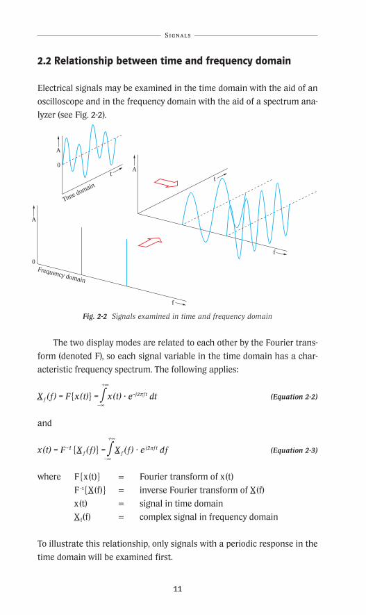
2.2 Relationship between time and frequency domain
Electrical signals may be examined in the time domain with the aid of an
oscilloscope and in the frequency domain with the aid of a spectrum ana-
lyzer (see Fig. 2-2).
Fig. 2-2 Signals examined in time and frequency domain
The two display modes are related to each other by the Fourier trans-
form (denoted F), so each signal variable in the time domain has a char-
acteristic frequency spectrum. The following applies:
X ƒ(ƒ) = Fx(t) = ∫ x(t) · e–j2πƒt dt (Equation 2-2)
and
x(t) = F–1 X ƒ(ƒ) = ∫ X ƒ(ƒ) · e j2πƒt dƒ (Equation 2-3)
where Fx(t) = Fourier transform of x (t)
F –1X(f) = inverse Fourier transform of X(f)
x (t) = signal in time domain
Xf(f) = complex signal in frequency domain
To illustrate this relationship, only signals with a periodic response in the
time domain will be examined first.
11
A
Time domain
A
t
f
t
f
Frequency domain
0
0
A
+∞
−∞
+∞
−∞
R&S_Pappband_Spektrumanal 24.10.2001 17:41 Uhr Seite 11
Fundamentals of Spectrum Analysis
Periodic signals
According to the Fourier theorem, any signal that is periodic in the time
domain can be derived from the sum of sine and cosine signals of differ-
ent frequency and amplitude. Such a sum is referred to as a Fourier series.
The following applies:
x(t) = +Σ An · sin(n · ω0 · t) +Σ Bn · cos(n · ω0 · t) (Equation 2-4)
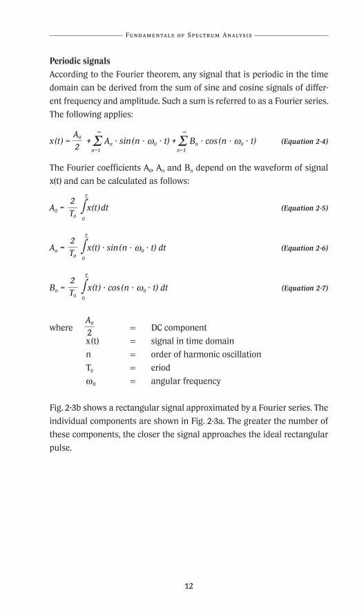
The Fourier coefficients A0, An and Bn depend on the waveform of signal
x(t) and can be calculated as follows:
A0 = ∫ x(t)dt (Equation 2-5)
An = ∫ x(t) · sin(n · ω0 · t) dt (Equation 2-6)
Bn = ∫ x(t) · cos(n · ω0 · t) dt (Equation 2-7)
where = DC component
x(t) = signal in time domain
n = order of harmonic oscillation
T0 = eriod
ω0 = angular frequency
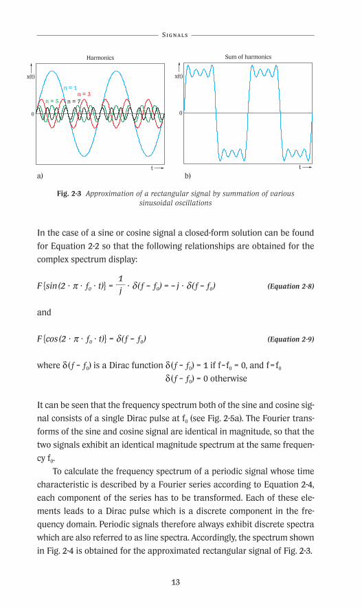
Fig. 2-3b shows a rectangular signal approximated by a Fourier series. The
individual components are shown in Fig. 2-3a. The greater the number of
these components, the closer the signal approaches the ideal rectangular
pulse.
12
A0
2
∞
n=1
∞
n=1
2
T0
T0
0
2
T0
T0
0
2
T0
T0
0
A0
2
R&S_Pappband_Spektrumanal 24.10.2001 17:41 Uhr Seite 12
0
x(t)
t
Sum of harmonics
0
x(t)
t
Harmonics
n = 1n = 3
n = 5 n = 7
a) b)
Fig. 2-3 Approximation of a rectangular signal by summation of various sinusoidal oscillations
In the case of a sine or cosine signal a closed-form solution can be found
for Equation 2-2 so that the following relationships are obtained for the
complex spectrum display:
F sin(2 · π · ƒ0 · t) = · δ (ƒ – ƒ0) = – j · δ (ƒ– ƒ0) (Equation 2-8)
and
F cos(2 · π · ƒ0 · t) = δ (ƒ – ƒ0) (Equation 2-9)
where δ (ƒ – ƒ0) is a Dirac function δ (ƒ – ƒ0) = 1 if f– f0 = 0, and f=f0
δ (ƒ – ƒ0) = 0 otherwise
It can be seen that the frequency spectrum both of the sine and cosine sig-
nal consists of a single Dirac pulse at f0 (see Fig. 2-5a). The Fourier trans-
forms of the sine and cosine signal are identical in magnitude, so that the
two signals exhibit an identical magnitude spectrum at the same frequen-
cy f0.
To calculate the frequency spectrum of a periodic signal whose time
characteristic is described by a Fourier series according to Equation 2-4,
each component of the series has to be transformed. Each of these ele-
ments leads to a Dirac pulse which is a discrete component in the fre-
quency domain. Periodic signals therefore always exhibit discrete spectra
which are also referred to as line spectra. Accordingly, the spectrum shown
in Fig. 2-4 is obtained for the approximated rectangular signal of Fig. 2-3.
13
Signals
1
j
R&S_Pappband_Spektrumanal 24.10.2001 17:41 Uhr Seite 13

|X(f)| ---
ff0 3f0 5f0 7f0
Fundamentals of Spectrum Analysis
14
Fig. 2-4 Magnitude spectrum of approximated rectangular signal shown in Fig. 2-3
Fig. 2-5 shows some further examples of periodic signals in the time and
frequency domain
Non-periodic signals
Signals with a non-periodic characteristic in the time domain cannot be
described by a Fourier series. Therefore the frequency spectrum of such
signals is not composed of discrete spectral components. Non-periodic
signals exhibit a continuous frequency spectrum with a frequency-depen-
dent spectral density. The signal in the frequency domain is calculated by
means of a Fourier transform (Equation 2-2).
Similar to the sine and cosine signals, a closed-form solution can be
found for Equation 2-2 for many signals. Tables with such transform pairs
can be found in [2-1].
For signals with random characteristics in the time domain, such as
noise or random bit sequences, a closed-form solution is rarely found. The
frequency spectrum can in this case be determined more easily by a nu-
meric solution of Equation 2-2.
Fig. 2-6 shows some non-periodic signals in the time and frequency
domain.
R&S_Pappband_Spektrumanal 24.10.2001 17:41 Uhr Seite 14
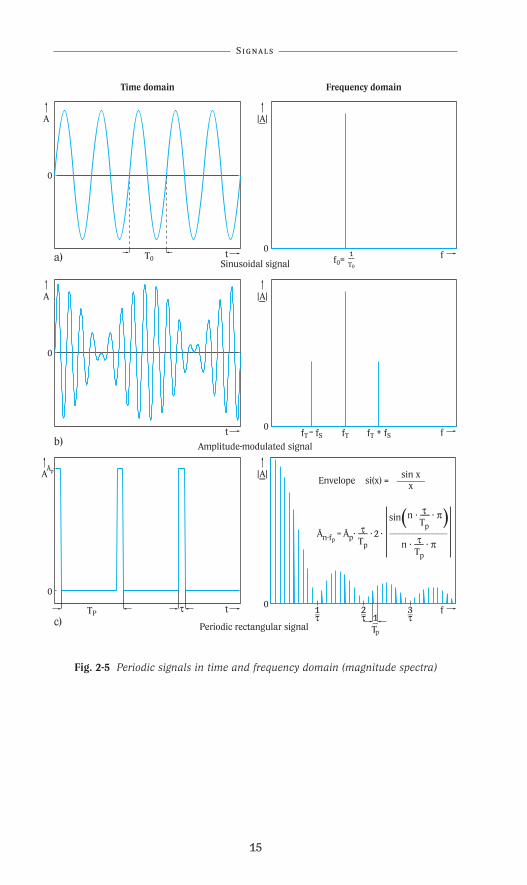
a)
b)
c)
Fig. 2-5 Periodic signals in time and frequency domain (magnitude spectra)
15
|A|__
|A|__
|A|__
0
A
tT0
0
A
t
0
A
t
0ff0=
Frequency domain
f1––τ
f0
fT – fS
1––T0Sinusoidal signal
fT + fSfT
Amplitude-modulated signal
τTP 2––τ
3––τ
Periodic rectangular signal
Envelope si(x) =sin x_____
x
0
Âp
Ân·fp =
Âp· · 2 ·
sin(n · ----- · π)____________
τTp
n · ----- · πτTp
-----τTp
-----1Tp
Time domain
Signals
R&S_Pappband_Spektrumanal 24.10.2001 17:41 Uhr Seite 15
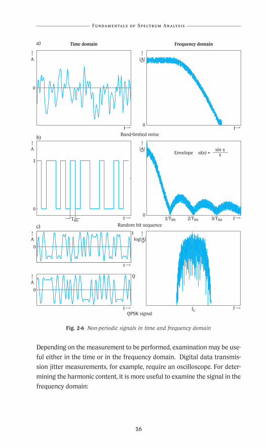
log|A| ----
_____x
|A|__
0
A
t
Time domain
0
A
t
A
t
|A|__
f
Frequency domain
f
f0
Envelope si(x) = sin x
Random bit sequence
QPSK signal
1
TBit 1/TBit 2/TBit 3/TBit
t
fC
Band-limited noise
0
0
I
A
0
Q
Fundamentals of Spectrum Analysis
a)
b)
c)
Fig. 2-6 Non-periodic signals in time and frequency domain
Depending on the measurement to be performed, examination may be use-
ful either in the time or in the frequency domain. Digital data transmis-
sion jitter measurements, for example, require an oscilloscope. For deter-
mining the harmonic content, it is more useful to examine the signal in the
frequency domain:
16
R&S_Pappband_Spektrumanal 24.10.2001 17:41 Uhr Seite 16

The signal shown in Fig. 2-7 seems to be a purely sinusoidal signal with a
frequency of 20 MHz. Based on the above considerations one would expect
the frequency spectrum to consist of a single component at 20 MHz.
On examining the signal in the frequency domain with the aid of a
spectrum analyzer, however, it becomes evident that the fundamental (1st
order harmonic) is superimposed by several higher-order harmonics (Fig.
2-8). This information cannot be easily obtained by examining the signal
in the time domain. A practical quantitative assessment of the higher-or-
der harmonics is not feasible. It is much easier to examine the short-term
stability of frequency and amplitude of a sinusoidal signal in the frequen-
cy domain compared to the time domain (see also chapter 6.1 Phase noise
measurement).
Fig. 2-7 Sinusoidal signal (f = 20 MHz) examined on oscilloscope
17
Signals
R&S_Pappband_Spektrumanal 24.10.2001 17:41 Uhr Seite 17

Fundamentals of Spectrum Analysis
Fig. 2-8 nusoidal signal of Fig. 2-7 examined in the frequency domain with the aid of a spectrum analyzer
18
R&S_Pappband_Spektrumanal 24.10.2001 17:41 Uhr Seite 18
Configuration and Control Elements of a Spectrum Analyzer
3 CONFIGURATION AND CONTROL ELEMENTS OF A SPECTRUM ANALYZER
Depending on the kind of measurement, different requirements are placed
on the maximum input frequency of a spectrum analyzer. In view of the
various possible configurations of spectrum analyzers, the input frequen-
cy range can be subdivided as follows:
– AF range up to approx. 1 MHz
– RF range up to approx. 3 GHz
– microwave range up to approx. 40 GHz
– millimeter-wave range above 40 GHz
The AF range up to approx. 1 MHz covers low-frequency electronics as well
as acoustics and mechanics. In the RF range, wireless communication ap-
plications are mainly found, such as mobile communications and sound
and TV broadcasting, while frequency bands in the microwave or millime-
ter-wave range are utilized to an increasing extent for broadband applica-
tions such as digital directional radio.
Various analyzer concepts can be implemented to suit the frequency
range. The two main concepts are described in detail in the following sec-
tions.
3.1 Fourier analyzer (FFT analyzer)
As explained in chapter 2, the frequency spectrum of a signal is clearly de-
fined by the signal's time characteristic. Time and frequency domain are
linked to each other by means of the Fourier transform. Equation 2-2 can
therefore be used to calculate the spectrum of a signal recorded in the time
domain. For an exact calculation of the frequency spectrum of an input sig-
nal, an infinite period of observation would be required. Another prerequi-
site of Equation 2-2 is that the signal amplitude should be known at every
point in time. The result of this calculation would be a continuous spectrum,
so the frequency resolution would be unlimited.
It is obvious that such exact calculations are not possible in practice.
Given certain prerequisites, the spectrum can nevertheless be determined
with sufficient accuracy.
19
R&S_Pappband_Spektrumanal 24.10.2001 17:41 Uhr Seite 19

Fundamentals of Spectrum Analysis
In practice, the Fourier transform is made with the aid of digital signal pro-
cessing, so the signal to be analyzed has to be sampled by an analog-digital
converter and quantized in amplitude. By way of sampling the continuous
input signal is converted into a time-discrete signal and the information
about the time characteristic is lost. The bandwidth of the input signal must
therefore be limited or else the higher signal frequencies will cause aliasing
effects due to sampling (see Fig. 3-1). According to Shannon's law of sam-
pling, the sampling frequency fS must be at least twice as high as the band-
width Bin of the input signal. The following applies:
ƒS ≥ 2 · Bin and ƒS = (Equation 3-1)
where fS = sampling rate, in Hz
Bin = signal bandwidth, in Hz
TS = sampling period, in s
For sampling lowpass-filtered signals (referred to as lowpass signals) the
minimum sampling rate required is determined by the maximum signal fre-
quency fin,max . Equation 3-1 then becomes:
ƒS ≥ 2 · ƒin,max (Equation 3-2)
If fS = 2 · fin,max , it may not be possible to reconstruct the signal from the sam-
pled values due to unfavorable sampling conditions. Moreover, a lowpass fil-
ter with infinite skirt selectivity would be required for band limitation. Sam-
pling rates that are much greater than 2 · fin,max are therefore used in practice.
A section of the signal is considered for the Fourier transform. That is,
only a limited number N of samples is used for calculation. This process is
called windowing. The input signal (see Fig. 3-2a) is multiplied with a spe-
cific window function before or after sampling in the time domain. In the
example shown in Fig. 3-2, a rectangular window is used (Fig. 3-2b). The re-
sult of multiplication is shown in Fig. 3-2c.
20
1
TS
R&S_Pappband_Spektrumanal 24.10.2001 17:41 Uhr Seite 20
A
ffin
A
f
Sampling with sampling rate fS
finfS–fin fS+finfS 2fS 3fS
A
ffin,max
A
f
fin,max < fs
fin,max fS 2fS 3fS
––2
A
f
A
f
fin,max > fS
fin,max fS 2fS 3fS
–––2
fin,max > fA
–––2
Aliasing
fS–––2
fS–––2
fS–––2
a)
b)
c)
Fig. 3-1 Sampling a lowpass filter with sampling rate fS
a), b) fin,max < fS/2
c) fin,max > fS/2, therefore ambiguity exists due to aliasing
The calculation of the signal spectrum from the samples of the signal in
the time domain is referred to as a discrete Fourier transform (DFT). Equa-
tion 2-2 then becomes:
X(k) = Σ x (nTS) · e–j2πkn / N (Equation 3-3)
where k = index of discrete frequency bins, where k = 0, 1, 2, …
n = index of samples
x (nTS) = samples at the point n · TS, where n = 0, 1, 2 …
N = length of DFT, i.e. total number of samples used for
calculation of Fourier transform
21
N–1
n=0
Configuration and Control Elements of a Spectrum Analyzer
R&S_Pappband_Spektrumanal 24.10.2001 17:41 Uhr Seite 21
Fundamentals of Spectrum Analysis
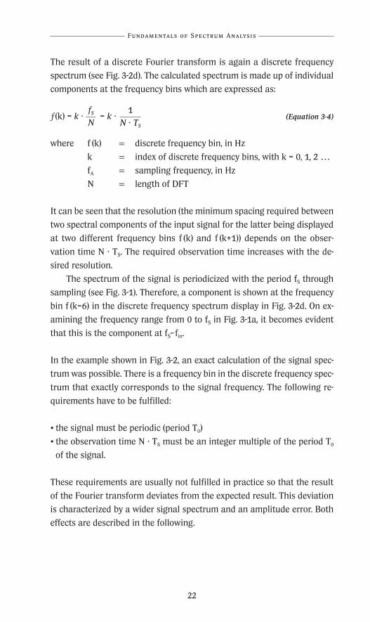
The result of a discrete Fourier transform is again a discrete frequency
spectrum (see Fig. 3-2d). The calculated spectrum is made up of individual
components at the frequency bins which are expressed as:
ƒ(k) = k · = k · (Equation 3-4)
where f (k) = discrete frequency bin, in Hz
k = index of discrete frequency bins, with k = 0, 1, 2 …
fA = sampling frequency, in Hz
N = length of DFT
It can be seen that the resolution (the minimum spacing required between
two spectral components of the input signal for the latter being displayed
at two different frequency bins f (k) and f (k+1)) depends on the obser-
vation time N · TS. The required observation time increases with the de-
sired resolution.
The spectrum of the signal is periodicized with the period fS through
sampling (see Fig. 3-1). Therefore, a component is shown at the frequency
bin f (k=6) in the discrete frequency spectrum display in Fig. 3-2d. On ex-
amining the frequency range from 0 to fS in Fig. 3-1a, it becomes evident
that this is the component at fS– fin.
In the example shown in Fig. 3-2, an exact calculation of the signal spec-
trum was possible. There is a frequency bin in the discrete frequency spec-
trum that exactly corresponds to the signal frequency. The following re-
quirements have to be fulfilled:
• the signal must be periodic (period T0)
• the observation time N · TS must be an integer multiple of the period T0
of the signal.
These requirements are usually not fulfilled in practice so that the result
of the Fourier transform deviates from the expected result. This deviation
is characterized by a wider signal spectrum and an amplitude error. Both
effects are described in the following.
22
fS
N
1
N · TS
R&S_Pappband_Spektrumanal 24.10.2001 17:41 Uhr Seite 22

|X(f) * W(f)|
|W(f)|-----
–1
0
1
A
t
Samples
0TA Te
Input signal x(t)
a)
0
1A
t0
Window w(t)
b)
N·TS
–1
0
1
A
t0
x(t) ·w(t)
x(t) ·w(t), continued periodically
c)
N=8
–1
0
1
A
t0 N·TLSd)
0ffin= -----
|X(f)|---
f
k=2 k=6
fek=0 k=1 fA–––21----–––N·TA
|A|----
f0
0_
1Tin
1----–––N·TS
1----–––N·TS
|A|----
|A|----
frequency bins
Fig. 3-2 DFT with periodic input signal. Observation time is an integer multipleof the period of the input signal
23
Configuration and Control Elements of a Spectrum Analyzer
R&S_Pappband_Spektrumanal 24.10.2001 17:41 Uhr Seite 23

1----–––N·TS
|W(f)|
–1
0
1
A
t
Samples
0TS Te
Input signal x(t)
0
1A
t0
Window w(t)
N·TS
–1
0
1
A
t0
x(t) ·w(t)
N=8
–1
0
1
A
t0 N·TS
0ffin= -----
|X(f)|---
f0
0_
1Tin
1----–––N·TS
N=8
|A|––
|A|––
|X(f) * W(f)| --- ----
ffin
k=0 k=1 fS–––21----–––N·TS
fS – fin
|A|––
a)
b)
c)
d)
x(t) ·w(t), continued periodically
frequency bins
Fundamentals of Spectrum Analysis
Fig. 3-3 DFT with periodic input signal. Observation time is not an integer multipleof the period of the input signal
24
R&S_Pappband_Spektrumanal 24.10.2001 17:41 Uhr Seite 24
The multiplication of input signal and window function in the time domain
corresponds to a convolution in the frequency domain (see [2-1]). In the fre-
quency domain the magnitude of the transfer function of the rectangular
window used in Fig. 3-2 follows a sine function:
|W (ƒ)| = N · TS · si (2πƒ · N · TS/2) = N · TS · (Equation 3-5)
where W (f) = windowing function in frequency domain
N · TS = window width
In addition to the distinct secondary maxima, nulls are obtained at multi-
ples of 1 / (N · TS). ). Due to the convolution by means of the window func-
tion the resulting signal spectrum is smeared, so it becomes distinctly
wider. This is referred to as leakage effect.
If the input signal is periodic and the observation time N · TS is an in-
teger multiple of the period, there is no leakage effect of the rectangular
window since, with the exception of the signal frequency, nulls always fall
within the neighboring frequency bins (see Fig. 3-2d).
If these conditions are not satisfied, which is the normal case, there is
no frequency bin that corresponds to the signal frequency. This case is
shown in Fig. 3-3. The spectrum resulting from the DFT is distinctly wider
since the actual signal frequency lies between two frequency bins and the
nulls of the windowing function no longer fall within the neighboring fre-
quency bins.
As shown in Fig. 3.3d, an amplitude error is also obtained in this case.
At constant observation time the magnitude of this amplitude error de-
pends on the signal frequency of the input signal (see Fig. 3-4). The error
is at its maximum if the signal frequency is exactly between two frequen-
cy bins.
25
sin (2πƒ · N · TS/2)
2πƒ · N · TS/2
Configuration and Control Elements of a Spectrum Analyzer
R&S_Pappband_Spektrumanal 24.10.2001 17:41 Uhr Seite 25

f(k)
max.amplitude error
fin
Frequency bins
Fundamentals of Spectrum Analysis
Fig. 3-4 Amplitude error caused by rectangular windowing
as a function of signal frequency
By increasing the observation time it is possible to reduce the absolute
widening of the spectrum through the higher resolution obtained, but the
maximum possible amplitude error remains unchanged. The two effects
can, however, be reduced by using optimized windowing instead of the rec-
tangular window. Such windowing functions exhibit lower secondary max-
ima in the frequency domain so that the leakage effect is reduced as
shown in Fig. 3-5. Further details of the windowing functions can be found
in [3-1] and [3-2].
To obtain the high level accuracy required for spectrum analysis a flat-top
window is usually used. The maximum level error of this windowing func-
tion is as small as 0.05 dB. A disadvantage is its relatively wide main lobe
which reduces the frequency resolution.
26
R&S_Pappband_Spektrumanal 24.10.2001 17:41 Uhr Seite 26

Fig. 3-5 Leakage effect when using rectangular window or Hann window
(MatLab® simulation)
The number of computing operations required for the Fourier transform
can be reduced by using optimized algorithms. The most widely used
method is the fast Fourier transform (FFT). Spectrum analyzers operating
on this principle are designated as FFT analyzers. The configuration of
such an analyzer is shown in Fig. 3-6.
Fig. 3-6 Configuration of FFT analyzer
To adhere to the sampling theorem, the bandwidth of the input signal is
limited by an analog lowpass filter (cutoff frequency fc = fin,max) ahead of the
A/D converter. After sampling the quantized values are saved in a memo-
ry and then used for calculating the signal in the frequency domain. Fi-
nally, the frequency spectrum is displayed.
Quantization of the samples causes the quantization noise which causes
a limitation of the dynamic range towards its lower end. The higher the
resolution (number of bits) of the A/D converter used, the lower the quan-
tization noise.
27
f
Leakage
Rectangular window
f
Amplitude error
HANN window
Configuration and Control Elements of a Spectrum Analyzer
D
AR AM FFT
Display
Input
MemoryLowpass
R&S_Pappband_Spektrumanal 24.10.2001 17:41 Uhr Seite 27
A
f
A
f
A
f1––T0
1––T0
A
t
Window
0
N·TS = n·T0
T0N·TS
Fundamentals of Spectrum Analysis
Due to the limited bandwidth of the available high-resolution A/D con-
verters, a compromise between dynamic range and maximum input fre-
quency has to be found for FFT analyzers. At present, a wide dynamic
range of about 100 dB can be achieved with FFT analyzers only for low-fre-
quency applications up to 100 kHz. Higher bandwidths inevitably lead to
a smaller dynamic range.
In contrast to other analyzer concepts, phase information is not lost
during the complex Fourier transform. FFT analyzers are therefore able to
determine the complex spectrum according to magnitude and phase. If
they feature sufficiently high computing speed, they even allow realtime
analysis.
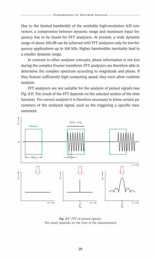
FFT analyzers are not suitable for the analysis of pulsed signals (see
Fig. 3-7). The result of the FFT depends on the selected section of the time
function. For correct analysis it is therefore necessary to know certain pa-
rameters of the analyzed signal, such as the triggering a specific mea-
surement.
Fig. 3-7 FFT of pulsed signals. The result depends on the time of the measurement
28
R&S_Pappband_Spektrumanal 24.10.2001 17:41 Uhr Seite 28

Display
Input
Detector
Sawtooth
tunable bandpass filter Amplifier
x
y A
fin
Tunable bandpass filter
3.2 Analyzers operating according to the heterodyneprinciple
Due to the limited bandwidth of the available A/D converters, FFT analyz-
ers are only suitable for measurements on low-frequency signals. To dis-
play the spectra of high-frequency signals in the microwave or millimeter-
wave range, analyzers with frequency conversion are used. In this case the
spectrum of the input signal is not calculated from the time characteristic,
but determined directly by analysis in the frequency domain. For such an
analysis it is necessary to break down the input spectrum into its individ-
ual components. A tunable bandpass filter as shown in Fig. 3-8 could be
used for this purpose.
Fig. 3-8 Block diagram of spectrum analyzer with tunable bandpass filter
The filter bandwidth corresponds to the resolution bandwidth (RBW)
of the analyzer. The smaller the resolution bandwidth, the higher the spec-
tral resolution of the analyzer.
Narrowband filters tunable throughout the input frequency range of
modern spectrum analyzers are, however, not technically feasible. More-
over, tunable filters have a constant relative bandwidth referred to the cen-
ter frequency. The absolute bandwidth, therefore, increases with increas-
ing center frequency so that this concept is not suitable for spectrum
analysis.
Spectrum analyzers for high input frequency ranges therefore usually
operate according to the principle of a heterodyne receiver. The block dia-
gram of such a receiver is shown in Fig. 3-9.
29
Configuration and Control Elements of a Spectrum Analyzer
R&S_Pappband_Spektrumanal 24.10.2001 17:41 Uhr Seite 29

Fig. 3-9 Block diagram of spectrum analyzer operating on heterodyne principle
The heterodyne receiver converts the input signal with the aid of a mixer
and a local oscillator (LO) to an intermediate frequency (IF). If the local os-
cillator frequency is tunable (a requirement that is technically feasible),
the complete input frequency range can be converted to a constant inter-
mediate frequency by varying the LO frequency. The resolution of the an-
alyzer is then given by a filter at the IF with fixed center frequency.
In contrast to the concept described above, where the resolution filter
as a dynamic component is swept over the spectrum of the input signal,
the input signal is now swept past a fixed-tuned filter.
The converted signal is amplified before it is applied to the IF filter
which determines the resolution bandwidth. This IF filter has a constant
center frequency so that problems associated with tunable filters can be
avoided.
To allow signals in a wide level range to be simultaneously displayed on
the screen, the IF signal is compressed using of a logarithmic amplifier
and the envelope determined. The resulting signal is referred to as the
video signal. This signal can be averaged with the aid of an adjustable low-
pass filter called a video filter. The signal is thus freed from noise and
smoothed for display. The video signal is applied to the vertical deflection
of a cathode-ray tube. Since it is to be displayed as a function of frequen-
cy, a sawtooth signal is used for the horizontal deflection of the electron
beam as well as for tuning the local oscillator. Both the IF and the LO fre-
quency are known. The input signal can thus be clearly assigned to
the displayed spectrum.
In modern spectrum analyzers practically all processes are controlled
Fundamentals of Spectrum Analysis
30
Display
Input
Sawtooth
Envelope detectorMixer
IF amplifier
Local oscillator
IF filter
Logarithmic amplifier
Video filter
x
y
R&S_Pappband_Spektrumanal 24.10.2001 17:41 Uhr Seite 30

IF filterA
f
Input signalconverted to IF
IF filterA
f
Input signalconverted to IF
fIF
fIF
by one or several microprocessors, giving a large variety of new functions
which otherwise would not be feasible. One application in this respect is
the remote control of the spectrum analyzer via interfaces such as the
IEEE bus.
Modern analyzers use fast digital signal processing where the input
signal is sampled at a suitable point with the aid of an A/D converter and
further processed by a digital signal processor. With the rapid advances
made in digital signal processing, sampling modules are moved further
ahead in the signal path. Previously, the video signal was sampled after
the analog envelope detector and video filter, whereas with modern spec-
Fig. 3-10 Signal “swept past” resolution filter in heterodyne receiver
31
Configuration and Control Elements of a Spectrum Analyzer
R&S_Pappband_Spektrumanal 24.10.2001 17:41 Uhr Seite 31

Fundamentals of Spectrum Analysis
trum analyzers the signal is often digitized at the last low IF. The envelope
of the IF signal is then determined from the samples.
Likewise, the first LO is no longer tuned with the aid of an analog saw-
tooth signal as with previous heterodyne receivers. Instead, the LO is
locked to a reference frequency via a phase-locked loop (PLL) and tuned by
varying the division factors. The benefit of the PLL technique is a consid-
erably higher frequency accuracy than achievable with analog tuning.
An LC display can be used instead of the cathode-ray tube, which leads
to more compact designs.
3.3 Main setting parameters
Spectrum analyzers usually provide the following elementary setting pa-
rameters (see Fig. 3-11):
• Frequency display range
The frequency range to be displayed can be set by the start and stop fre-
quency (that is the minimum and maximum frequency to be displayed),
or by the center frequency and the span centered about the center fre-
quency. The latter setting mode is shown in Fig. 3-11. Modern spectrum
analyzers feature both setting modes.
• Level display range
This range is set with the aid of the maximum level to be displayed (the
reference level), and the span. In the example shown in Fig. 3-11, a refer-
ence level of 0 dBm and a span of 100 dB is set. As will be described lat-
er, the attenuation of an input RF attenuator also depends on this setting.
• Frequency resolution
For analyzers operating on the heterodyne principle, the frequency reso-
lution is set via the bandwidth of the IF filter. The frequency resolution is
therefore referred to as the resolution bandwidth (RBW).
32
R&S_Pappband_Spektrumanal 24.10.2001 17:41 Uhr Seite 32
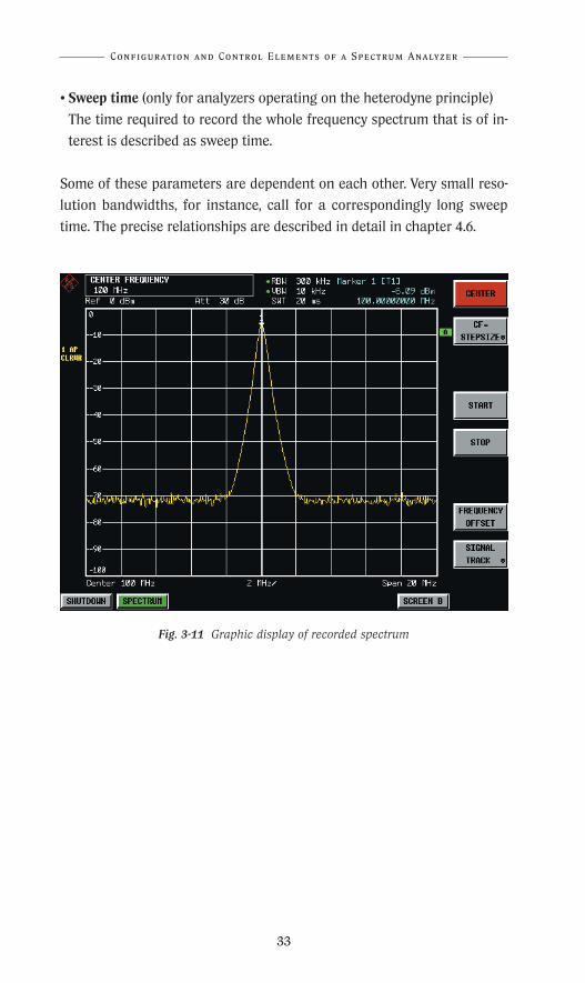
• Sweep time (only for analyzers operating on the heterodyne principle)
The time required to record the whole frequency spectrum that is of in-
terest is described as sweep time.
Some of these parameters are dependent on each other. Very small reso-
lution bandwidths, for instance, call for a correspondingly long sweep
time. The precise relationships are described in detail in chapter 4.6.
Fig. 3-11 Graphic display of recorded spectrum
33
Configuration and Control Elements of a Spectrum Analyzer
R&S_Pappband_Spektrumanal 24.10.2001 17:41 Uhr Seite 33
Fundamentals of Spectrum Analysis
4 PRACTICAL REALIZATION OF AN ANALYZEROPERATING ON THE HETERODYNE PRINCIPLE
In the following section a detailed description is given of the individual
components of an analyzer operating on the heterodyne principle as well
as the practical realization of a modern spectrum analyzer for a frequen-
cy range of 9 kHz to 3 GHz/7 GHz. A detailed block diagram can be found
on the fold-out page at the end of the book. The individual blocks are num-
bered and combined in functional units.
4.1 RF input section (frontend)
Like most measuring instruments used in modern telecommunications,
spectrum analyzers usually feature an RF input impedance of 50 Ω. To en-
able measurements in 75 Ω systems such as cable television (CATV), some
analyzers are alternatively provided with a 75 Ω input impedance. With
the aid of impedance transformers, analyzers with 50 Ω input may also be
used (see test hint: Measurements in 75 Ω system).
A quality criterion of the spectrum analyzer is the input VSWR, which is
highly influenced by the frontend components, such as the attenuator,
input filter and first mixer. These components form the RF input section
whose functionality and realization will be examined in detail in the fol-
lowing:
A step attenuator (2)* is provided at the input of the spectrum analyz-
er for the measurement of high-level signals. Using this attenuator, the sig-
nal level at the input of the first mixer can be set.
The RF attenuation of this attenuator is normally adjustable in 10 dB
steps. For measurement applications calling for a wide dynamic range, at-
tenuators with finer step adjustment of 5 dB or 1 dB are used in some an-
alyzers (see chapter 5.5: Dynamic range).
* The colored code numbers in parentheses refer to the block diagram at the end of the
book.
34
R&S_Pappband_Spektrumanal 24.10.2001 17:41 Uhr Seite 34
35
Practical Realization of an Analyzer
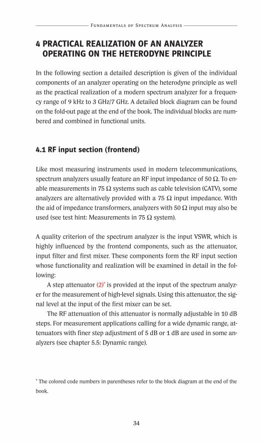
Measurements in 75 Ω system
In sound and TV broadcasting, an impedance of 75 Ω is more com-
mon than the widely used 50 Ω. To carry out measurements in
such systems with the aid of spectrum analyzers that usually fea-
ture an input impedance of 50 Ω, appropriate matching pads are
required. Otherwise, measurement errors would occur due to mis-
match between the device under test and spectrum analyzer.
The simplest way of transforming 50 Ω to 75 Ω is by means
of a 25 Ω series resistor. While the latter renders for low insertion
loss (approx. 1.8 dB), only the 75 Ω input is matched, however, the
output that is connected to the RF input of the spectrum analyzer
is mismatched (see Fig. 4-1a). Since the input impedance of the
spectrum analyzer deviates from the ideal 50 Ω value, measure-
ment errors due to multiple reflection may occur especially with
mismatched DUTs.
Therefore it is recommendable to use matching pads that are
matched at both ends (e.g. Π or L pads). The insertion loss through
the attenuator may be higher in this case.
Fig. 4-1 Input matching to 75 Ω using external matching pads
SourceSpectrumanalyzer
Zout = 75 Ω Z
in = 50 Ω
75 Ω 100 Ω
Matching pad
a)
b)75 Ω 50 Ω Spectrum
analyzerSource
Zout = 75 Ω Z
in = 50 Ω
25 Ω
R&S_Pappband_Spektrumanal 24.10.2001 17:41 Uhr Seite 35

Fundamentals of Spectrum Analysis
The heterodyne receiver converts the input signal with the aid of a mixer
(4) and a local oscillator (5) to an intermediate frequency (IF). This type of
frequency conversion can generally be expressed as:
| m · ƒLO ± n · ƒin | = ƒIF (Equation 4-1)
where m, n = 1, 2, …
fLO = frequency of local oscillator
fin = frequency of input signal to be converted
fIF = intermediate frequency
If the fundamentals of the input and LO signal are considered (m, n = 1),
Equation 4-1 is simplified to:
|ƒLO ± ƒin | = ƒIF (Equation 4-2)
or solved for fin
ƒin = |ƒLO ± ƒIF | (Equation 4-3)
With a continuously tunable local oscillator a wide input frequency range
can be realized at a constant IF. Equation 4-3 indicates that for certain LO
and intermediate frequencies, there are always two receiver frequencies
for which the criterion according to Equation 4-2 is fulfilled (see Fig. 4-2).
This means that in addition to the desired receiver frequency, there are
also image frequencies. To ensure unambiguity of this concept, input sig-
nals at such unwanted image frequencies have to be rejected with the aid
of suitable filters ahead of the RF input of the mixer.
36
R&S_Pappband_Spektrumanal 24.10.2001 17:41 Uhr Seite 36

A
f
Input frequencyrange
Image frequencyrange
fIF
Conversion
fin,min fe,maxfLO,min fLO,maxfim,min fim,max
LO frequency range
Overlap of input and imagefrequency range
A
ffIF fin,u fLO fin,o
Input filter Image frequency reponse
∆f=fIF
Conversion
Fig. 4-2 Ambiguity of heterodyne principle
Fig. 4-3 Input and image frequency ranges (overlapping)
Fig. 4-3 illustrates the input and image frequency ranges for a tunable re-
ceiver with low first IF. If the input frequency range is greater than 2 · fZF,
the two ranges are overlapping, so an input filter must be implemented as
a tunable bandpass for image frequency rejection without affecting the
wanted input signal.
To cover the frequency range from 9 kHz to 3 GHz, which is typical of
modern spectrum analyzers, this filter concept would be extremely com-
plex because of the wide tuning range (several decades). Much less com-
plex is the principle of a high first IF (see Fig. 4-4).
37
Practical Realization of an Analyzer
R&S_Pappband_Spektrumanal 24.10.2001 17:41 Uhr Seite 37
Fundamentals of Spectrum Analysis
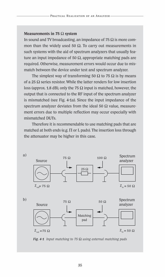
Fig. 4-4 Principle of high intermediate frequency
In this configuration, image frequency range lies above the input fre-
quency range. Since the two frequency ranges do not overlap, the image
frequency can be rejected by a fixed-tuned lowpass filter. The following re-
lationships hold for the conversion of the input signal:
ƒIF = ƒLO – ƒin, (Equation 4-4)
and for the image frequency response:
ƒIF = ƒim – ƒLO . (Equation 4-5)
Frontend for frequencies up to 3 GHz
For analyzers implemented to cover the frequency range from 9 kHz to
3 GHz, the input attenuator (2) is followed by a lowpass filter (3) for rejec-
tion of the image frequencies. Due to the limited isolation between RF and
IF port as well as between LO and RF port of the first mixer, this lowpass
filter also serves for minimizing the IF feedthrough and LO reradiation at
the RF input.
38
A
f
Input frequency rangefIF = fLO – fin
Image frequencyrange
fIF = fim – fLOLO frequencyrange
Input filter
fIF
Conversion
R&S_Pappband_Spektrumanal 24.10.2001 17:41 Uhr Seite 38

In our example the first IF is 3476.4 MHz. For converting the input
frequency range from 9 kHz to 3 GHz to an upper frequency of 3476.4 MHz,
the LO signal (5) must be tunable in the frequency range from 3476.40
MHz to 6476.4 MHz. According to Equation 4-5, an image frequency range
from 6952.809 MHz to 9952.8 MHz is then obtained.
Measurement on signals with DC component
Many spectrum analyzers, in particular those featuring a very low
input frequency at their lower end (such as 20 Hz), are DC-coupled,
so there are no coupling capacitors in the signal path between RF
input and first mixer.
A DC voltage may not be applied to the input of a mixer be-
cause it usually damages the mixer diodes. For measurements of
signals with DC components, an external coupling capacitor (DC
block) is used with DC-coupled spectrum analyzers. It should be
noted that the input signal is attenuated by the insertion loss of
this DC block. This insertion loss has to be taken into account in
absolute level measurements.
Some spectrum analyzers have an integrated coupling capac-
itor to prevent damage to the first mixer. The lower end of the fre-
quency range is thus raised. AC-coupled analyzers therefore have
a higher input frequency at the lower end, such as 9 kHz.
Due to the wide tuning range and low phase noise far from the carrier (see
chapter 5.3: Phase noise) a YIG oscillator is often used as local oscillator.
This technology uses a magnetic field for tuning the frequency of a re-
sonator.
Some spectrum analyzers use voltage-controlled oscillators (VCO) as
local oscillators. Although such oscillators feature a smaller tuning range
than the YIG oscillators, they can be tuned much faster than YIG oscilla-
tors.
To increase the frequency accuracy of the recorded spectrum, the LO sig-
nal is synthesized. That is, the local oscillator is locked to a reference signal
(26) via a phase-locked loop (6). In contrast to analog spectrum analyzers,
the LO frequency is not tuned continuously, but in many small steps. The
39
Practical Realization of an Analyzer
R&S_Pappband_Spektrumanal 24.10.2001 17:41 Uhr Seite 39
Fundamentals of Spectrum Analysis
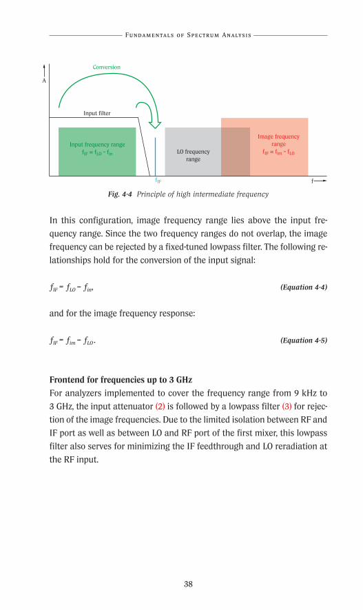
step size depends on the resolution bandwidth. Small resolution band-
widths call for small tuning steps. Otherwise, the input signal may not be
fully recorded or level errors could occur. To illustrate this effect, a filter
tuned in steps throughout the input frequency range is shown in Fig. 4-5.
To avoid such errors, a step size that is much lower than the resolution
bandwidth (such as 0.1·RBW) is selected in practice.
Fig. 4-5 Effects of too large tuning stepsa) input signal is completely lost
b) level error in display of input signal
The reference signal is usually generated by a temperature-controlled crys-
tal oscillator (TCXO). To increase the frequency accuracy and long-term
stability (see also chapter 5.9 Frequency accuracy), an oven-controlled crys-
tal oscillator (OCXO) is optionally available for most spectrum analyzers.
For synchronization with other measuring instruments, the reference sig-
nal (usually 10 MHz) is made available at an output connector (28). The
spectrum analyzer may also be synchronized to an externally applied ref-
erence signal (27). If only one connector is available for coupling a refer-
ence signal in or out, the function of such connector usually depends on a
setting internal to the spectrum analyzer.
As shown in Fig. 3-9, the first conversion is followed by IF signal process-
ing and detection of the IF signal. With such a high IF, narrowband IF fil-
ters can hardly be implemented, which means that the IF signal in the con-
cept described here has to be converted to a lower IF (such as 20.4 MHz in
our example).
40
Input signal
A
fin
A
fin
Displayed spectrum
Tuning step >> resolution bandwidth
A
fin
Input signal
A
fin
Displayed spectrum
Tuning step >> resolution bandwidth
R&S_Pappband_Spektrumanal 24.10.2001 17:41 Uhr Seite 40

A
f
2nd conversion
Image rejection filter
Image2nd IF 1st IF
2nd LO
Fig. 4-6 Conversion of high 1st IF to low 2nd IF
With direct conversion to 20.4 MHz, the image frequency would only be
offset 2 ·20.4 MHz = 40.8 MHz from the signal to be converted at 3476.4
MHz (Fig. 4-6). Rejection of this image frequency is important since the lim-
ited isolation between the RF and IF port of the mixers signals may be
passed to the first IF without conversion. This effect is referred to as IF
feedthrough (see chapter 5.6: Immunity to interference). If the frequency
of the input signal corresponds to the image frequency of the second con-
version, this effect is shown in the image frequency response of the second
IF. Under certain conditions, input signals may also be converted to the im-
age frequency of the second conversion. Since the conversion loss of mix-
ers is usually much smaller than the isolation between RF and IF port of
the mixers, this kind of image frequency response is far more critical.
Due to the high signal frequency, an extremely complex filter with high
skirt selectivity would be required for image rejection at a low IF of 20.4
MHz. It is therefore advisable to convert the input signal from the first IF
to a medium IF such as 404.4 MHz as in our example. A fixed LO signal (10)
of 3072 MHz is required for this purpose since the image frequency for
this conversion is at 2667.6 MHz. Image rejection is then simple to realize
with the aid of a suitable bandpass filter (8). The bandwidth of this band-
pass filter must be sufficiently large so that the signal will not be impaired
even for maximum resolution bandwidths. To reduce the total noise figure
of the analyzer, the input signal is amplified (7) prior to the second con-
version.
41
Practical Realization of an Analyzer
R&S_Pappband_Spektrumanal 24.10.2001 17:41 Uhr Seite 41

Fundamentals of Spectrum Analysis
The input signal converted to the second IF is amplified again, filtered by
an image rejection bandpass filter for the third conversion and converted
to the low IF of 20.4 MHz with the aid of a mixer. The signal thus obtained
can be subjected to IF signal processing.
Frontend for frequencies above 3 GHz
The principle of a high first IF calls for a high LO frequency range (fLO,max =
fin,max + f1stIF). In addition to a broadband RF input, the first mixer must also
feature an extremely broadband LO input and IF output – requirements
that are increasingly difficult to satisfy if the upper input frequency limit
is raised. Therefore this concept is only suitable for input frequency ranges
up to 7 GHz.
To cover the microwave range, other concepts have to be implemented by
taking the following criteria into consideration:
• The frequency range from 3 GHz to 40 GHz extends over more than a
decade, whereas 9 kHz to 3 GHz corresponds to approx. 5.5 decades.
• In the microwave range, filters tunable in a wide range and with narrow
relative bandwidth can be implemented with the aid of YIG technology
[4-1]. Tuning ranges from 3 GHz to 50 GHz are fully realizable.
Direct conversion of the input signal to a low IF calls for a tracking
bandpass filter for image rejection. In contrast to the frequency range up
to 3 GHz, such preselection can be implemented for the range above 3 GHz
due to the previously mentioned criteria. Accordingly, the local oscillator
need only be tunable in a frequency range that corresponds to the input
frequency range.
In our example the frequency range of the spectrum analyzer is thus
enhanced from 3 GHz to 7 GHz. After the attenuator, the input signal is
split by a diplexer (19) into the frequency ranges 9 kHz to 3 GHz and 3 GHz
to 7 GHz and applied to corresponding RF frontends.
42
R&S_Pappband_Spektrumanal 24.10.2001 17:42 Uhr Seite 42
A
ffin,min fin,maxfIF
Input frequency range= Tuning range of bandpass filter
A
ffIF
LO frequency range
Input frequency range
Input frequency range
LO frequency range
Input signal converted as lower sideband
Input signal converted as upper sideband
Tracking preselection
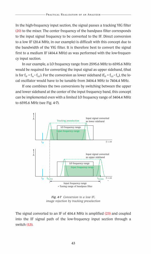
In the high-frequency input section, the signal passes a tracking YIG filter
(20) to the mixer. The center frequency of the bandpass filter corresponds
to the input signal frequency to be converted to the IF. Direct conversion
to a low IF (20.4 MHz, in our example) is difficult with this concept due to
the bandwidth of the YIG filter. It is therefore best to convert the signal
first to a medium IF (404.4 MHz) as was performed with the low-frequen-
cy input section.
In our example, a LO frequency range from 2595.6 MHz to 6595.6 MHz
would be required for converting the input signal as upper sideband, (that
is for fIF = fin – fLO). For the conversion as lower sideband (fIF = fLO – fin), the lo-
cal oscillator would have to be tunable from 3404.4 MHz to 7404.4 MHz.
If one combines the two conversions by switching between the upper
and lower sideband at the center of the input frequency band, this concept
can be implemented even with a limited LO frequency range of 3404.4 MHz
to 6595.6 MHz (see Fig. 4-7).
Fig. 4-7 Conversion to a low IF;image rejection by tracking preselection
The signal converted to an IF of 404.4 MHz is amplified (23) and coupled
into the IF signal path of the low-frequency input section through a
switch (13).
43
Practical Realization of an Analyzer
R&S_Pappband_Spektrumanal 24.10.2001 17:42 Uhr Seite 43
Fundamentals of Spectrum Analysis
Upper and lower frequency limits of this implementation are determined
by the technological constraints of the YIG filter. A maximum frequency of
about 50 GHz is feasible.
In our example, the upper limit of 7 GHz is determined by the tuning range
of the local oscillator. There are again various configurations for convert-
ing input signals above 7 GHz with the given LO frequency range:
• Fundamental mixing
The input signal is converted by means of the fundamental of the LO sig-
nal. For covering a higher frequency range with the given LO frequency
range it is necessary to double, for instance, the LO signal frequency by
means of a multiplier before the mixer.
• Harmonic mixing
The input signal is converted by a means of a harmonic of the LO signal
produced in the mixer due to the mixer's nonlinearities.
Fundamental mixing is preferred to obtain minimal conversion loss, there-
by maintaining a low noise figure for the spectrum analyzer. The superior
characteristics attained in this way, however, require complex processing of
the LO signal. In addition to multipliers (22), filters are required for reject-
ing subharmonics after multiplying. The amplifiers required for a suffi-
ciently high LO level must be highly broadband since they must be designed
for a frequency range that roughly corresponds to the input frequency
range of the high-frequency input section.
Conversion by means of harmonic mixing is easier to implement but
implies a higher conversion loss. A LO signal in a comparatively low fre-
quency range is required which has to be applied at a high level to the mix-
er. Due to the nonlinearities of the mixer and the high LO level, harmonics
of higher order with sufficient level are used for the conversion. Depend-
ing on the order m of the LO harmonic, the conversion loss of the mixer
compared to that in fundamental mixing mode is increased by:
44
R&S_Pappband_Spektrumanal 24.10.2001 17:42 Uhr Seite 44

∆aM = 20 · log m (Equation 4-6)
where ∆aM = increase of conversion loss compared to that in fun-
damental mixing mode
m = order of LO harmonic used for conversion
The two concepts are employed in practice depending on the price class of
the analyzer. A combination of the two methods is possible. For example,
a conversion using the harmonic of the LO signal doubled by a multiplier
would strike a compromise between complexity and sensitivity at an ac-
ceptable expense.
External mixers
For measurements in the millimeter-wave range (above 40 GHz), the fre-
quency range of the spectrum analyzer can be enhanced by using external
harmonic mixers. These mixers operate on the principle of harmonic mix-
ing, so a LO signal in a frequency range that is low compared to the input
signal frequency range is required.
The input signal is converted to a low IF by means of a LO harmonic
and an IF input inserted at a suitable point into the IF signal path of the
low-frequency input section of the analyzer.
In the millimeter-wave range, waveguides are normally used for con-
ducted signal transmission. Therefore, external mixers available for en-
hancing the frequency range of spectrum analyzers are usually wave-
guides. These mixers do not normally have a preselection filter and
therefore do not provide for image rejection. Unwanted mixture products
have to be identified with the aid of suitable algorithms. Further details
about frequency range extension with the aid of external harmonic mixers
can be found in [4-2].
45
Practical Realization of an Analyzer
R&S_Pappband_Spektrumanal 24.10.2001 17:42 Uhr Seite 45
log
(HV
(f))
/dB
f0f
0– 3– 6
60–
Fundamentals of Spectrum Analysis
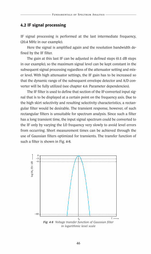
4.2 IF signal processing
IF signal processing is performed at the last intermediate frequency,
(20.4 MHz in our example).
Here the signal is amplified again and the resolution bandwidth de-
fined by the IF filter.
The gain at this last IF can be adjusted in defined steps (0.1 dB steps
in our example), so the maximum signal level can be kept constant in the
subsequent signal processing regardless of the attenuator setting and mix-
er level. With high attenuator settings, the IF gain has to be increased so
that the dynamic range of the subsequent envelope detector and A/D con-
verter will be fully utilized (see chapter 4.6: Parameter dependencies).
The IF filter is used to define that section of the IF-converted input sig-
nal that is to be displayed at a certain point on the frequency axis. Due to
the high skirt selectivity and resulting selectivity characteristics, a rectan-
gular filter would be desirable. The transient response, however, of such
rectangular filters is unsuitable for spectrum analysis. Since such a filter
has a long transient time, the input signal spectrum could be converted to
the IF only by varying the LO frequency very slowly to avoid level errors
from occurring. Short measurement times can be achieved through the
use of Gaussian filters optimized for transients. The transfer function of
such a filter is shown in Fig. 4-8.
Fig. 4-8 Voltage transfer function of Gaussian filter in logarithmic level scale
46
R&S_Pappband_Spektrumanal 24.10.2001 17:42 Uhr Seite 46
f0 f
0.5
HV (f)
HV,0
ff0
0.5
HV2 (f)
HV,02
Powertransferfunction
Voltagetransferfunction
Noise bandwidthBN
Pulse bandwidthBI
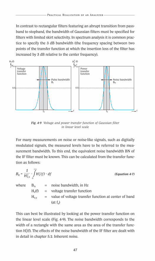
In contrast to rectangular filters featuring an abrupt transition from pass-
band to stopband, the bandwidth of Gaussian filters must be specified for
filters with limited skirt selectivity. In spectrum analysis it is common prac-
tice to specify the 3 dB bandwidth (the frequency spacing between two
points of the transfer function at which the insertion loss of the filter has
increased by 3 dB relative to the center frequency).
Fig. 4-9 Voltage and power transfer function of Gaussian filter in linear level scale
For many measurements on noise or noise-like signals, such as digitally
modulated signals, the measured levels have to be referred to the mea-
surement bandwidth. To this end, the equivalent noise bandwidth BN of
the IF filter must be known. This can be calculated from the transfer func-
tion as follows:
BR = · ∫ H 2V (ƒ) · dƒ (Equation 4-7)
where BN = noise bandwidth, in Hz
HV(f) = voltage transfer function
HV,0 = value of voltage transfer function at center of band
(at f0)
This can best be illustrated by looking at the power transfer function on
the linear level scale (Fig. 4-9). The noise bandwidth corresponds to the
width of a rectangle with the same area as the area of the transfer func-
tion HV2(f). The effects of the noise bandwidth of the IF filter are dealt with
in detail in chapter 5.1: Inherent noise.
47
+∞
0
1
H2V,0
Practical Realization of an Analyzer
R&S_Pappband_Spektrumanal 24.10.2001 17:42 Uhr Seite 47
Fundamentals of Spectrum Analysis
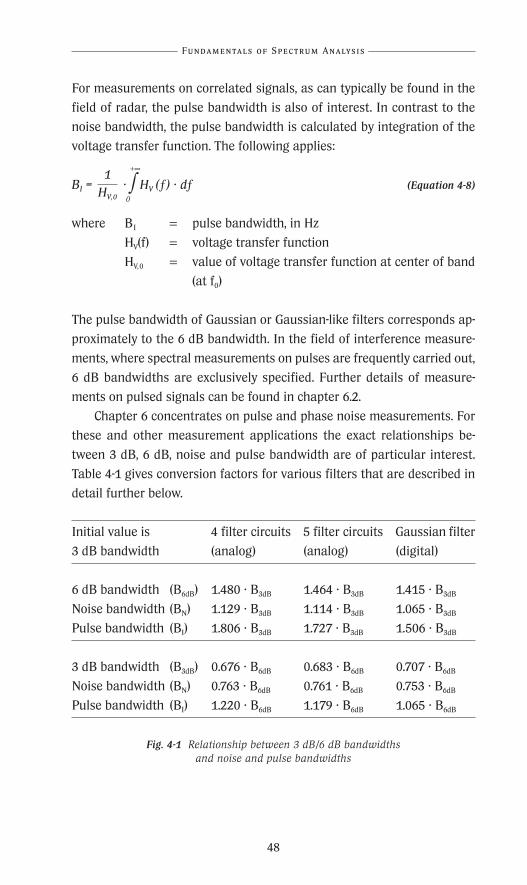
For measurements on correlated signals, as can typically be found in the
field of radar, the pulse bandwidth is also of interest. In contrast to the
noise bandwidth, the pulse bandwidth is calculated by integration of the
voltage transfer function. The following applies:
BI = · ∫ HV (ƒ) · dƒ (Equation 4-8)
where BI = pulse bandwidth, in Hz
HV(f) = voltage transfer function
HV,0 = value of voltage transfer function at center of band
(at f0)
The pulse bandwidth of Gaussian or Gaussian-like filters corresponds ap-
proximately to the 6 dB bandwidth. In the field of interference measure-
ments, where spectral measurements on pulses are frequently carried out,
6 dB bandwidths are exclusively specified. Further details of measure-
ments on pulsed signals can be found in chapter 6.2.
Chapter 6 concentrates on pulse and phase noise measurements. For
these and other measurement applications the exact relationships be-
tween 3 dB, 6 dB, noise and pulse bandwidth are of particular interest.
Table 4-1 gives conversion factors for various filters that are described in
detail further below.
Initial value is 4 filter circuits 5 filter circuits Gaussian filter
3 dB bandwidth (analog) (analog) (digital)
6 dB bandwidth (B6dB) 1.480 · B3dB 1.464 · B3dB 1.415 · B3dB
Noise bandwidth (BN) 1.129 · B3dB 1.114 · B3dB 1.065 · B3dB
Pulse bandwidth (BI) 1.806 · B3dB 1.727 · B3dB 1.506 · B3dB
3 dB bandwidth (B3dB) 0.676 · B6dB 0.683 · B6dB 0.707 · B6dB
Noise bandwidth (BN) 0.763 · B6dB 0.761 · B6dB 0.753 · B6dB
Pulse bandwidth (BI) 1.220 · B6dB 1.179 · B6dB 1.065 · B6dB
Fig. 4-1 Relationship between 3 dB/6 dB bandwidths and noise and pulse bandwidths
48
1
HV,0
+∞
0
R&S_Pappband_Spektrumanal 24.10.2001 17:42 Uhr Seite 48

PRN
*
S W T 6 8 0 m s
V B W 3 0 H z
* R B W 1 0 k H z
S p a n 1 0 0 k H zC e n t e r 1 G H z 1 0 k H z /
A t t 3 0 d BR e f 0 d B m
CLRWR
1 AP
A
-100
-90
-80
-70
-60
-50
-40
-30
-20
-10
0
M a r k e r 1 [ T 1 ]
- 5 . 1 6 d B m
1 . 0 0 0 0 0 0 0 0 G H z
n d B [ T 1 ] 3 . 0 0 d B
B W 9 . 8 0 0 0 0 0 0 0 k H z
T e m p 1 [ T 1 n d B ] T e m p 1 [ T 1 n d B ]
- 8 1 . 6 2 d B m . 2 d B m
9 9 9 . 9 5 0 0 0 0 0 0 M H z 9 9 9 . 9 0 0 0 0 M H z
T e m p 2 [ T 1 n d B ] T e m p 2 [ T 1 n d B ]
- 8 . 2 2 d B m - 8 . 2 2 d B m
1 . 0 0 0 0 0 5 0 0 G H z 1 . 0 0 0 0 0 5 0 0 G H z
T T 2T T 2
If one uses an analyzer operating on the heterodyne principle to record a
purely sinusoidal signal, one would expect a single spectral line according
to the Fourier theorem even when a small frequency span about the sig-
nal frequency is taken. In fact, the display shown in Fig. 4-10 is obtained.
Fig. 4-10 IF filter imaged by a sinusoidal input signal
The display shows the image of the IF filter. During the sweep, the input
signal converted to the IF is “swept past” the IF filter and multiplied with
the transfer function of the filter.
A schematic diagram of this process is shown in Fig. 4-11. For reasons of
simplification the filter is “swept past” a fixed-tuned signal, both kinds of
representations being equivalent.
49
Practical Realization of an Analyzer
R&S_Pappband_Spektrumanal 24.10.2001 17:42 Uhr Seite 49

A
f
Inputsignal
A
f
Image of resolution bandwidth
IF filter
Fundamentals of Spectrum Analysis
Fig. 4-11 IF filter imaged by an input signal “swept past” the filter(schematic representation of imaging process)
As pointed out before, the spectral resolution of the analyzer is mainly de-
termined by the resolution bandwidth, that is, the bandwidth of the IF fil-
ter. The IF bandwidth (3 dB bandwidth) corresponds to the minimum fre-
quency offset required between two signals of equal level to make the
signals distinguishable by a dip of about 3 dB in the display when using a
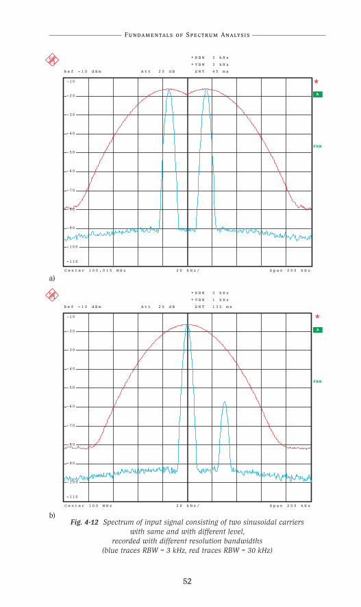
sample or peak detector (see chapter 4.4.). This case is shown in Fig. 4-12a.
The red trace was recorded with a resolution bandwidth of 30 kHz. By re-
50
R&S_Pappband_Spektrumanal 24.10.2001 17:42 Uhr Seite 50
ducing the resolution bandwidth, the two signals are clearly distinguish-
able (Fig. 4-12a, blue trace).
If two neighboring signals have distinctly different levels, the weaker
signal will not be shown in the displayed spectrum at a too high resolution
bandwidth setting (see Fig. 4-12b, red trace). By reducing the resolution
bandwidth, the weak signal can be displayed.
In such cases, the skirt selectivity of the IF filter is also important and
is referred to as the selectivity of a filter. The skirt selectivity is specified in
form of the shape factor which is calculated as follows:
SF60/3 = (Equation 4-9)
where B3dB = 3 dB bandwidth
B60dB = 60 dB bandwidth
For 6 dB bandwidths, as is customary in EMC measurements, the shape
factor is derived from the ratio of the 60 dB bandwidth to the 6 dB band-
width.
The effects of the skirt selectivity can clearly be seen in Fig. 4-13. One Kilo-
hertz IF filters with different shape factors were used for the two traces. In
the blue trace (SF = 4.6), the weaker signal can still be recognized by the
dip, but a separation of the two signals is not possible in the red trace (SF
= 9.5) where the weaker signal does not appear at all.
51
B60dB
B3dB
Practical Realization of an Analyzer
R&S_Pappband_Spektrumanal 24.10.2001 17:42 Uhr Seite 51
PRN
*
*
*
S W T 1 3 5 m s
V B W 1 k H z
R B W 3 k H z
S p a n 2 0 0 k H zC e n t e r 1 0 0 M H z 2 0 k H z /
A t t 2 0 d BR e f - 1 0 d B m
A
-110
-100
-90
-80
-70
-60
-50
-40
-30
-20
-10
Fundamentals of Spectrum Analysis
52
PRN
*
*
*
S W T 4 5 m s
V B W 3 k H z
R B W 3 k H z
S p a n 2 0 0 k H zC e n t e r 1 0 0 . 0 1 5 M H z 2 0 k H z /
A t t 2 0 d BR e f - 1 0 d B m
A
-110
-100
-90
-80
-70
-60
-50
-40
-30
-20
-10
b)Fig. 4-12 Spectrum of input signal consisting of two sinusoidal carriers
with same and with different level,recorded with different resolution bandwidths
(blue traces RBW = 3 kHz, red traces RBW = 30 kHz)
a)
R&S_Pappband_Spektrumanal 24.10.2001 17:42 Uhr Seite 52

Fig. 4-13 Two neighboring sinusoidal signals with different levels recorded with a resolution bandwidth of 1 kHz
and a shape factor of 9.5 and 4.6
If the weaker signal is to be distinguished by a filter with a lower skirt se-
lectivity, the resolution bandwidth has to be reduced. Due to the longer
transient time of narrowband IF filters, the minimum sweep time must be
increased. For certain measurement applications, shorter sweep times are
therefore feasible with filters of high skirt selectivity.
As mentioned earlier, the highest resolution is attained with narrowband
IF filters. These filters, however, always have a longer transient time than
broadband filters, so contemporary spectrum analyzers provide a large
number of resolution bandwidths to allow resolution and measurement
speed to be adapted to specific applications. The setting range is usually
large (from 10 Hz to 10 MHz). The individual filters are implemented in dif-
ferent ways. There are three different types of filters:
• analog filters
• digital filters
• FFT
53
R e f L v l
2AP
1SA
2A
-110
-100
-90
-80
-70
-60
-50
-40
-30
-20
-10
SF = 9.5
SF = 4.6
V B W 2 0 0 H z
SW T 3 0 0 m s
RBW 1 k H z
2 k H z / S p a n 2 0 k H z C e n t e r 1 0 0 M H z
RF A t t 2 0 d B
-10 d B m U n i t d B m
A
Practical Realization of an Analyzer
R&S_Pappband_Spektrumanal 24.10.2001 17:42 Uhr Seite 53

Fundamentals of Spectrum Analysis
Analog IF filters
Analog filters are used to realize very large resolution bandwidths. In the
spectrum analyzer described in our example, these are bandwidths from
100 kHz to 10 MHz. Ideal Gaussian filters cannot be implemented using
analog filters. A very good approximation, however, is possible at least
within the 20 dB bandwidth so that the transient response is almost iden-
tical to that of a Gaussian filter. The selectivity characteristics depend on
the number of filter circuits. Spectrum analyzers typically have four filter
circuits, but models with five filter circuits can be found, too. Shape factors
of about 14 and 10 can thus be attained, whereas an ideal Gaussian filter
exhibits a shape factor of 4.6.
The spectrum analyzer described in our example uses IF filters that
are made up of four individual circuits. Filtering is distributed so that two
filter circuits each (29 and 31) are arranged before and after the IF ampli-
fier (30). This configuration offers the following benefits:
• The filter circuits ahead of the IF amplifier provide for rejection of mix-
ture products outside the passband of the IF filter. Intermodulation prod-
ucts that may be caused by such signals in the last IF amplifier without
prefiltering can thus be avoided (see chapter 5.2: Nonlinearities).
• The filter circuits after the IF amplifier are used to reduce the noise band-
width. If they were arranged ahead of the IF amplifier, the total noise
power in the subsequent envelope detection would be distinctly higher
due to the broadband noise of the IF amplifier.
54
R&S_Pappband_Spektrumanal 24.10.2001 17:42 Uhr Seite 54

Digital IF filters
Narrow bandwidths can best be implemented with the aid of digital signal
processing. In contrast to analog filters, ideal Gaussian filters can be real-
ized. Much better selectivity (SF = 4.6) can be achieved using digital filters
instead of analog filters at an acceptable circuit cost. Analog filters con-
sisting of five individual circuits, for instance, have a shape factor of about
10, whereas a digitally implemented ideal Gaussian filter exhibits a shape
factor of 4.6. Moreover, digital filters feature temperature stability, are
free of aging effects and do not require adjustment. Therefore they feature
a higher accuracy regarding bandwidth.
The transient response of digital filters is defined and known. Using
suitable correction factors, digital filters allow shorter sweep times than
analog filters of the same bandwidth (see chapter 4.6: Parameter depen-
dencies).
In contrast to that shown in the block diagram, the IF signal after the
IF amplifier must first be sampled by an A/D converter. To comply with the
sampling theorem, the bandwidth of the IF signal must be limited by ana-
log prefilters prior to sampling. This band limiting takes place before the
IF amplifier so that intermodulation products can be avoided, as was the
case for analog filters. The bandwidth of the prefilter is variable, so de-
pending on the set digital resolution bandwidth, a very small bandwidth
can be selected. The digital IF filter provides for limiting the noise band-
width prior to envelope detection.
The digital IF filter can be implemented by configurations as de-
scribed in [3-1] or [3-2]. In our example, the resolution bandwidths from 10
Hz to 30 kHz of the spectrum analyzer are realized by digital filters.
55
Practical Realization of an Analyzer
R&S_Pappband_Spektrumanal 24.10.2001 17:42 Uhr Seite 55

Fundamentals of Spectrum Analysis
FFT
Very narrow IF bandwidths lead to long transient times which consider-
ably reduce the permissible sweep speed. With very high resolution it is
therefore advisable to calculate the spectrum from the time characteristic
– similar to the FFT analyzer described in chapter 3.1. Since very high fre-
quency signals (up to several GHz) cannot directly be sampled by an A/D
converter, the frequency range of interest is converted to the IF as a block,
using a fixed-tuned LO signal, and the bandpass signal is sampled in the
time domain (see Fig. 4-14). To ensure unambiguity, an analog prefilter is
required in this case.
For an IF signal with the center frequency fIF and a bandwidth B, one
would expect a minimum sampling rate of 2 · (fIF + 0,5 · B) according to
sampling requirements (Equation 3-1). If the relative bandwidth, however,
is small (B/fIF « 1), then undersampling is permissible to a certain extent.
That is, the sampling frequency may be lower than that resulting from the
sampling theorem for baseband signals. To ensure unambiguity, adher-
ance to the sampling theorem for bandpass signals must be maintained.
The permissible sampling frequencies are determined by:
≤ ƒS ≤ (Equation 4-10)
where fS = sampling frequency, in Hz
fIF = intermediate frequency, in Hz
B = bandwidth of IF signal, in Hz
k = 1, 2, …
The spectrum can be determined from the sampled values with the aid of
the Fourier transform.
56
2 · ƒIF + B
k + 1
2 · ƒIF – B
k
R&S_Pappband_Spektrumanal 24.10.2001 17:42 Uhr Seite 56

Fig. 4-14 Spectrum analysis using FFT
The maximum span that can be analyzed at a specific resolution by means
of an FFT is limited by the sampling rate of the A/D converter and by the
memory available for saving the sampled values. Large spans must there-
fore be subdivided into individual segments which are then converted to
the IF in blocks and sampled.
While analog or digital filter sweep times increase directly proportional to
the span, the observation time required for FFT depends on the desired fre-
quency resolution as described in chapter 3.1. To comply with sampling
principles, more samples have to be recorded for the FFT with increasing
span so that the computing time for the FFT also increases. At sufficient-
ly high computing speed of digital signal processing, distinctly shorter
measurement times than that of conventional filters can be attained with
FFT, especially with high span/RBW ratios (chapter 4.6: Parameter depen-
dencies).
The far-off selectivity of FFT filters is limited by the leakage effect, de-
pending on the windowing function used. The Hann window described in
chapter 3.1 is not suitable for spectrum analysis because of the amplitude
loss and the resulting level error. A flat-top window is therefore often used
to allow the leakage effect to be reduced so that a negligible amplitude er-
ror may be maintained. This is at the expense of an observation time that
is by a factor of 3.8 longer than that of a rectangular window. The flat-top
57
A
ffIF fLO
Analogbandpassfilter
Conversion
Span
Display
FFTRAMA
D
Practical Realization of an Analyzer
R&S_Pappband_Spektrumanal 24.10.2001 17:42 Uhr Seite 57

AVideo
0
AZF
t0
t
Envelopedetection
Envelpope
1-----fIF
Fundamentals of Spectrum Analysis
window causes a wider representation of the windowing function in the
frequency domain (corresponding to the convolution with a Dirac pulse in
the frequency domain). When the flat-top window is implemented, a shape
factor of about 2.6 can be attained, which means that selectivity is clearly
better than when analog or digital IF filters are used.
FFT filters are unsuitable for the analysis of pulsed signals (see chap-
ter 3.1). Therefore it is important for spectrum analyzers to be provided
with both FFT and conventional filters.
4.3 Determination of video voltage and video filters
Information about the level of the input signal is contained in the level of
the IF signal, such as amplitude-modulated signals in the envelope of the
IF signal. With the use of analog and digital IF filters, the envelope of the
IF signal is detected after filtering the highest intermediate frequency (see
Fig. 4-15).
Fig. 4-15 Detection of IF signal envelope
58
R&S_Pappband_Spektrumanal 24.10.2001 17:42 Uhr Seite 58
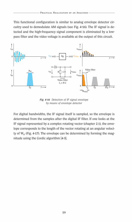
This functional configuration is similar to analog envelope detector cir-
cuitry used to demodulate AM signals (see Fig. 4-16). The IF signal is de-
tected and the high-frequency signal component is eliminated by a low-
pass filter and the video voltage is available at the output of this circuit.
Fig. 4-16 Detection of IF signal envelopeby means of envelope detector
For digital bandwidths, the IF signal itself is sampled, so the envelope is
determined from the samples after the digital IF filter. If one looks at the
IF signal represented by a complex rotating vector (chapter 2.1), the enve-
lope corresponds to the length of the vector rotating at an angular veloci-
ty of WIF (Fig. 4-17). The envelope can be determined by forming the mag-
nitude using the Cordic algorithm [4-3].
59
vIF
t0
vVideo
t0
vIF
f0
vVideo
f0
fIF
BIFVideo filter
fg
vIF vVideo
R C
Video filterfc = R·C
vVideovIF
BVideo
fIF 2fIF
Practical Realization of an Analyzer
R&S_Pappband_Spektrumanal 24.10.2001 17:42 Uhr Seite 59

Fundamentals of Spectrum Analysis
Fig. 4-17 IF signal with sinusoidal input signal,represented by complex rotating vector
Due to envelope detection, the phase information of the input signal gets
lost, so that only the magnitude can be indicated in the display. This is one
of the primary differences between the envelope detector and the FFT an-
alyzer as described in chapter 3.1.
The dynamic range of the envelope detector determines the dynamic range
of a spectrum analyzer. Modern analyzers feature a dynamic range of
about 100 dB. The level is usually displayed in a logarithmic scale on the
spectrum analyzer. The IF signal can therefore be amplified with the aid of
a log amplifier (32) ahead of the envelope detector (33), thereby increasing
the dynamic range of the display.
The resulting video voltage depends on the input signal and the selected
resolution bandwidth. Fig. 4-18 shows some examples. The spectrum ana-
lyzer is tuned to a fixed frequency in these examples, so the displayed span
is 0 Hz (zero span).
60
Re
jIm
ωIF
A Vide
o
Samples
R&S_Pappband_Spektrumanal 24.10.2001 17:42 Uhr Seite 60

61
Ain
t0
AIF
t0
AVideo
t0
-----fin
1
|Ain|
f0
|AIF|
f0
|AVideo|
f0
fIF
BIF
fin
fmfm
fm
-----fm
1
-----fIF
1
Ain
t0
AIF
t0
AVideo
t0
-----fe
1
|Ain|
f0
|AIF|
f0
|AVideo|
f0
fIF
BIF
fin
fmfm
-----fIF
1
Ain
t0
AIF
t0
AVideo
t0
-----fe
1 -----fIF
1
|Ain|
f0
|AIF|
f0
|AVideo|
f0
fIF
BIF
fin
a)
b)
c)
Fig. 4-18 Video signal (yellow trances) and IF signal after IF filter (blue traces) for various input signals (green traces) and resolution bandwidths
a) sinusoidal signal b) AM signal, resolution bandwidth smaller than twice themodulation bandwidth c) AM signal, resolution bandwidth greater than twice the
modulation bandwidth
Practical Realization of an Analyzer
R&S_Pappband_Spektrumanal 24.10.2001 17:42 Uhr Seite 61
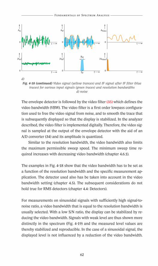
-1
Fundamentals of Spectrum Analysis
62
Ain
t0
AIF
t0
AVideo
t0
f
|Ain|
f0
|AIF|
0
|AVideo|
f0
fIF
BIF
d)Fig. 4-18 (continued) Video signal (yellow trances) and IF signal after IF filter (blue
traces) for various input signals (green traces) and resolution bandwidthsd) noise
The envelope detector is followed by the video filter (35) which defines the
video bandwidth (VBW). The video filter is a first order lowpass configura-
tion used to free the video signal from noise, and to smooth the trace that
is subsequently displayed so that the display is stabilized. In the analyzer
described, the video filter is implemented digitally. Therefore, the video sig-
nal is sampled at the output of the envelope detector with the aid of an
A/D converter (34) and its amplitude is quantized.
Similar to the resolution bandwidth, the video bandwidth also limits
the maximum permissible sweep speed. The minimum sweep time re-
quired increases with decreasing video bandwidth (chapter 4.6.1).
The examples in Fig. 4-18 show that the video bandwidth has to be set as
a function of the resolution bandwidth and the specific measurement ap-
plication. The detector used also has be taken into account in the video
bandwidth setting (chapter 4.5). The subsequent considerations do not
hold true for RMS detectors (chapter 4.4: Detectors).
For measurements on sinusoidal signals with sufficiently high signal-to-
noise ratio, a video bandwidth that is equal to the resolution bandwidth is
usually selected. With a low S/N ratio, the display can be stabilized by re-
ducing the video bandwidth. Signals with weak level are thus shown more
distinctly in the spectrum (Fig. 4-19) and the measured level values are
thereby stabilized and reproducible. In the case of a sinusoidal signal, the
displayed level is not influenced by a reduction of the video bandwidth.
R&S_Pappband_Spektrumanal 24.10.2001 17:42 Uhr Seite 62

PRN
*
SWT 280 ms
VBW 300 Hz
EXT
1 MHz/ Span 10 MHzCenter 100 MHz
Ref -40 dBm
B
A
1 MHz/ Span 10 MHzCenter 100 MHz
Ref -40 dBm
VBW 1 MHz
RBW 300 kHz
RBW 300 kHz
CLRWR
1 AP
Att 10 dB
CLRWR
1 AP
SWT 2.5 msAtt 10 dB
-130
-120
-110
-100
-90
-80
-70
-60
-50
-130
-120
-110
-100
-90
-80
-70
-60
-50
This becomes quite clear when looking at the video voltage resulting from
the sinusoidal input signal in Fig. 4-18a. The video signal is a pure DC volt-
age, so the video filter has no effect on the overall level of the video signal.
Fig. 4-19 Sinusoidal signal with low S/N ratio shown forlarge (top) and small (bottom half of screen) video bandwidth
To obtain stable and reproducible results of noise measurements, a nar-
row video bandwidth should be selected. The noise bandwidth is thus re-
duced and high noise peaks are averaged. As described in greater detail in
chapter 4.4, the displayed average noise level will be 2.5 dB below the sig-
nal’s RMS value.
63
Practical Realization of an Analyzer
R&S_Pappband_Spektrumanal 24.10.2001 17:42 Uhr Seite 63
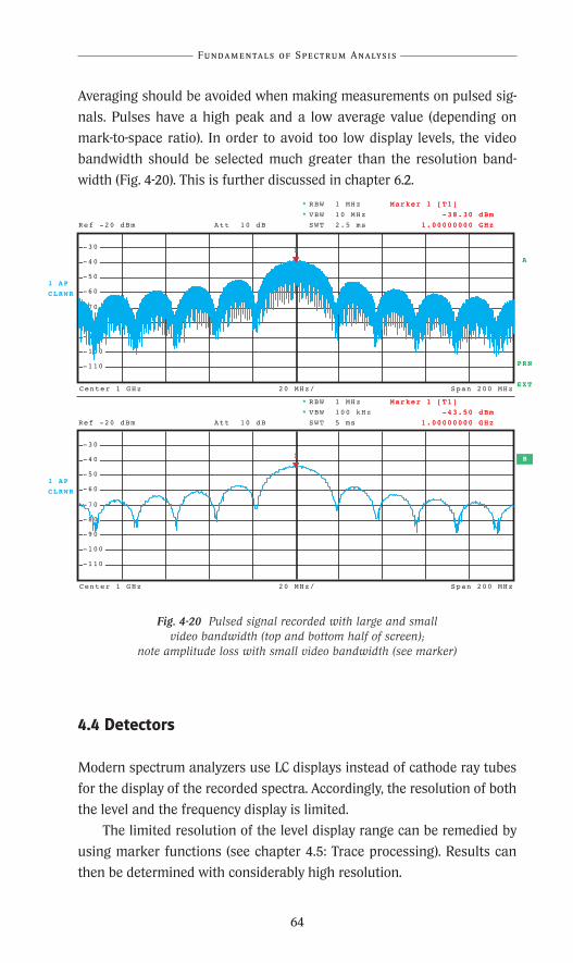
Fundamentals of Spectrum Analysis
Averaging should be avoided when making measurements on pulsed sig-
nals. Pulses have a high peak and a low average value (depending on
mark-to-space ratio). In order to avoid too low display levels, the video
bandwidth should be selected much greater than the resolution band-
width (Fig. 4-20). This is further discussed in chapter 6.2.
Fig. 4-20 Pulsed signal recorded with large and smallvideo bandwidth (top and bottom half of screen);
note amplitude loss with small video bandwidth (see marker)
4.4 Detectors
Modern spectrum analyzers use LC displays instead of cathode ray tubes
for the display of the recorded spectra. Accordingly, the resolution of both
the level and the frequency display is limited.
The limited resolution of the level display range can be remedied by
using marker functions (see chapter 4.5: Trace processing). Results can
then be determined with considerably high resolution.
64
PRN
B
A
EXT
* VBW 10 MHz
* RBW 1 MHz
*
SWT 5 ms
VBW 100 kHz
* RBW 1 MHz
20 MHz/ Span 200 MHzCenter 1 GHz
CLRWR
1 AP
SWT 2.5 msAtt 10 dBRef -20 dBm
20 MHz/ Span 200 MHzCenter 1 GHz
CLRWR
1 AP
Att 10 dBRef -20 dBm
-110
-100
-90
-80
-70
-60
-50
-40
-30
-110
-100
-90
-80
-70
-60
-50
-40
-30
Marker 1 [T1]
-38.30 dBm
1.00000000 GHz
1
Marker 1 [T1]
-43.50 dBm
1.00000000 GHz
1
Marker 1 [T1]
-38.30 dBm
1.00000000 GHz
1
Marker 1 [T1]
-43.50 dBm
1.00000000 GHz
1
R&S_Pappband_Spektrumanal 24.10.2001 17:42 Uhr Seite 64

Vide
o vo
ltag
e
f
A
fDisplayed sample
Samples N=5
Pixel (n+1)Pixel n
AVRMS
RMS
AV
Auto Peak
Min Peak
Max Peak
Sample
Particularily when large spans are displayed, one pixel contains the spec-
tral information of a relatively large subrange. As explained in chapter 4.1,
the tuning steps of the 1st local oscillator depend on the resolution band-
width so that several measured values, referred to as samples or as bins,
fall on one pixel. Which of the samples will be represented by the pixel de-
pends on the selected weighting which is determined by the detector. Most
of the spectrum analyzers feature min peak, max peak, auto peak and
sample detectors. The principles of the detectors is shown in Fig. 4-21.
Figs 4-21 Selection of sample to be displayed as a function of detector used
65
Practical Realization of an Analyzer
R&S_Pappband_Spektrumanal 24.10.2001 17:42 Uhr Seite 65
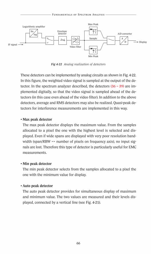
Fundamentals of Spectrum Analysis
Fig 4-22 Analog realization of detectors
These detectors can be implemented by analog circuits as shown in Fig. 4-22.
In this figure, the weighted video signal is sampled at the output of the de-
tector. In the spectrum analyzer described, the detectors (36 – 39) are im-
plemented digitally, so that the video signal is sampled ahead of the de-
tectors (in this case even ahead of the video filter). In addition to the above
detectors, average and RMS detectors may also be realized. Quasi-peak de-
tectors for interference measurements are implemented in this way.
• Max peak detector
The max peak detector displays the maximum value. From the samples
allocated to a pixel the one with the highest level is selected and dis-
played. Even if wide spans are displayed with very poor resolution band-
width (span/RBW >> number of pixels on frequency axis), no input sig-
nals are lost. Therefore this type of detector is particularly useful for EMC
measurements.
• Min peak detector
The min peak detector selects from the samples allocated to a pixel the
one with the minimum value for display.
• Auto peak detector
The auto peak detector provides for simultaneous display of maximum
and minimum value. The two values are measured and their levels dis-
played, connected by a vertical line (see Fig. 4-21).
66
loglin
D
A
Envelopedetector
Logarithmic amplifier
A/D converter
Video filter
Max Peak
Min Peak
Sample
IF signalDisplay
R&S_Pappband_Spektrumanal 24.10.2001 17:42 Uhr Seite 66
√
• Sample detector
The sample detector samples the IF envelope for each pixel of the trace
to be displayed only once. That is, it selects only one value from the sam-
ples allocated to a pixel as shown in Fig. 4-21 to be displayed. If the span
to be displayed is much greater than the resolution bandwidth
(span/RBW > number of pixels on frequency axis), input signals are no
longer reliably detected. The same unreliability applies when too large
tuning steps of the local oscillator are chosen (see Fig. 4-5). In this case,
signals may not be displayed at the correct level or may be completely
lost.
• RMS detector
The RMS (root mean square) detector calculates the power for each pix-
el of the displayed trace from the samples allocated to a pixel. The result
corresponds to the signal power within the span represented by the pix-
el. For the RMS calculation, the samples of the envelope are required on
a linear level scale. The following applies:
VRMS = · Σ vi2 (Equation 4-11)
where VRMS = RMS value of voltage, in V
N = number of samples allocated to the pixel concerned
vi = samples of envelope, in V
The reference resistance R can be used to calculate the power:
P = (Equation 4-12)
• AV detector
The AV (average) detector calculates the linear average for each pixel of
the displayed trace from the samples allocated to a pixel. For this calcu-
lation the samples of the envelope are required on a linear level scale.
The following applies:
VAV = · Σ vi (Equation 4-13)
67
1
N
N
i=1
V2RMS
R
1
N
N
i=1
ay
Practical Realization of an Analyzer
R&S_Pappband_Spektrumanal 24.10.2001 17:42 Uhr Seite 67

Fundamentals of Spectrum Analysis
where VAV = average voltage, in V
N = number of samples allocated to the pixel concerned
vi = samples of the envelope, in V
Like with the RMS detector, the reference resistance R can be used to cal-
culate the power (Equation 4-12).
• Quasi peak detector
This is a peak detector for interference measurement applications with
defined charge and discharge times. These times are laid down by CISPR
16-1 [4-4] for instruments measuring spurious emission. A detailed de-
scription of this type of detector can be found in chapter 6.2.5.1.
With a constant sampling rate of the A/D converter, the number of samples
allocated to a certain pixel increases at longer sweep times. The effect on
the displayed trace depends on the type of the input signal and the select-
ed detector. They are described in the following section.
Effects of detectors on the display of different types of input signals
Depending on the type of input signal, the different detectors partly pro-
vide different measurement results. Assuming that the spectrum analyzer
is tuned to the frequency of the input signal (span = 0 Hz), the envelope of
the IF signal and thus the video voltage of a sinusoidal input signal with
sufficiently high signal-to-noise ratio are constant. Therefore, the level of
the displayed signal is independent of the selected detector since all sam-
ples exhibit the same level and since the derived average value (AV detec-
tor) and RMS value (RMS detector) correspond to the level of the individ-
ual samples.
This is different however with random signals such as noise or noise-
like signals in which the instantaneous power varies with time. Maximum
and minimum instantaneous value as well as average and RMS value of
the IF signal envelope are different in this case.
68
R&S_Pappband_Spektrumanal 24.10.2001 17:42 Uhr Seite 68

The power of a random signal is calculated as follows:
P = · lim · ∫ v2 (t)dt (Equation 4-14)
or for a certain limited observation time T
P = · · ∫ v2 (t)dt (Equation 4-15)
In the given observation time T, a peak value can also be found for the in-
stantaneous power.The relationship between the peak value and power
can be expressed by the crest factor as follows:
CF = 10 · log (Equation 4-16)
where CF = crest factor, in dB
PS = peak value of instantaneous power in observation
time T, in W
P = power, in W
With noise, any voltage values may occur theoretically, so the crest factor
would be arbitrarily high. Since the probability for very high or very low
voltage values is low, a crest factor of about 12 dB is usually obtained in
practice for Gaussian noise observed over a sufficiently long period.
Digitally modulated signals often exhibit a spectrum similar to noise.
However, the crest factor usually differs from that for Gaussian noise. Fig.
4-23 shows the peak and RMS values of Gaussian noise and of a IS-95
CDMA signal (forward channel).
69
( )1
R
1
TT→∞
+T2
–T2
1
R
1
T
t+T2
t–T2
PS
P( )
Practical Realization of an Analyzer
R&S_Pappband_Spektrumanal 24.10.2001 17:42 Uhr Seite 69
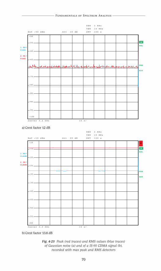
Fundamentals of Spectrum Analysis
70
PRN
2 PK
1 RM
*
*
VIEW
VIEW
SGL
EXT
1 0 s /C e n t e r 2 . 2 G H z
R e f - 5 0 d B m A t t 1 0 d B
V B W 1 0 M H z
S W T 1 0 0 s
R B W 3 M H z
-100
-95
-90
-85
-80
-75
-70
-65
-60
-55
-50
A
PRN
SGL
EXT
1 0 s /C e n t e r 2 . 2 G H z
*
A t t 2 0 d BR e f - 1 0 d B m S W T 1 0 0 s
*
*
V B W 1 0 M H z
R B W 3 M H z
A
CLRWR
2 PK
CLRWR
1 RM
-60
-55
-50
-45
-40
-35
-30
-25
-20
-15
-10
b) Crest factor 13.8 dB
Fig. 4-23 Peak (red traces) and RMS values (blue traces) of Gaussian noise (a) and of a IS-95 CDMA signal (b),
recorded with max peak and RMS detectors
a) Crest factor 12 dB
R&S_Pappband_Spektrumanal 24.10.2001 17:42 Uhr Seite 70

71
The effects of the selected detector and of the sweep time on the results of
measurements on stochastic signals are described in the following.
• Max peak detector
When using the max peak detector, stochastic signals are overweighted
so that the maximum level is displayed. With increasing sweep time the
dwell time in a frequency range allocated to a pixel is also increased. In
the case of Gaussian noise the probability that higher instantaneous val-
ues will occur also rises. This means that the levels of the displayed pix-
els also become higher (see Fig. 4-24a).
With a small ratio between span and resolution bandwidth, the noise
displayed for short sweep times is equal to that displayed with a sample
detector, since only one sample is recorded per pixel.
• Min peak detector
When using the min peak detector, stochastic signals are underweighted
so that the minimum level is displayed. The noise displayed on the spec-
trum analyzer is strongly suppressed. In the case of Gaussian noise the
probability that lower instantaneous values will occur increases with in-
creasing sweep time. This means that the levels of the displayed pixels
also become lower (see Fig. 4-24a).
If measurements are carried out on sinusoidal signals with low signal-
to-noise ratio, the minimum of the noise superimposed on the signal will
also be displayed so that the level measurements yield too low values.
With a small ratio between span and resolution bandwidth, the noise
displayed for short sweep times is equal to that displayed with a sample
detector, since only one sample is recorded per pixel.
• Auto peak detector
When using the auto peak detector, the results of the max peak and min
peak detectors are displayed simultaneously, the two values being con-
nected by a line. With increasing sweep time the displayed noise band be-
comes distinctly wider.
With a small ratio between span and resolution bandwidth, the noise
displayed for short sweep times is equal to that displayed with a sample
detector, since only one sample is recorded per pixel.
Practical Realization of an Analyzer
R&S_Pappband_Spektrumanal 24.10.2001 17:42 Uhr Seite 71

Fundamentals of Spectrum Analysis
72
PRN
SGL
** S W T 1 0 s
VIEW
2 PK *
1 0 M H z / S p a n 1 0 0 M H zC e n t e r 1 . 5 G H z
R e f - 5 0 d B m
*1 PK
*
V B W 3 M H z
R B W 1 M H z
A
CLRWR
A t t 1 0 d B
-150
-140
-130
-120
-110
-100
-90
-80
-70
-60
-50
PRN
SGL
*
* S W T 1 0 s
VIEW
2 MI *
1 MI *
1 0 M H z / S p a n 1 0 0 M H zC e n t e r 1 . 5 G H z
R e f - 5 0 d B m
*
V B W 3 M H z
R B W 1 M H z
A
CLRWR
A t t 1 0 d B
-150
-140
-130
-120
-110
-100
-90
-80
-70
-60
-50
b)
Fig. 4-24 Displayed noise varying as a function of sweep time,with max peak detector (a) and min peak detector (b),
sweep time 2.5 ms (blue trace) and 10 s (red trace)
a)
R&S_Pappband_Spektrumanal 24.10.2001 17:42 Uhr Seite 72
• Sample detector
As shown in Fig. 4-21, the sample detector always displays a sample
recorded at a defined point in time. Due to the distribution of the instan-
taneous values, the trace displayed in the case of Gaussian noise there-
fore varies about the average value of the IF signal envelope resulting
from noise. This average value is 1.05 dB below the RMS value. If noise
is averaged over a narrow video bandwidth (VBW < RBW) using the log-
arithmic level scale, the displayed average value is an additional 1.45 dB
too low. The displayed noise is then 2.5 dB below the RMS value.
In contrast to the other detectors the sweep time has no effect on the
displayed trace since the number of the recorded samples is independent
of the sweep time.
• RMS detector
The RMS detector allows measurement of the actual power of an input
signal irrespective of its temporal characteristic. When using a sample or
max peak detector, the relationship between RMS value and peak value
must be precisely known for determining the power of signals with ran-
dom instantaneous value. This knowledge is not required when using an
RMS detector.
The RMS value displayed by a specific pixel is calculated from all
samples pertaining to this pixel. By increasing the sweep time, the num-
ber of samples available for the calculation is increased, thus allowing
smoothing of the displayed trace. Smoothing by reducing the video band-
width or by averaging over several traces (see chapter 4.5) is neither
permissible nor necessary with the RMS detector. The measurement
results would be falsified, since the displayed values would be too low
(max. 2.51 dB).
To avoid any falsification of results, the video bandwidth should be
at least three times the resolution bandwidth when using the RMS de-
tector.
• AV detector
The AV detector determines the average value from the samples using
the linear level scale. The actual average value is thus obtained irrespec-
tive of the type of input signal. Averaging of logarithmic samples (log av-
erage) would yield results that were too low since higher signal levels are
subject to greater compression by logarithmation. By increasing the
73
Practical Realization of an Analyzer
R&S_Pappband_Spektrumanal 24.10.2001 17:42 Uhr Seite 73

sweep time, several samples are available for calculating the average val-
ue that is displayed by a specific pixel. The displayed trace can thus be
smoothed.
A narrow video bandwidth causes averaging of the video signal. If
samples of the linear level scale are applied to the input of the video fil-
ter, the linear average of the samples is formed when reducing the video
bandwidth. This corresponds to the function of the AV detector so that
smoothing by means of narrow video bandwidths is permissible in this
case.
The same holds true for the analyzer described here, since samples
with linear level scale are applied to the input of the video filter when the
AV detector is used (see block diagram).
If the video bandwidth is reduced, the displayed noise converges for max
peak, min peak, auto peak and sample detectors since the samples are av-
eraged by the video filter before they are weighted by the detector. If a lin-
ear envelope detector is used to determine the IF signal envelope, samples
with linear scale are averaged by the video filter. The resulting display cor-
responds to the true average value and hence to the displayed noise when
using an AV detector. If the IF signal is log-amplified before the video volt-
age is formed, the resulting averaged samples are lower than the true av-
erage value. In the case of Gaussian noise the difference is 1.45 dB (see Fig.
4-25a). Since the linear average of the video voltage resulting from Gauss-
ian noise is already 1.05 dB below the RMS value, the samples obtained
are all 2.5 dB lower than those obtained with the RMS detector (see Fig. 4-
25a). Due to this known relationship an RMS detector is not required to de-
termine the Gaussian noise power. The power can be calculated from the
samples collected by the sample detector, taking into account a correction
factor of 2.5 dB.
This relationship does not apply to other random signals whose in-
stantaneous values are not in line with the Gaussian distribution (for ex-
ample, digitally modulated signals, see Fig. 4-25b). If the crest factor is un-
known, the power of such signals can only be determined using an RMS
detector.
Fundamentals of Spectrum Analysis
74
R&S_Pappband_Spektrumanal 24.10.2001 17:42 Uhr Seite 74
75
Averaging over several measurements
As described in the following chapter, modern analyzers feature the possi-
bility of averaging traces over several measurements (trace average). This
method of averaging partly leads to results different from those when us-
ing narrowband video filters.
Depending on whether the recorded trace is displayed on a linear or
logarithmic level scale, linear or logarithmic samples are used for averag-
ing. Whether the trace is falsified by averaging depends on the display
mode.
In the case of averaging over several measurements, the displayed
noise levels do not converge for max peak, min peak and sample detectors.
The average is derived from the maximum and minimum values, whereas
with the use of the video filter, the samples are averaged prior to weight-
ing and therefore converge.
The sample detector yields the average noise level. With logarithmic
level display, the displayed average value is 1.45 dB too low, as already ex-
plained above. With linear level display and large video bandwidth (VBW
≥ 10 · RBW) the true average is obtained, as with the AV detector.
When using the auto peak detector, averaging over several traces is
not recommended since the maximum and minimum value is displayed.
When the trace average function is activated, automatic switchover to
sample detector is often made.
For the RMS detector, trace averaging is permitted neither in the lin-
ear nor in the logarithmic level mode.
Practical Realization of an Analyzer
R&S_Pappband_Spektrumanal 24.10.2001 17:42 Uhr Seite 75

Fundamentals of Spectrum Analysis
76
PRN
SGL
*
* S W T 5 s
V B W 3 MHz
*3 AV
CLRWR
VIEW
2 AP *
VIEW
1 RM *
EXT
1 M H z / S p a n 1 0 M H zC e n te r 1 0 0 M Hz
R ef -87 dB m
R B W 300 kHz
A
A tt 10 dB
-97
-96
-95
-94
-93
-92
-91
-90
-89
-88
-87
1.45 dB
1.05 dB
2.50 dB
RMS
Average (lin)
Auto Peak (log)
PRN
SGL
VIEW
1 RM *
*
*
V B W 1 0 M Hz
*3 AVCLRWR
VIEW
2 AP
R B W 3 M H z
EXT
10 0 m s /C en te r 2 . 2 G H z
R ef - 2 4 d B m S W T 1 s
A
A t t 1 0 d B
-34
-33
-32
-31
-30
-29
-28
-27
-26
-25
-24
>2.50 dB
RMS
Average (lin)
Auto Peak (log)
b)
Fig. 4-25 Measurement of Gaussian noise (a) and IS-95 CDMA signal (b) using RMS and AV detectors (green and red trace) as well as
auto peak detector with averaging over narrow video bandwidth (blue trace)
a)
R&S_Pappband_Spektrumanal 24.10.2001 17:42 Uhr Seite 76
4.5 Trace processing
As was explained in chapter 4.4, linear samples are required for AV and
RMS detectors. For displaying the traces on a logarithmic level scale when
these detectors are used, the detectors are followed by a log amplifier (40)
which may be optionally activated.
In modern spectrum analyzers, the measurement results are digitized be-
fore they are displayed. This allows many different methods of trace eval-
uation (41).
• Measured data memory
Several traces can be stored in modern analyzers and simultaneously dis-
played. This function is particularly useful for comparative measure-
ments.
• Trace average
With the aid of this function a displayed trace can be smoothed by aver-
aging over several measurements (sweeps). The user can enter the num-
ber of sweeps to be averaged.
Depending on the input signal and the detector used, this way of av-
eraging may lead to other results than averaging by reducing the video
bandwidth.
• Marker functions
Marker functions are particularly useful for the evaluation of recorded
traces. They allow frequency and level to be displayed at any point of the
trace. The limited display accuracy due to the constrained screen resolu-
tion can thus be remedied. In addition to functions which set the marker
automatically to a signal’s level, level differences between signals can
also be directly displayed using the delta marker feature.
Modern spectrum analyzers feature enhanced marker functions al-
lowing, for instance, direct noise or phase noise measurements, without
manual setting of bandwidth or correction factors (see Fig. 4-26).
77
Practical Realization of an Analyzer
R&S_Pappband_Spektrumanal 24.10.2001 17:42 Uhr Seite 77

Fundamentals of Spectrum Analysis
Fig. 4-26 Marker functions for easy phase noise measurement of an input signal
The precise frequency of a displayed signal can also be determined with
the aid of a marker and a count function (signal count). In many cases
the spectrum analyzer can thus replace a frequency counter.
• Tolerance masks (limit lines)
Limit values to be adhered to by the device under test can easily be
checked with the aid of tolerance masks. To simplify use in production,
recorded traces are automatically checked for violation of the specified
limit values and the result is output in form of a “pass” or “fail” message
(see Fig. 4-27).
78
R&S_Pappband_Spektrumanal 24.10.2001 17:42 Uhr Seite 78

Fig. 4-27 Evaluation of traces with the aid of limit lines
• Channel power measurement
In the case of digitally modulated signals, power often has to be mea-
sured within one channel or within a specific frequency range. Channel
power is calculated from the recorded trace, with special functions being
provided for this purpose by modern spectrum analyzers. Adjacent-chan-
nel power measurement with the aid of a spectrum analyzer is described
in detail in chapter 6.3.
79
Practical Realization of an Analyzer
R&S_Pappband_Spektrumanal 24.10.2001 17:42 Uhr Seite 79
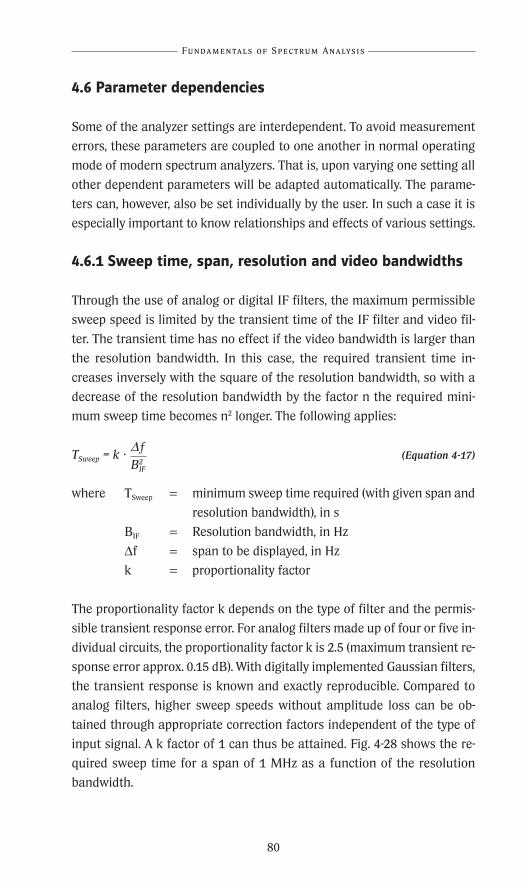
Min
swee
pti
me
/s
Fundamentals of Spectrum Analysis
4.6 Parameter dependencies
Some of the analyzer settings are interdependent. To avoid measurement
errors, these parameters are coupled to one another in normal operating
mode of modern spectrum analyzers. That is, upon varying one setting all
other dependent parameters will be adapted automatically. The parame-
ters can, however, also be set individually by the user. In such a case it is
especially important to know relationships and effects of various settings.
4.6.1 Sweep time, span, resolution and video bandwidths
Through the use of analog or digital IF filters, the maximum permissible
sweep speed is limited by the transient time of the IF filter and video fil-
ter. The transient time has no effect if the video bandwidth is larger than
the resolution bandwidth. In this case, the required transient time in-
creases inversely with the square of the resolution bandwidth, so with a
decrease of the resolution bandwidth by the factor n the required mini-
mum sweep time becomes n2 longer. The following applies:
TSweep = k · (Equation 4-17)
where TSweep = minimum sweep time required (with given span and
resolution bandwidth), in s
BIF = Resolution bandwidth, in Hz
∆f = span to be displayed, in Hz
k = proportionality factor
The proportionality factor k depends on the type of filter and the permis-
sible transient response error. For analog filters made up of four or five in-
dividual circuits, the proportionality factor k is 2.5 (maximum transient re-
sponse error approx. 0.15 dB). With digitally implemented Gaussian filters,
the transient response is known and exactly reproducible. Compared to
analog filters, higher sweep speeds without amplitude loss can be ob-
tained through appropriate correction factors independent of the type of
input signal. A k factor of 1 can thus be attained. Fig. 4-28 shows the re-
quired sweep time for a span of 1 MHz as a function of the resolution
bandwidth.
80
∆ƒB2
IF
R&S_Pappband_Spektrumanal 24.10.2001 17:42 Uhr Seite 80
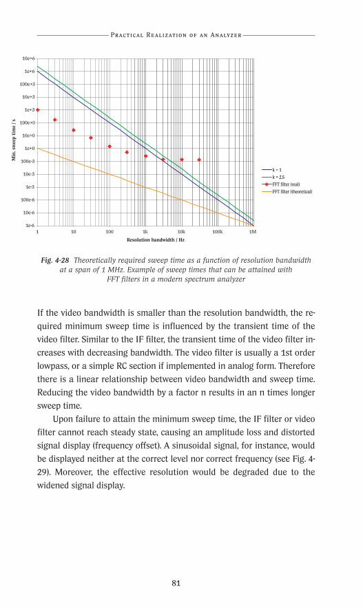
1 10 100 1k 10k 100k 1M
Resolution bandwidth / Hz
1e-6
10e-6
100e-6
1e-3
10e-3
100e-3
1e+0
10e+0
100e+0
1e+3
10e+3
100e+3
1e+6
10e+6
Min
. sw
eep
tim
e /
s
k = 1
k = 2.5
FFT filter (real)
FFT filter (theoretical)
Fig. 4-28 Theoretically required sweep time as a function of resolution bandwidth at a span of 1 MHz. Example of sweep times that can be attained with
FFT filters in a modern spectrum analyzer
If the video bandwidth is smaller than the resolution bandwidth, the re-
quired minimum sweep time is influenced by the transient time of the
video filter. Similar to the IF filter, the transient time of the video filter in-
creases with decreasing bandwidth. The video filter is usually a 1st order
lowpass, or a simple RC section if implemented in analog form. Therefore
there is a linear relationship between video bandwidth and sweep time.
Reducing the video bandwidth by a factor n results in an n times longer
sweep time.
Upon failure to attain the minimum sweep time, the IF filter or video
filter cannot reach steady state, causing an amplitude loss and distorted
signal display (frequency offset). A sinusoidal signal, for instance, would
be displayed neither at the correct level nor correct frequency (see Fig. 4-
29). Moreover, the effective resolution would be degraded due to the
widened signal display.
81
Practical Realization of an Analyzer
R&S_Pappband_Spektrumanal 24.10.2001 17:42 Uhr Seite 81
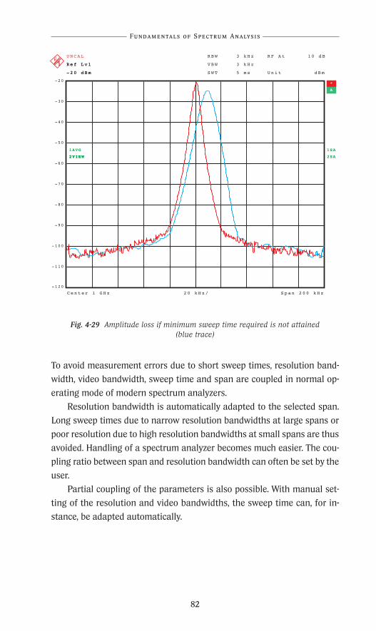
S p a n 2 0 0 k H zC e n t e r 1 G H z 2 0 k H z /
*
1SA
2SA
A
2VIEW
1AVG
2VIEW
-120
-110
-100
S W T 5 m s
U N C A L
V B W 3 k H z
R B W 3 k H z
U n i t d B m
R F A t 1 0 d B
R e f L v l
- 2 0 d B m
R e f L v l
- 2 0 d B m
-90
-80
-70
-60
-50
-40
-30
-20
Fundamentals of Spectrum Analysis
Fig. 4-29 Amplitude loss if minimum sweep time required is not attained (blue trace)
To avoid measurement errors due to short sweep times, resolution band-
width, video bandwidth, sweep time and span are coupled in normal op-
erating mode of modern spectrum analyzers.
Resolution bandwidth is automatically adapted to the selected span.
Long sweep times due to narrow resolution bandwidths at large spans or
poor resolution due to high resolution bandwidths at small spans are thus
avoided. Handling of a spectrum analyzer becomes much easier. The cou-
pling ratio between span and resolution bandwidth can often be set by the
user.
Partial coupling of the parameters is also possible. With manual set-
ting of the resolution and video bandwidths, the sweep time can, for in-
stance, be adapted automatically.
82
R&S_Pappband_Spektrumanal 24.10.2001 17:42 Uhr Seite 82

When using manual settings, if the minimum sweep time is not adhered
to, a warning is usually displayed (UNCAL in Fig. 4-29 upper left corner).
With FFT filters, the transient time is replaced by the observation time
required for a specific resolution (Equation 3-4). In contrast to the sweep
time with analog or digital filters, the observation time is independent of
the span, so even if the span were increased, the observation time would
not be increased for constant resolution. The observation time as a func-
tion of the resolution (yellow trace) shown in Fig. 4-28 is therefore inde-
pendent of the span.
In practice, larger spans are made up of several subranges. At a given
resolution, the resulting observation time is required for each subrange.
The total observation time is directly proportional to the number of sub-
ranges. The attainable measurement time therefore is distinctly longer
than the theoretically expected one. Fig. 4-28 shows sweep times that can
be attained with a modern spectrum analyzer using FFT filters. It is clear-
ly shown that high span-to-resolution bandwidth ratios allow greatly re-
duced sweep times with FFT filters, especially when using very narrow res-
olution bandwidths.
In modern spectrum analyzers, the video bandwidth can be coupled to the
resolution bandwidth. When varying the IF bandwidth, the video band-
width is automatically adapted. The coupling ratio (the ratio between re-
solution and video bandwidth) depends on the application mode and
therefore has to be set by the user (see chapter 4.3). In addition to the user-
defined entry of a numeric value, the following options are often available:
• Sine RBW/VBW = 0.3 to 1
• Pulse RBW/VBW = 0.1
• Noise RBW/VBW = 10
In the default setting, the video bandwidth is usually selected so that max-
imum averaging is achieved without increasing the required sweep time
with the video filter. With a proportionality factor k = 2.5 (Equation 4-17),
the video bandwidth must be at least equal to the resolution bandwidth
(RBW/VBW = 1). If the IF filter is implemented digitally, a proportionality
factor k = 1 can be attained through appropriate compensation as de-
scribed above, and the minimum sweep time required can be reduced by
83
Practical Realization of an Analyzer
R&S_Pappband_Spektrumanal 24.10.2001 17:42 Uhr Seite 83
Fundamentals of Spectrum Analysis
a factor of 2.5. To ensure steady state of the video filter despite the reduced
sweep time, the video bandwidth selected should be about three times
greater than the resolution bandwidth (RBW/VBW = 0.3).
4.6.2 Reference level and RF attenuation
Spectrum analyzers allow measurements in a very wide level range that is
limited by the inherent noise and the maximum permissible input level
(see chapter 5.1 and chapter 5.4 1). With modern analyzers this level range
may extend from –147 dBm to +30 dBm (with a resolution bandwidth of 10
Hz), thus covering almost 180 dB. It is not possible, however, to reach the
two range limits at a time since they require different settings and the dy-
namic range of log amplifiers, envelope detectors and A/D converters is
very small. Within the total level range, only a certain window can be used
which must be adapted by the user to the specific measurement applica-
tion by selecting the reference level (maximum signal level to be dis-
played). The RF attenuation aRF and the IF gain gIF are automatically ad-
justed as a function of the reference level.
To avoid overdriving or even damaging the first mixer and subsequent
processing stages, the high-level input signals must be attenuated by the
analyzer's attenuator (see Fig. 4-30). The attenuation required for a given
reference level depends on the dynamic range of the first mixer and sub-
sequent stages. The level at the input of the first mixer should be distinct-
ly below its 1 dB compression point. Due to nonlinearities, products are
generated in the spectrum analyzer whose levels increase with increasing
mixer level. If the mixer level is too high, these products may cause inter-
ference in the displayed spectrum so that the intermodulation-free range
will be reduced.
84
R&S_Pappband_Spektrumanal 24.10.2001 17:42 Uhr Seite 84
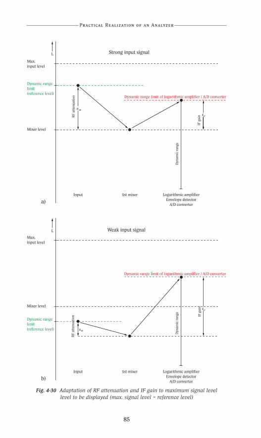
Fig. 4-30 Adaptation of RF attenuation and IF gain to maximum signal level level to be displayed (max. signal level = reference level)
L
Max.input level
Dynamic rangelimit (reference level)
Mixer level
gIF
Dyn
amic
ran
ge
a
Strong input signal
Input 1st mixer Logarithmic amplifierEnvelope detector
A/D converter
Dynamic range limit of logarithmic amplifier / A/D converter
L
Max.input level
Dynamic rangelimit (reference level)
Mixer levelg
IF
Dyn
amic
ran
ge
Weak input signal
Input 1st mixer Logarithmic amplifierEnvelope detector
A/D converter
Dynamic range limit of logarithmic amplifier / A/D converter
a)
b)
IF g
ainRF
atte
nu
atio
n
RF
RFa
RF
atte
nu
atio
n IF g
ain
85
Practical Realization of an Analyzer
R&S_Pappband_Spektrumanal 24.10.2001 17:42 Uhr Seite 85

PRN
* A t t 0 d B
*
S W T 1 4 0 m s
V B W 3 k H z
* R B W 3 0 0 k H z
S t o p 6 0 M H zS t a r t 1 0 M H z 5 M H z /
A
CLRWR
1 AP
R e f - 2 0 d B m
-120
-110
-100
-90
-80
-70
-60
-50
-40
-30
-20
PRN
* A t t 2 0 d B
5 M H z / S t o p 6 0 M H zS t a r t 1 0 M H z
R e f - 2 0 d B m
*
S W T 1 4 0 m s
V B W 3 k H z
* R B W 3 0 0 k H z
A
CLRWR
1 AP
-120
-110
-100
-90
-80
-70
-60
-50
-40
-30
-20
Fundamentals of Spectrum Analysis
86
a)
b)
R&S_Pappband_Spektrumanal 24.10.2001 17:42 Uhr Seite 86

PRN
* A t t 1 0 d B
*
S W T 1 4 0 m s
V B W 3 k H z
* R B W 3 0 0 k H z
S t o p 6 0 M H zS t a r t 1 0 M H z 5 M H z /
A
CLRWR
1 AP
R e f - 2 0 d B m
-120
-110
-100
-90
-80
-70
-60
-50
-40
-30
-20
87
c)
Fig. 4-31 Single-tone input: dynamic range reduced byby too high (a) or too low (b) mixer level. Dynamic range attainable with
optimum mixer level (c) shown in comparison
If the RF attenuation is too high, causing the mixer level to be too low, the
signal-to-noise ratio of the input signal will be unnecessarily reduced. As
shown in Fig. 4-32, the attainable dynamic range is then reduced by the
higher noise floor. Fig. 4-31 shows the effects of the mixer level with sin-
gle-tone input (see chapter 5.2: Nonlinearities).
Practical Realization of an Analyzer
R&S_Pappband_Spektrumanal 24.10.2001 17:42 Uhr Seite 87

Fundamentals of Spectrum Analysis
88
LMax.input level
Dynamic rangelimit(reference level)
Mixer level
Lmix,1
gIF,1
gIF,2
qRF,1
Lmix,2
qRF,2
Dynamic range
Noise floor
Input 1st mixer Logarithmic amplifierEnvelope detector
A/D converter
Fig. 4-32 Dynamic range limited by noise floor as a function of mixer level
To obtain the total dynamic range of the log amplifier and envelope de-
tector (with analog IF filters) or of the A/D converter (with digital IF filters),
the signal level is appropriately amplified with the aid of the IF amplifier
at the last IF. The gain is selected so that signals attaining the reference
level cause the full drive of the log amplifier, envelope detector (with lin-
ear level display) or A/D converter (with digital IF filters). The IF gain is
therefore set indirectly via the reference level although it is also dependent
on the selected attenuator. At a constant reference level, the IF gain has to
be increased with increasing RF attenuation (see gIF,1 and gIF,2 in Fig. 4-32).
If the level of the input signal to be displayed exceeds the reference
level, this may cause overdriving. The IF gain has then to be reduced by in-
creasing the reference level.
Coupling of reference level and RF attenuation
In modern spectrum analyzers, the RF attenuation can be coupled to the
reference level setting. The coupling criterion is the maximum mixer level
attained by an input signal whose level corresponds to the reference level.
The mixer level attained with full drive therefore results from the differ-
ence between reference level and RF attenuation. The following applies:
R&S_Pappband_Spektrumanal 24.10.2001 17:42 Uhr Seite 88

Lmix = Lin,max – aRF = LRef – aRF (Equation 4-18)
where Lmix = level at input of first mixer with full drive, in dBm
Lin,max = input level causing full drive, in dBm
LRef = reference level, in dBm
aRF = RF attenuation set via attenuator, in dB
A compromise between low signal-to-noise ratio and low distortion has to
be found in the selection of the mixer level. To optimize the mixer level for
specific applications, some analyzers allow the user to freely select the
mixer level for a given reference level. Predefined coupling degrees are of-
ten provided:
• Low signal-to-noise ratio
The lower the RF attenuation, the lower the reduction of the signal-to-
noise ratio before the first mixer. For low displayed noise, a high mixer
level is required (see chapter 5.1: Inherent noise).
• Low distortion
The lower the mixer level, the lower the distortion produced in a spec-
trum analyzer due to nonlinearities. In this display mode, the RF attenu-
ation is higher (see chapter 5.2: Nonlinearities).
Table 4-2 shows some typical settings of RF attenuation and IF gain at a
given reference level for the different display modes. The example shows
that even at very low reference levels, an RF attenuation of at least 10 dB
is always set. In this way the first mixer is protected and a good input
match is realized. Thus a higher level accuracy for absolute level mea-
surements is achieved (see chapter 5.10.1: Error components). In this
example, the RF attenuation can be set to a maximum of 70 dB, and the
IF gain to a maximum of 50 dB.
89
Practical Realization of an Analyzer
R&S_Pappband_Spektrumanal 24.10.2001 17:42 Uhr Seite 89

Fundamentals of Spectrum Analysis
Mixer –40 dBm –30 dBm –20 dBm
level (low distortion) (normal) (low noise)
Reference RF atten- IF RF atten- IF RF atten- IF
level uation gain uation gain uation gain
+30 dBm 70 dB 30 dB 60 dB 20 dB 50 dB 10 dB
+20 dBm 60 dB 30 dB 50 dB 20 dB 40 dB 10 dB
+10 dBm 50 dB 30 dB 40 dB 20 dB 30 dB 10 dB
0 dBm 40 dB 30 dB 30 dB 20 dB 20 dB 10 dB
–10 dBm 30 dB 30 dB 20 dB 20 dB 10 dB 10 dB
–20 dBm 20 dB 30 dB 10 dB 20 dB 10 dB 20 dB
–30 dBm 10 dB 30 dB 10 dB 30 dB 10 dB 30 dB
–40 dBm 10 dB 40 dB 10 dB 40 dB 10 dB 40 dB
–50 dBm 10 dB 50 dB 10 dB 50 dB 10 dB 50 dB
–60 dBm 10 dB 50 dB 10 dB 50 dB 10 dB 50 dB
–70 dBm 10 dB 50 dB 10 dB 50 dB 10 dB 50 dB
–80 dBm 10 dB 50 dB 10 dB 50 dB 10 dB 50 dB
–90 dBm 10 dB 50 dB 10 dB 50 dB 10 dB 50 dB
–100 dBm 10 dB 50 dB 10 dB 50 dB 10 dB 50 dB
Table 4-2 Example of setting RF attenuation and IF gain at a given reference level
(IF gain max. 50 dB, RF attenuation max. 70 dB)
4.6.3 Overdriving
When using a spectrum analyzer care should be taken to avoid overdriv-
ing by input signals with levels too high. Overdriving may occur at several
points in the signal path. To avoid this, both the RF attenuation and the
reference level (IF gain) have to be set correctly. In the following, the criti-
cal components and the criteria to be observed are described.
90
R&S_Pappband_Spektrumanal 24.10.2001 17:42 Uhr Seite 90
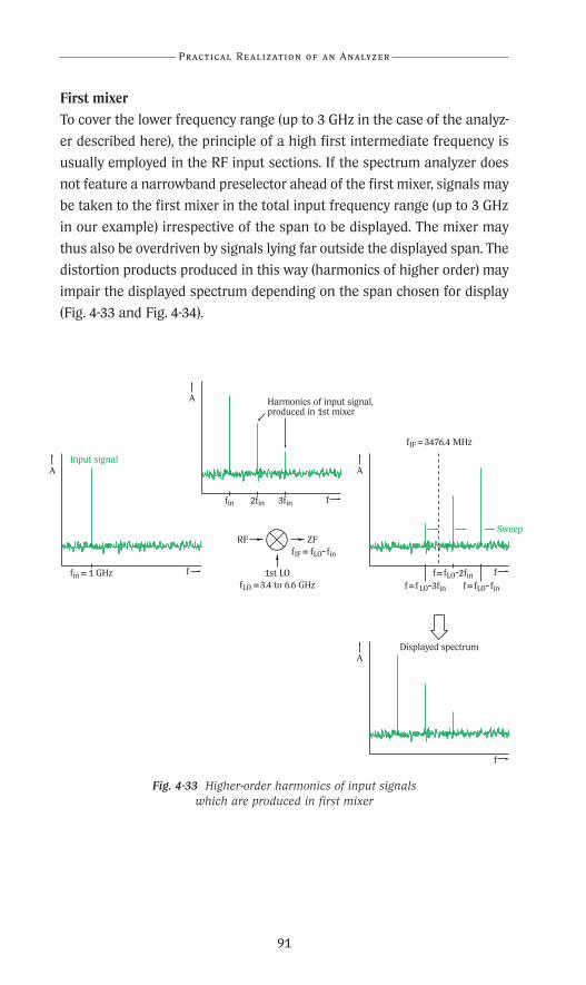
A
ffin = 1 GHz
Input signalA
f
f= fLO–3fin
Sweep
1st LOfLO =3.4 to 6.6 GHz
ZF fIF = fLO– fin
RF
f= fLO– fin
f= fLO–2fin
fIF = 3476.4 MHz
A
f
Displayed spectrum
A
f
Harmonics of input signal,produced in 1st mixer
fin 3fin2fin
First mixer
To cover the lower frequency range (up to 3 GHz in the case of the analyz-
er described here), the principle of a high first intermediate frequency is
usually employed in the RF input sections. If the spectrum analyzer does
not feature a narrowband preselector ahead of the first mixer, signals may
be taken to the first mixer in the total input frequency range (up to 3 GHz
in our example) irrespective of the span to be displayed. The mixer may
thus also be overdriven by signals lying far outside the displayed span. The
distortion products produced in this way (harmonics of higher order) may
impair the displayed spectrum depending on the span chosen for display
(Fig. 4-33 and Fig. 4-34).
Fig. 4-33 Higher-order harmonics of input signals which are produced in first mixer
91
Practical Realization of an Analyzer
R&S_Pappband_Spektrumanal 24.10.2001 17:42 Uhr Seite 91

Fundamentals of Spectrum Analysis
92
1 AP
CLRWR
A
A t t 0 d B*R e f - 1 0 d B m S W T 5 m s
1 0 0 M H z /S t a r t 3 0 0 M H z S t o p 1 . 3 G H z
R B W 3 M H z
V B W 1 0 M H z
*
*
PRN
-110
-100
-80
-70
-60
-50
-40
-30
-20
-10
M a r k e r 1 [ T 1 ]
- 5 3 . 7 7 d B m
1 . 0 4 0 0 0 0 0 0 G H z
1
1 AP
CLRWR
A
A t t 0 d B*R e f - 1 0 d B m S W T 5 m s
5 0 M H z /S t a r t 8 0 0 M H z S t o p 1 . 3 G H z
R B W 3 M H z
V B W 1 0 M H z
*
*
PRN
-110
-100
-90
-80
-70
-60
-50
-40
-30
-20
-10
M a r k e r 1 [ T 1 ]
- 5 3 . 7 4 d B m
1 . 0 4 0 0 0 0 0 0 G H z
1
b) Fig. 4-34 Spectrum analyzer driven by a sinusoidal signal with
f = 520 MHz (a). The second harmonic with f = 1040 MHz that is produced in the first mixer appears even if the fundamental of the signal is not contained
in the displayed spectrum (b)
a)
R&S_Pappband_Spektrumanal 24.10.2001 17:42 Uhr Seite 92

To avoid overdriving, the mixer level (the total signal level at the input of
the first mixer) should be below the mixer’s 1 dB compression point. The
latter is specified in the data sheet of the respective spectrum analyzer (see
chapter 5.4). As described in chapter 4.6.2, the mixer level is set with the
aid of the attenuator. Some contemporary spectrum analyzers feature an
overload detector ahead of the first mixer, so that an overdrive warning
can be displayed.
If the input section of the spectrum analyzer features a narrowband
tracking preselector, the risk of the analyzer being overdriven by signals
outside the displayed spectrum is considerably reduced. The analyzer de-
scribed in this chapter contains a narrowband preselector in form of a
tracking YIG filter in the signal path for the frequency range from 3 GHz
to 7 GHz. If a small span of this frequency range is displayed, the first mix-
er can only be overdriven by signals within or close to the displayed spec-
trum. Due to the limited skirt selectivity of the YIG filter, input signals out-
side the displayed spectrum must have a certain spacing from the range
of interest so that they will be sufficiently suppressed by the filter and not
overdrive the mixer (Fig. 4-35).
To allow EMC measurements, which often imply a very large number
of simultaneously occurring spectral components at a high level, with the
spectrum analyzer in line with relevant standards, analyzers can usually
also be enhanced with optional narrowband tracking preselectors in the
lower input frequency range.
IF signal processing through to resolution filter
The first mixer is followed by analog signal processing stages such as IF
amplifiers and conversion stages. These stages can only be overdriven by
strong signals within or in the vicinity of the displayed spectrum. Signals
outside the displayed spectrum are suppressed after the first conversion
by the subsequent IF filters, provided the frequency spacing from the
range of interest is sufficiently large (Fig. 4-36). The IF filter in the 1st and
2nd IF stage is usually extremely wideband so the required frequency
spacing for adequate attenuation may be very large (often some 100 MHz).
93
Practical Realization of an Analyzer
R&S_Pappband_Spektrumanal 24.10.2001 17:42 Uhr Seite 93

A
f
Input signal
A
f
Tracking bandwidth filter(preselector)
sufficient suppression
fStart fStop
Displayed frequency range (span)
Input signalof 1st mixer
little suppression
Fundamentals of Spectrum Analysis
Fig. 4-35 Suppression of input signals outside the displayed spectrum by a tracking YIG filter
94
Unlike overdriving of the first mixer, distortion products caused by over-
driving of analog IF signal processing components do not appear in the
displayed spectrum. They are suppressed by the subsequent narrowband
resolution filters (Fig. 4-37).
R&S_Pappband_Spektrumanal 24.10.2001 17:42 Uhr Seite 94

A
f
Strong input signal outside frequency range of interest
Signalto be displayed
Input signals
Frequency range to be displayed
Sweep
A
ff1st IF
Sweep Sweep
A
f
Input signalsconverted to 1st IF
f1st IF
1st IF filter
SweepSweep
1st LO
RF
1st IF amplifier 1st IF filter
IF signal after1st IF filter
ba c
IF signal after 1st IF filter
Fig. 4-36 Suppression of mixture products at the 1st IF by the first IF filter
95
a)
b)
c)
Practical Realization of an Analyzer
R&S_Pappband_Spektrumanal 24.10.2001 17:42 Uhr Seite 95

A
ff1st IF
1st IF filter
2f1st IF
Harmonics suppressedby 1st IF filter
A
f
Sinusoidal input signalconverted to 1st IF
f1st IF
1st IFf1st IF = 3476.4 MHz
1st IF filter 2nd mixer
IF signal after1st IF filter
1st IF amplifier
2nd LOfO = 3476.4 MHzB = 200 MHz
cba
A
ff1st IF 2f1st IF
Harmonics of IF signaldue to nonlinearities in 1st IF filter
Fig. 4-37 Suppression of distortion products produced in analog IF signal processing components
Fundamentals of Spectrum Analysis
96
a)
b)
c)
R&S_Pappband_Spektrumanal 24.10.2001 17:42 Uhr Seite 96
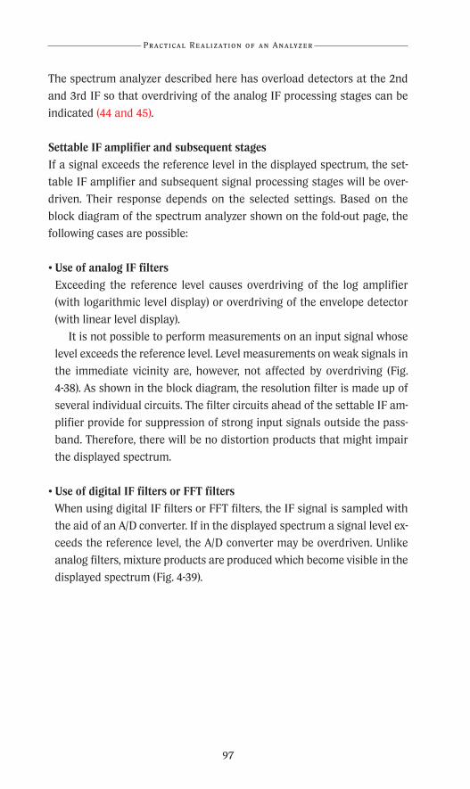
The spectrum analyzer described here has overload detectors at the 2nd
and 3rd IF so that overdriving of the analog IF processing stages can be
indicated (44 and 45).
Settable IF amplifier and subsequent stages
If a signal exceeds the reference level in the displayed spectrum, the set-
table IF amplifier and subsequent signal processing stages will be over-
driven. Their response depends on the selected settings. Based on the
block diagram of the spectrum analyzer shown on the fold-out page, the
following cases are possible:
• Use of analog IF filters
Exceeding the reference level causes overdriving of the log amplifier
(with logarithmic level display) or overdriving of the envelope detector
(with linear level display).
It is not possible to perform measurements on an input signal whose
level exceeds the reference level. Level measurements on weak signals in
the immediate vicinity are, however, not affected by overdriving (Fig.
4-38). As shown in the block diagram, the resolution filter is made up of
several individual circuits. The filter circuits ahead of the settable IF am-
plifier provide for suppression of strong input signals outside the pass-
band. Therefore, there will be no distortion products that might impair
the displayed spectrum.
• Use of digital IF filters or FFT filters
When using digital IF filters or FFT filters, the IF signal is sampled with
the aid of an A/D converter. If in the displayed spectrum a signal level ex-
ceeds the reference level, the A/D converter may be overdriven. Unlike
analog filters, mixture products are produced which become visible in the
displayed spectrum (Fig. 4-39).
97
Practical Realization of an Analyzer
R&S_Pappband_Spektrumanal 24.10.2001 17:42 Uhr Seite 97

Fundamentals of Spectrum Analysis
98
A t t 1 0 d B
1 AP
CLRWR
A
R B W 1 0 0 k H z
R e f - 3 0 d B m
C e n t e r 8 6 0 . 5 M H z S p a n 5 M H z5 0 0 k H z /
V B W 3 0 0 H z
S W T 4 2 0 m s
*
PRN
-130
-120
-110
-100
-90
-80
-70
-60
-50
-40
-30
M a r k e r 1 [ T 1 ]
- 5 6 . 0 7 d B m
8 6 2 . 0 1 0 0 0 0 0 0 M H z
1
A t t 1 0 d B
1 AP
CLRWR
A
R B W 1 0 0 k H z
R e f - 3 0 d B m
C e n t e r 8 6 0 . 5 M H z S p a n 5 M H z5 0 0 k H z /
V B W 3 0 0 H z
S W T 4 2 0 m s
*
PRN
-130
-120
-110
-100
-90
-80
-70
-60
-50
-40
-30
M a r k e r 1 [ T 1 ]
- 5 6 . 0 6 d B m
8 6 2 . 0 1 0 0 0 0 0 0 M H z
1
b) Fig. 4-38 Level measurement on a weak input signal
signal in the presence of a very strong signal, with normal driving (a) and overdriving of the settable IF amplifier (b).
Overdriving has no effect on the measurement result
a)
R&S_Pappband_Spektrumanal 24.10.2001 17:42 Uhr Seite 98

99
a)
1 AP
CLRWR
A
R B W 3 0 k H z*
V B W 3 0 0 H z
S W T 1 . 1 5 s
*
A t t 1 0 d BR e f - 4 0 d B m
C e n t e r 8 6 2 M H z S p a n 5 M H z5 0 0 k H z /
IFOVL
PRN
-140
-130
-120
-110
-100
-90
-80
-70
-60
-50
-40
M a r k e r 1 [ T 1 ]
- 8 9 . 1 8 d B m
8 6 2 . 0 0 0 0 0 0 0 0 M H z
1
1 AP
CLRWR
A
R B W 3 0 k H z*
R e f 0 d B m A t t 3 0 d B
C e n t e r 8 6 2 M H z S p a n 5 M H z5 0 0 k H z /
V B W 3 0 0 H z
S W T 1 . 1 5 s
*
PRN
-100
-90
-80
-70
-60
-50
-40
-30
-20
-10
0
M a r k e r 1 [ T 1 ]
- 6 9 . 9 3 d B m
8 6 2 . 0 0 0 0 0 0 0 0 M H z
1
b)
Fig. 4-39 Mixture products due to overdriving of A/D converter converter when using digital IF filters or FFT filters (a);
displayed spectrum in case of correct driving (b)
Practical Realization of an Analyzer
R&S_Pappband_Spektrumanal 24.10.2001 17:42 Uhr Seite 99

5 PERFORMANCE FEATURES OF SPECTRUM ANALYZERS
5.1 Inherent noise
Inherent noise is understood as the thermal noise which characterizes
both receivers and spectrum analyzers. Due to inherent noise the signal-
to-noise ratio of an input signal is reduced. Therefore, inherent noise is a
measure of the sensitivity of the spectrum analyzer. It allows conclusions
to be drawn as to the minimum level required for the input signal to be
detectable.
The inherent noise of receivers can be specified in different ways, usu-
ally it is expressed as the noise factor or noise figure.
The non-dimensional noise factor F of a two-port network is the ratio
between the signal-to-noise ratio at the input of the network and the sig-
nal-to-noise ratio at the output of the network. The following applies:
F = (Equation 5-1)
where S1 /N1 = signal-to-noise ratio at the input of the network
S2 /N2 = signal-to-noise ratio at the output of the network
The noise figure NF is then given by
NF = 10 · log F (Equation 5-2)
It is stated in dB.
Fig. 5-1 Several cascaded noisy networks
Fundamentals of Spectrum Analysis
100
S1 /N1
S2 /N2
F , G1 2F , G2
Ftotal , Gtotal
. . .
nF , Gn1
R&S_Pappband_Spektrumanal 24.10.2001 17:42 Uhr Seite 100

Practical Realization of an Analyzer
101
The total noise factor Ftotal of cascaded networks is given by
Ftotal = F1 + + + . . . + (Equation 5-3)
where Fi = noise factor of an individual stage
Gi = gain of an individual stage
The following holds true for passive lossy networks such as cables or at-
tenuator pads:
F = 10 10 and NF = a (Equation 5-4)
where F and NF = noise factor and noise figure of network
a = attenuation of network, in dB
Equation 5-3 reveals that the noise factor of the first stage is fully taken
into account in the total noise factor of a cascaded circuit. The attenuator
is located at the input of a spectrum analyzer – a passive stage whose
noise factor can be calculated by means of Equation 5-4.
The total noise factor of the analyzer therefore depends on the atten-
uator setting. Increasing the attenuation by 10 dB, for instance, results in
a 10 dB higher total noise figure. Maximum sensitivity is therefore at-
tained with an attenuator setting of 0 dB (see Fig. 5-2).
The sensitivity of spectrum analyzers is usually specified as the displayed
average noise level (DANL), a parameter that can be directly read from the
display of the spectrum analyzer.
The noise produced in a receiver is thermal noise, which means that it
does not contain any discrete components. The probability of a noise volt-
age occurring in a specific voltage range can be derived from the Gauss-
ian distribution so that the designation Gaussian noise is also used.
F2–1
G1
F3–1
G1· G2
Fn–1
ΠGi
n –1
i = 1
a_
Performance Features of Spectrum Analyzers
R&S_Pappband_Spektrumanal 24.10.2001 17:42 Uhr Seite 101

Fig. 5-2 Displayed average noise level of spectrum analyzer
as a function of RF attenuation
The displayed noise corresponds to the noise voltage picked up at the en-
velope detector. The corresponding noise power can be calculated by inte-
gration of the noise density over the noise bandwidth of the receiver which
would be the noise bandwidth of all stages ahead of the detector. In the
case of spectrum analyzers, this bandwidth is determined by the noise
bandwidth of the IF filter. Accordingly, the displayed noise depends on the
resolution bandwidth setting.
Since the spectral power density of thermal noise is constant within the
noise bandwidth, the displayed average noise level can be calculated as
follows provided the noise figure of the analyzer and the noise bandwidth
of the selected IF filter are known:
LDAN = 10 · log + NFSA – 2.5 dB (Equation 5-5)
Fundamentals of Spectrum Analysis
102
D a t e : 1 2 . A u g . 1 9 9 9 0 8 : 4 9 : 5 8
C e n t e r 8 9 0 M H z 1 M H z S p a n 1 0 k H z
PRN
EXT
-40
-50
-60
-70
-80
-90
-100
-110
-120
-130
-140
R e f - 4 0 d B m
* R B W 3 0 0 k H z
* V B W 3 k H z
S W T 3 0 m s
*A
RF Att = 20 dB
* A t t 2 0 d B
1 AP CLRWR 2 AP VIEW 3 AP VIEW
RF Att = 10 dB
RF Att = 0 dB
( )k · T · BN,IF
1 · 10–3 W
R&S_Pappband_Spektrumanal 24.10.2001 17:42 Uhr Seite 102

Practical Realization of an Analyzer
103
where LDAN = displayed average noise level, in dBm
k = Boltzmann’s constant, k = 1.38 · 10–23 W/Hz
T = ambient temperature, in K
BN,IF = noise bandwidth of IF filter
NFSA = noise figure of spectrum analyzer, in dB
–2.5 dB = underweighting of noise by sample detector and
averaging of logarithmic level values
For an ambient temperature of 290 K, the displayed average noise level is
given by:
LDAN = –174 dBm (1 Hz) + 10 · log dB + NFSA – 2.5 dB (Equation 5-6)
The value of –174 dBm (1 Hz) corresponds to the available thermal noise
power across an ohmic resistance in 1 Hz bandwidth at an ambient tem-
perature of 290 K. This is the noise floor, or the absolute minimum noise
level at a given temperature.
The sample detector usually used for noise measurements with spec-
trum analyzers (chapter 4.4: Detectors) determines the arithmetic mean of
the noise. In the case of Gaussian noise this is 1.05 dB below the RMS va-
lue (the effective noise power). Due to averaging of the results on a loga-
rithmic scale by averaging over several traces, the displayed noise is re-
duced by a further 1.45 dB. In calculating the displayed average noise level
according to Equation 5-6, this is taken account of by the subtraction of
2.5 dB. This correction is only permissible for Gaussian noise, which can
be assumed for thermal noise.
The following relationship can be derived from Equation 5-5 for the varia-
tion of the displayed noise as a function of varying the IF bandwidth set-
ting of BIF,1 to BIF,2:
∆LDAN = 10 · log (Equation 5-7)BN,IF,2
BN,IF,1
( )BN,IF
Hz
Performance Features of Spectrum Analyzers
R&S_Pappband_Spektrumanal 24.10.2001 17:42 Uhr Seite 103

where BN,IF,1, BN,IF,2 = noise bandwidth of IF filter before and after
variation of setting, in Hz
∆LDAN = variation of displayed noise as a function of
varying the IF bandwidth, in dB
If both IF filters have the same relationship between 3 dB bandwidth and
noise bandwidth, the difference in the displayed noise can also be calcu-
lated from the 3 dB bandwidths. The following then applies:
∆LDAN = 10 · log (Equation 5-8)
where BIF,1, BIF,2 = 3 dB bandwidth of IF filter before and after
variation of setting, in Hz
Fig. 5-3 shows the effects of different IF bandwidths on the displayed
noise. Due to the different practical realization of the IF filters of a spec-
trum analyzer, the noise figure of the analyzer may also depend on the
selected resolution bandwidth. The actual variation of the displayed aver-
age noise level may therefore differ from the value worked out with Equa-
tion 4-8.
Fig. 5-3 Displayed average noise level at various resolution bandwidths
Fundamentals of Spectrum Analysis
104
BIF,2
BIF,1
PRN
*
EXT
3 MHz/ Span 30 MHzCenter 891.5 MHz
Ref -60 dBm
*
*
VBW 300 Hz
RBW 300 kHz
SWT 840 ms
VIEW
3 AP
VIEW
2 AP
A
CLRWR
1 AP
Att 10 dB
-110
-105
-100
-95
-90
-85
-80
-75
-70
-65
-60
3 MHz
1 MHz
3 00 kHz
R&S_Pappband_Spektrumanal 24.10.2001 17:42 Uhr Seite 104
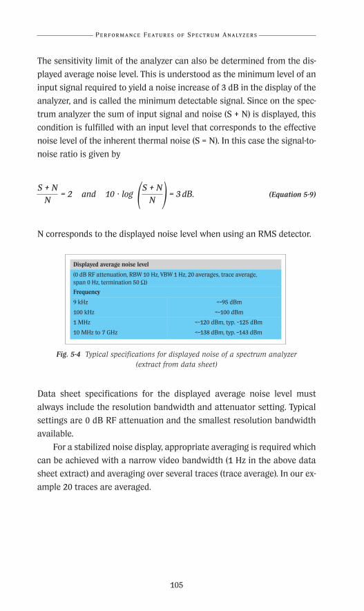
Practical Realization of an Analyzer
105
The sensitivity limit of the analyzer can also be determined from the dis-
played average noise level. This is understood as the minimum level of an
input signal required to yield a noise increase of 3 dB in the display of the
analyzer, and is called the minimum detectable signal. Since on the spec-
trum analyzer the sum of input signal and noise (S + N) is displayed, this
condition is fulfilled with an input level that corresponds to the effective
noise level of the inherent thermal noise (S = N). In this case the signal-to-
noise ratio is given by
= 2 and 10 · log = 3 dB. (Equation 5-9)
N corresponds to the displayed noise level when using an RMS detector.
Fig. 5-4 Typical specifications for displayed noise of a spectrum analyzer (extract from data sheet)
Data sheet specifications for the displayed average noise level must
always include the resolution bandwidth and attenuator setting. Typical
settings are 0 dB RF attenuation and the smallest resolution bandwidth
available.
For a stabilized noise display, appropriate averaging is required which
can be achieved with a narrow video bandwidth (1 Hz in the above data
sheet extract) and averaging over several traces (trace average). In our ex-
ample 20 traces are averaged.
( )S + N
N
S + N
N
Displayed average noise level
(0 dB RF attenuation, RBW 10 Hz, VBW 1 Hz, 20 averages, trace average, span 0 Hz, termination 50 Ω)
Frequency
9 kHz <–95 dBm
100 kHz <–100 dBm
1 MHz <–120 dBm, typ. –125 dBm
10 MHz to 7 GHz <–138 dBm, typ. –143 dBm
Performance Features of Spectrum Analyzers
R&S_Pappband_Spektrumanal 24.10.2001 17:42 Uhr Seite 105
Maximum sensitivity
The maximum sensitivity of spectrum analyzers is obtained with
an attenuator setting of 0 dB. It is important that the first mixer
of the analyzer is not overdriven by a high-level signal – even out-
side the displayed frequency range.
To further reduce the displayed noise, the resolution band-
width is reduced. A trade-off has to be found between low dis-
played noise and high measurement speed. For the display of in-
put signals with a very low signal-to-noise ratio, it is useful to
reduce the video bandwidth as well as the resolution bandwidth
or to increase the sweep time when using the RMS detector. The
trace is thus smoothed so that the input signal is clearly displayed.
The measured levels are thus stabilized – a prerequisite for accu-
rate, reproducible results.
If the sensitivity of the spectrum analyzer is unsatisfactory, it
can be enhanced with aid of an external preamplifier. The total
noise factor of the preamplifier and spectrum analyzer arrange-
ment can be calculated from Equation 5-3. F1 and G1 correspond
to the noise factor and gain of the preamplifier, F2 to the noise fac-
tor of the spectrum analyzer.
For level measurements it is essential to know the frequency-
dependent gain of the preamplifier. This gain must be subtracted
from the measured levels. Many spectrum analyzers offer the pos-
sibility of taking into account the frequency-dependent gain with
the aid of transducer tables. Recorded spectra can thus automati-
cally be displayed with the correct levels.
High sensitivity of the spectrum analyzer is especially impor-
tant for applications in which the resolution bandwidth is pre-
scribed by standards. In these cases a reduction of the displayed
noise by decreasing the resolution bandwidth is not permitted.
The sensitivity is also important for fast measurement speeds. To
attain sufficiently low displayed noise, narrowband IF filters are
required with lower sensitivities, which in turn increases the
sweep time. Spectrum analyzers featuring a low noise figure allow
the use of greater resolution bandwidths and hence shorter sweep
times (chapter 4.6: Parameter dependencies).
Fundamentals of Spectrum Analysis
106
R&S_Pappband_Spektrumanal 24.10.2001 17:42 Uhr Seite 106

Practical Realization of an Analyzer
107
5.2 Nonlinearities
An ideal linear two-port network provides for distortion-free transfer of sig-
nals from its input to its output. The voltage transfer function of such a
network is
vout(t) = GV · vin(t) (Equation 5-10)
where vout(t) = voltage at output of network
vin(t) = voltage at input of network
GV = voltage gain of network
Such ideal networks can only be realized with the aid of passive compo-
nents. Resistive attenuator pads, for instance, can be assumed to be ideal.
Networks containing semiconductor components, for instance ampli-
fiers or mixers, exhibit nonlinearities. In this case the transfer function can
be approximated by a power series as follows:
vout(t) =Σ an · vinn(t) = a1 · vin(t) + a2 · vin
2(t) + a3 · vin3(t) + . . . (Equation 5-11)
where vout(t) = voltage at output of network
vin(t) = voltage at input of network
an = coefficient of nonlinear element of voltage gain
In most cases it is sufficient to consider the square and cubic terms so that
the power series according to Equation 5-11 is taken up to n = 3.
For many components, such as mixers or level detectors, the nonlinear
response is desirable. Spectrum analyzers, however, should feature distor-
tion-free display of the input signals. Accordingly, linearity is an essential
criterion for the assessment of a spectrum analyzer.
The effects of a network’s nonlinearities on its output spectrum de-
pend on its input signal.
n =1
∞
Performance Features of Spectrum Analyzers
R&S_Pappband_Spektrumanal 24.10.2001 17:42 Uhr Seite 107

Single-tone input
If an input to a network is a sinusoidal signal vin(t) of
vin(t) = Ûin · sin(2π fin,1 · t) (Equation 5-12)
where Ûe = peak value of vin(t)
fin,1 = frequency of vin(t),
is present, this is referred to as a single-tone input. By substituting Equa-
tion 5-12 in Equation 5-11 it can be seen that due to nonlinearities, har-
monics of the input signal are produced with the frequencies fn.H = n · f1
(see Fig. 5-5).
Fig. 5-5 Spectrum before and after nonlinear network
The levels of these harmonics depend on the coefficients an in Equation 5-
11. They are also dependent on the order n of the respective harmonic as
well as on the input level. When the input level is increased, the levels of
harmonics increase with their order. That is, a variation of the input level
by ∆ dB causes a variation of the harmonic level by n · ∆ dB.
Data sheet specifications on this type of signal distortion usually refer
to the second harmonic only for which the level difference ak2 from the fun-
damental at the output of the network is specified. The specifications are
valid for a certain input level Lin, which has always to be stated. When com-
paring spectrum analyzers, it should therefore always be checked whether
the specifications of the various models refer to the same mixer level.
Fundamentals of Spectrum Analysis
108
Ain
ffin,1
Input signal
Aout
ffin,1
Output signal
2fin,1 3fin,1
Nonlinearamplifier
R&S_Pappband_Spektrumanal 24.10.2001 17:42 Uhr Seite 108
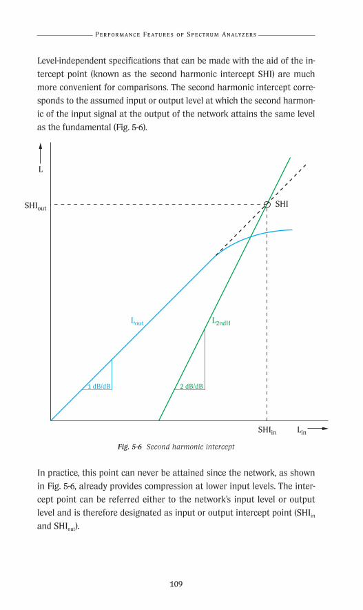
Practical Realization of an Analyzer
109
Level-independent specifications that can be made with the aid of the in-
tercept point (known as the second harmonic intercept SHI) are much
more convenient for comparisons. The second harmonic intercept corre-
sponds to the assumed input or output level at which the second harmon-
ic of the input signal at the output of the network attains the same level
as the fundamental (Fig. 5-6).
Fig. 5-6 Second harmonic intercept
In practice, this point can never be attained since the network, as shown
in Fig. 5-6, already provides compression at lower input levels. The inter-
cept point can be referred either to the network’s input level or output
level and is therefore designated as input or output intercept point (SHIin
and SHIout).
L
Lin
SHI
SHIin
SHIout
Lout L2ndH
1 dB/dB 2 dB/dB
Performance Features of Spectrum Analyzers
R&S_Pappband_Spektrumanal 24.10.2001 17:42 Uhr Seite 109

Since the output intercept point depends on the gain of the network, the
input intercept point (with selected RF attenuation, usually 0 dB) is always
stated in the spectrum analyzer specifications.
With given input level Lin and harmonic level difference ak2 of the sec-
ond harmonic, input intercept point can be calculated as follows:
SHIin = ak2 + Lin (Equation 5-13)
SHIout referred to the output is calculated as
SHIout = SHIin + g (Equation 5-14)
where g = power gain of network, in dB
Two-tone input
With a two-tone input, signal vin(t) consisting of two sinusoidal signals of
equal amplitude is applied to the input of the network. The input signal is
given by:
vin(t) = Ûin · sin(2πƒin,1 · t) + Ûin · sin(2πƒin,2 · t) (Equation 5-15)
where Ûin = peak value of the two sinusoidal signals
fin,1, fin,2 = signal frequencies
By substituting Equation 5-15 in the nonlinear transfer function according
to Equation 5-11, the mixture products listed in Table 5-1 are obtained
among others at the output of the network. The angular frequency ω is al-
ways stated as ω1 = 2·π· fin,1 and ω2 = 2·π· fin,2.
Fundamentals of Spectrum Analysis
110
R&S_Pappband_Spektrumanal 24.10.2001 17:42 Uhr Seite 110

Practical Realization of an Analyzer
111
Table 5-1 Mixture products with two-tone input
Fig. 5-7 Output spectrum of nonlinear network
with two-tone input (magnitude spectrum)
In addition to the harmonics, intermodulation products are produced, also
referred to as difference-frequency distortion. The order of intermodula-
tion products corresponds to the sum of the ordinal numbers of the com-
ponents involved. For the product at 2 · fin,1 + 1 · fin,2, for instance, the order
is 2 + 1 = 3. Table 5-1 gives products up to the 3rd order.
While even-numbered intermodulation products always occur far from
the two input signals in frequency, odd-numbered intermodulation prod-
ucts of low order are always found in the close vicinity of the input signal.
Performance Features of Spectrum Analyzers
DC component a2 · 0.5 (Ûin2,1 + Ûin
2,2)
Fundamentals a1 · Ûin,1 · sin(ω1t)
a1 · Ûin,2 · sin(ω2t)
2nd harmonics a2 · 0.5 · Ûin2,1 · cos(2 · ω1t)
a2 · 0.5 · Ûin2,2 · cos(2 · ω2t)
Intermodulation products a2 · Ûe,1 · Ûin,2 · cos(ω1 – ω2) t
of 2nd order a2 · Ûe,1 · Ûin,2 · cos(ω1 + ω2) t
3rd harmonics a3 · 0.25 · Ûin3,1 · sin(3 · ω1t)
a3 · 0.25 · Ûin3,2 · cos(3 · ω2t)
Intermodulation products a3 · Ûin2,1 · Ûin,2 · 0.75 · sin(2ω1+ ω2) t
of 3rd order a3 · Ûin2,1 · Ûin,2 · 0.75 · sin(2ω2+ ω1) t
a3 · Ûin2,1 · Ûin,2 · 0.75 · sin(2ω1 – ω2) t
a3 · Ûin2,1 · Ûin,2 · 0.75 · sin(2ω2 – ω1) t
A
ffin,1
fin,2–fin,1 fin,1+fin,2
fin,202fin,1–fin,2 2fin,2–fin,1
2fin,1 2fin,2
2fin,1+fin,2
3fin,1 3fin,2
2fin,2+fin,1
aIM3 ak2
6 dB
9.54 dB
Input signalsProducts of 2nd orderProducts of 3rd orderaIM2
R&S_Pappband_Spektrumanal 24.10.2001 17:42 Uhr Seite 111
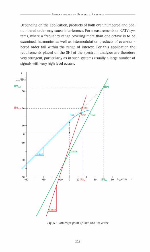
Depending on the application, products of both even-numbered and odd-
numbered order may cause interference. For measurements on CATV sys-
tems, where a frequency range covering more than one octave is to be
examined, harmonics as well as intermodulation products of even-num-
bered order fall within the range of interest. For this application the
requirements placed on the SHI of the spectrum analyzer are therefore
very stringent, particularly as in such systems usually a large number of
signals with very high level occurs.
Fig. 5-8 Intercept point of 2nd and 3rd order
Fundamentals of Spectrum Analysis
112
Lout/dBm
Lin/dBm–50 –30 –10 0 10 30 50–50
–30
–10
0
10
30
50
Lout
1dB/dB
IP2inIP3in
IP3out
IP2out
3 dB/dB
2 dB/dB
LIM2LIM3
IP2
IP3
g
R&S_Pappband_Spektrumanal 24.10.2001 17:42 Uhr Seite 112
Practical Realization of an Analyzer
113
For harmonics of higher order, a level variation of the two sinusoidal car-
riers at the input by ∆ dB causes a level variation of the respective inter-
modulation product by n · ∆ dB. The level differences between intermodu-
lation products and the fundamentals of the sinusoidal carriers must
therefore always be specified together with the input level since otherwise
no conclusion can be drawn as to the linearity. It is therefore advanta-
geous to calculate the intercept point of nth order too. The intercept point
of nth order referred to the input is given by:
IPnin = + Lin (Equation 5-16)
where IPnin = input intercept point of nth order, in dBm
aIMn = level difference between intermodulation product of
nth order and fundamental of the input signal, in dB
Lin = level of one of the two input signals, in dBm
In most cases, the intercept points of 2nd and 3rd order are specified (Fig.
5-8). They are designated as IP2 or SOI (second order intercept) and IP3 or
TOI (third order intercept). The input intercept points of 2nd and 3rd order
are given by
IP2in = aIM2 + Lin (Equation 5-17)
and
IP3in = + Lin (Equation 5-18)
The output intercept points can be calculated from the input intercept
points by adding the gain g of the network (in dB). In spectrum analyzer
specifications the intercept points are referred to the input.
The 2nd order intermodulation products with two-tone input as well as the
2nd harmonics with single-tone input are produced due to the square term
of the nonlinear transfer function. There is a fixed relationship between
IP2 and SHI (see [5-1]):
SHI = IP2 + 6 dB (Equation 5-19)
Performance Features of Spectrum Analyzers
aIMn
n – 1
aIM3
2
R&S_Pappband_Spektrumanal 24.10.2001 17:42 Uhr Seite 113
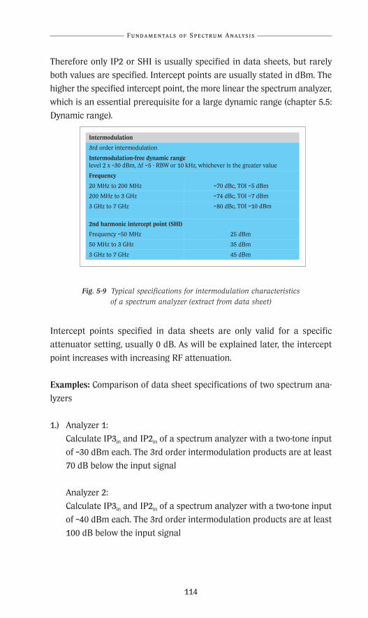
Therefore only IP2 or SHI is usually specified in data sheets, but rarely
both values are specified. Intercept points are usually stated in dBm. The
higher the specified intercept point, the more linear the spectrum analyzer,
which is an essential prerequisite for a large dynamic range (chapter 5.5:
Dynamic range).
Fig. 5-9 Typical specifications for intermodulation characteristics
of a spectrum analyzer (extract from data sheet)
Intercept points specified in data sheets are only valid for a specific
attenuator setting, usually 0 dB. As will be explained later, the intercept
point increases with increasing RF attenuation.
Examples: Comparison of data sheet specifications of two spectrum ana-
lyzers
1.) Analyzer 1:
Calculate IP3in and IP2in of a spectrum analyzer with a two-tone input
of –30 dBm each. The 3rd order intermodulation products are at least
70 dB below the input signal
Analyzer 2:
Calculate IP3in and IP2in of a spectrum analyzer with a two-tone input
of –40 dBm each. The 3rd order intermodulation products are at least
100 dB below the input signal
Fundamentals of Spectrum Analysis
114
Intermodulation
3rd order intermodulation
Intermodulation-free dynamic rangelevel 2 x –30 dBm, ∆f >5 · RBW or 10 kHz, whichever is the greater value
Frequency
20 MHz to 200 MHz >70 dBc, TOI >5 dBm
200 MHz to 3 GHz >74 dBc, TOI >7 dBm
3 GHz to 7 GHz >80 dBc, TOI >
10 dBm
2nd harmonic intercept point (SHI)
Frequency <50 MHz 25 dBm
50 MHz to 3 GHz 35 dBm
3 GHz to 7 GHz 45 dBm
R&S_Pappband_Spektrumanal 24.10.2001 17:42 Uhr Seite 114

Practical Realization of an Analyzer
115
Solution
Analyzer 1: IP3in = + (–30 dBm) = +5 dBm
Analyzer 2: IP3in = + (–40 dBm) = +10 dBm
2.) Analyzer 1
With two-tone input of –30 dBm each the 2nd order intermodulation
products are at least 65 dB below the input signal.
Analyzer 2
An SHI of +35 dBm is specified in the data sheet.
Solution
Analyzer 1: IP2in = 65 dB + (–30 dBm) = +35 dBm
Analyzer 2: IP2in = IPk2 – 6 dB = 35 dBm – 6 dB = +29 dBm
Often the intermodulation-free dynamic range is specified in the data
sheets. This is understood as the level difference between IM products and
input signals. Unless otherwise stated, these data solely refer to 3rd order
intermodulation products (products occurring in the vicinity of the input
signals). An essential parameter is the signal level at the input of the first
mixer which always has to be specified, too.
For the 3rd order intercept point specified in Fig. 5-9 (for the input fre-
quency range 200 MHz to 3 GHz in our example), the intermodulation-free
range can be calculated from IP3in by using Equation 5-18:
aIM3 = 2 · (IP3in – Lin) = 2 · (7 dBm – (–30 dBm)) = 74 dB (Equation 5-20)
Attenuator pad or amplifier ahead of first mixer
If a preamplifier or attenuator pad is connected ahead of the first mixer of
the spectrum analyzer, the total input intercept point of the arrangement
is affected. The following applies to two cascaded stages [5-2]:
Performance Features of Spectrum Analyzers
70 dB
2
100 dB
2
R&S_Pappband_Spektrumanal 24.10.2001 17:42 Uhr Seite 115
IP3in,total = IP3in,1 + IP3in,2 – 10 · log 10 + 10 (Equation 5-21)
where IP3in,total = 3rd order input intercept point of cascaded
stages, in dBm
IP3in,1, IP3in,2 = 3rd order input intercept points of individual
stages, in dBm
g1 = gain factor of first stage, in dB
Assuming an ideal linear attenuator pad – a prerequisite that is realisti-
cally implemented using resistive, mechanically switched attenuators – al-
most any value can be inserted into Equation 5-21 for IP3in,1. An increase
of the RF attenuation, for instance, from 0 dB to 10 dB (g = –10 dB in Equa-
tion 5-21) causes an increase of the intercept point by the same amount
(10 dB in our case). At the same time, the noise figure of the analyzer is
degraded to the same degree. Therefore, an increase of the RF attenuation
does not increase the dynamic range (chapter 5.5: Dynamic range).
If a preamplifier is connected ahead of the analyzer, this will cause a de-
grading of the total intercept point.
Example:
An input intercept point of +7 dBm is specified for the spectrum analyzer.
To increase the sensitivity, a preamplifier with a gain factor of 20 dB and
an input intercept point of –10 dBm is to be connected. The total 3rd order
input intercept point is then given by
IP3in,total = – 10 dBm + 7 dBm – 10 · log 10 + 10 = –14.8 dBm
Fundamentals of Spectrum Analysis
116
( )( ) ( )IP3in,1 + g1
10
IP3in,2
10
( )( ) ( )–10 dBm + 20 dB
10
7 dBm
10
R&S_Pappband_Spektrumanal 24.10.2001 17:42 Uhr Seite 116
Practical Realization of an Analyzer
117
Identification of intermodulation products
A typical application of the spectrum analyzer is distortion mea-
surement on devices under test such as amplifiers or mixers. Dis-
tortion in the form of higher-order harmonics or intermodulation
products is not only produced in the DUT but also in the spectrum
analyzer. Especially with high signal levels at the input of the first
mixer this may lead to incorrect measurements since the har-
monics or intermodulation products generated in the spectrum
analyzer are added to those produced in the DUT. Linearity mea-
surement would indicate poorer characteristics than it is actually
the case.
The spectrum analyzer's mixer and IF amplifier primarily de-
termine the linearity of a spectrum analyzer, whereas the input RF
attenuator has practically no effect. If the RF attenuator is used to
vary the mixer level, the levels of intermodulation products gen-
erated in the spectrum analyzer are determined according to their
order. The level of intermodulation products generated in the DUT
remain constant.
With the aid of the RF attenuator, it can thus be determined
where the intermodulation products displayed on the spectrum
analyzer are generated. The measurement yields correct results if
the relative levels of harmonics or intermodulation products re-
main constant despite an increase of the RF attenuation (Fig. 5-10a).
If the relative level of the harmonics displayed on the spectrum
analyzer varies however, the measurement result is incorrect.
(continued overleaf)
Performance Features of Spectrum Analyzers
R&S_Pappband_Spektrumanal 24.10.2001 17:42 Uhr Seite 117
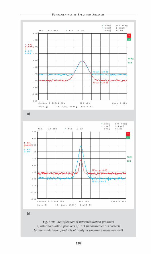
Fundamentals of Spectrum Analysis
118
D a t e : 1 2 . A u g . 1 9 9 9 1 0 : 4 3 : 0 6
C e n t e r 2 . 0 2 0 0 4 G H z 5 0 0 k H z S p a n 5 M H z
P R N
E X T
- 1 0
- 2 0
- 3 0
- 4 0
- 5 0
- 6 0
- 7 0
- 8 0
- 9 0
- 1 0 0
- 1 1 0
R e f - 1 0 d B m
* R B W 3 0 0 k H z
* V B W 3 k H z
S W T 1 5 m s
*
A
RF Att = 20 dB
* A t t 2 0 d B
1 A P C L R W R 2 A P V I E W
RF Att = 30 dB
D a t e : 1 2 . A u g . 1 9 9 9 1 0 : 5 5 : 0 3
C e n t e r 2 . 0 2 0 0 4 G H z 5 0 0 k H z S p a n 5 M H z
P R N
E X T
- 3 0
- 4 0
- 5 0
- 6 0
- 7 0
- 8 0
- 9 0
- 1 0 0
- 1 1 0
- 1 2 0
- 1 3 0
R e f - 3 0 d B m
* R B W 1 0 0 k H z
* V B W 3 k H z
S W T 4 5 m s
*
A
RF Att = 10 dB
* A t t 1 0 d B
1 A P C L R W R 2 A P V I E W
RF Att = 0 dB
a)
b)
Fig. 5-10 Identification of intermodulation productsa) intermodulation products of DUT (measurement is correct)
b) intermodulation products of analyzer (incorrect measurement)
R&S_Pappband_Spektrumanal 24.10.2001 17:42 Uhr Seite 118
Practical Realization of an Analyzer
119
5.3 Phase noise (spectral purity)
Phase noise is a measure for the short-time stability of oscillators. Phase
noise is caused by variations of phase or frequency and amplitude of an
oscillator output signal, although the amplitude effect is negligible in most
cases. These variations have a modulating effect on the oscillator signal.
Phase noise is usually specified as single-sideband phase noise re-
ferred to the carrier level and as a function of the carrier offset. The spec-
ified values are stated as relative noise levels within a bandwidth of 1 Hz.
Accordingly, the units are dBc (1 Hz) or dBc/Hz, where c is referred to the
carrier. Since the phase noise level is lower than the carrier level, negative
numeric values will be specified.
The effects of phase noise are shown in Fig. 5-11. Assuming a suffi-
ciently high resolution, one would expect a single spectral line for a pure-
ly sinusoidal signal in the frequency domain. In fact, the spectrum of a sig-
nal generated by a real oscillator is wider than a single line.
An oscillator signal exhibits phase noise that may be more or less distinct.
By choosing appropriate circuit configurations, phase noise can be mini-
mized to a certain degree but never be fully eliminated. In modern spec-
trum analyzers the local oscillators are implemented as synthesizers
locked to a high-precision reference (such as 10 MHz) via phase-locked
loops (PLL) as described in [5-3]. The phase noise characteristic will be in-
fluenced by the PLL bandwidth of the frequency locking circuitry. The spec-
trum is divided into the following subranges (see Fig. 5-11):
• Close to carrier (offset approximately up to 1 kHz):
In this range the phase noise corresponds to the phase noise of the ref-
erence signal referred to the output signal of the local oscillator. Due to
the multiplying effect in the PLL this phase noise is higher than that of
the reference oscillator.
Performance Features of Spectrum Analyzers
R&S_Pappband_Spektrumanal 24.10.2001 17:42 Uhr Seite 119

• Range extending to the upper limit of the PLL bandwidth (offset greater
than 1 kHz)
Within the PLL bandwidth, the phase noise corresponds to the additive
noise of several PLL components, such as divider, phase detector and of
the multiplied reference signal. The upper limit of this range depends on
the spectrum analyzer, or more precisely on the type of oscillator used. It
is typically in the range between 100 kHz and 300 kHz.
• Range outside the PLL bandwidth
Outside the PLL bandwidth, the phase noise is practically exclusively
determined by the phase noise of the oscillator in non-synchronized
mode. In this range it decreases by 20 dB per decade.
Fig. 5-11 Phase noise of OCXO, VCO and of VCO locked to OCXO at different PLL bandwidths
Fig. 5-11 shows the phase noise at different PLL bandwidths. It is of par-
ticular interest to compare the phase noise of a free-running oscillator
with the phase noise of an oscillator locked to a reference oscillator at
different PLL bandwidths. The following cases have to be considered:
Fundamentals of Spectrum Analysis
120
L
f
Free-runningoscillator (VCO)
Phase noise of reference oscillatorreferred to output frequency f0(OCXO)
narrow PLL bandwidth
medium PLL bandwidth
wide PLL bandwidth
f0
31 2
VCO locked to OCXO:
R&S_Pappband_Spektrumanal 24.10.2001 17:42 Uhr Seite 120

Practical Realization of an Analyzer
121
• Wide PLL bandwidth
The loop gain of the PLL is so high that the oscillator noise is reduced to
the reference oscillator noise. Due to the phase rotation of the filter
circuit, the phase noise is increased far from the carrier.
• Medium PLL bandwidth
The loop gain is not sufficient to attain the reference oscillator noise
close to the carrier. The increase of the phase noise far from the carrier
is, however, much smaller than with a wide PLL bandwidth.
• Narrow PLL bandwidth
The phase noise far from the carrier is not degraded compared to the
free-running oscillator. Close to the carrier it is, however, considerably
higher than that with medium and wide PLL bandwidth.
To optimize the phase noise for the specific application, the PLL band-
width should be variable.
Fig. 5-12 Internal phase noise transferred onto input signalby reciprocal mixing
Performance Features of Spectrum Analyzers
AA
f ffin,1 fin,2 fIF
A
ffLO
LO
IFInput
Input signal
LO signal
IF signal
R&S_Pappband_Spektrumanal 24.10.2001 17:42 Uhr Seite 121
The LO phase noise of a spectrum analyzer is transferred onto the input
signal by reciprocal mixing in the conversion stages (Fig. 5-12). This means
that even with an ideal sinusoidal input signal, the displayed spectrum will
reflect the combined phase noise of all LOs. If the input signal also exhibits
phase noise (which in practice is always the case), the trace displayed on
the spectrum analyzer corresponds to the combined phase noise of the in-
put signal and LOs.
The displayed phase noise is always referred to the carrier of the in-
put signal irrespective of the input signal level. This means that for phase
noise measurements on input signals (chapter 6.1: Phase noise measure-
ments) the dynamic range for close-to-carrier measurements cannot be
maximized by increasing the input signal level – which is in sharp contrast
to the effect of thermal noise.
In particular with measurements close to the carrier, the phase noise
of the spectrum analyzers therefore marks the limit of the measurement
range.
Apart from this restriction, the resolution and the dynamic range of
the analyzer will also be limited by the phase noise. Signals with little off-
set from the carrier of a signal with much higher levels may not be de-
tectable (Fig. 5-12).
Example:
A sinusoidal signal with a level of –10 dBm is present at the input of a
spectrum analyzer. At a carrier offset of 100 kHz the phase noise of the
spectrum analyzer is assumed to be –100 dBc (1 Hz).
What level must a second signal at the same offset of 100 kHz have to
be detectable at a resolution bandwidth of 1 kHz (in our example the res-
olution bandwidth is assumed to correspond to the noise bandwidth of the
filter)?
Solution:
Due to the resolution bandwidth of 1 kHz the phase noise produces a dis-
played noise level LN of
LN = –100 dBc (1 Hz) + 10 · log = –70 dBc (1 kHz)
Fundamentals of Spectrum Analysis
122
1 kHz
1 Hz( )
R&S_Pappband_Spektrumanal 24.10.2001 17:42 Uhr Seite 122
Practical Realization of an Analyzer
123
This means that the input signal must have at least a level LS,min of LS,min =
–10 dBm – 70 dBc (1 Hz) = –80 dBm in order to be detectable following a
noise increase by 3 dB.
This limited resolution has also an adverse effect on adjacent-channel
power measurements (chapter 6.3: Channel and adjacent-channel power
measurement) since dynamic range is reduced by phase noise occurring in
the adjacent channel.
Data sheets often specify residual frequency modulation (residual FM).
From the carrier-offset-dependent phase noise, the RMS value of the resid-
ual FM can be calculated by integration as follows:
∆FRMS = 2 · ∫ 10 · foff dfoff (Equation 5-22)
where ∆FRMS = RMS value of residual FM, in Hz
foff = frequency offset from carrier, in Hz
L(foff) = phase noise as a function of carrier offset, in dBc (1 Hz)
Similarly, the RMS value of the residual phase modulation (residual ϕM)
can be calculated from the phase noise:
∆ϕ RMS = 2 · ∫ 10 dfoff , in rad (Equation 5-23)
∆ϕ RMS = 2 · ∫ 10 dfoff · , in deg (Equation 5-24)
where ∆ϕRMS = RMS value of residual ϕM, in Hz
foff = frequency offset from carrier, in Hz
L(foff) = phase noise as a function of carrier offset, in dBc(1 Hz)
High residual FM of the LO signal may produce a smearing effect of the
displayed spectrum. This leads to a reduction of the resolution and thus
determines the lower limit for the useful smallest resolution bandwidth.
Since in modern spectrum analyzers the local oscillators are implemented
as synthesizers as described above, this effect is practically of no rele-
vance.
Performance Features of Spectrum Analyzers
√ ∞
fOff = 0
180
π
L(foff)
20
√ ∞
fOff = 0
L(foff)
10
√ ∞
fOff = 0
L(foff)
10
2
( )
R&S_Pappband_Spektrumanal 24.10.2001 17:42 Uhr Seite 123

Fig. 5-13 Typical specifications for phase noise and residual FM FM of a spectrum analyzer (extract from data sheet)
In view of the above restrictions, phase noise is an essential criterion for
evaluating a spectrum analyzer. Depending on the application, phase noise
may be important for the user both in the case of small offsets (such as
measurements on radar systems) and large offsets (such as measurements
on mobile radio equipment). Data sheets therefore always provide specifi-
cations at different offsets, usually in decade steps (see Fig. 5-13).
As shown above, phase noise is largely influenced by the PLL band-
width. In spectrum analyzers, the PLL bandwidth is usually variable to al-
low adaptation to the specific measurement task. Switchover is often im-
plicit, as is illustrated with the analyzer described in our example. The PLL
bandwidth is coupled to the frequency range to be displayed or to the se-
lected resolution bandwidth. Especially if large frequency ranges are to be
displayed (span >100 kHz, in our example), the minimum phase noise far
from the carrier is usually of interest. Therefore a narrow PLL bandwidth
is automatically selected for this setting.
Fundamentals of Spectrum Analysis
124
Spectral purity (dBc (1 Hz))SSB phase noise, f = 500 MHz
Carrier offset
100 Hz <–90. typ. –94
1 kHz <–100. typ. –108
10 kHz <–106. typ. –113
100 kHz 1) <–110. typ. –113
1 MHz 1) <–120. typ. –125
10 MHz typ . –145
Residual FM(f = 500 MHz, RBW = 1 kHz ,sweep time 100 ms) typ. 3 Hz
1) Valid for span >100 kHz.
Typical values for SSB phase noise
Carrier offset fin = 500 MHz fin = 3 GHz fin = 7 GHz
100 Hz 94 dBc/Hz 90 dBc/Hz 84 dBc/Hz
1 kHz 105 dBc/Hz 100 dBc/Hz 94 dBc/Hz
10 kHz 113 dBc/Hz 108 dBc/Hz 104 dBc/Hz
100 kHz 113 dBc/Hz 108 dBc/Hz 106 dBc/Hz
1 MHz 125 dBc/Hz 118 dBc/Hz 118 dBc/Hz
R&S_Pappband_Spektrumanal 24.10.2001 17:42 Uhr Seite 124

Practical Realization of an Analyzer
125
To better define parameter dependencies, resolution bandwidths and span
settings are often stated in data sheets in addition to the phase noise at
the various carrier offsets. Settings other than those specified may result
in poorer phase noise values.
For analyzing input signals of very high frequency, the LO signal must be
multiplied (chapter 4.1). Just as it is found in a frequency-modulated sig-
nal, the frequency deviation is multiplied, thus causing degrading of the
phase noise. The following applies:
Lmult (foff) = L(foff) + 20 · log(n) (Equation 5-25)
where Lmult(foff) = phase noise after multiplication as a function of car-
rier offset, in dBc (1 Hz)
L(foff) = phase noise of original signal as a function of carri-
er offset, in dBc (1 Hz)
n = multiplying factor
Due to this degradation, phase noise specifications are always referred to
a specific signal frequency. Typical phase noise curves are often given for
several signal frequencies, allowing an estimation of the expected phase
noise in the frequency range of interest.
5.4 1 dB compression point and maximum input level
The 1 dB compression point of a network marks the point in its dynamic
range at which the gain is reduced by 1 dB due to saturation (Fig. 5-14).
Similar to the intercept point, the 1 dB compression point can be referred
to the input or to the output level. For power amplifiers, the output level at
which the 1 dB compression occurs is usually given, and the input level is
specified for spectrum analyzers.
Performance Features of Spectrum Analyzers
R&S_Pappband_Spektrumanal 24.10.2001 17:42 Uhr Seite 125
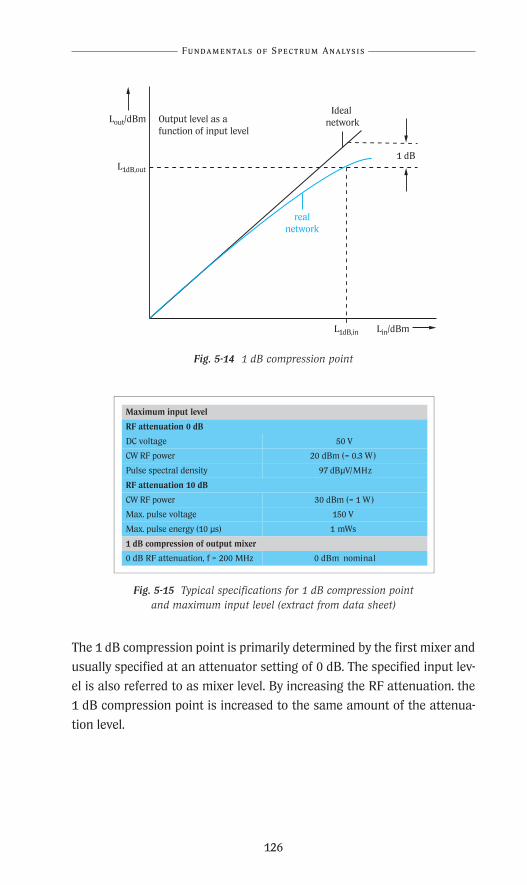
Fig. 5-14 1 dB compression point
Fig. 5-15 Typical specifications for 1 dB compression point and maximum input level (extract from data sheet)
The 1 dB compression point is primarily determined by the first mixer and
usually specified at an attenuator setting of 0 dB. The specified input lev-
el is also referred to as mixer level. By increasing the RF attenuation. the
1 dB compression point is increased to the same amount of the attenua-
tion level.
Fundamentals of Spectrum Analysis
126
Lout/dBm
Lin/dBm
1 dB
L1dB,in
L1dB,out
Ideal network
realnetwork
Output level as afunction of input level
Maximum input level
RF attenuation 0 dB
DC voltage 50 V
CW RF power 20 dBm (= 0.3 W )
Pulse spectral density 97 dBµV/MHz
RF attenuation 10 dB
CW RF power 30 dBm (= 1 W )
Max. pulse voltage 150 V
Max. pulse energy (10 µs) 1 mWs
1 dB compression of output mixer
0 dB RF attenuation, f > 200 MHz 0 dBm nominal
R&S_Pappband_Spektrumanal 24.10.2001 17:42 Uhr Seite 126
Practical Realization of an Analyzer
127
To avoid unwanted products due to distortion, the maximum input level
(reference level) to be displayed should be kept clearly below the 1 dB com-
pression point.
Due to the coupling of reference level and attenuator setting (chapter
4.6: Parameter dependencies), the maximum reference level is limited (in
our example to –10 dBm) with an RF attenuation of 0 dB. The 1 dB com-
pression point cannot be measured directly. Nevertheless, it is an impor-
tant criterion in many measurements.
For example, when making phase noise measurements a single sinu-
soidal signal is applied to the spectrum analyzer input. Even when driving
the spectrum analyzer close to its 1 dB compression point, no intermodu-
lation products will be generated that would appear in the vicinity of the
input signal. Given the wide dynamic range, only harmonics of the input
signal will be produced in the spectrum analyzer, which usually do not de-
grade phase noise measurements. The wide dynamic range makes for a
large signal-to-noise ratio so that the maximum dynamic range at large
carrier offsets is obtained for measurements.
In contrast to the 1 dB compression point, which provides information
about the overdrive capacity of the spectrum analyzer, the maximum input
level denotes the upper limit for damage-free operation. To avoid damage
to the analyzer, this value should not be exceeded.
The limit value is usually determined by the first critical component in
the signal processing chain. Accordingly, the selected RF attenuation has
always to be taken into account:
• RF attenuation 0 dB
The attenuator is not loaded in this case and the input signal is not atten-
uated. Therefore the first mixer is usually decisive for the maximum input
level. Due to the generally high load capacity of diplexer and tracking band-
pass filter, the same holds true for the high-frequency input section (above
3 GHz in our example).
• RF attenuation >0 dB (≥10 dB in our example)
The input signal is attenuated by the attenuator so that the subsequent
stages can usually be ignored. The specified value reflects the load ca-
pacity of the attenuator.
Performance Features of Spectrum Analyzers
R&S_Pappband_Spektrumanal 24.10.2001 17:42 Uhr Seite 127

Both of the above cases are important for practical operation, so they are
specified separately in data sheets.
Further distinction is made as to the type of the input signal (Fig. 5-15):
DC voltage
For DC-coupled spectrum analyzers this value corresponds to the maxi-
mum mixer-compatible DC voltage. Usually a value of 0 V is specified irre-
spective of the RF attenuation.
For AC-coupled spectrum analyzers the specified value corresponds to
the dielectric strength of the coupling capacitor at the spectrum analyzer
input. In the above data sheet extract a value of 50 V is specified.
Continuous wave (CW) RF power
This value specifies the maximum total power of all input signals that is
permissible without any time limit. It is assumed that all input signals are
stationary.
Pulse spectral density
Pulsed signals feature a very wide spectrum with many spectral compo-
nents whose sum power should not exceed a specific value. For pulse spec-
tra, a spectral density is usually specified as the voltage level referred to a
specific bandwidth, typically 1 MHz. In the above data sheet extract (Fig.
5-15), 97 dBµV/MHz is specified as the limit value.
Maximum pulse energy and maximum pulse voltage
With extremely short pulses, the pulse power may exceed the value speci-
fied for the CW RF power for long intervals of time. There is a limiting
threshold set by the maximum pulse energy, in our example specified in
mWs for a certain pulse period, as well as by the maximum pulse voltage.
Often the maximum pulse power is specified which can be calculated
from the pulse energy and pulse period as follows:
Fundamentals of Spectrum Analysis
128
R&S_Pappband_Spektrumanal 24.10.2001 17:42 Uhr Seite 128

Practical Realization of an Analyzer
129
PP = and EP = PP · tP (Equation 5-26)
where PP = pulse power, in W
EP = pulse energy, in Ws
tP = pulse period, in s
With the values specified in the data sheet extract in Fig. 5-15 (EP = 1 mWs,
tP = 10 µs) a maximum pulse power of 100 W is obtained.
Fig. 5-16 Pulses with different pulse width but equal pulse energy
For constant pulse energy EP, the permissible pulse power is even higher
for a short pulse period according to Equation 5-26 (Fig. 5-16).
By decreasing the pulse period, the pulse power may not be increased
arbitrarily since the maximum permissible pulse voltage must not be ex-
ceeded. In the cited specifications, a value of 150 V is stipulated. For the
rectangular pulse as shown in Fig. 5-16, the permissible peak voltage
yields a maximum pulse power of
PP = = = 450 W (Equation 5-27)
where ÛP = pulse peak voltage, in V
R = input impedance of spectrum analyzer, in Ω
Performance Features of Spectrum Analyzers
Û2P
R
(150 V)2
50 Ω
EP,2
PP
tP
EP,1 EP,1=EP,2
tP,2tP,1
PP,2
PP,1
EP
tP
R&S_Pappband_Spektrumanal 24.10.2001 17:42 Uhr Seite 129

This maximum pulse power, as well as the maximum permissible pulse
energy (1 mWs in our example), should not be exceeded under any cir-
cumstances. Equation 5-26 can be used to calculate the maximum pulse
period for a pulse of maximum pulse power, which in our example is
2.2 µs.
For longer pulse periods and constant pulse energy, the pulse power
has to be reduced. The relationship shown in Fig. 5-17 is then obtained
(valid for the specifications given in Fig. 5-15).
Fig. 5-17 Maximum pulse power as a function of pulse period(for max. pulse voltage of 150 V and max. pulse energy of 1 mWs)
5.5 Dynamic range
The dynamic range provides information about the analyzer’s capability to
simultaneously process signals with very different levels. The limits of the
dynamic range depend on the measurement to be performed. The lower
limit is determined by the inherent noise or phase noise. The upper limit
is set either by the 1 dB compression point or by distortion products oc-
curring in the analyzer in the case of overdriving. The dynamic range can
be defined in different ways. It should not be confused with the display
range.
Fundamentals of Spectrum Analysis
130
1
10
100
1000
0,1 1 10 100 1000
Pulse period tP / µs
Max
. pu
lse
pow
er P
p /
W
R&S_Pappband_Spektrumanal 24.10.2001 17:42 Uhr Seite 130

Practical Realization of an Analyzer
131
Fig. 5-18 Comparison of level display range, maximum dynamic rangeand max. intermodulation-free range
Level display range
The dynamic range does not correspond to the level display range which
is also specified in data sheets. The display range is the range from the
displayed average noise level to the maximum input level (Fig. 5-18). For
displaying a signal with a level corresponding to the maximum input level
of the analyzer, an RF attenuation greater than 0 dB is usually selected,
which means that the minimum displayed noise (the lower limit of the
specified level display range) will not be attained.
Maximum dynamic range
A maximum dynamic range is often specified which is limited by the
displayed noise (usually at the smallest resolution bandwidth) and the 1 dB
compression point (Fig. 5-18). If, however, an input signal at the first
mixer reaches the mixer’s 1 dB compression point, there will be very high
levels of the distortion products generated due to nonlinearities of the mixer.
Performance Features of Spectrum Analyzers
Max. input level
1 dB compression of 1st mixer
Optimum mixer level
Max. intermodulation-free range /max. harmonic supression
Max. dynamic range
Level display range
Displayed overrange noise level with selected resolution bandwidth
R&S_Pappband_Spektrumanal 24.10.2001 17:42 Uhr Seite 131
Using sufficiently small bandwidth, the distortion products can become
visible in the displayed spectrum (they are not covered up by the inherent
noise). The spectrum display is then no longer unambiguous.
In modern spectrum analyzers, the reference level selectable for a giv-
en RF attenuation is therefore limited even with manual decoupled atten-
uator setting. Signals attaining the 1 dB compression point at the mixer in-
put considerably exceed the reference level.
The value stated for the maximum dynamic range is therefore of lim-
ited significance and only relevant for certain applications, such as phase
noise measurements far from the carrier.
Maximum intermodulation-free range for maximum harmonic suppres-
sion
A compromise has to be found in the selection of the mixer level. If the RF
attenuation is high, so that the mixer level is low, the levels of the distor-
tion and intermodulation products generated in the analyzer are also low,
but at the same time the signal-to-noise ratio of the input signal is small.
In this case the dynamic range is limited at the lower end by the inherent
noise. If, on the other hand, the mixer level is high, then distortion and
intermodulation products are generated whose levels exceed the inherent
noise level and therefore become visible (Fig. 4-31). In practice, it is impor-
tant to have a level display range in which the displayed spectrum is free
from such products. Depending on whether intermodulation products or
harmonics of higher order limit this range, one speaks of an intermodula-
tion-free range or maximum harmonic suppression. Both parameters
depend on the mixer level and the selected resolution bandwidth. A maxi-
mum is attained if the levels of the intermodulation products or harmon-
ics of higher order are equal to the noise level. The ideal mixer level re-
quired for this purpose can either be calculated or graphically determined.
For elucidation the graphical method is described first.
Fundamentals of Spectrum Analysis
132
R&S_Pappband_Spektrumanal 24.10.2001 17:42 Uhr Seite 132

Practical Realization of an Analyzer
133
Fig. 5-19 Intermodulation-free range and maximum harmonic suppression as a function of mixer level (NF = 24.5 dB, IP3in = 7 dBm, SHIin = 40 dBm)
For a given noise bandwidth of the IF filter and noise figure of the spec-
trum analyzer, the noise power level is to be calculated relative to the mix-
er level using the following:
LN,rel = LR – Lmix = –174 dBm + 10 · log(BN,IF) + NF – Lmix (Equation 5-28)
where LN,rel = relative noise level referred to mixer level, in dB
Lmix = mixer level, in dBm
LN = noise level, in dBm
BN,IF = noise bandwidth of resolution filter, in Hz
NF = noise figure of spectrum analyzer, in dB
When using a sample detector and averaging by a narrowband video filter,
a further 2.5 dB is to be subtracted from the calculated value LN,rel due to
underweighting of the noise. The relative noise level is plotted in Fig. 5-19
for different resolution filters versus the mixer level. A noise figure of 24.5
dB is assumed in this example. It is shown that the relative noise level de-
creases with increasing mixer level.
Performance Features of Spectrum Analyzers
–120
–110
–100
–90
–80
–70
–60
–50
–40
–70 –60 –50 –40 –30 –20 –10 0
Mixer level / dBm
LN
,rel
, Lk2
,rel
, LIM
3,re
l / d
B
40
50
60
70
80
90
100
110
120
Inte
rmod
ula
tion
-fre
e or
dis
tort
ion
-fre
edy
nam
ic r
ange
/ dB
LN,rel (BN=10 Hz)
LN,rel (BN=1 Hz)
LN,rel (BR=1 kHz)
LIM3,rel Lk2,rel
Lmix,opt
R&S_Pappband_Spektrumanal 24.10.2001 17:42 Uhr Seite 133

The following relationship can be derived from Equation 5-16 for the rela-
tive level of nth order intermodulation products referred to the mixer level:
LIMn,rel = – (n – 1) · (IPnin – Lmix ) (Equation 5-29)
where LIMn,rel = relative level of nth order intermodulation products
referred to mixer level, in dB
IPnin = input intercept point of nth order of spectrum ana-
lyzer (RF attenuation 0 dB),
Lmix = mixer level, in dBm
Usually the 3rd order intermodulation products are the most disturbing
ones in practice since they occur in the immediate vicinity of the input sig-
nals. The relative level of such products is given by:
LIM3,rel = –2 · (IP3in – Lmix ) (Equation 5-30)
Likewise, the relative level of 2nd order distortion products (2nd order har-
monics) can be derived from Equation 5-13:
Lk2,rel = – (SHIin – Lmix ) (Equation 5-31)
where Lk2,rel = relative level of 2nd order distortion products
referred to mixer level, in dB
SHIin = input second harmonic intercept of spectrum ana-
lyzer, in dBm
Since the distortion and intermodulation products are always calculated
from the mixer level, the results are independent of the RF attenuation
setting. Therefore, the intercept points referred to the input of the first mix-
er have to be substituted for IP3in and SHIin. The values correspond to the
intercept points of the analyzer with a RF attenuation of 0 dB.
The relative level of the 3rd order intermodulation products as well as
of the 2nd harmonics are shown in Fig. 5-19 as a function of the mixer lev-
el. For IP3in, a value of 7 dBm has been assumed. SHIin is 40 dBm.
Fundamentals of Spectrum Analysis
134
R&S_Pappband_Spektrumanal 24.10.2001 17:42 Uhr Seite 134
Practical Realization of an Analyzer
135
Depending on the specific measurement application, 3rd order intermod-
ulation products or harmonics of higher order may limit the dynamic
range. The optimum mixer level for the specific application and hence the
maximum attainable dynamic range is obtained from the point of inter-
section of the noise level line and the line of the 3rd order intermodulation
products or 2nd order harmonics. At this point of intersection, the level of
the intermodulation or distortion products is equal to the noise level, and
the representation is still unambiguous.
In Fig. 5-19, a maximum intermodulation-free range of about 98 dB can
be found at the noise bandwidth of 10 Hz. A mixer level of –42 dBm is
required for this range. If two sinusoidal signals each having a level of
–42 dBm are applied to the spectrum analyzer (RF attenuation 0 dB), the 3rd
intermodulation products will attain a level of –42 dBm – 98 dB = –140 dBm.
The optimum mixer level and the attainable dynamic range can also be
calculated.
With optimum mixer level, the noise level corresponds to the level of the
intermodulation products. Equation 5-28 and Equation 5-29 have to be
equated and solved for Lmix. This yields
Lmix,opt = =
(Equation 5-32)
where Lmix, opt = optimum mixer level, in dBm
IPnin = input intercept point of nth order of spectrum ana-
lyzer (RF attenuation 0 dB), in dB
n = order of intermodulation or distortion products by
which the dynamic range is limited
BN,IF = noise bandwidth of resolution filter, in Hz
NF = noise figure of spectrum analyzer, in dB
For n = 3, that is limitation of the intermodulation-free range by 3rd order
intermodulation products, the following is obtained:
Lmix,opt = =
(Equation 5-33)
The optimum mixer level for maximum harmonic suppression is given by
Performance Features of Spectrum Analyzers
(n – 1) · IPnin + LN,rel
n
2 · IP3in + LN,rel
3
2 · IP3in – 174 dBm + 10 · log(BN,IF) + NF
3
(n – 1) · IPnin – 174 dBm + 10 · log(BN,IF) + NF
n
R&S_Pappband_Spektrumanal 24.10.2001 17:42 Uhr Seite 135
Lmix,opt = = (Equation 5-34)
With optimum mixer level, the dynamic range corresponds to the level dif-
ference between mixer level and nth order intermodulation products or
noise level. The following applies:
DRmax = · (IPnin – LN) = · (IPnin + 174 dBm – 10 · log(BN,IF) – NF)
(Equation 5-35)
where DRmax = maximum dynamic range, in dB
IPnin = input intercept point of nth order of spectrum ana-
lyzer (RF attenuation 0 dB), in dB
n = order of intermodulation or distortion products by
which the dynamic range is limited
BN,IF = noise bandwidth of resolution filter, in Hz
NF = noise figure of spectrum analyzer, in dB
For n = 3, a maximum intermodulation-free range of
DRmax = · (IP3in – LN) = · (IP3in + 174 dBm – 10 · log(BN,IF) – NF)
(Equation 5-36)
or (with n = 2) a maximum harmonic suppression of
DRmax = · (SHIin – LN) = · (SHIin + 174 dBm – 10 · log(BN,IF) – NF)
(Equation 5-37)
can be derived.
Equation 5-35 reveals that both a high intercept point and a low noise fig-
ure are required to obtain a high intermodulation-free range. For fast as-
sessment of the dynamic range of a spectrum analyzer a figure of merit
(FOM) can be used as follows:
FOM = IP3in – NF (Equation 5-38)
Fundamentals of Spectrum Analysis
136
SHIin + LN,rel
2
n – 1
n
2
3
2
3
1
2
1
2
n – 1
n
SHIin – 174 dBm + 10 · log(BN,IF) + NF
2
R&S_Pappband_Spektrumanal 24.10.2001 17:42 Uhr Seite 136

Practical Realization of an Analyzer
137
Modern high-end analyzers attain a figure of merit of 0 dBm with a typi-
cal 3rd order intercept point of 15 dBm and typical noise figure of 15 dB.
The above discussions regarding the dynamic range were with reference
to the signal level at the input of the first mixer. If the signal level at the
spectrum analyzer input is higher than the optimum mixer level, it must
be reduced by an appropriate RF attenuation. The required RF attenuation
can be calculated as follows:
aRF = Lin – Lmix (Equation 5-39)
where aRF = RF attenuation, in dB
Lin = signal level at spectrum analyzer input, in dBm
Lmix = mixer level to be set, in dBm
When setting the mixer level, the attenuator steps are important:
If in the above example the input level is –17 dBm and the attenuator
steps are 10 dB, the signal level can only be reduced to a mixer level of
–37 dBm (with 20 dB RF attenuation) or –47 dBm (with 30 dB RF attenua-
tion). Accordingly, the intermodulation-free range is then 92 dB (Lmix =
–47 dBm) or 88 dB (Lmix = –37 dBm). To utilize the maximum intermodula-
tion-free range, the level can be reduced to –22 dBm by means of an
external 5 dB attenuator. By applying an RF attenuation of 20 dB, the
optimum mixer level of –42 dBm and an intermodulation-free range of
98 dB are obtained again.
For some spectrum analyzers, an attenuator with 1 dB steps is avail-
able. It is then not necessary to use external attenuator pads or an exter-
nal RF attenuator.
Performance Features of Spectrum Analyzers
R&S_Pappband_Spektrumanal 24.10.2001 17:42 Uhr Seite 137

Effects of phase noise on dynamic range
As described in chapter 5.3, the phase noise of the local oscillators of the
spectrum analyzer is transferred onto the input signals by reciprocal mix-
ing. The dynamic range for phase noise measurements on input signals is
therefore limited by the spectrum analyzer phase noise – in particular at
small carrier offsets. The phase noise of the DUT must be higher than that
of the measuring instrument for accurate measurements (chapter 6.1:
Phase noise measurements).
If weak signals in the immediate vicinity of very strong input signals
are to be displayed (such as for measuring the 3rd intercept point of a
DUT), the phase noise of the analyzer needs to be as low as possible.
Otherwise, the weak input signal may be covered up by the phase noise
transferred onto the strong neighboring signal (Fig. 5-12). The phase noise
should be accounted for in such cases in the calculation of the dynamic
range.
Since the phase noise transferred onto the input signal depends on
the signal carrier level, varying the carrier level cannot influence the phase
noise effect. In Fig. 5-20, the phase noise contribution is represented ac-
cordingly as a horizontal line. If the signal frequency is greater than the
carrier offset at which measurements on weak signals are to be performed,
harmonics and 2nd order intermodulation products are insignificant. In
Fig. 5-20, only 3rd order intermodulation products are therefore taken into
account. The phase noise level has to be calculated for the given resolu-
tion bandwidth. The following applies:
LPN,RBW (ƒoff) = L(ƒoff) + 10 · log(BN,IF) (Equation 5-40)
where LPN,RBW(foff)= phase noise as a function of carrier offset within
bandwidth BN, IF, referred to carrier, in dBc
L(foff) = phase noise as a function of carrier offset, in dBc (1 Hz)
BN,IF = noise bandwidth of IF filter, in Hz
foff = carrier offset
Fundamentals of Spectrum Analysis
138
LL
L/d
B
R&S_Pappband_Spektrumanal 24.10.2001 17:42 Uhr Seite 138

Practical Realization of an Analyzer
139
The effects of thermal noise, intermodulation products and phase noise
have to be added linearly.
The sum trace (Lsum) represented in Fig. 5-20 holds true for a phase
noise of –122 dBc (1 Hz), a 3rd order intercept point of 7 dBm and a noise
figure of 24.5 dB. The selected resolution bandwidth of 10 kHz should cor-
respond to the noise bandwidth. Maximum dynamic range is attained at a
mixer level at which the combined trace is at its minimum.
Fig. 5-20 Dynamic range taking into account thermal noise, phase noise and 3rd order intermodulation products
(NF = 24.5 dB, IP3in = 7 dBm, L(foff) = –122 dBc (1Hz), BN,IF = 10 kHz)
Similarly, the dynamic range for adjacent-channel power measurements is
limited by phase noise. Further details on the dynamic range for this type
of measurement can be found in chapter 6.3: Channel and adjacent-chan-
nel power measurements.
For the simple determination of the dynamic range as a function of noise
figure, 3rd order intercept point and phase noise of the spectrum analyzer,
a spreadsheet in MS Excel® 5.0 is available (file DYN_CALC.XLS, Fig. 5-21)
which can be obtained via the R&S Web site (www.rohde-schwarz.com). In
the spreadsheet 2nd order harmonics are taken into account, so that the
Performance Features of Spectrum Analyzers
–120
–110
–100
–90
–80
–70
–60
–50
–40
–70 –60 –50 –40 –30 –20 –10 –0
40
50
60
70
80
90
100
110
120
LPN,RBW
LIM3,rel LN,rel
LSum
Lmix,opt
L N,r
el, L
IM3,
rel,
L PN
,RB
W /
dB
Dyn
amic
ran
ge /
dB
Mixer level / dBm
R&S_Pappband_Spektrumanal 24.10.2001 17:42 Uhr Seite 139
dynamic range can easily be calculated for practically any application. The
spreadsheet consists of two sheets:
• Input & Diagram: Input of noise bandwidth, noise figure, IP3, SHI and
phase noise of the spectrum analyzer (Fig. 5-21a, yel-
low highlighted fields top left). Graphical output of
relative noise level referred to input signal level,
phase noise level as well as relative levels of 2nd
harmonics and 3rd order intermodulation products.
Additionally, the sum of the contributions of ther-
mal noise, phase noise and 3rd order intermodula-
tion products is available.
• Num. Results: Numeric output of results, which are graphically
available on the Input & Diagram sheet.
The phase noise value to be entered depends on the frequency offset from
the strong signal at which a weak signal is to be represented.
Fundamentals of Spectrum Analysis
140
R&S_Pappband_Spektrumanal 24.10.2001 17:42 Uhr Seite 140
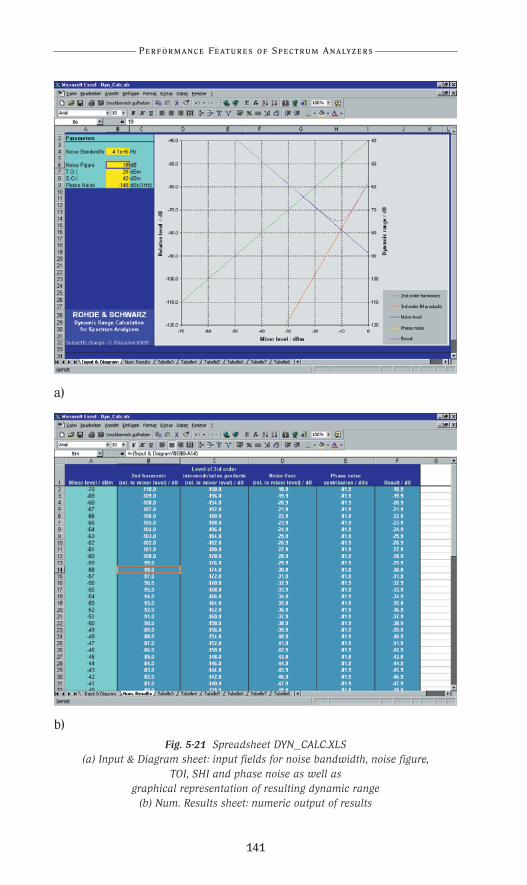
Practical Realization of an Analyzer
141
a)
b)
Fig. 5-21 Spreadsheet DYN_CALC.XLS (a) Input & Diagram sheet: input fields for noise bandwidth, noise figure,
TOI, SHI and phase noise as well as graphical representation of resulting dynamic range
(b) Num. Results sheet: numeric output of results
Performance Features of Spectrum Analyzers
R&S_Pappband_Spektrumanal 24.10.2001 17:42 Uhr Seite 141
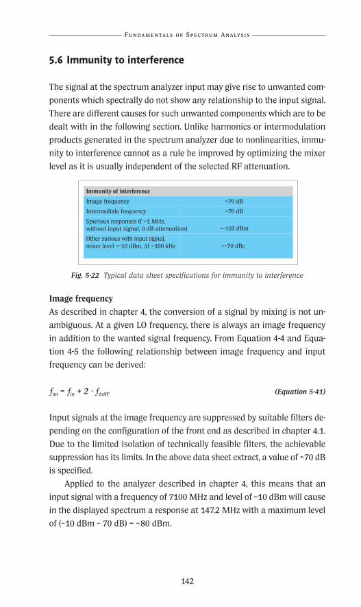
5.6 Immunity to interference
The signal at the spectrum analyzer input may give rise to unwanted com-
ponents which spectrally do not show any relationship to the input signal.
There are different causes for such unwanted components which are to be
dealt with in the following section. Unlike harmonics or intermodulation
products generated in the spectrum analyzer due to nonlinearities, immu-
nity to interference cannot as a rule be improved by optimizing the mixer
level as it is usually independent of the selected RF attenuation.
Fig. 5-22 Typical data sheet specifications for immunity to interference
Image frequency
As described in chapter 4, the conversion of a signal by mixing is not un-
ambiguous. At a given LO frequency, there is always an image frequency
in addition to the wanted signal frequency. From Equation 4-4 and Equa-
tion 4-5 the following relationship between image frequency and input
frequency can be derived:
ƒim = ƒin + 2 · ƒ1stIF (Equation 5-41)
Input signals at the image frequency are suppressed by suitable filters de-
pending on the configuration of the front end as described in chapter 4.1.
Due to the limited isolation of technically feasible filters, the achievable
suppression has its limits. In the above data sheet extract, a value of >70 dB
is specified.
Applied to the analyzer described in chapter 4, this means that an
input signal with a frequency of 7100 MHz and level of –10 dBm will cause
in the displayed spectrum a response at 147.2 MHz with a maximum level
of (–10 dBm – 70 dB) = –80 dBm.
Fundamentals of Spectrum Analysis
142
Immunity of interference
Image frequency >70 dB
Intermediale frequency >70 dB
Spurious responses (f >1 MHz, without input signal, 0 dB attenuation) <–103 dBm
Other surious with input signal, mixer level <–10 dBm, ∆f >100 kHz <–70 dBc
R&S_Pappband_Spektrumanal 24.10.2001 17:42 Uhr Seite 142

Practical Realization of an Analyzer
143
As shown in chapter 4.1, an image frequency also occurs in the second con-
version and has to be suppressed accordingly. For the analyzer described
in our example, the following relationship can be derived for the frequen-
cy the input signal must have to be converted to the image frequency of
the second mixer and to become visible at the frequency fin:
ƒim,2ndIF = ƒin + 2 · ƒ2ndIF (Equation 5-42)
where fim,2ndIF = spurious response due to image frequency at 2nd IF
fin = frequency at which spurious response becomes vis
ible in displayed spectrum
f2ndIF = second intermediate frequency
IF feedthrough or reception at intermediate frequency
Due to the limited isolation between the RF input and IF output of the first
mixer, input signals may be fed through directly (without conversion) to
the IF (chapter 4.1), which is known as the IF feedthrough. If the frequen-
cy of an input signal corresponds to the first IF, the signal will be repro-
duced in the frequency range of the displayed spectrum irrespective of the
LO frequency. Signals with a frequency corresponding to the first IF there-
fore must be suppressed before the first mixer by appropriate filters which
are required for image frequency rejection. The analyzer described here
uses an input lowpass filter (3) for this purpose in the RF input section for
up to 3 GHz and a tracking bandpass filter (20) for the frequency range
above 3 GHz. The signals to be suppressed are at 3476.4 MHz and 404.4 MHz.
In the above data sheet extract, a value of >70 dB is specified for the
immunity to interference at the IF. This means that for an input signal of
3476.4 MHz and –10 dBm, a maximum value of –80 dBm will be displayed
in the frequency range 9 kHz to 3 GHz.
Performance Features of Spectrum Analyzers
R&S_Pappband_Spektrumanal 24.10.2001 17:42 Uhr Seite 143
Spurious responses
Inherent spurious responses
Inherent spurious responses are signals in the displayed spectrum that are
generated in the spectrum analyzer itself. They are caused, for instance, by
clock signals of microprocessors, which may be propagated via supply volt-
age lines and coupled into the analog signal processing circuitry. Distinc-
tion has to be made whether inherent spurious responses are permanent-
ly present or only occur if a signal is present at the input of the spectrum
analyzer. Spurious of local oscillators belong to the latter group. Data
sheet specifications for inherent spurious responses produced by the input
signal are therefore related to the carrier level of the input signal (in dBc).
In the data sheet extract shown in Fig. 5-22, a value of –70 dBc is specified,
and for inherent spurious responses that are independent of the input sig-
nal –103 dBm is given.
Spurious responses
Harmonics of the input signal are produced among others in the first
mixer of the spectrum analyzer. If the input level is sufficiently high, the
harmonics will be displayed. Harmonics of the input signal are converted
to the first intermediate frequency by means of the fundamental and the
harmonics of the LO signal according to Equation 4-1. For input frequen-
cies fin,N, for which Equation 4-1 is fulfilled with m ≥ 1 and n > 1 at a given
IF and LO frequency range, spurious responses are generated.
Example:
A spectrum analyzer for the frequency range of 10 MHz to 5 GHz converts
the input signal to a high first IF of 5.8 GHz with the aid of a LO signal tun-
able from 5.81 GHz to 10.8 GHz. A signal of 3.87 GHz is applied to the an-
alyzer input and displayed at a frequency of 3.87 GHz.
Simultaneously, higher-order harmonics of the signal are produced in
the first mixer of the analyzer. The 3rd harmonic, for instance, is at 11.61
GHz. If the analyzer is tuned to an input frequency of 10 MHz, the LO fre-
quency is 5.81 GHz. The 3rd harmonic of the input signal is thus convert-
ed to the IF:
ƒIF = 3 · ƒin – ƒLO = 3 · 3.87 GHz – 5.81 GHz = 5.80 GHz
Fundamentals of Spectrum Analysis
144
R&S_Pappband_Spektrumanal 24.10.2001 17:42 Uhr Seite 144

Practical Realization of an Analyzer
145
The input signal at 3.87 GHz also causes a spurious response at 10 MHz
in the displayed spectrum.
Such spurious responses are inherent in the concept. To avoid the gener-
ated spurious from disturbing the displayed spectrum, particularly strin-
gent requirements have to be observed for the first mixer of the spectrum
analyzer regarding linearity – specifically intercept point. At the same time,
the mixer level should not be too high, which is a requirement that can be
fulfilled by appropriate setting of the RF attenuation.
5.7 LO feedthrough
In passive mixers as used in spectrum analyzers for the first conversion of
the input signal, the LO signal is coupled into the IF path due to its limited
isolation. The block diagram of the analyzer described (see fold-out page)
shows that if very low-frequency input signals are converted (such as
9 kHz), the frequency of the LO signal (3476.409 MHz, in our example)
corresponds to the first IF. Especially with large resolution bandwidths
(0.5 · BIF > fin) the LO signal coupled into the IF path is therefore only slightly
suppressed by the IF filter. The LO signal is then sent to the detector and
displayed (Fig. 5-23). This effect is referred to as LO feedthrough. Due to the
phase noise of the LO signal, the displayed average noise level close to the
minimum start frequency is increased and as a result the sensitivity in this
frequency range decreased. The LO feedthrough is usually not stated ex-
plicitly in data sheets. It can, however, be recognized from the displayed
noise level specified for the frequency range close to zero.
Performance Features of Spectrum Analyzers
R&S_Pappband_Spektrumanal 24.10.2001 17:42 Uhr Seite 145
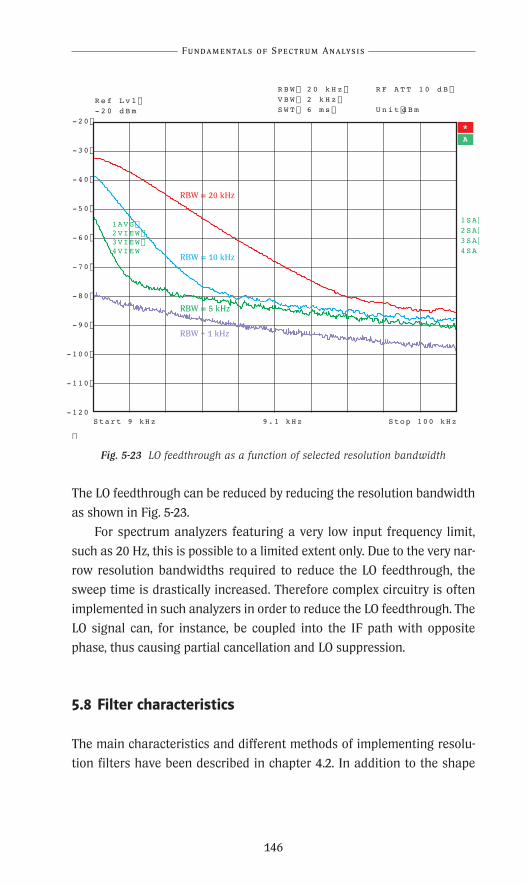
Fig. 5-23 LO feedthrough as a function of selected resolution bandwidth
The LO feedthrough can be reduced by reducing the resolution bandwidth
as shown in Fig. 5-23.
For spectrum analyzers featuring a very low input frequency limit,
such as 20 Hz, this is possible to a limited extent only. Due to the very nar-
row resolution bandwidths required to reduce the LO feedthrough, the
sweep time is drastically increased. Therefore complex circuitry is often
implemented in such analyzers in order to reduce the LO feedthrough. The
LO signal can, for instance, be coupled into the IF path with opposite
phase, thus causing partial cancellation and LO suppression.
5.8 Filter characteristics
The main characteristics and different methods of implementing resolu-
tion filters have been described in chapter 4.2. In addition to the shape
Fundamentals of Spectrum Analysis
146
S tart 9 kHz 9.1 kHz Stop 100 kHz
1SA
2SA
3SA
4SA
1AVG 2VIEW 3VIEW 4VIEW
-20
-30
-40
-50
-60
-70
-80
-90
-100
-110
-120
R e f L v l
- 2 0 d B m
R B W 2 0 k H z R F A T T 1 0 d B
V B W 2 k H z
S W T 6 m s U n i t d B m
*A
RBW = 20 kHz
RBW = 10 kHz
RBW = 5 kHz
RBW = 1 kHz
R&S_Pappband_Spektrumanal 24.10.2001 17:42 Uhr Seite 146

Practical Realization of an Analyzer
147
factor, which determines the selectivity characteristics, the minimum and
maximum resolution bandwidths of a spectrum analyzer play an impor-
tant role. For measurements requiring high sensitivity, very narrow band-
widths are needed (chapter 5.1), whereas for pulse measurements and
measurements in the time domain (chapters 6.2 and 6.3), very large reso-
lution bandwidths are necessary.
To allow shorter sweep times, FFT filters are advantageous for narrow
resolution bandwidths. However, it is essential that there is also a choice
of analog or digital filters as it may not be possible, for instance, to carry
out pulse measurements with FFT filters (chapter 3.1).
The accuracy of the bandwidth is important for applications where a mea-
sured signal level is referred to the measurement bandwidth. The accuracy
is usually stated as a percentage. The method of calculating the measure-
ment accuracy is described in detail in chapter 5.10.
5.9 Frequency accuracy
The local oscillators in modern spectrum analyzers are synchronized to a
stable reference oscillator via phase-locked loops. The frequency accuracy
of the spectrum analyzer thus corresponds to the accuracy of this refer-
ence and is also influenced by the temperature and long-term stability of
the reference.
References, usually at a frequency of 10 MHz, are implemented as
temperature-compensated crystal oscillators (TCXO) or oven-controlled
crystal oscillators (OCXO). The generated reference frequency depends on
the ambient temperature and varies due to aging during operation. To en-
sure a high absolute frequency accuracy of the spectrum analyzer, the ref-
erence frequency has to be adjusted at regular intervals. With modern
spectrum analyzers, the user can make this adjustment with a D/A con-
verter provided that a frequency counter or signal of known frequency is
available.
Performance Features of Spectrum Analyzers
R&S_Pappband_Spektrumanal 24.10.2001 17:42 Uhr Seite 147

Fig. 5-24 Typical specifications of frequency accuracy of spectrum analyzers
Fig. 5-24 shows a data sheet extract with frequency accuracy specifications
for a spectrum analyzer. A distinction is made between the accuracy of the
basic unit and the accuracy with built-in optional OCXO. It can be seen that
with an OCXO, a much higher temperature stability and a much smaller
temperature drift are achieved. The total frequency error is made up of
temperature drift and long-term stability. The long-term stability is only ef-
fective, however, if the instrument remains permanently switched on. If the
instrument (or the OCXO) is switched off and on again, a retrace takes
place [5-4] whereby the oscillator frequency assumes another value.
5.10 Level measurement accuracy
The measurement of signal levels always involves some uncertainty. In the
case of level measurements using spectrum analyzers, several components
contribute to this uncertainty. Spectrum analyzers are, therefore, factory-
calibrated prior to their delivery by recording the individual error compo-
nents and storing them in the analyzer. These error components are con-
sidered in the displayed level so that the accuracy is increased.
Since the analyzer characteristics are also subject to temperature drift
and aging, most analyzers feature an internal, temperature-stabilized sig-
nal source (43) as well as self-adjustment functions allowing critical error
components to be determined during operation and appropriate correc-
tions to be taken.
Fundamentals of Spectrum Analysis
148
1 ) After 30 days of operation.
Internal reference frequency (nominal)
Aging per year 1) 1 · 10 – 6
Temperature drift (+5 °C to 45 °C) 1 · 10 – 6
with optional OCXO
Aging per year 1) 1 · 10 – 7
Temperature drift (+5 °C to 45 °C) 1 · 10 – 8
R&S_Pappband_Spektrumanal 24.10.2001 17:42 Uhr Seite 148

Practical Realization of an Analyzer
149
To ensure minimum level errors, calibration at regular intervals (usually at
the manufacturer's) is nevertheless required since even the signal source
in the analyzer used for the self-adjustment is subject to certain aging,
however small, and parameters such as frequency response can only be
checked with the aid of external measurement equipment. A calibration
interval for factory calibration is therefore recommended in spectrum
analyzer data sheets.
The calibration by the manufacturer is also subject to certain mea-
surement uncertainties that are entered into the calibration results. These
uncertainties are stated as level error in spectrum analyzer data sheets.
The individual error sources are explained in the following. Systematic
measurement errors due to insufficient signal-to-noise ratio are not taken
into account. These will be discussed separately and in detail at the end of
this chapter.
5.10.1 Error components
Fig. 5-25 Typical data sheet specifications for the level measurement error of a spectrum analyzer
Performance Features of Spectrum Analyzers
Max. uncertainty of level measurement
at 128 MHz, –30 dBm (RF attenuation 10 dB, RBW 10 kHz, ref. level –20 dBm)
<0,2 dB (σ = 0,07 dB)
Frequency response
≤50 kHz
50 kHz to 3 GHz <0.5 dB (σ = 0.17 dB)
<+0.5/–1.0 dB
3 GHz to 7 GHz <2.0 dB (σ = 0.7 dB)
Frequency response with electronic attenuator switched on
Attenuator <0.2 dB (σ = 0.07 dB)
Reference level switching <0.2 dB (σ = 0.07 dB)
Display nonlinearity LOG/LIN (S/N >16 dB)
RBW ≤100 kHz
0 dB to –70 dB <0.2 dB (σ = 0.07 dB)
–70 dB to –90 dB <0.5 dB (σ = 0.17 dB)
RBW ≥300 kHz
0 dB to –50 dB <0.2 dB (σ = 0.07 dB)
–50 dB to –70 dB <0.5 dB (σ = 0.17 dB)
Bandwidth switching uncertainty (ref. to RBW = 10 kHz)
10 Hz to 100 kHz <0.1 dB (σ = 0.03 dB)
300 kHz to 10 MHz <0.2 dB (σ = 0.07 dB)
1 Hz to 3 kHz FFT <0.2 dB (σ = 0.03 dB)
10 MHz to 3 GHz <1 dB (σ = 0.33 dB)
3 GHz to 7 GHz <2.0 dB (σ = 0.7 dB)
R&S_Pappband_Spektrumanal 24.10.2001 17:42 Uhr Seite 149
Absolute level error
The total gain of the analog signal processing of a spectrum analyzer may
vary due to temperature drift or aging. For correction of the resulting lev-
el error, a signal can be applied to the input of the analyzer (ahead of the
RF attenuator) as shown in the block diagram on the fold-out page. If the
level of this signal is known, the actual transfer constant of the analog
stages can be determined and the level error due to temperature drift or
aging can be compensated. As a prerequisite, the signal level must be con-
stant throughout the temperature range of the analyzer. The stability of
the built-in signal source used for the self-adjustment is a determining fac-
tor for the absolute accuracy of the analyzer.
For precise level measurements throughout the temperature range,
the self-adjustment function is called up after the warmup time specified
in the data sheet (often 30 minutes). This function allows the errors de-
scribed above to be determined and corrected during measurements.
The frequency of the signal used for the self-adjustment is usually con-
stant since the transfer constant of the signal processing stages including
the first mixer can only be determined at one frequency. The absolute lev-
el error therefore is only valid at this frequency (128 MHz in our example).
The measurement uncertainty is increased by the magnitude of the fre-
quency response if the measurement is carried out at another frequency.
Since parameters such as selected IF bandwidth, RF attenuation, IF
gain (set via reference level) and linearity of the log amplifier also influ-
ence the accuracy, they are specified in conjunction with the absolute lev-
el error.
The above data sheet specifications are valid specifically at a level of
–30 dBm (corresponding to the level of the calibration source), 10 dB RF
attenuation, –20 dBm reference level and 10 kHz resolution bandwidth.
Frequency response
Errors due to the frequency response are entered into the total measure-
ment uncertainty if level measurements are not carried out at the fre-
quency of the signal source used for self-adjustment (128 MHz in our ex-
ample).
Fundamentals of Spectrum Analysis
150
R&S_Pappband_Spektrumanal 24.10.2001 17:42 Uhr Seite 150

Practical Realization of an Analyzer
151
For frequency ranges in which a YIG filter is switched in the signal path of
the analyzer (above 3 GHz in our example), additional conditions often
have to be met to attain the specified values. Due to their magnetic circuit,
YIG filters exhibit a certain inertia as well as some temperature drift of the
center frequency. Therefore, it is not always possible to measure exactly at
the same point of the transfer function. For example, the insertion loss of
the filter may vary due to passband ripple.
A peaking function is therefore often provided in spectrum analyzers.
If a signal is applied to the analyzer input, this peaking function can be
used for fine adjustment of the center frequency to the maximum signal
level which results in higher level accuracy.
During this fine adjustment process, the YIG filter is tuned in a very
small frequency range at a relatively low speed. Due to the dynamic re-
sponse of YIG filters, measurements are again not carried out exactly at
the point determined by fine adjustment, particularly at very high sweep
speeds. With very short sweep times (<10 ms/GHz in our example) an ad-
ditional error is produced.
Linearity error or display nonlinearity
The linearity error provides information about the display linearity. In the
ideal case, a variation of the input level by n dB causes a variation of the
displayed level by n dB. The linearity error gives the maximum deviation
from the expected variation of the displayed level.
With a logarithmic level display, the log amplifier primarily determines
this error. Often the maximum error is given for a specific level range re-
ferred to the reference level. (Fig. 5-25, such as <0.2 dB for displayed levels
that are maximally 70 dB below the reference level with resolution band-
widths ≥100 kHz). If the level varies within this range, the displayed level
differs from the actual value within the specified error.
It is customary to specify the maximum total linearity error as a func-
tion of the displayed level referred to the reference level.
Performance Features of Spectrum Analyzers
R&S_Pappband_Spektrumanal 24.10.2001 17:42 Uhr Seite 151
For example, the maximum linearity error for the level range 0 dB to 70 dB
below the reference level is 0.3 dB + 0.01 · (offset from reference level).
Accordingly, the display error of a signal with a display level 70 dB below
the reference level is 0.3 dB + 0.01 · 70 dB = 1 dB.
The level error specified in this way is especially relevant for absolute
level measurements. For relative level measurements, the deviation of the
displayed level variation from the expected level variation is of interest
and has to be specified as an arithmetic sum. It is usually stated as maxi-
mum error for a specific level variation. For instance, 0.4 dB/4 dB = 0.4 dB
deviation for a level variation by 4 dB.
For the linear display mode, the linearity error is stated as a percent-
age relative to the reference level.
Attenuator error
Attenuator settings are subject to errors. In modern instruments, this error
is determined during the self-adjustment procedure and the displayed
level is corrected accordingly. The value specified for the attenuator error
is regarded as a residual error due to long-term effects such as drift due to
temperature variations.
IF gain error or error of reference level setting
Similar to the attenuator setting, the IF gain setting is also subject to
errors. Since the IF gain can be set only indirectly via the reference level,
the error is also referred to as reference level setting error. In addition to
the specification of the maximum error, as in Fig. 5-25, the error is often
specified as a function of the set reference level.
For example, the maximum reference level setting error for a reference level
of –20 dBm is 0.3 dB. For other reference levels the error is 0.3 dB + 0.01
· (deviation from a reference level of –20 dBm). If the reference level is set
to +10 dBm, the maximum reference level setting error is 0.3 dB + 0.01
· (+10 dBm – (–20 dBm) = 0.6 dB.
Fundamentals of Spectrum Analysis
152
R&S_Pappband_Spektrumanal 24.10.2001 17:42 Uhr Seite 152
Practical Realization of an Analyzer
153
Bandwidth switching error
When switching between different resolution bandwidths, level uncertain-
ties occur that have to be taken into account. Similar to the attenuator er-
ror or IF gain error, this uncertainty can be determined during the self-ad-
justment procedure and compensated by a correction factor. The specified
error corresponds to the residual uncertainty due to long-term effects such
as temperature drift.
Effect of bandwidth errors
Bandwidth errors are understood as the deviation of the actual from the
set resolution bandwidth. A specified bandwidth error of 5% means that
with a set resolution bandwidth of 10 kHz, for example, the actual band-
width may be anywhere between 9.5 kHz and 10.5 kHz. This error is only
significant for applications in which the measured power has to be re-
ferred to the measurement bandwidth or the measurement bandwidth
must be known for further calculations. This is, for instance, the case with
phase noise measurements or channel power measurements (chapter 6.3).
The resulting level error can in turn be calculated from the bandwidth
error as a percentage. The following holds true for noise or noise-like sig-
nals:
∆LRBW /dB = 10 · log 1 – (Equation 5-43)
where ∆LRBW = level error due to bandwidth error
∆ RBW = bandwidth error
Error due to mismatch
An ideal spectrum analyzer with an input reflection coefficient of zero
would absorb the applied input power completely irrespective of the out-
put impedance of the signal source.
However, the reflection coefficient at the input of a real spectrum
analyzers is > 0, so that there is a mismatch. The measurement result,
therefore, depends on the output reflection coefficient of the source which
is typically > 0. The measurement uncertainty MU due to mismatch is
given by:
Performance Features of Spectrum Analyzers
∆RBW / %
100 )(
R&S_Pappband_Spektrumanal 24.10.2001 17:42 Uhr Seite 153
MU = 100 · (1 ± rs · rl )2 – 1 (Equation 5-44)
where MU = measurement uncertainty, in %
rs = magnitude of source reflection coefficient
rl = magnitude of spectrum analyzer reflection coefficient
The following approximation applies:
MU ≈ ± 200 · rs · rl (Equation 5-45)
In contrast to power meters, level errors are stated in dB for spectrum an-
alyzers. Equation 5-44 can be expressed as
∆Lr = 20 · log(1 – rs · rl) (Equation 5-46)
where ∆Lr = level error due to mismatch, in dB
The input matching of an analyzer or output matching of a DUT is often
stated as voltage standing wave ratio (VSWR) or return loss. Based on such
data, the corresponding reflection coefficients can be calculated as fol-
lows:
r = (Equation 5-47)
where r = reflection coefficient
s = VSWR
and
r = 10
where ar = return loss, in dB
Substituting Equation 5-47 in Equation 5-46 yields
∆Lr = 20 · log 1 – · (Equation 5-48)
Fundamentals of Spectrum Analysis
154
s – 1
s + 1
ar
20–
ss – 1
ss + 1
sl – 1
sl + 1( )
R&S_Pappband_Spektrumanal 24.10.2001 17:42 Uhr Seite 154
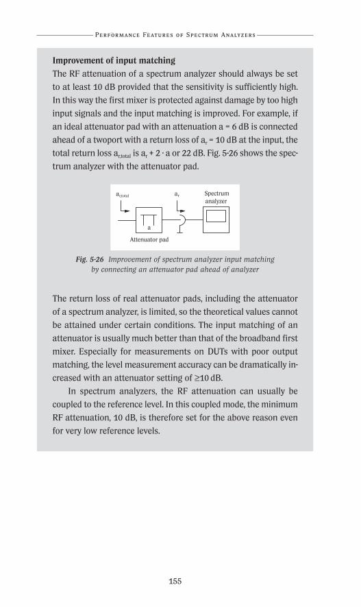
Practical Realization of an Analyzer
155
Improvement of input matching
The RF attenuation of a spectrum analyzer should always be set
to at least 10 dB provided that the sensitivity is sufficiently high.
In this way the first mixer is protected against damage by too high
input signals and the input matching is improved. For example, if
an ideal attenuator pad with an attenuation a = 6 dB is connected
ahead of a twoport with a return loss of ar = 10 dB at the input, the
total return loss ar,total is ar + 2 · a or 22 dB. Fig. 5-26 shows the spec-
trum analyzer with the attenuator pad.
Fig. 5-26 Improvement of spectrum analyzer input matchingby connecting an attenuator pad ahead of analyzer
The return loss of real attenuator pads, including the attenuator
of a spectrum analyzer, is limited, so the theoretical values cannot
be attained under certain conditions. The input matching of an
attenuator is usually much better than that of the broadband first
mixer. Especially for measurements on DUTs with poor output
matching, the level measurement accuracy can be dramatically in-
creased with an attenuator setting of ≥10 dB.
In spectrum analyzers, the RF attenuation can usually be
coupled to the reference level. In this coupled mode, the minimum
RF attenuation, 10 dB, is therefore set for the above reason even
for very low reference levels.
Performance Features of Spectrum Analyzers
Spectrumanalyzer
arar,total
Attenuator pad
a
R&S_Pappband_Spektrumanal 24.10.2001 17:42 Uhr Seite 155

5.10.2 Calculation of total measurement uncertainty
Error sources contributing to the total measurement uncertainty depend
on the type of measurement. In the following sections, error sources en-
countered in frequency measurement applications are described.
Measurement of absolute level
If the absolute level of a sinusoidal signal is to be measured, the following
factors usually contribute to the total measurement uncertainty:
• Absolute level error
• Frequency response
(only if the signal frequency distinctly differs from the frequency of the
internal calibration source)
• Attenuator error
(only if the attenuator setting differs from that specified in the data sheet
for the absolute error)
• IF gain error
(only if the set reference level differs from that specified in the data sheet
for the absolute error)
• Linearity error
The linearity error to be taken into account depends on the spacing of the
input signal from the reference level.
• Bandwidth switching error
(only if the set bandwidth differs from that specified in the data sheet for
the absolute error)
An additional bandwidth error has to be taken into account in noise or
channel power measurements.
Relative level measurement
The following error contributions have to be taken into account when
measuring the level difference between two sinusoidal signals.
Fundamentals of Spectrum Analysis
156
R&S_Pappband_Spektrumanal 24.10.2001 17:42 Uhr Seite 156
Practical Realization of an Analyzer
157
• Frequency response
(only if the signal frequency strongly varies between the individual mea-
surements)
• Attenuator error
If the attenuator setting is not varied during measurement, this error can
be ignored.
• IF gain error
If the reference level is not varied during measurement, this error can be
ignored.
• Linearity error
• Bandwidth switching error
If the bandwidth is not varied during measurement, this error can be
ignored.
An additional bandwidth error has to be taken into account in noise or
channel power measurements if the resolution bandwidth is varied be-
tween the measurements.
Resolution bandwidth, attenuator setting (RF attenuation) and refer-
ence level should not be varied during the measurement in order to mini-
mize the error of relative level measurement. Only the linearity error and
frequency response, if applicable, will then contribute to the total mea-
surement uncertainty.
Table 5-2 shows the error contributions that have to be considered in a
number of typical measurements. The maximum error (worst case error)
can be calculated from the individual contributions simply by adding the
relevant parameters. The calculated maximum error has a confidence lev-
el of 100% so that the actual error of a measurement never exceeds the cal-
culated error limits.
In practice, however, the maximum error seldom occurs. If the total
uncertainty is the sum of many individual errors stemming from com-
pletely independent sources, it is statistically a very rare event that all in-
dividual errors occur in a measurement simultaniously at their maximum
value and same sign.
Performance Features of Spectrum Analyzers
R&S_Pappband_Spektrumanal 24.10.2001 17:42 Uhr Seite 157

Fundamentals of Spectrum Analysis
158
Mea
sure
men
tA
bsol
ute
Har
m-
3rd
orde
r3r
d or
der
Chan
nel
Adj
acen
t-P
ower
ver
sus
Ph
ase
noi
se, f
ar
Ph
ase
noi
se,
leve
l of
onic
inte
rmod
ula
tion
inte
rcep
tpo
wer
chan
nel
tim
e (e
.g. f
orof
f ca
rrie
r, w
ith
cl
ose
to c
arri
er
CW s
ign
aldi
stor
-pr
odu
cts
pow
erT
DM
Ava
riat
ion
of
RF
tion
(clo
se t
o ca
rrie
r)ra
tio
sign
als)
, at
ten
uat
ion
an
d
rela
tive
refe
ren
ce le
vel
Err
or c
ontr
ibu
tion
Abs
olu
te e
rror
Freq
uen
cy r
espo
nse
Att
enu
ator
err
or
IF g
ain
err
or
Lin
eari
ty e
rror
Ban
dwid
th s
wit
chin
g
erro
r
Ban
dwid
th e
rror
Err
or d
ue
to li
mit
ed
nu
mbe
r of
sam
ples
Mis
mat
ch e
rror
Tabl
e 5-
2E
rror
con
trib
uti
ons
in t
ypic
al
mea
sure
men
ts u
sin
g a
spe
ctru
m a
na
lyze
r
R&S_Pappband_Spektrumanal 24.10.2001 17:42 Uhr Seite 158
Practical Realization of an Analyzer
159
It is more realistic to calculate the total uncertainty with a certain confi-
dence level, which is typically 95% or 99%. Such calculation is permissible
if the total uncertainty is composed of several error contributions of equal
magnitude.
The distribution of the individual error contributions depends on the
type of error. The following discussions are based on [5-5].
For random errors, that is for all errors listed above with the exception of
mismatch errors, a rectangular distribution is assumed. The variance σ 2 of
the individual errors is given by:
(Equation 5-49)
where σ 2 = variance
a = max. systematic error, in dB
If the data sheet specification of the level error is not given as worst case
but with a certain confidence level, the variance has to be calculated from
this value first. The following applies:
(Equation 5-50)
where σ 2 = variance
aCL = specified error with certain confidence level or
standard uncertainty, in dB
The value of k depends on the confidence level of the value specified in the
data sheet. The following applies:
k = 2 · erfinv (Equation 5-51)
where erfinv = inverse error function
CL = confidence level, in %
Fig. 5-27 shows k as a function of the confidence level. For a confidence
level of 95%, k assumes a value of 1.96, and for 99%, a value of 2.58.
Performance Features of Spectrum Analyzers
a2
3
aCL
k
2)(
σ 2 =
σ 2 =
CL
100( )√
R&S_Pappband_Spektrumanal 24.10.2001 17:42 Uhr Seite 159

Fig. 5-27 Coverage factor k as a function of confidence levela) confidence level 0% to 100%, b) confidence level 90% to 100% (zoomed)
In some cases the standard uncertainty s is specified in addition to the lev-
el error. This makes the calculation according to equation 5-50 unneces-
sary. The variance can be calculated from the specified standard uncer-
tainty simply by squaring it.
Bandwidth errors are usually specified as a percentage. The following ap-
plies:
(Equation 5-52)
where σ 2 = variance
∆RBW = bandwidth error, in %
Errors due to mismatch have a U-shape distribution. The variance σ2 is
given by
σ 2 = = (Equation 5-53)
where σ 2 = variance
rs = magnitude of source reflection coefficient
rl = magnitude of spectrum analyzer reflection coefficient
ss = VSWR of source
sl = VSWR of spectrum analyzer
The reflection coefficient can be calculated from Equation 5-47.
Fundamentals of Spectrum Analysis
160
10 · log 1 +
3
20 · log(1 – rs · rl)
2
20 · log 1 – ·
2
91 92 93 94 95 96 97 98 99 100091.5
2
2.5
3
3.5
4
50 10 20 30 40 0 60 70 80 90 1000
0.5
1
1.5
2
2.5
3
3.5
4
Confidence level / %
Fact
or k
k = 1.96
k = 2.58
a)
Fact
or k
Confidence level / %b)
2
2
( )∆RBW / %
100
( )ss – 1
ss + 1
sl – 1
sl + 1
2
σ 2 =
σ 2 =
R&S_Pappband_Spektrumanal 24.10.2001 17:42 Uhr Seite 160

Practical Realization of an Analyzer
161
Table 5-3 Calculating the variance of specified error contributions
The combined standard uncertainty σtot can be calculated from the vari-
ances σi2 of the individual contributions as follows:
σtot = σ12 + σ2
2 + . . . + σn2 (Equation 5-54)
It has a confidence level of 68% (Fig. 5-27a). To maintain the error at some
other confidence level, σtot tot has to be multiplied by a factor k which can
be derived from Fig. 5.27. For a confidence level of 95%, k = 1.96 and for
99%, k = 2.58.
Example:
For the absolute level measurement of a sinusoidal input signal of 1 GHz
(output VSWR of signal source 1.2:1), the total measurement uncertainty is
to be determined with a confidence level of 95%. The resolution bandwidth
set on the spectrum analyzer is 30 kHz, the RF attenuation is 20 dB and
the reference level 0 dBm. The signal level is about 20 dB below the refer-
ence level.
Performance Features of Spectrum Analyzers
Error Calculation of variance
Absolute level error
Frequency response
Attenuator error
IF gain error
Linearity error
Bandwidth switching error
Bandwidth error
Mismatch error
a2
3σ 2 =
10 · log 1 +
3
σ 2 =
20 · log(1 – rs · rl)
2
2
σ 2 =
√
Equation 5-49 and
Equation 5-50
Equation 5-52
Equation 5-53
and
2
( )∆RBW / %
100
R&S_Pappband_Spektrumanal 24.10.2001 17:42 Uhr Seite 161
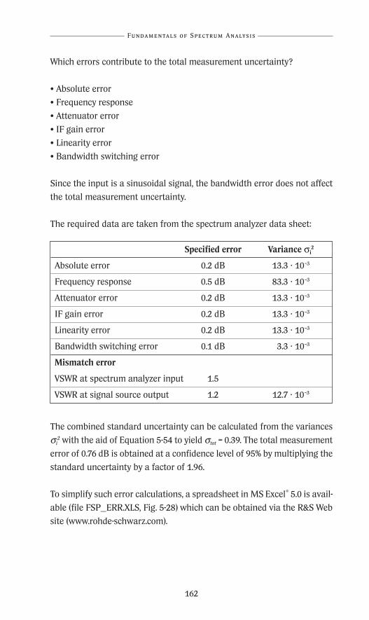
Which errors contribute to the total measurement uncertainty?
• Absolute error
• Frequency response
• Attenuator error
• IF gain error
• Linearity error
• Bandwidth switching error
Since the input is a sinusoidal signal, the bandwidth error does not affect
the total measurement uncertainty.
The required data are taken from the spectrum analyzer data sheet:
The combined standard uncertainty can be calculated from the variances
σi2 with the aid of Equation 5-54 to yield σtot = 0.39. The total measurement
error of 0.76 dB is obtained at a confidence level of 95% by multiplying the
standard uncertainty by a factor of 1.96.
To simplify such error calculations, a spreadsheet in MS Excel® 5.0 is avail-
able (file FSP_ERR.XLS, Fig. 5-28) which can be obtained via the R&S Web
site (www.rohde-schwarz.com).
Fundamentals of Spectrum Analysis
162
Specified error Variance σi2
Absolute error 0.2 dB 13.3 · 10–3
Frequency response 0.5 dB 83.3 · 10–3
Attenuator error 0.2 dB 13.3 · 10–3
IF gain error 0.2 dB 13.3 · 10–3
Linearity error 0.2 dB 13.3 · 10–3
Bandwidth switching error 0.1 dB 13.3 · 10–3
Mismatch error
VSWR at spectrum analyzer input 1.5
VSWR at signal source output 1.2 12.7 · 10–3
R&S_Pappband_Spektrumanal 24.10.2001 17:42 Uhr Seite 162

Practical Realization of an Analyzer
163
Fig. 5-28 Spreadsheet FSP_ERR.XLS
Legend for spreadsheet FSP_ERR.XLS
All input fields in the table are highlighted yellow. The fields for interme-
diate results and the resulting total level are highlighted in light and dark
blue.
1 You can choose whether the values entered in (2) are absolute error lim-
its (worst case) or a standard uncertainty.
2 Input fields for specified errors.
3 Output of the variances calculated from the input values.
4 You can choose whether the error entered under (2) is to be taken into
account in calculating the total error. Error contributions can thus very
easily be ignored without having to set the value entered under (2) to
zero.
5 Output of the calculated total error with a confidence level of 95% or
99%. Errors due to mismatch are not considered in this result.
6 You can choose whether the mismatch of the DUT or spectrum analyzer
is entered as VSWR (v) or as return loss (a).
7 Input field for specified maximum mismatch of the DUT or spectrum
analyzer.
8 Output of the calculated total error with a confidence level of 95% or
99%. All error sources are considered in the result.
Performance Features of Spectrum Analyzers
1 2
6 7
43
5
8
R&S_Pappband_Spektrumanal 24.10.2001 17:42 Uhr Seite 163
5.10.3 Error due to low signal-to-noise ratio
The signals displayed on a spectrum analyzer are the sum of the input sig-
nal (S) and the superimposed thermal noise (N). If the signal level is high
relative to the noise, this has no adverse effect since the resulting level
variation due to the superimposed noise referred to the measurement lev-
el is low. Level measurements on signals with low signal-to-noise ratio,
however, produce errors that are not negligible.
The error can be corrected if the ratio between total signal plus noise
power and inherent noise (S+N)/N is known. The thermal noise power with-
out input signal is determined first at the measurement frequency. With
the same spectrum analyzer settings, the level of the input signal includ-
ing the superimposed noise is then measured and the ratio (S+N)/N calcu-
lated. As described in the following, a correction factor can be found and
subtracted from the measured total power level (S+N) to obtain the true
signal level (S). Both the type of input signal and detector used have to be
taken into account.
To increase the measurement accuracy, it is necessary to smooth the
trace by employing appropriate methods.
RMS detector
When using the RMS detector, the effective value of power is measured in
both measurements of the thermal noise power and the input signal level
with superimposed noise. As already explained in connection with the sen-
sitivity limit (chapter 5.1), an input signal with a level corresponding to the
thermal noise level causes a noise increase by 3 dB. Accordingly, the cor-
rection value for (S+N)/N = 3 dB is 3 dB. The following applies:
Fundamentals of Spectrum Analysis
164
R&S_Pappband_Spektrumanal 24.10.2001 17:42 Uhr Seite 164

Practical Realization of an Analyzer
165
(Equation 5-55)
where cN = correction factor, in dB
(S+N)/N = measured ratio between total signal power and
noise power, in dB
Fig. 5-29 Correction factor cN as a function of total power/inherent noise ((S+N)/N)for measurement of noise or noise-like signals using RMS detector
Example:
The channel power of a digitally modulated signal at a low level is to be
measured and the result corrected. A special measurement function of the
spectrum analyzer is used to determine the channel power. The channel
bandwidth is 4.096 MHz.
Because of the noise-like signal, the RMS detector is used for the mea-
surement.
Performance Features of Spectrum Analyzers
10
10 – 1
0.1·S + N
N
0.1·S + N
N
cN = 10 · log( )
0
2
4
6
8
10
0 2 4 6 8 10 12 14 16
Total power/inherent noise / dB
Corr
ecti
on f
acto
r c N
/ dB
R&S_Pappband_Spektrumanal 24.10.2001 17:42 Uhr Seite 165

a)
b)
Fig. 5-30 Channel power measurement. Measurement of total power (a) and inherent noise (b)
Step 1: measurement of total power (S+N) in given channel:
S+N = – 81.95 dBm (Fig. 5-30 a)
Step 2: measurement of inherent noise (N) in given channel:
N = – 86.08 dBm (Fig. 5-30 b)
Step 3: calculation of ratio between total power and inherent noise
(S+N)/N:
(S+N)/N = –81.95 – (– 86.08 dBm) = 4.13 dB
Fundamentals of Spectrum Analysis
166
A
-170
-160
-150
-140
-130
-120
-110
-100
-90
- 1 0 2 . 7 9 d B m
1
C 0C 0
R e f -8 0 d B m * A t t 0 d B ** V B W 3 0 0 k H zS W T 1 0 s
* R B W 3 0 k H z M a r k e r 1 [ T 1 ]
2 . 2 0 0 0 0 0 0 0 G H z
P R N
S p a n 1 0 M H z1 M H z /C e n t e r 2 . 2 G H z
T x C h a n n e lP o w e r - 8 1 . 9 5 d B m B a n d w i d t h 4 . 0 9 6 M H z
R e f e r e n c e 0 . 0 0 d B m
*1 RMCLRWR
P R N
*
*
1 RM
* V B W 3 0 0 k H z* A t t 0 d B S W T 1 0 s
* R B W 3 0 k H z
1 M H z / S p a n 1 0 M H zC e n t e r 2 . 2 G H z
R e f -8 0 d B m
A
-170
-160
-150
-140
-130
-120
-110
-100
-90
B a n d w i d t h 4 . 0 9 6 M H zR e f e r e n c e 0 . 0 0 d B m
T x C h a n n e lP o w e r -8 6 . 0 8 d B m
M a r k e r 1 [ T 1 ]- 1 0 7 . 3 6 d B m
2 . 2 0 0 0 0 0 0 0 G H z
1
C0C0
CLRWR
R&S_Pappband_Spektrumanal 24.10.2001 17:42 Uhr Seite 166

Practical Realization of an Analyzer
167
Step 4: determination of correction factor (from Equation 5-55 or Fig. 5-29):
cN = 2.2 dB
Step 5: calculation of signal level from total power level:
S = (S+N) – cN = – 81.95 dBm – 2.2 dB = – 84.15 dBm
Sample detector
The displayed level of noise and noise-like signals is too low if the sample
detector is used and averaging over a logarithmic level scale. However, si-
nusoidal signals are not affected. The correction factor to be applied there-
fore depends on the type of input signal.
If measurements are carried out on noise signals, the displayed level
of both the input signal and the inherent noise is 2.5 dB too low. The re-
sulting ratio between total power and inherent noise corresponds to the
result that would be obtained with the RMS detector. The correction fac-
tor can be calculated according to Equation 5-55 or derived from Fig. 5-29.
If the input signal is a discrete spectral line, for instance a sinusoidal
signal, the measured level is not falsified by the sample detector and av-
eraging over a logarithmic level scale. Since a lower level is displayed for
the inherent noise, the ratio between total power and inherent noise is
greater than when using the RMS detector. Correction factors calculated
according to Equation 5-55 are not valid. It is recommended that the RMS
detector is used in such cases.
5.11 Sweep time and update rate
The minimum sweep time, that is the minimum time required for record-
ing a certain frequency span, is determined by various factors.
• Resolution and video bandwidths
• Setting time of LO
• Data processing
• Sampling rate of A/D converter
• Maximum sweep speed of YIG filter, if applicable
Performance Features of Spectrum Analyzers
R&S_Pappband_Spektrumanal 24.10.2001 17:42 Uhr Seite 167

The dependency of the sweep time on the resolution and video bandwidths
as well as on the span was described in chapter 4.6: Parameter dependen-
cies. As described, the required minimum sweep time increases with de-
creasing resolution bandwidth so that for such cases the use of FFT filters
is recommended provided their use is permitted by the specific measure-
ment application.
But even at very large resolution and video bandwidths, the sweep
time cannot be reduced without any limitation. For setting the local oscil-
lator and collecting measured data, a certain minimum time is always re-
quired which in turn depends on the set span, so that there is a limit
(2.5 ms in our example) that cannot be reduced even under the most fa-
vorable circumstances.
In the case of large spans, the minimum sweep time is additionally in-
fluenced by the permissible tuning speed of the local oscillator. For the an-
alyzer described here, a sweep time of 5 ms, for instance, is required for a
span of 1 GHz. In concepts using tracking YIG filters for image frequency
rejection (above 3 GHz for the analyzer described here), the sweep speed is
further reduced by the “inertia” of the tunable magnetic circuit. Sweep
times of less than 6 ms at 1 GHz span can hardly be attained in such cas-
es.
Data sheets usually specify the minimum sweep time that is achiev-
able under the most favorable conditions, such as large resolution and
video bandwidth and small span in a frequency range for which the track-
ing YIG filter is not required. In our example, 2.5 ms sweep time can be
achieved under these circumstances.
If the spectrum analyzer remains tuned to a fixed frequency during
the measurements, which is referred to as zero span, the minimum mea-
surement time only depends on the data acquisition of the analyzer. The
minimum measurement times achievable in this mode are very short (1 µs,
in our example).
An essential criterion in this mode is the time resolution. That is, the
minimum time between two samples (125 ns in our example). The sam-
pling rate of the A/D converter is the limiting parameter in this case.
Fundamentals of Spectrum Analysis
168
R&S_Pappband_Spektrumanal 24.10.2001 17:42 Uhr Seite 168

Practical Realization of an Analyzer
169
The update rate (number of sweeps per unit time), is again important both
for manual and remote-controlled operation of the spectrum analyzer. Ad-
ditional time is required for data processing, display and, where applica-
ble, data transfer via the IEEE bus or other interfaces so that the maxi-
mum update rate is considerably lower than the reciprocal value of the
achievable minimum sweep time (Fig. 5-31).
If FFT filters are used, the difference is especially high due to the very
complex calculations.
Fig. 5-31 Sequence of a measurement
A high screen update rate is desirable in the manual mode, such as for tun-
ing operations so that changes in the recorded spectrum are displayed
almost immediately. Update rates of about 20 measurements per second
are sufficient for such applications as they yield almost flicker-free display.
For automated measurements, such as in production, where control com-
mands and measurement results are transferred via interfaces like the
IEEE bus, the update rate can never be high enough to achieve minimum
test times and high production throughput.
As shown in Fig. 5-31, a certain time for displaying the results on the
screen is required in remote-controlled mode. To achieve maximum update
rates it is therefore advisable to deactivate the screen display.
Performance Features of Spectrum Analyzers
Sweep time Data processingDisplay update and
data output via IEEE bus
Sweep time Data processing Display update
Sweep time Data processingData
output viaIEEE bus
Display off
Display on
Manual operation
Remote-controlled operation
R&S_Pappband_Spektrumanal 24.10.2001 17:42 Uhr Seite 169

6 FREQUENT MEASUREMENTS AND ENHANCEDFUNCTIONALITY
6.1 Phase noise measurements
As described in chapter 5.3, the phase noise of an oscillator is a measure
of the oscillator’s short-term stability and hence an essential quality crite-
rion. Therefore, special phase noise measurement equipment or, when re-
quirements on the dynamic range are not stringent, spectrum analyzers
are used for phase noise measurement.
Phase noise measurement with a spectrum analyzer is referred to as
a direct measurement. As a prerequisite, the DUT must have a small fre-
quency drift relative to the sweep time of the spectrum analyzer or else the
measurable frequency variation of the oscillator would be too large and
invalidate the measurement results. Spectrum analyzers are therefore
mainly suitable for measurements on synthesized signal sources locked to
a stable reference rather than for measurements on free-running oscilla-
tors.
6.1.1 Measurement procedure
For oscillators, the SSB phase noise is usually specified at a certain carri-
er offset referred to the carrier level within 1 Hz bandwidth (Fig. 6-1).
Accordingly, the unit is dBc (1 Hz).
Fig. 6-1 Definition of SSB phase noise
Fundamentals of Spectrum Analysis
170
fT
L
f
LT
LPN
Oscillator signal
foff
1 Hz
R&S_Pappband_Spektrumanal 24.10.2001 17:42 Uhr Seite 170

Practical Realization of an Analyzer
171
Phase noise measurement with a spectrum analyzer requires two steps:
• Measurement of carrier level LC
• Measurement of phase noise level LPN at carrier offset foff
For evaluation, the phase noise measured at a carrier offset foff and reso-
lution bandwidth BIF is first referred to a 1 Hz bandwidth. The following
applies when using the RMS detector:
LPN (ƒoff) = LPN,meas (ƒoff) – 10 · logBN,IF (Equation 6-1)
where LPN (foff) = phase noise level at carrier offset foff referred to
1 Hz bandwidth, in dBm
LPN,meas (foff) = phase noise level measured with RMS detector
at noise bandwidth BN,IF in dBm
BN,IF = noise bandwidth of resolution filter, in Hz
Depending on the filter implementation, the noise bandwidth of the reso-
lution filter can be calculated from the 3 dB filter bandwidth with the aid
of the conversion factors given in Table 4-1. If the sample detector is used
instead of the RMS detector and the trace averaged over a narrow video
bandwidth or over several measurements, the noise will be underweight-
ed as described in chapter 4.4: Detectors. The following then applies:
LPN (ƒoff) = LPN,meas (ƒoff) – 10 · logBN,IF + 2.5 dB (Equation 6-2)
where LPN,meas (foff) = averaged phase noise level measured with
sample detector at noise bandwidth BN,IF, in dBm
The phase noise level within 1 Hz bandwidth is now referred to the carri-
er level:
L(ƒoff) = LPN(ƒoff) – LC (Equation 6-3)
Frequent Measurements and Enhanced Functionality
R&S_Pappband_Spektrumanal 24.10.2001 17:42 Uhr Seite 171

where L (foff) = relative phase noise level within 1 Hz band-
width at carrier offset foff referred to carrier lev-
el, in dBc (1 Hz)
LPN (foff) = phase noise level within 1 Hz bandwidth at car-
rier offset foff, in dBm
LC = carrier level, in dBm
To simplify phase noise measurements, most spectrum analyzers feature
marker functions which allow direct readout of the phase noise at a given
carrier offset. Usually, noise bandwidth and correction factors, which are
necessary due to the underweighting of noise signals when using the sam-
ple detector, are already taken into account.
Fig. 6-2 Marker function for easy phase noise measurement
With such marker functions the phase noise can only be determined at a
certain carrier offset. However, the phase noise is often of interest in a
wider range (such as 1 kHz to 1 MHz carrier offset). To make these mea-
surements simple, application software is available for some spectrum an-
alyzers. Fig. 6-3 shows the result of a phase noise measurement using this
kind of software.
Fundamentals of Spectrum Analysis
172
R&S_Pappband_Spektrumanal 24.10.2001 17:43 Uhr Seite 172
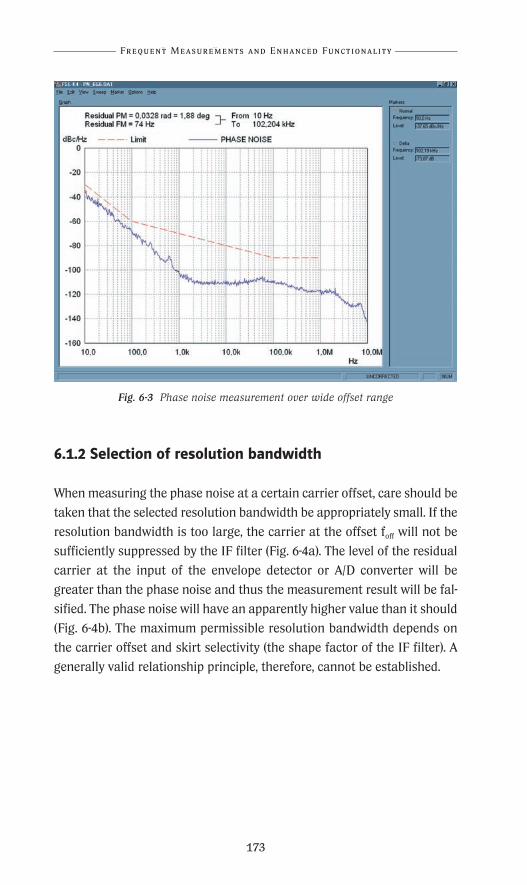
Practical Realization of an AnalyzerFrequent Measurements and Enhanced Functionality
173
Fig. 6-3 Phase noise measurement over wide offset range
6.1.2 Selection of resolution bandwidth
When measuring the phase noise at a certain carrier offset, care should be
taken that the selected resolution bandwidth be appropriately small. If the
resolution bandwidth is too large, the carrier at the offset foff will not be
sufficiently suppressed by the IF filter (Fig. 6-4a). The level of the residual
carrier at the input of the envelope detector or A/D converter will be
greater than the phase noise and thus the measurement result will be fal-
sified. The phase noise will have an apparently higher value than it should
(Fig. 6-4b). The maximum permissible resolution bandwidth depends on
the carrier offset and skirt selectivity (the shape factor of the IF filter). A
generally valid relationship principle, therefore, cannot be established.
R&S_Pappband_Spektrumanal 24.10.2001 17:44 Uhr Seite 173

a)
b)
Fig. 6-4 Choosing the right resolution bandwidth: (a) resolution bandwidth too large,carrier suppression is insufficient; (b) resolution bandwidth is small enough
Fundamentals of Spectrum Analysis
174
R e f - 1 0 d B m A t t 0 dB S W T 5 s*
*
C e n te r 49 7 . 06 MHz S p a n 2 00 kHz2 0 k H z/
1 R M
CLRWR
A
R B W 3 kH z
V B W 3 0 k H z
*
*
PRN
- 110
- 100
-90
-80
-70
-60
-50
-40
-30
-20
-10 Mar k er 1 [ T 1 F X D ]
- 1 2. 2 5 d B m
49 7 . 0 0 0 0 0 0 0 0 M H z
Del t a 2 [T 1 PH N ]
- 1 1 6 . 2 9 d B c/ H z
10 0 . 00 0 0 0 0 0 0 k H z
2
PHN -12.292 dBm
PHN
1
R e f - 1 0 d B m A t t 0 dB S W T 5 s*
C e n te r 4 9 7 . 0 6 M Hz S p a n 2 00 kHz2 0 k H z/
A
R B W 3 0 k H z
V B W 3 0 0 k H z
*
*
PRN
-110
-100
-90
-80
-70
-60
-50
-40
-30
-20
-10 M a r k e r 1 [ T 1 F X D ]
- 1 2. 2 5 d B m
49 7 . 0 0 0 0 00 0 0 M H z
Del t a 2 [T1 PH N ]
- 1 12 . 7 6 d B c/ H z
10 0 . 00 0 0 00 0 0 k H z
2
PHN
1PHN -12.292 dBm
*1 R M
CLRWR
R&S_Pappband_Spektrumanal 24.10.2001 17:44 Uhr Seite 174

Practical Realization of an Analyzer
175
Due to the high minimum sweep times at narrow IF bandwidths, high res-
olution bandwidths are desirable in practice. With a wideband IF filter, the
resolution bandwidth should be reduced in steps until the measured phase
noise values no longer decrease.
6.1.3 Dynamic range
The phase noise of the local oscillators is transferred to the converted
input signal by reciprocal mixing in the converting stages of the spectrum
analyzer (chapter 5.3: Phase noise). If the input signal is of sufficiently high
level so that the effects of thermal noise of the spectrum analyzer are neg-
ligible, the achievable dynamic range at small carrier offsets is solely de-
termined by the LO phase noise of the analyzer. The limitation imposed by
the system-inherent phase noise is independent of the input signal level.
Since it is always the sum of the DUT phase noise and LO phase noise
of the spectrum analyzer that is measured, such measurement can only be
carried out on DUTs with relatively high phase noise.
As shown in Fig. 5-11, the system-inherent phase noise of spectrum ana-
lyzers decreases with increasing carrier offset. At large carrier offsets the
dynamic range is limited to an increasing extent by the thermal noise of
the spectrum analyzer. There is no clear-cut difference between limitation
due to system-inherent phase noise and thermal noise.
To minimize the limitation caused by thermal noise, a high signal-to-
noise ratio is required via a high signal level at the input of the first mix-
er. A high 1 dB compression point is also important to achieve a wide
dynamic range far off the carrier.
Frequent Measurements and Enhanced Functionality
R&S_Pappband_Spektrumanal 24.10.2001 17:44 Uhr Seite 175

Due to the high signal level, harmonics of the input signal are produced in
the first mixer. If the maximum offset up to which phase noise is to be ex-
amined is smaller than the input frequency, the harmonics are outside the
frequency range of interest and do not cause any disturbance.
If the input signal level is greater than the dynamic range of the spec-
trum analyzer, it has to be reduced by setting a suitable RF attenuation.
Due to the attenuator step sizes, the maximum dynamic range may not be
fully utilized.
Example:
The 1 dB compression point of the spectrum analyzer is assumed to be
+10 dBm (mixer level). To avoid measurement errors, the signal level at the
first mixer should not exceed +5 dBm. The RF attenuation can be set in
10 dB steps.
A signal level of +17 dBm is applied to the analyzer input, so an RF at-
tenuation of at least 20 dB is required. The signal level at the first mixer is
then –3 dBm. The dynamic range for measurements at large carrier offsets
is thus 8 dB lower than the maximum achievable dynamic range.
To utilize the maximum dynamic range, the signal level in our exam-
ple would have to be attenuated to +15 dBm using an external 2 dB at-
tenuator pad. With 10 dB RF attenuation, a mixer level of +5 dBm is then
obtained.
To avoid distortion products due to overdriving, the maximum refer-
ence level settable at an RF attenuation of 0 dB is clearly below the upper
limit of the analyzer's dynamic range (+5 dBm in the above example). With
the analyzer driven to its maximum input, measurement of the carrier lev-
el as a subsequent reference for the phase noise would not be possible.
Likewise, measurement of phase noise close to the carrier would not be
possible. Phase noise is therefore measured in two steps:
1. Measurement of carrier level and phase noise close to carrier
The RF attenuation of the spectrum analyzer is increased until the refer-
ence level is equal to the signal level (Fig. 6-5). The carrier level can then
be readily measured with the aid of markers, since the input signal does
not exceed the reference level. To be able to refer the measured phase
noise to the carrier level, the latter is stored. The carrier level is usually
stored automatically when activating the marker function for the phase
noise measurement.
Fundamentals of Spectrum Analysis
176
R&S_Pappband_Spektrumanal 24.10.2001 17:44 Uhr Seite 176

Practical Realization of an Analyzer
177
Fig. 6-5 Setting RF attenuation and reference level for measurement of carrier level and phase noise close to carrier
2. Measurement of phase noise far off carrier
The RF attenuation is reduced until the maximum dynamic range limit is
attained with the signal applied to the input of the first mixer. The follow-
ing applies:
aRF, min = Lin – Lmax (Equation 6-4)
where aRF, min = required minimum RF attenuation, in dB
Lin = signal level at spectrum analyzer input, in dBm
Lmax = maximum dynamic range limit of analyzer, in
dBm
Frequent Measurements and Enhanced Functionality
CLRWR
A
R e f 0 d B m A t t 3 0 d B
*1RM
S W T 1 0 s
5 k Hz/S t a rt 496 . 9 8 M H z S t o p 497 . 03 M Hz
R B W 1 kH z
V B W 1 0 k H z
*
*
PRN
-100
-90
-80
-70
-60
-50
-40
-30
-20
-10
0 M a r k e r 1 [ T 1 F X D ]
- 0. 2 2 d B m
49 7 . 0 0 0 2 0 0 0 0 M H z
Del t a 2 [T1 PH N ]
- 1 09 . 3 6 d B c/ H z
2 0 . 00 0 0 00 0 0 k H z1
2
PHN -0.305 d B m
PHN
R&S_Pappband_Spektrumanal 24.10.2001 17:44 Uhr Seite 177

An overload detector before the first mixer is useful for determining the
minimum RF attenuation. The RF attenuation can then be increased until
overdriving is no longer detected.
If digital filters are used, deliberately exceeding the reference level
may result in overdriving of the A/D converter, which in turn produces un-
wanted products in the displayed spectrum (chapter 4.6.3: Overdriving).
This constraint is not significant, since measurements at large carrier off-
sets use relatively wideband analog resolution filters.
If digital filters are used and the input signal exceeds the reference
level, it has to be ensured that the carrier frequency is far from the dis-
played spectrum. The carrier is then suppressed by the analog anti-alias-
ing filter ahead of the A/D converter so that it cannot cause overdriving.
It is very easy to determine whether the noise displayed is the phase noise
or the thermal noise of the analyzer. To perform this test, the recorded
trace has to be stored and a second measurement carried out with the
same settings, but without input signal at the analyzer. If at the carrier off-
set of interest there is a clear level difference between the two traces as
shown in Fig. 6-6a, the measurement result is barely affected by the ther-
mal noise of the analyzer.
In the measurement shown in Fig. 6-6b, the dynamic range is limited
by the thermal noise and the result falsified.
The displayed phase noise is always the sum of the phase noise of the DUT
and the spectrum analyzer and the spectrum analyzer's thermal noise. If
measurements are carried out very close to the dynamic range limit, errors
may be produced due to insufficient spacing between the measured phase
noise and the system-inherent noise. If the system-inherent noise is known,
a correction can be made according to Equation 5-55 (chapter 5.10.3).
Fundamentals of Spectrum Analysis
178
R&S_Pappband_Spektrumanal 24.10.2001 17:44 Uhr Seite 178

Practical Realization of an Analyzer
CLRWR
A
S W T 1 0 s
R B W 1 0 0 k H z
V B W 1 M H z
*
*1RM
R e f - 1 0 d B m A t t 0 dB*
S t a rt 496 M Hz S t o p 5 0 3 M Hz7 0 0 k Hz/
*2RM
VIEW
*
PRN
-110
-100
-90
-80
-70
-60
-50
-40
-30
-20
-10 M a r k er 1 [ T 1 F X D ]
- 9 5. 2 1 d B m
49 6 . 9 9 4 0 0 0 0 0 M H z
D el t a 2 [T1 PH N ]
- 1 4 4 . 4 7 d B c/ H z
3 . 0 0 0 0 0 0 0 0 M H z
1 2
PHN -1.286 dBm
PHN
CLRWR
A
S W T 1 0 s
R B W 1 0 0 k H z
V B W 1 M H z
*
*1RM
R e f - 1 0 d B m
S t a rt 496 M Hz S t op 5 0 3 MHz7 00 kHz/
A t t 2 0 d B*
*2R M
VIEW
*
PRN
-110
-100
-90
-80
-70
-60
-50
-40
-30
-20
-10 M a r k e r 1 [ T 1 F X D ]
- 8 1. 0 1 d B m
49 6 . 9 9 4 0 0 0 0 0 M H z
D el t a 2 [T 1 PH N ]
- 1 30 . 2 7 d B c/ H z
3 . 0 0 0 0 0 0 0 0 M H z
1 2
PHN -1.286 dBm
PHN
179
a)
b)
Fig. 6-6 Verification of phase noise measurements. (a) Measurement is not not affected by thermal noise of the analyzer.
(b) Dynamic range is limited by thermal noise of the spectrum analyzer
Frequent Measurements and Enhanced Functionality
R&S_Pappband_Spektrumanal 24.10.2001 17:44 Uhr Seite 179
6.2 Measurements on pulsed signals(Dipl.-Ing. Volker Janssen)
Communications systems for information transfer, which for a long time
have mainly been implemented in analog form, are increasingly being re-
placed by digital components and systems. The latter often use pulse-mod-
ulated signals, for instance in television, radar and mobile radio. Due to
the spectral distribution of such signals, a spectrum analyzer used to mea-
sure the signals has to fulfil special requirements. The same applies to oth-
er types of signals, namely high-frequency, broadband interfering signals
occurring in switching operations or in the clock generation of micro-
processors. Almost any electronic circuit does not only produce the want-
ed signals but also unwanted spurious emissions that impair the function
of the circuit itself or of other electronic components. Inherent spurious
emissions of electronic communications equipment degrade, for instance,
specifications like the signal-to-noise ratio (S/N) or bit error rate (BER). The
situation can be even worse if conducted or radiated interference affects
other devices and impairs their performance or causes malfunction. The
prevention of spurious emissions and the provision of high immunity to
interference are the domain of electromagnetic compatibility (EMC).
Worldwide uniform EMC standards and guidelines provide for repro-
ducibility of interference measurements and form the basis of interna-
tional regulations with respect to interference limit values to be complied
with to ensure proper functioning of electronic units, modules, devices and
systems.
Theoretically, the energy of pulse-modulated signals is distributed over
the whole spectrum. The measured energy strongly depends on the reso-
lution bandwidth and on the point of measurement in the spectrum. If the
si function is measured close to a null in the envelope, overdriving of the
input stage may be caused as a result of incorrect setting. The total ener-
gy spectrum is applied to the input stage if no preselection filters are used.
This reduces the spectrum and applies the spectrum to the mixer of the
first conversion stage in ‘slices’. Modern spectrum analyzers feature low
nonlinearities and high overload capacity (high intercept points of 2nd and
3rd order and high 1 dB compression). Moreover, they are equipped with
internal overload detectors used for automatic correction of the analyzer
settings in order to optimize the dynamic range and shift it into a non-crit-
ical level range with the aid of automatic RF attenuation settings (auto
Fundamentals of Spectrum Analysis
180
R&S_Pappband_Spektrumanal 24.10.2001 17:44 Uhr Seite 180
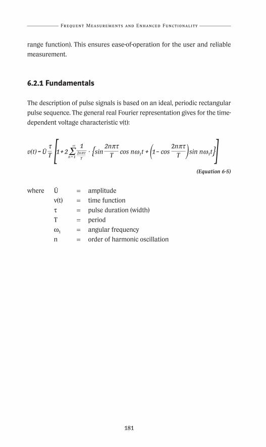
Practical Realization of an Analyzer
181
range function). This ensures ease-of-operation for the user and reliable
measurement.
6.2.1 Fundamentals
The description of pulse signals is based on an ideal, periodic rectangular
pulse sequence. The general real Fourier representation gives for the time-
dependent voltage characteristic v(t):
v(t) = Û 1+ 2 · sin cos nω1t + 1– cos sin nω1t
(Equation 6-5)
where Û = amplitude
v(t) = time function
τ = pulse duration (width)
T = period
ω1 = angular frequency
n = order of harmonic oscillation
Frequent Measurements and Enhanced Functionality
2nπτT
1τT
2nπτT( )[ ]n = 1
∞
Σ 2nπτT
R&S_Pappband_Spektrumanal 24.10.2001 17:44 Uhr Seite 181

The coefficients of the Fourier series describe the spectral amplitudes as
Vn = 2Û (Equation 6-6)
Fig. 6-7 General spectral display (si function) after Fourier analysis with modulated carrier frequency f0
While the Fourier representation furnishes contributions from –∞ to +∞and the coefficients may also have a negative sign (Fig. 6-1), the spectrum
analyzer only represents positive frequencies according to their magni-
tude. Two pulse sequence characteristics according to Fig. 6-8 are ob-
tained:
Fig. 6-8 Line spectra of two rectangular voltage characteristics with different mark-to-space ratio, shown in time domain and in frequency domain. The envelope of the spectral line is an si function decaying proportional to 1/f
Fundamentals of Spectrum Analysis
182
τT
sin
nπτT
nπτT
1----Τ
f0–3----τ
f0–2----τ
f0–1----τ
f0 f0+2----τ
f0+1----τ
f0+3----τ
f
v(t)
Tt
Û
τv(t)
Tt
Û
τ
|V(nf1)|
f
1---f
∆f=f1
|V(nf1)|
ff1=
1---T
fn=nf1f1=1---T
fn=nf1
f
1---τ
1---τsi
1f
si
2
R&S_Pappband_Spektrumanal 24.10.2001 17:44 Uhr Seite 182

Practical Realization of an Analyzer
183
The smallest frequency f1 is the fundamental, corresponding to the recip-
rocal value of the period T:
f1 = 1/T (Equation 6-7)
The amplitude values of the harmonics according to Equation 6-6 occur at
intervals of ∆f = f1 = 1/T.
The first null of the si function occurs at the reciprocal value of the pulse
duration:
fsi1 = 1/τ (Equation 6-8)
Further nulls follow at fn = n · fsi1 · intervals.
Fig. 6-9 Finite pulse time constants with real pulse signal
The nulls in the pulse spectra measured in practice are not always distinct,
because they are somewhat blurred. The reason lies in the asymmetries of
real signals that cannot be avoided, since in contrast to the theoretical
ideal rectangular pulses, the finite exponential rise and fall times of the
real pulses have to be taken into account.
Before dealing with the different terms and the dependencies of the dis-
played spectrum on the measurement bandwidth, let us examine some
other pulse shapes, as well.
Frequent Measurements and Enhanced Functionality
v(t)T
t
τ
0
R&S_Pappband_Spektrumanal 24.10.2001 17:44 Uhr Seite 183

Fig. 6-10 Real representation of envelope spectrum with a spectrum analyzer(100 µs pulse duration, 1 ms pulse period,
900 MHz carrier frequency, 1 kHz measurement bandwidth)
Fig. 6-11 Real representation of line spectrum with a spectrum analyzer,same settings as in Fig. 6-10, but 100 Hz measurement bandwidth
Fundamentals of Spectrum Analysis
184
PRN
*
S W T 5 0 m s
V B W 1 0 k H z
R B W 1 kH z
MAXH
1PK
5 k Hz/ S p a n 50 k HzC e n t e r 90 0 . 0 2 4 M H z
EXT
A
A t t 3 0 d BR e f 0 d B m
-100
-90
-80
-70
-60
-50
-40
-30
-20
-10
0
PRN
*
S W T 5 s
V B W 1 k H z
R B W 1 0 0 Hz
MAXH
1PK
5 kHz/ S pa n 50 k HzC e n te r 90 0 . 02 4 MHz
EXT
A
A t t 3 0 d BR e f 0 d B m
-100
-90
-80
-70
-60
-50
-40
-30
-20
-10
0
R&S_Pappband_Spektrumanal 24.10.2001 17:44 Uhr Seite 184

Practical Realization of an Analyzer
185
Triangular and trapezoidal pulses
The spectrum of a triangular pulse with equal rise and fall time exhibits
an envelope that corresponds to a si2 function. The trapezoidal pulse can
be obtained from a combination of rectangular and triangular pulse. The
effect of additional time constants is noticeable in the differently decaying
amplitudes of the log-log density spectrum. While with the trapezoidal
pulse at 1/pt the envelope of the amplitude density spectrum decreases 20
dB per decade, it decreases 40 dB per decade in the case of equal rise and
fall time. If the time constants are different, there is a decrease of 20 dB
per decade at the first (smaller) corner frequency and of another 20 dB at
the second (larger) corner frequency, similar to the characteristic of the
trapezoidal pulse.
Fig. 6-12 Amplitude density spectrum for rectangular, trapezoidal and triangular pulses (diagram is shown for τrise = τfall)
Considering τ → 0 clearly reveals that this corner frequency (Fig. 6-12) is
shifted towards infinitely high frequencies. Examination of the boundary
case that the period T → ∞ (∆f = 1/T → 0), yields a single pulse with infi-
nitely high amplitude (Dirac pulse).
The Fourier series only allows the representation of periodic time
domain functions. With the aid of the boundary conditions, T → ∞, and
∆f → 0, non-periodic functions can also be described. This is possible with
the aid of the Fourier transform and Fourier integral.
In practice, non-periodic events occur more frequently, such as switch-
ing operations, lightning strokes or electrostatic discharges.
Frequent Measurements and Enhanced Functionality
v(f)
/dB
log f
2ûτ
1−−πτfv=1−−πτr
fv=
R&S_Pappband_Spektrumanal 24.10.2001 17:44 Uhr Seite 185

6.2.2 Line and envelope spectrum
The energy of the periodic pulse occurs at the discrete frequencies n ⋅ f1
(Equation 6-7), or equivalently at n ⋅1/T.
The envelope si function has nulls at the integer multiples as a func-
tion of the mark-to-space ratio τ /T. If the pulse signal is used for modula-
tion of a carrier, the spectrum will be symmetrically distributed above and
below the carrier frequency. Depending on the measurement or resolution
bandwidth, the following three cases are possible when using a frequen-
cy-selective spectrum analyzer or test receiver for the spectrum measure-
ment:
1. If the measurement bandwidth is small relative to the offset of the fre-
quency lines (given by 1/T = ∆f), the individual spectral lines can be re-
solved so that a line spectrum is obtained.
B < 1/T (Equation 6-9)
A further reduction of the bandwidth yields equal amplitude values, re-
duces the noise and thus improves the signal-to-noise ratio with the
bandwidth ratio 10 ⋅ log(B1/B2).
2. The bandwidth B is greater than the spacing ∆f of the spectral lines, but
smaller than the spacing 1/τ of the first null of the envelope si function
from the carrier frequency.
The spectral lines cannot be resolved and the amplitude height of the en-
velope depends on the bandwidth. This makes sense as the amplitude
depends on the number of spectral lines collected within the measure-
ment bandwidth.
1/τ > B > 1/T (Equation 6-10)
The above condition is described as an envelope display. The envelope
amplitude increases with increasing bandwidth by 20 log B2/B1.
Fundamentals of Spectrum Analysis
186
R&S_Pappband_Spektrumanal 24.10.2001 17:44 Uhr Seite 186

Practical Realization of an Analyzer
187
Fig. 6-13 Line spectrum of pulsed signal (measurement bandwidth B = 100 Hz < 1/T = 1 kHz)
Fig. 6-14 Envelope spectrum of pulsed signals (1/τ = 10 kHz > B = 3 kHz > 1/T = 1 kHz)
Frequent Measurements and Enhanced Functionality
PRN
*
S W T 1 s
V B W 1 k H z
R B W 1 0 0 Hz
1 k Hz/ S pa n 10 k H zC e n t e r 90 0 . 0 2 4 0 8 M H z
EXT
MAXH
1PK
A
A t t 3 0 d BR e f 0 d B m
-100
-90
-80
-70
-60
-50
-40
-30
-20
-10
0
M arke r 1 [T1]
- 2 2. 3 5 d B m
90 0 . 0 2 4 0 8 0 0 0 M H z
D el t a 2 [T 1 ]
- 0. 1 5 d B
1 . 0 0 0 0 0 0 0 0 k H z
1 2
PR N
*
S W T 1 5 m s
V B W 3 0 k H z
R B W 3 kH z
1 0 k H z/ S p a n 1 0 0 k HzC e n te r 90 0 . 0 2 4 0 8 M H z
EXT
MAXH
1PK
A
A t t 3 0 d BR e f 0 d B m
-100
-90
-80
-70
-60
-50
-40
-30
-20
-10
0
M a rke r 1 [T1]
- 9. 1 5 d B m
90 0 . 02 4 0 80 0 0 M H z
D e l t a 2 [T 1 ]
- 1 7. 4 8 d B
1 0 . 00 0 0 0 0 0 0 k H z
1
2
R&S_Pappband_Spektrumanal 24.10.2001 17:44 Uhr Seite 187

3. The bandwidth B is greater than the null spacings of the envelope, se-
lectivity is no longer effective and the amplitude distribution in the spec-
trum cannot be recognized any more. With increasing bandwidth the im-
pulse response of the filter approaches the time function of the
pulse-modulated carrier.
B > 1/τ (Equation 6-11)
Fig. 6-15 Transition to display in time domain. Pulse duration of 100 µs and period of 1 ms can be clearly recognized
To put it simply:
• In the case of the line spectrum the number of lines does not vary as a
function of the bandwidth or frequency span, the amplitude remains con-
stant.
• In the case of the envelope spectrum the number of lines varies as a
function of the bandwidth and not as function of the frequency offset.
The displayed amplitude increases with the resolution bandwidth due to
the larger energy component within the measurement bandwidth.
Fundamentals of Spectrum Analysis
188
PRN
*
V B W 3 M H z
R B W 3 0 0 k H z
SGL
CLRWR
1AP
1 00 kHz/ Span 1 M H zC e n t e r 90 0 . 0 2 4 0 8 M H z
EXT
S W T 2 . 5 ms
A
A t t 3 0 d BR e f 0 d B m
-100
-90
-80
-70
-60
-50
-40
-30
-20
-10
0
R&S_Pappband_Spektrumanal 24.10.2001 17:44 Uhr Seite 188

Practical Realization of an Analyzer
189
With pulse modulation, the displayed amplitude decreases with decreas-
ing bandwidth, this effect being referred to as pulse desensitization. The
relationship can be expressed by the determination of the pulse desensiti-
zation factor (PDF):
PDFline = 20 · log(τ /T) (Equation 6-12)
for amplitude values in the line spectrum and
PDFenvelope = 20 · log(τ KB) (Equation 6-13)
for amplitude values in the envelope spectrum. The shape factor K de-
pends on the type of the resolution filter used and is described in detail in
the following section. Typical examples are K = 1 for Gaussian filters and
K = 1.5 for rectangular filters. For pulse signal measurements, a compro-
mise has to be found since with small resolution bandwidths the displayed
amplitude may become too small, whereas with large resolution band-
width the displayed amplitude will be larger but the resolution degraded
to an increasing extent. In practice, the following value has been empiri-
cally determined:
τ · B = 0.1 (Equation 6-14)
Fig. 6-16 Amplitude loss as a function of time/bandwidth product τ · B
Frequent Measurements and Enhanced Functionality
A [dB]
0
–20
–40
–60
0.001 0.01 0.1 1
tp · B
Rectangularfilter
Gaussian filter
R&S_Pappband_Spektrumanal 24.10.2001 17:44 Uhr Seite 189

Examples:
A pulse of the duration τ = 2 µs and pulse repetition frequency of 5 kHz
(= 1/T), corresponding to a period T = 200 µs, is measured with a Gaussian
filter (K = 1) of bandwidth B = 1 kHz.
The condition according to Equation 6-9 applies (B < 1/T), so we have a line
spectrum. Equation 6-12 then gives:
PDFline = 20 · log(2 µs/200 µs) = –40 dB
Accordingly, the displayed amplitude value of the unmodulated carrier
would be 40 dB higher.
Fig. 6-17 Pulse spectra measured with different bandwidths. The markers displaythe desensitization factor. The unmodulated carrier level is 0 dBm
Fundamentals of Spectrum Analysis
190
PRN
MAXH
1 PK
VBW 300 kHz
RBW 100 kHz
500 kHz/ Span 5 MHzCenter 900 MHz
SWT 2.5 ms
*
B
A
EXT
Att 30 dBRef 0 dBm
VIEW
1 AP
*
*
SWT 2.5 ms
VBW 1 MHz
RBW 100 kHz
Att 30 dBRef 0 dBm
200 kHz/ Span 2 MHzCenter 900.02408 MHz
Marker 1 [T1]
-40.39 dBm
900.02428000 MHz
1
Marker 1 [T1]
-13.17 dBm
900.02000000 MHz
1
Marker 1 [T1]
-40.39 dBm
900.02428000 MHz
1
Marker 1 [T1]
-13.17 dBm
900.02000000 MHz
1
0
-90
-80
-70
-60
-5
-40
-30
-20
-10
-90
-80
-70
-60
-50
-40
-30
-20
-10
R&S_Pappband_Spektrumanal 24.10.2001 17:44 Uhr Seite 190
191
The same measurement is repeated with the same parameters, but with a
measurement bandwidth B of 100 kHz. The relationship according to
Equation 6-10 applies (1/τ > B > 1/T). Equation 6-13 then gives:
PDFenvelope = 20 · log(2 · 10–6 · 1 · 100 · 103) = 20 · log(2 · 10–1) = –14 dB
The maximum amplitude of the spectrum is 14 dB lower than that of the
unmodulated carrier.
6.2.3 Resolution filters for pulse measurements
The spectral lines of broadband pulse signals are correlated, so the dis-
played level doubles when the measurement bandwidth is doubled. To de-
termine the actual pulse bandwidth, the displayed level with the use of a
real filter is compared with the displayed level from an ideal rectangular
filter. For Gaussian filters, which are mostly used due to their favorable
transient response, the following relationship is obtained:
BI = 1.506 · B3dB (Equation 6-15)
where BI = pulse bandwidth, in Hz
The pulse bandwidth of Gaussian or Gaussian-like filters corresponds ap-
proximately to the 6 dB bandwidth. For spectrum analyzers, the 3 dB band-
widths are usually specified, whereas for EMI measurements, where often
pulses are measured, 6 dB bandwidths are stated.
The relationship between 3 dB, 6 dB, noise and pulse bandwidths for dif-
ferent filters was described in chapter 4. The conversion factors can be di-
rectly taken from the table below.
Frequent Measurements and Enhanced Functionality
R&S_Pappband_Spektrumanal 24.10.2001 17:44 Uhr Seite 191
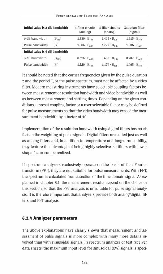
It should be noted that the corner frequencies given by the pulse duration
τ and the period T, or the pulse spectrum, must not be affected by a video
filter. Modern measuring instruments have selectable coupling factors be-
tween measurement or resolution bandwidth and video bandwidth as well
as between measurement and settling times. Depending on the given con-
ditions, a preset coupling factor or a user-selectable factor may be defined
for pulse measurements so that the video bandwidth may exceed the mea-
surement bandwidth by a factor of 10.
Implementation of the resolution bandwidth using digital filters has no ef-
fect on the weighting of pulse signals. Digital filters are suited just as well
as analog filters and, in addition to temperature and long-term stability,
they feature the advantage of being highly selective, so filters with lower
shape factor can be realized.
If spectrum analyzers exclusively operate on the basis of fast Fourier
transform (FFT), they are not suitable for pulse measurements. With FFT,
the spectrum is calculated from a section of the time domain signal. As ex-
plained in chapter 3.1, the measurement results depend on the choice of
this section, so that the FFT analysis is unsuitable for pulse signal analy-
sis. It is therefore important that analyzers provide both analog/digital fil-
ters and FFT analysis.
6.2.4 Analyzer parameters
The above explanations have clearly shown that measurement and as-
sessment of pulse signals is more complex with many more details in-
volved than with sinusoidal signals. In spectrum analyzer or test receiver
data sheets, the maximum input level for sinusoidal (CW) signals is speci-
Fundamentals of Spectrum Analysis
192
Initial value is 3 dB bandwidth 4 filter circuits 5 filter circuits Gaussian filter(analog) (analog) (digital)
6 dB bandwidth (B6dB) 1.480 · B3dB 1.464 · B3dB 1.415 · B3dB
Pulse bandwidth (BI) 1.806 · B3dB 1.727 · B3dB 1.506 · B3dB
Initial value is 6 dB bandwidth
3 dB bandwidth (B3dB) 0.676 · B6dB 0.683 · B6dB 0.707 · B6dB
Pulse bandwidth (BI) 1.220 · B6dB 1.179 · B6dB 1.065 · B6dB
R&S_Pappband_Spektrumanal 24.10.2001 17:44 Uhr Seite 192

193
fied. For pulse measurements, parameters such as pulse spectral density,
maximum pulse energy or pulse voltage are important to avoid erroneous
measurement or damage to the measuring instrument. It makes sense to
define a parameter such as the pulse spectral density and to relate a pulse
voltage to a reference bandwidth (chapter 5.4: 1 dB compression point and
maximum input level). A reference bandwidth of 1 MHz has been defined
for this purpose. The parameters are therefore given in the units µV/1 MHz
and dBµV/1 MHz.
The pulse spectral density can easily be calculated from the measured
level using the following correction factor:
KI = 20 log (BI /1 MHz) (Equation 6-16)
Example:
In a spectrum analyzer the measurement bandwidth is determined by a
Gaussian filter with a 3 dB bandwidth of 10 kHz. A pulse signal measure-
ment yields a displayed level of –67 dBm. What is the pulse spectral den-
sity?
First, the measured value has to be converted into the unit dBµV. A level
of 0 dBm corresponds to 107 dBµV. That is, –67 dBm corresponds to +40
dBµV. The pulse bandwidth is calculated for Gaussian filters according to
Equation 6-15 with · B3dB to give BI =15 kHz.
The correction factor of –36.5 dB is obtained from Equation 6-16:
KI = 20 · log (BI /1 MHz) = 20 · log(15 · 103 /1 · 106) = –36.5 dB
The measured value of +40 dBmV corresponds to a pulse spectral density
of 76.5 dBµV/1 MHz.
A detailed description of maximum pulse energy and voltage, which are
further important parameters for the assessment of spectrum analyzers
and test receivers, can be found in chapter 5.4.
Frequent Measurements and Enhanced Functionality
R&S_Pappband_Spektrumanal 24.10.2001 17:44 Uhr Seite 193

Certain instruments can even have two separate RF inputs, one of them
being pulse-protected for handling high maximum pulse voltage peaks.
Pulse energy is applied to the subsequent attenuator which is designed to
dissipate the resulting heat. In the case of inadequate heat dissipation,
components may be damaged.
6.2.5 Pulse weighting in spurious signal measurements
So far we have considered wanted signals that serve for transmitting in-
formation. As mentioned at the beginning of chapter 6.2, the measurement
and weighting of unwanted spurious signals is another important aspect
in the analysis of pulse signals.
The subject of electromagnetic compatibility is very complex because
almost every electronic device not only produces wanted but also un-
wanted signals or couples the wanted signals into the signal path at some
point. The mechanism is made even more complex by the fact that spuri-
ous emissions may be propagated on radiated or conducted paths.
Reproducibility of the spurious signal measurement is ensured by stand-
ards and guidelines. The relevant EMC standards define product-specific
limit lines taking into account the DUT’s field of application (domestic, in-
dustrial or military environment). For commercial measurements (in con-
trast to military standards), a specially designed and calibrated detector
known as quasi-peak detector is used for weighting continuous pulse
signals according to their pulse repetition frequency. The weighted levels
can be compared to the defined limit lines. If the determined level values
are below these limit lines, interference-free operation of the DUT within
the context of electromagnetic compatibility can be assumed.
With the matched circuitry, conducted pulses are not so hazardous pro-
vided that their energy does not exceed a certain limit value. It is more of-
ten the case that the interference pulse triggers some kind of oscillator.
Fundamentals of Spectrum Analysis
194
R&S_Pappband_Spektrumanal 24.10.2001 17:44 Uhr Seite 194
195
Examples:
According to the above and Fig. 6-12 it is shown that the bandwidth occu-
pied by an interference pulse is inversely proportional to its duration. This
means that if an interference pulse with a pulse width of 1 µs has its first
null at 1 MHz in the frequency spectrum, a decay of the spurious ampli-
tudes becomes significant from about 300 kHz. A 100 ns interference pulse
shows this decay at 3 MHz.
Furthermore, a pulse amplitude of 1 V is assumed. Accordingly, a pulse
of 1 µs width has an energy (product of voltage and time) of 1 µVs. A
100 ns interference pulse of 10 V amplitude also has an energy of 1 µVs.
With a pulse bandwidth setting of 10 kHz, the spectrum analyzer indicates
for the two pulses, both for the 1 µs and for the 100 ns pulse, a voltage of
10 mV on its display referred to the RMS value of a sinewave voltage. This
means that the spectrum analyzer cannot differentiate between the pulse
amplitudes. From the observed voltage value, no conclusions as to over-
driving can be made either since the same value will be displayed for a 10
ns pulse of 100 V in amplitude.
6.2.5.1 Detectors, time constants
The peak detectors described in chapter 4.2, such as max peak, min peak,
auto peak and sample detectors, are standard in most spectrum analyzers.
RMS (root mean square) and AV (average) detectors are also implemented
in state-of-the-art instruments.
A special detector for interference pulse measurements referred to as
a quasi-peak detector (QP) is frequently available as an option. It places
high demands on the dynamic range and linearity of the input as well as
of the IF stage, which cannot be satisfied by a large number of instruments
available on the market. The requirements are the result of the weighting
characteristic for pulse sequences (prescribed by CISPR 16-1 standard)
which, due to underweighting of pulse sequences at low pulse repetition
frequency (up to 40 dB for single pulses), calls for a dynamic range that is
wider than non-state-of-the-art-instruments by a factor of 100.
Frequent Measurements and Enhanced Functionality
R&S_Pappband_Spektrumanal 24.10.2001 17:44 Uhr Seite 195
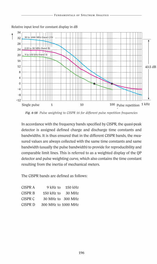
Fig. 6-18 Pulse weighting to CISPR 16 for different pulse repetition frequencies
In accordance with the frequency bands specified by CISPR, the quasi-peak
detector is assigned defined charge and discharge time constants and
bandwidths. It is thus ensured that in the different CISPR bands, the mea-
sured values are always collected with the same time constants and same
bandwidth (usually the pulse bandwidth) to provide for reproducibility and
comparable limit lines. This is referred to as a weighted display of the QP
detector and pulse weighting curve, which also contains the time constant
resulting from the inertia of mechanical meters.
The CISPR bands are defined as follows:
CISPR A 9 kHz to 150 kHz
CISPR B 150 kHz to 30 MHz
CISPR C 30 MHz to 300 MHz
CISPR D 300 MHz to 1000 MHz
Fundamentals of Spectrum Analysis
196
1 kHz10 100 1
32
28
24
20
16
12
8
4
0
–4
–8
–12
34
Single pulse
43.5 dB
Pulse repetitionf
Relative input level for constant display in dB
30 to 1000 MHz (band C/D)
0.15 to 30 MHz (band B)
9 to 150 kHz (band A)
R&S_Pappband_Spektrumanal 24.10.2001 17:44 Uhr Seite 196

197
The weighting of different pulse repetition frequencies shows that the
greatest difference between the displayed levels is at low pulse repetition
frequencies. With increasing pulse repetition frequency (PRF), for instance
PRF >10 kHz, the levels displayed by all detectors (AV, RMS and QP) ap-
proach the value of the peak detector.
Fig. 6-19 Levels displayed with different detectors and pulse repetition frequencies relative to peak display
Special standard pulse generators are available for calibration of the QP
display of spectrum analyzers and test receivers. Exacting requirements
are placed on such standard pulse generators. For the calibration of test
receivers up to 1 GHz, pulses with a width of much less than 1 ns are re-
quired, in practice usually 200 or 250 ps. In addition to the short pulse du-
ration, extremely short pulse rise and fall times can also be realized. The
pulse frequency of the generator must be variable for simulating the
CISPR weighting curve.
Frequent Measurements and Enhanced Functionality
dB
Frequency band 6 dB measure- Charge time Discharge time Time constant
ment bandwidth of QP detector of QP detector of meter
CISPR A 200 Hz 45 ms 500 ms 160 ms
CISPR B 9 kHz 1 ms 160 ms 160 ms
CISPR C 120 kHz 1 ms 550 ms 100 ms
CISPR D 120 kHz 1 ms 550 ms 100 ms
dB
0
–10
–20
–30
–40
–50
–60
–70
–80100 101 102 103 104 105 Hz2 3 5 2 3 5 2 3 5 2 3 5 2 3 5
CISPR band B (150 kHz to 30 MHz)
PK
OP
RMS
AV
Pulse repetition frequency
R&S_Pappband_Spektrumanal 24.10.2001 17:44 Uhr Seite 197
Peak detector PK/MHz
Another way of specifying the level in EMI measurements is the peak val-
ue referred to a 1 MHz bandwidth. In this display mode the pulse spectral
density of the input signal is measured. The peak value at the output of the
envelope demodulator within the selected measurement time is referred
to 1 MHz. It should be noted that due to the measurement bandwidth, the
displayed peak value is increased by 20 · log (1 MHz/BI).
Broadband and narrowband interference
Different pulse weighting methods are used in EMC. These are based on
the different limit values defined for broadband and narrowband interfer-
ence. Broadband interference is relatively evenly distributed over the spec-
trum, but due to this flat spectral distribution, the disturbance is lower
than that of a sinusoidal spurious signal (narrowband interferer) of a very
high level. The permissible spurious emission limit values are 10 dB high-
er than the narrowband limit values (depending on the relevant standard).
This means that a narrowband interferer should be suppressed in a circuit
(attenuated by at least 10 dB) by suitable RFI rejection or shielding.
The detector method and bandwidth detuning method are suitable to dif-
ferentiate between broadband and narrowband interference.
The detector method is based on the assumption that narrowband in-
terference weighted once by a peak detector and once by an average de-
tector yields approximately the same result (difference <6 dB). If there is a
greater difference, the interference is of broadband nature and the limit
values for broadband interference have to be applied. The detector method
can employ both a PK /AV and a PK /RMS detector comparison, depending
on the standard used.
The bandwidth detuning method assumes that a signal level is dis-
played with the selected peak detector, and used as a reference value. The
measurement is repeated with the same settings, but with the center fre-
quency shifted by ±(measurement bandwidth B). If the two new values are
less than the critical threshold (6 dB) of the reference level, the signal is
considered to be a narrowband interferer. An interferer that is not identi-
fied as being narrowband is considered to be broadband. The detuning
method can also be carried out with the center frequency shifted by ±2B.
Both methods are permitted in the relevant standards.
Fundamentals of Spectrum Analysis
198
R&S_Pappband_Spektrumanal 24.10.2001 17:44 Uhr Seite 198

199
6.2.5.2 Measurement bandwidths
The measurement bandwidths specified in the standards for pulse mea-
surements within spurious emission measurements are to be understood
as pulse bandwidths. For commercial standards, these are the bandwidths
of
200 Hz , 9 kHz, 120 kHz (civil specifications, such as EN, VDE, FCC, VCCI, etc),
whereas for military standards the following decade steps apply:
10 Hz, 100 Hz, 1 kHz, 10 kHz, 100 kHz, 1 MHz.
These bandwidths (designated as pulse bandwidths) as well as the QP de-
tector are additionally implemented in modern spectrum analyzers which,
due to their performance features regarding overload capability and dy-
namic range, are suitable for spurious emission measurements.
6.3 Channel and adjacent-channel power measurement(Dipl.-Ing. Roland Minihold)
6.3.1 Introduction
Advanced 3rd generation mobile radio systems operating on the CDMA
principle (code division multiple access) have a frequency multiplex com-
ponent like that of the 2nd generation TMDA systems (time domain multi-
ple access systems, such as GSM or IS-136) or the traditional 1st generation
analog FDMA systems (frequency domain multiple access, such as AMPS).
Frequent Measurements and Enhanced Functionality
R&S_Pappband_Spektrumanal 24.10.2001 17:44 Uhr Seite 199
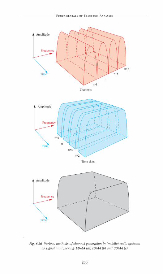
a)
b)
c
Fig. 6-20 Various methods of channel generation in (mobile) radio systems by signal multiplexing: FDMA (a), TDMA (b) and CDMA (c)
Fundamentals of Spectrum Analysis
200
Amplitude
Frequency
Time
Amplitude
Frequency
Time
Time slots
n–1
n
n+1
n+2
Amplitude
Frequency
Time
Channels
n–1
n
n+1
n+2
R&S_Pappband_Spektrumanal 24.10.2001 17:44 Uhr Seite 200
201
This means that in all these systems there are several adjacent radio chan-
nels in the frequency band providing multiple access. The main difference
between the various systems lies in the fact that compared to the tradi-
tional analog radio systems, the radio channels occupy a larger bandwidth.
In the traditional analog radio system such as the American AMPS system,
each user is allocated a separate transmit and receive channel, which are
both occupied over the whole duration of active radiocommunication. In
TDMA systems, several users either share transmit and receive channels
in the time domain (frequency duplex as in the GSM systems), or transmit
and receive channel are identical (time duplex as in DECT systems). In mo-
bile radio systems operating on the CDMA principle, many users (often ap-
proximately 128) share sufficiently wide transmit and receive channels.
The two channels are used over the whole duration and the individual
users are separated using despreading codes.
To ensure undisturbed reception for a large number of users, it is ab-
solutely necessary to avoid interference with adjacent transmission chan-
nels in the frequency band. An important criterion is a sufficiently low ad-
jacent-channel power specified either as absolute value (in dBm) or
relative value referred to the channel power in the transmit channel (in
dBc).
For cdmaOne systems (IS-95, 1.25 MHz channel bandwidth), addition-
al limit values have been prescribed for signals emitted in neighboring
analog radio channels of the AMPS systems (30 kHz channel bandwidth).
In TDMA systems (such as IS-136 or GSM), the transmitter power, and
hence the unwanted power radiated in the adjacent channels, is only ap-
plied in certain timeslots, so that special measures such as gating (mea-
surement only during the active timeslot) are required. A distinction is usu-
ally made as to whether the spurious emissions in the adjacent channels
are caused by the modulated stationary transmitter signal (spectrum due
to modulation) or by the on/off switching of the transmitter signal (spec-
trum due to switching). A spectrum analyzer intended for performing mea-
surements on TDMA systems should therefore feature suitable functions
for adjacent-channel power measurement as well as gating and trigger
functions.
Frequent Measurements and Enhanced Functionality
R&S_Pappband_Spektrumanal 24.10.2001 17:44 Uhr Seite 201

6.3.2 Key parameters for adjacent-channel powermeasurement
In addition to the channel bandwidth of the user channel and the adjacent
channels, the channel spacings are important parameters for adjacent-
channel power measurements. Channel spacing is understood as the dif-
ference between the center frequency of the user channel and that of the
adjacent channel.
The number of adjacent channels in which the channel power is mea-
sured is also important. The table below shows the channels to be mea-
sured according to the number of channels set:
As shown in Fig. 6-21, the adjacent channels have different designations
according to their position relative to the user channel. In our example,
two channels will be set.
Fundamentals of Spectrum Analysis
202
No. of channels Channel power measurement
0 User channel only
1 User channel and upper/lower adjacent channel
2 User channel and adjacent channels +
1st alternate channels
3 User channel and adjacent channels + 1st alter-
nate channels + 2nd alternate channels
R&S_Pappband_Spektrumanal 24.10.2001 17:44 Uhr Seite 202

203
Fig. 6-21 Position of user channel and adjacent channels in frequency domain, here for a WCDMA signal
6.3.3 Dynamic range in adjacent-channel power measure-ments(see also chapter 5.5: Dynamic range)
The dynamic range achievable in adjacent-channel power measurements
using a spectrum analyzer is influenced by three factors, assuming suffi-
cient filter selectivity for user channel suppression and ideal signal:
• Thermal inherent noise of analyzer
In this case it is the signal-to-noise ratio achieved with the specific device
setting (measurement level on analyzer, RF attenuation, reference level).
• Phase noise of the analyzer
• Intermodulation products (spectral regrowth)
Intermodulation products falling within the adjacent channels are a cru-
cial factor especially in measurements on wideband CDMA systems.
Frequent Measurements and Enhanced Functionality
A tt 10 dB
CLRWR
A
R B W 3 0 kHz
V B W 3 0 0 kHz
S W T 1 0 0 ms
1RM
*
*
*
*
R ef -10 d B m
C e n t e r 2 . 1 G H z S p a n 2 5 . 4 6 5 7 4 3 6 3 M H z2 . 5 4 6 5 7 4 3 6 3 M H z /
PRN00
-90
-80
-70
-60
-50
-40
-30
-20
B a n d w i d th 3.84 M H z
B a n d w i d th 3.84 M H z
S p a ci n g 5 M H z
B a n d w i d th 3.84 M H z
S p a ci n g 1 0 M H z
T x C h a n n e l
P o w e r -7 . 3 4 d B m
A dj a c e n t C h a n n e l
L o w e r - 58 . 7 5 d B c
U p p e r - 59 . 2 4 d B c
A l t e r n a t e C h a nn e l
L o w e r - 59 . 3 2 d B c
U p p e r - 58 . 8 4 d B c
C 0C 0
c u 2c u 2
c u1c u1
cl1c l1
cl2cl2
-1
R&S_Pappband_Spektrumanal 24.10.2001 17:44 Uhr Seite 203
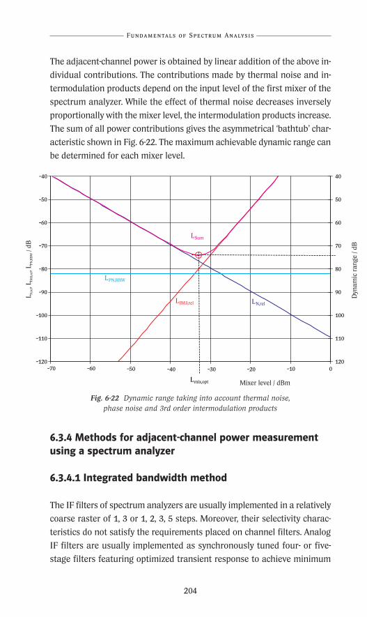
The adjacent-channel power is obtained by linear addition of the above in-
dividual contributions. The contributions made by thermal noise and in-
termodulation products depend on the input level of the first mixer of the
spectrum analyzer. While the effect of thermal noise decreases inversely
proportionally with the mixer level, the intermodulation products increase.
The sum of all power contributions gives the asymmetrical ‘bathtub’ char-
acteristic shown in Fig. 6-22. The maximum achievable dynamic range can
be determined for each mixer level.
Fig. 6-22 Dynamic range taking into account thermal noise, phase noise and 3rd order intermodulation products
6.3.4 Methods for adjacent-channel power measurementusing a spectrum analyzer
6.3.4.1 Integrated bandwidth method
The IF filters of spectrum analyzers are usually implemented in a relatively
coarse raster of 1, 3 or 1, 2, 3, 5 steps. Moreover, their selectivity charac-
teristics do not satisfy the requirements placed on channel filters. Analog
IF filters are usually implemented as synchronously tuned four- or five-
stage filters featuring optimized transient response to achieve minimum
Fundamentals of Spectrum Analysis
204
–120
–110
–100
–90
–80
–70
–60
–50
–40
–70 –60 –50 –40 –30 –20 –10 0
40
50
60
70
80
90
100
110
120
LPN,RBW
LIM3,rel LN,rel
LSum
Lmix,opt
L N,r
el, L
IM3,
rel,
L PN
,RB
W /
dB
Dyn
amic
ran
ge /
dB
Mixer level / dBm
R&S_Pappband_Spektrumanal 24.10.2001 17:44 Uhr Seite 204

205
sweep times. The selectivity characteristic of filters with a shape factor of
approximately 12 for four-stage filters and approximately 9.5 for five-stage
filters is rather poor and usually inadequate for sufficient suppression of
the signal in the user channel for adjacent channel measurements. Digital
resolution filters of modern spectrum analyzers that are usually imple-
mented as Gaussian filters are not suitable as channel filters despite their
better selectivity (shape factor of 4.6).
Therefore, spectrum analyzers usually offer power integration fea-
tures in the frequency domain for adjacent-channel power measurement.
Compared to the channel bandwidth, a very small resolution bandwidth of
typically 1% to 3% of the channel bandwidth is set to ensure appropriate
selectivity. The spectrum analyzer sweeps over the frequency range of in-
terest from the start of the lower adjacent channel to the end of the upper
adjacent channel depending on the number of measured adjacent chan-
nels (Fig. 6-21).
Fig. 6-23 Channel power measurement using integrated bandwidth method
Frequent Measurements and Enhanced Functionality
Dyn
amic
ran
ge /
dB
PRN
*
*
V B W 3 0 0 kHz
R B W 3 0 k Hz
1 5 0 k Hz / S p an 1 . 5 M H zC e n t e r 1 G Hz
A
S W T 1 0 0 msA tt 40 dBRef 10 dBm
-90
-80
-70
-60
-50
-40
-30
-20
-10
0
10 M a r k e r 1 [ T 1]
- 14 . 1 1 dBm
9 9 9. 3 8 3 0 0 0 0 0 MHz
D el t a 2 [ T 1 ]
2 . 1 5 dB
1. 2 3 0 0 0 0 0 0 MHz
12
R&S_Pappband_Spektrumanal 24.10.2001 17:44 Uhr Seite 205
The measured values corresponding to the levels of the displayed pixels
are integrated within the selected channel bandwidth on a linear scale.
The resulting adjacent-channel power is stated in dBc referred to the pow-
er in the user channel.
The following individual steps are carried out:
• For all levels measured within a channel, the power is determined on a
linear level scale. The following applies:
Pi = 10 (Li/10) (Equation 6-17)
where Pi = power of a measured value represented by pixel i
on linear level scale, in W
Li = level of a measured value represented by pixel i,
in dBm
• The linear power of all trace points within a channel is summed up and
divided by the number of trace points in the channel.
• The result in each channel is multiplied by the quotient from the select-
ed channel bandwidth and noise bandwidth of the resolution filter.
From the above steps, the following relationship is obtained for the ab-
solute channel power:
LCh = 10 · log · · 10 (Equation 6-18)
where LCh = channel power level, in dBm
BCh = channel bandwidth, in Hz
BN,IF = noise bandwidth of IF filter, in Hz
n1, n2 = indexes of measured values to be summed up
Pi = power of a measured value represented by pixel i, in W
Fundamentals of Spectrum Analysis
206
BCH
BN, IF
1
n2– n1( )n1
n2
ΣPi
10
R&S_Pappband_Spektrumanal 24.10.2001 17:44 Uhr Seite 206

207
Selection of resolution bandwidth (RBW)
The selected resolution bandwidth should be small relative to the channel
bandwidth for the channel bandwidth to be measured accurately. If the
resolution bandwidth is too large, the selectivity of the simulated channel
filter is insufficient and part of the main channel power will be measured
when measuring the adjacent channels, so the final result will be incorrect.
The well-chosen resolution bandwidth is typically 1% to 3% of the channel
bandwidth. If the resolution bandwidth is too small, the required sweep
time becomes unduly long, and the measurement time will be considerably
increased.
Selection of detector
For power measurements within the channel bandwidth, the sample de-
tector and the RMS detector are suitable since only these two detectors
furnish results that allow power calculation. The peak detectors (max
peak, min peak, auto peak) are not suitable for measuring noise or noise-
like signals since a correlation between the detected video voltage and in-
put signal power cannot be established.
When using the sample detector, the measured value represented by a
pixel is derived from a sample of the IF envelope voltage. If the displayed
spectrum is large relative to the resolution bandwidth (such as the
span/RBW >500), discrete signal components (sinusoidal signals) may get
lost due to the limited number of pixels of the analyzer screen (approxi-
mately 501), and the channel or adjacent-channel power measurement will
therefore be incorrect (chapter 4.4: Detectors).
Since digitally modulated signals are noise-like signals, the trace ob-
tained with a sample detector is subject to large variations. To obtain sta-
ble results, averaging is necessary, in which case the displayed signal will
be underweighted and falsified (chapter 4.5: Detectors).
When choosing the RMS detector, the power represented by a pixel is
calculated from several measured values to obtain stable results. More-
over, the measurement time can be increased to allow averaging of the
trace. The power of discrete spurious signals contained in the channel is
also correctly determined. The RMS detector is therefore a better choice
than the sample detector for channel power measurements.
Frequent Measurements and Enhanced Functionality
R&S_Pappband_Spektrumanal 24.10.2001 17:44 Uhr Seite 207
The RMS value is calculated from the samples of the video voltage as fol-
lows:
VRMS = · v2i (Equation 6-19)
where VRMS = RMS value of voltage, in V
N = number of samples allocated to the pixel concerned
vi = samples of envelope, in V
The reference resistance R can be used to calculate the power:
P = (Equation 6-20)
Some TDMA mobile radio standards (such as PDC) prescribe a peak de-
tector for measuring the adjacent-channel power (relative measurement)
to ensure better detection of the power transients.
Selection of video bandwidth / trace averaging
When using an RMS or sample detector, the video bandwidth must be at
least three times the resolution bandwidth to avoid averaging of the video
voltage, as this would lead to underweighting of noise-like signals, result-
ing in channel power that would be too low. For this reason, trace averag-
ing over several traces should also be avoided.
6.3.4.2 Spectral power weighting with modulation filter (IS-136, TETRA, WCDMA)
For determining the power in the main and adjacent channels of some mo-
bile radio systems, such as IS-136 (NADC), TETRA and WCDMA, it is nec-
essary to use a channel filter that corresponds to the modulation filter of
the respective system (typically root-raised cosine filter). This leads to a
more realistic weighting of the effect of the power emitted in the adjacent
channel since interference is mainly caused by signal components in the
center of an adjacent channel. Signal components close to the channel
boundaries are suppressed by the matched filter of the receiver so that
these cause less interference.
Fundamentals of Spectrum Analysis
208
1
N√ i=1
N
Σ
V2RMS
R
R&S_Pappband_Spektrumanal 24.10.2001 17:44 Uhr Seite 208

209
When using a spectrum analyzer for adjacent-channel power measure-
ments, the individual trace values in respective channels must be weight-
ed with a standard-specific modulation filter before each channel power is
determined by integration of the measured values. Modern spectrum ana-
lyzers provide measurement functions with automatic weighting.
Fig. 6-24 Channel filter for IS-136 (NADC) systems
Use of a weighting filter in channel power measurements with a spectrum
analyzer can very easily be verified by using the following test:
With the channel power measurement activated, a sinusoidal signal with
a frequency corresponding to the channel center frequency is applied to
the spectrum analyzer input. The measured channel power is used as a ref-
erence.
The frequency of the sinusoidal signal is then varied in steps towards
the channel boundaries (or alternatively by varying the channel center fre-
quency on the spectrum analyzer in case of a fixed-frequency sinusoidal
signal) and the measured channel power observed. If the channel power
varies under these conditions, a channel filter is obviously being used for
weighting.
This test can also be carried out in the adjacent channels. It is recom-
mended to set the spectrum analyzer for absolute adjacent-channel pow-
er measurement.
Frequent Measurements and Enhanced Functionality
fc+2 +4 +6 +8 +10 +12 +14 +16 +18–2–4–6–8–18
0 dB
–3 dB
–6 dB
–9 dB
–12 dB
–15 dB
–18 dB
–21 dB
–27 dB
–30 dB
Frequency/kHz
Att
enu
atio
n
–16 –14 –12 –10
–24 dB
R&S_Pappband_Spektrumanal 24.10.2001 17:45 Uhr Seite 209

6.3.4.3 Channel power measurement in time domain
As explained in chapter 6.3.4.1, very narrowband resolution filters are re-
quired for channel power measurements. Since these filters exhibit low in-
tegration times, their use inevitably leads to relatively long sweep times. If
measurements are carried out over several adjacent channels, frequency
ranges between the individual channels will be included that contain no
information of interest, but contribute to the total sweep time. All these
drawbacks can be avoided by measuring the channel power in the time do-
main.
With the aid of digital signal processing, practically any type of channel fil-
ter can be digitally implemented for modern spectrum analyzers, such as
root-raised cosine filters or near ideal rectangular bandpass filters as well
as filters with very large bandwidth (such as 4 MHz). These filters allow
channel power measurement in the time domain with the spectrum ana-
lyzer being tuned like a receiver to the center frequency of the channel. In
this way it is possible to avoid the limitation of the minimum sweep time
given by the transient time resulting from the narrow resolution band-
widths that are required for measurements in the frequency domain. In
the time domain, a much better reproducibility of the measurement results
can be achieved with the same measurement time as in the frequency do-
main, and the measurement time can be considerably reduced compared
to the conventional integration method.
If the power is to be measured in several adjacent channels, the spec-
trum analyzer is automatically successively tuned to the respective chan-
nel center frequencies. Frequency ranges between the various channels of
interest are skipped so that there is the further advantage in measurement
time compared to measurements in the frequency domain.
Another benefit of time-domain measurements is the correct detection
of transient signals caused by switching operations.
Fundamentals of Spectrum Analysis
210
R&S_Pappband_Spektrumanal 24.10.2001 17:45 Uhr Seite 210
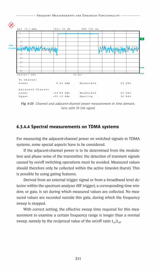
211
Fig. 6-25 Channel and adjacent-channel power measurement in time domain,here with IS-136 signal
6.3.4.4 Spectral measurements on TDMA systems
For measuring the adjacent-channel power on switched signals in TDMA
systems, some special aspects have to be considered.
If the adjacent-channel power is to be determined from the modula-
tion and phase noise of the transmitter, the detection of transient signals
caused by on/off switching operations must be avoided. Measured values
should therefore only be collected within the active timeslot (burst). This
is possible by using gating features.
Derived from an external trigger signal or from a broadband level de-
tector within the spectrum analyzer (RF trigger), a corresponding time win-
dow, or gate, is set during which measured values are collected. No mea-
sured values are recorded outside this gate, during which the frequency
sweep is stopped.
With correct setting, the effective sweep time required for this mea-
surement to examine a certain frequency range is longer than a normal
sweep, namely by the reciprocal value of the on/off ratio ton/toff.
Frequent Measurements and Enhanced Functionality
CLRWR
A
S W T 2 0 0 m sR e f 1 5. 7 d B m A t t 3 0 d B
*
C e n t e r 1 G H z 2 0 m s /
1RM
*
EXT
PRN
-80
-70
-60
-50
-40
-30
-20
-10
0
10
Ba n d w id t h 2 5 k H z
Ba n d w id t h 2 5 k H z
Sp a c i n g 30 k H z
T x C h a n n e l
P o w e r 9 .6 4 d Bm
A d j a c e n t C h a n n e l
L o w e r -3 4 .9 6 d Bc
U p p e r -3 5 .1 2 d Bc
R&S_Pappband_Spektrumanal 24.10.2001 17:45 Uhr Seite 211
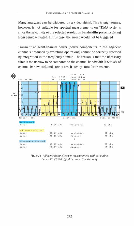
Many analyzers can be triggered by a video signal. This trigger source,
however, is not suitable for spectral measurements on TDMA systems
since the selectivity of the selected resolution bandwidths prevents gating
from being activated. In this case, the sweep would not be triggered.
Transient adjacent-channel power (power components in the adjacent
channels produced by switching operations) cannot be correctly detected
by integration in the frequency domain. The reason is that the necessary
filter is too narrow to be compared to the channel bandwidth (1% to 3% of
channel bandwidth), and cannot reach steady state for transients.
Fig. 6-26 Adjacent-channel power measurement without gating, here with IS-136 signal in one active slot only
Fundamentals of Spectrum Analysis
212
H1 5 .28 0 5 k Hz/ Sp a n 1 5 2 .805 k zC en t e r 1 G Hz
R e f - 1 0 d B m
CLRWR
1RM *
0-1 0
-90
-80
-70
-60
-50
-40
-30
-20
B a n d w i d t h 25 kHz
25 kHz
S p a c i n g 30 kHz
25 kHz
60 kHz
Tx Ch a nn e l
Power -6.65 dBm
A d j a c e n t
Lower -39.60 dBc
Upper -35.12 dBc
Al t e r n a t e C h a n n e l
Lower -69.65 dBc
Upper -68.87 dBc
c l2c l2
c l1c l1
c u1c u1
c uc u2
C 0C 0
B a n d w i d t h
B a n d w i d t h
S p a c i n g
C h a n n e l
PRN
A
*
*
* V B W 1 0 k H z
R B W 1 k H z
S W T 5 0 0 m sA t t 1 0 d B
M i x - 1 0 d B
2
R&S_Pappband_Spektrumanal 24.10.2001 17:45 Uhr Seite 212

213
Fig. 6-27 Adjacent-channel power measurement on IS-136 signal with correctly set gating (spectrum due to modulation)
Fig. 6-28 Gate setting in time domain
Frequent Measurements and Enhanced Functionality
PRN
GAT
1 5 . 2 8 0 5 k H z/ S p a n 1 5 2. 80 5 k H zC e n t e r 1 G H z
TRG
A
*
*
* V B W 1 0 k H z
R B W 1 k H z
S W T 1 s
25 kH z
25 kH z
30 kH z
25 kH z
60 kH z
T x Ch a nn e l
Power -2.79 dBm
Lower -33.51 dBc
Upper -32.32 dBc
Lower -67.10 dBc
Upper -67.48 dBc
C0C0
cl 2cl 2
cl 1cl 1
cu 1cu 1
cu 2cu 2
A t t 1 0 d B
M i x - 1 0 d B
B a n d w i d t h
B a n d w i d t h
S p a c i n g
B a n d w i d t h
S p a c i n g
A d j a c e n t C h a n n e l
Al t e r n a t e C h a n n e l
CLRWR
1RM *
R e f - 1 0 d B m
0-1 0
-90
-80
-70
-60
-50
-40
-30
-20
G H z
PRN
1 m s/C e n t e r 1
SW T 1 0 m s
TRG
* VBW 1 0 k H z
R BW 1 k H z
M i x -10 dBm
A
CLRWR
1RM *
A t t 10 dBR ef -10 dBm
-110
-100
- 90
- 80
- 70
- 60
- 50
- 40
- 30
- 20
- 10
GD GL
R&S_Pappband_Spektrumanal 24.10.2001 17:45 Uhr Seite 213
Fundamentals of Spectrum Analysis
References
[2-1] Brigham, E.O.: The Fast Fourier Transform and its Application.
Prentice Hall, 1988
[3-1] Parks, T.W., Burrus, C.S.: Digital Filter Design. John Wiley & Sons,
Inc., New York, Chichester, Brisbane, Toronto, Singapore, 1987.
[3-2] Oppenheim, A.V., Schafer, R.W.: Discrete-Time Signal Processing.
Prentice Hall, 1989.
[4-1] Helszajn, J.: YIG Resonators and Filters. John Wiley & Sons Ltd.,
Chichester, New York, Brisbane, Toronto, Singapore, 1985.
[4-2] Rauscher, C.: Frequency Range Extension of Spectrum Analyzers
with Harmonic Mixers. Application Note*) 1EF43_0E, Rohde &
Schwarz.
[4-3] Volder, J.E.: The CORDIC Trigonometric Computing Technique.
IRE Transaction on Electronic Computers, vol. EC-8, Seite 330-334,
Sept 1959.
[4-4] CISPR 16-1 (1997-07): Specification for radio disturbance and im-
munity measuring apparatus and methods, Part 1: Radio distur-
bance and immunity measuring apparatus.
[5-1] Winder, S.: Single Tone Intermodulation Testing. RF Design, Dezem-
ber 1993, p. 34.
[5-2] Freed, J.G.: Equations Provide Accurate Third-Order IMD Analysis.
Microwaves & RF, August 1992, p. 75.
[5-3] Rohde, U.L.: Microwave and Wireless Synthesizers Theory and De-
sign. John Wiley & Sons, Inc., New York, Chichester, Weinheim, Bris-
bane, Singapore, Toronto, 1997.
[5-4] Beck, B.: Understand the Effects of Retrace and Aging in OCXOs.
Microwaves & RF, November 1998, p. 72.
214
R&S_Pappband_Spektrumanal 24.10.2001 17:45 Uhr Seite 214

[5-5] Wolf, J.: Level Error Calculation for Spectrum Analyzers. Application
Note*) 1EF36_0E, Rohde & Schwarz.
*) Rohde & Schwarz Application Notes are available on the Internet under
www.rohde-schwarz.com.
215
References
R&S_Pappband_Spektrumanal 24.10.2001 17:45 Uhr Seite 215

Fundamentals of Spectrum Analysis
The current* spectrum analyzer modelsfrom Rohde & Schwarz
*As of summer 2001
216
R&S_Pappband_Spektrumanal 24.10.2001 17:45 Uhr Seite 216

The Current Spectrum Analyzer Models From Rohde & Schwarz
High-end allrounders:Spectrum Analyzer Family FSU
The FSU models introduced in 2001 set new standards for all RF perfor-
mance data of spectrum analyzers. This applies to dynamic range, over-
load capacity, phase noise and measurement accuracy alike. The instru-
ments are equipped to match their outstanding data. The FSU is the first
general-purpose spectrum analyzer with a resolution bandwidth of 50
MHz, which is ideal for measurements on broadband communication sys-
tems. A full choice of detectors, numerous resolution filters and filter
characteristics, as well as automatic routines for many standard mea-
surement tasks make these instruments extremely efficient and econom-
ical tools for use in the development lab and in production environments.
Application firmware packages, such as for GSM/EDGE or WCDMA, are
available to enhance the comprehensive basic configuration by adding
special mobile radio measurement functions, including modulation mea-
surement.
217
R&S_Pappband_Spektrumanal 24.10.2001 17:45 Uhr Seite 217

Fundamentals of Spectrum Analysis
Fully equipped high flyers:Spectrum Analyzers FSEM/FSEK
The Spectrum Analyzers FSEM and FSEK from Rohde & Schwarz for fre-
quencies up to 26.5 GHz and 44 GHz are suitable for the upper microwave
range. Use of the optional External Mixers FS-Zx opens up the range to
110 GHz, which is close to infrared. The analyzers are by no means purist
high-frequency machines, but come with a comprehensive basic function-
ality that can be further enhanced for diverse measurement tasks by a
large variety of options.
218
R&S_Pappband_Spektrumanal 24.10.2001 17:45 Uhr Seite 218
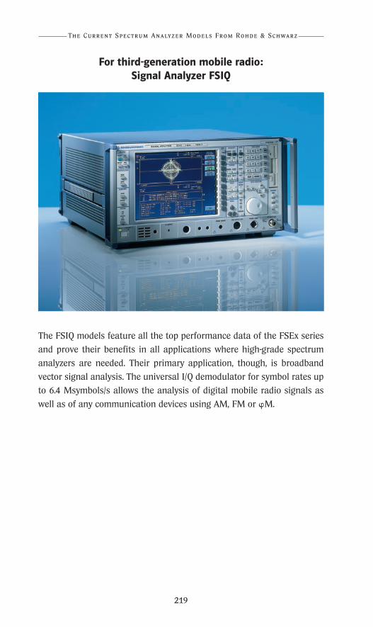
For third-generation mobile radio:Signal Analyzer FSIQ
The FSIQ models feature all the top performance data of the FSEx series
and prove their benefits in all applications where high-grade spectrum
analyzers are needed. Their primary application, though, is broadband
vector signal analysis. The universal I/Q demodulator for symbol rates up
to 6.4 Msymbols/s allows the analysis of digital mobile radio signals as
well as of any communication devices using AM, FM or M.
219
The Current Spectrum Analyzer Models From Rohde & Schwarz
R&S_Pappband_Spektrumanal 24.10.2001 17:45 Uhr Seite 219
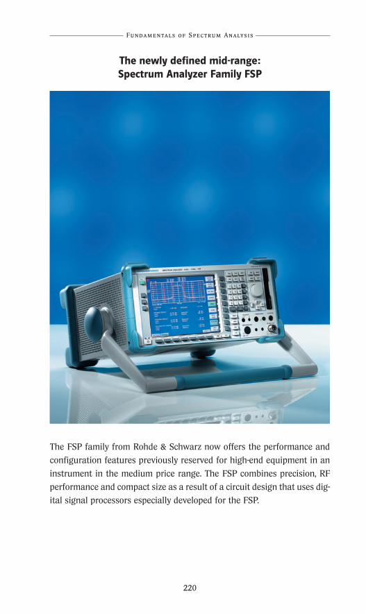
Fundamentals of Spectrum Analysis
The newly defined mid-range:Spectrum Analyzer Family FSP
The FSP family from Rohde & Schwarz now offers the performance and
configuration features previously reserved for high-end equipment in an
instrument in the medium price range. The FSP combines precision, RF
performance and compact size as a result of a circuit design that uses dig-
ital signal processors especially developed for the FSP.
220
R&S_Pappband_Spektrumanal 24.10.2001 17:45 Uhr Seite 220

The EMC expert:EMI Test Receiver ESI
The designation as a "test receiver" is somewhat deceptive, since the ESI
actually is a full-featured and high-grade spectrum analyzer. As a one-box
solution for EMI compliance measurements, it provides all the functions
required for EMI measurements conforming to standards. The ESI per-
forms measurements to all relevant commercial and military standards,
and its upper frequency limit of 40 GHz covers all frequency ranges that
are significant for EMC measurements.
221
The Current Spectrum Analyzer Models From Rohde & Schwarz
R&S_Pappband_Spektrumanal 24.10.2001 17:46 Uhr Seite 221
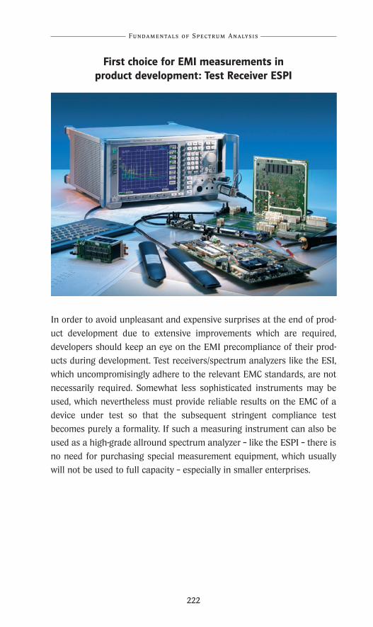
Fundamentals of Spectrum Analysis
First choice for EMI measurements inproduct development: Test Receiver ESPI
In order to avoid unpleasant and expensive surprises at the end of prod-
uct development due to extensive improvements which are required,
developers should keep an eye on the EMI precompliance of their prod-
ucts during development. Test receivers/spectrum analyzers like the ESI,
which uncompromisingly adhere to the relevant EMC standards, are not
necessarily required. Somewhat less sophisticated instruments may be
used, which nevertheless must provide reliable results on the EMC of a
device under test so that the subsequent stringent compliance test
becomes purely a formality. If such a measuring instrument can also be
used as a high-grade allround spectrum analyzer – like the ESPI – there is
no need for purchasing special measurement equipment, which usually
will not be used to full capacity – especially in smaller enterprises.
222
R&S_Pappband_Spektrumanal 24.10.2001 17:46 Uhr Seite 222
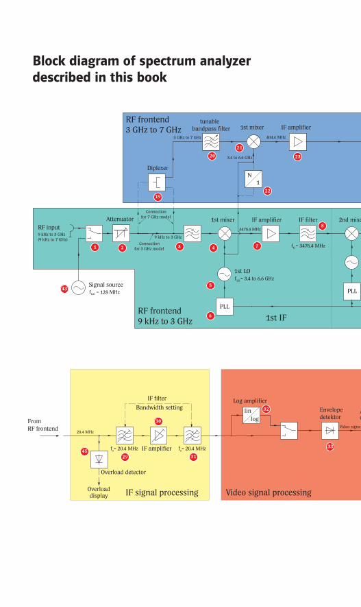
9 kHz to 3 GHz(9 kHz to 7 GHz)
RF input
f = 128 MHzCal
Attenuator
Diplexer
3 GHz to 7 GHz
1st mixertunable
bandpass filter404.4 MHz
1N
3.4 to 6.6 GHz
IF amplifier
3476.4 MHz
Signal source
RF frontend3 GHz to 7 GHz
PLL
1 2 3 4
5
19
20
21
22
23
7
6
8
9
10
11
1st IF
29
30
32
DA
34
FromRF frontend
IF signal processing
Envelopedetektor
330
31
Bandwidth settingLog amplifier
A/D conve
Video signal processing
43
Video signal
1245
Connectionfor 7 GHz model
Connectionfor 3 GHz model
9 kHz to 3 GHz
1st mixer 2nd mixerIF amplifier IF filter
RF frontend9 kHz to 3 GHz
f = 3.4 to 6.6 GHz
1st LO
LO
f = 3476.4 MHzO
PLL
f = 32nd L
LO
404.4
IF filter
IF amplifier
Overload detector
Overloaddisplay
f = 20.4 MHz0
f = 20.4 MHz
20.4 MHz
log
lin
Block diagram of spectrum analyzerdescribed in this book
R&S_Pappband_Spektrumanal 24.10.2001 17:46 Uhr Seite B
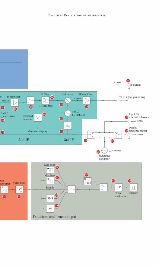
Practical Realization of an Analyzer
Referenceoscillator
Input forexternal reference
Outputreference signal
To IF signal processing
9
10
11
1213
14
1518
16
17
24 25
26
2nd IF 3rd IF
DA
34 35
41A/D converter Video filter
Detectors and trace output
28
27
39
RMS
AV
loglin
Display
Max Peak
Sample
36
37
38
39
40
o signal
42
Traceevaluation
µP
Overloaddetector
Overload display
44
d mixer
PLL
f = 3072 MHz2nd LO
LO
f = 384 MHz
3rd LO
LO
404.4 MHz
3rd mixerIF amplifier
IF filter
f = 404.4 MHzO
PLL
20.4 MHz
IF amplifier
20.4 MHz
10 MHz
10 MHz
IF output
f = 10 MHzRef
Min Peak
R&S_Pappband_Spektrumanal 24.10.2001 17:46 Uhr Seite C