SOLAR SolarInnovativ Thüringen - CiS :: Willkommen bei...
38
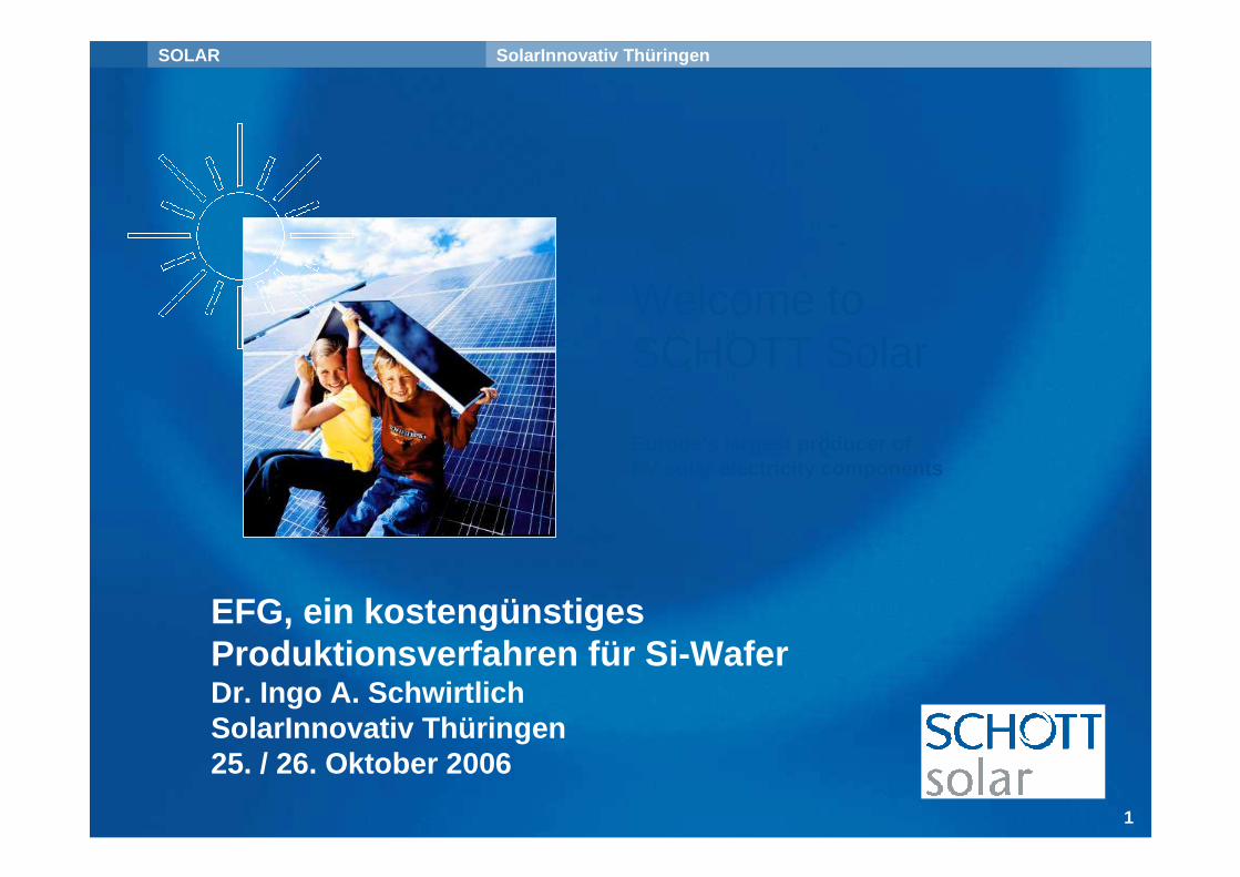
SOLAR SolarInnovativ Thüringen 1 Welcome to SCHOTT Solar Europe's largest producer of PV solar electricity components EFG, ein kostengünstiges Produktionsverfahren für Si-Wafer Dr. Ingo A. Schwirtlich SolarInnovativ Thüringen 25. / 26. Oktober 2006
-
Upload
trankhuong -
Category
Documents
-
view
214 -
download
0
Transcript of SOLAR SolarInnovativ Thüringen - CiS :: Willkommen bei...
SOLAR SolarInnovativ Thüringen
1
Welcome toSCHOTT Solar
Europe's largest producer ofPV solar electricity components
EFG, ein kostengünstiges Produktionsverfahren für Si-WaferDr. Ingo A. SchwirtlichSolarInnovativ Thüringen25. / 26. Oktober 2006

SOLAR SolarInnovativ Thüringen
2
The SCHOTT Synopsis
��������� ����� ���
� � �� � � � � �*� � � � ��� �� � ��� �� � � � ��� � ��� �� � � � �
� �� �
� �� �� �� � ����
� �� ��� ��� ���� � � � ����
� ��������� � � � �� � � ���� � �� �� �� ���� �
���! �� ��� ��� ��� �� �� � �� � ��
���" # $% % % ���� �� ��� ��� �& # ���� �� ���

SOLAR PHOTOVOLTAICS
3
200119991960 1970 1980
AEG Telefunken
Mobil Tyco Solar Energy
1990
MBB
1994
PST
DASA 50%
NUKEM 50%
Mobil Solar Energy
1996
100% TESSAG
100% NUKEM GmbH
100%RWE Solutions AG
ASE GmbH
ASE Americas Inc.
2002
RWE SCHOTT SolarGmbH
RWE SCHOTTSolar Inc.
Joint VentureRWE SolutionsSCHOTT Glas
RWE Solar GmbH
ASE Americas Inc.
2005
SCHOTTSolar GmbH
1999 2001
SOLAR PHOTOVOLTAICS
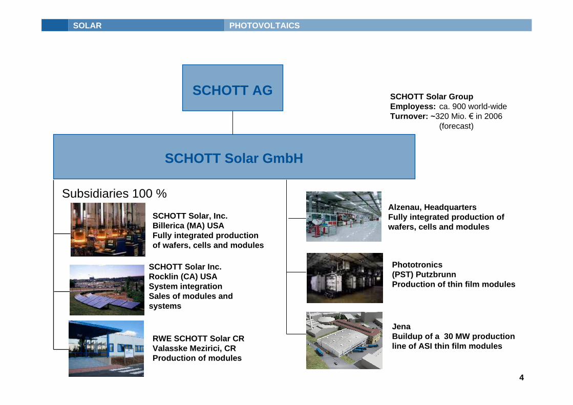
4
Alzenau, HeadquartersFully integrated production of wafers, cells and modules
Phototronics(PST) PutzbrunnProduction of thin film modules
SCHOTT Solar GmbH
SCHOTT Solar, Inc.Billerica (MA) USAFully integrated productionof wafers, cells and modules
SCHOTT Solar Inc.Rocklin (CA) USASystem integrationSales of modules andsystems
RWE SCHOTT Solar CRValasske Mezirici, CRProduction of modules
SCHOTT Solar GroupEmployess: ca. 900 world-wideTurnover: ~320 Mio. � in 2006
(forecast)
SCHOTT AG
Subsidiaries 100 %
JenaBuildup of a 30 MW productionline of ASI thin film modules
SOLAR PHOTOVOLTAICS
5
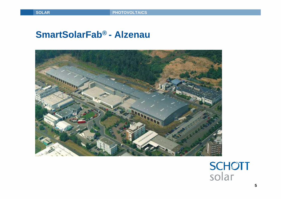
SmartSolarFab® - Alzenau
OEM Zellenfertigung
Heilbronn, D
SOLAR PHOTOVOLTAICS
6
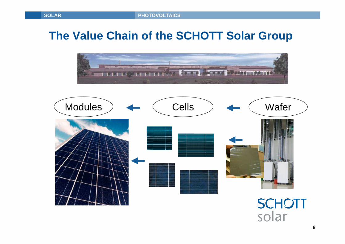
The Value Chain of the SCHOTT Solar Group
Modules Cells Wafer
SOLAR PHOTOVOLTAICS
7
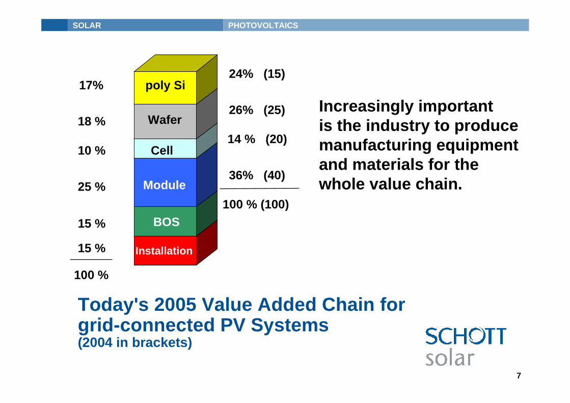
Today's 2005 Value Added Chain forgrid-connected PV Systems(2004 in brackets)
Module
poly Si
BOS
Installation
Cell
Wafer18 %
10 %
25 %
15 %
100 %
15 %
17%
26% (25)
14 % (20)
36% (40)
24% (15)
100 % (100)
Increasingly important is the industry to producemanufacturing equipmentand materials for the whole value chain.
SOLAR PHOTOVOLTAICS
8
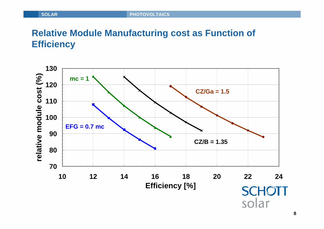
70
80
90
100
110
120
130
10 12 14 16 18 20 22 24Efficiency [%]
rela
tive
mo
du
le c
ost
(%
)
EFG = 0.7 mc
CZ/B = 1.35 mc
CZ/Ga = 1.5 mc
mc = 1
Relative Module Manufacturing cost as Function ofEfficiency
SOLAR PHOTOVOLTAICS
9
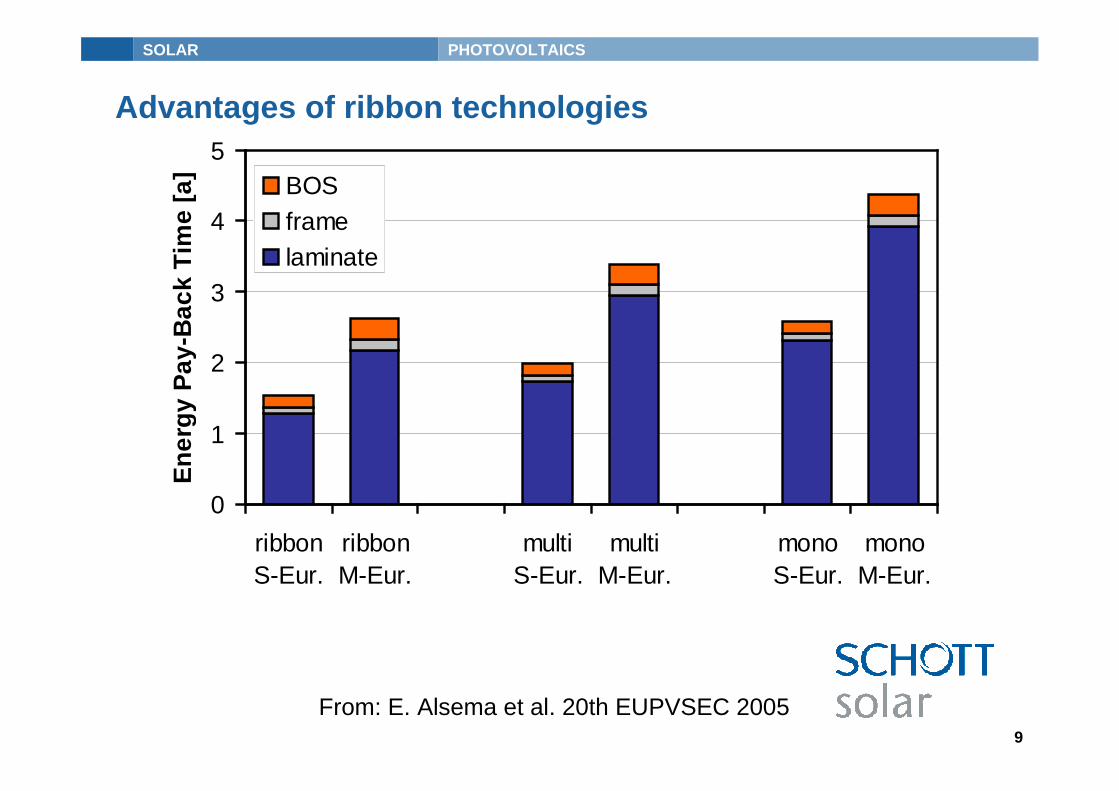
Advantages of ribbon technologies
0
1
2
3
4
5
ribbonS-Eur.
ribbonM-Eur.
multi S-Eur.
multiM-Eur.
monoS-Eur.
monoM-Eur.
En
erg
y P
ay-B
ack
Tim
e [a
] BOSframelaminate
From: E. Alsema et al. 20th EUPVSEC 2005

SOLAR PHOTOVOLTAICS
10
Estimated reduction of silicon consumption
0
2
4
6
8
10
12
14
16
2005 2010 2015 2020 2025
g S
i/ Wp mono / multi - Si15 % EFG
85 % mono / multi - Si
EFG
Specific feed stock consumption per Wp for different wafer technologies
SOLAR PHOTOVOLTAICS
11
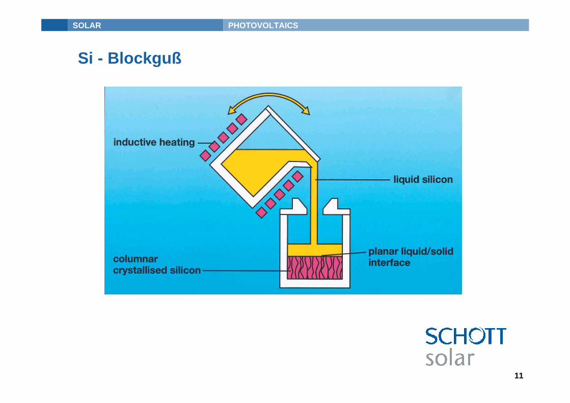
Si - Blockguß
SOLAR PHOTOVOLTAICS
12
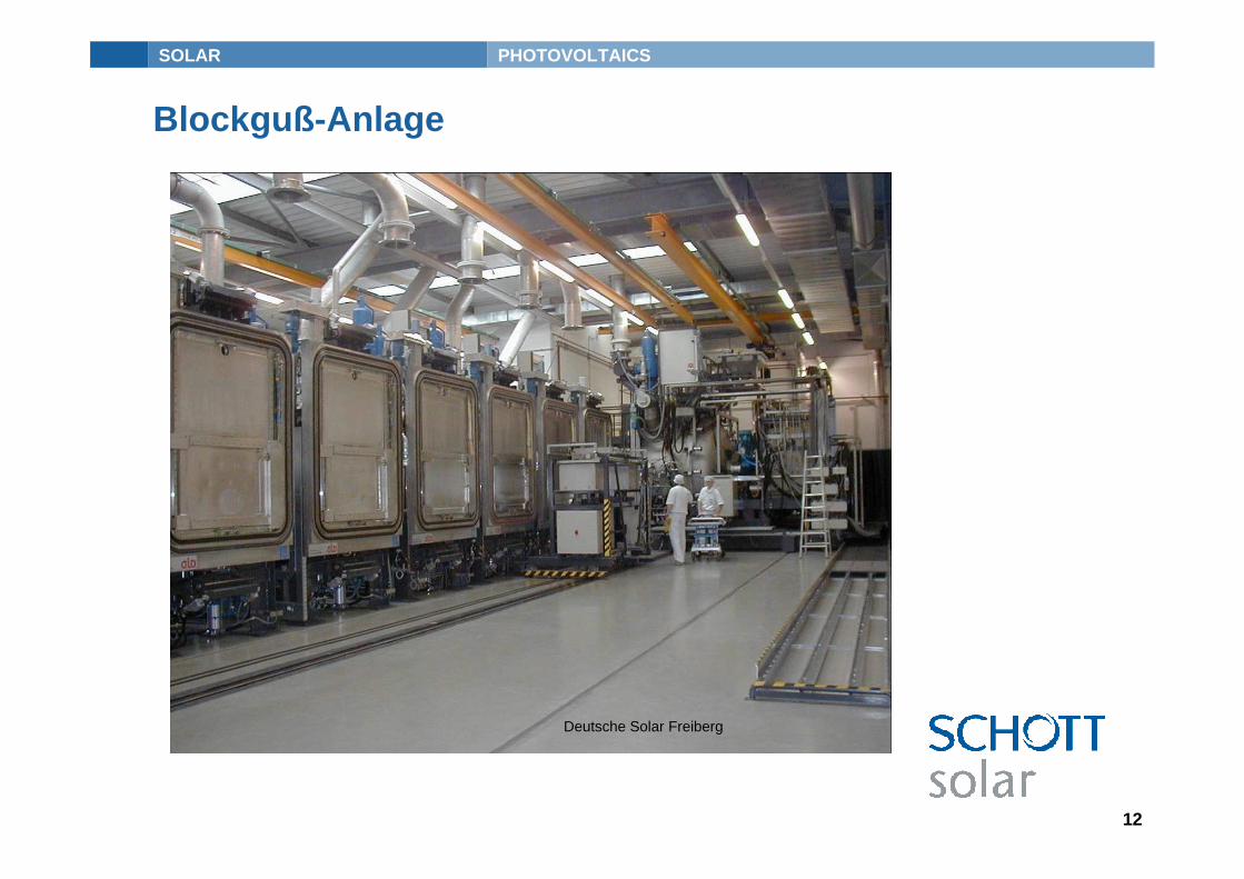
Blockguß-Anlage
Deutsche Solar Freiberg
SOLAR PHOTOVOLTAICS
13
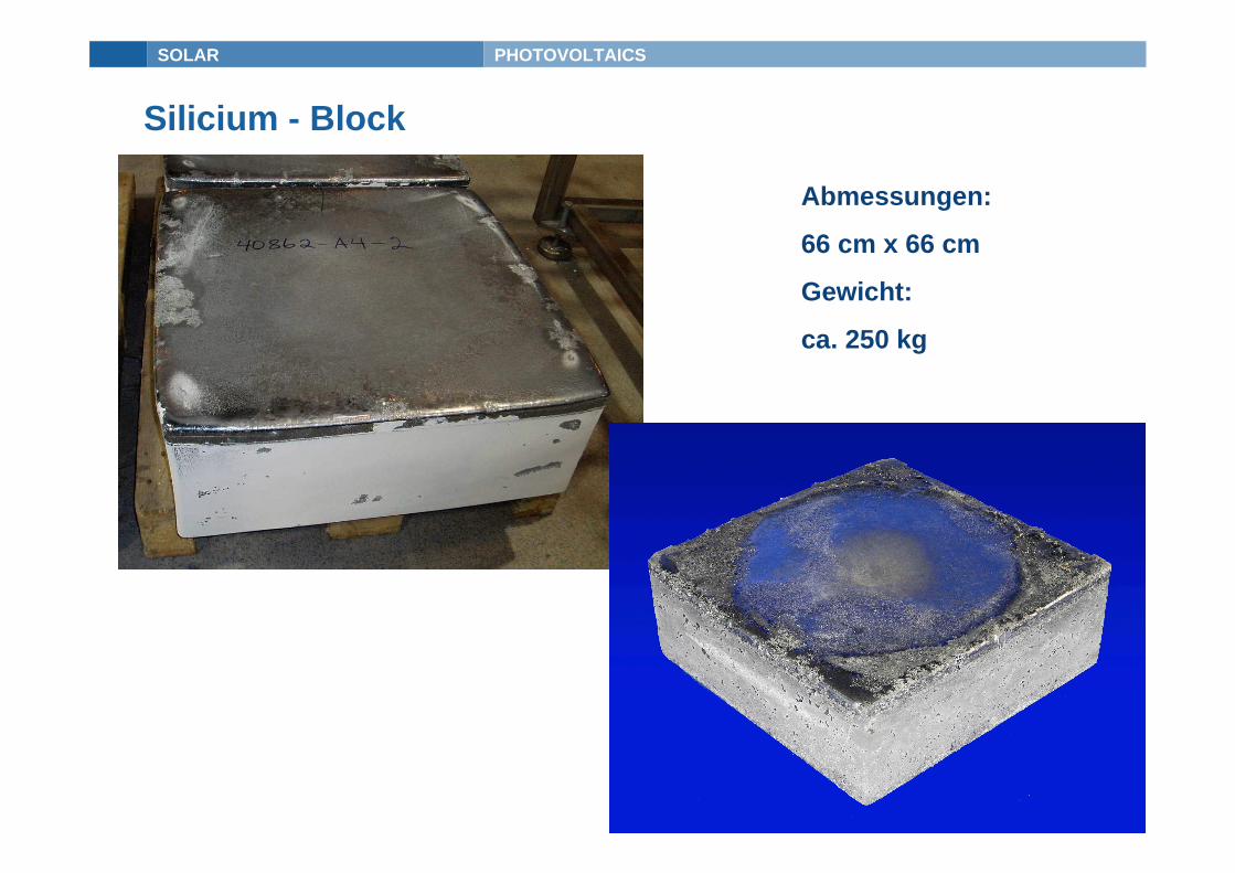
Silicium - Block
Abmessungen:
66 cm x 66 cm
Gewicht:
ca. 250 kg
SOLAR PHOTOVOLTAICS
14
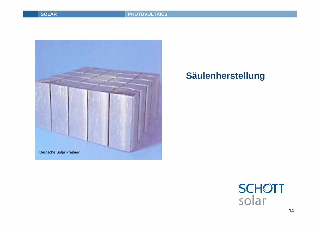
Säulenherstellung
Deutsche Solar Freiberg
SOLAR PHOTOVOLTAICS
15
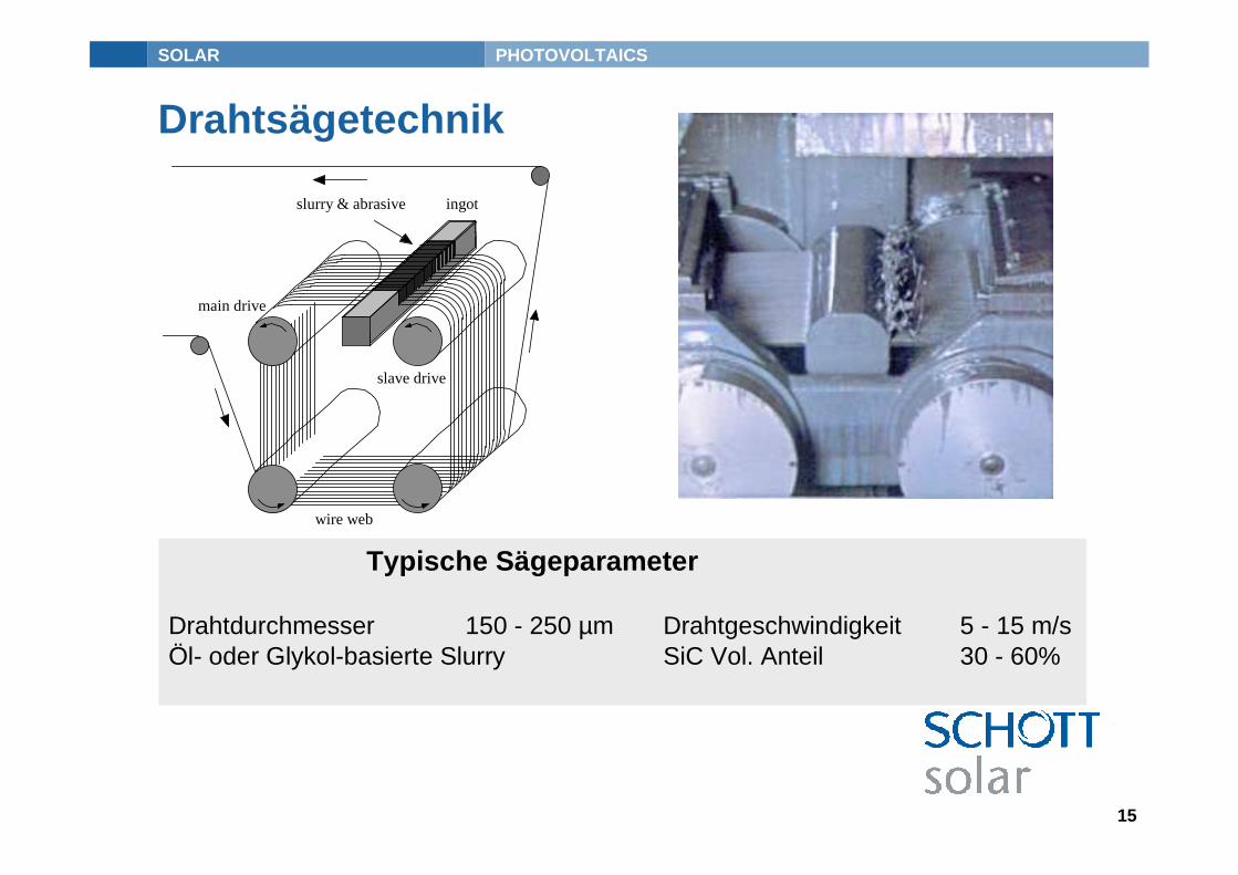
slave drive
main drive
wire web
ingotslurry & abrasive
Drahtsägetechnik
Typische Sägeparameter
Drahtdurchmesser 150 - 250 µm Drahtgeschwindigkeit 5 - 15 m/sÖl- oder Glykol-basierte Slurry SiC Vol. Anteil 30 - 60%
SOLAR PHOTOVOLTAICS
16
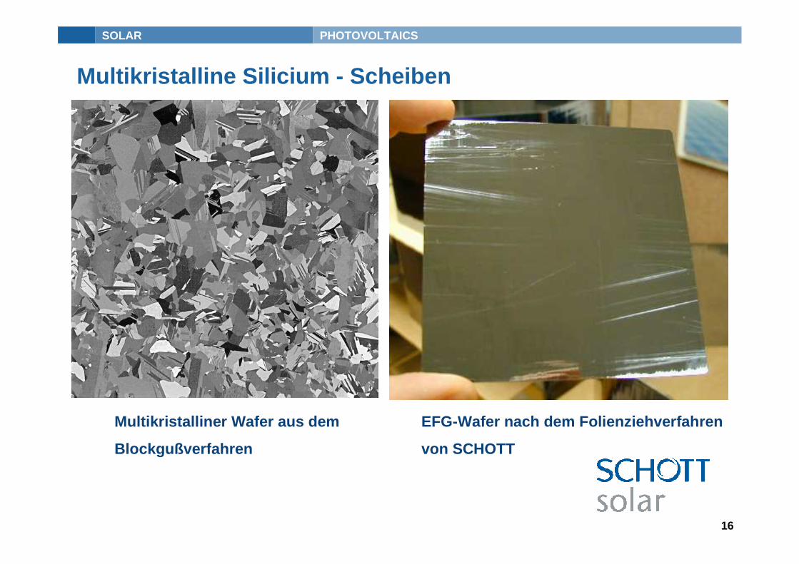
EFG-Wafer nach dem Folienziehverfahren
von SCHOTT
Multikristalliner Wafer aus dem
Blockgußverfahren
Multikristalline Silicium - Scheiben
SOLAR PHOTOVOLTAICS
17
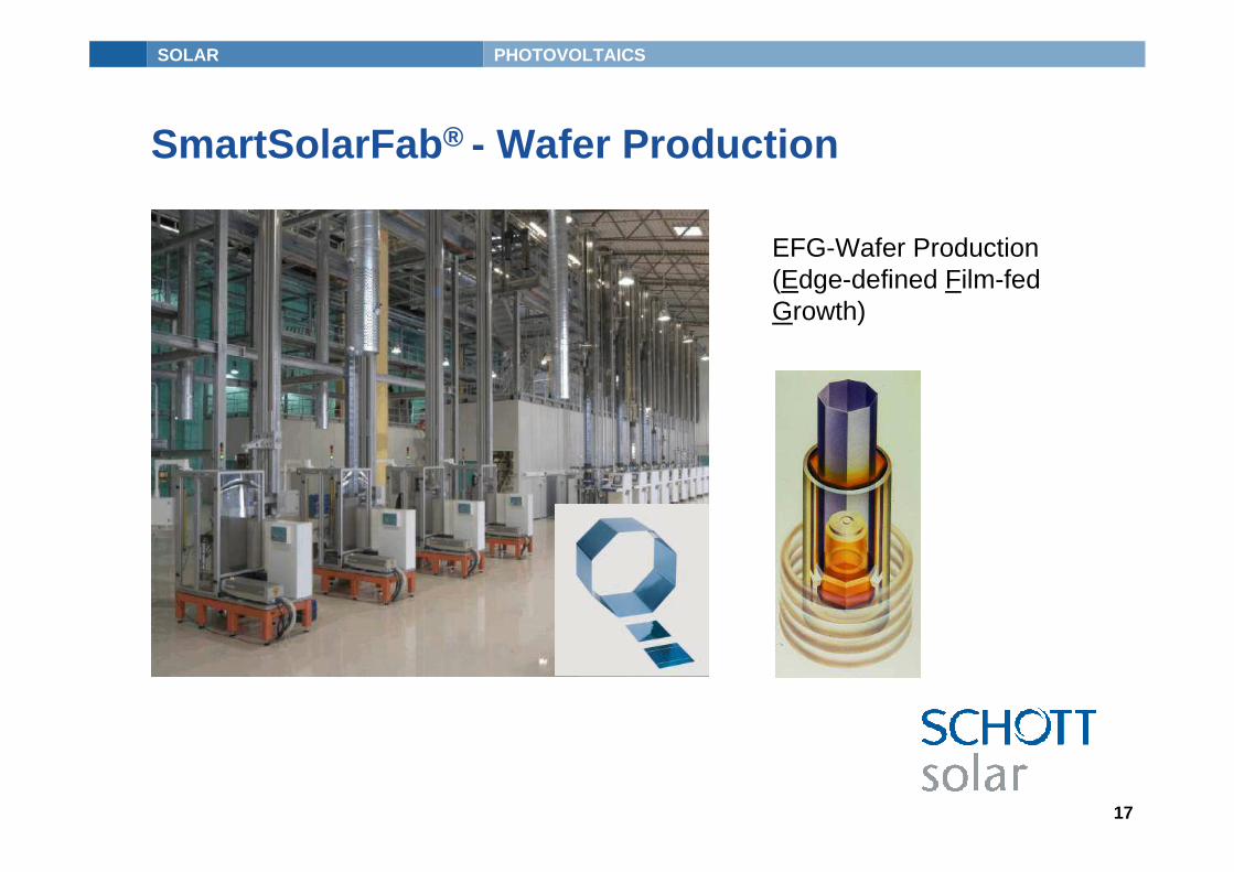
SmartSolarFab® - Wafer Production
EFG-Wafer Production (Edge-defined Film-fedGrowth)

SOLAR PHOTOVOLTAICS
18
Productivity Increase and Cost Reduction for c-SiWafers
1990 Actual 1. Step 2. Step 3. Step Long-TermSi-MaterialWafer Thickness [µm] 450 300 200 150 100 50 (-83%)
EFG-Wafer
Tube circumference [dm]9x0,54,5
8x18
8x1,2510
12x1,2515
12x1,518
circle ∅ 1,3m40
Productivity 0,6 1(norm.) 1,2 1,9 2,2 5Material add-on 2 1 1,2 1,7 2 4 (-20%)Personnel 1,5 1 1 1,1 1,2 1,3 (-74%)Depr/Interest 1,5 1 1 1,1 1,2 1,3 (-74%)
2003
SOLAR PHOTOVOLTAICS
19
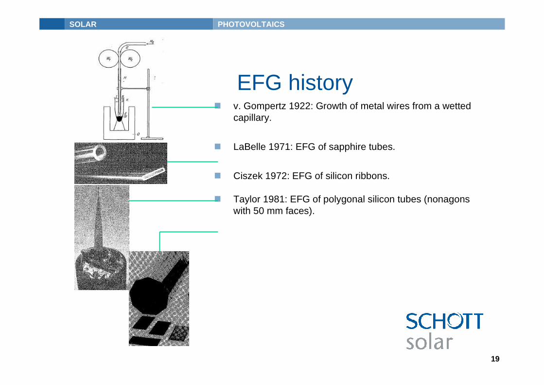
EFG history� v. Gompertz 1922: Growth of metal wires from a wetted
capillary.
� LaBelle 1971: EFG of sapphire tubes.
� Ciszek 1972: EFG of silicon ribbons.
� Taylor 1981: EFG of polygonal silicon tubes (nonagonswith 50 mm faces).
SOLAR PHOTOVOLTAICS
20
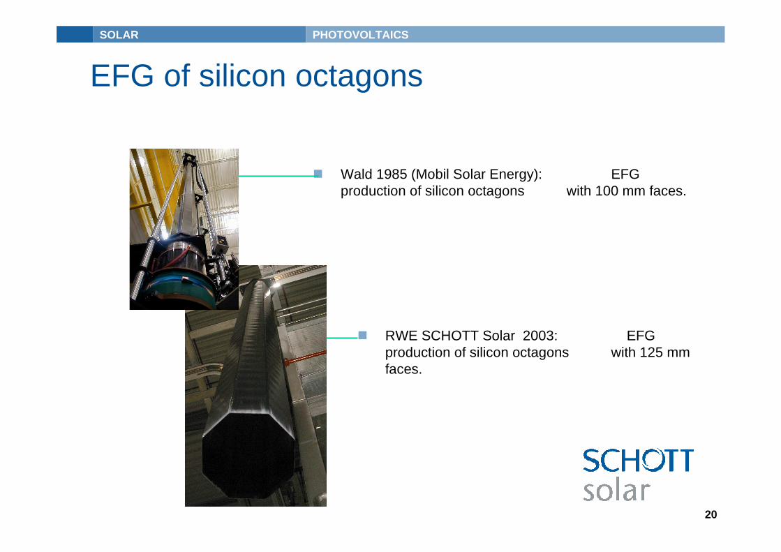
EFG of silicon octagons
� Wald 1985 (Mobil Solar Energy): EFGproduction of silicon octagons with 100 mm faces.
� RWE SCHOTT Solar 2003: EFGproduction of silicon octagons with 125 mmfaces.
SOLAR PHOTOVOLTAICS
21
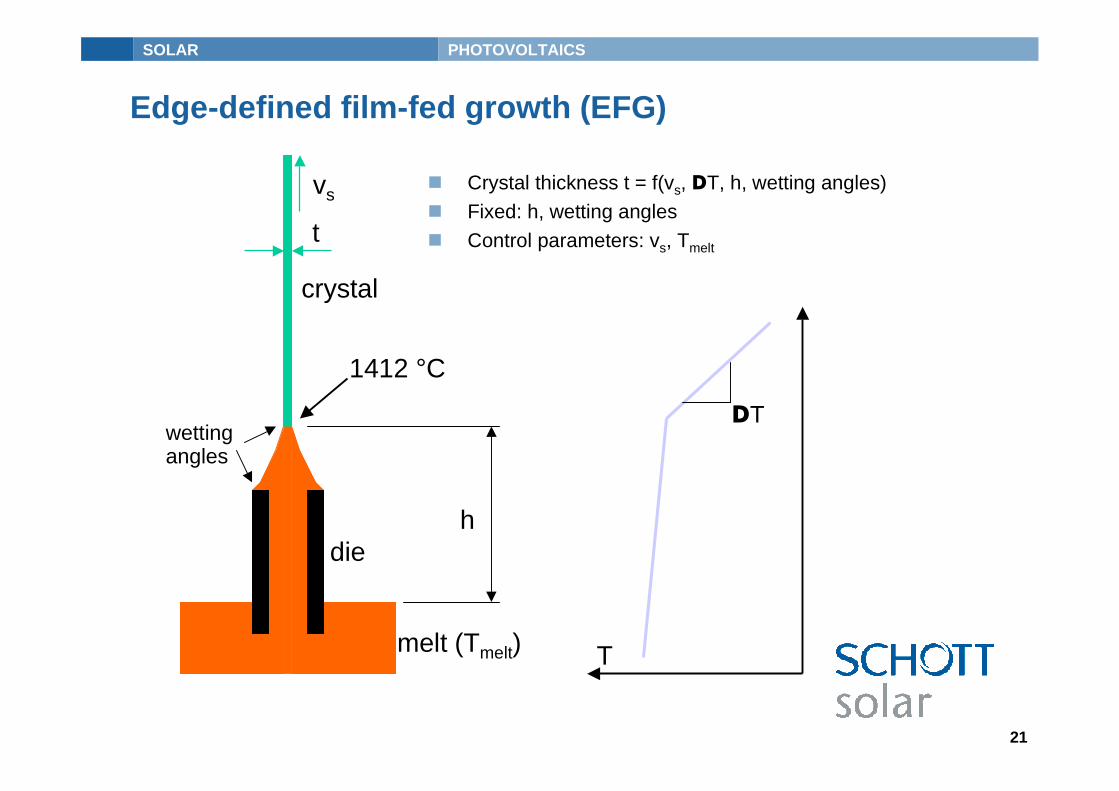
Edge-defined film-fed growth (EFG)
� Crystal thickness t = f(vs, �T, h, wetting angles)
� Fixed: h, wetting angles
� Control parameters: vs, Tmelt
melt (Tmelt)
die
crystal
vs
h
t
wettingangles
1412 °C
T
�T
SOLAR PHOTOVOLTAICS
22
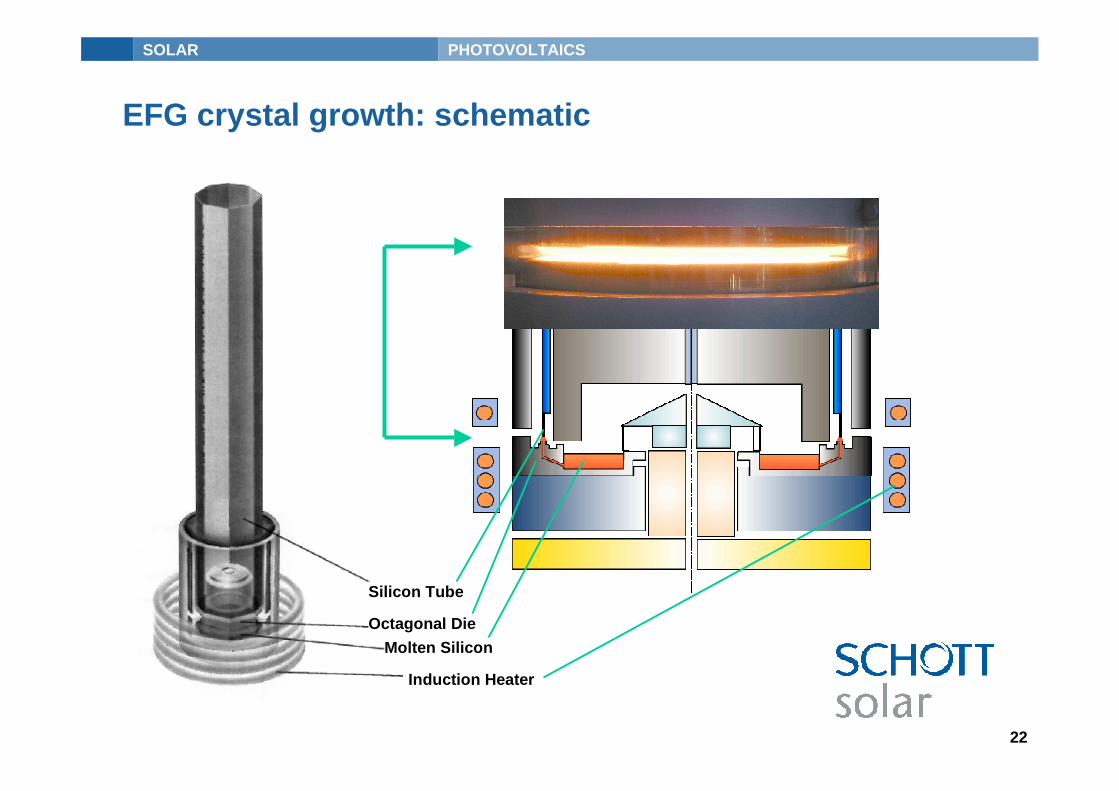
EFG crystal growth: schematic
Octagonal Die
Molten Silicon
Induction Heater
Silicon Tube
SOLAR PHOTOVOLTAICS
23
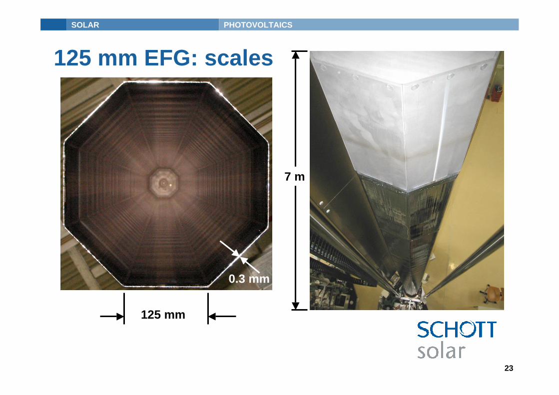
125 mm
7 m
125 mm EFG: scales
0.3 mm
SOLAR PHOTOVOLTAICS
24
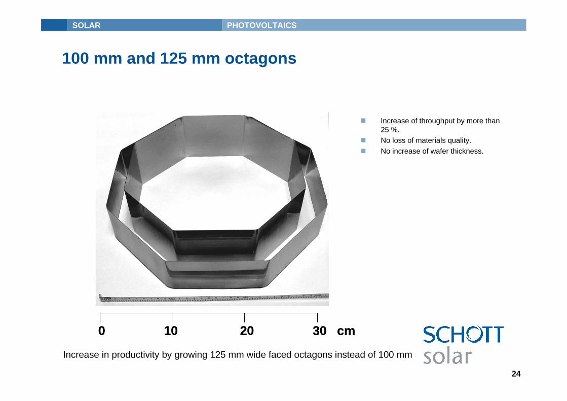
100 mm and 125 mm octagons
0 10 20 30 cm0 10 20 30 cm
� Increase of throughput by more than25 %.
� No loss of materials quality.
� No increase of wafer thickness.
Increase in productivity by growing 125 mm wide faced octagons instead of 100 mm

SOLAR PHOTOVOLTAICS
25
Cutting of tubes by laser for wafer production
� Several tubes per day and furnaceup to 7 m length.
� Less than 10 % silicon loss at cuttingstep.
� Wafers are immediately processedafter light etch.
SOLAR PHOTOVOLTAICS
26
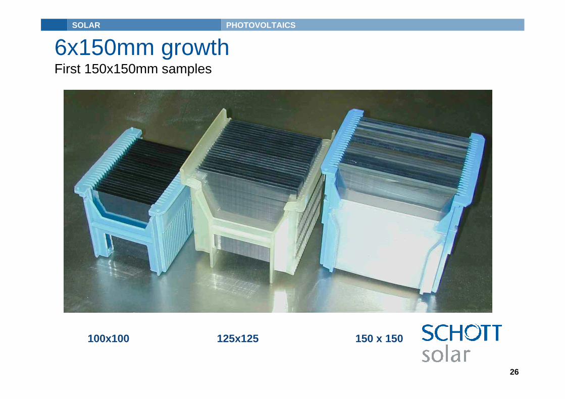
6x150mm growthFirst 150x150mm samples
100x100 125x125 150 x 150
SOLAR PHOTOVOLTAICS
27
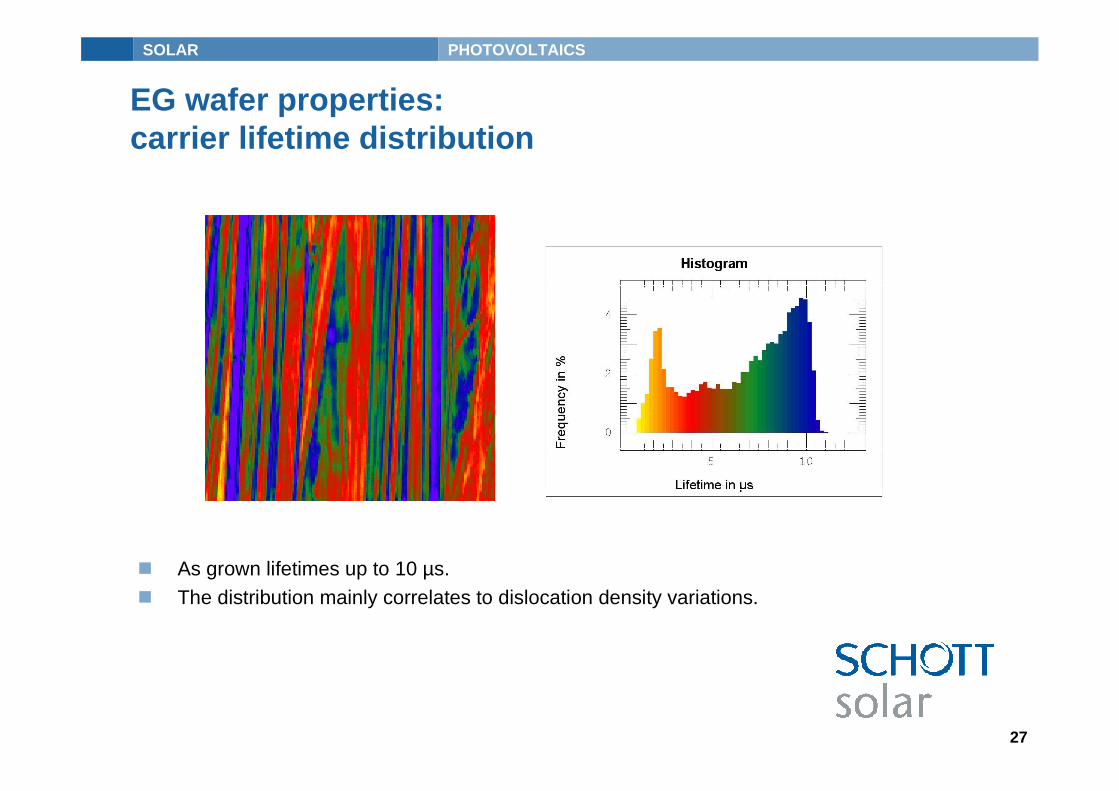
EG wafer properties:carrier lifetime distribution
� As grown lifetimes up to 10 µs.� The distribution mainly correlates to dislocation density variations.
SOLAR PHOTOVOLTAICS
28
Access
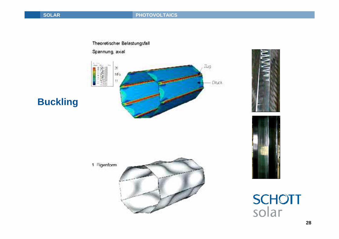
Buckling
SOLAR PHOTOVOLTAICS
29
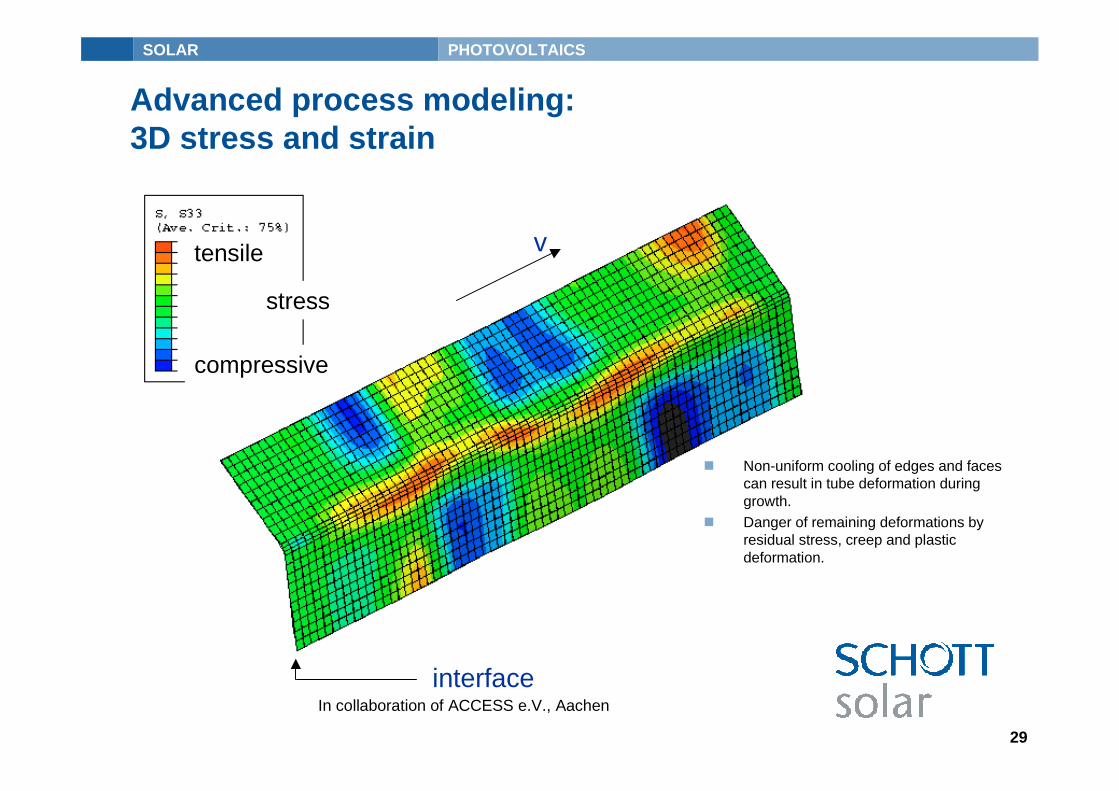
interface
v 45 MPa
-45 MPa
� Non-uniform cooling of edges and facescan result in tube deformation duringgrowth.
� Danger of remaining deformations byresidual stress, creep and plasticdeformation.
tensile
compressive
stress
Advanced process modeling:3D stress and strain
In collaboration of ACCESS e.V., Aachen
SOLAR PHOTOVOLTAICS
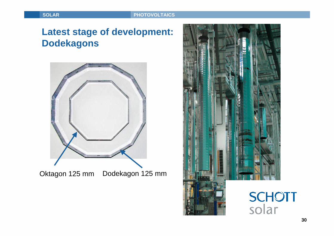
30
Latest stage of development: Dodekagons
Oktagon 125 mm Dodekagon 125 mm
SOLAR PHOTOVOLTAICS
31
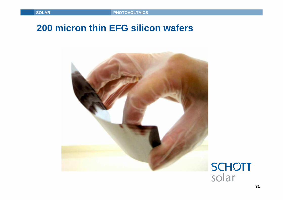
200 micron thin EFG silicon wafers

SOLAR PHOTOVOLTAICS
32
EFG wafer properties: mechanical strength
0
10
20
30
40
50
60
70
80
90
100
0 100 200 300 400 500 600 700 800 900 1000 1100
mc - Si as grownmc - Si damage etchedEFG as etched
Fracture strength [MPa]
Fai
lure
rat
e [%
]
� Biaxial test: fracture strength of 550 MPa(60% failure rate value) for EFG.
� As-grown surface is free of serious damage.
In collaboration with TU Freiberg
SOLAR PHOTOVOLTAICS
33
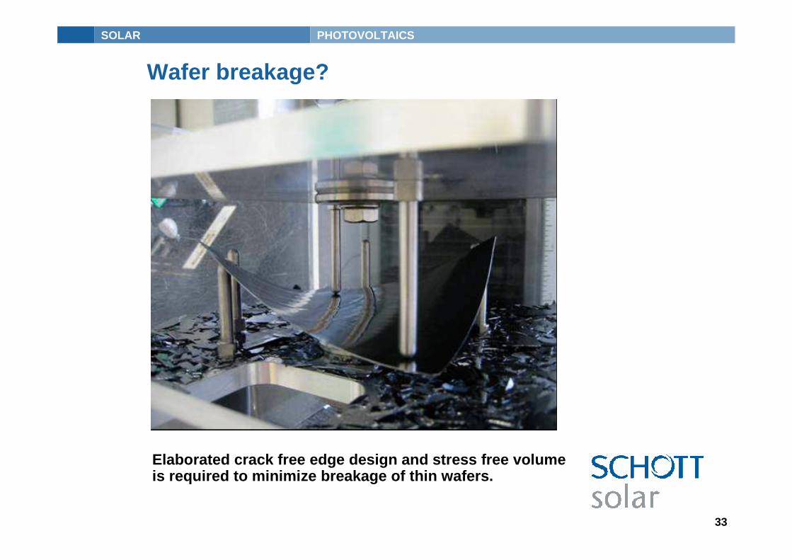
Wafer breakage?
Elaborated crack free edge design and stress free volumeis required to minimize breakage of thin wafers.

SOLAR PHOTOVOLTAICS
34
As cut, 4 min Sirtl etched
EFG wafer properties:wafer edge
Standard etched
SOLAR PHOTOVOLTAICS
35
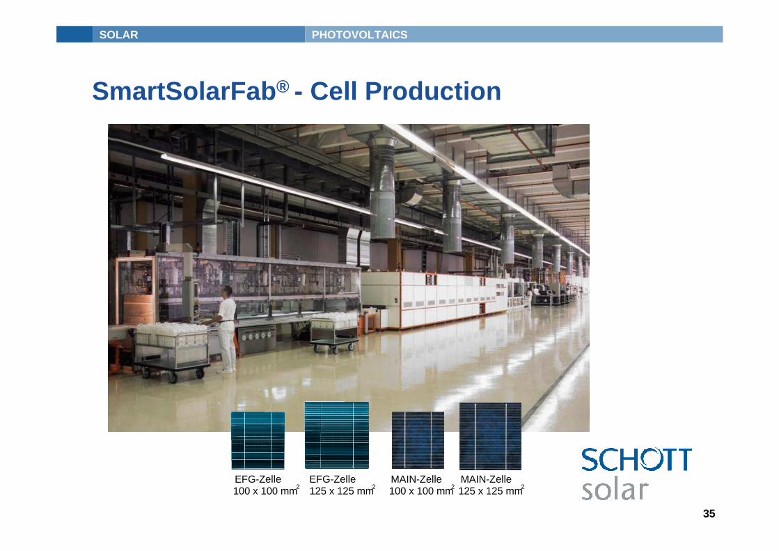
SmartSolarFab® - Cell Production
EFG-Zelle EFG-Zelle MAIN-Zelle MAIN-Zelle100 x 100 mm2 125 x 125 mm2 100 x 100 mm2 125 x 125 mm2
SOLAR PHOTOVOLTAICS
36
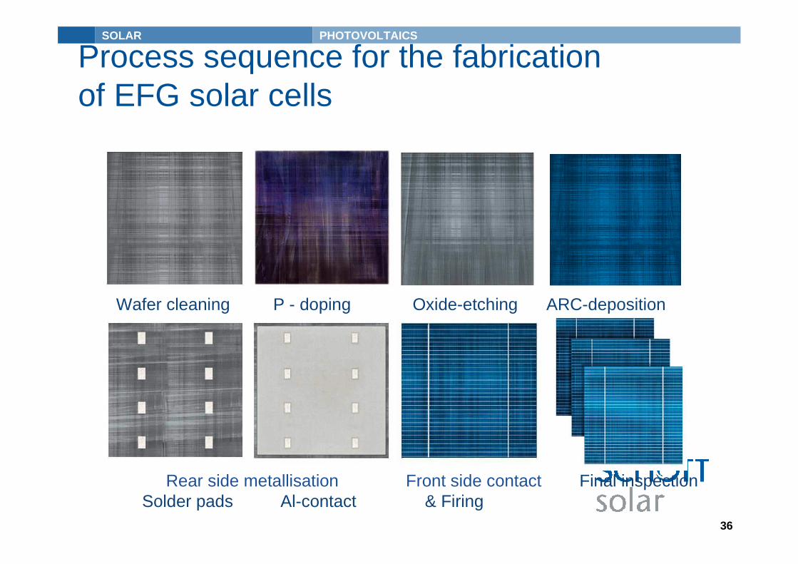
Rear side metallisation Front side contact Final inspectionSolder pads Al-contact & Firing
Process sequence for the fabricationof EFG solar cells
Wafer cleaning P - doping Oxide-etching ARC-deposition
SOLAR PHOTOVOLTAICS
37
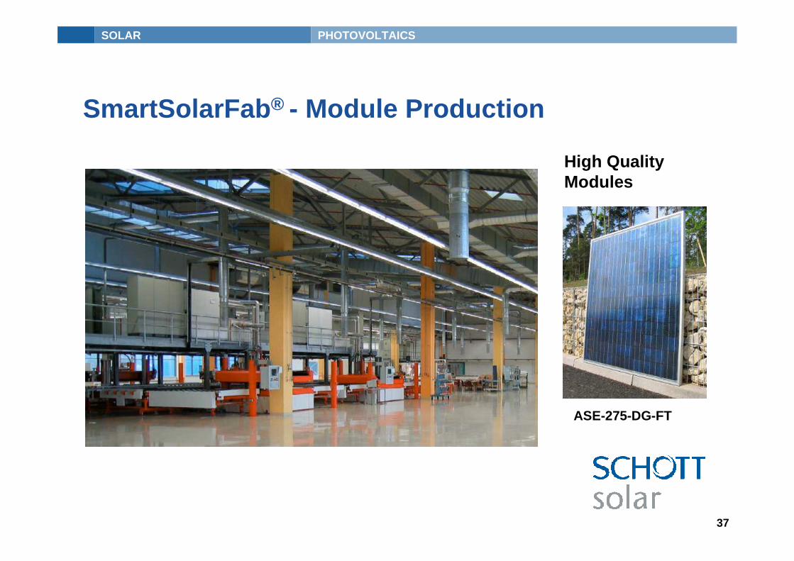
SmartSolarFab® - Module Production
ASE-275-DG-FT
High Quality Modules
SOLAR SolarInnovativ Thüringen
38
Many thanks for your attention