
Ultrafast Relaxation Dynamics after Optical Excitation …wolf/femtoweb/docs/thesis/... ·...
225
Ultrafast Relaxation Dynamics after Optical Excitation of Hybrid Inorganic/Organic Systems Ultraschnelle Relaxationsprozesse nach optischer Anregung von anorganisch/organischen Hybridsystemen Im Fachbereich Physik der Freien Universit¨ at Berlin eingereichte Dissertation zur Erlangung des Grades eines Doktors der Naturwissenschaften vorgelegt von Lea Bogner Berlin, November 2015
Transcript of Ultrafast Relaxation Dynamics after Optical Excitation …wolf/femtoweb/docs/thesis/... ·...

Ultrafast Relaxation Dynamics
after Optical Excitation of
Hybrid Inorganic/Organic Systems
Ultraschnelle Relaxationsprozesse
nach optischer Anregung von
anorganisch/organischen Hybridsystemen
Im Fachbereich Physik
der Freien Universitat Berlin
eingereichte
Dissertation
zur Erlangung des Grades eines
Doktors der Naturwissenschaften
vorgelegt von
Lea Bogner
Berlin, November 2015


This work was performed between June 2011 and March 2013 in the group Prof. Dr.
Petra Tegeder in the Department of Physics, Freie Universitat Berlin and from April
2013 until November 2015 in the group of Dr. Julia Stahler in the Department of
Physical Chemistry (Director: Prof. Dr. Martin Wolf) at the Fritz Haber Institute
of the Max Planck Society.
Berlin, November 2015
Erstgutachterin: Prof. Dr. Petra Tegeder
Zweitgutachter: Prof. Dr. Martin Wolf
Datum der Disputation: 04.12.2015

Abstract
This work focuses on fundamental processes which influence the efficiencies of or-
ganic solar cells and LEDs, for instance the formation and decay dynamics of exci-
tons, their diffusion, the charge transfer at interfaces between organic materials and
inorganic electrodes and the correlated energy level alignment at these interfaces.
These processes are investigated on the basis of four model systems, which represent
different parts of a solar cell or an LED, by means of time-resolved photoelectron
spectroscopy which facilitates the measurement of occupied and unoccupied states
as well as the acquisition of ultrafast processes.
ZnO is a promising material for transparent electrodes and as an active LED
medium, therefore the processes in optically excited ZnO are of great interest. The
investigations show that the electronic structure of the O-terminated ZnO surface
is strongly influenced by the adsorption of hydrogen and that the exciton formation
slows down at higher electron densities at the surface as the electron phonon coupling
is screened.
The SP6/ZnO interface can serve on the one hand as a model system for charge
transfer processes, however SP6 in thick films represents a potential LED medium. In
addition to the already known relaxation processes which have been observed before
by time-resolved optical spectroscopy, photoelectron spectroscopy reveals another
ultrafast component. The interaction of long-lived triplet states results in this system
in the emission of electrons. Furthermore, photoelectron spectroscopy allows to draw
conclusions on the absolute energies of the excited states.
The energy level alignment at the interface between a metal electrode and π-
conjugated molecules is investigated on dicyanovinyl-substituted oligothiophenes on
gold. The gold surface influences not only the electronic structure of the mono-
layer, it also significantly affects the lifetimes of excited states that increase with the
distance to the metal surface.
As a model system for a polymer semiconductor P3HT was established. The
investigation of two films with different amounts of crystalline fractions shows that
the relaxation dynamics proceeds faster in the film that features higher crystallinity
and therefore superior transport properties.
These results give an insight into the complex interrelated relaxation processes
of optically excited states. The detailed comprehension of these processes promises
their targeted utilization to optimize the efficiency of organic solar cells and LEDs.
I

Deutsche Kurzfassung
Diese Arbeit befasst sich mit fundamentalen Prozessen, welche die Effizienz organ-
ischer Solarzellen und LEDs beeinflussen, beispielsweise die Entstehungs- und Zer-
fallsdynamik von Exzitonen, deren Diffusion, der Ladungstransfer an Grenzflachen
zwischen organischen Molekulen und anorganischen Elektroden und der damit kor-
relierten Anordnung der Energieniveaus an diesen Grenzflachen. Anhand von vier
Modellsystemen, welche unterschiedliche Teile einer Solarzelle oder LED darstellen,
werden diese Prozesse mittels zeitaufgeloster Photoelektronenspektroskopie, welche
die Messung besetzter und unbesetzter Zustande, sowie die Erfassung ultraschneller
Prozesse ermoglicht, untersucht.
ZnO ist ein vielversprechendes Material fur transparente Elektroden und als ak-
tives LED-Medium, weshalb die Prozesse in optisch angeregtem ZnO von großem
Interesse sind. Die Untersuchungen zeigen, dass die elektronische Struktur der O-
terminierten ZnO-Oberflache stark durch Adsorption von Wasserstoff beeinflusst
wird und dass die Exzitonenentstehung mit großerer Elektronendichte an der Ober-
flache langsamer wird, da die effiziente Elektron-Phonon-Kopplung abgeschirmt wird.
Die SP6/Zn-Grenzflache dient einerseits als Modellsystem fur Ladungstransfer,
in dicken Filmen jedoch stellt SP6 ein potentielles LED-Medium dar. Zusatzlich zu
den bereits bekannten Relaxationsprozessen, die mit zeitaufgeloster optischer Spek-
troskopie beobachtet wurden, zeigt die Photoeletronenspektroskopie eine weitere ul-
traschnelle Komponente. Die Wechselwirkung langlebiger Tripletzustande fuhrt in
diesem System zur Emission von Elektronen. Außerdem erlaubt die Photoelektro-
nenspektroskopie Ruckschlusse auf die absoluten Energien der angeregten Zustande.
Die Anordnung molekularer Energieniveaus an der Grenzflache zwischen einer
Metallelektrode und π-konjugierten Molekulen wird an dicyanovinyl-substituierten
Oligothiophenen auf Gold untersucht. Die Goldoberflache hat nicht nur Einfluss auf
die elektronische Struktur der Monolage, sie beeinflusst auch erheblich die Lebens-
dauer der angeregten Zustande, welche mit dem Abstand zur Metalloberflache zu-
nimmt.
Als Modellsystem fur einen polymeren Halbleiter wurde P3HT eingesetzt. Die
Untersuchung zweier Filme mit unterschiedlich großen kristallinen Anteilen zeigt,
dass die Relaxationsdynamik in dem Film schneller ablauft, der die großere Kristall-
initat und somit die besseren Transporteigenschaften aufweist.
Diese Ergebnisse geben einen Einblick in die komplexen zusammenhangenden
Relaxationsprozesse optisch angeregter Zustande. Das detaillierte Verstandnis dieser
Prozesse verspricht deren gezielte Ausnutzung, um die Effizienz von organischen
Solarzellen und LEDs zu optimieren.
III


Contents
Contents
Abstract I
Deutsche Kurzfassung III
List of Figures XIII
List of Abbreviations XIV
1 Introduction 1
2 Theoretical Background 7
2.1 Metal and Semiconductor Surfaces and Interfaces . . . . . . . . . . . 8
2.1.1 Electronic States at Metal Surfaces . . . . . . . . . . . . . . . 8
2.1.2 Energy Level Alignment at Metal/Organic Interfaces . . . . . 11
2.1.3 Band Bending at Semiconductor Surfaces . . . . . . . . . . . 14
2.2 Elementary Excitations in Semiconductors . . . . . . . . . . . . . . . 17
2.2.1 Elementary Excitations in Inorganic Semiconductors . . . . . 18
2.2.2 Excitons in Organic Semiconductors . . . . . . . . . . . . . . 21
3 Investigated Systems 29
3.1 Electronic Properties and Excited State Dynamics at the Mixed- and
the O-terminated ZnO Surface . . . . . . . . . . . . . . . . . . . . . 30
3.1.1 Morphology of the O-and the Mixed-terminated ZnO Surface 32
3.1.2 Surface Metallization due to H-adsorption on ZnO Surface . . 33
3.1.3 Surface Exciton Dynamics at ZnO Surfaces . . . . . . . . . . 36
3.2 Electronic Structure and Excited State Dynamics in SP6 on ZnO . . 39
3.3 Electronic Structure of Dicyanovinyl-Substituted Oligothiophenes on
Au(111) . . . . . . . . . . . . . . . . . . . . . . . . . . . . . . . . . . 43
3.3.1 Adsorption and Electronic Properties of DCV5T-Me2/Au(111) 46
3.3.2 Adsorption and Electronic Properties of DCV6T/Au(111) . . 48
3.4 Electronic Structure of the Au(111) Surface . . . . . . . . . . . . . . 50
3.5 P3HT: Electronic Structure, Excited State Dynamics and the Influ-
ence of Crystallinity . . . . . . . . . . . . . . . . . . . . . . . . . . . 53
4 Methods and Experimental Details 59
4.1 Photoelectron Spectroscopy . . . . . . . . . . . . . . . . . . . . . . . 59
4.1.1 Two-Photon Photoemission . . . . . . . . . . . . . . . . . . . 61
4.1.2 Time-Resolved Two-Photon Photoemission . . . . . . . . . . 65
4.1.3 2PPE vs. Optical Spectroscopy . . . . . . . . . . . . . . . . . 69
V

Contents
4.2 Experimental Setup . . . . . . . . . . . . . . . . . . . . . . . . . . . 71
4.2.1 The Femtosecond Laser System . . . . . . . . . . . . . . . . . 71
4.2.2 Pulse Characterization . . . . . . . . . . . . . . . . . . . . . . 74
4.2.3 The Ultrahigh Vacuum Chamber . . . . . . . . . . . . . . . . 75
4.2.4 Electron Analysers . . . . . . . . . . . . . . . . . . . . . . . . 79
4.3 Sample Preparation . . . . . . . . . . . . . . . . . . . . . . . . . . . 85
4.3.1 Preparation of the O-terminated ZnO Surface and Quantifica-
tion of the H-Dosage . . . . . . . . . . . . . . . . . . . . . . . 85
4.3.2 Preparation of the SP6 Films and Determination of the Film
Thickness Using a Quartz Microbalance . . . . . . . . . . . . 87
4.3.3 Preparation of the DCV6T and DCV5T-Me2 Films on Au(111) 91
5 Results 95
5.1 H-induced Metallicity and Excited State Dynamics at the O-terminated
ZnO Surface . . . . . . . . . . . . . . . . . . . . . . . . . . . . . . . . 96
5.1.1 Hydrogen Induced Metallicity at the O-terminated ZnO Surface 97
5.1.2 Surface Exciton Formation and Decay Dynamics at the H-
doped Polar ZnO Surface . . . . . . . . . . . . . . . . . . . . 104
5.2 Exciton Formation and Decay Dynamics in SP6 Films on ZnO . . . 113
5.2.1 Ultrafast Dynamics of Excited States in SP6 Films . . . . . . 114
5.2.2 Triplet-Triplet Annihilation Leading to Electron Emission . . 123
5.3 Electronic Structure and Excited State Dynamics in DCV-substituted
Oligothiophenes on Au(111) . . . . . . . . . . . . . . . . . . . . . . . 135
5.3.1 Coverage-Dependent Electronic Structure of DCV5T-Me2 on
Au(111) . . . . . . . . . . . . . . . . . . . . . . . . . . . . . . 136
5.3.2 Coverage-Dependent Electronic Structure of DCV6T/Au(111) 143
5.3.3 Excited State Dynamics in DCV5T-Me2 on Au(111) . . . . . 147
5.3.4 Excited State Dynamics in DCV6T on Au(111) . . . . . . . . 150
5.4 Electronic Properties of P3HT Films and the Influence of Crystallinity155
5.4.1 Electronic Structure of P3HT Films with Different Degrees of
Crystallinity . . . . . . . . . . . . . . . . . . . . . . . . . . . 156
5.4.2 Influence of Crystallinity on the Excited State Dynamics in
P3HT Films . . . . . . . . . . . . . . . . . . . . . . . . . . . 161
6 Summary and Conclusions 165
A Mass Spectra and TPD of DCV6T & DCV5T-Me2 169
B Calculation of the Excitation Density 173
VI

Contents
C Differential Equation Solution 175
References 197
Acknowledgement 200
Academic Curriculum Vitae 201
List of Publications 203
VII

List of Figures
List of Figures
2.1 Schematic of a bilayer solar cell . . . . . . . . . . . . . . . . . . . . . 7
2.2 Schematic depiction of an image charge and image potential states . 9
2.3 Schematic of (a) charge density distribution at a metal surface, (b)
relevant energies connected to the work function . . . . . . . . . . . 11
2.4 Vacuum level alignment for (a) low and (b) high work function metals,
(c) interface dipole induced work function change . . . . . . . . . . . 12
2.5 Fermi level pinning for (a) low and (b) high work function metals . . 13
2.6 Decrease of HOMO-LUMO gap due to interaction with a metal sur-
face . . . . . . . . . . . . . . . . . . . . . . . . . . . . . . . . . . . . 13
2.7 (a) Upward and (b) downward band bending at metal and n-type
semiconductor contacs . . . . . . . . . . . . . . . . . . . . . . . . . . 14
2.8 (a) Upward surface band bending at the clean ZnO(0001) surface, (b)
reversed surface band bending upon H-adsorption . . . . . . . . . . . 15
2.9 Excitation and electron-hole pair formation in (a) an inorganic and
(b) an organic semiconductor. (c) Delocalized Mott-Wannier exciton
and (d) localized Frenkel exciton . . . . . . . . . . . . . . . . . . . . 17
2.10 (a) Excitation below and (b) above the Mott density . . . . . . . . . 18
2.11 (a) Surface photovoltage at low excitation density, (b) enhanced sur-
face photovoltage at higher excitation density . . . . . . . . . . . . . 20
2.12 Illustration of the exciton binding energy in an organic semiconductor 21
2.13 Probing (a) an occupied, (b) an unoccupied state and (c) an excitonic
state with 2PPE . . . . . . . . . . . . . . . . . . . . . . . . . . . . . 22
2.14 (a) Singlet and (b) triplet exciton. (c) Jablonski diagram . . . . . . 24
2.15 (a) Forster and (b) Dexter transfer . . . . . . . . . . . . . . . . . . . 26
3.1 Hexagonal unit cell of ZnO . . . . . . . . . . . . . . . . . . . . . . . 31
3.2 (a) Mixed-terminated ZnO(1010) and (b) O-terminated ZnO(0001)
surface . . . . . . . . . . . . . . . . . . . . . . . . . . . . . . . . . . 32
3.3 Schematic of the energy band structures of the clean and H-covered
ZnO(1010) surface, adopted from [Oza10] . . . . . . . . . . . . . . . 34
3.4 Evolution of work function and CAL intensity as a function of H-
dosage, adopted from [Dei15b] . . . . . . . . . . . . . . . . . . . . . 35
3.5 (a) Excitation density and (b) H-dosage dependent pump-induced
signal of H2/ZnO(1010), adopted from [Dei14] . . . . . . . . . . . . 37
3.6 Lewis formula and ball and stick model of SP6 . . . . . . . . . . . . 39
3.7 Energy level diagrams for SP6/ZnO and SP6/ZnMgO, adopted from
[Blu08] . . . . . . . . . . . . . . . . . . . . . . . . . . . . . . . . . . . 40
VIII
List of Figures
3.8 (a) τPOP vs. probe photon energy obtained from excited states trans-
mission, (b) schematic of the involved electronic processes, adopted
from [Fog15] . . . . . . . . . . . . . . . . . . . . . . . . . . . . . . . . 41
3.9 Ball and stick model of (a) DCV5T-Me2 and (b) DCV6T . . . . . . 43
3.10 STM images, dI/dV spectra and maps of a DCV5T-Me2 island, adopted
from [Bog15]. . . . . . . . . . . . . . . . . . . . . . . . . . . . . . . . 46
3.11 STM images and dI/dV spectra of the second DCV5T-Me2 layer . . 47
3.12 (a) dI/dV spectra and (b) STM image of DCV6T island, adopted
from [Yan14a] . . . . . . . . . . . . . . . . . . . . . . . . . . . . . . . 48
3.13 (a) Unit cell of the fcc-lattice and (b) the Au(111) surface . . . . . . 50
3.14 (a) STM image of the reconstructed Au(111) surface (image courtesy
of E. Varene and Y. Pennec). (b) Sketch of the herringbone recon-
struction, adopted from [Nar92] . . . . . . . . . . . . . . . . . . . . 51
3.15 Calculated bandstructure of gold and Brillouin zone of the fcc-lattice
adopted from [Eck84] . . . . . . . . . . . . . . . . . . . . . . . . . . . 52
3.16 Lewis formula of (a) RR-P3HT and (b) RRa-P3HT . . . . . . . . . 53
3.17 (a) Schematic of the microstructure of RR-P3HT, (b) AFM image of
a P3HT-mc film, adopted from [Wu10] . . . . . . . . . . . . . . . . . 54
4.1 Schematic depictions of (a) a PES experiment, (b) electron emission
under conservation of the wave vector component parallel to the surface 60
4.2 1C-2PPE pump-probe schemes in case of (a) occupied, (b) unoccupied
and (c) final states; (d) corresponding 2C-2PPE schemes . . . . . . . 62
4.3 Energy cutoffs in a 2PPE spectrum . . . . . . . . . . . . . . . . . . . 63
4.4 Commonly used energy axes in 2PPE spectra . . . . . . . . . . . . . 64
4.5 (a) Possible pump-probe schemes during a TR-2PPE experiment, (b)
population of an unoccupied state via an electron from the metal or
intramolecularly . . . . . . . . . . . . . . . . . . . . . . . . . . . . . 65
4.6 Exemplary TR-2PPE spectrum of H-doped ZnO, sketch of the pump-
probe scheme, XC-traces and spectra of differnt time delays . . . . . 67
4.7 Diagram of a 3- and a 4-level system . . . . . . . . . . . . . . . . . 69
4.8 Probing of the intermediate state population in (a) excited state trans-
mission and (b) 2PPE . . . . . . . . . . . . . . . . . . . . . . . . . . 70
4.9 Schematic of the laser setup, adopted from [Weg14] . . . . . . . . . . 72
4.10 (a) Example laser spectrum and (b) laser intensity profile . . . . . . 74
4.11 Schematic of the UHV chamber . . . . . . . . . . . . . . . . . . . . . 75
4.12 Sketch of the sample holder, adopted from [Hag09] . . . . . . . . . . 77
4.13 Schematic of the hemispherical analyser modified from [Bra09] . . . 79
4.14 Schematic of the time-of-flight spectrometer, adopted from [Hag09] . 82
IX
List of Figures
4.15 Bias correction . . . . . . . . . . . . . . . . . . . . . . . . . . . . . . 84
4.16 (a) Pressure trace taken during H2 dosing, (b) H2 cracking by electron
emission from the ion gauge filament . . . . . . . . . . . . . . . . . . 85
4.17 QMB trace for the determination of the tooling factor and the SP6
film thickness. . . . . . . . . . . . . . . . . . . . . . . . . . . . . . . . 88
4.18 TPDs of SP6/ZnO(1010) (a) of a 16 nm thick film and (b) of different
film thicknesses . . . . . . . . . . . . . . . . . . . . . . . . . . . . . . 89
4.19 (a) Downfield and (b) upfield H-NMR spectra of SP6 before and after
evaporation . . . . . . . . . . . . . . . . . . . . . . . . . . . . . . . . 90
4.20 2PPE spectra series as a function of DCV6T coverage . . . . . . . . 91
4.21 Coverage dependent 2PPE spectra of higher DCV6T coverages . . . 92
4.22 2C-2PPE spectra series taken on different coverages DCV5T-Me2 on
Au(111) . . . . . . . . . . . . . . . . . . . . . . . . . . . . . . . . . . 93
5.1 (a) Valence band 2PPE spectra of the ZnO(0001) surface, (b) energy
level diagram . . . . . . . . . . . . . . . . . . . . . . . . . . . . . . . 98
5.2 (a) Direct photoemission spectrum of 100 L H2/ZnO(0001), (b) en-
ergy level diagram of the pristine and (c) the H-doped surface . . . . 99
5.3 (a) Direct photoemission spectra monitoring the CAL build-up with
increasing H-dosage, (b) work function decrease and CAL intensity
increase as function of H-coverage . . . . . . . . . . . . . . . . . . . 100
5.4 (a) Work function and CAL intensity as a function of H2 dosage for
ZnO(0001) and (1010), (b) surface unit cells of the two surfaces . . . 102
5.5 Equlibrium and non-equilibrium 2PPE spectra of H-doped polar ZnO 104
5.6 (a) Time-resolved 2PPE spectrum of 100 L H2/ZnO(000-1) (b) XC
traces for different energies . . . . . . . . . . . . . . . . . . . . . . . 105
5.7 (a) Comparison of the measured fast time constants with calculated
values from [Zhu10], (b) energy dependent evolution of the relaxation
times and SX formation . . . . . . . . . . . . . . . . . . . . . . . . . 107
5.8 (a) SX emission signal of 63 L H2/ZnO(0001) for different excitation
densities. Exciton density (b) below and (c) above the Mott density 108
5.9 Illustration of the electronic processes after photoexcitation, modified
from [Dei14] . . . . . . . . . . . . . . . . . . . . . . . . . . . . . . . . 109
5.10 Comparison of the fast relaxation times of 100 L H2 on the (0001)
and the (1010) surfaces . . . . . . . . . . . . . . . . . . . . . . . . . 110
5.11 Comparison between the time constants for different total carrier den-
sities and (a) same and (b) different pump photon energies . . . . . 111
5.12 (a) 2PPE spectra for different time delays, (b) TR-2PPE spectrum of
21 nm SP6/ZnO, (c) XC-traces with triexponential fits . . . . . . . . 114
X
List of Figures
5.13 Time constants obtained from triexponential fitting of XC-traces from
a TR-2PPE spectrum of 21 nm SP6/ZnO . . . . . . . . . . . . . . . 115
5.14 (a) Excited state transmission vs. (b) 2PPE . . . . . . . . . . . . . . 116
5.15 Comparison of a 2PPE cross-correlation with a transient transmission
trace . . . . . . . . . . . . . . . . . . . . . . . . . . . . . . . . . . . . 118
5.16 Schematic of the time-dependent diffusion model . . . . . . . . . . . 119
5.17 Schematic of the diffusion model including the exciton diffusion length 119
5.18 (a) Simulated temporal evolution of the S1 population, (b) S1 start
population, (c) comparison of S1 population dynamics averaged of the
whole SP6 film and at the surface . . . . . . . . . . . . . . . . . . . . 121
5.19 Normalized 2PPE spectra of 21 nm SP6 on ZnO(1010) taken at dif-
ferent delays . . . . . . . . . . . . . . . . . . . . . . . . . . . . . . . . 122
5.20 (a) Schematic of two laser pulses with different duration, (b) emission
intensity as a function of the pulse duration . . . . . . . . . . . . . . 123
5.21 Overlap of the laser pulses with the triplet population for (a) 200
kHz and (b) 40 kHz, (c) repetition rate dependent spectra of 10 nm
SP6/ZnO(1010) . . . . . . . . . . . . . . . . . . . . . . . . . . . . . . 124
5.22 (a) 2PPE pump-probe scheme, (b) photon energy dependent spectra
series of 20 nm SP6/ZnO(1010) . . . . . . . . . . . . . . . . . . . . . 125
5.23 Jablonski diagram illustrating possible excitation energy transfer pro-
cesses . . . . . . . . . . . . . . . . . . . . . . . . . . . . . . . . . . . 126
5.24 (a) Triplet-triplet coupling in an autocorrelation experiment, (b) sim-
plified singlet and triplet poulation decays . . . . . . . . . . . . . . 127
5.25 Modeled autocorrelation traces for (a) triplet-singlet and (b) triplet-
triplet coupling . . . . . . . . . . . . . . . . . . . . . . . . . . . . . . 128
5.26 (a) 2D-spectrum of the autocorrelation measurement, (b) spectra
taken at different time delays, (c) background subtracted signal at
different time delays . . . . . . . . . . . . . . . . . . . . . . . . . . . 129
5.27 Schematic of the triplet-triplet annihilation process . . . . . . . . . 129
5.28 Fluence dependence of the electron emission signal due to TTA . . . 130
5.29 Temperature dependent spectra of 20 nm SP6 on ZnO . . . . . . . . 131
5.30 (a) Coverage dependent spectra series of SP6/ZnO(1010), (b) back-
ground subtraction and peak fitting . . . . . . . . . . . . . . . . . . 132
5.31 Jablonski diagram of the observed processes in SP6/ZnO . . . . . . 133
5.32 (a) 1C-2PPE spectrum of 0.3 ML DCV5T-ME2/Au(111), (b) photon
energy dependent peak positions . . . . . . . . . . . . . . . . . . . . 136
5.33 (a) 2C-2PPE spectrum of 0.3 ML DCV5T-ME2/Au(111), (b) photon
energy dependent peak positions . . . . . . . . . . . . . . . . . . . . 137
XI

List of Figures
5.34 (a) 1C-2PPE spectrum of 0.8 ML DCV5T-ME2/Au(111), (b) peak
positions as function of the photon energy . . . . . . . . . . . . . . . 138
5.35 (a) 1C-2PPE spectrum of 0.8 ML DCV5T-ME2/Au(111), (b) peak
positions as function of the photon energy . . . . . . . . . . . . . . . 139
5.36 (a) 1C-2PPE spectrum and (b) 2C-2PPE spectrum of 3 ML DCV5T-
Me−2/Au(111) . . . . . . . . . . . . . . . . . . . . . . . . . . . . . . 140
5.37 Energy level diagrams of (a) submonolayer, (b) monolayer and (c)
multilayer coverages DCV5T-Me2/Au(111) . . . . . . . . . . . . . . 141
5.38 (a) 2C-2PPE spectra series of 2 ML DCV5T-Me2/Au(111) and (b)
peak maxima as a function of the emission angle . . . . . . . . . . . 143
5.39 (a) 1C-2PPE spectrum of 1.4 ML DCV6T/Au(111), (b) peak posi-
tions as function of the photon energy . . . . . . . . . . . . . . . . . 144
5.40 (a) 2C-2PPE spectrum of 1.4 ML DCV6T/Au(111), (b) peak posi-
tions as function of the photon energy . . . . . . . . . . . . . . . . . 144
5.41 (a) 1C-2PPE and (b) 2C-2PPE spectra of a multilayer DCV6T/Au(111)145
5.42 Energy level diagram of (a) a monolayer and (b) a multilayer coverage
DCV6T on Au(111) . . . . . . . . . . . . . . . . . . . . . . . . . . . 146
5.43 Time-resolved 2PPE spectra of (a) 10 ML and (b) 20 ML DCV5T-
Me2/Au(111), (c) spectra taken at t = 0 and (d) corresponding XC-
traces . . . . . . . . . . . . . . . . . . . . . . . . . . . . . . . . . . . 148
5.44 (a) 2PPE spectrum of 20 ML DCV5T-Me2 at t= 0 ps, (b) TR-2PPE
spectrum and (c) XC-trace . . . . . . . . . . . . . . . . . . . . . . . 149
5.45 Time-resolved 2PPE spectra of (a) 3 ML and (b) 5 ML DCV6T on
Au(111), (c) spectra at t = 0 ps and (d) XC-traces . . . . . . . . . 151
5.46 (a) 2PPE spectrum of a 20 ML thick DCV6T film on Au(111) recorded
at t= 0 ps, (b) time-resolved spectrum and (c) XC-trace . . . . . . . 152
5.47 Comparison of the XC-traces of 20 ML thick DCV5T-Me2 and DCV6T
films on Au(111) . . . . . . . . . . . . . . . . . . . . . . . . . . . . . 153
5.48 Direct photoemission spectra of P3HT-mc and P3HT-as . . . . . . . 156
5.49 1C-2PPE spectra of (a) P3HT-mc and (b) P3HT-as films . . . . . . 157
5.50 (a) Photon energy dependent 1C-2PPE spectra series taken on P3HT-
mc, (b) peak maxima as a function of the photon energy . . . . . . 158
5.51 2C-2PPE spectra of (a) P3HT-mc and P3HT-as (b) of P3HT-mc at
different time-delays . . . . . . . . . . . . . . . . . . . . . . . . . . . 159
5.52 Energy level diagram of (a) P3HT-mc and (b) P3HT-as films . . . . 160
5.53 (a) Time-resolved 2PPE spectrum of P3HT-mc, (b) XC-traces with
triexponential fits . . . . . . . . . . . . . . . . . . . . . . . . . . . . . 161
XII

List of Figures
5.54 (a) Time-resolved 2PPE spectrum of P3HT-as, (b) XC-traces with
triexponential fits . . . . . . . . . . . . . . . . . . . . . . . . . . . . . 163
A.1 Mass spectrum of DCV6T . . . . . . . . . . . . . . . . . . . . . . . . 169
A.2 TPD of DCV6T/Au(111) evaporated on the cold surface . . . . . . . 170
A.3 TPDs of DCV6T/Au(111) evaporated on the surface at 300 K . . . 170
A.4 Mass spectrum of DCV5T-Me2 . . . . . . . . . . . . . . . . . . . . . 171
A.5 TPDs of DCV5T-Me2/Au(111) . . . . . . . . . . . . . . . . . . . . . 172
C.1 Simplified model describing singlet and triplet poulation decays . . . 175
XIII
List of Abbreviations
List of Abbreviations
1C-2PPE one-colour 2PPE.
2C-2PPE two-colour 2PPE.
2PPE two-photon photoelectron spectroscopy.
8T octithiophene.
AC autocorrelation.
A-D-A acceptor-donor-acceptor.
AFM atomic force microscopy.
ARPES angle-resolved photoelectron spectroscopy.
as as-spun.
ASE amplified spontaneous emission.
BBO β-barium borate.
CAL charge accumulation layer.
CB conduction band.
CBM conduction band maximum.
CS charge separation.
D-A donor-acceptor.
DCV- dicyanovinyl-.
DCV5T-Me2 bimethylated dicyanovinyl-quinquethiophene.
DCV6T dicyanovinyl-sexithiophene.
DF delayed fluorescence.
DOS density of states.
EA electron affinity.
fcc face centered cubic.
FHI Fritz Haber Institute.
FL fluorescence.
FRET Forster resonance energy transfer.
fs femtoseconds.
FU Freie Universitat Berlin.
GaAs gallium arsenide.
hcp hexagonal close packed.
HOMO highest occupied molecular orbital.
ID interface dipole.
IP ionization potential.
IPES inverse photoelectron spectroscopy.
IPS image potential state.
XIV

List of Abbreviations
ISC intersystem crossing.
ITO indium tin oxide.
IVR internal vibrational relaxation.
LEDs light emitting diodes.
LEED low-energy electron diffraction.
LO longitudinal optical.
LUMO lowest unoccupied molecular orbital.
mc melt-crystallized.
MCP micro-channel-plates.
ML monolayer.
NMR nuclear magnetic resonance.
OLEDs organic light emitting diodes.
OPA optical parametrical amplifier.
OPVC organic photovoltaic cell.
P3HT poly(3-hexylthiophene).
PCBM phenyl-C61-butyric acid methyl ester.
PCE power conversion efficiency.
PEDT:PSS poly(ethylenedioxythiophene):poly(styrenesulfonate).
PES photoelectron spectroscopy.
PH phosphorescence.
PHD pinhole doser.
PL photoluminescence.
ps picoseconds.
QMB quartz crystal microbalance.
QMS quadrupol mass spectrometer.
RGA rest gas analysis.
RR regioregular.
RRa regiorandom.
SFG sum-frequency generation.
SP6 2,7-bis(biphenyl-4-yl)-2’,7’-di-tert-butyl-9,9’-spirobifluorene.
SS surface state.
STM scanning tunneling microscopy.
STS scanning tunneling spectroscopy.
SX surface exciton.
Ta tantalum.
TC thermocouple.
TOF time-of-flight.
TPD temperature programmed desorption.
XV

TR-2PPE time-resolved two-photon photoemission.
TTA Triplet-triplet annihilation.
UHV ultrahigh vacuum.
UPS ultraviolet photoelectron spectroscopy.
VB valence band.
VBM valence band maximum.
XC cross-correlation.
XPS X-ray photoelectron spectroscopy.
ZnMgO zinc magnesium oxide.
ZnO zinc oxide.
XVI

1 Introduction
Utilizing solar power to generate electricity is an environmental friendly alternative
of power production. The preparation of inorganic solar cells usually requires high
energy costs whereas organic solar cells can be produced energy efficiently since the
active materials can be synthesized on petroleum basis and only a small amount of
material is needed for the molecular/polymer films of nanometer thickness. In addi-
tion, organic photovoltaic cells (OPVCs) are of particular interest as they promise
light weight and low cost devices and thus a great flexibility for future applications.
In contrast to inorganic solar cells the efficiency of OPVCs increases for low light
intensities and elevated temperatures, which are often present under real life condi-
tions [Hel15]. However, the maximum efficiencies of organic solar cells are still much
lower compared to their inorganic counterparts, e.g. GaAs based thin film solar cells
yield maximum efficiencies of 29 % while the maximum efficiency of organic solar
cells amounts to 11.0 %, as reported in the latest solar cell efficiency tables [Gre15].
OPVCs typically consist of two different organic materials: A donor material
which absorbes light and an acceptor material in which the electrons are conducted
towards the electrode. These active materials are either small molecule or polymer
based. The photon-to-electron conversion in a solar cell can be described by a
five step process: i) Light absorption leading to the formation of an exciton, i.e.
electron-hole pairs bound by Coulomb interaction. ii) Exciton diffusion towards the
donor/acceptor interface followed by iii) the formation of a charge-transfer state,
iv) charge separation and v) charge extraction by the electrodes. As light has to
get into the device to excite the donor material one of the electrodes needs to be
transparent.
In light emitting diodes (LEDs) the process works vice versa: Charges are in-
jected into the active materials and form excitons when the charges meet at the
interface. In this case the excitons decay via electron-hole recombination under the
emission of photons. Excitons are, thus, the key quasiparticles in light harvesting
and generating devices. The efficiencies of solar cells and LEDs are influenced by
several interacting parameters and processes such as the film morphology and the
energy level alignment at the interfaces between the electrodes and the organic ma-
terials as well as at the organic/oganic interfaces. In addition, exciton formation,
decay and diffusion as well as charge carrier mobility play a crucial role.
The definition of loss channels depends on the application: While electron-hole
recombination under emission of light is desired in LEDs, this process is unwanted in
1

1 Introduction
OPVCs where the excitons need to reach the donor/acceptor interface within their
lifetimes in order to be separated. Triplet excitons can also represent either a loss
channel in LEDs or a desired species in devices which are based on phosphorescence
or fluorescence up-conversion [Hof11]. In order to improve the efficiencies of solar
cells and LEDs, a detailed understanding of the elementary electronic processes at
the interfaces and within the active materials is required.
This work focuses on the following questions related to fundamental aspects and
processes relevant for light-harvesting and generation:
1) How do the molecular energy levels align at the interface with the substrate and
within the film?
2) How and on which time scales do exciton formation and decay occur?
3) How do these quasiparticles interact and what is the result of this interaction?
4) How are the lifetimes of excitons affected by manipulation of side conditions, e.g.
by reducing the distance to the substrate surface or by increasing the temperature?
The materials investigated in this work represent model systems for different
active parts of a solar cell or an LED. The electronic processes in optically ex-
cited ZnO are of interest for energy transfer in LEDs, but ZnO is also a candidate
for transparent electrodes when combining it with an organic semiconductor: The
spirobifluorene derivative SP6 is used to investigate, on the one hand, charge transfer
processes at the interface with ZnO, but also, on the other hand, as a model system
for an LED medium. In order to study the energy level alignment at an interface
between a metallic electrode and a donor material, dicyanovinyl(DCV)-substituted
oligothiophenes on Au are investigated. In a next step, the complexity is increased
by using P3HT, which is a polymer donor material.
The questions presented above are tackled using time-resolved two-photon pho-
toemission (2PPE). 2PPE is a powerful method for the investigation of energy level
alignment as it provides access to both occoupied and unoccupied states. In addi-
tion time-resolved 2PPE allows to measure the excited state dynamics on a femto-
to picosecond time scale.
H-induced Metallicity and Excited State Dynamics at the O-terminated
ZnO Surface
As mentioned above, ZnO is attractive as active LED medium as well as for the use as
transparent electrode material [Blu06]. The influence of hydrogen on the electronic
structure and the excited state dynamics in ZnO and its surfaces is of particular
interest, as hydrogen is a nearly inevitable impurity under almost all experimental
conditions, in production as well as during device operation. From previous studies it
is known that a charge accumulation layer (CAL) emerges upon H-adsorption at the
2

mixed-terminated surface which is reduced for higher H-coverages [Oza11, Dei14].
A 2PPE study on the H-covered non-polar ZnO surface revealed that after pho-
toexcitation the hot electrons relax on an ultrafast timescale via scattering with
longitudinal optical phonons and subsequently form a surface exciton [Dei14].
In this work, by comparing previous results with those for the fully O-terminated
surface, the influence of the Zn-ions on the electronic surface structure and the CAL
intensity is investigated. Another question is how the exciton formation dynamics
are influenced by enhanced charge carrier density at the ZnO surface. In particular
it is shown that H-adsorption on the O-terminated ZnO surface leads to a switch
from upward to downward surface band bending and the formation of a CAL which
saturates for higher H-coverages. Comparison of these results with those for the
non-polar ZnO surface demonstrates that the formation of ZnH-bonds, absent on
the polar surface, strongly affects the CAL intensity and the work function. In
addition it is shown that both the polar and the non-polar surface can be tuned by
H-doping so that they exhibit nearly identical electronic structures at the surface:
The hot electron relaxation dynamics at the H-covered polar ZnO surface exhibit a
behaviour similar to the one observed for the non-polar surface. Furthermore it is
discovered that increasing the total, photo- and H-induced, charge carrier density
leads to slower relaxation of the low excess energy electrons due to screening.
With these results I showed that, in the case of ZnO, the electronic surface struc-
ture is drastically influenced by adsorption of an electron donor, in particular the
work function which is a key ingredient for energy level alignment, and that the in-
tensity of the metallic surface state is highly affected by the formation of ZnH-bonds.
In addition, the increased electron density at the surface modifies the scattering of
the hot electrons through quasiparticle interactions, thus influencing the surface ex-
citon formation process.
Exciton Formation and Decay Dynamics in SP6 Films on ZnO
The spirobifluorene derivative SP6 exhibits strong blue luminescence making it an
ideal medium for LEDs or solid state lasers [Sch04a]. Adsorbed on the non-polar
ZnO surface, it forms the type-II level alignment which is required for charge and
energy transfer studies [Blu08]. Previous time-resolved excited state transmission
experiments on SP6 films on ZnO revealed that after resonant excitation the system
relaxes via internal vibrational relaxation within several ps [Fog15]. Two excited
states were observed which decay on a timescale of 200 ps through several compet-
ing pathways, such as electron-hole recombination, formation of a long-lived dark
state and diffusion towards the ZnO interface where charge separation occurs. Note
that only one of the excited states is affected by the diffusion to the ZnO interfaces
3

1 Introduction
and thus exhibits a faster decay. The dynamics of the long-lived dark state and the
absolute energetic positions of the excited states, however, remained unknown and
are tackled in this thesis.
First the 2PPE experiments conducted in this work reveal an additional ultrafast
decay on a timescale of 300 fs which is most likely related to polarization effects due
to the exciton formation process. The subsequent dynamics observed by 2PPE are
in good agreement with the results from excited state transmission, although 2PPE
is very surface sensitive while optical spectroscopy also probes bulk contributions.
Second, the long-lived dark state observed in excited state transmission is related
to a triplet state which undergoes triplet-triplet annihilation leading to electron
emission. The triplet lifetime is on the order of 25 µs and decreases for increasing
temperatures as the diffusion is enhanced. Furthermore, charge separation at the
ZnO interface leads also to a decrease of the triplet lifetime demonstrated by a
decrease of the triplet-triplet annihilation induced signal for lower coverages. In
addition, the absolute energies of the groundstate and the excited states could be
uncovered.
With these results most of the questions formulated above can be answered for
the SP6/ZnO model system: Long-lived triplet states were found to decay via triplet-
triplet annihilation, i.e. quasiparticle interaction, and other diffusion-controlled pro-
cesses, e.g. charge separation at the ZnO interface. In addition, the energy level
alignment at the SP6 interface was uncovered and the singlet exciton formation and
decay processes could be disentangled merging 2PPE and excited state transmission
results.
Electronic Structure and Excited State Dynamics in DCV-substituted
Oligothiophenes on Au(111)
Dicyanovinyl(DCV)-substituted oligothiophenes are of high relevance as they yield
high power conversion efficiencies as donor materials in small molecule based so-
lar cells. The two molecules investigated in this work, DCV5T-Me2 and DCV6T,
yield significantly different efficiencies despite their similar optoelectronic properties
[Fit11, Fit12b]. This behaviour was explained by enhanced intermolecular inter-
actions in the case of DCV5T-Me2 promoting exciton transport. A recent scan-
ning tunneling microscopy and spectroscopy study (STM/STS) showed that both
molecules form well-ordered monolayers on the Au(111) surface [Yan14a]. Moreover
it was found that the electron affinity levels in the monolayer shift to lower energies,
compared to the molecules in the second layer, due to hybridization with the metal
surface. In this work the electronic structure with focus on the occupied states and
the electronic structure of the multilayer regime, which were not observed by STS,
4

are studied. Further questions concern the excited state dynamics and how they are
affected by the metal surfaces and the different molecular interactions.
The results gained reveal additional occupied and unoccupied states for several
coverage regimes which have not been observed in STS before. The excited state
dynamics exhibit a highly coverage dependent behaviour demonstrating efficient
charge separation at the metal interface. Comparing the dynamics for both molecules
in thick molecular films reveals faster dynamics in the case of DCV5T-Me2. This can
be attributed to the enhanced transport properties resulting from a larger number
of intermolecular interactions.
In conclusion, it could be demonstrated that both energy level alignment and
excited state lifetime are influenced by the metal substrate and that these influences
can be tuned by increasing the distance to the metal surface.
Electronic Properties of P3HT Films and the Influence of Crystallinity
The polythiophene P3HT is a widely investigated polymer due to its high charge
carrier mobility. It is known that the degree of crystallinity in P3HT films sig-
nificantly influences the electronic structure, charge carrier transport and exciton
diffusion and dissociation [Pan15, Kan10]. Previous 2PPE studies of P3HT on con-
ductive substrates did not yield well-resolved spectra and, thus, did not succeed in
characterizing the electronic structure [Var12c, Soh07].
In this thesis the influence of different degrees of crystallinity on the electronic
structure and excited state dynamics is studied. In addition, the question whether
the electronic structure of a polymer is at all accessible by 2PPE or if this technique is
too surface sensitive will be answered: The 2PPE spectra obtained in this work from
two P3HT samples with different degrees of crystallinity allow the determination of
the electronic structure demonstrating that 2PPE is applicable as well on polymer
films if those are of high chemical and structural purity. Two long-lived states are
observed of which one is related to the exciton and the other is most likely due
to polaron pairs and/or polarons. The excitonic state is located at lower energies
and decays on a slower timescale compared to the polaron pair/polaronic feature.
Comparing the dynamics of the two films shows that the dynamics are faster in the
film with the higher degree of crystallinity. This behaviour can be explained by the
larger fraction of crystalline phases which are known to control and promote the
transport properties in P3HT. Nevertheless, both the electronic structure and the
excited state dynamics are only weakly affected by the difference in crystallinity.
These results demonstrate that already small changes of the film morphology,
which in turn influences the exciton diffusion and charge transport properties, have
an impact on the excited state lifetimes.
5

1 Introduction
In summary, several elementary processes relevant for light-harvesting or gen-
eration were investigated in four different model systems. First, the transparent
conductive oxide ZnO was investigated demonstrating that the electronic surface
structure changes significantly upon H-adsorption. It was shown that the exciton
formation slows down when the relaxation processes are screened by enhanced charge
carrier density at the surface. The processes after photoexcitation of an organic semi-
conductor were investigated using the model system SP6 on ZnO. The excited state
populations were found to decay via several competing pathways, as, for example
formation of a long-lived triplet state or diffusion towards the ZnO interface where
charge separation occurs. Interactions between a metal an organic semiconductor
were studied for two DCV-substituted oligothiophenes, demonstrating that both the
energy level alignment and the excited state dynamics are influenced by the metal
substrate. In addition enhanced diffusion due to a larger number of intermolecular
interactions was found to efficiently increase the decay rates. A higher degree of or-
der in the film morphology of the donor polymer P3HT was found to lead to faster
decays, too.
In conclusion, the non-equilibrium dynamics in organic/inorganic hybrid systems
can be manifold and are very sensitive to the respective material properties. Key
aspects in this context are energy level alignment and diffusion, which strongly
influence the potential relaxation pathways of excitons in condensed matter.
6
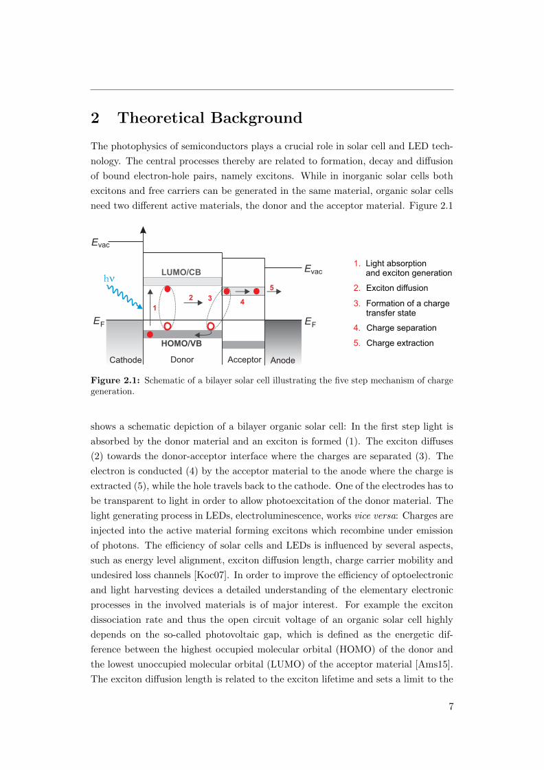
2 Theoretical Background
The photophysics of semiconductors plays a crucial role in solar cell and LED tech-
nology. The central processes thereby are related to formation, decay and diffusion
of bound electron-hole pairs, namely excitons. While in inorganic solar cells both
excitons and free carriers can be generated in the same material, organic solar cells
need two different active materials, the donor and the acceptor material. Figure 2.1
F
Donor Acceptor
1
2 34
5h
LUMO/CB
HOMO/VB
F
AnodeCathode
vacE
E
EE
vac1. Light absorption
and exciton generation
2. Exciton diffusion
3. Formation of a chargetransfer state
4. Charge separation
5. Charge extraction
Figure 2.1: Schematic of a bilayer solar cell illustrating the five step mechanism of chargegeneration.
shows a schematic depiction of a bilayer organic solar cell: In the first step light is
absorbed by the donor material and an exciton is formed (1). The exciton diffuses
(2) towards the donor-acceptor interface where the charges are separated (3). The
electron is conducted (4) by the acceptor material to the anode where the charge is
extracted (5), while the hole travels back to the cathode. One of the electrodes has to
be transparent to light in order to allow photoexcitation of the donor material. The
light generating process in LEDs, electroluminescence, works vice versa: Charges are
injected into the active material forming excitons which recombine under emission
of photons. The efficiency of solar cells and LEDs is influenced by several aspects,
such as energy level alignment, exciton diffusion length, charge carrier mobility and
undesired loss channels [Koc07]. In order to improve the efficiency of optoelectronic
and light harvesting devices a detailed understanding of the elementary electronic
processes in the involved materials is of major interest. For example the exciton
dissociation rate and thus the open circuit voltage of an organic solar cell highly
depends on the so-called photovoltaic gap, which is defined as the energetic dif-
ference between the highest occupied molecular orbital (HOMO) of the donor and
the lowest unoccupied molecular orbital (LUMO) of the acceptor material [Ams15].
The exciton diffusion length is related to the exciton lifetime and sets a limit to the
7

2 Theoretical Background
employed film thicknesses since excitons have to reach the donor-acceptor interface
within their lifetime to be separated. The focus of this thesis lies on the investigation
of the electronic structure and the excited state dynamics in different model systems
which will be introduced in Section 3.
In the following sections the theoretical concepts this work is based upon are
introduced. Fundamentals on metal surfaces and interfaces, such as adsorption in-
duced workfunction change and energy level alignment are presented in Sections 2.1.1
and 2.1.2, whereas Section 2.1.3 discusses the concept of band bending at pristine
and adsorbate covered semiconductor surfaces with focus on the n-type semicon-
ductor zinc oxide (ZnO). The basic theoretical background concerning excitations
in inorganic and organic semiconductors with focus on excitons will be treated in
Sections 2.2.1 and 2.2.2.
2.1 Metal and Semiconductor Surfaces and Interfaces
The energy level alignment between electrode and conjugated organic material strongly
affects the efficiency of charge carrier extraction and injection and thus the perfor-
mance of optoelectronic devices. Therefore the electronic processes at the interfaces
between the different materials is of particular interest. In the following sections
basic surface and interface phenomena, which are essential for the understanding
and interpretation of the results gained in this work, are introduced. First surface
states emerging at metal surfaces are treated in Section 2.1.1. The concepts of work
function and surface dipole, as well as energy level alignment upon adsorption of
organic semiconducting molecules on metal surfaces are introduced in Section 2.1.2.
The effect of band bending at semiconductor surfaces is discussed in Section 2.1.3.
2.1.1 Electronic States at Metal Surfaces
At the surface, the periodicity of the crystal lattice is broken. Due to this loss of
symmetry, the electronic band structure of the bulk changes at the surface and a
surface band structure emerges. New electronic states, which are located parallel to
the surface and decay exponentially into the vacuum and the bulk, appear within
the local band gaps. These so-called surface states were first described by Tamm and
Shockley [Tam32, Sho39]. Shockley states are suitable to describe electronic states
at metal or small band gap semiconductor surfaces, whereas Tamm states serve as a
valid description of transition metal and wide bandgap semiconductor surface states.
Surface states are very sensitive towards changes of the surface electronic structure
and thus towards adsorption of atoms and molecules [For03]. The energetic position
of a surface state can change upon adsorption, e.g. the Shockley surface states of
8
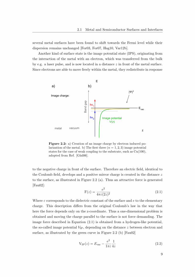
2.1 Metal and Semiconductor Surfaces and Interfaces
several metal surfaces have been found to shift towards the Fermi level while their
dispersion remains unchanged [For03, For07, Hag10, Var12b].
Another kind of surface state is the image potential state (IPS), originating from
the interaction of the metal with an electron, which was transferred from the bulk
by e.g. a laser pulse, and is now located in a distance z in front of the metal surface.
Since electrons are able to move freely within the metal, they redistribute in response
hv1
hv2
Evac
Band
gap
z
E
metal
Image charge:
vacuum
|Ψ|²
Image potential V(z)
a) b)
Figure 2.2: a) Creation of an image charge by electron induced po-larization of the metal. b) The first three (n = 1, 2, 3) image potentialstates for the case of weak coupling to the substrate, such as Cu(100),adopted from Ref. [Gud06].
to the negative charge in front of the surface. Therefore an electric field, identical to
the Coulomb field, develops and a positive mirror charge is created in the distance z
to the surface, as illustrated in Figure 2.2 (a). Thus an attractive force is generated
[Fau02]:
F(z) =e2
4πε(2z)2(2.1)
Where ε corresponds to the dielectric constant of the surface and e to the elementary
charge. This description differs from the original Coulomb’s law in the way that
here the force depends only on the z-coordinate. Thus a one-dimensional problem is
obtained and moving the charge parallel to the surface is not force demanding. The
image force described in Equation (2.1) is obtained from a hydrogen-like potential,
the so-called image potential VIP, depending on the distance z between electron and
surface, as illustrated by the green curve in Figure 2.2 (b) [Fau02]
VIP(z) = Evac −e2
1πε
1
4z(2.2)
9
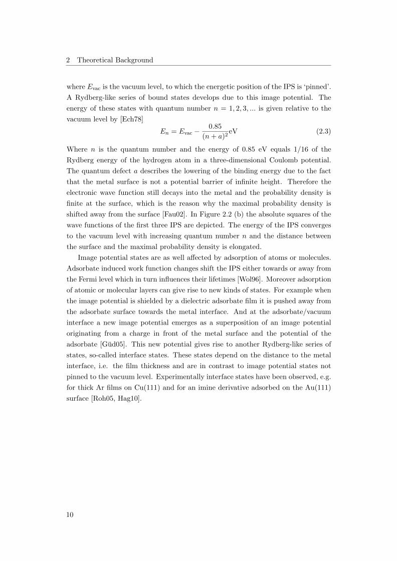
2 Theoretical Background
where Evac is the vacuum level, to which the energetic position of the IPS is ‘pinned’.
A Rydberg-like series of bound states develops due to this image potential. The
energy of these states with quantum number n = 1, 2, 3, ... is given relative to the
vacuum level by [Ech78]
En = Evac −0.85
(n+ a)2eV (2.3)
Where n is the quantum number and the energy of 0.85 eV equals 1/16 of the
Rydberg energy of the hydrogen atom in a three-dimensional Coulomb potential.
The quantum defect a describes the lowering of the binding energy due to the fact
that the metal surface is not a potential barrier of infinite height. Therefore the
electronic wave function still decays into the metal and the probability density is
finite at the surface, which is the reason why the maximal probability density is
shifted away from the surface [Fau02]. In Figure 2.2 (b) the absolute squares of the
wave functions of the first three IPS are depicted. The energy of the IPS converges
to the vacuum level with increasing quantum number n and the distance between
the surface and the maximal probability density is elongated.
Image potential states are as well affected by adsorption of atoms or molecules.
Adsorbate induced work function changes shift the IPS either towards or away from
the Fermi level which in turn influences their lifetimes [Wol96]. Moreover adsorption
of atomic or molecular layers can give rise to new kinds of states. For example when
the image potential is shielded by a dielectric adsorbate film it is pushed away from
the adsorbate surface towards the metal interface. And at the adsorbate/vacuum
interface a new image potential emerges as a superposition of an image potential
originating from a charge in front of the metal surface and the potential of the
adsorbate [Gud05]. This new potential gives rise to another Rydberg-like series of
states, so-called interface states. These states depend on the distance to the metal
interface, i.e. the film thickness and are in contrast to image potential states not
pinned to the vacuum level. Experimentally interface states have been observed, e.g.
for thick Ar films on Cu(111) and for an imine derivative adsorbed on the Au(111)
surface [Roh05, Hag10].
10
2.1 Metal and Semiconductor Surfaces and Interfaces
2.1.2 Energy Level Alignment at Metal/Organic Interfaces
Metal surfaces play an important role as electrodes in organic electronic devices.
Therefore it is crucial to understand the electronic processes and the electronic
structure upon adsorption of organic molecules.
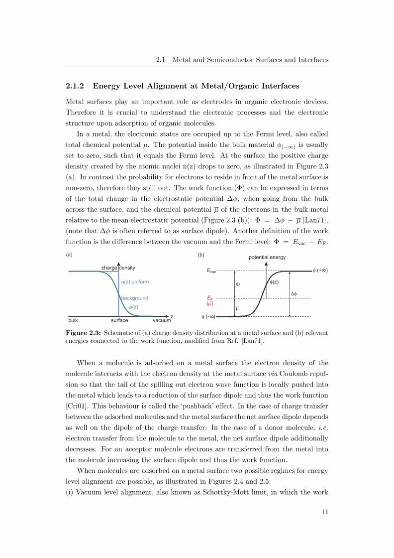
In a metal, the electronic states are occupied up to the Fermi level, also called
total chemical potential µ. The potential inside the bulk material φ(−∞) is usually
set to zero, such that it equals the Fermi level. At the surface the positive charge
density created by the atomic nuclei n(z) drops to zero, as illustrated in Figure 2.3
(a). In contrast the probability for electrons to reside in front of the metal surface is
non-zero, therefore they spill out. The work function (Φ) can be expressed in terms
of the total change in the electrostatic potential ∆φ, when going from the bulk
across the surface, and the chemical potential µ of the electrons in the bulk metal
relative to the mean electrostatic potential (Figure 2.3 (b)): Φ = ∆φ − µ [Lan71],
(note that ∆φ is often referred to as surface dipole). Another definition of the work
function is the difference between the vacuum and the Fermi level: Φ = Evac − EF.
bulk surface vacuum
-ρ(z)
z
E F
(b)(a)
n(z) uniform
background
charge density
potential energy
()
E vac
(- )8
(+ )8
(z)
Figure 2.3: Schematic of (a) charge density distribution at a metal surface and (b) relevantenergies connected to the work function, modified from Ref. [Lan71].
When a molecule is adsorbed on a metal surface the electron density of the
molecule interacts with the electron density at the metal surface via Coulomb repul-
sion so that the tail of the spilling out electron wave function is locally pushed into
the metal which leads to a reduction of the surface dipole and thus the work function
[Cri01]. This behaviour is called the ‘pushback’ effect. In the case of charge transfer
between the adsorbed molecules and the metal surface the net surface dipole depends
as well on the dipole of the charge transfer: In the case of a donor molecule, i.e.
electron transfer from the molecule to the metal, the net surface dipole additionally
decreases. For an acceptor molecule electrons are transferred from the metal into
the molecule increasing the surface dipole and thus the work function.
When molecules are adsorbed on a metal surface two possible regimes for energy
level alignment are possible, as illustrated in Figures 2.4 and 2.5:
(i) Vacuum level alignment, also known as Schottky-Mott limit, in which the work
11

2 Theoretical Background
function stays constant while the electron and hole injection barriers (∆e and ∆h),
i.e. the energetic positions of HOMO and LUMO relative to the Fermi level, change.
(ii) Fermi level pinning in which the work function changes while ∆e and ∆h stay
constant.
Vacuum level alignment is only possible when the Fermi level of the metal is located
between the initial EA/LUMO and IP/HOMO of the molecule [Ams15] as illustrated
in Figure 2.4 (a) and (b). In this case the hole and electron injection barriers ∆h
E
EF
Evac
LUMO
HOMO
(b) high metal
EA
IP e
h
E
EF
Evac
LUMO
HOMO
EA
IP e
h
(a) low metal
E
EF
Evac
LUMO
HOMO
EA
IP e
h
(c) effect of interface dipole
Figure 2.4: Vacuum level alignment for (a) low and (b) high work function metals, (c)interface dipole induced work function change.
and ∆e are given by
∆h = IP − Φ (2.4)
∆e = Φ − EA (2.5)
But this holds only under the assumption of an interface dipole (ID) of ID = 0 which
is usually not the case for interfaces between organic semiconductors and atomically
clean metals. The interface dipole in these systems emerges due to the ‘pushback’
effect, charge transfer or bond formation between adsorbate and substrate and leads
to a change of the work function as illustrated in Figure 2.4 (c). The concept of
vacuum level alignment thus becomes invalid and the hole and electron injection
barriers ∆h and ∆e write as
∆h = IP − Φ + ID (2.6)
∆e = Φ − EA − ID (2.7)
The second possibility, Fermi level pinning, occurs when the metal work function
is so low or high that the alignment of the vacuum levels would position the Fermi
level of the metal within the unoccupied or occupied molecular level [Koc12]. This
leads to the two limiting cases of LUMO-pinning in the case of a low work function
12
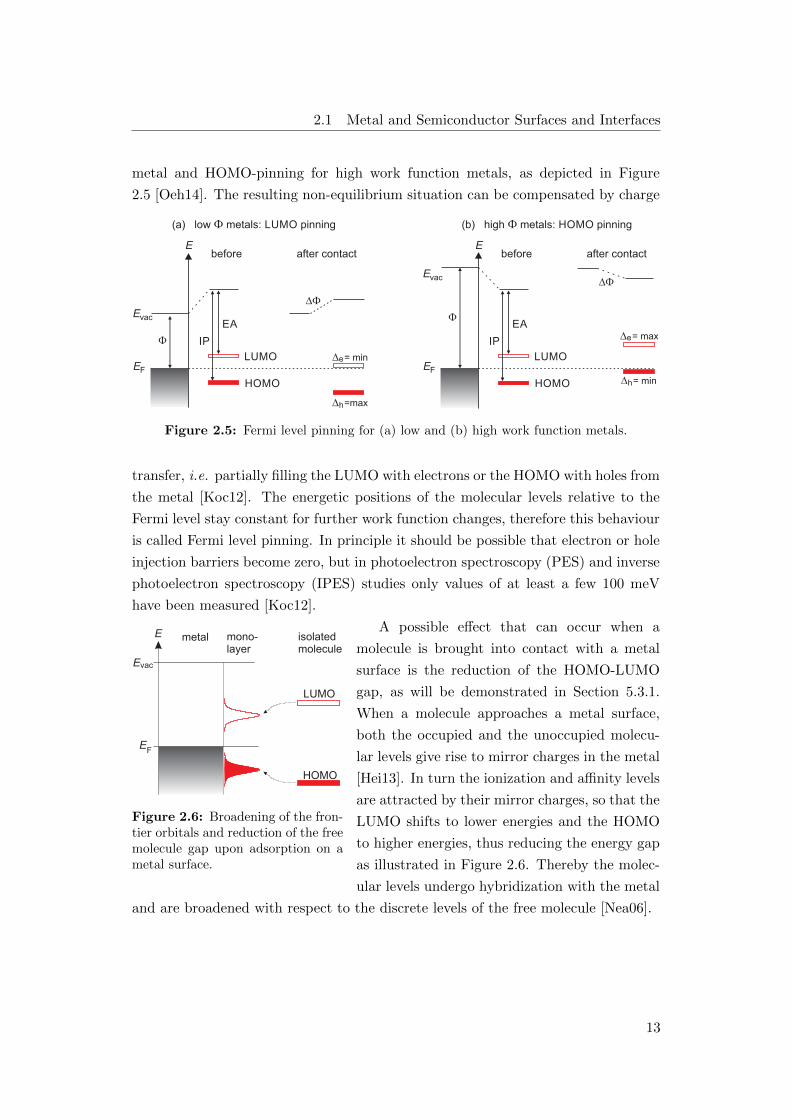
2.1 Metal and Semiconductor Surfaces and Interfaces
metal and HOMO-pinning for high work function metals, as depicted in Figure
2.5 [Oeh14]. The resulting non-equilibrium situation can be compensated by charge
E
EF
Evac
before after contact
LUMO
HOMO
(a) low metals: LUMO pinning
EA
IP
=maxh
= mine
(b) high metals: HOMO pinning
E
EF
Evac
before after contact
LUMO
HOMO
EA
IP
= minh
= maxe
Figure 2.5: Fermi level pinning for (a) low and (b) high work function metals.
transfer, i.e. partially filling the LUMO with electrons or the HOMO with holes from
the metal [Koc12]. The energetic positions of the molecular levels relative to the
Fermi level stay constant for further work function changes, therefore this behaviour
is called Fermi level pinning. In principle it should be possible that electron or hole
injection barriers become zero, but in photoelectron spectroscopy (PES) and inverse
photoelectron spectroscopy (IPES) studies only values of at least a few 100 meV
have been measured [Koc12].
E
E
E
vac
F
metal mono-layer
isolatedmolecule
LUMO
HOMO
Figure 2.6: Broadening of the fron-tier orbitals and reduction of the freemolecule gap upon adsorption on ametal surface.
A possible effect that can occur when a
molecule is brought into contact with a metal
surface is the reduction of the HOMO-LUMO
gap, as will be demonstrated in Section 5.3.1.
When a molecule approaches a metal surface,
both the occupied and the unoccupied molecu-
lar levels give rise to mirror charges in the metal
[Hei13]. In turn the ionization and affinity levels
are attracted by their mirror charges, so that the
LUMO shifts to lower energies and the HOMO
to higher energies, thus reducing the energy gap
as illustrated in Figure 2.6. Thereby the molec-
ular levels undergo hybridization with the metal
and are broadened with respect to the discrete levels of the free molecule [Nea06].
13

2 Theoretical Background
2.1.3 Band Bending at Semiconductor Surfaces
The concept of surface band bending was first developed by Schottky and Mott in
order to explain the adjustment of the semiconductor bands in contact with a metal
surface [Sch38, Mot38]. When an n-type semiconductor, in which electrons are the
majority carriers, and a metal with a work function larger than the semiconductor
(Φm > Φs) are brought into contact the electrons flow from the semiconductor to
the metal until the Fermi levels are aligned. This gives rise to an electric field
at the metal-semiconductor interface. In equilibrium a Helmholtz double layer is
formed where the metal is negatively and the semiconductor is positively charged
in its surface region, as depicted in Figure 2.7 (a). This electric field between metal
and semiconductor cannot be screened effectively in the semiconductor since the
concentration of free carriers is too low. Therefore the carrier concentration near the
semiconductor surface is reduced compared to the bulk, forming a so-called depletion
layer. In general the surface-near region in which the concentration of free majority
carriers differs from the bulk is called space charge region [Lut10]. In the space charge
E F
Evac
(a) > : upward band bending
z
CB
VBVB
---
+++
depletionlayer
E F
Evac
CB
VB
metal n-typesemiconductor
m ms
EAVbb
VSE F
Evac
z
CB
accumulationlayer
E F
Evac
CB
VB
metal n-typesemiconductor
m ms
EA
Vbb
--++
VB
m s
before contact after contact before contact after contact
(b) < : downward band bending m s
Figure 2.7: Energy level diagrams of metal and n-type semiconductor contacts: (a) WhenΦm > Φs upward band bending is induced and (b) Φm < Φs results in downward bandbending.
region the band edges of the semiconductor shift continuously due to the charge
transfer induced electric field between semiconductor and metal. In the case of Φm >
Φs (Figure 2.7 (a)) upward band bending occurs since electrons moving towards the
negatively charged Helmholtz layer in the metal feel the Coulomb repulsion so that
their potential energy rises [Zha12b]. The degree of band bending (Vbb) corresponds
to the energetic difference between the metal and the semiconductor work functions
Vbb = |Φm − Φs| (2.8)
14

2.1 Metal and Semiconductor Surfaces and Interfaces
The barrier which is formed at the metal-semiconductor interface when Φm > Φs
is called Schottky barrier (VS) and corresponds to the difference between the metal
work function and the electron affinity of the semiconductor
VS = (Φm − EA) (2.9)
When the work function of the metal is smaller than the work function of the semi-
conductor (Φm < Φs), electrons flow from the metal to the semiconductor so that
the metal is positively and the semiconductor negatively charged, as illustrated in
Figure 2.7 (b). In this case the electron concentration at the semiconductor surface
is higher than in the bulk thus forming a so-called accumulation layer in which the
band edges are bent downwards.
Band bending can be induced not only by a metal interface but as well by ex-
ternal electric fields, adsorption of atoms/molecules or by surface states [Zha12b].
In this work the effect of hydrogen adsorption on the electronic structure of the O-
terminated ZnO(0001) surface is investigated, as will be discussed in Section 5.1.1.
This ZnO surface is polar due to the negatively charged O-ions at the surface, there-
fore the pristine surface exhibits upward surface band bending, as depicted in Figure
2.8 (a). Adsorption of donor atoms, in this case hydrogen, leads to electron trans-
z
EF
Evac
CB
ʹʹ
VBz
EF
CBCAL
VBVBz
+ ---++
EF
Evac
CB
VBz
-+
+-+
-
ʹ
ʹEvacʹ
H-adsorption H-adsorption
(a) clean ZnO(0001)_
(b) H-doped ZnO(0001)_
Figure 2.8: (a) Upward surface band bending at the clean ZnO(0001) surface, (b) reversedsurface band bending upon H-adsorption.
fer from the donor to the semiconductor thus reducing the work function and the
upward surface band bending. Figure 2.8 (b) illustrates that further H-adsorption
leads to an enhanced work function reduction and downward surface band bending.
When the conduction band maximum (CBM) crosses the Fermi level, a charge ac-
cumulation layer (CAL) is formed which is populated by electrons donated by the
H-atoms. In comparison to other semiconductors such as Si and gallium arsenide
15

2 Theoretical Background
(GaAs) surface band bending in n-type ZnO only extends a few tens of A into the
bulk instead of a few hundreds of nm [Lut10], leading to a strongly confined CAL
[Dei15b].
16

2.2 Elementary Excitations in Semiconductors
2.2 Elementary Excitations in Semiconductors
In the following sections the fundamental processes resulting from illumination of
semiconductors are introduced. First a general introduction about the concept of
semiconductor excitons will be given. Section 2.2.1 is dedicated to elementary exci-
tations in inorganic semiconductors relevant for this thesis and Section 2.2.2 treats
the properties of excitons in organic semiconductors.
(a) excitation in an inorganic semiconductor (b) excitation in an organic semiconductor
VB
CB
HOMO
LUMO
(c) Mott-Wannier exciton (d) Frenkel exciton
k
E E
k
y
x
y
x
Figure 2.9: Excitation and electron-hole pair formation in (a) an inorganic and (b) anorganic semiconductor. (c) Delocalized Mott-Wannier exciton and (d) Frenkel exciton lo-calized on a single molecule.
Photoexciting an electron from the valence band (VB) in case of an inorganic
semiconductor (Figure 2.9 (a)), or the HOMO1 in a molecular semiconductor (Fig-
ure 2.9 (b)) to the conduction band (CB) or the LUMO leads to the formation of
Coulomb bound electron-hole pairs, so-called excitons. The holes are treated as
electron-like particles with a positive charge and a different effective mass. Excitons
are neutral quasiparticles which move through a dielectric medium transporting ex-
citation energy, not charge. There are two limiting cases of excitons which differ in
their binding radius and accordingly their binding energy: (i) Mott-Wannier exci-
tons (Figure 2.9 (c)), which usually have binding energies in the range of 0.001 - 0.1
eV and radii exceeding the lattice constant. (ii) In contrast Frenkel excitons (Figure
2.9 (d)), are confined to the size of a molecule and possess larger binding energies
in the range of 0.1 - 1 eV. Mott-Wannier excitons are usually found in inorganic
semiconductors while Frenkel excitons occur in organic semiconductors.
1In organic polymeric semiconductors both terminologies HOMO/LUMO and VB/CB are used.
17

2 Theoretical Background
2.2.1 Elementary Excitations in Inorganic Semiconductors
Excitons in inorganic semiconductors, Mott-Wannier excitons, can be understood as
hydrogen-like particles, which consist of an electron and a hole instead of a proton,
thus yielding a Rydberg-like series of energies depending on the exciton Rydberg
energy Rex [Mun10]
Rex =µ
m0ε2R∞ (2.10)
with the reduced mass of the electron-hole pair µ = me·mh(me+mh) , the free electron mass
m0, the dielectric constant ε and the Rydberg constant R∞. The exciton energy is
significantly smaller than the Rydberg energy of 13.6 eV of a hydrogen atom since
the effective electron and hole masses are smaller and the dielectric constant of the
semiconductor screens the Coulomb interaction between electron and hole [Koc06].
The Bohr radius of the exciton rex is given by
rex =m0ε
µa0 (2.11)
where a0 is the Bohr radius of a hydrogen atom in its ground state.
(b) d < rex
electron
hole
(a) d > rex
exciton Bohr radius rex
Figure 2.10: (a) Excitation below Mott density: distance between excitons is larger thanthe exciton radius, (b) excitation above Mott density: distance between excitons is smallerthan the exciton radius.
The properties of excitons in inorganic semiconductors highly depend on the
excitation density and the temperature. Figure 2.10 (a) shows the exciton gas at low
excitation densities where the distance between the excitons is larger than the exciton
Bohr radius d > rex. At high exciton densities, the distance between the excitons
becomes smaller than the exciton Bohr radius d < rex, as illustrated in Figure 2.10
(b). This leads to an enhanced screening of the attractive Coulomb interaction
between electron and hole, so that exciton formation becomes less probable [Mot68,
Hen07, Ver11]. This critical electron-hole density is called Mott density or Mott
18

2.2 Elementary Excitations in Semiconductors
limit and will play a role when it comes to the interpretation of excitation density-
dependent measurements of the H-covered ZnO(0001) surface in Section 5.1.2. Since
the reported values scatter over a broad range between 4 × 1016 cm−3 and 3.7 ×1019 cm−3 [Hen07, Sch11, Ver12, Sun05], I will not refer to it as a strict limit but
reference the excitation densities used in this work to the lower or upper Mott density
regime.
Versteegh et al. calculated a phase diagram of the electron-hole gas in ZnO as
a function of the electron-hole density and the temperature [Ver12]. They yielded 5
different regimes of which 2 are relevant for this work: The exciton gas which exists
in the low excitation density regime for temperatures above 1 K and the electron
hole plasma which forms at temperatures higher than ≈ 20 K for high excitation
densities.
The exciton formation and decay dynamics depend on the interaction between
the excited electrons and later the excitons with their surrounding. There are various
possible interactions such as scattering with electrons and holes, acoustic and optical
phonons or scattering with impurities and defects [Sha96]. After weak non-resonant
and above band gap excitation of a polar semiconductor like ZnO or GaAs the in-
teraction of excited electrons with phonons dominates the exchange of energy and
momentum between the carriers and the lattice. For large excess energies the scat-
tering with polar longitudinal optical (LO) phonons, Frohlich interaction, prevails.
The Frohlich interaction rate is given by [Sha96]
W (E) = W0
√hωLO
E
[n(hωLO)
sinh
(E
hωLO
)+
(n(hωLO) + 1)
sinh
((E
hωLO
)− 1
)](2.12)
With the phonon occupation number n(ωLO) and
W0 =e2√
2m0hωLO
4πh2
(1
ε∞− 1
εS
)(2.13)
Where hωLO is the LO phonon energy, m0 the free electron mass, and ε∞ and εS are
the optical and static permittivities. For low energy electrons the exciton formation
proceeds via coupling with acoustic phonons. The interaction with acoustic phonons
occurs either via deformation potential or piezoelectric scattering mechanisms, of
which usually the first prevails [Sha96].
The decay of excitons is often dominated by radiative electron-hole recombina-
tion (luminescence), which is desired in light-generating applications but needs to
be avoided in solar cells. Another decay channel is the dissociation of excitons into
free charge carriers, i.e. electrons and holes, giving rise to the formation of another
type of quasiparticles, namely polarons. In general a polaron can be described as a
19
2 Theoretical Background
charge surrounded by a polarization field. Since the polarization fields can have dif-
ferent origins and dimensions different kinds of polarons are distinguished. Polarons
originate not exclusively from dissociated excitons, they form as well directly from
excited charge carriers. One example for a polaronic species is the ‘large polaron’,
as well called ‘Frohlich-polaron’, which consists of an electron (or hole) and the po-
larization induced by LO phonons [Dev96]. In this case the polarization exceeds the
lattice constant, explaining the name ‘large polaron’. Another kind of polaron is the
‘small polaron’, where the polarization is confined to the lattice constant, consisting
of a charge which is trapped in a potential well resulting from its self-induced ionic
displacement. In principle ‘large’ and ‘small polarons’ can coexist in a material, but
concerning ZnO only ‘large polarons’ were found to be stable [Dev96, Sez15, Var12d].
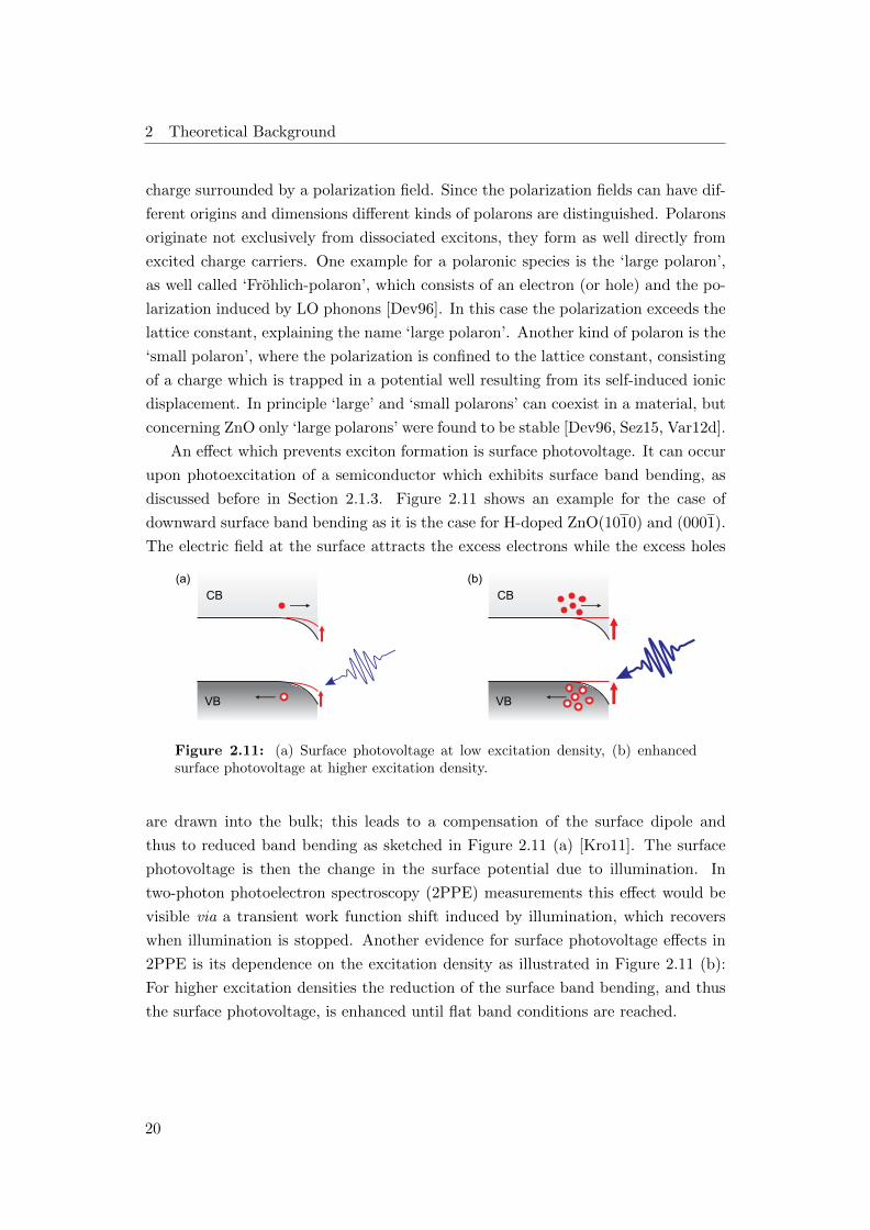
An effect which prevents exciton formation is surface photovoltage. It can occur
upon photoexcitation of a semiconductor which exhibits surface band bending, as
discussed before in Section 2.1.3. Figure 2.11 shows an example for the case of
downward surface band bending as it is the case for H-doped ZnO(1010) and (0001).
The electric field at the surface attracts the excess electrons while the excess holes
CB
VB
CB
VB
(a) (b)
Figure 2.11: (a) Surface photovoltage at low excitation density, (b) enhancedsurface photovoltage at higher excitation density.
are drawn into the bulk; this leads to a compensation of the surface dipole and
thus to reduced band bending as sketched in Figure 2.11 (a) [Kro11]. The surface
photovoltage is then the change in the surface potential due to illumination. In
two-photon photoelectron spectroscopy (2PPE) measurements this effect would be
visible via a transient work function shift induced by illumination, which recovers
when illumination is stopped. Another evidence for surface photovoltage effects in
2PPE is its dependence on the excitation density as illustrated in Figure 2.11 (b):
For higher excitation densities the reduction of the surface band bending, and thus
the surface photovoltage, is enhanced until flat band conditions are reached.
20

2.2 Elementary Excitations in Semiconductors
2.2.2 Excitons in Organic Semiconductors
In this section the concept of exciton binding energy in organic semiconductors is
introduced and the experimental accessibility of the relevant states is discussed.
Moreover different kinds of excitonic species will be presented.
The dielectric model introduced in Section 2.2.1 is only suitable to describe
delocalized Mott-Wannier excitons since the dielectric constant is a macroscopic
quantity and is thus not applicable to describe Frenkel excitons which are localized on
one molecular unit [Mun10]. The binding energy of Frenkel excitons can be defined
as the energy needed to separate a bound electron-hole pair located on one molecule
into free charges located at two molecules far away from each other. According to
Knupfer the exciton binding energy Eexcb is composed of three contributions [Knu03]
Eexcb = Eintra
b + U −W (2.14)
where Eintrab is the intramolecular binding energy which is lost by going from a bound
to an unbound electron-hole pair located on the same molecular unit, as illustrated
in Figure 2.12 (a) and (b). U is the charging, or Coulomb repulsion, energy which
has to be paid when the separated charges locate on two different molecules which
have been neutral before (Figure 2.12 (c)) and is defined as
U = E(N + 1) + E(N − 1)− 2E(N) (2.15)
where E is the energy and N is the number of electrons. W is the intermolecular
band width and thus the maximum amount of energy the separated charges can
gain. But since the band width in molecular solids is rather small and roughly of
(a) (b) (c)
- Ebintro
- U
-
+
Figure 2.12: (a) Bound electron-hole pair located on one molecular unit, (b) unboundelectron and hole and (c) electron and hole are located on two different molecules far awayfrom each other.
the same amount of energy as Eintrab , the exciton binding energy can be approximated
to [Knu03]
Eexcb ≈ U + 0.1 eV (2.16)
21

2 Theoretical Background
In the following paragraph the experimental determination of the exciton binding
energy by means of 2PPE will be discussed. Moreover the comparability of molecular
levels derived from photoemission and scanning tunneling spectroscopy (STS) will
be debated briefly, as in Section 5.3 STS will be used complementary to 2PPE.
Experimentally the exciton binding energy can be determined by subtracting the
optical gap (Eopt) from the transport gap (Etrans)
Eb = Etrans − Eopt (2.17)
The transport gap corresponds to the HOMO-LUMO gap, as indicated in Figure
2.13, and is called thus since the transport of free charge carriers occurs in these
energetic levels. The energetic positions of the HOMO and the LUMO can be
measured e.g. by 2PPE, as will be explained in Section 4.1.1, PES and IPES or
STS. All of the mentioned methods measure the HOMO as the difference between
the N electron state and the cation (N-1 electron state), while the LUMO is measured
as the difference between the negative ion (N+1 electrons) and the ground state (N
electrons). Since the charge transporting molecules are as well ions, the measured
HOMO/LUMO levels correspond to the electron/hole transport levels.
The optical gap corresponds to the threshold of photon absorption and can be
measured for instance by means of absorption spectroscopy or with 2PPE. In order
to illustrate the different 2PPE processes, especially the difference between the pop-
ulation of the LUMO and the exciton, Figure 2.13 shows pump-probe schemes for
photoemission from (a) the HOMO (b) the LUMO and (c) the exciton. The HOMO
Evac
EF
E
HOMO
LUMO
IP
EA
Ebexc
EoptE trans
N-1
N N-1 electrons
substrate
2PPE of (a) occ. state (b) unocc. state (c) exc. state
Figure 2.13: Probing (a) an occupied, (b) an unoccupied state and (c) an excitonic statewith 2PPE. The energetic position of the HOMO relative to the vacuum level correspondsto the ionization potential (IP) and the position of the LUMO to the electron affinity (EA).
is probed in a concerted 2PPE process as sketched in Figure 2.13 (a) and corresponds
to the IP. Figure 2.13 (b) shows the pump-probe scheme employed to measure the
LUMO, i.e. the EA level: An electron from the substrate is excited by the first
22
2.2 Elementary Excitations in Semiconductors
photon into the LUMO of the molecular adsorbate from where it is subsequently
probed by the second photon. In contrast intermolecular excitation of an electron
from the HOMO to the LUMO leads to the formation of an exciton as depicted
in Figure 2.13 (c). The exciton binding energy corresponds then to the energetic
difference between the kinetic energy of the electron emitted from the LUMO and
the kinetic energy of the electron emitted from the excitonic state. The optical gap
is given by the difference between HOMO and excitonic level. Since the exciton
binding energy is actually carried by both electron and hole, but only the electron
is emitted one could think that the measured kinetic energy actually corresponds
only to the energetic position of the Coulomb bound electron. But it has to be
taken into account that additional energy is needed to break up the exciton before
the electron can be emitted. This amount of energy is paid by the probe photon
energy and therefore this method is considered to be a good approximation. Thus
2PPE provides the possibility to measure the energetic positions of all the relevant
states: the HOMO/IP by photoemission from an occupied state, LUMO/EA level
by charge injection from the substrate, and the excitonic level by intramolecular
excitation from the HOMO.
Excitons usually decay via several competing mechanisms such as electron-hole
recombination, relaxation into other states (e.g. charge-transfer states, polarons
or trap states) and they can diffuse towards the substrate interface where charge-
separation occurs. Typical for the latter case is a coverage dependent lifetime since
with increasing coverage the surface-near electrons, probed by 2PPE, are not affected
anymore by the substrate. An increase of exciton lifetime as a function of the
distance to the metal surface will be discussed in Section 5.3 and has been observed
before for C60 and 6T on Au(111) [Dut05, Var12a].
In the following paragraphs different types of excitons which are relevant for this
thesis will be presented and discussed.
Charge Transfer Excitons
There are two different kinds of charge transfer excitons which should not be con-
fused:
(i) When electron and hole are located on two different materials or simply on two
neighbouring molecules they form a charge transfer state, also called charge transfer
exciton, polaron pair or polaron exciton [Dei10]. They can occur at donor-acceptor
interfaces as well as in homomolecular films and are considered to be precursors
for exciton dissociation leading to the formation of free charge carriers or polarons
(polarons have been introduced in Section 2.2.1 for inorganic semiconductors; the
polarons in organic semiconductors are similar to the ‘small polaron’ type).
23

2 Theoretical Background
(ii) The second type of charge transfer excitons occurs at the vacuum interface of
an organic semiconductor. In this case the electron is attracted not only by the
positive charge of the hole but as well by the image potential which emerges due to
the electron being located in front of the surface. This scenario is as well similar
to a hydrogen-like problem giving rise to a series of excitonic states which converge
toward the continuum of image potential states [Mun10]. These kinds of charge
transfer excitons have been studied at the surface of pentacene and tetracene films
by means of 2PPE [Zhu09].
Singlet and Triplet Excitons
Excitons can appear in different spin multiplicities, as singlet states with antiparallel
spins (2.14 (a)) or as triplets with parallel spins, as illustrated in Figure 2.14 (b).
Singlets are usually formed after absorption of a photon with sufficient energy as
depicted in the Jablonski diagram in Figure 2.14 (c): Excitation from the ground
state S0 into higher excited vibrational states of the first excited state S1,n is often
followed by internal vibrational relaxation (IVR) into the vibrational ground state
S1,0. The population partially decays via electron-hole recombination under emis-
sion of photons (Sn → S0), so-called fluorescence (FL), while another part of the
population undergoes intersystem crossing (ISC) forming triplet states. The singlet-
to-triplet ratio is often assumed to 1:3, but there is experimental and theoretical
evidence that the ratio can be completely different, due to carrier trapping and the
spin-dependent formation process [Kal02].
S1
S0
T1
A FL PH
ISC
IVR
ISC: intersystem crossing
A: absorption
IVR: internal vibrational relaxation
FL: fluorescence
PH: phosphorescence
S1
S0
T1
S0
(a) singlet (b) triplet exciton (c) Jablonski diagram
Figure 2.14: (a) Singlet and (b) triplet exciton. (c) Jablonski diagram illustrating relevantprocesses which can happen after photoexcitation of an organic semiconductor.
Since transitions from a singlet ground state to a triplet excited state (S0 → Tn),
and vice versa (Tn → S0), require a spin-flip, thus violating the conservation of spin
these transitions are considered to be ‘forbidden’ [Pow15]. Actually this is only true
when spin orbit coupling is zero but as soon as spin orbit coupling is present, i.e.
for angular quantum numbers l ≥ 1, these transitions are allowed. Strictly speaking
when spin orbit coupling is non-zero, spin and orbital angular momentum are no
24
2.2 Elementary Excitations in Semiconductors
good quantum numbers anymore and singlet and triplet excitations mix [Pow15].
However, spin orbit coupling is usually weak compared to other relevant effects
such as dipole coupling and therefore the probability for direct triplet formation is
very small so that triplets are formed via ISC from singlet states, as illustrated in
Figure 2.14 (c). ISC is a radiationless transition from an excited state to another
excited state with a different spin multiplicity. ISC is more efficient when singlet and
triplet are energetically close, their vibrational levels overlap and when the spin orbit
coupling is large. Due to the rather small probabilities for the radiative transition
from an excited triplet state to the singlet ground state, phosphorescence (PH), the
decay rates are typically orders of magnitudes slower than the FL decay rates. In
compounds containing heavy atoms, however, PH can be very efficient due to the
enhanced spin orbit coupling and the mixing with singlet states. Those efficient
phosphors provide the possibility to gain unity charge-to-photon conversion and are
already widely employed in phosphorescent organic light emitting diodes (OLEDs)
[Rei12]. Therefore PH presents in OLEDs using materials with weak spin orbit
coupling a significant loss channel, which needs to be avoided, while in the case of
strong spin orbit coupling PH can be exploited.
Another process leading to the formation of triplet excitons is singlet fission
during which one singlet state splits up into two triplet states:
S0S0hν→ S1S0 → T1T1 (2.18)
This process is very attractive for light harvesting devices since it promises quantum
yields to exceed 100% by converting 1 photon into 2 charge carriers, but up to now
it has been observed only for a few materials [Yos14]. Singlet fission requires a large
S1-T1 splitting and weak spin orbit coupling in order to avoid ISC [Yos14]. Singlet
fission has been reported as well in 2PPE measurements of pentacene and tetracene
by Zhu and co-workers [Cha11, Cha12b, Cha12a].
Singlet and triplet excitons travel via different excitation energy transfer mech-
anisms:
• Singlet transfer occurs via Forster resonance energy transfer [For48] (Figure
2.15(a)) which is a dipole coupling mechanism, i.e. that the transition dipole
moments of the coupling molecules have to be aligned parallel for efficient
transfer. Another condition is that the absorption and emission spectra of the
coupling molecules overlap, otherwise the amount of energy being transferred
is not sufficient. Forster transfer decays with the distance, R, of the coupling
molecules with R−6 [Yos12].
• In contrast triplet transfer takes place via a two electron exchange mechanism,
25
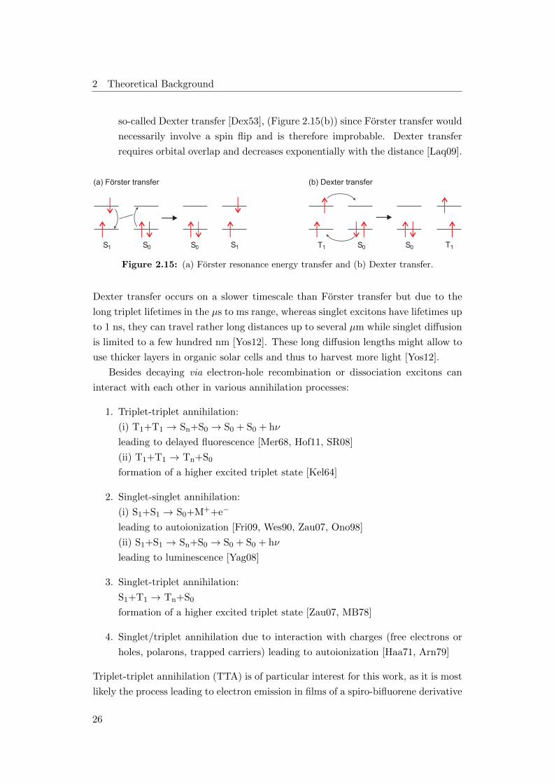
2 Theoretical Background
so-called Dexter transfer [Dex53], (Figure 2.15(b)) since Forster transfer would
necessarily involve a spin flip and is therefore improbable. Dexter transfer
requires orbital overlap and decreases exponentially with the distance [Laq09].
S1 S1S0 S0 T1 T1S0 S0
(a) Förster transfer (b) Dexter transfer
Figure 2.15: (a) Forster resonance energy transfer and (b) Dexter transfer.
Dexter transfer occurs on a slower timescale than Forster transfer but due to the
long triplet lifetimes in the µs to ms range, whereas singlet excitons have lifetimes up
to 1 ns, they can travel rather long distances up to several µm while singlet diffusion
is limited to a few hundred nm [Yos12]. These long diffusion lengths might allow to
use thicker layers in organic solar cells and thus to harvest more light [Yos12].
Besides decaying via electron-hole recombination or dissociation excitons can
interact with each other in various annihilation processes:
1. Triplet-triplet annihilation:
(i) T1+T1 → Sn+S0 → S0 + S0 + hν
leading to delayed fluorescence [Mer68, Hof11, SR08]
(ii) T1+T1 → Tn+S0
formation of a higher excited triplet state [Kel64]
2. Singlet-singlet annihilation:
(i) S1+S1 → S0+M++e−
leading to autoionization [Fri09, Wes90, Zau07, Ono98]
(ii) S1+S1 → Sn+S0 → S0 + S0 + hν
leading to luminescence [Yag08]
3. Singlet-triplet annihilation:
S1+T1 → Tn+S0
formation of a higher excited triplet state [Zau07, MB78]
4. Singlet/triplet annihilation due to interaction with charges (free electrons or
holes, polarons, trapped carriers) leading to autoionization [Haa71, Arn79]
Triplet-triplet annihilation (TTA) is of particular interest for this work, as it is most
likely the process leading to electron emission in films of a spiro-bifluorene derivative
26

2.2 Elementary Excitations in Semiconductors
(SP6) on ZnO as will be discussed in Section 5.2. In the following paragraph basic
properties of the TTA process, relevant for the interpretation of the 2PPE data
obtained for SP6 films on ZnO, will be discussed. Usually TTA is identified in
luminescence measurements by detecting the delayed fluorescence resulting from the
singlet due to TTA mechanism (i) [Mer68, Hof11, SR08]. If the higher excited singlet
state Sn lies energetically above the vacuum level autoionization might occur in an
analogous manner to the singlet-singlet annihilation process (i) reported before in the
literature [Fri09, Wes90, Zau07, Ono98]. Moreover TTA is a bimolecular process and
thus depends quadratically on the triplet concentration. A quadratic dependence
of the delayed fluorescence signal intensity on the incident laser power has been
observed experimentally by Singh-Rachford et al. [SR08].
In addition delayed fluorescence (DF), and thus TTA, was found to be temper-
ature dependent, since the TTA rate constant is controlled by the triplet diffusion
which increases for higher temperatures [Hof11]. Hoffmann et al. observed maximum
DF at a temperature of 100 K in the case of a ethylhexyl-substituted poly(fluorene)
trimer.
In the following chapter the systems investigated in this work will be introduced
and previous studies relevant for this work will be presented.
27

2 Theoretical Background
28
3 Investigated Systems
As mentioned before in Section 2 the active materials in organic photovoltaic cell
(OPVC)s and OLEDs consist of organic semiconducting materials. Thereby two
classes of materials are distinguished, so-called small molecules and polymers [Koc07].
While polymer films have to be prepared from solution, small molecule based devices
can be as well prepared via vapour deposition. Therefore small molecular films are
usually of higher order and purity compared to polymer films. The efficiencies of
solar cells and LEDs depend on several aspects such as the energy level alignment at
the interfaces of the active materials and exciton lifetime and diffusion. Depending
on the application different processes are considered as loss channels, e.g. strong
luminescence is desired in LEDs while it is an unwanted side effect in solar cells
where the excitons have to reach the donor/acceptor interface within their lifetime.
Therefore the elementary processes in the active materials are of particular interest
to enable device optimization. The central aspects of this thesis are the electronic
structure and the excited state dynamics of different model systems representing
anode-donor interfaces, small molecule and polymer donor films and a transparent
electrode material.
In the following sections the systems investigated in this work will be introduced
and the questions which will be examined in this work will be formulated. The
systems studied in this thesis can be divided into four parts:
1) The H-covered polar ZnO(0001) surface
2) The spirobifluorene derivative SP6 on ZnO(1010)
3) Two dicyanovinyl-substituted oligothiophenes on Au(111)
4) Two P3HT films with different degree of crystallinity
To provide a comprehensive basis for the investigations carried out in this work each
material is introduced in a separate section and if available recent studies on the
investigated systems are presented: In Section 3.1 the morphology of the mixed- and
the O-terminated ZnO surface are presented and the effects of H-adsorption on the
morphology, the electronic structure and the excited state dynamics will be discussed
on the basis of previous studies. Section 3.2 treats fundamental properties of SP6
as well as recent photoemission and excited state transmission studies on SP6/ZnO.
The oligothiophenes are introduced in Section 3.3 with focus on their adsorption
geometry and electronic structure on Au(111), as investigated recently by scanning
tunneling microscopy (STM) and STS. The morphology and the electronic structure
of the Au(111) surface is presented in Section 3.4. Section 3.5 treats besides relevant
studies on the electronic structure and excited state dynamics in P3HT films the
preparation and characterization of the films.
29

3 Investigated Systems
3.1 Electronic Properties and Excited State Dynamics
at the Mixed- and the O-terminated ZnO Surface
In the following section fundamental, structural and electronic properties of zinc
oxide will be introduced. The two investigated surfaces, the mixed-terminated
ZnO(1010) and the O-terminated ZnO(0001) surface, are presented in Section 3.1.1.
The phenomenon of surface metallization due to H-adsorption will be discussed in
Section 3.1.2 while Section 3.1.3 deals with previous studies on surface exciton for-
mation and decay dynamics at the two relevant ZnO surfaces.
ZnO is a promising candidate for the application in various optoelectronic de-
vices, such as LEDs and solar cells, due to its wide bandgap of Eg = 3.37 eV (300
K), which makes it transparent to visible light, and its intrinsic n-type conductiv-
ity [Bla99]. In addition ZnO has a large exciton binding energy of Eexb = 59.5 ±
0.5 meV, compared to e.g. the exciton binding energy of silicon which amounts to
15 meV [Gre13], and thus exhibits strong luminescence even at room temperature
[Kli10]. Moreover the topmost LO phonon has a relatively high energy of 72 meV
in ZnO due to the light mass of oxygen [Kli10] and plays a central role in the re-
laxation dynamics of hot electrons in ZnO, as will be discussed in Sections 3.1.3
and 5.1.2. The application of ZnO as transparent electrode material and indium tin
oxide (ITO) substitute is particularly attractive since it is a cheap, easily accessi-
ble and non-toxic material. ZnO is already used in a huge variety of everyday life
products, e.g. as UV blocker in sun creams, as white pigment in paints, as fungicide
in the food industry, in dental inlays and ointments due to its antibacterial proper-
ties [Mor09, Kli10]. Furthermore it is used in nanorod gas sensors [Wan05a] and in
heterogeneous catalysis for e.g. methanol synthesis, where especially the polar sur-
faces showed enhanced catalytic reactivity [Bow83, Wil03, Kur05]. A still unsolved
problem is p-type doping in ZnO, which is needed for p-n-homojunctions in LEDs
or transistors. ZnO is very vulnerable to defect states, which strongly influence the
electronic structure. Oxygen vacancies and Zn interstitials have been regarded as ex-
planations for intrinsically n-type doping in ZnO. But it has been discovered during
the past 15 years that oxygen vacancies are deep donors and thus cannot contribute
to n-type conductivity. Moreover it has been shown that Zn interstitials are as well
unlikely to cause n-type conductivity and that impurities acting as shallow donors
play an important role. Oxygen vacancies and Zn-interstitials however do play a
role in p-type doping acting as compensating centers [Jan09].
Hydrogen for example is present in almost every fabrication environment, even
under UHV conditions it shows a significant effect on the electronic structure of
ZnO [Kin11, Jan09, Dei15b] as will be discussed in detail in Section 3.1.2. Usually
30
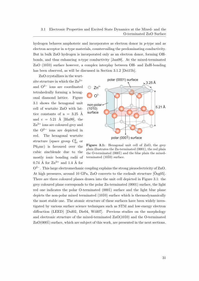
3.1 Electronic Properties and Excited State Dynamics at the Mixed- and theO-terminated ZnO Surface
hydrogen behaves amphoteric and incorporates as electron donor in p-type and as
electron acceptor in n-type materials, countervailing the predominating conductivity.
But in bulk ZnO hydrogen is incorporated only as an electron donor, forming OH-
bonds, and thus enhancing n-type conductivity [Jan09]. At the mixed-terminated
ZnO (1010) surface however, a complex interplay between OH- and ZnH-bonding
has been observed, as will be discussed in Section 3.1.2 [Dei15b].
2+Zn
2-O
3.25 A °
5.21 A °
polar (0001) surface
polar (0001) surface
non-polar (1010) surface
Figure 3.1: Hexagonal unit cell of ZnO, the greyplain illustrates the Zn-terminated (0001), the red plainthe O-terminated (0001) and the blue plain the mixed-terminated (1010) surface.
ZnO crystallizes in the wurt-
zite structure in which the Zn2+
and O2− ions are coordinated
tetrahedrally forming a hexag-
onal diamond lattice. Figure
3.1 shows the hexagonal unit
cell of wurtzite ZnO with lat-
tice constants of a = 3.25 A
and c = 5.21 A [Bla99], the
Zn2+ ions are coloured grey and
the O2− ions are depicted in
red. The hexagonal wurtzite
structure (space group C46v or
P63mc) is favoured over the
cubic zincblende due to the
mostly ionic bonding radii of
0.74 A for Zn2+ and 1.4 A for
O2−. This large electromechanic coupling explains the strong piezoelectricity of ZnO.
At high pressures, around 10 GPa, ZnO converts to the rocksalt structure [Ozg05].
There are three coloured planes drawn into the unit cell depicted in Figure 3.1: the
grey coloured plane corresponds to the polar Zn-terminated (0001) surface, the light
red one indicates the polar O-terminated (0001) surface and the light blue plane
depicts the non-polar mixed terminated (1010) surface which is thermodynamically
the most stable one. The atomic structure of these surfaces have been widely inves-
tigated by various surface science techniques such as STM and low-energy electron
diffraction (LEED) [Dul02, Die04, Wol07]. Previous studies on the morphology
and electronic structure of the mixed-terminated ZnO(1010) and the O-terminated
ZnO(0001) surface, which are subject of this work, are presented in the next sections.
31

3 Investigated Systems
3.1.1 Morphology of the O-and the Mixed-terminated ZnO Surface
Since the Zn-terminated ZnO(0001) surface is not subject of this work I will from
now on refer to the O-terminated ZnO(0001) surface as the polar surface. Figure
3.2 (a) depicts the ZnO(1010) surface which consists of equal amounts of Zn- and
O-ions arranged in alternating rows. Since the negative charge of each O2− ion is
compensated by the positive charge of a Zn2+ ion the surface is non-polar. This sur-
face is atomically flat and presents the most stable ZnO surface. The O-terminated
ZnO ZnO
(a) ZnO(1010)_
(b) ZnO(0001)_
Figure 3.2: (a) Mixed-terminated ZnO(1010) and (b) O-terminated ZnO(0001)surface, image courtesy by B. Bieniek
ZnO(0001) surface, shown in Figure 3.2 (b), is exclusively composed of O-ions and
therefore a polar surface, i.e. it exhibits a surface dipole which points with its
negative end into the vacuum. Despite its polarity the O-terminated surface is sur-
prisingly stable and shows, like the non-polar surface, a 1×1 termination [Dul02].
But it is still under debate whether the observed 1×1 pattern is really due to the
clean O-terminated surface or corresponds to a H-overlayer, since the clean surface
is expected to show a 1×3 reconstruction [Kun02]. In contrast to the atomically
flat non-polar surface the polar surface features a terrace structure consisting of flat
hexagonal terraces with no additional holes or islands [Dul02].
The density of oxygen ions on the polar surface is ≈ 1.9 times higher than on
the non-polar surface; this will play a role when comparing the amounts of adsorbed
hydrogen on the polar with the non-polar surface in Section 5.1.1.
The surface properties are of great interest since they play a central role in lots
of applications. The stability and reactivity of surfaces are crucial in e.g. catalytic
processes while the electronic structure plays a major role in optoelectronic devices
where energy level alignment and conductivity are important issues. Oxygen vacan-
cies at the polar (0001) surface are discussed as active centers in methanol synthesis
and are therefore particularly interesting [Fin06]. K. Fink calculated the energetic
positions of several defect states at the polar ZnO(0001) surface [Fin06]. She chose
as initial situation the H-covered polar ZnO(0001) surface and calculated the geo-
metry and the electronic structure of different defects, such as the O-defect (VO)
32

3.1 Electronic Properties and Excited State Dynamics at the Mixed- and theO-terminated ZnO Surface
and the OH defect (VOH). In the case of the O-defect a neutral O-atom is removed
from the surface leaving two electrons in the vacancy. For the OH defect a neutral
OH-group is withdrawn and only one electron is left in the vacancy. The defect levels
of these two cases were found to be located 1.8 eV above valence band maximum
(VBM), i.e. 1.6 eV below CBM [Fin06]. Experimentally luminescence from defect
states has been observed at comparable energies around 1.8 eV below the CBM in
our group by L. Foglia [Fog15]. This information will be of particular interest for
the interpretation of the photoelectron spectra discussed in Section 5.1.1.
3.1.2 Surface Metallization due to H-adsorption on ZnO Surface
In the following section a short overview on recent studies investigating the effect
of H-adsorption on the electronic structure of ZnO surfaces will be given. These
previous studies are of great interest for this thesis in which the influence of H-
doping on the electronic structure of the O-terminated ZnO surface is investigated,
as will be discussed in Section 5.1.1.
Woll and co-workers performed several studies using various surface science tech-
niques and discovered that hydrogen adsorbes on the non-polar (1010) surface at low
temperatures in a 2H(1×1) overlayer binding to Zn- and O-ions, while at room tem-
perature the overlayer changes towards a H(1×1) fashion in which the hydrogen
atoms are bonded only to the surface oxygen [Bec01, Kun03]. This temperature de-
pendent binding behaviour demonstrates that the OH-bonds are stronger than the
ZnH-bonds. The formation of OH-bonds leads to the development of a CAL, i.e. a
metallic surface state, since hydrogen acts as an electron donor in the OH-bond and
partially fills the CB, as discussed before in Section 2.1.3 [Bec01, Kun03, Wan05b].
Hydrogen adsorption on the O-terminated polar surface leads to H(1×1) over-
layers which are formed directly during the adsorption process and give rise to a
metallic surface state, too. (This metallic surface state does not exist at the Zn-
terminated surface since hydrogen has a negative partial charge in the ZnH-bond
and thus cannot donate electrons to the CB.)
Ozawa and Mase investigated in an angle-resolved photoelectron spectroscopy
(ARPES) study the effect of H-adsorption on the electronic structure of the sta-
ble ZnO surfaces [Oza11]. On the clean O-terminated surface they observe upward
surface band bending which was reverted to downward surface band bending upon
H-adsorption accompanied by a large work function decrease of ≈ 1.2 eV. Upon
H-adsorption they found adsorbate induced surface metallization in the case of the
O-terminated ZnO(0001) and the mixed-terminated ZnO(1010) surfaces, but not for
the Zn-terminated ZnO(0001) surface [Oza11]. They estimated the charge density
accumulating on the ZnO surfaces due to H-adsorption to 1013 cm−2. In addi-
33

3 Investigated Systems
Figure 3.3: Schematic of the energy band structures of theclean (left) and H-covered ZnO(1010) surface (right) with themetallic surface state (red) as published by Ozawa and Mase,adopted from Ref. [Oza10].
tion they investigated the non-polar ZnO(1010) surface as a function of hydrogen,
methanol and water adsorption [Oza10]. They found that all three adsorbates in-
duce bending of the CB below the Fermi level and thus the formation of a CAL,
which was explained by all three adsorbates acting as electron donors.
Figure 3.3 shows schematics of the band structures of the clean and the H-covered
ZnO(1010) surfaces observed by Ozawa et al. [Oza10]. The valence electronic struc-
ture of the pristine surface (left) is characterized by the O2p-Zn4sp (blue shaded
area) hybrid band, with the O2p dangling bond state, located between 3 - 9 eV
below the Fermi energy. The conduction band consists of the empty Zn4s levels
(green shaded area). The H-covered ZnO surface exhibits an enhanced downward
surface band bending giving rise to a CAL (red line) with a thickness of several 10 A
[Wan05b] and a maximum surface charge density of 1013 cm−2 due to the electrons
donated by the adsorbed hydrogen, partially occupying the CB [Oza11].
While Ozawa et al. studied the H2-dosage regime between 200 and 2000 L Dein-
ert et al. investigated the low dosage regime between 6 and 500 L by means of
2PPE [Dei14, Dei15b]. They also observed a pronounced work function decrease
correlated with increased downward surface band bending and the formation of a
CAL upon hydrogen adsorption. Figure 3.4 shows the work function and the in-
tegrated CAL intensity plotted as a function of H2-dosage. The work function
saturates around 3.8 eV with a maximal shift of ∆Φmax = -0.65 eV, while the
CAL intensity decreases for H2-dosages higher than 150 L. The reduction of the
34

3.1 Electronic Properties and Excited State Dynamics at the Mixed- and theO-terminated ZnO Surface
CAL intensity was explained by the formation of ZnH-bonds which compensate
the surface dipole induced by the OH-bonds because hydrogen acts as an electron
acceptor in the zinc-hydride bond [Dei15b]. According to DFT calculations pre-
sented in the same work, ZnH-bond formation sets in at a H-coverage of ≈ 18 %
leading to a complex and competitive behaviour of OH- and ZnH-bond formation.
H dosage (L)2
4.6
4.5
4.4
4.3
4.2
4.1
4.0
3.9
3.8
work
funct
ion (
eV
)
norm
alize
d m
eta
llic peak in
tensity (a
rb. u
nits)
5004003002001000
1.0
0.8
0.6
0.4
0.2
0.0
sample A
sample B
Figure 3.4: Work function and CAL intensity as afunction of H-dosage as measured by Deinert et al.,adopted from Ref. [Dei15b].
They found out that next to
an H-terminated O-atom H-
adsorption on a Zn-ion is ener-
getically favoured over the for-
mation of another OH-bond.
This was explained by the re-
duction of the work function,
and consequently the IP and
EA, due to OH-bond forma-
tion, thus making charge trans-
fer from the electron donor (H
in OH-bond) to the ZnO less
favourable while charge trans-
fer from the ZnO to an acceptor
(H in ZnH-bond) becomes pro-
fitable. In addition the calculations revealed that the CAL starts to delocalize at a
critical H-coverage of ≈ 25 % when the potential wells, which are due to a significant
reduction of the surface potential induced by the OH-bonds and have a diameter of
≈ 5 nm, start to overlap [Dei15b]. Concerning the extension of the CAL perpen-
dicular to the surface, they found it located right at the surface since the OH-bond
induced changes of the surface potential reach less than 20 A into the bulk.
On the basis of the results presented in this section questions for the behaviour
of the O-terminated surface towards H-adsorption can be derived. The absence of
Zn-ions at the polar surface should lead to a larger work function shift upon H-
adsorption compared to the non-polar surface. Moreover no decrease of the CAL
intensity above a certain H2-dosage is expected since no ZnH-bonds, countervailing
the effects of OH-bond formation, should be formed. The saturation of the work
function is expected to be reached at higher H2-dosages since there are nearly twice
as many O-ions on the polar than on the non-polar surface.
In the following section previous studies on surface exciton (SX) dynamics at
ZnO surfaces will be presented.
35

3 Investigated Systems
3.1.3 Surface Exciton Dynamics at ZnO Surfaces
In this section general information about surface excitons on ZnO surfaces is given,
relevant studies for the understanding of the results obtained in this work are pre-
sented and open questions will be motivated. Exciting ZnO above the band gap
leads to the formation of excitons which are important quasi-particles for opto-
electronic and light harvesting devices. In ZnO the existence of several excitonic
species, such as free excitons, donor- and acceptor-bound and SX, have been re-
ported [Ozg05, Kue13, Dei14, Tis08]. Surface excitons are of great interest since
energy transfer processes between different materials take place at their interfaces
and usually involve short distance energy transfer processes such as Forster reso-
nance energy transfer (FRET). They deserve particular attention because also exci-
ton free surface layers in ZnO, potentially inhibiting energy transfer at the surface,
have been reported [Lag63]. Surface excitons have been observed on single crystal
surfaces [Tis08, Dei14], pseudomorphically grown thin films [Kue13, Fri15] and even
in confined nanoscale systems [Bis11, Ric08, Yan07] in which so-called ’exciton dead
layers’ are expected to prevent exciton localization at the surface [Fon04].
The origin of SX was investigated by Biswas et al. who concluded that the
existence of surface excitons was due to modification of the surface by an adsorbate,
in their case most likely an OH-related species [Bis11]. Other studies demonstrated
that the SX can be influenced by adsorbates, irradiation or particle bombardment
[Kue13, Bis11, Yan07, Ric08]. For example Kuehn et al. reported an enhancement of
the signal intensity related to the SX by adsorbing organic molecules with carboxylic
anchor groups [Kue13]. In contrast the SX related signal was quenched in another
study upon treatment with titanium plasma as [Yan07].
The emission signals from the SX were found around 3.365 - 3.368 eV, i.e. be-
tween the free and the donor-bound excitons, in photoluminescence measurements
[Kue13, Bis11, Ric08]. The SX were reported to be spatially located right at the
surface [Fri15], within 5 nm from the surface [Yan07] and around 20 Abelow the
surface [Dei14].
A time-resolved 2PPE study on the SX dynamics on the H-doped ZnO(1010) sur-
face has been performed in our group by J.-C. Deinert [Dei14]. He found that after
excitation above the band gap the hot carriers relax via scattering with LO phonons
followed by SX formation within 200 fs. Ultrafast phonon-mediated relaxation of
above band gap excited electrons, slowing down for energies close to the CBM,
has been also demonstrated in another 2PPE study by Tisdale et al. [Tis08]. Both
studies revealed a temperature-independent behaviour of the ultrafast relaxation dy-
namics up to 300 K which was interpreted as a confirmation of Frohlich coupling with
LO phonons since interaction with lower lying transversal optical phonons leads to a
36

3.1 Electronic Properties and Excited State Dynamics at the Mixed- and theO-terminated ZnO Surface
slowing down of the relaxation dynamics, as it is the case for low energies. In addition
a theoretical study by Zhukov et al. confirms the existence of two types of excited
electron dynamics: (i) a fast one in the fs regime for high excess energy electrons
related to electron-phonon scattering and (ii) ps dynamics for electrons close to the
bottom of the CB associated with the reduction of the phonon phase space [Zhu10].
intermediate state energy E - E (eV)F
ph
oto
em
issi
on
inte
nsity
(a
rbitr
ary
un
its)
0 fs
1 ps
0.80.60.40.20.0-0.2
3 L, 18 -33.4 x 10 cm 16 L,
18 -33.4 x 10 cm
44 L, 18 -3
1.7 x 10 cm
1 ps
0 fs
bu
lk CB
EF
E
OZn
H
CB
CAL
su
b
s
urf
ac
e
z
(a)
(b)
18 -31.7 x 10 cm18 -3
5.2 x 10 cm
screenedFCoulomb
e
h
bu
lk ga
p
44 L H /ZnO(1010)2
excitation density
hydrogen termination
photo-excited e-h plasma
Figure 3.5: Pump-induced 2PPE signals for(a) different excitation densities and (b) dif-ferent H-dosages, normalized to the hot elec-tron intensity between 0.4 and 0.6 eV to com-pare intensity changes relative to the singleparticle excitation density. (a) Higher ex-citation densities lead to a screening of theCoulomb interaction, as illustrated in the in-set, and diminish the SX formation probabil-ity. (b) The SX intensity is not decreasingfor increased carrier concentration in the CAL,due to higher H-coverages, indicating localiza-tion in the subsurface region as visualized inthe inset. Adopted from Ref. [Dei14].
The time constants calculated by
Zhukov et al. will be compared to the
time constants experimentally obtained
in this work in Section 5.1.2. Above
a critical photoinduced carrier density,
which was calculated to 1× 1019 cm−3,
the phonon emission rate is expected
to decrease significantly with increasing
carrier density [Tis08]. The SX lifetime
was found to exceed 400 ps and electron-
hole recombination, leading to lumines-
cence or Auger-like processes, was sug-
gested as decay channel [Dei14].
Deinert et al. demonstrated that the
formation probability of SX is reduced
by transient screening of the Coulomb
interaction at excitation densities close
to the Mott density [Dei14]. This result
was achieved performing time-resolved
2PPE measurements on the H-doped
ZnO surface as a function of the excita-
tion density. Figure 3.5 (a) displays the
pump-induced 2PPE signals related to
the SX for low (green) and high (orange)
excitation densities. For high excitation
densities the distance between the exci-
tons becomes smaller than the exciton
Bohr radius, leading to a screening of
the Coulomb interaction between elec-
tron and hole and thus to a reduction of
their formation probability, as discussed
in Section 2.2.1.
In addition they concluded that the
37

3 Investigated Systems
SX is located in the sub-surface region based on the finding that the SX was stable
towards work function changes and enhanced charge carrier density in the CAL,
induced by H-adsorption. The fact that the photoemission signal assigned to the
SX does not decrease for H2-dosages up to 44 L, as demonstrated in Figure 3.5 (b),
reflects that the SX is neither affected by the change of the surface potential nor
by the increased carrier density in the CAL, which might lead to a screening of the
Coulomb interaction between electron and hole and with this to a reduction of the
exciton formation probability. Moreover the SX could still be observed after exposing
the single crystal surface to air [Dei15a]. This extraordinary stability towards air in
combination with its stability at room temperature make the SX a promising feature
for charge transfer applications, as fabrication processes and device operation usually
do not take place in ultrahigh vacuum (UHV) chambers at a temperature of 100 K.
In this thesis the questions, whether such a surface exciton exists as well at the
O-polar ZnO(0001) surface and if yes, how fast the formation and decay dynamics
take place, are examined using time-resolved 2PPE. In addition the question whether
the total charge density, consisting of the H-induced (CAL) and the photoinduced
(excitation density) electron density, affects the relaxation dynamics of the hot elec-
trons will be pursued. Further problems arising from the discussion above concern
the influence of H-adsorption on the electronic structure of the O-terminated sur-
face, e.g. how is the H-induced work function shift on the polar surface affected
by the absence of Zn-ions in comparison to the mixed-terminated surface where the
O-density is smaller. Another question is related to the behaviour of the CAL in-
tensity as a function of the H2-dosage, which is not expected to decrease for higher
H2-dosages on the polar surface, as it is the case on the non-polar surface, since no
ZnH-bond formation is expected. These problems will be treated in Sections 5.1.1
and 5.1.2.
38
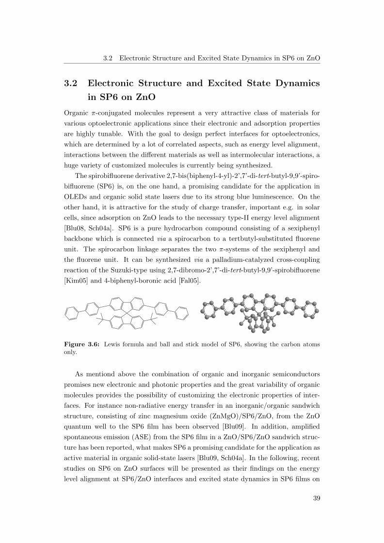
3.2 Electronic Structure and Excited State Dynamics in SP6 on ZnO
3.2 Electronic Structure and Excited State Dynamics
in SP6 on ZnO
Organic π-conjugated molecules represent a very attractive class of materials for
various optoelectronic applications since their electronic and adsorption properties
are highly tunable. With the goal to design perfect interfaces for optoelectronics,
which are determined by a lot of correlated aspects, such as energy level alignment,
interactions between the different materials as well as intermolecular interactions, a
huge variety of customized molecules is currently being synthesized.
The spirobifluorene derivative 2,7-bis(biphenyl-4-yl)-2’,7’-di-tert-butyl-9,9’-spiro-
bifluorene (SP6) is, on the one hand, a promising candidate for the application in
OLEDs and organic solid state lasers due to its strong blue luminescence. On the
other hand, it is attractive for the study of charge transfer, important e.g. in solar
cells, since adsorption on ZnO leads to the necessary type-II energy level alignment
[Blu08, Sch04a]. SP6 is a pure hydrocarbon compound consisting of a sexiphenyl
backbone which is connected via a spirocarbon to a tertbutyl-substituted fluorene
unit. The spirocarbon linkage separates the two π-systems of the sexiphenyl and
the fluorene unit. It can be synthesized via a palladium-catalyzed cross-coupling
reaction of the Suzuki-type using 2,7-dibromo-2’,7’-di-tert-butyl-9,9’-spirobifluorene
[Kim05] and 4-biphenyl-boronic acid [Fal05].
Figure 3.6: Lewis formula and ball and stick model of SP6, showing the carbon atomsonly.
As mentiond above the combination of organic and inorganic semiconductors
promises new electronic and photonic properties and the great variability of organic
molecules provides the possibility of customizing the electronic properties of inter-
faces. For instance non-radiative energy transfer in an inorganic/organic sandwich
structure, consisting of zinc magnesium oxide (ZnMgO)/SP6/ZnO, from the ZnO
quantum well to the SP6 film has been observed [Blu09]. In addition, amplified
spontaneous emission (ASE) from the SP6 film in a ZnO/SP6/ZnO sandwich struc-
ture has been reported, what makes SP6 a promising candidate for the application as
active material in organic solid-state lasers [Blu09, Sch04a]. In the following, recent
studies on SP6 on ZnO surfaces will be presented as their findings on the energy
level alignment at SP6/ZnO interfaces and excited state dynamics in SP6 films on
39

3 Investigated Systems
ZnO are of major interest for this work.
Information on intermolecular as well as molecule-substrate interactions is pro-
vided by a recent experimental and theoretical Raman study of SP6 on different
substrates, e.g. ZnO(0001), by Stahler et al. [Sta13]. They observed that the vibra-
tional response of the SP6 molecules is not affected by the substrate and compares
well to the DFT calculations of SP6 in the gas phase, revealing that the interaction
between the molecules and the employed oxide substrates is weak [Sta13].
The adsorption behaviour of SP6 has been studied by Blumstengel et al. by
means of atomic force microscopy (AFM) showing that SP6 forms smooth, amor-
phous films on ZnO surfaces. This is due to the rigid propeller-like structure of the
molecules, induced by the spiro-linkage, which prevents crystallization on the sample
surface [Blu08]. Furthermore they investigated the electronic structure and the exci-
Figure 3.7: Energy level diagrams of SP6/ZnO and SP6/ZnMgOadopted from Ref. [Blu08].
ton dynamics of SP6 on the O-terminated ZnO(0001) surface of a ZnO single crystal
and on a ZnMgO(0001) epilayer using ultraviolet photoelectron spectroscopy (UPS)
and time-resolved photoluminescence (PL) spectroscopy. The UPS measurements
were carried out for films between 0.2 nm and 3.2 nm thickness, exhibiting work func-
tion reductions of 0.8 eV from 5.0 eV to 4.2 eV in the case of SP6/ZnO(0001), and
0.4 eV from 4.4 eV to 4.0 eV for SP6/ZnMgO. The energy level diagrams obtained
by Blumstengel et al. are depicted in Figure 3.7 and exhibit the staggered type-II
energy level alignment, where the CBM and the VBM of the inorganic semiconduc-
tor lie below the LUMO and HOMO of the molecule [Blu08]. The CBM and LUMO
energies have been estimated by adding the optical gaps (ESP6opt = 3.15 eV, EZnO
opt
= 3.34 eV and EZnMgOopt = 3.69 eV), obtained from absorption measurements, and
40
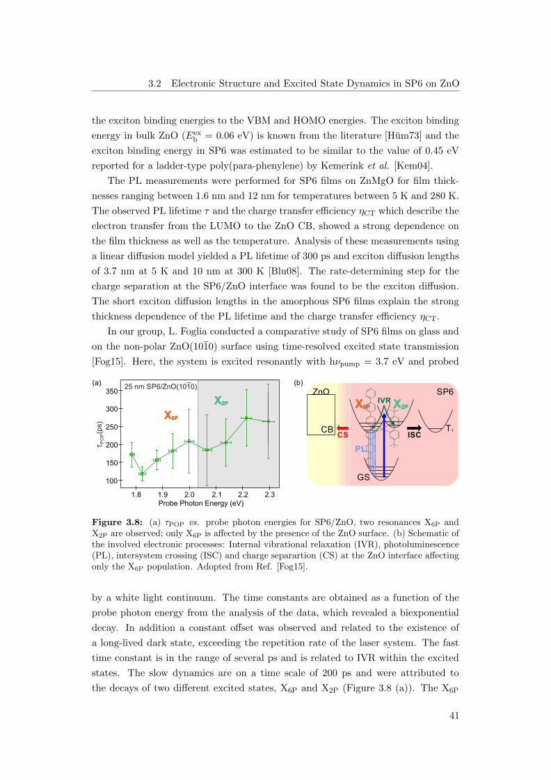
3.2 Electronic Structure and Excited State Dynamics in SP6 on ZnO
the exciton binding energies to the VBM and HOMO energies. The exciton binding
energy in bulk ZnO (Eexb = 0.06 eV) is known from the literature [Hum73] and the
exciton binding energy in SP6 was estimated to be similar to the value of 0.45 eV
reported for a ladder-type poly(para-phenylene) by Kemerink et al. [Kem04].
The PL measurements were performed for SP6 films on ZnMgO for film thick-
nesses ranging between 1.6 nm and 12 nm for temperatures between 5 K and 280 K.
The observed PL lifetime τ and the charge transfer efficiency ηCT which describe the
electron transfer from the LUMO to the ZnO CB, showed a strong dependence on
the film thickness as well as the temperature. Analysis of these measurements using
a linear diffusion model yielded a PL lifetime of 300 ps and exciton diffusion lengths
of 3.7 nm at 5 K and 10 nm at 300 K [Blu08]. The rate-determining step for the
charge separation at the SP6/ZnO interface was found to be the exciton diffusion.
The short exciton diffusion lengths in the amorphous SP6 films explain the strong
thickness dependence of the PL lifetime and the charge transfer efficiency ηCT.
In our group, L. Foglia conducted a comparative study of SP6 films on glass and
on the non-polar ZnO(1010) surface using time-resolved excited state transmission
[Fog15]. Here, the system is excited resonantly with hνpump = 3.7 eV and probed
CB
GS
T1
CS
PL
X2PX6PIVR
ISC
ZnO SP6
(p
s)P
OP
350
300
250
200
150
100
2.32.22.12.01.91.8Probe Photon Energy (eV)
25 nm SP6/ZnO(1010)(a)
X6P
X2P
_(b)
Figure 3.8: (a) τPOP vs. probe photon energies for SP6/ZnO, two resonances X6P andX2P are observed; only X6P is affected by the presence of the ZnO surface. (b) Schematic ofthe involved electronic processes: Internal vibrational relaxation (IVR), photoluminescence(PL), intersystem crossing (ISC) and charge separartion (CS) at the ZnO interface affectingonly the X6P population. Adopted from Ref. [Fog15].
by a white light continuum. The time constants are obtained as a function of the
probe photon energy from the analysis of the data, which revealed a biexponential
decay. In addition a constant offset was observed and related to the existence of
a long-lived dark state, exceeding the repetition rate of the laser system. The fast
time constant is in the range of several ps and is related to IVR within the excited
states. The slow dynamics are on a time scale of 200 ps and were attributed to
the decays of two different excited states, X6P and X2P (Figure 3.8 (a)). The X6P
41
3 Investigated Systems
population possesses a shorter lifetime than the X2P population as only the first is
affected by charge separation at the ZnO interface.
The observed processes are summed up in Figure 3.8 (b): After resonant ex-
citation with 3.7 eV the system undergoes 1) IVR within the excited states on a
timescale of several ps, 2) the X6P population decays on a timescale of ≈ 200 ps
via 3 competing pathways: photoluminescence (PL), ISC leading to the formation
of a long-lived triplet state with a lifetime of several µs and diffusion of X6P exci-
tons towards the ZnO interface where charge separation (CS) occurs. 3) The X2P
population, instead, decays only via ISC.
Despite the manifold of studies the energetic positions of the excited states,
which are of crucial interest for charge- and energy transfer and the dynamics of the
dark state remain unknown. We tackle these open question by time-resolved 2PPE
providing not only access to the absolute energies of excited states but also to the
dark state dynamics. The triplet state is not necessarily dark for photoemission since
electron emission does not underly the strict selection rules which hold for optical
spectroscopy, as will be shown in Section 5.2.
42
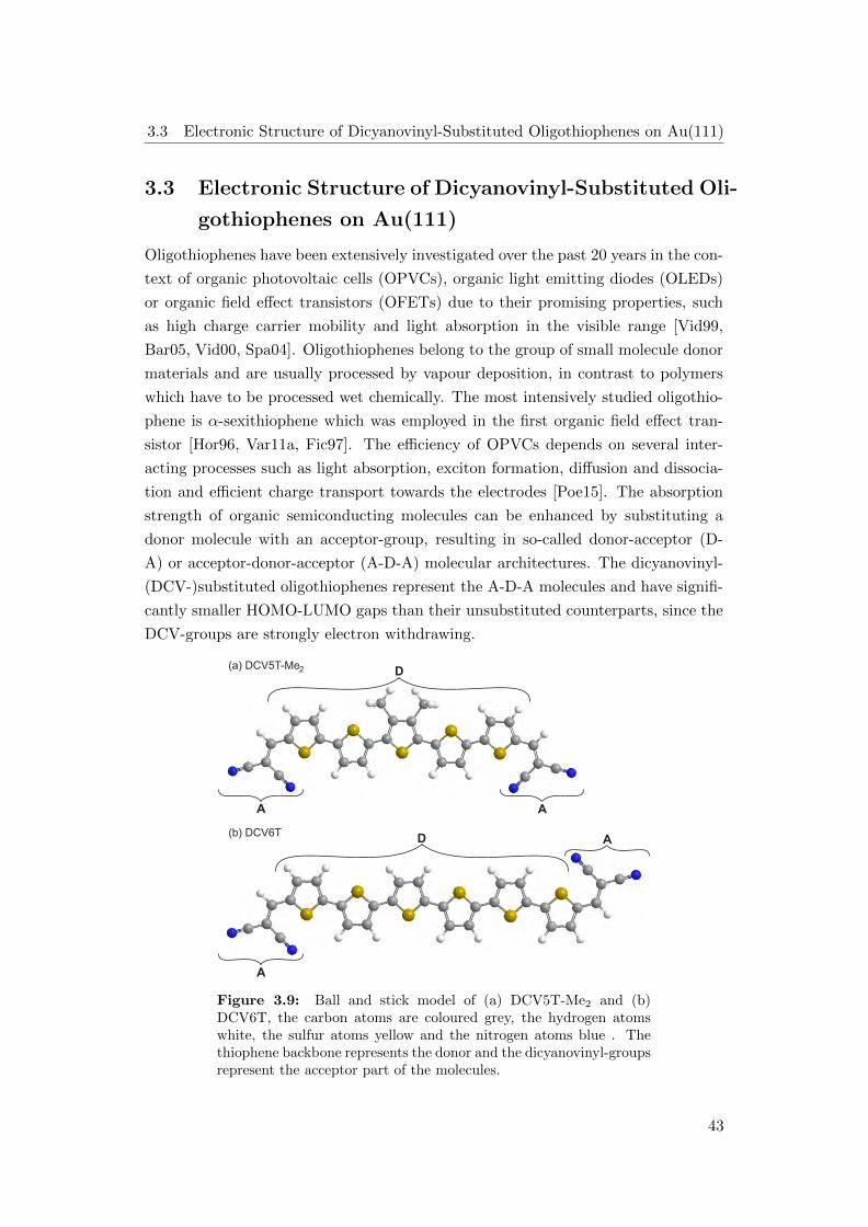
3.3 Electronic Structure of Dicyanovinyl-Substituted Oligothiophenes on Au(111)
3.3 Electronic Structure of Dicyanovinyl-Substituted Oli-
gothiophenes on Au(111)
Oligothiophenes have been extensively investigated over the past 20 years in the con-
text of organic photovoltaic cells (OPVCs), organic light emitting diodes (OLEDs)
or organic field effect transistors (OFETs) due to their promising properties, such
as high charge carrier mobility and light absorption in the visible range [Vid99,
Bar05, Vid00, Spa04]. Oligothiophenes belong to the group of small molecule donor
materials and are usually processed by vapour deposition, in contrast to polymers
which have to be processed wet chemically. The most intensively studied oligothio-
phene is α-sexithiophene which was employed in the first organic field effect tran-
sistor [Hor96, Var11a, Fic97]. The efficiency of OPVCs depends on several inter-
acting processes such as light absorption, exciton formation, diffusion and dissocia-
tion and efficient charge transport towards the electrodes [Poe15]. The absorption
strength of organic semiconducting molecules can be enhanced by substituting a
donor molecule with an acceptor-group, resulting in so-called donor-acceptor (D-
A) or acceptor-donor-acceptor (A-D-A) molecular architectures. The dicyanovinyl-
(DCV-)substituted oligothiophenes represent the A-D-A molecules and have signifi-
cantly smaller HOMO-LUMO gaps than their unsubstituted counterparts, since the
DCV-groups are strongly electron withdrawing.
(b) DCV6T
(a) DCV5T-Me2
D
D
AA
A
A
Figure 3.9: Ball and stick model of (a) DCV5T-Me2 and (b)DCV6T, the carbon atoms are coloured grey, the hydrogen atomswhite, the sulfur atoms yellow and the nitrogen atoms blue . Thethiophene backbone represents the donor and the dicyanovinyl-groupsrepresent the acceptor part of the molecules.
43

3 Investigated Systems
Figure 3.9 shows the two DCV-substituted oligothiophenes investigated in this
work: (a) the bimethylated dicyanovinyl-quinquethiophene (DCV5T-Me2) and (b)
the dicyanovinyl-sexithiophene (DCV6T). The molecules were synthesized by R.
Fitzner in the group of P. Bauerle (Ulm University) from DCV-substituted bro-
mobithiophene and distannylated mono-and bithiophene via a Pd-catalysed cross-
coupling reaction (Stille-coupling) a detailed description of the synthesis and char-
acterization can be found in [Fit11].
Compound ECVg (sol.) Eopt
g (sol.) Eoptg (film)
DCV5T-Me2 1.91 eV 1.99 eV 1.69 eV
DCV6T 1.56 eV 2.00 eV 1.68 eV
Table 3.1: Energy gaps of DCV5T-ME2 and DCV6Tin solution (sol.) and of 30 nm thick films, adopted fromRef. [Fit11, Fit12b].
Table 3.1 presents optoelectronic properties of the two molecules in solution and
as 30 nm thick films respectively, which were obtained from absorption spectroscopy
and cyclic voltammetry carried out by Fitzner et al. [Fit11, Fit12b]. The gaps
measured by means of cyclic voltammetry correspond to the difference between ox-
idation and reduction potential of the molecules, i.e. the difference between the
(N+1)- and the (N-1)-electronic state, and can thus be compared to the transport
gaps (EA/LUMO - IP/HOMO) obtained from 2PPE and STS. The gaps from ab-
sorption measurements correspond to the optical gaps, the difference between optical
and transport gap is discussed in Section 2.2.2. The optical gaps measured in solu-
tion are larger compared to the gaps obtained from the films. Moreover Fitzner et
al. observed that the absorption and emission spectra of the films exhibited a signif-
icant broadening and a red-shift compared to the spectra measured in solution. This
was explained by enhanced ordering and intermolecular interaction of the molecules
in the bulk [Fit11]. X-ray structure analysis of DCV5T-Me2 crystals revealed that
each molecule in the crystal interacts with 10 neighbouring molecules via 16 well-
defined interactions [Fit12b]. For example H-bonds between vinylic or aromatic
CH-groups and the N-atoms of adjacent cyanogroups were identified, furthermore
dipolar interactions between methyl-H and S atoms and π-stacking contribute to the
intermolecular interactions.
Both molecules have been incorporated as donor materials via vapour deposi-
tion in OPVCs with different architectures and yielded significantly different power
conversion efficiencies. A planar heterojunction solar cell with DCV6T as donor
44

3.3 Electronic Structure of Dicyanovinyl-Substituted Oligothiophenes on Au(111)
material yielded a power conversion efficiency (PCE) of 2.8 % [Fit11], while a bulk
heterojunction solar cell employing DCV5T-Me2 yielded 6.1 % [Fit11, Fit12b]. More
sophisticated solar cell architectures even achieved a PCE of 8.3 % for a single and
9.7 % for a triple junction cell using DCV5T-Me2 as donor material [Mee14]. This
makes DCV5T-Me2 the world-champion of the evaporated molecular donor materials
with a disclosed chemical structure2. The question is why these two molecules show
such a different solar cell performance, although they exhibit similar optoelectronic
properties. Poelking et al. provide an explanation for the high solar cell performance
of DCV-substituted molecules by linking molecular order with the energy landscape
of the donor/acceptor interface which is influenced by long-range electrostatic effects
[Poe15]. These long-range electrostatic effects might be affected by the permanent
molecular dipole moment, which is strong in the case of DCV5T-Me2, due to its
C2v symmetry, and cancels out for DCV6T since the DCV-groups point in opposite
directions. Another aspect is the film morphology and the degree of order therein.
Fitzner et al. compared the solar cell performance and crystal structure of differ-
ently alkylated DCV-substituted quarterthiophenes and found that the number of
intermolecular interactions correlates with the solar cell efficiency [Fit12a]. While
the small structural variations due to alkylation do not significantly change the opto-
electronic properties, they have an astonishing influence on the solid state properties
which play a major role for exciton diffusion and charge transport, on which in turn
the photovoltaic performance relies [Fit12a]. Methyl substitution proved to be a
practical method to influence the morphology of donor/acceptor blends in bulk het-
erojunction solar cells, which leads in this case to an improvement of the device
performance [Fit12b].
A theoretical study by Schrader et al. on the charge dynamics in crystalline DCV-
substituted oligothiophenes showed that the direction with the highest carrier mobil-
ity was not parallel to the direction with the strongest coupling and that pronounced
π-stacking even inhibited other transport directions [Sch12b]. Moreover they found
that the mobility was higher in the methylated compounds which give rise to more
balanced three-dimensional networks of electronic couplings [Sch12c, Sch12b]. Re-
cent X-ray scattering experiments demonstrated that the organic films employed in
devices, prepared by vapour deposition in UHV, exhibit well ordered polycrystalline
morphologies [Koe12]. Therefore the finding from the theoretical study presented
above can be applied to these devices.
In the following sections recent STM and STS studies on the adsorption geome-
try and electronic structure of DCV5T-Me2 and DCV6T adsorbed on the Au(111)
surface will be presented.
2Another A-D-A quinquethiophene yielded a PCE of 10.1 % in a solution processes device [Kan15]
45
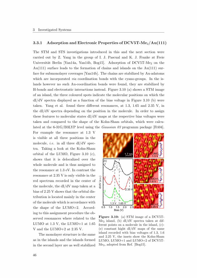
3 Investigated Systems
3.3.1 Adsorption and Electronic Properties of DCV5T-Me2/Au(111)
The STM and STS investigations introduced in this and the next section were
carried out by Z. Yang in the group of I. J. Pascual and K. J. Franke at Freie
Universitat Berlin [Yan14a, Yan14b, Bog15]. Adsorption of DCV5T-Me2 on the
Au(111) surface leads to the formation of chains and islands on the Au(111) sur-
face for submonolayer coverages [Yan14b]. The chains are stabilized by Au-adatoms
which are incorporated via coordination bonds with the cyano-groups. In the is-
lands however no such Au-coordination bonds were found, they are stabilized by
H-bonds and electrostatic interactions instead. Figure 3.10 (a) shows a STM image
of an island, the three coloured spots indicate the molecular positions on which the
dI/dV spectra displayed as a function of the bias voltage in Figure 3.10 (b) were
taken. Yang et al. found three different resonances, at 1.3, 1.65 and 2.35 V, in
the dI/dV spectra depending on the position in the molecule. In order to assign
these features to molecular states dI/dV maps at the respective bias voltages were
taken and compared to the shape of the Kohn-Sham orbitals, which were calcu-
lated at the 6-31G/B3LYP level using the Gaussian 03 programm package [Fri04].
LUMO+11.6 V
1
2
3
(a)
LUMO1.3 V
0.5 1.0 1.5 2.0 2.5
Bias (V)
1
2
3
1.3 V 1.65 V
2.35 V
(c)
(d)
LUMO+22.25 V
(e)
1.7 nm
(b)
dI/dV
(a.u
.)
Figure 3.10: (a) STM image of a DCV5T-Me2 island, (b) dI/dV spectra taken at dif-ferent points on a molecule in the island, (c)-(e) constant hight dI/dV maps of the sameisland recorded with bias voltages of 1.3, 1.6and 2.25 V, the insets show the Kohn-ShamLUMO, LUMO+1 and LUMO+2 of DCV5T-Me2, adopted from Ref. [Bog15].
For example the resonance at 1.3 V
is visible at all three positions in the
molecule, i.e. in all three dI/dV spec-
tra. Taking a look at the Kohn-Sham
orbital of the LUMO, Figure 3.10 (c),
shows that it is delocalized over the
whole molecule and is thus assigned to
the resonance at 1.3 eV. In contrast the
resonance at 2.35 V is only visible in the
red spectrum recorded in the center of
the molecule, the dI/dV map taken at a
bias of 2.25 V shows that the orbital dis-
tribution is located mainly in the center
of the molecule which is accordance with
the shape of the LUMO+2. Accord-
ing to this assignment procedure the ob-
served resonances where related to the
LUMO at 1.3 V, the LUMO+1 at 1.65
V and the LUMO+2 at 2.35 V.
The monolayer structure is the same
as in the islands and the islands formed
in the second layer are as well stabilized
46
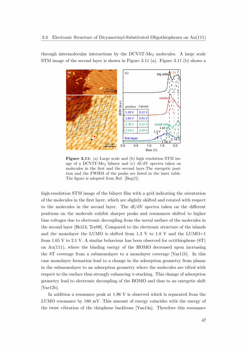
3.3 Electronic Structure of Dicyanovinyl-Substituted Oligothiophenes on Au(111)
through intermolecular interactions by the DCV5T-Me2 molecules. A large scale
STM image of the second layer is shown in Figure 3.11 (a). Figure 3.11 (b) shows a
first layer
0.0 0.5 1.0 1.5 2.0
).u.
a( V
d/Id
Bias (V)
big side
center
small side
1.96 V
2.14 V
1.30 V 0.22 V
1.65 V 0.41 V
1.78 V 0.12 V
2.14 V 0.20 V1.65 V
(a)
(b)
(c)
1.3 V
1.78 V3.3 nm
10 nm
FWHMposi�on
Figure 3.11: (a) Large scale and (b) high resolution STM im-age of a DCV5T-Me2 bilayer and (c) dI/dV spectra taken onmolecules in the first and the second layer.The energetic posi-tion and the FWHM of the peaks are listed in the inset table.The figure is adopted from Ref. [Bog15].
high-resolution STM image of the bilayer film with a grid indicating the orientation
of the molecules in the first layer, which are slightly shifted and rotated with respect
to the molecules in the second layer. The dI/dV spectra taken on the different
positions on the molecule exhibit sharper peaks and resonances shifted to higher
bias voltages due to electronic decoupling from the metal surface of the molecules in
the second layer [Hei13, Tor08]. Compared to the electronic structure of the islands
and the monolayer the LUMO is shifted from 1.3 V to 1.8 V and the LUMO+1
from 1.65 V to 2.1 V. A similar behaviour has been observed for octithiophene (8T)
on Au(111), where the binding energy of the HOMO decreased upon increasing
the 8T coverage from a submonolayer to a monolayer coverage [Var11b]. In this
case monolayer formation lead to a change in the adsorption geometry from planar
in the submonolayer to an adsorption geometry where the molecules are tilted with
respect to the surface thus strongly enhancing π-stacking. This change of adsorption
geometry lead to electronic decoupling of the HOMO and thus to an energetic shift
[Var12b].
In addition a resonance peak at 1.96 V is observed which is separated from the
LUMO resonance by 180 mV. This amount of energy coincides with the energy of
the twist vibration of the thiophene backbone [Yan14a]. Therefore this resonance
47

3 Investigated Systems
has been assigned to a vibronic feature which is excited by the tunneling electrons
[Fra12, Bog15].
3.3.2 Adsorption and Electronic Properties of DCV6T/Au(111)
Submonolayer adsorption of DCV6T on the Au(111) surface leads to the formation
of three different adsorption regimes, (i) islands, (ii) chains growing across the her-
ringbone reconstruction and (iii) chains which grow in the face centered cubic (fcc)
region of the resonstructed Au(111) surface [Yan14a]. The islands (i) and chains
(iii) growing in the fcc region of the herringbone reconstructed Au(111) surface are
formed via intermolecular hydrogen bonding and electrostatic interactions [Yan14a].
In contrast the chains (ii) which grow across the herringbone pattern are stabi-
lized by metal-organic coordination bonds with Au-adatoms, as observed before for
DCV5T2.
-1.0 -0.5 0.0 0.5 1.0 1.5 2.0 2.5
).u.
a(V
d/Id
Bias (V)
1.3 V 1.6 V
2.4nm
1.3 V
2.4nm
1.6 V
2.4nm
2.3 V
2.2 V
(a) (b)
pure Au
Figure 3.12: (a) dI/dV spectra measured at different locationson the molecule in the island as indicated in the inset. (b) STMimages of an island recorded at bias voltages of 1.3 V, 1.6 V and2.2 V, revealing the distribution of the unoccupied molecularorbitals. Adopted from Ref. [Yan14a].
Figure 3.12 (a) shows dI/dV spectra taken at different positions on a molecule
within an island, exhibiting altogether 3 resonances at 1.3, 1.6 and 2.3 V, depending
on the position of the STM tip on the molecule. Figure 3.12 (b) displays dI/dV
maps recorded at the bias voltages of the resonances showing the distribution of the
orbitals. The resonances were assigned to the LUMO at 1.3 V, the LUMO+1 at 1.6
V and the LUMO+2 at 2.3 V [Yan14a]. These energetic positions are similar for
DCV6T molecules within all the three adsorption regimes observed, in addition they
show a strong similarity to the resonances found for DCV5T-Me2. For the second
layer DCV6T on Au(111) no STM data is available.
48

3.3 Electronic Structure of Dicyanovinyl-Substituted Oligothiophenes on Au(111)
In order to gain deeper insight into the electronic structure, this work investigates
the electronic structure of the two DCV-substituted oligothiophenes on Au(111) as
a function of the coverage. Particular focus is on the occupied electronic structure
and the electronic structure of higher coverages, which have not been observed in the
STS study. Furthermore the excited state dynamics are of particular interest since
no time-resolved studies have been reported so far on neither of the two molecules.
Time-resolved 2PPE is a powerful method which allows to measure the excited
state population after optical excitation at the sample surface. This promises to
gain deeper insight into exciton formation and decay dynamics in DCV5T-Me2 and
DCV6T on Au(111) and to reveal whether the difference in solar cell performance
is reflected in the excited state dynamics.
49

3 Investigated Systems
3.4 Electronic Structure of the Au(111) Surface
Gold is the noble metal with the highest atomic number in the copper group, the
first group of the transition metals. It is very inert and exhibits some extraordinary
properties [Hol07] such as the highest (positive) redox potential of all metals (ε0 =
+1.50 V for Au/ Au3+), the biggest Pauling-electronegativity (EN = 2.4), the most
negative electron affinity (EA = -2.31 eV) and, besides mercury and zinc, gold has
the highest ionisation energy (IE = +9.22 eV). In contrast to the the surrounding
metals in the periodic table gold shows halogen analogous behaviour due to the
ability of forming a monoanion [Hol07]. Some of these special properties rely on the
fact that the valence electrons of gold are liable to powerful relativistic effects, which
cause a fairly strong 6s- and a weaker 6p-orbital contraction, and thus a lowering
in energy, as well as an expansion of the 5d orbitals, which experience an energetic
exaltation [Hol07].
Gold crystallizes in the fcc lattice with a lattice constant of a = 4.08 A [Kit80],
a model of the unit cell is depicted in Figure 3.13 (a). The (111)-surface is obtained
by intersecting the coordinate axes of the unit cell at the same axis intercept and is
shown in Figure 3.13 (b). The (111)-surface of each unit cell amounts√
3a2/2 = 14.42
(a) (b)
Figure 3.13: (a) Unit cell of the fcc-lattice and (b) the hexagonal Au(111) surface, picturesgenerated with Xcrysden [Kok03].
A2 and contains two Au atoms. It exhibits a hexagonal structure of the hexagonal
close packed (hcp)-type and the expected stacking would be ABABAB...(hcp-like)
or ABCABC...(fcc-like).
But the real Au(111) surface appears in a different structure, since the surface
undergoes a reconstruction, the so-called herringbone reconstruction. Figure 3.14
(a) shows an STM image of the reconstructed Au(111) surface, exhibiting nicely
the herringbone pattern. The reconstructed surface shows a (n×√
3) unit cell with
n ≈ 22, containing 2n+2 surface atoms. The reason for this reconstruction can be
found in the competition of two effects [Nar92]:
50
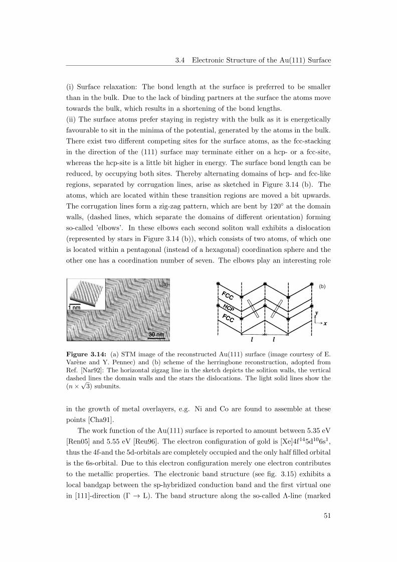
3.4 Electronic Structure of the Au(111) Surface
(i) Surface relaxation: The bond length at the surface is preferred to be smaller
than in the bulk. Due to the lack of binding partners at the surface the atoms move
towards the bulk, which results in a shortening of the bond lengths.
(ii) The surface atoms prefer staying in registry with the bulk as it is energetically
favourable to sit in the minima of the potential, generated by the atoms in the bulk.
There exist two different competing sites for the surface atoms, as the fcc-stacking
in the direction of the (111) surface may terminate either on a hcp- or a fcc-site,
whereas the hcp-site is a little bit higher in energy. The surface bond length can be
reduced, by occupying both sites. Thereby alternating domains of hcp- and fcc-like
regions, separated by corrugation lines, arise as sketched in Figure 3.14 (b). The
atoms, which are located within these transition regions are moved a bit upwards.
The corrugation lines form a zig-zag pattern, which are bent by 120◦ at the domain
walls, (dashed lines, which separate the domains of different orientation) forming
so-called ’elbows’. In these elbows each second soliton wall exhibits a dislocation
(represented by stars in Figure 3.14 (b)), which consists of two atoms, of which one
is located within a pentagonal (instead of a hexagonal) coordination sphere and the
other one has a coordination number of seven. The elbows play an interesting role
30 nm
1 nm
30 nm30 nm
1 nm1 nm
(b)(a)
Figure 3.14: (a) STM image of the reconstructed Au(111) surface (image courtesy of E.Varene and Y. Pennec) and (b) scheme of the herringbone reconstruction, adopted fromRef. [Nar92]: The horizontal zigzag line in the sketch depicts the solition walls, the verticaldashed lines the domain walls and the stars the dislocations. The light solid lines show the(n×
√3) subunits.
in the growth of metal overlayers, e.g. Ni and Co are found to assemble at these
points [Cha91].
The work function of the Au(111) surface is reported to amount between 5.35 eV
[Ren05] and 5.55 eV [Reu96]. The electron configuration of gold is [Xe]4f145d106s1,
thus the 4f-and the 5d-orbitals are completely occupied and the only half filled orbital
is the 6s-orbital. Due to this electron configuration merely one electron contributes
to the metallic properties. The electronic band structure (see fig. 3.15) exhibits a
local bandgap between the sp-hybridized conduction band and the first virtual one
in [111]-direction (Γ → L). The band structure along the so-called Λ-line (marked
51

3 Investigated Systems
green in fig. 3.15) is observed during photoemission experiments on the Au(111)
surface.
Figure 3.15: Self-consistent relativistic band structure of gold, adopted fromRef. [Eck84], and the Brillouin zone of the fcc-lattice. The Λ-line, along whichthe sp- and d-bands (6−,4−+5+ and 6+) are observed during the photoemissionexperiments is marked green.
According to DFT calculations, performed by Eckardt et al. in 1984 using Kohn-
Sham-type relativistic one-particle equations and the local exchange-correlation po-
tential Xα, the bandgap amounts 3.38 eV (from -0.37 to 3.01 eV) at the L-point
and 19.26 eV (from -3.38 to 15.88) at the Γ-point. The values of the L-gap were
considered to be too small by 1.2 eV [Eck84], which is not an unusual result since
DFT calculations tend to underestimate bandgaps. Within these bandgaps Shock-
ley surface states arise as described before in Section 2.1.1. The surface state in
the L-gap of the pristine Au(111) surface lies 0.48-0.49 eV below the Fermi level
[Rei01, Nic01], while the surface state of the adsorbate covered Au(111) surface is
shifted towards the Fermi level as reported by [For07, Hag10, Var12b]. The d-bands
of the Au(111) surface are found at binding energies between -2 and -3 eV relative
to the Fermi level [Eck84, Cou86]. The image potential state of the Au(111) surface
is located ≈ 0.6 eV below the vacuum level to which it is pinned, i.e. shifts with the
work function upon changes of the surface potential [Woo86].
52
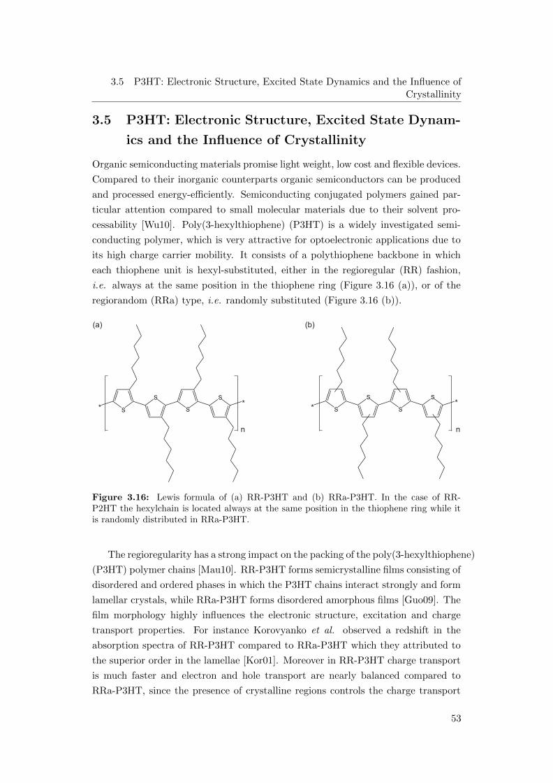
3.5 P3HT: Electronic Structure, Excited State Dynamics and the Influence ofCrystallinity
3.5 P3HT: Electronic Structure, Excited State Dynam-
ics and the Influence of Crystallinity
Organic semiconducting materials promise light weight, low cost and flexible devices.
Compared to their inorganic counterparts organic semiconductors can be produced
and processed energy-efficiently. Semiconducting conjugated polymers gained par-
ticular attention compared to small molecular materials due to their solvent pro-
cessability [Wu10]. Poly(3-hexylthiophene) (P3HT) is a widely investigated semi-
conducting polymer, which is very attractive for optoelectronic applications due to
its high charge carrier mobility. It consists of a polythiophene backbone in which
each thiophene unit is hexyl-substituted, either in the regioregular (RR) fashion,
i.e. always at the same position in the thiophene ring (Figure 3.16 (a)), or of the
regiorandom (RRa) type, i.e. randomly substituted (Figure 3.16 (b)).
S
S
S
S
S
S
S
S
n n
(a) (b)
**
**
Figure 3.16: Lewis formula of (a) RR-P3HT and (b) RRa-P3HT. In the case of RR-P2HT the hexylchain is located always at the same position in the thiophene ring while itis randomly distributed in RRa-P3HT.
The regioregularity has a strong impact on the packing of the poly(3-hexylthiophene)
(P3HT) polymer chains [Mau10]. RR-P3HT forms semicrystalline films consisting of
disordered and ordered phases in which the P3HT chains interact strongly and form
lamellar crystals, while RRa-P3HT forms disordered amorphous films [Guo09]. The
film morphology highly influences the electronic structure, excitation and charge
transport properties. For instance Korovyanko et al. observed a redshift in the
absorption spectra of RR-P3HT compared to RRa-P3HT which they attributed to
the superior order in the lamellae [Kor01]. Moreover in RR-P3HT charge transport
is much faster and electron and hole transport are nearly balanced compared to
RRa-P3HT, since the presence of crystalline regions controls the charge transport
53
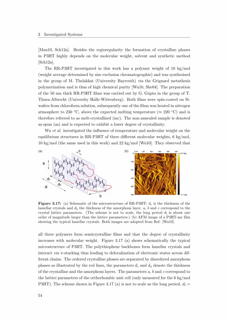
3 Investigated Systems
[Mau10, Sch12a]. Besides the regioregularity the formation of crystalline phases
in P3HT highly depends on the molecular weight, solvent and synthetic method
[Sch12a].
The RR-P3HT investigated in this work has a polymer weight of 10 kg/mol
(weight average determined by size exclusion chromatographie) and was synthesized
in the group of M. Thelakkat (University Bayreuth) via the Grignard metathesis
polymerization and is thus of high chemical purity [Wu10, She04]. The preparation
of the 50 nm thick RR-P3HT films was carried out by G. Gupta in the group of T.
Thurn-Albrecht (University Halle-Wittenberg). Both films were spin-coated on Si-
wafers from chloroform solution, subsequently one of the films was heated in nitrogen
atmosphere to 230 ◦C, above the expected melting temperature (≈ 220 ◦C) and is
therefore referred to as melt-crystallized (mc). The non-annealed sample is denoted
as-spun (as) and is expected to exhibit a lower degree of crystallinity.
Wu et al. investigated the influence of temperature and molecular weight on the
equilibrium structures in RR-P3HT of three different molecular weights, 6 kg/mol,
10 kg/mol (the same used in this work) and 22 kg/mol [Wu10]. They observed that
(a) (b)
Figure 3.17: (a) Schematic of the microstructure of RR-P3HT: dc is the thickness of thelamellar crystals and da the thickness of the amorphous layer, a, b and c correspond to thecrystal lattice parameters. (The scheme is not to scale, the long period dl is about oneorder of magnitude larger than the lattice parameters.) (b) AFM image of a P3HT-mc filmshowing the typical lamellar crystals. Both images are adopted from Ref. [Wu10].
all three polymers form semicrystalline films and that the degree of crystallinity
increases with molecular weight. Figure 3.17 (a) shows schematically the typical
microstructure of P3HT. The polythiophene backbones form lamellar crystals and
interact via π-stacking thus leading to delocalization of electronic states across dif-
ferent chains. The ordered crystalline phases are separated by disordered amorphous
phases as illustrated by the red lines, the parameters dc and da denote the thickness
of the crystalline and the amorphous layers. The parameters a, b and c correspond to
the lattice parameters of the orthorhombic unit cell (only measured for the 6 kg/mol
P3HT). The scheme shown in Figure 3.17 (a) is not to scale as the long period, dl =
54

3.5 P3HT: Electronic Structure, Excited State Dynamics and the Influence ofCrystallinity
dc + da, is about one order of magnitude larger than the lattice parameters. Figure
3.17 (b) shows an AFM image of a P3HT film prepared under the same conditions
like the mc-film investigated in this work. Due to heating above the melting temper-
ature and subsequent slow cooling the a-direction is oriented perpendicular to the
surface. The image shows the b-c plane, exhibiting the characteristic pattern of the
lamellar crystals.
Concerning the optical properties of RR-P3HT thin films, the optical gap amounts
to 1.8 - 1.9 eV as reported in several studies employing absorption spectroscopy
[Kor01, Sch14, Coo08]. Panzer et al. [Pan15] investigated the effect of annealing
on thin films prepared from the 22 kg/mol RR-P3HT (studied before by Wu et al.
[Wu10]). They found two different types of H-aggregates, one with ordered and
one with disordered side chains, after heating the film to 250◦ and cooling down
slowly to room temperature. Before annealing however only one type of aggregate
was found. In addition they found that the aggregates in the annealed film could be
excited separately depending on the photon energy. For photon energies higher than
2 eV only the aggregate which prevails as well in the non-annealed film is excited.
Therefore only the aggregate with the ordered side chains should be excited in the
measurements presented in this work, since only photon energies > 2 eV have been
used, as will be shown in Section 5.4.
The effect of annealing on the electronic structure of RR-P3HT thin films has
been investigated as well by means of UPS which is of particular interest for this
work as UPS yields IP comparable to those obtained from 2PPE. For instance Kanai
et al. [Kan10] performed a combined UPS/IPES study on a 17 nm thick RR-P3HT
film (Mw= 25-30 kg/mol) on Si. They found that the transport gap decreases
upon annealing from 2.6 to 2.4 eV, due to a downward shift of the EA level by 0.2
eV while the IP of 4.7 eV stays constant. Moreover they observed that the peak
width are reduced upon annealing at 170 ◦C. Another UPS study was performed
by Frisch et al. [Fri11] on a 20 nm thick RR-P3HT (Mw= 64 kg/mol) film on
poly(ethylenedioxythiophene):poly(styrenesulfonate) (PEDT:PSS). They observed a
very small VBM shift of 0.05 eV from 4.55 eV to 4.6 eV upon annealing at 120 ◦C.
The results obtained in this thesis will be compared with the results from Kanai et
al. since they employed rather light weight P3HT and Si as a substrate. Comparison
with the results from Frisch et al. have to handled with caution due to the conduct-
ing substrate which potentially influences the film morphology and the electronic
structure.
In the following paragraphs information on excited states and their dynamics
will be presented as those are of great importance when it comes to the interpreta-
tion of the data obtained in this work, as will be discussed in Section 5.4. Several
55
3 Investigated Systems
excited states have been reported to exist in RR-P3HT, e.g. singlet excitons, po-
laron pairs and polarons (the different species have been introduced before in Section
2.2.2) [Guo09, Kor01, Zha12a, Kan92]. Previous studies yielded controversial results
concerning the number and the kind of excited states in RR-P3HT as well as their
dynamics. (Triplet formation however, has been consistently reported to occur only
in RRa-P3HT [Guo09, Kor01]. Korovyanko et al. proposed that the suppression of
intersystem crossing in RR-P3HT might be a consequence of enhanced interchain
interaction in the crystalline phases [Kor01].) The energetic position and the dy-
namics of the excited states are influenced by a variety of parameters, such as the
molecular weight, the film preparation and morphology, as well as the excitation
energy and density used in the measurements. The comparability of the results is
therefore questionable, but besides the inconsistencies there are as well a few com-
mon tendencies in the reported findings:
1. A significant number of publications find the singlet exciton at a resonance
energy between 1.0 and 1.2 eV [Guo09, Kor01, Coo08, Her11, Mul12, Zha12a].
2. A polaron signal around 1.9 eV has been observed in many studies [Kor01,
Zha12a, Her11, Mul12] and has been related to delocalized polarons residing
in the crystalline phases of the RR-P3HT film [Kor01, Zha12a]. Whereas Guo
et al. related this resonance to polaron pairs [Guo09].
3. Another polaronic feature, energetically located between the exciton (1-1.2 eV)
and the polaron (around 1.9 eV) mentioned before, was observed at resonances
between 1.13 and 1.65 eV [Guo09, Kor01, Zha12a, Kan92]. Korovyanko et
al. and Zhang et al. assigned this polaronic resonance to localized polarons
inhabiting the disordered phases.
Additional polaronic states have been reported at resonances of 0.1 and 0.4 eV
[Kor01] and at 0.5 eV [Kan92] using optical spectroscopy, while X-ray absorption
yields a feature related to a polarons 0.8 eV above the VBM [Mul12].
RR-P3HT thin films have been studied as well before by means of 2PPE [Var12c,
Soh07]. Varene et al. [Var12c] employed PEDT:PSS as a substrate while Sohn et
al. [Soh07] used a Au-substrate. Both studies report a polaronic state located 0.9
eV [Var12c] and 1.75 eV [Soh07] above the VBM respectively.
As mentioned before a great variety of studies on the excited state dynamics can
be found. But unfortunately the reported results are highly contradictory. Only the
photoluminescence lifetime was congruently found to take place between 300 - 400
ps and related to the exciton decay via electron-hole recombination [Mag97, Kan92,
Coo08, Guo09]. Guo et al. observed a triexponential exciton decay and assigned the
slowest time constant (330 ps) to the recombinative decay.
56
3.5 P3HT: Electronic Structure, Excited State Dynamics and the Influence ofCrystallinity
The formation and decay dynamics of polaron pairs and polarons have been re-
ported to take place on various different time scales. The ability of P3HT to form
polarons by itself without the need for a donor-acceptor interface is well known.
However there has been a discussion in the past whether polarons are formed im-
mediately after photon absorption or whether they are formed from relaxed singlet
excitons [Sak09, Ai06, Mag97, Kor01, Guo09]. But there is convincing evidence that
polarons and polaron pairs are formed on an ultrafast timescale from an initial hot
exciton population. Guo et al. for example observed in a transient absorption study
that polarons and polaron pairs are generated in a competitive process directly from
hot excitons in RR-P3HT [Guo09].
The decay of polaron pairs was reported to take place on time scales ranging
between 0.55 ps [Ai06] and 2.6 ps [Var12c]. The suggested decay mechanisms are
geminate recombination to the singlet exciton or the ground state or dissociation into
polarons [Guo09, Var12c]. Polaron lifetimes have been reported in a range reaching
from several ps [Ai06, Var12c] over several hundred ps [Coo08, Her11] even to µs
[Mul12, Kan92]. The prevailing decay mechansim for polarons is the bimolecular
with other polarons [Guo09].
The influence of enhanced order in the polymer films on the excited state dy-
namics has been studied by Korovyanko et al., who observed slower decay dynamics
in RRa-P3HT compared to RR-P3HT [Kor01]. Moreover Laquai et al. reported
that the PCE of a P3HT:phenyl-C61-butyric acid methyl ester (PCBM) based solar
cell was increased by a factor of ten upon annealing the device at 110 ◦C. This was
explained by an enhancement of the hole transport efficiency in the P3HT phase by
more than three orders of magnitude [Laq15].
In this thesis the influence of annealing on the electronic structure and the ex-
cited state dynamics in RR-P3HT is investigated. 2PPE is a very powerful method
to investigate the electronic structure of a material since it provides access not only
to occupied but as well to unoccupied states. In addition it allows to measure the
lifetimes of excited states. But photoemission is usually not the method of choice
to investigate polymers since it is a very surface sensitive technique and polymers,
even when they are highly regular and chemically pure, form only semicrystalline
films which contain significant fractions of disordered phases. Moreover polymers
are usually processed wet chemically which is a problematic precondition for inves-
tigations carried out under UHV conditions due to the possible contamination by
residual solvent. Therefore RR-P3HT films which were prepared under well defined
conditions from polymers of very high regularity and chemical purity were chosen
for this 2PPE study.
These films are investigated to find out whether it is possible at all to obtain high
57

3 Investigated Systems
quality 2PPE spectra exhibiting distinct features, since previous 2PPE studies on
RR-P3HT films did not yield well resolved spectra [Var12c, Soh07]. Further ques-
tions which will be tackled in this work are the influence of enhanced crystallinity,
i.e. interchain interaction, on the electronic structure and the excited state dynam-
ics in two RR-P3HT films with different degrees of crystallinity. The results will be
presented and discussed in Section 5.4.
58
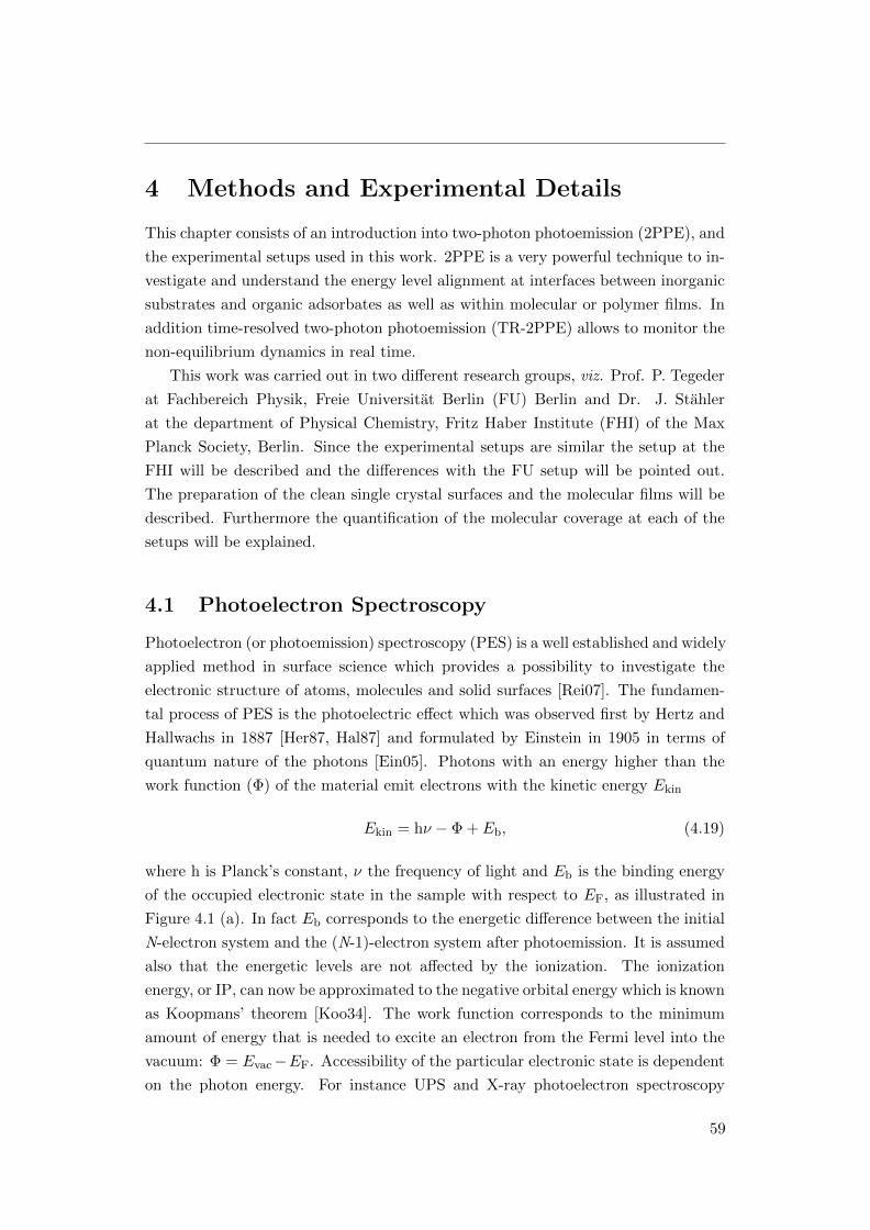
4 Methods and Experimental Details
This chapter consists of an introduction into two-photon photoemission (2PPE), and
the experimental setups used in this work. 2PPE is a very powerful technique to in-
vestigate and understand the energy level alignment at interfaces between inorganic
substrates and organic adsorbates as well as within molecular or polymer films. In
addition time-resolved two-photon photoemission (TR-2PPE) allows to monitor the
non-equilibrium dynamics in real time.
This work was carried out in two different research groups, viz. Prof. P. Tegeder
at Fachbereich Physik, Freie Universitat Berlin (FU) Berlin and Dr. J. Stahler
at the department of Physical Chemistry, Fritz Haber Institute (FHI) of the Max
Planck Society, Berlin. Since the experimental setups are similar the setup at the
FHI will be described and the differences with the FU setup will be pointed out.
The preparation of the clean single crystal surfaces and the molecular films will be
described. Furthermore the quantification of the molecular coverage at each of the
setups will be explained.
4.1 Photoelectron Spectroscopy
Photoelectron (or photoemission) spectroscopy (PES) is a well established and widely
applied method in surface science which provides a possibility to investigate the
electronic structure of atoms, molecules and solid surfaces [Rei07]. The fundamen-
tal process of PES is the photoelectric effect which was observed first by Hertz and
Hallwachs in 1887 [Her87, Hal87] and formulated by Einstein in 1905 in terms of
quantum nature of the photons [Ein05]. Photons with an energy higher than the
work function (Φ) of the material emit electrons with the kinetic energy Ekin
Ekin = hν − Φ + Eb, (4.19)
where h is Planck’s constant, ν the frequency of light and Eb is the binding energy
of the occupied electronic state in the sample with respect to EF, as illustrated in
Figure 4.1 (a). In fact Eb corresponds to the energetic difference between the initial
N-electron system and the (N-1)-electron system after photoemission. It is assumed
also that the energetic levels are not affected by the ionization. The ionization
energy, or IP, can now be approximated to the negative orbital energy which is known
as Koopmans’ theorem [Koo34]. The work function corresponds to the minimum
amount of energy that is needed to excite an electron from the Fermi level into the
vacuum: Φ = Evac−EF. Accessibility of the particular electronic state is dependent
on the photon energy. For instance UPS and X-ray photoelectron spectroscopy
59

4 Methods and Experimental Details
(XPS) enable access to valence and core-regions respectively.
In addition PES provides a possibility to measure the dispersion of electronic
states, i.e. the energy-momentum relation of the emitted electron, where the parallel
component of the wave vector (k||) is conserved during the photoemission process.
This special case is known as angle-resolved PES (ARPES) and either demands the
use of an angle-resolved analyser (like the Phoibos 100 as described in section 4.2.4)
or can be carried by rotating the surface in front of the analyser which changes the
emission angle. Figure 4.1 (b) schematically depicts the electron emission process in
two dimensions. The parallel component of the wave vector, which is proportional to
the electron’s momentum is conserved k|| = k′||, while the perpendicular component
k⊥ is changed by the work function when passing the surface k′⊥ 6= k⊥. Therefore
Evac
Ekin
analyser
h
Eb
E = 0F
E
(a)
vacuum
sample
'
k
k'
II
II
k
k'
T
T
k' = II kII
k' = T k - T kT
(b)
Figure 4.1: (a) Sketch of a photoemission experiment, (b) illustration of the electronemission process: The wave vector component parallel to the surface k|| is conserved whileand the perpendicular component k⊥ changes.
k|| can be obtained from Ekin and the emission angle α of the photoelectrons with
respect to the surface normal [Hen94]
k|| =
√2meEkin
hsinα (4.20)
where me is the electron rest mass (not the effective mass of the electron in the
solid). The functional relation between the binding energy Eb of a state and the
effective mass of electron can be expressed as the following
Eb = E0 +
(hk||)2
2m∗(4.21)
where m∗ is the effective mass of an electron as determined by the strength of the
coupling to its surroundings, E0 is the energy of the photoemitted electrons when
the sample surface is oriented perpendicular to the analyser. In practice, a small
60

4.1 Photoelectron Spectroscopy
bias is applied between the sample and the analyser tip so that the photoelectrons
would reach the spectrometer efficiently, essentially the bias lowers the Fermi level
of the spectrometer as will be discussed in Section 4.2.4.
4.1.1 Two-Photon Photoemission
PES is a powerful tool for the investigation of the electronic structure of a variety
of materials, however yields information about the occupied electronic states only.
To study the unoccupied electronic states above the Fermi level inverse photoemis-
sion spectroscopy (IPES) is a possibility, in which electrons impact on the surface
and populate the unoccupied states. This process emitts photons of energy that
correspond to the difference between the initial electron energy and the energetic
position of the unoccupied state [Bur85]. 2PPE provides a possibility to observe
both occupied and unoccupied states. Moreover with TR-2PPE electron dynamics
on ultrafast, i.e. as - fs, timescale can be investigated, as will be discussed in Section
4.5 [Mii00]. In a 2PPE experiment two, in our case femtosecond, laser pulses with
a controllable delay with respect to each other are used to pump and subsequently
probe certain electronic states. The first photon excites an electron from an occu-
pied electronic state below EF to an unoccupied intermediate state which is then
emitted into the vacuum by the second photon. The kinetic energy of the photoemit-
ted electrons provides information about the energetic position of the probed state.
Since 2PPE is based on a second order non-linear optical process it has four times
lower cross section than direct photoemission, thus yielding much lower emission
intensities [Fau94]. Therefore the photon energies of pump and probe pulse should
be smaller than the work function of the sample to avoid direct photoemission.
In order to assign the features obtained in a 2PPE spectrum to occupied and
unoccupied states it is necessary to understand the excitation processes. The depen-
dence of the kinetic energy of the photoemitted electrons on the photon energies in
a 2PPE process is illustrated in Figure 4.2 (a) - (c) for one-colour 2PPE (1C-2PPE)
and in (d) for two-colour 2PPE (2C-2PPE):
(a) Initial state (Ei)
In the case of photoemission from an occupied initial state (Ei) via a virtual
intermediate state, the kinetic energy (Ekin) of the photoelectron depends on
both pump and probe photon energies. Therefore increasing the photon energy
by an amount of ∆hν leads to an increase in Ekin by 2∆hν.
(b) Intermediate state (Ek)
Ekin of a photoelectron from a real intermediate state scales with the probe
photon energy. In this case, varying the photon energy by ∆hν changes the
61
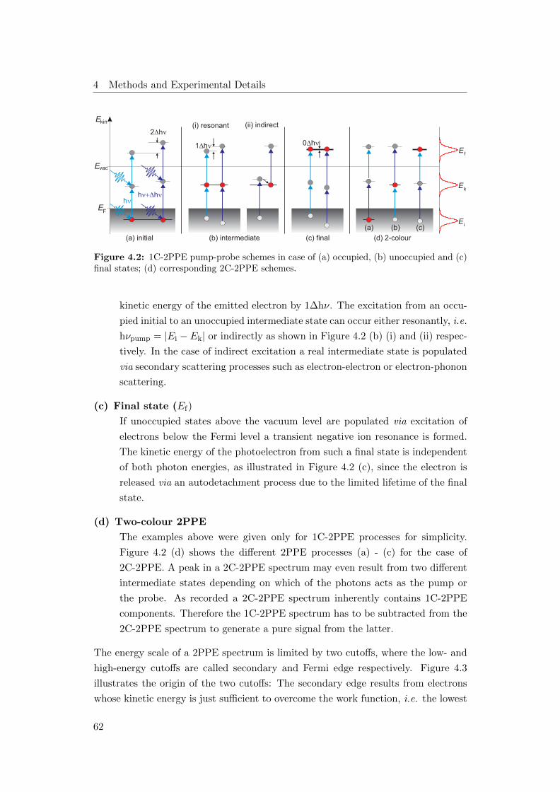
4 Methods and Experimental Details
(a) initial
E
E
E
kin
vac
F
hhh
2h
1h
(b) intermediate (c) final
(i) resonant (ii) indirect
0h
(d) 2-colour
(a) (b) (c)
E
E
E
f
k
i
Figure 4.2: 1C-2PPE pump-probe schemes in case of (a) occupied, (b) unoccupied and (c)final states; (d) corresponding 2C-2PPE schemes.
kinetic energy of the emitted electron by 1∆hν. The excitation from an occu-
pied initial to an unoccupied intermediate state can occur either resonantly, i.e.
hνpump = |Ei − Ek| or indirectly as shown in Figure 4.2 (b) (i) and (ii) respec-
tively. In the case of indirect excitation a real intermediate state is populated
via secondary scattering processes such as electron-electron or electron-phonon
scattering.
(c) Final state (Ef)
If unoccupied states above the vacuum level are populated via excitation of
electrons below the Fermi level a transient negative ion resonance is formed.
The kinetic energy of the photoelectron from such a final state is independent
of both photon energies, as illustrated in Figure 4.2 (c), since the electron is
released via an autodetachment process due to the limited lifetime of the final
state.
(d) Two-colour 2PPE
The examples above were given only for 1C-2PPE processes for simplicity.
Figure 4.2 (d) shows the different 2PPE processes (a) - (c) for the case of
2C-2PPE. A peak in a 2C-2PPE spectrum may even result from two different
intermediate states depending on which of the photons acts as the pump or
the probe. As recorded a 2C-2PPE spectrum inherently contains 1C-2PPE
components. Therefore the 1C-2PPE spectrum has to be subtracted from the
2C-2PPE spectrum to generate a pure signal from the latter.
The energy scale of a 2PPE spectrum is limited by two cutoffs, where the low- and
high-energy cutoffs are called secondary and Fermi edge respectively. Figure 4.3
illustrates the origin of the two cutoffs: The secondary edge results from electrons
whose kinetic energy is just sufficient to overcome the work function, i.e. the lowest
62

4.1 Photoelectron Spectroscopy
possible kinetic energy while the Fermi edge arises due to photoemission via virtual
intermediate states of electrons near EF and possess thus the highest possible kinetic
energy. The work function of the sample corresponds to the difference between the
EE
EF vac
kin
Fermi edge
secondary edge
Figure 4.3: Schematic depiction of the origin of the low- and high-energycutoffs in a 2PPE spectrum.
sum of the photon energies and the width of the spectrum.
Φsample = (hν1 + hν2)−(EF
kin − ESkin
)(4.22)
EFkin and ES
kin are the energetic positions of the Fermi and the secondary edge respec-
tively. Semiconducting materials, like ZnO and P3HT do not possess any density of
states at the Fermi level. Hence the Fermi edge is measured on a metallic reference
under the same conditions (bias voltage and distance from the analyser, an example
is shown in section 5.4).
2PPE spectra can be displayed as a function of different energy scales depend-
ing on the origin of the observed states. This allows the parameters required to be
accessible directly from the axis. Figure 4.4 illustrates the difference between the
possible axes:
(a) Kinetic energy axis (Ekin)
On the kinetic energy axis the secondary edge is set to 0 while the Fermi edge cor-
responds to the width of the spectrum which can be read directly from the energy
axis. The peak positions in the spectrum correspond to the kinetic energy of the
photoemitted electrons with respect to the vacuum level.
(b) Final state axis (EFin − EF)
On the final state energy axis the work function can be read directly at the sec-
ondary edge while the Fermi edge corresponds to the sum of the photon energies
(hν1+hν2). The energetic positions of the peaks correspond to their final state en-
ergy relative to the Fermi level. If the peak is due to photoemission from an occupied
state, the binding energy is obtained by subtracting both photon energies from the
peak position. In case of an intermediate state, its energetic position is obtained
by subtracting the probe photon energy from the final state energy of the peak.
63

4 Methods and Experimental Details
The final state energy axis is useful when the origins of the peaks are still unclear
or when a spectrum contains peaks originating from occupied and unoccupied states.
Ekinh1h2
0E - EFin
F
h + h1 2
0E - EInt,2 F
h 1
0E - EIni F
0E - EInt,1 F
- h1
(a)
(b)
(c)
(d)
(e)
FE vacE
Fermiedge
0
h2
sec. edge
- h2
occupied states
unoccupied states
Figure 4.4: Illustration of the different possible energyaxes in 2PPE spectra, see text for details.
(c) Intermediate state axis
(EInt,1 − EF)
In 2C-2PPE two different in-
termediate state axes are pos-
sible depending on which of the
laser beams acts as the probe
pulse. Here the whole spec-
trum is shifted by hν1 com-
pared to the final state axis
since hν1 and hν2 correspond to
the probe and the pump pulse
respectively. This axis is conve-
nient to read directly the inter-
mediate state energy.
(d) Intermediate state axis
(EInt,2 − EF)
Here the other intermediate
state axis is displayed, which
shows the intermediate state
energy of an unoccupied state
relative to the Fermi level which
is probed by hν2.
(e) Intitial state axis (EIni−EF)
The intial state axis is use-
ful only when occupied initial
states are observed, e.g. in a
direct photoemission spectrum.
The Fermi edge is shifted to
zero here and the peak positions correspond directly to the binding energies with
respect to the Fermi level.
64
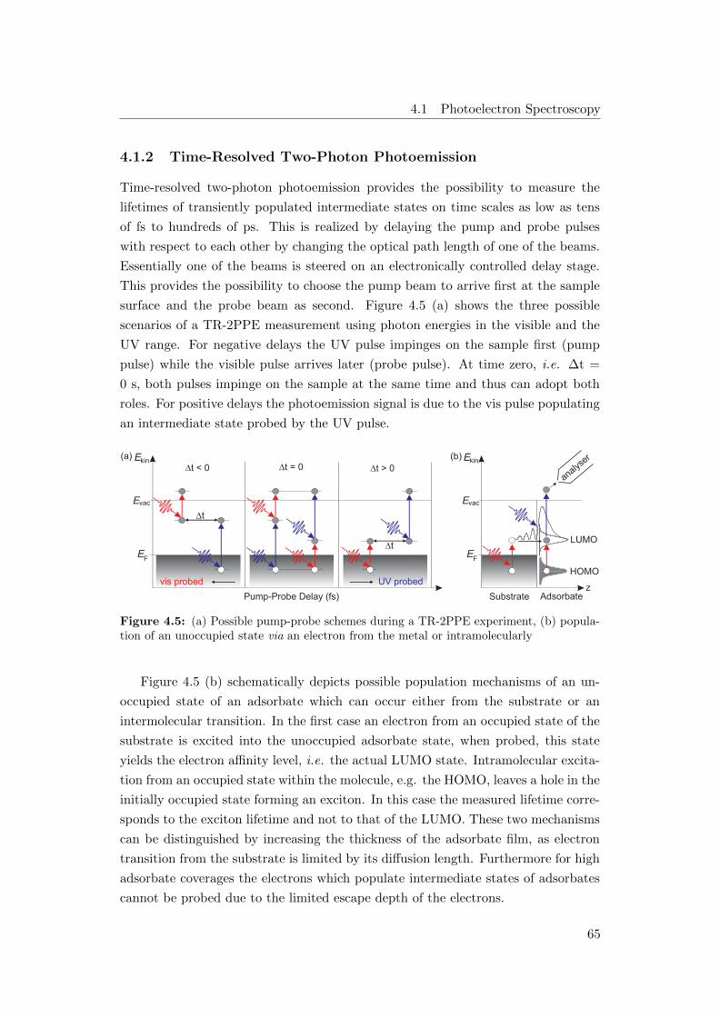
4.1 Photoelectron Spectroscopy
4.1.2 Time-Resolved Two-Photon Photoemission
Time-resolved two-photon photoemission provides the possibility to measure the
lifetimes of transiently populated intermediate states on time scales as low as tens
of fs to hundreds of ps. This is realized by delaying the pump and probe pulses
with respect to each other by changing the optical path length of one of the beams.
Essentially one of the beams is steered on an electronically controlled delay stage.
This provides the possibility to choose the pump beam to arrive first at the sample
surface and the probe beam as second. Figure 4.5 (a) shows the three possible
scenarios of a TR-2PPE measurement using photon energies in the visible and the
UV range. For negative delays the UV pulse impinges on the sample first (pump
pulse) while the visible pulse arrives later (probe pulse). At time zero, i.e. ∆t =
0 s, both pulses impinge on the sample at the same time and thus can adopt both
roles. For positive delays the photoemission signal is due to the vis pulse populating
an intermediate state probed by the UV pulse.
t < 0 E
E
E
kin
vac
F
t = 0 t > 0
Substrate Adsorbate
LUMO
z
HOMO
t
Pump-Probe Delay (fs)
t
E
E
E
kin
vac
F
UV probedvis probed
(b) (a)
analyser
Figure 4.5: (a) Possible pump-probe schemes during a TR-2PPE experiment, (b) popula-tion of an unoccupied state via an electron from the metal or intramolecularly
Figure 4.5 (b) schematically depicts possible population mechanisms of an un-
occupied state of an adsorbate which can occur either from the substrate or an
intermolecular transition. In the first case an electron from an occupied state of the
substrate is excited into the unoccupied adsorbate state, when probed, this state
yields the electron affinity level, i.e. the actual LUMO state. Intramolecular excita-
tion from an occupied state within the molecule, e.g. the HOMO, leaves a hole in the
initially occupied state forming an exciton. In this case the measured lifetime corre-
sponds to the exciton lifetime and not to that of the LUMO. These two mechanisms
can be distinguished by increasing the thickness of the adsorbate film, as electron
transition from the substrate is limited by its diffusion length. Furthermore for high
adsorbate coverages the electrons which populate intermediate states of adsorbates
cannot be probed due to the limited escape depth of the electrons.
65

4 Methods and Experimental Details
In a time-resolved experiment 2PPE spectra are recorded at varying time delays.
Plotting these spectra as a function of the intermediate state energy and the pump-
probe delay yields a TR-2PPE spectrum as displayed in Figure 4.6. The 2PPE
intensity is presented by a false colour-code. This spectrum was measured on H-
doped ZnO(0001) depicting a long-lived emission signal for positive delays, i.e. hν1
= 3.80 eV is the pump and hν2 = 4.65 eV the probe pulse. For negative delays the
pump-probe sequence is vice versa as illustrated in Figure 4.6 (top). As mentioned
earlier the 1C-2PPE signal needs to be subtracted from the 2C-2PPE signal at each
delay point to obtain the pump-induced signal only. There are two possibilities for
the background spectra: (i) The background spectrum is taken at negative pump-
probe delays, ∆t = - 30 ps, where no long-lived emission signal is observed (this
procedure was carried out on the data from FHI and was used in the case of the
example shown in Figure 4.6). (ii) The other possibility is to subtract the 1C-
2PPE spectra from the raw 2C-2PPE signal (this procedure was applied on the data
collected at the FU).
Vertical cut of the TR-2PPE spectrum yields spectrally resolved 2PPE signal at
certain time delays, as shown on the right side for pump-probe delays of 0 fs and 100
fs. In order to gain deeper insights into the excited state dynamics the TR-2PPE
spectrum is integrated over the energetic ranges marked by the grey boxes yielding
the cross-correlation (XC)-traces (Figure4.6 bottom). The black lines correspond to
biexponential fits whose derivation is explained below. The red curve represents the
XC of the laser pulses which was fitted with a sech2 envelope.
The population decay can be described analytically with optical Bloch equations
which consider as well coherence effects. But in case of non-resonant excitation or
dephasing times shorter than the pulse duration coherence effects can be neglected
and the optical Bloch equations can be simplified to a set of coupled rate equations
[Lou83, Kir08]. In the simplest case the population decay can be treated as a dis-
crete 3-level system consisting of initial, intermediate and final state populations as
illustrated in Figure 4.7 (a).
ni = − |Vik(t, τ)|2 ni + Γ1nk (4.23)
nk = |Vik(t, τ)|2 ni − |Vkf (t, τ)|2 nk − Γ1nk (4.24)
nf = − |Vkf (t, τ)|2 nk (4.25)
nx are the population densities of the initial (x = i), intermediate (x = k) and final
state (x = f). |Vxy|2 is the probability of a transition from x → y in the presence
of the optical field and τ is the pump-probe delay. Γ1 is the inelastic scattering
rate from the intermediate to the ground state (k → i) and describes an exponential
66
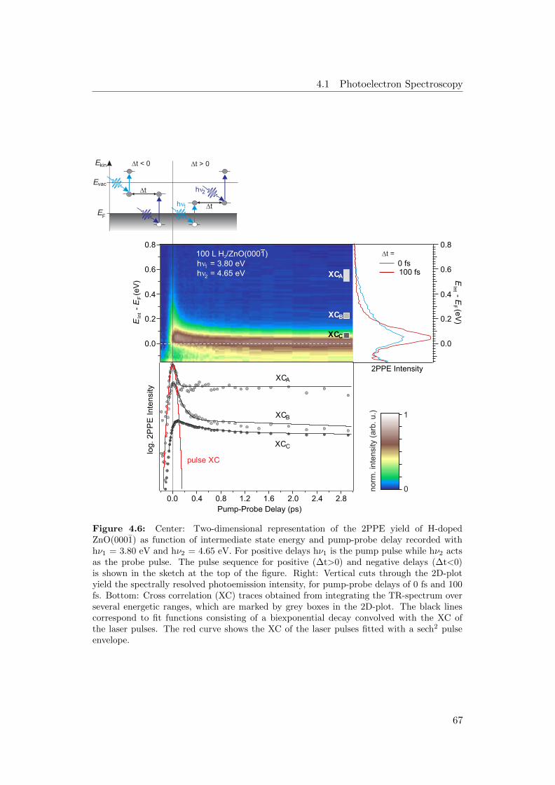
4.1 Photoelectron Spectroscopy
XCA
XCB
XCC
2.82.42.01.61.20.80.40.0
Pump-Probe Delay (ps)
0
1
norm
. in
tensi
ty (
arb
. u.)
h = 3.80 eVh = 4.65 eV
100 L H /ZnO(0001)2
0.8
0.6
0.4
0.2
0.0
E - E
(e
V)
Int
F
t < 0 E
E
E
kin
vac
F
t > 0
t
t h 1
h 2
log. 2
PP
E Inte
nsity
pulse XC
XC
XC
XC
2PPE Intensity
0.8
0.6
0.4
0.2
0.0
E - E
(eV
)In
tF
0 fs 100 fs
t =
1
2
C
B
A
Figure 4.6: Center: Two-dimensional representation of the 2PPE yield of H-dopedZnO(0001) as function of intermediate state energy and pump-probe delay recorded withhν1 = 3.80 eV and hν2 = 4.65 eV. For positive delays hν1 is the pump pulse while hν2 actsas the probe pulse. The pulse sequence for positive (∆t>0) and negative delays (∆t<0)is shown in the sketch at the top of the figure. Right: Vertical cuts through the 2D-plotyield the spectrally resolved photoemission intensity, for pump-probe delays of 0 fs and 100fs. Bottom: Cross correlation (XC) traces obtained from integrating the TR-spectrum overseveral energetic ranges, which are marked by grey boxes in the 2D-plot. The black linescorrespond to fit functions consisting of a biexponential decay convolved with the XC ofthe laser pulses. The red curve shows the XC of the laser pulses fitted with a sech2 pulseenvelope.
67

4 Methods and Experimental Details
decay of the intermediate state population after the optical excitation is extinguished
(Vxy=0).
If the excitation densities are small enough then the population density of the initial
state can be considered as constant and |Vkf (t, τ)|2 nk can be neglected. The 2PPE
response function for the intermediate state is yielded by integration
I2PPEk (τ) ∝
∫ ∫dt′dt′′I1(t
′)Rk(t
′′ − t′)I2(t′′ − τ) (4.26)
where I1(t) and I2(t) denote the transient envelopes of the pump and probe pulses,
respectively, Rk(t) represents the response function of the intermediate state. The
cross correlation function of both laser pulses is given by [Rul98]
IXC(t) =
∫dt′I1(t)I2(t− t′) (4.27)
With IXC(t) the 2PPE response function in terms of the pump-probe delay becomes
I2PPEk (τ) ∝
∫dt IXC(t− τ)Rk(t) (4.28)
IXC is obtained from two-photon photoemission from occupied states of a metal
surface. The 2PPE process occurs in such case via a virtual intermediate state with
an infinitely small lifetime therefore the response function of the system is a delta
function (Rk(t) = δ(t)). Now Equation (4.28) is reduced to the XC function in
Equation (4.27). The response function for a 3-level-system with finite lifetime of
the intermediate state is given by
R1(t) = Θ(t) n(0)1 e−Γ1twith Γ1 =
1
τ1(4.29)
describing the exponential decay of the initial population density n(0)1 = n1(t = 0)
of the intermediate state with a lifetime of τ1. Θ(t) is the Heaviside function.
Most of the systems investigated in this thesis exhibit multiexponential popu-
lation decays which could not be described analytically by rate equations, since it
was not possible to disentangle the following situations: (i) transient populations in
several intermediate states which decay monoexponentially but are located so close
to each other that they cannot be distinguished or (ii) a population in one excited
state which decays in a complex way, e.g. via relaxation into energetically close
states and other decay channels, leading to a multiexonential behaviour. The XC
traces shown in Figure 4.6 were fitted with biexponential decays since the population
decay can be approximated here with a 4 -level system as shown in Figure 4.7 (b).
68
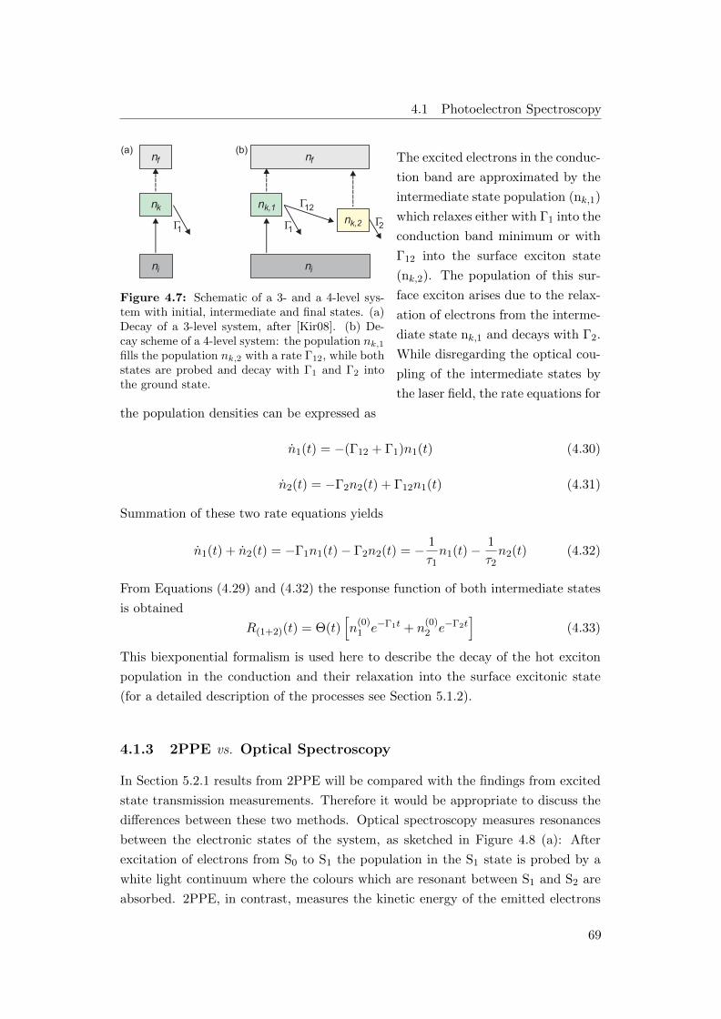
4.1 Photoelectron Spectroscopy
1
12
2
nk,1nk,2
ni
nf
1
nk
ni
nf(a) (b)
Figure 4.7: Schematic of a 3- and a 4-level sys-tem with initial, intermediate and final states. (a)Decay of a 3-level system, after [Kir08]. (b) De-cay scheme of a 4-level system: the population nk,1fills the population nk,2 with a rate Γ12, while bothstates are probed and decay with Γ1 and Γ2 intothe ground state.
The excited electrons in the conduc-
tion band are approximated by the
intermediate state population (nk,1)
which relaxes either with Γ1 into the
conduction band minimum or with
Γ12 into the surface exciton state
(nk,2). The population of this sur-
face exciton arises due to the relax-
ation of electrons from the interme-
diate state nk,1 and decays with Γ2.
While disregarding the optical cou-
pling of the intermediate states by
the laser field, the rate equations for
the population densities can be expressed as
n1(t) = −(Γ12 + Γ1)n1(t) (4.30)
n2(t) = −Γ2n2(t) + Γ12n1(t) (4.31)
Summation of these two rate equations yields
n1(t) + n2(t) = −Γ1n1(t)− Γ2n2(t) = − 1
τ1n1(t)− 1
τ2n2(t) (4.32)
From Equations (4.29) and (4.32) the response function of both intermediate states
is obtained
R(1+2)(t) = Θ(t)[n
(0)1 e−Γ1t + n
(0)2 e−Γ2t
](4.33)
This biexponential formalism is used here to describe the decay of the hot exciton
population in the conduction and their relaxation into the surface excitonic state
(for a detailed description of the processes see Section 5.1.2).
4.1.3 2PPE vs. Optical Spectroscopy
In Section 5.2.1 results from 2PPE will be compared with the findings from excited
state transmission measurements. Therefore it would be appropriate to discuss the
differences between these two methods. Optical spectroscopy measures resonances
between the electronic states of the system, as sketched in Figure 4.8 (a): After
excitation of electrons from S0 to S1 the population in the S1 state is probed by a
white light continuum where the colours which are resonant between S1 and S2 are
absorbed. 2PPE, in contrast, measures the kinetic energy of the emitted electrons
69

4 Methods and Experimental Details
-3.2
-4.85
-6.6
-1.7
ZnO SP6
S0
E(eV)
Evac
CB
EF
3.4
VB
S1
-3.2
-6.6
ZnO SP6
S0
E(eV)
Evac
CB
EF
3.4
VB
S1
S2
(a) Excited state transmission (b) Two-photon photoemission
3
1
2CS
ISC
FL
IVR
T1
Figure 4.8: Probing of the intermediate state population in (a) excitedstate transmission and (b) 2PPE.
and allows to determine the energetic position of the intermediate state S2 with
reference to EF (Figure 4.8 (b)). Both methods yield comparable results when the
same pump and probe photon energies are used.
The first excitation process from the ground state (Ψi) into the first excited
state (Ψk) is the same for optical spectroscopy and 2PPE. For this transition the
dipole selection rules apply and the transition occurs only when the transition matrix
element Vik does not vanish [Huf95]:
Vik = 〈Ψi |µ|Ψk〉 6= 0 (4.34)
here µ is the transition moment operator which depends on the polarization of the
laser light. Now the second transition from the intermediate state (Ψk) to the final
state (Ψf ) is different for the two methods since the final states diverge (Ψoptf 6=
Ψ2PPEf ). In the case of optical spectroscopy the final state is a molecular or crystal
resonance and therefore the dipole selection rules apply strictly. In 2PPE however,
the final state is an unknown state in the vacuum and is thus not restricted to
molecular resonances. Therefore 2PPE provides access to states which would require
a forbidden transition in optical spectroscopy. For example if the intermediate state
is a triplet state and thus dark for optical spectroscopy, due to the spin forbidden
transition between a triplet and a singlet state, it can be probed by 2PPE as the
spin can be conserved in the final state.
70
4.2 Experimental Setup
4.2 Experimental Setup
This chapter provides an overview of the experimental setups and methods which
have been employed in this work. As mentioned earlier the 2PPE experiments have
been conducted at two different places, but very similar setups. They will be referred
to as FHI- and FU-setup in the following and have been described in detail before
(FU: [Kir08, Hag09]) (FHI: [Dei11, Weg14]). Both setups consist of mainly two
parts, a femtosecond laser system and an UHV chamber and the details of which
will be given in the following sections.
4.2.1 The Femtosecond Laser System
The laser system provides the required ultrashort laser pulses tunable over a broad
range of wavelengths. The whole laser system is installed on two optical tables
placed inside a tent consisting of a base frame which is fixed to the ceiling and
plastic curtains reach the floor from the frame. The temperature and humidity of the
whole laboratory are controlled by an air conditioning system. Furthermore, there is
a flow box in the laser-tent producing a little overpressure such that only a minimal
amount of dust is able to enter the tent and to deposit on the optics. The FHI laser
system (Figure 4.9) consists of commercially available components from Coherent,
such as a pump laser (Verdi V-18), a broadband femtosecond oscillator (Micra), a
regenerative amplifier (RegA 9050), a broadband grating stretcher/compressor and
an optical parametrical amplifier (OPA) (vis-OPA 9450). The FU-setup consisted
of the same components but the oscillator was seed based (MIRA 900B). (In the
meantime at the FHI the Verdi V-18 pump laser and the Micra oscillator have been
substituted by a Vitara including a Verdi G pump laser and an additional Verdi
G pumping the RegA 9050.) Verdi V-18 is a diode pumped continuous wave laser
with a maximum power of 18 W at 532 nm pumping both the oscillator and the
amplifier. The Micra oscillator contains a Ti:sapphire (titanium doped corundum,
Ti3+ : Al2O3) crystal as an active laser medium and provides ultrashort laser pulses
at a repetition rate of 80 MHz with a pulse energy of about 6.3 nJ. Before the pulses
are amplified in the RegA they are stretched up to 50-100 ps in order to reduce their
high peak powers protecting the optics in the amplifier from damage. In the RegA
the stretched pulses are amplified at a repetition rate of 40 - 300 kHz (usually runs
at 200 kHz) and subsequently guided back into the stretcher/compressor unit where
they are compressed to 40 fs. The setup at FHI typically delivers pulse energies of
5 - 6.7 µJ at a center wavelength of 800 nm (1.55 eV).
The potential of 2PPE relies on the usage of different photon energies. Hence the
setup is equipped with a possibility to generate a broad range of photon energies.
71

4 Methods and Experimental Details
RegA 9050
Mic
ra
Verd
i
OPA 9450
800nm
800 nm
400 nm
480-700 nm480-700 nm480-700 nm
240-350 nm
lense
NL-crystal
prism
stretcher
compressor 266 nm
200 nmnoncollinear THG/FHG
spherical mirror
mirror/beamsplitter
800 nm
compressed WLC 480-700 nmcompressed WLC 480-700 nm
optical setup
SHG
SHG
deformable mirror based compressor
inte
nsi
ty
200 300 500400 600 700 800wavelength (nm)
schematic overview of spectral range:
optical setup
Figure 4.9: Schematic of the laser setup adopted from [Weg14]: The Coherent laser systemconsisting of a Verdi pump laser, a Micra oscillator, a RegA 9050 amplifier and a stretcher/compressor unit provides ultrafast laser pulses with a photon energy of 1.55 eV. In theOPA 9450 visible light of different wavelengths is generated which can be frequency doubledyielding UV light. In addition, second, third and fourth harmonic generation provides accessto other UV photon energies.
72

4.2 Experimental Setup
The fundamental pulses may be used directly, or can be frequency doubled in a β-
barium borate (BBO) (β−BaB2O4) crystal yielding the second harmonic at 3.1 eV.
Third and fourth harmonic generation (THG and FHG) are realized by overlapping
the 3.1 eV pulses with a part of the fundamental (1.55 eV) pulses in a BBO where
they undergo sum-frequency generation (SFG) yielding the third harmonic of 4.65
eV. The fourth harmonic is generated analogously by adding another part of the
fundamental 1.55 eV beam to yield 6.2 eV. The third and fourth harmonic generation
is described in detail in [Weg14]. Especially the 6.2 eV beam is suitable for direct
photoemission experiments covering the work functions of the currently investigated
materials (ΦAu(111)= 5.35 eV [Ren05], ΦZnO(1010)= 4.5 eV and ΦZnO(0001)= 5.15 eV
[Oza11]).
A part of the fundamental beam can be used in the OPA providing access to a
wide range of wavelength in the visible spectrum. In the OPA the fundamental IR
beam splits where 25 % is used to generate white light in a sapphire crystal and the
other 75 % is frequency doubled in a BBO crystal to yield a photon energy of 3.1
eV. The white light and the 3.1 eV beam are spatially overlapped in a second BBO
crystal. The spectral part of the white light which overlaps with the 3.1 eV beam
is amplified. The temporal delay between these two beams can be adjusted using a
linear stage which allows continuous tunability over a broad spectral range (≈ 1.7
- 2.5 eV). Hence the photon energy can be tuned according to the sample’s work
function and the energetic positions of the investigated electronic states.
The time resolution of TR-2PPE depends on the pulsewidth of the laser. In the
following the comprehension of laser pulses is discussed. In most transparent media
the red colour features a higher group velocity than the blue colour.This causes a
divergence of the spectral parts of the pulse in time. This effect is called the chirp
of a pulse which has to be avoided to obtain short pulses. The chirp can be avoided
using a prism compressor which consists of two prisms positioned parallel to each
other’s bases at an angle of minimum deviation. The laser beam passes the first
prism which disperses the constituents such that the longer wavelength components
travel a longer optical path through the second prism. After passing the second prism
the beam is reflected from a mirror and returns through the two prisms collinearly
to the incoming beam. Thereby components of varying wavelengths are brought to
a temporal overlap.
73

4 Methods and Experimental Details
4.2.2 Pulse Characterization
In order to analyse the 2PPE data detailed information about the laser pulses, such
as photon energy, laser power, pulse duration and spot size is needed. The photon
energy is measured with a Maya200Pro spectrometer (OceanOptics). Note that the
enrgy of the photon is an important parameter that is needed to determine the work
function of the sample and the binding energy of the electronic states. A typical
laser spectrum is shown in Figure 4.10 (a), where the central photon energy and the
bandwidth (FWHM) are obtained from a Gaussian fit (black line). The power of
the laser beam is measured with a power meter (Newport) just before the beam is
coupled into the chamber. In order to calculate the laser fluence, as described in
appendix B, the spot size of the laser beam is required. The spot size is measured
with a beam profiler (SP620U, Spiricon) which is placed at a virtual sample position
outside the UHV chamber. A typical laser intensity profile is displayed in Figure
4.10 (b) in false colours. The black contours correspond to a 2D gaussian fit from
which the FWHM is obtained.
340330320310300
1400
1200
1000
800
600
400
200
012008004000
Width (µm)
Wid
th (
µm
)
Wavelength (nm)
Inte
nsi
ty
raw dataGaussian fit
peak center:318.4 nm (3.89 eV)
FWHM:3.78 nm(46 meV)
(a) (b)FWHM (x) = 117 1.2 µmFWHM (y) = 125 1.3 µm
+_+_
Figure 4.10: (a) An example laser spectrum and (b) the corresponding beam profile infalse colours with a 2D Gaussian fit.
The duration of the laser pulses is determined via the XC of the laser pulses,
which is usually measured by 2PPE from occupied states of a metal surface. The
2PPE process occurs in such a case via a virtual intermediate state with an in-
finitesimal lifetime. Therefore the measured 2PPE signal (IXC(t)) corresponds to
the correlation of the transient intensities of pump (I1(t)) and probe (I2(t)) pulses
IXC(t) =
∫ +∞
−∞dt′I1(t)I2(t− t′) (4.35)
This can be approximated by an autocorrelation of two identical laser pulses under
the assumption that pump and probe pulse possess the same pulse duration [Rul98].
74

4.2 Experimental Setup
4.2.3 The Ultrahigh Vacuum Chamber
The UHV chamber provides a reduced pressure environment that is required for the
investigation of surfaces. On the one hand UHV conditions are necessary in order to
guarantee clean surfaces since the electronic structure is highly sensitive to surface
contamination, e.g. nitrogen, oxygen or water, which would rapidly cover the surface
under ambient conditions. On the other hand the mean free path of the photoelec-
trons decreases with increasing pressure. The UHV chamber sketched in Figure 4.11
is part of the FHI-setup and consists of two levels, the preparation and spectrom-
eter chamber, separated by a gate valve. This helps to avoid contamination of the
electron multipliers and optics of the electron analyser during sample preparation.
The transfer system is separated from the chamber by a gate valve and provides a
possibility to change the samples without breaking the vacuum. The base pressure
QMS
LEED
sputter gun
PHD
leak valve
gas system
Ar, H , D O, etc.2 2
ion gauge
window
Knudsen cell
transfer rod
gate valve
QMB
μ-metal
SPECSPhoibos
100
time delay
focusing
ion gauge
(a) upper level: preparation chamber
(b) lower level: spectrometer chamber
MgF window2
lenses
Figure 4.11: Schematic of a horizontal cross section of the UHV chamber consisting of(a) the preparation chamber at the upper level and (b) at the lower level the spectrometerchamber. The sample holder is schematically shown in the center 4.12
of the chamber is ≈ 1× 10⁻¹⁰mbar and is achieved by several vacuum pumps. The
upper level (preparatopn chamber) is pumped by a high-capacity turbomolecular
pump (HiPace 700, Pfeiffer Vacuum AG) and the lower level (analyser chamber)
by an ion getter pump (TiTan 200L, Gamma Vacuum, LLC) apart from an op-
tional titanium sublimation pump (Vacom GmbH). The Knudsen effusion cell and
the gas system together with the transfer system are equipped with their own turbo
pumps respectively. The pre-vacuum is generated by membrane pumps (MV2NT,
75

4 Methods and Experimental Details
Vacuubrand GmbH).
The preparation chamber is equipped with several devices needed for the prepa-
ration and characterization of clean single-crystal and adsorbate-covered surfaces.
The details of the devices are as follows:
• Sputter gun (SPECS) is employed for the preparation of the sample surface
during which the surface is first sputtered with argon ions and subsequently
annealed. During the sputtering procedure argon is let into the UHV chamber
via a leak valve and subsequently ionized by the electrons from the sputter gun
filament. The Ar+ ions are accelerated and bombarded onto the sample surface
removing the surface atoms by momentum transfer. Since sputtering roughens
the sample surface usually an annealing cycle, inducing surface reorganisation,
follows to obtain a smooth surface again.
• Low-energy electron diffraction (LEED) (ErLEED 1000-A, SPECS) pro-
vides the possibility to investigate the surface crystal structure of the sample.
• Quadrupole mass spectrometer (QMS) (MKS, Satellite) has several ap-
plications: (i) to quantify the coverage by means of temperature programmed
desorption (TPD), (ii) to conduct rest gas analysis (RGA) and to test the
purity of the sputter gas and the evaporated molecules and (iii) to detect the
mass of helium in leak testing.
• Knudsen effusion cell (Dr. Eberl, MBE components) contains two water-
cooled crucibles in which molecular solids with sublimation temperatures up to
700 ◦C can be evaporated separately or simultaneously. A copper block with
two apertures is attached in front of the crucibles to focus the molecular beam
onto the sample. The Knudsen cell is mounted on a linear stage and can be
moved into the chamber until the sample is at the focus of the molecular beam.
Furthermore, it is equipped with its own turbo pump and separated from the
main chamber by a gate valve allowing to refill or exchange the molecules
without breaking the vacuum of the UHV chamber.
• Quarz microbalance (QMB) (agilent technologies) is used to quantify the
thickness of molecular films and faces the Knudsen cell such that a part of
the molecular beam arrives on to the quartz crystal. The adsorbed molecules
change the vibrational frequency of the quartz crystal. The working principle
of the quartz crystal microbalance (QMB) is detailed in Section 4.3.2.
• Pinhole doser (PHD): Gaseous, liquid and even solid molecules with evap-
oration points close to room temperature can be deposited on the sample
76

4.2 Experimental Setup
surface. In the case of liquids or solids the substances are stored in a glass
tube which is attached to the gas system via a metal adapter. To evaporate
the compounds the glass tube is heated with a heat gun. The gas system is
then flooded with the evaporated substance and enters the chamber through
the pinhole doser (PHD) (described detailed in [Dei11]).
The spectrometer chamber contains a hemispherical electron analyser (Phoibos 100,
SPECS) which has been described and characterised in detail before [Dei11], while
a brief description is given in Section 4.2.4. A magnesium fluoride (MgF2) window
is installed to couple the laser pulses into the chamber, MgF2 is transparent from
ultraviolet to the infrared spectral region. Also its low refractive index minimizes
the dispersion of the laser pulses.
The UHV setup at the FU differs mainly in 3 aspects: (i) upper and lower level
are not separated by a gate valve, (ii) the electron analyser is a time-of-flight (TOF)
instead of a hemispherical analyser (see Section 4.2.4 for details) and (iii) the LEED
is located in the lower level opposite to the TOF.
Both setups use the same sample holder [Hag09] depicted schematically in Figure
4.12. The upper sample holder is attached to the cold finger of the cryostat and
consists of copper and is electrically (not thermally) isolated by sapphire plates from
the two copper parts which form the intake slits for the sample boat. The sample
Figure 4.12: Sketch of the sampleholder, adopted from [Hag09].
(1) upper sample holder(2) lower sample holder (boat)
(a) connection to cryostat(b) mount for heating(c) sapphire plates(d) macor isolated screws(e) screws to fix boat(f) macor isolated TC pins(g) tantalum heating wires(h) metal substrate(i) thermocouple(j) port for transfer(k) screws to fix sample
boat consists of two electrically isolated molybdenum parts which connect the two
77

4 Methods and Experimental Details
isolated copper parts of the upper sample holder serving thus as electrodes for the
resistive heating. The metal sample is fixed with tantalum (Ta) heating wires in the
sample boat. The sample temperature is measured with thermocouple (TC) wires
which are connected via TC pins to the jacks of the upper part of the sample holder.
The ZnO crystals are due to their poor thermal conductivity fixed with grips on a
tantalum sheet welded to the heating wires in order to guarantee a homogeneous
heating. The cryostat is connected to a manipulator enabling the sample to move in
x-, y- and z-direction, as well as to rotate around the z-axis (cryostat axis). The low
temperature limit amounts to 77 K when the cryostat is filled with liquid nitrogen
(LN2). A PID temperature controller (LakeShore 340) provides a required heating
rate. The sample is resistively heated via the tantalum wires with which it is fixed
to the sample holder. Furthermore, they can be used to ground the sample during
sputtering and to apply a bias voltage between sample and analyser during 2PPE
measurements.
78

4.2 Experimental Setup
4.2.4 Electron Analysers
As pointet out earlier the electron analysers are the parts of the two setups which
differ the most. The FHI-setup contains a hemispherical analyser (Phoibos 100,
SPECS) while a custom built TOF spectrometer is included in the FU-setup. Both
analysers will be described briefly in the following.
Hemispherical Analyser Phoibos 100
The hemispherical analyser Phoibos 100 is the central part of the experimental setup.
It enables a simultaneous measurement of the energetic and the angular distribu-
tion of the photoelectrons. Its working principle and characterisation have been
described in detail in [Dei11]. In a hemispherical analyser the photoelectrons are
spatially selected via electric fields and multiplied by micro-channel-plates (MCP)
before illuminating a phosphor screen. The illumination on the phosphor screen
is recorded by a camera which is located outside the chamber. The details of the
camera are given are given at the end of the section. The analyser is shown schemat-
ically in Figure 4.13 and consists of two parts, viz. electrostatic lens system and a
hemispherical capacitor. The photoelectrons enter the lens system after passing a
working distance of 4 mm. The variable electric field of the lens system allows se-
sample surface
working distance
CCD-camera
detector
MCP
inner
hemisphere
adjustment window
entrance slit
lens tubes
handwheel to select
entrance slit
µ-metal-
shielding
handwheel for
iris entrance
energetically selected
trajectoriesenergy-dispersive
axis
non-energy
dispersive axis
electrical
feedthroughs
outer
hemisphere
Figure 4.13: Cross section of the hemispherical analyser modified from [Bra09] showingthe dispersing trajectories of the photoelectrons along the energy-dispersive axes.
lective projection of the electrons mapping either the spatial position or the angle
of emission parallel to the entrance slit onto the 2D detector. The energy range
79

4 Methods and Experimental Details
of mapping can be selected via acceleration voltages inside the lens system. The
size of the entrance slit defines the transmission vs. energy resolution which can be
regulated by a magnetically coupled handwheel. Energy selection is realized by the
radial electric field (E(r)) in the hemispherical capacitor forcing the photoelectrons
on elliptic trajectories with different radii according to their kinetic energy. The lens
system and the hemispherical capacitors are shielded by µ-metal to prevent distrac-
tion of the electrons due to external magnetic fields. The radial electric field (E(r))
is given by
E(r) = (Vin − Vout)RinRout
Rout −Rin
1
r2(4.36)
where Vin/out are the voltages of the inner/outer hemisphere and Rin/out are the
respective radii. The geometry of this setup leads to a non-energy dispersive axis
perpendicular to the energy-dispersive axis which is parallel to the radial direction.
Along the energy-dispersive axis of the 2D detector electrons are spatially separated
according to their kinetic energy. Depending on the selected working mode the
photoelectrons are spatially separated along the non-energy dispersive axis according
to either their horizontal spatial position on the sample surface or their emission
angle.
After passing the hemispherical capacitor the energetically selected electrons are
multiplied by a MCP before illuminating the phosphor screen. The digital picture of
the electrons illuminating the phosphor screen is recorded by a highly sensitive CCD-
camera (PCP Sensicam qe). To obtain from this image a 2D-spectrum, where the
kinetic energy is represented as function of the emission angle, the pixel coordinates
(mα, mE) have to be converted into kinetic energy E and emission angle α. The
kinetic energy Ekin can be calculated using the following formula [SPEa]:
Ekin = E′kin +De1 · Epass ·M · Ps(mE −ME
2) (4.37)
Where E′kin and Epass select the energetic range (E′kin defines the center of the
spectrum). De1 is the energetic dispersion depending on the radius of the hemisphere
and M is the magnification factor of the camera objective. Ps is the pixel size and
ME corresponds to the total range of pixels along the energy-dispersive axis and is
aligned such that the image is in the center of the CCD-screen. The conversion to the
emission angle (α) from the pixels (mα) along the non-energy dispersive axis is more
complicated since chromatic abberation of the lens system and the hemispherical
capacitor lead to a non-linear relation between E′kin and Epass. The image can
be unwarped by calculating the trajectories of the electrons and the corresponding
iso-angle lines.The pixel (mα) at energy Ekin can be calculated via a second order
80

4.2 Experimental Setup
polynomial [Weg14]:
mα(Ekin, r) = n0(α, r) + n1(α, r)Ekin + n2(α, r)E2kin (4.38)
The coefficiants ni can be calculated from a polynomial expression provided by
SPECS [SPEb] and depend on the retarding ratio (r = E′kin/Epass).
81
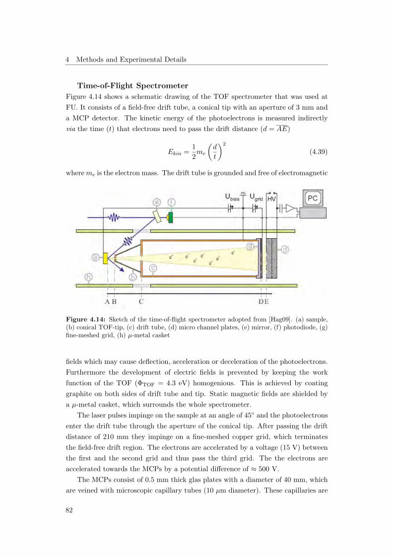
4 Methods and Experimental Details
Time-of-Flight Spectrometer
Figure 4.14 shows a schematic drawing of the TOF spectrometer that was used at
FU. It consists of a field-free drift tube, a conical tip with an aperture of 3 mm and
a MCP detector. The kinetic energy of the photoelectrons is measured indirectly
via the time (t) that electrons need to pass the drift distance (d = AE)
Ekin =1
2me
(d
t
)2
(4.39)
where me is the electron mass. The drift tube is grounded and free of electromagnetic
Figure 4.14: Sketch of the time-of-flight spectrometer adopted from [Hag09]. (a) sample,(b) conical TOF-tip, (c) drift tube, (d) micro channel plates, (e) mirror, (f) photodiode, (g)fine-meshed grid, (h) µ-metal casket
fields which may cause deflection, acceleration or deceleration of the photoelectrons.
Furthermore the development of electric fields is prevented by keeping the work
function of the TOF (ΦTOF = 4.3 eV) homogenious. This is achieved by coating
graphite on both sides of drift tube and tip. Static magnetic fields are shielded by
a µ-metal casket, which surrounds the whole spectrometer.
The laser pulses impinge on the sample at an angle of 45◦ and the photoelectrons
enter the drift tube through the aperture of the conical tip. After passing the drift
distance of 210 mm they impinge on a fine-meshed copper grid, which terminates
the field-free drift region. The electrons are accelerated by a voltage (15 V) between
the first and the second grid and thus pass the third grid. The the electrons are
accelerated towards the MCPs by a potential difference of ≈ 500 V.
The MCPs consist of 0.5 mm thick glas plates with a diameter of 40 mm, which
are veined with microscopic capillary tubes (10 µm diameter). These capillaries are
82
4.2 Experimental Setup
oriented at an angle of 8◦ relative to the surface normal which enables the multiple
collisions of photoelectrons inside the glass capillary. This collision produces sec-
ondary electrons. The secondary electrons are further accelerated by a high voltage
of 2.7 kV, which is applied between the two MCPs. Due to these electron cascades
the high voltage decreases for a moment which is detected by a capacitor and a
preamplifier. In fact, a time-dependent signal −∆V (t) is recorded.
Measuring the Energy via the Time
In order to obtain the kinetic energy of the photoelectrons via the relation shown in
Equation (4.39) the time (t) between the emission and their arrival at the MCPs has
to be known. The impact of the electrons on the MCPs is detected but the point of
time at which the electrons are emitted cannot be measured directly. Therefore a
reference signal for the time measurement is taken from a photodiode which is placed
at the RegA output. The measured time (difference between start and arrival signal)
is referred to as t′ which contains the time (t0) that light takes to travel from the
photodiode to the sample plus the time-of-flight (t)
t = t′ − t0 (4.40)
Substituting Equation 4.40 in Equation 4.39 yields
Ekin =1
2me
(d
t′ − t0
)2
(4.41)
t0 is determined by a series of spectra taken with different bias voltages. It is assumed
that the spectra shift energetically according to the bias voltages. The correct t0
is obtained by superimposing the spectra taken with different bias voltages under
variation of t0. The value for t0 for which all spectra have the same shape is the right
one. The energy thus obtained is the kinetic energy relative to the TOF’s vacuum
level, whereas the kinetic energy with respect to the sample’s vacuum level, the final
state energy Efinkin, is required. In order to obtain Efin
kin relative to the Fermi level the
work function difference (∆Φ = ΦTOF − Φsample) and the bias voltage (eUbias) have
to be taken into account
Efinkin =
1
2me
(d
t′ − t0
)2
−∆Φ + eUbias (4.42)
In fact, voltage vs. the time-of-flight is measured and is transformed into energy
spectra employing Equation 4.42. The measured signal intensity is proportional to
the number of electrons (dN) within a certain time frame (bin) (dt), i.e. ∆V (t) ∝ dNdt
and subsequently generated energy spectrum should contain the number of events
83
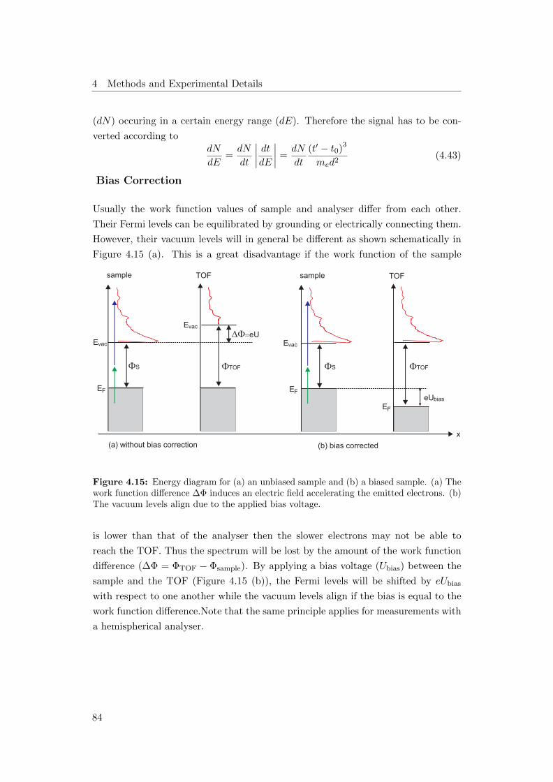
4 Methods and Experimental Details
(dN) occuring in a certain energy range (dE). Therefore the signal has to be con-
verted according todN
dE=dN
dt
∣∣∣∣ dtdE∣∣∣∣ =
dN
dt
(t′ − t0)3
med2(4.43)
Bias Correction
Usually the work function values of sample and analyser differ from each other.
Their Fermi levels can be equilibrated by grounding or electrically connecting them.
However, their vacuum levels will in general be different as shown schematically in
Figure 4.15 (a). This is a great disadvantage if the work function of the sample
x
sample
TOFS
eU
TOF
(a) without bias correction
sample
TOFS
eU
TOF
(b) bias corrected
bias
Evac
EF
EF
Evac
Evac
EF
Figure 4.15: Energy diagram for (a) an unbiased sample and (b) a biased sample. (a) Thework function difference ∆Φ induces an electric field accelerating the emitted electrons. (b)The vacuum levels align due to the applied bias voltage.
is lower than that of the analyser then the slower electrons may not be able to
reach the TOF. Thus the spectrum will be lost by the amount of the work function
difference (∆Φ = ΦTOF − Φsample). By applying a bias voltage (Ubias) between the
sample and the TOF (Figure 4.15 (b)), the Fermi levels will be shifted by eUbias
with respect to one another while the vacuum levels align if the bias is equal to the
work function difference.Note that the same principle applies for measurements with
a hemispherical analyser.
84

4.3 Sample Preparation
4.3 Sample Preparation
In the following sections the preparation procedures for the ZnO and Au single
crystal samples will be presented. Also the adsorption procedures for solid and
gaseous adsorbates will be introduced. Apart from this, the quantification of the
adsorbate coverages will be discussed.
4.3.1 Preparation of the O-terminated ZnO Surface and Quantifi-
cation of the H-Dosage
The single crystal ZnO(0001) (MaTeck GmbH) sample was prepared by repeated
sputtering and annealing cycles until the measures for cleanliness, such as maximal
work function (Φ= 5.1 - 5.2 eV, which agrees with the literature 5.15(5) eV [Oza11])
and minimal CAL intensity were satisfied. The sample was sputtered at room tem-
perature for 10 min with argon ions with the following parameters, pAr = 2× 10⁻⁶
mbar, 1.0 keV and a sputter current of ≈ 6µA. Subsequently the sample was an-
nealed at 950 K for 30 min under oxygen atmosphere, pO2 = 1× 10⁻⁶ mbar, with a
heating rate of β = 30 K/min (the ZnO sample was mounted on a Ta sheet which was
heated resistively guaranteeing a homogeneous heat distribution). The sample was
prepared by following the above procedure on a daily basis. All the measurements
were performed at temperatures around 100 K.
O-terminated ZnO(0001)
H H HH H H
HH
H
H2 H2
H2
H2
H2
H2
H2
H
iongaugefilament
H
(b)2.5x10⁻⁷
2.0
1.5
1.0
0.5Pre
ssure
(m
bar)
8006004002000Time (s)
Integrated area
(a)
Figure 4.16: (a) Pressure trace taken during H2 dosing, the dosage can be calcu-lated using the integrated area below the trace (b) illustration of H2 cracking intoatomic hydrogen by the electrons emitted from the filament of the ion gauge.
Hydrogen was dosed via the background pressure through a leak valve. The
hydrogen dosage was quantified by measuring the pressure and the time as shown
in Figure 4.16 (a), where the dosage can be calculated in Langmuir (L) with the
integrated area. 1 L is defined as a gas dosage of 1 torr for 1 µs (1 L = 1 torr·µs)
under the assumption of a sticking coefficient (Sc) 1. This corresponds to a pressure
of 1.33×10⁻⁶ mbar for 1 s. 1 L hydrogen can be obtained by dosing 4.4×10⁻⁷ mbar
85

4 Methods and Experimental Details
for 1 s, since the sensitivity of the ion gauge (Arun Microelectronics Limited) is
3 times smaller for hydrogen than nitrogen, where the latter is at default setting.
Opening a valve for 1 s is not practical with our system, therefore we decided to
dose 1 L at a H2 pressure of 2.2 × 10⁻⁷ mbar for 2 s. The H2-dosage in L is then
obtained by dividing the integrated area of pressure vs. time curve (Figure 4.16 (a))
by 2 · 2.2× 10−7 mbar·s. During the hydrogen dosage the sample was kept at 100 K
and facing the glowing filament of the ion gauge from a distance of ≈ 15 cm. The
hot filament enhances dissociation of H2 as sketched in Figure 4.16 (b).
86
4.3 Sample Preparation
4.3.2 Preparation of the SP6 Films and Determination of the Film
Thickness Using a Quartz Microbalance
ZnO(1010) sample was prepared on a daily basis by sputtering for 10 min with Ar+
(pAr = 2.0 × 10⁻⁶mbar, 0.75 keV at 300 K followed by 30 min annealing at 950 K
with a temperature ramp of 30 K/min). The SP6 molecules were evaporated from
a Knudsen-cell at a temperature of 580 K onto the sample at 300 K. During the
evaporation the QMB was placed behind the sample to quantify the thickness of the
SP6 molecules. The thickness on the QMB is proportional to that of the sample,
where the proportionality constant is called tooling factor (T ).
The working principle of a QMB is based on the piezoelectric properties of quartz.
This piezoelectric effect is nearly temperature independent and perpendicular to the
prism axis along the a-axis. Therefore it is important to have the crystal either
AT-(parallel to the (001)-plain) or BT-cut (parallel to the (023)-plain). Applying
pressure or draught to a quartz crystal results in an electrical polarization along the
force direction. Conversely under a direct-current voltage a distension or compres-
sion occurs. Applying an alternating current voltage with a suitable frequency leads
to a resonant vibration of the quartz crystal. The resonance frequency depends on
the shape and size of the crystal. The mass of the quartz crystal is changed under
absorption of atoms or molecules on the surface and thus the resonance frequency.
In order to determine the mass of the adsorbed material, and thus the film
thickness, Sauerbrey equation [Sau59] is employed.
∆f = − 2(f0)2
A√ρqµq
∆m (4.44)
where f0 = resonant frequency (Hz)
∆f = frequency change (Hz)
∆m = mass change (g)
A = piezoelectrically active crystal area (cm2)
ρq = 2.65 g/cm3 density of quartz
µq = 2.95×10⁻¹¹ g/cm2s2 shear modulus for AT-cut crystal
Solving for ∆mA with
√ρqµq = zq = 8.8 × 10⁶ kg m−2 s−1 Equation 4.44 can be
written as∆m
A= − ∆fzq
2(f0)2=
∆f(8.8× 10⁶ kg m−2 s−1)
2(f0)2(4.45)
87

4 Methods and Experimental Details
The film thickness (θ) is then given by
θ =∆m T
A ρMat(4.46)
where ρMat is the density of the adsorbed material and T corresponds to the tooling
factor which is the ratio between the adsorption rate on the QMB with and without
the sample between QMB and evaporator. The Sauerbrey equation holds only for
very small frequency changes (∆ff0≤ 0.02) and equally distributed rigid masses. The
frequency changes are usually in the range of 0.2 kHz5978 kHz = 3.4× 10⁻⁵ which is 0.02.
But of course the large organic molecules such as SP6 are not rigid masses, which
introduces a finite error.
In the following an example is given for the determination of the SP6 film thick-
ness. Figure 4.17 shows a QMB trace to determine the tooling factor and the film
5978.05
5978.00
5977.95Fre
qu
en
cy (
kH
z)
6004002000
Time (s)
QMB trace m 1
m 2
f
0,1
f 2
f 1
f 0,2
Figure 4.17: QMB trace vs. the time for the determination ofthe tooling factor and the SP6 film thickness.
thickness. The slope, m1 refers to the frequency change of the quartz crystal with-
out the sample between QMB and evaporator and m2 is the slope obtained with the
sample. The tooling factor is given by
T =m1
m2= 1.74 (4.47)
With T and the density of SP6 (ρSP6 = 1.4 g/cm3, as determined by M. Sparenberg
in the group of F. Henneberger (HU Berlin), the film thickness can be calculated
from Equation 4.46
θ =∆mT
AρSP6(4.48)
the start frequency (f0,1) and the shift (∆f2) can be simply read out from the QMB
88

4.3 Sample Preparation
trace, ∆m/A can be calculated using Equation 4.45
∆m
A=
0.13 kHz(8.8× 10⁶ kgm−2s−1)
2(5978.05 kHz)2= 2.46× 10⁻⁵ kg/m2 (4.49)
and hence the thickness of film
θ =2.45× 10⁻⁵ kgm−2 · 1.74
1.4 gcm−3= 31nm (4.50)
TPD turned out to be not a suitable method to quantify the film thickness, nev-
ertheless it unveils some important information. Figure 4.18 (a) shows TPD traces
measured at masses of (m/z) 58 and 78 amu, where the former can be related to a
tert-butyl group with an additional hydrogen atom and the latter may correspond
to a benzene molecule. The signal measured for m/z = 78 amu is much lower than
that of m/z = 58 amu. Both masses are detected at the same temperature indicating
that the detected fragments originate from molecules and not from adsorbed frag-
ments. Fragmentation due to dissociation of the molecules may take place during
evaporation. In Figure 4.18 (b) the TPD of different coverages SP6/ZnO(1010) show
10
8
6
4
2
0
QM
S-S
ignal (a
rb.u
.)
800600400200Temperature (K)
(b) m/z = 58
19 nm
16 nm
6 nm
10
8
6
4
2
0
QM
S-S
ignal (a
rb.u
.)
800600400200Temperature (K)
(a) 16 nm SP6/ZnO(10-10)
m/z = 58
m/z = 78
multilayer desorption
desorption from Ta or sample holder
Figure 4.18: (a) TPD of 16 nm SP6/ZnO(1010) measured with different masses, both ofwhich desorb at the same temperature, (b) TPD traces of different coverages SP6/ZnO(1010)
that the intensity of both peaks increase with the coverage in a zero order fashion.
Essentially, the low temperature signal is from the tantalum sheet or the sample-
holder while the high temperature signal originates from multilayer desorption of the
SP6 molecules from the ZnO(1010) surface. A monolayer desorption is not observed
here indicating that either the molecules in the monolayer stick to the surface and
decompose thermally or that the intermolecular interactions are as strong as the
interactions between the SP6 molecules and the ZnO surface such that the whole
film desorbs at once. The latter situation is more likely to be the case. A Raman
study of SP6 on glass or ZnO revealed that the interaction of the SP6 molecules
with the ZnO surface was weak [Sta13].
89

4 Methods and Experimental Details
In order to understand whether the SP6 molecules decompose thermally during
the evaporation nuclear magnetic resonance (NMR) spectra were taken before and
after evaporation when dissolved in deuterated benzene. The evaporated molecules
were collected from the focussing block which is fixed at the front of the Knudsen cell.
Figure 4.19 (a) shows the downfield part of the NMR spectrum with the signals of the
aromatic hydrogen atoms which are less screened by the ring current of the π-systems
induced by the magnetic field. The signal from the evaporated SP6 molecules (blue-
green) is less intense compared to that of the pristine SP6 (before evaporation). Also
the solvent (C6D6) peak is relatively higher in intensity for the evaporated molecules.
This is due to the differences in ratio between solvent and molecules. The solution of
the evaporated SP6 molecules is less concentrated than its pristine counterpart. The
number and position of the signals from the aromatic hydrogen well agreed across
the two samples, i.e. both SP6 fractions possess the same chemically equal hydrogen
atoms and thus both samples are identical within the detection limits. In Figure 4.19
(b) the upfield part of the NMR spectrum with the signals of the aliphatic hydrogen
atoms is depicted. Besides the peaks related to the tert-butyl hydrogen atoms there
are signals which my be attributed to aliphatic contaminations or water. The peaks
next to the tert-butyl hydrogens peak are the C13 satellites. Another proof that
the evaporated molecules are still intact is the ratio between the integrals of the
tert-butyl hydrogen peak and the peaks between 7.8 - 7.9 ppm, which correspond
to 4 aromatic hydrogen atoms. There are 18 H-atoms at the tert-butyl-groups, thus
the ideal ratio is 18 : 4. In the case of pristine SP6 the ratio amounts to 21.96 : 4.11
and for the evaporated SP6 to 18.76 : 4.00. Notably the ratio from the evaporated
SP6 compares very well with the ideal ratio of 18 : 4. This confidently concludes
that the SP6 molecules do not decompose during evaporation.
0.00.20.40.60.81.01.21.4
0.00
0.02
0.04
0.06
0.08
0.10
0.12
0.14
0.16
0.18
7.07.17.27.37.47.57.67.77.87.9Chemical Shift (ppm)
0.0
0.2
0.4
0.6
0.8
1.0
1.2
1.4
1.6
1.8
2.0
Chemical Shift (ppm)
Inte
nsity (
arb
. u
.)In
ten
sity
(arb
. u.)
C D6 6
SP6 after evaporation
(a) downfield H-NMR spectra of
(b) upfield
tert-butyl Hsaliphaticcontaminationsor water
aromatic Hs
SP6 before evaporation
Figure 4.19: (a) Downfield and (b) upfield H-NMR spectra of SP6 before (dark red) andafter (blue-green) evaporation.
90
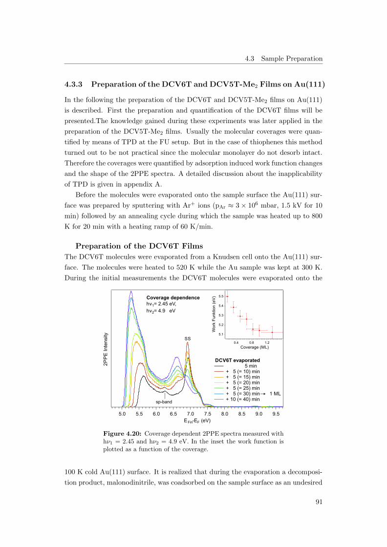
4.3 Sample Preparation
4.3.3 Preparation of the DCV6T and DCV5T-Me2 Films on Au(111)
In the following the preparation of the DCV6T and DCV5T-Me2 films on Au(111)
is described. First the preparation and quantification of the DCV6T films will be
presented.The knowledge gained during these experiments was later applied in the
preparation of the DCV5T-Me2 films. Usually the molecular coverages were quan-
tified by means of TPD at the FU setup. But in the case of thiophenes this method
turned out to be not practical since the molecular monolayer do not desorb intact.
Therefore the coverages were quantified by adsorption induced work function changes
and the shape of the 2PPE spectra. A detailed discussion about the inapplicability
of TPD is given in appendix A.
Before the molecules were evaporated onto the sample surface the Au(111) sur-
face was prepared by sputtering with Ar+ ions (pAr ≈ 3 × 10⁶ mbar, 1.5 kV for 10
min) followed by an annealing cycle during which the sample was heated up to 800
K for 20 min with a heating ramp of 60 K/min.
Preparation of the DCV6T Films
The DCV6T molecules were evaporated from a Knudsen cell onto the Au(111) sur-
face. The molecules were heated to 520 K while the Au sample was kept at 300 K.
During the initial measurements the DCV6T molecules were evaporated onto the
2P
PE
In
ten
sity
9.59.08.58.07.57.06.56.05.55.0
EFin-EF (eV)
sp-band
SS
DCV6T evaporated 5 min + 5 (= 10) min + 5 (= 15) min + 5 (= 20) min + 5 (= 25) min + 5 (= 30) min 1 ML + 10 (= 40) min
Coverage dependencehν1= 2.45 eV,
hν2= 4.9 eV
5.5
5.4
5.3
5.2
5.1
Work
Funkt
ion (
eV
)
1.20.80.4
Coverage (ML)
Figure 4.20: Coverage dependent 2PPE spectra measured withhν1 = 2.45 and hν2 = 4.9 eV. In the inset the work function isplotted as a function of the coverage.
100 K cold Au(111) surface. It is realized that during the evaporation a decomposi-
tion product, malonodinitrile, was coadsorbed on the sample surface as an undesired
91

4 Methods and Experimental Details
contamination. This can be easily avoided by evaporating the molecules onto the
300 K sample surface since malonodinitrile desorbs between 180 -300 K. Detailed
information is available in appendix A.
In order to quantify the effect of DCV6T coverage, 2PPE measurements were
performed as a function of the film thickness. Figure 4.20 shows a series of 2PPE
spectra measured with hν1 = 2.45 and hν2 = 4.9 eV. The work function decreases and
the features of the Au(111) surface (sp-band and surface state (SS)) are quenched
due to DCV6T adsorption. In the inset of Figure 4.20 the work function is plotted
as a function of the DCV6T coverage. It is assumed that the work function decrease
saturates at a monolayer (ML) coverage. Therefore the spectrum taken after an
evaporation period of 30 min is assigned to a ML coverage. The different film
thicknesses were determined according to the ML calibration. This is based on the
assumption of a constant evaporation rate, since these depositions were performed
in one session (i.e. on the same day). The error thereby is estimated to be 20 %.
Higher coverages can be quantified only according to their shape and the excited
state lifetime since the work function is more or less constant for coverages ≥ 1 ML.
Also, the evaporation rate is not always constant due to the decreasing filling level of
the crucible and the irregular heat distribution therein. Therefore a constant evap-
oration rate is assumed only during evaporation cycles carried out on the same day.
2P
PE
Inte
nsi
ty
98765
EFin-EF (eV)
DCV6T evaporated
4 min 1.5 0.5 ML
+ 2 (= 6) min 2 1.0 ML
+ 2 (= 8) min 3 1.0 ML
+ 5 (= 13) min 5 2.0 ML
+ 5 (= 18) min 7 3.0 ML
Coverage dependence hν1= 2.3 eV,
hν2= 4.6 eV
+ _
+ _
+ _
+ _
+ _
Figure 4.21: 2C-2PPE spectra series measured on dif-ferent DCV6T coverages on Au(111).
To illustrate this procedure an
additional coverage-dependent
series of spectra for coverages
up to 7 ± 3 ML are depicted
in Figure 4.21. The black spec-
trum has been recorded after
a deposition for 4 min and as-
signed to a coverage of 1.5 ± 0.5
ML since we note a minimum
work function and quenched
surface state. The other cov-
erages within this series have
been determined from this cal-
ibration assuming a constant
evaporation rate (for deposi-
tions carried out on the same day). At a film thickness of 2 ± 1 ML a very broad
feature arises at final state energies between ≈ 5.5 - 6.0 eV which becomes even
more prominent and shifts to lower energies with increasing coverage, while the
other molecular features decrease. This feature exhibits an increasing lifetime with
92

4.3 Sample Preparation
coverage as observed in TR-2PPE. Coverages higher than 7 ± 3 ML can only be dis-
tinguished according to the lifetimes measured from the TR-2PPE spectra, mounting
the error at least to 30 %.
Preparation of the DCV5T-Me2 Films
The DCV5T-Me2 molecules were evaporated from the Knudsen-cell at a temperature
of 553◦C onto the Au(111) surface which was held at a temperature of 300 K. The
coverage was quantified according to the procedure described before in the case of
DCV6T, since TPD was not applicable for DCV5T-Me2 either (see Appendix A for
further information). Figure 4.22 displays a series of coverage-dependent 2C-2PPE
2P
PE
In
ten
sity
10.09.08.07.06.05.0
EFin-EF (eV)
sp-band
SS
Coverage dependence
hν1 = 2.37 eV,
hν2 = 4.74 eV
5.5
5.4
5.3
5.2
5.1
5.0
4.9
Wo
rk F
un
ctio
n
(eV
)
2.52.01.51.00.50.0
Coverage (ML)
DCV5T-Me 2 evaporated
0 min 3 min
6 min 9 min
12 min 1 ML 17 min
27 min
Figure 4.22: Coverage-dependent 2PPE spectra series mea-sured with hν1 = 2.37 and hν2 = 4.74 eV. In the inset the workfunction is plotted as a function of the coverage..
spectra recorded with hν1 = 2.37 and hν2 = 4.74 eV. The black spectrum shows the
pristine Au(111) surface with a work function of Φ = 5.5 eV and two characteristic
features, namely the sp-band and the surface state (SS). These features are quenched
with increasing coverage and the work function shifts to lower values as much as 0.55
eV (see inset of Figure 4.22). After 12 min of evaporation the coverage is assigned to
1 ML (minimal work function and quenched surface state). Based on this calibration
the other coverages were determined within an error of 20 %. Higher coverages are
determined the same way as described before for DCV6T.
The preparation of the molecular films was carried out using the same experi-
mental parameters, e.g. evaporation and sample temperature, as used during the
STM experiments which did not show any decomposed molecules on the Au(111)
surface [Yan14b, Yan14a]. This supports the existence of intact DCV5T-Me2 and
93

4 Methods and Experimental Details
DCV6T molecules on the Au(111) surface.
94

5 Results
The efficiencies of solar cells and LEDs are determined by similar aspects and
processes, such as the film morphology, the energy level alignment at the inor-
ganic/organic and organic/organic interfaces as well as exciton formation, decay
and diffusion. A detailed understanding of these fundamental processes is needed in
order to improve the performance of LEDs and OPVCs.
In this work the questions of how the molecular levels align at the interface with
the substrate and within the film, how and on which times scales excitons form and
decay, how the quasiparticles interact and how they are affected by modifications of
side conditions are handled. These questions are tackled by 2PPE studies of four
model systems which represent different active parts of a solar cell or an LED.
The transparent conductive oxide ZnO is, on the one hand, attractive for the use
as active LED medium and thus electronic processes in otpically excited Zno are of
interest. On the other hand, it is a promising candidate for transparent electrodes in
combination with an organic semiconductor. In this work the spirobifluorene deriva-
tive SP6 is used to study charge transfer processes at the ZnO interface. However,
bulk SP6 represents a model system for an organic LED or laser medium. The
energy level alignment at metal/organic interfaces is investigated using two DCV-
substituted oligothiophenes on Au(111). The complexity is further increased by
investigating the polymer donor P3HT.
In the following the structure of this chapter is outlined:
In Section 5.1 the influence of H-adsorption on the electronic surface structure
of the fully O-terminated ZnO surface is investigated. A comparison with previous
results for the mixed-terminated surface allows to study the role of ZnH-bond for-
mation. In addition, the influence of increased electron density at the surface on the
relaxation dynamics of hot electrons is investigated.
The model system SP6 on ZnO is studied in Section 5.2 with focus on the dark-
state dynamics and the energy level alignment of excited states which have not been
observed so far.
In Section 5.3 the influence of a metal surface on the energy level alignment
and the excited state dynamics in two DCV-substituted thiophenes adsorbed on the
Au(111) surface is investigated.
The influence of the degree of crystallinity on the electronic structure and the
excited state dynamics in two different P3HT films is studied in Section 5.4.
95

5 Results
5.1 H-induced Metallicity and Excited State Dynamics
at the O-terminated ZnO Surface
ZnO is a transparent conductive oxide and therefore very attractive for the appli-
cation in optoelectronic and light harvesting devices. The stable ZnO surfaces are
of particular interest since lots of processes like charge transfer or catalytic pro-
cesses take place at surfaces and depend highly on the surface electronic structure
and morphology. The SX is a promising feature for energy transfer processes at
interfaces due to its stability at room temperature and towards air, which are good
prerequisites for applications under ambient conditions. Time-resolved 2PPE is a
powerful tool to study both, the occupied and unoccupied electronic surface struc-
ture, as well as excited state dynamics. Due to its pronounced surface sensitivity it
is very suitable to investigate SX dynamics on single crystal surfaces while optical
spectroscopy requires high surface-to-volume ratios [Kue13].
As discussed in Section 3.1, previous studies on the effect of H-adsorption on
the electronic structure at the O-and the mixed-terminated ZnO surfaces revealed
a work function decrease and the formation of a charge accumulation layer right
below the Fermi level, i.e. surface metallization [Oza11, Dei14]. Moreover a very
long-lived and stable surface exciton was observed at the H-doped non-polar ZnO
surface in a previous 2PPE study [Dei14]. This work tackles the open questions how
the work function change and the CAL intensity develop at the O-terminated ZnO
surface in the absence of Zn-ions. In addition the SX formation and decay dynamics
and how they are influenced by the photo- and H-induced charge carrier density are
of central interest.
In the following sections the influence of hydrogen doping on the surface elec-
tronic structure and excited electron dynamics of the polar ZnO(0001) surface will
be presented and discussed. First static 2PPE measurements of the pristine and
the H-doped ZnO(0001) surface will be presented in Section 5.1.1. The formation
and decay dynamics of the SX exciton are investigated with focus on the ultrafast
electron relaxation dynamics after excitation above the band gap. Moreover the
influence of charge carrier density at the surface (photo- and H-induced) on the
relaxation dynamics at the H-doped non-polar surface are investaigated.
The pristine O-terminated ZnO surface exhibits upward surface band bending
which switches to downward band bending upon H-adsorption accompanied by a
significant decrease of the work function. The CB bends even below the Fermi level
giving rise to a CAL right below the Fermi level, often referred to as metallic sur-
face state. Direct photoemission measurements reveal the existence of a state inside
the band gap which is related to O- or OH-vacancies according to theoretical and
96

5.1 H-induced Metallicity and Excited State Dynamics at the O-terminated ZnOSurface
experimental work as discussed before in Section 3.1 [Fin06, Fog15]. In compari-
son with the non-polar surface the O-terminated surface behaves in some aspects,
auch as the work function decrease and CAL formation, qualitatively similar to-
wards H-adsorption. This is striking since the two surfaces are very different in
their pristine state: The one is non-polar and atomically flat while the other one
has a strong surface dipole and shows a triangular terrace structure. Moreover the
mixed-terminated surface includes Zn-ions which form ZnH-bonds and thus intro-
duce additional complexity in the H-adsorption behaviour and the surface potential
landscape. Despite all these differences these surfaces can be tuned via H-doping
such that their electronic surface structure nearly coincides. However, there are dis-
tinct differences related to the absence of Zn-ions at the polar surface. The total
work function shift of the O-terminated surface is significantly larger than for the
non-polar surface and the CAL intensity saturates for high H2-dosages and does
not decrease. Exciting the H-doped ZnO(0001) surface above the band gap leads
to ultrafast phonon-mediated relaxation of the hot electrons in the CB followed by
the formation of a long-lived surface exciton. A comparison with the relaxation
dynamics measured at the non-polar surface and a calculated for bulk ZnO demon-
strates that the ultrafast relaxation dynamics via phonon-scattering are determined
by the bulk electronic structure and are thus similar on both surfaces. The emission
intensity from the SX decreases for excitation densities close to the Mott density.
This exciton characteristic behaviour confirms that the measured species really is a
surface exciton. Moreover it will be shown that with increasing total carrier density
the relaxation of low energetic hot electrons slows down due to enhanced screening
of the interaction with lower lying phonons.
This work has been performed in close collaboration with C. Richter during his
master’s thesis and in continuous dialogue with J.-C. Deinert.
5.1.1 Hydrogen Induced Metallicity at the O-terminated ZnO Sur-
face
This section treats the effects of hydrogen adsorption on the electronic structure of
the ZnO(0001) surface. Hydrogen is a hardly inevitable impurity in most fabrication
processes and is even present under UHV conditions, therefore its very desirable
to understand its influence on the electronic surface structure of the stable ZnO
surfaces. The preparation of the single crystal ZnO surface and the quantification
of the hydrogen dosage is described in Section 4.3.1.
In order to investigate the surface band bending on the pristine ZnO(0001) sur-
face 2PPE measurements of the VBM region have been performed. Figure 5.1 (a)
shows an exemplary 2PPE spectrum (green) of the pristine ZnO(0001) surface mea-
97
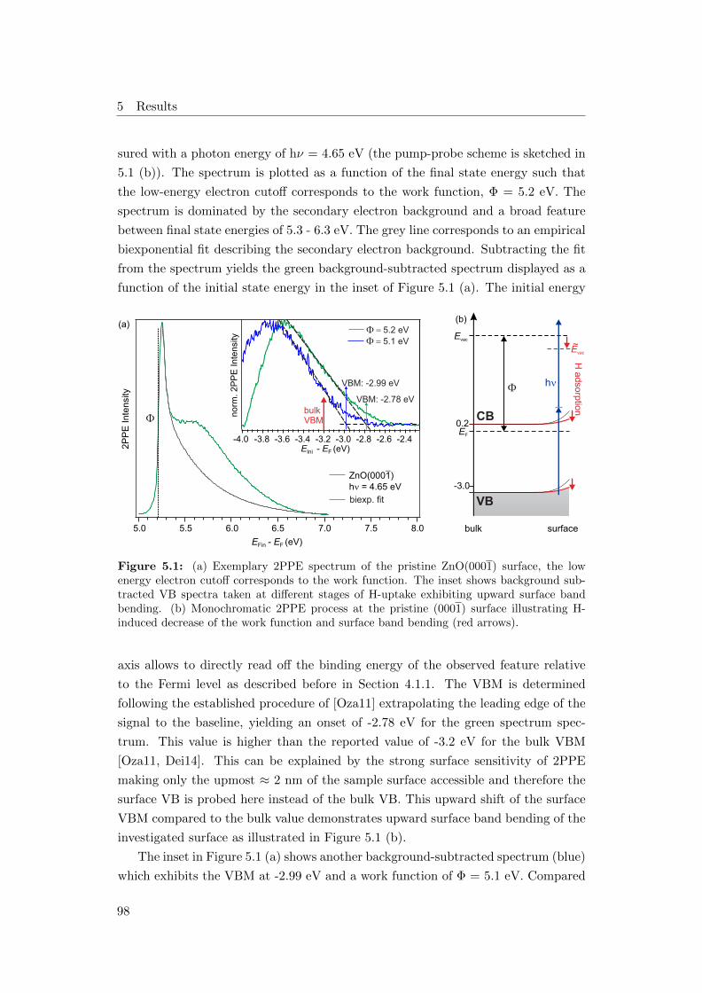
5 Results
sured with a photon energy of hν = 4.65 eV (the pump-probe scheme is sketched in
5.1 (b)). The spectrum is plotted as a function of the final state energy such that
the low-energy electron cutoff corresponds to the work function, Φ = 5.2 eV. The
spectrum is dominated by the secondary electron background and a broad feature
between final state energies of 5.3 - 6.3 eV. The grey line corresponds to an empirical
biexponential fit describing the secondary electron background. Subtracting the fit
from the spectrum yields the green background-subtracted spectrum displayed as a
function of the initial state energy in the inset of Figure 5.1 (a). The initial energy
7.06.56.05.55.0 7.5 8.0
2P
PE
Inte
nsi
ty
-4.0 -3.8 -3.6 -3.4 -3.2 -3.0 -2.8 -2.6 -2.4
no
rm.
2P
PE
In
ten
sity
5.1 eV
5.2 eV
VBM: -2.99 eV
VBM: -2.78 eV
E - E (eV)Ini F
bulkVBM
VB
EF
Evac
CB0.2
-3.0
h
bulk surface
(b)
H a
dsorp
tion
Evac
~
(a)
ZnO(0001)h = 4.65 eV
E - E (eV)Fin F
biexp. fit
Figure 5.1: (a) Exemplary 2PPE spectrum of the pristine ZnO(0001) surface, the lowenergy electron cutoff corresponds to the work function. The inset shows background sub-tracted VB spectra taken at different stages of H-uptake exhibiting upward surface bandbending. (b) Monochromatic 2PPE process at the pristine (0001) surface illustrating H-induced decrease of the work function and surface band bending (red arrows).
axis allows to directly read off the binding energy of the observed feature relative
to the Fermi level as described before in Section 4.1.1. The VBM is determined
following the established procedure of [Oza11] extrapolating the leading edge of the
signal to the baseline, yielding an onset of -2.78 eV for the green spectrum spec-
trum. This value is higher than the reported value of -3.2 eV for the bulk VBM
[Oza11, Dei14]. This can be explained by the strong surface sensitivity of 2PPE
making only the upmost ≈ 2 nm of the sample surface accessible and therefore the
surface VB is probed here instead of the bulk VB. This upward shift of the surface
VBM compared to the bulk value demonstrates upward surface band bending of the
investigated surface as illustrated in Figure 5.1 (b).
The inset in Figure 5.1 (a) shows another background-subtracted spectrum (blue)
which exhibits the VBM at -2.99 eV and a work function of Φ = 5.1 eV. Compared
98

5.1 H-induced Metallicity and Excited State Dynamics at the O-terminated ZnOSurface
to the green spectrum the work function of the blue spectrum is 0.1 eV lower while
the VBM is shifted down by 0.21 eV. The two spectra were taken on ZnO surfaces
with different degrees of H-doping due to adsorption of residual hydrogen in the
UHV chamber. The green spectrum was taken on the pristine surface directly after
preparation, while the blue spectrum corresponds to the pristine surface ≈ 1.5 h
after the preparation. The residual hydrogen in the UHV chamber is sufficient to
dope the ZnO surface with a dosage of ≈ 0.01 L per hour and was used here in order
to dope the polar surface with hydrogen. The observed work function and VBM
shift illustrate nicely that already small amounts of hydrogen significantly lower the
surface potential what leads to a work function decrease and countervails the upward
surface band bending as depicted in 5.1 (b). Ozawa et al. observed the VBM on
the clean ZnO(0001) surface at -2.9 eV, which compares very well with our findings
[Oza11].
100 L H /ZnO(0001)2
hν = 6.2 eV
CAL
VO/OH
z
EF
Evac
CB
Evac
~H-doping
VO/OH-1.4
ʹ
0.50.0-0.5-1.0-1.5-2.0
PE
In
ten
sity
(a)
E - E (eV)Ini F
VB
hν
z
EF
CB
VO/OH-1.4
CAL
VB
hν
(b) clean surface (c) H-doped surface
VB
Figure 5.2: (a) Direct photoemission spectrum of 100 L H2/ZnO(0001) showingan additional feature at -1.4 eV which can be related to an O- or OH-defect state,(b) energy level diagram of the pristine and (c) the H-doped ZnO(0001) surfaceillustrating the inverse surface band bending and the work function decrease dueto H2 adsorption which makes it possible to probe the defect state.
For H2-dosages ≥ 60 L two occupied states have been measured in direct pho-
toemission. Figure 5.2 (a) shows a spectrum (grey) of a 100 L dosage hydrogen on
ZnO(0001) measured with hν = 6.2 eV. The corresponding background subtracted
spectrum (dark red) clearly exhibits two peaks, one close to EF (CAL) and one lo-
cated at -1.4 eV relative to the Fermi level, denoted VO/OH. Both lie within the band
gap of ZnO, but have very different origin, as will be debated below. As discussed
in Section 3.1.1, in gap states are a common feature of ZnO crystals and result from
different types of defects. For example O- and OH-vacancies were found to be lo-
cated 1.8 eV above the VBM, i.e. 1.6 eV below the CBM, in a theoretical study
[Fin06]. Experimental evidence has been given by luminescence ≈ 1.8 eV below the
99

5 Results
CBM [Fog15]. It can, thus, be concluded that the feature at a binding energy of
-1.4 eV is due to photoemission from a defect state, either an O- or OH-vacancy.
It should be noted that this feature can only be detected in direct photoemission
when the work function of the sample is sufficiently low as illustrated in Figures 5.2
(b) and (c): (b) shows an energy level diagram of the pristine surface, where the
defect state cannot be probed with 6.2 eV since the work function is too high. In
Figure 5.2 (c) the energy level diagram of the H-doped surface is depicted: The work
function is reduced significantly, since the OH-bonds formed at the surface reduce
the surface dipole, and even lead to downward surface band-bending. Now the work
function is low enough so that electrons from the defect state can be photoemitted
with a photon energy of 6.2 eV. For the non-polar (1010) surface this feature could
not be observed clearly, maybe because this surface is less susceptible towards de-
fect states and contains only half the amount of oxygen compared the polar surface,
what might decrease the dominance of O-related defect states. The second feature,
directly below the Fermi level, is very sensitive to hydrogen adsorption and will be
discussed below.
In order to investigate the influence of hydrogen on the electronic surface struc-
ture of the polar ZnO surface, the H-dosage has been varied systematically. Figure
5.3 (a) shows a series of direct photoemission spectra taken with hν = 6.2 eV for
different H2-dosages. The spectra are plotted as a function of the initial state energy,
PE
In
ten
sity
0 7 10 20 60 100 190 500
(a) H /ZnO(0001), hv = 6.2 eV
4.5
4.0
3.5
3.0
2.5
2.0
1.5
1.0
0.5
0.0
CA
L In
tensity (a
rb. u
nits)
160012008004000H2 Dosage (L)
5.2
5.0
4.8
4.6
4.4
4.2
4.0
3.8
3.6
CAL intensity
_H2 dosage (L)
Work
Funct
ion (
eV
)
work function
(b)
E - E (eV)Ini F
2
-0.8 -0.6 -0.4 -0.2 0.0 0.2
biexp. fit
Figure 5.3: (a) Direct photoemission spectra for different hydrogen coverages monitoringthe build-up of the CAL at the ZnO(0001) surface, (b) CAL intensity increase and workfunction decrease as function of the H2-dosage.
thus the Fermi level corresponds to 0 eV on this axis. Clearly the signal right below
the Fermi level emerges with increasing H2-dosage with its maximum around -0.2
eV. Analogous to previous studies this signal is assigned to the metallic surface state
or CAL [Oza11, Kun03]. Analysis of the CAL intensity as a function of hydrogen
dosage shows an increase up to a coverage of ≈ 500 L where it saturates (Figure
100

5.1 H-induced Metallicity and Excited State Dynamics at the O-terminated ZnOSurface
5.3 (b)). Concurrent with the CAL intensity increase the work function decreases
rapidly during the first 500 L of H2-dosage and saturates at a work function of 3.6
eV with a maximal decrease of ∆Φmax = 1.6 eV. Both effects, the CAL forma-
tion and the work function change, can be rationalized by considering the following
consequences of H-adsorption:
(i) H-adsorption leads to the formation of polar hydroxyl-bonds, in which
hydrogen has a positive and oxygen a negative partial charge,
(ii) this decreases the surface dipole
(iii) thus leading to a work function decrease and downward surface
band bending of the CBM below the Fermi level
(iv) this in turn permits the electrons, donated by the hydrogen, to settle
at the CBM which is bent below the Fermi level.
These effects of H-doping on the electronic structure of the O-terminated ZnO surface
are qualitatively very similar to the behaviour observed for H-doping of the non-polar
ZnO(1010) surface. However, as discussed in Section 3.1.2, some distinct differences
in the behaviour towards H-adsorption are expected for the polar ZnO surface:
1. A larger work function shift, and thus a stronger decrease of the surface dipole,
is expected for the polar surface due to the absence of Zn-ions.
2. The saturation of the work function is expected at higher H2-dosages due to
the higher oxygen density at the polar surface.
3. The CAL intensity is expected to saturate instead of decreasing for higher H-
coverages since ZnH-bond formation, which potentially countervail the effects
of the OH-bonds, should not occur on the polar surface.
To compare the behaviour of the non-polar ZnO(1010) surface with the polar (0001)
surface towards H-adsorption, the work functions and the CAL intensities of both
surfaces are plotted as a function of the H2-dosage in Figure 5.4 (a). While the work
function of the non-polar surface (green triangles, adapted from [Dei15b]) decreases
from 4.45 eV to 3.8 eV with a maximal shift of ∆Φmax = - 0.65 eV the work function
of the polar surface (grey triangles) undergoes a reduction from 5.2 - 3.6 eV and thus
a total work function shift of ∆Φmax = -1.6 eV upon H-adsorption. This yields a 0.95
eV larger total work function shift for the O-terminated ZnO surface with respect
to the non-polar surface, confirming thus the first expectation.
Taking a closer look at the evolution of the work functions of the two different
surfaces as a function of the H2-dosage, reveals that the work function of the non-
polar surface saturates at H2-dosages around 500 L. In contrast the work function
of the polar ZnO surface saturates at hydrogen dosages of ≈ 1000 L, i.e. about the
101
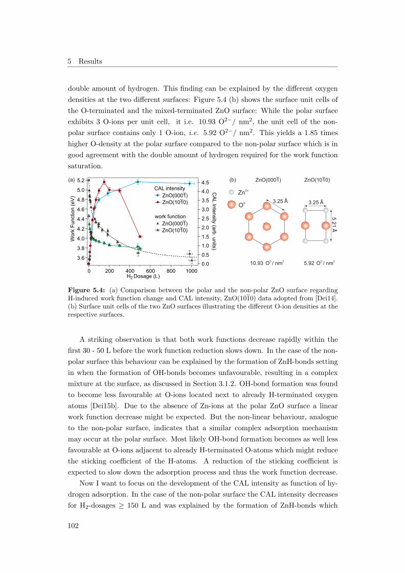
5 Results
double amount of hydrogen. This finding can be explained by the different oxygen
densities at the two different surfaces: Figure 5.4 (b) shows the surface unit cells of
the O-terminated and the mixed-terminated ZnO surface: While the polar surface
exhibits 3 O-ions per unit cell, it i.e. 10.93 O2−/ nm2, the unit cell of the non-
polar surface contains only 1 O-ion, i.e. 5.92 O2−/ nm2. This yields a 1.85 times
higher O-density at the polar surface compared to the non-polar surface which is in
good agreement with the double amount of hydrogen required for the work function
saturation.
4.5
4.0
3.5
3.0
2.5
2.0
1.5
1.0
0.5
0.0
CA
L In
ten
sity (arb
. un
its)
10008006004002000H2 Dosage (L)
5.2
5.0
4.8
4.6
4.4
4.2
4.0
3.8
3.6
Wo
rk F
un
ctio
n (
eV
) ZnO(0001)
CAL intensity
ZnO(1010)
_
_
ZnO(0001)
work function
ZnO(1010)
_
_
2+Zn
2-O
5.2
1 A
°
ZnO(0001) ZnO(1010) (a) (b)
10.93 / nm2-O
2
3.25 A °3.25 A °
5.92 / nm2-O
2
Figure 5.4: (a) Comparison between the polar and the non-polar ZnO surface regardingH-induced work function change and CAL intensity, ZnO(1010) data adopted from [Dei14].(b) Surface unit cells of the two ZnO surfaces illustrating the different O-ion densities at therespective surfaces.
A striking observation is that both work functions decrease rapidly within the
first 30 - 50 L before the work function reduction slows down. In the case of the non-
polar surface this behaviour can be explained by the formation of ZnH-bonds setting
in when the formation of OH-bonds becomes unfavourable, resulting in a complex
mixture at the surface, as discussed in Section 3.1.2. OH-bond formation was found
to become less favourable at O-ions located next to already H-terminated oxygen
atoms [Dei15b]. Due to the absence of Zn-ions at the polar ZnO surface a linear
work function decrease might be expected. But the non-linear behaviour, analogue
to the non-polar surface, indicates that a similar complex adsorption mechanism
may occur at the polar surface. Most likely OH-bond formation becomes as well less
favourable at O-ions adjacent to already H-terminated O-atoms which might reduce
the sticking coefficient of the H-atoms. A reduction of the sticking coefficient is
expected to slow down the adsorption process and thus the work function decrease.
Now I want to focus on the development of the CAL intensity as function of hy-
drogen adsorption. In the case of the non-polar surface the CAL intensity decreases
for H2-dosages ≥ 150 L and was explained by the formation of ZnH-bonds which
102
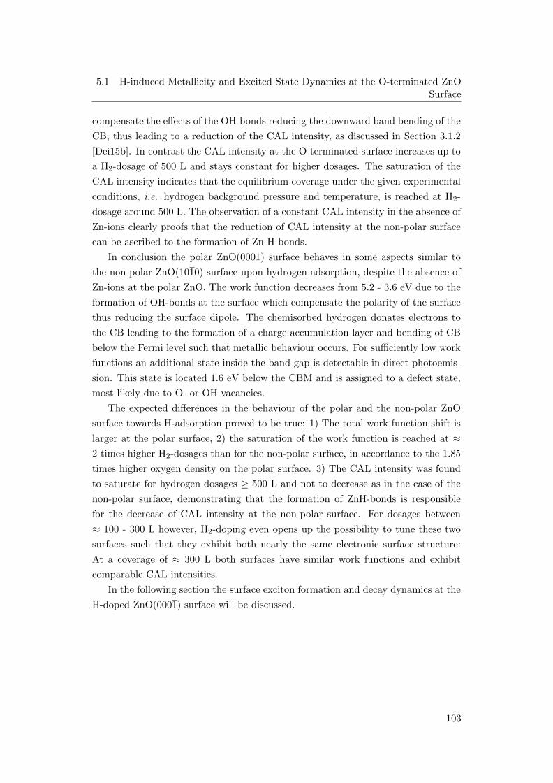
5.1 H-induced Metallicity and Excited State Dynamics at the O-terminated ZnOSurface
compensate the effects of the OH-bonds reducing the downward band bending of the
CB, thus leading to a reduction of the CAL intensity, as discussed in Section 3.1.2
[Dei15b]. In contrast the CAL intensity at the O-terminated surface increases up to
a H2-dosage of 500 L and stays constant for higher dosages. The saturation of the
CAL intensity indicates that the equilibrium coverage under the given experimental
conditions, i.e. hydrogen background pressure and temperature, is reached at H2-
dosage around 500 L. The observation of a constant CAL intensity in the absence of
Zn-ions clearly proofs that the reduction of CAL intensity at the non-polar surface
can be ascribed to the formation of Zn-H bonds.
In conclusion the polar ZnO(0001) surface behaves in some aspects similar to
the non-polar ZnO(1010) surface upon hydrogen adsorption, despite the absence of
Zn-ions at the polar ZnO. The work function decreases from 5.2 - 3.6 eV due to the
formation of OH-bonds at the surface which compensate the polarity of the surface
thus reducing the surface dipole. The chemisorbed hydrogen donates electrons to
the CB leading to the formation of a charge accumulation layer and bending of CB
below the Fermi level such that metallic behaviour occurs. For sufficiently low work
functions an additional state inside the band gap is detectable in direct photoemis-
sion. This state is located 1.6 eV below the CBM and is assigned to a defect state,
most likely due to O- or OH-vacancies.
The expected differences in the behaviour of the polar and the non-polar ZnO
surface towards H-adsorption proved to be true: 1) The total work function shift is
larger at the polar surface, 2) the saturation of the work function is reached at ≈2 times higher H2-dosages than for the non-polar surface, in accordance to the 1.85
times higher oxygen density on the polar surface. 3) The CAL intensity was found
to saturate for hydrogen dosages ≥ 500 L and not to decrease as in the case of the
non-polar surface, demonstrating that the formation of ZnH-bonds is responsible
for the decrease of CAL intensity at the non-polar surface. For dosages between
≈ 100 - 300 L however, H2-doping even opens up the possibility to tune these two
surfaces such that they exhibit both nearly the same electronic surface structure:
At a coverage of ≈ 300 L both surfaces have similar work functions and exhibit
comparable CAL intensities.
In the following section the surface exciton formation and decay dynamics at the
H-doped ZnO(0001) surface will be discussed.
103

5 Results
5.1.2 Surface Exciton Formation and Decay Dynamics at the H-
doped Polar ZnO Surface
In this section it is shown that it is possible to generate surface excitons at the polar
ZnO surface. The dynamics of SX formation will be discussed with regard to the
ultrafast relaxation dynamics of the hot electrons and the influence of the photo- and
H-induced carrier density. Moreover the obtained time constants will be compared
with the results of a theoretical study and the findings at non-polar surface.
Δt = 50 fs
equilibriumsignal
pump inducedsignal
CAL
2P
PE
Inte
nsi
ty
0.40.20.0-0.2-0.4
h = 4.65 eVh = 3.8 eV
probe
pump
1.5
(Δt = -30 ps)
100 L H /ZnO(0001)2
E − E (eV)Int F
Figure 5.5: 2PPE spectra of the H-dopedpolar ZnO surface, the signal below EF (0 eV)originates from the CAL. The pump-inducedsignal (grey coloured area, red spectrum) isthe difference between the equilibrium spec-trum (blue) and the spectrum after above gapexcitation (grey).
In a time-resolved 2PPE experiment
a transient electron population in an in-
termediate state is generated by pho-
toexcitation with a first laser pulse and
is probed after a time delay by a sec-
ond pulse as described in Section 4.5.
Figure 5.5 displays static 2PPE spectra
of 100 L H2/ZnO(0001) as a function
of the intermediate state energy, which
were taken at different time delays with
3.8 and 4.65 eV. As both photon en-
ergies can excite the sample above the
band gap and also photoemit excited
electrons, positive delays describe here
excitation with a pump photon energy
of hνpump = 3.8 eV and probing with
hνprobe = 4.65 eV, for negative delays the pump-probe scheme works vice versa.
The blue spectrum was taken at a time delay of -30 ps under equilibrium conditions
and is therefore used as background spectrum. The grey spectrum was recorded at
a time delay of +50 fs and contains the pump-induced signal, which is presented by
the grey coloured area. Subtracting the blue background spectrum form the grey
spectrum yields the red difference spectrum, showing only the pump-induced signal.
The signal below EF (0 eV) originates from the CAL.
Figure 5.6 (a) shows an exemplary time-resolved 2PPE spectrum of a 100 L
H2-dosage on ZnO(0001) measured with 3.8 eV and 4.65 eV. The photoemission
intensity is plotted in false colours as a function of the intermediate state energy
(left) and the pump-probe delay (bottom). In order to obtain exclusively the pump-
induced signal the background spectrum taken at a negative delay of -30 ps, shown
in Figure 5.5, was subtracted from the depicted spectrum.
The background subtracted signal exhibits a fast reduction of phoemission in-
tensity at energies between ≈ 0.65 - 0.2 eV which slows down for lower energies. A
104
5.1 H-induced Metallicity and Excited State Dynamics at the O-terminated ZnOSurface
XC : 0.5 - 0.6 eVA
XC : 0.20 - 0.24 eVB
XC : 0.04 - 0.08 eVC
XC : -0.1 - 0.0 eVX
-210
-110
1
pulse XC
2P
PE
Inte
nsity (a
rb. u
nits)
1.51.00.50Pump-Probe Delay (ps)
(b)
XCA
XCB
XCC
XCx2 X
1 h
0.8
0.6
0.4
0.2
0.0
2.82.42.01.61.20.80.40.0Pump-Probe Delay (ps)
E - E
(e
V)
Int
F
(a)0 1
norm. intensity (arb. u.)
hv = 3.8 eVpump
hv = 4.65 eVprobe
100 L H /ZnO(0001)2
Figure 5.6: (a) Time-resolved 2PPE spectrum of 100 L H2/ZnO(000-1) showing fast elec-tron relaxation dynamics for energies above ≈ 0.1 eV and pump-induced electron densitybuild-up below EF (Eint = 0 eV). (b) XC traces for energies above EF, (grey dots) show(1) ultrafast relaxation of the above band gap excited electrons via phonon scattering andformation of a long-lived state. The XC below EF (red diamonds) shows the bulid up ofadditional photoelectron intensity (2) which is related to the formation of a surface exciton.
long-lived state is formed just at the Fermi level which shifts even below the Fermi
level for longer time delays. This behaviour is very similar to the dynamics observed
by Deinert et al. at the H-doped non-polar ZnO surface, who assigned this long-lived
signal to a surface excitonic state [Dei14]. Therefore I will refer to this state as SX
in the following and will discuss it in detail below.
To obtain quantitative insights into the observed excited state dynamics the
time-resolved spectrum was integrated over several energetic ranges as indicated by
the grey and red boxes yielding the corresponding XC traces shown in Figure 5.6 (b).
The XC traces are plotted logarithmically as a function of the pump-probe delay
and are offset for clarity. The green dashed line illustrates the XC of the laser pulses
which have an average duration of 70 fs. The cross-correlation trace A (0.5 - 0.6 eV)
shows nearly exclusively the fast decay, although all XC traces possess a long-lived
component. XC B was obatined by integration between intermediate state energies
of 0.20 -0.24 eV and already clearly exhibits the slowing down of the fast component.
This behaviour becomes more intense for lower energies, as demonstrated by XC C
(0.04 - 0.08 eV), which indicates as well the relaxation into the long-lived state.
Integrating the time-resolved spectrum below the Fermi level yields the red XC
trace which differs significantly from the ones obtained by integration at energies
above EF: For positive delays the intensity increases with τX until it saturates at
time delays around 1 ps. Assuming that the long-lived state originates from the
surface exciton this rise in intensity corresponds to the build-up of the excitonic
population below EF on a timescale of a few hundred fs. The dynamics at negative
delays corresponds here to the hot electron dynamics pumped and probed by the
105

5 Results
inverted pump-probe process.
In order to fit the grey coloured XC traces the following considerations were
taken into account:
The 2PPE instensity I2PPE as a function of the pump-probe delay is yielded by
integration
I2PPE(∆t) ∝∫dt FXC(t−∆t) R(t) (5.51)
where FXC denotes the cross correlation of the two laser pulses, described by sech2
pulse envelopes (indicated by the green dashed line in Figure 5.6 (b)), and R(t)
the response function of the system. The response function R(t) for positive delays
consists of a phenomenological biexponential decay describing the decay of the hot
electron population in the CB and the lifetime of the long-lived SX
R(t ≥ 0) = A e−tτ1 +B e
−tτ2 (5.52)
For negative delays the response function is described by the single exponential decay
of the hot electrons excited by the reversed pump-probe scheme
R(t < 0) = C etτ3 (5.53)
The biexponential fit yields a fast time constant τ1 and a slow time constant τ2. The
fast time constant can be related to the ultrafast relaxation of the above band gap
excited electrons.
As discussed in Section 3.1.3 hot electrons in polar semiconductors such as ZnO
relax mainly via two mechanisms, electron-electron scattering and electron-phonon
scattering which take place on different time scales. Electron-electron scattering
can be excluded due to the low electron density in the CB, resulting from the rather
low excitation density (2.86 ×1018 cm−3) employed in this experiment, thus electron-
phonon scattering is very efficient. This finding is in good agreement with the strong
coupling of electrons with LO phonons in ZnO, well known from literature, both
theoretically and experimentally as discussed in Section 3.1.3 [Tis08, Dei14, Zhu10].
The slow time constant τ2 can be attributed to the lifetime of the long-lived
surface exciton, which shows residual intensity even at higher energies and does
not decay within the measured 300 ps, thus possessing a lifetime of at least several
hundred ps.
In order to analyse the ultrafast relaxation of the photoexcited electrons quan-
titatively, the fast time constant τ1 (red dots) obtained from the biexponential fit
is plotted as a function of the intermediate state energy in Figure 5.7 (a) and is
compared to the values calculated by Zhukov et al. [Zhu10]. The dynamics of the
106

5.1 H-induced Metallicity and Excited State Dynamics at the O-terminated ZnOSurface
bulk band
gap
bulkCB
h
EF
CB−
− 1
X
(b)800
700
600
500
400
300
200
100
0
0.60.40.20.0
bulk ZnO (Zhukov et al.)
100 L H /ZnO(0001)2
E - E (eV)Int F
(
fs)
1
0.50.30.1
(a)
Figure 5.7: a) Comparison of the measured fast time constants (red)with calculated values (black) from ref. [Zhu10] plotted as a function ofthe intermediate state energy. b) Schematic illustration of the energy-dependent evolution of the relaxation times (green dashed line) prior toSX formation.
hot electrons in the CB is extremely fast (10 - 95 fs) at energies ≥ 0.2 eV, i.e. for
excitation above the bulk CBM, and slows significantly down towards lower energies.
Comparable time constants were observed before by Tisdale it et al. and Deinert
et al. for above gap excitation of the mixed-terminated ZnO surface who explained
the slowing down of the dynamics for lower energies by the reduction of the phonon
phase space [Tis08, Dei14]. Comparison to the calculated lifetimes show that the
experimentally derived data compares fairly well in the high energy region down
to ≈ 0.22 eV while they diverge for lower energies. The calculated values increase
rapidly up to ≈ 1 ps for energies close to the bulk CBM while the experimentally
derived time constant slows down to ≈ 400 fs close to the Fermi level. This differ-
ent behaviour is due to the different preconditions of calculation and experiment:
The calculation was performed for bulk ZnO while the experiment was conducted
on the H-doped polar ZnO surface with a highly surface sensitive method. In the
case of bulk ZnO the electrons at the CBM have no excess energy left to scatter
with phonons, leading thus to an increase of their lifetime. In our experiment the
situation is different since the surface CBM is not at 0.2 eV but is bent below the
Fermi level,as illustrated in Figure 5.7 (b). Therefore the phonon-mediated relax-
ation of the excited electrons is still possible at lower energies, which explains the
slower increase of the time constant down to the Fermi level.
The formation of an intermediate electron population below the Fermi level is
an unusual behaviour since usually the electronic levels are filled up to the Fermi
level such that no additional pump induced density of states (DOS) can be gener-
107
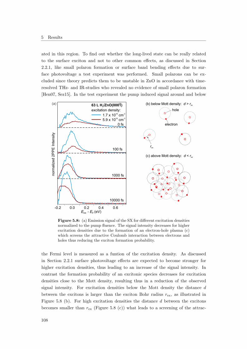
5 Results
ated in this region. To find out whether the long-lived state can be really related
to the surface exciton and not to other common effects, as discussed in Section
2.2.1, like small polaron formation or surface band bending effects due to sur-
face photovoltage a test experiment was performed. Small polarons can be ex-
cluded since theory predicts them to be unstable in ZnO in accordance with time-
resolved THz- and IR-studies who revealed no evidence of small polaron formation
[Hen07, Sez15]. In the test experiment the pump induced signal around and below
0.60.40.20.0-0.2
0 fs
100 fs
1000 fs
10000 fs
63 L H /ZnO(0001) 2
excitation density:18 -31.7 x 10 cm18 -35.9 x 10 cm
(a)
norm
aliz
ed 2
PP
E Inte
nsi
ty
E - E (eV)Int F
_
(c) above Mott density: d < rex
electron
hole
(b) below Mott density: d > rex
rex
Figure 5.8: (a) Emission signal of the SX for different excitation densitiesnormalized to the pump fluence. The signal intensity decreases for higherexcitation densities due to the formation of an electron-hole plasma (c)which screens the attractive Coulomb interaction between electrons andholes thus reducing the exciton formation probability.
the Fermi level is measured as a funtion of the excitation density. As discussed
in Section 2.2.1 surface photovoltage effects are expected to become stronger for
higher excitation densities, thus leading to an increase of the signal intensity. In
contrast the formation probability of an excitonic species decreases for excitation
densities close to the Mott density, resulting thus in a reduction of the observed
signal intensity. For excitation densities below the Mott density the distance d
between the excitons is larger than the exciton Bohr radius rex, as illustrated in
Figure 5.8 (b). For high excitation densities the distance d between the excitons
becomes smaller than rex (Figure 5.8 (c)) what leads to a screening of the attrac-
108

5.1 H-induced Metallicity and Excited State Dynamics at the O-terminated ZnOSurface
tive Coulomb interaction between electrons and holes thus reducing the exciton
formation probability. In the test experiment the excitation density is varied by
changing the fluence of the pump pulse. The obtained spectra clearly demonstrate
the characteristic behaviour of excitons: Figure 5.8 shows the photoemission signal
attributed to the surface exciton for an excitation density in the lower Mott density
region (1.7×1018 cm−3, blue) and for a higher excitation density (5.9×1018 cm−3,
purple) plotted as a function of the intermediate state energy. The signal inten-
sity is normalized to the excitation density and is shown for different time delays.
VB
EF
Evac
hpump
−
CB −
h
−
SX
X
1
2
Evac
~
H-termination
E
z
Figure 5.9: Illustration of the rele-vant processes taking place after pho-toexcitation of the H-doped polarZnO surface, modified from [Dei14].hνpump photoexcites electrons fromthe VB above the CBM which re-lax (1) via electron-phonon scatter-ing and (2) surface exciton forma-tion.
The signal derived from the low excitation den-
sity (blue) is more intense than the one obtained
from the higher excitation density (purple). This
demonstrates explicitly that the formation prob-
ability of the excitons is reduced by the forma-
tion of an electron-hole plasma which screens the
attractive Coulomb interaction between electron
and hole. Moreover this finding is in accordance
with the results of Deinert et al. for the H-doped
non-polar ZnO surface [Dei14].
Figure 5.9 summarizes the relevant electronic
processes observed after photoexciting the H-
doped polar ZnO surface above the band gap.
The observed processes and dynamics are com-
parable to the ones found for the H-doped non-
polar ZnO surface: Electrons are photoexcited
from the VB above the band gap into the CB
where they undergo very efficient scattering with
phonons (1) before long-lived surface excitons
are formed (2).
In order to quantitatively compare the ul-
trafast relaxation dynamics of the excited elec-
trons at the H-doped polar surface with the dynamics observed at the non-polar
surface, the time constants obtained for a dosage of 100 L H2 on both sur-
faces are plotted as a function of the intermediate state energy in Figure 5.10.
This coverage was chosen, as outlined in Section 5.1.1, because at a H2-dosage of
100 L the CAL intensity is comparable for both surfaces. The red data points
correspond to the time constants obtained for the H-doped polar surface and the
green ones to the time constants obtained for the non-polar surface. The results
compare well, although for a H2-dosage of 100 L already ZnH-bond formation has set
109

5 Results
in on the non-polar surface and despite the different work functions of the investigates
samples the electron dynamics are in good accordance. This observation leads to
the conclusion that the ultrafast relaxation of the hot electrons in the CB is not,
or very weakly, affected by the surface potential. This can be explained by the
relaxation mechanism of the electrons: they couple via Frohlich interaction with LO
phonons, i.e. vibrations of the lattice in which the Zn- and O-ions move in opposite
directions. This motion of the ions induces a stronger electric field compared to the
compensating polarization of the surrounding electrons, thus leading to a long range
interaction between the excited electrons and LO phonons [Tis08].
400
300
200
100
0
0.60.50.40.30.20.10.0
(
fs)
1
E - E (eV)Int F
100 L H /ZnO(0001)2
100 L H /ZnO(1010)2
bulk CB
Figure 5.10: Comparison of the fast timeconstant τ1 of 100 L H2 on the (0001) and the(1010) surfaces.
To evaluate the influence of the to-
tal charge carrier density (photo- and H-
induced) on the relaxation dynamics the
fast time constants, derived from mea-
surements with varying excitation den-
sities and H-coverages on the non-polar
ZnO surface, are compared in Figure
5.11. The total charge carrier density is
calculated by summing up the photoin-
duced carrier density, i.e. the excitation
density, and the H-induced carrier den-
sity in the CAL. The latter is estimated
according to the maximal surface charge
density of 1013 cm−2 [Oza11], which is
related to the CAL intensity maximum
at a H2-dosage of 150 L, and a CAL thickness of 1 nm. This yields for a H2-dosage
of 150 L an electron density of 1020 cm−3 in the CAL. Figure 5.11 (a) displays
the fast time constants as a function of intermediate state energy of two data sets
recorded with a pump photon energy of 3.8 eV for different total carrier densities in
the upper Mott regime. For energies above 0.2 eV the time constants diverge only
within the error such that no conclusion can be drawn. For lower energies, however,
the time constants measured for a total carrier density of 6.8 × 1019 cm−3 (green),
which is above the critical carrier density of 1019 cm−3 [Tis08], slow down compared
to the time constants obtained for the lower carrier density (red). This slowing
down of the relaxation dynamics demonstrates that the scattering of low energetic
hot electrons with acoustic phonons is screened by the enhanced carrier density. In
Figure 5.11 (b) the time constants derived from 2PPE measurements with a pump
photon energy of 3.8 eV are compared to time constants adopted from Deinert et
al. [Dei15b] which were gained using a pump photon energy of 4.2 eV. These time
110
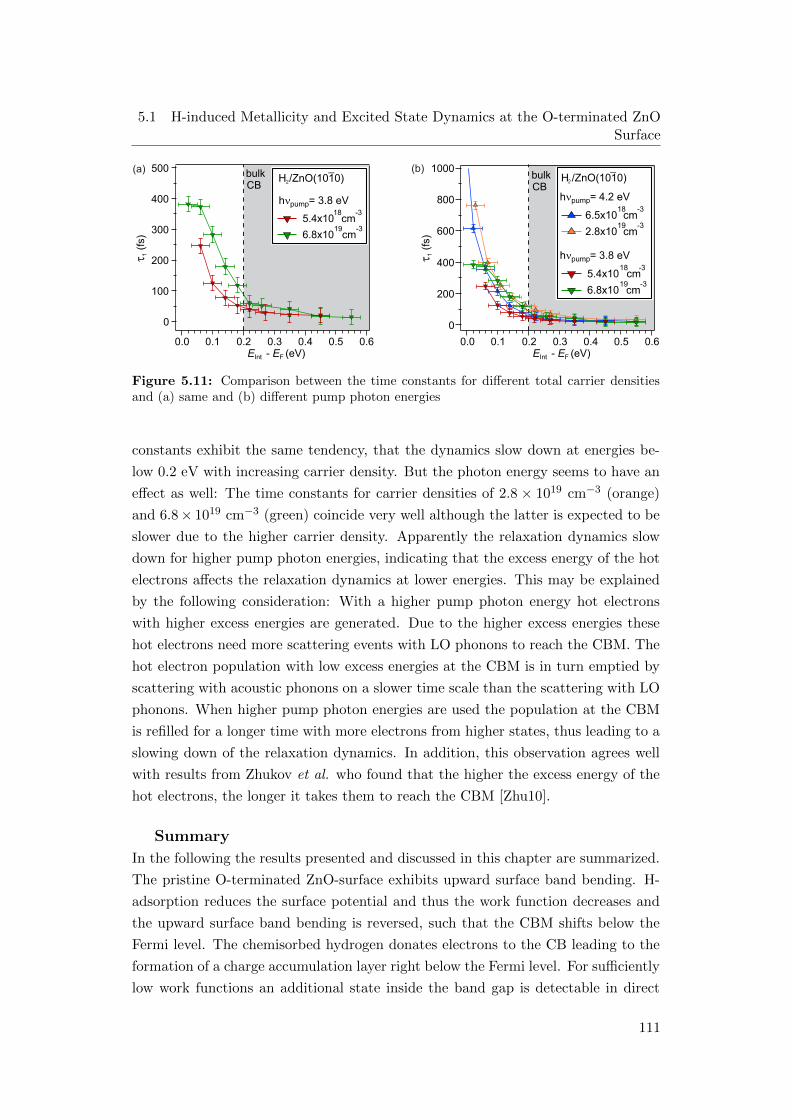
5.1 H-induced Metallicity and Excited State Dynamics at the O-terminated ZnOSurface
500
400
300
200
100
0
0.60.40.20.0 0.1 0.3 0.5E - E (eV)Int F
(
fs)
1
1000
800
600
400
200
0
0.60.40.20.0 0.1 0.3 0.5E - E (eV)Int F
(
fs)
1
bulk CB
bulk CB
5.4x10¹⁸
cm-3
6.8x10¹⁹
cm-3
H /ZnO(1010)_
2
hpump= 3.8 eV
H /ZnO(1010)
hpump= 4.2 eV
6.5x1018cm
-3
2.8x1019cm
-3
hpump= 3.8 eV
5.4x10¹⁸
cm-3
6.8x10¹⁹
cm-3
_2
(a) (b)
Figure 5.11: Comparison between the time constants for different total carrier densitiesand (a) same and (b) different pump photon energies
constants exhibit the same tendency, that the dynamics slow down at energies be-
low 0.2 eV with increasing carrier density. But the photon energy seems to have an
effect as well: The time constants for carrier densities of 2.8 × 1019 cm−3 (orange)
and 6.8× 1019 cm−3 (green) coincide very well although the latter is expected to be
slower due to the higher carrier density. Apparently the relaxation dynamics slow
down for higher pump photon energies, indicating that the excess energy of the hot
electrons affects the relaxation dynamics at lower energies. This may be explained
by the following consideration: With a higher pump photon energy hot electrons
with higher excess energies are generated. Due to the higher excess energies these
hot electrons need more scattering events with LO phonons to reach the CBM. The
hot electron population with low excess energies at the CBM is in turn emptied by
scattering with acoustic phonons on a slower time scale than the scattering with LO
phonons. When higher pump photon energies are used the population at the CBM
is refilled for a longer time with more electrons from higher states, thus leading to a
slowing down of the relaxation dynamics. In addition, this observation agrees well
with results from Zhukov et al. who found that the higher the excess energy of the
hot electrons, the longer it takes them to reach the CBM [Zhu10].
Summary
In the following the results presented and discussed in this chapter are summarized.
The pristine O-terminated ZnO-surface exhibits upward surface band bending. H-
adsorption reduces the surface potential and thus the work function decreases and
the upward surface band bending is reversed, such that the CBM shifts below the
Fermi level. The chemisorbed hydrogen donates electrons to the CB leading to the
formation of a charge accumulation layer right below the Fermi level. For sufficiently
low work functions an additional state inside the band gap is detectable in direct
111
5 Results
photoemission. This state is located 1.6 eV below the CBM and is assigned to a
defect state, most likely due to O- or OH-vacancies.
The polar ZnO surface behaves towards H-doping in some aspects qualitatively
very similar to the non-polar surface, despite the absence of Zn-ions and the lower
stability. For example, both surfaces exhibit a reduction of the work funcntion
and the formation of a CAL due to band bending below the Fermi level. But
quantitatively there are distinct differences, such as the signficantly higher total
work function decrease at the polar ZnO surface and the saturation of the CAL
intensity for H2-dosages above 500 L. This proofs that the formation of ZnH-bonds
at the non-polar surface is responsable for the decrease of CAL intensity for H2-
dosages higher than 150 L.
The investigation of the hot electron relaxation and SX formation and decay dy-
namics on the H-doped polar ZnO surface reveals ultrafast relaxation of the above
band gap (3.4 eV) excited electrons slowing down for lower energies, followed by the
formation of a long-lived surface excitonic feature. Measurements under variation of
the excitation density clearly demonstrate the exciton characteristic Mott physics:
the observed emission signal decreases with increasing excitation density, which leads
to a screening of the attractive Coulomb interaction between electron and hole re-
ducing thus the formation probability of excitons. The ultrafast relaxation times
are in good accordance with the calculated values by Zhukov et al. as well as with
experimentally derived results for the non-polar ZnO surface [Zhu10, Tis08, Dei14].
A comparison with the findings obtained for the H-doped non-polar surface, studied
before by Deinert el al., shows astonishing coincidence in consideration of the differ-
ent surface electronic structure and composition and morphology. This behaviour is
explained by the strong Frohlich-type interaction of electrons and phonons prevailing
over other scattering mechanisms, such as electron-electron scattering. Moreover it
was demonstrated that the relaxation dynamics of the low energetic hot electrons
slows down for high charge carrier densities screening the scattering with lower lying
phonons.
112

5.2 Exciton Formation and Decay Dynamics in SP6 Films on ZnO
5.2 Exciton Formation and Decay Dynamics in SP6 Films
on ZnO
SP6 is a promising material for applications in OLEDs and organic solid state lasers
due to its strong luminescence [Sch04b, Sch05]. The Also the SP6/ZnO interface is
attractive for the study of charge transfer from molecular excitons to the conduction
band of ZnO, as demonstrated by Blumstengel et al. [Blu08, Blu09].
In the following sections the results of our time-resolved 2PPE study of SP6 films
on the non-polar ZnO(1010) surface are presented and discussed. The ultrafast ex-
citon formation and decay dynamics are treated in Section 5.2.1. The TR-2PPE
measurements reveal an ultrafast decay on a time scale of 300 fs directly after pho-
toexcitation most likely due to polarization effects resulting from exciton formation.
In addition two slower decay times, in the range of several ps and hundreds of ps,
are observed and related to internal vibrational relaxation within the excited state
and the decay of the population in the excited state. The time scales of the two
slow processes agree surprisingly well with the values resulting from the analysis
of the transient transmission traces [Fog15]. In order to find an explanation why
photoemission and optical spectroscopy yield here the same excited state dynamics
a time-dependent diffusion model was developed and described in Section 5.2.1. It
could be shown that the charge separation at the ZnO interface has no strong in-
fluence on the dynamics in a 21 nm thick SP6 film, although optical spectroscopy
probed as well bulk contributions.
Furthermore an electron emission signal was observed which exhibits no depen-
dence on neither the photon energy nor the pulse duration. This signal could be
revealed as emission from the long-lived dark state indicated by the excited state
transmission data as described in Section 5.2.2. We were able to show with a set
of specialized time-resolved experiments that electron emission results here from
excitation energy transfer between two long-lived, most likely triplet, states in a
triplet-triplet annihilation process. In addition our 2PPE results provided the pos-
sibility to calculate the energetic positions of the ground state S0, the first excited
state S1 and the triplet state T1.
113

5 Results
5.2.1 Ultrafast Dynamics of Excited States in SP6 Films
In order to investigate the excited state dynamics and the electronic structure in SP6
films on ZnO(1010), time-resolved (TR) 2PPE measurements have been performed.
Figure 5.12 (b) shows a background subtracted time-resolved 2PPE spectrum of a
21 nm thick SP6 film on ZnO(1010) which was measured with a resonant pump
photon energy of hνpump = 3.86 eV and probed as well resonantly with hνprobe =
1.93 eV, as known from the excited states transmission data (presented in Section
3.2). The 2PPE intensity is plotted as a function of the kinetic energy (Ekin) and
the pump-probe delay. The 2PPE intensity is represented by a false colour code,
where dark blue corresponds to zero intensity and white to maximal intensity. The
maximum photoemission intensity is at the low-energy cutoff and decreases towards
higher energies. This intense 2PPE signal at the low-energy cutoff seems to exhibit
the slowest dynamics while for higher energies the dynamics seem to decrease.
5 4 3 2 10Pump-Probe Delay (ps)
30025020015010050Pump-Probe Delay (ps)
1.2
1.0
0.8
0.6
0.4
0.2
0.0
Kin
etic
Energ
y (e
V)
log. P
E In
tensity (a
rb.u
.)
0.1
1
10
0
1
2P
PE
inte
nsi
ty (
arb
. u.)
1.0 0.6 0.2norm. Intensity
(a)
bg spectrum
bg subtracted spectra at
@ -30 ps
0 t
10 ps
1.2
1.0
0.8
0.6
0.4
0.2
0.0
Kin
etic E
nerg
y (
eV
)
sec. el. bg.
DS
ultrafast 2PPE signal
0.1
1
10
log. P
E Inte
nsi
ty (
arb
.u.)
(b) 21 nm SP6/ZnO(1010)hν1 = 3.86 eVhν2 = 1.93 eV
_
XC: -0.04 - 0.19 eV
XC: 0.11 - 0.23 eV
XC: 0.63 - 0.76 eV triexponential fits
(c)
Figure 5.12: (a) Comparison of 2PPE spectra for different time delays. The intensities arenormalized to point out the 2PPE signal showing ultrafast dynamics, since the spectra aredominated by long-lived background signals: The secondary electron background (sec. el.bg.) and a signal labeled DS which will be discussed below. (Note that the photoemissionintensity of the background signals is amplified for the applied pump probe scheme and istherefore still visible in the background subtracted spectra.) (b) Background subtractedTR-2PPE spectrum of 21 nm SP6/ZnO(1010): the 2PPE intensity is plotted as a functionof the kinetic energy and the pump-probe delay. (c) Cross-correlation traces obtained fromintegrating the TR-spectrum over the energetic ranges marked by the coloured boxes in (b),the black lines correspond to triexponential fits.
114

5.2 Exciton Formation and Decay Dynamics in SP6 Films on ZnO
To take a closer look at the spectral signature vertical cuts at time delays of 0
ps (blue) and 10 ps (yellow) are plotted as a function of the kinetic energy (Figure
5.12 (a)). The spectra are compared to the background spectrum taken at -30 ps
with the reversed pump-probe scheme (i.e. 1.93 eV pumped and 3.86 eV probed)
which has been subtracted as well from the data shown in Figure 5.12 (b). All
spectra are normalized to the maximum intensity of the secondary electron back-
ground in order to emphasize the signal which exhibits ultrafast dynamics. (Note
that the photoemission intensity of the DS signal is amplified for the applied pump
probe scheme ( hνpump = 3.86 eV, hνprobe = 1.93 eV) and is thus still present after
background subtraction.) The spectra exhibit an intense photoemission intensity
at the low-energy cutoff, after a rapid intensity decrease up to Ekin ≈ 0.2 eV the
spectrum is dominated by a broad photoemission signal up to Ekin ≈ 1 eV. The
spectra are divided into three parts according to the observed features. (i) 0 - 0.15
eV: The most intense photoemission signal at the low-energy cutoff is related to the
secondary electron background (sec. el. bg.). (ii) The signal between 0.15 eV and
0.4 eV is labeled ultrafast 2PPE signal and is subject of the following analysis and
discussion.(iii) The broad feature up to 1 eV, labeled DS, will be further investigated
in the next section.
In order to gain deeper insight into the dynamics the time-resolved spectrum was
integrated over different energetic ranges, e.g. in the red, green and blue marked
energy windows, yielding the XC-traces plotted on a logarithmic intensity scale as
a function of the pump-probe delay in Figure 5.12 (c). The intensity of the XC-
traces rises on an ultrafast timescale and decreases on a timescale of a few hundred
ps. The XC traces can be described with triexponential decays convolved with
Gaussian shape pulse envelopes, shown by the black lines in Figure 5.12 (c).
IVR
(ps)
4.5
4.0
3.5
3.0
2.5
1.00.80.60.40.20.0Kinetic Energy (eV)
XF
(ps)
0.4
0.3
0.2
1.00.80.60.40.20.0Kinetic Energy (eV)
PO
P(p
s)
280
260
240
220
1.00.80.60.40.20.0Kinetic Energy (eV)
XFIVR POP(b)(a) (c)
Figure 5.13: Time constants yielded by triexponential fitting of 8 XC-traces obtained fromthe TR-2PPE spectrum of 21 nm SP6/ZnO shown in Figure 5.12 (b). The time constantsare plotted as a function of the kinetic energy and range from a time scale of several hundredfs to several hundred ps.
115

5 Results
To analyse the dynamics quantitatively as a function of the kinetic energy, the
XC-traces yielded by integrating the TR-spectrum over 8 contiguous energy windows
were fitted with the triexonential fit function. The three time constants obtained
from the fits, τXF, τIVR and τPOP, are plotted as a function of the kinetic energy in
Figure 5.13. τXF is with several hundred femtoseconds (fs) the fastest time constant.
The next slower time constant, τIVR, is in the range of a few picoseconds (ps) while
the slowest one, τPOP, is on a time scale of a few hundred ps. While τXF and τIVR
get faster for higher energies, τPOP stays almost constant up to an energy of 0.6 eV
and increases for higher energies. All three time constants exhibit a dip at a kinetic
energy of 0.8 eV.
-3.2
-4.85
-6.6
-1.7
ZnO SP6
S0
E(eV)
Evac
CB
EF
3.4
VB
S1
-3.2
-6.6
ZnO SP6
S0
E(eV)
Evac
CB
EF
3.4
VB
S1
S2
(a) Excited state transmission (b) Two-photon photoemission
3
1
2CS
ISC
FL
IVR
T1
Figure 5.14: (a) Excited state transmission probes resonances between excitedstates: The differently coloured arrows illustrate photons with different photonenergies. In addition the electronic processes observed after photoexcitation areillustrated. (b) During the probing step in 2PPE the population in the excitedstate is excited above the vacuum level by the probe pulse (red arrows) yieldingthus absolute energies.
In order to compare the 2PPE results with the time constants obtained from
excited state transmission, presented in Section 3.2, the differences of these two
methods have to be pointed out. Excited state transmission probes resonances be-
tween excited states as sketched in Figure 5.14 (a) and underlies thus the dipole
selection rules for optical transitions. The time constants obtained from excited
state transmission depend on the probe photon energy. In contrast, in a photoemis-
sion experiment electrons are emitted and thus the second transition does not have
to match a molecular resonance, as discussed before in Section 4.1.3. In the sim-
116

5.2 Exciton Formation and Decay Dynamics in SP6 Films on ZnO
plest picture, 2PPE vertically projects the electronic structure and probes thus the
absolute energies of the excited electrons as illustrated in Figure 5.14 (b). The time
constants resulting from a time-resolved 2PPE experiment depend on the kinetic
energy of the photoemitted electrons.
In order to compare the results yielded by the two different methods the same
probe photon energies have to be used. Here a probe photon energy of 1.93 eV
was used in the 2PPE measurements and thus the results can be compared with the
time constants obtained from excited state transmission at 1.94 eV. The excited state
transmission data revealed for a probe photon energy of 1.94 eV two time constants:
τIVR ≈ 4 ps and τPOP ≈ 200 ps [Fog15, Fog14]. These time constants were related
to the following processes, as illustrated in Figure 5.14 (a) and discussed before in
Section 3.2: τIVR is attributed to internal vibrational relaxation (IVR) occuring after
resonant excitation from the ground state to the first excited state within S1. τPOP
corresponds to the total S1 population decay decaying via three competing pathways:
(1) fluorescence (FL), (2) the formation of a long-lived, most probably triplet state
via intersystem crossing (ISC) and (3) diffusion towards the ZnO interface, followed
by charge separation (CS).
The time constants obtained from 2PPE adopt comparable values of 3.8 ± 0.4
ps and 230 ± 23 ps to the ones from excited state transmission for kinetic energies
between 0.2-0.3 eV, as shown in Figure 5.13 (b) and (c). Therefore the two ps
time constants are related to IVR within the S1 and to the overall S1 population
decay, according to the results from excited state transmission [Fog15, Fog14]. Now
the energetic position of the S1 state can be estimated by subtracting the probe
photon energy (1.93 eV) from the kinetic energy (averaged to 0.25 eV) yielding
for the S1 an energetic position of 1.7 eV below the vacuum level. The groundstate
energy can be estimated by subtracting the energy difference between the S1 and the
ground state S0, which amounts to 3.15 eV according to luminescence measurements
[Blu08, Fog14]. With this the ground state (S0) is estimated to be located 4.85 eV
below the vacuum level, as depicted in Figure 5.14 (b).
The additional fast time constant τXF yielded by the analysis of the TR-2PPE
experiments (Figure 5.13 (a)) amounts to several hundred fs and has not been ob-
served in excited state transmission. This ultrafast time constant is probably related
to electronic processes, such as polarization effects, or very fast vibrations due to
the exciton formation process.
The comparability of 2PPE and excited state transmission can be tested as well
by plotting the data obtained from the respective experiments. In Figure 5.15 a XC
trace from the time-resolved 2PPE spectrum (integrated in an energetic range of
0.11 - 0.23 eV, as the fit of this XC yielded results comparable to those from excited
117

5 Results
1.0
0.8
0.6
0.4
0.2
0.0
Norm
. In
tensi
ty (
arb
. u.)
3210 3 4 5 6 7 8 10 2 3 4 5 6 7 8100 2 3
Pump-Probe Delay (ps)
Transient transmission trace25 nm SP6/ZnO(10-10)hv = 3.7 eVhv = 1.94 eV
pump
probe
2PPE XC trace (0.11-0.23 eV)21 nm SP6/ZnO(10-10)hv = 3.86 eVhv = 1.93 eV
pump
probe
Figure 5.15: Comparison of a 2PPE cross-correlation with a transient transmis-sion trace normalized to maximal intensity: The traces agree very well, demon-strating that in this case both techniques probe the same excited state dynamics,although photoemission is very surface sensitive and can access only the dynamicsin the upmost few nm, while optical spectroscopy probes the dynamics of the wholefilm.
state transmission) shown in Figure 5.12 (b) and an excited state transmission trace
from L. Foglia are plotted as a function of the pump-probe delay. The traces are
normalized to the maximum intensity and compare very well, demonstrating that
both methods probe here the same dynamics although photoemission is very surface
sensitive while optical spectroscopy is able to probe the dynamics of the whole film.
In order to explain this observation a simple numerical model of the exciton diffusion
as function of time was developed and will be explained in the following.
The exciton diffusion length was adopted from Blumstengel et al. who analysed
their time-resolved photoluminescence data with a linear diffusion model yielding an
exciton diffusion length of LD = 3.7 nm (T = 5 K) and a PL lifetime of τ0 = 300 ps
[Blu08]. With the exciton diffusion length LD and the PL lifetime τ0 the diffusion
constant D is given by
D =L2D
τ0=
(3.7 nm)2
300 ps= 0.0456 nm2/ps (5.54)
The time steps in the model were set to 1 ps as it is significantly shorter than τ0 and
the exciton lifetime of 230 ps, as measured with 2PPE. The diffusion length L′D for
1 ps can be calculated as follows
L′D =√
0.0456 nm2/ps · 1 ps = 0.2135 nm (5.55)
118
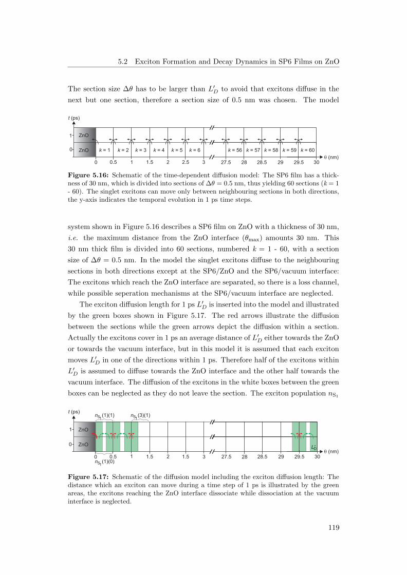
5.2 Exciton Formation and Decay Dynamics in SP6 Films on ZnO
The section size ∆θ has to be larger than L′D to avoid that excitons diffuse in the
next but one section, therefore a section size of 0.5 nm was chosen. The model
(nm) 300 0.5 1 29
ZnO
2 3 28
t (ps)
1
0
ZnOZnO
k = 1 k = 2 k = 3 k = 4 k = 5 k = 6
1.5 2.5
k = 56 k = 57 k = 58 k = 59 k = 60
27.5 28.5 29.5
Figure 5.16: Schematic of the time-dependent diffusion model: The SP6 film has a thick-ness of 30 nm, which is divided into sections of ∆θ = 0.5 nm, thus yielding 60 sections (k = 1- 60). The singlet excitons can move only between neighbouring sections in both directions,the y-axis indicates the temporal evolution in 1 ps time steps.
system shown in Figure 5.16 describes a SP6 film on ZnO with a thickness of 30 nm,
i.e. the maximum distance from the ZnO interface (θmax) amounts 30 nm. This
30 nm thick film is divided into 60 sections, numbered k = 1 - 60, with a section
size of ∆θ = 0.5 nm. In the model the singlet excitons diffuse to the neighbouring
sections in both directions except at the SP6/ZnO and the SP6/vacuum interface:
The excitons which reach the ZnO interface are separated, so there is a loss channel,
while possible seperation mechanisms at the SP6/vacuum interface are neglected.
The exciton diffusion length for 1 ps L′D is inserted into the model and illustrated
by the green boxes shown in Figure 5.17. The red arrows illustrate the diffusion
between the sections while the green arrows depict the diffusion within a section.
Actually the excitons cover in 1 ps an average distance of L′D either towards the ZnO
or towards the vacuum interface, but in this model it is assumed that each exciton
moves L′D in one of the directions within 1 ps. Therefore half of the excitons within
L′D is assumed to diffuse towards the ZnO interface and the other half towards the
vacuum interface. The diffusion of the excitons in the white boxes between the green
boxes can be neglected as they do not leave the section. The exciton population nS1
300 0.5 1 292 3 28
1
0L' D
n (1)(0)S 1
ZnO
ZnO
t (ps)
(nm) 1.5 1.5 27.5 28.5 29.5
n (1)(1)S 1n (3)(1)S 1
Figure 5.17: Schematic of the diffusion model including the exciton diffusion length: Thedistance which an exciton can move during a time step of 1 ps is illustrated by the greenareas, the excitons reaching the ZnO interface dissociate while dissociation at the vacuuminterface is neglected.
119
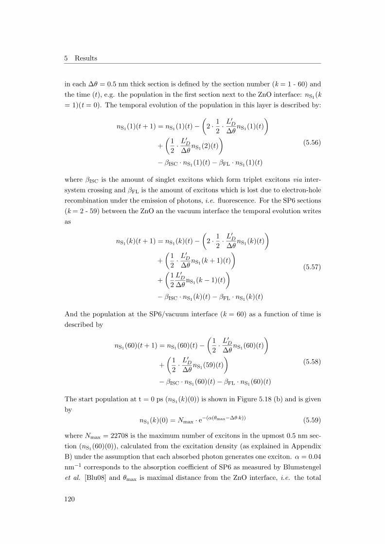
5 Results
in each ∆θ = 0.5 nm thick section is defined by the section number (k = 1 - 60) and
the time (t), e.g. the population in the first section next to the ZnO interface: nS1(k
= 1)(t = 0). The temporal evolution of the population in this layer is described by:
nS1(1)(t+ 1) = nS1(1)(t)−(
2 · 1
2·L′D∆θ
nS1(1)(t)
)+
(1
2·L′D∆θ
nS1(2)(t)
)− βISC · nS1(1)(t)− βFL · nS1(1)(t)
(5.56)
where βISC is the amount of singlet excitons which form triplet excitons via inter-
system crossing and βFL is the amount of excitons which is lost due to electron-hole
recombination under the emission of photons, i.e. fluorescence. For the SP6 sections
(k = 2 - 59) between the ZnO an the vacuum interface the temporal evolution writes
as
nS1(k)(t+ 1) = nS1(k)(t)−(
2 · 1
2·L′D∆θ
nS1(k)(t)
)+
(1
2·L′D∆θ
nS1(k + 1)(t)
)+
(1
2
L′D∆θ
nS1(k − 1)(t)
)− βISC · nS1(k)(t)− βFL · nS1(k)(t)
(5.57)
And the population at the SP6/vacuum interface (k = 60) as a function of time is
described by
nS1(60)(t+ 1) = nS1(60)(t)−(
1
2·L′D∆θ
nS1(60)(t)
)+
(1
2·L′D∆θ
nS1(59)(t)
)− βISC · nS1(60)(t)− βFL · nS1(60)(t)
(5.58)
The start population at t = 0 ps (nS1(k)(0)) is shown in Figure 5.18 (b) and is given
by
nS1(k)(0) = Nmax · e−(α(θmax−∆θ·k)) (5.59)
where Nmax = 22708 is the maximum number of excitons in the upmost 0.5 nm sec-
tion (nS1(60)(0)), calculated from the excitation density (as explained in Appendix
B) under the assumption that each absorbed photon generates one exciton. α = 0.04
nm−1 corresponds to the absorption coefficient of SP6 as measured by Blumstengel
et al. [Blu08] and θmax is maximal distance from the ZnO interface, i.e. the total
120
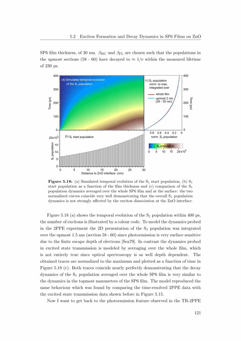
5.2 Exciton Formation and Decay Dynamics in SP6 Films on ZnO
SP6 film thickness, of 30 nm. βISC and βFL are chosen such that the populations in
the upmost sections (58 - 60) have decayed to ≈ 1/e within the measured lifetime
of 230 ps.
upmost 2 nm
302520151050Distance to ZnO interface (nm)
S
15
10
5
0
400
300
200
100
0
Tim
e (
ps)
320x10 S start population 1
of the S population 1
400
300
200
100
0
Tim
e (p
s)
20151050 x103
0.8 0.6 0.4 0.2 0
norm. S population 1
S popula
tion
1
S population 1
Simulated temporal evolution
whole film
S population 1
norm. to max. integrated over
(28 - 30 nm)
(a)
(b)
(c)
Figure 5.18: (a) Simulated temporal evolution of the S1 start population, (b) S1
start population as a function of the film thickness and (c) comparison of the S1
population dynamics averaged over the whole SP6 film and at the surface: the twonormalized curves coincide very well demonstrating that the overall S1 populationdynamics is not strongly affected by the exciton dissociation at the ZnO interface.
Figure 5.18 (a) shows the temporal evolution of the S1 population within 400 ps,
the number of excitons is illustrated by a colour code. To model the dynamics probed
in the 2PPE experiment the 2D presentation of the S1 population was integrated
over the upmost 1.5 nm (section 58 - 60) since photoemission is very surface sensitive
due to the finite escape depth of electrons [Sea79]. In contrast the dynamics probed
in excited state transmission is modeled by averaging over the whole film, which
is not entirely true since optical spectroscopy is as well depth dependent. The
obtained traces are normalized to the maximum and plotted as a function of time in
Figure 5.18 (c). Both traces coincide nearly perfectly demonstrating that the decay
dynamics of the S1 population averaged over the whole SP6 film is very similar to
the dynamics in the topmost nanometers of the SP6 film. The model reproduced the
same behaviour which was found by comparing the time-resolved 2PPE data with
the excited state transmission data shown before in Figure 5.15.
Now I want to get back to the photoemission feature observed in the TR-2PPE
121

5 Results
data which was labeled DS. Figure 5.19 shows again the spectra depicted before in
Figure 5.12 (a). Here 3 spectra taken at different pump-probe delays are displayed as
a function of the kinetic energy and are normalized to maximum intensity. The spec-
tra recorded at positive delays originate from 3.86 eV pumping and 1.93 eV probing
while the spectrum taken at -30 ps results from the reversed pump-probe scheme.
1.0
0.8
0.6
0.4
0.2
0.0
norm
. In
tensi
ty (
arb
.u.)
1.41.21.00.80.60.40.20.0-0.2Kinetic Energy (eV)
bg spectrum
bg subtracted spectra at
t = -30 ps
0 t
10 ps
21 nm SP6/ZnO(1010)h1 = 3.86 eVh2 = 1.93 eV
_
t =
DS
S signature
se
con
da
ry e
lect
ron
bg
.
1
Figure 5.19: Comparison of 2PPE spectrataken at different time delays. The intensi-ties are normalized to the maximum inten-sity. The ratio between the secondary elec-tron background and the DS signature staysnearly constant for the different time delays(the spectra nearly coincide at these signals).This indicates that both features have simi-lar dynamics in the observed time range. Incontrast the ratio between the ultrafast 2PPEsignal (S1) intensity with the background sig-nals changes as a function of pump-probe de-lay and is not present in the background spec-trum (red) taken at - 30 ps with the reversedpump-probe scheme.
The secondary electron background and
the signal labeled DS coincide nearly
perfectly for all three spectra whereas
the S1 signature exhibits dynamics on a
ps timescale, as analysed and discussed
above. This almost constant intensity
ratio of the secondary electron back-
ground and the DS signal indicates that
both features possess similar dynamics,
at least within the investigated time
range and for this photon energy com-
bination (a different behaviour is ob-
served for a longer timescale, i.e. hun-
dreds of ps to ns, in an autocorrelation
experiment presented and discussed in
Section 5.2.2). The DS feature can be
most probably related to the dark state
indicated before in excited state trans-
mission, as discussed before in Section
3.2 [Fog15, Fog14]. This long-lived dark
state appeared as a constant offset in
the excited state transmission data ex-
ceeding the repetition rate of the laser
system. In the following section the dy-
namics and origin of this state will be investigated and discussed.
122

5.2 Exciton Formation and Decay Dynamics in SP6 Films on ZnO
5.2.2 Triplet-Triplet Annihilation Leading to Electron Emission
In this section the dynamics of the long-lived background signal, which has been ob-
served in the time-resolved 2PPE measurements (labeled DS in Figure 5.12, Section
5.2.1), and as a constant offset in the excited state transmission data by L. Foglia
[Fog14] will be investigated and discussed. This feature has been labeled DS before
and is most likely related to a triplet state, as it is dark for optocal spectroscopy,
and will thus be referred to as triplet (T) in the following.
To find out whether the observed signal is really due to a long-lived state which
exceeds the repetition rate of the laser system the intensity of the observed electron
emission signal is investigated as a function of the pulse duration. In a 2PPE process
(b) Pulse duration dependence(a)1.2
1.0
0.8
0.6
0.4
0.2
0.0
Peak
Am
plit
ude (
arb
.u.)
1601208040Pulse Duration (fs)
Inte
nsi
ty
Time
Figure 5.20: (a) Schematic of two laser pulses with different duration but sameintegral, (b) emission intensity as a function of the pulse duration, demonstratingthat the emission signal is not due to a 2PPE process.
the peak intensity highly depends on the pulse duration. Figure 5.28 (a) shows two
Gaussian pulses with the same integral but different pulse durations: Overlapping
two short pulses leads to a signal with a higher intensity compared to the signal
intensity resulting from a 2PPe process with longer pulses. A 20 nm thick SP6 film
on ZnO(1010) was measured with a photon energy of 3.1 eV under variation of the
pulse duration. Figure 5.28 (b) displays the peak amplitudes of the most prominent
peak of the triplet signature as a function of the pulse durations, showing clearly
that the observed signal is not affected by the variation of the pulse duration. This
behaviour demonstrates that the detected electrons are not emitted via a 2PPE
process, i.e. are not pumped and probed within 2 laser pulses. This corroborates
the suggestion that the triplet state is so long-lived that it exceeds the repetition
rate. The time delay between the laser pulses amounts 5 µs at a repetition rate of
200 kHz which was used in the pulse duration as well as in the TR-2PPE and the
excited state transmission experiments. This demonstartes that the lifetime of the
triplet is longer than 5 µs.
In order to investigate the lifetime of the triplet state the pump-probe delay
123
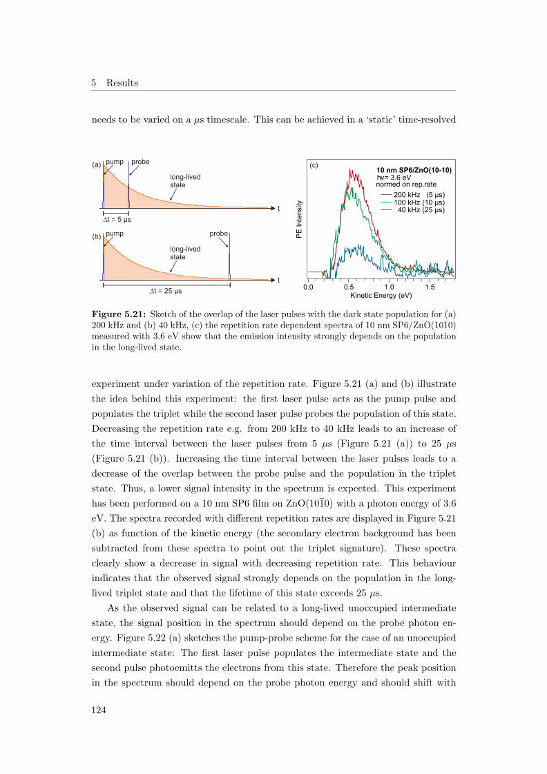
5 Results
needs to be varied on a µs timescale. This can be achieved in a ‘static’ time-resolved
PE
In
ten
sity
1.51.00.50.0Kinetic Energy (eV)
10 nm SP6/ZnO(10-10)hν = 3.6 eVnormed on rep.rate
200 kHz (5 µs) 100 kHz (10 µs) 40 kHz (25 µs)
(b)
(c)
pump probe
t = 25 µs
t
long-lived state
(a) pump probe
t = 5 µs
t
long-lived state
Figure 5.21: Sketch of the overlap of the laser pulses with the dark state population for (a)200 kHz and (b) 40 kHz, (c) the repetition rate dependent spectra of 10 nm SP6/ZnO(1010)measured with 3.6 eV show that the emission intensity strongly depends on the populationin the long-lived state.
experiment under variation of the repetition rate. Figure 5.21 (a) and (b) illustrate
the idea behind this experiment: the first laser pulse acts as the pump pulse and
populates the triplet while the second laser pulse probes the population of this state.
Decreasing the repetition rate e.g. from 200 kHz to 40 kHz leads to an increase of
the time interval between the laser pulses from 5 µs (Figure 5.21 (a)) to 25 µs
(Figure 5.21 (b)). Increasing the time interval between the laser pulses leads to a
decrease of the overlap between the probe pulse and the population in the triplet
state. Thus, a lower signal intensity in the spectrum is expected. This experiment
has been performed on a 10 nm SP6 film on ZnO(1010) with a photon energy of 3.6
eV. The spectra recorded with different repetition rates are displayed in Figure 5.21
(b) as function of the kinetic energy (the secondary electron background has been
subtracted from these spectra to point out the triplet signature). These spectra
clearly show a decrease in signal with decreasing repetition rate. This behaviour
indicates that the observed signal strongly depends on the population in the long-
lived triplet state and that the lifetime of this state exceeds 25 µs.
As the observed signal can be related to a long-lived unoccupied intermediate
state, the signal position in the spectrum should depend on the probe photon en-
ergy. Figure 5.22 (a) sketches the pump-probe scheme for the case of an unoccupied
intermediate state: The first laser pulse populates the intermediate state and the
second pulse photoemitts the electrons from this state. Therefore the peak position
in the spectrum should depend on the probe photon energy and should shift with
124

5.2 Exciton Formation and Decay Dynamics in SP6 Films on ZnO
E
E
E
kin
vac
F
1h
2.01.51.00.5Kinetic Energy (eV)
6.20 eV
4.65 eV
4.11 eV
3.85 eV
3.62 eV
3.45 eV
3.10 eV
PE
Inte
nsity
(arb
.u.)
(a) (b)
Figure 5.22: (a) 2PPE pump-probe scheme for the case of an unoccupiedintermediate state: The peak position in the spectrum shifts with thephoton energy difference ∆hν, (b) photon energy dependent spectra seriesof 20 nm SP6/ZnO(1010): The kinetic energy of the emission signal doesnot shift with ∆hν.
1 ×∆hν. Figure 5.22 (b) displays a photon energy dependent spectra series (after
background subtraction) measured on ≈ 20 nm thick SP6 films on ZnO(1010) as a
function of the kinetic energy. The spectra reveal that the signal does not shift with
the photon energy difference. Although varying the photon energy from 3.1 - 6.2
eV should shift the signal by 3.1 eV it stays at the same energetic position. Such
behaviour is usually observed for final states. But this is not the case here, because
a two-photon process would be required to populate a final state at this energetic
position. (And the absence of a real 2PPE process has been demonstrated before
in the pulse duration dependent experiment, Figure 5.20). This demonstrates that
the photon energy information put into the system via the laser pulses gets lost in
an intermediate step which acts as an energy filter, so that the emitted electrons
possess the same kinetic energy. The electrons emitted from the long-lived triplet
state are emitted by a fixed amount of energy rather than the laser photons, whose
varied photon energies did not show an effect on the kinetic energy of the emitted
electrons.
This observation leads to the question where this fixed amount of energy origi-
nates from and how much energy it amounts to. A fixed amount of energy hints at a
system immanent property like a molecular resonance. Thinking about the transfer
of an intrinsic amount of energy in an optically excited system which consists of a
molecular film on a semiconductor surface, exciton recombination or excitation en-
ergy transfer appear to be probable processes. Figure 5.23 shows the scenario of two
neighbouring SP6 molecules: Molecule A is excited at t = 0 µs by a first laser pulse,
undergoes internal vibrational relaxation within the S1, which in turn decays on a
125
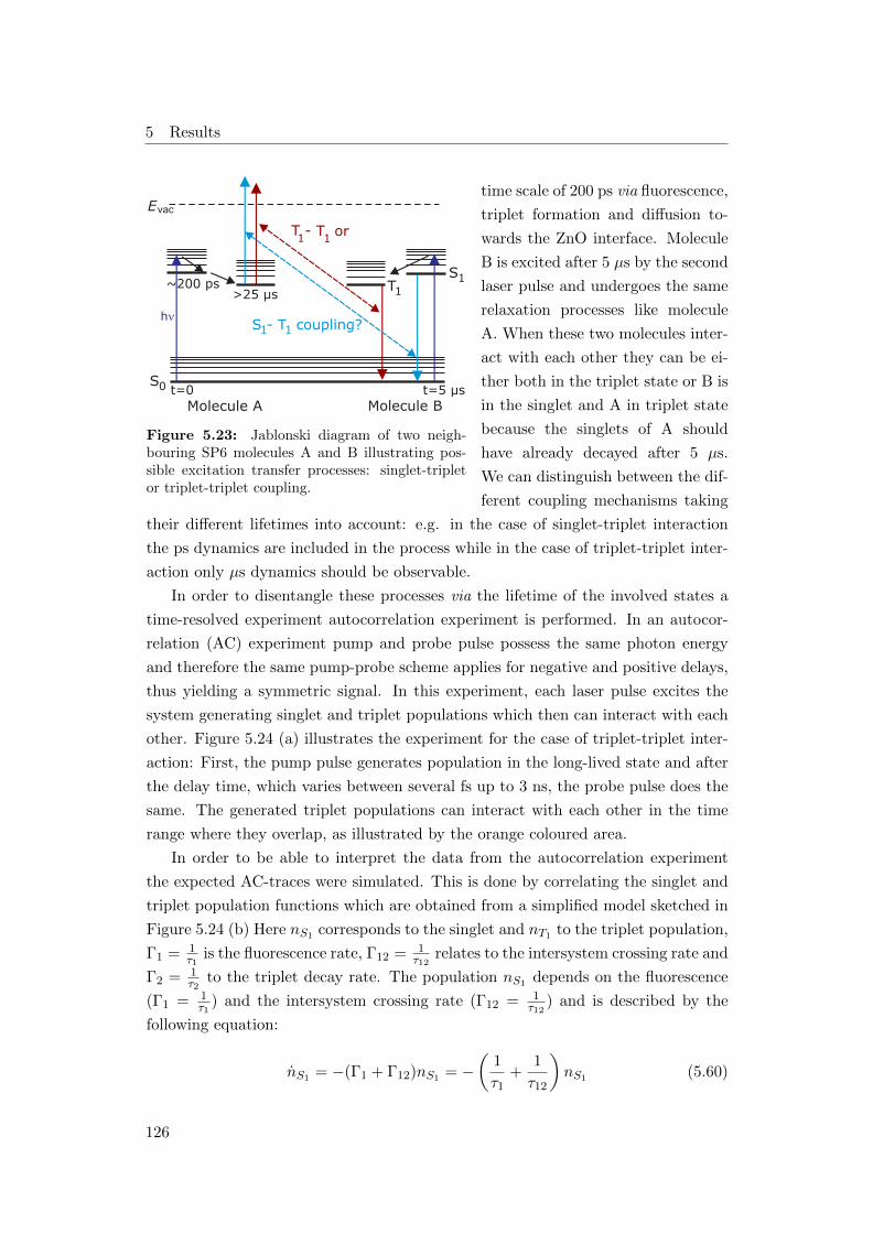
5 Results
Molecule A Molecule B
S1
S0 t=5 µs
h
>25 µs
t=0
~200 ps
S - T coupling?1 1
T 1
T - T or1 1
Evac
Figure 5.23: Jablonski diagram of two neigh-bouring SP6 molecules A and B illustrating pos-sible excitation transfer processes: singlet-tripletor triplet-triplet coupling.
time scale of 200 ps via fluorescence,
triplet formation and diffusion to-
wards the ZnO interface. Molecule
B is excited after 5 µs by the second
laser pulse and undergoes the same
relaxation processes like molecule
A. When these two molecules inter-
act with each other they can be ei-
ther both in the triplet state or B is
in the singlet and A in triplet state
because the singlets of A should
have already decayed after 5 µs.
We can distinguish between the dif-
ferent coupling mechanisms taking
their different lifetimes into account: e.g. in the case of singlet-triplet interaction
the ps dynamics are included in the process while in the case of triplet-triplet inter-
action only µs dynamics should be observable.
In order to disentangle these processes via the lifetime of the involved states a
time-resolved experiment autocorrelation experiment is performed. In an autocor-
relation (AC) experiment pump and probe pulse possess the same photon energy
and therefore the same pump-probe scheme applies for negative and positive delays,
thus yielding a symmetric signal. In this experiment, each laser pulse excites the
system generating singlet and triplet populations which then can interact with each
other. Figure 5.24 (a) illustrates the experiment for the case of triplet-triplet inter-
action: First, the pump pulse generates population in the long-lived state and after
the delay time, which varies between several fs up to 3 ns, the probe pulse does the
same. The generated triplet populations can interact with each other in the time
range where they overlap, as illustrated by the orange coloured area.
In order to be able to interpret the data from the autocorrelation experiment
the expected AC-traces were simulated. This is done by correlating the singlet and
triplet population functions which are obtained from a simplified model sketched in
Figure 5.24 (b) Here nS1 corresponds to the singlet and nT1 to the triplet population,
Γ1 = 1τ1
is the fluorescence rate, Γ12 = 1τ12
relates to the intersystem crossing rate and
Γ2 = 1τ2
to the triplet decay rate. The population nS1 depends on the fluorescence
(Γ1 = 1τ1
) and the intersystem crossing rate (Γ12 = 1τ12
) and is described by the
following equation:
nS1 = −(Γ1 + Γ12)nS1 = −(
1
τ1+
1
τ12
)nS1 (5.60)
126
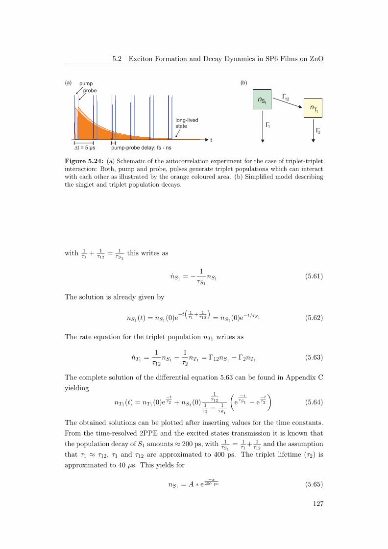
5.2 Exciton Formation and Decay Dynamics in SP6 Films on ZnO
1
12
2
nS1nT1
(a)
long-lived state
pump
probe
t
t = 5 µs pump-probe delay: fs - ns
(b)
Figure 5.24: (a) Schematic of the autocorrelation experiment for the case of triplet-tripletinteraction: Both, pump and probe, pulses generate triplet populations which can interactwith each other as illustrated by the orange coloured area. (b) Simplified model describingthe singlet and triplet population decays.
with 1τ1
+ 1τ12
= 1τS1
this writes as
nS1 = − 1
τS1
nS1 (5.61)
The solution is already given by
nS1(t) = nS1(0)e−t
(1τ1
+ 1τ12
)= nS1(0)e−t/τS1 (5.62)
The rate equation for the triplet population nT1 writes as
nT1 =1
τ12nS1 −
1
τ2nT1 = Γ12nS1 − Γ2nT1 (5.63)
The complete solution of the differential equation 5.63 can be found in Appendix C
yielding
nT1(t) = nT1(0)e−tτ2 + nS1(0)
1τ12
1τ2− 1
τS1
(e−tτS1 − e
−tτ2
)(5.64)
The obtained solutions can be plotted after inserting values for the time constants.
From the time-resolved 2PPE and the excited states transmission it is known that
the population decay of S1 amounts ≈ 200 ps, with 1τS1
= 1τ1
+ 1τ12
and the assumption
that τ1 ≈ τ12, τ1 and τ12 are approximated to 400 ps. The triplet lifetime (τ2) is
approximated to 40 µs. This yields for
nS1 = A ∗ e−x
200 ps (5.65)
127

5 Results
and for
nT1 = B ∗ e−x
40 µs − C ∗1
400 ps1
200 ps −1
40 µs
(e−x
200 ps − e−x
40 µs
)(5.66)
which can be simplified to
nT1 = B ∗ e−x
40 µs − C ∗ 0.5 ∗(
e−x
200 ps − e−x
40 µs
)(5.67)
The amplitude A was set to 1 and the amplitudes B = C were set such that both
decay functions yield the same integral, since the number of singlet and triplet
excitons is assumed to be in the same order of magnitude in this model. The case
of triplet-singlet interaction is modeled by correlating nS1 with nT1 and vice versa,
as both processes should happen in the autocorrelation experiment and correlation
is not a commutative mathematical operation. Triplet-tiplet coupling is simulated
by autocorrelating nT1 .
ps dynamics µs dynamics µs dynamics
El.
Em
issio
n Inte
ns.
-3 -2 -1 0 1 2 3Time (ns)
S - T coupling1 1(a) T - T coupling1 1
(b)
-3 -2 -1 0 1 2 3Time (ns)
El.
Em
issio
n Inte
ns.
Figure 5.25: Modeled autocorrelation traces for (a) triplet-singlet and (b) triplet-tripletcoupling
Figure 5.25 (a) depicts the AC-trace of the singlet-triplet coupling and exhibits
an intensity loss within several hundred ps around t0 since the S1 population decay
takes part in this process. Figure 5.25 (b) shows the simulated autocorrelation trace
for triplet-triplet interaction, which is a constant line in the time range of -3 - 3 ns.
This autocorrelation experiment has been conducted as well experimentally on
a 20 nm thick SP6 film on ZnO(1010) with hνpump = hνprobe = 3.85 eV in a delay
range from -0.5 - 3.0 ns, which technical is the limit due to the length of the delay
stage. The autocorrelation spectrum is presented in Figure 5.26 (a) and exhibits a
little increase in intensity around t0. In order to disentangle whether this intensity
decrease really originates from the signal of the long-lived state, vertical cuts were
taken at different time delays, as illustrated by the coloured lines in the 2D spectrum,
and biexponential background fits were subtracted from the spectra. The biexpo-
nential background fits and the corresponding spectra are shown in Figure 5.26 (b),
128
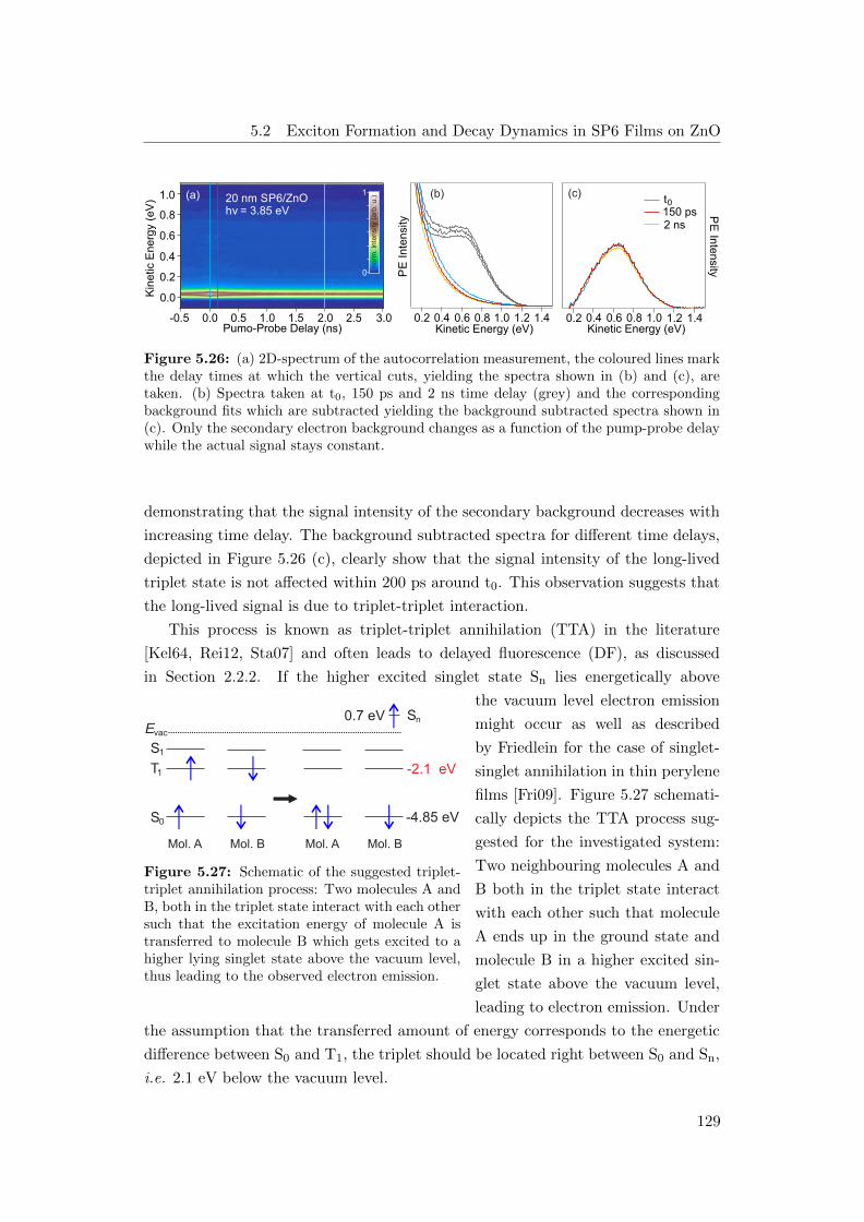
5.2 Exciton Formation and Decay Dynamics in SP6 Films on ZnO
1.0
0.8
0.6
0.4
0.2
0.0Kin
etic
En
erg
y (e
V)
3.02.52.01.51.00.50.0-0.5Pumo-Probe Delay (ns)
1.41.21.00.80.60.40.2Kinetic Energy (eV)
PE
Inte
nsi
ty
1.41.21.00.80.60.40.2Kinetic Energy (eV)
t 150 ps 2 ns
0
PE
Inte
nsity
(b) (c) 20 nm SP6/ZnO
0
1
no
rm.
inte
nsi
ty (
arb
. u
.)(a)
hν = 3.85 eV
Figure 5.26: (a) 2D-spectrum of the autocorrelation measurement, the coloured lines markthe delay times at which the vertical cuts, yielding the spectra shown in (b) and (c), aretaken. (b) Spectra taken at t0, 150 ps and 2 ns time delay (grey) and the correspondingbackground fits which are subtracted yielding the background subtracted spectra shown in(c). Only the secondary electron background changes as a function of the pump-probe delaywhile the actual signal stays constant.
demonstrating that the signal intensity of the secondary background decreases with
increasing time delay. The background subtracted spectra for different time delays,
depicted in Figure 5.26 (c), clearly show that the signal intensity of the long-lived
triplet state is not affected within 200 ps around t0. This observation suggests that
the long-lived signal is due to triplet-triplet interaction.
This process is known as triplet-triplet annihilation (TTA) in the literature
[Kel64, Rei12, Sta07] and often leads to delayed fluorescence (DF), as discussed
in Section 2.2.2. If the higher excited singlet state Sn lies energetically above
T1
S0
S1
SnEvac
Mol. A Mol. B Mol. A Mol. B
0.7 eV
-2.1 eV
-4.85 eV
Figure 5.27: Schematic of the suggested triplet-triplet annihilation process: Two molecules A andB, both in the triplet state interact with each othersuch that the excitation energy of molecule A istransferred to molecule B which gets excited to ahigher lying singlet state above the vacuum level,thus leading to the observed electron emission.
the vacuum level electron emission
might occur as well as described
by Friedlein for the case of singlet-
singlet annihilation in thin perylene
films [Fri09]. Figure 5.27 schemati-
cally depicts the TTA process sug-
gested for the investigated system:
Two neighbouring molecules A and
B both in the triplet state interact
with each other such that molecule
A ends up in the ground state and
molecule B in a higher excited sin-
glet state above the vacuum level,
leading to electron emission. Under
the assumption that the transferred amount of energy corresponds to the energetic
difference between S0 and T1, the triplet should be located right between S0 and Sn,
i.e. 2.1 eV below the vacuum level.
129

5 Results
As TTA is a bimolecular process the resulting signal intensity should depend
quadratically on the triplet concentration, as observed before for the DF inten-
sity [SR08]. To study the dependence of the electron emission on the laser fluence
spectra were taken on a 25 nm thick SP6 film on ZnO(1010) under variation of
the power of the 3.6 eV laser beam. Figure 5.28 displays the peak amplitudes
2.0
1.0P
ea
k A
mp
litu
de
(a
rb.
u.)
1614121086420Laser Power (µW)
power law: I1.5
Fluence dependence
1.5
0.5
Figure 5.28: Dependence of the electronemission signal, due to TTA, on the incidentlaser light: The peak amplitudes of the mostprominent peak are plotted as a function ofthe laser power.
of the most prominent feature of the
emission signal as a function of the laser
power. The power law fit yields neither
a linear nor a quadratic fluence depen-
dence, but instead an exponent of 1.5.
This behaviour which deviates from the
expected quadratic dependence may be
explained by the following consideration
which was originally formulated by Hoff-
mann et al. for a DF study [Hof11]. Un-
der steady state conditions, which are
suitable here as the triplet can be con-
sidered as a quasi stationary state dur-
ing measurements with a repetition rate
of 200 kHz, the rate equation of the
triplet concentration [T] writes as
d[T ]
dt= kISC − kD[T ]− kTTA[T ]2 = 0 (5.68)
Where kISC is the triplet formation rate by ISC from the singlet, kD is the sum of
other decay rates, e.g. phosphorescence or triplet quenching rate and kTTA is the
rate constant for bimolecular TTA. If the triplet population decays predominantly
via TTA (which is a plausible assumption since a significant electron emission signal
is observed), i.e. kTTA >>> kD, so that the other decay channels can be neglected
Equation 5.68 becomes
kISC − kTTA[T ]2 = 0 (5.69)
From this follows
[T ] =
√kISC
kTTA(5.70)
As mentioned before, the intensity IEm of electron emission signal is a result of
bimolecular TTA and thus quadratically dependent on the triplet concentration
IEm ∝ kISC[T ]2 (5.71)
130

5.2 Exciton Formation and Decay Dynamics in SP6 Films on ZnO
inserting Equation 5.70 yields for this limiting case a linear relation between emission
signal intensity and triplet formation rate and thus the triplet concentration
IEm ∝ kISC
(√kISC
kTTA
)2
∝ kISC (5.72)
Taken this consideration into account it is possible that the exponent of 1.5 describes
a situation which lies in between the two limiting cases of quadratic and linear
dependence.
Other decay channels besides TTA are e.g. triplet quenching at defect sites or
charge separation at the ZnO interface. As all these decay channels are diffusion con-
trolled they should be influenced by enhancing the diffusion, e.g. by increasing the
temperature. Thus, the electron emission signal resulting from TTA is expected to
1.0
0.8
0.6
0.4
0.2
0.0
No
rm.
Em
issi
on
In
ten
sity
(a
rb.u
.)
1.20.80.40.0Kinetic Energy (eV)
100 K
300 K
20 nm SP6/ZnO
hv=3.85 eV
Figure 5.29: Spectra of 20 nm SP6on ZnO measured at liquid nitrogentemperature (100 K) and at roomtemperature (300 K): The emissionsignal due to TTA is only observableat low temperatures.
exhibit a temperature behaviour, i.e. to decrease
upon increasing the sample temperature. To test
this, spectra were taken at temperatures of 100
K and 300 K on 20 nm SP6 on ZnO(1010) as
shown in Figure 5.29. Comparing the two spec-
tra, normalized to maximum intensity, clearly
shows that the electron emission signal due to
TTA has completely vanished at 300 K and only
the secondary electron background is left. Hoff-
mann et al. observed the same temperature de-
pendent behaviour for the intensity of the de-
layed fluorescence in poly(p-phenylene) deriva-
tives [Hof11]. The disappearance of the electron
emission signal at room temperature is thus con-
sistent with the increased triplet diffusion lead-
ing to enhanced triplet quenching at defect sites
and/or charge separation at the ZnO interface.
To further investigate the possibility of triplet dissociation at the SP6/ZnO inter-
face, as observed for the singlet excitons in this system [Blu08, Fog15], the distance
to the ZnO interface is decreased by lowering the coverage. Figure 5.30 (a) displays
a coverage dependent spectra series of SP6 on ZnO measured with an excitation
photon energy of 3.6 eV, where the electron emission intensity is plotted logarithmi-
cally as a function of the kinetic energy. The electron emission signal resulting from
TTA is significantly lower for a SP6 coverage of 6 nm, demonstrating the influence
of CS at the SP6/ZnO interface on the triplet lifetime. At a distance of 20 nm from
the ZnO interface, triplet quenching due to CS does not significantly affect the life-
131

5 Results
times of triplets close to the SP6/vacuum interface anymore, as the emission signal
saturates.
To obtain more information on the electron emission signature the secondary
electron background is described by an empirical background fit, blue curve in Figure
5.30 (b), which is subtracted from the original spectrum (yellow), yielding the red
beckground subtracted spectrum. This background subtracted spectrum can be
fitted with a function consisting of three Gaussians (black). This fine structure may
be due to vibronic replica as observed before by Arnold et al. [Arn79] in an electron
emission signal due to interaction of trapped charge-transfer states and free electrons
in crystalline tetracene. They attributed the structure of the signal to a sequence
of molecular vibrational states. This is as well plausibel explanation for the fine
structure observed here spectra since all three peaks exhibit the same behaviour
towards variations of the repetition rate and the photon energy indicating that they
have the same origin.
0.01
0.1
1
10
log. E
m. In
tensi
ty(a
rb. u.)
1.51.00.50.0 Kinetic Energy (eV)
SP6/ZnO(10-10)h = 3.6 eV
21 nm12 nm 6 nm
4
3
2
1
0
Em
issi
on
In
ten
sity
(a
rb.
u.)
2.01.51.00.50.0Kinetic Energy (eV)
A
B
C
SP6/ZnO(10-10)25 nmh = 3.6 eV
spectrum biexponential bg. bg. substracted fit: 3 Gaussians
A: 0.32 eVB: 0.45 eVC: 0.72 eV
(a) (b)
Figure 5.30: (a) The coverage dependent spectra series of SP6/ZnO(1010) measured with3.6 eV shows an increase of the signal with the coverage up to 20 nm. (b) Illustration of thesubtraction of a biexponential background fitted to the secondary electron background andfitting of the corrsponding background subtracted spectrum with a fit function consisting ofthree Gaussians.
132

5.2 Exciton Formation and Decay Dynamics in SP6 Films on ZnO
Summary
Time-resolved 2PPE measurements of 20 nm SP6 on ZnO(1010) reveal an ultrafast
time constant, τXF, in addition to the slower time constants, τIVR and τPOP, observed
as well in excited state transmission by L. Foglia [Fog15, Fog14]. In Figure 5.31 the
photoinduced processes observed in SP6 films on ZnO(1010) are summarized. The
system is excited from the ground state S0 to a higher vibrational level of the first
excited state S1 and subsequently undergoes internal vibrational relaxation (IVR)
within the S1 state on a time scale of a few picoseconds. The S1 population decays
within ≈ 200 ps via three competing pathways: (1) electron-hole recombination,
i.e. fluorescence (FL), (2) formation of the long-lived triplet state by intersytsem
crossing (ISC) and (3) diffusion towards the ZnO interface, where charge separation
(CS) takes place. It is shown that the broad emission signal in the 2PPE spectra,
E(eV)
Evac
-1.7
-2.1
-3.2CB
EF
=3.4
-4.85
S1
S0
T1
S1
S0
T1
T-T annihilation
0
Molecule A Molecule B
ZnO SP6
VB -6.6
3
1
2
CS
ISC
FL
IVR
Figure 5.31: Jablonski diagram of the observed processes in SP6/ZnO: Afterresonant excitation from the ground state, S0, to the first excited state, S1, thesystem relaxes vibrationally on a timescale of τIVR ≈ 4 ps. The S1 populationdecays within ≈ 200 ps via three competing pathways: (1) fluorescence (FL), (2)formation of the long-lived triplet state (ISC) and (3) diffusion towards the ZnOinterface, where charge separation (CS) takes place.
independent of the probe photon energy and the pulse duration, originates from
emission of a very long-lived triplet state, exceeding 25 µs. The conclusion that
the observed emission signal does not result from a two-photon process leads to the
conjecture that electron emission occur here most likely via intermolecular excitation
energy transfer instead of photoemission by the laser light. This assumption is
133

5 Results
corroborated by the result of an autocorrelation experiment, thus leading to the
conclusion that triplet-triplet annihilation between two neighbouring molecules is
the process which underlies the observed electron emission signal. In addition, the
absolute energies of the ground state as well as the singlet and the triplet state are
obtained from the 2PPE measurements.
134

5.3 Electronic Structure and Excited State Dynamics in DCV-substitutedOligothiophenes on Au(111)
5.3 Electronic Structure and Excited State Dynamics
in DCV-substituted Oligothiophenes on Au(111)
Dicyanovinyl-substituted oligothiophenes are very attractive molecules for the appli-
cation as donor materials in organic solar cells because they absorb light in the visible
range and exhibit high charge carrier mobility. The methylated DCV-substituted
quinquethiophene DCV5T-Me2 yields up to now the highest PCE among the known
molecular donor materials processed by vapour-deposition [Poe15]. Although the
optical gap of DCV6T was reported to be similar to the one of DCV5T-Me2 its
solar cell performance is much lower which was explained by enhanced molecular
interactions due to methyl-substitution [Fit12a, Fit11, Fit12b].
In this work the electronic structures of DCV5T-Me2 and DCV6T adsorbed
on Au(111) are studied by means of 2PPE in collaboration with Z. Yang, I. N.
Pascual and K. J. Franke (FU Berlin) who investigated the adsorption and electronic
properties of the two systems with STM and STS, as presented before in Section
3.3. The 2PPE study is focused especially on the occupied molecular states and the
electronic structure of multilayer coverages which have not been observed in STS.
Moreover the excited state dynamics are of particular interest since so far no time-
resolved studies have been reported on DCV5T-Me2 and DCV6T, thus nothing is
known about the excited state dynamics in these materials.
Merging 2PPE results obtained in this work with those from STM/STS we are
able to draw a rather complete picture of the electronic structure as a function of the
coverage [Yan14b, Yan14a, Bog15]. The energy level alignment at the organic/metal
interface reveals a decreased HOMO-LUMO gap due to interaction with the metal.
The gap increases again in the second layer when the molecules are electronically de-
coupled from the surface. Time-resolved 2PPE measurements demonstrate that the
excited state dynamics in DCV5T-Me2 are faster than in DCV6T. This observation
may be explained with the enhanced intermolecular interactions in DCV5T-Me2 pro-
moting exciton and charge carrier transport according to Fitzner et al. [Fit12b]. In
addition the relaxation and decay processes occuring within the first 2 ps are more
efficient in DCV5T-Me2 which might be due to stronger coupling to vibrational
states.
135

5 Results
5.3.1 Coverage-Dependent Electronic Structure of DCV5T-Me2 on
Au(111)
In this section the electronic structure of DCV5T-Me2 on Au(111) interface and as
a function of the coverage is investigated. The preparation and quantification of
the molecular films is described in Section 4.3.3. In order to investigate the energy
level alignment at the DCV5T-Me2/Au(111) interface, 2PPE measurements under
variation of the photon energy have been performed. Figure 5.32 (a) shows an
exemplary 1C-2PPE spectrum of a submonolayer coverage DCV5T-Me2 on Au(111)
measured with a photon energy of hν = 4.8 eV. The spectrum is plotted as a function
of the final state energy above the Fermi level such that the secondary electron cutoff
corresponds to the work function of the system, Φ = 5.4 eV, which is reduced by
≈ 50 meV compared to the bare Au(111) surface. The features in the low energy
region, i.e. at final state energies between 6.4 and 7.6 eV, can be related to occupied
states of the Au(111) substrate, namely to emission from the d-bands which are
located between ≈ -2.0 and -3.0 eV [Hei79, Eck84].
9.2
8.8
8.4
8.0
EF
in -EF (e
V)
4.84.44.0Photon Energy (eV)
C 1.2
HOMO-2 1.9 ± 0.4
B 0.8 ± 0.1
A 0.9 ± 0.1
SS 2.0 ± 0.1
2P
PE
Inte
nsi
ty HOMO-2
B
SS
d-bands
x4C
A
DCV5T-Me2 /Au(111)
0.3 ± 0.2 ML
hν = 4.78 eV
9.4
9.0
8.6
8.2
9.08.07.06.0EFin-EF (eV)
5.5 6.5 7.5 8.5 9.5
(a) (b)
= 5.4 eV
Figure 5.32: (a) 1C-2PPE spectrum of 0.3 ML DCV5T-ME2/Au(111), (b) peak positionsas a function of the photon energy: A slope of 1 is characteristic for photoemission fromunoccupied electronic states while a slope of 2 indicates photoemission from occupied states.
At higher energies there are five features located very close to each other. This
part of the spectrum was fitted with five gaussians as depicted in Figure 5.32 (a).
In order to distinguish between occupied and unoccupied states the peak maxima
are plotted as a function of the photon energy in Figure 5.32 (b). As described
before in Section 4.1.1 a slope of 1 indicates photoemission from an unoccupied
state while a slope of 2 demonstrates photoemission from an initially occupied state.
According to this analysis two occupied and three unoccupied states are found here.
The peaks related to occupied states are labeled SS and HOMO-2, since the first
originates from photoemission from the surface state of the Au(111) surface, which
136
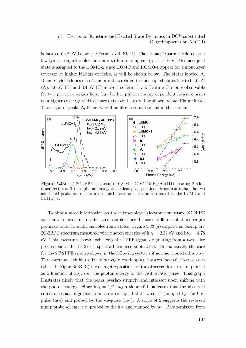
5.3 Electronic Structure and Excited State Dynamics in DCV-substitutedOligothiophenes on Au(111)
is located 0.48 eV below the Fermi level [Nic01]. The second feature is related to a
low-lying occupied molecular state with a binding energy of -1.0 eV. This occupied
state is assigned to the HOMO-2 since HOMO and HOMO-1 appear for a monolayer
coverage at higher binding energies, as will be shown below. The states labeled A,
B and C yield slopes of ≈ 1 and are thus related to unoccupied states located 4.0 eV
(A), 3.6 eV (B) and 3.4 eV (C) above the Fermi level. Feature C is only observable
for two photon energies here, but further photon energy dependent measurements
on a higher coverage yielded more data points, as will be shown below (Figure 5.34).
The origin of peaks A, B and C will be discussed at the end of the section.
7.0
6.8
6.6
6.4
6.2
6.0
5.8
2.42.22.01.8Photon Energy (eV)
LUMO
1.8 ± 0.1
LUMO+1
2.2 ± 0.1
B
0.8 ± 0.1
A 1.0 ± 0.1
SS
3.1 ± 0.1
2P
PE
In
ten
sity
LUMO+1
A
B/LUMO
SS
hν1 = 2.39 eV
hν2 = 4.78 eV
8.07.06.0EFin-EF (eV)
5.5 6.5 7.5 8.5
DCV5T-Me2 /Au(111)
0.3 ± 0.2 ML
EF
in -EF (e
V)
(a) (b)
Figure 5.33: (a) 2C-2PPE spectrum of 0.3 ML DCV5T-ME2/Au(111) showing 2 addi-tional features, (b) the photon energy dependent peak positions demonstrate that the twoadditional peaks are due to unoccupied states and can be attributed to the LUMO andLUMO+1.
To obtain more information on the submonolayer electronic structure 2C-2PPE
spectra were measured on the same sample, since the use of different photon energies
promises to reveal additional electronic states. Figure 5.33 (a) displays an exemplary
2C-2PPE spectrum measured with photon energies of hν1 = 2.39 eV and hν2 = 4.78
eV. This spectrum shows exclusively the 2PPE signal originating from a two-color
process, since the 1C-2PPE spectra have been subtracted. This is usually the case
for the 2C-2PPE spectra shown in the following sections if not mentioned otherwise.
The spectrum exhibits a lot of strongly overlapping features located close to each
other. In Figure 5.33 (b) the energetic positions of the observed features are plotted
as a function of hν1, i.e. the photon energy of the visible laser pulse. This graph
illustrates nicely that the peaks overlap strongly and intersect upon shifting with
the photon energy. Since hν1 = 1/2 hν2 a slope of 1 indicates that the observed
emission signal originates from an unoccupied state which is pumped by the UV-
pulse (hν2) and probed by the vis-pulse (hν1). A slope of 2 suggests the reversed
pump probe scheme, i.e. probed by the hν2 and pumped by hν1. Photoemission from
137
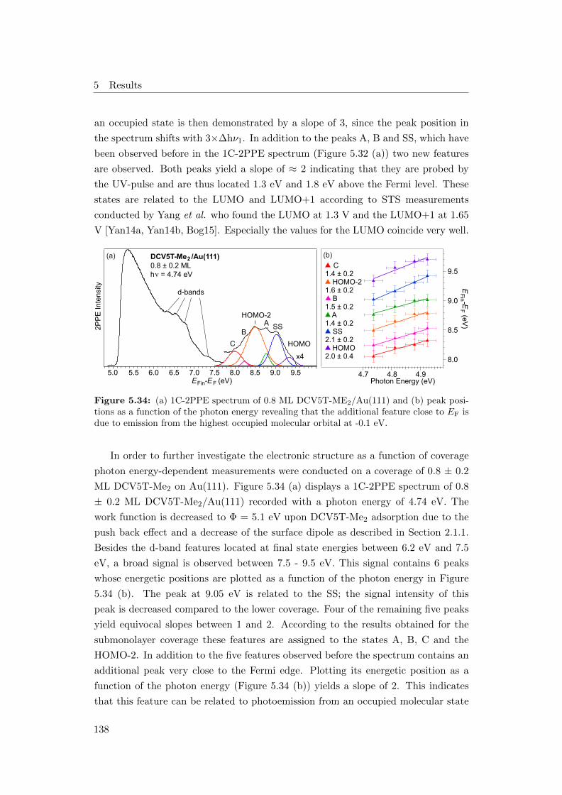
5 Results
an occupied state is then demonstrated by a slope of 3, since the peak position in
the spectrum shifts with 3×∆hν1. In addition to the peaks A, B and SS, which have
been observed before in the 1C-2PPE spectrum (Figure 5.32 (a)) two new features
are observed. Both peaks yield a slope of ≈ 2 indicating that they are probed by
the UV-pulse and are thus located 1.3 eV and 1.8 eV above the Fermi level. These
states are related to the LUMO and LUMO+1 according to STS measurements
conducted by Yang et al. who found the LUMO at 1.3 V and the LUMO+1 at 1.65
V [Yan14a, Yan14b, Bog15]. Especially the values for the LUMO coincide very well.
9.5
9.0
8.5
8.0
EF
in -EF (e
V)
4.94.84.7Photon Energy (eV)
2P
PE
Inte
nsi
ty
d-bands
A
C
HOMO-2
BSS
HOMO
DCV5T-Me2 /Au(111)0.8 ± 0.2 MLh = 4.74 eV
C1.4 ± 0.2
HOMO-21.6 ± 0.2
B1.5 ± 0.2
A1.4 ± 0.2
SS2.1 ± 0.2
HOMO2.0 ± 0.4
9.08.07.06.05.0 EFin-EF (eV)9.58.57.56.55.5
(a) (b)
x4
Figure 5.34: (a) 1C-2PPE spectrum of 0.8 ML DCV5T-ME2/Au(111) and (b) peak posi-tions as a function of the photon energy revealing that the additional feature close to EF isdue to emission from the highest occupied molecular orbital at -0.1 eV.
In order to further investigate the electronic structure as a function of coverage
photon energy-dependent measurements were conducted on a coverage of 0.8 ± 0.2
ML DCV5T-Me2 on Au(111). Figure 5.34 (a) displays a 1C-2PPE spectrum of 0.8
± 0.2 ML DCV5T-Me2/Au(111) recorded with a photon energy of 4.74 eV. The
work function is decreased to Φ = 5.1 eV upon DCV5T-Me2 adsorption due to the
push back effect and a decrease of the surface dipole as described in Section 2.1.1.
Besides the d-band features located at final state energies between 6.2 eV and 7.5
eV, a broad signal is observed between 7.5 - 9.5 eV. This signal contains 6 peaks
whose energetic positions are plotted as a function of the photon energy in Figure
5.34 (b). The peak at 9.05 eV is related to the SS; the signal intensity of this
peak is decreased compared to the lower coverage. Four of the remaining five peaks
yield equivocal slopes between 1 and 2. According to the results obtained for the
submonolayer coverage these features are assigned to the states A, B, C and the
HOMO-2. In addition to the five features observed before the spectrum contains an
additional peak very close to the Fermi edge. Plotting its energetic position as a
function of the photon energy (Figure 5.34 (b)) yields a slope of 2. This indicates
that this feature can be related to photoemission from an occupied molecular state
138

5.3 Electronic Structure and Excited State Dynamics in DCV-substitutedOligothiophenes on Au(111)
2P
PE
Inte
nsi
ty
8.07.06.05.0
SS
LUMO/
A
LUMO+1HOMO-1
HOMO
HOMO 2.8 ± 0.8
SS' 2.8 ± 0.1
SS 3.1 ± 0.5
HOMO-1 3.1 ± 0.2
A 1.1 ± 0.3
LUMO/
1.9
h = 2.37 eV1
h = 4.74 eV2
EFin-EF (eV)
7.4
7.2
7.0
6.8
6.6
6.4
6.2
6.02.52.42.32.22.1
Photon Energy (eV)
DCV5T-Me2 /Au(111)0.8 ± 0.2 ML
LUMO+1
SS'
EF
in -EF (e
V)
(a) (b)
= 5.1 eV
Figure 5.35: (a) 1C-2PPE spectrum of 0.8 ± 0.2 ML DCV5T-ME2/Au(111), (b) peakpositions as function of the photon energy.
0.1 eV below the Fermi level, which is assigned to the HOMO.
The newly discovered HOMO feature is more pronounced in the corresponding
2C-2PPE spectrum shown in Figure 5.35 (a). The features overlap strongly in
this spectrum so that they can hardly be distinguished. In the secondary electron
background close to the low energy cutoff a shoulder emerges indicating the excitonic
signature which increases with the coverage until it dominates the complete spectrum
as will be shown below. The signal between final state energies of 6 eV and 7.2 eV
has been fitted with six Gaussians as depicted in Figure 5.35 (a). In Figure 5.35
(b) the peak positions are displayed as a function of hν1, revealing four occupied
states and two unoccupied states of which one is probed by the UV- and the other
one by the vis-pulse. Among the occupied states are the HOMO, HOMO-2 and
the SS observed before. The additional two occupied states correspond to states at
binding energies of -0.6 and -0.3 eV. The first one is related to the HOMO-1 and
the latter to the emission signal from the adsorbate covered surface state SS’. It is
known that adsorption of atoms and molecules can lead to an energetic shift of the
Shockley surface state as described before in Section 2.1.1. The unoccupied state
probed by the UV-pulse is located 1.5 eV above the Fermi level and might be due
to a superposition of the LUMO and LUMO+1. But this feature appears only as
a shoulder in two spectra, therefore this assignment has to be treated with caution.
The other unoccupied state probed by the vis-pulse corresponds to the peak A,
which has been observed before.
To further track the evolution of the electronic structure upon increasing coverage
2PPE measurements have been performed on a coverage of 3 ± 1 ML DCV5T-Me2
on Au(111). Figure 5.36 shows a 1C-2PPE spectrum (a) and the corresponding 2C-
2PPE (b) spectrum of 3 ML DCV5T-Me2 on Au(111). The 1C-2PPE spectrum was
139
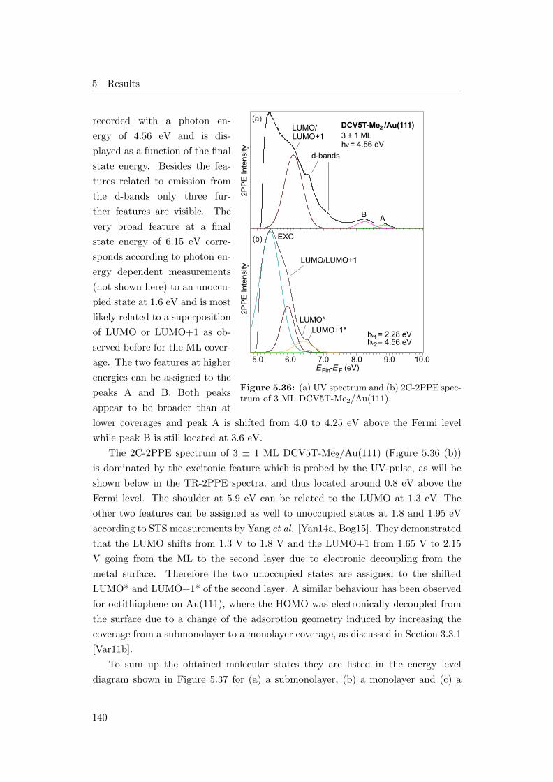
5 Results
d-bands
B A
DCV5T-Me2 /Au(111)
3 ± 1 MLh = 4.56 eV
10.09.08.07.06.05.0
LUMO*
LUMO+1*
LUMO/LUMO+1
EXC
h 1 = 2.28 eVh 2 = 4.56 eV
2P
PE
In
ten
sity
2P
PE
In
ten
sity
LUMO/LUMO+1
EFin-EF (eV)
(a)
(b)
Figure 5.36: (a) UV spectrum and (b) 2C-2PPE spec-trum of 3 ML DCV5T-Me2/Au(111).
recorded with a photon en-
ergy of 4.56 eV and is dis-
played as a function of the final
state energy. Besides the fea-
tures related to emission from
the d-bands only three fur-
ther features are visible. The
very broad feature at a final
state energy of 6.15 eV corre-
sponds according to photon en-
ergy dependent measurements
(not shown here) to an unoccu-
pied state at 1.6 eV and is most
likely related to a superposition
of LUMO or LUMO+1 as ob-
served before for the ML cover-
age. The two features at higher
energies can be assigned to the
peaks A and B. Both peaks
appear to be broader than at
lower coverages and peak A is shifted from 4.0 to 4.25 eV above the Fermi level
while peak B is still located at 3.6 eV.
The 2C-2PPE spectrum of 3 ± 1 ML DCV5T-Me2/Au(111) (Figure 5.36 (b))
is dominated by the excitonic feature which is probed by the UV-pulse, as will be
shown below in the TR-2PPE spectra, and thus located around 0.8 eV above the
Fermi level. The shoulder at 5.9 eV can be related to the LUMO at 1.3 eV. The
other two features can be assigned as well to unoccupied states at 1.8 and 1.95 eV
according to STS measurements by Yang et al. [Yan14a, Bog15]. They demonstrated
that the LUMO shifts from 1.3 V to 1.8 V and the LUMO+1 from 1.65 V to 2.15
V going from the ML to the second layer due to electronic decoupling from the
metal surface. Therefore the two unoccupied states are assigned to the shifted
LUMO* and LUMO+1* of the second layer. A similar behaviour has been observed
for octithiophene on Au(111), where the HOMO was electronically decoupled from
the surface due to a change of the adsorption geometry induced by increasing the
coverage from a submonolayer to a monolayer coverage, as discussed in Section 3.3.1
[Var11b].
To sum up the obtained molecular states they are listed in the energy level
diagram shown in Figure 5.37 for (a) a submonolayer, (b) a monolayer and (c) a
140
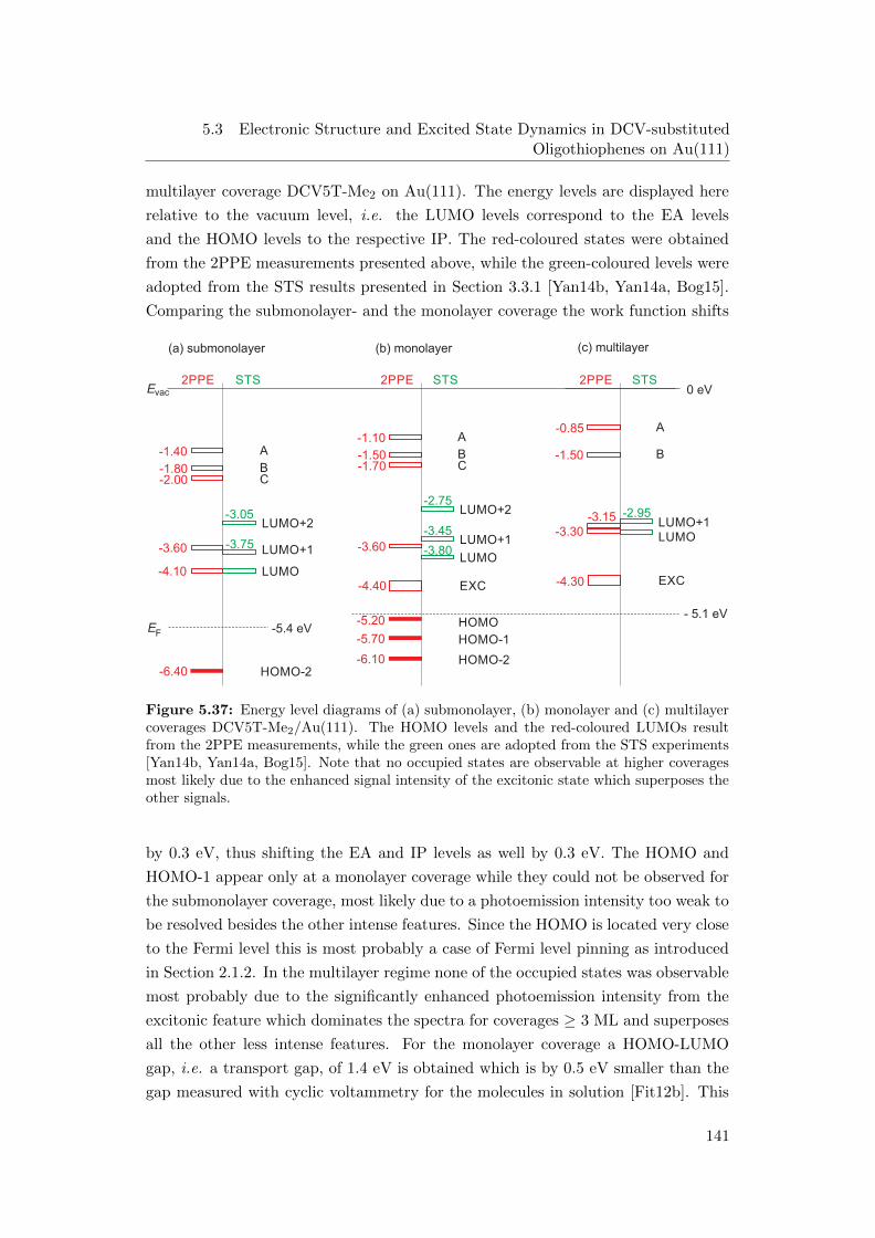
5.3 Electronic Structure and Excited State Dynamics in DCV-substitutedOligothiophenes on Au(111)
multilayer coverage DCV5T-Me2 on Au(111). The energy levels are displayed here
relative to the vacuum level, i.e. the LUMO levels correspond to the EA levels
and the HOMO levels to the respective IP. The red-coloured states were obtained
from the 2PPE measurements presented above, while the green-coloured levels were
adopted from the STS results presented in Section 3.3.1 [Yan14b, Yan14a, Bog15].
Comparing the submonolayer- and the monolayer coverage the work function shifts
EF
Evac 0 eV
- 5.1 eV-5.4 eV
-4.10
-2.00-1.80
-1.40
-6.40
(a) submonolayer (b) monolayer (c) multilayer
-3.05LUMO+2
A
BC
LUMO
-3.80
-3.45
-1.70-1.50
-1.10
-2.75LUMO+2
A
BC
LUMO+1
LUMO
-6.10
-5.70
-5.20
HOMO-2HOMO-2
HOMO-1
HOMO
-4.40 EXC -4.30 EXC
-1.50
-0.85 A
B
-3.30
-2.95LUMO+1LUMO
-3.75 LUMO+1-3.60 -3.60
-3.15
2PPE STS2PPE STS 2PPE STS
Figure 5.37: Energy level diagrams of (a) submonolayer, (b) monolayer and (c) multilayercoverages DCV5T-Me2/Au(111). The HOMO levels and the red-coloured LUMOs resultfrom the 2PPE measurements, while the green ones are adopted from the STS experiments[Yan14b, Yan14a, Bog15]. Note that no occupied states are observable at higher coveragesmost likely due to the enhanced signal intensity of the excitonic state which superposes theother signals.
by 0.3 eV, thus shifting the EA and IP levels as well by 0.3 eV. The HOMO and
HOMO-1 appear only at a monolayer coverage while they could not be observed for
the submonolayer coverage, most likely due to a photoemission intensity too weak to
be resolved besides the other intense features. Since the HOMO is located very close
to the Fermi level this is most probably a case of Fermi level pinning as introduced
in Section 2.1.2. In the multilayer regime none of the occupied states was observable
most probably due to the significantly enhanced photoemission intensity from the
excitonic feature which dominates the spectra for coverages ≥ 3 ML and superposes
all the other less intense features. For the monolayer coverage a HOMO-LUMO
gap, i.e. a transport gap, of 1.4 eV is obtained which is by 0.5 eV smaller than the
gap measured with cyclic voltammetry for the molecules in solution [Fit12b]. This
141

5 Results
reduced HOMO-LUMO gap with respect to the ’free’ molecule in solution indicates
that the molecular levels are shifted towards the Fermi level due to interaction with
the metal substrate as discussed in Section 2.1.2. In the second layer the LUMO and
LUMO+1 are shifted upwards by 0.5 eV demonstrating electronic decoupling from
the metal surface. The exciton binding energy amounts to 0.6 eV for the monolayer
coverage and increases to 1.0 eV for the multilayer coverage. The latter compares
well to the exciton binding energy of 0.9 eV obtained for 1 ML sexithiophene on
Au(111) [Var11a].
The origin of the unoccupied states A, B and C has not been tackled so far. In
a system consisting of a metal substrate and an organic semiconducting adsorbate
layer different kinds of unoccupied states are possible:
• (i) Image potential states (IPS), as were found on tetracene and pentacene
surfaces [Zhu09].
• (ii) Interface states (IS), which were observed before at organic/metal inter-
faces [Hag10, Mar14].
• (iii) Charge transfer (CT) excitons, as witnessed before at the surfaces of
tetracene and pentacene [Yan09, Zhu09].
• (iv) Energetically higher located unoccupied molecular states (LUMO+n).
These states can be at least partially distinguished since the first two examples,
(i) and (ii), possess characteristic properties: Both types of unoccupied states are
expected to exhibit a parabolic dispersion parallel to the surface and in addition
image potential states are pinned to the vacuum level. Thus the first possibility, (i)
the image potential states, can be ruled out since the energetic positions of A, B and
C stay constant relative to the Fermi level, i.e. do not shift with the vacuum level,
when the DCV5T2 coverage is increased from the submonolayer to the monolayer
regime.
In order to identify whether one of the states shows a dispersion, 1C-2PPE spec-
tra of 2 ± 0.5 ML DCV5T-Me2 on Au(111) were recorded as a function of the emis-
sion angle. Figure 5.38 (a) shows the spectra series, measured with a photon energy
of hν = 4.3 eV, plotted as function of the final state energy. For this photon energy
and coverage only peaks A, B and the HOMO-1 are visible. The peak positions are
plotted as a function of the angle in Figure 5.38 (b) demonstrating clearly that none
of the investigated states shows a dispersion. With this result the second possibility,
(ii) the interface states, can be excluded as well. The possibilities still left are (iii)
the CT states and (iv) the higher lying unoccupied molecular orbitals. The charge
transfer excitons observed before at vacuum interfaces with tetracene and pentacene
142

5.3 Electronic Structure and Excited State Dynamics in DCV-substitutedOligothiophenes on Au(111)
8.6
8.4
8.2
8.0
7.8
7.6
-15 -10 -5 0 5 10 15Angle (°)
HOMO-1 B
A
2P
PE
Inte
nsi
ty
10.09.08.07.06.05.0EFin-EF (eV)
AHOMO-1
14° 12° 10° 8° 6° 4° 2° 0° -2° -4° -6° -8° -10° -12° -14°
DCV5T-Me /Au(111)
h = 4.33 eV
2 0.5 ML+_2
B
EF
in-E
F (
eV
)
(a) (b)
Figure 5.38: (a) 2C-2PPE spectra series of 2 ML DCV5T-Me2/Au(111) and (b) peakmaxima as a function of the angle: None of the studied states shows a dispersion.
appeared always in the vicinity of IPS [Yan09, Zhu09]. Since no IPS was observed
here the states A, B and C originate most likely from higher lying LUMO+n levels
and not from charge transfer states at the molecule/vacuum interface.
In the next section the electronic structure of DCV6T on Au(111) will be inves-
tigated accordingly.
5.3.2 Coverage-Dependent Electronic Structure of DCV6T/Au(111)
In the following the electronic structure as a function of DCV6T coverage on Au(111)
is investigated with focus on occupied states, energetically higher located unoccupied
states and the electronic structure of the multilayer regime, which have not been
observed by STS. For DCV6T adsorbed on Au(111) an electronic structure similar
to the one of DCV5T-Me2 is expected according to adsorption measurements of both
molecules yielding comparable optical gaps [Fit11, Fit12b, Yan14a]. In addition the
LUMO levels from STS measurements agree very well [Yan14a].
Figure 5.39 (a) shows an exemplary 1C-2PPE spectrum of 1.4 ± 0.4 ML DCV6T
on Au(111) recorded with a photon energy of 4.6 eV. The spectrum is displayed as
a function of the final state energy where the low energy cutoff corresponds to the
work function, which amounts here to Φ = 5.1 eV. Besides the features related
to the d-bands of the Au(111) surface there are three peaks located at final state
energies between 8 eV and 9 eV which are labeled A, B and HOMO-1. This already
anticipates the peak assignment, which is based on the one hand on the slopes yielded
by the plot of the peak positions as a function of the photon energy, shown in Figure
5.39 (b), and on the other hand on the electronic structure found for the related
DCV5T-Me2. The features A and B yield slopes of ≈ 1 indicating that those are
due to unoccupied states located 4.1 eV and 3.7 eV above the Fermi level. These
143

5 Results
2P
PE
Inte
nsi
ty
d-bands
x3
DCV6T/Au(111)
1.4 ± 0.4 ML
h = 4.6 eV
9.08.07.06.05.0EFin-EF (eV)
9.2
9.0
8.8
8.6
8.4
4.94.84.74.64.5Photon Energy (eV)
B 1.4 ± 0.4
A 0.8 ± 0.2
HOMO-1
2.8 ± 0.2
E
Fin -E
F (eV
)A
B
HOMO-1
(a) (b)
= 5.1 eV
Figure 5.39: (a) 1C-2PPE spectrum of 1.4 ML DCV6T/Au(111), (b) peak positions asfunction of the photon energy.
energetic positions remind strongly of features A and B observed for DCV5T-Me2
(A: 4.0 eV, B: 3.6 eV) and are thus named after them. The slope of the third peak
amounts to 2.8 instead of 1 or 2. This deviant behaviour can be explained with the
deficient quality of the data; the features overlap strongly and none of the recorded
spectra shows all three peaks separated from each other. Since 2.8 is closer to 2 than
to 1 it can be assumed that this feature is due to photoemission from an occupied
state located 0.6 eV below the Fermi level which may be related to the HOMO-1,
in accordance to the HOMO-1 of DCV5T-Me2.
LUMO+2 1.9 ± 0.6
LUMO+1* 2.1 ± 0.6
A 0.6 ± 0.3
LUMO+1 2.1 ± 0.4
2P
PE
Inte
nsi
ty
8.07.06.05.0
A
LUMO+1*
LUMO+1
h 1 = 2.3 eV
h 2 = 4.6 eV
DCV6T/Au(111)
1.4 ± 0.4 ML
7.4
7.2
7.0
6.8
6.6
6.4
6.2
6.0
2.52.42.32.22.1Photon Energy (eV)
EF
in -EF (e
V)
EFin-EF (eV)
(a) (b)
EXC
Figure 5.40: (a) 2C-2PPE spectrum of 1.4 ML DCV6T/Au(111), (b) peak positions asfunction of the photon energy.
Figure 5.40 (a) shows the corresponding 2C-2PPE spectrum measured with hν1
= 2.3 eV and hν2 = 4.6 eV. The spectrum exhibits as well strongly overlapping peaks
but three peak maxima are clearly visible here. Although this spectrum shows three
peaks at final state energies between 6 eV and 6.7 eV the positions of four peaks
144

5.3 Electronic Structure and Excited State Dynamics in DCV-substitutedOligothiophenes on Au(111)
are displayed as a function of the photon energy in Figure 5.40 (b). This is because
none of the recorded spectra shows all four peaks simultaneously. Three of the
peaks yield slopes of ≈ 2 indicating that they result from unoccupied states probed
by the UV pulse and are thus located 1.6 eV, 2.0 eV and 2.3 eV above the Fermi level.
According to the unoccupied states derived from STS measurements the states at 1.6
eV and 2.3 eV are assigned to the LUMO+1 and LUMO+2 [Yan14b, Yan14a, Bog15].
The unoccupied state at 2.0 eV might be related to the LUMO+1* of the second
layer shifted to higher binding energies due to electronic decoupling from the metal
surface, as discussed for DCV5T-Me2 and in Section 2.1.2. The fourth feature is
related to peak A (4.1 eV), although yielding a slope of 0.6, according to the 1C-
2PPE spectrum shown in Figure 5.39 (a). Close to the secondary electron cutoff the
broad excitonic feature emerges which increases in intensity for higher coverages as
shown below in Figure 5.41 (b).
In order to investigate the electronic structure of the multilayer coverage, 2PPE
measurements on 4 ± 1 ML DCV6T on Au(111) have been performed. Figure
5.41 (a) displays a 1C-2PPE spectrum measured with hν = 4.6 eV as a func-
tion of the final state energy. The work function decreases by 0.1 eV to 5.0 eV
2P
PE
Inte
nsi
ty
9.08.07.06.05.0EFin-EF (eV)
LUMO/HOMO-2
LUMO+1*
LUMO+1
EXC
2P
PE
Inte
nsi
ty
AB
d-bands
h = 4.6 eV
x4
h 1 = 2.3 eV,
h 2= 4.6 eV
4 1 ML DCV6T/Au(111)+_
= 5.0 eV
Figure 5.41: (a) 1C-2PPE and (b) 2C-2PPE spectraof a multilayer DCV6T/Au(111)
in comparison to the 1.4 ML
coverage. The peaks A and B
are broadened and shift by 0.1
eV to higher binding energies
of 4.2 eV and 3.7 eV upon ad-
sorption of additional DCV6T.
Figure 5.41 (b) shows the cor-
responding 2C-2PPE spectrum
recorded with hν1 = 2.3 eV and
hν2 = 4.6 eV. A broad feature
rises at a final state energy of
5.5 eV and is related to the
exciton located 0.9 eV above
the Fermi level, i.e. probed by
hν2, as will be shown below in
TR-2PPE spectra. This fea-
ture dominates the spectrum,
so that the other features ap-
pear only as shoulders of this
intense peak. The feature at a
final state energy of 5.9 eV could be either due to an occupied state 1.0 eV below the
145
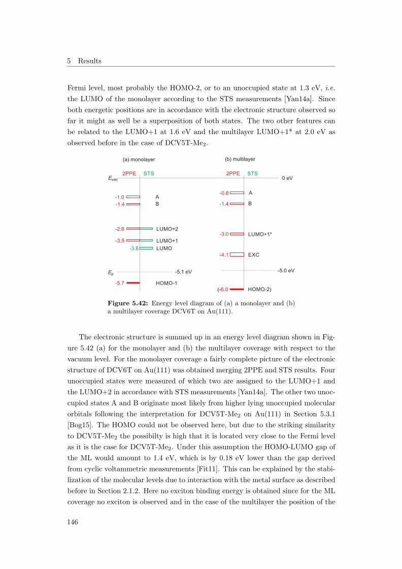
5 Results
Fermi level, most probably the HOMO-2, or to an unoccupied state at 1.3 eV, i.e.
the LUMO of the monolayer according to the STS measurements [Yan14a]. Since
both energetic positions are in accordance with the electronic structure observed so
far it might as well be a superposition of both states. The two other features can
be related to the LUMO+1 at 1.6 eV and the multilayer LUMO+1* at 2.0 eV as
observed before in the case of DCV5T-Me2.
EF
Evac
-5.0 eV-5.1 eV
-3.8
-1.4
-1.0
-5.7
(a) monolayer (b) multilayer
-2.8 LUMO+2
A
B
LUMO
-3.0
-1.4
-0.8 A
B
LUMO+1*
(-6.0HOMO-1
HOMO-2)
-4.1 EXC
-3.5 LUMO+1
0 eV2PPE STS 2PPE STS
Figure 5.42: Energy level diagram of (a) a monolayer and (b)a multilayer coverage DCV6T on Au(111).
The electronic structure is summed up in an energy level diagram shown in Fig-
ure 5.42 (a) for the monolayer and (b) the multilayer coverage with respect to the
vacuum level. For the monolayer coverage a fairly complete picture of the electronic
structure of DCV6T on Au(111) was obtained merging 2PPE and STS results. Four
unoccupied states were measured of which two are assigned to the LUMO+1 and
the LUMO+2 in accordance with STS measurements [Yan14a]. The other two unoc-
cupied states A and B originate most likely from higher lying unoccupied molecular
orbitals following the interpretation for DCV5T-Me2 on Au(111) in Section 5.3.1
[Bog15]. The HOMO could not be observed here, but due to the striking similarity
to DCV5T-Me2 the possibilty is high that it is located very close to the Fermi level
as it is the case for DCV5T-Me2. Under this assumption the HOMO-LUMO gap of
the ML would amount to 1.4 eV, which is by 0.18 eV lower than the gap derived
from cyclic voltammetric measurements [Fit11]. This can be explained by the stabi-
lization of the molecular levels due to interaction with the metal surface as described
before in Section 2.1.2. Here no exciton binding energy is obtained since for the ML
coverage no exciton is observed and in the case of the multilayer the position of the
146

5.3 Electronic Structure and Excited State Dynamics in DCV-substitutedOligothiophenes on Au(111)
LUMO in unknown. With increasing coverage the LUMO+1 state shifts to higher
binding energies due to the decoupling from the metal surface, as observed before
for DCV5T-Me2. At coverages of ≈ 3 - 4 ML a broad feature emerges whose signal
intensity increases with the coverage and can be related to an excitonic state, as will
be treated in detail in Section 5.3.4.
The electronic structure observed for DCV6T is very similar compared to the
electronic structure of DCV5T-Me2, which is in agreement with the results obtained
from absorption spectroscopy and STS [Fit11, Fit12b, Yan14a]. In the next two
sections the excited state dynamics as function of the coverage will be presented and
discussed.
5.3.3 Excited State Dynamics in DCV5T-Me2 on Au(111)
In this section the excited state dynamics of different coverages of DCV5T-Me2 on
Au(111) will be investigated by means of TR-2PPE. The excited state dynamics
of the DCV-substituted thiophenes are of great interest since up to now no time-
resolved experiments have been reported. Especially the question whether the dif-
ferent solar cell efficiencies yielded by the molecules are reflected in the dynamics
is crucial. First TR-2PPE spectra of two different coverages will be presented and
the influence of the metal substrate on the dynamics will be discussed. Then the
dynamics measured on a thick DCV5T-Me2 film will be debated.
To investigate the excited state dynamics as a function of the DCV5T-Me2 film
thickness time-resolved 2PPE measurements were performed on different coverages.
Figure 5.43 shows time-resolved 2PPE spectra of (a) 10 ± 3 ML and (b) 20 ± 5 ML
measured with photon energies of hν1 = 2.28 eV and hν2 = 4.56 eV. The photoe-
mission signal observed here for positive delays originates from initially unoccupied
intermediate states pumped with hν1 and probed with hν2. The signal originating
from monochromatic 2PPE processes was subtracted, as explained before in Section
4.5. The intermediate state energy relative to the Fermi level is plotted as a function
of the pump-probe delay and the signal intensity is illustrated by a false colour code
(white corresponds to 100 % and dark blue to 0 % intensity). The electrons are
excited above the optical gap and relax on a femtosecond time-scale into a broad
long-lived state, which can be related most probably to an excitonic state and will
be referred to as such from now on. The broad long-lived feature has a maximum
around 0.8 eV and dominates the spectra of both coverages. This can be observed
as well in Figure 5.43 (c) where 2PPE spectra taken on different coverages and a
pump-probe delay of t = 0 ps are displayed as a function of the intermediate state
energy. Comparing the 2PPE spectra taken on 4 ± 1 , 10 ± 3 and 20 ± 5 ML
DCV5T-Me2 on Au(111) reveals that the dominance of the excitonic feature over
147
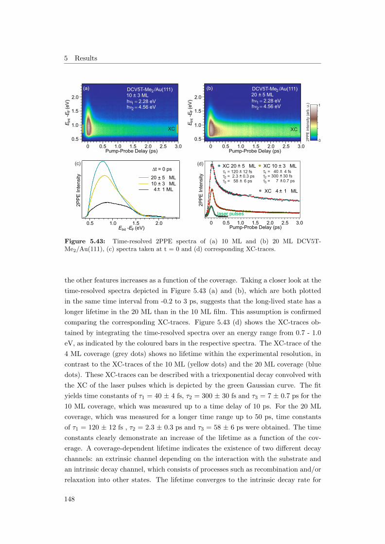
5 Results
3.02.52.01.51.00.50Pump-Probe Delay (ps)
0
1
2P
PE
inte
nsity
(a
rb.
u.)
3.02.52.01.51.00.50Pump-Probe Delay (ps)
EIn
t-E
F (e
V)
EIn
t-E
F (e
V)
2P
PE
In
ten
sity
2.01.51.00.5
DCV5T-Me2 /Au(111)
h2.28 eV
4 1 ML 10 3 ML 20 5 ML
3.02.52.01.51.00.50Pump-Probe Delay (ps)
2P
PE
In
ten
sity
t = 0 ps
h4.56 eV1
2
+ _ + _ + _
10 3 ML + _DCV5T-Me2 /Au(111)
h2.28 eVh4.56 eV
1
2
20 5 ML + _
EInt -EF (eV)
(a) (b)
(c)
(d)
XC XC
2.0
1.5
1.0
0.5
2.0
1.5
1.0
0.5
XC 10 3 ML + _ XC 20 5 ML + _
= 120 12 fs 1 + _
= 2.3 0.3 ps 2 + _
= 58 6 ps 3 + _
XC 4 1 ML + _
laser pulses
= 40 4 fs 1 + _
= 300 30 fs 2 + _
= 7 0.7 ps 3 + _
Figure 5.43: Time-resolved 2PPE spectra of (a) 10 ML and (b) 20 ML DCV5T-Me2/Au(111), (c) spectra taken at t = 0 and (d) corresponding XC-traces.
the other features increases as a function of the coverage. Taking a closer look at the
time-resolved spectra depicted in Figure 5.43 (a) and (b), which are both plotted
in the same time interval from -0.2 to 3 ps, suggests that the long-lived state has a
longer lifetime in the 20 ML than in the 10 ML film. This assumption is confirmed
comparing the corresponding XC-traces. Figure 5.43 (d) shows the XC-traces ob-
tained by integrating the time-resolved spectra over an energy range from 0.7 - 1.0
eV, as indicated by the coloured bars in the respective spectra. The XC-trace of the
4 ML coverage (grey dots) shows no lifetime within the experimental resolution, in
contrast to the XC-traces of the 10 ML (yellow dots) and the 20 ML coverage (blue
dots). These XC-traces can be described with a triexponential decay convolved with
the XC of the laser pulses which is depicted by the green Gaussian curve. The fit
yields time constants of τ1 = 40 ± 4 fs, τ2 = 300 ± 30 fs and τ3 = 7 ± 0.7 ps for the
10 ML coverage, which was measured up to a time delay of 10 ps. For the 20 ML
coverage, which was measured for a longer time range up to 50 ps, time constants
of τ1 = 120 ± 12 fs , τ2 = 2.3 ± 0.3 ps and τ3 = 58 ± 6 ps were obtained. The time
constants clearly demonstrate an increase of the lifetime as a function of the cov-
erage. A coverage-dependent lifetime indicates the existence of two different decay
channels: an extrinsic channel depending on the interaction with the substrate and
an intrinsic decay channel, which consists of processes such as recombination and/or
relaxation into other states. The lifetime converges to the intrinsic decay rate for
148

5.3 Electronic Structure and Excited State Dynamics in DCV-substitutedOligothiophenes on Au(111)
high coverages when the excited state population in the upmost layers, probed by
2PPE, is not affected anymore by the substrate, as discussed in Section 2.2.2. Such
an increase of lifetime as function of the distance to the metal surface has been
observed before for C60 and 6T on Au(111) [Dut05, Var12a].
30025020015010050Pump-Probe Delay (ps)
DCV5T-Me2/Au(111)
h1 = 2.4 eV
h2 = 4.8 eV
20 5 ML+_
86420Pump-Probe Delay (ps)
2PPE Intensity
= 130 13 fs 1
= 1 0.1 ps 2
= 11 1.1 ps 3
= 390 40 ps 4+_
+_
+_+_
10
2P
PE
Inte
nsi
ty
XC (0.7 - 1.0 eV) fit
(a) t = 0 ps (b)
(c)
0
1
2P
PE
inte
nsi
ty (
arb
. u.)
2.0
1.5
1.0
0.5
E - E
F (e
V)
Int
2.0
1.5
1.0
0.5
E -
EF
(e
V)
Int
XC
Figure 5.44: (a) 2PPE spectrum of 20 ML DCV5T-Me2 at t= 0 ps, (b) time-resolvedspectrum and (c) the XC-trace, described by a quadruple exponential decay.
To gain deeper insight into the excited state dynamics of a high coverage DCV5T-
Me2 on Au(111) a 20 ± 5 ML film was measured with a pump photon energy of hν1
= 2.4 eV and a probe photon energy of hν2 = 4.8 eV for pump-probe delays up to
300 ps. The resulting time-resolved spectrum is depicted in Figure 5.44 (b). The
intermediate state energy is plotted as a function of the pump-probe delay, in the
left part from - 0.2 to 10 ps and in the right part from 10 - 300 ps. The spectrum
is dominated by the broad excitonic feature with a maximum at an intermediate
state energy of ≈ 0.8 eV. The XC trace displayed in Figure 5.44 (c) as a function
of the pump-probe delay, analogous to the time-resolved spectrum in two parts,
was obtained by integrating the time-resolved spectrum between 0.7 and 1.0 eV.
It exhibits a rapid decay within the first 2 ps during which ≈ 2/3 of the excited
state population decays. After that the decay slows down significantly and a small
amount of the initial population exhibits a lifetime of several hundred ps. The XC
trace was fitted with an empirical fit function consisting of a quadruple exponential
decay convolved with the XC of the laser pulses. The obtained time constants
amount to τ1 = 130 ± 13 fs, τ2 = 1 ± 0.1 ps, τ3 = 11 ± 1.1 ps and τ4 = 390
± 40 ps. Since the spectrum shows no structure it is not possible to energetically
separate the involved states and to disentangle the involved processes. Therefore the
149
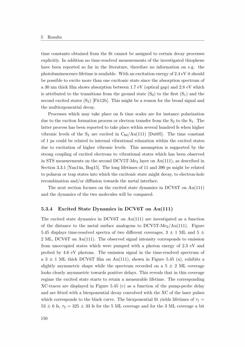
5 Results
time constants obtained from the fit cannot be assigned to certain decay processes
explicitly. In addition no time-resolved measurements of the investigated thiophene
have been reported so far in the literature, therefore no information on e.g. the
photoluminescence lifetime is available. With an excitation energy of 2.4 eV it should
be possible to excite more than one excitonic state since the absorption spectrum of
a 30 nm thick film shows absorption between 1.7 eV (optical gap) and 2.8 eV which
is attributed to the transitions from the ground state (S0) to the first (S1) and the
second excited states (S2) [Fit12b]. This might be a reason for the broad signal and
the multiexponential decay.
Processes which may take place on fs time scales are for instance polarization
due to the exciton formation process or electron transfer from the S2 to the S1. The
latter process has been reported to take place within several hundred fs when higher
vibronic levels of the S2 are excited in C60/Au(111) [Dut05]. The time constant
of 1 ps could be related to internal vibrational relaxation within the excited states
due to excitation of higher vibronic levels. This assumption is supported by the
strong coupling of excited electrons to vibrational states which has been observed
in STS measurements on the second DCV5T-Me2 layer on Au(111), as described in
Section 3.3.1 [Yan14a, Bog15]. The long lifetimes of 11 and 390 ps might be related
to polaron or trap states into which the excitonic state might decay, to electron-hole
recombination and/or diffusion towards the metal interface.
The next section focuses on the excited state dynamics in DCV6T on Au(111)
and the dynamics of the two molecules will be compared.
5.3.4 Excited State Dynamics in DCV6T on Au(111)
The excited state dynamics in DCV6T on Au(111) are investigated as a function
of the distance to the metal surface analogous to DCV5T-Me2/Au(111). Figure
5.45 displays time-resolved spectra of two different coverages, 3 ± 1 ML and 5 ±2 ML, DCV6T on Au(111). The observed signal intensity corresponds to emission
from unoccupied states which were pumped with a photon energy of 2.3 eV and
probed by 4.6 eV photons. The emission signal in the time-resolved spectrum of
a 3 ± 1 ML thick DCV6T film on Au(111), shown in Figure 5.45 (a), exhibits a
slightly asymmetric shape while the spectrum recorded on a 5 ± 2 ML coverage
looks clearly asymmetric towards positive delays. This reveals that in this coverage
regime the excited state starts to retain a measurable lifetime. The corresponding
XC-traces are displayed in Figure 5.45 (c) as a function of the pump-probe delay
and are fitted with a biexponential decay convolved with the XC of the laser pulses
which corresponds to the black curve. The biexponential fit yields lifetimes of τ1 =
53 ± 6 fs, τ2 = 325 ± 33 fs for the 5 ML coverage and for the 3 ML coverage a bit
150
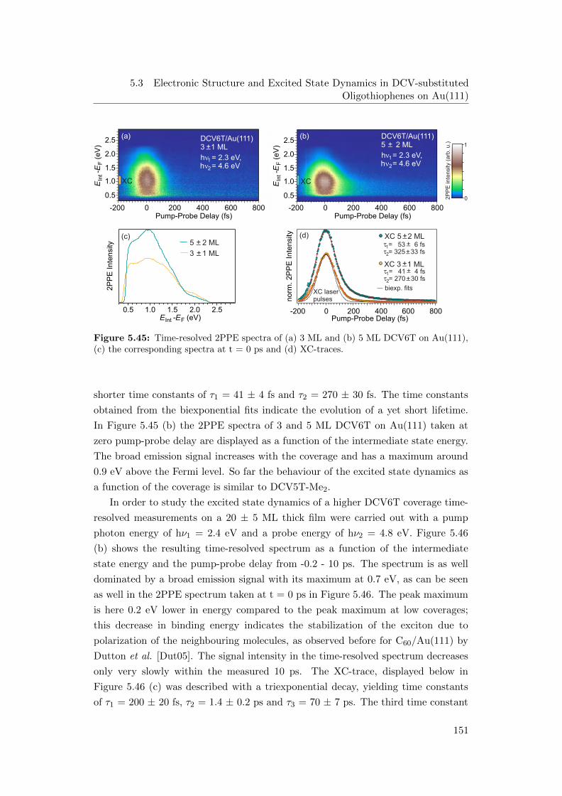
5.3 Electronic Structure and Excited State Dynamics in DCV-substitutedOligothiophenes on Au(111)
Pump-Probe Delay (fs)
DCV6T/Au(111)3 1 ML
h1 = 2.3 eV, h2= 4.6 eV
2P
PE
Inte
nsi
ty
2.52.01.51.00.5
8006004002000-200
+_(a)
5 2 ML+_
EInt -EF (eV)
3 1 ML+_
(c)
8006004002000-200
norm
. 2P
PE
Inte
nsi
ty
Pump-Probe Delay (fs)
(d) XC 5 2 ML+_
XC 3 1 ML+_
XCEIn
t-E
F (
eV
)
2.5
2.0
1.5
1.0
0.5
DCV6T/Au(111)5 2 ML
h1= 2.3 eV, h2= 4.6 eV
+_
Pump-Probe Delay (fs)8006004002000-200
(b)
XC
0
1
2P
PE
inte
nsi
ty (
arb
. u
.)
EIn
t-E
F (
eV
)
2.5
2.0
1.5
1.0
0.5
= 53 6 fs+_
= 325 33 fs+_1
2
= 41 4 fs+_
= 270 30 fs+_1
2
biexp. fitsXC laser pulses
Figure 5.45: Time-resolved 2PPE spectra of (a) 3 ML and (b) 5 ML DCV6T on Au(111),(c) the corresponding spectra at t = 0 ps and (d) XC-traces.
shorter time constants of τ1 = 41 ± 4 fs and τ2 = 270 ± 30 fs. The time constants
obtained from the biexponential fits indicate the evolution of a yet short lifetime.
In Figure 5.45 (b) the 2PPE spectra of 3 and 5 ML DCV6T on Au(111) taken at
zero pump-probe delay are displayed as a function of the intermediate state energy.
The broad emission signal increases with the coverage and has a maximum around
0.9 eV above the Fermi level. So far the behaviour of the excited state dynamics as
a function of the coverage is similar to DCV5T-Me2.
In order to study the excited state dynamics of a higher DCV6T coverage time-
resolved measurements on a 20 ± 5 ML thick film were carried out with a pump
photon energy of hν1 = 2.4 eV and a probe energy of hν2 = 4.8 eV. Figure 5.46
(b) shows the resulting time-resolved spectrum as a function of the intermediate
state energy and the pump-probe delay from -0.2 - 10 ps. The spectrum is as well
dominated by a broad emission signal with its maximum at 0.7 eV, as can be seen
as well in the 2PPE spectrum taken at t = 0 ps in Figure 5.46. The peak maximum
is here 0.2 eV lower in energy compared to the peak maximum at low coverages;
this decrease in binding energy indicates the stabilization of the exciton due to
polarization of the neighbouring molecules, as observed before for C60/Au(111) by
Dutton et al. [Dut05]. The signal intensity in the time-resolved spectrum decreases
only very slowly within the measured 10 ps. The XC-trace, displayed below in
Figure 5.46 (c) was described with a triexponential decay, yielding time constants
of τ1 = 200 ± 20 fs, τ2 = 1.4 ± 0.2 ps and τ3 = 70 ± 7 ps. The third time constant
151

5 Results
DCV6T/Au(111)20 5 ML
h = 2.4 eV
XC (0.5 - 0.8 eV) triexponential fit
= 200 20 fs
+_
1h = 4.8 eV2
1086420Pump-Probe Delay (ps)
2P
PE
Inte
nsi
ty
1 +_
= 1.4 0.2 ps 2 +_
= 70 7 ps 3 +_
2PPE Intensity
(a) t = 0 ps (b)
(c)
0
1
2P
PE
inte
nsi
ty (
arb
. u
.)
2.0
1.5
1.0
0.5
EIn
t -EF (e
V)
0.0
2.0
1.5
1.0
0.5
EIn
t-E
F (
eV
)
0.0
+_
XC
Figure 5.46: (a) 2PPE spectrum of a 20 ML thick DCV6T film onAu(111) recorded at t= 0 ps, (b) time-resolved spectrum measured up to apump-probe delay of 10 ps and (c) XC-trace described by a triexponentialempirical fit function.
exceeds the measured time range and a further slowing down of the decay can be
assumed. This would require a fourth component to describe the overall decay as
it is the case for DCV5T-Me2. Due to the broad emission signal which does not
allow to disentangle different states no unambiguous assignment can be made for
the obtained time constants. The possible decay and relaxation mechanisms taking
place on the respective time scales have been discussed before in Section 5.3.3.
In the following paragraph the dynamics of the two DCV-substituted thiophenes
will be compared in order to find out whether the obtained results reflect the better
solar cell performance of DCV5T-Me2 compared to DCV6T.
To compare the dynamics of the two molecules the XC-traces of the 20 ± 5 ML
thick DCV5T-Me2 and DCV6T films are plotted as a function of the pump-probe
delay and normalized to the maximum signal intensity in Figure 5.47. The striking
difference between these two XC-traces are the different amplitudes. Whereas for
DCV5T-Me2 the intensity drops by more than 2/3 within the first two ps only a small
decrease in intensity is observed for DCV6T. This indicates that the ultrafast decay
processes are much more efficient in the case of DCV5T-Me2. This might be due to
a stronger coupling to vibrational states. In order to compare the time constants
the DCV5T-Me2 XC-trace was fitted in a time range between -0.2 and 10 ps (before
normalization) with the triexponential decay function employed before to fit the
152

5.3 Electronic Structure and Excited State Dynamics in DCV-substitutedOligothiophenes on Au(111)
no
rm.
2P
PE
In
ten
sity
1086420Pump-Probe Delay (ps)
XC 20 5 ML DCV6T triexponential fit
= 200 20 fs1 +_
= 1.4 0.2 ps 2 +_
= 70 7 ps 3 +_
+_
XC 20 5 ML DCV5T-Me triexponential fit
= 125 13 fs1 +_
= 0.9 0.1 ps 2 +_
= 11 1 ps 3 +_
+_ 2
Figure 5.47: Comparison of the normalized XC-traces of 20 ML thick DCV5T-Me2 and DCV6T films on Au(111) in a time interval between -0.2 to 10 ps, bothfitted with the same triexponential decay function: The dynamics in DCV6T issignificantly slower than in DCV5T-Me2.
DCV6T XC-trace. The time constants obtained with this fit are in good accordance
with the first three time constants yielded before by the quadruple exponential fit
(which was used to fit the complete XC-trace up to a pump-probe delay of 300 ps).
A comparison of the time constants reveals that especially the third component is
significantly slower in the DCV6T film than in DCV5T-Me2. This ps lifetime might
be related to the exciton or polaron lifetime, which is considerably faster in DCV5T-
Me2. This may have several reasons such as a faster recombination rate or faster
exciton diffusion, or charge carrier transport in the case of polarons, away from the
surface towards the metal interface where charge transfer occurs. A faster electron-
hole recombination rate seems unlikely due to the very similar optical properties
of the two molecules known so far. In DCV5T-Me2 crystals a greater number of
intermolecular interactions, which are known to promote the exciton mobility, was
found and employed as an explanation for the superior performance of solar cells
containing DCV5T-Me2 [Fit12b, Fit12a, Sch12b]. In a solar cell efficient diffusion
allows excitons to travel fast to the donor/acceptor interface where the charges are
separated, resulting thus in a high photon to electron conversion.
Summary
In the following the findings on the electronic structure and excited state dynamics
in DCV5T-Me2 and DCV6T on Au(111) are concluded. The electronic structure,
from the submonolayer to the multilayer regime, of the DCV-substituted thiophenes
on Au(111) was found to be very similar and in good accordance with STS measure-
ments [Yan14a, Bog15]. At submonolayer coverages hybridization of the molecular
states with the metal surface leads to a decrease of the HOMO-LUMO gap, which
153

5 Results
opens up again in the second layer when the molecules are electronically decoupled
from the surface. Time-resolved 2PPE measurements demonstrate coverage depen-
dent excited state lifetimes indicating interaction with the metal surface which is
quenched for higher coverages. In addition TR-2PPE revealed that the dynamics in
DCV6T films is slower than in DCV5T-Me2 films. This can be explained by a more
efficient exciton and carrier diffusion in DCV5T-Me2 films due to enhanced inter-
molecular interactions via the methyl-groups which are correlated with the solar cell
efficiency [Fit12b, Fit12a, Sch12b]. To obtain a complete picture of the elementary
electronic processes in these systems further investigations using time-resolved op-
tical spectroscopy such as transient absorption or time-resolved photoluminescence
would be attractive since they promise information about e.g. the recombination
lifetime.
154

5.4 Electronic Properties of P3HT Films and the Influence of Crystallinity
5.4 Electronic Properties of P3HT Films and the Influ-
ence of Crystallinity
P3HT is a semiconducting conjugated polymer which has been investigated exten-
sively due to its high carrier mobility and easy processibility. The film morphology
of π-conjugated polymers is known to have a significant impact on the electronic
structure, charge carrier transport and exciton diffusion and dissociation [Pan15].
In this work the influence of annealing on the electronic structure and excited
state dynamics in RR-P3HT films is investigated. As previous 2PPE studies of RR-
P3HT films did not yield well resolved spectra [Var12c, Soh07] we aim to demonstrate
that 2PPE is a good method to study as well highly defined polymer films. In
the following sections a comparative 2PPE study of two P3HT films with different
degrees of crystallinity is presented.
Direct photoemission measurements demonstrate that the IP is not influenced
by enhanced crystallinity. In contrast the optical gap increases upon annealing,
as the CBM shifts upwards. Further 2PPE experiments reveal the existence of
additional three unoccupied electronic states. One of the states can be related to
the exciton while the second feature is most likely due to polaron pairs and/or
polarons. The third unoccupied state might be due to a higher lying unoccupied
band or an excitonic state and is shifted to lower energies for the annealed sample.
Moreover the peak width of the features was found to decrease upon annealing.
Compared to previous 2PPE measurements on RR-P3HT films the spectra obtained
in this work are of good quality and allow to determine the electronic structure of
the two samples.
Time-resolved 2PPE measurements reveal multiexponential decays for both ex-
cited states. The exciton decay takes place on a slower time scale than the polaron
pair and/or polaron decay. Comparing the dynamics of the two different films shows
that the decay dynamics are faster in the mc-sample than in the as-sample. This can
be explained by the larger fraction of crystalline phases which are known to control
and promote the transport properties in P3HT.
155
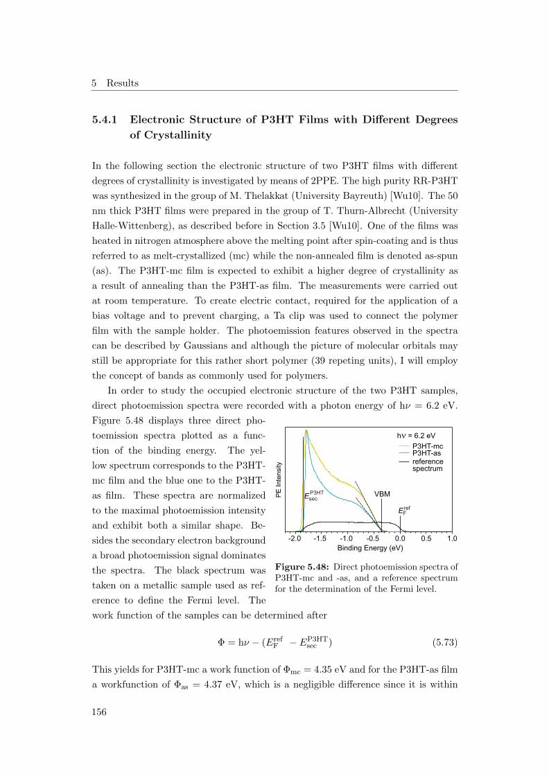
5 Results
5.4.1 Electronic Structure of P3HT Films with Different Degrees
of Crystallinity
In the following section the electronic structure of two P3HT films with different
degrees of crystallinity is investigated by means of 2PPE. The high purity RR-P3HT
was synthesized in the group of M. Thelakkat (University Bayreuth) [Wu10]. The 50
nm thick P3HT films were prepared in the group of T. Thurn-Albrecht (University
Halle-Wittenberg), as described before in Section 3.5 [Wu10]. One of the films was
heated in nitrogen atmosphere above the melting point after spin-coating and is thus
referred to as melt-crystallized (mc) while the non-annealed film is denoted as-spun
(as). The P3HT-mc film is expected to exhibit a higher degree of crystallinity as
a result of annealing than the P3HT-as film. The measurements were carried out
at room temperature. To create electric contact, required for the application of a
bias voltage and to prevent charging, a Ta clip was used to connect the polymer
film with the sample holder. The photoemission features observed in the spectra
can be described by Gaussians and although the picture of molecular orbitals may
still be appropriate for this rather short polymer (39 repeting units), I will employ
the concept of bands as commonly used for polymers.
In order to study the occupied electronic structure of the two P3HT samples,
direct photoemission spectra were recorded with a photon energy of hν = 6.2 eV.
PE
Inte
nsi
ty
-2.0 -1.5 -1.0 -0.5 0.0 0.5 1.0
Binding Energy (eV)
VBM
E
h = 6.2 eV
reference
P3HT-mc P3HT-as
F
spectrum
Esec
ref
P3HT
Figure 5.48: Direct photoemission spectra ofP3HT-mc and -as, and a reference spectrumfor the determination of the Fermi level.
Figure 5.48 displays three direct pho-
toemission spectra plotted as a func-
tion of the binding energy. The yel-
low spectrum corresponds to the P3HT-
mc film and the blue one to the P3HT-
as film. These spectra are normalized
to the maximal photoemission intensity
and exhibit both a similar shape. Be-
sides the secondary electron background
a broad photoemission signal dominates
the spectra. The black spectrum was
taken on a metallic sample used as ref-
erence to define the Fermi level. The
work function of the samples can be determined after
Φ = hν − (ErefF − EP3HT
sec ) (5.73)
This yields for P3HT-mc a work function of Φmc = 4.35 eV and for the P3HT-as film
a workfunction of Φas = 4.37 eV, which is a negligible difference since it is within
156
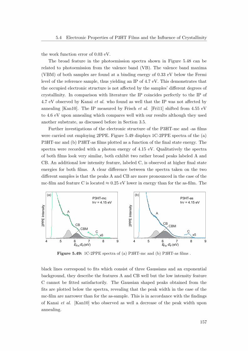
5.4 Electronic Properties of P3HT Films and the Influence of Crystallinity
the work function error of 0.03 eV.
The broad feature in the photoemission spectra shown in Figure 5.48 can be
related to photoemission from the valence band (VB). The valence band maxima
(VBM) of both samples are found at a binding energy of 0.33 eV below the Fermi
level of the reference sample, thus yielding an IP of 4.7 eV. This demonstrates that
the occupied electronic structure is not affected by the samples’ different degrees of
crystallinity. In comparison with literature the IP coincides perfectly to the IP of
4.7 eV observed by Kanai et al. who found as well that the IP was not affected by
annealing [Kan10]. The IP measured by Frisch et al. [Fri11] shifted from 4.55 eV
to 4.6 eV upon annealing which compares well with our results although they used
another substrate, as discussed before in Section 3.5.
Further investigations of the electronic structure of the P3HT-mc and -as films
were carried out employing 2PPE. Figure 5.49 displays 1C-2PPE spectra of the (a)
P3HT-mc and (b) P3HT-as films plotted as a function of the final state energy. The
spectra were recorded with a photon energy of 4.15 eV. Qualitatively the spectra
of both films look very similar, both exhibit two rather broad peaks labeled A and
CB. An additional low intensity feature, labeled C, is observed at higher final state
energies for both films. A clear difference between the spectra taken on the two
different samples is that the peaks A and CB are more pronounced in the case of the
mc-film and feature C is located ≈ 0.25 eV lower in energy than for the as-film. The
2P
PE
In
ten
sity
987654EFin-EF (eV)
2P
PE
In
ten
sity
P3HT-as
987654EFin-EF (eV)
h = 4.15 eV h = 4.15 eV
P3HT-mc(a) (b)
AA
CBMC
CBM
Cx6 x5
CBCB
Figure 5.49: 1C-2PPE spectra of (a) P3HT-mc and (b) P3HT-as films .
black lines correspond to fits which consist of three Gaussians and an exponential
background, they describe the features A and CB well but the low intensity feature
C cannot be fitted satisfactorily. The Gaussian shaped peaks obtained from the
fits are plotted below the spectra, revealing that the peak width in the case of the
mc-film are narrower than for the as-sample. This is in accordance with the findings
of Kanai et al. [Kan10] who observed as well a decrease of the peak width upon
annealing.
157

5 Results
The feature labeled CB is related to the conduction band of P3HT, as will be
discussed below, and the CBM is determined by extrapolating the rising edge of
the Gaussian to the baseline. This yields CBM at final state energies of 5.65 eV
for P3HT-mc and 5.5 eV for P3HT-as, i.e. intermediate state energies of 2.85 eV
and 3.0 eV below the vacuum level. This upward shift of the CBM upon annealing
is here due to the decrease of the peak width, while the peak maximum stays at
the same energetic position. Note that the energetic positions of the unoccupied
electronic states obtained here from 2PPE can not be compared to those from IPES
from reference [Kan10]. IPES measures an (N+1)-electron state while 2PPE mea-
sures in this case an N-electron state as the unoccupied states are populated via
intermolecular excitations and not through electron transfer from the substrate to
the adsorbate.
In order to be able to assign the observed features to occupied or unoccupied
states, photon energy dependent measurements were performed. Figure 5.50 (a)
displays a 1C-2PPE spectra series measured on the P3HT-mc film as a function of
the final state energy. In the spectrum recorded with a photon energy of 4.15 eV
the features A and CB are visible very clearly while they have vanished in the 4.4
eV spectrum. In Figure 5.50 (b) the peak positions are plotted as a function of
8765
4.00 eV P3HT-mc
8.0
7.5
7.0
6.5
6.0
5.5
EF
in
- E
F (
eV
)
4.34.24.14.03.9 Photon Energy (eV)
A: m = 0.7 ± 0.2 CB: m = 1.1 ± 0.1 C: m = 0.9 ± 0.4
EFin - EF (eV)
2P
PE
Inte
nsi
ty
(a) (b)
4.15 eV 4.20 eV 4.40 eV
A
CB
x10 C
h =
Figure 5.50: (a) Photon energy dependent 1C-2PPE spectra series taken on P3HT-mc, (b)peak maxima plotted as a function of the photon energy, indicating that all three featuresoriginate from unoccupied intermediate states.
the photon energy, yielding a slope around 1 in all three cases. This indicates that
all three the peaks can be assigned to unoccupied states or bands. As mentioned
before CB is related to the conduction band with its minimum 2.85 eV below the
vacuum level. This assignment is based on the energetic position of the CBM which
is located 1.85 eV above the VBM. This value corresponds to the optical gap and
compares well with the literature value around 1.8 - 1.9 eV [Kor01, Sch14, Coo08].
158

5.4 Electronic Properties of P3HT Films and the Influence of Crystallinity
The features A and C can be related to unoccupied intermediate states located
2.95 eV (A) and 0.95 eV (C) below the vacuum level. Feature A is thus located
1.75 eV above the VBM and is most likely due to polaron pairs and/or polarons,
according to previous studies which found the resonance related to polaron pairs
[Guo09] or delocalized polarons residing in the crystalline phase of the P3HT film
at 1.9 eV [Kor01, Zha12a]. Feature C might originate from an energetically higher
unoccupied band or excitonic state, according to Muller et al. [Mul12] who measured
with X-ray absorption an excitonic state 3.1 eV above the VBM.
In the case of P3HT-as, the CBM is shifted to lower energies by 0.15 eV, thus
yielding an optical gap of 1.7 eV. The downward shift of the CBM is due to the
broader peak width characteristic for the lower degree of crystallinity in the as-
sample. The energetic position of state A which is most likely due to polaron pairs
or polarons is the same for both samples. Whereas the third feature C, related to
either a higher lying unoccupied band or exciton, is shifted upwards by 0.15 eV
compared to the mc-film, and is thus located 0.7 eV below the vacuum level for the
as-film.
In order to further investigate the electronic structure of the P3HT films 2C-
2PPE spectra of both films are compared and the 2C-2PPE signal as a function of
the pump-probe delay is studied (Figure 5.51). Figure 5.51 (a) compares 2C-2PPE
P3HT-mc
h = 2.085 eV1
h = 4.170 eV2
7.06.56.05.55.04.5
2P
PE
In
ten
sity
EFin-EF(eV)
(a)
A
2P
PE
In
ten
sity
EFin -EF (eV)
P3HT-mch = 2.085 eV
7.06.56.05.55.04.5
t = 0 ps
= 100 ps = 50 ps
= 10 ps = 20 ps
fit peak X peak AA
X
1h = 4.170 eV2
(b)
P3HT-as
Figure 5.51: (a) 2C-2PPE spectra of the P3HT-mc and the P3HT-as film, (b) spectra takenat different time-delays on the melt-crystallized film: at longer time-delays an additionalfeature X becomes visible at 5.0 eV
spectra recorded with photon energies of 2.9 eV and 4.17 eV on the two respective
films. Both spectra look qualitatively very similar showing a feature at a final state
energy of 5.55 eV. This emission signal is more pronounced in the spectrum taken on
the mc-film and can be, according to the energetic position, related to state A which
was observed before in the 1C-2PPE spectra. Another feature is hidden between
peak A and the secondary electron background and becomes visible at longer time
delays (Figure 5.51 (b)).
159

5 Results
Figure 5.51 (b) shows a series of 2C-2PPE spectra which were measured on the
P3HT-mc film at different time delays with a pump photon energy of hν1 = 2.09
eV and a probe photon energy of hν2 = 4.17 eV. The black spectrum corresponds
to the spectrum taken at zero pump-probe delay shown before in Figure 5.51 (a).
The 2PPE emission intensity of feature A decreases rapidly within the first 10 ps.
Whereas the spectra taken at time delays of 10 ps (green) and 20 ps (blue) do not
exhibit any pronounced structure and look like photoemission from a continuum
of states, a structure becomes visible again at a time delay of 50 ps (yellow). At a
pump-probe delay of 100 ps (red spectrum) clearly two broad features are observable
which can be fitted with a function consisting of two Gaussians and an exponential
background, as illustrated by the grey line. The fit yields peak positions at final state
energies of 4.95 eV and 5.55 eV which corresponds to intermediate state energies
of 3.55 and 2.95 eV below the vacuum level, due to probing with 4.17 eV photons.
Evac
EF
(a) P3HT-mc (b) P3HT-asE (eV)
VB-4.70
VB
-0.95
-4.70
-3.55
-2.95-2.85
-0.7
0
X
ACBM
C
X
C
-4.35
-3.00
-3.55
-2.95 ACBM
1.7 eVE =gopt1.85 eVE =g
opt
Figure 5.52: Energy level diagram of (a) P3HT-mcand (b) P3HT-as films.
This confirms that the feature
at higher energies corresponds
to state A. The feature at lower
energies, labeled as X, is lo-
cated 1.15 eV above the VBM
and is thus attributed to the
singlet exciton which was ob-
served before at resonances be-
tween 1.0 and 1.2 eV [Guo09,
Kor01, Coo08, Her11, Mul12,
Zha12a].
The observed states are
summed up in an energy level
diagram shown in Figure 5.52
(a) for the P3HT-mc and (b) for
the P3HT-as film. The optical gaps amount to 1.85 eV for P3HT-mc and to 1.7 eV
for P3HT-as. State X is assigned to an excitonic state 1.15 eV above the VBM and
state A originates most likely from polaron pairs or polarons. Feature C may be
related to an energetically higher excitonic level or unoccupied band.
In conclusion the different degrees of crystallinity of the two P3HT samples only
weakly influences their electronic structure. Compared to spectra from previous
2PPE studies of RR-P3HT films, the 2PPE spectra obtained in this work show a
larger number and more distinct features [Var12c, Soh07]. This confirms that the
investigated polymer films possess a very well defined structure. In the next section
the dynamics of the excited states A and X will be further investigated.
160

5.4 Electronic Properties of P3HT Films and the Influence of Crystallinity
5.4.2 Influence of Crystallinity on the Excited State Dynamics in
P3HT Films
From the spectra taken at different time delays (Figure 5.51 (b)), it is known that
the excited state populations in X and A are still observable at a pump-probe delay
of 100 ps. In order to investigate the influence of the different degrees of crystallinity
on the excited state dynamics, time-resolved 2PPE measurements on the mc- and
the as-P3HT films were performed.
Figure 5.53 (a) shows the background subtracted (i.e. 1C-2PPE signals have
been subtracted as discussed before in Section 4.5) time-resolved data measured on
the mc-P3HT film with a pump photon energy of hν1 = 2.09 eV and a probe photon
energy of hν2 = 4.18 eV. In the 2D-spectrum the data is plotted as a function of
the intermediate state energy with respect to the Fermi level and as a function of
the pump-probe delay, the photoemission intensity is illustrated by a false colour
code. The spectrum is divided into two parts, the first part includes a pump-probe
delay in the range of -0.3 - 10 ps and the second part is reaching from 10 ps to 300
ps. The time-resolved spectrum shows a very broad 2PPE emission signal in which
the features X and A are not well resolved. But a closer look at the signal at later
delay times reveals that the signal between ≈ 1 - 1.5 eV decays faster than the signal
between ≈ 0.5 - 1 eV. The secondary electron background signal at energies below
0.5 eV exhibits an even longer lifetime.
10
2.0
1.5
1.0
0.5
EIn
t-E
F (
eV
)
86420Pump-Probe Delay (ps)
2P
PE
Inte
nsi
ty
30025020015010050Pump-Probe Delay (ps)
2P
PE
Inte
nsity
triexp. fits
P3HT-mch1 = 2.09 eV
h2 = 4.18 eV 0 1
2PPE intensity (arb. u.)
XC A= 1.2 0.1 ps + _1
= 13 1.3 ps + _2= 80 8 ps + _3
XC X= 1.7 0.2 ps + _1
= 23 2.3 ps + _2= 220 22 ps + _3
2.0
1.5
1.0
0.5
EIn
t-E
F (e
V)
(a)
(b)
A
X
XC A
XC X
Figure 5.53: (a) Time-resolved 2PPE spectrum of P3HT-mc, (b) XC-traces integratedaround the peak maxima of A and X with triexponential fits.
In order to gain deeper insights into the decay dynamics of the investigated
161

5 Results
excited states the time-resolved spectrum was integrated around the peak maxima
of the states A and X, as illustrated by the light green and blue boxes. The obtained
XC-traces are displayed as a function of the pump-probe delay in Figure 5.53 (b).
The XC-traces are described by empirical fit functions consisting of a triexponential
decay convolved with the cross-correlation of Gaussian shaped pulse envelopes. The
fits yield three time constants for each XC-trace, a fast one τ1 in the range of 1-2 ps,
a slower one τ2 which amounts to 10-20 ps and a slow time constant τ3 in the range
of 100-200 of ps. Comparing the time constants obtained for X and A confirms the
observation that the population decay of state X is slower than those of state A.
Due to the broad and overlapping 2PPE signals the excited states cannot be
separated energetically so that the obtained time constants cannot be assigned un-
ambiguously. In addition, divergent time scales for the same processes are reported
in literature, as discussed in Section 3.5, making it even more difficult to relate the
time constants to distinct processes.
State X is related to the singlet exciton 1.15 eV above the VBM, the time con-
stants obtained from the fit amount to τ1 = 1.7 ± 0.2 ps, τ2 = 23 ± 2.3 ps and τ3 =
220 ± 22 ps. A triexponential exciton decay has been observed before by Guo et al.
in transient absorption measurements [Guo09]. They attributed the slowest decay
constant (330 ps) to electron-hole recombination, while for the faster time constants
no assignment was reported. According to the reported luminescence decay ranging
from 300 - 400 ps [Mag97, Kan92, Coo08] the slow decay of 220 ± 22 ps is most
likely connected to the recombinative decay of excitons. The fast time constant τ1 =
1.7 ± 0.2 ps might originate from internal vibrational relaxation within the excited
state due to excitation of higher vibronic levels.
Fitting the XC-trace of state A, which is most probably related to polaron pairs
and/or polarons, yields time constants of τ1 = 1.2 ± 0.1 ps, τ2 = 13 ± 1.3 ps and
τ2 = 80 ± 8 ps. All three time constants are faster than those obtained for the
excitonic state but they are still in the same order of magnitude. According to
literature where the decay of polaron pairs via recombination and dissociation into
polarons was found to take place on a time scale ranging from 0.5 ps [Ai06] to 2.6 ps
[Var12c] the fast decay of 1.2 ± 0.1 ps might be related to the decay of polaron pairs.
The slower decay times (τ2 and τ3) might the be due to geminate recombination
of polaron pairs and/or recombination of negative polarons with positive polarons
located on adjacent polymer chains. The XC-traces of the exciton and the polaron
exhibit the same instantaneous risetime corroborating the observation by Guo et al.
that polarons can form directly after photon absorption and not only from relaxed
singlet excitons [Guo09].
In order to investigate the influence of the different degrees of crystallinity on
162

5.4 Electronic Properties of P3HT Films and the Influence of Crystallinity
the excited state dynamics time-resolved 2PPE measurements have been performed
as well on the P3HT-as film. Figure 5.54 (a) shows a time-resolved 2PPE spectrum
EIn
t-E
F (e
V)
1086420Pump-Probe Delay (ps)
2P
PE
In
ten
sity
30025020015010050Pump-Probe Delay (ps)
triexp. fits
2P
PE
Inte
nsity
2.0
1.5
1.0
0.5
EIn
t-E
F (
eV
)
2.0
1.5
1.0
0.5
P3HT-ash1=2.09 eV
h2=4.17eV 0 1
2PPE intensity (arb. u.)
XC A= 1.7 0.2 ps + _1= 23 2.3 ps + _2= 140 14 ps + _3
XC X= 2.5 0.3 ps + _1
= 34 3.4 ps + _2= 230 23 ps + _3
(a)
(b)
A
X
XC A
XC X
Figure 5.54: (a) Time-resolved 2PPE spectrum of P3HT-as, (b) XC-traces integratedaround the peak maxima of A and X with triexponential fits.
of the P3HT-as film as a function of the pump-probe delay, recorded with photon
energies of hν1 = 2.09 eV and hν2 = 4.17 eV. The time-resolved spectrum looks
qualitatively very similar to the spectrum measured on the mc-film: It shows as well
a broad emission signal which decays faster between 1.0 - 1.5 eV than between 0.5
- 1.0 eV and below intermediate state energies of 0.5 eV the hot electron dynamics
decay even slower. The time-resolved 2PPE spectrum was integrated around the
maxima of states A and X, yielding the XC-traces displayed as a function of the
pump-probe delay in Figure 5.54, where the red lines correspond to triexponential
fits. The time constants obtained for the polaronic state A are, like in the case
of the mc-film, faster than those obtained for the exciton. Again, the electronic
processes leading to the triexponential decay cannot be disentangled, therefore the
same possible processes as for P3HT-mc might be considered.
Comparing the time constants obtained for the two different films, listed in Ta-
ble 5.1, reveals that the decay dynamics in the P3HT-as film are slower than in
the P3HT-mc film. Only the slowest decay (τ3) of the excitonic state X, which is
attributed to electron-hole recombination, is in good agreement for both films. In
case of the other time constants, especially those related to polaron decay, the faster
dynamics observed for the mc-film can be explained by the enhanced crystallinity
which is known to promote charge transport.
163
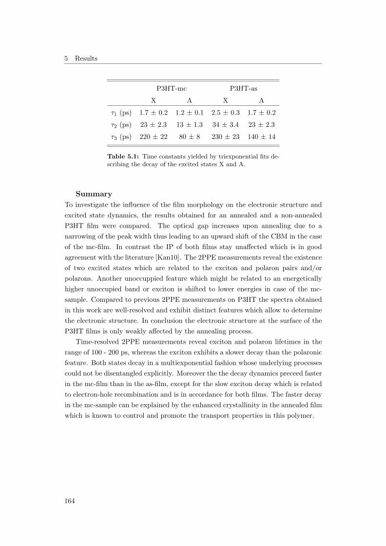
5 Results
P3HT-mc P3HT-as
X A X A
τ1 (ps) 1.7 ± 0.2 1.2 ± 0.1 2.5 ± 0.3 1.7 ± 0.2
τ2 (ps) 23 ± 2.3 13 ± 1.3 34 ± 3.4 23 ± 2.3
τ3 (ps) 220 ± 22 80 ± 8 230 ± 23 140 ± 14
Table 5.1: Time constants yielded by triexponential fits de-scribing the decay of the excited states X and A.
Summary
To investigate the influence of the film morphology on the electronic structure and
excited state dynamics, the results obtained for an annealed and a non-annealed
P3HT film were compared. The optical gap increases upon annealing due to a
narrowing of the peak width thus leading to an upward shift of the CBM in the case
of the mc-film. In contrast the IP of both films stay unaffected which is in good
agreement with the literature [Kan10]. The 2PPE measurements reveal the existence
of two excited states which are related to the exciton and polaron pairs and/or
polarons. Another unoccuppied feature which might be related to an energetically
higher unoccupied band or exciton is shifted to lower energies in case of the mc-
sample. Compared to previous 2PPE measurements on P3HT the spectra obtained
in this work are well-resolved and exhibit distinct features which allow to determine
the electronic structure. In conclusion the electronic structure at the surface of the
P3HT films is only weakly affected by the annealing process.
Time-resolved 2PPE measurements reveal exciton and polaron lifetimes in the
range of 100 - 200 ps, whereas the exciton exhibits a slower decay than the polaronic
feature. Both states decay in a multiexponential fashion whose underlying processes
could not be disentangled explicitly. Moreover the the decay dynamics preceed faster
in the mc-film than in the as-film, except for the slow exciton decay which is related
to electron-hole recombination and is in accordance for both films. The faster decay
in the mc-sample can be explained by the enhanced crystallinity in the annealed film
which is known to control and promote the transport properties in this polymer.
164

6 Summary and Conclusions
This work focuses on fundamental processes relevant for light harvesting and gen-
eration. Both conversion mechanisms, photon-to-electron and electron-to-photon,
are influenced by similar mechanisms such as exciton formation, decay and diffusion
as well as charge and energy transfer processes at interfaces. Those in turn are
highly affected by e.g. the energy level alignment at the active inorganic/organic
and organic/organic interfaces and the film morphology. The questions of how the
molecular levels align at the interface with the substrate and within the film, how
and on which times scales excitons form and decay, how the quasiparticles interact
and how they are affected by modifications of side conditions are treated in this
thesis.
These questions were tackled by 2PPE investigations of four model systems which
represent different active parts of a solar cell or an LED. For instance the conduc-
tive transparent oxide ZnO is a promising candidate as active medium in LEDs and
also as transparent electrode material for OPVCs when combined with an organic
semiconductor. Here the spirobifluorene derivative SP6 was used to study charge
transfer processes at the interface with ZnO. In addition, bulk SP6 represents a
model system for an organic LED medium. The energy level alignment at an inter-
face between a metallic electrode and an organic donor material was studied using
DCV-substituted oligothiophenes on Au. The fourth model system is the polymer
donor material P3HT, in which the influence of the film morphology on the electronic
structure and the excited state dynamics was investigated.
In the following the findings for the different model systems are summarized:
H-induced Metallicity and Excited State Dynamics at the O-terminated
ZnO Surface
On the fully O-terminated ZnO surface the adsorption of hydrogen leads to a switch-
ing of the upward surface band bending to downward band bending and the work
function decreases significantly. In addition, the formation of a CAL at the surface
was observed which saturates for higher coverages. This strongly suggests that the
CAL reduction observed for the non-polar surface is due to ZnH-bond formation.
With increasing charge carrier density at the surface, both photo- and H-induced,
the ultrafast electron-phonon scattering which is a prerequisite for surface exciton
formation is screened, thus leading to a slower formation of the surface exciton.
On this basis time-resolved 2PPE investigations on the fully Zn-terminated sur-
face seem to be an interesting experiment as this surface is known to exhibit a
completely different electronic surface structure. For instance no CAL is formed
165
6 Summary and Conclusions
since hydrogen acts as an electron acceptor in the ZnH-bond. Therefore it would be
very interesting to find out whether an excitonic species, e.g. the bulk exciton or
another kind of surface exciton, is at all observable at this surface.
Exciton Formation and Decay Dynamics in SP6 Films on ZnO
In addition to the picosecond dynamics which were observed before in excited state
transmission and were related to internal vibrational relaxation and the excited
states’ population decay via competing pathways [Fog15], an ultrafast decay was
discovered in 2PPE which may be attributed to polarization effects due to the exci-
ton formation process. The picosecond dynamics agree well with those from excited
state transmission, although 2PPE probes only the surface whereas excited state
transmission probed also bulk contributions. This is due to the slow exciton dif-
fusion in the amorphous film. The long-lived triplet state decays via triplet-triplet
annihilation which leads here to the emission of electrons. This triplet state has a
lifetime of tens of µs which can be efficiently reduced by increasing the temperature
and thus the diffusion towards the ZnO surface or other quenching sites. A reduction
of the film thickness showed the same effect. In addition the 2PPE measurements
allowed to uncover the energy level alignment at the SP6/ZnO interface.
Based on these findings it would be interesting to conduct further time-resolved
photoluminescence measurements to find out whether delayed fluorescence, which is
often a consequence of triplet-triplet annihilation, occurs as well in this system.
Electronic Structure and Excited State Dynamics in DCV-substituted
Oligothiophenes on Au(111)
The 2PPE measurements of DCV-substituted oligothiophenes on Au(111) revealed,
in accordance with previous STS measurements, that the energy level alignment of
the molecular monolayer is influenced by the metal surface and changes in the mul-
tilayer regime. The excited state dynamics exhibit a dependence on the coverage
demonstrating that charge transfer at the metal interface is an efficient decay chan-
nel. In addition, the excited state dynamics are faster in the case of the molecule
which is known to possess a larger number of intermolecular interactions thus pro-
moting the exciton diffusion.
On the basis of these results further investigations using time-resolved optical
spectroscopy seem promising as they provide the possibility to measure the photolu-
minescence lifetimes and thus allow a deeper insight into the processes after optical
excitation.
166
Electronic Properties of P3HT Films and the Influence of Crystallinity
In contrast to previous 2PPE studies on P3HT films well-resolved spectra were
obtained confirming the outstanding chemical purity and quality of these films. Two
long-lived states, related to the exciton and to polaron pairs and/or polarons, have
been observed. The excited state dynamics were found to be faster in the film with
the higher degree of crystallinity, thus reflecting the superior transport properties.
Both the electronic structure and the excited state dynamics are only weakly affected
by the different film morphologies of these two P3HT films.
Further 2PPE investigations could be performed using lower pump photon ener-
gies since a recent study revealed the existence of two kinds of aggregates in annealed
P3HT films [Pan15]. These aggregates can be excited separately with photon ener-
gies lower than 2 eV.
In conclusion these results provide a deeper insight into the complex interplay be-
tween the various decay pathways of optically excited states. Understanding these
processes in detail opens up the possibility to selectively utilize and influence decay
channels in order to optimize device performances. The challenges thereby are to
reinforce the desired processes while unwanted loss channels have to be minimized.
For instance, the solar cell efficiency can be improved by enhancing the exciton dif-
fusion such that the excitons have not decayed before reaching the active interfaces.
This can be achieved e.g. by external modifications like the temperature or by in-
creasing the internal arrangement of the film via annealing or the use of sophisticated
molecular designs. In systems where triplet-triplet annihilation results in delayed
fluorescence the enhancement of this process promises greater photon yields. This
represents an additional way, besides enhancing phosphorescence with heavy atoms,
to exploit triplets for light generation.
167

6 Summary and Conclusions
168
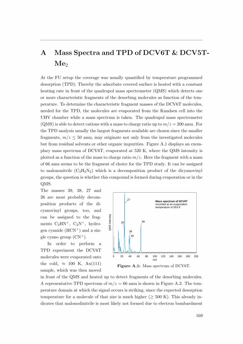
A Mass Spectra and TPD of DCV6T & DCV5T-
Me2
At the FU setup the coverage was usually quantified by temperature programmed
desorption (TPD). Thereby the adsorbate covered surface is heated with a constant
heating rate in front of the quadrupol mass spectrometer (QMS) which detects one
or more characteristic fragments of the desorbing molecules as function of the tem-
perature. To determine the characteristic fragment masses of the DCV6T molecules,
needed for the TPD, the molecules are evaporated from the Knudsen cell into the
UHV chamber while a mass spectrum is taken. The quadrupol mass spectrometer
(QMS) is able to detect cations with a mass to charge ratio up tom/z = 200 amu. For
the TPD analysis usually the largest fragments available are chosen since the smaller
fragments, m/z ≤ 50 amu, may originate not only from the investigated molecules
but from residual solvents or other organic impurities. Figure A.1 displays an exem-
plary mass spectrum of DCV6T, evaporated at 520 K, where the QMS intensity is
plotted as a function of the mass to charge ratio m/z. Here the fragment with a mass
of 66 amu seems to be the fragment of choice for the TPD study. It can be assigned
to malononitrile (C3H2N2) which is a decomposition product of the dicyanovinyl
groups, the question is whether this compound is formed during evaporation or in the
QMS.
QM
S In
tens
ity
200180160140120100806040200m/z
66
38
27
26
39
Mass spectrum of DCV6Trecorded at an evaporationtemperature of 553 K
Figure A.1: Mass spectrum of DCV6T.
The masses 39, 38, 27 and
26 are most probably decom-
position products of the di-
cyanovinyl groups, too, and
can be assigned to the frag-
ments C2HN+, C2N+, hydro-
gen cyanide (HCN+) and a sin-
gle cyano group (CN+).
In order to perform a
TPD experiment the DCV6T
molecules were evaporated onto
the cold, ≈ 100 K, Au(111)
sample, which was then moved
in front of the QMS and heated up to detect fragments of the desorbing molecules.
A representative TPD spectrum of m/z = 66 amu is shown in Figure A.2. The tem-
perature domain at which the signal occurs is striking, since the expected desorption
temperature for a molecule of that size is much higher (≥ 500 K). This already in-
dicates that malonodinitrile is most likely not formed due to electron bombardment
169

A Mass Spectra and TPD of DCV6T & DCV5T-Me2
by the QMS or during the desorption from the surface, but that it is formed during
evaporation and coadsorbed on the surface.
QM
S Inte
nsi
ty
700600500400300200100 Temperature (K)
TPD of DCV6T/Au(111) Tc= 520 K, Ts= 97 K
= 66 amum/z
Figure A.2: TPD of DCV6T/Au(111) evap-orated on the cold surface.
The TPD experiment has been re-
peated with the sample temperature
changed to 300 K during evaporation,
since at this temperature malononitrile
is already desorbed, i.e. should not stick
on the surface in the first place. In Fig-
ure A.3 (a) TPD spectra of the masses
27 amu and 66 amu are shown. There
is no significant QMS signal of the frag-
ment mass m/z = 66 amu at tempera-
tures between 180 and 250 K, this con-
firms the suggestion that malonodini-
trile is not generated during DCV6T
desorption or electron bombardment in
the QMS. In fact part of the DCV6T
molecules decompose during evaporation producing malonodinitrile which sticks on
the cold but not on the warm surface. Thus the desorption peaks observed in the
TPD spectrum shown in Figure A.2, can be related to the malondionitrile desorption
between ≈ 180 and 300 K and not to the desorption of DCV6T.
Temperature (K) Temperature (K)
QM
S In
tensity
200 200300 300400 400500 500600 600700 700
TPD of DCV6T/Au(111) Tc= 553 K, Ts = 300 K
evaporation time: 20 min
TPD of DCV6T/Au(111) Tc= 553 K, Ts = 300 K
(a) (b)
increasingcoverage
= 66 amum/z = 27 amum/z
= 27 amum/z
20 min 18 min 25 min
QM
S Inte
nsi
ty
evaporation time
Figure A.3: TPDs of DCV6T/Au(111) evaporated on the Au(111) surface held at 300 K.
Since the detection of the fragment mass of 66 amu does not carry any informa-
tion on the desorption of the DCV6T molecules another mass was tested in TPD
experiments, namely the mass of 27 amu which corresponds most likely to hydro-
gen cyanide (HCN+). The desorption signal of this mass does not vanish when the
molecules are adsorbed on the warm surface, but the features are not separated
170

from each other and the shape of the signal does not allow for exact TPD analy-
sis. The rising signal up to the maximal temperature indicates that the molecules
stick strongly on the sample surface and do not desorb completely. This behaviour
is expected since gold is highly thiophilic and photoemission experiments showed
that the Au(111) surface is not clean after being heated up to 800 K during the
TPD experiment. Figure A.3 (b) shows TPD spectra of m/z = 26 amu for different
coverages, but unfortunately the signal behaves neither proportionally to the film
thickness nor to the evaporation period what makes this fragment inapplicable for
further TPD experiments as well. Since TPD is not practicable for this system and
the evaporation time is not a useful parameter either, the film thickness has to be
determined otherwise as described in Section 4.3.3.
QM
S In
tens
ity
200180160140120100806040200m/z
66
38
39
27
26
Mass spectrum of DCV5T-Me2
recorded at an evaporationtemperature of 553 K
Figure A.4: Mass spectrum of DCV5T-Me2 adsorbedon the Au(111) surface at 300 K.
For DCV5T-Me2 the situa-
tion concerning the applicabil-
ity of TPD was found to be
the same like for DCV6T. Fig-
ure A.4 shows a mass spectrum
taken during the evaporation of
DCV5T-Me2 at a temperature
of 553 K. Here as well malono-
dinitrile with a mass of 66 amu
is observed, but since it does
not show a significant desorp-
tion signal when the sample is
held at 300 K during the depo-
sition of DCV5T-Me2, the same
conclusion can be drawn like for DCV6T, namely that malonodinitrile is already pro-
duced during evaporation and not during the desorption or in the QMS.
The masses 39 , 38 , 27 and 26 amu may be assigned to the same fragments of
the dicyanovinyl groups as described above for DCV5T-Me2. Figure A.5 (a) shows
TPD spectra of DCV5T-Me2 for the masses 26 and 39 amu. Only the fragment
mass of 26 amu which is related to a single cyano group shows a significant signal
which rises at temperatures towards 800 K indicating that the molecules do not
desorb completely and stick on the surface instead. In Figure A.5 (b) TPD spectra
of different coverages DCV5T-Me2/Au(111) are shown but again the integrals of
the QMS signals do not behave proportionally neither to the film thickness nor to
the evaporation period. Therefore the same procedure to quantify the coverage was
carried out like for DCV6T, as described in Section 4.3.3.
The DCV5T-Me2 and DCV6T films were prepared under the same experimental
171
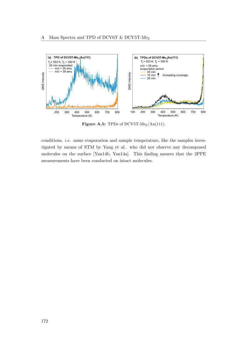
A Mass Spectra and TPD of DCV6T & DCV5T-Me2
Q
MS
In
ten
sity
800700600500400300200
Temperature (K)
(a) TPD of DCV5T-Me /Au(111) 2
m/z = 26 amum/z = 39 amu
20 min evaporated
QM
S I
nte
nsi
ty
800700600500400300200100
Temperature (K)
(b) TPDs of DCV5T-Me 2 /Au(111)
m/z = 26 amu evaporation period
25 min
10 min increasing coverage 20 min
Tc= 553 K, Ts = 300 K Tc= 553 K, Ts = 300 K
Figure A.5: TPDs of DCV5T-Me2/Au(111).
conditions, i.e. same evaporation and sample temperature, like the samples inves-
tigated by means of STM by Yang et al. who did not observe any decomposed
molecules on the surface [Yan14b, Yan14a]. This finding assures that the 2PPE
measurements have been conducted on intact molecules.
172

B Calculation of the Excitation Density
The absorption of light is described by a exponential decay from the surface into the
bulk after the Beer-Lambert law cite:
I(z) = I0 · e(−αz) (B.74)
here I0 is the intensity of the absorbed light at the surface, α is the absorption
coefficient which is a material specific constant and z is the thickness of the light ab-
sorbing material. The penetration depth, l0, is the lengths over which the absorption
decays by 1/e
l0 =1
α(B.75)
The excitation density is given by
N0 =fl
l0hω·
∣∣∣∣∣(
2
1 +√εopt
)2∣∣∣∣∣ (B.76)
where fl corresponds to the laser fluence, i.e. the energy per m2, the second term
accounts for the surface reflectivity and εopt is the dielectric constant of the pho-
toexcited material. In order to calculate the fluence of the incident laser light it has
to be taken into account that after the power is measured the laser beam has to
pass two mirrors and a MgF2 window before it reaches the sample surface. For a
photon energy of 3.8 eV the reflectivity of a Al-mirror is ≈ 90 % and the transmit-
tance of the MgF2 window is ≈ 95 %, thus the prefactor for the laser power P is
0.92 · 0.95=0.77. For the calculation of the illuminated area A of the sample surface
the incidence angle of 45◦ has to be taken into account since it leads to an elliptical
distortion of the laser spot, the laser spot area on the surface is thus given by
A = π · a · b = π ·√
2 ·(
FWHM(x) · FWHM(y)
2
)(B.77)
Since we are working with a pulsed laser source the repetition rate (usually 200 kHz)
has to be included in the calculation. With this the fluence writes as
fl =P
A · rep. rate=
P · 0.77 · 2 · 2π ·√
2 · FWHM(x) · FWHM(y) · rep. rate
=P · 0.77 ·
√8
π · FWHM(x) · FWHM(y) · rep. rate
(B.78)
173
B Calculation of the Excitation Density
Excitation Density in ZnO
The absorption coefficient α of ZnO is for photon energies ≥ 3.3 eV αZnO = 2 ·105 cm−1 [Jel98], with this a penetration depth of l0 = 1/αZnO = 50 nm is obtained.
The optical dielectric constant εopt depends on the photon energy and amounts to
ε3.8 eVopt = 4 + i1.8 for the pump photon energy of 3.8 eV and to ε4.64 eV
opt = 2 + i1.5
for the 4.65 eV probe photon energy [Jel98]. So the fluence of a laser pulse with a
photon energy of 3.8 eV, a spot size of 118 × 101µm and a power of P = 710 µW
and a repetition rate of 200 kHz can be calculated after
fl =710 µW · 0.77 ·
√8
π · 118 µm · 101 µm · 200 kHz= 0.207 J/m2 (B.79)
and with this the excitation density writes as
N0 =0.207 J/m2
l0hω·
∣∣∣∣∣(
2
1 +√
4 + i1.8
)2∣∣∣∣∣ = 2.86 · 1018 cm−3 (B.80)
Excitation Density in SP6
The absorption coefficient of SP6 for a photon energy of 3.6 eV amounts to αSP6 =
4 · 105 cm−1 this yields a penetration depth of l0 = 1/αSP6 = 25 nm [Blu08]. Since
the optical dielectric constant of SP6 is not known it was set to 1. With this
approximation the excitation density for a laser pulse with a photon energy of 3.6
eV and a fluence of 0.013 J/m2 is given by
N0 =0.013 J/m2
l0hω· 1 = 8.96 · 1023m−3 (B.81)
The start population for the diffusion model was calculated for a spot area of 2561
µm. The percentage of the absorbed photons in the upmost 0.5 nm layer of the SP6
film is given by
1− e−0.5 nm25 nm = 0.0198 (B.82)
Thus 1.98 % of 896 000 photons/µm3 = 17741 photons/µm3 are absorbed in the
upmost 0.5 nm layer. The volume of the illuminated are is given by V = 2561 µm ·0.5 nm = 1.28 µm3 and with this the number of absorbed photons amounts to 17741
photons/µm3 · 1.28 µm3= 22708.
174
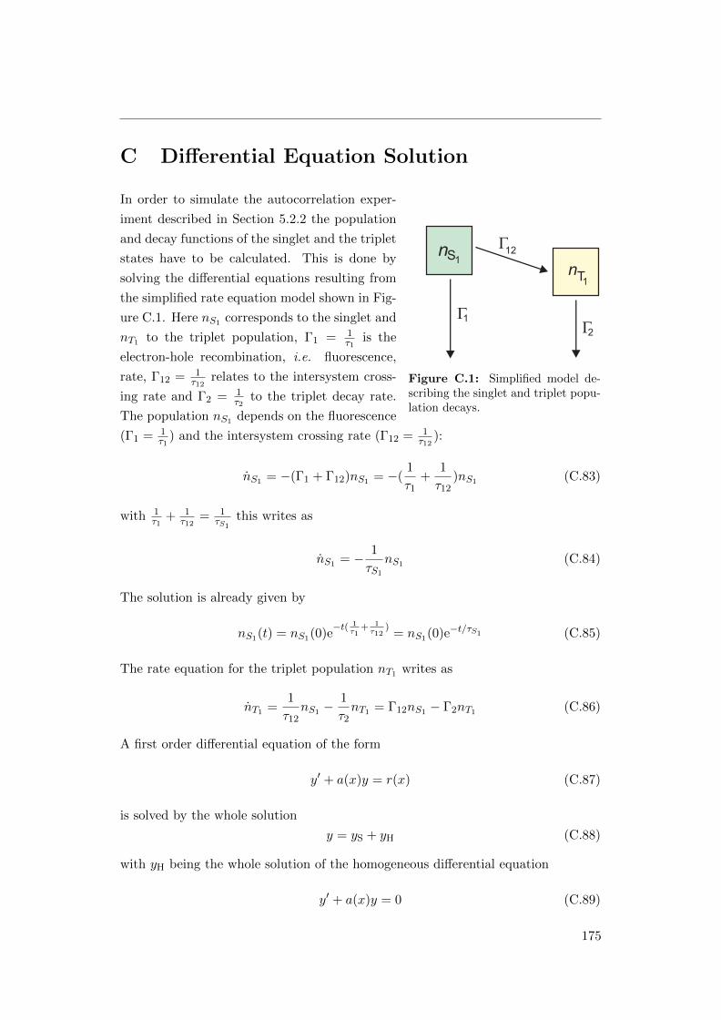
C Differential Equation Solution
1
12
2
nS1nT1
Figure C.1: Simplified model de-scribing the singlet and triplet popu-lation decays.
In order to simulate the autocorrelation exper-
iment described in Section 5.2.2 the population
and decay functions of the singlet and the triplet
states have to be calculated. This is done by
solving the differential equations resulting from
the simplified rate equation model shown in Fig-
ure C.1. Here nS1 corresponds to the singlet and
nT1 to the triplet population, Γ1 = 1τ1
is the
electron-hole recombination, i.e. fluorescence,
rate, Γ12 = 1τ12
relates to the intersystem cross-
ing rate and Γ2 = 1τ2
to the triplet decay rate.
The population nS1 depends on the fluorescence
(Γ1 = 1τ1
) and the intersystem crossing rate (Γ12 = 1τ12
):
nS1 = −(Γ1 + Γ12)nS1 = −(1
τ1+
1
τ12)nS1 (C.83)
with 1τ1
+ 1τ12
= 1τS1
this writes as
nS1 = − 1
τS1
nS1 (C.84)
The solution is already given by
nS1(t) = nS1(0)e−t( 1
τ1+ 1τ12
)= nS1(0)e−t/τS1 (C.85)
The rate equation for the triplet population nT1 writes as
nT1 =1
τ12nS1 −
1
τ2nT1 = Γ12nS1 − Γ2nT1 (C.86)
A first order differential equation of the form
y′ + a(x)y = r(x) (C.87)
is solved by the whole solution
y = yS + yH (C.88)
with yH being the whole solution of the homogeneous differential equation
y′ + a(x)y = 0 (C.89)
175

C Differential Equation Solution
and yS being a special solution of the inhomogeneous differential equation
y′ + a(x)y = r(x) (C.90)
Bringing equation C.86 in the same form according to Equation C.87 yields
d
dtnT1(t) + Γ2nT1(t) = Γ12nS1(t) (C.91)
With this yH writes asd
dtnT1(t) + Γ2nT1(t) = 0 (C.92)
d
dtnT1(t) = −Γ2nT1(t) (C.93)
and the solution is given by
nT1(t)H = nT1(0)e−Γ2t = nT1(0)e−tτ2 (C.94)
In order to solve yS the following formula can be applied
yS = e−A(x)
∫r(x)eA(x)dx (C.95)
which yields
nT1(t)S = e−Γ2t
∫Γ12nS1(t)eΓ2tdt with equation C.85
= e−Γ2tΓ12
∫nS1(0)e−ΓS1 teΓ2tdt
= e−Γ2tΓ12nS1(0)
∫e−ΓS1 teΓ2tdt
= e−Γ2tΓ12nS1(0)
∫e(−ΓS1+Γ2)tdt
= e−Γ2tΓ12nS1(0)
[1
(−ΓS1 + Γ2)e(−ΓS1+Γ2)t
]t0
= e−Γ2tnS1(0)Γ12
(−ΓS1 + Γ2)(e(Γ2−ΓS1 )t − 1)
= nS1(0)Γ12
(−ΓS1 + Γ2)(e(Γ2−ΓS1−Γ2)t − e−Γ2t)
= nS1(0)Γ12
(−ΓS1 + Γ2)(e−ΓS1 t − e−Γ2t)
176

Adding up the solutions for yH and yS yields the solution for nT1(t)
nT1(t)H + nT1(t)S = nT1(0)e−Γ2t + nS1(0)Γ12
(−ΓS1 + Γ2)(e−ΓS1 t − e−Γ2t)
= nT1(0)e−tτ2 + nS1(0)
1τ12
1τ2− 1
τS1
(e−tτS1 − e
−tτ2 )
177

C Differential Equation Solution
178

References
References
[Ai06] X. Ai, M. C. Beard, K. P. Knutsen, S. E. Shaheen, G. Rumbles, &
R. J. Ellingson. Photoinduced Charge Carrier Generation in a Poly(3-
hexylthiophene) and Methanofullerene Bulk Heterojunction Investigated
by Time-Resolved Terahertz Spectroscopy. Journal of Physical Chemistry
B 110, (2006) 25462 . 57, 162
[Ams15] P. Amsalem, G. Heimel, M. Oehzelt, & N. Koch. The interface electronic
properties of organic photovoltaic cells. Journal of Electron Spectroscopy
and Related Phenomena 204, (2015) 177. 7, 12
[Arn79] S. Arnold, M. Pope, & T. K. T. Hsieh. Double Quantum External Pho-
toelectric Effect in Crystalline Tetracene. Physica Status Solidi B 94,
(1979) 263. 26, 132
[Bar05] G. Barbarella, M. Melucci, & G. Sotgiu. The Versatile Thiophene: An
Overview of Recent Research on Thiophene-Based Materials. Advanced
Materials 17, 13, (2005) 1581. 43
[Bec01] T. Becker, S. Hovel, M. Kunat, C. Boas, U. Burghaus, & C. Woll. In-
teraction of hydrogen with metal oxides: the case of the polar ZnO(0001)
surface. Surface Science Letters 486, (2001) L502. 33
[Bis11] M. Biswas, Y. S. Jung, H. K. Kim, K. Kumar, G. J. Hughes, S. Newcomb,
M. O. Henry, & E. McGlynn. Microscopic origins of the surface exciton
photoluminescence peak in ZnO nanostructures. Physical Review B 83,
(2011) 235320. 36
[Bla99] R. Blachnik, J. Chu, R. R. Galazka, J. Geurts, J. Gutowski, B. Honer-
lage, D. Hofmann, J. Kossut, R. Levy, P. Michler, U. Neukirch, T. Story,
D. Strauch, & A. Waag. Landolt-Bornstein, New Series III/41B, Semi-
conductors: II-VI and I-VII Compounds; Semimagnetic Compounds.
Springer, Heidelberg, (1999). 30, 31
[Blu06] S. Blumstengel, S. Sadofev, C. Xu, J. Puls, & F. Henneberger. Converting
Wannier into Frenkel Excitons in an Inorganic/Organic Hybrid Semicon-
ductor Nanostructure. Physical Review Letters 97, 23, (2006) 237401.
2
[Blu08] S. Blumstengel, S. Sadofev, C. Xu, J. Puls, R. L. Johnson, H. Glowatzki,
N. Koch, & F. Henneberger. Electronic coupling in organic-inorganic
179

References
semiconductor hybrid structures with type-II energy level alignment. Phy-
ical Review B 77, (2008) 085323. VIII, 3, 39, 40, 41, 113, 117, 118, 120,
131, 174
[Blu09] S. Blumstengel, S. Sadofev, J. Puls, & F. Henneberger. An Inor-
ganic/Organic Semiconductor ”Sandwich” Structure Grown by Molecular
Beam Epitaxy. Advanced Materials 21, (2009) 4850. 39, 113
[Bog15] L. Bogner, Z. Yang, M. Corso, R. Fitzner, P. Bauerle, K. J. Franke, J. I.
Pascual, & P. Tegeder. Electronic structure and excited states dynamics in
a dicyanovinyl-substituted oligothiophene on Au(111). Physical Chemistry
Chemical Physics 17, (2015) 27118. IX, 46, 47, 48, 135, 138, 140, 141,
145, 146, 150, 153
[Bow83] M. Bowker, H. Houghton, K. C. Waugh, T. Giddings, & M. Green. Crystal
plane dependence of adsorption and reaction on zinc oxide. Journal of
Catalysis 84 (1), (1983) 252. 30
[Bra09] T. Braun. Entwicklung und Charakterisierung einer Elektronenlinse fur
abbildende Photoelektronenspektroskopie. Dissertation, Freie Universitat
Berlin (2009). IX, 79
[Bur85] G. Burns. Solid State Physics. Academis Press, Inc., Orlando/Florida,
(1985). 61
[Cha91] D. D. Chambliss, R. J. Wilson, & S. Chiang. Nucleation of ordered Ni
islands arrays on Au(111) by surface lattice dislocations. Physical Review
Letters 66, (1991) 1721. 51
[Cha11] W.-L. Chan, M. Ligges, A. Jailaubekov, L. Kaake, L. Miaja-Avila, & X.-
Y. Zhu. Observing the Multiexciton State in Singlet Fission and Ensuing
Ultrafast Multielectron Transfer. Science 334, (2011) 1541 . 25
[Cha12a] W.-L. Chan, M. Ligges, & X-Y. Zhu. The energy barrier in singlet fission
can be overcome through coherent coupling and entropic gain. Nature
Chemistry 4, (2012) 840. 25
[Cha12b] W.-L. Chan, J. R. Tritsch, & X.-Y. Zhu. Harvesting Singlet Fission for
Solar Energy Conversion: One- versus Two-Electron Transfer from the
Quantum Mechanical Superposition. Journal of the American Chemical
Society 134, (2012) 18295 . 25
180

References
[Coo08] S. Cook, A. Furube, & R. Katoh. Analysis of the excited states of regioreg-
ular polythiophene P3HT. Energy & Environmental Science 1, (2008)
294. 55, 56, 57, 158, 160, 162
[Cou86] R. Courths, H. G. Zimmer, A. Goldmann, & H. Saalfeld. Electronic
structure of gold: An angle-resolved photoemission study along the Γ line.
Physical Review B 34, (1986) 3577. 52
[Cri01] X. Crispin, V. Geskin, A. Crispin, J. Cornil, R. Lazzaroni, W. R. Salaneck,
& J.-L. Bredas. Characterization of the Interface Dipole at Organic/ Metal
Interfaces. Journal of the American Chemical Society 124, (2001) 8131.
11
[Dei10] C. Deibel, Th. Strobel, & V. Dyakonov. Role of the Charge Transfer State
in Organic Donor-Acceptor Solar Cells. Advanced Materials 22, (2010)
4097. 23
[Dei11] J.-C. Deinert. Zeit- und winkelaufgeloste Zweiphotonen-Photoemissions-
spektroskopie: Aufbau und Charakterisierung des Experiments anhand der
Cu(111)- und der D2O/Cu(111)-Oberflache. Diplomarbeit, Freie Univer-
sitat Berlin (2011). 71, 77, 79
[Dei14] J.-C. Deinert, D. Wegkamp, M. Meyer, C. Richter, M. Wolf, & J. Stahler.
Ultrafast Exciton Formation at the ZnO(101 0) Surface. Physical Review
Letters 113, 5, (2014) 057602. VIII, X, 3, 34, 36, 37, 96, 98, 102, 105,
106, 107, 109, 112
[Dei15a] J.-C. Deinert. Zinc oxide surfaces and interfaces: Electronic structure
and charge carrier dynamics. Dissertation, Technische Universitat Berlin
(2015). 38
[Dei15b] J.-C. Deinert, O. T. Hofmann, M. Meyer, P. Rinke, & J. Stahler. Local
aspects of hydrogen-induced metallization of the ZnO(101 0) surface. Phy-
ical Review B 91, (2015) 235313. VIII, 16, 30, 31, 34, 35, 101, 102, 103,
110
[Dev96] J.T. Devreese. Encyclopedia of Applied Physics, Vol. 14. Wiley-VCH
Publishers, Inc., (1996) 383. 20
[Dex53] D. L. Dexter. A Theory of Sensitized Luminescence in Solids. Journal of
Chemical Physics 21, (1953) 836 . 26
[Die04] U. Diebold, L. V. Koplitz, & O. Dulub. Atomic-scale properties of low-
index ZnO surfaces. Applied Surface Science 237, 1-4, (2004) 336. 31
181

References
[Dul02] O. Dulub, L. A. Boatner, & U. Diebold. STM study of the geometric
and electronic structure of ZnO(0001)-Zn, (0001 )-O, (101 0), and (112 0)
surfaces. Surface Science 519, 3, (2002) 201. 31, 32
[Dut05] G. Dutton, D. P. Quinn, C. D. Lindstrom, & X.-Y. Zhu. Exciton dynamics
at molecule-metal interfaces: C60/Au(111). Physical Review B 72, (2005)
045441. 23, 149, 150, 151
[Ech78] P. M. Echenique & J. B. Pendry. The existance and detection of Rydberg
states at surfaces. Journal of Physics C 11, (1978) 2065. 10
[Eck84] H. Eckardt, L. Fritsche, & J. Noffke. Self-constistent relativistic band
structure of the noble metals. Journal of Physics F 14, (1984) 97. IX, 52,
136
[Ein05] A. Einstein. Uber einen die Erzeugung und Verwandlung des Lichtes
betreffenden heuristischen Gesichtspunkt. Annalen der Physik 17, (1905)
132. 59
[Fal05] A. Falcou, F. Meyer, A. Parham, & H. Becker. Organic electroluminescent
elements with spirobifluorene derivative-containing hole-blocking layers.
PCT Int. Appl., WO 2005011334 A1 20050203, (2005) . 39
[Fau94] T. Fauster. Two-photon photoemission. Progress in Surface Science 46,
(1994) 177. 61
[Fau02] T. Fauster. Elektronen nahe Metalloberflachen. Physik in unserer Zeit
33, (2002) 68. 9, 10
[Fic97] D. Fichou, M.-P. Ulade-Fichou, G. Horowitz, & F. Demanze. Thermal
and optical characterization of high purity α-octithiophene. Advanced
Materials 9, 1, (1997) 75. 43
[Fin06] K. Fink. Ab initio cluster calculations on the electronic structure of oxygen
vacancies at the polar ZnO(0001 ) surface and on the adsorption of H2,
CO, and CO2 at these sites. Physical Chemistry Chemical Physics 8, 13,
(2006) 1482. 32, 33, 97, 99
[Fit11] R. Fitzner, E. Reinhold, A. Mishra, E. Mena-Osteritz, H. Ziehlke,
C. Korner, K. Leo, M. Riede, M. Weil, O. Tsaryova, C. Uhrich A. Weiß,
M. Pfeiffer, & P. Bauerle. Dicyanovinyl-Substituted Oligothiophenes:
Structure-Property Relationships and Application in Vacuum-Processed
Small-Molecule Organic Solar Cells. Advanced Functional Materials 21,
(2011) 897. 4, 44, 45, 135, 143, 146, 147
182

References
[Fit12a] R. Fitzner, C. Elschner, M. Weil, C. Uhrich, C. Korner, M. Riede, K. Leo,
M. Pfeiffer, E. Reinhold, E. Mena-Osteritz, & P. Bauerle. Interrelation
between Crystal Packing and Small - Molecule Organic Solar Cell Perfor-
mance. Advanced Materials 24, (2012) 675. 45, 135, 153, 154
[Fit12b] R. Fitzner, E. Mena-Osteritz, A. Mishra, G. Schulz, E. Reinhold, M. Weil,
C. Korner, H. Ziehlke, C. Elschner, K. Leo, M. Riede, M. Pfeiffer,
C. Uhrich, & P. Bauerle. Correlation of π-Conjugated Oligomer Structure
with Film Morphology and Organic Solar Cell Performance. Journal of
the American Chemical Society 134, (2012) 11064. 4, 44, 45, 135, 141,
143, 147, 150, 153, 154
[Fog14] L. Foglia, L. Bogner, J. Stahler, & M. Wolf. Exciton trapping in vibra-
tionally excited organic molecules near a ZnO surface. arXiv:1412.0597,
(2014) . 117, 122, 123, 133
[Fog15] L. Foglia. Ultafast dynamics and energy loss channels at a hybrid in-
organic/organic interface. Dissertation, Technische Universitat Berlin
(2015). IX, 3, 33, 41, 97, 100, 113, 117, 122, 131, 133, 166
[Fon04] V. A. Fonoberov & A. A. Balandin. Radiative lifetime of excitons in
ZnO nanocrystals: The dead-layer effect. Physical Review B 70, (2004)
195410. 36
[For03] F. Forster, G. Nicolay, F. Reinert, D. Ehm, S. Schmidt, & S. Hufner.
Surface and interface states on adsorbate covered nobel metal surfaces.
Surface Science 532-353, (2003) 160. 8, 9
[For07] F. Forster, A. Bendounan, F. Reinert, V.G. Grigoryan, & M. Springborg.
The Shockley-type surface state on Ar covered Au(111): High resolution
photoemission results and the description by slab-layer DFT calculations.
Surface Science 601, (2007) 5595. 9, 52
[For48] T. Forster. Zwischenmolekulare Energiewanderung und Fluoreszenz. An-
nalen der Physik 437, (1948) 55 . 25
[Fra12] K. J. Franke & J. I. Pascual. Effects on electron-vibration coupling in
transport through single molecules. Journal of Physics: Condensed Matter
24, (2012) 394002. 48
[Fri04] M. J. Frisch, G. W. Trucks, H. B. Schlegel, G. E. Scuseria, M. A. Robb,
J. R. Cheeseman, J. A. Montgomery, T. Vreven Jr., K. N. Kudin, J. C.
183

References
Burant, J. M. Millam, S. S. Iyengar, J. Tomasi, V. Barone, B. Men-
nucci, M. Cossi, G. Scalmani, N. Rega, G. A. Petersson, H. Nakatsuji,
M. Hada, M. Ehara, K. Toyota, R. Fukuda, J. Hasegawa, M. Ishida,
T. Nakajima, Y. Honda, O. Kitao, H. Nakai, M. Klene, X. Li, J. E. Knox,
H. P. Hratchian, J. B. Cross, V. Bakken, C. Adamo, J. Jaramillo, R. Gom-
perts, R. E. Stratmann, O. Yazyev, A. J. Austin, R. Cammi, C. Pomelli,
J. W. Ochterski, P. Y. Ayala, K. Morokuma, G. A. Voth, P. Salvador, J. J.
Dannenberg, V. G. Zakrzewski, S. Dapprich, A. D. Daniels, M. C. Strain,
O. Farkas, D. K. Malick, A. D. Rabuck, K. Raghavachari, J. B. Foresman,
J. V. Ortiz, Q. Cui, A. G. Baboul, S. Clifford, J. Cioslowski, B. B. Ste-
fanov, G. Liu, A. Liashenko, P. Piskorz, I. Komaromi, R. L. Martin, D. J.
Fox, T. Keith, M. A. Al-Laham, C. Y. Peng, A. Nanayakkara, M. Challa-
combe, P. M. W. Gill, B. Johnson, W. Chen, M. W. Wong, C. Gonzalez,
& J. A. Pople. Gaussian03, Revision C0.2. Inc., Wallingford, CT, (2004).
46
[Fri09] S. Friedlein. Two-photon photoionization by singlet-singlet annihilation
in polycrystalline, thin perylene films. Applied Physics A 95, (2009) 315.
26, 27, 129
[Fri11] J. Frisch, A. Vollmer, J. P. Rabe, & N. Koch. Ultrathin polythiophene films
on an intrinsically conducting polymer electrode: Charge transfer induced
valence states and interface dipoles. Organic Electronics 12, (2011) 916
. 55, 157
[Fri15] S. Friede, S. Kuehn, S. Sadofev, S. Blumstengel, F. Henneberger, &
T. Elsaesser. Nanoscale transport of surface excitons at the interface be-
tween ZnO and a molecular monolayer. Physical Review B 91, (2015)
121415(R). 36
[Gud05] J. Gudde & U. Hofer. Femtosecond time-resolved studies of image-
potential states at surfaces and interfaces of rare-gas adlayers. Progress
in Surface Science 80, 3-4, (2005) 49. 10
[Gud06] J. Gudde, W. Berthold, & U. Hofer. Dynamics of Electronic Transfer Pro-
cesses at Metal/Insulator Interfaces. Chemical Reviews 106, 10, (2006)
4261. 9
[Gre13] M. A. Green. Improved value for the silicon free exciton binding energy.
AIP Advances 3, (2013) 112104. 30
184

References
[Gre15] Martin A. Green, Keith Emery, Yoshihiro Hishikawa, Wilhelm Warta, ,
& Ewan D. Dunlop. Solar cell efficiency tables (version 46). Progress in
Photovoltaics: Research and Applications 23, (2015) 805. 1
[Guo09] J. Guo, H. Ohkita, H. Benten, & S. Ito. Near-IR Femtosecond Transient
Absorption Spectroscopy of Ultrafast Polaron and Triplet Exciton Forma-
tion in Polythiophene Films with Different Regioregularities. Journal of
the American Chemical Society 131, (2009) 16869. 53, 56, 57, 159, 160,
162
[Haa71] D. Haarer & G. Castro. Exciton induced photoemission in anthracene.
Chemical Physics Letters 12, (1971) 277 . 26
[Hag09] S. Hagen. Isomerization behavior of photochromic molecules in direct
contact with noble metal surfaces. Dissertation, Freie Universitat Berlin
(2009). IX, 71, 77, 82
[Hag10] S. Hagen, Y. Luo, R. Haag, M. Wolf, & P. Tegeder. Electronic struc-
ture and electron dynamics at an organic molecule/metal interface: inter-
face states of tetra-tert-butylimine/Au(111). New Journal of Physics 12,
(2010) 125022. 9, 10, 52, 142
[Hal87] W. Hallwachs. Uber den Einfluss des Lichtes auf electrostatisch geladene
Korper. Annalen der Physik 269, (1887) 301. 59
[Hei79] P. Heimann, H. Miosga, & H. Neddermeyer. Photoemission from Au single
crystals. Location of transitions in k space along lines of high symmetry.
Solid State Communications 29, (1979) 463. 136
[Hei13] G. Heimel, S. Duhm, I. Salzmann, A. Gerlach, A. Strozecka, J. Nieder-
hausen, C. Burker, T. Hosokai, I. Fernandez-Torrente, G. Schulze, S. Win-
kler, A. Wilke, R. Schlesinger, J. Frisch, B. Broker, A. Vollmer, B. Detlefs,
J. Pflaum, S. Kera, K. J. Franke, , N. Ueno, J. I. Pascual, F. Schreiber,
& N. Koch. Charged and metallic molecular monolayers through surface-
induced aromatic stabilization. Nature Chemistry 5, (2013) 187. 13, 47
[Hel15] http://www.heliatek.com/en/press/press-releases Heliatek (last acessed,
October 27th, 2015). 1
[Hen94] M. Henzler & W. Gopel. Oberflachenphysik des Festkorpers. B. G. Teub-
ner Stuttgart, 2. Auflage, (1994). 60
185

References
[Hen07] E. Hendry, M. Koeberg, & M. Bonn. Exciton and electron-hole plasma
formation dynamics in ZnO. Physical Review B 76, 4, (2007) 045214.
18, 19, 108
[Her87] H. Hertz. Uber einen Einfluss des ultravioletten Lichtes auf die electrische
Entladung. Annalen der Physik 267, (1887) 983. 59
[Her11] D. Herrmann, S. Niesar, C. Scharsich, A. Koohler, M. Stutzmann, &
E. Riedle. Role of Structural Order and Excess Energy on Ultrafast Free
Charge Generation in Hybrid Polythiophene/Si Photovoltaics Probed in
Real Time by Near-Infrared Broadband Transient Absorption. Journal of
the American Chemical Society 133, (2011) 18220. 56, 57, 160
[Huf95] S. Hufner. Photoelectron Spectroscopy. Springer, Heidelberg, (1995). 70
[Hum73] K. Hummer. Interband Magnetoreflection of ZnO. Physica Status Solidi
B 56, (1973) 249. 41
[Hof11] S. T. Hoffmann, J.-M. Koenen, U. Scherf, I. Bauer, P. Strohriegel,
H. Bassler, & A. Kohler. Triplet-Triplet Annihilation in a Series of
Poly(p-phenylene Derivatives. Journal of Physical Chemistry B 115,
(2011) 8417. 2, 26, 27, 130, 131
[Hol07] A. F. Holleman, E. Wiberg, & N. Wiberg. Lehrbuch der Anorganischen
Chemie. Walter de Gruyter, Berlin, 102. Auflage, (2007). 50
[Hor96] G. Horowitz, F. Garnier A. Yassar, R. Hajlaoui, & F. Kouki. Field-effect
transistor made with a sexithiophene single crystal. Advanced Materials
8, 1, (1996) 52. 43
[Jan09] A. Janotti & C. G. Van de Walle. Fundamentals of zinc oxide as a semi-
conductor. Reports on Progress in Physics 72, 12, (2009) 126501. 30,
31
[Jel98] G. Jellison & L. Boatner. Optical functions of uniaxial ZnO determined
by generalized ellipsometry. Physical Review B 58 (7), (1998) 3586. 174
[Kal02] J. Kalinowski, W. Stampor, J. Mezyk, M. Cocchi, D. Virgili, V. Fat-
tori, & P. Di Marco. Quenching effects in organic electrophosphorescence.
Physical Review B 66, (2002) 235321. 24
[Kan92] G. S. Kanner, X. Wei, B. C. Hess, L. R. Chen, & Z. V. Vardeny. Evo-
lution of Excitons and Polarons in Polythiophene from Femtoseconds to
Milliseconds. Physical Review Letters 69, (1992) 538 . 56, 57, 162
186

References
[Kan10] K. Kanai, T. Miyazaki, H. Suzuki, M. Inaba, Y. Ouchi, & K. Seki. Effect of
annealing on the electronic structure of poly(3-hexylthiophene) thin film.
Physical Chemistry Chemical Physics 12, (2010) 273 . 5, 55, 157, 158,
164
[Kan15] B. Kan, M. Li, Q. Zhang, F. Liu, X. Wan, Y. Wang, W. Ni, G. Long,
X. Yang, H. Feng, Y. Zuo, M. Zhang, F. Huang, Y. Cao, T. P. Russell,
& Y. Chen. A Series of Simple Oligomer-like Small Molecules Based on
Oligothiophenes for Solution-Processed Solar Cells with High Efficiency.
Journal of the American Chemical Society 137, (2015) 3886. 45
[Kel64] R. E. Kellogg. Radionless Intermolecular Energy Transfer. IV. Triplet-
Triplet Annihilation. The Journal of Chemical Physics 41, (1964) 3046.
26, 129
[Kem04] M. Kemerink, S. F. Alvaro, P. Muller, P. M. Koenraad, H. W. M.
Salemink, J. H. Wolter, & R. A. J. Janssen. Scanning tunneling spec-
troscopy on organic semiconductors: Experiment and model. Physical
Review B 70, (2004) 045202. 41
[Kim05] Y.-H. Kim, H.-S. Kim, & S.-K. Kwon. Synthesis and Characterization of
Highly Soluble and Oxygen Permeable New Polyimides Based on Twisted
Biphenyl Dianhydride and Spirobifluorene Diamine. Macromolecules 38,
(2005) 7950. 39
[Kin11] P. D. C. King & T. D. Veal. Conductivity in transparent oxide semicon-
ductors. Journal of Physics: Condensed Matter 23, 33, (2011) 334214.
30
[Kir08] P. S. Kirchmann. Ultrafast Electron Dynamics in Low-Dimensional Ma-
terials. Dissertation, Freie Universitat Berlin (2008). 66, 69, 71
[Kit80] C. Kittel. Einfuhrung in die Festkorperphysik. R. Oldenburg Verlag,
Munchen, Wien, 5. Auflage, (1980). 50
[Kli10] C. Klingshirn, J. Fallert, H. Zhou, J. Sartor, C. Thiele, F. Maier-Flaig,
D. Schneider, & H. Kalt. 65 years of ZnO research - old and very recent
results. Physica Status Solidi B 247, 6, (2010) 1424. 30
[Knu03] M. Knupfer. Exciton binding energies in organic semiconductors. Applied
Physics A 77, (2003) 623. 21
[Koc06] S. W. Koch, M. Kira, G. Khitrova, & H. M. Gibbs. Semiconductor exci-
tons in new light. Nature Materials 5, 7, (2006) 523. 18
187

References
[Koc07] N. Koch. Organic Electronic Devices and Their Functional Interfaces.
ChemPhysChem 8, (2007) 1438. 7, 29
[Koc12] N. Koch. Electronic structure of interfaces with conjugated organic mate-
rials. Physica Status Solidi (RRL) 7, (2012) 227 . 12, 13
[Koe12] C. Koerner, C. Elschner, N. C. Miller, R. Fitzner, F. Selzer, E. Reinold,
P. Bauerle, M. F. Toney, M. D. McGehee, K. Leo, & M. Riede. Probing the
effect of substrate heating during deposition of DCV4T:C60 blend layers
for organic solar cells. Organic Electronics 13, (2012) 623. 45
[Kok03] A. Kokalj. Computer graphics and graphical user interfaces as tools in
simulations of matter at the atomic scale. Computational Materials Sci-
ence 28, (2003) 155. 50
[Koo34] T. Koopmans. Uber die Zuordnung von Wellenfunktionen und Eigen-
werten zu den Einzelnen Elektronen Eines Atoms. Physica 1, (1934)
104. 59
[Kor01] O. J. Korovyanko, R. Osterbacka, X. M. Jiang, Z. V. Vardeny, & R. A. J.
Janssen. Photoexcitation dynamics in regioregular and regiorandom poly-
thiophene films. Physical Review B 64, (2001) 235122. 53, 55, 56, 57,
158, 159, 160
[Kro11] L. Kronik & Y. Shapira. Surface photovoltage spectroscopy of semicon-
ductor structures: at the crossroads of physics, chemistry and electrical
enineering. Surface and Interface Analysis 31, (2011) 954 . 20
[Kue13] S. Kuehn, S. Friede, S. Sadofev, S. Blumstengel, F. Henneberger, & T. El-
saesser. Surface excitons on a ZnO(0001 ) thin film. Applied Physcs Let-
ters 103, (2013) 191909. 36, 96
[Kun02] M. Kunat, St. Gil Girol, Th. Becker, U. Burghaus, & Ch. Woll. Stability
of the polar surfaces of ZnO: A reinvestigation using He-atom scattering.
Physical Review B 66, 8, (2002) 081402. 32
[Kun03] M. Kunat, U. Burghaus, & Ch. Woll. Adsorption of hydrogen on the polar
O-ZnO surface: a molecular beam study. Physical Chemistry Chemical
Physics 5, (2003) 4962. 33, 100
[Kur05] M. Kurtz, J. Strunk, O. Hinrichsen, M. Muhler, K. Fink, B. Meyer, &
C. Woll. Active Sites on Oxide Surfaces: ZnO-Catalyzed Synthesis of
Methanol from CO and H2. Angewandte Chemie, International Edition
44, (2005) 2790. 30
188

References
[Lag63] J. Lagois & K. Hummer. Experimental and Theoretical Effects of Surface
Layers and Spatial Dispersion on the Free Exciton Reflectance of ZnO.
Physica Status Solidi B 72, (1963) 393. 36
[Lan71] N. D. Lang & W. Kohn. Theory of Metal Surfaces: Work Function.
Physical Review B 3, (1971) 1215. 11
[Laq09] F. Laquai, Y.-S. Park, J.-J. Kim, & T. Basche. Excitation Energy Trans-
fer in Organic Materials: From Fundamentals to Optoelectronic Devices.
Macromolecules Rapid Communications 30, (2009) 1203. 26
[Laq15] F. Laquai, D. Andrienko, R. Mauer, & P. W. M. Blom. Charge Car-
rier Transport and Photogeneration in P3HT:PCBM Photovoltaic Blends.
Macromolecules Rapid Communications 36, (2015) 1001. 57
[Lou83] R. Loudon. Quantum Theorie of Light. Oxford University Press, New
York, (1983). 66
[Lut10] H. Luth. Solid Surfaces, Interfaces and Thin Films. Springer-Verlag,
Berlin Heidelberg, (2010). 14, 16
[Mag97] L. Magnani, G. Rumbles, I. D. W. Samuel, K. Murray, S. C. Moratti, A. B.
Holmes, & R. H. Friend. Photoluminescence studies of chain interactions
in electroluminescent polymers. Synthetic Metals 84, (1997) 899 . 56, 57,
162
[Mar14] M. Marks, A. Scholl, & U. Hofer. Formation of metal-organic interface
states studied with 2PPE. Journal of Electron Spectroscopy and Related
Phenomena 195, (2014) 263. 142
[Mau10] R. Mauer, M. Kastler, & F. Laquai. The Impact of Polymer Regioregu-
larity on Charge Transport and Efficiency of P3HT:PCBM Photovoltaic
Devices. Advanced Functional Materials 20, (2010) 2085. 53, 54
[MB78] M. E. Michel-Beyerle, R. Haberkorn, J. Kinder, & H. Seidlitz. Direct Evi-
dence for the Singlet-Triplet Exciton Annihilation in Anthracene Crystals.
Physica Status Solidi B 85, (1978) 45 . 26
[Mee14] R. Meerheim, C. Korner, & K. Leo. Highly efficient organic multi-junction
solar cells with a thiophene based donor material. Applied Physcs Letters
105, (2014) 063306. 45
[Mer68] R.E. Merrifield. Diffusion and Mutual Annihilation of Triplet Excitons in
Organic Crystals. Accounts of Chemical Research 1, (1968) 129. 26, 27
189

References
[Mii00] T. Mii & H. Ueba. Theory of time-resolved two-photon photoemission
spectroscopy from metal surfaces. Journal of Luminescence 87-89, (2000)
898. 61
[Mul12] K. Muller, M. Richter, S. Philip, M. Kunst, & D. Schmeißler. Excited
States in P3HT and P3HT/PCBM Blends. BioNanoScience 2, (2012)
42. 56, 57, 159, 160
[Mor09] H. Morkoc & U. Ozgur. Zinc Oxide. Wiley-VCH, Weinheim, (2009). 30
[Mot38] N. F. Mott. Note on the contect between a metal and an insulator or semi-
conductor. Mathematical Proceedings of the Cambridge Philosophical
Society 34, (1938) 568. 14
[Mot68] N. F. Mott. Metal-Insulator Transition. Reviews of Modern Physics 40,
(1968) 677 . 18
[Mun10] M. Muntwiler & X.-Y. Zhu. Dynamics at Solid State Surfaces and In-
terfaces Vol.1: Current Developments. Wiley-VCH Verlag GmbH & Co.
KGaA, Weinheim, (2010) 325. 18, 21, 24
[Nar92] S. Narasimhan & D. Vanderbilt. Elastic Stress Domains and the Herring-
bone Reconstruction on Au(111). Physical Review Letters 69, (1992)
1564. IX, 50, 51
[Nea06] J. B. Neaton, Mark S. Hybertsen, & Steven G. Louie. Renormalization of
Molecular Electronic Levels at Metal-Molecule Interfaces. Physical Review
Letters 97, (2006) 216405. 13
[Nic01] G. Nicolay, F. Reinert, S. Hufner, & P. Blaha. Spin-orbit splitting of
the L-gap surface state on Au(111) and Ag(111). Physical Review B 65,
(2001) 033407. 52, 137
[Oeh14] M. Oehzelt, N. Koch, & G. Heimel. Organic semiconductor density of
states controls the energy level alignment at electrode interfaces. Nature
Communications 5:4174, (2014) 1. 13
[Ono98] M. Ono & M. Kotani. Time-resolved measurement of excitonic electron
emission from a fluoranthrene crystal. Chemical Physics Letters 295,
(1998) 493. 26, 27
[Oza10] K. Ozawa & K. Mase. Metallization of ZnO(1010) by adsorption of hy-
drogen, methanol, and water: Angle-resolved photoelectron spectroscopy.
Physical Review B 81, 20, (2010) 205322. VIII, 34
190

References
[Oza11] K. Ozawa & K. Mase. Comparison of the surface electronic structures of
H-adsorbed ZnO surfaces: An angle-resolved photoelectron spectroscopy
study. Physical Review B 83, 12, (2011) 125406. 3, 33, 34, 73, 85, 96,
98, 99, 100, 110
[Pan15] F. Panzer, M. Sommer, H. Bassler, M. Thelakkat, & A. Kohler. Spec-
troscopic Signature of Two Distinct H-Aggregate Species in Poly(3-
hexylthiophene). Macromolecules 48, (2015) 1543. 5, 55, 155, 167
[Poe15] C. Poelking, M. Tietze, C. Elschner, S. Olthof, D. Hertel, B. Baumeier,
F. Wurthner, K. Meerholze, K. Leo, & D. Adrienko. Impact of mesoscale
order on open-circuit voltage in organic solar cells. Nature Materials 14,
(2015) 434. 43, 45, 135
[Pow15] B. J. Powell. Theories of phosphoresceence in organo-transition metal
complexes - From relativistic effects to simple models and design principles
for organic light-emitting diodes. Coordination Chemistry Reviews 295,
(2015) 46 . 24, 25
[Rei01] F. Reinert, G. Nicolay, S. Schmidt, D. Ehm, & S. Hufner. Direct mea-
surements of the L-gap surface states on the (111) face of noble metals by
photoelectron spectroscopy. Phys. Rev. B 63, (2001) 115415. 52
[Rei07] F. Reinert & S. Hufner. Photoemission Spectroscopy with Very High En-
ergy Resolution: Studying the Influence of Electronic Correlations on the
Millielectronvolt Scale. Lecture Notes Physics 715, (2007) 13. 59
[Rei12] S. Reineke & Marc A. Baldo. Recent progress in the understanding of
exciton dynamics within phosphorescent OLEDs. Physica Status Solidi A
209, (2012) 2341. 25, 129
[Ren05] V. De Renzi, R. Rousseau, D. Marchetto, R. Biagi, S. Scandolo, & U. des
Pennino. Metal Work-Function Changes Induced by Organic Adsorbates:
A Combined Experimental and Theoretical Study. Physical Review Letters
95, (2005) 046804. 51, 73
[Reu96] C. Reuß, W. Wallauer, & T. Fauster. Image States of Ag on Au(111).
Surface Review and Letters 3, (1996) 1547. 51
[Ric08] J.-P. Richters, T. Voss, L. Wischmeier, I. Ruckmann, & J. Gutowski.
Influence of polymer coating on the low-temperature photoluminescence
properties of ZnO nanowires. Applied Physics Letters 92, (2008) 011103.
36
191

References
[Roh05] M. Rohleder, W. Berthold, J. Gudde, & U. Hofer. Time-Resolved Two-
Photon Photoemission of Buried Interface States in Ar/Cu(100). Physical
Review Letters 94, (2005) 017401. 10
[Rul98] C. Rulliere. Laser Spectroscopy. Springer, Berlin, (1998). 68, 74
[Sak09] A. Sakamoto & M. Takezawa. Picosecond time-resolved infrared
absorption study on photoexcited dynamics of regioregular poly(3-
hexylthiophene). Synthetic Metals 159, (2009) 809 . 57
[Sau59] G. Sauerbrey. Verwendung von Schwingquarzen zur Wagung dunner
Schichten und zur Mirkrowagung. Zeitschrift fur Physik 155, (1959) 206.
87
[Sch38] W. Schottky. Halbleitertheorie der Sperrschicht. Naturwissenschaften 26,
(1938) 843. 14
[Sch04a] D. Schneider, T. Rabe, T. Riedl, T. Dobbertin, M. Kroger, E. Becker,
H.-H. Johannes, W. Kowalsky, T. Weimann, J. Wang, & P. Hinze. Laser
threshold reduction in all-spiro guest-host system. Applied Physics Letters
85, (2004) 1659. 3, 39
[Sch04b] D. Schneider, T. Rabe, T. Riedl, T. Dobbertin, O. Werner, M. Kroger,
E. Becker, H.-H. Johannes, W. Kowalsky, T. Weimann, J. Wang, P. Hinze,
A. Gerhard, P. Stoossel, & H. Vestweber. Deep blue widely tunable organic
solid-state laser based on a spirobifluorene derivative. Applied Physics
Letters 84, 23, (2004) 4693. 113
[Sch05] D. Schneider, T. Rabe, T. Riedl, T. Dobbertin, M. Kroger, E. Becker, H.-
H. Johannes, W. Kowalsky, T. Weimann, J. Wang, & P. Hinze. Organic
solid-state lasers based on sexiphenyl as active chromophore. Journal of
Applied Physics 98, (2005) 043104. 113
[Sch11] A. Schleife, C. Rodl, F. Fuchs, K. Hannewald, & F. Bechstedt. Optical
Absorption in Degenerately Doped Semiconductors: Mott Transition or
Mahan Excitons? Physical Review Letters 107, 23, (2011) 236405. 19
[Sch12a] C. Scharsich, R. H. Lohwasser, M. Sommer, U. Asawapirom, U. Scherf,
M. Thelakkat, D. Neher, & A. Kohler. Control of Aggregate Formation
in Poly(3-hexylthiophene) by Solvent, Molecular Weight, and Synthetic
Method. Journal of Polymer Science Part B: Polymer Physics 50, (2012)
442 . 54
192

References
[Sch12b] M. Schrader, R. Fitzner, M. Hein, C. Elschner, B. Baumeierr, K. Leo,
M. Riede, P. Bauerle, & D. Andrienko. Comparative Study of Micro-
scopic Charge Dynamics in Crystalline Acceptor-Substituted Oligothio-
phenes. Journal of the American Chemical Society 134, (2012) 6052.
45, 153, 154
[Sch12c] Manuel Schrader, Christian Korner, Chris Elschner, & Denis Andrienko.
Charge transport in amorphous and smectic mesophases of dicyanovinyl-
substituted oligothiophenes. J. Mater. Chem. 22, (2012) 22258. 45
[Sch14] M. Schulze, M. Hansel, & P. Tegeder. Hot Excitons Increase the
Donor/Acceptor Charge Transfer Yield. Journal of Physical Chemistry
C 118, (2014) 28527. 55, 158
[Sea79] M. P. Seah & W. A. Dench. Quantitative Electron Spectroscopy of Sur-
faces: A Standard Data Base for Electron Inelastic Mean Free Paths in
Solids. Surface and Interface Analysis 1, (1979) 2. 121
[Sez15] H. Sezen, H. Shang, F. Bebensee, C. Yang, M. Buchholz, A. Nefedov,
S. Heissler, C. Carbogno, M. Scheffler, P. Rinke, & C. Woll. Evidence for
photogenerated intermediate hole polarons in ZnO. Nature Communica-
tions 6: 6901, (2015) 1. 20, 108
[Sha96] J. Shah. Ultrafast Spectroscopy of Semiconductors and Semiconductor
Nanostructures. Springer Series in Solid-State Sciences 115, Springer Sci-
ence + Business Media, New York, (1996). 19
[She04] E. E. Sheina, J. Liu, M. C. Iovu, D. W. Laird, & R. D. McCullough. Chain
Growth Mechanism for Regioregular Nickel-Initiated Cross-Coupling Poly-
merizations. Macromolecules 37, (2004) 3526. 54
[Sho39] W. Shockley. On the Surface States Associated with a Periodic Potential.
Physical Reviews 56, (1939) 317. 8
[Soh07] Y. Sohn & J. T. Stuckless. Characteristics of Photoexcitations and In-
terfacial Energy Levels of Regioregular Poly(3-hexythiophene-2,5-diyl) on
Gold. ChemPhysChem 8, (2007) 1937. 5, 56, 58, 155, 160
[Spa04] H. Spanggaard & F. C. Krebs. A brief history of the development of
organic and polymeric photovoltaics. Solar Energy Materials and Solar
Cells 83, (2004) 125 . 43
[SPEa] SPECS. SpecsLab, Juggler and CCD Acquire Software for 2D and 3D
Detect. 80
193
References
[SPEb] SPECS GmbH (Hrsg.): PHOIBOS Hemispherical Energy Analyzer Se-
ries. Version 2.2. Specs GmbH, (2008). 81
[SR08] T. N. Singh-Rachford & F. N. Castellano. Pd(II) Phtalocyanine-Sensitized
Triplet-Triplet Annihilation from Rubrene. Journal of Physical Chemistry
A 112, (2008) 3550. 26, 27, 130
[Sta13] Julia Stahler, Oliver T. Hofmann, Patrick Rinke, Sylke Blumstengel,
Fritz Henneberger, Yilei Li, & Tony F. Heinz. Raman study of 2,7-
bis(biphenyl-4-yl-)2’,7’-ditertbutyl-9,9’-spirobifluorene adsorbed on oxide
surfaces. Chemical Physics Letters 584, (2013) 74. 40, 89
[Sta07] W. Staroske, M. Pfeiffer, K. Leo, & M. Hoffmann. Single-Step Triplet-
Triplet Annihilation: An Intrinsic Limit for the High Brightness Effi-
ciency of Phosphorescent Organic Light Emitting Diodes. Physical Review
Letters 98, (2007) 197402. 129
[Sun05] C. K. Sun, S. Z. Sun, K. H. Lin, K. Y. J. Zhang, H. L. Liu, S. C. Liu, &
J. J. Wu. Ultrafast carrier dynamics in ZnO nanorods. Applied Physics
Letters 87, (2005) 023106. 19
[Tam32] I. Tamm. Uber eine mogliche Art der Elektronenbindung an Kristallober-
flachen. Journal of Physics F 76, (1932) 849. 8
[Tis08] W. A. Tisdale, M. Muntwiler, D. J. Norris, E. S. Aydil, & X.-Y. Zhu. Elec-
tron Dynamics at the ZnO(1010) Surface. Journal of Physical Chemistry
C 112, (2008) 14682. 36, 37, 106, 107, 110, 112
[Tor08] I. F. Torrente, K. J. Franke, & J. I. Pascual. Spectroscopy of C60 single
molecules: the role of screening on energy level alignment. Journal of
Physics: Condensed Matter 20, (2008) 184001. 47
[Var11a] E. Varene, I. Martin, & P. Tegeder. Optically Induced Inter- and Intrafa-
cial Electron Transfer Probed by Two-Photon Photoemission: Electronic
States of Sexithiophene on Au(111). Journal of Physical Chemistry Let-
ters 2, (2011) 252. 43, 142
[Var11b] E. Varene, Y. Pennec, & P. Tegeder. Assembly and electronic structure
of octithiophene on Au(111). Chemical Physics Letters 515, (2011) 141.
47, 140
[Var12a] E. Varene, L. Bogner, C. Bronner, & P. Tegeder. Ultrafast Exciton Pop-
ulation, Relaxation, and Decay Dynamics in Thin Oligothiophene Films.
Physical Review Letters 109, (2012) 207601. 23, 149
194
References
[Var12b] E. Varene, L. Bogner, S. Meyer, Y. Pennec, & P. Tegeder. Coverage-
dependent adsorption geometry of octithiophene on Au(111). Physical
Chemistry Chemical Physics 14, (2012) 691. 9, 47, 52
[Var12c] E. Varene & P. Tegeder. Polaron dynamics in thin polythiophene films
studied with time-resolved photoemission. Applied Physics A 107, (2012)
13. 5, 56, 57, 58, 155, 160, 162
[Var12d] J. B. Varley, A. Janotti, C. Franchini, & C. G. Van de Walle. Role of self-
trapping in luminescence and p-type conductivity of wide-band-gap oxides.
Physical Review B 85, (2012) 081109(R). 20
[Ver11] M. A. M. Versteegh, T. Kuis, H. T. C. Stoof, & J. I. Dijkhuis. Ultrafast
screening and carrier dynamics in ZnO: Theory and experiment. Physical
Review B 84, 3, (2011) 035207. 18
[Ver12] M. A. M. Versteegh, A. J. van Lange, H. T. C. Stoof, & J. I. Dijkhuis.
Observation of preformed electron-hole Cooper pairs in highly excited ZnO.
Physical Review B 85, 19, (2012) 195206. 19
[Vid99] C. Videlot & D. Fichou. Influence of molecular orientation on the pho-
tovoltaic properties of octithiophene. Synthetic Metals 102, 1-3, (1999)
885. 43
[Vid00] C. Videlot, A. El Kassmi, & D. Fichou. Photovoltaic properties of
octithiophene-based Schottky and p/n junction cells: Influence of molecu-
lar orientation. Solar Energy Materials and Solar Cells 63, 1, (2000) 69.
43
[Wan05a] H. T. Wang, B. S. Kang, F. Ren, L. C. Tien, P. W. Sadik, D. P. Norton,
S. J. Pearton, & J. Lin. Hydrogen-selective sensing at room temperature
with ZnO nanorod. Applied Physics Letters 86, 24, (2005) 243503. 30
[Wan05b] Y. Wang, B. Meyer, X. Yin, M. Kunat, D. Langenberg, F. Traeger,
A. Birkner, & Ch. Woll. Hydrogen Induced Metallicity on the ZnO(1010)
Surface. Physical Review Letters 95, 26, (2005) 266104. 33, 34
[Weg14] D. Wegkamp. Ultrafast electron dynamics and the role of screening. Dis-
sertation, Freie Universitat Berlin (2014). IX, 71, 72, 73, 81
[Wes90] J. Wessel. Biexcitonic Autoionization in Naphtalene Trimer Clusters.
Physical Review Letters 64, (1990) 2046 . 26, 27
195

References
[Wil03] H. Wilmer, M. Kurtz, K. V. Klementiev, O. P. Tkachenko, W. Grunert,
O. Hinrichsen, A. Birkner, S. Rabe, K. Merz, M. Driess, C. Woll, &
M. Muhler. Methanol synthesis over ZnO: A structure-sensitive reaction?
Physical Chemistry Chemical Physics 5, (2003) 4736. 30
[Wol07] C. Woll. The chemistry and physics of zinc oxide surfaces. Progress in
Surface Science 82, 2-3, (2007) 55. 31
[Wol96] M. Wolf, E. Knoesel, & T. Hertel. Ultrafast dynamics of electrons in
image-potential states on clean and Xe-covered Cu(111). Physical Review
B 54, (1996) R5295. 10
[Woo86] D. P. Woodruff, W. A. Royer, & N. V. Smith. Empty surface states, image
states, and band edge on Au(111). Physical Review B 34, (1986) 764. 52
[Wu10] Z. Wu, A. Petzold, T. Henze, T. Thurn-Albrecht, R. H. Lohwasser,
M. Sommer, & M. Thelakkat. Temperature and Molecular Weight De-
pendent Hierarchical Equilibrium Structures in Semiconducting Poly(3-
hexylthiophene). Macromolecules 43, (2010) 4646. IX, 53, 54, 55, 156
[Yag08] T. Yago, Y. Tamaki, A. Furube, & R. Katoh. Self-trapping limited exci-
ton diffusion in a monomeric perylene crystal as revealed by femtosecond
transient absorption microscopy. Physical Chemistry Chemical Physics
10, (2008) 4435. 26
[Yan07] Y. Yang, B. K. Tay, X. W. Sun, J. Y. Sze, Z. J. Han, J. X. Wang, X. H.
Zhang, Y. B. Li, & S. Zhang. Quenching of surface-exciton emission from
ZnO nanocombs by plasma immersion ion implantation. Applied Physics
Letters 91, (2007) 071921. 36
[Yan09] Q. Yang, M. Muntwiler, & X.-Y. Zhu. Charge transfer excitons and image
potential states on organic semiconductor surfaces. Physical Review B 80,
(2009) 115214. 142, 143
[Yan14a] Z. Yang. Structural and Electronic Properties of Thiophene-based
Supramolecular Architectures on Metal Surfaces. Dissertation, Fachbere-
ich Physik, Freie Universitat Berlin (2014). IX, 4, 46, 47, 48, 93, 135,
138, 140, 141, 143, 145, 146, 147, 150, 153, 172
[Yan14b] Z. Yang, M. Corso, R. Robles, C. Lotze, R. Fitzner, E. Mena-Osteritz,
P. Bauerle, K. J. Franke, & J. I. Pascual. Orbital Redistribution in Molec-
ular Nanostructures Mediated by Metal-Organic Bonds. ACS Nano 8,
(2014) 10715. 46, 93, 135, 138, 141, 145, 172
196

References
[Yos12] S. R. Yost, E. Hontz, S. Yeganeh, & T. Van Voorhis. Triplet vs Singlet
Energy Transfer in Organic Semiconductors: The Tortoise and the Hare.
The Journal of Physical Chemistry C 116, (2012) 17369. 25, 26
[Yos14] S. R. Yost, J. Lee, M. W. B. Wilson, T. Wu, D. P. MacMahon, R. R.
Parkhurst, N. J. Thompson, D. N. Congreve, A. Rao, K. Johnson, M. Y.
Sfeir, M. G. Bawendi, T. M. Swager, R. H. Friend, M. A. Baldo, & T. Van
Voorhis. A transferable model for singlet-fission kinetics. Nature Che-
mistry 6, (2014) 492. 25
[Zau07] Y. Zaushitsyn, K. G. Jespersen, L. Valkunas, V. Sundstrom, & A. Yartsev.
Ultrafast dynamics of singlet-singlet and singlet-triplet exciton annihila-
tion in poly(3-2’ methoxy-5’octyl)thiophene films. Physical Review B 75,
(2007) 195201. 26, 27
[Ozg05] U. Ozgur, Ya. I. Alivov, C. Liu, A. Teke, M. a. Reshchikov, S. Dogan,
V. Avrutin, S.-J. Cho, & H. Morkoc. A comprehensive review of ZnO
materials and devices. Journal of Applied Physics 98, 4, (2005) 041301.
31, 36
[Zha12a] W. Zhang, R. Hu, D. Li, M.-M. Huo, X.-C. Ai, & J.-P. Zhang. Pri-
mary Dynamics of Exciton and Charge Photogeneration in Solvent Vapor
Annealed P3HT/PCBM Films. Journal of Physical Chemistry C 116,
(2012) 4298. 56, 159, 160
[Zha12b] Z. Zhang & Jr. J. T. Yates. Band Bending in Semiconductors: Chemical
and Physical Consequences at Surfaces and Interfaces. Chemical Reviews
112, (2012) 5520 . 14, 15
[Zhu09] X.-Y. Zhu, Q. Yang, & M. Muntwiler. Charge-Transfer Excitons at Or-
ganic Semiconductor Surfaces and Interfaces. Accounts of Chemical Re-
search 42, (2009) 1779 . 24, 142, 143
[Zhu10] V. P. Zhukov, P. M. Echenique, & E. V. Chulkov. Two types of excited
electron dynamics in zinc oxide. Physical Review B 82, 9, (2010) 094302.
X, 37, 106, 107, 111, 112
197

References
198

Acknowledgement
Zuerst mochte ich mich bei Petra Tegeder dafur bedanken, dass sie mir die Moglichkeit
gegeben hat meine Doktorarbeit in ihrer Gruppe anzufangen und auch nach ihrem
Umzug nach Heidelberg stets erreichbar fur mich und meine Belange geblieben ist.
Ebenso großer Dank gebuhren Julia Stahler und Martin Wolf, dafur dass sie mich
am Fritz-Haber-Institut aufgenommen haben und mir ermoglicht haben an meine
bisherige Arbeit anzuknupfen. Daruber hinaus danke ich Julia fur ihre engmaschige
Betreuung und ihre vielen hilfreichen Anregungen.
I would like to acknowledge all the scientists with whom I had the possibility
to collaborate with. In particular I would like to thank Zechao Yang, Nacho Pas-
cual and Katharina Franke (Freie Universitar Berlin) for the fruitful cooperation
on the thiophenes. Roland Fitzner und Peter Bauerle (Universitat Ulm) danke ich
dafur, dass sie mir ihre DCV-substituierten Thiophene zur Verfugung gestellt haben.
Furthermore I would like to thank Gaurav Gupta and Thomas Thurn-Albrecht (Uni-
versitat Halle-Wittenberg) for the preparation of the P3HT films. Mino Sparenberg
(AG Henneberger, HU Berlin) danke ich dafur, dass er mich mit der Spiroverbindung
SP6 versorgt hat. Außerdem danke ich dem DFG-Schwerpunktprogramm 1355 und
dem Sonderforschungsbereich 951 der DFG, die diese Arbeit mitfinanziert haben und
mir daruber hinaus einen Rahmen fur wissenschaftlichen Austausch geboten haben.
Ich danke meinen ehemaligen Kollegen von der FU, Chris, Stephan, Erwan,
Michael S. und Michael M., Felix, Rocıo und Laurenz fur eine angenehme Arbeit-
satmosphare und Dietgard fur ihre Hilfe bei administrativen Dingen. Besonders
danke ich Chris der mich vor vielen Jahren mit dem experimentellen Aufbau ver-
traut gemacht hat und stets fur Fragen jeglicher Art zur Verfugung stand. Von der
Universitat Heidelberg danke ich Frau Neuner und Friedrich Maaß, die sich um die
Weiterleitung meiner Unterlagen gekummert haben.
Ebenso danke ich allen meinen Kollegen am FHI, vor allem der Electron Dynamiχ
Gruppe. Besonders danke ich Jan, der mich in den Aufbau am FHI eingefuhrt hat
und mit dem ich viele Stunden im Labor verbracht habe und dessen ZnO Experten-
wissen ich jederzeit anzapfen konnte. Clemens danke ich ebenfalls fur die vielen
gemeinsamen Stunden im Labor; ohne Euch ware es bestimmt weniger unterhalt-
sam gewesen! Besonderer Dank gebuhrt auch Laura, mit der ich viele erhellende
Gesprache uber SP6 und ZnO gefuhrt habe, im Buro oder an der frischen Luft. I
want to thank Sesha particularly for critical review of part of this thesis and for help-
ful discussions about P3HT. Meinen neuen Buronachbarn Alex und Joachim danke
ich fur die freundliche Aufnahme. Naturlich konnte ich jetzt zu jedem einzelnen
einen Satz schreiben, aber machen wir’s kurz: Danke Selene, Marc, Lutz, Daniel,
Lukas und Sarah fur gemeinsame Mittagessen, Gesprache zwischen Tur und Angel
199

und unterhaltsame Kaffeepausen. Des Weiteren danke ich allen Mitarbeitern der
Abteilung PC, die einem das Leben in administrativen und technischen Belangen
erleichtern, Albrecht, Marcel, Manuel, Daria, Waruno, Frau Ziebarth und allen die
ich an dieser Stelle vergessen habe.
Ich danke ‘meinen’ Chemikern, Jule, Christoph und Olaf, die mich vom Anfang
des Studiums an begleitet haben, fur viele amusante Mittagessen, die das Men-
saessen ungemein aufgewertet haben. Besonders danke ich Jule fur’s NMR messen
und Christoph fur extrem engagiertes Korrekturlesen. Ich danke meinen Freunden
Grusche und Johannes, ohne deren haufiges Babysitten ich nicht mal den Bachelor
geschafft hatte. Gesine und Enku danke ich ebenfalls fur samtliche Nachmittage in
denen sie Samira mitgenommen haben. Ich danke meinen Geschwistern und Freun-
den fur all die offenen Ohren und dafur dass ich mich auf sie verlassen kann. Danke
Lisa, Simon, Suse, Franzi, Ivana, Judith, Nina und Cordula.
Meinen Eltern danke ich fur regelmaßige Ferienbetreuung und jahrelange Un-
terstutzung. Ich danke meiner Tochter Samira dafur, dass sie meinen Alltag ab-
wechslungsreich und bunt macht, mich auch im großten Arbeitsstress auf andere
Gedanken bringt und naturlich fur ihre leckeren Pfannkuchen! Ganz besonders
großer Dank gebuhrt ‘meinem’ Martin ohne den alles viel schwieriger ware. Danke
fur warmes Essen, jahrelange Samirabespaßung, Diskussionen uber wie man was
verstandlich ausdruckt, Korrekturlesen und vieles mehr.
200

Academic Curriculum Vitae
The curriculum vitae is omitted in this online version due to data privacy.
201

202

List of Publications
Publications within this thesis
Lea Bogner, Zechao Yang, Martina Corso, Roland Fitzner, Peter Bauerle, Katharina
J. Franke, Jose Ignacio Pascual and Petra Tegeder Electronic structure and excited
state dynamics in a dicyanovinyl-substituted oligothiophene on Au(111),
Physical Chemistry Chemical Physics 17, (2015), 27118
Laura Foglia, Lea Bogner, Julia Stahler and Martin Wolf, Exciton trapping in vibra-
tionally excited organic molecules near a ZnO surface,
arXiv:1412.0597, (2014)
Publications concerning other topics
Erwan Varene, Lea Bogner, Stephan Meyer, Yan Pennec and Petra Tegeder, Coverage-
dependent adsorption geometry of octithiophene on Au(111),
Physical Chemistry Chemical Physics 14, (2012), 691
E. Varene, Lea Bogner, Christopher Bronner and Petra Tegeder, Ultrafast Exci-
ton Population, Relaxation, and Decay Dynamics in Thin Oligothiophene Films,
Physical Review Letters 109, (2012), 207601
203

204

Selbststandigkeitserklarung gemaß §7
der Promotionsordnung
Samtliche verwendeten Hilfsmittel, Hilfen und Quellen sind an der entsprechenden
Stelle angegeben. Ich versichere, dass ich auf dieser Grundlage diese Arbeit selbst-
standig verfasst habe. Diese Arbeit wurde bisher weder in gleicher noch ahnlicher
Form einer anderen Prufungskomission vorgelegt oder veroffentlicht.
Berlin, den 04.11.2015
Lea Bogner
205


![720 IEEE TRANSACTIONS ON ULTRASONICS, FERROELECTRICS, … · Ultrafast cardiac ultrasound imaging is also possible with diverging waves [12]–[14]. To preserve contrast and spatial](https://static.fdokument.com/doc/165x107/606340c80ae30d765b5c6650/720-ieee-transactions-on-ultrasonics-ferroelectrics-ultrafast-cardiac-ultrasound.jpg)