der Universität Bonn A Magnetic Elevator for Neutral Atoms ...
51
Institut für Angewandte Physik der Universität Bonn Wegelerstraße 8 53115 Bonn A Magnetic Elevator for Neutral Atoms into a 2D State-dependent Optical Lattice Experiment Volker Schilling Masterarbeit in Physik angefertigt im Institut für Angewandte Physik vorgelegt der Mathematisch-Naturwissenschaftlichen Fakultät der Rheinischen Friedrich-Wilhelms-Universität Bonn November 2015
Transcript of der Universität Bonn A Magnetic Elevator for Neutral Atoms ...
Institut1für1Angewandte1Physikder1Universität1Bonn
Wegelerstraße18531151Bonn
A Magnetic Elevator for Neutral Atoms into a 2DState-dependent Optical Lattice Experiment
Volker Schilling
Masterarbeit in Physikangefertigt im Institut für Angewandte Physik
vorgelegt derMathematisch-Naturwissenschaftlichen Fakultät
derRheinischen Friedrich-Wilhelms-Universität
Bonn
November 2015

1. Gutachter: Prof. Dr. Dieter Meschede2. Gutachterin: Priv.-Doz. Dr. Elisabeth Soergel

Abstract
This master thesis contains two major parts. On the theoretical side simulating the state-dependenttransport of neutral caesium atoms in a two-dimensional optical lattice gives an intuitive picture of thestate-dependent potential during transport. The more practical part deals with the task to load the atomsinto the lattice since they cannot be trapped directly in the plane of the experiment. A magneto-opticaltrap in a distance of about ∼2 mm below the lattice traps atoms out of the vacuum background and liftthem afterwards into the lattice. This is realised using a precise electronic control of the imbalance ofcurrent guided through the two coils for building up the required quadrupole field by diverting a certainamount of current around one coil. Analysis of the step-response signal of the used metal band coilsyields mandatory characteristics for achieving a fast and stable control. A galvanic isolated signal transferprotects the computer control against damage due to accidental voltage pulses from the high-powersystem. The diverted current can change with ∼0.9 A ms−1.
iii


Contents
1 Introduction 1
2 Cooling and trapping atoms 32.1 Magneto-optical trap . . . . . . . . . . . . . . . . . . . . . . . . . . . . . . . . . . . 32.2 Dipole traps . . . . . . . . . . . . . . . . . . . . . . . . . . . . . . . . . . . . . . . . 3
2.2.1 State dependent dipole traps and system specific wavelength . . . . . . . . . . 42.2.2 State dependent transport . . . . . . . . . . . . . . . . . . . . . . . . . . . . . 52.2.3 Two-dimensional state dependent optical lattice . . . . . . . . . . . . . . . . . 5
2.3 Experimental Setup . . . . . . . . . . . . . . . . . . . . . . . . . . . . . . . . . . . . 62.3.1 Vacuum system . . . . . . . . . . . . . . . . . . . . . . . . . . . . . . . . . . 62.3.2 Imaging system . . . . . . . . . . . . . . . . . . . . . . . . . . . . . . . . . . 72.3.3 Laser cooling system . . . . . . . . . . . . . . . . . . . . . . . . . . . . . . . 7
3 Simulation of two dimensional transport 93.1 General Explanation . . . . . . . . . . . . . . . . . . . . . . . . . . . . . . . . . . . 9
3.1.1 Simulation of state dependent transport . . . . . . . . . . . . . . . . . . . . . 103.1.2 Potential depth during transport . . . . . . . . . . . . . . . . . . . . . . . . . 11
3.2 Outlook . . . . . . . . . . . . . . . . . . . . . . . . . . . . . . . . . . . . . . . . . . 12
4 Magnetic elevator for trapped 133Cs atoms 154.1 Required magnetic fields . . . . . . . . . . . . . . . . . . . . . . . . . . . . . . . . . 154.2 Implementation of magnetic field gradients . . . . . . . . . . . . . . . . . . . . . . . 164.3 Characterisation of the anti Helmholtz coils . . . . . . . . . . . . . . . . . . . . . . . 174.4 Realisation of current driver for elevating atoms . . . . . . . . . . . . . . . . . . . . . 19
4.4.1 Control of asymmetrically coil currents . . . . . . . . . . . . . . . . . . . . . 194.4.2 Passive stabilization with snubber circuit . . . . . . . . . . . . . . . . . . . . 204.4.3 Galvanic isolated signal transfer . . . . . . . . . . . . . . . . . . . . . . . . . 21
4.5 Thermal analysis . . . . . . . . . . . . . . . . . . . . . . . . . . . . . . . . . . . . . 244.5.1 Thermal properties . . . . . . . . . . . . . . . . . . . . . . . . . . . . . . . . 244.5.2 Heat dissipation . . . . . . . . . . . . . . . . . . . . . . . . . . . . . . . . . . 26
4.6 Outlook . . . . . . . . . . . . . . . . . . . . . . . . . . . . . . . . . . . . . . . . . . 27
5 Summary 29
Bibliography 31
A Additional explanations / data 33A.1 Inductivity using LR-circuit . . . . . . . . . . . . . . . . . . . . . . . . . . . . . . . . 33A.2 Inductivity using LC-circuit . . . . . . . . . . . . . . . . . . . . . . . . . . . . . . . . 34
v

A.3 Capacity using LC-circuit . . . . . . . . . . . . . . . . . . . . . . . . . . . . . . . . . 35
List of Figures 37
List of Tables 39
Acronyms 41
vi

CHAPTER 1
Introduction
Understanding of processes in nature can be veryfied by simulating the observed effects. An exactanalysis of the process in a finite number of logical operations is possible if the simulator is doing exactlythe same as nature does [1]. Certain quantum mechanical systems have already been investigated usingdifferent environments, for instance ions in Paul traps to investigate entanglement [2], neutral atoms in atwo-dimensional optical lattice investigating Mott-insulators [3] or photons in fibre networks to performtwo-dimensional quantum walks [4].
A quantum walk is the quantum analog of the classical random walk. While the walker’s position isclassically described by a Gaussian probability distribution, where the covered mean square distanceσ2 of the walker increases linear with time (σ2 ∝ t), forming a Bell-shaped curve, quantum mechanicalsuperposition results in a quadratic increase over time (σ2 ∝ t2) [5]. Applied to certain tasks, for instancelooking for a special entry in an unordered database, a random walk based algorithm would choosean entry randomly after the other while quantum walk based algorithms exploit interference of everyentry’s result simultaneously, ending up at the final entry quadratically faster than its classical counterpart.This can be seen as a faster information spreading. While in continuous-time quantum walks an unitaryoperation, applied to a Hamiltonian fully describes its time evolution, discrete-time quantum walksconsist of two operations. The “coin” operation is acting on the state and the “shift” operation actson the walker’s position. As an example of a discrete time quantum walk on a line, the coin space istwo-dimensional and can be represented by any two-level system.
In the quantum technologies group in Bonn we work on the realization of discrete-time quantumwalks of neutral atoms in state-dependent optical lattices. In our experiments, we use single caesiumatoms as a quantum walker providing the two-level system defining its qubit states |↑〉 and |↓〉 to itstwo outermost hyperfine ground state levels. An external coherent microwave pulse realizes the “coin”operation while changing the atom’s state [3]. Operating the state-dependent optical lattice changes theatom’s position and realizes the “shift” operation. The state-dependent lattice consists of two similaroverlapping standing wave dipole traps, each created by an original scheme based on the dynamicalsynthesis of light polarization.
In an already established experiment, we realize one-dimensional discrete-time quantum walks withneutral atoms to investigate for instance Bloch oscillations in a simulated electric field [6]. Additionallyto this, we currently build an apparatus to perform quantum walk experiments with neutral atoms intwo-dimensions. This will enable us to investigate two-dimensional problems for instance the dispersionrelation of electrons in graphene. The lattice is placed in an in-house built dodecagonal vacuum glass-cell [7]. Its ulta-low birefringence supports precise polarisation synthesis of the laser beams withoutdisturbances. The solid immersion of our in-vacuum, high numerical aperture (NA = 0.92) objective will
1

Chapter 1 Introduction
enable single site resolution of single atoms in an optical lattice with a lattice constant of 612 nm. In thisthesis I will explain how the two dimensional state dependent transport happens. To achieve this I willstart in chapter two with basic information about the used cooling and trapping mechanisms. AfterwardsI explain in chapter three how I simulated the transport procedure within the two-dimensional latticeusing Mathematica and in chapter four how the necessary magnetic elevator for the atoms is driven bya current diverter board which I designed and included in the experimental setup during the last year.Chapter five will summarize the necessary steps to have a working elevator for atoms in place now.
2
CHAPTER 2
Cooling and trapping atoms
The discrete quantum simulation (DQSIM) experiment is designed to investigate physics in a two-dimensional state-dependent optical lattice (2D-SDL). Our primary interest focussed on studying smallensembles of atoms, which allow us to form a small magneto-optical trap (MOT) directly in the sciencechamber. This MOT serves as a source of cold atoms, however, due to the high-numerical aperture (NA)objective (see section 2.3.2) we are unable to load the atoms directly from the MOT into the opticallattice. Instead we employ a so called magnetic elevator to move the atoms. Since we are primarilyinterested in small ensembles of atoms, we can start the experiment by simply loading a MOT directlyinside the science chamber. Once the atoms are in the 2D-SDL we use an additional lattice along thez-axis to achieve a strong confinement in all three dimension. In this position we can illuminate themusing molasses laser beams, which allow us to take fluorescence images with single site resolutionusing our high-NA objective. The lifetime of the trapped atoms is limited by collisions with the thermalbackground gas. In our experimental apparatus, the science chamber consists of an ultra-high vacuum(UHV) glass cell with ultra low birefringence [7].
2.1 Magneto-optical trap
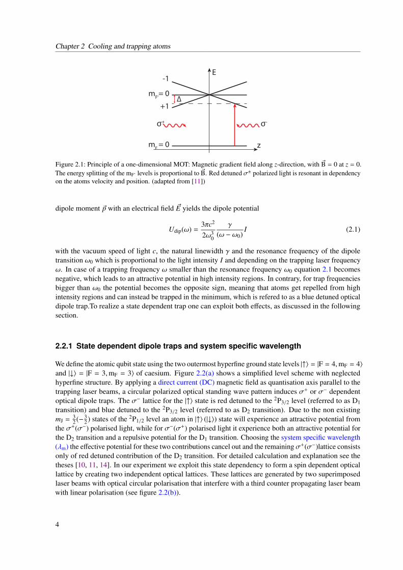
Dilute caesium atoms in the vacuum chamber are in thermal equilibrium with the surrounding at roomtemperature. In contrast the potential in the state dependent optical lattice is below 1 mK and thereforethe atoms need to be cooled. To capture caesium atoms out the background vapour and cool them tothe Doppler temperature we use a MOT. The basic principle of a MOT is velocity dependent Dopplercooling combined with a position dependent force. The position dependency results on circular polariseddipole transitions in a magnetic quadrupole field (see figure 2.1). The atoms are trapped in the centreof a magnetic quadrupole field generated by a pair of anti Helmholtz coils at the point of ~B = 0. Thecloud of cooled atoms can therefore be shifted in space by changing the zero point of this magneticquadrupole field, i.e. by applying an additional homogeneous magnetic offset field using coils inHelmholtz configuration. An in depth description of a MOT in general and of the MOT used in a similarexperiment can be found in [8–10].
2.2 Dipole traps
An optical dipole trap exploits the potential created by an alternating electrical light field several nmdetuned from a resonance of a dipole transition. Following the calculation (shown in [12]) of an induced
3
Chapter 2 Cooling and trapping atoms
mF = 0
mF‘= 0
-1
+1
z
E
σ+ σ-
∆
Figure 2.1: Principle of a one-dimensional MOT: Magnetic gradient field along z-direction, with ~B = 0 at z = 0.The energy splitting of the mF’ levels is proportional to ~B. Red detuned σ± polarized light is resonant in dependencyon the atoms velocity and position. (adapted from [11])
dipole moment ~p with an electrical field ~E yields the dipole potential
Udip(ω) =3πc2
2ω30
γ
(ω − ω0)I (2.1)
with the vacuum speed of light c, the natural linewidth γ and the resonance frequency of the dipoletransition ω0 which is proportional to the light intensity I and depending on the trapping laser frequencyω. In case of a trapping frequency ω smaller than the resonance frequency ω0 equation 2.1 becomesnegative, which leads to an attractive potential in high intensity regions. In contrary, for trap frequenciesbigger than ω0 the potential becomes the opposite sign, meaning that atoms get repelled from highintensity regions and can instead be trapped in the minimum, which is refered to as a blue detuned opticaldipole trap.To realize a state dependent trap one can exploit both effects, as discussed in the followingsection.
2.2.1 State dependent dipole traps and system specific wavelength
We define the atomic qubit state using the two outermost hyperfine ground state levels |↑〉 = |F = 4,mF = 4〉and |↓〉 = |F = 3,mF = 3〉 of caesium. Figure 2.2(a) shows a simplified level scheme with neglectedhyperfine structure. By applying a direct current (DC) magnetic field as quantisation axis parallel to thetrapping laser beams, a circular polarized optical standing wave pattern induces σ+ or σ− dependentoptical dipole traps. The σ− lattice for the |↑〉 state is red detuned to the 2P3/2 level (referred to as D1transition) and blue detuned to the 2P3/2 level (referred to as D2 transition). Due to the non existingmJ = 3
2 (−32 ) states of the 2P1/2 level an atom in |↑〉 (|↓〉) state will experience an attractive potential from
the σ+(σ−) polarised light, while for σ−(σ+) polarised light it experience both an attractive potential forthe D2 transition and a repulsive potential for the D1 transition. Choosing the system specific wavelength(λm) the effective potential for these two contributions cancel out and the remaining σ+(σ−)lattice consistsonly of red detuned contribution of the D2 transition. For detailed calculation and explanation see thetheses [10, 11, 14]. In our experiment we exploit this state dependency to form a spin dependent opticallattice by creating two independent optical lattices. These lattices are generated by two superimposedlaser beams with optical circular polarisation that interfere with a third counter propagating laser beamwith linear polarisation (see figure 2.2(b)).
4

2.2 Dipole traps
2P1/2
2P3/2
2S1/2
(a)
f0
v ~ Δf1v ~ -Δf1
f0-Δf1
f0+Δf1
f0
f0
f0
B
(b)
Figure 2.2: State dependent transport: (a) Level scheme of 133Cs without hyperfine structure. The D1 transitionconnects the 2S 1/2-level to the 2P1/2-level while the D2 transition connects the 2S 1/2 and the 2P3/2-level. Thefrequency ω is related to the system specific wavelength λm [11]. (b) One laser beam, consisting of precisesynthesizedσ+ andσ− polarized light, propagates parallel to a magnetic field. Together with the counter propagatinglinear polarized laser beam it creates a standing wave dipole trap. Variation in the circular polarized frequencyleads to moving lattice potentials. [13]
BB
+
Figure 2.3: The two-dimensional lattice is constructed by two one-dimensional lattices. The different colours showthe frequency difference of 160 MHz. The electric field of every laser beam is orthogonal to the magnetic field.
2.2.2 State dependent transport
The state dependent transport as explained in the previous section has been realised in one dimensionin another experiment [10]. To control the atom’s positionslightly shifting the phase with respect toeach other shifts the lattice sites. In the laboratory, an acousto-optic modulator (AOM) constructs atiny frequency difference of the corresponding laser beams resulting into a changing phase relation andtherefore into lattice velocity proportional to the frequency difference. Superposition of σ+ and σ−
polarised laser beams yields an effective linear polarisation. Since it is sufficient to change the frequencyon one side the constant phase relation will further on be marked as a linear polarised laser beam.
2.2.3 Two-dimensional state dependent optical lattice
In the DQSIM experiment we want to extent this to two dimensions, however, simply installing anadditional orthogonal state dependent lattice would not work since the quantisation axis introduces πcontributions to one dimension. Precise frequency synthetisation of every laser beam and turning thequantisation axis orthogonal to every lattice laser beam provide an working lattice scheme to performtwo dimensional state dependent transport. With respect to the hyperfine structure the resulting trap
5

Chapter 2 Cooling and trapping atoms
high-NA objective
glass cell
ion pumpCs reservoir
turbo pump* ion gauge*
NEG pump
SF57 window
Figure 2.4: Vacuum system: Functional parts are labelled. The *-symbol marks parts which helped to establish thevacuum and are removed now [16].
potentials would be
U|↑〉 = Uσ+ + Uπ
U|↓〉 = 78 Uσ++
18
Uσ+ + Uπ (2.2)
Intersecting the corresponding laser beams within an angle of 90° yields an 45° rotated standing wavedipole lattice with a enlarged lattice constant of d = λm/
√2, that can be single site resolved by our
high-NA objective. The working principle of this configuration and an analysis of its transport andpotential behaviour is explained in detail in chapter 3.
2.3 Experimental Setup
In the following I will introduce the main components of the experimental apparatus, which includes thevacuum maintenance apparatuses and the optical and mechanical details to run the experiment.
2.3.1 Vacuum system
The vacuum system contains the in-house designed and constructed high-NA objective [15] which isglued in an in-house built glass cell as well as the vacuum maintenance machines. The experiments takeplace inside the glass cell [7] in a distance of about 150 µm below the objective. The entire experimentchamber is sketched in figure 2.4.
6

2.3 Experimental Setup
Vacuum system The vacuum chamber is designed such that it can be mounted below an optical breadboard with a whole, such that no component hinders the optical paths which are all going into the glasscell. An ion pump in combination with a non-evaporable getter pump (NEG-pump) binds residual gasmolecules and atoms. Heating the caesium reservoir supports the vacuum pressure below 1 × 10⁻¹⁰ mbaras well as providing a background caesium vapour. A vacuum tube connects this area to the twelve-sidedglass cell where the experiments take place.
Ultra-high-vacuum glass cell The in-house built cylindrical twelve-sided glass cell is made of SF57and the ultra-low birefringence of ∼1 × 10⁻⁷ [7] allows for precise polarisation control which is crucialto establish and control the state-dependent optical lattice. The in-house designed vacuum compatibleobjective is glued at the ceiling and is the central part of the imaging system.
2.3.2 Imaging system
High-numerical aperture objective The central part of the imaging system is the in vacuum ob-jective providing a high-NA of 0.92 yields an imaging resolution of 565 nm. It is designed for ima-ging caesium atoms in single lattice sites of 612 nm distance, emitting light on the D2 transition atλD2 = 852 nm and provides diffraction limited imaging in a field of view with a width of 70 µm whichis related to 120 lattice sites [17]. The images are acquired by an electron multiplying charge-coupleddevice (EMCCD) camera (Andor iXon3).
2.3.3 Laser cooling system
Magneto-optical trap The MOT is created by laser beams which are red detuned to the D2 transitionat 852 nm [18] and pumps the almost closed transition from F = 4 to F′ = 5. The Doppler temperaturefor this transition is TD = 126 µK. A re-pumping laser pumping the transition from F = 3 level toF′ = 4 brings the off resonant excited atoms back to the cooling cycle. The cooled atoms are left inthe |↑〉 state [10]. The cooling laser beam diameters of dcool = 2.2 mm and a magnetic field gradientof ∼80 G/cm establishes the MOT. Because of the objective’s working distance of 150 µm the coolingbeams would be clipped at the objective’s edge and therefore the MOT is loaded 2 mm below with asubsequent transport of the atoms upwards.
Magnetic elevator To load the MOT 2 mm below, the magnetic quadrupole field needs to be shifteddown. To transport the trapped atoms upwards to the 2D-SDL they just follow the point of ~B = 0. Thisstarts shifting the MOT and is combined with the principle of magnetic transport [19] when leavingthe area of present MOT laser beams. Both of these two principles are based on shifting the magneticquadrupole filed. The construction of this magnetic elevator is explained in more detail in chapter 4.
Horizontal confinement The 2D-SDL consists of two independently controllable one dimensionallattices. Both operating at the system specific wavelength (see chapter 2.2.1) of λm = 866 nm [11]detuned with respect to each other by 160 MHz to prevent interference. To achieve nearly homogeneoushorizontal intensity while preventing stray light resulting from the laser beams clipping at the objective’sedge, the beam profile at the position of the trap is elliptically with a horizontal beam waist of 52 µm anda vertical beam waist of 145 µm.
7
Chapter 2 Cooling and trapping atoms
dBdz
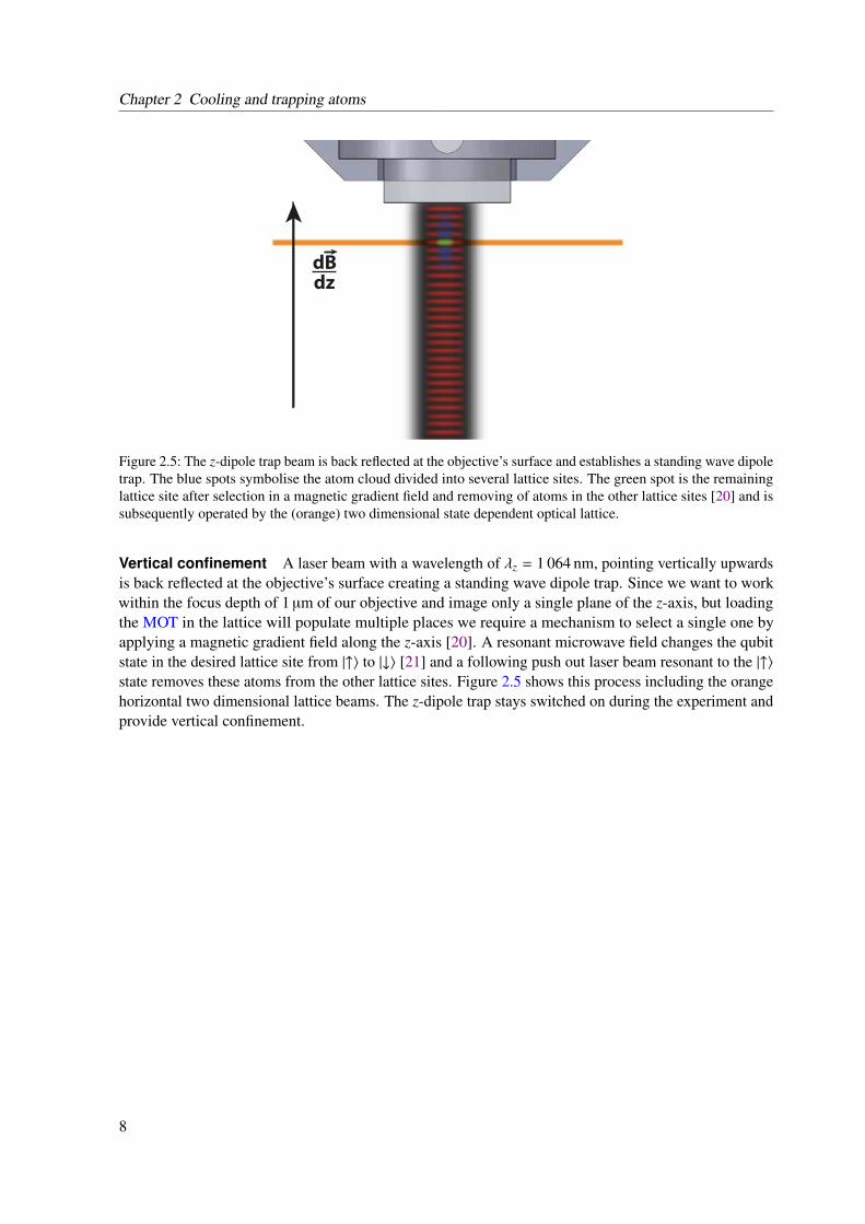
Figure 2.5: The z-dipole trap beam is back reflected at the objective’s surface and establishes a standing wave dipoletrap. The blue spots symbolise the atom cloud divided into several lattice sites. The green spot is the remaininglattice site after selection in a magnetic gradient field and removing of atoms in the other lattice sites [20] and issubsequently operated by the (orange) two dimensional state dependent optical lattice.
Vertical confinement A laser beam with a wavelength of λz = 1 064 nm, pointing vertically upwardsis back reflected at the objective’s surface creating a standing wave dipole trap. Since we want to workwithin the focus depth of 1 µm of our objective and image only a single plane of the z-axis, but loadingthe MOT in the lattice will populate multiple places we require a mechanism to select a single one byapplying a magnetic gradient field along the z-axis [20]. A resonant microwave field changes the qubitstate in the desired lattice site from |↑〉 to |↓〉 [21] and a following push out laser beam resonant to the |↑〉state removes these atoms from the other lattice sites. Figure 2.5 shows this process including the orangehorizontal two dimensional lattice beams. The z-dipole trap stays switched on during the experiment andprovide vertical confinement.
8

CHAPTER 3
Simulation of two dimensional transport
The previous part of this thesis described the general setup an mechanisms we are going to use inthe experiment. The general description of the working principle is used in a simulation of the statedependent transport in Mathematica with simplification to one dimension. Detailed analysis of thepotential contributions of the different polarisations resulting from the decomposed laser light field givesinformation how to perform state dependent transport with respect to the potential depth during transport.
3.1 General Explanation
As mentioned before, the atoms are constrained in the xy-direction by the 2D-SDL and in the z-directionby a state independent standing wave dipole trap. Thus, atoms are stored in a three dimensional potentialwhere two dimensions are state-dependent. The vertical dipole trap is required to keep the atoms in the1 µm wide depth of focus [15] of our objective.
An effective two dimensional system is realised by selecting a single slice of atoms. The atoms aretrapped in a standing wave dipole trap consisting of linear polarized light back reflected at the objective’ssurface. The Potential depth at the 2D-SDL 150 µm below is calculated for a Gaussian distributed laserbeam profile with a beam waist of w0z = 75 µm at the surface of our objective and a laser power of 5 Wat a wavelength of λz = 1 064 nm. Following [11, 12, 22] this yields a trap depth of Uz−dip = 587.4 µKfor |↑〉 state in the retro reflected configuration. Along the horizontal directions (x, y) state dependenttransport is available. The decomposed polarisations of the horizontal 2D-SDL laser beams contribute tothe horizontal dipole potential when the resulting linear polarisation contains an electrical field orthogonalto the quantisation axis. Calculating the dipole potential of the lattice laser beams envelope function leadsto a normalised horizontal dipole potential. Figure 3.1(a) shows the one dimensional potential for the|↑〉-state in red and the |↓〉-state in green in case of only slightly shifted lattice potential near the maximalpotential depth (Umax). Figure 3.1(b) shows an example of the case of a small horizontal lattice potentialdue to shifted potential wells of the state dependent contribution and the state independent π-contributionto the potential. In this case, the horizontal lattice potential is below zero and traps atoms in the intensitymaximum (Imax) but different horizontal lattice sites can hardly be distinguished. The potential depth,which is mentioned here defines the potential between two neighbouring lattice sites for a certain qubit(qualitative analysis below). The effective horizontal lattice potential is the potential between two latticesites (marked by orange lines in figure 3.1).
9

Chapter 3 Simulation of two dimensional transport
-1.5 -1.0 -0.5 0.0 0.5 1.0 1.5
-2.0
-1.5
-1.0
-0.5
0.0
0.5
Position /λ/ 2
PotentialDepth
/n.u.
(a)
-1.5 -1.0 -0.5 0.0 0.5 1.0 1.5
-2.0
-1.5
-1.0
-0.5
0.0
0.5
Position /λ/ 2
PotentialDepth
/n.u.
(b)
Figure 3.1: Two-dimensional potential in normalised units (n.u.) for the |↑〉-state (red) and the |↓〉-state (green) fortwo different settings of the polarisation angles Θ1 and Θ2 as defined in figure 3.2(a). (a): Θ1 = 0.2 π,Θ2 = 0.2 π:The two dimensional potential is deep and atoms can be trapped in certain lattice sites. (b): Θ1 = 0.025 π,Θ2 =
0.5 π: The shallow two dimensional potential is in general below zero and traps atoms in the beam’s intensitymaximum. Trapping atoms in certain lattice sites and subsequently state dependent transport is hardly possible.
3.1.1 Simulation of state dependent transport
The following section elucidates a simulation of state dependent transport using Mathematica [23],performed with two linear polarised laser beams, intersecting each other by an angle of 90° providing asingle side resolved lattice distance of d2D = 866√
2nm.
Configuration The simulation starts describing the electric fields of the involved laser beams as aplane wave in the xy-plane as
~Elin = E0 · elin · ei~k~x−iωl·t (3.1)
with the wave vector ~k = 2πλ
cos(φ)sin(φ)
0
directed into the direction of the propagating laser beam with an
unity electric field E0, the laser frequency ωl = 2π cλl
and a linear polarisation vector elin =
0sin(Θ)cos(Θ)
.Treatment of a planar wave holds since the calculated area is small in the middle of the horizontalRayleigh length of zR = 21.5 mm. The phase shift between the circular polarised laser beams results inan equivalent linear polarisation described by the angle Θ. Rotation for ±45° around z-axis rotates thetwo laser beams in opposite directions and let them intersect each other in the origin. The transformationinto the circular basis is realised by multiplication with matrix M defined as
M · ~x =
1√2
i√2
01√2
−i√2
00 0 1
·xyz
=
σ+
σ−
π
. (3.2)
Connecting the electric field vector in circular basis (~Ecirc) to the intensity Il ∝ |~Ecirc|2 enable a qualit-
ative simulation of the one-dimensional state-dependent optical lattice (1D-SDL) where the separate
10

3.1 General Explanation
θ2
θ1
B
z
y
x
(a)
0.4
0.6
0.8
1.0
Posi
tion
/ λ/√
2
(b)
Figure 3.2: (a): Configuration for simulation of 1D-SDL: Two orthogonal polarisation synthesized laser beamsintersecting in the origin. The phase shift of the two circular polarisations is expressed as the linear polarisationangle Θ1 and Θ2 respectively. (b): Displacement of the |↑〉 potential well from the origin for different polarisationangles Θ1 and Θ2. The displacement is visualised by different colours on the map. One turn on the map leads to adisplacement of one lattice site. The discontinuity at Θ1 = 0 symbolise the lattice potential to be the same aftertransporting one qubit for one lattice site.
components for σ+, σ− and π-polarised light are directly connected to the potential components actingon the qubit states (see equation 2.2).
State-dependent transport The position of the |↑〉 qubit potential related to the origin, demonstratedin figure 3.2(a) is mapped in figure 3.2(b) for possible configurations of Θ1 and Θ2. Different colourssymbolise different displacements. The periodicity of λ/2 limits the complexity to angles from Θ1,2 =
0 to π. Transporting the atoms to the next lattice site requires a polarisation synthesized path along aposition gradient by means of one circle around the centre point in the map (figure 3.2(b)). After one turnthe potential configuration is equal to the start configuration but the atoms are shifted by one lattice sitewhich is symbolised by the discontinuity. A proper transport velocity can be found by modelling a pathwith a desired displacement gradient over time.
3.1.2 Potential depth during transport
Additionally to the transport velocity, it is important to control the potential depth during transport sincean unwanted fluctuating dipole potential can heat the atoms and limit coherence. Figure 3.3 shows amap similar to figure 3.2(b) but here, the colour defines the trap potential for a certain configuration ofΘ1 and Θ2. The |↑〉 qubit potential (figure 3.3(a)) for instance provides a constant potential depth byperforming the transport along the polarisation synthetisation marked by the black square. The sametransport configuration will result in a not constant potential for the |↓〉 qubit. No configuration canprovide transport with a constant potential for both qubit states simultaneously. Hence an appropriatetransport configuration including the changing potential for one of the two or both qubit states needs tobe tailored for the different classes of experiments.
11

Chapter 3 Simulation of two dimensional transport
- 0.4 - 0.2 0.0 0.2 0.40.0
0.2
0.4
0.6
0.8
1.0
θ1
θ2
- 0.4 - 0.2 0.0 0.2 0.40.0
0.2
0.4
0.6
0.8
1.0
θ1
θ2
0.2
0.6
1
1.4
1.8
Pote
ntia
l dep
th /n
.u.
(a) (b)
U U
Figure 3.3: Dipole potential depth in a lattice site depending on the polarisation angles Θ1 and Θ2. The potentialdepth inside the state-dependent lattice is the difference between the maximal and the minimal potential for eachconfiguration (see figure 3.1). The potential depth is displayed using colours. Equal potentials are marked usingheight lines. (a): Potential mapping for the state |↑〉. A path with constant potential depth is along a square onthe map. (b): Potential mapping for the state |↓〉. The potential depth, symbolised by the colour is differentlydistributed compared to the state |↑〉 and therefore lead to different potentials acting on atoms in the two qubit statesduring transport.
Quantisation orthogonal Quantisation parallelrequired synthesized beams 4 2single site resolution yes yespresent π contribution yes no
Table 3.1: Comparison between the simulated transport scheme with an quantisation axis orthogonal and the noveltransport scheme with the quantisation axis parallel to the 2D-SDL plane.
3.2 Outlook
An improved transport configuration without a containing π-contribution was discussed [16] after Ifinished my analysis. In this configuration (see figure 3.4), only σ+ and σ− polarised light contributes tothe state dependent potential since all present electric field vector points orthogonal to the quantisationaxis. The absence of π potentials leads to a constant potential depth of the |↑〉 state. Fortunately thediscussed transport scheme can be investigated with just a few modification in my Mathematica-code.Further on it simplifies the installation and operation of the two-dimensional transport a lot since itis easier to adjust and operate, when two lattice beams fewer require polarisation synthesisation (seetable 3.1). Resulting this, four AOM including careful alignment, control and at least space on the opticaltable can be saved.
12

3.2 Outlook
B
Figure 3.4: Improved state dependent transport schematics: The quantisation axis is parallel to the counterpropagating synthsized laser beams. The corresponding linear polarised laser beams contains only electrical fieldcomponents orthogonal to the quantisation axis.
13


CHAPTER 4
Magnetic elevator for trapped 133Cs atoms
Experimental verification of these simulation presupposes having a controllable state dependent opticallattice as well as the presence of caesium atoms trapped in it. The standard tool for capturing atoms outof the background vapour of an UHV cell into a MOT cannot be used at the position of the 2D-SDL in adistance of dl = 150 µm beneath the high-NA objective. The MOT laser beams with a diameter of aboutwMOT = 2 mm would be clipped at the edge of the objective producing stay light and random reflections.Subsequently the MOT needs to be established at a point around d ≈ 2 mm below the 2D-SDL in amagnetic quadrupole field with a gradient of d~B/dt ∼ 80 G/cm at the position where the magnetic field is~B = 0. Henceforth compressing the MOT and select a certain slice of atoms to load the 2D-SDL requiresa magnetic gradient of up to d~B/dt ∼ 300 G/cm directly at the position of the 2D-SDL 150 µm belowthe high-NA objective. This chapter deals with the problem to provide magnetic quadrupole fields atdifferent times of the experiment cycle with different magnetic field gradients providing ~B = 0 at differentpositions.
4.1 Required magnetic fields
As mentioned above, the selection of a slice of atoms in the objective’s focal plane requires a highmagnetic field gradient of d~B/dt ∼ 300 G/cm with the point of zero magnetic field exactly there. Ata current guided through the gradient coils of I = 32 A, resulting in a magnetic field gradient ofd~B/dt ∼ 303 G/cm a current imbalance of ∆I = 2 h is enough to select the atoms out of focus whichcan already happen in case of independent noisy power supplies. In case of a spacial fluctuating magneticfield during the micro wave state manipulation this leads to a not clear defined Rabi oscillation and theselection of Atoms will broaden which makes it impossible to choose just one lattice site. The MOT ismore tolerant to the required magnetic gradient field and keeps working even in case the point of ~B = 0 isroughly in the middle of the MOT laser beams and using another magnetic field gradient only change thetrap volume by a fraction. Therefore the magnetic gradient coils need to be mounted such that ~B = 0 is inthe objective’s focal plane for equal current in both magnetic gradient coils. The magnetic quadrupolefield can be shifted to load the atoms in the MOT about 2 mm below this point. Performing this shiftby an homogeneous offset field using the z-compensation coils would be the simplest way but requirestoo high current since their winding number is smaller than 1/10 of the gradient coil’s winding number(see table 4.1). This chapter describes therefore a control circuit to divert a certain amount of currentaround the bottom gradient coil to lower the magnetic quadrupole field’s position for loading the MOT.Building up this circuit requires a detailed characterisation of the magnetic gradient coils to drive thecurrent as well as a stabilised precise current bypass and finally a galvanic isolated information transfer
15

Chapter 4 Magnetic elevator for trapped 133Cs atoms
Figure 4.1: Experimental area: a) water cooled plates, b) z-compensation coils, c) z-gradient aluminium bandcoils, d) x/y-compensation coils, e) double-layer µ-metal shielding against high frequent magnetic fields, f) highNA-objective (NA = 0.92) [17], g) twelve-sided vacuum glass cell [7], h) connection to vacuum maintainingsystem (see section 2.3.1).
Coil gradient x/y-compensation z-compensationmaterial aluminium band copper wire copper wireconductor area (0.15 mm × 30 mm) π · (0.4mm)2 π · (0.4mm)2
No. of windings 260 20 21magnetic field per 1 A 33.7 G 1.6 G 3.2 Gmagnetic gradient field per 1 A 9.5 G/cm — 1.4 G/cm
Table 4.1: Dimensions and properties of the different coils used in the experiment. The magnetic (gradient) field iscalculated using MatLab [16] and previous characterisation of the coils [16].
to protect the computer control system from high voltage damage in case of failure in the high-powercircuit including the gradient coils.
4.2 Implementation of magnetic field gradients
The magnetic gradient field required for the MOT is controlled by two metal band coils made of aluminiumwith oxidisation layer for isolation mounted in an anti Helmholtz configuration (see figure 4.1). Threepairs of additional coils in Helmholtz configuration (figure 4.1(b),(d)) optimised to not limit opticalaccess to the science chamber are used. A double layer barrel consisting of µ-metal shield (figure 4.1(e))the experimental area against high frequency magnetic fields to establish a well defined magnetic field.The dimensional properties of the implemented magnetic coils can be seen in table 4.1 to get a completepicture while in the following only the gradient coils will be important.
16

4.3 Characterisation of the anti Helmholtz coils
4.3 Characterisation of the anti Helmholtz coils
The properties of the magnetic gradient coils in the low frequency range can be modelled by its physicalvalues of the ohmic DC-gradient coil’s resistance (RL), the gradient coil’s inductivity (LL) and gradientcoil’s capacity (CL) in an equivalent circuit (see figure 4.2(a)).
Ohmic resistance
Information about RLcan be extracted by measuring the voltage when a constant current is applied tothe coils. The resistances of the top and the bottom gradient coil are RL = (0.62 ± 0.01)Ω and RL =
(0.61 ± 0.01)Ω respectively at room temperature. These results are included in the overview table for thecoil’s properties (table 4.2).
Inductance
The Inductance LL can be estimated by an ideal flat spiral air-core coil, which neglects the fact of havingmetal band instead of an infinitesimal wire using the formula [24]
L =r2N2
20r + 28dµH (4.1)
where N is the number of windings, r the mean radius given in cm and d the depth of the coil, that is thedifference of the outer and the inner radius, in cm. This estimation yields an inductance of 8.7 mH withan uncertainty below 5 % for the radial dimensions of the aluminium band coils1.
Besides this estimation the inductance was measured in two ways exploiting the response to a stepfunction. One to quantify exponential decay and the other to analyse the frequency of an oscillatingcircuit including each coil separately. A voltage signal generated by a function generator is guidedacross a high resistor to generate the current step function. The following characterisation used severalmeasurements with different output resistances. Detailed values are given in appendix A.Exponential decay in LR-circuit: The voltage across one gradient coil (UL) contains information aboutthe coil’s inductance. The system is described by the ordinary differential equation U = L · I = L
R U,which is solved by
UL = U0e−RL t. (4.2)
Fitting the curve to the response signal (see figure 4.2(b)) gives a relation for RL where R can be calculated
knowing all the DC resistors giving LL = (6.0 ± 0.8) mH for the top and LL = (6.0 ± 0.5) mH for thebottom coil’s inductance.Oscillations in LC-circuit: An Cext of about (100 ± 20) µF parallel to the coil leads to an oscillatingcurrent (see figure 4.2(c)) while high impedances are applied at the frequency generator R0 as well as atthe oscilloscope’s input channel Rin. As measured below, CL can be neglected since it is several ordersof magnitude smaller than Cext. Fitting a damped sinusoidal oscillation to the measurement data givesthe frequency of an oscillating LC-circuit and inserting this together with Cext into the formula for theresonance frequency [25]
f =1
2π√
LC(4.3)
of an oscillating circuit gives LL = (6.4 ± 0.2) mH for the top and LL = (6.5 ± 0.1) mH for the bottomcoil after solving it for L . An average value and using Gaussian error propagation yields the averaged
1 The uncertainty is below 5 % if d > 0.2 r [24].
17

Chapter 4 Magnetic elevator for trapped 133Cs atoms
Square equivalent coil circuit
R0
Rin
LL
RL
CL
Cext
(a) (b)
(c) (d)
Figure 4.2: Gradient coil’s characterisation: (a): Schematic of a coil equivalent measurement circuit for character-isation measurements of the coils. The function generator gives in combination with R0 a square current signal. Anoscilloscope with adjustable input impedance Rin measures the voltage across the coil (here: equivalent circuit),and external capacitance (Cext) for the measurement of LL in an LC measurement. (b): Step response in LR-circuit:The exponential decay contains information of LL (see equation 4.2). (c), (d): Step response in LC-circuit (c) withCext to calculate LL and (d) without Cext to calculate CL using formula 4.3.
measurement values of LL = (6.2 ± 0.8) mH for the top and LL = (6.3 ± 0.5) mH for the bottom coil.
Capacitance
Removing Cext enables the LC-circuit to give information about CL. A highly damped sinusoidaloscillation is fitted to the measured step-response (see figure 4.2(d)). Solving formula 4.3 for C gives acapacity of CL = (1.50 ± 0.20) nF for the top and CL = (1.31 ± 0.06) nF for the bottom coil with respectto the previous measured inductances.
18

4.4 Realisation of current driver for elevating atoms
top coil bottom coilRL (0.62 ± 0.01)Ω (0.61 ± 0.01)ΩLcalc 8.7 mH 8.7 mHLmeas (6.2 ± 0.8) mH (6.3 ± 0.5) mHC (1.50 ± 0.20) nF (1.28 ± 0.07) nF
Table 4.2: The fundamental values required to develop an equivalent circuit which is used for simulation anddevelopment of the current bypass circuit. LCalc used equation 4.1. Lmeas includes LLRC and LLLC .
Results
The measured Ohmic resistance of the coils is 3 % below the manufacturers value of RL = 0.64 Ω forthe top or RL = 0.63Ω respectively for the bottom coil what is slightly out of the error resulting fromthe measurement. The measured inductivity of LL = (6.2 ± 0.8) mH for the top and LL = (6.3 ± 0.5) mHrespectively for the bottom coil is about 28 % below the calculated value of LL = 8.7 mH and far outof the given precision [24] for the used approximation. Since the used aluminium band coils are muchdifferent to the calculated ideal flat spiral air-core coil the approximation is useful to choose the rightorder of magnitude. The control circuit for the magnetic gradient coils of another experiment in our groupis designed for an inductance L = 20 mH and a resistance of R = 1.6 Ω. These coils consists of magneticcoils with each 340 windings of a copper wire with a diameter of 1.4 mm yielding 21.9 G/(cmA) [22].
4.4 Realisation of current driver for elevating atoms
The basic idea of the control circuit is to divert current by a power metal–oxide–semiconductor field-effecttransistor (MOSFET) as depicted in figure 4.3. The MOSFET’s highly non-linear response functionis linearised using a feedback operation amplifier (OpAmp) circuit. The amount of bypass current ismeasured across a sensing resistance (RM) and giving a voltage feedback to the OpAmp to compare theactual amount of bypass current with the value, given at the input by the computer control.
4.4.1 Control of asymmetrically coil currents
An N-channel power-MOSFET (IXTH 88N30P) is used to divert the current by changing its resistance.A feedback of measuring the voltage across a sensing resistor RM = 0.1 Ω [26] linearises this MOSFETto enable the driving circuit to control the bypass current precisely. The large gate capacity of more than6 nF [27] coming from the power-MOSFETs large junction area to enable conductivity of large currentsand require high driving currents to change the gate voltage fast. The chosen operation amplifier supportsup to 150 mA output current but requires special care to avoid hardly controllable oscillations due to itshigh operation bandwidth of 270 MHz [28]. An operation amplifier supporting a lower bandwidth wouldrequire an additional current buffer to drive the MOSFET properly.
Tuning the feedback loop The integrator circuit (solid square figure 4.4) shifts the operation band-width to a lower region. The calculated −3 dB cutoff frequency is defined by a low pass [29] to
fc =1
2πRC= 2.8 MHz. (4.4)
19

Chapter 4 Magnetic elevator for trapped 133Cs atoms
OPAMP
I
L
L
N-MOSFET
0.1
input
Figure 4.3: Basic idea of current diversion: The power supply gives a constant current through the top an the bottommagnetic gradient coil. A power MOSFET diverts a certain amount of current around the bottom magnetic gradientcoil. The voltage of the diverted current measured across a resistor gives feedback to an operation amplifier whichcompares the feedback voltage with the input signal coming from the computer control and drives the MOSFET.
4.4.2 Passive stabilization with snubber circuit
The equivalent circuit of the magnetic gradient coil acts like a LC oscillation circuit for fast currentchanges which might occur by running an experimental sequence. This oscillation behaviour is changedby a snubber circuit consisting of a resistance and a capacitance in series to the coil. An aperiodicdamping to establish a steady state within a few 10 ms after changing the bypass current can be achievedconsidering the voltage in the coil equivalent circuits (see figure 4.2(a)). Starting with the formula
UL(t) + UR(t) + UC(t) = 0, (4.5)
describing the total voltage in this circuit, we use UL = L ddt I,UR = RI and UC =
QC [30] to get
Lddt
I(t) + RI(t) +Q(t)C
= 0. (4.6)
Taking the temporal derivative and the Ansatz I(t) = I0 · eωt dividing by L gives the differential equation
ω2 +RLω +
1CL
= 0 (4.7)
and using the well known pq-formula to solve this differential equation yields the solutions
ω1,2 = −R2L±
√R2
4L2 −1
CL. (4.8)
20

4.4 Realisation of current driver for elevating atoms
OPAMP
L
L
N-MOSFET
560
560
0.1
1k56pF
Circuit100 nF
Snubber-
Snubber-Circuit100 nF
56input
200
I
Figure 4.4: MOSFET driving circuit including the two MOT coils L with their snubber circuits (dashed square).The amount of diverted current is measured across RM = 0.1 Ω. The integrating feedback circuit (solid square)reduces the operating bandwidth to 2.8 MHz. Resistances (dotted boxes) enclose the operating amplifier fromcapacities.
Aperiodic damping requires the square root to be zero. An external capacitance of CS = 100 nF definesthe oscillating frequency (equation 4.3) to fL = 6.4 kHz and leads to the aperiodic damping in case of
RS =
√4LC
= 498 Ω. (4.9)
For practical reasons and to have a magnitude to establish rather slow relaxation, the chosen resistance of560Ω is a bit bigger than required.
4.4.3 Galvanic isolated signal transfer
The remaining part to complete the current driver circuit is the galvanic isolated signal transfer, realisedusing an optocoupler and a isolated DC/DC power supply. The basic circuit is adapted from theoptocoupler’s datasheet [31].
Optocoupler-circuit Figure 4.5(a) shows the used circuit (adapted from [31]) and can be understoodas follows: The light emitting diode (LED) driver transforms the voltage signal from the computer controlsystem into a proper current for the LED. The feedback of diode 2 (D2) ensures reliable signal transferindependent from temperature or aging processes. The trans-impedance OpAmp after diode 1 (D1)converts the photo current back into a stabilized voltage signal to drive the current diversion using theprevious explained circuit. Tuning resistor R2 with respect to resistor R1 further allow for defining thetransfer ratio of the signal. Calibration of the control voltage to the bypass current is essentially based onthis ratio and the sensing resistor RM = 0.1Ω. Although the ration can be calculated a calibration of this
21

Chapter 4 Magnetic elevator for trapped 133Cs atoms
OPAMP
33pF
20,6k
R2
PNP
OPAMP
R1
220k
Optocoupler
LED
D2
D1
+15 V+15 V
2.2k 270
Output
Input
330pF
6.8k
47pF
(a)
15 -15V+15V
GND10
2µF10
1µF1µF
5µF
DC/DC converter
(b)
Figure 4.5: (a): Isolated signal transfer: The optocoupler transmits the information from a LED to two photodiodes. The current of D2 builds a feedback signal to stabilise the input signal. The right operation amplifierconverts the current of D1 to a voltage at the output (adapted from [31]). (b): The DC/DC converter establishthe power supply at the ground free part that is connected to the gradient coil system. 2 µF at the input side and a16 kHz low pass filter at the ±15 V connection flatten the voltage spikes from the switching power supply.
transfer ratio is required to compensate the tolerances of the used components.
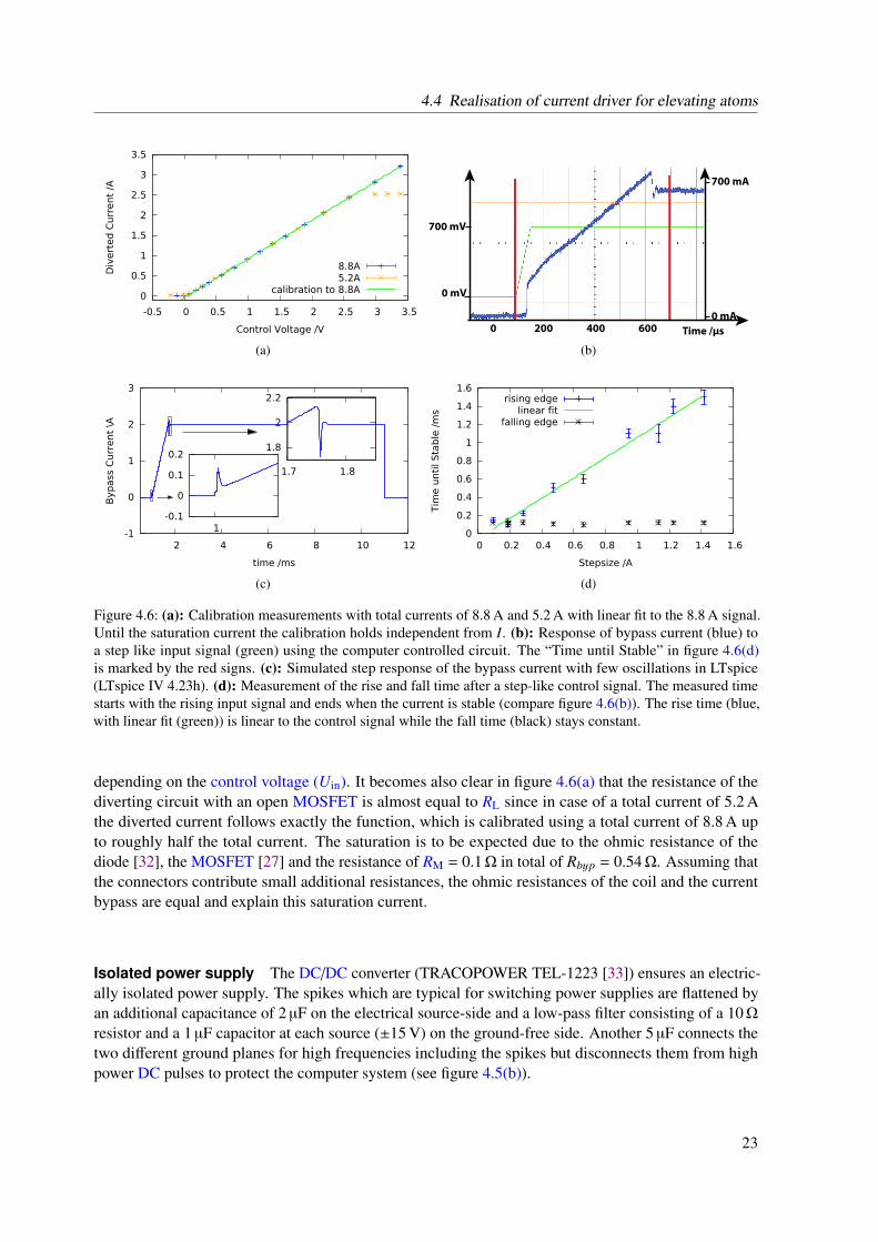
Calibration Enable the computer system to give appropriate commands during a measurement cyclerequires a calibration. Figure 4.6(a) shows measured data of the diverted current with respect to the inputsignal. Positive input signals lead to a linear response of the diverted current while negative input signalsblock the diversion of current. A linear calibration fit leads to a diverted current (Id) of about
Id(Uin) = (0.94 ± 0.01) Ω−1 · Uin − (0.00 ± 0.01) A (4.10)
22
4.4 Realisation of current driver for elevating atoms
0
0.5
1
1.5
2
2.5
3
3.5
-0.5 0 0.5 1 1.5 2 2.5 3 3.5
Div
ert
ed
Curr
ent
/A
Control Voltage /V
8.8A5.2A
calibration to 8.8A
(a)Time /µs0 200 400 600
0 mV
700 mV
0 mA
700 mA
(b)
-1
0
1
2
3
2 4 6 8 10 12
Byp
ass
Curr
ent
\A
time /ms
1.8
2
2.2
1.7 1.8
-0.1
0
0.1
0.2
1
(c)
0
0.2
0.4
0.6
0.8
1
1.2
1.4
1.6
0 0.2 0.4 0.6 0.8 1 1.2 1.4 1.6
Tim
e u
nti
l S
tab
le /
ms
Stepsize /A
rising edgelinear fit
falling edge
(d)
Figure 4.6: (a): Calibration measurements with total currents of 8.8 A and 5.2 A with linear fit to the 8.8 A signal.Until the saturation current the calibration holds independent from I. (b): Response of bypass current (blue) toa step like input signal (green) using the computer controlled circuit. The “Time until Stable” in figure 4.6(d)is marked by the red signs. (c): Simulated step response of the bypass current with few oscillations in LTspice(LTspice IV 4.23h). (d): Measurement of the rise and fall time after a step-like control signal. The measured timestarts with the rising input signal and ends when the current is stable (compare figure 4.6(b)). The rise time (blue,with linear fit (green)) is linear to the control signal while the fall time (black) stays constant.
depending on the control voltage (Uin). It becomes also clear in figure 4.6(a) that the resistance of thediverting circuit with an open MOSFET is almost equal to RL since in case of a total current of 5.2 Athe diverted current follows exactly the function, which is calibrated using a total current of 8.8 A upto roughly half the total current. The saturation is to be expected due to the ohmic resistance of thediode [32], the MOSFET [27] and the resistance of RM = 0.1Ω in total of Rbyp = 0.54Ω. Assuming thatthe connectors contribute small additional resistances, the ohmic resistances of the coil and the currentbypass are equal and explain this saturation current.
Isolated power supply The DC/DC converter (TRACOPOWER TEL-1223 [33]) ensures an electric-ally isolated power supply. The spikes which are typical for switching power supplies are flattened byan additional capacitance of 2 µF on the electrical source-side and a low-pass filter consisting of a 10Ωresistor and a 1 µF capacitor at each source (±15 V) on the ground-free side. Another 5 µF connects thetwo different ground planes for high frequencies including the spikes but disconnects them from highpower DC pulses to protect the computer system (see figure 4.5(b)).
23

Chapter 4 Magnetic elevator for trapped 133Cs atoms
Characterisation of the current driver
The current driver’s characteristics is investigated using a suddenly changed bypass current using a steplike control signal forming a steep ramp (green signal in figure 4.6(b)). The bypass current (blue curve)starts rising after a delay with a step and a following linear rising bypass current. The bypass currentstabilises at the final value after an overshooting and short oscillations. The red bar mark the time whenthe control signal changes until the bypass current is stable again.
Delay time The delay time is not seen in the circuit simulation [34]. During measurements the delaytime is at a constant value of about ∆tdelay = 50 µs in case the control voltage started above zero. Whenthe control voltage started above zero, ∆tdelay was up to 100 µs and depending on the step size whatis not further investigated here. Therefore this seems to be a mixture of the transmission bandwidthand the time the last OpAmp needs to raise the gate voltage from the closed MOSFET to a controlledarea. The bandwidth of the isolated transmission is limited by the feedback capacitors of 33.47 pF tof = 10 kHz [31] what is still larger than the measured delays. The MOSFET completely switchesopen until it reaches the final value. The first step seems to result from direct response of the snubber-capacitors. This beginning peak was higher using lower RS in the simulated circuit. The following bypasscurrent is not controlled and follows the law of self inductance[30]. The overshooting at the end of thisslope is independent from any changes in the snubber circuits. This is also seen in the simulation (seefigure 4.6(c)).
Required switching time The time it takes until a steady state is established after changing the bypasscurrent is important for the duration of a measurement cycle. Figures 4.6(d) and 4.6(b) show this timefor a measurement with I = 8.8 A starting with the step-like signal until the diverted current is stable. Alinear fit to the rise-time (∆T ) gives a relation of
∆t(∆I) = (1.11 ± 0.06) ms A−1 · ∆I − (0.05 ± 0.04) ms (4.11)
in dependency of the amount of changed bypass current ∆I. The response time is proportional to theamplitude of the current to be changed at ∆t = ∼1.1 ms A−1. Stopping the diversion of current is stableand much faster and constant at ∆t = ∼120 µs since the MOSFET stops the current immediately. Eventhe simulation show just a sudden stopped current. However, a real experimental sequence requires toramp up and down in a controlled way for adiabatic transport.
4.5 Thermal analysis
The electrical components dissipate a lot of electrical power which needs do be conducted to thesurrounding air to protect the circuit from damage due to overheating. In the following, I will present acalculation to estimate the expected thermal energy dissipated by the MOSFET and the sensing resistorand afterwards a comparison to a temperature measurement using a thermal camera.
4.5.1 Thermal properties
Thermal power The dissipated power P in an electronic device due to guided currents is given byP = U · I = R · I2. The first part is used to calculate the power dissipated by the MOSFET while thesecond part is an expression to calculate the dissipated power of the sensing resistor. The MOSFET and
24

4.5 Thermal analysis
0
5
10
15
20
25
30
35
40
0 2 4 6 8 10
ΔT /
K
Diverted Current /A
temp MOSFETtemp Resistor
Figure 4.7: Calculated temperature difference between the junction temperature and the surrounding laboratory airtemperature. This calculation is based on a total current of 10 A assuming the sensing resistor and the MOSFET tobe mounted at the same heat sink and therefore influence each others temperature.
Contributions to RThM [K W−1] RThR [K W−1]RTh inside component 0,42 2,50Silicon layer / heat paste 0,33 0,15Aluminium case 0,03 <0,01Heat paste <0,01 0,01over all resistance 0,78 2,66Common heat sink to air 1,40
Table 4.3: Specific RTh of the different layers from the junction area to the common heat sink included in MOSFET’sthermal resistance (RThM) and sensing resistor’s dissipated power (RThR).
the sensing resistor are mounted at the back side of the case to the same heat sink and therefore I assumethe back side to have the same temperature for both of them. The summarised power (PSUM) is given by
PSUM = PM + PR
= IdRL(I − Id), (4.12)
where the gradient coil’s resistance is RL. The different values for thermal resistance (RTh) the MOSFET’sdissipated power (PM), PR, Id and the total current I. The temperature difference between the backsidecasing and the surrounding laboratory air can be calculated using
∆T = PRTh (4.13)
with thermal resistance RTh which is listed for the different layers from the junction area to the commonheat sink in table 4.3. To calculate the specific junction temperature difference ∆T one needs to calculate
25

Chapter 4 Magnetic elevator for trapped 133Cs atoms
20
30
40
50
60
70
80
90
100
1 2 3 4 5 6
Tem
pera
ture
of
Devic
e /
°C
Diverted Current /A
temp MOSFETtemp Diode
temp Resistor
Figure 4.8: Temperature at the hottest point of the measured devices depending on the diverted current in dependencyof the diverted current, at a total current of 10.3 A.
in case of the MOSFET
∆TM = PMRThM + PSUMRcool
= I2d · (−(RL + RR)RThM − RcoolRL) + Id · IRL(RThM + Rcool) (4.14)
and in case of the sensing resistor
∆TR = PRRThR + PPSUMRcool
= I2d · (RRRThR − RLRcool) + Id · IRLRcool (4.15)
using PM, RThM, the thermal resistance of the common heat sink (Rcool) and RThR. Figure 4.7 shows thesolution for equations 4.14 and 4.15 in dependency of the diverted current Id at a total current of I = 10 A.The case temperature of the MOSFET, which is a marker of its power dissipation, first increases dueto the bigger amount of current but decreases after a maximum because the RM is nearly negligible incase the MOSFET completely opens. The sensing resistor’s temperature is linked to the MOSFET’stemperature since they are mounted close to each other. The sensing resistor’s temperature seems to bedominated by the heat of the MOSFET. The resistor in use is very precise [26] within a wide range oftemperature, for instance for a range of 50 K the resistance changes by less than 2.5 ‰ and subsequentlyshift the MOT by less than 5 µm. The MOT is not that sensitive to the effective position since the laserbeams have a larger diameter of wMOT = 2 mm with a total MOT size of dMOT = ∼30 − 50 µm. Forcompressing and loading the atoms into the 2D-SDL it is even less important since a the magneticfield gradient will minimize the displacement by nearly a factor of 4 and additionally the bypass circuitswitches off during this experimental sequence. Subsequently it is the fact that the sensing resistor doesnot need to be heated externally to mount it to a separate heat sink.
4.5.2 Heat dissipation
Observing the temperature with a heat camera (Flir T200) while the circuit runs in steady state confirms thecalculated values in the previous section. Figure 4.8 gives the device’s temperature in dependency of the
26

4.6 Outlook
diverted current. The total current in this measurement is 10.3 A. It turned out, that a diode dissipates a lotof power and should be cooled with a bigger heat sink at the outer casing. The MOSFET’s temperature didnot rise over 50 C and is lower than the expected temperature difference to the surrounding laboratory airtemperature. The measurement resistor’s temperature is different to the expected curve in figure 4.7. Thisshows that already the small distance between these devices is enough to treat them more independently.
Conclusion
The thermal properties of this current diversion circuit are sufficient to load caesium atoms in the MOTand load them into the 2D-SDL. The estimated total current to load the MOT is about 9 A and a littlebit below the total current of 10.3 A used in the previous measurements. Further on, the duty cycle toload the MOT during an experiment sequence is ∼ 0.05 with a bypass current of about ∼1 A while thisthermal characterisation used a steady diverted current of several A.
4.6 Outlook
Next to mounting the power dissipating diode (see figure 4.9(b)) to a proper heat sink outside of thealuminium casing, further characterisation is required to learn more about the circuits limits. A Bodemeasurement can give additional information on the controlled operating speed already acquired with themeasurement of the rise and fall time of the bypass current with an uncontrolled time in between. Themagnetic field is not necessarily in a steady state when the bypass current is. Control measurements usinga magnetic flux sensor with a bandwidth above 1 kHz give information about the decay of the limitingeddy currents inside the aluminium band coils. Eddy currents in MOT coils in another experiment in thisgroup are limited by eddy currents within the copper cooling plates to a decay time of about 50 ms [22].Towards loading the MOT automatically controlled by the computer control requires some debugging inthe lab. Loading the MOT from time to time requires a different bypass current. Until now the origin ofthis issue is not clear, since the control circuit diverts reliable the programmed amount of current. Oneidea is that it is due to saturation effects of the magnetic shielding yielding an magnetic offset field.
27

Chapter 4 Magnetic elevator for trapped 133Cs atoms
(a) (b)
Figure 4.9: Infrared pictures to visualise the thermal behaviour of the electric elements in the current controlcircuit. In the middle and on the left part are some artefacts due to camera defects. (a): The measurement resistor(right) and the MOSFET (left, partially covered by cables) mounted at the back side of the housing. The heat sink,mounted on the outer side of the aluminium housing is partially visible in the upper part of the image. (b): Adiode, where the diverted current is guided through together with its heat sink.
28

CHAPTER 5
Summary
This thesis deals with theoretical considerations of the three-dimensional confined optical potentialsused for state dependent transport in two dimensions. This includes the implementation to performa transport as well as an analysis of the effective potential depth for the atoms in the different states.The practical part of this thesis consists of the main project to construct a control circuit to operate themagnetic quadrupole field to establish fast loading of atoms from the MOT into the 2D-SDL.
Transport Considerations
Dipole trap potential
The calculated dipole potential for every single optical dipole trap allow to estimate the required trappinglaser power and distinguish between a proper cooling or not. The simulation of transport lead to ideasto model a proper transport with respect to optimal acceleration of the atoms. The considered latticeinstallation shows that a transport performation can lead to a vanishing state dependent lattice even athigh laser power due to π-contribution to the state-dependent potential.
Magnetic Elevator
Calibration
The calibration enables the computer system to drive the point of ~B = 0 porperly. Setting the controlvalue for the diverted current manually allow for capturing caesium atoms out of the background vapourin a MOT 2 mm beneath the high-NA objective and transport them upwards. Implementing the MOTloading into the programmed experiment control cycle requires additional investigation of static magneticfields in the laboratory since the required current to establish a MOT changed from time to time. Thiseffect is not investigated until now but the origin is assumed in saturation effects in the µ-metal shielding.Probably the implementation of an automatic demagnetisation cycle will solve this problem.
Operation Speed
An increased bypass current is stable after ∆t = (1.11 ± 0.06) ms A−1. This is not necessarily related tothe magnetic gradient field in steady state since the metal band coils itself can provide eddy currentsrequiring a longer damping time. For dimensional reasons the magnetic field cannot be measured atthe point of the 2D-SDL. To verify the time until an established constant magnetic field measurements
29

Chapter 5 Summary
outside the vacuum glass cell requires a magnetic flux sensor, which is sensitive above 1 kHz. A moresensitive tool would be the direct measurement of coherence with atoms, loaded in the two-dimensionallattice.
Thermal Consideration
The cooling of the MOSFET and the sensing resistor is properly dimensioned. The MOT positionat ~B = 0 fluctuate by less than 5 µm for a temperature difference of ∆T = 50 K due to temperaturedepending resistance changing. This is as well within the MOT laser beams and does not contribute to the2D-SDL plane since in this case, there is no bypass current to be measured. Nevertheless mounting thesensing resistor to a separate heat sink further improve its accuracy. The diode reaching high temperaturesrequires mounting to an external heat sink.
30

Bibliography
[1] R. P. Feynman, Simulating Physics with Computers, Int. J. Theor. Phys. 21.6/7 (1982) 467(cit. on p. 1).
[2] T. Monz et al., 14-Qubit Entanglement: Creation and Coherence,Phys. Rev. Lett. 106 (13 2011) 130506 (cit. on p. 1).
[3] C. Weitenberg, M. Endres, J. F. Sherson, M. Cheneau, P. Schauß, T. Fukuhara, I. Bloch andS. Kuhr, Single-spin addressing in an atomic Mott insulator, Nature 471 (2011) 319 (cit. on p. 1).
[4] A. Schreiber, A. Gábris, P. P. Rohde, K. Laiho, M. Štefanák, V. Potocek, C. Hamilton, I. Jex andC. Silberhorn, A 2D Quantum Walk Simulation of Two-Particle Dynamics,Science 336.6077 (2012) 55 (cit. on p. 1).
[5] A. Schreiber, Quantum Walks in Time,PhD thesis: Friedrich-Alexander-Universität Erlangen-Nürnberg, 2013 (cit. on p. 1).
[6] M. Genske, W. Alt, A. Steffen, A. H. Werner, R. F. Werner, D. Meschede and A. Alberti,Electric quantum walks with individual atoms, Phys. Rev. Lett. 110 (2013) 190601 (cit. on p. 1).
[7] S. Brakhane, W. Alt, D. Meschede, C. Robens and A. Alberti,Ultra-low birefringence dodecagonal vacuum glass cell, Submitted (2015)(cit. on pp. 1, 3, 6, 7, 16).
[8] E. L. Raab, M. Prentiss, A. Cable, S. Chu and D. E. Pritchard,Trapping of Neutral Sodium Atoms with Radiation Pressure, Phys. Rev. Lett. 59 (23 1987) 2631(cit. on p. 3).
[9] H. J. Metcalf and P. van der Straten, Laser Cooling and Trapping,ed. by R. Berry, J. L. Birman, J. W. Lynn, M. P. Silverman, H. E. Stanley and M. Voloshin,Springer-Verlag, 1999 (cit. on p. 3).
[10] M. Karski, L. Förster, J. Choi, W. Alt, A. Alberti, A. Widera and D. Meschede, DirectObservation and Analysis of Spin-Dependent Transport of Single Atoms in a 1D Optical Lattice,J. Korean Phys. Soc. 59.4 (2011) 2947 (cit. on pp. 3–5, 7).
[11] D. Döring, Ein Experiment zum zustandsabhängigen Transport einzelner Atome,Diplomarbeit, 2007 (cit. on pp. 4, 5, 7, 9).
[12] R. Grimm, M. Weidemüller and Y. B. Ovchinnikov, “Optical Dipole Traps for Neutral Atoms”,ed. by B. Bederson and H. Walther, vol. 42, Advances In Atomic, Molecular, and Optical Physics,Academic Press, 2000 95 (cit. on pp. 3, 9).
[13] C. Robens, private communication, 2015 (cit. on p. 5).
[14] A. Härter,Ein Aufbau zur kohärenten Manipulation und zum zustandsabhängigen Transport einzelner Atome,MA thesis, 2007 (cit. on p. 4).
31

Bibliography
[15] F. Kleißler,Assembly and Characterization of a High Numerical Aperture Microscope for Single Atoms,MA thesis, 2014 (cit. on pp. 6, 9).
[16] S. Brakhane, private communication, 2015 (cit. on pp. 6, 12, 16).
[17] C. Robens, “A high-numerical-aperture microscope objective for optical imaging an addressing ofcold atoms”, 2014 (cit. on pp. 7, 16).
[18] D. A. Steck, Cesium D Line Data (2010) (cit. on p. 7).
[19] M. Greiner, I. Bloch, T. W. Hänsch and T. Esslinger,Magnetic transport of trapped cold atoms over a large distance, Phys. Rev. A 63 (3 2001) 031401(cit. on p. 7).
[20] C. Weitenberg, Single-Atom Resolved Imaging and Manipulation in an Atomic Mott Insulator,PhD thesis: Ludwig-Maximilians-Universität München, 2011 (cit. on p. 8).
[21] F. Bloch, Nuclear Induction, Phys. Rev. 70 (7-8 1946) 460 (cit. on p. 8).
[22] W. Alt, Optical control of single neutral atoms, PhD thesis: University Bonn, 2004(cit. on pp. 9, 19, 27).
[23] I. Wolfram Research, Mathematica, Version 10.1,Champaign, Illinois: Wolfram Research, Inc., 2015 (cit. on p. 10).
[24] H. Wheeler, Simple Inductance Formulas for Radio Coils,Radio Engineers, Proceedings of the Institute of 16.10 (1928) 1398, issn: 0731-5996(cit. on pp. 17, 19).
[25] P. Horowitz and W. Hill, The Art of Electronics, Second Edition,Cambridge University Press, 1994 (cit. on p. 17).
[26] ISA-PLAN - Präzisionswiderstände, RTO-B 0R100,Isabellenhütte Heusler GmbH & Co. KG, Eibacher Weg 3-5, D-35683 Dillenburg(cit. on pp. 19, 26).
[27] Power MOSFET, IXTH 88N30P, IXYS, 2005 (cit. on pp. 19, 23).
[28] 270-MHz High-Speed Amplifier, THS 4001,Texas Instruments, Post Office Box 655303, Dallas, Texas 75265, 1997 (cit. on p. 19).
[29] U. Tietze, c. Schenk and E. Gamm, Halbleiter-Schaltungstechnik, 12. Auflage,Berlin: Springer-Verlag, 2002, isbn: 3-540-42849-6 (cit. on p. 19).
[30] W. Demtröder, Experimentalphysik 2: Elektrizität und Optik,Experimentalphysik / Wolfgang Demtröder, Springer Berlin Heidelberg, 2007,isbn: 9783540337959 (cit. on pp. 20, 24).
[31] High-Linearity Analog Optocouplers, HCNR 201, Avago Technologies, 2014(cit. on pp. 21, 22, 24).
[32] Power Rectifier, MUR1520/D, ON Semicontuctor (cit. on p. 23).
[33] DC/DC Converters, TEL2-1223, Traco power, Jenatschstraße 1, CH-8002 Zürich, 2009(cit. on p. 23).
[34] M. Engelhardt, LTspice 4.23h, 2015 (cit. on p. 24).
32

APPENDIX A
Additional explanations / data
A.1 Inductivity using LR-circuit
Rres / Ω exponent / s−1 L / mH75.08 ± 0.74 12 121.80 ± 51.00 6.19 ± 0.0750.39 ± 0.50 8 444.50 ± 38.14 5.97 ± 0.0670.64 ± 0.70 11 682.90 ± 28.26 6.05 ± 0.0638.14 ± 0.38 6 564.27 ± 12.19 5.81 ± 0.06
27.91 ± 10.50 4 642.05 ± 5.86 6.01 ± 2.269.456 ± 0.150 1 525.11 ± 0.01 6.20 ± 0.98
Average 6.04 ± 0.82
Table A.1: Data from single measurements to calculate the top coils inductance using a LR-circuit.
Rres / Ω exponent / s−1 L / mH75.08 ± 0.74 13 905.90 ± 79.45 5.40 ± 0.0575.08 ± 0.74 14 018.20 ± 90.21 5.36 ± 0.0538.14 ± 0.38 6 661.45 ± 26.59 5.73 ± 0.0638.14 ± 0.38 6 512.29 ± 23.32 5.86 ± 0.0670.64 ± 0.70 11 037.60 ± 36.70 6.34 ± 0.0670.64 ± 0.70 11 020.80 ± 32.37 6.41 ± 0.06
60.64 ± 10.50 9 329.12 ± 22.50 6.50 ± 1.1360.64 ± 10.50 9 291.79 ± 22.71 6.53 ± 1.13
Average 6.02 ± 0.46
Table A.2: Data from single measurements to calculate the bottom coils inductance using a LR-circuit.
33

Appendix A Additional explanations / data
A.2 Inductivity using LC-circuit
ω / s−1 C / µF L / mH1 240.45 ± 0.25 100 ± 20 6.50 ± 1.301 269.25 ± 1.02 100 ± 20 6.21 ± 1.241 262.00 ± 0.03 100 ± 20 6.28 ± 1.261 261.00 ± 0.02 100 ± 20 6.29 ± 1.261 262.34 ± 0.12 100 ± 20 6.28 ± 1.26
1 217.820 ± 0.003 100 ± 20 6.74 ± 1.35Average 6.38 ± 0.18
Table A.3: Data from single measurements to calculate the top coils inductance using a LC-circuit
ω / s−1 C / µF L / mH1 228.82 ± 0.87 100 ± 20 6.62 ± 1.321 242.65 ± 0.79 100 ± 20 6.48 ± 1.301 241.54 ± 0.85 100 ± 20 6.49 ± 1.301 240.23 ± 0.11 100 ± 20 6.50 ± 1.301 240.29 ± 0.11 100 ± 20 6.50 ± 1.301 236.94 ± 0.19 100 ± 20 6.54 ± 1.301 236.09 ± 0.14 100 ± 20 6.54 ± 1.311 240.88 ± 0.12 100 ± 20 6.49 ± 1.301 242.04 ± 0.15 100 ± 20 6.48 ± 1.30
Average 6.54 ± 0.08
Table A.4: Data from single measurements to calculate the bottom coils inductance using a LC-circuit
34

A.3 Capacity using LC-circuit
A.3 Capacity using LC-circuit
ω / s−1 C / nF327 739.0 ± 644.8 1.50 ± 0.20
Table A.5: Data from a single measurements to calculate the top coils capacitance using a LC-circuit.
ω / s−1 C / nF350 506.0 ± 168.5 1.30 ± 0.10354 055.0 ± 179.5 1.27 ± 0.10
Average 1.28 ± 0.01
Table A.6: Data from single measurements to calculate the top coils capacitance using a LC-circuit
35


List of Figures
2.1 Position dependent force of a magneto-optical trap . . . . . . . . . . . . . . . . . . . 42.2 State dependent lattice . . . . . . . . . . . . . . . . . . . . . . . . . . . . . . . . . . 52.3 Creation of 2D-SDL by two independent 1D-SDL . . . . . . . . . . . . . . . . . . . . 52.4 Sketch of vacuum system . . . . . . . . . . . . . . . . . . . . . . . . . . . . . . . . . 62.5 Selection of atoms in the focus depth and vertical confinement . . . . . . . . . . . . . 8
3.1 Simulated one-dimensional trap potential . . . . . . . . . . . . . . . . . . . . . . . . 103.2 Laser configuration and displacement for one-dimensional state dependent transport . . 113.3 Potential depth in an 1D-SDL for the qubit states |↑〉 , |↓〉 . . . . . . . . . . . . . . . . 123.4 Improved transport schematics . . . . . . . . . . . . . . . . . . . . . . . . . . . . . . 13
4.1 Schematic overview of science chamber . . . . . . . . . . . . . . . . . . . . . . . . . 164.2 Circuit for characterising the gradient coils and related data plots . . . . . . . . . . . . 184.3 Basic idea of current diversion . . . . . . . . . . . . . . . . . . . . . . . . . . . . . . 204.4 Current diversion circuit including all components . . . . . . . . . . . . . . . . . . . . 214.5 Galvanic isolated circuits . . . . . . . . . . . . . . . . . . . . . . . . . . . . . . . . . 224.6 Calibration and step response analysis . . . . . . . . . . . . . . . . . . . . . . . . . . 234.7 Calculated device temperature in use for 10 A . . . . . . . . . . . . . . . . . . . . . . 254.8 Power dissipation of the electrical elements for I = 10.3 A . . . . . . . . . . . . . . . 264.9 Heat pictures of electrical elements . . . . . . . . . . . . . . . . . . . . . . . . . . . . 28
37


List of Tables
3.1 Comparison of transport schemes . . . . . . . . . . . . . . . . . . . . . . . . . . . . . 12
4.1 Dimensions and properties of the used magnetic coils . . . . . . . . . . . . . . . . . . 164.2 Gradient coil properties . . . . . . . . . . . . . . . . . . . . . . . . . . . . . . . . . . 194.3 Thermal resistances . . . . . . . . . . . . . . . . . . . . . . . . . . . . . . . . . . . . 25
A.1 Data: Inductance of top coil (LR-circuit) . . . . . . . . . . . . . . . . . . . . . . . . . 33A.2 Data: Inductance of bottom coil (LR-circuit) . . . . . . . . . . . . . . . . . . . . . . . 33A.3 Data: Inductance of top coil (LC-circuit) . . . . . . . . . . . . . . . . . . . . . . . . . 34A.4 Data: Inductance of bottom coil (LC-circuit) . . . . . . . . . . . . . . . . . . . . . . . 34A.5 Data: Capacitance of top coil (LC-circuit) . . . . . . . . . . . . . . . . . . . . . . . . 35A.6 Data: Capacitance of bottom coil (LC-circuit) . . . . . . . . . . . . . . . . . . . . . . 35
39


Acronyms
~Ecirc electric field vector in circular basis. 10
λm system specific wavelength. 4, 7
CL gradient coil’s capacity. 16, 17, 18
Cext external capacitance. 17, 18
Id diverted current. 22, 25
Imax intensity maximum. 9
LL gradient coil’s inductivity. 16, 17, 18
PM MOSFET’s dissipated power. 25, 26
PR sensing resistor’s dissipated power. 24, 25
PSUM summarised power. 24, 25, 26
RL gradient coil’s resistance. 16, 17, 18, 22, 25
RM sensing resistance. 19, 21, 22, 26
Rcool thermal resistance of the common heat sink. 26
RThM MOSFET’s thermal resistance. 25, 26
RThR sensing resistor’s dissipated power. 25, 26
RTh thermal resistance. 25
UL voltage across one gradient coil. 17
Uin control voltage. 22
Umax maximal potential depth. 9
1D-SDL one-dimensional state-dependent optical lattice. 10, 11, 37
2D-SDL two-dimensional state-dependent optical lattice. 3, 7, 9, 11, 15, 26, 27, 29, 30, 37
AOM acousto-optic modulator. 4, 11
DC direct current. 4, 16, 23
41

Acronyms
DQSIM discrete quantum simulation. 3, 5, 43
EMCCD electron multiplying charge-coupled device. 7
LED light emitting diode. 21
MOSFET metal–oxide–semiconductor field-effect transistor. 19, 22, 24, 25, 26, 30
MOT magneto-optical trap. 3, 7, 15, 16, 19, 26, 27, 29, 30
NA numerical aperture. 3, 6, 7, 15, 16, 29
NEG-pump non-evaporable getter pump. 6
OpAmp operation amplifier. 19, 21, 24
UHV ultra-high vacuum. 3, 15
42

Acknowledgements
Zum Abschluss des praktischen Teils meiner Masterarbeit möchte ich Danke! sagen.Danke . . .
. . . Professor Meschede, für die sehr spannende Zeit den Aufbau des DQSIM-Experimentes mit zuerleben und zu gestalten.
. . . Frau Dr. Soergel, für die Übernahme des Zweitgutachtens.
. . . Dr. Andrea Alberti und Dr. Wolfgang Alt, für die vielen hilfreichen Diskussionen.
. . . Stefan Brakhane für die gesamte Unterstützung und Betreuung während meiner Zeit in der AGQuantentechnologie, deren detailierte Erwähnung nicht möglich ist.
. . . Carsten Robens für die Unterstützung bei der Laborarbeit und praktische Hinweise für Vorträgeund Niedergeschriebenes.
. . . Gautam für die Motivation auf der Zielgeraden.
. . . für die Unterstützung zwischendurch bei Geol, Tobi, Nathalie, Muhammad, Florian, Josè.
. . . den Unterstützern im Hintergrund bei organisatorischen Fragen: Anneliese, Fien und Dietmar.
. . . allen, die mich auch abseits der Physik unterstützt und motiviert haben . . .
43


I hereby declare that this thesis was formulated by myself and that no sources or tools other than thosecited were used.
Bonn, . . . . . . . . . . . . . . . . . . . . . . . . . . . . . . . . . . . . . . . . . . . . . . . . . . . .Date Signature