G 153 R 224 G 225 Globale Zusammenarbeit - Von Erlangen ... · PDF filePhysikalisches...
21
External Use Globale Zusammenarbeit - Von Erlangen ins Silicon Valley Dr.-Ing. Wolfgang Aderhold Technologist Applied Materials 11/20/2015
Transcript of G 153 R 224 G 225 Globale Zusammenarbeit - Von Erlangen ... · PDF filePhysikalisches...

R 139
G 141
B 142
R 224
G 225
B 221
R 69
G 153
B 195
R 254
G 203
B 0 R 255
G 121
B 1 R 205
G 32
B 44
R 163
G 219
B 232 R 122
G 184
B 0
R 77
G 79
B 83
R 6
G 30
B 60
External Use
Globale Zusammenarbeit
- Von Erlangen ins
Silicon Valley Dr.-Ing. Wolfgang Aderhold
Technologist
Applied Materials
11/20/2015

External Use
R 139
G 141
B 142
R 224
G 225
B 221
R 69
G 153
B 195
R 254
G 203
B 0 R 255
G 121
B 1 R 205
G 32
B 44
R 163
G 219
B 232 R 122
G 184
B 0
R 77
G 79
B 83
R 6
G 30
B 60
Timeline and outline FAU 1976 – Elektrotechnik
1981 - Diplomarbeit
1982 - 1985 Siemens
1985 - 1995 FhG/UNI ERL
1995 -1997 USA AG ASSOC
1997 - USA Applied Materials
2
https://en.wikipedia.org/wiki/Semiconductor_device_fabrication#/media/File:Comparison_semiconductor_process_nodes.svg
https://en.wikipedia.org/wiki/Apollo_Guidance_Computer

External Use
R 139
G 141
B 142
R 224
G 225
B 221
R 69
G 153
B 195
R 254
G 203
B 0 R 255
G 121
B 1 R 205
G 32
B 44
R 163
G 219
B 232 R 122
G 184
B 0
R 77
G 79
B 83
R 6
G 30
B 60
WHAT WE DO
We make the equipment
that makes the components
that change the world.
3

External Use
R 139
G 141
B 142
R 224
G 225
B 221
R 69
G 153
B 195
R 254
G 203
B 0 R 255
G 121
B 1 R 205
G 32
B 44
R 163
G 219
B 232 R 122
G 184
B 0
R 77
G 79
B 83
R 6
G 30
B 60
Universitaet Erlangen 1976
4
FAU 1976
Grundstudium Highlights
► Informatik Praktikum
► Physikalisches Praktikum
Highlights Haupt Studium
► Technologiepraktikum
► Digitale Signalverarbeitung
TR440 0.8MIPS 18KB RAM
„AMD 8088 die“ von Pauli
Rautakorpi - Eigenes Werk.
Lizenziert unter CC BY 3.0
über Wikimedia Commons -
https://commons.wikimedia.
org/wiki/File:AMD_8088_die
.JPG#/media/File:AMD_808
8_die.JPG
http://www.mirrorservice.org/sites/www.bitsav
ers.org/pdf/aeg-
telefunken/tr440/TR440_SystemOverview_Ma
r70.pdf
https://en.wikipedia.org/wiki/7400_series
https://en.wikipedia.org/wiki/Citro%C3%ABn_2CV

External Use
R 139
G 141
B 142
R 224
G 225
B 221
R 69
G 153
B 195
R 254
G 203
B 0 R 255
G 121
B 1 R 205
G 32
B 44
R 163
G 219
B 232 R 122
G 184
B 0
R 77
G 79
B 83
R 6
G 30
B 60
Diplomarbeit
► Entwicklung einer MOS
Depletion Transistor
Technologie mit Implantation
Abschluss – Diplom 1981
5
https://en.wikipedia.org/wiki/Intel_8088
https://en.wikipedia.org/wi
ki/IBM_Personal_Comput
er#/media/File:Ibm_pc_51
50.jpg

External Use
R 139
G 141
B 142
R 224
G 225
B 221
R 69
G 153
B 195
R 254
G 203
B 0 R 255
G 121
B 1 R 205
G 32
B 44
R 163
G 219
B 232 R 122
G 184
B 0
R 77
G 79
B 83
R 6
G 30
B 60
6
John Hennessy (center) inspects MIPS chip layout, 1984
http://www.computerhistory.org/fellowawards/hall/bios/John,Hennessy/
https://en.wikipedia.org/wiki/Computervision#/media/File:Computervision_piping.agr.jpg
MOS-Design
1982 – 1985 at Siemens

External Use
R 139
G 141
B 142
R 224
G 225
B 221
R 69
G 153
B 195
R 254
G 203
B 0 R 255
G 121
B 1 R 205
G 32
B 44
R 163
G 219
B 232 R 122
G 184
B 0
R 77
G 79
B 83
R 6
G 30
B 60
MIKE83 redesign:
Multiplikator carry chain
Plazierung und Interface SW
fuer Macrozellen
8048/51
Macrozellenarchitektur
1984 – 1985 at Siemens
7
https://en.wikipedia.org/wiki/Macintosh
W. Heywang, Die Rolle der Physik in der modernen Elektronik,
Phys. Bl. 40 (1984) Nr. 8

External Use
R 139
G 141
B 142
R 224
G 225
B 221
R 69
G 153
B 195
R 254
G 203
B 0 R 255
G 121
B 1 R 205
G 32
B 44
R 163
G 219
B 232 R 122
G 184
B 0
R 77
G 79
B 83
R 6
G 30
B 60
1985 – 1991 FhG/LEB Erlangen 1985 Artilleriestr Werkstatt zu Fab in 2
Jahren
Teamwork machte es moeglich
Test Strukturen 1987
CMOS Prozess1988
IGBT Prozessentwicklung1988
8
http://www.leb.eei.uni-
erlangen.de/reinraumlabor/ausstattung/strukturierung.
php
Erlanger tagblatt8/2/1984
http://www.iis.fraunhofer.de/content/dam/iis/de/doc/PR/broschueren/25_Jahre_Fraunhofer_IIS.pdf
T. Fehn, Entwurf und numerische Analyse von Halbleiterstrukturen für den Insulated Gate Bipolar Transistor (IGBT),
Dissertation LEB Erlangen 1992
http://www.leb.eei.uni-
erlangen.de/reinraumlabor/ausstattu
ng/duennschichttechnik.php

External Use
R 139
G 141
B 142
R 224
G 225
B 221
R 69
G 153
B 195
R 254
G 203
B 0 R 255
G 121
B 1 R 205
G 32
B 44
R 163
G 219
B 232 R 122
G 184
B 0
R 77
G 79
B 83
R 6
G 30
B 60
Geraeteumzug
Fokussierung auf prozess
analytik und Einfluss von
Spurenverunreinigung auf
Halbleiterprozesse
Ofentechnik und Nasschemie
Entwicklung automatische
Reinigungsanlage
Reinraum Universitaet Erlangen 1991
9
http://www.leb.eei.uni-
erlangen.de/reinraumlabor/ausstattung/strukturierun
g.php
http://www.leb.eei.uni-
erlangen.de/reinraumlabor/ausstattu
ng/duennschichttechnik.php
http://www.leb.eei.uni-
erlangen.de/reinraumlabor/index.php

External Use
R 139
G 141
B 142
R 224
G 225
B 221
R 69
G 153
B 195
R 254
G 203
B 0 R 255
G 121
B 1 R 205
G 32
B 44
R 163
G 219
B 232 R 122
G 184
B 0
R 77
G 79
B 83
R 6
G 30
B 60
1994 Fraunhofer Institut Industrieforschung f. Chemie
und Gashersteller
Industrieforschung RTP
Dr. Arbeit – Einfluss von
Metallkontamination auf die
Oxidqualitaet
10
http://www.iis.fraunhofer.de/content/dam/iis/de/doc/PR/broschueren/25_Jahre_Fraunhofer_IIS.pdf
External Use
R 139
G 141
B 142
R 224
G 225
B 221
R 69
G 153
B 195
R 254
G 203
B 0 R 255
G 121
B 1 R 205
G 32
B 44
R 163
G 219
B 232 R 122
G 184
B 0
R 77
G 79
B 83
R 6
G 30
B 60
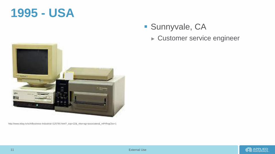
Sunnyvale, CA
► Customer service engineer
1995 - USA
11
http://www.ebay.tv/sch/Business-Industrial-/12576/i.html?_sop=22&_nkw=ag+associates&_mPrRngCbx=1

External Use
R 139
G 141
B 142
R 224
G 225
B 221
R 69
G 153
B 195
R 254
G 203
B 0 R 255
G 121
B 1 R 205
G 32
B 44
R 163
G 219
B 232 R 122
G 184
B 0
R 77
G 79
B 83
R 6
G 30
B 60
FOUNDED in 1967
Applied Materials
began in a small
industrial unit in
Mountain View,
California
1997 – Applied Materials 30 Years!
12

External Use
R 139
G 141
B 142
R 224
G 225
B 221
R 69
G 153
B 195
R 254
G 203
B 0 R 255
G 121
B 1 R 205
G 32
B 44
R 163
G 219
B 232 R 122
G 184
B 0
R 77
G 79
B 83
R 6
G 30
B 60
The Global Strength of Applied
Stock Ticker: Nasdaq: AMAT
Fiscal 2014 Revenue: $9.1 billion
Fiscal 2014 RD&E: $1.4 billion
Founded: November 10, 1967
Headquarters: Santa Clara, California
Global Presence: 81 locations in
18 countries
Principal Locations United States, Israel, Singapore, Taiwan
Employees*: ~14,000 worldwide
Patents: ~10,500 issued
Data as of fiscal year end, October 26, 2014
*Excluding temporary and interns
13

External Use
R 139
G 141
B 142
R 224
G 225
B 221
R 69
G 153
B 195
R 254
G 203
B 0 R 255
G 121
B 1 R 205
G 32
B 44
R 163
G 219
B 232 R 122
G 184
B 0
R 77
G 79
B 83
R 6
G 30
B 60
Since 1997 at Applied materials
Energy and
Environmental
Solutions
Display Silicon Systems Global Services
14
Application engineer, KAT, KAT manager, Technologist

External Use
R 139
G 141
B 142
R 224
G 225
B 221
R 69
G 153
B 195
R 254
G 203
B 0 R 255
G 121
B 1 R 205
G 32
B 44
R 163
G 219
B 232 R 122
G 184
B 0
R 77
G 79
B 83
R 6
G 30
B 60
Accelerating Innovation
Thermal
Metals
Deposition
Planarization
Etch Inspection
Collaborate earlier and deeper
with customers on inflections
Provide the broadest suite of solutions
with unmatched integration benefits
Drive to atomic precision on interfaces
with multi-chamber platforms
Extend the technology roadmap
with fast cadence in product innovation
Enable faster learning
with Maydan Technology Center Plating Implant
15
External Use
R 139
G 141
B 142
R 224
G 225
B 221
R 69
G 153
B 195
R 254
G 203
B 0 R 255
G 121
B 1 R 205
G 32
B 44
R 163
G 219
B 232 R 122
G 184
B 0
R 77
G 79
B 83
R 6
G 30
B 60
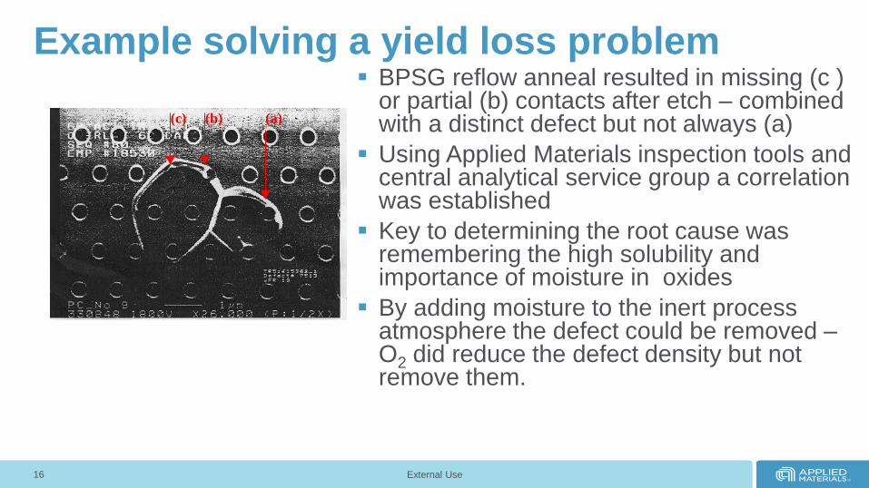
BPSG reflow anneal resulted in missing (c ) or partial (b) contacts after etch – combined with a distinct defect but not always (a)
Using Applied Materials inspection tools and central analytical service group a correlation was established
Key to determining the root cause was remembering the high solubility and importance of moisture in oxides
By adding moisture to the inert process atmosphere the defect could be removed – O2 did reduce the defect density but not remove them.
Example solving a yield loss problem
16
( c) ( a) ( b)

External Use
R 139
G 141
B 142
R 224
G 225
B 221
R 69
G 153
B 195
R 254
G 203
B 0 R 255
G 121
B 1 R 205
G 32
B 44
R 163
G 219
B 232 R 122
G 184
B 0
R 77
G 79
B 83
R 6
G 30
B 60
Temperature data from 7
pyrometers and wafer rotation
FFT transformed and high
frequency portion converted in
temperature maps
Used for tuning wafer
placement, separating real
temperature signature from
the wafer metrology,
optimizing recipes, preventing
yield issues
Example Using Digital Signal Analysis for VM
17
Victor Vitale, Wolfgang Aderhold, Aaron Hunter, Ilias Iliopoulos, Natalia Kroupnova, Aleksey Yanovich, Nir Merry, “Use of Virtual Metrology for in-situ
Visualization of Thermal Uniformity and Handoff Adjustment in RTP Critical Anneals”,2008 IEEE/SEMI Advanced Semiconductor Manufacturing
Conference, p349
External Use
R 139
G 141
B 142
R 224
G 225
B 221
R 69
G 153
B 195
R 254
G 203
B 0 R 255
G 121
B 1 R 205
G 32
B 44
R 163
G 219
B 232 R 122
G 184
B 0
R 77
G 79
B 83
R 6
G 30
B 60
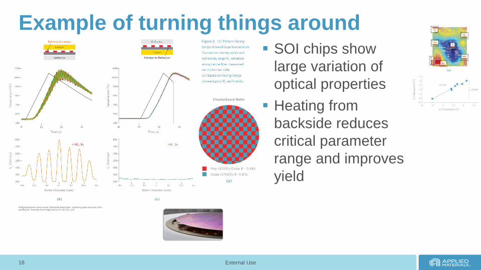
SOI chips show
large variation of
optical properties
Heating from
backside reduces
critical parameter
range and improves
yield
Example of turning things around
18
Wolfgang Aderhold, Aaron Hunter, Shankar Muthukrishnan, “Optimizing Spike Anneal for 32nm
and Beyond”, Nanochip Technology Journal, Vol. 9/2 2011, p10

External Use
R 139
G 141
B 142
R 224
G 225
B 221
R 69
G 153
B 195
R 254
G 203
B 0 R 255
G 121
B 1 R 205
G 32
B 44
R 163
G 219
B 232 R 122
G 184
B 0
R 77
G 79
B 83
R 6
G 30
B 60
Summary Accompanied a nice portion of the IC
evolution
What was learned on the way was never
useless
Field of semiconductor keeps demanding it all
Recent revolution of the transistor going 3D
requires to provide solutions integrated in the
flow, consisting of several equipment steps
and the understanding of how devices are
designed
To achieve this assistance from academia and
research institutes is more than welcome 19
TR440 0.8MIPS
18KB RAM
http://www.mirrorservice.org/sites/www.bitsav
ers.org/pdf/aeg-
telefunken/tr440/TR440_SystemOverview_Ma
r70.pdf

R 139
G 141
B 142
R 224
G 225
B 221
R 69
G 153
B 195
R 254
G 203
B 0 R 255
G 121
B 1 R 205
G 32
B 44
R 163
G 219
B 232 R 122
G 184
B 0
R 77
G 79
B 83
R 6
G 30
B 60
Learn More. Visit appliedmaterials.com
Dr.-Ing. Wolfgang Aderhold

R 139
G 141
B 142
R 224
G 225
B 221
R 69
G 153
B 195
R 254
G 203
B 0 R 255
G 121
B 1 R 205
G 32
B 44
R 163
G 219
B 232 R 122
G 184
B 0
R 77
G 79
B 83
R 6
G 30
B 60


![Bypaßklappe / registre de dérivation BPK 224 / bypass damper · BPK 200 Best.-Nr. ø d1 [mm] 200 ø d3 [mm] 224 Bestellbeispiel Exemple de commande Order example 224 Bypaßklappe](https://static.fdokument.com/doc/165x107/5d5e958688c993252f8b7525/bypassklappe-registre-de-derivation-bpk-224-bypass-damper-bpk-200-best-nr.jpg)


