Inter- and Intraband Carrier Dynamics in Cubic GaN/AlxGa1 ...
123
Fakultät Naturwissenschaften Department Physik Inter- and Intraband Carrier Dynamics in Cubic GaN/Al x Ga 1-x N Heterostructures Grown by MBE Dem Department Physik der Universität Paderborn zur Erlangung des akademischen Grades eines Doktor der Naturwissenschaften vorgelegte Dissertation von Tobias Wecker Paderborn, 15.09.2017 Erster Gutachter: Prof. Dr. Donat J. As Zweiter Gutachter: Prof. Dr. Cedrik Meier
Transcript of Inter- and Intraband Carrier Dynamics in Cubic GaN/AlxGa1 ...

Fakultät Naturwissenschaften
Department Physik
Inter- and Intraband Carrier Dynamics in Cubic
GaN/AlxGa1-xN Heterostructures Grown by MBE
Dem Department Physik
der Universität Paderborn
zur Erlangung des akademischen Grades eines
Doktor der Naturwissenschaften
vorgelegte
Dissertation
von
Tobias Wecker
Paderborn, 15.09.2017
Erster Gutachter: Prof. Dr. Donat J. As
Zweiter Gutachter: Prof. Dr. Cedrik Meier

I Kurzfassung Tobias Wecker PHD Thesis
Tobias Wecker
2
„Gott, gib mir die Gelassenheit, Dinge hinzunehmen, die ich nicht än-
dern kann, den Mut, Dinge zu ändern, die ich ändern kann, und die
Weisheit, das eine vom anderen zu unterscheiden.“
Gelassenheitsgebet von Reinhold Niebuhr (1941 oder 1942)
I Kurzfassung Tobias Wecker PHD Thesis
3
I Kurzfassung
In dieser Arbeit wurde die Ladungsträgerdynamik systematisch erforscht, indem
asymmetrische Doppelquantentröge (ADQWs) und mehrfach Quantentröge
(MQWs) aus kubischen GaN/AlxGa1-xN hergestellt und experimentell ausgewertet
wurden. Hierbei wurde besonderes Augenmerk auf den Einfluss der Kopplung von
Einzel- und Mehrfach-QWs auf die optischen Eigenschaften gelegt. Die gewonnen
Erkenntnisse können zu einem erweiterten experimentellen und theoretischen Ver-
ständnis für die Forschung an Intersubband Übergängen (ISBT) verwendet werden.
Denn diese Übergänge ermöglichen die Erforschung nicht linearer Effekte, sowie
die Herstellung von unipolaren Bauelementen im Bereich der 1,55 µm Emissions-
wellenlänge.
Zu Beginn wurden GaN/AlxGa1-xN ADQWs mit unterschiedlicher Al Konzentration in
den Barrieren auf ihr Kopplungsverhalten analysiert. Dies ergab eine Kopplung bei
7 nm dicken Barrieren für x = 0,26 und bei x = 0,64 startete die Kopplung bereits
bei 3 nm. Daraufhin wurde extrapoliert, dass bei x = 1 die Kopplung bei 1-2 nm an-
fängt. Für diese Berechnungen wurden Ratengleichungen und zeitabhängige Pho-
tolumineszenz Messungen (TRPL) verwendet, welche eine klare Korrelation zwi-
schen Barrierendicke und Rekombinationszeit zeigten.
Des Weiteren wurden Si dotierte kubische GaN/AlN MQWs auf ihre IR Absorption
untersucht. Die Halbwertsbreite (FWHM) dieser Spektren wurde theoretisch model-
liert und es ergaben sich eine Korrelationslänge von Λ = 0.53 nm sowie eine
durchschnittliche Höhe der Rauigkeit von Δ = 0.45 nm. Zudem wurden erste nicht
lineare Messungen mit einem Pump Probe Aufbau gemessen. Dies lieferte eine
dritte Ordnung Suszeptibilität von Im χ(3) ~ 1.1 ⋅ 10−20 m2/V2. Weiterhin wurden zu-
sätzliche Intensitäten in den reziproken Raumkarten (RSM) von Messungen mittels
hochauflösender Röntgenbeugung (HRXRD) in (002) und (113) Richtung gemes-
sen, welche die Ausbildung eines Übergitters belegen. Die Verspannung der
Schichten wurde ermittelt und in Berechnungen für die Übergangsenergien in next-
nano³ verwendet. Ferner wurden ω-2θ Messungen mit MadMax modelliert, sie lie-
ferten die realen Schichtdicken sowie Informationen über die Verspannung.
Die Parameter für kubische Nitride wurden schrittweise den experimentellen Daten
angepasst und liefern in den theoretischen Überlegungen mittels nextnano³ und
MadMax sehr gute Übereinstimmungen mit den experimentellen Messungen.

II Abstract Tobias Wecker PHD Thesis
Tobias Wecker
4
II Abstract
In this thesis a systematic investigation of the carrier dynamics between QWs is
done exploiting asymmetric double quantum wells (ADQWs) and multi quantum
wells (MQWs) based on cubic GaN/AlxGa1-xN. The focus of interest was the cou-
pling behaviour of single and multi QWs and the influence on optical properties.
This leads to the experimental and theoretical knowledge needed for the analysis of
intersubband transitions (ISBT) important for the research of non-linear effects and
unipolar devices emitting at a wavelength of 1.55 µm.
The first approach to the coupling was done with cubic GaN/AlxGa1-xN ADQWs with
different Al content in the barriers. For the series with x = 0.26 the coupling starts at
7 nm barriers, for x = 0.64 the coupling begins at 3 nm barriers. For x = 1 the cou-
pling is estimated to occur at 1-2 nm. In the calculation rate equations, time-
resolved photoluminescence (TRPL) and conventional photoluminescence were
used. The decay times of the TRPL data show a clear correlation with the barrier
thickness. This indicates the tunnelling of carriers from the narrow QW to the wide
QW.
Si doped cubic GaN/AlN MQWs have been used for intersubband absorption
measurements. The full width at half maximum (FWHM) of this absorption was the-
oretically fitted leading to a correlation length of Λ = 0.53 nm and a mean height
Δ = 0.45 nm of the roughness. Also first experiments on MQWs concerning the
non-linear behaviour have been performed with a pump probe setup revealing a
third order susceptibility of Im χ(3) ~ 1.1 ⋅ 10−20 m2/V2. The MQWs were investigat-
ed with high resolution X-Ray diffractometry (HRXRD) reciprocal space maps
(RSM) around the (002) and (113) reflections, in order to prove the existence of SL
peaks. Besides the strain in the heterostructures has been investigated by HRXRD
RSM around (113) and are also validated by the theoretical calculations of the tran-
sition energies via nextnano³. Furthermore ω-2θ scans have been done and com-
pared to theoretical considerations via MadMax. This revealed a good match with
the expected layer thicknesses and the measured strain.
Thus one main point in this thesis is the systematic understanding of GaN/AlxGa1-xN
heterostructures and the validation of the theoretical models needed for energy
transitions (nextnano³), layer thicknesses and strain (MadMax). To achieve this, a
set of parameters was improved successively to match all the experimental results.

III Content Tobias Wecker PHD Thesis
5
III Content
I Kurzfassung .........................................................................................................................................3
II Abstract ...............................................................................................................................................4
III Content ...............................................................................................................................................5
IV List of Abbreviations ........................................................................................................................7
1 Motivation ......................................................................................................................................8
2 Theory ............................................................................................................................................9
2.1 Exciton Binding Energy .......................................................................................................10
2.2 Heterostructures, Rate Equations and Selection Rules ......................................................12
2.3 MQWs, Waveguide and ISB Absorption .............................................................................15
2.4 Band Edge of AlxGa1-xN and Band Offsets..........................................................................18
3 Experimental Setups ................................................................................................................. 21
3.1 Molecular Beam Epitaxy (MBE) ..........................................................................................21
3.2 Reflection High Energy Electron Diffraction (RHEED) ........................................................22
3.3 UV Photoluminescence Spectroscopy Setup CW (PL) .......................................................23
3.4 Optical Setup TU Berlin .......................................................................................................24
3.4.1 Photoluminescence Spectroscopy (PL) ......................................................................24
3.4.2 Photoluminescence Excitation Spectroscopy (PLE) ...................................................25
3.4.3 Time-resolved Photoluminescence Spectroscopy (TRPL) .........................................25
3.5 High Resolution X-Ray Diffractometry (HRXRD) ................................................................26
3.6 IR Absorption Setup TU Dormtund .....................................................................................29
3.7 Spatially-resolved Raman Spectroscopy ............................................................................30
3.8 Picosecond Acoustics TU Dormtund ...................................................................................31
3.9 Intraband Non-linear Measurements TU Dortmund ............................................................32
4 Results and Discussion ............................................................................................................ 33
4.1 GaN Bulk: Raman and Defect Density ................................................................................33
4.2 Thick QW: Strain Pulse .......................................................................................................39
4.3 Asymmetric Double Quantum Wells (ADQW) .....................................................................43
4.3.1 General Characterisation ............................................................................................43
4.3.2 Influence of Barrier Thickness to the Coupling ...........................................................46
4.3.3 Time-resolved Investigation of Carrier Transfer ..........................................................54
4.3.4 Excited Energy Levels .................................................................................................58
4.3.5 Summary ADQWs .......................................................................................................64
4.4 Multi Quantum Wells (MQW)...............................................................................................65
III Content Tobias Wecker PHD Thesis
Tobias Wecker
6
4.4.1 Growth of MQW Samples ........................................................................................... 66
4.4.2 Investigation of MQWs by HRXRD ............................................................................. 68
4.4.3 Calibration of QW Thickness by TEM ......................................................................... 70
4.4.4 Photoluminescence Spectroscopy (PL) ...................................................................... 72
4.4.5 Measurements of Intersubband Absorption ................................................................ 75
4.4.6 Intersubband Absorption Linewidth and Roughness .................................................. 79
4.4.7 Non-linear Optical Measurements .............................................................................. 85
4.4.8 Summary MQWs ......................................................................................................... 87
5 Simulation ................................................................................................................................... 88
5.1 Nextnano³ ........................................................................................................................... 88
5.2 MadMax and ω-2θ Profiles ................................................................................................. 90
6 Summary ..................................................................................................................................... 94
7 Appendix ..................................................................................................................................... 96
7.1 Sample List ......................................................................................................................... 96
7.2 Literature ........................................................................................................................... 100
7.3 Abbildungsverzeichnis ...................................................................................................... 104
7.4 List of Conferences ........................................................................................................... 109
7.5 List of Publications ............................................................................................................ 110
7.6 Parameters ....................................................................................................................... 111
7.7 Nextnano³ Source Code ................................................................................................... 112
7.8 Matlab Source Code ......................................................................................................... 120
7.9 Acknowledgements ........................................................................................................... 122
7.10 Eidesstattliche Erklärung .................................................................................................. 123

IV List of Abbreviations Tobias Wecker PHD Thesis
7
IV List of Abbreviations
ADQW Asymmetric Double Quantum Well
c-AlxGa1-xN cubic Aluminium Gallium Nitride
c-AlN cubic Aluminium Nitride
CBO Conduction Band Offset
c-GaN cubic Gallium Nitride
HRXRD High Resolution X-Ray Diffraction
MBE Molecular Beam Epitaxy
PL Photoluminescence
RHEED Reflection High Energy Electron Diffraction
RSM Reciprocal Space Map
VBO Valence Band Offset
MBE Molecular Beam Epitaxy
PAMBE Plasma-assisted Molecular Beam Epitaxy
hh Heavy hole
lh Light hole
TRPL Time-resolved Photoluminescence
MQW Multi Quantum Well
QCL Quantum Cascade Laser
ISB Intersubband
nn³ Nextnano³
QWW Wide QW
QWN Narrow QW
X Exciton
Xe-hh Exciton (electron and heavy hole)
Xe-lh Exciton (electron and light hole)
ML Monolayer

Motivation Tobias Wecker PHD Thesis
Tobias Wecker
8
1 Motivation
Intersubband transitions (ISBT) of multi quantum well (MQW) structures are in the
focus of interest for designing several novel devices like quantum cascade lasers
(QCL), IR detectors and more. Moreover, structures based on the material system
of the group III-nitrides have numerous advantages, for instance high stability
against mechanical, thermal, and chemical stress. Therefore structures containing
these materials can be investigated using high excitation power, which is favourable
for the optical study of nonlinear effects. Especially the ISBT in MQW structures can
be exploited to get an insight into nonlinear effects, due to their high nonlinear re-
sponse [1-5]. In addition, the inherently large band offset between GaN/AlN is bene-
ficial for devices based on ISBT such as THz devices, fast modulators and fast pho-
to detectors [6]. As a result, the ISBT in these devices can reach the 1.55 µm spec-
tral window (optical C-band) [7], suitable for devices in the telecommunication in-
dustry. Consequently, a number of studies have elucidated the dynamical optical
nonlinearity of such nitride-based heterostructures [3][5]. So far, these experiments
have focused on the common hexagonal phase. Recently, ISBT in the near infrared
have been achieved in n-doped cubic GaN/AlN quantum wells (QWs) fabricated by
plasma-assisted molecular beam epitaxy (PA-MBE) [8][6][9]. First studies of ultra-
fast carrier dynamics and nonlinear optical properties of these cubic heterostruc-
tures have been reported recently [10][11].
Also AlxGa1-xN as a compound material permits another degree of freedom and can
be exploited for tailoring the bandgap in future heterostructures. Utilizing AlxGa1-xN
is especially suited for an efficient tuning of the required QW energy levels. A first
approach to the topic of quantum cascade lasers is the investigation of asymmetric
double quantum wells (ADQW), due to their different QW thicknesses the emission
visible in luminescence can be adjusted separately. Thus coupling effects and the
carrier transfer as well as the lifetimes of the charge carriers can be investigated in
such ADQW structures using photoluminescence (PL) [12], photoluminescence
excitation spectroscopy (PLE) [13] and time dependent photoluminescence (TRPL)
[14] measurements. These measurements deliver the exact position of each energy
level for electrons and holes within the QWs and their dynamic optical behaviour.
Furthermore the tuning of the wavelength of the excitation source used in PLE gi-
ves direct access to the related absorption but also to charge carrier transfer pro-
cesses by monitoring the luminescence signal. Therefore, not only the charge car-

Theory Tobias Wecker PHD Thesis
9
rier transfer from e.g. the barrier material into the QWs can be observed but even
inter QW coupling processes (or their suppression) can experimentally be wit-
nessed [15].
Common hexagonal group III-nitrides suffer from large internal polarisation fields
along the c-axis resulting in a bending of the bands and the quantum confined
Stark-effect. Due to both effects the design of modern devices for ISBT in the hex-
agonal phase is fairly complicated [16]. In order to reduce these effects the growth
of hexagonal nitrides in semi-polar directions is intensively investigated [17]. Anoth-
er approach is the growth of group III nitrides in the cubic phase in the (001) direc-
tion on 3C-SiC. Therefore, all above listed unfavourable effects can be significantly
reduced [18][19]. Thus only cubic group III-nitrides have been grown and investi-
gated in this thesis.
2 Theory
In this chapter some of the fundamentals about low dimensional semiconductors
are described. The exciton binding energy in quantum wells (QWs) significantly dif-
fers from a thick semiconductor layer. This is important for the comparison of the
simulations of the band structure (nextnano³) and the energy transitions with the
experimental optical results delivered by photoluminescence and photolumines-
cence excitation spectroscopy. Thus this has to be considered for the optical be-
haviour in heterostructures for example by comparing the rate equations and selec-
tion rules with the experimental data. The third subchapter covers MQWs and their
optical properties like IR absorption. For this absorption the light has to approach
perpendicular to the QW growth direction, in order to satisfy the selection rules. The
last subchapter deals with the theoretical band edges of AlxGa1-xN for various Al
content. This is crucial for the determination of the band offsets between the va-
lence and the conduction band at the GaN/AlxGa1-xN hetero interface for single and
multi QWs.
Theory Tobias Wecker PHD Thesis
Tobias Wecker
10
2.1 Exciton Binding Energy
An exciton is an electron hole pair connected by the Coulomb force. This quasi par-
ticle can be described as a single particle with hydrogen like line spectrum. Due to
the Coulomb force the energy of the exciton is lowered by the exciton binding ener-
gy. This energy can be expressed very similar to the hydrogen model [20].
E3D = μ∗e4
2 (4πϵ)²ℏ2
1
n2=
Rx
n2 (2.1)
With the effective mass 1
𝜇∗ = 1
𝑚𝑒∗ +
1
𝑚ℎ∗ determined by the effective electron mass
𝑚𝑒∗ and the effective hole mass 𝑚ℎ
∗ . This description is only valid for thick bulk mate-
rial. For quantum mechanical systems like quantum dots, quantum wires and quan-
tum wells the deviation to this formula increases for smaller dimensions. Thus in
this thesis the model presented in [21] is used to calculate the exciton binding ener-
gy in the QWs. The following formula can be applied for QWs with LW
2 < aex, where
LW is the thickness of the QW and aex the Bohr radius of the exciton.
Eex =4
(α−1)2E3D (2.2)
The dimension in space α has to be an integer value between 2 and 3. This term is
given by:
α = 3 − e−(2/kb +Lw)/ 2 aex (2.3)
The exciton binding energy for thick c-GaN layers is E3D = 24 meV [22] and kb cor-
responds to the wave vector in the barriers.
kb =√2mb(V−E)
ℏ (2.4)
Adapting the relating mass mb and the potentials V and E the parameter kb for elec-
trons kbe, light holes kblh and heavy holes kbhh can be calculated. The value kbh is
determined using the light holes (lh) or heavy holes (hh).
1
kb=
1
kbe+
1
kbh (2.5)
The Bohr radius in a semiconductor is influenced by the Bohr radius of the hydro-
gen atom aH = 0,529 ⋅ 10−10 m and the dielectric constant in the semiconductor εs.
aex =εs
μ∗ aH (2.6)
The effective mass 1
μ∗ = 1
me∗ +
1
mh∗ depends on the penetration length into the barri-
er, described by the parameter β.

Theory Tobias Wecker PHD Thesis
11
β =LW
2
kb+LW
(2.7)
m∗ = βmw + (1 − β)mb (2.8)
These theoretical considerations lead to the following formula for the exciton bind-
ing energy Eex in a QW:
Eex =E3D
(1−1
2exp(−
2kb
+Lw
2aex))
2 (2.9)
Figure 2.1 Excitonic binding energies for excitons consisting of e-hh and e-lh. The dotted lines cor-
respond to complex simulations and the straight lines are calculated by the fractal dimensional
method. In the left side the Al content in the barriers is 15% and on the right 30% [21].
The calculated results of a Ga1-xAlxAs/GaAs QW are shown in Figure 2.1 against
the well width. Considering a very thick QW the binding energy approaches the val-
ue for the bulk layer of the QW material (GaAs). For real structures with finite barri-
er heights the binding energy increases to a factor of 1.4-1.6, although the theory
for infinite barrier heights predicts a factor of 4. For very thin QWs the exciton radius
is much larger than the QW width, leading to a strong penetration into the barriers.
This results in a lowering of the exciton binding energy towards the bulk value of the
barrier material (Ga1-xAlxAs).

Theory Tobias Wecker PHD Thesis
Tobias Wecker
12
2.2 Heterostructures, Rate Equations and Selection Rules
Optical investigations on a single QW structure reveal an insight into the energy
levels of the electrons and holes. Due to selection rules the amount of possible
transitions is limited. In case of the excitation light entering the structure parallel to
the QW growth direction, only the interband transitions with electrons and holes
take part. The dipole matrix element describes all transitions enabling the calcula-
tion and identification of allowed transitions and forbidden transitions [23].
⟨ϕje(z)|e⃗ ⋅ p̂|ϕi
h(z)⟩ (2.10)
With the two wave functions ϕje(z) and ϕj
h(z). These wave functions are oriented
along the z direction, which is equal to the growth direction of the QWs. Further-
more ϕje(z) describes an electron wave function and ϕj
h(z) a hole wave function.
Besides the dipole matrix element depends on the polarisation e⃗ and the momen-
tum operator p̂ = − iℏΔ. The polarisation e⃗ contains the geometry information of
the incident beam in regard to the QW growth direction and strongly influences the
absorption. This leads for our case to the selection rules Δninter = 0,2,4,6, …, with
the difference of the quantum number of the two participating energy levels Δn.
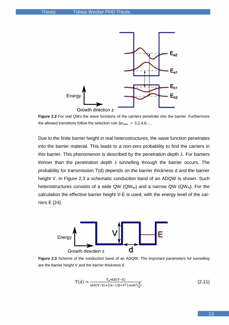
Some of the allowed transitions visible in optical spectra are shown in Figure 2.2.
Only the transitions between the first electron level (e1) and the first heavy hole
level (hh1) Ee1 − Eh1 and the second e and hh level Ee2 − Eh2 can be investigated
optically. There is a non-zero probability to measure a forbidden transition in real
structures, but the allowed transitions are several orders of magnitude stronger. In
real structures interface roughness, defects and fluctuation of Al in the AlxGa1-xN
layers lead to a deviation from the above described transition rules. Due to these
effects the symmetry of the wave function can differ from that in the ideal case,
changing the value of the dipole matrix element.
Theory Tobias Wecker PHD Thesis
13
Figure 2.2 For real QWs the wave functions of the carriers penetrate into the barrier. Furthermore
the allowed transitions follow the selection rule Δninter = 0,2,4,6.....
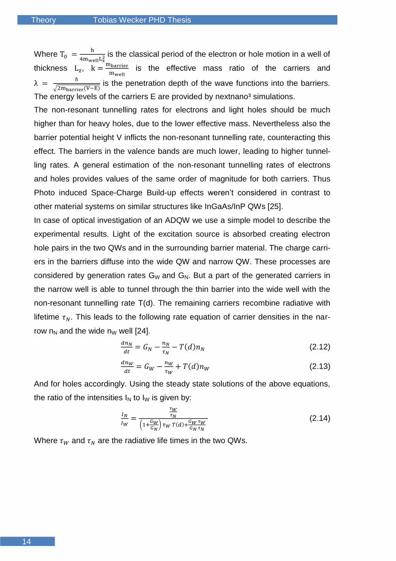
Due to the finite barrier height in real heterostructures, the wave function penetrates
into the barrier material. This leads to a non-zero probability to find the carriers in
this barrier. This phenomenon is described by the penetration depth λ. For barriers
thinner than the penetration depth λ tunnelling through the barrier occurs. The
probability for transmission T(d) depends on the barrier thickness d and the barrier
height V. In Figure 2.3 a schematic conduction band of an ADQW is shown. Such
heterostructures consists of a wide QW (QWW) and a narrow QW (QWN). For the
calculation the effective barrier height V-E is used, with the energy level of the car-
riers E [24].
Figure 2.3 Scheme of the conduction band of an ADQW. The important parameters for tunnelling
are the barrier height V and the barrier thickness d.
T(d) =T04kE(V−E)
4kE(V−E)+((k−1)E+V2) sinh2(d
λ) (2.11)
Theory Tobias Wecker PHD Thesis
Tobias Wecker
14
Where T0 =h
4mwellLz2 is the classical period of the electron or hole motion in a well of
thickness Lz, k =mbarrier
mwell is the effective mass ratio of the carriers and
λ = ℏ
√2mbarrier(V−E) is the penetration depth of the wave functions into the barriers.
The energy levels of the carriers E are provided by nextnano³ simulations.
The non-resonant tunnelling rates for electrons and light holes should be much
higher than for heavy holes, due to the lower effective mass. Nevertheless also the
barrier potential height V inflicts the non-resonant tunnelling rate, counteracting this
effect. The barriers in the valence bands are much lower, leading to higher tunnel-
ling rates. A general estimation of the non-resonant tunnelling rates of electrons
and holes provides values of the same order of magnitude for both carriers. Thus
Photo induced Space-Charge Build-up effects weren’t considered in contrast to
other material systems on similar structures like InGaAs/InP QWs [25].
In case of optical investigation of an ADQW we use a simple model to describe the
experimental results. Light of the excitation source is absorbed creating electron
hole pairs in the two QWs and in the surrounding barrier material. The charge carri-
ers in the barriers diffuse into the wide QW and narrow QW. These processes are
considered by generation rates GW and GN. But a part of the generated carriers in
the narrow well is able to tunnel through the thin barrier into the wide well with the
non-resonant tunnelling rate T(d). The remaining carriers recombine radiative with
lifetime 𝜏𝑁. This leads to the following rate equation of carrier densities in the nar-
row nN and the wide nW well [24].
𝑑𝑛𝑁
𝑑𝑡= 𝐺𝑁 −
𝑛𝑁
𝜏𝑁− 𝑇(𝑑)𝑛𝑁 (2.12)
𝑑𝑛𝑊
𝑑𝑡= 𝐺𝑊 −
𝑛𝑊
𝜏𝑊+ 𝑇(𝑑)𝑛𝑊 (2.13)
And for holes accordingly. Using the steady state solutions of the above equations,
the ratio of the intensities IN to IW is given by:
𝐼𝑁
𝐼𝑊=
𝜏𝑊𝜏𝑁
(1+𝐺𝑊𝐺𝑁
) 𝜏𝑊 𝑇(𝑑)+𝐺𝑊 𝜏𝑊𝐺𝑁 𝜏𝑁
(2.14)
Where 𝜏𝑊 and 𝜏𝑁 are the radiative life times in the two QWs.

Theory Tobias Wecker PHD Thesis
15
2.3 MQWs, Waveguide and ISB Absorption
The possibility to grow complex structures like multi quantum wells (MQWs) ena-
bles several areas of investigation. For example for the group III nitrides the IR
spectral region can be covered in a wide range around the important telecom wave-
length 1.55 µm. Devices consisting MQW structures in this field are quantum cas-
cade lasers (QCL), IR detectors and more.
To investigate these structures in the IR optically, intraband transitions are exploit-
ed. For these transitions only one charge carrier type take part in the transition.
Here mostly electrons are used, due to their lower effective mass the devices can
operate much faster than with holes. For the intraband transition the transition ma-
trix element in equation 2.10 is still valid, but both wave functions in the formula are
electron wave functions. For light arriving parallel to the QW growth direction e⃗ can
be written as e⃗ x = (1,0,0) (also called TE polarisation) or e⃗ y = (0,1,0). Both direc-
tions are equal for optical measurements of QWs. Calculating these two geometries
lead to e⃗ x ⋅ p̂ = − iℏ∂
∂x and e⃗ y ⋅ p̂ = − iℏ
∂
∂y. In this case the dipole matrix element
in formula (2.10) is zero and no absorption is possible. Thus the intraband transi-
tions can only be excited for light arriving perpendicular to the growth direction of
the MQWs. For intraband transitions e⃗ z = (0,0,1) (also called TM polarisation)
holds true leading to e⃗ z ⋅ p̂ = − iℏ∂
∂z [26]. For this case absorption is possible, be-
cause of the z orientation of the wave functions. This leads to a change in the se-
lection rules. The momentum operator p̂ = − iℏΔ changes the parity of the wave
function ϕi(z). So the selection rules change to Δnintra = 1,3,5,7,… .
Theory Tobias Wecker PHD Thesis
Tobias Wecker
16
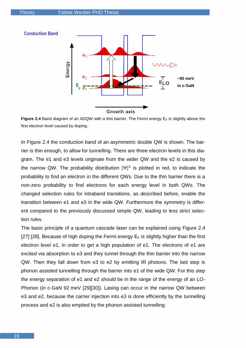
Figure 2.4 Band diagram of an ADQW with a thin barrier. The Fermi energy EF is slightly above the
first electron level caused by doping.
In Figure 2.4 the conduction band of an asymmetric double QW is shown. The bar-
rier is thin enough, to allow for tunnelling. There are three electron levels in this dia-
gram. The e1 and e3 levels originate from the wider QW and the e2 is caused by
the narrow QW. The probability distribution |Ψ|2 is plotted in red, to indicate the
probability to find an electron in the different QWs. Due to the thin barrier there is a
non-zero probability to find electrons for each energy level in both QWs. The
changed selection rules for intraband transitions, as described before, enable the
transition between e1 and e3 in the wide QW. Furthermore the symmetry is differ-
ent compared to the previously discussed simple QW, leading to less strict selec-
tion rules.
The basic principle of a quantum cascade laser can be explained using Figure 2.4
[27] [28]. Because of high doping the Fermi energy EF is slightly higher than the first
electron level e1, in order to get a high population of e1. The electrons of e1 are
excited via absorption to e3 and they tunnel through the thin barrier into the narrow
QW. Then they fall down from e3 to e2 by emitting IR photons. The last step is
phonon assisted tunnelling through the barrier into e1 of the wide QW. For this step
the energy separation of e1 and e2 should be in the range of the energy of an LO-
Phonon (in c-GaN 92 meV [29][30]). Lasing can occur in the narrow QW between
e3 and e2, because the carrier injection into e3 is done efficiently by the tunnelling
process and e2 is also emptied by the phonon assisted tunnelling.
~90 meV
in c-GaN
Conduction Band
EF

Theory Tobias Wecker PHD Thesis
17
The substrates used for this thesis consist of 500 µm Si (001) with 10 µm 3C-SiC
(001) on top. This is followed by the PA-MBE grown c-GaN buffer layer with 100 nm
and the MQW structure with around 100 nm. Thus the MQW layers important for
our investigation are only 100 nm thick. This is very significant for the absorption
measurements, because of the selection rules the incident light has to approach
perpendicular to the MQW growth direction. Therefore most of the light enters the
Si and 3C-SiC and doesn’t take part to our experiment. In order to improve this, a
waveguide structure is processed with 30° side facets (Figure 2.5). For this angle
total reflection at the top and bottom of the sample piece is achieved. In our case
the waveguide samples are 5-8 mm long leading to 10-20 passes through the MQW
layers. Unfortunately the waveguide structure changes the angle of the light travel-
ing through the MQWs as well, decreasing the coupling of the light and the MQW.
The best coupling is achieved for a perpendicular angle of incidence in regard to
the growth direction of the MQWs (selection rules). These two processes have to
be optimised, to get a good absorption signal. For the waveguide with 30° facets
discussed here, the coupling is high enough to measure IR absorption.
Figure 2.5 Sketch of a waveguide used for absorption measurements. Multiple passes through the
MQWs are achieved by total reflection. The layer thicknesses are not to scale.

Theory Tobias Wecker PHD Thesis
Tobias Wecker
18
2.4 Band Edge of AlxGa1-xN and Band Offsets
For the simulation of the band structure with the semi empirical program nextnano³
the knowledge of the conduction band and valence band offsets for the
GaN/AlxGa1-xN interface is needed. So an ab-initio calculation was done by Marc
Landmann of AG Schmidt in University of Paderborn. The ab-initio determination of
(strained) band offsets commonly involves a two-step procedure relying on sepa-
rate heterostructure and bulk calculation. The super-cell approach is utilized to
model the semiconductor interfaces on the microscopic level. In the super-cell ap-
proach the semiconductor heterostructure is represented as an infinite superlattice
with fixed in-plane lattice parameter. Choosing the substrates’ in-plane lattice con-
stant and allowing unit-cell relaxation along the growth direction enables the accu-
rate estimation of band offsets in pseudomorphically strained heterostructures. Us-
ing the medial in-plane lattice parameter of the interfacing materials enables an es-
timation of the natural unstrained band discontinuities.
The change in the macroscopic three-dimensional average of the local electrostatic
potential across the interface has been used as an energy reference to align the
band energies of the interfacing materials, which are obtained from two separate
bulk calculations. In case of strained band-offsets the bulk semiconductors are con-
sidered to be bi-axially strained under the constraint of volume conservation. For
estimation of natural band offsets the bulk semiconductors are considered at equi-
librium lattice constant.
The electronic structure calculations are performed within the framework of plane-
wave density functional theory (DFT) as implemented in the Vienna Ab-initio Simu-
lation Package (VASP) code. The DFT inherent under estimation of electronic band
gaps, originating from the use of common (semi)local exchange-correlation (XC)
functionals, is corrected by using nonlocal, screened Coulomb potential Heyd-
Scuseria-Ernzerhof (HSE) type hybrid density functionals with material dependent
exact exchange (EXX) fractions. The EXX fractions have been adjusted to mimic
electronic structure characteristics obtained via higher level theories as the GW ap-
proximation to many-body perturbation theory. Since the relative change in the
average of the electrostatic potential across the heterostructure-super cell is barely
affected by the use of conventional (semi)local XC functionals and the use of hybrid
functionals is computationally expensive, the hybrid functional treatment is restric-
ted to the bulk calculations. For further details on the ab-initio determination of natu-

Theory Tobias Wecker PHD Thesis
19
ral and strained band offsets, including details of the heterostructure unit-cell setup
as well as numerical details of the electronic structure calculations, the reader is
referred to the references [9],[31]. In Figure 2.6 the general behaviour of the band
offsets for AlxGa1-xN /GaN heterostructures partially strained on a c-GaN buffer lay-
er is shown for different Al content.
0.0 0.2 0.4 0.6 0.8 1.0
-0.4
0.0
0.4
0.8
1.2
1.6
2.0
bVBO
= -0.16
x = 0.63
bindirect
CBO = -0.14
Ban
d O
ffse
ts [
eV
]
Al Content x
bdirect
CBO = 0.36
Figure 2.6 Trend of the band offsets for a GaN/AlxGa1-xN interface partially strained on a c-GaN
buffer layer for various Al concentrations in the AlxGa1-xN barrier layers. (Provided by Marc Landman
in University of Paderborn)
In case of the direct ΓV − ΓC conduction band edge CBOdir and the valence band
VBO the formulas are:
CBOdir = 2.0032x − 0.3637x(1 − x) (2.15)
VBO = −0.5569x + 0.1640x(1 − x) (2.16)
The indirect ΓV − XC conduction band edge CBOind for different Al content x is de-
scribed by:
CBOind = 0.9860x + 1.4147(1 − x) + 0.1339x(1 − x) (2.17)
The change of AlxGa1-xN from a direct to an indirect semiconductor starts at
x = 0.63. Besides the exact influence of strain on the CBO:VBO values and the cor-
rect application into nextnano³ is still under investigation. The direct bandgap

Theory Tobias Wecker PHD Thesis
Tobias Wecker
20
CBO:VBO used in this thesis are 80:20, 79:21 and 78:22 for x = 0.26, x = 0.64 and
x = 1, respectively.
Another important parameter is the bandgap for different Al content x, as can be
seen in Figure 2.7. Similar to Figure 2.6 there is a change from the direct bandgap
(ΓV − ΓC) to the indirect bandgap (ΓV − XC) visible at an Al content of around 0.71.
The difference in the Al content at which the change occurs is caused by the ap-
plied strain, for fully and partly strained layers the value is slightly different. This is
still under investigation. The calculated data are represented as dots and squares
with a quadratic fit. These fit curves provide the bowing parameter for the direct
bandgap bBowingdirect = 0.85 and the indirect bandgap bBowing
indirect = 0.01 [77].
0.0 0.2 0.4 0.6 0.8 1.0
3.0
3.5
4.0
4.5
5.0
5.5
6.0 Theory V
C
Theory VX
C
Fitcurve V
C
Fitcurve VX
C
Ban
dg
ap
[e
V]
Al Content x
x=0.71
Figure 2.7 Bandgap of relaxed cubic AlxGa1−xN for different Al content. There is a change from di-
rect ΓV − ΓC (red) to indirect bandgap ΓV − XC (blue) at x = 0.71 [77].
Experimental Setups Tobias Wecker PHD Thesis
21
3 Experimental Setups
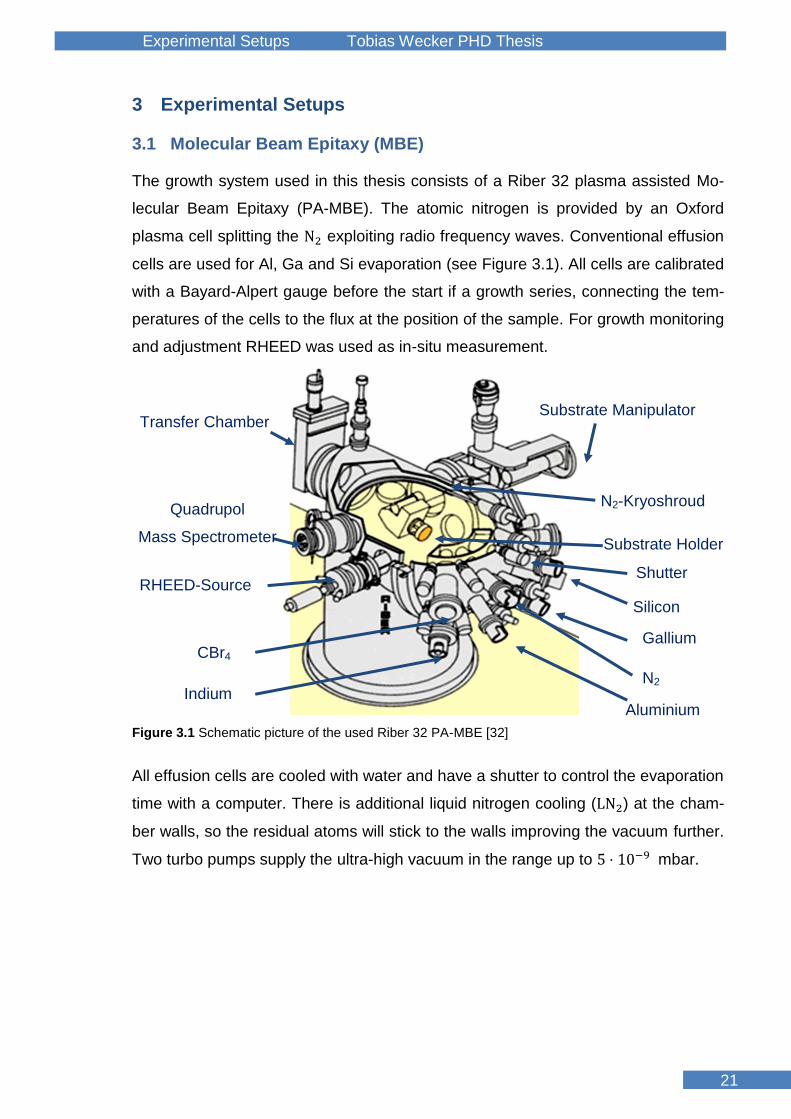
3.1 Molecular Beam Epitaxy (MBE)
The growth system used in this thesis consists of a Riber 32 plasma assisted Mo-
lecular Beam Epitaxy (PA-MBE). The atomic nitrogen is provided by an Oxford
plasma cell splitting the N2 exploiting radio frequency waves. Conventional effusion
cells are used for Al, Ga and Si evaporation (see Figure 3.1). All cells are calibrated
with a Bayard-Alpert gauge before the start if a growth series, connecting the tem-
peratures of the cells to the flux at the position of the sample. For growth monitoring
and adjustment RHEED was used as in-situ measurement.
Figure 3.1 Schematic picture of the used Riber 32 PA-MBE [32]
All effusion cells are cooled with water and have a shutter to control the evaporation
time with a computer. There is additional liquid nitrogen cooling (LN2) at the cham-
ber walls, so the residual atoms will stick to the walls improving the vacuum further.
Two turbo pumps supply the ultra-high vacuum in the range up to 5 ⋅ 10−9 mbar.
Substrate Manipulator
N2-Kryoshroud
Substrate Holder
Shutter
Silicon
Gallium
N2
Aluminium Indium
CBr4
RHEED-Source
Quadrupol
Mass Spectrometer
Transfer Chamber

Experimental Setups Tobias Wecker PHD Thesis
Tobias Wecker
22
3.2 Reflection High Energy Electron Diffraction (RHEED)
Reflection High Energy Electron Diffraction (RHEED) can be used to monitor the
growth parameters during growth. An electron gun accelerates the electrons with
V = 16 kV and I = 1.6 A towards the sample. Due to the small angle of incidence
the electrons only penetrate few monolayers into the sample. The electrons are dif-
fracted at the sample surface and measured at a fluorescence screen. This screen
is surveyed by a digital camera connected to a computer. The basic principle and
the geometries of the RHEED measurements can be seen in Figure 3.2. A part of
the electron beam is transmitted (dotted red line) and visible as a single point (red)
on the screen. Another part of the beam is reflected (orange).
Figure 3.2 Representation of the basic principle of the RHEED measurement. Also the geometries
of the different beams in regard to the sample can be seen.
2 dimensional (flat) surfaces appear as lines on the RHEED pattern. On the other
hand 3 dimensional (rough) surfaces cause spots. In realistic RHEED patterns both
components are visible. In Figure 3.2 a simplified RHEED pattern is shown with 2
dim lines (blue) and 3 dim spots (green).

Experimental Setups Tobias Wecker PHD Thesis
23
3.3 UV Photoluminescence Spectroscopy Setup CW (PL)
The photoluminescence setup contains a Nd:YAG Laser, a closed cycle cryostat
and a Spex270M monochromator suitable for optical investigation in the UV spec-
tral range. A sketch of the setup is shown in Figure 3.3. The Nd:YAG CW laser with
two frequency doubling steps emits at 266 nm. Furthermore a HeCd CW Laser of
Kimmon emitting at 325 nm can be used by switching a movable mirror (Figure 3.3
in red). In this thesis only the Nd:YAG laser was used at a power of 5 mW. For low
temperature and temperature dependent PL measurements the sample is posi-
tioned in a cryostat, connected to a closed cycle cooler reaching 13 K. The detec-
tion is done by a Spex270M monochromator with an Hamamatsu type 943-02 GaAs
photomultiplier or an Andor CCD (iDus 420). There are two monochromator grids
with a blaze wavelength of 500 nm and 1200 g/mm available. In order to eliminate
the laser lines in the PL spectra there is an edge filter for each laser available, posi-
tioned in front of the monochromator. The beam diameter for the two lasers are in
the order of dHeCd = (150 ± 30) μm and dNd:YAG = (140 ± 10) μm.
Figure 3.3 Sketch of the UV PL setup. The excitation light is focused on the sample placed in a cry-
ostat reaching 13 K. The detection is done by a monochromator with photomultiplier and CCD at-
tached.

Experimental Setups Tobias Wecker PHD Thesis
Tobias Wecker
24
3.4 Optical Setup TU Berlin
The optical setup used in the workgroup of Axel Hoffman at Institute of Solid State
Physics in TU Berlin enables photoluminescence, photoluminescence excitation
and time-resolved photoluminescence measurements. The complex setup is de-
picted in Figure 3.4. Generally, the samples were placed in a He-flow cryostat (Jan-
is ST-500) at a temperature of 7 K. The details are explained in the following sub-
chapters.
Figure 3.4 Illustration of the complex optical setup. With this setup PL, PLE and TRPL measure-
ments can be done. (AG Hoffmann TU Berlin)
3.4.1 Photoluminescence Spectroscopy (PL)
Photoluminescence (PL) measurements were conducted time integrated with a fre-
quency-quadrupled, picosecond Nd:YAG laser (266 nm, 76 MHz repetition rate).
For recording the PL spectra, the luminescence signal was dispersed by a single
monochromator (Spex 1702, 1 m focal length, 1200 g/mm, 300 nm blaze) and de-
tected by a CCD.

Experimental Setups Tobias Wecker PHD Thesis
25
3.4.2 Photoluminescence Excitation Spectroscopy (PLE)
The photoluminescence excitation (PLE) measurements were done using a 500 W
Xenon short-arc lamp (XBO) for the optical excitation of the samples. In addition, for
the PLE experiments the XBO lamp was guided through an additive double mono-
chromator (SpectraPro) yielding a spectral resolution of about 3.2 nm.
3.4.3 Time-resolved Photoluminescence Spectroscopy (TRPL)
For the time-resolved photoluminescence (TRPL) measurements, the luminescence
signal was analysed with a subtractive double monochromator (McPherson 2035 -
0.35 m focal length, 2400 g/mm, and 300 nm blaze) and a single photon-detection
can be achieved with a multichannel-plate (MCP) photomultiplier tube (Hamamatsu
R3809U-52). Here, the overall time-resolution of the setup is limited by the laser
pulse width of ≈ 55 ps. Standard photon counting electronics were applied in order
to derive the final histograms. Finally, a common, convoluted fitting approach was
applied to the data, to extract all decay times unaffected by the particular temporal
response function of the entire setup.

Experimental Setups Tobias Wecker PHD Thesis
Tobias Wecker
26
3.5 High Resolution X-Ray Diffractometry (HRXRD)
Structural information about the samples like lattice constants, strain and composi-
tion of ternary alloys can be gained exploiting high resolution X-Ray diffractometry
(HRXRD). The setup used is a Panalytical X’Pert diffractometer containing a hybrid
monochromator with a mirror and a germanium (220) crystal monochromator. The
beam divergence is Δθ = 47 arcsec. For excitation the Kα1 line of a copper X-Ray
source having λ = 1,54056 Å is used. The sample can be adjusted mechanically
via an Euler-Cradle along 6 axes. The detection is done by an X’Celerator, based
on a CCD-Array. This can be seen in Figure 3.5.
Figure 3.5 The important optical components in the HRXRD setup are the Cu source and a four
crystal monochromator which filters the Kα1 line. The detection is accomplished with a CCD array.
Figure 3.6 Schematic overview of the diffraction spots in reciprocal space. The excitation is done
with an angle of ω and the detection angle is 2θ [37].
Figure 3.6 depicts the sample geometry and the reciprocal space. The Reciprocal
Space Map (RSM) in (113) direction leads to different reciprocal lattice constants

Experimental Setups Tobias Wecker PHD Thesis
27
caused by the projection of the true lattice constant on the lattice constant parallel
and orthogonal to the surface Q|| and Q⊥. In order to calculate the true lattice con-
stants, the formula for the plane distance dhkl can be used. It depends on the lattice
constant a0 and the Miller indices h, k, l. For a cubic lattice the formula is given by:
𝑑ℎ𝑘𝑙 =𝑎0
√ℎ2+𝑘2+𝑙2 (3.1)
For the (113) direction this formula can be adjusted to:
𝑄|| =2𝜋
𝑎𝑥𝑦/√ℎ2+𝑘2=
2𝜋
𝑎𝑥𝑦/√2 (3.2)
𝑄⊥ =2𝜋
𝑎𝑧/√𝑙2=
2𝜋
𝑎𝑧/3 (3.3)
There are several measurements possible, which provide different information
about the reciprocal space as described in the following.
3.5.1.1 ω-Scan
At first a “Rocking-curve” (ω-scan) can be performed in order to evaluate the dislo-
cation density D. The defect densities are calculated from the full width at half max-
imum (FWHM) ΔΘ of an ω-scan of the (002) diffraction peak [33]. The dislocation
density D can be determined with the length of the Burgers vector b.
D =Δθ2
9b2 (3.4)
The Burgers vector for a dislocation in a cubic zinc-blende crystal, such as c-GaN
and c-AlN, can be expressed by b = a0/√2, where a is the lattice parameter [34].
The lattice constant for c-GaN is a0 = 0.4503 nm [35], [36].
3.5.1.2 ω-2θ-Scan
Another possibility is the ω-2θ-scan, which allows for information about the strain.
In this scan the ω angle is always the same as the 2θ angle. This provides a line
scan perpendicular to the 𝑄|| axis, as can be seen in Figure 3.6 (red line). This will
be further described in the chapter 5.2.
Experimental Setups Tobias Wecker PHD Thesis
Tobias Wecker
28
3.5.1.3 Reciprocal Space Maps
In Figure 3.6 one reciprocal space map (RSM) is shown by a blue square, in this
map a region of the reciprocal space is measured. For different ω an ω-2θ scan is
done, to achieve such a RSM. The calculation needed to form a RSM with the ω-2θ
measurements are: [38]
𝑄|| =2𝜋
𝜆(cos(2𝜃 − 𝜔) − cos𝜔) (3.5)
𝑄⊥ =2𝜋
𝜆(sin(2𝜃 − 𝜔) + sin𝜔) (3.6)
For strain investigation an asymmetric RSM of the (113) reflex is needed. This
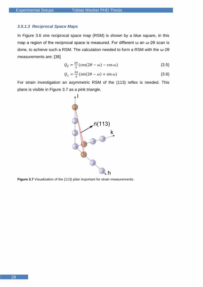
plane is visible in Figure 3.7 as a pink triangle.
Figure 3.7 Visualization of the (113) plain important for strain measurements.

Experimental Setups Tobias Wecker PHD Thesis
29
3.6 IR Absorption Setup TU Dormtund
A general sketch of the absorption setup used in the workgroup of Markus Betz in
TU Dortmund Department of Experimental Physics 2 is shown in Figure 3.8. For
excitation a IR Thorlabs SLS201 lamp with SLSC1 optic emitting from 360 nm to
2600 nm is used followed by a polarisation filter and a pinhole (d =2 mm). The po-
larisation filter allows for excitation of TE or TM only. The light is focused on the
sample by a lens to a spot diameter of 0.5-0.8 mm. The transmitted light is collected
with a 400 µm fibre. A chopper is placed in front of the spectrometer entrance. At
the spectrometer an InGaAs-Photodiode is attached and furthermore extended with
a Lock-In system (Stanford Research Systems SR830 DSP).
Figure 3.8 Sketch of the absorption setup used for the IR absorption measurements. (AG Betz TU
Dortmund)
Experimental Setups Tobias Wecker PHD Thesis
Tobias Wecker
30
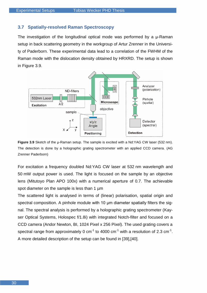
3.7 Spatially-resolved Raman Spectroscopy
The investigation of the longitudinal optical mode was performed by a μ-Raman
setup in back scattering geometry in the workgroup of Artur Zrenner in the Universi-
ty of Paderborn. These experimental data lead to a correlation of the FWHM of the
Raman mode with the dislocation density obtained by HRXRD. The setup is shown
in Figure 3.9.
Figure 3.9 Sketch of the μ-Raman setup. The sample is excited with a Nd:YAG CW laser (532 nm).
The detection is done by a holographic grating spectrometer with an applied CCD camera. (AG
Zrenner Paderborn)
For excitation a frequency doubled Nd:YAG CW laser at 532 nm wavelength and
50 mW output power is used. The light is focused on the sample by an objective
lens (Mitutoyo Plan APO 100x) with a numerical aperture of 0.7. The achievable
spot diameter on the sample is less than 1 µm
The scattered light is analysed in terms of (linear) polarisation, spatial origin and
spectral composition. A pinhole module with 10 μm diameter spatially filters the sig-
nal. The spectral analysis is performed by a holographic grating spectrometer (Kay-
ser Optical Systems, Holospec f/1.8i) with integrated Notch-filter and focused on a
CCD camera (Andor Newton, BI, 1024 Pixel x 256 Pixel). The used grating covers a
spectral range from approximately 0 cm-1 to 4000 cm-1 with a resolution of 2.3 cm-1.
A more detailed description of the setup can be found in [39],[40].

Experimental Setups Tobias Wecker PHD Thesis
31
3.8 Picosecond Acoustics TU Dormtund
The setup exploiting strain pulses to shift the photon energy of a thick QW is based
on a time-resolved pump-probe setup. The setup is placed in the workgroup of
Manfred Bayer in TU Dortmund Department of Experimental Physics 2 (see Figure
3.10). For this setup only one laser is used for the pump pulse and the probe pulse.
The pump pulse creates acoustic pulses in the sample. For this step the Si substra-
te layer is thinned to 90 µm and a 100 nm thick Al layer is evaporated on the
backside of the sample, to achieve a good absorption. The absorbed light induces a
temperature change leading to a strain pulse, which travels through the sample
[41]. The light source is an optical parametric amplifier with pulses of 100 fs durati-
on, a wavelength between 700 - 900 nm, and a repetition rate of 30 kHz. In front of
the source a 90/10 beam splitter divides the pump and the probe pulses. In order to
achieve the time tuning, a mechanical delay stage in the pump pulse is used. Then
the pump pulse is focused on the Al coated backside of the sample with a spot di-
ameter of about 100 μm. The probe beam passes a nonlinear BBO crystal (Beta-
Barium-Borat) to generate second harmonic light. To reduce additional phonons
influencing the acoustic pulse, the sample is cooled in a flow cryostat reaching 40 K
[42].
Figure 3.10 Sketch of the pump probe setup for measuring picosecond acoustics. (AG Bayer TU
Dortmund)

Experimental Setups Tobias Wecker PHD Thesis
Tobias Wecker
32
3.9 Intraband Non-linear Measurements TU Dortmund
The third order nonlinear susceptibility can be measured by a degenerate femtose-
cond pump probe setup in the workgroup of Markus Betz in TU Dortmund Depart-
ment of Experimental Physics 2, visible in Figure 3.11. For excitation a laser toge-
ther with an optical parametric amplifier (Coherent OPA 9850) is used, which emits
~50 fs pulses at 250 kHz repetition rate. Its central wavelength is tuneable from
1375 nm (0.8 eV) to 1550 nm (0.9 eV). The pump and the probe pulse are focused
at the sample with a spot FWHM of ~50 µm at a relative angle of ~10°. The trans-
mission change ΔT = T of the probe signal caused by the pump pulse is measured
with Lock-In detection. For investigation of the intersubband transition (ISBT) polar-
isation dependent measurements have to be done. This is realised with a polarisa-
tion filter directly in front of the source. Furthermore the sample is tilted to an angle
of incidence of ~65. Due to the non-linear properties of the Si substrate, the sample
is glued onto a fused silica window at the MQW side and the Si was removed me-
chanically from the backside. The time resolution is realised with a motorised delay
stage in the pump beam.
Figure 3.11 Sketch of the pump probe setup for measuring intraband non-linearity. (AG Betz TU
Dortmund)
Results and Discussion Tobias Wecker PHD Thesis
33
4 Results and Discussion
Many of the results described in this thesis have already been published. A general
comparison of the defect densities in GaN bulk layers measured with Raman spec-
troscopy and high resolution X-Ray diffractometry (HRXRD) was done together with
Michael Rüsing of AG Zrenner University of Paderborn [29]. Another analysis about
strain pulses in GaN/AlxGa1-xN single QWs was done by Thomas Czerniuk with a
time-resolved pump-probe setup [43]. Besides the optical behaviour of asymmetric
GaN/AlxGa1-xN double QWs are studied in great detail using PL [12], time-
resolved PL [14] and PLE [13] measurements which were partly provided by Gor-
don Callsen of AG Hoffmann TU Berlin. These investigations revealed the barrier
thickness at which the coupling for GaN/AlxGa1-xN double QW starts. This informa-
tion is important for the design of the GaN/AlN MQWs, to reduce the FWHM of the
IR absorption.
IR absorption experiments on GaN/AlN MQWs were performed by Thorben Jost-
meier of AG Betz in TU Dortmund [10] and TEM measurements on similar struc-
tures have been done by Torsten Rieger of AG Pawlis in FZ Jülich [11]. First expe-
riments concerning the nonlinear behaviour of MQW intersubband transitions
(ISBT) have been executed by Thorben Jostmeier [10].
4.1 GaN Bulk: Raman and Defect Density
The crystal quality depends on the amount of defects in the layer, limiting the opti-
cal and electrical properties in semiconductor devices. The common method to in-
vestigate the structural quality of epitaxial layers is HRXRD. Another method is
Raman spectroscopy (RS) providing the vibrational properties of such structures
[44], [45]. RS is sensitive to the crystal structure, symmetry and different phases
[46], [47], defects [30], dielectric constants [48] or free carrier densities [49], [50],
[51]. Both methods can be used to investigate the details of the defects, which inflict
the crystal quality. This information can be used to optimise the growth processes.
Raman enables the investigation of very thin layers, barely measureable with
HRXRD. Thus this first experiment with bulk GaN is a starting point for the determi-
nation of important parameters of MQWs, like doping in the QWs and defects espe-
cially for MQW with few periods. Hall Effect measurements on MQW are difficult
because of the background doping of the thick substrate layer. The thickness of the
MQWs is in the order of 100-300 nm this is much smaller than the 10 µm thick 3C-

Results and Discussion Tobias Wecker PHD Thesis
Tobias Wecker
34
SiC. Up to now a series of MQWs with different doping profiles is planned to inves-
tigate the influence of the doping on the Raman spectra.
In previous reports stacking faults (SFs) along (111) planes have been identified to
be the dominant defect type in c-GaN [52-56]. The amount of this defect is directly
correlated to the smoothness of the substrates [57]. A well-established technique
used to decrease this defect type, is the growth of thick layers. Unfortunately this
defect leads to hexagonal inclusions in the cubic phase, caused by the change in
the stacking period of the atoms. Due to the SFs geometry an annihilation process
occurs, in case of two SFs, with (111) and (111̅), meet in the crystal. Only sessile
dislocations [58], [59] remain, which leads to an increase of crystal quality for thick-
er layers [57].
In order to compare both characterisation methods a series with thick cubic GaN
(001) layers were grown on a 10 µm 3C-SiC (001) layer deposited on a 0.5 mm
thick Si substrate. The layer thickness was increased from 75 to 505 nm as can be
seen in Table 4.1. More details concerning the growth of cubic GaN on 3C-SiC can
be found in [60]. Atomic force microscopy measurements revealed an RMS surface
roughness of around 5 nm for 5×5 µm² areas. The layer thicknesses have been
measured by Reflectometric Interference Spectroscopy in case of the thickest sam-
ples (thicker than 300 nm) with a resolution in the range of ±25 nm [61]. For the
thinner samples a similar growth rate is assumed, leading to estimated thicknesses.
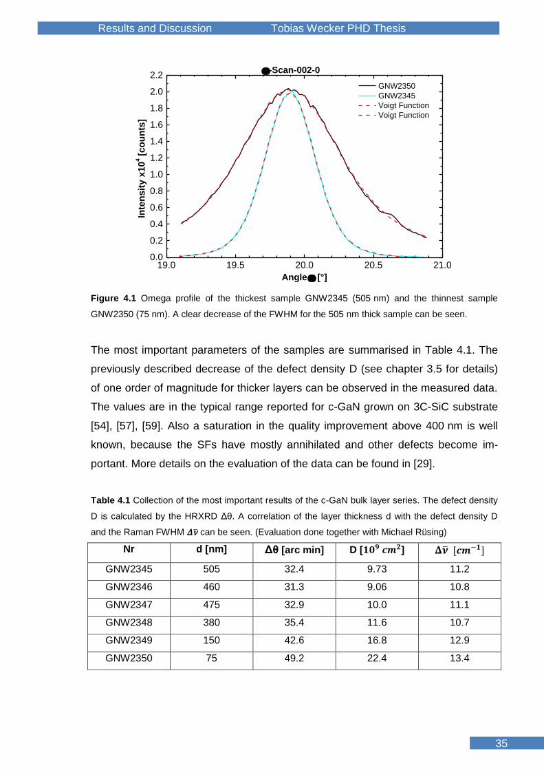
Figure 4.1 shows two ω profiles of the thickest and the thinnest sample, in order to
compare the FWHM of both layers. The sample GNW2350 is 75 nm thick leading to
a very high FWHM compared to the sample GNW2345 with 505 nm thickness. To
evaluate the FWHM Voigt functions are used. With this FWHM the dislocation den-
sity was calculated as described in chapter 3.5.1.1. High dislocation densities cause
disorder in the material resulting in a broader FWHM. Thus the FWHM can be used
to determine the dislocation density.
Results and Discussion Tobias Wecker PHD Thesis
35
19.0 19.5 20.0 20.5 21.00.0
0.2
0.4
0.6
0.8
1.0
1.2
1.4
1.6
1.8
2.0
2.2 GNW2350
GNW2345
Voigt Function
Voigt Function
Inte
nsit
y x
10
4 [
co
un
ts]
Angle [°]
-Scan-002-0
Figure 4.1 Omega profile of the thickest sample GNW2345 (505 nm) and the thinnest sample
GNW2350 (75 nm). A clear decrease of the FWHM for the 505 nm thick sample can be seen.
The most important parameters of the samples are summarised in Table 4.1. The
previously described decrease of the defect density D (see chapter 3.5 for details)
of one order of magnitude for thicker layers can be observed in the measured data.
The values are in the typical range reported for c-GaN grown on 3C-SiC substrate
[54], [57], [59]. Also a saturation in the quality improvement above 400 nm is well
known, because the SFs have mostly annihilated and other defects become im-
portant. More details on the evaluation of the data can be found in [29].
Table 4.1 Collection of the most important results of the c-GaN bulk layer series. The defect density
D is calculated by the HRXRD Δθ. A correlation of the layer thickness d with the defect density D
and the Raman FWHM 𝜟�̅� can be seen. (Evaluation done together with Michael Rüsing)
Nr d [nm] Δθ [arc min] D [𝟏𝟎𝟗 𝒄𝒎𝟐] 𝚫�̅� [𝒄𝒎−𝟏]
GNW2345 505 32.4 9.73 11.2
GNW2346 460 31.3 9.06 10.8
GNW2347 475 32.9 10.0 11.1
GNW2348 380 35.4 11.6 10.7
GNW2349 150 42.6 16.8 12.9
GNW2350 75 49.2 22.4 13.4

Results and Discussion Tobias Wecker PHD Thesis
Tobias Wecker
36
200 400 600 800 1000
2T
O(W
) Si
TA
+T
O(
) Si
TA
+T
O(X
) Si
2T
A(W
) Si
2T
A(X
) Si
TO
() c
-GaNTO
() S
i
2T
A(X
) 3C
-SiC
LO
() c
-GaN
TO
() 3
C-S
iC
LO
() 3
C-S
iC
Inte
nsit
y [
arb
. u
.]
Raman Shift [cm-1]
3C-SiC/Si
475 nm c-GaN
2T
A(L
) Si
Figure 4.2 A comparison of Raman spectra of a 3C-SiC/Si substrate piece (dashed) and a thick c-
GaN layer (red) reveals two additional peaks (marked in red). These peaks are attributed to the TO
and LO mode of c-GaN. (Measured in University of Paderborn by Michael Rüsing)
Figure 4.2 shows a typical back-scattering Raman spectrum of c-GaN on 3C-SiC/Si
substrate (red) with a reference 3C-SiC/Si substrate (dashed). Various distinct fea-
tures are visible in the spectrum, which are mostly related to the substrate. By com-
paring both spectra only two features are different and labelled in red. These fea-
tures correspond to the c-GaN (at 738 cm−1 is the LO mode and at 550 cm−1 is the
TO mode). They are similar to the values in literature [46], [30], [51]. The TO mode
is barely visible, due to the selection rules in c-GaN. Thus the main results are con-
centrated on the LO mode only. Besides even small inclusions of hexagonal GaN
results in a strong peak at 560– 570 cm−1 [30], [62], but this peak is absent in all
investigated samples. This is a proof for the cubic phase purity of the samples.
Results and Discussion Tobias Wecker PHD Thesis
37
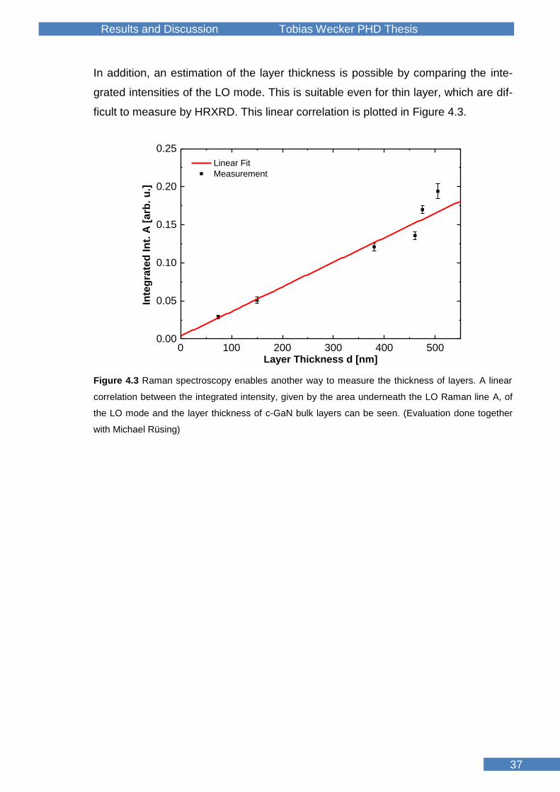
In addition, an estimation of the layer thickness is possible by comparing the inte-
grated intensities of the LO mode. This is suitable even for thin layer, which are dif-
ficult to measure by HRXRD. This linear correlation is plotted in Figure 4.3.
0 100 200 300 400 5000.00
0.05
0.10
0.15
0.20
0.25
Linear Fit
Measurement
Inte
gra
ted
In
t. A
[a
rb.
u.]
Layer Thickness d [nm]
Figure 4.3 Raman spectroscopy enables another way to measure the thickness of layers. A linear
correlation between the integrated intensity, given by the area underneath the LO Raman line A, of
the LO mode and the layer thickness of c-GaN bulk layers can be seen. (Evaluation done together
with Michael Rüsing)

Results and Discussion Tobias Wecker PHD Thesis
Tobias Wecker
38
Figure 4.4 shows the connection between the dislocation density determined via
HRXRD with the FWHM of the LO mode Δ�̅� measured with Raman. A linear trend is
found. This enables Raman spectroscopy as a further investigation method, in or-
der to get information about the structural quality.
11 12 13 14
8
12
16
20
24 Linear Fit
Measurement
Dis
loc
ati
on
Den
sit
y D
[1
09/c
m2]
Raman FWHM [cm-1]
75 nm
150 nm
475 nm
505 nm
460 nm
380 nm
Figure 4.4 A linear correlation between the dislocation density D via HRXRD and Raman FWHM 𝜟�̅�
is found. These data can be used as a calibration to determine the dislocation density with Raman
only. (Evaluation done together with Michael Rüsing)
With this data a calibration between HRXRD and Raman is found. Thus further de-
termination of the dislocation density of c-GaN layers can be done via Raman spec-
troscopy only. This enables a spatial resolved investigation of the defects. Further-
more these first results can be adapted to more complex samples like MQWs lead-
ing to a possibility to measure also structures with only a few periods. HRXRD can
only be used to measure thick samples with several periods.
Results and Discussion Tobias Wecker PHD Thesis
39
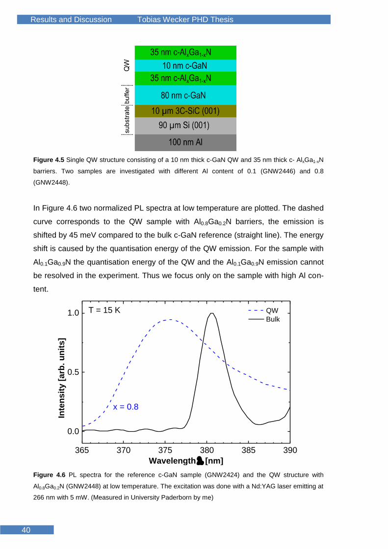
4.2 Thick QW: Strain Pulse
Picosecond acoustics can be used to investigate the influence of strain pulses on
heterostructures. Due to strain pulses the optical response of the material changes
leading to different emission/absorption in QWs compared to the unstrained case.
With this knowledge detectors for sub terahertz and terahertz elastic waves can be
designed with picosecond temporal resolution. The group III nitrides are suitable for
measuring coherent phonons with frequencies up to 2 THz [63-72]. Besides the
different layer thicknesses can be modelled enabling a detailed insight into the real
layer thicknesses and the interfaces of the different heterostructures. Complex
MQW structures with several periods have not been investigated so far, but the
basic principle is shown for a single QW structure. This provides information about
the strain behaviour of the different layers. More details can be found in [43]. After
the publication of [43] further investigation revealed a deviation of the nominal layer
thicknesses. Here the newest results are shown, as written in [73].
Two single cubic GaN/AlxGa1-xN QWs were analysed with picosecond acoustic
pulses revealing a sufficient change in the signal to serve as a detector. Their back-
side Si(100) is thinned to 90 µm and coated with 100 nm Al, in order to excite the
samples by a laser together with an optical parametric amplifier. The undoped QW
is 10 nm thick surrounded by 35 nm thick AlxGa1-xN barriers. The Al content in the
barriers is different for the two investigated samples. The sample GNW2446 has an
Al content of x = 0.1 and GNW2448 has x = 0.8. In addition, a 550 nm thick refe-
rence c-GaN bulk sample (GNW2424) was investigated, to compare with the two
ADQWs. On the backside of the sample an Al film is evaporated, to heat the samp-
le with the pulses. The sample structure is shown in Figure 4.5.
Results and Discussion Tobias Wecker PHD Thesis
Tobias Wecker
40
Figure 4.5 Single QW structure consisting of a 10 nm thick c-GaN QW and 35 nm thick c- AlxGa1-xN
barriers. Two samples are investigated with different Al content of 0.1 (GNW2446) and 0.8
(GNW2448).
In Figure 4.6 two normalized PL spectra at low temperature are plotted. The dashed
curve corresponds to the QW sample with Al0.8Ga0.2N barriers, the emission is
shifted by 45 meV compared to the bulk c-GaN reference (straight line). The energy
shift is caused by the quantisation energy of the QW emission. For the sample with
Al0.1Ga0.9N the quantisation energy of the QW and the Al0.1Ga0.9N emission cannot
be resolved in the experiment. Thus we focus only on the sample with high Al con-
tent.
365 370 375 380 385 390
0.0
0.5
1.0
x = 0.8
QW
Bulk
Inte
nsit
y [
arb
. u
nit
s]
Wavelength [nm]
T = 15 K
Figure 4.6 PL spectra for the reference c-GaN sample (GNW2424) and the QW structure with
Al0.8Ga0.2N (GNW2448) at low temperature. The excitation was done with a Nd:YAG laser emitting at
266 nm with 5 mW. (Measured in University Paderborn by me)

Results and Discussion Tobias Wecker PHD Thesis
41
For the picosecond acoustics the Al film absorbs the optical energy of the laser and
is heated locally. Thermal expansion launches an acoustic pulse into the Si sub-
strate at this spot. This pulse travels through the whole sample and is transmit-
ted/reflected at each interface. When the pulse approaches at the GaN bulk and
QW layer, it interferes with the probe beam. The probe beam is reflected at the
sample surface and at the acoustic pulse and Brillouin oscillations are formed [74].
This leads to an interference, which is complicated by all the transmitted/reflected
waves of the different interfaces. The measurements for two different pump powers
(W0 and 4W0) are shown in Figure 4.7. The curve for a probe wavelength of 370 nm
shows a simple shape, as expected for a picosecond strain pulse in a thin layer
near the surface [65] ,[66]. In this case the shape is mainly caused by the QW layer.
For the probe wavelengths 375 nm and 380 nm the shape gets more complicated,
due to the increasing contribution of the c-GaN layer. For the wavelength of 370 nm
the QW is in resonance with the pump signal and in case of 380 nm the c-GaN
buffer layer is in resonance. The Al0.8Ga0.2N layer does not contribute to the meas-
urement, because of the much higher bandgap energy compared to the QW emis-
sion. The parameter β is the ratio of the photo elastic coupling efficiency of the QW
over the one of the bulk layer.

Results and Discussion Tobias Wecker PHD Thesis
Tobias Wecker
42
-40 -20 0 20 40 60
x=0.8
380 nm
=0.3
375 nm
Sig
na
l S
(T)
& C
alc
ula
ted
In
terf
ere
nc
e I
(t)
[arb
. u
nit
s]
Delay [ps]
370 nm
a) W=W0
-40 -20 0 20 40 60
Sig
na
l S
(T)
& C
alc
ula
ted
In
terf
ere
nc
e I
(t)
[arb
. u
nit
s]
Delay [ps]
W=4W0
x=0.8
b)
Figure 4.7 Measured acoustic signal (dashed lines) and simulated signal (straight lines) for the
sample with x = 0.8 (GNW2248) for three different probe wavelengths. The pump power was in-
creased from W0 (left) to 4W0 (right). The parameter β represents the ratio of the photo elastic cou-
pling efficiency of the QW over the one of the bulk layer. (Measured in TU Dortmund by Thomas
Czerniuk) [73]
For a theoretical understanding two contributions to the measurements should be
considered. The first is the photo elastic effect, which changes the band gap and
refractive index in case of strain. The second part is caused by interferences of the
reflected light at the surface and the interfaces, leading to a phase shift and dis-
placement. The simulations shown in Figure 4.7 are performed with an input acous-
tic pulse, which propagates through the sample (calculated via transfer-matrix and
scattering-states method), in order to get the strain and displacement profiles.
These simulations reveal a stronger contribution of the photo elastic response com-
pared to the interface displacement effect.
These results validate the elastic constants which are also used for the simulations
of the optical transitions (nextnano³) and the strain investigations via MadMax. Thus
the parameter set needed for a complete understanding of c-GaN/c-AlGaN is con-
firmed.

Results and Discussion Tobias Wecker PHD Thesis
43
4.3 Asymmetric Double Quantum Wells (ADQW)
In order to get an insight into the basics of a quantum cascade laser (QCL), as a
first step asymmetric double quantum wells (ADQW) were grown and investigated.
The following chapters covering the ADQWs are divided in 3 main topics. At first
two series with average Al content of x = 0.26 ± 0.03 and x = 0.64 ± 0.03 in the bar-
riers were used to investigate the coupling of the two QWs depending on the barrier
thickness between them. The second part covers the time-resolved measurements
on the ADQWs series with Al content of x = 0.64 ± 0.03 dealing with the carrier dy-
namics in more detail. In the third chapter one sample of the first series with
x = 0.25 ± 0.03 was investigated exploiting photoluminescence excitation
spectroscopy (PLE) leading to more information about excited energy levels. By
collecting the data of these chapters the model and parameters used in the nextna-
no³ simulations are adapted and the prediction of the emission and absorption for
more complex structures like MQWs important for quantum cascade lasers can be
done. Nearly all of the measurements and the complete analysis of this chapter ha-
ve been performed by me with the assistance of the mentioned cooperation part-
ners.
4.3.1 General Characterisation
The growth of c-GaN and c-AlxGa1-xN was realised at a substrate temperature of
TS = 720 °C under one monolayer of Ga excess on the surface. More details con-
cerning the growth of cubic GaN on 3C-SiC can be found in [60]. The Al, Ga and N
shutter have been opened together for the c-AlxGa1-xN layers, in order to measure
RHEED oscillations. Two series of ADQWs have been grown with different Al con-
tent in the AlxGa1-xN barriers. The first series consists of AlxGa1-xN barriers with
x = 0.26 ± 0.03 (Series 0.26) and the second has x = 0.64 ± 0.03 (Series 0.64). In
both cases the substrate consists of a 10 µm 3C-SiC (001) layer deposited on a 0.5
mm thick Si (001) substrate. Directly on the 3C-SiC substrate a 100 nm thick c-GaN
buffer layer was grown, followed by the ADQW. The barrier thickness d between a
wide quantum well (QWW) and a narrow quantum well (QWN) was varied between
1 nm and 15 nm. The ADQW structure is embedded between two 50 nm thick cubic
AlxGa1-xN layers. The sample structures are shown in Figure 4.8.

Results and Discussion Tobias Wecker PHD Thesis
Tobias Wecker
44
Series 0.26 Series 0.64
Figure 4.8 Sample structure of the two ADQW series. The barrier thickness d was varied from 1 nm
to 15 nm. In series 0.26 (left) the Al content is x = 0.26 ± 0.03 and for series 0.64 (right) the Al con-
tent is x = 0.64 ± 0.03.
Some of the important parameters of the two ADQW series are summarised in Tab-
le 4.2.
Table 4.2 Overview of the parameters for the two ADQWs series.
Parameter Series 0.26 Series 0.64
Degree of Relaxation R 0.4 ± 0.05 0.48 ± 0.07
Barrier Thickness d [nm] 1, 3, 5, 10, 15 1, 3, 15
Al content in barriers 0.26 ± 0.03 0.64 ± 0.03
Thickness wide QW [nm] 3.15 ± 0.225 2.5 ± 0.225
Thickness narrow QW [nm] 0.9 ± 0.225 1.35 ± 0.225
AFM measurements revealed a rms surface roughness for 5x5 µm2 areas reaching
from 1.9 nm to 2.6 nm for the series 0.26 and around 4 nm for the second series.
Other structural properties were characterized by high resolution X-Ray diffraction
(HRXRD). The defect density of the order of D = 2 × 1010 cm−2 was determined by
rocking curve FWHM around the (002) reflection. From the reciprocal space map
(RSM) around the (113) reflection the Al content could be determined. As an exam-
ple a RSM of one sample of the series 0.26 is shown in Figure 4.9 (left). In this case
the Al content was measured to x = 0.25 ± 0.03. From this RSM also the degree of
relaxation R = 40% of the AlxGa1-xN layers is provided. One sample of the se-

Results and Discussion Tobias Wecker PHD Thesis
45
ries 0.64 has an Al content of x = 0.62 ± 0.03 and the degree of relaxation is
R = 48% (Figure 4.9 on the right). All c-AlxGa1-xN layers in all ADQWs are partly
tensile strained to the GaN buffer layer, thus an equilibrium lattice parameter is
formed in the ADQW structure leading to partly compressively strained QWs.
1.85 1.90 1.95 2.00 2.05 2.104.10
4.15
4.20
4.25
4.30
4.35
4.40
4.45
q[Å
-1]
d=15nm
x=0.25
(113)
q||[Å
-1]
SiC-substrate
strained c-AlN
relaxed c-AlN
c-GaN 4.503Å
c-Al0.25
Ga0.75
N
1.85 1.90 1.95 2.00 2.05 2.104.10
4.15
4.20
4.25
4.30
4.35
4.40
4.45
strained c-AlNd=15nm
x=0.62
(113)
q[Å
-1]
q||[Å
-1]
strained c-AlN
SiC-substrate
relaxed c-AlN
c-GaN 4.503Å
c-Al0.62
Ga0.38
N
Figure 4.9 RSM of the (113) reflection of two cubic GaN/AlxGa1-xN ADQW with d = 15 nm of the two
different series. A partial strain of the barriers is visible in both measurements. (Left) An Al content of
x = 0.25 ± 0.03 is determined. (Right) The Al content is x = 0.62 ± 0.03.
In order to evaluate the strain of the individual layers, the degree of relaxation R
can be expressed by.
𝑅 =(𝑎||−𝑎𝑠)
𝑎𝐿−𝑎𝑠 (4.1)
It describes the difference in the lattice constant of the in plane lattice constant a|| of
the investigated layer to the value of the substrate as and includes the lattice pa-
rameter for the unstrained layer aL.Thus the real AlxGa1-xN lattice parameter can be
determined using a RSM (Figure 4.9) and this value is projected to the x axis (q||).
The substrate in this case is the GaN buffer layer [38] [76]. These strain effects are
also considered in the nextnano³ calculations.

Results and Discussion Tobias Wecker PHD Thesis
Tobias Wecker
46
4.3.2 Influence of Barrier Thickness to the Coupling
For a detailed analysis of influence of the barrier thickness on optical measure-
ments two series of asymmetric cubic GaN/AlxGa1-xN double quantum wells
(ADQWs) were grown. In both series the barrier thickness between the two QWs
was varied. The series 0.26was grown with an Al content of x = 0.26 ± 0.03 and the
series 0.64 has x = 0.64 ± 0.03. Figure 4.10 depicts the low temperature interband
photoluminescence measurements at 13 K for the sample with d = 15 nm of series
0.26. For excitation a Nd:YAG CW laser (266 nm) was used. Four clearly distin-
guishable emission bands at 3.27 eV, 3.37 eV, 3.60 eV and 3.74 eV are observed.
Using 4 Gaussian fit functions the emission bands were determined and they could
be assigned to the c-GaN buffer [22], the wide QW, the narrow QW and the cubic
Al0.26Ga0.74N [77], respectively. The transition energies of both QWs are consistent
with the calculations by nn3 (see Table 4.3). This fit procedure was performed for all
PL spectra of the series 0.26 and 0.64, in order to evaluate the intensities and the
energy of the emission maximum.
3.2 3.4 3.6 3.8 4.0
105
106
107
d = 15 nm
T = 13 K
Inte
ns
ity
[c
ps
]
Energy [eV]
c-GaN
3.27±0.01 eV
QW 3.15 nm
3.37±0.01 eV
QW 0.9 nm
3.60±0.01 eV
c-Al0.25
Ga0.75
N
3.74±0.01 eV
Figure 4.10 Low temperature PL spectrum of the cubic GaN/Al0.26Ga0.74N ADQW with d = 15 nm
excited with a Nd:YAG laser (266 nm).
In Figure 4.11 the low temperature PL spectra of the two ADQW series with differ-
ent barrier thicknesses d are shown. For better comparison the PL spectra have
been normalized to the emission of the AlxGa1-xN and are plotted in a semi-

Results and Discussion Tobias Wecker PHD Thesis
47
logarithmic scale. The PL experiments for series 0.64 in Figure 4.11 (right) were
performed time integrated with a frequency-quadrupled, picosecond Nd:YAG laser
(266 nm, 76 MHz repetition rate). The three emission bands could be assigned to
the wide QWW (3.49 eV), the narrow QWN (3.73 eV) and the cubic Al0.64Ga0.36N
(4.12 eV) [77]. The two diagrams show a different spectral region. Due to the higher
Al content of series 0.64 all emission bands are shifted to higher energies. Never-
theless the general behaviour for the different barrier thicknesses d is very similar.
3.0 3.2 3.4 3.6 3.8 4.0
10-2
10-1
100
101
d = 15 nm
d = 10 nm
d = 5 nm
d = 3 nm
d = 1 nm
Nd:YAG (266 nm)
T = 13 K
no
rm. I
nte
nsi
ty [
arb
. un
its]
Energy [eV]
c-GaN
QWW
QWN
c-AlGaN
3.2 3.4 3.6 3.8 4.0 4.2 4.4 4.6
0.1
1
10
no
rm. I
nte
nsi
ty [
arb
. un
its]
Energy [eV]
d=1nm
d=3nm
d=15nm
QWW
QWN
Al0.64
Ga0.36
N
T = 7K
Figure 4.11 Semi-logarithmic plot of the low temperature (7 K) PL spectra of the cubic GaN/ AlxGa1-
xN ADQWs with x = 0.26 (left) and x = 0.64 (right). Three emission bands are visible for the wide QW
(QWW), the narrow QW (QWN) and the AlxGa1-xN barriers. The emission intensity of the narrow QW
can be correlated to the barrier thickness d. (right: measured in TU Berlin together with Gordon Call-
sen)
A clear correlation between the intensity of the narrow QW IN and the barrier thick-
ness d can be seen. The emission of the narrow QW IN decreases with increasing
barrier thickness and the other way round for the wide QW. Thus coupling between
the QWs is relevant for these barrier thicknesses. The energy shift of the emission
of the wide QW for the sample with the lowest barrier thickness d = 1nm of series
0.26 (pink curve, left) may be caused by variation in the QW thickness of one
monolayer. The sample with d = 10 nm (blue curve, left) of series 0.26 shows a
strong broadening of the emission band related to the AlxGa1-xN emission and the
intensity of the wide QW emission is decreased compared to the other samples.
The AFM, HRXRD and RHEED data of this sample are consistent with the data of

Results and Discussion Tobias Wecker PHD Thesis
Tobias Wecker
48
the other samples. But the PL measurements show a fluctuation of the intensities of
the emission bands for different positions at this sample piece.
The intensity ratio of both QW series varies for different barrier thicknesses d (see
Figure 4.12). For barriers thinner than 7 nm (series 0.26, left) and 3 nm (series
0.64, right) a strong drop in the intensity ratio is observed. This difference in barrier
thickness, where the drop occurs, is caused by the higher Al content and the great-
er potential step at the interface. For thicker barriers no coupling is observed and a
constant IN to IW ratio is found.
For radiative recombination processes the presence of both electrons and holes is
necessary. Therefore, the carrier type with lower tunnelling rate is expected to limit
the finally observed equilibrium intensity ratio in the steady state PL measurements.
The intensity ratio is calculated for the carrier transfer processes for electron tunnel-
ling (blue curve) and heavy hole tunnelling (red curve). The overall behaviour is well
explained, however for low barrier thicknesses a deviation from the calculations is
seen, indicating a reduced non-resonant tunnelling rate (higher IN to IW ratio) for thin
barriers.
0 2 4 6 8 10 12 14 1610
-2
10-1
100
101
Inte
ns
ity
ra
tio
IN/I
W
Barrier Thickness d [nm]
e
hh
Experiment
x = 0.26
0 2 4 6 8 10 12 14 1610
-2
10-1
100
101
Inte
ns
ity r
ati
o I
N/I
W
Barrier Thickness d [nm]
e
hh
Experiment
x = 0.64
Figure 4.12 Intensity ratio IN/IW as a function of barrier thickness d for series 0.26 (left) and series
0.64 (right). The calculated curves for electrons (e) (blue line) and heavy holes (hh) (red line) follow
the same trend as the measured ratios (dots). (Evaluation done by me)
More details for the evaluation of the data can be found in [12] [14]. We analyse the
experimental results by considering the following processes (as described in chap-
ter 2.2). Light of the excitation source is absorbed creating electron hole pairs in the

Results and Discussion Tobias Wecker PHD Thesis
49
two QWs and in the surrounding barrier material, the carriers in the barriers diffuse
into the QWW and QWN. Time-resolved PL measurements on decoupled samples
estimate that the life times in both QWs are in the order of τ ≈ 180 ps for series
0.26. A detailed analysis for the times in series 0.64 is shown in the next chapter.
For the ratio of the generation rates the best match with the experimental data for
the uncoupled QW with d = 15 nm is found to be 𝐺𝑊
𝐺𝑁 = 0.55 for series 0.26 and
𝐺𝑊
𝐺𝑁 = 0.707 for series 0.64. The details about the time-resolved PL measurements
of series 0.64 are described in chapter 4.3.3.
The limiting process is the heavy hole transfer (red) which is slower than the elect-
ron transfer (blue). Only for thinner barriers a deviation to the experimental data
(black points) is observed. A lower carrier transfer is measured than expected by
our simple model. This difference between model and experiment can be explained
by the parameters used for the calculation, for example the uncertainty of 5% for
the band offset at the GaN/AlxGa1-xN interfaces and the inaccuracy of the Al content
in the barrier of Δx = ± 0.03. Finally, scattering of carriers by defects in the barriers
may increase the transfer time and lead to a higher IN to IW ratio.
For the comparison with the optical measurements and a detailed understanding of
the energy levels, band structure calculations are accomplished with nextnano³
providing energy levels of the QWs important for the calculation of tunnelling. The
parameters used for the nextnano³ simulations are summarised in the appendix.
The details for the simulations are collected in chapter 5.1. The simulated and mea-
sured transition energies for the ADQWs at low temperatures are shown in Table
4.3. The ADQWs are nominally undoped. Nevertheless in all nextnano³ calculations
a background n-type doping of around 5x1017 cm-3 in AlxGa1-xN and of around
1x1017 cm-3 in GaN is assumed [75].
Table 4.3 Optical transitions measured via PL together with nextnano³ simulated transitions for both
ADQW series.
Series 0.26 Series 0.64
𝑸𝑾𝑾𝒆𝒙𝒑
[eV] 3.37 3.49
𝑸𝑾𝑾𝒔𝒊𝒎 [eV] 3.42 3.53
𝑸𝑾𝑵𝒆𝒙𝒑
[eV] 3.60 3.73
𝑸𝑾𝑵𝒔𝒊𝒎 [eV] 3.66 3.77

Results and Discussion Tobias Wecker PHD Thesis
Tobias Wecker
50
In Figure 4.13 and Figure 4.14 the conduction band edge and the valence band
edges for electrons (e), heavy holes (hh) and light holes (lh) are plotted for the
ADQW structure with the barrier of 1 nm and 5 nm. Electrons in the wide QW are
confined as indicated by the dashed lines e1 and e2, respectively. The penetration
depths of the wave functions for e, hh and lh are much larger than the 1 nm barrier
thickness, leading to a different probability distribution |Ψ1|2. Therefore, a clear
coupling of the two QWs and thus non-resonant tunnelling is expected, which can
be described by non-resonant tunnelling of carriers. Additional calculations for the
other GaN/AlxGa1-xN ADQW structures with wider barrier thicknesses showed, that
coupling is relevant for barrier thicknesses below 5 nm (see Figure 4.13 right). For
thick barriers of d > 5 nm nn3 simulations indicate that no significant coupling will
occur.
0 2 4 6 8 10 12 14 16-0.2
0.0
0.2
0.4
0.6
0.8
1.0
1.2
1.4
d = 1 nm
T = 13 K
CB
En
erg
y [
eV
]
Position [nm]
CB
e1
e2
2
1
2
2
0 2 4 6 8 10 12 14 16-0.2
0.0
0.2
0.4
0.6
0.8
1.0
1.2
1.4
d = 5 nm
T = 13 K
CB
En
erg
y [
eV
]
Position [nm]
CB
e1
e2
2
1
2
2
Figure 4.13 Simulated conduction band of the cubic GaN/AlxGa1-xN ADQW with x = 0.26 and a bar-
rier thickness d = 1 nm (left) and d = 5 nm (right) at 13 K.
Similar calculations of the band diagram for the heavy holes are illustrated in Figure
4.14.The general behaviour is analogous to the electrons. The wave function for the
two heavy hole states hh1 and hh2 penetrate into the neighbouring QW leading to
strong coupling of the two QWs for 1 nm barriers.
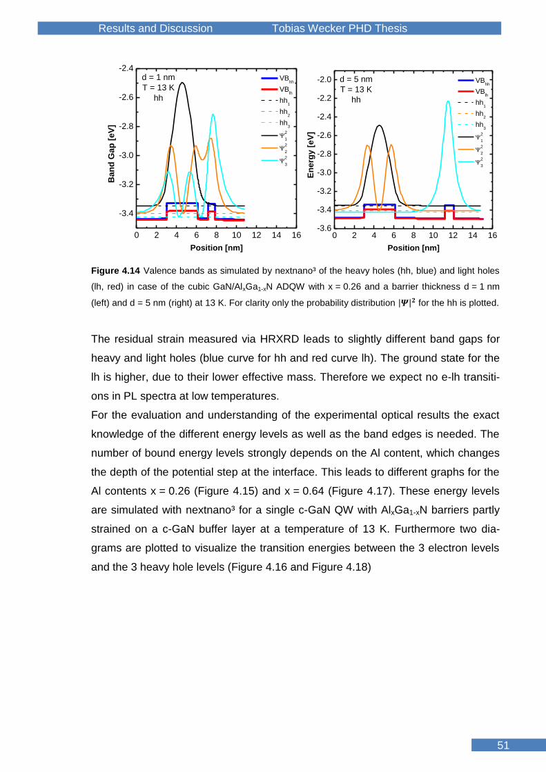
Results and Discussion Tobias Wecker PHD Thesis
51
0 2 4 6 8 10 12 14 16
-3.4
-3.2
-3.0
-2.8
-2.6
-2.4
d = 1 nm
T = 13 K
hh
Ban
d G
ap
[eV
]
Position [nm]
VBhh
VBlh
hh1
hh2
hh3
2
1
2
2
2
3
0 2 4 6 8 10 12 14 16-3.6
-3.4
-3.2
-3.0
-2.8
-2.6
-2.4
-2.2
-2.0
d = 5 nm
T = 13 K
hh
En
erg
y [
eV
]
Position [nm]
VBhh
VBlh
hh1
hh2
hh3
2
1
2
2
2
3
Figure 4.14 Valence bands as simulated by nextnano³ of the heavy holes (hh, blue) and light holes
(lh, red) in case of the cubic GaN/AlxGa1-xN ADQW with x = 0.26 and a barrier thickness d = 1 nm
(left) and d = 5 nm (right) at 13 K. For clarity only the probability distribution |𝜳|𝟐 for the hh is plotted.
The residual strain measured via HRXRD leads to slightly different band gaps for
heavy and light holes (blue curve for hh and red curve lh). The ground state for the
lh is higher, due to their lower effective mass. Therefore we expect no e-lh transiti-
ons in PL spectra at low temperatures.
For the evaluation and understanding of the experimental optical results the exact
knowledge of the different energy levels as well as the band edges is needed. The
number of bound energy levels strongly depends on the Al content, which changes
the depth of the potential step at the interface. This leads to different graphs for the
Al contents x = 0.26 (Figure 4.15) and x = 0.64 (Figure 4.17). These energy levels
are simulated with nextnano³ for a single c-GaN QW with AlxGa1-xN barriers partly
strained on a c-GaN buffer layer at a temperature of 13 K. Furthermore two dia-
grams are plotted to visualize the transition energies between the 3 electron levels
and the 3 heavy hole levels (Figure 4.16 and Figure 4.18)

Results and Discussion Tobias Wecker PHD Thesis
Tobias Wecker
52
0 1 2 3 4 5 6 7 8 9 10 11 12-0.80
-0.75
-0.70
-0.65
2.6
2.7
2.8
2.9
3.0
3.1
3.2
hh3hh2
e3e2
CB_GaN
SQW, x=0.26, strain 0.4, CBO 80, 13K
En
erg
y [
eV
]
QW Thickness [nm]
CB_AlN
HH_AlN
HH_GaN
e1
hh1LH_GaN
LH_AlN
lh3lh2
lh1
Figure 4.15 Simulated energy levels for electrons (e), heavy holes (hh) and light holes (lh) of a sin-
gle c-GaN QW with AlxGa1-xN barriers (x = 0.26) partly strained on c-GaN buffer at 13 K.
0 1 2 3 4 5 6 7 8 9 10 11
3.3
3.4
3.5
3.6
3.7
3.8
3.9SQW, x=0.26, strain 0.4, CBO 80, 13K
En
erg
y [
eV
]
QW Thickness [nm]
e1-hh1
e2-hh2
e3-hh3
Figure 4.16 Transition energies of the 3 electron levels with the 3 heavy hole levels for the SQW
with c-GaN QW and AlxGa1-xN barriers (x = 0.26).

Results and Discussion Tobias Wecker PHD Thesis
53
The strain changes for different Al content. For higher Al content the degree of re-
laxation increases (see Table 4.2).
0 1 2 3 4 5 6 7 8 9 10 11 12
-1.4
-1.3
-1.2
-1.1
2.0
2.5
3.0
3.5
hh3hh2
e3e2
CB_GaN
SQW, x=0.64, strain 0.48, CBO 79, 13K
En
erg
y [
eV
]
QW Thickness [nm]
CB_AlN
HH_AlN
HH_GaN
e1
hh1LH_GaN
LH_AlNlh3
lh2
lh1
Figure 4.17 Simulated energy levels for electrons (e), heavy holes (hh) and light holes (lh) of a sin-
gle c-GaN QW with AlxGa1-xN barriers (x = 0.64) partly strained on c-GaN buffer at 13 K.
0 1 2 3 4 5 6 7 8 9 10 113.2
3.4
3.6
3.8
4.0
4.2
4.4
4.6
4.8
5.0SQW, x=0.64, strain 0.48, CBO 79, 13K
En
erg
y [
eV
]
QW Thickness [nm]
e1-hh1
e2-hh2
e3-hh3
Figure 4.18 Transition energies of the 3 electron levels with the 3 heavy hole levels for the SQW
with c-GaN QW and AlxGa1-xN barriers (x = 0.64).

Results and Discussion Tobias Wecker PHD Thesis
Tobias Wecker
54
4.3.3 Time-resolved Investigation of Carrier Transfer
For the time-resolved measurements of series 0.64, the luminescence signal was
analysed with a subtractive double monochromator (McPherson 2035 - 0.35 m focal
length, 2400 g/mm, 300 nm blaze) and a single photon-detection was achieved with
a multichannel-plate (MCP) photomultiplier tube (Hamamatsu R3809U-52).
For evaluation of the data a convolution routine has to been done, in order to ex-
tract the contribution of the temporal response of the setup and to identify the signal
of the sample. For this reason a convoluted fitting approach [78] was applied to the
data. In Figure 4.19 a time transient for the ADQW of series 0.64 with the barrier
thickness d = 15 nm is shown. This time transient was determined at the emission
wavelength for the wide QW (2.5 nm) at 7 K. The red curve is a fit function using a
commercial software called Fluofit (Picoquant, GmbH) exploiting deconvolution of
the laser emission characteristic Isource(t’) with the sample emission characteristic.
The experimental data are plotted as dots, the blue curve corresponds to the time
transient Isource(t’) of the laser source and the red curve is the fit curve I(t) as descri-
bed in the following formula.

Results and Discussion Tobias Wecker PHD Thesis
55
A common approach for such experimental data is a bi-exponential fit.
I(t) = ∫ Isource(t′) (Afaste
−t−t′
τfast + Aslowe−
t−t′
τslow)dt′t
−∞ (4.2)
The time transients of the emission for the 3 ADQW samples of series 0.64 are
shown in Figure 4.20 for the QWW (left) and for the QWN (right). There is one fast
decay time τfast (63 ps – 215 ps) and a slow component τslow (406 ps – 557 ps). Be-
sides the peak areas Afast (640 – 3717 counts) and Aslow (130 – 1251 counts) cor-
respond to the intensity of the two exponential functions.
0.0 0.5 1.0 1.5 2.0 2.5 3.0 3.5 4.0 4.5 5.010
0
101
102
103
104
In
ten
sit
y [
arb
. u
nit
s]
Measurement
Fitcurve
Laser transient
Time [ns]
Figure 4.19 Time transients for the ADQW of series 0.64 with the thickest barrier d = 15 nm meas-
ured at the QWW (2.5 nm) emission at 7 K. A bi-exponential fit was used with a convolution approach
to match the data. (measured in TU Berlin together with Gordon Callsen)
The physical reason for the bi-exponential transient observed in our samples is up
to now unidentified. In literature different explanations are discussed and are men-
tioned below. There are several papers describing also one fast and one slow time
decay in AlGaAs/GaAs structures with an applied electric field. The explanations
cover phonon-assisted tunnelling and impurity-/defect-assisted tunnelling [79][80].
Furthermore the valence band mixing of hh and lh is supposed to influence the tun-
nelling process [80] [81]. In addition, it is claimed, that exciton tunnelling times are
much longer than the tunnelling times of individual electrons and holes causing two
different decay times [80] [81].

Results and Discussion Tobias Wecker PHD Thesis
Tobias Wecker
56
Another approach is to distinguish between direct excitons and indirect excitons
(also called crossed excitons) in multi quantum well structures. Due to the tun-
nelling process some of the direct excitons become crossed excitons. These are
excitons where electron and hole are in different QWs and thus separated by the
barrier. The binding energies of crossed excitons are considerably smaller leading
to a much lower recombination probability [81] [82]. Finally experiments with hydro-
static pressure indicated the participation of Γ-X scattering in the fast decay time
and the X-X scattering in the slow decay time [83]. These two decay times have
also been reported for other material systems. For example in an investigation on
CdTe/(Cd,Zn)Te ADQWs they explain the slow decay time with the process where
the QWs get into thermal equilibrium after excitation [84]. As well as in InGaN/GaN
double QWs the slow component may be caused by impurity related transitions
[85][ 86].
The intensity influence of the slow component is much smaller than for the fast
component. Thus in the following we focus mainly on the fast component.
1E-3
0.01
0.1
1Transients of the wide QW (QW
W 2.5 nm)
1 nm
Fit
Inte
nsit
y [
arb
. u
nit
s]
1E-3
0.01
0.1
1 3 nm
Fit
1.0 1.5 2.0 2.5 3.0 3.5 4.0
1E-3
0.01
0.1
1 15 nm
Fit
Time [ns]
1E-3
0.01
0.1
1
Transients of the narrow QW (QWN 1.35 nm)
1 nm
Fit
Inte
ns
ity
[a
rb. u
nit
s]
1E-3
0.01
0.1
1 3 nm
Fit
1.0 1.5 2.0 2.5 3.0 3.5 4.0
1E-3
0.01
0.1
1 15 nm
Fit
Time [ns]
Figure 4.20 Time transients for the 3 ADQW samples of series 0.64 measured at the QWW (2.5 nm,
left) emission and at the QWN (1.35 nm, right) emission for the three samples with different barrier
thickness d. (measured in TU Berlin together with Gordon Callsen)
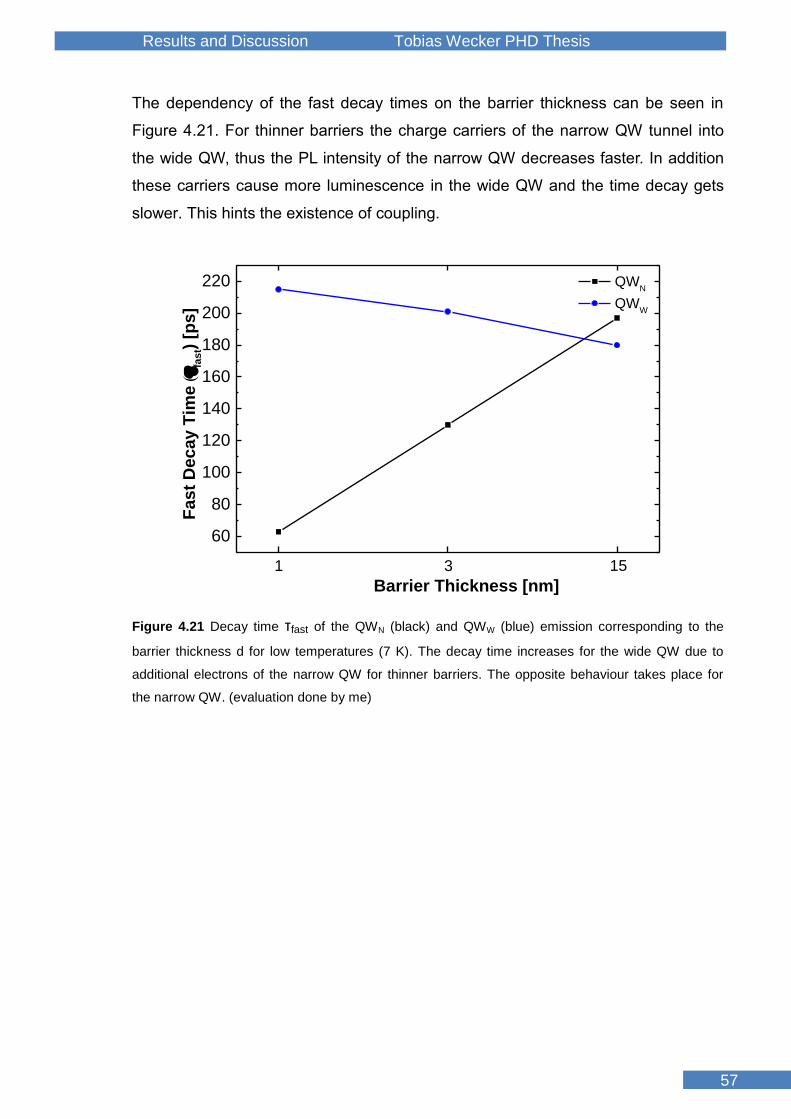
Results and Discussion Tobias Wecker PHD Thesis
57
The dependency of the fast decay times on the barrier thickness can be seen in
Figure 4.21. For thinner barriers the charge carriers of the narrow QW tunnel into
the wide QW, thus the PL intensity of the narrow QW decreases faster. In addition
these carriers cause more luminescence in the wide QW and the time decay gets
slower. This hints the existence of coupling.
1 2 3
60
80
100
120
140
160
180
200
220
31 15
Barrier Thickness [nm]
QWN
QWW
Fast
Decay T
ime ( fa
st) [
ps]
Figure 4.21 Decay time τfast of the QWN (black) and QWW (blue) emission corresponding to the
barrier thickness d for low temperatures (7 K). The decay time increases for the wide QW due to
additional electrons of the narrow QW for thinner barriers. The opposite behaviour takes place for
the narrow QW. (evaluation done by me)

Results and Discussion Tobias Wecker PHD Thesis
Tobias Wecker
58
4.3.4 Excited Energy Levels via PLE
For an investigation of the excited energy levels an asymmetric cubic
GaN/AlxGa1-xN double quantum well with an Al content of x = 0.25 ± 0.03 was
grown. The separating barrier between a wide (3.15 nm thickness) quantum well
(QWW) and a narrow (0.9 nm thickness) quantum well (QWN) is 15 nm thick. Hence,
these quantum wells can be considered to be uncoupled [12]. Nevertheless this
sample can be used as a starting point for further considerations with coupled QWs.
The ADQW structure is placed in between two 50 nm thick cubic Al0.25Ga0.75N lay-
ers. The entire sample structure is depicted in Figure 4.22.
GNW2356
Figure 4.22 Sample structure of the cubic GaN/Al0.25Ga0.75N ADQW. The barrier thickness between
the two QWs is 15 nm, thus the wells are uncoupled.
The PLE spectra are measured at different detection wavelengths matching the
emission maxima provided by PL (red for the QWW, green for the QWN, blue for the
Al0.25Ga0.75N barrier). The blue curve related to the emission maximum of the
AlxGa1-xN barriers show no additional transition except the band to band transition.
The green curve for the narrow QW was compared with ellipsometry data of bulk
AlxGa1-xN [90]. In these ellipsometry data only the band edge of AlxGa1-xN was
measured, because there was no QW in the layer. This comparison revealed no
additional feature, thus we expect there is no QW related transition visible in the
green curve. The step visible in all PLE spectra at around 3.9 eV is caused by the
band to band transition in bulk AlxGa1-xN as also observed in [90] via absorption
measurements at room temperature. In contrast, the PLE spectrum of the QWW
shows additional spectral features at lower excitation energies as analysed in the
following.

Results and Discussion Tobias Wecker PHD Thesis
59
50
100
150
200
250300350
3.2 3.4 3.6 3.8 4.0 4.2 4.410
-5
10-4
(b) PLE
T = 7 K
(a) PL
T = 7 K
Inte
nsit
y [
cp
s]
AlGaN
3.770 eV
QWN
3.596 eV
QWW
3.358 eV
Inte
nsit
y [
arb
. u
nit
s]
Energy [eV]
Figure 4.23 (a) Semi-logarithmic plot of the low temperature photoluminescence (PL) spectrum of
the cubic GaN/Al0.25Ga0.75N ADQW at a temperature (T) of 7 K. The depicted rectangles illustrate the
applied spectral window for the detection of the PLE measurements. (b) Furthermore, photolumines-
cence excitation (PLE) data for three different detection wavelengths with T = 7 K are shown, which
correspond to the emission maxima of the PL spectrum (red for the QWW, green for the QWN, blue
for the Al0.25Ga0.75N barrier). (measured in TU Berlin together with Gordon Callsen)
Figure 4.24 depicts the PLE spectrum detected at the maximum emission of the
QWW. The narrow peak at 3.38 eV is caused from an overlay of the excitation light
and resonant sample luminescence, thus this part of the spectrum is neglected in
our evaluation. Although the simulations predict 5 allowed transitions, only two can
be identified. The low energy transition occurs between the first electron level (e1)
and the third heavy hole level (hh3) at 3.51 eV. The high energy one can be assig-
ned to the second electron level (e2) and the second heavy hole (hh2) transition at
3.63 eV. The interface roughness leads to a broadening of the transition. This is
more significant for higher energy levels, because the influence of QW thickness
variation is stronger for a smaller energy separation of the bound energy level to the
potential barrier (as is described in chapter 4.4.6). As an approximation the intensity
is fitted exploiting two Gaussian functions with an error function to take into account
the step behaviour of the 2D density of states. In order to distinguish between the
AlxGa1-xN emission and the QW transitions the green curve used as background for
the fit is the PLE spectra of the QWN. The two QWs are uncoupled. Therefore the

Results and Discussion Tobias Wecker PHD Thesis
Tobias Wecker
60
transitions cannot be assigned to the transition of the QWN, although the energy is
similar with 3.63 eV. The step at around 3.9 eV is a characteristic of band to band
transitions in AlxGa1-xN, which was also measured in ellipsometry measurements of
bulk AlxGa1-xN [90].
3.2 3.4 3.6 3.8 4.0 4.2 4.4
1
10
Experiment
TheoryAlGaN (PLE of QW
N)
3.73 eVQW
W e2-hh2
nn³ 3.63 eV
PLE of QWW
T = 7 K
Inte
ns
ity
[a
rb.
un
its
]
Energy [eV]
QWW
e1-hh3
nn³ 3.50 eV
Figure 4.24 Detailed, semi-logarithmic plot of the low temperature photoluminescence excitation
(PLE) spectrum detected at the emission maximum of the wide quantum well (QWW) at a tempera-
ture (T) of 7 K. The narrow peak at 3.38 eV originates from an overlay of the excitation light and
resonant sample luminescence. Furthermore, two transitions can be verified (e1-hh3 and e2-hh2) by
a careful fitting routine. (measured in TU Berlin together with Gordon Callsen)
Due to the complexity of the band structure and the several energy levels for elec-
trons (e), heavy holes (hh) and light holes (lh) a detailed simulation of the sample is
needed, in order to evaluate the experimental data. These simulations were done
with nextnano³ providing a good match with the experimental data for a 0.9 nm and
3.15 nm QW at 7 K. Details concerning the used nextnano³ inputs are explained in
chapter 5.1. In the nextnano³ calculations excitonic effects are neglected, thus a
separate calculation was done analogue to the theory chapter. The different mas-
ses of lh and hh affect the excitonic binding energies. In case of an exciton (X),
which is formed by an e and hh (Xe-hh) or e and lh (Xe-lh) the binding energy is diffe-
rent. In addition, the effective mass m∗(ϵ) is energy dependent, leading to different
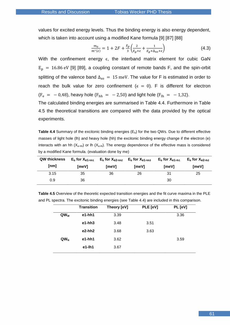
Results and Discussion Tobias Wecker PHD Thesis
61
values for excited energy levels. Thus the binding energy is also energy dependent,
which is taken into account using a modified Kane formula [9] [87] [88]
𝑚0
𝑚∗(𝜖)= 1 + 2𝐹 +
𝐸𝑝
3(
2
𝐸𝑔+𝜖+
1
𝐸𝑔+Δso+𝜖) (4.3)
With the confinement energy ϵ, the interband matrix element for cubic GaN
Ep = 16.86 eV [9] [89], a coupling constant of remote bands F, and the spin-orbit
splitting of the valence band Δso = 15 meV. The value for F is estimated in order to
reach the bulk value for zero confinement (ϵ = 0). F is different for electron
(Fe = − 0,48), heavy hole (Fhh = − 2,50) and light hole (Flh = − 1,32).
The calculated binding energies are summarised in Table 4.4. Furthermore in Table
4.5 the theoretical transitions are compared with the data provided by the optical
experiments.
Table 4.4 Summary of the excitonic binding energies (Eb) for the two QWs. Due to different effective
masses of light hole (lh) and heavy hole (hh) the excitonic binding energy change if the electron (e)
interacts with an hh (Xe-hh) or lh (Xe-lh). The energy dependence of the effective mass is considered
by a modified Kane formula. (evaluation done by me)
QW thickness
[nm]
Eb for Xe1-hh1
[meV]
Eb for Xe2-hh2
[meV]
Eb for Xe1-hh3
[meV]
Eb for Xe1-lh1
[meV]
Eb for Xe2-lh2
[meV]
3.15 35 36 26 31 25
0.9 36 30
Table 4.5 Overview of the theoretic expected transition energies and the fit curve maxima in the PLE
and PL spectra. The excitonic binding energies (see Table 4.4) are included in this comparison.
Transition Theory [eV] PLE [eV] PL [eV]
QWW e1-hh1 3.39 3.36
e1-hh3 3.48 3.51
e2-hh2 3.68 3.63
QWN e1-hh1 3.62 3.59
e1-lh1 3.67

Results and Discussion Tobias Wecker PHD Thesis
Tobias Wecker
62
Due to the thick AlxGa1-xN barrier (15 nm) the QWs can be investigated and simula-
ted independently. In Figure 4.25 and Figure 4.26 the conduction band edge (blue
line) and the valence band edges are plotted vs. the position along the growth di-
rection for the QWW and the QWN The residual strain in the QW structures lead to a
difference in the band gaps for hh and lh. This inflicts also the energy levels for hh
and lh diverge regarding to the unstrained QW (red for hh, green for lh).
0 2 4 6 8 10-1.70
-1.68
-1.66
-1.64
-1.62
-1.60
-1.58
1.74
1.80
1.86
1.92
1.98
2.04
2.10
2.16
lh2
3.706 eV
3.750 eV
lh1
hh3
hh2
hh1
e2
QWW 3.15 nm x = 0.26 strain=0.4 CBO 80 T = 7 K
En
erg
y [
eV
]
Position [nm]
e1
3.421 eV
3.479 eV
3.512 eV
Figure 4.25 Nextnano³ simulation of the energy levels and the band edges for the wide QW
(3.15 nm) at 7 K. Two bound energy levels exist for the electrons (e), whereas the holes have five
bound states, three for the heavy holes (hh) and two for the light holes (lh). This leads to 5 allowed
transition.
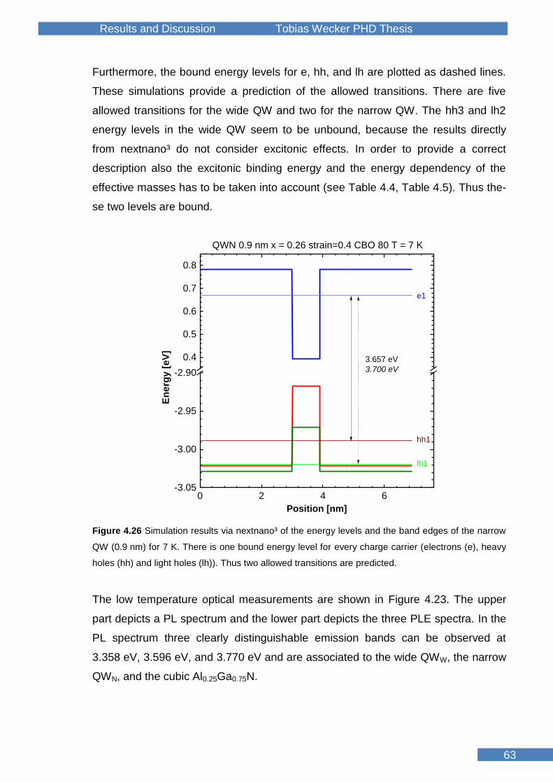
Results and Discussion Tobias Wecker PHD Thesis
63
Furthermore, the bound energy levels for e, hh, and lh are plotted as dashed lines.
These simulations provide a prediction of the allowed transitions. There are five
allowed transitions for the wide QW and two for the narrow QW. The hh3 and lh2
energy levels in the wide QW seem to be unbound, because the results directly
from nextnano³ do not consider excitonic effects. In order to provide a correct
description also the excitonic binding energy and the energy dependency of the
effective masses has to be taken into account (see Table 4.4, Table 4.5). Thus the-
se two levels are bound.
0 2 4 6-3.05
-3.00
-2.95
-2.90
0.4
0.5
0.6
0.7
0.8
3.657 eV
3.700 eV
lh1
hh1
QWN 0.9 nm x = 0.26 strain=0.4 CBO 80 T = 7 K
En
erg
y [
eV
]
Position [nm]
e1
Figure 4.26 Simulation results via nextnano³ of the energy levels and the band edges of the narrow
QW (0.9 nm) for 7 K. There is one bound energy level for every charge carrier (electrons (e), heavy
holes (hh) and light holes (lh)). Thus two allowed transitions are predicted.
The low temperature optical measurements are shown in Figure 4.23. The upper
part depicts a PL spectrum and the lower part depicts the three PLE spectra. In the
PL spectrum three clearly distinguishable emission bands can be observed at
3.358 eV, 3.596 eV, and 3.770 eV and are associated to the wide QWW, the narrow
QWN, and the cubic Al0.25Ga0.75N.

Results and Discussion Tobias Wecker PHD Thesis
Tobias Wecker
64
4.3.5 Summary ADQWs
In this chapter two series of asymmetric double quantum wells (ADQWs) have been
analysed in order to achieve a complete theoretical understanding of the energy
structure and the coupling between the two quantum wells (QW). For this reason
several photoluminescence (PL) measurements have been performed to investi-
gate the influence of the barrier thickness to the coupling between the two QWs.
Although the series have different Al content (0.26 and 0.64) the general behaviour
in the PL spectra is very similar. The higher Al content in the series 0.64 cause a
lower tunnelling rate leading to a significant coupling at a thinner barrier (3 nm)
compared to the series 0.26 where the coupling starts at 7 nm thick barriers. For
the evaluation time-resolved PL was used to determine the decay times needed for
rate equations as well as simulations of the energy levels in the QWs via nextnano³.
In addition, photoluminescence excitation spectroscopy (PLE) was used to deter-
mine higher transitions (e1-hh3 and e2-hh2) which cannot be measured by PL. This
is very important to confirm the parameters used for the nextnano³ simulations, be-
cause for higher energy levels the conduction band valence band offset (CBO:VBO)
gets more important.
The theoretical considerations presented in this chapter fit very well with the exper-
imental data, thus the parameter set is consistent and can be applied to more com-
plex heterostructures.

Results and Discussion Tobias Wecker PHD Thesis
65
4.4 Multi Quantum Wells (MQW)
The experimental and theoretical knowledge gained with the ADQWs was used for
the design of the MQW samples. Especially the influence on the IR absorption
FWHM and intensity was in the focus of interest. The intersubband transitions
(ISBT) can be used to investigate nonlinear effects, due to their high nonlinear
properties. Besides the influence of parameters like doping, period number and
substrates on the FWHM in ISBT have been investigated. Furthermore such MQWs
can be used for quantum cascade lasers (QCL).
This chapter is divided in different parts. At first general information about the
growth of the MQW samples is described briefly followed by an investigation of the
real layer thicknesses of one MQW sample via TEM [11]. This layer thickness is
crucial for the exact simulation of the energy levels via nextnano³. Then HRXRD
measurements showed the existence of additional SL peaks, which is the proof for
the formation of a SL structure. Besides the photoluminescence (PL) spectra re-
vealed very similar emission bands providing the good reproducibility of the QW
layer thicknesses. The IR absorption data revealed a FWHM of 370 meV for the
MQW with 80 periods and 250 meV for the MQW with 40 periods. The difference is
caused by an unexpected high doping of the first sample and the higher period
number. A detailed theoretical modelling of the FWHM in the IR absorption revealed
the high significance of the interface roughnesses. The last sub-chapter deals with
one of the first non-linear measurements on MQWs based on the cubic phase of
the group III-nitrides. These first experimental data present a third order susceptibil-
ity in the order of Im χ(3) ~ 1.1 ⋅ 10−20 m2/V2 as described in [10].
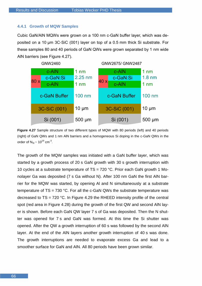
Results and Discussion Tobias Wecker PHD Thesis
Tobias Wecker
66
4.4.1 Growth of MQW Samples
Cubic GaN/AlN MQWs were grown on a 100 nm c-GaN buffer layer, which was de-
posited on a 10 µm 3C-SiC (001) layer on top of a 0.5 mm thick Si substrate. For
these samples 80 and 40 periods of GaN QWs were grown separated by 1 nm wide
AlN barriers (see Figure 4.27).
GNW2460 GNW2675/ GNW2487
Figure 4.27 Sample structure of two different types of MQW with 80 periods (left) and 40 periods
(right) of GaN QWs and 1 nm AlN barriers and a homogeneous Si doping in the c-GaN QWs in the
order of NSi ~ 1019
cm-3
.
The growth of the MQW samples was initiated with a GaN buffer layer, which was
started by a growth process of 20 s GaN growth with 30 s growth interruption with
10 cycles at a substrate temperature of TS = 720 °C. Prior each GaN growth 1 Mo-
nolayer Ga was deposited (7 s Ga without N). After 100 nm GaN the first AlN bar-
rier for the MQW was started, by opening Al and N simultaneously at a substrate
temperature of TS = 730 °C. For all the c-GaN QWs the substrate temperature was
decreased to TS = 720 °C. In Figure 4.29 the RHEED intensity profile of the central
spot (red area in Figure 4.28) during the growth of the first QW and second AlN lay-
er is shown. Before each GaN QW layer 7 s of Ga was deposited. Then the N shut-
ter was opened for 7 s and GaN was formed. At this time the Si shutter was
opened. After the QW a growth interruption of 60 s was followed by the second AlN
layer. At the end of the AlN layers another growth interruption of 40 s was done.
The growth interruptions are needed to evaporate excess Ga and lead to a
smoother surface for GaN and AlN. All 80 periods have been grown similar.

Results and Discussion Tobias Wecker PHD Thesis
67
Figure 4.28 RHEED diffraction pattern taken after the first MQW cycle of sample GNW2460.
150 200 250 30025
30
35
40
45
50
55
60
65
70
Al, N closed
AlN BreakBreakGaN QW
Inte
nsit
y [
%]
Time [s]
Ga open
N open
Si open
N, Ga, Si closed
Al, N open
Figure 4.29 RHEED intensity profile of the first QW and second AlN layer of the MQW structure
(GNW2460) measured in the red area in Figure 4.28.
In all MQWs a homogeneous doping of the c-GaN QWs with Si in the order of
NSi ~ 1018-1019 cm-3) is intended, in order to shift the Fermi energy above the first
electron level (e1). This is crucial for the absorption measurements. Only if there
are electrons populating the first electron level, absorption between e1 and e2 can
Results and Discussion Tobias Wecker PHD Thesis
Tobias Wecker
68
be measured. The sample structures of the most important MQWs are shown in
Figure 4.27. The main difference is the QW thickness and the period number. For
GNW2460 the QW is 2.25 nm thick with 80 periods. In order to match the desired
1.55 µm in the IR absorption, the QWs of the other MQWs are 1.8 nm thick. Be-
sides the period number of 40 is expected to be sufficient to achieve a good IR ab-
sorption and to decrease the FWHM in the absorption spectra.
4.4.2 Investigation of MQWs by HRXRD
Similar to the ADQWs all MQW layers have been investigated via HRXRD. An av-
erage defect density of the order of D ≈ 2 × 1010 cm−2 was obtained by measuring
the width of the rocking curve of the (002) reflection of the MQW samples. Atomic
force microscopy measurements revealed a surface roughness of 5-6 nm (rms) for
5x5 µm2 areas.
By growing a MQW structure with several periods of AlN/GaN layers a superlattice
(SL) is formed. This superlattice is characterised by an averaged lattice constant,
which can be calculated by adding the AlN barrier thickness and the GaN QW
thickness. Furthermore additional reflections are visible in the HRXRD, caused by
this SL lattice constant. In Figure 4.30 the RSM around the (113) direction for
GNW2460 with 80 periods (left) and GNW2687 with 40 periods (right) are shown. In
both (113) RSM two additional reflections corresponding to the lattice constant of
the superlattice can be seen, proving the existence of a superlattice. Thus the
growth of the superlattice was successful on the structural level. Besides the RSM
reveal a partial strain in the SL. A deviation in the reciprocal lattice constant parallel
to the surface (q||) of the additional SL peaks compared to the c-GaN and c-AlN is
visible. This leads to partial strain in the QW and barrier materials, thus an aver-
aged lattice constant is formed. The degree of relaxation of all MQWs measured in
this thesis is R = 0.25 ± 0.04, determined via the additional SL peaks visible in the
RSM in (113).

Results and Discussion Tobias Wecker PHD Thesis
69
1.90 1.95 2.00 2.05
4.0
4.2
4.4
SL
SL
q[Å
-1]
q||[Å
-1]
3C-SiC
c-GaN
GNW2460-RSM-113-0
1.90 1.95 2.00 2.05
4.0
4.2
4.4
q[Å
-1]
q||[Å
-1]
GNW2687-RSM-113-0-58h
3C-SiC
SL
c-GaN
SL
Figure 4.30 RSM in (113) direction of GaN/AlN MQW structures with 80 periods (left) and 40 peri-
ods (right).
In Figure 4.31 the RSM in (002) direction of the same MQWs are depicted. Alt-
hough in the (113) direction two additional peaks occur in the (002) direction of the
MQW with 40 periods (right) only one SL peak is visible. This is caused by the rela-
tively high intensity of the 3C-SiC reflection and the SL peak is too weak to be de-
tectable.
-0.4 -0.2 0.0 0.2 0.4
2.4
2.5
2.6
2.7
2.8
2.9
SL
q[Å
-1]
q||[Å
-1]
GNW2460-RSM-002-0
SL
c-GaN
3C-SiC
-0.4 -0.2 0.0 0.2 0.4
2.4
2.5
2.6
2.7
2.8
2.9
q[Å
-1]
q||[Å
-1]
GNW2487-RSM-002-0-15h
SL
SL
c-GaN
3C-SiC
Figure 4.31 RSM in (002) direction of GaN/AlN MQW structures with 80 periods (left) and 40 peri-
ods (right).

Results and Discussion Tobias Wecker PHD Thesis
Tobias Wecker
70
4.4.3 Calibration of QW Thickness by TEM
The growth rate for c-GaN layer is estimated by growing a nominal 600 nm thick c-
GaN sample. The real sample thickness is measured by reflection interference
spectra leading to the growth rate. This procedure determines the growth speed of
c-GaN on c-GaN without interface effects. But the growth speed strongly depends
on the underlying material, leading to a deviation of the growth speed for complex
heterostructures. In order to investigate the real thicknesses of the MQWs, Trans-
mission electron microscopy (TEM) measurements were done by Torsten Rieger of
AG Pawlis in FZ Jülich [11]. So a general calibration of the real QW thickness with
the simulations and the optical transitions (nextnano³) can be achieved. A MQW
sample with 20 periods of nominal 1.35 nm c-GaN QWs and 5 nm AlN barriers was
deposited on a 100 nm thick c-GaN buffer layer on top of 3C-SiC/Si substrate (see
Figure 4.32). The c-GaN QWs are homogeneous doped with Si in the order of
NSi ~ 1019 cm-3.
GNW2608
Figure 4.32 Sample structure of a MQW with 20 periods of 1.35 nm GaN QWs and 5 nm AlN barri-
ers and a homogeneous Si doping in the c-GaN QWs in the order of NSi ~ 1019
cm-3
.
Cross-sectional high resolution TEM bright field images along the <110> direction
(see Figure 4.33) are measured with a FEI Tecnai G² F20 microscope [91]. A TEM
lamella was prepared by focused ion beam using Ga ions and a final polishing step
with an acceleration voltage of 5 kV. In this diagram 5 c-AlN layers and 4 c-GaN
QWs are visible. Furthermore in the lower left corner are some stacking fault (SF)
measured.
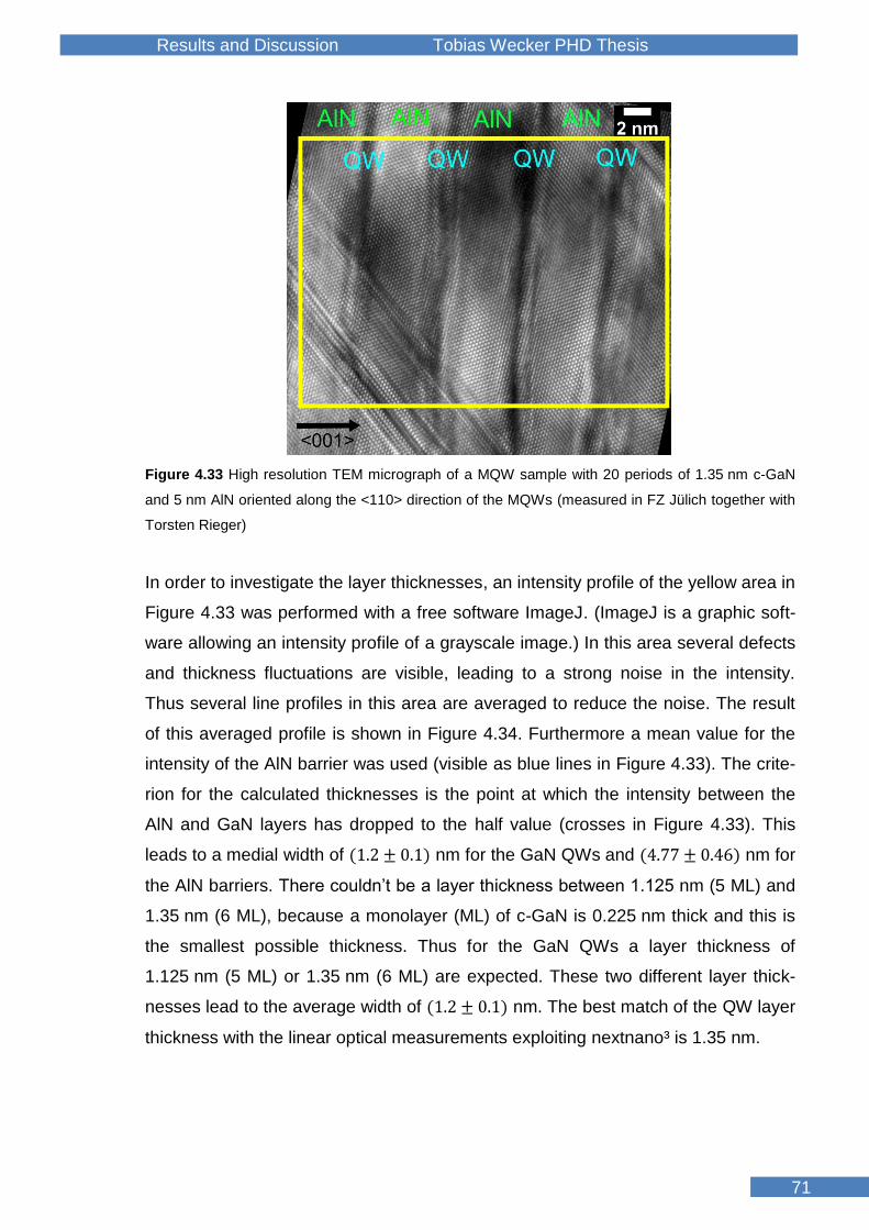
Results and Discussion Tobias Wecker PHD Thesis
71
Figure 4.33 High resolution TEM micrograph of a MQW sample with 20 periods of 1.35 nm c-GaN
and 5 nm AlN oriented along the <110> direction of the MQWs (measured in FZ Jülich together with
Torsten Rieger)
In order to investigate the layer thicknesses, an intensity profile of the yellow area in
Figure 4.33 was performed with a free software ImageJ. (ImageJ is a graphic soft-
ware allowing an intensity profile of a grayscale image.) In this area several defects
and thickness fluctuations are visible, leading to a strong noise in the intensity.
Thus several line profiles in this area are averaged to reduce the noise. The result
of this averaged profile is shown in Figure 4.34. Furthermore a mean value for the
intensity of the AlN barrier was used (visible as blue lines in Figure 4.33). The crite-
rion for the calculated thicknesses is the point at which the intensity between the
AlN and GaN layers has dropped to the half value (crosses in Figure 4.33). This
leads to a medial width of (1.2 ± 0.1) nm for the GaN QWs and (4.77 ± 0.46) nm for
the AlN barriers. There couldn’t be a layer thickness between 1.125 nm (5 ML) and
1.35 nm (6 ML), because a monolayer (ML) of c-GaN is 0.225 nm thick and this is
the smallest possible thickness. Thus for the GaN QWs a layer thickness of
1.125 nm (5 ML) or 1.35 nm (6 ML) are expected. These two different layer thick-
nesses lead to the average width of (1.2 ± 0.1) nm. The best match of the QW layer
thickness with the linear optical measurements exploiting nextnano³ is 1.35 nm.

Results and Discussion Tobias Wecker PHD Thesis
Tobias Wecker
72
0 5 10 15 20 25550
600
650
700
750
800
850
900
950
1000
1050
5.26 nm4.96 nm4.08 nm
1.20 nm1.01 nm1.28 nmIn
ten
sit
y [
arb
. u
.]
Distance [nm]
1.25 nm
Figure 4.34 TEM intensity contrast profile averaged over the yellow area in Figure 4.33. The medial
QW thickness is (1.2 ± 0.1) nm and the medial thickness for the AlN barriers is (4.77 ± 0.46) nm. (the
evaluation done by me)
4.4.4 Photoluminescence Spectroscopy (PL)
In the following the most important parameters of the used substrates and the
grown samples will be compared via photoluminescence spectroscopy. All the sub-
strates referred to in this chapter have very similar roughness (0.6 – 0.8 nm) and
FWHM of ω-scans in (002) (5 - 7 arcmin). Furthermore the samples show also simi-
lar roughness (3 - 5 nm) and FWHM in HRXRD (44-46 arcmin) (see Table 4.6). In
Figure 4.35 the room temperature PL spectra of 3 different MQW samples with
equal doping of NSi = 1019 cm-3 grown on different substrates are shown. The dop-
ing is always done homogenous in the QWs. All the spectra are normalized in order
to compare the emission energy and the FWHM. The difference in the emission
energy between GNW2460 and GNW2675/GNW2687 was intended to adapt the IR
absorption to 1.55 µm by growing thinner QWs. The similarities of GNW2675 and
GNW2687 are a clear indication for the independency of the PL spectra in regard to
the substrate.

Results and Discussion Tobias Wecker PHD Thesis
73
Table 4.6 Overview of the important structural properties, like roughness and FWHM of ω-scans of
the used substrates and the grown MQW samples.
Substrate Roughness
AFM [nm]
HRXRD
[arcmin]
Sample numbers Roughness
AFM [nm]
HRXRD
[arcmin]
UniPad1102 0.6 7.3 2460, 2486, 2487 5.3 45.7
14CO050 0.7 5.1 2675, 2729-32 4.1 44.1
14CO144 0.8 5.2 2684,2687 3.0 43.8
2.2 2.4 2.6 2.8 3.0 3.2 3.4 3.6 3.8 4.0 4.2 4.4 4.6 4.810
-3
10-2
10-1
100 PL CCD 266nm
300K
GNW2460
GNW2675
GNW2687
Inte
nsit
y [
arb
. u
nit
s]
Energy [eV]
Figure 4.35 PL spectra of MQW with 80 periods (red) and 40 periods (green, blue) grown on differ-
ent substrates.
There is no significant influence of the number of periods on the energy and FWHM
of the emission, as can be seen in Figure 4.36. In this figure the three samples
have 40, 50 and 60 periods, corresponding to GNW2675, GNW2732 and
GNW2729, respectively. Nevertheless only GNW2460 and GNW2675 show IR ab-
sorption, but the PL data are also very similar in regard to the emission energy and
the FWHM. Another parameter, which affects the IR absorption, is the doping den-
sity.

Results and Discussion Tobias Wecker PHD Thesis
Tobias Wecker
74
2.2 2.4 2.6 2.8 3.0 3.2 3.4 3.6 3.8 4.0 4.2 4.4 4.6 4.810
-4
10-3
10-2
10-1
100 PL CCD 266nm
300K GNW2675 40x
GNW2732 50x
GNW2729 60x
Inte
nsit
y [
arb
. u
nit
s]
Energy [eV]
Figure 4.36 PL spectra of MQW with 40 (green), 50 (black) and 60 (red) periods of GaN/AlN. The
spectrum of GNW2675 shows a higher noise, because of a lower integration time during the meas-
urement.
In Figure 4.37 three spectra of samples with equal periods but different doping den-
sities are shown. The sample GNW2675 has the lowest doping density with
NSi = 1019 cm-3 and the sample GNW2731 has NSi = 2x1019 cm-3 and GNW2730
has NSi = 4x1019 cm-3. The spectra are again very similar and only GNW2675
shows IR absorption.
2.2 2.4 2.6 2.8 3.0 3.2 3.4 3.6 3.8 4.0 4.2 4.4 4.6 4.810
-4
10-3
10-2
10-1
100 PL CCD 266nm
300K GNW2675 1x10
19
GNW2731 2x10¹⁹
GNW2730 4x10¹⁹
Inte
ns
ity
[a
rb.
un
its
]
Energy [eV]
Figure 4.37 PL spectra of MQW with 40 periods and different doping. The spectrum of GNW2675
shows a higher noise, because of a lower integration time during the measurement.

Results and Discussion Tobias Wecker PHD Thesis
75
4.4.5 Measurements of Intersubband Absorption
The absorption measurements of the intersubband transition (ISBT) are taken in TU
Dortmund by AG Betz, but the evaluation of the data presented here was performed
by me. More details about the sample processing can be seen in chapter 2.3 and
3.6. The incident light approaches perpendicular to the surface of the 30° facet.
Due to the selection rules for ISBTs, the absorption is only expected for TM polar-
ized excitation. In order to obtain the absorption spectrum the detected spectra for
TM and TE excitation are subtracted for the MQW sample. Moreover, a reference
sample of 600 nm c-GaN with equivalent 30° facets was used, to identify spectral
features of the substrate and the c-GaN buffer layer contained in the absorption
data. The spectra in Figure 4.38 are achieved subtracting the different TM and TE
transmissions through the waveguide structure and normalize this by the spectrum
of the reference. All absorption measurements were performed at room tempera-
ture
0.5 0.6 0.7 0.8 0.9 1.0 1.12x10
-2
3x10⁻²
4x10⁻²
5x10⁻²
GNW2460
GNW2675
ISB
T A
bs
orp
tio
n p
er
Pe
rio
d [
%]
Energy [eV]
300 K
Figure 4.38 IR absorption spectra of the two MQW samples at room temperature. The FWHM of
GNW2460 is with 370 meV much broader than for GNW2675 (250 meV), caused by higher doping.
For GNW2460 e1-e2 and e2-e3 is absorbing, leading to a broader spectrum. (measured in TU
Dortmund AG Betz)
The absorption maximum for sample GNW2460 is about 0.7 eV and for the sample
GNW2675 it is at 0.83 eV, which is caused by the different layer thicknesses. The

Results and Discussion Tobias Wecker PHD Thesis
Tobias Wecker
76
FWHM of sample GNW2675 is 250 meV and for sample GNW2460 it is 370 meV.
The FWHM of GNW2460 is higher than that cited in literature for both the cubic
[8][6] and the hexagonal [92-94] phase. The FWHM of sample GNW2675 is close to
the value 267 meV reported for similar structures [6]. The explanation will be given
in the following together with the detailed presentation of the different energy levels
and transitions provided by nextnano³.
Figure 4.39 shows the band diagram for a QW thickness of 2.25 nm (left) and
1.8 nm (right) with the different energy levels at room temperature. Due to the partly
strained AlN barriers the QW is also strained. This results in an average lattice
constant of the MQW structure. The transition responsible in PL is the first electron
to the first heavy hole transition (e1-hh1). For the IR absorption measurements the
first and the second electron levels take part (e1-e2). As a result of unexpected high
doping the Fermi energy EF of the sample with 80 periods is above the e2 level,
leading to an additional absorption (e2-e3) visible in Figure 4.38. This result in a
much broader absorption compared to the sample with 40 periods.
0 1 2 3 4 5 6 7 8
-1
3
4
5
e3
630 meV
EF
e2
SQW 2.25 nm x = 1 strain=0.25 CBO 78 T = 300 K
En
erg
y [
eV
]
Position [nm]
e1
3.581 eV
lh2
lh1
hh3
hh2
hh1
940 meV
0 1 2 3 4 5 6 7 8
-1
3
4
5
854 meV
EF
e2
SQW 1.8 nm x = 1 strain=0.25 CBO 78 T = 300 K
En
erg
y [
eV
]
Position [nm]
e1
3.686 eV
lh2
lh1
hh3
hh2
hh1
Figure 4.39 Band diagram of the sample with 80 periods (dQW = 2.25 nm, left) and with 40 periods
(dQW = 1.8 nm, right) at 300 K.

Results and Discussion Tobias Wecker PHD Thesis
77
In order to compare this very broad absorption with the nextnano³ simulations Figu-
re 4.40 and Figure 4.41 can be used. Figure 4.40 presents the calculated transition
energies between the electron levels in the conduction band. It shows the absence
of an e3 level for QWs thinner than 2.25 nm, thus the QWs of sample GNW2640
has to be at least 2.25 nm thick. The transition energy of e1-e2 for this thickness is
630 meV as depicted in Figure 4.39 (left) and e2-e3 has 940 meV. Taking both
transitions into account the absorption of GNW2460 can be explained. Furthermore,
in Figure 4.40 the needed QW thickness for an e1-e2 transition with an energy dif-
ference of 0.8 eV (1.55 µm) can be seen. The MQW with the QW thickness of
1.8 nm is very close to this transition, as also provided by the nextnano³ calculati-
ons.
1 2 3 4 5 6 7 8 9 10 11
0.0
0.2
0.4
0.6
0.8
1.0
1.2
1.4
1.6 SQW, x=1, strain 0.25, CBO 78, 300K
e1-e2
e1-e3
e2-e3
En
erg
y [
eV
]
QW Thickness [nm]
Figure 4.40 Calculated ISBT of a single QW with a degree of relaxation of 0.25 and AlN barriers at
300K.
Figure 4.41 shows the bound energy levels provided by nextnano³ for a single QW
with AlN barriers partly strained on a c-GaN buffer layer at 300 K. The AlN cannot
be measured in HRXRD, thus the degree of relaxation for x = 1 is determined with
the additional SL peaks visible in RSM along (113) to 𝑅 = 0.25 ± 0.04.

Results and Discussion Tobias Wecker PHD Thesis
Tobias Wecker
78
0 1 2 3 4 5 6 7 8 9 10 11 12-1.4
-1.2
-1.0
-0.8
-0.62.5
3.0
3.5
4.0
4.5
5.0
hh3hh2
e3e2
CB_GaN
SQW, x=1, strain 0.25, CBO 78, 300K
En
erg
y [
eV
]
QW Thickness [nm]
CB_AlN
HH_AlN
HH_GaN
e1
hh1LH_GaN
LH_AlNlh3lh2
lh1
Figure 4.41 Simulated energy levels for electrons (e), heavy holes (hh) and light holes (lh) of a sin-
gle c-GaN QW with AlN barriers partly strained on c-GaN buffer at 300 K.
Only two of the MQW structures (GNW2460, GNW2675) show IR absorption, alt-
hough the experimental data of AFM, HRXRD and PL are similar also for the non-
absorbing samples. The reason for the difference in the IR absorption couldn’t be
identified. There is no correlation on the substrate, doping and period number ob-
servable in PL (see previous chapter).

Results and Discussion Tobias Wecker PHD Thesis
79
4.4.6 Intersubband Absorption Linewidth and Roughness
This subchapter deals with the influence of interface roughnesses on the intersub-
band absorption linewidth. All considerations and calculations in this chapter have
been performed by me. The FWHM of the optical measurements of the MQW sam-
ples is affected by the amount of defects and monolayer fluctuation. The main con-
tribution on the linewidth is the ML fluctuation. To describe the influence of the
thickness variation of the QW width 𝐿 on the energy levels 𝐸𝑚 and 𝐸𝑛, the following
formula for the form factor Fmn can be used [95].
𝐹𝑚𝑛 = √𝜕𝐸𝑚
𝜕𝐿⋅𝜕𝐸𝑛
𝜕𝐿 (4.4)
The energy levels have been simulated with nextnano³ for different QW thickness-
es. The function used for the fits is:
𝑦 =𝐴
𝑥−𝐶− 𝑦0 (4.5)
There is a deviation to the fit for very thin QWs. In case of the first electron level e1
this occurs at 0.225 nm and for e2 it starts for 1.35 nm. In Figure 4.42 the electron
energy levels for a c-GaN/AlN QW are plotted. They have been simulated with
nextnano³ for a degree of relaxation of 0.5 at 300K. The derivative of this fit function
was taken for the calculation of Fmn (see Figure 4.43).
𝑦′ = −𝐴
(𝑥−𝐶)2 (4.6)
0 1 2 3 4 5 6 7 8 9 10 11
2.6
2.8
3.0
3.2
3.4
3.6
3.8
4.0
4.2
4.4
4.6
4.8
y(e1)=0.69581/(x+0.08718)+2.60066
SQW, x=1, strain 0.25, CBO 78, 300K
e1 Fit e1
e2 Fit e2
En
erg
y [
eV
]
QW Thickness [nm]
y(e2)=1.88315/(x-0.30038)+2.52244
Figure 4.42 Electron energy levels for a c-GaN/AlN QW provided by nextnano³ with a degree of
relaxation of 0.5 at 300 K.

Results and Discussion Tobias Wecker PHD Thesis
Tobias Wecker
80
0 1 2 3 4 5 6 7 8 9 10 11
0.0
0.2
0.4
0.6
0.8
1.0
1.2
1.4
1.6
1.8
2.0SQW, x=1, strain 0.25, CBO 78, 300K
F00
F01
F11
En
erg
y [
eV
]
QW Thickness [nm]
Figure 4.43 Influence of the QW thickness on the electron energy levels for a c-GaN/AlN QW.
In the following a simple roughness model is used to describe the influence on the
absorption linewidth. The theory provided by Ando [95] connects the intersubband
line shape for elastic scattering processes with the real part of the electric conduc-
tivity 𝜎𝑧𝑧(𝜔). The absorption at the frequency 𝜔 close to the energy difference of the
subbands 𝐸10 depends on the optical scattering matrix element Γ𝑜𝑝𝑡(𝐸) and the
Fermi distribution 𝑓(𝐸).
𝑅𝑒 𝜎𝑧𝑧(𝜔)~ ∫Γ𝑜𝑝𝑡(𝐸)
(ℏ𝜔−𝐸10)+Γ𝑜𝑝𝑡(𝐸)2𝑓(𝐸)𝑑𝐸 (4.7)
The scattering matrix element consists of the scattering matrix elements of the in-
traband and the interband.
Γ𝑜𝑝𝑡(𝐸) =1
2(Γ𝑖𝑛𝑡𝑟𝑎(𝐸) + Γ𝑖𝑛𝑡𝑒𝑟(𝐸)) (4.8)
Both scattering elements depend on an exponential function, which has to be inte-
grated for all scattering angles 𝜃.
Γ𝑖𝑛𝑡𝑟𝑎(𝐸) =𝑚∗Δ2Λ2
ℏ2(𝐹00 − 𝐹11)
2 ∫ 𝑒−𝑞2Λ2/4𝑑𝜃𝜋
0 (4.9)
Γ𝑖𝑛𝑡𝑒𝑟(𝐸) =𝑚∗Δ2Λ2
ℏ2𝐹01
2 ∫ 𝑒−�̃�2Λ2/4𝑑𝜃𝜋
0 (4.10)
Results and Discussion Tobias Wecker PHD Thesis
81
The other parameters used are the effective mass 𝑚∗, the correlation length Λ, the
mean height Δ of the roughness. The absolute values of the two-dimensional scat-
tering vector 𝑞 and �̃� can be expressed as:
𝑞2 =4𝑚∗
ℏ2 𝐸(1 − cos 𝜃) (4.11)
�̃�2 =4𝑚∗
ℏ2 (𝐸 +𝐸10
2− √𝐸(𝐸 + 𝐸10) cos 𝜃) (4.12)
For the calculation of the absorption Matlab was used. The source code can be
seen in the appendix.
In the following the experimental results will be compared with the theoretical ex-
pectations considering also the influence of the material system on the FWHM of
the intraband absorption between e1-e2. In Table 4.7 the main influences on the
absorption linewidth for c-GaN and GaAs are collected. In equation 4.9 and 4.10
the effective mass 𝑚∗ changes the linewidth linearly. The other contribution is the
thickness fluctuation Δ of the QW ending up to different energy levels and thus
broadening the width for a higher fluctuation quadratically.
Table 4.7 Comparison of two simulated QW structures with the same thickness of 2.025 nm consist-
ing of different materials. The difference for the FWHM of the absorption between e1-e2 is mainly
caused by the effective mass and the influence on thickness fluctuations of the QW on the energy
levels F00, F01, F11.
c-GaN/AlN GaAs/AlAs
Effective Mass e 0.19[96]
0.069[95]
(F00-F11) [eV/nm] 0.5 0.08
F01 [eV/nm] 0.3 0.5
FWHM [eV] 2.78 0.047
For a GaAs/AlAs QW with thickness of 2.025 nm the calculated width in absorption
is much smaller due to the smaller effective mass and the weaker thickness de-
pendency of the energy levels. Thus for similar values of the correlation length
Λ = 4.3 nm and the mean height Δ = 0.45 nm of the roughness the FWHM of the
absorption of GaN is 2.78 eV and in case of GaAs 47 meV (see Figure 4.44).
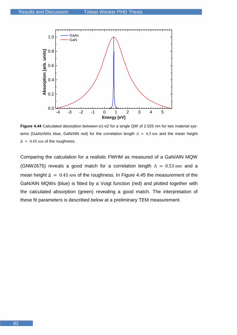
Results and Discussion Tobias Wecker PHD Thesis
Tobias Wecker
82
-4 -3 -2 -1 0 1 2 3 4 50.0
0.2
0.4
0.6
0.8
1.0 GaAs
GaN
Ab
so
rpti
on
[a
rb.
un
its
]
Energy [eV]
Figure 4.44 Calculated absorption between e1-e2 for a single QW of 2.025 nm for two material sys-
tems (GaAs/AlAs blue, GaN/AlN red) for the correlation length Λ = 4.3 𝑛𝑚 and the mean height
Δ = 0.45 𝑛𝑚 of the roughness.
Comparing the calculation for a realistic FWHM as measured of a GaN/AlN MQW
(GNW2675) reveals a good match for a correlation length Λ = 0.53 𝑛𝑚 and a
mean height Δ = 0.45 𝑛𝑚 of the roughness. In Figure 4.45 the measurement of the
GaN/AlN MQWs (blue) is fitted by a Voigt function (red) and plotted together with
the calculated absorption (green) revealing a good match. The interpretation of
these fit parameters is described below at a preliminary TEM measurement.

Results and Discussion Tobias Wecker PHD Thesis
83
0.6 0.7 0.8 0.9 1.00.0
0.2
0.4
0.6
0.8
1.0 Absorption e1-e2 GNW2675
Voigt Fit
Calculation
Ab
so
rpti
on
[a
rb. u
nit
s]
Energy [eV]
Figure 4.45 Absorption measurement of GNW2675 together with the calculated absorption (green).
The calculation was performed with a correlation length Λ = 0.53 𝑛𝑚 and a mean height
Δ = 0.45 nm of the roughness.
Figure 4.46 shows a TEM image of an MQW grown by Christian Mietze (sample
GNC2206). It reveals a much smoother interface roughness compared to the sam-
ple surface, thus the AFM RMS will not be used for the calculation of the FWHM in
the absorption spectra. An interface roughness of about ± 2 ML is assumed
(0.45 nm). As estimation for the correlation length the excitonic radius of c-GaN is
considered (about 2.9 nm). In this length the interface is always rough, because the
step size of the individual roughness regions is much smaller than 3 nm. For GaAs
this is not the case, there are larger regions with similar thickness compared to the
excitonic radius. So a much smaller correlation length compared to GaAs is as-
sumed, in order to fit with the experiment of c-GaN QWs.

Results and Discussion Tobias Wecker PHD Thesis
Tobias Wecker
84
Figure 4.46 TEM Image of an MQW GNC2206 (provided by Christian Mietze)
In Figure 4.47 the influence of the correlation length on the FWHM in the absorption
for a fixed roughness of 0.45 nm can be seen. A value of 0.54 leads to a FWHM of
250 meV as measured for sample GNW2675.
0.1 1
10
100
1000
250
rough 0.45
FW
HM
[m
eV
]
Correlation Length [nm]
0.54
Figure 4.47 Calculated FWHM of the absorption for various correlation lengths. The value of
0.54 nm fits best with the experimental FWHM of 250 meV.
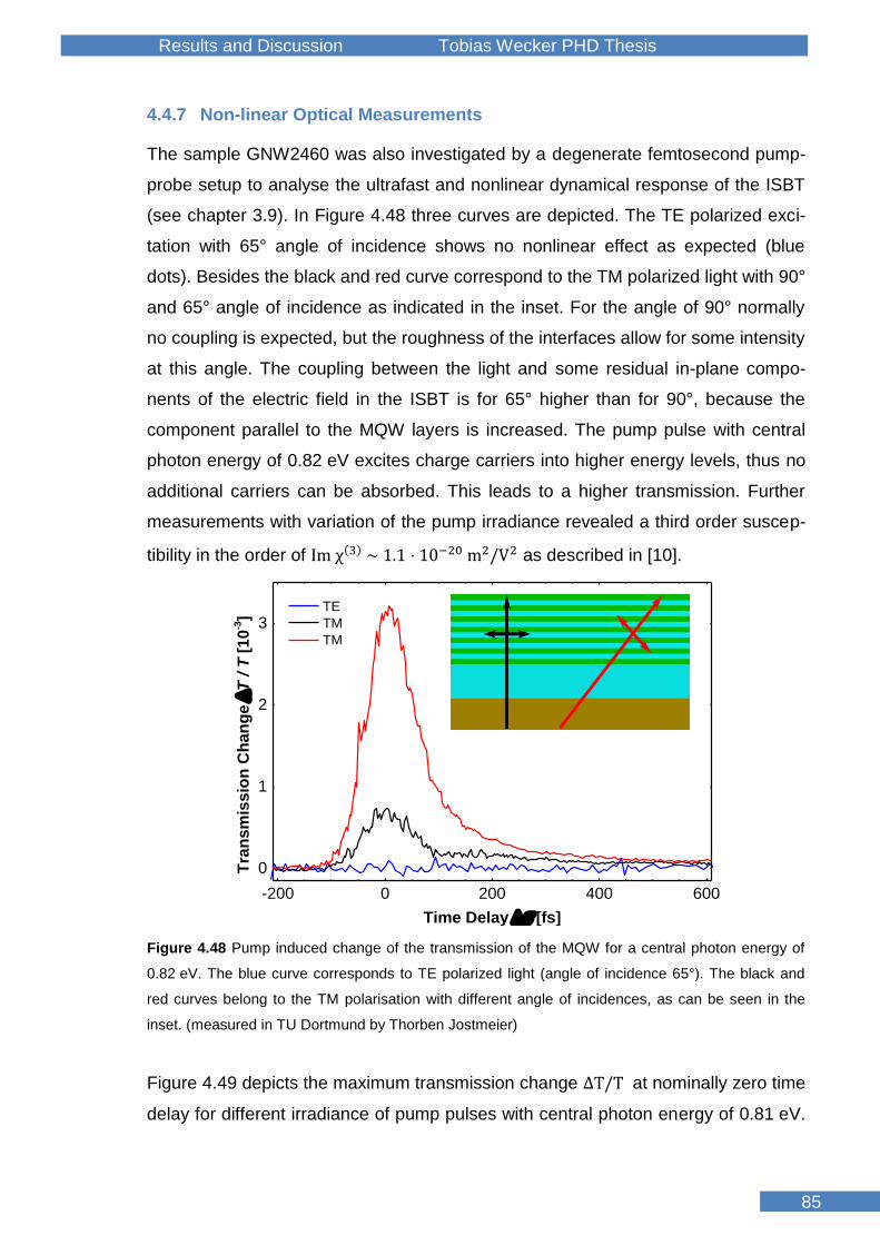
Results and Discussion Tobias Wecker PHD Thesis
85
4.4.7 Non-linear Optical Measurements
The sample GNW2460 was also investigated by a degenerate femtosecond pump-
probe setup to analyse the ultrafast and nonlinear dynamical response of the ISBT
(see chapter 3.9). In Figure 4.48 three curves are depicted. The TE polarized exci-
tation with 65° angle of incidence shows no nonlinear effect as expected (blue
dots). Besides the black and red curve correspond to the TM polarized light with 90°
and 65° angle of incidence as indicated in the inset. For the angle of 90° normally
no coupling is expected, but the roughness of the interfaces allow for some intensity
at this angle. The coupling between the light and some residual in-plane compo-
nents of the electric field in the ISBT is for 65° higher than for 90°, because the
component parallel to the MQW layers is increased. The pump pulse with central
photon energy of 0.82 eV excites charge carriers into higher energy levels, thus no
additional carriers can be absorbed. This leads to a higher transmission. Further
measurements with variation of the pump irradiance revealed a third order suscep-
tibility in the order of Im χ(3) ~ 1.1 ⋅ 10−20 m2/V2 as described in [10].
-200 0 200 400 600
0
1
2
3 TE
TM
TM
Tra
ns
mis
sio
n C
ha
ng
e
T /
T [
10
-3]
Time Delay [fs]
Figure 4.48 Pump induced change of the transmission of the MQW for a central photon energy of
0.82 eV. The blue curve corresponds to TE polarized light (angle of incidence 65°). The black and
red curves belong to the TM polarisation with different angle of incidences, as can be seen in the
inset. (measured in TU Dortmund by Thorben Jostmeier)
Figure 4.49 depicts the maximum transmission change ΔT/T at nominally zero time
delay for different irradiance of pump pulses with central photon energy of 0.81 eV.
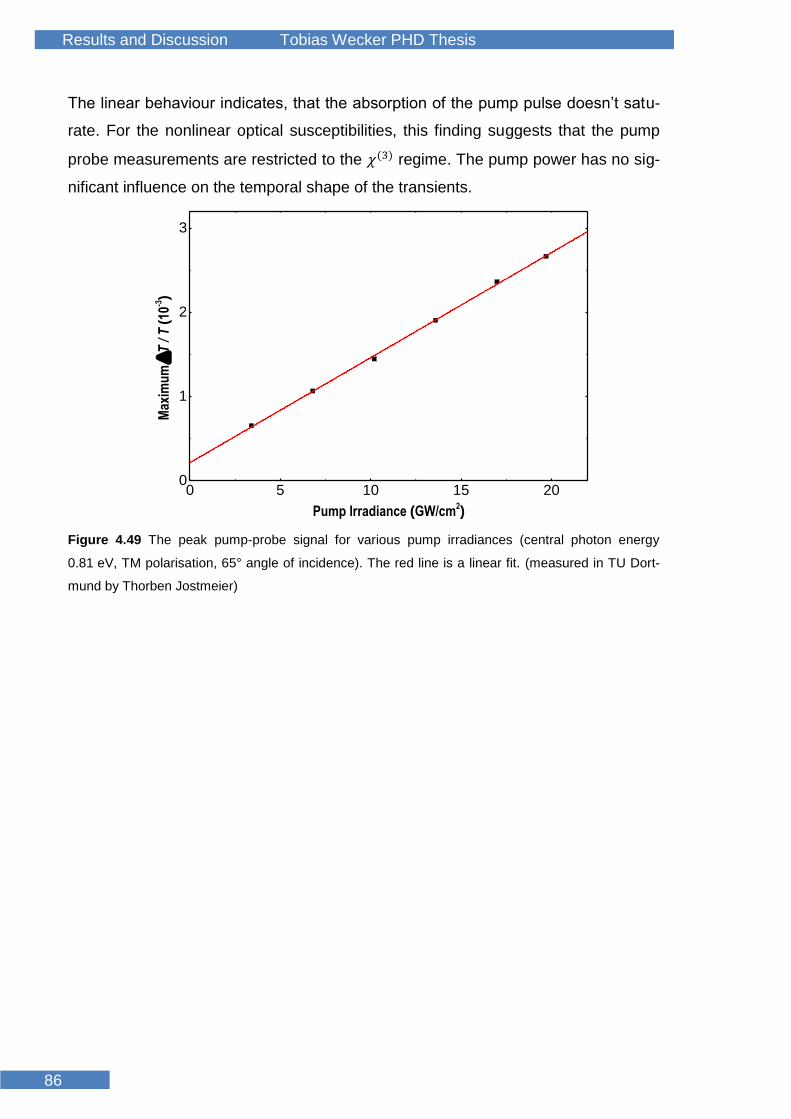
Results and Discussion Tobias Wecker PHD Thesis
Tobias Wecker
86
The linear behaviour indicates, that the absorption of the pump pulse doesn’t satu-
rate. For the nonlinear optical susceptibilities, this finding suggests that the pump
probe measurements are restricted to the 𝜒(3) regime. The pump power has no sig-
nificant influence on the temporal shape of the transients.
0 5 10 15 200
1
2
3
Max
imu
m
T /
T (
10-3)
Pump Irradiance (GW/cm2)
Figure 4.49 The peak pump-probe signal for various pump irradiances (central photon energy
0.81 eV, TM polarisation, 65° angle of incidence). The red line is a linear fit. (measured in TU Dort-
mund by Thorben Jostmeier)

Results and Discussion Tobias Wecker PHD Thesis
87
4.4.8 Summary MQWs
In this chapter several Si doped cubic AlN/GaN multi quantum well (MQWs) sam-
ples have been investigated in order to achieve a systematic understanding of the
intersubbandtransition (ISBT). This ISBT is very important for the field of non-linear
optics, because of the high non-linear properties. Furthermore in our group III-
nitride system the high band offset in the conduction band allows for a wavelength
of the ISBT that covers the 1.55 µm range interesting for telecommunication.
At first some important information about the growth is presented followed by a
chapter about the high resolution X-Ray diffractometry on the MQWs. Additional SL
peaks have been determined at MQWs with HRXRD RSM around the (002) and
(113) reflections. Strain investigations of the heterostructures have been performed
by HRXRD RSM around (113) revealing partly strained MQWs with
R = 0.25 ± 0.04. The strain is also validated by the theoretical calculations of the
transition energies via nextnano³. Furthermore transmission electron microscopy
(TEM) measurements on the MQW structures provided the real layer thickness.
This thickness was used for the transition energy calculation via nextnano³ and a
comparison with the PL data revealed a good agreement.
Another chapter deals with the investigation of the MQWs via photoluminescence
spectroscpy (PL). These measurements have been used to analyse the influence of
the doping, substrate and period number on the optical behaviour. There is no in-
fluence on the FWHM of the PL emission bands obersable for all these parameters.
In the next chapter intersubband absorption experiments were done with cubic
AlN/GaN MQWs. The FWHM of this absorption was theoretically fitted leading to a
correlation length of Λ = 0.53 nm and a mean height Δ = 0.45 nm of the rough-
ness. Furthermore a pump probe setup was used to measure the non-linear behav-
iour of MQW structures revealing a third order susceptibility of Im χ(3) ~ 1.1 ⋅
10−20 m2/V2.
Simulation Tobias Wecker PHD Thesis
Tobias Wecker
88
5 Simulation
For the interpretation of the experimental data in this thesis several simulations
have been done. One of the great challenges in this thesis was the absence of con-
sistent parameters for the cubic group III nitrides, thus all the experimental data
have been used to identify a consistent parameter set. The parameters used in this
thesis can be seen in the appendix. All theoretical considerations in this chapter
have been done by me.
For the understanding of the band structure, energy levels and transitions of the
QW structures nextnano³ (nn³) was used. Furthermore the HRXRD measurements
for the MQWs are investigated by MadMax, in order to extract the exact layer thick-
nesses of the ω-2θ curves.
5.1 Nextnano³
Nextnano³ is a commercial available self-consistent Schrödinger-Poisson solver.
These simulations are based on the effective mass approximation. For all nominally
undoped samples a background n-type doping of around 5 ⋅ 1017 𝑐𝑚−3 in AlxGa1-xN
and of around 1 ⋅ 1017 𝑐𝑚−3 in GaN is assumed for the calculations [75]. The infor-
mation about the energy levels provided by nextnano³ does not include excitonic
effects. Thus for a comparison of the transition energies with experimental data the
excitonic binding energy is calculated as shown in theory chapter and subtracted
from the theoretical values. In addition, the band offset between AlxGa1-xN and GaN
is considered as explained in chapter 2.4. For the calculation of the band edges of
valence and conduction band nextnano³ take the split off energy Δ𝑆𝑂 into account
[97].
𝐸′ = 𝐸 +Δ𝑆𝑂
3 (5.1)
HRXRD measurements revealed a partial strain in all heterostructures presented in
this work. But nextnano³ cannot treat partial strain, only pseudomorphical strained
or unstrained structures can be defined in the parameters of the program. So a vir-
tual lattice constant 𝑎𝑏𝑢𝑓𝑓𝑒𝑟𝑣𝑖𝑟𝑡𝑢𝑎𝑙 is used replacing the lattice constant of the cubic GaN
buffer layer, in order to achieve a partial strain in the heterostructure as delivered by
HRXRD RSM. Besides the relaxed lattice constant of the AlxGa1-xN layers 𝑎𝑏𝑢𝑓𝑓𝑒𝑟𝑣𝑖𝑟𝑡𝑢𝑎𝑙 is
interpolated between the relaxed cubic GaN and relaxed cubic AlN (bowing factor
bBowing = 0.85 [77]). The lattice constant of the strained AlxGa1-xN is calculated by
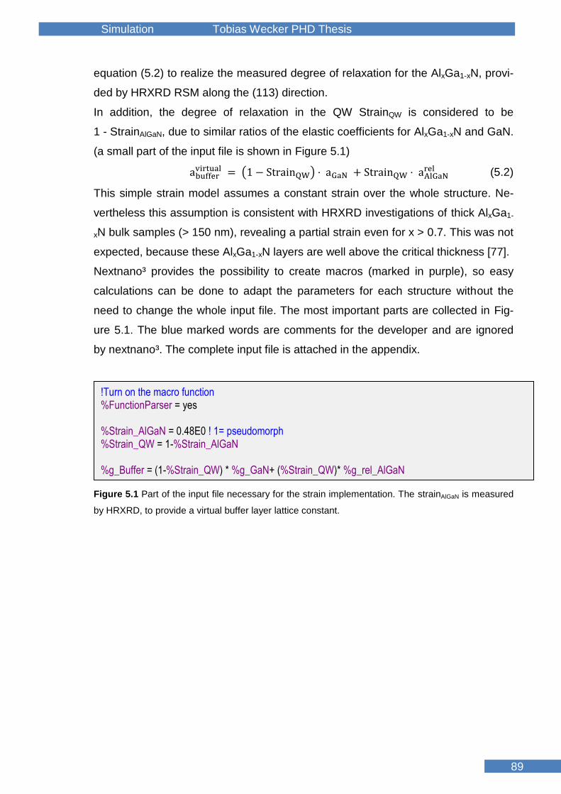
Simulation Tobias Wecker PHD Thesis
89
equation (5.2) to realize the measured degree of relaxation for the AlxGa1-xN, provi-
ded by HRXRD RSM along the (113) direction.
In addition, the degree of relaxation in the QW StrainQW is considered to be
1 - StrainAlGaN, due to similar ratios of the elastic coefficients for AlxGa1-xN and GaN.
(a small part of the input file is shown in Figure 5.1)
abuffervirtual = (1 − StrainQW) ⋅ aGaN + StrainQW ⋅ aAlGaN
rel (5.2)
This simple strain model assumes a constant strain over the whole structure. Ne-
vertheless this assumption is consistent with HRXRD investigations of thick AlxGa1-
xN bulk samples (> 150 nm), revealing a partial strain even for x > 0.7. This was not
expected, because these AlxGa1-xN layers are well above the critical thickness [77].
Nextnano³ provides the possibility to create macros (marked in purple), so easy
calculations can be done to adapt the parameters for each structure without the
need to change the whole input file. The most important parts are collected in Fig-
ure 5.1. The blue marked words are comments for the developer and are ignored
by nextnano³. The complete input file is attached in the appendix.
Figure 5.1 Part of the input file necessary for the strain implementation. The strainAlGaN is measured
by HRXRD, to provide a virtual buffer layer lattice constant.
!Turn on the macro function %FunctionParser = yes %Strain_AlGaN = 0.48E0 ! 1= pseudomorph %Strain_QW = 1-%Strain_AlGaN %g_Buffer = (1-%Strain_QW) * %g_GaN+ (%Strain_QW)* %g_rel_AlGaN

Simulation Tobias Wecker PHD Thesis
Tobias Wecker
90
5.2 MadMax and ω-2θ Profiles
In order to investigate the HRXRD data the program MadMax (Massively Acceler-
ated Dynamical Multilayer Analysis by X-ray diffraction) was used [98]. It is suitable
to evaluate the influence of strain and different layer thicknesses on ω-2θ curves in
different directions. In this thesis only the (113) and (002) directions are measured.
MadMax simulate diffraction profiles in co-planar diffraction geometry. Furthermore
complex heterostructures can be calculated by adding all the different layers. For
each layer the degree of relaxation R can be set. A value of R = 0 corresponds to a
fully strained layer, thus this layer gets the lattice constant of the previous layer. For
R = 1 the layer is fully relaxed leading to the lattice constant implemented in the
database. In addition, ternary semiconductors can be introduced with various mix-
tures, by changing the x value. A screenshot of the main window is shown in Figure
5.2. Unfortunately the material parameters for the cubic nitrides are slightly different
from the values determined recently with samples of our workgroup. The lattice
constants used in MadMax for c-GaN and c-AlN are 0.452 nm and 0.438 nm, re-
spectively. Moreover, 3C-SiC isn’t implemented at all. To solve these problems the
lattice constant of a GaAs substrate is replaced by the value for 3C-SiC
(0.43596 nm [99]) and c- AlxGa1-xN with x = 0.12 is used to match 0.4503 nm [35]
expected for c-GaN. Only the correct lattice parameter for c-AlN (0.4373 nm [100])
couldn’t be reached, this will be partly solved applying a different strain to the c-AlN
layers. The result of the input of Figure 5.2 can be seen in Figure 5.3.
Figure 5.2 Input window of MadMax for a c-GaN reference sample. The c- AlxGa1-xN layer is used to
achieve the lattice constant of c-GaN. The GaAsN layer matches the lattice constant of the Si in the
substrate.

Simulation Tobias Wecker PHD Thesis
91
The red line corresponds to the measured profile for a 500 nm (GNW2614) thick c-
GaN reference sample and the black line is the calculated profile. The main intensi-
ty is caused by the 3C-SiC layer, which serves as a reference point. Next to this
peak the c-GaN peak is visible and a very narrow peak appears at the left side of
the profile. This narrow peak originates from the Si of the substrate and is meas-
ured for all samples and wafers. To evaluate the lattice constant necessary for this
peak a GaxAs1-xN layer with x = 0.195 is used. This layer matches the lattice con-
stant of Si with 0.5431 nm [101].
16 18 20 22 2410
-10
10-9
10-8
10-7
10-6
10-5
10-4
10-3
GNW2614
MadMax
Inte
ns
ity
[a
rb. u
nit
s]
Omega [°]
Si
c-GaN
3C-SiC
Figure 5.3 MadMax output profile (black) with the measured ω-2θ profile of a c-GaN reference sam-
ple (red) in (002). The three peaks are caused by the Si, c-GaN and 3C-SiC, respectively.
In detailed investigation of the ω-2θ profiles several very weak peaks appear in long
measurements (around 24h per profile). These peaks originate from the substrate.
This can be seen comparing a profile of the substrate (blue) with a MQW sample
(green) as plotted in Figure 5.4. Only the c-GaN layer is causing a difference for
those two profiles. This MQW sample shows no additional peaks corresponding to
the SL.

Simulation Tobias Wecker PHD Thesis
Tobias Wecker
92
8 10 12 14 16 18 20 22 24 26 28 30 3210
-5
10-4
10-3
10-2
10-1
100
GNW2693
UniPad1004
Inte
nsit
y [
arb
. u
]
Omega[°]
Si caused by Wafer
c-GaN Buffer
3C-SiC
Figure 5.4 Comparison of two ω-2θ measurements in the (002) direction. The green curve corre-
sponds to a MQW sample and the blue curve to a wafer piece without any grown layer.
In Figure 5.6 an ω-2θ measurement of a MQW sample with 80 periods in (002) di-
rection is shown. This curve was fitted by 3 Gaussian curves for the sample emis-
sion and one sigmoid curve for the SiC peak. There are additional peaks visible
which are caused by the SL (red Gaussian, blue Gaussian), as well as the c-GaN
buffer layer peak (green Gaussian). The red dotted line corresponds to simulation
data provided by MadMax (input in Figure 5.5). HRXRD measurements have shown
a partial strain in the MQW layers caused by the c-GaN buffer layer. This partial
strain was achieved in the simulation by inserting a virtual AlxGa1-xN layer with
x = 0.35. This results in a degree of relaxation of 0.25 and an in-plane lattice con-
stant of 0.4471 nm, as measured in HRXRD. The QW thickness of 2.025 nm is ex-
actly the same value as provided by the investigation of the optical experiments
utilising nextnano³. This is a further proof of the consistence of all the theoretical
considerations as well as the parameters used for the calculations.
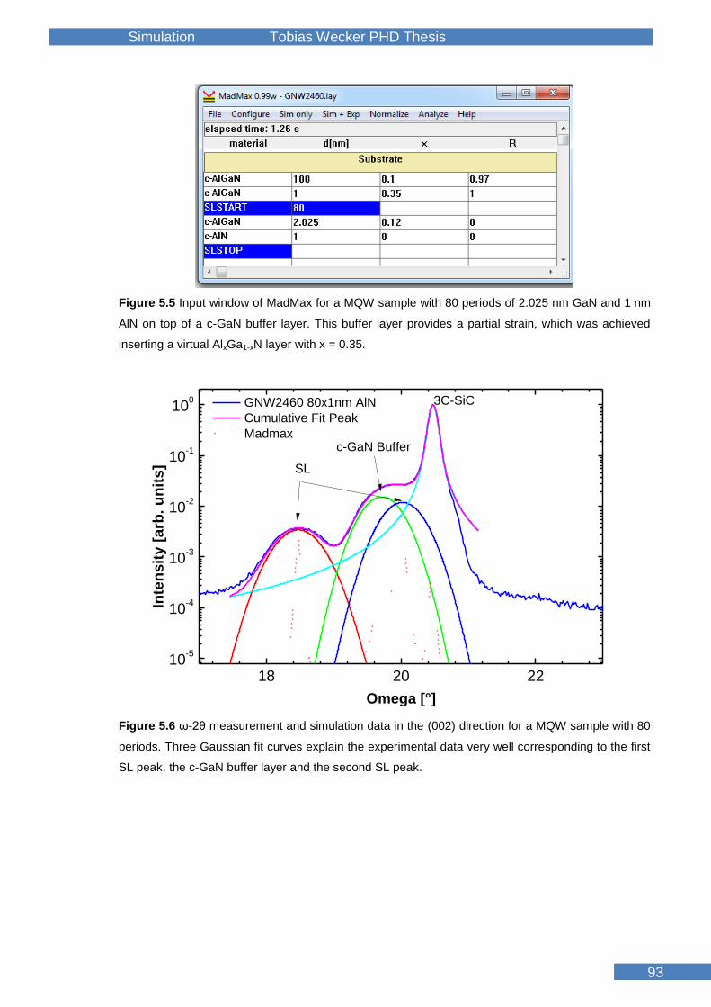
Simulation Tobias Wecker PHD Thesis
93
Figure 5.5 Input window of MadMax for a MQW sample with 80 periods of 2.025 nm GaN and 1 nm
AlN on top of a c-GaN buffer layer. This buffer layer provides a partial strain, which was achieved
inserting a virtual AlxGa1-xN layer with x = 0.35.
18 20 2210
-5
10-4
10-3
10-2
10-1
100 GNW2460 80x1nm AlN
Cumulative Fit Peak
Madmax
Inte
ns
ity
[a
rb.
un
its
]
Omega [°]
SL
c-GaN Buffer
3C-SiC
Figure 5.6 ω-2θ measurement and simulation data in the (002) direction for a MQW sample with 80
periods. Three Gaussian fit curves explain the experimental data very well corresponding to the first
SL peak, the c-GaN buffer layer and the second SL peak.
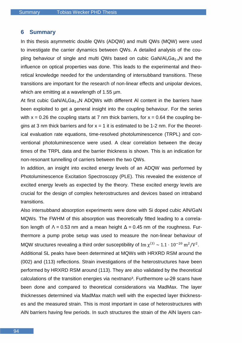
Summary Tobias Wecker PHD Thesis
Tobias Wecker
94
6 Summary
In this thesis asymmetric double QWs (ADQW) and multi QWs (MQW) were used
to investigate the carrier dynamics between QWs. A detailed analysis of the cou-
pling behaviour of single and multi QWs based on cubic GaN/AlxGa1-xN and the
influence on optical properties was done. This leads to the experimental and theo-
retical knowledge needed for the understanding of intersubband transitions. These
transitions are important for the research of non-linear effects and unipolar devices,
which are emitting at a wavelength of 1.55 µm.
At first cubic GaN/AlxGa1-xN ADQWs with different Al content in the barriers have
been exploited to get a general insight into the coupling behaviour. For the series
with x = 0.26 the coupling starts at 7 nm thick barriers, for x = 0.64 the coupling be-
gins at 3 nm thick barriers and for x = 1 it is estimated to be 1-2 nm. For the theoret-
ical evaluation rate equations, time-resolved photoluminescence (TRPL) and con-
ventional photoluminescence were used. A clear correlation between the decay
times of the TRPL data and the barrier thickness is shown. This is an indication for
non-resonant tunnelling of carriers between the two QWs.
In addition, an insight into excited energy levels of an ADQW was performed by
Photoluminescence Excitation Spectroscopy (PLE). This revealed the existence of
excited energy levels as expected by the theory. These excited energy levels are
crucial for the design of complex heterostructures and devices based on intraband
transitions.
Also intersubband absorption experiments were done with Si doped cubic AlN/GaN
MQWs. The FWHM of this absorption was theoretically fitted leading to a correla-
tion length of Λ = 0.53 nm and a mean height Δ = 0.45 nm of the roughness. Fur-
thermore a pump probe setup was used to measure the non-linear behaviour of
MQW structures revealing a third order susceptibility of Im χ(3) ~ 1.1 ⋅ 10−20 m2/V2.
Additional SL peaks have been determined at MQWs with HRXRD RSM around the
(002) and (113) reflections. Strain investigations of the heterostructures have been
performed by HRXRD RSM around (113). They are also validated by the theoretical
calculations of the transition energies via nextnano³. Furthermore ω-2θ scans have
been done and compared to theoretical considerations via MadMax. The layer
thicknesses determined via MadMax match well with the expected layer thickness-
es and the measured strain. This is most important in case of heterostructures with
AlN barriers having few periods. In such structures the strain of the AlN layers can-

Summary Tobias Wecker PHD Thesis
95
not be measured and the theory provided by nextnano³ and MadMax can be used
to get strain information. Besides, TEM measurements on the MQW structures
have been used to determine the real layer thickness. This thickness was used for
the transition energy calculation via nextnano³ and a comparison with the PL data
revealed a good agreement.
A systematic insight into heterostructures based on GaN/AlxGa1-xN was achieved.
Also the theoretical models needed for energy transitions (nextnano³), layer thick-
nesses and strain (MadMax) are compared to the experiments and revealed a good
agreement. In this process a set of parameters for cubic group III nitrides was im-
proved successively.
Furthermore GaN/AlxGa1-xN QWs have been investigated by picosecond acoustics
to get an insight into the influence of strain pulses on such heterostructures. This
revealed additional information about the strain behaviour, the interfaces and the
layer thicknesses. Raman and HRXRD experiments of thick GaN layers have been
compared to enable Raman as an additional measurement for the defect density
and the layer thickness also for very thin layers. Such thin layers are difficult to
measure with HRXRD. Besides Raman can achieve a much better spatial resolu-
tion compared with HRXRD.

Appendix Tobias Wecker PHD Thesis
Tobias Wecker
96
7 Appendix
7.1 Sample List
Sample GNW
Substrate Structure Remark Date
2345 UniPad 11-03
Novasic
GaN 500 nm 11.12.12
2346 GaN 460 nm 17.12.12
2347 GaN 470 nm 18.12.12
2348
11CO186 Novasic
GaN 380 nm 16.01.13
2349 GaN 150 nm 17.01.13
2350 GaN 74 nm 17.01.13
2351 GaN 180nm/AlGaN 180nm 𝑥 ≈ 0,3 21.01.13
2352 180nm/../170nm 𝑥 ≈ 0,3 22.01.13
2353 170nm/../170nm 𝑥 ≈ 0,2 23.01.13
2354 170nm/170nm 𝑥 ≈ 0,25 24.01.13
2355 50nm/15nm/30nm/15nm/30nm 𝑥 ≈ 0,25 28.01.13
2356 d=15nm, x=0,25 Series A 29.01.13
2357 d=5nm, x=0,26 Series A 30.01.13
2358 d=3,6nm, x=0,26 Series A 31.01.13
2359 d=10nm, x=0,26 Series A 04.02.13
2360 d=1nm, x=0,26 Series A 05.02.13
2361 d=15nm, x=0,19 Series B 06.02.13
2362 d=10nm, x=0,20 Series B 07.02.13
2363 d=5nm, x=0,20 Series B 11.02.13
2364 d=3nm, x=0,17 Series B 12.02.13
2365 d=1nm, x=0,20 Series B 13.02.13
2371 GaN
Optimization
27.03.13
2372 GaN AlGaN 28.03.13
2373 GaN AlGaN 23.04.13
2374 GaN 600 nm 24.04.13
2375 200nm GaN / 200nm AlGaN x=0,32 29.04.13
2376 200nm GaN / 200nm AlGaN x=0,27 30.04.13
2377 200nm GaN / 200nm AlGaN x=0,39 06.05.13
2378 200nm GaN / 200nm AlGaN x=0,62 08.05.13
2379 200nm GaN / 100nm AlGaN x=0,8 14.05.13
2380 d=15nm, x=0,21 Narrow QW below wide QW reabsorption?
15.05.13
2381 d=15nm, x=0,21 16.05.13
2382 d=3nm, x=0,37 Series C 21.05.13
2383 d=3nm, x=0,67 Series C/D 23.05.13
2384 d=3nm, x=0,8 Series C 27.05.13
2385 d=3nm, x=0,13 Series C 29.05.13
2386 d= 15nm, x=0,63 Series D 04.06.13
2387 d= 1nm, x=0,65 Series D 05.06.13
2388 d= 5nm, x=0,62 Series D 11.06.13
2389 d= 10nm, x=0,60 Series D 13.06.13
2417 Unipad 1102
-
Optimization
08.01.14
2418 - 09.01.14
2419 600 nm GaN 15.01.14

Appendix Tobias Wecker PHD Thesis
97
2420 - No Ga flashes in RHEED 21.01.14
2421 400 nm GaN 23.01.14
2422 400 nm GaN:Si Si 1040°C 27.01.14
2423 200nm GaN/ 200nm AlGaN x = 0,17 29.01.14
2424 550 nm GaN 13.02.14
2425 200 nm GaN/ 200 nm AlGaN x = 0,13 17.02.14
2426 100 nm/ 5 nm/ 1,8 nm/ 5 nm 19.02.14
2427 100 nm/ 5 nm/ 1,8 nm/ 5 nm 21.02.14
2428 100 nm/ 5 nm/ 1,35 nm/ 5 nm 24.02.14
2429 - Optimization
19.03.14
2430 - 20.03.14
2431 600 nm GaN Leo 26.03.14
2432 200 nm GaN/ 75 AlGaN x =0,15 Leo 27.03.14
2440 100 nm / 5nm / 1,35/5 / 0,675/ 5 AlN Leo 06.05.14
2441
Unipad 1102
100 nm/ 10 nm/ 10 nm/ 10 nm X =0,3 07.05.14
2442 100 nm/ 30 nm/ 10 nm/ 30 nm X =0,3 07.05.14
2443 100 nm/ 30 nm / 10 nm/ 30 nm AlN 08.05.14
2444 100 nm / 15nm / 1,35/15 / 0,675/
15 AlN Leo 09.05.14
2445 1 µm GaN Leo 12.05.14
2446 100 nm/ 50 nm / 10 nm/ 50 nm X = 0,1 13.05.14
2447 100 nm/ 50 nm / 10 nm/ 50 nm X = 0,6 14.05.14
2448 100 nm/ 50 nm / 10 nm/ 50 nm X = 0,8 14.05.14
2449 1 µm GaN: Si Si 1100 °C Leo 15.05.14
2450 100 nm/ 50 nm X = 0,3 16.05.14
2451 100nm/ 17x Multi DQWs without step 1,35 nm/0,45 nm Leo 19.05.14
2452 100 nm/ 20x Multi DQWs without step 1,35 nm/0,45 nm Leo 20.05.14
2453 100 nm/ 100 nm X =0,3 21.05.14
2454 100 nm/ 50 nm / 10 nm/ 50 nm X =0,3 21.05.14
2455 100 nm (Si)/ 30 nm/ 20x Multi DQWs/ 30 nm/ 100 nm (Si)
without step 1,8 nm/0,45 nm Leo 22.05.14
2456 100 nm/ 50 nm / 10 nm/ 50 nm X =0,2 23.05.14
2457 100 nm (Si)/ 30 nm/ 20x Multi
QWs/ 30 nm/ 100 nm (Si) without step 1,8 nm Leo 26.05.14
2458 Unipad 1102
100 nm/ 50 nm / 10 nm/ 50 nm X =0,5 28.05.14
2459 100 nm/ 50 nm / 5 nm/ 50 nm X = 0,3 02.06.14
2460 100 nm / 80x Multi QWs 1,8 nm doped (Si 1080°C) 04.06.14
2461
11CO192
HEMT Single Channel no BB Last AlN 3 nm, x=0,7 05.06.14
2462 HEMT Single Channel no BB No Isolation 11.06.14
2463 HEMT Single Channel no BB Last AlN 6nm, x=0,3 18.06.14
2464 HEMT Single Channel no BB AlN 6nm, x=0,3, different spacer 24.06.14
2465 HEMT Single Channel BB last AlN 6 nm 25.06.14
2466 HEMT Double Channel no BB last AlN 6 nm 07.02.14
2467 HEMT Double Channel BB last AlN 6 nm
Wrong Ga temperature 03.02.14
2468 Growth stopped Leo 08.07.14
2469 Growth stopped Leo 08.07.14
2470 100 nm (Si)/ 30 nm/ 20x Multi
QWs/ 30 nm/ 100 nm (Si) with step 0,45nm / 0,45 nm/0,45
nm 09.07.14

Appendix Tobias Wecker PHD Thesis
Tobias Wecker
98
2486 UniPad1102
100 nm/ 80*MQW 1,8nm GaN/ 1 nm AlN 24.09.14
2487 100 nm/ 80*MQW Temperature
rampe 1,8nm GaN/ 1 nm AlN 25.09.14
2488
11CO186
-
Optimization
29.10.14
2489 - 04.11.14
2490 - 05.11.14
2491 - 11.11.14
2492 - 12.11.14
2542
UniPad10-04
-
Optimization
14.07.15
2543 600 nm GaN 15.07.15
2544 - 13.08.15
2545 - 19.08.15
2548 - 24.08.15
2549 AlN optimised 25.08.15
2550 GaN hexagonal 28.08.15
2551 GaN
Optimization
01.09.15
2552 GaN/ AlGaN 02.09.15
2553 GaN/ AlGaN 03.09.15
2554 GaN/AlGaN Ga 920°C 08.09.15
2556 GaN/AlGaN Ga 927°C 10.09.15
2557
Unipad 1101
GaN/AlGaN Ga 926°C 11.09.15
2559 GaN 321 nm Ga 926°C 15.09.15
2560 GaN 351 nm Ga 924°C 16.09.15
2561 GaN 331 nm Ga 922°C, Hexagonal 23.09.15
2562 GaN 292 nm Ga 928°C 24.09.15
2564 GaN 323 nm Ga 930°C 28.09.15
2565
14CO 051
GaN 326 nm 01.10.15
2566 100 nm/ 3 nm AlN/ 1.8 nm/ 3 nm
AlN 05.10.15
2567 100 nm/ 3 nm AlN /1.8 nm QW:Si/
3 nm AlN No RHEED after AlN 06.10.15
2568 100 nm/ 3 nm AlN/ 1.8 nm/ 3 nm
AlN No RHEED after AlN 08.10.15
2569 100 nm/ 3 nm AlN/ 1.8 nm/ 3 nm
AlN 09.10.15
2570 100 nm/ 3 nm AlN /1.8 nm QW:Ge/
3 nm AlN Hexagonal 13.10.15
2571 1h 17 min GaN No RHEED at the end 14.10.15
2572 5 h GaN 14.10.15
2573 100 nm/ 3 nm AlN /1.6 nm QW:Si/
3 nm AlN 15.10.15
2574 100 nm/ MQW Shutter didn’t work 19.10.15
2588 1h GaN 05.01.16
2589 31min GaN 06.01.16
2590 GaN AlGaN 07.01.16
2591 510nm GaN 11.01.16
2594 14CO-051
GaN QW/ 3nm AlN 18.01.16
2597 GaN QW/ 3nm AlN 20.01.16
2599 GaN QW Si/ 3nm AlN 22.01.16

Appendix Tobias Wecker PHD Thesis
99
2600 582 nm GaN:Si 4x10^19 cm^-3 26.01.16
2603
14CO146
MQW 12x Hexagonal, growth stopped 03.02.16
2604 MQW 20x 1,8nm/3nm 04.01.16
2608 MQW 20x 1,8nm/5nm Hexagonal 15.01.16
2610 MQW 20x 1,8nm/8nm Bad quality 17.01.16
2612 MQW 5x 1,8nm/5nm Delta doping 24.01.16
2613 MQW 20x 1,8nm/5nm Delta doping 25.01.16
2614 4h30min GaN 29.01.16
2618 100 nm GaN/ AlGaN Optimization 21.03.16
2619 100 nm GaN/ AlGaN Optimization 22.03.16
2649 MQW 10x1,8nm/5nm GaN:Si 23.03.16
2650 MQW 20x1,8/5 24.03.16
2651 MQW 5x 28.03.16
2652 MQW 20x AlN:Si 30.03.16
2653 MQW 20x AlN:Si(delta) 05.07.16
2654 MQW 20x AlN:Si(delta) 06.07.16
2655 MQW 20x GaN:Si(delta) edge of QW 12.07.16
2656 14CO-146 MQW 20x GaN:Si(delta) middle of QW 14.07.16
2665
14C0-133
Optimization 28.09.16
2666 Optimization 29.09.16
2667 20x1,8nm/5nm Si 1000°C 05.10.16
2668 MQW 20x Si 940°C 06.10.16
2675 14CO050
MQW 40x1,8nm/1nm Si 940°C 08.11.16
2678 MQW 45x Si Shutter didn’t work 10.11.16
2684 14CO-144
MQW 40x 18.11.16
2687 MQW 40x Rotation during QW growth 23.11.16
2693
14CO-144
MQW 40x 3nm AlN 30.11.16
2694 MQW 40x GaN:Si(delta) 01.12.16
2698 MQW 40x GaN:Si 2 nm AlN Bad in RHEED 08.12.16
2699 MQW 40x GaN:Si 2 nm AlN 09.12.16
2729
14CO050
MQW 60x GaN:Si 940°C 08.03.17
2730 MQW 40x GaN:Si 1000°C 15.03.17
2731 MQW 40x GaN:Si 970°C 16.03.17
2732 MQW 50x GaN:Si 940°C 17.03.17
2748 14CO-144 SQW 1,238 nm 03.05.17
2749 14CO050 DQW 40x Al shutter didn’t work 04.05.17

Appendix Tobias Wecker PHD Thesis
Tobias Wecker
100
7.2 Literature
[1] N. Suzuki and N. Iizuka, Japanese Journal of Applied Physics 37, 369 (1998).
[2] C. Gmachl, S. V. Frolov, H. M. Ng, S. N. G Chu and A. Y. Cho, Electronics Letters 37, 178 (2001).
[3] J. D. Heber, C. Gmachl, H. M. Ng and A. Y. Cho, Appl. Phys. Lett. 81, 1237 (2002).
[4] N. Iizuka, K. Kaneko and N. Suzuki, Electronics Letters 40, 962 (2004).
[5] J. Hamazaki, S. Matsui, H. Kunugita, K. Ema, H. Kanazawa, T. Tachibana, A. Kiku-chi and K. Kishino, Appl. Phys. Lett. 84, 1102 (2004).
[6] H. Machhadani, M. Tchernycheva, L. Rigutti, S. Saki, R. Colombelli, C. Mietze, D.J. As, F.H. Julien, Phys. Rev. B 83 (2011) 075313.
[7] C. Gmachl and H.M. Ng, Electron. Lett. 39, 567 (2003).
[8] E.A. DeCuir, E. Fred, M.O. Manasreh, J. Schörmann, D.J. As and K. Lischka, Appl. Phys. Lett. 91, 041991 (2007).
[9] C. Mietze, M. Landmann, E. Rauls, H. Machhadani, S. Sakr, M. Tchernycheva, F. H. Julien, W. G. Schmidt, K. Lischka, and D. J. As, Phys. Rev. B 83, 195301 (2011).
[10] T. Jostmeier, T. Wecker, D. Reuter, D. J. As, and M. Betz, Appl. Phys. Lett. 107, 211101 (2015)
[11] T. Wecker, T. Jostmeier, T. Rieger, E. Neumannn, A. Pawlis, M. Betz, D. Reuter, D.J. As, J. Crystal Growth (2016) in press
[12] T. Wecker, F. Hörich, M. Feneberg, R. Goldhahn, D. Reuter, and D. J. As, Phys. Status Solidi B 252, 873 (2015).
[13] T. Wecker, G. Callsen, A. Hoffmann, D. Reuter and D. J. As, Jpn. J. Appl. Phys. 55, 05FG01 (2016)
[14] T. Wecker, G. Callsen, A. Hoffmann, D. Reuter, and D. J. As, submitted
[15] M. Beeler, E. Trichas and E. Monroy, Semicond. Sci. Technol. 28, 074022 (2013).
[16] M. Beeler, C. Bougerol, E. Bellet-Amalaric, and E. Monroy, Phys. Status Solidi (a) 211, No. 4, 761–764 (2014).
[17] F. Scholz, Semicond. Sci. Technol. 27, 024002 (2012).
[18] D.J. As and C. Mietze, Phys. Status Solidi (a) 210, 474 (2013).
[19] C. Mietze, M. Bürger, S. Sakr, M. Thernycheva, F.H. Julien, and D.J. As, Phys. Status Solidi (a) 210, 455 (2013).
[20] L. Pavesi, M. Guzzi, J. Appl. Phys. 75, 4779 (1994)
[21] H. Mathieu, P. Lefebvre, P. Christol, Phys. Rev. B, Vol 46, Nr 7 (1992)
[22] M. Feneberg, M. Röppischer, C. Cobet, N. Esser, J. Schörmann, T. Schupp, D. J. As, F. Hörich, J. Bläsing, A. Krost, and R. Goldhahn, Phys. Rev. B 85, 155207 (2012)
[23] John H. Davies, „The Physics of low- dimensional semiconductors“, Cambridge University Press (1998)
[24] T. Tada, A. Yamaguchi, T. Ninomiya, H. Uchiki, T.Kobayashi, and T. Yao, J. Appl. Phys. 63, 5491 (1988).
[25] R. Sauer, K. Thonke, and W. T. Tsang, Phys. Rev. Lett. 61, 609 (1988).
[26] S. L. Chuang, Physics of photonic devices, second edition, Wiley Verlag, 2009 S.384 372 365
[27] O. Gauthier-Lafayea, et al., Physica E 7 (2000) 12-9
Appendix Tobias Wecker PHD Thesis
101
[28] J. Faist, F. Capasso, D. L. Sivco, C. Sirtori, A. L. Hutchinson, A. Y. Cho, Science Vol. 264 (1994)
[29] M. Rüsing, T. Wecker, G. Berth, D.J. As, and A. Zrenner, Phys. Stat. Sol. (b) 253, 778 (2016)
[30] H. Harima, J. Phys.: Condens. Matter 14, R967–R993 (2002).
[31] M. Landmann, E. Rauls, and W. G. Schmidt, Phys. Rev.B 00, 005300 (2017)
[32] E. Tschumak, PhD Thesis, University of Paderborn (2010)
[33] P. Gay, P.B. Hirsch, and A.Kelley, Acta Metall. 1, 315 (1953).
[34] D. Hull and D. Bacon, Introduction to Dislocation (Butterworth-Heinemann, Oxford, 2011).
[35] T. Schupp, unpublished
[36] K. Kim, W. R. L. Lambrecht, and B. Segall, Phys. Rev. B 52(24), 16310–16326 (1996).
[37] J. Stangl et. al., Physik Journal 3 (2004) 6, S. 33
[38] V. Holý, U. Pietsch, T. Baumbach, “High-Resolution X-Ray Scattering from Thin Films and Multilayers”, Springer-Verlag, Berlin Heidelberg New York (1999)
[39] V. Wiedemeier, G. Berth, A. Zrenner, E. M. Larramendi, U. Woggon, K. Lischka, and D. Schikora, Semicond. Sci. Technol. 26, 105023 (2011).
[40] G. Berth,W. Hahn, V.Wiedemeier, A. Zrenner, S. Sanna, and W. G. Schmidt, Fer-roelectrics 420(1), 44–48 (2011).
[41] C. Thomsen, H. T. Grahn, H. J. Maris, and J. Tauc, Opt. Commun. 60, 55 (1986).
[42] B. C. Daly, K. Kang, Y. Wang, and D. G. Cahill, Phys. Rev. B 80, 174112 (2009).
[43] T. Czerniuk, T. Ehrlich, T. Wecker, D.J. As, D.R. Yakovlev, A.V. Akimov, M. Bayer: Phys. Rev. Appl. 7, 014006 (2017)
[44] P. Y. Yu and M. Cardona, Fundamentals of Semiconductors, 3rd edition (Springer, Berlin, Heidelberg, New York, 2005).
[45] D. Gardiner,H. Bowley, P. Graves, D. Gerrard, J. Louden, and G. Turrell, Practical Raman Spectroscopy (Springer, Berlin, Heidelberg, 2012).
[46] T. Frey, D. J. As, M. Bartels, A. Pawlis, K. Lischka, A. Tabata, J. R. L. Fernandez, M. T. O. Silva, J. R. Leite, C. Haug, and R. Brenn, J. Appl. Phys. 89, 2631 (2001).
[47] H. Morkoc, Handbook of Nitiride Semiconductors and Devices (Wiley-VCH, Wein-heim, 2008).
[48] R. H. Lyddane, R. G. Sachs, and E. Teller, Phys. Rev. 59, 673–676 (1941).
[49] Y. A. Pusep, M. T. O. Silva, J. R. L. Fernandez, V. A. Chitta, J. R. Leite, T. Frey, D. J. As, D. Schikora, and K. Lischka, J. Appl. Phys. 91, 6197 (2002).
[50] T. Kozawa, T. Kachi, H. Kano, Y. Taga, M. Hashimoto, N. Koide, and K. Manabe, J. Appl. Phys. 75, 1098 (1994).
[51] H. Harima, S. Nakashima, and T. Uemura, J. Appl. Phys. 78, 1996 (1995).
[52] E. Martinez-Guerrero, E. Bellet-Amalric, L. Martinet, G. Feuillet, B. Daudin, H. Mari-ette, P. Holliger, C. Dubois, C. Bru-Chevallier, P. Aboughe Nze, T. Chassagne, G. Ferro, and Y. Montei, J. Appl. Phys. 91, 4983 (2002).
[53] A. Trampert, O. Brandt, H. Yang, and K. H. Ploog, Appl. Phys. Lett. 70, 583 (1997).
[54] H. Okumura, K. Ohta, G. Feuillet, K. Balakrishnan, S. Chichibu, H. Hamaguchi, P. Hacke, and S. Yoshida, J. Cryst. Growth 178, 113–133 (1997).
[55] D. Wang, Y. Hiroyama, M. Tamura, M. Ichikawa, and S. Yoshida, J. Cryst. Growth 220, 204–208 (2000).

Appendix Tobias Wecker PHD Thesis
Tobias Wecker
102
[56] H. Yang, O. Brandt, and K. Ploog, J. Electron. Mater. 25(5), 787 (1996).
[57] B. Daudin, G. Feuillet, J. Hbner, Y. Samson, F. Widmann, A. Philippe, C. Bru-Chevallier, G. Guillot, E. Bustarret, G. Bentoumi, and A. Deneuville, J. Appl. Phys. 84, 2295 (1998).
[58] H. Yang, L. X. Zheng, J. B. Li, X. J. Wang, D. P. Xu, Y. T. Wang, X. W. Hu, and P. D. Han, Appl. Phys. Lett. 74, 2498 (1999).
[59] D. J. As, Proc. SPIE 7608, 76080G (2010).
[60] J. Schörmann, S. Potthast, D. J. As, and K. Lischka, Appl. Phys. Lett. 90, 041918 (2007).
[61] C. Hänel and G. Gauglitz, Anal. Bioanal. Chem. 372, 91–100 (2002).
[62] H. Siegle, L. Eckey, A. Hoffmann, C. Thomsen, B. Meyer, D. Schikora, M. Hankeln, and K. Lischka, Solid State Commun. 96(12), 943–949 (1995).
[63] O. Matsuda, M. C. Larciprete, R. L. Voti, and O. B. Wright, Ultrasonics 56, 3 (2015).
[64] P. Babilotte, P. Ruello, D. Mounier, T. Pezeril, G. Vaudel, M. Edely, J.-M. Breteau, V. Gusev, and K. Blary, Phys. Rev. B 81, 245207 (2010).
[65] O. Matsuda, T. Tachizaki, T. Fukui, J. J. Baumberg, and O. B. Wright, Phys. Rev. B 71, 115330 (2005).
[66] A. V. Akimov, A. V. Scherbakov, D. R. Yakovlev, C. T. Foxon, and M. Bayer, Phys. Rev. Lett. 97, 037401 (2006).
[67] D. Moss, A. V. Akimov, R. P. Campion, M. Henini, C. T. Foxon, L. Eaves, A. J. Kent, and B. A. Glavin, Phys. Rev. B 83, 245303 (2011).
[68] C.-K. Sun, J.-C. Liang, and X.-Y. Yu, Phys. Rev. Lett. 84, 179 (2000).
[69] D. Moss, A. V. Akimov, S. V. Novikov, R. P. Campion, C. R. Staddon, N. Zainal, C. T. Foxon, and A. J. Kent, J. Phys. D 42, 115412 (2009).
[70] Chuan He, Martin Grossmann, Delia Brick, Martin Schubert, Sergei V. Novikov, C. Thomas Foxon, Vitalyi Gusev, Anthony J. Kent, and Thomas Dekorsy, Appl. Phys. Lett. 107, 112105 (2015).
[71] K.-H. Lin, C.-M. Lai, C.-C. Pan, J.-I. Chyi, J.-W. Shi, S.-Z. Sun, C.-F. Chang, and C.-K. Sun, Nat. Nanotechnol. 2, 704 (2007).
[72] D. M. Moss, A. V. Akimov, B. A. Glavin, M. Henini, and A. J. Kent, Phys. Rev. Lett. 106, 066602 (2011).
[73] T. Czerniuk, PhD Thesis, TU Dortmund (2017)
[74] C. Thomsen, H. T. Grahn, H. J. Maris, and J. Tauc, Phys. Rev. B 34, 4129 (1986).
[75] D. Bouguenna, A. Boudghene Stambouli, N. Mekkakia Maaza, A. Zado, and D.J. As, Superlattices and Microstructures 62, 260 (2013)
[76] M. Birkholz, "Thin Film Analysis by X-Ray Scattering", Wiley-VCH Verlag (2006)
[77] M. Landmann, E. Rauls, W. G. Schmidt, M. Röppischer, C. Cobet, N. Esser, T. Schupp, D. J. As, M. Feneberg, and R. Goldhahn, Phys. Rev. B 87, 195210 (2013).
[78] D.V. O'Connor, W. R. Ware, and J. C. Andre, J Phys Chem 83, 1333–1343 (1979).
[79] D. Y. Oberli, Jagdeep Shah, T.C. Damen, J. M. Kuo, J. E. Henry, Jenifer Lary and Stephen M. Goodnick, Appl. Phys. Lett. 56 (13) (1990).
[80] H. W. Liu, R. Ferreira, G. Bastard, C. Delalande, J. F. Palmier, and B. Etienne, Appl. Phys. Lett. 54, 2082 (1989).
[81] R. Ferreira, P. Rolland, P. Roussignol, C. Delalade, A. Vinattieri, L. Carraresi, M. Colocci, N. Roy, B.Sermage, J. F. Palmier, B. Etienne, Phys. Rev. B, 45 (20) (1992).
[82] F. C. Michl, R. Winkler and U. Rössler, Solid State Communications, Vol. 99, No. 1, pp. 13-18 (1996).

Appendix Tobias Wecker PHD Thesis
103
[83] M. Nido, M.G.W. Alexander, K. Reimann, K. Ploog, W.W. Rühle, Surface Science 229, 195-198 (1990).
[84] S. Haacke, N. T. Pelekanos, H. Mariette, M. Zigone, A.P. Heberle, and W.W. Rühle, Phys. Rev. B. 47, 24 (1993).
[85] Mee-Yi Ryu, Phil Won Yu, Eun-joo Shin, Joo In Lee, Sung Kyu Yu, Eun Soon Oh, Yong Jo Park, Hyeong Soo Park, and Tae Ill Kim, Journal of the Korean Physical Society, Vol. 37, No. 4 (2000).
[86] Eun-joo Shin, N. W. Song, J. I. Lee, D. Kim, M. Y. Ryu, P. W. Yu, D. Lee, Y.-H- Choi, C.-H. Hong, Journal of the Korean Physical Society, Vol. 34 (1990).
[87] E. O. Kane, J. Phys. Chem. Solids 1, 249 (1957).
[88] C. Wetzel, R. Winkler, M. Drechsler, B. K. Meyer, U. Rössler, J. Scriba, J. P. Kotthaus, V. Härle, and F. Scholz, Phys. Rev. B 53, 1038 (1996).
[89] P. Rinke, M. Winkelnkemper, A. Qteish, D. Bimberg, J. Neugebauer, and M. Scheffler, Phys. Rev. B 77, 075202 (2008).
[90] M. Röppischer, Dissertation, Fakultät für Mathematik und Naturwissenschaften, TU Berlin, Berlin (2011).
[91] M. Luysberg, M. Heggen, K. Tillmann, JLSRF 2 (2016) 138.
[92] M. Tchernycheva, L. Nevou, L. Doyennette, F.H. Julien, E. Warde, F. Guillot, E. Monroy, E. Bellet-Amalric, T. Remmele, M. Albrecht, Phys. Rev. B 73 (2006) 125347.
[93] A. Helman, M. Tchernycheva, A. Lusson, E. Warde, F.H. Julien, Kh Moumanis, G. Fishman, E. Monroy, B. Daudin, D. Le Si Dang, E. Bellet-Amalric, D. Jalabert, Appl. Phys. Lett. 83 (2003) 5196.
[94] X.Y. Liu, P. Holmstrm, P. Jnes, L. Thyln, T.G. Andersson, Phys. Status Solidi (a) 244 (2007) 2892.
[95] T. Unuma, M. Yoshita, T. Noda, H. Sakaki, H. Akiyama, J. Appl. Phys., Vol. 93, No 3 (2003)
[96] L. C. de Carvalho, A. Schleife, F. Bechstedt, Phys. Rev. B 84, 195105 (2011).
[97] M.P.C.M. Krijn, Sci. Technol. 6, 27 (1991)
[98] MadMax (c) 2001-2005 Oliver Brandt, Patrick Waltereit, Martin Kästner, and Daniel Schaadt.
[99] V. Cimalla, J. Pezoldt, and O. Ambacher, „Group III nitride and SiC based MEMS and NEMS: materials properties, technology and appli-cations“, J. Phys. D: Appl. Phys. 40, 6386(2007).
[100] T. Schupp, K. Lischka, and D.J. As, J. Crystal Growth 312, 1500 (2010)
[101] D. Windisch and P. Beckers, phys. stat. sol. (a) 118, 379 (1990)
[102] In h-AlN the difference in the energy gap from 0 K to 300 K is about 67 meV [106][107]. A similar value for c-AlN is assumed leading to Egap, 0K =Egap, 300K + 67 meV.
[103] M. Röppischer, R. Goldhahn, G. Rossbach, P. Schley, C. Cobet, N. Esser, T. Schupp, K. Lischka, and D.J. As, J.Appl. Phys. 106, 076104 (2009)
[104] A. F. Wright, J. Appl. Phys. 82, 2833 (1997)
[105] C. G. V. de Walle and J. Neugebauer, Appl. Phys. Lett. 70, 2577 (1997).
[106] M. Feneberg, M. F. Romero, M. Röppischer, C. Cobet, N. Esser, B. Neuschl, K. Thonke, M. Bickermann, and R. Goldhahn, Phys. Rev. B 87, 235209 (2013)
[107] I. Vurgaftman and J.R. Meyer, J. Appl. Phys. 94, 3675 (2003).
[108] P. Schley, R. Goldhahn, C. Napierala, G. Gobsch, J. Schörmann, D. J. As, K. Lisch-ka, M. Feneberg and K. Thonke, Semicond. Sci. Technol. 23, 055001 (2008)

Appendix Tobias Wecker PHD Thesis
Tobias Wecker
104
7.3 Abbildungsverzeichnis
Figure 2.1 Excitonic binding energies for excitons consisting of e-hh and e-lh. The dotted lines correspond to complex simulations and the straight lines are calculated by the fractal dimensional method. In the left side the Al content in the barriers is 15% and on the right 30% [21]. ................................................................................................................ 11
Figure 2.2 For real QWs the wave functions of the carriers penetrate into the barrier. Furthermore the allowed transitions follow the selection rule Δninter = 0,2,4,6..... ............................. 13
Figure 2.3 Scheme of the conduction band of an ADQW. The important parameters for tunnelling are the barrier height V and the barrier thickness d. ...................................................... 13
Figure 2.4 Band diagram of an ADQW with a thin barrier. The Fermi energy EF is slightly above the first electron level caused by doping. ............................................................................. 16
Figure 2.5 Sketch of a waveguide used for absorption measurements. Multiple passes through the MQWs are achieved by total reflection. The layer thicknesses are not to scale. .......... 17
Figure 2.6 Trend of the band offsets for a GaN/AlxGa1-xN interface partially strained on a c-GaN buffer layer for various Al concentrations in the AlxGa1-xN barrier layers. (Provided by Marc Landman in University of Paderborn) ................................................................... 19
Figure 2.7 Bandgap of relaxed cubic 𝐴𝑙𝑥𝐺𝑎1 − 𝑥𝑁 for different Al content. There is a change from
direct 𝛤𝑉 − 𝛤𝐶 (red) to indirect bandgap 𝛤𝑉 − 𝑋𝐶 (blue) at 𝑥 = 0.71 [77]. ................ 20
Figure 3.1 Schematic picture of the used Riber 32 PA-MBE [32]...................................................... 21
Figure 3.2 Representation of the basic principle of the RHEED measurement. Also the geometries of the different beams in regard to the sample can be seen. ......................................... 22
Figure 3.3 Sketch of the UV PL setup. The excitation light is focused on the sample placed in a cryostat reaching 13 K. The detection is done by a monochromator with photomultiplier and CCD attached. ......................................................................................................... 23
Figure 3.4 Illustration of the complex optical setup. With this setup PL, PLE and TRPL measurements can be done. (AG Hoffmann TU Berlin) ................................................ 24
Figure 3.5 The important optical components in the HRXRD setup are the Cu source and a four crystal monochromator which filters the Kα1 line. The detection is accomplished with a CCD array. ..................................................................................................................... 26
Figure 3.6 Schematic overview of the diffraction spots in reciprocal space. The excitation is done with an angle of ω and the detection angle is 2θ [37]. ................................................... 26
Figure 3.7 Visualization of the (113) plain important for strain measurements. ................................ 28
Figure 3.8 Sketch of the absorption setup used for the IR absorption measurements. (AG Betz TU Dortmund) ...................................................................................................................... 29
Figure 3.9 Sketch of the μ-Raman setup. The sample is excited with a Nd:YAG CW laser (532 nm). The detection is done by a holographic grating spectrometer with an applied CCD camera. (AG Zrenner Paderborn) .................................................................................. 30
Figure 3.10 Sketch of the pump probe setup for measuring picosecond acoustics. (AG Bayer TU Dortmund) ...................................................................................................................... 31
Figure 3.11 Sketch of the pump probe setup for measuring intraband non-linearity. (AG Betz TU Dortmund) ...................................................................................................................... 32
Appendix Tobias Wecker PHD Thesis
105
Figure 4.1 Omega profile of the thickest sample GNW2345 (505 nm) and the thinnest sample GNW2350 (75 nm). A clear decrease of the FWHM for the 505 nm thick sample can be seen. ...............................................................................................................................35
Figure 4.2 A comparison of Raman spectra of a 3C-SiC/Si substrate piece (dashed) and a thick c-GaN layer (red) reveals two additional peaks (marked in red). These peaks are attributed to the TO and LO mode of c-GaN. (Measured in University of Paderborn by Michael Rüsing) ..............................................................................................................36
Figure 4.3 Raman spectroscopy enables another way to measure the thickness of layers. A linear correlation between the integrated intensity, given by the area underneath the LO Raman line A, of the LO mode and the layer thickness of c-GaN bulk layers can be seen. (Evaluation done together with Michael Rüsing) ..................................................37
Figure 4.4 A linear correlation between the dislocation density D via HRXRD and Raman FWHM 𝜟𝝂 is found. These data can be used as a calibration to determine the dislocation density with Raman only. (Evaluation done together with Michael Rüsing) ...............................38
Figure 4.5 Single QW structure consisting of a 10 nm thick c-GaN QW and 35 nm thick c- AlxGa1-xN barriers. Two samples are investigated with different Al content of 0.1 (GNW2446) and 0.8 (GNW2448). ..............................................................................................................40
Figure 4.6 PL spectra for the reference c-GaN sample (GNW2424) and the QW structure with Al0.8Ga0.2N (GNW2448) at low temperature. The excitation was done with a Nd:YAG laser emitting at 266 nm with 5 mW. (Measured in University Paderborn by me) .........40
Figure 4.7 Measured acoustic signal (dashed lines) and simulated signal (straight lines) for the sample with x = 0.8 (GNW2248) for three different probe wavelengths. The pump power was increased from W0 (left) to 4W0 (right). The parameter β represents the ratio of the photo elastic coupling efficiency of the QW over the one of the bulk layer. (Measured in TU Dortmund by Thomas Czerniuk) [73] ........................................................................42
Figure 4.8 Sample structure of the two ADQW series. The barrier thickness d was varied from 1 nm to 15 nm. In series 0.26 (left) the Al content is x = 0.26 ± 0.03 and for series 0.64 (right) the Al content is x = 0.64 ± 0.03. ....................................................................................44
Figure 4.9 RSM of the (113) reflection of two cubic GaN/AlxGa1-xN ADQW with d = 15 nm of the two different series. A partial strain of the barriers is visible in both measurements. (Left) An Al content of x = 0.25 ± 0.03 is determined. (Right) The Al content is x = 0.62 ± 0.03. 45
Figure 4.10 Low temperature PL spectrum of the cubic GaN/Al0.26Ga0.74N ADQW with d = 15 nm excited with a Nd:YAG laser (266 nm). ..........................................................................46
Figure 4.11 Semi-logarithmic plot of the low temperature (7 K) PL spectra of the cubic GaN/ AlxGa1-
xN ADQWs with x = 0.26 (left) and x = 0.64 (right). Three emission bands are visible for the wide QW (QWW), the narrow QW (QWN) and the AlxGa1-xN barriers. The emission intensity of the narrow QW can be correlated to the barrier thickness d. (right: measured in TU Berlin together with Gordon Callsen) ...................................................47
Figure 4.12 Intensity ratio IN/IW as a function of barrier thickness d for series 0.26 (left) and series 0.64 (right). The calculated curves for electrons (e) (blue line) and heavy holes (hh) (red line) follow the same trend as the measured ratios (dots). (Evaluation done by me) ....48
Figure 4.13 Simulated conduction band of the cubic GaN/AlxGa1-xN ADQW with x = 0.26 and a barrier thickness d = 1 nm (left) and d = 5 nm (right) at 13 K. ........................................50
Figure 4.14 Valence bands as simulated by nextnano³ of the heavy holes (hh, blue) and light holes (lh, red) in case of the cubic GaN/AlxGa1-xN ADQW with x = 0.26 and a barrier thickness d = 1 nm (left) and d = 5 nm (right) at 13 K. For clarity only the probability distribution
𝜳𝟐 for the hh is plotted. ..................................................................................................51

Appendix Tobias Wecker PHD Thesis
Tobias Wecker
106
Figure 4.15 Simulated energy levels for electrons (e), heavy holes (hh) and light holes (lh) of a single c-GaN QW with AlxGa1-xN barriers (x = 0.26) partly strained on c-GaN buffer at 13 K. ............................................................................................................................... 52
Figure 4.16 Transition energies of the 3 electron levels with the 3 heavy hole levels for the SQW with c-GaN QW and AlxGa1-xN barriers (x = 0.26). ........................................................ 52
Figure 4.17 Simulated energy levels for electrons (e), heavy holes (hh) and light holes (lh) of a single c-GaN QW with AlxGa1-xN barriers (x = 0.64) partly strained on c-GaN buffer at 13 K. ............................................................................................................................... 53
Figure 4.18 Transition energies of the 3 electron levels with the 3 heavy hole levels for the SQW with c-GaN QW and AlxGa1-xN barriers (x = 0.64). ........................................................ 53
Figure 4.19 Time transients for the ADQW of series 0.64 with the thickest barrier d = 15 nm measured at the QWW (2.5 nm) emission at 7 K. A bi-exponential fit was used with a convolution approach to match the data. (measured in TU Berlin together with Gordon Callsen) .......................................................................................................................... 55
Figure 4.20 Time transients for the 3 ADQW samples of series 0.64 measured at the QWW (2.5 nm, left) emission and at the QWN (1.35 nm, right) emission for the three samples with different barrier thickness d. (measured in TU Berlin together with Gordon Callsen) ... 56
Figure 4.21 Decay time τfast of the QWN (black) and QWW (blue) emission corresponding to the barrier thickness d for low temperatures (7 K). The decay time increases for the wide QW due to additional electrons of the narrow QW for thinner barriers. The opposite behaviour takes place for the narrow QW. (evaluation done by me) ............................. 57
Figure 4.22 Sample structure of the cubic GaN/Al0.25Ga0.75N ADQW. The barrier thickness between the two QWs is 15 nm, thus the wells are uncoupled. ................................................... 58
Figure 4.25 (a) Semi-logarithmic plot of the low temperature photoluminescence (PL) spectrum of the cubic GaN/Al0.25Ga0.75N ADQW at a temperature (T) of 7 K. The depicted rectangles illustrate the applied spectral window for the detection of the PLE measurements. (b) Furthermore, photoluminescence excitation (PLE) data for three different detection wavelengths with T = 7 K are shown, which correspond to the emission maxima of the PL spectrum (red for the QWW, green for the QWN, blue for the Al0.25Ga0.75N barrier). (measured in TU Berlin together with Gordon Callsen) ................................................. 59
Figure 4.26 Detailed, semi-logarithmic plot of the low temperature photoluminescence excitation (PLE) spectrum detected at the emission maximum of the wide quantum well (QWW) at a temperature (T) of 7 K. The narrow peak at 3.38 eV originates from an overlay of the excitation light and resonant sample luminescence. Furthermore, two transitions can be verified (e1-hh3 and e2-hh2) by a careful fitting routine. (measured in TU Berlin together with Gordon Callsen) ....................................................................................... 60
Figure 4.23 Nextnano³ simulation of the energy levels and the band edges for the wide QW (3.15 nm) at 7 K. Two bound energy levels exist for the electrons (e), whereas the holes have five bound states, three for the heavy holes (hh) and two for the light holes (lh). This leads to 5 allowed transition. .................................................................................. 62
Figure 4.24 Simulation results via nextnano³ of the energy levels and the band edges of the narrow QW (0.9 nm) for 7 K. There is one bound energy level for every charge carrier (electrons (e), heavy holes (hh) and light holes (lh)). Thus two allowed transitions are predicted. ........................................................................................................................ 63
Figure 4.27 Sample structure of two different types of MQW with 80 periods (left) and 40 periods (right) of GaN QWs and 1 nm AlN barriers and a homogeneous Si doping in the c-GaN QWs in the order of NSi ~ 10
19 cm
-3. ............................................................................... 66

Appendix Tobias Wecker PHD Thesis
107
Figure 4.28 RHEED diffraction pattern taken after the first MQW cycle of sample GNW2460. .........67
Figure 4.29 RHEED intensity profile of the first QW and second AlN layer of the MQW structure (GNW2460) measured in the red area in Figure 4.28. ...................................................67
Figure 4.30 RSM in (113) direction of GaN/AlN MQW structures with 80 periods (left) and 40 periods (right). .................................................................................................................69
Figure 4.31 RSM in (002) direction of GaN/AlN MQW structures with 80 periods (left) and 40 periods (right). .................................................................................................................69
Figure 4.32 Sample structure of a MQW with 20 periods of 1.35 nm GaN QWs and 5 nm AlN barriers and a homogeneous Si doping in the c-GaN QWs in the order of NSi ~ 10
19 cm
-
3. ......................................................................................................................................70
Figure 4.33 High resolution TEM micrograph of a MQW sample with 20 periods of 1.35 nm c-GaN and 5 nm AlN oriented along the <110> direction of the MQWs (measured in FZ Jülich together with Torsten Rieger) .........................................................................................71
Figure 4.34 TEM intensity contrast profile averaged over the yellow area in Figure 4.33. The medial QW thickness is (1.2 ± 0.1) nm and the medial thickness for the AlN barriers is (4.77 ± 0.46) nm. (the evaluation done by me) ...........................................................................72
Figure 4.35 PL spectra of MQW with 80 periods (red) and 40 periods (green, blue) grown on different substrates. ........................................................................................................73
Figure 4.36 PL spectra of MQW with 40 (green), 50 (black) and 60 (red) periods of GaN/AlN. The spectrum of GNW2675 shows a higher noise, because of a lower integration time during the measurement. ................................................................................................74
Figure 4.37 PL spectra of MQW with 40 periods and different doping. The spectrum of GNW2675 shows a higher noise, because of a lower integration time during the measurement....74
Figure 4.38 IR absorption spectra of the two MQW samples at room temperature. The FWHM of GNW2460 is with 370 meV much broader than for GNW2675 (250 meV), caused by higher doping. For GNW2460 e1-e2 and e2-e3 is absorbing, leading to a broader spectrum. (measured in TU Dortmund AG Betz)............................................................75
Figure 4.39 Band diagram of the sample with 80 periods (dQW = 2.25 nm, left) and with 40 periods (dQW = 1.8 nm, right) at 300 K. ........................................................................................76
Figure 4.40 Calculated ISBT of a single QW with a degree of relaxation of 0.25 and AlN barriers at 300K. ...............................................................................................................................77
Figure 4.41 Simulated energy levels for electrons (e), heavy holes (hh) and light holes (lh) of a single c-GaN QW with AlN barriers partly strained on c-GaN buffer at 300 K. ..............78
Figure 4.42 Electron energy levels for a c-GaN/AlN QW provided by nextnano³ with a degree of relaxation of 0.5 at 300 K. ...............................................................................................79
Figure 4.43 Influence of the QW thickness on the electron energy levels for a c-GaN/AlN QW. ......80
Figure 4.44 Calculated absorption between e1-e2 for a single QW of 2.025 nm for two material
systems (GaAs/AlAs blue, GaN/AlN red) for the correlation length 𝛬 = 4.3 𝑛𝑚 and the
mean height 𝛥 = 0.45 𝑛𝑚 of the roughness. .................................................................82
Figure 4.45 Absorption measurement of GNW2675 together with the calculated absorption (green).
The calculation was performed with a correlation length 𝛬 = 0.53 𝑛𝑚 and a mean
height 𝛥 = 0.45 𝑛𝑚 of the roughness. ...........................................................................83

Appendix Tobias Wecker PHD Thesis
Tobias Wecker
108
Figure 4.46 TEM Image of an MQW GNC2206 (provided by Christian Mietze) ................................ 84
Figure 4.47 Calculated FWHM of the absorption for various correlation lengths. The value of 0.54 nm fits best with the experimental FWHM of 250 meV. ......................................... 84
Figure 4.48 Pump induced change of the transmission of the MQW for a central photon energy of 0.82 eV. The blue curve corresponds to TE polarized light (angle of incidence 65°). The black and red curves belong to the TM polarisation with different angle of incidences, as can be seen in the inset. (measured in TU Dortmund by Thorben Jostmeier) .............. 85
Figure 4.49 The peak pump-probe signal for various pump irradiances (central photon energy 0.81 eV, TM polarisation, 65° angle of incidence). The red line is a linear fit. (measured in TU Dortmund by Thorben Jostmeier) ......................................................................... 86
Figure 5.1 Part of the input file necessary for the strain implementation. The strainAlGaN is measured by HRXRD, to provide a virtual buffer layer lattice constant. ......................................... 89
Figure 5.2 Input window of MadMax for a c-GaN reference sample. The c- AlxGa1-xN layer is used to achieve the lattice constant of c-GaN. The GaAsN layer matches the lattice constant of the Si in the substrate. ................................................................................................... 90
Figure 5.3 MadMax output profile (black) with the measured ω-2θ profile of a c-GaN reference sample (red) in (002). The three peaks are caused by the Si, c-GaN and 3C-SiC, respectively. ................................................................................................................... 91
Figure 5.4 Comparison of two ω-2θ measurements in the (002) direction. The green curve corresponds to a MQW sample and the blue curve to a wafer piece without any grown layer. ............................................................................................................................... 92
Figure 5.5 Input window of MadMax for a MQW sample with 80 periods of 2.025 nm GaN and 1 nm AlN on top of a c-GaN buffer layer. This buffer layer provides a partial strain, which was achieved inserting a virtual AlxGa1-xN layer with x = 0.35. ............................................. 93
Figure 5.6 ω-2θ measurement and simulation data in the (002) direction for a MQW sample with 80 periods. Three Gaussian fit curves explain the experimental data very well corresponding to the first SL peak, the c-GaN buffer layer and the second SL peak. ... 93

Appendix Tobias Wecker PHD Thesis
109
7.4 List of Conferences
Nr. Conference Destination Date Contribution
1 DPG 2013 Regensburg 10.03-15.03.2013 Talk
2 SFB 2014 Bad Sassendorf 27.11.-28.11.2014 Talk
3 DPG 2014 Dresden 30.03-04.04.2014 Talk
4 DMBE 2014 Darmstadt 15.09.-16.09.2014 Talk
5 IWN 2014 Poland, Breslau 23.08.-29.08.2014 Talk
6 SFB 1-2015 Bad Sassendorf 28.05.-29.05.2015 Poster
7 DMBE 2015 Paderborn 21.09.-22.09.2014 -
8 SFB 2-2015 Dortmund 26.11.-27.11.2015 Talk
9 ISGN6 2015 Japan, Hamamatsu 06.11.-08.11.2015 Talk + Poster
10 DPG 2016 Regensburg 06.03.-11.03.2016 Talk
11 SFB 2016 Dortmund 13.10.-14.10.2016 -
12 MBE 2016 France, Montpellier 03.09.-09.09.2016 Talk
13 DPG 2017 Dresden 19.03-24.03.2017 Poster
14 SFB 2017 Paderborn 14.02.-15.02.2017 Poster
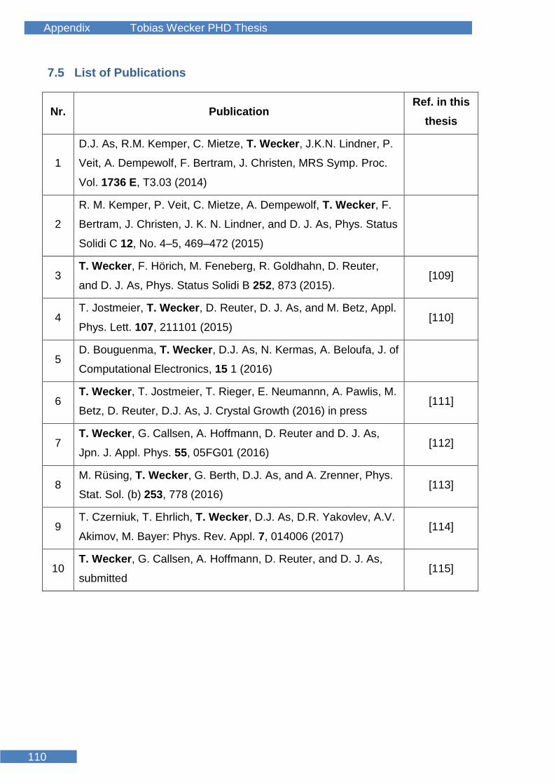
Appendix Tobias Wecker PHD Thesis
Tobias Wecker
110
7.5 List of Publications
Nr. Publication Ref. in this
thesis
1
D.J. As, R.M. Kemper, C. Mietze, T. Wecker, J.K.N. Lindner, P.
Veit, A. Dempewolf, F. Bertram, J. Christen, MRS Symp. Proc.
Vol. 1736 E, T3.03 (2014)
2
R. M. Kemper, P. Veit, C. Mietze, A. Dempewolf, T. Wecker, F.
Bertram, J. Christen, J. K. N. Lindner, and D. J. As, Phys. Status
Solidi C 12, No. 4–5, 469–472 (2015)
3 T. Wecker, F. Hörich, M. Feneberg, R. Goldhahn, D. Reuter,
and D. J. As, Phys. Status Solidi B 252, 873 (2015). [109]
4 T. Jostmeier, T. Wecker, D. Reuter, D. J. As, and M. Betz, Appl.
Phys. Lett. 107, 211101 (2015) [110]
5 D. Bouguenma, T. Wecker, D.J. As, N. Kermas, A. Beloufa, J. of
Computational Electronics, 15 1 (2016)
6 T. Wecker, T. Jostmeier, T. Rieger, E. Neumannn, A. Pawlis, M.
Betz, D. Reuter, D.J. As, J. Crystal Growth (2016) in press [111]
7 T. Wecker, G. Callsen, A. Hoffmann, D. Reuter and D. J. As,
Jpn. J. Appl. Phys. 55, 05FG01 (2016) [112]
8 M. Rüsing, T. Wecker, G. Berth, D.J. As, and A. Zrenner, Phys.
Stat. Sol. (b) 253, 778 (2016) [113]
9 T. Czerniuk, T. Ehrlich, T. Wecker, D.J. As, D.R. Yakovlev, A.V.
Akimov, M. Bayer: Phys. Rev. Appl. 7, 014006 (2017) [114]
10 T. Wecker, G. Callsen, A. Hoffmann, D. Reuter, and D. J. As,
submitted [115]

Appendix Tobias Wecker PHD Thesis
111
7.6 Parameters cubic III-Nitrides
Parameter c-GaN c-AlN c-InN
Egap, 0K [eV] 3.293[22] 5.997[102] -
Egap, 300K [eV] 3.23[22] 5.93[103] 0.595[108]
Eexciton [meV] 24[22] - -
a [Å] 4.503[35] 4.373[100] 5.01[108]
me*/m0 0.19[96] 0.3[96] 0.052[96]
mhh*/m0 0.83[96] 1.32[96] 0.91[96]
mlh*/m0 0.28[96] 0.44[96] 0.079[96]
mso*/m0 0.34[96] 0.55[96] 0.11[96]
Δso [meV] 15[22] 19[96] 5[96]
𝛜𝐫 9.44[22] 8.07[103] 12.3[108]
𝛜∞ 5.31[22] 4.25[103] 7.84[108]
c11 [GPa] 293[104] 304[104] 187[104]
c12 [GPa] 159[104] 160[104] 125[104]
c44 [GPa] 155[104] 193[104] 86[104]
ag [eV] -8.0[105] -9.1[105] -5.0[105]
ac=ag+av [eV] -6.0 -6.8 -3.3
av [eV] 2.0[105] 2.3[105] 1.7[105]
buniax [eV] -1.7[105] -1.5[105] -1.2[105]
𝐛𝐁𝐨𝐰𝐢𝐧𝐠𝐝𝐢𝐫𝐞𝐜𝐭 [eV] 0.85[77]
𝐛𝐁𝐨𝐰𝐢𝐧𝐠𝐢𝐧𝐝𝐢𝐫𝐞𝐜𝐭 [eV] 0.01[77]
Background n-type doping of around 5x1017 cm-3 in AlxGa1-xN and of around
1x1017 cm-3 in GaN [75].
Lattice constant 3C-SiC: 4.3596 Å [99]

Appendix Tobias Wecker PHD Thesis
Tobias Wecker
112
7.7 Nextnano³ Source Code
Here the Nextnano³ source code for a MQW c-GaN/c-AlN structure with 1.8 nm
thick QWs is shown.
!%&CBO angepasst für Al=1%& !****** OVERALL SIMULATION PARAMETERS **************************************! !¯o filename = 'macro.in' !Einschalten der Makrofunktion %FunctionParser = yes !Die Dicken der einzelnen Schichten des ADQW %Barrier1 = 3 !%&Barrier1%& %QW = 1.8 !%&QWw%& %piezo_AlGaN = 0E0 %piezo = 0E0 !Automatisierung für die Erstellung der Simulationsbereiche %region1 = %Barrier1 + %QW %domain = %Barrier1 + %QW + %Barrier1 %AlGehalt = 1 !%&AlGehalt%& %Temperatur = 300E0 %Strain_status = 0.25E0 ! 1= pseudomorph %Strain_qw = 1-%Strain_status %g_AlN = 0.4373E0 %g_GaN = 0.4503E0 %dop_AlGaN = 0.5E0 ! 150 * 10^18 cm^-3 = 1.5 * 10^20 cm^-3 %dop_GaN = 0.1E0 %g_rel_AlGaN = %g_AlN*%AlGehalt +%g_GaN*(1-%AlGehalt) !Gitterkonstante [nm] !%g_AlGaN = (1-%Strain_status) * %g_GaN+ %Strain_status* %g_rel_AlGaN %g_AlGaN = %g_rel_AlGaN %g_Buffer = (1-%Strain_qw) * %g_GaN+ (%Strain_qw)* %g_rel_AlGaN !Vorgaben für die Energien der Bänder %CBO = 78 !%&CBO%& %VBO = 100-%CBO !%E_GaN = 3.293+0.0057 !13K %&Temperatur GaN 13K %& !%E_AlN = 5.997 +0.0063 !13K %&Temperatur AlN 13K %& %E_GaN = 3.24+0.006 !300K %&Temperatur GaN 300K %& %E_AlN = 5.93 !300K %&Temperatur AlN 300K %& !%E_AlN = 5.3 !300K indirekt %&Temperatur AlN 300K %& %b = -0.85 !Bowing Parameter %GaN_VB = -0.726 %GaN_LB = %E_GaN+%GaN_VB %E_AlGaN = %E_GaN*(1-%AlGehalt) + %E_AlN*%AlGehalt + %b*%AlGehalt *(1-%AlGehalt) %DeltaE = %E_AlGaN - %E_GaN %Leitunsgband_AlGaN = %DeltaE *%CBO/100 +%GaN_LB %Valenzband_AlGaN = -%DeltaE *%VBO/100+%GaN_VB !Effektive Massen der beteiligten Binären Halbleiter %mass_eGaN = 0.19E0 !Carvalho Phys Rev B 84, 195105 (2011) %mass_eAlN = 0.30E0 !Carvalho Phys Rev B 84, 195105 (2011)
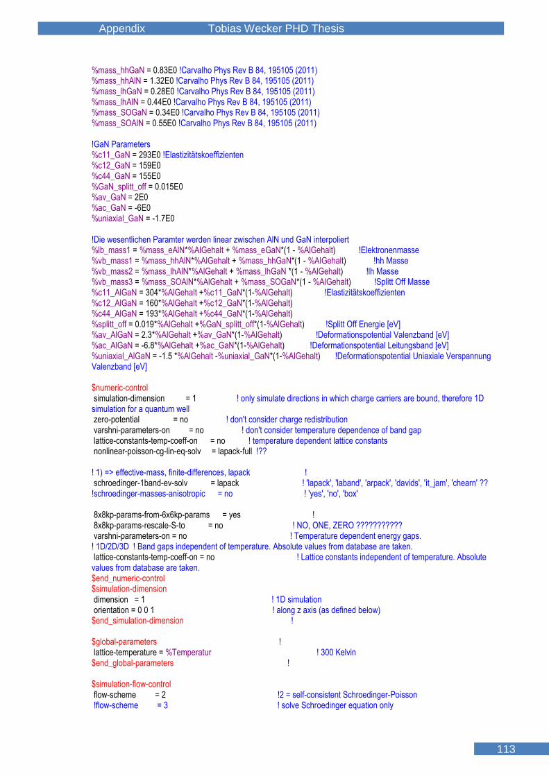
Appendix Tobias Wecker PHD Thesis
113
%mass_hhGaN = 0.83E0 !Carvalho Phys Rev B 84, 195105 (2011) %mass_hhAlN = 1.32E0 !Carvalho Phys Rev B 84, 195105 (2011) %mass_lhGaN = 0.28E0 !Carvalho Phys Rev B 84, 195105 (2011) %mass_lhAlN = 0.44E0 !Carvalho Phys Rev B 84, 195105 (2011) %mass_SOGaN = 0.34E0 !Carvalho Phys Rev B 84, 195105 (2011) %mass_SOAlN = 0.55E0 !Carvalho Phys Rev B 84, 195105 (2011) !GaN Parameters %c11_GaN = 293E0 !Elastizitätskoeffizienten %c12_GaN = 159E0 %c44_GaN = 155E0 %GaN_splitt_off = 0.015E0 %av_GaN = 2E0 %ac_GaN = -6E0 %uniaxial_GaN = -1.7E0 !Die wesentlichen Paramter werden linear zwischen AlN und GaN interpoliert %lb_mass1 = %mass_eAlN*%AlGehalt + %mass_eGaN*(1 - %AlGehalt) !Elektronenmasse %vb_mass1 = %mass_hhAlN*%AlGehalt + %mass_hhGaN*(1 - %AlGehalt) !hh Masse %vb_mass2 = %mass_lhAlN*%AlGehalt + %mass_lhGaN *(1 - %AlGehalt) !lh Masse %vb_mass3 = %mass_SOAlN*%AlGehalt + %mass_SOGaN*(1 - %AlGehalt) !Splitt Off Masse %c11_AlGaN = 304*%AlGehalt +%c11_GaN*(1-%AlGehalt) !Elastizitätskoeffizienten %c12_AlGaN = 160*%AlGehalt +%c12_GaN*(1-%AlGehalt) %c44_AlGaN = 193*%AlGehalt +%c44_GaN*(1-%AlGehalt) %splitt_off = 0.019*%AlGehalt +%GaN_splitt_off*(1-%AlGehalt) !Splitt Off Energie [eV] %av_AlGaN = 2.3*%AlGehalt +%av_GaN*(1-%AlGehalt) !Deformationspotential Valenzband [eV] %ac_AlGaN = -6.8*%AlGehalt +%ac_GaN*(1-%AlGehalt) !Deformationspotential Leitungsband [eV] %uniaxial_AlGaN = -1.5 *%AlGehalt -%uniaxial_GaN*(1-%AlGehalt) !Deformationspotential Uniaxiale Verspannung Valenzband [eV] $numeric-control simulation-dimension = 1 ! only simulate directions in which charge carriers are bound, therefore 1D simulation for a quantum well zero-potential = no ! don't consider charge redistribution varshni-parameters-on = no ! don't consider temperature dependence of band gap lattice-constants-temp-coeff-on = no ! temperature dependent lattice constants nonlinear-poisson-cg-lin-eq-solv = lapack-full !?? ! 1) => effective-mass, finite-differences, lapack ! schroedinger-1band-ev-solv = lapack ! 'lapack', 'laband', 'arpack', 'davids', 'it_jam', 'chearn' ?? !schroedinger-masses-anisotropic = no ! 'yes', 'no', 'box' 8x8kp-params-from-6x6kp-params = yes ! 8x8kp-params-rescale-S-to = no ! NO, ONE, ZERO ??????????? varshni-parameters-on = no ! Temperature dependent energy gaps. ! 1D/2D/3D ! Band gaps independent of temperature. Absolute values from database are taken. lattice-constants-temp-coeff-on = no ! Lattice constants independent of temperature. Absolute values from database are taken. $end_numeric-control $simulation-dimension dimension = 1 ! 1D simulation orientation = 0 0 1 ! along z axis (as defined below) $end_simulation-dimension ! $global-parameters ! lattice-temperature = %Temperatur ! 300 Kelvin $end_global-parameters ! $simulation-flow-control flow-scheme = 2 !2 = self-consistent Schroedinger-Poisson !flow-scheme = 3 ! solve Schroedinger equation only

Appendix Tobias Wecker PHD Thesis
Tobias Wecker
114
!(because no charge redistribution here) raw-strain-in or homogeneous-strain or strain-minimization or zero-strain-amorphous !raw-directory-in = raw_data1/ !raw-potential-in = no ! strain-calculation = homogeneous-strain! homogeneous-strain or strain-minimization or zero-strain-amorphous $end_simulation-flow-control ! $domain-coordinates ! domain-type = 0 0 1 ! again: along z axis z-coordinates = 0d0 %domain ! beginning and end of simulated region in nm !z-coordinates = 0d0 8d0 growth-coordinate-axis = 0 0 1 ! needed if pseudomorphic strain is to be calculated pseudomorphic-on = GaN(zb)! needed if pseudomorphic strain is to be calculated lattice-constants = %g_Buffer %g_Buffer %g_Buffer lattice-constants-temp-coeff = 5.59d-6 5.59d-6 5.59d-6 ! [nm/K] http://www.ioffe.ru/SVA/NSM/ $end_domain-coordinates ! !****** REGIONS AND CLUSTERS ***********************************************! $regions ! region-number = 1 base-geometry = line region-priority = 2 z-coordinates = 0d0 %Barrier1 !Material: Barri-ere region-number = 2 base-geometry = line region-priority = 2 z-coordinates = %Barrier1 %region1 !Material: QW region-number = 3 base-geometry = line region-priority = 2 z-coordinates = %region1 %domain !Material: Barrier $end_regions ! $grid-specification ! for every boundary between regions, there has to exist a grid line grid-type = 0 0 1 ! again: along z axis z-grid-lines = 0d0 %Barrier1 %region1 %domain ! explicity specified grid lines z-nodes = 300 300 300 ! number of additional grid lines between those z-grid-factors = 1d0 1d0 1d0 ! can be used for inhomogeneous grids $end_grid-specification ! You specified n regions in the simulation area. If they do not ! ! completely fill the simulation area, the resulting rest area is ! ! automatically assigned as region number n+1. ! $region-cluster ! regions can be grouped into clusters cluster-number = 1 region-numbers = 1 3 4 ! Barrieren cluster-number = 2 region-numbers = 2 ! Quantentopf $end_region-cluster !****** MATERIALS AND ALLOY PROFILES **************************************** $material material-number = 1 material-name = AlN(zb) ! AlGaN cluster-numbers = 1 crystal-type = zincblende material-number = 2 material-name = GaN(zb) ! QW cluster-numbers = 2 $end_material !****** DOPING AND IMPURITIES **********************************************! $doping-function ! doping-function-number = 1 ! impurity-number = 1 ! properties of this impurity type have to be specified below doping-concentration = 0d0 ! 150 * 10^18 cm^-3 = 1.5 * 10^20 cm^-3 only-region = 0d0 %region1 !only-region = 0d0 2.5d0 $end_doping-function ! $impurity-parameters !

Appendix Tobias Wecker PHD Thesis
115
! n-Si in GaAs = 0.0058d0 ! ! n-Si in AlAs = 0.007d0 ! 300 K, Landolt-Boernstein ! p-C in GaAs = 0.027d0 impurity-number = 1 ! impurity numbers labelled in doping-function impurity-type = n-type ! n-type, p-type number-of-energy-levels = 1 ! number of energy levels of this impurity (only 1 is currently allowed) energy-levels-relative = 0.02d0 ! energy relative to 'nearest' band edge (n-type -> conduction band, p-type -> valence band) !energy-levels-relative = -1000d0 ! = all ionized ! energy relative to 'nearest' band edge (n-type -> conduc-tion band, p-type -> valence band) degeneracy-of-energy-levels = 2 ! degeneracy of energy levels, 2 for n-type, 4 for p-type ! impurity-number = 2 ! impurity numbers labelled in doping-function ! impurity-type = n-type ! n-type, p-type ! number-of-energy-levels = 1 ! number of energy levels of this impurity (only 1 is currently allowed) ! energy-levels-relative = 0.006d0 ! energy relative to 'nearest' band edge (n-type -> conduction band, p-type -> valence band) !energy-levels-relative = -1000d0 ! = all ionized ! energy relative to 'nearest' band edge (n-type -> conduc-tion band, p-type -> valence band) ! degeneracy-of-energy-levels = 2 ! degeneracy of energy levels, 2 for n-type, 4 for p-type $end_impurity-parameters !****** QUANTUM ************************************************************! $quantum-regions ! Schroedinger equation is only solved inside this region(s) region-number = 1 ! usually only one simulation region base-geometry = line ! region-priority = 3 ! z-coordinates = 0d0 %domain ! can also be smaller than total simulation region $end_quantum-regions ! $quantum-cluster ! again: regions can be grouped into clusters cluster-number = 1 region-numbers = 1 deactivate-cluster = no $end_quantum-cluster ! $quantum-model-electrons ! how to solve Schroedinger equation for electrons model-number = 1 ! model-name = effective-mass ! quantum model, here: single band effective mass approximation cluster-numbers = 1 ! quantum cluster numbers to which this model applies conduction-band-numbers = 1 ! select conductions bands (minima), here: only gamma point number-of-eigenvalues-per-band = 4 ! how many eigenenergies are calculated for each band separation-model = eigenvalue ! to determine separation between classic and quantum density maximum-energy-for-eigenstates = 1d0 ! has to be present but is ignored in separation model "eigenvalue" quantization-along-axes = 0 0 1 ! directions in which charge carriers are quantized, here: same as simulation direction boundary-condition-100 = Neumann ! mixed, Neumann or (Dirichlet|dirichlet|DIRICHLET). Nonsens input means Neumann (default). boundary-condition-010 = Neumann ! mixed, Neumann or (Dirichlet|dirichlet|DIRICHLET). Nonsens input means Neumann (default) boundary-condition-001 = Neumann ! periodic boundary conditions are necessary for superlattices $end_quantum-model-electrons $quantum-model-holes model-number = 1 ! model-name = effective-mass ! quantum model, here: single band effective mass approximation cluster-numbers = 1 ! quantum cluster numbers to which this model applies valence-band-numbers = 1 2 3 ! select valence bands (maxima), 1 = heavy holes, 2 = light holes, 3 = split-off holes number-of-eigenvalues-per-band = 3 3 3 ! how many eigenenergies are calculated for each band separation-model = eigenvalue ! to determine separation between classic and quantum density maximum-energy-for-eigenstates = 1d0 1d0 1d0 ! has to be present but is ignored in separation model "eigenvalue"
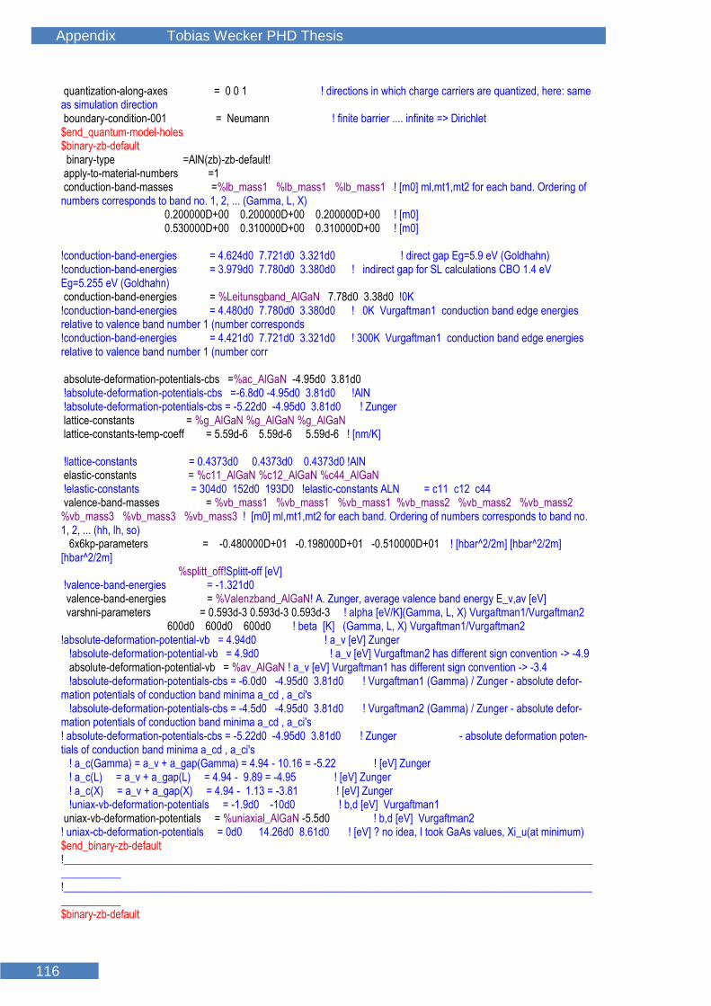
Appendix Tobias Wecker PHD Thesis
Tobias Wecker
116
quantization-along-axes = 0 0 1 ! directions in which charge carriers are quantized, here: same as simulation direction boundary-condition-001 = Neumann ! finite barrier .... infinite => Dirichlet $end_quantum-model-holes $binary-zb-default binary-type =AlN(zb)-zb-default! apply-to-material-numbers =1 conduction-band-masses =%lb_mass1 %lb_mass1 %lb_mass1 ! [m0] ml,mt1,mt2 for each band. Ordering of numbers corresponds to band no. 1, 2, ... (Gamma, L, X) 0.200000D+00 0.200000D+00 0.200000D+00 ! [m0] 0.530000D+00 0.310000D+00 0.310000D+00 ! [m0] !conduction-band-energies = 4.624d0 7.721d0 3.321d0 ! direct gap Eg=5.9 eV (Goldhahn) !conduction-band-energies = 3.979d0 7.780d0 3.380d0 ! indirect gap for SL calculations CBO 1.4 eV Eg=5.255 eV (Goldhahn) conduction-band-energies = %Leitunsgband_AlGaN 7.78d0 3.38d0 !0K !conduction-band-energies = 4.480d0 7.780d0 3.380d0 ! 0K Vurgaftman1 conduction band edge energies relative to valence band number 1 (number corresponds !conduction-band-energies = 4.421d0 7.721d0 3.321d0 ! 300K Vurgaftman1 conduction band edge energies relative to valence band number 1 (number corr absolute-deformation-potentials-cbs =%ac_AlGaN -4.95d0 3.81d0 !absolute-deformation-potentials-cbs =-6.8d0 -4.95d0 3.81d0 !AlN !absolute-deformation-potentials-cbs = -5.22d0 -4.95d0 3.81d0 ! Zunger lattice-constants = %g_AlGaN %g_AlGaN %g_AlGaN lattice-constants-temp-coeff = 5.59d-6 5.59d-6 5.59d-6 ! [nm/K] !lattice-constants = 0.4373d0 0.4373d0 0.4373d0 !AlN elastic-constants = %c11_AlGaN %c12_AlGaN %c44_AlGaN !elastic-constants = 304d0 152d0 193D0 !elastic-constants ALN = c11 c12 c44 valence-band-masses = %vb_mass1 %vb_mass1 %vb_mass1 %vb_mass2 %vb_mass2 %vb_mass2 %vb_mass3 %vb_mass3 %vb_mass3 ! [m0] ml,mt1,mt2 for each band. Ordering of numbers corresponds to band no. 1, 2, ... (hh, lh, so) 6x6kp-parameters = -0.480000D+01 -0.198000D+01 -0.510000D+01 ! [hbar^2/2m] [hbar^2/2m] [hbar^2/2m] %splitt_off!Splitt-off [eV] !valence-band-energies = -1.321d0 valence-band-energies = %Valenzband_AlGaN! A. Zunger, average valence band energy E_v,av [eV] varshni-parameters = 0.593d-3 0.593d-3 0.593d-3 ! alpha [eV/K](Gamma, L, X) Vurgaftman1/Vurgaftman2 600d0 600d0 600d0 ! beta [K] (Gamma, L, X) Vurgaftman1/Vurgaftman2 !absolute-deformation-potential-vb = 4.94d0 ! a_v [eV] Zunger !absolute-deformation-potential-vb = 4.9d0 ! a_v [eV] Vurgaftman2 has different sign convention -> -4.9 absolute-deformation-potential-vb = %av_AlGaN ! a_v [eV] Vurgaftman1 has different sign convention -> -3.4 !absolute-deformation-potentials-cbs = -6.0d0 -4.95d0 3.81d0 ! Vurgaftman1 (Gamma) / Zunger - absolute defor-mation potentials of conduction band minima a_cd , a_ci's !absolute-deformation-potentials-cbs = -4.5d0 -4.95d0 3.81d0 ! Vurgaftman2 (Gamma) / Zunger - absolute defor-mation potentials of conduction band minima a_cd , a_ci's ! absolute-deformation-potentials-cbs = -5.22d0 -4.95d0 3.81d0 ! Zunger - absolute deformation poten-tials of conduction band minima a_cd , a_ci's ! a_c(Gamma) = a_v + a_gap(Gamma) = 4.94 - 10.16 = -5.22 ! [eV] Zunger ! a_c(L) = a_v + a_gap(L) = 4.94 - 9.89 = -4.95 ! [eV] Zunger ! a_c(X) = a_v + a_gap(X) = 4.94 - 1.13 = -3.81 ! [eV] Zunger !uniax-vb-deformation-potentials = -1.9d0 -10d0 ! b,d [eV] Vurgaftman1 uniax-vb-deformation-potentials = %uniaxial_AlGaN -5.5d0 ! b,d [eV] Vurgaftman2 ! uniax-cb-deformation-potentials = 0d0 14.26d0 8.61d0 ! [eV] ? no idea, I took GaAs values, Xi_u(at minimum) $end_binary-zb-default !____________________________________________________________________________________________________________ !____________________________________________________________________________________________________________ $binary-zb-default

Appendix Tobias Wecker PHD Thesis
117
binary-type =GaN(zb)-zb-default! apply-to-material-numbers =2 conduction-band-masses =%mass_eGaN %mass_eGaN %mass_eGaN ! [m0] ml,mt1,mt2 for each band. Order-ing of numbers corresponds to band no. 1, 2, ... (Gamma, L, X) 0.200000D+00 0.200000D+00 0.200000D+00 ! [m0] 0.500000D+00 0.300000D+00 0.300000D+00 ! [m0] conduction-band-energies = %GaN_LB 4.870d0 3.800d0 ! Eigen !conduction-band-energies = 2.579d0 4.870d0 3.800d0 ! 0K Vurgaftman1/Vurgaftman2 conduction band edge energies relative to valence band number 1 (number corresponds !conduction-band-energies = 2.520d0 4.811d0 3.741d0 ! 300K Vurgaftman1/Vurgaftman2 conduction band edge energies relative to valence band number 1 (number corresponds absolute-deformation-potentials-cbs = %ac_GaN -7.46d0 -0.52d0 lattice-constants = %g_GaN %g_GaN %g_GaN ! [nm] including 'lattice-constants-temp-coeff' lattice-constants-temp-coeff = 5.59d-6 5.59d-6 5.59d-6 ! [nm/K] http://www.ioffe.ru/SVA/NSM/Semicond/GaN/basic.html !a_lc = a_lc(300 K) + b * (T - 300K) elastic-constants = %c11_GaN %c12_GaN %c44_GaN valence-band-masses = %mass_hhGaN %mass_hhGaN %mass_hhGaN %mass_lhGaN %mass_lhGaN %mass_lhGaN 0.29d0 0.29d0 0.29d0 6x6kp-parameters = -6.74d0 -2.18d0 -6.66d0 ! Vurgaftman2 L,M,N [hbar^2/2m] (--> divide by hbar^2/2m) 0.015d0 ! Vurgaftman1/Vurgaftman2 delta_(split-off) in [eV] valence-band-energies = %GaN_VB ! A. Zunger, average valence band energy E_v,av [eV] varshni-parameters = 0.593d-3 0.593d-3 0.593d-3 ! alpha [eV/K](Gamma, L, X) Vurgaftman1/Vurgaftman2 600d0 600d0 600d0 ! beta [K] (Gamma, L, X) Vurgaftman1/Vurgaftman2 !absolute-deformation-potential-vb = 0.69d0 ! a_v [eV] Zunger !absolute-deformation-potential-vb = 0.69d0 ! a_v [eV] Vurgaftman2 has different sign convention -> -0.69 absolute-deformation-potential-vb = %av_GaN ! a_v [eV] Vurgaftman1 has different sign convention -> -5.2 !absolute-deformation-potentials-cbs = -2.2d0 -7.46d0 -0.52d0 ! Vurgaftman1 (Gamma) / Zunger - absolute defor-mation potentials of conduction band minima a_cd , a_ci's !absolute-deformation-potentials-cbs = -6.71d0 -7.46d0 -0.52d0 ! Vurgaftman2 (Gamma) / Zunger - absolute defor-mation potentials of conduction band minima a_cd , a_ci's ! absolute-deformation-potentials-cbs = -6.68d0 -7.46d0 -0.52d0 ! Zunger - absolute deformation poten-tials of conduction band minima a_cd , a_ci's ! a_c(Gamma) = a_v + a_gap(Gamma) = 0.69 - 7.37 = -6.68 ! [eV] Zunger ! a_c(L) = a_v + a_gap(L) = 0.69 - 8.15 = -7.46 ! [eV] Zunger ! a_c(X) = a_v + a_gap(X) = 0.69 - 1.21 = -0.52 ! [eV] Zunger !uniax-vb-deformation-potentials = -2.2d0 -3.4d0 ! b,d [eV] Vurgaftman1 uniax-vb-deformation-potentials = %uniaxial_GaN -3.7d0 ! b,d [eV] Vurgaftman2 !uniax-cb-deformation-potentials = 0d0 14.26d0 8.61d0 ! [eV] ? no idea, I took GaAs values, Xi_u(at minimum) $end_binary-zb-default !_________________________________________________________________________________________________ !****** OUTPUT *************************************************************! $global-settings ! output-directory = output/ !output-directory = ./ ! This setting is currently needed for nextnanomat. Will be obsolet in the future. !debug-level = 0 number-of-parallel-threads = 4 ! 1 = for single-core CPU $end_global-settings ! $output-raw-data ! destination-directory = raw_data1/ potential = yes ! fermi-levels = yes !

Appendix Tobias Wecker PHD Thesis
Tobias Wecker
118
strain = yes ! kp-eigenstates = no ! $end_output-raw-data ! $output-1-band-schroedinger ! !Note: We apply an overall band-shift to all bands in order to align the topmost valence bands (heavy hole/light hole) to zero (0 eV). !----------------------------------------------- ! Shift all bands, so that GaAs (hh/lh) = 0 eV. !----------------------------------------------- destination-directory = Schroedinger_1band/ !band-shift = 2,5401! [eV] ! shift-wavefunction-by-eigenvalue = yes sg-structure = yes ! ?? conduction-band-numbers = 1 ! only gamma point (as specified above) cb-min-ev = 1 ! cb-max-ev = 4 ! four eigenvalues per band (as specified above) valence-band-numbers = 1 2 3 ! heavy hole, light hole and split-off hole (as specified above) vb-min-ev = 1 ! vb-max-ev = 4 ! four eigenvalues per band (as specified above) complex-wave-functions = no ! scale = 2d0 ! for psi_squared, no physical relevance interband-matrix-elements = yes intraband-matrix-elements = yes ! electron-hole transition energies and wave function overlaps $end_output-1-band-schroedinger ! $output-bandstructure ! output for the band structure and the potential destination-directory = band_structure/ ! conduction-band-numbers = 1 ! conduction band edge at gamma point=1,L=2,X=3 valence-band-numbers = 1 2 3 ! valence band edge for heavy, light and split-off holes potential = yes ! $end_output-bandstructure ! !***** END BAND STRUCTURE AND DENSITIES ************************************! !***** OUTPUT STRAIN *******************************************************! ! This is the output for the densities. ! $output-densities ! destination-directory = densities1/ ! electrons = yes ! holes = no ! charge-density = no intrinsic-density = yes ! ionized-dopant-density = yes ! piezo-electricity = yes ! pyro-electricity = no ! interface-density = yes effective-density-of-states-Nc-Nv = yes subband-density = yes ! $end_output-densities ! !Biaxial strain (in plane of interface) e_xx = e_yy = ( a_substrate - a_layer ) / a_layer = 0.0155 (1.55 % lattice mismatch) !Uniaxial strain (perpendicular to interface) ezz = - 2 (c12/c11) exx = - 0.014 $output-strain ! This is the output for the strain. destination-directory = strain1/ ! strain = yes ! strain-simulation-system = yes ! $end_output-strain ! !***** END OUTPUT STRAIN ***************************************************! $output-current-data ! destination-directory = current1/ current = no ! fermi-levels = yes !

Appendix Tobias Wecker PHD Thesis
119
mobility-out = yes ! IV-curve-out = no recombination = no $end_output-current-data ! $output-material ! destination-directory = material/ doping-concentration = doping_concentration1D.dat $end_output-material !

Appendix Tobias Wecker PHD Thesis
Tobias Wecker
120
7.8 Matlab Source Code
This is the Matlab source code used for the simulation of the FWHM of the IR ab-
sorption.
%clc clearvars F0011 = -0.5; F01 = 0.3; Ef = 0.52; E10 = 0.82; rough = 0.45; m1 = 0.19; m2 = m1*9.109*10^-31; hbar = 1.05457*10^-34; hbar2 = 6.58212*10^-16; e = 1.602*10^-19; start1 = 0.1; ende1 = 0.9; schritt = 0.1; range = (ende1-start1)/schritt; data(uint8(range),2)= 0; l = 1; for i=start1:schritt:ende1 format long corr = i*10^-9; eq = m2.*e.*(corr.^2)./(hbar.^2); eq0 = @(E,t) eq.*E.*(1-cos(t)); eq1 = @(E,t) exp(-eq0(E,t)); G1 = m2.*corr.^2.*rough.^2./(hbar2.^2.*e); GIntra = @(E)G1.*F0011.^2.*integral(@(t)eq1(E,t),0, pi); eq2 = @(E,t) eq.*(E+E10./2-sqrt(E.*(E+E10)).*cos(t)); eq3 = @(E,t) exp(-eq2(E,t)); GInter = @(E)G1.*F01.^2.*integral(@(t)eq3(E,t),0, pi); GOpt = @(E) (GIntra(E)+GInter(E)); Fermi = @(E)(1./(exp((E-Ef)./0.025)+1)); Resigma = @(x, E10) integral(@(E) Fermi(E).*GOpt(E)./((x-E10).^2+GOpt(E).^2),0,1,'ArrayValued',true); start = E10-5; ende = E10+5; g = fplot(@(x) Resigma(x, E10), [start ende], 'MeshDensity', 50); %grid on x = g.XData; y= g.YData; maxy = max(y); f = find(y==maxy); cp = x(f);% ignore Matlabs suggestion to fix!!! y1= y./maxy; ydatawr(:,1) = y1; ydatawr(:,2) = x; newFit1=find(x>= cp); newFit2=find(x < cp);

Appendix Tobias Wecker PHD Thesis
121
ydatawr2 = ydatawr(min(newFit1):max(newFit1),:); ydatawr3 = ydatawr(min(newFit2):max(newFit2),:); sp1 = spline(ydatawr2(:,1),ydatawr2(:,2),0.5); sp2 = spline(ydatawr3(:,1),ydatawr3(:,2),0.5); Fullw = (sp1-sp2)*1000; data(l,1) = i; data(l,2) = Fullw; i; l=l+1; clearvars -except data l m1 m2 hbar hbar2 rough e Ef E10 F0011 F01 end format short data

Appendix Tobias Wecker PHD Thesis
Tobias Wecker
122
7.9 Acknowledgements
Zuletzt möchte ich mich bei allen bedanken, die mir bei meiner Masterarbeit gehol-
fen haben. Als erstes gilt mein Dank apl. Prof. Dr. Donat As, der mir diese Arbeit
angeboten und mir mit hilfreichen Vorschlägen zur Seite gestanden hat. Ich danke
auch Prof. Dr. Dirk Reuter der mich mit vielen Anregungen und Diskussionen unter-
stützt hat.
Außerdem danke ich Prof. Dr. Cedrik Meier für die Übernahme des Gutachtens
meiner Arbeit. Als letztes möchte ich noch den übrigen Mitgliedern meiner Arbeits-
gruppe für ihre Unterstützung und Motivation danken.

Appendix Tobias Wecker PHD Thesis
123
7.10 Eidesstattliche Erklärung
Hiermit versichere ich, dass ich die vorliegende Arbeit selbständig verfasst und kei-
ne anderen Quellen und Hilfsmittel als die angegeben benutzt habe.
Paderborn, 15.09.2017
______________________
Tobias Wecker