Recent Progress of Two-Dimensional Thermoelectric Materials
40
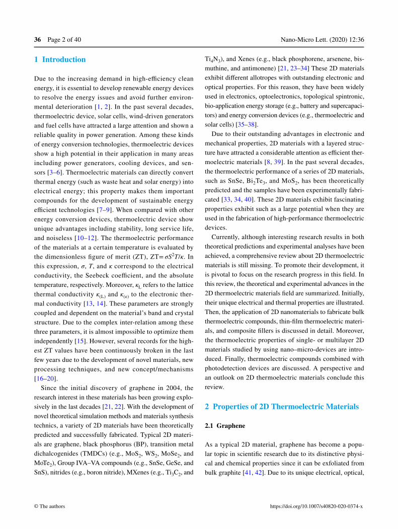
Vol.:(0123456789) 1 3 Recent Progress of Two‑Dimensional Thermoelectric Materials Delong Li 1 , Youning Gong 1 , Yuexing Chen 2 , Jiamei Lin 1 , Qasim Khan 3 , Yupeng Zhang 1 * , Yu Li 4 * , Han Zhang 1 * , Heping Xie 5 * Yupeng Zhang, [email protected]; Yu Li, [email protected]; Han Zhang, [email protected] 1 Collaborative Innovation Centre for Optoelectronic Science & Technology, and Key Laboratory of Optoelectronic Devices and Systems of Ministry of Education and Guangdong Province, Institute of Microscale Optoelectronics, College of Chemistry and Environmental Engineering, Shenzhen University, Shenzhen 518060, Guangdong, People’s Republic of China 2 Shenzhen Key Laboratory of Advanced Thin Films and Applications, College of Physics and Optoelectronic Engineering, Shenzhen University, Shenzhen 518060, Guangdong, People’s Republic of China 3 Department of Mechanical and Mechatronics Engineering, University of Waterloo, Waterloo, ON, Canada 4 Shenzhen Key Laboratory of Special Functional Materials, Shenzhen Engineering Laboratory for Advanced Technology of Ceramics, Guangdong Research Center for Interfacial Engineering of Functional Materials, College of Materials Science and Engineering, Shenzhen University, Shenzhen 518060, Guangdong, People’s Republic of China 5 Shenzhen Clean Energy Research Institute, Shenzhen University, Shenzhen 518060, Guangdong, People’s Republic of China HIGHLIGHTS • A comprehensive review on the recent development of two-dimensional (2D) nanomaterials for bulk or thin-film thermoelectric materials, as well as composite filler, has been extensively presented. • Development of micro-device platform and its application to study the inherent thermoelectric properties of individual single- and few-layer 2D nanomaterials. ABSTRACT Thermoelectric generators have attracted a wide research interest owing to their ability to directly convert heat into electrical power. Moreover, the thermoelectric properties of traditional inorganic and organic materials have been significantly improved over the past few decades. Among these compounds, layered two-dimensional (2D) materials, such as graphene, black phosphorus, transition metal dichalcogenides, IVA–VIA compounds, and MXenes, have generated a large research attention as a group of potentially high-performance thermoelectric materi- als. Due to their unique electronic, mechanical, thermal, and optoelectronic proper- ties, thermoelectric devices based on such materials can be applied in a variety of applications. Herein, a comprehensive review on the development of 2D materials for thermoelectric applications, as well as theoretical simulations and experimental preparation, is presented. In addition, nanodevice and new applications of 2D ther- moelectric materials are also introduced. At last, current challenges are discussed and several prospects in this field are proposed. KEYWORDS Two-dimensional thermoelectric materials; Black phosphorus analogue; Tin selenide; Transition metal dichalcogenides; Photothermoelectric effect Sintering Bulk Composite filler Restack Thin Film Self-Power Devices Nano-Micro Devices TMDs 2D-Materials for Thermoelectric Black Phosphorus MXenes Graphene IV-VI Chalcogenides ISSN 2311-6706 e-ISSN 2150-5551 CN 31-2103/TB REVIEW Cite as Nano-Micro Lett. (2020) 12:36 Received: 26 October 2019 Accepted: 24 December 2019 Published online: 23 January 2020 © The Author(s) 2020 https://doi.org/10.1007/s40820-020-0374-x
Transcript of Recent Progress of Two-Dimensional Thermoelectric Materials
Vol.:(0123456789)
1 3
Recent Progress of Two‑Dimensional Thermoelectric Materials
Delong Li1, Youning Gong1, Yuexing Chen2, Jiamei Lin1, Qasim Khan3, Yupeng Zhang1 *, Yu Li4 *, Han Zhang1 *, Heping Xie5
* Yupeng Zhang, [email protected]; Yu Li, [email protected]; Han Zhang, [email protected] Collaborative Innovation Centre for Optoelectronic Science & Technology, and Key Laboratory
of Optoelectronic Devices and Systems of Ministry of Education and Guangdong Province, Institute of Microscale Optoelectronics, College of Chemistry and Environmental Engineering, Shenzhen University, Shenzhen 518060, Guangdong, People’s Republic of China
2 Shenzhen Key Laboratory of Advanced Thin Films and Applications, College of Physics and Optoelectronic Engineering, Shenzhen University, Shenzhen 518060, Guangdong, People’s Republic of China
3 Department of Mechanical and Mechatronics Engineering, University of Waterloo, Waterloo, ON, Canada4 Shenzhen Key Laboratory of Special Functional Materials, Shenzhen Engineering Laboratory for Advanced
Technology of Ceramics, Guangdong Research Center for Interfacial Engineering of Functional Materials, College of Materials Science and Engineering, Shenzhen University, Shenzhen 518060, Guangdong, People’s Republic of China
5 Shenzhen Clean Energy Research Institute, Shenzhen University, Shenzhen 518060, Guangdong, People’s Republic of China
HIGHLIGHTS
• A comprehensive review on the recent development of two-dimensional (2D) nanomaterials for bulk or thin-film thermoelectric materials, as well as composite filler, has been extensively presented.
• Development of micro-device platform and its application to study the inherent thermoelectric properties of individual single- and few-layer 2D nanomaterials.
ABSTRACT Thermoelectric generators have attracted a wide research interest owing to their ability to directly convert heat into electrical power. Moreover, the thermoelectric properties of traditional inorganic and organic materials have been significantly improved over the past few decades. Among these compounds, layered two-dimensional (2D) materials, such as graphene, black phosphorus, transition metal dichalcogenides, IVA–VIA compounds, and MXenes, have generated a large research attention as a group of potentially high-performance thermoelectric materi-als. Due to their unique electronic, mechanical, thermal, and optoelectronic proper-ties, thermoelectric devices based on such materials can be applied in a variety of applications. Herein, a comprehensive review on the development of 2D materials for thermoelectric applications, as well as theoretical simulations and experimental preparation, is presented. In addition, nanodevice and new applications of 2D ther-moelectric materials are also introduced. At last, current challenges are discussed and several prospects in this field are proposed.
KEYWORDS Two-dimensional thermoelectric materials; Black phosphorus analogue; Tin selenide; Transition metal dichalcogenides; Photothermoelectric effect
SinteringBulk
Compositefiller
RestackThin Film
Self-PowerDevices
Nano-MicroDevices
TMDs
2D-Materials forThermoelectricBlack
Phosphorus
MXenes Graphene
IV-V
ICh
alco
geni
des
ISSN 2311-6706e-ISSN 2150-5551
CN 31-2103/TB
REVIEW
Cite asNano-Micro Lett. (2020) 12:36
Received: 26 October 2019 Accepted: 24 December 2019 Published online: 23 January 2020 © The Author(s) 2020
https://doi.org/10.1007/s40820-020-0374-x
Nano-Micro Lett. (2020) 12:3636 Page 2 of 40
https://doi.org/10.1007/s40820-020-0374-x© The authors
1 Introduction
Due to the increasing demand in high-efficiency clean energy, it is essential to develop renewable energy devices to resolve the energy issues and avoid further environ-mental deterioration [1, 2]. In the past several decades, thermoelectric device, solar cells, wind-driven generators and fuel cells have attracted a large attention and shown a reliable quality in power generation. Among these kinds of energy conversion technologies, thermoelectric devices show a high potential in their application in many areas including power generators, cooling devices, and sen-sors [3–6]. Thermoelectric materials can directly convert thermal energy (such as waste heat and solar energy) into electrical energy; this property makes them important compounds for the development of sustainable energy efficient technologies [7–9]. When compared with other energy conversion devices, thermoelectric device show unique advantages including stability, long service life, and noiseless [10–12]. The thermoelectric performance of the materials at a certain temperature is evaluated by the dimensionless figure of merit (ZT), ZT= σS2T/κ. In this expression, σ, T, and κ correspond to the electrical conductivity, the Seebeck coefficient, and the absolute temperature, respectively. Moreover, κL refers to the lattice thermal conductivity κ(L) and κ(e) to the electronic ther-mal conductivity [13, 14]. These parameters are strongly coupled and dependent on the material’s band and crystal structure. Due to the complex inter-relation among these three parameters, it is almost impossible to optimize them independently [15]. However, several records for the high-est ZT values have been continuously broken in the last few years due to the development of novel materials, new processing techniques, and new concept/mechanisms [16–20].
Since the initial discovery of graphene in 2004, the research interest in these materials has been growing explo-sively in the last decades [21, 22]. With the development of novel theoretical simulation methods and materials synthesis technics, a variety of 2D materials have been theoretically predicted and successfully fabricated. Typical 2D materi-als are graphene, black phosphorus (BP), transition metal dichalcogenides (TMDCs) (e.g., MoS2, WS2, MoSe2, and MoTe2), Group IVA–VA compounds (e.g., SnSe, GeSe, and SnS), nitrides (e.g., boron nitride), MXenes (e.g., Ti3C2, and
Ti4N3), and Xenes (e.g., black phosphorene, arsenene, bis-muthine, and antimonene) [21, 23–34] These 2D materials exhibit different allotropes with outstanding electronic and optical properties. For this reason, they have been widely used in electronics, optoelectronics, topological spintronic, bio-application energy storage (e.g., battery and supercapaci-tors) and energy conversion devices (e.g., thermoelectric and solar cells) [35–38].
Due to their outstanding advantages in electronic and mechanical properties, 2D materials with a layered struc-ture have attracted a considerable attention as efficient ther-moelectric materials [8, 39]. In the past several decades, the thermoelectric performance of a series of 2D materials, such as SnSe, Bi2Te3, and MoS2, has been theoretically predicted and the samples have been experimentally fabri-cated [33, 34, 40]. These 2D materials exhibit fascinating properties exhibit such as a large potential when they are used in the fabrication of high-performance thermoelectric devices.
Currently, although interesting research results in both theoretical predictions and experimental analyses have been achieved, a comprehensive review about 2D thermoelectric materials is still missing. To promote their development, it is pivotal to focus on the research progress in this field. In this review, the theoretical and experimental advances in the 2D thermoelectric materials field are summarized. Initially, their unique electrical and thermal properties are illustrated. Then, the application of 2D nanomaterials to fabricate bulk thermoelectric compounds, thin-film thermoelectric materi-als, and composite fillers is discussed in detail. Moreover, the thermoelectric properties of single- or multilayer 2D materials studied by using nano–micro-devices are intro-duced. Finally, thermoelectric compounds combined with photodetection devices are discussed. A perspective and an outlook on 2D thermoelectric materials conclude this review.
2 Properties of 2D Thermoelectric Materials
2.1 Graphene
As a typical 2D material, graphene has become a popu-lar topic in scientific research due to its distinctive physi-cal and chemical properties since it can be exfoliated from bulk graphite [41, 42]. Due to its unique electrical, optical,
Nano-Micro Lett. (2020) 12:36 Page 3 of 40 36
1 3
catalytic, and mechanical features, graphene has attracted a broad attention in recent years in many fields. For instance, graphene shows an ultrahigh electrical conductivity (106 S cm−1) at room temperature due to its high electron mobility [43]. Its maximum Seebeck coefficient value was reported to be about 80 mV K−1 [27, 44, 45]. The thermal conductivity of graphene is in the 4840–5300 W mK−1 range at room temperature [46]. A large theoretical and experimen-tal effort has been done to study the thermoelectric perfor-mance of graphene [44, 45, 47–69].
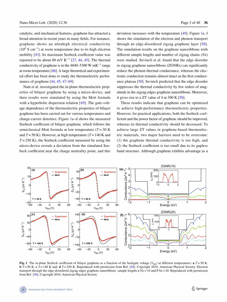
Nam et al. investigated the in-plane thermoelectric prop-erties of bilayer graphene by using a micro-device, and their results were simulated by using the Mott formula with a hyperbolic dispersion relation [49]. The gate-volt-age dependence of the thermoelectric properties of bilayer graphene has been carried out for various temperatures and charge-carrier densities. Figure 1a–d shows the measured Seebeck coefficient of bilayer graphene, which follows the semiclassical Mott formula at low temperature (T = 30 K and T = 50 K). However, at high temperature (T = 140 K and T = 250 K), the Seebeck coefficient measured by using the micro-device reveals a deviation from the simulated See-beck coefficient near the charge neutrality point, and this
deviation increases with the temperature [49]. Figure 1e, f shows the simulation of the electron and phonon transport through an edge-disordered zigzag graphene layer [50]. The simulation results on the graphene nanoribbons with different sample lengths and number of zigzag chains (Nz) were studied. Sevincli et al. found that the edge disorder in zigzag graphene nanoribbons (ZGNRs) can significantly reduce the phonon thermal conductance, whereas the elec-tronic conduction remains almost intact at the first conduct-ance plateau [50]. Sevincli predicted that the edge disorder suppresses the thermal conductivity by few orders of mag-nitude in the zigzag edges graphene nanoribbons. Moreover, it gives rise to a ZT value of 4 at 300 K [50].
These results indicate that graphene can be optimized to achieve high-performance thermoelectric properties. However, for practical applications, both the Seebeck coef-ficient and the power factor of graphene should be improved, whereas its thermal conductivity should be decreased. To achieve large ZT values in graphene-based thermoelec-tric materials, two major barriers need to be overcome: (1) the graphene thermal conductivity is too high, and (2) the Seebeck coefficient is too small due to its gapless band structure. Although graphene exhibits advantage as a
ExperimentMott
30
15
0
−15
−30
Sxx
(µV
K−1
)
VBG (V)
T = 30 K
(a)
−60 −30 0 30 60
ExperimentMott
40
20
0
−20
−40
Sxx
(µV
K−1
)
Con
duct
ance
(2e2
h−1)
VBG (V)
T = 50 K
(b)
−60 −30
−2
200
100
00
l el (n
m)
2
−2 −1 0
ZGNR(10)5
4
3
2
1
01 2
0 30 60
80
40
0
−40
−80
Sxx
(µV
K−1
)
VBG (V)
T = 140 K
(c)
−60 −30 0 30 60
ExperimentMott
ExperimentMott
140
70
0
−70
−140
Sxx
(µV
K−1
)
VBG (V)
T = 250 K
(d)
−60 −30 0 30 60
Con
duct
ance
(2e2
h−1)
−2
3000
1500
00
l el (n
m)
2
−2 −1 0
ZGNR(20)(f)
(e)
Energy (eV)
Energy (eV)
6
4
2
01 2
Fig. 1 The in-plane Seebeck coefficient of bilayer graphene as a function of the backgate voltage (VBG) at different temperatures: a T = 30 K, b T = 50 K, c T = 140 K and, d T = 250 K. Reproduced with permission from Ref. [49]. Copyright 2010, American Physical Society. Electron transport through the edge-disordered zigzag edges graphene nanoribbons: sample lengths e Nz = 10 and f Nz = 20. Reproduced with permission from Ref. [50]. Copyright 2010, American Physical Society

Nano-Micro Lett. (2020) 12:3636 Page 4 of 40
https://doi.org/10.1007/s40820-020-0374-x© The authors
high-performance thermoelectric material, more efforts in simulations and experiments need to be done to optimize its thermoelectric performance.
2.2 TMDC
As a novel class of layered materials, 2D TMDCs, such as MX2 (M = Mo, W, Ti, and X = S, Se, Te), have attracted a large attention in last decades due to their semiconducting characteristics, outstanding chemical stability, and mechani-cal and physical properties. Moreover, they have been widely studied in various fields including optoelectronic, energy harvests and conversion, and cancer therapy. These types of material have been widely studied in many fields, such as photodetector, thermoelectric, and gas-sensing applications. Their relatively high electrical conductivity and relatively low thermal conductivity make the TMDCs emerge as prom-ising materials for high-performance thermoelectric devices, especially for the fabrication of wearable heating/cooling devices and power generators.
The thermoelectric properties of 2D TMDCs with dif-ferent thickness have been investigated both experimen-tally and theoretically. The most common TMDCs, such as MoS2, MoSe2, WS2, and WSe2, exhibit very similar elec-tronic properties. For instance, the MoS2 monolayer is a direct semiconductor with a band gap of 1.9 eV, whereas bulk MoS2 is an indirect semiconductor with a band gap of 1.2 eV [70]. The band structures of the 2D TMDCs share a similar transition from the direct band gap to the indirect band gap, as the atomic layer increases from a monolayer to a bilayer [8].
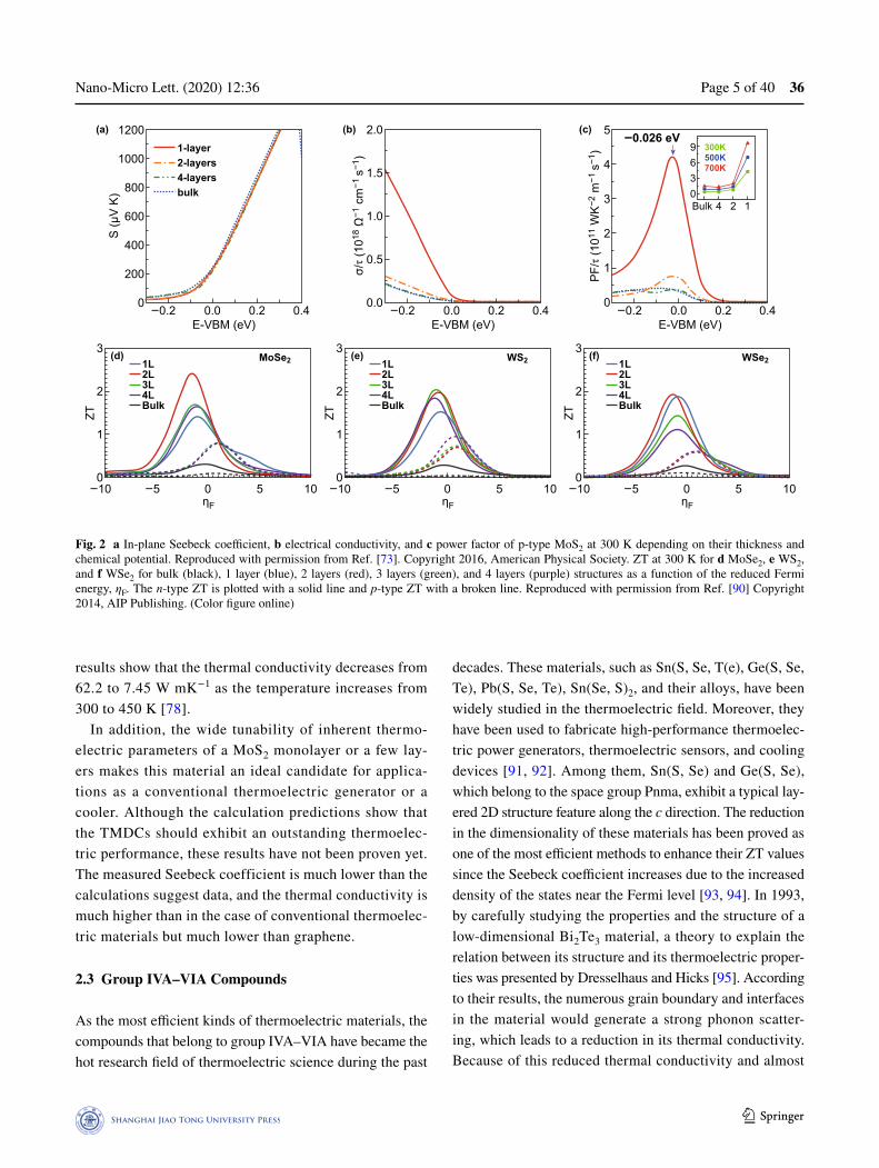
As previously mentioned, the ZT value depends on three inherent physical quantities: the thermal conductivity, the electrical conductivity, and the Seebeck coefficient. These quantities have been widely studied in the case of 2D mate-rials. Owing to their characteristic quasi-two- dimensional crystal structures, TMDCs exhibit high Seebeck coefficient [71–73]. By considering MoS2 as a reference compound, a brief introduction about the thermoelectric properties of 2D TMDCs is presented below. As shown in Fig. 2a–c, the thermoelectric properties of MoS2 multilayers at 300 K are calculated along the in-plane direction. According to the calculation results, the Seebeck coefficients are not affected so much by the change of the layer numbers. However, the electric conductivity shows clear changes depending on
the layer thickness, as shown in Fig. 2b. The significantly increased electrical conductivity as well as the PF/τ is mainly caused by the valley degeneracy at the valence band edge [73]. The ZT values of TMDCs (MoSe2, WS2, and WSe2) along the in-plane direction have been predicted. As shown in Fig. 2d–f, the few layers’ structure shows large increase in the values of their ZT compared to those of the bulk. Besides the theory prediction, the thermoelec-tric properties of 2D TMDCs have also been measured and the experimental results have proven that their thermo-electric properties can be enhanced by applying external electric field and pressure. Buscema et al. [71] reported a large Seebeck coefficient with a large tunability between − 4 × 10² and − 1 × 10⁵ μV K−1 for the MoS2 monolayer in the presence of an external electric field. However, in a highly positive gate range, the Seebeck coefficient varies from −2 × 10² to − 1.5 × 10³ μV K−1 and in a highly nega-tive gate range, it varies from − 3 × 10⁴ to − 3 × 10⁵ μV K−1, showing an increases of about two orders of magnitude. Wu et al. observed a large Seebeck coefficient of 30 mV K−1 by adjusting the backgate voltage [74]. The thermoelectric properties of an exfoliated 2D MoS2 flake with different thickness were studied by Hippalgaonkar. Due to the high electron concentration of n = 1.06 × 1013 cm−2, the bilayer MoS2 exhibits the highest power factor (8.5 mW mK−2) as the gate voltage is 104 V [72]. Due to the high electron con-centration of n = 1.06 × 1013 cm−2, the MoS2 bilayer exhibits the highest power factor (8.5 mW mK−2) as the gate voltage reaches 104 V.
The 2D TMDCs exhibit a relatively lower thermal conductivity when compared to graphene, which make them a promising material for various applications in thermoelectric devices. The low thermal conductivity of the 2D TMDCs has been widely studied in experimental and theoretical works [75–89]. For instance, Sahoo et al. measured the thermal conductivity of a suspended few-layer MoS2 film by using a laser-power-dependent Raman scattering experiment method. As a result, the thermal conductivity at room temperature for few-layer MoS2 was found to be 52 W mK−1 [80]. Yan et al. [79] care-fully measured and analyzed the temperature-dependent Raman spectra of the exfoliated MoS2 monolayer at room temperature, and the measured thermal conductivity is 34.5 W mK−1. Taube et al. measured the temperature-dependent thermal conductivity of the MoS2 monolayer on a SiO2/Si substrate via Raman spectroscopy. The
Nano-Micro Lett. (2020) 12:36 Page 5 of 40 36
1 3
results show that the thermal conductivity decreases from 62.2 to 7.45 W mK−1 as the temperature increases from 300 to 450 K [78].
In addition, the wide tunability of inherent thermo-electric parameters of a MoS2 monolayer or a few lay-ers makes this material an ideal candidate for applica-tions as a conventional thermoelectric generator or a cooler. Although the calculation predictions show that the TMDCs should exhibit an outstanding thermoelec-tric performance, these results have not been proven yet. The measured Seebeck coefficient is much lower than the calculations suggest data, and the thermal conductivity is much higher than in the case of conventional thermoelec-tric materials but much lower than graphene.
2.3 Group IVA–VIA Compounds
As the most efficient kinds of thermoelectric materials, the compounds that belong to group IVA–VIA have became the hot research field of thermoelectric science during the past
decades. These materials, such as Sn(S, Se, T(e), Ge(S, Se, Te), Pb(S, Se, Te), Sn(Se, S)2, and their alloys, have been widely studied in the thermoelectric field. Moreover, they have been used to fabricate high-performance thermoelec-tric power generators, thermoelectric sensors, and cooling devices [91, 92]. Among them, Sn(S, Se) and Ge(S, Se), which belong to the space group Pnma, exhibit a typical lay-ered 2D structure feature along the c direction. The reduction in the dimensionality of these materials has been proved as one of the most efficient methods to enhance their ZT values since the Seebeck coefficient increases due to the increased density of the states near the Fermi level [93, 94]. In 1993, by carefully studying the properties and the structure of a low-dimensional Bi2Te3 material, a theory to explain the relation between its structure and its thermoelectric proper-ties was presented by Dresselhaus and Hicks [95]. According to their results, the numerous grain boundary and interfaces in the material would generate a strong phonon scatter-ing, which leads to a reduction in its thermal conductivity. Because of this reduced thermal conductivity and almost
1-layer2-layers4-layersbulk
(a) (b) (c)
(d) (e) (f)
1200
1000
800
600
400
200
0
3
2
1
0
2.0
1.5
1.0
0.5
0.0
5
4
3
2
1
0
S (µ
V K
)
σ/τ
(1018
Ω−1
cm
−1 s
−1)
PF/τ
(1011
WK
−2 m
−1 s
−1)
−0.2 0.0 0.2 0.4E-VBM (eV)
−0.2 0.0 0.0 0.2 0.40.2 0.4E-VBM (eV)
−0.2
−0.026 eV
E-VBM (eV)
300K500K700K
9630Bulk 4 2 1
1L2L3L4LBulk
MoSe2
ZT
−10 −5 0ηF
5 10
3
2
1
0
1L2L3L4LBulk
WS2
ZT
−10 −5 0ηF
5 10
3
2
1
0
1L2L3L4LBulk
WSe2
ZT
−10 −5 0ηF
5 10
Fig. 2 a In-plane Seebeck coefficient, b electrical conductivity, and c power factor of p-type MoS2 at 300 K depending on their thickness and chemical potential. Reproduced with permission from Ref. [73]. Copyright 2016, American Physical Society. ZT at 300 K for d MoSe2, e WS2, and f WSe2 for bulk (black), 1 layer (blue), 2 layers (red), 3 layers (green), and 4 layers (purple) structures as a function of the reduced Fermi energy, ηF. The n-type ZT is plotted with a solid line and p-type ZT with a broken line. Reproduced with permission from Ref. [90] Copyright 2014, AIP Publishing. (Color figure online)

Nano-Micro Lett. (2020) 12:3636 Page 6 of 40
https://doi.org/10.1007/s40820-020-0374-x© The authors
unchanged electrical properties, an enhanced ZT value could be obtained in the case of such low-dimensional materials [95]. Several years later, Sofo and Mahan [96] proposed a modified theory. They suggested that the well-quantum mix-ing and the changing density of state from a 2D into a 3D lead to a higher thermoelectric performance. Subsequently, by converting them into the well-quantum, the highest ZT value of bulk Bi2Te3 was improved 13 times. This result confirms the validity of the theory that the reduction in the dimensionality is helpful to enhance the energy conversion efficiency of these materials [97]. Fei and Cheng [98, 99] reported a bismuth monolayer showing very promising ther-moelectric properties.
As a typical compound belonging to the group IVA–VIA, tin selenide (SnSe) has been widely studied due to its out-standing electronic and photonic properties. SnSe exhibits potential applications in many fields such as in energy stor-age and conversion devices and novel optoelectronic devices [92, 100–102] SnSe exhibits a layered orthorhombic struc-ture and belongs to the Pnma space group at room tempera-ture. Its structure can be derived from a three-dimensional distortion of a rock-salt structure. Normally, the Sn and Se atoms are arranged in double layers with two planes consist-ing of zigzag Sn–Se chains along the a-axis.
As a thermoelectric material, the thermoelectric proper-ties of SnSe are limited by its poor electrical conductivity at room temperature. However, Zhao et al. reported a remark-ably high ZT value of 2.6 (at 923 K) and of 2.2 (at 773 K) in p-type and n-type single-crystal SnSe, respectively [33, 103]. These results triggered the researchers in performing further studies on the thermoelectric properties of SnSe and its alloys. According to Zhao’s study, such excellent thermo-electric performances originate from the ultralow thermal conductivity when the SnSe transfers into a high-temper-ature phase at T >973 K. Inspired by the ultralow thermal conductivity and by the excellent electrical properties, SnSe and its alloys have attracted a significant attention in recent years [104]. Despite the excellent thermoelectric properties obtained for the SnSe single crystals, their complex crys-tal growth conditions and high production costs limit their practical applications [105]. Therefore, scientists focused on the development of high-performance polycrystalline SnSe. Via systematic optimization methods, such as texturing, dop-ing, and alloying, a significant enhancement of the ZT value of polycrystalline SnSe materials was achieved during the last several years [106–108]. Recently, the thermoelectric
properties of polycrystalline SnSe have been improved con-tinuously and their ZT value have been improved from 0.5 to nearly 1.7 via optimization of the carrier concentration [109, 110]. The thermoelectric performance of polycrystalline SnSe can further improved since its ZT value is still much lower than that of a single-crystal SnSe. For polycrystal-line SnSe, the thermal conductivity remains higher than its theoretical calculation value and its electrical conductivity is lower than a single-crystal SnSe due to the existing grain boundaries [111]. Achieving an ultrahigh ZT value for the polycrystalline comparable to its single-crystal counterpart is still a challenge, and more experimental and theoretical work needs to be done in the next years.
2.4 Black Phosphorus
A monolayer phosphorene and a few-layer phosphorene have been successfully exfoliated from bulk BP in 2014 and have attracted a tremendous research interest in the past few years [28, 112, 113]. As a novel elementary 2D material, the few-layer BP has gained tremendous attention in theoreti-cal and experimental investigations [114–119]. Due to its unique crystal structure and in-plane anisotropic properties, BP has been widely studied in various fields including in the development of photodetectors [116, 120, 121], cancer therapies [115, 122, 123], supercapacitors [124], field-effect transistors (FETs) [125, 126], batteries [127, 128], and ther-moelectric devices [39, 98, 129–133].
Moreover, BP has also been reported as a prospective materials for the production of thermoelectric devices due to its large Seebeck coefficient (335 μV K−1 at room temperature) [130], high carrier mobility (1000 cm2 (Vs)−1 at room temperature) [28], and moderate band gap (0.3–2.0 eV) [28, 112, 130]. According to the experimen-tal results, bulk BP displays a high Seebeck coefficient of 335 μV K−1 and the few-layer BP show an increased Seebeck coefficient up to 510 μV K−1 [130, 134]. Due to its puckered structure, the electrical conductivity, the Seebeck coefficient, and the thermal conductivity of BP exhibit a strongly in-plane anisotropic behavior. This char-acteristic has been proved theoretically and experimentally in various kinds of BP materials including few-layer BP, thin-film BP, and bulk BP [135–140]. Recently, a number of theoretical simulation results have been published and predicted that the few-layer BP is an appealing materials
Nano-Micro Lett. (2020) 12:36 Page 7 of 40 36
1 3
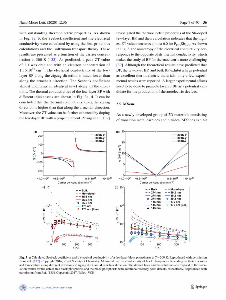
with outstanding thermoelectric properties. As shown in Fig. 3a, b, the Seebeck coefficient and the electrical conductivity were calculated by using the first-principles calculations and the Boltzmann transport theory. These results are presented as a function of the carrier concen-tration at 300 K [132]. As predicted, a peak ZT value of 1.1 was obtained with an electron concentration of 1.5 × 1020 cm−3. The electrical conductivity of the few-layer BP along the zigzag direction is much lower than along the armchair direction. The Seebeck coefficient almost maintains an identical level along all the direc-tions. The thermal conductivities of the few-layer BP with different thicknesses are shown in Fig. 3c, d. It can be concluded that the thermal conductivity along the zigzag direction is higher than that along the armchair direction. Moreover, the ZT value can be further enhanced by doping the few-layer BP with a proper element. Zhang et al. [132]
investigated the thermoelectric properties of the Sb-doped few-layer BP, and their calculation indicates that the high-est ZT value measures almost 6.0 for P0.75Sb0.25. As shown in Fig. 3, the anisotropy of the electrical conductivity cor-responds to the opposite of its thermal conductivity, which makes the study of BP for thermoelectric more challenging [39]. Although the theoretical results have predicted that BP, the few-layer BP, and bulk BP exhibit a huge potential as excellent thermoelectric materials, only a few experi-mental results were reported. A larger experimental efforts need to be done to promote layered BP as a potential can-didate for the production of thermoelectric devices.
2.5 MXene
As a newly developed group of 2D materials consisting of transition metal carbides and nitrides, MXenes exhibit
300K-x300K-y300K-z
(b)(a)
(c)
200
100
0
−100
−200
S (µ
V K
−1)
κ (W
m−1
K−1
)
−1.0×10²¹
104
103
102
1010 100 200 300
T (K)
−0.5×10²¹
Carrier concentration (cm−3)0.5×10²¹ 1.0×10²¹
300K-x300K-y300K-z
20
15
10
5
0
σ (1
06 S
m−1
)
−1.0×10²¹ −0.5×10²¹
Carrier concentration (cm−3)0.5×10²¹ 1.0×10²¹
BulkMonolayer55.6 nm55.6 nm55.6 nm170 nm170 nm (Lee)
(d)
κ (W
m−1
K−1
)
104
103
102
1010 100 200 300
T (K)
Monolayer39.2 nm39.2 nm39.2 nm170 nm170 nm (Lee)
Bulk274 nm274 nm274 nm145 nm145 nm145 nm
Fig. 3 a Calculated Seebeck coefficient and b electrical conductivity of a few-layer black phosphorus at T = 300 K. Reproduced with permission from Ref. [132]. Copyright 2016, Royal Society of Chemistry. Measured thermal conductivity of black phosphorus depending on their thickness and temperature along different directions: c zigzag direction, d armchair direction. The dashed lines and the solid lines correspond to the calcu-lation results for the defect-free black phosphorus and the black phosphorus with additional vacancy point defects, respectively. Reproduced with permission from Ref. [135]. Copyright 2017, Wiley–VCH
Nano-Micro Lett. (2020) 12:3636 Page 8 of 40
https://doi.org/10.1007/s40820-020-0374-x© The authors
either metallic or semiconducting properties depending on its surface functionalization [141]. MXenes can be pre-pared by exfoliating the MAX phases into 2D nanosheets via selective etching of “A” layers by using appropriate hydrofluoric acids [29, 141–145]. These materials are defined as Mn+1AXn, where n = 1, 2, or 3, “M” corresponds to an early transition metal (Sc, Ti, V, Cr, Zr, Nb, Mo, Hf, Ta), “A” is an element from groups 13–16 in the periodic table (Al, Si, P, S, Ga, Ge, As, In, Sn, Tl, Pb), and “X” is carbon and/or nitrogen. Due to its excellent thermal stabil-ity in air, MXene has been studied as a high-temperature thermoelectric material. Moreover, Kumar et al. have pre-dicted that the functionalization of MXene by O, F, and OH groups can significantly affect its structural properties and electronic band structure, further enhancing its ther-moelectric performance [146]. For instance, when ScC2 is functionalized with C, O, or OH, its band gap measures 1.84 (indirect), 1.03 (indirect), and 0.44 eV (indirect), respectively [146]. Such varied band gap structure leads to different thermoelectric properties of the materials. The calculation results show that the Seebeck coefficient of Sc2C(OH)2 measures only 372 μV K−1, while the Seebeck coefficient of Sc2CO2 and Sc2CF2 is above 1000 μV K−1 at room temperature [146]. Furthermore, the calculation results show that these materials exhibit different thermal conductivity. The lattice thermal conductivity of Sc2CO2, Sc2CF2, and Sc2C(OH)2 is 59, 36, and 10 W mK−1, respec-tively. By using the Boltzmann transport theory and the first-principles electronic structure calculations, Khazaei et al. [141] predicted the thermoelectric properties of more than 35 kinds of different functionalized MXene monolay-ers and multilayers of the type M2C, where M=Sc, Ti, V, Zr, Nb, Mo, Hf, and Ta, and M2N, M=Ti, Zr, and Hf. The calculation results prove that the monolayer and multilayer Mo2C nanosheets exhibit a higher power factor than other functionalized MXenes samples. However, several positive results show that MXene can achieve a higher thermoelec-tric performance. According to the calculations, almost all the semiconducting MXene shows a Seebeck coefficient larger than 100 μV K−1 at 400 K and some of them (such as Mo2CF2, Mo2C(OH)2, and Mo2CCl2) exhibit a high electrical conductivity [141].
The outstanding thermoelectric performance of MXenes has also been proved by a series of experiments. Kim et al. fabricated two kinds of Mo-based MXene (Mo2CTx, Mo2TiC2Tx, and Mo2Ti2C3Tx) flexible thin films and studied
their thermoelectric properties [147]. For instance, the Mo2TiC2Tx film exhibits the highest power factor (about 309 μW mK−2 at 800 K) among these samples. Although a high thermoelectric performance for MXene has been theoretically predicted [141, 146–148], more experimental results have to be performed.
3 Thermoelectric Materials Based on 2D Materials
Layered 2D materials have been widely employed as effi-cient thermoelectric materials in the last decades. In this section, the 2D layer structure materials based on the ele-ments belonging to the groups IV–VI and on TMDCs are investigated. The previously reported results proved that bulk and monolayer materials exhibit extremely different thermoelectric properties [149]. In this section, the ther-moelectric properties of bulk and thin films based on 2D materials are discussed.
3.1 Bulk Thermoelectric Materials
Due to the limitations in materials synthesis techniques, bulk thermoelectric materials are usually fabricated via a simple melting process or a ball milling process followed by a post-sintering process (such as spark plasma sintering or hot press process). Although the materials exhibit a layer-by-layer structure, the synthesis of these compounds via these methods is not discussed in this review. With the devel-opment of nanotechniques, a series of new methods have been developed to fabricate nanomaterials with a variety of microstructures. Currently, it is possible to synthesize 2D compounds in large amounts to fabricate bulk thermoelectric materials. Since the grain boundary can scatter the phonons and can lead to low a thermal conductivity, it may be useful to fabricate high-performance thermoelectric materials by decreasing the particle size of the nanostructure thermoelec-tric material. Recently, 2D metal chalcogenides (including the group IV–VI compounds and the TMDCs) have trig-gered a considerable attention in the field of thermoelectrics as they exhibit a high ZT value. Due to their anisotropic crystal and electronic structures, these materials exhibit an intrinsically low thermal conductivity, which makes them promising thermoelectric materials [17, 150].
Nano-Micro Lett. (2020) 12:36 Page 9 of 40 36
1 3
Among the 2D metal chalcogenides thermoelectric materials, SnSe seems to be promising commercially available thermoelectric material. Until now, the highest ZT value for both the p-type (2.6 at 923 K) and n-type (2.8 at 923 K) compounds was obtained from SnSe single crystals. This may be due to their layered structure, soft chemical bonding, and lattice anharmonicity. However, the ZT value of polycrystalline SnSe bulk materials is
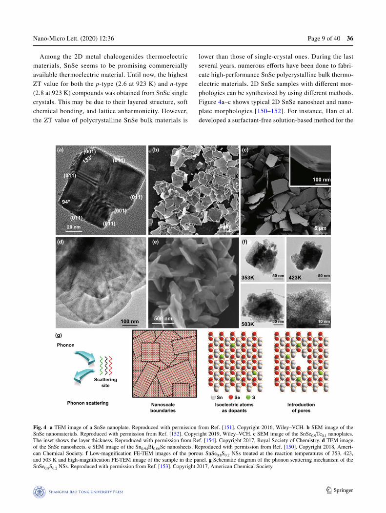
lower than those of single-crystal ones. During the last several years, numerous efforts have been done to fabri-cate high-performance SnSe polycrystalline bulk thermo-electric materials. 2D SnSe samples with different mor-phologies can be synthesized by using different methods. Figure 4a–c shows typical 2D SnSe nanosheet and nano-plate morphologies [150–152]. For instance, Han et al. developed a surfactant-free solution-based method for the
(a)
(d)
(b)
(e)
(c)
100 nm
(f)
(g)
353K 423K
503K
(001)
133° (011)
(011)
(011)(011)
(001)
(011)94°
5 µm5 µm
50 nm
100 nm
Phonon
Scatteringsite
Phonon scattering Nanoscaleboundaries
Isoelectric atomsas dopants
Introductionof pores
50 nm
50 nm 10 nm500 nm
Sn Se S
20 nm
Fig. 4 a TEM image of a SnSe nanoplate. Reproduced with permission from Ref. [151]. Copyright 2016, Wiley–VCH. b SEM image of the SnSe nanomaterials. Reproduced with permission from Ref. [152]. Copyright 2019, Wiley–VCH. c SEM image of the SnSe0.9Te0.1 nanoplates. The inset shows the layer thickness. Reproduced with permission from Ref. [154]. Copyright 2017, Royal Society of Chemistry. d TEM image of the SnSe nanosheets. e SEM image of the Sn0.94Bi0.06Se nanosheets. Reproduced with permission from Ref. [150]. Copyright 2018, Ameri-can Chemical Society. f Low-magnification FE-TEM images of the porous SnSe0.8S0.2 NSs treated at the reaction temperatures of 353, 423, and 503 K and high-magnification FE-TEM image of the sample in the panel. g Schematic diagram of the phonon scattering mechanism of the SnSe0.8S0.2 NSs. Reproduced with permission from Ref. [153]. Copyright 2017, American Chemical Society
Nano-Micro Lett. (2020) 12:3636 Page 10 of 40
https://doi.org/10.1007/s40820-020-0374-x© The authors
synthesis of single-phase SnSe nanoplates. Their power factor measured perpendicularly to the hot-pressing direc-tion reaches 0.4 mW mK−2 at 550 K [151]. Rongione et al. [152] fabricated a series of SnSe nanosheets and obtained an ultralow thermal conductivity of 0.09 W m−1 K−1. Such value mainly originates from the large thermal boundary resistance of the materials due to the strong phonon scat-tering near the interfaces between two SnSe nanosheets. In order to further improve the ZT value of SnSe bulk, Bi-, Te-, and S- doped SnSe nanosheets were synthesized by using a large variety of methods [150, 153–155]. The SEM morphology of the doped SnSe samples is shown in Fig. 4d–f. Chandra et al. synthesized a 2D ultrathin n-type Bi-doped SnSe nanosheet via a simple low-temperature solvothermal method [150]. The thickness of the SnSe nanosheet measures about 1–3 nm. Due to the presence of the nanoscale grain boundaries and the layered aniso-tropic structure, the heat-carrying phonons strongly scat-ter. This leads to an ultralow lattice thermal conductivity of 0.3 W mK−1 in the range of 300–720 K. Ju et al. fab-ricated a porous SnSe1−xSx nanosheet, and the details of this structure are shown in Fig. 4g [153]. A reduction in the thermal conductivity and an improved ZT value were obtained. Such enhanced ZT value is mostly due to the substitution of the S atoms into SnSe, which induces the scattering of the phonons and several atomic disorders and nanosized boundaries. The mechanism of phonon scat-tering in porous SnSe0.8S0.2-based materials is illustrated by the simple schematic diagram in Fig. 4g. As a result, the high ZT value of the bulk based on porous SnSe0.8S0.2 nanosheets reaches 0.12 at 310 K. The substitution of the S atoms into SnSe and the fabrication of the SnSe1−xSx NSs reduce the thermal conductivity by introducing phonon scattering in the atomic disorders and nanoscale bounda-ries, leading to a higher ZT.
Similarly to SnSe, SnSe2 is also a layered structure ther-moelectric material and exhibits promising thermoelectric performance [156–159]. Saha et al. fabricated ultrathin Cl-doped SnSe2 nanosheets with the thickness of 3–5 nm via a simple low-temperature solvothermal process [159]. Similarly to SnSe, the hot-pressed SnSe2 pellet achieves an ultralow thermal conductivity of 0.67 W/mK due to its effective phonon scattering at the grain boundary, which is induced by its anisotropic layered structure.
During the last decades, the most efficient single-phase thermoelectric materials used in the near room temperature
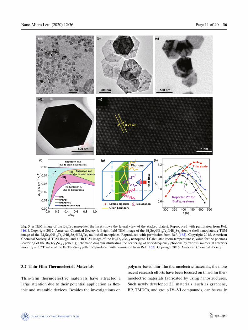
range are Bi2Te3-based alloys, which are also layered materi-als. Until now, the optimized ZT value of these compounds measure around 1.0. The highest ZT value for the p-type and n-type Bi2Te3 alloys is obtained in the case of Bi0.5Te1.5Se3 (ZTmax = 1.2) and Bi2Te2.7Se0.3 (ZTmax = 0.9) [17, 160]. Both these samples are bulk materials. Recently, Bi2Te3-based nanosheets have been widely reported in the fabrication of bulk Bi2Te3-based thermoelectric materials. As shown in Fig. 5a, Son et al. synthesized an ultrathin Bi2Te3 nanoplate with a thickness of about 1 nm via a simple solution process [161]. The Bi2Te3 bulk was prepared by sintering Bi2Te3 nanoplates via spark plasma sintering, and the maximum ZT value obtained was 0.62 at 400 K. Figure 5b, c shows the TEM images of the Bi2Se3@Bi2Te3 heterostructure nanoplates and of the Bi2Se3@Bi2Te3@Bi2Se3@Bi2Te3 multishell nanoplates, which were scalable synthesized via a solution epitaxial growth process [162]. The thickness of the nanoplate is in the 5–20 nm range. Via the simultaneous modulation of the electronic and thermal transport in the presence of highly dense grain and phase boundaries, the peak ZT value measures 0.71 and it was obtained at 450 K for via the bulk sintering of the Bi2Se3@Bi2Te3 nanoplates. Hong et al. synthesized a n-type Bi2Te3−xSex nanoplate by using the microwave-assisted surfactant-free solvothermal method. The TEM images of the nanoplate are shown in Fig. 5d, e [163]. The schematic diagram of the phonon scat-tering is shown in Fig. 5f, g. The grain boundaries, the point defects, and the dislocations may lead to the reduction in the lattice thermal conductivity. The experimental results prove these predictions. In this case, a relatively high ZT value of 1.23 at 480 K for the n-type Bi2Te2.7Se0.3 nanostructures was obtained from the sintered pellets. Since the nanostructure was employed as a raw material to obtain the sinter pellets, a high amount of grain boundaries was maintained and sub-stantially reduced the thermal conductivity of the sample [163].
In the case of the bulk layered thermoelectric materials, the layered structure induces strong anisotropic thermo-electric properties along three different directions. More importantly, the grain boundaries, which were introduced by the nanostructuring, can substantially reduce the ther-mal conductivity when compared to the pellet structure. These samples were, in fact, synthesized by using ball milling and other melting methods. The 2D nanostruc-ture materials employed to fabricate bulk thermoelectric materials further enhance their ZT value.
Nano-Micro Lett. (2020) 12:36 Page 11 of 40 36
1 3
3.2 Thin‑Film Thermoelectric Materials
Thin-film thermoelectric materials have attracted a large attention due to their potential application as flex-ible and wearable devices. Besides the investigations on
polymer-based thin-film thermoelectric materials, the more recent research efforts have been focused on thin-film ther-moelectric materials fabricated by using nanostructures. Such newly developed 2D materials, such as graphene, BP, TMDCs, and group IV–VI compounds, can be easily
(a) (b)
50 nm
(d)
(f) (g) (h)Phonons
Lattice disorder DislocationGrain boundary
Hea
t flo
w
(e)
200 nm
(c)
500 nm 1 nm
This study
Reported ZT forBi2Te3 systems
0.22 nm
500 nm
(I)(III)
(II)
Reduction in κldue to dislocations
U+EU+E+BU+E+B+PDU+E+B+PD+DC+DS
Reduction in κldue to point defects
Reduction in κldue to grain boudndaries
0.05
0.04
0.03
0.02
0.01
0.00
1.2
1.0
0.8
0.6
κ s (p
W s
m−1
K−1
)
0.0 0.2 0.4 0.6ω/ωD
0.8 1.0
ZT
300 400 450T (K)
500 550350
Fig. 5 a TEM image of the Bi2Te3 nanoplate, the inset shows the lateral view of the stacked plates). Reproduced with permission from Ref. [161]. Copyright 2012, American Chemical Society. b Bright-field TEM image of the Bi2Se3@Bi2Te3@Bi2Se3 double shell nanoplates. c TEM image of the Bi2Se3@Bi2Te3@Bi2Se3@Bi2Te3 multishell nanoplates. Reproduced with permission from Ref. [162]. Copyright 2015, American Chemical Society. d TEM image, and e HRTEM image of the Bi2Te2.7Se0.3 nanoplate. f Calculated room-temperature κs value for the phonons scattering of the Bi2Te2.7Se0.3 pellet. g Schematic diagram illustrating the scattering of wide-frequency phonons by various sources. h Carriers mobility and ZT value of the Bi2Te2.7Se0.3 pellet. Reproduced with permission from Ref. [163]. Copyright 2016, American Chemical Society
Nano-Micro Lett. (2020) 12:3636 Page 12 of 40
https://doi.org/10.1007/s40820-020-0374-x© The authors
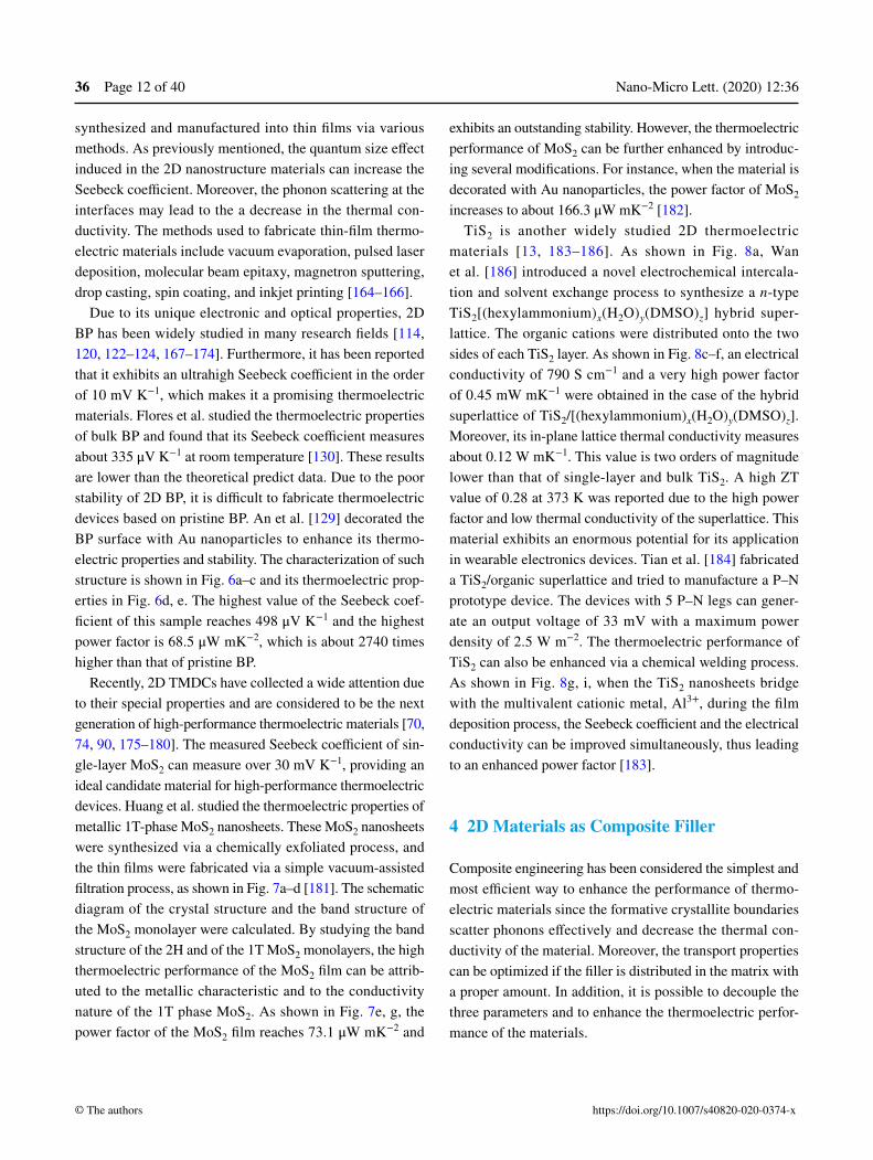
synthesized and manufactured into thin films via various methods. As previously mentioned, the quantum size effect induced in the 2D nanostructure materials can increase the Seebeck coefficient. Moreover, the phonon scattering at the interfaces may lead to the a decrease in the thermal con-ductivity. The methods used to fabricate thin-film thermo-electric materials include vacuum evaporation, pulsed laser deposition, molecular beam epitaxy, magnetron sputtering, drop casting, spin coating, and inkjet printing [164–166].
Due to its unique electronic and optical properties, 2D BP has been widely studied in many research fields [114, 120, 122–124, 167–174]. Furthermore, it has been reported that it exhibits an ultrahigh Seebeck coefficient in the order of 10 mV K−1, which makes it a promising thermoelectric materials. Flores et al. studied the thermoelectric properties of bulk BP and found that its Seebeck coefficient measures about 335 μV K−1 at room temperature [130]. These results are lower than the theoretical predict data. Due to the poor stability of 2D BP, it is difficult to fabricate thermoelectric devices based on pristine BP. An et al. [129] decorated the BP surface with Au nanoparticles to enhance its thermo-electric properties and stability. The characterization of such structure is shown in Fig. 6a–c and its thermoelectric prop-erties in Fig. 6d, e. The highest value of the Seebeck coef-ficient of this sample reaches 498 μV K−1 and the highest power factor is 68.5 μW mK−2, which is about 2740 times higher than that of pristine BP.
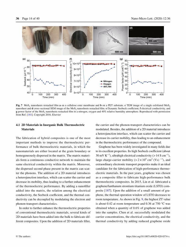
Recently, 2D TMDCs have collected a wide attention due to their special properties and are considered to be the next generation of high-performance thermoelectric materials [70, 74, 90, 175–180]. The measured Seebeck coefficient of sin-gle-layer MoS2 can measure over 30 mV K−1, providing an ideal candidate material for high-performance thermoelectric devices. Huang et al. studied the thermoelectric properties of metallic 1T-phase MoS2 nanosheets. These MoS2 nanosheets were synthesized via a chemically exfoliated process, and the thin films were fabricated via a simple vacuum-assisted filtration process, as shown in Fig. 7a–d [181]. The schematic diagram of the crystal structure and the band structure of the MoS2 monolayer were calculated. By studying the band structure of the 2H and of the 1T MoS2 monolayers, the high thermoelectric performance of the MoS2 film can be attrib-uted to the metallic characteristic and to the conductivity nature of the 1T phase MoS2. As shown in Fig. 7e, g, the power factor of the MoS2 film reaches 73.1 μW mK−2 and
exhibits an outstanding stability. However, the thermoelectric performance of MoS2 can be further enhanced by introduc-ing several modifications. For instance, when the material is decorated with Au nanoparticles, the power factor of MoS2 increases to about 166.3 μW mK−2 [182].
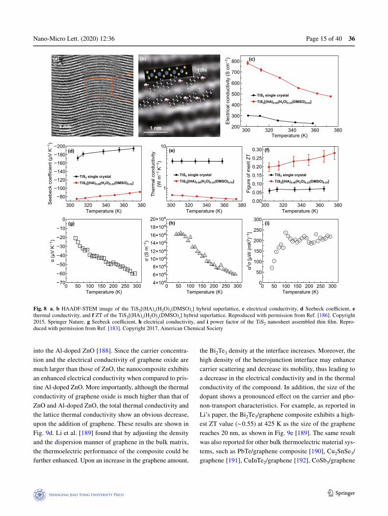
TiS2 is another widely studied 2D thermoelectric materials [13, 183–186]. As shown in Fig. 8a, Wan et al. [186] introduced a novel electrochemical intercala-tion and solvent exchange process to synthesize a n-type TiS2[(hexylammonium)x(H2O)y(DMSO)z] hybrid super-lattice. The organic cations were distributed onto the two sides of each TiS2 layer. As shown in Fig. 8c–f, an electrical conductivity of 790 S cm−1 and a very high power factor of 0.45 mW mK−1 were obtained in the case of the hybrid superlattice of TiS2/[(hexylammonium)x(H2O)y(DMSO)z]. Moreover, its in-plane lattice thermal conductivity measures about 0.12 W mK−1. This value is two orders of magnitude lower than that of single-layer and bulk TiS2. A high ZT value of 0.28 at 373 K was reported due to the high power factor and low thermal conductivity of the superlattice. This material exhibits an enormous potential for its application in wearable electronics devices. Tian et al. [184] fabricated a TiS2/organic superlattice and tried to manufacture a P–N prototype device. The devices with 5 P–N legs can gener-ate an output voltage of 33 mV with a maximum power density of 2.5 W m−2. The thermoelectric performance of TiS2 can also be enhanced via a chemical welding process. As shown in Fig. 8g, i, when the TiS2 nanosheets bridge with the multivalent cationic metal, Al3+, during the film deposition process, the Seebeck coefficient and the electrical conductivity can be improved simultaneously, thus leading to an enhanced power factor [183].
4 2D Materials as Composite Filler
Composite engineering has been considered the simplest and most efficient way to enhance the performance of thermo-electric materials since the formative crystallite boundaries scatter phonons effectively and decrease the thermal con-ductivity of the material. Moreover, the transport properties can be optimized if the filler is distributed in the matrix with a proper amount. In addition, it is possible to decouple the three parameters and to enhance the thermoelectric perfor-mance of the materials.

Nano-Micro Lett. (2020) 12:36 Page 13 of 40 36
1 3
(a) (b)
(c)
(d) (e)
ACZZ
AC
ZZ 2 nm
50 nm2 nm2.3 Å
Pris
tine
BP
80
60
40
20
0
Ele
ctric
al c
ondu
ctiv
ity (S
cm
−1)
0.00 0.02 0.04 0.06Content of Au NP (molar ratio)
See
beck
coe
ffici
ent (
µV K
−1)
Pow
er fa
ctor
(µW
m−1
K−2
)
0.08 0.10 0.100.080.060.040.020.00Content of Au NP (molar ratio)
100
80
60
40
20
0
800
600
400
200
0
−200
Fig. 6 a Low-magnitude TEM image of the black phosphorus nanosheet decorated with Au nanoparticles. b Lattice image of the exfoliated black phosphorus nanosheet (inset illustration showing the corresponding crystal structure). c High magnitude HRTEM image of the black phos-phorus nanosheet decorated with Au nanoparticles. d In-plane Seebeck coefficient, electrical conductivity, and e their corresponding in-plane power factor of the black phosphorus decorated with Au nanoparticles. Reproduced with permission from Ref. [129]. Copyright 2018, Wiley–VCH
Nano-Micro Lett. (2020) 12:3636 Page 14 of 40
https://doi.org/10.1007/s40820-020-0374-x© The authors
4.1 2D Materials in Inorganic Bulk Thermoelectric Materials
The fabrication of hybrid composites is one of the most important methods to improve the thermoelectric per-formance of bulk thermoelectric materials, in which the nanomaterials are either located at the grain boundary or homogeneously dispersed in the matrix. The matrix materi-als form a continuous conductive network to maintain the same electrical conductivity within the matrix. Moreover, the dispersed second phase present in the matrix can scat-ter the phonons. The addition of a 2D material introduces a heterojunction interface, which can scatter the carrier and decrease its mobility, thus leading to a further enhancement of the thermoelectric performance. By adding a nanofiller added into the matrix, the relation among the electrical conductivity, the Seebeck coefficient, and the thermal con-ductivity can be decoupled by modulating the electron and phonon-transport characteristics.
In order to further enhance the thermoelectric properties of conventional thermoelectric materials, several kinds of 2D materials have been added into the bulk to fabricate dif-ferent composites. Upon the addition of 2D materials filler,
the carrier and the phonon-transport characteristics can be modulated. Besides, the addition of a 2D material introduces a heterojunction interface, which can scatter the carrier and decrease its carrier mobility, thus leading to an enhancement in the thermoelectric performance of the compound.
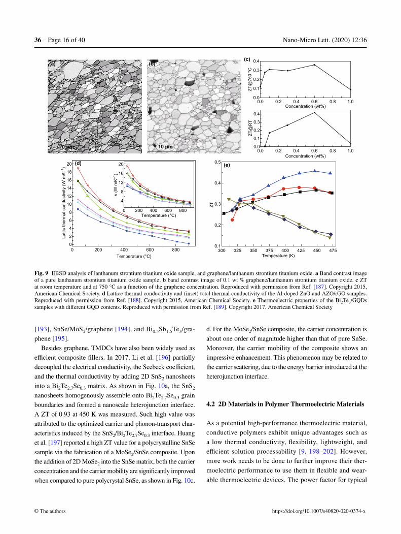
Graphene has been widely investigated in many fields due to its excellent properties. Its high Seebeck coefficient (about 30 mV K−1), ultrahigh electrical conductivity (> 14 S cm−1), large charge-carrier mobility (> 2 × 105 cm2 (Vs) −1), and extraordinary electronic transport properties make it an ideal candidate for the fabrication of high-performance thermo-electric materials. In the past years, graphene was chosen as a composite filler to fabricate high-performance bulk thermoelectric composites. In 2015, Lin et al. fabricated a graphene/lanthanum strontium titanium oxide (LSTO) com-posite [187]. Upon the addition of a small amount of gra-phene, the thermal operation window of LSTO decreases to room temperature. As shown in Fig. 9, the highest ZT value is about 0.42 at room temperature and 0.36 at 750 °C was obtained when a quantity of 0.6% of graphene was added into the samples. Chen et al. successfully modulated the carrier concentrations, the electrical conductivity, and the thermal conductivity by adding reduced graphene oxide
90
80
70
60
50
40
See
beck
(µV
K−1
)
Pow
er fa
ctor
[µW
(mK
2 )−1
]
0 100 200Time (min)
300 400
Ele
ctric
al c
ondu
ctiv
ity (S
m−1
)
0 100
10×103
9×10³
8×10³
7×10³
6×10³
5×103200
Time (min)300 400 0 100 200
Time (min)300 400
NitrogenOxygen40% RH
80
70
60
50
40
30
20
10
0
(e) (f) (g)
(a) (b) (c) (d)
500 nm
300 nm
500 nm
Fig. 7 MoS2 nanosheets restacked film a on a cellulose ester membrane and b on a PET substrate. c TEM image of a single exfoliated MoS2 nanosheet and d cross-sectional SEM image of the MoS2 nanosheets restacked film. e Dynamic Seebeck coefficient, f electrical conductivity, and g power factor of the MoS2 nanosheets restacked film in a nitrogen, oxygen and 40% relative humidity atmosphere. Reproduced with permission from Ref. [181]. Copyright 2016, Elsevier
Nano-Micro Lett. (2020) 12:36 Page 15 of 40 36
1 3
into the Al-doped ZnO [188]. Since the carrier concentra-tion and the electrical conductivity of graphene oxide are much larger than those of ZnO, the nanocomposite exhibits an enhanced electrical conductivity when compared to pris-tine Al-doped ZnO. More importantly, although the thermal conductivity of graphene oxide is much higher than that of ZnO and Al-doped ZnO, the total thermal conductivity and the lattice thermal conductivity show an obvious decrease, upon the addition of graphene. These results are shown in Fig. 9d. Li et al. [189] found that by adjusting the density and the dispersion manner of graphene in the bulk matrix, the thermoelectric performance of the composite could be further enhanced. Upon an increase in the graphene amount,
the Bi2Te3 density at the interface increases. Moreover, the high density of the heterojunction interface may enhance carrier scattering and decrease its mobility, thus leading to a decrease in the electrical conductivity and in the thermal conductivity of the compound. In addition, the size of the dopant shows a pronounced effect on the carrier and pho-non-transport characteristics. For example, as reported in Li’s paper, the Bi2Te3/graphene composite exhibits a high-est ZT value (~ 0.55) at 425 K as the size of the graphene reaches 20 nm, as shown in Fig. 9e [189]. The same result was also reported for other bulk thermoelectric material sys-tems, such as PbTe/graphene composite [190], Cu2SnSe3/graphene [191], CuInTe2/graphene [192], CoSb3/graphene
(a) (b)
5 nm 1 nm
TiS2 single crystal
TiS2[(HA)0.08(H2O)0.22(DMSO)0.03]
TiS2 single crystal
TiS2[(HA)0.08(H2O)0.22(DMSO)0.03]
TiS2 single crystal
TiS2[(HA)0.08(H2O)0.22(DMSO)0.03]TiS2 single crystal
TiS2[(HA)0.08(H2O)0.22(DMSO)0.03]
800
700
600
500
400
300
200
0.30
0.25
0.20
0.15
0.10
0.05
0.00
Ele
ctric
al c
ondu
ctiv
ity (S
cm
−1)
Ther
mal
con
duct
ivity
(W m
−1 K
−1)
See
beck
coe
ffici
ent (
µV K
−1)
α (µ
V K
−1)
α2 σ [µ
W (m
K2 )
−1]
σ (S
m−1
)
4×10⁴
6×10⁴
8×10410×10412×104
14×104
16×104
18×104
20×104
300 320 340Temperature (K)
360 380
300
300
250
200
150
100
50
0
1
10
320 340Temperature (K)
360 380300 320 340Temperature (K)
360 380
Figu
re o
f mer
it ZT
300 320
−200
−180
−160
−140
−120
−100
−80
0
−10
−20
−30
−40
−50
−60
−70
340Temperature (K)
360 380
0 50 100 200 300Temperature (K)
250150 0 50 100 200 300Temperature (K)
250150 0 50 100 200 300Temperature (K)
250150
TiS2
(c)
(e)(d)
(g) (h) (i)
(f)
Fig. 8 a, b HAADF-STEM image of the TiS2[(HA)x(H2O)y(DMSO)z] hybrid superlattice, c electrical conductivity, d Seebeck coefficient, e thermal conductivity, and f ZT of the TiS2[(HA)x(H2O)y(DMSO)z] hybrid superlattice. Reproduced with permission from Ref. [186]. Copyright 2015, Springer Nature. g Seebeck coefficient, h electrical conductivity, and i power factor of the TiS2 nanosheet assembled thin film. Repro-duced with permission from Ref. [183]. Copyright 2017, American Chemical Society
Nano-Micro Lett. (2020) 12:3636 Page 16 of 40
https://doi.org/10.1007/s40820-020-0374-x© The authors
[193], SnSe/MoS2/graphene [194], and Bi0.5Sb1.5Te3/gra-phene [195].
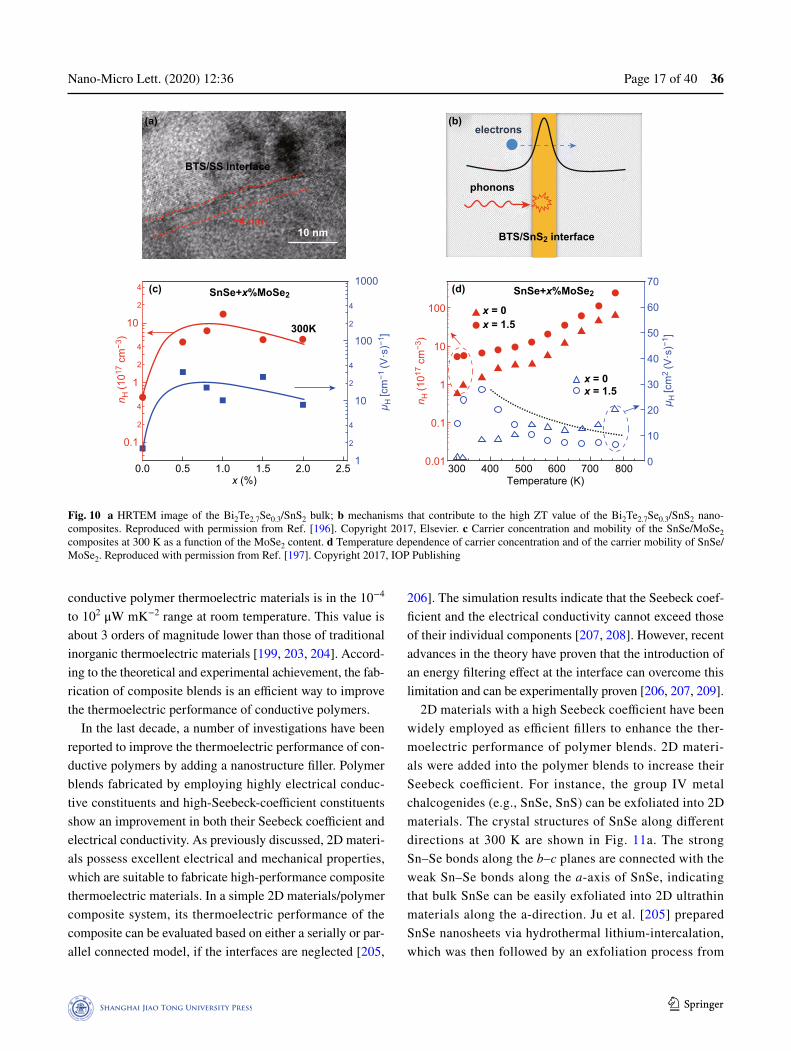
Besides graphene, TMDCs have also been widely used as efficient composite fillers. In 2017, Li et al. [196] partially decoupled the electrical conductivity, the Seebeck coefficient, and the thermal conductivity by adding 2D SnS2 nanosheets into a Bi2Te2.7Se0.3 matrix. As shown in Fig. 10a, the SnS2 nanosheets homogenously assemble onto Bi2Te2.7Se0.3 grain boundaries and formed a nanoscale heterojunction interface. A ZT of 0.93 at 450 K was measured. Such high value was attributed to the optimized carrier and phonon-transport char-acteristics induced by the SnS2/Bi2Te2.7Se0.3 interface. Huang et al. [197] reported a high ZT value for a polycrystalline SnSe sample via the fabrication of a MoSe2/SnSe composite. Upon the addition of 2D MoSe2 into the SnSe matrix, both the carrier concentration and the carrier mobility are significantly improved when compared to pure polycrystal SnSe, as shown in Fig. 10c,
d. For the MoSe2/SnSe composite, the carrier concentration is about one order of magnitude higher than that of pure SnSe. Moreover, the carrier mobility of the composite shows an impressive enhancement. This phenomenon may be related to the carrier scattering, due to the energy barrier introduced at the heterojunction interface.
4.2 2D Materials in Polymer Thermoelectric Materials
As a potential high-performance thermoelectric material, conductive polymers exhibit unique advantages such as a low thermal conductivity, flexibility, lightweight, and efficient solution processability [9, 198–202]. However, more work needs to be done to further improve their ther-moelectric performance to use them in flexible and wear-able thermoelectric devices. The power factor for typical
(a) (b)(c)
(e)(d)
20 µm 10 µm
0.4
0.3
0.2
0.1
0.0
ZT@
750
°C
0.4
0.3
0.2
0.1
0.0
0.5
0.4
0.3
0.2
0.1ZT
@R
T
0.0
20
16
12
8
4
20
18
16
14
12
10
8
6
4
2
0
0.2 0.4 0.6Concentration (wt%)
0.8 1.0
0.0 0.2 0.4 0.6Concentration (wt%)
0.8 1.0
ZT
300200 400 600 8000 325 350 400375 425Temperature (K)
475450
0 200
κ (W
mK
−1)
Latti
c th
erm
al c
ondu
ctiv
ity (W
mK
−1)
400 600 800Temperature (°C)
Temperature (°C)
Fig. 9 EBSD analysis of lanthanum strontium titanium oxide sample, and graphene/lanthanum strontium titanium oxide. a Band contrast image of a pure lanthanum strontium titanium oxide sample; b band contrast image of 0.1 wt % graphene/lanthanum strontium titanium oxide. c ZT at room temperature and at 750 °C as a function of the graphene concentration. Reproduced with permission from Ref. [187]. Copyright 2015, American Chemical Society. d Lattice thermal conductivity and (inset) total thermal conductivity of the Al-doped ZnO and AZO/rGO samples. Reproduced with permission from Ref. [188]. Copyright 2015, American Chemical Society. e Thermoelectric properties of the Bi2Te3/GQDs samples with different GQD contents. Reproduced with permission from Ref. [189]. Copyright 2017, American Chemical Society
Nano-Micro Lett. (2020) 12:36 Page 17 of 40 36
1 3
conductive polymer thermoelectric materials is in the 10−4 to 102 μW mK−2 range at room temperature. This value is about 3 orders of magnitude lower than those of traditional inorganic thermoelectric materials [199, 203, 204]. Accord-ing to the theoretical and experimental achievement, the fab-rication of composite blends is an efficient way to improve the thermoelectric performance of conductive polymers.
In the last decade, a number of investigations have been reported to improve the thermoelectric performance of con-ductive polymers by adding a nanostructure filler. Polymer blends fabricated by employing highly electrical conduc-tive constituents and high-Seebeck-coefficient constituents show an improvement in both their Seebeck coefficient and electrical conductivity. As previously discussed, 2D materi-als possess excellent electrical and mechanical properties, which are suitable to fabricate high-performance composite thermoelectric materials. In a simple 2D materials/polymer composite system, its thermoelectric performance of the composite can be evaluated based on either a serially or par-allel connected model, if the interfaces are neglected [205,
206]. The simulation results indicate that the Seebeck coef-ficient and the electrical conductivity cannot exceed those of their individual components [207, 208]. However, recent advances in the theory have proven that the introduction of an energy filtering effect at the interface can overcome this limitation and can be experimentally proven [206, 207, 209].
2D materials with a high Seebeck coefficient have been widely employed as efficient fillers to enhance the ther-moelectric performance of polymer blends. 2D materi-als were added into the polymer blends to increase their Seebeck coefficient. For instance, the group IV metal chalcogenides (e.g., SnSe, SnS) can be exfoliated into 2D materials. The crystal structures of SnSe along different directions at 300 K are shown in Fig. 11a. The strong Sn–Se bonds along the b–c planes are connected with the weak Sn–Se bonds along the a-axis of SnSe, indicating that bulk SnSe can be easily exfoliated into 2D ultrathin materials along the a-direction. Ju et al. [205] prepared SnSe nanosheets via hydrothermal lithium-intercalation, which was then followed by an exfoliation process from
(a) (b)
(d)(c)
BTS/SS interface
~4 nm10 nm
electrons
phonons
BTS/SnS2 interface
4
2
4
2
4
2
4
2
4
2
1000
100
10
1
70
60
50
40
30
20
10
0
4
2
10
1
0.1
100
10
1
0.1
0.01
n H (1
017 c
m−3
)
n H (1
017 c
m−3
)
μ H [c
m−1
(V·s
)−1]
μ H [c
m2
(V·s
)−1]
0.0 1.0 2.0 2.5 300 400 500 600 700 800Temperature (K)
1.5x (%)
0.5
300K
SnSe+x%MoSe2 SnSe+x%MoSe2
x = 0x = 1.5
x = 0x = 1.5
Fig. 10 a HRTEM image of the Bi2Te2.7Se0.3/SnS2 bulk; b mechanisms that contribute to the high ZT value of the Bi2Te2.7Se0.3/SnS2 nano-composites. Reproduced with permission from Ref. [196]. Copyright 2017, Elsevier. c Carrier concentration and mobility of the SnSe/MoSe2 composites at 300 K as a function of the MoSe2 content. d Temperature dependence of carrier concentration and of the carrier mobility of SnSe/MoSe2. Reproduced with permission from Ref. [197]. Copyright 2017, IOP Publishing

Nano-Micro Lett. (2020) 12:3636 Page 18 of 40
https://doi.org/10.1007/s40820-020-0374-x© The authors
the SnSe powders. During the intercalation process, eth-ylene glycol acts as both the solvent and the reducing agent. The morphology of the exfoliated SnSe nanosheets is shown in Fig. 11b–d. Their thickness is about 3.4 nm. The Seebeck coefficient of pure SnSe at room temperature is higher than 520 μV K−1, whereas for PEDOT:PSS is about 30 μV K−1. As the SnSe nanosheets are dispersed into the PEDOT:PSS solution, the measured Seebeck coef-ficient increases with the increase in the weight fraction of
SnSe. The increase in the power factor to 386 μW mK−2 is induced by the substantial increases in the Seebeck coef-ficient when compared to the reduction in the electrical conductivity of the material. Other 2D group IV metal chalcogenides have also been fabricated and added as fillers to enhance the thermoelectric performance of the composites [210–213]. Ju et al. [212] coated the SnSeS nanosheet by polyaniline (PANI) and then used it as a filler to fabricate the composite. The PANI-coated SnSeS
a b
c a
b c
a
bc
(a)
(b) (c)
(e) (f) (g)
(d)
1 µm 2 µm100 nm
0.5
0.4
0.3
0.2
0.1
0.0
Pow
er fa
ctor
[mW
(m·k
2 )−1
]
0.0 0.1 0.2 0.3 0.4 0.5 0.6Weight fraction of SnSe
1.0
0.8
0.6
0.4
0.2
0.0
Ther
mal
con
duct
ivity
[W (m
·K)−1
]
0.0 0.1 0.2 0.3 0.4 0.5 0.6Weight fraction of SnSe
0.40
0.35
0.30
0.25
0.20
0.15
0.10
0.05
0.00
Figu
re o
f mer
it, ZT
0.0 0.1 0.2 0.3 0.4 0.5 0.6Weight fraction of SnSe
SnSe
Fig. 11 a Crystal structures of SnSe along the a-, b-, and c- axial directions. b SEM morphology and c TEM image of SnSe nanosheets. d SEM of the SnSe/PEDOT:PSS composites with SnSe a content of 50%. e Power factor, f thermal conductivity, and g ZT value of the SnSe/PEDOT:PSS composites. Reproduced with permission from Ref. [205]. Copyright 2016, American Chemical Society
Nano-Micro Lett. (2020) 12:36 Page 19 of 40 36
1 3
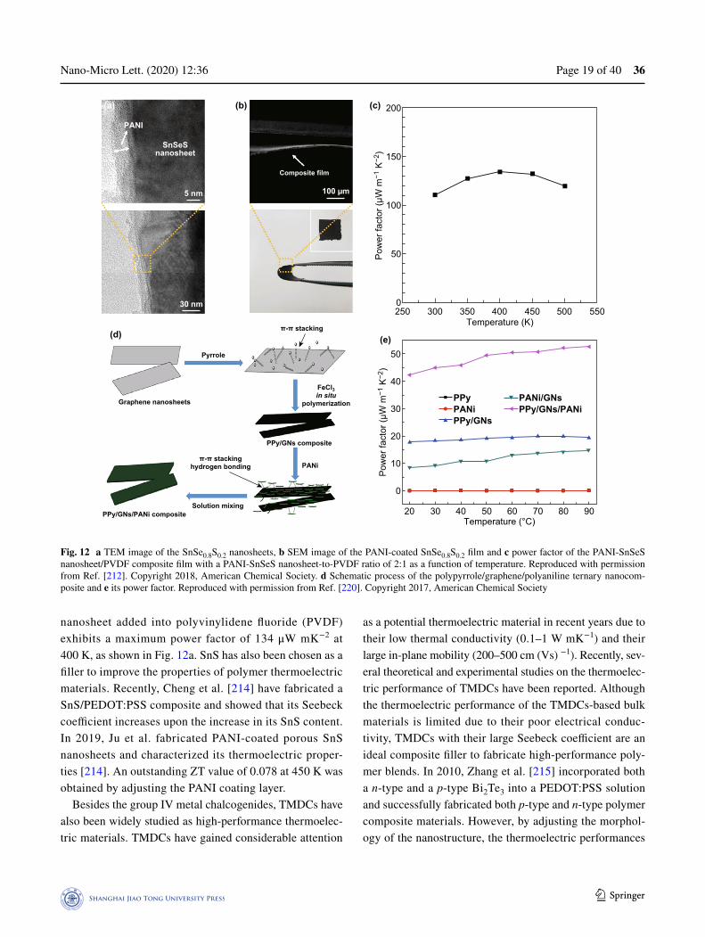
nanosheet added into polyvinylidene fluoride (PVDF) exhibits a maximum power factor of 134 μW mK−2 at 400 K, as shown in Fig. 12a. SnS has also been chosen as a filler to improve the properties of polymer thermoelectric materials. Recently, Cheng et al. [214] have fabricated a SnS/PEDOT:PSS composite and showed that its Seebeck coefficient increases upon the increase in its SnS content. In 2019, Ju et al. fabricated PANI-coated porous SnS nanosheets and characterized its thermoelectric proper-ties [214]. An outstanding ZT value of 0.078 at 450 K was obtained by adjusting the PANI coating layer.
Besides the group IV metal chalcogenides, TMDCs have also been widely studied as high-performance thermoelec-tric materials. TMDCs have gained considerable attention
as a potential thermoelectric material in recent years due to their low thermal conductivity (0.1–1 W mK−1) and their large in-plane mobility (200–500 cm (Vs) −1). Recently, sev-eral theoretical and experimental studies on the thermoelec-tric performance of TMDCs have been reported. Although the thermoelectric performance of the TMDCs-based bulk materials is limited due to their poor electrical conduc-tivity, TMDCs with their large Seebeck coefficient are an ideal composite filler to fabricate high-performance poly-mer blends. In 2010, Zhang et al. [215] incorporated both a n-type and a p-type Bi2Te3 into a PEDOT:PSS solution and successfully fabricated both p-type and n-type polymer composite materials. However, by adjusting the morphol-ogy of the nanostructure, the thermoelectric performances
(a) (b) (c)
(e)(d)
Graphene nanosheets
Pyrrole
PANI
SnSeSnanosheet
5 nm
30 nm
100 µm
Composite film
π-π stacking
π-π stackinghydrogen bonding
FeCl3in situ
polymerization
PANi
PPy/GNs composite
Solution mixingPPy/GNs/PANi composite
200
150
100
50
0
50
40
30
20
10
0
Pow
er fa
ctor
(µW
m−1
K−2
)P
ower
fact
or (µ
W m
−1 K
−2)
250 300
20 30 40 50 60Temperature (°C)
70 80 90
400 500 550Temperature (K)
450350
PPyPANiPPy/GNs
PANi/GNsPPy/GNs/PANi
Fig. 12 a TEM image of the SnSe0.8S0.2 nanosheets, b SEM image of the PANI-coated SnSe0.8S0.2 film and c power factor of the PANI-SnSeS nanosheet/PVDF composite film with a PANI-SnSeS nanosheet-to-PVDF ratio of 2:1 as a function of temperature. Reproduced with permission from Ref. [212]. Copyright 2018, American Chemical Society. d Schematic process of the polypyrrole/graphene/polyaniline ternary nanocom-posite and e its power factor. Reproduced with permission from Ref. [220]. Copyright 2017, American Chemical Society
Nano-Micro Lett. (2020) 12:3636 Page 20 of 40
https://doi.org/10.1007/s40820-020-0374-x© The authors
of these composites were further enhanced. Du et al. [216] fabricated a Bi2Te3 nanosheet/PEDOT:PSS thin-film com-posite via a simple coating process. With the addition of Bi2Te3 nanosheets, the Seebeck coefficient and the electri-cal conductivity of the composite increase simultaneously. Generally, in this kind of composite materials, a 2D mate-rial filler is chosen to improve the Seebeck coefficient, thus leading to a high power factor. In 2016, Jiang et al. [217] fabricated a high-performance MoS2/PEDOT:PSS thin film via a vacuum filtration process. By the addition of a small amount of liquid-phase exfoliated MoS2 nanosheets into a PEDOT:PSS solution, the thermoelectric properties of the PEDOT:PSS-based thin film were enhanced significantly. Several 2D nanostructures including nanosheet, nanopar-ticles, nanowire, and nanobarbell were reported to enhance
the thermoelectric performance of the films [205, 211, 212, 215–219].
Moreover, the addition of a high-Seebeck-coefficient component, high-electrical-conductivity component was also employed to enhance the electrical properties of the hybrid composite, leading to an enhanced power factor. However, 2D materials with a high electrical conductivity, such as graphene and reduced graphene oxide, have also been widely studied. Due to their relatively low electrical resistivity, this group of 2D materials is usually employed to enhance the electrical conductivity of the composite. As shown in Fig. 12c, Wang et al. [220] fabricated a polypyr-role/graphene/polyaniline ternary nanocomposite via a simple in situ polymerization process. Due to the ultrahigh electrical conductivity of graphene, this ternary composite
(a) (b)
(c) (d)
10 mm
30 µm 5 nm
few layers rGO
[001]
Te lattice direction
Evac
ΦTe= 4.95 eV
ΦPEDOT:PSS= 4.71 eV
ΦrGO= 4.40 eV
Φb = 0.24 eV
Φb = 0.31 eV
Energy filtering at two junctions
Low evergy holesHigh evergy holesVB or HOMO level
Evac Evac
Ef
Ef
Ef
Evac
EfCB LUMO
VB
VB
rGOTe
Constituents Ternary hybrid
PEDOT:PSS
COLD holesscattering
HOT holesflowing
rGOTe PEDOT:PSS
HOMO
Fig. 13 a Photographs and cross-sectional SEM images of the flexible rGO/PEDOT:PSS/Te hybrid paper. b HRTEM images of the rGO/PEDOT:PSS/Te hybrid composite. c Energy diagram of the rGO/PEDOT:PSS/Te heterojunctions. d Energy filtering effects at two junctions. Reproduced with permission from Ref. [208]. Copyright 2016, Wiley–VCH
Nano-Micro Lett. (2020) 12:36 Page 21 of 40 36
1 3
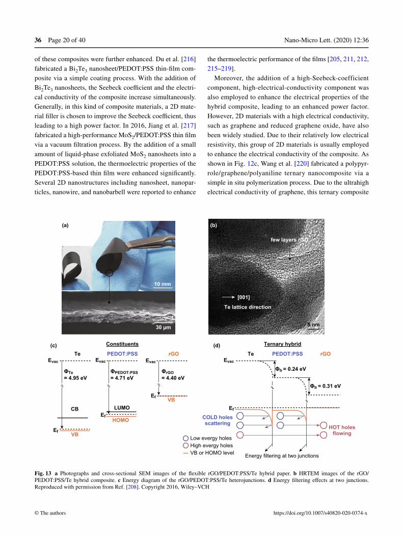
exhibits at least two magnitude higher Power factors than that of PANI and PPy. As shown in Fig. 13, Choi et al. [208] fabricated a novel Graphene/PEDOT:PSS/Te composite. The electrical conductivity of such composite is about 15 times higher than that of PEDOT:PSS/Te although the Seebeck coefficient is almost identical. The significant increase in the electrical conductivity of the ternary composite is ascribed to the carrier scattering at the double interface, as shown in Fig. 13c, d. This work shows that graphene may be an ideal composite filler to optimize the thermoelectric perfor-mance of polymers. Inspired by these pioneer works, several investigations, including graphene/P3HT, rGO/PEDOT:PSS, PANI/graphene and graphene/CNT, have reported the use of graphene or reduced graphene oxide into a conductive polymer [43, 59, 221–226].
Besides their use in the enhancement of either the See-beck coefficient or the electrical conductivity, 2D material-based composites can be employed as electrodes to fabri-cated high-performance flexible devices. Jiang et al. [227] prepared a graphene/polyethyleneglycol composite, which was used for heat collection and transport. The presence of highly conductive graphene in this composite introduces several conductive pathways for heat transfer and acts as a highly thermal conductive reservoir of phase-change mate-rials for thermal energy collection, storage, and release. Moreover, this work opens a new door to fabricate novel thermoelectric materials and to realize high-performance flexible thermoelectric devices.
5 Thermoelectric Properties of Single‑ or Few‑layer 2D Materials
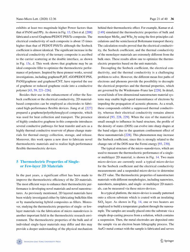
In the past years, a significant effort has been made to improve the thermoelectric efficiency of the 2D materials. The most efficient ways to enhance their thermoelectric per-formance is developing novel materials and novel nanostruc-tures. As previously mentioned, 2D layered materials have been widely investigated either by fabricating bulk/thin film or by manufacturing hybrid composites as fillers. Moreo-ver, studying the thermoelectric properties of single- or few-layer materials via the fabrication of micro–nanodevices is another important field in the thermoelectric research envi-ronment. The thermoelectric properties of the bulk and of individual single-layer materials may differ and this may provide a deeper understanding of the physical mechanism
behind their thermoelectric effect. For example, Kumar et al. [149] simulated the thermoelectric properties of bulk and monolayer MoSe2 and WSe2 by using the first-principles cal-culations and the semiclassical Boltzmann transport theory. The calculation results proved that the electrical conductiv-ity, the Seebeck coefficient, and the thermal conductivity of the monolayer materials are extremely different from the bulk ones. These results allow one to optimize the thermo-electric properties based on the unit materials.
Decoupling the Seebeck coefficient, the electrical con-ductivity, and the thermal conductivity is a challenging problem to solve. However, the different mean free paths of electrons and phonons provide the possibility to decouple the electrical properties and the thermal properties, which are governed by the Wiedemann–Franz law [228]. In detail, several kinds of low-dimensional nanostructure material sys-tems may enable high-speed transmittance of electrons by impeding the propagation of acoustic phonons. As a result, these compounds exhibit a suppressed thermal conductiv-ity, whereas their electrical conductivity remains almost identical [93, 228, 229]. When the size of the material is small enough to influence its band structure, the profile of the density of states (DOS) can evolve into sharp shapes at the band edges due to the quantum confinement effect of these nanomaterials [228]. This phenomenon may increase the Seebeck coefficient, since this is strongly related to the change rate of the DOS near the Fermi energy [93, 230].
The typical structure of the micro–nanodevices, which are used to measure the thermoelectric performance of a single- or multilayer 2D material, is shown in Fig. 14. Two main micro-devices are currently used: a typical micro-device for the Seebeck coefficient and the electrical conductivity measurements and a suspended micro-device to determine the ZT value. The thermoelectric properties of nanostructure materials with different morphologies, including nanowires, nanosheets, nanoplates, and single- or multilayer 2D materi-als, can be measured via these micro-devices.
In a typical platform, the micro-device is usually patterned onto a silicon substrate which is coated with an insulating SiO2 layer. As shown in Fig. 14, one or two heaters are employed to build a temperature gradient through the nanosa-mple. The samples are usually placed onto the substrate via a simple drop-casting process from a solution, which contains a suspension. Then, the metal electrodes are deposited onto the sample via an electron beam lithography process. The Au/Cr metal contact with the sample is fabricated and serves
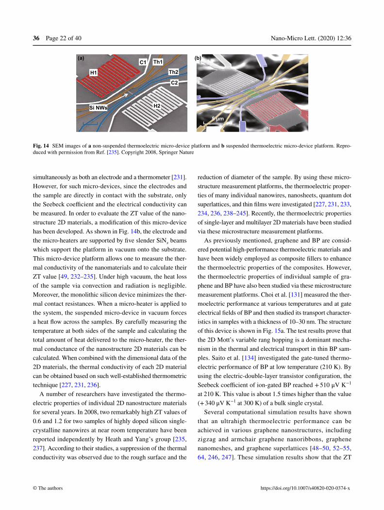
Nano-Micro Lett. (2020) 12:3636 Page 22 of 40
https://doi.org/10.1007/s40820-020-0374-x© The authors
simultaneously as both an electrode and a thermometer [231]. However, for such micro-devices, since the electrodes and the sample are directly in contact with the substrate, only the Seebeck coefficient and the electrical conductivity can be measured. In order to evaluate the ZT value of the nano-structure 2D materials, a modification of this micro-device has been developed. As shown in Fig. 14b, the electrode and the micro-heaters are supported by five slender SiNx beams which support the platform in vacuum onto the substrate. This micro-device platform allows one to measure the ther-mal conductivity of the nanomaterials and to calculate their ZT value [49, 232–235]. Under high vacuum, the heat loss of the sample via convection and radiation is negligible. Moreover, the monolithic silicon device minimizes the ther-mal contact resistances. When a micro-heater is applied to the system, the suspended micro-device in vacuum forces a heat flow across the samples. By carefully measuring the temperature at both sides of the sample and calculating the total amount of heat delivered to the micro-heater, the ther-mal conductance of the nanostructure 2D materials can be calculated. When combined with the dimensional data of the 2D materials, the thermal conductivity of each 2D material can be obtained based on such well-established thermometric technique [227, 231, 236].
A number of researchers have investigated the thermo-electric properties of individual 2D nanostructure materials for several years. In 2008, two remarkably high ZT values of 0.6 and 1.2 for two samples of highly doped silicon single-crystalline nanowires at near room temperature have been reported independently by Heath and Yang’s group [235, 237]. According to their studies, a suppression of the thermal conductivity was observed due to the rough surface and the
reduction of diameter of the sample. By using these micro-structure measurement platforms, the thermoelectric proper-ties of many individual nanowires, nanosheets, quantum dot superlattices, and thin films were investigated [227, 231, 233, 234, 236, 238–245]. Recently, the thermoelectric properties of single-layer and multilayer 2D materials have been studied via these microstructure measurement platforms.
As previously mentioned, graphene and BP are consid-ered potential high-performance thermoelectric materials and have been widely employed as composite fillers to enhance the thermoelectric properties of the composites. However, the thermoelectric properties of individual sample of gra-phene and BP have also been studied via these microstructure measurement platforms. Choi et al. [131] measured the ther-moelectric performance at various temperatures and at gate electrical fields of BP and then studied its transport character-istics in samples with a thickness of 10–30 nm. The structure of this device is shown in Fig. 15a. The test results prove that the 2D Mott’s variable rang hopping is a dominant mecha-nism in the thermal and electrical transport in thin BP sam-ples. Saito et al. [134] investigated the gate-tuned thermo-electric performance of BP at low temperature (210 K). By using the electric-double-layer transistor configuration, the Seebeck coefficient of ion-gated BP reached + 510 μV K−1 at 210 K. This value is about 1.5 times higher than the value (+ 340 μV K−1 at 300 K) of a bulk single crystal.
Several computational simulation results have shown that an ultrahigh thermoelectric performance can be achieved in various graphene nanostructures, including zigzag and armchair graphene nanoribbons, graphene nanomeshes, and graphene superlattices [48–50, 52–55, 64, 246, 247]. These simulation results show that the ZT
(a) (b)
H1
Si NWs H2
C1
C2
Th1
Th2
5 µm
Fig. 14 SEM images of a non-suspended thermoelectric micro-device platform and b suspended thermoelectric micro-device platform. Repro-duced with permission from Ref. [235]. Copyright 2008, Springer Nature
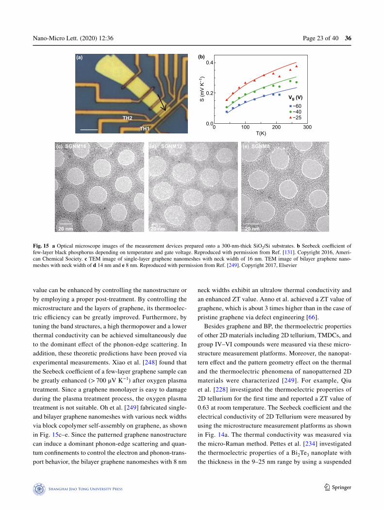
Nano-Micro Lett. (2020) 12:36 Page 23 of 40 36
1 3
value can be enhanced by controlling the nanostructure or by employing a proper post-treatment. By controlling the microstructure and the layers of graphene, its thermoelec-tric efficiency can be greatly improved. Furthermore, by tuning the band structures, a high thermopower and a lower thermal conductivity can be achieved simultaneously due to the dominant effect of the phonon-edge scattering. In addition, these theoretic predictions have been proved via experimental measurements. Xiao et al. [248] found that the Seebeck coefficient of a few-layer graphene sample can be greatly enhanced (> 700 μV K−1) after oxygen plasma treatment. Since a graphene monolayer is easy to damage during the plasma treatment process, the oxygen plasma treatment is not suitable. Oh et al. [249] fabricated single- and bilayer graphene nanomeshes with various neck widths via block copolymer self-assembly on graphene, as shown in Fig. 15c–e. Since the patterned graphene nanostructure can induce a dominant phonon-edge scattering and quan-tum confinements to control the electron and phonon-trans-port behavior, the bilayer graphene nanomeshes with 8 nm
neck widths exhibit an ultralow thermal conductivity and an enhanced ZT value. Anno et al. achieved a ZT value of graphene, which is about 3 times higher than in the case of pristine graphene via defect engineering [66].
Besides graphene and BP, the thermoelectric properties of other 2D materials including 2D tellurium, TMDCs, and group IV–VI compounds were measured via these micro-structure measurement platforms. Moreover, the nanopat-tern effect and the pattern geometry effect on the thermal and the thermoelectric phenomena of nanopatterned 2D materials were characterized [249]. For example, Qiu et al. [228] investigated the thermoelectric properties of 2D tellurium for the first time and reported a ZT value of 0.63 at room temperature. The Seebeck coefficient and the electrical conductivity of 2D Tellurium were measured by using the microstructure measurement platforms as shown in Fig. 14a. The thermal conductivity was measured via the micro-Raman method. Pettes et al. [234] investigated the thermoelectric properties of a Bi2Te3 nanoplate with the thickness in the 9–25 nm range by using a suspended
(a)
(c) SGNM16 (d) SGNM12 (e) SGNM8
TH2
TH1
(b)
Vg (V)−60−40−25
0.4
0.2
0.0
S (m
V K
−1)
0 100T(K)
200 300
20 nm 20 nm 20 nm
Fig. 15 a Optical microscope images of the measurement devices prepared onto a 300-nm-thick SiO2/Si substrates. b Seebeck coefficient of few-layer black phosphorus depending on temperature and gate voltage. Reproduced with permission from Ref. [131]. Copyright 2016, Ameri-can Chemical Society. c TEM image of single-layer graphene nanomeshes with neck width of 16 nm. TEM image of bilayer graphene nano-meshes with neck width of d 14 nm and e 8 nm. Reproduced with permission from Ref. [249]. Copyright 2017, Elsevier
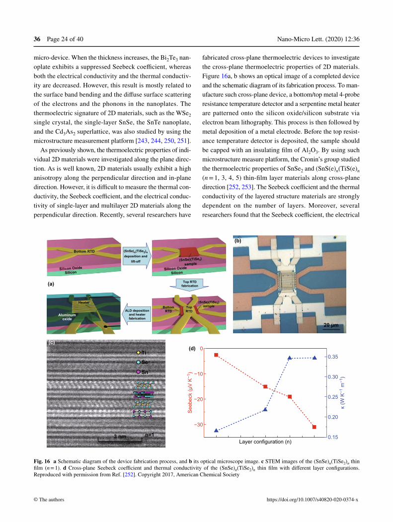
Nano-Micro Lett. (2020) 12:3636 Page 24 of 40
https://doi.org/10.1007/s40820-020-0374-x© The authors
micro-device. When the thickness increases, the Bi2Te3 nan-oplate exhibits a suppressed Seebeck coefficient, whereas both the electrical conductivity and the thermal conductiv-ity are decreased. However, this result is mostly related to the surface band bending and the diffuse surface scattering of the electrons and the phonons in the nanoplates. The thermoelectric signature of 2D materials, such as the WSe2 single crystal, the single-layer SnSe, the SnTe nanoplate, and the Cd3As2 superlattice, was also studied by using the microstructure measurement platform [243, 244, 250, 251].
As previously shown, the thermoelectric properties of indi-vidual 2D materials were investigated along the plane direc-tion. As is well known, 2D materials usually exhibit a high anisotropy along the perpendicular direction and in-plane direction. However, it is difficult to measure the thermal con-ductivity, the Seebeck coefficient, and the electrical conduc-tivity of single-layer and multilayer 2D materials along the perpendicular direction. Recently, several researchers have
fabricated cross-plane thermoelectric devices to investigate the cross-plane thermoelectric properties of 2D materials. Figure 16a, b shows an optical image of a completed device and the schematic diagram of its fabrication process. To man-ufacture such cross-plane device, a bottom/top metal 4-probe resistance temperature detector and a serpentine metal heater are patterned onto the silicon oxide/silicon substrate via electron beam lithography. This process is then followed by metal deposition of a metal electrode. Before the top resist-ance temperature detector is deposited, the sample should be capped with an insulating film of Al2O3. By using such microstructure measure platform, the Cronin’s group studied the thermoelectric properties of SnSe2 and (SnS(e)n(TiS(e)n (n = 1, 3, 4, 5) thin-film layer materials along cross-plane direction [252, 253]. The Seebeck coefficient and the thermal conductivity of the layered structure materials are strongly dependent on the number of layers. Moreover, several researchers found that the Seebeck coefficient, the electrical
Bottom RTD
Heater
Aluminumoxide
Silicon Oxide Silicon Oxide
(SnSe)(TiSe2)sample
Silicon Silicon
(SnSe)n(TiSe2)ndeposition and
lift-off
ALD depositionand heaterfabrication
Top RTDfabrication
(SnSe)(TiSe2)sampleTop
RTDBottom
RTD
(b)
(a)
(d)(c)
20 µm
Ti
Se
Sn
n=13 nm
0.35
0.30
0.25
0.20
0.15
0
−10
−20
−30
See
beck
(μV
K−1
)
κ (W
K−1
m−1
)
Layer configuration (n)
Fig. 16 a Schematic diagram of the device fabrication process, and b its optical microscope image. c STEM images of the (SnSe)n(TiSe2)n thin film (n = 1). d Cross-plane Seebeck coefficient and thermal conductivity of the (SnSe)n(TiSe2)n thin film with different layer configurations. Reproduced with permission from Ref. [252]. Copyright 2017, American Chemical Society
Nano-Micro Lett. (2020) 12:36 Page 25 of 40 36
1 3
conductivity, and the thermal conductivity along cross-plane direction are very different from the properties along the in-plane direction. This is in agreement with the properties of bulk thermoelectric materials based on 2D materials (such as SnSe, Bi2Te3, and Sb2Te3). For example, Li et al. found that when the number of layers decreases from 5 to 1, the cross-plane Seebeck coefficient decreases from − 31 to − 2.5 μV K−1, whereas the cross-plane thermal conductiv-ity decreases from 0.35 to 0.15 W mK−1 (Fig. 16c, d), due to an increased interfacial phonon scattering [252]. Juang et al. [254] proposed a cross-plane micro-device onto a sili-con substrate to measure the thermoelectric properties of the vertical graphene/gold nanoparticles heterostructure along the perpendicular direction. Since the Au nanoparticles can further inhibit the phonon transport and enhance the electri-cal conductivity along the perpendicular direction, a high ZT value larger than 1.0 (at room temperature) can be achieved for a single-layer graphene. Chen et al. [255] fabricated a graphene/hexagonal boron nitride/graphene heterostructure device and measured its thermoelectric transport properties. The top and bottom graphene surfaces in this device work as both an electrode and a micro-heater to induce a tempera-ture gradient. The measured thermoelectric properties are useful to understand the thermoelectric component in the cross-plane behavior of emerging 2D heterostructure devices.
The development of micro–nanoprocessing techniques enables us to fabricate micro-devices to investigate the thermoelectric properties of individual 2D nanostructure materials. The study of the thermoelectric transport char-acteristics of individual 2D materials is pivotal to under-stand its physical mechanism. The massive proliferation of 2D materials, such as TMDCs, BP, MXenes, graphene, and Xene, offers new opportunities to engineer such compounds and to fabricate high-performance thermoelectric devices. The device structures reviewed in this section serve as a gen-eral approach to characterize the in-plane and cross-plane transport properties of 2D materials.
6 Thermoelectric Materials Combined with Photodetection
Thermoelectr ic materials have been widely used as power generators, cooling devices, and sensors. Recently, they have been found to work as power sup-plies and can be used to develop highly efficient and
wearable self-powered electronics devices. As a group of developing materials, 2D materials have been widely employed as optoelectronic devices, including in the manufacturing of photodetectors and photovoltaic devices. When irradiated by light, these devices convert photons into electric current due to separation of the excited electron–hole pair via a built-in electric field. The development of low-cost and high-performance broadband photodetectors is the key to fulfill differ-ent application requirements. The photothermoelectric effect, which is based on the Seebeck effect, enables the device to generate a photocurrent due to the temperature gradient induced by the absorbed light on an electric voltage. Moreover, this temperature gradient would be generated across the materials due to light irradiation and the photocurrent is generated by the photothermo-electric effect. Self-power photodetectors are promising devices, which can be employed in a large variety of application including sensing, environmental monitor-ing, night vision, and astronomy.
2D materials, such as graphene and BP, have been widely used as photothermal agents due to their efficient photother-mal conversion efficient [122, 256–259]. Gabor found that upon heating a junction consisting of a single graphene sheet by shining laser onto it, a thermoelectric voltage is generated across the junction [260]. However, this kind of photothermo-electric effect was found in other 2D materials system, as well [51, 71, 126, 261–264]. As predicted by Basko, this effect can be potentially exploited in novel optoelectronic devices [70].
In 2011, Kraemer et al. [265] reported a novel solar ther-mal flat panel, which converts thermal energy into electric power based on the Seebeck effect and on the high thermal concentration. The peak efficiency of such solar thermoelec-tric generator is close to that of a common solar cell (4.6%). However, the total power conversion efficiency of this device is limited by the photothermal and thermoelectric efficiency [56, 265].
Besides their use as solar energy converters, 2D thermo-electric materials also can be employed in the fabrication of high-performance self-power photodetectors. When com-pared to other photodetection mechanisms, such as photo-conduction, photovoltage, and bolometry, the photothermo-electric effect achieves a broadband detection without an external bias at room temperature. A photodetector based on the photothermoelectric effect mechanism exhibits a respon-sivity, which is related to the light-induced temperature

Nano-Micro Lett. (2020) 12:3636 Page 26 of 40
https://doi.org/10.1007/s40820-020-0374-x© The authors
gradient and to its Seebeck coefficient. The temperature gradient is determined by the absorption, heat capacity, and the photothermal conversion efficiency of the material.
Graphene and BP are the most widely studied 2D materials and have attracted a large attention. In 2010, Xu et al. [51] found that the photothermoelectric effect has a pronounced effect into the photocurrent generation process at the graphene interface in field-effect transis-tors. This phenomenon has several positive benefits in the design of high-performance optoelectronics devices based on graphene. As shown in Fig. 17a, Cai et al. [266] fabricated a simple thermoelectric terahertz photodetector based on graphene, which exhibits an excellent sensitivity exceeding 10 V W−1 (700 V W−1) at room temperature and noise-equivalent power less than 1100 pW Hz−1/2
(20 pW Hz−1/2), referenced to the incident (absorbed) power. The performance of such graphene-based thermo-electric terahertz photodetectors can compete with the best room-temperature terahertz detectors to develop optimally coupled devices. Echtermeyer et al. [61] investigated the influence of the wavelength on the performance of metal-graphene-metal photodetectors via polarization-dependent measurements. The device that used in this study is shown in Fig. 17b. As shown in Fig. 17c, Muench et al. report a compact, photothermoelectric-based, waveguide- inte-grated, plasmonic enhanced graphene photodetector for telecom wavelengths operating at zero dark current. Owing to the voltage generated by the photothermoelectric, the graphene photodetector exhibits an external responsiv-ity ~ 12.2 V W−1 and a 3 dB bandwidth ~ 42 GHz [267].
(a)
(c) (d)
Drain
Gate 1
SiNWaveguide
SLGchannel
Gate 2Source
(b)100 µm
3 µm
Au Cr
Graphene
Au Cr
x
Metal
SiO25 µm
y Graphene
1575 nm
1000
Pho
tovo
ltage
(µV
)
100
0.01Power at device (mW)
0.1
Fig. 17 a Optical micrograph and atomic force microscopy of graphene photodetector with asymmetric metal electrodes. Reproduced with per-mission from Ref. [266]. Copyright 2014, Springer Nature. b Optical micrograph of the graphene-based photodetector devices. Reproduced with permission from Ref. [61]. Copyright 2014, American Chemical Society. c Scheme of the single-layer graphene photodetector SiN waveguide. The green arrow indicates the light propagation direction. d The photovoltage Vph dependence of optical power. Reproduced with permission from Ref. [267]. Copyright 2019, American Chemical Society
Nano-Micro Lett. (2020) 12:36 Page 27 of 40 36
1 3
The photovoltage (Vph) generated by the thermoelectric current as for the Seebeck effect dependence on power is shown in Fig. 17d. The linear response indicates a power-independent external voltage responsivities in the tested optical power range [267].
As graphene, BP has also been studied as a high-per-formance photothermoelectric photodetector. Hong et al. [126] investigated the electrical transport and optoelectronic properties of FETs manufactured from a few-layer BP sam-ple. Their results reveal that the photocurrent signals at the BP–electrode junctions can be mainly attributed to the pho-tovoltaic effect in its the off-state, whereas the photothermo-electric effect occurs during its on-state. Leong et al. [268] fabricated a device based on exfoliated BP nanoflakes with a responsivity of 1 mV W−1 for a 2.5-THz beam with a diam-eter of 200 μm. In this case, the photothermoelectric effect was found to be the primary source of the THz photosignal.
The photothermoelectric effect of several 2D TMDC materials, such as MoS2, WSe2, and Bi2Se3, has also been widely investigated [71, 261, 262, 264]. Buscema et al. [71] studied the photoresponse of MoS2 monolayer FETs via scanning photocurrent microscopy. The device and results are shown in Fig. 18. To summarize, the photocurrent gen-eration in a MoS2 monolayer is dominated by the photother-moelectric effect. The separation of the photoexcited elec-tron–hole pairs across the Schottky barriers at the MoS2/electrode interfaces only plays a marginal role. As shown in Fig. 18h, a large and controllable Seebeck coefficient in the − 1 × 10⁵ to −4 × 10² μV K−1 range was observed in the case of MoS2 monolayer. However, the mechanism behind the generation of the photocurrent is different when compared to other 2D TMDC materials. In order to deeply understand such physical mechanism, Groenendijk et al. [262] studied the photocurrent in a WSe2 sample by fabricating a double-gated WSe2 device and by applying varied gate voltages and illumination power. The results show that the photo-current of the WSe2-based devices (for both the PN and NP configurations) is mainly generated by the photovoltaic effect. Moreover, a maximum responsivity of 0.7 mA W−1 at 532-nm illumination was obtained. In the PP configura-tions devices, the photocurrent mainly is generated by the photothermoelectric effect and the intensity is about 2 times larger than that generated by the photovoltaic effect. Due to the strong optical absorption caused by an asymmetry in flake thickness or by the optical absorption of the electrodes, a sizable temperature gradient can be generated across the
2D material-based devices. In addition, the photothermo-electric effect plays a significant role in such devices and can be used to develop high-performance self-power opto-electronic devices.
Photothermoelectric photodetectors have exhibited their advantages in developing low-cost, uncooled ultrafast and ultrabroadband photodetectors, and their performance has been significantly enhanced owing to the development of low- dimensional materials and the micro–nanofabrication technology. However, due to the limited effective active sur-face area, the saturation effect and relatively low practical Seebeck coefficient at room temperature limit the tempera-ture gradient in the case of exfoliated or single-crystal 2D materials. For this reason, no high voltage can be gener-ated. Although tremendous progress has been made in recent years, more work needs to be done to further optimize the performance of 2D material-based photothermoelectric photodetectors.
7 Conclusions and Outlook
During the last decades, a significant progress has been achieved in the development of thermoelectric materials. As new members of the thermoelectric material family, 2D materials have attracted a large attention and many milestone investigations have been reported. Due to their unique elec-tronic, thermal, and mechanic properties, 2D thermoelectric materials are expected to be the next-generation high-per-formance thermoelectric materials.
In this review, the thermoelectric properties of various 2D materials, such as TMDCs, graphene, BP, group IVA–VA compounds, MXene, and their nanocomposites, were illus-trated in detail. Moreover, the state-of-the-art of theoretical and experimental data were presented to elucidate the rela-tion among various factors which determine the thermoelec-tric properties of these materials. Although a tremendous progress has been achieved in the past few years, these prop-erties still need to be improved for their practical application as thermoelectric devices. Here, some major outlooks are presented to address this issue:
1. The thermoelectric performance of 2D materials is still much lower then for conventional bulk thermoelectric materials. A precise chemical doping during the fabrica-tion and the functionalization of these composites must
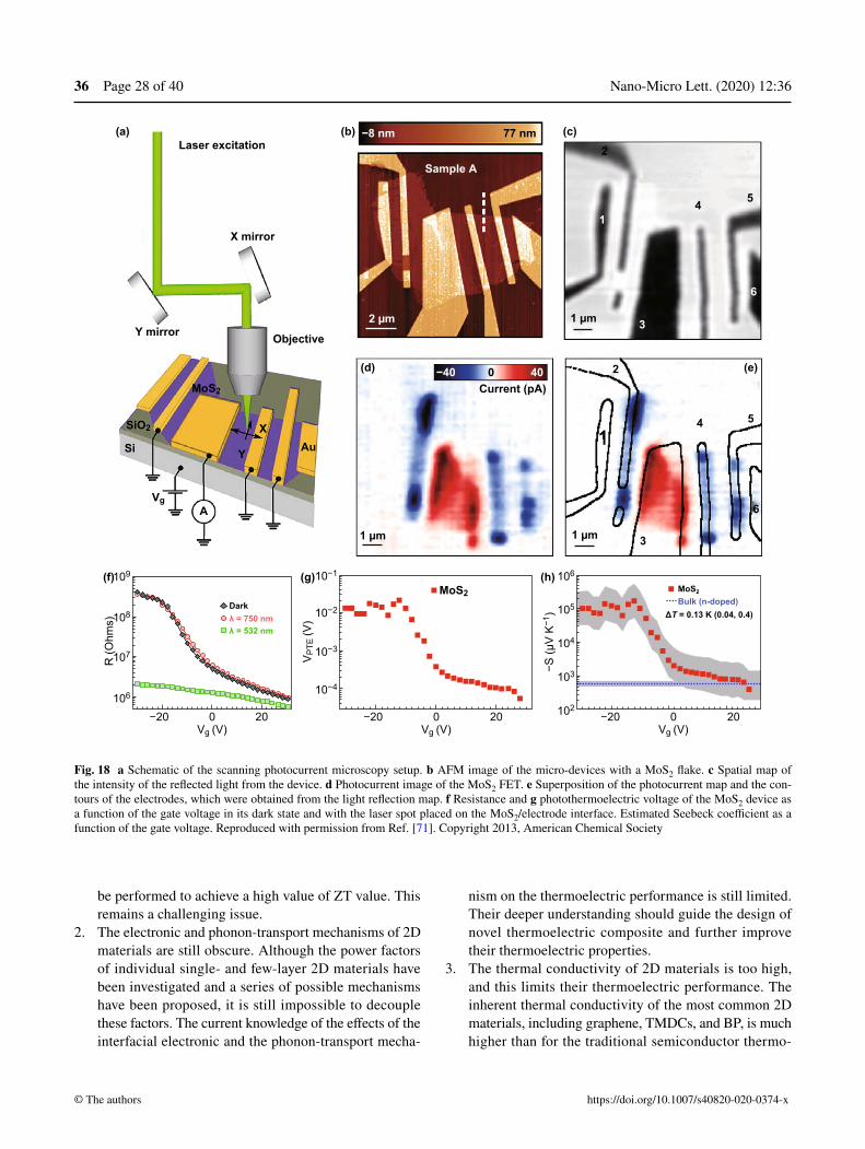
Nano-Micro Lett. (2020) 12:3636 Page 28 of 40
https://doi.org/10.1007/s40820-020-0374-x© The authors
be performed to achieve a high value of ZT value. This remains a challenging issue.
2. The electronic and phonon-transport mechanisms of 2D materials are still obscure. Although the power factors of individual single- and few-layer 2D materials have been investigated and a series of possible mechanisms have been proposed, it is still impossible to decouple these factors. The current knowledge of the effects of the interfacial electronic and the phonon-transport mecha-
nism on the thermoelectric performance is still limited. Their deeper understanding should guide the design of novel thermoelectric composite and further improve their thermoelectric properties.
3. The thermal conductivity of 2D materials is too high, and this limits their thermoelectric performance. The inherent thermal conductivity of the most common 2D materials, including graphene, TMDCs, and BP, is much higher than for the traditional semiconductor thermo-
(a) (b) (c)−8 nm
−40 400(d) (e)2
14 5
6
3
Current (pA)
77 nm
Sample A
Laser excitation
X mirror
Y mirror Objective
MoS2
SiO2
VgA
(f) (g) (h)
Y AuX
Si
2 µm
1 µm
1 µm
1 µm
3
1
2
4 5
6
DarkMoS2
λ = 750 nmλ = 532 nm
109
108
107
106 10−4
10−3
10−2
106
105
104
103
102
10−1
Vg (V)
R (O
hms)
−20 0 20Vg (V)
VP
TE (V
)
−S (µ
V K
−1)
−20 0 20
MoS2
Vg (V)−20 0 20
Bulk (n-doped)ΔT = 0.13 K (0.04, 0.4)
Fig. 18 a Schematic of the scanning photocurrent microscopy setup. b AFM image of the micro-devices with a MoS2 flake. c Spatial map of the intensity of the reflected light from the device. d Photocurrent image of the MoS2 FET. e Superposition of the photocurrent map and the con-tours of the electrodes, which were obtained from the light reflection map. f Resistance and g photothermoelectric voltage of the MoS2 device as a function of the gate voltage in its dark state and with the laser spot placed on the MoS2/electrode interface. Estimated Seebeck coefficient as a function of the gate voltage. Reproduced with permission from Ref. [71]. Copyright 2013, American Chemical Society
Nano-Micro Lett. (2020) 12:36 Page 29 of 40 36
1 3
electric materials. Their structural modifications, as well as the introduction of structural defects and the control of their elemental components, are likely to have a posi-tive effect on the thermal conductivity of these materi-als.
4. The fabrication realization and the characterization of 2D material-based thin films are still challenging. With the increase in the demand of wearable and port-able flexible devices, thin-film thermoelectric materi-als have received a wide attention. Although they have been studied for very short time when compared to bulk thermoelectric materials, they are considered the next generation of thermoelectric materials for practi-cal applications. Due to their excellent electronic and mechanical properties, several researchers have tried to fabricate thin-film thermoelectric materials by using 2D nanomaterials and their composites. However, the measurements of the thermal conductivity of thin films are still challenging.
5. It is of pivotal importance to achieve a facile production of high-quality and scalable 2D material. This is cur-rently an active research topic. Until now, many meth-ods have been employed to fabricate 2D materials, such as chemical vapor deposition, mechanical exfoliation, atomic layer deposition, molecular beam epitaxy, physi-cal vapor deposition liquid exfoliation, and mechanical exfoliation. However, it is still challenging to manufac-ture such materials with a controlled structure via scale-up methods.
Acknowledgements This work was supported by National Sci-ence Foundation for Young Scientists of China (No. 61905161 and 51702219), the National Natural Science Foundation of China (No. 61975134, 61875138 and 61775147), the Science and Technology Innovation Commission of Shenzhen (No. JCYJ20180206121837007), and the Shenzhen Nanshan District Pilotage Team Program (LHTD20170006).
Open Access This article is licensed under a Creative Commons Attribution 4.0 International License, which permits use, shar-ing, adaptation, distribution and reproduction in any medium or format, as long as you give appropriate credit to the original author(s) and the source, provide a link to the Creative Commons licence, and indicate if changes were made. The images or other third party material in this article are included in the article’s Creative Commons licence, unless indicated otherwise in a credit line to the material. If material is not included in the article’s Creative Commons licence and your intended use is not permit-ted by statutory regulation or exceeds the permitted use, you will need to obtain permission directly from the copyright holder. To view a copy of this licence, visit http://creat iveco mmons .org/licen ses/by/4.0/.
References
1. Z.G. Chen, G. Han, L. Yang, L. Cheng, J. Zou, Nanostruc-tured thermoelectric materials: current research and future challenge. Prog. Nat. Sci. 22(6), 535–549 (2012). https ://doi.org/10.1016/j.pnsc.2012.11.011
2. T. Zhu, Y. Liu, C. Fu, J.P. Heremans, J.G. Snyder, X. Zhao, Compromise and synergy in high-efficiency thermoelectric materials. Adv. Mater. 29(14), 1605884 (2017). https ://doi.org/10.1002/adma.20160 5884
3. G.J. Snyder, E.S. Toberer, Complex thermoelectric materials. Nat. Mater. 7(2), 105–114 (2008). https ://doi.org/10.1038/nmat2 090
4. M. Rull-Bravo, A. Moure, J.F. Fernandez, M. Martin-Gonzalez, Skutterudites as thermoelectric materials: revisited. RSC Adv. 5(52), 41653–41667 (2015). https ://doi.org/10.1039/c5ra0 3942h
5. P. Sundarraj, D. Maity, S.S. Roy, R.A. Taylor, Recent advances in thermoelectric materials and solar thermo-electric generators - a critical review. RSC Adv. 4(87), 46860–46874 (2014). https ://doi.org/10.1039/c4ra0 5322b
6. G. Tan, L.-D. Zhao, M.G. Kanatzidis, Rationally design-ing high-performance bulk thermoelectric materials. Chem. Rev. 116(19), 12123–12149 (2016). https ://doi.org/10.1021/acs.chemr ev.6b002 55
7. C. Gayner, K.K. Kar, Recent advances in thermoelectric materials. Prog. Mater Sci. 83, 330–382 (2016). https ://doi.org/10.1016/j.pmats ci.2016.07.002
8. G. Zhang, Y.-W. Zhang, Thermoelectric properties of two-dimensional transition metal dichalcogenides. J. Mater. Chem. C 5(31), 7684–7698 (2017). https ://doi.org/10.1039/c7tc0 1088e
9. D. Li, C. Luo, Y. Chen, D. Feng, Y. Gong, C. Pan, J. He, High performance polymer thermoelectric composite achieved by carbon-coated carbon nanotubes network. ACS Appl. Energy Mater. 2(4), 2427–2434 (2019). https ://doi.org/10.1021/acsae m.9b003 34
10. Z.-H. Ge, L.-D. Zhao, D. Wu, X. Liu, B.-P. Zhang, J.-F. Li, J. He, Low-cost, abundant binary sulfides as promis-ing thermoelectric materials. Mater. Today 19(4), 227–239 (2016). https ://doi.org/10.1016/j.matto d.2015.10.004
11. S. Ortega, M. Ibanez, Y. Liu, Y. Zhang, M.V. Kovalenko, D. Cadavid, A. Cabot, Bottom-up engineering of thermo-electric nanomaterials and devices from solution-processed nanoparticle building blocks. Chem. Soc. Rev. 46(12), 3510–3528 (2017). https ://doi.org/10.1039/c6cs0 0567e
12. R. Kroon, D.A. Mengistie, D. Kiefer, J. Hynynen, J.D. Ryan, L. Yu, C. Muller, Thermoelectric plastics: from design to synthesis, processing and structure-property relationships. Chem. Soc. Rev. 45(22), 6147–6164 (2016). https ://doi.org/10.1039/c6cs0 0149a
13. L. Wang, Z. Zhang, L. Geng, T. Yuan, Y. Liu et al., Solu-tion-printable fullerene/TiS2 organic/inorganic hybrids for high-performance flexible n-type thermoelectrics. Energy Environ. Sci. 11(5), 1307–1317 (2018). https ://doi.org/10.1039/c7ee0 3617e
Nano-Micro Lett. (2020) 12:3636 Page 30 of 40
https://doi.org/10.1007/s40820-020-0374-x© The authors
14. J. Yang, H.-L. Yip, A.K.Y. Jen, Rational design of advanced thermoelectric materials. Adv. Energy Mater. 3(5), 549–565 (2013). https ://doi.org/10.1002/aenm.20120 0514
15. J.R. Sootsman, D.Y. Chung, M.G. Kanatzidis, New and old concepts in thermoelectric materials. Angew. Chem. Int. Ed. 48(46), 8616–8639 (2009). https ://doi.org/10.1002/anie.20090 0598
16. J.P. Heremans, V. Jovovic, E.S. Toberer, A. Saramat, K. Kurosaki, A. Charoenphakdee, S. Yamanaka, G.J. Sny-der, Enhancement of thermoelectric efficiency in PbTe by distortion of the electronic density of states. Science 321(5888), 554–557 (2008). https ://doi.org/10.1126/scien ce.11597 25
17. B. Poudel, Q. Hao, Y. Ma, Y. Lan, A. Minnich et al., High-thermoelectric performance of nanostructured bismuth antimony telluride bulk alloys. Science 320(5876), 634–638 (2008). https ://doi.org/10.1126/scien ce.11564 46
18. K. Biswas, J. He, I.D. Blum, C.-I. Wu, T.P. Hogan, D.N. Seidman, V.P. Dravid, M.G. Kanatzidis, High-performance bulk thermoelectrics with all-scale hierarchical architec-tures. Nature 489(7416), 414–418 (2012). https ://doi.org/10.1038/natur e1143 9
19. Y. Pei, X. Shi, A. LaLonde, H. Wang, L. Chen, G.J. Snyder, Convergence of electronic bands for high performance bulk thermoelectrics. Nature 473(7345), 66–69 (2011). https ://doi.org/10.1038/natur e0999 6
20. J.P. Heremans, C.M. Thrush, D.T. Morelli, Thermopower enhancement in lead telluride nanostructures. Phys. Rev. B 70(11), 115334 (2004). https ://doi.org/10.1103/PhysR evB.70.11533 4
21. F. Schedin, A.K. Geim, S.V. Morozov, E.W. Hill, P. Blake, M.I. Katsnelson, K.S. Novoselov, Detection of individual gas molecules adsorbed on graphene. Nat. Mater. 6, 652–655 (2007). https ://doi.org/10.1038/nmat1 967
22. S. Grimme, J. Antony, S. Ehrlich, H. Krieg, A consistent and accurate ab initio parametrization of density func-tional dispersion correction (DFT-D) for the 94 elements H-Pu. J. Chem. Phys. 132(15), 154104 (2010). https ://doi.org/10.1063/1.33823 44
23. C. Nie, L. Yu, X. Wei, J. Shen, W. Lu, W. Chen, S. Feng, H. Shi, Ultrafast growth of large-area monolayer MoS2 film via gold foil assistant CVD for a highly sensitive photode-tector. Nanotechnology 28(27), 275203 (2017). https ://doi.org/10.1088/1361-6528/aa747 3
24. Y. Yu, G.-H. Nam, Q. He, X.-J. Wu, K. Zhang et al., High phase-purity 1T’-MoS2- and 1T’-MoSe2- layered crystals. Nat. Chem. 10(6), 638–643 (2018). https ://doi.org/10.1038/s4155 7-018-0035-6
25. J. Lai, X. Liu, J. Ma, Q. Wang, K. Zhang et al., Anisotropic broadband photoresponse of layered type-II weyl semimetal MoTe2. Adv. Mater. 30(22), e1707152 (2018). https ://doi.org/10.1002/adma.20170 7152
26. J. Yang, T. Lu, Y.W. Myint, J. Pei, D. Macdonald, J.-C. Zheng, Y. Lu, Robust excitons and trions in monolayer MoTe2. ACS Nano 9(6), 6603–6609 (2015). https ://doi.org/10.1021/acsna no.5b026 65
27. C. Lee, X. Wei, J.W. Kysar, J. Hone, Measurement of the elastic properties and intrinsic strength of monolayer gra-phene. Science 321(5887), 385–388 (2008). https ://doi.org/10.1126/scien ce.11579 96
28. L. Li, Y. Yu, G.J. Ye, Q. Ge, X. Ou et al., Black phospho-rus field-effect transistors. Nat. Nanotechnol. 9(5), 372–377 (2014). https ://doi.org/10.1038/nnano .2014.35
29. M. Naguib, O. Mashtalir, J. Carle, V. Presser, J. Lu, L. Hult-man, Y. Gogotsi, M.W. Barsoum, Two-dimensional transi-tion metal carbides. ACS Nano 6(2), 1322–1331 (2012)
30. W. Tao, N. Kong, X. Ji, Y. Zhang, A. Sharma et al., Emerg-ing two-dimensional monoelemental materials (Xenes) for biomedical applications. Chem. Soc. Rev. 48(11), 2891–2912 (2019). https ://doi.org/10.1039/c8cs0 0823j
31. A. Molle, J. Goldberger, M. Houssa, Y. Xu, S.C. Zhang, D. Akinwande, Buckled two-dimensional Xene sheets. Nat. Mater. 16(2), 163–169 (2017). https ://doi.org/10.1038/nmat4 802
32. Y. Liu, S. Zhang, J. He, Z.M. Wang, Z. Liu, Recent progress in the fabrication, properties, and devices of heterostructures based on 2D materials. Nano-Micro Lett. 11, 13 (2019). https ://doi.org/10.1007/s4082 0-019-0245-5
33. L.-D. Zhao, S.-H. Lo, Y. Zhang, H. Sun, G. Tan, C. Uher, C. Wolverton, V.P. Dravid, M.G. Kanatzidis, Ultralow ther-mal conductivity and high thermoelectric figure of merit in SnSe crystals. Nature 508(7496), 373–377 (2014). https ://doi.org/10.1038/natur e1318 4
34. C. Chang, M. Wu, D. He, Y. Pei, C.-F. Wu et al., 3D charge and 2D phonon transports leading to high out-of-plane in n-type SnSe crystals. Science 360(6390), 778 (2018). https ://doi.org/10.1126/scien ce.aaq14 79
35. K. Nielsch, J. Bachmann, J. Kimling, H. Boettner, Thermo-electric nanostructures: from physical model systems towards nanograined composites. Adv. Energy Mater. 1(5), 713–731 (2011). https ://doi.org/10.1002/aenm.20110 0207
36. H. Wang, C. Li, P. Fang, Z. Zhang, J.Z. Zhang, Synthesis, properties, and optoelectronic applications of two-dimen-sional MoS2 and MoS2-based heterostructures. Chem. Soc. Rev. 47(16), 6101–6127 (2018). https ://doi.org/10.1039/c8cs0 0314a
37. F. Wang, Z. Wang, L. Yin, R. Cheng, J. Wang et al., 2D library beyond graphene and transition metal dichalcoge-nides: a focus on photodetection. Chem. Soc. Rev. 47(16), 6296–6341 (2018). https ://doi.org/10.1039/c8cs0 0255j
38. S. Wang, A. Robertson, J.H. Warner, Atomic structure of defects and dopants in 2D layered transition metal dichalco-genides. Chem. Soc. Rev. 47(17), 6764–6794 (2018). https ://doi.org/10.1039/c8cs0 0236c
39. Y. Zhang, Y. Zheng, K. Rui, H.H. Hng, K. Hippalgaonkar et al., 2D black phosphorus for energy storage and thermo-electric applications. Small 13(28), 1700661 (2017). https ://doi.org/10.1002/smll.20170 0661
40. H. Babaei, J.M. Khodadadi, S. Sinha, Large theoretical ther-moelectric power factor of suspended single-layer MoS2.
Nano-Micro Lett. (2020) 12:36 Page 31 of 40 36
1 3
Appl. Phys. Lett. 105(19), 193901 (2014). https ://doi.org/10.1063/1.49013 42
41. K.S. Novoselov, A.K. Geim, S.V. Morozov, D. Jiang, Y. Zhang, S.V. Dubonos, I.V. Grigorieva, A.A. Firsov, Elec-tric field effect in atomically thin carbon films. Science 306(5696), 666–669 (2004). https ://doi.org/10.1126/scien ce.11028 96
42. A.H. Castro Neto, F. Guinea, N.M.R. Peres, K.S. Novoselov, A.K. Geim, The electronic properties of graphene. Rev. Mod. Phys. 81(1), 109–162 (2009). https ://doi.org/10.1103/RevMo dPhys .81.109
43. A. Dey, O.P. Bajpai, A.K. Sikder, S. Chattopadhyay, M.A.S. Khan, Recent advances in CNT/graphene based thermoelec-tric polymer nanocomposite: a proficient move towards waste energy harvesting. Renew. Sust. Energy Rev. 53, 653–671 (2016). https ://doi.org/10.1016/j.rser.2015.09.004
44. K.I. Bolotin, K.J. Sikes, Z. Jiang, M. Klima, G. Fudenberg, J. Hone, P. Kim, H.L. Stormer, Ultrahigh electron mobil-ity in suspended graphene. Solid State Commun. 146(9–10), 351–355 (2008). https ://doi.org/10.1016/j.ssc.2008.02.024
45. P. Wei, W. Bao, Y. Pu, C.N. Lau, J. Shi, Anomalous thermo-electric transport of dirac particles in graphene. Phys. Rev. Lett. 102(16), 166808 (2009). https ://doi.org/10.1103/PhysR evLet t.102.16680 8
46. A.A. Balandin, S. Ghosh, W. Bao, I. Calizo, D. Tewelde-brhan, F. Miao, C.N. Lau, Superior thermal conductivity of single-layer graphene. Nano Lett. 8(3), 902–907 (2008). https ://doi.org/10.1021/nl073 1872
47. D. Dragoman, M. Dragoman, Giant thermoelectric effect in graphene. Appl. Phys. Lett. 91(20), 203116 (2007). https ://doi.org/10.1063/1.28140 80
48. Y. Chen, T. Jayasekera, A. Calzolari, K.W. Kim, M.B. Nardelli, Thermoelectric properties of graphene nanorib-bons, junctions and superlattices. J. Phys. Condens. Mat. 22(37), 372202 (2010). https ://doi.org/10.1088/0953-8984/22/37/37220 2
49. S.-G. Nam, D.-K. Ki, H.-J. Lee, Thermoelectric transport of massive Dirac fermions in bilayer graphene. Phys. Rev. B 82(24), 245416 (2010). https ://doi.org/10.1103/PhysR evB.82.24541 6
50. H. Sevincli, G. Cuniberti, Enhanced thermoelectric figure of merit in edge-disordered zigzag graphene nanoribbons. Phys. Rev. B 81(11), 113401 (2010). https ://doi.org/10.1103/PhysR evB.81.11340 1
51. X. Xu, N.M. Gabor, J.S. Alden, A.M. van der Zande, P.L. McEuen, Photo-thermoelectric effect at a graphene inter-face junction. Nano Lett. 10(2), 562–566 (2010). https ://doi.org/10.1021/nl903 451y
52. T. Gunst, T. Markussen, A.-P. Jauho, M. Brandbyge, Ther-moelectric properties of finite graphene antidot lattices. Phys. Rev. B 84(15), 155449 (2011). https ://doi.org/10.1103/PhysR evB.84.15544 9
53. H. Karamitaheri, M. Pourfath, M. Pazoki, R. Faez, H. Kosina, Graphene-based antidots for thermoelectric applications. J.
Electrochem. Soc. 158(12), K213–K216 (2011). https ://doi.org/10.1149/2.02511 2jes
54. F. Mazzamuto, V.H. Nguyen, Y. Apertet, C. Caer, C. Chas-sat, J. Saint-Martin, P. Dollfus, Enhanced thermoelectric properties in graphene nanoribbons by resonant tunneling of electrons. Phys. Rev. B 83(23), 235426 (2011). https ://doi.org/10.1103/PhysR evB.83.23542 6
55. C.-R. Wang, W.-S. Lu, L. Hao, W.-L. Lee, T.-K. Lee, F. Lin, I.C. Cheng, J.-Z. Chen, Enhanced thermoelectric power in dual-gated bilayer graphene. Phys. Rev. Lett. 107(18), 186602 (2011). https ://doi.org/10.1103/PhysR evLet t.107.18660 2
56. Y. Chen, K. Chen, H. Bai, L. Li, Electrochemically reduced graphene porous material as light absorber for light-driven thermoelectric generator. J. Mater. Chem. 22(34), 17800–17804 (2012). https ://doi.org/10.1039/c2jm3 3530a
57. L. Liang, E. Cruz-Silva, E.C. Girao, V. Meunier, Enhanced thermoelectric figure of merit in assembled graphene nanor-ibbons. Phys. Rev. B 86(11), 115438 (2012). https ://doi.org/10.1103/PhysR evB.86.11543 8
58. S. Cho, S.D. Kang, W. Kim, E.-S. Lee, S.-J. Woo et al., Thermoelectric imaging of structural disorder in epitaxial graphene. Nat. Mater. 12(10), 913–918 (2013). https ://doi.org/10.1038/nmat3 708
59. Y. Lu, Y. Song, F. Wang, Thermoelectric properties of gra-phene nanosheets-modified polyaniline hybrid nanocom-posites by an in situ chemical polymerization. Mater. Chem. Phys. 138(1), 238–244 (2013). https ://doi.org/10.1016/j.match emphy s.2012.11.052
60. D. Wu, K. Yan, Y. Zhou, H. Wang, L. Lin, H. Peng, Z. Liu, Plasmon-enhanced photothermoelectric conversion in chemi-cal vapor deposited graphene p–n junctions. J. Am. Chem. Soc. 135(30), 10926–10929 (2013). https ://doi.org/10.1021/ja404 890n
61. T.J. Echtermeyer, P.S. Nene, M. Trushin, R.V. Gorbachev, A.L. Eiden et al., Photothermoelectric and photoelectric con-tributions to light detection in metal-graphene-metal photo-detectors. Nano Lett. 14(7), 3733–3742 (2014). https ://doi.org/10.1021/nl500 4762
62. Y. Xu, Z. Li, W. Duan, Thermal and thermoelectric properties of graphene. Small 10(11), 2182–2199 (2014). https ://doi.org/10.1002/smll.20130 3701
63. P. Dollfus, N. Viet Hung, J. Saint-Martin, Thermoelectric effects in graphene nanostructures. J. Phys. Condens. Mater. 27(13), 133204 (2015). https ://doi.org/10.1088/0953-8984/27/13/13320 4
64. J.Y. Kim, J.C. Grossman, High-efficiency thermoelectrics with functionalized graphene. Nano Lett. 15(5), 2830–2835 (2015). https ://doi.org/10.1021/nl504 257q
65. F. Ghahari, H.-Y. Xie, T. Taniguchi, K. Watanabe, M.S. Fos-ter, P. Kim, Enhanced thermoelectric power in graphene: vio-lation of the mott relation by inelastic scattering. Phys. Rev. Lett. 116(13), 136802 (2016). https ://doi.org/10.1103/PhysR evLet t.116.13680 2
66. Y. Anno, Y. Imakita, K. Takei, S. Akita, T. Arie, Enhance-ment of graphene thermoelectric performance through defect
Nano-Micro Lett. (2020) 12:3636 Page 32 of 40
https://doi.org/10.1007/s40820-020-0374-x© The authors
engineering. 2D Mater 4(2), 025019 (2017). https ://doi.org/10.1088/2053-1583/aa57f c
67. M.B. Lundeberg, Y. Gao, A. Woessner, C. Tan, P. Alonso-Gonzalez et al., Thermoelectric detection and imaging of propagating graphene plasmons. Nat. Mater. 16(2), 204–207 (2017). https ://doi.org/10.1038/nmat4 755
68. N. Poudel, S.-J. Liang, D. Choi, B. Hou, L. Shen, H. Shi, L.K. Ang, L. Shi, S. Cronin, Cross-plane thermoelectric and thermionic transport across AU/h-BN/graphene heterostruc-tures. Sci. Rep. 7, 14148 (2017). https ://doi.org/10.1038/s4159 8-017-12704 -w
69. N. Yang, S. Hu, D. Ma, T. Lu, B. Li, Nanoscale graphene disk: a natural functionally graded material-how is fourier’s law violated along radius direction of 2D disk. Sci. Rep. 5, 14878 (2015). https ://doi.org/10.1038/srep1 4878
70. K.F. Mak, C. Lee, J. Hone, J. Shan, T.F. Heinz, Atomically thin MoS2: a new direct-gap semiconductor. Phy. Rev. Lett. 105(13), 136805 (2010). https ://doi.org/10.1103/PhysR evLet t.105.13680 5
71. M. Buscema, M. Barkelid, V. Zwiller, H.S.J. van der Zant, G.A. Steele, A. Castellanos-gomez, large and tunable pho-tothermoelectric effect in single-layer MoS2. Nano Lett. 13(2), 358–363 (2013). https ://doi.org/10.1021/nl303 321g
72. K. Hippalgaonkar, Y. Wang, Y. Ye, D.Y. Qiu, H. Zhu, Y. Wang, J. Moore, S.G. Louie, X. Zhang, High thermoelectric power factor in two-dimensional crystals of MoS2. Phys. Rev. B 95(11), 115407 (2017). https ://doi.org/10.1103/PhysR evB.95.11540 7
73. J. Hong, C. Lee, J.S. Park, J.H. Shim, Control of valley degeneracy in MoS2 by layer thickness and electric field and its effect on thermoelectric properties. Phys. Rev. B 93(3), 035445 (2016). https ://doi.org/10.1103/PhysR evB.93.03544 5
74. J. Wu, H. Schmidt, K.K. Amara, X. Xu, G. Eda, B. Oezy-ilmaz, Large thermoelectricity via variable range hop-ping in chemical vapor deposition grown single-layer MoS2. Nano Lett. 14(5), 2730–2734 (2014). https ://doi.org/10.1021/nl500 666m
75. A. Molina-Sanchez, L. Wirtz, Phonons in single-layer and few-layer MoS2 and WS2. Phys. Rev. B 84(15), 155413 (2011). https ://doi.org/10.1103/PhysR evB.84.15541 3
76. Y. Cai, J. Lan, G. Zhang, Y.-W. Zhang, Lattice vibrational modes, phonon thermal conductivity of monolayer MoS2. Phys. Rev. B 89(3), 035438 (2014). https ://doi.org/10.1103/PhysR evB.89.03543 8
77. C. Lee, H. Yan, L.E. Brus, T.F. Heinz, J. Hone, S. Ryu, Anomalous lattice vibrations of singleand few-layer MoS2. ACS Nano 4(5), 2695–2700 (2010). https ://doi.org/10.1021/nn100 3937
78. A. Taube, J. Judek, A. Lapiriska, M. Zdrojek, Temperature-dependent thermal properties of supported MoS2 monolay-ers. ACS Appl. Mater. Interfaces. 7(9), 5061–5065 (2015). https ://doi.org/10.1021/acsam i.5b006 90
79. R. Yan, J.R. Simpson, S. Bertolazzi, J. Brivio, M. Watson et al., Thermal conductivity of monolayer molybdenum disulfide obtained from temperature-dependent Raman
spectroscopy. ACS Nano 8(1), 986–993 (2014). https ://doi.org/10.1021/nn405 826k
80. S. Sahoo, A.P.S. Gaur, M. Ahmadi, M.J.F. Guinel, R.S. Katiyar, Temperature-dependent raman studies and thermal conductivity of few-layer MoS2. J. Phys. Chem. C 117(17), 9042–9047 (2013). https ://doi.org/10.1021/jp402 509w
81. I. Jo, M.T. Pettes, E. Ou, W. Wu, L. Shi, Basal-plane thermal conductivity of few-layer molybdenum disulfide. Appl. Phys. Lett. 104(20), 201902 (2014). https ://doi.org/10.1063/1.48769 65
82. X. Liu, G. Zhang, Q.-X. Pei, Y.-W. Zhang, Phonon ther-mal conductivity of monolayer MoS2 sheet and nanorib-bons. Appl. Phys. Lett. 103(13), 133113 (2013). https ://doi.org/10.1063/1.48235 09
83. Z. Ding, J.-W. Jiang, Q.-X. Pei, Y.-W. Zhang, In-plane and cross-plane thermal conductivities of molybdenum disulfide. Nanotechnology 26(6), 065703 (2015). https ://doi.org/10.1088/0957-4484/26/6/06570 3
84. G. Zhang, Y.-W. Zhang, Strain effects on thermoelectric prop-erties of two-dimensional materials. Mech. Mate. 91, 382–398 (2015). https ://doi.org/10.1016/j.mechm at.2015.03.009
85. W.-X. Zhou, K.-Q. Chen, First-pprinciples determination of ultralow thermal conductivity of monolayer WSe2. Sci. Rep. 5, 15070 (2015). https ://doi.org/10.1038/srep1 5070
86. J. Ma, W. Li, X. Luo, Ballistic thermal transport in mon-olayer transition-metal dichalcogenides: role of atomic mass. Appl. Phys. Lett. 108(8), 082102 (2016). https ://doi.org/10.1063/1.49424 51
87. X. Gu, R. Yang, Phonon transport in single-layer tran-sition metal dichalcogenides: a first-principles study. Appl. Phys. Lett. 105(13), 131903 (2014). https ://doi.org/10.1063/1.48966 85
88. T.-H. Liu, Y.-C. Chen, C.-W. Pao, C.-C. Chang, Anisotropic thermal conductivity of MoS2 nanoribbons: chirality, edge effects. Appl. Phys. Lett. 104(20), 201909 (2014). https ://doi.org/10.1063/1.48783 95
89. W. Li, J. Carrete, N. Mingo, Thermal conductivity and phonon linewidths of monolayer MoS2 from first princi-ples. Appl. Phys. Lett. 103(25), 253103 (2013). https ://doi.org/10.1063/1.48509 95
90. D. Wickramaratne, F. Zahid, R.K. Lake, Electronic and ther-moelectric properties of few-layer transition metal dichalco-genides. J. Chem. Phys. 140(12), 124710 (2014). https ://doi.org/10.1063/1.48691 42
91. M. Achimovicova, N. Daneu, A. Recnik, J. Durisin, P. Balaz, M. Fabian, J. Kovac, A. Satka, Characterization of mechanochemically synthesized lead selenide. Chem. Pap. 63(5), 562–567 (2009). https ://doi.org/10.2478/s1169 6-009-0050-6
92. C. Guillen, J. Montero, J. Herrero, Characteristics of SnSe and SnSe2 thin films grown onto polycrystalline SnO2-coated glass substrates. Phys. Status Solidi A 208(3), 679–683 (2011). https ://doi.org/10.1002/pssa.20102 6584
93. M.S. Dresselhaus, G. Chen, M.Y. Tang, R. Yang, H. Lee et al., New directions for low-dimensional thermoelectric

Nano-Micro Lett. (2020) 12:36 Page 33 of 40 36
1 3
materials. Adv. Mater. 19(8), 1043–1053 (2007). https ://doi.org/10.1002/adma.20060 0527
94. J.R. Szczech, J.M. Higgins, S. Jin, Enhancement of the ther-moelectric properties in nanoscale and nanostructured mate-rials. J. Mater. Chem. 21(12), 4037–4055 (2011). https ://doi.org/10.1039/c0jm0 2755c
95. L.D. Hicks, M.S. Dresselhaus, Thermoelectric figure of merit of a one-dimensional conductor. Phys. Rev. B 47(24), 16631–16634 (1993). https ://doi.org/10.1103/PhysR evB.47.16631
96. G.D. Mahan, J.O. Sofo, The best thermoelectric. Proc. Natl. Acad. Sci. U.S.A. 93(15), 7436–7439 (1996). https ://doi.org/10.1073/pnas.93.15.7436
97. A. Samad, M. Noor-A-Alam, Y.-H. Shin, First principles study of a SnS2/graphene heterostructure: a promising anode material for rechargeable Na ion batteries. J. Mater. Chem. A 4(37), 14316–14323 (2016). https ://doi.org/10.1039/c6ta0 5739j
98. R. Fei, A. Faghaninia, R. Soklaski, J.-A. Yan, C. Lo, L. Yang, Enhanced thermoelectric efficiency via orthogonal electrical and thermal conductances in phosphorene. Nano Lett. 14(11), 6393–6399 (2014). https ://doi.org/10.1021/nl502 865s
99. L. Cheng, H. Liu, X. Tan, J. Zhang, J. Wei, H. Lv, J. Shi, X. Tang, Thermoelectric properties of a monolayer bis-muth. J. Phys. Chem. C 118(2), 904–910 (2014). https ://doi.org/10.1021/jp411 383j
100. A. Agarwal, M.N. Vashi, D. Lakshminarayana, N.M. Batra, Electrical resistivity anisotropy in layered p-SnSe single crys-tals. J. Mater. Sci. Mater. El. 11(1), 67–71 (2000). https ://doi.org/10.1023/A:10089 60305 097
101. K.-M. Chung, D. Wamwangi, M. Woda, M. Wuttig, W. Bensch, Investigation of SnSe, SnSe2, and Sn2Se3 alloys for phase change memory applications. J. Appl. Phys. 103(8), 083523 (2008). https ://doi.org/10.1063/1.28949 03
102. S. Chen, K. Cai, W. Zhao, The effect of Te doping on the elec-tronic structure and thermoelectric properties of SnSe. Phys. B 407(21), 4154–4159 (2012). https ://doi.org/10.1016/j.physb .2012.06.041
103. Q. Zhang, H. Wang, W. Liu, H. Wang, B. Yu et al., Enhance-ment of thermoelectric figure-of-merit by resonant states of aluminium doping in lead selenide. Energ. Environ. Sci. 5(1), 5246–5251 (2012). https ://doi.org/10.1039/c1ee0 2465e
104. I.U. Arachchige, M.G. Kanatzidis, Anomalous band gap evo-lution from band inversion in Pb1−xSnxTe nanocrystals. Nano Lett. 9(4), 1583–1587 (2009). https ://doi.org/10.1021/nl803 7757
105. X. Shi, J.R. Salvador, J. Yang, H. Wang, Prospective thermo-electric materials: (AgSbTe2)100−x(SnTe)x quaternary sys-tem (x = 80, 85, 90, and 95). Sci. Adv. Mater. 3(4), 667–671 (2011). https ://doi.org/10.1166/sam.2011.1198
106. R.F. Brebrick, Deviations from Stoichiometry, electrical properties in SnTe. J. Phys. Chem. Solids 24(1), 27 (1963). https ://doi.org/10.1016/0022-3697(63)90038 -6
107. Y. Chen, M.D. Nielsen, Y.-B. Gao, T.-J. Zhu, X. Zhao, J.P. Heremans, SnTe-AgSbTe2 thermoelectric alloys. Adv.
Energy Mater. 2(1), 58–62 (2012). https ://doi.org/10.1002/aenm.20110 0460
108. M.-K. Han, J. Androulakis, S.-J. Kim, M.G. Kanatzidis, Lead-free thermoelectrics: high figure of merit in p-type AgSnmSbTem+2. Adv. Energy Mater. 2(1), 157–161 (2012). https ://doi.org/10.1002/aenm.20110 0613
109. Z.G. Chen, X.L. Shi, L.D. Zhao, J. Zou, High-performance SnSe thermoelectric materials: progress and future chal-lenge. Prog. Mater Sci. 97, 283–346 (2018). https ://doi.org/10.1016/j.pmats ci.2018.04.005
110. L.-D. Zhao, C. Chang, G. Tan, M.G. Kanatzidis, SnSe: a remarkable new thermoelectric material. Energy Environ. Sci. 9(10), 3044–3060 (2016). https ://doi.org/10.1039/c6ee0 1755j
111. J.A. Kafalas, R.F. Brebrick, A.J. Strauss, Evidence that snte is semiconductor energy band model thermoelectric preparation at high pressure. Appl. Phys. Lett. 4(5), 93 (1964). https ://doi.org/10.1063/1.17539 77
112. S.C. Dhanabalan, J.S. Ponraj, Z. Guo, S. Li, Q. Bao, H. Zhang, Emerging trends in phosphorene fabrication towards next generation devices. Adv. Sci. 4(6), 1600305 (2017). https ://doi.org/10.1002/advs.20160 0305
113. H.O. Churchill, P. Jarillo-Herrero, Two-dimensional crystals: phosphorus joins the family. Nat. Nanotechnol. 9(5), 330–331 (2014). https ://doi.org/10.1038/nnano .2014.85
114. M. Zhang, Q. Wu, F. Zhang, L. Chen, X. Jin, Y. Hu, Z. Zheng, H. Zhang, 2D black phosphorus saturable absorbers for ultra-fast photonics. Adv. Opt. Mater. 7(1), 1800224 (2019). https ://doi.org/10.1002/adom.20180 0224
115. Z. Li, H. Xu, J. Shao, C. Jiang, F. Zhang, J. Lin, H. Zhang, J. Li, P. Huang, Polydopamine-functionalized black phosphorus quantum dots for cancer theranostics. Appl. Mater. Today 15, 297–304 (2019). https ://doi.org/10.1016/j.apmt.2019.02.002
116. R. Cao, H.D. Wang, Z.N. Guo, D.K. Sang, L.Y. Zhang et al., Black phosphorous/indium selenide photoconductive detector for visible and near-infrared light with high sensitivity. Adv. Opt. Mater. 7(12), 1900020 (2019). https ://doi.org/10.1002/adom.20190 0020
117. J. Qiao, X. Kong, Z.-X. Hu, F. Yang, W. Ji, High-mobility transport anisotropy and linear dichroism in few-layer black phosphorus. Nat. Commun. 5, 4475 (2014). https ://doi.org/10.1038/ncomm s5475
118. R. Fei, L. Yang, Strain-engineering the anisotropic electrical conductance of few-layer black phosphorus. Nano Lett. 14(5), 2884–2889 (2014). https ://doi.org/10.1021/nl500 935z
119. H. Wang, X. Wang, F. Xia, L. Wang, H. Jiang, Q. Xia, M.L. Chin, M. Dubey, S.-J. Han, Black phosphorus radio-frequency transistors. Nano Lett. 14(11), 6424–6429 (2014). https ://doi.org/10.1021/nl502 9717
120. W. Huang, Z. Xie, T. Fan, J. Li, Y. Wang et al., Black-phos-phorus-analogue tin monosulfide: an emerging optoelectronic two-dimensional material for high-performance photodetec-tion with improved stability under ambient/harsh conditions. J. Mater. Chem. C 6(36), 9582–9593 (2018). https ://doi.org/10.1039/c8tc0 3284j

Nano-Micro Lett. (2020) 12:3636 Page 34 of 40
https://doi.org/10.1007/s40820-020-0374-x© The authors
121. L. Viti, J. Hu, D. Coquillat, A. Politano, W. Knap, M.S. Vitiello, Efficient terahertz detection in black-phosphorus nano-transistors with selective and controllable plasma-wave, bolometric and thermoelectric response. Sci. Rep. 6, 20474 (2016). https ://doi.org/10.1038/srep2 0474
122. M. Qiu, D. Wang, W. Liang, L. Liu, Y. Zhang et al., Novel concept of the smart NIR-light-controlled drug release of black phosphorus nanostructure for cancer therapy. Proc. Natl. Acad. Sci. U.S.A. 115(3), 501–506 (2018). https ://doi.org/10.1073/pnas.17144 21115
123. C. Xing, S. Chen, M. Qiu, X. Liang, Q. Liu et al., Con-ceptually novel black phosphorus/cellulose hydrogels as promising photothermal agents for effective cancer therapy. Adv. Healthc. Mater. 7(7), 1701510 (2018). https ://doi.org/10.1002/adhm.20170 1510
124. S. Luo, J. Zhao, J. Zou, Z. He, C. Xu, F. Liu, Y. Huang, L. Dong, L. Wang, H. Zhang, Self-standing polypyrrole/black phosphorus laminated film: promising electrode for flex-ible supercapacitor with enhanced capacitance and cycling stability. ACS Appl. Mater. Interfaces. 10(4), 3538–3548 (2018). https ://doi.org/10.1021/acsam i.7b154 58
125. H.-D. Wang, D.K. Sang, Z.-N. Guo, R. Cao, J.-L. Zhao et al., Black phosphorus-based field effect transistor devices for Ag ions detection. Chin. Phys. B 27(8), 087308 (2018). https ://doi.org/10.1088/1674-1056/27/8/08730 8
126. T. Hong, B. Chamlagain, W. Lin, H.-J. Chuang, M. Pan, Z. Zhou, Y.-Q. Xu, Polarized photocurrent response in black phosphorus field-effect transistors. Nanoscale 6(15), 8978–8983 (2014). https ://doi.org/10.1039/c4nr0 2164a
127. J. Sun, H.-W. Lee, M. Pasta, H. Yuan, G. Zheng, Y. Sun, Y. Li, Y. Cui, A phosphorene-graphene hybrid material as a high-capacity anode for sodium-ion batteries. Nat. Nano-technol. 10(11), 980–985 (2015). https ://doi.org/10.1038/nnano .2015.194
128. J. Sun, G. Zheng, H.-W. Lee, N. Liu, H. Wang, H. Yao, W. Yang, Y. Cui, Formation of stable phosphorus-carbon bond for enhanced performance in black phosphorus nanoparti-cle-graphite composite battery anodes. Nano Lett. 14(8), 4573–4580 (2014). https ://doi.org/10.1021/nl501 617j
129. C.J. An, Y.H. Kang, C. Lee, S.Y. Cho, Preparation of highly stable black phosphorus by gold decoration for high-performance thermoelectric generators. Adv. Funct. Mater. 28(28), 1800532 (2018). https ://doi.org/10.1002/adfm.20180 0532
130. E. Flores, J.R. Ares, A. Castellanos-Gomez, M. Barawi, I.J. Ferrer, C. Sanchez, Thermoelectric power of bulk black-phosphorus. Appl. Phys. Lett. 106(2), 022102 (2015). https ://doi.org/10.1063/1.49056 36
131. S.J. Choi, B.-K. Kim, T.-H. Lee, Y.H. Kim, Z. Li et al., Elec-trical and thermoelectric transport by variable range hopping in thin black phosphorus devices. Nano Lett. 16(7), 3969–3975 (2016). https ://doi.org/10.1021/acs.nanol ett.5b049 57
132. J. Zhang, H.J. Liu, L. Cheng, J. Wei, J.H. Liang et al., High thermoelectric performance can be achieved in black phos-phorus. J. Mater. Chem. C 4(5), 991–998 (2016). https ://doi.org/10.1039/c5tc0 3238e
133. G. Qin, Q.-B. Yan, Z. Qin, S.-Y. Yue, H.-J. Cui, Q.-R. Zheng, G. Su, Hinge-like structure induced unusual properties of black phosphorus and new strategies to improve the thermo-electric performance. Sci. Rep. 4, 6946 (2014). https ://doi.org/10.1038/srep0 6946
134. Y. Saito, T. Iizuka, T. Koretsune, R. Arita, S. Shimizu, Y. Iwasa, Gate-tuned thermoelectric power in black phosphorus. Nano Lett. 16(8), 4819–4824 (2016). https ://doi.org/10.1021/acs.nanol ett.6b009 99
135. B. Smith, B. Vermeersch, J. Carrete, E. Ou, J. Kim, N. Mingo, D. Akinwande, L. Shi, Temperature and thickness depend-ences of the anisotropic in-plane thermal conductivity of black phosphorus. Adv. Mater. 29(5), 1603756 (2017). https ://doi.org/10.1002/adma.20160 3756
136. B. Sun, X. Gu, Q. Zeng, X. Huang, Y. Yan, Z. Liu, R. Yang, Y.K. Koh, Temperature dependence of anisotropic thermal-conductivity tensor of bulk black phosphorus. Adv. Mater. 29(3), 1603297 (2017). https ://doi.org/10.1002/adma.20160 3297
137. S. Lee, F. Yang, J. Suh, S. Yang, Y. Lee et al., Anisotropic in-plane thermal conductivity of black phosphorus nanorib-bons at temperatures higher than 100 K. Nat. Commun. 6, 8573 (2015). https ://doi.org/10.1038/ncomm s9573
138. Z. Luo, J. Maassen, Y. Deng, Y. Du, R.P. Garrelts, M.S. Lundstrom, P.D. Ye, X. Xu, Anisotropic in-plane thermal conductivity observed in few-layer black phosphorus. Nat. Commun. 6, 8572 (2015). https ://doi.org/10.1038/ncomm s9572
139. A. Jain, A.J.H. McGaughey, Strongly anisotropic in-plane thermal transport in single-layer black phosphorene. Sci. Rep. 5, 8501 (2015). https ://doi.org/10.1038/srep0 8501
140. H. Jang, J.D. Wood, C.R. Ryder, M.C. Hersam, D.G. Cahill, Anisotropic thermal conductivity of exfoliated black phos-phorus. Adv. Mater. 27(48), 8017–8022 (2015). https ://doi.org/10.1002/adma.20150 3466
141. M. Khazaei, M. Arai, T. Sasaki, M. Estili, Y. Sakka, Two-dimensional molybdenum carbides: potential thermoelec-tric materials of the MXene family. Phys. Chem. Chem. Phys. 16(17), 7841–7849 (2014). https ://doi.org/10.1039/c4cp0 0467a
142. M. Naguib, J. Halim, J. Lu, K.M. Cook, L. Hultman, Y. Gogotsi, M.W. Barsoum, New two-dimensional niobium and vanadium carbides as promising materials for Li-ion batteries. J. Am. Chem. Soc. 135(43), 15966–15969 (2013). https ://doi.org/10.1021/ja405 735d
143. M.R. Lukatskaya, O. Mashtalir, C.E. Ren, Y. Dall’Agnese, P. Rozier et al., Cation intercalation and high volumetric capacitance of two-dimensional titanium carbide. Science 341(6153), 1502–1505 (2013). https ://doi.org/10.1126/scien ce.12414 88
144. M. Naguib, M. Kurtoglu, V. Presser, J. Lu, J. Niu et al., Two-dimensional nanocrystals produced by exfoliation of Ti3AlC2. Adv. Mater. 23(37), 4248–4253 (2011). https ://doi.org/10.1002/adma.20110 2306

Nano-Micro Lett. (2020) 12:36 Page 35 of 40 36
1 3
145. O. Mashtalir, M. Naguib, V.N. Mochalin, Y. Dall’Agnese, M. Heon, M.W. Barsoum, Y. Gogotsi, Intercalation and delamination of layered carbides and carbonitrides. Nat. Commun. 4, 1716 (2013). https ://doi.org/10.1038/ncomm s2664
146. S. Kumar, U. Schwingenschlogl, Thermoelectric performance of functionalized Sc2C MXenes. Phys. Rev. B 94(3), 035405 (2016). https ://doi.org/10.1103/PhysR evB.94.03540 5
147. H. Kim, B. Anasori, Y. Gogotsi, H.N. Alshareef, Thermo-electric properties of two-dimensional molybdenum-based MXenes. Chem. Mater. 29(15), 6472–6479 (2017). https ://doi.org/10.1021/acs.chemm ater.7b020 56
148. S. Sarikurt, D. Cakir, M. Keceli, C. Sevik, The influence of surface functionalization on thermal transport and thermo-electric properties of MXene monolayers. Nanoscale 10(18), 8859–8868 (2018). https ://doi.org/10.1039/c7nr0 9144c
149. S. Kumar, U. Schwingenschlogl, Thermoelectric response of bulk and mono layer MoSe2 and WSe2. Chem. Mater. 27(4), 1278–1284 (2015). https ://doi.org/10.1021/cm504 244b
150. S. Chandra, A. Banik, K. Biswas, N-type ultrathin few-layer nanosheets of bi-doped SnSe: synthesis and thermoelectric properties. ACS Energy Lett. 3(5), 1153–1158 (2018). https ://doi.org/10.1021/acsen ergyl ett.8b003 99
151. G. Han, S.R. Popuri, H.F. Greer, J.-W.G. Bos, W. Zhou et al., Facile surfactant-free synthesis of p-type SnSe nanoplates with exceptional thermoelectric power factors. Angew. Chem. Int. Ed. 55(22), 6433–6437 (2016). https ://doi.org/10.1002/anie.20160 1420
152. N.A. Rongione, M. Li, H. Wu, H.D. Nguyen, J.S. Kang, B. Ouyang, H. Xia, Y. Hu, High-performance solution-processable flexible SnSe nanosheet films for lower grade waste heat recovery. Adv. Electron. Mater. 5(3), 1800774 (2019). https ://doi.org/10.1002/aelm.20180 0774
153. H. Ju, M. Kim, D. Park, J. Kim, A strategy for low thermal conductivity and enhanced thermoelectric performance in SnSe: porous SnSe1–xSx nanosheets. Chem. Mater. 29(7), 3228–3236 (2017). https ://doi.org/10.1021/acs.chemm ater.7b004 23
154. M. Hong, Z.-G. Chen, L. Yang, T.C. Chasapis, S.D. Kang et al., Enhancing the thermoelectric performance of SnSe1−xTex nanoplates through band engineering. J. Mater. Chem. A 5(21), 10713–10721 (2017). https ://doi.org/10.1039/c7ta0 2677c
155. H. Ju, K. Kim, D. Park, J. Kim, Fabrication of porous SnSeS nanosheets with controlled porosity and their enhanced thermoelectric performance. Chem. Eng. J. 335, 560–566 (2018). https ://doi.org/10.1016/j.cej.2017.11.003
156. P. Xu, T. Fu, J. Xin, Y. Liu, P. Ying, X. Zhao, H. Pan, T. Zhu, Anisotropic thermoelectric properties of layered com-pound SnSe2. Sci. Bull. 62(24), 1663–1668 (2017). https ://doi.org/10.1016/j.scib.2017.11.015
157. Y. Wu, W. Li, A. Faghaninia, Z. Chen, J. Li et al., Promis-ing thermoelectric performance in van der Waals layered SnSe2. Mater. Today Phys. 3, 127–136 (2017). https ://doi.org/10.1016/j.mtphy s.2017.10.001
158. Y. Shu, X. Su, H. Xie, G. Zheng, W. Liu, Y. Yan, T. Luo, X. Yang, D. Yang, C. Uher, X. Tang, Modification of bulk heterojunction and Cl doping for high-performance thermoelectric SnSe2/SnSe nanocomposites. ACS Appl. Mater. Interfaces 10(18), 15793–15802 (2018). https ://doi.org/10.1021/acsam i.8b005 24
159. S. Saha, A. Banik, K. Biswas, Few-layer nanosheets of n-type SnSe2. Chem. Eur. J. 22(44), 15634–15638 (2016). https ://doi.org/10.1002/chem.20160 4161
160. X. Yan, X. Cui, B. Li, L.-S. Li, Large, solution-process-able graphene quantum dots as light absorbers for photo-voltaics. Nano Lett. 10(5), 1869–1873 (2010). https ://doi.org/10.1021/nl101 060h
161. J.S. Son, M.K. Choi, M.-K. Han, K. Park, J.-Y. Kim et al., N-type nanostructured thermoelectric materials prepared from chemically synthesized ultrathin Bi2Te3 nanoplates. Nano Lett. 12(2), 640–647 (2012). https ://doi.org/10.1021/nl203 389x
162. Y. Min, G. Park, B. Kim, A. Giri, J. Zeng, J.W. Roh, S.I. Kim, K.H. Lee, U. Jeong, Synthesis of multishell nano-plates by consecutive epitaxial growth of Bi2Se3 and Bi2Te3 nanoplates and enhanced thermoelectric properties. ACS Nano 9(7), 6843–6853 (2015). https ://doi.org/10.1021/nn507 250r
163. M. Hong, T.C. Chasapis, Z.-G. Chen, L. Yang, M.G. Kanatzidis, G.J. Snyder, J. Zou, N-type Bi2Te3−xSex nano-plates with enhanced thermoelectric efficiency driven by wide-fequency phonon scatterings and synergistic carrier scatterings. ACS Nano 10(4), 4719–4727 (2016). https ://doi.org/10.1021/acsna no.6b011 56
164. Z. Lu, M. Layani, X. Zhao, L.P. Tan, T. Sun, S. Fan, Q. Yan, S. Magdassi, H.H. Hng, Fabrication of flexible thermoe-lectric thin film devices by inkjet printing. Small 10(17), 3551–3554 (2014). https ://doi.org/10.1002/smll.20130 3126
165. Z. Aabdin, N. Peranio, M. Winkler, D. Bessas, J. König, R.P. Hermann, H. Böttner, O. Eibl, Sb2Te3 and Bi2Te3 thin films grown by room-temperature MBE. J. Electron. Mater. 41(6), 1493–1497 (2011). https ://doi.org/10.1007/s1166 4-011-1870-z
166. H. You, S.-H. Bae, J. Kim, J.-S. Kim, C. Park, Deposition of nanocrystalline Bi2Te3 films using a modified MOCVD system. J. Electron. Mater. 40(5), 635–640 (2011). https ://doi.org/10.1007/s1166 4-010-1490-z
167. X. Tang, H. Chen, J.S. Ponraj, S.C. Dhanabalan, Q. Xiao, D. Fan, H. Zhang, Fluorination-enhanced ambient stability and electronic tolerance of black phosphorus quantum dots. Adv. Sci. 5(9), 1800420 (2018). https ://doi.org/10.1002/advs.20180 0420
168. X. Zhongjian, W. Dou, F. Taojian, X. Chenyang, L. Zhongjun et al., Black phosphorus analogue tin sulfide nanosheets: synthesis and application as near-infrared pho-tothermal agents and drug delivery platforms for cancer therapy. J. Mater. Chem. B 6(29), 4747–4755 (2018). https ://doi.org/10.1039/c8tb0 0729b
169. J. Zhou, Z. Li, M. Ying, M. Liu, X. Wang, X. Wang, L. Cao, H. Zhang, G. Xu, Black phosphorus nanosheets for

Nano-Micro Lett. (2020) 12:3636 Page 36 of 40
https://doi.org/10.1007/s40820-020-0374-x© The authors
rapid microRNA detection. Nanoscale 10(11), 5060–5064 (2018). https ://doi.org/10.1039/c7nr0 8900g
170. L. Wu, Z. Xie, L. Lu, J. Zhao, Y. Wang et al., Few-layer tin sulfide: a promising black-phosphorus-analogue 2D mate-rial with exceptionally large nonlinear optical response, hgh stability, and applications in all-optical switching and wavelength conversion. Adv. Opt. Mater. 6(2), 1700985 (2018). https ://doi.org/10.1002/adom.20170 0985
171. Y. Zhou, M. Zhang, Z. Guo, L. Miao, S.-T. Han, Z. Wang, X. Zhang, H. Zhang, Z. Peng, Recent advances in black phosphorus-based photonics, electronics, sensors and energy devices. Mater. Horizons 4(6), 997–1019 (2017). https ://doi.org/10.1039/c7mh0 0543a
172. Y. Xu, J. Yuan, K. Zhang, Y. Hou, Q. Sun et al., Field-induced n-doping of black phosphorus for CMOS com-patible 2D logic electronics with high electron mobility. Adv. Funct. Mater. 27(38), 1702211 (2017). https ://doi.org/10.1002/adfm.20170 2211
173. X. Ren, J. Zhou, X. Qi, Y. Liu, Z. Huang et al., Few-layer black phosphorus nanosheets as electrocatalysts for highly efficient oxygen evolution reaction. Adv. Energy Mater. 7(19), 1700396 (2017). https ://doi.org/10.1002/aenm.20170 0396
174. M. Qiu, Z.T. Sun, D.K. Sang, X.G. Han, H. Zhang, C.M. Niu, Current progress in black phosphorus materials and their applications in electrochemical energy storage. Nanoscale 9(36), 13384–13403 (2017). https ://doi.org/10.1039/c7nr0 3318d
175. G. Eda, H. Yamaguchi, D. Voiry, T. Fujita, M. Chen, M. Chhowalla, Photoluminescence from chemically exfoliated MoS2. Nano Lett. 11(12), 5111–5116 (2011). https ://doi.org/10.1021/nl201 874w
176. J. Pu, Y. Yomogida, K.-K. Liu, L.-J. Li, Y. Iwasa, T. Tak-enobu, Highly flexible MoS2 thin-film transistors with ion gel dielectrics. Nano Lett. 12(8), 4013–4017 (2012). https ://doi.org/10.1021/nl301 335q
177. B. Radisavljevic, A. Radenovic, J. Brivio, V. Giacometti, A. Kis, Single-layer MoS2 transistors. Nat. Nanotechnol. 6(3), 147–150 (2011). https ://doi.org/10.1038/nnano .2010.279
178. J. Feng, W. Zhu, Y. Deng, Q. Song, Q. Zhang, Enhanced antioxidation and thermoelectric properties of the flexible screen-printed Bi2Te3 films through interface modification. ACS Appl. Energy Mater. 2(4), 2828–2836 (2019). https ://doi.org/10.1021/acsae m.9b001 78
179. M.R. Scimeca, F. Yang, E. Zaia, N. Chen, P. Zhao et al., Rapid stoichiometry control in Cu2Se thin films for room-temperature power factor improvement. ACS Appl. Energy Mater. 2(2), 1517–1525 (2019). https ://doi.org/10.1021/acsae m.8b021 18
180. A. Bano, N.K. Gaur, Interfacial coupling effect on electron transport in MoS2/SrTiO3 heterostructure: an ab initio study. Sci. Rep. 8, 714 (2018). https ://doi.org/10.1038/s4159 8-017-18984 -6
181. H. Huang, Y. Cui, Q. Li, C. Dun, W. Zhou, W. Huang, L. Chen, C.A. Hewitt, D.L. Carroll, Metallic 1T phase MoS2 nanosheets for high-performance thermoelectric energy
harvesting. Nano Energy 26, 172–179 (2016). https ://doi.org/10.1016/j.nanoe n.2016.05.022
182. Y. Guo, C. Dun, J. Xu, P. Li, W. Huang et al., Wearable ther-moelectric devices based on Au-decorated two-dimensional MoS2. ACS Appl. Mater. Interfaces 10(39), 33316–33321 (2018). https ://doi.org/10.1021/acsam i.8b107 20
183. Y. Zhou, J. Wan, Q. Li, L. Chen, J. Zhou et al., Chemical welding on semimetallic TiS2 nanosheets for high-perfor-mance flexible n-type thermoelectric films. ACS Appl. Mater. Interfaces 9(49), 42430–42437 (2017). https ://doi.org/10.1021/acsam i.7b150 26
184. R. Tian, C. Wan, Y. Wang, Q. Wei, T. Ishida et al., A solution-processed TiS2/organic hybrid superlattice film towards flex-ible thermoelectric devices. J. Mater. Chem. A 5(2), 564–570 (2017). https ://doi.org/10.1039/c6ta0 8838d
185. C. Wan, Y. Kodama, M. Kondo, R. Sasai, X. Qian et al., Dielectric mismatch mediates carrier mobility in organic-intercalated layered TiS2. Nano Lett. 15(10), 6302–6308 (2015). https ://doi.org/10.1021/acs.nanol ett.5b010 13
186. C. Wan, X. Gu, F. Dang, T. Itoh, Y. Wang et al., Flexible n-type thermoelectric materials by organic intercalation of layered transition metal dichalcogenide TiS2. Nat. Mater. 14(6), 622–627 (2015). https ://doi.org/10.1038/nmat4 251
187. Y. Lin, C. Norman, D. Srivastava, F. Azough, L. Wang et al., Thermoelectric power generation from lanthanum strontium titanium oxide at room temperature through the addition of graphene. ACS Appl. Mater. Interfaces 7(29), 15898–15908 (2015). https ://doi.org/10.1021/acsam i.5b035 22
188. D. Chen, Y. Zhao, Y. Chen, B. Wang, H. Chen, J. Zhou, Z. Liang, One-step chemical synthesis of ZnO/Graphene Oxide molecular hybrids for high-temperature thermoelectric applications. ACS Appl. Mater. Interfaces 7(5), 3224–3230 (2015). https ://doi.org/10.1021/am507 882f
189. S. Li, T. Fan, X. Liu, F. Liu, H. Meng, Y. Liu, F. Pan, Gra-phene quantum dots embedded in Bi2Te3 nanosheets to enhance thermoelectric performance. ACS Appl. Mater. Interfaces 9(4), 3677–3685 (2017). https ://doi.org/10.1021/acsam i.6b142 74
190. J. Dong, W. Liu, H. Li, X. Su, X. Tang, C. Uher, In situ synthesis and thermoelectric properties of PbTe–graphene nanocomposites by utilizing a facile and novel wet chemical method. J. Mater. Chem. A 1(40), 12503–12511 (2013). https ://doi.org/10.1039/c3ta1 2494k
191. D. Zhao, X. Wang, D. Wu, Enhanced thermoelectric prop-erties of graphene/Cu2SnSe3 composites. Crystals 7(3), 71 (2017). https ://doi.org/10.3390/cryst 70300 71
192. H. Chen, C. Yang, H. Liu, G. Zhang, D. Wan, F. Huang, Thermoelectric properties of CuInTe2/graphene compos-ites. CrystEngComm 15(34), 6648–6651 (2013). https ://doi.org/10.1039/c3ce4 0334c
193. B. Feng, J. Xie, G. Cao, T. Zhu, X. Zhao, Enhanced thermo-electric properties of p-type CoSb3/graphene nanocomposite. J. Mater. Chem. A 1(42), 13111–13119 (2013). https ://doi.org/10.1039/c3ta1 3202a
Nano-Micro Lett. (2020) 12:36 Page 37 of 40 36
1 3
194. S. Yang, J. Si, Q. Su, H. Wu, Enhanced thermoelectric per-formance of SnSe doped with layered MoS2/graphene. Mater. Lett. 193, 146–149 (2017). https ://doi.org/10.1016/j.matle t.2017.01.079
195. D. Suh, S. Lee, H. Mun, S.-H. Park, K.H. Lee, S.W. Kim, J.-Y. Choi, S. Baik, Enhanced thermoelectric performance of Bi0.5Sb1.5Te3-expanded graphene composites by simultaneous modulation of electronic and thermal carrier transport. Nano Energy 13, 67–76 (2015). https ://doi.org/10.1016/j.nanoe n.2015.02.001
196. S. Li, X. Liu, Y. Liu, F. Liu, J. Luo, F. Pan, Optimized hetero-interfaces by tuning 2D SnS2 thickness in Bi2Te2.7Se0.3/SnS2 nanocomposites to enhance thermoelectric performance. Nano Energy 39, 297–305 (2017). https ://doi.org/10.1016/j.nanoe n.2017.07.011
197. X.-Q. Huang, Y.-X. Chen, M. Yin, D. Feng, J. He, Origin of the enhancement in transport properties on polycrys-talline SnSe with compositing two-dimensional material MoSe2. Nanotechnology 28(10), 105708 (2017). https ://doi.org/10.1088/1361-6528/aa55e 3
198. Z.U. Khan, J. Edberg, M.M. Hamedi, R. Gabrielsson, H. Granberg et al., Thermoelectric polymers and their elastic aerogels. Adv. Mater. 28(22), 4556–4562 (2016). https ://doi.org/10.1002/adma.20150 5364
199. M. He, F. Qiu, Z. Lin, Towards high-performance polymer-based thermoelectric materials. Energy Environ. Sci. 6(5), 1352–1361 (2013). https ://doi.org/10.1039/c3ee2 4193a
200. X. Hu, K. Zhang, J. Zhang, S. Wang, Y. Qiu, Thermoelectric properties of conducting polymer nanowire-tellurium nanow-ire composites. ACS Appl. Energy Mater. 1(9), 4883–4890 (2018). https ://doi.org/10.1021/acsae m.8b009 09
201. A.S. Kshirsagar, C. Hiragond, A. Dey, P.V. More, P.K. Khanna, Band engineered I/III/V-VI binary metal selenide/MWCNT/PANI nanocomposites for potential room tempera-ture thermoelectric applications. ACS Appl. Energy Mater. 2(4), 2680–2691 (2019). https ://doi.org/10.1021/acsae m.9b000 13
202. X. Wang, F. Meng, Q. Jiang, W. Zhou, F. Jiang et al., Simple layer-by-layer assembly method for simultaneously enhanced electrical conductivity and thermopower of PEDOT:PSS/Ce-MoS2 heterostructure films. ACS Appl. Energy Mater. 1(7), 3123–3133 (2018). https ://doi.org/10.1021/acsae m.8b003 15
203. Y. Chen, Y. Zhao, Z. Liang, Solution processed organic ther-moelectrics: towards flexible thermoelectric modules. Energy Environ. Sci. 8(2), 401–422 (2015). https ://doi.org/10.1039/c4ee3 297g
204. B. Russ, A. Glaudell, J.J. Urban, M.L. Chabinyc, R.A. Segal-man, Organic thermoelectric materials for energy harvesting, temperature control. Nat. Rev. Mater. 1(10), 16050 (2016). https ://doi.org/10.1038/natre vmats .2016.50
205. H. Ju, J. Kim, Chemically exfoliated SnSe nanosheets and their SnSe/Poly(3,4-ethylenedioxythiophene):poly(styrenesulfonate) composite films for polymer based thermoelectric applications. ACS Nano 10(6), 5730–5739 (2016). https ://doi.org/10.1021/acsna no.5b073 55
206. N.E. Coates, S.K. Yee, B. McCulloch, K.C. See, A. Majum-dar, R.A. Segalman, J.J. Urban, Effect of interfacial proper-ties on polymer-nanocrystal thermoelectric transport. Adv. Mater. 25(11), 1629–1633 (2013). https ://doi.org/10.1002/adma.20120 3915
207. L. Wang, Q. Yao, J. Xiao, K. Zeng, S. Qu, W. Shi, Q. Wang, L. Chen, Engineered molecular chain ordering in single-walled carbon nanotubes/polyaniline composite films for high-performance organic thermoelectric materials. Chem. Asian J. 11(12), 1804–1810 (2016). https ://doi.org/10.1002/asia.20160 0212
208. J. Choi, J.Y. Lee, S.S. Lee, C.R. Park, H.J.A.E.M. Kim, High-performance thermoelectric paper based on double carrier-filtering processes at nanowire heterojunctions. Adv. Energy Mater. 6(9), 1502181 (2016). https ://doi.org/10.1002/aenm.20150 2181
209. E.W. Zaia, A. Sahu, P. Zhou, M.P. Gordon, J.D. Forster et al., Carrier scattering at alloy nanointerfaces enhances power factor in PEDOT:PSS hybrid thermoelectrics. Nano Lett. 16(5), 3352–3359 (2016). https ://doi.org/10.1021/acs.nanol ett.6b010 09
210. H. Ju, D. Park, J. Kim, Fabrication of porous SnS nanosheets and their combination with conductive polymer for hybrid thermoelectric application. Chem. Eng. J. 356, 950–954 (2019). https ://doi.org/10.1016/j.cej.2018.09.106
211. H. Ju, J. Kim, Fabrication of conductive polymer/inorganic nanoparticles composite films: PEDOT:PSS with exfoliated tin selenide nanosheets for polymer-based thermoelectric devices. Chem. Eng. J. 297, 66–73 (2016). https ://doi.org/10.1016/j.cej.2016.03.137
212. H. Ju, D. Park, J. Kim, Fabrication of polyaniline-coated SnSeS Nanosheet/Polyvinylidene difluoride composites by a solution-based process and optimization for flexible ther-moelectrics. ACS Appl. Mater. Interfaces. 10(14), 11920–11925 (2018). https ://doi.org/10.1021/acsam i.7b196 67
213. H. Ju, D. Park, J. Kim, Solution-processable flexible ther-moelectric composite films based on conductive polymer/SnSe0.8S0.2 nanosheets/carbon nanotubes for wearable electronic applications. J. Mater. Chem. 6(14), 5627–5634 (2018). https ://doi.org/10.1039/c7ta1 1285h
214. X. Cheng, L. Wang, X. Wang, G. Chen, Flexible films of poly(3,4-ethylenedioxythiophene):poly(styrenesulfonate)/SnS nanobelt thermoelectric composites. Compos. Sci. Technol. 155, 247–251 (2018). https ://doi.org/10.1016/j.comps citec h.2017.12.028
215. B. Zhang, J. Sun, H.E. Katz, F. Fang, R.L. Opila, Promis-ing thermoelectric properties of commercial PEDOT:PSS materials and their Bi2Te3 powder composites. ACS Appl. Mater. Interfaces 2(11), 3170–3178 (2010). https ://doi.org/10.1021/am100 654p
216. Y. Du, K.F. Cai, S. Chen, P. Cizek, T. Lin, Facile prepara-tion and thermoelectric Properties of Bi2Te3 based alloy nanosheet/PEDOT:PSS composite films. ACS Appl. Mater. Interfaces 6(8), 5735–5743 (2014). https ://doi.org/10.1021/am500 2772
Nano-Micro Lett. (2020) 12:3636 Page 38 of 40
https://doi.org/10.1007/s40820-020-0374-x© The authors
217. F. Jiang, J. Xiong, W. Zhou, C. Liu, L. Wang, F. Zhao, H. Liu, J. Xu, Use of organic solvent-assisted exfoliated MoS2 for optimizing the thermoelectric performance of flexible PEDOT:PSS thin films. J. Mater. Chem. A 4(14), 5265–5273 (2016). https ://doi.org/10.1039/c6ta0 0305b
218. E.J. Bae, Y.H. Kang, K.-S. Jang, C. Lee, S.Y. Cho, Solu-tion synthesis of telluride-based nano-barbell structures coated with PEDOT:PSS for spray-printed thermoelectric generators. Nanoscale 8(21), 10885–10890 (2016). https ://doi.org/10.1039/c5nr0 7032e
219. X. Li, C. Liu, T. Wang, W. Wang, X. Wang, Q. Jiang, F. Jiang, J. Xu, Preparation of 2D MoSe2/PEDOT:PSS com-posite and its thermoelectric properties. Mater. Res. Express 4(11), 116410 (2017). https ://doi.org/10.1088/2053-1591/aa99f 9
220. Y. Wang, J. Yang, L. Wang, K. Du, Q. Yin, Q. Yin, Polypyr-role/graphene/polyaniline ternary nanocomposite with high thermoelectric power factor. ACS Appl. Mater. Interfaces 9(23), 20124–20131 (2017). https ://doi.org/10.1021/acsam i.7b053 57
221. L. Wang, Q. Yao, H. Bi, F. Huang, Q. Wang, L. Chen, PANI/graphene nanocomposite films with high thermoelectric prop-erties by enhanced molecular ordering. J. Mater. Chem. A 3(13), 7086–7092 (2015). https ://doi.org/10.1039/c4ta0 6422d
222. Z. Zhang, G. Chen, H. Wang, W. Zhai, Enhanced thermoe-lectric property by the construction of a nanocomposite 3D interconnected architecture consisting of graphene nanolay-ers sandwiched by polypyrrole nanowires. J. Mater. Chem. C 3(8), 1649–1654 (2015). https ://doi.org/10.1039/c4tc0 2471k
223. K. Xu, G. Chen, D. Qiu, Convenient construction of poly(3,4-ethylenedioxythiophene)–graphene pie-like structure with enhanced thermoelectric performance. J. Mater. Chem. A 1(40), 12395–12399 (2013). https ://doi.org/10.1039/c3ta1 2691a
224. L. Wang, Q. Yao, H. Bi, F. Huang, Q. Wang, L. Chen, Large thermoelectric power factor in polyaniline/graphene nano-composite films prepared by solution-assistant dispersing method. J. Mater. Chem. A 2(29), 11107–11113 (2014). https ://doi.org/10.1039/c4ta0 1541j
225. Y. Du, K.F. Cai, S.Z. Shen, P.S. Casey, Preparation and characterization of graphene nanosheets/poly(3-hexylth-iophene) thermoelectric composite materials. Synth. Met. 162(23), 2102–2106 (2012). https ://doi.org/10.1016/j.synth met.2012.09.011
226. F. Li, K. Cai, S. Shen, S. Chen, Preparation and thermo-electric properties of reduced graphene oxide/PEDOT:PSS composite films. Synth. Met. 197, 58–61 (2014). https ://doi.org/10.1016/j.synth met.2014.08.014
227. Y. Jiang, Z. Wang, M. Shang, Z. Zhang, S. Zhang, Heat collection and supply of interconnected netlike graphene/polyethyleneglycol composites for thermoelectric devices. Nanoscale 7(25), 10950–10953 (2015). https ://doi.org/10.1039/c5nr0 2051d
228. G. Qiu, S. Huang, M. Segovia, P.K. Venuthurumilli, Y. Wang, W. Wu, X. Xu, P.D. Ye, Thermoelectric performance
of 2D tellurium with accumulation contacts. Nano Lett. 19(3), 1955–1962 (2019). https ://doi.org/10.1021/acs.nanol ett.8b051 44
229. J.P. Heremans, M.S. Dresselhaus, L.E. Bell, D.T. Morelli, When thermoelectrics reached the nanoscale. Nat. Nano-technol. 8(7), 471–473 (2013). https ://doi.org/10.1038/nnano .2013.129
230. J. Zeng, X. He, S.-J. Liang, E. Liu, Y. Sun et al., Experimen-tal identification of critical condition for drastically enhanc-ing thermoelectric power factor of two-dimensional layered materials. Nano Lett. 18(12), 7538–7545 (2018). https ://doi.org/10.1021/acs.nanol ett.8b030 26
231. J.P. Small, K.M. Perez, P. Kim, Modulation of thermoelec-tric power of individual carbon nanotubes. Phys. Rev. Lett. 91(25), 256801 (2003). https ://doi.org/10.1103/PhysR evLet t.91.25680 1
232. J. Lee, W. Lee, G. Wehmeyer, S. Dhuey, D.L. Olynick et al., Investigation of phonon coherence and backscattering using silicon nanomeshes. Nat. Commun. 8, 14054 (2017). https ://doi.org/10.1038/ncomm s1405 4
233. J.-K. Yu, S. Mitrovic, D. Tham, J. Varghese, J.R. Heath, Reduction of thermal conductivity in phononic nanomesh structures. Nat. Nanotechnol. 5(10), 718–721 (2010). https ://doi.org/10.1038/nnano .2010.149
234. M.T. Pettes, J. Maassen, I. Jo, M.S. Lundstrom, L. Shi, Effects of surface band bending and scattering on ther-moelectric transport in suspended bismuth telluride nano-plates. Nano Lett. 13(11), 5316–5322 (2013). https ://doi.org/10.1021/nl402 828s
235. A.I. Boukai, Y. Bunimovich, J. Tahir-Kheli, J.-K. Yu, W.A. Goddard III, J.R. Heath, Silicon nanowires as efficient ther-moelectric materials. Nature 451(7175), 168–171 (2008). https ://doi.org/10.1038/natur e0645 8
236. K. Hippalgaonkar, B. Huang, R. Chen, K. Sawyer, P. Ercius, A. Majumdar, Fabrication of microdevices with integrated nanowires for investigating low-dimensional phonon transport. Nano Lett. 10(11), 4341–4348 (2010). https ://doi.org/10.1021/nl101 671r
237. A.I. Hochbaum, R. Chen, R.D. Delgado, W. Liang, E.C. Garnett, M. Najarian, A. Majumdar, P. Yang, Enhanced thermoelectric performance of rough silicon nanowires. Nature 451(7175), 163–167 (2008). https ://doi.org/10.1038/natur e0638 1
238. J. Lim, H.-T. Wang, J. Tang, S.C. Andrews, H. So, J. Lee, D.H. Lee, T.P. Russell, P. Yang, Simultaneous thermoelec-tric property measurement and incoherent phonon transport in holey silicon. ACS Nano 10(1), 124–132 (2016). https ://doi.org/10.1021/acsna no.5b053 85
239. J. Lee, J. Lim, P. Yang, Ballistic phonon transport in holey silicon. Nano Lett. 15(5), 3273–3279 (2015). https ://doi.org/10.1021/acs.nanol ett.5b004 95
240. J. Tang, H.-T. Wang, D.H. Lee, M. Fardy, Z. Huo, T.P. Rus-sell, P. Yang, Holey silicon as an efficient thermoelectric material. Nano Lett. 10(10), 4279–4283 (2010). https ://doi.org/10.1021/nl102 931z
Nano-Micro Lett. (2020) 12:36 Page 39 of 40 36
1 3
241. G. Zeng, J.M.O. Zide, W. Kim, J.E. Bowers, A.C. Gossard, Cross-plane seebeck coefficient of ErAs:InGaAs∕InGaAlAs superlattices. J. Appl. Phys. 101(3), 035502 (2007). https ://doi.org/10.1063/1.24337 51
242. B. Yang, W.L. Liu, J.L. Liu, K.L. Wang, G. Chen, Measure-ments of anisotropic thermoelectric properties in superlat-tices. Appl. Phys. Lett. 81(19), 3588–3590 (2002). https ://doi.org/10.1063/1.15158 76
243. Z. Jia, C. Li, X. Li, J. Shi, Z. Liao, D. Yu, X. Wu, Ther-moelectric signature of the chiral anomaly in Cd3As2. Nat. Commun. 7, 13013 (2016). https ://doi.org/10.1038/ncomm s1301 3
244. J. Shen, Y. Jung, A.S. Disa, F.J. Walker, C.H. Ahn, J.J. Cha, Synthesis of SnTe nanoplates with 100 and 111 sur-faces. Nano Lett. 14(7), 4183–4188 (2014). https ://doi.org/10.1021/nl501 953s
245. Y.M. Zuev, J.S. Lee, C. Galloy, H. Park, P. Kim, Diameter ependence of the transport properties of antimony telluride nanowires. Nano Lett. 10(8), 3037–3040 (2010). https ://doi.org/10.1021/nl101 505q
246. H. Karamitaheri, M. Pourfath, R. Faez, H. Kosina, Geo-metrical effects on the thermoelectric properties of ballistic graphene antidot lattices. J. Appl. Phys. 110(5), 054506 (2011). https ://doi.org/10.1063/1.36299 90
247. J.Y. Kim, J.-H. Lee, J.C. Grossman, Thermal transport in functionalized graphene. ACS Nano 6(10), 9050–9057 (2012). https ://doi.org/10.1021/nn303 1595
248. N. Xiao, X. Dong, L. Song, D. Liu, Y. Tay et al., Enhanced thermopower of graphene films with oxygen plasma treat-ment. ACS Nano 5(4), 2749–2755 (2011). https ://doi.org/10.1021/nn200 1849
249. J. Oh, H. Yoo, J. Choi, J.Y. Kim, D.S. Lee et al., Significantly reduced thermal conductivity and enhanced thermoelectric properties of single- and bi-layer graphene nanomeshes with sub-10 nm neck-width. Nano Energy 35, 26–35 (2017). https ://doi.org/10.1016/j.nanoe n.2017.03.019
250. T. Pei, L. Bao, R. Ma, S. Song, B. Ge et al., Epitaxy of ultrathin SnSe single crystals on polydimethylsiloxane: in-plane electrical anisotropy and gate-tunable thermopower. Adv. Electron. Mater. 2(11), 1600292 (2016). https ://doi.org/10.1002/aelm.20160 0292
251. M. Yoshida, T. Iizuka, Y. Saito, M. Onga, R. Suzuki, Y. Zhang, Y. Iwasa, S. Shimizu, Gate-optimized thermoelectric power factor in ultrathin WSe2 single crystals. Nano Lett. 16(3), 2061–2065 (2016). https ://doi.org/10.1021/acs.nanol ett.6b000 75
252. Z. Li, S.R. Bauers, N. Poudel, D. Hamann, X. Wang et al., Cross-plane seebeck coefficient measurement of misfit lay-ered compounds (SnSe)(n)(TiSe2)(n), (n = 1,3,4,5). Nano Lett. 17(3), 1978–1986 (2017). https ://doi.org/10.1021/acs.nanol ett.6b054 02
253. J. Chen, D.M. Hamann, D. Choi, N. Poudel, L. Shen, L. Shi, D.C. Johnson, S. Cronin, Enhanced cross-plane thermoelec-tric transport of rotationally disordered SnSe2 via Se-vapor annealing. Nano Lett. 18(11), 6876–6881 (2018). https ://doi.org/10.1021/acs.nanol ett.8b027 44
254. Z.-Y. Juang, C.-C. Tseng, Y. Shi, W.-P. Hsieh, S. Ryuzaki et al., Graphene-Au nanoparticle based vertical heterostruc-tures: a novel route towards high-ZT Thermoelectric devices. Nano Energy 38, 385–391 (2017). https ://doi.org/10.1016/j.nanoe n.2017.06.004
255. C.-C. Chen, Z. Li, L. Shi, S.B. Cronin, Thermoelectric trans-port across graphene/hexagonal boron nitride/graphene het-erostructures. Nano Res. 8(2), 666–672 (2014). https ://doi.org/10.1007/s1227 4-014-0550-8
256. J.T. Robinson, S.M. Tabakman, Y. Liang, H. Wang, H.S. Casalongue, V. Daniel, H. Dai, Ultrasmall reduced graphene oxide with high near-infrared absorbance for photothermal therapy. J. Am. Chem. Soc. 133(17), 6825–6831 (2011). https ://doi.org/10.1021/ja201 0175
257. J. Shao, H. Xie, H. Huang, Z. Li, Z. Sun et al., Biodegradable black phosphorus-based nanospheres for in vivo photother-mal cancer therapy. Nat. Commun. 7, 12967 (2016). https ://doi.org/10.1038/ncomm s1296 7
258. K. Yang, S. Zhang, G. Zhang, X. Sun, S.T. Lee, Z. Liu, Gra-phene in mice: ultrahigh in vivo tumor uptake and efficient photothermal therapy. Nano Lett. 10(9), 3318–3323 (2010). https ://doi.org/10.1021/nl100 996u
259. Z. Sun, H. Xie, S. Tang, X.-F. Yu, Z. Guo et al., Ultrasmall black phosphorus quantum dots: synthesis and use as photo-thermal agents. Angew. Chem. Int. Ed. 54(39), 11526–11530 (2015). https ://doi.org/10.1002/anie.20150 6154
260. N.M. Gabor, J.C.W. Song, Q. Ma, N.L. Nair, T. Taycha-tanapat et al., Hot carrier-assisted intrinsic photoresponse in graphene. Science 334(6056), 648–652 (2011). https ://doi.org/10.1126/scien ce.12113 84
261. Y. Yan, Z.-M. Liao, X. Ke, G. Van Tendeloo, Q. Wang et al., Topological surface state enhanced photothermoelectric effect in Bi2Se3 nanoribbons. Nano Lett. 14(8), 4389–4394 (2014). https ://doi.org/10.1021/nl501 276e
262. D.J. Groenendijk, M. Buscema, G.A. Steele, S.M. de Vas-concellos, R. Bratschitsch, H.S.J. van der Zant, A. Castella-nos-gomez, Photovoltaic and photothermoelectric effect in a double-gated WSe2 device. Nano Lett. 14(10), 5846–5852 (2014). https ://doi.org/10.1021/nl502 741k
263. B.C. St-Antoine, D. Menard, R. Martel, Position sensitive photothermoelectric effect in suspended single-walled carbon nanotube films. Nano Lett. 9(10), 3503–3508 (2009). https ://doi.org/10.1021/nl901 696j
264. Y. Zhang, H. Li, L. Wang, H. Wang, X. Xie, S.-L. Zhang, R. Liu, Z.-J. Qiu, Photothermoelectric and photovoltaic effects both present in MoS2. Sci. Rep. 5, 7938 (2015). https ://doi.org/10.1038/srep0 7938
265. D. Kraemer, B. Poudel, H.-P. Feng, J.C. Caylor, B. Yu et al., High-performance flat-panel solar thermoelectric generators with high thermal concentration. Nat. Mater. 10(7), 532–538 (2011). https ://doi.org/10.1038/nmat3 013
266. X. Cai, A.B. Sushkov, R.J. Suess, M.M. Jadidi, G.S. Jenkins et al., Sensitive room-temperature terahertz detection via the photothermoelectric effect in graphene. Nat. Nanotech-nol. 9(10), 814–819 (2014). https ://doi.org/10.1038/nnano .2014.182

Nano-Micro Lett. (2020) 12:3636 Page 40 of 40
https://doi.org/10.1007/s40820-020-0374-x© The authors
267. J.E. Muench, A. Ruocco, M.A. Giambra, V. Miseikis, D. Zhang et al., Waveguide-integrated, plasmonic enhanced gra-phene photodetectors. Nano Lett. 19(11), 7632–7644 (2019). https ://doi.org/10.1021/acs.nanol ett.9b022 38
268. E. Leong, R.J. Suess, A.B. Sushkov, H.D. Drew, T.E. Murphy, M. Mittendorff, Terahertz photoresponse of black phospho-rus. Opt. Express 25(11), 12666–12674 (2017). https ://doi.org/10.1364/OE.25.01266 6