
Magnetic Microstructure and Actuation Dynamics of NiMnGa ...
Self-assembled Magnetic Nanostructures: Synthesis and
Characterization
DISSERTATION
zur
Erlangung des Grades
“Doktor der Naturwissenschaften”
an der Fakultät für Physik und Astronomie der Ruhr-Universität Bochum
von
María José Benítez Romero
aus
Quito (Ecuador)
Bochum 2009

1. Gutachter Prof. Dr. Dr. h.c. Hartmut Zabel 2. Gutachter Prof. Dr. Ferdi Schüth
Datum der Disputation 14.12.2009

“There's Plenty of Room at the Bottom”
Richard P. Feynman

Dedico esta thesis a mi familia
por su constante apoyo y su amor incondicional.
Los amo mucho.

i
List of Abbreviations
AF Antiferromagnetic
BET Brunauer-Emmett-Teller
BJH Barrett-Joyner-Halenda
BSE Back Scattered Electrons
CMC Critical Micelle Concentration
DAFF Diluted Antiferromagnetic in a Field
dc direct current
DS Domain State
dw wires diameter
EASG Edwards-Anderson Ising Sping Glass
EBL Electron Beam Lithography
EDX Energy Dispersive X-Ray Spectroscopy
FC Field-Cooled
FM Ferromagnetic
FiM Ferrimagnetic
FORC First Order Reversal Curve
GMR Giant Magneto-Resistance
IPA Isopropanol
IRM Isothermo-Remanent Magnetization
IUPAC International Union of Pure and Applied Chemistry
HRSEM High Resolution Scanning Electron Microscope
HRTEM High Resolution Transmission Electron Microscope
LRO Long Range Order
MF Molecular Field
MIBK Methylisobutylketon
ii
NP Nanoparticle
NW Nanowire
PEO Poly(ethylene oxide)
PPO Poly(propylene oxide)
PM Paramagnetic
PMMA Polymethylmethacrylat
RF Random Field
RIE Reactive Ion Etching
RFIM Random Field Ising Model
RKKY Ruderman-Kittel-Kasuya-Yosida
SDA Structure Directing Agent
SE Secondary Electrons
SEM Scanning Electron Microscope
SG Spin Glass
SPM Superparamagnetic
SQUID Superconducting Quantum Interference Device
STP Standard Temperature and Pressure
SW Stoner-Wohlfarth
TEM Transmission Electron Microscope
TEOS Tetraethoxysilane
TRM Thermo-Remanent Magnetization
XRD X-Ray Diffraction
ZFC Zero-Field-Cooled
List of Figures
2.1 Schematic representation of a paramagnetic system under an applied field. 6
2.2 Temperature dependence of spontaneous magnetization. . . . . . . . . . . 10
2.3 Schematic representation of the two equivalent interpenetrating sublattices. 13
2.4 Spin rotation in an antiferromagnetic material. . . . . . . . . . . . . . . . 16
2.5 The temperature dependence of the susceptibility of antiferromagnets. . . 16
2.6 Spin-flop transition. . . . . . . . . . . . . . . . . . . . . . . . . . . . . . . 17
2.7 Schematic phase diagram of a three-dimensional DAFF. . . . . . . . . . . 18
2.8 Schematic spin configuration illustrating the Imry-Ma argument. . . . . . 19
2.9 Spin arrangement of inverse spinel ferrite. . . . . . . . . . . . . . . . . . 21
2.10 Spinel structure. . . . . . . . . . . . . . . . . . . . . . . . . . . . . . . . . 21
2.11 Coordinate system for magnetization reversal process in a single-domain
particles. . . . . . . . . . . . . . . . . . . . . . . . . . . . . . . . . . . . . 25
2.12 Angular dependence of the magnetization hysteresis in the S-W model. . 26
2.13 φ dependence of the total energy for a SPM system. . . . . . . . . . . . . 27
2.14 The dependence of the relaxation time τ as a function of T . . . . . . . . 28
2.15 Schematic illustration of ZFC and FC magnetization curves for SPM systems. 30
2.16 Possible cases of ’uncompensated’ surface spins according to Néel. . . . . 31
3.1 Examples of magnetic nanostructures. . . . . . . . . . . . . . . . . . . . . 33
3.2 Examples of self-assembly. . . . . . . . . . . . . . . . . . . . . . . . . . . 34
3.3 Examples of the combination of top-down and bottom-up processes. . . . 35
3.4 Schematic of nanocasting method. . . . . . . . . . . . . . . . . . . . . . . 36
3.5 Different aggregate morphologies predicted by the packing parameter g. . 37
3.6 Mechanism of template formation. . . . . . . . . . . . . . . . . . . . . . . 39
iii
3.7 Schematic of an electron-beam lithography. . . . . . . . . . . . . . . . . . 43
3.8 Schematic of an electron-beam exposure system. . . . . . . . . . . . . . . 44
3.9 Expression of dose for area, line and dots. . . . . . . . . . . . . . . . . . 45
3.10 Mechanism of radiation-induced chain scission in PMMA. . . . . . . . . . 46
3.11 Schematic of possible dry etching techniques. . . . . . . . . . . . . . . . . 48
3.12 Schematic of an ion beam milling system. . . . . . . . . . . . . . . . . . . 49
4.1 Types of gas adsorption - desoportion isotherms. . . . . . . . . . . . . . . 52
4.2 Types of adsorption-desorption hysteresis loops. . . . . . . . . . . . . . . 54
4.3 Scattering of radiation from two particles. . . . . . . . . . . . . . . . . . 57
4.4 Example of experimental and calculated powder XRD diffraction pattern
of mesoporous materials. . . . . . . . . . . . . . . . . . . . . . . . . . . . 59
4.5 The principle set-up of a TEM. . . . . . . . . . . . . . . . . . . . . . . . 61
4.6 The principle set-up of a SEM. . . . . . . . . . . . . . . . . . . . . . . . 63
4.7 Schematic of specimen-electron beam interaction. . . . . . . . . . . . . . 64
4.8 Schematic of a dc SQUID. . . . . . . . . . . . . . . . . . . . . . . . . . . 67
4.9 Critical current of a dc SQUID as a function of the applied flux. . . . . . 68
4.10 Schematic representation of commercial SQUID-magnetometer (MPMS-
5S, Quantum Design). . . . . . . . . . . . . . . . . . . . . . . . . . . . . 69
4.11 Schematic representation of ZFC and FC magnetization curves. . . . . . 70
4.12 Schematic representation of hysteresis loops. . . . . . . . . . . . . . . . . 71
5.1 Schematic illustration of the synthesis of mesoporous SBA-15. . . . . . . 75
5.2 Small-angle XRD patterns of SBA-15-100 with different connectivities. . 76
5.3 N2 sorption isotherm and pore size distribution of SBA-15-100-50. . . . . 77
5.4 N2 sorption isotherm of SBA-15-100 with different conectivities. . . . . . 78
5.5 Schematic illustration of the synthesis of mesoporous KIT-6. . . . . . . . 79
5.6 Small-angle XRD pattern of KIT-6. . . . . . . . . . . . . . . . . . . . . . 80
5.7 N2 sorption isotherm and pore size distribution of KIT-6-100 . . . . . . . 81
5.8 N2 sorption isotherm of KIT-6 synthesized at different hydrothermal treat-
ment temperatures. . . . . . . . . . . . . . . . . . . . . . . . . . . . . . . 82
5.9 Schematic illustration of the synthesis of Co3O4 NWs. . . . . . . . . . . . 83
iv
5.10 Small-angle XRD pattern of Co3O4 NWs with different connectivities. . . 84
5.11 High-angle XRD pattern of Co3O4 NWs. . . . . . . . . . . . . . . . . . . 85
5.12 TEM, HRSEM and HRTEM images of the Co3O4 NWs. . . . . . . . . . . 86
5.13 HRSEM images of Co3O4 NWs with different diameter sizes. . . . . . . . 87
5.14 N2 sorption isotherm and pore size distribution of Co3O4 NWs. . . . . . . 88
5.15 High-angle XRD pattern of Co3O4 and Co2SiO4. . . . . . . . . . . . . . . 89
5.16 Schematic illustration of the synthesis of cubic Co3O4 nanostructures. . . 90
5.17 Small-angle XRD pattern of cubic Co3O4 nanostructures. . . . . . . . . . 91
5.18 High-angle XRD pattern of cubic Co3O4 nanostructures. . . . . . . . . . 91
5.19 N2 sorption isotherm and pore size distribution of Co3O4-Cubic-100. . . . 92
5.20 N2 sorption isotherms and pore size distribution of cubic Co3O4 nanos-
tructures. . . . . . . . . . . . . . . . . . . . . . . . . . . . . . . . . . . . 93
5.21 Schematic of how one or two pore sizes in mesoporous materials can occur. 94
5.22 HRSEM and TEM images of cubic Co3O4 nanostructures with different
diameter sizes. . . . . . . . . . . . . . . . . . . . . . . . . . . . . . . . . . 94
5.23 HRSEM image of cubic ordered mesoporous CoO. . . . . . . . . . . . . . 95
5.24 HRSEM image of cubic ordered mesoporous Cr2O3. . . . . . . . . . . . . 96
6.1 Defect structure of wüstite. . . . . . . . . . . . . . . . . . . . . . . . . . 98
6.2 Crystal structure of magnetite. . . . . . . . . . . . . . . . . . . . . . . . 99
6.3 Synthesis of monodispersed nanocrystals. . . . . . . . . . . . . . . . . . . 100
6.4 TEM images of 20 nm monodisperse iron oxide nanoparticles. . . . . . . 101
6.5 Schematic illustration of NPs self-assembly on a solid substrate. . . . . . 102
6.6 SEM image of iron oxide NPs on Si(100). . . . . . . . . . . . . . . . . . . 103
6.7 SEM image of one monolayer of iron oxide NPs. . . . . . . . . . . . . . . 104
6.8 SEM image of iron oxide NPs annealed at 170 ◦C . . . . . . . . . . . . . 104
6.9 XRD patterns of iron oxide NPs. . . . . . . . . . . . . . . . . . . . . . . 105
6.10 Schematic illustration of deposition of iron oxide NPs into patterned lines. 107
6.11 SEM image of parallel arrays of NPs in patterned lines. . . . . . . . . . . 108
6.12 SEM image of self-assembled NPs in patterned circles. . . . . . . . . . . 109
6.13 SEM image of NPs in patterned lines of 130 nm width dried at 80 ◦C. . . 109
v
6.14 SEM image of NPs in patterned lines of 130 nm width dried at 170 ◦C. . 110
7.1 Crystal structure of Co3O4. . . . . . . . . . . . . . . . . . . . . . . . . . 112
7.2 Level configuration for Co2+ and Co3+ ions in Co3O4. . . . . . . . . . . . 113
7.3 M vs. T curves of Co3O4 NWs. . . . . . . . . . . . . . . . . . . . . . . . 114
7.4 ΔM vs. T of Co3O4 NWs. . . . . . . . . . . . . . . . . . . . . . . . . . . 115
7.5 Memory effect of Co3O4 NWs. . . . . . . . . . . . . . . . . . . . . . . . . 116
7.6 M vs. T curves of Co3O4 NWs with different connectivities. . . . . . . . 117
7.7 M vs. T curves of Co3O4 with different diameter sizes. . . . . . . . . . . 119
7.8 M vs. T curves of 6nm Co3O4 NWs. . . . . . . . . . . . . . . . . . . . . 120
7.9 Dependence of T1 and T2 as a function of dw. . . . . . . . . . . . . . . . . 121
7.10 HRSEM image and schematic diagram of Co3O4 NWs showing the AF core
and a 2d DAFF shell. . . . . . . . . . . . . . . . . . . . . . . . . . . . . . 122
7.11 M vs. H hysteresis curves of Co3O4 NWs. . . . . . . . . . . . . . . . . . 123
7.12 M vs. H hysteresis curves of Co3O4 with different diameter sizes. . . . . 124
7.13 The experimetal procedure to measure TRM and IRM vs. H . . . . . . . 126
7.14 TRM and IRM vs. H of 8 nm Co3O4 NWs. . . . . . . . . . . . . . . . . 127
7.15 TRM and IRM vs. H of magnetic systems. . . . . . . . . . . . . . . . . . 128
7.16 TRM and IRM vs. H for different diameters of Co3O4 NWs. . . . . . . . 130
7.17 TRM and IRM vs. T of 6 nm Co3O4 NWs. . . . . . . . . . . . . . . . . . 131
7.18 M vs. T curves of cubic Co3O4 nanostructures. . . . . . . . . . . . . . . 133
7.19 M vs. T curves of different diameters of cubic Co3O4 nanostructures. . . 134
7.20 M vs. H curves of cubic Co3O4 nanostructures. . . . . . . . . . . . . . . 135
7.21 TRM and IRM vs. H of cubic Co3O4 nanostructures. . . . . . . . . . . . 136
7.22 TRM vs. T of cubic Co3O4 nanostructures. . . . . . . . . . . . . . . . . . 137
7.23 M vs. T curves of cubic CoO nanostructures. . . . . . . . . . . . . . . . 138
7.24 M vs. H hysteresis curves of cubic CoO nanostructures. . . . . . . . . . 139
7.25 TRM and IRM vs. H of cubic CoO nanostructures. . . . . . . . . . . . . 140
7.26 TRM vs. T of cubic CoO nanostructures. . . . . . . . . . . . . . . . . . . 140
7.27 The magnetic structure of Cr2O3. . . . . . . . . . . . . . . . . . . . . . . 141
7.28 M vs. T curves of cubic Cr2O3 nanostructures. . . . . . . . . . . . . . . 142
vi
7.29 M vs. H curves of cubic Cr2O3 nanostructures. . . . . . . . . . . . . . . 143
7.30 M vs. H curves of cubic Cr2O3 nanostructures. . . . . . . . . . . . . . . 144
7.31 TRM and IRM vs. H of cubic Cr2O3 nanostructures. . . . . . . . . . . . 145
7.32 TRM vs. T of cubic Cr2O3 nanostructures. . . . . . . . . . . . . . . . . . 146
7.33 M vs. T curves of Co2SiO4. . . . . . . . . . . . . . . . . . . . . . . . . . 147
7.34 M vs. H hysteresis curves of Co2SiO4. . . . . . . . . . . . . . . . . . . . 148
7.35 TRM and IRM vs. H of Co2SiO4. . . . . . . . . . . . . . . . . . . . . . 149
7.36 TRM vs. T of Co2SiO4. . . . . . . . . . . . . . . . . . . . . . . . . . . . 149
8.1 Antiferromagnetic structure of wüstite. . . . . . . . . . . . . . . . . . . . 152
8.2 Electron transfer between Fe2+ and Fe3+ states in magnetite. . . . . . . . 153
8.3 M vs. T curves of iron oxide NPs dried at 80 ◦C. . . . . . . . . . . . . . 155
8.4 Schematic representation of mechanical rotation of NP in toluene matrix. 156
8.5 M vs. T curves of iron oxide NPs dissolved in benzene and on top of PMMA.157
8.6 M vs. T curves of iron oxide NP dried at 80 ◦C. . . . . . . . . . . . . . . 158
8.7 M vs. T curves of iron oxide NP dried at 80 ◦C. . . . . . . . . . . . . . . 159
8.8 M vs. T curves of iron oxide NP annealed at 170 ◦C. . . . . . . . . . . . 160
8.9 M vs. T curves of iron oxide NP annealed at 170 ◦C. . . . . . . . . . . . 161
8.10 M vs. H hysteresis curves of iron oxide nanoparticles dried at 80 ◦C. . . 162
8.11 M vs. H hysteresis curves of iron oxide NP annealed at 170 ◦C. . . . . . 163
8.12 M vs. T curves of iron oxide NPs. . . . . . . . . . . . . . . . . . . . . . . 164
8.13 M vs. T curves of iron oxide NPs trenches annealed at 170 ◦C. . . . . . . 165
8.14 M vs. H curves of iron oxide NPs trenches annealed at 170 ◦C. . . . . . 165
9.1 HRSEM image and schematic diagram of Co3O4 NWs showing the AF core
and a 2d DAFF shell. . . . . . . . . . . . . . . . . . . . . . . . . . . . . . 167
9.2 TRM and IRM vs. H of magnetic systems. . . . . . . . . . . . . . . . . . 168
9.3 SEM image of self-assembled nanoparticles into patterned structures. . . 169
vii

viii
List of Tables
2.1 Examples of ferromagnetic materials. . . . . . . . . . . . . . . . . . . . . 12
2.2 Examples of antiferromagnetic materials. . . . . . . . . . . . . . . . . . . 18
2.3 Examples of ferrimagnetic materials. . . . . . . . . . . . . . . . . . . . . 23
2.4 Critical single-domain radius for different magnetic materials. . . . . . . 24
2.5 The experimental measuring time for some experimental techniques. . . . 29
3.1 Relation between g of cationic surfactant and mesostructure. . . . . . . . 38
3.2 Synthesis routes to mesoporous materials focous on silicates. . . . . . . . 40
ix

x
Contents
1 Introduction 1
2 Basic concepts in magnetism 3
2.1 Basic bulk properties . . . . . . . . . . . . . . . . . . . . . . . . . . . . . 3
2.1.1 Ferromagnetism . . . . . . . . . . . . . . . . . . . . . . . . . . . . 8
2.1.2 Antiferromagnetism . . . . . . . . . . . . . . . . . . . . . . . . . . 11
2.1.3 Diluted antiferromagnets in a uniform field . . . . . . . . . . . . . 17
2.1.4 Ferrimagnetism . . . . . . . . . . . . . . . . . . . . . . . . . . . . 20
2.2 Small particles . . . . . . . . . . . . . . . . . . . . . . . . . . . . . . . . . 23
2.2.1 Stoner-Wohlfarth model . . . . . . . . . . . . . . . . . . . . . . . 24
2.2.2 Superparamagnetism . . . . . . . . . . . . . . . . . . . . . . . . . 27
2.2.3 Nanoscale antiferromagnetism . . . . . . . . . . . . . . . . . . . . 30
3 Fabrication of magnetic nanostructures 33
3.1 Nanocasting . . . . . . . . . . . . . . . . . . . . . . . . . . . . . . . . . . 35
3.2 Electron beam lithography . . . . . . . . . . . . . . . . . . . . . . . . . . 43
3.2.1 EBL with positive resist and lift-off . . . . . . . . . . . . . . . . . 43
3.2.2 EBL with negative resist and etching . . . . . . . . . . . . . . . . 47
4 Characterization techniques of magnetic nanostructures 51
4.1 Gas adsorption-desorption techniques . . . . . . . . . . . . . . . . . . . . 51
4.1.1 Classification of the gas adsorption isotherms . . . . . . . . . . . 52
4.1.2 Types of adsorption-desorption hysteresis loops . . . . . . . . . . 53
4.1.3 Determination of surface area . . . . . . . . . . . . . . . . . . . . 54
xi
4.1.4 Determination of pore volume . . . . . . . . . . . . . . . . . . . . 55
4.1.5 Determination of pore size distribution . . . . . . . . . . . . . . . 55
4.2 X-ray diffraction . . . . . . . . . . . . . . . . . . . . . . . . . . . . . . . 56
4.3 Microscopy techniques . . . . . . . . . . . . . . . . . . . . . . . . . . . . 60
4.3.1 Transmission electron microscopy . . . . . . . . . . . . . . . . . . 60
4.3.2 Scanning electron microscopy . . . . . . . . . . . . . . . . . . . . 63
4.4 The superconducting quantum interference device: SQUID . . . . . . . . 65
4.4.1 SQUID magnetometer . . . . . . . . . . . . . . . . . . . . . . . . 68
4.4.2 Applications of SQUID magnetometers . . . . . . . . . . . . . . . 70
5 Synthesis and structural characterization of antiferromagnetic nanos-
tructures 73
5.1 Synthesis of mesoporous SBA-15 . . . . . . . . . . . . . . . . . . . . . . . 74
5.2 Synthesis of mesoporous KIT-6 . . . . . . . . . . . . . . . . . . . . . . . 79
5.3 Synthesis and structural characterization of Co3O4 nanowires . . . . . . . 82
5.4 Synthesis and structural characterization of cubic Co3O4 nanostructures . 89
5.5 Synthesis of cubic CoO and Cr2O3 nanostructures . . . . . . . . . . . . . 95
5.6 Summary and conclusions . . . . . . . . . . . . . . . . . . . . . . . . . . 96
6 Synthesis and structural characterization of iron oxide nanoparticles 97
6.1 Crystal structures of bulk iron oxides . . . . . . . . . . . . . . . . . . . . 98
6.2 Synthesis of iron oxide nanoparticles . . . . . . . . . . . . . . . . . . . . 100
6.3 Self-assembly of three and two dimensional arrays of iron oxide nanoparticles102
6.4 Templated self-assembly of iron oxide nanoparticles in lithographical patterns106
6.5 Summary and conclusions . . . . . . . . . . . . . . . . . . . . . . . . . . 110
7 Magnetic characterization of antiferromagnetic nanostructures 111
7.1 Magnetic properties of bulk Co3O4 . . . . . . . . . . . . . . . . . . . . . 112
7.2 Magnetic properties of Co3O4 nanowires . . . . . . . . . . . . . . . . . . 114
7.2.1 Magnetization vs. temperature curves . . . . . . . . . . . . . . . . 114
7.2.2 Hysteresis loops . . . . . . . . . . . . . . . . . . . . . . . . . . . . 123
7.2.3 Remanent magnetization curves . . . . . . . . . . . . . . . . . . . 125
xii
7.3 Magnetic properties of cubic Co3O4 . . . . . . . . . . . . . . . . . . . . 132
7.3.1 Magnetization vs. temperature curves . . . . . . . . . . . . . . . . 132
7.3.2 Hysteresis loops . . . . . . . . . . . . . . . . . . . . . . . . . . . . 135
7.3.3 Remanent magnetization curves . . . . . . . . . . . . . . . . . . . 136
7.4 Magnetic properties of cubic CoO . . . . . . . . . . . . . . . . . . . . . . 137
7.4.1 Magnetization vs. temperature curves . . . . . . . . . . . . . . . . 137
7.4.2 Hysteresis loops . . . . . . . . . . . . . . . . . . . . . . . . . . . . 138
7.4.3 Remanent magnetization curves . . . . . . . . . . . . . . . . . . . 139
7.5 Magnetic properties of cubic Cr2O3 . . . . . . . . . . . . . . . . . . . . . 140
7.5.1 Magnetization vs. temperature curves . . . . . . . . . . . . . . . . 141
7.5.2 Hysteresis loops . . . . . . . . . . . . . . . . . . . . . . . . . . . . 143
7.5.3 Remanent magnetization curves . . . . . . . . . . . . . . . . . . . 144
7.6 Magnetic properties of Co2SiO4 . . . . . . . . . . . . . . . . . . . . . . . 146
7.6.1 Magnetization vs. temperature curves . . . . . . . . . . . . . . . . 146
7.6.2 Hysteresis loops . . . . . . . . . . . . . . . . . . . . . . . . . . . . 148
7.6.3 Remanent magnetization curves . . . . . . . . . . . . . . . . . . . 148
7.7 Summary and conclusions . . . . . . . . . . . . . . . . . . . . . . . . . . 150
8 Magnetic characterization of iron oxide nanoparticles 151
8.1 Magnetic structure of bulk iron oxides . . . . . . . . . . . . . . . . . . . 152
8.2 Magnetic characterization of two dimensional arrays of iron oxide nanopar-
ticles . . . . . . . . . . . . . . . . . . . . . . . . . . . . . . . . . . . . . . 154
8.3 Magnetic characterization of iron oxide nanoparticles in lithographical pat-
terns . . . . . . . . . . . . . . . . . . . . . . . . . . . . . . . . . . . . . . 164
8.4 Conclusions . . . . . . . . . . . . . . . . . . . . . . . . . . . . . . . . . . 166
9 Summary and Final Remarks 167
xiii

xiv
Chapter 1
Introduction
Today, nearly three thousand years since the first discovery of magnetism, scientists
around the world are working on new findings that bring us closer to its understanding.
Bulk magnetic materials exhibit exiting magnetic properties, and what happens when we
get to the very, very small scales?
In the annual meeting of the American Physical Society in 1959, Richard Feymann
raised several questions regarding the very small world [1]. Can we write the entire 24
volumes of the Encyclopedia Brittanica on the head of a pin? Can we arrange the atoms
in the way that we want? Can we make smaller computers? How do we write small? He
believed that there is a positive answer to all of these questions. Nowadays, we know that
he was right. The Giant Magneto-Resistance (GMR) effect discovered by A. Fert and P.
Grünberg is an impressive example of what we can do [2,3]. The GMR effect opened the
way to an efficient control of the motion of electrons by acting on their spin through the
orientation of a magnetization.
The magnetic properties on a very small scale are not the same as on a large scale.
They do not simply scale down in proportion. Upon decreasing the size, nanosized fer-
romagnetic structures enter so-called superparamagnetism, i.e. a thermally activated
single-domain state. However, antiferromagnetic nanosystems are governed by core-shell
behavior. In this case the surface plays a particularly important role for the magnetic
behavior. This dissertation presents an exciting experimental study on antiferromagnetic
nanostructures. This study does not only reveal a completely different view on the surface
1
2 Introduction
behavior of these antiferromagnetic nanosystems, but it also shows a surprising decou-
pling scenario of the shell of these systems and its core. Furthermore, this dissertation
presents an easy approach to fabricate sub-100-nm arrangements of iron oxide nanopar-
ticles. Studies on the self-assembled nanoparticle films as well as on the nanoparticle
arrays show a strong dependence of the magnetic properties on a thermal treatment.
The contents of this dissertation are divided in nine Chapters. Chapter 2 provides the
basic concepts in magnetism focusing on the basic bulk properties and small particles. In
Chapter 3 two fabrication methods of magnetic nanostructures, i.e. nanocasting and e-
beam lithography are discussed. The experimental techniques required to characterize the
systems are described in Chapter 4. Chapter 5 and 6 are concerned with the synthesis
of magnetic nanostructures. Chapter 7 and Chapter 8 are devoted to discussions of
magnetic characterization of the synthesized magnetic nanostructures. The summary
and final remarks are presented in Chapter 9.

Chapter 2
Basic concepts in magnetism
2.1 Basic bulk properties
Magnetism in solids arises from the magnetic moments of the electrons. The origin of
the orbital magnetic moment can be understood by considering the model of an orbiting
electron around its nucleus [4, 5]. In a classical approach, where the electron motion is
modeled as a ring current I, around the enclosed are A with normal vector n, the magnetic
moment μ is then given by
μ = IAn, (2.1)
Taking into account that the current is given by I = −e(ω/2π) where ω is the angular
frequency with which the charge e moves around the current loop, and the area of the
loop is A = πr2, where r is the orbital radius, Eqn. 2.1 can be written as
μ = −e
2r2ω, (2.2)
By considering the classical angular momentum, l, of an orbiting electron with mass
me,
l = mer2ω (2.3)
Eqn. 2.2 can be written as
3
4 Basic concepts in magnetism
μ = − e
2me
l = γl (2.4)
where γ is the gyromagnetic ratio [6]. In the quantum mechanical approach, however,
one has to consider expectation values of operators [4]. The component of the expectation
value of l along the quantization axis, z, usually that of the applied magnetic field, is 〈lz〉.The eigenvalues of the operator l̂z are ml�, with ml = −l, −l + 1, ..., l [5]. The quantum
mechanical expression for the measured magnetic moment along z can then be written
as
〈μz〉 = − e
2me
ml� = −μB
�〈lz〉 (2.5)
where μB = e�
2me= 0.927 × 10⁻²³[Am2] is the Bohr magneton1.
Eqn. 2.5 gives only the orbital magnetic moment. In addition, the electron has a
characteristic intrinsic angular momentum, the spin. Electrons have a half-integer spin
quantum number s=1/2 and projections 〈sz〉 = ms� = ±�/2. The spin magnetic moment
〈μzs〉 is
〈μzs〉 = −gs
μB
�〈sz〉 (2.6)
with gs ≈ 2 being the spin Landé-factor2.
The total magnetic moment is obtained by the sum of the orbital and spin magnetic
moments, thus
〈μztotal〉 = −μB
�(2 〈sz〉 + 〈lz〉) (2.7)
Let us consider the behavior of magnetic moments in a field. An important mea-
surement value is the magnetization M. It is defined as the total magnetic moment per
volume,
1Two system of units are particular useful in magnetism, i.e. the Gauss CGS and the InternationalSystem of Units (SI) [6]. The system employed throughout this chapter is the SI system of units. Thereader can find summarized conversions between both systems of units in the Ref. [7]
2In a full QED description one finds gs=2.0023 [8].
2.1 Basic bulk properties 5
M =1
V
∑i
μi (2.8)
In matter the magnetic field H and the magnetic induction B are related by
B = μ0(H+M) (2.9)
where μ0 = 4π × 10−7 Hm−1 is the permeability of free space [4, 7, 9].
The magnetic susceptibility, χ, per unit of volume is defined as
M = χH (2.10)
From Eqns. 2.9 and 2.10, one can write
B = μ0(1 + χ)H = μ0μrH (2.11)
The relation is only valid if the medium is isotropic and no hysteresis occurs [9].
Let us consider first isolated magnetic moments, viz. non-interacting magnetic mo-
ments. If the susceptibility given by Eqn. 2.10 is small and negative (χ < 0), the material
is called diamagnetic [5]. The negative susceptibility arises from the fact that the applied
field induces a magnetic moment which is proportional to the applied field and is always
in the opposite direction to it. Let us consider a solid composed of N atoms per unit
of volume V . If 〈r2i 〉 is the mean square distance from the nucleus, and on average the
distribution is spherically symmetrical, the diamagnetic susceptibility is given by [5, 6]
χ = −Ne2μ0
V 6me
Z∑i=1
⟨r2i
⟩(2.12)
Eqn. 2.12 is the Langevin formula for diamagnetism. Note that diamagnetism is inde-
pendent of the temperature. Next, let us consider paramagnetism, which is characterized
by a positive susceptibility, χ > 0. It can be understood in a model of non-interacting
magnetic moments, where their orientations are determined by a competition between an
external field and thermal fluctuations. That is, in absence of a magnetic field, thermal
fluctuations cause a random orientation of the individual magnetic moments, giving zero
6 Basic concepts in magnetism
net magnetization. When a magnetic field is applied, the magnetic moments tend to be
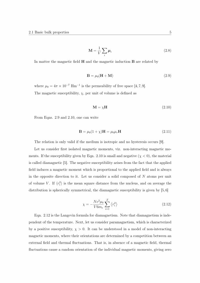
oriented in direction of the field (Fig. 2.1). The potential energy of a single moment in
a field is equal to −μ ·B [4, 6].
Fig. 2.1: Schematic representation of a paramagnetic (PM) system under an applied field [10]. Themagnetic field is assumed to be along the z axis.
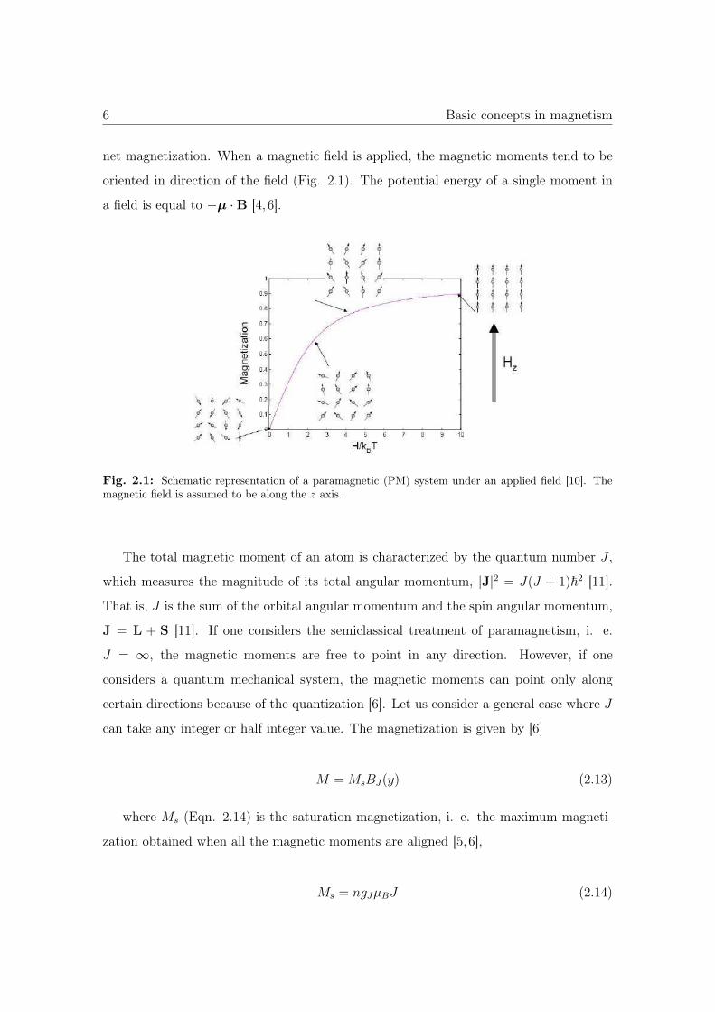
The total magnetic moment of an atom is characterized by the quantum number J ,
which measures the magnitude of its total angular momentum, |J|2 = J(J + 1)�2 [11].
That is, J is the sum of the orbital angular momentum and the spin angular momentum,
J = L + S [11]. If one considers the semiclassical treatment of paramagnetism, i. e.
J = ∞, the magnetic moments are free to point in any direction. However, if one
considers a quantum mechanical system, the magnetic moments can point only along
certain directions because of the quantization [6]. Let us consider a general case where J
can take any integer or half integer value. The magnetization is given by [6]
M = MsBJ(y) (2.13)
where Ms (Eqn. 2.14) is the saturation magnetization, i. e. the maximum magneti-
zation obtained when all the magnetic moments are aligned [5, 6],
Ms = ngJμBJ (2.14)
2.1 Basic bulk properties 7
where n is the number of magnetic moments per unit of volume. The Brillouin
function, BJ(y), is given by [6]
BJ(y) =2J + 1
2Jcoth
(2J + 1
2Jy
)− 1
2Jcoth
y
2J(2.15)
with
y =gJμBμ0JH
kBT(2.16)
kB is the Boltzmann’s constant. The constant gJ is called the Landé g-value and is
given by
gJ =3
2+
S(S + 1) − L(L + 1)
2J(J + 1)(2.17)
In the limit when J → ∞ one obtains the Langevin function [4, 6]
B∞(y) = L(y) = coth y − 1
y(2.18)
When J = 12
only two states are possible, corresponding to mJ = ±12, the Brillouin
function is simply the tanh y, and thus the magnetization is
M = Ms tanh y (2.19)
where y = μBμ0H/kBT .
For small values of y the susceptibility is given by
χ =M
H∝ μ0M
B=
nμ0μ2eff
3kBT=
C
T(2.20)
where C is the Curie constant given by
C =nμ0μ
2eff
3kB
(2.21)
and μeff is the effective moment
8 Basic concepts in magnetism
μeff = gJμB
√J(J + 1) (2.22)
The temperature dependence of the susceptibility in Eqn. 2.20 is known as the Curie
law. Note that in paramagnetism the magnetic moments interact only with an external
magnetic field and not with each other. When interactions between the moments are
present, one may add an appropriately chosen effective field to the applied external field,
as it will be shown in the next sections.
2.1.1 Ferromagnetism
A ferromagnetic (FM) material is characterized by a saturation or spontaneous mag-
netization Ms even without any applied field. Above a critical temperature, the Curie
temperature TC , the spontaneous magnetization vanishes [5,11,12]. The material is then
paramagnetic with a susceptibility given by the Curie-Weiss law. Below TC , the interac-
tion of the single magnetic moments leads to a collective alignment and thus a magneti-
zation which is non-zero integrating over the volume. A strong interaction field favors the
collective alignment of the moments along a common direction. Weiss proposed that the
interaction field, called molecular field Hm, is proportional to the magnetization [5,8,11],
i. e.
Hm = λM (2.23)
where λ is a constant thus parametrizing the strength of the molecular field as a
function of temperature. In a ferromagnet, the total magnetic field that each moment
experiences consists of the applied field (Ha) and the molecular field, i. e.
Ht = Ha + λM (2.24)
In the previous discussion of paramagnetism, the relation between the magnetization
and the applied field was given by (Eqn. 2.13).
M = MsBJ
(gJμ0μBJH
kBT
)(2.25)
2.1 Basic bulk properties 9
For a FM material, the field H can be replaced by the total field [5, 11, 13], i. e.
M = MsBJ(y) (2.26)
and
y =
(gJμ0μBJ(Ha + λM)
kBT
)(2.27)
To obtain solutions to the Weiss model, it is required that Eqn. 2.26 and Eqn. 2.27 are
satisfied simultaneously. The spontaneous magnetization can be obtained by considering
the limit where Ha → 0. The magnetization then follows the law
M = MsBJ
(gJμ0μBJ(λM)
kBT
)(2.28)
The solutions can be found graphically by plotting both functions at various T and
determining the points at which the curves intersect [5, 6, 9, 11, 13]. The case when the
straight line is tangent to the Brillouin function at the origin corresponds to the critical
temperature. This critical temperature at which Ms falls to zero is the Curie temperature,
TC . Its value in terms of the molecular field parameters is determined from the slope of
the Brillouin function at the origin which is (J + 1)/3J [5, 11]. Thus,
TC =gJμB(J + 1)λMs
3kB
(2.29)
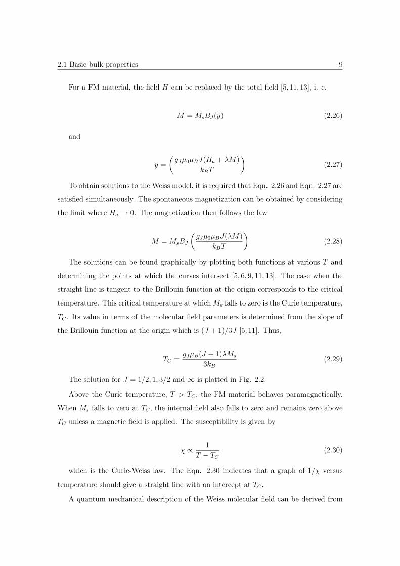
The solution for J = 1/2, 1, 3/2 and ∞ is plotted in Fig. 2.2.
Above the Curie temperature, T > TC , the FM material behaves paramagnetically.
When Ms falls to zero at TC , the internal field also falls to zero and remains zero above
TC unless a magnetic field is applied. The susceptibility is given by
χ ∝ 1
T − TC
(2.30)
which is the Curie-Weiss law. The Eqn. 2.30 indicates that a graph of 1/χ versus
temperature should give a straight line with an intercept at TC .
A quantum mechanical description of the Weiss molecular field can be derived from
10 Basic concepts in magnetism
Fig. 2.2: Temperature dependence of spontaneous magnetization at H=0 and for different values ofJ . [6].
the Heisenberg Hamiltonian [4, 5, 9]. Let us consider two atoms, i and j, each of them
having one electron. The exchange Hamiltonian is
Hij = −2Jijsi · sj (2.31)
where Jij is the exchange integral of the two electrons. For two atoms, each of them
having more than one electron with an unpaired spin, the exchange Hamiltonian is
Hij = −2JijSi · Sj (2.32)
where Si =∑si and Sj =
∑sj. It was considered here, that all the electrons have
the same exchange integral Jij, and that the exchange integral between the electrons of
the same atom is constant, and therefore can be omitted3.
If the exchange integral is isotropic and if only nearest neighbors interact, then the
exchange Hamiltonian for spin i can be written as
Hi = −2∑
j
JeSi · Sj (2.33)
3The first considerations is valid if the angular momentum is quenched. The second one is valid ifthe spin angular momentum is not quenched. In this case, J = S, which works for most 3d ions.
2.1 Basic bulk properties 11
where the summation is over the nearest neighbors of atom i.
Considering by simplicity the Ising model, one has
Hi = −2Je
∑j
Szi S
zj (2.34)
The connection of Je to the Weiss field is seen by taking into account the magnetiza-
tion, assumed along the z-direction, which is given by M = ngμB
∑j
⟨Sz
j
⟩. Here one re-
places the summation by a time average as an approximation, i. e. Hi = −2Je
∑Sz
i Szj ≈
−2JeSzi
∑j
⟨Sz
j
⟩neglecting fluctuations [5]. Thus, for the z nearest neighbors, Eqn. 2.34
can be written in terms of the magnetization as
Hi = −2zSz
i JeM
ngμB
(2.35)
where z is .The Hamiltonian in term of the Weiss field is then
Hi = −gSzi μBλM (2.36)
From Eqn. 2.35 and 2.36 one obtains the molecular field constant, λ,
λ =2zJe
ng2μ2B
(2.37)
A positive Je favors parallel alignment of the spins, which is the case for a ferromag-
netic interaction [12].
Using Eqn. 2.29 [5, 6], one finds that the Curie temperature is
TC =2zJeS(S + 1)
3kB
(2.38)
Examples of ferromagnetic materials are shown in Table 2.1.
2.1.2 Antiferromagnetism
It has been discussed that when the exchange interaction is positive, the spins tend
to be aligned parallel to each other. However, a negative exchange interaction tends
to align the neighboring spins antiparallel [5, 12]. In the ordered state, which sets in
12 Basic concepts in magnetism
Tab. 2.1: Examples of ferromagnetic materials taken from Ref. [6].Material Tc (K) magnetic moment
(μB/formula unit)Fe 1043 2.22Co 1394 1.1715Ni 631 0.605Gd 289 7.5
MnSb 587 3.5EuO 70 6.9EuS 16.5 6.9
below a critical temperature, the magnetic moments are aligned forming two or more
spontaneously magnetized and interpenetrating sublattices. Since the magnetizations
are differently oriented, the resultant magnetization is zero at zero applied field. This
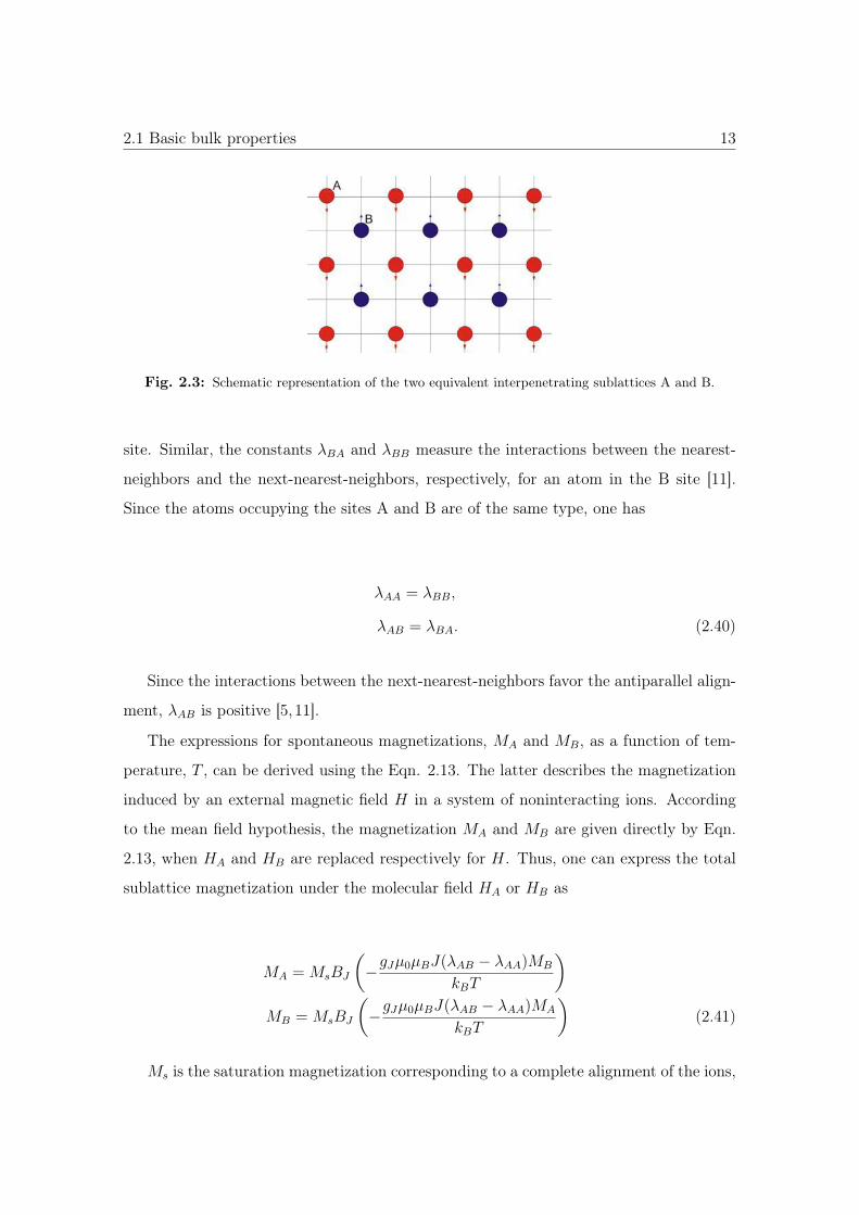
kind of order is known as antiferromagnetism [5, 8, 11, 14]. Let us consider the case of
two interpenetrating sublattices, A and B, on one of which the spins point up and on the
other down as shown in Figure 2.3. The theory considers that the exchange interaction
between the nearest neighbors favors antiparallel alignment of the magnetic moments [14].
In that case, it is expected that a close approximation to the magnetically ordered state
at absolute zero is the alignment of all A ions in one direction and of all B ions in
the opposite direction. This consideration involves short-range interactions between first
neighbor atoms and negligible interactions beyond the second or third neighbors. In this
situation, the sublattice A exerts a molecular field HA on the sublattice B, whereas the
sublattice B exerts a molecular field HB on the sublattice A [14]. Then the molecular
field acting on sublattice A and B is given by
HA = −λAAMA − λABMB,
HB = −λBAMA − λBBMB. (2.39)
where MA = μA/VA and MB = μB/VB are the total magnetization of the A and B
sublattices, respectively. The constants λAB and λAA measure the interaction between
the nearest-neighbors and the next-nearest-neighbors, respectively, for an atom in the A
2.1 Basic bulk properties 13
Fig. 2.3: Schematic representation of the two equivalent interpenetrating sublattices A and B.
site. Similar, the constants λBA and λBB measure the interactions between the nearest-
neighbors and the next-nearest-neighbors, respectively, for an atom in the B site [11].
Since the atoms occupying the sites A and B are of the same type, one has
λAA = λBB,
λAB = λBA. (2.40)
Since the interactions between the next-nearest-neighbors favor the antiparallel align-
ment, λAB is positive [5, 11].
The expressions for spontaneous magnetizations, MA and MB, as a function of tem-
perature, T , can be derived using the Eqn. 2.13. The latter describes the magnetization
induced by an external magnetic field H in a system of noninteracting ions. According
to the mean field hypothesis, the magnetization MA and MB are given directly by Eqn.
2.13, when HA and HB are replaced respectively for H. Thus, one can express the total
sublattice magnetization under the molecular field HA or HB as
MA = MsBJ
(−gJμ0μBJ(λAB − λAA)MB
kBT
)
MB = MsBJ
(−gJμ0μBJ(λAB − λAA)MA
kBT
)(2.41)
Ms is the saturation magnetization corresponding to a complete alignment of the ions,
14 Basic concepts in magnetism
and J is the total quantum number of the ion4. The two sublattices are exactly equivalent
in the absence of an external applied field, therefore MA will be equal in magnitude to
MB and with λAB (favoring antiparallel alignment) much greater than λAA. Consequently
MA = MB = M and the total sublattice magnetization can be written as
M = MsBJ
(gJμ0μBJ(λAB − λAA)M
kBT
), H = 0 (2.42)
The expression in Eqn. 2.42 is similar to the corresponding equation derived for
ferromagnetism (Eqn. 2.28), but in this case (λAB − λAA) is the molecular field constant
which replace to λ in the case of expression 2.28. At absolute zero MA and MB are equal
to Ms. The two sublattices acquire spontaneous magnetization (H = 0) in opposite
directions with increasing temperature and vanishing for temperatures T greater than
the Néel temperature TN [14]. TN is given by
TN =gJμB(J + 1)(λAB − λAA)Ms
3kB
=1
2C(λAB − λAA) (2.43)
Thus the Néel temperature is defined as the temperature at which the spontaneous
magnetization of one of the sublattices vanishes. For T > TN the material becomes
regularly paramagnetic [5, 8, 11].
The existence of antiferromagnetism is observed experimentally using neutron diffrac-
tion, nuclear magnetic resonance, Mössbauer effect, specific heat and magnetic suscepti-
bility. In this section the magnetic susceptibility will be described.
For temperatures greater than TN and in a sufficiently small applied field, one can
derive the expression for the susceptibility using the Eqn. 2.13. MA and MB are induced
only in the presence of an external applied field Ha. One can use the limiting behavior of
the Brillouin function for small values of its argument. One considers that above TN , MA
and MB are both parallel to Ha and therefore to each other. This assumption is valid if
λABMA and λABMB are much smaller than Ha. The magnetic susceptibility is given by
χ =C
T − Θ(2.44)
4Often in the literature, the orbital momentum is neglected in the description of antiferromagnetismbecause in most AF the crystal fields almost completely quench the orbital moments.
2.1 Basic bulk properties 15
where Θ is the Curie-Weiss temperature. Note that in contrast to the case of ferro-
magnetism, Θ is not equal to the critical temperature. In this case, Θ is negative. If
Θ = 0, the material is paramagnetic.
Taking into account magnetocrystalline anisotropy, below TN one finds two suscepti-
bilities depending on whether the magnetic field is applied along the easy axis (longitudi-
nal susceptibility) or perpendicular to it (transverse susceptibility). For a magnetic field
applied parallel to the anisotropy easy axis one can write
MA =M+ δMA (2.45)
MB = −M+ δMB (2.46)
The parallel susceptibility is
χ|| =δMA + δMB
H(2.47)
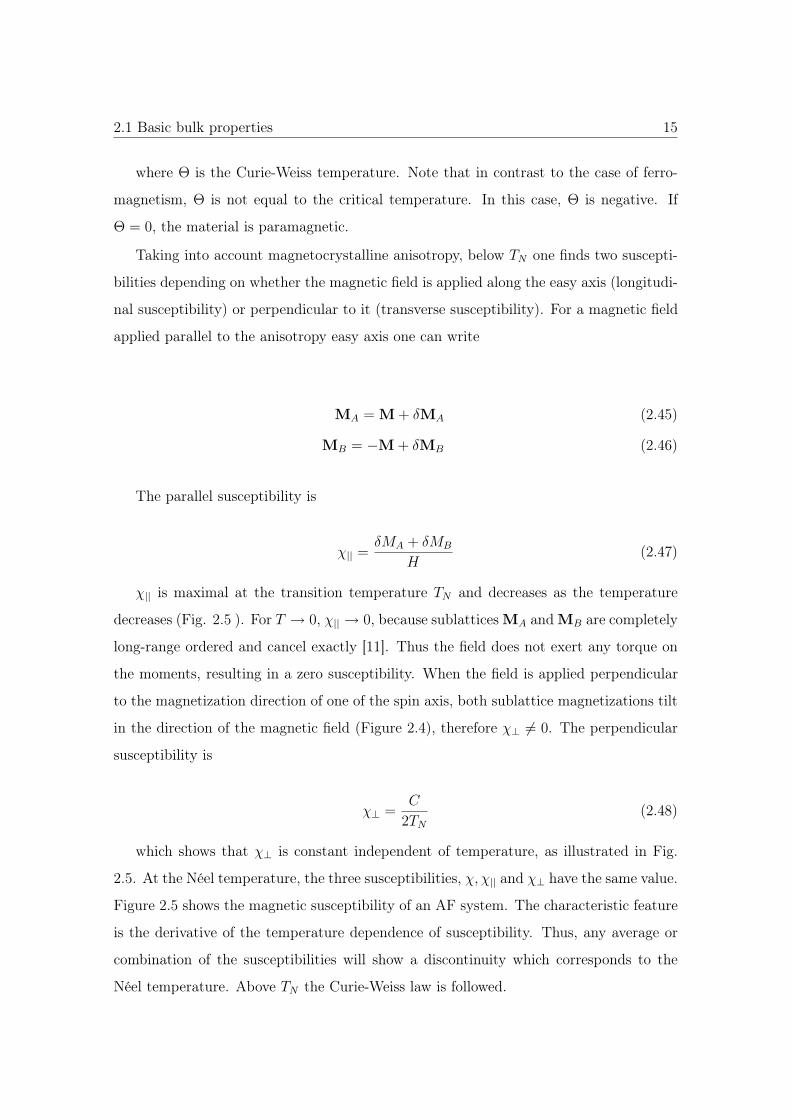
χ|| is maximal at the transition temperature TN and decreases as the temperature
decreases (Fig. 2.5 ). For T → 0, χ|| → 0, because sublatticesMA andMB are completely
long-range ordered and cancel exactly [11]. Thus the field does not exert any torque on
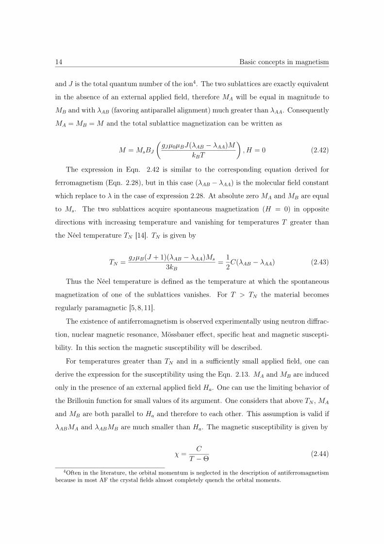
the moments, resulting in a zero susceptibility. When the field is applied perpendicular
to the magnetization direction of one of the spin axis, both sublattice magnetizations tilt
in the direction of the magnetic field (Figure 2.4), therefore χ⊥ �= 0. The perpendicular
susceptibility is
χ⊥ =C
2TN
(2.48)
which shows that χ⊥ is constant independent of temperature, as illustrated in Fig.
2.5. At the Néel temperature, the three susceptibilities, χ, χ|| and χ⊥ have the same value.
Figure 2.5 shows the magnetic susceptibility of an AF system. The characteristic feature
is the derivative of the temperature dependence of susceptibility. Thus, any average or
combination of the susceptibilities will show a discontinuity which corresponds to the
Néel temperature. Above TN the Curie-Weiss law is followed.
16 Basic concepts in magnetism
Fig. 2.4: Spin rotation in an antiferromagnetic material for the case when the field is applied perpen-dicular to the easy axis [15].
Fig. 2.5: The temperature dependence of the susceptibility of antiferromagnets.
The susceptibility for a polycrystalline sample is obtained by averaging the suscepti-
bility over the angle θ between the spins axis and the magnetic field [7]. For example for
a cubic material χ is
χp = χ||⟨cos2 θ
⟩+ χ⊥
⟨sin2 θ
⟩=
1
3(χ|| + 2χ⊥) (2.49)
Considering the case of uniaxial anisotropy, the energy per unit volume is
Ea
V= K sin θ (2.50)
where K is the anisotropy constant and θ the angle between the sublattice magneti-
zation and the easy axis.
2.1 Basic bulk properties 17
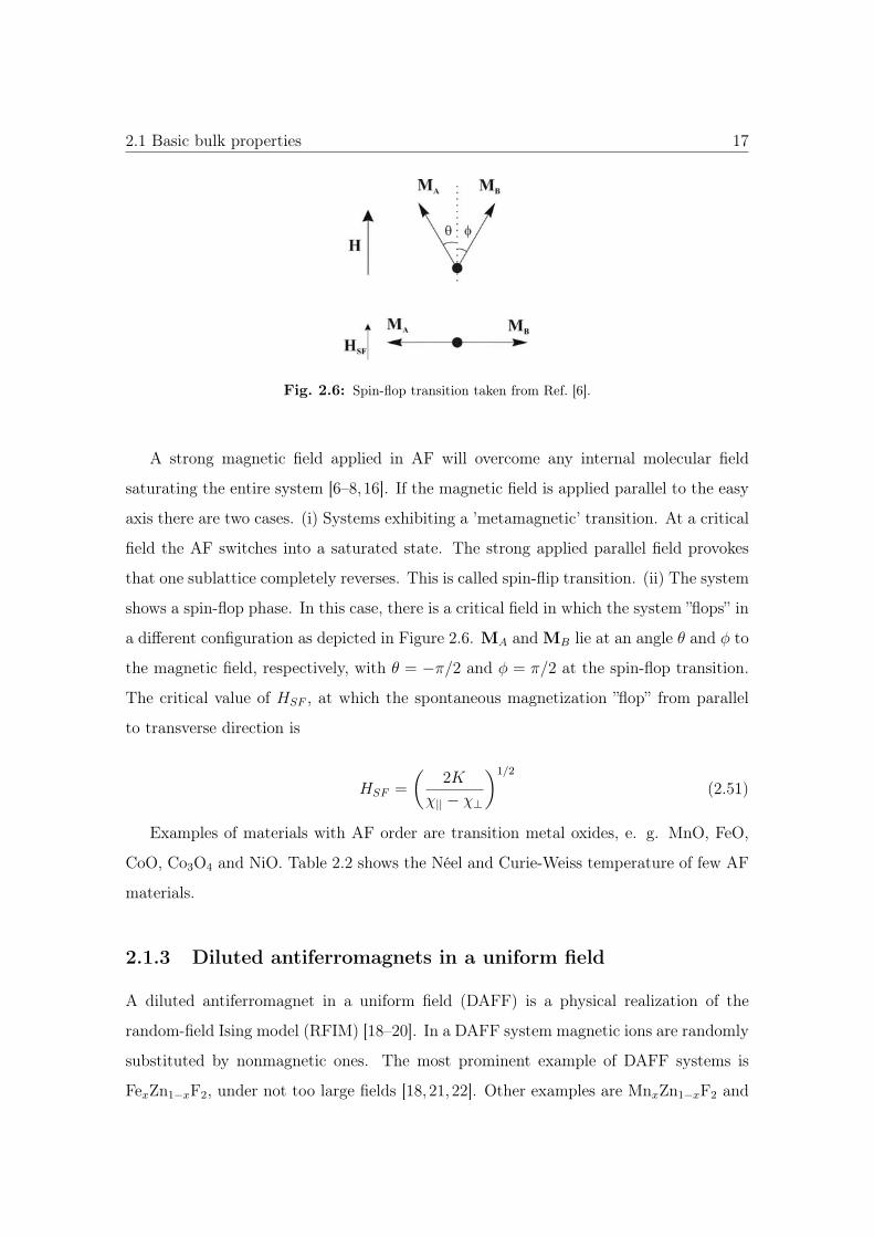
Fig. 2.6: Spin-flop transition taken from Ref. [6].
A strong magnetic field applied in AF will overcome any internal molecular field
saturating the entire system [6–8,16]. If the magnetic field is applied parallel to the easy
axis there are two cases. (i) Systems exhibiting a ’metamagnetic’ transition. At a critical
field the AF switches into a saturated state. The strong applied parallel field provokes
that one sublattice completely reverses. This is called spin-flip transition. (ii) The system
shows a spin-flop phase. In this case, there is a critical field in which the system ”flops” in
a different configuration as depicted in Figure 2.6. MA andMB lie at an angle θ and φ to
the magnetic field, respectively, with θ = −π/2 and φ = π/2 at the spin-flop transition.
The critical value of HSF , at which the spontaneous magnetization ”flop” from parallel
to transverse direction is
HSF =
(2K
χ|| − χ⊥
)1/2
(2.51)
Examples of materials with AF order are transition metal oxides, e. g. MnO, FeO,
CoO, Co3O4 and NiO. Table 2.2 shows the Néel and Curie-Weiss temperature of few AF
materials.
2.1.3 Diluted antiferromagnets in a uniform field
A diluted antiferromagnet in a uniform field (DAFF) is a physical realization of the
random-field Ising model (RFIM) [18–20]. In a DAFF system magnetic ions are randomly
substituted by nonmagnetic ones. The most prominent example of DAFF systems is
FexZn1−xF2, under not too large fields [18, 21, 22]. Other examples are MnxZn1−xF2 and
18 Basic concepts in magnetism
Tab. 2.2: Examples of antiferromagnetic materials.Material TN (K) Θ (K)MnF2 67 -80 [6]MnO 122 -610 [6, 15]CoO 293 -280 [15]Co3O4 40 -53 [17]FeO 198 -570 [15]Cr2O3 307 -485 [6]FeF2 79 -117 [15]
CoxZn1−xF2 [18].
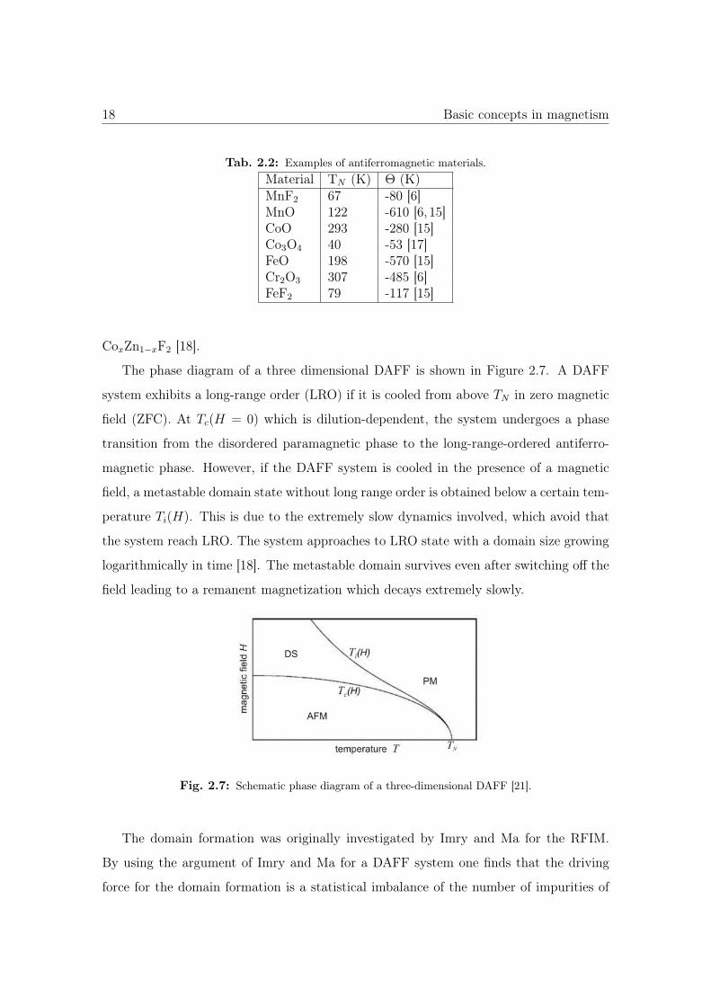
The phase diagram of a three dimensional DAFF is shown in Figure 2.7. A DAFF
system exhibits a long-range order (LRO) if it is cooled from above TN in zero magnetic
field (ZFC). At Tc(H = 0) which is dilution-dependent, the system undergoes a phase
transition from the disordered paramagnetic phase to the long-range-ordered antiferro-
magnetic phase. However, if the DAFF system is cooled in the presence of a magnetic
field, a metastable domain state without long range order is obtained below a certain tem-
perature Ti(H). This is due to the extremely slow dynamics involved, which avoid that
the system reach LRO. The system approaches to LRO state with a domain size growing
logarithmically in time [18]. The metastable domain survives even after switching off the
field leading to a remanent magnetization which decays extremely slowly.
Fig. 2.7: Schematic phase diagram of a three-dimensional DAFF [21].
The domain formation was originally investigated by Imry and Ma for the RFIM.
By using the argument of Imry and Ma for a DAFF system one finds that the driving
force for the domain formation is a statistical imbalance of the number of impurities of
2.1 Basic bulk properties 19
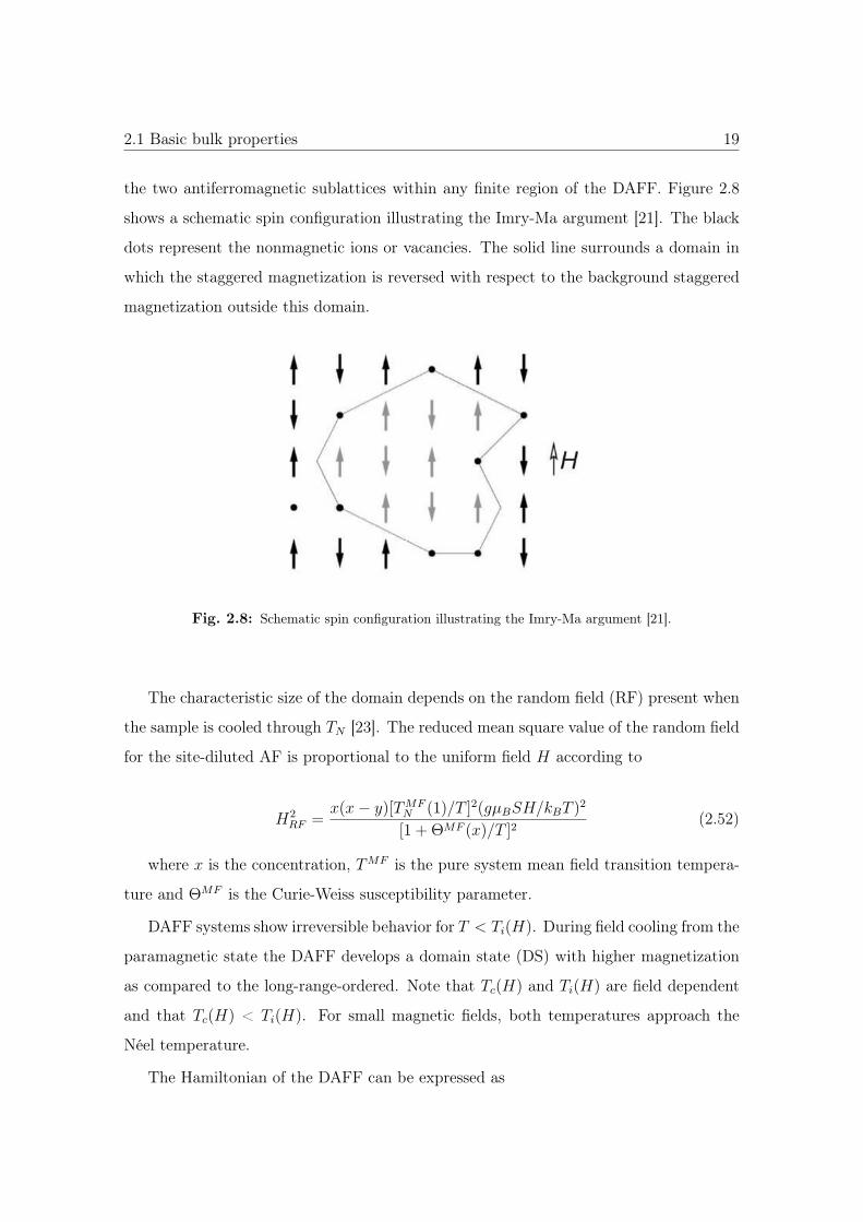
the two antiferromagnetic sublattices within any finite region of the DAFF. Figure 2.8
shows a schematic spin configuration illustrating the Imry-Ma argument [21]. The black
dots represent the nonmagnetic ions or vacancies. The solid line surrounds a domain in
which the staggered magnetization is reversed with respect to the background staggered
magnetization outside this domain.
Fig. 2.8: Schematic spin configuration illustrating the Imry-Ma argument [21].
The characteristic size of the domain depends on the random field (RF) present when
the sample is cooled through TN [23]. The reduced mean square value of the random field
for the site-diluted AF is proportional to the uniform field H according to
H2RF =
x(x − y)[TMFN (1)/T ]2(gμBSH/kBT )2
[1 + ΘMF (x)/T ]2(2.52)
where x is the concentration, TMF is the pure system mean field transition tempera-
ture and ΘMF is the Curie-Weiss susceptibility parameter.
DAFF systems show irreversible behavior for T < Ti(H). During field cooling from the
paramagnetic state the DAFF develops a domain state (DS) with higher magnetization
as compared to the long-range-ordered. Note that Tc(H) and Ti(H) are field dependent
and that Tc(H) < Ti(H). For small magnetic fields, both temperatures approach the
Néel temperature.
The Hamiltonian of the DAFF can be expressed as
20 Basic concepts in magnetism
H = −∑ij
JijεiεjSiSj − μμ0H∑
i
εiSi (2.53)
where Jij < 0 is the antiferromagnetic nearest-neighbor exchange constant and H is
the magnetic field. Si = ±1 are normalized Ising spin variables representing spins with
an atomic moment μ. A fraction p of sites is left without a magnetic moment (εi = 0)
while the other sites carry a moment ( εi = 1) [21].
A 2d DAFF does not show a phase transition and hence no critical behavior in a
field [24]. This is in contrast to the 3d case, where a sharp phase transition at Tc(H)
is present as explained above. However, in 2d DAFF systems it is possible to observe
a peak that becomes rounder and decreases in amplitude with increasing field [25]. It
marks the (non-critical) transition from the paramagnetic state to a metastable domain-
state with short-range AF order [26]. The domain-state is characterized by an irreversible
(non-ergodic) behavior. An example of 2d DAFF is Rb2Co0.85Mg0.15F4 [27, 28].
2.1.4 Ferrimagnetism
A ferrimagnetic (FiM) material possesses a spontaneous magnetization without applied
field, similar to a ferromagnet. In order to understand ferrimagnetism, let us consider
two sublattices denoted by A and B as in the case of antiferromagnetism. When the
sublattices magnetizations, MA and MB are not equal, there will be a non-zero net
magnetic moment [12, 15]. Therefore, it is expected that the magnetizations MA amd
MB do not cancel each other out. This is the case when the atoms occupying the A
and B sites are from different elements or when the ions are not the same. Examples
are ferrites in which Fe3+ ions are found in one sublattice whereas divalent metal ions
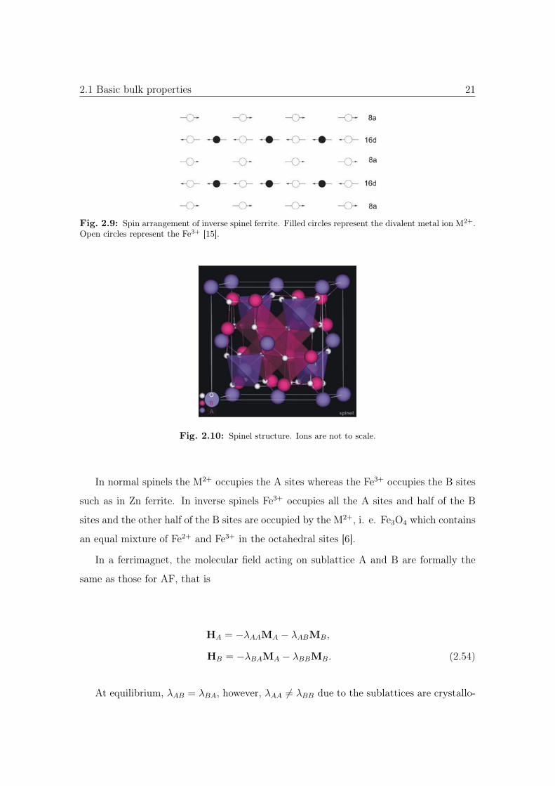
M such as Mn2+, Co2+, Ni2+, Zn2+ or Fe2+ are in the other sublattice (Fig. 2.9) [15].
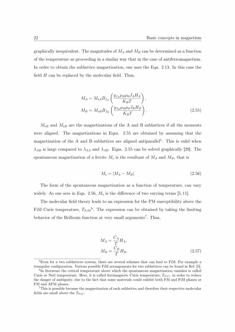
The most typical ferrimagnets are the spinel ferrites (Figure 2.10). The white circles in
the Figure 2.10 represent the oxygen ions which are forming a close-packed face centered
cubic lattice. The pink and purple circles represent the metal ions. The spinel structure
contains two types of lattice sites, i. e. tetrahedral (A or 8a) and octahedral (B or 16d)
sites. In the former, the metal ions are surrounded by four oxygen atoms whereas in the
latter the metal ions are surrounded by six oxygen atoms.
2.1 Basic bulk properties 21
Fig. 2.9: Spin arrangement of inverse spinel ferrite. Filled circles represent the divalent metal ion M2+.Open circles represent the Fe3+ [15].
Fig. 2.10: Spinel structure. Ions are not to scale.
In normal spinels the M2+ occupies the A sites whereas the Fe3+ occupies the B sites
such as in Zn ferrite. In inverse spinels Fe3+ occupies all the A sites and half of the B
sites and the other half of the B sites are occupied by the M2+, i. e. Fe3O4 which contains
an equal mixture of Fe2+ and Fe3+ in the octahedral sites [6].
In a ferrimagnet, the molecular field acting on sublattice A and B are formally the
same as those for AF, that is
HA = −λAAMA − λABMB,
HB = −λBAMA − λBBMB. (2.54)
At equilibrium, λAB = λBA, however, λAA �= λBB due to the sublattices are crystallo-
22 Basic concepts in magnetism
graphically inequivalent. The magnitudes of MA and MB can be determined as a function
of the temperature as proceeding in a similar way that in the case of antiferromagnetism.
In order to obtain the sublattice magnetization, one uses the Eqn. 2.13. In this case the
field H can be replaced by the molecular field. Thus,
MA = MsABJA
(gJA
μBμ0JAHA
KBT
),
MB = MsBBJB
(gJB
μBμ0JBHB
KBT
). (2.55)
MsB and MsB are the magnetizations of the A and B sublattices if all the moments
were aligned. The magnetizations in Eqns. 2.55 are obtained by assuming that the
magnetization of the A and B sublattices are aligned antiparallel5. This is valid when
λAB is large compared to λAA and λAB. Eqns. 2.55 can be solved graphically [29]. The
spontaneous magnetization of a ferrite Ms is the resultant of MA and MB, that is
Ms = |MA − MB| (2.56)
The form of the spontaneous magnetization as a function of temperature, can vary
widely. As one sees in Eqn. 2.56, Ms is the difference of two varying terms [5, 11].
The molecular field theory leads to an expression for the PM susceptibility above the
FiM Curie temperature, TFiM6. The expression can be obtained by taking the limiting
behavior of the Brillouin function at very small arguments7. Thus,
MA =CA
THA,
MB =CB
THB. (2.57)
5Even for a two sublattices system, there are several schemes that can lead to FiM. For example atriangular configuration. Various possible FiM arrangements for two sublattices can be found in Ref. [5].
6In literature the critical temperature above which the spontaneous magnetization vanishes is calledCurie or Néel temperature. Here, it is called ferrimagnetic Curie temperature, TFiC , in order to reducethe danger of ambiguity, due to the fact that some materials could exhibit both FM and FiM phases orFM and AFM phases.
7This is possible because the magnetization of each sublattice and therefore their respective molecularfields are small above the TFiC .
2.2 Small particles 23
Tab. 2.3: Examples of ferrimagnetic materials taken from Ref. [6].Material Tc (K) magnetic moment
(μB/formula unit)Fe3O4 858 4.1
CoFe2O4 793 3.7NiFe2O4 858 2.3CuFe2O4 728 1.3Y3Fe5O12 560 5.0
where
CA =NAg2
JAμ2
BJA(JA + 1)
3kB
,
CB =NBg2
JBμ2
BJB(JB + 1)
3kB
. (2.58)
The susceptibily is then
χ =MA + MB
Ha
(2.59)
and the ferrimagnetic Curie temperature, T = TFiC is [5],
TFiC = −1
2(CAλAA + CBλBB) +
1
2[(CAλAA − CBλBB)2 + 4CACBλ2
AB]1/2 (2.60)
Below TFiC there is a spontaneous magnetization in zero applied field which is similar
to a ferromagnet. Above TFiC the magnetization is zero in zero applied field. Further
examples of FiM are garnets and certain rare earth-transition metal alloys. Table 2.3
shows the properties of some common ferrimagnets.
2.2 Small particles
The formation of magnetic domains is dominated by the minimization of magnetostatic
energy. By reducing the size of the magnetic material one finds that for a critical diameter
24 Basic concepts in magnetism
it is energetically favorable to form only one magnetic domain (single domain state) and
to avoid domain walls. The latter depends on the spontaneous magnetization, anisotropy
energy and exchange interactions between individual spins. Typical values for the critical
radius of magnetic nanoparticles are between 10-800 nm (Table 2.4) [30]. It is given
by [16]
Rc =36
√AK1
μ0M2s
(2.61)
where Ms is the saturation magnetization, A is the exchange stiffness constant, and
K1 is the crystalline anisotropy constant [16].
Tab. 2.4: Critical single-domain radius for different magnetic materials [16].Compound Rc (nm)
Fe 6Co 34Ni 16
BaFe12O19 290SmCo5 764
Nd2Fe14B 107
The reduction in size of a magnetic material changes its bulk magnetic properties
which has attracted much interest among magnetism researchers for decades. Magnetic
nanoparticles and nanowires exhibit huge potential in technological applications either in
purely magnetic areas as recording technology [31], but also in other disciplines such as
in biology and medicine [32]. In fundamental research they usually serve as ideal model
systems, mentioning e.g. the Stoner-Wohlfarth and the Néel-Brown model [30] or to
study the finite size effect [33]. In this section the fundamental aspects of fine magnetic
particles will be introduced.
2.2.1 Stoner-Wohlfarth model
The Stoner-Wohlfahrt model (SW) or coherent rotation model proposes a description of
magnetization reversal of noninteracting single-domain particles with shape anisotropy
[12]. The model assumes constant magnetization throughout the magnet [16, 34]. The
2.2 Small particles 25
consequences of this assumption is that the exchange energy is constant during magne-
tization reversal and the energy of the particle is equal to the anisotropy and Zeeman
energy [16].
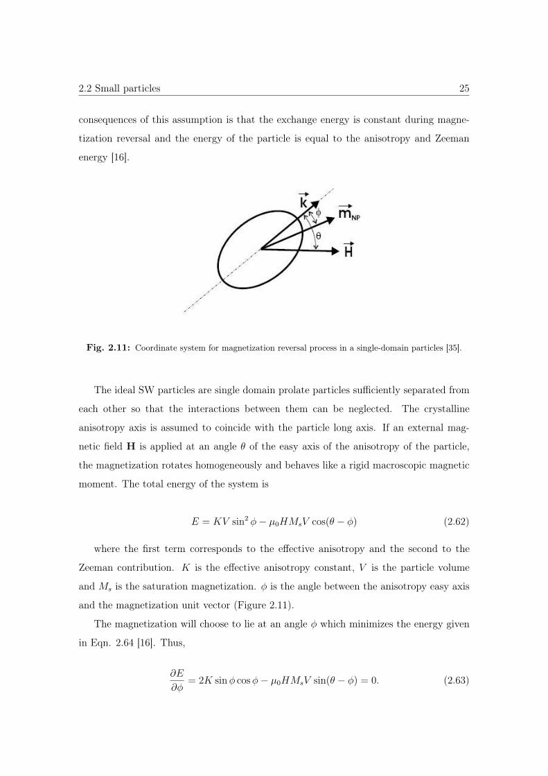
Fig. 2.11: Coordinate system for magnetization reversal process in a single-domain particles [35].
The ideal SW particles are single domain prolate particles sufficiently separated from
each other so that the interactions between them can be neglected. The crystalline
anisotropy axis is assumed to coincide with the particle long axis. If an external mag-
netic field H is applied at an angle θ of the easy axis of the anisotropy of the particle,
the magnetization rotates homogeneously and behaves like a rigid macroscopic magnetic
moment. The total energy of the system is
E = KV sin2 φ − μ0HMsV cos(θ − φ) (2.62)
where the first term corresponds to the effective anisotropy and the second to the
Zeeman contribution. K is the effective anisotropy constant, V is the particle volume
and Ms is the saturation magnetization. φ is the angle between the anisotropy easy axis
and the magnetization unit vector (Figure 2.11).
The magnetization will choose to lie at an angle φ which minimizes the energy given
in Eqn. 2.64 [16]. Thus,
∂E
∂φ= 2K sin φ cos φ − μ0HMsV sin(θ − φ) = 0. (2.63)
26 Basic concepts in magnetism
The equilibrium energy states are stable when ∂2E∂2φ
is positive,
∂2E
∂2φ= 2K(cos2 φ − sin2 φ) − μ0HMsV cos(θ − φ) > 0 (2.64)
If the magnetic field H is applied at an angle θ = 0 of the easy axis of the anisotropy
of the particle, a perfectly square hysteresis loop is obtained. In this case, the model
predicts that the coercivity is equal to the anisotropy field 2K/μ0Ms [16].
If the magnetic field H is applied perpendicular to the the easy axis of the anisotropy
of the particle (θ = 90◦), no anisotropy is obtained. The loop is a straight line with no
hysteresis and zero coercivity and slope dM/dH = 2K/μ0M2s [16].
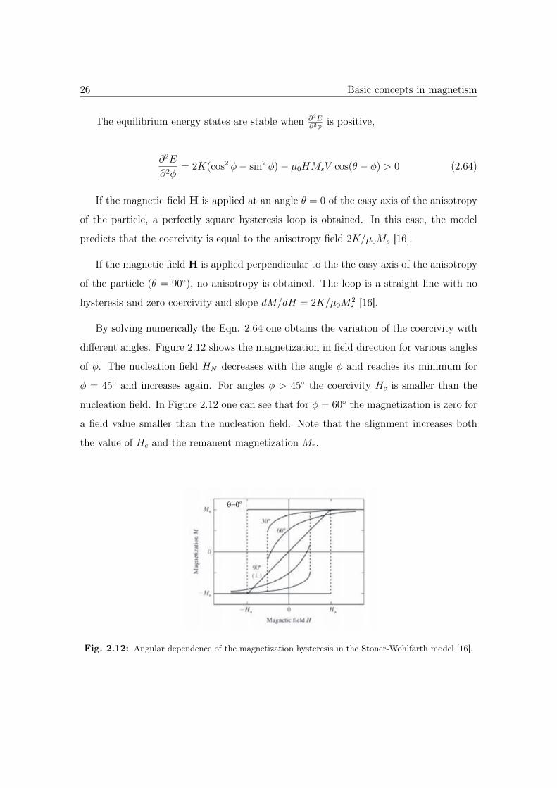
By solving numerically the Eqn. 2.64 one obtains the variation of the coercivity with
different angles. Figure 2.12 shows the magnetization in field direction for various angles
of φ. The nucleation field HN decreases with the angle φ and reaches its minimum for
φ = 45◦ and increases again. For angles φ > 45◦ the coercivity Hc is smaller than the
nucleation field. In Figure 2.12 one can see that for φ = 60◦ the magnetization is zero for
a field value smaller than the nucleation field. Note that the alignment increases both
the value of Hc and the remanent magnetization Mr.
Fig. 2.12: Angular dependence of the magnetization hysteresis in the Stoner-Wohlfarth model [16].
2.2 Small particles 27
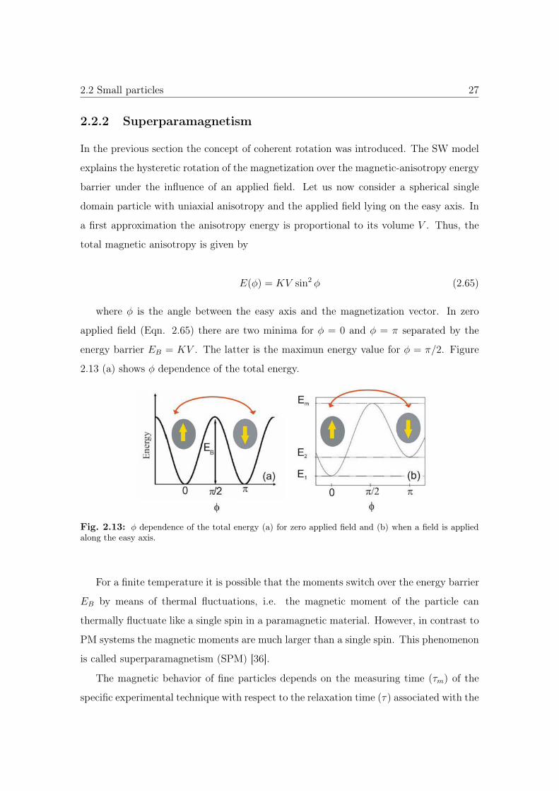
2.2.2 Superparamagnetism
In the previous section the concept of coherent rotation was introduced. The SW model
explains the hysteretic rotation of the magnetization over the magnetic-anisotropy energy
barrier under the influence of an applied field. Let us now consider a spherical single
domain particle with uniaxial anisotropy and the applied field lying on the easy axis. In
a first approximation the anisotropy energy is proportional to its volume V . Thus, the
total magnetic anisotropy is given by
E(φ) = KV sin2 φ (2.65)
where φ is the angle between the easy axis and the magnetization vector. In zero
applied field (Eqn. 2.65) there are two minima for φ = 0 and φ = π separated by the
energy barrier EB = KV . The latter is the maximun energy value for φ = π/2. Figure
2.13 (a) shows φ dependence of the total energy.
Fig. 2.13: φ dependence of the total energy (a) for zero applied field and (b) when a field is appliedalong the easy axis.
For a finite temperature it is possible that the moments switch over the energy barrier
EB by means of thermal fluctuations, i.e. the magnetic moment of the particle can
thermally fluctuate like a single spin in a paramagnetic material. However, in contrast to
PM systems the magnetic moments are much larger than a single spin. This phenomenon
is called superparamagnetism (SPM) [36].
The magnetic behavior of fine particles depends on the measuring time (τm) of the
specific experimental technique with respect to the relaxation time (τ) associated with the
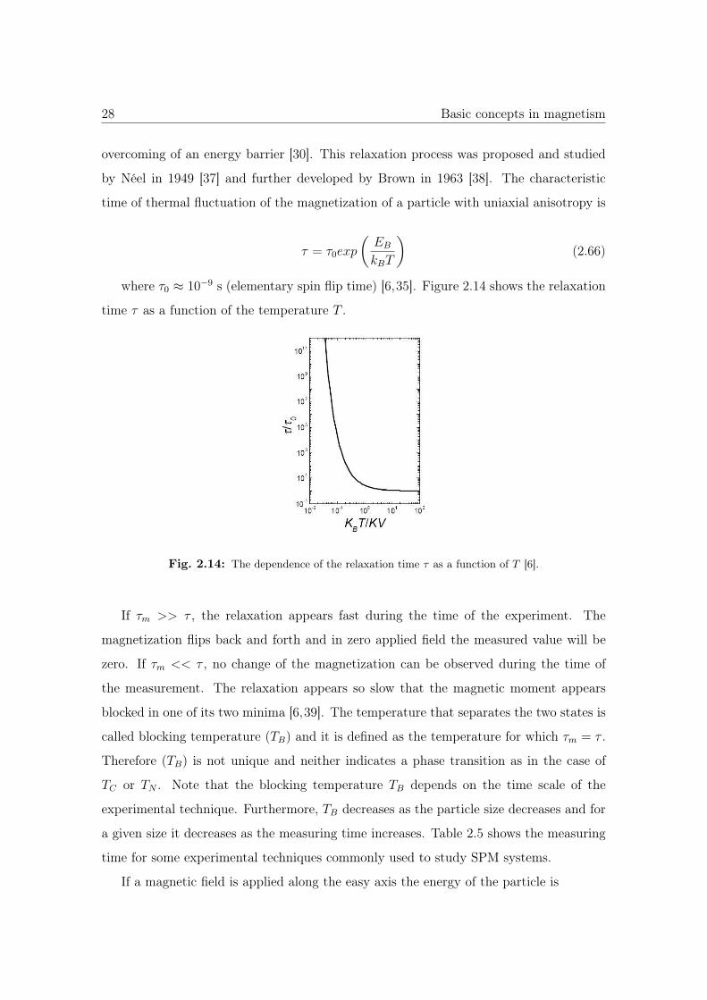
28 Basic concepts in magnetism
overcoming of an energy barrier [30]. This relaxation process was proposed and studied
by Néel in 1949 [37] and further developed by Brown in 1963 [38]. The characteristic
time of thermal fluctuation of the magnetization of a particle with uniaxial anisotropy is
τ = τ0exp
(EB
kBT
)(2.66)
where τ0 ≈ 10−9 s (elementary spin flip time) [6,35]. Figure 2.14 shows the relaxation
time τ as a function of the temperature T .
Fig. 2.14: The dependence of the relaxation time τ as a function of T [6].
If τm >> τ , the relaxation appears fast during the time of the experiment. The
magnetization flips back and forth and in zero applied field the measured value will be
zero. If τm << τ , no change of the magnetization can be observed during the time of
the measurement. The relaxation appears so slow that the magnetic moment appears
blocked in one of its two minima [6,39]. The temperature that separates the two states is
called blocking temperature (TB) and it is defined as the temperature for which τm = τ .
Therefore (TB) is not unique and neither indicates a phase transition as in the case of
TC or TN . Note that the blocking temperature TB depends on the time scale of the
experimental technique. Furthermore, TB decreases as the particle size decreases and for
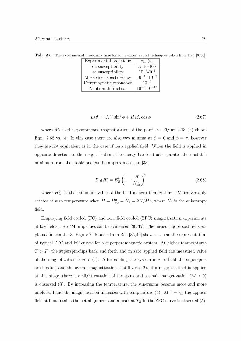
a given size it decreases as the measuring time increases. Table 2.5 shows the measuring
time for some experimental techniques commonly used to study SPM systems.
If a magnetic field is applied along the easy axis the energy of the particle is
2.2 Small particles 29
Tab. 2.5: The experimental measuring time for some experimental techniques taken from Ref. [6, 30].Experimental technique τm (s)
dc susceptibility ≈ 10-100ac susceptibility 10−5-104
Mössbauer spectroscopy 10−7 -10−9
Ferromagnetic resonance 10−9
Neutron diffraction 10−8-10−12
E(θ) = KV sin2 φ + HMs cos φ (2.67)
where Ms is the spontaneous magnetization of the particle. Figure 2.13 (b) shows
Eqn. 2.68 vs. φ. In this case there are also two minima at φ = 0 and φ = π, however
they are not equivalent as in the case of zero applied field. When the field is applied in
opposite direction to the magnetization, the energy barrier that separates the unstable
minimum from the stable one can be approximated to [33]
EB(H) = E0B
(1 − H
H0sw
)2
(2.68)
where H0sw is the minimum value of the field at zero temperature. M irreversably
rotates at zero temperature when H = H0sw = Ha = 2K/Ms, where Ha is the anisotropy
field.
Employing field cooled (FC) and zero field cooled (ZFC) magnetization experiments
at low fields the SPM properties can be evidenced [30,35]. The measuring procedure is ex-
plained in chapter 3. Figure 2.15 taken from Ref. [35,40] shows a schematic representation
of typical ZFC and FC curves for a superparamagnetic system. At higher temperatures
T > TB the superspin-flips back and forth and in zero applied field the measured value
of the magnetization is zero (1). After cooling the system in zero field the superspins
are blocked and the overall magnetization is still zero (2). If a magnetic field is applied
at this stage, there is a slight rotation of the spins and a small mangetization (M > 0)
is observed (3). By increasing the temperature, the superspins become more and more
unblocked and the magnetization increases with temperature (4). At τ = τm the applied
field still maintains the net alignment and a peak at TB in the ZFC curve is observed (5).
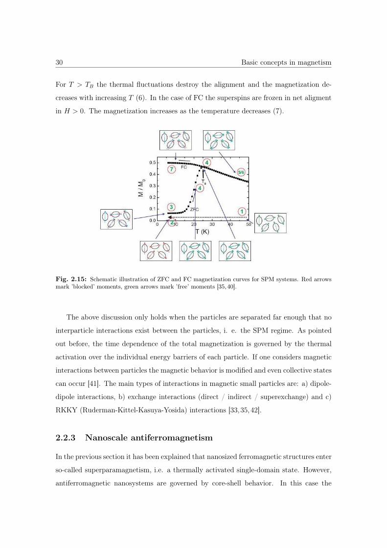
30 Basic concepts in magnetism
For T > TB the thermal fluctuations destroy the alignment and the magnetization de-
creases with increasing T (6). In the case of FC the superspins are frozen in net aligment
in H > 0. The magnetization increases as the temperature decreases (7).
Fig. 2.15: Schematic illustration of ZFC and FC magnetization curves for SPM systems. Red arrowsmark ’blocked’ moments, green arrows mark ’free’ moments [35,40].
The above discussion only holds when the particles are separated far enough that no
interparticle interactions exist between the particles, i. e. the SPM regime. As pointed
out before, the time dependence of the total magnetization is governed by the thermal
activation over the individual energy barriers of each particle. If one considers magnetic
interactions between particles the magnetic behavior is modified and even collective states
can occur [41]. The main types of interactions in magnetic small particles are: a) dipole-
dipole interactions, b) exchange interactions (direct / indirect / superexchange) and c)
RKKY (Ruderman-Kittel-Kasuya-Yosida) interactions [33,35, 42].
2.2.3 Nanoscale antiferromagnetism
In the previous section it has been explained that nanosized ferromagnetic structures enter
so-called superparamagnetism, i.e. a thermally activated single-domain state. However,
antiferromagnetic nanosystems are governed by core-shell behavior. In this case the
2.2 Small particles 31
surface plays a particularly important role for the magnetic behavior. As the size of
a magnetic system decreases the significance of the surface spins increases. Since an
antiferromagnet usually has two mutually compensating sublattices, the surface always
leads to a breaking of the sublattice pairing and thus leading to ’uncompensated’ surface
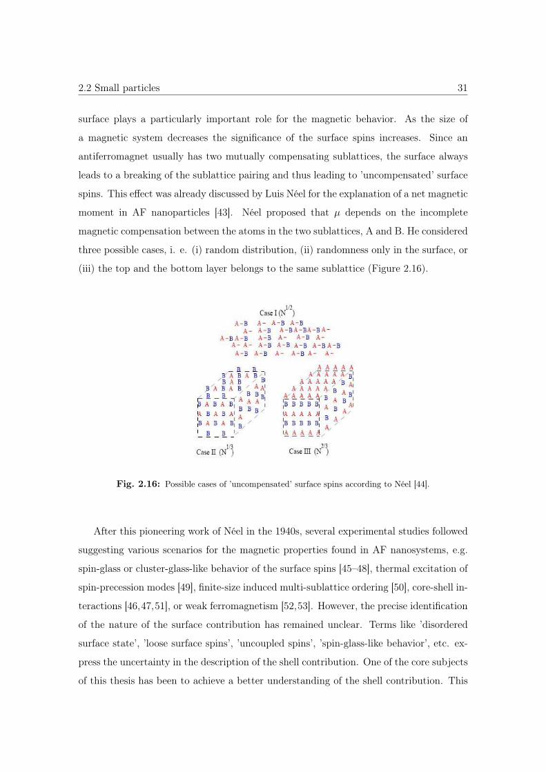
spins. This effect was already discussed by Luis Néel for the explanation of a net magnetic
moment in AF nanoparticles [43]. Néel proposed that μ depends on the incomplete
magnetic compensation between the atoms in the two sublattices, A and B. He considered
three possible cases, i. e. (i) random distribution, (ii) randomness only in the surface, or
(iii) the top and the bottom layer belongs to the same sublattice (Figure 2.16).
Fig. 2.16: Possible cases of ’uncompensated’ surface spins according to Néel [44].
After this pioneering work of Néel in the 1940s, several experimental studies followed
suggesting various scenarios for the magnetic properties found in AF nanosystems, e.g.
spin-glass or cluster-glass-like behavior of the surface spins [45–48], thermal excitation of
spin-precession modes [49], finite-size induced multi-sublattice ordering [50], core-shell in-
teractions [46,47,51], or weak ferromagnetism [52,53]. However, the precise identification
of the nature of the surface contribution has remained unclear. Terms like ’disordered
surface state’, ’loose surface spins’, ’uncoupled spins’, ’spin-glass-like behavior’, etc. ex-
press the uncertainty in the description of the shell contribution. One of the core subjects
of this thesis has been to achieve a better understanding of the shell contribution. This

32 Basic concepts in magnetism
is discussed in Chapter 7 in detail.
Chapter 3
Fabrication of magnetic nanostructures
Exciting novel phenomena are introduced once the dimensionality of the magnetic struc-
tures are on length scales between 1 nm and 100 nm. Examples are the giant magnetore-
sistance (GMR) effect in magnetic-nonmagnetic multilayers [2,3,54], oscillatory exchange
coupling between magnetic thin films [55] and enhancement of the energy product in two-
phase nanostructured systems composed of an aligned hard phase and a soft phase [56].
Thus, magnetic nanostructures are a fascinating topic with increasing interest on both
fundamental and applied level in physics, chemistry, material science and engineering.
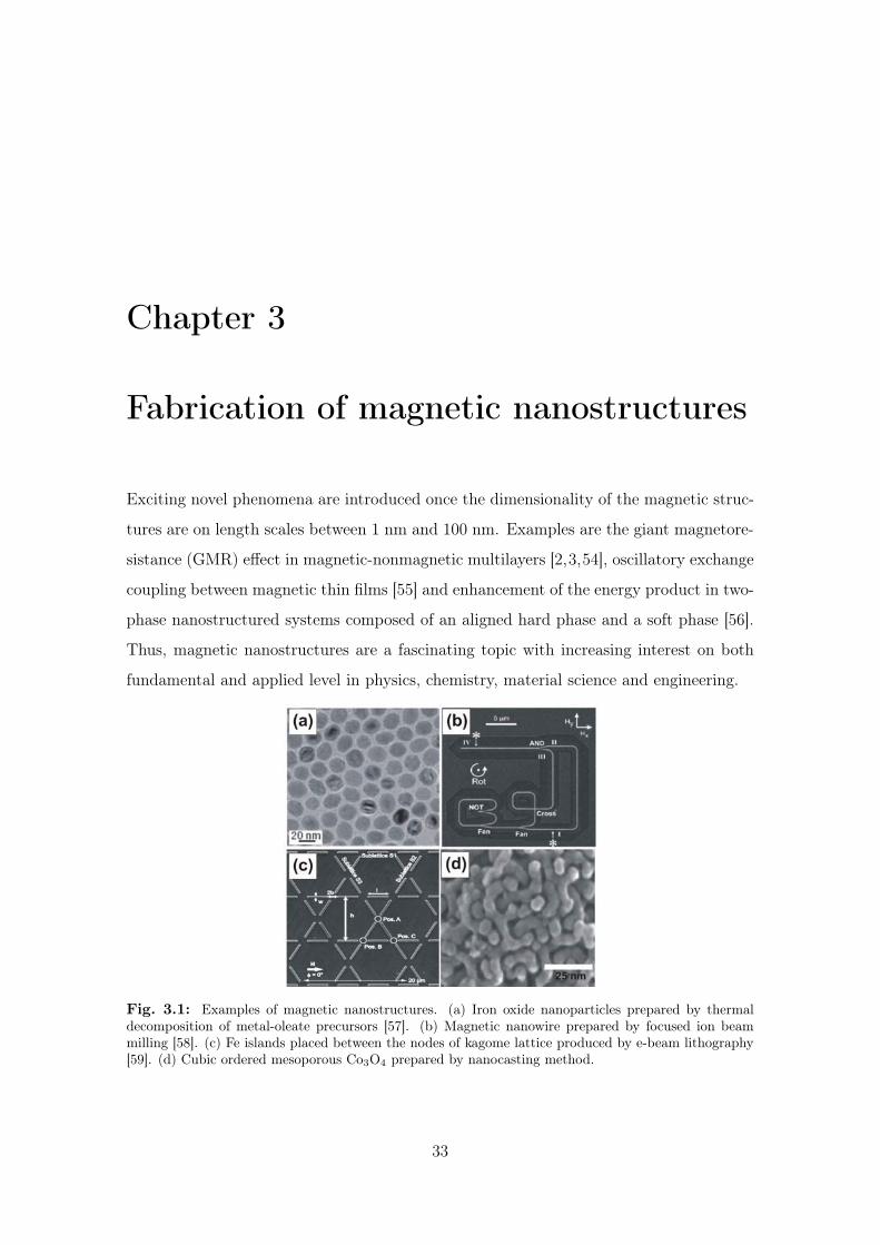
Fig. 3.1: Examples of magnetic nanostructures. (a) Iron oxide nanoparticles prepared by thermaldecomposition of metal-oleate precursors [57]. (b) Magnetic nanowire prepared by focused ion beammilling [58]. (c) Fe islands placed between the nodes of kagome lattice produced by e-beam lithography[59]. (d) Cubic ordered mesoporous Co3O4 prepared by nanocasting method.
33
34 Fabrication of magnetic nanostructures
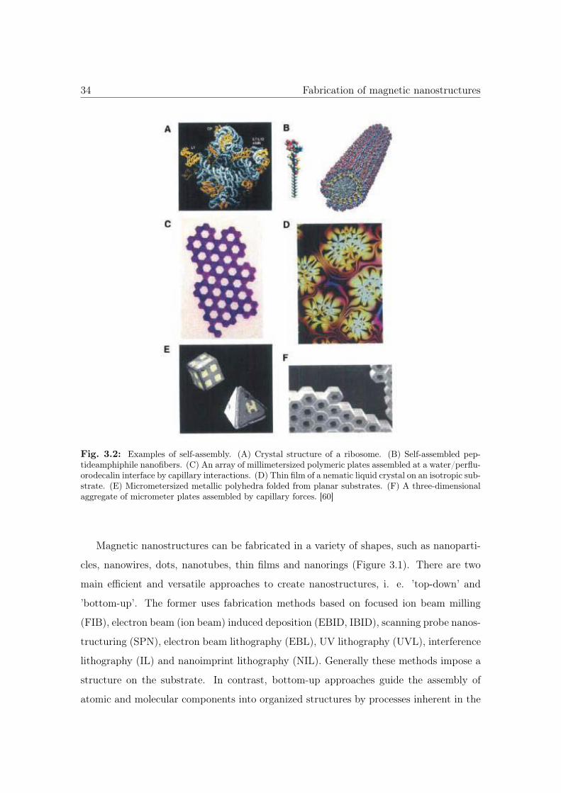
Fig. 3.2: Examples of self-assembly. (A) Crystal structure of a ribosome. (B) Self-assembled pep-tideamphiphile nanofibers. (C) An array of millimetersized polymeric plates assembled at a water/perflu-orodecalin interface by capillary interactions. (D) Thin film of a nematic liquid crystal on an isotropic sub-strate. (E) Micrometersized metallic polyhedra folded from planar substrates. (F) A three-dimensionalaggregate of micrometer plates assembled by capillary forces. [60]
Magnetic nanostructures can be fabricated in a variety of shapes, such as nanoparti-
cles, nanowires, dots, nanotubes, thin films and nanorings (Figure 3.1). There are two
main efficient and versatile approaches to create nanostructures, i. e. ’top-down’ and
’bottom-up’. The former uses fabrication methods based on focused ion beam milling
(FIB), electron beam (ion beam) induced deposition (EBID, IBID), scanning probe nanos-
tructuring (SPN), electron beam lithography (EBL), UV lithography (UVL), interference
lithography (IL) and nanoimprint lithography (NIL). Generally these methods impose a
structure on the substrate. In contrast, bottom-up approaches guide the assembly of
atomic and molecular components into organized structures by processes inherent in the
3.1 Nanocasting 35
manipulated system [61]. Examples of bottom-up are self-assembled structures such as
atomic, ionic and molecular crystals, liquid crystals and lipid bilayers. Figure 3.2 shows
some examples of self-assembly [60]. The structure is usually determined by van-der-
Waals, hydrogen bonding, and electromagnetic dipolar interactions.
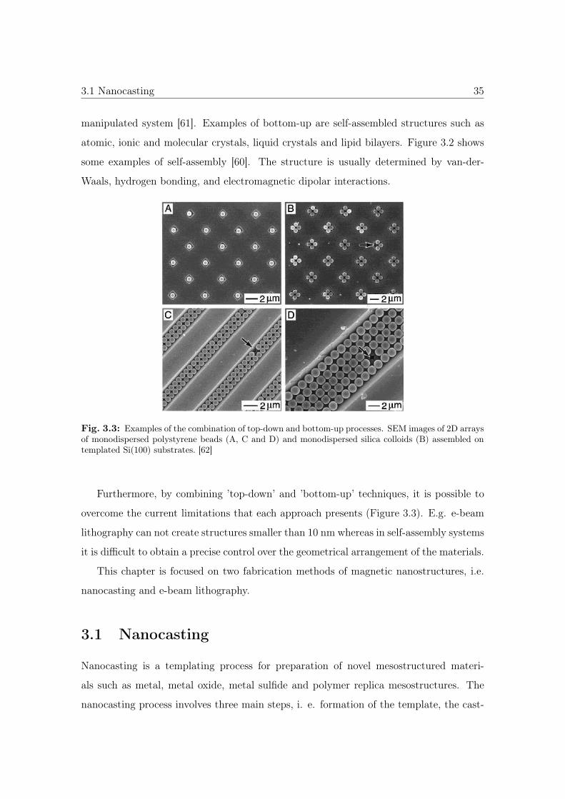
Fig. 3.3: Examples of the combination of top-down and bottom-up processes. SEM images of 2D arraysof monodispersed polystyrene beads (A, C and D) and monodispersed silica colloids (B) assembled ontemplated Si(100) substrates. [62]
Furthermore, by combining ’top-down’ and ’bottom-up’ techniques, it is possible to
overcome the current limitations that each approach presents (Figure 3.3). E.g. e-beam
lithography can not create structures smaller than 10 nm whereas in self-assembly systems
it is difficult to obtain a precise control over the geometrical arrangement of the materials.
This chapter is focused on two fabrication methods of magnetic nanostructures, i.e.
nanocasting and e-beam lithography.
3.1 Nanocasting
Nanocasting is a templating process for preparation of novel mesostructured materi-
als such as metal, metal oxide, metal sulfide and polymer replica mesostructures. The
nanocasting process involves three main steps, i. e. formation of the template, the cast-
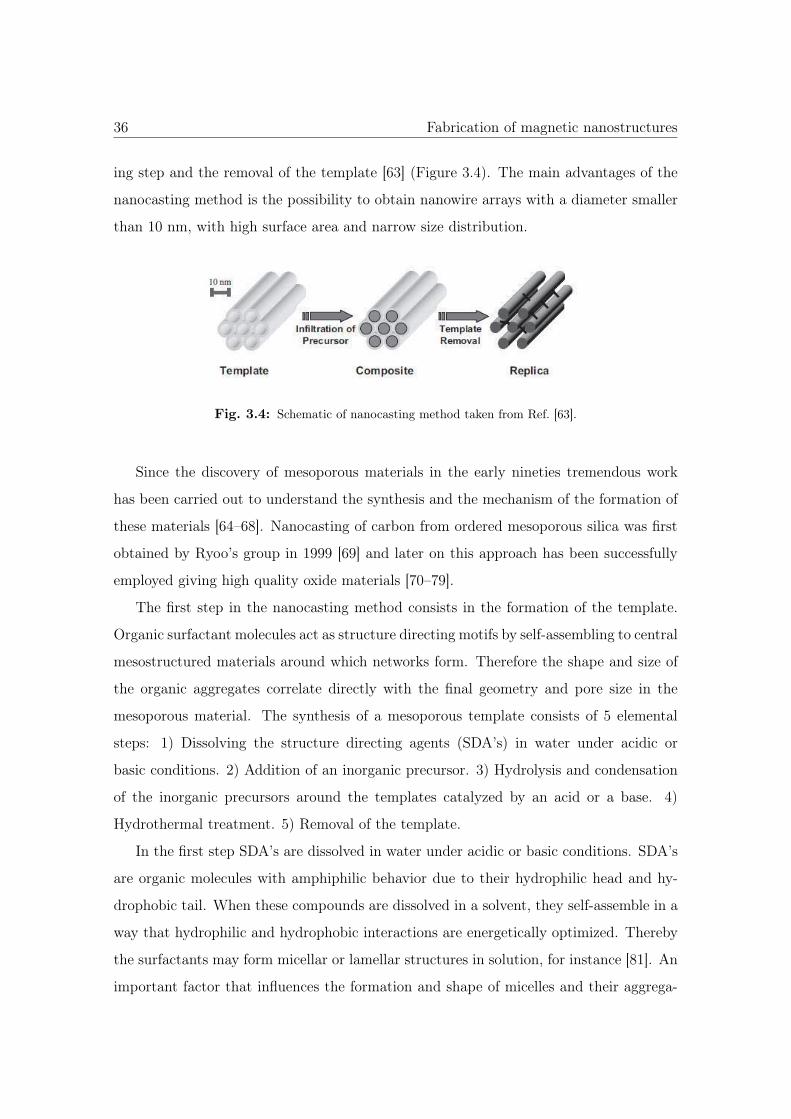
36 Fabrication of magnetic nanostructures
ing step and the removal of the template [63] (Figure 3.4). The main advantages of the
nanocasting method is the possibility to obtain nanowire arrays with a diameter smaller
than 10 nm, with high surface area and narrow size distribution.
Fig. 3.4: Schematic of nanocasting method taken from Ref. [63].
Since the discovery of mesoporous materials in the early nineties tremendous work
has been carried out to understand the synthesis and the mechanism of the formation of
these materials [64–68]. Nanocasting of carbon from ordered mesoporous silica was first
obtained by Ryoo’s group in 1999 [69] and later on this approach has been successfully
employed giving high quality oxide materials [70–79].
The first step in the nanocasting method consists in the formation of the template.
Organic surfactant molecules act as structure directing motifs by self-assembling to central
mesostructured materials around which networks form. Therefore the shape and size of
the organic aggregates correlate directly with the final geometry and pore size in the
mesoporous material. The synthesis of a mesoporous template consists of 5 elemental
steps: 1) Dissolving the structure directing agents (SDA’s) in water under acidic or
basic conditions. 2) Addition of an inorganic precursor. 3) Hydrolysis and condensation
of the inorganic precursors around the templates catalyzed by an acid or a base. 4)
Hydrothermal treatment. 5) Removal of the template.
In the first step SDA’s are dissolved in water under acidic or basic conditions. SDA’s
are organic molecules with amphiphilic behavior due to their hydrophilic head and hy-
drophobic tail. When these compounds are dissolved in a solvent, they self-assemble in a
way that hydrophilic and hydrophobic interactions are energetically optimized. Thereby
the surfactants may form micellar or lamellar structures in solution, for instance [81]. An
important factor that influences the formation and shape of micelles and their aggrega-
3.1 Nanocasting 37
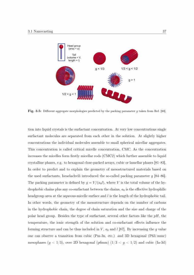
Fig. 3.5: Different aggregate morphologies predicted by the packing parameter g taken from Ref. [80].
tion into liquid crystals is the surfactant concentration. At very low concentrations single
surfactant molecules are separated from each other in the solution. At slightly higher
concentrations the individual molecules assemble to small spherical micellar aggregates.
This concentration is called critical micelle concentration, CMC. As the concentration
increases the micelles form firstly micellar rods (CMC2) which further assemble to liquid
crystalline phases, e.g. to hexagonal close-packed arrays, cubic or lamellar phases [81–83].
In order to predict and to explain the geometry of mesostructured materials based on
the used surfactants, Israelachvili introduced the so-called packing parameter g [84–86].
The packing parameter is defined by g = V/(a0l), where V is the total volume of the hy-
drophobic chains plus any co-surfactant between the chains, a0 is the effective hydrophilic
headgroup area at the aqueous-micelle surface and l is the length of the hydrophobic tail.
In other words, the geometry of the mesostructure depends on the number of carbons
in the hydrophobic chain, the degree of chain saturation and the size and charge of the
polar head group. Besides the type of surfactant, several other factors like the pH, the
temperature, the ionic strength of the solution and co-surfactant effects influence the
forming structure and can be thus included in V , a0 and l [87]. By increasing the g value
one can observe a transition from cubic (Pm-3n, etc.) and 3D hexagonal (P63/mmc)
mesophases (g < 1/3), over 2D hexagonal (p6mm) (1/3 < g < 1/2) and cubic (Ia-3d)
38 Fabrication of magnetic nanostructures
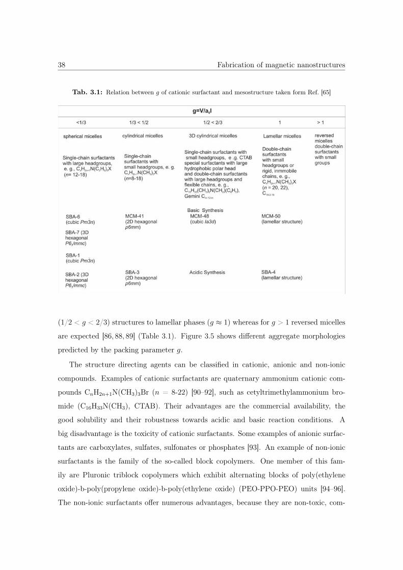
Tab. 3.1: Relation between g of cationic surfactant and mesostructure taken form Ref. [65]
(1/2 < g < 2/3) structures to lamellar phases (g ≈ 1) whereas for g > 1 reversed micelles
are expected [86, 88, 89] (Table 3.1). Figure 3.5 shows different aggregate morphologies
predicted by the packing parameter g.
The structure directing agents can be classified in cationic, anionic and non-ionic
compounds. Examples of cationic surfactants are quaternary ammonium cationic com-
pounds CnH2n+1N(CH3)3Br (n = 8-22) [90–92], such as cetyltrimethylammonium bro-
mide (C16H33N(CH3), CTAB). Their advantages are the commercial availability, the
good solubility and their robustness towards acidic and basic reaction conditions. A
big disadvantage is the toxicity of cationic surfactants. Some examples of anionic surfac-
tants are carboxylates, sulfates, sulfonates or phosphates [93]. An example of non-ionic
surfactants is the family of the so-called block copolymers. One member of this fam-
ily are Pluronic triblock copolymers which exhibit alternating blocks of poly(ethylene
oxide)-b-poly(propylene oxide)-b-poly(ethylene oxide) (PEO-PPO-PEO) units [94–96].
The non-ionic surfactants offer numerous advantages, because they are non-toxic, com-
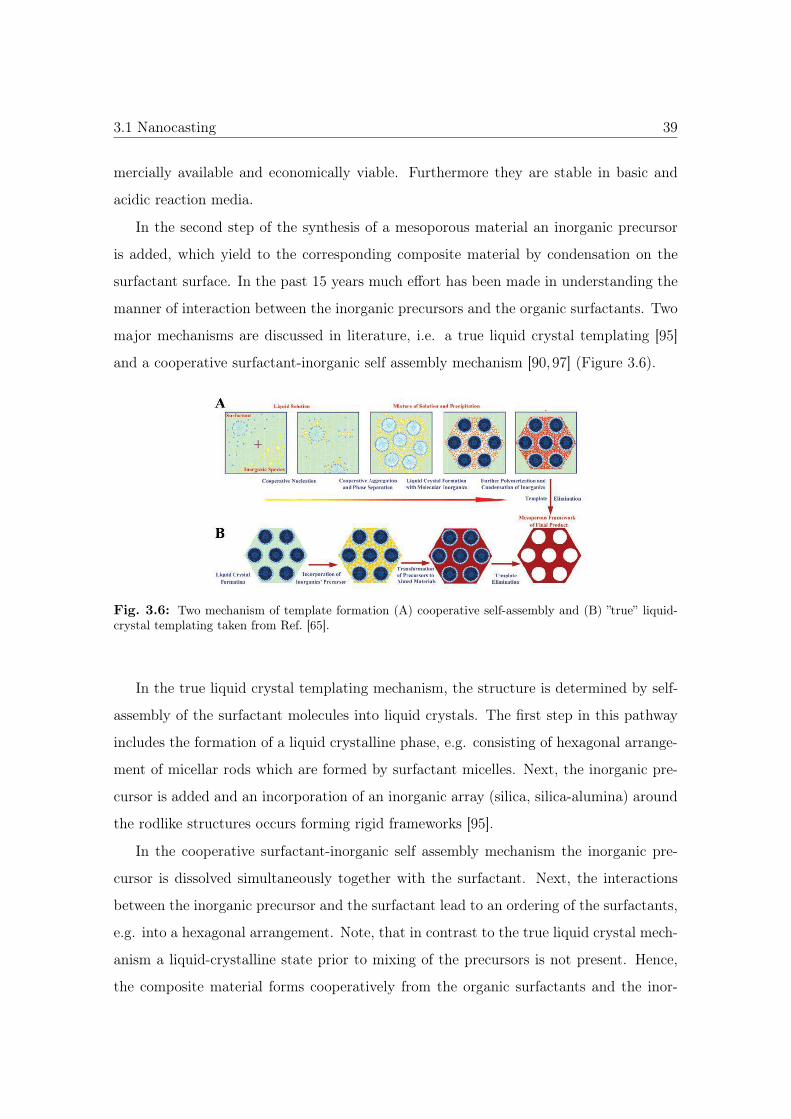
3.1 Nanocasting 39
mercially available and economically viable. Furthermore they are stable in basic and
acidic reaction media.
In the second step of the synthesis of a mesoporous material an inorganic precursor
is added, which yield to the corresponding composite material by condensation on the
surfactant surface. In the past 15 years much effort has been made in understanding the
manner of interaction between the inorganic precursors and the organic surfactants. Two
major mechanisms are discussed in literature, i.e. a true liquid crystal templating [95]
and a cooperative surfactant-inorganic self assembly mechanism [90,97] (Figure 3.6).
Fig. 3.6: Two mechanism of template formation (A) cooperative self-assembly and (B) ”true” liquid-crystal templating taken from Ref. [65].
In the true liquid crystal templating mechanism, the structure is determined by self-
assembly of the surfactant molecules into liquid crystals. The first step in this pathway
includes the formation of a liquid crystalline phase, e.g. consisting of hexagonal arrange-
ment of micellar rods which are formed by surfactant micelles. Next, the inorganic pre-
cursor is added and an incorporation of an inorganic array (silica, silica-alumina) around
the rodlike structures occurs forming rigid frameworks [95].
In the cooperative surfactant-inorganic self assembly mechanism the inorganic pre-
cursor is dissolved simultaneously together with the surfactant. Next, the interactions
between the inorganic precursor and the surfactant lead to an ordering of the surfactants,
e.g. into a hexagonal arrangement. Note, that in contrast to the true liquid crystal mech-
anism a liquid-crystalline state prior to mixing of the precursors is not present. Hence,
the composite material forms cooperatively from the organic surfactants and the inor-
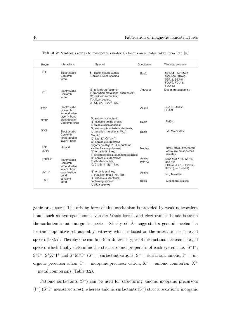
40 Fabrication of magnetic nanostructures
Tab. 3.2: Synthesis routes to mesoporous materials focous on silicates taken form Ref. [65]
ganic precursors. The driving force of this mechanism is provided by weak noncovalent
bonds such as hydrogen bonds, van-der-Waals forces, and electrovalent bonds between
the surfactants and inorganic species. Stucky et al. suggested a general mechanism
for the cooperative self-assembly pathway which is based on the interaction of charged
species [90,97]. Thereby one can find four different types of interactions between charged
species which finally determine the structure and properties of each system, i.e. S+I−,
S−I+, S+X−I+ and S−M+I− (S+ = surfactant cations, S− = surfactant anions, I− = in-
organic precursor anion, I+ = inorganic precursor cation, X− = anionic counterion, X+
= metal counterion) (Table 3.2).
Cationic surfactants (S+) can be used for structuring anionic inorganic precursors
(I−) (S+I− mesostructures), whereas anionic surfactants (S−) structure cationic inorganic
3.1 Nanocasting 41
species (I+) (S−I+ mesostructures). Furthermore also a combination of identically charged
species is possible, but then countercharged ions are necessary for the formation of the
mesostructure (S+X−I+, and S−M+I− mesostructures). In the case of neutral amines or
nonionic polyethylene oxide surfactants which can also act as structure directing agents,
one has to consider that the surfactant species are probably partially protonated or
charged. However, the cooperative surfactant-inorganic self-assembly mechanism has
been extended to pathways using neutral (S0) or non-ionic surfactants (N0). The main
driving force for the formation of the mesophase in these neutral templating routes is
considered to be a hydrogen-bonding interaction at the S0I0 [98] or N0I0 [99] interface.
During this step, microphase separation and condensation of the inorganic precursor
occur. For instance, in the case of silicate precursor, e.g. tetraethoxysilane (TEOS) the
condensation and the subsequent precipitation is rapid in cationic solutions whereas the
formation of mesostructures is slow if nonionic surfactants are used as templates [65].
In order to cause a complete condensation and to improve the organization, i.e. the
mesoscopic regularity of the mesostructured material, a hydrothermal treatment follows
[86,100]. The hydrothermal treatment leads to a reorganization, growth, and -sometimes-
crystallization of the mesostructures. Due to a degradation of ordering and decomposition
of the organic surfactants the temperature during the hydrothermal treatment is relatively
low (80 - 150 ◦C). Once the hydrothermal treatment is finished the product is cooled
down to room temperature where the mesostructured material is easily separated from
the mother liquor by filtering. In the case of small particles a centrifugation might be
also necessary in the workup. Further purification includes several washing steps, mostly
by water. In order to maintain the mesoscopic regularity the drying is usually carried out
at room temperature. The last step in the synthesis of a mesoporous material requires
a removal of the organic template from the inorganic-organic mesostructures. In the
case of mesoporous silicates, aluminosilicates, metal oxides, and phosphates the template
is easily removable by calcination, i.e. by heating of the inorganic-organic composite
material up to temperatures in which the organic part completely decomposes or oxidizes
under oxygen or air atmosphere [101, 102]. An alternative, in fact milder, method to
remove the template is extraction with common organic solvents, e.g. ethanol or THF.
In that case an addition of a small amount of hydrochloric acid leads to an improvement
42 Fabrication of magnetic nanostructures
of the extraction procedure and of the final product [103,104].
Mesoporous silica is the most suitable template for the nanocasting process. The
main advantage in usage of ordered mesoporous silica is the easy controllability of the
structure and morphology. Furthermore, it possesses large surface areas and large pore
volumes and can be prepared in diverse shapes such as spheres, fibers, rods and chiral
morphologies. The synthesis temperature is rather low, from room temperature to 130◦C.
The second step of the nanocasting method is the casting step. Here, the target
material is incorporated into the channels of the mesoporous template in the form of a
precursor (generally molecular) and later it is converted to the desired material by calci-
nation under air or inert atmosphere. The precursors are incorporated in the pore system
of mesoporous silica by sorption, phase transition or ion exchange. In order to be easily
infiltrated into the pore system, the precursor has to be either gaseous, highly soluble
or liquid. The interaction between the silica walls and the precursors are determined
by hydrogen bonding, coordination bonding, coulombic interactions and van-der-Waals
forces. Once inside the pore system, the precursor is then thermally decomposed. Note
that the conversion of the precursor to the final material should proceed with low volume
shrinkage and without a reaction with the template in order to get a high quality replica.
The byproducts usually leave the channels in the gas phase. Some examples of convenient
precursors are metal chlorides, metal nitrates and metal acetates.
The final step in the nanocasting method consist of the removal of the template using
chemical treatments, combustion or treatment with other highly reactive gases. For
example, silica templates can be easily removed by dissolution in NaOH or HF solutions.
Therefore, the obtained replica material using silica template must be stable not only
during thermal treatments but also towards chemical agents. Carbon templates offer an
alternative to nanocast materials that are attacked by NaOH or HF. The carbon template
is removable by combustion or treatment with highly reactive gases.
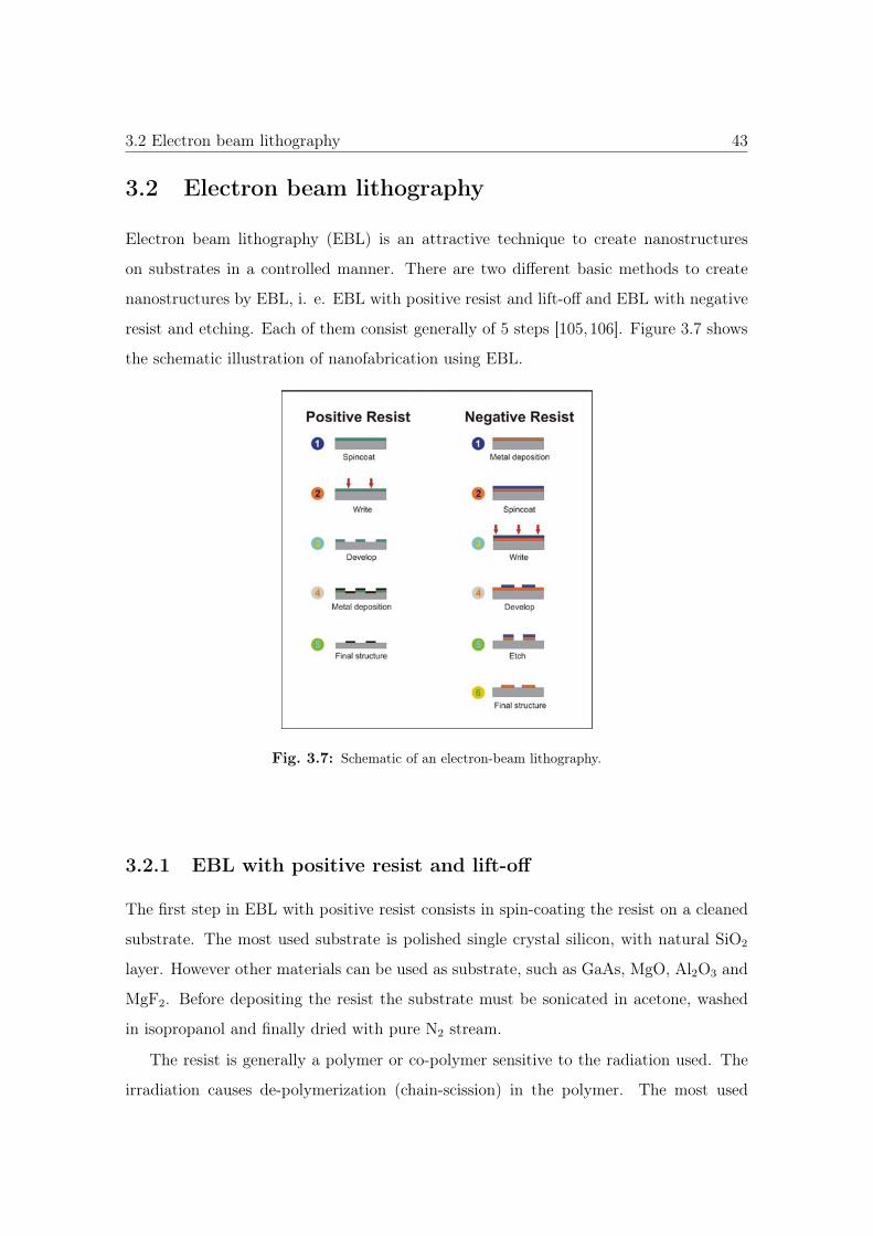
3.2 Electron beam lithography 43
3.2 Electron beam lithography
Electron beam lithography (EBL) is an attractive technique to create nanostructures
on substrates in a controlled manner. There are two different basic methods to create
nanostructures by EBL, i. e. EBL with positive resist and lift-off and EBL with negative
resist and etching. Each of them consist generally of 5 steps [105,106]. Figure 3.7 shows
the schematic illustration of nanofabrication using EBL.
Fig. 3.7: Schematic of an electron-beam lithography.
3.2.1 EBL with positive resist and lift-off
The first step in EBL with positive resist consists in spin-coating the resist on a cleaned
substrate. The most used substrate is polished single crystal silicon, with natural SiO2
layer. However other materials can be used as substrate, such as GaAs, MgO, Al2O3 and
MgF2. Before depositing the resist the substrate must be sonicated in acetone, washed
in isopropanol and finally dried with pure N2 stream.
The resist is generally a polymer or co-polymer sensitive to the radiation used. The
irradiation causes de-polymerization (chain-scission) in the polymer. The most used
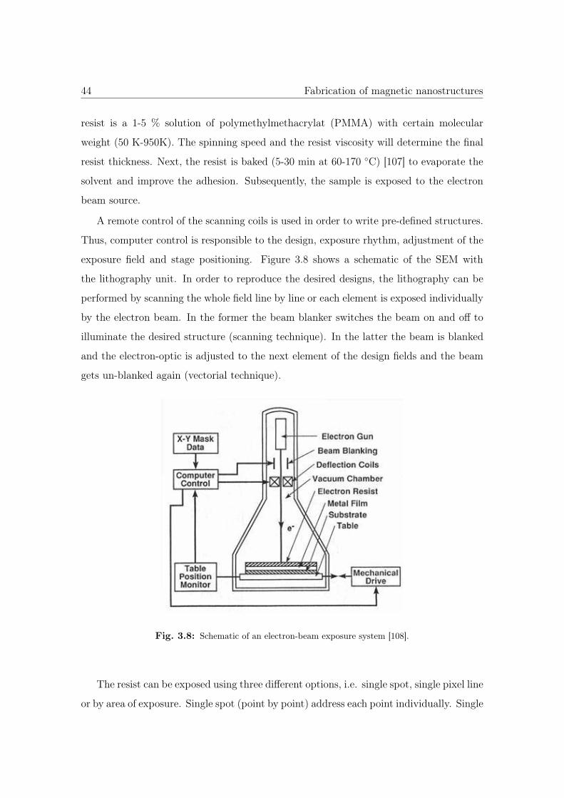
44 Fabrication of magnetic nanostructures
resist is a 1-5 % solution of polymethylmethacrylat (PMMA) with certain molecular
weight (50 K-950K). The spinning speed and the resist viscosity will determine the final
resist thickness. Next, the resist is baked (5-30 min at 60-170 ◦C) [107] to evaporate the
solvent and improve the adhesion. Subsequently, the sample is exposed to the electron
beam source.
A remote control of the scanning coils is used in order to write pre-defined structures.
Thus, computer control is responsible to the design, exposure rhythm, adjustment of the
exposure field and stage positioning. Figure 3.8 shows a schematic of the SEM with
the lithography unit. In order to reproduce the desired designs, the lithography can be
performed by scanning the whole field line by line or each element is exposed individually
by the electron beam. In the former the beam blanker switches the beam on and off to
illuminate the desired structure (scanning technique). In the latter the beam is blanked
and the electron-optic is adjusted to the next element of the design fields and the beam
gets un-blanked again (vectorial technique).
Fig. 3.8: Schematic of an electron-beam exposure system [108].
The resist can be exposed using three different options, i.e. single spot, single pixel line
or by area of exposure. Single spot (point by point) address each point individually. Single
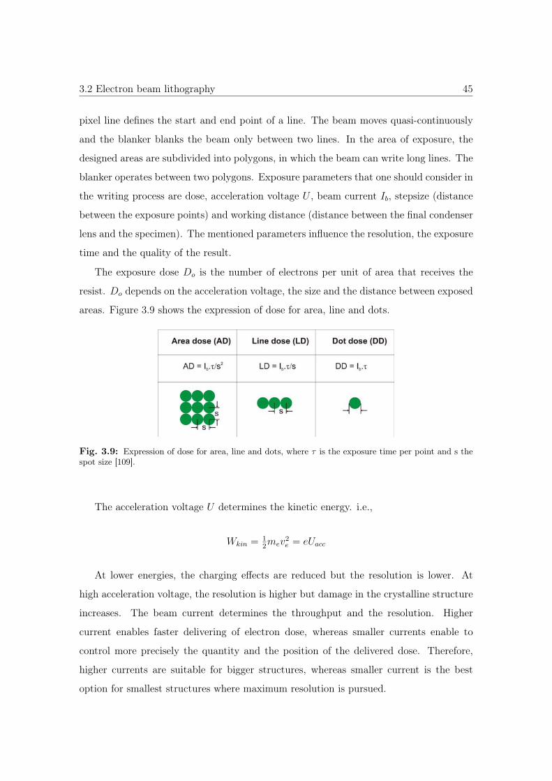
3.2 Electron beam lithography 45
pixel line defines the start and end point of a line. The beam moves quasi-continuously
and the blanker blanks the beam only between two lines. In the area of exposure, the
designed areas are subdivided into polygons, in which the beam can write long lines. The
blanker operates between two polygons. Exposure parameters that one should consider in
the writing process are dose, acceleration voltage U , beam current Ib, stepsize (distance
between the exposure points) and working distance (distance between the final condenser
lens and the specimen). The mentioned parameters influence the resolution, the exposure
time and the quality of the result.
The exposure dose Do is the number of electrons per unit of area that receives the
resist. Do depends on the acceleration voltage, the size and the distance between exposed
areas. Figure 3.9 shows the expression of dose for area, line and dots.
Fig. 3.9: Expression of dose for area, line and dots, where τ is the exposure time per point and s thespot size [109].
The acceleration voltage U determines the kinetic energy. i.e.,
Wkin = 12mev
2e = eUacc
At lower energies, the charging effects are reduced but the resolution is lower. At
high acceleration voltage, the resolution is higher but damage in the crystalline structure
increases. The beam current determines the throughput and the resolution. Higher
current enables faster delivering of electron dose, whereas smaller currents enable to
control more precisely the quantity and the position of the delivered dose. Therefore,
higher currents are suitable for bigger structures, whereas smaller current is the best
option for smallest structures where maximum resolution is pursued.
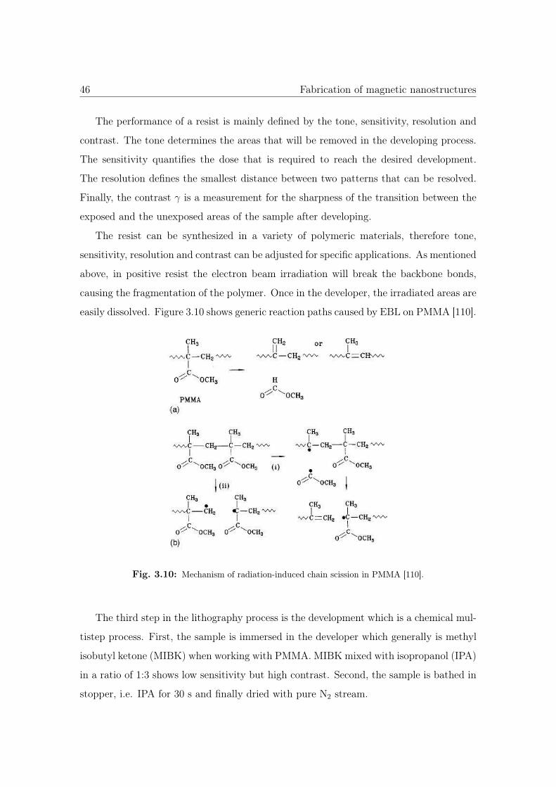
46 Fabrication of magnetic nanostructures
The performance of a resist is mainly defined by the tone, sensitivity, resolution and
contrast. The tone determines the areas that will be removed in the developing process.
The sensitivity quantifies the dose that is required to reach the desired development.
The resolution defines the smallest distance between two patterns that can be resolved.
Finally, the contrast γ is a measurement for the sharpness of the transition between the
exposed and the unexposed areas of the sample after developing.
The resist can be synthesized in a variety of polymeric materials, therefore tone,
sensitivity, resolution and contrast can be adjusted for specific applications. As mentioned
above, in positive resist the electron beam irradiation will break the backbone bonds,
causing the fragmentation of the polymer. Once in the developer, the irradiated areas are
easily dissolved. Figure 3.10 shows generic reaction paths caused by EBL on PMMA [110].
Fig. 3.10: Mechanism of radiation-induced chain scission in PMMA [110].
The third step in the lithography process is the development which is a chemical mul-
tistep process. First, the sample is immersed in the developer which generally is methyl
isobutyl ketone (MIBK) when working with PMMA. MIBK mixed with isopropanol (IPA)
in a ratio of 1:3 shows low sensitivity but high contrast. Second, the sample is bathed in
stopper, i.e. IPA for 30 s and finally dried with pure N2 stream.
3.2 Electron beam lithography 47
In the fourth step of EBL with positive resist, a single material layer or multilayer
is deposited on top of the entire structure. Deposition is performed generally by regular
thin-film deposition techniques, i.e. thermal evaporation, sputtering, etc. [111].
Finally, in the liff-off process the resist is removed by dissolving it in a solvent. For
example, acetone and ultrasonic bath is an efficient method to remove the PMMA.
3.2.2 EBL with negative resist and etching
The first step in EBL with negative resist consists of depositing a single material layer or
multilayer on a cleaned substrate. Deposition is performed generally by regular thin-film
deposition techniques, i.e. thermal evaporation, sputtering, etc. [111]. The most used
substrate is polished single crystal silicon, with natural SiO2 layer, or extra thick layer.
However other materials can be used as substrate, such as GaAs, MgO, Al2O3 and MgF2.
Before depositing the material, the substrate must be sonicated in acetone, washed in
isopropanol and finally dried with pure N2 stream.
The second step is the spin-coating of the negative resist on top of the material layer.
The resist is generally a polymer or co-polymer sensitive to the used radiation. In contrast
to positive resist, in negative resist the electron beam irradiation will cause a cross-linking
of the polymer chains, the solubility of the irradiated areas in the developer decreases.
Examples of negative resists are poly-chloromethylstyrene and SU8 . The spinning speed
and the resist viscosity will determine the final resist thickness as in the case of positive
resist. The following steps, exposure and development of the resist are similar to the case
of a positive resist, as described above.
Next, in order to remove the material that is not protected by the resist, dry or
wet etching is used. Dry etching techniques use gases which are usually dissociated and
ionized in a plasma. The most common dry etching techniques are high-pressure plasma
etching, reactive ion etching (RIE) and ion milling. The advantages are high definition
and high anisotropy. Figure 3.11 shows a schematic of possible dry etching.
High-pressure plasma etching is performed at pressures of 10−1 - 5 Torr. Highly
reactive species are created that react with the material to be etched. Products are
volatile and diffuse away, leaving the new material exposed to the reactive species.
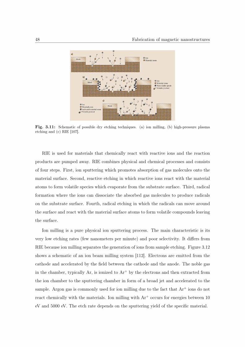
48 Fabrication of magnetic nanostructures
Fig. 3.11: Schematic of possible dry etching techniques. (a) ion milling, (b) high-pressure plasmaetching and (c) RIE [107].
RIE is used for materials that chemically react with reactive ions and the reaction
products are pumped away. RIE combines physical and chemical processes and consists
of four steps. First, ion sputtering which promotes absorption of gas molecules onto the
material surface. Second, reactive etching in which reactive ions react with the material
atoms to form volatile species which evaporate from the substrate surface. Third, radical
formation where the ions can dissociate the absorbed gas molecules to produce radicals
on the substrate surface. Fourth, radical etching in which the radicals can move around
the surface and react with the material surface atoms to form volatile compounds leaving
the surface.
Ion milling is a pure physical ion sputtering process. The main characteristic is its
very low etching rates (few nanometers per minute) and poor selectivity. It differs from
RIE because ion milling separates the generation of ions from sample etching. Figure 3.12
shows a schematic of an ion beam milling system [112]. Electrons are emitted from the
cathode and accelerated by the field between the cathode and the anode. The noble gas
in the chamber, typically Ar, is ionized to Ar+ by the electrons and then extracted from
the ion chamber to the sputtering chamber in form of a broad jet and accelerated to the
sample. Argon gas is commonly used for ion milling due to the fact that Ar+ ions do not
react chemically with the materials. Ion milling with Ar+ occurs for energies between 10
eV and 5000 eV. The etch rate depends on the sputtering yield of the specific material.
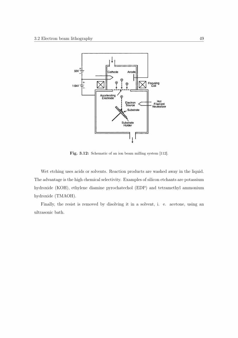
3.2 Electron beam lithography 49
Fig. 3.12: Schematic of an ion beam milling system [112].
Wet etching uses acids or solvents. Reaction products are washed away in the liquid.
The advantage is the high chemical selectivity. Examples of silicon etchants are potassium
hydroxide (KOH), ethylene diamine pyrochatechol (EDP) and tetramethyl ammonium
hydroxide (TMAOH).
Finally, the resist is removed by disolving it in a solvent, i. e. acetone, using an
ultrasonic bath.

50 Fabrication of magnetic nanostructures
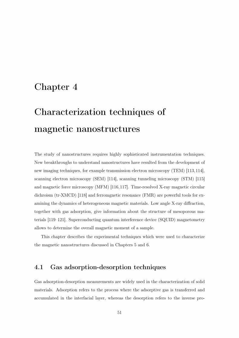
Chapter 4
Characterization techniques of
magnetic nanostructures
The study of nanostructures requires highly sophisticated instrumentation techniques.
New breakthroughs to understand nanostructures have resulted from the development of
new imaging techniques, for example transmission electron microscopy (TEM) [113,114],
scanning electron microscopy (SEM) [114], scanning tunneling microscopy (STM) [115]
and magnetic force microscopy (MFM) [116,117]. Time-resolved X-ray magnetic circular
dichroism (tr-XMCD) [118] and ferromgnetic resonance (FMR) are powerful tools for ex-
amining the dynamics of heterogeneous magnetic materials. Low angle X-ray diffraction,
together with gas adsorption, give information about the structure of mesoporous ma-
terials [119–121]. Superconducting quantum interference device (SQUID) magnetometry
allows to determine the overall magnetic moment of a sample.
This chapter describes the experimental techniques which were used to characterize
the magnetic nanostructures discussed in Chapters 5 and 6.
4.1 Gas adsorption-desorption techniques
Gas adsorption-desorption measurements are widely used in the characterization of solid
materials. Adsorption refers to the process where the adsorptive gas is transferred and
accumulated in the interfacial layer, whereas the desorption refers to the inverse pro-
51
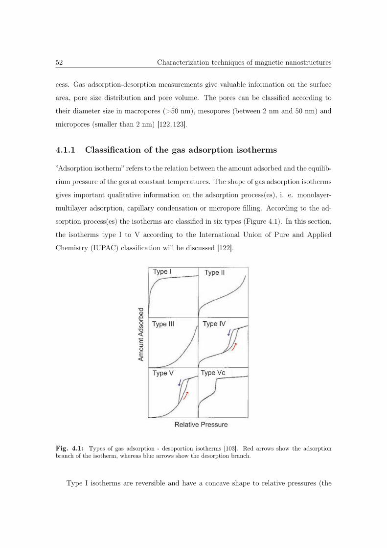
52 Characterization techniques of magnetic nanostructures
cess. Gas adsorption-desorption measurements give valuable information on the surface
area, pore size distribution and pore volume. The pores can be classified according to
their diameter size in macropores (>50 nm), mesopores (between 2 nm and 50 nm) and
micropores (smaller than 2 nm) [122,123].
4.1.1 Classification of the gas adsorption isotherms
”Adsorption isotherm” refers to the relation between the amount adsorbed and the equilib-
rium pressure of the gas at constant temperatures. The shape of gas adsorption isotherms
gives important qualitative information on the adsorption process(es), i. e. monolayer-
multilayer adsorption, capillary condensation or micropore filling. According to the ad-
sorption process(es) the isotherms are classified in six types (Figure 4.1). In this section,
the isotherms type I to V according to the International Union of Pure and Applied
Chemistry (IUPAC) classification will be discussed [122].
Fig. 4.1: Types of gas adsorption - desoportion isotherms [103]. Red arrows show the adsorptionbranch of the isotherm, whereas blue arrows show the desorption branch.
Type I isotherms are reversible and have a concave shape to relative pressures (the
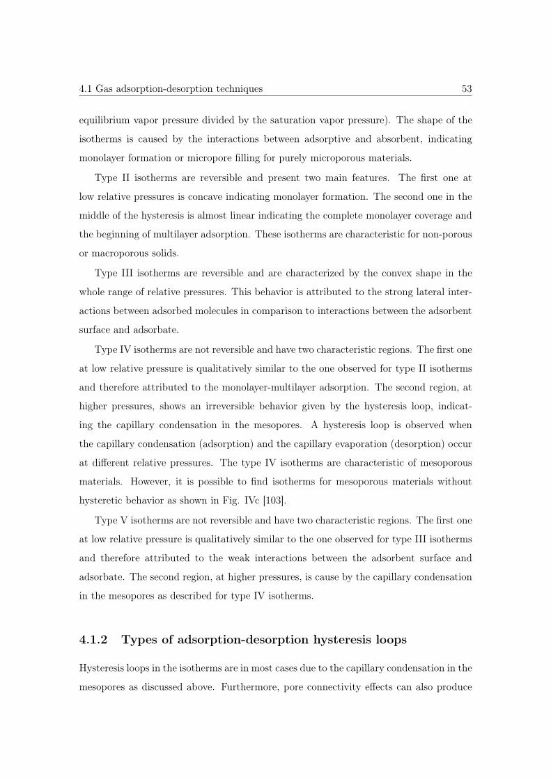
4.1 Gas adsorption-desorption techniques 53
equilibrium vapor pressure divided by the saturation vapor pressure). The shape of the
isotherms is caused by the interactions between adsorptive and absorbent, indicating
monolayer formation or micropore filling for purely microporous materials.
Type II isotherms are reversible and present two main features. The first one at
low relative pressures is concave indicating monolayer formation. The second one in the
middle of the hysteresis is almost linear indicating the complete monolayer coverage and
the beginning of multilayer adsorption. These isotherms are characteristic for non-porous
or macroporous solids.
Type III isotherms are reversible and are characterized by the convex shape in the
whole range of relative pressures. This behavior is attributed to the strong lateral inter-
actions between adsorbed molecules in comparison to interactions between the adsorbent
surface and adsorbate.
Type IV isotherms are not reversible and have two characteristic regions. The first one
at low relative pressure is qualitatively similar to the one observed for type II isotherms
and therefore attributed to the monolayer-multilayer adsorption. The second region, at
higher pressures, shows an irreversible behavior given by the hysteresis loop, indicat-
ing the capillary condensation in the mesopores. A hysteresis loop is observed when
the capillary condensation (adsorption) and the capillary evaporation (desorption) occur
at different relative pressures. The type IV isotherms are characteristic of mesoporous
materials. However, it is possible to find isotherms for mesoporous materials without
hysteretic behavior as shown in Fig. IVc [103].
Type V isotherms are not reversible and have two characteristic regions. The first one
at low relative pressure is qualitatively similar to the one observed for type III isotherms
and therefore attributed to the weak interactions between the adsorbent surface and
adsorbate. The second region, at higher pressures, is cause by the capillary condensation
in the mesopores as described for type IV isotherms.
4.1.2 Types of adsorption-desorption hysteresis loops
Hysteresis loops in the isotherms are in most cases due to the capillary condensation in the
mesopores as discussed above. Furthermore, pore connectivity effects can also produce
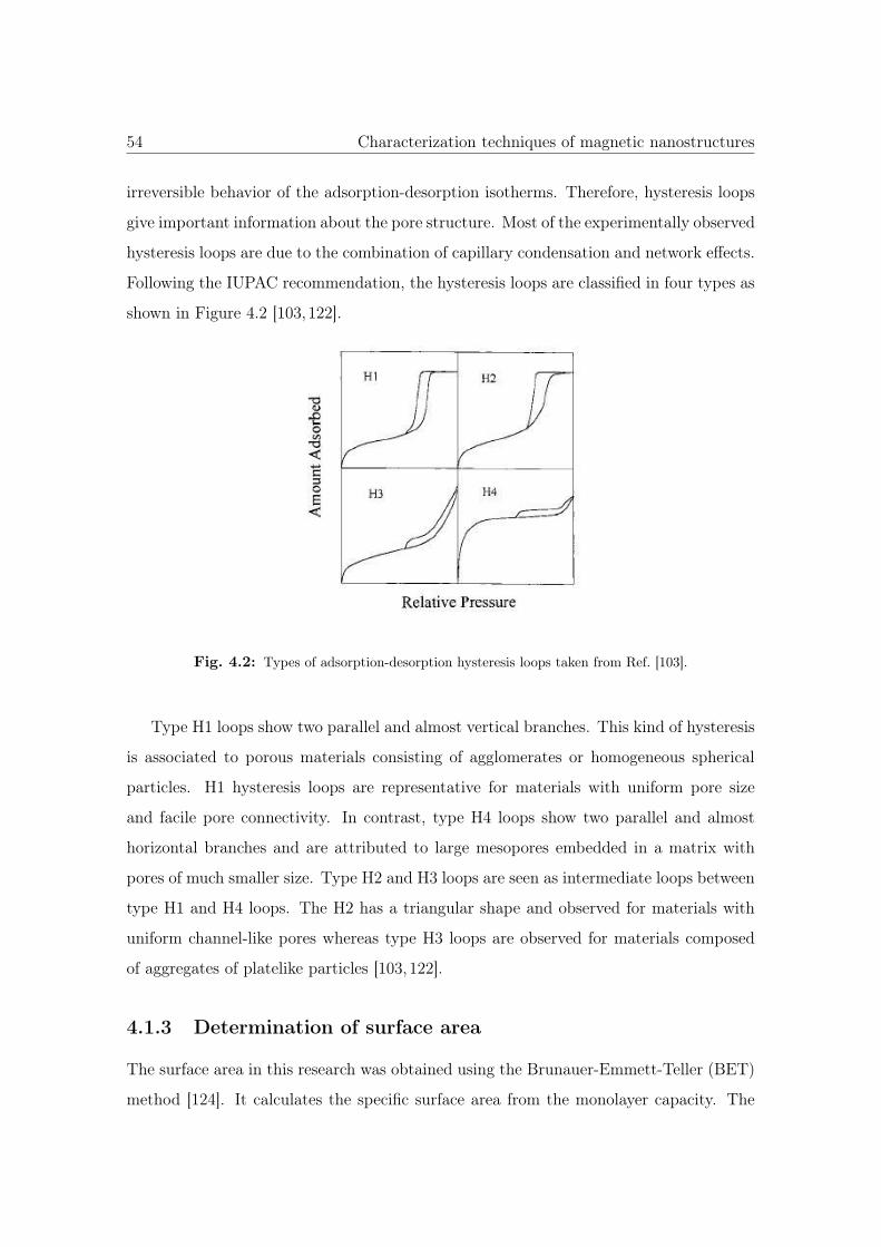
54 Characterization techniques of magnetic nanostructures
irreversible behavior of the adsorption-desorption isotherms. Therefore, hysteresis loops
give important information about the pore structure. Most of the experimentally observed
hysteresis loops are due to the combination of capillary condensation and network effects.
Following the IUPAC recommendation, the hysteresis loops are classified in four types as
shown in Figure 4.2 [103,122].
Fig. 4.2: Types of adsorption-desorption hysteresis loops taken from Ref. [103].
Type H1 loops show two parallel and almost vertical branches. This kind of hysteresis
is associated to porous materials consisting of agglomerates or homogeneous spherical
particles. H1 hysteresis loops are representative for materials with uniform pore size
and facile pore connectivity. In contrast, type H4 loops show two parallel and almost
horizontal branches and are attributed to large mesopores embedded in a matrix with
pores of much smaller size. Type H2 and H3 loops are seen as intermediate loops between
type H1 and H4 loops. The H2 has a triangular shape and observed for materials with
uniform channel-like pores whereas type H3 loops are observed for materials composed
of aggregates of platelike particles [103,122].
4.1.3 Determination of surface area
The surface area in this research was obtained using the Brunauer-Emmett-Teller (BET)
method [124]. It calculates the specific surface area from the monolayer capacity. The
4.1 Gas adsorption-desorption techniques 55
latter is defined as the number of adsorbed molecules in the monolayer on the surface of a
material. The main BET calculation considers a flat surface, the same adsorption energy
for all adsorption sites, no lateral interactions between adsorbed molecules, the adsorption
energy for all molecules is equal to the liquefaction energy with exception of the first layer
and an infinite number of layers, which can form. Despite the considerations of the BET
equation differ for porous materials, it is currently the best method to determine the
specific surface area of porous materials. Thus,
As(BET ) = namLam (4.1)
where As(BET) is the total and specific surface area of the adsorbent, am is the
molecular cross-sectional area, nam is the monolayer capacity area and L is the Avogadro
constant. The BET surface area is typically extracted from the linear part of the so called
BET plot.
4.1.4 Determination of pore volume
The total pore volume can be calculated from the amount of vapor adsorbed at a relative
pressure close to the saturation vapor pressure by assuming that the density of condensed
adsorbate in the pores is equal to the density of bulk liquid adsorbate. The absorbed
amount is converted to the corresponding volume of liquid adsorbate at the temperature
of the adsorption measurement. For N2 at 77 K, the conversion factors from the amount
adsorbed to the volume of liquid adsorbate is 0.0015468 cm3 STP g−1 [103], where STP
stands for standard temperature and pressure.
4.1.5 Determination of pore size distribution
The pore size can be calculated using the Barrett-Joyner-Halenda (BJH) algorithm [125].
This method considers cylindrical pores and that the equilibrium between the gas phase
and the adsorbed phase during desorption is determined by two mechanisms, the physical
adsorption on the pore walls and the capillary condensation. The BJH algorithm takes
into account the Kelvin equation [122], which describes the relationship between the pore
56 Characterization techniques of magnetic nanostructures
radius and the relative pressure. The pore size distribution is usually expressed in the
graphical form ΔV/ΔD vs. D, where V, is the total pore volume and D is the pore
radius [122].
Nitrogen adsorption-desorption isotherms were measured with an ASAP 2010 adsorp-
tion analyzer (Micromeritics) at liquid nitrogen temperature (77 K) with prior degassing
of the calcined silica samples under vacuum at 200 ◦C and nanocasted Co3O4 at 150 ◦C
overnight. Total pore volumes were determined using the adsorbed volume at a relative
pressure of 0.97. BET surface area was estimated from the relative pressure range from
0.06 to 0.2. The pore size distribution of the mesoporous materials was analyzed using
the BJH algorithm using the desorption branch.
4.2 X-ray diffraction
By employing X-ray diffraction technique it is possible to obtain information about the
crystal structure, chemical composition, and physical properties of the studied system.
Furthermore, it is also a powerful tool to characterize mesostructured materials. The in-
formation is obtained by the use of X-ray beams of radiation. The latter can be described
by its wavelength λ, its direction of traveling and its amplitude A [126]. The direction
of the beam as well as its wavelength can be expressed using the wave vector k, which
points along the direction of the beam with a magnitude |k| = 2π/λ. In three directions,
the incident plane wave can be described as [126]
ψ = A exp(ik.x) (4.2)
where x is a position in space. The quantity k.x is the phase angle.
The scattering of radiation from two particles separated by the vector r is shown in
Figure 4.3. The initial wave vector is ki and the scattered wave vector is ks. The two
rays come in with the same phase, however in the scattering process they have different
path lengths which leads to different phases of the two scattered rays. The total phase
difference is the sum of the two separate phase differences,
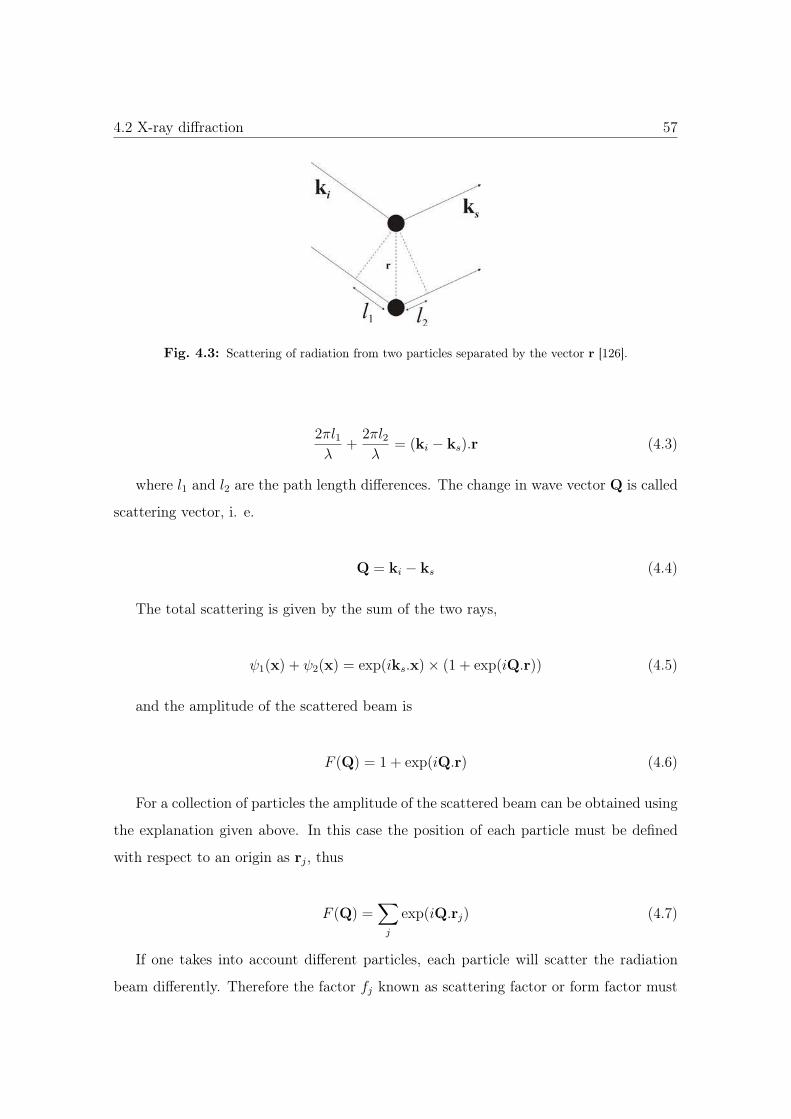
4.2 X-ray diffraction 57
Fig. 4.3: Scattering of radiation from two particles separated by the vector r [126].
2πl1λ
+2πl2λ
= (ki − ks).r (4.3)
where l1 and l2 are the path length differences. The change in wave vector Q is called
scattering vector, i. e.
Q = ki − ks (4.4)
The total scattering is given by the sum of the two rays,
ψ1(x) + ψ2(x) = exp(iks.x) × (1 + exp(iQ.r)) (4.5)
and the amplitude of the scattered beam is
F (Q) = 1 + exp(iQ.r) (4.6)
For a collection of particles the amplitude of the scattered beam can be obtained using
the explanation given above. In this case the position of each particle must be defined
with respect to an origin as rj, thus
F (Q) =∑
j
exp(iQ.rj) (4.7)
If one takes into account different particles, each particle will scatter the radiation
beam differently. Therefore the factor fj known as scattering factor or form factor must
58 Characterization techniques of magnetic nanostructures
be considered, thus
F (Q) =∑
j
fj exp(iQ.rj) (4.8)
The scattering of X-rays by atoms can be seen as the scattering from the continuous
distribution of electrons around the atom [126]. The X-ray atomic scattering factor is
f(Q) =
∫ρel(r) exp(iQ.r)dr (4.9)
Note that the amplitude of the scattered signal is given by the Fourier transform of the
electron density. On mesoporous materials, XRD studies are not trivial. The standard
crystallographic procedures cannot be used for their characterization due to the lack of
ordering at the atomic level. In the case of mesoporous materials the obtained Bragg
peaks are caused by the ordering of pores of uniform size [120], i. e., the scattering power
only depends on the electron density contrast between the solid matter with a constant
electron density (on the mesoscale) and the empty pores with zero electron density [127].
The XRD patterns for mesoporous materials generally contain 3 to 5 reflections. They
are located in the low angle 2 θ range from 0.4◦ to 3◦ degrees because of the presence of
relatively large ordered pores.
Several approaches have been reported for X-ray diffraction (XRD) structural investi-
gations of the ordered mesoporous materials [127–134]. By modeling the XRD intensities
of a mesoporous material it has been shown that it is possible to obtain values of lattice
parameters, pore diameters and wall thicknesses of the studied materials. For example,
X-ray diffraction studies on SBA-15 have shown that this structure consists of hexagonally
close packed cylindrical pore channels belonging to the p6mm space group. They exhibit
four or more charactersitic reflections. The most intensive peak is the (100) reflection,
the other three less intensive peaks are the (110), (200) and (210) [94, 96]. Furthermore,
quantitative XRD analysis of the SBA-15 diffraction pattern indicates that this silica
material displays not only the mesoporosity (pore diameter >2 nm) due to the hexago-
nal arrangement of cylindrical aggregates but also microporosity (pore diameter <2 nm)
liberated by the poly(ethylene oxide) (PEO) moieties [128]. Studies by Morishige and
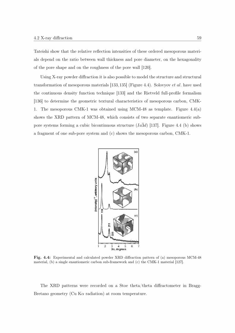
4.2 X-ray diffraction 59
Tateishi show that the relative reflection intensities of these ordered mesoporous materi-
als depend on the ratio between wall thickness and pore diameter, on the hexagonality
of the pore shape and on the roughness of the pore wall [120].
Using X-ray powder diffraction it is also possible to model the structure and structural
transformation of mesoporous materials [133,135] (Figure 4.4). Solovyov et al. have used
the continuous density function technique [133] and the Rietveld full-profile formalism
[136] to determine the geometric textural characteristics of mesoporous carbon, CMK-
1. The mesoporous CMK-1 was obtained using MCM-48 as template. Figure 4.4(a)
shows the XRD pattern of MCM-48, which consists of two separate enantiomeric sub-
pore systems forming a cubic bicontinuous structure (Ia3d) [137]. Figure 4.4 (b) shows
a fragment of one sub-pore system and (c) shows the mesoporous carbon, CMK-1.
Fig. 4.4: Experimental and calculated powder XRD diffraction pattern of (a) mesoporous MCM-48material, (b) a single enantiomeric carbon sub-framework and (c) the CMK-1 material [127].
The XRD patterns were recorded on a Stoe theta/theta diffractometer in Bragg-
Bretano geometry (Cu Kα radiation) at room temperature.
60 Characterization techniques of magnetic nanostructures
4.3 Microscopy techniques
In 1986 half of the Nobel Prize in physics was awarded to Ernst Ruska for ”his fundamental
work in electron optics and for the design of the first electron microscope” and it was
pointed out in the press release on the 15th of October of that year as ”one of the most
important inventions of this century” [138]. The outstanding developments in electron
microscopy techniques have significantly enhanced the understanding of nanostructures.
4.3.1 Transmission electron microscopy
In the early 20th century, Louis de Broglie proposed that the wavelength λ of a particle
of a certain momentum p is given by
λ = h/p = h/(mv) (4.10)
where h = 6.626 x 10⁻³⁴ Js is the Planck constant, m and v represent the mass and
speed of the particle, respectively [139]. Using this relation one finds that the wavelength
of an electron depends on the accelerating voltage, i. e. increasing the electron energy
(and therefore the momentum) decreases the de Broglie wavelength of electrons. For
an accelerating voltage of 50 keV the wavelength is λ ≈ 0.005 nm. Such high-energy
electrons can penetrate distances of several microns into a solid. If the solid is crystalline,
the electrons are diffracted by atomic planes inside the material [140–142]. Therefore, it
is possible to form a transmission electron diffraction pattern from electrons that have
passed through a thin specimen.
Transmission electron microscopy (TEM) is a powerful imaging tool to study systems
of smaller length scales. Employing TEM one gets information about the crystal dislo-
cations, crystal quality, grain size and crystal orientation. The electron energy is in the
range of 60-150 keV or up to 400 keV in the case of high resolution transmission electron
microscope (HRTEM) [142]. Using the latter one, it is possible to observe the atomistic
structure of crystalline solids in real space. The TEM is not only a highly magnifying
camera but it is an instrument of precise physical measurements. A transmission elec-
tron microscope consists of an illumination system, specimen stage and imaging system
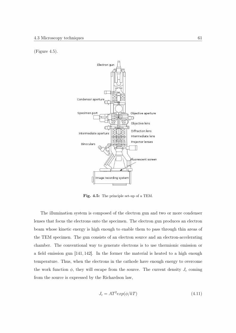
4.3 Microscopy techniques 61
(Figure 4.5).
Fig. 4.5: The principle set-up of a TEM.
The illumination system is composed of the electron gun and two or more condenser
lenses that focus the electrons onto the specimen. The electron gun produces an electron
beam whose kinetic energy is high enough to enable them to pass through thin areas of
the TEM specimen. The gun consists of an electron source and an electron-accelerating
chamber. The conventional way to generate electrons is to use thermionic emission or
a field emission gun [141, 142]. In the former the material is heated to a high enough
temperature. Thus, when the electrons in the cathode have enough energy to overcome
the work function φ, they will escape from the source. The current density Jc coming
from the source is expressed by the Richardson law,
Jc = AT 2exp(φ/kT ) (4.11)
62 Characterization techniques of magnetic nanostructures
where A is a constant that depends on the cathode material, T is the emission tem-
perature and k = 1.38 x 10⁻²³ J K−1 is the Boltzmann constant [141,143]. Therefore, the
cathode material should have a high melting point as in the case of tungsten or low work
function as LaB6. Field emission guns consist of a pointed cathode tip and at least two
anodes. A voltage between the field emission tip and the first anode controls the field-
emission current. The latter depends on the work function and on the field strength.
A second voltage between tip and the second anode determines the final energy of the
electrons.
The most important parameter of the electron gun is its brightness defined as the
beam current per unit area per solid angle Ω [141], and is conserved when the beam
passes an (ideal) electron lens.
B =Ie
AsΩ(4.12)
where Ie is the available emission current, As is the emitting area.
The TEM incorporates a two lens-system in order to focus the electron beam on the
specimen, change the illumination aperture and produce a small electron probe (2-100
nm diameter) [141].
The specimen stage allows specimens to either be held stationary or else intentionally
moved. Its mechanical stability is an important factor for spatial resolution of the TEM
image. TEM specimens are always fabricated circular with a diameter of 3 mm [142].
The specimen must be thin enough and the energy of the incident electrons must be high
enough to allow that most of the incident electrons are transmitted to form the magnified
image.
Once the electrons are focused at the specimen with the condenser lenses, the electron
intensity distribution behind the specimen is imaged with a three or four stage lens
system, onto a fluorescent screen, on a photographic film, or on the monitor screen of an
electronic camera system [140–142]. The spatial resolution of the image depends on the
quality and design of these lenses, especially on the objective. TEM images shown here
were obtained with a HF 2000 microscope (Hitachi) equipped with a cold field emission
gun.
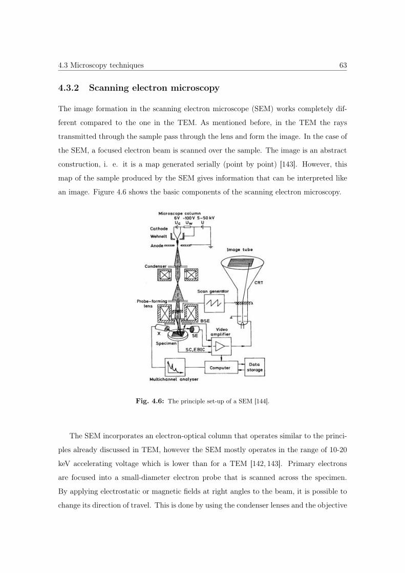
4.3 Microscopy techniques 63
4.3.2 Scanning electron microscopy
The image formation in the scanning electron microscope (SEM) works completely dif-
ferent compared to the one in the TEM. As mentioned before, in the TEM the rays
transmitted through the sample pass through the lens and form the image. In the case of
the SEM, a focused electron beam is scanned over the sample. The image is an abstract
construction, i. e. it is a map generated serially (point by point) [143]. However, this
map of the sample produced by the SEM gives information that can be interpreted like
an image. Figure 4.6 shows the basic components of the scanning electron microscopy.
Fig. 4.6: The principle set-up of a SEM [144].
The SEM incorporates an electron-optical column that operates similar to the princi-
ples already discussed in TEM, however the SEM mostly operates in the range of 10-20
keV accelerating voltage which is lower than for a TEM [142, 143]. Primary electrons
are focused into a small-diameter electron probe that is scanned across the specimen.
By applying electrostatic or magnetic fields at right angles to the beam, it is possible to
change its direction of travel. This is done by using the condenser lenses and the objective
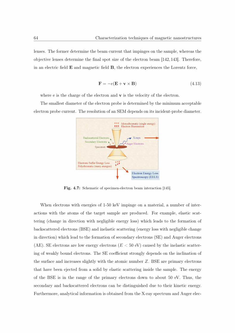
64 Characterization techniques of magnetic nanostructures
lenses. The former determine the beam current that impinges on the sample, whereas the
objective lenses determine the final spot size of the electron beam [142, 143]. Therefore,
in an electric field E and magnetic field B, the electron experiences the Lorentz force,
F = −e(E+ v ×B) (4.13)
where e is the charge of the electron and v is the velocity of the electron.
The smallest diameter of the electron probe is determined by the minimum acceptable
electron probe current. The resolution of an SEM depends on its incident-probe diameter.
Fig. 4.7: Schematic of specimen-electron beam interaction [145].
When electrons with energies of 1-50 keV impinge on a material, a number of inter-
actions with the atoms of the target sample are produced. For example, elastic scat-
tering (change in direction with negligible energy loss) which leads to the formation of
backscattered electrons (BSE) and inelastic scattering (energy loss with negligible change
in direction) which lead to the formation of secondary electrons (SE) and Auger electrons
(AE). SE electrons are low energy electrons (E < 50 eV) caused by the inelastic scatter-
ing of weakly bound electrons. The SE coefficient strongly depends on the inclination of
the surface and increases slightly with the atomic number Z. BSE are primary electrons
that have been ejected from a solid by elastic scattering inside the sample. The energy
of the BSE is in the range of the primary electrons down to about 50 eV. Thus, the
secondary and backscattered electrons can be distinguished due to their kinetic energy.
Furthermore, analytical information is obtained from the X-ray spectrum and Auger elec-
4.4 The superconducting quantum interference device: SQUID 65
trons [142, 143]. The most important signals are produced by secondary electrons and
backscattered electrons.
In contrast to TEM which uses a stationary incident beam, the focused electron beam
of diameter dp of a SEM is scanned in two perpendicular (x and y) directions across
the specimen. Thus a square or rectangular area of specimen can be covered and an
image of this area can be formed by collecting secondary electrons from each point on
the specimen.
HRSEM images of the samples shown here were taken using a Hitachi S-5500 ultra-
high resolution cold field emission scanning electron microscope. All samples were pre-
pared on lacey carbon films supported by a copper grid. The obtained images were
analyzed using the Scandium 5.0 software package from Soft Imaging System GmbH.
The electron beam lithography was performed using a QUANTA 200 FEG SEM with
a Raith Elphy Quantum lithography unit. The patterns were designed using a GDSII
database included in the lithography software.
4.4 The superconducting quantum interference device:
SQUID
The superconductive state can be described by a macroscopic quantum wave function ψ
for the Cooper pairs, of the form,
ψ(r, t) = ψ0(r, t)eiθ(r,t) (4.14)
where θ is the phase common to all the Cooper pairs in the condensate.
The properties of a supercurrent through a tunnel barrier were studied theoretical by
Brian David Josephson. The Josephson junction consists of two weakly coupled super-
conducting electrodes [146]. Let us consider that the two superconductors are identical
and ψ1 is the probability amplitud of electron pairs on one side of the junction and ψ2
is the probability amplitud on the other side. The supercurrent density (Js) depends
on the phase of the wave functions. If the coupling between the two superconductors
is weak enough, the relation between the supercurrent density to the phase difference
66 Characterization techniques of magnetic nanostructures
(ϕ = θ2 − θ1) in the absence of any scalar and vector potential is
Js = Jcsinϕ (4.15)
where Jc is the critical or maximum Josephson current density. This relation is the
first Josephson equation.
If ϕ changes with time, then one obtains the second Josephson equation, i.e.
∂ϕ
∂t=
2π
Φ0
∫ 2
1
E(r, t).dl (4.16)
where Φ0 represents the flux quantum (Φ0 = h/2e) and∫ 2
1E(r, t).dl is the voltage
drop across the junction.
This discovery is the base of the superconducting quantum interference device (SQUID).
SQUID devices combine two physical phenomena, i.e. the Josephson effect and the flux
quantization in superconducting loops [147]. SQUIDs are very sensitive instruments
which measure magnetic flux variations. They work as a highly sensitive flux to voltage
converter giving a flux dependent output voltage with a period of one quantum flux.
The minimum flux variation which can be measured using the SQUID is of the order
of fractions (≈ 10−5) of the flux quantum Φ0 [146]. There are two main operational
modes in superconducting quantum interference device, i. e., direct current (dc) and
radio frequency (rf). The former consists of a closed superconducting loop including two
Josephson junctions in the loop’s current path, whereas the latter consists of a supercon-
ducting loop with one Josephson junction [7,147,148]. In this section the dc-SQUID will
be explained in more detail .
The dc SQUID
The direct current superconducting quantum interference device consists of a supercon-
ducting ring with two Josephson junctions as depicted in Figure 4.8 [7, 147, 148]. The
second junction allows a finite, time-averaged, direct voltage difference to be established
across the junctions by a direct bias current. The junctions, 1 and 2, are characterized
by the first Josephson equation, i. e. Is1 = Icsinϕ1 and Is2 = Icsinϕ2. The total current
Is through the circuit is composed of the current in each junction, i. e. Is = Is1 + Is2.
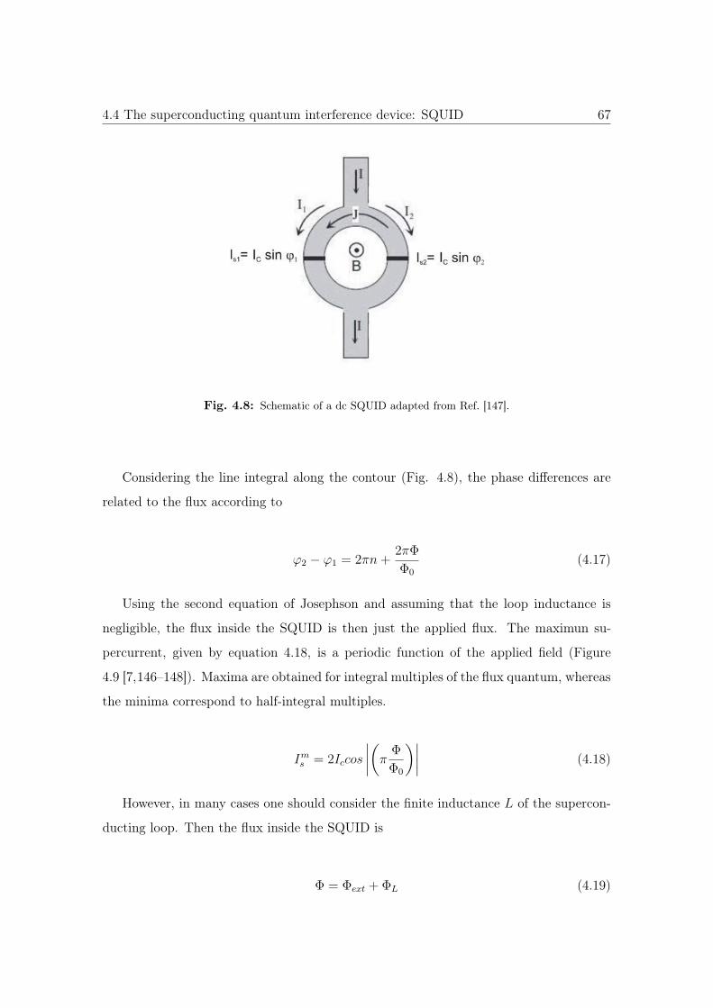
4.4 The superconducting quantum interference device: SQUID 67
Fig. 4.8: Schematic of a dc SQUID adapted from Ref. [147].
Considering the line integral along the contour (Fig. 4.8), the phase differences are
related to the flux according to
ϕ2 − ϕ1 = 2πn +2πΦ
Φ0
(4.17)
Using the second equation of Josephson and assuming that the loop inductance is
negligible, the flux inside the SQUID is then just the applied flux. The maximun su-
percurrent, given by equation 4.18, is a periodic function of the applied field (Figure
4.9 [7,146–148]). Maxima are obtained for integral multiples of the flux quantum, whereas
the minima correspond to half-integral multiples.
Ims = 2Iccos
∣∣∣∣(
πΦ
Φ0
)∣∣∣∣ (4.18)
However, in many cases one should consider the finite inductance L of the supercon-
ducting loop. Then the flux inside the SQUID is
Φ = Φext + ΦL (4.19)
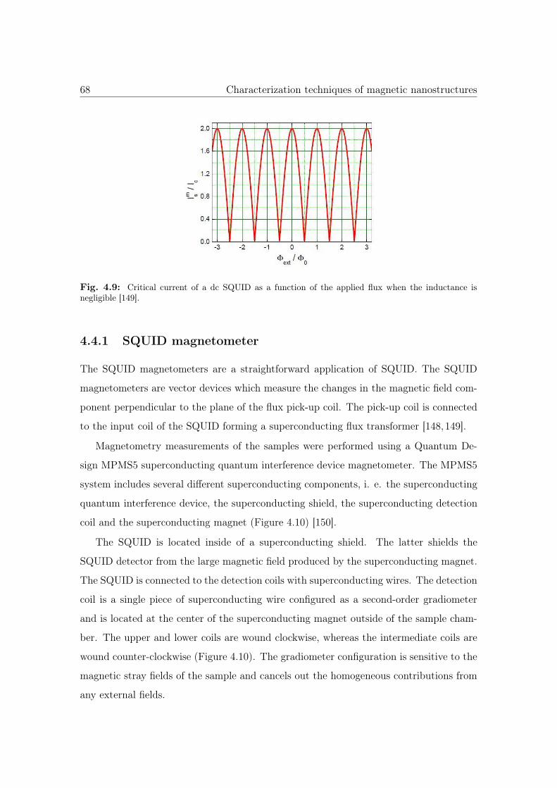
68 Characterization techniques of magnetic nanostructures
Fig. 4.9: Critical current of a dc SQUID as a function of the applied flux when the inductance isnegligible [149].
4.4.1 SQUID magnetometer
The SQUID magnetometers are a straightforward application of SQUID. The SQUID
magnetometers are vector devices which measure the changes in the magnetic field com-
ponent perpendicular to the plane of the flux pick-up coil. The pick-up coil is connected
to the input coil of the SQUID forming a superconducting flux transformer [148,149].
Magnetometry measurements of the samples were performed using a Quantum De-
sign MPMS5 superconducting quantum interference device magnetometer. The MPMS5
system includes several different superconducting components, i. e. the superconducting
quantum interference device, the superconducting shield, the superconducting detection
coil and the superconducting magnet (Figure 4.10) [150].
The SQUID is located inside of a superconducting shield. The latter shields the
SQUID detector from the large magnetic field produced by the superconducting magnet.
The SQUID is connected to the detection coils with superconducting wires. The detection
coil is a single piece of superconducting wire configured as a second-order gradiometer
and is located at the center of the superconducting magnet outside of the sample cham-
ber. The upper and lower coils are wound clockwise, whereas the intermediate coils are
wound counter-clockwise (Figure 4.10). The gradiometer configuration is sensitive to the
magnetic stray fields of the sample and cancels out the homogeneous contributions from
any external fields.
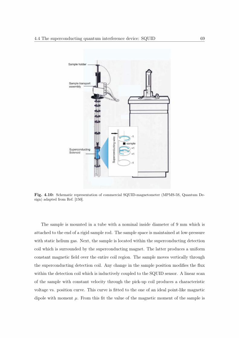
4.4 The superconducting quantum interference device: SQUID 69
Fig. 4.10: Schematic representation of commercial SQUID-magnetometer (MPMS-5S, Quantum De-sign) adapted from Ref. [150].
The sample is mounted in a tube with a nominal inside diameter of 9 mm which is
attached to the end of a rigid sample rod. The sample space is maintained at low-pressure
with static helium gas. Next, the sample is located within the superconducting detection
coil which is surrounded by the superconducting magnet. The latter produces a uniform
constant magnetic field over the entire coil region. The sample moves vertically through
the superconducting detection coil. Any change in the sample position modifies the flux
within the detection coil which is inductively coupled to the SQUID sensor. A linear scan
of the sample with constant velocity through the pick-up coil produces a characteristic
voltage vs. position curve. This curve is fitted to the one of an ideal point-like magnetic
dipole with moment μ. From this fit the value of the magnetic moment of the sample is
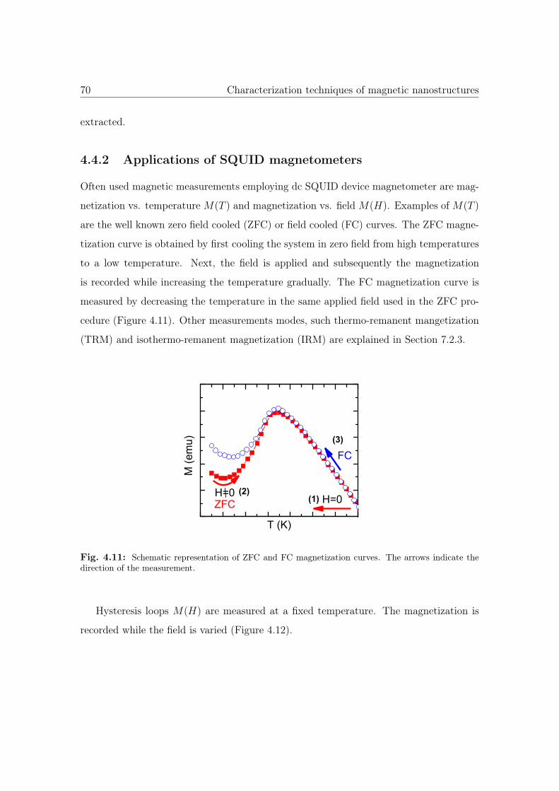
70 Characterization techniques of magnetic nanostructures
extracted.
4.4.2 Applications of SQUID magnetometers
Often used magnetic measurements employing dc SQUID device magnetometer are mag-
netization vs. temperature M(T ) and magnetization vs. field M(H). Examples of M(T )
are the well known zero field cooled (ZFC) or field cooled (FC) curves. The ZFC magne-
tization curve is obtained by first cooling the system in zero field from high temperatures
to a low temperature. Next, the field is applied and subsequently the magnetization
is recorded while increasing the temperature gradually. The FC magnetization curve is
measured by decreasing the temperature in the same applied field used in the ZFC pro-
cedure (Figure 4.11). Other measurements modes, such thermo-remanent mangetization
(TRM) and isothermo-remanent magnetization (IRM) are explained in Section 7.2.3.
H=0
FC
H=0ZFC
M (e
mu)
T (K)
(1)(2)
(3)
Fig. 4.11: Schematic representation of ZFC and FC magnetization curves. The arrows indicate thedirection of the measurement.
Hysteresis loops M(H) are measured at a fixed temperature. The magnetization is
recorded while the field is varied (Figure 4.12).
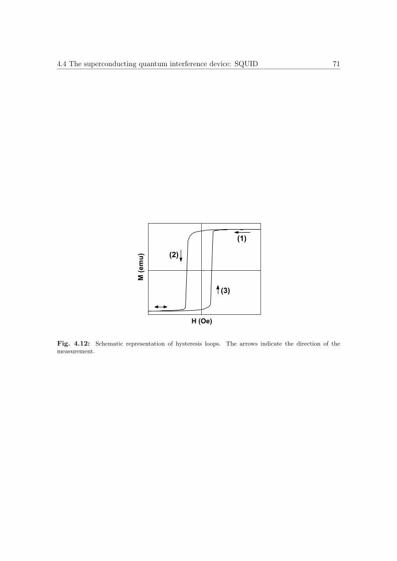
4.4 The superconducting quantum interference device: SQUID 71
(3)
(2)
(1)
M (e
mu)
H (Oe)
Fig. 4.12: Schematic representation of hysteresis loops. The arrows indicate the direction of themeasurement.

72 Characterization techniques of magnetic nanostructures
Chapter 5
Synthesis and structural
characterization of antiferromagnetic
nanostructures
Magnetic nanoparticles and nanowires have attracted much interest among magnetism
researchers for decades. This is not only due to their huge potential in technological ap-
plications either in purely magnetic areas as recording technology [31], but also in other
disciplines such as in biology and medicine [32, 151, 152]. In fundamental research they
usually serve as ideal model systems, mentioning e.g. the Stoner-Wohlfarth and the Néel-
Brown model [30] or to study the finite size effect [33]. The latter one is in particular
relevant for nanoparticles and nanowires consisting of an antiferromagnetic (AF) material.
As the size of a magnetic system decreases, the significance of the surface spins increases.
Since an antiferromagnet usually has two mutually compensating sublattices, the surface
always leads to a breaking of the sublattice pairing and thus leading to ’uncompensated’
surface spins. This effect was already discussed by Louis Néel for the explanation of
a net magnetic moment in AF nanoparticles [43]. Various explanations have been pro-
posed, e.g. spin-glass or cluster-glass-like behavior of the surface spins [45–48], thermal
excitation of spin-precession modes [49], finite-size induced multi-sublattice ordering [50],
core-shell interactions [46, 47, 51], or weak ferromagnetism [52, 53]. However, the precise
identification of the nature of the surface contribution has remained unclear. Terms like
73
74 Synthesis and structural characterization of antiferromagnetic nanostructures
’disordered surface state’, ’loose surface spins’, ’uncoupled spins’, ’spin-glass-like behav-
ior’, etc. express the uncertainty in the description of the shell contribution.
With the motivation to explicitly investigate the surface spin contribution in AF
nanosystems, high-quality AF Co3O4 nanostructures have been synthesized using the
nanocasting method described in Chapter 3. As discussed therein, the structure and
the properties of the template play an important role for the synthesis of the metal
oxides [63,73]. This approach has been successfully employed giving well ordered magnetic
nanostructures, such as, NiO [73,153], MnxOy [73], Co3O4 [73–75], Cr2O3 [76,77], Fe2O3
[78], Fe3O4 [79], and Co3O4-CoFe2O4 [71]. It has been demonstrated that direct control
of the pore size of the silica template, typically between 5 and 30 nm, [94, 154] is easily
achieved by selecting an appropriate temperature for the hydrothermal treatment step of
the synthesis protocol. The cobalt nitrate, which is the precursor for the final Co3O4, is
incorporated in the channels of the silica template and later thermally decomposed inside
the silica matrix. In the final step, the silica template is removed yielding nanowire arrays
which are in the same size range as the pores of the silica template [68].
In this section, the synthesis of nanostructured Co3O4 using two silica templates,
two-dimensional hexagonal silica SBA-15 and three-dimensional cubic silica KIT-6, will
be discussed. The samples were characterized by powder X-ray diffraction (XRD), N2-
sorption, high resolution scanning electron microscopy (HRSEM) and high resolution
transmission electron microscopy (HRTEM). Magnetometry studies of Co3O4 as well as
other AF nanostructures will be discussed in Chapter 7.
5.1 Synthesis of mesoporous SBA-15 with variable con-
nectivity and pore size
At the end of the 1990’s Stucky and coworkers from the University of California, Santa
Barbara showed the preparation of well-ordered hexagonal mesoporous silica structures
with uniform pore size varying from 5 to 30 nanometers [94, 96]. These materials, called
SBA-15 (Santa Barbara), are usually synthesized under strongly acidic condition using
a block copolymer as a structure-directing agent. The mesoporous SBA-15 have walls
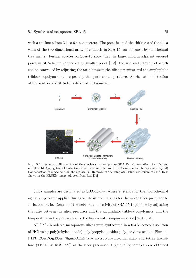
5.1 Synthesis of mesoporous SBA-15 75
with a thickness from 3.1 to 6.4 nanometers. The pore size and the thickness of the silica
walls of the two dimensional array of channels in SBA-15 can be tuned by the thermal
treatments. Further studies on SBA-15 show that the large uniform adjacent ordered
pores in SBA-15 are connected by smaller pores [103], the size and fraction of which
can be controlled by adjusting the ratio between the silica precursor and the amphiphilic
triblock copolymers, and especially the synthesis temperature. A schematic illustration
of the synthesis of SBA-15 is depicted in Figure 5.1.
Fig. 5.1: Schematic illustration of the synthesis of mesoporous SBA-15. a) Formation of surfactantmicelles. b) Aggregation of surfactant micelles to micellar rods. c) Formation to a hexagonal array. d)Condensation of silicic acid on the surface. e) Removal of the template. Final structutre of SBA-15 isshown in the HRSEM image adapted from Ref. [71]
Silica samples are designated as SBA-15-T -r, where T stands for the hydrothermal
aging temperature applied during synthesis and r stands for the molar silica precursor to
surfactant ratio. Control of the network connectivity of SBA-15 is possible by adjusting
the ratio between the silica precursor and the amphiphilic triblock copolymers, and the
temperature in the preparation of the hexagonal mesoporous silica [74,96,154].
All SBA-15 ordered mesoporous silicas were synthesized in a 0.3 M aqueous solution
of HCl using poly(ethylene oxide)-poly(propylene oxide)-poly(ethylene oxide) (Pluronic
P123, EO20PO70EO20, Sigma-Aldrich) as a structure-directing agent and tetraethoxysi-
lane (TEOS, ACROS 99%) as the silica precursor. High quality samples were obtained
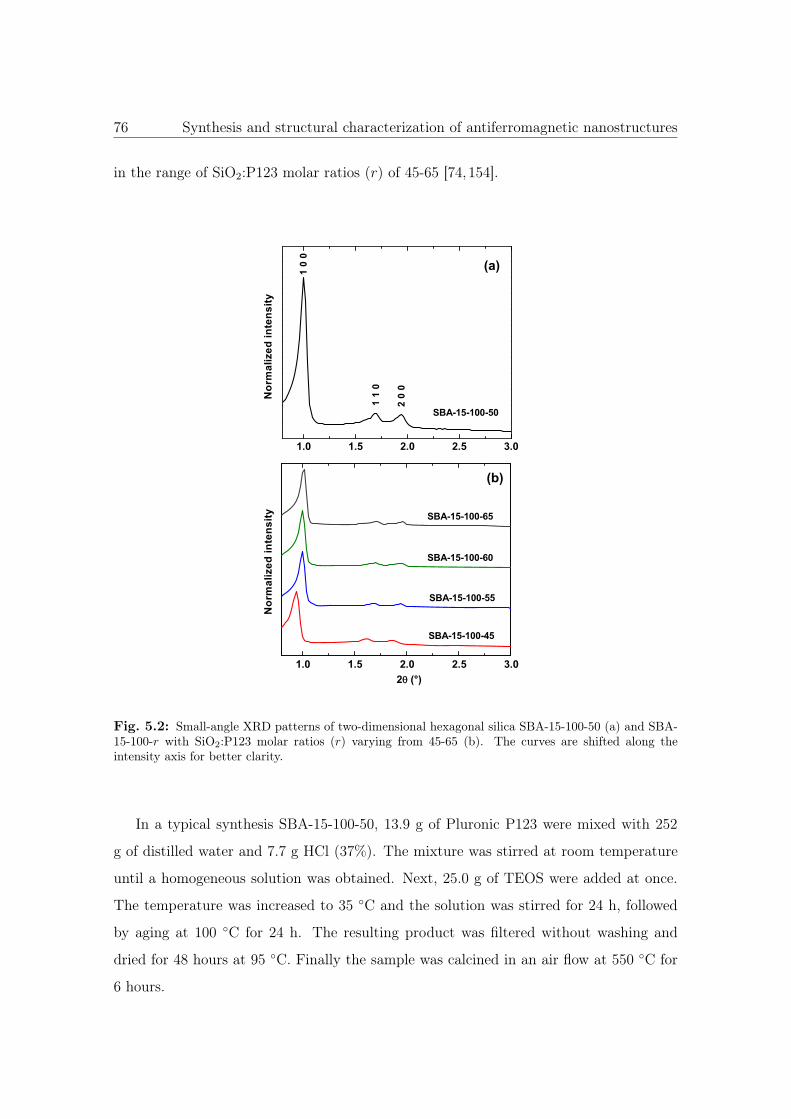
76 Synthesis and structural characterization of antiferromagnetic nanostructures
in the range of SiO2:P123 molar ratios (r) of 45-65 [74,154].
1.0 1.5 2.0 2.5 3.0
SBA-15-100-50
(a)N
orm
aliz
ed in
tens
ity
2 0
0
1 1
0
1 0
0
1.0 1.5 2.0 2.5 3.0
���
���������
����������
��������
��������
Nor
mal
ized
inte
nsity
�θθ � ���
Fig. 5.2: Small-angle XRD patterns of two-dimensional hexagonal silica SBA-15-100-50 (a) and SBA-15-100-r with SiO2:P123 molar ratios (r) varying from 45-65 (b). The curves are shifted along theintensity axis for better clarity.
In a typical synthesis SBA-15-100-50, 13.9 g of Pluronic P123 were mixed with 252
g of distilled water and 7.7 g HCl (37%). The mixture was stirred at room temperature
until a homogeneous solution was obtained. Next, 25.0 g of TEOS were added at once.
The temperature was increased to 35 ◦C and the solution was stirred for 24 h, followed
by aging at 100 ◦C for 24 h. The resulting product was filtered without washing and
dried for 48 hours at 95 ◦C. Finally the sample was calcined in an air flow at 550 ◦C for
6 hours.
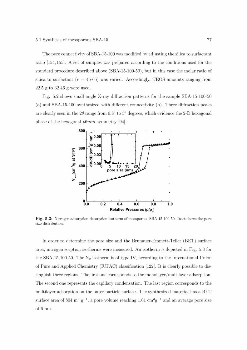
5.1 Synthesis of mesoporous SBA-15 77
The pore connectivity of SBA-15-100 was modified by adjusting the silica to surfactant
ratio [154, 155]. A set of samples was prepared according to the conditions used for the
standard procedure described above (SBA-15-100-50), but in this case the molar ratio of
silica to surfactant (r = 45-65) was varied. Accordingly, TEOS amounts ranging from
22.5 g to 32.46 g were used.
Fig. 5.2 shows small angle X-ray diffraction patterns for the sample SBA-15-100-50
(a) and SBA-15-100 synthesized with different connectivity (b). Three diffraction peaks
are clearly seen in the 2θ range from 0.8◦ to 3◦ degrees, which evidence the 2-D hexagonal
phase of the hexagonal p6mm symmetry [94].
0.0 0.2 0.4 0.6 0.8 1.00
200
400
600
800
0 5 10 15 200.00
0.03
0.06
0.09
dV/d
D (c
m3 g-1
nm-1
)
Relative Pressures (p/po)
Vad
s(cm
3 /g a
t STP
)
pore size (nm)
Fig. 5.3: Nitrogen adsorption-desorption isotherm of mesoporous SBA-15-100-50. Inset shows the poresize distribution.
In order to determine the pore size and the Brunauer-Emmett-Teller (BET) surface
area, nitrogen sorption isotherms were measured. An isotherm is depicted in Fig. 5.3 for
the SBA-15-100-50. The N2 isotherm is of type IV, according to the International Union
of Pure and Applied Chemistry (IUPAC) classification [122]. It is clearly possible to dis-
tinguish three regions. The first one corresponds to the monolayer/multilayer adsorption.
The second one represents the capillary condensation. The last region corresponds to the
multilayer adsorption on the outer particle surface. The synthesized material has a BET
surface area of 804 m2 g−1, a pore volume reaching 1.01 cm3g−1 and an average pore size
of 6 nm.
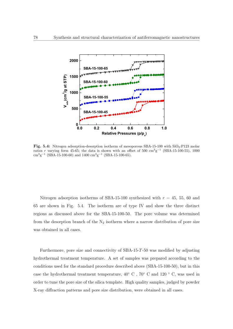
78 Synthesis and structural characterization of antiferromagnetic nanostructures
0.0 0.2 0.4 0.6 0.8 1.00
500
1000
1500
2000V
ads(c
m3 /g
at S
TP)
Relative Pressures (p/po)
SBA-15-100-55
SBA-15-100-45
SBA-15-100-60
SBA-15-100-65
Fig. 5.4: Nitrogen adsorption-desorption isotherm of mesoporous SBA-15-100 with SiO2:P123 molarratios r varying form 45-65; the data is shown with an offset of 500 cm3g−1 (SBA-15-100-55), 1000cm3g−1 (SBA-15-100-60) and 1400 cm3g−1 (SBA-15-100-65).
Nitrogen adsorption isotherms of SBA-15-100 synthesized with r = 45, 55, 60 and
65 are shown in Fig. 5.4. The isotherm are of type IV and show the three distinct
regions as discussed above for the SBA-15-100-50. The pore volume was determined
from the desorption branch of the N2 isotherm where a narrow distribution of pore size
was obtained in all cases.
Furthermore, pore size and connectivity of SBA-15-T -50 was modified by adjusting
hydrothermal treatment temperature. A set of samples was prepared according to the
conditions used for the standard procedure described above (SBA-15-100-50), but in this
case the hydrothermal treatment temperature, 40◦ C , 70◦ C and 120 ◦ C, was used in
order to tune the pore size of the silica template. High quality samples, judged by powder
X-ray diffraction patterns and pore size distribution, were obtained in all cases.
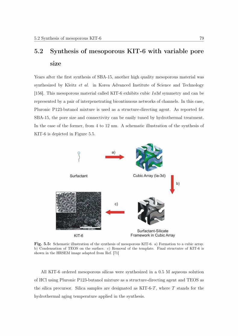
5.2 Synthesis of mesoporous KIT-6 79
5.2 Synthesis of mesoporous KIT-6 with variable pore
size
Years after the first synthesis of SBA-15, another high quality mesoporous material was
synthesized by Kleitz et al. in Korea Advanced Institute of Science and Technology
[156]. This mesoporous material called KIT-6 exhibits cubic Ia3d symmetry and can be
represented by a pair of interpenetrating bicontinuous networks of channels. In this case,
Pluronic P123-butanol mixture is used as a structure-directing agent. As reported for
SBA-15, the pore size and connectivity can be easily tuned by hydrothermal treatment.
In the case of the former, from 4 to 12 nm. A schematic illustration of the synthesis of
KIT-6 is depicted in Figure 5.5.
Fig. 5.5: Schematic illustration of the synthesis of mesoporous KIT-6. a) Formation to a cubic array.b) Condensation of TEOS on the surface. c) Removal of the template. Final structutre of KIT-6 isshown in the HRSEM image adapted from Ref. [71]
All KIT-6 ordered mesoporous silicas were synthesized in a 0.5 M aqueous solution
of HCl using Pluronic P123-butanol mixture as a structure-directing agent and TEOS as
the silica precursor. Silica samples are designated as KIT-6-T , where T stands for the
hydrothermal aging temperature applied in the synthesis.
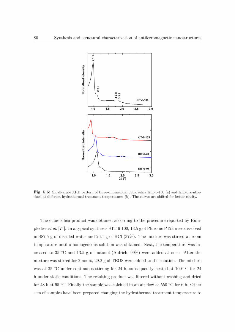
80 Synthesis and structural characterization of antiferromagnetic nanostructures
1.0 1.5 2.0 2.5 3.0
KIT-6-100
N
orm
aliz
ed in
tens
ity
3 3
2 4
2 0
2 2
0
2 1
1
1.0 1.5 2.0 2.5 3.0
������ ��
�������
��������
Nor
mal
ized
inte
nsity
�θθ � ���
Fig. 5.6: Small-angle XRD pattern of three-dimensional cubic silica KIT-6-100 (a) and KIT-6 synthe-sized at different hydrothermal treatment temperatures (b). The curves are shifted for better clarity.
The cubic silica product was obtained according to the procedure reported by Rum-
plecker et al. [74]. In a typical synthesis KIT-6-100, 13.5 g of Pluronic P123 were dissolved
in 487.5 g of distilled water and 26.1 g of HCl (37%). The mixture was stirred at room
temperature until a homogeneous solution was obtained. Next, the temperature was in-
creased to 35 ◦C and 13.5 g of butanol (Aldrich, 99%) were added at once. After the
mixture was stirred for 2 hours, 29.2 g of TEOS were added to the solution. The mixture
was at 35 ◦C under continuous stirring for 24 h, subsequently heated at 100◦ C for 24
h under static conditions. The resulting product was filtered without washing and dried
for 48 h at 95 ◦C. Finally the sample was calcined in an air flow at 550 ◦C for 6 h. Other
sets of samples have been prepared changing the hydrothermal treatment temperature to
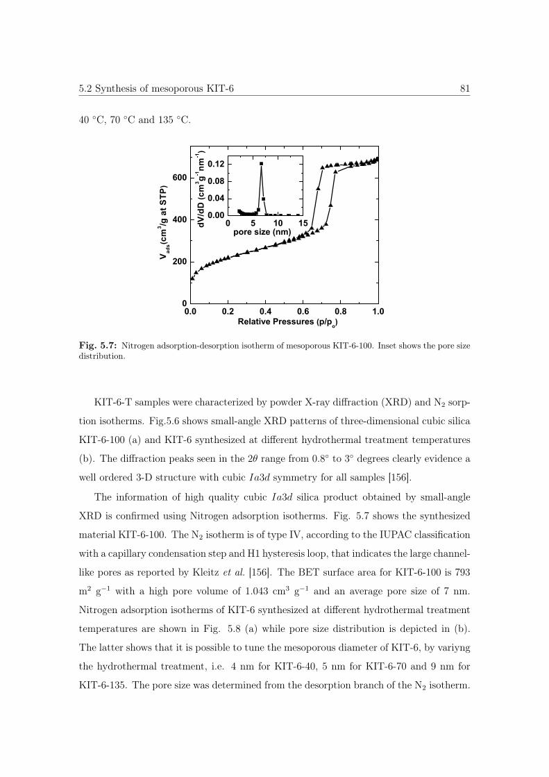
5.2 Synthesis of mesoporous KIT-6 81
40 ◦C, 70 ◦C and 135 ◦C.
0.0 0.2 0.4 0.6 0.8 1.00
200
400
600
0 5 10 150.00
0.04
0.08
0.12
pore size (nm)
dV/d
D (c
m3 g-1
nm-1
)
Vad
s(cm
3 /g a
t STP
)
Relative Pressures (p/po)
Fig. 5.7: Nitrogen adsorption-desorption isotherm of mesoporous KIT-6-100. Inset shows the pore sizedistribution.
KIT-6-T samples were characterized by powder X-ray diffraction (XRD) and N2 sorp-
tion isotherms. Fig.5.6 shows small-angle XRD patterns of three-dimensional cubic silica
KIT-6-100 (a) and KIT-6 synthesized at different hydrothermal treatment temperatures
(b). The diffraction peaks seen in the 2θ range from 0.8◦ to 3◦ degrees clearly evidence a
well ordered 3-D structure with cubic Ia3d symmetry for all samples [156].
The information of high quality cubic Ia3d silica product obtained by small-angle
XRD is confirmed using Nitrogen adsorption isotherms. Fig. 5.7 shows the synthesized
material KIT-6-100. The N2 isotherm is of type IV, according to the IUPAC classification
with a capillary condensation step and H1 hysteresis loop, that indicates the large channel-
like pores as reported by Kleitz et al. [156]. The BET surface area for KIT-6-100 is 793
m2 g−1 with a high pore volume of 1.043 cm3 g−1 and an average pore size of 7 nm.
Nitrogen adsorption isotherms of KIT-6 synthesized at different hydrothermal treatment
temperatures are shown in Fig. 5.8 (a) while pore size distribution is depicted in (b).
The latter shows that it is possible to tune the mesoporous diameter of KIT-6, by variyng
the hydrothermal treatment, i.e. 4 nm for KIT-6-40, 5 nm for KIT-6-70 and 9 nm for
KIT-6-135. The pore size was determined from the desorption branch of the N2 isotherm.
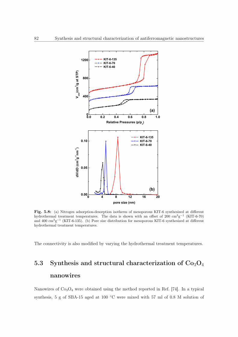
82 Synthesis and structural characterization of antiferromagnetic nanostructures
0.0 0.2 0.4 0.6 0.8 1.00
400
800
1200
Vad
s(cm
3 /g a
t STP
)
(a)
KIT-6-135 KIT-6-70 KIT-6-40
Relative Pressures (p/po)
0 4 8 12 16 200.00
0.05
0.10
(b)
dV/d
D (c
m3 g-1
nm-1
)
pore size (nm)
KIT-6-135 KIT-6-70 KIT-6-40
Fig. 5.8: (a) Nitrogen adsorption-desorption isotherm of mesoporous KIT-6 synthesized at differenthydrothermal treatment temperatures. The data is shown with an offset of 200 cm3g−1 (KIT-6-70)and 400 cm3g−1 (KIT-6-135). (b) Pore size distribution for mesoporous KIT-6 synthesized at differenthydrothermal treatment temperatures.
The connectivity is also modified by varying the hydrothermal treatment temperatures.
5.3 Synthesis and structural characterization of Co3O4
nanowires
Nanowires of Co3O4 were obtained using the method reported in Ref. [74]. In a typical
synthesis, 5 g of SBA-15 aged at 100 ◦C were mixed with 57 ml of 0.8 M solution of
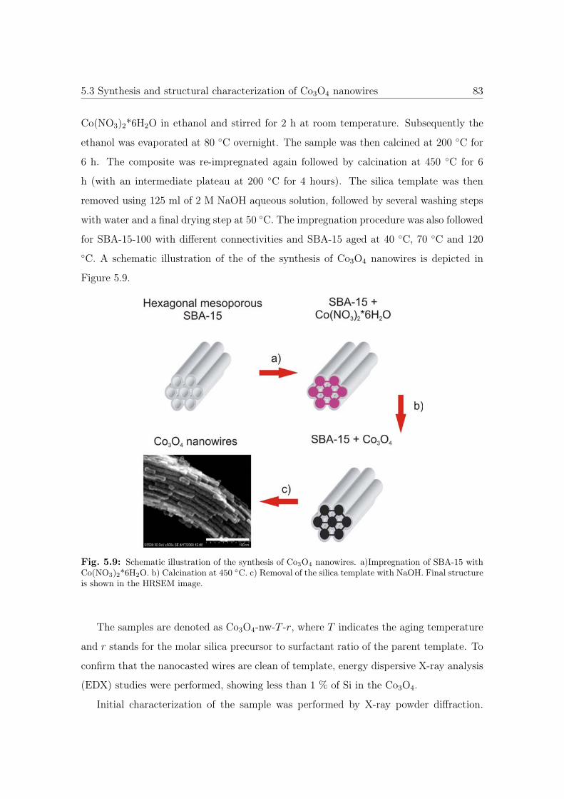
5.3 Synthesis and structural characterization of Co3O4 nanowires 83
Co(NO3)2*6H2O in ethanol and stirred for 2 h at room temperature. Subsequently the
ethanol was evaporated at 80 ◦C overnight. The sample was then calcined at 200 ◦C for
6 h. The composite was re-impregnated again followed by calcination at 450 ◦C for 6
h (with an intermediate plateau at 200 ◦C for 4 hours). The silica template was then
removed using 125 ml of 2 M NaOH aqueous solution, followed by several washing steps
with water and a final drying step at 50 ◦C. The impregnation procedure was also followed
for SBA-15-100 with different connectivities and SBA-15 aged at 40 ◦C, 70 ◦C and 120◦C. A schematic illustration of the of the synthesis of Co3O4 nanowires is depicted in
Figure 5.9.
Fig. 5.9: Schematic illustration of the synthesis of Co3O4 nanowires. a)Impregnation of SBA-15 withCo(NO3)2*6H2O. b) Calcination at 450 ◦C. c) Removal of the silica template with NaOH. Final structureis shown in the HRSEM image.
The samples are denoted as Co3O4-nw-T -r, where T indicates the aging temperature
and r stands for the molar silica precursor to surfactant ratio of the parent template. To
confirm that the nanocasted wires are clean of template, energy dispersive X-ray analysis
(EDX) studies were performed, showing less than 1 % of Si in the Co3O4.
Initial characterization of the sample was performed by X-ray powder diffraction.
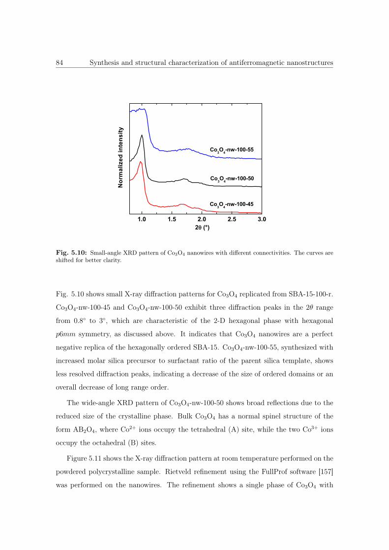
84 Synthesis and structural characterization of antiferromagnetic nanostructures
1.0 1.5 2.0 2.5 3.0
�������������
�������������
�������������
N
orm
aliz
ed in
tens
ity
θθ � ���
Fig. 5.10: Small-angle XRD pattern of Co3O4 nanowires with different connectivities. The curves areshifted for better clarity.
Fig. 5.10 shows small X-ray diffraction patterns for Co3O4 replicated from SBA-15-100-r.
Co3O4-nw-100-45 and Co3O4-nw-100-50 exhibit three diffraction peaks in the 2θ range
from 0.8◦ to 3◦, which are characteristic of the 2-D hexagonal phase with hexagonal
p6mm symmetry, as discussed above. It indicates that Co3O4 nanowires are a perfect
negative replica of the hexagonally ordered SBA-15. Co3O4-nw-100-55, synthesized with
increased molar silica precursor to surfactant ratio of the parent silica template, shows
less resolved diffraction peaks, indicating a decrease of the size of ordered domains or an
overall decrease of long range order.
The wide-angle XRD pattern of Co3O4-nw-100-50 shows broad reflections due to the
reduced size of the crystalline phase. Bulk Co3O4 has a normal spinel structure of the
form AB2O4, where Co2+ ions occupy the tetrahedral (A) site, while the two Co3+ ions
occupy the octahedral (B) sites.
Figure 5.11 shows the X-ray diffraction pattern at room temperature performed on the
powdered polycrystalline sample. Rietveld refinement using the FullProf software [157]
was performed on the nanowires. The refinement shows a single phase of Co3O4 with
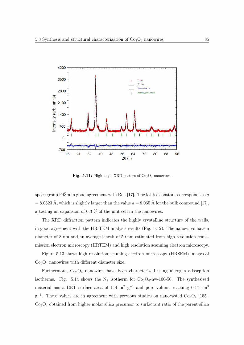
5.3 Synthesis and structural characterization of Co3O4 nanowires 85
Fig. 5.11: High-angle XRD pattern of Co3O4 nanowires.
space group Fd3̄m in good agreement with Ref. [17]. The lattice constant corresponds to a
= 8.0823 Å, which is slightly larger than the value a = 8.065 Å for the bulk compound [17],
attesting an expansion of 0.3 % of the unit cell in the nanowires.
The XRD diffraction pattern indicates the highly crystalline structure of the walls,
in good agreement with the HR-TEM analysis results (Fig. 5.12). The nanowires have a
diameter of 8 nm and an average length of 50 nm estimated from high resolution trans-
mission electron microscopy (HRTEM) and high resolution scanning electron microscopy.
Figure 5.13 shows high resolution scanning electron microscopy (HRSEM) images of
Co3O4 nanowires with different diameter size.
Furthermore, Co3O4 nanowires have been characterized using nitrogen adsorption
isotherms. Fig. 5.14 shows the N2 isotherm for Co3O4-nw-100-50. The synthesized
material has a BET surface area of 114 m2 g−1 and pore volume reaching 0.17 cm3
g−1. These values are in agreement with previous studies on nanocasted Co3O4 [155].
Co3O4 obtained from higher molar silica precursor to surfactant ratio of the parent silica
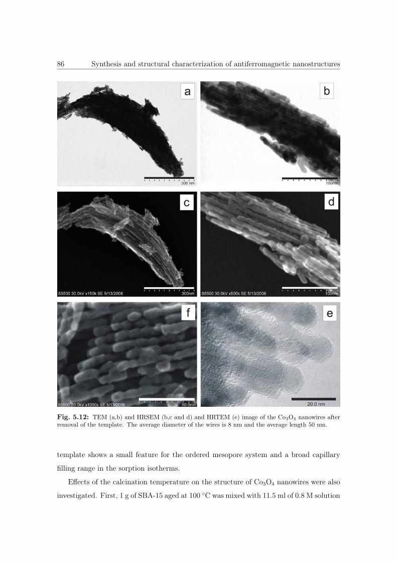
86 Synthesis and structural characterization of antiferromagnetic nanostructures
Fig. 5.12: TEM (a,b) and HRSEM (b,c and d) and HRTEM (e) image of the Co3O4 nanowires afterremoval of the template. The average diameter of the wires is 8 nm and the average length 50 nm.
template shows a small feature for the ordered mesopore system and a broad capillary
filling range in the sorption isotherms.
Effects of the calcination temperature on the structure of Co3O4 nanowires were also
investigated. First, 1 g of SBA-15 aged at 100 ◦C was mixed with 11.5 ml of 0.8 M solution
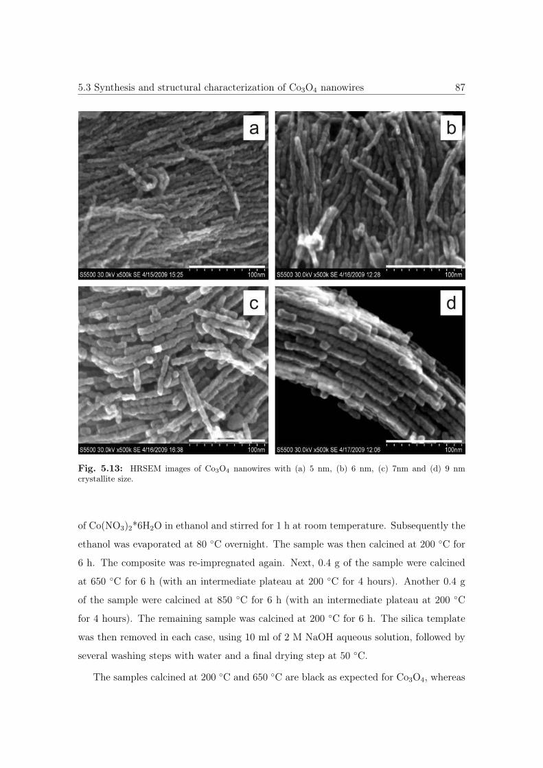
5.3 Synthesis and structural characterization of Co3O4 nanowires 87
Fig. 5.13: HRSEM images of Co3O4 nanowires with (a) 5 nm, (b) 6 nm, (c) 7nm and (d) 9 nmcrystallite size.
of Co(NO3)2*6H2O in ethanol and stirred for 1 h at room temperature. Subsequently the
ethanol was evaporated at 80 ◦C overnight. The sample was then calcined at 200 ◦C for
6 h. The composite was re-impregnated again. Next, 0.4 g of the sample were calcined
at 650 ◦C for 6 h (with an intermediate plateau at 200 ◦C for 4 hours). Another 0.4 g
of the sample were calcined at 850 ◦C for 6 h (with an intermediate plateau at 200 ◦C
for 4 hours). The remaining sample was calcined at 200 ◦C for 6 h. The silica template
was then removed in each case, using 10 ml of 2 M NaOH aqueous solution, followed by
several washing steps with water and a final drying step at 50 ◦C.
The samples calcined at 200 ◦C and 650 ◦C are black as expected for Co3O4, whereas
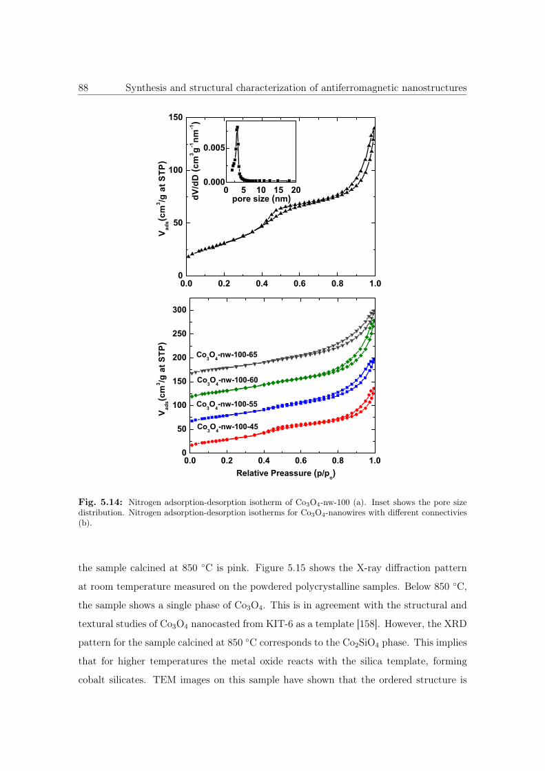
88 Synthesis and structural characterization of antiferromagnetic nanostructures
0.0 0.2 0.4 0.6 0.8 1.00
50
100
150
0 5 10 15 200.000
0.005
pore size (nm)dV/d
D (c
m3 g-1
nm-1)
Vad
s(cm
3 /g a
t STP
)
0.0 0.2 0.4 0.6 0.8 1.00
50
100
150
200
250
300
Co3O4-nw-100-45
Co3O4-nw-100-55
Co3O4-nw-100-60
Co3O4-nw-100-65
Vad
s(cm
3 /g a
t STP
)
Relative Preassure (p/po)
Fig. 5.14: Nitrogen adsorption-desorption isotherm of Co3O4-nw-100 (a). Inset shows the pore sizedistribution. Nitrogen adsorption-desorption isotherms for Co3O4-nanowires with different connectivies(b).
the sample calcined at 850 ◦C is pink. Figure 5.15 shows the X-ray diffraction pattern
at room temperature measured on the powdered polycrystalline samples. Below 850 ◦C,
the sample shows a single phase of Co3O4. This is in agreement with the structural and
textural studies of Co3O4 nanocasted from KIT-6 as a template [158]. However, the XRD
pattern for the sample calcined at 850 ◦C corresponds to the Co2SiO4 phase. This implies
that for higher temperatures the metal oxide reacts with the silica template, forming
cobalt silicates. TEM images on this sample have shown that the ordered structure is
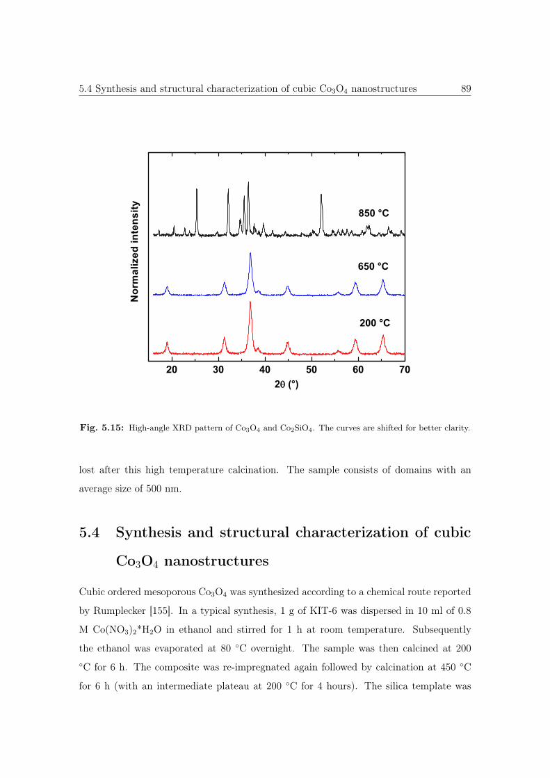
5.4 Synthesis and structural characterization of cubic Co3O4 nanostructures 89
20 30 40 50 60 70
��� ��
���� ��
��� ��
N
orm
aliz
ed in
tens
ity
�θθ � ���
Fig. 5.15: High-angle XRD pattern of Co3O4 and Co2SiO4. The curves are shifted for better clarity.
lost after this high temperature calcination. The sample consists of domains with an
average size of 500 nm.
5.4 Synthesis and structural characterization of cubic
Co3O4 nanostructures
Cubic ordered mesoporous Co3O4 was synthesized according to a chemical route reported
by Rumplecker [155]. In a typical synthesis, 1 g of KIT-6 was dispersed in 10 ml of 0.8
M Co(NO3)2*H2O in ethanol and stirred for 1 h at room temperature. Subsequently
the ethanol was evaporated at 80 ◦C overnight. The sample was then calcined at 200◦C for 6 h. The composite was re-impregnated again followed by calcination at 450 ◦C
for 6 h (with an intermediate plateau at 200 ◦C for 4 hours). The silica template was
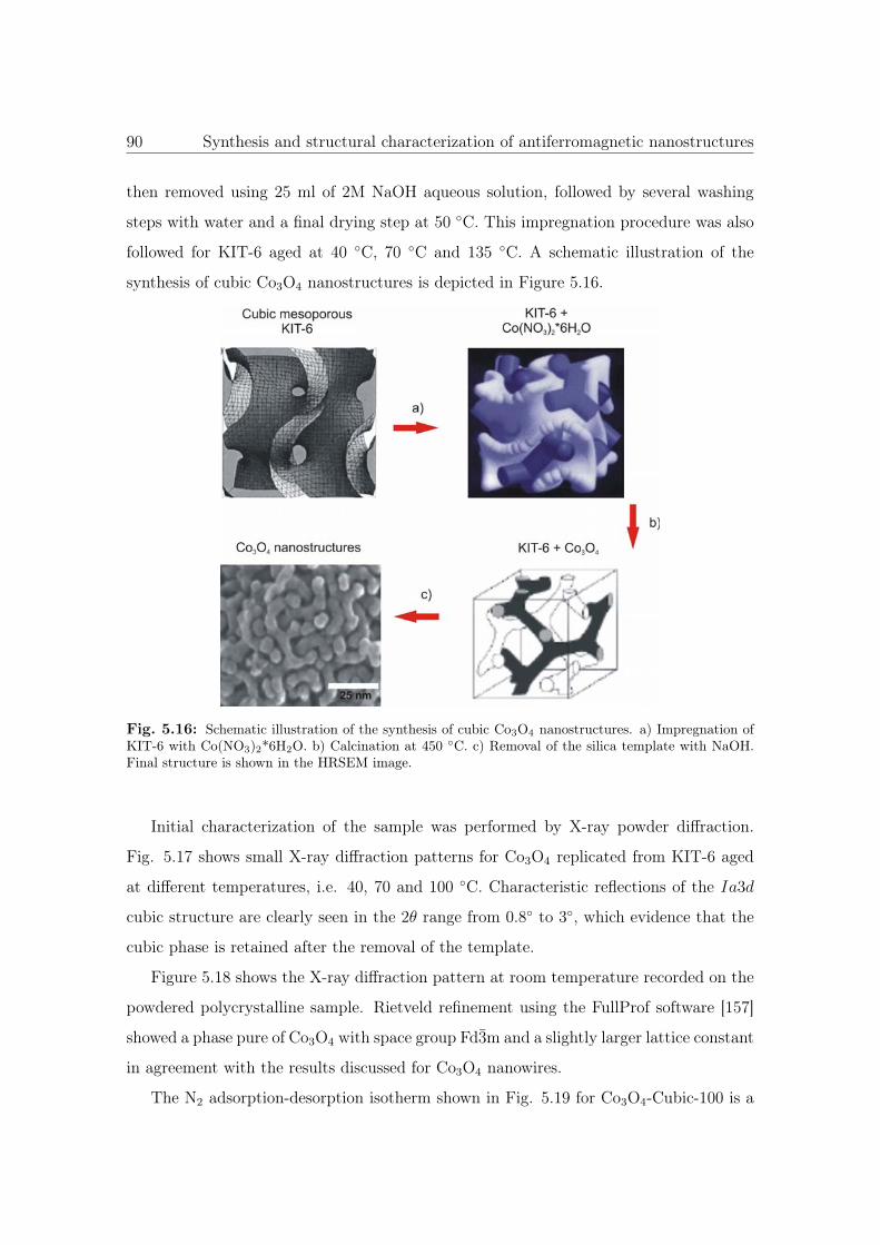
90 Synthesis and structural characterization of antiferromagnetic nanostructures
then removed using 25 ml of 2M NaOH aqueous solution, followed by several washing
steps with water and a final drying step at 50 ◦C. This impregnation procedure was also
followed for KIT-6 aged at 40 ◦C, 70 ◦C and 135 ◦C. A schematic illustration of the
synthesis of cubic Co3O4 nanostructures is depicted in Figure 5.16.
Fig. 5.16: Schematic illustration of the synthesis of cubic Co3O4 nanostructures. a) Impregnation ofKIT-6 with Co(NO3)2*6H2O. b) Calcination at 450 ◦C. c) Removal of the silica template with NaOH.Final structure is shown in the HRSEM image.
Initial characterization of the sample was performed by X-ray powder diffraction.
Fig. 5.17 shows small X-ray diffraction patterns for Co3O4 replicated from KIT-6 aged
at different temperatures, i.e. 40, 70 and 100 ◦C. Characteristic reflections of the Ia3d
cubic structure are clearly seen in the 2θ range from 0.8◦ to 3◦, which evidence that the
cubic phase is retained after the removal of the template.
Figure 5.18 shows the X-ray diffraction pattern at room temperature recorded on the
powdered polycrystalline sample. Rietveld refinement using the FullProf software [157]
showed a phase pure of Co3O4 with space group Fd3̄m and a slightly larger lattice constant
in agreement with the results discussed for Co3O4 nanowires.
The N2 adsorption-desorption isotherm shown in Fig. 5.19 for Co3O4-Cubic-100 is a
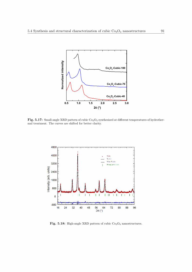
5.4 Synthesis and structural characterization of cubic Co3O4 nanostructures 91
0.5 1.0 1.5 2.0 2.5 3.0
���� ���������
���� ���������
���� ������� �
Nor
mal
ized
inte
nsity
�θθ � ���
Fig. 5.17: Small-angle XRD pattern of cubic Co3O4 synthesized at different temperatures of hydrother-mal treatment. The curves are shifted for better clarity.
Fig. 5.18: High-angle XRD pattern of cubic Co3O4 nanostructures.
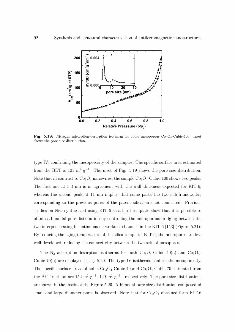
92 Synthesis and structural characterization of antiferromagnetic nanostructures
0.0 0.2 0.4 0.6 0.8 1.00
50
100
150
200
0 10 20 300.000
0.004
dV/d
D (c
m3 g-1
nm-1)
pore size (nm)
Vad
s(cm
3 /g a
t STP
)
Relative Preassure (p/po)
Fig. 5.19: Nitrogen adsorption-desorption isotherm for cubic mesoporous Co3O4-Cubic-100. Insetshows the pore size distribution.
type IV, confirming the mesoporosity of the samples. The specific surface area estimated
from the BET is 121 m2 g−1. The inset of Fig. 5.19 shows the pore size distribution.
Note that in contrast to Co3O4 nanowires, the sample Co3O4-Cubic-100 shows two peaks.
The first one at 3.3 nm is in agreement with the wall thickness expected for KIT-6,
whereas the second peak at 11 nm implies that some parts the two sub-frameworks,
corresponding to the previous pores of the parent silica, are not connected. Previous
studies on NiO synthesized using KIT-6 as a hard template show that it is possible to
obtain a bimodal pore distribution by controlling the microporous bridging between the
two interpenetrating bicontinuous networks of channels in the KIT-6 [153] (Figure 5.21).
By reducing the aging temperature of the silica template, KIT-6, the micropores are less
well developed, reducing the connectivity between the two sets of mesopores.
The N2 adsorption-desorption isotherms for both Co3O4-Cubic 40(a) and Co3O4-
Cubic-70(b) are displayed in fig. 5.20. The type IV isotherms confirm the mesoporosity.
The specific surface areas of cubic Co3O4-Cubic-40 and Co3O4-Cubic-70 estimated from
the BET method are 152 m2 g−1, 129 m2 g−1 , respectively. The pore size distributions
are shown in the insets of the Figure 5.20. A bimodal pore size distribution composed of
small and large diameter pores is observed. Note that for Co3O4 obtained form KIT-6
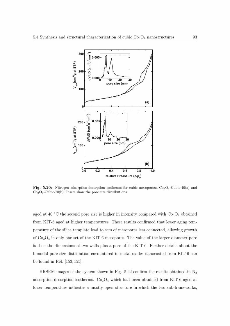
5.4 Synthesis and structural characterization of cubic Co3O4 nanostructures 93
0
100
200
300
0 10 20 300.000
0.005
Vad
s(cm
3 /g a
t STP
)
dV/d
D (c
m3 g-1
nm-1)
(a)
pore size (nm)
0.0 0.2 0.4 0.6 0.8 1.00
100
200
0 10 20 300.000
0.005
(b)
Relative Preassure (p/po)
pore size (nm)dV/d
D (c
m3 g-1
nm-1)
Vad
s(cm
3 /g a
t STP
)
Fig. 5.20: Nitrogen adsorption-desorption isotherms for cubic mesoporous Co3O4-Cubic-40(a) andCo3O4-Cubic-70(b). Insets show the pore size distributions.
aged at 40 ◦C the second pore size is higher in intensity compared with Co3O4 obtained
from KIT-6 aged at higher temperatures. These results confirmed that lower aging tem-
perature of the silica template lead to sets of mesopores less connected, allowing growth
of Co3O4 in only one set of the KIT-6 mesopores. The value of the larger diameter pore
is then the dimensions of two walls plus a pore of the KIT-6. Further details about the
bimodal pore size distribution encountered in metal oxides nanocasted from KIT-6 can
be found in Ref. [153,155].
HRSEM images of the system shown in Fig. 5.22 confirm the results obtained in N2
adsorption-desorption isotherms. Co3O4 which had been obtained from KIT-6 aged at
lower temperature indicates a mostly open structure in which the two sub-frameworks,
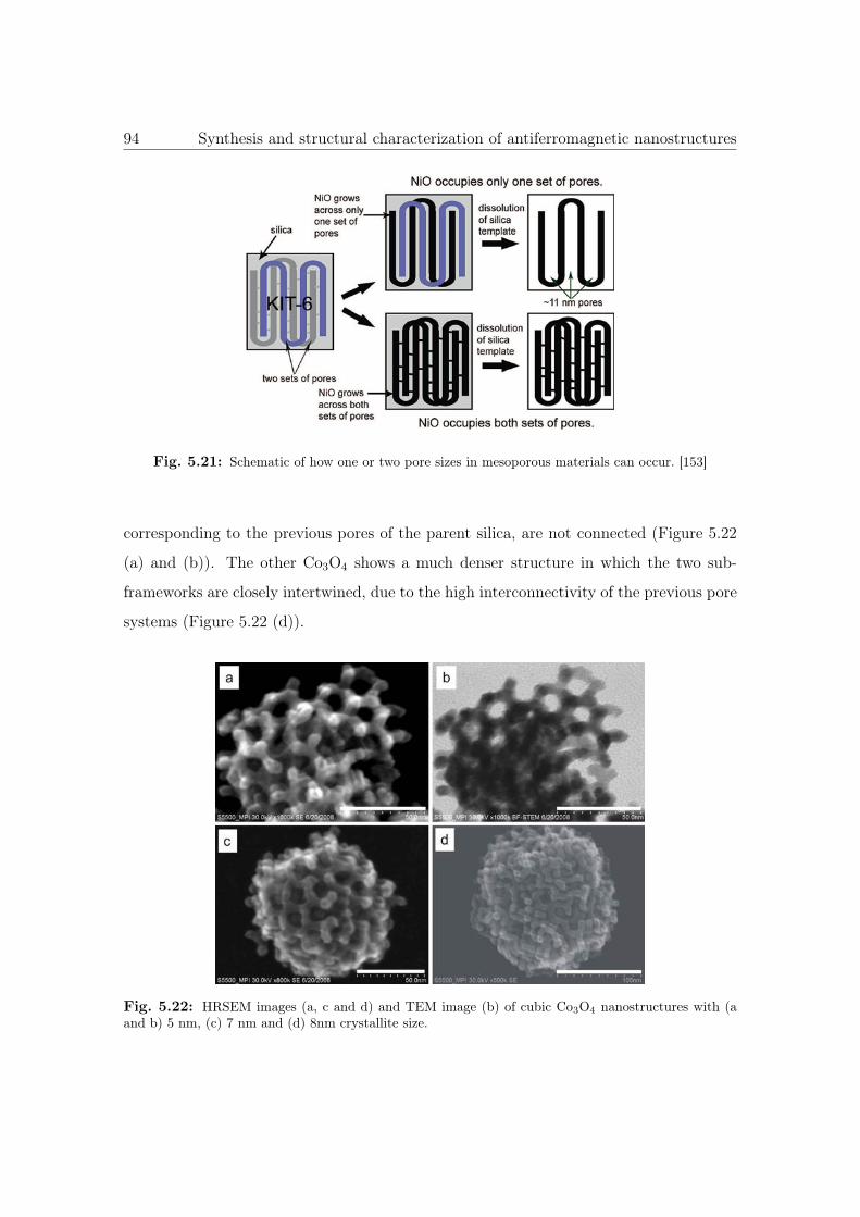
94 Synthesis and structural characterization of antiferromagnetic nanostructures
Fig. 5.21: Schematic of how one or two pore sizes in mesoporous materials can occur. [153]
corresponding to the previous pores of the parent silica, are not connected (Figure 5.22
(a) and (b)). The other Co3O4 shows a much denser structure in which the two sub-
frameworks are closely intertwined, due to the high interconnectivity of the previous pore
systems (Figure 5.22 (d)).
Fig. 5.22: HRSEM images (a, c and d) and TEM image (b) of cubic Co3O4 nanostructures with (aand b) 5 nm, (c) 7 nm and (d) 8nm crystallite size.
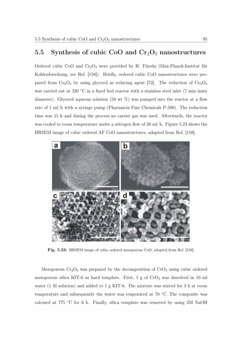
5.5 Synthesis of cubic CoO and Cr2O3 nanostructures 95
5.5 Synthesis of cubic CoO and Cr2O3 nanostructures
Ordered cubic CoO and Cr2O3 were provided by H. Tüysüz (Max-Planck-Institut für
Kohlenforschung, see Ref. [158]). Briefly, ordered cubic CoO nanostructures were pre-
pared from Co3O4 by using glycerol as reducing agent [72]. The reduction of Co3O4
was carried out at 320 ◦C in a fixed bed reactor with a stainless steel inlet (7 mm inner
diameter). Glycerol aqueous solution (50 wt %) was pumped into the reactor at a flow
rate of 1 ml/h with a syringe pump (Pharmacia Fine Chemicals P-500). The reduction
time was 15 h and during the process no carrier gas was used. Afterwards, the reactor
was cooled to room temperature under a nitrogen flow of 20 ml/h. Figure 5.23 shows the
HRSEM image of cubic ordered AF CoO nanostructures, adapted from Ref. [158].
Fig. 5.23: HRSEM image of cubic ordered mesoporous CoO, adapted from Ref. [158].
Mesoporous Cr2O3 was prepared by the decomposition of CrO3 using cubic ordered
mesoporous silica KIT-6 as hard template. First, 1 g of CrO3 was dissolved in 10 ml
water (1 M solution) and added to 1 g KIT-6. The mixture was stirred for 3 h at room
temperature and subsequently the water was evaporated at 70 ◦C. The composite was
calcined at 775 ◦C for 6 h. Finally, silica template was removed by using 2M NaOH
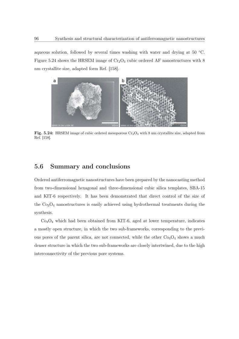
96 Synthesis and structural characterization of antiferromagnetic nanostructures
aqueous solution, followed by several times washing with water and drying at 50 ◦C.
Figure 5.24 shows the HRSEM image of Cr2O3 cubic ordered AF nanostructures with 8
nm crystallite size, adapted form Ref. [158].
Fig. 5.24: HRSEM image of cubic ordered mesoporous Cr2O3 with 8 nm crystallite size, adapted fromRef. [158].
5.6 Summary and conclusions
Ordered antiferromagnetic nanostructures have been prepared by the nanocasting method
from two-dimensional hexagonal and three-dimensional cubic silica templates, SBA-15
and KIT-6 respectively. It has been demonstrated that direct control of the size of
the Co3O4 nanostructures is easily achieved using hydrothermal treatments during the
synthesis.
Co3O4 which had been obtained from KIT-6, aged at lower temperature, indicates
a mostly open structure, in which the two sub-frameworks, corresponding to the previ-
ous pores of the parent silica, are not connected, while the other Co3O4 shows a much
denser structure in which the two sub-frameworks are closely intertwined, due to the high
interconnectivity of the previous pore systems.
Chapter 6
Synthesis and structural
characterization of iron oxide
nanoparticles
Research on magnetic nanoparticles (NPs) and fabrication of magnetic nanostructures by
lithographic methods have attracted intense attention in the last decade. In particular,
magnetic nanoparticles and wires with sizes smaller than 20 nm are in the focus of huge
interest, because they could serve as building blocks for future high-density data storage
media [159–161]. Other potential technological applications of magnetic nanoparticles are
found in electronics [162,163], photonics [164], sensors [165], and in contrast enhancement
agents for magnetic resonance imaging [166].
Rapid developments in the chemical synthesis of magnetic nanoparticles in the last
years offer the possibility to exploit new magnetic, optical and electrical properties that
emerge when reducing the size of the particles. Nanoparticles can be synthesized with
controlled size, shape and surface coating. In most cases they consist of a ferromagnetic
(FM) or ferrimagnetic material. However, core-shell nanoparticles are equally interesting.
From a technological perspective magnetic core-shell nanoparticles with functionalyzed
shells and coatings are suitable in biomedicine for applications in targeted delivery and
diagnostics [167,168]. From a fundamental perspective core-shell nanoparticles might be
even more interesting than those with a single ferro- and ferrimagnetic phase, because of
97
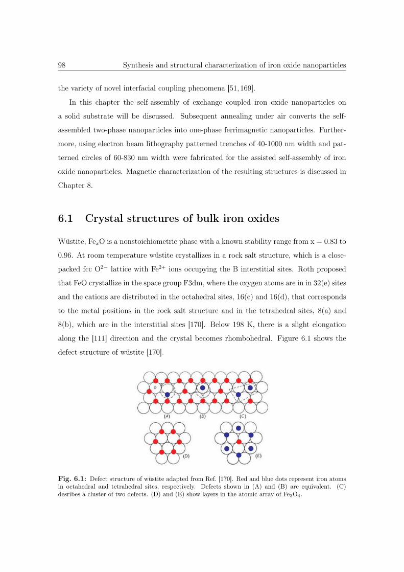
98 Synthesis and structural characterization of iron oxide nanoparticles
the variety of novel interfacial coupling phenomena [51,169].
In this chapter the self-assembly of exchange coupled iron oxide nanoparticles on
a solid substrate will be discussed. Subsequent annealing under air converts the self-
assembled two-phase nanoparticles into one-phase ferrimagnetic nanoparticles. Further-
more, using electron beam lithography patterned trenches of 40-1000 nm width and pat-
terned circles of 60-830 nm width were fabricated for the assisted self-assembly of iron
oxide nanoparticles. Magnetic characterization of the resulting structures is discussed in
Chapter 8.
6.1 Crystal structures of bulk iron oxides
Wüstite, FexO is a nonstoichiometric phase with a known stability range from x = 0.83 to
0.96. At room temperature wüstite crystallizes in a rock salt structure, which is a close-
packed fcc O2− lattice with Fe2+ ions occupying the B interstitial sites. Roth proposed
that FeO crystallize in the space group F3dm, where the oxygen atoms are in in 32(e) sites
and the cations are distributed in the octahedral sites, 16(c) and 16(d), that corresponds
to the metal positions in the rock salt structure and in the tetrahedral sites, 8(a) and
8(b), which are in the interstitial sites [170]. Below 198 K, there is a slight elongation
along the [111] direction and the crystal becomes rhombohedral. Figure 6.1 shows the
defect structure of wüstite [170].
Fig. 6.1: Defect structure of wüstite adapted from Ref. [170]. Red and blue dots represent iron atomsin octahedral and tetrahedral sites, respectively. Defects shown in (A) and (B) are equivalent. (C)desribes a cluster of two defects. (D) and (E) show layers in the atomic array of Fe3O4.
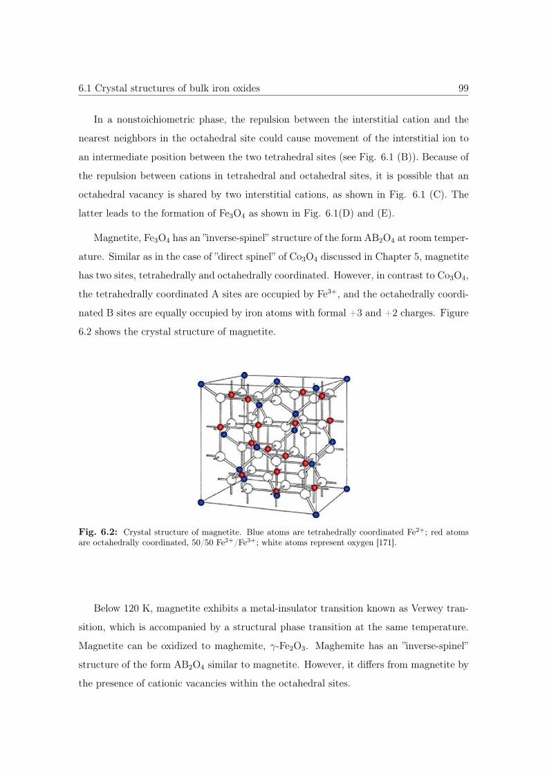
6.1 Crystal structures of bulk iron oxides 99
In a nonstoichiometric phase, the repulsion between the interstitial cation and the
nearest neighbors in the octahedral site could cause movement of the interstitial ion to
an intermediate position between the two tetrahedral sites (see Fig. 6.1 (B)). Because of
the repulsion between cations in tetrahedral and octahedral sites, it is possible that an
octahedral vacancy is shared by two interstitial cations, as shown in Fig. 6.1 (C). The
latter leads to the formation of Fe3O4 as shown in Fig. 6.1(D) and (E).
Magnetite, Fe3O4 has an ”inverse-spinel” structure of the form AB2O4 at room temper-
ature. Similar as in the case of ”direct spinel” of Co3O4 discussed in Chapter 5, magnetite
has two sites, tetrahedrally and octahedrally coordinated. However, in contrast to Co3O4,
the tetrahedrally coordinated A sites are occupied by Fe3+, and the octahedrally coordi-
nated B sites are equally occupied by iron atoms with formal +3 and +2 charges. Figure
6.2 shows the crystal structure of magnetite.
Fig. 6.2: Crystal structure of magnetite. Blue atoms are tetrahedrally coordinated Fe2+; red atomsare octahedrally coordinated, 50/50 Fe2+/Fe3+; white atoms represent oxygen [171].
Below 120 K, magnetite exhibits a metal-insulator transition known as Verwey tran-
sition, which is accompanied by a structural phase transition at the same temperature.
Magnetite can be oxidized to maghemite, γ-Fe2O3. Maghemite has an ”inverse-spinel”
structure of the form AB2O4 similar to magnetite. However, it differs from magnetite by
the presence of cationic vacancies within the octahedral sites.
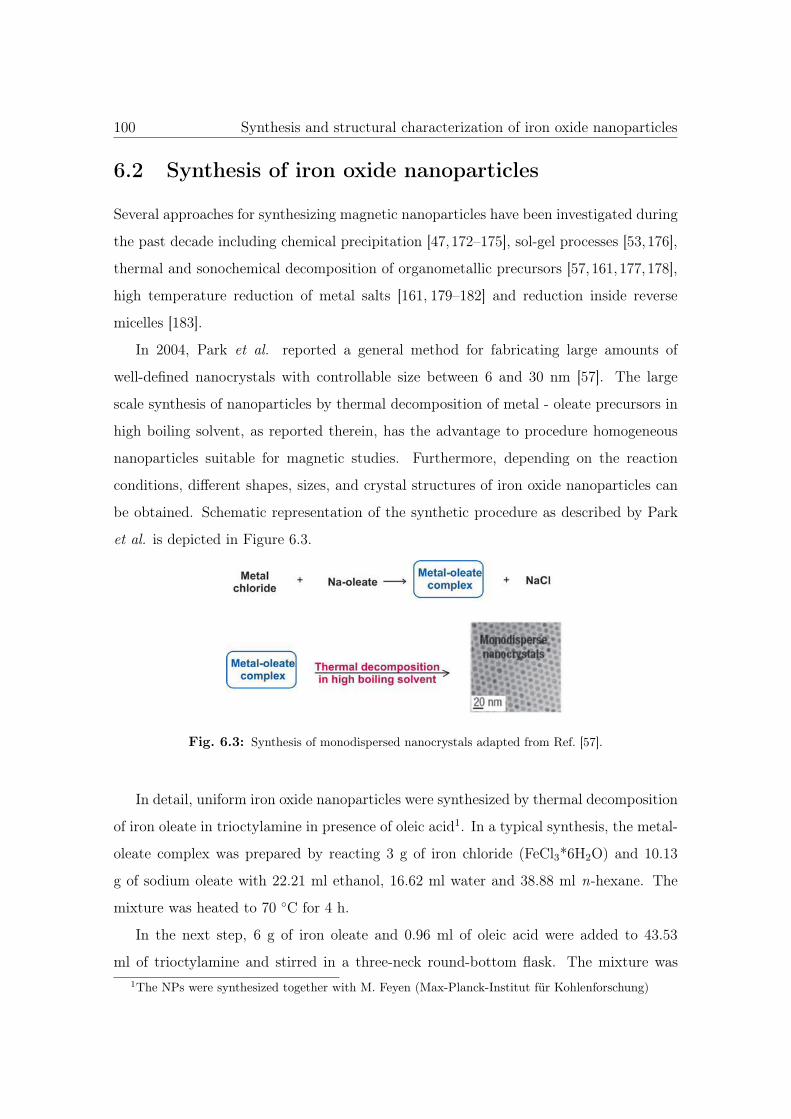
100 Synthesis and structural characterization of iron oxide nanoparticles
6.2 Synthesis of iron oxide nanoparticles
Several approaches for synthesizing magnetic nanoparticles have been investigated during
the past decade including chemical precipitation [47,172–175], sol-gel processes [53,176],
thermal and sonochemical decomposition of organometallic precursors [57, 161, 177, 178],
high temperature reduction of metal salts [161, 179–182] and reduction inside reverse
micelles [183].
In 2004, Park et al. reported a general method for fabricating large amounts of
well-defined nanocrystals with controllable size between 6 and 30 nm [57]. The large
scale synthesis of nanoparticles by thermal decomposition of metal - oleate precursors in
high boiling solvent, as reported therein, has the advantage to procedure homogeneous
nanoparticles suitable for magnetic studies. Furthermore, depending on the reaction
conditions, different shapes, sizes, and crystal structures of iron oxide nanoparticles can
be obtained. Schematic representation of the synthetic procedure as described by Park
et al. is depicted in Figure 6.3.
Fig. 6.3: Synthesis of monodispersed nanocrystals adapted from Ref. [57].
In detail, uniform iron oxide nanoparticles were synthesized by thermal decomposition
of iron oleate in trioctylamine in presence of oleic acid1. In a typical synthesis, the metal-
oleate complex was prepared by reacting 3 g of iron chloride (FeCl3*6H2O) and 10.13
g of sodium oleate with 22.21 ml ethanol, 16.62 ml water and 38.88 ml n-hexane. The
mixture was heated to 70 ◦C for 4 h.
In the next step, 6 g of iron oleate and 0.96 ml of oleic acid were added to 43.53
ml of trioctylamine and stirred in a three-neck round-bottom flask. The mixture was1The NPs were synthesized together with M. Feyen (Max-Planck-Institut für Kohlenforschung)
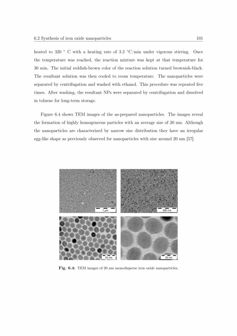
6.2 Synthesis of iron oxide nanoparticles 101
heated to 320 ◦ C with a heating rate of 3.3 ◦C/min under vigorous stirring. Once
the temperature was reached, the reaction mixture was kept at that temperature for
30 min. The initial reddish-brown color of the reaction solution turned brownish-black.
The resultant solution was then cooled to room temperature. The nanoparticles were
separated by centrifugation and washed with ethanol. This procedure was repeated five
times. After washing, the resultant NPs were separated by centrifugation and dissolved
in toluene for long-term storage.
Figure 6.4 shows TEM images of the as-prepared nanoparticles. The images reveal
the formation of highly homogeneous particles with an average size of 20 nm. Although
the nanoparticles are characterized by narrow size distribution they have an irregular
egg-like shape as previously observed for nanoparticles with size around 20 nm [57].
Fig. 6.4: TEM images of 20 nm monodisperse iron oxide nanoparticles.
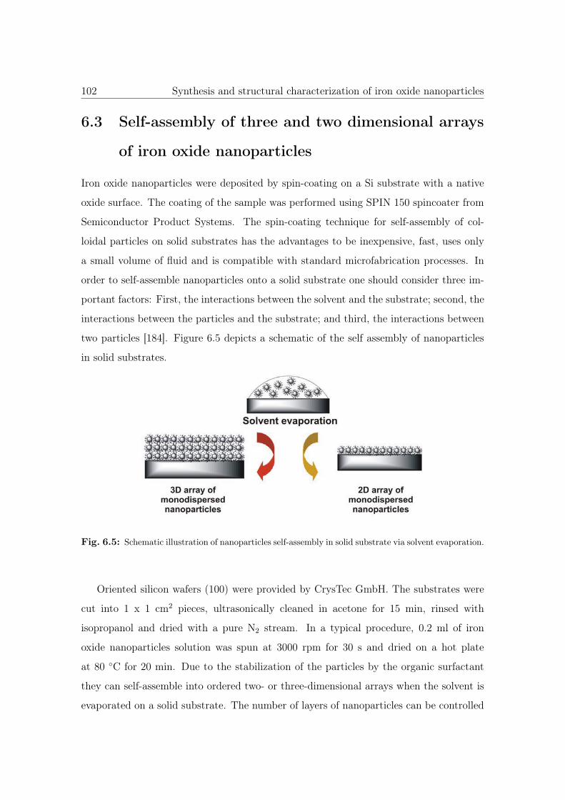
102 Synthesis and structural characterization of iron oxide nanoparticles
6.3 Self-assembly of three and two dimensional arrays
of iron oxide nanoparticles
Iron oxide nanoparticles were deposited by spin-coating on a Si substrate with a native
oxide surface. The coating of the sample was performed using SPIN 150 spincoater from
Semiconductor Product Systems. The spin-coating technique for self-assembly of col-
loidal particles on solid substrates has the advantages to be inexpensive, fast, uses only
a small volume of fluid and is compatible with standard microfabrication processes. In
order to self-assemble nanoparticles onto a solid substrate one should consider three im-
portant factors: First, the interactions between the solvent and the substrate; second, the
interactions between the particles and the substrate; and third, the interactions between
two particles [184]. Figure 6.5 depicts a schematic of the self assembly of nanoparticles
in solid substrates.
Fig. 6.5: Schematic illustration of nanoparticles self-assembly in solid substrate via solvent evaporation.
Oriented silicon wafers (100) were provided by CrysTec GmbH. The substrates were
cut into 1 x 1 cm2 pieces, ultrasonically cleaned in acetone for 15 min, rinsed with
isopropanol and dried with a pure N2 stream. In a typical procedure, 0.2 ml of iron
oxide nanoparticles solution was spun at 3000 rpm for 30 s and dried on a hot plate
at 80 ◦C for 20 min. Due to the stabilization of the particles by the organic surfactant
they can self-assemble into ordered two- or three-dimensional arrays when the solvent is
evaporated on a solid substrate. The number of layers of nanoparticles can be controlled
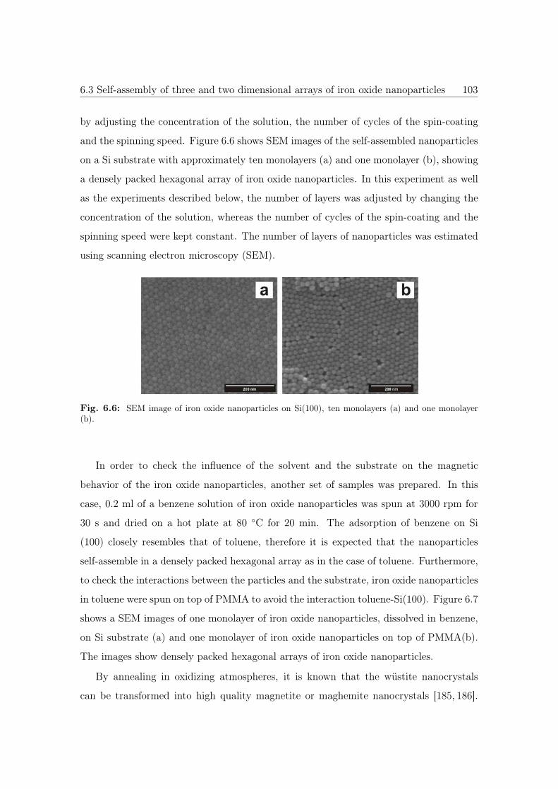
6.3 Self-assembly of three and two dimensional arrays of iron oxide nanoparticles 103
by adjusting the concentration of the solution, the number of cycles of the spin-coating
and the spinning speed. Figure 6.6 shows SEM images of the self-assembled nanoparticles
on a Si substrate with approximately ten monolayers (a) and one monolayer (b), showing
a densely packed hexagonal array of iron oxide nanoparticles. In this experiment as well
as the experiments described below, the number of layers was adjusted by changing the
concentration of the solution, whereas the number of cycles of the spin-coating and the
spinning speed were kept constant. The number of layers of nanoparticles was estimated
using scanning electron microscopy (SEM).
Fig. 6.6: SEM image of iron oxide nanoparticles on Si(100), ten monolayers (a) and one monolayer(b).
In order to check the influence of the solvent and the substrate on the magnetic
behavior of the iron oxide nanoparticles, another set of samples was prepared. In this
case, 0.2 ml of a benzene solution of iron oxide nanoparticles was spun at 3000 rpm for
30 s and dried on a hot plate at 80 ◦C for 20 min. The adsorption of benzene on Si
(100) closely resembles that of toluene, therefore it is expected that the nanoparticles
self-assemble in a densely packed hexagonal array as in the case of toluene. Furthermore,
to check the interactions between the particles and the substrate, iron oxide nanoparticles
in toluene were spun on top of PMMA to avoid the interaction toluene-Si(100). Figure 6.7
shows a SEM images of one monolayer of iron oxide nanoparticles, dissolved in benzene,
on Si substrate (a) and one monolayer of iron oxide nanoparticles on top of PMMA(b).
The images show densely packed hexagonal arrays of iron oxide nanoparticles.
By annealing in oxidizing atmospheres, it is known that the wüstite nanocrystals
can be transformed into high quality magnetite or maghemite nanocrystals [185, 186].
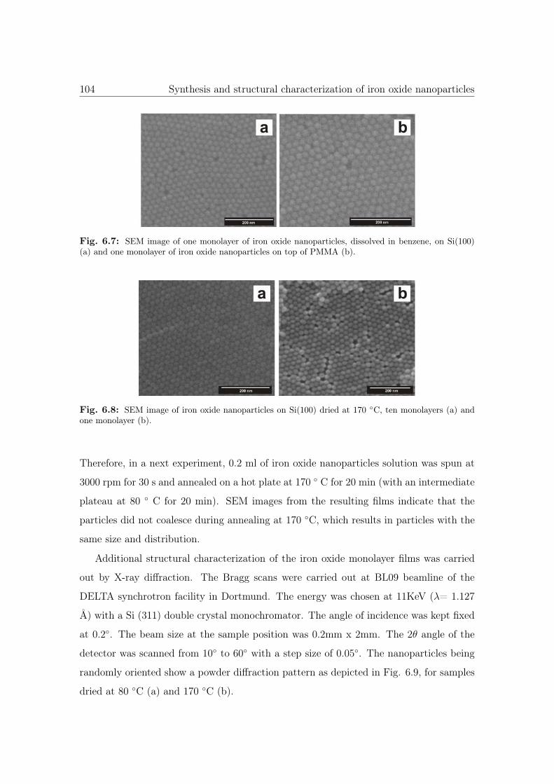
104 Synthesis and structural characterization of iron oxide nanoparticles
Fig. 6.7: SEM image of one monolayer of iron oxide nanoparticles, dissolved in benzene, on Si(100)(a) and one monolayer of iron oxide nanoparticles on top of PMMA (b).
Fig. 6.8: SEM image of iron oxide nanoparticles on Si(100) dried at 170 ◦C, ten monolayers (a) andone monolayer (b).
Therefore, in a next experiment, 0.2 ml of iron oxide nanoparticles solution was spun at
3000 rpm for 30 s and annealed on a hot plate at 170 ◦ C for 20 min (with an intermediate
plateau at 80 ◦ C for 20 min). SEM images from the resulting films indicate that the
particles did not coalesce during annealing at 170 ◦C, which results in particles with the
same size and distribution.
Additional structural characterization of the iron oxide monolayer films was carried
out by X-ray diffraction. The Bragg scans were carried out at BL09 beamline of the
DELTA synchrotron facility in Dortmund. The energy was chosen at 11KeV (λ= 1.127
Å) with a Si (311) double crystal monochromator. The angle of incidence was kept fixed
at 0.2◦. The beam size at the sample position was 0.2mm x 2mm. The 2θ angle of the
detector was scanned from 10◦ to 60◦ with a step size of 0.05◦. The nanoparticles being
randomly oriented show a powder diffraction pattern as depicted in Fig. 6.9, for samples
dried at 80 ◦C (a) and 170 ◦C (b).
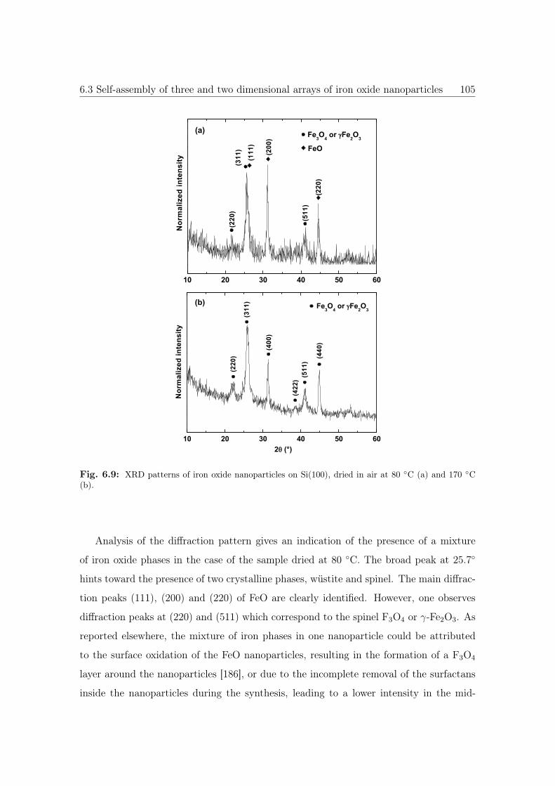
6.3 Self-assembly of three and two dimensional arrays of iron oxide nanoparticles 105
10 20 30 40 50 60
(a)
N
orm
aliz
ed in
tens
ity
FeO
Fe3O4 or γγFe2O3
(220
)(3
11)
(111
)
(200
)
(511
)
(220
)
10 20 30 40 50 60
���
(311
)
(422
)
�θθ � ���
���� � ��� γγ�����
Nor
mal
ized
inte
nsity
(220
)
(511
)
(400
)
(440
)
Fig. 6.9: XRD patterns of iron oxide nanoparticles on Si(100), dried in air at 80 ◦C (a) and 170 ◦C(b).
Analysis of the diffraction pattern gives an indication of the presence of a mixture
of iron oxide phases in the case of the sample dried at 80 ◦C. The broad peak at 25.7◦
hints toward the presence of two crystalline phases, wüstite and spinel. The main diffrac-
tion peaks (111), (200) and (220) of FeO are clearly identified. However, one observes
diffraction peaks at (220) and (511) which correspond to the spinel F3O4 or γ-Fe2O3. As
reported elsewhere, the mixture of iron phases in one nanoparticle could be attributed
to the surface oxidation of the FeO nanoparticles, resulting in the formation of a F3O4
layer around the nanoparticles [186], or due to the incomplete removal of the surfactans
inside the nanoparticles during the synthesis, leading to a lower intensity in the mid-
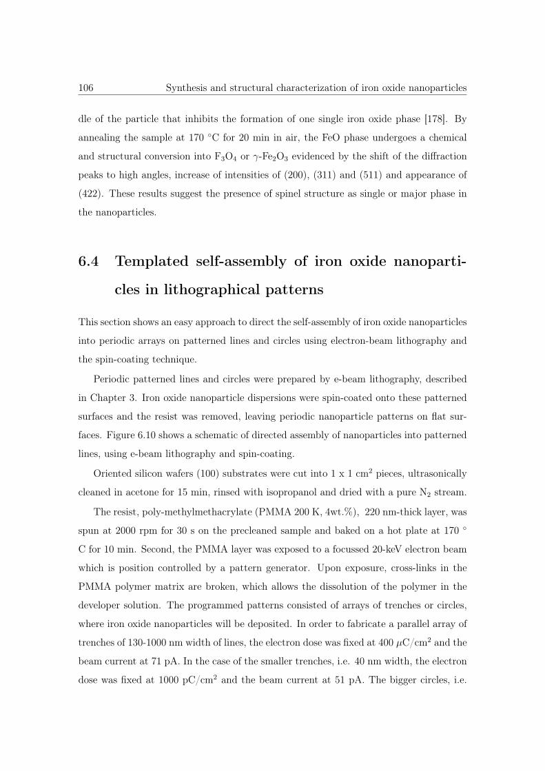
106 Synthesis and structural characterization of iron oxide nanoparticles
dle of the particle that inhibits the formation of one single iron oxide phase [178]. By
annealing the sample at 170 ◦C for 20 min in air, the FeO phase undergoes a chemical
and structural conversion into F3O4 or γ-Fe2O3 evidenced by the shift of the diffraction
peaks to high angles, increase of intensities of (200), (311) and (511) and appearance of
(422). These results suggest the presence of spinel structure as single or major phase in
the nanoparticles.
6.4 Templated self-assembly of iron oxide nanoparti-
cles in lithographical patterns
This section shows an easy approach to direct the self-assembly of iron oxide nanoparticles
into periodic arrays on patterned lines and circles using electron-beam lithography and
the spin-coating technique.
Periodic patterned lines and circles were prepared by e-beam lithography, described
in Chapter 3. Iron oxide nanoparticle dispersions were spin-coated onto these patterned
surfaces and the resist was removed, leaving periodic nanoparticle patterns on flat sur-
faces. Figure 6.10 shows a schematic of directed assembly of nanoparticles into patterned
lines, using e-beam lithography and spin-coating.
Oriented silicon wafers (100) substrates were cut into 1 x 1 cm2 pieces, ultrasonically
cleaned in acetone for 15 min, rinsed with isopropanol and dried with a pure N2 stream.
The resist, poly-methylmethacrylate (PMMA 200 K, 4wt.%), 220 nm-thick layer, was
spun at 2000 rpm for 30 s on the precleaned sample and baked on a hot plate at 170 ◦
C for 10 min. Second, the PMMA layer was exposed to a focussed 20-keV electron beam
which is position controlled by a pattern generator. Upon exposure, cross-links in the
PMMA polymer matrix are broken, which allows the dissolution of the polymer in the
developer solution. The programmed patterns consisted of arrays of trenches or circles,
where iron oxide nanoparticles will be deposited. In order to fabricate a parallel array of
trenches of 130-1000 nm width of lines, the electron dose was fixed at 400 μC/cm2 and the
beam current at 71 pA. In the case of the smaller trenches, i.e. 40 nm width, the electron
dose was fixed at 1000 pC/cm2 and the beam current at 51 pA. The bigger circles, i.e.
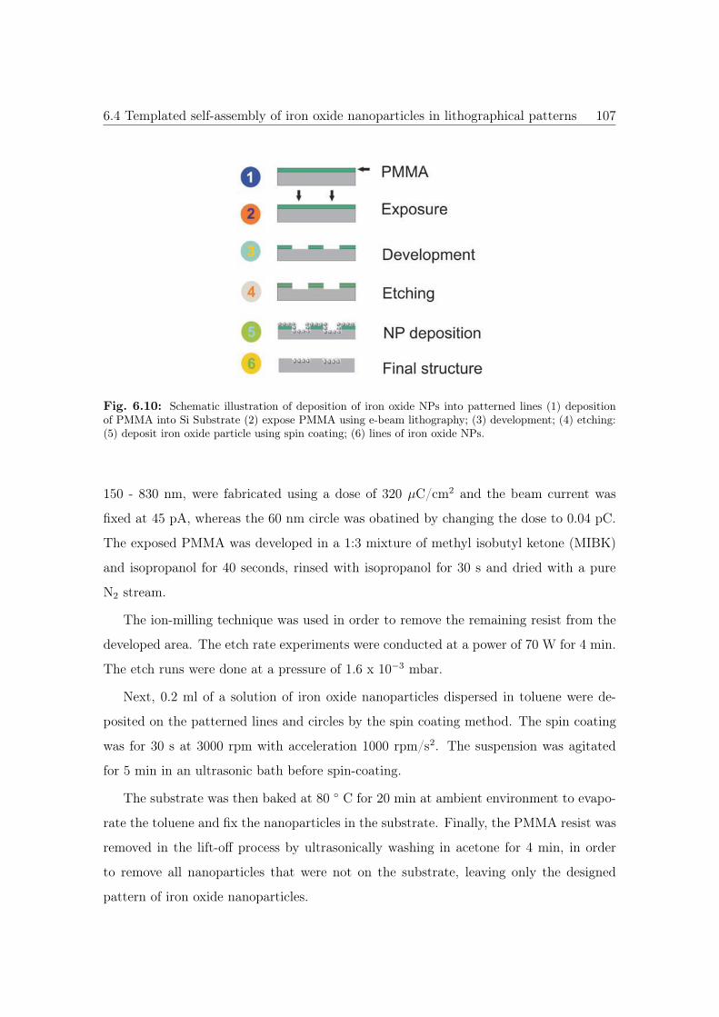
6.4 Templated self-assembly of iron oxide nanoparticles in lithographical patterns 107
Fig. 6.10: Schematic illustration of deposition of iron oxide NPs into patterned lines (1) depositionof PMMA into Si Substrate (2) expose PMMA using e-beam lithography; (3) development; (4) etching:(5) deposit iron oxide particle using spin coating; (6) lines of iron oxide NPs.
150 - 830 nm, were fabricated using a dose of 320 μC/cm2 and the beam current was
fixed at 45 pA, whereas the 60 nm circle was obatined by changing the dose to 0.04 pC.
The exposed PMMA was developed in a 1:3 mixture of methyl isobutyl ketone (MIBK)
and isopropanol for 40 seconds, rinsed with isopropanol for 30 s and dried with a pure
N2 stream.
The ion-milling technique was used in order to remove the remaining resist from the
developed area. The etch rate experiments were conducted at a power of 70 W for 4 min.
The etch runs were done at a pressure of 1.6 x 10⁻³ mbar.
Next, 0.2 ml of a solution of iron oxide nanoparticles dispersed in toluene were de-
posited on the patterned lines and circles by the spin coating method. The spin coating
was for 30 s at 3000 rpm with acceleration 1000 rpm/s2. The suspension was agitated
for 5 min in an ultrasonic bath before spin-coating.
The substrate was then baked at 80 ◦ C for 20 min at ambient environment to evapo-
rate the toluene and fix the nanoparticles in the substrate. Finally, the PMMA resist was
removed in the lift-off process by ultrasonically washing in acetone for 4 min, in order
to remove all nanoparticles that were not on the substrate, leaving only the designed
pattern of iron oxide nanoparticles.
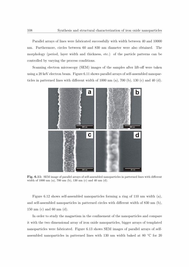
108 Synthesis and structural characterization of iron oxide nanoparticles
Parallel arrays of lines were fabricated successfully with width between 40 and 10000
nm. Furthermore, circles between 60 and 830 nm diameter were also obtained. The
morphology (period, layer width and thickness, etc.) of the particle patterns can be
controlled by varying the process conditions.
Scanning electron microscopy (SEM) images of the samples after lift-off were taken
using a 20 keV electron beam. Figure 6.11 shows parallel arrays of self-assembled nanopar-
ticles in patterned lines with different width of 1000 nm (a), 700 (b), 130 (c) and 40 (d).
Fig. 6.11: SEM image of parallel arrays of self-assembled nanoparticles in patterned lines with differentwidth of 1000 nm (a), 700 nm (b), 130 nm (c) and 40 nm (d).
Figure 6.12 shows self-assembled nanoparticles forming a ring of 110 nm width (a),
and self-assembled nanoparticles in patterned circles with different width of 830 nm (b),
150 nm (c) and 60 nm (d).
In order to study the magnetism in the confinement of the nanoparticles and compare
it with the two dimensional array of iron oxide nanoparticles, bigger arrays of templated
nanoparticles were fabricated. Figure 6.13 shows SEM images of parallel arrays of self-
assembled nanoparticles in patterned lines with 130 nm width baked at 80 ◦C for 20
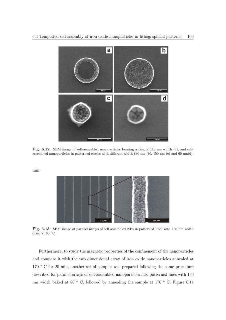
6.4 Templated self-assembly of iron oxide nanoparticles in lithographical patterns 109
Fig. 6.12: SEM image of self-assembled nanoparticles forming a ring of 110 nm width (a), and self-assembled nanoparticles in patterned circles with different width 830 nm (b), 150 nm (c) and 60 nm(d).
min.
Fig. 6.13: SEM image of parallel arrays of self-assembled NPs in patterned lines with 130 nm widthdried at 80 ◦C.
Furthermore, to study the magnetic properties of the confinement of the nanoparticles
and compare it with the two dimensional array of iron oxide nanoparticles annealed at
170 ◦ C for 20 min, another set of samples was prepared following the same procedure
described for parallel arrays of self-assembled nanoparticles into patterned lines with 130
nm width baked at 80 ◦ C, followed by annealing the sample at 170 ◦ C. Figure 6.14
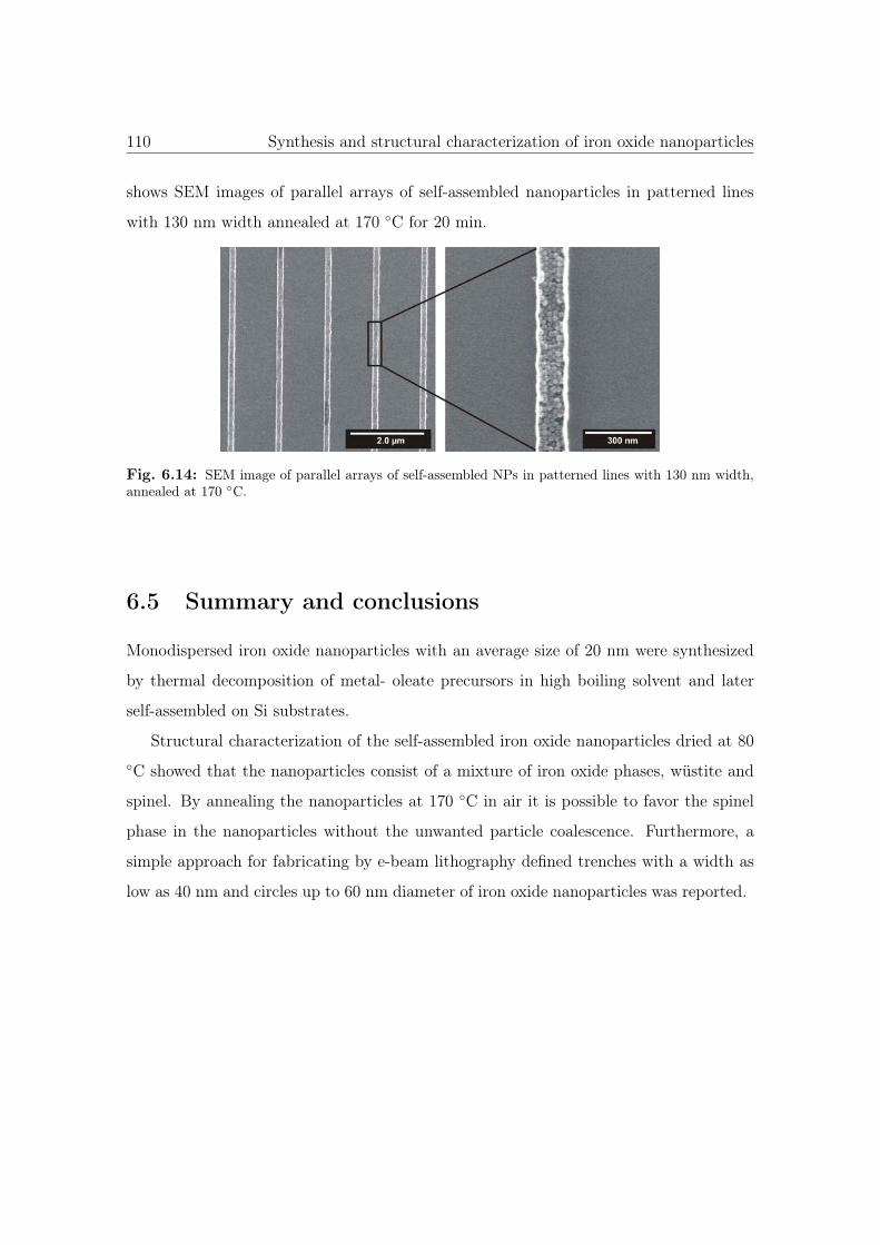
110 Synthesis and structural characterization of iron oxide nanoparticles
shows SEM images of parallel arrays of self-assembled nanoparticles in patterned lines
with 130 nm width annealed at 170 ◦C for 20 min.
Fig. 6.14: SEM image of parallel arrays of self-assembled NPs in patterned lines with 130 nm width,annealed at 170 ◦C.
6.5 Summary and conclusions
Monodispersed iron oxide nanoparticles with an average size of 20 nm were synthesized
by thermal decomposition of metal- oleate precursors in high boiling solvent and later
self-assembled on Si substrates.
Structural characterization of the self-assembled iron oxide nanoparticles dried at 80◦C showed that the nanoparticles consist of a mixture of iron oxide phases, wüstite and
spinel. By annealing the nanoparticles at 170 ◦C in air it is possible to favor the spinel
phase in the nanoparticles without the unwanted particle coalescence. Furthermore, a
simple approach for fabricating by e-beam lithography defined trenches with a width as
low as 40 nm and circles up to 60 nm diameter of iron oxide nanoparticles was reported.
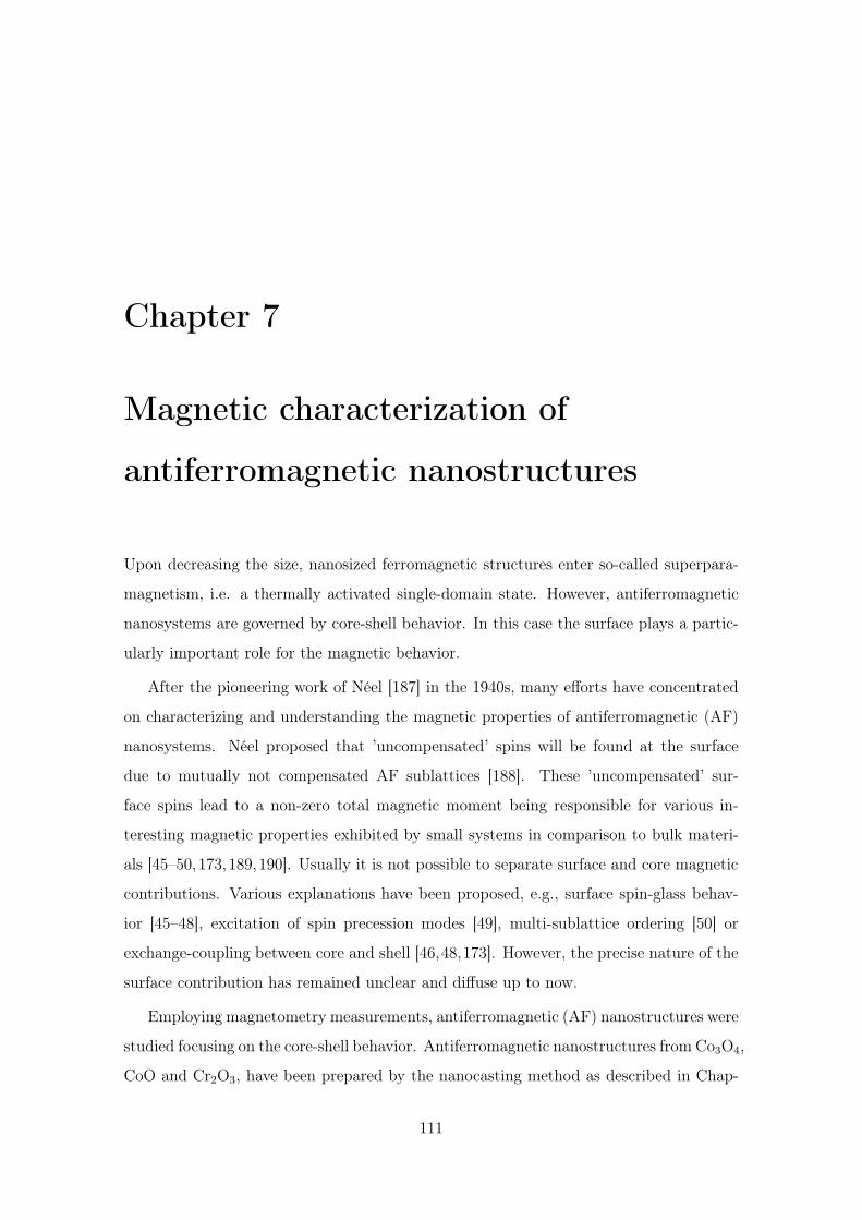
Chapter 7
Magnetic characterization of
antiferromagnetic nanostructures
Upon decreasing the size, nanosized ferromagnetic structures enter so-called superpara-
magnetism, i.e. a thermally activated single-domain state. However, antiferromagnetic
nanosystems are governed by core-shell behavior. In this case the surface plays a partic-
ularly important role for the magnetic behavior.
After the pioneering work of Néel [187] in the 1940s, many efforts have concentrated
on characterizing and understanding the magnetic properties of antiferromagnetic (AF)
nanosystems. Néel proposed that ’uncompensated’ spins will be found at the surface
due to mutually not compensated AF sublattices [188]. These ’uncompensated’ sur-
face spins lead to a non-zero total magnetic moment being responsible for various in-
teresting magnetic properties exhibited by small systems in comparison to bulk materi-
als [45–50,173,189,190]. Usually it is not possible to separate surface and core magnetic
contributions. Various explanations have been proposed, e.g., surface spin-glass behav-
ior [45–48], excitation of spin precession modes [49], multi-sublattice ordering [50] or
exchange-coupling between core and shell [46,48,173]. However, the precise nature of the
surface contribution has remained unclear and diffuse up to now.
Employing magnetometry measurements, antiferromagnetic (AF) nanostructures were
studied focusing on the core-shell behavior. Antiferromagnetic nanostructures from Co3O4,
CoO and Cr2O3, have been prepared by the nanocasting method as described in Chap-
111
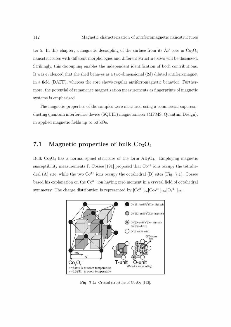
112 Magnetic characterization of antiferromagnetic nanostructures
ter 5. In this chapter, a magnetic decoupling of the surface from its AF core in Co3O4
nanostructures with different morphologies and different structure sizes will be discussed.
Strikingly, this decoupling enables the independent identification of both contributions.
It was evidenced that the shell behaves as a two-dimensional (2d) diluted antiferromagnet
in a field (DAFF), whereas the core shows regular antiferromagnetic behavior. Further-
more, the potential of remanence magnetization measurements as fingerprints of magnetic
systems is emphasized.
The magnetic properties of the samples were measured using a commercial supercon-
ducting quantum interference device (SQUID) magnetometer (MPMS, Quantum Design),
in applied magnetic fields up to 50 kOe.
7.1 Magnetic properties of bulk Co3O4
Bulk Co3O4 has a normal spinel structure of the form AB2O4. Employing magnetic
susceptibility measurements P. Cossee [191] proposed that Co2+ ions occupy the tetrahe-
dral (A) site, while the two Co3+ ions occupy the octahedral (B) sites (Fig. 7.1). Cossee
based his explanation on the Co3+ ion having zero moment in a crystal field of octahedral
symmetry. The charge distribution is represented by [Co2+]8a[Co23+]16d[O4
2−]32e.
Fig. 7.1: Crystal structure of Co3O4 [192].
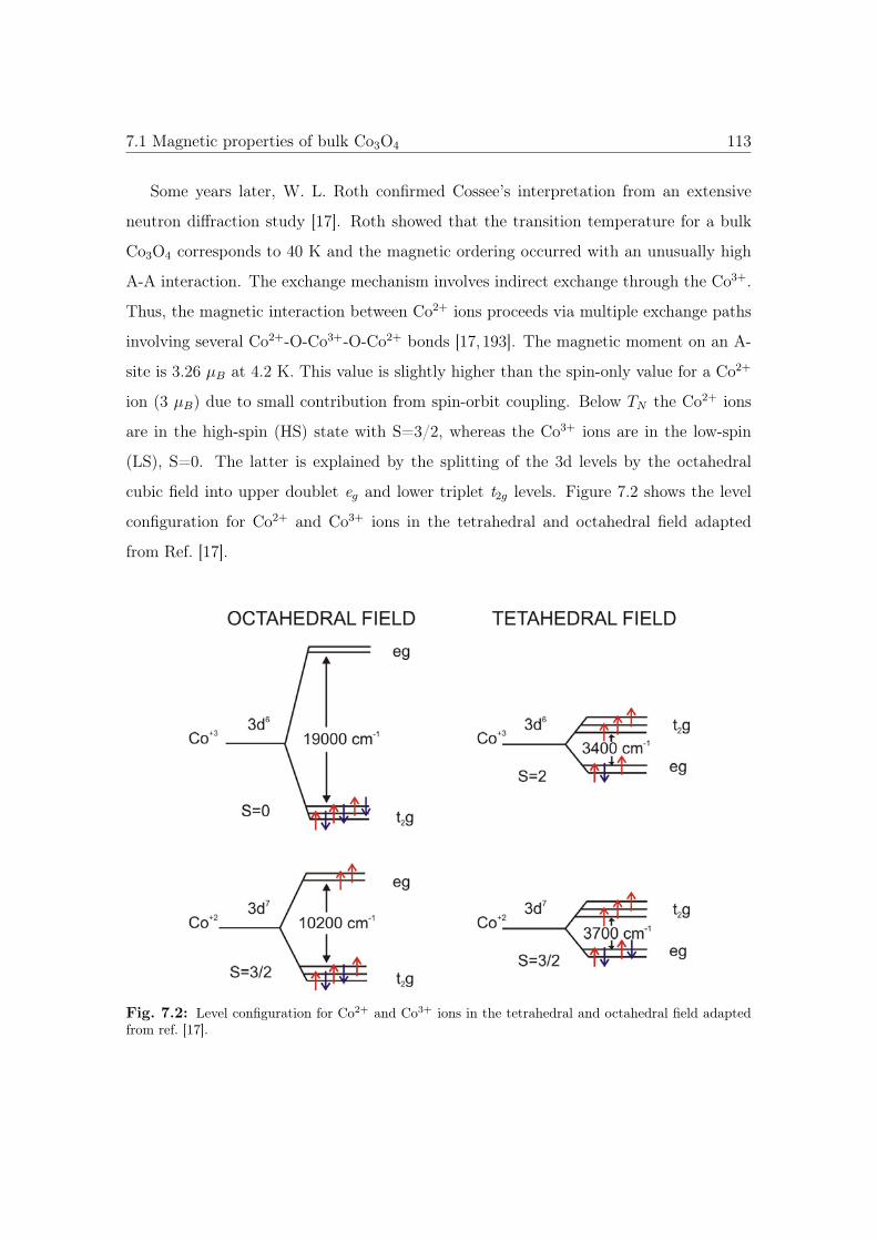
7.1 Magnetic properties of bulk Co3O4 113
Some years later, W. L. Roth confirmed Cossee’s interpretation from an extensive
neutron diffraction study [17]. Roth showed that the transition temperature for a bulk
Co3O4 corresponds to 40 K and the magnetic ordering occurred with an unusually high
A-A interaction. The exchange mechanism involves indirect exchange through the Co3+.
Thus, the magnetic interaction between Co2+ ions proceeds via multiple exchange paths
involving several Co2+-O-Co3+-O-Co2+ bonds [17, 193]. The magnetic moment on an A-
site is 3.26 μB at 4.2 K. This value is slightly higher than the spin-only value for a Co2+
ion (3 μB) due to small contribution from spin-orbit coupling. Below TN the Co2+ ions
are in the high-spin (HS) state with S=3/2, whereas the Co3+ ions are in the low-spin
(LS), S=0. The latter is explained by the splitting of the 3d levels by the octahedral
cubic field into upper doublet eg and lower triplet t2g levels. Figure 7.2 shows the level
configuration for Co2+ and Co3+ ions in the tetrahedral and octahedral field adapted
from Ref. [17].
Fig. 7.2: Level configuration for Co2+ and Co3+ ions in the tetrahedral and octahedral field adaptedfrom ref. [17].
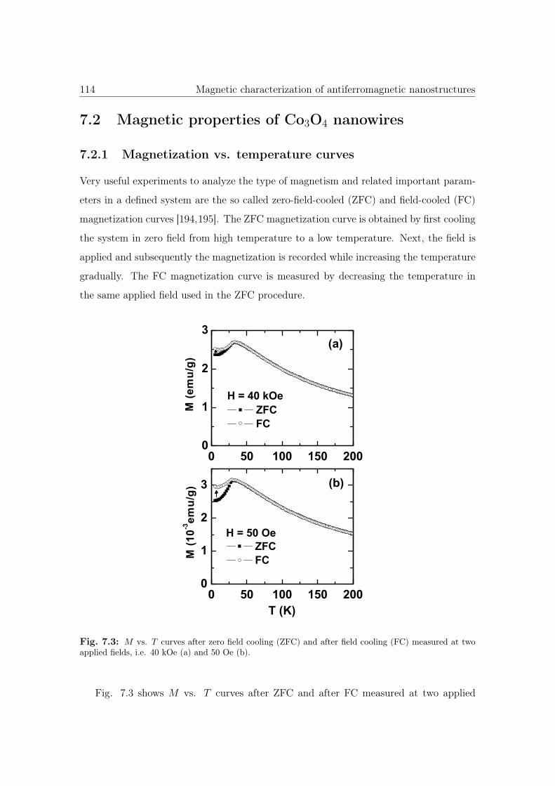
114 Magnetic characterization of antiferromagnetic nanostructures
7.2 Magnetic properties of Co3O4 nanowires
7.2.1 Magnetization vs. temperature curves
Very useful experiments to analyze the type of magnetism and related important param-
eters in a defined system are the so called zero-field-cooled (ZFC) and field-cooled (FC)
magnetization curves [194,195]. The ZFC magnetization curve is obtained by first cooling
the system in zero field from high temperature to a low temperature. Next, the field is
applied and subsequently the magnetization is recorded while increasing the temperature
gradually. The FC magnetization curve is measured by decreasing the temperature in
the same applied field used in the ZFC procedure.
0 50 100 150 2000
1
2
3
0 50 100 150 2000
1
2
3
(a)
T (K)
M (1
0-3em
u/g)
ZFC FC
M (e
mu/
g)
H = 40 kOe
(b)
H = 50 Oe ZFC FC
Fig. 7.3: M vs. T curves after zero field cooling (ZFC) and after field cooling (FC) measured at twoapplied fields, i.e. 40 kOe (a) and 50 Oe (b).
Fig. 7.3 shows M vs. T curves after ZFC and after FC measured at two applied
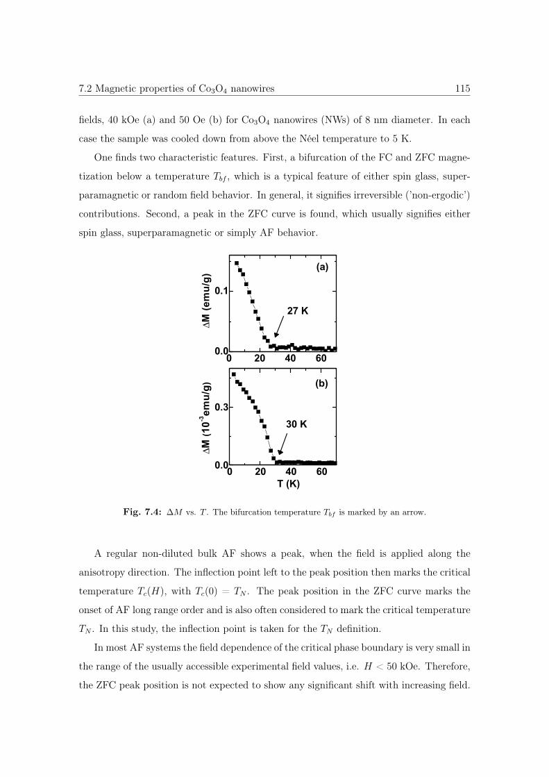
7.2 Magnetic properties of Co3O4 nanowires 115
fields, 40 kOe (a) and 50 Oe (b) for Co3O4 nanowires (NWs) of 8 nm diameter. In each
case the sample was cooled down from above the Néel temperature to 5 K.
One finds two characteristic features. First, a bifurcation of the FC and ZFC magne-
tization below a temperature Tbf , which is a typical feature of either spin glass, super-
paramagnetic or random field behavior. In general, it signifies irreversible (’non-ergodic’)
contributions. Second, a peak in the ZFC curve is found, which usually signifies either
spin glass, superparamagnetic or simply AF behavior.
0 20 40 600.0
0.1
0 20 40 600.0
0.3
(a)
27 K
ΔM (1
0-3em
u/g)
ΔM (e
mu/
g)
T (K)
(b)
30 K
Fig. 7.4: ΔM vs. T . The bifurcation temperature Tbf is marked by an arrow.
A regular non-diluted bulk AF shows a peak, when the field is applied along the
anisotropy direction. The inflection point left to the peak position then marks the critical
temperature Tc(H), with Tc(0) = TN . The peak position in the ZFC curve marks the
onset of AF long range order and is also often considered to mark the critical temperature
TN . In this study, the inflection point is taken for the TN definition.
In most AF systems the field dependence of the critical phase boundary is very small in
the range of the usually accessible experimental field values, i.e. H < 50 kOe. Therefore,
the ZFC peak position is not expected to show any significant shift with increasing field.
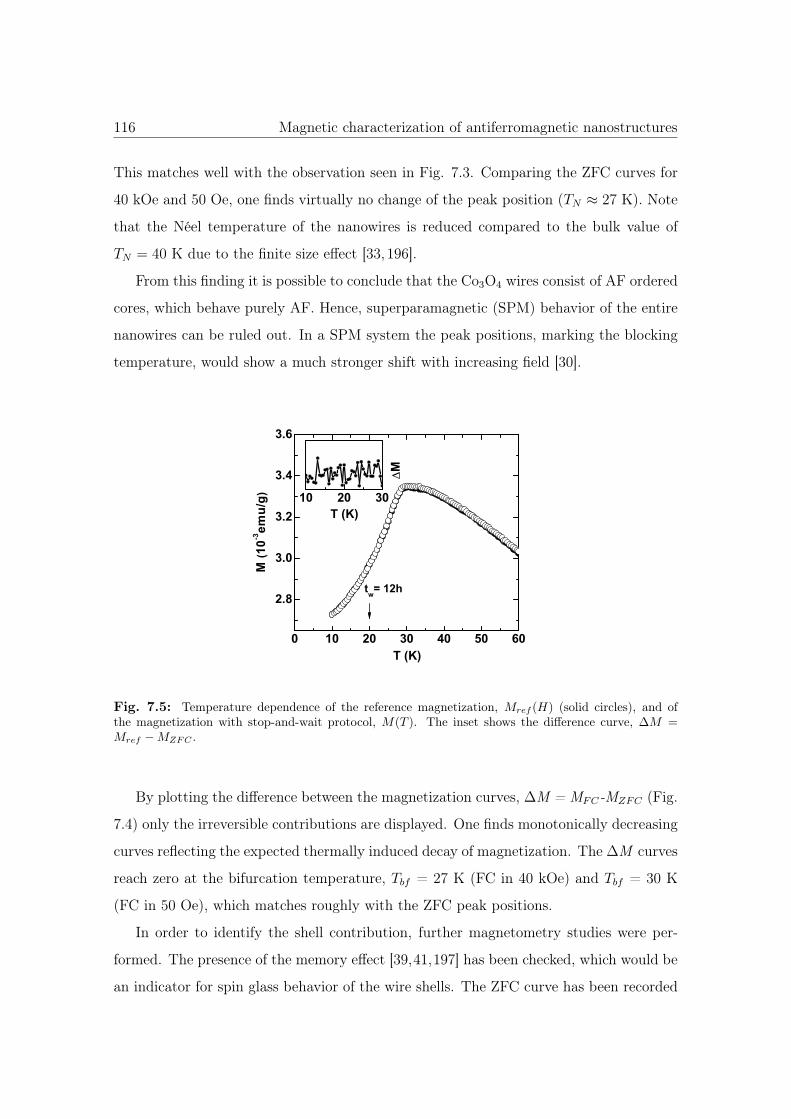
116 Magnetic characterization of antiferromagnetic nanostructures
This matches well with the observation seen in Fig. 7.3. Comparing the ZFC curves for
40 kOe and 50 Oe, one finds virtually no change of the peak position (TN ≈ 27 K). Note
that the Néel temperature of the nanowires is reduced compared to the bulk value of
TN = 40 K due to the finite size effect [33, 196].
From this finding it is possible to conclude that the Co3O4 wires consist of AF ordered
cores, which behave purely AF. Hence, superparamagnetic (SPM) behavior of the entire
nanowires can be ruled out. In a SPM system the peak positions, marking the blocking
temperature, would show a much stronger shift with increasing field [30].
0 10 20 30 40 50 60
2.8
3.0
3.2
3.4
3.6
10 20 30T (K)
ΔM
tw= 12h
T (K)
M (1
0-3em
u/g)
Fig. 7.5: Temperature dependence of the reference magnetization, Mref (H) (solid circles), and ofthe magnetization with stop-and-wait protocol, M(T ). The inset shows the difference curve, ΔM =Mref − MZFC .
By plotting the difference between the magnetization curves, ΔM = MFC-MZFC (Fig.
7.4) only the irreversible contributions are displayed. One finds monotonically decreasing
curves reflecting the expected thermally induced decay of magnetization. The ΔM curves
reach zero at the bifurcation temperature, Tbf = 27 K (FC in 40 kOe) and Tbf = 30 K
(FC in 50 Oe), which matches roughly with the ZFC peak positions.
In order to identify the shell contribution, further magnetometry studies were per-
formed. The presence of the memory effect [39,41,197] has been checked, which would be
an indicator for spin glass behavior of the wire shells. The ZFC curve has been recorded
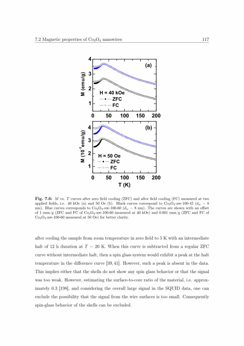
7.2 Magnetic properties of Co3O4 nanowires 117
0 50 100 150 200
1
2
3
4
0 50 100 150 200
1
2
3
4
M
(em
u/g)
(a)
T (K)
M (1
0-3em
u/g)
ZFC FC
H = 40 kOe
ZFC FC
(b)
H = 50 Oe
Fig. 7.6: M vs. T curves after zero field cooling (ZFC) and after field cooling (FC) measured at twoapplied fields, i.e. 40 kOe (a) and 50 Oe (b). Black curves correspond to Co3O4-nw-100-45 (dw = 8nm). Blue curves corresponds to Co3O4-nw-100-60 (dw = 8 nm). The curves are shown with an offsetof 1 emu/g (ZFC and FC of Co3O4-nw-100-60 measured at 40 kOe) and 0.001 emu/g (ZFC and FC ofCo3O4-nw-100-60 measured at 50 Oe) for better clarity.
after cooling the sample from room temperature in zero field to 5 K with an intermediate
halt of 12 h duration at T = 20 K. When this curve is subtracted from a regular ZFC
curve without intermediate halt, then a spin glass system would exhibit a peak at the halt
temperature in the difference curve [39, 41]. However, such a peak is absent in the data.
This implies either that the shells do not show any spin glass behavior or that the signal
was too weak. However, estimating the surface-to-core ratio of the material, i.e. approx-
imately 0.3 [198], and considering the overall large signal in the SQUID data, one can
exclude the possibility that the signal from the wire surfaces is too small. Consequently
spin-glass behavior of the shells can be excluded.
118 Magnetic characterization of antiferromagnetic nanostructures
It has been shown that using the nanocasting strategy it is possible to synthesize
Co3O4 nanowires with different connectivities and different diameters (dw). To verify that
the Néel temperature found for 8 nm wires replicated from SBA-15-100-50 is independent
of the connectivity between the wires and scales with the diameter due to the finite size
effect [33], magnetization vs. temperature curves at an applied field of 50 Oe and 40
kOe on Co3O4 nanowires with different connectivities and with different diameters were
studied.
Fig.7.6 shows magnetization vs. temperature curves measured at 50 Oe (b) and
40 kOe(a) on Co3O4-nw-100-45 and Co3O4-nw-100-60. For all connectivities, the M
vs. T curves exhibit a splitting of the zero-field-cooled (ZFC) and field-cooled (FC)
magnetization below a splitting temperature Ts. All the samples show one peak at a
temperature T1 = 27 K in the ZFC curve, which marks the critical temperature. These
results are quantitatively equal to the ones obtained for dw = 8 nm.
Magnetization vs. temperature curves at an applied field of 50 Oe and 40 kOe on
Co3O4 nanowires with different diameters, dw = 5, 6, 7 and 9 nm, are shown in Fig.7.7
(b) and (a) respectively. For all sizes, the M vs. T curves exhibit a splitting of the zero-
field-cooled (ZFC) and field-cooled (FC) magnetization below a splitting temperature Ts.
The sample with dw = 9 nm shows one peak at a temperature T1 = 31 K in the ZFC
curve, which marks the critical temperature. These results are qualitatively similar to
the ones obtained for dw = 8 nm.
Surprisingly, for diameters smaller than 8 nm the ZFC magnetization curves exhibit
a second peak at a lower temperature, T2 (Fig. 7.7). This could evidence a second
magnetic sub-system. HRSEM and TEM images of the samples (Fig. 5.13) exclude the
trivial possibility of two distinct types of wires, which would give two separate magnetic
contributions. Rather one assumes that the two peaks signify a decoupled core-shell
behavior, where the first peak at T1 marks the critical temperature of the wire cores
and the second one at the lower temperature T2 the (non-critical) contribution from the
shells. Due to the reduced dimensionality of the shell the transition temperature will
be reduced. Moreover, the field-dependence of the two peaks should show a different
behavior. While for most AF materials T1 = Tc(H) is independent of the magnetic field,
the second temperature T2 of the 2d-shell is expected to show a stronger field-dependence
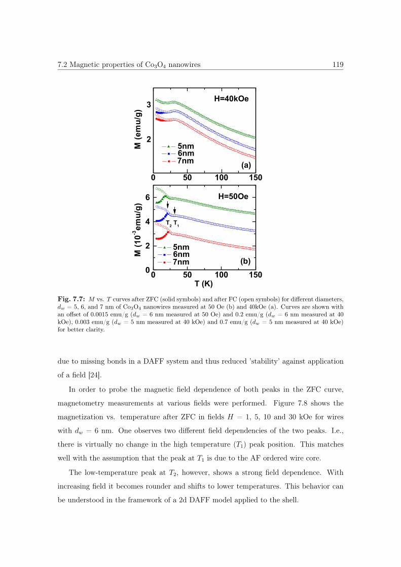
7.2 Magnetic properties of Co3O4 nanowires 119
0 50 100 1500
2
4
6
0 50 100 150
2
3
T1T2
(b)
H=50Oe
H=40kOe
T (K)
(a)
M (1
0-3em
u/g)
M (e
mu/
g)
7nm 6nm
5nm
7nm 6nm 5nm
Fig. 7.7: M vs. T curves after ZFC (solid symbols) and after FC (open symbols) for different diameters,dw = 5, 6, and 7 nm of Co3O4 nanowires measured at 50 Oe (b) and 40kOe (a). Curves are shown withan offset of 0.0015 emu/g (dw = 6 nm measured at 50 Oe) and 0.2 emu/g (dw = 6 nm measured at 40kOe), 0.003 emu/g (dw = 5 nm measured at 40 kOe) and 0.7 emu/g (dw = 5 nm measured at 40 kOe)for better clarity.
due to missing bonds in a DAFF system and thus reduced ’stability’ against application
of a field [24].
In order to probe the magnetic field dependence of both peaks in the ZFC curve,
magnetometry measurements at various fields were performed. Figure 7.8 shows the
magnetization vs. temperature after ZFC in fields H = 1, 5, 10 and 30 kOe for wires
with dw = 6 nm. One observes two different field dependencies of the two peaks. I.e.,
there is virtually no change in the high temperature (T1) peak position. This matches
well with the assumption that the peak at T1 is due to the AF ordered wire core.
The low-temperature peak at T2, however, shows a strong field dependence. With
increasing field it becomes rounder and shifts to lower temperatures. This behavior can
be understood in the framework of a 2d DAFF model applied to the shell.
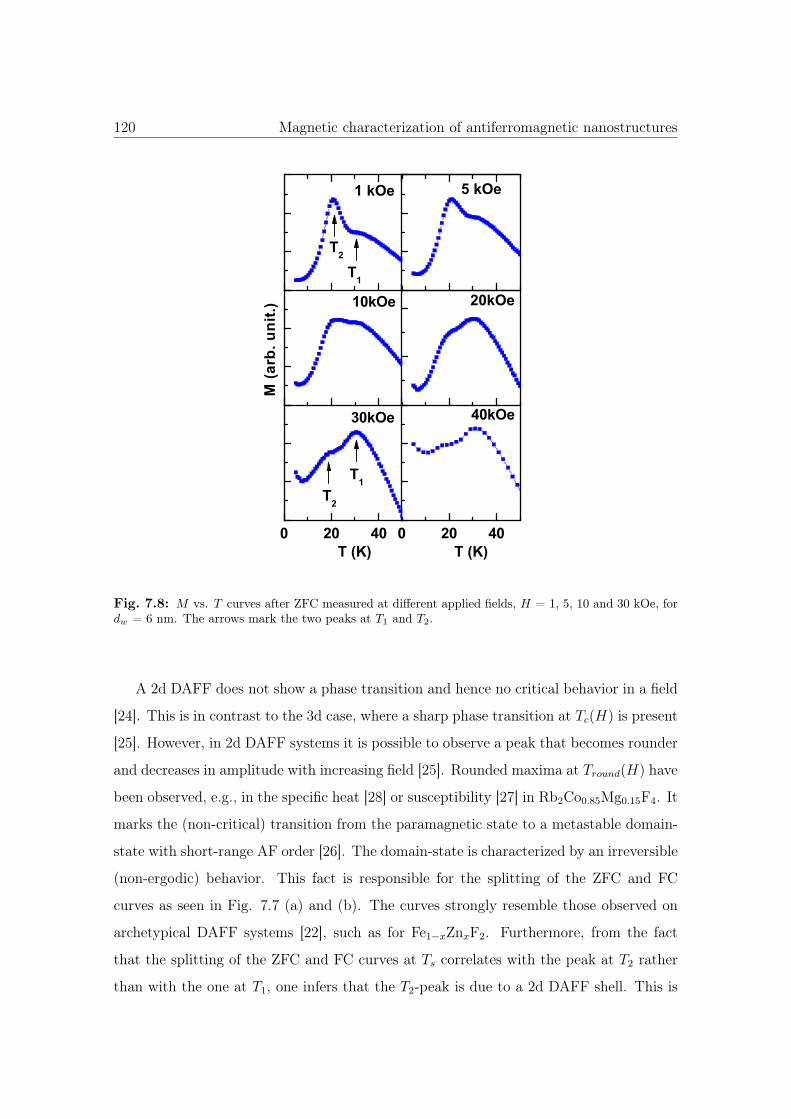
120 Magnetic characterization of antiferromagnetic nanostructures
0 20 40 0 20 40
T1
T1
T2
1 kOe
5 kOe
10kOe
M (a
rb. u
nit.)
T (K)T (K)
40kOe30kOe
20kOe
T2
Fig. 7.8: M vs. T curves after ZFC measured at different applied fields, H = 1, 5, 10 and 30 kOe, fordw = 6 nm. The arrows mark the two peaks at T1 and T2.
A 2d DAFF does not show a phase transition and hence no critical behavior in a field
[24]. This is in contrast to the 3d case, where a sharp phase transition at Tc(H) is present
[25]. However, in 2d DAFF systems it is possible to observe a peak that becomes rounder
and decreases in amplitude with increasing field [25]. Rounded maxima at Tround(H) have
been observed, e.g., in the specific heat [28] or susceptibility [27] in Rb2Co0.85Mg0.15F4. It
marks the (non-critical) transition from the paramagnetic state to a metastable domain-
state with short-range AF order [26]. The domain-state is characterized by an irreversible
(non-ergodic) behavior. This fact is responsible for the splitting of the ZFC and FC
curves as seen in Fig. 7.7 (a) and (b). The curves strongly resemble those observed on
archetypical DAFF systems [22], such as for Fe1−xZnxF2. Furthermore, from the fact
that the splitting of the ZFC and FC curves at Ts correlates with the peak at T2 rather
than with the one at T1, one infers that the T2-peak is due to a 2d DAFF shell. This is
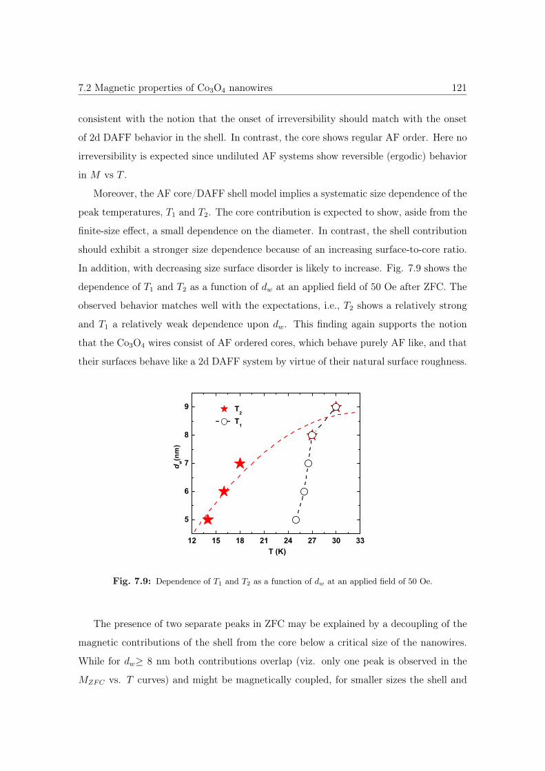
7.2 Magnetic properties of Co3O4 nanowires 121
consistent with the notion that the onset of irreversibility should match with the onset
of 2d DAFF behavior in the shell. In contrast, the core shows regular AF order. Here no
irreversibility is expected since undiluted AF systems show reversible (ergodic) behavior
in M vs T .
Moreover, the AF core/DAFF shell model implies a systematic size dependence of the
peak temperatures, T1 and T2. The core contribution is expected to show, aside from the
finite-size effect, a small dependence on the diameter. In contrast, the shell contribution
should exhibit a stronger size dependence because of an increasing surface-to-core ratio.
In addition, with decreasing size surface disorder is likely to increase. Fig. 7.9 shows the
dependence of T1 and T2 as a function of dw at an applied field of 50 Oe after ZFC. The
observed behavior matches well with the expectations, i.e., T2 shows a relatively strong
and T1 a relatively weak dependence upon dw. This finding again supports the notion
that the Co3O4 wires consist of AF ordered cores, which behave purely AF like, and that
their surfaces behave like a 2d DAFF system by virtue of their natural surface roughness.
12 15 18 21 24 27 30 33
5
6
7
8
9 T2
T1
d w(n
m)
T (K)
Fig. 7.9: Dependence of T1 and T2 as a function of dw at an applied field of 50 Oe.
The presence of two separate peaks in ZFC may be explained by a decoupling of the
magnetic contributions of the shell from the core below a critical size of the nanowires.
While for dw≥ 8 nm both contributions overlap (viz. only one peak is observed in the
MZFC vs. T curves) and might be magnetically coupled, for smaller sizes the shell and
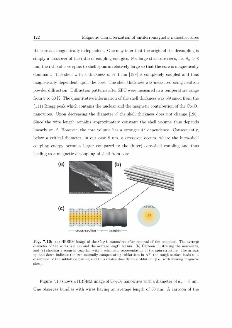
122 Magnetic characterization of antiferromagnetic nanostructures
the core act magnetically independent. One may infer that the origin of the decoupling is
simply a crossover of the ratio of coupling energies. For large structure sizes, i.e. dw > 8
nm, the ratio of core spins to shell spins is relatively large so that the core is magnetically
dominant. The shell with a thickness of ≈ 1 nm [198] is completely coupled and thus
magnetically dependent upon the core. The shell thickness was measured using neutron
powder diffraction. Diffraction patterns after ZFC were measured in a temperature range
from 5 to 60 K. The quantitative information of the shell thickness was obtained from the
(111) Bragg peak which contains the nuclear and the magnetic contribution of the Co3O4
nanowires. Upon decreasing the diameter d the shell thickness does not change [198].
Since the wire length remains approximately constant the shell volume thus depends
linearly on d. However, the core volume has a stronger d 2 dependence. Consequently,
below a critical diameter, in our case 8 nm, a crossover occurs, where the intra-shell
coupling energy becomes larger compared to the (inter) core-shell coupling and thus
leading to a magnetic decoupling of shell from core.
Fig. 7.10: (a) HRSEM image of the Co3O4 nanowires after removal of the template. The averagediameter of the wires is 8 nm and the average length 50 nm. (b) Cartoon illustrating the nanowires,and (c) showing a zoom-in together with a schematic representation of the spin-structure. The arrowsup and down indicate the two mutually compensating sublattices in AF, the rough surface leads to adisruption of the sublattice pairing and thus relates directly to a ’dilution’ (i.e. with missing magneticsites).
Figure 7.10 shows a HRSEM image of Co3O4 nanowires with a diameter of dw = 8 nm.
One observes bundles with wires having an average length of 50 nm. A cartoon of the
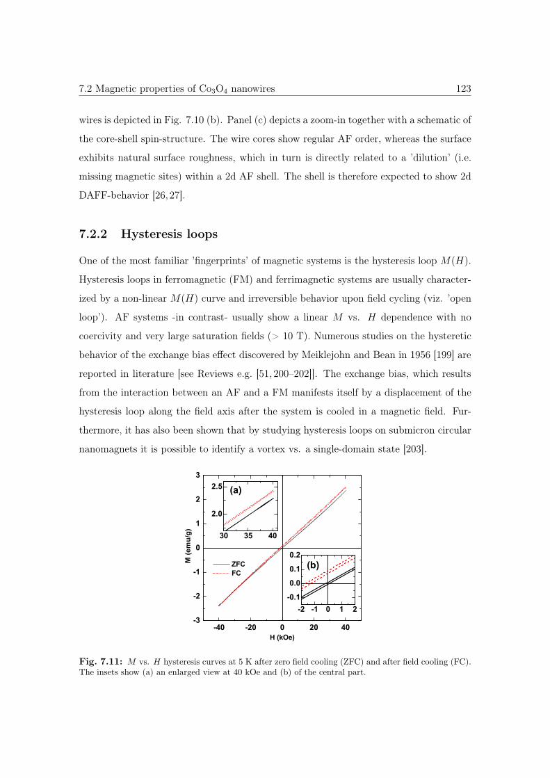
7.2 Magnetic properties of Co3O4 nanowires 123
wires is depicted in Fig. 7.10 (b). Panel (c) depicts a zoom-in together with a schematic of
the core-shell spin-structure. The wire cores show regular AF order, whereas the surface
exhibits natural surface roughness, which in turn is directly related to a ’dilution’ (i.e.
missing magnetic sites) within a 2d AF shell. The shell is therefore expected to show 2d
DAFF-behavior [26,27].
7.2.2 Hysteresis loops
One of the most familiar ’fingerprints’ of magnetic systems is the hysteresis loop M(H).
Hysteresis loops in ferromagnetic (FM) and ferrimagnetic systems are usually character-
ized by a non-linear M(H) curve and irreversible behavior upon field cycling (viz. ’open
loop’). AF systems -in contrast- usually show a linear M vs. H dependence with no
coercivity and very large saturation fields (> 10 T). Numerous studies on the hysteretic
behavior of the exchange bias effect discovered by Meiklejohn and Bean in 1956 [199] are
reported in literature [see Reviews e.g. [51, 200–202]]. The exchange bias, which results
from the interaction between an AF and a FM manifests itself by a displacement of the
hysteresis loop along the field axis after the system is cooled in a magnetic field. Fur-
thermore, it has also been shown that by studying hysteresis loops on submicron circular
nanomagnets it is possible to identify a vortex vs. a single-domain state [203].
-40 -20 0 20 40-3
-2
-1
0
1
2
3
30 35 40
2.0
2.5
-2 -1 0 1 2-0.1
0.0
0.1
0.2
ZFC FC
M (e
mu/
g)
H (kOe)
(a)
(b)
Fig. 7.11: M vs. H hysteresis curves at 5 K after zero field cooling (ZFC) and after field cooling (FC).The insets show (a) an enlarged view at 40 kOe and (b) of the central part.
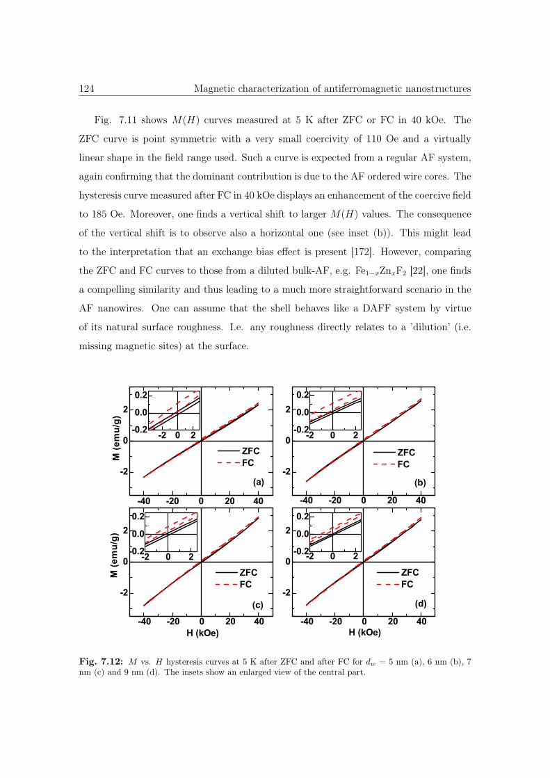
124 Magnetic characterization of antiferromagnetic nanostructures
Fig. 7.11 shows M(H) curves measured at 5 K after ZFC or FC in 40 kOe. The
ZFC curve is point symmetric with a very small coercivity of 110 Oe and a virtually
linear shape in the field range used. Such a curve is expected from a regular AF system,
again confirming that the dominant contribution is due to the AF ordered wire cores. The
hysteresis curve measured after FC in 40 kOe displays an enhancement of the coercive field
to 185 Oe. Moreover, one finds a vertical shift to larger M(H) values. The consequence
of the vertical shift is to observe also a horizontal one (see inset (b)). This might lead
to the interpretation that an exchange bias effect is present [172]. However, comparing
the ZFC and FC curves to those from a diluted bulk-AF, e.g. Fe1−xZnxF2 [22], one finds
a compelling similarity and thus leading to a much more straightforward scenario in the
AF nanowires. One can assume that the shell behaves like a DAFF system by virtue
of its natural surface roughness. I.e. any roughness directly relates to a ’dilution’ (i.e.
missing magnetic sites) at the surface.
-40 -20 0 20 40
-2
0
2
-2 0 2-0.2
0.0
0.2
-40 -20 0 20 40
-2
0
2
-40 -20 0 20 40
-2
0
2
-40 -20 0 20 40
-2
0
2
-2 0 2-0.2
0.0
0.2
-2 0 2-0.2
0.0
0.2
-2 0 2-0.2
0.0
0.2
M (e
mu/
g)
(a)
M (e
mu/
g)
ZFC FC
(c)
ZFC FC
H (kOe)
(b)
H (kOe)
ZFC FC
(d)
ZFC FC
Fig. 7.12: M vs. H hysteresis curves at 5 K after ZFC and after FC for dw = 5 nm (a), 6 nm (b), 7nm (c) and 9 nm (d). The insets show an enlarged view of the central part.
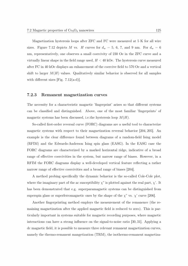
7.2 Magnetic properties of Co3O4 nanowires 125
Magnetization hysteresis loops after ZFC and FC were measured at 5 K for all wire
sizes. Figure 7.12 depicts M vs. H curves for dw = 5, 6, 7, and 9 nm. For dw = 6
nm, representatively, one observes a small coercivity of 230 Oe in the ZFC curve and a
virtually linear shape in the field range used, H < 40 kOe. The hysteresis curve measured
after FC in 40 kOe displays an enhancement of the coercive field to 570 Oe and a vertical
shift to larger M(H) values. Qualitatively similar behavior is observed for all samples
with different sizes [Fig. 7.12(a-d)].
7.2.3 Remanent magnetization curves
The necessity for a characteristic magnetic ’fingerprint’ arises so that different systems
can be classified and distinguished. Above, one of the most familiar ’fingerprints’ of
magnetic systems has been discussed, i.e.the hysteresis loop M(H).
So-called first-order reversal curve (FORC) diagrams are a useful tool to characterize
magnetic systems with respect to their magnetization reversal behavior [204, 205]. An
example is the clear difference found between diagrams of a random-field Ising model
(RFIM) and the Edwards-Anderson Ising spin glass (EASG). In the EASG case the
FORC diagrams are characterized by a marked horizontal ridge, indicative of a broad
range of effective coercivities in the system, but narrow range of biases. However, in a
RFIM the FORC diagrams display a well-developed vertical feature reflecting a rather
narrow range of effective coercivities and a broad range of biases [204].
A method probing specifically the dynamic behavior is the so-called Cole-Cole plot,
where the imaginary part of the ac susceptibility χ” is plotted against the real part, χ’. It
has been demonstrated that e.g. superparamagnetic systems can be distinguished from
superspin glass or superferromagnetic ones by the shape of the χ” vs. χ’ curve [206].
Another fingerprinting method employs the measurement of the remanence (the re-
maining magnetization after the applied magnetic field is reduced to zero). This is par-
ticularly important in systems suitable for magnetic recording purposes, where magnetic
interactions can have a strong influence on the signal-to-noise ratio [30, 31]. Applying a
dc magnetic field, it is possible to measure three relevant remanent magnetization curves,
namely the thermo-remanent mangetization (TRM), the isothermo-remanent magnetiza-
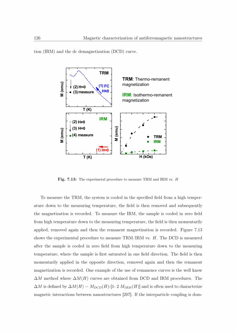
126 Magnetic characterization of antiferromagnetic nanostructures
tion (IRM) and the dc demagnetization (DCD) curve.
TRM: Thermo-remanentmagnetization
IRM: Isothermo-remanentmagnetization
H (kOe)
(3)(1)(2)
measureH=0
H=0FC
M (e
mu)
TRMIRM
T (K)M
(em
u)
(1)
(2) H=0
H=0
M (e
mu)
T (K)
H=0(3)(4) measure
TRM
IRM
Fig. 7.13: The experimetal procedure to measure TRM and IRM vs. H
To measure the TRM, the system is cooled in the specified field from a high temper-
ature down to the measuring temperature, the field is then removed and subsequently
the magnetization is recorded. To measure the IRM, the sample is cooled in zero field
from high temperature down to the measuring temperature, the field is then momentarily
applied, removed again and then the remanent magnetization is recorded. Figure 7.13
shows the experimental procedure to measure TRM/IRM vs. H. The DCD is measured
after the sample is cooled in zero field from high temperature down to the measuring
temperature, where the sample is first saturated in one field direction. The field is then
momentarily applied in the opposite direction, removed again and then the remanent
magnetization is recorded. One example of the use of remanence curves is the well know
ΔM method where ΔM(H) curves are obtained from DCD and IRM procedures. The
ΔM is defined by ΔM(H) = MDCD(H)-[1- 2 MIRM(H)] and is often used to characterize
magnetic interactions between nanostructures [207]. If the interparticle coupling is dom-
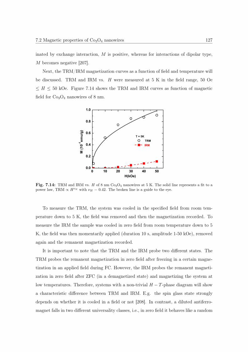
7.2 Magnetic properties of Co3O4 nanowires 127
inated by exchange interaction, M is positive, whereas for interactions of dipolar type,
M becomes negative [207].
Next, the TRM/IRM magnetization curves as a function of field and temperature will
be discussed. TRM and IRM vs. H were measured at 5 K in the field range, 50 Oe
≤ H ≤ 50 kOe. Figure 7.14 shows the TRM and IRM curves as function of magnetic
field for Co3O4 nanowires of 8 nm.
0 10 20 30 40 500.0
0.2
0.4
0.6
0.8
1.0
TRM IRM
T = 5K
M (1
0-1em
u/g)
H(kOe)
Fig. 7.14: TRM and IRM vs. H of 8 nm Co3O4 nanowires at 5 K. The solid line represents a fit to apower law, TRM ∝ HνH with νH = 0.42. The broken line is a guide to the eye.
To measure the TRM, the system was cooled in the specified field from room tem-
perature down to 5 K, the field was removed and then the magnetization recorded. To
measure the IRM the sample was cooled in zero field from room temperature down to 5
K, the field was then momentarily applied (duration 10 s, amplitude 1-50 kOe), removed
again and the remanent magnetization recorded.
It is important to note that the TRM and the IRM probe two different states. The
TRM probes the remanent magnetization in zero field after freezing in a certain magne-
tization in an applied field during FC. However, the IRM probes the remanent magneti-
zation in zero field after ZFC (in a demagnetized state) and magnetizing the system at
low temperatures. Therefore, systems with a non-trivial H − T -phase diagram will show
a characteristic difference between TRM and IRM. E.g. the spin glass state strongly
depends on whether it is cooled in a field or not [208]. In contrast, a diluted antiferro-
magnet falls in two different universality classes, i.e., in zero field it behaves like a random
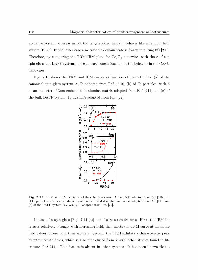
128 Magnetic characterization of antiferromagnetic nanostructures
exchange system, whereas in not too large applied fields it behaves like a random field
system [19,22]. In the latter case a metastable domain state is frozen in during FC [209].
Therefore, by comparing the TRM/IRM plots for Co3O4 nanowires with those of e.g.
spin glass and DAFF systems one can draw conclusions about the behavior in the Co3O4
nanowires.
Fig. 7.15 shows the TRM and IRM curves as function of magnetic field (a) of the
canonical spin glass system AuFe adapted from Ref. [210], (b) of Fe particles, with a
mean diameter of 3nm embedded in alumina matrix adapted from Ref. [211] and (c) of
the bulk-DAFF system, Fe1−xZnxF2 adapted from Ref. [22].
0 5 10 15 200.0
0.1
0.2
0.3
0 20 40 600.0
0.3
0.6
0.0 0.2 0.40.00.30.60.91.2
(a)
Nor
mal
ized
Rem
anen
ceM
(em
u/g)
M (1
0-2em
u/g) SG
T = 1.2K
TRM IRM
(c)T = 4.5K
DAFF
TRM IRM
(b) TRM
H(kOe)
SPM
IRMT = 10K
Fig. 7.15: TRM and IRM vs. H (a) of the spin glass system AuFe(0.5%) adapted from Ref. [210], (b)of Fe particles, with a mean diameter of 3 nm embedded in alumina matrix adapted from Ref. [211] and(c) of the DAFF system Fe0.48Zn0.52F, adapted from Ref. [22].
In case of a spin glass [Fig. 7.14 (a)] one observes two features. First, the IRM in-
creases relatively strongly with increasing field, then meets the TRM curve at moderate
field values, where both then saturate. Second, the TRM exhibits a characteristic peak
at intermediate fields, which is also reproduced from several other studies found in lit-
erature [212–214]. This feature is absent in other systems. It has been known that a
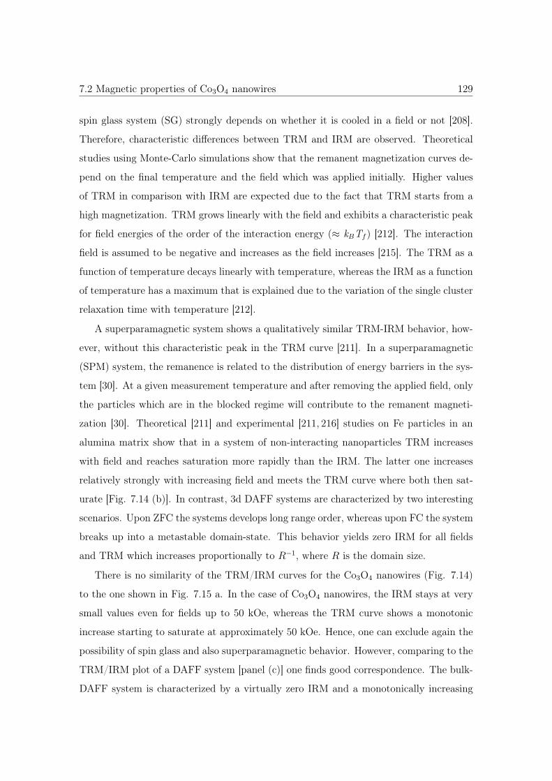
7.2 Magnetic properties of Co3O4 nanowires 129
spin glass system (SG) strongly depends on whether it is cooled in a field or not [208].
Therefore, characteristic differences between TRM and IRM are observed. Theoretical
studies using Monte-Carlo simulations show that the remanent magnetization curves de-
pend on the final temperature and the field which was applied initially. Higher values
of TRM in comparison with IRM are expected due to the fact that TRM starts from a
high magnetization. TRM grows linearly with the field and exhibits a characteristic peak
for field energies of the order of the interaction energy (≈ kBTf ) [212]. The interaction
field is assumed to be negative and increases as the field increases [215]. The TRM as a
function of temperature decays linearly with temperature, whereas the IRM as a function
of temperature has a maximum that is explained due to the variation of the single cluster
relaxation time with temperature [212].
A superparamagnetic system shows a qualitatively similar TRM-IRM behavior, how-
ever, without this characteristic peak in the TRM curve [211]. In a superparamagnetic
(SPM) system, the remanence is related to the distribution of energy barriers in the sys-
tem [30]. At a given measurement temperature and after removing the applied field, only
the particles which are in the blocked regime will contribute to the remanent magneti-
zation [30]. Theoretical [211] and experimental [211, 216] studies on Fe particles in an
alumina matrix show that in a system of non-interacting nanoparticles TRM increases
with field and reaches saturation more rapidly than the IRM. The latter one increases
relatively strongly with increasing field and meets the TRM curve where both then sat-
urate [Fig. 7.14 (b)]. In contrast, 3d DAFF systems are characterized by two interesting
scenarios. Upon ZFC the systems develops long range order, whereas upon FC the system
breaks up into a metastable domain-state. This behavior yields zero IRM for all fields
and TRM which increases proportionally to R−1, where R is the domain size.
There is no similarity of the TRM/IRM curves for the Co3O4 nanowires (Fig. 7.14)
to the one shown in Fig. 7.15 a. In the case of Co3O4 nanowires, the IRM stays at very
small values even for fields up to 50 kOe, whereas the TRM curve shows a monotonic
increase starting to saturate at approximately 50 kOe. Hence, one can exclude again the
possibility of spin glass and also superparamagnetic behavior. However, comparing to the
TRM/IRM plot of a DAFF system [panel (c)] one finds good correspondence. The bulk-
DAFF system is characterized by a virtually zero IRM and a monotonically increasing
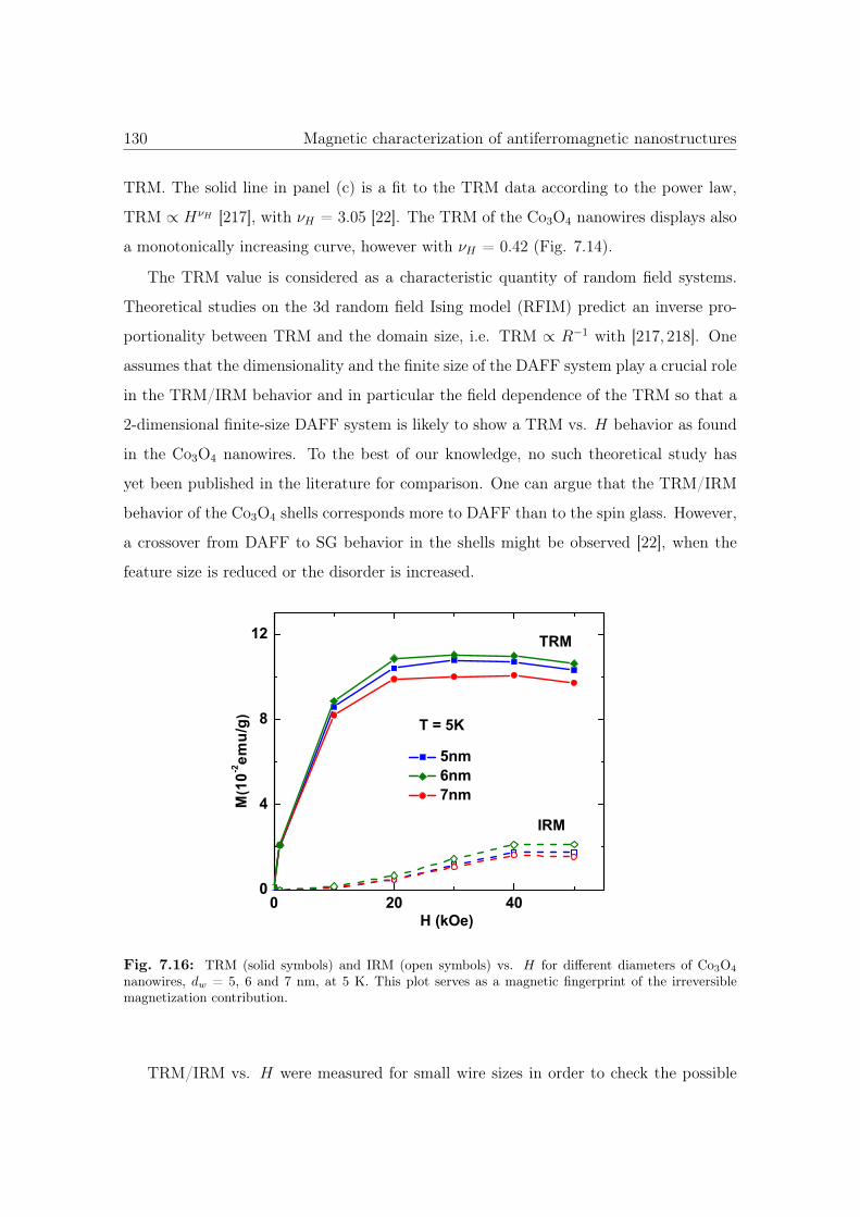
130 Magnetic characterization of antiferromagnetic nanostructures
TRM. The solid line in panel (c) is a fit to the TRM data according to the power law,
TRM ∝ HνH [217], with νH = 3.05 [22]. The TRM of the Co3O4 nanowires displays also
a monotonically increasing curve, however with νH = 0.42 (Fig. 7.14).
The TRM value is considered as a characteristic quantity of random field systems.
Theoretical studies on the 3d random field Ising model (RFIM) predict an inverse pro-
portionality between TRM and the domain size, i.e. TRM ∝ R−1 with [217, 218]. One
assumes that the dimensionality and the finite size of the DAFF system play a crucial role
in the TRM/IRM behavior and in particular the field dependence of the TRM so that a
2-dimensional finite-size DAFF system is likely to show a TRM vs. H behavior as found
in the Co3O4 nanowires. To the best of our knowledge, no such theoretical study has
yet been published in the literature for comparison. One can argue that the TRM/IRM
behavior of the Co3O4 shells corresponds more to DAFF than to the spin glass. However,
a crossover from DAFF to SG behavior in the shells might be observed [22], when the
feature size is reduced or the disorder is increased.
0 20 400
4
8
12
IRM
TRM
5nm 6nm 7nm
T = 5K
M(1
0-2em
u/g)
H (kOe)
Fig. 7.16: TRM (solid symbols) and IRM (open symbols) vs. H for different diameters of Co3O4
nanowires, dw = 5, 6 and 7 nm, at 5 K. This plot serves as a magnetic fingerprint of the irreversiblemagnetization contribution.
TRM/IRM vs. H were measured for small wire sizes in order to check the possible
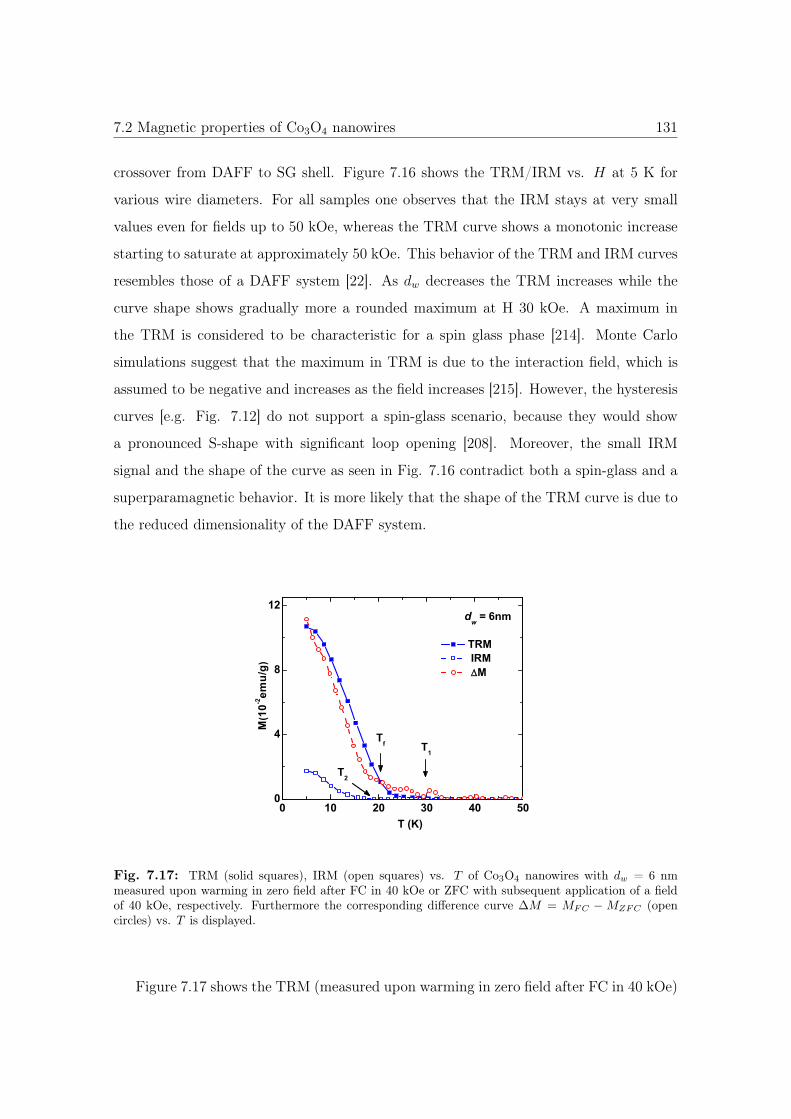
7.2 Magnetic properties of Co3O4 nanowires 131
crossover from DAFF to SG shell. Figure 7.16 shows the TRM/IRM vs. H at 5 K for
various wire diameters. For all samples one observes that the IRM stays at very small
values even for fields up to 50 kOe, whereas the TRM curve shows a monotonic increase
starting to saturate at approximately 50 kOe. This behavior of the TRM and IRM curves
resembles those of a DAFF system [22]. As dw decreases the TRM increases while the
curve shape shows gradually more a rounded maximum at H 30 kOe. A maximum in
the TRM is considered to be characteristic for a spin glass phase [214]. Monte Carlo
simulations suggest that the maximum in TRM is due to the interaction field, which is
assumed to be negative and increases as the field increases [215]. However, the hysteresis
curves [e.g. Fig. 7.12] do not support a spin-glass scenario, because they would show
a pronounced S-shape with significant loop opening [208]. Moreover, the small IRM
signal and the shape of the curve as seen in Fig. 7.16 contradict both a spin-glass and a
superparamagnetic behavior. It is more likely that the shape of the TRM curve is due to
the reduced dimensionality of the DAFF system.
0 10 20 30 40 500
4
8
12
T1
T2
TRM IRM ΔΔM
M(1
0-2em
u/g)
T (K)
dw = 6nm
Tf
Fig. 7.17: TRM (solid squares), IRM (open squares) vs. T of Co3O4 nanowires with dw = 6 nmmeasured upon warming in zero field after FC in 40 kOe or ZFC with subsequent application of a fieldof 40 kOe, respectively. Furthermore the corresponding difference curve ΔM = MFC − MZFC (opencircles) vs. T is displayed.
Figure 7.17 shows the TRM (measured upon warming in zero field after FC in 40 kOe)
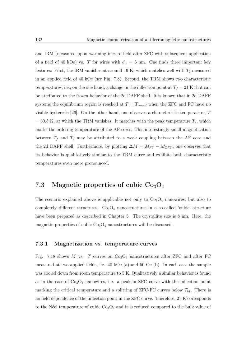
132 Magnetic characterization of antiferromagnetic nanostructures
and IRM (measured upon warming in zero field after ZFC with subsequent application
of a field of 40 kOe) vs. T for wires with dw = 6 nm. One finds three important key
features: First, the IRM vanishes at around 19 K, which matches well with T2 measured
in an applied field of 40 kOe (see Fig. 7.8). Second, the TRM shows two characteristic
temperatures, i.e., on the one hand, a change in the inflection point at Tf = 21 K that can
be attributed to the frozen behavior of the 2d DAFF shell. It is known that in 2d DAFF
systems the equilibrium region is reached at T = Tround when the ZFC and FC have no
visible hysteresis [26]. On the other hand, one observes a characteristic temperature, T
= 30.5 K, at which the TRM vanishes. It matches with the peak temperature T2, which
marks the ordering temperature of the AF cores. This interestingly small magnetization
between Tf and T2 may be attributed to a weak coupling between the AF core and
the 2d DAFF shell. Furthermore, by plotting ΔM = MFC − MZFC , one observes that
its behavior is qualitatively similar to the TRM curve and exhibits both characteristic
temperatures even more pronounced.
7.3 Magnetic properties of cubic Co3O4
The scenario explained above is applicable not only to Co3O4 nanowires, but also to
completely different structures. Co3O4 nanostructures in a so-called ’cubic’ structure
have been prepared as described in Chapter 5. The crystallite size is 8 nm. Here, the
magnetic properties of cubic Co3O4 nanostructures will be discussed.
7.3.1 Magnetization vs. temperature curves
Fig. 7.18 shows M vs. T curves on Co3O4 nanostructures after ZFC and after FC
measured at two applied fields, i.e. 40 kOe (a) and 50 Oe (b). In each case the sample
was cooled down from room temperature to 5 K. Qualitatively a similar behavior is found
as in the case of Co3O4 nanowires, i.e. a peak in ZFC curve with the inflection point
marking the critical temperature and a splitting of ZFC-FC curves below Tbf . There is
no field dependence of the inflection point in the ZFC curve. Therefore, 27 K corresponds
to the Néel temperature of cubic Co3O4 and it is reduced compared to the bulk value of
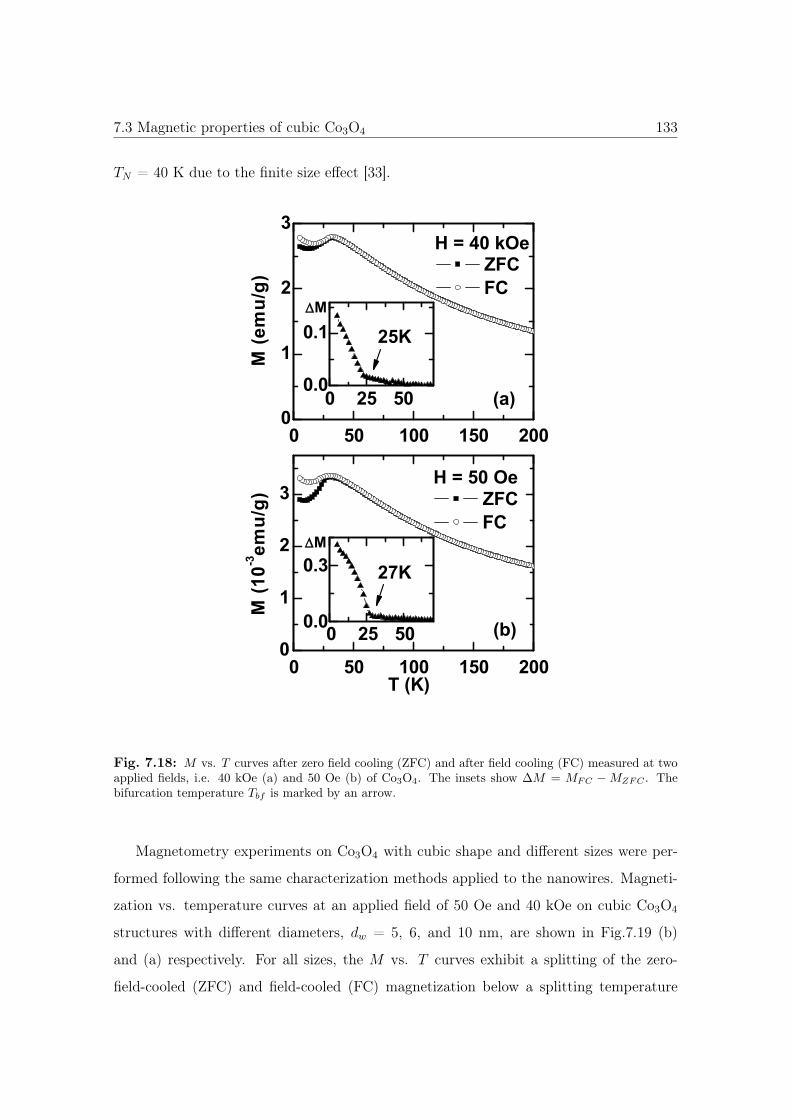
7.3 Magnetic properties of cubic Co3O4 133
TN = 40 K due to the finite size effect [33].
0 50 100 150 2000
1
2
3
0 50 100 150 2000
1
2
3
0 25 500.0
0.1
0 25 500.0
0.3
25K
27K
ΔΔM
(a)
T (K)
M (1
0-3em
u/g)
ZFC FC
M (e
mu/
g)H = 40 kOe
ΔΔM
(b)
H = 50 Oe ZFC FC
Fig. 7.18: M vs. T curves after zero field cooling (ZFC) and after field cooling (FC) measured at twoapplied fields, i.e. 40 kOe (a) and 50 Oe (b) of Co3O4. The insets show ΔM = MFC − MZFC . Thebifurcation temperature Tbf is marked by an arrow.
Magnetometry experiments on Co3O4 with cubic shape and different sizes were per-
formed following the same characterization methods applied to the nanowires. Magneti-
zation vs. temperature curves at an applied field of 50 Oe and 40 kOe on cubic Co3O4
structures with different diameters, dw = 5, 6, and 10 nm, are shown in Fig.7.19 (b)
and (a) respectively. For all sizes, the M vs. T curves exhibit a splitting of the zero-
field-cooled (ZFC) and field-cooled (FC) magnetization below a splitting temperature
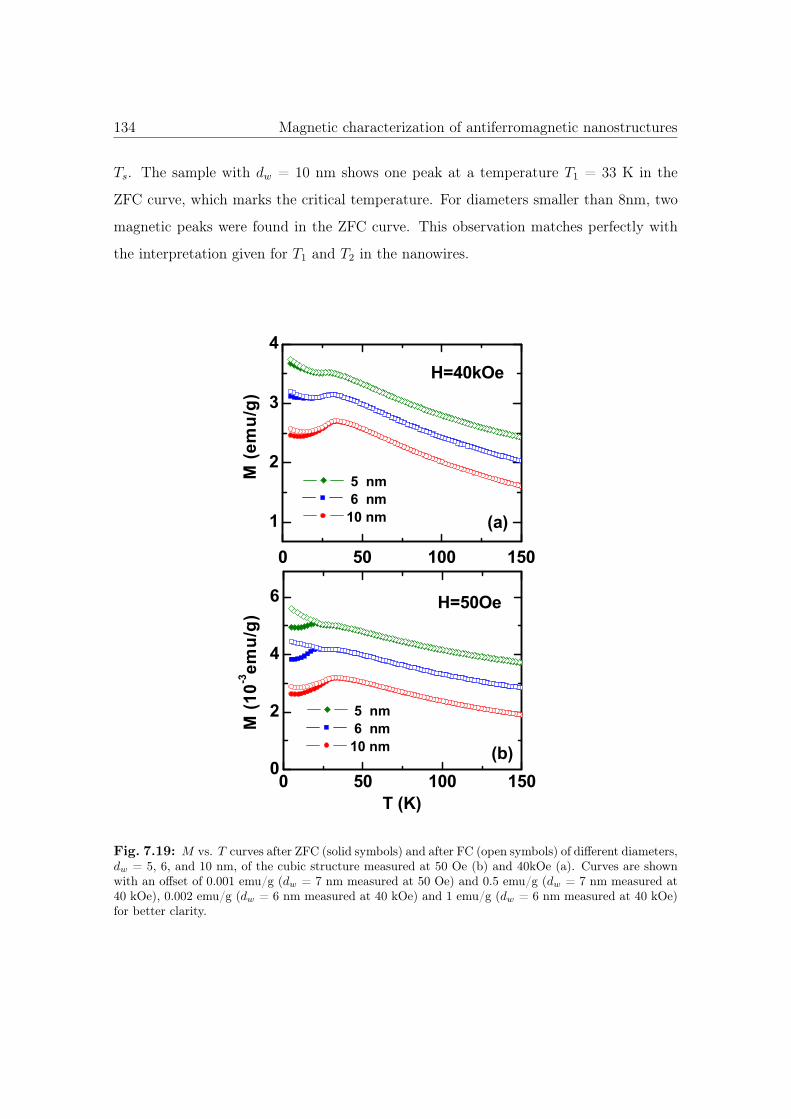
134 Magnetic characterization of antiferromagnetic nanostructures
Ts. The sample with dw = 10 nm shows one peak at a temperature T1 = 33 K in the
ZFC curve, which marks the critical temperature. For diameters smaller than 8nm, two
magnetic peaks were found in the ZFC curve. This observation matches perfectly with
the interpretation given for T1 and T2 in the nanowires.
0 50 100 1500
2
4
6
0 50 100 150
1
2
3
4
6 nm 10 nm (b)
T (K)
5 nm
H=50Oe
H=40kOe
5 nm 6 nm 10 nm (a)
M (e
mu/
g)M
(10-3
emu/
g)
Fig. 7.19: M vs. T curves after ZFC (solid symbols) and after FC (open symbols) of different diameters,dw = 5, 6, and 10 nm, of the cubic structure measured at 50 Oe (b) and 40kOe (a). Curves are shownwith an offset of 0.001 emu/g (dw = 7 nm measured at 50 Oe) and 0.5 emu/g (dw = 7 nm measured at40 kOe), 0.002 emu/g (dw = 6 nm measured at 40 kOe) and 1 emu/g (dw = 6 nm measured at 40 kOe)for better clarity.
7.3 Magnetic properties of cubic Co3O4 135
7.3.2 Hysteresis loops
Magnetization hysteresis loops at 5 K after ZFC and FC were measured on cubic Co3O4
nanostructures with different sizes. Figure 7.12 depicts M vs. H curves for dw = 5, 6, 8,
and 10 nm. For dw = 8 nm, representatively, one observes a small coercivity of 78 Oe in
the ZFC curve and a virtually linear shape in the field range used, |H| < 40 kOe. This
matches well with the previous results found on Co3O4 nanowires [219]. The overall linear
behavior is due to the regular AF nanostructure cores, while the irreversible contribution
(viz. the loop opening) has been attributed to the 2d-DAFF shells [219]. The hysteresis
curve measured after FC in 40 kOe displays an enhancement of the coercive field to 146
Oe and a vertical shift to larger M(H) values. This matches as well with previous results
on Co3O4 nanowires [219] and with hysteresis loops on DAFF systems [22]. Qualitatively
similar behavior to Co3O4 nanowires is observed for all samples with different sizes [Fig.
7.20(a-d)].
-40 -20 0 20 40
-2
0
2
-2 -1 0
0.0
0.1
-40 -20 0 20 40
-2
0
2
-40 -20 0 20 40
-2
0
2
-40 -20 0 20 40
-2
0
2
-1 0-0.10.00.1
-1 0
0.0
0.1
-1 0
0.0
0.1
(a)
M (e
mu/
g)
ZFC FC
(b)
ZFC FC
(c)
H (kOe)H (kOe)
ZFC FC
M (e
mu/
g)
(d)
ZFC FC
Fig. 7.20: M vs. H curves after ZFC (solid line) and after FC (dashed line) of dw = 5 (a), 6 (b), 8 (c)and 10 nm (d) of the cubic structure measured at 5 K. The insets show an enlarged view of the centralpart.
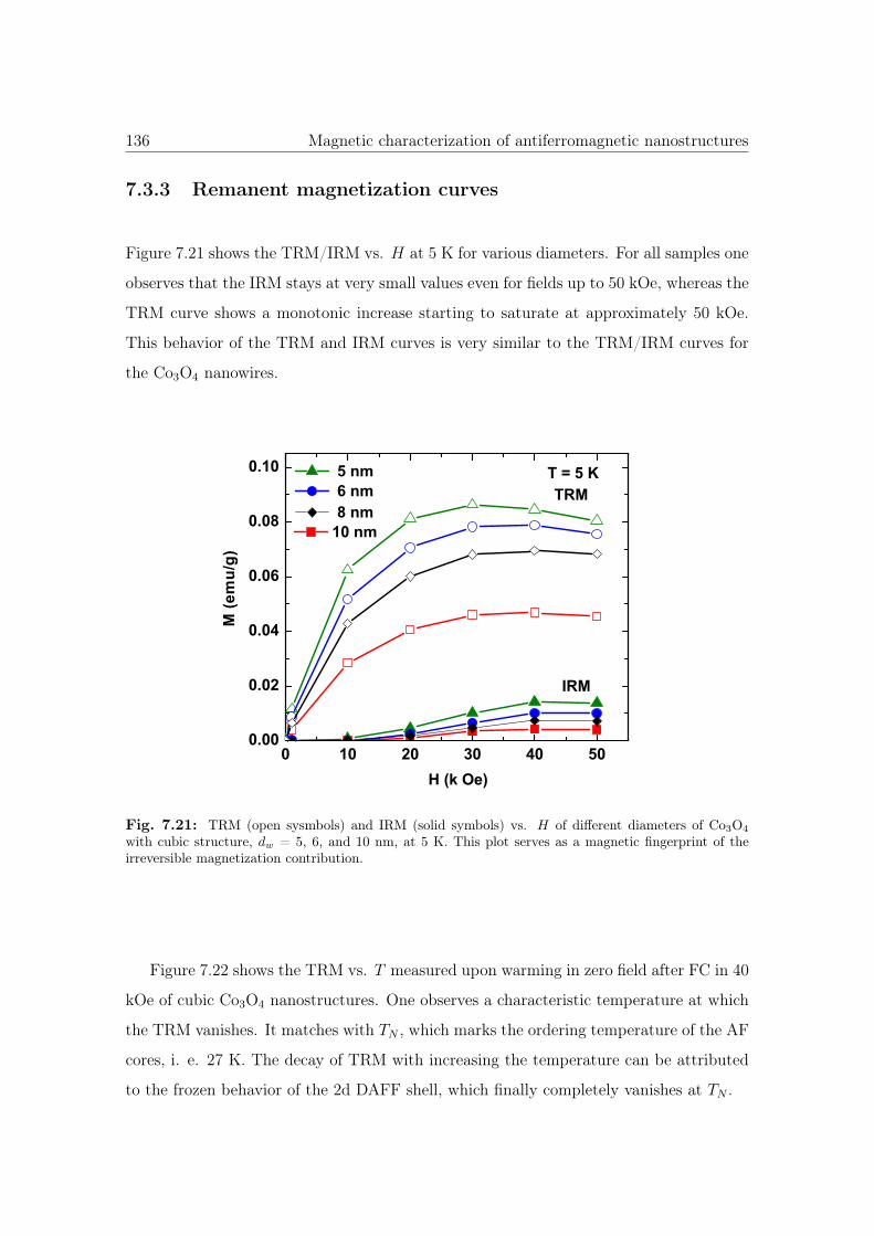
136 Magnetic characterization of antiferromagnetic nanostructures
7.3.3 Remanent magnetization curves
Figure 7.21 shows the TRM/IRM vs. H at 5 K for various diameters. For all samples one
observes that the IRM stays at very small values even for fields up to 50 kOe, whereas the
TRM curve shows a monotonic increase starting to saturate at approximately 50 kOe.
This behavior of the TRM and IRM curves is very similar to the TRM/IRM curves for
the Co3O4 nanowires.
0 10 20 30 40 500.00
0.02
0.04
0.06
0.08
0.10
10 nm
5 nm 6 nm 8 nm
IRM
TRMT = 5 K
M (e
mu/
g)
H (k Oe)
Fig. 7.21: TRM (open sysmbols) and IRM (solid symbols) vs. H of different diameters of Co3O4
with cubic structure, dw = 5, 6, and 10 nm, at 5 K. This plot serves as a magnetic fingerprint of theirreversible magnetization contribution.
Figure 7.22 shows the TRM vs. T measured upon warming in zero field after FC in 40
kOe of cubic Co3O4 nanostructures. One observes a characteristic temperature at which
the TRM vanishes. It matches with TN , which marks the ordering temperature of the AF
cores, i. e. 27 K. The decay of TRM with increasing the temperature can be attributed
to the frozen behavior of the 2d DAFF shell, which finally completely vanishes at TN .
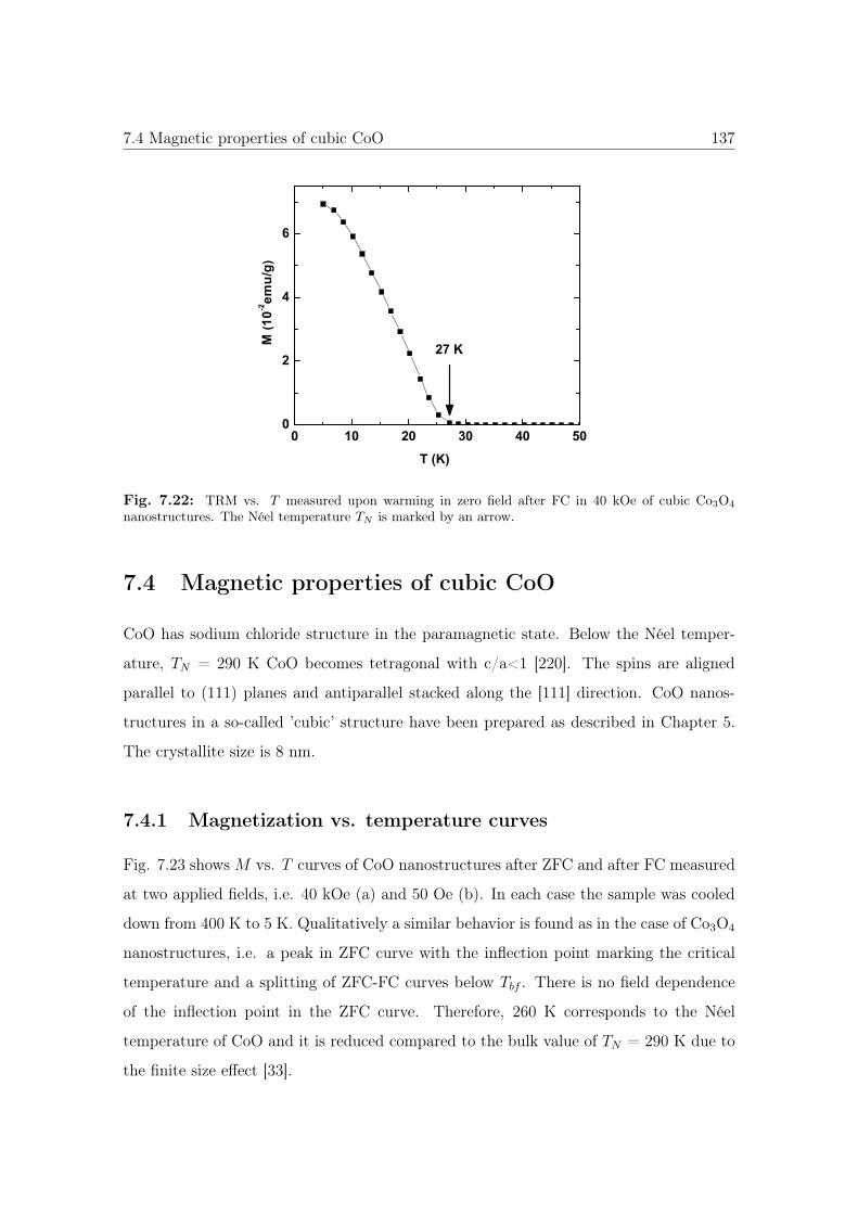
7.4 Magnetic properties of cubic CoO 137
0 10 20 30 40 500
2
4
6
27 K
T (K)
M (1
0-2em
u/g)
Fig. 7.22: TRM vs. T measured upon warming in zero field after FC in 40 kOe of cubic Co3O4
nanostructures. The Néel temperature TN is marked by an arrow.
7.4 Magnetic properties of cubic CoO
CoO has sodium chloride structure in the paramagnetic state. Below the Néel temper-
ature, TN = 290 K CoO becomes tetragonal with c/a<1 [220]. The spins are aligned
parallel to (111) planes and antiparallel stacked along the [111] direction. CoO nanos-
tructures in a so-called ’cubic’ structure have been prepared as described in Chapter 5.
The crystallite size is 8 nm.
7.4.1 Magnetization vs. temperature curves
Fig. 7.23 shows M vs. T curves of CoO nanostructures after ZFC and after FC measured
at two applied fields, i.e. 40 kOe (a) and 50 Oe (b). In each case the sample was cooled
down from 400 K to 5 K. Qualitatively a similar behavior is found as in the case of Co3O4
nanostructures, i.e. a peak in ZFC curve with the inflection point marking the critical
temperature and a splitting of ZFC-FC curves below Tbf . There is no field dependence
of the inflection point in the ZFC curve. Therefore, 260 K corresponds to the Néel
temperature of CoO and it is reduced compared to the bulk value of TN = 290 K due to
the finite size effect [33].
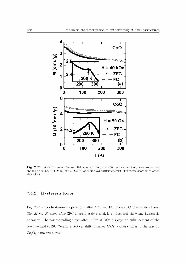
138 Magnetic characterization of antiferromagnetic nanostructures
0 100 200 3000
2
4
6
200 300
4.2
0 100 200 3000
1
2
3
4
200 300
2.4
2.6M
(10-3
emu/
g)
T (K)
CoO
(b)
H = 50 Oe
ZFC FC260 K
M
(em
u/g)
CoO
(a)
H = 40 kOe ZFC FC
260 K
Fig. 7.23: M vs. T curves after zero field cooling (ZFC) and after field cooling (FC) measured at twoapplied fields, i.e. 40 kOe (a) and 50 Oe (b) of cubic CoO antiferromagnet. The insets show an enlargedview of TN .
7.4.2 Hysteresis loops
Fig. 7.24 shows hysteresis loops at 5 K after ZFC and FC on cubic CoO nanostructures.
The M vs. H curve after ZFC is completely closed, i. e. does not show any hysteretic
behavior. The corresponding curve after FC in 40 kOe displays an enhancement of the
coercive field to 264 Oe and a vertical shift to larger M(H) values similar to the case on
Co3O4 nanostructures.
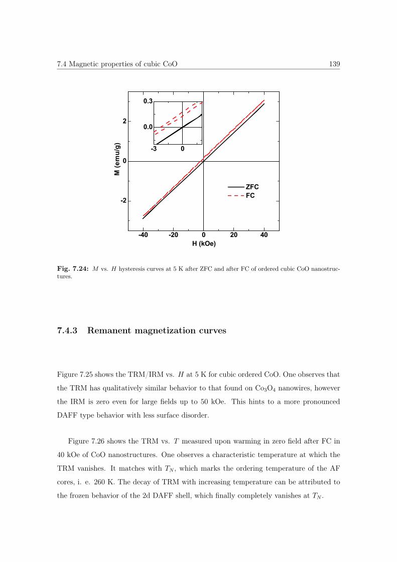
7.4 Magnetic properties of cubic CoO 139
-40 -20 0 20 40
-2
0
2
-3 0
0.0
0.3
H (kOe)
ZFC FC
M (e
mu/
g)
Fig. 7.24: M vs. H hysteresis curves at 5 K after ZFC and after FC of ordered cubic CoO nanostruc-tures.
7.4.3 Remanent magnetization curves
Figure 7.25 shows the TRM/IRM vs. H at 5 K for cubic ordered CoO. One observes that
the TRM has qualitatively similar behavior to that found on Co3O4 nanowires, however
the IRM is zero even for large fields up to 50 kOe. This hints to a more pronounced
DAFF type behavior with less surface disorder.
Figure 7.26 shows the TRM vs. T measured upon warming in zero field after FC in
40 kOe of CoO nanostructures. One observes a characteristic temperature at which the
TRM vanishes. It matches with TN , which marks the ordering temperature of the AF
cores, i. e. 260 K. The decay of TRM with increasing temperature can be attributed to
the frozen behavior of the 2d DAFF shell, which finally completely vanishes at TN .
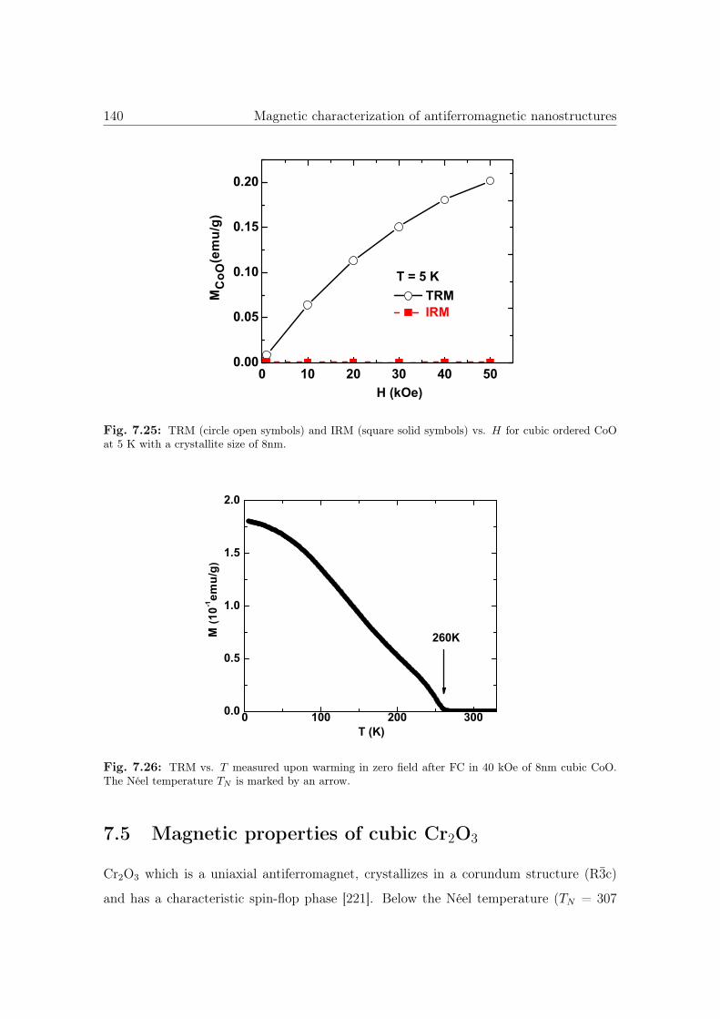
140 Magnetic characterization of antiferromagnetic nanostructures
0 10 20 30 40 500.00
0.05
0.10
0.15
0.20
T = 5 K TRM IRM
MC
oO(e
mu/
g)
H (kOe)
Fig. 7.25: TRM (circle open symbols) and IRM (square solid symbols) vs. H for cubic ordered CoOat 5 K with a crystallite size of 8nm.
0 100 200 3000.0
0.5
1.0
1.5
2.0
T (K)
M (1
0-1em
u/g)
260K
Fig. 7.26: TRM vs. T measured upon warming in zero field after FC in 40 kOe of 8nm cubic CoO.The Néel temperature TN is marked by an arrow.
7.5 Magnetic properties of cubic Cr2O3
Cr2O3 which is a uniaxial antiferromagnet, crystallizes in a corundum structure (R3̄c)
and has a characteristic spin-flop phase [221]. Below the Néel temperature (TN = 307
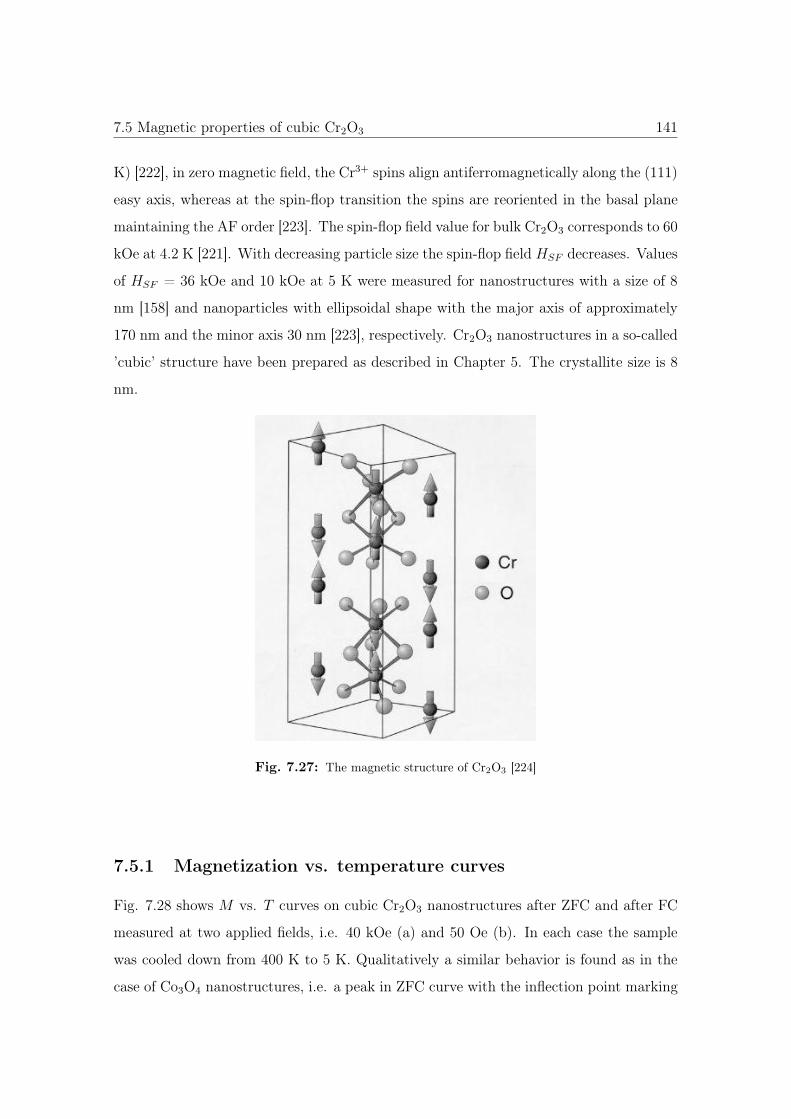
7.5 Magnetic properties of cubic Cr2O3 141
K) [222], in zero magnetic field, the Cr3+ spins align antiferromagnetically along the (111)
easy axis, whereas at the spin-flop transition the spins are reoriented in the basal plane
maintaining the AF order [223]. The spin-flop field value for bulk Cr2O3 corresponds to 60
kOe at 4.2 K [221]. With decreasing particle size the spin-flop field HSF decreases. Values
of HSF = 36 kOe and 10 kOe at 5 K were measured for nanostructures with a size of 8
nm [158] and nanoparticles with ellipsoidal shape with the major axis of approximately
170 nm and the minor axis 30 nm [223], respectively. Cr2O3 nanostructures in a so-called
’cubic’ structure have been prepared as described in Chapter 5. The crystallite size is 8
nm.
Fig. 7.27: The magnetic structure of Cr2O3 [224]
7.5.1 Magnetization vs. temperature curves
Fig. 7.28 shows M vs. T curves on cubic Cr2O3 nanostructures after ZFC and after FC
measured at two applied fields, i.e. 40 kOe (a) and 50 Oe (b). In each case the sample
was cooled down from 400 K to 5 K. Qualitatively a similar behavior is found as in the
case of Co3O4 nanostructures, i.e. a peak in ZFC curve with the inflection point marking
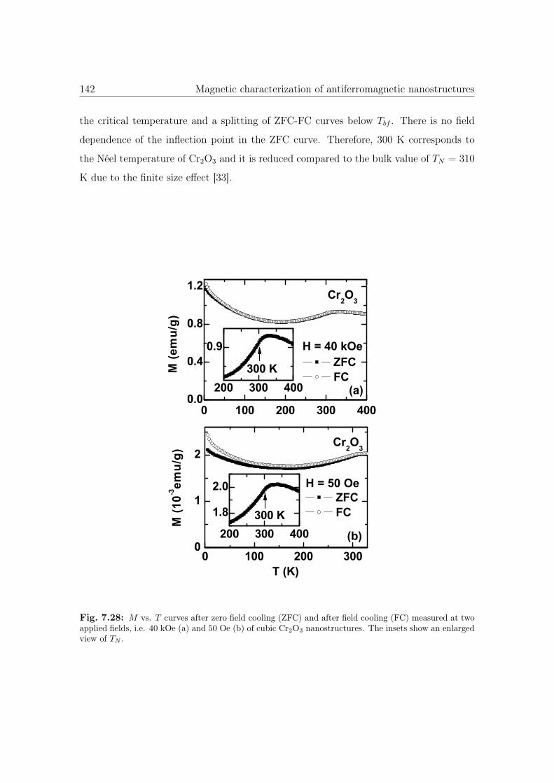
142 Magnetic characterization of antiferromagnetic nanostructures
the critical temperature and a splitting of ZFC-FC curves below Tbf . There is no field
dependence of the inflection point in the ZFC curve. Therefore, 300 K corresponds to
the Néel temperature of Cr2O3 and it is reduced compared to the bulk value of TN = 310
K due to the finite size effect [33].
0 100 200 3000
1
2
200 300 400
1.8
2.0
0 100 200 300 4000.0
0.4
0.8
1.2
200 300 400
0.9
Cr2O3
M (1
0-3em
u/g)
T (K)
(b)
H = 50 Oe ZFC FC300 K
Cr2O3
M (e
mu/
g)
(a)
H = 40 kOe ZFC FC
300 K
Fig. 7.28: M vs. T curves after zero field cooling (ZFC) and after field cooling (FC) measured at twoapplied fields, i.e. 40 kOe (a) and 50 Oe (b) of cubic Cr2O3 nanostructures. The insets show an enlargedview of TN .
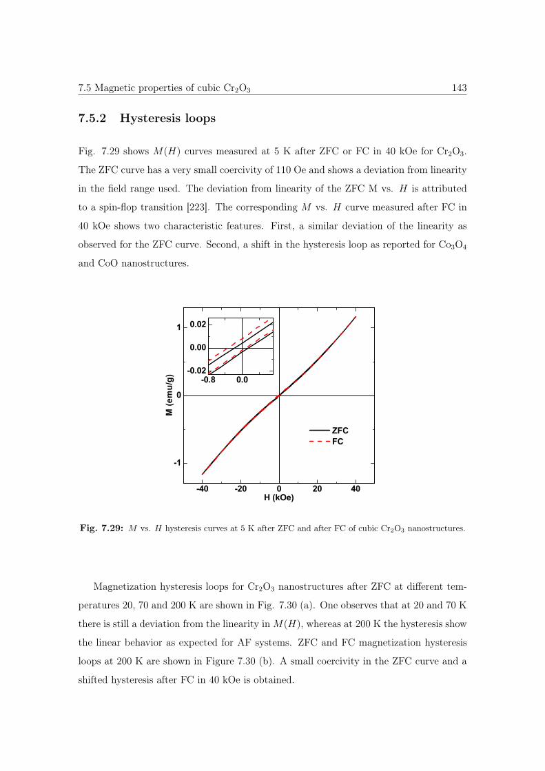
7.5 Magnetic properties of cubic Cr2O3 143
7.5.2 Hysteresis loops
Fig. 7.29 shows M(H) curves measured at 5 K after ZFC or FC in 40 kOe for Cr2O3.
The ZFC curve has a very small coercivity of 110 Oe and shows a deviation from linearity
in the field range used. The deviation from linearity of the ZFC M vs. H is attributed
to a spin-flop transition [223]. The corresponding M vs. H curve measured after FC in
40 kOe shows two characteristic features. First, a similar deviation of the linearity as
observed for the ZFC curve. Second, a shift in the hysteresis loop as reported for Co3O4
and CoO nanostructures.
-40 -20 0 20 40
-1
0
1
-0.8 0.0-0.02
0.00
0.02
ZFC FC
M (e
mu/
g)
H (kOe)
Fig. 7.29: M vs. H hysteresis curves at 5 K after ZFC and after FC of cubic Cr2O3 nanostructures.
Magnetization hysteresis loops for Cr2O3 nanostructures after ZFC at different tem-
peratures 20, 70 and 200 K are shown in Fig. 7.30 (a). One observes that at 20 and 70 K
there is still a deviation from the linearity in M(H), whereas at 200 K the hysteresis show
the linear behavior as expected for AF systems. ZFC and FC magnetization hysteresis
loops at 200 K are shown in Figure 7.30 (b). A small coercivity in the ZFC curve and a
shifted hysteresis after FC in 40 kOe is obtained.
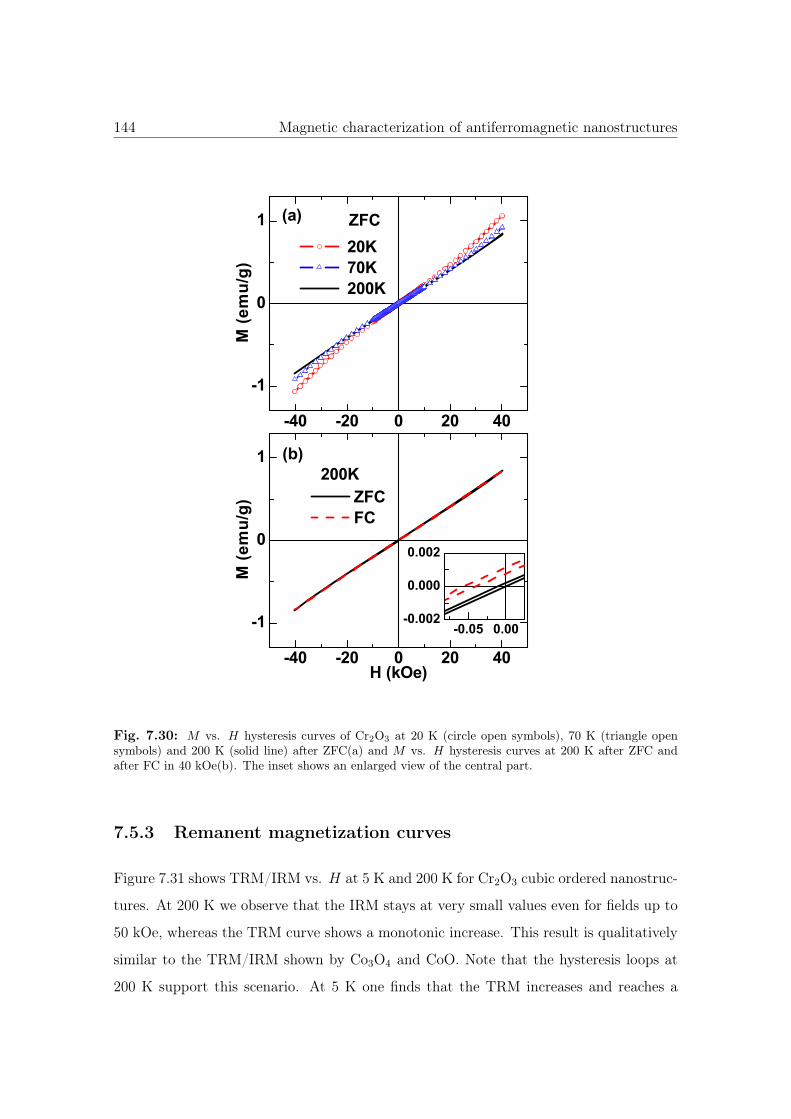
144 Magnetic characterization of antiferromagnetic nanostructures
-40 -20 0 20 40
-1
0
1
-40 -20 0 20 40
-1
0
1
-0.05 0.00-0.002
0.000
0.002
ZFC 20K 70K 200K
M (e
mu/
g)
(b)
(a)
200K
ZFC FC
M (e
mu/
g)
H (kOe)
Fig. 7.30: M vs. H hysteresis curves of Cr2O3 at 20 K (circle open symbols), 70 K (triangle opensymbols) and 200 K (solid line) after ZFC(a) and M vs. H hysteresis curves at 200 K after ZFC andafter FC in 40 kOe(b). The inset shows an enlarged view of the central part.
7.5.3 Remanent magnetization curves
Figure 7.31 shows TRM/IRM vs. H at 5 K and 200 K for Cr2O3 cubic ordered nanostruc-
tures. At 200 K we observe that the IRM stays at very small values even for fields up to
50 kOe, whereas the TRM curve shows a monotonic increase. This result is qualitatively
similar to the TRM/IRM shown by Co3O4 and CoO. Note that the hysteresis loops at
200 K support this scenario. At 5 K one finds that the TRM increases and reaches a
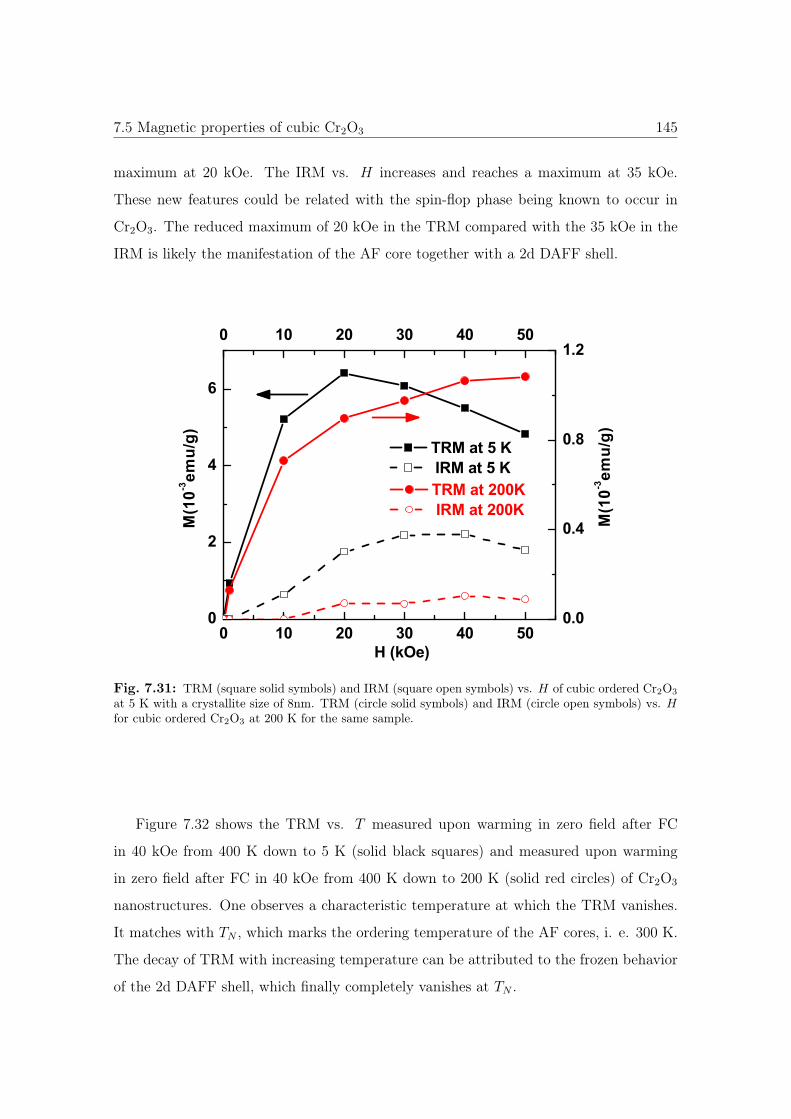
7.5 Magnetic properties of cubic Cr2O3 145
maximum at 20 kOe. The IRM vs. H increases and reaches a maximum at 35 kOe.
These new features could be related with the spin-flop phase being known to occur in
Cr2O3. The reduced maximum of 20 kOe in the TRM compared with the 35 kOe in the
IRM is likely the manifestation of the AF core together with a 2d DAFF shell.
0 10 20 30 40 500
2
4
6
0 10 20 30 40 50
0.0
0.4
0.8
1.2
M(1
0-3em
u/g)
TRM at 5 K IRM at 5 K
M(1
0-3em
u/g)
H (kOe)
TRM at 200K IRM at 200K
Fig. 7.31: TRM (square solid symbols) and IRM (square open symbols) vs. H of cubic ordered Cr2O3
at 5 K with a crystallite size of 8nm. TRM (circle solid symbols) and IRM (circle open symbols) vs. Hfor cubic ordered Cr2O3 at 200 K for the same sample.
Figure 7.32 shows the TRM vs. T measured upon warming in zero field after FC
in 40 kOe from 400 K down to 5 K (solid black squares) and measured upon warming
in zero field after FC in 40 kOe from 400 K down to 200 K (solid red circles) of Cr2O3
nanostructures. One observes a characteristic temperature at which the TRM vanishes.
It matches with TN , which marks the ordering temperature of the AF cores, i. e. 300 K.
The decay of TRM with increasing temperature can be attributed to the frozen behavior
of the 2d DAFF shell, which finally completely vanishes at TN .
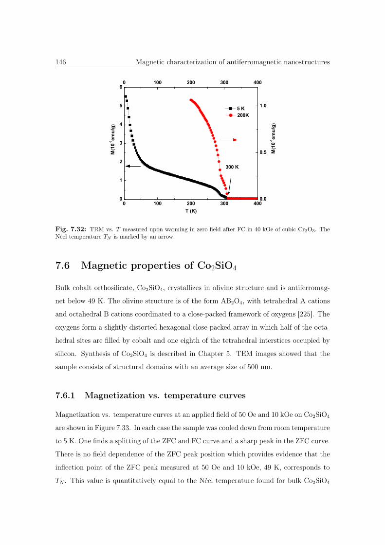
146 Magnetic characterization of antiferromagnetic nanostructures
0 100 200 300 4000
1
2
3
4
5
60 100 200 300 400
0.0
0.5
1.0M
(10-3
emu/
g) 5 K
T (K)
300 K
M(1
0-3em
u/g)
200K
Fig. 7.32: TRM vs. T measured upon warming in zero field after FC in 40 kOe of cubic Cr2O3. TheNéel temperature TN is marked by an arrow.
7.6 Magnetic properties of Co2SiO4
Bulk cobalt orthosilicate, Co2SiO4, crystallizes in olivine structure and is antiferromag-
net below 49 K. The olivine structure is of the form AB2O4, with tetrahedral A cations
and octahedral B cations coordinated to a close-packed framework of oxygens [225]. The
oxygens form a slightly distorted hexagonal close-packed array in which half of the octa-
hedral sites are filled by cobalt and one eighth of the tetrahedral interstices occupied by
silicon. Synthesis of Co2SiO4 is described in Chapter 5. TEM images showed that the
sample consists of structural domains with an average size of 500 nm.
7.6.1 Magnetization vs. temperature curves
Magnetization vs. temperature curves at an applied field of 50 Oe and 10 kOe on Co2SiO4
are shown in Figure 7.33. In each case the sample was cooled down from room temperature
to 5 K. One finds a splitting of the ZFC and FC curve and a sharp peak in the ZFC curve.
There is no field dependence of the ZFC peak position which provides evidence that the
inflection point of the ZFC peak measured at 50 Oe and 10 kOe, 49 K, corresponds to
TN . This value is quantitatively equal to the Néel temperature found for bulk Co2SiO4
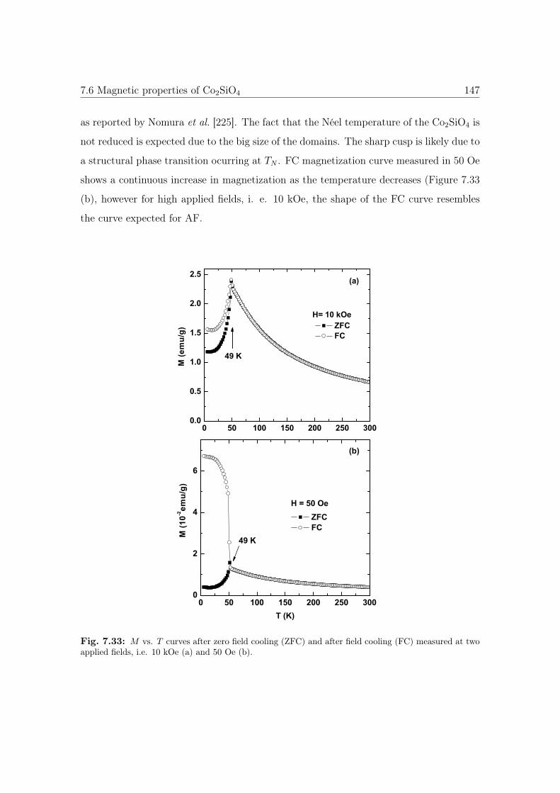
7.6 Magnetic properties of Co2SiO4 147
as reported by Nomura et al. [225]. The fact that the Néel temperature of the Co2SiO4 is
not reduced is expected due to the big size of the domains. The sharp cusp is likely due to
a structural phase transition ocurring at TN . FC magnetization curve measured in 50 Oe
shows a continuous increase in magnetization as the temperature decreases (Figure 7.33
(b), however for high applied fields, i. e. 10 kOe, the shape of the FC curve resembles
the curve expected for AF.
0 50 100 150 200 250 3000.0
0.5
1.0
1.5
2.0
2.5
(a)
ZFC FC
49 K
M (e
mu/
g)
H= 10 kOe
0 50 100 150 200 250 3000
2
4
6
49 K
(b)
H = 50 Oe ZFC FC
M (1
0-2em
u/g)
T (K)
Fig. 7.33: M vs. T curves after zero field cooling (ZFC) and after field cooling (FC) measured at twoapplied fields, i.e. 10 kOe (a) and 50 Oe (b).
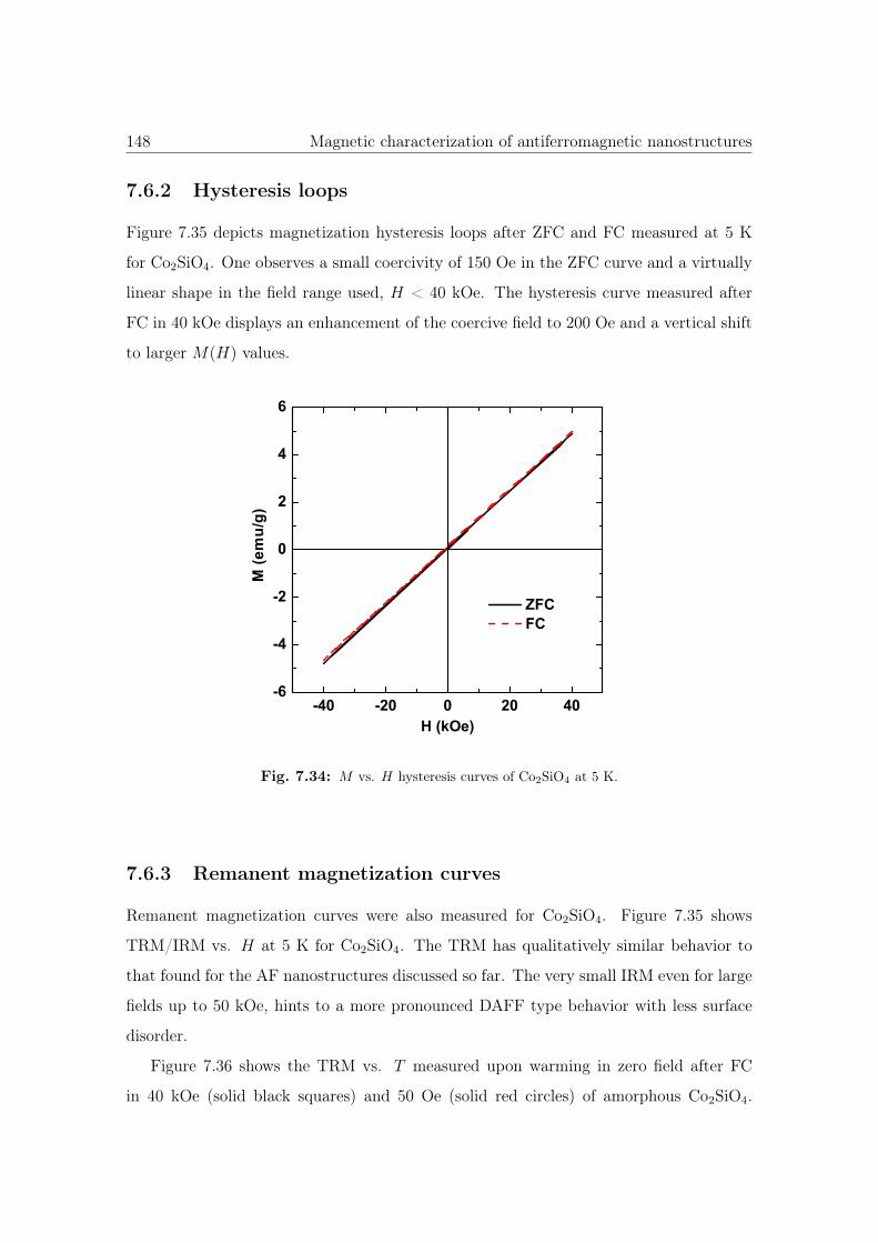
148 Magnetic characterization of antiferromagnetic nanostructures
7.6.2 Hysteresis loops
Figure 7.35 depicts magnetization hysteresis loops after ZFC and FC measured at 5 K
for Co2SiO4. One observes a small coercivity of 150 Oe in the ZFC curve and a virtually
linear shape in the field range used, H < 40 kOe. The hysteresis curve measured after
FC in 40 kOe displays an enhancement of the coercive field to 200 Oe and a vertical shift
to larger M(H) values.
-40 -20 0 20 40-6
-4
-2
0
2
4
6
ZFC FC
M (e
mu/
g)
H (kOe)
Fig. 7.34: M vs. H hysteresis curves of Co2SiO4 at 5 K.
7.6.3 Remanent magnetization curves
Remanent magnetization curves were also measured for Co2SiO4. Figure 7.35 shows
TRM/IRM vs. H at 5 K for Co2SiO4. The TRM has qualitatively similar behavior to
that found for the AF nanostructures discussed so far. The very small IRM even for large
fields up to 50 kOe, hints to a more pronounced DAFF type behavior with less surface
disorder.
Figure 7.36 shows the TRM vs. T measured upon warming in zero field after FC
in 40 kOe (solid black squares) and 50 Oe (solid red circles) of amorphous Co2SiO4.
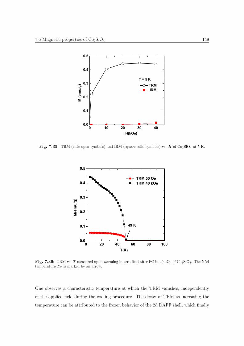
7.6 Magnetic properties of Co2SiO4 149
0 10 20 30 400.0
0.1
0.2
0.3
0.4
0.5
T = 5 K TRM IRM
M (e
mu/
g)
H(kOe)
Fig. 7.35: TRM (cicle open symbols) and IRM (square solid symbols) vs. H of Co2SiO4 at 5 K.
0 20 40 60 80 1000.0
0.1
0.2
0.3
0.4
0.5
49 K
TRM 50 Oe TRM 40 kOe
M(e
mu/
g)
T(K)
Fig. 7.36: TRM vs. T measured upon warming in zero field after FC in 40 kOe of Co2SiO4. The Néeltemperature TN is marked by an arrow.
One observes a characteristic temperature at which the TRM vanishes, independently
of the applied field during the cooling procedure. The decay of TRM as increasing the
temperature can be attributed to the frozen behavior of the 2d DAFF shell, which finally
150 Magnetic characterization of antiferromagnetic nanostructures
completely vanishes at TN as in the case of the AF nanostructures.
7.7 Summary and conclusions
Antiferromagnetic (AF) nanostructures from Co3O4, CoO and Cr2O3, have been prepared
by the nanocasting method from cubic silica templates and investigated using magnetom-
etry with emphasis on the core-shell behavior.
It is shown that the properties of these three AF systems are governed by core-
shell behavior, where the core behaves regularly AF, while the shell behaves as a two-
dimensional diluted antiferromagnet in a field (DAFF).
Magnetometry results on Co3O4 nanostructures of different sizes confirm a core-shell
model, involving a regularly ordered AF core and a 2d DAFF shell. Below a critical
structure size of 8 nm, core and shell decouple magnetically and yield independent mag-
netization signatures, evidenced by two temperatures, T1 and T2, in the magnetization
vs. temperature curves. The origin of the decoupling could be due to a crossover of the
ratio of coupling energies, i.e. intra-shell and core and inter-shell and core.
Furthermore, this study reports about a "magnetic fingerprint" method to charac-
terize the magnetic behavior, i.e. it is demonstrated how thermo-remanent (TRM) and
isothermo-remanent (IRM) magnetization curves can serve to identify the irreversible
magnetization contributions usually encountered in nanosized magnetic structures. The
TRM/IRM fingerprint is compared to those of superparamagnetic systems, superspin
glasses or 3d DAFFs.
The results discussed here may have important consequences for the understanding of
the surface behavior of magnetic nanosystems in general. Moreover since many exchange-
bias models consider the understanding of the AF surface to be crucial for the interpreta-
tion of the exchange-bias effect, the present results might lead to a refined consideration
of the AF interfacial magnetization contribution.

Chapter 8
Magnetic characterization of iron oxide
nanoparticles
Magnetic nanoparticles are in the focus of high interest, because they could serve as build-
ing blocks for future high-density data storage, spintronic devices, photonic, bio-medical
or refrigeration applications [226–230]. In particular, magnetite (Fe3O4) nanoparticles
are currently intensively discussed for medical applications due to their bio-compatibility
and for spintronic devices due to their half-metallic properties.
The rapid progress in the synthesis of nanoparticles makes it possible to fabricate
them with tuned size, shape and crystallinity. Furthermore, it is also possible to prepare
core-shell nanoparticles with interesting exchange coupling phenomena.
In chapter 6 the synthesis and the assembly of iron oxide nanoparticles with a di-
ameter of 20 nm on silicon substrate was discussed. Furthermore, using electron beam
lithography patterned trenches of 40-1000 nm width for templated self-assembly were
fabricated to study the influence of the confinement of the nanoparticles. By changing
the annealing conditions (i. e. temperature and atmosphere), AF phase (FeO), FiM
phase (γ -Fe2O3, Fe3O4) or mixed phases of iron oxide can be obtained.
This chapter is devoted to the magnetic characterization of iron oxide nanoparticles
using a Quantum Design MPMS5 superconducting quantum interference device (SQUID)
magnetometer.
151
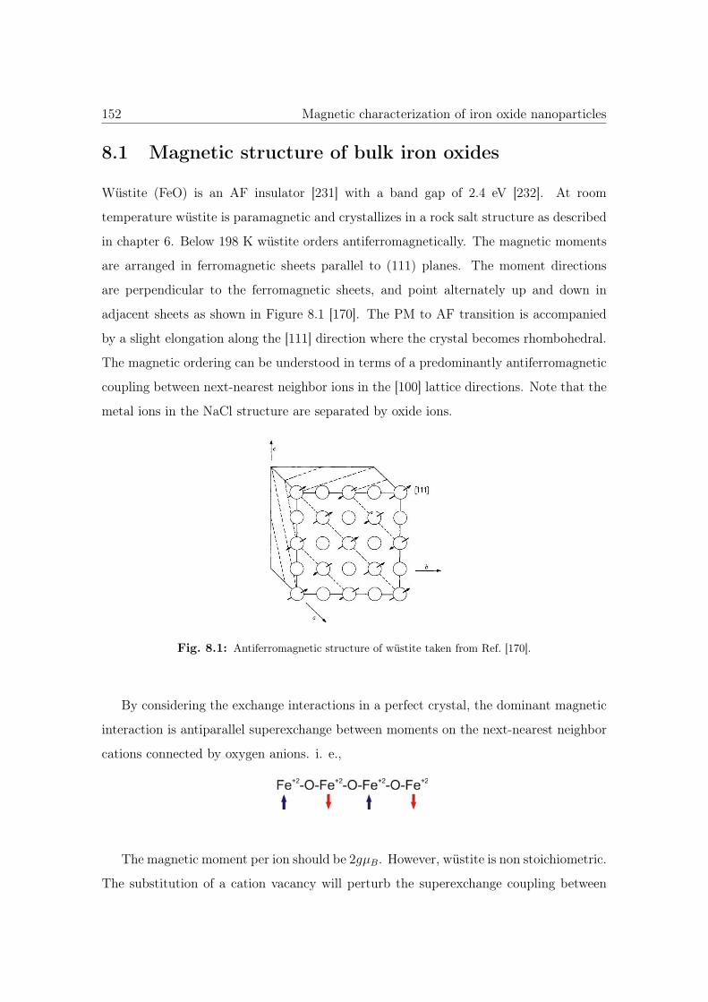
152 Magnetic characterization of iron oxide nanoparticles
8.1 Magnetic structure of bulk iron oxides
Wüstite (FeO) is an AF insulator [231] with a band gap of 2.4 eV [232]. At room
temperature wüstite is paramagnetic and crystallizes in a rock salt structure as described
in chapter 6. Below 198 K wüstite orders antiferromagnetically. The magnetic moments
are arranged in ferromagnetic sheets parallel to (111) planes. The moment directions
are perpendicular to the ferromagnetic sheets, and point alternately up and down in
adjacent sheets as shown in Figure 8.1 [170]. The PM to AF transition is accompanied
by a slight elongation along the [111] direction where the crystal becomes rhombohedral.
The magnetic ordering can be understood in terms of a predominantly antiferromagnetic
coupling between next-nearest neighbor ions in the [100] lattice directions. Note that the
metal ions in the NaCl structure are separated by oxide ions.
Fig. 8.1: Antiferromagnetic structure of wüstite taken from Ref. [170].
By considering the exchange interactions in a perfect crystal, the dominant magnetic
interaction is antiparallel superexchange between moments on the next-nearest neighbor
cations connected by oxygen anions. i. e.,
The magnetic moment per ion should be 2gμB. However, wüstite is non stoichiometric.
The substitution of a cation vacancy will perturb the superexchange coupling between
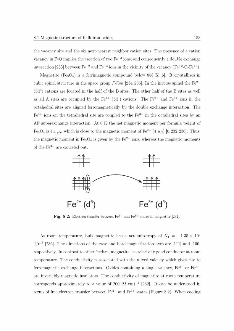
8.1 Magnetic structure of bulk iron oxides 153
the vacancy site and the six next-nearest neighbor cation sites. The presence of a cation
vacancy in FeO implies the creation of two Fe+3 ions, and consequently a double exchange
interaction [233] between Fe+2 and Fe+3 ions in the vicinity of the vacancy (Fe+2-O-Fe+3).
Magnetite (Fe3O4) is a ferrimagnetic compound below 858 K [6]. It crystallizes in
cubic spinel structure in the space group Fd3m [234,235]. In the inverse spinel the Fe2+
(3d6) cations are located in the half of the B sites. The other half of the B sites as well
as all A sites are occupied by the Fe3+ (3d5) cations. The Fe2+ and Fe3+ ions in the
octahedral sites are aligned ferromagnetically by the double exchange interaction. The
Fe3+ ions on the tetrahedral site are coupled to the Fe3+ in the octahedral sites by an
AF superexchange interaction. At 0 K the net magnetic moment per formula weight of
Fe3O4 is 4.1 μB which is close to the magnetic moment of Fe2+ (4 μB) [6,232,236]. Thus,
the magnetic moment in Fe3O4 is given by the Fe2+ ions, whereas the magnetic moments
of the Fe3+ are canceled out.
Fig. 8.2: Electron transfer between Fe2+ and Fe3+ states in magnetite [232].
At room temperature, bulk magnetite has a net anisotropy of K1 = −1.35 × 10⁴
J/m3 [236]. The directions of the easy and hard magnetization axes are [111] and [100]
respectively. In contrast to other ferrites, magnetite is a relatively good conductor at room
temperature. The conductivity is associated with the mixed valency which gives rise to
ferromagnetic exchange interactions. Oxides containing a single valency, Fe2+ or Fe3+,
are invariably magnetic insulators. The conductivity of magnetite at room temperature
corresponds approximately to a value of 200 (Ω cm)−1 [232]. It can be understood in
terms of free electron transfer between Fe2+ and Fe3+ states (Figure 8.2). When cooling
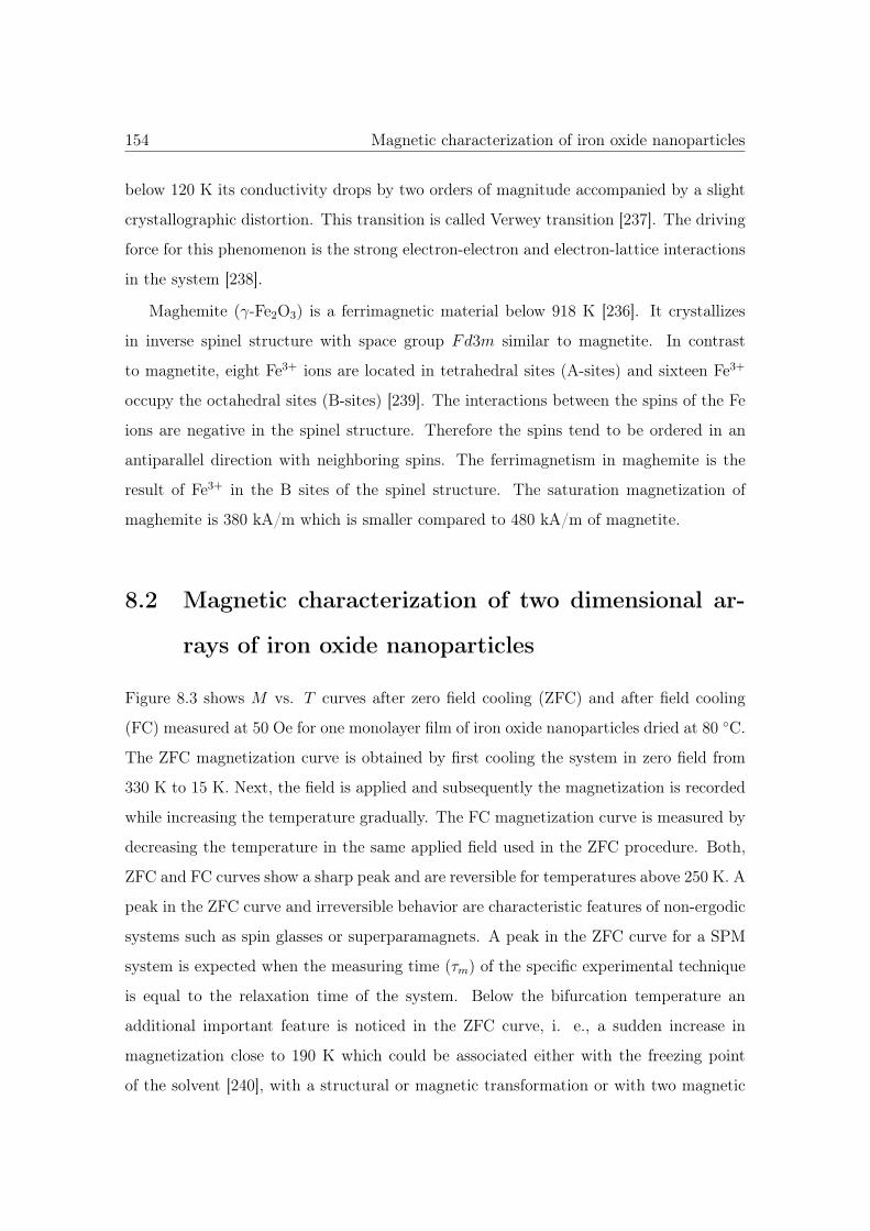
154 Magnetic characterization of iron oxide nanoparticles
below 120 K its conductivity drops by two orders of magnitude accompanied by a slight
crystallographic distortion. This transition is called Verwey transition [237]. The driving
force for this phenomenon is the strong electron-electron and electron-lattice interactions
in the system [238].
Maghemite (γ-Fe2O3) is a ferrimagnetic material below 918 K [236]. It crystallizes
in inverse spinel structure with space group Fd3m similar to magnetite. In contrast
to magnetite, eight Fe3+ ions are located in tetrahedral sites (A-sites) and sixteen Fe3+
occupy the octahedral sites (B-sites) [239]. The interactions between the spins of the Fe
ions are negative in the spinel structure. Therefore the spins tend to be ordered in an
antiparallel direction with neighboring spins. The ferrimagnetism in maghemite is the
result of Fe3+ in the B sites of the spinel structure. The saturation magnetization of
maghemite is 380 kA/m which is smaller compared to 480 kA/m of magnetite.
8.2 Magnetic characterization of two dimensional ar-
rays of iron oxide nanoparticles
Figure 8.3 shows M vs. T curves after zero field cooling (ZFC) and after field cooling
(FC) measured at 50 Oe for one monolayer film of iron oxide nanoparticles dried at 80 ◦C.
The ZFC magnetization curve is obtained by first cooling the system in zero field from
330 K to 15 K. Next, the field is applied and subsequently the magnetization is recorded
while increasing the temperature gradually. The FC magnetization curve is measured by
decreasing the temperature in the same applied field used in the ZFC procedure. Both,
ZFC and FC curves show a sharp peak and are reversible for temperatures above 250 K. A
peak in the ZFC curve and irreversible behavior are characteristic features of non-ergodic
systems such as spin glasses or superparamagnets. A peak in the ZFC curve for a SPM
system is expected when the measuring time (τm) of the specific experimental technique
is equal to the relaxation time of the system. Below the bifurcation temperature an
additional important feature is noticed in the ZFC curve, i. e., a sudden increase in
magnetization close to 190 K which could be associated either with the freezing point
of the solvent [240], with a structural or magnetic transformation or with two magnetic
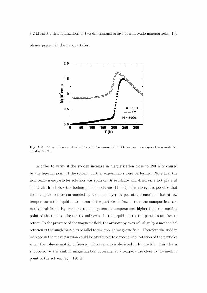
8.2 Magnetic characterization of two dimensional arrays of iron oxide nanoparticles 155
phases present in the nanoparticles.
0 50 100 150 200 250 3000.0
0.5
1.0
1.5
2.0
ZFC FC
H = 50Oe
M(1
0-5em
u)
T (K)
Fig. 8.3: M vs. T curves after ZFC and FC measured at 50 Oe for one monolayer of iron oxide NPdried at 80 ◦C.
In order to verify if the sudden increase in magnetization close to 190 K is caused
by the freezing point of the solvent, further experiments were performed. Note that the
iron oxide nanoparticles solution was spun on Si substrate and dried on a hot plate at
80 ◦C which is below the boiling point of toluene (110 ◦C). Therefore, it is possible that
the nanoparticles are surrounded by a toluene layer. A potential scenario is that at low
temperatures the liquid matrix around the particles is frozen, thus the nanoparticles are
mechanical fixed. By warming up the system at temperatures higher than the melting
point of the toluene, the matrix unfreezes. In the liquid matrix the particles are free to
rotate. In the presence of the magnetic field, the anisotropy axes will align by a mechanical
rotation of the single particles parallel to the applied magnetic field. Therefore the sudden
increase in the magnetization could be attributed to a mechanical rotation of the particles
when the toluene matrix unfreezes. This scenario is depicted in Figure 8.4. This idea is
supported by the kink in magnetization occurring at a temperature close to the melting
point of the solvent, Tm=180 K.
156 Magnetic characterization of iron oxide nanoparticles
This scenario has been investigated in our group via scanning electron microscopy
(SEM) and low temperature atomic force microscopy (AFM) measurements [40]. However
no mechanical rotation has been found.
Fig. 8.4: Schematic representaion of mechanical rotation of the nanoparticles in the toluene matrixtaken from Ref. [40]. Tm corresponds to the melting temperature of the solvent.
Furthermore, nanoparticles were prepared in a different solvent, i. e. benzene. The
adsorption of benzene on Si (100) closely resembles that of toluene, however, its freezing
point is 279 K compared with 180 K of toluene. Another sample was prepared on top of
PMMA in order to avoid the interaction toluene-Si (100).
Figure 8.5 shows M vs. T curves after zero field cooling (ZFC) and after field cooling
(FC) measured at 50 Oe for both samples, i.e. nanoparticles dissolved in benzene and
nanoparticles on top of PMMA. Both samples show similar features compared to the
sample dissolved in toluene (Fig. 8.3). All these results lead to the conclusion that
the model of a rotation of the particles most probably does not fit. Consequently the
hypothesis that the increase in magnetization close to 190 K is caused by the freezing
point of the solvent can be excluded. Note that the samples do not oxidize fast under
ambient conditions. Magnetometry studies on the same sample were performed after 3,
6 and 12 months, showing the identical magnetic properties.
The nature of the peak position as well as the sudden increase in magnetization in the
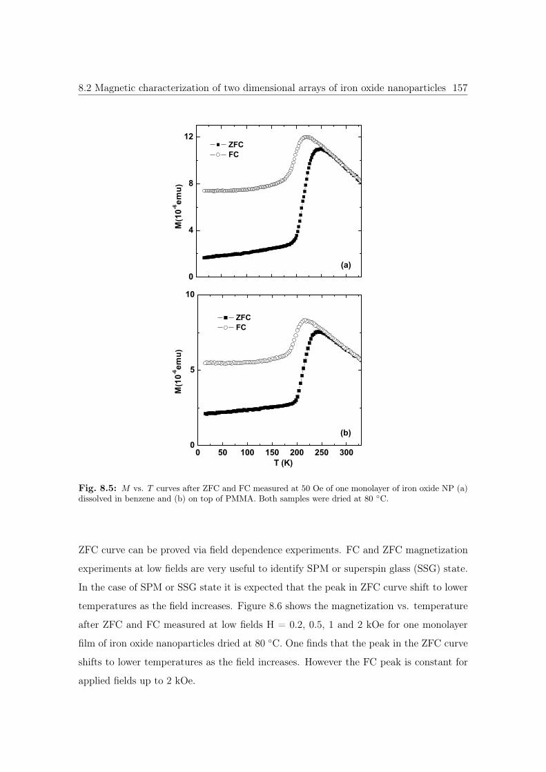
8.2 Magnetic characterization of two dimensional arrays of iron oxide nanoparticles 157
0
4
8
12
(a)
M(1
0-6em
u)
ZFC FC
0 50 100 150 200 250 3000
5
10
(b)
ZFC FC
T (K)
M(1
0-6em
u)
Fig. 8.5: M vs. T curves after ZFC and FC measured at 50 Oe of one monolayer of iron oxide NP (a)dissolved in benzene and (b) on top of PMMA. Both samples were dried at 80 ◦C.
ZFC curve can be proved via field dependence experiments. FC and ZFC magnetization
experiments at low fields are very useful to identify SPM or superspin glass (SSG) state.
In the case of SPM or SSG state it is expected that the peak in ZFC curve shift to lower
temperatures as the field increases. Figure 8.6 shows the magnetization vs. temperature
after ZFC and FC measured at low fields H = 0.2, 0.5, 1 and 2 kOe for one monolayer
film of iron oxide nanoparticles dried at 80 ◦C. One finds that the peak in the ZFC curve
shifts to lower temperatures as the field increases. However the FC peak is constant for
applied fields up to 2 kOe.
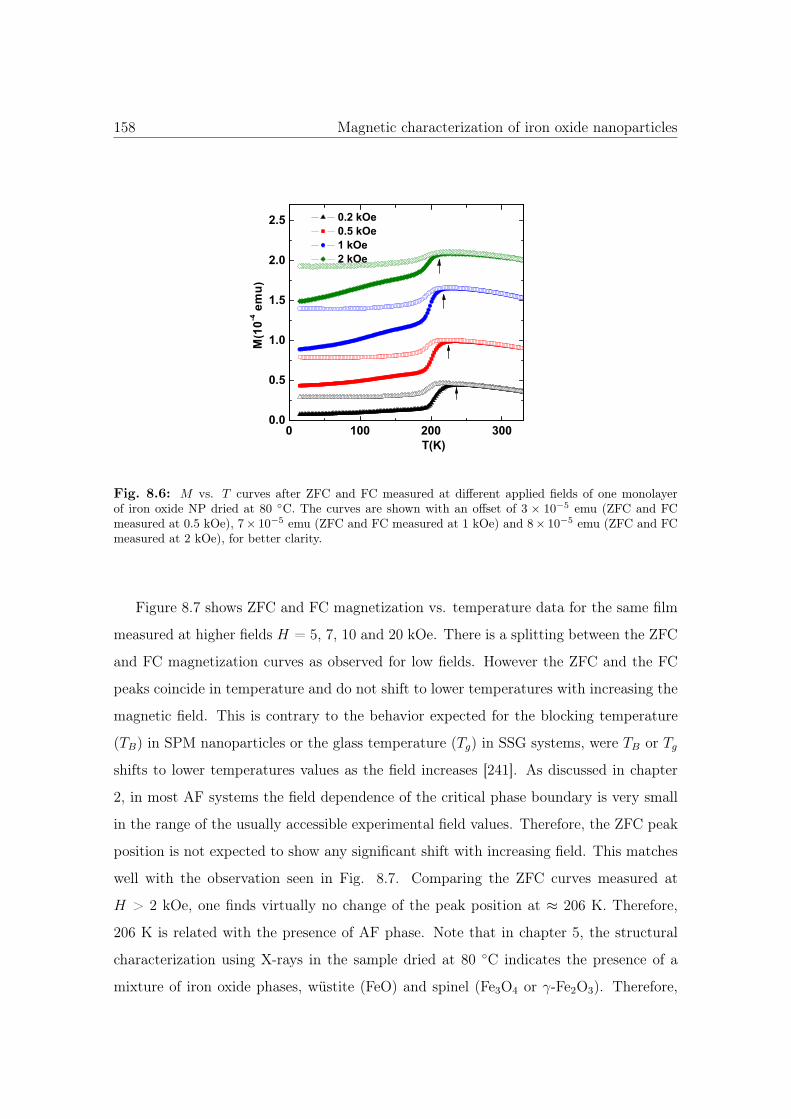
158 Magnetic characterization of iron oxide nanoparticles
0 100 200 3000.0
0.5
1.0
1.5
2.0
2.5 0.2 kOe 0.5 kOe 1 kOe 2 kOe
M(1
0-4 e
mu)
T(K)
Fig. 8.6: M vs. T curves after ZFC and FC measured at different applied fields of one monolayerof iron oxide NP dried at 80 ◦C. The curves are shown with an offset of 3 × 10⁻⁵ emu (ZFC and FCmeasured at 0.5 kOe), 7 × 10⁻⁵ emu (ZFC and FC measured at 1 kOe) and 8 × 10⁻⁵ emu (ZFC and FCmeasured at 2 kOe), for better clarity.
Figure 8.7 shows ZFC and FC magnetization vs. temperature data for the same film
measured at higher fields H = 5, 7, 10 and 20 kOe. There is a splitting between the ZFC
and FC magnetization curves as observed for low fields. However the ZFC and the FC
peaks coincide in temperature and do not shift to lower temperatures with increasing the
magnetic field. This is contrary to the behavior expected for the blocking temperature
(TB) in SPM nanoparticles or the glass temperature (Tg) in SSG systems, were TB or Tg
shifts to lower temperatures values as the field increases [241]. As discussed in chapter
2, in most AF systems the field dependence of the critical phase boundary is very small
in the range of the usually accessible experimental field values. Therefore, the ZFC peak
position is not expected to show any significant shift with increasing field. This matches
well with the observation seen in Fig. 8.7. Comparing the ZFC curves measured at
H > 2 kOe, one finds virtually no change of the peak position at ≈ 206 K. Therefore,
206 K is related with the presence of AF phase. Note that in chapter 5, the structural
characterization using X-rays in the sample dried at 80 ◦C indicates the presence of a
mixture of iron oxide phases, wüstite (FeO) and spinel (Fe3O4 or γ-Fe2O3). Therefore,
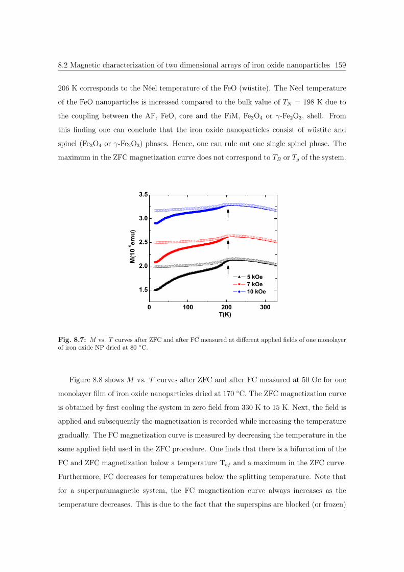
8.2 Magnetic characterization of two dimensional arrays of iron oxide nanoparticles 159
206 K corresponds to the Néel temperature of the FeO (wüstite). The Néel temperature
of the FeO nanoparticles is increased compared to the bulk value of TN = 198 K due to
the coupling between the AF, FeO, core and the FiM, Fe3O4 or γ-Fe2O3, shell. From
this finding one can conclude that the iron oxide nanoparticles consist of wüstite and
spinel (Fe3O4 or γ-Fe2O3) phases. Hence, one can rule out one single spinel phase. The
maximum in the ZFC magnetization curve does not correspond to TB or Tg of the system.
0 100 200 300
1.5
2.0
2.5
3.0
3.5
M
(10-4
emu)
T(K)
5 kOe 7 kOe 10 kOe
Fig. 8.7: M vs. T curves after ZFC and after FC measured at different applied fields of one monolayerof iron oxide NP dried at 80 ◦C.
Figure 8.8 shows M vs. T curves after ZFC and after FC measured at 50 Oe for one
monolayer film of iron oxide nanoparticles dried at 170 ◦C. The ZFC magnetization curve
is obtained by first cooling the system in zero field from 330 K to 15 K. Next, the field is
applied and subsequently the magnetization is recorded while increasing the temperature
gradually. The FC magnetization curve is measured by decreasing the temperature in the
same applied field used in the ZFC procedure. One finds that there is a bifurcation of the
FC and ZFC magnetization below a temperature Tbf and a maximum in the ZFC curve.
Furthermore, FC decreases for temperatures below the splitting temperature. Note that
for a superparamagnetic system, the FC magnetization curve always increases as the
temperature decreases. This is due to the fact that the superspins are blocked (or frozen)
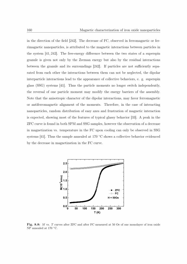
160 Magnetic characterization of iron oxide nanoparticles
in the direction of the field [242]. The decrease of FC, observed in ferromagnetic or fer-
rimagnetic nanoparticles, is attributed to the magnetic interactions between particles in
the system [41, 242]. The free-energy difference between the two states of a superspin
granule is given not only by the Zeeman energy but also by the residual interactions
between the granule and its surroundings [242]. If particles are not sufficiently sepa-
rated from each other the interactions between them can not be neglected, the dipolar
interparticle interactions lead to the appearance of collective behaviors, e. g. superspin
glass (SSG) systems [41]. Thus the particle moments no longer switch independently,
the reversal of one particle moment may modify the energy barriers of the assembly.
Note that the anisotropic character of the dipolar interactions, may favor ferromagnetic
or antiferromagnetic alignment of the moments. Therefore, in the case of interacting
nanoparticles, random distribution of easy axes and frustration of magnetic interaction
is expected, showing most of the features of typical glassy behavior [33]. A peak in the
ZFC curve is found in both SPM and SSG samples, however the observation of a decrease
in magnetization vs. temperature in the FC upon cooling can only be observed in SSG
systems [41]. Thus the sample annealed at 170 ◦C shows a collective behavior evidenced
by the decrease in magnetization in the FC curve.
0 50 100 150 200 250 3000.0
0.5
1.0
1.5
2.0
2.5
T (K)
M(1
0-4em
u)
ZFC FC
H = 50Oe
Fig. 8.8: M vs. T curves after ZFC and after FC measured at 50 Oe of one monolayer of iron oxideNP annealed at 170 ◦C.
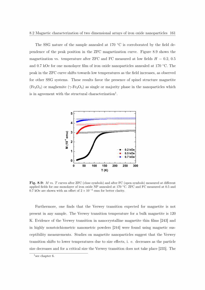
8.2 Magnetic characterization of two dimensional arrays of iron oxide nanoparticles 161
The SSG nature of the sample annealed at 170 ◦C is corroborated by the field de-
pendence of the peak position in the ZFC magnetization curve. Figure 8.9 shows the
magnetization vs. temperature after ZFC and FC measured at low fields H = 0.2, 0.5
and 0.7 kOe for one monolayer film of iron oxide nanoparticles annealed at 170 ◦C. The
peak in the ZFC curve shifts towards low temperatures as the field increases, as observed
for other SSG systems. These results favor the presence of spinel structure magnetite
(Fe3O4) or maghemite (γ-Fe2O3) as single or majority phase in the nanoparticles which
is in agreement with the structural characterization1.
0 50 100 150 200 250 3000
1
2
3
4
5
0.2 kOe 0.5 kOe 0.7 kOe
M (1
0-4 e
mu)
T (K)
Fig. 8.9: M vs. T curves after ZFC (close symbols) and after FC (open symbols) measured at differentapplied fields for one monolayer of iron oxide NP annealed at 170 ◦C. ZFC and FC measured at 0.5 and0.7 kOe are shown with an offset of 2 × 10⁻⁴ emu for better clarity.
Furthermore, one finds that the Verwey transition expected for magnetite is not
present in any sample. The Verwey transition temperature for a bulk magnetite is 120
K. Evidence of the Verwey transition in nanocrystalline magnetite thin films [243] and
in highly nonstoichiometric nanometric powders [244] were found using magnetic sus-
ceptibility measurements. Studies on magnetite nanoparticles suggest that the Verwey
transition shifts to lower temperatures due to size effects, i. e. decreases as the particle
size decreases and for a critical size the Verwey transition does not take place [235]. The1see chapter 6.
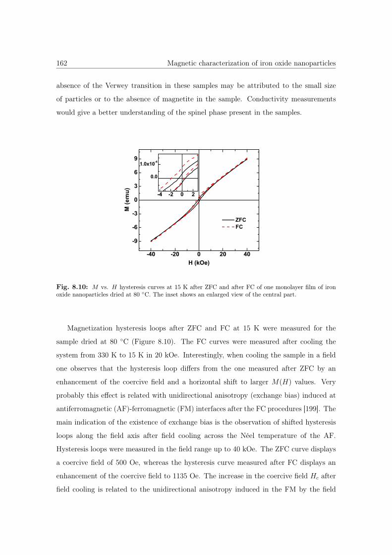
162 Magnetic characterization of iron oxide nanoparticles
absence of the Verwey transition in these samples may be attributed to the small size
of particles or to the absence of magnetite in the sample. Conductivity measurements
would give a better understanding of the spinel phase present in the samples.
-40 -20 0 20 40
-9
-6
-3
0
3
6
9
-4 -2 0 2
0.0
1.0x10⁻⁴
ZFC FC
M (e
mu)
H (kOe)
Fig. 8.10: M vs. H hysteresis curves at 15 K after ZFC and after FC of one monolayer film of ironoxide nanoparticles dried at 80 ◦C. The inset shows an enlarged view of the central part.
Magnetization hysteresis loops after ZFC and FC at 15 K were measured for the
sample dried at 80 ◦C (Figure 8.10). The FC curves were measured after cooling the
system from 330 K to 15 K in 20 kOe. Interestingly, when cooling the sample in a field
one observes that the hysteresis loop differs from the one measured after ZFC by an
enhancement of the coercive field and a horizontal shift to larger M(H) values. Very
probably this effect is related with unidirectional anisotropy (exchange bias) induced at
antiferromagnetic (AF)-ferromagnetic (FM) interfaces after the FC procedures [199]. The
main indication of the existence of exchange bias is the observation of shifted hysteresis
loops along the field axis after field cooling across the Néel temperature of the AF.
Hysteresis loops were measured in the field range up to 40 kOe. The ZFC curve displays
a coercive field of 500 Oe, whereas the hysteresis curve measured after FC displays an
enhancement of the coercive field to 1135 Oe. The increase in the coercive field Hc after
field cooling is related to the unidirectional anisotropy induced in the FM by the field
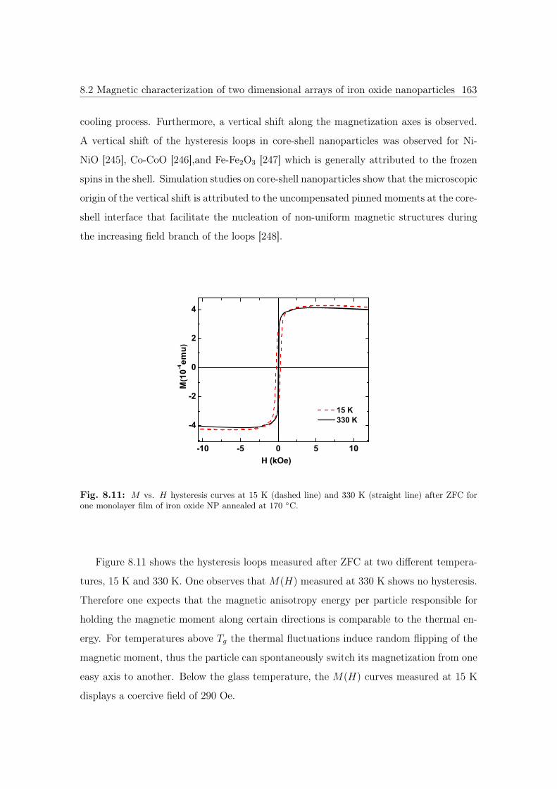
8.2 Magnetic characterization of two dimensional arrays of iron oxide nanoparticles 163
cooling process. Furthermore, a vertical shift along the magnetization axes is observed.
A vertical shift of the hysteresis loops in core-shell nanoparticles was observed for Ni-
NiO [245], Co-CoO [246],and Fe-Fe2O3 [247] which is generally attributed to the frozen
spins in the shell. Simulation studies on core-shell nanoparticles show that the microscopic
origin of the vertical shift is attributed to the uncompensated pinned moments at the core-
shell interface that facilitate the nucleation of non-uniform magnetic structures during
the increasing field branch of the loops [248].
-10 -5 0 5 10
-4
-2
0
2
4
M(1
0-4em
u)
15 K 330 K
H (kOe)
Fig. 8.11: M vs. H hysteresis curves at 15 K (dashed line) and 330 K (straight line) after ZFC forone monolayer film of iron oxide NP annealed at 170 ◦C.
Figure 8.11 shows the hysteresis loops measured after ZFC at two different tempera-
tures, 15 K and 330 K. One observes that M(H) measured at 330 K shows no hysteresis.
Therefore one expects that the magnetic anisotropy energy per particle responsible for
holding the magnetic moment along certain directions is comparable to the thermal en-
ergy. For temperatures above Tg the thermal fluctuations induce random flipping of the
magnetic moment, thus the particle can spontaneously switch its magnetization from one
easy axis to another. Below the glass temperature, the M(H) curves measured at 15 K
displays a coercive field of 290 Oe.
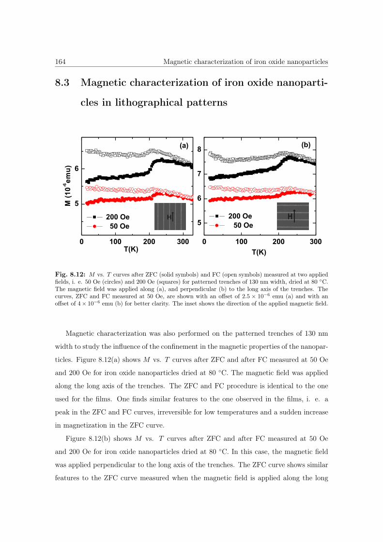
164 Magnetic characterization of iron oxide nanoparticles
8.3 Magnetic characterization of iron oxide nanoparti-
cles in lithographical patterns
0 100 200 300
5
6
0 100 200 300
5
6
7
8(a)
T(K)
200 Oe 50 Oe
T(K)
M (1
0-6em
u)
(b)
200 Oe 50 Oe
Fig. 8.12: M vs. T curves after ZFC (solid symbols) and FC (open symbols) measured at two appliedfields, i. e. 50 Oe (circles) and 200 Oe (squares) for patterned trenches of 130 nm width, dried at 80 ◦C.The magnetic field was applied along (a), and perpendicular (b) to the long axis of the trenches. Thecurves, ZFC and FC measured at 50 Oe, are shown with an offset of 2.5 × 10⁻⁶ emu (a) and with anoffset of 4 × 10⁻⁶ emu (b) for better clarity. The inset shows the direction of the applied magnetic field.
Magnetic characterization was also performed on the patterned trenches of 130 nm
width to study the influence of the confinement in the magnetic properties of the nanopar-
ticles. Figure 8.12(a) shows M vs. T curves after ZFC and after FC measured at 50 Oe
and 200 Oe for iron oxide nanoparticles dried at 80 ◦C. The magnetic field was applied
along the long axis of the trenches. The ZFC and FC procedure is identical to the one
used for the films. One finds similar features to the one observed in the films, i. e. a
peak in the ZFC and FC curves, irreversible for low temperatures and a sudden increase
in magnetization in the ZFC curve.
Figure 8.12(b) shows M vs. T curves after ZFC and after FC measured at 50 Oe
and 200 Oe for iron oxide nanoparticles dried at 80 ◦C. In this case, the magnetic field
was applied perpendicular to the long axis of the trenches. The ZFC curve shows similar
features to the ZFC curve measured when the magnetic field is applied along the long
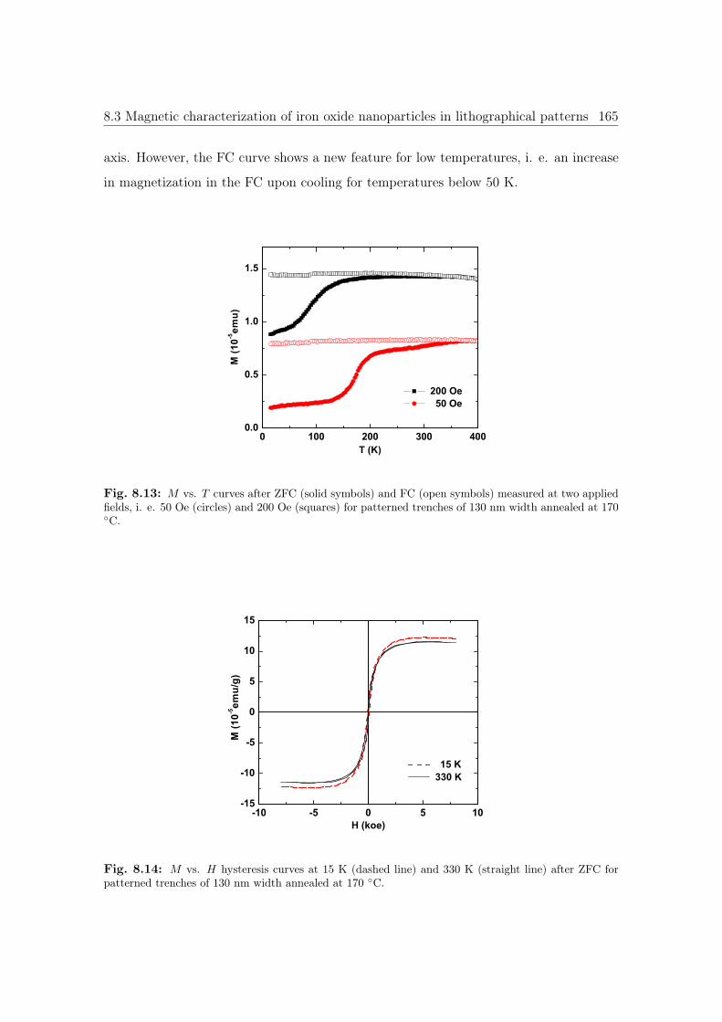
8.3 Magnetic characterization of iron oxide nanoparticles in lithographical patterns 165
axis. However, the FC curve shows a new feature for low temperatures, i. e. an increase
in magnetization in the FC upon cooling for temperatures below 50 K.
0 100 200 300 4000.0
0.5
1.0
1.5
200 Oe 50 Oe
M (1
0-5em
u)
T (K)
Fig. 8.13: M vs. T curves after ZFC (solid symbols) and FC (open symbols) measured at two appliedfields, i. e. 50 Oe (circles) and 200 Oe (squares) for patterned trenches of 130 nm width annealed at 170◦C.
-10 -5 0 5 10-15
-10
-5
0
5
10
15
15 K 330 K
M (1
0-5em
u/g)
H (koe)
Fig. 8.14: M vs. H hysteresis curves at 15 K (dashed line) and 330 K (straight line) after ZFC forpatterned trenches of 130 nm width annealed at 170 ◦C.
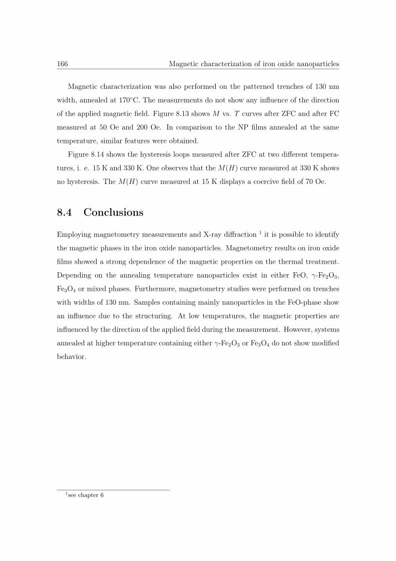
166 Magnetic characterization of iron oxide nanoparticles
Magnetic characterization was also performed on the patterned trenches of 130 nm
width, annealed at 170◦C. The measurements do not show any influence of the direction
of the applied magnetic field. Figure 8.13 shows M vs. T curves after ZFC and after FC
measured at 50 Oe and 200 Oe. In comparison to the NP films annealed at the same
temperature, similar features were obtained.
Figure 8.14 shows the hysteresis loops measured after ZFC at two different tempera-
tures, i. e. 15 K and 330 K. One observes that the M(H) curve measured at 330 K shows
no hysteresis. The M(H) curve measured at 15 K displays a coercive field of 70 Oe.
8.4 Conclusions
Employing magnetometry measurements and X-ray diffraction 1 it is possible to identify
the magnetic phases in the iron oxide nanoparticles. Magnetometry results on iron oxide
films showed a strong dependence of the magnetic properties on the thermal treatment.
Depending on the annealing temperature nanoparticles exist in either FeO, γ-Fe2O3,
Fe3O4 or mixed phases. Furthermore, magnetometry studies were performed on trenches
with widths of 130 nm. Samples containing mainly nanoparticles in the FeO-phase show
an influence due to the structuring. At low temperatures, the magnetic properties are
influenced by the direction of the applied field during the measurement. However, systems
annealed at higher temperature containing either γ-Fe2O3 or Fe3O4 do not show modified
behavior.
1see chapter 6
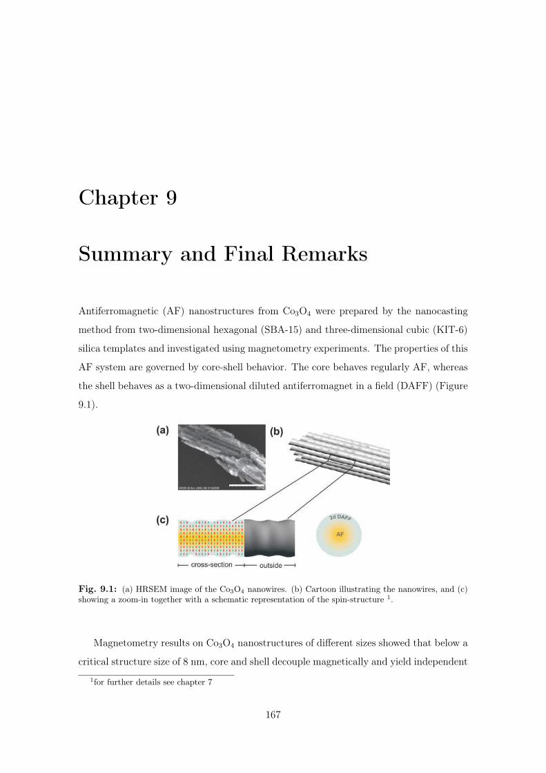
Chapter 9
Summary and Final Remarks
Antiferromagnetic (AF) nanostructures from Co3O4 were prepared by the nanocasting
method from two-dimensional hexagonal (SBA-15) and three-dimensional cubic (KIT-6)
silica templates and investigated using magnetometry experiments. The properties of this
AF system are governed by core-shell behavior. The core behaves regularly AF, whereas
the shell behaves as a two-dimensional diluted antiferromagnet in a field (DAFF) (Figure
9.1).
Fig. 9.1: (a) HRSEM image of the Co3O4 nanowires. (b) Cartoon illustrating the nanowires, and (c)showing a zoom-in together with a schematic representation of the spin-structure 1.
Magnetometry results on Co3O4 nanostructures of different sizes showed that below a
critical structure size of 8 nm, core and shell decouple magnetically and yield independent
1for further details see chapter 7
167
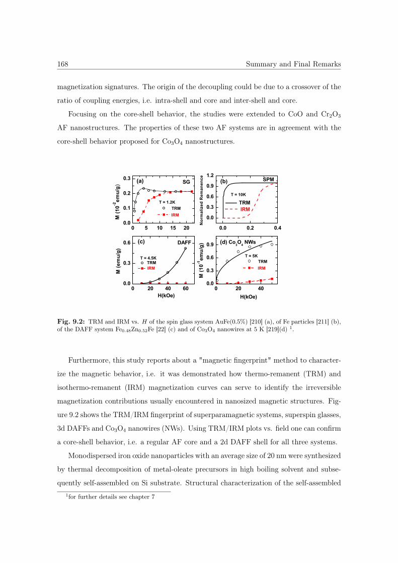
168 Summary and Final Remarks
magnetization signatures. The origin of the decoupling could be due to a crossover of the
ratio of coupling energies, i.e. intra-shell and core and inter-shell and core.
Focusing on the core-shell behavior, the studies were extended to CoO and Cr2O3
AF nanostructures. The properties of these two AF systems are in agreement with the
core-shell behavior proposed for Co3O4 nanostructures.
0 20 400.0
0.3
0.6
0.9
0 5 10 15 200.0
0.1
0.2
0.3
0 20 40 600.0
0.3
0.6
0.0 0.2 0.4
0.0
0.3
0.6
0.9
1.2
Co3O4 NWs
Nor
mal
ized
Rem
anen
ce
(d)
M (1
0-2em
u/g)
M (e
mu/
g)
T = 4.5K TRM IRM
(b)
(c)
(a)
H(kOe)
T = 5K
M (1
0-1em
u/g)
H(kOe)
SG
T = 1.2K
TRM IRM
DAFF
TRM IRM
SPM
TRM IRM
T = 10K
Fig. 9.2: TRM and IRM vs. H of the spin glass system AuFe(0.5%) [210] (a), of Fe particles [211] (b),of the DAFF system Fe0.48Zn0.52Fe [22] (c) and of Co3O4 nanowires at 5 K [219](d) 1.
Furthermore, this study reports about a "magnetic fingerprint" method to character-
ize the magnetic behavior, i.e. it was demonstrated how thermo-remanent (TRM) and
isothermo-remanent (IRM) magnetization curves can serve to identify the irreversible
magnetization contributions usually encountered in nanosized magnetic structures. Fig-
ure 9.2 shows the TRM/IRM fingerprint of superparamagnetic systems, superspin glasses,
3d DAFFs and Co3O4 nanowires (NWs). Using TRM/IRM plots vs. field one can confirm
a core-shell behavior, i.e. a regular AF core and a 2d DAFF shell for all three systems.
Monodispersed iron oxide nanoparticles with an average size of 20 nm were synthesized
by thermal decomposition of metal-oleate precursors in high boiling solvent and subse-
quently self-assembled on Si substrate. Structural characterization of the self-assembled1for further details see chapter 7
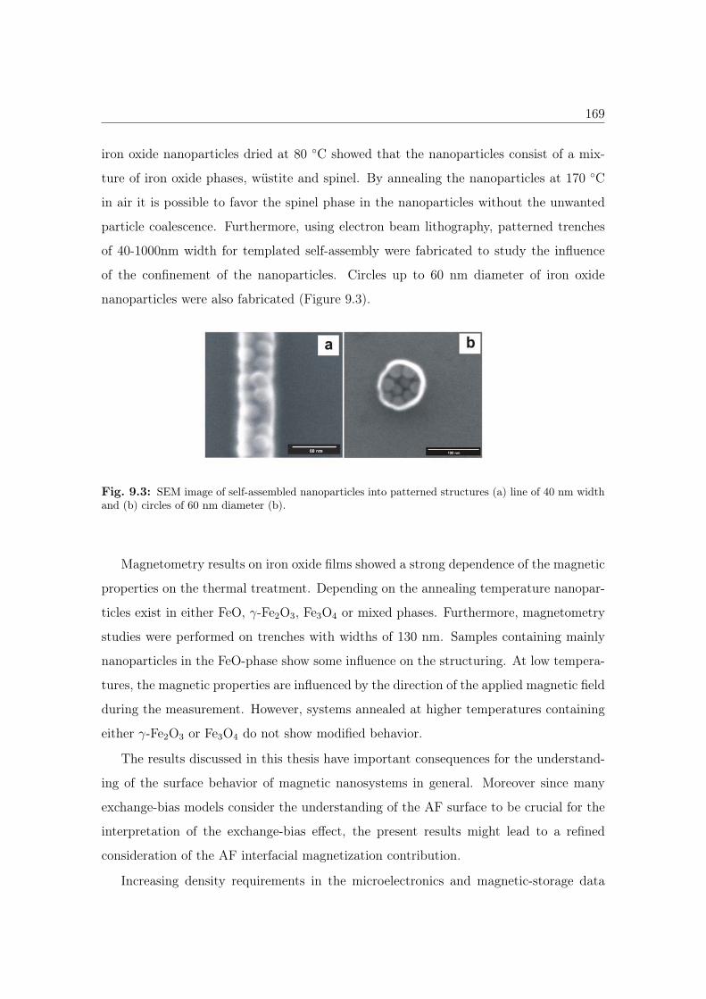
169
iron oxide nanoparticles dried at 80 ◦C showed that the nanoparticles consist of a mix-
ture of iron oxide phases, wüstite and spinel. By annealing the nanoparticles at 170 ◦C
in air it is possible to favor the spinel phase in the nanoparticles without the unwanted
particle coalescence. Furthermore, using electron beam lithography, patterned trenches
of 40-1000nm width for templated self-assembly were fabricated to study the influence
of the confinement of the nanoparticles. Circles up to 60 nm diameter of iron oxide
nanoparticles were also fabricated (Figure 9.3).
Fig. 9.3: SEM image of self-assembled nanoparticles into patterned structures (a) line of 40 nm widthand (b) circles of 60 nm diameter (b).
Magnetometry results on iron oxide films showed a strong dependence of the magnetic
properties on the thermal treatment. Depending on the annealing temperature nanopar-
ticles exist in either FeO, γ-Fe2O3, Fe3O4 or mixed phases. Furthermore, magnetometry
studies were performed on trenches with widths of 130 nm. Samples containing mainly
nanoparticles in the FeO-phase show some influence on the structuring. At low tempera-
tures, the magnetic properties are influenced by the direction of the applied magnetic field
during the measurement. However, systems annealed at higher temperatures containing
either γ-Fe2O3 or Fe3O4 do not show modified behavior.
The results discussed in this thesis have important consequences for the understand-
ing of the surface behavior of magnetic nanosystems in general. Moreover since many
exchange-bias models consider the understanding of the AF surface to be crucial for the
interpretation of the exchange-bias effect, the present results might lead to a refined
consideration of the AF interfacial magnetization contribution.
Increasing density requirements in the microelectronics and magnetic-storage data
170 Summary and Final Remarks
continue to motivate the production of devices at ever smaller dimensions. The results
presented in this thesis show that combining conventional lithography, chemical synthesis,
and self-assembly it is possible to fabricate sub-100-nm arranges of iron oxide NP. These
results can be extended to other NP, such as CoPt or FePt. It has been reported by Black
et al. that self-assembled devices composed of periodic arrays of 10-nanometer-diameter
cobalt nanocrystals display spin-dependent electron transport [249] with magnetoresis-
tance ratios on the order of 10% below 20 K. Electron transport properties of magnetite
nanocrystal arrays should be very interesting as well. Magnetite is a half-metal, where the
electronic density of states is spin polarized at the Fermi level. The conductivity is dom-
inated by spin-polarized charge carriers. At the time of this writing, magnetoresistance
experiments on these iron oxide NPs are carried out in our group.
Bibliography
[1] Feynman, R. There’s Plenty of Room at the Bottom. The annual meeting of the
American Physical Society, (1959).
[2] Baibich, M. N., Broto, J. M., Fert, A., Nguyen van Dau, F., Petroff, F., Etienne,
P., Creuzet, G., Friederich, A., and Chazelas, J. Phys. Rev. Lett. 61, 2472 (1988).
[3] Binasch, G., Grunberg, P., Saurenbach, F., and Zinn, W. Phys. Rev. B 39, 4828
(1989).
[4] Stöhr, J. and Siegmann, H. C. Magnetism. Springer, (2006).
[5] Morrish, A. H. The Physical Principles of Magnetism. Robert E. Krieger Publishing
Company, Inc, (1980).
[6] Blundell, S. Magnetism in Condensed Matter. Oxford University Press, (2006).
[7] Lévy, L.-P. Magnetism and superconductivity. Springer, (2000).
[8] Yosida, K. Theory of magnetism. Springer, (1996).
[9] Bertotti, G. Hysteresis in Magnetism. Academic Press, (1998).
[10] Zabel, H. Thin film magnetism. Curriculum IMPRS-Surmat T4: Deposition and
properties of thin films and self organized monolayers, (2006).
[11] Martin, D. H. Magnetism in Solids. THE M.I.T. PRESS, (1967).
[12] Aharoni, A. Introduction to the theory of ferromagnetism. Oxford University Press,
(1996).
171
172 BIBLIOGRAPHY
[13] Chakravarty. Introduction to Magnetic Properties of Solids. John Wiley and Sons,
(1980).
[14] Néel, L. Magnetism and the local molecular field. Nobel Lecture, (1970).
[15] Chikazumi, S. Magnetism. John Wiley and Sons, (1964).
[16] Skomski, R. Simple models of magnetism. Oxford, (2008).
[17] Roth, W. L. J. Phys. Chem. Solids 25, 1 (1964).
[18] Nattermann, T. and Vilfan, I. Phys. Rev. Lett. 61, 223 (1988).
[19] Fishman, S. and Aharony, A. J. Phys. C 12, L729 (1979).
[20] Cardy, J. Phys. Rev. B 29, L729 (1979).
[21] Nowak, U. and Usadel, K. D. Phys. Rev. B 66, 014430 (2002).
[22] Montenegro, F. C., Rezende, S. M., and Coutinho-Filho, M. D. Revista Brasileira
de Física 21, 192 (1991).
[23] Becerra, C. C., Paduan-Filho, A., Fries, T., Shapira, Y., and Palacios, F. J. Phys.:
Condens. Matter 6, 5725 (1994).
[24] Belanger, D. P. and Young, A. P. J. Magn. Magn. Mater. 100, 272 (1991).
[25] Jaccarino, V., King, R., and Belanger, D. J. App. Phys. 57, 3291 (1985).
[26] Belanger, D. Phys. Rev. Lett. 54, 577 (1985).
[27] Ikeda, H. J. Phys. C: Solid State Phys. 16, L1033 (1983).
[28] Ferreira, I. B., King, A. R., Jaccarino, V., Cardy, J. L., and Guggenheim, H. J.
Phys. Rev. B 28, 5192 (1983).
[29] Néel, L. Ann. Phys. 3, 137 (1948).
[30] Dormann, J., L. Fiorani, D., and Tronc, E. Adv. Chem. Phys. 98, 283 (1997).
[31] Terris, B. D. and Thomson, T. J. Phys. D 38, R199 (2005).
BIBLIOGRAPHY 173
[32] Gupta, A. K. and Gupta, M. Biomaterials 26, 3995 (2005).
[33] Batlle, X. and Labarta, A. J. Phys. D: Appl. Phys. 35, R15 (2002).
[34] Stoner, E. C. and Wohlfarth, E. P. Philos. Trans. London Ser. A 240, 599 (1948).
[35] Petracic, O. Nanomagnetismus. Vorlesung Sommersemester, Ruhr-Universität
Bochum, (2009).
[36] Bean, C. P. and Livingston, J. D. J. Appl. Phys. 30, 120s (1959).
[37] Néel, L. Ann. Geophys. 5, 99 (1949).
[38] Brown, W. F. J. Phys. Rev. 130, 1677 (1963).
[39] Jönsson, P. E. Adv. Chem. Phys. 128, 191 (2004).
[40] Szary, P. Magnetization reversal in magnetic nanostructures. Diploma thesis, Ruhr-
Universität Bochum, (2009).
[41] Petracic, O., Chen, X., Bedanta, S., Kleemann, W., Sahoo, S., Cardoso, S., and
Freitas, P. P. J. Magn. Magn. Mater. 300, 192 (2006).
[42] Lu, A.-H., Salabas, E. L., and Schüth, F. Angew. Chem. Int. Ed. 46, 1222 (2007).
[43] Néel, L. Comptes Rendus 252, 4057 (1961).
[44] Richardson, J. T., Yiagas, D. I., Turk, B., Forster, K., and Twigg, M. V. J. Appl.
Phys. 70, 6977 (1991).
[45] Tiwari, D. and Rajeev, K. P. Phys. Rev. B 72, 104433 (2005).
[46] Salabas, E. L., Rumplecker, A., Kleitz, F., Radu, F., and Schüth, F. Nano Lett 6,
2977 (2006).
[47] Winkler, E., Zysler, R. D., Vasquez Mansilla, M., and Fiorani, D. Phys. Rev. B 72,
132409 (2005).
[48] Yi, J. B., Ding, J., Feng, Y. P., Peng, G. W., Chow, G. M., Kawazoe, Y., Liu,
B. H., Yin, J. H., and Thongmee, S. Phys. Rev. B 76, 224402 (2007).
174 BIBLIOGRAPHY
[49] Moerup, S. and Frandsen, C. Phys. Rev. Lett. 92, 217201 (2004).
[50] Komada, R. H., Makhlouf, S. A., and Berkowitz, A. E. Phys. Rev. Lett. 79, 1393
(1997).
[51] Nogues, J., Sorta, J., Langlais, V., Skumryev, V., Surinach, S., Munoz, J. S., and
Baro, M. D. Physics Reports 442, 65 (2005).
[52] Tomou, A., Gournis, D., Panagiotopoulos, I., Huang, Y., Hadjipanayis, G. C., and
Kooi, B. J. J. Appl. Phys. 99, 123915 (2006).
[53] Punnoose, A. and Seehra, M. S. J. Appl. Phys. 91, 7766 (2002).
[54] Parkin, S. S. P. Ann. Revs. Mater. Sci. 25, 357 (1995).
[55] Parkin, S. S. P., More, N., and Roche, K. P. Phys. Rev. Lett. 64, 2304 (1990).
[56] Skomski, R. and Coey, J. M. D. Phys. Rev. B 48, 15812 (1993).
[57] Park, J., An, K., Hwang, Y., Park, J.-G., Noh, H.-J., Kim, J.-Y., Park, J.-H.,
Hwang, N.-M., and Hyeon, T. Nature Mater. 3, 891 (2004).
[58] Allwood, D. A., Xiong, G. Faulkner, C. C., Atkinson, D., Petit, D., and Cowburn,
R. P. Science 309, 1688 (2005).
[59] Westphalen, A., Schumann, A., Remhof, A., Zabel, H., Karolak, M., Baxevanis,
B., Vedmedenko, E. Y., Last, T., Kunze, U., and Eimüller, T. Phys. Rev. B 77,
174407 (2008).
[60] Whitesides, G. M. and Grzybowski, B. Science 295, 2418 (2002).
[61] Schüth, F. Self-Assembly. Curriculum IMPRS-Surmat T4: Deposition and proper-
ties of thin films and self organized monolayers, (2006).
[62] Yin, Y., Lu, Y., Gates, B., and Xia, Y. J. Am. Chem. Soc. 123, 8718 (2001).
[63] Lu, A. H. and Schüth, F. Adv. Mater. 18, 1793 (2006).
[64] Ying, J. Y., Mehnert, C. P., and Wong, M. S. Angew. Chem. Int. Ed. 38, 56 (1999).
BIBLIOGRAPHY 175
[65] Wan, Y. and Zhao, D. Y. Chem. Rev. 107, 2821 (2007).
[66] Corma, A. Chem. Rev. 97, 2373 (1997).
[67] Schüth, F. and Schmidt, W. Adv. Mater. 14, 629 (2002).
[68] Schüth, F. Chem. Mater. 13, 3184 (2001).
[69] Ryoo, R., Joo, S. H., and Jun, S. J. Phys. Chem. B 103, 7743 (1999).
[70] Yang, H., Shi, Q., Tian, B., Lu, Q., Gao, F., Xie, S., Fan, J., Yu, C., Tu, B., and
Zhao, D. Y. J. Am. Chem. Soc. 125, 4724 (2003).
[71] Tüysüz, H., Lehmann, C. W., Bongard, H., Tesche, B., Schmidt, R., and Schüth,
F. J. Am. Chem. Soc. 130, 11510 (2008).
[72] Tüysuz, H., Liu, Y., Weidenthaler, C., and Schüth, F. J. Am. Chem. Soc. 130,
14108 (2008).
[73] Tian, B., Liu, X., Yang, H., Xie, S., Yu, C., Tu, B., and Zhao, D. Y. Adv. Mater.
15, 1370 (2003).
[74] Rumplecker, A., Kleitz, F., Salabas, E. L., and Schüth, F. Chem. Mater. 19, 485
(2007).
[75] Tian, B., Liu, X., Solovyov, L. A., Liu, Z., Yang, H., Zhang, Z., Xie, S., Zhang, F.,
Tu, B., Yu, C., Terasaki, O., and Zhao, D. Y. J. Am. Chem. Soc. 126, 865 (2004).
[76] Yang, H. and Zhao, D. Y. J. Mater. Chem. 15, 1217 (2005).
[77] Jiao, K., Zhang, B., Yue, B., Ren, Y., Liu, S., Yan, S., Dickinson, C., Zhou, W.,
and He, H. Chem. Commun. , 5618 (2005).
[78] Jiao, F., Harrison, A., Jumas, J. C., Chadwick, A. V., Kockelmann, W., and Bruce,
P. G. J. Am. Chem. Soc. 128, 5468 (2006).
[79] Jiao, F., Jumas, J. C., Womes, M., Chadwick, A. V., Harrison, A., and Bruce, P. G.
J. Am. Chem. Soc. 128, 12905 (2006).
176 BIBLIOGRAPHY
[80] Vriezema, D. M., Aragones, M. C., Elemans, J. A. A. W., Cornelissen, J. J. L. M.,
Rowan, A. E., and Nolte, R. J. M. Chem. Rev. 105, 1445 (2005).
[81] M. Lindén, M., Schacht, S., Schüth, F., Steel, A., and Unger, K. K. J. of Porous
Mater. 5, 177 (1998).
[82] Yu, C. Z., Fan, J., Tian, B. Z., Stucky, G. D., and Zhao, D. Y. J. Phys. Chem. B
107, 13368 (2003).
[83] Raman, N. K., Anderson, M. T., and Brinker, C. J. Chem. Mater. 8, 1682 (1996).
[84] Israelachvili, J. N., Mitchell, D. J., and Ninham, B. W. J. Chem. Soc., Faraday
Trans. 72, 1525 (1976).
[85] Israelachvili, J. N., Mitchell, D. J., and Ninham, B. W. Biochimica Biophysica Acta
470, 185 (1997).
[86] Huo, Q. S., Margolese, D. I., and Stucky, G. D. Chem. Mater. 8, 1147 (1996).
[87] Israelachvili, J. Intermolecular and Surfaces Forces. Academic Press, London,
(1991).
[88] Firouzi, A., Kumar, D., Bull, L. M., Besier, T., Sieger, P., Huo, Q., Walker, S. A.,
Zasadzinski, J. A., Glinka, C., Nicol, J., Margolese, D., Stucky, G. D., and Chmelka,
B. F. Science 267, 1138 (1995).
[89] Huo, Q., Leon, R., Petroff, P. M., and Stucky, G. D. Science 268, 1324 (1995).
[90] Huo, Q. S., Margolese, D. I., Ciesla, U., Feng, P. Y., Gier, T. E., Sieger, P., Leon,
R., Petroff, P. M., Schüth, F., and Stucky, G. D. Nature 368, 317 (1994).
[91] Sakamoto, Y., Kaneda, M., Terasaki, O., Zhao, D. Y., Kim, J. M., Stucky, G.,
Shim, H. J., and Ryoo, R. Nature 408, 449 (2000).
[92] Zhang, Z. D., Yan, X. X., Tian, B. Z., Yu, C. Z., Tu, B., Zhu, G. S., Qiu, S. L.,
and Zhao, D. Y. Microporous Mesoporous Mater. 90, 23 (2006).
BIBLIOGRAPHY 177
[93] Che, S., Garcia-Bennett, A. E., Yokoi, T., Sakamoto, K., Kunieda, H., Terasaki,
O., and Tatsumi, T. Nat. Mater. 2, 801 (2003).
[94] Zhao, D. Y., Feng, J., Huo, Q., Melosh, N., Fredrickson, G. H., Chmelka, B. F.,
and Stucky, G. D. Science 279, 548 (1998).
[95] Attard, G. S., Glyde, J. C., and Goltner, C. G. Nature 378, 366 (1995).
[96] Zhao, D. Y., Huo, Q., Feng, J., Chmelka, B. F., and Stucky, G. D. J. Am. Chem.
Soc. 120, 6042 (1998).
[97] Huo, Q. S., Margolese, D. I., Ciesla, U., Demuth, D. G., Feng, P. Y., Gier, T. E.,
Sieger, P., Firouzi, A., Chmelka, B. F., Schuth, F., and Stucky, G. D. Chem. Mater
6, 1176 (1994).
[98] Tanev, P. T. and Pinnavaia, T. J. Science 267, 865 (1995).
[99] Bagshaw, S. A., Prouzet, E., and Pinnavaia, T. J. Science 269, 1242 (1995).
[100] Patarin, J., Lebeau, B., and Zana, R. Curr. Opin. Colloid Interface Sci. 7, 107
(2002).
[101] Zhang, F. Q., Yan, Y., Yang, H. F., Meng, Y., Yu, C. Z., Tu, B., and Zhao, D. Y.
J. Phys. Chem. B 109, 8723 (2005).
[102] Keene, M. T. J., Gougeon, R. D. M., Denoyel, R., Harris, R. K., Rouquerol, J., and
Llewellyn, P. L. J. Mater. Chem. 9, 2843 (1999).
[103] Kruk, M., Jaroniec, M., Ko, C. H., and Ryoo, R. Chem. Mater. 12, 1961 (2000).
[104] Inagaki, S., Sakamoto, Y., Fukushima, Y., and Terasaki, O. Chem. Mater. 8, 2089
(1996).
[105] Remhof, A. Nanolithography. Curriculum IMPRS-Surmat T4: Deposition and
properties of thin films and self organized monolayers, (2006).
[106] Petracic, O. Nanofabrication. Curriculum IMPRS-Surmat T4: Deposition and
properties of thin films and self organized monolayers, (2008).
178 BIBLIOGRAPHY
[107] Bhushan, B. Springer handbook of nanotechnology. Springer, (2004).
[108] Henderson, C. L. http://dot.che.gatech.edu/henderson/Introductions/intro
%20to%20e-beam%20lithography.htm.
[109] Rius, G. Electron beam lithography for nanofabrication. PhD thesis, Universidat
Autónoma de Barcelona, (2008).
[110] Bermudez, V. M. J. Vac. Sci. Technol. B 17, 2512 (1999).
[111] Theis-Bröhl, K. Thin films deposition. Curriculum IMPRS-Surmat T4: Deposition
and properties of thin films and self organized monolayers, (2006).
[112] Cui, Z. Nanofabrication. Springer, (200).
[113] Colmont, M. and Terasaki, O. Journal of Solid State Chemistry 180, 885 (2007).
[114] Pan, Z. W., Dai, Z. R., and Wang, Z. L. Science 291, 1947 (2001).
[115] Krause, S., Berbil-Bautista, L., Herzog, G., Bode, M., and Wiesendanger, R. Sci-
ence 307, 1537 (2007).
[116] Shinjo, T., Okuno, T., Hassdorf, R., Shigeto, K., and Ono, T. Science 289, 930
(2000).
[117] Hehn, M., Ounadjela, K., Bucher, J.-P., Rousseaux, F., Decanini, D., Bartenlian,
B., and Chappert, C. Science 272, 1782 (1996).
[118] Bonfim, M., Ghiringhelli, G., Montaigne, F., Pizzini, S., Brookes, N. B., Petroff,
F., Vogel, J., Camarero, J., and Fontaine, A. Phys. Rev. Lett. 86, 3646 (2001).
[119] Albouy, P.-A. and Ayral, A. Chem. Mater. 14, 3391 (2002).
[120] Morishige, K. and Tateishi, M. Langmuir 22, 4165 (2006).
[121] Muroyama, N., Yoshimura, A., Kubota, Y., Miyasaka, K., Ohsuna, T., Ryoo, R.,
Ravikovitch, P., Neimark, A. V., Takataand, M., and Terasaki, O. J. Phys. Chem.
C 112, 10803 (2008).
BIBLIOGRAPHY 179
[122] Sing, K. S. W., Everett, D. H., Haul, R. A. W., Moscou, L., Pierotti, R. A.,
Rouquerol, J., and Siemienniewska, T. Pure. Appl. Chem. 57, 603 (1985).
[123] Kruk, M. and Jaroniec, M. Chem. Mater. 13, 3169 (2001).
[124] Brunauer, S., Emmet, P. H., and Teller, E. J. Am. Chem. Soc. 60, 309 (1938).
[125] Barrett, E. P., Joyner, L. G., and Halenda, P. P. J. Am. Chem. Soc. 73, 373 (1951).
[126] Dove, M. Structure and dynamics. Oxford University Press, (2003).
[127] Solovyov, L. A., Zaikovskii, V. I., Shmakov, A. N., Belousov, O. V., and Ryoo, R.
J. Phys. Chem. B 106, 12198 (2002).
[128] Impéror-Clerc, M., Davidson, P., and Davidson, A. J. Am. Chem. Soc. 122, 11925
(2000).
[129] Muroyama, N., Ohsuna, T., Ryoo, R., Kubota, Y., and Terasaki, O. J. Phys. Chem.
B 110, 10630 (2006).
[130] Sauer, J., Marlow, F., and Schüth, F. Phys. Chem. Chem. Phys. 3, 5579 (2001).
[131] Beck, J. S., Vartuli, J. C., Roth, W. J., Leonowicz, M. E., Kresge, C. T., Schmitt,
K. D., Chu, C. T.-W., Olson, D. H., Sheppard, E. W., McCullen, S. B., Higgins,
J. B., and Schlenker, J. L. J. Am. Chem. Soc. 114, 10834 (1992).
[132] Feuston, B. P. and Higgins, J. B. J. Phys. Chem. 98, 4459 (1994).
[133] Solovyov, L. A., Kirik, S. D., Shmakov, A. N., and Romannikov, V. N. Microporous
Mesoporous Mater. 44-45, 17 (2001).
[134] Kim, T.-W. and Solovyov, L. J. Mater. Chem. 16, 1445 (2006).
[135] Yu, C., Yu, Y., and Zhao, D. Y. Chem. Commun. , 575 (2000).
[136] Rietveld, H. M. J. Appl. Crystallogr. 2, 65 (1969).
[137] Monnier, A., Schüth, F., Huo, Q., Kumar, D., Margolese, D., Maxwell, R. S.,
Stucky, G. D., Krishnamurty, M., Petroff, P., Firouzi, A., Janicke, M., and Chmelka,
B. F. Science 261, 1299 (1993).
180 BIBLIOGRAPHY
[138] Nobel-Foundation. http://nobelprize.org/.
[139] de Borglie, L. The wave nature of the electron. Nobel Lecture, (1929).
[140] Amelinckx, S., Gevers, R., and van Landuyt, J. Diffraction and imaging techniques
in material science. North-Holland Publishing Company, (1978).
[141] Reimer, L. Transmission electron microscopy. Springer-Verlag, (1984).
[142] Egerton, R. F. Physcial principles of electron microscopy. Springer, (2005).
[143] Goldstein, J. I. and Yakowitz, H. Practical scanning electron microscopy. Plenum
press, (1975).
[144] Interdisciplinary-Nanoscience-Center. http://www.inano.dk/research/competences-
and-facilities/nanotools/transmission-and-scanning-electron-microscopy/.
[145] Microanalysis. http://www7430.nrlssc.navy.mil/facilities/emf/microanalysis.htm.
[146] Barone, A. and Paternó, G. Physics and applications of the Josephson effect. John
Wiley and Sons, (1982).
[147] Clarke, J. and Braginski, A. The SQUID handbook. Wiley-VCH Verlag GmbH and
co. KGaA, (2004).
[148] Gallop, J. C. SQUIDs, the Josephson effects and superconducting electronics. Adam
Hilger, (1991).
[149] Gross, R. and Marx, A. Applied superconductivity: Josephson effect and supercon-
ducting electronics. Lecture WS, Technische Universität München, (2003).
[150] McElfresh, M. Fundamentals of magnetism and magnetic measurements featuring
quantum design’s magnetic property measurement system. Quantum Design, (1994).
[151] Dobson, J. Nature Nanotechnology 3, 139 (2008).
[152] Reiss, G. and Hütten, A. Nature Mater. 4, 725 (2005).
BIBLIOGRAPHY 181
[153] Jiao, F., Hill, A. H., Harrison, A., Berko, A., Chadwick, A. V., and Bruce, P. G. J.
Am. Chem. Soc. 130, 5262 (2008).
[154] Choi, M., Heo, W., Kleitz, F., and Ryoo, R. Chem. Commun. , 1340 (2003).
[155] Rumplecker, A. Host-Guest Chemistry of Mesoscopically Ordered Porous Materials.
PhD thesis, Ruhr-Universität Bochum, (2007).
[156] Kleitz, F., Choi, S. H., and Ryoo, R. Chem. Commun. , 2136 (2003).
[157] Rodriguez-Carvajal, J. http://www-llb.cea.fr/fullweb/, (2006).
[158] Tüysüz, H. Novel Mesostructured Metal Oxides. PhD thesis, Ruhr-Universität
Bochum, (2008).
[159] Wang, J. P. Nature Mater. 4, 191 (2005).
[160] Back, C. H., Allenspach, R., Weber, W., Parkin, S. S. P., Weller, D., Garwin, E. L.,
and Siegmann, H. C. Science 285, 864 (1999).
[161] Sun, S. C., Murray, C. B., Weller, D., Folks, L., and Moser, A. Science 287, 1989
(2000).
[162] Kim, T. H., Jang, E. Y., Lee, N. Y., Choi, D. J., Lee, K. J., Jang, J.-t., Choi, J.-s.,
Moon, S. H., and Cheon, J. Nano Lett. 9, 2229 (2009).
[163] Cui, Y., Bjork, M. T., Liddle, J. A., Sonnichsen, C., Boussert, B., and Alivisatos,
A. P. Nano Lett. 4, 1093 (2004).
[164] Wong, S., Kitaev, V., and Ozin, G. O. J. Am. Chem. Soc. 125, 15589 (2003).
[165] Daughton, J. Proc. of the IEEE 91, 681 (2003).
[166] Medarova, Z., Pham, W., Farrar, C., Petkova, V., and Moore, A. Nature Med. 13,
372 (2006).
[167] Krishnan, K. M., Pakhomov, A. B., Bao, Y., Blomqvist, P., Chun, Y., Gonzales,
M., Griffin, K., Ji, X., and Roberts, B. K. J. Mater. Sci. 793, 793 (2006).
182 BIBLIOGRAPHY
[168] Pankhurst, Q. A., Connolly, J., Jones, S. K., and Dobson, J. J. Phys. D: Appl.
Phys. 36, R167 (2003).
[169] Darling, S. B. and Bader, S. D. J. Mater. Chem. 15, 4189 (2005).
[170] Roth, W. L. Acta Cryst. 13, 140 (1960).
[171] Natelson, D. http://www.ruf.rice.edu/ natelson/research.html.
[172] Makhlouf, S. J. Magn. Magn. Mater. 246, 184 (2002).
[173] Makhlouf, S. A., Parker, F. T., Spada, F. E., and Berkowitz, A. E. J. App. Phys.
81, 5561 (1997).
[174] Makhlouf, S. J. Magn. Magn. Mater. 272, 1530 (2004).
[175] Gass, J., Poddar, P., Almand, J., Srinath, S., and Srikanth, H. Adv. Funct. Mater.
16, 71 (2006).
[176] Dutta, P., Seehra, M. S., Thota, S., and Kumar, J. J. Phys.: Condens. Matter 20,
015218 (2008).
[177] Park, S. J., Kim, S., Lee, S., Khim, Z. G., Char, K., and Hyeon, T. J. Am. Chem.
Soc. 122, 8581 (2000).
[178] Shtykova, E. V., Huang, X., Remmes, N., Baxter, D., Stein, B., Dragnea, B.,
Svergun, D. I., and Bronstein, L. M. J. Phys. Chem. C 111, 18078 (2007).
[179] Sun, S. and Murray, C. B. J. Appl. Phys. 85, 4325 (1999).
[180] Sun, S., Zeng, H., Robinson, D. B., Raoux, S., Rice, P. M., Wang, S. X., and Li,
G. J. Am. Chem. Soc. 126, 273 (2004).
[181] Sun, S. and Zeng, H. J. Am. Chem. Soc. 124, 8204 (2002).
[182] Dumestre, F., Chaudret, B., Amiens, C., Renaud, P., and Fejes, P. Science 303,
821 (2004).
[183] Petit, C., Taleb, A., and Pileni, M. P. J. Phys. Chem. B 103, 1805 (1999).
BIBLIOGRAPHY 183
[184] Sellmyer, D. and Skomski, R. Advanced magnetic nanostructures. Springer Sci-
ence+Business Media, Inc., (2006).
[185] Redl, F., Black, C. T., Papaefthymiou, G. C., Sandstrom, R. L., Yin, M., Zeng, H.,
Murray, C. B., and O’Brien, S. P. J. Am. Chem. Soc. 126, 14583 (2004).
[186] Hou, Y., Xu, Z., and Sun, S. Angew. Chem. Int. Ed. 46, 6329 (2007).
[187] Néel, L. C. R. Acad. Sci. Paris 228, 664 (1949).
[188] Néel, L. C. R. Acad. Sci. Paris 252, 4075 (1961).
[189] Bode, M., Vedmedenko, E. Y., von Bergmann, K., Kubetzka, A., Ferriani, P.,
Heinze, S., and Wiesendanger, R. Nature Mater. 5, 477 (2006).
[190] Scholl, A., Stöhr, J., Lüning, J., Seo, J. W., Fompeyrine, J., Siegwart, H., Locquet,
J.-P., Nolting, F., Anders, S., Fullerton, E. E., Scheinfein, M. R., and Padmore,
H. A. Science 287, 1014 (2000).
[191] Cossee, P. J. inorg. nucl. Chem. 8, 483 (1958).
[192] http://www.freewebs.com/diendanhoak26/hoahocvoco.htm.
[193] Ikedo, Y., Sugiyama, J., Nozaki, H., Itahara, H., Brewer, J. H., Ansaldo, E. J.,
Morris, G. D. Andreica, D., and Amato, A. Phys. Rev. B 75, 054424 (2007).
[194] Hansen, M. F. and Moerup, S. J. Magn. Magn. Mater. 203, 214 (1999).
[195] Sappey, R., Vincent, E., Hadacekand, N., Chaput, F., Boilot, J. P., and Zins, D.
Phys. Rev. B 56, 14551 (1997).
[196] Zheng, X. G., Zangwill, A., and Stiles, M. D. Phys. Rev. B 72, 014464 (2005).
[197] Jonason, K., Vincent, E., Hammann, J., Bouchaud, J. P., and P., N. Phys. Rev.
Lett. 81, 3243 (1998).
[198] Salabas, E. L., Radu, F., Tüysüz, H., and Benitez, M. J. Experimental report ILL
D20 (2008).
184 BIBLIOGRAPHY
[199] Meiklejohn, W. H. and Bean, C. P. Phys. Rev. 102, 1413 (1956).
[200] Nogues, J. and Schuller, I. K. J. Magn. Magn. Matter. 192, 203 (1999).
[201] Berkowitz, A. E. and Takano, K. J. Magn. Magn. Mater. 200, 552 (1999).
[202] Radu, F. and Zabel, H. Springer Tracts in Modern Physics 227, 97 (2007).
[203] Cowburn, R. P., Koltsov, D. K., Adeyeye, A. O., Welland, M. E., and Tricker, D. M.
Phys. Rev. Lett. 83, 1042 (1999).
[204] Katzgraber, H. G., Pázmándi, F., Pike, C. R., Liu, K., Scalettar, R. T., Verosub,
K. L., and Zimányi, G. T. Phys. Rev. Lett. 89, 257202 (2002).
[205] Pike, C. R., Ross, C. A., Scalettar, R. T., and Zimányi, G. Phys. Rev.B 71, 134407
(2005).
[206] Petracic, O., Glanz, A., and Kleemann, W. Phys. Rev. B 70, 214432 (2004).
[207] Repain, V., Jamet, J.-P., Vernier, N., Bauer, M., Ferre, J., Chappert, C., Gierak,
J., and Mailly, D. J. Appl. Phys. 95, 2614 (2004).
[208] Mydosh, J. Spin Glasses: An Experimental Introduction. Taylor and Francis,
London, (1993).
[209] Kleemann, W. Int. J. Mod. Phys. B 7, 2469 (1993).
[210] Tholence, J. L. and Tournier, R. J. Phys. 35, C4–229 (1974).
[211] Roshko, R. M., Viddal, C. A., Ge, S., and Gao, M. IEEE Trans. Magn. 40, 2137
(2004).
[212] Kinzel, W. Phys. Rev. B 19, 4595 (1979).
[213] Binder, K. and Young, A. P. Rev. Mod. Phys. 58, 801.
[214] Bouchiat, H. and Monod, P. J. Magn. Magn. Mater. 30, 175 (1982).
[215] El-Hilo, M., O’Grady, K., and Chantrell, R. W. J. Magn. Magn. Mater. 140, 359
(1995).
BIBLIOGRAPHY 185
[216] Dormann, J. L., Fiorani, D., Tholence, J. L., and Sella, C. J. Magn. Magn. Mater.
35, 117 (1983).
[217] Villain, J. Phys. Rev. Lett. 52, 1543 (1984).
[218] Malozemoff, A. P. Phys. Rev. B 37, 7673 (1988).
[219] Benitez, M. J., Petracic, O., Salabas, E. L., Radu, F., Tüysüz, H., Schüth, F., and
Zabel, H. Phys. Rev. Lett. 101, 097206 (2008).
[220] Roth, W. L. Phys. Rev. 110, 1333 (1958).
[221] Shapira, Y. Phys. Rev. 187, 734 (1969).
[222] McGuire, T. R., Scott, E. J., and Grannis, F. H. Phys. Rev. 102, 1000 (1956).
[223] Tobia, D., Winkler, E., Zysler, R. D., Granada, M., and Troiani, H. E. Phys. Rev.
B 78, 104412 (2008).
[224] Brown, P. J., Forsyth, J. B., and Tasset, F. J. Phys.: Condens. Matter 10, 663
(1998).
[225] Nomura, S., Santoro, R., Fang, J., and Newnham, R. J. Phys. Chem. Solids 25,
901 (1964).
[226] Sun, S. Adv. Mater. 18, 393 (2006).
[227] Jeong, U., Teng, X., Wang, Y., Yang, H., and Xia, Y. Adv. Mater. 19, 33 (2007).
[228] Laurent, S., Forge, D., Port, M., Roch, A., Robic, C., Elst, L. V., and Muller, R.
Chem. Rev. 108, 2064 (2008).
[229] Murray, C. B., Kagan, C. R., and Bawendi, M. G. Annu. Rev. Mater. Sci. 30, 545
(2000).
[230] Ferrando, R., Jellinek, J., and Johnston, R. L. Chem. Rev. 108, 845 (2008).
[231] Terakura, K., Oguchi, T., Williams, A. R., and Kübler, J. Phys. Rev. B 30, 4734
(1984).
186 BIBLIOGRAPHY
[232] Cox, P. A. Transition metal oxides. Clarendon press, (1995).
[233] Zener, C. Phys. Rev. 82, 403 (1951).
[234] Mazo-Zuluaga, J., Restrepo, J., and Mejía-López, J. Physica B 398, 187 (2007).
[235] Goya, G. F., Berquó, T. S., Fonseca, F. C., and Morales, M. P. J. Appl. Phys. 94,
3520 (2003).
[236] Dunlop, D. J. and Özdemir, O. Rock magnetism. Fundametals and frontiers. Cam-
bridge University Press, (1997).
[237] Verwey, E. J. W. Nature 144, 327 (1939).
[238] Poddar, P., Fried, T., and Markovich, G. Phys. Rev. B 65, 172405 (2002).
[239] Restrepo, J., Labaye, Y., and Greneche, J. M. Physica B 384, 221 (2006).
[240] Zhang, L.-Y., Dou, Y.-H., Zhang, L., and Gu, H.-C. Chin. Phys. Lett. 24, 483
(2007).
[241] Zheng, R. K., Wen, G. H., Fung, K. K., and Zhang, X. X. Phsy. Rev. B 69, 214431
(2004).
[242] Sasaki, M., Jönsson, P. E., Takayama, H., and Mamiya, H. Phys. Rev. B 71, 104405
(2005).
[243] Tang, J., Wang, K.-Y., and Zhou, W. J. Appl. Phys. 89, 7690 (2001).
[244] Guigue-Millot, N., Keller, N., and Perriat, P. Phys. Rev. B 64, 012402 (2001).
[245] Yao, Y. D., Chen, Y. Y., Hsu, C. M., Lin, H. M., Tung, C. Y., Tai, M. F., Wang,
D. H., Wu, K. T., and Suo, C. T. Nanostruct. Mater. 6, 933 (1995).
[246] Tracy, J. B. and Bawendi, M. G. Phys. Rev. B 74, 184434 (2006).
[247] Zheng, R. K., Wen, G. H., Fung, K. K., and Zhang, X. X. J. Appl. Phys. 95, 5244
(2004).
[248] Iglesias, O., Labarta, A., and Batlle, X. J. Nanosci. Nanotechnol. 8, 2761 (2008).

BIBLIOGRAPHY 187
[249] Black, C. T., Murry, C. B., Sandstorm, R. L., and Sun, S. Science 290, 1131 (2000).

188 BIBLIOGRAPHY

Acknowledgement
At first and foremost, I would like to thank my supervisors Prof. Dr. Dr. h.c. Hartmut
Zabel and Prof. Dr. Ferdi Schüth to provide me with sufficient freedom in this project.
I express my deepest gratitude to them for their vital encouragement and invaluable
suggestions throughout the course of my studies.
I am deeply indebted to PD Dr. Oleg Petracic for his valuable advice and support.
It has been pleasing to discuss with him many aspects of physics and magnetism in a
friendly and relaxed atmosphere. I also thank him for taking the time to read my thesis.
Our discussions on the completion of the thesis have been of great value.
Furthermore I would like to thank Dr. Harun Tüysüz and Mathias Feyen not only
for explaining me the syntheses but also for providing me some of the materials used in
this dissertation. I appreciate their willingness and kindness to help me any time when
I had questions. I sincerely thank Philipp Szary not only for his excellent comments
but also for listening to me whenever I had doubts or ideas for our project. This is also
extended to Durga Mishra who provided me several useful XRD patterns of iron oxide
nanoparticles.
Furthermore I would like to recognize many valuable contributions from Prof. Dr.
Kurt Westerholt, Dr. Lorena Salabas, Dr. Wolfgang Schmidt, Dr. Florin Radu, Dr.
An-Hui Lu and Dr. Claudia Weidenthaler.
I would like to acknowledge the help from the Microscopy Department at Max-Planck-
Insititut für Kohlenforschung, in the persons of Dr. Bernd Tesche, Dr. Christian W.
Lehmann, Bernd Spliethoff, Axel Dreier and Hans Bongard.
I owe my special thanks to Dr. Miriana Vadalá and Dr. Nan Li for their warm
welcome and their help in personal issues especially during the first months of my doctoral
189
190 Acknowledgement
project.
Special thanks to my office mates, Dr. Miriana Vadalá, Dr. Numan Akdogan, Dr.
Harun Tüysüz, Dr. Anja Rumplecker, Dr. Arti Dangwal Pandey, Durga Mishra, Alexan-
der Cepak, Piotr Bazula and Astrid Ebbing for distinct helpfulness and for maintaining
a nice working atmosphere. I am grateful for the nice time spent in conferences and
schools with my colleagues and especially I would like to thank Alexandra Schumann for
organizing our hotels. I would like to thank Jörg Dudek for giving me a hand with the
helium bottle any time that I needed it.
I am grateful to Petra Hahn, Bazar Öztamur, Claudia Wulf, Inis Gottmannshausen,
Helga Wasilewski and Angelika Rathofer, for their kind help on many administrative
issues.
I would also like to thank Peter Stauche, Horst Glowatzki, Deniss Schöpper and
Marjan Tomas, for their help on technical problems.
Many others at Experimentalphysik IV and Max-Planck-Insititut für Kohlenforschung
that have been involved also deserve recognition. It is, however, not possible to list them
all here. Their support in this effort is greatly appreciated.
I gratefully acknowledge a fellowship trough the International Max-Planck Research
School for Surface and Interface Engineering in Advance Materials (IMPRS-Surmat). I
also would like to thank to Dr. Angelika Büttner, Dr. Christoph Somsen and Dr. Rebekka
Loschen for their wonderful help and support with regards to various official matters. I
would like to thank all the Surmat students for very pleasant and friendly atmosphere
during our meetings and seminars.
It is a pleasure to express my gratitude wholeheartedly to Folsche’s and Cadenbach’s
family for their kindness and affection. I would also like to thank all my friends from
different parts of the world for wishing me luck towards this research.
Me gustaría agradecer de todo corazón a mi familia por su inmenso amor y su apoyo
constante. A mis padres Susana y Guillermo, quienes me han alentado a seguir mi corazón
y enseñado que si hay una meta, hay un camino. A mis abuelitos Teresa y Segundo, por
todas sus oraciones. A mi tía Ligia, quien con mucho amor siempre me ha apoyado y
a disfrutado de mis logros. A mis hermanos Felipe y Sebastián, quienes a pesar de la
distancia han estado siempre conmigo, contagiándome su buen humor. A mi tío Claudio,

Acknowledgement 191
a Bachita y a Andrea.
Words fail me to express my appreciation to my best friend and my great love Thomas
for his everlasting love, motivation, support and encouragement. I would like to thank
him for reading the whole thesis thoroughly and correct the English spelling and grammar
and also for our long scientific discussions. You are a powerful source of inspiration and
an example of perseverance. I am really blessed to have you. I love you with all my heart.
Thank you all for your insights, guidance and support!

192

193
Curriculum Vitae Name: María José Benítez Romero Date of Birth: February, 16 1981 Place of Birth: Quito - Ecuador Nationality: Ecuadorian Office Adress: Ruhr-Universität Bochum, NB4 Institut für Experimentalphysik/Festkörperphysik Universitätsstraße 150 44801 Bochum
Germany Office Phone: ++492343223626 Email Adress: [email protected]
EDUCATION
� Since Sept. 2006 Ph.D. Thesis in Physics“Self-assembled Magnetic Nanostructures: Synthesis and Characterization”
Faculty of Physics and Astronomy, Experimental Physics 4, Ruhr-University Bochum, Germany, Supervisor: Prof. Dr. Dr. h. c. Hartmut Zabel Supervisor: Prof. Dr. Ferdi Schüth
� 1999-2005 Diploma in Physics “Synthesis and characterization of calcium doped zirconia
nanopowder.” Final Grade: With Distinction
194
Faculty of Physics, Escuela Politecnica Nacional Quito, Ecuador, Supervisor: Dr. Luis Lascano
� 1999 Highschool degree in Ecuatoriano Suizo, Quito, Ecuador. Score: 19/20
AWARDS AND FELLOWSHIPS
� 2009 Awarded for one of the best two contributed oral presentations of young scientists at Nanomagnets 2009.
� 2006 Awarded 3 years scholarship for graduate studies from International Max-Planck Research School for Surface and Interface Engineering in Advanced Materials “Surmat”.
� 2005 Awarded partial scholarship to 2nd European Hydrogen Energy Conference. Zaragoza - Spain.
� 2005 Awarded full scholarship to the 7th Giambiagi Winter School. Buenos Aires, Argentina.
� 2004 Awarded full scholarship to the ICTP Spring College on Science at the Nanoscale. Trieste, Italy.
PUBLICATIONS
� Benitez, M. J.; Petracic, O.; Tüysüz, H.; Schüth, F.; Zabel, H. “Decoupling of magnetic core and shell contributions in antiferromagnetic Co3O4 nanostructures”, Europhys. Lett. In press.
195
� Benitez, M. J.; Petracic, O.; Salabas, E. L., Radu, F.; Tüysüz, H.; Schüth, F.; Zabel, H. “Evidence for core-shell magnetic behavior in antiferromagnetic Co3O4 nanowires”, Phys. Rev. Lett. 101, 097206 (2008).
Manuscripts Under Revison or In Preparation:
� Benitez, M. J.; Petracic, O.; Tüysüz, H.; Schüth, F.; Zabel, H. “Fingerprinting the magnetic behavior of antiferromagnetic nanostructures using remanent magnetization curves”, submitted to Phys. Rev. B.
� Benitez, M. J.; Petracic, O.; Szary, P.; Mishra, D.; Feyen, M.; Lu, A-H.; Schüth, F.; Zabel, H. “Magnetic and structural characterization of self-assembly iron oxide nanoparticles”, in preparation.
� Benitez, M. J.; Petracic, O.; Szary, P.; Feyen, M.; Mishra, D.; Lu, A-H.; Schüth, F.; Zabel, H. “Templated self-assembly of iron oxide nanoparticles in lithographically nanopatterned structures”, in preparation.
CONTRIBUTIONS TO CONFERENCES/WORKSHOPS
� Benitez, M. J.; Petracic, O.; Tüysüz, H.; Schüth, F.; Zabel, H. “Evidence for core-shell magnetic behavior in antiferromagnetic nanostructures”, presented at ICMFS 2009, Berlin, Germany. March 29th-April 3rd, 2009 (Oral).
� Benitez, M. J.; Petracic, O.; Tüysüz, H.; Schüth, F.; Zabel, H. “Evidence for core-shell magnetic behavior in antiferromagnetic nanostructures”, presented at the European Workshop Self-organized Nanomagnets 2009, Aussois, France. March 29th-April 3rd, 2009 (Oral).
196
� Benitez, M. J.; Petracic, O.; Feyen, M.; Mishra, D.; Lu, A-H.; Schüth, F.; Zabel, H. “Templated self-assembly of Fe3O4 nanoparticles in lithographically nanopatterned lines”, presented at the European Workshop Self-organized Nanomagnets 2009, Aussois, France. March 29th-April 3rd, 2009 (Poster).
� Benitez, M. J.; Petracic, O.; Tüysüz, H.; Schüth, F.; Zabel, H. “Evidence for core-shell magnetic behavior in antiferromagnetic nanostructures” presented at DPG Spring Meeting 2009, Dresden, Germany. March 22th-27th, 2009 (Oral).
� Benitez, M. J.; Petracic, O.; Feyen, M.; Mishra, D.; Lu, A-H.; Schüth, F.; Zabel, H. “Templated self-assembly of Fe3O4 nanoparticles in lithographically nanopatterned lines”, presented at DPG Spring Meeting 2009, Dresden, Germany. March 22th-27th, 2009 (Poster).
� Benitez, M. J.; Petracic, O.; Salabas, E. L., Radu, F.; Tüysüz, H.; Schüth, F.; H. Zabel “Understanding the behavior of Co3O4 nanowires using thermoremanent magnetization curves as fingerprints of magnetic systems”, presented at the Summer School 2008, Nässlingen, Sweden. Sep 14th-19th, 2008 (Poster).
� Benitez, M. J.; Petracic, O.; Tüysüz, H.; Schüth, F.; H. Zabel “Preparation and Characterization of Self-Assembled Magnetic Nanostructures”, presented at the 2nd IMPRS-SurMat Workshop on Surface and Interface Engineering in Advanced Materials. Bochum, Germany. July 15th-16th, 2008 (Oral).
� Benitez, M. J.; Petracic, O.; Salabas, E. L., Radu, F.; Tüysüz, H.; Schüth, F.; H. Zabel “Understanding the behavior of Co3O4 nanowires using remanent magnetization curves as fingerprints of magnetic systems”, presented at the 2nd IMPRS-SurMat Workshop on Surface and Interface Engineering in Advanced Materials. Bochum, Germany. July 15th-16th, 2008 (Poster).
� Benitez, M. J.; Petracic, O.; Salabas, E. L., Radu, F.; Tüysüz, H.; Schüth, F.; H. Zabel “Understanding the behavior of Co3O4 nanowires using remanent magnetization curves as
197
fingerprints of magnetic systems”, presented at the Materials day. Bochum, Germany. July 17th, 2008 (Poster).
� Benitez, M. J.; Petracic, O.; Salabas, E. L., Radu, F.; Tüysüz, H.; Schüth, F.; H. Zabel “Understanding the behavior of Co3O4 nanowires using TRM-IRM curves as fingerprints of magnetic systems”, presented at the DPG Spring Meeting, Berlin, Germany. Feb 25th-29th, 2008. (Poster).
� Benitez, M. J.; Rodríguez J., Lascano L. “Synthesis and characterization of calcium stabilized zirconia nanopowder”, presented at the 2nd European Hydrogen Energy Conference, Zaragoza, Spain. November 22nd - 25th, 2005 (Poster).
� Benitez, M. J.; Rodríguez J., Lascano L. “Synthesis and characterization of calcium stabilized zirconia nanopowder”, presented at XLC SECV Conference, Sevilla, Spain. November 2nd – 5th, 2005 (Poster).
� Benitez, M. J.; Rodríguez J., Lascano L. “Synthesis and characterization of calcium stabilized zirconia nanopowder”, presented at the 1st Science and Technology International Conference. Escuela Politécnica del Ejército. Quito, Ecuador. October 26th-28th, 2005 (Oral).
� Benitez, M. J.; Rodríguez J., Lascano L. “Synthesis and characterization of calcium stabilized zirconia nanopowder”, presented at the Seventh Giambiagi Winter School. Buenos Aires, Argentina. July 25th – 29th, 2005 (Poster).
TEACHING EXPERIENCE
� 2005-2006 Instituto Tecnológico Edwards Deming. Lecturer for Introduction to Statistics and Mathematics I to
undergraduate students.
� 2004-2005 Department of Physics, Escuela Politécnica Nacional.

198
Teaching Assistant in Molecular Physics, Physics III and Modern Physics, to undergraduate physics and mechanical engineering students. Responsible for laboratory class preparation including conducting experiments, and grading of laboratory reports.
LANGUAGE SKILLS
� English: fluent � Italian: fluent � French: fluent � German: moderate � Spanish: fluent native